architecture and synthesis for on-chip multicycle communication
TRANSCRIPT
550 IEEE TRANSACTIONS ON COMPUTER-AIDED DESIGN OF INTEGRATED CIRCUITS AND SYSTEMS, VOL. 23, NO. 4, APRIL 2004
Architecture and Synthesis for On-ChipMulticycle Communication
Jason Cong, Fellow, IEEE, Yiping Fan, Student Member, IEEE, Guoling Han, Student Member, IEEE, Xun Yang,and Zhiru Zhang, Student Member, IEEE
Abstract—For multigigahertz designs in nanometer technolo-gies, data transfers on global interconnects take multiple clockcycles. In this paper, we propose a regular distributed register(RDR) microarchitecture, which offers high regularity and di-rect support of multicycle on-chip communication. The RDRmicroarchitecture divides the entire chip into an array of islandsso that all local computation and communication within an islandcan be performed in a single clock cycle. Each island contains acluster of computational elements, local registers, and a local con-troller. On top of the RDR microarchitecture, novel layout-drivenarchitectural synthesis algorithms have been developed for mul-ticycle communication, including scheduling-driven placement,placement-driven simultaneous scheduling with rebinding, anddistributed control generation, etc. The experimentation on anumber of real-life examples demonstrates promising results. Fordata flow intensive examples, we obtain a 44% improvement onaverage in terms of the clock period and a 37% improvement onaverage in terms of the final latency, over the traditional flow.For designs with control flow, our approach achieves a 28%clock-period reduction and a 23% latency reduction on average.
Index Terms—Binding, high-level synthesis, interconnect, multi-cycle communication, placement, scheduling.
I. INTRODUCTION
NANOMETER process technologies allow billions of tran-sistors on a single die, running at multiple-gigahertz fre-
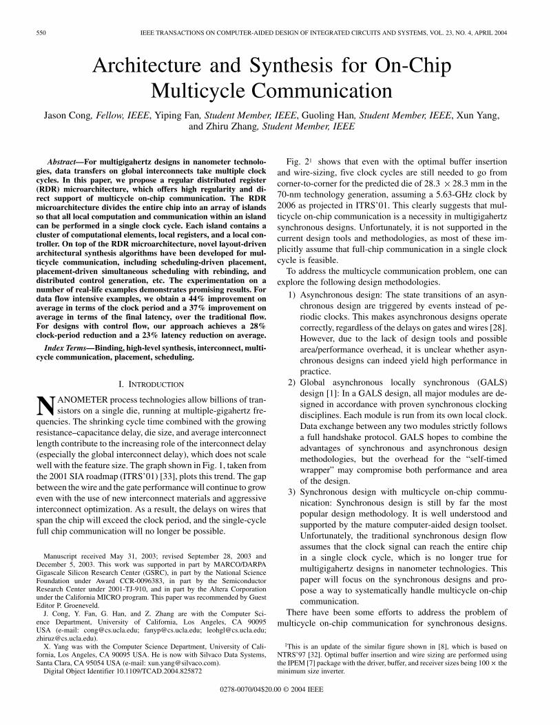
quencies. The shrinking cycle time combined with the growingresistance–capacitance delay, die size, and average interconnectlength contribute to the increasing role of the interconnect delay(especially the global interconnect delay), which does not scalewell with the feature size. The graph shown in Fig. 1, taken fromthe 2001 SIA roadmap (ITRS’01) [33], plots this trend. The gapbetween the wire and the gate performance will continue to groweven with the use of new interconnect materials and aggressiveinterconnect optimization. As a result, the delays on wires thatspan the chip will exceed the clock period, and the single-cyclefull chip communication will no longer be possible.
Manuscript received May 31, 2003; revised September 28, 2003 andDecember 5, 2003. This work was supported in part by MARCO/DARPAGigascale Silicon Research Center (GSRC), in part by the National ScienceFoundation under Award CCR-0096383, in part by the SemiconductorResearch Center under 2001-TJ-910, and in part by the Altera Corporationunder the California MICRO program. This paper was recommended by GuestEditor P. Groeneveld.
J. Cong, Y. Fan, G. Han, and Z. Zhang are with the Computer Sci-ence Department, University of California, Los Angeles, CA 90095USA (e-mail: [email protected]; [email protected]; [email protected];[email protected]).
X. Yang was with the Computer Science Department, University of Cali-fornia, Los Angeles, CA 90095 USA. He is now with Silvaco Data Systems,Santa Clara, CA 95054 USA (e-mail: [email protected]).
Digital Object Identifier 10.1109/TCAD.2004.825872
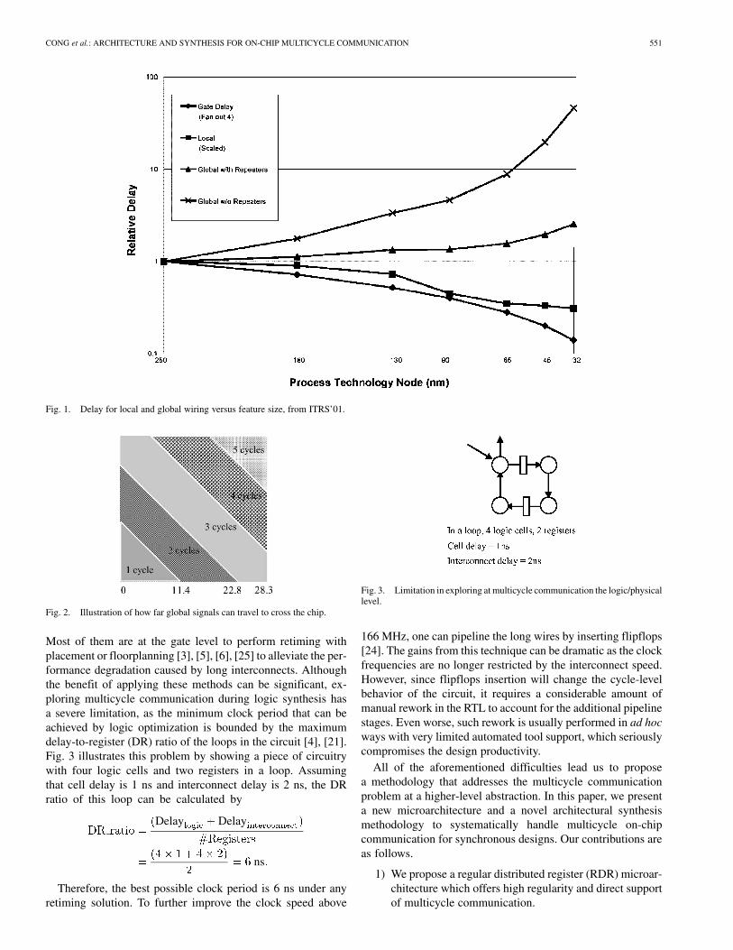
Fig. 21 shows that even with the optimal buffer insertionand wire-sizing, five clock cycles are still needed to go fromcorner-to-corner for the predicted die of 28.3 28.3 mm in the70-nm technology generation, assuming a 5.63-GHz clock by2006 as projected in ITRS’01. This clearly suggests that mul-ticycle on-chip communication is a necessity in multigigahertzsynchronous designs. Unfortunately, it is not supported in thecurrent design tools and methodologies, as most of these im-plicitly assume that full-chip communication in a single clockcycle is feasible.
To address the multicycle communication problem, one canexplore the following design methodologies.
1) Asynchronous design: The state transitions of an asyn-chronous design are triggered by events instead of pe-riodic clocks. This makes asynchronous designs operatecorrectly, regardless of the delays on gates and wires [28].However, due to the lack of design tools and possiblearea/performance overhead, it is unclear whether asyn-chronous designs can indeed yield high performance inpractice.
2) Global asynchronous locally synchronous (GALS)design [1]: In a GALS design, all major modules are de-signed in accordance with proven synchronous clockingdisciplines. Each module is run from its own local clock.Data exchange between any two modules strictly followsa full handshake protocol. GALS hopes to combine theadvantages of synchronous and asynchronous designmethodologies, but the overhead for the “self-timedwrapper” may compromise both performance and areaof the design.
3) Synchronous design with multicycle on-chip commu-nication: Synchronous design is still by far the mostpopular design methodology. It is well understood andsupported by the mature computer-aided design toolset.Unfortunately, the traditional synchronous design flowassumes that the clock signal can reach the entire chipin a single clock cycle, which is no longer true formultigigahertz designs in nanometer technologies. Thispaper will focus on the synchronous designs and pro-pose a way to systematically handle multicycle on-chipcommunication.
There have been some efforts to address the problem ofmulticycle on-chip communication for synchronous designs.
1This is an update of the similar figure shown in [8], which is based onNTRS’97 [32]. Optimal buffer insertion and wire sizing are performed usingthe IPEM [7] package with the driver, buffer, and receiver sizes being 100� theminimum size inverter.
0278-0070/04$20.00 © 2004 IEEE
CONG et al.: ARCHITECTURE AND SYNTHESIS FOR ON-CHIP MULTICYCLE COMMUNICATION 551
Fig. 1. Delay for local and global wiring versus feature size, from ITRS’01.
Fig. 2. Illustration of how far global signals can travel to cross the chip.
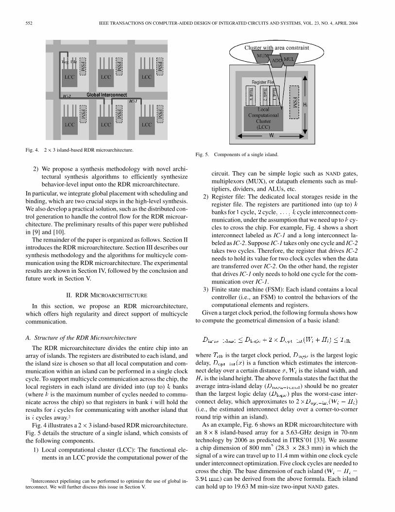
Most of them are at the gate level to perform retiming withplacement or floorplanning [3], [5], [6], [25] to alleviate the per-formance degradation caused by long interconnects. Althoughthe benefit of applying these methods can be significant, ex-ploring multicycle communication during logic synthesis hasa severe limitation, as the minimum clock period that can beachieved by logic optimization is bounded by the maximumdelay-to-register (DR) ratio of the loops in the circuit [4], [21].Fig. 3 illustrates this problem by showing a piece of circuitrywith four logic cells and two registers in a loop. Assumingthat cell delay is 1 ns and interconnect delay is 2 ns, the DRratio of this loop can be calculated by
Delay Delay
ns
Therefore, the best possible clock period is 6 ns under anyretiming solution. To further improve the clock speed above
Fig. 3. Limitation in exploring at multicycle communication the logic/physicallevel.
166 MHz, one can pipeline the long wires by inserting flipflops[24]. The gains from this technique can be dramatic as the clockfrequencies are no longer restricted by the interconnect speed.However, since flipflops insertion will change the cycle-levelbehavior of the circuit, it requires a considerable amount ofmanual rework in the RTL to account for the additional pipelinestages. Even worse, such rework is usually performed in ad hocways with very limited automated tool support, which seriouslycompromises the design productivity.
All of the aforementioned difficulties lead us to proposea methodology that addresses the multicycle communicationproblem at a higher-level abstraction. In this paper, we presenta new microarchitecture and a novel architectural synthesismethodology to systematically handle multicycle on-chipcommunication for synchronous designs. Our contributions areas follows.
1) We propose a regular distributed register (RDR) microar-chitecture which offers high regularity and direct supportof multicycle communication.
552 IEEE TRANSACTIONS ON COMPUTER-AIDED DESIGN OF INTEGRATED CIRCUITS AND SYSTEMS, VOL. 23, NO. 4, APRIL 2004
Fig. 4. 2� 3 island-based RDR microarchitecture.
2) We propose a synthesis methodology with novel archi-tectural synthesis algorithms to efficiently synthesizebehavior-level input onto the RDR microarchitecture.
In particular, we integrate global placement with scheduling andbinding, which are two crucial steps in the high-level synthesis.We also develop a practical solution, such as the distributed con-trol generation to handle the control flow for the RDR microar-chitecture. The preliminary results of this paper were publishedin [9] and [10].
The remainder of the paper is organized as follows. Section IIintroduces the RDR microarchitecture. Section III describes oursynthesis methodology and the algorithms for multicycle com-munication using the RDR microarchitecture. The experimentalresults are shown in Section IV, followed by the conclusion andfuture work in Section V.
II. RDR MICROARCHITECTURE
In this section, we propose an RDR microarchitecture,which offers high regularity and direct support of multicyclecommunication.
A. Structure of the RDR Microarchitecture
The RDR microarchitecture divides the entire chip into anarray of islands. The registers are distributed to each island, andthe island size is chosen so that all local computation and com-munication within an island can be performed in a single clockcycle. To support multicycle communication across the chip, thelocal registers in each island are divided into (up to) banks(where is the maximum number of cycles needed to commu-nicate across the chip) so that registers in bank will hold theresults for cycles for communicating with another island thatis cycles away.2
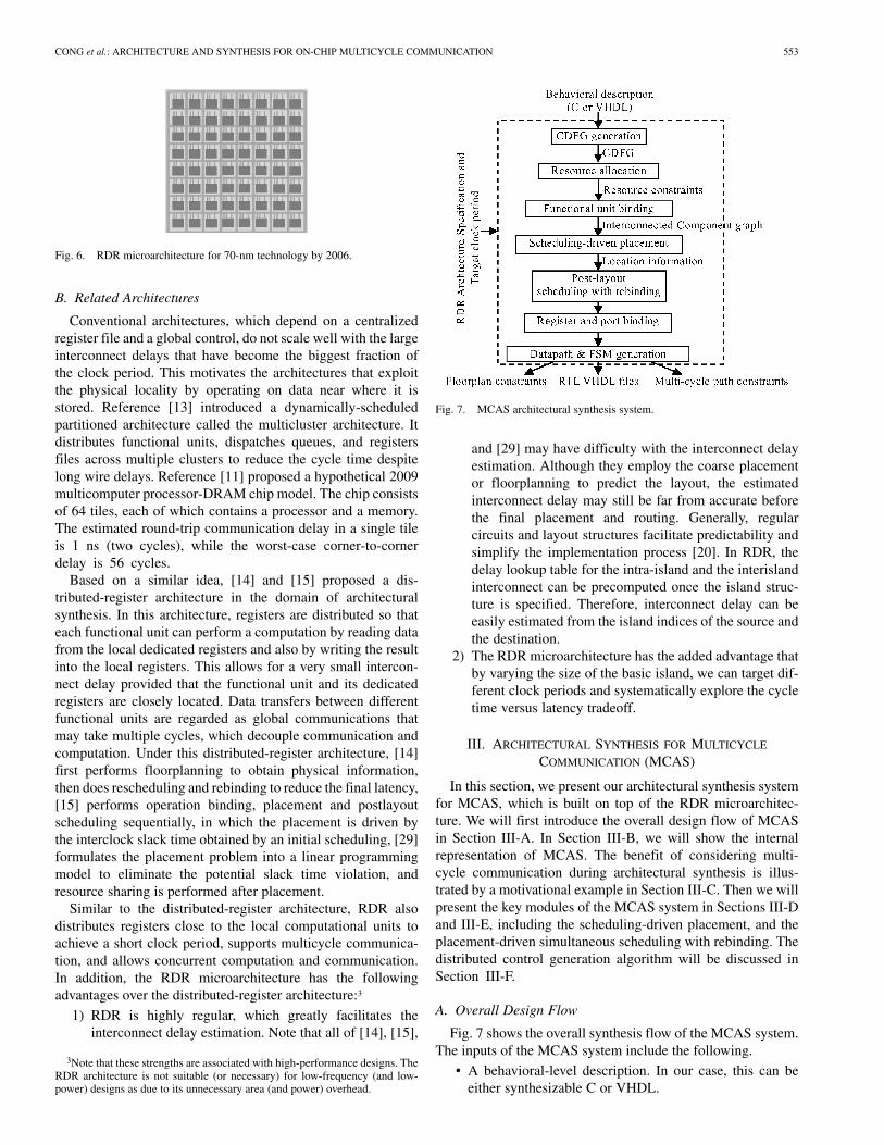
Fig. 4 illustrates a 2 3 island-based RDR microarchitecture.Fig. 5 details the structure of a single island, which consists ofthe following components.
1) Local computational cluster (LCC): The functional ele-ments in an LCC provide the computational power of the
2Interconnect pipelining can be performed to optimize the use of global in-terconnect. We will further discuss this issue in Section V.
Fig. 5. Components of a single island.
circuit. They can be simple logic such as NAND gates,multiplexors (MUX), or datapath elements such as mul-tipliers, dividers, and ALUs, etc.
2) Register file: The dedicated local storages reside in theregister file. The registers are partitioned into (up to)banks for cycle cycle cycle interconnect com-munication, under the assumption that we need up to cy-cles to cross the chip. For example, Fig. 4 shows a shortinterconnect labeled as IC-1 and a long interconnect la-beled as IC-2. Suppose IC-1 takes only one cycle and IC-2takes two cycles. Therefore, the register that drives IC-2needs to hold its value for two clock cycles when the dataare transferred over IC-2. On the other hand, the registerthat drives IC-1 only needs to hold one cycle for the com-munication over IC-1.
3) Finite state machine (FSM): Each island contains a localcontroller (i.e., an FSM) to control the behaviors of thecomputational elements and registers.
Given a target clock period, the following formula shows howto compute the geometrical dimension of a basic island:
where is the target clock period, is the largest logicdelay, is a function which estimates the intercon-nect delay over a certain distance , is the island width, and
is the island height. The above formula states the fact that theaverage intra-island delay ( ) should be no greaterthan the largest logic delay ( ) plus the worst-case inter-connect delay, which approximates to 2(i.e., the estimated interconnect delay over a corner-to-cornerround trip within an island).
As an example, Fig. 6 shows an RDR microarchitecture withan 8 8 island-based array for a 5.63-GHz design in 70-nmtechnology by 2006 as predicted in ITRS’01 [33]. We assumea chip dimension of 800 mm (28.3 28.3 mm) in which thesignal of a wire can travel up to 11.4 mm within one clock cycleunder interconnect optimization. Five clock cycles are needed tocross the chip. The base dimension of each island (
) can be derived from the above formula. Each islandcan hold up to 19.63 M min-size two-input NAND gates.
CONG et al.: ARCHITECTURE AND SYNTHESIS FOR ON-CHIP MULTICYCLE COMMUNICATION 553
Fig. 6. RDR microarchitecture for 70-nm technology by 2006.
B. Related Architectures
Conventional architectures, which depend on a centralizedregister file and a global control, do not scale well with the largeinterconnect delays that have become the biggest fraction ofthe clock period. This motivates the architectures that exploitthe physical locality by operating on data near where it isstored. Reference [13] introduced a dynamically-scheduledpartitioned architecture called the multicluster architecture. Itdistributes functional units, dispatches queues, and registersfiles across multiple clusters to reduce the cycle time despitelong wire delays. Reference [11] proposed a hypothetical 2009multicomputer processor-DRAM chip model. The chip consistsof 64 tiles, each of which contains a processor and a memory.The estimated round-trip communication delay in a single tileis 1 ns (two cycles), while the worst-case corner-to-cornerdelay is 56 cycles.
Based on a similar idea, [14] and [15] proposed a dis-tributed-register architecture in the domain of architecturalsynthesis. In this architecture, registers are distributed so thateach functional unit can perform a computation by reading datafrom the local dedicated registers and also by writing the resultinto the local registers. This allows for a very small intercon-nect delay provided that the functional unit and its dedicatedregisters are closely located. Data transfers between differentfunctional units are regarded as global communications thatmay take multiple cycles, which decouple communication andcomputation. Under this distributed-register architecture, [14]first performs floorplanning to obtain physical information,then does rescheduling and rebinding to reduce the final latency,[15] performs operation binding, placement and postlayoutscheduling sequentially, in which the placement is driven bythe interclock slack time obtained by an initial scheduling, [29]formulates the placement problem into a linear programmingmodel to eliminate the potential slack time violation, andresource sharing is performed after placement.
Similar to the distributed-register architecture, RDR alsodistributes registers close to the local computational units toachieve a short clock period, supports multicycle communica-tion, and allows concurrent computation and communication.In addition, the RDR microarchitecture has the followingadvantages over the distributed-register architecture:3
1) RDR is highly regular, which greatly facilitates theinterconnect delay estimation. Note that all of [14], [15],
3Note that these strengths are associated with high-performance designs. TheRDR architecture is not suitable (or necessary) for low-frequency (and low-power) designs as due to its unnecessary area (and power) overhead.
Fig. 7. MCAS architectural synthesis system.
and [29] may have difficulty with the interconnect delayestimation. Although they employ the coarse placementor floorplanning to predict the layout, the estimatedinterconnect delay may still be far from accurate beforethe final placement and routing. Generally, regularcircuits and layout structures facilitate predictability andsimplify the implementation process [20]. In RDR, thedelay lookup table for the intra-island and the interislandinterconnect can be precomputed once the island struc-ture is specified. Therefore, interconnect delay can beeasily estimated from the island indices of the source andthe destination.
2) The RDR microarchitecture has the added advantage thatby varying the size of the basic island, we can target dif-ferent clock periods and systematically explore the cycletime versus latency tradeoff.
III. ARCHITECTURAL SYNTHESIS FOR MULTICYCLE
COMMUNICATION (MCAS)
In this section, we present our architectural synthesis systemfor MCAS, which is built on top of the RDR microarchitec-ture. We will first introduce the overall design flow of MCASin Section III-A. In Section III-B, we will show the internalrepresentation of MCAS. The benefit of considering multi-cycle communication during architectural synthesis is illus-trated by a motivational example in Section III-C. Then we willpresent the key modules of the MCAS system in Sections III-Dand III-E, including the scheduling-driven placement, and theplacement-driven simultaneous scheduling with rebinding. Thedistributed control generation algorithm will be discussed inSection III-F.
A. Overall Design Flow
Fig. 7 shows the overall synthesis flow of the MCAS system.The inputs of the MCAS system include the following.
• A behavioral-level description. In our case, this can beeither synthesizable C or VHDL.
554 IEEE TRANSACTIONS ON COMPUTER-AIDED DESIGN OF INTEGRATED CIRCUITS AND SYSTEMS, VOL. 23, NO. 4, APRIL 2004
• A target clock period. This is optional because MCAS willtry to find the best possible cycle time by binary search ifthe user does not provide it.
• A resource library, which defines the available functionalunits, on-chip memories, and registers, etc.
• The island structure and the delay lookup table of the RDRmicroarchitecture, which can be derived from the afore-mentioned formula once the target clock period is set.
At the front end, MCAS first generates the control dataflow graph (CDFG) from the behavioral descriptions throughthe intermediate representations of the SUIF compiler infra-structure [37] and Machine-SUIF [26]. Based on the CDFG,MCAS performs resource allocation, followed by an initialfunctional unit binding. The objective of resource allocationis to minimize the resource usage (e.g., functional units, reg-isters, etc.) without violating the timing constraint. It uses thetime-constrained force-directed scheduling algorithm [22] toobtain the resource allocation. After the resource allocation,it employs an algorithm proposed in [15] to bind operationnodes to functional units for minimizing the potential globaldata transfers. An interconnected component graph (ICG) isderived from the bound CDFG. An ICG consists of a set ofcomponents (i.e., functional units) to which operation nodesare bound. They are interconnected by a set of connectionsthat denote data transfers between components.
At the core, MCAS performs the scheduling-driven place-ment, which takes the ICG as input, places the components inthe island structure of the RDR microarchitecture, and returnsthe island index of each component. After the scheduling-drivenplacement, both the CDFG schedule and the layout informa-tion are produced. To further minimize the schedule latency, itperforms placement-driven scheduling with rebinding. The al-gorithm is based on the force-directed list-scheduling (FDLS)framework, and is integrated with simultaneous rebinding.
At the back end, MCAS performs register and port bindingfollowed by datapath and distributed controller generation. Thefinal outputs of MCAS include:
• A datapath in structural VHDL format and a set ofdistributed controllers in behavioral FSM style. TheseRT-level VHDL files will be fed into logic synthesis tools.
• Floorplan and multicycle path constraints for the down-stream place-and-route tools.
B. Internal Representation
A two-level CDFG representation is used in MCAS. Thefirst-level CDFG is a Control Flow Graph (CFG). Each nodecorresponds to a basic block. The edges represent the con-trol dependencies between the basic blocks. Each basic blockcontains, at most, one operation producing the control signal.If there are two successors, the labels on the control edgesindicate which branch is the fall-through path and which oneis the taken path.
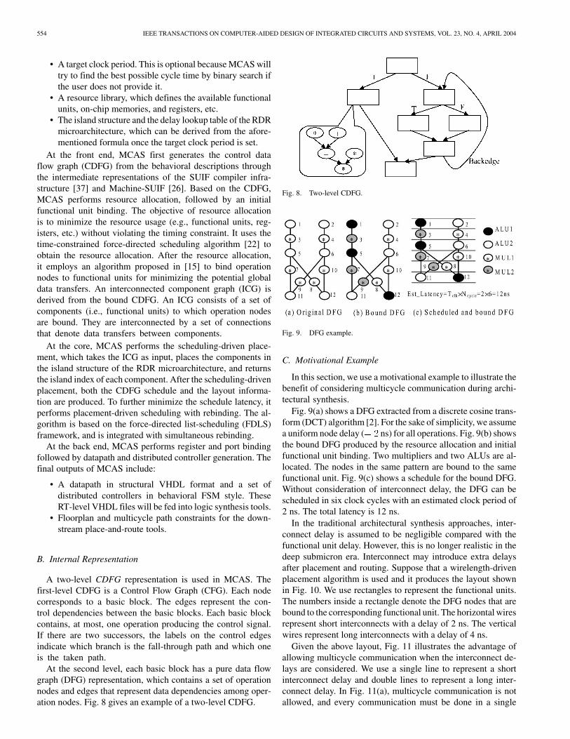
At the second level, each basic block has a pure data flowgraph (DFG) representation, which contains a set of operationnodes and edges that represent data dependencies among oper-ation nodes. Fig. 8 gives an example of a two-level CDFG.
Fig. 8. Two-level CDFG.
Fig. 9. DFG example.
C. Motivational Example
In this section, we use a motivational example to illustrate thebenefit of considering multicycle communication during archi-tectural synthesis.
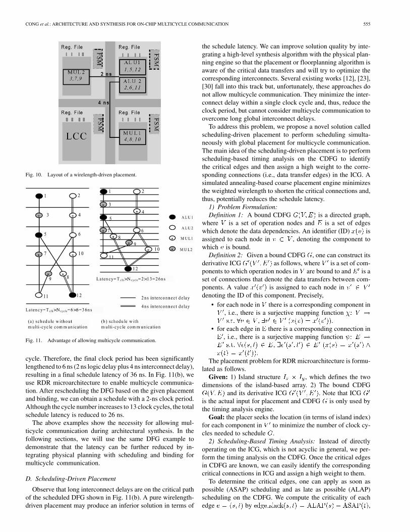
Fig. 9(a) shows a DFG extracted from a discrete cosine trans-form (DCT) algorithm [2]. For the sake of simplicity, we assumea uniform node delay ( ns) for all operations. Fig. 9(b) showsthe bound DFG produced by the resource allocation and initialfunctional unit binding. Two multipliers and two ALUs are al-located. The nodes in the same pattern are bound to the samefunctional unit. Fig. 9(c) shows a schedule for the bound DFG.Without consideration of interconnect delay, the DFG can bescheduled in six clock cycles with an estimated clock period of2 ns. The total latency is 12 ns.
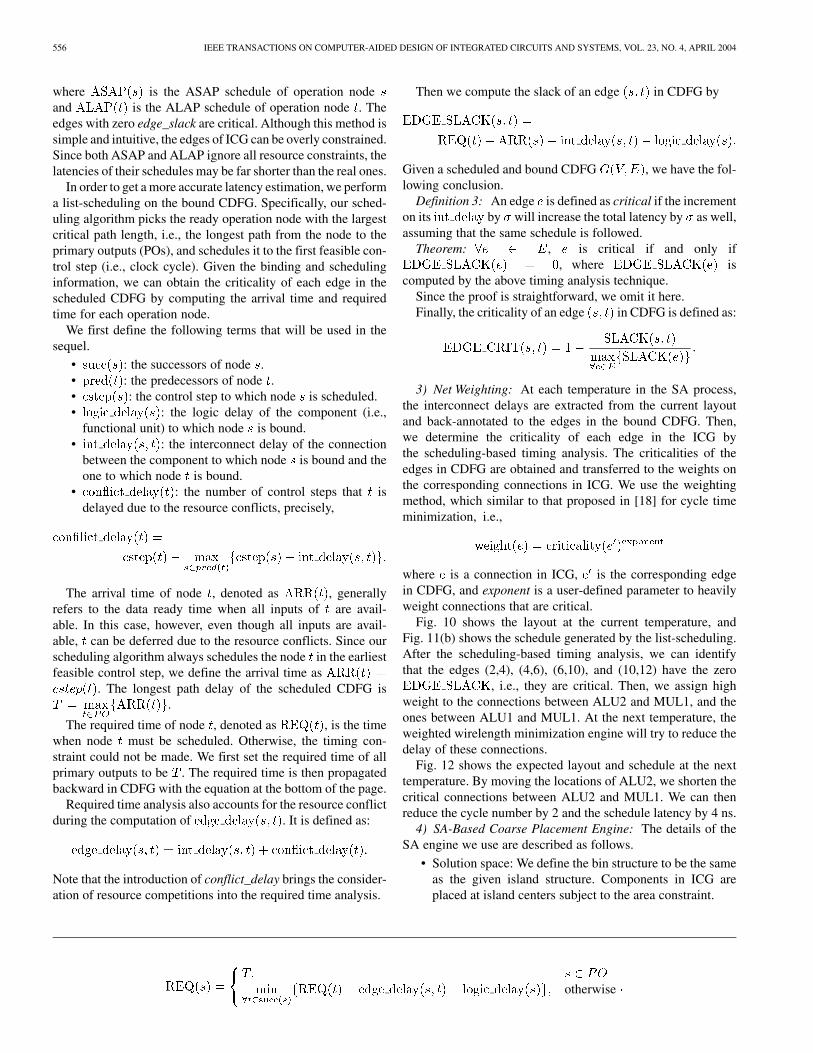
In the traditional architectural synthesis approaches, inter-connect delay is assumed to be negligible compared with thefunctional unit delay. However, this is no longer realistic in thedeep submicron era. Interconnect may introduce extra delaysafter placement and routing. Suppose that a wirelength-drivenplacement algorithm is used and it produces the layout shownin Fig. 10. We use rectangles to represent the functional units.The numbers inside a rectangle denote the DFG nodes that arebound to the corresponding functional unit. The horizontal wiresrepresent short interconnects with a delay of 2 ns. The verticalwires represent long interconnects with a delay of 4 ns.
Given the above layout, Fig. 11 illustrates the advantage ofallowing multicycle communication when the interconnect de-lays are considered. We use a single line to represent a shortinterconnect delay and double lines to represent a long inter-connect delay. In Fig. 11(a), multicycle communication is notallowed, and every communication must be done in a single
CONG et al.: ARCHITECTURE AND SYNTHESIS FOR ON-CHIP MULTICYCLE COMMUNICATION 555
Fig. 10. Layout of a wirelength-driven placement.
Fig. 11. Advantage of allowing multicycle communication.
cycle. Therefore, the final clock period has been significantlylengthened to 6 ns (2 ns logic delay plus 4 ns interconnect delay),resulting in a final schedule latency of 36 ns. In Fig. 11(b), weuse RDR microarchitecture to enable multicycle communica-tion. After rescheduling the DFG based on the given placementand binding, we can obtain a schedule with a 2-ns clock period.Although the cycle number increases to 13 clock cycles, the totalschedule latency is reduced to 26 ns.
The above examples show the necessity for allowing mul-ticycle communication during architectural synthesis. In thefollowing sections, we will use the same DFG example todemonstrate that the latency can be further reduced by in-tegrating physical planning with scheduling and binding formulticycle communication.
D. Scheduling-Driven Placement
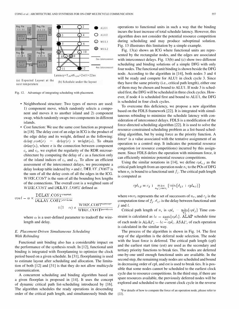
Observe that long interconnect delays are on the critical pathof the scheduled DFG shown in Fig. 11(b). A pure wirelength-driven placement may produce an inferior solution in terms of
the schedule latency. We can improve solution quality by inte-grating a high-level synthesis algorithm with the physical plan-ning engine so that the placement or floorplanning algorithm isaware of the critical data transfers and will try to optimize thecorresponding interconnects. Several existing works [12], [23],[30] fall into this track but, unfortunately, these approaches donot allow multicycle communication. They minimize the inter-connect delay within a single clock cycle and, thus, reduce theclock period, but cannot consider multicycle communication toovercome long global interconnect delays.
To address this problem, we propose a novel solution calledscheduling-driven placement to perform scheduling simulta-neously with global placement for multicycle communication.The main idea of the scheduling-driven placement is to performscheduling-based timing analysis on the CDFG to identifythe critical edges and then assign a high weight to the corre-sponding connections (i.e., data transfer edges) in the ICG. Asimulated annealing-based coarse placement engine minimizesthe weighted wirelength to shorten the critical connections and,thus, potentially reduces the schedule latency.
1) Problem Formulation:Definition 1: A bound CDFG is a directed graph,
where is a set of operation nodes and is a set of edgeswhich denote the data dependencies. An identifier (ID) isassigned to each node in , denoting the component towhich is bound.
Definition 2: Given a bound CDFG , one can construct itsderivative ICG as follows, where is a set of com-ponents to which operation nodes in are bound to and is aset of connections that denote the data transfers between com-ponents. A value is assigned to each node indenoting the ID of this component. Precisely,
• for each node in there is a corresponding component in, i.e., there is a surjective mapping function
, .• for each edge in there is a corresponding connection in
, i.e., there is a surjective mapping function,
.The placement problem for RDR microarchitecture is formu-
lated as follows.Given: 1) Island structure , which defines the two
dimensions of the island-based array. 2) The bound CDFGand its derivative ICG . Note that ICG
is the actual input for placement and CDFG is only used bythe timing analysis engine.
Goal: the placer seeks the location (in terms of island index)for each component in to minimize the number of clock cy-cles needed to schedule .
2) Scheduling-Based Timing Analysis: Instead of directlyoperating on the ICG, which is not acyclic in general, we per-form the timing analysis on the CDFG. Once the critical edgesin CDFG are known, we can easily identify the correspondingcritical connections in ICG and assign a high weight to them.
To determine the critical edges, one can apply as soon aspossible (ASAP) scheduling and as late as possible (ALAP)scheduling on the CDFG. We compute the criticality of eachedge by ,
556 IEEE TRANSACTIONS ON COMPUTER-AIDED DESIGN OF INTEGRATED CIRCUITS AND SYSTEMS, VOL. 23, NO. 4, APRIL 2004
where is the ASAP schedule of operation nodeand is the ALAP schedule of operation node . Theedges with zero edge_slack are critical. Although this method issimple and intuitive, the edges of ICG can be overly constrained.Since both ASAP and ALAP ignore all resource constraints, thelatencies of their schedules may be far shorter than the real ones.
In order to get a more accurate latency estimation, we performa list-scheduling on the bound CDFG. Specifically, our sched-uling algorithm picks the ready operation node with the largestcritical path length, i.e., the longest path from the node to theprimary outputs (POs), and schedules it to the first feasible con-trol step (i.e., clock cycle). Given the binding and schedulinginformation, we can obtain the criticality of each edge in thescheduled CDFG by computing the arrival time and requiredtime for each operation node.
We first define the following terms that will be used in thesequel.
• : the successors of node .• : the predecessors of node .• : the control step to which node is scheduled.• : the logic delay of the component (i.e.,
functional unit) to which node is bound.• : the interconnect delay of the connection
between the component to which node is bound and theone to which node is bound.
• : the number of control steps that isdelayed due to the resource conflicts, precisely,
The arrival time of node , denoted as , generallyrefers to the data ready time when all inputs of are avail-able. In this case, however, even though all inputs are avail-able, can be deferred due to the resource conflicts. Since ourscheduling algorithm always schedules the node in the earliestfeasible control step, we define the arrival time as
. The longest path delay of the scheduled CDFG is.
The required time of node , denoted as , is the timewhen node must be scheduled. Otherwise, the timing con-straint could not be made. We first set the required time of allprimary outputs to be . The required time is then propagatedbackward in CDFG with the equation at the bottom of the page.
Required time analysis also accounts for the resource conflictduring the computation of . It is defined as:
Note that the introduction of conflict_delay brings the consider-ation of resource competitions into the required time analysis.
Then we compute the slack of an edge in CDFG by
Given a scheduled and bound CDFG , we have the fol-lowing conclusion.
Definition 3: An edge is defined as critical if the incrementon its by will increase the total latency by as well,assuming that the same schedule is followed.
Theorem: , is critical if and only if, where is
computed by the above timing analysis technique.Since the proof is straightforward, we omit it here.Finally, the criticality of an edge in CDFG is defined as:
3) Net Weighting: At each temperature in the SA process,the interconnect delays are extracted from the current layoutand back-annotated to the edges in the bound CDFG. Then,we determine the criticality of each edge in the ICG bythe scheduling-based timing analysis. The criticalities of theedges in CDFG are obtained and transferred to the weights onthe corresponding connections in ICG. We use the weightingmethod, which similar to that proposed in [18] for cycle timeminimization, i.e.,
where is a connection in ICG, is the corresponding edgein CDFG, and exponent is a user-defined parameter to heavilyweight connections that are critical.
Fig. 10 shows the layout at the current temperature, andFig. 11(b) shows the schedule generated by the list-scheduling.After the scheduling-based timing analysis, we can identifythat the edges (2,4), (4,6), (6,10), and (10,12) have the zero
, i.e., they are critical. Then, we assign highweight to the connections between ALU2 and MUL1, and theones between ALU1 and MUL1. At the next temperature, theweighted wirelength minimization engine will try to reduce thedelay of these connections.
Fig. 12 shows the expected layout and schedule at the nexttemperature. By moving the locations of ALU2, we shorten thecritical connections between ALU2 and MUL1. We can thenreduce the cycle number by 2 and the schedule latency by 4 ns.
4) SA-Based Coarse Placement Engine: The details of theSA engine we use are described as follows.
• Solution space: We define the bin structure to be the sameas the given island structure. Components in ICG areplaced at island centers subject to the area constraint.
otherwise
CONG et al.: ARCHITECTURE AND SYNTHESIS FOR ON-CHIP MULTICYCLE COMMUNICATION 557
Fig. 12. Advantage of integrating scheduling with placement.
• Neighborhood structure: Two types of moves are used:1) component move, which randomly selects a compo-nent and moves it to another island and 2) componentswap, which randomly swaps two components in differentislands.
• Cost function: We use the same cost function as proposedin [18]. The delay cost of an edge in ICG is the product ofthe edge delay and its weight, defined as the following:
. To obtain, where is the connection between component
and , we exploit the regularity of the RDR microar-chitecture by computing the delay of as a function onlyof the island indices of and . To allow an efficientassessment of the interconnect delays, we precompute adelay lookup table indexed by and . isthe sum of all the delay costs of all the edges in the ICG.
is the sum of all the bounding box lengthsof the connections. The overall cost is a weighted sum of
and defined as
where is a user-defined parameter to tradeoff the wire-length and delay.
E. Placement-Driven Simultaneous SchedulingWith Rebinding
Functional unit binding also has a considerable impact onthe performance of the synthesis result. In [12], functional unitbinding is integrated with floorplanning to optimize the clockperiod based on a given schedule. In [31], floorplanning is usedto estimate layout after scheduling and allocation. The limita-tion of both [12] and [31] is that they do not allow multicyclecommunication.
A concurrent scheduling and binding algorithm based ona given floorplan is proposed in [14]. It uses the conceptof dynamic critical path list-scheduling introduced by [16].The algorithm schedules the ready operations in descendingorder of the critical path length, and simultaneously binds the
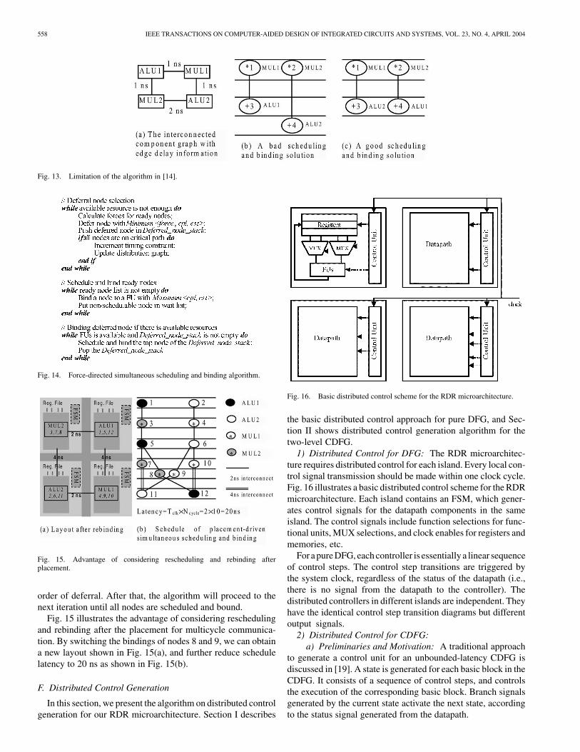
operations to functional units in such a way that the bindingincurs the least increase of total schedule latency. However, thisalgorithm does not consider the potential resource competitionduring scheduling and may produce suboptimal solution.Fig. 13 illustrates this limitation by a simple example.
Fig. 13(a) shows an ICG where functional units are repre-sented by the rectangular nodes, and the edges are associatedwith interconnect delays. Fig. 13(b) and (c) show two differentscheduling and binding solutions of a simple DFG with onlyfour nodes. The functional unit binding is shown beside the DFGnode. According to the algorithm in [14], both nodes 3 and 4will be ready and compete for ALU1 in clock cycle 3. Sincethey have the same priority (i.e., critical path length), either oneof them may be chosen and bound to ALU1. If node 3 is sched-uled first, the DFG will be scheduled in three clock cycles. How-ever, if node 4 is scheduled first and bound to ALU1, the DFGis scheduled in four clock cycles.
To overcome this deficiency, we propose a new algorithmbased on the FDLS framework [22]. It is integrated with simul-taneous rebinding to minimize the schedule latency with con-sideration of interconnect delays. FDLS is a modification of theforce-directed scheduling algorithm [22]. It is used to solve theresource-constrained scheduling problem as a list-based sched-uling algorithm, but by using force as the priority function. Aforce4 is a value associated with the tentative assignment of anoperation to a control step. It indicates the potential resourcecongestion (or resource competitions) incurred by this assign-ment. Since FDLS defers the operation with minimum force, itcan efficiently minimize potential resource competitions.
Using the similar notations in [14], we define as thecritical path length from an operation node to the POs of DFGwhen is bound to a functional unit . The critical path lengthis computed as
where represents the set of successors of , and is thecomputation time of . is the delay between functional unit
and .Critical path length of is Time con-
straint is calculated as . schedule time
of each node is . of each operationis calculated in the similar way.
The process of the algorithm is shown in Fig. 14. The firststep of the algorithm is the deferral node selection. The nodewith the least force is deferred. The critical path length (cpl)and the earliest start time (est) are used as the secondary andtertiary priority functions to break ties. The nodes are deferredone-by-one until enough functional units are available. In thesecond step, the remaining ready nodes are scheduled and boundin decreasing order of cpl, and est is used to break ties. It is pos-sible that some nodes cannot be scheduled to the earliest clockcycle due to resource competitions. In the third step, if there arespare resources available, the previously deferred nodes will beexplored and scheduled to the current clock cycle in the reverse
4For details of how to compute the force of an operation node, please refer to[22].
558 IEEE TRANSACTIONS ON COMPUTER-AIDED DESIGN OF INTEGRATED CIRCUITS AND SYSTEMS, VOL. 23, NO. 4, APRIL 2004
Fig. 13. Limitation of the algorithm in [14].
Fig. 14. Force-directed simultaneous scheduling and binding algorithm.
Fig. 15. Advantage of considering rescheduling and rebinding afterplacement.
order of deferral. After that, the algorithm will proceed to thenext iteration until all nodes are scheduled and bound.
Fig. 15 illustrates the advantage of considering reschedulingand rebinding after the placement for multicycle communica-tion. By switching the bindings of nodes 8 and 9, we can obtaina new layout shown in Fig. 15(a), and further reduce schedulelatency to 20 ns as shown in Fig. 15(b).
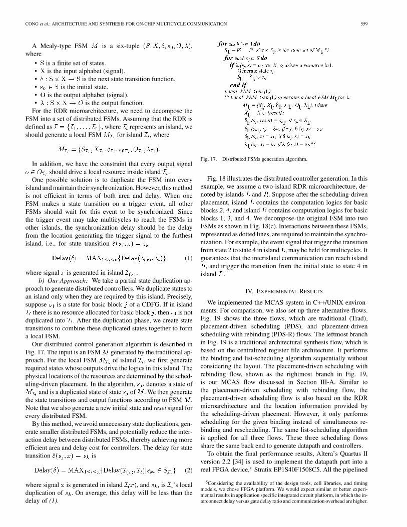
F. Distributed Control Generation
In this section, we present the algorithm on distributed controlgeneration for our RDR microarchitecture. Section I describes
Fig. 16. Basic distributed control scheme for the RDR microarchitecture.
the basic distributed control approach for pure DFG, and Sec-tion II shows distributed control generation algorithm for thetwo-level CDFG.
1) Distributed Control for DFG: The RDR microarchitec-ture requires distributed control for each island. Every local con-trol signal transmission should be made within one clock cycle.Fig. 16 illustrates a basic distributed control scheme for the RDRmicroarchitecture. Each island contains an FSM, which gener-ates control signals for the datapath components in the sameisland. The control signals include function selections for func-tional units, MUX selections, and clock enables for registers andmemories, etc.
For a pure DFG, each controller is essentially a linear sequenceof control steps. The control step transitions are triggered bythe system clock, regardless of the status of the datapath (i.e.,there is no signal from the datapath to the controller). Thedistributed controllers in different islands are independent. Theyhave the identical control step transition diagrams but differentoutput signals.
2) Distributed Control for CDFG:a) Preliminaries and Motivation: A traditional approach
to generate a control unit for an unbounded-latency CDFG isdiscussed in [19]. A state is generated for each basic block in theCDFG. It consists of a sequence of control steps, and controlsthe execution of the corresponding basic block. Branch signalsgenerated by the current state activate the next state, accordingto the status signal generated from the datapath.
CONG et al.: ARCHITECTURE AND SYNTHESIS FOR ON-CHIP MULTICYCLE COMMUNICATION 559
A Mealy-type FSM is a six-tuple ,where
• is a finite set of states.• is the input alphabet (signal).• is the next state transition function.• is the initial state.• is the output alphabet (signal).• is the output function.
For the RDR microarchitecture, we need to decompose theFSM into a set of distributed FSMs. Assuming that the RDR isdefined as , where represents an island, weshould generate a local FSM for island , where
In addition, we have the constraint that every output signalshould drive a local resource inside island .
One possible solution is to duplicate the FSM into everyisland and maintain their synchronization. However, this methodis not efficient in terms of both area and delay. When oneFSM makes a state transition on a trigger event, all otherFSMs should wait for this event to be synchronized. Sincethe trigger event may take multicycles to reach the FSMs inother islands, the synchronization delay should be the delayfrom the location generating the trigger signal to the furthestisland, i.e., for state transition
(1)
where signal is generated in island .b) Our Approach: We take a partial state duplication ap-
proach to generate distributed controllers. We duplicate states toan island only when they are required by this island. Precisely,suppose is a state for basic block of a CDFG. If in island
there is no resource allocated for basic block , then is notduplicated into . After the duplication phase, we create statetransitions to combine these duplicated states together to forma local FSM.
Our distributed control generation algorithm is described inFig. 17. The input is an FSM generated by the traditional ap-proach. For the local FSM of island , we first generaterequired states whose outputs drive the logics in this island. Thephysical locations of the resources are determined by the sched-uling-driven placement. In the algorithm, denotes a state of
and is a duplicated state of state of . We then generatethe state transitions and output functions according to FSM .Note that we also generate a new initial state and reset signal forevery distributed FSM.
By this method, we avoid unnecessary state duplications, gen-erate smaller distributed FSMs, and potentially reduce the inter-action delay between distributed FSMs, thereby achieving moreefficient area and delay cost for controllers. The delay for statetransition is
(2)
where signal is generated in island , and is ’s localduplication of . On average, this delay will be less than thedelay of (1).
Fig. 17. Distributed FSMs generation algorithm.
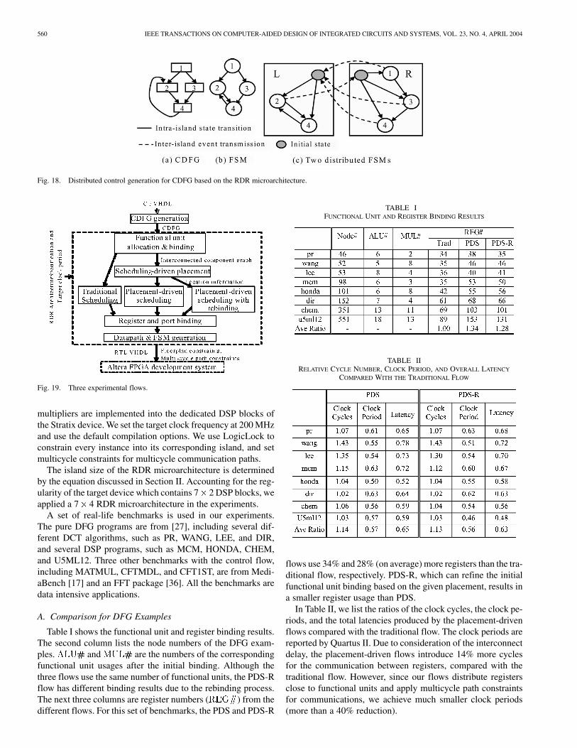
Fig. 18 illustrates the distributed controller generation. In thisexample, we assume a two-island RDR microarchitecture, de-noted by islands and . Suppose after the scheduling-drivenplacement, island contains the computation logics for basicblocks 2, 4, and island contains computation logics for basicblocks 1, 3, and 4. We decompose the original FSM into twoFSMs as shown in Fig. 18(c). Interactions between these FSMs,represented as dotted lines, are required to maintain the synchro-nization. For example, the event signal that trigger the transitionfrom state 2 to state 4 in island , may be held for multicycles. Itguarantees that the interisland communication can reach island
, and trigger the transition from the initial state to state 4 inisland .
IV. EXPERIMENTAL RESULTS
We implemented the MCAS system in C++/UNIX environ-ments. For comparison, we also set up three alternative flows.Fig. 19 shows the three flows, which are traditional (Trad),placement-driven scheduling (PDS), and placement-drivenscheduling with rebinding (PDS-R) flows. The leftmost branchin Fig. 19 is a traditional architectural synthesis flow, which isbased on the centralized register file architecture. It performsthe binding and list-scheduling algorithm sequentially withoutconsidering the layout. The placement-driven scheduling withrebinding flow, shown as the rightmost branch in Fig. 19,is our MCAS flow discussed in Section III-A. Similar tothe placement-driven scheduling with rebinding flow, theplacement-driven scheduling flow is also based on the RDRmicroarchitecture and the location information provided bythe scheduling-driven placement. However, it only performsscheduling for the given binding instead of simultaneous re-binding and rescheduling. The same list-scheduling algorithmis applied for all three flows. These three scheduling flowsshare the same back end to generate datapath and controllers.
To obtain the final performance results, Altera’s Quartus IIversion 2.2 [34] is used to implement the datapath part into areal FPGA device,5 Stratix EP1S40F1508C5. All the pipelined
5Considering the availability of the design tools, cell libraries, and timingmodels, we chose FPGA platform. We would expect similar or better experi-mental results in application specific integrated circuit platform, in which the in-terconnect delay versus gate delay ratio and communication overhead are higher.
560 IEEE TRANSACTIONS ON COMPUTER-AIDED DESIGN OF INTEGRATED CIRCUITS AND SYSTEMS, VOL. 23, NO. 4, APRIL 2004
Fig. 18. Distributed control generation for CDFG based on the RDR microarchitecture.
Fig. 19. Three experimental flows.
multipliers are implemented into the dedicated DSP blocks ofthe Stratix device. We set the target clock frequency at 200 MHzand use the default compilation options. We use LogicLock toconstrain every instance into its corresponding island, and setmulticycle constraints for multicycle communication paths.
The island size of the RDR microarchitecture is determinedby the equation discussed in Section II. Accounting for the reg-ularity of the target device which contains 7 2 DSP blocks, weapplied a 7 4 RDR microarchitecture in the experiments.
A set of real-life benchmarks is used in our experiments.The pure DFG programs are from [27], including several dif-ferent DCT algorithms, such as PR, WANG, LEE, and DIR,and several DSP programs, such as MCM, HONDA, CHEM,and U5ML12. Three other benchmarks with the control flow,including MATMUL, CFTMDL, and CFT1ST, are from Medi-aBench [17] and an FFT package [36]. All the benchmarks aredata intensive applications.
A. Comparison for DFG Examples
Table I shows the functional unit and register binding results.The second column lists the node numbers of the DFG exam-ples. and are the numbers of the correspondingfunctional unit usages after the initial binding. Although thethree flows use the same number of functional units, the PDS-Rflow has different binding results due to the rebinding process.The next three columns are register numbers ( ) from thedifferent flows. For this set of benchmarks, the PDS and PDS-R
TABLE IFUNCTIONAL UNIT AND REGISTER BINDING RESULTS
TABLE IIRELATIVE CYCLE NUMBER, CLOCK PERIOD, AND OVERALL LATENCY
COMPARED WITH THE TRADITIONAL FLOW
flows use 34% and 28% (on average) more registers than the tra-ditional flow, respectively. PDS-R, which can refine the initialfunctional unit binding based on the given placement, results ina smaller register usage than PDS.
In Table II, we list the ratios of the clock cycles, the clock pe-riods, and the total latencies produced by the placement-drivenflows compared with the traditional flow. The clock periods arereported by Quartus II. Due to consideration of the interconnectdelay, the placement-driven flows introduce 14% more cyclesfor the communication between registers, compared with thetraditional flow. However, since our flows distribute registersclose to functional units and apply multicycle path constraintsfor communications, we achieve much smaller clock periods(more than a 40% reduction).
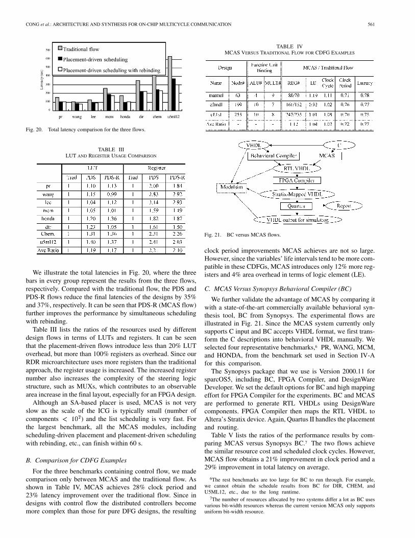
CONG et al.: ARCHITECTURE AND SYNTHESIS FOR ON-CHIP MULTICYCLE COMMUNICATION 561
Fig. 20. Total latency comparison for the three flows.
TABLE IIILUT AND REGISTER USAGE COMPARISON
We illustrate the total latencies in Fig. 20, where the threebars in every group represent the results from the three flows,respectively. Compared with the traditional flow, the PDS andPDS-R flows reduce the final latencies of the designs by 35%and 37%, respectively. It can be seen that PDS-R (MCAS flow)further improves the performance by simultaneous schedulingwith rebinding.
Table III lists the ratios of the resources used by differentdesign flows in terms of LUTs and registers. It can be seenthat the placement-driven flows introduce less than 20% LUToverhead, but more than 100% registers as overhead. Since ourRDR microarchitecture uses more registers than the traditionalapproach, the register usage is increased. The increased registernumber also increases the complexity of the steering logicstructure, such as MUXs, which contributes to an observablearea increase in the final layout, especially for an FPGA design.
Although an SA-based placer is used, MCAS is not veryslow as the scale of the ICG is typically small (number ofcomponents ) and the list scheduling is very fast. Forthe largest benchmark, all the MCAS modules, includingscheduling-driven placement and placement-driven schedulingwith rebinding, etc., can finish within 60 s.
B. Comparison for CDFG Examples
For the three benchmarks containing control flow, we madecomparison only between MCAS and the traditional flow. Asshown in Table IV, MCAS achieves 28% clock period and23% latency improvement over the traditional flow. Since indesigns with control flow the distributed controllers becomemore complex than those for pure DFG designs, the resulting
TABLE IVMCAS VERSUS TRADITIONAL FLOW FOR CDFG EXAMPLES
Fig. 21. BC versus MCAS flows.
clock period improvements MCAS achieves are not so large.However, since the variables’ life intervals tend to be more com-patible in these CDFGs, MCAS introduces only 12% more reg-isters and 4% area overhead in terms of logic element (LE).
C. MCAS Versus Synopsys Behavioral Compiler (BC)
We further validate the advantage of MCAS by comparing itwith a state-of-the-art commercially available behavioral syn-thesis tool, BC from Synopsys. The experimental flows areillustrated in Fig. 21. Since the MCAS system currently onlysupports C input and BC accepts VHDL format, we first trans-form the C descriptions into behavioral VHDL manually. Weselected four representative benchmarks,6 PR, WANG, MCM,and HONDA, from the benchmark set used in Section IV-Afor this comparison.
The Synopsys package that we use is Version 2000.11 forsparcOS5, including BC, FPGA Compiler, and DesignWareDeveloper. We set the default options for BC and high mappingeffort for FPGA Compiler for the experiments. BC and MCASare performed to generate RTL VHDLs using DesignWarecomponents. FPGA Compiler then maps the RTL VHDL toAltera’s Stratix device. Again, Quartus II handles the placementand routing.
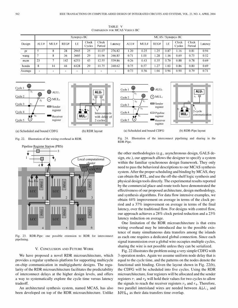
Table V lists the ratios of the performance results by com-paring MCAS versus Synopsys BC.7 The two flows achievethe similar resource cost and scheduled clock cycles. However,MCAS flow obtains a 21% improvement in clock period and a29% improvement in total latency on average.
6The rest benchmarks are too large for BC to run through. For example,we cannot obtain the schedule results from BC for DIR, CHEM, andU5ML12, etc., due to the long runtime.
7The number of resources allocated by two systems differ a lot as BC usesvarious bit-width resources whereas the current version MCAS only supportsuniform bit-width resource.
562 IEEE TRANSACTIONS ON COMPUTER-AIDED DESIGN OF INTEGRATED CIRCUITS AND SYSTEMS, VOL. 23, NO. 4, APRIL 2004
TABLE VCOMPARISON FOR MCAS VERSUS BC
Fig. 22. Illustration of the wiring overhead in RDR.
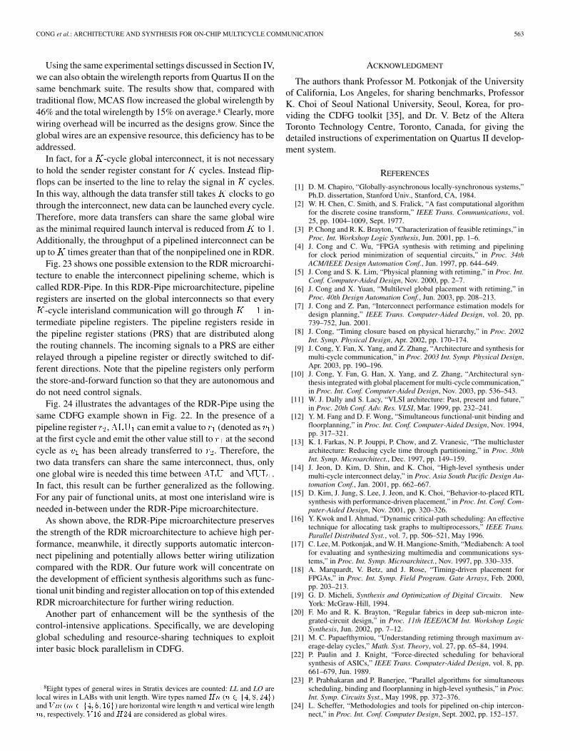
Fig. 23. RDR-Pipe: one possible extension to RDR for interconnectpipelining.
V. CONCLUSION AND FUTURE WORK
We have proposed a novel RDR microarchitecture, whichprovides a regular synthesis platform for supporting multicycleon-chip communication in multigigahertz designs. The regu-larity of the RDR microarchitecture facilitates the predictabilityof interconnect delays at the higher design levels, and offersa way to systematically explore the cycle time versus latencytradeoff.
An architectural synthesis system, named MCAS, has alsobeen developed on top of the RDR microarchitecture. Unlike
Fig. 24. Illustration of the interconnect pipelining and sharing in theRDR-Pipe.
the other methodologies (e.g., asynchronous design, GALS de-sign, etc.), our approach allows the designer to specify a systemwithin the familiar synchronous design framework. They onlyneed to pass the behavioral descriptions to our MCAS synthesissystem. After the proper scheduling and binding by MCAS, theycan obtain the RTL, and use the off-the-shelf logic synthesis andphysical design tools directly. The experimental results reportedby the commercial place-and-route tools have demonstrated theeffectiveness of our proposed architecture, design methodology,and synthesis algorithms. For data flow intensive examples, weobtain 44% improvement on average in terms of the clock pe-riod and a 37% improvement on average in terms of the finallatency, over the traditional flow. For designs with control flow,our approach achieves a 28% clock period reduction and a 23%latency reduction on average.
One limitation of the RDR microarchitecture is that extrawiring overhead may be introduced due to the possible exis-tence of many simultaneous data transfers among the islandsas each one requires a dedicated global connection. Since eachsignal transmission over a global wire occupies multiple cycles,sharing the wire is not possible unless they can be serialized.
Fig. 22 illustrates the problem using a very simple CDFG with3 operation nodes. Again we assume uniform node delay that isequal to the cycle time, and the patterns on the nodes denote thefunctional unit binding. Given the layout shown in Fig. 22(b),the CDFG will be scheduled into five cycles. Using the RDRmicroarchitecture, four registers will be allocated and the senderregisters and will hold their values for two cycles to allowthe signals to reach the receiver registers and . Therefore,two parallel interisland wires are needed between and
as their data transfers time overlap.
CONG et al.: ARCHITECTURE AND SYNTHESIS FOR ON-CHIP MULTICYCLE COMMUNICATION 563
Using the same experimental settings discussed in Section IV,we can also obtain the wirelength reports from Quartus II on thesame benchmark suite. The results show that, compared withtraditional flow, MCAS flow increased the global wirelength by46% and the total wirelength by 15% on average.8 Clearly, morewiring overhead will be incurred as the designs grow. Since theglobal wires are an expensive resource, this deficiency has to beaddressed.
In fact, for a -cycle global interconnect, it is not necessaryto hold the sender register constant for cycles. Instead flip-flops can be inserted to the line to relay the signal in cycles.In this way, although the data transfer still takes clocks to gothrough the interconnect, new data can be launched every cycle.Therefore, more data transfers can share the same global wireas the minimal required launch interval is reduced from to 1.Additionally, the throughput of a pipelined interconnect can beup to times greater than that of the nonpipelined one in RDR.
Fig. 23 shows one possible extension to the RDR microarchi-tecture to enable the interconnect pipelining scheme, which iscalled RDR-Pipe. In this RDR-Pipe microarchitecture, pipelineregisters are inserted on the global interconnects so that every
-cycle interisland communication will go through in-termediate pipeline registers. The pipeline registers reside inthe pipeline register stations (PRS) that are distributed alongthe routing channels. The incoming signals to a PRS are eitherrelayed through a pipeline register or directly switched to dif-ferent directions. Note that the pipeline registers only performthe store-and-forward function so that they are autonomous anddo not need control signals.
Fig. 24 illustrates the advantages of the RDR-Pipe using thesame CDFG example shown in Fig. 22. In the presence of apipeline register , can emit a value to (denoted as )at the first cycle and emit the other value still to at the secondcycle as has been already transferred to . Therefore, thetwo data transfers can share the same interconnect, thus, onlyone global wire is needed this time between and .In fact, this result can be further generalized as the following.For any pair of functional units, at most one interisland wire isneeded in-between under the RDR-Pipe microarchitecture.
As shown above, the RDR-Pipe microarchitecture preservesthe strength of the RDR microarchitecture to achieve high per-formance, meanwhile, it directly supports automatic intercon-nect pipelining and potentially allows better wiring utilizationcompared with the RDR. Our future work will concentrate onthe development of efficient synthesis algorithms such as func-tional unit binding and register allocation on top of this extendedRDR microarchitecture for further wiring reduction.
Another part of enhancement will be the synthesis of thecontrol-intensive applications. Specifically, we are developingglobal scheduling and resource-sharing techniques to exploitinter basic block parallelism in CDFG.
8Eight types of general wires in Stratix devices are counted: LL and LO arelocal wires in LABs with unit length. Wire types named Hn (n 2 f4; 8; 24g)and Vm (m 2 f4;8; 16g) are horizontal wire length n and vertical wire lengthm, respectively. V 16 and H24 are considered as global wires.
ACKNOWLEDGMENT
The authors thank Professor M. Potkonjak of the Universityof California, Los Angeles, for sharing benchmarks, ProfessorK. Choi of Seoul National University, Seoul, Korea, for pro-viding the CDFG toolkit [35], and Dr. V. Betz of the AlteraToronto Technology Centre, Toronto, Canada, for giving thedetailed instructions of experimentation on Quartus II develop-ment system.
REFERENCES
[1] D. M. Chapiro, “Globally-asynchronous locally-synchronous systems,”Ph.D. dissertation, Stanford Univ., Stanford, CA, 1984.
[2] W. H. Chen, C. Smith, and S. Fralick, “A fast computational algorithmfor the discrete cosine transform,” IEEE Trans. Communications, vol.25, pp. 1004–1009, Sept. 1977.
[3] P. Chong and R. K. Brayton, “Characterization of feasible retimings,” inProc. Int. Workshop Logic Synthesis, Jun. 2001, pp. 1–6.
[4] J. Cong and C. Wu, “FPGA synthesis with retiming and pipeliningfor clock period minimization of sequential circuits,” in Proc. 34thACM/IEEE Design Automation Conf., Jun. 1997, pp. 644–649.
[5] J. Cong and S. K. Lim, “Physical planning with retiming,” in Proc. Int.Conf. Computer-Aided Design, Nov. 2000, pp. 2–7.
[6] J. Cong and X. Yuan, “Multilevel global placement with retiming,” inProc. 40th Design Automation Conf., Jun. 2003, pp. 208–213.
[7] J. Cong and Z. Pan, “Interconnect performance estimation models fordesign planning,” IEEE Trans. Computer-Aided Design, vol. 20, pp.739–752, Jun. 2001.
[8] J. Cong, “Timing closure based on physical hierarchy,” in Proc. 2002Int. Symp. Physical Design, Apr. 2002, pp. 170–174.
[9] J. Cong, Y. Fan, X. Yang, and Z. Zhang, “Architecture and synthesis formulti-cycle communication,” in Proc. 2003 Int. Symp. Physical Design,Apr. 2003, pp. 190–196.
[10] J. Cong, Y. Fan, G. Han, X. Yang, and Z. Zhang, “Architectural syn-thesis integrated with global placement for multi-cycle communication,”in Proc. Int. Conf. Computer-Aided Design, Nov. 2003, pp. 536–543.
[11] W. J. Dally and S. Lacy, “VLSI architecture: Past, present and future,”in Proc. 20th Conf. Adv. Res. VLSI, Mar. 1999, pp. 232–241.
[12] Y. M. Fang and D. F. Wong, “Simultaneous functional-unit binding andfloorplanning,” in Proc. Int. Conf. Computer-Aided Design, Nov. 1994,pp. 317–321.
[13] K. I. Farkas, N. P. Jouppi, P. Chow, and Z. Vranesic, “The multiclusterarchitecture: Reducing cycle time through partitioning,” in Proc. 30thInt. Symp. Microarchitect., Dec. 1997, pp. 149–159.
[14] J. Jeon, D. Kim, D. Shin, and K. Choi, “High-level synthesis undermulti-cycle interconnect delay,” in Proc. Asia South Pacific Design Au-tomation Conf., Jan. 2001, pp. 662–667.
[15] D. Kim, J. Jung, S. Lee, J. Jeon, and K. Choi, “Behavior-to-placed RTLsynthesis with performance-driven placement,” in Proc. Int. Conf. Com-puter-Aided Design, Nov. 2001, pp. 320–326.
[16] Y. Kwok and I. Ahmad, “Dynamic critical-path scheduling: An effectivetechnique for allocating task graphs to multiprocessors,” IEEE Trans.Parallel Distributed Syst., vol. 7, pp. 506–521, May 1996.
[17] C. Lee, M. Potkonjak, and W. H. Mangione-Smith, “Mediabench: A toolfor evaluating and synthesizing multimedia and communications sys-tems,” in Proc. Int. Symp. Microarchitect., Nov. 1997, pp. 330–335.
[18] A. Marquardt, V. Betz, and J. Rose, “Timing-driven placement forFPGAs,” in Proc. Int. Symp. Field Program. Gate Arrays, Feb. 2000,pp. 203–213.
[19] G. D. Micheli, Synthesis and Optimization of Digital Circuits. NewYork: McGraw-Hill, 1994.
[20] F. Mo and R. K. Brayton, “Regular fabrics in deep sub-micron inte-grated-circuit design,” in Proc. 11th IEEE/ACM Int. Workshop LogicSynthesis, Jun. 2002, pp. 7–12.
[21] M. C. Papaefthymiou, “Understanding retiming through maximum av-erage-delay cycles,” Math. Syst. Theory, vol. 27, pp. 65–84, 1994.
[22] P. Paulin and J. Knight, “Force-directed scheduling for behavioralsynthesis of ASICs,” IEEE Trans. Computer-Aided Design, vol. 8, pp.661–679, Jun. 1989.
[23] P. Prabhakaran and P. Banerjee, “Parallel algorithms for simultaneousscheduling, binding and floorplanning in high-level synthesis,” in Proc.Int. Symp. Circuits Syst., May 1998, pp. 372–376.
[24] L. Scheffer, “Methodologies and tools for pipelined on-chip intercon-nect,” in Proc. Int. Conf. Computer Design, Sept. 2002, pp. 152–157.
564 IEEE TRANSACTIONS ON COMPUTER-AIDED DESIGN OF INTEGRATED CIRCUITS AND SYSTEMS, VOL. 23, NO. 4, APRIL 2004
[25] D. P. Singh and S. D. Brown, “Integrated retiming and placement forfield programmable gate arrays,” in Proc. Int. Symp. Field Program.Gate Arrays, Feb. 2002, pp. 67–76.
[26] M. D. Smith and G. Holloway, “An introduction to machine SUIF andits portable libraries for analysis and optimization,” in Division of Engi-neering and Applied Sciences. Cambridge, MA: Harvard Univ., 2002.
[27] M. B. Srivastava and M. Potkonjak, “Optimum and heuristic trans-formation techniques for simultaneous optimization of latency andthroughput,” IEEE Trans. VLSI Syst., vol. 3, pp. 2–19, Mar. 1995.
[28] J. T. Udding, “A formal model for defining and classifying delay-insen-sitive circuits and systems,” Distrib. Comput., vol. 1, no. 4, pp. 197–204,1986.
[29] J. Um, J. Kim, and T. Kim, “Layout-driven resource sharing in high-levelsynthesis,” in Proc. Int. Conf. Computer-Aided Design, Nov. 2002, pp.614–618.
[30] J. Weng and A. Parker, “3D scheduling: High-level synthesis with floor-planning,” in Proc. Design Automation Conf., Jun. 1991, pp. 668–673.
[31] M. Xu and F. J. Kurdahi, “Layout-driven RTL binding techniques forhigh-level synthesis,” in Proc. 9th Int. Symp. Syst. Synthesis, Nov. 1996,pp. 33–38.
[32] The National Technology Roadmap for Semiconductors, SemiconductorIndustry Association, 1997.
[33] International Technology Roadmap for Semiconductors, Semicon-ductor Industry Association, 2001.
[34] Altera Web Site [Online]. Available: http://www.altera.com.[35] CDFG Toolset [Online]. Available: http://poppy.snu.ac.kr/CDFG.[36] FFT Package [Online]. Available: http://momonga.t.u-
tokyo.ac.jp/~ooura/fft.html.[37] SUIF Compiler [Online]. Available: http://suif.stanford.edu.
Jason Cong (S’88–M’90–SM’96–F’00) received theB.S. degree from Peking University, Beijing, China,in 1985 and the M.S. and Ph.D. degrees from the Uni-versity of Illinois, Urbana-Champaign, in 1987 and1990, respectively, all in computer science.
Currently, he is a Professor and Co-Director ofthe VLSI CAD Laboratory in the Computer ScienceDepartment, University of California, Los Angeles.He has been appointed as a Guest Professor atPeking University since 2000. He has published over170 research papers and led over 20 research projects
supported by the Defense Advanced Research Projects Agency, the NationalScience Foundation, the Semiconductor Research Corporation (SRC), and anumber of industrial sponsors in these areas. His research interests includelayout synthesis and logic synthesis for high-performance low-power VLSIcircuits, design and optimization of high-speed VLSI interconnects, field-pro-grammable gate array (FPGA) synthesis, and reconfigurable computing.
Prof. Cong has served as the General Chair of the 1993 ACM/SIGDA Phys-ical Design Workshop, the Program Chair and General Chair of the 1997 and1998 International Symposia on FPGAs, respectively, and on program commit-tees of many VLSI CAD conferences, including the Design Automation Con-ference, International Conference on Computer-Aided Design, and InternationalSymposium on Circuits and Systems. He is an Associate Editor of ACM Trans-actions on Design Automation of Electronic Systems and IEEE TRANSACTIONS
ON VERY LARGE SCALE INTEGRATION (VLSI) SYSTEMS. He received the BestGraduate Award from Peking University, in 1985, and the Ross J. Martin Awardfor Excellence in Research from the University of Illinois, in 1989. He receivedthe Research Initiation and Young Investigator Awards from the National Sci-ence Foundation, in 1991 and 1993, respectively. He received the Northrop Out-standing Junior Faculty Research Award from the University of California, in1993, and the IEEE TRANSACTIONS ON COMPUTER-AIDED DESIGN Best PaperAward in 1995. He received the ACM Recognition of Service Award in 1997,the ACM Special Interest Group on Design Automation Meritorious ServiceAward in 1998, and the Inventor Recognition and Technical Excellence Awardsfrom the SRC, in 2000 and 2001, respectively.
Yiping Fan (S’02) received the B.S. and M.S. de-grees in computer science from Tsinghua University,Beijing, China, in 1998 and 2001, respectively. He iscurrently pursuing the Ph.D. degree in computer sci-ence at the University of California, Los Angeles.
His current research interests include very largescale integration system-level design, architecturalsynthesis, and reconfigurable computing.
Guoling Han (S’03) received the B.S. and M.S. de-grees in computer science from Peking University,Beijing, China, in 1999 and 2002, respectively. He iscurrently pursuing the Ph.D. degree in computer sci-ence at the University of California, Los Angeles.
His current research interests include system-levelsynthesis and behavioral synthesis.
Xun Yang received the B.S. degree in computerscience from Hefei Poly-Technique University,Hefei, China, in 1993, and the M.S. and Ph.D.degrees in computer science from Beijing Instituteof Technology, Beijing, China, in 1996 and 1999,respectively.
He was with the Computer Science Departmentof Tsinghua University, Beijing, China, from 1999to 2001, and with the Computer Science Departmentof University of California, Los Angles, from 2001to 2003 as a Postdoctoral Researcher. He joined
Silvaco Data Systems, Santa Clara, CA, in 2003. His research interests includeVHDL simulation algorithm, high-level synthesis, and system-level design andsynthesis.
Dr. Yang won Chinese National Third Class Scientific Progress Award for the“VHDL high level synthesis and multilevel simulation system for ASIC design”project that he worked on in 1999.
Zhiru Zhang (S’02) received the B.S. degree incomputer science from Peking University, Beijing,China, in 2001 and the M.S. degree in computerscience in 2003 from University of California, LosAngeles (UCLA), where he is currently pursuing thePh.D. degree in computer science.
His current research interests include plat-form-based hardware/software codesign forembedded systems, interconnect-driven high-levelsynthesis, and compilation techniques for reconfig-urable systems.