atom chip fabrication
TRANSCRIPT

Atom Chips. J. Reichel and V. Vuletic (Eds.)Copyright © 2010 Wiley-VCH, WeinheimISBN: 3-527-XXXXX-X
65
3Atom chip fabricationRon Folman, Philipp Treutlein, and Jörg Schmiedmayer
3.1Introduction
One of the key promises of atom chips is the building of a robust quantum lab-oratory by miniaturizing and integrating quantum optics and atomic physicstools on a single device, on a chip [1–3]. This vision follows the path taken pre-viously by the micro electronics and micro optics fields. The advantages andstrengths of the specific field, in our case quantum optics in atomic systems,are combined with the technological potential of microfabrication and (largescale) integration to build a robust platform for implementation of quantumoperations. An important ingredient in developing such an integrated, micro-fabricated approach to manipulating atoms, molecules or ions is the fabrica-tion of the devices. The possibilities to combine vastly different technologiesis thereby a key factor. This creates the technological basis for combining thebest of the different quantum worlds of photons, atoms and solid-state in asingle integrated quantum device.
This overview of atom chip fabrication is organized as follows: We first dis-cuss the challenges to be faced when starting to conceive and fabricate chipsfor the (quantum) manipulation of atoms. We then describe the various ingre-dients and the corresponding fabrication methods. We focus not only on thecurrently most active and successful areas - current carrying wires and inte-grated photonics, but also look at more visionary approaches, examples beingsuperconducting chips or the manipulation of atoms with real nano structuressuch as carbon nano tubes.
Here we explicitly discuss the material engineering and fabrication of atomchips for the manipulation of neutral atoms, but the same concept of robust-ness and versatility through miniaturization and integration can also be ap-plied to manipulate (polar) molecules, ions, or trapped electrons.

66 3 Atom chip fabrication
3.2Fabrication challenges
In building atom physics based quantum devices on a chip, the challenge isnot so much in micro and nano scale miniaturization, but rather in the inte-gration of numerous technologies on the same device, and in the exceptionalquality required from both the materials and the fabrication. Besides beingUHV compatible, different requirements need to be addressed, depending onthe specific application we have in mind.
• Current carrying wires are the workhorse of atom chips. Their key roleis to provide magnetic fields for trapping and manipulation. These wireshave to support high current densities, in some cases > 107 A/cm2 [4,5],many orders of magnitude larger than in a light bulb. Ultra cold atomsare extremely sensitive to variations in the magnetic potential. Thesecan be caused by non uniform current flow in the wires. Current flowdeviations of ∼ 10−6 rad can be seen in 1d BEC experiments [6, 7]. Adeviation of > 10−4 rad makes a trap unusable for many experiments.
• Micro structured magnetic films and permanent magnets provide a veryattractive way to create strongly confining micro traps at very high in-tegration density [8–12]. One of the key issues in fabrication thereby isagain the homogeneity of the magnetic materials [13].
• Radio-frequency (RF) and microwave (MW) fields complement the staticmagnetic trapping potentials [14–20]. Coupling two different groundstates creates dressed state potentials similar to optical dipole potentials.The wire structures and the substrates need to be chosen well to supportprecise microwaves.
• Electric fields offer a route to detailed structuring and manipulation [21].At the micron scale the substrates and the fabricated structures have towithstand the large electric fields created at even moderate voltages.
• Multi layer chips [20,22,23] are very instrumental. In an integrated atomchip, large structures (10 to 500 μm) for the initial trapping and coolingof atoms have to be combined with functional structures on the (sub)micrometer scale to achieve controlled manipulation at a length scalewhere tunnel coupling between sites becomes important. Furthermore,the versatile application of electric and magnetic potentials requires thecrossing of wires on the chip without contact.
• In many applications the chip surface needs to be a high quality mir-ror, be it for cooling and accumulating the atoms in a mirror MOT orfor imaging atoms close to the surface. Furthermore, reflection of light

3.3 The substrate 67
from the chip surface allows to integrate optical dipole traps and opticallattices on the atom chip [24]. This puts very stringent requirements onthe quality of the mirror surface.
• By integrating micro optics and fiber optics on the atom chip [25, 26]one can incorporate optical micro manipulation and efficient detectionof atoms. The fabrication methods for the optics have to be compatiblewith the other processes. Integrating fully tunable optical micro cavitiespose an even larger challenge [27].
• Integration of superconducting elements on the chip will require com-patibility with cryogenics.
• The atom chip is an ideal platform to integrate other solid state quan-tum devices like Micro-Electro-Mechanical systems (MEMs) [28,29], mi-cro lenses and holes, miniature high finesse cavities, current carryingmolecules or nano magnets, crystalline materials, etc. with the atomicphysics on the chip. Connecting atoms to superconducting qubits [30,31]through circuit CQED [32, 33] will even require to go to mK tempera-tures.
• Looking further into the future one can think of integrating more com-plex devices onto the chips like on board light and particle sources,miniature vacuum volumes and pumps, etc. (see last figure of this chap-ter) to build an independent stand alone device.
With all these diverse science possibilities each chip has an individual de-sign, tailored to the physics and functions it is required to perform. What isneeded is an interplay between physics, material engineering and fabrication,and compatibility of the methods.
3.3The substrate
The substrate onto which the atom chip is fabricated has to be compatiblewith the different fabrication techniques needed to implement the chip designand has to guarantee the robust operation of the device. For a comparison ofdifferent substrate materials see Table 3.1.
In general the most important physical properties for present day atomchips stem from the fact that one of the key functions is to accumulate, cooland manipulate ultra cold atoms using static or oscillating fields. The sub-strate of the atom chip has to support the wires, provide electrical insulationbetween them, and dissipate the heat generated in the wires. Therefore, a

68 3 Atom chip fabrication
substrate with high thermal conductivity, a high heat capacity, and an insulat-ing surface is needed. A second important requirement, needed for smoothmagnetic potentials, is the ease of high quality fabrication (few geometricaldefects) and low wire surface roughness. This translates, for example, to verylow surface roughness of the substrate.
A common substrate is a single crystal Si wafer in a (100) orientation witha thermal conductivity of ∼ 150 W/(mK) at room temperature. Wafers aretypically ∼ 500 μm thick and polished with very small surface roughness,sufficient even for the smallest wires. They can be cleaved with a diamondscorer. Neither the resistivity of Si nor the 2 nm native oxide layer on thesubstrate are sufficiently insulating for controlling DC currents at the 10−5
level. Therefore the wafer is covered by a SiO2 insulation layer which providesa DC resistance of > 40 MΩ between the wires. Since SiO2 has a thermalconductivity of only 1.5 W/(mK), the insulating layer should be as thin aspossible [5, 34].
AlN is a non-toxic polycrystalline ceramic with an excellent heat conduc-tivity of typically 180 W/(mK) at room temperature. Compared with Si, AlNis less brittle. It can be laser machined and easily cleaved with a diamond
Material Therm. Specific loss tang. Linear Density Opticalcond. Heat 10 GHz expans. transm.
Wm−1K−1 J/KgK εr 10−4 10−6K−1 g cm−3 nmBeO 260-300 1000 6.7 30 8.4-9.0 2.86AlN 170-280 800 8.9 5 4.4-5.7 3.25 500-3000BN 740 600 5-7 2-4 1.2-3 3.4InN 450 320 15 3-4 6.8 620-2500GaN 1300 490 10 3-5.5 6.5 400-2500Macor 1.5 790 5.9 50 13 2.52Sapphire 35-40 700 9-11 0.2-0.8 5.8 3.99 200-5500Alumina 18-35 900 9.6 1 8.0 3.9SiN 10-43 680-800 10 10-20 3.3 2.4-3.3fused quartz 1.46 670-740 3.8 1-4 0.54 2.2 180 - 2500SiO2 1.46 700 3.9 1-10 0.54 2.2 180-2500BK7 1.11 858 8 2.51 400-1400Pyrex 1.13 750 5.1 260 3.25 2.23 300-2500Polyimide 0.1-0.35 1090 3.4 20-40 30-60 1.42Diamond 900-2000 470 5.7 2 0.8 3.52 400-300000GaAs ∼ 55 330 10.9-12.9 <6 5.8 5.3 1500-14000Si 80-150 700 11.7 <10 4.7-7.6 2.34 1200-15000SiC 350-490 690 10.8 30 4.8 3.2
Tab. 3.1 Room temperature properties of commonly used substrates for micro fabrication.The properties given are typical values found in data sheets . The actual values can can varyconsiderable for specific samples, depending on crystal orientation, purity and fabrication pro-cedure. The data was compiled form data sheets of the distributors, a number of Internet re-sources like http://www.ioffe.ru, and ref. [2])
3.4 Lithography 69
scorer. A polished AlN surface (specified surface roughness < 40 nm) has asignificant residual roughness, with isolated defects of micrometer size. Thisis a problem if structures < 10 μm are desired.
Both AlN and Si are common substrate materials for microwave circuits.AlN has a dielectric constant of εr = 8.7 and a loss tangent of tan δ < 1× 10⁻³
at 10 GHz. If only DC currents are used in the experiment, Si of any dopinglevel can be employed as the substrate material. For microwave applications,however, it is very important to choose high-resistivity Si to avoid strong di-electric losses. A typical wafer has a resistivity of ρ > 104Ωcm, εr = 11.9, andtan δ = 1× 10⁻³ at 10 GHz.
Other substrates commonly used in atom chip fabrication are GaAs, sap-phire, alumina or SiO2. Especially sapphire is interesting as a substrate forlow temperature micro wave applications, where a loss tangent close to 10−6
has been observed. Sapphire is also interesting when using light, as it is trans-parent in the visible light range.
3.4Lithography
In lithography, a pattern is transferred into a layer of resist on the chip surface.The patterned resist is subsequently used as a stencil for etching or depositingmaterial. An extensive discussion of lithographic techniques can be foundin [35]. In the following, we give a brief introduction to optical and electronbeam lithography, which are most commonly used for atom chip fabrication.
3.4.1Optical lithography
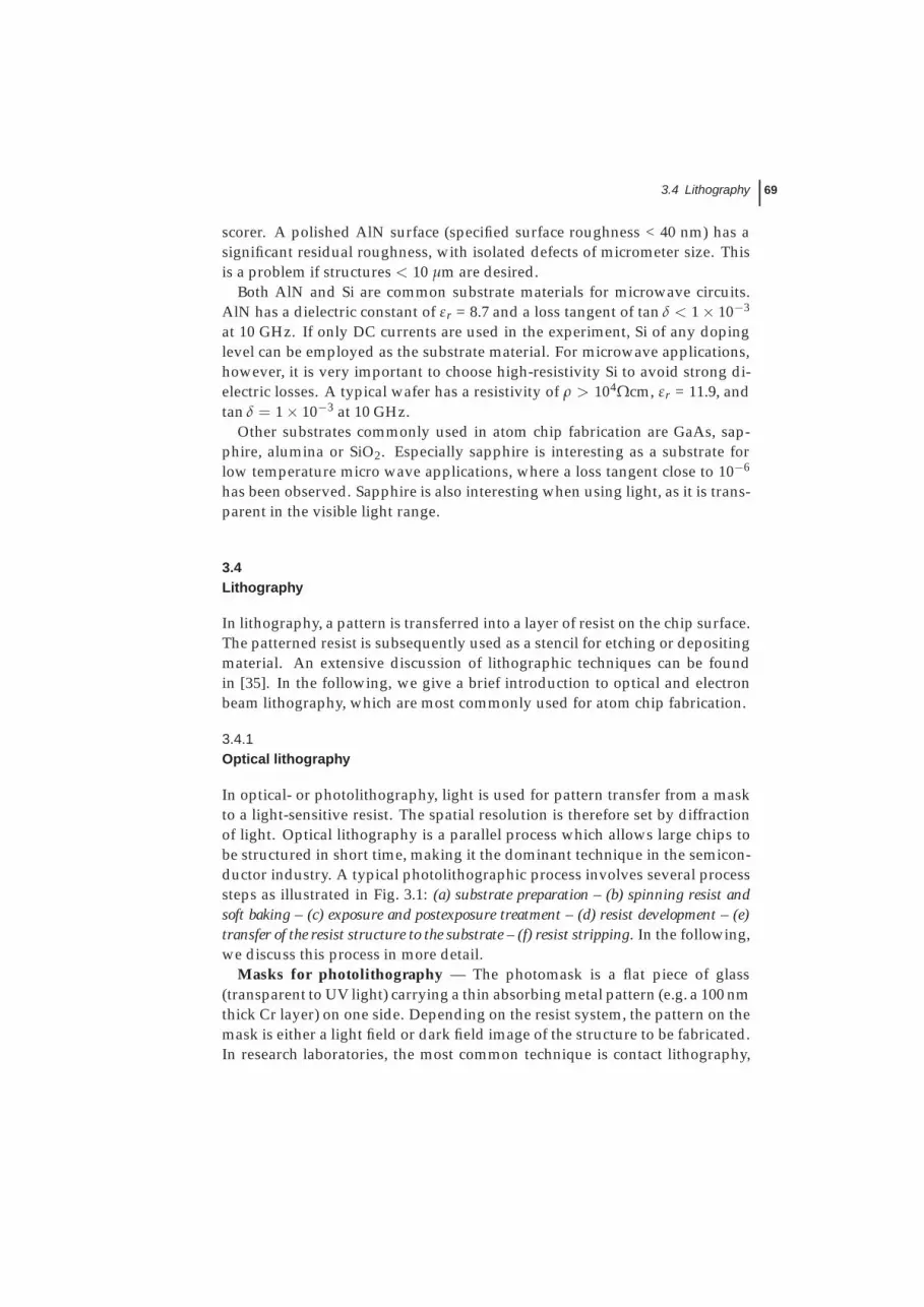
In optical- or photolithography, light is used for pattern transfer from a maskto a light-sensitive resist. The spatial resolution is therefore set by diffractionof light. Optical lithography is a parallel process which allows large chips tobe structured in short time, making it the dominant technique in the semicon-ductor industry. A typical photolithographic process involves several processsteps as illustrated in Fig. 3.1: (a) substrate preparation – (b) spinning resist andsoft baking – (c) exposure and postexposure treatment – (d) resist development – (e)transfer of the resist structure to the substrate – (f) resist stripping. In the following,we discuss this process in more detail.
Masks for photolithography — The photomask is a flat piece of glass(transparent to UV light) carrying a thin absorbing metal pattern (e.g. a 100 nmthick Cr layer) on one side. Depending on the resist system, the pattern on themask is either a light field or dark field image of the structure to be fabricated.In research laboratories, the most common technique is contact lithography,
70 3 Atom chip fabrication
Fig. 3.1 Process steps of optical lithography (see text). The exampleuses a contact mask, a positive resist system, and pattern transfer tothe metal layer by wet etching.
where the metal pattern on the mask is in direct contact with the photoresistlayer during exposure. A mask aligner is used to align mask and substrate withrespect to each other and expose them to UV light (often, mercury lamps withspectral lines near 400 nm are used). The direct contact of mask and resist canresult in defects. An alternative are projection masks, which are imaged bya high-resolution lens system onto the resist. Many commercially availablemasks are fabricated by laser lithography, i.e. by writing the pattern with alaser beam of 0.7 μm spot size into a thin resist layer on the mask. Maskswith smaller structures can be written by electron beam lithography (see be-low). For coarse structures (> 50 μm), the mask can be simply printed on atransparency. Laser lithography can also be used to avoid photomasks com-pletely, by directly exposing the resist on each chip with the laser beam.
Substrate preparation — Lithography starts with a thorough cleaning ofthe substrate. Different (combinations of) wet or dry cleaning procedures areused, involving e.g. organic solvents in an ultrasonic bath, or a strong acidsuch as H2SO4, or an acid-oxidant combination (e.g. ‘piranha etch’), or oxygenplasma cleaning. Subsequent to cleaning, some processes require depositionof homogeneous insulating and/or metal layers on the substrate. In the ex-ample of Fig. 3.1, the substrate is covered with a thin Ti adhesion layer and agold layer, which will later be patterned by wet etching.
Spinning resist and soft baking — A spin coater is used to apply a photore-sist layer of a desired thickness (ranging from a few 100 nm to a few 100 μm,depending on the resist system and application). The photoresist is an organicpolymer sensitive to UV radiation. After spin coating, the resist layer is softbaked (prebaked) to remove solvents and promote adhesion to the substrate.
Exposure and postexposure treatment — The resist-coated substrate isaligned with respect to the photomask and subsequently illuminated with awell defined intensity of UV light for a controlled duration (typically a fewseconds). Finding the proper exposure dose is an important task during op-timization of the process. The UV light induces a chemical reaction in the ex-posed areas of the photoresist, altering the solubility of the resist in a solvent.If a positive resist is used, the exposed areas are rendered soluble. In a nega-tive resist, the exposed areas are rendered insoluble. After exposure, certainresists require further treatments. For example, an image reversal resist requires

3.4 Lithography 71
a post-exposure bake and subsequent flood exposure with UV light, therebyturning the originally positive resist into a negative one. The choice of the re-sist system for a given application depends on many parameters, such as thedesired spatial resolution and resist thickness, the desired shape of the resistprofile (positive vs. negative slope of the resist sidewalls, see section 3.5), andthe chemical stability in subsequent processing steps.
Resist development — During development, the resist is selectively dis-solved, usually by submerging and agitating the substrate in a liquid devel-oper solution. This transforms the latent image formed during exposure intoa resist pattern that will serve as a mask in further deposition or etching steps.Careful control of the development time and developer temperature is re-quired to reproducibly obtain the desired resist profile. A mild oxygen plasmatreatment can be useful to remove unwanted resist left behind after develop-ment. Furthermore, some applications require postbaking of the developedresist to improve stability.
Transfer of the resist structure to the substrate — Various methods exist totransfer the resist structure to the substrate, and the most common ones foratom chip fabrication are discussed in section 3.5 below. In the example ofFig. 3.1, wires are defined by a wet etch of the metal layers with aqua regia.
Resist stripping — In the last step of the photolithographic process, the re-sist is removed (stripped). Similar to the procedures for substrate cleaning, asequence of steps involving organic solvents, acids, acids+oxidants, or plasmacleaning is used. The additional requirement is that the chemicals and proce-dures employed should not attack the desired structures.
Spatial resolution — The spatial resolution of contact lithography is limitedby the near-field diffraction of light at the structures in the mask and thus de-creases if there is a gap between the mask and the substrate. Consider photore-sist of thickness t exposed with light of wavelength λ through a mask with apattern of equal lines and spaces of periodicity 2w. The theoretical resolution,i.e. the minimum linewidth resolved, is given by wmin = (3/2)
√λ(g + t/2),
where g is the gap between resist and mask [35]. To obtain high resolution,g has to be as small as possible. This means that edge beads and defects ofthe photoresist have to be avoided. The substrate has to be pressed againstthe mask. In a multi-layer process, the topology of the lower layers (if notplanarized perfectly) will introduce gaps and thus decrease resolution. Asan example, consider λ = 400 nm, t = 1.5 μm, and g = 0, which yieldswmin = 0.8 μm. In practice, achieving such high resolution is possible, butchallenging. Routinely, w > 2− 3 μm is achieved.
Resist bleaching is a phenomenon that allows one, to some extent, to en-hance resolution beyond wmin. During exposure, the resist becomes moretransparent to the illuminating light. This allows one to define narrow fea-tures in thick resist, i.e. the fabrication of structures with high aspect ratio.

72 3 Atom chip fabrication
3.4.2Electron beam lithography
Electron beam lithography allows one to fabricate significantly smaller struc-tures than optical lithography. Moreover, the electron beam has a large depthof focus, facilitating patterning of substrates with uneven topography. E-beam lithography is a serial technique in which a narrow electron beam isscanned across a resist layer pixel-by-pixel. The resolution is limited by elec-tron scattering in the resist and substrate to typically 10− 100 nm, dependingon resist thickness. The standard positive resist is polymethylmethacrylate(PMMA). Electron bombardment breaks the PMMA into fragments, the re-sulting shorter polymer chains are dissolved faster during development. Neg-ative resists and multi-layer resist systems are available as well.
E-beam lithography is slow, and writing a complex pattern can easily takeseveral hours, making the system prone to drifts and vibrations. Moreover,the size of the field that can be written without moving the substrate is typi-cally only a few hundred μm, for larger areas stitching is necessary. Neverthe-less, the superior resolution make e-beam lithography the method of choicein many applications. The basic steps involved in an electron beam lithog-raphy process are similar to those discussed in the previous section. Duringexposure with the e-beam, the substrate is mounted in a vacuum chamber. Nophysical mask is needed, the pattern is defined in computer software.
Optical and electron beam lithography are often combined. The smallestand most critical structures in the chip center are defined by electron beamlithography, while optical lithography is used in a separate process step foruncritical ‘large-scale’ structures such as lead wires and contact pads at theedge of the chip.
3.5Metallic layers
Metallic wires, electrodes, or permanent magnets are the most commonly usedstructures on an atom chip. In the following we introduce the most importantdeposition and etching techniques used for the patterning of normal metals,discuss issues of roughness and homogeneity of the structures, and review thefabrication of structures out of special metals such as alloys, superconductors,semiconductors, and permanent magnets.
3.5.1Deposition and etching
Resist patterns created by lithography can be transferred to the substrate byadditive (deposition) or subtractive (etching) techniques. The two most com-

3.5 Metallic layers 73
b) spin on + soft bake photoresist
a) evaporate gold seed layer
c) UV exposure d) develop photoresist
e) electroplate gold
U+ −
ammoniumsulfite-gold-solution
Au+
Ti/P
t an
od
ef ) remove photoresist
g) gold etch to remove seed layer
Fig. 3.2 Electroplating. The process steps are explained in the text.
monly used techniques for the fabrication of atom chip wires are additivetechniques: electroplating and lift-off metallization.
3.5.1.1 Electroplating
Electroplating was among the first techniques used for atom chip fabrica-tion [4, 36]. In this technique, the chip serves as the cathode of an electrolyticcell. Resist structures on the chip form a mold for the electroplated metal. Un-der an applied voltage, metal ions from the plating solution deposit on theareas not covered by resist. The amount of deposited material per unit timeis controlled by the current flow. Electroplating is more time and material ef-ficient than metal deposition through thermal evaporation or sputtering. Itis therefore well suited also for structures with a thickness � 1μm. Further-more, structures with high aspect ratio (wire height comparable to or higherthan width) are easier to fabricate than with lift-off or etching techniques (seebelow). Electroplating is very versatile, it can also be used to fabricate viasand other non-planar structures [35]. A review of electroplating can be foundin [37, 38], and its application to atom chips is discussed e.g. in [39–41].
Fig. 3.2 illustrates a basic gold electroplating process (a detailed recipe canbe found in [41]). (a) After substrate cleaning, a 2 nm Ti adhesion layer and a50 nm Au seed layer are deposited by thermal evaporation. This layer servesas the cathode. (b) The chip is spin coated with a 6.5 μm thick layer of pho-toresist and subsequently patterned by optical lithography (c+d). The resiststructures should be slightly taller than the desired thickness of the wires. Inour example, a positive tone resist with high pattern stability in acidic andalkaline plating baths is used.
In the following electroplating step (e), the chip and a Ti/Pt mesh an-ode are connected to a power supply and submerged in 1 liter of electro-plating solution, whose temperature is carefully controlled in a water bath.

74 3 Atom chip fabrication
Fig. 3.3 Electroplated gold wires fabricated with two different pro-cesses. (a)-(d) Wires of 5 μm thickness on a Si chip, fabricated withthe process of [41]. (a) Entire chip with contact pads. (b) Close-upof (a). The gaps between wires are 3 μm wide. (c)+(d) SEM picturesof the wires. The grain size of the gold is 200 nm, the r.m.s. surfaceroughness is 15 nm. (e)+(f) For comparison, SEM pictures of wiresfabricated with the process of [42] are shown (thickness 4.5 μm).Grains of micrometer size are visible, the r.m.s. roughness is 200 nm.
In our example, a solution from Metakem is employed, which is based onammoniumsulfite-gold(I) ([(NH4)3Au(SO3)2]). It is commonly used for den-tistry and jewelery and yields very smooth gold deposits of 99.99% purity.To deposit gold, the desired plating current I is driven through the elec-trolytic cell. Stirring helps to avoid local depletion of the solution and thusensures a more homogeneous gold layer. The thickness h of the gold layerdeposited after a time t can be determined by Faraday’s law: h = α ItM
nFS� =
1.1× 10⁻¹⁰ m3
A s × ItS , where M the molar mass and � the mass density of gold,
F is Faraday’s constant, n = 1 is the charge of the gold ions, and α ≈ 1 thecurrent efficiency for gold plating. The surface area S of the deposited goldfilm is given by the surface area of the wire layout plus the contact pads andconnectors. In the parallel plate configuration, the current density is approxi-mately constant over the exposed gold areas of the chip. (f) After the wires areelectroplated to the desired thickness, the resist is stripped. In the final step(g), the Au seed layer and the Ti adhesion layer are removed by a wet etchwith aqua regia. This isolates the electroplated wires from each other. Thegold etch also attacks the wires, increasing surface roughness. It is therefore

3.5 Metallic layers 75
b) UV exposure c) image reversal bake
d) flood exposure
e) develop resist until undercut forms
f) evaporate gold g ) lift-off resist
a) spin on + soft bake photoresist
Fig. 3.4 Lift-off sequence with an image reversal resist. Gold is de-posited by e-beam evaporation. The process steps are explained inthe text.
desirable to work with a seed layer as thin as possible. Figs. 3.3(a)-(d) showelectroplated gold structures on Si chips fabricated with this process.
The quality of the electroplated wires crucially depends on the choice ofthe plating solution and on the process parameters. Different solutions (andalso the same solution at different process parameters) deposit gold of verydifferent grain size [38]. Moreover, the complex bath chemistry can be dis-turbed by contaminants. Some processes result in deposits with micrometergrain size [42], resulting in inhomogeneous current flow in the wires and thusroughness of the generated potentials. Optimized electroplating processes,however, result in structures with very low roughness [39,41]. In Fig. 3.3(c)-(f),SEM pictures of electroplated gold wires fabricated with the processes of [41]and [42] are shown in comparison. The roughness of the wires of [41] is aboutone order of magnitude smaller than that of [42].
3.5.1.2 Evaporation and lift-off metallization
Evaporation and lift-off metallization is a standard technique for fabricatingmetal structures of high quality [35]. In this technique, patterned resist acts asa mask for evaporated gold. After removal of the resist (“lift-off”), only thedesired gold structures remain on the chip. Gold layers deposited by thermalor electron-beam evaporation often have smaller surface roughness than elec-troplated wires. This is important for generating smooth trapping potentialsfor waveguides or 1d traps [43] and for using the wire layer simultaneously asa mirror [44] for a mirror-MOT [36]. Evaporation allows very precise controlover the thickness of the deposited material. However, the thickness is limitedby the slow deposition rate and substantial material consumption to a few μmat maximum. An alternative for thicker structures is sputtering of the metal,or electroplating (see previous section). Evaporation and lift-off was adaptedto atom chip fabrication as described in [5, 23, 40, 41, 45].

76 3 Atom chip fabrication
An example of a lift-off sequence is illustrated in Fig. 3.4 (a detailed recipecan be found in [41]). (a) The substrate is spin-coated with a 1.6 μm thicklayer of photoresist. An image reversal resist is used, which allows one tocreate resist sidewalls with a negative slope (“undercut”), which is crucial forlift-off metallization. (b) The resist is exposed for a few seconds with UV lightthrough a mask which bears a negative image of the wires to be fabricated.Due to the small exposure dose, the resist is not fully exposed down to thesubstrate. This leads to the negative slope of the resist sidewalls after imagereversal and development. (c) An image reversal bake on a hot plate at a care-fully controlled temperature cross-links the resist in the exposed areas andthus renders it insoluble in the developer and insensitive to further exposure.(d) Subsequently, the chip is flooded with UV light, which now renders thepreviously unexposed areas soluble. (e) These areas are removed during de-velopment. The development time is carefully adjusted to control the forma-tion of the undercut. Residues of photoresist are removed by a short oxygenplasma cleaning step. Subsequent baking of the resist structures on a hot plateimproves resist stability. (f) A 1 μm thick layer of gold is deposited on top ofa 3 nm thick Ti adhesion layer by e-beam evaporation in a UHV evaporationchamber. The resist acts as a mask for the gold, while the undercut preventsgold in the resist trenches from sticking to gold on top of the resist. (g) Lift-offis performed in a bath of hot acetone. This removes the resist and the gold ontop of it and leaves behind the desired structures. If necessary, lift-off can beforced by agitation or by mild ultrasound.
For successful lift-off, the resist layer should be somewhat thicker than thethickness of the deposited gold layer. The resist undercut can be adjusted bychanging exposure time, image-reversal temperature, and development time.A strong undercut can be seen in an optical microscope as a bright outline ofthe resist edges. However, for very small periodic structures, mechanical andthermal stability of the resist requires that development be stopped beforethe bright outline is visible. For process optimization, the undercut can beobserved with an electron microscope, see Fig. 3.5.
Fig. 3.6 shows wires that were fabricated by evaporation and lift-off [5, 41].The surface and edge roughness of the wires is small, resulting in very smoothmagnetic potentials. Moreover, the gold wire layer can serve as a high-qualitymirror if the gaps between the wires are sufficiently narrow.
3.5.1.3 Wet and dry etching
The simplest subtractive technique is wet etching, which is illustrated inFig. 3.1 above. After the resist has been patterned, the chip is submergedand agitated in a suitable etchant (aqua regia in the case of gold wires), whichremoves the metal layer in the areas not covered by the resist. Wet etching re-sults in relatively rough wire edges. Moreover, the metal is removed isotropi-

3.5 Metallic layers 77
Fig. 3.5 SEM images of gold wires before and after lift-off. (a) Resiststructure with deposited gold on top. (b) Close-up of (a), the undercutof the resist sidewalls is visible. (c) Gold wires remaining after lift-off.
Fig. 3.6 SEM images of micrometer-size atom chip wires fabricated byevaporation and lift-off. (a) Gold wire, 1 μm thick and 1.7 μm wide [41].The grain size of the gold is ∼ 100 nm, the r.m.s. surface roughness is3 nm. (b)+(c) Gold wires of [5] with 50− 80 nm grain size.
cally, and wet etching is thus not suitable for fabricating structures with steepside walls and high aspect ratio. By contrast, some dry etching techniquessuch as reactive ion etching [35] are very anisotropic, and can thus be used tofabricate high aspect ratio structures with steep edges. Brute force ion etch-ing (called ion beam milling) may also be used if a thin layer of metal needsto be etched and the lift-off method is not feasible, for example, when highevaporation temperatures are used (e.g. if one needs large grain size), and theresist may only be put after the evaporation process (this method has beenused in [7]).
For wet and dry etching, it is essential to choose an etchant that effectivelyremoves the material to be patterned, but leaves intact additional structures onthe chip and the functionality of the etch mask. The etch mask does not haveto be a resist structure, it can also be a suitable patterned metal or dielectriclayer. Two very useful papers with hundreds of etch rates for a large numberof materials in different wet and dry etches are Refs. [46, 47]. They are alsouseful for choosing the right chemicals for cleaning and resist stripping tasks.
Besides etching, subtractive patterning techniques include focused ionbeam milling (see the next section), which can be used to structure arbitrary
78 3 Atom chip fabrication
materials, and laser machining, which is useful e.g. for hole drilling. Thesetechniques differ from etching in that they do not require a physical mask.
3.5.1.4 Designing potentials by post processing the wires
In general the magnetic potentials on atom chips are formed by the subtrac-tion of two (large) magnetic fields, the field of a current carrying wire and a(homogeneous) bias field (see other chapters in this book). The value of themagnetic field at the potential minimum δBmin is determined by the angle be-tween the field of the wire and the bias field. A small change of the currentdirection results in a significant change in the trapping potential. A devia-tion of the current flow by ϑ ∼ 10−5 rad can lead to δBmin ∼ 1 mG whichcorresponds to 67 nK for trapped Rb atoms.
One can implement slight changes in the current path deliberately by sculp-turing the bulk of a lithographically patterned plane conductor [48] andthereby fine tune or even design local features in the trapping potential. Thecontributions of a current flow pattern with wave vector k to the magneticfield are exponentially damped with height z as e−kz when receding from thewire. Therefore, in order to achieve a modulation of a fraction η0 of the max-imum achievable field at a minimum structure size λmin = 2π/kmax one hasto stay at distances of z < − log η0
kmax(for details see [48, 49]).
This post processing of the chip structures can be done with a Focused IonBeam (FIB) technique [50], which allows to create modifications with high pre-cision (< 20 nm) and large aspect ratios (height/width > 30). The Heidel-berg/Vienna group experimentally demonstrated the power of this techniqueby sculpturing a 10 μm wide and 2.5 μm thick gold conductor on a Si sub-strate [48, 51] (Fig. 3.7).
3.5.2Effects of roughness and homogeneity of the fabricated structures
A small change of the current direction results in a significant change in thetrapping potential. Irregular current flow will result in uneven potentials withsignificant roughness.
After the first creation of a BEC on an atom chip a number of groups ob-served large roughness in the magnetic potentials holding the atoms. In manycases even a 1 μK thermal cold atom cloud was fragmented into many com-ponents when approaching distances below 100 μm from the wire [42,52–55].This potential variation originates from inhomogeneous magnetic field com-ponents ΔB in the direction parallel to the current carrying wire [56] and can beattributed to variations in the current flow direction in the chip wires. Com-mon to all but one of these experiments was, that they used electro platedwires to hold the trapping currents (the experiment by the Sussex/Imperial

3.5 Metallic layers 79
Fig. 3.7 Examples of wires sculptured by FIB a) Double well createdby making two 1 μm deep, 0.2 μm wide cuts in opposite edges of atrapping wire. b) Polishing the wire edge as imaged by the FIB itself.The polished region (on the right) is smoother and reveals details ofthe structure of the gold wire. The contrast in the image is given bythe ion reflection coefficient, varying with the relative orientation of thecrystal axes of the gold grains. The picture shows a small region of9.2 μm × 5.1 μm at the end of the polished section. c) Magnetic lat-tice with periodicity a=4 μm created by a string of holes with diameterD=a/2 in a wire with thickness d=a/2 and width w=10 μm. Top: Cur-rent density jy in the transverse direction. Center : The potential mod-ulation V at a height of z=6 μm, scaled to the characteristic energyEr = h2k2
a/2mRb (lattice vector ka = 2π/a). Bottom: The potentialalong the lines drawn in the central image. The maximum modulationwith a peak-to-peak depth V0 20 Er, is obtained at y=2 μm (orangecontinuous curve) while V0 6 Er for y=5 μm (blue dashed curve).
College group used a drawn copper wire [54]). In an experiment by the Or-say group, the large potential roughness observed was clearly identified ascoming from the rough edges of the fabricated wires, and the model of Wanget al. [57] provided a full quantitative explanation [42, 55]. In many cases theobserved modulations were so strong that they prevented the creation of acontinuous elongated BEC.
At about the same time in 2003 it became clear that this is not the generalcase. Such strong potential roughness was not found in the experiments atHeidelberg [43, 58] using atom chips with gold wires evaporated on a Si sub-strate and structured by the lift-off technique [5]. Nevertheless, a very smallpotential roughness remains which is also magnetic in origin. Measurementsof the potential landscape over the whole width of a 100 μm wide wire, byscanning the position of the condensate across the wire using the BEC mag-

80 3 Atom chip fabrication
101
102
10−6
10−5
10−4
10−3
10−2
hight μm
ΔB
/ B
IC / SussexOrsay 50 μm 0.7 μmTübingenMelbourneMITWIS/HD 100 μm 10 μmBGU/HDw = 1μmw = 10μmw =100μm
Fig. 3.8 Comparison of different atom chip potential roughness mea-surements. Data is taken from figures in the published literature andPhD theses and displayed with color codes according to the experi-mental group. Filled symbols denote rms values, and data displayedas open symbols are peak to valley maximum height of the roughness.Sussex : data from a gold coated copper wire [60]; Orsay : data froman electro plated wire [42, 55], and recent data from a 5 wire setup onan evaporated gold chip; Tübingen: data from electroplated wires (PhDthesis, J. Fortagh); Melbourne: data from a permanent magnet atomchip [13]; MIT : data from electro plated wires; WIS/HD: data from theanalysis chips fabricated at the Weizmann Institute of Science: a 100μm wire [43], 2003 data from various 10 μm wires [58, 61]. The opentriangles give the peak to valley of the worst ever roughness observedin HD: a 10 μm wire (PhD thesis, L. Della Pietra). BGU/HD: Recentdata from 3 different wires fabricated at Ben-Gurion and analyzed inHD [7].
netic field microscope [6,59], show no significant increase near the wire edges.A detailed analysis clearly showed that the edge roughness model can notexplain the observed potential variations [43, 58].
Even more surprising are the findings of Aigner et al [7] where the cur-rent flow in 3 different wires with different grain size and wire thickness wasprobed. The measurements showed that the thinnest wire with the largestgrains had the smoothest current flow. A detailed analysis of the measuredpotential landscape and a comparison to the surface roughness of the goldlayer clearly show that the local properties of the metal, and not imperfections

3.5 Metallic layers 81
in the wire boundary are the key to the current flow variations in the wireswith the smoothest potentials [62].
It is interesting to compare the potential roughness observed on differentchips and in different experiments. In most applications of atom chips an im-portant parameter is how large the potential roughness ΔB is in comparisonto the energy scale of the transverse confinement ω⊥. A stringent requirementfor 1d experiments is hω⊥ � μΔB, where μ = μBgFmF is the magnetic mo-ment of the trapped atomic state. The magnetic confinement ω⊥ ∝ d2B/dr2
is determined by the magnetic field gradient dB/dr and the longitudinal Ioffefield BIoffe. To achieve the same ratio Rω⊥ = μΔB/hω⊥, the allowed relativemagnetic field roughness for a trap built at height h above a flat wire of finitewidth w scales like:
ΔBB
< Rω⊥2w
(w2 + 4h2)(π2 − arctan[ 2h
w ])
√μBgFmF
MBip(3.1)
Fig. 3.8 shows a comparison of a large variety of measured potential rough-ness data from many different laboratories.
3.5.3Special metals
3.5.3.1 Alloys
One of the high priority goals in atom chip research is the increase of life-time and coherence time for ultracold atoms trapped in magnetic potentialsclose to the surface. This is important for both scientific aims and techno-logical applications. Progress towards this goal demands the control and re-duction of magnetic noise produced by the metallic components of the atomchip. Randomly fluctuating magnetic fields are generated by thermal cur-rent noise in the conducting chip elements and reduce the number of trappedatoms (losses), increase their temperature (heating) and lead to a phase uncer-tainty in the atom’s state (decoherence) - see, for example, [63] and referencestherein. Theoretical analysis of the magnetic noise generated by a normalmetal [64–67] predicts a fast reduction of the lifetime τ with the decrease ofthe distance zt between the trapped atom and the metal surface (trap height);this is in excellent agreement with lifetime measurements [60, 68, 69]. At atrap height less than 10÷ 20 μm, thermal magnetic noise may exceed all otherharmful influences on the atom cloud (technical noise due to the current sup-ply instability, residual gas collisions, stray magnetic fields) and could presentthe dominant limit for the lifetime.
As is well known by now following the work of Carsten Henkel (see thecorresponding chapter in this book), cooling of normal metals such as gold or

82 3 Atom chip fabrication
copper will not reduce the harmful effect of thermally induced noise on theatoms. Hindering processes such as spin-flip (reducing trap lifetime), heatingand decoherence will thus not be suppressed by cooling the atom chip. Thereason for this rather counter intuitive behavior has to do with the fact thatthe strength of the relevant magnetic noise is proportional to R = T/ρ whereT is the metal surface temperature and ρ its resistivity. As ρ is typically lin-early dependent on T (due to phonon scattering) R does not become smallerwith dropping temperatures and typically even becomes larger. As presentedin the next section, superconductors are expected to have much smaller noise,but on the other hand present other challenges such as sensitivity to externalmagnetic fields and inhomogeneous current distribution. The question there-fore arises if one may find a material where on the one hand cold temperaturesdo lower the level of R and on the other, a simple material is used.
Indeed alloys have such features. On the one hand they are a simple metaleasily deposited (e.g. with sputter), with no sensitivity to external magneticfields and with an homogeneous current distribution, and on the other theirR drops with dropping temperatures. The reason for this behavior lies in thespecial dependency of ρ on T in alloys. At low temperatures, resistivity dueto imperfections and impurities, if large enough, may become dominant overthat dependent on phonon scattering. Alloys have impurities and hence theresistance becomes a constant at low temperatures. This is explained in detailin Ref. [70], which also presents the data for numerous metals. As an exampleof the benefits of such a material, we present in Fig. 3.9 how the spin flip ratebehaves as a function of distance to the surface. The fact that such a simplechoice of material may make a difference of up to two orders of magnitude inthe lifetime, shows clearly the important role material engineering can play inatom chips.
3.5.3.2 Superconductors
In the last few years, the application of superconducting materials to atomchips has been widely discussed as a perspective to extend the lifetime ofcold atoms [67,72–75]. A recent theoretical estimate [74] of the magnetic noisecaused by a superconductor in the Meissner state showed that the lifetime ofatoms trapped above a superconducting layer would be, at least, six orders ofmagnitude longer than above a normal metal in the same geometry. The anal-ysis presented in [75] predicts an atom lifetime of 5000 s at a trap height of 1μm. For comparison, at the same height in a normal metal trap the lifetime isless than 0.1 s [69].
Details of experiments with superconductors may be found in 10. Herewe give a brief account with emphasis on fabrication. Two first realizations ofatom chips with superconducting elements have been reported in Refs. [76,77]and [78]. In both setups, the trapped atoms were 87Rb. In the Paris exper-

3.5 Metallic layers 83
Fig. 3.9 Comparison of trapping lifetimes of 87Rb atoms above a cop-per wire on an atom chip [69] with a theoretical calculation (solid line)- taken from [70]. Predicted lifetimes are also shown for a similar wiremade of an alloy of Ag with 5.5% Au content, cooled down to T =77K (dashed) and 4.2 K (dash-dotted). Note that the calculation in [70]differs from the one made in [69]. Van der Waals forces are not takeninto account. Let us also mention that the maximum noise reductionfactor of 75 is not visible, due to the affect of the technical noise and/orbackground gas collisions limiting the lifetime in this experiment to amaximum of τtech = 2.5 s [71].
iment, the current-carrying wires (in “U" and “Z" shape) were made of nio-bium and operated at about 4.2 K. The obtained atom spin relaxation time τs
was estimated as 115 s. This value is comparable to the best one achieved foratoms trapped near normal-metal wires [79]. In the second experiment [78],special efforts have been undertaken to reduce the influence of technical noise.Utilizing a MgB2 film, a “Z"-shaped wire was fabricated as a part of a closedsuperconducting loop and operated in the persistent current regime. This per-mits to disconnect the current supply and get rid of its instability i.e. technicalnoise. To our knowledge, in both experiments the trap lifetimes were limitedby processes other than the magnetic noise generated by the superconductingelements of the atom chip. Furthermore, to the best of our knowledge, to dateno atoms were taken in these two experiments to a distance below a few tensof μm from the surface.
The Paris atom chip was made on a 65 mm x 30 mm silicon wafer (thick-ness 360 μm) with a 500 nm insulating oxidized layer. It was coated by a 900nm thick layer of Nb by cathodic plasma sputtering. A “U"-wire (width 280μm) is used for the on-chip mirror-MOT, and a “Z"-wire (width 40 μm) for themagnetic Ioffe-Pritchard trap. The cross section of the “Z" wire was 40 x 0.9μm2. The wires and contact pads are produced by standard optical lithogra-phy with a laser-printed mask followed by reactive ion etching. The resulting
84 3 Atom chip fabrication
wire edge precision is about 5 μm. A gold layer of thickness 200 nm was de-posited on the niobium wire to increase its reflection. The current through the“Z" wire reached 1.5 A, close to the critical current value of 1.94 A. The criticalcurrent density obtained for the niobium wire was Jc ≈ 5× 10⁶ A/cm2 at 4.2K.
In the Japanese group, a magnesium diboride MgB2 film of 1.6 μm thicknesswas grown by molecular-beam epitaxy (MBE) on a sapphire C substrate (10 x10 x 0.5 mm). The cross section of the “Z"-wire was 100 x 1.6 μm2. The persis-tent superconducting current of I = 2.4 A in a “Z"-structure was significantlylower than the critical value of Ic ≈ 16 A (the critical current density at 4.2 Kis about Jc ≈ 107 A/cm2 and the transition temperature of MgB2 is Tc ≈ 35K). The top of the MgB2 thin film was coated with a thin gold layer to pre-vent radiation heating and for better reflection. The circuit pattern on the chipwas produced by removing the unnecessary part of the MgB2 thin film by ionmilling. This group has also demonstrated trapping atoms on a Nb film [80].
Recently, two additional groups joined the experimental effort: In the Sin-gapore group, an atomic interferometer was created on the basis of a high-Tc superconducting film [81, 82]. The YBa2Cu3O7−δ (YBCO) film was grownby epitaxy on a yttria- stabilized zirconia (YSZ) single crystalline substrate.The lattice constants of YBCO and YSZ are matched, allowing homogeneousgrowth of the superconducting material. The final thickness of the YBCO filmwas 600-800 nm. On top of the YBCO film a 200 nm thick layer of gold wasdeposited to protect the superconducting material. Structuring of the chip isperformed by two different techniques. These are standard optical lithogra-phy followed by a wet-chemical etching as well as direct femto-second (fs)laser ablation. The standard lithography procedure has a resolution limit ofabout 1μm for the structure size. With the fs-laser ablation procedure the de-sired patterns on the chip are realized by locally removing the gold and YBCOlayers with focused laser pulses (2 μJ, 130 fs, center wavelength 800 nm), re-sulting in insulating regions between the superconducting structures. In thislaser assisted structuring technique, it is crucial that the film is not heated. Incase of heating, oxygen would be lost and the superconducting properties ofthe thin film would degrade. This requirement sets the demand for using fs-laser pulses and may at times set the wet etching as the preferable method. Inthe final chip, the roughness of the surface was almost negligible with an rmsvalue of the surface height of only 2.3 nm. The critical current density Jc at liq-uid nitrogen temperature was 2 MA/cm2. Recently, this group has managedto trap atoms in the field of a vortex [83].
In the Tübingen group [84], a cylindrical niobium wire of diameter 0.125mm has been used. The wire was mechanically clamped to copper platesfirmly attached to a helium cryostat. From the published data one may as-sume that the small distance of about 25-30 μm was achieved between the

3.5 Metallic layers 85
atoms and the super current (where one has to take into account the supercurrent radius for each temperature).
Aside from low thermal magnetic noise, the application of superconductorsin atom chips may be advantageous also due to high current densities withoutJoule heating, and practically zero electric fields across the superconductingelements. In addition, as noted, technical noise can be reduced by inducinga persistent current. Hence there is significant motivation to make availablesimple fabrication procedures for superconductors. Recently, two works haveanalyzed in detail the trapping parameters of cold atoms in magnetic trapsmade by type I and type II superconductors [85, 86].
3.5.3.3 Semiconductors
In the future, atom chips might be built like integrated circuits from a singlesemiconductor substrate. For example, the current used for trapping and ma-nipulating atoms will flow in an epitaxially grown layer, that is covered byan insulating layer on top. Such an approach has the advantage that the epi-taxially grown material is more uniform and better controlled than the wiresdeposited onto the surface. In addition, such a structured semiconductor atomtrap may be used to probe the current flow in the semiconductor, by using thecold atoms as a magnetic field microscope [6, 7, 59].
First steps to develop a semiconductor based atom chip were carried out bythe Heidelberg/Weizmann team [34]. The chips were fabricated from a GaAswafer grown using molecular beam epitaxy (MBE) at the Weizmann Instituteof Science. Such a chip contains a super lattice of twenty layers of GaAs andAlGaAs which are used as an etch stop layer for selective etching. On top of it,about one micron of Si doped (n+) GaAs is grown as a conductive layer. Themeasured 3d charge carrier density is N ∼ 6.4× 10¹⁸, the mobility is μ = 1160cm2/V sec, and the 2d resistivity of this layer is 8.5 Ω
The wire structures are then fabricated into the GaAs wafer by UV lithogra-phy and dry etched by reactive ion etching, which is stopped when the superlattice below the doped layer is reached. The etch results in straight walls.In the patterned semiconductor wires the charge carriers are located in thedoped layer below the surface, which is insulating. They are contacted by al-loying: Several metal films are evaporated in defined order and thickness (50Å Ni, 400 Å Ge, 800 Å Au, 200 Å Ni and 2000 Å Au) onto the regions, wherethe semiconductor is going to be contacted. The first 4 layers are to be alloyedinto the surface and contact the semiconductor, the top gold layer supportsenough metal to allow bonding. Alloying is accomplished by a well definedthermal cycle heating the sample up to 430°C [34].
Finally the small GaAs chip is mounted on a standard gold layer carrieratom chip by gluing, and contacted by wire bonding. The atoms are to betrapped and cooled on the carrier atom chip, and then transported to the semi-
86 3 Atom chip fabrication
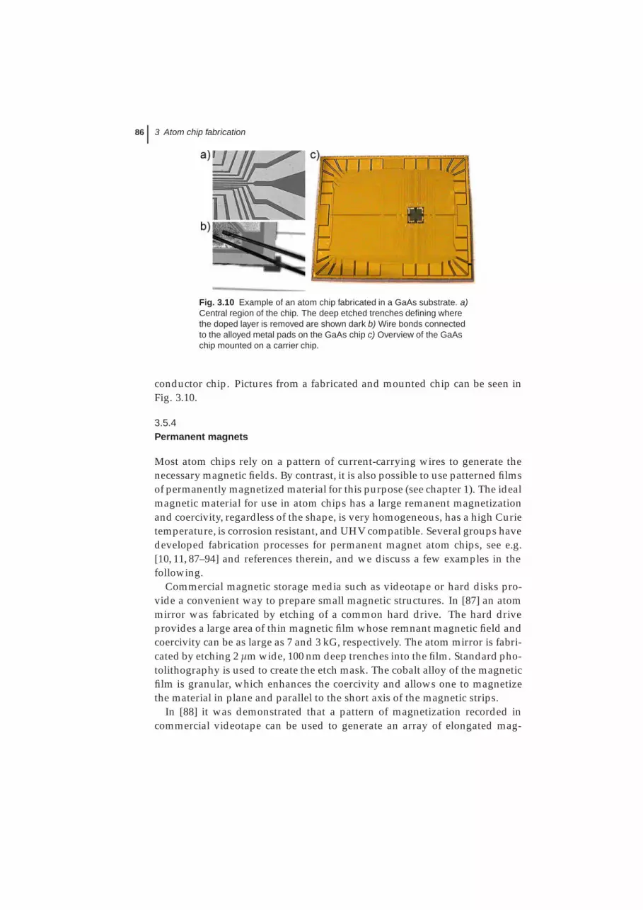
Fig. 3.10 Example of an atom chip fabricated in a GaAs substrate. a)Central region of the chip. The deep etched trenches defining wherethe doped layer is removed are shown dark b) Wire bonds connectedto the alloyed metal pads on the GaAs chip c) Overview of the GaAschip mounted on a carrier chip.
conductor chip. Pictures from a fabricated and mounted chip can be seen inFig. 3.10.
3.5.4Permanent magnets
Most atom chips rely on a pattern of current-carrying wires to generate thenecessary magnetic fields. By contrast, it is also possible to use patterned filmsof permanently magnetized material for this purpose (see chapter 1). The idealmagnetic material for use in atom chips has a large remanent magnetizationand coercivity, regardless of the shape, is very homogeneous, has a high Curietemperature, is corrosion resistant, and UHV compatible. Several groups havedeveloped fabrication processes for permanent magnet atom chips, see e.g.[10, 11, 87–94] and references therein, and we discuss a few examples in thefollowing.
Commercial magnetic storage media such as videotape or hard disks pro-vide a convenient way to prepare small magnetic structures. In [87] an atommirror was fabricated by etching of a common hard drive. The hard driveprovides a large area of thin magnetic film whose remnant magnetic field andcoercivity can be as large as 7 and 3 kG, respectively. The atom mirror is fabri-cated by etching 2 μm wide, 100 nm deep trenches into the film. Standard pho-tolithography is used to create the etch mask. The cobalt alloy of the magneticfilm is granular, which enhances the coercivity and allows one to magnetizethe material in plane and parallel to the short axis of the magnetic strips.
In [88] it was demonstrated that a pattern of magnetization recorded incommercial videotape can be used to generate an array of elongated mag-

3.5 Metallic layers 87
netic microtraps. Videotape can store patterns with feature sizes down to afew micrometers using simple commercial recording equipment adapted inthe laboratory. It is designed to hold data reliably for long periods of timeand has a high coercivity (1500 Oe), making the magnetization insensitive tothe presence of magnetic bias fields. The tape used in [88] has a 3.5 μm thickmagnetic layer containing iron-composite needles, 100 nm long with 10 nmradius, which are set in a glue and aligned in parallel. The film is supportedby a polymer ribbon 11 μm thick. Remarkably, the tape is UHV compatibleand is able to withstand baking at 120°CThe same group has also investigatedvarious other permanent magnetic materials for atom chips, such as magneto-optically patterned CoPt thin films [89].
The Amsterdam group has found that FePt is a magnetic material ideallysuited for the use in atom chips [10, 90–92]. Their first chip was made out ofa 40 μm thick foil of FePt [10]. An “F”-like shape was cut out by spark ero-sion and glued onto a mirror. This produces a self-biasing Ioffe-Pritchard trap.The second generation atom chip uses structures lithographically written intoa FePt film [91]. Fig. 3.11a shows a two-dimensional FePt pattern with themagnetization oriented perpendicular to the film, which has been used to cre-ate a large two-dimensional array of magnetic microtraps [12]. The 300 nmthick FePt film is grown in the ordered face-centered-tetragonal (fct) phase,which is magnetically hard with high uniaxial anisotropy constant. The mea-sured remanent magnetization is Mr = 670 kA/m, the remanent to saturationmagnetization ratio Mr/Ms = 0.93, and the coercivity Hc = 0.95 T. After bak-ing for 3 h at 150°C in air, the magnetization had reduced by only 3%, andthe film was found to be stable against typical time-varying fields applied inthe experiment. The film is patterned using optical lithography and argonplasma etching. After patterning, the film is coated with a 100 nm reflectivegold overlayer and magnetized in a 5 T magnetic field.
The Melbourne group uses atom chips based on perpendicularly magne-tized multilayered TbGdFeCo/Cr films [11, 93, 94]. These films have a largeperpendicular magnetic anisotropy and are suitable for the production of pe-riodically grooved, micron-scale structures. Fig. 3.11b shows an example of apatterned film that can be used to produce a one-dimensional magnetic lattice.To pattern such magnetic films, a periodically grooved structure is first fabri-cated into a Si substrate by reactive ion etching. The TbGdFeCo film is thendeposited on this grooved structure by magnetron sputtering. Because themagnetic anisotropy is found to deteriorate for a film thickness above 250 nm,a multi-layer structure is deposited, consisting of several layers of TbGdFeCo(160 nm) and Cr (100 nm) to achieve a total thickness of about 1 μm. A 10 nmCr film and finally a 150 nm gold film are deposited on top of this structure inorder to produce a mirror for the mirror-MOT. Measurements show that the

88 3 Atom chip fabrication
Fig. 3.11 Permanent magnet atom chips. (a) SEM image of the pat-terned magnetic film of [91]. The light gray areas correspond to theFePt pattern and the darker regions are the Si substrate. The film canbe used to create a two-dimensional magnetic lattice potential. (b)Magnetic force micrograph of the patterned magnetic film of [93]. Thestructure is a 150 nm thick Gd10Tb6Fe80Co4 film on a 140 nm thickCr underlayer on a Si grating structure with a period of 3 μm. Thegrooves are represented by the light regions and the inset shows across-section of the MFM signal along the indicated line.
remanent magnetization of the film is about 3 kG and the coercivity is about6 kOe [94].
3.5.5Metal outlook
As the fabrication of magnetic field based atom chips evolves in the future,one would also need to look at additional forms of materials. Aside from theabove mentioned metals, alloys, superconductors, semi conductors and per-manent magnets, it stands to reason that additional classes of new materialswill be investigated in the near future. Here, as an example, we shall focus onnano wires, molecules and metallic crystals, which are already being studiedin several groups.
Nano wires (Fig. 3.12) constitute an interesting system. While the currentmay be sufficiently high to maintain magnetic traps, the Johnson noise maybe sufficiently low to enable long spin flip lifetimes at small atom-surface dis-tances. Lifetimes of seconds may be reached for atom-surface distances of lessthan one micrometer [49]. Fabricating nano wires may only be done throughdirect e-beam writing, and even then, requires considerable attention to de-tails such as edge roughness and contact resistivities. We note that due tosurface scattering, the nano wire resistivity may be high, an issue which maybe solved by using crystalline nano wires, namely molecules, which are ournext topic.

3.5 Metallic layers 89
Molecules may form interesting conductors for numerous reasons. First,they may be able to sustain extremely high current densities. Second, theymay suppress hindering effects such as Van der Waals and Casimir-Polder(CP) forces, corrugations due to imperfections causing electron scattering, andnoise giving rise to spin flips, heating and decoherence. Third, molecules havea relatively sharp absorption spectrum and hence may be put much closer tosensitive optical devices in comparison with normal metal wires. Finally, onemay also look into a future in which molecules will self assemble into circuits(forming molecular electronics), and similarly may be used to assemble cur-rent carrying atom chip circuits.
A specific molecule that has recently attracted attention is the Carbon NanoTube (CNT). The CNT may hold current densities of up to 109 A/cm2 (twoorders of magnitude higher than normal metals), may have ballistic trans-port (hence negligible scattering causing corrugations) and is also expectedto produce less noise and CP forces. Two articles describe the advantages ofCNTs [95, 96]. To the best of our knowledge, to date, no atoms have beentrapped in the magnetic field of a CNT but several groups, such as the Tübin-gen group, are pursuing this goal.
CNTs come in different shapes and forms: from single-wall CNTs to multi-wall CNTs, from semi-conducting to metallic, and from suspended to sub-strate based. While a multi-wall CNT offers more current, it is also less crys-talline in nature. While a suspended CNT offers less CP it probably also en-ables less current density due to the lack of a heat sink. It is unclear whatthe ultimate current limit of single wall CNTs is but while 20 μA seem to beenough for trapping at a height of a few hundred nanometers (also taking intoaccount the CP force) [97], experiments at the Ben-Gurion University groupshow that CNTs of a few μm length are able to carry up to 50 μA.
Typically a Chemical Vapor Deposition sample will contain many CNTswith random orientations, lengths, and degrees of straightness. A preliminarysurvey is taken by AFM and, if suitable CNTs are seen, grids of Ti alignmentmarks (e.g. 2 μm long, 1 μm wide, 40 nm thick, 10 μm spacing) are grown bye-beam lithography (PMMA resist baked at 200°C ) and thermal evaporationover several small areas of the Si wafer. After lift-off with NMP at 80°C theseareas are then carefully scanned by AFM; co-ordinates for suitable CNTs aremeasured with respect to the Ti alignment marks.
The next step is to contact both ends of the CNT with parallel leads in orderto form the "Z" shape typically used for Ioffe-Pritchard atom chip micro-traps(and now for CNT-based nano-traps). Pd leads are usually thought to havethe best contact resistance to CNTs and are made by using a second e-beamlithography step with PMMA (the same as before) and are typically 30-40 nmthick and 1 μm wide, (see Fig. 3.12).

90 3 Atom chip fabrication
Fig. 3.12 (a) An AFM scan of a single wall carbon nano tube (2μmlong connected to Pd pads [97]. Around 40μA were pushed throughthis CNT. (b) Nano wire: 50nm wide and 20nm thick [49] (fabrication ofboth samples done at the Ben-Gurion University fabrication facility).
In the future, it is expected that CNTs will be grown in a controlled wayalong pre-defined paths. One such method, includes growth of CNTs alongatomic steps in the substrate [98, 99]. An alternative method for controllingthe CNT position and orientation utilizes an imprint process [100]. In such acase where the CNT’s position and direction is determined by the user, onemay also etch the substrate before depositing the CNT, evaporate or electro-plate a loading wire into the etched channel, deposit an insulating layer andobtain a smooth substrate by Chemical Mechanical Polishing (CMP) or otherplanarization methods described in this chapter, and then place the CNT ontop - hence obtaining a truly monolithic CNT atom chip.
Before moving on, let us note that nano wires and molecules such as CNTsmay be used also for other purposes. For example, ideas have emerged whereplasmonic waves on such elements may be used to trap and couple light be-tween nearby atoms. Another example, which was realized experimentally,includes utilizing CNTs for high efficiency atom counting. The experimentwas conducted in the Tübingen group of J. Fortagh [101]. In Fig. 3.13 we showthe CNTs used to create a high electric field for the purpose of ionization andion counting.
Another class of materials that has so far not been used in atom chips is crys-talline metals. There may be several advantages for utilizing such materials.To start with, they may offer reduced electron scattering and thus producepotentials with less corrugation. They may also be used in their electricallyanisotropic form to significantly reduce decoherence even at room tempera-ture (Fig. 3.14) [102].
Fabrication of atom chips using these materials is not trivial. To start with,these materials may not be deposited through evaporation and need to be

3.5 Metallic layers 91
Fig. 3.13 Vertical CNTs used to create a high electric field for ion-ization of neutral atoms. The ions are then detected with single atomprecision.
100
101
102
103
104
10510
−6
10−4
10−2
100
r = σxx
σyy
γspin
decoh
eren
ce
[s−
1]
Au
Ti Ga
NaCo2O
4
Graphite
HOPG2
HOPG1
SrNbO3.41
σzz � σxx , σyy ≈ σxx
σyy � σxx , σzz ≈ σxx
σyy � σxx , σzz ≈ σyy
σzz � σyy � σxx
Fig. 3.14 The spin decoherence rate as a function of the electricalanisotropicity of the material [102]. The different lines represent dif-ferent types of anisotropic materials (see legend). Several materialexamples are also shown.
grown in specialized methods. Typically, one can buy layers of these materialsafter which they will need to be bonded to a substrate (as they usually comeas thick leafs or attached to dissolvable substrates), thinned (without causingtoo much surface roughness) and patterned. Obviously, standard lift-off maynot be used here as the photoresist may only be put on top of the material.
92 3 Atom chip fabrication
Shadow masks followed by wet etching, ion beam milling or plasma etch-ing will need to be utilized. In addition to the above, one would also haveto utilize normal evaporated metals to make electrical contacts as the abovecrystalline materials may not have suitable conductivity in all directions.
3.6Additional features
3.6.1Planarization and insulation
Dielectric layers for planarization and electrical insulation are essential for thefabrication of multi-layer chips. Besides the dielectric and planarization prop-erties, good heat conductivity, ultra-high vacuum compatibility, and chemicalstability in subsequent processing steps are important criteria for the choice ofsuitable materials.
Spin-on polyimide has been used in the multi-layer atom chip designs of[23,41]. It provides good planarization, electrical insulation, and is UHV com-patible. Moreover, some polyimides can be directly structured by UV lithogra-phy. On the other hand, polyimide has a thermal conductivity which is aboutthree orders of magnitude smaller than that of gold or silicon. Therefore, thepolyimide layer has to be as thin as possible to allow for large current densitiesin the wires of the upper gold layer. To process polyimide, the chip is spin-coated with the polyamic ester. Subsequent curing of the polyimide is carriedout at temperatures of typically 300-400°CFully cured polyimide is resistantto solvents and most acids, but can be dry etched in an oxygen plasma [47].
As illustrated in Fig. 3.15, a layer of polyimide does not globally planarizea chip surface with an uneven topography. It rather acts as a “low-pass fil-ter” which locally smoothens out the topography. Only features with a lat-eral extension smaller than the planarization length, which is ∼ 20 μm forthe polyimide used in [41], can be fully flattened out [103]. The degree ofplanarization is higher for several thin coatings compared with a single thickcoating of equal total thickness. Fig. 3.16 shows AFM measurements of thepolyimide surface topography above gold wire structures. Thin gaps (5 μmwide) between 5 μm thick wires are planarized to a step height of 300 nmwith three layers of polyimide. If necessary, the thickness of the polyimidecould be reduced by subsequent back-etching.

3.6 Additional features 93
polyimide
planarizationlength ~ 20 μm
isolated wire narrow gaps multiple coatings
Au
Si
Fig. 3.15 Planarization and insulation with polyimide. Narrow gaps areeasier to planarize than broader, isolated features. Multiple coatingsimprove planarization [41].
polyimide layer 1
layer 2
layer 3300 nm
gold
5 μm
0
2
4
6
8
z [μ
m]
0 10 40 60 80x [μm]
-2
-4
20 30 50 70
Fig. 3.16 Planarization results [41]. Surface topography of three poly-imide layers above small gaps in a lower gold layer, measured withan AFM. Note the different scaling of the two axes. On this chip, thepolyimide layers were 4.3, 1.9, and 1.0μm thick.
3.6.2On-chip mirrors
It is often desirable to have a high-quality mirror as the uppermost layer onthe atom chip. A mirror is required for the operation of a mirror-MOT [36].Moreover, it enables imaging of the atoms very close to the chip surface, us-ing an absorption imaging beam that is reflected from the surface [104]. Themirror can also be used for reflecting laser beams that generate optical dipoletraps.
High-quality dielectric mirror coatings can be transferred to the chip usinga replica technique [105, 106], which is illustrated in Fig. 3.17. In this tech-nique, a detachable mirror coating supplied on a transfer substrate is gluedonto the desired chip area using vacuum-compatible epoxy glue. The transfersubstrate is manually removed, leaving the coating on the atom chip. Varioustypes of dielectric coatings on transfer substrates are commercially available.By cutting the transfer substrate to the desired size, it is possible to only par-tially cover the atom chip with the mirror [29,107]. The transfer technique canalso be used for homogeneous metal layers [105]. The advantage compared
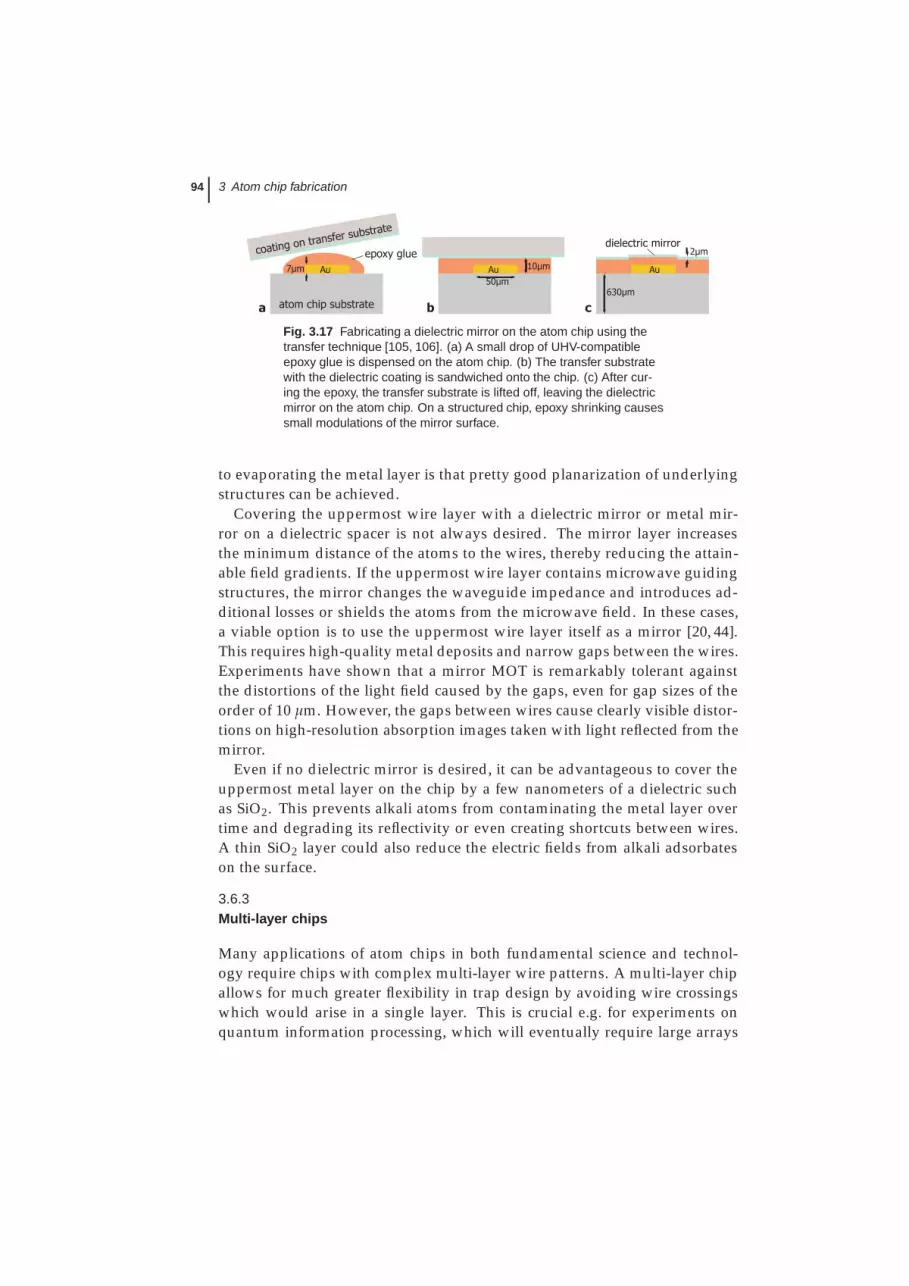
94 3 Atom chip fabrication
Fig. 3.17 Fabricating a dielectric mirror on the atom chip using thetransfer technique [105, 106]. (a) A small drop of UHV-compatibleepoxy glue is dispensed on the atom chip. (b) The transfer substratewith the dielectric coating is sandwiched onto the chip. (c) After cur-ing the epoxy, the transfer substrate is lifted off, leaving the dielectricmirror on the atom chip. On a structured chip, epoxy shrinking causessmall modulations of the mirror surface.
to evaporating the metal layer is that pretty good planarization of underlyingstructures can be achieved.
Covering the uppermost wire layer with a dielectric mirror or metal mir-ror on a dielectric spacer is not always desired. The mirror layer increasesthe minimum distance of the atoms to the wires, thereby reducing the attain-able field gradients. If the uppermost wire layer contains microwave guidingstructures, the mirror changes the waveguide impedance and introduces ad-ditional losses or shields the atoms from the microwave field. In these cases,a viable option is to use the uppermost wire layer itself as a mirror [20, 44].This requires high-quality metal deposits and narrow gaps between the wires.Experiments have shown that a mirror MOT is remarkably tolerant againstthe distortions of the light field caused by the gaps, even for gap sizes of theorder of 10 μm. However, the gaps between wires cause clearly visible distor-tions on high-resolution absorption images taken with light reflected from themirror.
Even if no dielectric mirror is desired, it can be advantageous to cover theuppermost metal layer on the chip by a few nanometers of a dielectric suchas SiO2. This prevents alkali atoms from contaminating the metal layer overtime and degrading its reflectivity or even creating shortcuts between wires.A thin SiO2 layer could also reduce the electric fields from alkali adsorbateson the surface.
3.6.3Multi-layer chips
Many applications of atom chips in both fundamental science and technol-ogy require chips with complex multi-layer wire patterns. A multi-layer chipallows for much greater flexibility in trap design by avoiding wire crossingswhich would arise in a single layer. This is crucial e.g. for experiments onquantum information processing, which will eventually require large arrays

3.6 Additional features 95
Fig. 3.18 (a) Atom chip of [22]. Three different experiment chips withmicrometer size structures are glued on top of a carrier chip with largerstructures for positioning of the atoms. (b) Atom chip of [107]. Thismagnetic conveyor belt is a two-layer structure with vias, fabricated bythick-film hybrid technology.
of qubits in individually addressable microtraps on a single chip (see chap-ter 9). Some proposals for quantum gates require the integration of microwaveguiding structures on the chip in addition to the already complex DC wirestructures [17, 20]. Moreover, it is often necessary to combine wires of verydifferent size and thickness on the same chip, e.g. because the experimentalsequence starts with an ensemble of atoms in a large-volume trap, while theactual experiment is performed with a small Bose-Einstein condensate in amicrometer scale trap. In all these cases, multiple wire layers separated bydielectric insulation layers are beneficial. Here we discuss several examplesof multi-layer atom chips which have been used in experiments. A generalintroduction to multi-layer microfabrication is given in [103].
The simplest way to produce a “multi-layer” chip is to fabricate two single-layer chips and glue them on top of each other. This greatly simplifies fabrica-tion because the processes used for the two layers are completely independentand the chips can be independently discarded if something goes wrong. Thistechnique has been used e.g. in the experiments of [22], where a carrier chipwith a standard layout of larger wires for initial trapping and transportingof atom clouds carries several experiment chips with dedicated micro- andnanostructures for the main experimental task, see Fig. 3.18a. The carrier chipused in [22] is itself a two-layer structure, with one wire layer on the front sideand another one on the back side of the same substrate. For interconnectingthe two layers, wire vias have to be fabricated through the 250 μm thick sub-strate. The vias are made by laser cutting of holes 400 μm in diameter andelectroplating gold inside.
In [107], a two-layer chip is described in which the two wire layers are onthe same side of the substrate, see Fig. 3.18b. The chip is fabricated usingthick-film hybrid technology. This fabrication process is mainly employed inhigh-power electronics and is based on screen-printing with metallic and di-electric printing pastes. The desired structure is lithographically transferred toa fine-gauge printing mesh. The printing paste is then squeezed through thismesh onto the substrate. Large-format substrates and thick conductor layers

96 3 Atom chip fabrication
Fig. 3.19 Multi-layer atom chip of [23]. (a) SEM micrograph of thecentral part of the chip. 10 μm wide wires with a height of 1.4 μm crossstructures created by e-beam lithography. The smallest features are300 nm gaps between 700 nm wide and 140 nm high wires. Electricalinsulation of the two layers is provided by 500 nm thick polyimide pads,visible as partially transparent layer. (b) Cross section of chip (not toscale). The step in the upper gold wire causes a bottleneck of reducedwire cross section. (c) SEM top view of the step. The wire runs fromleft to right in the upper half of the picture. In the lower right part thepolyimide pad running from top to bottom is visible.
with high current capability are standard with this technology. However, thestructures are grainy and the minimum feature size as well as the thicknessof the layers is of the order of tens of micrometers and thus not as small as indirect lithographic techniques.
While relatively simple to implement and useful in many cases, these tech-niques have two main drawbacks: there is a relatively large distance be-tween the two wire layers and it is difficult to accurately align the structureson the different layers with respect to each other. To overcome these limi-tations, several groups have developed custom multi-layer chip fabricationprocesses where the metal layers are fabricated by optical or electron beamlithography and separated by thin insulating layers of at most a few μm thick-ness [23,34,41]. This enables precisely aligned crossed wire configurations ona micrometer scale, greatly enhancing the flexibility in designing potentialsfor the atoms.
Fig. 3.19 shows pictures of the multi-layer chip described in [23]. It is fab-ricated using a combination of optical and electron-beam lithography, golddeposition by evaporation, and lift-off. On this chip, larger wire structures arefabricated on top of smaller ones, facilitating planarization of the lower layer.The two wire layers are separated by a polyimide layer, which is structuredby optical lithography to cover only regions where conducting structures willcross. The insulation layer is thinned in an ozonator to about 500 nm andcured. This layer thickness proves to be sufficient to insulate the two conduct-ing planes while providing good heat transfer and keeping the step height thetop layer wires have to surmount to a minimum (see Fig. 3.19b-c).

3.7 Current densities and tests 97
Fig. 3.20 Multi-layer atom chips of [20, 41]. (a) Photograph of a wholechip. Two gold wire layers are separated by a thin polyimide layer (seemain text). Wires on the lower layer have an orange color becauseof the overlying polyimide. (b) Close-up of the central region of thechip. Parallel wires on the upper layer cross wires on the lower layer.(c) SEM micrograph of a different chip. Small gold wires (thickness800 nm) forming a coplanar microwave guide cross a large transversewire of 7 μm thickness. A single polyimide layer of only 4 μm thicknessbetween the wires already provides sufficient smoothing of the step.
Fig. 3.20 shows pictures of multi-layer chips described in [20,41]. The chipsare fabricated using optical lithography. The chip shown in Fig. 3.20a-b has alower wire layer of 5 μm thick electroplated gold, which is covered by threelayers of spin-on polyimide with a total thickness of 6 μm. On top of the poly-imide, a 1 μm thick gold wire layer is fabricated by evaporation and lift-off.On this chip, the small wires are on top of the larger ones. The three poly-imide layers provide very good planarization. The smallest structures on theupper wire layer are several parallel wires of 2.5 μm width, separated by 2 μmgaps. Some of the wires on the upper layer form integrated microwave guid-ing structures. Fig. 3.20c shows a different chip, on which such a microwaveguide crosses a thick transverse wire on the lower gold layer, demonstratingthe smoothing of the step by the polyimide.
3.7Current densities and tests
An important parameter in all atom chips is the electric performance of thefabricated structures. Atom chips require current densities in the excess of106A/cm2 in continuous use. For a wire (height h and width w) to support

98 3 Atom chip fabrication
such high current densities j = I/wh, the ohmic heat P = RI2 created in thewires has to be efficiently transferred into the substrate and removed. Thetemperature rise and eventually the destruction limit of a wire depends notonly on j and the length of the current pulse τ but also on the geometry andon material parameters like heat conductivity λ and heat capacity CV . In a typ-ical atom chip the wire is separated from the thermally conducting substrateby a thin electrical insulating layer which at the same time is a bad thermalconductor. This leads to two heat removal mechanisms on very different timescales [5].
The first process concerns the heat flow from the wire to the substratethrough the insulating layer. In a 1d model, the timescale of this process isgiven by τf ast = CVh
k−hj2ρ where k is the thermal conductance through the in-sulating layer and ρ the temperature dependent resistivity of the wire. For atypical Au chip wire τf ast ∼ 1 μs which is very short when compared to othertimescales of the experiments and the temperature difference ΔT saturates to:
ΔT(t) =hj2ρ(ΔT = 0)
k− hj2ρ(1− e−t/τf ast). (3.2)
The second concerns the heat transport in the substrate and is much slower:in a 2d model with a point-like heat source on the surface of a half space sub-strate the temperature increase is then given by
Ts(t) =hwρj2
2πλΓ(
0,CV w2
4π2λt
)≈ ρI j
2πλln(
4π2λtCVw2
)(3.3)
where the (small) temperature dependence of the resistivity is neglected.These two models together accurately reproduce the results obtained in a
two-dimensional numerical calculation as long as the substrate can be treatedas a heat sink, which holds for short times (typically 100 ms – 1 s). For longertimes the heat transport out of the substrate has to be taken into account.
Atom chip wires are typically tested using a four-point measurement, push-ing a constant current through the wires while recording the change of the re-spective voltage drop with time. For simple single layer chips the latter is agood indicator of the change in resistivity caused by the Ohmic heating of thewires. In typical tests [5] a silicon substrate with a thin SiO2 layer shows thelowest immediate increase of temperature, and the smallest long term heat-ing. Silicon with a thick SiO2 layer does show stronger heating, which iseven worse for sapphire and GaAs substrates. In accordance with the abovemodel the highest current densities are tolerated by the thinnest wires withthe smallest width. A 700 nm wide and 140 nm high wires carried currents ofup to 60 mA over 10 s, corresponding to a current density of 6× 10⁷ A/cm2.Similar tests were recently carried out with a chip fabricated on an AlN sub-strate [108].

3.7 Current densities and tests 99
Fig. 3.21 a) Temperature evolution of a 80 μm top layer trapping wirefor different applied currents. After ∼ 6 s, an additional current of 1 Ais sent through two 500 μm bottom layer confinement wires. b) Tem-perature evolution for different current densities in various chip wires.Solid lines are theoretical predictions according to a simple dissipationmodel which applies to bottom layer wires in direct contact with thesubstrate [5]. Reduced heat dissipation reduces the current densityfor top layer wires, currents in the bottom layer wires lead to additionalheating (dashed lines to guide the eye).
Tests of multi-layer atom chip structures (Fig. 3.21) [23] show a similar be-havior, but the combination of short sub–μm wires connected to large struc-tures, and the simultaneous current through crossing wires does lead to del-icate failure modes. The resistivity change is not a firm indicator of the tem-perature any more because different parts of the wire contribute differently tothe changes. A simple rule of how much resistivity increase one can safelytolerate cannot be applied. Limits have to be found for each individual wirecategory.
Finally, atom chips also create electric fields. Very small structures natu-rally create large electric fields. This is due to sharp corners as well as smallgaps. For example, a moderate voltage of 60 V translates to an applied electricfield of over 200 kV/mm over 300 nm gaps between small wires. It has beenshown that atom chips can indeed sustain very high electric fields without
100 3 Atom chip fabrication
breakdown allowing to create very steep potential surfaces and to implementversatile state selective combinations of electric and magnetic potentials [21].
3.8Photonics on atom chips
The interaction between atoms and light is an essential ingredient in prepar-ing, detecting and manipulating atoms. It is therefore natural to integratemicro-optics on the atom chip.
3.8.1Fiber-based integrated optics
A simple and very well developed technology that allows to integrate lightwith the atom chip is fiber optics, which may be placed on the chip surface.Components that don’t need active alignment, such as cavities with mirrorsimplanted in the fiber, or tapered fibers for dipole traps or for the deliveringof excitation light, can be directly integrated on the chip, and microfabricatedSU8 holding structures are the method of choice [26]. This strategy will notwork well for fiber cavities which need to be actively aligned during opera-tion; here actuators are needed.
3.8.1.1 SU8 - holding structures
SU8 [109] is an epoxy based negative photo resist which can be patterned us-ing 365-436 nm UV-light, and which is compatible with Ultra High Vacuumrequirements. It has very high mechanical, chemical, and thermal stability. Itsspecific properties facilitate the production of > 100 μm thick structures withvery smooth sidewalls with a sizable undercut. SU8 is widely used to fabricatediverse micro-components ranging from optical planar waveguides with highthermal stability and controllable optical properties to mechanical parts suchas microgears [110] for engineering applications, and microfluidic systems forchemistry [111].
To mount fibers on the chip, the Heidelberg / Vienna team fabricate twoSU8 ridges which are separated by a distance a few hundreds of nanometersmaller than the fiber diameter, and have a height of typically 60% of the fiberdiameter. The layout of the used alignment structure with fibers is shown inFig. 3.22. This design includes funnels to simplify assembly. To avoid angularmisalignment the total length of the alignment structure is quite long (6000µm). The structure is divided into several subsegments to reduce stress in-duced by thermal expansion. The fibers can then be inserted from the top byapplying a little pressure on the fiber. Inside the holding structure the fibers

3.8 Photonics on atom chips 101
Fig. 3.22 a) Layout of the alignment structure and a magnified part(dotted rectangle) in b). c) Fiber in a SU8 structure mounted on a goldcoated atom chip. The atom chip and the SU8 structures have beencut with a wafer saw. The SU8 maintains structural integrity during thecutting.
are held precisely by the undercut, and can be shifted longitudinally with highprecision. To fix the fibers they are glued with UV cured glue.
The quality of the SU8 alignment structures can be assessed by mounting asplit fiber based optical resonator, with mirrors inside the two mounted fibers.The finesse of the resonator then strongly depends on losses introduced in thegap by misalignment of the two fibers [112]. Starting with a fiber resonatorwith a finesse of F = 152.8± 1.1, the fiber is cut between the mirrors tointroduce a gap and the new surfaces are polished. The two separate fiberpieces are then introduced into the SU8 structures and mounted with a small(< 1 μm) gap size. The finesse of the split and mounted resonator was mea-sured to be F = 132.0± 1.3. This corresponds to a coupling loss from fiberto fiber of 0.29± 0.04%. Neglecting other additional losses, this correspondsto a transversal misalignment of < 100 nm or an angular misalignment of< 5× 10⁻³ rad. When changing the temperature of the substrate between20°C and 70°C the finesse of the mounted fiber resonator shows no change.
3.8.1.2 Fiber-based fluorescence detector
A simple fluorescence detector capable of high fidelity detection of singleatoms can be built using a single mode tapered lensed fiber to deliver theexcitation light to a very small spot and a multi-mode fiber mounted at rightangle to collect the fluorescent light (Fig. 3.23). To eliminate background lightand to protect the photon counter, the light passes through an interferencefilter before being directed to the single photon counting module (SPCM)
In the implementation by the Vienna group [114–116] the fibers are arrangedat 45◦ to the guide and orthogonal to one another. The detector is fully inte-grated on the atom chip by mounting the two fibers on the chip surface inlithographically defined holders fabricated from SU8 resist guaranteeing very

102 3 Atom chip fabrication
Fig. 3.23 a) Basic layout of the detector and the atom chip in the vac-uum chamber. A magnetic guide (blue) transports the atoms from theZ-shaped wire trap (red) to the detector. The excitation light is deliv-ered by a tapered fiber, and the fluorescence light is collected by amultimode fiber. Both are connected to the optics outside the vacuumchamber by a fiber feed-through [113]. The collected light then passesthrough a 3 nm wide (FWHM) interference filter centered at 780 nmbefore being directed to the single photon counting module(s) (SPCM).For high efficiency atom detection a single SPCM is employed whilecorrelation measurements require two SPCMs in a Hanbury Brown-Twiss like configuration. b) A microscope image of the detection regionon the chip. The multimode fiber collects light from a cone (blue) deter-mined by its NA. The overlap of this cone with the excitation light fromthe tapered fiber (red) defines the detection region (yellow).
accurate and ultra stable passive alignment [26]. The collection fiber with NA0.275 collects 1.9% of the fluorescence photons, and an average of 1.1 photonsis counted for each atom. In the absence of atoms, less than 10−8 of the exci-tation light is scattered into the collection fiber and the a total background isdominated by the SPCM dark count rate. With such a low background a singledetected photon implies that an atom is present in the detection region. Withan average of 1.1 photons/atom, the detector achieved single atom detectionwith 66% efficiency, and a typical signal to noise ratio of 100. Most remark-able is that the stray light level is so low that atoms can propagate freely inthe magnetic guide for more than a second with the detection light on, and bedetected one by one when passing the detection region. The single atom de-tection was verified by measuring the photon correlation function, and valuesof g(2)(0) < 0.05 were obtained [115].
The efficiency of the detector is limited by the NA of the collection fiber,while the SNR is limited by the background. Using a low noise photon counterwith a dark count rate < 25 cps, a total background of 55 cps can be achieved.Using a commercially available fiber with NA = 0.53 will allow to collect4.5 photons from each atom, and a single atom detection efficiency of ≈ 95%could be reached for an interaction time of 20 μs. With two detection fibers

3.8 Photonics on atom chips 103
of NA = 0.53 and with an interaction time of 20 μs, a single atom detec-tion efficiency beyond 99% seems feasible. Such a system would reach 9 pho-tons/atom. This will allow true atom counting by transient count rate analy-sis.
3.8.1.3 Fiber cavities
The integration of high finesse optical fiber cavities on atom chips has en-abled spectacular experiments on cavity quantum electrodynamics with aBose-Einstein condensate [27] as well as high-fidelity single atom detectionand preparation [117], an essential ingredient of chip-based quantum infor-mation processing (see chapter 9). In these experiments, the atom chip allowsprecise positioning of the atoms in the cavity field. Fiber cavities advanta-geously combine small mode volume with direct access to the high-intensitypart of the intracavity field. Moreover, the light can be coupled directly inand out of the cavity through the fiber, avoiding the need for sensitive cou-pling optics. Here we discuss different methods to fabricate chip-based fibercavities.
In [118–120], plano-concave microcavities are described, where the curvedmirror is etched into a silicon wafer. The plane mirror is a flat, cleaved fiber tipwith a high reflectivity coating applied to it, see Fig. 3.24a. Arrays of concavemirrors are fabricated in silicon by wet-etching isotropically through circularapertures in a lithographic mask using a mixture of HF and HNO3 in aceticacid. In order to investigate cavities of various lengths, the etching parametersare adjusted to produce wafers with a range of mirror radii between 30 and250 μm. The etched surface typically has an r.m.s. roughness of 5 nm. If theconcave mirror templates are coated with sputtered gold, a cavity finesse F ofthe order of a few hundred results. Alternatively, a dielectric coating designedfor 99.99% reflectivity can be used [118]. In this case, a cavity finesse of F =6000 can be achieved for a 15 μm long cavity, limited by the surface roughnessof the curved mirror. A cavity of this kind but with F = 280 was used foratom detection with less than one atom on average in the cavity mode [120].
A different type of fiber cavities was developed in [106, 121], see Fig. 3.24b.The cavities are of the Fabry-Pérot type and are formed with miniature spher-ical mirrors positioned on the end of single- or multimode optical fibers. Theconcave mirrors are fabricated from a convex template and a lift-off step. Forlarge radii of curvature, ≥ 500 μm, the template is a commercial ball lenswhereas for smaller radii, 100− 500 μm, a custom silica microlens with a sur-face roughness ∼ 1 nm is used. It is coated in one run with a release layer anda dielectric Bragg mirror with nominal reflectivity of 99.7%. A cleaved singlemode fiber is then positioned immediately above the center of the coated lensby maximizing the back reflection of a laser beam coupled into the fiber. Thefiber is then glued in place with an UV-curing epoxy, after which the appli-

104 3 Atom chip fabrication
Fig. 3.24 Optical fiber cavities on atom chips. (a) Plano-concave cav-ity of [118, 119] with a finesse of up to F = 6000. Left: The planemirror is formed by coating a fiber tip, the concave mirror is formed bycoating an etched silicon wafer. Right: SEM micrograph of an array ofmirrors on a silicon wafer. (b) Fiber Fabry-Pérot cavity with F = 1000described in [106, 121]. Two fibers functionalized with a concave di-electric mirror face each other. Left photograph: a single-mode fiberprocessed with a concave mirror. Right: mounted cavity of 27 μmlength on an atom chip. (c) Fiber Fabry-Pérot cavity with F = 37000used in [27, 117]. Top: SEM image of a laser-machined fiber end face.Bottom: Two fiber cavities of different length mounted on the sameatom chip.
cation of a small force is sufficient to detach the mirror from the original sub-strate. The result is a fiber functionalized with a concave mirror, see Fig. 3.24b.Two fiber tips facing each other form the cavity. The finesse is F = 1000, cur-rently limited by the quality of the multi-layer coatings. The detection of smallensembles of cold Rb atoms guided through such a cavity on an atom chip wasdemonstrated in [106].
In the experiments of [27, 117], an improved fiber Fabry-Pérot cavity witha much higher finesse of F = 37000 is used. The cavity design is based ona new laser machining process [122] where a single, focused CO2 laser pulsecreates a concave depression in the cleaved fiber surface, see Fig. 3.24c. Themachining is performed in a regime where thermal evaporation occurs, whilemelting is restricted to a thin surface region, avoiding global contraction intoa convex shape. The surface is then coated with a dielectric mirror coating.
The observedF = 37000 is limited by the sub-optimum coating. Ultimately,a finesse of F = 150000 should be achievable based on the measured surfaceroughness of about 0.2 nm r.m.s. Radii of curvature can be fabricated down

3.8 Photonics on atom chips 105
Fig. 3.25 An hexagonal array of spherical micro lenses (taken from[124]). On the right, the light intensity distribution at the focal plane.
to 50 μm and probably below. Because of the small mirror diameter (smallerthan the fiber diameter, which is typically 125 μm), the mirrors can approacheach other very closely (down to a few optical wavelengths) without touching.The result is a very small mode waist between 1 and 2 μm, and a small modevolume down to a few cubic wavelengths. These high finesse fiber cavitieshave enabled atom chip based cavity quantum electrodynamics experimentsin the strong coupling regime as well as high fidelity single atom detectionand preparation [27, 117].
3.8.2Micro lens and cylindrical lens
While fibers certainly hold promise, they also posses numerous disadvan-tages. For example, they require alignment and gluing. Due to their radius oftypically 60 microns, their interaction with atoms is usually at a similar heightabove the surface and this hinders the advantages of traps close to the sur-face (high gradients and low power consumption). To overcome this problemone would have to etch paths for the fibers within the substrate. However,the main disadvantage of fibers is in the scaling problem. Because of theirsize and the need for individual handling, it is hard to imagine hundreds andperhaps thousands of traps addressed individually by arrays of fibers. Thishas prompted an intensive effort aimed at integrating photonics into standardatom chips in order to achieve monolithic devices. The first interaction of coldatoms with substrate based optical elements was achieved in 2002 in the groupof Ertmer and Birkl [123].
A review of these elements may be found in Ref. [124]. Here circular andcylindrical lenses are formed with the goal of creating dipole force traps andguides. These guides may then be combined to create beam splitters and in-terferometers [125]. A review of how these lenses may be fabricated can befound in Ref. [126].

106 3 Atom chip fabrication
3.8.3Micro disks and toroids
The first substrate based high finesse devices to interact with cold atoms ap-peared in 2006 in two papers from the groups of Kimble and Vahala [127]and from the group of Mabuchi [128]. These experiments showed single atomsensitivity. To the best of our knowledge, these were also the first non fiberphotonic elements of any kind to be put into the vacuum at close vicinity tothe atoms. Hence, perhaps they may deserve the title of the first photonicatom chips. They were based on micro toroids sustaining a whispering gallerymode of light [129]. These seminal experiments still used fibers (tapered) inorder to couple the light into the disks and this required delicate positioning,gluing and tuning. Furthermore, no trapping of atoms has taken place in theseexperiments and this will presumably be aspired to in the next generation se-tups.
Let us review in more detail the above experiments. In the experimentsperformed by the Mabuchi group a quality factor of Q ≈ 106 (defined as theratio of the frequency to the line width or loss rate) was achieved by etching a 9μm SiN disk. Here work was done with commercially available Si wafers witha 250 nm layer of SiN deposited by Low Pressure Chemical Vapor Deposition(LPCVD). A highly circular mask was made by e-beam lithography and resistreflow and was transferred to the SiN by way of C4F8/SF6 plasma dry etch.Potassium hydroxide wet etch selectively removed the underlying <100> Sisubstrate until the SiN micro disk was supported by a small diameter Si pillar.A final cleaning step to remove organic materials from the disk surface wasperformed using a H2SO4 : H2O2 wet etch. To fine tune the disk to the atomicresonance, a series of timed etches of a 20:1 diluted 49% HF solution wereemployed. The resonance was shown to blue shift at a rate of 1.1 nm perminute. Further fine tuning can be achieved by temperature variations and adependence of 0.012 nm/°C was measured.
Similar work was done in the group of Kimble [127]. Their micro toroid wasdeveloped by the group of Vahala, where quality factors exceeding Q ≈ 108
were achieved by surface tension reflow following the melting of the surfacewith a CO2 laser [130]. The laser, having typical intensities of 100 MW/cm2,is centered on the disk, but because of the Si pillar, only the disk peripheryis melted. Here, nanometer scale and lower surface roughness needs to beachieved. For the purposes of interacting with atoms, quality factors exceed-ing 106 were sufficient and those were realized with disk diameters of about100 μm without the need for laser melting [131]. First, silicon wafers with 2μm of silicon oxide thermally grown (silica) were patterned by standard op-tical lithograph and wet etch of the oxide using buffered HF. The silica diskswere then isolated from the silicon substrate with an isotropic silicon dry etch
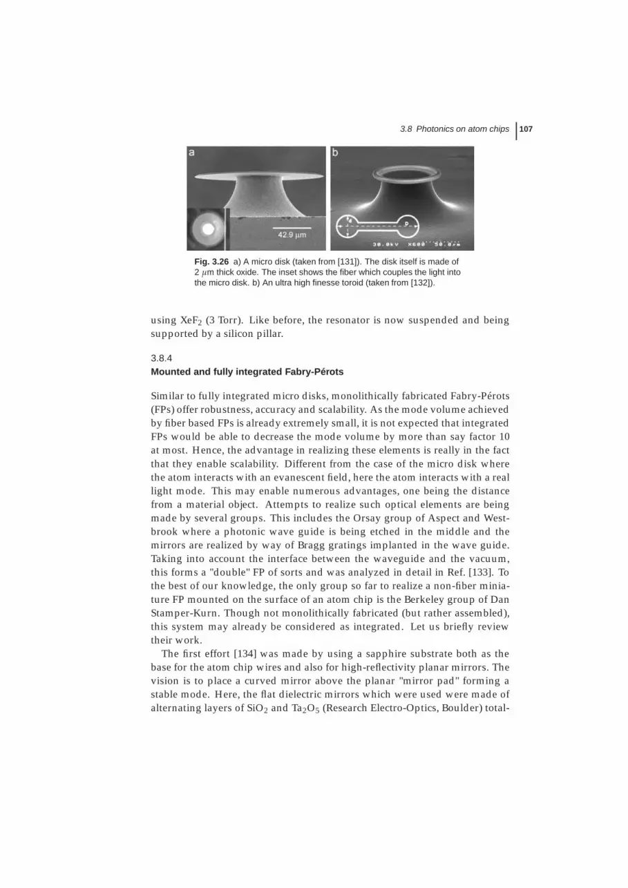
3.8 Photonics on atom chips 107
Fig. 3.26 a) A micro disk (taken from [131]). The disk itself is made of2 μm thick oxide. The inset shows the fiber which couples the light intothe micro disk. b) An ultra high finesse toroid (taken from [132]).
using XeF2 (3 Torr). Like before, the resonator is now suspended and beingsupported by a silicon pillar.
3.8.4Mounted and fully integrated Fabry-Pérots
Similar to fully integrated micro disks, monolithically fabricated Fabry-Pérots(FPs) offer robustness, accuracy and scalability. As the mode volume achievedby fiber based FPs is already extremely small, it is not expected that integratedFPs would be able to decrease the mode volume by more than say factor 10at most. Hence, the advantage in realizing these elements is really in the factthat they enable scalability. Different from the case of the micro disk wherethe atom interacts with an evanescent field, here the atom interacts with a reallight mode. This may enable numerous advantages, one being the distancefrom a material object. Attempts to realize such optical elements are beingmade by several groups. This includes the Orsay group of Aspect and West-brook where a photonic wave guide is being etched in the middle and themirrors are realized by way of Bragg gratings implanted in the wave guide.Taking into account the interface between the waveguide and the vacuum,this forms a "double" FP of sorts and was analyzed in detail in Ref. [133]. Tothe best of our knowledge, the only group so far to realize a non-fiber minia-ture FP mounted on the surface of an atom chip is the Berkeley group of DanStamper-Kurn. Though not monolithically fabricated (but rather assembled),this system may already be considered as integrated. Let us briefly reviewtheir work.
The first effort [134] was made by using a sapphire substrate both as thebase for the atom chip wires and also for high-reflectivity planar mirrors. Thevision is to place a curved mirror above the planar "mirror pad" forming astable mode. Here, the flat dielectric mirrors which were used were made ofalternating layers of SiO2 and Ta2O5 (Research Electro-Optics, Boulder) total-

108 3 Atom chip fabrication
Fig. 3.27 Flat dielectric mirror on a sapphire substrate (taken from[134]). The mirror is made of a combination of alternating layers of sil-icon dioxide and tatalum pentoxide (see text). Around the mirror onemay observe the platinum heaters for actuating the mirror. The sec-ond mirror is curved and mounted on a piezo stage. top right: (i) ther-mometer wire (ii) dielectric mirror pad (iii) heater wire (iv) waveguidewire.
ing about 5 μm in thickness. With a 400 nm thermally evaporated aluminiumprotective layer in place, Reactive Ion Etching (RIE) was used to etch awayunwanted mirror areas (100 sccm CF4 and 10-20 sccm O2 at 85 mTorr and RFpower of 0.4 W/cm2). About 5 μm of mirror edge were lost in this process,achieving finally a finesse of about F = 105.
One valuable outcome of this work is the high level of control realized overthe temperature of the atom chip surface, and the discovery that one couldactuate a high finesse mirror thermally to achieve a closed-loop control of theFabry-Pérot cavity spacing with a 1 MHz bandwidth. This is a powerful newcapability which would enable robust Cavity QED since the kHz-level acous-tic noise can be now suppressed immensely.
A second "cheaper" and less integrated project now under way utilizes DeepReactive Ion Etching (DRIE) to thin down a silicon wafer to just <100 mi-cron thickness, including the wires atop that thinned substrate. A hole is thenmicro-machined through this thinned wafer. Mirrors mounted on a separatepiezo mounting are positioned on both sides of the chip so that a vertical cav-ity mode pierces through the horizontal chip surface. In this way, the mirrorsare decoupled from the atom chip (useful for both thermal and vibrational iso-lation), and may be reused for many iterations of the atom chip. In additionone may use cheaper materials and fabrication for the chip itself.

3.8 Photonics on atom chips 109
Fig. 3.28 An array of monolithically fabricated atom-light junctions[135].
Finally, let us note a recent result from the group of Ed Hinds at ImperialCollege [135] in which for the first time a fully integrated (monolithically fab-ricated) array of atom-light junctions has been operated (Fig. 3.28). This maybe considered the first real step towards a scalable system.
3.8.5Planar optics
Planar optics (i.e. optics with no curved surfaces) are well established, andalthough they are ideal for standard fabrication techniques, they have almostnot been exploited in the field of atom chips. To the best of our knowledgeonly one publication exists describing such work [136]. In this work by J.Weiner and H.J. Lezec, a Fresnel (diffraction) lens has been etched by a Fo-cused Ion Beam (FIB) (Fig. 3.29). The overall size of the element is still quitelarge (about 200 by 200 μm2) but the method may be considerably miniatur-ized. For example, it has also been suggested to trap and measure atoms vialong focal length plasmon lens [137], made so far also by FIB. Here light passesthe substrate through a 250 nm hole. Such holes may be produced by the

110 3 Atom chip fabrication
Fig. 3.29 The cold atom setup and a zoom in on the FIB etched 1dFresnel diffraction lens (taken from [136]).
beam of a FIB or electron beam induced etching (utilizing gas injectors insidean e-beam machine), as these beams have a very small diameter of severalnanometers. To the best of our knowledge, while a small divergence beamhas been produced by plasmon lens, a focus has not. Another idea for an ex-tremely small planar optical element is to utilize the fast growing field of subwavelength optics. Here, a transparent material may be etched with high as-pect ratios to produce a phase mask which gives rise to optical control. Asthe resolution required in these elements is below that of optical lithography,and as e-beam lithography is time and price consuming, such elements willmost likely be produced by nano imprint methods where a hard mask pos-sessing the negative image is brought into contact with a soft material. Themask can, for example, be made of sapphire. Currently, DRIE protocols existfor sapphire e.g. with Nickel masks allowing for an etch selectiveness of 1:7.
3.8.6Photonics outlook
It is clear that the eventual goal of the photonics effort should be to use light onthe surface of the atom chip to trap, manipulate and measure atoms (down to asingle atom) in a way that allows integration with other atom chip techniquessuch as magnetic traps, and utilizing configurations that require standardsmonolithic fabrication techniques in order to achieve robust and accurate scal-ability. This probably means solid state light wave guides which will transferlight from fibers glued at the edge of the chip to monolithic optical elementsin the center of the chip, as in the recent achievement by the Hinds group(Fig. 3.28). Waveguides with low scattering i.e. small surface roughness, area challenge in their own right. For example, annealing a SiO waveguide for20 hours at 1000°C may reduce its surface roughness from several nanometerrms to less than one. The eventual goal would of course be to have no fibers atall, namely to have the light sources and the photo detectors integrated on thechip itself so that only electronics will need to interface with the chip. While
3.8 Photonics on atom chips 111
the above is the general vision, it is unclear what the final "winning" mono-lithic optical element would be. Considering the variety of demands includ-ing also the eventual price tag, it is likely that for every specific applicationanother type of element would perform best.
Concerning the integration of micro disks, the first issue is that of simul-taneous trapping allowing for long interrogation times. Standard magnetictrapping poses the challenge of light induced spin flips to un-trapable states.In addition, a metal with a wide absorption spectrum put in the vicinity of ahigh finesse mode may significantly reduce its finesse. Magnetic traps basedon molecules (e.g. CNT) with very sharp absorption peaks may be one way tosolve this problem. Another way may be through simultaneous optical trap-ping and sensing. Here blue and red modes create a potential minimum nextto the disk. Counter propagating modes can create arrays of traps. A fabrica-tion tolerance analysis of such a scenario was done in Ref. [138]. The secondissue requiring development is that of tunability. So far tunability has onlybeen done by thermal control. In Ref. [129], other tunability mechanisms havebeen analyzed. These include fabricating the disk from piezo material wherea voltage would change the disk diameter or utilizing an Electro-Optical (EO)material where a voltage would induce a change of index. Both these optionsrequire extensive materials and fabrication development. For example, stan-dard EO materials are crystalline in nature and may not be evaporated ontothe wafer (e.g. LiNbO3). Etching these materials with a high surface qualityis also very challenging. A possible solution may be to use polymers with EOfeatures that may be deposited through evaporation. A third issue is that oflight coupling. While disk fabrication without the existence of a nearby waveguide enables to utilize a variety of methods to achieve high finesse (in whichcase a tapered fiber is later brought to the vicinity of the disk), monolithic fab-rication of both disk and waveguide demand either a single step fabricationin which methods are used for the disk that do not harm the wave guide orsignificantly affect the gap between the two, or alternatively a double stepfabrication which involves accurate alignment and reduces the yield. As pa-rameters like the shape of the wave guide, its surface roughness and the ex-act dimension of the gap to the micro disk may significantly affect the lightcoupling and the disk finesse, the joint fabrication of these two elements is ademanding challenge.
Concerning the integration of FPs: Two issues seem to be the most challeng-ing problems on the way to the development of such a device. The first is 3dfabrication and the second tunability. For a stable mode to exist at least oneof the two mirrors must have a 3d profile or alternatively both mirrors musthave a 2d profile where the overall structure is 3d. A well established fabri-cation protocol for 3d structures actually does not exist. There are attempts toproduce 3d structures by way of controlled electron penetration and scatter-

112 3 Atom chip fabrication
ing within an e-beam resist. Similarly, there are attempts to utilize laser lightwhere the focus exposes 3d structures in a photo resist. However, these arecrude methods with no good control over parameters like curvatures and thesurface roughness achieved so far is not good enough. Even if these problemswere to be solved, there still remains the issue of how to evaporate a mirror (beit metallic or dielectric) onto these highly curved surfaces. The second issueinvolves tunability. Different from the case of the micro disk, here tunabil-ity would involve a real movement of the mirrors (unless some of the cavitymode is in a material, as in the above described "double" FP, in which case theindex of refraction may be changed as in the micro disks, or unless some ther-mal mechanism like that developed by the Dan Stamper-Kurn group may beemployed). Such a movement is possible through MEMs or piezo stages, butthen the interface to the waveguides bringing and taking the light becomescomplex.
Aside from the above noted elements realized so far, there are also numer-ous other ideas in the early stage of development, and below we note three asan example. The first is photonic crystals or band gap materials. In Ref. [139], afeasibility study was done concerning atom detection via the interaction witha light mode confined in the wafer by a 2d array of holes. Here the featuresof the light mode are critical as there needs to be a significant component oflight outside the wafer. In a second example, it has been suggested to usethe evanscent field of waveguides for trapping and interacting with atoms.Two color schemes (red detuned and blue detuned) create a trapping mini-mum while counter propagating beams create standing waves and thereforearrays of traps. The affect of surface roughness on the feasibility of such anidea was analyzed in Ref. [138]. These ideas would require considerable fab-rication development and nanometer scale control over parameters such asedge and surface roughness, as well as high aspect ratio etching. In a thirdexample, light is confined to propagation in nano structures, and may be usedfor strong interaction with atoms and for efficient transport of light (see forexample the work of M. Lukin, P. Hemmer, P. Zoller and others [140, 141]).
Last but not least, photonics will also include considerable work on the sub-strate itself. Using transparent substrates such as sapphire, one would be ableto introduce planar optics such a Fresnel lens described previously or evensub-wavelength optics. 3d fabrication may also be utilized such as in the pyra-mid or bowl shaped substrate etching done by the Hinds group (and collabo-rators from Southampton) for the creation of an on-chip integrated Magneto-Optical Trap [142] or optical cavity [118,119]. Transparent substrates may alsoenable evanescent blue detuned light to form stable near surface traps withcharged electrodes [143].
3.9 Chip dicing, mounting and bonding 113
3.9Chip dicing, mounting and bonding
After the microstructures on an atom chip have been fabricated, the chip hasto be cut to the desired size, mounted on a heat sink, integrated into a UHVvacuum chamber, and connected to the outside world. Fig. 3.30 shows exam-ples of such complete atom chip systems.
In Fig. 3.30a, the atom chip of [20, 41] is shown. The main “experimentchip” consists in this case of two layers of gold wires on a Si substrate (cf.Fig. 3.20). It is cut to size with a diamond blade and subsequently glued ontoa “carrier chip” with larger gold wires on an AlN substrate. The carrier chipserves as a heat sink and electrical vacuum feed through. The epoxy glueis UHV-compatible, heat-conductive, but electrically insulating, and care istaken that the gap between the chips is completely filled with epoxy to avoidvirtual leaks in the vacuum system. The wires on the experiment chip are wirebonded to the carrier chip, using up to 15 gold bond wires per chip wire. Thecarrier chip substrate has arrays of holes on each side, which were laser-cutbefore the wires were fabricated. The holes allow one to solder wires on thefront side of the chip to pins of a connector fed through from the back side,using a 70In/30Pb reflow solder paste. A connector on the back side has theadvantage that it does not inhibit optical access to the chip.
The atom chip is attached to a copper block, which is kept at a constanttemperature by water cooling. Millimeter scale machined copper structuresare integrated into this block. Such U- or Z-shaped metal structures are a use-ful tool to create large-volume quadrupole or Ioffe-Pritchard type magneticfields in the initial trapping stages of the experiment [44, 144].
Different techniques exist to integrate atom chips into the UHV vacuumchambers required for ultracold atom experiments. One approach is to mountthe atom chip assembly onto a vacuum flange with electrical feedthroughs,see Fig. 3.30c [44, 144, 145]. In the example of Fig. 3.30b, a different techniqueis used, in which the carrier chip is directly connected to a glass cell vacuumchamber. This technique, which was first described in [146], eliminates theneed for separate electrical vacuum feedthroughs, as the carrier chip wires canbe directly connected from outside the vacuum chamber. To seal the vacuum,either UHV compatible epoxy glue [41] or anodic bonding techniques [147]can be used. This technique allows one to further miniaturize ultracold atomexperiments [147], and complete systems consisting of an atom chip attachedto a miniaturized glass cell vacuum chamber are commercially available.

114 3 Atom chip fabrication
Fig. 3.30 Atom chip mounting, bonding, and contacting. (a) Multi-layer microwave atom chip of [20, 41]. The two-layer experiment chipis glued and wire bonded to a single-layer carrier chip. Microwave andDC connectors are soldered onto the front and back side of the car-rier chip. (b) Atom chip shown in (a) attached to a glass cell vacuumchamber. UHV compatible epoxy seals the vacuum. (c) Atom chip sys-tem of [144]. The chip is attached to a vacuum flange with electricalfeedthroughs. Copper structures behind the chip are used as a heatsink and to create large-volume traps.
3.10Further integration and portability
The atom chip was born in three laboratories around 1999 (Munich, Innsbruckand Boston). The vision of its makers and those who followed was of a ro-bust and accurate, miniature and portable system that could replace the largecold atom systems. Such an achievement would not only enable subtle ex-periments in fundamental physics but could also enable technological appli-cations such as clocks, sensors, and quantum information processing.
For this to happen numerous technologies must be further developed andintegrated:
• Substrates: Although substrates (wafers) may seem a trivial matter, theyare an extremely important issue. For example, when using standard sil-icon wafers, one reduces the possibility to transmit visible light throughthe wafer. One also adds in such a case the requirement for an insulationlayer which usually conducts heat badly, thus disconnecting betweenthe current carrying wires and their heat sink. Sapphire, for example, istransparent in the visible and does not require an insulating layer while

3.10 Further integration and portability 115
being a good heat conductor. However, it is very hard (although possi-ble) to etch sapphire, and adhesion to metallic layers may be more prob-lematic. Sapphire is a good example for other considerations, as it maybe used when RF with low losses is required (e.g. in ion chips). Transpar-ent wafers also enable easy back side alignment for back side fabrication.It is very likely that any substrate used in the future will require robustdeep etch processes. Vias for through-wafer electrical contacts (see fol-lowing), loading wires (for magnetic loading) and loading slits (e.g. inion chips where the particle source is likely to be on the back side of thechip), and eventually miniature vacuum cells within the wafers (closedby anodic bonding for example) - all these would require deep and attimes high aspect ratio etching.
• Metallic and insulating layers: Assuming electro-magnetic, electric, andmagnetic fields will continue to play a major role in atom chips, metallicand insulation layers will continue to need improved material engineer-ing and fabrication protocols. Numerous methods may be combined.For example, loading wires which are shut down during subtle quan-tum operations and which are far away from the atoms, may be madeof thick layers (e.g.10-100 μm) by way of electroplating on the back sideof a thin wafer (e.g. 100 μm) or in deep etched grooves on the front sideof a thick wafer. Finer wires made by evaporation with thickness up to2 μm will be put closer to atoms for traps and guides in which quantumoperations take place. Here, for complex trap and guide geometries,numerous layers may evaporated with planarized insulating layers inbetween.
• "Exotic" materials: These pose a fabrication challenge in terms of com-patibility of materials and fabrication protocols. For example, as de-scribed above, crystalline materials (e.g. electrically anisotropic mate-rials) may prove to be very advantageous in fighting potential corruga-tions and spin-flip, heating and dephasing due to noise. Such materialsmay not be evaporated and their patterning may not be done by normalmeans of lift-off (of photo resist). Here techniques of shadow mask needto be employed for plasma etching or ion beam milling. Finally, integra-tion with nanowires, molecules such as CNTs and other nano devicessuch as mechanical oscillators will require the integration of even morematerials and fabrication techniques as described above. For example,while single wall CNTs usually grow in a Chemical Vapor Deposition(CVD) oven, delicate electrical contacts may be done by Electron BeamInduced Deposition (EBID), and contact wires by thermal evaporationwhich may be either done by an e-gun (in the case of paladium) or bythermal evaporation (in the case of gold).
116 3 Atom chip fabrication
• Photonics: The integration of photonics means that all light sources andphoto detectors would eventually be on the chip so that no light con-nections via fibers are required. These light sources would deliver thelight to the different optical systems through single or multi mode di-electric wave guides having cross sections of a few microns, or alterna-tively through nano structures (plasmonics), as noted in the photonicsoutlook section. The optical elements themselves have been discussedabove and may include wave guides, micro curved lens, planar lens,and FP or micro disk cavities. Transparent substrates may also enableevanescent blue detuned light to form stable near surface traps withcharged electrodes. Atom laser cooling would also need to be miniatur-ized and here a single beam Magneto-Optical Trap (MOT) would per-haps be utilized. Such miniature pyramid/cone MOTs have recentlybeen developed in several groups [142,148,149]. For effective atom cool-ing, manipulation and measurement, frequency lock schemes will alsoneed to be integrated onto the chip. Indeed, recently several new minia-turized lock schemes have been suggested (e.g. see Ref. [150]).
• Electronics: To increase the signal over noise, and to reduce the amountof electrical connections to the chip, it is plausible that future chips willrequire some level of electronics to be integrated onto them. For exam-ple, fabrication of photo diodes and pre amplifiers for the readout, orfeedback electronics and high voltage drivers for the laser lock. It standsto reason that such electronics will be fabricated on the back side of thewafer and connected to the atom optics side by means of electrical vias.
• Vacuum: The issue of miniature vacuum cells has been the focus of con-siderable effort and will undoubtedly continue to be so. Similar to theeffort in the context of atom cells for room temperature atom optics de-vices made by the group of John Kitching [151], it is possible that futureminiature cells will be contained inside the substrate itself. Here tech-niques of wafer anodic bonding, as well as deep etch and MEMs, willplay a major role. Blue LEDs may also be used to achieve a fast tran-sition from the state of bad vacuum required for good MOT loading,to the state of good vacuum required for long trap and interrogationtimes [152].
As an example of the state-of-the-art of miniature vacuum systems and elec-tric contacts we present recent work from the groups of Dana Anderson andVictor Bright (Fig. 3.31) [153]. This paper describes a new method for fabri-cating through-wafer interconnects in atom trapping chips used in ultra-high-vacuum atom optics cells for Bose-Einstein condensation experiments. A fab-rication process was developed which uses copper electroplating to seal the

3.11 Conclusion and outlook 117
vias. The advantages of using feedthrough atom trapping chips are the sim-ple microfabrication process and the reduction of the overall chip area bondedto the glass of the atom trapping cell. The results demonstrate that more than10A of current can be conducted through the vias while the vacuum can beheld at around 10−11 Torr pressure at room temperature. The yield rate of fab-ricated via interconnects in this process after anodic bonding (requires heatingto 425°C ) is 97%.
Fig. 3.31 A new atom chip configuration in which the atom chip itselfis one facet of the vacuum chamber and the electrical contacts aredone through the substrate by way of vias (see text for details). (takenfrom [153]).
The group has also pioneered work on ultra low volume vacuum systemsas part of an effort to complement the miniaturization of atom optics whichstate-of-the-art fabrication enables. In Fig. 3.32 we present their chamber.
We conclude this section with a beautiful illustration of a future atom chipmade by Tim Freegarde of Southampton. Here one finds many of the featuresdiscussed above. Deeply etched substrate, miniature vacuum system includ-ing miniature particle sources, pumps and valves, single beam MOT, on boardlight sources and photo detectors, and so on.
3.11Conclusion and outlook
Fabrication of atom chips came a long way from the simple gold layers ofthe first demonstration experiments. Ten years later we have numerous dif-
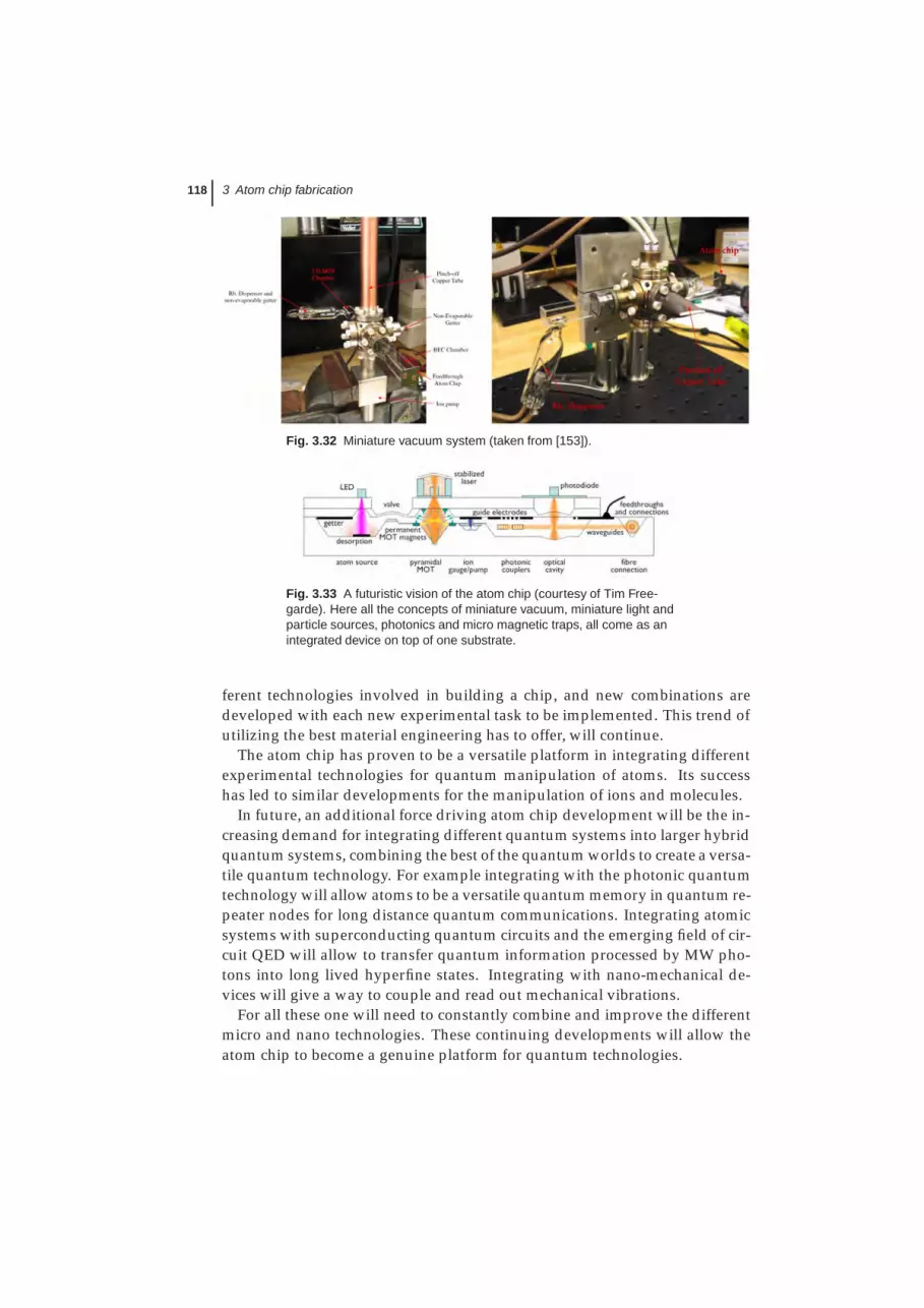
118 3 Atom chip fabrication
Fig. 3.32 Miniature vacuum system (taken from [153]).
Fig. 3.33 A futuristic vision of the atom chip (courtesy of Tim Free-garde). Here all the concepts of miniature vacuum, miniature light andparticle sources, photonics and micro magnetic traps, all come as anintegrated device on top of one substrate.
ferent technologies involved in building a chip, and new combinations aredeveloped with each new experimental task to be implemented. This trend ofutilizing the best material engineering has to offer, will continue.
The atom chip has proven to be a versatile platform in integrating differentexperimental technologies for quantum manipulation of atoms. Its successhas led to similar developments for the manipulation of ions and molecules.
In future, an additional force driving atom chip development will be the in-creasing demand for integrating different quantum systems into larger hybridquantum systems, combining the best of the quantum worlds to create a versa-tile quantum technology. For example integrating with the photonic quantumtechnology will allow atoms to be a versatile quantum memory in quantum re-peater nodes for long distance quantum communications. Integrating atomicsystems with superconducting quantum circuits and the emerging field of cir-cuit QED will allow to transfer quantum information processed by MW pho-tons into long lived hyperfine states. Integrating with nano-mechanical de-vices will give a way to couple and read out mechanical vibrations.
For all these one will need to constantly combine and improve the differentmicro and nano technologies. These continuing developments will allow theatom chip to become a genuine platform for quantum technologies.
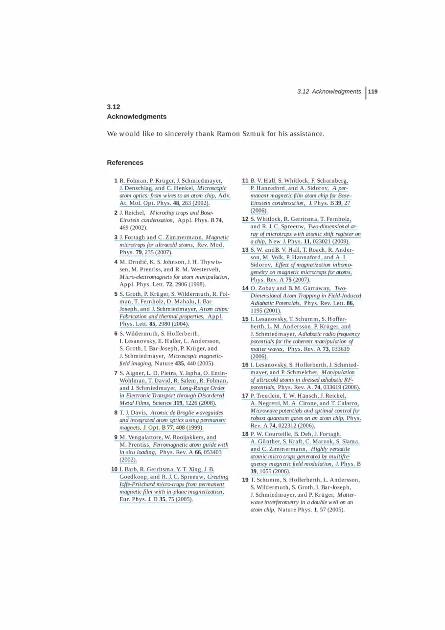
3.12 Acknowledgments 119
3.12Acknowledgments
We would like to sincerely thank Ramon Szmuk for his assistance.
References
1 R. Folman, P. Krüger, J. Schmiedmayer,J. Denschlag, and C. Henkel, Microscopicatom optics: from wires to an atom chip, Adv.At. Mol. Opt. Phys. 48, 263 (2002).
2 J. Reichel, Microchip traps and Bose-Einstein condensation, Appl. Phys. B 74,469 (2002).
3 J. Fortagh and C. Zimmermann, Magneticmicrotraps for ultracold atoms, Rev. Mod.Phys. 79, 235 (2007).
4 M. Drndic, K. S. Johnson, J. H. Thywis-sen, M. Prentiss, and R. M. Westervelt,Micro-electromagnets for atom manipulation,Appl. Phys. Lett. 72, 2906 (1998).
5 S. Groth, P. Krüger, S. Wildermuth, R. Fol-man, T. Fernholz, D. Mahalu, I. Bar-Joseph, and J. Schmiedmayer, Atom chips:Fabrication and thermal properties, Appl.Phys. Lett. 85, 2980 (2004).
6 S. Wildermuth, S. Hofferberth,I. Lesanovsky, E. Haller, L. Andersson,S. Groth, I. Bar-Joseph, P. Krüger, andJ. Schmiedmayer, Microscopic magnetic-field imaging, Nature 435, 440 (2005).
7 S. Aigner, L. D. Pietra, Y. Japha, O. Entin-Wohlman, T. David, R. Salem, R. Folman,and J. Schmiedmayer, Long-Range Orderin Electronic Transport through DisorderedMetal Films, Science 319, 1226 (2008).
8 T. J. Davis, Atomic de Broglie waveguidesand integrated atom optics using permanentmagnets, J. Opt. B 77, 408 (1999).
9 M. Vengalattore, W. Rooijakkers, andM. Prentiss, Ferromagnetic atom guide within situ loading, Phys. Rev. A 66, 053403(2002).
10 I. Barb, R. Gerritsma, Y. T. Xing, J. B.Goedkoop, and R. J. C. Spreeuw, CreatingIoffe-Pritchard micro-traps from permanentmagnetic film with in-plane magnetization,Eur. Phys. J. D 35, 75 (2005).
11 B. V. Hall, S. Whitlock, F. Scharnberg,P. Hannaford, and A. Sidorov, A per-manent magnetic film atom chip for Bose–Einstein condensation, J. Phys. B 39, 27(2006).
12 S. Whitlock, R. Gerritsma, T. Fernholz,and R. J. C. Spreeuw, Two-dimensional ar-ray of microtraps with atomic shift register ona chip, New J. Phys. 11, 023021 (2009).
13 S. W. andB. V. Hall, T. Roach, R. Ander-son, M. Volk, P. Hannaford, and A. I.Sidorov, Effect of magnetization inhomo-geneity on magnetic microtraps for atoms,Phys. Rev. A 75 (2007).
14 O. Zobay and B. M. Garraway, Two-Dimensional Atom Trapping in Field-InducedAdiabatic Potentials, Phys. Rev. Lett. 86,1195 (2001).
15 I. Lesanovsky, T. Schumm, S. Hoffer-berth, L. M. Andersson, P. Krüger, andJ. Schmiedmayer, Adiabatic radio frequencypotentials for the coherent manipulation ofmatter waves, Phys. Rev. A 73, 033619(2006).
16 I. Lesanovsky, S. Hofferberth, J. Schmied-mayer, and P. Schmelcher, Manipulationof ultracold atoms in dressed adiabatic RF-potentials, Phys. Rev. A. 74, 033619 (2006).
17 P. Treutlein, T. W. Hänsch, J. Reichel,A. Negretti, M. A. Cirone, and T. Calarco,Microwave potentials and optimal control forrobust quantum gates on an atom chip, Phys.Rev. A 74, 022312 (2006).
18 P. W. Courteille, B. Deh, J. Fortagh,A. Günther, S. Kraft, C. Marzok, S. Slama,and C. Zimmermann, Highly versatileatomic micro traps generated by multifre-quency magnetic field modulation, J. Phys. B39, 1055 (2006).
19 T. Schumm, S. Hofferberth, L. Andersson,S. Wildermuth, S. Groth, I. Bar-Joseph,J. Schmiedmayer, and P. Krüger, Matter-wave interferometry in a double well on anatom chip, Nature Phys. 1, 57 (2005).
120 References
20 P. Böhi, M. F. Riedel, J. Hoffrogge, J. Re-ichel, T. W. Hänsch, and P. Treutlein, Co-herent manipulation of Bose-Einstein con-densates with state-dependent microwavepotentials on an atom chip, Nature Phys. 5,592 (2009).
21 P. Krüger, X. Luo, M. W. Klein, K. Brug-ger, A. Haase, S. Wildermuth, S. Groth,I. Bar-Joseph, R. Folman, and J. Schmied-mayer, Trapping and manipulating neutralatoms with electrostatic fields, Phys. Rev.Lett. 91, 233201 (2003).
22 A. Günther, M. Kemmler, S. Kraft, C. J.Vale, C. Zimmermann, and J. Fortagh,Combined chips for atom-optics, Phys. Rev.A 71, 063619 (2005).
23 M. Trinker, S. Groth, S. Haslinger,S. Manz, T. Betz, I. Bar-Joseph,T. Schumm, and J. Schmiedmayer, Multi-layer atom chips for versatile atom micromanipulation, Appl. Phys. Lett. 92, 254102(2008).
24 D. Gallego, S. Hofferberth, T. Schumm,P. Krüger, and J. Schmiedmayer, Opticallattice on an atom chip, Opt. Lett. 34, 3463(2009).
25 P. Quinto-Su, M. Tscherneck, M. Holmes,and N. Bigelow, On-chip optical detectionof laser cooled atoms, Opt. Expr. 12, 5098(2004).
26 X. Liu, K.-H. Brenner, M. Wilzbach,M. Schwarz, T. Fernholz, and J. Schmied-mayer, Fabrication of alignment structuresfor a fiber resonator by use of deep-ultravioletlithography, Appl. Opt. 44, 6857 (2005).
27 Y. Colombe, T. Steinmetz, G. Dubois,F. Linke, D. Hunger, and J. Reichel, Strongatom-field coupling for Bose-Einstein conden-sates in an optical cavity on a chip, Nature450, 272 (2007).
28 P. Treutlein, D. Hunger, S. Camerer, T. W.Hänsch, and J. Reichel, Bose-EinsteinCondensate Coupled to a NanomechanicalResonator on an Atom Chip, Phys. Rev.Lett. 99, 140403 (2007).
29 D. Hunger, S. Camerer, T. W. Hänsch,D. König, J. P. Kotthaus, J. Reichel, andP. Treutlein, Resonant coupling of a Bose-Einstein condensate to a micromechanicaloscillator, Phys. Rev. Lett. 104, 143002(2010).
30 J. Verdu, H. Zoubi, C. Koller, J. Majer,H. Ritsch, and J. Schmiedmayer, Strongmagnetic coupling of an ultracold gas to asuperconducting waveguide cavity, eprintarXiv:0809.2552 (2009).
31 J. Petrosyan, G. Bensky, G. Kurizki,I. Mazets, J. Majer, and J. Schmiedmayer,Reversible state transfer between supercon-ducting qubits and atomic ensembles, Phys.Rev. A 97, 040304 (2009).
32 A. Wallraff, D. I. Schuster, A. Blais,L. Frunzio, R. S. Huang, J. Majer, S. Ku-mar, S. M. Girvin, and R. J. Schoelkopf,Strong coupling of a single photon to a su-perconducting qubit using circuit quantumelectrodynamics, Nature 431, 162 (2004).
33 R. Schoelkopf and S. Girvin, Wiring upquantum systems, Nature 451, 664 (2008).
34 S. Groth, Development, fabrication, andcharacterisation of atom chips, Ph.D. thesis,University of Heidelberg (2006).
35 M. J. Madou, Fundamentals of Microfabri-cation: The Science of Miniaturization, CRCPress, New York, 2nd edn. (2002).
36 J. Reichel, W. Hänsel, and T. W. Hänsch,Atomic Micromanipulation with MagneticSurface Traps, Phys. Rev. Lett. 83, 3398(1999).
37 W. Ruythooren, K. Attenborough,S. Beerten, P. Merken, J. Fransaer,E. Beyne, C. Van Hoof, J. De Boeck, andJ. P. Celis, Electrodeposition for the synthesisof microsystems, J. Micromech. Microeng.10, 101 (2000).
38 M. Schlesinger and M. Paunovic (eds.),Modern Electroplating, Wiley & Sons, NewYork, 4th edn. (2000).
39 E. Koukharenko, Z. Moktadir, M. Kraft,M. E. Abdelsalam, D. M. Bagnall,C. Valeb, M. P. A. Jones, and E. A. Hinds,Microfabrication of gold wires for atomguides, Sens. Act. A 115, 600 (2004).
40 B. Lev, Fabrication of micro-magnetic trapsfor cold neutral atoms, Quant. Inf. Comput.3, 450 (2003).
41 P. Treutlein, Coherent manipulation ofultracold atoms on atom chips, Ph.D. the-sis, Ludwig-Maximilians-UniversitätMünchen and Max-Planck-Institut fürQuantenoptik (2008), Published as MPQreport 321.

References 121
42 J. Estève, C. Aussibal, T. Schumm, C. Figl,D. Mailly, I. Bouchoule, C. I. Westbrook,and A. Aspect1, Role of wire imperfectionsin micromagnetic traps for atoms, Phys. Rev.A 70, 043629 (2004).
43 P. Kruger, L. M. Andersson, S. Wilder-muth, S. Hofferberth, E. Haller, S. Aigner,S. Groth, I. Bar-Joseph, and J. Schmied-mayer, Potential Roughness near Litho-graphically Fabricated Atom Chips, Phys.Rev. A 76, 063621 (2007).
44 R. Folman, P. Krüger, D. Cassettari,B. Hessmo, T. Maier, and J. Schmied-mayer, Controlling Cold Atoms usingNanofabricated Surfaces: Atom Chips, Phys.Rev. Lett. 84, 4749 (2000).
45 J. J. P. van Es, P. Wicke, A. H. vanAmerongen, C. Rétif, S. Whitlock, andN. J. van Druten, Box traps on an atom chipfor one-dimensional quantum gases, preprintarXiv:0911.5250 (2009).
46 K. Williams and R. Muller, Etch rates formicromachining processing, J. Microelec-tromech. Syst. 5, 256 (1996).
47 K. R. Williams, G. Kishan, and M. Wasilik,Etch Rates for Micromachining Processing—Part II, J. Microelectromech. Syst. 12, 761(2003).
48 L. D. Pietra, S. Aigner, C. V. Hagen,S. Groth, I. Bar-Joseph, H. Lezec, andJ. Schmiedmayer, Designing potentials bysculpturing wires, Phys. Rev. A 75, 063604(2007).
49 R. Salem, Y. Japha, J. Chabé, B. Hadad,M. Keil, K. Milton, and R. Folman,Nanowire atomchip traps for sub-micronatom–surface distances, New J. Phys. 12,023039 (2010).
50 J.Meingailis, J. Vac. Sci. Technol. B 5, 469(1987).
51 L. D. Pietra, S. Aigner, C. vom Hagen,H. J. Lezec, and J. Schmiedmayer, Coldatoms near surfaces: designing potentials bysculpturing wires, In Journal of Physics:Conference Series, vol. 19, 30–33, Instituteof Physics Publishing (2005).
52 J. Fortágh, H. Ott, S. Kraft, A. Günther,and C. Zimmermann, Surface effects inmagnetic microtraps, Phys. Rev. A 66,041604R (2002).
53 A. E. Leanhardt, Y. Shin, A. P. Chikkatur,D. Kielpinski, W. Ketterle, and D. E.
Pritchard, Bose-Einstein Condensates neara Microfabricated Surface, Phys. Rev. Lett.90, 100404 (2003).
54 M. P. A. Jones, C. J. Vale, D. Sahagun,B. V. Hall, C. C. Eberlein, B. E. Sauer,K. Furusawa, D. Richardson, and E. A.Hinds, Cold atoms probe the magnetic fieldnear a wire, J. Phys. B: At. Mol. Opt. Phys.37, L15 (2004).
55 T. Schumm, J. Estève, C. Figl, J.-B. Treb-bia, C. Aussibal, H. Nguyen, D. Mailly,I. Bouchoule, C. I. Westbrook, and A. As-pect, Atom chips in the real world: the effectsof wire corrugation, Eur. Phys. J. D 32, 171(2005).
56 S. Kraft, A. Günther, H. Ott, D. Wharam,C. Z. J., and Fortágh, Anomalous longitu-dinal magnetic field near the surface of copperconductors, J. Phys. B 35, L469 (2002).
57 D.-W. Wang, M. D. Lukin, and E. Dem-ler, Disordered Bose-Einstein Condensatesin Quasi-One-Dimensional Magnetic Micro-traps, Phys. Rev. Lett. 92 (2004).
58 P. Krüger, L. M. Andersson, S. Wilder-muth, S. Hofferberth, E. Haller, S. Aigner,S. Groth, I. Bar-Joseph, and J. Schmied-mayer, Disorder Potentials near Litho-graphically Fabricated Atom Chips, eprintarXiv:cond-mat/0504686 (2004).
59 S. Wildermuth, S. Hofferberth,I. Lesanovsky, S. Groth, I. Bar-Joseph,P. Krüger, and J. Schmiedmayer, Sens-ing electric and magnetic fields with Bose-Einstein Condensates, Appl. Phys. Lett. 88,264103 (2006).
60 M. P. A. Jones, C. J. Vale, D. Sahagun,B. V. Hall, and E. A. Hinds, Spin couplingbetween cold atoms and the thermal fluctua-tions of a metal surface, Phys. Rev. Lett. 91,080401 (2003).
61 P. Krüger, Coherent matter waves nearsurfaces, Ph.D. thesis, University of Hei-delberg (2004).
62 Y. Japha, O. Entin-Wohlman, T. David,R. Salem, S. Aigner, J. Schmiedmayer, andR. Folman, Model for organized current pat-terns in disordered conductors, Phys. Rev. B77 (2008).
63 R. Folman, P. Krueger, J. Schmiedmayer,J. Denschlag, and C. Henkel, Advances inAtomic, Mol. Opt. Phys. 48, 263 (2002).
64 T. Varpula and T. Poutanen, Magnetic fieldfluctuations arising from thermal motion of

122 References
electric charge in conductors, J. Appl. Phys.55, 4015 (1984).
65 C. Henkel, S. Pötting, and M. Wilkens,Loss and heating of particles in small andnoisy traps, Appl. Phys. B 69, 379 (1999).
66 J. Sidles, J. Garbini, W. Dougherty, andS. H. Chao, The classical and quantum the-ory of thermal magnetic noise, with applica-tions in spintronics and quantum microscopy,Proc. IEEE 91, 799 (2003).
67 S. Scheel, P. Rekdal, P. Knight, andE. Hinds, Atomic spin decoherence nearconducting and superconducting films, Phys.Rev. A 72, 42901 (2005).
68 D. Harber, J. McGuirk, J. Obrecht, andE. Cornell, Thermally induced losses inultra-cold atoms magnetically trapped nearroom-temperature surfaces, J. Low Temp.Phys. 133, 229 (2003).
69 Y. Lin, I. Teper, C. Chin, and V. Vuletic,Impact of the Casimir-Polder Potential andJohnson Noise on Bose-Einstein CondensateStability Near Surfaces, Phys. Rev. Lett. 92,050404 (2004).
70 V. Dikovsky, Y. Japha, C. Henkel, andR. Folman, Reduction of magnetic noise inatom chips by material optimization, Eur.Phys. J. D 35, 87 (2005).
71 Y.-J. Lin, private communications.
72 B. Skagerstam, U. Hohenester,A. Eiguren, and P. Rekdal, Spin decoher-ence in superconducting atom chips, Phys.Rev. Lett. 97, 70401 (2006).
73 P. Rekdal and B. Skagerstam, Decay pro-cesses in the presence of thin superconductingfilms, Phys. Rev. A 75, 22904 (2007).
74 B. Skagerstam and P. Redkal, Photon emis-sion near superconducting bodies, Phys. Rev.A 76, 052901 (2007).
75 U. Hohenester, A. Eiguren, S. Scheel,and E. Hinds, Spin-flip lifetimes in su-perconducting atom chips: Bardeen-Cooper-Schrieffer versus Eliashberg theory, Phys.Rev. A 76, 33618 (2007).
76 T. Nirrengarten, A. Qarry, C. Roux,A. Emmert, G. Nogues, M. Brune, J.-M.Raimond, and S. Haroche, Realization ofa Superconducting Atom Chip, Phys. Rev.Lett. 97, 200405 (2006).
77 C. Roux, A. Emmert, A. Lupascu, T. Nir-rengarten, G. Nogues, M. Brune, J. M.
Raimond, and S. Haroche, BEC on a super-conducting atom chip, Eur. Phys. Lett. 81,56004 (2008).
78 T. Mukai, C. Hufnagel, A. Kasper,T. Meno, A. Tsukada, K. Semba, andF. Shimizu, Persistent supercurrent atomchip, Phys. Rev. Lett. 98, 260407 (2007).
79 B. Zhang, C. Henkel, E. Haller, S. Wil-dermuth, S. Hofferberth, P. Krüger, andJ. Schmiedmayer, Relevance of sub-surfacechip layers for the lifetime of magneticallytrapped atoms, Eur. Phys. J. D 35, 97 (2005).
80 F. Shimizu, C. Hufnagel, and T. Mukai,Stable Neutral Atom Trap with a Thin Su-perconducting Disc, Phys. Rev. Lett. 103,253002 (2009).
81 T. Müller, X. Wu, A. Mohan, A. Eyvazov,Y. Wu, and R. Dumke, Towards a guidedatom interferometer based on a superconduct-ing atom chip, New J. Phys. 10, 073006(2008).
82 T. Müller, B. Zhang, R. Fermani, K. Chan,Z. Wang, C. Zhang, M. Lim, andR. Dumke, Trapping of ultra-cold atomswith the magnetic field of vortices in a thinfilm superconducting micro-structure, Arxivpreprint arXiv:0910.2332 (2009).
83 T. M"uller, B. Zhang, R. Fermani, K. Chan,
Z. Wang, C. Zhang, M. Lim, andR. Dumke, Trapping of ultra-cold atomswith the magnetic field of vortices in a thinfilm superconducting micro-structure, Arxivpreprint arXiv:0910.2332 (2009).
84 D. Cano, B. Kasch, H. Hattermann,R. Kleiner, C. Zimmermann, D. Koelle,and J. Fortágh, Meissner effect in supercon-ducting microtraps, Phys. Rev. Lett. 101,183006 (2008).
85 D. Cano, B. Kasch, H. Hattermann,D. Koelle, R. Kleiner, C. Zimmermann,and J. Fortágh, Impact of the Meissner effecton magnetic microtraps for neutral atomsnear superconducting thin films, Phys. Rev.A 77, 63408 (2008).
86 V. Dikovsky, V. Sokolovsky, B. Zhang,C. Henkel, and R. Folman, Superconduct-ing atom chips: advantages and challenges,Eur. Phys. J. D 51, 247 (2009).
87 B. Lev, Y. Lassailly, C. Lee, A. Scherer, andH. Mabuchi, Atom mirror etched from ahard drive, Appl. Phys. Lett. 83 (2003).

References 123
88 C. D. J. Sinclair, J. A. Retter, E. A. Curtis,B. V. Hall, I. L. Garcia, S. Eriksson, B. E.Sauer, and E. A. Hinds, Cold atoms invideotape micro-traps, Eur. Phys. J. D 35,105 (2005).
89 S. Eriksson, F. Ramirez-Martinez, E. A.Curtis, B. E. Sauer, P. W. Nutter, E. W.Hill, and E. A. Hinds, Micron-sized atomtraps made from magneto-optical thin films,Appl. Phys. B 79, 811 (2004).
90 Y. T. Xing, A. Eljaouhari, I. Barb, R. Ger-ritsma, R. J. C. Spreeuw, and J. B. Goed-koop, Hard magnetic FePt films for atomchips, Phys. stat. sol. (c) 1, 3702 (2004).
91 R. Gerritsma, S. Whitlock, T. Fernholz,H. Schlatter, J. A. Luigjes, J. U. Thiele, J. B.Goedkoop, and R. J. C. Spreeuw, Latticeof microtraps for ultracold atoms based onpatterned magnetic films, Phys. Rev. A 76,33408 (2007).
92 Y. T. Xing, I. Barb, R. Gerritsma, R. J. C.Spreeuw, H. Luigjes, Q. F. Xiao, C. Retif,and J. B. Goedkoop, Fabrication of mag-netic atom chips based on FePt, J. Magn.Magn. Mater. 313, 192 (2007).
93 J. Y. Wang, S. Whitlock, F. Scharnberg,D. S. Gough, A. I. Sidorov, R. J. McLean,and P. Hannaford, Perpendicularly magne-tized, grooved GdTbFeCo microstructures, J.Phys. D 38, 4015 (2005).
94 M. Singh, M. Volk, A. Akulshin,A. Sidorov, R. McLean, and P. Hannaford,One-dimensional lattice of permanent mag-netic microtraps for ultracold atoms on anatom chip, J. Phys. B 41, 065301 (2008).
95 V. Peano, M. Thorwart, A. Kasper, andR. Egger, Nanoscale atomic waveguides withsuspended carbon nanotubes, Appl. Phys. B81, 1075 (2005).
96 R. Fermani, S. Scheel, and P. Knight, Trap-ping cold atoms near carbon nanotubes: Ther-mal spin flips and Casimir-Polder potential,Phys. Rev. A 75, 62905 (2007).
97 P. Petrov, S. Machluf, S. Younis,R. Macaluso, T. David, B. Hadad,Y. Japha, M. Keil, E. Joselevich, andR. Folman, Trapping cold atoms usingsurface-grown carbon nanotubes, Phys. Rev.A 79, 43403 (2009).
98 A. Ismach, L. Segev, E. Wachtel, andE. Joselevich, Atomic-step-templated for-
mation of single wall carbon nanotube pat-terns, Angewandte Chemie InternationalEdition 43, 6140 (2004).
99 A. Ismach, D. Kantorovich, and E. Jose-levich, Carbon nanotube graphoepitaxy:Highly oriented growth by faceted nanosteps,J. Am. Chem. Soc. 127, 11554 (2005).
100 X. M. H. Huang, R. Caldwell, L. Huang,S. C. Jun, M. Huang, M. Y. Sfeir, S. P.O’Brien, and J. Hone, Controlled place-ment of individual carbon nanotubes, NanoLett. 5, 1515 (2005).
101 B. Grüner, M. Jag, A. Stibor, G. Visanescu,M. Häffner, D. Kern, A. Günther, andJ. Fortágh, Integrated atom detector based onfield ionization near carbon nanotubes, gas](2009).
102 T. David, Y. Japha, V. Dikovsky, R. Salem,C. Henkel, and R. Folman, Magneticinteractions of cold atoms with anisotropicconductors, Eur. Phys. J. D 48, 321 (2008).
103 S. R. Wilson and C. J. Tracy (eds.), Hand-book of Multilevel Metallization for Inte-grated Circuits: Materials, Technology, andApplications, Noyes Publications, West-wood, New Jersey, U.S.A. (1993).
104 S. Schneider, A. Kasper, C. V. Hagen,M. Bartenstein, B. Engeser, T. Schumm,I. Bar-Joseph, R. Folman, L. Feenstra, andJ. Schmiedmayer, Bose-Einstein Condensa-tion in a Simple Microtrap, Phys. Rev. A 67,023612 (2003).
105 J. Reichel, W. Hänsel, P. Hommelhoff, andT. W. Hänsch, Applications of integratedmagnetic microtraps, Appl. Phys. B 72, 81(2001).
106 T. Steinmetz, A. Balocchi, Y. Colombe,D. Hunger, T. W. Hänsch, R. J. Warburton,and J. Reichel, Stable fiber-based Fabry-Pérot cavity, Appl. Phys. Lett. 89, 111110(2006).
107 R. Long, T. Rom, W. Hänsel, T. W. Hän-sch, and J. Reichel, Long distance magneticconveyor for precise positioning of ultracoldatoms, Eur. Phys. J. D 35, 125 (2005).
108 J. Armijo, A. C. Garridor, and I. Bou-choule, Thermal properties of AlN-basedatom chips, Eur. Phys. J. D 56, 33 (2010).
109 A. del Campo and C. Greiner, SU-8:a photoresist for high-aspect-ratio and 3Dsubmicron lithography, J. Micromech. Mi-croeng. 17, R81 (2007).

124 References
110 V. Seidemann, J. Rabe, M. Feldmann, andS. Büttgenbach, SU8-micromechanicalstructures with in situ fabricated movableparts, Microsyst. Tech. 8, 348 (2002).
111 D. Duffy, J. M. O. Schueller, and G. White-sides, Rapid Prototyping of MicrofluidicSystems in Poly(dimethylsiloxane), Anal.Chem. 70, 4974 (1998).
112 M. Wilzbach, A. Haase, M. Schwarz,D. Heine, K. Wicker, X. Liu, K.-H. Bren-ner, S. Groth, T. Fernholz, B. Hessmo, andJ. Schmiedmayer, Detecting Neutral Atomson an Atom Chip, Fortschr. Phys. 54, 746(2006).
113 E. R. I. Abraham and E. A. Cornell, TeflonFeedthrough for Coupling Optical Fibers IntoUltrahigh Vacuum Systems, Appl. Opt. 37,1762 (1998).
114 M.Wilzbach, D. Heine, S. Groth, X. Liu,B. Hessmo, and J. Schmiedmayer, A sim-ple integrated single-atom detector, Opt.Lett. 34, 259 (2009).
115 D. Heine, M.Wilzbach, B. Hessmo, andJ. Schmiedmayer, Single-atom detector:photon and atom statistics, Phys. Rev. A 97,021804 R (2009).
116 D. Heine, W. Rohringer, D. Fischer,M. Wilzbach, T. Raub, S. Loziczky, X. Liu,S. Groth, B. Hessmo, and J. Schmied-mayer, A single atom detector integrated onan atom chip: fabrication, characterizationand application, eprint arXiv:1002.1573(2010).
117 R. Gehr, J. Volz, G. Dubois, T. Steinmetz,Y. Colombe, B. L. Lev, R. Long, J. Estève,and J. Reichel, Cavity-based single atompreparation and high-fidelity hyperfine statereadout, to be published in Phys. Rev.Lett., preprint arXiv:1002.4424 (2010).
118 M. Trupke, E. A. Hinds, S. Eriksson, E. A.Curtis, Z. Moktadir, E. Kukharenka, andM. Kraft, Microfabricated high-finesse opti-cal cavity with open access and small volume,Appl. Phys. Lett. 87, 211106 (2005).
119 S. Eriksson, M. Trupke, H. F. Powell,D. Sahagun, C. D. J. Sinclair, E. A. Cur-tis, B. E. Sauer, E. A. Hinds, Z. Moktadir,and C. O. Gollasch, Integrated optical com-ponents on atom chips, Eur. Phys. J. D 35,135 (2005).
120 M. Trupke, J. Goldwin, B. Darquié, G. Du-tier, S. Eriksson, J. P. Ashmore, and E. A.
Hinds, Atom detection and photon produc-tion in a scalable, open, optical microcavity,Phys. Rev. Lett. 99, 63601 (2007).
121 T. Steinmetz, Resonator-Quantenelektrodynamik auf einem Mikro-fallenchip, Ph.D. thesis, Ludwig-Maximilians-Universität München andMax-Planck-Institut für Quantenoptik(2008).
122 D. Hunger, T. Steinmetz, Y. Colombe,C. Deutsch, T. W. Hänsch, and J. Reichel,Fiber Fabry-Perot cavity with high finesse,accepted for publication in New J. Phys.(2010).
123 R. Dumke, M. Volk, T. Müther,F. Buchkremer, G. Birkl, and W. Ertmer,Micro-optical realization of arrays of selec-tively addressable dipole traps: a scalableconfiguration for quantum computation withatomic qubits, Phys. Rev. Lett. 89, 97903(2002).
124 G. Birkl, F. Buchkremer, R. Dumke, andW. Ertmer, Atom optics with microfabricatedoptical elements, Opt. Commun. 191, 67(2001).
125 R. Dumke, T. Müther, M. Volk, W. Ertmer,and G. Birkl, Interferometer-type struc-tures for guided atoms, Phys. Rev. Lett. 89,220402 (2002).
126 N. F. Borrelli, Microoptics Technology: fab-rication and applications of lens arrays anddevices, CRC (1999).
127 T. Aoki, B. Dayan, E. Wilcut, W. Bowen,A. Parkins, T. Kippenberg, K. Vahala, andH. Kimble, Observation of strong couplingbetween one atom and a monolithic microres-onator, Nature 443, 671 (2006).
128 P. E. Barclay, K. Srinivasan, O. Painter,B. Lev, and H. Mabuchi, Integration offiber-coupled high-Q SiNx microdisks withatom chips, Appl. Phys. Lett. 89 (2006).
129 M. R. andP. Horak, S. Helsby, andR. Folman, Single-atom detection usingwhispering-gallery modes of microdisk res-onators, Phys. Rev. A 70, 53808 (2004).
130 D. Armani, T. Kippenberg, S. Spillane,and K. Vahala, Ultra-high-Q toroid micro-cavity on a chip, Nature 421, 925 (2003).
131 T. Kippenberg, S. Spillane, D. Armani,and K. Vahala, Fabrication and coupling toplanar high-Q silica disk microcavities, Appl.Phys. Lett. 83, 797 (2003).
References 125
132 S. Spillane, T. Kippenberg, K. Vahala,K. Goh, E. Wilcut, and H. Kimble,Ultrahigh-Q toroidal microresonators forcavity quantum electrodynamics, Phys. Rev.A 71, 13817 (2005).
133 P. Horak, B. G. Klappauf, A. Haase,R. Folman, J. Schmiedmayer, P. Domokos,and E. Hinds, Possibility of single-atomdetection on a chip, Phys. Rev. A 67, 43806(2003).
134 T. Purdy and D. Stamper-Kurn, Integrat-ing cavity quantum electrodynamics andultracold-atom chips with on-chip dielectricmirrors and temperature stabilization, Appl.Phys. B 90, 401 (2008).
135 M. Kohnen, M. Succo, P. Petrov, R. Ny-man, M. Trupke, and E. Hinds, An inte-grated atom-photon junction, Arxiv preprintarXiv:0912.4460 (2009).
136 G. Gay, O. Alloschery, B. V. de Lesegno,C. OŠDwyer, J. Weiner, and H. Lezec, Op-tical Response of Nanostructured Surfaces:Experimental Investigation of the CompositeDiffracted Evanescent Wave Model (2006).
137 H. Lezec, A. Degiron, E. Devaux,R. Linke, L. Martin-Moreno, F. Garcia-Vidal, and T. Ebbesen, Beaming light froma subwavelength aperture, Science 297, 820(2002).
138 M. Rosenblit, Y. Japha, P. Horak, andR. Folman, Simultaneous optical trap-ping and detection of atoms by microdiskresonators, Phys. Rev. A 73, 63805 (2006).
139 B. Lev, K. Srinivasan, P. Barclay,O. Painter, and H. Mabuchi, Feasibil-ity of detecting single atoms using photonicbandgap cavities, Nanotechnology 15, S556(2004).
140 A. Akimov, A. Mukherjee, C. Yu,D. Chang, A. Zibrov, P. Hemmer, H. Park,and M. Lukin, Generation of single opticalplasmons in metallic nanowires coupled toquantum dots, Nature 450, 402 (2007).
141 D. Chang, J. Thompson, H. Park,V. Vuletic, A. Zibrov, P. Zoller, andM. Lukin, Trapping and manipulation ofisolated atoms using nanoscale plasmonicstructures, Phys. Rev. Lett. 103, 123004(2009).
142 M. Trupke, F. Ramirez-Martinez, E. Cur-tis, J. Ashmore, S. Eriksson, E. Hinds,Z. Moktadir, C. Gollasch, M. Kraft, G. V.Prakash, et al., Pyramidal micromirrors for
microsystems and atom chips, Appl. Phys.Lett. 88, 071116 (2006).
143 A. Shevchenko, T. Lindvall, I. Tittonen,and M. Kaivola, Microscopic electro-opticalatom trap on an evanescent-wave mirror,Eur. Phys. J. D 28, 273 (2004).
144 S. Wildermuth, P. Krüger, C. Becker,M. Brajdic, S. Haupt, A. Kasper, R. Fol-man, and J. Schmiedmayer, Optimizedmagneto-optical trap for experiments withultracold atoms near surfaces, Phys. Rev. A69, 030901 (2004).
145 W. Hänsel, P. Hommelhoff, T. W. Hänsch,and J. Reichel, Bose-Einstein condensationon a microelectronic chip, Nature 413, 498(2001).
146 S. Du, M. B. Squires, Y. Imai, L. Czaia,R. Saravanan, V. Brigh, J. Reichel, T. W.Hänsch, and D. Z. Anderson, Atom-ChipBose-Einstein condensation in a portable vac-uum cell, Phys. Rev. A 70, 053606 (2004).
147 D. M. Farkas, K. M. Hudek, E. A. Salim,S. R. Segal, M. B. Squires, and D. Z.Anderson, A Compact, Transportable,Microchip-Based System for High RepetitionRate Production of Bose-Einstein Conden-sates, preprint arXiv:0912.0553 (2009).
148 K. Lee, J. Kim, H. Noh, and W. Jhe, Single-beam atom trap in a pyramidal and conicalhollow mirror, Opt. Lett. 21, 1177 (1996).
149 J. Kim, K. Lee, H. Noh, W. Jhe, andM. Ohtsu, Atom trap in an axicon mirror,Opt. Lett. 22, 117 (1997).
150 D. Groswasser, A. Waxman, M. Givon,G. Aviv, Y. Japha, M. Keil, and R. Folman,Retroreflecting polarization spectroscopy en-abling miniaturization, Rev. Sci. Inst. 80,093103 (2009).
151 L. A. Liew, S. Knappe, J. Moreland,H. Robinson, L. Hollberg, and J. Kitch-ing, Microfabricated alkali atom vapor cells,Appl. Phys. Lett. 84, 2694 (2004).
152 S. Aubin, M. Extavour, S. Myrskog,L. LeBlanc, J. Esteve, S. Singh, P. Scrut-ton, D. McKay, R. McKenzie, I. Leroux,et al., Trapping fermionic 40 K and bosonic87 Rb on a chip, J. Low Temp. Phys. 140,377 (2005).
153 H. C. R. Chuang, D. Z. Anderson, andV. M. Bright, The fabrication of through-wafer interconnects in silicon substrates, J.Micromech. Microeng. 18, 045003 (2008).