development and fabrication of nanoporous silicon-based bioreactors within a microfluidic chip
TRANSCRIPT
Development and Fabrication of Nanoporous Silicon-basedBioreactors within a Microfluidic Chip
Scott T. Retterer1, Piro Siuti2, Chang-Kyoung Choi1,3, and Mitchel J. Doktycz1,21Oak Ridge National Laboratory, Oak Ridge, TN2University of Tennessee, Knoxville, TN3Michigan Technological University, Houghton, MI
AbstractMulti-scale lithography and cryogenic deep reactive ion etching techniques were used to createensembles of nanoporous, picoliter volume, reaction vessels within a microfluidic system. Thefabrication of these vessels is described and how this process can be used to tailor vessel porosityby controlling the width of slits that constitute the vessel pores is demonstrated. Control of poresize allows the containment of nucleic acids and enzymes that are the foundation of biochemicalreaction systems, while allowing smaller reaction constituents to traverse the container membraneand continuously supply the reaction. In this work, a 5.4kB DNA plasmid was retained within thereaction vessels and labeled under microfluidic control with ethidium bromide as an initial proof-of-principle. Subsequently, a coupled enzyme reaction, in which glucose oxidase and horseradishperoxidase were contained and fed with a substrate solution of glucose and Amplex Red™ toproduce fluorescent Resorufin, was carried out under microfluidic control and monitored usingfluorescent microscopy. The fabrication techniques presented are broadly applicable and can beadapted to produce devices in which a variety of high aspect ratio, nanoporous silicon structurescan be integrated within a microfluidic network. The devices shown here are amenable to beingscaled in number and organized to implement more complex reaction systems for applications insensing and actuation as well as fundamental studies of biological reaction systems.
IntroductionBiochemical reactions such as protein synthesis and enzymatic conversion are fundamentalto the function of living systems and are vital tools in industry and research. As ourunderstanding of these reactions, and the living cellular systems in which they are carriedout, has grown, the importance of cellular organization and efficiencies achieved byoperating at the cellular scale have become more apparent1. This, combined with a desire tounderstand “what constitutes life,” has led to efforts to create synthetic cellular-scalecontainers, cell mimics, in which basic biochemical processes can be sustained2-6.
Chemical reactions within the cell depend on the cellular membrane, as it 1) defines thespatial extent (volume) of the cell, and 2) regulates the transfer of reactants and productsbetween the cellular reaction volume and its surroundings. Within the small volume of thecell, passive transport of molecules via diffusion is rapid and facilitates the efficient mixingof molecules within the cell1. Furthermore, because the cell can contain only a limited, smallnumber of molecules, small changes in the numbers of molecules can lead to drastic changesin concentration within the cell. Such changes, can lead to significant alterations in cellularfunction and fate7. Beyond its passive role as a “container,” the cellular membrane plays adynamic role in affecting internal concentrations by regulating the exchange of materials
NIH Public AccessAuthor ManuscriptLab Chip. Author manuscript; available in PMC 2011 April 14.
Published in final edited form as:Lab Chip. 2010 May 7; 10(9): 1174–1181. doi:10.1039/b921592a.
NIH
-PA Author Manuscript
NIH
-PA Author Manuscript
NIH
-PA Author Manuscript
between the internal volume of the cell and the external microenvironment, both in concertwith, and against electrical and chemical potentials.
A growing body of work has examined the efficacy of biomimetic systems for carrying outbiological processes in micro/cellular-scale systems. Such work includes the solutionsynthesis of liposomes and vesicles5, 6, 8-10, serial creation of surface bound, single andnetworked vesicles11, microfluidic generation of cellular scale droplets formed inmultiphase fluidics12, 13, and inorganic microscale containers 2, 14-18. In general, theseapproaches have all sought to capture the basic function of the cellular membrane, definingsmall volumes in which diffusive transport is efficient, and the transfer of materials betweenthe internal reaction volume and the external environment is regulated.
Norieaux et al8 examined the use of vesicle bioreactors for carrying out cell freetranscription and translation for the production of GFP, and found that reactions could besustained for up to four days with the incorporation of an alpha-hemolysin pore that madethe membrane permeable to external reactants. In similar work, Murtas et al. successfullycarried out the expression of enhanced GFP in liposomes using a specific and well-definedset of minimal enzymes6. A more thorough review of work done in this area is provided byboth Monnard5 and by Walde and Ichikawa10. Despite the success of these solution basedapproaches, the isolation of individual vesicles for monitoring individual reactions(addressability) and potential difficulties involving long term stability and storage of suchvesicles in extreme conditions of tonicity (osmolarity), pH and temperature remain achallenge for the integration of these vesicle reactors into a sensing and actuation platforms.
In related work, Karlsson et al11 utilized vesicles formed on surfaces, which could beconnected by small nanoscale vesicle channels, to create small reaction volumes andnetworks. Because each volume could be formed using a different microinjection pipette,each could be filled with individual reagents and scaled according to the desired function.The technique was highly effective, and allowed tuning of mass transport from one volumeto the other by controlling the interconnecting channel width and length, establishing apredictable concentration gradient (flux) between reaction containers. The approachdemonstrates improved addressability over conventional liposome and vesicle basedapproaches, allowing the progression of a reaction within a single volume to be monitoredover time. However, the serial nature by which the reaction volumes are created coupledwith their inability to be stored over long periods makes the creation and use of manyidentical reaction volumes difficult. Furthermore, like vesicles synthesized in solution, theapproach is likely to suffer from poor stability under more extreme reaction conditions.
Advances in soft lithography have made the study of reactions in microscale droplets createdwithin lab-on-a-chip (LOC) systems accessible. Significant contributions have been made inthe development and study of droplet generating and mixing systems12, 13. The exquisitecontrol of droplet size and mixing afforded by microfluidics has even facilitated studies ofreaction kinetics in sub-cellular scale droplets19. Song et al review the topic of reactions indroplets in detail, highlighting the techniques and describing various applications formicrofluidic droplet generation and mixing20. While droplet-based microfluidics provideexquisite control of single reaction volumes, the multiphase nature of these systems canmake the exchange of materials between reaction containers difficult.
To develop a cellular scale reaction container that can be spatially addressed for monitoringand filling, while allowing both the storage and exchange of chemical information across thereactor membrane, a combination of conventional microfabrication and advancedlithographic techniques was used to create ensembles of nanoporous, picoliter volumereaction vessels that are integrated within a microfluidic system. Similar concepts have been
Retterer et al. Page 2
Lab Chip. Author manuscript; available in PMC 2011 April 14.
NIH
-PA Author Manuscript
NIH
-PA Author Manuscript
NIH
-PA Author Manuscript
used in the development of nanofabricated chemostats and cellular containers formed insilicon14, 21, 22 and silicone elastomer23. In these systems, microchannels allow for loadingand restricted movement of cells, and nanoscale pores or slits allow the exchange ofmolecular species (nutrients, signaling molecules, etc.) with the external environment oradjacent bioreactors. In this work, methods for refining pore size at a level that allows thedifferentiation between large and small molecules, as opposed to cellular and molecularscale materials, is demonstrated. The reaction vessels described here are batch fabricated,allowing over a thousand identical containers to be produced in a single fabrication run, andcan be stored indefinitely. Each of the reaction containers can be individually filled withdifferent reagents at the time of use. Because the process used to fabricate the devicescombines direct write electron beam lithography to define individual reaction volumes, thephysical spacing of the containers and their individual properties, including total volume,pore size and shape, can be tailored for specific applications. For example, placing reactionvessels proximal to one another within a microfluidic channel, that contains only aqueoussolution, can allow for reaction products to be exchanged between vessels via diffusionacross membranes and convection along the microchannel. This would enable the study ofreaction networks where the product of one reaction regulates or initiates a second reactionoccurring downstream. The level of communication between vessels can be tailored forspecific applications by controlling the proximity and porosity of containers, their positionsrelative to the direction of fluid flow, and the overall rate of fluid flow within themicrochannel.
The fabrication techniques used to create these containers and the impact of those techniqueson pore size and functionality are described here. In addition, the methods used to tailor theeffective size of device pores and a demonstration of the ability to contain largerbiomolecules (plasmid DNA, and enzymes) within the reaction containers whilemicrofluidically addressing the reaction containers and exchanging small molecules areprovided. Two simple reactions were demonstrated; 1) the labeling of DNA in the reactionvessel with ethidium bromide, and 2) a coupled enzyme reaction of HRP and GOX with afluorogenic substrate to determine glucose concentrations within the microfluidic channel.While the use of inorganic membrane materials does not allow the direct incorporation ofbiological materials or function into the membrane itself, the long-term and overall stability,addressability, and ability to discretely tailor reaction vessel properties as a means ofcontrolling material exchange suggest that the described platform represents an usefulcomplementary alternative to bioreactors based on organic membrane systems.
Materials and MethodsChemicals and Reagents
Fluorsbrite™ 100nm and 350nm latex beads used in size exclusion experiments wereobtained from Polysciences Inc. (Warrington, PA) Amplex Red™ was purchased fromInvitrogen. Ethidium bromide, horseradish peroxidase, glucose oxidase and other reagentswere purchased from Sigma Aldrich. A Sylgard 184 Elastomer Kit was obtained from FisherScientific.
Plasmid DNA (5.4kB) used in the DNA containment and labeling experiments wasconstructed by recombining a gene for enhanced GFP (eGFP) into pDEST17 (Invitrogen) toallow expression of 6xHis-GFP from a T7 promoter. Plasmid DNA was purified from E.coli BL21 (DE3) (Invitrogen) using a Qiagen Midiprep kit (Valancia, CA) according tomanufacturer’s instructions. Production of eGFP, was carried out by using the plasmiddescribed above to transform E. coli BL21 (DE3) cells. IPTG was added to a finalconcentration of 1mM to induce expression of 6xHis-GFP. His-tagged protein was purified
Retterer et al. Page 3
Lab Chip. Author manuscript; available in PMC 2011 April 14.
NIH
-PA Author Manuscript
NIH
-PA Author Manuscript
NIH
-PA Author Manuscript
from cell lysates on a Ni-NTA column according to manufacturer’s instructions (Qiagen, no31314). Protein concentration was determined using a Bradford assay (Pierce).
Nanoporous Reaction Vessel FabricationThe fabrication of nanoporous reaction vessels is carried out using a combination of electronbeam and optical lithography techniques to define the etch masks for the reaction vesselsand surrounding microchannels. Electron beam lithography is used to define the etch maskfor the reaction containers, and conventional contact photolithography is used to align anddefine the microchannels. Once the etch masks are defined, the vessels and microchannelsare etched simultaneously using a cryogenic silicon etching process. A brief plasmaenhanced chemical vapor deposition process is used to coat the reaction vessel with silicondioxide and to modify the final pore size. (Figure 1)
Fabrication was carried out using standard 4” silicon wafers with a <100> crystalorientation. To define the etch mask for the reaction vessels, wafers were spin-coated withNANO™PMMA 495 A4 electron beam resist (Microchem Corp., Newton, MA) at 2500RPM for 45 seconds and baked on a hotplate for 10 minutes at 180°C. A JEOL JBX9300-FSelectron beam lithography system operating at 100kV and 2nA was used to expose thegeometry of the reaction container and optical alignment marks for subsequent processing.The dose was approximately 1250μC/cm2, but was modulated through iterative exposureand examination via scanning electron microscopy to yield the desired pore sizes. Patternswere developed for one minute in 1:3 methyl isobutyl ketone (MIBK): isopropyl alcohol(IPA), rinsed with IPA, and dried with nitrogen. The patterns were then exposed to a briefoxygen plasma (10sccm, 150mT, 100W, 6 seconds) before depositing 15 nm of chromiumvia electron beam evaporation. Samples were soaked in acetone, and rinsed with IPA andwater, leaving behind a chromium etch mask in the areas exposed by the electron beam.
Microchannel masks were defined using conventional contact alignment optical lithography.A negative photoresist, JSR Micro NFR 016 D2 55cp (JSR Micro Inc., Sunnyvale, CA) waschosen as the etch mask for the microchannels as it was more resistant to cracking duringthe cryogenic etching process. Resist was spin-coated at 6000 RPM following wafertreatment with Microprime P20 Adhesion promoter. Wafers were baked on a hot-plate at90°C for 90 seconds, exposed, and baked for an additional 90 seconds at 90°C. Sampleswere then developed in CD26 (Microchem Corp., Newton, MA) (<5% tetramethylammonium hydroxide) for 20 seconds, until the microchannels were visibly developed.After rinsing and drying with N2, samples were baked for 3 minutes at 180°C.
Once the chromium and photoresist etch masks were defined, samples were exposed to abrief oxygen plasma (10sccm O2, 150mT, 400W, 1 min) to remove any organic solvent andresist residue left on the exposed silicon. Samples were then etched in an Oxford Plasmalab100 Inductively Coupled Plasma Reactive Ion Etching systems using a cryogenic siliconetching process. This process is carried out by exposing samples to a plasma of SF6 and O2at -110°C. The oxygen flow rate and RF bias of the plasma are used to balance etching andsidewall passivation to allow highly anisotropic etching of the exposed silicon to yield highaspect ratio features in silicon. Reaction vessels and channels were etched to a depth of15μm at a rate of approximately 3 μm per minute. Following the completion of etching,mask materials were removed by an exposure to a more aggressive oxygen plasma and briefsoak in chromium etchant.
Following removal of the etch mask materials an Oxford Plasmalab 100 Plasma EnhancedChemical Vapor deposition system was used to deposit silicon dioxide on the structures. Theduration of the deposition was varied to control final pore dimensions and tune sizeselectivity of the nanoporous reaction vessels.
Retterer et al. Page 4
Lab Chip. Author manuscript; available in PMC 2011 April 14.
NIH
-PA Author Manuscript
NIH
-PA Author Manuscript
NIH
-PA Author Manuscript
Device Packaging and General Imaging TechniquesPolydimethylsiloxane (PDMS) used to seal the microchannels was mixed at a 10:1 w/wratio, degassed and cured for approximately 1 hour at 70°C. PDMS was cut into 4mm thickpieces matching the microfluidic chip size. Inlet and outlet holes were punched in the deviceusing an 18-gauge blunt tip needle. 0.020” OD polyethylene tubing was press fit into thePDMS. The packaged chip measured approximately 4 cm long by 15 mm wide. The numberand type of individual reaction vessels can be modified from one chip to the next. Each chipconfiguration consisted of 30 vessels, three groups of five in each of two channels, spaced atequal intervals along the channel. Each group of five devices can be imaged simultaneouslyin the viewing area of a Zeiss Axioscope epifluorescent microscope with a 10x objective.For the experiments described here, each of the vessels was created with the same nominalpore size, a 200nm wide pore that extended across the full width of the vessel wall. Theability to control pore size down to tens of nanometers via electron beam lithography, priorto coating with silicon dioxide, was demonstrated by the creation of test reaction vesselswith 5 different size pores. Pore width was designed to be 30, 50, 80, 100, and 200nm. Thefour smallest sizes started at 200nm wide and tapered to a pore of width 30, 50, 80, or100nm and length of 600nm.
Loading of Nanoporous Reaction VesselsPrior to sealing with a PDMS “roof,” chips were treated with a 1 mg/mL solution of bovineserum albumin for ten minutes to prevent nonspecific adsorption of reaction constituents tothe device walls. Individual vessels were filled using an adapted cell microinjection system.A hydraulic manipulator with manual injection pump was attached to a BurleighMicromanipulator. Pulled micropipettes with tip diameters of two microns (Small Parts Inc.,Logansport, IN) were backfilled with the desired reagent using a flexible polyimide needle,(World Precision Instruments, Sarasota, FL). Chips were placed under a stereo microscopeand were manually filled by touching the filled pipette into the center of the reaction vessels.The volume of the device structure and viscosity of the filling solution dictated the amountof material injected, as materials generally wetted the device to the inner wall of themembrane, allowing repeatable filling of devices. For DNA experiments solutions contain4% glycerol to reduce the risk of overfilling devices
Functional Demonstration of Size Exclusion and Molecular ContainmentTo demonstrate the functional size range of the 200nm pore devices, microchannels wereloaded with solutions of 100nm and 350nm Fluorsbrite™ latex beads. Care was taken toinsure that air bubbles were not trapped in the reaction vessels. DNA containment andlabeling experiments were carried out by filling reaction vessels with concentrations ofDNA ranging from 0.06 to 600 ng/μL in buffer. A labeling solution of ethidium bromide(EtBr) at a concentration of 100μg/mL was injected into the microchannel. Images werecaptured before adding EtBr, immediately after adding EtBr, and after 30 minutes underflow at a flow rate of 10 μL/hour.
Containment of Proteins and Coupled Enzyme ReactionsFlow experiments were conducted by first filling the reaction vessels with a 100 μg/mLsolution of GFP. Under a steady flow of 10 μL/hour ensembles of reaction vessels wereimaged. A Retiga firewire camera and QCapture software were used to capture fluorescentand brightfield images. Care was taken to ensure that exposure times, binning and otherrelevant camera settings were maintained to allow reasonable comparisons to be madebetween experiments. A shutter was used to minimize photobleaching when images werenot being captured.
Retterer et al. Page 5
Lab Chip. Author manuscript; available in PMC 2011 April 14.
NIH
-PA Author Manuscript
NIH
-PA Author Manuscript
NIH
-PA Author Manuscript
Coupled enzyme reactions were carried out by first filling reaction vessels with a mixture ofHorseradish Peroxidase (0.25 U/mL) and glucose oxidase (0.25 U/mL) in PBS buffer.Channels were filled with a solution containing 100μM amplex red and glucose ranging inconcentrations from 100μM to 100mM. Fluorescent images were recorded at different timeintervals under constant flow conditions.
Results and DiscussionDevice Fabrication
The hybrid lithography techniques used in the reaction vessel fabrication, combining opticaland electron beam lithography, provide for a robust and flexible process by which devicegeometries and configurations can be readily varied for different applications. The use ofelectron beam lithography to define the reaction vessel etch mask allows routine definitionof features below 30nm. Additionally, because the containers are defined using a direct writetechnology, the number, organization and physical attributes of containers can be variedacross samples and from run to run. Batch fabrication of samples allowed eight chips to becompleted per wafer. Electron beam lithography write times were relatively short, 45minutes per wafer, allowing multiple samples to be produced in an afternoon. Furtherreductions in write times could be realized by using higher sensitivity electron beam resist,increasing the electron beam current and increasing the writing shot pitch. Completedvessels had an inner diameter of 40 microns, a 2 micron thick wall, and 56 pores (8 sets of 7pores spaced at 45° intervals). Structures and channels were nominally 15 microns tall, withheights measured using physical profilometry. The internal volume of the structures wereapproximately 18 picoliters. A diameter of 40 microns was chosen because of the relativeease with which the devices could be imaged and filled using microinjection. Figure 2illustrates the multi-scale features of the completed devices.
While electron beam lithography could be used to create pores below 30nm (figure 3) weultimately found that the modification of larger pores through silicon dioxide deposition wasa more effective strategy for reducing and controlling pore size. Thus the containmentexperiments discussed in this manuscript were performed with devices having initial porewidths of 200nm and a minimal silicon dioxide coating (2min duration). One of the primarydrivers for making this choice is the coupling of slit width with etch depth as shown infigure 4.
As can be seen in figures 2 and 4, even though the pores and the larger vessel structure areetched simultaneously the overall depth of the device and channel are nearly twice the depthof the pore slit. This can be attributed to aspect ratio dependent etching24 resulting frompoor diffusion of reactive gases and depletion of etching reactants within the narrower slits.Test structures combining different pore widths side by side were constructed to illustratethe effects of pore width on etch depth. In addition, the effects of plasma oxygen content onsidewall profile are illustrated (figure 4). During the cryogenic etch process a silicon-oxy-fluorine polymer forms on the sidewalls of the structure while reactive fluorine ions etchexposed silicon. By balancing the lateral etch rate with the passivating polymer depositionan anisotropic etch process can be developed. At low oxygen content some undercutting canoccur as shown in the 12 sccm O2 flow condition (top), while at higher oxygen content thedeposition and presence of the passivating polymer becomes notable (bottom). Thesensitivity of the balance in passivation and etching is notable near the slits where a smallpillar-like structure is noticeable beneath the pore. We hypothesize that this results from thelocal consumption of etching gases in the etching of the pore slit. Locally this results in anexcess of passivating gases below the slit, resulting in local variations in sidewall profile andthe appearance of the pillar-like structures below the slit. It is important to note, andindicated from figure 4, that the cryogenic etching process is sensitive to oxygen content.
Retterer et al. Page 6
Lab Chip. Author manuscript; available in PMC 2011 April 14.
NIH
-PA Author Manuscript
NIH
-PA Author Manuscript
NIH
-PA Author Manuscript
The choice of oxygen flow rate must therefore be fine-tuned for different structure designsand geometries. Etch profiles were also affected by variations in RF power, though theeffects were less dramatic (not shown).
Functional Demonstration of Size Exclusion and Molecular ContainmentIn separate experiments 100 and 350 nm beads were injected into microfluidic devicescontaining vessels with 200nm pores. 100 nm beads easily entered the vessels while 350 nmbeads were excluded. Figure 5 demonstrates that vessels are defect free and have afunctional pore size, and size distribution between 100nm and 350nm. In previous work weexamined the use of patterned carbon nanofiber membranes for similar separations, butfound that defect density resulting from the nanofiber growth resulted in “leaky” membranestructures25, 26. In addition to being free of defects, the deterministic nature of the structuresused here help make modeling and simulation of these systems more tractable. This basicdemonstration helps illustrate the potential utility in using the reaction vessels to excludemolecules or functionalized particles based on size. In future work, surface modificationtechniques may be used to create pores that enable selection based on charge or selectivebinding.
In DNA labeling experiments 600ng/μL, 60ng/μL, 6ng/μL and 0.6ng/μL and 0.06ng/μL of5.4kb plasmid DNA were loaded in reaction vessels using the Burleigh microinjectionsystem. Images taken 30 minutes after ethidium bromide is introduced through themicrofluic channel illustrate a fluorescent response proportional to DNA concentration(figure 6). Only limited degradation of the fluorescent signal was observed over timeindicating that the DNA is contained within the reaction vessels over extended periods. Thesuccessful containment of DNA while allowing small molecules to traverse the reactormembrane and intercalate the DNA suggest a potential path for the development of morecomplex systems based on cell-free transcription and translation. DNA containmentexperiments were carried out in reaction vessels with a 200nm pore and minimal siliconoxide coating.
A 5.4kb plasmid has an experimentally and computationally predicted radius of gyrationbetween 80 and 240nm27, 28. This suggests an overall diameter that fluctuates near the200nm pore slit width. Assuming a diffusion coefficient of approximately 3×10⁻⁸cm2/s forthe 5.4kb plasmid, a simple numerical model of free leakage of DNA through the 200nmpores approximates a 50% reduction in concentration in less than 3 minutes, and a near zeroconcentration within 10 minutes (supplementary material). The persistence of fluorescencefrom the labeled DNA after 30 minutes and the absence of fluorescent material outside ofthe vessels indicates that the plasmid is not able to freely diffuse through the reaction vesselmembrane. Ultimately, to control the transport of specific proteins or small molecules acrossand between reaction vessels, the pore size and surface charge or functionality would needto be tuned further. Towards that end we examined the use of plasma enhanced chemicalvapor depostion to reduce pore size (width) and limit the flux of GFP across the vesselmembranes. A comparison of GFP retention within devices having different thicknesscoatings of silicon dioxide was carried out. Individual device chips were subjected todifferent duration PECVD silicon dioxide depositions. From the scanning electronmicrographs shown in figure 7 it is clear that there is a considerable reduction in pore size asmore silicon dioxide is deposited on the reaction vessels. Though it would be difficult todirectly measure the effective gap size through the entire thickness of the membrane usingimaging techniques, changes in the retention of GFP within devices that have differentthickness silicon dioxide coatings suggests that we can modify pore size to tune the flux ofsmall molecules across the reactor membrane and to contain proteins of a particular size(figure 7).
Retterer et al. Page 7
Lab Chip. Author manuscript; available in PMC 2011 April 14.
NIH
-PA Author Manuscript
NIH
-PA Author Manuscript
NIH
-PA Author Manuscript
Coupled Enzyme Reaction SystemThe ability to controllably contain macromolecules opens the possibility for applications inboth sensing and the production or conversion of biological materials. Coupled enzymereactions were carried out in vessels subjected to a 7 minute PECVD silicon dioxide coating.The retention of GOX and HRP within the reactors is demonstrated by the continuedfluorescence of the coupled reaction system under steady flow. It is conceivable thatnonspecific adsorption could account for some percentage of the retained fluorescence, butone would expect that this would manifest as some initial drop in fluorescence intensityfollowed by a longer steady state condition. We see a proportional response of fluorescencewith glucose concentration 100 seconds after the addition of the substrate. Figure 8illustrates the measured fluorescence intensity for the coupled enzyme reaction at a fixedtime and shows a predictable increase in intensity with glucose concentration. In future workwe intend to characterize, in greater detail, the effects of enzyme concentration and devicegeometry on enzyme kinetics and compare results with predictive reaction/diffusion modelsfor our platform.
ConclusionsLessons gleaned from nature clearly point towards the biological cell as a model system forcarrying out a multitude of functions. While it is a tremendous endeavor to syntheticallyengineer and build all of the complexities of the cell into a synthetic system from thebottom-up, basic physical aspects of cell design can be replicated in syntheticnanoengineered systems. Here, the concepts of controlled flux and scaled transport drive thedesign of synthetic reaction vessels which can eventually be used to contain and create morecomplex networks. One can envision reaction systems akin to synthetic gene regulatorynetworks as described in synthetic biology pursuits29, 30. The flux of material into orbetween chambers could be tailored to modulate the level of feedback between systems or toallow response to changes in the local environment. Using multi-scale fabrication techniquesto create ensembles of addressable, nanoporous, cellular scale reactors allows the retentionof larger species that represent information or functionality within a reaction system whileallowing materials and energy to freely traverse the porous membrane. Such reaction vesselsmay prove useful in fundamental studies of protein-based complex reaction systems and willenable the development of responsive sensors and therapeutic platforms that rely upon theon-demand conversion or production of biological materials.
Supplementary MaterialRefer to Web version on PubMed Central for supplementary material.
AcknowledgmentsThis research was supported by NIH Grant EB000657. STR and MJD would like to acknowledge funding from theCenter for Nanophase Materials Sciences, which is sponsored at Oak Ridge National Laboratory by the Division ofScientific User Facilities, U.S. Department of Energy. This work was performed at the Oak Ridge NationalLaboratory, managed by UT-Battelle, LLC, for the U.S. DOE under Contract No. DE-AC05- 00OR22725.
References1. Verkman AS. Trends Biochem Sci. 2002; 27:27–33. [PubMed: 11796221]2. Doktycz MJ, Simpson ML. Mol Syst Biol. 2007; 33. Pohorille A, Deamer D. Trends Biotechnol. 2002; 20:123–128. [PubMed: 11841864]4. Zhang Y, Ruder WC, Leduc PR. Trends Biotechnol. 2008; 26:14–20. [PubMed: 18037179]5. Monnard PA. J Membr Biol. 2003; 191:87–97. [PubMed: 12533776]
Retterer et al. Page 8
Lab Chip. Author manuscript; available in PMC 2011 April 14.
NIH
-PA Author Manuscript
NIH
-PA Author Manuscript
NIH
-PA Author Manuscript
6. Murtas G, Kuruma Y, Bianchini P, Diaspro A, Luisi PL. Biochem Biophys Res Commun. 2007;363:12–17. [PubMed: 17850764]
7. Raj A, van Oudenaarden A. Cell. 2008; 135:216–226. [PubMed: 18957198]8. Noireaux V, Libchaber A. P Natl Acad Sci USA. 2004; 101:17669–17674.9. Pileni MP. J Phys Chem-Us. 1993; 97:6961–6973.10. Walde P, Ichikawa S. Biomol Eng. 2001; 18:143–177. [PubMed: 11576871]11. Karlsson A, Sott K, Markstrom M, Davidson M, Konkoli Z, Orwar O. J Phys Chem B. 2005;
109:1609–1617. [PubMed: 16851132]12. He MY, Edgar JS, Jeffries GDM, Lorenz RM, Shelby JP, Chiu DT. Anal Chem. 2005; 77:1539–
1544. [PubMed: 15762555]13. Tice JD, Song H, Lyon AD, Ismagilov RF. Langmuir. 2003; 19:9127–9133.14. Desai TA, West T, Cohen M, Boiarski T, Rampersaud A. Adv Drug Deliver Rev. 2004; 56:1661–
1673.15. Fletcher BL, Retterer ST, McKnight TE, Melechko AV, Fowlkes JD, Simpson ML, Doktycz MJ.
Acs Nano. 2008; 2:247–254. [PubMed: 19206624]16. Leoni L, Desai TA. Adv Drug Deliver Rev. 2004; 56:211–229.17. Yamamoto T, Nojima T, Fujii T. Lab Chip. 2002; 2:197–202. [PubMed: 15100810]18. Fletcher BL, Hullander ED, Melechko AV, McKnight TE, Klein KL, Hensley DK, Morrell JL,
Simpson ML, Doktycz MJ. Nano Lett. 2004; 4:1809–1814.19. Liu Y, Jung SY, Collier CP. Anal Chem. 2009; 81:4922–4928. [PubMed: 19441820]20. Song H, Chen DL, Ismagilov RF. Angew Chem Int Ed Engl. 2006; 45:7336–7356. [PubMed:
17086584]21. Keymer JE, Galajda P, Lambert G, Liao D, Austin RH. Proc Natl Acad Sci U S A. 2008;
105:20269–20273. [PubMed: 19074280]22. Keymer JE, Galajda P, Muldoon C, Park S, Austin RH. Proc Natl Acad Sci U S A. 2006;
103:17290–17295. [PubMed: 17090676]23. Hung PJ, Lee PJ, Sabounchi P, Lin R, Lee LP. Biotechnol Bioeng. 2005; 89:1–8. [PubMed:
15580587]24. Yeom J, Wu Y, Selby JC, Shannon MA. J Vac Sci Technol B. 2005; 23:2319–2329.25. Fowlkes JD, Fletcher BL, Retterer ST, Melechko AV, Simpson ML, Doktycz MJ.
Nanotechnology. 2008; 1926. Retterer ST, Melechko A, Hensley DK, Simpson ML, Doktycz MJ. Carbon. 2008; 46:1378–1383.
[PubMed: 19448842]27. Smith DE, Perkins TT, Chu S. Macromolecules. 1996; 29:1372–1373.28. Langowski J, Hammermann M, Klenin K, May R, Toth K. Genetica. 1999; 106:49–55. [PubMed:
10710709]29. Hasty J, McMillen D, Collins JJ. Nature. 2002; 420:224–230. [PubMed: 12432407]30. Purnick PE, Weiss R. Nat Rev Mol Cell Biol. 2009; 10:410–422. [PubMed: 19461664]
Retterer et al. Page 9
Lab Chip. Author manuscript; available in PMC 2011 April 14.
NIH
-PA Author Manuscript
NIH
-PA Author Manuscript
NIH
-PA Author Manuscript
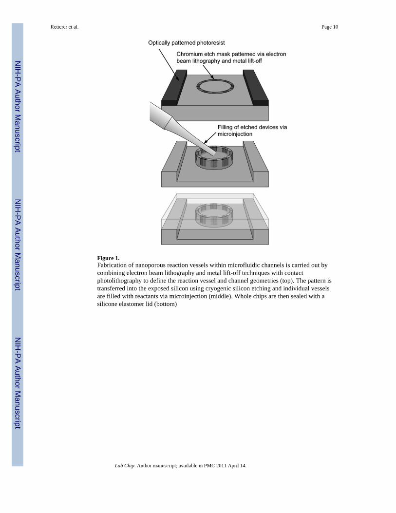
Figure 1.Fabrication of nanoporous reaction vessels within microfluidic channels is carried out bycombining electron beam lithography and metal lift-off techniques with contactphotolithography to define the reaction vessel and channel geometries (top). The pattern istransferred into the exposed silicon using cryogenic silicon etching and individual vesselsare filled with reactants via microinjection (middle). Whole chips are then sealed with asilicone elastomer lid (bottom)
Retterer et al. Page 10
Lab Chip. Author manuscript; available in PMC 2011 April 14.
NIH
-PA Author Manuscript
NIH
-PA Author Manuscript
NIH
-PA Author Manuscript
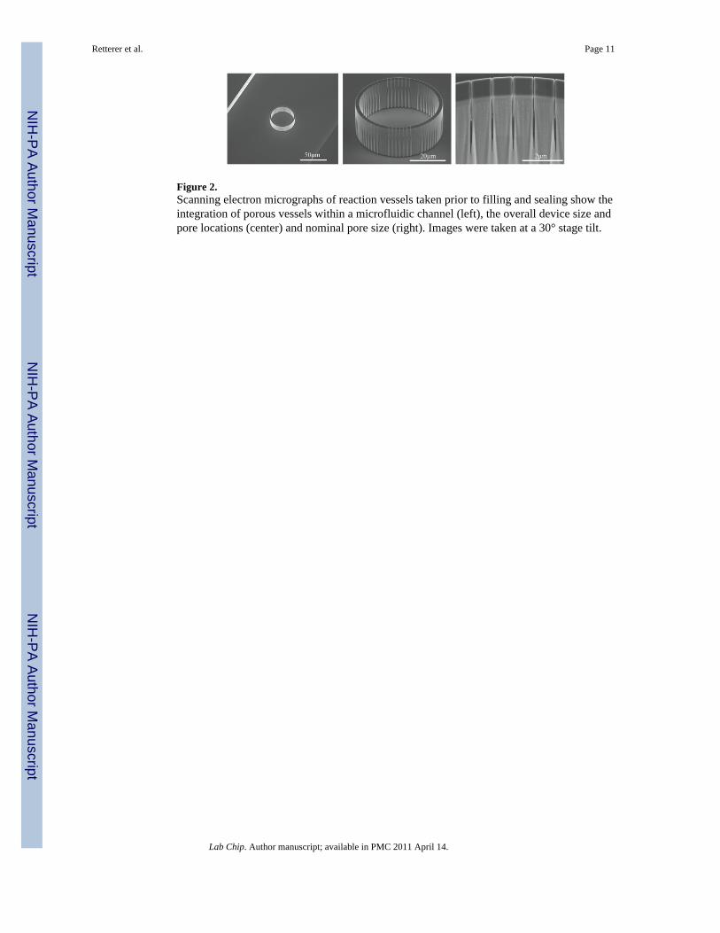
Figure 2.Scanning electron micrographs of reaction vessels taken prior to filling and sealing show theintegration of porous vessels within a microfluidic channel (left), the overall device size andpore locations (center) and nominal pore size (right). Images were taken at a 30° stage tilt.
Retterer et al. Page 11
Lab Chip. Author manuscript; available in PMC 2011 April 14.
NIH
-PA Author Manuscript
NIH
-PA Author Manuscript
NIH
-PA Author Manuscript
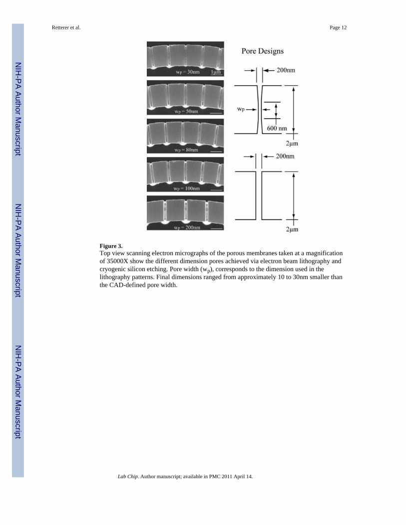
Figure 3.Top view scanning electron micrographs of the porous membranes taken at a magnificationof 35000X show the different dimension pores achieved via electron beam lithography andcryogenic silicon etching. Pore width (wp), corresponds to the dimension used in thelithography patterns. Final dimensions ranged from approximately 10 to 30nm smaller thanthe CAD-defined pore width.
Retterer et al. Page 12
Lab Chip. Author manuscript; available in PMC 2011 April 14.
NIH
-PA Author Manuscript
NIH
-PA Author Manuscript
NIH
-PA Author Manuscript
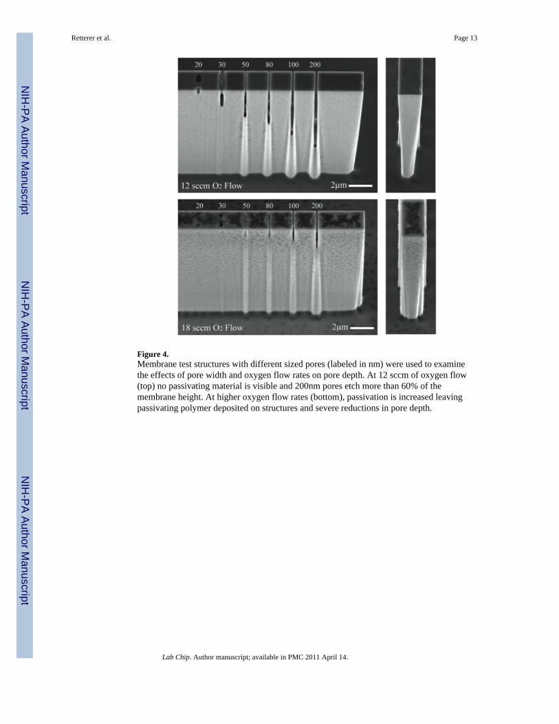
Figure 4.Membrane test structures with different sized pores (labeled in nm) were used to examinethe effects of pore width and oxygen flow rates on pore depth. At 12 sccm of oxygen flow(top) no passivating material is visible and 200nm pores etch more than 60% of themembrane height. At higher oxygen flow rates (bottom), passivation is increased leavingpassivating polymer deposited on structures and severe reductions in pore depth.
Retterer et al. Page 13
Lab Chip. Author manuscript; available in PMC 2011 April 14.
NIH
-PA Author Manuscript
NIH
-PA Author Manuscript
NIH
-PA Author Manuscript
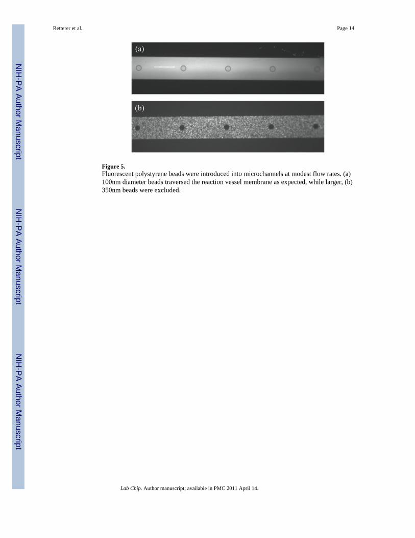
Figure 5.Fluorescent polystyrene beads were introduced into microchannels at modest flow rates. (a)100nm diameter beads traversed the reaction vessel membrane as expected, while larger, (b)350nm beads were excluded.
Retterer et al. Page 14
Lab Chip. Author manuscript; available in PMC 2011 April 14.
NIH
-PA Author Manuscript
NIH
-PA Author Manuscript
NIH
-PA Author Manuscript
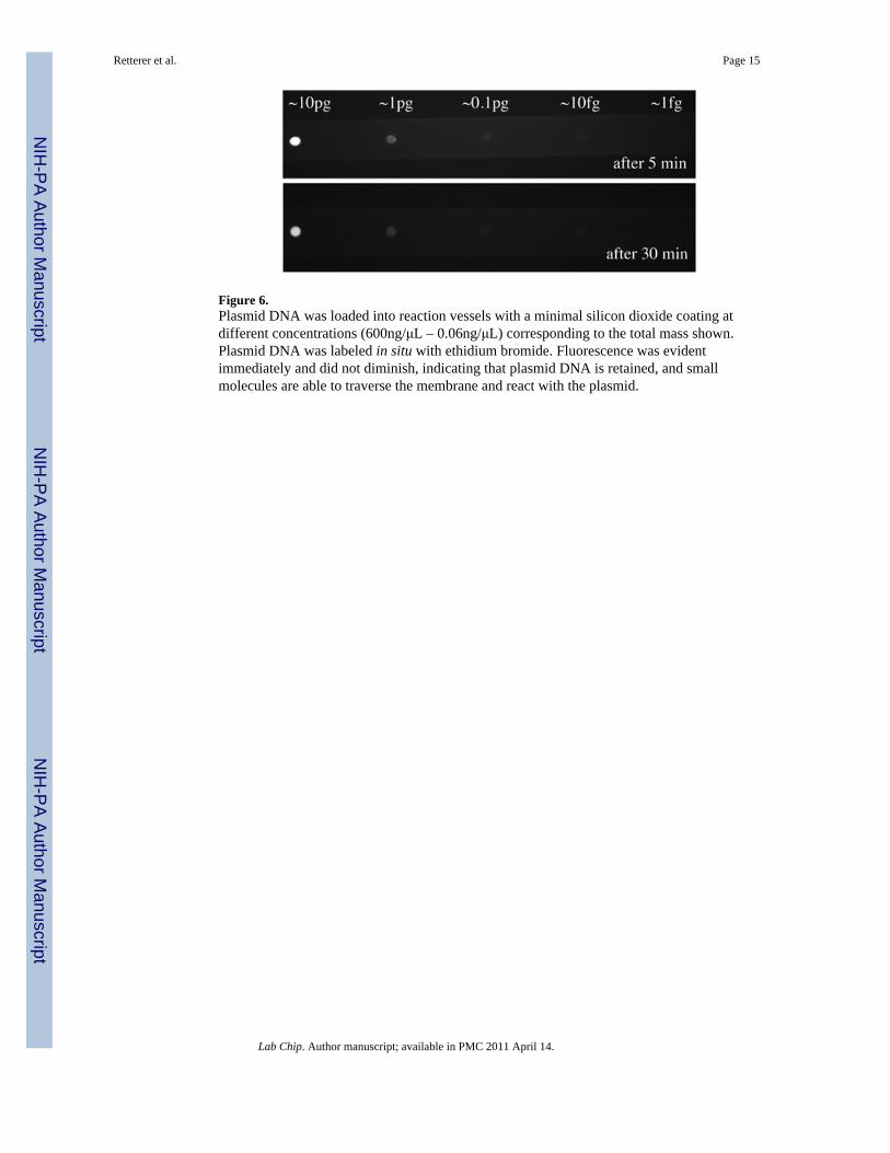
Figure 6.Plasmid DNA was loaded into reaction vessels with a minimal silicon dioxide coating atdifferent concentrations (600ng/μL – 0.06ng/μL) corresponding to the total mass shown.Plasmid DNA was labeled in situ with ethidium bromide. Fluorescence was evidentimmediately and did not diminish, indicating that plasmid DNA is retained, and smallmolecules are able to traverse the membrane and react with the plasmid.
Retterer et al. Page 15
Lab Chip. Author manuscript; available in PMC 2011 April 14.
NIH
-PA Author Manuscript
NIH
-PA Author Manuscript
NIH
-PA Author Manuscript
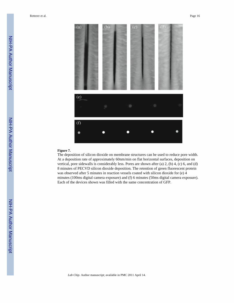
Figure 7.The deposition of silicon dioxide on membrane structures can be used to reduce pore width.At a deposition rate of approximately 60nm/min on flat horizontal surfaces, deposition onvertical, pore sidewalls is considerably less. Pores are shown after (a) 2, (b) 4, (c) 6, and (d)8 minutes of PECVD silicon dioxide deposition. The retention of green fluorescent proteinwas observed after 5 minutes in reaction vessels coated with silicon dioxide for (e) 4minutes (100ms digital camera exposure) and (f) 6 minutes (50ms digital camera exposure).Each of the devices shown was filled with the same concentration of GFP.
Retterer et al. Page 16
Lab Chip. Author manuscript; available in PMC 2011 April 14.
NIH
-PA Author Manuscript
NIH
-PA Author Manuscript
NIH
-PA Author Manuscript
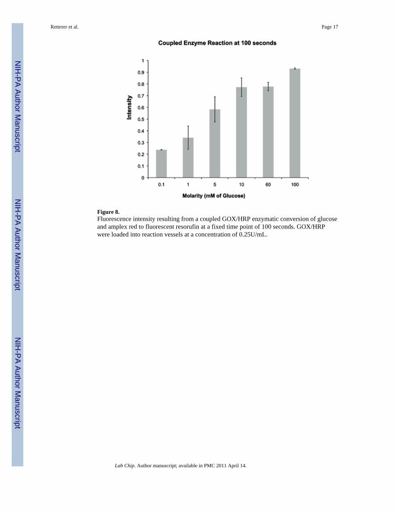
Figure 8.Fluorescence intensity resulting from a coupled GOX/HRP enzymatic conversion of glucoseand amplex red to fluorescent resorufin at a fixed time point of 100 seconds. GOX/HRPwere loaded into reaction vessels at a concentration of 0.25U/mL.
Retterer et al. Page 17
Lab Chip. Author manuscript; available in PMC 2011 April 14.
NIH
-PA Author Manuscript
NIH
-PA Author Manuscript
NIH
-PA Author Manuscript