multiphoton fabrication
TRANSCRIPT

MicrostructuresDOI: 10.1002/anie.200603995
Multiphoton FabricationChristopher N. LaFratta, John T. Fourkas,* Tommaso Baldacchini, andRichard A. Farrer
AngewandteChemie
Keywords:lithography · microfabrication ·nanostructures · nonlinear optics ·polymerization
J. T. Fourkas et al.Reviews
6238 www.angewandte.org � 2007 Wiley-VCH Verlag GmbH & Co. KGaA, Weinheim Angew. Chem. Int. Ed. 2007, 46, 6238 – 6258

1. Introduction
Technological developments in microscopic pattern gen-eration have driven the information revolution. The controlprocessors of state-of-the-art computers will soon containmore than 1 billion transistors per square centimeter, withindividual features on the scale of tens of nanometers. Acomparable revolution is brewing for microtechnology of adifferent sort. What if all the benefits of speed, cost, andportability of microelectronics could be extended to mechan-ical, chemical, and medical systems? This is the basic conceptbehind emergent technologies such as microelectromechan-ical systems[1–4] (MEMS) and micro total analysis systems[5,6]
(mTAS), which are poised to make major leaps in a broadrange of applications in the near future.
Photolithography has been the dominant technique formicroscale patterning for the past fifty years. By shrinking thesize of electronic components and fabricating them in batches,huge leaps have been made in portability, speed, and cost.Recent improvements in the resolution of 193-nm immersionlithography have pushed feature sizes below a half pitch of32 nm, which had been thought to be the limit of thetechnique.[7,8] This achievement is a technological marvel;however, a number of facets of conventional photolithogra-phy still pose constraints in its expansion into areas such asMEMS and mTAS. One problem is that the materialscommonly used for photolithography require processingconditions that can be severe, including etching with harshagents such as HF or reactive ions. Another issue is thatphotolithography is essentially a planar technique. By com-bining layers or using special release techniques, patterns canextend into the third dimension. However, the controlcurrently available in the vertical dimension does not beginto approach what can be achieved in the other two dimen-sions.
To extend the range of materials that can be used inlithography, alternative patterning techniques have beendeveloped, including dip-pen nanolithography,[9] nanoimprintlithography,[10] and soft lithography.[11, 12] These techniqueshave some advantages over photolithography, such as higherresolution, more materials options, and gentler processingconditions. However, these techniques are also essentiallytwo-dimensional.
Efforts to extend patterning capabilities into the thirddimension have made the development of new techniques for3D micro- and nanofabrication a highly active area of
research. The most important approaches include ink-basedwriting,[13,14] self-assembly,[15] layer-by-layer assembly,[16,17]
LIGA (lithography, electroplating, and molding),[18,19] andlaser-based photolithographic techniques.
Writing with ink can be performed by either drop- orfilament-based techniques, which are referred to as ink-jetprinting[20,21] and robotic deposition,[22] respectively. A nozzlecan deliver inks composed of colloids, polymers, or polyelec-trolytes, whose rheological parameters can be tailored for theparticular deposition technique. Structures can span a rangeof sizes, with the resolution of individual features rangingfrom roughly 1 to 100 mm. Although 3D control is possible inprinciple, in practice the inks are not rigid enough to createstructures of arbitrary geometries. For example, ink-basedwriting of lattice-type scaffolds has been demonstrated, but,without the structural support of a lattice, freestandingindividual lines cannot be created.
Self-assembly of 3D microstructures with arbitrary con-trol of geometry is currently beyond reach in the laboratory,although its ultimate feasibility is clearly demonstrated by thecountless examples provided in biological systems. Self-assembly techniques are currently best-suited for the creation
Chemical and physical processes driven by multiphoton absorptionmake possible the fabrication of complex, 3D structures with featuresizes as small as 100 nm. Since its inception less than a decade ago, thefield of multiphoton fabrication has progressed rapidly, and multi-photon techniques are now being used to create functional micro-devices. In this Review we discuss the techniques and materials usedfor multiphoton fabrication, the applications that have been demon-strated, as well as those being pursued. We also consider the outlookfor this field, both in the laboratory and in industrial settings.
From the Contents
1. Introduction 6239
2.Multiphoton Absorption 6241
3.Multiphoton AbsorptionPolymerization 6242
4.Multiphoton Fabrication withOther Materials 6248
5. Applications 6250
6.Mass Production 6252
7. Outlook 6253
8. Conclusions 6254
[*] C. N. LaFratta, Prof. J. T. FourkasDepartment of Chemistry and BiochemistryUniversity of MarylandCollege Park, MD 20742 (USA)Fax: (+1)301-314-4121E-mail: [email protected]: http://www.chem.umd.edu/faculty/fourkas
Dr. T. BaldacchiniTechnology and Application CenterNewport Corporation1791 Deere Avenue, Irvine, CA 92606 (USA)
Prof. R. A. FarrerChemistry DepartmentColorado State University-Pueblo2200 Bonaforte Blvd., Pueblo, CO 81001 (USA)
MicrostructuresAngewandte
Chemie
6239Angew. Chem. Int. Ed. 2007, 46, 6238 – 6258 � 2007 Wiley-VCH Verlag GmbH & Co. KGaA, Weinheim

of periodic structures. For example, colloidal solutions can bedried carefully to yield close-packed colloidal crystals that canhave optical properties similar to those of opals or inverseopals.[23] Block copolymers also self-assemble into usefulperiodic patterns in three dimensions.[24] DNA has also beenused to great advantage in the self-assembly of 2D structuresin recent years.[25] Research into self-assembly of nonperiodic,3D microstructures is still in its infancy.
Layer-by-layer assembly creates 3D structures by stackingplanar patterns, which can be made by using the 2Dpatterning techniques discussed above. A variety of materialscan be used for layer-by-layer assembly. However, the 3Dstructures that are produced have geometric limitations thatarise from mechanical constraints. For example, in manylayer-by-layer techniques, each point fabricated in a layermust be attached either to another point in the layer or to apoint in the layer below. This means that some features, suchas the downward serif at the top right of the letter “G”, cannotbe fabricated in a layer-by-layer approach. Layer-by-layertechniques also require a large number of processing stepsand suffer from problems of registration.[26]
Another process that can extend fabrication into the thirddimension was developed in the early 1980s and is now knownas LIGA.[27,28] LIGA is a German acronym for X-raylithography (Lithographie), electroplating (Galvanofor-mung), and molding (Abformung). In this method, X-raysare used to create patterns. Synchrotron-generated X-rayshave small divergence angles owing to their extremely shortwavelength, which allows patterning in photoresists with
micrometer resolution and depths that can exceed 1 cm. Theresult is high-aspect-ratio patterns, such as channels and gears,that can be used as molds to electrodeposit metals, such asnickel. The metal pattern can be used as is, or its shape can beinverted again by using the metal pattern as a mold forpolymer parts. Structures made by LIGA have smoothsurfaces and sharp vertical features, but are of limited 3Dcomplexity because of the line-of-sight nature of the X-rayexposure.
Laser-based techniques such as holographic lithographyand phase-mask lithography have also been developed tocreate periodic 3D patterns. In holographic lithography,which is also known as multibeam interference lithography(MBIL), two or more nonparallel laser beams are incident ona photoresist.[29–31] The resulting light intensity distribution iscaptured within the photoresist, resulting in periodic voidsbased on the interference pattern of the light. Phase-masklithography also relies on interference to generate a periodicpattern within a photoresist but, instead of using multiplebeams, a single beam is transmitted through a phase mask,which creates a complex 3D distribution of light to expose thephotoresist.[32] Both of these techniques are promising meth-ods for the rapid preparation of 3D patterns; however, theyare inherently restricted to locally periodic patterns becausethey take advantage of the periodic nature of light to definethe features and therefore are not capable of arbitrarypatterning in three dimensions.
Unlike the previous techniques described, fabrication by afocused laser can allow for true 3D control. Laser chemical
Christopher LaFratta was born in Malden,Massachusetts, USA, in 1979. He received aBS in chemistry from the University ofMassachusetts, Dartmouth, in 2001. Hethen joined the laboratory of Prof. JohnFourkas at Boston College, where hisresearch focused on aspects of multiphotonfabrication. After the research group movedto the University of Maryland, College Park,he received his PhD in 2006. He was thenawarded an NIH TEACHRS postdoctoralfellowship to work in the group of Prof.David Walt at Tufts University on the devel-opment of a microarray-based universalchemical sensing platform.
John T. Fourkas received a BS and an MS inchemistry from the Caltech in 1986, and aPhD in chemistry from Stanford Universityin 1991. He worked at the University ofTexas at Austin and MIT as an NSF Postdoc-toral Fellow. He joined the chemistry facultyat Boston College in 1994, and then movedto the University of Maryland, College Park,in 2005, where he holds the MillardAlexander Chair in Chemistry. He is aFellow of the American Association for theAdvancement of Science, the AmericanPhysical Society, and the Optical Society of
America. His research interests include applications of nonlinear optics inspectroscopy, microscopy, and fabrication.
Tommaso Baldacchini was born in Rome,Italy, in 1973. After studying chemistry atthe University of Rome “La Sapienza”, hepursued doctoral research at Boston College,where he worked on unconventional meth-ods to fabricate 3D microstructures. Hereceived a PhD in chemistry in 2004. As apostdoctoral researcher with Prof. EricMazur at Harvard University he investigatedthe wettability properties of nanostructuredsurfaces prepared by laser ablation. In 2006he joined the Technology and ApplicationCenter at Newport Corporation as a Senior
Scientist. His research interests lie in applications of nonlinear optics inmicroscopy and nanofabrication.
Richard A. Farrer was born in 1968 inGrand Rapids, MI. He received his BScdegree from Aquinas College (Michigan) in1991. He attended graduate school atBoston College and received his PhD inchemistry with Prof. John T. Fourkas in2001. He remained at Boston College as apostdoctoral researcher with Prof. Fourkasuntil 2005. He is currently an assistantprofessor in the Chemistry Department atColorado State University in Pueblo withresearch interests that include the develop-ment of three-dimensional microscopic devi-ces and the production and properties ofnanoparticles.
J. T. Fourkas et al.Reviews
6240 www.angewandte.org � 2007 Wiley-VCH Verlag GmbH & Co. KGaA, Weinheim Angew. Chem. Int. Ed. 2007, 46, 6238 – 6258

machining, for example, is capable of etching or depositingmaterial in a liquid or gaseous environment.[33, 34] Micro-stereolithography uses a laser to harden the surface of aprepolymer resin into 2D pattern.[35–39] Additional resin isthen flowed onto the pattern to create a new surface, and theprocess is repeated until the part is finished. Any unhardenedresin is washed away with solvent. 3D parts of considerablecomplexity can be created with this technique, although thefabrication is slow and high precision is required in the resinreflow step.
Multiphoton absorption (MPA) offers another means offabricating 3D structures. Because MPA depends nonlinearlyupon intensity, it is possible to localize photochemical orphotophysical material transformations within the focalvolume of a laser beam that has passed through a microscopeobjective. Complex structures can be fabricated by movingthe laser focus in three dimensions relative to the substrate.Multiphoton techniques offer true 3D fabrication capabilityat resolutions lower than 100 nm with a straightforwardexperimental setup.
In this Review we summarize the principles of MPA-based fabrication. We discuss the fundamental principles ofMPA, the types of materials that have been patterned, as wellas applications and future prospects for the technology.
2.Multiphoton Absorption
The process of MPA was first predicted theoretically in1931 by Maria GEppert-Mayer.[40] Because of the high photonintensities required, even two-photon absorption (TPA) wasnot demonstrated until the advent of the laser.[41] The basicrequirement for MPA is that an absorption event is caused bythe collective action of two or more photons, all of which mustbe present simultaneously to impart enough energy to drive atransition. For example, in TPA the sum of the two photonenergies is resonant with the energy of the transition that isdriven. The most common implementation of TPA infabrication is for both photons to have the same energy, butthis need not be the case.
There is a strong analogy between MPA of n photons andthe rate of a concerted chemical reaction involving nmolecules. For the reaction nA!An to occur concertedly, nmolecules of A must be in the same place at the same time. Asa result, the rate of the reaction is proportional to [A]n. By thesame token, the rate of MPA for n photons is proportional tothe concentration of photons (i.e., the intensity) to the nthpower.
It is common to employ ultrafast lasers to drive MPA. Atypical ultrafast Ti:sapphire laser produces pulses that are afew tens of femtoseconds in duration at a repetition rate ofapproximately 80 MHz, which corresponds to an interpulseseparation of about 12 ns. The instantaneous intensity duringa pulse is quite high, which is favorable for MPA. However,because the pulses are five to six orders of magnitude shorterthan the repetition period of the laser, the average power islow.
The nonlinear intensity dependence of the absorptionprocess allows the excitation to be localized within the focal
volume of a laser beam. To see how this process works,consider a sample in which the absorbing molecules aredistributed homogeneously. The rate of absorption in atransverse cross section of a laser beam depends upon theproduct of the intensity (number of photons per time perarea) and the number of molecules in the cross section (whichis proportional to the area). Thus, the absorption rate does notdepend upon area. The number of molecules excited bysingle-photon absorption is constant in any transverse planeof a focused laser beam, and so there is no localization ofexcitation in the focal region (Figure 1, left).
In the case of TPA, the rate of absorption in a transversecross section of a laser beam is proportional to the intensitysquared times the number of molecules in the cross section.The absorption rate therefore scales inversely with area. Thegreatest density of excited molecules will therefore be in theregion in which the laser beam is focused most tightly(Figure 1, right). This localization was first utilized in 1990 byDenk, Strickler, and Webb in two-photon fluorescencemicroscopy (TPFM).[42] In TPFM, the excitation wavelengthused is usually approximately double the peak absorptionwavelength of a given fluorophore. TPA occurs at the focalpoint, inducing fluorescence that can be imaged. Since thisseminal work, hundreds of groups around the world have usedMPA for fluorescence imaging techniques,[43,44] 3D datastorage,[45] photodynamic therapy,[46] and microfabrica-tion.[47–52]
In almost all of these applications of MPA, objectives withhigh numerical aperture (NA) are employed to create thephoton density needed for nonlinear absorption. For anultrafast laser with a pulse duration t and a pulse repetitionrate fp, the number of photons absorbed per molecule perpulse is given by Equation (1),[42] in which p0 is the time-averaged laser power, l is the excitation wavelength, and d isthe two-photon absorption cross section.
na �p2
0d
tf 2p
�ðNAÞ2
2�hcl
�2
ð1Þ
The units for d are named GEppert-Mayer (GM), after theNobel-laureate physicist, and are defined in SI units as
Figure 1. Fluorescence from a solution of rhodamine B caused bysingle-photon excitation from a UV lamp (left) and by two-photonexcitation from a mode-locked Ti:sapphire laser operating at a wave-length of 800 nm (right). The integrated intensity in each transversesection of the beam does not depend upon position for single-photonexcitation, but is tightly peaked in the focal region for two-photonexcitation.
MicrostructuresAngewandte
Chemie
6241Angew. Chem. Int. Ed. 2007, 46, 6238 – 6258 � 2007 Wiley-VCH Verlag GmbH & Co. KGaA, Weinheim www.angewandte.org

1 GM= 10�58 m4 sphoton�1. As an example, d for fluorescein,a good two-photon-absorbing fluorophore, is 38 GM.
Figure 2 shows a typical experimental setup for multi-photon fabrication. The excitation source is a mode-lockedTi:sapphire laser, which typically produces pulses with a
duration of tens to hundreds of femtoseconds and a centerwavelength of 800 nm. The repetition rates for these lasers ison the order of 80 MHz, and the average output power canrange from hundreds of milliwatts to more than a watt. Anisolator, such as a Faraday rotator, is often placed in the beampath to prevent interference from reflected light. Dispersionof the laser pulses can be compensated for by a pair of prismsto obtain the shortest possible pulses at the sample. Theintensity of the laser can also be controlled by a device such asan acoustooptic modulator, an electrooptic modulator, or ashutter. The beam is generally expanded so as to overfill theback aperture of the objective, although a variable beamexpander can be used if one wishes to control the degree offocusing to manipulate the dimensions of the region in whichfabrication occurs.
Although a mounted objective is sufficient for fabricationpurposes, using a microscope is convenient for samplepositioning and viewing and for being able to switchobjectives rapidly. In the experimental setup shown inFigure 2, the laser beam enters through the reflected-lightport of an upright microscope and is directed into theobjective by a beam splitter. The sample rests on a computer-controlled stage that can be translated in three dimensionsrelative to the focus of the laser beam; an alternativeapproach is to employ scanning mirrors to move the focalpoint relative to the sample. Transmitted light is used to viewthe sample with a CCD camera and a video screen, simplify-ing the positioning of the sample and making it possible tomonitor fabrication in real time.
3.Multiphoton Absorption Polymerization
The most well developed of multiphoton fabricationtechniques is multiphoton absorption polymerization(MAP). In this method, the sample is a prepolymer resincontaining a photoinitiator that can that can be excited byMPA. The resins most commonly used act as negative-tone
photoresists, that is, polymerization occurs in the regions thatare exposed. However, MAP prepolymer resins that act aspositive-tone photoresists, that is, ones in which the unex-posed regions are hardened, have also been demonstrated.After exposure, a development process is used to remove anyunhardened material. Development generally involves wash-ing with one or more solvents, and can also involve additionalprocessing steps such as baking.
In this section we examine the photoinitiators andpolymers that have been used in MAP fabrication and discussthe physical properties of the structures produced.
3.1.MAP Materials3.1.1. The Prepolymer Resin
To prevent components from moving during fabrication,the prepolymer resin used for MAP is usually a viscous liquid,an amorphous solid, or a gel. Each of these options has its ownadvantages and disadvantages. Liquid samples are simple toprepare and process, but can allow undesired motion ofstructures during fabrication. Solids and gels are moredifficult and time-consuming to prepare and process, but thecomplete restriction of motion in these media facilitates thefabrication of complex structures, such as those with free-moving parts.
There are two crucial components in a prepolymer resinfor MAP: the photoinitiator and the monomers. Othercomponents can include polymerization inhibitors (to stabi-lize the resin and influence the feature size), solvents (to assistin casting), filler polymers (to create gels or increase theviscosity of liquid resins), and other additives (such as dyemolecules) that introduce new function to polymerizedstructures. In the following subsections we discuss the typesof polymer systems that have found the greatest use in MAP.
3.1.2. Radical Polymerization
The majority of the MAP research reported to date hasinvolved radical polymerization. The popularity of radicalpolymerization in MAP stems from a combination of highreaction rates, ease of processing, and wide availability ofphotoinitiators and monomers for this type of chemistry.
3.1.2.1. Radical Photoinitiators
The first step in radical polymerization is the nonlinearexcitation of a photoinitiator, which can either cleavehomolytically or transfer its energy to a coinitiator to createthe radicals that begin the polymerization reaction. Photo-initiators that operate by these mechanisms are classified astype I and type II, respectively, although type I initiators canalso be used as type II initiators. One requirement for eithertype of photoinitiator, if it to be useful in MAP, is that it notabsorb light in the near-infrared and in the red portion of thespectrum.
The utility of a radical photoinitiator for MAP dependsupon a balance among a number of different parameters.Efficient polymerization is promoted by a high value of d, a
Figure 2. Schematic of a typical experimental setup for multiphotonfabrication. PDC=prism dispersion compensator, AOM=acoustoopticmodulator, VBE=variable beam expander, CCD= charge-coupleddevice camera.
J. T. Fourkas et al.Reviews
6242 www.angewandte.org � 2007 Wiley-VCH Verlag GmbH & Co. KGaA, Weinheim Angew. Chem. Int. Ed. 2007, 46, 6238 – 6258

high radical yield (Fr), and a high initiation velocity. How-ever, solubility is also an important consideration. A highlysoluble photoinitiator of modest efficiency may be preferableto a sparingly soluble initiator of high efficiency, for example.
We first consider Norrish type I radical initiators. Severalgroups have synthesized custom type I photoinitiators thatare optimized for TPA, making fabrication possible at lowlaser powers. Similar molecules engineered in this manner canbe used for other applications that take advantage of TPA,such as optical data storage, optical limiting, photodynamictherapy, and two-photon imaging. Work in this field centerson molecules composed of a conjugated central regionflanked by electron-donating (D) or -accepting (A) groups.The various core moieties that have been used for MAPinitiators include (E)-stilbene, bis(stryl)benzene, naphtha-lene, biphenyl, and fluorene.
Marder, Perry, and co-workers have done extensive workon the (E)-stilbene and bis(stryl)benzene systems, symmetri-cally altering the strength and positions of electron-donatingand -accepting groups.[53–56] Configurations such as D-p-D, D-p-A-p-D, and A-p-D-p-A (p represents a conjugated bridge)have been tested, and molecules with d values as high as1250 GM have been synthesized.[53] Studies show that sym-metric charge transfer from the molecular center to the ends(or vice versa) is responsible for high d values. Extending theconjugation length increases the value of d, as does increasingthe electron-donating or -accepting strength. A side effect ofthese changes is a shift of the TPA maximum to longerwavelengths with increasing conjugation length. This shiftallows molecules to be optimized for different wavelengths,but for the most common case of 800-nm excitation, shiftedTPA spectra also lead to inefficient pumping. After this typeof molecule has been excited by TPA it is thought to undergodirect electron transfer to an acrylate monomer/oligomer,initiating the polymerization reaction. Thanks to its highd value, 4,4’bis(N,N-di-n-butylamino)-(E)-stilbene has beenused for MAP at powers as low as a few hundred microwattswith a Ti:sapphire oscillator.[54] Since the polymerizationefficiency is proportional to the product of d and Fr, the highTPA cross sections of these molecules evidently more thancompensate for low radical yields.
Building on the work of Marder, Perry, and co-workers,Watanabe and co-workers showed that a custom photoinitia-tor with a cyano-substituted imino core could effectivelyinitiate MAP with a tightly focused Ti:sapphire oscillator.[57]
They also confirmed, by comparing different photoinitiators,that a high d value alone is not sufficient for rapid polymer-ization.
Prasad, Reinhardt, and co-workers developed the initiator6-benzothiazol-2-yl-2-naphthyl diphenylamine (AF183) andincorporated it into a mixture of commercial resins NOA 72(Norland Products) and EPO-TEK 301 (Epoxy Technology)for use in MAP.[58] AF183, an unsymmetric molecule with ad value of 6840 GM, is part of series of molecules optimizedfor strong TPA at 800 nm.
The biphenyl and fluorene systems have also been studiedby Prasad, Reinhardt, and co-workers[59–62] and have beenapplied to MAP by Belfield, Van Stryland, and co-workers.[63]
Like the (E)-stilbene and naphthalene systems, these con-
jugated units provide a bridge for charge transfer. It has beenfound that locking the planarity of the biphenyl system bybridging it into a fluorene system can enhance this chargetransfer. The initiator used by Belfield and co-workers was adiphenylaminobenzothiazolylfluorene analogue of the formD-p-A. This asymmetric motif takes advantage of the factthat polar molecules have a large change in dipole momentduring excitation through a virtual state and therefore have acorrespondingly high value of d. This initiator was used topolymerize acrylic monomers by using an amplified Ti:sap-phire system with an average power of a few milliwatts and arepetition rate of 1 kHz.[63]
Andraud and co-workers have also used a substitutedfluorenyl system to initiate MAP.[47] They used this initiator todemonstrate fabrication with an inexpensive, frequency-doubled Nd:YAG microlaser that produces 0.5-ns pulses at532 nm with a repetition rate of 6.5 kHz.[64, 65] The amino-biphenyl-substituted fluorene is of the D-p-D type and has ad value of 80 GM at 532 nm. Acrylic monomers have beenpolymerized with an average power of around 1 mW. Thisgroup has also reported TPA of 1064-nm light in symmetricphotoinitiator molecules composed of a central ketoneelectron-accepting group attached to two electron-donatinggroups by conjugated bridges. The d value for such moleculesis about 100 GM at 1064 nm, and the intensity threshold forfabrication is roughly twice that for initiation at 532 nm.
There are many commercially available examples oftype I initiators, most of which are aromatic carbonyl com-pounds. Electronic excitation of these molecules generallyleads to the creation of a singlet CC-OC diradical that under-goes intersystem crossing to a triplet diradical state with alifetime on the order of 100 ps and subsequent rapidhomolytic a-cleavage.[66]
SCR500 (Japan Synthetic Rubber Co.) is a popular MAPresin composed of urethane acrylate oligomers (molecularweights 480 and 1200) and two type I photoinitiators (Irga-cure 369 and Irgacure 184).[48] This resin has been polymer-ized with just a few milliwatts of average power from aTi:sapphire oscillator through a high-NA objective. Irga-cure 369 and 184 both have two-photon cross sections ofapproximately 20 GM, which is a typical value for thecommercial compounds that have been measured.[67]
Another commercial acrylic resin that has been used forMAP is Nopcocure 800 (Japan Synthetic Rubber Co.).[68–71]
Frequency-doubled light from a regeneratively amplifiedTi:sapphire laser operating near 800 nm was used to makegears[70] and photonic crystal structures[68, 69] using this resin.
An alternative to using a premixed commercial resin is touse a commercially available photoinitiator combined withselected monomers or oligomers to create a tailored resinwith specific properties. Photoinitiators such as Irgacure 819(bis(2,4,6-trimethylbenzoyl)phenylphosphine oxide), BME(2-methoxy-1,2-diphenylethanone), and ITX (2-/4-isopro-pylthioxanthone) have been used for MAP with customacrylate or methacrylate resins.[63,72]
Our group has worked extensively with a commerciallyavailable acylphosphine oxide photoinitiator known asLucirin TPO-L.[73–76] The UV/Vis absorption of LucirinTPO-L arises from an n!p* transition. Upon excitation
MicrostructuresAngewandte
Chemie
6243Angew. Chem. Int. Ed. 2007, 46, 6238 – 6258 � 2007 Wiley-VCH Verlag GmbH & Co. KGaA, Weinheim www.angewandte.org

and intersystem crossing the molecule photocleaves to formcarbonyl and phosphinoyl radicals, resulting in the efficientinitiation of the polymerization chain reaction. Although theTPA cross section of Lucirin TPO-L is small,[77] MAP with thisphotoinitiator generally requires only a few milliwatts ofaverage power from a Ti:sapphire oscillator. The highefficiency of Lucirin TPO-L as a photoinitiator results froma combination of its high radical yield, highly reactive radicalproducts, and high solubility. Another advantage of LucirinTPO-L is that it is a liquid at room temperature and so can bemixed quickly, and at high weight percentages, with high-viscosity monomer or oligomer components. Thus, samplescan be prepared in a few minutes or hours; in contrast,dissolving solid photoinitiators is a slow process that can takeas long as days or even weeks.
Several groups have also demonstrated type II radicalpolymerization by using custom resins. Type II photoinitiatorsare used with a coinitiator, which is generally a bulky tertiaryamine. This reaction takes place when the excited photo-initiator forms an exciplex and abstracts an a-hydrogen atomfrom the amine, which is followed by electron transfer.
Campagnola, Pitts, and co-workers have used severalxanthene-based chromophores, including Rose Bengal, eryth-rosin, and eosin, in combination with the coinitiator trietha-nolamine, for the radical polymerization of acrylates, acryl-amides, and biopolymers.[78,79] These chromophores all haved values of about 10 GM at 800 nm, and approximately100 mWof the output of a Ti:sapphire oscillator was requiredwith a 0.75-NA objective to create structures. Campagnolaand co-workers also performed MAP using 9-fluorenone-2-carboxylic acid with triethanolamine at an excitation wave-length of 780 nm, which is approximately three times itsmaximum single-photon absorption wavelength (260 nm).[79]
This is the first clear demonstration of three-photon poly-merization.
Belfield and co-workers used the commercial fluoronedye H-NU 470, along with the aryl amine N,N-dimethyl-2,6-diisopropylaniline (DIDMA), for type II radical polymeri-zation of acrylates and methacrylates.[63] Single-photonabsorption studies suggest the mechanism of initiationinvolves electron transfer from the aryl amine to the excitedH-NU 470 followed by proton transfer from the aryl amineradical cation to H-NU 470; the resulting radical aryl amineinitiates the polymerization reaction. ITX has also been usedas a type II initiator in combination with DIDMA.[63] Boththis system and H-NU 470 have been used for MAP with anamplified Ti:sapphire laser.
Li et al. reported the use of 7-diethylamino-3-(2’-benzi-midazolyl)coumarin with a coinitiator of diphenyliodoniumhexafluorophosphate.[80] They were able to achieve fabrica-tion at average powers of less than 1 mW with a Ti:sapphireoscillator tuned to 800 nm. Watanabe and co-workers haveused this iodonium coinitiator with their cyano-substituted,imino-backbone chromophore and a tertiary amine to enablefabrication with acrylates in dioxane.[81]
The photoinitiators that have been used for radical MAPvary from small molecules to large conjugated molecules toternary systems. Many groups have designed custom photo-initiators that require low threshold powers and allow less
expensive laser systems to be employed. Although thebenefits of custom initiators are clear, their availability islimited. Commercial resins or resins that employ commercialphotoinitiators have the benefit of accessibility but generallyhave slightly higher power thresholds for fabrication. How-ever, the fabrication threshold for all of the systems discussedherein is well below the available power of the lasers used,and therefore the use of commercial photoinitiators is entirelypractical.
3.1.2.2.Materials for Radical Polymerization
The majority of the resins used in the studies describedabove employed acrylate monomers. Acrylic resins have anumber of properties that make them attractive for MAP.Acrylates are used extensively in industry and so arecommercially available in a wide assortment of functional-ities, sizes, and compositions. They are easily processed byspin coating or drop casting. The nonpolymerized resins aresoluble in common solvents such as ethanol. Polyfunctionalacrylates result in polymeric solids that are highly cross-linkedand are therefore able to resist swelling during the develop-ment step after fabrication. Acrylic structures are also inertenough to withstand many harsh solvents as well as elevatedtemperatures. Acrylic microstructures exhibit low shrinkageand have favorable mechanical properties. The polymerizedsolids are transparent in the visible region and are of highoptical quality. Perhaps the most important quality ofacrylates, however, is the high speed at which they polymer-ize. Rapid polymerization enables the use of fast scanningspeeds, which is of fundamental importance in a serial processsuch as MAP.
Electron micrographs of typical structures created fromacrylic resins are shown in Figure 3a–c. The interpenetratingmicrocoils in Figure 3a demonstrate the complexity of thestructures that can be created with MAP. Figure 3b shows acantilever with a high aspect ratio, a structure that could becreated only with great difficulty by using conventionalmicrostereolithography. The microbull in Figure 3c is perhapsthe most famous structure created with MAP.[82] The degree ofdetail on this structure underscores the high resolution of thistechnique.
Acrylic resins are usually used in a pure liquid form, and asample can be prepared by simply putting a drop onto a coverglass. Binders can also be combined with the acrylatemonomers to form a gel. As an example, equal parts of thealkoxylated trifunctional acrylates (SR9008) and tris(2-hydroxyethyl)isocyanurate triacrylate (SR368) can be mixedwith approximately 1% w/w photoinitiator and then com-bined with a poly(styrene-co-acrylonitrile) polymer binder ina 3:1 ratio.[54, 57,64,83] The binder is dissolved in dioxane andmixed with the monomers, after which the sample is cast.After the solvent evaporates, the resulting film is rigid,allowing structures such as links on a chain to be madewithout fear of the resin reflowing (Figure 3d). Reflowingotherwise occurs easily if the resin is sandwiched between acoverslip and a slide with an oil-immersion objective pressingon it. Although the binder allows the creation of a sample that
J. T. Fourkas et al.Reviews
6244 www.angewandte.org � 2007 Wiley-VCH Verlag GmbH & Co. KGaA, Weinheim Angew. Chem. Int. Ed. 2007, 46, 6238 – 6258

cannot flow, its preparation is time-consuming becausesolvent evaporation may take days.
Hydrogel materials made of acryloylacetone, acrylamide,and N,N’-bisacrylamide have also been fabricated by MAP.[84]
These materials undergo a tautomerization after exposure toUV light, resulting in controllable shrinkage of the structures.Watanabe et al. produced a cantilever by using this materialwith an irreversible photoactuated process.[84]
Organically modified ceramics (ORMOCERs or ceram-ers) have also been used in MAP.[85] These silicate-basedmaterials combine the best features of sol–gel processing andorganic polymers.[86] They have an inorganic (-Si-O-Si-)backbone functionalized with organic groups such as acyrlatesor epoxides. The organic side chains can cross-link the resininto a durable, biocompatible solid. In fact, such compoundsare often used as photocurable dental composites.
Another material that has been used in MAP is polydi-methylsiloxane (PDMS). This material is ubiquitous in softlithography, where it is used for making 2D patterns withnanometer resolution.[12] Ober and co-workers reportedphotopolymerization of PDMS by two distinct methods.[87]
The first was a photohydrosilylation reaction using a photo-active platinum catalyst. This method suffers from undesiredthermal polymerization, which adversely affects the resolu-tion that can be attained. The second method employed ITXto initiate cross-linking of the dimethylvinyl-terminatedsiloxane components, and did not exhibit any thermalpolymerization.
3.1.3. Cationic Polymerization
An alternative mechanism to radical polymerization iscationic polymerization. A cationic photoinitiator works bygenerating a strong Brønsted acid that is capable of polymer-izing epoxides and vinyl ethers. This photoacid is catalytic,and so each photoacid generator (PAG) molecule can initiate
multiple polymerizations. Although singlet oxygen canquench radical polymerization, it does not affect cationicpolymerization.
3.1.3.1. Cationic Photoinitiators
Diaryl iodonium and triaryl sulfonium salts are two classesof commercial PAG molecules that have been used in MAP.Both can be used alone or with a photosensitizer. Belfieldet al.[63] used these salts alone to polymerize a diepoxide resin(Sartomer K-126).[63] Boiko et al. added ITX to diaryliodonium hexafluoroantimonate and reported thresholdpolymerization intensities of around 1 GWcm�2 with aTi:sapphire oscillator.[63,88]
Two groups have reported the use of custom-made PAGs.Ober and co-workers[89] used the coumarin iodonium salt firstreported by Li et al.[80] because of its high TPA cross section.Marder, Perry, and co-workers adapted their high-d mole-cules with the bis(styryl)benzene core into PAGs by changingthe pendant groups to contain sulfonium moieties.[90] Theresulting molecule, labeled BSB-S2, has a d value of 690 GMand is more than ten times as sensitive as commercial cationicphotoinitiators.
3.1.3.2.Materials for Cationic Polymerization
Epon SU-8, the most widely used epoxy polymerized byMAP,[91–93] has eight epoxy groups per monomer and containsa triaryl sulfonium salt PAG. SU-8 is used extensively in theconventional photolithography of MEMS because of itsability to be cast in films up to 500 mm thick that can yieldstructures with high aspect ratios. The availability and well-documented use of SU-8 make it a convenient choice as acationic resin. For example, Teh et al.[92] have performed anextensive study of MAP with SU-8. Using a low-NA objectiveit was shown that structures with high aspect ratios (50:1)could be made with pulse energies of about 1.0 nJ. Generally,SU-8 requires additional processing steps, such as a pre- andpostexposure baking; however, Misawa and co-workersshowed recently that the postexposure baking can beeliminated because of the heating during exposure. Theresulting features are approximately twice as small as thosethat underwent a postexposure treatment.[94]
Another commercial epoxy resin that has been used isSCR-701 (Japanese Rubber Co.). Originally designed formicrostereolithography, SCR-701 has been used to makemicrogears and nanotweezers by Maruo et al.[95]
The PAGs used for cationic polymerization can also beused in positive-tone photoresists, which promises to be auseful way to fabricate 3D microfluidic devices. Marder,Perry, and co-workers demonstrated positive-tone MAP withthe initiator BSB-S2 in a random copolymer consisting oftetrahydropyranyl methacrylate, methylmethacrylate, andmethacrylic acid units.[96,97] The tetrahydropyranyl estergroups are converted into carboxylic acids after the photoacidprotolysis, causing them to be soluble in a basic developer.Channels 4 mm O 4 mm in cross section have been made 10 mmbelow a surface by using an average power of 40 mW from aTi:sapphire oscillator.
Figure 3. Scanning electron micrographs of structures created byMAP: a) interpenetrating microcoils, b) a cantilever, c) a microbull(reproduced from reference [82]), and d) a chain with interlockingrings (reproduced from reference [83]). The scale bars are 10 mm in (a)and (b), 2 mm in (c), and 100 mm in (d).
MicrostructuresAngewandte
Chemie
6245Angew. Chem. Int. Ed. 2007, 46, 6238 – 6258 � 2007 Wiley-VCH Verlag GmbH & Co. KGaA, Weinheim www.angewandte.org

3.2. Physical Properties of Structures Fabricated with MAP3.2.1. Resolution
One important aspect in many applications of MAP is thesize and shape of the volume elements (voxels). The accuratemeasurement of voxel dimensions is a considerable challenge.An issue that must always be considered is the truncationeffect. For a structure (or an individual voxel) to remain afterwashing, it must be in contact with the substrate. Such contactrequires that the focal point of the beam be partiallysubmerged in the substrate. Under such conditions only apartial voxel is created. If more than half of the focal volumeis below the substrate, the observed voxel is only the “tip ofthe iceberg.” This problem is exacerbated by the fact that thesmallest voxels that can be created cannot be viewed duringthe fabrication process, but rather must be imaged later byelectron microscopy. To obtain an accurate representation ofan individual voxel, an ascending scan must be performed. Inthis technique, identical voxels are made at different heightsthat range from submerged within the substrate to suspendedabove it.[98] In the intermediate range, the voxel will be onlyloosely connected to the substrate and will therefore toppleover after washing, giving a clear perspective of its true sizeand shape (Figure 4).
As a result of the combination of optical and chemicalnonlinearity, MAP can achieve a resolution that is consid-erably better than that predicted by the diffraction limit. Thesmallest individual voxel thus far reported with 800-nmexcitation was 100 nm in diameter.[99] Suspended lines withwidths as small as 30 nm have also been fabricated in SU-8,although this kind of resolution has not yet been achieved formore complex structures.[100] Voxels are generally ellipsoidal,
and the two minor axes perpendicular to the optical axis areabout 3–5 times smaller than the major axis.[98] This shape isdetermined in part by the point-spread function (PSF) of thelight intensity near the focus.
The probability for TPA is proportional to I2, whicheffectively narrows the PSF of the beam near the focal pointso that it is smaller than the diffraction limit at the excitationwavelength. However, this narrowing alone is not sufficient toexplain the decrease in voxel size that is observed exper-imentally.[101] In fact, voxels of comparable size have also beenfabricated by using single-photon absorption.[37] The realbenefit of the optical nonlinearity of TPA lies in the negligibleabsorption away from the focal point. Photoinitiator concen-trations can be employed that are approximately ten timeshigher than would be feasible for single-photon excitation, yetwithout any fear of out-of-plane polymerization.
Chemical nonlinearity is also an important factor in thecreation of voxels that are smaller than the diffraction limit.Because of quenching processes, there is a threshold intensitybelow which the polymerization reaction cannot be sustainedto create a solid structure. By careful control of the laserintensity, this threshold can be exceeded in only a smallfraction of the focal volume. For example, a beam that isfocused to a 400-nm diffraction-limited spot may exceed theintensity threshold in only a 100-nm-wide region in the centerof the spot.
The ultimate dimensions of a voxel are governed byfactors such as the photoinitiator concentration, the radicalquantum yield, the viscosity of the resin, and the concen-tration of any inhibitors, such as dissolved oxygen. Althoughno rigorous theory has been put forth that covers all of theseparameters, Chichkov and co-workers have developed asimple model that fits many of the available experimentaldata.[85] Their model assumes a laser beam with a Gaussianprofile and a square temporal pulse shape. It is furtherassumed that a threshold concentration of radicals is requiredto form a sustainable, solid polymer voxel. The model predictsthe rate of change of radical concentration as a function ofposition and time, and defines a voxel as the volume withinwhich the radical concentration is above the survival thresh-old.
The above model does not take into account diffusion,which should play an important role in determining the voxelshape in liquid resins. The incorporation of viscosity in arealistic model is challenging, as this parameter changes overthe course of the polymerization reaction. Linear-exposuretheory predicts that if all other parameters are kept constant,the voxel dimensions should depend only on the product ofthe exposure time and the square of the laser power. DeVoeet al.[102] and Sun et al.,[103] in studying the scaling laws forvoxel dimensions, have demonstrated deviations from thistheory. Sun et al. proposed that voxels grow by two differentmechanisms.[103] One mechanism, which they named “focal-spot duplication”, depends on the PSF of the focused laserbeam. The other mechanism, which they named “voxelgrowth”, depends upon the diffusion of radicals and mono-mers. On short time scales, it was proposed that focal-spotduplication is responsible for the aspect ratio of the voxels.On longer time scales, the growth of the aspect ratio saturates.
Figure 4. The ascending scan technique for measuring voxel dimen-sions. a) The laser is focused partly within the substrate, so that only aportion of the voxel is fabricated. b) The stage is translated to a newposition and lowered slightly for the fabrication of each subsequentvoxel. c) At a certain height of the focal point above the substrate, thevoxels will barely adhere to the surface and will tip over duringdevelopment, making their dimensions readily visible by electronmicroscopy. The scale bar in (c) is 10 mm.
J. T. Fourkas et al.Reviews
6246 www.angewandte.org � 2007 Wiley-VCH Verlag GmbH & Co. KGaA, Weinheim Angew. Chem. Int. Ed. 2007, 46, 6238 – 6258

Continued exposure is believed to result in slower growth,driven by diffusion, which is analogous to dark growth incationic polymerization.[103] DeVoe et al. made similar obser-vations for an acrylic resin.[102] In contrast, for SU-8 theyobserved that the aspect ratio is constant for short exposures,increases rapidly above a certain exposure dose, and thenlevels out for higher exposures.[104] The fact that similarbehavior is observed in a solid resin indicates that a morecomplex model is needed to understand the dependence ofvoxel shape on exposure. DeVoe et al. also suggest that inmedia such as acrylates, in which polymerization occursimmediately (rather than in a postexposure step, as is the casefor SU-8), waveguiding by voxels may be an importantmechanism for voxel growth.[102]
In the case of radical polymerization, quenching isanother phenomenon that must be incorporated into arealistic model. Although the inclusion of a radical inhibitorin a resin increases the fabrication threshold, it has also beenshown to reduce the minimum voxel dimension.[99] The exactmechanism of this action is not well understood.
3.2.2.Mechanical Properties
Because MAP fabrication occurs in a voxel-by-voxelfashion, there is some question as to whether the mechanicalproperties of polymers created with this technique arecomparable to those of the same materials when polymerizedin a more conventional manner. The challenge in making sucha comparison is finding a reliable technique for measuring themechanical properties of microscopic structures.
To give a qualitative sense of the mechanical strength ofstructures created with MAP, in Figure 5 we show a tower thatis 20 mm wide and 1.6 mm tall. Micrometer-sized iron filingswere glued to the top of the tower so that it bent in proximityto a strong magnet. Despite the small area of adhesion of thetower to the substrate and the large forces to which it wassubjected repeatedly, the tower always returned to its uprightequilibrium position when the magnet was withdrawn.
The first technique to be applied to make more-quanti-tative measurements of the mechanical properties of astructure created with MAP was optical tweezing. Opticaltweezers take advantage of photon momentum to applyforces in the piconewton range to microscopic objects.[105] Sun,Takada, and Kawata used this technique to displace andrelease a microcoil, and thereby measured its spring con-
stant.[106] The four-turn coil with a diameter of 2 mm wasanchored on one end to a polymer block. The other end of thecoil was attached a polymer bead that was trapped with theoptical tweezers. Upon release, the coil acted as an over-damped oscillator with a spring constant of 10 nNm�1. Thisvalue is three to five orders of magnitude smaller than wouldbe predicted on the basis of the macroscopic YoungPs modulusof SCR500 (0.46 GPa). The authors attributed this discrep-ancy to a difference in YoungPs modulus between polymerscured with MAP and those cured with ultraviolet light. As thedwell time per voxel in creating the microcoil was approx-imately 1 ms, they theorized that the MAP samples werecross-linked to a lesser degree than the UV-cured samples. Inaddition, these experiments were performed in ethanol, whichis a good solvent for acrylates and so presumably swelled thepolymer in the microcoil. The difference in stiffness betweendry and wet sponges underscores the degree to which suchswelling can affect mechanical properties.
The second technique to be applied to measuring themechanical properties of objects created by MAP was atomicforce microscopy (AFM). Polymer cantilevers that werefabricated with MAP were deflected with calibrated AFMcantilevers. Force versus displacement curves were obtained,allowing the spring constant of the polymer cantilever to bemeasured in air.[107] The YoungPs modulus of a cantilever canbe calculated from its physical dimensions and its forceconstant.[108] Measurements were made on a series of canti-levers of varying dimensions, and a YoungPs modulus of0.44 GPa was obtained. This modulus is comparable to thatmeasured for a bulk sample of the same polymer that was UVcured (2 GPa).[107]
The fact that the YoungPs modulus of the cantilevers issmaller than that of the UV-cured polymer probably indicatesthat the MAP-fabricated polymers are not fully cross-linked.It will be interesting to study the effects that parameters suchas exposure time, postexposure UV curing, and solvent haveon the mechanical properties of structures fabricated withMAP.
3.2.3. Optical Properties
Structures fabricated by MAP have many potentialapplications in optics. Achieving the necessary high opticalquality requires that the polymer volume be spatiallyhomogeneous and that any optical surfaces have a roughnessthat is small relative to the wavelength of the light to beemployed.
Attaining polymer homogeneity, and thereby opticaltransparency, does not present significant difficulties so longas the scanning conditions are similar throughout a structure.Figure 6a shows an electron micrograph of a complex tunnelcreated with MAP. Despite the significant surface roughnessof this tunnel, as demonstrated by the optical micrographs inFigure 6b–d, the transparency of the tunnel is sufficient that aglass microbead can be optically trapped and transportedthrough the structure.
Because the minimum feature size attainable in MAP is sosmall, it is possible with some effort to create optically smoothsurfaces. The creation of flat surfaces requires smooth
Figure 5. A 1.6 mmC20 mmC20 mm tower fabricated with MAP. Micro-meter-sized iron filings were attached to the top of the tower. When astrong magnet is brought into close proximity (a), the tower bends.When the magnet is withdrawn (b), the tower snaps back to itsoriginal position.
MicrostructuresAngewandte
Chemie
6247Angew. Chem. Int. Ed. 2007, 46, 6238 – 6258 � 2007 Wiley-VCH Verlag GmbH & Co. KGaA, Weinheim www.angewandte.org
scanning of the laser or sample and high laser stability, both interms of intensity and direction. The voxel size and degree ofoverlap are also critical parameters in creating smoothsurfaces. Takada, Sun, and Kawata demonstrated that surfa-ces with a mean roughness of around 8 nm can be fabricated ifthe distance between voxels is about 20% of the voxel size.[99]
It is also believed that resins with higher viscosity tend to yieldsmoother structures. To illustrate the smoothness that can beachieved, Figure 7 shows a representative image of a shortsection of an optical waveguide.
4.Multiphoton Fabrication with Other Materials
Although an impressive range of structures can be createdwith MPA, most 3D microdevices will require the incorpo-ration of materials other than polymers. Virtually any photo-chemical or photophysical process has the potential to belocalized in three dimensions by using MPA. The fact thatthere are still relatively few demonstrations of 3D patterningof materials other than polymers by MPA is a testament to thepractical difficulties that are often encountered in suchprocesses. In this section we review the patterning of other
materials either directly by MPA or onto structures that werecreated with MAP.
4.1.Metals
A crucial element of many applications of 3D micro-fabrication is the ability to interface devices with electricalcircuits. Thus, it is essential to be able to incorporate metalliccomponents into 3D microstructures. There are two basicapproaches for using MPA to create 3D structures thatinclude metals. The first approach is to use MPA to depositmetal directly and the second is to use selective chemistry todeposit metals on desired regions of 3D structures created byusing MAP.
4.1.1. Direct Multiphoton Deposition of Metals
Numerous reports describe chemistry that can be used todeposit metal by either photoreduction of metal ions orphotodecomposition of neutral metal-containing molecules.The most famous example of this type of chemistry is thesilver halide photoreduction used in photographic processes,but there are many other metals that can be deposited withlight, all of which are also candidates for patterning withMPA. A natural division for such direct deposition techniquesis whether the source of metal atoms is in free solution or isheld in some sort of matrix.
4.1.1.1. Deposition of Metals from Solution
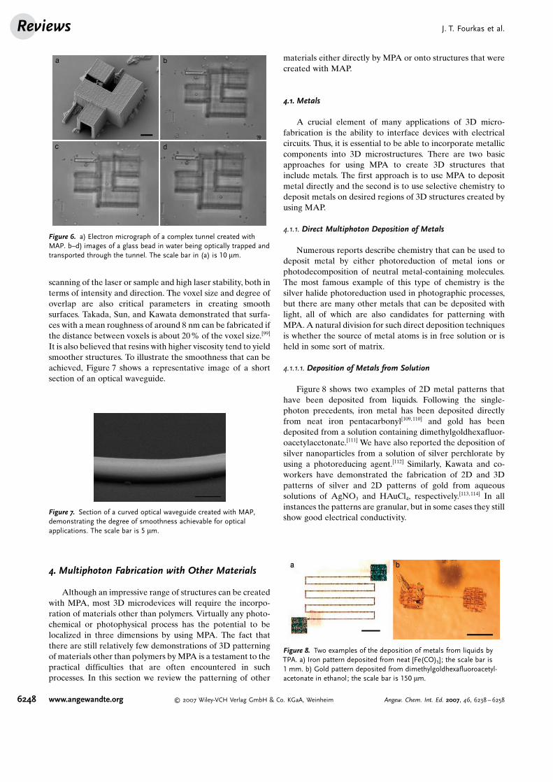
Figure 8 shows two examples of 2D metal patterns thathave been deposited from liquids. Following the single-photon precedents, iron metal has been deposited directlyfrom neat iron pentacarbonyl[109,110] and gold has beendeposited from a solution containing dimethylgoldhexafluor-oacetylacetonate.[111] We have also reported the deposition ofsilver nanoparticles from a solution of silver perchlorate byusing a photoreducing agent.[112] Similarly, Kawata and co-workers have demonstrated the fabrication of 2D and 3Dpatterns of silver and 2D patterns of gold from aqueoussolutions of AgNO3 and HAuCl4, respectively.[113, 114] In allinstances the patterns are granular, but in some cases they stillshow good electrical conductivity.
Figure 6. a) Electron micrograph of a complex tunnel created withMAP. b–d) images of a glass bead in water being optically trapped andtransported through the tunnel. The scale bar in (a) is 10 mm.
Figure 7. Section of a curved optical waveguide created with MAP,demonstrating the degree of smoothness achievable for opticalapplications. The scale bar is 5 mm.
Figure 8. Two examples of the deposition of metals from liquids byTPA. a) Iron pattern deposited from neat [Fe(CO)5]; the scale bar is1 mm. b) Gold pattern deposited from dimethylgoldhexafluoroacetyl-acetonate in ethanol; the scale bar is 150 mm.
J. T. Fourkas et al.Reviews
6248 www.angewandte.org � 2007 Wiley-VCH Verlag GmbH & Co. KGaA, Weinheim Angew. Chem. Int. Ed. 2007, 46, 6238 – 6258

A number of significant problems limit the applicability ofthe fabrication of metallic structures from solution. The firstdifficulty is the above-mentioned granularity, which arisesprimarily because diffusion cannot replenish metal-generat-ing species as fast as they are reduced. Thus, the concentrationin the focal volume is depleted rapidly, which can terminatefabrication until the focal spot is moved to a fresh region ofthe solution. The second problem is that the solutions tend toboil owing to absorption of the incident laser by the depositedmetal, which leads to further roughening of features and evento delamination of deposited structures. Third, metal depos-ited by photoreduction or photodecomposition in solutioncan have numerous impurities. Finally, because of the rough-ness of the structures and the poor mechanical properties ofmany easily deposited metals, freestanding structures areoften not stable. For these reasons it is quite challenging touse solution-phase deposition to create high-quality 2Dmetallic structures, much less 3D structures.
4.1.1.2. Deposition of Metals from Matrices
An alternative technique to fabrication from metalsolutions is to suspend the metal atom source in a transparentmatrix. The matrix serves to support fabricated structures andcan also act as a reducing agent. The first demonstration ofthis approach, by Wu et al., used AgNO3 suspended in asilicate sol–gel matrix.[115] After fabrication, the 3D pattern ofsilver particles was further developed by AgClO4 into dark,solid lines. The conductivity of these patterns was notmeasured and no attempt was made to remove the glassymatrix.
Stellacci et al. used a polyvinylcarbazole matrix infusedwith an organic-solvent-soluble silver salt (AgBF4) andalkanethiol-coated silver nanoparticles to act as seeds formetal growth.[116] The reaction was initiated by a bis-(styryl)benzene derivative, which acted as a TPA photo-reducing dye sensitizer. Using this system, they demonstratedthe fabrication of a log-pile-type structure of silver lines,which was significantly deformed upon removal of the matrix.The conductivity of the metallic features was roughly threeorders of magnitude lower than that of bulk silver. Copperand gold structures were also formed using salts of thosemetals in a poly(methyl methacrylate) matrix.
Kaneko et al. demonstrated the reduction of HAuCl4 togold in a poly(vinyl alcohol) film.[117] By interfering twoultrafast pulses in a film containing HAuCl4, photoreductionresulted in the periodic patterning of gold nanoparticles overa large area. The metal patterns were not continuous orconductive, but nanoparticles were clearly formed in areas ofconstructive interference.
We have demonstrated a different MPA-based techniquefor patterning 2D metallic features on surfaces.[118] MixingAgNO3 with an ethanol-based solution of polyvinylpyrroli-done (PVP) leads to the reduction of some of the silver salt toform silver nanoparticles. This suspension can be used to casta polymer film on a substrate, and MPA can be used to depositsmooth silver features. The polymer can then be dissolved toleave only the metallic features, which adhere strongly to thesubstrate. The patterns formed are granular and are not
electrically conductive, but they are effective for opticalapplications such as the creation of efficient microscopicdiffraction gratings.[118]
This work on silver patterning has been extended with thedemonstration that enhancement with copper can be used torender the metallic patterns electrically conductive.[119] Theconductivity could be increased to within a factor of four ofthat of the bulk metal. Although it was not possible to castthick enough films of PVP to create 3D silver patterns, wehave demonstrated the use of this technique to createconductive metal patterns on 3D microstructures producedwith MAP.[119]
4.1.2. Chemical Deposition of Metals on 3D Microstructures
The third alternative to patterning metal in three dimen-sions is to deposit it chemically on an existing 3D structure. Acommon way to coat polymers with metal is to use anadhesion promoting agent such as SnCl2. Formanek et al.demonstrated that silver can be bound to a styrene-modifiedSCR500 resin that is treated with SnCl2 after fabrica-tion.[120, 121] By making the substrate surface hydrophobic,silver can be reduced selectively onto polymeric microstruc-tures from an aqueous solution. The conductivity of thecoating is only about a factor of five lower than that of bulksilver.
Kuebler and co-workers used the strong nucleophileNH2(CH3)2NHLi to modify the surfaces of acrylate, meth-acrylate, and epoxy polymers by amide-bond formation togive surface-bound primary amines.[122] These amines can beused to form gold seeds by reduction, and the gold can thencatalyze electroless silver reduction. As granular structuresare formed by the electroless deposition, the silver coating hasa conductivity that is about 1.5% of that of bulk silver.
More-general approaches to selective surface modifica-tion of polymers have also been employed for metallization.We have shown that acrylates and methacrylates have differ-ent enough reactivities to enable the selective functionaliza-tion of the former polymer.[123] Polymer microstructures withsome acrylic features and some methacrylic features werefabricated by MAP. The structures were treated with ethylenediamine, which reacts selectively with non-cross-linked acryl-ates by Michael addition to leave the methacrylates unfunc-tionalized (Figure 9). The amine groups on the acrylates canthen be used either to reduce metal directly, as was
Figure 9. Selective metallization of microstructures created with MAP.The “U” and the “D” were created from an acrylic polymer and the“M” from a methacrylic polymer. Copper was deposited selectively onthe acrylic structures.
MicrostructuresAngewandte
Chemie
6249Angew. Chem. Int. Ed. 2007, 46, 6238 – 6258 � 2007 Wiley-VCH Verlag GmbH & Co. KGaA, Weinheim www.angewandte.org

demonstrated with HAuCl4, or to complex a catalytic metalsuch as palladium, which can be used to deposit a variety ofspecies. Palladium was used to catalyze electroless copperenhancement, forming highly conductive metallic regions onmicrostructures. A functional microinductor was created inthis manner.[123]
Our selective functionalization scheme is quite general.Amine groups can be used to facilitate the deposition orlocalized synthesis of many other materials, including metaloxides and biomolecules. Furthermore, there are numerousother choices of reagents that can functionalize eithermethacrylates or acrylates with high selectivity.
4.2. Biomolecules
Biomolecular applications are likely to be a rapid growtharea in multiphoton fabrication in the near future. There isgreat interest, for example, in being able to create 3Dbiomolecular scaffolds with spatially varying properties, anapplication for which multiphoton techniques are well suited.Such structures are of interest for studying the growth andinteractions of cells as well as for applications in tissueengineering.
Campagnola and co-workers demonstrated the cross-linking of proteins such as bovine serum albumin (BSA),fibrinogen, and alkaline phosphatase (AP) by two- and three-photon absorption with Rose Bengal as a photosensitizer.[78,79]
AP has been shown to retain enzymatic activity after cross-linking, and the degree of cross-linking, as measured byfluorescence recovery, is controllable by exposuredosage.[124,125] This technique has the potential to allow thecreation of tailorable delivery devices on the micrometerscale.
Another biopolymer, collagen, has been cross-linked byusing a benzophenone dimer as photosensitizer.[126] Thisdimer was developed as an alternative to Rose Bengal,which because of its acidity cannot be used with some proteins(such as type I and type II collagen). Two-dimensionalcollagen scaffolds were fabricated and used to influencedermal fibroblast growth. Campognola and co-workers alsoshowed that the degree of cross-linking in these collagenstructures could be measured by the rate of enzymaticdegradation. The degradation rates are consistent with thatof native collagen and can be tuned by changing thefabrication conditions.[126]
Campagnola and co-workers also demonstrated that MPAcan be used to polymerize cytoplasmic proteins inside a livingcell.[127] This technique could be applied as a means ofphysically separating intracellular components for experi-ments in cell biology.
Shear and co-workers have also demonstrated biologicalapplications of MPA-based fabrication. To avoid the cytotox-icity associated with Rose Bengal, flavin adenine dinucleotidewas developed as an alternative photosensitizer for cross-linking proteins.[128] This photosensitizer has been demon-strated with a number of proteins, including BSA, cyto-chromec, glutamate dehydrogenase, and (neutr)avidin.[128]
Avidin structures cross-linked with MPA retain the ability
to bind biotin, which implies that cross-linking does not leadto denaturation. BSA structures were used to steer inter-actions during neurite growth. Voxels made of BSA have alsobeen optically trapped and translocated through the plasmamembrane of a live cell.[129] Particles of avidin were shown toretain the ability to bind biotin after trapping.
An important facet of the cross-linking of proteins is thatit can be accomplished with a micro-YAG laser.[130] Shear andco-workers demonstrated the cross-linking of BSA withpulses of 532-nm light. The ability to create 3D biomolecularstructures with a compact, inexpensive, turnkey laser systemwill facilitate the spread of this technology in biologicalapplications.
Shear and co-workers also demonstrated a technique formetallization of cross-linked protein structures.[131] Au nano-particles coated with biotinylated BSA bind to cytosine Cmicrostructures through electrostatic interactions, resulting ingold-coated structures. The structures can be further devel-oped with metal, rendering them electrically conductive. Thisapproach may offer a means to incorporate electricalmonitoring and stimulation in microbiological systems.
4.3. Other Materials
Although examples are limited so far, it is also possible touse MPA to deposit inorganic materials. Photocurable “spin-on” glasses have been reported,[132] and it is possible to create2D patterns of these materials by using MPA. Chalcogenideglass has also been patterned with MPA.[133] As2S3 has anindex of refraction close to 2.5 and is transparent in the near-infrared region. This transparency allows the starting mate-rial, As4S6 cage molecules, to be patterned by using aTi:sapphire laser. Upon multiphoton excitation, these mole-cules photopolymerize into As2S3 glass. The unpolymerizedmolecules can then be etched away chemically. This reactiondoes not change the density of the material. The high index ofrefraction makes this material particularly attractive for thecreation of photonic band-gap structures, but it also compli-cates fabrication by causing defocusing of the laser beam.
5. Applications
Although the development of MPA-based fabricationtechniques is still at an early stage, quite a few applicationshave already been demonstrated. The majority of theapplications reported so far have been in the field of optics,although interest in applications in biology, micromanipula-tion, and electronics is also growing.
5.1. Optics
Because it can create 3D, optically flat structures, MAP isan ideal technique for creating both planar and nonplanarcomponents of waveguide structures. Klein et al. fabricatedsuspended waveguide structures between and among opticalfibers,[134] including linear couplers, Y-splitters, and Mach–
J. T. Fourkas et al.Reviews
6250 www.angewandte.org � 2007 Wiley-VCH Verlag GmbH & Co. KGaA, Weinheim Angew. Chem. Int. Ed. 2007, 46, 6238 – 6258
Zehnder interferometers. Individual microlenses and Fresnellenses have also been fabricated.[135]
Sherwood et al. applied MAP to fiber optics: Theypolished the side of a fiber to remove the cladding and thenfabricated a polymeric microring resonator directly on thesurface of the core.[136] The guided light inside the corecouples to the microring with sharp resonances seen as dips inthe transmission spectrum. The reported microring was 5 mmthick, had inner and outer diameters of 40 and 50 mm,respectively, and was robust enough to be transferred from aseparate substrate to the polished fiber. The position of themicroring midway along the fiber eliminates the need forexternal coupling to the resonator and enables multiplemicrorings to be placed on the same fiber. This novel designhas advantages for fiber-based sensors and telecommunica-tions devices.
Kawata and co-workers demonstrated the doping offluorescent dyes into polymeric structures created withMAP,[137] and Yokoyama et al.,[138] used these types ofmaterials as a gain medium in a distributed feedback laserwith a footprint of 100O 200 mm2.
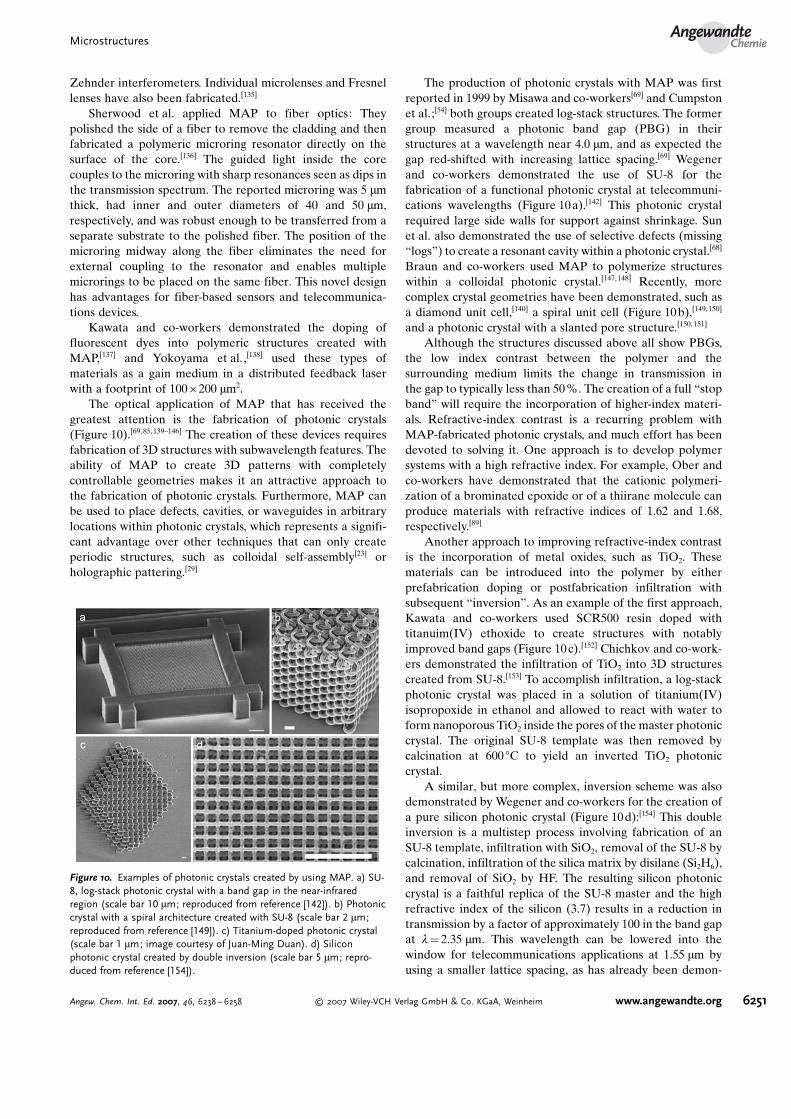
The optical application of MAP that has received thegreatest attention is the fabrication of photonic crystals(Figure 10).[69,85,139–146] The creation of these devices requiresfabrication of 3D structures with subwavelength features. Theability of MAP to create 3D patterns with completelycontrollable geometries makes it an attractive approach tothe fabrication of photonic crystals. Furthermore, MAP canbe used to place defects, cavities, or waveguides in arbitrarylocations within photonic crystals, which represents a signifi-cant advantage over other techniques that can only createperiodic structures, such as colloidal self-assembly[23] orholographic pattering.[29]
The production of photonic crystals with MAP was firstreported in 1999 by Misawa and co-workers[69] and Cumpstonet al.;[54] both groups created log-stack structures. The formergroup measured a photonic band gap (PBG) in theirstructures at a wavelength near 4.0 mm, and as expected thegap red-shifted with increasing lattice spacing.[69] Wegenerand co-workers demonstrated the use of SU-8 for thefabrication of a functional photonic crystal at telecommuni-cations wavelengths (Figure 10a).[142] This photonic crystalrequired large side walls for support against shrinkage. Sunet al. also demonstrated the use of selective defects (missing“logs”) to create a resonant cavity within a photonic crystal.[68]
Braun and co-workers used MAP to polymerize structureswithin a colloidal photonic crystal.[147,148] Recently, morecomplex crystal geometries have been demonstrated, such asa diamond unit cell,[140] a spiral unit cell (Figure 10b),[149,150]
and a photonic crystal with a slanted pore structure.[150,151]
Although the structures discussed above all show PBGs,the low index contrast between the polymer and thesurrounding medium limits the change in transmission inthe gap to typically less than 50%. The creation of a full “stopband” will require the incorporation of higher-index materi-als. Refractive-index contrast is a recurring problem withMAP-fabricated photonic crystals, and much effort has beendevoted to solving it. One approach is to develop polymersystems with a high refractive index. For example, Ober andco-workers have demonstrated that the cationic polymeri-zation of a brominated epoxide or of a thiirane molecule canproduce materials with refractive indices of 1.62 and 1.68,respectively.[89]
Another approach to improving refractive-index contrastis the incorporation of metal oxides, such as TiO2. Thesematerials can be introduced into the polymer by eitherprefabrication doping or postfabrication infiltration withsubsequent “inversion”. As an example of the first approach,Kawata and co-workers used SCR500 resin doped withtitanuim(IV) ethoxide to create structures with notablyimproved band gaps (Figure 10c).[152] Chichkov and co-work-ers demonstrated the infiltration of TiO2 into 3D structurescreated from SU-8.[153] To accomplish infiltration, a log-stackphotonic crystal was placed in a solution of titanium(IV)isopropoxide in ethanol and allowed to react with water toform nanoporous TiO2 inside the pores of the master photoniccrystal. The original SU-8 template was then removed bycalcination at 600 8C to yield an inverted TiO2 photoniccrystal.
A similar, but more complex, inversion scheme was alsodemonstrated by Wegener and co-workers for the creation ofa pure silicon photonic crystal (Figure 10d):[154] This doubleinversion is a multistep process involving fabrication of anSU-8 template, infiltration with SiO2, removal of the SU-8 bycalcination, infiltration of the silica matrix by disilane (Si2H6),and removal of SiO2 by HF. The resulting silicon photoniccrystal is a faithful replica of the SU-8 master and the highrefractive index of the silicon (3.7) results in a reduction intransmission by a factor of approximately 100 in the band gapat l= 2.35 mm. This wavelength can be lowered into thewindow for telecommunications applications at 1.55 mm byusing a smaller lattice spacing, as has already been demon-
Figure 10. Examples of photonic crystals created by using MAP. a) SU-8, log-stack photonic crystal with a band gap in the near-infraredregion (scale bar 10 mm; reproduced from reference [142]). b) Photoniccrystal with a spiral architecture created with SU-8 (scale bar 2 mm;reproduced from reference [149]). c) Titanium-doped photonic crystal(scale bar 1 mm; image courtesy of Juan-Ming Duan). d) Siliconphotonic crystal created by double inversion (scale bar 5 mm; repro-duced from reference [154]).
MicrostructuresAngewandte
Chemie
6251Angew. Chem. Int. Ed. 2007, 46, 6238 – 6258 � 2007 Wiley-VCH Verlag GmbH & Co. KGaA, Weinheim www.angewandte.org

strated in an SU-8 photonic crystal.[142] One issue that shouldnot be overlooked is the 7.5% shrinkage of SU-8 upondevelopment. To avoid lattice distortion, photonic crystals ofSU-8 must have retaining walls for structural support.
5.2. Biology
The ability to fabricate and control structures on themicroscale is fundamental in the study of biological micro-systems. Recent advances in MPA patterning of biopolymersand in the use of surface modification to make syntheticpolymers biocompatible have already led to some remarkableresults in areas such as the in situ scaffolding of cells,[127–130] asdiscussed in Section 4.2. Tissue scaffolding is a major growtharea in MPA fabrication.
Another biologically relevant application of devicescreated with MAP is the manipulation of microscopicstructures. Maruo, Ikuta, and Korogi fabricated microme-chanical devices such as microtweezers and microneedles thatcan be controlled by optical trapping.[95,155–157] With a tipdiameter of only 250 nm and a positioning accuracy of 15 nm,optically actuated microtweezers offer substantially bettercontrol than do electrostatic tweezers. Moreover, rastering ofthe trapping beam allows a number of devices to be controlledsimultaneously. Optical actuation of devices will be useful inmany other complex applications, including micropumps,valves, and other components of microfluidic systems.[155]
5.3. Electronics
The ability to create conductive metal coatings onstructures fabricated with MAP is a recent development, sothere is only one electrical application that has been reportedto date. We have used MAP to create 100-mm-long functionalmicroinductors.[123] The resonance frequencies of such induc-tors are in the GHz range, which is useful for communicationsdevices, and can be lowered into the MHz range forapplications in magnetic resonance. Inductors have numerousapplications in electronics as filters, transformers, and com-ponents of oscillator circuits. They can also be used togenerate magnetic fields for mechanical actuation or sensing,as in magnetic resonance force microscopy.[158, 159]
6.Mass Production
One drawback of MPA-based fabrication techniques isthat they are inherently serial processes. Structures arecreated on a voxel-by-voxel basis, and scaling up productionto a viable level is a daunting task. Nevertheless, substantialprogress has been made toward mass production.
6.1.Multipoint Fabrication
If fabrication can be accomplished at low enough laserpower, one approach to mass production is to split the output
of a laser into many beams that can be used to fabricatestructures at different points simultaneously. Kawata and co-workers have implemented such an approach by splitting uptheir laser beam with a microlens array (MLA).[120,121,160]
Placing the MLA in the beam path before the objectivecreates hundreds of focal spots, each of which can be used forMAP fabrication. The resolution of fabrication at each focalpoint is similar to that of the objective. This method is well-suited for the creation of periodic structures or of arrays ofidentical structures. However, to deliver enough power toeach focal spot, an amplified laser system must be employed.Furthermore, nonuniformities in the intensity across theMLA can cause the voxel size to vary from focal point to focalpoint.
It is technically feasible to create a multipoint fabricationsystem in which the intensity of each focal point can becontrolled independently by a spatial light modulator (SLM).With such a system it would be possible to fabricate non-periodic structures in a highly parallel fashion. It should bepossible to increase throughput by three orders of magnitudeor more with an efficient enough photoinitiator.
6.2. Interference Lithography
Interference lithography techniques offer another meansof creating complex 3D structures. Although interferencetechniques can be implemented with single-photon absorp-tion,[30, 31] the use of MPA can lead to significant improve-ments in feature size. The most common such technique ismultibeam interference lithography (MBIL).[161–163] In MBIL,three or more laser beams approach a photoresist fromdifferent directions. The polarization of each beam can becontrolled independently. Together the beams create acomplex, 3D interference pattern that can be used toexpose the photoresist. If an amplified laser is used, largebeam diameters can be employed so that sizeable sampleareas can be exposed in a short period of time. MBILnecessarily creates periodic 3D structures, and so is well-suited for fabrication of photonic crystal materials. If defectsare desired, they can be fabricated subsequently in thephotonic crystals by conventional MAP.
Rogers and co-workers developed an alternative type ofinterference lithography, which they call proximity-fieldnanopatterning (PnP).[161, 164,165] In this technique, a reliefpattern is created on the surface of a piece of polydimethyl-siloxane (PDMS) elastomer. The PDMS is then pressedagainst a thick layer of photoresist on a substrate. The reliefpattern in the elastomer acts as a phase mask to create acomplex (but calculable) 3D interference pattern that is usedto expose the photoresist. As with MBIL, PnP was originallyimplemented with single-photon absorption, but its resolutioncan be improved substantially with MPA.[161] One advantageof PnP over MBIL is that the relief pattern can vary over thesurface of the mask, which can potentially be as large as asilicon wafer. Thus, although the patterns created must be atleast quasiperiodic on a local scale, they can vary considerablyover a distance scale as small as 10 mm.
J. T. Fourkas et al.Reviews
6252 www.angewandte.org � 2007 Wiley-VCH Verlag GmbH & Co. KGaA, Weinheim Angew. Chem. Int. Ed. 2007, 46, 6238 – 6258

6.3.Molding
Another approach to mass production is the use of MAPto fabricate master structures that are then replicated in aparallel manner. This approach is analogous to conventionalphotolithography, which also begins with the slow, serialprocess of mask writing. Masks enable rapid, parallelpatterning on the wafer scale.
With this idea in mind, we explored the use of a soft-lithographic technique known as microtransfer molding(mTM)[12] for the replication of structures created withMAP.[166] In mTM, PDMS is cured over master structures tocreate an elastomeric mold. This mold is released from themaster structures, filled with a molding material, and pressedagainst a new substrate. The molding material is then curedand the mold is released once again. Many molds can becreated from a single set of master structures, and each moldcan be used to create many replicas.
Although mTM enables the rapid replication of structurescreated with MAP, one might suppose that there aresignificant topological limitations to the sort of structuresthat can be replicated. For example, structures with highaspect ratios would be expected to be difficult to release, andstructures with overhangs should be impossible to release.However, the elasticity of PDMS makes possible the replica-tion of a far greater range of structures than might beimagined.[166] As an example, Figure 11a shows a structure
with two opposing overhangs with open angles of 308. Notonly can the mold be released from this structure, but, asshown in Figure 11b, the structure can also be replicatedreproducibly. The PDMS is able to deform to release fromthese structures and then to snap back to its original shape. Itis similarly possible to replicate structures with extremelyhigh aspect ratios, such as a 300-mm tower that has a crosssection of 10 O 10 mm2.[166]
Despite the surprising range of structures that can bereplicated by mTM, it is still a “2.5-dimensional” technique, asit cannot be used to replicate structures that contain closedloops. Consider, for example, attempting to replicate a tunnel.In creating the mold, PDMS will flow into the tunnel and becured there, locking the tunnel into the mold so that it cannotbe released. We have recently developed a technique calledmembrane-assisted microtrasnfer molding (MA-mTM) thatcircumvents this “mold-lock” problem.[167] Imagine that in themiddle of the tunnel master structure there is a thin
membrane that stops the PDMS from making a completeloop. The PDMS, due to its elasticity, can then be releasedfrom the master structure. Flat PDMS surfaces that are inclose proximity have a tendency to stick together, so bycompressing the mold slightly the PDMS can adhere to itselfin the membrane region. The remainder of the moldingprocess is as usual, and the adhesion of the PDMS to itself isweak enough that the replica can be released from the moldreadily. The replica differs from the original in that it nowcontains a closed loop. Figure 12a shows an example of a five-
turn coil with a membrane in each turn. This master structurewas used to create the replica in Figure 12b in which all of theloops are open. MA-mTM makes possible the replication of awide range of structures with closed loops, including struc-tures with interlocking parts.[167] Furthermore, if the mold isexpanded rather than compressed, it is possible to createreplica structures that do contain membranes.
Not all 3D structures can be replicated with MA-mTM.There remain some topological restrictions related to moldrelease,[167] and any feature to be replicated must be a factor ofroughly three or more thicker than the membranes. Complexstructures with large numbers of small closed loops, such asphotonic crystals, are not likely to be able to be replicatedwith MA-mTM. However, this technique does vastly expandthe range of structures that can be replicated, and whencombined with a suitable technique for creating wafer-scalemasters MA-mTM promises to open the door to rapid massproduction of structures created with MAP.
7. Outlook
The work discussed above only scratches the surface ofwhat will one day be accomplished with MPA-based fabrica-tion. In this section we discuss some of the major challenges inMPA-based fabrication and some of the improvements thatare on the horizon.
7.1.Materials
There are many materials improvements that would beuseful for specific applications of MPA-based fabrication,
Figure 11. a) A master structure created with MAP featuring opposingoverhangs with 308 open angles. b) A replica of this structure createdwith mTM. The scale bars are 10 mm (reproduced from reference [166]).
Figure 12. a) A five-turn coil master structure created with MAP. Thereis a membrane inside of each turn of the coil. b) Replica of the coilcreated by using MA-mTM. The membranes have not been replicated,leaving a structure with closed loops. The scale bars are 10 mm(reproduced from reference [167]).
MicrostructuresAngewandte
Chemie
6253Angew. Chem. Int. Ed. 2007, 46, 6238 – 6258 � 2007 Wiley-VCH Verlag GmbH & Co. KGaA, Weinheim www.angewandte.org

such as increasing the refractive-index contrast for photoniccrystals. Herein we will focus on more general materialschallenges that affect a broad range of applications.
Although there are many excellent photoinitiators forMAP, there is still progress to be made. An ideal photo-initiator should be highly soluble, so that samples can beprepared quickly. It should have a high TPA cross section at800 nm, so that a Ti:sapphire oscillator can be employed forfabrication. It should also have a high yield of reactiveradicals, so that fabrication is efficient. Finding a photo-initiator that meets all of these criteria will open the door tomany new applications.
Another significant materials challenge is the shrinkagethat occurs in polymeric structures during the developmentstep. For structures created with MAP to survive washing,they need to be highly cross-linked, but this cross-linkinggenerally leads to shrinkage. Removal of unpolymerizedmaterial by solvent further augments shrinkage. It is possiblein many applications to precompensate for shrinkage in theinitial design, but this can be a difficult task near the substrate,where structures are tethered and cannot shrink. For someapplications, such as photonic crystals, currently the onlysolution is to add a supporting structure to prevent shrinkage.Ultimately, overcoming the shrinkage problem will requirethe development of highly cross-linked materials that do notchange volume appreciably during development.
The development of new patterning techniques for abroader range of materials will greatly expand the potentialapplications of MPA-based fabrication. The techniques dis-cussed above have made possible the incorporation ofmaterials such as metals into 3D structures, but means ofincorporating many other materials of interest (or evenmultiple metals) at selected locations have yet to bedemonstrated.
7.2. Resolution
The ability of MAP to create features with a resolution of100 nm from 800-nm light is undeniably impressive. However,being able to create even smaller features is crucial to manyapplications, such as the creation of photonic crystals withband gaps at higher energies. Furthermore, it would bedesirable to be able to create voxels that are spheres ratherthan prolate spheroids (see Section 3.2.1).
Part of the solution to the resolution problem may bechemical. For example, as mentioned in Section 3.2.1, theaddition of radical inhibitors to a resin appears to decreasethe voxel size.[99] Careful control of the polymerizationchemistry may yield further decreases in voxel size, althoughprobably only in the range of 10 to 20%. It is unclear whetherchemistry can be used to improve the voxel shape as well.
Optical techniques probably offer the greatest hope forsignificant reductions in voxel volumes and significantimprovements in voxel shapes. Optical approaches to con-trolling the excitation volume that may allow for modestimprovements in voxel size include optimizing the focallength of the tube lens used,[168] employing annular amplitudefilters,[169] and using radially polarized light.[170] Another
promising technique, which has been developed in the contextof fluorescence microscopy, is stimulated emission depletion(STED).[171] STED employs two laser beams, one to excite themolecules and one, which is tuned to the red of the absorptionspectrum, to stimulate emission back down to the groundstate. The depletion beam passes through a phase mask thatcauses it to be dark in the center of the focal region, so that noemission is stimulated there. As a result, it has proven possibleto attain resolution of tens of nanometers in fluorescencemicroscopy with visible light.[172] STED also assists in creatinga considerably more-spherical PSF than with standardfocused laser excitation.
STED should be directly applicable to MAP. Typicalradical photoinitiators become singlet diradicals upon exci-tation, and it is only after intersystem crossing that homolysisoccurs and polymerization can be initiated.[173] The intersys-tem crossing time is in the range of 100 ps, so there is plenty ofopportunity to stimulate emission before polymerization isinitiated. In fluorescence microscopy, ideally more than 95%of molecules should be deexcited to improve resolution. InMAP it is only necessary to deexcite enough molecules to fallbelow the polymerization threshold; thus, stimulating emis-sion from even 10% of the molecules may be sufficient toreduce voxel size significantly. STED may ultimately enablethe creation of 20-nm voxels with 800-nm light.
7.3. Fabrication Systems
It is desirable to be able to make MPA fabrication systemsmore compact and less expensive. Both of these goals rely to agreat extent on some of the improvements in materialsdiscussed in Section 7.1. Beyond that, the desirable improve-ments in fabrication systems depend on the fabrication goals.
In a laboratory setting, it would be desirable to have asingle-point fabrication system consisting of nothing morethan a microscope, a laptop computer, and an inexpensive,compact, turnkey laser system. Such a fabrication systemcould easily fit on top of a desk or a lab bench. The use ofinexpensive microlasers in place of ultrafast Ti:sapphiresystems for MPA-based fabrication has already been demon-strated (Sections 3.1.2.1 and 4.2). Compact ultrafast lasersystems with tens of milliwatts of power at 800 nm are alsoavailable, albeit at a somewhat greater cost. The commercialavailability of highly efficient photoinitiators would makeeither of these laser options quite attractive.
In an industrial setting, high throughput and multipointfabrication would be highly desirable. With efficient enoughphotoinitiators, such a system should be possible with aTi:sapphire oscillator rather than an amplified laser system.The development of an SLM-based multipoint fabricationsystem (see Section 6.1) should then enable independent andsimultaneous fabrication at 1000 or more points in a sample.
8. Conclusions
Multiphoton fabrication techniques make possible thecreation of arbitrarily complex, 3D structures with sub-
J. T. Fourkas et al.Reviews
6254 www.angewandte.org � 2007 Wiley-VCH Verlag GmbH & Co. KGaA, Weinheim Angew. Chem. Int. Ed. 2007, 46, 6238 – 6258

micrometer feature sizes. Thanks to the efforts of researchgroups worldwide, the basic “toolbox” of these techniques innearly complete. Efficient, photopolymerizable systems witha wide range of properties are now available, and it is possibleto incorporate a wide variety of additional materials intomicrostructures. Although some additional developmentalwork is needed, this technology is mature enough that thefocus is now shifting to applications, and we expect to seemany more examples of functional devices that have beencreated with MPA-based techniques in the near future. Assoon as the remaining obstacles to mass production areovercome, multiphoton fabrication has the potential tobecome an important tool in industry as well.
Abbreviations
AFM atomic force microscopyAP alkaline phosphataseBME 2-methoxy-1,2-diphenylethanoneBS bovine serum albuminGM GEppert–MayerITX 2-/4-isopropylthioxanthoneLIGA Lithographie, Galvanoformung und
AbformungMA-mTM membrane-assisted microtransfer moldingMAP multiphoton absorption polymerizationMBIL multibeam interference lithographyMEMS microelectromechanical systemsMLA microlens arrayMPA multiphoton absorptionmTAS micro total analysis systemsmTM microtransfer moldingNA numerical aperturePAG photoacid generatorPDMS polydimethylsiloxanePnP proximity-field nanopatterningPSF point-spread functionPVP polyvinylpyrrolidoneSLM spatial light modulatorSTED stimulated emission depletionTPA two-photon absorptionTPFM two-photon fluorescence microscopyYAG Yttrium aluminum garnet
Part of the work described herein was supported by theNational Science Foundation (ECS-0088438 and ECS-0210533). We are grateful for the contributions our colleagueshave made to work from our laboratory that was describedherein: Prof. Michael J. Naughton, Prof. Malvin C. Teich, Prof.Bahaa E. A. Selah, Prof. Michael Giersig, Dr. Michael J. R.Previte, Dr. Zeynel Bayindir, Dr. Joel Moser, Linjie Li, JulietZnovena, Daniel Lim, Huzhen Chen, Anne-C<cile Pons,Josefina Pons, Kevin O?Malley, and Thomas Kempa.
Received: September 28, 2006Published online: July 24, 2007
[1] J. Elders, V. Spiering, S. Walsh, MRS Bull. 2001, 26, 312.[2] M. Esashi, T. Ono, J. Phys. D 2005, 38, R223.[3] K. Petersen, Sens. Actuators A 1996, 56, 143.[4] P. Grabiec, K. Domanski, P. Janus, M. Zaborowski, B.
Jaroszewicz, Bioelectrochemistry 2005, 66, 23.[5] D. R. Reyes, D. Iossifidis, P.-A. Auroux, A. Manz, Anal. Chem.
2002, 74, 2623.[6] P. S. Dittrich, K. Tachikawa, A. Manz, Anal. Chem. 2006, 78,
3887.[7] The International Technology Roadmap for Semiconductors,
Semiconductor Industry Association, San Jose, 2005.[8] Y. Wang, T. Miyamatsu, T. Furukawa, K. Yamada, T. Tominaga,
Y. Makita, H. Nakagawa, A. Nakamura, M. Shima, S.Kusumoto, T. Shimokawa, K. Hieda, Proc. SPIE-Int. Soc.Opt. Eng. 2006, 6153, 61530A.
[9] D. Ginger, S. H. Zhang, C. A. Mirkin, Angew. Chem. 2004, 116,30; Angew. Chem. Int. Ed. 2004, 43, 30.
[10] S. Y. Chou, MRS Bull. 2001, 26, 512.[11] M. Geissler, Y. Xia, Adv. Mater. 2004, 16, 1249.[12] Y. Xia, G. M. Whitesides, Angew. Chem. 1998, 110, 568; Angew.
Chem. Int. Ed. 1998, 37, 550.[13] G. M. Gratson, F. Garcia-Santamaria, V. Lousse, M. J. Xu, S. H.
Fan, J. A. Lewis, P. V. Braun, Adv. Mater. 2006, 18, 461.[14] D. Therriault, R. F. Shepherd, S. R. White, J. A. Lewis, Adv.
Mater. 2005, 17, 395.[15] T. C. Wang, R. E. Cohen, M. F. Rubner, Adv. Mater. 2002, 14,
1534.[16] J. G. Fleming, S. Y. Lin, I. El-Kady, R. Biswas, K. M. Ho, Nature
2002, 417, 52.[17] X. M. Zhao, Y. Xia, G. M. Whitesides, Adv. Mater. 1996, 8, 837.[18] D. W. L. Tolfree, Rep. Prog. Phys. 1998, 61, 313.[19] J. Hruby, MRS Bull. 2001, 26, 337.[20] P. Calvert, Chem. Mater. 2001, 13, 3299.[21] B.-J. de Gans, P. C. Duineveld, U. S. Schubert, Adv. Mater. 2004,
16, 203.[22] G. M. Gratson, M. J. Xu, J. A. Lewis, Nature 2004, 428, 386.[23] Y. Xia, B. Gates, Y. Yin, Y. Lu, Adv. Mater. 2000, 12, 693.[24] A. C. Edrington, A. M. Urbas, P. DeRege, C. X. Chen, T. M.
Swager, N. Hadjichristidis, M. Xenidou, L. J. Fetters, J. D.Joannopoulos, Y. Fink, E. L. Thomas, Adv. Mater. 2001, 13, 421.
[25] U. Feldkamp, C. M. Niemeyer, Angew. Chem. 2006, 118, 1888;Angew. Chem. Int. Ed. 2006, 45, 1856.
[26] J. A. Lewis, G. M. Gratson, Mater. Today 2004, 7, 32.[27] E. W. Becker, W. Ehrfeld, D. Muenchmeyer, Institut fRr
Kernverfahrenstechnik, Kernforschungszentrum Karlsruhe,Karlsruhe, 1984, p. 92.
[28] W. Ehrfeld, E. W. Becker, KFK-Nachr. 1987, 19, 167.[29] M. Campbell, D. N. Sharp, M. T. Harrison, R. G. Denning, A. J.
Turberfield, Nature 2000, 404, 53.[30] S. Shoji, H.-B. Sun, S. Kawata, Appl. Phys. Lett. 2003, 83, 608.[31] S. Shoji, S. Kawata, Appl. Phys. Lett. 2000, 76, 2668.[32] S. Jeon, J. U. Park, R. Cirelli, S. Yang, C. E. Heitzman, P. V.
Braun, P. J. A. Kenis, J. A. Rogers, Proc. Natl. Acad. Sci. USA2004, 101, 12428.
[33] C. Duty, D. Jean, W. J. Lackey, Int. Mater. Rev. 2001, 46, 271.[34] D. Lim, Y. Kamotani, B. Cho, J. Mazumder, S. Takayama, Lab
Chip 2003, 3, 318.[35] A. Bertsch, H. Lorenz, P. Renaud, Sens. Actuators A 1999, 73,
14.[36] A. Bertsch, S. Jiguet, P. Bernhard, P. Renaud in Rapid
Prototyping Technologies (Eds.: A. Pique, A. S. Holmes, D. B.Dimos), Materials Research Society, Warrendale, PA, 2003,p. 3.
[37] S. Maruo, K. Ikuta, Sens. Actuators A 2002, 100, 70.[38] K. Ikuta, S. Maruo, T. Hasegawa, T. Adachi, A. Takahashi, K.
Ikeda in Rapid Prototyping Technologies (Eds.: A. Pique, A. S.
MicrostructuresAngewandte
Chemie
6255Angew. Chem. Int. Ed. 2007, 46, 6238 – 6258 � 2007 Wiley-VCH Verlag GmbH & Co. KGaA, Weinheim www.angewandte.org

Holmes, D. B. Dimos), Materials Research Society, Warren-dale, PA, 2003, p. 193.
[39] A. Bertsch, S. Jiguet, P. Renaud, J. Micromech. Microeng. 2004,14, 197.
[40] M. Goppert-Mayer, Ann. Phys. 1931, 9, 273.[41] W. Kaiser, C. G. B. Garrett, Phys. Rev. Lett. 1961, 7, 229.[42] W. Denk, J. H. Strickler, W. W. Webb, Science 1990, 248, 73.[43] P. T. C. So, C. Y. Dong, B. R. Masters, K. M. Berland, Annu.
Rev. Biomed. Eng. 2000, 2, 399.[44] C. Soeller, M. B. Cannell, Microsc. Res. Tech. 1999, 47, 182.[45] C. E. Olson, M. J. R. Previte, J. T. Fourkas, Nat. Mater. 2002, 1,
225.[46] S. Svanberg in Ultrafast Optics IV (Eds.: F. Krausz, G. Korn, P.
Corkum, I. Warmsley), Springer, New York, 2004, p. 437.[47] G. Lemercier, J.-C. Mulatier, C. Martineau, R. Anemian, C.
Andraud, I. Wang, O. Stephan, N. Amari, P. Baldeck, C. R.Chim. 2005, 8, 1308.
[48] H.-B. Sun, S. Kawata, J. Lightwave Technol. 2003, 21, 624.[49] S. Kawata, H.-B. Sun, Appl. Surf. Sci. 2003, 208–209, 153.[50] T. Baldacchini, J. T. Fourkas in Dekker Encyclopedia of Nano-
science and Nanotechnology (Eds.: J. A. Schwarz, C. I. Con-tescu, K. Putyera), Marcel Dekker, New York, 2004, p. 3905.
[51] D. Yang, S. J. Jhaveri, C. K. Ober, MRS Bull. 2005, 30, 976.[52] S. Wu, J. Serbin, M. Gu, J. Photochem. Photobiol. A 2006, 181,
1.[53] M. Albota, D. Beljonne, J.-L. Bredas, J. E. Ehrlich, J.-Y. Fu,
A. A. Heikal, S. E. Hess, T. Kogej, M. D. Levin, S. R. Marder,D. McCord-Maughon, J. W. Perry, H. Rockel, M. Rumi, G.Subramaniam, W. W. Webb, X.-L. Wu, C. Xu, Science 1998, 281,1653.
[54] B. H. Cumpston, S. P. Ananthavel, S. Barlow, D. L. Dyer, J. E.Ehrlich, L. L. Erskine, A. A. Heikal, S. M. Kuebler, I. Y. S. Lee,D. McCord-Maughon, J. Qin, H. Rockel, M. Rumi, X.-L. Wu,S. R. Marder, J. W. Perry, Nature 1999, 398, 51.
[55] J. E. Ehrlich, X. L. Wu, I. Y. S. Lee, Z. Y. Hu, H. Rockel, S. R.Marder, J. W. Perry, Opt. Lett. 1997, 22, 1843.
[56] M. Rumi, J. E. Ehrlich, A. A. Heikal, J. W. Perry, S. Barlow, Z.Hu, D. McCord-Maughon, T. C. Parker, H. Roeckel, S.Thayumanavan, S. R. Marder, D. Beljonne, J.-L. Bredas, J.Am. Chem. Soc. 2000, 122, 9500.
[57] Y. Lu, F. Hasegawa, T. Goto, S. Ohkuma, S. Fukuhara, Y.Kawazu, K. Totani, T. Yamashita, T. Watanabe, J. Mater. Chem.2004, 14, 75.
[58] M. P. Joshi, H. E. Pudavar, J. Swiatkiewicz, P. N. Prasad, B. A.Reinhardt, Appl. Phys. Lett. 1999, 74, 170.
[59] R. Kannan, G. S. He, L. Yuan, F. Xu, P. N. Prasad, A. G.Dombroskie, B. A. Reinhardt, J. W. Baur, R. A. Vaia, L.-S. Tan,Chem. Mater. 2001, 13, 1896.
[60] B. A. Reinhardt, L. L. Brott, S. J. Clarson, A. G. Dillard, J. C.Bhatt, R. Kannan, L. Yuan, G. S. He, P. N. Prasad, Chem. Mater.1998, 10, 1863.
[61] O.-K. Kim, K.-S. Lee, H. Y. Woo, K.-S. Kim, G. S. He, J.Swiatkiewicz, P. N. Prasad, Chem. Mater. 2000, 12, 284.
[62] G. S. He, T.-C. Lin, J. Dai, P. N. Prasad, R. Kannan, A. G.Dombroskie, R. A. Vaia, L.-S. Tan, J. Chem. Phys. 2004, 120,5275.
[63] K. D. Belfield, K. J. Schafer, Y. Liu, J. Liu, X. Ren, E. W.Van Stryland, J. Phys. Org. Chem. 2000, 13, 837.
[64] C. Martineau, R. Anemian, C. Andraud, I. Wang, M. Bouriau,P. L. Baldeck, Chem. Phys. Lett. 2002, 362, 291.
[65] I. Wang, M. Bouriau, P. L. Baldeck, C. Martineau, C. Andraud,Opt. Lett. 2002, 27, 1348.
[66] S. Jockusch, I. V. Koptyug, P. F. McGarry, G. W. Sluggett, N. J.Turro, D. M. Watkins, J. Am. Chem. Soc. 1997, 119, 11495.
[67] K. J. Schafer, J. M. Hales, M. Balu, K. D. Belfield, E. W.Van Stryland, D. J. Hagan, J. Photochem. Photobiol. A 2004,162, 497.
[68] H.-B. Sun, V. Mizeikis, Y. Xu, S. Juodkazis, J.-Y. Ye, S. Matsuo,H. Misawa, Appl. Phys. Lett. 2001, 79, 1.
[69] H.-B. Sun, S. Matsuo, H. Misawa, Appl. Phys. Lett. 1999, 74,786.
[70] H.-B. Sun, T. Kawakami, Y. Xu, J.-Y. Ye, S. Matsuo, H. Misawa,M. Miwa, R. Kaneko, Opt. Lett. 2000, 25, 1110.
[71] M. Miwa, S. Juodkazis, T. Kawakami, S. Matsuo, H. Misawa,Appl. Phys. A 2001, 73, 561.
[72] K. D. Belfield, X. Ren, E. W. Van Stryland, D. J. Hagan, V.Dubikovsky, E. J. Miesak, J. Am. Chem. Soc. 2000, 122, 1217.
[73] C. Decker, K. Zahouily, D. Decker, T. Nguyen, T. Viet, Polymer2001, 42, 7551.
[74] T. Baldacchini, H. Chen, R. A. Farrer, M. J. R. Previte, J.Moser, M. J. Naughton, J. T. Fourkas in Commerical andBiomedical Applications of Ultrafast Lasers, Vol. 4633 (Eds.:G. S. Edwards, J. Neev, A. Ostendorf, J. C. Sutherland),Bellingham, WA, 2002, p. 136.
[75] T. Baldacchini, R. A. Farrer, J. Moser, J. T. Fourkas, M. J.Naughton, Synth. Met. 2003, 135–136, 11.
[76] T. Baldacchini, C. N. LaFratta, R. A. Farrer, M. C. Teich,B. E. A. Saleh, M. J. Naughton, J. T. Fourkas, J. Appl. Phys.2004, 95, 6072.
[77] C. Mendonca, Universidade de Sao Paolo, personal communi-cation, 2006.
[78] P. J. Campagnola, D. M. Delguidice, G. A. Epling, K. D.Hoffacker, A. R. Howell, J. D. Pitts, S. L. Goodman, Macro-molecules 2000, 33, 1511.
[79] J. D. Pitts, P. J. Campagnola, G. A. Epling, S. L. Goodman,Macromolecules 2000, 33, 1514.
[80] C. Li, L. Luo, S. Wang, W. Huang, Q. Gong, Y. Yang, S. Feng,Chem. Phys. Lett. 2001, 340, 444.
[81] Y. Lu, F. Hasegawa, S. Ohkuma, T. Goto, S. Fukuhara, Y.Kawazu, K. Totani, T. Yamashita, T. Watanabe, J. Mater. Chem.2004, 14, 1391.
[82] S. Kawata, H.-B. Sun, T. Tanaka, K. Takada, Nature 2001, 412,697.
[83] S. M. Kuebler, M. Rumi, T. Watanabe, K. Braun, B. H.Cumpston, A. A. Heikal, L. L. Erskine, S. Thayumanavan, S.Barlow, S. R. Marder, J. W. Perry, J. Photopolym. Sci. Technol.2001, 14, 657.
[84] T. Watanabe, M. Akiyama, K. Totani, S. M. Kuebler, F.Stellacci, W. Wenseleers, K. Braun, S. R. Marder, J. W. Perry,Adv. Funct. Mater. 2002, 12, 611.
[85] J. Serbin, A. Egbert, A. Ostendorf, B. N. Chichkov, R.Houbertz, G. Domann, J. Schulz, C. Cronauer, L. Frohlich,M. Popall, Opt. Lett. 2003, 28, 301.
[86] K.-H. Haas, K. Rose, Rev. Adv. Mater. Sci. 2003, 5, 47.[87] C. A. Coenjarts, C. K. Ober, Chem. Mater. 2004, 16, 5556.[88] Y. Boiko, J. M. Costa, M. Wang, S. Esener, Opt. Express 2001, 8,
571.[89] Y. Murakami, C. A. Coenjarts, C. K. Ober, J. Photopolym. Sci.
Technol. 2004, 17, 115.[90] W. Zhou, S. M. Kuebler, K. L. Braun, T. Yu, J. K. Cammack,
C. K. Ober, J. W. Perry, S. R. Marder, Science 2002, 296, 1106.[91] W. H. Teh, U. Durig, G. Salis, R. Harbers, U. Drechsler, R. F.
Mahrt, C. G. Smith, H. J. Guntherodt, Appl. Phys. Lett. 2004,84, 4095.
[92] W. H. Teh, U. Durig, U. Drechsler, C. G. Smith, H. J. Guen-therodt, J. Appl. Phys. 2005, 97, 054907.
[93] X. Yin, N. Fang, X. Zhang, I. B. Martini, B. J. Schwartz, Appl.Phys. Lett. 2002, 81, 3663.
[94] K. K. Seet, S. Juodkazis, V. Jarutis, H. Misawa, Appl. Phys. Lett.2006, 89, 024106.
[95] S. Maruo, K. Ikuta, H. Korogi, J. Microelectromech. Syst. 2003,12, 533.
J. T. Fourkas et al.Reviews
6256 www.angewandte.org � 2007 Wiley-VCH Verlag GmbH & Co. KGaA, Weinheim Angew. Chem. Int. Ed. 2007, 46, 6238 – 6258

[96] S. M. Kuebler, K. L. Braun, W. Zhou, J. K. Cammack, T. Yu,C. K. Ober, S. R. Marder, J. W. Perry, J. Photochem. Photobiol.A 2003, 158, 163.
[97] T. Yu, C. K. Ober, S. M. Kuebler, W. Zhou, S. R. Marder, J. W.Perry, Adv. Mater. 2003, 15, 517.
[98] H.-B. Sun, T. Tanaka, S. Kawata, Appl. Phys. Lett. 2002, 80,3673.
[99] K. Takada, H.-B. Sun, S. Kawata, Appl. Phys. Lett. 2005, 86,071122.
[100] S. Juodkazis, V. Mizeikis, K. K. Seet, M. Miwa, H. Misawa,Nanotechnology 2005, 16, 846.
[101] T. Tanaka, H.-B. Sun, S. Kawata, Appl. Phys. Lett. 2002, 80, 312.[102] R. J. DeVoe, H. Kalweit, C. A. Leatherdale, T. R. Williams in
Multiphoton Absorption and Nonlinear Transmission Process-es: Materials, Theory, and Applications (Eds.: K. D. Belfield,S. J. Caracci, F. Kajzar, C. M. Lawson, A. T. Yeates), SPIE,Bellingham, WA, 2003, p. 310.
[103] H.-B. Sun, K. Takada, M.-S. Kim, K.-S. Lee, S. Kawata, Appl.Phys. Lett. 2003, 83, 1104.
[104] C. A. Leatherdale, R. J. DeVoe in Nonlinear Optical Trans-mission and Multiphoton Processes in Organics (Eds.: A. T.Yeates, K. D. Belfield, F. Kajzar, C. M. Lawson), SPIE,Bellingham, WA, 2003, p. 112.
[105] A. Ashkin, Proc. Natl. Acad. Sci. USA 1997, 94, 4853.[106] H.-B. Sun, K. Takada, S. Kawata, Appl. Phys. Lett. 2001, 79,
3173.[107] Z. Bayindir, Y. Sun, M. J. Naughton, C. N. LaFratta, T.
Baldacchini, J. T. Fourkas, J. Stewart, B. E. A. Saleh, M. C.Teich, Appl. Phys. Lett. 2005, 86, 064105.
[108] C. A. Clifford, M. P. Seah, Nanotechnology 2005, 16, 1666.[109] J. R. Swanson, C. M. Friend, Y. J. Chabal, J. Chem. Phys. 1987,
87, 5028.[110] X. Xu, J. I. Steinfeld, Appl. Surf. Sci. 1990, 45, 281.[111] D. Wexler, J. I. Zink, L. W. Tutt, S. R. Lunt, J. Phys. Chem. 1993,
97, 13563.[112] T. Kempa, R. A. Farrer, M. Giersig, J. T. Fourkas, Plasmonics
2006, 1, 45.[113] T. Tanaka, A. Ishikawa, S. Kawata, Appl. Phys. Lett. 2006, 88,
081107.[114] A. Ishikawa, T. Tanaka, S. Kawata, Appl. Phys. Lett. 2006, 89,
113102.[115] P.-W. Wu, W. Cheng, I. B. Martini, B. Dunn, B. J. Schwartz, E.
Yablonovitch, Adv. Mater. 2000, 12, 1438.[116] F. Stellacci, C. A. Bauer, T. Meyer-Friedrichsen, W. Wenseleers,
V. Alain, S. M. Kuebler, S. J. K. Pond, Y. Zhang, S. R. Marder,J. W. Perry, Adv. Mater. 2002, 14, 194.
[117] K. Kaneko, H.-B. Sun, X.-M. Duan, S. Kawata, Appl. Phys.Lett. 2003, 83, 1426.
[118] T. Baldacchini, A.-C. Pons, J. Pons, C. N. LaFratta, J. T. Fourkas,Y. Sun, M. J. Naughton, Opt. Express 2005, 13, 1275.
[119] C. N. LaFratta, D. Lim, K. OPMalley, T. Baldacchini, J. T.Fourkas, Chem. Mater. 2006, 18, 2038.
[120] F. Formanek, N. Takeyasu, T. Tanaka, K. Chiyoda, A. Ishikawa,S. Kawata, Opt. Express 2006, 14, 800.
[121] F. Formanek, N. Takeyasu, T. Tanaka, K. Chiyoda, A. Ishikawa,S. Kawata, Appl. Phys. Lett. 2006, 88, 083110.
[122] Y.-S Chen, A. Tal, D. B. Torrance, S. M. Kuebler, Adv. Funct.Mater. 2006, 16, 1739.
[123] R. A. Farrer, C. N. LaFratta, L. Li, J. Praino, M. J. Naughton,B. E. A. Saleh, M. C. Teich, J. T. Fourkas, J. Am. Chem. Soc.2006, 128, 1796.
[124] S. Basu, P. J. Campagnola, Biomacromolecules 2004, 5, 572.[125] S. Basu, C. W. Wolgemuth, P. J. Campagnola, Biomacromole-
cules 2004, 5, 2347.[126] S. Basu, L. P. Cunningham, G. D. Pins, K. A. Bush, R. Taboada,
A. R. Howell, J. Wang, P. J. Campagnola, Biomacromolecules2005, 6, 1465.
[127] S. Basu, V. Rodionov, M. Terasaki, P. J. Campagnola, Opt. Lett.2005, 30, 159.
[128] B. Kaehr, R. Allen, D. J. Javier, J. Currie, J. B. Shear, Proc. Natl.Acad. Sci. USA 2004, 101, 16104.
[129] R. Allen, R. Nielson, D. D. Wise, J. B. Shear, Anal. Chem. 2005,77, 5089.
[130] B. Kaehr, N. Ertas, R. Nielson, R. Allen, R. T. Hill, M. Plenert,J. B. Shear, Anal. Chem. 2006, 78, 3198.
[131] R. T. Hill, J. L. Lyon, R. Allen, K. J. Stevenson, J. B. Shear, J.Am. Chem. Soc. 2005, 127, 10707.
[132] B. R. Harkness, K. Takeuchi, M. Tachikawa, Macromolecules1998, 31, 4798.
[133] S. Wong, M. Deubel, F. Perez-Willard, S. John, G. A. Ozin, M.Wegener, G. von Freymann, Adv. Mater. 2006, 18, 265.
[134] S. Klein, A. Barsella, H. Leblond, H. Bulou, A. Fort, C.Andraud, G. Lemercier, J. C. Mulatier, K. Dorkenoo, Appl.Phys. Lett. 2005, 86, 211118.
[135] R. Guo, S. Xiao, X. Zhai, J. Li, A. Xia, W. Huang, Opt. Express.2006, 14, 810.
[136] T. Sherwood, A. C. Young, J. Takayesu, A. K. Y. Jen, L. R.Dalton, A. T. Chen, Photonics Technol. Lett. IEEE 2005, 17,2107.
[137] H.-B. Sun, T. Tanaka, K. Takada, S. Kawata, Appl. Phys. Lett.2001, 79, 1411.
[138] S. Yokoyama, T. Nakahama, H. Miki, S. Mashiko, Thin SolidFilms 2003, 438–439, 452.
[139] R. A. Borisov, G. N. Dorojkina, N. I. Koroteev, V. M. Kozen-kov, S. A. Magnitskii, D. V. Malakhov, A. V. Tarasishin, A. M.Zheltikov, Appl. Phys. B 1998, 67, 765.
[140] K. Kaneko, H.-B. Sun, X.-M. Duan, S. Kawata, Appl. Phys.Lett. 2003, 83, 2091.
[141] F. Korte, J. Serbin, J. Koch, A. Egbert, C. Fallnich, A.Ostendorf, B. N. Chichkov, Appl. Phys. A 2003, 77, 229.
[142] M. Deubel, G. von Freymann, M. Wegener, S. Pereira, K.Busch, C. M. Soukoulis, Nat. Mater. 2004, 3, 444.
[143] R. Guo, Z. Li, Z. Jiang, D. Yuan, W. Huang, A. Xia, J. Opt. A2005, 7, 396.
[144] M. Straub, L. H. Nguyen, A. Fazlic, M. Gu, Opt. Mater. 2004,27, 359.
[145] S. Wu, M. Straub, M. Gu, Polym. Prepr. Am. Chem. Soc. Div.Polym. Chem. 2005, 46, 10246.
[146] J. Serbin, M. Gu, Adv. Mater. 2006, 18, 221.[147] P. V. Braun, S. A. Pruzinsky, W. Lee, PMSE Prepr. 2005, 92, 117.[148] S. A. Pruzinsky, P. V. Braun, Adv. Funct. Mater. 2005, 15, 1995.[149] K. K. Seet, V. Mizeikis, S. Matsuo, S. Juodkazis, H. Misawa,
Adv. Mater. 2005, 17, 541.[150] K. K. Seet, V. Mizeikis, S. Juodkazis, H. Misawa, Appl. Phys.
Lett. 2006, 88, 221101.[151] M. Deubel, M. Wegener, A. Kaso, S. John, Appl. Phys. Lett.
2004, 85, 1895.[152] X.-M. Duan, H.-B. Sun, K. Kaneko, S. Kawata, Thin Solid Films
2004, 453–454, 518.[153] J. Serbin, A. Ovsianikov, B. Chichkov, Opt. Express 2004, 12,
5221.[154] N. TTtreault, G. von Freymann, M. Deubel, M. Hermatsch-
weiler, F. Perez-Willard, S. John, M. Wegener, G. A. Ozin, Adv.Mater. 2006, 18, 457.
[155] S. Maruo, Polym. Prepr. Am. Chem. Soc., Div. Polym. Chem.2006, 94, 101.
[156] S. Maruo, K. Ikuta, H. Korogi in Three-Dimensional Nano-engineered Assemblies, (Eds.: T. M. Orlando, L. Merhari, D. P.Taylor, K. Ikuta), Materials Research Society, Warrendale, PA,2003, p. 269.
[157] S. Maruo, K. Ikuta, H. Korogi, Appl. Phys. Lett. 2003, 82, 133.[158] A. Suter, Prog. Nucl. Magn. Reson. Spectrosc. 2004, 45, 239.[159] J. A. Sidles, J. L. Garbini in Challenges and Opportunities in
Magnetic Resonance Force Microscopy (Eds.: M. Sarikaya,
MicrostructuresAngewandte
Chemie
6257Angew. Chem. Int. Ed. 2007, 46, 6238 – 6258 � 2007 Wiley-VCH Verlag GmbH & Co. KGaA, Weinheim www.angewandte.org

H. K. Wikiramasinghe, M. Isaacson), Materials ResearchSociety, Warrendale, PA, 1994, p. 25.
[160] J.-I. Kato, N. Takeyasu, Y. Adachi, H.-B. Sun, S. Kawata, Appl.Phys. Lett. 2005, 86, 044102.
[161] S. Jeon, V. Malyarchuk, J. A. Rogers, G. P. Wiederrecht, Opt.Express 2006, 14, 2300.
[162] X.-M. Duan, H.-B. Sun, S. Kawata, J. Photopolym. Sci. Technol.2004, 17, 393.
[163] H.-B. Sun, A. Nakamura, S. Shoji, X.-M. Duan, S. Kawata, Adv.Mater. 2003, 15, 2011.
[164] S. Jeon, E. Menard, J. U. Park, J. Maria, M. Meitl, J. Zaumseil, J.A Rogers, Adv. Mater. 2004, 16, 1369.
[165] S. Jeon, V. Malyarchuk, J. O. White, J. A. Rogers, Nano Lett.2005, 5, 1351.
[166] C. N. LaFratta, T. Baldacchini, R. A. Farrer, J. T. Fourkas, M. C.Teich, B. E. A. Saleh, M. J. Naughton, J. Phys. Chem. B 2004,108, 11256.
[167] C. N. LaFratta, L. Li, J. T. Fourkas, Proc. Natl. Acad. Sci. USA2006, 103, 8589.
[168] C. J. R. Sheppard, M. Gu, Appl. Opt. 1991, 30, 3563.[169] M. Martinez-Corral, C. Ibanez-Lopez, G. Saavedra, Opt.
Express 2003, 11, 1740.[170] S. Quabis, R. Dorn, M. Eberler, O. Glockl, G. Leuchs, Opt.
Commun. 2000, 179, 1.[171] T. A. Klar, E. Engel, S. W. Hell, Phys. Rev. E 2001, 64, 066613.[172] T. A. Klar, S. Jakobs, M. Dyba, A. Egner, S. W. Hell, Proc. Natl.
Acad. Sci. USA 2000, 97, 8206.[173] C. S. Colley, D. C. Grills, N. A. Besley, S. Jockusch, P. Matousek,
A. W. Parker, M. Towrie, N. J. Turro, P. M. W. Gill, M. W.George, J. Am. Chem. Soc. 2002, 124, 14952.
J. T. Fourkas et al.Reviews
6258 www.angewandte.org � 2007 Wiley-VCH Verlag GmbH & Co. KGaA, Weinheim Angew. Chem. Int. Ed. 2007, 46, 6238 – 6258