chip-scale atomic frequency references: fabrication and performance
TRANSCRIPT
CHIP-SCALE ATOMIC FREQUENCY REFERENCES: FABRICATION AND PERFORMANCE
J. Kitching*, S. Knappe*, L. Liew†, J. Moreland†, H. G. Robinson*, P. Schwindt*, V. Shah*‡, V. Gerginov** and L. Hollberg*
* Time and Frequency Division, National Institute of Standards and Technology, Boulder, CO 80305 † Electromagnetics Division, National Institute of Standards and Technology, Boulder, CO 80305
‡ The University of Colorado, Boulder, CO 80309 ** The University of Notre Dame, South Bend, IN 46556
Keywords: Atomic, clock, compact, microfabrication, wafer bonding.
Abstract The physics package for a chip-scale atomic frequency reference was constructed and tested. The device has a total volume of 9.5 mm3, dissipates 75 mW of electrical power at an ambient temperature of 45 °C and has a short-term fractional frequency instability of 2.4×10⁻¹⁰/ . Advanced cell fabrication techniques indicate a long-term instability near 10-11 may be feasible.
1 Introduction While the long-term precision of atomic clocks is unsurpassed, the size and power required to run these devices has prevented their use in a variety of areas, particularly in those applications requiring portability or battery operation. The state of the art in compact commercial atomic frequency references are Rb vapor-cell devices with volumes near 100 cm3 that operate on a few watts of power and cost about $1000.
Miniaturization based on microelectromechanical systems (MEMS) offers many of the same compelling advantages to atomic frequency references as it does to other large-scale technologies. In addition to small size, a corresponding improvement in the device power dissipation is gained because the heat lost to the environment via the device surface is smaller. MEMS could also enable high-volume, wafer-based production of atomic frequency references, which would substantially reduce cost. Such improvements would make atomic timekeeping useful in a variety of advanced applications where quartz references are now used.
The most recent work at NIST has focused on the development of the physics package. Previously, the smallest physics packages of atomic frequency references have been based on alkali vapor cells fabricated by means of traditional glass-blowing techniques and have had volumes of roughly 1 cm3 [1]. In addition, the power required to run the physics package has been quite high (near 1 W), partly because of the need to heat the large cell to its operating temperature of a few tens of degrees Kelvin above ambient. Finally, the physics packages are expensive to fabricate in a commercial
setting since components must be manufactured and assembled individually into complete devices. The microfabrication approach developed by NIST simultaneously addresses all of these issues and could enable the fabrication of small, low-power and inexpensive physics packages for use in new generations of compact atomic clocks.
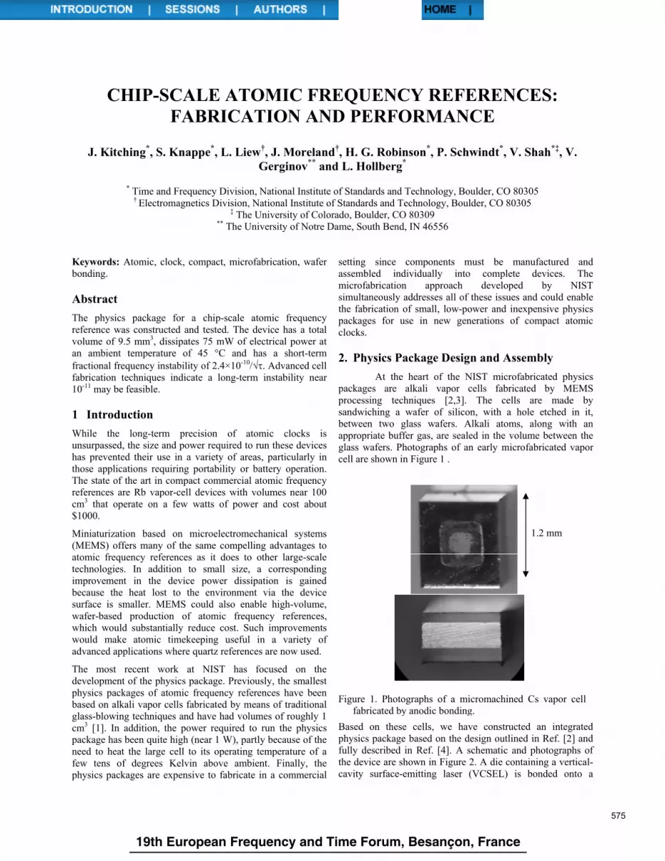
2. Physics Package Design and Assembly At the heart of the NIST microfabricated physics packages are alkali vapor cells fabricated by MEMS processing techniques [2,3]. The cells are made by sandwiching a wafer of silicon, with a hole etched in it, between two glass wafers. Alkali atoms, along with an appropriate buffer gas, are sealed in the volume between the glass wafers. Photographs of an early microfabricated vapor cell are shown in Figure 1 .
Based on these cells, we have constructed an integrated physics package based on the design outlined in Ref. [2] and fully described in Ref. [4]. A schematic and photographs of the device are shown in Figure 2. A die containing a vertical-cavity surface-emitting laser (VCSEL) is bonded onto a
1.2 mm
Figure 1. Photographs of a micromachined Cs vapor cell fabricated by anodic bonding.
575
19th European Frequency and Time Forum, Besançon, France

substrate patterned with gold (Figure 2A, layer a). The VCSEL is used because of its low power requirements (typically < 5 mW for most devices), high modulation efficiency, and availability of single-mode devices at the 852 nm optical transition in Cs and the 795 nm optical transition in Rb.
The light emitted by the VCSEL is conditioned by an optics assembly (Figure 2A, layers b-f) attached to the baseplate. This optics assembly attenuates and collimates the light and changes the light polarization from linear to circular. In this vertically integrated structure, glass spacers (Figure 2A, layer b) support the rest of the clock assembly over the laser and provide thermal isolation between the heated cell and the baseplate. Two neutral-density filters (Figure 2A, layers c and f), cut from a wafer of optically dense glass, attenuate the light power to roughly 10 W, and the light is collimated by means of a commercially available microrefractive lens fabricated by inkjet deposition of optical epoxy (Figure 2A, layer d). The light polarization is altered with a piece of a quartz wafer, 80 m thick, with its optical axis oriented at 45º to the direction of the initial polarization of the laser beam (Figure 2A, layer e, not shown).
The cell assembly (Figure 2A, layers g-k) is placed on top of the optics assembly. During operation of the clock, the cell is heated with planar heaters (Figure 2A, layers g and k), fabricated from a thin layer of transparent indium-tin oxide (ITO) deposited on a glass substrate and then wire-bonded to the substrate through gold contact strips. Heaters are placed above and below the cell to provide uniform heating when a current is passed through the ITO film. Because the heat enters the cell though the windows, these parts remain slightly warmer than the cell body, which prevents buildup of an opaque alkali metal film on the windows that might prevent light from entering or exiting the cell.
Finally a photodiode assembly (Figure 2A, layers l-m) is mounted onto the top of the structure to detect the light power transmitted through the cell.
In most cases, the layers are bonded together with optical epoxy. Gold wires of thickness 25 m are bonded on one end to individual components before they are assembled and the other end is bonded to the baseplate after assembly. We anticipate that with further refinement of the design, all wire-bonding can be done after assembly of the entire structure.
A B
C
D
E
F
a
b
c
d
ef
gh
i
jk
lm
Figure 2. The microfabricated atomic clock physics package based on Cs atoms. (A) Schematic of assembly. Layers from bottom to top: a, Laser and baseplate; b, Glass (500 m); c, ND filter (500 m); d, Spacer (375 m); e, Quartz (70 m, not shown); f, ND filter (500 m); g, Glass/ITO (125 m/30 nm); h, Glass (200 m); i, Si (1000 m); j, Glass (200 m); k, Glass/ITO (125 m/30 nm); l, Si (375 m); m, Glass (125 m). Total height, 4.2 mm, width and depth, 1.5 mm. Photographs (B), photodiode assembly, (C), cell assembly, (D), optics assembly and (E), laser assembly and (F), the full atomic frequency reference physics package realized as a microchip. The black lines in the photographs indicate 1 mm.
576
19th European Frequency and Time Forum, Besançon, France

Photographs of the fully assembled device and individual components are shown in Figure 2B-F.
3. Device Characterization The physics package is operated by first heating the
alkali vapor cell to about 80 ºC. At this temperature, vapor-phase Cs atoms are in equilibrium with the liquid phase at a density of about 1013 atoms/cm3, which is sufficient for observation of the atomic resonance. Modulation near 4.6 GHz, one-half of the Cs ground-state hyperfine oscillation frequency, is applied to the laser. As the modulation frequency is swept around the frequency of the atomic resonance, a change in the DC optical power transmitted through the cell occurs, which is detected with the photodiode at the top of the structure. A plot of the photodiode signal as a function of the detuning of twice the modulation signal is shown in Figure 3. The resonance width of 7.1 kHz gives a Q-factor of 1.2×10⁶.
By modulating the frequency of the local oscillator and using lock-in detection, an error signal can be generated from the resonance in Figure 3. When this error signal is fed back to the frequency-tuning port of the LO, the LO frequency can be stabilized onto the atomic resonance. The stabilized output frequency of the LO is then compared to a secondary, more stable oscillator to measure its frequency as a function of time; a plot of these data is shown in Figure 4, Trace A. When integrated for a time , the fractional frequency instability as measured by the Allan deviation is shown in Figure 5, Trace A. An instability of 2.5×10⁻¹⁰ at one second of integration is obtained, which averages down to a minimum of 4×10-11 near 100 s. A linear drift of -1.6×10⁻⁸/day is also observed, which we attribute to chemical reactions occurring in the cell that change the pressure of the buffer gas and therefore also the frequency of the clock.
The short-term instability of the frequency reference is determined by the resonance width (Q-factor) and the noise present at the photodetector. The resonance width is
dominated in this particular device by optical power-broadening, with secondary contributions due to collisions of alkali atoms with the walls of the cell and buffer-gas atoms. The noise is dominated by shot-noise in the conversion of optical power into electrons in the photodiode.
4. Power Dissipation The electrical power required to run the physics package was 75 mW, and was dominated by the power required to heat the cell above the ambient temperature of 46 ºC set by the baseplate. The high baseplate temperature was required to tune the particular laser used in the device to the correct
Figure 4. Output frequency of the microfabricated atomic clock physics packages and cells as a function of time. A: Physics package based on Cs(drift -2×10⁻⁸/day). B: physics package based on 87Rb (drift -5×10⁻⁹/day). and C: cell based on 87Rbfabricated using the beam-filling technique (drift << 10-10/day).
20000 30000 40000 50000
-4
-2
0
2
4
Rel
ativ
e Fr
eque
ncy
(10-9
)
Time (sec)
A
B
C
Figure 3. Atomic resonance signal from the Cs microfabricated atomic clock physics package shown in Figure 2.
40 50 60 70 80 905.65
5.66
5.67
PD
Sig
nal [
V]
Frequency Detuning [kHz]from 9,192,631,770 Hz
7.1 kHz
Contrast: 0.91%
Figure 5. Fractional frequency instability of the microfabricated devices as a function of integration time. Squares indicate stability of Cs physics package, circles indicate stability of 87Rb physics package, and triangles indicate stability of 87Rb cell fabricated with the beam filling technique.
100 101 102 103 104 10510-12
10-11
10-10
10-9
1 day1 hourAlle
n D
evia
tion,
f/f
(sec)
A
B
C
577
19th European Frequency and Time Forum, Besançon, France

wavelength and is not generally necessary; the frequency reference was in fact operated without baseplate heating but the short-term instability was somewhat higher. An advantage obtained through the use of a VCSEL is the extremely low power (< 2 mW) required to both run the laser and to modulate it with amplitude sufficient to excite the CPT resonance.
By modelling the heat flow in the structure, both analytically and with a finite-element computation, the heat loss channels could be roughly identified, as shown in Figure 6. We estimate that 30 mW is lost through the lower spacer unit, and that 24 mW is lost through the six gold wire bonds providing the electrical connections to the baseplate. The remainder is presumably lost through radiation and through conduction to the air surrounding the physics package. Our modelling suggests that the heat lost through these last two channels could be reduced to well below one milliwatt by use of vacuum packaging with a low-emissivity coating on its interior surface [2,5]. The remaining sources of heat loss, conduction through the lower spacer unit and the wire-bonds, can be addressed through more advanced thermal design of the spacer unit itself. For example, the use of a polymer material with a lower thermal conductivity and thin (10 m) gold traces as part of the electrical path would reduce the heater power to below 12 mW needed to maintain a temperature difference of 50 K between the baseplate and the cell. The two key differences between the design of these chip-scale physics packages and current commercial frequency reference designs are the use of a laser, rather than a lamp, as the optical source and a smaller cell size combined with better thermal isolation.
As mentioned above, two other components are required, in addition to the physics package, to form a complete atomic frequency reference. The development of small low-power oscillators at gigahertz-frequencies with sufficient frequency stability to be able to be locked to the atomic resonance is being undertaken by a number of research groups. In addition, a digital control system based on a microprocessor is being developed at NIST and is expected to be able to implement
the four feedback loops necessary to run the clock. The anticipated power budget of the complete frequency reference is outlined in Table 1.
Table 1. Anticipated power budget for fully integrated chip-scale atomic clock based on Cs atoms, operating at an ambient temperature near 25 °C.
Component Power Confidence Heating of cell (modeling) 12 mW moderate Laser DC power (measured) 4 mW high Laser RF power (measured) 70 W high Local oscillator (measured) 3 mW high Control circuit (estimate) 20 mW moderate B-field, temp. sensor, etc. < 1 mW high Total: 40 mW moderate
5. A Microfabricated Physics Package Based on 87Rb
It is known that excitation of CPT resonances with light tuned to the D1 optical transition of alkali atoms results in a signal with an amplitude larger than those excited with light resonant with the D2 line [6]. A chip-scale atomic frequency reference based on D1 excitation is therefore expected to be more precise. Since single-mode VCSELs are not commercially available at 895 nm (the wavelength of the D1 transition of Cs), but are available at 795 nm (the wavelength of the D1 transition in Rb), a microfabricated frequency reference was constructed based on a cell containing 87Rb. This cell was fabricated in a manner very similar to that used for the previous Cs cells. An isotopically pure compound of 87RbCl was reacted with BaN6 inside the cell preform before the final window was bonded to the structure. The cell was backfilled with a buffer gas of an Ar/Ne mixture instead of one containing N2. These buffer gases were used instead of N2 with the goal of reducing the frequency drift, since Ar and Ne are both inert to reaction with Ba, while N2 is not.
A chip-scale atomic clock physics package based on this cell was constructed with a structure identical to that of the Cs device. A photograph of this physics package is shown in Figure 7.
Figure 7. A CSAC physics package based on a cell containing 87Rb and excited with a laser at 795 nm.
30 mW
24 mW15 mW
30 mW
24 mW15 mW
Figure 6. Estimated heat loss sources in the chip-scale atomic clock physics package.
578
19th European Frequency and Time Forum, Besançon, France

The performance of this physics package was substantially better than that obtained in the Cs/D2 device. The resonance contrast improved to 4.9 %, while the width remained largely unchanged. As a result, the short-term instability was reduced by about a factor of five to 4×10-11 at one second of integration. The drift was also reduced to near -5×10⁻⁹/day. The frequency as a function of time and corresponding Allan deviation are shown in Figure 4, Trace B and Figure 5, Trace B, respectively. We believe that the residual frequency drift in this physics package is caused by reabsorption of N2 gas initially created during the chemical reaction to produce the 87Rb and not completely pumped away during the cell filling process.
This device required about 195 mW to operate at an ambient temperature of 22 °C. This larger operating power was a result of the higher operating temperature (120 °C) of the cell, and a lower ambient temperature, as compared to the Cs physics package. The increased cell temperature for the 87Rbdevice was in part because 87Rb has a lower vapour pressure than Cs at a given temperature. However, it is also likely that optical pumping processes were more important in the 87Rbdevice than in the Cs device because the former was excited using light resonant with the D1 transition, while the latter was excited on the D2 transition.
6. Microfabricated vapour cells with reduced frequency drift In order to eliminate the frequency drift due to the presence of Ba inside the vapour cells, a new cell filling technique was developed and is illustrated in Figure 8. In this process, a glass ampoule with a narrow open neck is filled with the mixture of BaN6 and AlkaliCl instead of the cell itself. The cell preform is first baked at 300 °C to extract water from the glass (Figure 8a). The neck of the ampoule is inserted into
the vacuum chamber (Figure 8b), positioned over the cell opening and heated to react the compounds (Figure 8c). Because the vapour pressure of alkali metals is much higher than that of the other materials created in the reaction, a fairly pure beam of alkali atoms emerges from the neck of the ampoule and is deposited into the cell. After the chamber is backfilled with an appropriate buffer gas, a second glass piece is then bonded to the Si, to seal the alkali atoms and buffer gas inside the cell (Figure 8d).
A cell fabricated in this manner showed a significantly reduced frequency drift. The cell was tested in a highly temperature-controlled environment by locking an external oscillator to the CPT resonance excited by the D1 optical transition. The frequency of the locked oscillator is plotted as a function of time in Figure 4, Trace C and the corresponding Allan deviation is shown in Figure 5, Trace C. The frequency drift is reduced to below 5×10-11/day while the short-term frequency stability is maintained.
7. Other applications While the main goal of our research over the last three years has been to design and build highly miniaturized atomic clocks, the basic technologies developed as part of this research program have significant applications in other areas. One example is highly sensitive and accurate magnetometers [7] based on vapors of alkali atoms. Because atoms have a magnetic moment, different orientations of certain atomic states in an external magnetic field have different internal energies. Since the energy difference is proportional to the magnetic field (at least at low field strengths), measuring this energy difference is equivalent to measuring the strength of the magnetic field. It is therefore possible to determine the magnetic field by comparing the energy difference of magnetically sensitive states to the energy difference of magnetically insensitive states (or some other stable frequency), as shown in Figure 9.
Operationally, this can be accomplished by simply tuning the frequency of the local oscillator in a chip-scale atomic clock from the magnetically insensitive transition at 0 to a magnetically sensitive one at 0+ B, where B is the magnitude of the external magnetic field and is a constant. This change in LO frequency causes an oscillation between
Figure 9. A magnetometer based on coherent population trapping spectroscopy of magnetically sensitive hyperfine transitions.
Cell preformHeaters
HV-
+
Buffer Gas Combination
Cover GlassGlass ampoule
withBaN6 + AlkaliCl
Alkali atoms
300 ° C
180 ° C
300 ° C
200 V
(a) (b)
(c) (d)
Figure 8. Fabrication process for cells with low frequency drift.
579
19th European Frequency and Time Forum, Besançon, France

two atomic states whose energy depends on magnetic field. A magnetometer of this type has been implemented at NIST [8] with a microfabricated structure similar to that in Figure 2 but based on 87Rb atoms, rather than Cs. With this device magnetic fields can be measured with a sensitivity of
HzpT /40 in the frequency range of 10 Hz to 100 Hz. The output of the device when subject to an external magnetic field stepped by 2.53 nT every ten seconds is shown in Figure 10.
0 10 20 30 40 50Time (s)
Lock
-in S
igna
l (ar
b. u
nits
)
2.53 nT
0 10 20 30 40 50Time (s)
Lock
-in S
igna
l (ar
b. u
nits
)
2.53 nT
10. Conclusion We have described here recent work at NIST to
develop highly miniaturized atomic clocks and magnetometers using MEMS microfabrication techniques. The physics packages associated with these devices have volumes in the range of 10 mm3 and dissipate under 100 mW of power, with significant potential for even lower power dissipation. A critical aspect of the work is the possibility of low-cost, wafer-level fabrication and assembly of devices, which would likely open the door to a wide range of commercial applications for which cost is a considerable factor. However, even a compact atomic clock capable of being operated on batteries for an extended period would be useful in many applications requiring mobility [9,10].
Although the work so far has focussed primarily on the physics package, future work will undoubtedly progress towards integration of this subsystem with a compact local oscillator and control electronics. Development of these other critical subsystems will pave the way toward commercial realization of chip-scale atomic frequency references [11]
Acknowledgements This work was supported by NIST and the Defence Advanced Research Projects Agency (DARPA). This work is a contribution of NIST, an agency of the US government, and is not subject to copyright. Portions of this manuscript have been published previously in Refs. [3], [4], [5], [8] and [12]
[1] P.J. Chantry, I. Liberman, W.R. Verbanets, C. F.
Petronio, R. L. Cather, and W. D. Partlow, "Miniature laser-pumped cesium cell atomic clock oscillator," Proc. IEEE Int. Frequency Control Symp., pp. 1002-1010, 1996.
[2] J. Kitching, S. Knappe, L. Liew, J. Moreland, H. G. Robinson, P. D. D. Schwindt, V. Shah and L. Hollberg, "Microfabricated atomic frequency references," Proc.18th Eur. Freq. Time Forum, April 5-6, Guildford, UK, 2004.
[3] L-A. Liew, S. Knappe, J. Moreland, H. Robinson, L. Hollberg and J. Kitching, "Microfabricated alkali atom vapor cells," Appl. Phys. Lett., 84, 2694-2696, 2004.
[4] S. Knappe, L. Liew, V. Shah, P. Schwindt, J. Moreland, L. Hollberg, and J. Kitching, "A micromachined atomic clock," Appl. Phys. Lett., 85, 1460-1462, 2004.
[5] J. Kitching, S. Knappe, P. D. D. Schwindt, V. Shah, L. Hollberg, L. Liew and J. Moreland, "Power dissipation in a vertically-integrated chip-scale atomic clock," Proc. IEEE Int. Freq. Cont. Symp., Montreal, Canada, Aug. 24-27, 2004.
[6] M. Stahler, R. Wynands, S. Knappe, J. Kitching, L. Hollberg, A. Taichenachev, and V. Yudin, "Coherent population trapping resonances in thermal Rb-85 vapor: D-1 versus D-2 line excitation," Opt. Lett., 27, 1472-1474, 2002
[7] H. Dehmelt, “Modulation of a light beam by precessing absorbing atoms,” Phys. Rev., vol. 105, pp. 1924-1925, 1957.
[8] P. D. D. Schwindt, S. Knappe, V. Shah, L. Hollberg, J. Kitching, L. Liew and J. Moreland, "A chip-scale atomic magnetometer," Appl. Phys. Lett., 85, 6409, 2004.
[9] J. Vig, "Military applications of high-accuracy frequency standards and clocks," IEEE Trans. Ultrason. Ferroelec. Freq. Cont., 40, 522-527, 1993
[10] H. Fruehoff, “Fast "direct-P(Y)" GPS signal acquisition using a special portable clock,” Proc 33rd Ann. Precise Time and Time Interval (PTTI) Meeting, 359-369, 2001.
[11] R. Lutwak, J. Deng, W. Riley, M. Varghese, J. Leblanc, G. Tepolt, M. Mescher, D. K. Serkland, K. M. Geib and G. M. Peake, “The chip-scale atomic clock – low-power physics package,” Proc. 36th Ann. Precise Time and Time Interval (PTTI) Meeting, Washington, DC, Dec. 7-9, 2004.
[12] J. Kitching, S. Knappe, L. Liew, P. D. D. Schwindt, V. Shah, J. Moreland and L. Hollberg, "Microfabricated atomic clocks," Proc. 18th Int. IEEE Conf. Micro Elec. Mech. Sys., Jan 30- Feb. 3, 2005, Miami, FL, 2005.
Figure 10. The magnetometer output signal is plotted as a function of time as the magnetic flux is stepped in 10-second intervals. The averaging time is 30 ms.
580
19th European Frequency and Time Forum, Besançon, France