triac dimmer compatible led driver - renesas
TRANSCRIPT
1 CAUTION: Th1-888-INTERSIL or 1
September 21, 2010AN1583.1
Application Note 1583
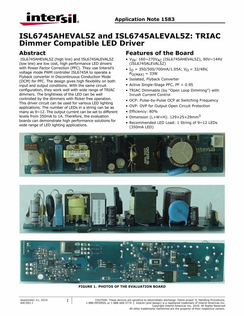
ISL6745AHEVAL5Z and ISL6745ALEVAL5Z: TRIAC Dimmer Compatible LED DriverAbstract ISL6745AHEVAL5Z (high line) and ISL6745ALEVAL5Z (low line) are low cost, high performance LED drivers with Power Factor Correction (PFC). They use Intersil’s voltage mode PWM controller ISL6745A to operate a Flyback converter in Discontinuous Conduction Mode (DCM) for PFC. The design gives high flexibility on both input and output conditions. With the same circuit configuration, they work well with wide range of TRIAC dimmers. The brightness of the LED can be well controlled by the dimmers with flicker free operation. This driver circuit can be used for various LED lighting applications. The number of LEDs in a string can be as many as 9~12. The output current can be set to different levels from 350mA to 1A. Therefore, the evaluation boards can demonstrate high performance solutions for wide range of LED lighting applications.
Features of the Board• VIN: 160~270VAC (ISL6745AHEVAL5Z), 90V~144V
(ISL6745ALEVAL5Z)
• IO = 350/500/700mA/1.05A; VO = 32/48V, PO(MAX) = 33W
• Isolated, Flyback Converter
• Active Single-Stage PFC, PF > 0.95
• TRIAC Dimmable (by “Open Loop Dimming”) with Inrush Current Control
• OCP: Pulse-by-Pulse OCP at Switching Frequency
• OVP: OVP for Output Open Circuit Protection
• Efficiency: 80%
• Dimension (L×W×H): 129×25×29mm3
• Recommended LED Load: 1 String of 9~12 LEDs (350mA LED)
FIGURE 1. PHOTOS OF THE EVALUATION BOARD
ese devices are sensitive to electrostatic discharge; follow proper IC Handling Procedures.-888-468-3774 | Intersil (and design) is a registered trademark of Intersil Americas Inc.
Copyright Intersil Americas Inc. 2010. All Rights ReservedAll other trademarks mentioned are the property of their respective owners.
Application Note 1583
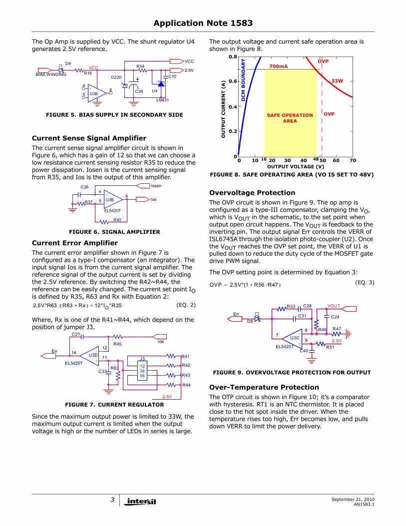
Operation TheoryThe block diagram of ISL6745AHEVAL5Z LED driver is shown in Figure 3. It is composed of a Flyback converter and the following circuitries: Duty Cycle Limit, In-Rush Control, OTP, OVP, Current Error Amplifier, Current Sense Signal Amplifier and Bias Supply, etc.
The PFC is implemented by running the Flyback converter in DCM. the input equivalent resistance of the driver is:
Where:
Lp is the primary inductance of transformer,
fs is the switching frequency, and
D is the duty cycle.
Since the converter runs in constant frequency and D is fixed in open loop operation, RIN is constant. Therefore, the driver behaves like a pure resistive incandescent light bulb, so the driver has a built-in PFC function.
Please refer to AN1387 for more details on general LED lighting design guidelines.
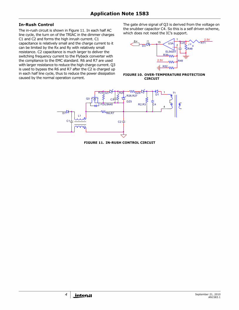
Bias SupplyThe bias supply in the primary side is shown in Figure 4. It has two sources; one is from the rectified DC bus (VBUS+) for start up, and the other is from the bias winding of primary side for normal operation.
The bias supply in the secondary side is shown in Figure 5; it is powered by aux winding in secondary side.
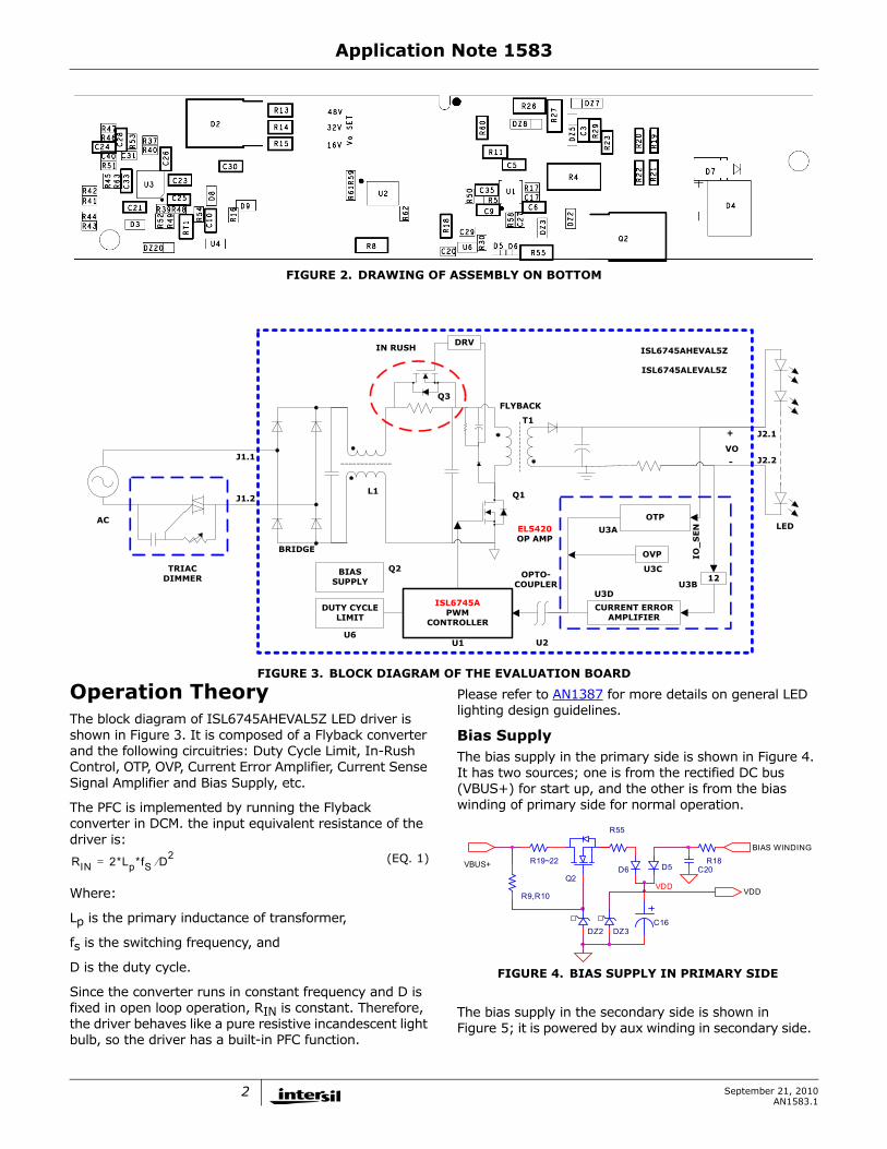
FIGURE 2. DRAWING OF ASSEMBLY ON BOTTOM
+
-
TRIAC DIMMER
AC
ISL6745APWM
CONTROLLER
CURRENT ERROR AMPLIFIER
OPTO-COUPLER
BRIDGE
LED
DRV
12
OVP
OTP
DUTY CYCLE LIMIT
IN RUSH
EL5420OP AMP
VO
IO_
SEN
U3D
U3A
U3B
U3C
U1U6
Q1
Q3
U2
Q2BIAS SUPPLY
T1
L1
ISL6745AHEVAL5Z
FLYBACK
ISL6745ALEVAL5Z
J1.1
J1.2
J2.1
J2.2
FIGURE 3. BLOCK DIAGRAM OF THE EVALUATION BOARD
RIN 2*Lp*fS D2⁄= (EQ. 1)
R9,R10
R18
Q2VDD
DZ3
R55
C20
C16
D6
DZ2
D5R19~22VBUS+
BIAS WINDING
VDD
FIGURE 4. BIAS SUPPLY IN PRIMARY SIDE
2 September 21, 2010AN1583.1
Application Note 1583
The Op Amp is supplied by VCC. The shunt regulator U4 generates 2.5V reference.
Current Sense Signal AmplifierThe current sense signal amplifier circuit is shown in Figure 6, which has a gain of 12 so that we can choose a low resistance current sensing resistor R35 to reduce the power dissipation. Iosen is the current sensing signal from R35, and Ios is the output of this amplifier.
Current Error AmplifierThe current error amplifier shown in Figure 7 is configured as a type-I compensator (an integrator). The input signal Ios is from the current signal amplifier. The reference signal of the output current is set by dividing the 2.5V reference. By switching the R42~R44, the reference can be easily changed. The current set point IO is defined by R35, R63 and Rx with Equation 2:
Where, Rx is one of the R41~R44, which depend on the position of jumper J3.
Since the maximum output power is limited to 33W, the maximum output current is limited when the output voltage is high or the number of LEDs in series is large.
The output voltage and current safe operation area is shown in Figure 8.
Overvoltage ProtectionThe OVP circuit is shown in Figure 9. The op amp is configured as a type-III compensator, clamping the VO, which is VOUT in the schematic, to the set point when output open circuit happens. The VOUT is feedback to the inverting pin. The output signal Err controls the VERR of ISL6745A through the isolation photo-coupler (U2). Once the VOUT reaches the OVP set point, the VERR of U1 is pulled down to reduce the duty cycle of the MOSFET gate drive PWM signal.
The OVP setting point is determined by Equation 3:
Over-Temperature ProtectionThe OTP circuit is shown in Figure 10; it’s a comparator with hysteresis. RT1 is an NTC thermistor. It is placed close to the hot spot inside the driver. When the temperature rises too high, Err becomes low, and pulls down VERR to limit the power delivery.
VCC
BIAS WINDING2.5V
VCC
DZ20
-
+U3B
4
56
C10R16
D9R54
U4
LM431
C38
FIGURE 5. BIAS SUPPLY IN SECONDARY SIDE
Ios
Iosen
-
+U3B
EL5420T
4
56
C26
R40
R37
FIGURE 6. SIGNAL AMPLIFIER
2.5V*R63 R63( Rx ) 12*IO*=+⁄ R35 (EQ. 2)
Ios
Err
2.5V
J3
135
246
R42
R43
R44
-
+
U3D
EL5420T11
1214
C33R63
C21
R41
R45
FIGURE 7. CURRENT REGULATOR
0.8
0.6
0.4
0.2
00 10 16 20 30 40 48 50 60 70
OVP
33W
OVP700mA
OU
TP
UT
CU
RR
EN
T (
A)
OUTPUT VOLTAGE (V)
SAFE OPERATIONAREA
DC
M B
OU
ND
AR
Y
FIGURE 8. SAFE OPERATING AREA (VO IS SET TO 48V)
OVP 2.5V*(1 R56 R47 )⁄+= (EQ. 3)
FIGURE 9. OVERVOLTAGE PROTECTION FOR OUTPUT
Err
R53
D8
-
+
U3C
EL5420T9
87
C31
C28 VOUT
R47R46
2.5V
C24
C40R51
3 September 21, 2010AN1583.1
Application Note 1583
In-Rush ControlThe in-rush circuit is shown in Figure 11. In each half AC line cycle, the turn on of the TRIAC in the dimmer charges C1 and C2 and forms the high inrush current. C1 capacitance is relatively small and the charge current to it can be limited by the Rx and Ry with relatively small resistance. C2 capacitance is much larger to deliver the switching frequency current to the Flyback converter with the compliance to the EMC standard. R6 and R7 are used with larger resistance to reduce the high charge current. Q3 is used to bypass the R6 and R7 after the C2 is charged up in each half line cycle, thus to reduce the power dissipation caused by the normal operation current.
The gate drive signal of Q3 is derived from the voltage on the snubber capacitor C4. So this is a self driven scheme, which does not need the IC’s support.
ErrD3
R52
-
+
U3A
EL5420T
2
115
R48
C25 t RT12.5V
R39
R492.5V
FIGURE 10. OVER-TEMPERATURE PROTECTION CIRCUIT
D1
R6,R7
DZ5
R26,R27Q3
FDU3N40
DZ8
C3
R29DZ7
L1
R2,R3
D7
C1
R23
C2
C4
T1
4
1
FIGURE 11. IN-RUSH CONTROL CIRCUIT
4 September 21, 2010AN1583.1
Application Note 1583
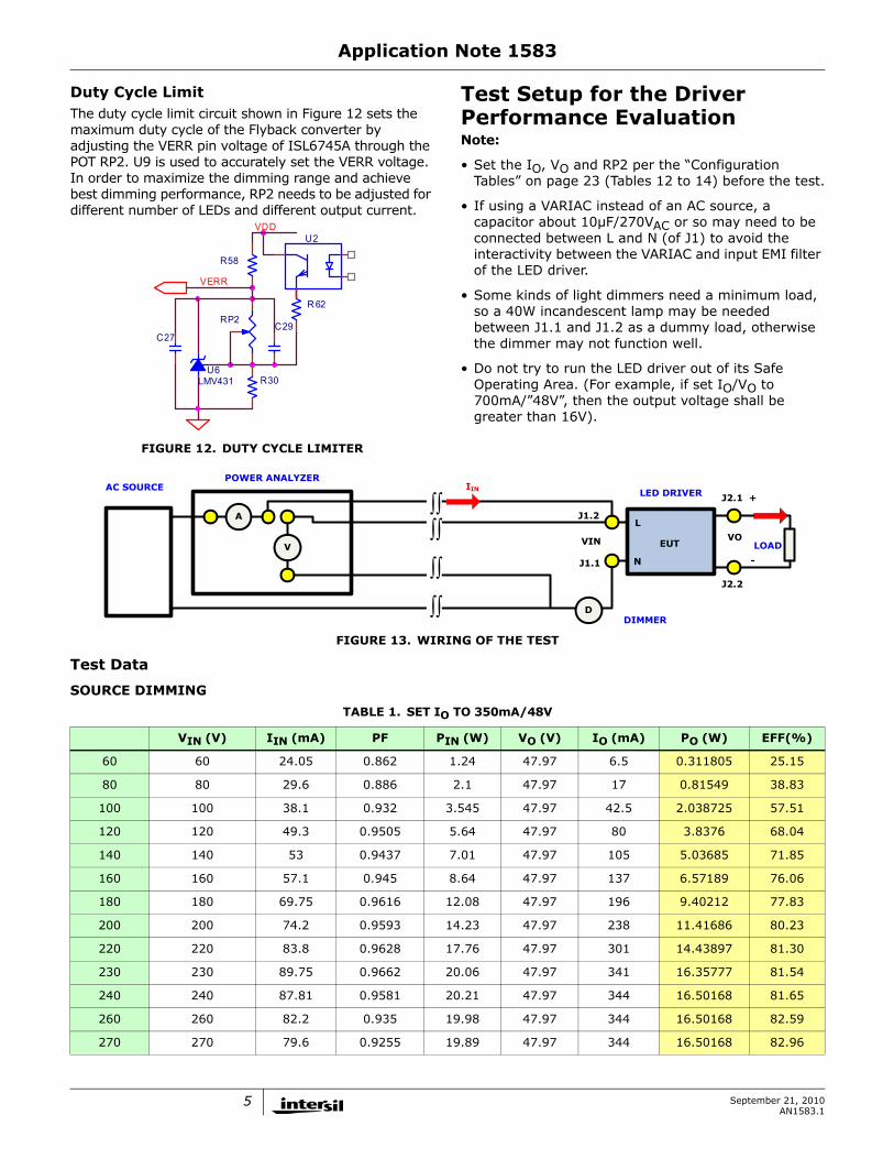
Duty Cycle LimitThe duty cycle limit circuit shown in Figure 12 sets the maximum duty cycle of the Flyback converter by adjusting the VERR pin voltage of ISL6745A through the POT RP2. U9 is used to accurately set the VERR voltage. In order to maximize the dimming range and achieve best dimming performance, RP2 needs to be adjusted for different number of LEDs and different output current.
Test Setup for the Driver Performance EvaluationNote:
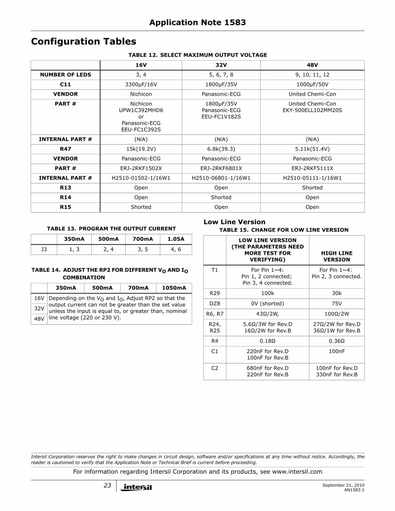
• Set the IO, VO and RP2 per the “Configuration Tables” on page 23 (Tables 12 to 14) before the test.
• If using a VARIAC instead of an AC source, a capacitor about 10µF/270VAC or so may need to be connected between L and N (of J1) to avoid the interactivity between the VARIAC and input EMI filter of the LED driver.
• Some kinds of light dimmers need a minimum load, so a 40W incandescent lamp may be needed between J1.1 and J1.2 as a dummy load, otherwise the dimmer may not function well.
• Do not try to run the LED driver out of its Safe Operating Area. (For example, if set IO/VO to 700mA/”48V”, then the output voltage shall be greater than 16V).
Test Data
SOURCE DIMMING
R30
VDD
C27
R 62
R58
U2
VERR
RP2C29
U6LMV431
FIGURE 12. DUTY CYCLE LIMITER
EUT
POWER ANALYZER
V
A
LOAD
∫∫
∫∫∫∫
∫∫
L
N
LED DRIVER AC SOURCE
VIN VO
+
-
J1.2
J1.1
J2.1
J2.2
IIN
DDIMMER
FIGURE 13. WIRING OF THE TEST
TABLE 1. SET IO TO 350mA/48V
VIN (V) IIN (mA) PF PIN (W) VO (V) IO (mA) PO (W) EFF(%)
60 60 24.05 0.862 1.24 47.97 6.5 0.311805 25.15
80 80 29.6 0.886 2.1 47.97 17 0.81549 38.83
100 100 38.1 0.932 3.545 47.97 42.5 2.038725 57.51
120 120 49.3 0.9505 5.64 47.97 80 3.8376 68.04
140 140 53 0.9437 7.01 47.97 105 5.03685 71.85
160 160 57.1 0.945 8.64 47.97 137 6.57189 76.06
180 180 69.75 0.9616 12.08 47.97 196 9.40212 77.83
200 200 74.2 0.9593 14.23 47.97 238 11.41686 80.23
220 220 83.8 0.9628 17.76 47.97 301 14.43897 81.30
230 230 89.75 0.9662 20.06 47.97 341 16.35777 81.54
240 240 87.81 0.9581 20.21 47.97 344 16.50168 81.65
260 260 82.2 0.935 19.98 47.97 344 16.50168 82.59
270 270 79.6 0.9255 19.89 47.97 344 16.50168 82.96
5 September 21, 2010AN1583.1

Application Note 1583
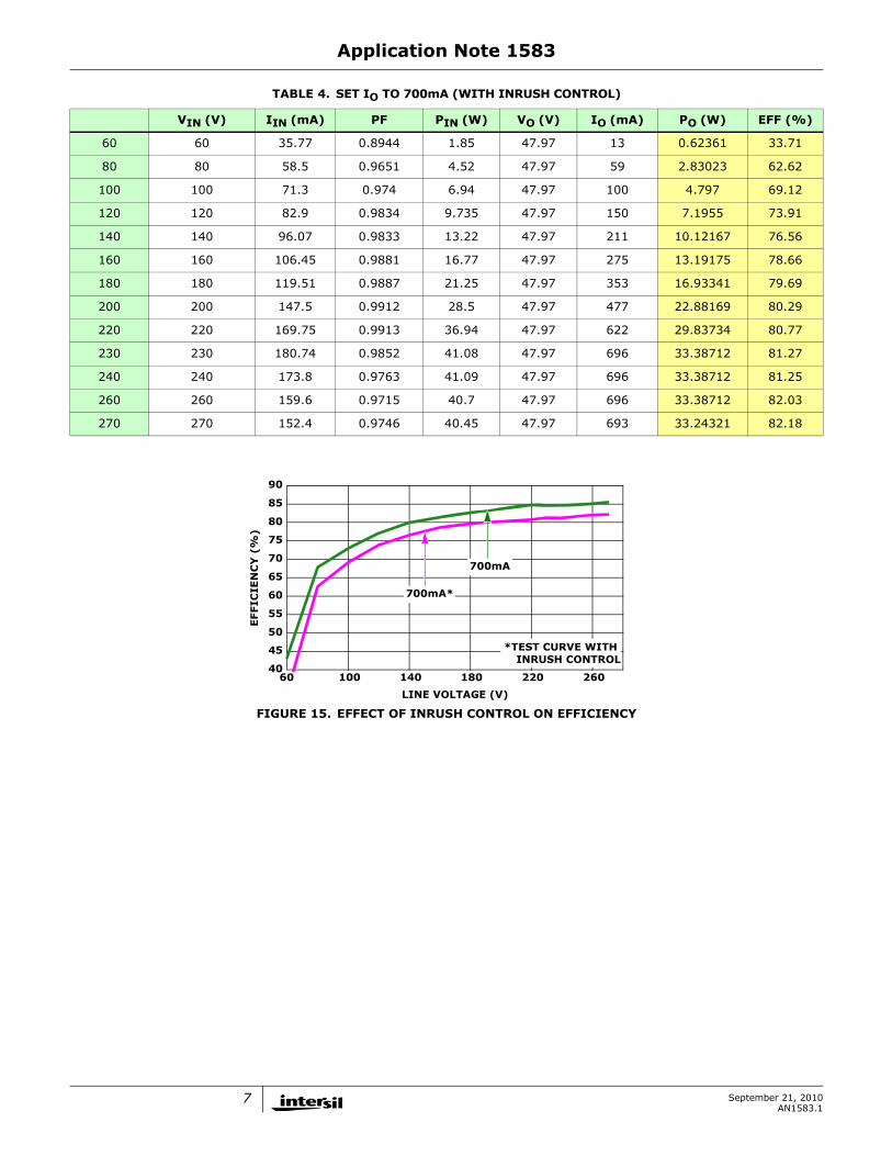
The above test bypassed the inrush control circuit (R6, R7, R24 and R25 is shorted), which is necessary if the TRIAC dimming function is not needed. For better TRIAC dimming performance, the inrush control is necessary.
Following is efficiency test data with R6 = R7 = 100Ω and R24 = R25 = 25.5 Ω.
TABLE 2. SET IO TO 500mA/48V
VIN (V) IIN (mA) PF PIN (W) VO (V) IO (mA) PO (W) EFF (%)
60 60 30.9 0.8765 1.62 47.97 12 0.57564 35.53
80 80 35 0.9118 2.55 47.97 25 1.19925 47.03
100 100 43.1 0.9375 4.04 47.97 52 2.49444 61.74
120 120 63.44 0.955 7.28 47.97 112 5.37264 73.80
140 140 77.2 0.96 10.37 47.97 168 8.05896 77.71
160 160 86.1 0.966 13.32 47.97 221 10.60137 79.59
180 180 99.7 0.9726 17.45 47.97 298 14.29506 81.92
200 200 111.2 0.9744 21.65 47.97 375 17.98875 83.09
220 220 122.3 0.9751 26.23 47.97 462 22.16214 84.49
230 230 125.01 0.9741 28.02 47.97 494 23.69718 84.57
240 240 121.23 0.9687 28.21 47.97 494 23.69718 84.00
260 260 113.8 0.9619 28.42 47.97 494 23.69718 83.38
270 270 110 0.9595 28.49 47.97 494 23.69718 83.18
TABLE 3. SET IO TO 700mA/48V
VIN (V) IIN (mA) PF PIN (W) VO (V) IO (mA) PO (W) EFF (%)
60 60 40.6 0.857 2.1 47.97 19 0.91143 43.40
80 80 64.84 0.9545 4.95 47.97 70 3.3579 67.84
100 100 73.37 0.959 7.03 47.97 107 5.13279 73.01
120 120 91.85 0.9645 10.76 47.97 173 8.29881 77.13
140 140 99.9 0.9773 13.67 47.97 228 10.93716 80.01
160 160 117.6 0.9837 18.55 47.97 315 15.11055 81.46
180 180 130.5 0.9846 22.97 47.97 396 18.99612 82.70
200 200 162.2 0.9883 32.15 47.97 561 26.91117 83.71
220 220 181.5 0.9874 39.43 47.97 697 33.43509 84.80
230 230 174.2 0.982 39.5 47.97 697 33.43509 84.65
240 240 168.3 0.9761 39.5 47.97 697 33.43509 84.65
260 260 154.6 0.9738 39.29 47.97 697 33.43509 85.10
270 270 148.2 0.9742 39.05 47.97 696 33.38712 85.50
FIGURE 14A. OUTPUT CURRENT vs INPUT VOLTAGE
FIGURE 14B. PF vs LINE VOLTAGE FIGURE 14C. EFFICIENCY vs LINE VOLTAGE
FIGURE 14. CHART OF THE DATA TABLE
0
100
200
300
400
500
600
700
800
60 100 140 180 220 260LINE VOLTAGE (V)
700mA
500mA
350mA
I O (
mA
)
0.60
0.65
0.70
0.75
0.80
0.85
0.90
0.95
1.00
60 100 140 180 220 260
LINE VOLTAGE (V)
500mA 350mA 700mA
PF
20
30
40
50
60
70
80
90
60 100 140 180 220 260LINE VOLTAGE (V)
EFFIC
IEN
CY
(%
)
500mA700mA
350mA
6 September 21, 2010AN1583.1
Application Note 1583
TABLE 4. SET IO TO 700mA (WITH INRUSH CONTROL)
VIN (V) IIN (mA) PF PIN (W) VO (V) IO (mA) PO (W) EFF (%)
60 60 35.77 0.8944 1.85 47.97 13 0.62361 33.71
80 80 58.5 0.9651 4.52 47.97 59 2.83023 62.62
100 100 71.3 0.974 6.94 47.97 100 4.797 69.12
120 120 82.9 0.9834 9.735 47.97 150 7.1955 73.91
140 140 96.07 0.9833 13.22 47.97 211 10.12167 76.56
160 160 106.45 0.9881 16.77 47.97 275 13.19175 78.66
180 180 119.51 0.9887 21.25 47.97 353 16.93341 79.69
200 200 147.5 0.9912 28.5 47.97 477 22.88169 80.29
220 220 169.75 0.9913 36.94 47.97 622 29.83734 80.77
230 230 180.74 0.9852 41.08 47.97 696 33.38712 81.27
240 240 173.8 0.9763 41.09 47.97 696 33.38712 81.25
260 260 159.6 0.9715 40.7 47.97 696 33.38712 82.03
270 270 152.4 0.9746 40.45 47.97 693 33.24321 82.18
FIGURE 15. EFFECT OF INRUSH CONTROL ON EFFICIENCY
40
45
50
55
60
65
70
75
80
85
90
60 100 140 180 220 260
LINE VOLTAGE (V)
EFFIC
IEN
CY
(%
)
700mA
700mA*
*TEST CURVE WITH INRUSH CONTROL
7 September 21, 2010AN1583.1

Application Note 1583
TRIAC DimmingTABLE 5. LOAD = 1P9S (ONE STRING OF 9 LEDS IN SERIES)
IGNITION ANGLE (°) IIN (mA) PIN (W) VO (V) IO (mA) PO (W) EFF (%)
0 111.1 24.81 29.84 692 20.64928 83.22967
30 120.6 25.35 30.12 696 20.96352 82.69633
60 132.5 21.95 29.29 587.7 17.21373 78.42247
90 121.5 14.1 28.23 362.8 10.24184 72.63719
120 100.1 6.31 26.41 134.9 3.562709 56.46132
130 91.7 4.54 25.86 85.9 2.221374 48.92894
140 70 2.52 24.87 36.6 0.910242 36.12071
TABLE 6. LOAD = 1P10S
IGNITION ANGLE (°) IIN (mA) PIN (W) VO (V) IO (mA) PO (W) EFF (%)
0 125.3 28.15 33.88 693 23.47884 83.40618
30 134 28.31 33.77 692.2 23.37559 82.5701
60 139 24.83 33.26 592.5 19.70655 79.36589
90 125 15.76 31.97 366.7 11.7234 74.38705
120 96 6.56 30.1 136.7 4.11467 62.72363
130 86 4.6 29.34 85.8 2.517372 54.72548
140 73.1 2.81 28.33 42.7 1.209691 43.0495
TABLE 7. LOAD = 1P11S
IGNITION ANGLE (°) IIN (mA) PIN (W) VO (V) IO (mA) PO (W) EFF (%)
0 139.1 31.32 37.68 693 26.11224 83.37241
30 147.1 31.53 37.62 692.5 26.05185 82.62559
60 150.5 27.13 36.9 585.7 21.61233 79.66211
90 131.5 17.2 35.6 361.1 12.85516 74.7393
120 96.5 6.83 33.28 136.6 4.546048 66.56
130 85 4.66 32.6 85.7 2.79382 59.95322
140 72 2.9 31.63 44.7 1.413861 48.75383
TABLE 8. LOAD = 1P12S
IGNITION ANGLE (°) IIN (mA) PIN (W) VO (V) IO (mA) PO (W) EFF (%)
0 152.2 34.34 41.15 693.8 28.54987 83.13882
30 159.58 34.45 41.06 690.7 28.36014 82.32262
60 159.3 29.76 40.41 588.3 23.7732 79.88307
90 138.5 18.62 38.98 358.1 13.95874 74.96637
120 100.3 7.36 36.57 134.6 4.922322 66.87938
130 90 4.87 35.69 83 2.96227 60.8269
140 75.2 2.83 34.5 43.2 1.4904 52.66431
8 September 21, 2010AN1583.1

Application Note 1583
THD of Input Current
FIGURE 16A. IO vs IGNITION ANGLE FIGURE 16B. EFFICIENCY vs IGNITION ANGLE
FIGURE 16. PLOTS OF DIMMING AND EFFICIENCY
0
100
200
300
400
500
600
700
800
0 30 60 90 120 150 180IGNITION ANGLE (°)
I O (
mA
)
11 LED
10 LED
12 LED
9 LED
0
10
20
30
40
50
60
70
80
0 30 60 90 120 150 180IGNITION ANGLE (°)
EFFIC
IEN
CY
(%
)
11 LED
10 LED
9 LED
12 LED
TABLE 9. CURRENT THD (BY WT210, WITHOUT DIMMER) LOAD USE LED (CREE)
230V/700mA 230V/350mA
12.8% 16.9%
TABLE 10. HARMONICS OF INPUT CURRENT
ORDER IN/I (%) ORDER IN/I (%)
1 / 2 0.467
3 9.89 4 0.543
5 4.453 6 0.175
7 3.296 8 0.176
9 3.191 10 0.369
11 0.285 12 0.284
13 2.965 14 0.109
15 0.77 16 0.212
17 1.003 18 0.112
19 1.255 20 0.199
21 0.529 22 0.091
23 1.007 24 0.334
25 0.61 26 0.257
27 0.913 28 0.106
29 0.492 30 0.083
31 0.783 32 0.038
33 1.332 34 0.512
35 1.02 36 0.949
1
2
2
I
ITHD n
n∑∞
==(EQ. 4) 37 0.249 38 0.904
39 0.594 40 0.852
41 0.124 42 0.837
43 0.065 44 0.328
45 0.179 46 0.169
47 0.377 48 0.036
49 0.688 50 0.116
THD(%) 12.8
TABLE 10. HARMONICS OF INPUT CURRENT (Continued)
ORDER IN/I (%) ORDER IN/I (%)
FIGURE 17. SPECTRUM OF INPUT CURRENT
0
1
2
3
4
5
6
7
8
9
10
1 6 11 16 21 26 31 36 41 46
9 September 21, 2010AN1583.1
Application Note 1583
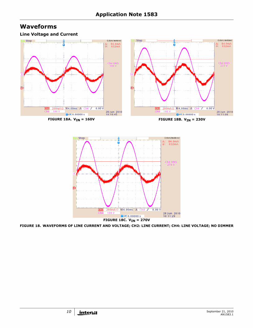
Waveforms Line Voltage and Current
FIGURE 18A. VIN = 160V FIGURE 18B. VIN = 230V
FIGURE 18C. VIN = 270V
FIGURE 18. WAVEFORMS OF LINE CURRENT AND VOLTAGE; CH2: LINE CURRENT; CH4: LINE VOLTAGE; NO DIMMER
10 September 21, 2010AN1583.1

Application Note 1583
FIGURE 19A. IGNITION ANGLE IS 30° FIGURE 19B. IGNITION ANGLE IS 60°
FIGURE 19C. IGNITION ANGLE IS 90° FIGURE 19D. IGNITION ANGLE IS 120°
FIGURE 19. WAVEFORM OF LINE CURRENT AND VOLTAGE (IO = 700mA), CH2: LINE CURRENT; CH4: LINE VOLTAGE; VIN = 230VAC
Line Voltage and Current (Continued)
11 September 21, 2010AN1583.1

Application Note 1583
Ripple Voltage and Output Current
FIGURE 20A. IGNITION ANGLE IS 0° FIGURE 20B. IGNITION ANGLE IS 30°
FIGURE 20C. IGNITION ANGLE IS 60° FIGURE 20D. IGNITION ANGLE IS 90°
FIGURE 20E. IGNITION ANGLE IS 120°
FIGURE 20. WAVEFORM OF VO AND IO RIPPLE (VIN = 230VAC); CH2: RIPPLE CURRENT; CH4: RIPPLE VOLTAGE
12 September 21, 2010AN1583.1
Application Note 1583
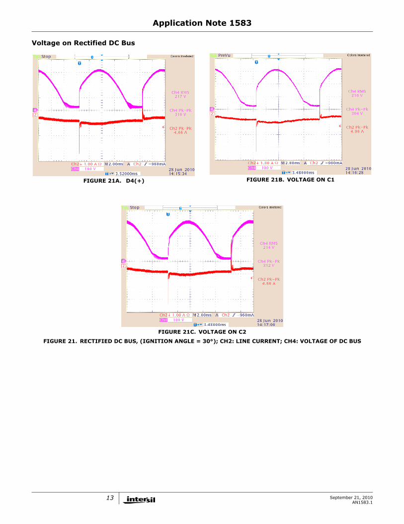
Voltage on Rectified DC Bus
FIGURE 21A. D4(+) FIGURE 21B. VOLTAGE ON C1
FIGURE 21C. VOLTAGE ON C2
FIGURE 21. RECTIFIED DC BUS, (IGNITION ANGLE = 30°); CH2: LINE CURRENT; CH4: VOLTAGE OF DC BUS
13 September 21, 2010AN1583.1
Application Note 1583
FIGURE 22A. D4(+) FIGURE 22B. VOLTAGE ON C1
FIGURE 22C. VOLTAGE ON C2
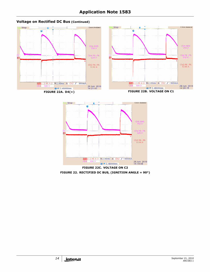
FIGURE 22. RECTIFIED DC BUS, (IGNITION ANGLE = 90°)
Voltage on Rectified DC Bus (Continued)
14 September 21, 2010AN1583.1
Application Note 1583
FIGURE 23A. D4(+) FIGURE 23B. VOLTAGE ON C1
FIGURE 23C. VOLTAGE ON C2
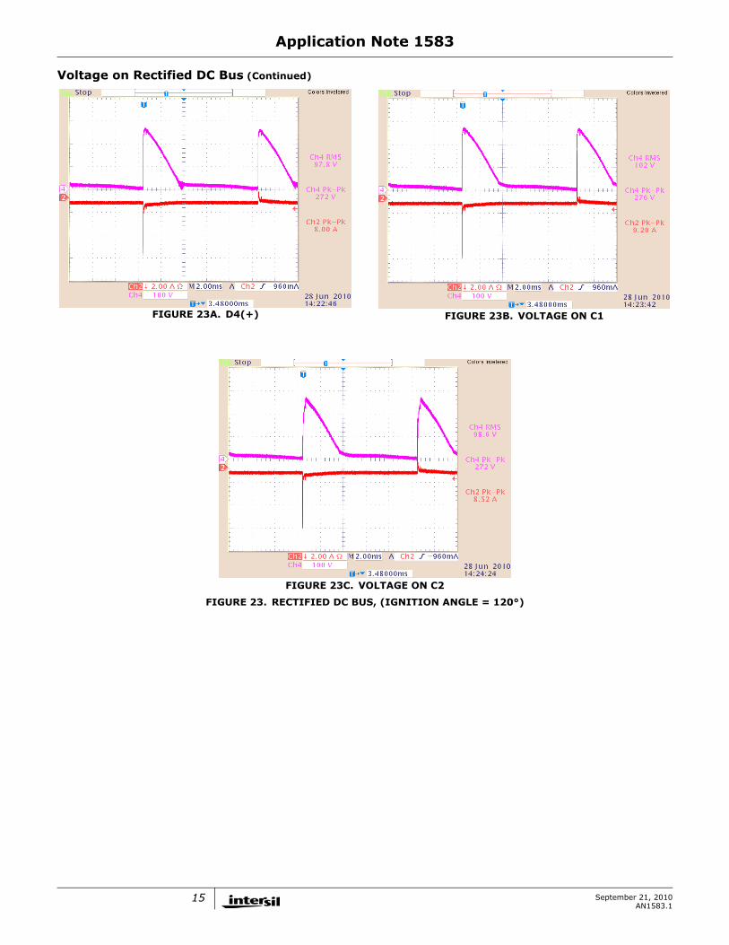
FIGURE 23. RECTIFIED DC BUS, (IGNITION ANGLE = 120°)
Voltage on Rectified DC Bus (Continued)
15 September 21, 2010AN1583.1
Application Note 1583
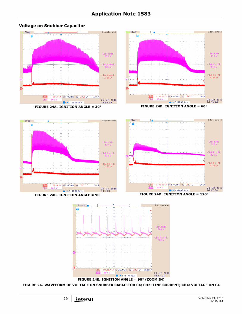
Voltage on Snubber Capacitor
FIGURE 24A. IGNITION ANGLE = 30° FIGURE 24B. IGNITION ANGLE = 60°
FIGURE 24C. IGNITION ANGLE = 90° FIGURE 24D. IGNITION ANGLE = 120°
FIGURE 24E. IGNITION ANGLE = 90° (ZOOM IN)
FIGURE 24. WAVEFORM OF VOLTAGE ON SNUBBER CAPACITOR C4; CH2: LINE CURRENT; CH4: VOLTAGE ON C4
16 September 21, 2010AN1583.1

Application Note 1583
Inrush Control Circuit
FIGURE 25A. IGNITION ANGLE = 30° FIGURE 25B. IGNITION ANGLE = 60°
FIGURE 25C. IGNITION ANGLE = 90° FIGURE 25D. IGNITION ANGLE = 120°
FIGURE 25E. IGNITION ANGLE = 120° (ZOOM IN)
FIGURE 25. VGS AND VDS OF Q3 (NEED AN ISOLATION TRANSFORMER TO PROBE THE WAVEFORM); CH2: LINE CURRENT; CH3:VGS; CH4: VDS
17 September 21, 2010AN1583.1

Application Note 1583
Reference[1] Fred Greenfeld, Intersil Application Note AN1387, “White LED Driver Circuits for Off-Line Applications using Standard PWM Controllers”
18 September 21, 2010AN1583.1
19
Sep
tember 2
1, 2
010
AN
1583.1
Z20
C10
Rev
ED Driv er (9~12 LEDs)
0.7/1.05A;Po=33W(max)
1*
J3
135
246
VOUT
J212
C
R42
R43
EL5420T
6
R44
VCC2.5V
R48 R54
U4
LM431
R47
VOUTC24
C23
t RT12.5V
R35
C30
C38
R41
2.5VR51
Ap
plica
tion
No
te 1
58
3
Schematic [Patent Applications Pending]R9
R53
D1
D
R6
Title
Size Document Number
ISL6745AHEVAL,33W Triac Dimmable L
R52
Vin=230V±10%;Io=0.35/0.5/
R30
R13
R61
D3
C1
R14
R15
D8
C37R18
DZ5
R8
R27R26
- +D4
VCC
J1
12
VC
Q1
STF8NK100Z
DZ8
-
+U3B
4
5
Q3
FDU3N40
Q2
R3'
R2'
-
+
U3C
EL5420T9
87
RV1
VDD
EMC12X
D Limit
FlybackInrush
PWM
OVP
i-RegBIAS
R3
C26
-
+
U3D
EL5420T
11
1214
C31
R16
DZ3
-
+
U3A
EL5420T
2
115
C3
R19
R55
VDD
D2
C7
VDD
R24
R25
C20
DZ7 R29
R2
C33
L1D7
C16
C1
R63
D9
DZ2
R62
R20
C27
R60
C25
C28
R7
R46
D6
R23
R59
R50
R22
R37
D5
R40
C6
R39
C15
R58 U2
R21 R11
C2
R4
R17
F1
R12
2.5V
C21
T1
4
2
1
3
5 10
12
9
11
13
14
6
C5
C4
RP2
10k
VCC
C29
R45
C40
R49
OTP
C17
R5
U1
OUTA7
CT5
CS4
RTD2
VDDP9
GND6
SS1
OUTB8
VERR3
VDD10
C35
C9
U6
LMV431
R10
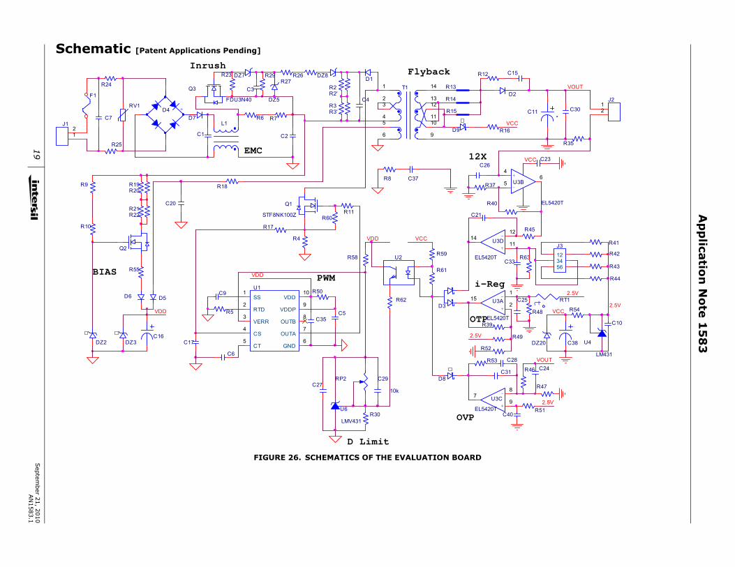
FIGURE 26. SCHEMATICS OF THE EVALUATION BOARD
Application Note 1583
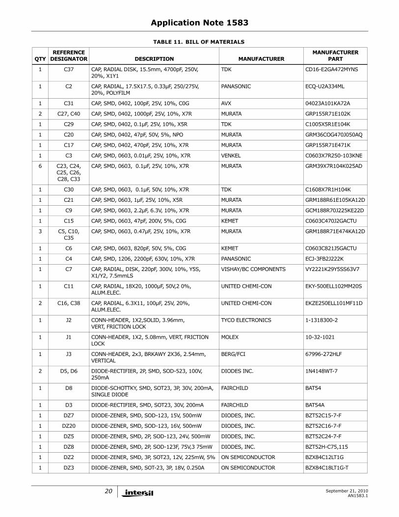
TABLE 11. BILL OF MATERIALS
QTYREFERENCE
DESIGNATOR DESCRIPTION MANUFACTURERMANUFACTURER
PART
1 C37 CAP, RADIAL DISK, 15.5mm, 4700pF, 250V,20%, X1Y1
TDK CD16-E2GA472MYNS
1 C2 CAP, RADIAL, 17.5X17.5, 0.33µF, 250/275V,20%, POLYFILM
PANASONIC ECQ-U2A334ML
1 C31 CAP, SMD, 0402, 100pF, 25V, 10%, C0G AVX 04023A101KA72A
2 C27, C40 CAP, SMD, 0402, 1000pF, 25V, 10%, X7R MURATA GRP155R71E102K
1 C29 CAP, SMD, 0402, 0.1µF, 25V, 10%, X5R TDK C1005X5R1E104K
1 C20 CAP, SMD, 0402, 47pF, 50V, 5%, NPO MURATA GRM36COG470J050AQ
1 C17 CAP, SMD, 0402, 470pF, 25V, 10%, X7R MURATA GRP155R71E471K
1 C3 CAP, SMD, 0603, 0.01µF, 25V, 10%, X7R VENKEL C0603X7R250-103KNE
6 C23, C24, C25, C26, C28, C33
CAP, SMD, 0603, 0.1µF, 25V, 10%, X7R MURATA GRM39X7R104K025AD
1 C30 CAP, SMD, 0603, 0.1µF, 50V, 10%, X7R TDK C1608X7R1H104K
1 C21 CAP, SMD, 0603, 1µF, 25V, 10%, X5R MURATA GRM188R61E105KA12D
1 C9 CAP, SMD, 0603, 2.2µF, 6.3V, 10%, X7R MURATA GCM188R70J225KE22D
1 C15 CAP, SMD, 0603, 47pF, 200V, 5%, C0G KEMET C0603C470J2GACTU
3 C5, C10, C35
CAP, SMD, 0603, 0.47µF, 25V, 10%, X7R MURATA GRM188R71E474KA12D
1 C6 CAP, SMD, 0603, 820pF, 50V, 5%, C0G KEMET C0603C821J5GACTU
1 C4 CAP, SMD, 1206, 2200pF, 630V, 10%, X7R PANASONIC ECJ-3FB2J222K
1 C7 CAP, RADIAL, DISK, 220pF, 300V, 10%, Y5S,X1/Y2, 7.5mmLS
VISHAY/BC COMPONENTS VY2221K29Y5SS63V7
1 C11 CAP, RADIAL, 18X20, 1000µF, 50V,2 0%, ALUM.ELEC.
UNITED CHEMI-CON EKY-500ELL102MM20S
2 C16, C38 CAP, RADIAL, 6.3X11, 100µF, 25V, 20%, ALUM.ELEC.
UNITED CHEMI-CON EKZE250ELL101MF11D
1 J2 CONN-HEADER, 1X2,SOLID, 3.96mm,VERT, FRICTION LOCK
TYCO ELECTRONICS 1-1318300-2
1 J1 CONN-HEADER, 1X2, 5.08mm, VERT, FRICTION LOCK
MOLEX 10-32-1021
1 J3 CONN-HEADER, 2x3, BRKAWY 2X36, 2.54mm,VERTICAL
BERG/FCI 67996-272HLF
2 D5, D6 DIODE-RECTIFIER, 2P, SMD, SOD-523, 100V,250mA
DIODES INC. 1N4148WT-7
1 D8 DIODE-SCHOTTKY, SMD, SOT23, 3P, 30V, 200mA,SINGLE DIODE
FAIRCHILD BAT54
1 D3 DIODE-RECTIFIER, SMD, SOT23, 30V, 200mA FAIRCHILD BAT54A
1 DZ7 DIODE-ZENER, SMD, SOD-123, 15V, 500mW DIODES, INC. BZT52C15-7-F
1 DZ20 DIODE-ZENER, SMD, SOD-123, 16V, 500mW DIODES, INC. BZT52C16-7-F
1 DZ5 DIODE-ZENER, SMD, 2P, SOD-123, 24V, 500mW DIODES, INC. BZT52C24-7-F
1 DZ8 DIODE-ZENER, SMD, 2P, SOD-123F, 75V,3 75mW DIODES, INC. BZT52H-C75,115
1 DZ2 DIODE-ZENER, SMD, 3P, SOT23, 12V, 225mW, 5% ON SEMICONDUCTOR BZX84C12LT1G
1 DZ3 DIODE-ZENER, SMD, SOT-23, 3P, 18V, 0.250A ON SEMICONDUCTOR BZX84C18LT1G-T
20 September 21, 2010AN1583.1
Application Note 1583
1 D4 DIODE-RECTIFIER, 4P, SMD, DF-S(8.5X6.5),1000V, 1A
DIODES, INC. DF10S
1 D7 DIODE-RECTIFIER, SMD, 2P, SMA, 500V, 1A FAIRCHILD ES1H
1 D2 DIODE-RECTIFIER, SMD, DPAK(TO252), 200V, 6A FAIRCHILD FFD06UP20S
1 D9 DIODE-SWITCHING, SMD, SOT-23, 100V, 250mA INFINEON TECHNOLOGY MMBD914LT1
1 D1 DIODE-RECTIFIER, SMD, 2P, SMA, 1000V, 1A, 1.4W FAIRCHILD S1M
1 L1 COIL-COMMON MODE CHOKE, TH, 6P, 100mH,CUSTOM
MAIN POWER ELECTRIC CO.,LTD J11-016-001
1 U3 IC-12MHz R/R OP AMP, 16P, QFN INTERSIL EL5420TILZ
1 U1 IC-BRIDGE CONTROLLER, 10P, MSOP INTERSIL ISL6745AAUZ
1 U4 IC-ADJ.ZENER SHUNT REGULATOR, SOT23, 2.5V NATIONAL SEMICONDUCTOR LM431BIM3/NOPB
1 U6 IC-ADJ.SHUNT REGULATOR, SMD, SOT-23-3,1.24V, 0.5%
NATIONAL SEMICONDUCTOR LMV431BIMF/NOPB
1 U2 IC-HI ISO PHOTOCOUPLER, 4P, SSOP CALIFORNIA EASTERNLABORATORIES
PS2801-1-A
1 Q3 TRANSIST-MOS, N-CHANNEL, TH, I-PAK, 400V, 2A FAIRCHILD FDU3N40TU
1 Q2 TRANSISTOR-QFET, N-CHANNEL, SMD, DPAK,600V, 1A
FAIRCHILD FQD1N60CTM
1 Q1 TRANSIST-MOS, N-CHANNEL, TH, TO-220FP,1000V, 6.5A
STMICROELECTRONICS STF8NK100Z
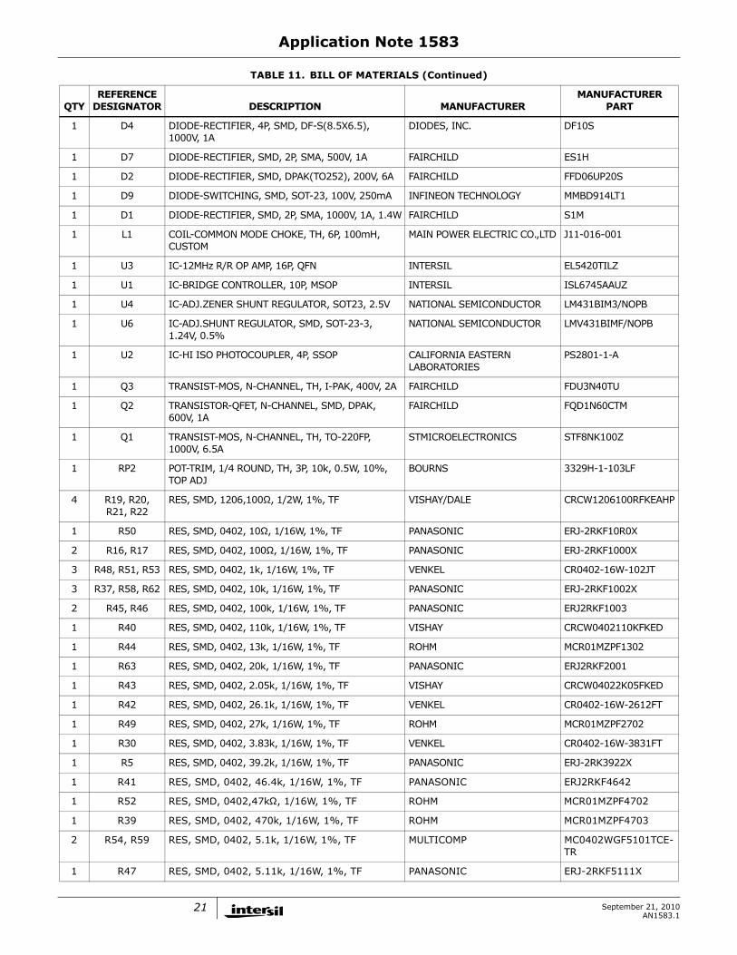
1 RP2 POT-TRIM, 1/4 ROUND, TH, 3P, 10k, 0.5W, 10%,TOP ADJ
BOURNS 3329H-1-103LF
4 R19, R20, R21, R22
RES, SMD, 1206,100Ω, 1/2W, 1%, TF VISHAY/DALE CRCW1206100RFKEAHP
1 R50 RES, SMD, 0402, 10Ω, 1/16W, 1%, TF PANASONIC ERJ-2RKF10R0X
2 R16, R17 RES, SMD, 0402, 100Ω, 1/16W, 1%, TF PANASONIC ERJ-2RKF1000X
3 R48, R51, R53 RES, SMD, 0402, 1k, 1/16W, 1%, TF VENKEL CR0402-16W-102JT
3 R37, R58, R62 RES, SMD, 0402, 10k, 1/16W, 1%, TF PANASONIC ERJ-2RKF1002X
2 R45, R46 RES, SMD, 0402, 100k, 1/16W, 1%, TF PANASONIC ERJ2RKF1003
1 R40 RES, SMD, 0402, 110k, 1/16W, 1%, TF VISHAY CRCW0402110KFKED
1 R44 RES, SMD, 0402, 13k, 1/16W, 1%, TF ROHM MCR01MZPF1302
1 R63 RES, SMD, 0402, 20k, 1/16W, 1%, TF PANASONIC ERJ2RKF2001
1 R43 RES, SMD, 0402, 2.05k, 1/16W, 1%, TF VISHAY CRCW04022K05FKED
1 R42 RES, SMD, 0402, 26.1k, 1/16W, 1%, TF VENKEL CR0402-16W-2612FT
1 R49 RES, SMD, 0402, 27k, 1/16W, 1%, TF ROHM MCR01MZPF2702
1 R30 RES, SMD, 0402, 3.83k, 1/16W, 1%, TF VENKEL CR0402-16W-3831FT
1 R5 RES, SMD, 0402, 39.2k, 1/16W, 1%, TF PANASONIC ERJ-2RK3922X
1 R41 RES, SMD, 0402, 46.4k, 1/16W, 1%, TF PANASONIC ERJ2RKF4642
1 R52 RES, SMD, 0402,47kΩ, 1/16W, 1%, TF ROHM MCR01MZPF4702
1 R39 RES, SMD, 0402, 470k, 1/16W, 1%, TF ROHM MCR01MZPF4703
2 R54, R59 RES, SMD, 0402, 5.1k, 1/16W, 1%, TF MULTICOMP MC0402WGF5101TCE-TR
1 R47 RES, SMD, 0402, 5.11k, 1/16W, 1%, TF PANASONIC ERJ-2RKF5111X
TABLE 11. BILL OF MATERIALS (Continued)
QTYREFERENCE
DESIGNATOR DESCRIPTION MANUFACTURERMANUFACTURER
PART
21 September 21, 2010AN1583.1
Application Note 1583
0 R61 RES,SMD,0402, DNP, DNP, DNP, TF
1 R18 RES, SMD, 0603, 10Ω, 1/10W, 1%, TF KOA RK73H1JT10R0F
1 R60 RES, SMD, 0603, 10k, 1/10W, 1%, TF KOA RK73H1JT1002F
2 R23, R29 RES, SMD, 0603, 39k, 1/10W, 1%, TF PANASONIC ERJ-3EKF3902V
1 R11 RES, SMD, 0805, 10Ω, 1/8W, 1%, TF VENKEL CR0805-8W-10R0FT
1 R13 RES, SMD, 0805, 0Ω, 1/8W, TF YAGEO RC0805JR-070RL
0 R14, R15 RES, SMD, 0805, DNP-PLACE HOLDER
2 R12, R55 RES, SMD, 1206, 10Ω, 1/4W, 1%, TF VENKEL CR1206-4W-10R0FT
1 R8 RES, SMD, 1206, 0Ω, 1/4W, TF VISHAY CRCW1206-000Z
2 R9,R10 RES, SMD, 1206, 1M, 1/4W, 1%, TF VENKEL CR1206-4W-1004FT
4 R2', R2, R3', R3
RES, SMD, 1206, 300k, 1/4W, 1%, TF YAGEO RC1206FR-07300KL
2 R26,R27 RES,SMD,1206, 49.9k,1/4W,1%,TF VENKEL CR1206-4W-4992FT
1 R35 RES, SMD, 2512, 0.18Ω, 1W, 1%, TF ROHM MCR100JZHFLR180
1 R4 RES, SMD, 2512, 0.36Ω,1W, 1%, TF VENKEL CR2512-1W-R360FT
2 R24,R25 RES, AXIAL, 27Ω, 2W, 5%, MOF YAGEO RSF200JB-27R
2 R6,R7 RES, AXIAL, 100Ω, 2W, 5%, MOF PANASONIC ERG-2SJ101A
1 F1 FUSE-TIME-LAG, TH, 8.5X8.0, 1.60A, 250V, 601mW
LITTELFUSE 40011600440
1 C1 CAP-EMI, RADIAL, 10.5X18, 0.1µF, 305V, 20%, 15mmLS
EPCOS, INC B32922C3104M
1 RT1 THERMISTOR-NTC, SMD, 0805, 22k, 5%, 210mW
EPCOS, INC B57620C0223J062
1 RV1 TVS-VARISTOR, TYPE D, RADIAL, 14mm, 390V, 4500A
PANASONIC ERZV14D391
1 T1 TRANSFORMER, TH, 23.5x20.3, 14P, 4 50µH, 5%, CUSTOM
COILCRAFT CN7225-AL
TABLE 11. BILL OF MATERIALS (Continued)
QTYREFERENCE
DESIGNATOR DESCRIPTION MANUFACTURERMANUFACTURER
PART
22 September 21, 2010AN1583.1
Application Note 1583
Intersil Corporation reserves the right to make changes in circuit design, software and/or specifications at any time without notice. Accordingly, thereader is cautioned to verify that the Application Note or Technical Brief is current before proceeding.
For information regarding Intersil Corporation and its products, see www.intersil.com
Configuration Tables
Low Line Version
TABLE 12. SELECT MAXIMUM OUTPUT VOLTAGE
16V 32V 48V
NUMBER OF LEDS 3, 4 5, 6, 7, 8 9, 10, 11, 12
C11 3300µF/16V 1800µF/35V 1000µF/50V
VENDOR Nichicon Panasonic-ECG United Chemi-Con
PART # NichiconUPW1C392MHD6
orPanasonic-ECGEEU-FC1C392S
1800µF/35VPanasonic-ECGEEU-FC1V182S
United Chemi-ConEKY-500ELL102MM20S
INTERNAL PART # (N/A) (N/A) (N/A)
R47 15k(19.2V) 6.8k(39.3) 5.11k(51.4V)
VENDOR Panasonic-ECG Panasonic-ECG Panasonic-ECG
PART # ERJ-2RKF1502X ERJ-2RKF6801X ERJ-2RKF5111X
INTERNAL PART # H2510-01502-1/16W1 H2510-06801-1/16W1 H2510-05111-1/16W1
R13 Open Open Shorted
R14 Open Shorted Open
R15 Shorted Open Open
TABLE 13. PROGRAM THE OUTPUT CURRENT
350mA 500mA 700mA 1.05A
J3 1, 3 2, 4 3, 5 4, 6
TABLE 14. ADJUST THE RP2 FOR DIFFERENT VO AND IO COMBINATION
350mA 500mA 700mA 1050mA
16V Depending on the VO and IO, Adjust RP2 so that the output current can not be greater than the set value unless the input is equal to, or greater than, nominal line voltage (220 or 230 V).
32V
48V
TABLE 15. CHANGE FOR LOW LINE VERSION
LOW LINE VERSION(THE PARAMETERS NEED
MORE TEST FOR VERIFYING)
HIGH LINE VERSION
T1 For Pin 1~4:Pin 1, 2 connected; Pin 3, 4 connected.
For Pin 1~4: Pin 2, 3 connected.
R29 100k 30k
DZ8 0V (shorted) 75V
R6, R7 43Ω/2W, 100Ω/2W
R24, R25
5.6Ω/3W for Rev.D16Ω/2W for Rev.B
27Ω/2W for Rev.D36Ω/1W for Rev.B
R4 0.18Ω 0.36Ω
C1 220nF for Rev.D100nF for Rev.B
100nF
C2 680nF for Rev.D220nF for Rev.B
100nF for Rev.D330nF for Rev.B
23 September 21, 2010AN1583.1