r8a66593fp/bg datasheet - renesas
TRANSCRIPT
Datasheet R8A66593FP/BG ASSP (USB2.0 Peripheral Controller)
R19DS0071EJ0101 Rev1.01 Page 1 of 142 Jun 28,2013
R19DS0071EJ0101 Rev1.01
Jun 28,2013
1 Overview 1.1 Overview
The R8A66593 is a Universal Serial Bus (USB) Peripheral Controller that is compliant with USB Specification Revision 2.0 for Hi-Speed and Full-Speed transfer. This controller has a built-in USB transceiver and is compatible with all the transfer types defined in USB Specification Revision 2.0. The internal buffer memory is 8.5K, and a maximum ten pipes can be used for transferring data. For Pipe1 to Pipe9, any endpoint address can be assigned matching user system. Separate bus or multiplex bus can be selected for the CPU connection. A split bus interface (exclusively for the DMA interface) that is different from the CPU bus interface is provided and is suitable for systems demanding high-performance data transfer.
1.2 Features
1.2.1 USB Rev2.0 Hi-speed supported • Complient with USB specification Rev. 2.0 • Both Hi-Speed transfer(480Mbs)and Full-Speed transfer(12Mbps) are supported • Built-in Hi-Speed / Full-Speed USB transceiver • Can be operated as a Hi-Speed / Full-Speed USB Peripheral Controller
1.2.2 Low power consumption • 1.5V core power consumes less power when operating • With the installed Low Power Sleep Mode functions, less power is consumed when the USB is not in use, which is
also applicable for portable devices • Standby power consumption can be greatly reduced by keeping only the VIF power source ON when not using the
USB function. • Operational with a 3.3V single power supply using the internal 1.5V core power regulator
1.2.3 Space-saving package • Few external devices and space-saving package VBUS signal can be connected directly to the controller input pin Built-in D+ pull-up resistor Built-in D+ and D- terminating resistors (for Hi-Speed operations) Built-in D+ and D- output resistors (for Full-Speed operations)
R8A66593FP/BG
R19DS0071EJ0101 Rev1.01 Page 2 of 142 Jun 28,2013
1.2.4 Compatible with all USB transfer types • Compatible with all USB transfer types, including isochronous transfer Control transfer Bulk transfer Interrupt transfer (not compatible with high-bandwidth) Isochronous transfer (not compatible with high-bandwidth)
1.2.5 Bus interface • The user can select either a 1.8V or 3.3V bus interface power • 16-bit CPU bus interface
Compatible with 16-bit separate bus/16-bit multiplex bus Compatible with DMA transfer in 8-bit/16-bit access (slave function)
• 8-bit split bus (exclusive for external direct memory access controller (DMAC)) interface • Built-in two DMA interface channels • DMA transfer provides 40MB/second high-performance data transfer
1.2.6 Pipe configuration • Built-in 8.5KB buffer memory for USB communication • Maximum of ten pipes can be selected (including default control pipe) • Programmable pipe configuration • Any endpoint address can be assigned to Pipe1 to Pipe9 • Transfer conditions that can be written for each pipe Pipe0: Control transfer, single buffer fixed at 256 bytes Pipe1~Pipe2: Bulk transfer/Isochronous transfer, continuous transfer modes.
programmable buffer size (specifiable up to 2K bytes per side, double buffer also specifiable) Pipe3~Pipe5: Bulk transfer, continuous transfer modes,
programmable buffer size (specifiable up to 2K bytes per side, double buffer also specifiable) Pipe6~Pipe9: Interrupt transfer, single buffer fixed at 64 bytes
1.2.7 Other functions • Auto identification of Hi-Speed or Full-Speed operations according to reset handshake auto response • Compatible with the CPU of big-endian or little-endian according to the byte-endian swap function
This function can be set against each FIFO Port • Transfer end function according to transaction count
This function can be set against each Pipe. • End function of DMA transfer by external trigger (DEND pin) • Control transfer stage management function • Device state management function • Auto response function related to SET_ADDRESS request • NAK response interrupt function (NRDY) • SOF interpolation function • SOF plus output function • Three types of input clock can be selected by built-in PLL
Select from 48MHz/24MHz/12MHz • Function to modify the BRDY interrupt event notification timing (BFRE) • Function to clear the auto buffer memory after the pipe data specified in the DxFIFO port is read (DCLRM) • Function to provide the auto clock from clock stop status • NAK setting function (SHTNAK) for PID response corresponding to transfer end
1.2.8 Applications Digital video cameras, digital still cameras, printers, external storage devices, portable information terminals,
USB audio devices Also: GeneralOrdinary PC peripheral devices equipped with Hi-Speed USB
R8A66593FP/BG
R19DS0071EJ0101 Rev1.01 Page 3 of 142 Jun 28,2013
1.3 Package
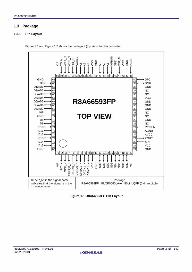
1.3.1 Pin Layout Figure 1.1 and Figure 1.2 shows the pin layout (top view) for this controller.
60 59 58 57 56 55 54 53 52 51 50 49 48 47 46 45 44 43 42 4161 40 DP062 39 DM063 38 GND64 37 NC65 36 NC66 35 VCC67 34 GND68 33 GND69 32 GND70 31 NC71 30 NC72 29 GND73 28 NC74 27 REFRIN75 26 AGND76 25 AVCC77 24 XOUT78 23 XIN79 22 VCC80 21 GND
1 2 3 4 5 6 7 8 9 10 11 12 13 14 15 16 17 18 19 20
R8A66593FP
DAC
K0_N
DEN
D0_
ND
REQ
1_N
DAC
K1_N
TOP VIEW
VIF
INT_
NSO
F_N
DR
EQ0_
N
VCC
GN
DVB
US
GND
A3 A2 A1 MPB
US
A4 VDD
D5/AD5D6/AD6
D13D14
D7/AD7VIF
GNDD8
D15GND
D9D10D11D12
D0D1/AD1D2/AD2
SD5
DEN
D1_
NVD
DG
ND
SD0
D3/AD3D4/AD4
SD6
SD7
VIF
SD1
SD2
SD3
SD4
GN
D
GN
DR
ST_N
RD
_NA7
/ALE
A6 A5VIF
CS_
NW
R1_
NW
R0_
N
Figure 1.1 R8A66593FP Pin Layout
The “_N” in the signal name indicates that the signal is in the “L” active state.
Package R8A66593FP : PLQP0080LA-A : 80pinLQFP (0.4mm pitch)
R8A66593FP/BG
R19DS0071EJ0101 Rev1.01 Page 4 of 142 Jun 28,2013
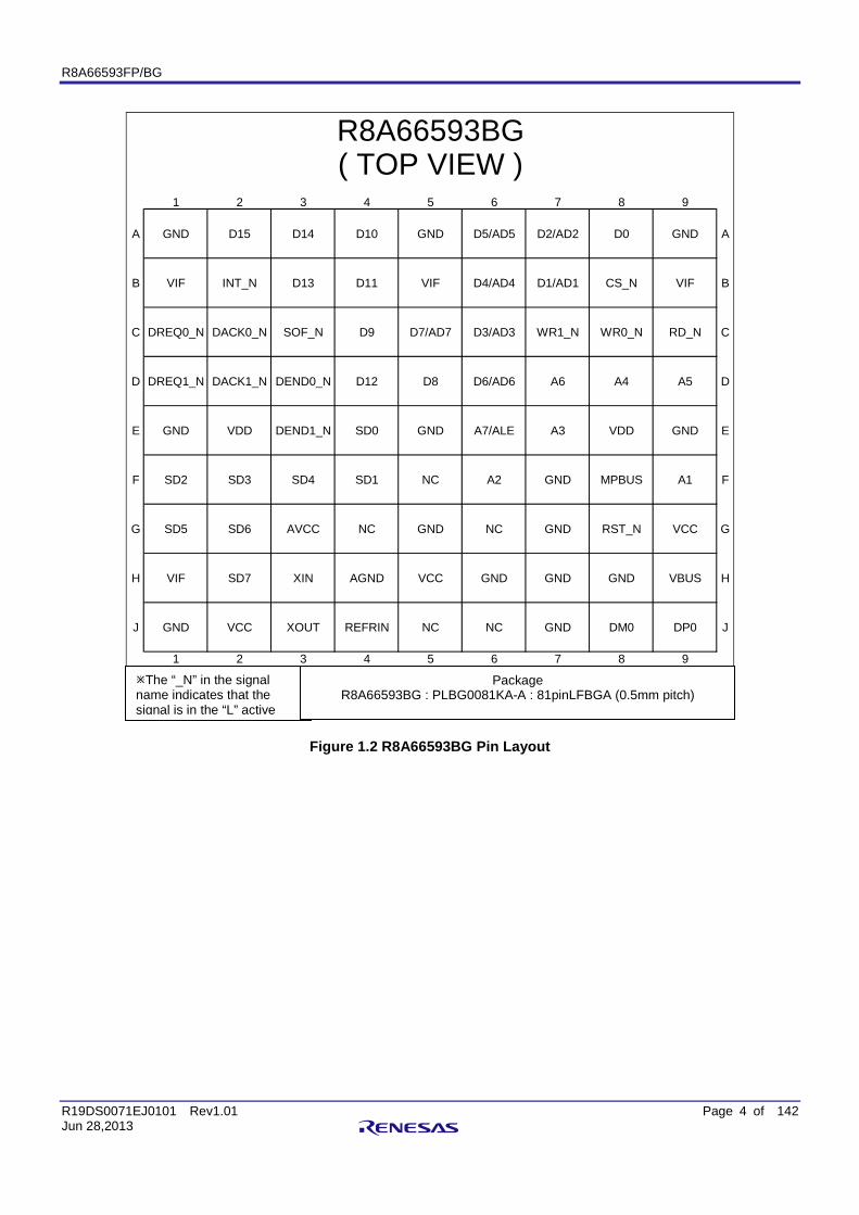
1 2 3 4 5 6 7 8 9
A GND D15 D14 D10 GND D5/AD5 D2/AD2 D0 GND A
B VIF INT_N D13 D11 VIF D4/AD4 D1/AD1 CS_N VIF B
C DREQ0_N DACK0_N SOF_N D9 D7/AD7 D3/AD3 WR1_N WR0_N RD_N C
D DREQ1_N DACK1_N DEND0_N D12 D8 D6/AD6 A6 A4 A5 D
E GND VDD DEND1_N SD0 GND A7/ALE A3 VDD GND E
F SD2 SD3 SD4 SD1 NC A2 GND MPBUS A1 F
G SD5 SD6 AVCC NC GND NC GND RST_N VCC G
H VIF SD7 XIN AGND VCC GND GND GND VBUS H
J GND VCC XOUT REFRIN NC NC GND DM0 DP0 J
1 2 3 4 5 6 7 8 9
R8A66593BG( TOP VIEW )
Figure 1.2 R8A66593BG Pin Layout
The “_N” in the signal name indicates that the signal is in the “L” active
Package R8A66593BG : PLBG0081KA-A : 81pinLFBGA (0.5mm pitch)
R8A66593FP/BG
R19DS0071EJ0101 Rev1.01 Page 5 of 142 Jun 28,2013
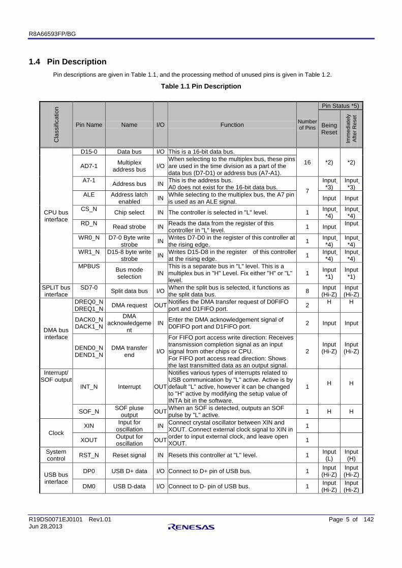
1.4 Pin Description Pin descriptions are given in Table 1.1, and the processing method of unused pins is given in Table 1.2.
Table 1.1 Pin Description
Cla
ssifi
catio
n
Pin Name Name I/O Function Number of Pins
Pin Status *5)
Being Reset
Imm
edia
tely
A
fter R
eset
CPU bus interface
D15-0 Data bus I/O This is a 16-bit data bus.
16 *2) *2) AD7-1 Multiplex address bus I/O
When selecting to the multiplex bus, these pins are used in the time division as a part of the data bus (D7-D1) or address bus (A7-A1).
A7-1 Address bus IN This is the address bus. A0 does not exist for the 16-bit data bus. 7
Input *3)
Input *3)
ALE Address latch enabled IN While selecting to the multiplex bus, the A7 pin
is used as an ALE signal. Input Input
CS_N Chip select IN The controller is selected in "L" level. 1 Input *4)
Input *4)
RD_N Read strobe IN Reads the data from the register of this controller in "L" level. 1 Input Input
WR0_N D7-0 Byte write
strobe IN Writes D7-D0 in the register of this controller at the rising edge. 1 Input
*4) Input *4)
WR1_N D15-8 byte write strobe IN Writes D15-D8 in the register of this controller
at the rising edge. 1 Input *4)
Input *4)
MPBUS Bus mode selection IN
This is a separate bus in "L" level. This is a multiplex bus in "H" Level. Fix either "H" or "L" level.
1 Input *1)
Input *1)
SPLIT bus interface
SD7-0 Split data bus I/O When the split bus is selected, it functions as the split data bus. 8 Input
(Hi-Z) Input (Hi-Z)
DMA bus interface
DREQ0_N DREQ1_N DMA request OUT Notifies the DMA transfer request of D0FIFO
port and D1FIFO port. 2 H
H
DACK0_N DACK1_N
DMA acknowledgeme
nt IN Enter the DMA acknowledgement signal of
D0FIFO port and D1FIFO port. 2 Input Input
DEND0_N DEND1_N
DMA transfer end I/O
For FIFO port access write direction: Receives transmission completion signal as an input signal from other chips or CPU. For FIFO port access read direction: Shows the last transmitted data as an output signal.
2 Input (Hi-Z)
Input (Hi-Z)
Interrupt/ SOF output
INT_N Interrupt OUT
Notifies various types of interrupts related to USB communication by "L" active. Active is by default "L" active, however it can be changed to "H" active by modifying the setup value of INTA bit in the software.
1 H
H
SOF_N SOF pluse output OUT When an SOF is detected, outputs an SOF
pulse by "L" active. 1 H H
Clock XIN Input for
oscillation IN Connect crystal oscillator between XIN and XOUT. Connect external clock signal to XIN in order to input external clock, and leave open XOUT.
1
XOUT Output for oscillation OUT 1
System control RST_N Reset signal IN Resets this controller at "L" level. 1 Input
(L) Input (H)
USB bus interface
DP0 USB D+ data I/O Connect to D+ pin of USB bus. 1 Input (Hi-Z)
Input (Hi-Z)
DM0 USB D-data I/O Connect to D- pin of USB bus. 1 Input (Hi-Z)
Input (Hi-Z)
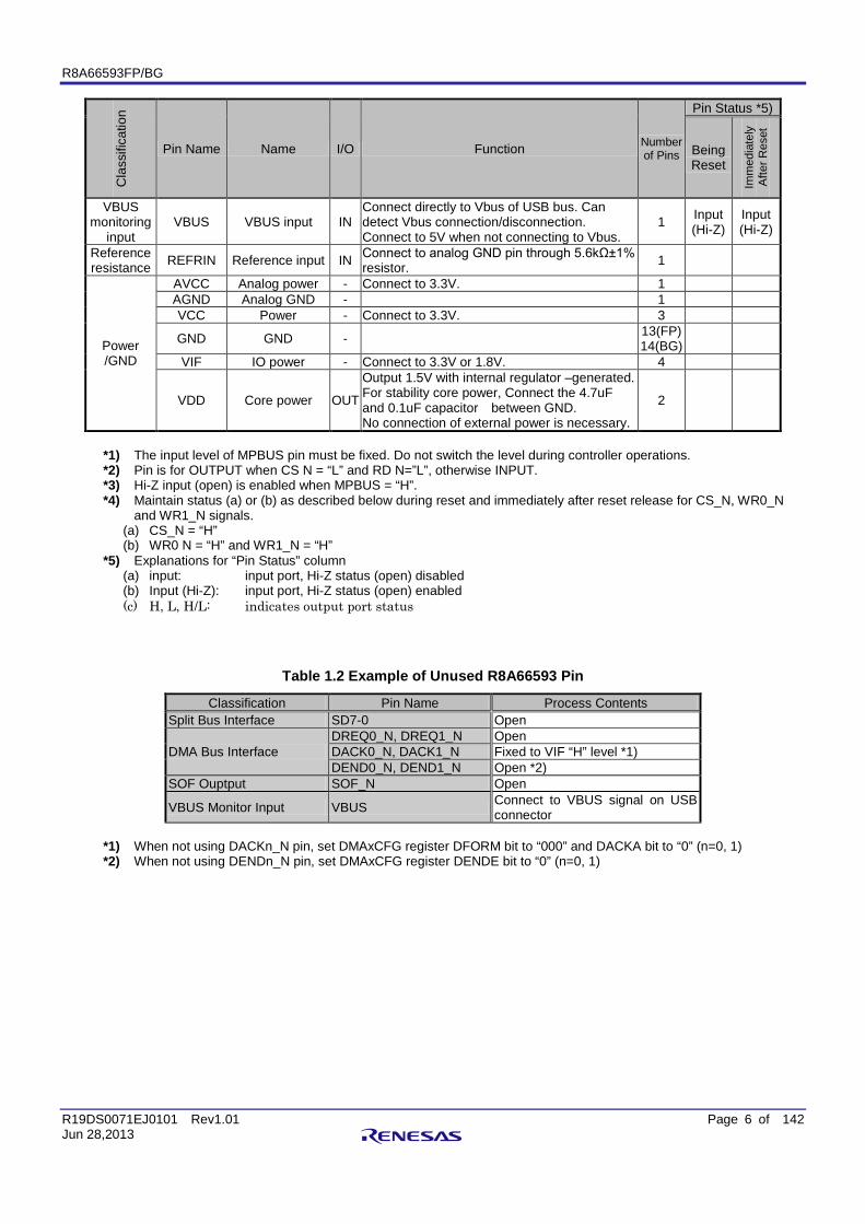
R8A66593FP/BG
R19DS0071EJ0101 Rev1.01 Page 6 of 142 Jun 28,2013
Cla
ssifi
catio
n
Pin Name Name I/O Function Number of Pins
Pin Status *5)
Being Reset
Imm
edia
tely
A
fter R
eset
VBUS monitoring
input VBUS VBUS input IN
Connect directly to Vbus of USB bus. Can detect Vbus connection/disconnection. Connect to 5V when not connecting to Vbus.
1 Input (Hi-Z)
Input (Hi-Z)
Reference resistance REFRIN Reference input IN Connect to analog GND pin through 5.6kΩ±1%
resistor. 1
Power /GND
AVCC Analog power - Connect to 3.3V. 1 AGND Analog GND - 1 VCC Power - Connect to 3.3V. 3
GND GND - 13(FP) 14(BG)
VIF IO power - Connect to 3.3V or 1.8V. 4
VDD Core power OUT
Output 1.5V with internal regulator –generated. For stability core power, Connect the 4.7uF and 0.1uF capacitor between GND. No connection of external power is necessary.
2
*1) The input level of MPBUS pin must be fixed. Do not switch the level during controller operations. *2) Pin is for OUTPUT when CS N = “L” and RD N=”L”, otherwise INPUT. *3) Hi-Z input (open) is enabled when MPBUS = “H”. *4) Maintain status (a) or (b) as described below during reset and immediately after reset release for CS_N, WR0_N
and WR1_N signals. (a) CS_N = “H” (b) WR0 N = “H” and WR1_N = “H”
*5) Explanations for “Pin Status” column (a) input: input port, Hi-Z status (open) disabled (b) Input (Hi-Z): input port, Hi-Z status (open) enabled (c) H, L, H/L: indicates output port status
Table 1.2 Example of Unused R8A66593 Pin
Classification Pin Name Process Contents Split Bus Interface SD7-0 Open
DMA Bus Interface DREQ0_N, DREQ1_N Open DACK0_N, DACK1_N Fixed to VIF “H” level *1) DEND0_N, DEND1_N Open *2)
SOF Ouptput SOF_N Open
VBUS Monitor Input VBUS Connect to VBUS signal on USB connector
*1) When not using DACKn_N pin, set DMAxCFG register DFORM bit to “000” and DACKA bit to “0” (n=0, 1) *2) When not using DENDn_N pin, set DMAxCFG register DENDE bit to “0” (n=0, 1)
R8A66593FP/BG
R19DS0071EJ0101 Rev1.01 Page 7 of 142 Jun 28,2013
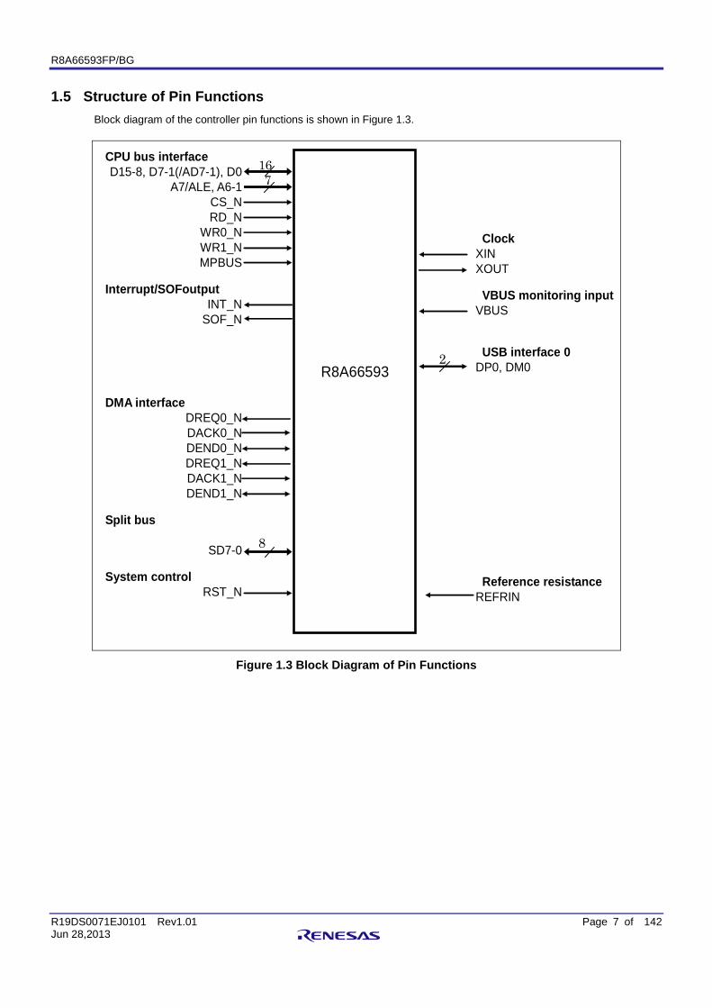
1.5 Structure of Pin Functions Block diagram of the controller pin functions is shown in Figure 1.3.
CPU bus interface D15-8, D7-1(/AD7-1), D0
A7/ALE, A6-1 CS_N RD_N
WR0_N WR1_N MPBUS
Interrupt/SOFoutput INT_N
SOF_N
DMA interface DREQ0_N DACK0_N DEND0_N DREQ1_N DACK1_N DEND1_N
Split bus
SD7-0
System control RST_N
16 7
Clock XIN XOUT
VBUS monitoring input VBUS
USB interface 0 DP0, DM0
Reference resistance REFRIN
R8A66593
8
2
Figure 1.3 Block Diagram of Pin Functions
R8A66593FP/BG
R19DS0071EJ0101 Rev1.01 Page 8 of 142 Jun 28,2013
1.6 Functional Overview
1.6.1 Bus interface The controller is compatible with the bus interfaces given below.
1.6.1.1 External bus interface
The CPU accesses the control register of the controller using the CPU bus interface. There are two types of access below for the bus interface from the CPU. Access using a chip select pin (CS_N) and three strobe pins (RD_N, WR0_N and WR1_N). (1)16-bit separate bus
Seven address buses (A7-1) and sixteen data buses (D15-0) are used. (2)16-bit multiplex bus
The ALE pin (ALE) and sixteen data buses (D15-0) are used. The data bus uses the address and data in the time division.
Separate bus or multiplex bus are selected at the MPBUS pin signal level while canceling the hardware reset.
1.6.1.2 FIFO buffer memory access method
This controller is compatible with the following two access types as an access method of the FIFO buffer memory for USB data transmission. Read (write) of the data from the FIFO buffer memory is possible by accessing (read/write) the FIFO port from the CPU (DMAC). (1) CPU access
Write the data in, or read the data from, the FIFO buffer memory using the address signal and control signal. (2) DMA access
Write the data in the FIFO buffer memory from the CPU’s built-in DMAC or dedicated DMAC, or read the data from the FIFO buffer memory.
USB communication is executed by a little endian. A byte endian swap function is provided in the FIFO port access. For 16-bit access, the endian can be changed according to what is written to the register.
1.6.1.3 FIFO buffer memory access method from DMAC
To access the FIFO buffer memory through the DMA access, select an access method from the following: (1) Method of using common bus with CPU (2) Method in which dedicated bus (split bus) is used
1.6.2 USB event The controller notifies the events regarding USB operations to the user system through the interrupt. It also notifies that the DMA interface can access the buffer memory of the selected pipe by asserting the DREQ signal. Depending on what the software writes, interrupt notification activation can be selected for the type and factor.
R8A66593FP/BG
R19DS0071EJ0101 Rev1.01 Page 9 of 142 Jun 28,2013
1.6.3 USB data transfer All types of data transfer of USB communication, such as control transfer, bulk transfer, interrupt transfer and isochronous transfer, are possible with this controller. The following are the pipe resources for each transfer type: (1) Control transfer dedicated pipe - 1 (2) Interrupt transfer dedicated pipes - 4 (3) Bulk transfer dedicated pipes - 3 (4) Bulk transfer or isochronous transfer selection pipes - 2
Write the USB transfer requirements for each pipe, such as transfer type, endpoint address, maximum packet size, etc., according to the user system. This controller is equipped with an 8.5KB buffer memory. Allocate the buffer memory according to the user system or execute the settings such as buffer operation mode, for the bulk transfer dedicated pipe, and bulk transfer or isochronous transfer selection pipe. In buffer operations mode, high-performance data transfer with low interrupt frequency is possible by using a double buffer configuration or continuous transfer function of the data packet. A transfer completion function has been added, using the transaction counter function for efficient data transfer rates of bulk and isochronous transfer pipes. The user system control CPU and DMA controller access the buffer memory through three FIFO port registers.
1.6.4 Interface for access from DMAC The DMA interface is the data transfer between the user system and this controller, in which the DxFIFO port is used, and it is a data transfer that does not use the CPU. This controller is equipped with 2-ch DMA interface and includes the following functions: (1) Transfer end notification function corresponding to the transfer end signal (DEND signal) (2) FIFO buffer auto clear function while receiving a zero-length packet
This controller is equipped with an interface compatible with the two types of DMA transfers given below: (1) Cycle Steal Transfer
Assert and negate of the DREQ pin is repeatedly transmitted for one data transmission (1 byte/1 word). (2) Burst Transmission
This is a transmission in which the DREQ pin is asserted (not negated) until the transmission is completed, due to the pipe buffer memory area allocated to the FIFO port or DEND signal.
"CS_N, RD_N and WR_N" or DACK_N can be selected as the handshake signal (pin) of the DMA interface. High-performance DMA transmission is possible in the DMA transmission by a split bus by modifying the data setup timing using an OBUS bit operation of the DMAxCFG register.
1.6.5 SOF pulse output function This controller is equipped with an SOF pulse output function that notifies the SOF packet send/receive timing. A pulse is output from the SOF_N pin at receiving the SOF packet. When the SOF packet is damaged, a pulse is output within the specified period according to the SOF interpolation timer.
R8A66593FP/BG
R19DS0071EJ0101 Rev1.01 Page 10 of 142 Jun 28,2013
1.6.6 Importing the external devices This controller is equipped with the external devices listed below. Also, as the VBUS pin has 5V-tolerant, the user system can connect the VBUS signal directly to this controller. (1) Resistors necessary in D+ and D-line control
The following D+ and D- resistors necessary for USB communication are installed: D+ pull-up resistor D+ and D- termination resistors (for Hi-Speed operations) D+ and D- output resistors (for Full-Speed operations)
(2) 48MHz and 480MHz PLL Operations can be executed by selecting one of the three types of external clocks (12MHz/24MHz/48MHz).
(3) 3.3V → 1.5V regulator 1.5V core power is generated in this controller. In the system where a 3.3V interface power is used, this controller can be operated on a single power supply.
R8A66593FP/BG
R19DS0071EJ0101 Rev1.01 Page 11 of 142 Jun 28,2013
2 Register
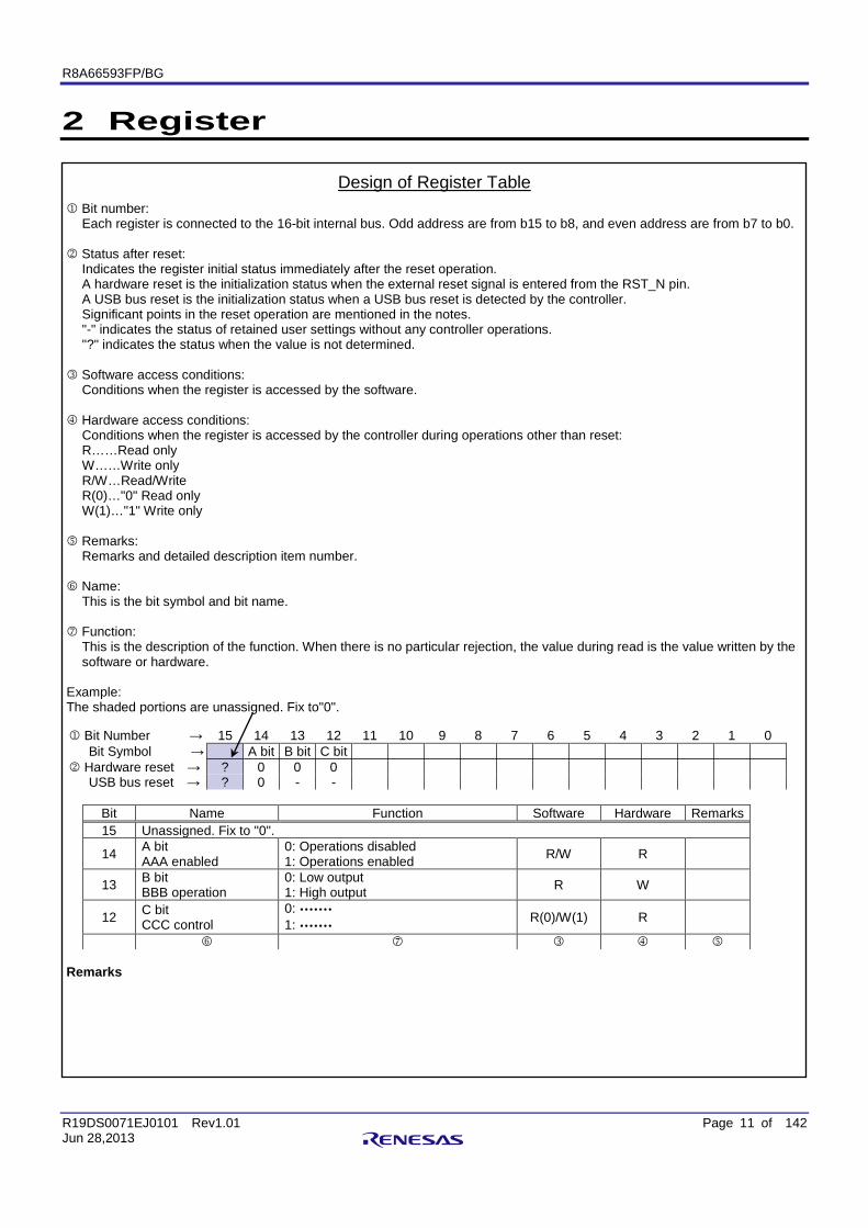
Design of Register Table
Bit number: Each register is connected to the 16-bit internal bus. Odd address are from b15 to b8, and even address are from b7 to b0.
Status after reset:
Indicates the register initial status immediately after the reset operation. A hardware reset is the initialization status when the external reset signal is entered from the RST_N pin. A USB bus reset is the initialization status when a USB bus reset is detected by the controller. Significant points in the reset operation are mentioned in the notes. "-" indicates the status of retained user settings without any controller operations. "?" indicates the status when the value is not determined.
Software access conditions:
Conditions when the register is accessed by the software. Hardware access conditions:
Conditions when the register is accessed by the controller during operations other than reset: R……Read only W……Write only R/W…Read/Write R(0)…"0" Read only W(1)…"1" Write only
Remarks:
Remarks and detailed description item number. Name:
This is the bit symbol and bit name. Function:
This is the description of the function. When there is no particular rejection, the value during read is the value written by the software or hardware.
Example: The shaded portions are unassigned. Fix to"0".
Bit Number → 15 14 13 12 11 10 9 8 7 6 5 4 3 2 1 0 Bit Symbol → A bit B bit C bit
Hardware reset → ? 0 0 0 USB bus reset → ? 0 - -
Bit Name Function Software Hardware Remarks 15 Unassigned. Fix to "0".
14 A bit AAA enabled
0: Operations disabled 1: Operations enabled
R/W R
13 B bit BBB operation
0: Low output 1: High output
R W
12 C bit CCC control
0: 1:
R(0)/W(1) R
Remarks
R8A66593FP/BG
R19DS0071EJ0101 Rev1.01 Page 12 of 142 Jun 28,2013
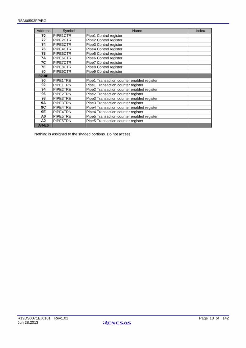
2.1 Register List The controller register list is shown in Table 2.1.
Table 2.1 Register List
Address Symbol Name Index 00 SYSCFG0 System configuration control register 0 02 SYSCFG1 System configuration control register 1 04 SYSSTS0 System configuration status register 0 06 08 DVSTCTR0 Device control register 0 0A 0C TESTMODE Test mode register 0E PINCFG Data pin configuration register 10 DMA0CFG DMA0 Pin configuration register 12 DMA1CFG DMA1 Pin configuration register 14 CFIFO CFIFO Port register 16 18 D0FIFO D0FIFO Port register 1A 1C D1FIFO D1FIFO Port register 1E 20 CFIFOSEL CFIFO Port selection register 22 CFIFOCTR CFIFO Port control register 24 26 28 D0FIFOSEL D0FIFO Port selection register 2A D0FIFOCTR D0FIFO Port control register 2C D1FIFOSEL D1FIFO Port selection register 2E D1FIFOCTR D1FIFO Port control register 30 INTENB0 Interrupt enable register 0 32 34 36 BRDYENB BRDY Interrupt enable register 38 NRDYENB NRDY Interrupt enable register 3A BEMPENB BEMP Interrupt enable register 3C SOFCFG SOF Output configuration register 3E 40 INTSTS0 Interrupt status register0 42 44 46 BRDYSTS BRDY Interrupt status register 48 NRDYSTS NRDY Interrupt status register 4A BEMPSTS BEMP Interrupt status register 4C FRMNUM Frame number register 4E UFRMNUM Microframe number register 50 USBADDR USB address register 52 54 USBREQ USB request type register 56 USBVAL USB request value register 58 USBINDX USB request index register 5A USBLENG USB request length register 5C DCPCFG DCP configuration register 5E DCPMAXP DCP maximum packet size register 60 DCPCTR DCP control register 62 64 PIPESEL Pipe window selection register 66 68 PIPECFG Pipe configuration register 6A PIPEBUF Pipe buffer specification register 6C PIPEMAXP Pipe maximum packet size register 6E PIPEPERI Pipe period control register
R8A66593FP/BG
R19DS0071EJ0101 Rev1.01 Page 13 of 142 Jun 28,2013
Address Symbol Name Index 70 PIPE1CTR Pipe1 Control register 72 PIPE2CTR Pipe2 Control register 74 PIPE3CTR Pipe3 Control register 76 PIPE4CTR Pipe4 Control register 78 PIPE5CTR Pipe5 Control register 7A PIPE6CTR Pipe6 Control register 7C PIPE7CTR Pipe7 Control register 7E PIPE8CTR Pipe8 Control register 80 PIPE9CTR Pipe9 Control register
82-8E 90 PIPE1TRE Pipe1 Transaction counter enabled register 92 PIPE1TRN Pipe1 Transaction counter register 94 PIPE2TRE Pipe2 Transaction counter enabled register 96 PIPE2TRN Pipe2 Transaction counter register 98 PIPE3TRE Pipe3 Transaction counter enabled register 9A PIPE3TRN Pipe3 Transaction counter register 9C PIPE4TRE Pipe4 Transaction counter enabled register 9E PIPE4TRN Pipe4 Transaction counter register A0 PIPE5TRE Pipe5 Transaction counter enabled register A2 PIPE5TRN Pipe5 Transaction counter register
A4-E6
Nothing is assigned to the shaded portions. Do not access.
R8A66593FP/BG
R19DS0071EJ0101 Rev1.01 Page 14 of 142 Jun 28,2013
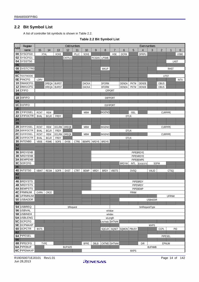
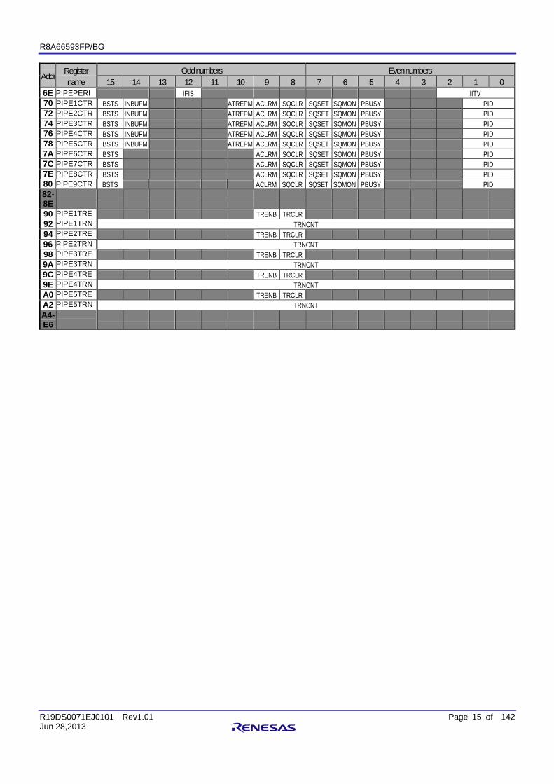
2.2 Bit Symbol List A list of controller bit symbols is shown in Table 2.2.
Table 2.2 Bit Symbol List
Addr Register name
Odd numbers Even numbers 15 14 13 12 11 10 9 8 7 6 5 4 3 2 1 0
00 SYSCFG0 XTAL XCKE PLLC SCKE HSE DCFM DPRPU USBE 02 SYSCFG1 CNTFLG PCSDIS LPSME 04 SYSSTS0 LNST 06 08 DVSTCTR0 WKUP RHST 0A 0C TESTMODE UTST 0E PINCFG LDRV INTA 10 DMA0CFG DREQA BURST DACKA DFORM DENDA PKTM DENDE OBUS 12 DMA1CFG DREQA BURST DACKA DFORM DENDA PKTM DENDE OBUS 14 CFIFO CFPORT 16 18 D0FIFO D0FPORT 1A 1C D1FIFO D1FIPORT 1E 20 CFIFOSEL RCNT REW MBW BIGEND ISEL CURPIPE 22 CFIFOCTR BVAL BCLR FRDY DTLN 24 26 28 D0FIFOSEL RCNT REW DCLRM DREQE MBW BIGEND CURPIPE 2A D0FIFOCTR BVAL BCLR FRDY DTLN 2C D1FIFOSEL RCNT REW DCLRM DREQE MBW BIGEND CURPIPE 2E D1FIFOCTR BVAL BCLR FRDY DTLN 30 INTENB0 VBSE RSME SOFE DVSE CTRE BEMPE NRDYE BRDYE 32 34 36 BRDYENB PIPEBRDYE 38 NRDYENB PIPENRDYE 3A BEMPENB PIPEBEMPE 3C SOFCFG BRDYM INTL EDGESTS SOFM 3E 40 INTSTS0 VBINT RESM SOFR DVST CTRT BEMP NRDY BRDY VBSTS DVSQ VALID CTSQ 42 44 46 BRDYSTS PIPEBRDY 48 NRDYSTS PIPENRDY 4A BEMPSTS PIPEBEMP 4C FRMNUM OVRN CRCE FRNM 4E UFRMNUM UFRNM 50 USBADDR USBADDR 52 54 USBREQ bRequest bmRequestType 56 USBVAL wValue 58 USBINDX wIndex 5A USBLENG wLength 5C DCPCFG CNTMD SHTNAK 5E DCPMAXP MXPS 60 DCPCTR BSTS SQCLR SQSET SQMON PBUSY CCPL PID 62 64 PIPESEL PIPESEL 66 68 PIPECFG TYPE BFRE DBLB CNTMD SHTNAK DIR EPNUM 6A PIPEBUF BUFSIZE BUFNMB 6C PIPEMAXP MXPS
R8A66593FP/BG
R19DS0071EJ0101 Rev1.01 Page 15 of 142 Jun 28,2013
Addr Register name
Odd numbers Even numbers 15 14 13 12 11 10 9 8 7 6 5 4 3 2 1 0
6E PIPEPERI IFIS IITV 70 PIPE1CTR BSTS INBUFM ATREPM ACLRM SQCLR SQSET SQMON PBUSY PID 72 PIPE2CTR BSTS INBUFM ATREPM ACLRM SQCLR SQSET SQMON PBUSY PID 74 PIPE3CTR BSTS INBUFM ATREPM ACLRM SQCLR SQSET SQMON PBUSY PID 76 PIPE4CTR BSTS INBUFM ATREPM ACLRM SQCLR SQSET SQMON PBUSY PID 78 PIPE5CTR BSTS INBUFM ATREPM ACLRM SQCLR SQSET SQMON PBUSY PID 7A PIPE6CTR BSTS ACLRM SQCLR SQSET SQMON PBUSY PID 7C PIPE7CTR BSTS ACLRM SQCLR SQSET SQMON PBUSY PID 7E PIPE8CTR BSTS ACLRM SQCLR SQSET SQMON PBUSY PID 80 PIPE9CTR BSTS ACLRM SQCLR SQSET SQMON PBUSY PID 82-8E
90 PIPE1TRE TRENB TRCLR 92 PIPE1TRN TRNCNT 94 PIPE2TRE TRENB TRCLR 96 PIPE2TRN TRNCNT 98 PIPE3TRE TRENB TRCLR 9A PIPE3TRN TRNCNT 9C PIPE4TRE TRENB TRCLR 9E PIPE4TRN TRNCNT A0 PIPE5TRE TRENB TRCLR A2 PIPE5TRN TRNCNT A4-E6
R8A66593FP/BG
R19DS0071EJ0101 Rev1.01 Page 16 of 142 Jun 28,2013
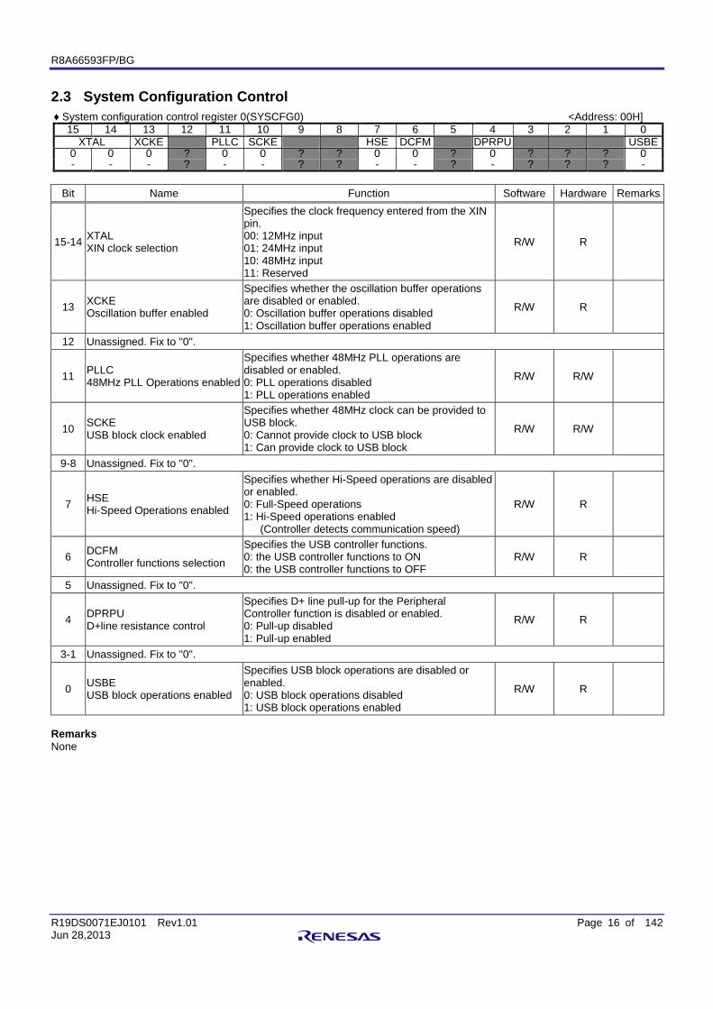
2.3 System Configuration Control ♦ System configuration control register 0(SYSCFG0) <Address: 00H]
15 14 13 12 11 10 9 8 7 6 5 4 3 2 1 0 XTAL XCKE PLLC SCKE HSE DCFM DPRPU USBE
0 0 0 ? 0 0 ? ? 0 0 ? 0 ? ? ? 0 - - - ? - - ? ? - - ? - ? ? ? -
Bit Name Function Software Hardware Remarks
15-14 XTAL XIN clock selection
Specifies the clock frequency entered from the XIN pin. 00: 12MHz input 01: 24MHz input 10: 48MHz input 11: Reserved
R/W R
13 XCKE Oscillation buffer enabled
Specifies whether the oscillation buffer operations are disabled or enabled. 0: Oscillation buffer operations disabled 1: Oscillation buffer operations enabled
R/W R
12 Unassigned. Fix to "0".
11 PLLC 48MHz PLL Operations enabled
Specifies whether 48MHz PLL operations are disabled or enabled. 0: PLL operations disabled 1: PLL operations enabled
R/W R/W
10 SCKE USB block clock enabled
Specifies whether 48MHz clock can be provided to USB block. 0: Cannot provide clock to USB block 1: Can provide clock to USB block
R/W R/W
9-8 Unassigned. Fix to "0".
7 HSE Hi-Speed Operations enabled
Specifies whether Hi-Speed operations are disabled or enabled. 0: Full-Speed operations 1: Hi-Speed operations enabled
(Controller detects communication speed)
R/W R
6 DCFM Controller functions selection
Specifies the USB controller functions. 0: the USB controller functions to ON 0: the USB controller functions to OFF
R/W R
5 Unassigned. Fix to "0".
4 DPRPU D+line resistance control
Specifies D+ line pull-up for the Peripheral Controller function is disabled or enabled. 0: Pull-up disabled 1: Pull-up enabled
R/W R
3-1 Unassigned. Fix to "0".
0 USBE USB block operations enabled
Specifies USB block operations are disabled or enabled. 0: USB block operations disabled 1: USB block operations enabled
R/W R
Remarks None
R8A66593FP/BG
R19DS0071EJ0101 Rev1.01 Page 17 of 142 Jun 28,2013
2.3.1 XIN clock selection bit (XTAL) In this bit, write the value corresponding to the quartz crystal or oscillator connected to the XIN pin. This controller determines the increasing multiples of 48MHz PLL according to the setup value of this bit. This bit is set immediately after a hardware reset. Do not modify it during controller operations.
2.3.2 Oscillation buffer enable bit (XCKE) Write "1" to this bit to enable the oscillation buffer operations of this controller. Write "0" to disable the oscillation buffer operations. Do not write "XCKE=0" for the time (time when "CNTFLG=1" is displayed) when clock restoration process is carried out by the controller. Write "XCKE=1" to end the clock restoration process.
2.3.3 48MHz PLL operations enabled bit (PLLC) Write "1" to this bit to enable this controller’s 48MHz PLL operations. Write "0" to disable them.
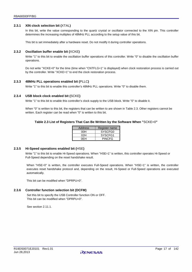
2.3.4 USB block clock enabled bit (SCKE) Write "1" to this bit to enable this controller’s clock supply to the USB block. Write "0" to disable it. When "0" is written to this bit, the registers that can be written to are shown in Table 2.3. Other registers cannot be written. Each register can be read when "0" is written to this bit.
Table 2.3 List of Registers That Can Be Written by the Software When "SCKE=0"
Address Register name 00H SYSCFG0 02H SYSCFG1 0EH PINCFG
2.3.5 Hi-Speed operations enabled bit (HSE) Write "1" to this bit to enable Hi-Speed operations. When "HSE=1" is written, this controller operates Hi-Speed or Full-Speed depending on the reset handshake result. When "HSE=0" is written, the controller executes Full-Speed operations. When "HSE=1" is written, the controller executes reset handshake protocol and, depending on the result, Hi-Speed or Full-Speed operations are executed automatically. This bit can be modified when "DPRPU=0".
2.3.6 Controller function selection bit (DCFM) Set this bit to specify the USB Controller function ON or OFF. This bit can be modified when "DPRPU=0".
See section 2.11.1.
R8A66593FP/BG
R19DS0071EJ0101 Rev1.01 Page 18 of 142 Jun 28,2013
2.3.7 D+ line resistance control (DPRPU) Settings related to USB data bus resistance is given in Table 2.4. Select USB data bus resistance in DPRPU bits.
Table 2.4 USB Data Bus Resistance Control
Write Contents USB data bus resistance control DPRPU D+ Line Remarks
1 Pull-up Set D+ line when it is a pull-up. 0 Open Set D+ line when it releases a pull-up.
If "1" is written to this bit, the controller pulls up the D+ line to 3.3V, and can notify the USB host of an "attach". The controller cancels the D+ line pull-up if the bit setting is changed from "1" to "0", and the status for the USB Host can be shown as detached.
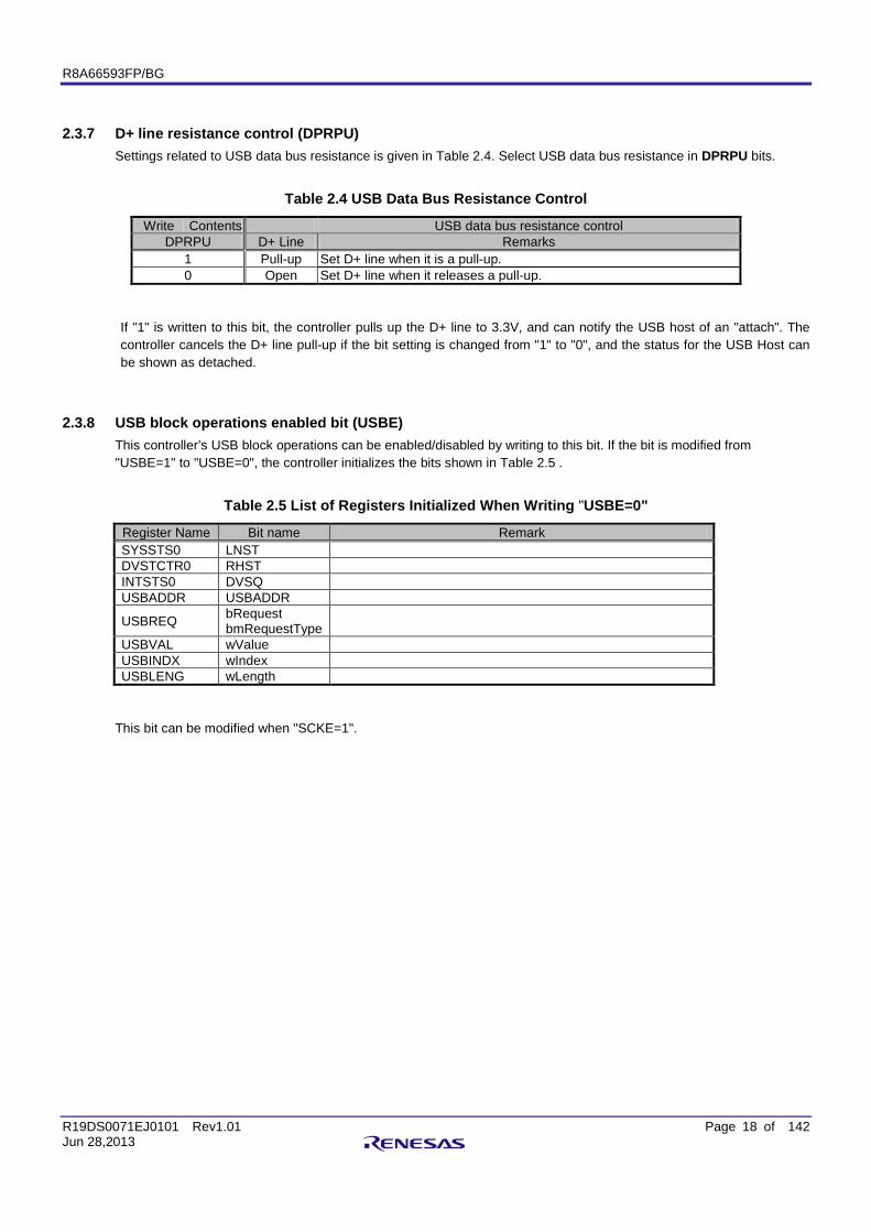
2.3.8 USB block operations enabled bit (USBE) This controller’s USB block operations can be enabled/disabled by writing to this bit. If the bit is modified from "USBE=1" to "USBE=0", the controller initializes the bits shown in Table 2.5 .
Table 2.5 List of Registers Initialized When Writing "USBE=0"
Register Name Bit name Remark SYSSTS0 LNST DVSTCTR0 RHST INTSTS0 DVSQ USBADDR USBADDR
USBREQ bRequest bmRequestType
USBVAL wValue USBINDX wIndex USBLENG wLength
This bit can be modified when "SCKE=1".
R8A66593FP/BG
R19DS0071EJ0101 Rev1.01 Page 19 of 142 Jun 28,2013
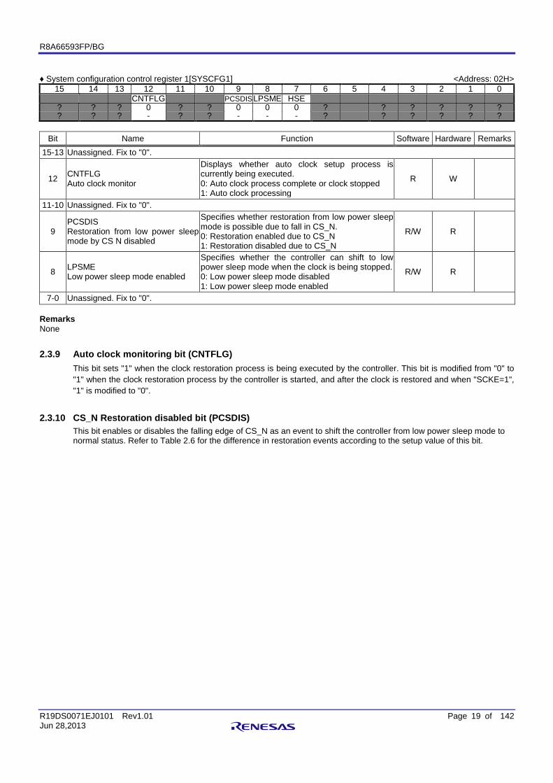
♦ System configuration control register 1[SYSCFG1] <Address: 02H>
15 14 13 12 11 10 9 8 7 6 5 4 3 2 1 0 CNTFLG PCSDIS LPSME HSE
? ? ? 0 ? ? 0 0 0 ? ? ? ? ? ? ? ? ? - ? ? - - - ? ? ? ? ? ?
Bit Name Function Software Hardware Remarks
15-13 Unassigned. Fix to "0".
12 CNTFLG Auto clock monitor
Displays whether auto clock setup process is currently being executed. 0: Auto clock process complete or clock stopped 1: Auto clock processing
R W
11-10 Unassigned. Fix to "0".
9 PCSDIS Restoration from low power sleep mode by CS N disabled
Specifies whether restoration from low power sleep mode is possible due to fall in CS_N. 0: Restoration enabled due to CS_N 1: Restoration disabled due to CS_N
R/W R
8 LPSME Low power sleep mode enabled
Specifies whether the controller can shift to low power sleep mode when the clock is being stopped. 0: Low power sleep mode disabled 1: Low power sleep mode enabled
R/W R
7-0 Unassigned. Fix to "0". Remarks None
2.3.9 Auto clock monitoring bit (CNTFLG) This bit sets "1" when the clock restoration process is being executed by the controller. This bit is modified from "0" to "1" when the clock restoration process by the controller is started, and after the clock is restored and when "SCKE=1", "1" is modified to "0".
2.3.10 CS_N Restoration disabled bit (PCSDIS) This bit enables or disables the falling edge of CS_N as an event to shift the controller from low power sleep mode to normal status. Refer to Table 2.6 for the difference in restoration events according to the setup value of this bit.
R8A66593FP/BG
R19DS0071EJ0101 Rev1.01 Page 20 of 142 Jun 28,2013
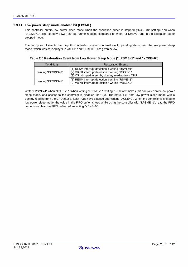
2.3.11 Low power sleep mode enabled bit (LPSME) This controller enters low power sleep mode when the oscillation buffer is stopped ("XCKE=0" setting) and when "LPSME=1". The standby power can be further reduced compared to when "LPSME=0" and in the oscillation buffer stopped mode. The two types of events that help this controller restore to normal clock operating status from the low power sleep mode, which was caused by "LPSME=1" and "XCKE=0", are given below.
Table 2.6 Restoration Event from Low Power Sleep Mode ("LPSME=1" and "XCKE=0")
Conditions Restoration Events
If writing "PCSDIS=0" (1) RESM interrupt detection if writing "RSME=1" (2) VBINT interrupt detection if writing "VBSE=1" (3) CS_N signal assert by dummy reading from CPU
If writing "PCSDIS=1" (1) RESM interrupt detection if writing "RSME=1" (2) VBINT interrupt detection if writing "VBSE=1"
Write "LPSME=1" when "XCKE=1". When writing "LPSME=1", writing "XCKE=0" makes this controller enter low power sleep mode, and access to the controller is disabled for 10μs. Therefore, exit from low power sleep mode with a dummy reading from the CPU after at least 10μs have elapsed after writing "XCKE=0". When the controller is shifted to low power sleep mode, the value in the FIFO buffer is lost. While using the controller with "LPSME=1", read the FIFO contents or clear the FIFO buffer before writing "XCKE=0".
R8A66593FP/BG
R19DS0071EJ0101 Rev1.01 Page 21 of 142 Jun 28,2013
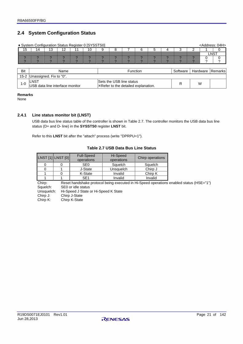
2.4 System Configuration Status ♦ System Configuration Status Register 0 [SYSSTS0] <Address: 04H>
15 14 13 12 11 10 9 8 7 6 5 4 3 2 1 0 LNST
? ? ? ? ? ? ? ? ? ? ? ? ? ? 0 0 ? ? ? ? ? ? ? ? ? ? ? ? ? ? ? ?
Bit Name Function Software Hardware Remarks
15-2 Unassigned. Fix to "0".
1-0 LNST USB data line interface monitor
Sets the USB line status Refer to the detailed explanation. R W
Remarks None
2.4.1 Line status monitor bit (LNST) USB data bus line status table of the controller is shown in Table 2.7. The controller monitors the USB data bus line status (D+ and D- line) in the SYSSTS0 register LNST bit.
Refer to this LNST bit after the "attach" process (write "DPRPU=1").
Table 2.7 USB Data Bus Line Status
LNST [1] LNST [0] Full-Speed operations
Hi-Speed operations Chirp operations
0 0 SE0 Squelch Squelch 0 1 J-State Unsquelch Chirp J 1 0 K-State Invalid Chirp K 1 1 SE1 Invalid Invalid
Chirp: Reset handshake protocol being executed in Hi-Speed operations enabled status (HSE="1") Squelch: SE0 or idle status Unsquelch: Hi-Speed J State or Hi-Speed K State Chirp J: Chirp J-State Chirp K: Chirp K-State
R8A66593FP/BG
R19DS0071EJ0101 Rev1.01 Page 22 of 142 Jun 28,2013
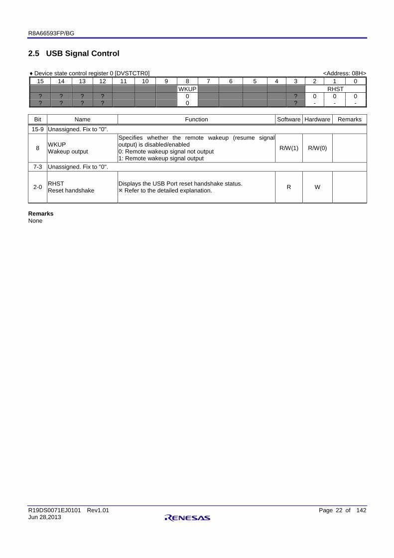
2.5 USB Signal Control ♦ Device state control register 0 [DVSTCTR0] <Address: 08H>
15 14 13 12 11 10 9 8 7 6 5 4 3 2 1 0 WKUP RHST
? ? ? ? 0 ? 0 0 0 ? ? ? ? 0 ? - - -
Bit Name Function Software Hardware Remarks
15-9 Unassigned. Fix to "0".
8 WKUP Wakeup output
Specifies whether the remote wakeup (resume signal output) is disabled/enabled 0: Remote wakeup signal not output 1: Remote wakeup signal output
R/W(1) R/W(0)
7-3 Unassigned. Fix to "0".
2-0 RHST Reset handshake
Displays the USB Port reset handshake status. Refer to the detailed explanation. R W
Remarks None
R8A66593FP/BG
R19DS0071EJ0101 Rev1.01 Page 23 of 142 Jun 28,2013
2.5.1 Remote wakeup (resume signal output) enabled/disabled bit (WKUP) If "1" is written to this bit, the controller outputs the remote wakeup signal to the USB bus. The controller manages the output time of the remote wakeup signal. If the software writes "1" to the WKUP bit, the controller outputs a "K-State" of 10ms and then changes the setting to "WKUP=0". According to the USB Specification Revision 2.0, the USB bus idle status should be maintained for at least 5ms until the remote wakeup signal is sent. Therefore, the controller outputs a K-State after waiting for 2ms, although "WKUP=1" is written immediately after detecting the suspend status. Write "1" to the WKUP bit only when the device state is suspend ("DVSQ=1xx") and when the remote wakeup is enabled from the USB Host. Do not stop the internal clock when "1" is written to the WKUP bit, irrespective of the suspend status (write "WKUP=1" in the "SCKE=1" status).
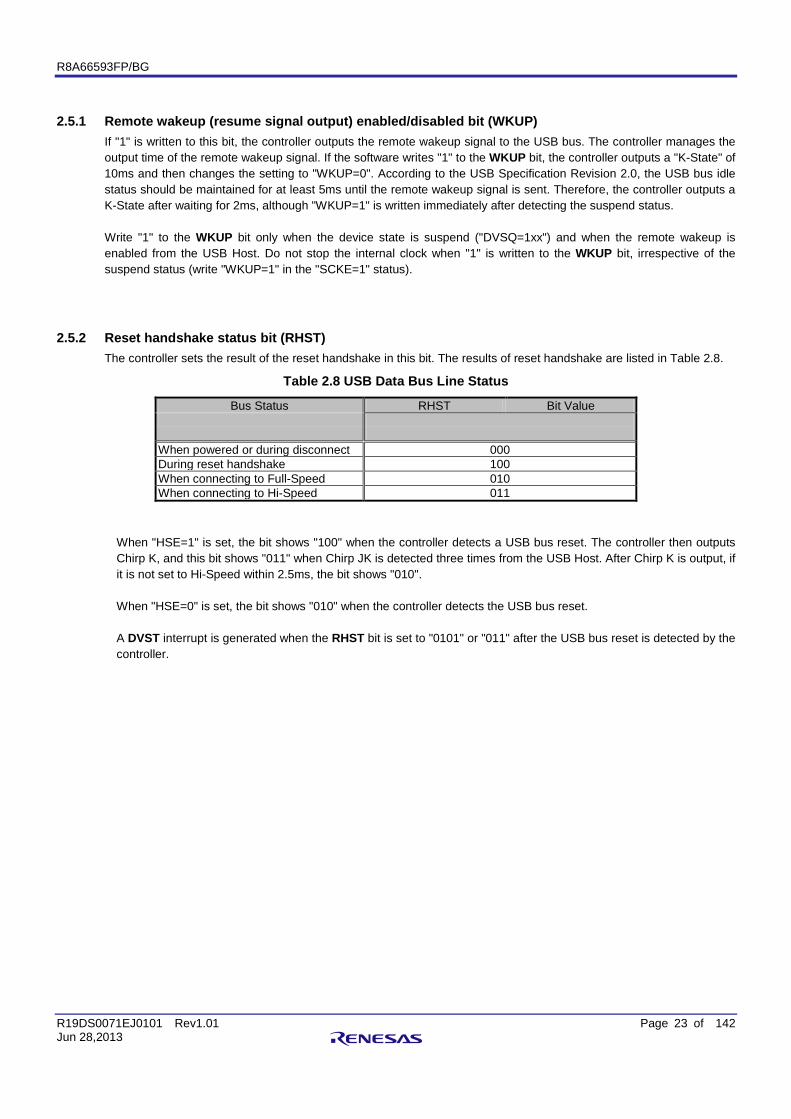
2.5.2 Reset handshake status bit (RHST) The controller sets the result of the reset handshake in this bit. The results of reset handshake are listed in Table 2.8.
Table 2.8 USB Data Bus Line Status
Bus Status RHST Bit Value
When powered or during disconnect 000 During reset handshake 100 When connecting to Full-Speed 010 When connecting to Hi-Speed 011
When "HSE=1" is set, the bit shows "100" when the controller detects a USB bus reset. The controller then outputs Chirp K, and this bit shows "011" when Chirp JK is detected three times from the USB Host. After Chirp K is output, if it is not set to Hi-Speed within 2.5ms, the bit shows "010". When "HSE=0" is set, the bit shows "010" when the controller detects the USB bus reset. A DVST interrupt is generated when the RHST bit is set to "0101" or "011" after the USB bus reset is detected by the controller.
R8A66593FP/BG
R19DS0071EJ0101 Rev1.01 Page 24 of 142 Jun 28,2013
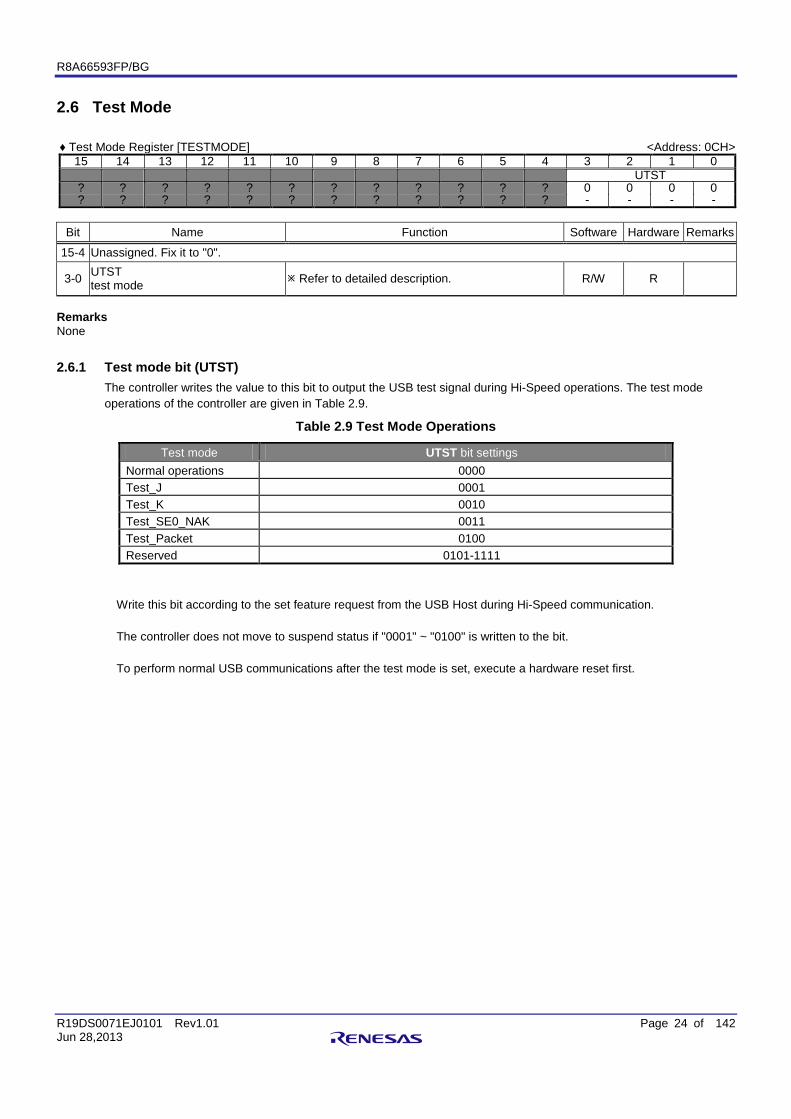
2.6 Test Mode ♦ Test Mode Register [TESTMODE] <Address: 0CH>
15 14 13 12 11 10 9 8 7 6 5 4 3 2 1 0 UTST
? ? ? ? ? ? ? ? ? ? ? ? 0 0 0 0 ? ? ? ? ? ? ? ? ? ? ? ? - - - -
Bit Name Function Software Hardware Remarks
15-4 Unassigned. Fix it to "0".
3-0 UTST test mode Refer to detailed description. R/W R
Remarks None
2.6.1 Test mode bit (UTST) The controller writes the value to this bit to output the USB test signal during Hi-Speed operations. The test mode operations of the controller are given in Table 2.9.
Table 2.9 Test Mode Operations
Test mode UTST bit settings Normal operations 0000 Test_J 0001 Test_K 0010 Test_SE0_NAK 0011 Test_Packet 0100 Reserved 0101-1111
Write this bit according to the set feature request from the USB Host during Hi-Speed communication. The controller does not move to suspend status if "0001" ~ "0100" is written to the bit. To perform normal USB communications after the test mode is set, execute a hardware reset first.
R8A66593FP/BG
R19DS0071EJ0101 Rev1.01 Page 25 of 142 Jun 28,2013
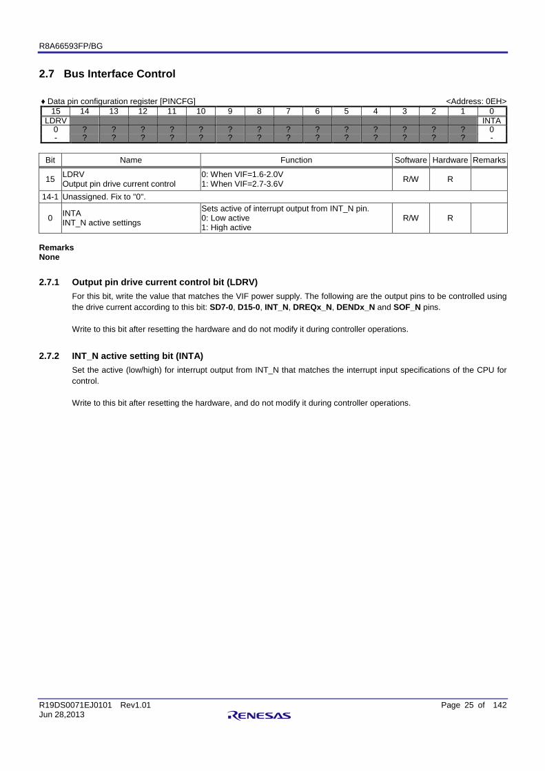
2.7 Bus Interface Control ♦ Data pin configuration register [PINCFG] <Address: 0EH>
15 14 13 12 11 10 9 8 7 6 5 4 3 2 1 0 LDRV INTA
0 ? ? ? ? ? ? ? ? ? ? ? ? ? ? 0 - ? ? ? ? ? ? ? ? ? ? ? ? ? ? -
Bit Name Function Software Hardware Remarks
15 LDRV Output pin drive current control
0: When VIF=1.6-2.0V 1: When VIF=2.7-3.6V R/W R
14-1 Unassigned. Fix to "0".
0 INTA INT_N active settings
Sets active of interrupt output from INT_N pin. 0: Low active 1: High active
R/W R
Remarks None
2.7.1 Output pin drive current control bit (LDRV) For this bit, write the value that matches the VIF power supply. The following are the output pins to be controlled using the drive current according to this bit: SD7-0, D15-0, INT_N, DREQx_N, DENDx_N and SOF_N pins. Write to this bit after resetting the hardware and do not modify it during controller operations.
2.7.2 INT_N active setting bit (INTA) Set the active (low/high) for interrupt output from INT_N that matches the interrupt input specifications of the CPU for control. Write to this bit after resetting the hardware, and do not modify it during controller operations.
R8A66593FP/BG
R19DS0071EJ0101 Rev1.01 Page 26 of 142 Jun 28,2013
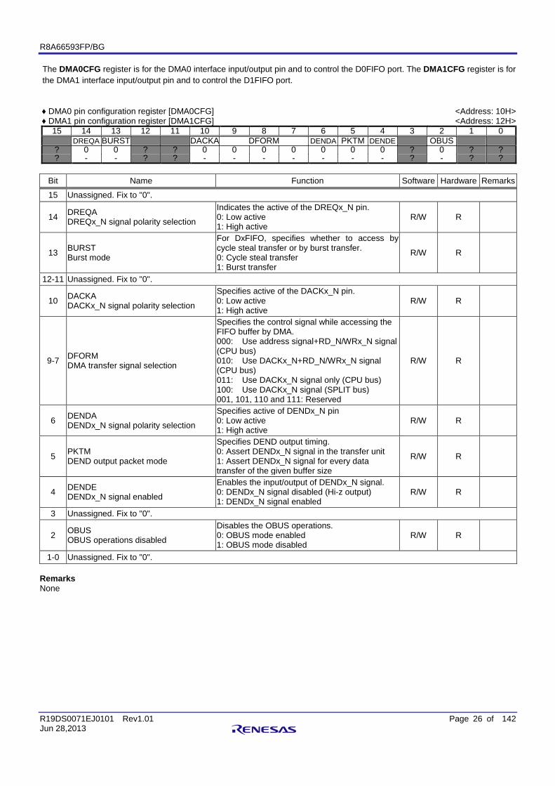
The DMA0CFG register is for the DMA0 interface input/output pin and to control the D0FIFO port. The DMA1CFG register is for the DMA1 interface input/output pin and to control the D1FIFO port.
♦ DMA0 pin configuration register [DMA0CFG] ♦ DMA1 pin configuration register [DMA1CFG]
<Address: 10H> <Address: 12H>
15 14 13 12 11 10 9 8 7 6 5 4 3 2 1 0 DREQA BURST DACKA DFORM DENDA PKTM DENDE OBUS
? 0 0 ? ? 0 0 0 0 0 0 0 ? 0 ? ? ? - - ? ? - - - - - - - ? - ? ?
Bit Name Function Software Hardware Remarks
15 Unassigned. Fix to "0".
14 DREQA DREQx_N signal polarity selection
Indicates the active of the DREQx_N pin. 0: Low active 1: High active
R/W R
13 BURST Burst mode
For DxFIFO, specifies whether to access by cycle steal transfer or by burst transfer. 0: Cycle steal transfer 1: Burst transfer
R/W R
12-11 Unassigned. Fix to "0".
10 DACKA DACKx_N signal polarity selection
Specifies active of the DACKx_N pin. 0: Low active 1: High active
R/W R
9-7 DFORM DMA transfer signal selection
Specifies the control signal while accessing the FIFO buffer by DMA. 000: Use address signal+RD_N/WRx_N signal (CPU bus) 010: Use DACKx_N+RD_N/WRx_N signal (CPU bus) 011: Use DACKx_N signal only (CPU bus) 100: Use DACKx_N signal (SPLIT bus) 001, 101, 110 and 111: Reserved
R/W R
6 DENDA DENDx_N signal polarity selection
Specifies active of DENDx_N pin 0: Low active 1: High active
R/W R
5 PKTM DEND output packet mode
Specifies DEND output timing. 0: Assert DENDx_N signal in the transfer unit 1: Assert DENDx_N signal for every data transfer of the given buffer size
R/W R
4 DENDE DENDx_N signal enabled
Enables the input/output of DENDx_N signal. 0: DENDx_N signal disabled (Hi-z output) 1: DENDx_N signal enabled
R/W R
3 Unassigned. Fix to "0".
2 OBUS OBUS operations disabled
Disables the OBUS operations. 0: OBUS mode enabled 1: OBUS mode disabled
R/W R
1-0 Unassigned. Fix to "0". Remarks None
R8A66593FP/BG
R19DS0071EJ0101 Rev1.01 Page 27 of 142 Jun 28,2013
2.7.3 DMA signal control If transferring data using the DMA interface, use the DMAxCFG register’s BURST bit, PKTM bit, DENDE bit, and OBUS bit to select the DMA interface operation (assert/negate of DREQx_N /DENDx_N signal and DMA transfer mode settings) that is configured to the user system. The DMA signal is valid for access to the FIFO buffer assigned to the pipe selected by the DxFIFOSEL register CURPIPE bit (to be mentioned later). When the status of the pipe FIFO buffer changes to buffer ready (BRDY) status, this controller asserts the DREQx_N signal if "DREQE=1".
2.7.4 DREQx_N signal polarity selection bit (DREQA) Set active of DREQx_N pin in this bit. For the FIFO port, write to this bit when "CURPIPE=000".
2.7.5 Burst mode bit (BURST) When the DMA controller executes a cycle steal transfer for DxFIFO, write "0" to this bit. The controller negates a DREQx_N signal for access to one word or one byte. When the DMA controller executes a burst transfer for DxFIFO, write "1" to this bit. The controller negates the DREQx_N signal for accessing the last one word or one byte of FIFO buffer. Do not modify the bit during pipe communication operations.
2.7.6 DACKx_N signal polarity selection bit (DACKA) In this bit, set active the DACKx_N pin. For the FIFO port, write to this bit when "CURPIPE=000".
2.7.7 DMA transfer signal selection bit (DFORM) In this bit, set the control signal while accessing the FIFO buffer with the DMA controller. For the FIFO port, write to this bit when "CURPIPE=000"
2.7.8 DENDx_N signal polarity selection bit (DENDA) In this bit, set active the DENDx_N pin. For the FIFO port, write to this bit when "CURPIPE=000".
2.7.9 DEND output packet mode bit (PKTM) Write the DEND output timing in this bit. When "0" is written to this bit, the controller asserts the DENDx_N signal when any of the following conditions are fulfilled: (1) During the last read access while reading the short packet data (2) During the last read access while reading the data completed at the transaction counter (TRNCNT) (3) If a zero-length packet is received when the FIFO buffer is empty
When "1" is written to this bit, the controller asserts a DENDx_N output for every data transfer of the given FIFO buffer size. For the FIFO port, write to this bit when "CURPIPE=000".
R8A66593FP/BG
R19DS0071EJ0101 Rev1.01 Page 28 of 142 Jun 28,2013
2.7.10 Input/Output enabled bit of the DENDx_N signal (DENDE) Set I/O enabled/disabled for the DENDx_N pin in this bit. For the FIFO port, write to this bit when "CURPIPE=000".
2.7.11 OBUS operation disabled bit (OBUS) In this bit, write OBUS operations to be enabled/disabled. When "0" is written to this bit, theSD7-0 of the split bus and DEND is always input/output enabled". When "1" is written to this bit, the SD7-0 of the split bus and DENDx_N are are enabled only when DACKx_N is active. While commonly using D0FIFO and D1FIFO in the split bus, write "1" to all the OBUS bits.
R8A66593FP/BG
R19DS0071EJ0101 Rev1.01 Page 29 of 142 Jun 28,2013
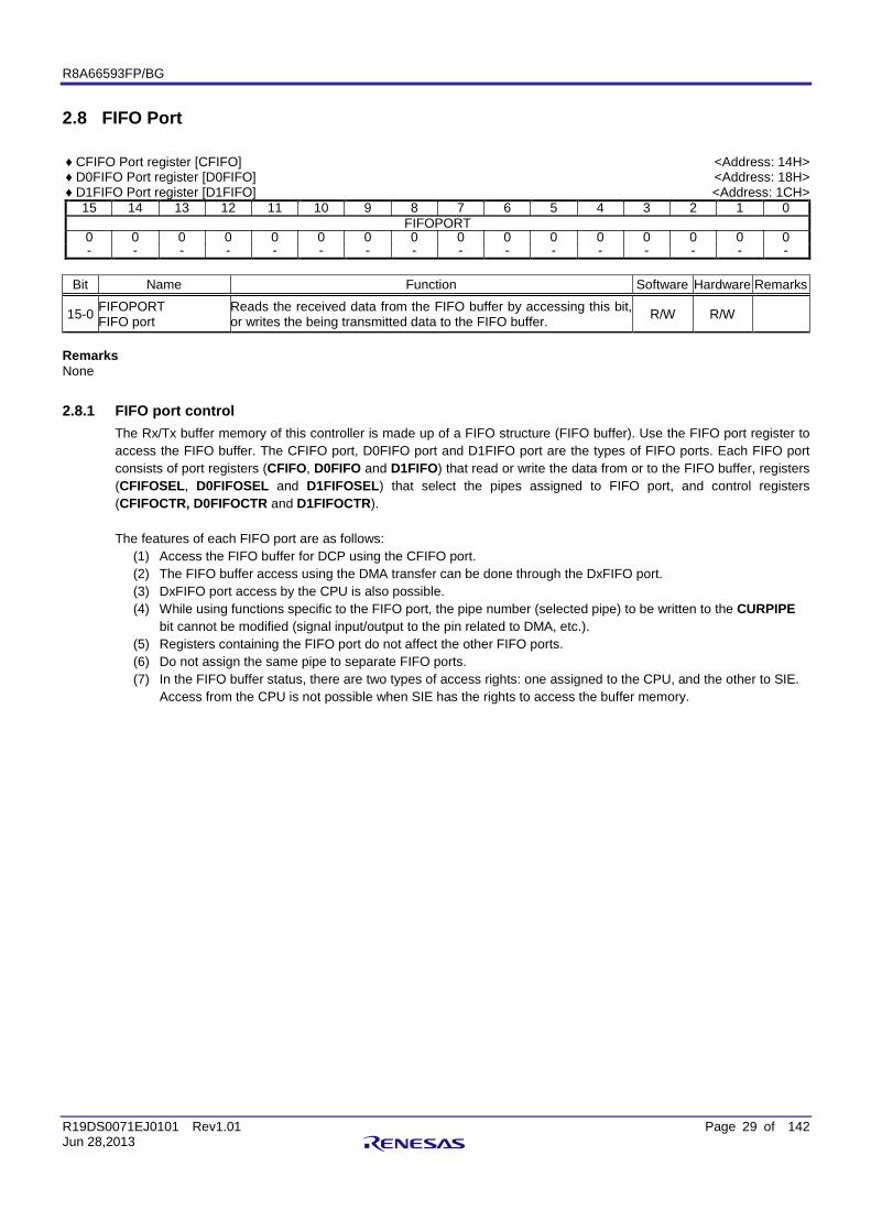
2.8 FIFO Port ♦ CFIFO Port register [CFIFO] ♦ D0FIFO Port register [D0FIFO] ♦ D1FIFO Port register [D1FIFO]
<Address: 14H> <Address: 18H> <Address: 1CH>
15 14 13 12 11 10 9 8 7 6 5 4 3 2 1 0 FIFOPORT
0 0 0 0 0 0 0 0 0 0 0 0 0 0 0 0 - - - - - - - - - - - - - - - -
Bit Name Function Software Hardware Remarks
15-0 FIFOPORT FIFO port
Reads the received data from the FIFO buffer by accessing this bit, or writes the being transmitted data to the FIFO buffer. R/W R/W
Remarks None
2.8.1 FIFO port control The Rx/Tx buffer memory of this controller is made up of a FIFO structure (FIFO buffer). Use the FIFO port register to access the FIFO buffer. The CFIFO port, D0FIFO port and D1FIFO port are the types of FIFO ports. Each FIFO port consists of port registers (CFIFO, D0FIFO and D1FIFO) that read or write the data from or to the FIFO buffer, registers (CFIFOSEL, D0FIFOSEL and D1FIFOSEL) that select the pipes assigned to FIFO port, and control registers (CFIFOCTR, D0FIFOCTR and D1FIFOCTR). The features of each FIFO port are as follows:
(1) Access the FIFO buffer for DCP using the CFIFO port. (2) The FIFO buffer access using the DMA transfer can be done through the DxFIFO port. (3) DxFIFO port access by the CPU is also possible. (4) While using functions specific to the FIFO port, the pipe number (selected pipe) to be written to the CURPIPE
bit cannot be modified (signal input/output to the pin related to DMA, etc.). (5) Registers containing the FIFO port do not affect the other FIFO ports. (6) Do not assign the same pipe to separate FIFO ports. (7) In the FIFO buffer status, there are two types of access rights: one assigned to the CPU, and the other to SIE.
Access from the CPU is not possible when SIE has the rights to access the buffer memory.
R8A66593FP/BG
R19DS0071EJ0101 Rev1.01 Page 30 of 142 Jun 28,2013
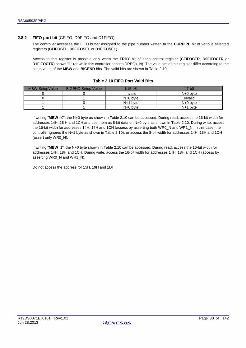
2.8.2 FIFO port bit (CFIFO, D0FIFO and D1FIFO) The controller accesses the FIFO buffer assigned to the pipe number written to the CURPIPE bit of various selected registers (CFIFOSEL, D0FIFOSEL or D1FIFOSEL). Access to this register is possible only when the FRDY bit of each control register (CFIFOCTR, D0FIFOCTR or D1FIFOCTR) shows "1" (or while this controller asserts DREQx_N). The valid bits of this register differ according to the setup value of the MBW and BIGEND bits. The valid bits are shown in Table 2.10.
Table 2.10 FIFO Port Valid Bits
MBW SetupValue BIGEND Setup Value b15-b8 b7-b0 0 0 Invalid N+0 byte 0 1 N+0 byte Invalid 1 0 N+1 byte N+0 byte 1 1 N+0 byte N+1 byte
If writing "MBW =0", the N+0 byte as shown in Table 2.10 can be accessed. During read, access the 16-bit width for addresses 14H, 18 H and 1CH and use them as 8-bit data on N+0 byte as shown in Table 2.10. During write, access the 16-bit width for addresses 14H, 18H and 1CH (access by asserting both WR0_N and WR1_N. In this case, the controller ignores the N+1 byte as shown in Table 2.10), or access the 8-bit width for addresses 14H, 18H and 1CH (assert only WR0_N). If writing "MBW=1", the N+0 byte shown in Table 2.10 can be accessed. During read, access the 16-bit width for addresses 14H, 18H and 1CH. During write, access the 16-bit width for addresses 14H, 18H and 1CH (access by asserting WR0_N and WR1_N). Do not access the address for 15H, 19H and 1DH.
R8A66593FP/BG
R19DS0071EJ0101 Rev1.01 Page 31 of 142 Jun 28,2013
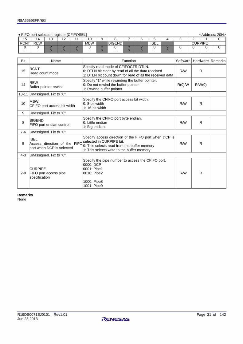
♦ FIFO port selection register [CFIFOSEL] <Address: 20H>
15 14 13 12 11 10 9 8 7 6 5 4 3 2 1 0 RCNT REW MBW BIGEND ISEL CURPIPE
0 0 ? ? ? 0 ? 0 ? ? 0 ? 0 0 0 0 - - ? ? ? - ? - ? ? - ? - - - -
Bit Name Function Software Hardware Remarks
15 RCNT Read count mode
Specify read mode of CFIFOCTR DTLN. 0: DTLN bit clear by read of all the data received 1: DTLN bit count down for read of all the received data
R/W R
14 REW Buffer pointer rewind
Specify "1" while rewinding the buffer pointer. 0: Do not rewind the buffer pointer 1: Rewind buffer pointer
R(0)/W R/W(0)
13-11 Unassigned. Fix to "0".
10 MBW CFIFO port access bit width
Specify the CFIFO port access bit width. 0: 8-bit width 1: 16-bit width
R/W R
9 Unassigned. Fix to "0".
8 BIGEND FIFO port endian control
Specify the CFIFO port byte endian. 0: Little endian 1: Big endian
R/W R
7-6 Unassigned. Fix to "0".
5 ISEL Access direction of the FIFO port when DCP is selected
Specify access direction of the FIFO port when DCP is selected in CURPIPE bit. 0: This selects read from the buffer memory 1: This selects write to the buffer memory
R/W R
4-3 Unassigned. Fix to "0".
2-0 CURPIPE FIFO port access pipe specification
Specify the pipe number to access the CFIFO port. 0000: DCP 0001: Pipe1 0010: Pipe2 1000: Pipe8 1001: Pipe9
R/W R
Remarks None
R8A66593FP/BG
R19DS0071EJ0101 Rev1.01 Page 32 of 142 Jun 28,2013
2.8.3 Read count mode (RCNT) When "0" is written to this bit, if all reception data of the FIFO buffer assigned to the pipe specified in the CURPIPE bit is read (when the data is read on one side of a double buffer), the controller clears the CFIFOCTR register DTLN bit to "0". When "1" is written to this bit, the controller counts the CFIFOCTR register DTLN bit whenever the data received from the FIFO buffer assigned to the specified bit is read.
2.8.4 Buffer pointer rewind (REW) When the selection pipe is receiving, if "1" is written to this bit during the FIFO buffer read, the initial data of the FIFO buffer can be read (for a double buffer, the initial data on one side can be read again during the read process). When the software writes "1" to this bit, the controller again writes "0" to this bit. Do not modify the "REW=1" settings and the CURPIPE bit settings at the same time. First confirm that "FRDY=1" and then write "REW=1". Use the BCLR bit while rewriting the initial data of the FIFO buffer for the transmission pipe.
2.8.5 CFIFO Port access bit width (MBW) In this bit, set the CFIFO port access bit width. When the pipe specified in the CURPIPE bit is receiving, if read is started after writing "1" to this bit, modify the MBW bit from "1" to "0" only after all the data is read. When the DTLN bit is an odd number, write "MBW=0" and read with the variable having an 8-bit length, or read with a 16-bit maintaining "MBW=1", delete the excess byte, and then read the last byte. When the specified pipe is receiving, set the CURPIPE bit and MBW bit simultaneously. When the the specified pipe is transmitting, to start writing the data having an odd number of bytes by writing "1" to this bit, write "MBW=0" and write with the variable having a 16-bit length (refer to 2.8.2 for the data to be written), or write with the variable having an 8-bit length maintaining "MBW=1", and then write the last byte (write with the WR0_N strobe if "BIGEND=0", and with the WR1_N strobe if "BIGEND=1").
2.8.6 Control bit of CFIFO port byte endian (BIGEND) In this bit, write the CFIFO port byte endian. Refer to 2.8.2 for details.
2.8.7 FIFO port access direction specification bit when selecting DCP (ISEL) To change this bit when the specified pipe is DCP, first write the data to this bit and then read it. Proceed to the next process after checking if the written values match with the read values. When the settings of this bit are modified during access to the FIFO buffer, access up to then is saved. Access to the buffer can be continued after rewriting the settings. Write to this bit and the CURPIPE bit simultaneously.
2.8.8 FIFO port access byte specification bit (CURPIPE) Write the pipe number for the data to be read or written through the CFIFO port. When modifying this bit, first write the data “0” and then write specified pipe number. Check that the written values and the read values match, and then proceed to the next process. Do not write to the same pipe to CURPIPE of CFIFOSEL, D0FIFOSEL, and D1FIFOSEL registers. When the settings of this bit are modified during access to the FIFO buffer, access up to then is saved. Access to the

R8A66593FP/BG
R19DS0071EJ0101 Rev1.01 Page 33 of 142 Jun 28,2013
buffer can be continued after rewriting the settings.
R8A66593FP/BG
R19DS0071EJ0101 Rev1.01 Page 34 of 142 Jun 28,2013
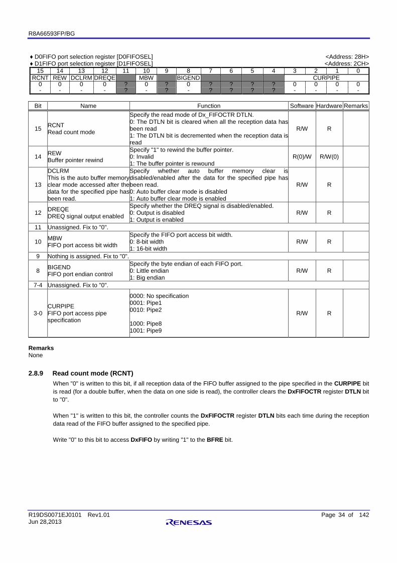
♦ D0FIFO port selection register [D0FIFOSEL] ♦ D1FIFO port selection register [D1FIFOSEL]
<Address: 28H> <Address: 2CH>
15 14 13 12 11 10 9 8 7 6 5 4 3 2 1 0 RCNT REW DCLRM DREQE MBW BIGEND CURPIPE
0 0 0 0 ? 0 ? 0 ? ? ? ? 0 0 0 0 - - - - ? - ? - ? ? ? ? - - - -
Bit Name Function Software Hardware Remarks
15 RCNT Read count mode
Specify the read mode of Dx_FIFOCTR DTLN. 0: The DTLN bit is cleared when all the reception data has been read 1: The DTLN bit is decremented when the reception data is read
R/W R
14 REW Buffer pointer rewind
Specify "1" to rewind the buffer pointer. 0: Invalid 1: The buffer pointer is rewound
R(0)/W R/W(0)
13
DCLRM This is the auto buffer memory clear mode accessed after the data for the specified pipe has been read.
Specify whether auto buffer memory clear is disabled/enabled after the data for the specified pipe has been read. 0: Auto buffer clear mode is disabled 1: Auto buffer clear mode is enabled
R/W R
12 DREQE DREQ signal output enabled
Specify whether the DREQ signal is disabled/enabled. 0: Output is disabled 1: Output is enabled
R/W R
11 Unassigned. Fix to "0".
10 MBW FIFO port access bit width
Specify the FIFO port access bit width. 0: 8-bit width 1: 16-bit width
R/W R
9 Nothing is assigned. Fix to "0".
8 BIGEND FIFO port endian control
Specify the byte endian of each FIFO port. 0: Little endian 1: Big endian
R/W R
7-4 Unassigned. Fix to "0".
3-0 CURPIPE FIFO port access pipe specification
0000: No specification 0001: Pipe1 0010: Pipe2 1000: Pipe8 1001: Pipe9
R/W R
Remarks None
2.8.9 Read count mode (RCNT) When "0" is written to this bit, if all reception data of the FIFO buffer assigned to the pipe specified in the CURPIPE bit is read (for a double buffer, when the data on one side is read), the controller clears the DxFIFOCTR register DTLN bit to "0". When "1" is written to this bit, the controller counts the DxFIFOCTR register DTLN bits each time during the reception data read of the FIFO buffer assigned to the specified pipe. Write "0" to this bit to access DxFIFO by writing "1" to the BFRE bit.
R8A66593FP/BG
R19DS0071EJ0101 Rev1.01 Page 35 of 142 Jun 28,2013
2.8.10 Buffer pointer rewind (REW) When the selection pipe is receiving, if "1" is written to this bit during the FIFO buffer read, the initial data of the FIFO buffer can be read (for a double buffer, during the read process, the initial data on one side can be read again). When the software writes "1" to this bit, the controller again writes "0" to this bit. Do not modify the "REW=1" settings and the CURPIPE bit settings as the same time. First confirm the "FRDY=1" and then write "REW=1". Use the BLCR bit while rewriting the initial data of the FIFO buffer for the transmission pipe.
2.8.11 Auto FIFO buffer clear disabled/enabled bit (DCLRM) After reading the specified pipe data, set disabled/enabled for the auto FIFO buffer clear. When "1" is written to this bit, the controller executes a "BCLR=1" process of the FIFO buffer if a zero-length packet is received when the FIFO buffer assigned to the specified pipe is empty, or when the short packet reception data is read if writing "BFRE=1". If "BRDYM=1" is written when using this controller, make sure to write "0" to this bit.
2.8.12 DREQx_N output disabled/enabled bit (DREQE) Write this bit so that the DxREQ_N signal output can be disabled/enabled. When the DxREQ_N signal output is enabled, write "1" to this bit after writing to the CURPIPE bit. Write "0" to this bit and then modify the CURPIPE bit.
2.8.13 DxFIFO port access bit width (MBW) Write the DxFIFO port access bit width in this bit. Refer to 2.8.5 for details.
2.8.14 Control bit of DxFIFO port byte endian (BIGEND) Write the DxFIFO port byte endian in this bit. Refer to 2.8.2 for details.
2.8.15 FIFO port access pipe specification bit (CURPIPE) Write the pipe number for the data to be read or written through the DxFIFO port. To modify this bit, first write the data to this bit and then read it. Check if the write value matches the read value and then proceed to the next process. Do not write the same pipe to the CFIFOSEL, D0FIFOSEL, and D1FIFOSEL registers’ CURPIPE. When this bit is modified during access to the FIFO buffer, access up to then is saved. Access to the buffer can be continued after rewriting.
R8A66593FP/BG
R19DS0071EJ0101 Rev1.01 Page 36 of 142 Jun 28,2013
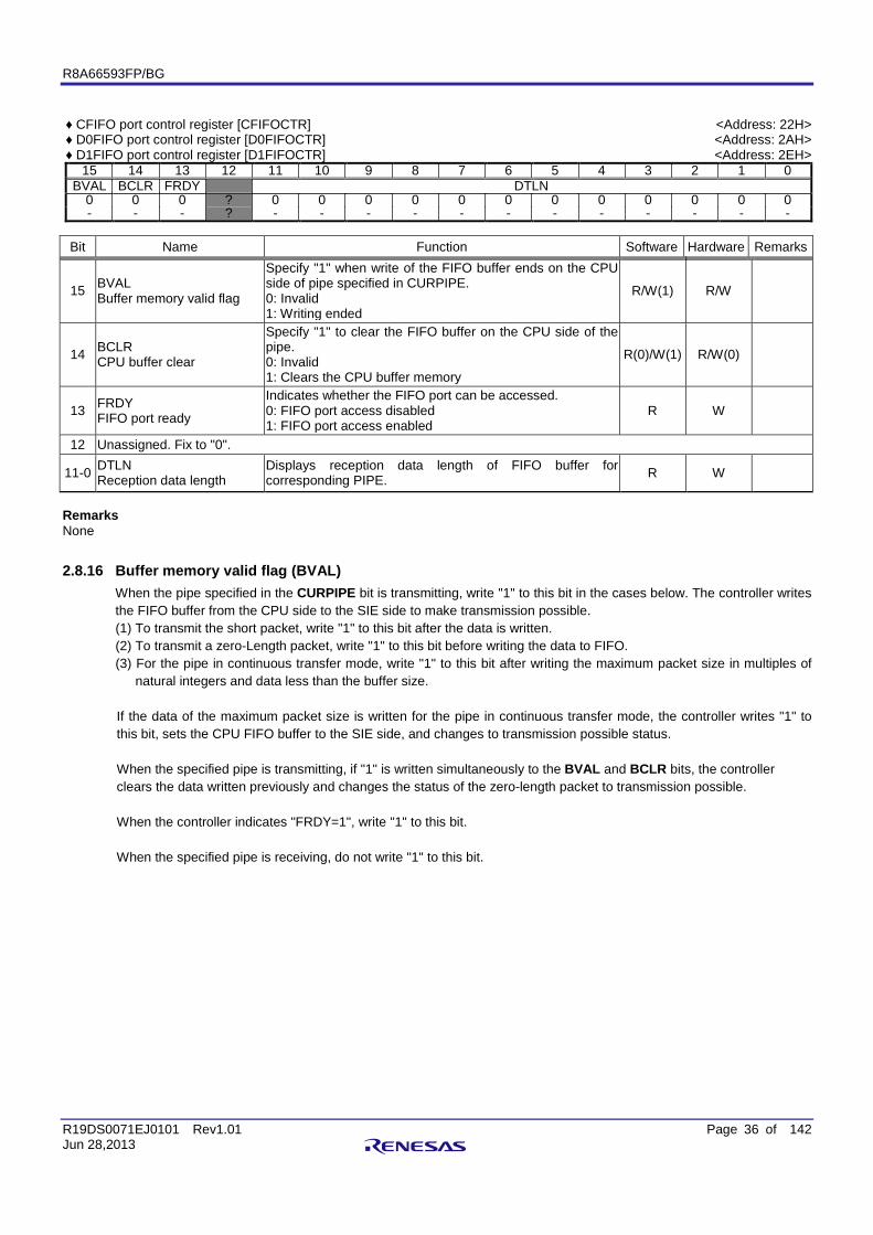
♦ CFIFO port control register [CFIFOCTR] ♦ D0FIFO port control register [D0FIFOCTR] ♦ D1FIFO port control register [D1FIFOCTR]
<Address: 22H> <Address: 2AH> <Address: 2EH>
15 14 13 12 11 10 9 8 7 6 5 4 3 2 1 0 BVAL BCLR FRDY DTLN
0 0 0 ? 0 0 0 0 0 0 0 0 0 0 0 0 - - - ? - - - - - - - - - - - -
Bit Name Function Software Hardware Remarks
15 BVAL Buffer memory valid flag
Specify "1" when write of the FIFO buffer ends on the CPU side of pipe specified in CURPIPE. 0: Invalid 1: Writing ended
R/W(1) R/W
14 BCLR CPU buffer clear
Specify "1" to clear the FIFO buffer on the CPU side of the pipe. 0: Invalid 1: Clears the CPU buffer memory
R(0)/W(1) R/W(0)
13 FRDY FIFO port ready
Indicates whether the FIFO port can be accessed. 0: FIFO port access disabled 1: FIFO port access enabled
R W
12 Unassigned. Fix to "0".
11-0 DTLN Reception data length
Displays reception data length of FIFO buffer for corresponding PIPE. R W
Remarks None
2.8.16 Buffer memory valid flag (BVAL) When the pipe specified in the CURPIPE bit is transmitting, write "1" to this bit in the cases below. The controller writes the FIFO buffer from the CPU side to the SIE side to make transmission possible. (1) To transmit the short packet, write "1" to this bit after the data is written. (2) To transmit a zero-Length packet, write "1" to this bit before writing the data to FIFO. (3) For the pipe in continuous transfer mode, write "1" to this bit after writing the maximum packet size in multiples of
natural integers and data less than the buffer size. If the data of the maximum packet size is written for the pipe in continuous transfer mode, the controller writes "1" to this bit, sets the CPU FIFO buffer to the SIE side, and changes to transmission possible status. When the specified pipe is transmitting, if "1" is written simultaneously to the BVAL and BCLR bits, the controller clears the data written previously and changes the status of the zero-length packet to transmission possible. When the controller indicates "FRDY=1", write "1" to this bit. When the specified pipe is receiving, do not write "1" to this bit.
R8A66593FP/BG
R19DS0071EJ0101 Rev1.01 Page 37 of 142 Jun 28,2013
2.8.17 CPU buffer clear bit (BCLR) If "1" is written to this bit, the controller clears the FIFO buffer on the CPU side from the FIFO buffers assigned to the specified pipe. When the setting of the FIFO buffer assigned to the specified pipe is a double buffer, the controller clears the FIFO buffer only on one side, though the buffers on both sides can be read. When the specified pipe is DCP, the controller clears the FIFO buffer when "BCLR=1", irrespective of the CPU or SIE side. To clear the buffer on the SIE side, write "BCLR=1" after writing "NAK" to the PID bit. If the specified pipe is not DCP, write "1" to this bit when the controller sets "FRDY=1".
2.8.18 FIFO port ready bit (FRDY) In this bit, the controller shows if access is possible to the FIFO port from the CPU (DMAC). In the following cases, the controller sets "FRDY=1", but cannot read the data from the FIFO port since the data is not available. In these cases, write "BCLR=1", clear the FIFO buffer, and then change the status to Data Send/Receive. (1) If a zero-length packet is received when the FIFO buffer assigned to the specified pipe is empty. (2) If "BFRE=1" is written, when the short packet is received and the data is read.
2.8.19 Reception data length bit (DTLN) The controller sets the reception data length in this bit. The value of this bit changes according to the setup value of the RCNT bit during the FIFO buffer read. (1) When "RCNT=0":
The controller sets the reception data length in this bit until the CPU (DMAC) reads all the reception data on one side of the FIFO buffer. When "BFRE=1", the controller holds the reception data length until "BCLR=1", although the data is read.
(2) When "RCNT=1": The controller counts the DTLN bit display during each data read (counts down by -1 when "MBW=0", and by -2 when "MBW=1").
When the data on one side of the FIFO buffer is read, the controller sets "DTLN=0". However, when the double buffer is set, and when data is received in the FIFO buffer on one side before reading the reception data on other FIFO buffer, the reception data on one side is set in the DTLN bit when read on the first side is being completed. When "RCNT=1", while reading the value of this bit during FIFO buffer read, the controller sets the updated value of this bit up to150ns after the read cycle of the FIFO port.
R8A66593FP/BG
R19DS0071EJ0101 Rev1.01 Page 38 of 142 Jun 28,2013
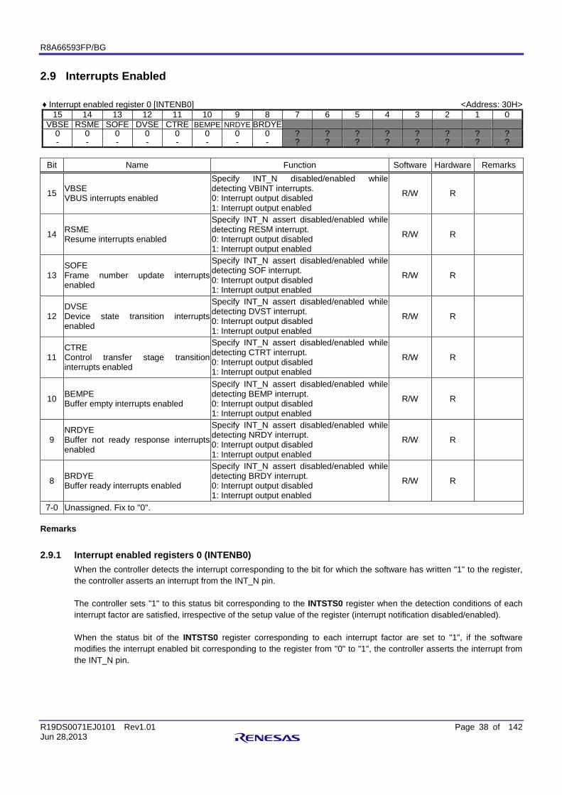
2.9 Interrupts Enabled
♦ Interrupt enabled register 0 [INTENB0] <Address: 30H> 15 14 13 12 11 10 9 8 7 6 5 4 3 2 1 0
VBSE RSME SOFE DVSE CTRE BEMPE NRDYE BRDYE 0 0 0 0 0 0 0 0 ? ? ? ? ? ? ? ? - - - - - - - - ? ? ? ? ? ? ? ?
Bit Name Function Software Hardware Remarks
15 VBSE VBUS interrupts enabled
Specify INT_N disabled/enabled while detecting VBINT interrupts. 0: Interrupt output disabled 1: Interrupt output enabled
R/W R
14 RSME Resume interrupts enabled
Specify INT_N assert disabled/enabled while detecting RESM interrupt. 0: Interrupt output disabled 1: Interrupt output enabled
R/W R
13 SOFE Frame number update interrupts enabled
Specify INT_N assert disabled/enabled while detecting SOF interrupt. 0: Interrupt output disabled 1: Interrupt output enabled
R/W R
12 DVSE Device state transition interrupts enabled
Specify INT_N assert disabled/enabled while detecting DVST interrupt. 0: Interrupt output disabled 1: Interrupt output enabled
R/W R
11 CTRE Control transfer stage transition interrupts enabled
Specify INT_N assert disabled/enabled while detecting CTRT interrupt. 0: Interrupt output disabled 1: Interrupt output enabled
R/W R
10 BEMPE Buffer empty interrupts enabled
Specify INT_N assert disabled/enabled while detecting BEMP interrupt. 0: Interrupt output disabled 1: Interrupt output enabled
R/W R
9 NRDYE Buffer not ready response interrupts enabled
Specify INT_N assert disabled/enabled while detecting NRDY interrupt. 0: Interrupt output disabled 1: Interrupt output enabled
R/W R
8 BRDYE Buffer ready interrupts enabled
Specify INT_N assert disabled/enabled while detecting BRDY interrupt. 0: Interrupt output disabled 1: Interrupt output enabled
R/W R
7-0 Unassigned. Fix to "0". Remarks
2.9.1 Interrupt enabled registers 0 (INTENB0) When the controller detects the interrupt corresponding to the bit for which the software has written "1" to the register, the controller asserts an interrupt from the INT_N pin. The controller sets "1" to this status bit corresponding to the INTSTS0 register when the detection conditions of each interrupt factor are satisfied, irrespective of the setup value of the register (interrupt notification disabled/enabled). When the status bit of the INTSTS0 register corresponding to each interrupt factor are set to "1", if the software modifies the interrupt enabled bit corresponding to the register from "0" to "1", the controller asserts the interrupt from the INT_N pin.
R8A66593FP/BG
R19DS0071EJ0101 Rev1.01 Page 39 of 142 Jun 28,2013
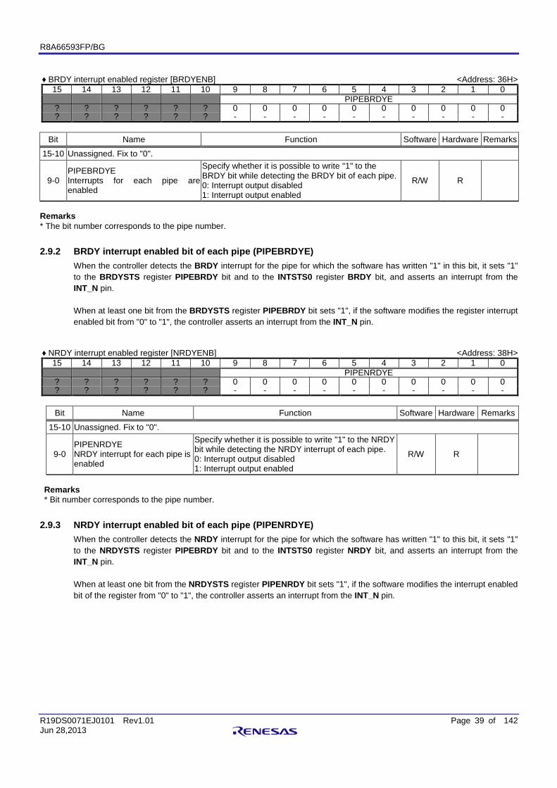
♦ BRDY interrupt enabled register [BRDYENB] <Address: 36H>
15 14 13 12 11 10 9 8 7 6 5 4 3 2 1 0 PIPEBRDYE
? ? ? ? ? ? 0 0 0 0 0 0 0 0 0 0 ? ? ? ? ? ? - - - - - - - - - -
Bit Name Function Software Hardware Remarks
15-10 Unassigned. Fix to "0".
9-0 PIPEBRDYE Interrupts for each pipe are enabled
Specify whether it is possible to write "1" to the BRDY bit while detecting the BRDY bit of each pipe. 0: Interrupt output disabled 1: Interrupt output enabled
R/W R
Remarks * The bit number corresponds to the pipe number.
2.9.2 BRDY interrupt enabled bit of each pipe (PIPEBRDYE) When the controller detects the BRDY interrupt for the pipe for which the software has written "1" in this bit, it sets "1" to the BRDYSTS register PIPEBRDY bit and to the INTSTS0 register BRDY bit, and asserts an interrupt from the INT_N pin. When at least one bit from the BRDYSTS register PIPEBRDY bit sets "1", if the software modifies the register interrupt enabled bit from "0" to "1", the controller asserts an interrupt from the INT_N pin.
♦ NRDY interrupt enabled register [NRDYENB] <Address: 38H> 15 14 13 12 11 10 9 8 7 6 5 4 3 2 1 0
PIPENRDYE ? ? ? ? ? ? 0 0 0 0 0 0 0 0 0 0 ? ? ? ? ? ? - - - - - - - - - -
Bit Name Function Software Hardware Remarks
15-10 Unassigned. Fix to "0".
9-0 PIPENRDYE NRDY interrupt for each pipe is enabled
Specify whether it is possible to write "1" to the NRDY bit while detecting the NRDY interrupt of each pipe. 0: Interrupt output disabled 1: Interrupt output enabled
R/W R
Remarks * Bit number corresponds to the pipe number.
2.9.3 NRDY interrupt enabled bit of each pipe (PIPENRDYE) When the controller detects the NRDY interrupt for the pipe for which the software has written "1" to this bit, it sets "1" to the NRDYSTS register PIPEBRDY bit and to the INTSTS0 register NRDY bit, and asserts an interrupt from the INT_N pin. When at least one bit from the NRDYSTS register PIPENRDY bit sets "1", if the software modifies the interrupt enabled bit of the register from "0" to "1", the controller asserts an interrupt from the INT_N pin.
R8A66593FP/BG
R19DS0071EJ0101 Rev1.01 Page 40 of 142 Jun 28,2013
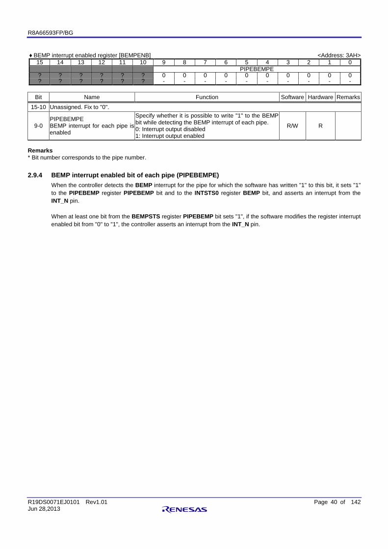
♦ BEMP interrupt enabled register [BEMPENB] <Address: 3AH>
15 14 13 12 11 10 9 8 7 6 5 4 3 2 1 0 PIPEBEMPE
? ? ? ? ? ? 0 0 0 0 0 0 0 0 0 0 ? ? ? ? ? ? - - - - - - - - - -
Bit Name Function Software Hardware Remarks
15-10 Unassigned. Fix to "0".
9-0 PIPEBEMPE BEMP interrupt for each pipe is enabled
Specify whether it is possible to write "1" to the BEMP bit while detecting the BEMP interrupt of each pipe. 0: Interrupt output disabled 1: Interrupt output enabled
R/W R
Remarks * Bit number corresponds to the pipe number.
2.9.4 BEMP interrupt enabled bit of each pipe (PIPEBEMPE) When the controller detects the BEMP interrupt for the pipe for which the software has written "1" to this bit, it sets "1" to the PIPEBEMP register PIPEBEMP bit and to the INTSTS0 register BEMP bit, and asserts an interrupt from the INT_N pin. When at least one bit from the BEMPSTS register PIPEBEMP bit sets "1", if the software modifies the register interrupt enabled bit from "0" to "1", the controller asserts an interrupt from the INT_N pin.
R8A66593FP/BG
R19DS0071EJ0101 Rev1.01 Page 41 of 142 Jun 28,2013
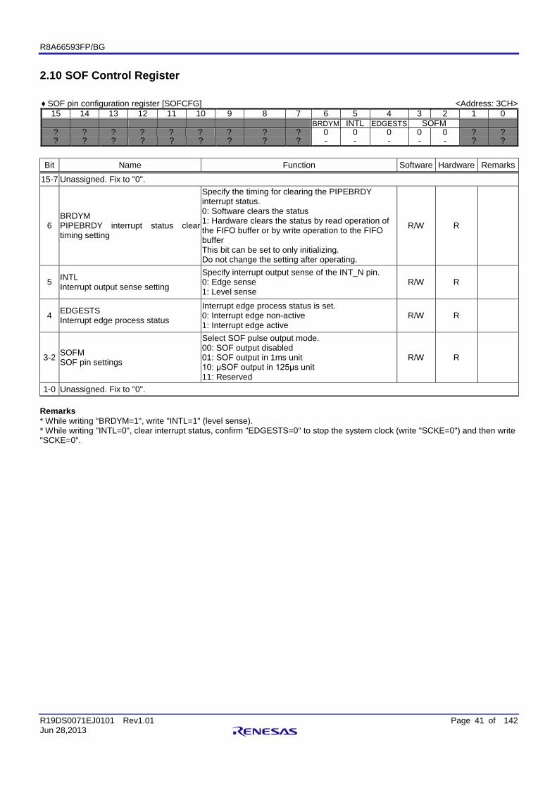
2.10 SOF Control Register ♦ SOF pin configuration register [SOFCFG] <Address: 3CH>
15 14 13 12 11 10 9 8 7 6 5 4 3 2 1 0 BRDYM INTL EDGESTS SOFM
? ? ? ? ? ? ? ? ? 0 0 0 0 0 ? ? ? ? ? ? ? ? ? ? ? - - - - - ? ?
Bit Name Function Software Hardware Remarks
15-7 Unassigned. Fix to "0".
6 BRDYM PIPEBRDY interrupt status clear timing setting
Specify the timing for clearing the PIPEBRDY interrupt status. 0: Software clears the status 1: Hardware clears the status by read operation of the FIFO buffer or by write operation to the FIFO buffer This bit can be set to only initializing. Do not change the setting after operating.
R/W R
5 INTL Interrupt output sense setting
Specify interrupt output sense of the INT_N pin. 0: Edge sense 1: Level sense
R/W R
4 EDGESTS Interrupt edge process status
Interrupt edge process status is set. 0: Interrupt edge non-active 1: Interrupt edge active
R/W R
3-2 SOFM SOF pin settings
Select SOF pulse output mode. 00: SOF output disabled 01: SOF output in 1ms unit 10: μSOF output in 125μs unit 11: Reserved
R/W R
1-0 Unassigned. Fix to "0". Remarks * While writing "BRDYM=1", write "INTL=1" (level sense). * While writing "INTL=0", clear interrupt status, confirm "EDGESTS=0" to stop the system clock (write "SCKE=0") and then write "SCKE=0".
R8A66593FP/BG
R19DS0071EJ0101 Rev1.01 Page 42 of 142 Jun 28,2013
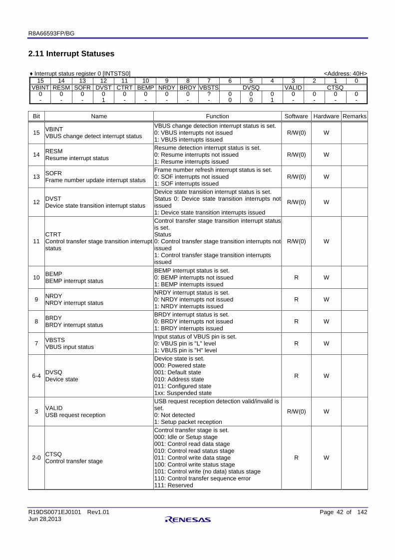
2.11 Interrupt Statuses ♦ Interrupt status register 0 [INTSTS0] <Address: 40H>
15 14 13 12 11 10 9 8 7 6 5 4 3 2 1 0 VBINT RESM SOFR DVST CTRT BEMP NRDY BRDY VBSTS DVSQ VALID CTSQ
0 0 0 0 0 0 0 0 ? 0 0 0 0 0 0 0 - - - 1 - - - - - 0 0 1 - - - -
Bit Name Function Software Hardware Remarks
15 VBINT VBUS change detect interrupt status
VBUS change detection interrupt status is set. 0: VBUS interrupts not issued 1: VBUS interrupts issued
R/W(0) W
14 RESM Resume interrupt status
Resume detection interrupt status is set. 0: Resume interrupts not issued 1: Resume interrupts issued
R/W(0) W
13 SOFR Frame number update interrupt status
Frame number refresh interrupt status is set. 0: SOF interrupts not issued 1: SOF interrupts issued
R/W(0) W
12 DVST Device state transition interrupt status
Device state transition interrupt status is set. Status 0: Device state transition interrupts not issued 1: Device state transition interrupts issued
R/W(0) W
11 CTRT Control transfer stage transition interrupt status
Control transfer stage transition interrupt status is set. Status 0: Control transfer stage transition interrupts not issued 1: Control transfer stage transition interrupts issued
R/W(0) W
10 BEMP BEMP interrupt status
BEMP interrupt status is set. 0: BEMP interrupts not issued 1: BEMP interrupts issued
R W
9 NRDY NRDY interrupt status
NRDY interrupt status is set. 0: NRDY interrupts not issued 1: NRDY interrupts issued
R W
8 BRDY BRDY interrupt status
BRDY interrupt status is set. 0: BRDY interrupts not issued 1: BRDY interrupts issued
R W
7 VBSTS VBUS input status
Input status of VBUS pin is set. 0: VBUS pin is "L" level 1: VBUS pin is "H" level
R W
6-4 DVSQ Device state
Device state is set. 000: Powered state 001: Default state 010: Address state 011: Configured state 1xx: Suspended state
R W
3 VALID USB request reception
USB request reception detection valid/invalid is set. 0: Not detected 1: Setup packet reception
R/W(0) W
2-0 CTSQ Control transfer stage
Control transfer stage is set. 000: Idle or Setup stage 001: Control read data stage 010: Control read status stage 011: Control write data stage 100: Control write status stage 101: Control write (no data) status stage 110: Control transfer sequence error 111: Reserved
R W
R8A66593FP/BG
R19DS0071EJ0101 Rev1.01 Page 43 of 142 Jun 28,2013
Remarks * To clear the status indicated by the VBINT, RESM, SOFR, DVST or CTRT bits, write "0" only for the bit to be cleared, and write "1" for other bits. Do not write "0" to the status bit set to "0". * The controller detects the change in status indicated by the VBINT and RESM bits of this register, even while the clock is being stopped ("SCKE=0"), and notifies the interrupt if the corresponding interrupt is enabled. When the clock is enabled, clear the status using software.
2.11.1 VBUS conversion interrupt status bit (VBINT) When the controller detects the change in the VBUS pin input value (from High to Low and from Low to High), "1" is written to this bit. The controller writes the input value of the VBUS pin to the VBSTS bit. When the VBINT interrupt occurs, use the software to execute a consistency check several times during the VBSTS bit read, and reject the chattering. When detect to attach or detach ,please process as follows. (1)When detect to attach: Set DRPPU bit to “1”. (2)When detect to detach: Please process as follows. (a) Set DRPPU bit to “0”. (b) Wait for 1us (1000ns)
(c) Set DCFM bit to “1” (b) Wait for 200ns
(e) Set DCFM bit to “0”
2.11.2 Resume interrupt status bit (RESM) The controller is in suspend status (DVSQ=1XX), and "1" is set to this bit when the DP pin falling edge is detected.
2.11.3 Frame number update interrupt status bit (SOFR) The conditions when the controller sets "1" in this bit are below. While updating the frame number, the controller sets "1" to this bit (this interrupt is detected every 1ms). The controller detects the SOFR interrupt by internal interpolation even if the SOF packet from the USB Host is corrupted.
2.11.4 Device state transition interrupt status bit (DVST) If the controller detects a change in the device state, it updates the DVSQ value and sets "1" to this bit. When this interrupt occurs, clear the status before the controller detects the next device status state transition.
R8A66593FP/BG
R19DS0071EJ0101 Rev1.01 Page 44 of 142 Jun 28,2013
2.11.5 Control transfer and stage transition interrupt status bit (CTRT) If the controller detects the stage transition of control transfer, it updates the CTSQ value and sets "1" to this bit. When this interrupt occurs, clear the status before the controller detects stage transition after the control transfer.
2.11.6 Buffer empty interrupt status bit (BEMP) The controller sets "1’ in the interrupt when, among the BEMPSTS register PIPEBEMP bits corresponding to the pipe for which "1" is written to the BEMPENB register PIPEBEMPE bit (when the controller detects the BEMP interrupt status for at least one pipe from the pipes for which the software has enabled the BEMP interrupt notification), at least one bit is "1". Refer to the PIPEBEMP register for assert conditions of the PIPEBEMP status. If the software writes "0" for all the PIPEBEMP bits corresponding to the pipe that is enabled by the PIPEBEMPE bit, the controller clears this bit to "0’. This bit cannot be cleared to "0" even if "0" is written to this bit by the software.
2.11.7 Buffer not ready interrupt status bit (NRDY) The controller sets "1" in the interrupt when, among the NRDYSTS register PIPENRDY bits corresponding to the pipe for which "1" is written to the NRDYENB register PIPENRDYE bit (when the controller detects the NRDY interrupt status for at least one pipe from the pipes for which the software has enabled the NRDY interrupt notification), at least one bit is "1". Refer to the PIPENRDY register for assert conditions of the PIPENRDY status. If the software writes "0" to all the PIPENRDY bits corresponding to the pipe that is enabled by the PIPENRDYE bit, the controller clears this bit to "0". This bit cannot be cleared to "0’ even if the software writes "0" to this bit.
2.11.8 Buffer ready interrupt status bit (BRDY) The controller sets "1" in the interrupt when, among the BRDYSTS register PIPEBRDY bits corresponding to the pipe for which "1" is written in the BRDYENB register PIPEBRDYE bit (when the controller detects the BRDY interrupt status for at least one pipe from the pipes for which the software has enabled the BRDY interrupt notification), at least one bit is "1". Refer to the PIPEBRDY register for the assert conditions of the PIPEBRDY status. If the software writes "0" to all the PIPEBRDY bits corresponding to the pipe that is enabled by the PIPEBRDYE bit, the controller clears this bit to "0". This bit cannot be cleared to "0" even if the software writes "0" to this bit.
R8A66593FP/BG
R19DS0071EJ0101 Rev1.01 Page 45 of 142 Jun 28,2013
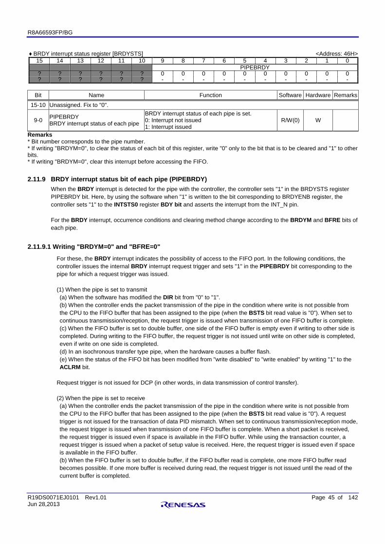
♦ BRDY interrupt status register [BRDYSTS] <Address: 46H>
15 14 13 12 11 10 9 8 7 6 5 4 3 2 1 0 PIPEBRDY
? ? ? ? ? ? 0 0 0 0 0 0 0 0 0 0 ? ? ? ? ? ? - - - - - - - - - -
Bit Name Function Software Hardware Remarks
15-10 Unassigned. Fix to "0".
9-0 PIPEBRDY BRDY interrupt status of each pipe
BRDY interrupt status of each pipe is set. 0: Interrupt not issued 1: Interrupt issued
R/W(0) W
Remarks * Bit number corresponds to the pipe number. * If writing "BRDYM=0", to clear the status of each bit of this register, write "0" only to the bit that is to be cleared and "1" to other bits. * If writing "BRDYM=0", clear this interrupt before accessing the FIFO.
2.11.9 BRDY interrupt status bit of each pipe (PIPEBRDY) When the BRDY interrupt is detected for the pipe with the controller, the controller sets "1" in the BRDYSTS register PIPEBRDY bit. Here, by using the software when "1" is written to the bit corresponding to BRDYENB register, the controller sets "1" to the INTSTS0 register BDY bit and asserts the interrupt from the INT_N pin. For the BRDY interrupt, occurrence conditions and clearing method change according to the BRDYM and BFRE bits of each pipe.
2.11.9.1 Writing "BRDYM=0" and "BFRE=0"
For these, the BRDY interrupt indicates the possibility of access to the FIFO port. In the following conditions, the controller issues the internal BRDY interrupt request trigger and sets "1" in the PIPEBRDY bit corresponding to the pipe for which a request trigger was issued.
(1) When the pipe is set to transmit (a) When the software has modified the DIR bit from "0" to "1". (b) When the controller ends the packet transmission of the pipe in the condition where write is not possible from the CPU to the FIFO buffer that has been assigned to the pipe (when the BSTS bit read value is "0"). When set to continuous transmission/reception, the request trigger is issued when transmission of one FIFO buffer is complete. (c) When the FIFO buffer is set to double buffer, one side of the FIFO buffer is empty even if writing to other side is completed. During writing to the FIFO buffer, the request trigger is not issued until write on other side is completed, even if write on one side is completed. (d) In an isochronous transfer type pipe, when the hardware causes a buffer flash. (e) When the status of the FIFO bit has been modified from "write disabled" to "write enabled" by writing "1" to the ACLRM bit.
Request trigger is not issued for DCP (in other words, in data transmission of control transfer).
(2) When the pipe is set to receive (a) When the controller ends the packet transmission of the pipe in the condition where write is not possible from the CPU to the FIFO buffer that has been assigned to the pipe (when the BSTS bit read value is "0"). A request trigger is not issued for the transaction of data PID mismatch. When set to continuous transmission/reception mode, the request trigger is issued when transmission of one FIFO buffer is complete. When a short packet is received, the request trigger is issued even if space is available in the FIFO buffer. While using the transaction counter, a request trigger is issued when a packet of setup value is received. Here, the request trigger is issued even if space is available in the FIFO buffer. (b) When the FIFO buffer is set to double buffer, if the FIFO buffer read is complete, one more FIFO buffer read becomes possible. If one more buffer is received during read, the request trigger is not issued until the read of the current buffer is completed.
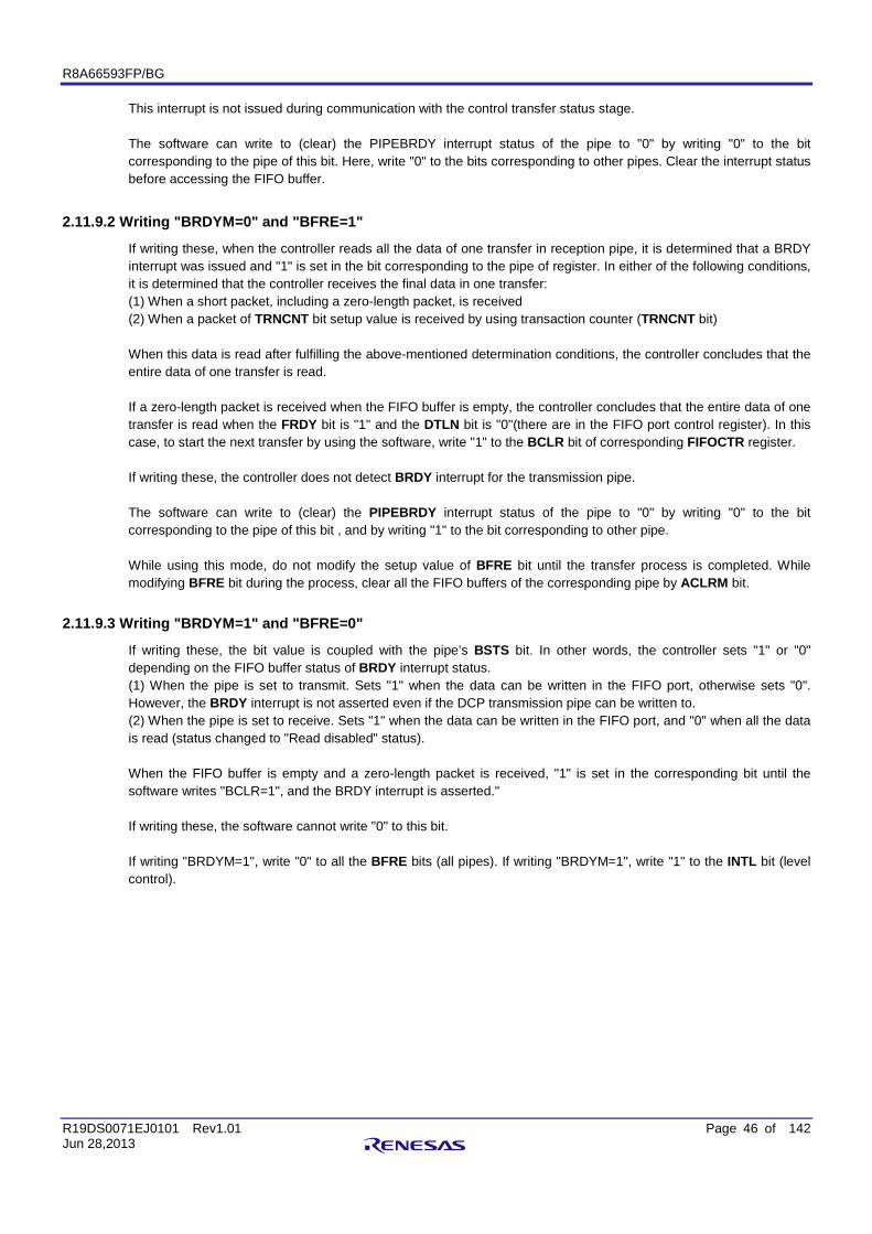
R8A66593FP/BG
R19DS0071EJ0101 Rev1.01 Page 46 of 142 Jun 28,2013
This interrupt is not issued during communication with the control transfer status stage. The software can write to (clear) the PIPEBRDY interrupt status of the pipe to "0" by writing "0" to the bit corresponding to the pipe of this bit. Here, write "0" to the bits corresponding to other pipes. Clear the interrupt status before accessing the FIFO buffer.
2.11.9.2 Writing "BRDYM=0" and "BFRE=1"
If writing these, when the controller reads all the data of one transfer in reception pipe, it is determined that a BRDY interrupt was issued and "1" is set in the bit corresponding to the pipe of register. In either of the following conditions, it is determined that the controller receives the final data in one transfer: (1) When a short packet, including a zero-length packet, is received (2) When a packet of TRNCNT bit setup value is received by using transaction counter (TRNCNT bit)
When this data is read after fulfilling the above-mentioned determination conditions, the controller concludes that the entire data of one transfer is read. If a zero-length packet is received when the FIFO buffer is empty, the controller concludes that the entire data of one transfer is read when the FRDY bit is "1" and the DTLN bit is "0"(there are in the FIFO port control register). In this case, to start the next transfer by using the software, write "1" to the BCLR bit of corresponding FIFOCTR register. If writing these, the controller does not detect BRDY interrupt for the transmission pipe. The software can write to (clear) the PIPEBRDY interrupt status of the pipe to "0" by writing "0" to the bit corresponding to the pipe of this bit , and by writing "1" to the bit corresponding to other pipe. While using this mode, do not modify the setup value of BFRE bit until the transfer process is completed. While modifying BFRE bit during the process, clear all the FIFO buffers of the corresponding pipe by ACLRM bit.
2.11.9.3 Writing "BRDYM=1" and "BFRE=0"
If writing these, the bit value is coupled with the pipe’s BSTS bit. In other words, the controller sets "1" or "0" depending on the FIFO buffer status of BRDY interrupt status. (1) When the pipe is set to transmit. Sets "1" when the data can be written in the FIFO port, otherwise sets "0". However, the BRDY interrupt is not asserted even if the DCP transmission pipe can be written to. (2) When the pipe is set to receive. Sets "1" when the data can be written in the FIFO port, and "0" when all the data is read (status changed to "Read disabled" status). When the FIFO buffer is empty and a zero-length packet is received, "1" is set in the corresponding bit until the software writes "BCLR=1", and the BRDY interrupt is asserted."
If writing these, the software cannot write "0" to this bit. If writing "BRDYM=1", write "0" to all the BFRE bits (all pipes). If writing "BRDYM=1", write "1" to the INTL bit (level control).
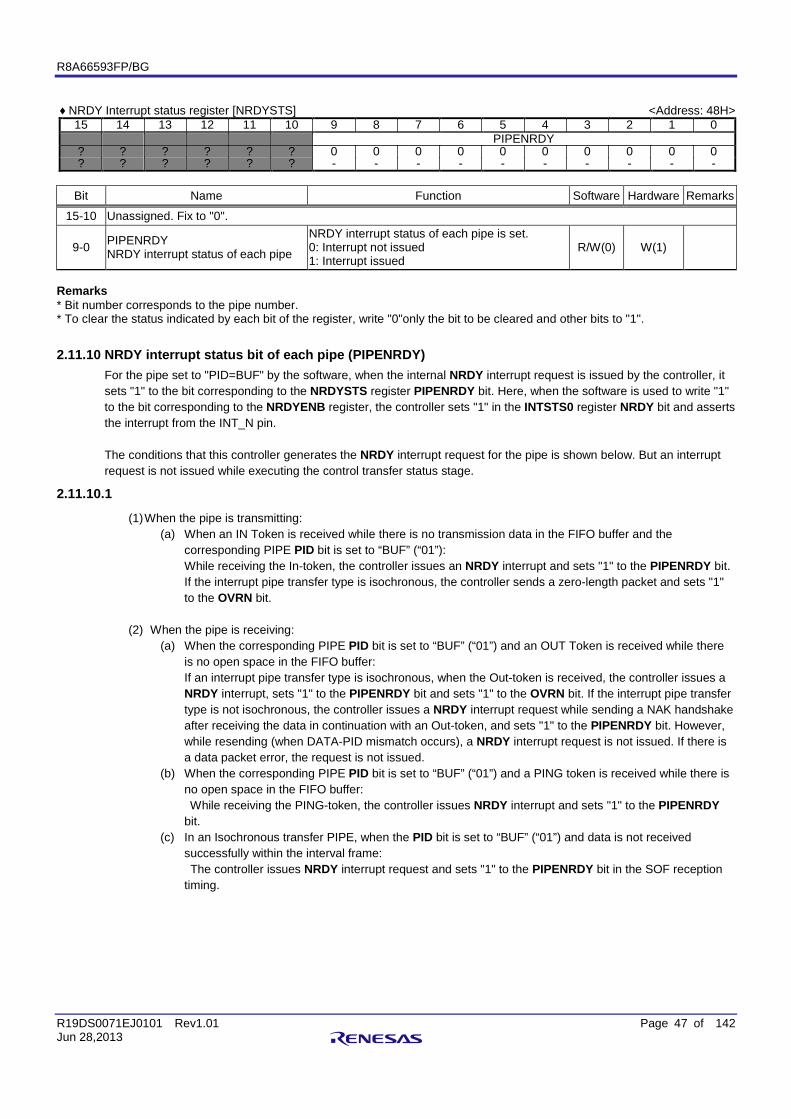
R8A66593FP/BG
R19DS0071EJ0101 Rev1.01 Page 47 of 142 Jun 28,2013
♦ NRDY Interrupt status register [NRDYSTS] <Address: 48H>
15 14 13 12 11 10 9 8 7 6 5 4 3 2 1 0 PIPENRDY
? ? ? ? ? ? 0 0 0 0 0 0 0 0 0 0 ? ? ? ? ? ? - - - - - - - - - -
Bit Name Function Software Hardware Remarks
15-10 Unassigned. Fix to "0".
9-0 PIPENRDY NRDY interrupt status of each pipe
NRDY interrupt status of each pipe is set. 0: Interrupt not issued 1: Interrupt issued
R/W(0) W(1)
Remarks * Bit number corresponds to the pipe number. * To clear the status indicated by each bit of the register, write "0"only the bit to be cleared and other bits to "1".
2.11.10 NRDY interrupt status bit of each pipe (PIPENRDY) For the pipe set to "PID=BUF" by the software, when the internal NRDY interrupt request is issued by the controller, it sets "1" to the bit corresponding to the NRDYSTS register PIPENRDY bit. Here, when the software is used to write "1" to the bit corresponding to the NRDYENB register, the controller sets "1" in the INTSTS0 register NRDY bit and asserts the interrupt from the INT_N pin. The conditions that this controller generates the NRDY interrupt request for the pipe is shown below. But an interrupt request is not issued while executing the control transfer status stage.
2.11.10.1
(1) When the pipe is transmitting: (a) When an IN Token is received while there is no transmission data in the FIFO buffer and the
corresponding PIPE PID bit is set to “BUF” (“01”): While receiving the In-token, the controller issues an NRDY interrupt and sets "1" to the PIPENRDY bit. If the interrupt pipe transfer type is isochronous, the controller sends a zero-length packet and sets "1" to the OVRN bit.
(2) When the pipe is receiving:
(a) When the corresponding PIPE PID bit is set to “BUF” (“01”) and an OUT Token is received while there is no open space in the FIFO buffer: If an interrupt pipe transfer type is isochronous, when the Out-token is received, the controller issues a NRDY interrupt, sets "1" to the PIPENRDY bit and sets "1" to the OVRN bit. If the interrupt pipe transfer type is not isochronous, the controller issues a NRDY interrupt request while sending a NAK handshake after receiving the data in continuation with an Out-token, and sets "1" to the PIPENRDY bit. However, while resending (when DATA-PID mismatch occurs), a NRDY interrupt request is not issued. If there is a data packet error, the request is not issued.
(b) When the corresponding PIPE PID bit is set to “BUF” (“01”) and a PING token is received while there is no open space in the FIFO buffer: While receiving the PING-token, the controller issues NRDY interrupt and sets "1" to the PIPENRDY bit.
(c) In an Isochronous transfer PIPE, when the PID bit is set to “BUF” (“01”) and data is not received successfully within the interval frame: The controller issues NRDY interrupt request and sets "1" to the PIPENRDY bit in the SOF reception timing.
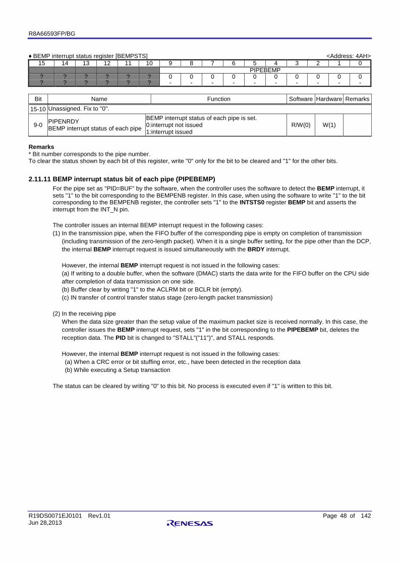
R8A66593FP/BG
R19DS0071EJ0101 Rev1.01 Page 48 of 142 Jun 28,2013
♦ BEMP interrupt status register [BEMPSTS] <Address: 4AH>
15 14 13 12 11 10 9 8 7 6 5 4 3 2 1 0 PIPEBEMP
? ? ? ? ? ? 0 0 0 0 0 0 0 0 0 0 ? ? ? ? ? ? - - - - - - - - - -
Bit Name Function Software Hardware Remarks
15-10 Unassigned. Fix to "0".
9-0 PIPENRDY BEMP interrupt status of each pipe
BEMP interrupt status of each pipe is set. 0:interrupt not issued 1:interrupt issued
R/W(0) W(1)
Remarks * Bit number corresponds to the pipe number. To clear the status shown by each bit of this register, write "0" only for the bit to be cleared and "1" for the other bits.
2.11.11 BEMP interrupt status bit of each pipe (PIPEBEMP) For the pipe set as "PID=BUF" by the software, when the controller uses the software to detect the BEMP interrupt, it sets "1" to the bit corresponding to the BEMPENB register. In this case, when using the software to write "1" to the bit corresponding to the BEMPENB register, the controller sets "1" to the INTSTS0 register BEMP bit and asserts the interrupt from the INT_N pin. The controller issues an internal BEMP interrupt request in the following cases: (1) In the transmission pipe, when the FIFO buffer of the corresponding pipe is empty on completion of transmission
(including transmission of the zero-length packet). When it is a single buffer setting, for the pipe other than the DCP, the internal BEMP interrupt request is issued simultaneously with the BRDY interrupt. However, the internal BEMP interrupt request is not issued in the following cases: (a) If writing to a double buffer, when the software (DMAC) starts the data write for the FIFO buffer on the CPU side after completion of data transmission on one side. (b) Buffer clear by writing "1" to the ACLRM bit or BCLR bit (empty). (c) IN transfer of control transfer status stage (zero-length packet transmission)
(2) In the receiving pipe When the data size greater than the setup value of the maximum packet size is received normally. In this case, the controller issues the BEMP interrupt request, sets "1" in the bit corresponding to the PIPEBEMP bit, deletes the reception data. The PID bit is changed to "STALL"("11")", and STALL responds. However, the internal BEMP interrupt request is not issued in the following cases: (a) When a CRC error or bit stuffing error, etc., have been detected in the reception data (b) While executing a Setup transaction
The status can be cleared by writing "0" to this bit. No process is executed even if "1" is written to this bit.
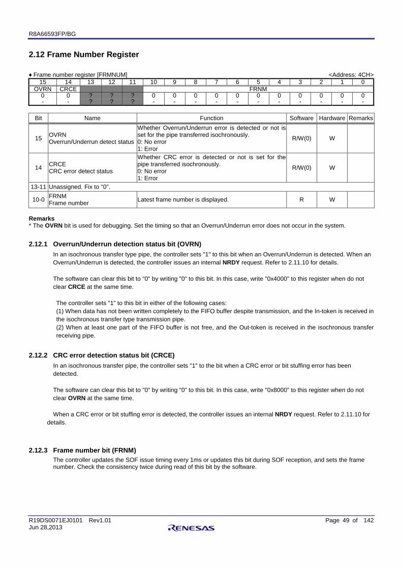
R8A66593FP/BG
R19DS0071EJ0101 Rev1.01 Page 49 of 142 Jun 28,2013
2.12 Frame Number Register ♦ Frame number register [FRMNUM] <Address: 4CH>
15 14 13 12 11 10 9 8 7 6 5 4 3 2 1 0 OVRN CRCE FRNM
0 0 ? ? ? 0 0 0 0 0 0 0 0 0 0 0 - - ? ? ? - - - - - - - - - - -
Bit Name Function Software Hardware Remarks
15 OVRN Overrun/Underrun detect status
Whether Overrun/Underrun error is detected or not is set for the pipe transferred isochronously. 0: No error 1: Error
R/W(0) W
14 CRCE CRC error detect status
Whether CRC error is detected or not is set for the pipe transferred isochronously. 0: No error 1: Error
R/W(0) W
13-11 Unassigned. Fix to "0".
10-0 FRNM Frame number Latest frame number is displayed. R W
Remarks * The OVRN bit is used for debugging. Set the timing so that an Overrun/Underrun error does not occur in the system.
2.12.1 Overrun/Underrun detection status bit (OVRN) In an isochronous transfer type pipe, the controller sets "1" to this bit when an Overrun/Underrun is detected. When an Overrun/Underrun is detected, the controller issues an internal NRDY request. Refer to 2.11.10 for details. The software can clear this bit to "0" by writing "0" to this bit. In this case, write "0x4000" to this register when do not clear CRCE at the same time. The controller sets "1" to this bit in either of the following cases: (1) When data has not been written completely to the FIFO buffer despite transmission, and the In-token is received in the isochronous transfer type transmission pipe. (2) When at least one part of the FIFO buffer is not free, and the Out-token is received in the isochronous transfer receiving pipe.
2.12.2 CRC error detection status bit (CRCE) In an isochronous transfer pipe, the controller sets "1" to the bit when a CRC error or bit stuffing error has been detected. The software can clear this bit to "0" by writing "0" to this bit. In this case, write "0x8000” to this register when do not clear OVRN at the same time. When a CRC error or bit stuffing error is detected, the controller issues an internal NRDY request. Refer to 2.11.10 for
details.
2.12.3 Frame number bit (FRNM) The controller updates the SOF issue timing every 1ms or updates this bit during SOF reception, and sets the frame number. Check the consistency twice during read of this bit by the software.
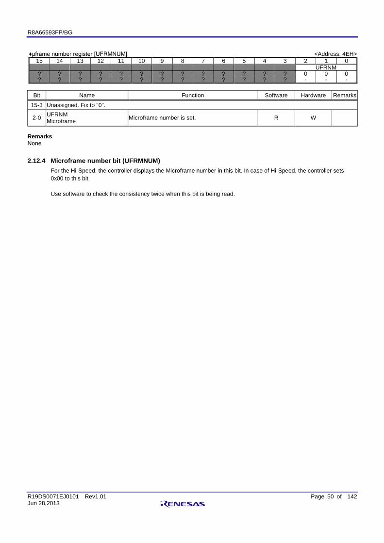
R8A66593FP/BG
R19DS0071EJ0101 Rev1.01 Page 50 of 142 Jun 28,2013
♦μframe number register [UFRMNUM] <Address: 4EH>
15 14 13 12 11 10 9 8 7 6 5 4 3 2 1 0 UFRNM
? ? ? ? ? ? ? ? ? ? ? ? ? 0 0 0 ? ? ? ? ? ? ? ? ? ? ? ? ? - - -
Bit Name Function Software Hardware Remarks
15-3 Unassigned. Fix to "0".
2-0 UFRNM Microframe Microframe number is set. R W
Remarks None
2.12.4 Microframe number bit (UFRMNUM) For the Hi-Speed, the controller displays the Microframe number in this bit. In case of Hi-Speed, the controller sets 0x00 to this bit. Use software to check the consistency twice when this bit is being read.
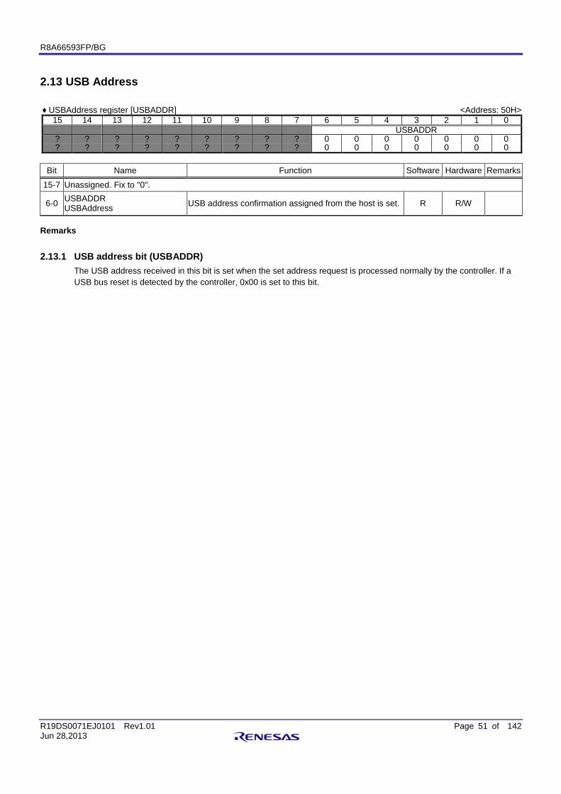
R8A66593FP/BG
R19DS0071EJ0101 Rev1.01 Page 51 of 142 Jun 28,2013
2.13 USB Address ♦ USBAddress register [USBADDR] <Address: 50H>
15 14 13 12 11 10 9 8 7 6 5 4 3 2 1 0 USBADDR
? ? ? ? ? ? ? ? ? 0 0 0 0 0 0 0 ? ? ? ? ? ? ? ? ? 0 0 0 0 0 0 0
Bit Name Function Software Hardware Remarks
15-7 Unassigned. Fix to "0".
6-0 USBADDR USBAddress USB address confirmation assigned from the host is set. R R/W
Remarks
2.13.1 USB address bit (USBADDR) The USB address received in this bit is set when the set address request is processed normally by the controller. If a USB bus reset is detected by the controller, 0x00 is set to this bit.
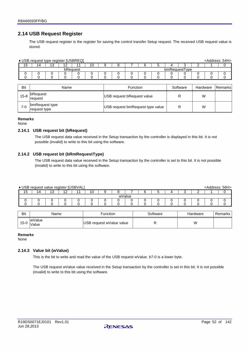
R8A66593FP/BG
R19DS0071EJ0101 Rev1.01 Page 52 of 142 Jun 28,2013
2.14 USB Request Register The USB request register is the register for saving the control transfer Setup request. The received USB request value is stored.
♦ USB request type register [USBREQ] <Address: 54H> 15 14 13 12 11 10 9 8 7 6 5 4 3 2 1 0
bRequest bmRequestType 0 0 0 0 0 0 0 0 0 0 0 0 0 0 0 0 0 0 0 0 0 0 0 0 0 0 0 0 0 0 0 0
Bit Name Function Software Hardware Remarks
15-8 bRequest request USB request bRequest value R W
7-0 bmRequest type request type USB request bmRequest type value R W
Remarks None
2.14.1 USB request bit (bRequest) The USB request data value received in the Setup transaction by the controller is displayed in this bit. It is not possible (invalid) to write to this bit using the software.
2.14.2 USB request bit (bRmRequestType) The USB request data value received in the Setup transaction by the controller is set to this bit. It is not possible (invalid) to write to this bit using the software.
♦ USB request value register [USBVAL] <Address: 56H> 15 14 13 12 11 10 9 8 7 6 5 4 3 2 1 0
wValue 0 0 0 0 0 0 0 0 0 0 0 0 0 0 0 0 0 0 0 0 0 0 0 0 0 0 0 0 0 0 0 0
Bit Name Function Software Hardware Remarks
15-0 wValue Value USB request wValue value R W
Remarks None
2.14.3 Value bit (wValue) This is the bit to write and read the value of the USB request wValue. b7-0 is a lower byte. The USB request wValue value received in the Setup transaction by the controller is set in this bit. It is not possible (invalid) to write to this bit using the software.
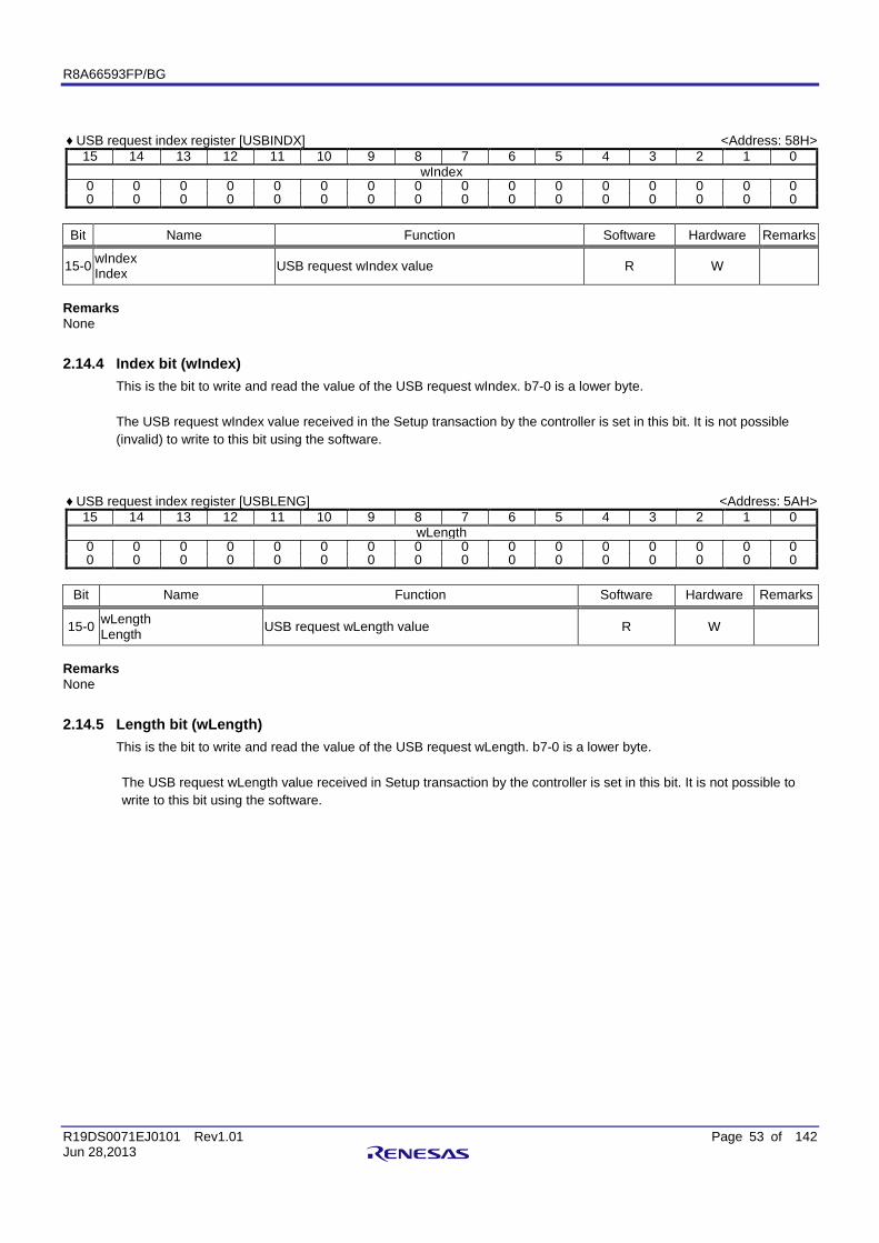
R8A66593FP/BG
R19DS0071EJ0101 Rev1.01 Page 53 of 142 Jun 28,2013
♦ USB request index register [USBINDX] <Address: 58H> 15 14 13 12 11 10 9 8 7 6 5 4 3 2 1 0
wIndex 0 0 0 0 0 0 0 0 0 0 0 0 0 0 0 0 0 0 0 0 0 0 0 0 0 0 0 0 0 0 0 0
Bit Name Function Software Hardware Remarks
15-0 wIndex Index USB request wIndex value R W
Remarks None
2.14.4 Index bit (wIndex) This is the bit to write and read the value of the USB request wIndex. b7-0 is a lower byte. The USB request wIndex value received in the Setup transaction by the controller is set in this bit. It is not possible (invalid) to write to this bit using the software.
♦ USB request index register [USBLENG] <Address: 5AH> 15 14 13 12 11 10 9 8 7 6 5 4 3 2 1 0
wLength 0 0 0 0 0 0 0 0 0 0 0 0 0 0 0 0 0 0 0 0 0 0 0 0 0 0 0 0 0 0 0 0
Bit Name Function Software Hardware Remarks
15-0 wLength Length USB request wLength value R W
Remarks None
2.14.5 Length bit (wLength) This is the bit to write and read the value of the USB request wLength. b7-0 is a lower byte. The USB request wLength value received in Setup transaction by the controller is set in this bit. It is not possible to write to this bit using the software.
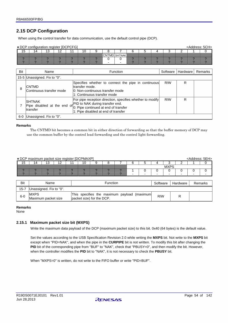
R8A66593FP/BG
R19DS0071EJ0101 Rev1.01 Page 54 of 142 Jun 28,2013
2.15 DCP Configuration When using the control transfer for data communication, use the default control pipe (DCP). ♦ DCP configuration register [DCPCFG] <Address: 5CH>
15 14 13 12 11 10 9 8 7 6 5 4 3 2 1 0 CNTMD SHTNAK
? ? ? ? ? ? ? 0 0 ? ? ? ? ? ? ? ? ? ? ? ? ? ? - - ? ? ? ? ? ? ?
Bit Name Function Software Hardware Remarks
15-5 Unassigned. Fix to "0".
8 CNTMD Continuous transfer mode
Specifies whether to connect the pipe in continuous transfer mode. 0: Non-continuous transfer mode 1: Continuous transfer mode
R/W R
7 SHTNAK Pipe disabled at the end of transfer
For pipe reception direction, specifies whether to modify PID to NAK during transfer end. 0: Pipe continued at end of transfer 1: Pipe disabled at end of transfer
R/W R
6-0 Unassigned. Fix to "0". Remarks
The CNTMD bit becomes a common bit in either direction of forwarding so that the buffer memory of DCP may use the common buffer by the control lead forwarding and the control light forwarding.
♦ DCP maximum packet size register [DCPMAXP] <Address: 5EH>
15 14 13 12 11 10 9 8 7 6 5 4 3 2 1 0 MXPS
? ? ? ? ? ? ? ? ? 1 0 0 0 0 0 0 ? ? ? ? ? ? ? ? ? - - - - - - -
Bit Name Function Software Hardware Remarks
15-7 Unassigned. Fix to "0".
6-0 MXPS Maximum packet size
This specifies the maximum payload (maximum packet size) for the DCP. R/W R
Remarks None
2.15.1 Maximum packet size bit (MXPS) Write the maximum data payload of the DCP (maximum packet size) to this bit. 0x40 (64 bytes) is the default value. Set the values according to the USB Specification Revision 2.0 while writing the MXPS bit. Not write to the MXPS bit except when "PID=NAK", and when the pipe in the CURPIPE bit is not written. To modify this bit after changing the PID bit of the corresponding pipe from "BUF" to "NAK", check that "PBUSY=0", and then modify the bit. However, when the controller modifies the PID bit to "NAK", it is not necessary to check the PBUSY bit. When "MXPS=0" is written, do not write to the FIFO buffer or write "PID=BUF".
R8A66593FP/BG
R19DS0071EJ0101 Rev1.01 Page 55 of 142 Jun 28,2013
♦ DCP control register [DCPCTR] <Address: 60H>
15 14 13 12 11 10 9 8 7 6 5 4 3 2 1 0 BSTS SQCLR SQSET SQMON PBUSY CCPL PID
0 ? ? ? ? ? ? 0 0 1 0 ? ? 0 0 0 - ? ? ? ? ? ? - - - - ? ? 0 0 0
Bit Name Function Software Hardware Remarks
15 BSTS Buffer status
Access possibility status of DCP FIFO buffer is set. 0: Buffer access is disabled 1: Buffer access is enabled
R W
14-9 Unassigned. Fix to "0".
8 SQCLR Toggle bit clear
In DCP transfer, the expected value of sequence toggle bit of next transaction can be written to DATA0. 0: Invalid 1: Specifies DATA0
R(0)/W(1) R
7 SQSET Toggle bit set
In the DCP transfer, the expected value of the sequence toggle bit of the next transaction can be written to DATA1. 0: Invalid 1: Specifies DATA1
R(0)/W(1) R
6 SQMON Sequence toggle bit monitor
In the DCP transfer, the expected value of the sequence toggle bit of the next transaction is set. 0: DATA0 1: DATA1
R W
5 PBUSY Pipe busy
Sets whether the pipe is being used by the current USB bus. 0: Pipe not used in the USB bus 1: Pipe used in the USB bus
R W
4-3 Unassigned. Fix to "0".
2 CCPL Control transfer end enabled
Status stage end of control transfer is enabled by writing "1" to this bit. 0: Invalid 1: Control transfer end enabled
R(0)/W(1) R/W(0)
1-0 PID Response PID
This bit controls the controller response in the control transfer. 00: NAK response 01: BUF response (conforms with the buffer state) 10: STALL response 11: STALL response
R/W R/W
Remarks None
2.15.2 Buffer status bit (BSTS) The controller indicates by this bit whether access of the FIFO buffer assigned to the DCP is possible from the CPU. The meaning of this bit differs according to the setup value of the ISEL bit as follows: (1) When "ISEL=0": Indicates whether read of reception data is possible. (2) When "ISEL=1": Indicates whether write of transmission data is possible.
2.15.3 Clear bit of sequence toggle bit (SQCLR) If the software writes "1" to this bit, the controller writes the expected value of the sequence toggle bit of the pipe to DATA0. The controller always sets "0" to this bit. Do not write "1" to the SQCLR bit and SQSET bit simultaneously. Write "1" to this bit when "PID=NAK". To write "1" to this bit after modifying the PID bit of the corresponding pipe from "BUF" to "NAK", check that "PBUSY=0", and then write the bit. However, since the controller has modified the PID bit to "NAK", it is not necessary to check the PBUSY bit.
R8A66593FP/BG
R19DS0071EJ0101 Rev1.01 Page 56 of 142 Jun 28,2013
2.15.4 Sequence toggle bit set bit (SQSET) If the software writes "1" to this bit, the controller writes the expected value sequence toggle bit of the pipe to DATA1. The controller always sets "0" to this bit. Do not write "1" to the SQCLR bit and SQSET bit simultaneously. Write "1" to this bit when "PID=NAK". To write "1" to this bit after modifying the PID bit of the corresponding pipe from "BUF" to "NAK", check that "PBUSY=0", and then write the bit. However, since the controller modifies the PID bit to "NAK", it is not necessary to check the PBUSY bit.
2.15.5 Sequence toggle bit monitor bit (SQMON) The controller sets the expected value of the sequence toggle bit of the pipe in this bit. If a normal process is executed for the transaction, the controller toggles this bit. However, the bit is not toggled when a DATA-PID mismatch occurs during reception transfer. The controller writes "1" to this bit (writes the expected value to "1") when the Setup packet is received normally. The controller does not refer to this bit during IN/OUT transaction of the status stage. It does not toggle the bit even if the process is completed normally.
2.15.6 Pipe busy bit (PBUSY) The controller modifies this bit from "0" to "1" when the USB transaction of the pipe is started. This bit is modified from "1" to "0’ when one transaction is complete. When the software has written "PID=NAK", it is possible to check whether the pipe setting can be modified by reading this bit.
2.15.7 Control transfer end enabled (CCPL) If the corresponding PID bit is "BUF" and the software writes "1" to this bit, the controller completes the control transfer stage. In other words, it transmits an ACK handshake for the OUT transaction from the USB Host during a Control Read Transfer, and transmits a zero-length packet for an IN transaction from the USB Host during a Control Write and No Data Control Transfer. However, irrespective of the setup value of this bit, the controller responds automatically from the Setup stage until the status stage is complete when a SET_ADDRESS request is detected. When a new Setup packet is received, the controller modifies this bit from "1" to "0". When "VALID=1", the software cannot write "1" to this bit.
2.15.8 Response PID bit (PID) For this bit, while executing data stage or status stage of control transfer, use the software to modify this bit from "NAK" to "BUF".
The controller modifies the bit value in the following cases: (1) When the controller receives the Setup packet, the controller modifies this bit to "NAK" ("00"). Here, the controller sets "VALID=1" and the software cannot modify this bit until it writes "VALID=0". (2) When the software writes "BUF" to this bit and the controller receives the data exceeding the maximum packet size, the controller sets "PID=STALL(11)". (3) When the controller detects a control transfer sequence error, it sets "PID=STALL(1x)". (4) When the controller detects a USB bus reset, it sets "PID=NAK".
During a SET_ADDRESS request process (auto process), the controller does not refer to the setup value of this bit.
R8A66593FP/BG
R19DS0071EJ0101 Rev1.01 Page 57 of 142 Jun 28,2013
2.16 Pipe Configuration Register Pipe1 - Pipe9 should be written to using the PIPESEL, PIPECFG, PIPEBUF, PIPEMAXP, PIPEPERI, PIPExCTR, PIPExTRE and PIPExTRN registers. After selecting the pipe using the PIPESEL register, write to the pipe functions using the PIPECFG, PIPEBUF, PIPEMAXP and PIPEPERI registers. The PIPExCTR, PIPExTRE and PIPExTRN registers can be written to separately from the pipe selection specified with the PIPESEL register, with no relation between them.
♦ Pipe window selection register [PIPESEL] <Address: 64H>
15 14 13 12 11 10 9 8 7 6 5 4 3 2 1 0 PIPESEL
? ? ? ? ? ? ? ? ? ? ? ? 0 0 0 0 ? ? ? ? ? ? ? ? ? ? ? ? - - - -
Bit Name Function Software Hardware Remarks
15-4 Unassigned. Fix to "0".
3-0 PIPESEL Pipe window selection
Specifies pipe related to Address68H-6EH register. 0000: Not selected 0001: Pipe1 0010: Pipe2 0011: Pipe3 0100: Pipe4 0101: Pipe5 0110: Pipe6 0111: Pipe7 1000: Pipe8 1001: Pipe9
R/W R
Remarks * When "PIPESEL=0000", "0" is read from all of the bits of the related registers noted above. When "PIPESEL=0000", write to the pipe related to Address68H-6EH register is invalid.
2.16.1 Pipe window selection bit (PIPESEL) If the software writes "0001" to "1001" to this bit, the controller displays the pipe information and the setup value corresponding to the registers from address H68 to H6C. After pipe specification writing of this bit, the value written by the software in address H68 to H6C is reflected in the corresponding pipe transfer method. If the software writes "0000" to this bit, the controller setss all "0" in the register from address H68 to H6C. Using software to write to address H68 to H6C is invalid.
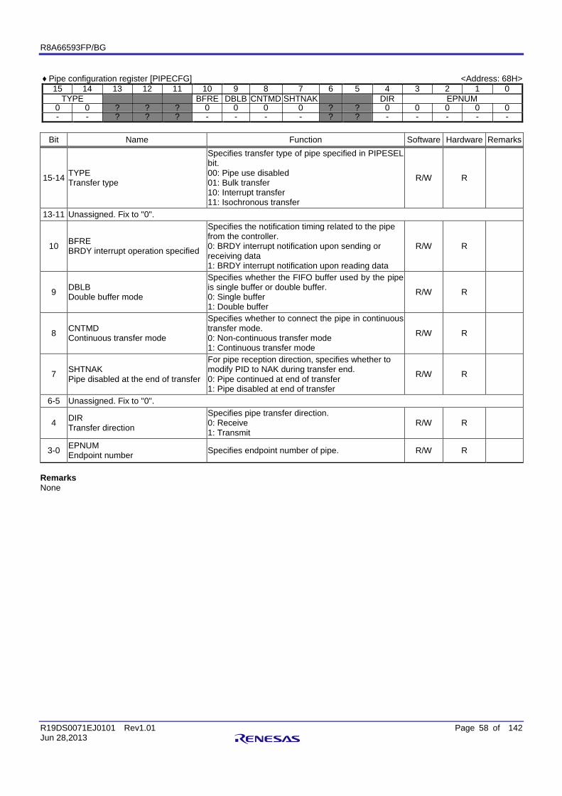
R8A66593FP/BG
R19DS0071EJ0101 Rev1.01 Page 58 of 142 Jun 28,2013
♦ Pipe configuration register [PIPECFG] <Address: 68H>
15 14 13 12 11 10 9 8 7 6 5 4 3 2 1 0 TYPE BFRE DBLB CNTMD SHTNAK DIR EPNUM
0 0 ? ? ? 0 0 0 0 ? ? 0 0 0 0 0 - - ? ? ? - - - - ? ? - - - - -
Bit Name Function Software Hardware Remarks
15-14 TYPE Transfer type
Specifies transfer type of pipe specified in PIPESEL bit. 00: Pipe use disabled 01: Bulk transfer 10: Interrupt transfer 11: Isochronous transfer
R/W R
13-11 Unassigned. Fix to "0".
10 BFRE BRDY interrupt operation specified
Specifies the notification timing related to the pipe from the controller. 0: BRDY interrupt notification upon sending or receiving data 1: BRDY interrupt notification upon reading data
R/W R
9 DBLB Double buffer mode
Specifies whether the FIFO buffer used by the pipe is single buffer or double buffer. 0: Single buffer 1: Double buffer
R/W R
8 CNTMD Continuous transfer mode
Specifies whether to connect the pipe in continuous transfer mode. 0: Non-continuous transfer mode 1: Continuous transfer mode
R/W R
7 SHTNAK Pipe disabled at the end of transfer
For pipe reception direction, specifies whether to modify PID to NAK during transfer end. 0: Pipe continued at end of transfer 1: Pipe disabled at end of transfer
R/W R
6-5 Unassigned. Fix to "0".
4 DIR Transfer direction
Specifies pipe transfer direction. 0: Receive 1: Transmit
R/W R
3-0 EPNUM Endpoint number Specifies endpoint number of pipe. R/W R
Remarks None
R8A66593FP/BG
R19DS0071EJ0101 Rev1.01 Page 59 of 142 Jun 28,2013
2.16.2 Transfer type bit (TYPE) For this bit, write to USB transfer type of pipe (selected pipe) written to the PIPESEL bit. A list of transfer types that can be written to the selected pipe and this bit are shown in Table 2.11.
Table 2.11 List of Transfer Types That Can Be Written To The Selected Pipe & TYPE bit
Selected Pipe TYPE Bit USB Transfer Type Pipe1 or Pipe2 "01" or "11" Bulk or isochronous transfer Pipe3 ~ Pipe5 "01" Bulk transfer Pipe6 ~ Pipe9 "10" Interrupt transfer
Write a value other than "00" to this bit and then write "PID=BUF" (USB communication is started by writing "PID=BUF" when using the selected pipe). This bit can be modified when the PID bit of the selected pipe is in "NAK" status. To modify this bit after chenging the PID bit of the selected pipe from "BUF" to "NAK", check that "PBUSY=0", and then modify the bit. However, when the controller modifies the PID bit to "NAK", it is not necessary to check the PBUSY bit.
2.16.3 BRDY interrupt operation specification bit (BFRE) This bit is valid when the selected pipes are Pipe1 to Pipe5. When the software has written "1" to this bit and the selected pipe is used in reception, (i.e. when "DIR bit=0" is written), the controller detects transfer completion and issues a BRDY interrupt when that packet is completely read. When the BRDY interrupt is issued with these settings, the software need write "BCLR=1". The status of the FIFO buffer assigned to the selected pipe does not change to receive status until "BCLR=1". The software writes "1" to this bit and the selected pipe is used in transmission, (in other words when "DIR bit=1" is written) the controller does not issue the BRDY interrupt. Refer to the PIPEBRDY interrupt register for details. This bit can be modified when "PID=NAK", and when the pipe is in the CURPIPE bit is not written. Execute USB communication by using the selected pipe, use the software to continuously write "ACLRM=1" and "ACLRM=0", clear the FIFO buffer assigned to the selected pipe, and then modify this bit in addition to the status of the above three registers. To modify this bit after chenging the PID bit of the selected pipe from "BUF" to "NAK", check that "PBUSY=0", and modify the bit. However, when the controller has modified the PID bit to "NAK", it is not necessary to check the PBUSY bit.
R8A66593FP/BG
R19DS0071EJ0101 Rev1.01 Page 60 of 142 Jun 28,2013
2.16.4 Double buffer mode bit (DBLB) This bit is valid when the selected pipe is Pipe1 to Pipe5. When the software writes "1" to this bit, for the selected pipe the controller assigns the FIFO buffer size equal to two sides specified by the PIPEBUF register BUFSIZE bit. In other words, the size of the FIFO buffer that is assigned by the controller to the selected pipe is given below. (BUFSIZE+1)*64*(DBLB+1) [Byte] When the software writes "1" to this bit, and the selected pipe is used in transmission (written to "DIR bit=1"), the controller does not issue a BRDY interrupt. Refer to the PIPEBRDY interrupt register for details. This bit can be modified when "PID=NAK", and when the pipe in the CURPIPE bit is not written. Execute USB communication using the selected pipe, use the software to continuously write "ACLRM=1" and "ACLRM=0", clear the FIFO buffer assigned to the selected pipe, and then modify this bit in addition to the status of the above three registers. Check that "PBUSY=0", modify the PID bit of the selected pipe from "BUF" to "NAK" and then modify this bit. However, when the controller has modified the PID bit to "NAK", it is not necessary to use the software to check the PBUSY bit.
2.16.5 Continuous transfer mode bit (CNTMD) This bit is valid when Pipe1 to Pipe5 are selected and the transfer type of the selected pipe is set to bulk. According to the setup value of this bit, this controller determines transmission/reception completion for the FIFO buffer assigned to the selected pipe, as shown in Table 2.12.
Table 2.12 Relation Between Transmission/Reception Completion Determination for the CNTMD Setup Value and the FIFO Buffer
CNTMD bit Setup value Method of judging state that can be read or transmitted
0 If the reception direction has been written ("DIR=0"), the condition when the status of the FIFO buffer changes to Read Possible. When the controller has received one packet.
If transmission direction has been written ("DIR=1"), the condition when the status of the FIFO buffer changes to Transmission Possible. When following conditions are fulfilled: (1) The software (or DMAC) has written the data of maximum packet size in the FIFO buffer. (2) The software (or DMAC) has written the data of short packet (including the case of 0 byte) and "BVAL=1".
1
If the reception direction has been written ("DIR=0"), the conditions when the status of the FIFO buffer change to Read Possible When (1), (2) , (3) or (4) from the following conditions is fulfilled: (1) When the number of bytes of received data in the specified FIFO buffer of the selected PIPE matches the set number of bytes ((BUFSIZE+1)*64)
(2) When the controller receives a short packet other than a zero-length packet (3) When the contoller receives a Zero-Length packet even though data is already stored in the specified FIFO buffer of the selected PIPE. (4) When the controller receives packets as many as the transaction counter set for the selected pipe.
If the transmission direction has been written ("DIR=1"), the condition when the status of the FIFO buffer changes to Transmission Possible. When (1), (2) or (3) from the following conditions is fulfilled: (1) When the data count written by the software (or DMAC) does match with one side of FIFO buffer size
assigned to the selected pipe. (2) When the software (or DMAC) writes the data (including 0 bytes) smaller than the data on one side of
FIFO buffer assigned to the selected pipe and "BVAL=1". (3) When the software writes the data (including 0 bytes) smaller than the data on one side of FIFO buffer assigned to the selected pipe and asserts the DENDx_N signal simultaneously with write of the data for the
R8A66593FP/BG
R19DS0071EJ0101 Rev1.01 Page 61 of 142 Jun 28,2013
last time. This bit can be modified when "PID=NAK", and when the pipe in the CURPIPE bit is not written to. Execute USB communication using the selected pipe, use the software to continuously write "ACLRM=1" and "ACLRM=0", clear the FIFO buffer assigned to the selected pipe, and then modify this bit in addition to the status of the above three registers. To modify this bit after changing the PID bit of the corresponding pipe from "BUF" to "NAK", check that "PBUSY=0", and modify the bit. However, when the controller has modified the PID bit to "NAK", it is not necessary tto check the PBUSY bit.
2.16.6 Pipe disabled at the end of transfer bit (SHTNAK) This bit is valid when Pipe1 to Pipe5 are selected and is receiving. When the software has set "1" to this bit for the receiving pipe, when the transfer end is determined for the selected pipe, the controller modifies the PID bit of the selected pipe to "NAK". The controller determines transfer end when either one of the following conditions are fulfilled: (1) When a short packet data (including a zero-length packet) is received normally. (2) When a transaction counter is used and a packet of transaction counter portion is received normally. This bit can be modified when "PID=NAK". To modify this bit after changing the PID bit of the corresponding pipe from "BUF" to "NAK", check that "PBUSY=0", and modify the bit. However, when the controller has modified the PID bit to "NAK", it is not necessary to check the PBUSY bit. Write "0" to this bit for the transmission direction pipe".
2.16.7 Transfer direction bit (DIR) When the software has written "0" to this bit and the controller has set the selected pipe to receive and "1" is written to this bit, the controller uses the selected pipe in transmission. This bit can be modified when "PID=NAK", and when the pipe in the CURPIPE bit is not written. Execute USB communication using the selected pipe, use the software to continuously write "ACLRM=1" and "ACLRM=0", clear the FIFO buffer assigned to the selected pipe, and then modify this bit in addition to the status of the above three registers. To modify this bit after changing the PID bit of the corresponding pipe from "BUF" to "NAK", check that "PBUSY=0", and modify the bit. However, when the controller has modified the PID bit to "NAK", it is not necessary to check the PBUSY bit.
2.16.8 Endpoint number bit (EPNUM) In this bit, use the software to write the endpoint number related to the selected pipe. However, writing "0000" indicates that the pipe is not being used. This bit can be modified when "PID=NAK", and when the in the CURPIPE bit is not written. To modify this bit after changing the PID bit of the corresponding pipe from "BUF" to "NAK", check that "PBUSY=0", and modify the bit. However, when the controller has modified the PID bit to "NAK", it is not necessary to check the PBUSY bit. Set the combination of the DIR bit and EPNUM bit so that they are not duplicated with the other pipe settings ("EPNUM=000" (selected pipe not used) settings can be duplicated).
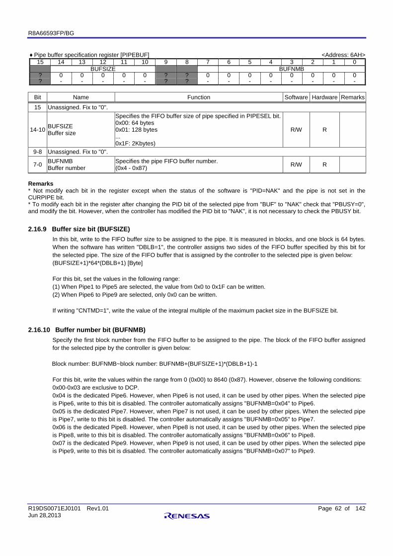
R8A66593FP/BG
R19DS0071EJ0101 Rev1.01 Page 62 of 142 Jun 28,2013
♦ Pipe buffer specification register [PIPEBUF] <Address: 6AH>
15 14 13 12 11 10 9 8 7 6 5 4 3 2 1 0 BUFSIZE BUFNMB
? 0 0 0 0 0 ? ? 0 0 0 0 0 0 0 0 ? - - - - - ? ? - - - - - - - -
Bit Name Function Software Hardware Remarks
15 Unassigned. Fix to "0".
14-10 BUFSIZE Buffer size
Specifies the FIFO buffer size of pipe specified in PIPESEL bit. 0x00: 64 bytes 0x01: 128 bytes ... 0x1F: 2Kbytes)
R/W R
9-8 Unassigned. Fix to "0".
7-0 BUFNMB Buffer number
Specifies the pipe FIFO buffer number. (0x4 - 0x87) R/W R
Remarks * Not modify each bit in the register except when the status of the software is "PID=NAK" and the pipe is not set in the CURPIPE bit. * To modify each bit in the register after changing the PID bit of the selected pipe from "BUF" to "NAK" check that "PBUSY=0", and modify the bit. However, when the controller has modified the PID bit to "NAK", it is not necessary to check the PBUSY bit.
2.16.9 Buffer size bit (BUFSIZE) In this bit, write to the FIFO buffer size to be assigned to the pipe. It is measured in blocks, and one block is 64 bytes. When the software has written "DBLB=1", the controller assigns two sides of the FIFO buffer specified by this bit for the selected pipe. The size of the FIFO buffer that is assigned by the controller to the selected pipe is given below: (BUFSIZE+1)*64*(DBLB+1) [Byte] For this bit, set the values in the following range: (1) When Pipe1 to Pipe5 are selected, the value from 0x0 to 0x1F can be written. (2) When Pipe6 to Pipe9 are selected, only 0x0 can be written. If writing "CNTMD=1", write the value of the integral multiple of the maximum packet size in the BUFSIZE bit.
2.16.10 Buffer number bit (BUFNMB) Specify the first block number from the FIFO buffer to be assigned to the pipe. The block of the FIFO buffer assigned for the selected pipe by the controller is given below: Block number: BUFNMB~block number: BUFNMB+(BUFSIZE+1)*(DBLB+1)-1 For this bit, write the values within the range from 0 (0x00) to 8640 (0x87). However, observe the following conditions: 0x00-0x03 are exclusive to DCP. 0x04 is the dedicated Pipe6. However, when Pipe6 is not used, it can be used by other pipes. When the selected pipe is Pipe6, write to this bit is disabled. The controller automatically assigns "BUFNMB=0x04" to Pipe6. 0x05 is the dedicated Pipe7. However, when Pipe7 is not used, it can be used by other pipes. When the selected pipe is Pipe7, write to this bit is disabled. The controller automatically assigns "BUFNMB=0x05" to Pipe7. 0x06 is the dedicated Pipe8. However, when Pipe8 is not used, it can be used by other pipes. When the selected pipe is Pipe8, write to this bit is disabled. The controller automatically assigns "BUFNMB=0x06" to Pipe8. 0x07 is the dedicated Pipe9. However, when Pipe9 is not used, it can be used by other pipes. When the selected pipe is Pipe9, write to this bit is disabled. The controller automatically assigns "BUFNMB=0x07" to Pipe9.
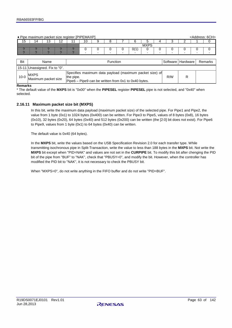
R8A66593FP/BG
R19DS0071EJ0101 Rev1.01 Page 63 of 142 Jun 28,2013
♦ Pipe maximum packet size register [PIPEMAXP] <Address: 6CH>
15 14 13 12 11 10 9 8 7 6 5 4 3 2 1 0 MXPS
? ? ? ? ? 0 0 0 0 0(1) 0 0 0 0 0 0 ? ? ? ? ? - - - - - - - - - - -
Bit Name Function Software Hardware Remarks
15-11 Unassigned. Fix to "0".
10-0 MXPS Maximum packet size
Specifies maximum data payload (maximum packet size) of the pipe. Pipe6 – Pipe9 can be written from 0x1 to 0x40 bytes.
R/W R
Remarks * The default value of the MXPS bit is "0x00" when the PIPESEL register PIPESEL pipe is not selected, and "0x40" when selected.
2.16.11 Maximum packet size bit (MXPS) In this bit, write the maximum data payload (maximum packet size) of the selected pipe. For Pipe1 and Pipe2, the value from 1 byte (0x1) to 1024 bytes (0x400) can be written. For Pipe3 to Pipe5, values of 8 bytes (0x8), 16 bytes (0x10), 32 bytes (0x20), 64 bytes (0x40) and 512 bytes (0x200) can be written (the [2:0] bit does not exist). For Pipe6 to Pipe9, values from 1 byte (0x1) to 64 bytes (0x40) can be written. The default value is 0x40 (64 bytes). In the MXPS bit, write the values based on the USB Specification Revision 2.0 for each transfer type. While transmitting isochronous pipe in Split-Transaction, write the value to less than 188 bytes in the MXPS bit. Not write the MXPS bit except when "PID=NAK" and values are not set in the CURPIPE bit. To modify this bit after chenging the PID bit of the pipe from "BUF" to "NAK", check that "PBUSY=0", and modify the bit. However, when the controller has modified the PID bit to "NAK", it is not necessary to check the PBUSY bit. When "MXPS=0", do not write anything in the FIFO buffer and do not write "PID=BUF".
R8A66593FP/BG
R19DS0071EJ0101 Rev1.01 Page 64 of 142 Jun 28,2013
♦ Pipe timing control register [PIPEPERI] <Address: 6EH>
15 14 13 12 11 10 9 8 7 6 5 4 3 2 1 0 IFIS IITV
? ? ? 0 ? ? ? ? ? ? ? ? ? 0 0 0 ? ? ? - ? ? ? ? ? ? ? ? ? - - -
Bit Name Function Software Hardware Remarks
15-13 Unassigned. Fix to "0".
12 IFIS Isochronous IN buffer flush
Specifies buffer flushed/not-flushed when the transfer type of pipe specified in PIPESEL bit is isochronous IN. 0: The buffer is not flushed 1: The buffer is flushed
R/W R
11-3 Unassigned. Fix to "0".
2-0 IITV Interval error detection spacing
Specifies the transfer interval timing of pipe as second power frame timing. R/W R
Remarks None
2.16.12 Isochronous IN buffer flush bit (IFIS) This is the function in which the controller automatically clears the FIFO buffer, if transfer type isochronous pipe, transfer is IN transfer, and when the controller has not received the In-token from the USB Host in the (micro) frame for each interval specified in IITV bit. In the double buffer setting (write "DBLB=1"), the controller clears only the data on one side of the previous buffer. The FIFO buffer is cleared when the SOF packet is received immediately after the (micro) frame receives the In-token. It is cleared also when the SOF packet is corruped when the SOF is to be received by an internal interpolation function. If the selected pipe of other than transfer type isochronous, write "0" to this bit.
2.16.13 Interval error detection spacing bit (IITV) In this bit, specify the interval error detection spacing to frame timing squared. Not write to this bit except when "PID=NAK", and when the pipe in the CURPIPE bit is not written. To modify this bit after chenging the PID bit of the pipe from "BUF" to "NAK", check that "PBUSY=0", and then modify the bit. However, when the controller has modified the PID bit to "NAK", it is not necessary to check the PBUSY bit. When modifying the bit value, after execute USB communication, write "ACLRM=1" after writing "PID=NAK", and initialize the interval timer. This bit does not exist in Pipe3 to Pipe5. Set "0" in the position of the bit corresponding to Pipe3 to Pipe5.
2.16.13.1
If the selected pipe transfer type is isochronous, this bit can be written to. (1) If the selected pipe is an isochronous-OUT transfer pipe
When the data packet is received in the (micro) frame for each interval set in IITV bit, the controller issues a NRDY interrupt. A NRDY interrupt is also issued when the data packet is not received due to errors such as a CRC error or (due to reasons like the reading of data from FIFO buffer by the software (DMAC) is slow) when the controller cannot receive the data because the FIFO buffer is full. A NRDY interrupt is issued when the SOF packet is received. Also, when the SOF packet is corrupted, the interrupt is issued when the SOF packet is to be received by an internal interpolation function. However, if other than "IITV=0", a NRDY interrupt is to be issued when the SOF packet is received for each interval after starting interval counting. After activating the interval timer, when the PID bit is written to "NAK" by the software, the controller does not
R8A66593FP/BG
R19DS0071EJ0101 Rev1.01 Page 65 of 142 Jun 28,2013
(Micro) Frame
S O F
S O F
S O F
O U T
D A T A 0
S O F
S O F
O U T
D A T A 0
S O F
S O F
O U T
D A T A 0
PID bit setup value N A K B U F B U F B U F B U F B U F B U F Token reception
expectation flag (0: Reception expected
-: Not received is expected)
- - 0 - 0 - 0
Interval counting start ↑
(Micro) Frame
S O F
S O F
S O F
O U T
D A T A 0
S O F
O U T
D A T A 0
PID bit setup value N A K B U F B U F B U F Token reception
expectation flag (0: Reception expected
-: Not received is expected)
- - 0 0
Interval counting start
issue the NRDY interrupt even if the SOF packet is received. The count start conditions of the interval differ according to the setup value of the IITV bit (a) If "IITV=0": Counting of the interval is started from the next (micro) frame after modifying the PID bit of the selected pipe to "BUF".
Figure 2.1 Correlation between (micro) frame and token reception expectation flag when "IITV=0"
(b) If other than "IITV=0": Counting of interval is started when the initial DATA packet is received normally after modifying the PID bit of the selected pipe to "BUF".
Figure 2.2 Correlation between (micro) frame and token reception expectation flag when "IITV=1"
(2) When the selected pipe is an isochronous IN transfer pipe It is used in combination with "IFIS="1". If "IFIS=0", a data packet is sent as a response to the received token, irrespective of the setup value of the IITV bit. If "IFIS=1" is written, the controller clears the FIFO buffer when the FIFO buffer does not contain the data that can be sent, and the In-token is not received in the (micro) frames of each interval set in the IITV bit. It also clears the buffer when the In-token is not received normally due to bus errors, such as a CRC error. The FIFO buffer is cleared when the SOF packet is received. Also, when the SOF packet is corrupted, the FIFO buffer is cleared when the SOF packet is to be received by internal interpolation function. Conditions to start the interval counting differ according to the setup value of IITV bit (similar for OUT). The following are the conditions for initialization of the interval counter:
(a) When this controller is hardware reset (at this point, the setup value of the IITV bit is also cleared to"0"). (b) When the software writes "ACLRM=1". (c) When the controller detects a USB bus reset.
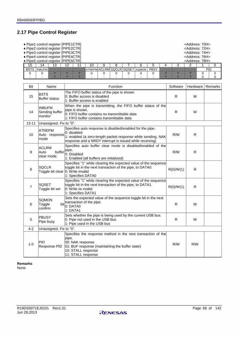
R8A66593FP/BG
R19DS0071EJ0101 Rev1.01 Page 66 of 142 Jun 28,2013
2.17 Pipe Control Register
♦ Pipe1 control register [PIPE1CTR] ♦ Pipe2 control register [PIPE2CTR] ♦ Pipe3 control register [PIPE3CTR] ♦ Pipe4 control register [PIPE4CTR] ♦ Pipe5 control register [PIPE5CTR]
<Address: 70H> <Address: 72H> <Address: 74H> <Address: 76H> <Address: 78H>
15 14 13 12 11 10 9 8 7 6 5 4 3 2 1 0 BSTS INBUFM ATREPM ACLRM SQCLR SQSET SQMON PBSY PID
0 0 ? ? ? 0 0 0 0 0 0 ? ? ? 0 0 - - ? ? ? - - - - - - ? ? ? 0 0
Bit Name Function Software Hardware Remarks
15 BSTS Buffer status
The FIFO buffer status of the pipe is shown. 0: Buffer access is disabled 1: Buffer access is enabled
R W
14 INBUFM Sending buffer monitor
When the pipe is transmitting, the FIFO buffer status of the pipe is shown. 0: FIFO buffer contains no transmittable data 1: FIFO buffer contains transmittable data
R W
13-11 Unassigned. Fix to "0".
10 ATREPM Auto response mode
Specifies auto response is disabled/enabled for the pipe. 0: disabled 1: enabled (a zero-length packet response while sending, NAK response and a NRDY interrupt is issued while receiving)
R/W R
9 ACLRM Auto buffer clear mode
Specifies auto buffer clear mode is disabled/enabled of the pipe. 0: Disabled 1: Enabled (all buffers are initialized)
R/W R
8 SQCLR Toggle bit clear
Specifies "1" while clearing the expected value of the sequence toggle bit in the next transaction of the pipe, to DATA0. 0: Write invalid 1: Specifies DATA0
R(0)/W(1) R
7 SQSET Toggle bit set
Specifies "1" while clearing the expected value of the sequence toggle bit in the next transaction of the pipe, to DATA1. 0: Write iis nvalid 1: Specifies DATA1
R(0)/W(1) R
6 SQMON Toggle bit confirm
Sets the expected value of the sequence toggle bit in the next transaction of the pipe. 0: DATA0 1: DATA1
R W
5 PBUSY Pipe busy
Sets whether the pipe is being used by the current USB bus. 0: Pipe not used in the USB bus 1: Pipe used in the USB bus
R W
4-2 Unassigned. Fix to "0".
1-0 PID Response PID
Specifies the response method in the next transaction of the pipe. 00: NAK response 01: BUF response (maintaining the buffer state) 10: STALL response 11: STALL response
R/W R/W
Remarks None
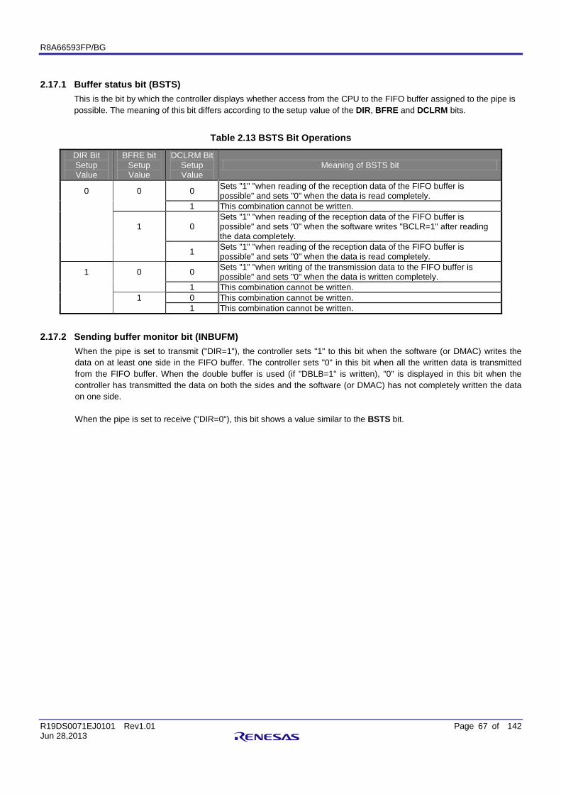
R8A66593FP/BG
R19DS0071EJ0101 Rev1.01 Page 67 of 142 Jun 28,2013
2.17.1 Buffer status bit (BSTS) This is the bit by which the controller displays whether access from the CPU to the FIFO buffer assigned to the pipe is possible. The meaning of this bit differs according to the setup value of the DIR, BFRE and DCLRM bits.
Table 2.13 BSTS Bit Operations
DIR Bit Setup Value
BFRE bit Setup Value
DCLRM Bit Setup Value
Meaning of BSTS bit
0 0 0 Sets "1" "when reading of the reception data of the FIFO buffer is possible" and sets "0" when the data is read completely.
1 This combination cannot be written.
1 0 Sets "1" "when reading of the reception data of the FIFO buffer is possible" and sets "0" when the software writes "BCLR=1" after reading the data completely.
1 Sets "1" "when reading of the reception data of the FIFO buffer is possible" and sets "0" when the data is read completely.
1 0 0 Sets "1" "when writing of the transmission data to the FIFO buffer is possible" and sets "0" when the data is written completely.
1 This combination cannot be written. 1 0 This combination cannot be written. 1 This combination cannot be written.
2.17.2 Sending buffer monitor bit (INBUFM) When the pipe is set to transmit ("DIR=1"), the controller sets "1" to this bit when the software (or DMAC) writes the data on at least one side in the FIFO buffer. The controller sets "0" in this bit when all the written data is transmitted from the FIFO buffer. When the double buffer is used (if "DBLB=1" is written), "0" is displayed in this bit when the controller has transmitted the data on both the sides and the software (or DMAC) has not completely written the data on one side. When the pipe is set to receive ("DIR=0"), this bit shows a value similar to the BSTS bit.
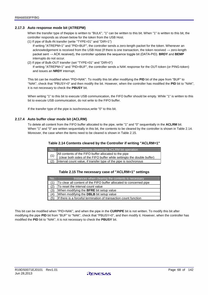
R8A66593FP/BG
R19DS0071EJ0101 Rev1.01 Page 68 of 142 Jun 28,2013
2.17.3 Auto response mode bit (ATREPM) When the transfer type of thepipe is written to "BULK", "1" can be written to this bit. When "1" is written to this bit, the controller responds as shown below for the token from the USB Host. (1) If pipe of Bulk-IN transfer (write "TYPE=01" and "DIR=1")
If writing "ATREPM=1" and "PID=BUF", the controller sends a zero-length packet for the token. Whenever an acknowledgement is received from the USB Host (If there is one transaction, the token received → zero-length packet sent → ACK received), the controller updates the sequence toggle bit (DATA-PID). BRDY and BEMP interrupts do not occur.
(2) If pipe of Bulk-OUT transfer (set "TYPE=01" and "DIR=0") If writing "ATREPM=1" and "PID=BUF", the controller sends a NAK response for the OUT-token (or PING-token) and issues an NRDY interrupt.
This bit can be modified when "PID=NAK". To modify this bit after modifying the PID bit of the pipe from "BUF" to "NAK", check that "PBUSY=0" and then modify the bit. However, when the controller has modified the PID bit to "NAK", it is not necessary to check the PBUSY bit. When writing "1" to this bit to execute USB communication, the FIFO buffer should be empty. While "1" is written to this bit to execute USB communication, do not write to the FIFO buffer. If the transfer type of the pipe is isochronous,write "0" to this bit.
2.17.4 Auto buffer clear mode bit (ACLRM) To delete all content from the FIFO buffer allocated to the pipe, write "1" and "0" sequentially in the ACLRM bit. When "1" and "0" are written sequentially in this bit, the contents to be cleared by the controller is shown in Table 2.14. Moreover, the case when the items need to be cleared is shown in Table 2.15.
Table 2.14 Contents cleared by the Controller if writing "ACLRM=1"
No. Contents cleared by ACLRM bit operation
(1) All contents of the FIFO buffer allocated to the pipe (clear both sides of the FIFO buffer while settingto the double buffer)
(2) Interval count value, if transfer type of the pipe is isochronous
Table 2.15 The necessary case of "ACLRM=1" settings
No. Instances when clearing the contents is necessary (1) To clear all content of the FIFO buffer allocated to concerned pipe (2) To reset the interval count value (3) When modifying the BFRE bit setup value (4) When modifying the DBLB bit setup value (5) If there is a forceful termination of transaction count function
This bit can be modified when "PID=NAK", and when the pipe in the CURPIPE bit is not written. To modify this bit after modifying the pipe PID bit from "BUF" to "NAK", check that "PBUSY=0", and then modify it. However, when the controller has modified the PID bit to "NAK", it is not necessary to check the PBUSY bit.
R8A66593FP/BG
R19DS0071EJ0101 Rev1.01 Page 69 of 142 Jun 28,2013
2.17.5 Clear bit of sequence toggle bit (SQCLR) If the software writes "1" to this bit, the controller writes the expected value of the sequence toggle bit of the pipe to DATA0. The controller always sets "0" to this bit. Not write "1" to the SQCLR bit except when "PID=NAK". To write "1" to this bit after the PID bit of the PIPE is modified from "BUF" to "NAK", check that "PBUSY=0" and then modify the bit. However, when the controller has modified the PID bit to "NAK", it is not necessary to check the PBUSY bit.
2.17.6 Write bit of sequence toggle bit (SQSET) If the software writes "1" to this bit, the controller sets the expected value sequence toggle bit of the pipe to DATA1. The controller always sets "0" to this bit. Not write "1" to the SQSET bit except when "PID=NAK". To write "1" to this bit after the PID bit of the PIPE is modified from "BUF" to "NAK", check that "PBUSY=0", and then modify the bit. However, when the controller has modified the PID bit to "NAK", it is not necessary to check the PBUSY bit.
2.17.7 Monitor bit of sequence toggle bit (SQMON) In this bit, the controller displays the expected value of the sequence toggle bit of the pipe. If the selected pipe other than transfer type isochronous, the controller toggles this bit if the transaction is executed normally. However, this bit is not toggled if there is a DATA-PID mismatch during reception direction transfer.
2.17.8 Pipe busy bit (PBUSY) The controller modifies this bit from "0" to "1" when the USB transaction of the pipe is started. When one transaction is completed, the bit is modified from "1" to "0". When the software has set "PID=NAK", possibility of pipe modification can be checked by reading this bit.
2.17.9 Response PID bit (PID) For this bit, set a response of the controller in each pipe by the software. The default value of this bit is "NAK". While executing a USB transfer by the pipe, modify this bit to "BUF". The basic operations (operations when there is no error in the communication packet) of this controller for each setup value of the PID bit are given in Table 2.16. If the pipe is in USB communication, when this bit is modified from "BUF" to "NAK" by the software, after writing "NAK", to check whether the USB transfer of pipe is actually shifted to "NAK" status, and check whether "PBUSY=0". However, when the controller modifies this bit to "NAK", it is not necessary to use the software to check the PBUSY bit. In following cases, the controller modifies the value of this bit: (1) When the pipe is receiving and when the software has written "1" to the SHTNAK bit of the pipe, the controller sets "PID=NAK" upon identifying the transfer end. (2) For the pipe, when the data packet of payload exceeding the maximum packet size is received, the controller sets "PID=STALL(11)". (3) When the USB bus reset is detected, the controller sets "PID=NAK". Write "10" to shift from "PID=NAK("00")" status to "PID=STALL" status. Write "11" to shift from BUF("01") status to STALL status. First write "10" and then write "00" to shift form "STALL(11)" to NAK status. First, shift to NAK status and then to BUF status to shift from STALL status to BUF status.
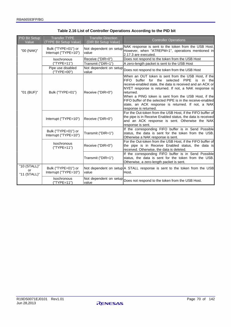
R8A66593FP/BG
R19DS0071EJ0101 Rev1.01 Page 70 of 142 Jun 28,2013
Table 2.16 List of Controller Operations According to the PID bit
PID Bit Setup Value
Transfer TYPE (TYPE Bit Setup Value)
Transfer Direction (DIR Bit Setup Value) Controller Operations
"00 (NAK)" Bulk ("TYPE=01") or Interrupt ("TYPE=10")
Not dependent on setup value
NAK response is sent to the token from the USB Host. However, when "ATREPM=1", operations mentioned in 2.17.3 are executed.
Isochronous ("TYPE=11")
Receive ("DIR=0") Does not respond to the token from the USB Host Transmit ("DIR=1") A zero-length packet is sent to the USB Host
Pipe use disabled ("TYPE=00")
Not dependent on setup value Does not respond to the token from the USB Host
"01 (BUF)" Bulk ("TYPE=01") Receive ("DIR=0")
When an OUT token is sent from the USB Host, if the FIFO buffer for the selected PIPE is in the receive-enabled state, the data is received and an ACK or NYET response is returned. If not, a NAK response is returned. When a PING token is sent from the USB Host, if the FIFO buffer of the selected PIPE is in the receive-enabled state, an ACK response is returned. If not, a NAK response is returned.
Interrupt ("TYPE=10") Receive ("DIR=0")
For the Out-token from the USB Host, if the FIFO buffer of the pipe is in Receive Enabled status, the data is received and an ACK response is sent. Otherwise the NAK response is sent.
Bulk ("TYPE=01") or Interrupt ("TYPE=10") Transmit ("DIR=1")
If the corresponding FIFO buffer is in Send Possible status, the data is sent for the token from the USB. Otherwise a NAK response is sent.
Isochronous ("TYPE=11") Receive ("DIR=0")
For the Out-token from the USB Host, if the FIFO buffer of the pipe is in Receive Enabled status, the data is received. Otherwise, the data is deleted.
Transmit ("DIR=1") If the corresponding FIFO buffer is in Send Possible status, the data is sent for the token from the USB. Otherwise, a zero-length packet is sent.
"10 (STALL)" or
"11 (STALL)"
Bulk ("TYPE=01") or Interrupt ("TYPE=10")
Not dependent on setup value
A STALL response is sent to the token from the USB Host.
Isochronous ("TYPE=11")
Not dependent on setup value Does not respond to the token from the USB Host.
R8A66593FP/BG
R19DS0071EJ0101 Rev1.01 Page 71 of 142 Jun 28,2013
♦ Pipe6 control register [PIPE6CTR] ♦ Pipe7 control register [PIPE7CTR] ♦ Pipe8 control register [PIPE8CTR] ♦ Pipe9 control register [PIPE9CTR]
<Address: 7AH> <Address: 7CH> <Address: 7EH> <Address: 80H>
15 14 13 12 11 10 9 8 7 6 5 4 3 2 1 0 BSTS ACLRM SQCLR SQSET SQMON PBSY PID
0 ? ? ? ? ? 0 0 0 0 0 ? ? ? 0 0 - ? ? ? ? ? - - - - - ? ? ? 0 0
Bit Name Function Software Hardware Remarks
15 BSTS Buffer status
FIFO buffer status of the pipe is displayed. 0: Buffer access is disabled 1: Buffer access is enabled
R W
14-10 Unassigned. Fix to "0".
9 ACLRM Auto Buffer Clear mode
Specifies auto buffer clear mode disable/enable of the pipe. 0: Disabled 1: Enabled (all buffers are initialized)
R/ W R
8 SQCLR Toggle Bit Clear
Specifies "1" while clearing the expected value of the sequence toggle bit in the next transaction of the pipe to DATA0. 0: Invalid 1: Specifies DATA0
R(0)/ W(1) R
7 SQSET Toggle Bit Set
Specifies "1" while clearing the expected value of the sequence toggle bit in the next transaction of the pipe to DATA1. 0: Invalid 1: Specifies DATA1
R(0)/ W(1) R
6 SQMON Toggle Bit Confirm
Sets the expected value of the sequence toggle bit in the next transaction of the pipe. 0: DATA0 1: DATA1
R W
5 PBUSY Pipe busy
Displays whether the pipe is being used by the current USB bus. 0: Pipe not used in the USB bus 1: Pipe used in the USB bus
R W
4-2 Unassigned. Fix to "0".
1-0 PID Response PID
Specifies the response method in the next transaction of the pipe. 00: NAK response 01: BUF response (in keeping with the buffer state) 10: STALL response 11: STALL response
R/W R/W
Remarks None
R8A66593FP/BG
R19DS0071EJ0101 Rev1.01 Page 72 of 142 Jun 28,2013
2.17.10 Buffer status bit (BSTS) Refer to 2.17.1.
2.17.11 Auto buffer clear mode (ACLRM) To delete all content from the FIFO buffer allocated to the pipe, write "1" and "0" sequentially in the ACLRM bit. When "1" and "0" are written sequentially to this bit, the contents to be cleared by the controller is shown in Table 2.17. Moreover, the cases when the items need to be cleared is shown in Table 2.18.
Table 2.17 Contents cleared by the controller if writing "ACLRM=1"
No. Contents cleared by ACLRM bit operation (1) All content from the FIFO buffer allocated to the pipe
Table 2.18 The necessary case of "ACLRM=1" settimgs
No. Instances when clearing the contents is necessary (1) To clear all content of the FIFO buffer allocated to concerned pipe (2) To reset the value of interval count (3) While modifying the BFRE bit setup value (4) If there is a forceful termination of transaction count function
This bit can be modified when "PID=NAK", and the pipe in the CURPIPE bit is not written. To modify this bit after modifying the PID bit of the pipe from "BUF" to "NAK" check that "PBUSY=0", and modify the bit. However, when the controller has modified the PID bit to "NAK", it is not necessary to check the PBUSY bit.
2.17.12 Clear bit of sequence toggle bit (SQCLR) Refer to 2.17.5.
2.17.13 Set bit of sequence toggle bit (SQSET) Refer to 2.17.6.
2.17.14 Monitor bit of sequence toggle bit (SQMON) Refer to 2.17.7.
2.17.15 Pipe busy bit (PBUSY) Refer to 2.17.8.
2.17.16 Response PID bit (PID) Refer to 2.17.9.
R8A66593FP/BG
R19DS0071EJ0101 Rev1.01 Page 73 of 142 Jun 28,2013
2.18 Transaction counter ♦ Pipe1 Transaction counter enabled register [PIPE1TRE] ♦ Pipe2 Transaction counter enabled register [PIPE2TRE] ♦ Pipe3 Transaction counter enabled register [PIPE3TRE] ♦ Pipe4 Transaction counter enabled register [PIPE4TRE] ♦ Pipe5 Transaction counter enabled register [PIPE5TRE]
<Address: 90H> <Address: 94H> <Address: 98H> <Address: 9CH> <Address: A0H>
15 14 13 12 11 10 9 8 7 6 5 4 3 2 1 0 TRENB TRCLR ? ? ? ? ? ? 0 0 ? ? ? ? ? ? ? ? ? ? ? ? ? ? - - ? ? ? ? ? ? ? ?
Bit Name Function Software Hardware Remarks
15-10 Unassigned. Fix to "0".
9 TRENB Transaction counter enabled
Specifies whether the transaction counter is invalid/valid. 0: Transaction counter function invalid 1: Transaction counter function valid
R/W R
8 TRCLR Transaction counter clear
Transaction counter can be cleared to "0" by writing "1" to this bit. 0: Invalid 1: Count counter clear
R(0)/W(1) R
7-0 Unassigned. Fix to "0"." Remarks * Not modify each bit of the register except when "PID=NAK". To modify each bit after modifying the PID bit of the pipe from "BUF" to "NAK", check that "PBUSY=0", and then modify it. However, when the controller modifies PID bit to "NAK", it is not necessary to check the PBUSY bit.
2.18.1 Transaction counter enabled bit (TRENB) For the reception pipe, after the total number of packets is written to the TRNCNT bit using the software, the controller executes the following control on receiving the same number of packets as the setup value of the TRNCNT bit: (1) When the continuous transmission/reception mode is used (write "CNTMD=1"), toggles on CPU side even if the FIFO buffer is not full when reception is completed. (2) If writing "SHTNAK=1", modifies the pipe PID bit to "NAK". (3) If writing "DENDE=1" and "PKTMD=0", asserts the DEND signal while reading the last data. (4) If writing "BFRE=1", asserts the BRDY interrupt. Regarding the transmission pipe, write "0" to this bit. When the transaction count function is not used, write "0" to this bit. When the transaction count function is used, set the TRNCNT bit before writing "1" to this bit. Also write "1" to this bit before receiving the initial packet that is the transaction target.
2.18.2 Transaction counter clear bit (TRCLR) If the software writes "1" to this bit, the controller clears the current count value of the transaction counter corresponding to the pipe and sets "0" in this bit.
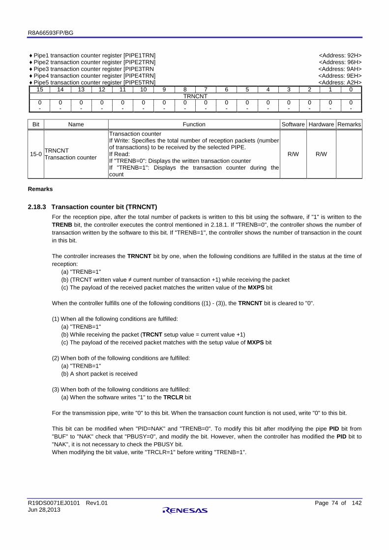
R8A66593FP/BG
R19DS0071EJ0101 Rev1.01 Page 74 of 142 Jun 28,2013
♦ Pipe1 transaction counter register [PIPE1TRN] ♦ Pipe2 transaction counter register [PIPE2TRN] ♦ Pipe3 transaction counter register [PIPE3TRN ♦ Pipe4 transaction counter register [PIPE4TRN] ♦ Pipe5 transaction counter register [PIPE5TRN]
<Address: 92H> <Address: 96H> <Address: 9AH> <Address: 9EH> <Address: A2H>
15 14 13 12 11 10 9 8 7 6 5 4 3 2 1 0 TRNCNT
0 0 0 0 0 0 0 0 0 0 0 0 0 0 0 0 - - - - - - - - - - - - - - - -
Bit Name Function Software Hardware Remarks
15-0 TRNCNT Transaction counter
Transaction counter If Write: Specifies the total number of reception packets (number of transactions) to be received by the selected PIPE. If Read: If "TRENB=0": Displays the written transaction counter If "TRENB=1": Displays the transaction counter during the count
R/W R/W
Remarks
2.18.3 Transaction counter bit (TRNCNT) For the reception pipe, after the total number of packets is written to this bit using the software, if "1" is written to the TRENB bit, the controller executes the control mentioned in 2.18.1. If "TRENB=0", the controller shows the number of transaction written by the software to this bit. If "TRENB=1", the controller shows the number of transaction in the count in this bit. The controller increases the TRNCNT bit by one, when the following conditions are fulfilled in the status at the time of reception:
(a) "TRENB=1" (b) (TRCNT written value ≠ current number of transaction +1) while receiving the packet (c) The payload of the received packet matches the written value of the MXPS bit
When the controller fulfills one of the following conditions ((1) - (3)), the TRNCNT bit is cleared to "0". (1) When all the following conditions are fulfilled:
(a) "TRENB=1" (b) While receiving the packet (TRCNT setup value = current value +1) (c) The payload of the received packet matches with the setup value of MXPS bit
(2) When both of the following conditions are fulfilled:
(a) "TRENB=1" (b) A short packet is received
(3) When both of the following conditions are fulfilled:
(a) When the software writes "1" to the TRCLR bit For the transmission pipe, write "0" to this bit. When the transaction count function is not used, write "0" to this bit. This bit can be modified when "PID=NAK" and "TRENB=0". To modify this bit after modifying the pipe PID bit from "BUF" to "NAK" check that "PBUSY=0", and modify the bit. However, when the controller has modified the PID bit to "NAK", it is not necessary to check the PBUSY bit. When modifying the bit value, write "TRCLR=1" before writing "TRENB=1".
R8A66593FP/BG
R19DS0071EJ0101 Rev1.01 Page 75 of 142 Jun 28,2013
3 Operating Instructions
3.1 System Controls and Oscillation Controls This chapter provides instructions concerning register operations necessary to initialize the R8A66593 controller and descriptions of the registers necessary to control power consumption.
3.1.1 RESET Table 3.1 shows the list of the various resets related to this controller. Please refer to “Chapter 2. Registers” for a description of the register initialization status after each reset operation.
Table 3.1 RESET List
Name Operation H/W Reset ”L” level input from RST_N pin USB Bus Reset This controller detects reset automatically from D+/D- line status
3.1.2 Bus Interface Setting Table 3.2 shows the parameters for the controller bus interface that must be set before enabling (“XCKE = 0”) the oscillation buffer operation. Make sure these are set immediately after the H/W reset. Table 3.3 shows the parameters to be set after the oscillation buffer operation is enabled (“XCKE = 1” is set and controller is in “SCKE = 1” status).
Table 3.2 Bus Interface Settings (set before clock supply starts)
Register Name Bit Name Setting Description PINCFG LDRV Specify drive current controls PINCFG INTA Set INT_N pin polarity
Table 3.3 Bus Interface Settings (set after clock supply starts)
Register Name Bit Name Setting Description SYSCFG1 PCSDIS Specify include/exclude CS_N assert in recovery conditions
from low power sleep state SYSCFG1 LPSME Specify enable/disable for low power sleep state DMAxCFG DREQA Set DREQx_N pin polarity DMAxCFG DACKA Set DACKx_N pin polarity DMAxCFG DENDA Set DENDx_N pin polarity DMAxCFG OBUS Set OBUS mode SOFCFG BRDYM Set PIPEBRDY interrupt status clear timing SOFCFG INTL Set INT_N pin output sense x = 0 or 1
3.1.3 Clock Supply Control The clock supply to the controller USB block is started by selecting the XIN pin input clock in the SYSCFG0 register XTAL bit and enabling the oscillation buffer in the XCKE bit by software. Confirm by software that the SCKE bit is set to “1”, then proceed with the next process.
R8A66593FP/BG
R19DS0071EJ0101 Rev1.01 Page 76 of 142 Jun 28,2013
3.1.4 USB Block Operation Enable After clock supply has started to the USB block (“SCKE = 1”), set the SYSCFG0 register USBE bit to “1" with software to enable USB block operations.
3.1.5 Hi-Speed Operation Enable Bit Setting and USB Transmission Speed Determination
When the Hi-Speed operation is enabled, set the Hi-Speed operation enable bit (SYSCFG0 register HSE bit) to “1” after setting the controller function selection bit. If operating the controller only at Full-Speed, set the SYSCFG0 register HSE bit to“0”. When Hi-Speed operation is enabled, the controller executes the reset handshake protocol and automatically determines the USB transmission speed. The result of the reset handshake is shown in the DVSTCTR0 register RHST bit.
3.1.6 USB Transmission Speed Control Table 3.4 shows the corresponding USB transmission speeds.
Table 3.4 Controller Function Selection Table
Settings Function and Transmission speed HSE Speed Remarks
0 Full Operates at Full-Speed 1 Hi or Full Operates at Hi-Speed when Reset Handshake Protocol (RHSP) is
successful, at Full-Speed when RSHP is not successful.
3.1.7 USB Data Bus Pull-Up Settings This controller has built-in pull-up resistance for the D+ line. Power supply for the D+ pull-up is AVCC. After the connection to the USB Host is confirmed, set SYSCFG0 register DPRPU bit to “1” and pull-up D+. In addition, the controller has built-in D+/D- line terminating resistance for Hi-Speed transmissions and output resistance for Full-Speed transmissions. The controller automatically switches the built-in resistance after connection to the USB Host upon the execution or detection of a reset handshake, suspend, or resume event. When the SYSCFG0 register DPRPU bit is set to “0” in the USB Host attached status, the controller disables the USB D+ line pull-up (or D+, D- line termination). Therefore, software can be used to create the USB cable detached status when viewed from the USB Host.
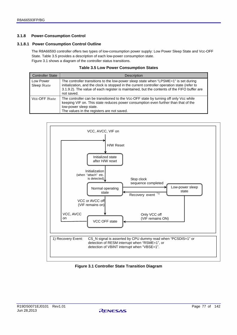
R8A66593FP/BG
R19DS0071EJ0101 Rev1.01 Page 77 of 142 Jun 28,2013
3.1.8 Power-Consumption Control
3.1.8.1 Power Consumption Control Outline
The R8A66593 controller offers two types of low-consumption power supply: Low Power Sleep State and Vcc-OFF State. Table 3.5 provides a description of each low-power consumption state. Figure 3.1 shows a diagram of the controller status transitions.
Table 3.5 Low Power Consumption States
Controller State Description Low Power Sleep State
The controller transitions to the low-power sleep state when “LPSME=1” is set during initialization, and the clock is stopped in the current controller operation state (refer to 3.1.9.2). The value of each register is maintained, but the contents of the FIFO buffer are not saved.
Vcc-OFF State
The controller can be transitioned to the Vcc-OFF state by turning off only Vcc while keeping VIF on. This state reduces power consumption even further than that of the low-power sleep state. The values in the registers are not saved.
Initialized state after H/W reset
Normal operating state
Initialization (when “attach” etc.
is detected)
H/W Reset
VCC or AVCC off (VIF remains on)
Only VCC off (VIF remains ON)
VCC, AVCC on
VCC, AVCC, VIF on
Low-power sleep state
VCC OFF state
Stop clock sequence completed
Recovery event *1)
1) Recovery Event: CS_N signal is asserted by CPU dummy read when “PCSDIS=1” or detection of RESM interrupt when “RSME=1”, or detection of VBINT interrupt when “VBSE=1”.
Figure 3.1 Controller State Transition Diagram
R8A66593FP/BG
R19DS0071EJ0101 Rev1.01 Page 78 of 142 Jun 28,2013
3.1.8.2 Low-Power Sleep State
When SYSCFG1 register LPSME bit is set to “1” in the controller initialization, if the clock stop process is executed while the controller is in the normal operating state, the controller goes to the low-power sleep state. In this state, power consumption is reduced while maintaining the value of each register. If the controller is transitioned to this state during USB suspend, power consumption can be reduced while still maintaining the USB address, device state, and other information. Please refer to 3.1.9.2 and Figure 3.3 for the detailed the setup sequence to transition to the low-power sleep state. To return from the low-power sleep state, refer to Table 2.6. The return sequence is detailed in 3.1.9.3 and Figure 3.4. The controller automatically enables the oscillation buffer operation when it detects a recovery condition from the low-power sleep state. At this time, the value of the XCKE bit is not changed. The user must confirm “SCKE=1” by software and then set “XCKE=1”. To enable the low-power sleep state, set the SYSCFG1 register LPSME bit to “1” during controller initialization. Registers cannot be accessed during the low-power sleep state. In addition, data in the FIFO buffers will be lost during the transition, so make a send/receive data process is executed before transitioning to the low-power sleep state.
3.1.8.3 VCC OFF State
The VCC OFF state allows some power to be supplied to the controller but cuts off supply to the USB block. The controller is transitioned to the VCC OFF state by keeping the VIF on while turning off the VCC and AVCC. Unlike returning the controller from the low-power sleep state by controlling the registers with software, this state requires the VCC and AVCC to be turned on and an H/W reset executed. The contents of each register are lost when the VCC is turned off, and the controller goes to the initialization state after recovery.
R8A66593FP/BG
R19DS0071EJ0101 Rev1.01 Page 79 of 142 Jun 28,2013
3.1.9 State Transition Timing
3.1.9.1 Start of Internal Clock Supply (from H/W reset state to normal operating state)
Figure 3.2 shows a diagram of the clock supply start control timing for the controller. When transitioning from the H/W reset state or the clock stopped state to the normal operating state, handle the bits according to the timing below.
(1) Enable oscillation buffer “XCKE=1” (2) Software wait until “SCKE=1”. (Controller automatically enables PLLC and SCKE.)
XCKE
PLLC(H/W)
SCKE(H/W)
(1) (2) Start internal clock supply start
process
Figure 3.2 Clock Supply Start Control Timing Diagram
3.1.9.2 Internal Clock Supply Stop (setup sequence to transition from normal operating state to low –power sleep state)
Figure 3.3 shows the control timing diagram for transitioning the controller from the normal operating state to the low-power sleep state. To enable the low-power sleep state, set “LPSME=1” in the initialization.
(1) Confirm SOFCFG register EDGESTS bit, then use software wait until “EDGESTS=0”. (2) Stop internal clock supply “SCKE=0” (3) Software wait until internal clock stops. (requires 60ns or more wait) (4) Stop PLL. “PLLC=0” (5) Stop oscillation buffer operation “XCKE=0”
PLLC
SCKE
(3) min 60ns
(2) Start
(4) (5)
XCKE
Figure 3.3 Internal Clock Supply Stop Process Timing Diagram
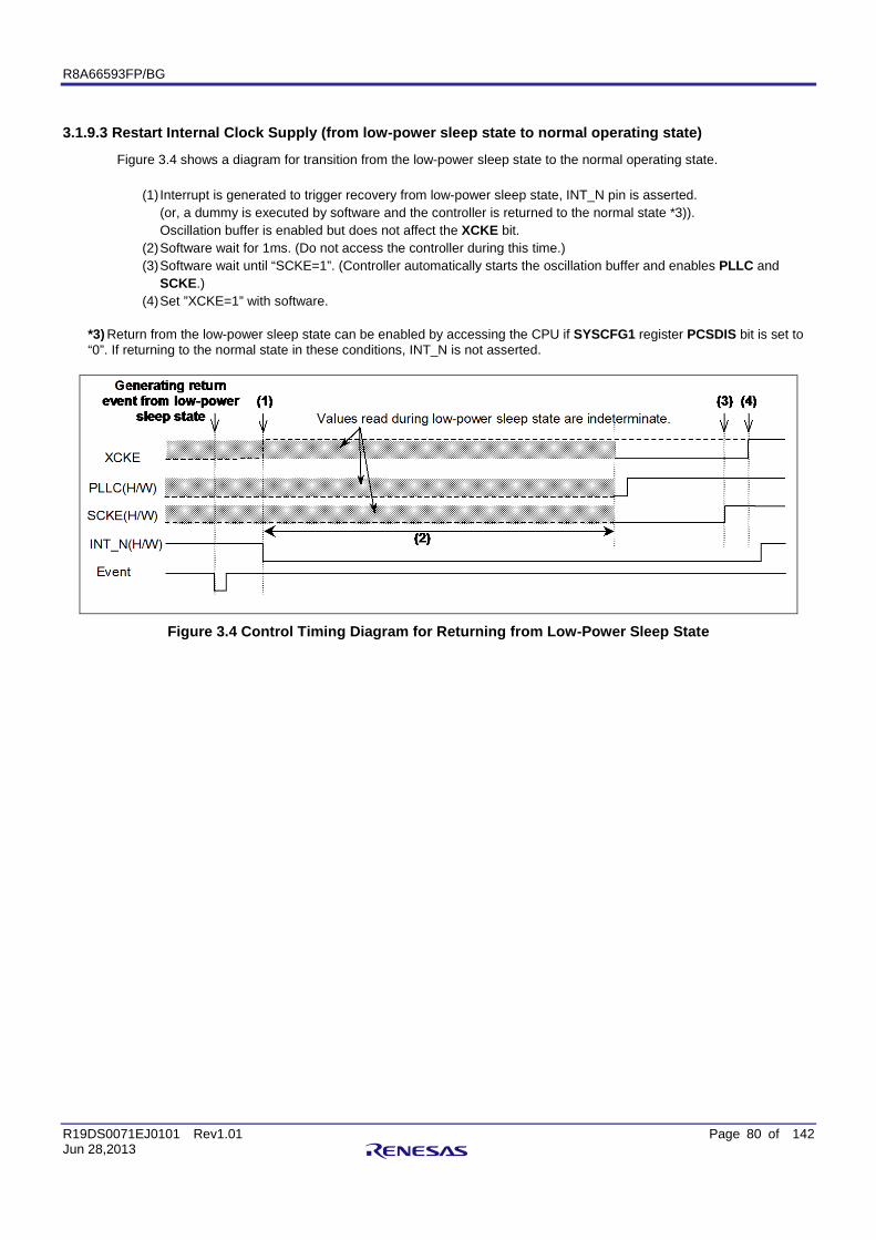
R8A66593FP/BG
R19DS0071EJ0101 Rev1.01 Page 80 of 142 Jun 28,2013
3.1.9.3 Restart Internal Clock Supply (from low-power sleep state to normal operating state)
Figure 3.4 shows a diagram for transition from the low-power sleep state to the normal operating state.
(1) Interrupt is generated to trigger recovery from low-power sleep state, INT_N pin is asserted. (or, a dummy is executed by software and the controller is returned to the normal state *3)). Oscillation buffer is enabled but does not affect the XCKE bit.
(2) Software wait for 1ms. (Do not access the controller during this time.) (3) Software wait until “SCKE=1”. (Controller automatically starts the oscillation buffer and enables PLLC and
SCKE.) (4) Set ”XCKE=1” with software.
*3) Return from the low-power sleep state can be enabled by accessing the CPU if SYSCFG1 register PCSDIS bit is set to “0”. If returning to the normal state in these conditions, INT_N is not asserted.
Figure 3.4 Control Timing Diagram for Returning from Low-Power Sleep State
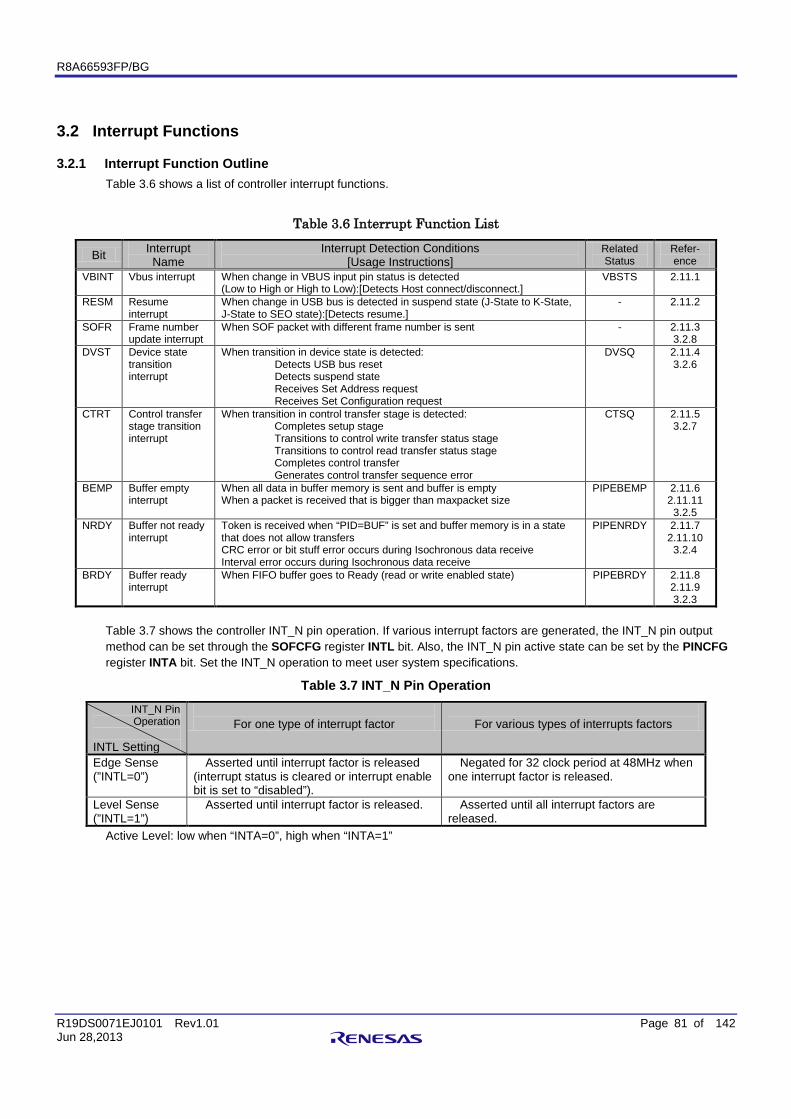
R8A66593FP/BG
R19DS0071EJ0101 Rev1.01 Page 81 of 142 Jun 28,2013
3.2 Interrupt Functions
3.2.1 Interrupt Function Outline Table 3.6 shows a list of controller interrupt functions.
Table 3.6 Interrupt Function List
Bit Interrupt Name
Interrupt Detection Conditions [Usage Instructions]
Related Status
Refer- ence
VBINT Vbus interrupt When change in VBUS input pin status is detected (Low to High or High to Low):[Detects Host connect/disconnect.]
VBSTS 2.11.1
RESM Resume interrupt
When change in USB bus is detected in suspend state (J-State to K-State, J-State to SEO state):[Detects resume.]
- 2.11.2
SOFR Frame number update interrupt
When SOF packet with different frame number is sent - 2.11.3 3.2.8
DVST Device state transition interrupt
When transition in device state is detected: Detects USB bus reset Detects suspend state Receives Set Address request Receives Set Configuration request
DVSQ 2.11.4 3.2.6
CTRT Control transfer stage transition interrupt
When transition in control transfer stage is detected: Completes setup stage Transitions to control write transfer status stage Transitions to control read transfer status stage Completes control transfer Generates control transfer sequence error
CTSQ 2.11.5 3.2.7
BEMP Buffer empty interrupt
When all data in buffer memory is sent and buffer is empty When a packet is received that is bigger than maxpacket size
PIPEBEMP 2.11.6 2.11.11 3.2.5
NRDY Buffer not ready interrupt
Token is received when “PID=BUF” is set and buffer memory is in a state that does not allow transfers CRC error or bit stuff error occurs during Isochronous data receive Interval error occurs during Isochronous data receive
PIPENRDY 2.11.7 2.11.10 3.2.4
BRDY Buffer ready
interrupt When FIFO buffer goes to Ready (read or write enabled state) PIPEBRDY 2.11.8
2.11.9 3.2.3
Table 3.7 shows the controller INT_N pin operation. If various interrupt factors are generated, the INT_N pin output method can be set through the SOFCFG register INTL bit. Also, the INT_N pin active state can be set by the PINCFG register INTA bit. Set the INT_N operation to meet user system specifications.
Table 3.7 INT_N Pin Operation INT_N Pin Operation
INTL Setting
For one type of interrupt factor
For various types of interrupts factors
Edge Sense (”INTL=0”)
Asserted until interrupt factor is released (interrupt status is cleared or interrupt enable bit is set to “disabled”).
Negated for 32 clock period at 48MHz when one interrupt factor is released.
Level Sense (”INTL=1”)
Asserted until interrupt factor is released. Asserted until all interrupt factors are released.
Active Level: low when “INTA=0”, high when “INTA=1”
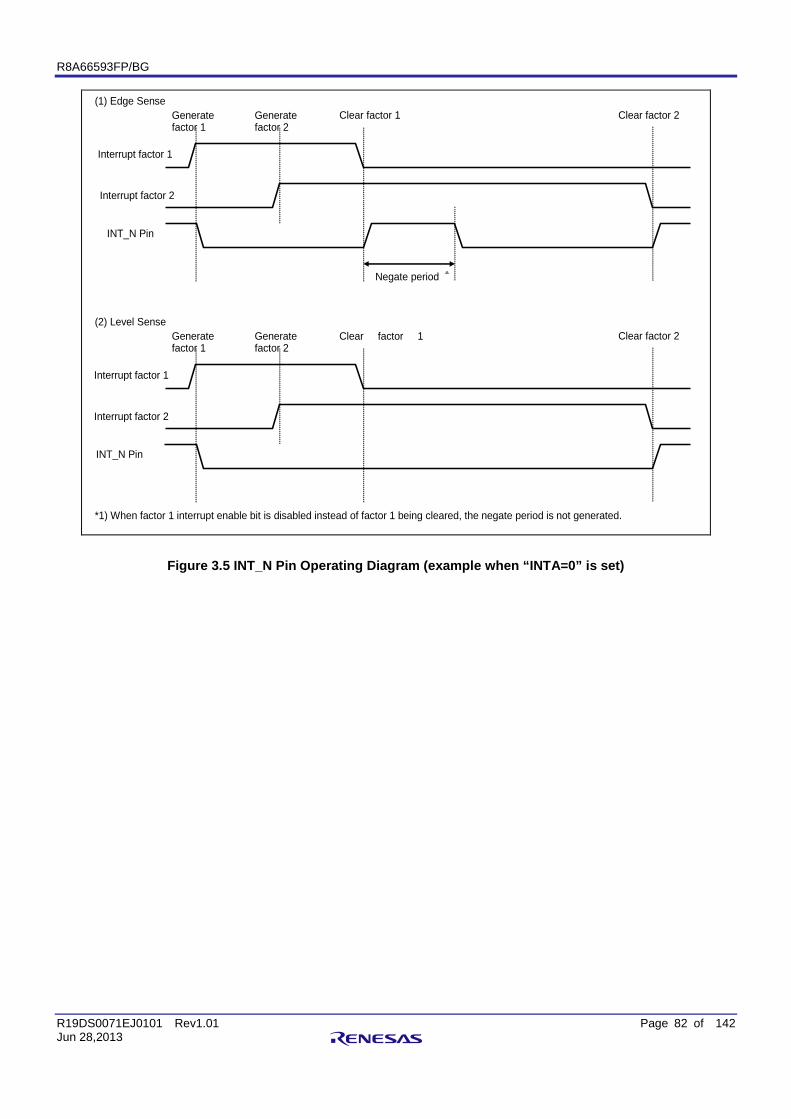
R8A66593FP/BG
R19DS0071EJ0101 Rev1.01 Page 82 of 142 Jun 28,2013
Interrupt factor 1
Interrupt factor 2
INT_N Pin
(1) Edge Sense Generate factor 1
Generate factor 2
Clear factor 1 Clear factor 2
Negate period 1
Interrupt factor 1
Interrupt factor 2
INT_N Pin
(2) Level Sense Generate factor 1
Generate factor 2
Clear factor 1
Clear factor 2
*1) When factor 1 interrupt enable bit is disabled instead of factor 1 being cleared, the negate period is not generated.
Figure 3.5 INT_N Pin Operating Diagram (example when “INTA=0” is set)
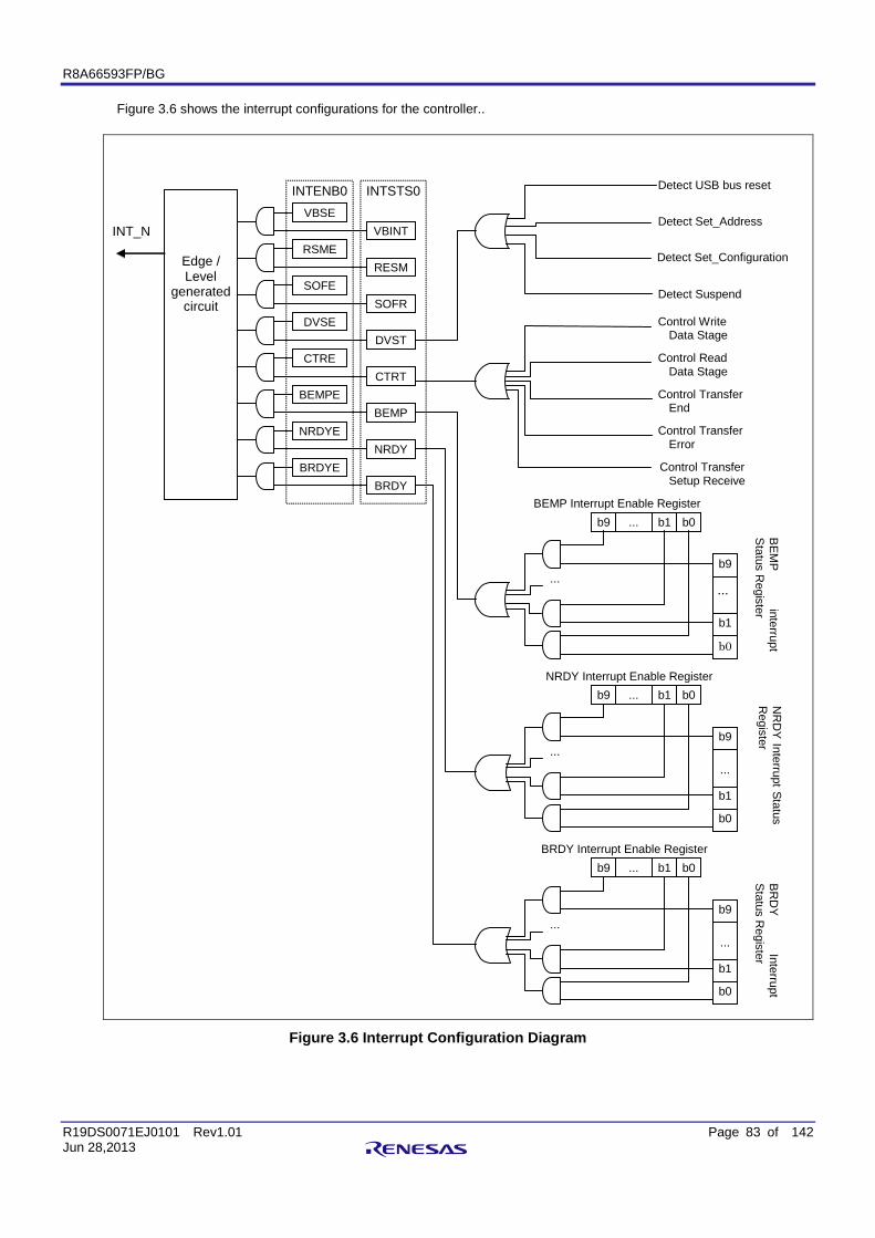
R8A66593FP/BG
R19DS0071EJ0101 Rev1.01 Page 83 of 142 Jun 28,2013
Figure 3.6 shows the interrupt configurations for the controller..
INT_N
Edge / Level
generated circuit
INTENB0 INTSTS0
DVST DVSE
VBINT VBSE
RESM RSME
SOFR SOFE
CTRT CTRE
BEMP BEMPE
NRDY NRDYE
BRDY BRDYE
Detect USB bus reset
Detect Set_Address
Detect Set_Configuration
Detect Suspend
End Control Transfer
Data Stage
Data Stage
Error
Setup Receive
Control Write
Control Read
Control Transfer
Control Transfer
b9 b1 b0
b0
b1
b9
... ...
...
b9 b1 b0
b0
b1
b9
...
...
...
b9 b1 b0
b0
b1
b9
...
...
...
BEMP Interrupt Enable Register
NRDY Interrupt Enable Register
BRDY Interrupt Enable Register
BEM
P
interrupt S
tatus Register
NR
DY
Interrupt Status R
egister B
RD
Y
Interrupt S
tatus Register
Figure 3.6 Interrupt Configuration Diagram
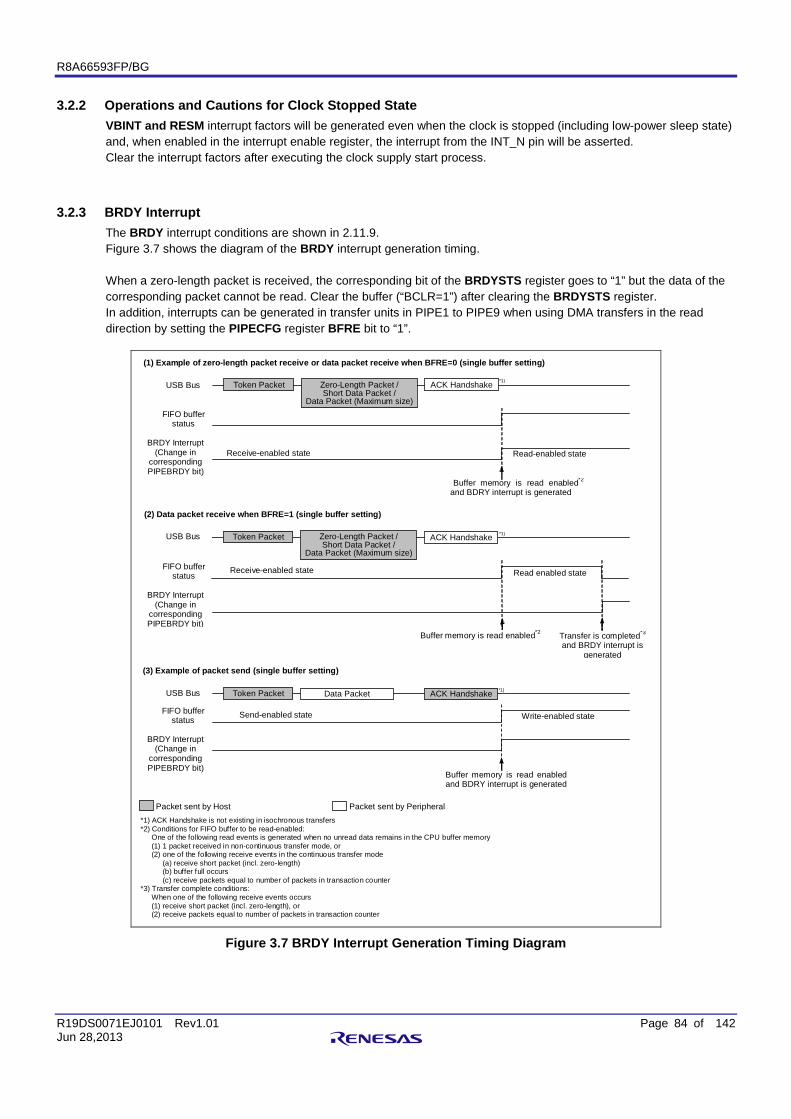
R8A66593FP/BG
R19DS0071EJ0101 Rev1.01 Page 84 of 142 Jun 28,2013
3.2.2 Operations and Cautions for Clock Stopped State VBINT and RESM interrupt factors will be generated even when the clock is stopped (including low-power sleep state) and, when enabled in the interrupt enable register, the interrupt from the INT_N pin will be asserted. Clear the interrupt factors after executing the clock supply start process.
3.2.3 BRDY Interrupt The BRDY interrupt conditions are shown in 2.11.9. Figure 3.7 shows the diagram of the BRDY interrupt generation timing. When a zero-length packet is received, the corresponding bit of the BRDYSTS register goes to “1” but the data of the corresponding packet cannot be read. Clear the buffer (“BCLR=1”) after clearing the BRDYSTS register. In addition, interrupts can be generated in transfer units in PIPE1 to PIPE9 when using DMA transfers in the read direction by setting the PIPECFG register BFRE bit to “1”.
(1) Example of zero-length packet receive or data packet receive when BFRE=0 (single buffer setting)
Token Packet USB Bus ACK Handshake
(2) Data packet receive when BFRE=1 (single buffer setting)
Token Packet USB Bus
(3) Example of packet send (single buffer setting)
Token Packet Data Packet USB Bus ACK Handshake
BRDY Interrupt (Change in
corresponding PIPEBRDY bit)
Buffer memory is read enabled*2 and BDRY interrupt is generated
Buffer memory is read enabled and BDRY interrupt is generated
Transfer is completed*3 and BRDY interrupt is
generated
Packet sent by Host Packet sent by Peripheral
FIFO buffer status
*1) ACK Handshake is not existing in isochronous transfers *2) Conditions for FIFO buffer to be read-enabled: One of the following read events is generated when no unread data remains in the CPU buffer memory (1) 1 packet received in non-continuous transfer mode, or (2) one of the following receive events in the continuous transfer mode (a) receive short packet (incl. zero-length) (b) buffer full occurs (c) receive packets equal to number of packets in transaction counter *3) Transfer complete conditions: When one of the following receive events occurs (1) receive short packet (incl. zero-length), or (2) receive packets equal to number of packets in transaction counter
FIFO buffer status
Zero-Length Packet / Short Data Packet /
Data Packet (Maximum size)
Zero-Length Packet / Short Data Packet /
Data Packet (Maximum size)
FIFO buffer status
Buffer memory is read enabled*2
*1)
ACK Handshake *1)
*1)
BRDY Interrupt (Change in
corresponding PIPEBRDY bit)
BRDY Interrupt (Change in
corresponding PIPEBRDY bit)
Receive-enabled state Read-enabled state
Receive-enabled state
Read enabled state
Send-enabled state
Write-enabled state
Figure 3.7 BRDY Interrupt Generation Timing Diagram
R8A66593FP/BG
R19DS0071EJ0101 Rev1.01 Page 85 of 142 Jun 28,2013
The conditions needed for the controller to clear the INTSTS0 register BRDY bit vary depending on the set value of the SOFCFG register BRDYM bit. Table 3.9 shows the conditions needed to clear the BRDY bit.
Table 3.8 Conditions for BRDY Clear by Controller
BRDYM BRDY Bit Clear Conditions 0 When all bits of the BRDYSTS register are cleared by software, the controller clears the INTSTS0
register BRDY bit. 1 When the BSTS bit of all pipes go to “0”, the controller clears the INTSTS0 register BRDY bit.
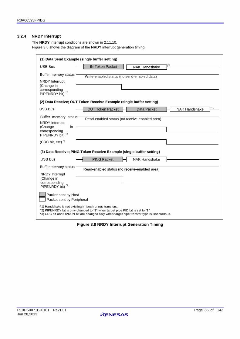
R8A66593FP/BG
R19DS0071EJ0101 Rev1.01 Page 86 of 142 Jun 28,2013
3.2.4 NRDY Interrupt The NRDY interrupt conditions are shown in 2.11.10. Figure 3.8 shows the diagram of the NRDY interrupt generation timing.
(*1
(*1
(CRC bit, etc) *3
(2) Data Receive; OUT Token Receive Example (single buffer setting)
IN Token Packet
OUT Token Packet
NAK Handshake
Data Packet
USB Bus
USB Bus
PING Packet NAK Handshake USB Bus
NRDY Interrupt (Change in corresponding PIPENRDY bit) *2
(3) Data Receive; PING Token Receive Example (single buffer setting)
(1) Data Send Example (single buffer setting)
NRDY Interrupt (Change in corresponding PIPENRDY bit) *2
NRDY Interrupt (Change in corresponding PIPENRDY bit) *2
*1) Handshake is not existing in isochronous transfers. *2) PIPENRDY bit is only changed to “1” when target pipe PID bit is set to “1”. *3) CRC bit and OVRUN bit are changed only when target pipe transfer type is isochronous.
Buffer memory status
Buffer memory status
Buffer memory status
Write-enabled status (no send-enabled data)
Read-enabled status (no receive-enabled area)
Read-enabled status (no receive-enabled area)
NAK Handshake
Packet sent by Host Packet sent by Peripheral
Figure 3.8 NRDY Interrupt Generation Timing
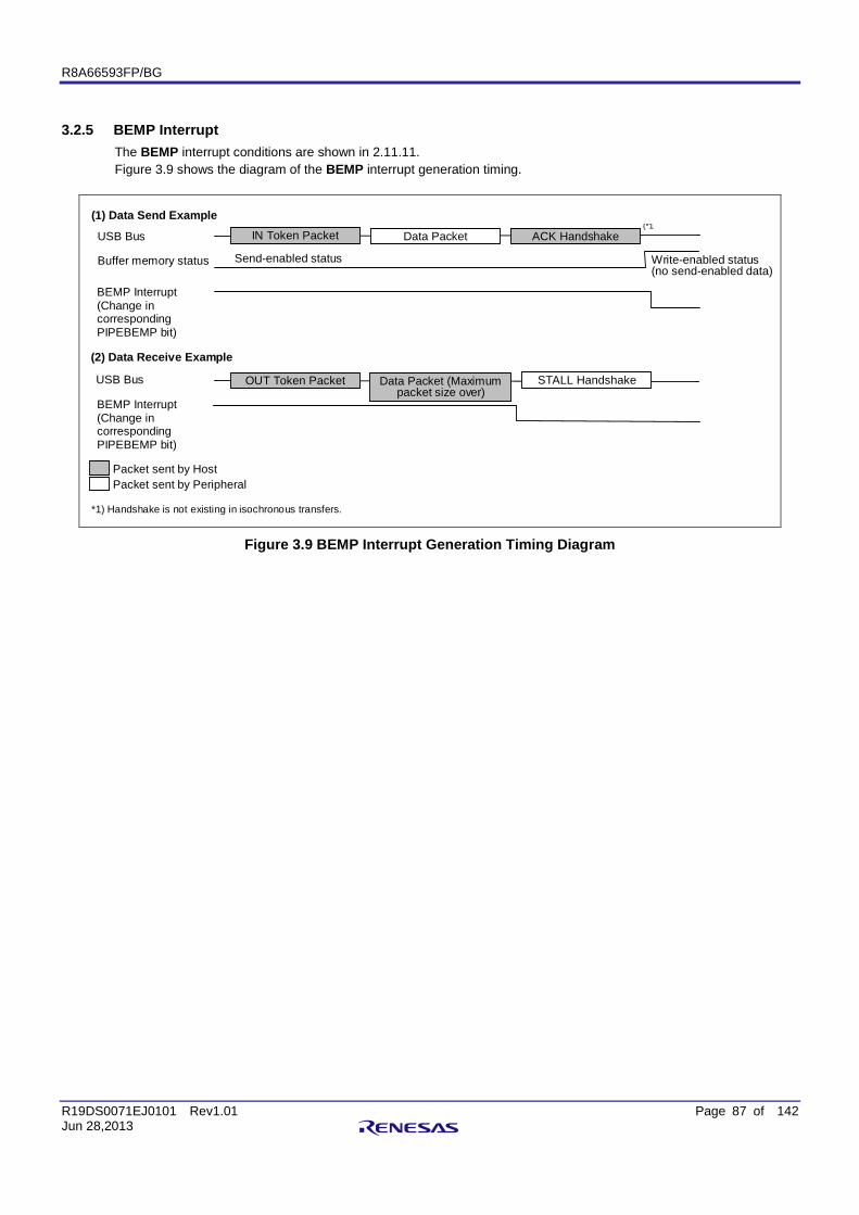
R8A66593FP/BG
R19DS0071EJ0101 Rev1.01 Page 87 of 142 Jun 28,2013
3.2.5 BEMP Interrupt The BEMP interrupt conditions are shown in 2.11.11. Figure 3.9 shows the diagram of the BEMP interrupt generation timing.
(*1
(*1 (1) Data Send Example
(2) Data Receive Example
IN Token Packet
OUT Token Packet
ACK Handshake Data Packet
STALL Handshake Data Packet (Maximum packet size over)
USB Bus
USB Bus
BEMP Interrupt (Change in corresponding PIPEBEMP bit)
BEMP Interrupt (Change in corresponding PIPEBEMP bit)
Packet sent by Host Packet sent by Peripheral
Buffer memory status Write-enabled status (no send-enabled data)
*1) Handshake is not existing in isochronous transfers.
Send-enabled status
Figure 3.9 BEMP Interrupt Generation Timing Diagram
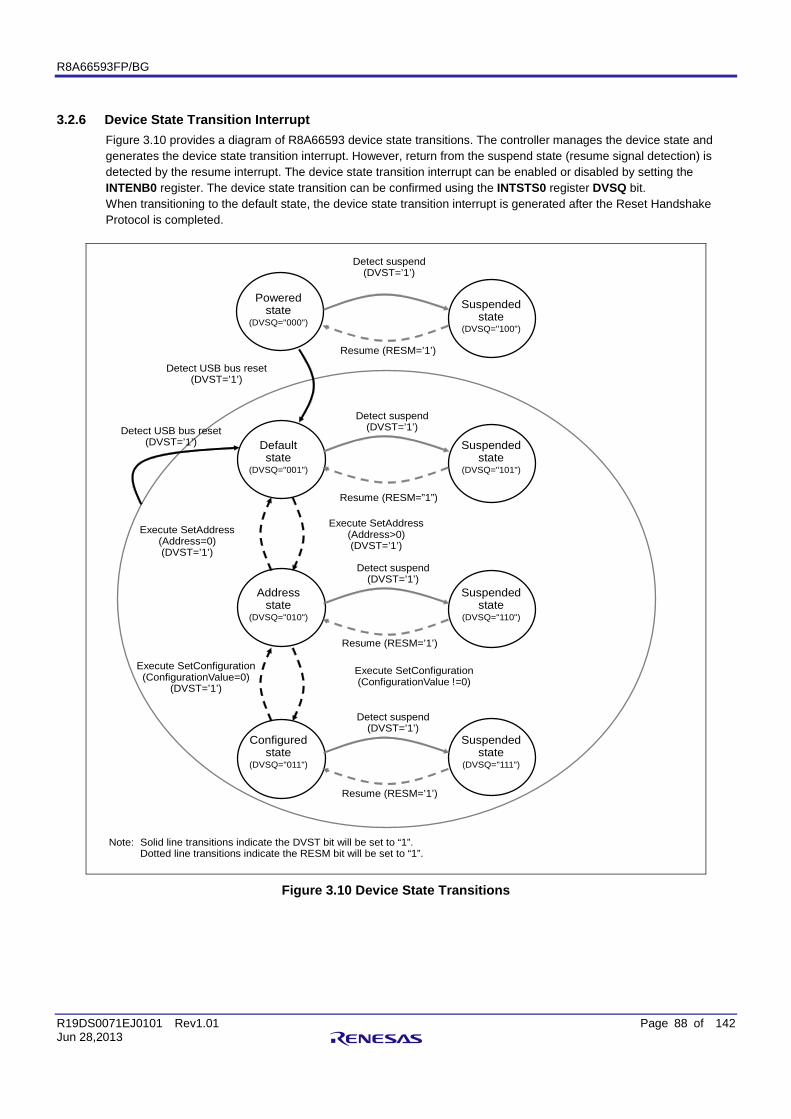
R8A66593FP/BG
R19DS0071EJ0101 Rev1.01 Page 88 of 142 Jun 28,2013
3.2.6 Device State Transition Interrupt Figure 3.10 provides a diagram of R8A66593 device state transitions. The controller manages the device state and generates the device state transition interrupt. However, return from the suspend state (resume signal detection) is detected by the resume interrupt. The device state transition interrupt can be enabled or disabled by setting the INTENB0 register. The device state transition can be confirmed using the INTSTS0 register DVSQ bit. When transitioning to the default state, the device state transition interrupt is generated after the Reset Handshake Protocol is completed.
Powered state
(DVSQ="000")
Detect suspend (DVST=’1’)
Resume (RESM=’1’) Detect USB bus reset
(DVST=’1’)
Execute SetAddress (Address=0) (DVST=’1’)
Detect USB bus reset (DVST=’1’) Default
state (DVSQ="001")
Address state
(DVSQ="010")
Configured state
(DVSQ="011")
Suspended state
(DVSQ="100")
Suspended state
(DVSQ="101")
Suspended state
(DVSQ="110")
Suspended state
(DVSQ="111")
Detect suspend (DVST=’1’)
Resume (RESM=”1”)
Execute SetAddress (Address>0) (DVST=’1’)
Detect suspend (DVST=’1’)
Resume (RESM=’1’)
Detect suspend (DVST=’1’)
Resume (RESM=’1’)
Execute SetConfiguration (ConfigurationValue=0)
(DVST=’1’) Execute SetConfiguration (ConfigurationValue !=0)
(DVST ’1’)
Note: Solid line transitions indicate the DVST bit will be set to “1”. Dotted line transitions indicate the RESM bit will be set to “1”.
Figure 3.10 Device State Transitions
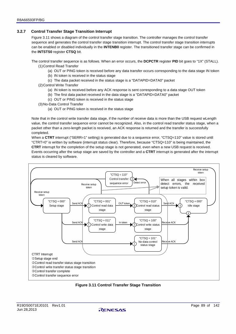
R8A66593FP/BG
R19DS0071EJ0101 Rev1.01 Page 89 of 142 Jun 28,2013
3.2.7 Control Transfer Stage Transition Interrupt Figure 3.11 shows a diagram of the control transfer stage transition. The controller manages the control transfer sequence and generates the control transfer stage transition interrupt. The control transfer stage transition interrupts can be enabled or disabled individually in the INTENB0 register. The transitioned transfer stage can be confirmed in the INTSTS0 register CTSQ bit. The control transfer sequence is as follows. When an error occurs, the DCPCTR register PID bit goes to “1X” (STALL).
(1) Control Read Transfer (a) OUT or PING token is received before any data transfer occurs corresponding to the data stage IN token (b) IN token is received in the status stage (c) The data packet received in the status stage is a “DATAPID=DATA0” packet
(2) Control Write Transfer (a) IN token is received before any ACK response is sent corresponding to a data stage OUT token (b) The first data packet received in the data stage is a “DATAPID=DATA0” packet (c) OUT or PING token is received in the status stage
(3) No-Data Control Transfer (a) OUT or PING token is received in the status stage
Note that in the control write transfer data stage, if the number of receive data is more than the USB request wLength value, the control transfer sequence error cannot be recognized. Also, in the control read transfer status stage, when a packet other than a zero-length packet is received, an ACK response is returned and the transfer is successfully completed. When a CTRT interrupt (“SERR=1” setting) is generated due to a sequence error, “CTSQ=110” value is stored until “CTRT=0” is written by software (interrupt status clear). Therefore, because “CTSQ=110” is being maintained, the CTRT interrupt for the completion of the setup stage is not generated, even when a new USB request is received. Events occurring after the setup stage are saved by the controller and a CTRT interrupt is generated after the interrupt status is cleared by software.
Send ACK
Receive ACK Send ACK
Detect error
Receive setup token
Send ACK
Send ACK
"CTSQ = 011" Control write data
stage
"CTSQ = 100" Control write status
stage
"CTSQ = 000" Idle stage
"CTSQ = 101" No-data control
status stage
OUT token
In token Receive ACK 1
1
3
4
"CTSQ = 000" Setup stage
"CTSQ = 001" Control read data
stage
"CTSQ = 010" Control read status
stage 2 1 4
"CTSQ = 110" Control transfer sequence error
5
CTRT Interrupt Setup stage end Control read transfer status stage transition Control write transfer status stage transition Control transfer complete Control transfer sequence error
Receive setup token
Receive setup token
When all stages within box detect errors, the received setup token is valid.
Figure 3.11 Control Transfer Stage Transition
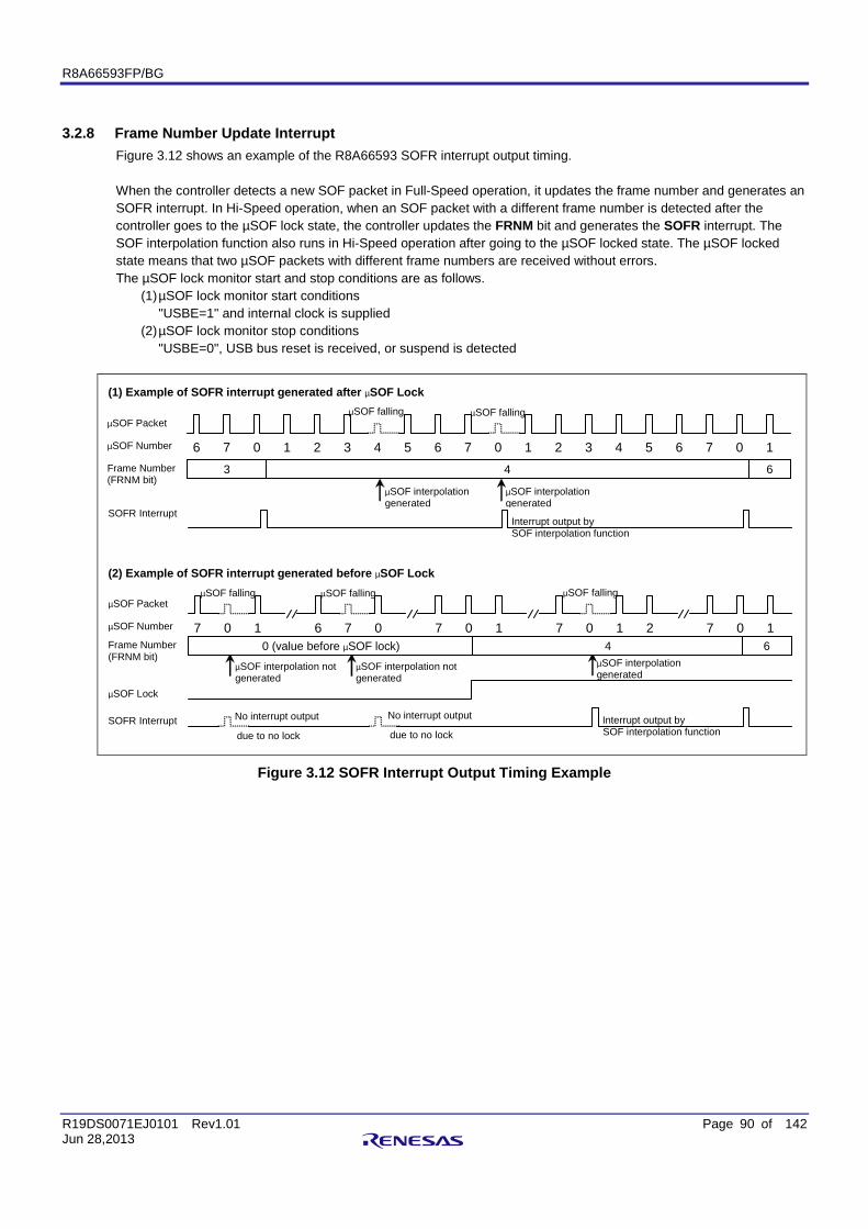
R8A66593FP/BG
R19DS0071EJ0101 Rev1.01 Page 90 of 142 Jun 28,2013
3.2.8 Frame Number Update Interrupt Figure 3.12 shows an example of the R8A66593 SOFR interrupt output timing. When the controller detects a new SOF packet in Full-Speed operation, it updates the frame number and generates an SOFR interrupt. In Hi-Speed operation, when an SOF packet with a different frame number is detected after the controller goes to the µSOF lock state, the controller updates the FRNM bit and generates the SOFR interrupt. The SOF interpolation function also runs in Hi-Speed operation after going to the µSOF locked state. The µSOF locked state means that two µSOF packets with different frame numbers are received without errors. The µSOF lock monitor start and stop conditions are as follows.
(1) µSOF lock monitor start conditions "USBE=1" and internal clock is supplied
(2) µSOF lock monitor stop conditions "USBE=0", USB bus reset is received, or suspend is detected
µSOF falling
µSOF falling µSOF falling µSOF falling
(1) Example of SOFR interrupt generated after µSOF Lock
µSOF Packet
µSOF Number
Frame Number (FRNM bit)
SOFR Interrupt
(2) Example of SOFR interrupt generated before µSOF Lock
µSOF Packet
µSOF Number
SOFR Interrupt
µSOF Lock
7 0 1 6 7 0 7 0 1 7 0 1 2 7 0 1
No interrupt output
due to no lock
7 0 1 2 3 6 7 0 1 2 3 4 5 6 6 7 0 1 3 4 6
Interrupt output by SOF interpolation function
4 5
µSOF falling
µSOF interpolation generated
µSOF interpolation generated
µSOF interpolation not generated
µSOF interpolation not generated
µSOF interpolation generated
No interrupt output
due to no lock Interrupt output by SOF interpolation function
Frame Number (FRNM bit)
0 (value before µSOF lock) 4 6
Figure 3.12 SOFR Interrupt Output Timing Example
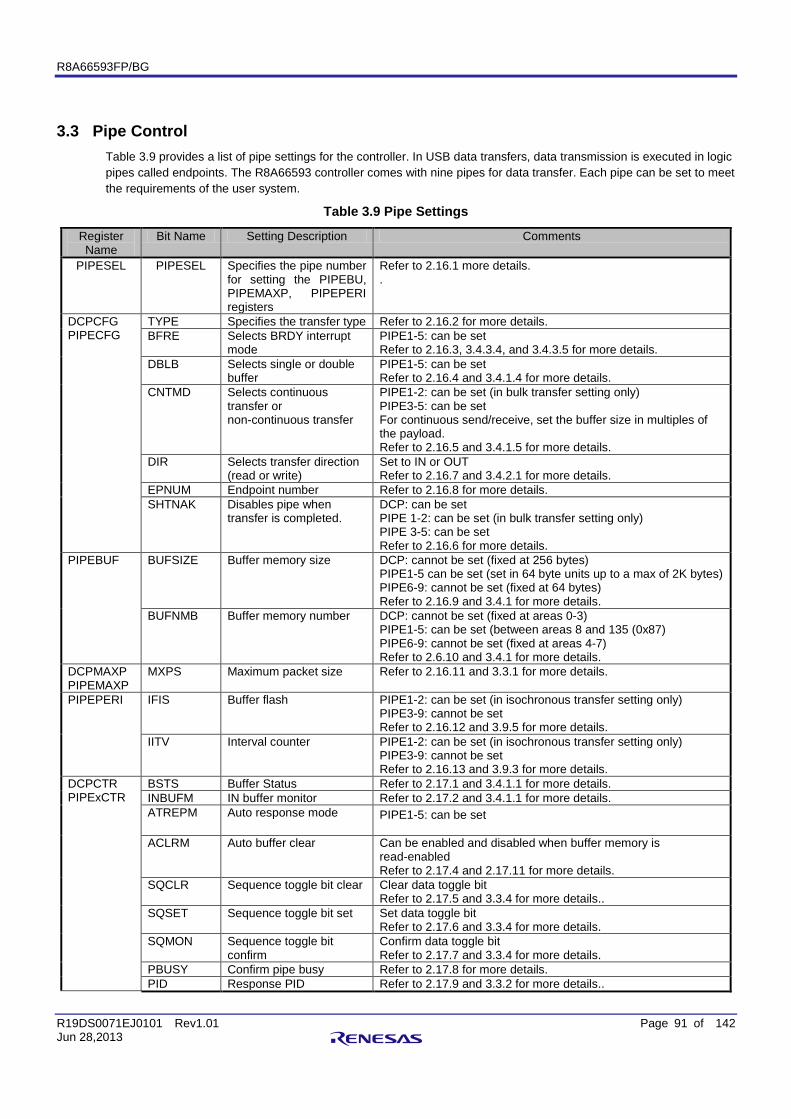
R8A66593FP/BG
R19DS0071EJ0101 Rev1.01 Page 91 of 142 Jun 28,2013
3.3 Pipe Control Table 3.9 provides a list of pipe settings for the controller. In USB data transfers, data transmission is executed in logic pipes called endpoints. The R8A66593 controller comes with nine pipes for data transfer. Each pipe can be set to meet the requirements of the user system.
Table 3.9 Pipe Settings
Register Name
Bit Name Setting Description Comments
PIPESEL PIPESEL
Specifies the pipe number for setting the PIPEBU, PIPEMAXP, PIPEPERI registers
Refer to 2.16.1 more details. .
DCPCFG PIPECFG
TYPE Specifies the transfer type Refer to 2.16.2 for more details. BFRE Selects BRDY interrupt
mode PIPE1-5: can be set Refer to 2.16.3, 3.4.3.4, and 3.4.3.5 for more details.
DBLB Selects single or double buffer
PIPE1-5: can be set Refer to 2.16.4 and 3.4.1.4 for more details.
CNTMD Selects continuous transfer or non-continuous transfer
PIPE1-2: can be set (in bulk transfer setting only) PIPE3-5: can be set For continuous send/receive, set the buffer size in multiples of the payload. Refer to 2.16.5 and 3.4.1.5 for more details.
DIR Selects transfer direction (read or write)
Set to IN or OUT Refer to 2.16.7 and 3.4.2.1 for more details.
EPNUM Endpoint number Refer to 2.16.8 for more details. SHTNAK Disables pipe when
transfer is completed. DCP: can be set PIPE 1-2: can be set (in bulk transfer setting only) PIPE 3-5: can be set Refer to 2.16.6 for more details.
PIPEBUF BUFSIZE Buffer memory size DCP: cannot be set (fixed at 256 bytes) PIPE1-5 can be set (set in 64 byte units up to a max of 2K bytes) PIPE6-9: cannot be set (fixed at 64 bytes) Refer to 2.16.9 and 3.4.1 for more details.
BUFNMB Buffer memory number DCP: cannot be set (fixed at areas 0-3) PIPE1-5: can be set (between areas 8 and 135 (0x87) PIPE6-9: cannot be set (fixed at areas 4-7) Refer to 2.6.10 and 3.4.1 for more details.
DCPMAXP PIPEMAXP
MXPS Maximum packet size Refer to 2.16.11 and 3.3.1 for more details.
PIPEPERI IFIS Buffer flash PIPE1-2: can be set (in isochronous transfer setting only) PIPE3-9: cannot be set Refer to 2.16.12 and 3.9.5 for more details.
IITV Interval counter PIPE1-2: can be set (in isochronous transfer setting only) PIPE3-9: cannot be set Refer to 2.16.13 and 3.9.3 for more details.
DCPCTR PIPExCTR
BSTS Buffer Status Refer to 2.17.1 and 3.4.1.1 for more details. INBUFM IN buffer monitor Refer to 2.17.2 and 3.4.1.1 for more details. ATREPM Auto response mode PIPE1-5: can be set
ACLRM Auto buffer clear Can be enabled and disabled when buffer memory is
read-enabled Refer to 2.17.4 and 2.17.11 for more details.
SQCLR Sequence toggle bit clear Clear data toggle bit Refer to 2.17.5 and 3.3.4 for more details..
SQSET Sequence toggle bit set Set data toggle bit Refer to 2.17.6 and 3.3.4 for more details.
SQMON Sequence toggle bit confirm
Confirm data toggle bit Refer to 2.17.7 and 3.3.4 for more details.
PBUSY Confirm pipe busy Refer to 2.17.8 for more details. PID Response PID Refer to 2.17.9 and 3.3.2 for more details..
R8A66593FP/BG
R19DS0071EJ0101 Rev1.01 Page 92 of 142 Jun 28,2013
Register Name
Bit Name Setting Description Comments
PIPExTRE TRENB Transaction count enable PIPE1-5: can be set Refer to 2.18.1 for more details.
TRCLR Current transaction counter clear
PIPE1-5: can be set Refer to 2.18.2 for more details.
PIPExTRN TRNCNT Transaction counter PIPE1-5: can be set Refer to 2.18.3 for more details.
3.3.1 Maximum Packet Size Setting Maximum packet size for each pipe is set in the MXPS bit of the DCPMAXP and PIPEMAXP registers. DCP and pipes 1-5 can be set with any maximum packet size defined in the USB specifications. Pipes 6-9 are limited to maximum packet size of 64 bytes. Set the maximum packet size before starting transfers (set “PID=BUF”). DCP: set to “64” for Hi-Speed operation DCP: set to “8”, “16”, “32”, or “64” for Full-Speed operation PIPE 1-5: set to “512” for Hi-Speed bulk transfer PIPE 1-5: set to “8”, “16”, “32”, or “64” for Full-Speed bulk transfer PIPE 1-2: set a value from “1” to “1024” for Hi-Speed isochronous transfer PIPE: 1-2: set a value from “1” to “1023” for Full-Speed isochronous transfer. For more details, see section 3.9. PIPE 6-9: Set a value from “1” to “64”. High-bandwidth transfers are not yet supported in interrupt and isochronous transfers.
3.3.2 Response PID Set the response PID for each pipe with the PID bit of the DCPCTR and PIPExCTR registers. The response PID specifies the response to a transaction from the Host.
(a) NAK setting: Always sends a NAK response when a transaction is issued. (b) BUF setting: Responds to the transaction in accordance with the buffer memory status. (c) STALL setting: Always sends a STALL response when a transaction is issued.
Regardless of the value set in the PID bit, an ACK is always sent as a response to a setup transaction and the USB request is stored in corresponding registers.
Based on the results of the transaction, the controller may trigger the PID bit to be written. The controller will trigger a write event to the PID bit in the following cases.
(a) NAK Setting:
(i) When SETUP token is received normally (only DCP) (ii) In bulk transfers when PIPECFG register SHTNAK bit is set to “1” and short packet is received (iii) In bulk transfers when SHTNAK bit is set to “1” and the transfaction counter is completed.
(b) BUF setting: the BUF cannot be written by the controller (c) STALL setting:
(i) When a maximum packet size over error is detected for a received data packet (ii) When a control transfer sequence error is detected
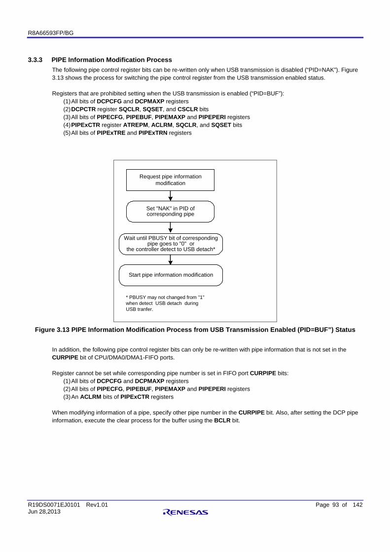
R8A66593FP/BG
R19DS0071EJ0101 Rev1.01 Page 93 of 142 Jun 28,2013
3.3.3 PIPE Information Modification Process The following pipe control register bits can be re-written only when USB transmission is disabled (“PID=NAK”). Figure 3.13 shows the process for switching the pipe control register from the USB transmission enabled status. Registers that are prohibited setting when the USB transmission is enabled (“PID=BUF”):
(1) All bits of DCPCFG and DCPMAXP registers (2) DCPCTR register SQCLR, SQSET, and CSCLR bits (3) All bits of PIPECFG, PIPEBUF, PIPEMAXP and PIPEPERI registers (4) PIPExCTR register ATREPM, ACLRM, SQCLR, and SQSET bits (5) All bits of PIPExTRE and PIPExTRN registers
Set "NAK" in PID of corresponding pipe
Wait until PBUSY bit of corresponding pipe goes to "0" or
the controller detect to USB detach*
Start pipe information modification
Request pipe information modification
* PBUSY may not changed from "1" when detect USB detach during USB tranfer.
Figure 3.13 PIPE Information Modification Process from USB Transmission Enabled (PID=BUF”) Status
In addition, the following pipe control register bits can only be re-written with pipe information that is not set in the CURPIPE bit of CPU/DMA0/DMA1-FIFO ports. Register cannot be set while corresponding pipe number is set in FIFO port CURPIPE bits:
(1) All bits of DCPCFG and DCPMAXP registers (2) All bits of PIPECFG, PIPEBUF, PIPEMAXP and PIPEPERI registers (3) An ACLRM bits of PIPExCTR registers
When modifying information of a pipe, specify other pipe number in the CURPIPE bit. Also, after setting the DCP pipe information, execute the clear process for the buffer using the BCLR bit.
R8A66593FP/BG
R19DS0071EJ0101 Rev1.01 Page 94 of 142 Jun 28,2013
3.3.4 Data PID Sequence Bit When a normal data transfer occurs in the control transfer data stage, bulk transfer or interrupt transfer, the controller automatically toggles the data PID sequence bit. The next data PID sequence bit for data transfer can be confirmed in the SQMON bit in the DCPCTR or PIPExCTR registers. The sequence bit is switched in the ACK handshake receive timing when data is sent or in the ACK handshake send timing when data is received. The data PID sequence bit can also be modified for the SQCLR and SQSET bits of the DCPCTR and PIPExCTR registers. For control transfers, the controller automatically sets the sequence bit for stage transitions. In control transfers, the controller automatically sets the sequence bit when the stage transitions. The bit goes to DATA1 when the setup stage completes. The sequence bit doesn't refer, and responds with DATA1 in the status stage. Therefore, the bit does not need to be set with software. Note: the data PID sequence bit must be set with software when a ClearFeature request is received. Finally, the sequence bit cannot be controlled through the SQSET bit for the isochronous transfer setup pipe.
R8A66593FP/BG
R19DS0071EJ0101 Rev1.01 Page 95 of 142 Jun 28,2013
3.4 Buffer Memory This section describes operations concerning the controller’s built-in buffer memory.
3.4.1 Buffer Memory Allocation Figure 3.14 provides an example buffer memory map of the controller. The buffer memory is an area shared by the CPU that controls the user system and this controller. The various buffer memory conditions determine access authority for the user system (CPU side) and/or this controller (SIE side). The buffer memory is set into independent areas for each pipe. The memory area is set in 64-byte blocks by the block start addresses and the number of blocks (set in PIPEBUF register BUFNMB bit and BUFSIZE bit). When selecting the continuous transfer mode with the PIPECFG register CNTMD bit, make sure the BUFSIZE bit is set in integral multiples of the maximum packet size. Also, when selecting the double buffer in the PIPECFG register DBLB bit, 2 areas of the memory specified in the PIPEBUF register BUFSIZE bit will be allocated for the corresponding pipe. Three FIFO ports are used for access (data read/write) to the buffer memory. The pipe number of the pipe assigned to each FIFO port is specified in the C/DxFIFOSEL register CURPIPE bit. The buffer status (enable/disable access for data read/write to buffer memory from CPU) of each pipe can be confirmed in the BSTS and INBUFM bits of the DCPCTR and the PIPExCTR registers. Also, FIFO port access authorization can be confirmed in the C/DxFIFOCTR register FRDY bit.
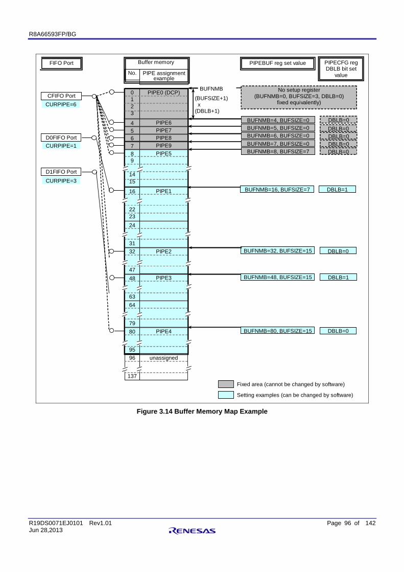
R8A66593FP/BG
R19DS0071EJ0101 Rev1.01 Page 96 of 142 Jun 28,2013
PIPE assignment example
4 5 6
8 9
14 15
7
0 1 2 3
32
47 48
63
80
95
FIFO Port
D0FIFO Port
No setup register (BUFNMB=0, BUFSIZE=3, DBLB=0)
fixed equivalently) CFIFO Port
D1FIFO Port CURPIPE=3
Buffer memory PIPEBUF reg set value
PIPE0 (DCP)
PIPE6 PIPE7
PIPE5
PIPE1
PIPE2
PIPE3
PIPE4
BUFNMB=4, BUFSIZE=0 BUFNMB=5, BUFSIZE=0 BUFNMB=6, BUFSIZE=0
BUFNMB=8, BUFSIZE=7
BUFNMB=16, BUFSIZE=7
BUFNMB=32, BUFSIZE=15
BUFNMB=48, BUFSIZE=15
CURPIPE=6
PIPE8 PIPE9
BUFNMB
(BUFSIZE+1) x (DBLB+1)
BUFNMB=7, BUFSIZE=0
BUFNMB=80, BUFSIZE=15
CURPIPE=1
PIPECFG reg DBLB bit set
value
DBLB=0 DBLB=0 DBLB=0
DBLB=0
DBLB=1
DBLB=0
DBLB=1
DBLB=0
DBLB=0
No.
16
22 23
96
137
unassigned
Fixed area (cannot be changed by software)
24
31
64
79
Setting examples (can be changed by software)
Figure 3.14 Buffer Memory Map Example
R8A66593FP/BG
R19DS0071EJ0101 Rev1.01 Page 97 of 142 Jun 28,2013
3.4.1.1 Buffer Status
Table 3.10 shows the buffer statuses for the controller. The buffer memory status can be confirmed with the BSTS and INBUFM bits. The direction of buffer memory access can be specified in the PIPECFG register DIR bit or the CFIFOSEL register ISEL bit (in the DCP setting). The INBUFM bit is only valid in the send direction of pipes 1 to 5. When the send-side transfer pipe is set to double buffer, the BSTS bit is used to determine the status of the CPU-side buffer and the INBUFM bit is used to determine the status of the SIE-side buffer. If the write event to the FIFO port using the CPU (DMAC) is slow and the buffer empty space cannot be determined by the BEMP interrupt, send completion can be confirmed with the INBUFM bit.
Table 3.10 Buffer Status Confirmation with BSTS Bit
ISEL or DIR BSTS Buffer Memory Status 0 (receive direction)
0 No receive data or now receiving. FIFO port is read-disabled.
0 (receive direction)
1 Receive data is in FIFO buffer or zero-length packet is received. FIFO port is read-enabled. However, when zero-length packet is received the FIFO port is read-disabled and the buffer must be cleared.
1 (send direction)
0 Send is not completed. FIFO port is write-disabled.
1 (send direction)
1 Send is completed. FIFO port is write-enabled.
Table 3.11 Buffer Status Confirmation with INBUFM Bit
DIR INBUFM Buffer Memory Status 0 (receive direction)
Invalid Invalid
1 (send direction)
0 Send data transfer is complete. No send data in FIFO buffer
1 (send direction)
1 Send data is written from FIFO port. Send data is in FIFO buffer.
3.4.1.2 Buffer Clear
Table 3.12shows the buffer memory clear conditions for the controller. The following 4 bits can clear the buffer memory.
Table 3.12 Buffer Clear Bits
Bit Name BCLR DCLRM ACLRM Register CFIFOCTR register
DxFIFOCTR register DxFIFOSEL register PIPExCTR register
Function Clears the CPU-side buffer memory of the pipe assigned to the CFIFO port or DxFIFO port
automatically clears the buffer memory after data is read from the specified pipe. Convenient function when using DMAC to read data. Refer to 3.4.3.4
Clears the SIE-side buffer memory of the corresponding pipe by writing “1” and “0” consecutively to the ACLRM bit.
Setup Method
Clear the buffer memory by setting “BCLR=1”. (Automatically returns to “BCLR=0”)
Set “DCLRM=1” to enable mode. Set “DCLRM=0” to disable mode.
Set “ACLRM=1” to enable mode. Set “ACLRM=0” to disable mode.
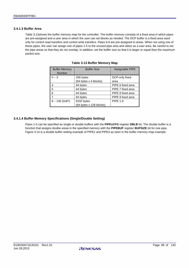
R8A66593FP/BG
R19DS0071EJ0101 Rev1.01 Page 98 of 142 Jun 28,2013
3.4.1.3 Buffer Area
Table 3.13shows the buffer memory map for the controller. The buffer memory consists of a fixed area in which pipes are pre-assigned and a user area in which the user can set blocks as needed. The DCP buffer is a fixed area used only for control read transfers and control write transfers. Pipes 6-9 are pre-assigned to areas. When not using one of these pipes, the user can assign one of pipes 1-5 to the unused pipe area and utilize as a user area. Be careful to set the pipe areas so that they do not overlap. In addition, set the buffer size so that it is larger or equal than the maximum packet size.
Table 3.13 Buffer Memory Map
Buffer Memory Number
Buffer Size Assignable PIPE
0 – 3 256 bytes (64 bytes x 4 blocks)
DCP-only fixed area
4 64 bytes PIPE 6 fixed area 5 64 bytes PIPE 7 fixed area 6 64 bytes PIPE 8 fixed area 7 64 bytes PIPE 9 fixed area 8 – 135 (0x87) 8192 bytes
(64 bytes x 128 blocks) PIPE 1-5
3.4.1.4 Buffer Memory Specifications (Single/Double Setting)
Pipes 1-5 can be specified as single or double buffers with the PIPExCFG register DBLB bit. The double buffer is a function that assigns doulbe areas in the specified memory with the PIPEBUF register BUFSIZE bit for one pipe. Figure 3.14 is a double buffer setting example of PIPE1 and PIPE3 as seen in the buffer memory map example.
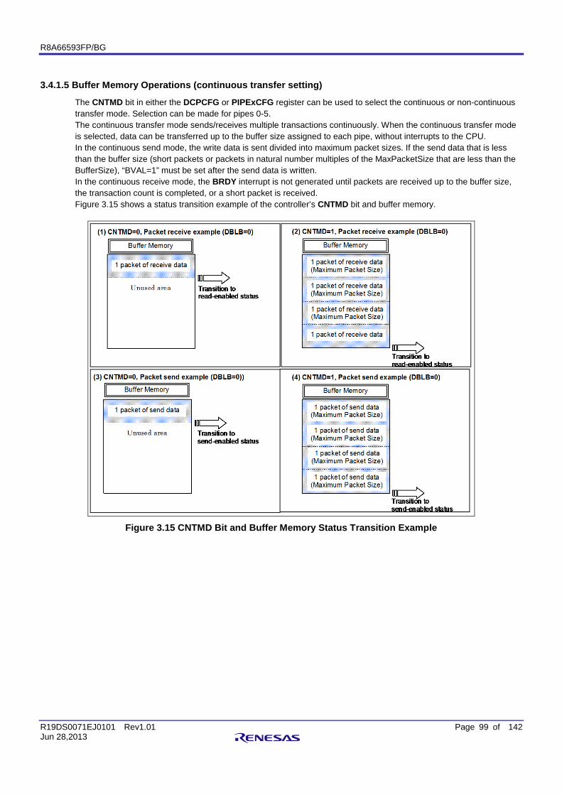
R8A66593FP/BG
R19DS0071EJ0101 Rev1.01 Page 99 of 142 Jun 28,2013
3.4.1.5 Buffer Memory Operations (continuous transfer setting)
The CNTMD bit in either the DCPCFG or PIPExCFG register can be used to select the continuous or non-continuous transfer mode. Selection can be made for pipes 0-5. The continuous transfer mode sends/receives multiple transactions continuously. When the continuous transfer mode is selected, data can be transferred up to the buffer size assigned to each pipe, without interrupts to the CPU. In the continuous send mode, the write data is sent divided into maximum packet sizes. If the send data that is less than the buffer size (short packets or packets in natural number multiples of the MaxPacketSize that are less than the BufferSize), “BVAL=1” must be set after the send data is written. In the continuous receive mode, the BRDY interrupt is not generated until packets are received up to the buffer size, the transaction count is completed, or a short packet is received. Figure 3.15 shows a status transition example of the controller’s CNTMD bit and buffer memory.
Figure 3.15 CNTMD Bit and Buffer Memory Status Transition Example
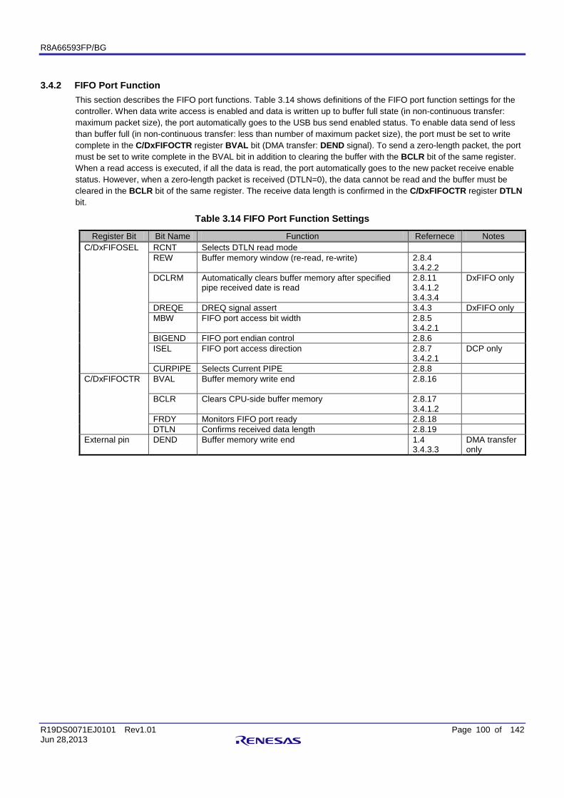
R8A66593FP/BG
R19DS0071EJ0101 Rev1.01 Page 100 of 142 Jun 28,2013
3.4.2 FIFO Port Function This section describes the FIFO port functions. Table 3.14 shows definitions of the FIFO port function settings for the controller. When data write access is enabled and data is written up to buffer full state (in non-continuous transfer: maximum packet size), the port automatically goes to the USB bus send enabled status. To enable data send of less than buffer full (in non-continuous transfer: less than number of maximum packet size), the port must be set to write complete in the C/DxFIFOCTR register BVAL bit (DMA transfer: DEND signal). To send a zero-length packet, the port must be set to write complete in the BVAL bit in addition to clearing the buffer with the BCLR bit of the same register. When a read access is executed, if all the data is read, the port automatically goes to the new packet receive enable status. However, when a zero-length packet is received (DTLN=0), the data cannot be read and the buffer must be cleared in the BCLR bit of the same register. The receive data length is confirmed in the C/DxFIFOCTR register DTLN bit.
Table 3.14 FIFO Port Function Settings
Register Bit Bit Name Function Refernece Notes C/DxFIFOSEL RCNT Selects DTLN read mode
REW Buffer memory window (re-read, re-write) 2.8.4 3.4.2.2
DCLRM Automatically clears buffer memory after specified pipe received date is read
2.8.11 3.4.1.2 3.4.3.4
DxFIFO only
DREQE DREQ signal assert 3.4.3 DxFIFO only MBW FIFO port access bit width 2.8.5
3.4.2.1
BIGEND FIFO port endian control 2.8.6 ISEL FIFO port access direction 2.8.7
3.4.2.1 DCP only
CURPIPE Selects Current PIPE 2.8.8 C/DxFIFOCTR BVAL Buffer memory write end 2.8.16
BCLR Clears CPU-side buffer memory 2.8.17 3.4.1.2
FRDY Monitors FIFO port ready 2.8.18 DTLN Confirms received data length 2.8.19
External pin DEND Buffer memory write end 1.4 3.4.3.3
DMA transfer only
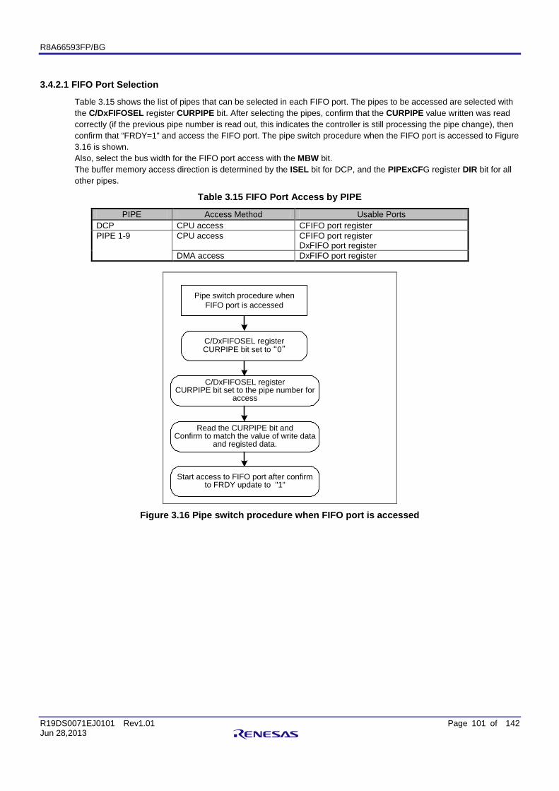
R8A66593FP/BG
R19DS0071EJ0101 Rev1.01 Page 101 of 142 Jun 28,2013
3.4.2.1 FIFO Port Selection
Table 3.15 shows the list of pipes that can be selected in each FIFO port. The pipes to be accessed are selected with the C/DxFIFOSEL register CURPIPE bit. After selecting the pipes, confirm that the CURPIPE value written was read correctly (if the previous pipe number is read out, this indicates the controller is still processing the pipe change), then confirm that “FRDY=1” and access the FIFO port. The pipe switch procedure when the FIFO port is accessed to Figure 3.16 is shown. Also, select the bus width for the FIFO port access with the MBW bit. The buffer memory access direction is determined by the ISEL bit for DCP, and the PIPExCFG register DIR bit for all other pipes.
Table 3.15 FIFO Port Access by PIPE
PIPE Access Method Usable Ports DCP CPU access CFIFO port register PIPE 1-9 CPU access CFIFO port register
DxFIFO port register DMA access DxFIFO port register
C/DxFIFOSEL register CURPIPE bit set to “0”
C/DxFIFOSEL register CURPIPE bit set to the pipe number for
access
Read the CURPIPE bit and Confirm to match the value of write data
and registed data.
Start access to FIFO port after confirm to FRDY update to "1"
Pipe switch procedure when FIFO port is accessed
Figure 3.16 Pipe switch procedure when FIFO port is accessed
R8A66593FP/BG
R19DS0071EJ0101 Rev1.01 Page 102 of 142 Jun 28,2013
3.4.2.2 REW Bit
The REW bit the C/DxFIFOSEL register in allows the user to temporarily stop the current pipe access, execute access of another pipe, then continue the current pipe access process again.
3.4.2.3 Transaction Counter (read direction)
The transaction counter enables the controller to recognize transfer completion after the specified number of transactions has completed in the data packet receive direction. The transaction counter is a function that operates in correspondence to pipes set in the receive direction. This function can be used for read events from any FIFO port. The transaction counter includes the TRNCNT register, which specifies the number of transactions, and the current counter that counts the number of internal transactions. When the current counter reaches the specified number of transactions, the buffer memory goes to the read-enabled status, even if it is not full. The TRCLR bit can be used to initialize the current counter in the transaction counter function so that the transaction can counted from the beginning again. Also, the information read from the TRNCNT register can be switched by setting the TRENB bit accordingly.
TRENB=0: the set transaction counter value is read out TRENB=1: the current counter value counted internally is read out
Modification conditions for the CURPIPE are as follows:
(1) Do not change the CURPIPE setting until the transaction in the specified pipe is completed. (2) The CURPIPE cannot be changed unless the current counter is cleared.
TRCLR bit usage conditions are as follows.
(1) The current counter cannot be cleared while a transaction is in process and “PID=BUF”. (2) The current counter cannot be cleared when data remains in the buffer.
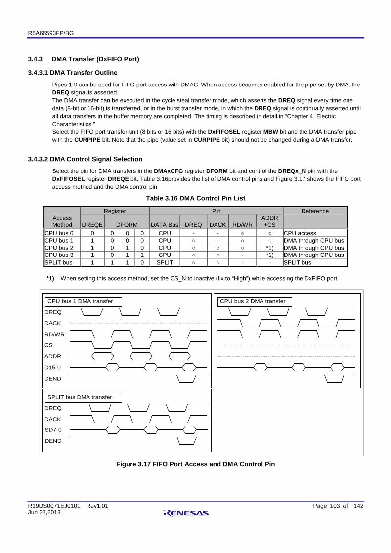
R8A66593FP/BG
R19DS0071EJ0101 Rev1.01 Page 103 of 142 Jun 28,2013
3.4.3 DMA Transfer (DxFIFO Port)
3.4.3.1 DMA Transfer Outline
Pipes 1-9 can be used for FIFO port access with DMAC. When access becomes enabled for the pipe set by DMA, the DREQ signal is asserted. The DMA transfer can be executed in the cycle steal transfer mode, which asserts the DREQ signal every time one data (8-bit or 16-bit) is transferred, or in the burst transfer mode, in which the DREQ signal is continually asserted until all data transfers in the buffer memory are completed. The timing is described in detail in “Chapter 4. Electric Characteristics.” Select the FIFO port transfer unit (8 bits or 16 bits) with the DxFIFOSEL register MBW bit and the DMA transfer pipe with the CURPIPE bit. Note that the pipe (value set in CURPIPE bit) should not be changed during a DMA transfer.
3.4.3.2 DMA Control Signal Selection
Select the pin for DMA transfers in the DMAxCFG register DFORM bit and control the DREQx_N pin with the DxFIFOSEL register DREQE bit. Table 3.16provides the list of DMA control pins and Figure 3.17 shows the FIFO port access method and the DMA control pin.
Table 3.16 DMA Control Pin List
Access Method
Register Pin Reference
DREQE DFORM DATA Bus DREQ DACK RD/WR ADDR +CS
CPU bus 0 0 0 0 0 CPU - - CPU access CPU bus 1 1 0 0 0 CPU - DMA through CPU bus CPU bus 2 1 0 1 0 CPU *1) DMA through CPU bus CPU bus 3 1 0 1 1 CPU - *1) DMA through CPU bus SPLIT bus 1 1 1 0 SPLIT - - SPLIT bus
*1) When setting this access method, set the CS_N to inactive (fix to “High”) while accessing the DxFIFO port.
DREQ
DACK
D15-0
CPU bus 1 DMA transfer CPU bus 2 DMA transfer
DEND
DREQ
DACK
SD7-0
SPLIT bus DMA transfer
DEND
RD/WR
CS
ADDR
Figure 3.17 FIFO Port Access and DMA Control Pin
R8A66593FP/BG
R19DS0071EJ0101 Rev1.01 Page 104 of 142 Jun 28,2013
3.4.3.3 DEND Pint
The controller can end a DMA transfer using the DEND pin. The DEND pin also functions as input/output according to the USB data transfer direction.
(1) Buffer memory read direction The DEND pin can perform as an output pin and notify the external DMA controller of the last data transfer. The DEND signal assert conditions can be set in the DMAxCFG register PKTM bit. Table 3.17 provides a list of DEND pin asserts.
Table 3.17 DEND Pin Assert List
Event
PKTM
Transaction Count End
BRDY generated due to packet receive
Receive short packet other than zero-length
Receive Zero-Length packet when buffer is not EMPTY
Receive zero-length packet when buffer is EMPTY *2)
0 Assert No assert Assert Assert Assert 1 Assert Assert Assert Assert No assert
*1) The DREQ signal is not asserted if a zero-length packet is received when the buffer is empty. (2) Buffer memory write direction The DEND pin becomes an input pin and the buffer memory goes to send-enabled (same status as when “BVAL=1”) when an active edge is detected.
3.4.3.4 DxFIFO Automatic Clear Mode (DxFIFO port read direction)
When a data read event of the controller buffer memory is completed with setting DxFIFOSEL register DCLRM bit to “1”, the buffer memory of the corresponding pipe is automatically cleared.
Table 3.18 shows the correspondence between the packet received and the buffer memory clear process by software in each setting. As indicated in Table 3.18, the buffer clear conditions differ according to the BFRE bit set value, even for statuses in which clear is normally required, using the DCLRM bit eliminates the need for buffer clear by software, enabling DMA transfers without the use of software. Note that this function only has supports the buffer memory read direction setting.
Table 3.18 Correspondence of Packet Receive and Buffer Memory Clear Process by Software
Register Setting Buffer state when packet received
DCLRM = 0 DCLRM=1 BFRE=0 BFRE=1 BFRE=0 BFRE=1
Buffer full Clear unnecessary Clear unnecessary Clear unnecessary Clear unnecessary Zero-Length packet received Clear necessary Clear necessary Clear unnecessary Clear unnecessary Normal short packet received Clear unnecessary Clear necessary Clear unnecessary Clear unnecessary Transaction count end Clear unnecessary Clear necessary Clear unnecessary Clear unnecessary
R8A66593FP/BG
R19DS0071EJ0101 Rev1.01 Page 105 of 142 Jun 28,2013
3.4.3.5 BRDY Interrupt Timing Selection Function
The PIPECFG register BFRE bit can be set so that the BRDY interrupt is not generated when a data packet of maximum packet size is received. When using a DMA transfer, this function enables an interrupt to be generated only when the last data is received. The last data indicates either a short packet receive or the transaction count end. By setting “BFRE=1”, the BRDY interrupt will be generated after the received data is read. By reading the DnFIFOCTR register DTLN bit, the receive data length of last data packet received just before the BRDY interrupt was generated can be confirmed. Table 3.19 shows the timing of the BRDY interrupt.
Table 3.19 BRDY Interrupt Generation Timing List
Registration Setting Buffer state when packet received BFRE = “0” BFRE = “1” Buffer full (normal packet received) When packet is received No interrupt generated Zero-Length packet received When packet is received When packet is received
Normal short packet received When packet is received When read event of data received from buffer memory is completed
Transaction count end When packet is received When read event of data received from buffer memory is completed
The BFRE bit function is only valid in the read direction of the buffer memory. When in the write direction, fix the BFRE bit to “0”.
R8A66593FP/BG
R19DS0071EJ0101 Rev1.01 Page 106 of 142 Jun 28,2013
3.4.4 FIFO Port Access Enable Timing This section describes the FIFO port access enable timing.
3.4.4.1 FIFO Port Access Enable Timing at Pipe Switch
Figure 3.18 shows the timing diagram up to confirmation of the FRDY and DRLN bits when the pipe specified by the FIFO port is switched (modified C/DxFIFOSEL register CURPIPE bit). When the CURPIPE bit is modified, first confirm that the written CURPIPE value was read correctly (if the previous pipe number is read out, this indicates the controller is still processing the pipe modification), then confirm that “FRDY=1” and access the FIFO port. The same timing applies to modification of the ISEL bit for the CFIFO port.
Figure 3.18 FRDY, DRLN Fix Timing after Pipe Switch
3.4.4.2 FIFO Port Access Enable Timing after Double Buffer Read/Write is Completed
Figure 3.19 shows the timing diagram up to when access is enabled for the second buffer, after the buffer read or write is completed in the double buffer mode. In the double buffer mode, always access the FIFO port after waiting 300ns after the access just before the toggle. The same timing is applied to sending a short packet by setting “BVAL=1” in the IN direction pipe.
Figure 3.19 Figure 3.18 FRDY, DTLN Confirmation Timing after Double Buffer Read/Write Complete
R8A66593FP/BG
R19DS0071EJ0101 Rev1.01 Page 107 of 142 Jun 28,2013
3.5 Data Setup Timing This section describes the OBUS bit that sets the split bus timing. The timing of the SD0-7 and DEND pins can be modified through the DMAxCFG register OBUS bit as described in Table 3.20. The OBUS bit function is only valid for DMA transfers using a split bus. When using the CPU bus for DMA transfers, the OBUS bit setting is ignored.
Table 3.20 Operation Differences According to OBUS Bit Setup Value
Direction OBUS Bit Setting
Operation
Read 0 SD0-7/DEND signals are output normally, regardless of the control signal *1. If the control signal is negated, the next data is output. Therefore, the DMAC data setup timing is secured and Hi-Speed DMA transfer is enabled.
1 SD0-7/DEND signals are output after the control signal is asserted. SD0-7/DEND signals go to Hi-z if the control signal is negated.
Write 0 SD0-7/DEND signals are output normally, regardless of the DACKx_N signal. The DMAC can output the next data before the DACKx_N signal is asserted. Therefore, the controller data setup timing is secured and Hi-Speed DMA transfer is enabled.
1 SD0-7/DEND signals are input-enabled only when the DACKx_N signal is asserted. SD0-7/DEND signals are ignored if the DACKx_N signal is negated.
*1) The control signal indicates DACKx_N when DMAxCFG register DFORM [9 – 7] is “100”. When ”OBUS=0” is set in the read direction, SD0-7/DEND signal are always output. Note that, therefore, when sharing
the bus with another device, ”OBUS=1” shall be set. When ”OBUS=0” is set in the write direction, SD0-7/DEND signals are always input-enabled. Do not allow the signals
to be used as mid-rail voltage. Figure 3.20 shows the configuration of data setup timing by the OBUS bit.
OBUS=1: normal mode OBUS=0: High-Speed mode
DREQ
DACK
SD7-0
DEND
Figure 3.20 Data Setup Timing Configuration
R8A66593FP/BG
R19DS0071EJ0101 Rev1.01 Page 108 of 142 Jun 28,2013
3.6 Control Transfer (DCP) Data transfer in the data stage of the control transfer uses the default control pipe (DCP). The DCP buffer memory is a 256-byte single buffer fixed area used for both control read and control write events. Only the CFIFO port is enabled for access to the buffer memory.
3.6.1 Setup Stage The controller always responds with an ACK when it receives a normal setup packet. The controller operations in the setup stage are as follows.
(1) When a new setup packet is received, the controller sets the following bits. (a) Sets INTSTS0 register VALID bit to “1”. (b) Sets DCPCTR register PID bit to “NAK”. (c) Sets DCPCTR register CCPL bit to “0”.
(2) When a data packet is received following the setup packet, the USB request parameters are stored in the following registers: USBREQ, USBVAL, USBINDX and USBLENG.
Always set “VALID=0” in the response process to a control transfer. In the “VALID=1” state, “PID=BUF” will not be set and the data stage cannot be completed. The VALID bit function allows the controller to temporarily stop a request in-process when it receives a new USB request during a control transfer, and respond to the newest request. In addition, the controller automatically judges the direction bit (bmRequestType bit 8) and the request data length (wLength) of the received USB request and determines whether it is a control read transfer, control write transfer or no-data control transfer, and then handles the stage transition. If the sequence is incorrect, a sequence error for the control transfer stage transition interrupt occurs and is notified to the software. For more information concerning the controller stage management, refer to Figure 3.11.
3.6.2 Data Stage Use the DCP for data transfers in response to receiving a USB request. Before accessing the DCP buffer memory, set the access direction in the CFIFOSEL register ISEL bit. Also set the transfer direction in the DCPCFG register DIR bit. The transaction is executed by setting the the PID bit of the DCPCFG register to BUF. Data transfer completion is detected by the BRDY or BEMP interrupts. Use the BRDY interrupt for control write transfers and the BEMP interrupt for control read transfers. For control write transfers in Hi-Speed operation, a NYET handshake is sent in accordance with the buffer memory status. For more details, see Chapter 3.7.1,
3.6.3 Status Stage When the DCPCTR register PID bit status is “PID=BUF”, set the CCPL bit to “1” to complete the control transfer. After the above settings, the controller automatically executes the status stage in accordance with the data transfer direction fixed in the setup stage. The detailed process is as follows.
(1) Control read transfers: The controller sends a zero-length packet and receives an ACK response from the USB Host Controller.
(2) Control write transfers and no-data control transfers: The controller receives a zero-length packet from the USB host and sends an ACK response.
R8A66593FP/BG
R19DS0071EJ0101 Rev1.01 Page 109 of 142 Jun 28,2013
3.6.4 Control Transfer Automatic Response Function The controller automatically sends a response to a normal SET ADDRESS request. If one of the following errors occurs, a response must be sent by software.
(1) bmRequestType ≠ “0x00” (2) wIndex ≠ “0x00” (3) wLength ≠ “0x00” (4) wValue > “0x7F” (5) wValue ≠ 0 and DVSQ = "011" (6) wValue = 0 and DVSQ = "001"
All requests other than the SET ADDRESS request must be responded to by software.
R8A66593FP/BG
R19DS0071EJ0101 Rev1.01 Page 110 of 142 Jun 28,2013
3.7 Bulk Transfer (Pipes 1-5) The user can select the buffer memory usage method (single/double buffer, continuous/non-continuous transfer mode) for the bulk transfer mode. The buffer memory size can be set up to a 2K-byte double buffer. The controller manages the buffer memory state and automatically responds to PING packets and NYET handshakes.
3.7.1 NYET Handshake Control Table 3.21 shows the list of responses to a token received in a bulk or control transfer. When an OUT token is received in a bulk or control transfer and there is only enough open space for one packet in the buffer memory, the controller sends a NYET response. However, when a short packet is received, the controller sends an ACK response instead of a NYET response, even under these conditions.
Table 3.21 Response List for Received Tokens
PID Bit Set Value
Buffer Memory Status *1) Receive Token Response Notes
NAK/STALL - SETUP ACK - - IN/OUT/PING NAK/STALL -
BUF
- SETUP ACK - RCV-BRDY OUT/PING ACK Receive data packet at OUT token receive*1 RCV-BRDY OUT NYET Receive data packet*2 RCV-BRDY OUT (Short) ACK Receive data packet*2 RCV-BRDY PING ACK *2 RCV-NRDY OUT / PING NAK TRN-BRDY IN DATA0 / 1 Send data packet TRN-NRDY IN NAK
*1) Further response details: RCV-BRDY*1: Buffer memory has enough space for 2 packets or more when OUT/PING token is received. RCV-BRDY*2: Buffer memory has only enough space for one packet when OUT token is received RCV-NRDY: Buffer memory has not enough space for one packet when PING token is received. TRN-BRDY: Buffer memory has send data when IN token is received. TRN-NRDY: Buffer memory does not have send data when IN token is received.
3.8 Interrupt Transfer (Pipes 6-9) The controller executes an interrupt transfer in accordance with the period managed by the Host controller. The controller ignores (no response) PING packets in interrupt transfers. In addition, the controller does not send a NYET handshake, but responds with ACK, NAK or STALL. The R8A66593 controller does not support high-bandwidth transfers in the interrupt transfer mode.
R8A66593FP/BG
R19DS0071EJ0101 Rev1.01 Page 111 of 142 Jun 28,2013
3.9 Isochronous Transfer (Pipes 1-2) The controller provides the following functions for isochronous transfers.
(1) Isochronous transfer error information notification (2) Interval counter (IITV bit setting) (3) Isochronous IN transfer data setup control (IDLY function) (4) Isochronous IN transfer buffer flush function (IFIS bit setting) (5) SOF pulse output function
The controller does not support high-bandwidth isochronous transfers..
3.9.1 Isochronous Transfer Error Detection The controller manages isochronous transfer errors by software and therefore has the following error information detection functions. Table 3.22 and Table 3.23 describe the procedure in which errors are confirmed and the interrupts that are generated.
(1) PID Error When the receive packet PID is corrupted
(2) CRC Error and Bit Stuffing Error When an error occurs in the receive packet CRC or when the bit stuffing is corrupted.
(3) Maximum Packet Size Over This indicates the data size of the receive packet is larger than the value set for the maximum packet size.
(4) Overrun and Underrun (a) When there is no data in the buffer memory at an IN token receive for an IN-direction (send) transfer (b) When there is no empty space in the buffer memory at an OUT token receive for an OUT-direction
(receive) transfer (5) Interval Error
(a) When an IN token could not be received in the interval frame of an isochronous IN transfer (b) When an OUT token could not be received in the interval frame of an isochronous OUT transfer
Table 3.22 Errors Detected at Token Receive/Send
Priority of Detected Errors
Error Type Generated Interrupts and Status at Time of Error Detection
1 PID error No interrupt generated (ignored as corrupted packet) 2 CRC error, bit stuffing error No interrupt generated (ignored as corrupted packet)
3 Overrun, underrun NRDY interrupt is generated, and OVRN bit is set. A zero-length packet is sent in response to an IN token. A data packet is not received in response to an OUT token.
4 Interval error NRDY interrupt is generated.
Table 3.23 Errors Detected at Data Packet Receive
Priority of Detected Errors
Error Type Generated Interrupts and Status
1 PID error No interrupt generated (ignored as corrupted packet)
2 CRC error, bit stuffing error NRDY interrupt is generated, and CRCE bit is set.
3 Maximum packet size over error BEMP interrupt is generated, and PID is set to “STALL”.
R8A66593FP/BG
R19DS0071EJ0101 Rev1.01 Page 112 of 142 Jun 28,2013
3.9.2 DATA-PID The R8A66593 controller does not support high-bandwidth transfers. The following occurs in response to a received PID.
(1) IN Direction (a) DATA0: sent as data packet PID (b) DATA1: not sent (c) DATA2: not sent (d) mDATA: not sent
(2) OUT Direction (in Full-Speed operation) (a) DATA0: received successfully as data packet PID (b) DATA1: received successfully as data packet PID (c) DATA2: ignored packet (d) mDATA: ignored packet
(3) OUT Direction (in Hi-Speed operation) (a) DATA0: received successfully as data packet PID (b) DATA1: received successfully as data packet PID (c) DATA2: received successfully as data packet PID (d) mDATA: received successfully as data packet PID
3.9.3 Interval Counter
3.9.3.1 Operation Outline
The isochronous transfer interval can be set in the PIPEPERI register IITV bit. Table 3.24 shows the functions of the interval counter.
Table 3.24 Interval Counter Functions
Transfer Direction Function Detection Conditions
IN Send buffer flush function Cannot successfully receive IN token in interval frame in isochronous IN transfer
OUT Token un-received notification
Cannot successfully receive OUT token in interval frame in isochronous OUT transfer
The interval count is executed for an SOF receive or a interpolated SOF. Therefore, when an SOF is damaged, the isochrony can still be maintained. Frame intervals are set as 2IITV (u) frames.
3.9.3.2 Interval Counter Initialization
The controller initializes the interval counter under the following conditions. (1) H/W reset
Initializes the IITV bit. (2) Buffer memory clear by ACLRM bit
This initializes the count but not the IITV bit. (3) USB bus reset
After the interval counter is initialized and a packet is successfully transferred, the interval count starts under the following conditions.
(1) SOF is received after data is sent in response to an IN token in the “PID=BUF” status (2) SOF is received after data is received in response to an OUT token in the “PID=BUF” status
Note that the interval counter is not initialized in the following conditions.
(1) When the PID is set to NAK or STALL The interval timer is not stopped at this time. The transaction will be attempted at the next interval.
(2) USB bus reset or USB suspend The IITV bit is not initialized at this time. When the SOF is received, the count starts from the value before the
R8A66593FP/BG
R19DS0071EJ0101 Rev1.01 Page 113 of 142 Jun 28,2013
receive.
3.9.4 Isochronous Transfer Send Data Setup After data is written to the buffer memory in the isochronous transmission, the data packet can be sent out in the next frame detected after the SOF packet. This function, called the isochronous transfer send data setup function, allows the frame that started the send to be specified. When using the buffer memory as a double buffer and both buffers have been written, only the first buffer memory to complete the write event is transfer-enabled. Therefore, even when several IN tokens are received in the same frame, only one packet of data is sent by the buffer memory. When an IN token is received, if the buffer memory is in the send-enabled state, the data transfer will be sent and a normal response returned. However, if the buffer memory is not in the send-enabled state, a zero-length packet is sent and an underrun error occurs. Figure 3.21 shows a controller send example using the isochronous transfer send data setup function when “IITV=0 (per frame)” is set.
Transfer-enabled status
Writing
Buffer A
Buffer B
Write end
Writing
Write end
Empty state Empty state
IN
Transfer-enabled
Writing
Buffer A
Buffer B
Write end
Writing
Write end
Empty state Empty state
IN
Data-A
Writing
Write end
Empty state
Transfer-enabled status
Empty state
IN
Data-B
IN
Transfer-enabled
Writing
Buffer A
Buffer B
Write end
Writing
Write end
Empty state Empty state
IN
Data-A
Writing
Write end
Empty state
Empty state
IN
Data-B
IN
Transfer-enabled status
Writing
Write end
Empty state
IN
IN
Empty state
IN
Buffer A
Buffer B Empty state
Data-A
Receive token Send packet
Receive token Send packet
Receive token Send packet
Receive token
Zero- length
Zero- length
Zero- length
Zero- length
SOF
SOF
SOF
SOF
SOF
SOF
SOF
SOF
SOF
SOF
SOF
SOF
SOF
(1) Receive Start Example 1 (when send data is ready before IN token receive start)
Send packet
(2) Receive Start Example 2 (Ex. 1 of when send data is ready after IN token receive start)
(3) Receive Start Example 2 (Ex. 2 of when send data is ready after IN token receive start)
(3) Example of Irregular Period IN Token receive
Zero- length
Transfer-enabled status
Figure 3.21 Data Setup Function Operation
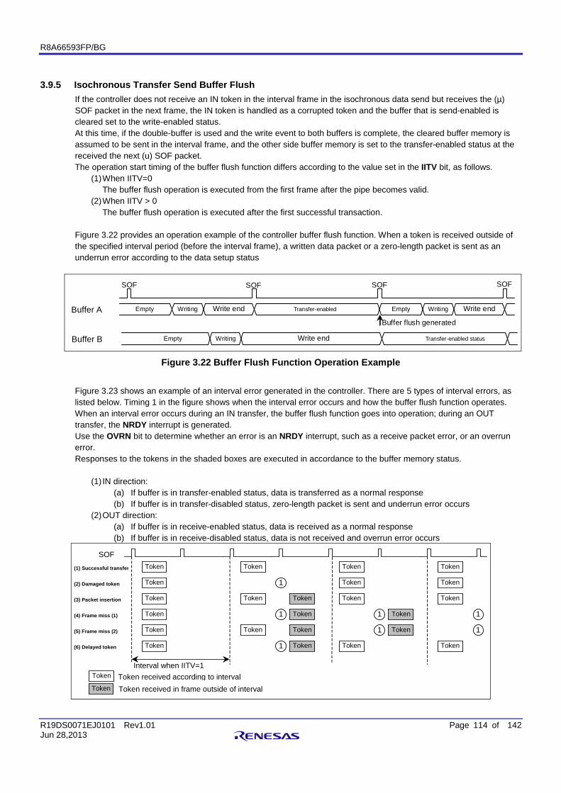
R8A66593FP/BG
R19DS0071EJ0101 Rev1.01 Page 114 of 142 Jun 28,2013
3.9.5 Isochronous Transfer Send Buffer Flush If the controller does not receive an IN token in the interval frame in the isochronous data send but receives the (µ) SOF packet in the next frame, the IN token is handled as a corrupted token and the buffer that is send-enabled is cleared set to the write-enabled status. At this time, if the double-buffer is used and the write event to both buffers is complete, the cleared buffer memory is assumed to be sent in the interval frame, and the other side buffer memory is set to the transfer-enabled status at the received the next (u) SOF packet. The operation start timing of the buffer flush function differs according to the value set in the IITV bit, as follows.
(1) When IITV=0 The buffer flush operation is executed from the first frame after the pipe becomes valid.
(2) When IITV > 0 The buffer flush operation is executed after the first successful transaction.
Figure 3.22 provides an operation example of the controller buffer flush function. When a token is received outside of the specified interval period (before the interval frame), a written data packet or a zero-length packet is sent as an underrun error according to the data setup status
SOF
SOF
SOF
SOF
Transfer-enabled
Writing
Buffer A
Buffer B
Write end
Writing
Write end
Empty S
Empty S
Empty S
Writing
Write end
Transfer-enabled status
Buffer flush generated
Figure 3.22 Buffer Flush Function Operation Example
Figure 3.23 shows an example of an interval error generated in the controller. There are 5 types of interval errors, as listed below. Timing 1 in the figure shows when the interval error occurs and how the buffer flush function operates. When an interval error occurs during an IN transfer, the buffer flush function goes into operation; during an OUT transfer, the NRDY interrupt is generated. Use the OVRN bit to determine whether an error is an NRDY interrupt, such as a receive packet error, or an overrun error. Responses to the tokens in the shaded boxes are executed in accordance to the buffer memory status.
(1) IN direction: (a) If buffer is in transfer-enabled status, data is transferred as a normal response (b) If buffer is in transfer-disabled status, zero-length packet is sent and underrun error occurs
(2) OUT direction: (a) If buffer is in receive-enabled status, data is received as a normal response (b) If buffer is in receive-disabled status, data is not received and overrun error occurs
Token
(1) Successful transfer Token
Token
Token
(2) Damaged token Token
Token
Token
Token
(6) Delayed token Token
Token
Token
Token
(4) Frame miss (1)
Token
Token
Token
(3) Packet insertion
Token
Token
Token
Token
(5) Frame miss (2) Token
Token
Token
Token
1
1
1
1 1
1 1
SOF
Token Token
Token received according to interval Token received in frame outside of interval
Interval when IITV=1
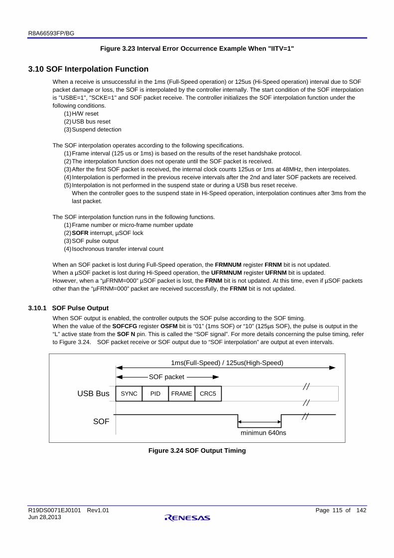
R8A66593FP/BG
R19DS0071EJ0101 Rev1.01 Page 115 of 142 Jun 28,2013
Figure 3.23 Interval Error Occurrence Example When "IITV=1"
3.10 SOF Interpolation Function When a receive is unsuccessful in the 1ms (Full-Speed operation) or 125us (Hi-Speed operation) interval due to SOF packet damage or loss, the SOF is interpolated by the controller internally. The start condition of the SOF interpolation is "USBE=1", "SCKE=1" and SOF packet receive. The controller initializes the SOF interpolation function under the following conditions.
(1) H/W reset (2) USB bus reset (3) Suspend detection
The SOF interpolation operates according to the following specifications.
(1) Frame interval (125 us or 1ms) is based on the results of the reset handshake protocol. (2) The interpolation function does not operate until the SOF packet is received. (3) After the first SOF packet is received, the internal clock counts 125us or 1ms at 48MHz, then interpolates. (4) Interpolation is performed in the previous receive intervals after the 2nd and later SOF packets are received. (5) Interpolation is not performed in the suspend state or during a USB bus reset receive.
When the controller goes to the suspend state in Hi-Speed operation, interpolation continues after 3ms from the last packet.
The SOF interpolation function runs in the following functions.
(1) Frame number or micro-frame number update (2) SOFR interrupt, µSOF lock (3) SOF pulse output (4) Isochronous transfer interval count
When an SOF packet is lost during Full-Speed operation, the FRMNUM register FRNM bit is not updated. When a µSOF packet is lost during Hi-Speed operation, the UFRMNUM register UFRNM bit is updated. However, when a “µFRNM=000” µSOF packet is lost, the FRNM bit is not updated. At this time, even if µSOF packets other than the “µFRNM=000” packet are received successfully, the FRNM bit is not updated.
3.10.1 SOF Pulse Output When SOF output is enabled, the controller outputs the SOF pulse according to the SOF timing. When the value of the SOFCFG register OSFM bit is “01” (1ms SOF) or “10” (125µs SOF), the pulse is output in the “L” active state from the SOF N pin. This is called the “SOF signal”. For more details concerning the pulse timing, refer to Figure 3.24. SOF packet receive or SOF output due to “SOF interpolation” are output at even intervals.
USB Bus
SOF packet
1ms(Full-Speed) / 125us(High-Speed)
SOFminimun 640ns
SYNC PID FRAME CRC5
Figure 3.24 SOF Output Timing
R8A66593FP/BG
R19DS0071EJ0101 Rev1.01 Page 116 of 142 Jun 28,2013
3.11 USB Connector Connection example Figure 3.25 shows an example of the connection between the controller and USB connector.
R8A66593 VBUS
USB connector
1
3 2
4 GND
D- D+
Vbus
DM0
DP0
D+ and D- lines must be configured to support impedance control
REFRIN 5.6k ohm
AGND
Figure 3.25 USB Connector Connection Example
R8A66593FP/BG
R19DS0071EJ0101 Rev1.01 Page 117 of 142 Jun 28,2013
4 Electrical Characteristics 4.1 Absolute Maximum Ratings
Symbol Item Rated vlalue Unit VIF IO power supply voltage -0.3 ~ +4.0 V
VCC Power supply voltage (3.3V) -0.3 ~ +4.0 V AVCC Analog power supply voltage (3.3V) -0.3 ~ +4.0 V VBUS VBUS input voltage -0.3 ~ +5.5 V VI(IO) System interface input voltage -0.3 ~ VIF+0.3, VCC+0.3 V VO(IO) System interface output voltage -0.3 ~ VIF+0.3, VCC+0.3 V
Pd Power consumption 600 mW Tstg Storage temperature -55 ~ +150 degrees Celcius
4.2 Recommended Operating Conditions
Symbol Item Rated value Unit Minimum Average Maximum
VIF IO power supply voltage
1.8V supported 1.6 1.8 2.0 V 3.3V supported 2.7 3.3 3.6 V
VCC Power supply voltage (3.3V) 3.0 3.3 3.6 V
AVCC Analog power supply voltage (3.3V) 3.0 3.3 3.6 V
AGND Analog power supply GND 0 V
GND Power supply GND 0 V VI(IO) System interfaceinput voltage 0 VIF, VCC V
VI(VBUS) Input voltage (VBUS input only) 0 5.25 V VO(IO) System interface output voltage 0 VIF, VCC V
Topr Ambient operating temperatrure
R8A66593FP (Standard items) -20 +25 +85 degrees
Celcius
tr, tf Input rise, fall times Normal input 500 ns Schmitt Trigger input 5 ms
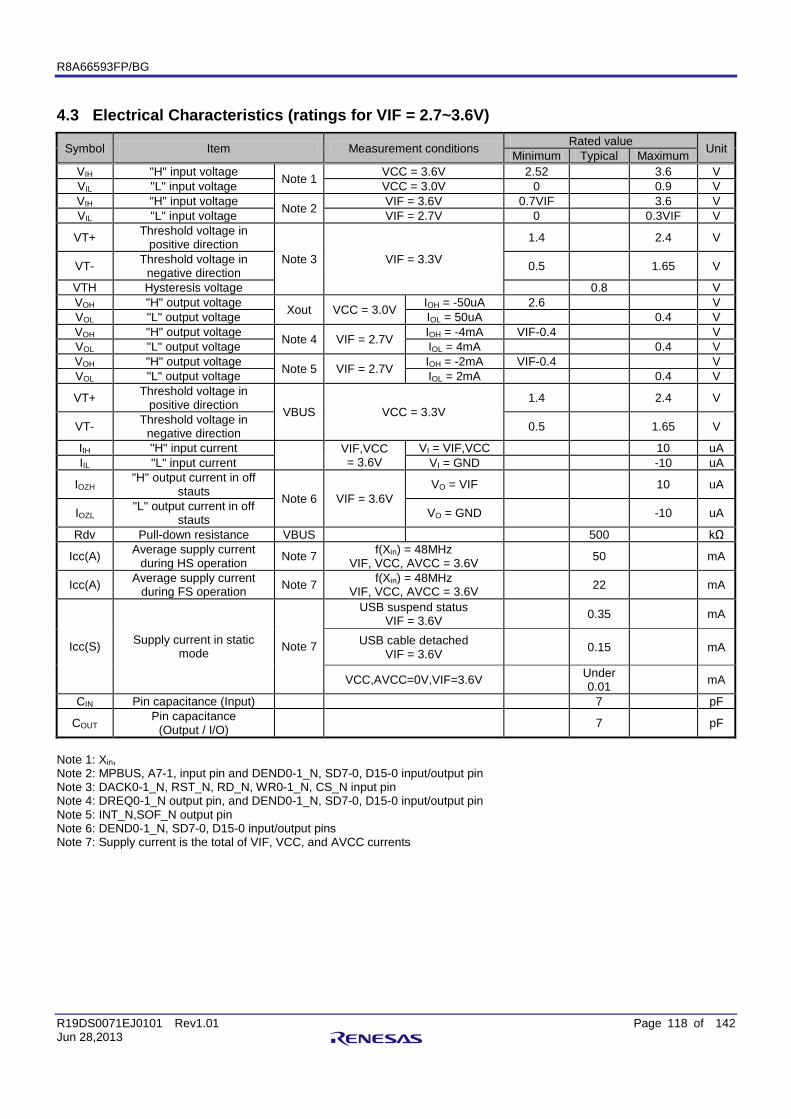
R8A66593FP/BG
R19DS0071EJ0101 Rev1.01 Page 118 of 142 Jun 28,2013
4.3 Electrical Characteristics (ratings for VIF = 2.7~3.6V)
Symbol Item Measurement conditions Rated value Unit Minimum Typical Maximum VIH "H" input voltage Note 1 VCC = 3.6V 2.52 3.6 V VIL "L" input voltage VCC = 3.0V 0 0.9 V VIH "H" input voltage Note 2 VIF = 3.6V 0.7VIF 3.6 V VIL "L" input voltage VIF = 2.7V 0 0.3VIF V
VT+ Threshold voltage in positive direction
Note 3 VIF = 3.3V
1.4 2.4 V
VT- Threshold voltage in negative direction 0.5 1.65 V
VTH Hysteresis voltage 0.8 V VOH "H" output voltage Xout VCC = 3.0V IOH = -50uA 2.6 V VOL "L" output voltage IOL = 50uA 0.4 V VOH "H" output voltage Note 4 VIF = 2.7V IOH = -4mA VIF-0.4 V VOL "L" output voltage IOL = 4mA 0.4 V VOH "H" output voltage Note 5 VIF = 2.7V IOH = -2mA VIF-0.4 V VOL "L" output voltage IOL = 2mA 0.4 V
VT+ Threshold voltage in positive direction VBUS VCC = 3.3V
1.4 2.4 V
VT- Threshold voltage in negative direction 0.5 1.65 V
IIH "H" input current VIF,VCC = 3.6V
VI = VIF,VCC 10 uA IIL "L" input current VI = GND -10 uA
IOZH "H" output current in off stauts Note 6 VIF = 3.6V
VO = VIF 10 uA
IOZL "L" output current in off
stauts VO = GND -10 uA
Rdv Pull-down resistance VBUS 500 kΩ
Icc(A) Average supply current during HS operation Note 7 f(Xin) = 48MHz
VIF, VCC, AVCC = 3.6V 50 mA
Icc(A) Average supply current during FS operation Note 7 f(Xin) = 48MHz
VIF, VCC, AVCC = 3.6V 22 mA
Icc(S) Supply current in static mode Note 7
USB suspend status VIF = 3.6V 0.35 mA
USB cable detached VIF = 3.6V 0.15 mA
VCC,AVCC=0V,VIF=3.6V Under 0.01 mA
CIN Pin capacitance (Input) 7 pF
COUT Pin capacitance (Output / I/O) 7 pF
Note 1: Xin, Note 2: MPBUS, A7-1, input pin and DEND0-1_N, SD7-0, D15-0 input/output pin Note 3: DACK0-1_N, RST_N, RD_N, WR0-1_N, CS_N input pin Note 4: DREQ0-1_N output pin, and DEND0-1_N, SD7-0, D15-0 input/output pin Note 5: INT_N,SOF_N output pin Note 6: DEND0-1_N, SD7-0, D15-0 input/output pins Note 7: Supply current is the total of VIF, VCC, and AVCC currents

R8A66593FP/BG
R19DS0071EJ0101 Rev1.01 Page 119 of 142 Jun 28,2013
4.4 Electrical Characteristics (Ratings for VIF = 1.6 ~ 2.0V)
Symbol Item Measurement conditions Rated value Unit Minimum Typical Maximum VIH "H" input voltage Note 1 VCC = 3.6V 2.52 3.6 V VIL "L" input voltage VCC = 3.0V 0 0.9 V VIH "H" input voltage Note 2 VIF = 2.0V 0.7VIF 3.6 V VIL "L" input voltage VIF = 1.6V 0 0.3VIF V
VT+ Threshold voltage in positive direction
Note 3 VIF = 1.8V
0.7 1.4 V
VT- Threshold voltage in negative direction 0.2 0.8 V
VTH Hysteresis voltage 0.5 V VOH "H" output voltage Xout VCC = 3.0V IOH = -50uA 2.6 V VOL "L" output voltage IOL = 50uA 0.4 V VOH "H" output voltage Note 4 VIF = 1.6V IOH = -4mA VIF-0.4 V VOL "L" output voltage IOL = 4mA 0.4 V VOH "H" output voltage Note 5 VIF = 1.6V IOH = -2mA VIF-0.4 V VOL "L" output voltage IOL = 2mA 0.4 V
VT+ Threshold voltage in positive direction VBUS VCC = 3.3V
1.4 2.4 V
VT- Threshold voltage in negative direction 0.5 1.65 V
IIH "H" input current VIF = 2.0V VCC = 3.6V
VI = VIF,VCC 10 uA IIL "L" input current VI = GND -10 uA
IOZH "H" output current in off stauts Note 6 VIF = 2.0V
VO = VIF 10 uA
IOZL "L" output current in off
stauts VO = GND -10 uA
Rdv Pull-down resistance VBUS 500 kΩ
Icc(A) Average supply current during HS operation Note 7 f(Xin) = 48MHz
VIF=2.0V, VCC, AVCC = 3.6V 50 mA
Icc(A) Average supply current during FS operations Note 7 f(Xin) = 48MHz
VIF=2.0V,VCC,AVCC = 3.6V 20 mA
Icc(S) Supply current in static mode Note 7
USB suspend status VIF = 2.0V 0.35 mA
USB cable detached status VIF = 2.0V 0.15 mA
VCC,AVCC=0V,VIF2.0V Undewr0.01 mA
CIN Pin capacitance (Input) 7 pF
COUT Pin capacitance (Output / I/O) 7 pF
Note 1: Xin, Note 2: MPBUS, A7-1, input pin, and DEND0-1_N, SD7-0, D15-0 input/output pins Note 3: DACK0-1_N, RST_N, RD_N, WR0-1_N, CS_N input pins Note 4: DREQ0-1_N output pin, and DEND0-1_N, SD7-0, D15-0 input/output pin Note 5: INT_N,SOF_N output pin Note 6: DEND0-1_N, SD7-0, D15-0 input/output pins Note 7: Supply current is the total of VIF, VCC, and AVCC currents
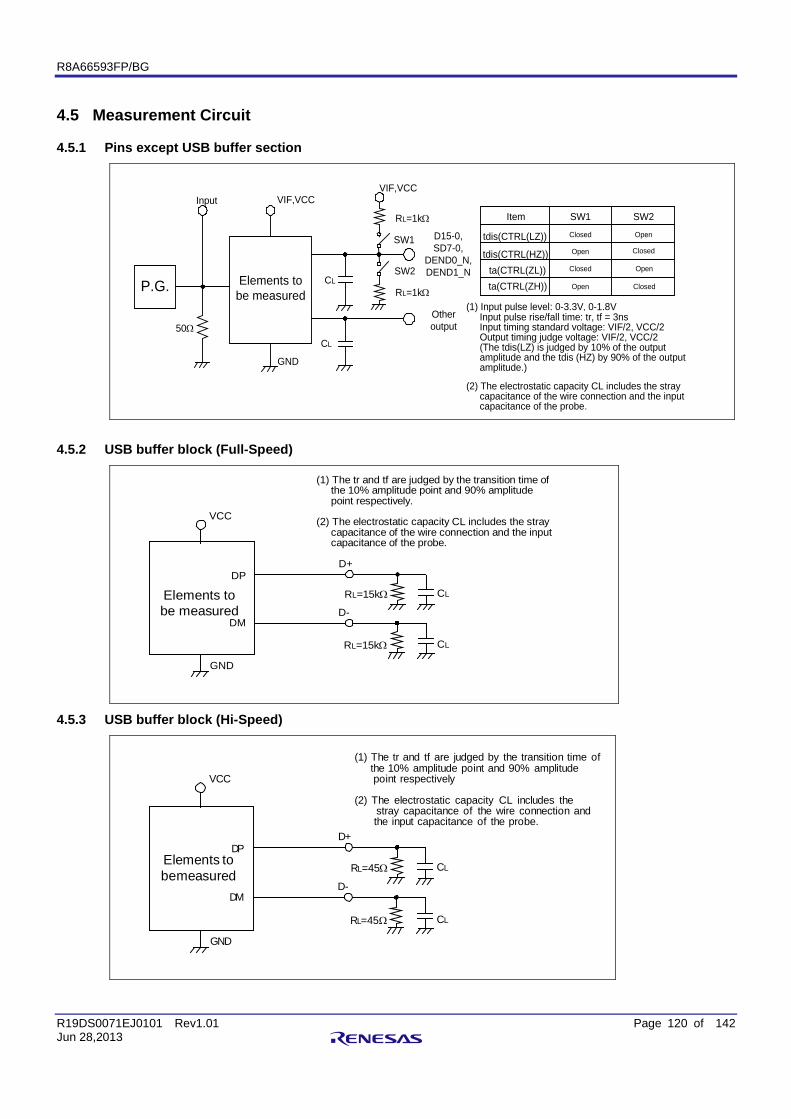
R8A66593FP/BG
R19DS0071EJ0101 Rev1.01 Page 120 of 142 Jun 28,2013
4.5 Measurement Circuit
4.5.1 Pins except USB buffer section
CLRL=1kΩ
SW2
SW1
CL
Elements to be measured
P.G.
RL=1kΩ
VIF,VCCVIF,VCCInput
tdis(CTRL(LZ))
tdis(CTRL(HZ))ta(CTRL(ZL))ta(CTRL(ZH))
Item SW1 SW2
Closed
Closed
Open
Open
Open
Closed
Closed
Open
(1) Input pulse level: 0-3.3V, 0-1.8V Input pulse rise/fall time: tr, tf = 3ns Input timing standard voltage: VIF/2, VCC/2 Output timing judge voltage: VIF/2, VCC/2 (The tdis(LZ) is judged by 10% of the output amplitude and the tdis (HZ) by 90% of the output amplitude.)
(2) The electrostatic capacity CL includes the stray capacitance of the wire connection and the input capacitance of the probe.
50Ω
GND
D15-0,SD7-0,
DEND0_N,DEND1_N
Other output
4.5.2 USB buffer block (Full-Speed)
CL
D+
RL=15kΩ
CL
D-
RL=15kΩ
VCC
GND
Elements tobe measured
(1) The tr and tf are judged by the transition time of the 10% amplitude point and 90% amplitude point respectively.
(2) The electrostatic capacity CL includes the stray capacitance of the wire connection and the input capacitance of the probe.
DM
DP
4.5.3 USB buffer block (Hi-Speed)
CL
D+
RL=45Ω
CL
D-
RL=45Ω
VCC
GND
Elements tobe measured
(1) The tr and tf are judged by the transition time of the 10% amplitude point and 90% amplitude point respectively
(2) The electrostatic capacity CL includes the stray capacitance of the wire connection and the input capacitance of the probe.
DM
DP
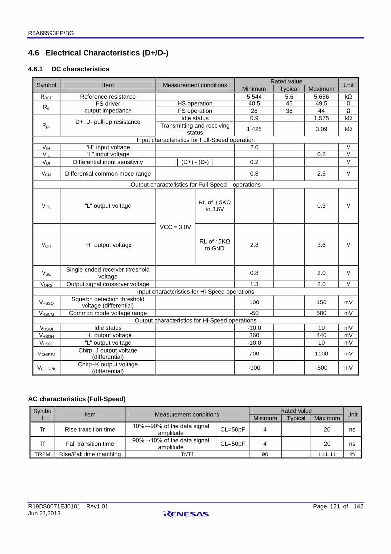
R8A66593FP/BG
R19DS0071EJ0101 Rev1.01 Page 121 of 142 Jun 28,2013
4.6 Electrical Characteristics (D+/D-)
4.6.1 DC characteristics
Symbol Item Measurement conditions Rated value Unit Minimum Typical Maximum RREF Reference resistance 5.544 5.6 5.656 kΩ
Ro FS driver
output impedance HS operation 40.5 45 49.5 Ω FS operation 28 36 44 Ω
Rpu D+, D- pull-up resistance
Idle status 0.9 1.575 kΩ Transmitting and receiving
status 1.425 3.09 kΩ
Input characteristics for Full-Speed operation VIH "H" input voltage 2.0 V VIL "L" input voltage 0.8 V VDI Differential input sensitivity (D+) - (D-) 0.2 V
VCM Differential common mode range 0.8 2.5 V
Output characteristics for Full-Speed operations
VOL "L" output voltage
VCC = 3.0V
RL of 1.5KΩ to 3.6V 0.3 V
VOH "H" output voltage RL of 15KΩ to GND 2.8 3.6 V
VSE Single-ended receiver threshold voltage 0.8 2.0 V
VORS Output signal crossover voltage 1.3 2.0 V Input characteristics for Hi-Speed operations
VHSSQ Squelch detection threshold voltage (differential) 100 150 mV
VHSCM Common mode voltage range -50 500 mV Output characteristics for Hi-Speed operations
VHSOI Idle status -10.0 10 mV VHSOH "H" output voltage 360 440 mV VHSOL "L" output voltage -10.0 10 mV
VCHIRPJ Chirp–J output voltage
(differential) 700 1100 mV
VCHIRPK Chirp–K output voltage (differential) -900 -500 mV
AC characteristics (Full-Speed)
Symbol Item Measurement conditions Rated value Unit Minimum Typical Maximum
Tr Rise transition time 10%→90% of the data signal amplitude CL=50pF 4 20 ns
Tf Fall transition time 90%→10% of the data signal amplitude CL=50pF 4 20 ns
TRFM Rise/Fall time matching Tr/Tf 90 111.11 %
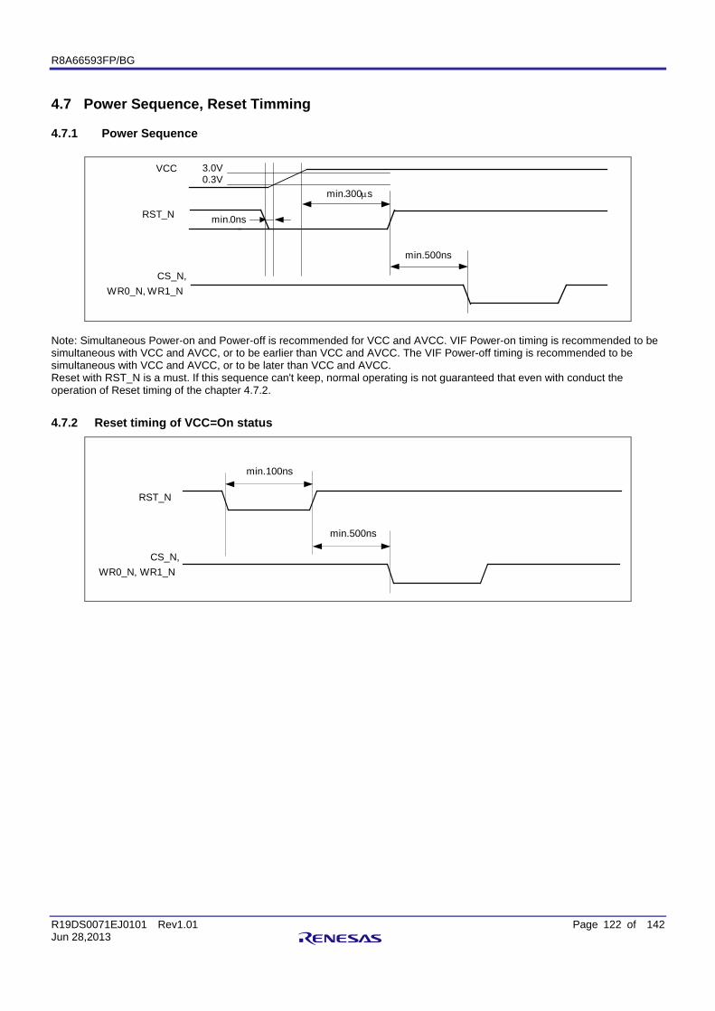
R8A66593FP/BG
R19DS0071EJ0101 Rev1.01 Page 122 of 142 Jun 28,2013
4.7 Power Sequence, Reset Timming
4.7.1 Power Sequence
RST_N
CS_N,WR0_N, WR1_N
VCC
min.300µs
min.500ns
3.0V0.3V
min.0ns
Note: Simultaneous Power-on and Power-off is recommended for VCC and AVCC. VIF Power-on timing is recommended to be simultaneous with VCC and AVCC, or to be earlier than VCC and AVCC. The VIF Power-off timing is recommended to be simultaneous with VCC and AVCC, or to be later than VCC and AVCC. Reset with RST_N is a must. If this sequence can't keep, normal operating is not guaranteed that even with conduct the operation of Reset timing of the chapter 4.7.2.
4.7.2 Reset timing of VCC=On status
RST_N
CS_N,WR0_N, WR1_N
min.100ns
min.500ns
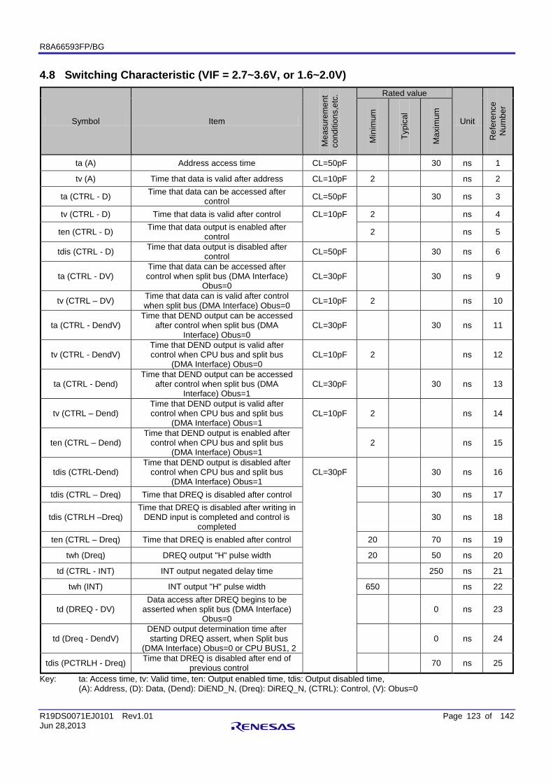
R8A66593FP/BG
R19DS0071EJ0101 Rev1.01 Page 123 of 142 Jun 28,2013
4.8 Switching Characteristic (VIF = 2.7~3.6V, or 1.6~2.0V)
Symbol Item
Mea
sure
men
t co
nditi
ons,
etc.
Rated value
Unit
Ref
eren
ce
Num
ber
Min
imum
Typi
cal
Max
imum
ta (A) Address access time CL=50pF 30 ns 1
tv (A) Time that data is valid after address CL=10pF 2 ns 2
ta (CTRL - D) Time that data can be accessed after control CL=50pF 30 ns 3
tv (CTRL - D) Time that data is valid after control CL=10pF 2 ns 4
ten (CTRL - D) Time that data output is enabled after control 2 ns 5
tdis (CTRL - D) Time that data output is disabled after control CL=50pF 30 ns 6
ta (CTRL - DV) Time that data can be accessed after control when split bus (DMA Interface)
Obus=0 CL=30pF 30 ns 9
tv (CTRL – DV) Time that data can is valid after control when split bus (DMA Interface) Obus=0 CL=10pF 2 ns 10
ta (CTRL - DendV) Time that DEND output can be accessed
after control when split bus (DMA Interface) Obus=0
CL=30pF 30 ns 11
tv (CTRL - DendV) Time that DEND output is valid after control when CPU bus and split bus
(DMA Interface) Obus=0 CL=10pF 2 ns 12
ta (CTRL - Dend) Time that DEND output can be accessed
after control when split bus (DMA Interface) Obus=1
CL=30pF 30 ns 13
tv (CTRL – Dend) Time that DEND output is valid after control when CPU bus and split bus
(DMA Interface) Obus=1 CL=10pF 2 ns 14
ten (CTRL – Dend) Time that DEND output is enabled after
control when CPU bus and split bus (DMA Interface) Obus=1
2 ns 15
tdis (CTRL-Dend) Time that DEND output is disabled after
control when CPU bus and split bus (DMA Interface) Obus=1
CL=30pF 30 ns 16
tdis (CTRL – Dreq) Time that DREQ is disabled after control 30 ns 17
tdis (CTRLH –Dreq) Time that DREQ is disabled after writing in
DEND input is completed and control is completed
30 ns 18
ten (CTRL – Dreq) Time that DREQ is enabled after control 20 70 ns 19
twh (Dreq) DREQ output "H" pulse width 20 50 ns 20
td (CTRL - INT) INT output negated delay time 250 ns 21
twh (INT) INT output "H" pulse width 650 ns 22
td (DREQ - DV) Data access after DREQ begins to be
asserted when split bus (DMA Interface) Obus=0
0 ns 23
td (Dreq - DendV) DEND output determination time after starting DREQ assert, when Split bus
(DMA Interface) Obus=0 or CPU BUS1, 2 0 ns 24
tdis (PCTRLH - Dreq) Time that DREQ is disabled after end of previous control 70 ns 25
Key: ta: Access time, tv: Valid time, ten: Output enabled time, tdis: Output disabled time, (A): Address, (D): Data, (Dend): DiEND_N, (Dreq): DiREQ_N, (CTRL): Control, (V): Obus=0
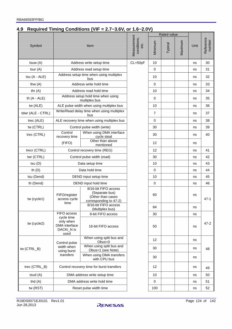
R8A66593FP/BG
R19DS0071EJ0101 Rev1.01 Page 124 of 142 Jun 28,2013
4.9 Required Timing Conditions (VIF = 2.7~3.6V, or 1.6~2.0V)
Symbol Item
Mea
sure
men
t co
nditi
ons,
et
c.
Rated value
Unit
Ref
eren
ce
num
ber
Min
imum
Typi
cal
Max
imum
tsuw (A) Address write setup time CL=50pF 10 ns 30
tsur (A) Address read setup time 0 ns 31
tsu (A - ALE) Address setup time when using multiplex bus 10 ns 32
thw (A) Address write hold time 0 ns 33
thr (A) Address read hold time 10 ns 34
th (A - ALE) Address setup hold time when using multiplex bus 0 ns 35
tw (ALE) ALE pulse width when using multiplex bus 10 ns 36
tdwr (ALE - CTRL) Write/Read delay time when using multiplex bus 7 ns 37
trec (ALE) ALE recovery time when using multiplex bus 0 ns 38
tw (CTRL) Control pulse width (write) 30 ns 39
trec (CTRL) Control recovery time
When using DMA interface cycle steal 30 ns 40
(FIFO) Other than above mentioned 12 ns
trecr (CTRL) Control recovery time (REG) 12 ns 41
twr (CTRL) Control pulse width (read) 30 ns 42
tsu (D) Data setup time 10 ns 43
th (D) Data hold time 0 ns 44
tsu (Dend) DEND input setup time 10 ns 45
th (Dend) DEND input hold time 0 ns 46
tw (cycle1) FIFO/register access cycle
time
8/16-bit FIFO access (Separate bus)
(Other than cases corresponding to 47-2)
60 ns 47-1
8/16-bit FIFO access (Multiplex bus) 84 ns
tw (cycle2)
FIFO access cycle time only when
DMA interface DACKi_N is
used
8-bit FIFO access 30 ns
47-2 16-bit FIFO access 50 ns
tw (CTRL_B)
Control pulse width when using burst transfers
When using split bus and Obus=0 12 ns
48 When using split bus and
Obus=1 (see Note)
30 ns
When using DMA transfers with CPU bus 30 ns
trec (CTRL_B) Control recovery time for burst transfers 12 ns 49
tsud (A) DMA address write setup time 10 ns 50
thd (A) DMA address write hold time 0 ns 51
tw (RST) Reset pulse width time 100 ns 52
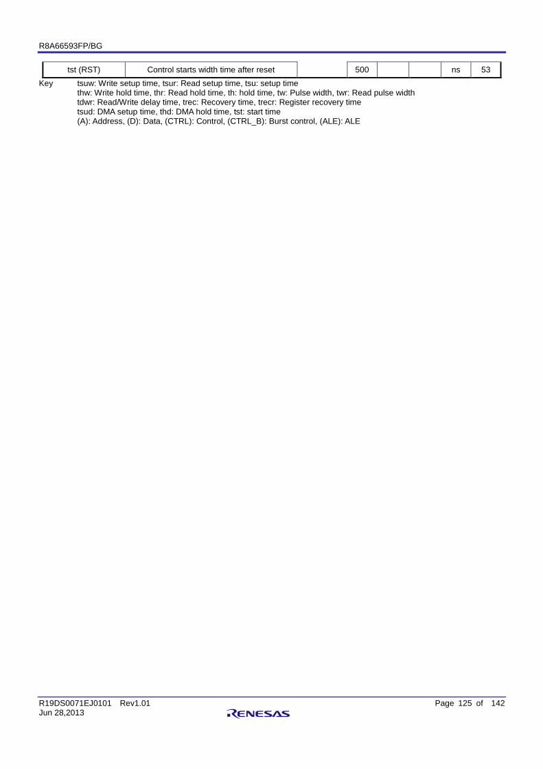
R8A66593FP/BG
R19DS0071EJ0101 Rev1.01 Page 125 of 142 Jun 28,2013
tst (RST) Control starts width time after reset 500 ns 53 Key tsuw: Write setup time, tsur: Read setup time, tsu: setup time thw: Write hold time, thr: Read hold time, th: hold time, tw: Pulse width, twr: Read pulse width tdwr: Read/Write delay time, trec: Recovery time, trecr: Register recovery time tsud: DMA setup time, thd: DMA hold time, tst: start time (A): Address, (D): Data, (CTRL): Control, (CTRL_B): Burst control, (ALE): ALE
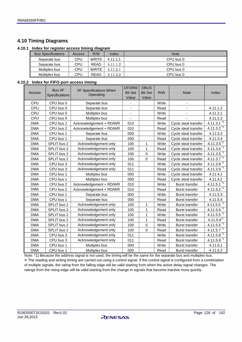
R8A66593FP/BG
R19DS0071EJ0101 Rev1.01 Page 126 of 142 Jun 28,2013
4.10 Timing Diagrams 4.10.1 Index for register access timing diagram
Bus Specifications Access R/W Index Note Separate bus CPU WRITE 4.11.1.1 CPU bus 0 Separate bus CPU READ 4.11.1.2 CPU bus 0 Multiplex bus CPU WRITE 4.11.2.1 CPU bus 0 Multiplex bus CPU READ 4.11.2.2 CPU bus 0
4.10.2 Index for FIFO port access timing
Access Bus I/F
Specifications I/F Specifications When
Operating
DFORM Bit Set Value
OBUS Bit Set Value
R/W Note Index
CPU CPU bus 0 Separate bus - Write - CPU CPU bus 0 Separate bus - Read - 4.11.1.2 CPU CPU bus 0 Multiplex bus - Write - 4.11.2.1 CPU CPU bus 0 Multiplex bus - Read - 4.11.2.2 DMA CPU bus 2 Acknowledgement + RD/WR 010 Write Cycle steal transfer 4.11.3.1 *1 DMA CPU bus 2 Acknowledgement + RD/WR 010 Read Cycle steal transfer 4.11.3.2 *1 DMA CPU bus 1 Separate bus 000 Write Cycle steal transfer 4.11.3.3 DMA CPU bus 1 Separate bus 000 Read Cycle steal transfer 4.11.3.4 DMA SPLIT bus 2 Acknowledgement only 100 1 Write Cycle steal transfer 4.11.3.5 *1 DMA SPLIT bus 2 Acknowledgement only 100 1 Read Cycle steal transfer 4.11.3.6 *1 DMA SPLIT bus 2 Acknowledgement only 100 0 Write Cycle steal transfer 4.11.3.5 *1 DMA SPLIT bus 2 Acknowledgement only 100 0 Read Cycle steal transfer 4.11.3.7 *1 DMA CPU bus 3 Acknowledgement only 011 Write Cycle steal transfer 4.11.3.8 *1 DMA CPU bus 3 Acknowledgement only 011 Read Cycle steal transfer 4.11.3.9 *1 DMA CPU bus 1 Multiplex bus 000 Write Cycle steal transfer 4.11.4.1 DMA CPU bus 1 Multiplex bus 000 Read Cycle steal transfer 4.11.4.2 DMA CPU bus 2 Acknowledgement + RD/WR 010 Write Burst transfer 4.11.5.1 *1 DMA CPU bus 2 Acknowledgement + RD/WR 010 Read Burst transfer 4.11.5.2 *1 DMA CPU bus 1 Separate bus 000 Write Burst transfer 4.11.5.3 DMA CPU bus 1 Separate bus 000 Read Burst transfer 4.11.5.4 DMA SPLIT bus 2 Acknowledgement only 100 1 Write Burst transfer 4.11.5.5 *1 DMA SPLIT bus 2 Acknowledgement only 100 1 Read Burst transfer 4.11.5.6 *1 DMA SPLIT bus 2 Acknowledgement only 100 1 Write Burst transfer 4.11.5.5 *1 DMA SPLIT bus 2 Acknowledgement only 100 1 Read Burst transfer 4.11.5.6*1 DMA SPLIT bus 2 Acknowledgement only 100 0 Write Burst transfer 4.11.5.5 *1 DMA SPLIT bus 2 Acknowledgement only 100 0 Read Burst transfer 4.11.5.7 *1 DMA CPU bus 3 Acknowledgement only 011 Write Burst transfer 4.11.5.8 *1 DMA CPU bus 3 Acknowledgement only 011 Read Burst transfer 4.11.5.9 *1 DMA CPU bus 1 Multiplex bus 000 Write Burst transfer 4.11.6.1 DMA CPU bus 1 Multiplex bus 000 Read Burst transfer 4.11.6.2
Note: *1) Because the address signal is not used, the timing will be the same for the separate bus and multiplex bus. The reading and writing timing are carried out using a control signal. If the control signal is configured from a combination of multiple signals, the rating from the falling edge will be valid starting from when the active delay signal changes. The ratings from the rising edge will be valid starting from the change in signals that become inactive more quickly.
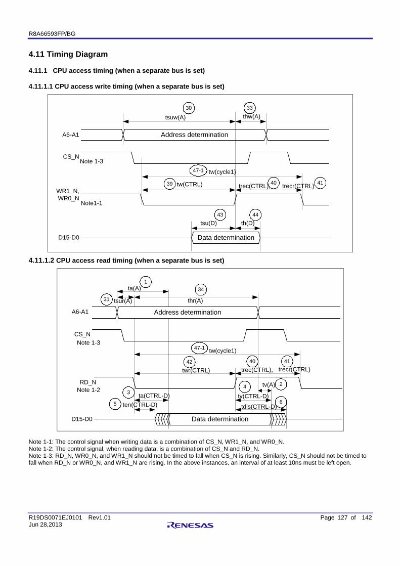
R8A66593FP/BG
R19DS0071EJ0101 Rev1.01 Page 127 of 142 Jun 28,2013
4.11 Timing Diagram
4.11.1 CPU access timing (when a separate bus is set)
4.11.1.1 CPU access write timing (when a separate bus is set)
30
tsuw(A) thw(A)33
tw(cycle1)
tw(CTRL) trecr(CTRL)
47-1
39
tsu(D) th(D)43 44
A6-A1
CS_N
D15-D0
Note1-1
Address determination
41
Data determination
Note 1-3
WR1_N,WR0_N
trec(CTRL),40
4.11.1.2 CPU access read timing (when a separate bus is set)
31 tsur(A) thr(A)
tw(cycle1)
twr(CTRL) trecr(CTRL)
47-1
42
tv(CTRL-D)
tdis(CTRL-D)5 ten(CTRL-D) 6
41
ta(CTRL-D)3
ta(A)1
CS_N
D15-D0
Note 1-22
34
tv(A)4
Note 1-3
Address determination
Data determination
RD_N
trec(CTRL),40
A6-A1
Note 1-1: The control signal when writing data is a combination of CS_N, WR1_N, and WR0_N. Note 1-2: The control signal, when reading data, is a combination of CS_N and RD_N. Note 1-3: RD_N, WR0_N, and WR1_N should not be timed to fall when CS_N is rising. Similarly, CS_N should not be timed to fall when RD_N or WR0_N, and WR1_N are rising. In the above instances, an interval of at least 10ns must be left open.
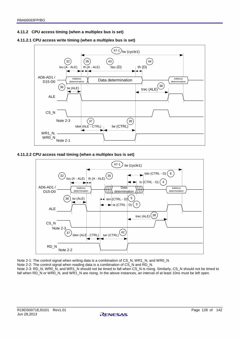
R8A66593FP/BG
R19DS0071EJ0101 Rev1.01 Page 128 of 142 Jun 28,2013
4.11.2 CPU access timing (when a multiplex bus is set)
4.11.2.1 CPU access write timing (when a multiplex bus is set)
tw (cycle1)47-1
AD6-AD1 /D15-D0
CS_N
WR1_N,WR0_N
Note 2-1
ALE
tsu (A - ALE)
32
th (A - ALE)
35
tsu (D)43
th (D)44
tw (ALE)36
tdwr (ALE - CTRL)37
tw (CTRL)39
trec (ALE)38
Note 2-3
AddressdeterminationData determinationAddress
determination
4.11.2.2 CPU access read timing (when a multiplex bus is set)
tw (cycle1)47-1
32
CS_N
RD_NNote 2-2
ALE
tsu (A - ALE) th (A - ALE)35
tw (ALE)36
tdwr (ALE - CTRL)37
ten (CTRL - D) 5
ta (CTRL - D) 3
tv (CTRL - D) 4
tdis (CTRL - D) 6
twr (CTRL)42
trec (ALE) 38
Note 2-3
Datadetermination
Addressdetermination
Addressdetermination
AD6-AD1 /D15-D0
Note 2-1: The control signal when writing data is a combination of CS_N, WR1_N, and WR0_N. Note 2-2: The control signal when reading data is a combination of CS_N and RD_N. Note 2-3: RD_N, WR0_N, and WR1_N should not be timed to fall when CS_N is rising. Similarly, CS_N should not be timed to fall when RD_N or WR0_N, and WR1_N are rising. In the above instances, an interval of at least 10ns must be left open.
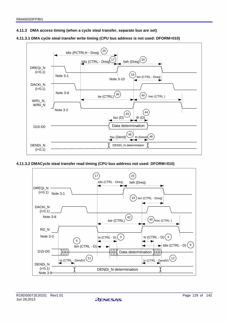
R8A66593FP/BG
R19DS0071EJ0101 Rev1.01 Page 129 of 142 Jun 28,2013
4.11.3 DMA access timing (when a cycle steal transfer, separate bus are set)
4.11.3.1 DMA cycle steal transfer write timing (CPU bus address is not used: DFORM=010)
17tdis (CTRL - Dreq) twh (Dreq) 20
tw (CTRL)39
tsu (D) th (D)43 44
DREQi_N(i=0,1)
DACKi_N(i=0,1)
D15-D0
Note 3-2
Note 3-1 ten (CTRL - Dreq)19
tsu (Dend) th (Dend)45
46
DENDi_N(i=0,1)
Note 3-8
Data determination
DENDi_N determintaion
WR1_N,WR0_N
25
40 trec (CTRL )
Note 3-10
tdis (PCTRLH - Dreq)
4.11.3.2 DMACycle steal transfer read timing (CPU bus address not used: DFORM=010)
tdis (CTRL - Dreq) twh (Dreq)
20
twr (CTRL)
ten (CTRL - Dreq)
42
tv (CTRL - D)
tdis (CTRL - D)ten (CTRL - D)
4
6
19
ta (CTRL - D)
DREQi_N(i=0,1)
DACKi_N(i=0,1)
D15-D0
Note 3-3
17
5
DENDi_N determination
ta (CTRL - DendV)11
tv (CTRL - DendV)12
3
Note 3-8
Data determination
Note 3-1
RD_N
DENDi_N(i=0,1)
Note 3-9
40 trec (CTRL )
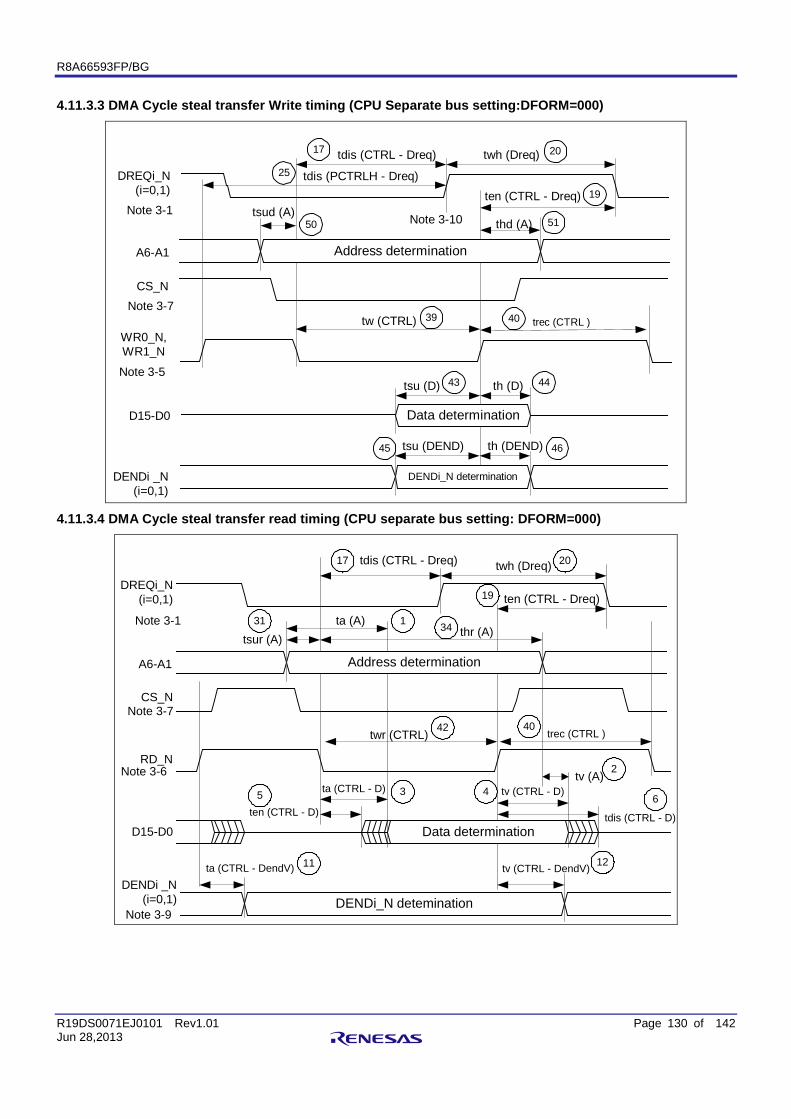
R8A66593FP/BG
R19DS0071EJ0101 Rev1.01 Page 130 of 142 Jun 28,2013
4.11.3.3 DMA Cycle steal transfer Write timing (CPU Separate bus setting:DFORM=000)
50tsud (A)
thd (A) 51
tw (CTRL) 39
tsu (D) th (D)43 44
A6-A1
CS_N
WR0_N,WR1_N
D15-D0
tdis (CTRL - Dreq) twh (Dreq) 20
ten (CTRL - Dreq) 19
DREQi_N(i=0,1)
Note 3-5
tsu (DEND) th (DEND)45 46
DENDi _N(i=0,1)
Note 3-7
Data determination
DENDi_N determination
Address determination
Note 3-1
17
25
40 trec (CTRL )
Note 3-10
tdis (PCTRLH - Dreq)
4.11.3.4 DMA Cycle steal transfer read timing (CPU separate bus setting: DFORM=000)
31
tsur (A) thr (A)34
twr (CTRL)42
tv (CTRL - D)
tdis (CTRL - D)
5ten (CTRL - D)
46
ta (CTRL - D) 3
ta (A) 1
Note 3-6 2tv (A)
tdis (CTRL - Dreq)17 twh (Dreq) 20
ten (CTRL - Dreq)19
Note 3-7
ta (CTRL - DendV) 11 tv (CTRL - DendV) 12
Data determination
CS_N
RD_N
D15-D0
DREQi_N(i=0,1)
DENDi _N(i=0,1)
A6-A1 Address determination
Note 3-1
DENDi_N deteminationNote 3-9
40trec (CTRL )
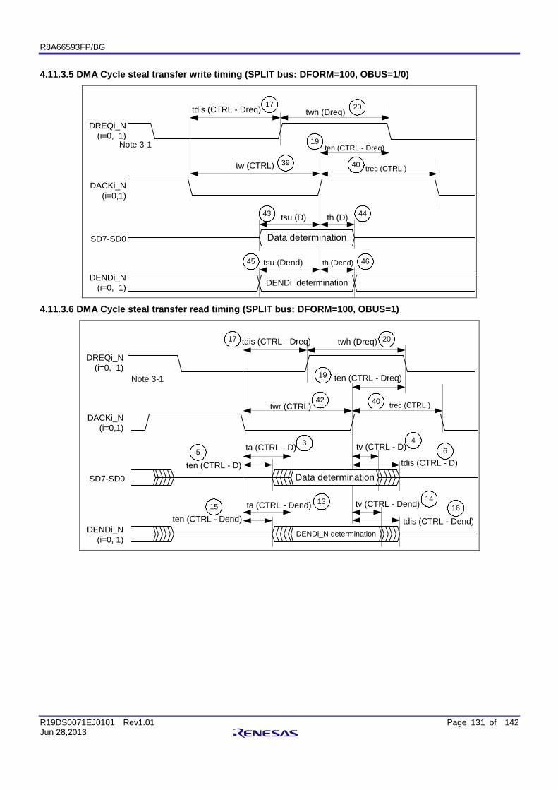
R8A66593FP/BG
R19DS0071EJ0101 Rev1.01 Page 131 of 142 Jun 28,2013
4.11.3.5 DMA Cycle steal transfer write timing (SPLIT bus: DFORM=100, OBUS=1/0)
17tdis (CTRL - Dreq) twh (Dreq)
20
tw (CTRL) 39
tsu (D) th (D)43 44
DREQi_N(i=0, 1)
SD7-SD0 Data determination
Note 3-1 ten (CTRL - Dreq)19
tsu (Dend) th (Dend)45 46
DENDi_N(i=0, 1) DENDi determination
DACKi_N(i=0,1)
40 trec (CTRL )
4.11.3.6 DMA Cycle steal transfer read timing (SPLIT bus: DFORM=100, OBUS=1)
tdis (CTRL - Dreq) twh (Dreq) 20
twr (CTRL)
ten (CTRL - Dreq)
42
tv (CTRL - D)
tdis (CTRL - D)ten (CTRL - D)
46
19
ta (CTRL - D)
DREQi_N(i=0, 1)
SD7-SD0
Note 3-1
17
5
DENDi_N determination
tv (CTRL - Dend)14
ten (CTRL - Dend)ta (CTRL - Dend)15
tdis (CTRL - Dend)16
3
13
DENDi_N(i=0, 1)
DACKi_N(i=0,1)
Data determination
40 trec (CTRL )
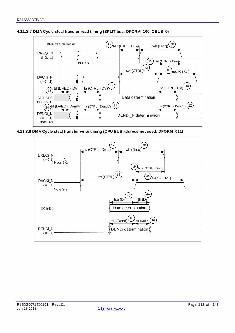
R8A66593FP/BG
R19DS0071EJ0101 Rev1.01 Page 132 of 142 Jun 28,2013
4.11.3.7 DMA Cycle steal transfer read timing (SPLIT bus: DFORM=100, OBUS=0)
tdis (CTRL - Dreq) twh (Dreq) 20
twr (CTRL)
ten (CTRL - Dreq)
42
tv (CTRL - DV) 10
19
ta (CTRL - DV)
17
9
ta (CTRL - DendV) 11 tv (CTRL - DendV) 12
Note 3-1
Data determination
DENDi_N determination
DREQi_N(i=0, 1)
SD7-SD0
DENDi_N(i=0, 1)
DACKi_N(i=0, 1)
td (DREQ - DV)
td (DREQ - DendV)
23
24
DMA transfer begins
Note 3-9
Note 3-9
40 trec (CTRL )
4.11.3.8 DMA Cycle steal transfer write timing (CPU BUS address not used: DFORM=011)
17tdis (CTRL - Dreq) twh (Dreq)
20
tw (CTRL)39
tsu (D) th (D)43 44
DREQi_N(i=0,1)
D15-D0
Note 3-8
Note 3-1ten (CTRL - Dreq)19
tsu (Dend) th (Dend)45
46
DENDi_N(i=0,1)
Data determination
DENDi determination
DACKi_N(i=0,1)
40 trec (CTRL)
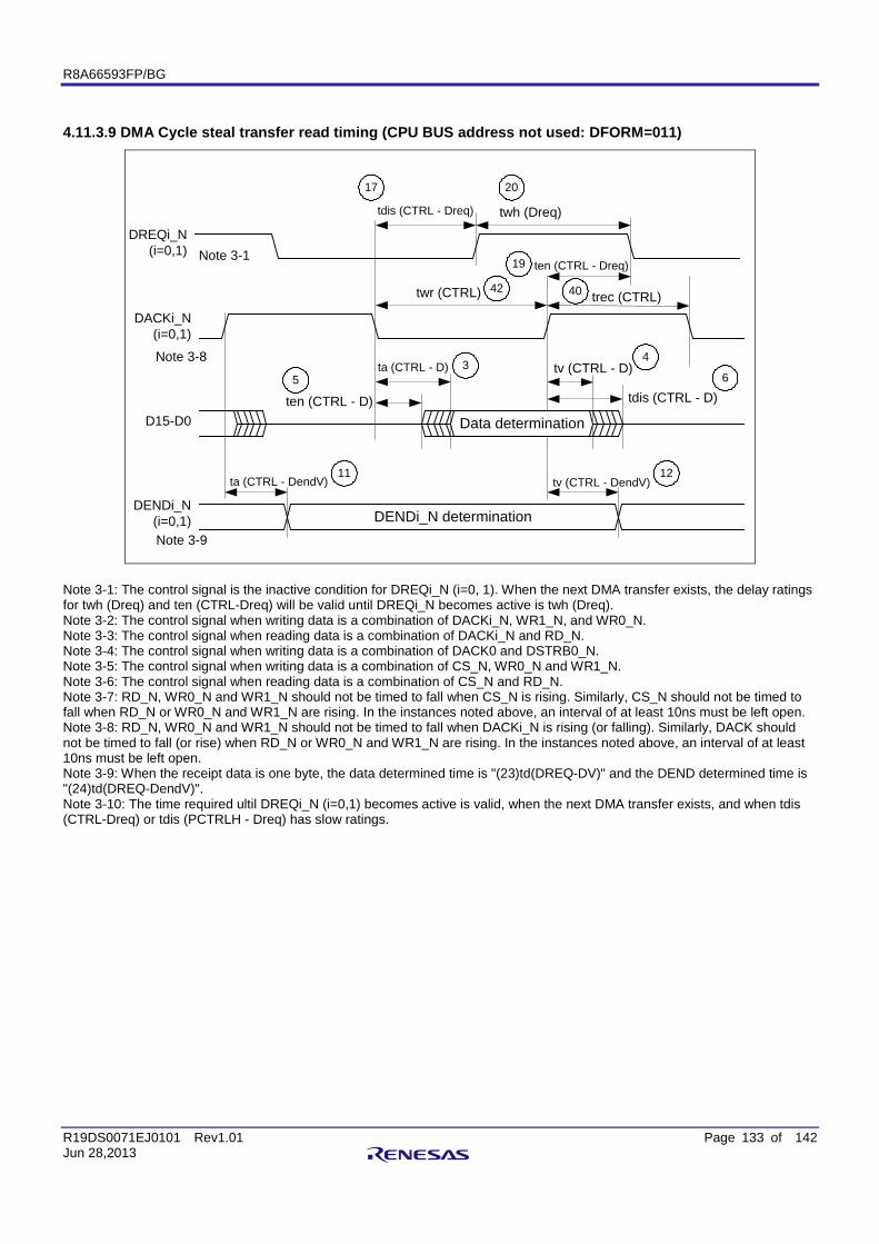
R8A66593FP/BG
R19DS0071EJ0101 Rev1.01 Page 133 of 142 Jun 28,2013
4.11.3.9 DMA Cycle steal transfer read timing (CPU BUS address not used: DFORM=011)
tdis (CTRL - Dreq) twh (Dreq)
20
twr (CTRL)
ten (CTRL - Dreq)
42
tv (CTRL - D)
tdis (CTRL - D)ten (CTRL - D)
4
6
19
ta (CTRL - D)
DREQi_N(i=0,1)
D15-D0
Note 3-8
17
5
DENDi_N determination
ta (CTRL - DendV)11
tv (CTRL - DendV)12
3
Data determination
Note 3-1
DACKi_N(i=0,1)
DENDi_N(i=0,1)Note 3-9
40 trec (CTRL)
Note 3-1: The control signal is the inactive condition for DREQi_N (i=0, 1). When the next DMA transfer exists, the delay ratings for twh (Dreq) and ten (CTRL-Dreq) will be valid until DREQi_N becomes active is twh (Dreq). Note 3-2: The control signal when writing data is a combination of DACKi_N, WR1_N, and WR0_N. Note 3-3: The control signal when reading data is a combination of DACKi_N and RD_N. Note 3-4: The control signal when writing data is a combination of DACK0 and DSTRB0_N. Note 3-5: The control signal when writing data is a combination of CS_N, WR0_N and WR1_N. Note 3-6: The control signal when reading data is a combination of CS_N and RD_N. Note 3-7: RD_N, WR0_N and WR1_N should not be timed to fall when CS_N is rising. Similarly, CS_N should not be timed to fall when RD_N or WR0_N and WR1_N are rising. In the instances noted above, an interval of at least 10ns must be left open. Note 3-8: RD_N, WR0_N and WR1_N should not be timed to fall when DACKi_N is rising (or falling). Similarly, DACK should not be timed to fall (or rise) when RD_N or WR0_N and WR1_N are rising. In the instances noted above, an interval of at least 10ns must be left open. Note 3-9: When the receipt data is one byte, the data determined time is "(23)td(DREQ-DV)" and the DEND determined time is "(24)td(DREQ-DendV)". Note 3-10: The time required ultil DREQi_N (i=0,1) becomes active is valid, when the next DMA transfer exists, and when tdis (CTRL-Dreq) or tdis (PCTRLH - Dreq) has slow ratings.
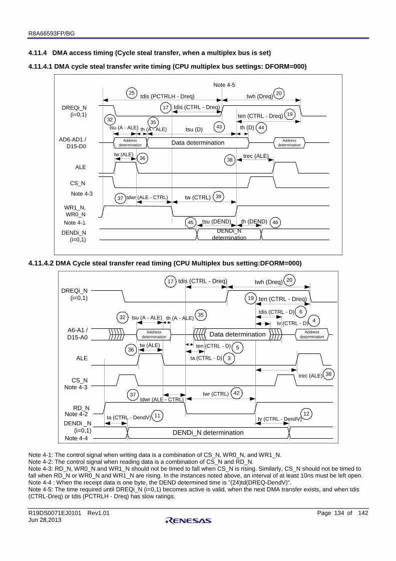
R8A66593FP/BG
R19DS0071EJ0101 Rev1.01 Page 134 of 142 Jun 28,2013
4.11.4 DMA access timing (Cycle steal transfer, when a multiplex bus is set)
4.11.4.1 DMA cycle steal transfer write timing (CPU multiplex bus settings: DFORM=000)
tdis (CTRL - Dreq)
twh (Dreq)
17
20
ten (CTRL - Dreq) 19DREQi_N
(i=0,1)
tsu (DEND) th (DEND)45 46
DENDi_N (i=0,1)
DENDi_N determination
AD6-AD1 / D15-D0
CS_N
Note 4-1
Address determination
ALE
tsu (A - ALE)32
th (A - ALE)35
tsu (D) 43 th (D) 44
tw (ALE)36
37 tw (CTRL) 39
trec (ALE)38
Note 4-3tdwr (ALE - CTRL)
Address determination Data determination
WR1_N, WR0_N
25 tdis (PCTRLH - Dreq)
Note 4-5
4.11.4.2 DMA Cycle steal transfer read timing (CPU Multiplex bus setting:DFORM=000)
DREQi_N(i=0,1)
tdis (CTRL - Dreq)17 twh (Dreq) 20
ten (CTRL - Dreq)19
32
A6-A1 /D15-A0
CS_N
RD_NNote 4-2
Addressdetermination
ALE
tsu (A - ALE) th (A - ALE) 35
tw (ALE)36
tdwr (ALE - CTRL)37
ten (CTRL - D) 5
ta (CTRL - D) 3
tv (CTRL - D) 4tdis (CTRL - D) 6
twr (CTRL) 42
trec (ALE) 38
Note 4-3
DENDi _N(i=0,1)
ta (CTRL - DendV) 11 tv (CTRL - DendV)12
Data determinationAddressdetermination
DENDi_N determinationNote 4-4
Note 4-1: The control signal when writing data is a combination of CS_N, WR0_N, and WR1_N. Note 4-2: The control signal when reading data is a combination of CS_N and RD_N. Note 4-3: RD_N, WR0_N and WR1_N should not be timed to fall when CS_N is rising. Similarly, CS_N should not be timed to fall when RD_N or WR0_N and WR1_N are rising. In the instances noted above, an interval of at least 10ns must be left open. Note 4-4 : When the receipt data is one byte, the DEND determined time is "(24)td(DREQ-DendV)". Note 4-5: The time required until DREQi_N (i=0,1) becomes active is valid, when the next DMA transfer exists, and when tdis (CTRL-Dreq) or tdis (PCTRLH - Dreq) has slow ratings.

R8A66593FP/BG
R19DS0071EJ0101 Rev1.01 Page 135 of 142 Jun 28,2013
4.11.5 DMA access timing (burst transfer and separate bus are set)
4.11.5.1 DMA burst transfer write timing (CPU BUS address not used: DFORM=010)
18tdis (CTRLH - Dreq)
tw (CTRL_B)48
tsu (D) th (D)43 44
DREQi_N(i=0,1)
DACKi_N(i=0,1)
D15-D0
Note 5-1
D0
tsu (Dend) th (Dend)45 46
DENDi_N(i=0,1)
trec (CTRL_B)
tw (cycle1)
49
47-1
D1 DnD2
WR1_N,WR0_N
17tdis (CTRL - Dreq)
Note 5-8
25 tdis (PCTRLH - Dreq)Note 5-9
4.11.5.2 DMA burst transfer read timing (CPU BUS address not used: DFORM=010)
17tdis (CTRL - Dreq)
tw (CTRL_B)48
ta (CTRL - D) tv (CTRL - D) 43
DREQi_N(i=0,1)
DACKi_N(i=0,1)
RD_N
D15-D0
Note 5-2
D0
ta (CTRL - DendV) tv (CTRL - DendV)
12
DENDi _N(i=0,1)
trec (CTRL_B)tw (cycle1)
49
47-1
D1
11
Dn-1 Dn
Note 5-8
Note 5-6
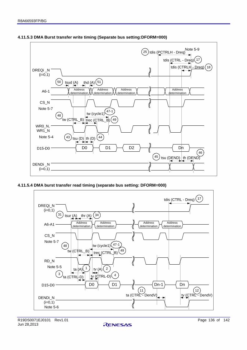
R8A66593FP/BG
R19DS0071EJ0101 Rev1.01 Page 136 of 142 Jun 28,2013
4.11.5.3 DMA Burst transfer write timing (Separate bus setting:DFORM=000)
tdis (PCTRLH - Dreq)Note 5-9
18tdis (CTRLH - Dreq)
tw (CTRL_B)48
tsu (D) th (D)43 44
DREQi _N(i=0,1)
CS_N
WR0_N,WR1_N
D15-D0
Note 5-4
D0
tsu (DEND) th (DEND)4546
DENDi _N(i=0,1)
trec (CTRL_B)
tw (cycle1)49
47-1
D1 Dn
tsud (A) thd (A)50 51
A6-1 Addressdetermination
Addressdetermination
Addressdetermination
Addressdetermination
D2
17tdis (CTRL - Dreq)
Note 5-7
25
4.11.5.4 DMA burst transfer read timing (separate bus setting: DFORM=000)
tw (CTRL_B)48
ta (CTRL-D) tv (CTRL-D) 43
A6-A1
CS_N
RD_N
D15-D0
Note 5-5
D0
ta (CTRL - DendV) tv (CTRL - DendV)11 12
DENDi_N(i=0,1)
trec (CTRL_B)
tw (cycle1)49
47-1
D1
17tdis (CTRL - Dreq)DREQi_N
(i=0,1)
Addressdetermination
Addressdetermination
tsur (A) thr (A)31 34
ta (A) tv (A) 21
Dn-1 Dn
Addressdetermination
Addressdetermination
Note 5-7
Note 5-6
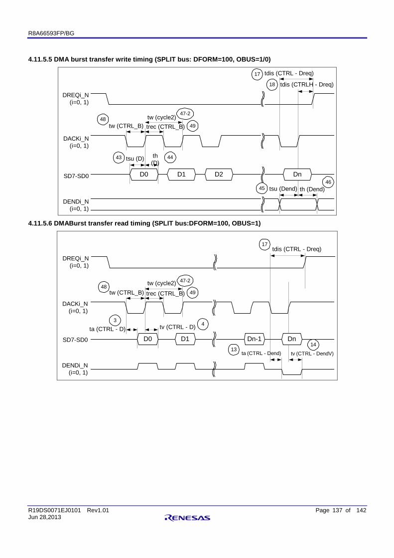
R8A66593FP/BG
R19DS0071EJ0101 Rev1.01 Page 137 of 142 Jun 28,2013
4.11.5.5 DMA burst transfer write timing (SPLIT bus: DFORM=100, OBUS=1/0)
18 tdis (CTRLH - Dreq)
tw (CTRL_B)48
tsu (D) th(D)
43 44
DREQi_N(i=0, 1)
DACKi_N(i=0, 1)
SD7-SD0 D0
tsu (Dend) th (Dend)4546
DENDi_N(i=0, 1)
trec (CTRL_B)tw (cycle2)
49
47-2
D1 DnD2
17 tdis (CTRL - Dreq)
4.11.5.6 DMABurst transfer read timing (SPLIT bus:DFORM=100, OBUS=1)
17tdis (CTRL - Dreq)
tw (CTRL_B)48
ta (CTRL - D) tv (CTRL - D) 43
DREQi_N(i=0, 1)
DACKi_N(i=0, 1)
SD7-SD0 D0
ta (CTRL - Dend) tv (CTRL - DendV)13
14
DENDi_N(i=0, 1)
trec (CTRL_B)
tw (cycle2)49
47-2
D1 Dn-1 Dn
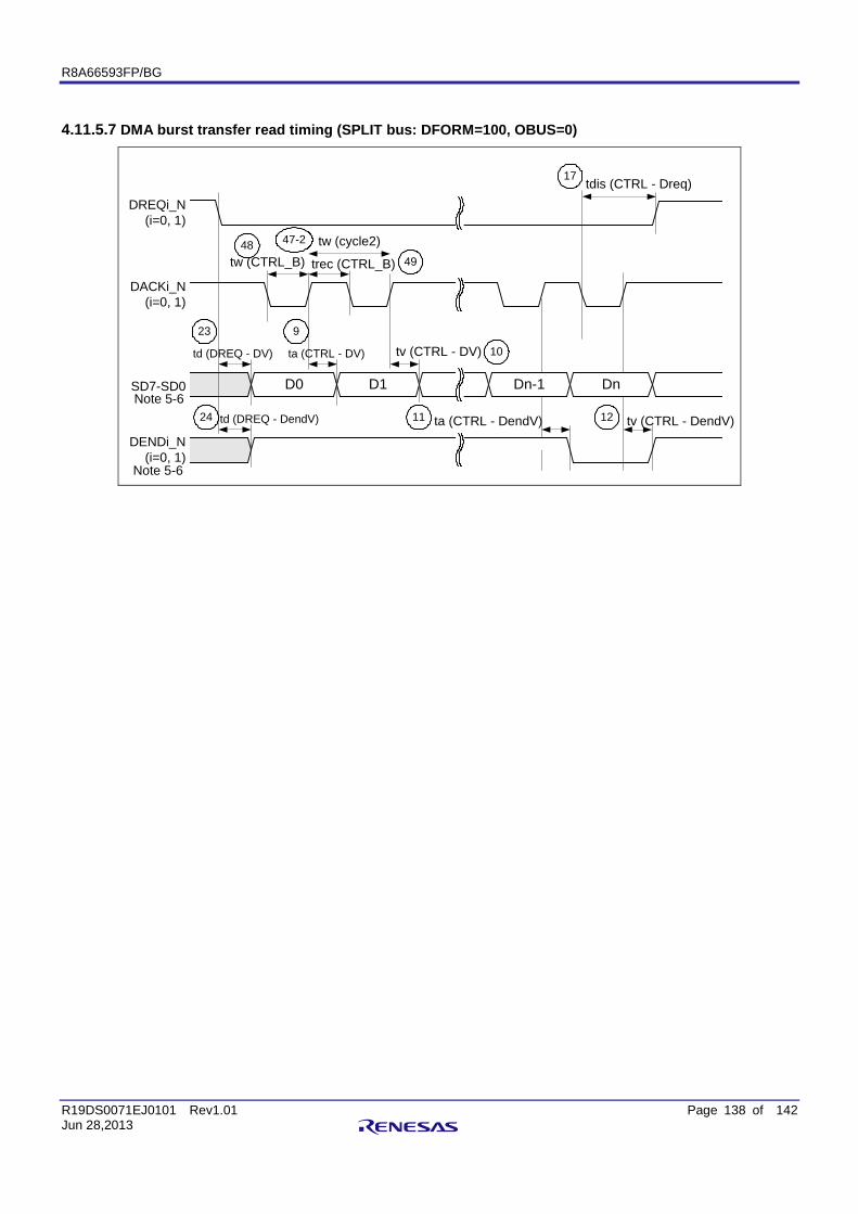
R8A66593FP/BG
R19DS0071EJ0101 Rev1.01 Page 138 of 142 Jun 28,2013
4.11.5.7 DMA burst transfer read timing (SPLIT bus: DFORM=100, OBUS=0)
17tdis (CTRL - Dreq)
tw (CTRL_B)48
ta (CTRL - DV) tv (CTRL - DV) 10
9
DREQi_N(i=0, 1)
DACKi_N(i=0, 1)
SD7-SD0 D0
ta (CTRL - DendV) tv (CTRL - DendV)11
DENDi_N(i=0, 1)
trec (CTRL_B)
tw (cycle2)49
47-2
D1
12
DnDn-1
td (DREQ - DV)
23
td (DREQ - DendV)24Note 5-6
Note 5-6
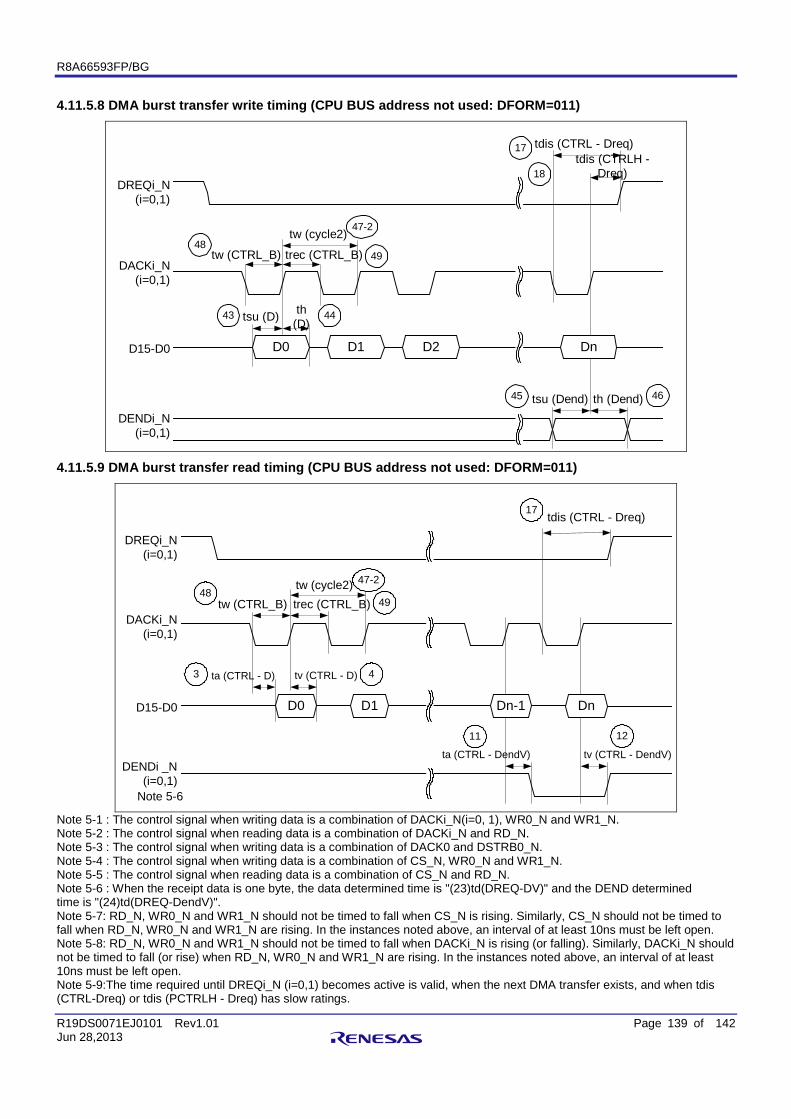
R8A66593FP/BG
R19DS0071EJ0101 Rev1.01 Page 139 of 142 Jun 28,2013
4.11.5.8 DMA burst transfer write timing (CPU BUS address not used: DFORM=011)
18tdis (CTRLH -
Dreq)
tw (CTRL_B)48
tsu (D) th(D)
43 44
DREQi_N(i=0,1)
D15-D0 D0
tsu (Dend) th (Dend)45 46
DENDi_N(i=0,1)
trec (CTRL_B)
tw (cycle2)
49
47-2
D1 DnD2
DACKi_N(i=0,1)
17 tdis (CTRL - Dreq)
4.11.5.9 DMA burst transfer read timing (CPU BUS address not used: DFORM=011)
17tdis (CTRL - Dreq)
tw (CTRL_B)48
ta (CTRL - D) tv (CTRL - D) 43
DREQi_N(i=0,1)
DACKi_N(i=0,1)
D15-D0 D0
ta (CTRL - DendV) tv (CTRL - DendV)
12
DENDi _N(i=0,1)
trec (CTRL_B)tw (cycle2)
49
47-2
D1
11
Dn-1 Dn
Note 5-6
Note 5-1 : The control signal when writing data is a combination of DACKi_N(i=0, 1), WR0_N and WR1_N. Note 5-2 : The control signal when reading data is a combination of DACKi_N and RD_N. Note 5-3 : The control signal when writing data is a combination of DACK0 and DSTRB0_N. Note 5-4 : The control signal when writing data is a combination of CS_N, WR0_N and WR1_N. Note 5-5 : The control signal when reading data is a combination of CS_N and RD_N. Note 5-6 : When the receipt data is one byte, the data determined time is "(23)td(DREQ-DV)" and the DEND determined time is "(24)td(DREQ-DendV)". Note 5-7: RD_N, WR0_N and WR1_N should not be timed to fall when CS_N is rising. Similarly, CS_N should not be timed to fall when RD_N, WR0_N and WR1_N are rising. In the instances noted above, an interval of at least 10ns must be left open. Note 5-8: RD_N, WR0_N and WR1_N should not be timed to fall when DACKi_N is rising (or falling). Similarly, DACKi_N should not be timed to fall (or rise) when RD_N, WR0_N and WR1_N are rising. In the instances noted above, an interval of at least 10ns must be left open. Note 5-9:The time required until DREQi_N (i=0,1) becomes active is valid, when the next DMA transfer exists, and when tdis (CTRL-Dreq) or tdis (PCTRLH - Dreq) has slow ratings.
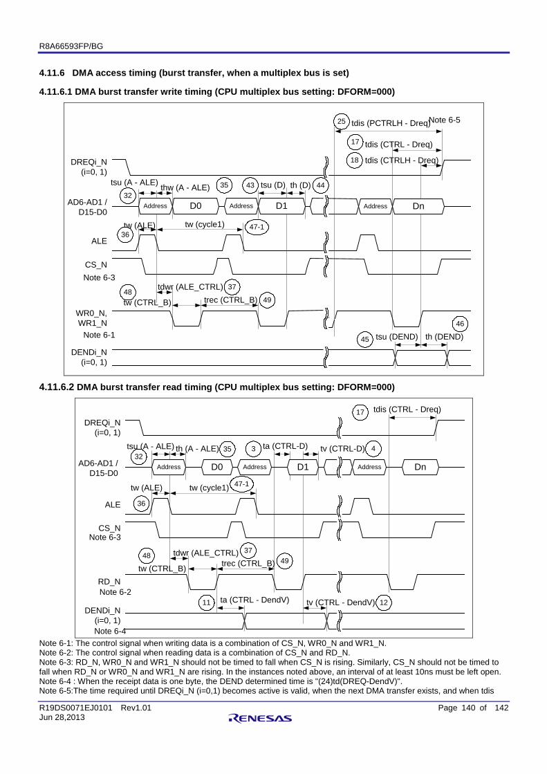
R8A66593FP/BG
R19DS0071EJ0101 Rev1.01 Page 140 of 142 Jun 28,2013
4.11.6 DMA access timing (burst transfer, when a multiplex bus is set)
4.11.6.1 DMA burst transfer write timing (CPU multiplex bus setting: DFORM=000)
tdis (CTRLH - Dreq)
tw (CTRL_B)48
tsu (D) th (D)43 44
DREQi_N(i=0, 1)
CS_N
WR0_N,WR1_N
Note 6-1 tsu (DEND) th (DEND)45
46
DENDi_N(i=0, 1)
trec (CTRL_B)
tw (cycle1)
49
47-1
tsu (A - ALE) thw (A - ALE)32
35
AD6-AD1 /D15-D0
Address AddressD0
ALE
tw (ALE)36
tdwr (ALE_CTRL) 37Note 6-3
DnD1Address
17 tdis (CTRL - Dreq)
25
18
tdis (PCTRLH - Dreq)Note 6-5
4.11.6.2 DMA burst transfer read timing (CPU multiplex bus setting: DFORM=000)
17 tdis (CTRL - Dreq)
tw (CTRL_B)48
ta (CTRL-D) tv (CTRL-D)3 4
DREQi_N(i=0, 1)
CS_N
RD_NNote 6-2
ta (CTRL - DendV) tv (CTRL - DendV)11 12DENDi_N
(i=0, 1)
trec (CTRL_B)
tw (cycle1)
49
47-1
tsu (A - ALE) th (A - ALE)32
35
AD6-AD1 /D15-D0
AddressD0
ALE
tw (ALE)
36
tdwr (ALE_CTRL) 37
Note 6-3
DnD1AddressAddress
Note 6-4 Note 6-1: The control signal when writing data is a combination of CS_N, WR0_N and WR1_N. Note 6-2: The control signal when reading data is a combination of CS_N and RD_N. Note 6-3: RD_N, WR0_N and WR1_N should not be timed to fall when CS_N is rising. Similarly, CS_N should not be timed to fall when RD_N or WR0_N and WR1_N are rising. In the instances noted above, an interval of at least 10ns must be left open. Note 6-4 : When the receipt data is one byte, the DEND determined time is "(24)td(DREQ-DendV)". Note 6-5:The time required until DREQi_N (i=0,1) becomes active is valid, when the next DMA transfer exists, and when tdis

R8A66593FP/BG
R19DS0071EJ0101 Rev1.01 Page 141 of 142 Jun 28,2013
(CTRL-Dreq) or tdis (PCTRLH - Dreq) has slow ratings.
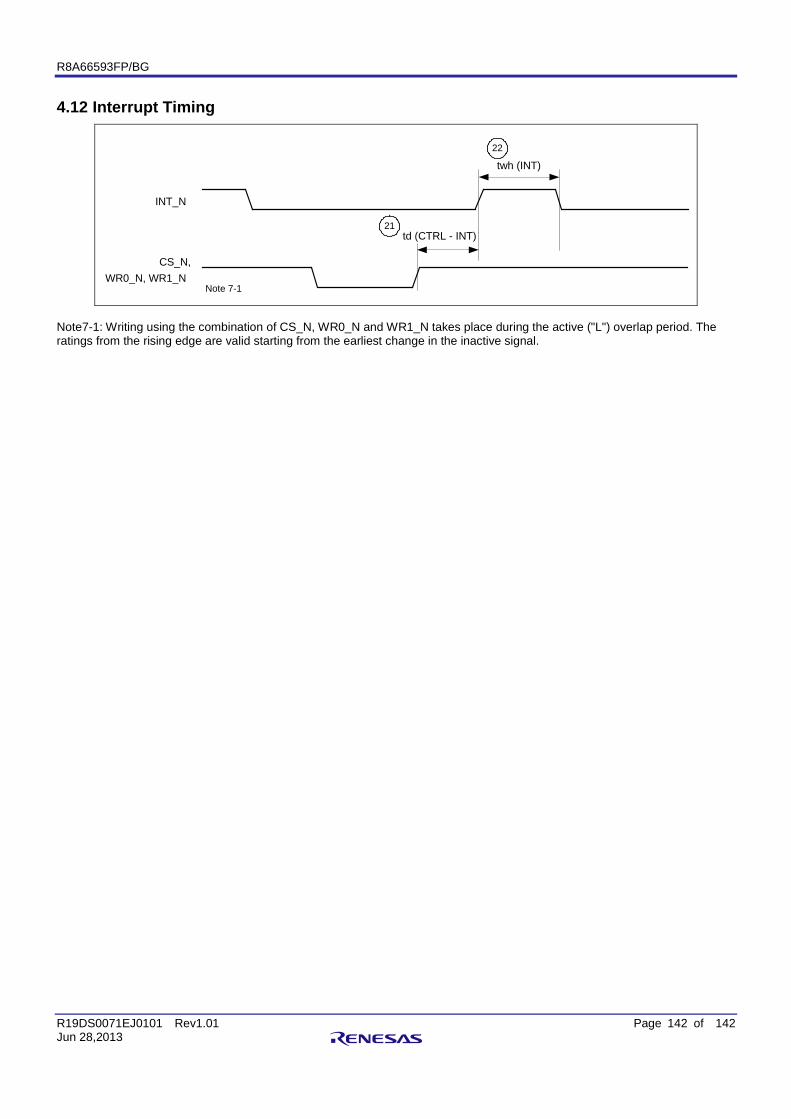
R8A66593FP/BG
R19DS0071EJ0101 Rev1.01 Page 142 of 142 Jun 28,2013
4.12 Interrupt Timing
td (CTRL - INT)
Note 7-1
twh (INT)
INT_N
CS_N,WR0_N, WR1_N
22
21
Note7-1: Writing using the combination of CS_N, WR0_N and WR1_N takes place during the active ("L") overlap period. The ratings from the rising edge are valid starting from the earliest change in the inactive signal.
All trademarks and registered trademarks are the property of their respective owners.
C - 1
Revision history R8A66593 Data Sheet
Rev. Date Description
Page Summary 1.00 Oct 26, 2012 Rev.1.00 issued 1.01 Jun 28,2013 P.14 Add DCFM bit to bit symbol list.
P.16 Add DCFM bit to SYSCFG0 register. P.43 Add process at the time of attach/detach in section 2.11.1.
Notice1. Descriptions of circuits, software and other related information in this document are provided only to illustrate the operation of semiconductor products and application examples. You are fully responsible for
the incorporation of these circuits, software, and information in the design of your equipment. Renesas Electronics assumes no responsibility for any losses incurred by you or third parties arising from the
use of these circuits, software, or information.
2. Renesas Electronics has used reasonable care in preparing the information included in this document, but Renesas Electronics does not warrant that such information is error free. Renesas Electronics
assumes no liability whatsoever for any damages incurred by you resulting from errors in or omissions from the information included herein.
3. Renesas Electronics does not assume any liability for infringement of patents, copyrights, or other intellectual property rights of third parties by or arising from the use of Renesas Electronics products or
technical information described in this document. No license, express, implied or otherwise, is granted hereby under any patents, copyrights or other intellectual property rights of Renesas Electronics or
others.
4. You should not alter, modify, copy, or otherwise misappropriate any Renesas Electronics product, whether in whole or in part. Renesas Electronics assumes no responsibility for any losses incurred by you or
third parties arising from such alteration, modification, copy or otherwise misappropriation of Renesas Electronics product.
5. Renesas Electronics products are classified according to the following two quality grades: "Standard" and "High Quality". The recommended applications for each Renesas Electronics product depends on
the product's quality grade, as indicated below.
"Standard": Computers; office equipment; communications equipment; test and measurement equipment; audio and visual equipment; home electronic appliances; machine tools; personal electronic
equipment; and industrial robots etc.
"High Quality": Transportation equipment (automobiles, trains, ships, etc.); traffic control systems; anti-disaster systems; anti-crime systems; and safety equipment etc.
Renesas Electronics products are neither intended nor authorized for use in products or systems that may pose a direct threat to human life or bodily injury (artificial life support devices or systems, surgical
implantations etc.), or may cause serious property damages (nuclear reactor control systems, military equipment etc.). You must check the quality grade of each Renesas Electronics product before using it
in a particular application. You may not use any Renesas Electronics product for any application for which it is not intended. Renesas Electronics shall not be in any way liable for any damages or losses
incurred by you or third parties arising from the use of any Renesas Electronics product for which the product is not intended by Renesas Electronics.
6. You should use the Renesas Electronics products described in this document within the range specified by Renesas Electronics, especially with respect to the maximum rating, operating supply voltage
range, movement power voltage range, heat radiation characteristics, installation and other product characteristics. Renesas Electronics shall have no liability for malfunctions or damages arising out of the
use of Renesas Electronics products beyond such specified ranges.
7. Although Renesas Electronics endeavors to improve the quality and reliability of its products, semiconductor products have specific characteristics such as the occurrence of failure at a certain rate and
malfunctions under certain use conditions. Further, Renesas Electronics products are not subject to radiation resistance design. Please be sure to implement safety measures to guard them against the
possibility of physical injury, and injury or damage caused by fire in the event of the failure of a Renesas Electronics product, such as safety design for hardware and software including but not limited to
redundancy, fire control and malfunction prevention, appropriate treatment for aging degradation or any other appropriate measures. Because the evaluation of microcomputer software alone is very difficult,
please evaluate the safety of the final products or systems manufactured by you.
8. Please contact a Renesas Electronics sales office for details as to environmental matters such as the environmental compatibility of each Renesas Electronics product. Please use Renesas Electronics
products in compliance with all applicable laws and regulations that regulate the inclusion or use of controlled substances, including without limitation, the EU RoHS Directive. Renesas Electronics assumes
no liability for damages or losses occurring as a result of your noncompliance with applicable laws and regulations.
9. Renesas Electronics products and technology may not be used for or incorporated into any products or systems whose manufacture, use, or sale is prohibited under any applicable domestic or foreign laws or
regulations. You should not use Renesas Electronics products or technology described in this document for any purpose relating to military applications or use by the military, including but not limited to the
development of weapons of mass destruction. When exporting the Renesas Electronics products or technology described in this document, you should comply with the applicable export control laws and
regulations and follow the procedures required by such laws and regulations.
10. It is the responsibility of the buyer or distributor of Renesas Electronics products, who distributes, disposes of, or otherwise places the product with a third party, to notify such third party in advance of the
contents and conditions set forth in this document, Renesas Electronics assumes no responsibility for any losses incurred by you or third parties as a result of unauthorized use of Renesas Electronics
products.
11. This document may not be reproduced or duplicated in any form, in whole or in part, without prior written consent of Renesas Electronics.
12. Please contact a Renesas Electronics sales office if you have any questions regarding the information contained in this document or Renesas Electronics products, or if you have any other inquiries.
(Note 1) "Renesas Electronics" as used in this document means Renesas Electronics Corporation and also includes its majority-owned subsidiaries.
(Note 2) "Renesas Electronics product(s)" means any product developed or manufactured by or for Renesas Electronics.
http://www.renesas.comRefer to "http://www.renesas.com/" for the latest and detailed information.
Renesas Electronics America Inc. 2880 Scott Boulevard Santa Clara, CA 95050-2554, U.S.A.Tel: +1-408-588-6000, Fax: +1-408-588-6130Renesas Electronics Canada Limited1101 Nicholson Road, Newmarket, Ontario L3Y 9C3, CanadaTel: +1-905-898-5441, Fax: +1-905-898-3220Renesas Electronics Europe LimitedDukes Meadow, Millboard Road, Bourne End, Buckinghamshire, SL8 5FH, U.KTel: +44-1628-651-700, Fax: +44-1628-651-804Renesas Electronics Europe GmbHArcadiastrasse 10, 40472 Düsseldorf, Germany Tel: +49-211-65030, Fax: +49-211-6503-1327 Renesas Electronics (China) Co., Ltd.7th Floor, Quantum Plaza, No.27 ZhiChunLu Haidian District, Beijing 100083, P.R.China Tel: +86-10-8235-1155, Fax: +86-10-8235-7679Renesas Electronics (Shanghai) Co., Ltd.Unit 204, 205, AZIA Center, No.1233 Lujiazui Ring Rd., Pudong District, Shanghai 200120, China Tel: +86-21-5877-1818, Fax: +86-21-6887-7858 / -7898 Renesas Electronics Hong Kong LimitedUnit 1601-1613, 16/F., Tower 2, Grand Century Place, 193 Prince Edward Road West, Mongkok, Kowloon, Hong KongTel: +852-2886-9318, Fax: +852 2886-9022/9044Renesas Electronics Taiwan Co., Ltd.13F, No. 363, Fu Shing North Road, Taipei, TaiwanTel: +886-2-8175-9600, Fax: +886 2-8175-9670Renesas Electronics Singapore Pte. Ltd. 80 Bendemeer Road, Unit #06-02 Hyflux Innovation Centre Singapore 339949Tel: +65-6213-0200, Fax: +65-6213-0300Renesas Electronics Malaysia Sdn.Bhd.Unit 906, Block B, Menara Amcorp, Amcorp Trade Centre, No. 18, Jln Persiaran Barat, 46050 Petaling Jaya, Selangor Darul Ehsan, MalaysiaTel: +60-3-7955-9390, Fax: +60-3-7955-9510Renesas Electronics Korea Co., Ltd.11F., Samik Lavied' or Bldg., 720-2 Yeoksam-Dong, Kangnam-Ku, Seoul 135-080, KoreaTel: +82-2-558-3737, Fax: +82-2-558-5141
SALES OFFICES
© 2013 Renesas Electronics Corporation. All rights reserved.Colophon 2.2