zl2006ev2 user guide - renesas
TRANSCRIPT
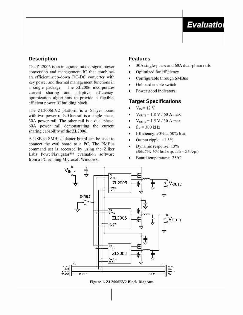
Description The ZL2006 is an integrated mixed-signal power conversion and management IC that combines an efficient step-down DC-DC converter with key power and thermal management functions in a single package. The ZL2006 incorporates current sharing and adaptive efficiency-optimization algorithms to provide a flexible, efficient power IC building block.
The ZL2006EV2 platform is a 6-layer board with two power rails. One rail is a single phase, 30A power rail. The other rail is a dual phase, 60A power rail demonstrating the current sharing capability of the ZL2006.
A USB to SMBus adapter board can be used to connect the eval board to a PC. The PMBus command set is accessed by using the Zilker Labs PowerNavigator™ evaluation software from a PC running Microsoft Windows.
Features • 30A single-phase and 60A dual-phase rails • Optimized for efficiency • Configurable through SMBus • Onboard enable switch • Power good indicators
Target Specifications • VIN = 12 V • VOUT1 = 1.8 V / 60 A max • VOUT2 = 1.5 V / 30 A max • fsw = 300 kHz • Efficiency: 90% at 50% load • Output ripple: ±1.5% • Dynamic response: ±3%
(50%-70%-50% load step, di/dt = 2.5 A/μs) • Board temperature: 25°C
Figure 1. ZL2006EV2 Block Diagram
ZL2006EV2
2 ZL2006EV2DSR3.0
Functional Description The ZL2006EV2 provides all circuitry required to demonstrate the features of the ZL2006. The ZL2006EV2 has a functionally-optimized ZL2006 circuit layout that allows efficient operation up to the maximum output current. Power and load connections are provided through plug-in sockets.
All features of the ZL2006 such as current sharing, soft-start delay and ramp times, supply sequencing, voltage tracking, and voltage margining are available on this evaluation board. For voltage tracking, the board is set up for the single phase rail (VOUT2) to track the dual phase rail (VOUT1). Contact the Zilker Labs sales office for configuring the board for other tracking combinations.
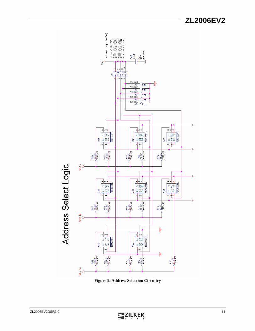
Figure 1 shows a functional block diagram of the ZL2006EV2 board. The SMBus address is selectable through a jumper on the top side of the board. All power to the board (VIN and I2C bus) must be removed before changing the jumpers.
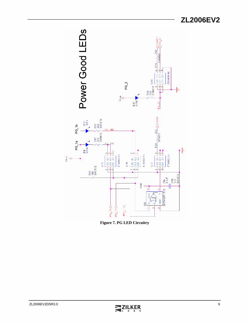
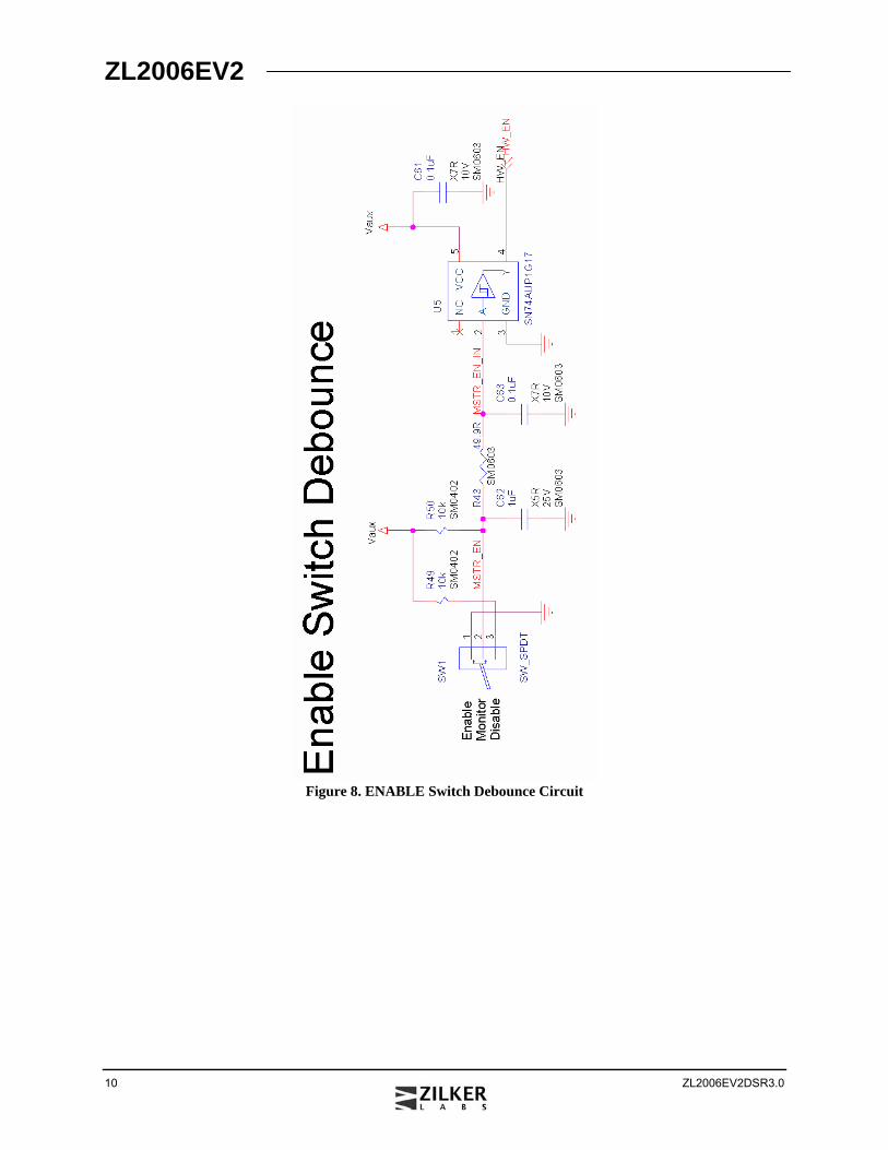
The hardware enable function is controlled by a toggle switch on the ZL2006EV2 board. The power good (PG) LEDs indicate the correct state of PG when external power is applied to the ZL2006EV2 board. (Note: If a USB board is connected to the ZL2006EV2 and no power is applied to the board, the PG LEDs will turn on even though the power rails are not enabled.) The right angle headers at opposite ends of the board are for connecting a USB to SMBus adapter board or for daisy chaining of multiple evaluation boards.
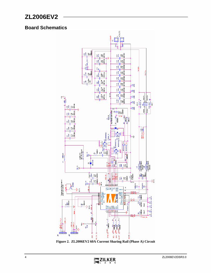
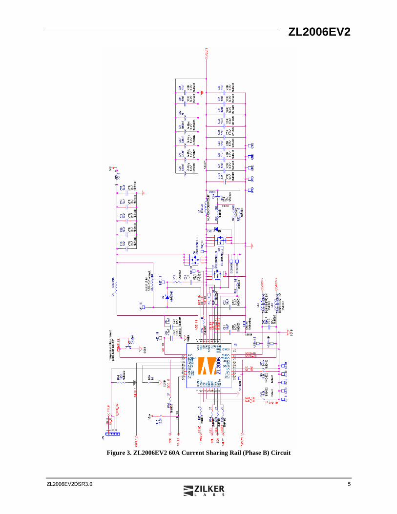
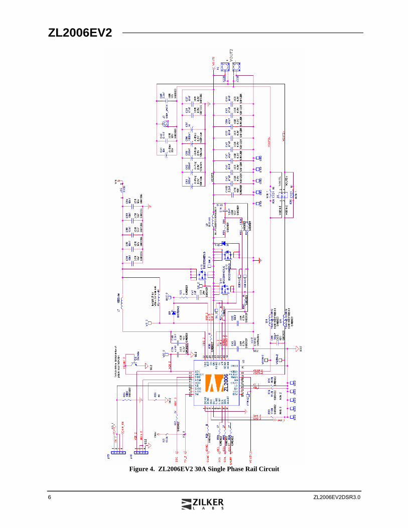
Figure 2 and Figure 3 show the two phases of the 60A circuit. Figure 4 shows the single phase operational circuit. The circuit consists of the ZL2006 IC with its minimal component count to realize a 30 A buck converter. The board layout has been optimized for thermal performance.
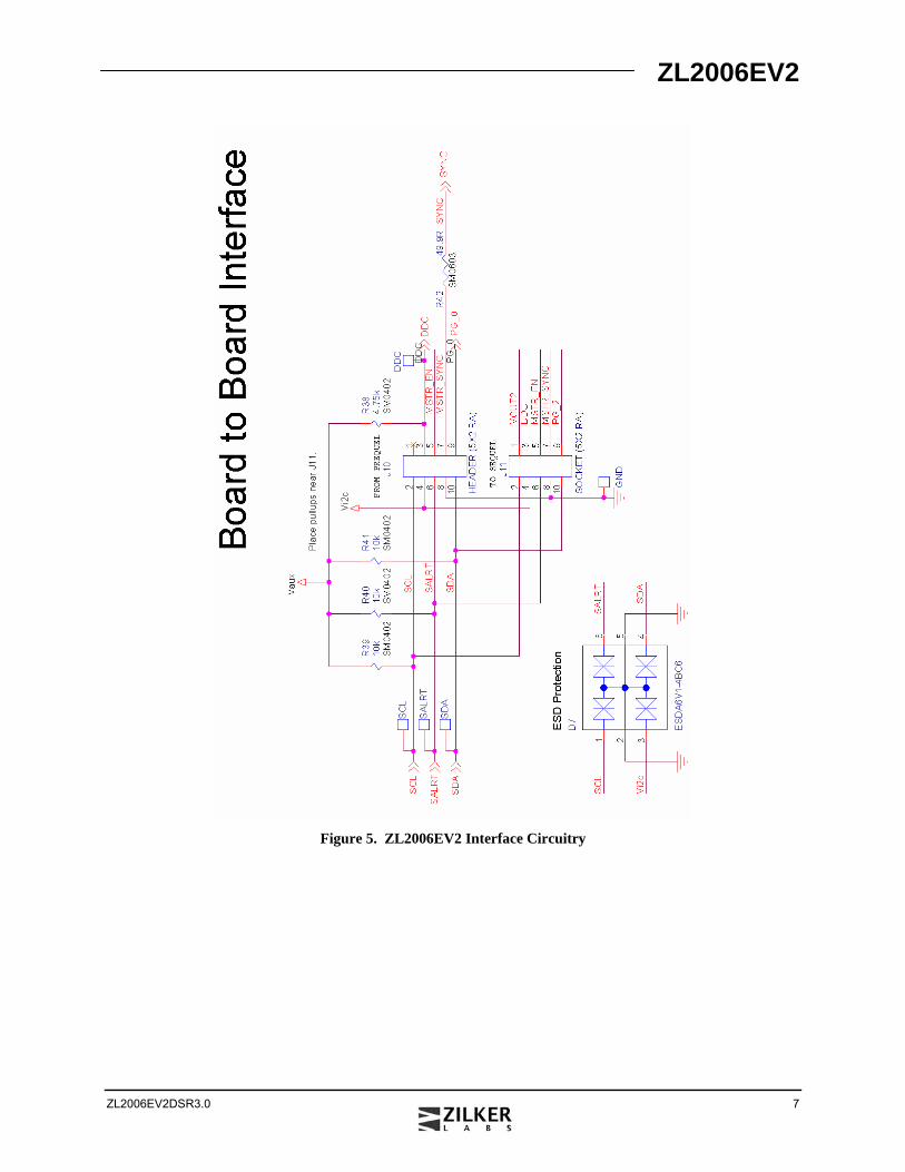
Figure 5 is the Interface and Figure 9 SMBus address selection circuitry.
Operation
PMBus Operation The ZL2006 utilizes the PMBus protocol. The PMBus functionality can be controlled via USB from a PC running the PowerNavigator evaluation software in a Windows XP or Windows 2000/NT operating system.
Install the ZL2006EV2 software using the CD included in the ZL2006EV2 kit.
For board operation, connect the included USB-to-SMBus adapter board to J10 of the ZL2006EV2 board. Connect the desired load and an appropriate power supply to the input and connect the included USB cable to the PC running the PowerNavigator evaluation software. Place the ENABLE switch in “DISABLE” and turn on the power.
The evaluation software allows modification of all ZL2006 PMBus parameters. Each of the ZL2006 devices have been pre-configured as described in this document, but the user may modify the operating parameters through the eval software or by loading a predefined scenario from a configuration file.
Use the mouse-over pop-ups for PowerNavigator help. Refer to Zilker Labs application note AN33 [2] for PMBus details.
The ENABLE switch can then be moved to “ENABLE” and the ZL2006EV2 board can be tested. Alternately, the PMBus ON-OFF CONFIG and OPERATION commands may be used.
ZL2006EV2
ZL2006EV2DSR3.0 3
Quick Start Guide
Stand Alone Operation 1. Set ENABLE switch to “DISABLE”
2. Apply load to VOUT+/VOUT- for each channel
3. Connect power supply to VIN+/VIN- (supply turned off)
4. Turn power supply on
5. Set ENABLE switch to “ENABLE”
6. Monitor ZL2006EV2 board operation using an oscilloscope
USB (PMBus) Operation 1. Set ENABLE switch to “DISABLE”
2. Apply load to VOUT+/VOUT- for each channel
3. Connect power supply to VIN+/VIN- (supply turned off)
4. Turn power supply on
5. Insert the Zilker Labs Eval Kit CD
6. Connect USB to SMBus adapter board to J10 of ZL2006EV2
7. Connect supplied USB cable from computer to USB to SMBus adapter board
a. Upon first-time connection, the Found New Hardware Wizard will appear.
b. Windows XP users: Select ‘No’ at prompt to search the Internet for drivers.
c. Follow the steps on the screen to install the drivers from the CD.
8. Install the PowerNavigator evaluation software by running setup.exe from the PowerNavigator_installer folder on the CD.
9. Set ENABLE switch on EVB to “ENABLE”
10. Monitor and configure the ZL2006EV2 board using PMBus commands in the evaluation software
11. Test the ZL2006EV2 operation using an oscilloscope and the evaluation software.
ZL2006EV2
4 ZL2006EV2DSR3.0
Board Schematics
Figure 2. ZL2006EV2 60A Current Sharing Rail (Phase A) Circuit
ZL2006EV2
ZL2006EV2DSR3.0 5
Figure 3. ZL2006EV2 60A Current Sharing Rail (Phase B) Circuit
ZL2006EV2
6 ZL2006EV2DSR3.0
Figure 4. ZL2006EV2 30A Single Phase Rail Circuit
ZL2006EV2
ZL2006EV2DSR3.0 7
Figure 5. ZL2006EV2 Interface Circuitry
ZL2006EV2
8 ZL2006EV2DSR3.0
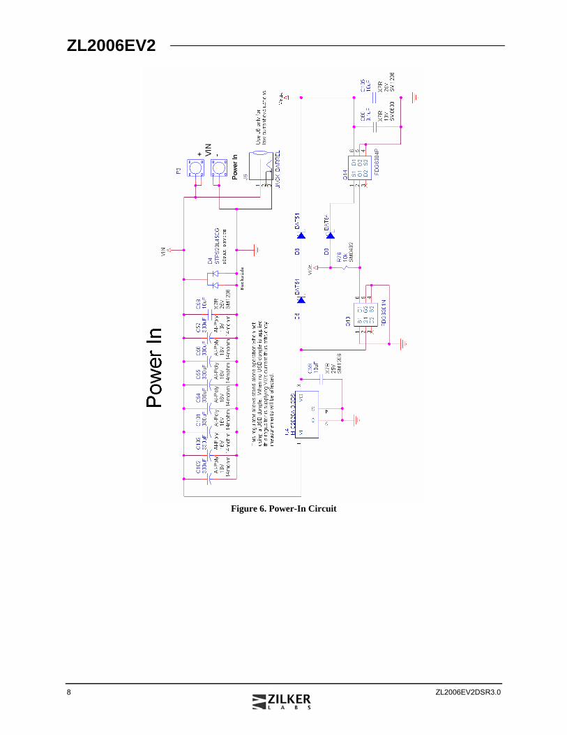
Figure 6. Power-In Circuit
ZL2006EV2
ZL2006EV2DSR3.0 9
Figure 7. PG LED Circuitry
ZL2006EV2
10 ZL2006EV2DSR3.0
Figure 8. ENABLE Switch Debounce Circuit
ZL2006EV2
ZL2006EV2DSR3.0 11
Figure 9. Address Selection Circuitry
ZL2006EV2
12 ZL2006EV2DSR3.0
Board Layout – 6 Layers
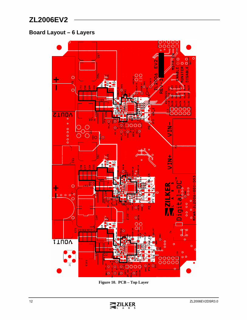
Figure 10. PCB – Top Layer
ZL2006EV2
ZL2006EV2DSR3.0 13
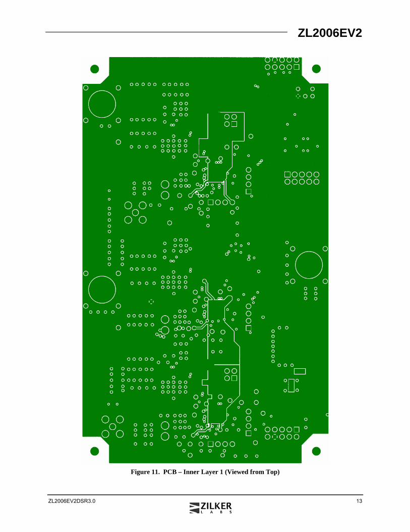
Figure 11. PCB – Inner Layer 1 (Viewed from Top)
ZL2006EV2
14 ZL2006EV2DSR3.0
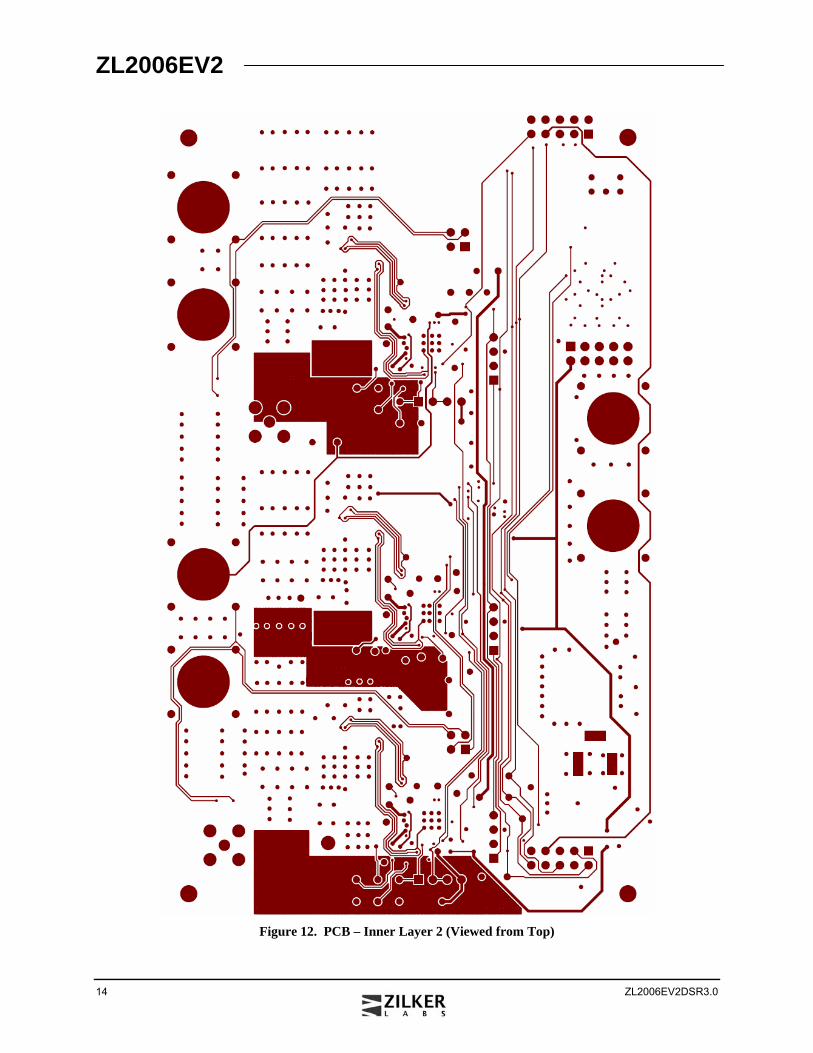
Figure 12. PCB – Inner Layer 2 (Viewed from Top)
ZL2006EV2
ZL2006EV2DSR3.0 15
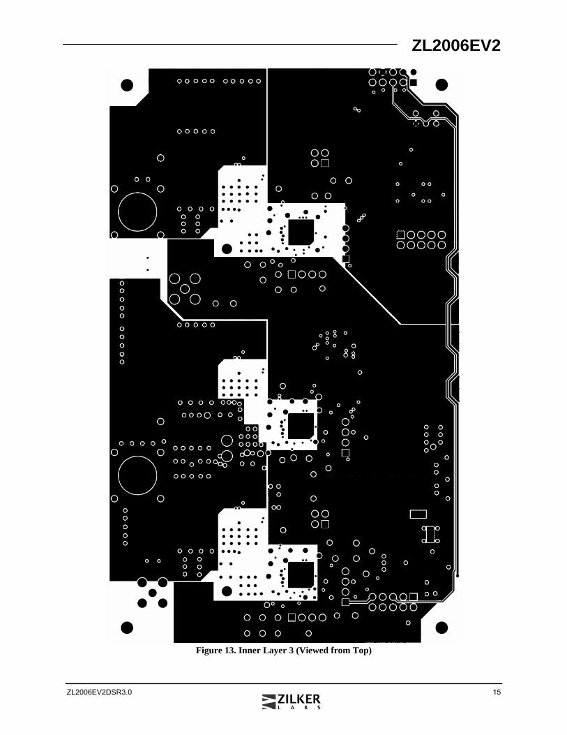
Figure 13. Inner Layer 3 (Viewed from Top)
ZL2006EV2
16 ZL2006EV2DSR3.0
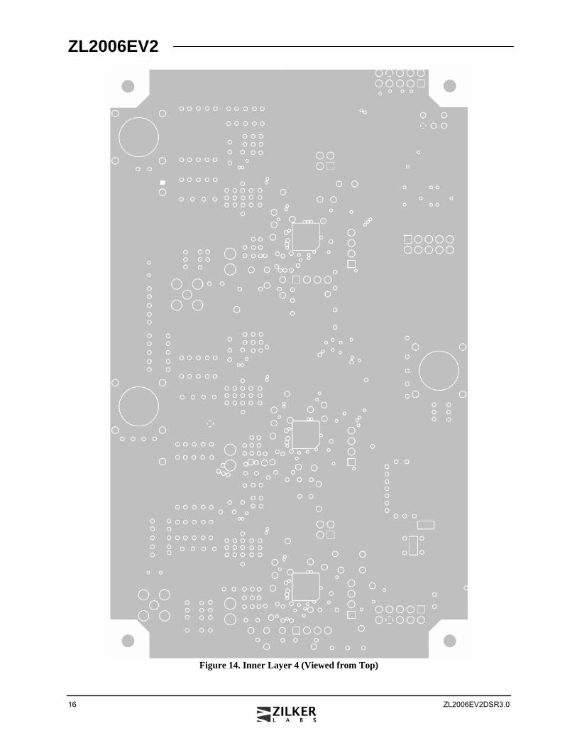
Figure 14. Inner Layer 4 (Viewed from Top)
ZL2006EV2
ZL2006EV2DSR3.0 17
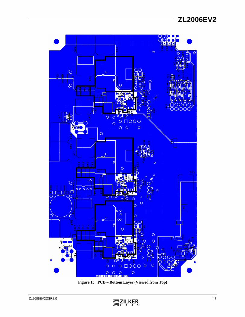
Figure 15. PCB – Bottom Layer (Viewed from Top)
ZL2006EV2
18 ZL2006EV2DSR3.0
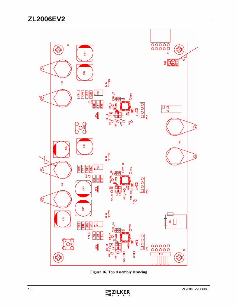
Figure 16. Top Assembly Drawing
ZL2006EV2
ZL2006EV2DSR3.0 19
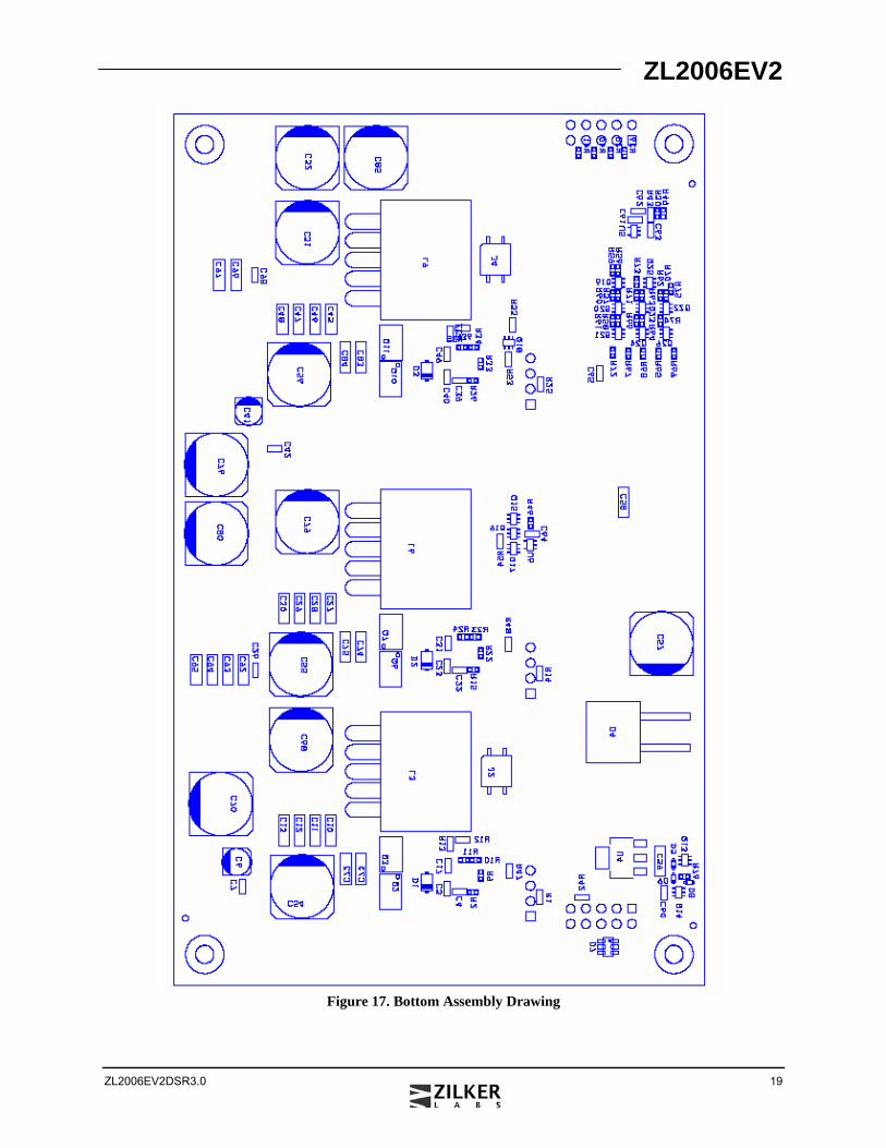
Figure 17. Bottom Assembly Drawing
ZL2006EV2
20 ZL2006EV2DSR3.0
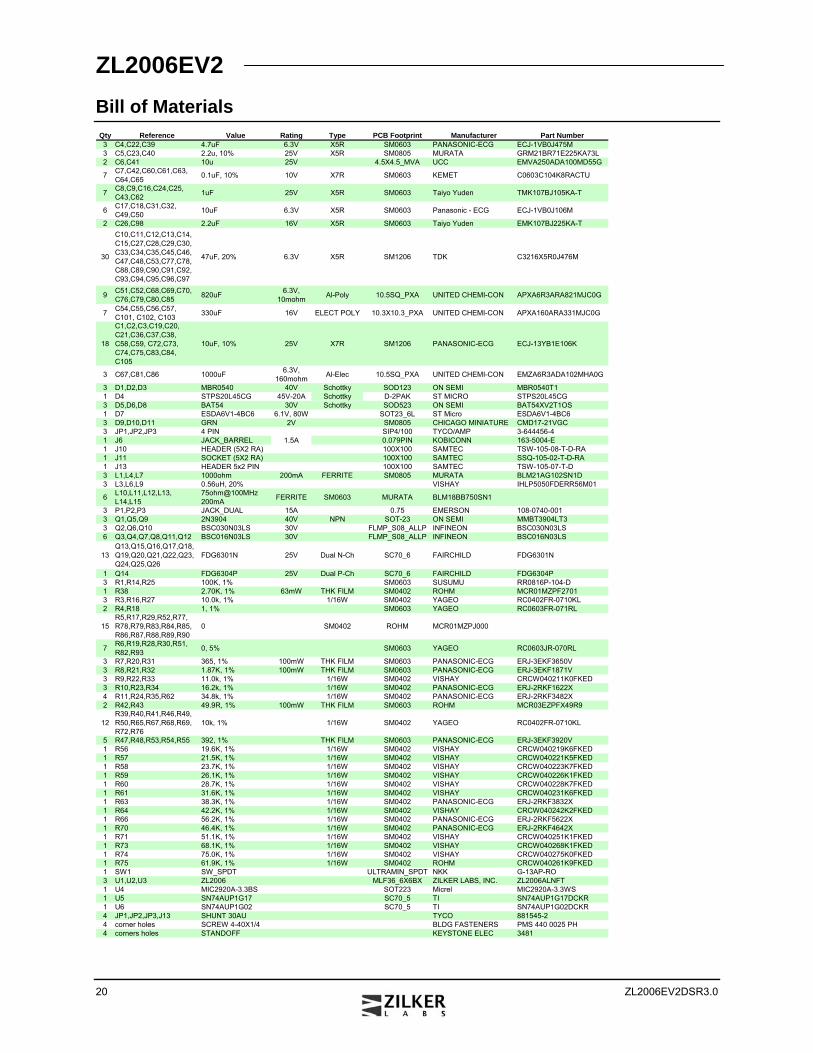
Bill of Materials Qty Reference Value Rating Type PCB Footprint Manufacturer Part Number3 C4,C22,C39 4.7uF 6.3V X5R SM0603 PANASONIC-ECG ECJ-1VB0J475M3 C5,C23,C40 2.2u, 10% 25V X5R SM0805 MURATA GRM21BR71E225KA73L2 C6,C41 10u 25V 4.5X4.5_MVA UCC EMVA250ADA100MD55G
7 C7,C42,C60,C61,C63,C64,C65 0.1uF, 10% 10V X7R SM0603 KEMET C0603C104K8RACTU
7 C8,C9,C16,C24,C25,C43,C62 1uF 25V X5R SM0603 Taiyo Yuden TMK107BJ105KA-T
6 C17,C18,C31,C32,C49,C50 10uF 6.3V X5R SM0603 Panasonic - ECG ECJ-1VB0J106M
2 C26,C98 2.2uF 16V X5R SM0603 Taiyo Yuden EMK107BJ225KA-T
30
C10,C11,C12,C13,C14,C15,C27,C28,C29,C30,C33,C34,C35,C45,C46,C47,C48,C53,C77,C78,C88,C89,C90,C91,C92,C93,C94,C95,C96,C97
47uF, 20% 6.3V X5R SM1206 TDK C3216X5R0J476M
9 C51,C52,C68,C69,C70,C76,C79,C80,C85 820uF 6.3V,
10mohm Al-Poly 10.5SQ_PXA UNITED CHEMI-CON APXA6R3ARA821MJC0G
7 C54,C55,C56,C57,C101, C102, C103 330uF 16V ELECT POLY 10.3X10.3_PXA UNITED CHEMI-CON APXA160ARA331MJC0G
18
C1,C2,C3,C19,C20,C21,C36,C37,C38,C58,C59, C72,C73,C74,C75,C83,C84,C105
10uF, 10% 25V X7R SM1206 PANASONIC-ECG ECJ-13YB1E106K
3 C67,C81,C86 1000uF 6.3V,160mohm Al-Elec 10.5SQ_PXA UNITED CHEMI-CON EMZA6R3ADA102MHA0G
3 D1,D2,D3 MBR0540 40V Schottky SOD123 ON SEMI MBR0540T11 D4 STPS20L45CG 45V-20A Schottky D-2PAK ST MICRO STPS20L45CG3 D5,D6,D8 BAT54 30V Schottky SOD523 ON SEMI BAT54XV2T1OS1 D7 ESDA6V1-4BC6 6.1V, 80W SOT23_6L ST Micro ESDA6V1-4BC63 D9,D10,D11 GRN 2V SM0805 CHICAGO MINIATURE CMD17-21VGC3 JP1,JP2,JP3 4 PIN SIP4/100 TYCO/AMP 3-644456-41 J6 JACK_BARREL 1.5A 0.079PIN KOBICONN 163-5004-E1 J10 HEADER (5X2 RA) 100X100 SAMTEC TSW-105-08-T-D-RA1 J11 SOCKET (5X2 RA) 100X100 SAMTEC SSQ-105-02-T-D-RA1 J13 HEADER 5x2 PIN 100X100 SAMTEC TSW-105-07-T-D3 L1,L4,L7 1000ohm 200mA FERRITE SM0805 MURATA BLM21AG102SN1D3 L3,L6,L9 0.56uH, 20% VISHAY IHLP5050FDERR56M01
6 L10,L11,L12,L13,L14,L15
75ohm@100MHz200mA FERRITE SM0603 MURATA BLM18BB750SN1
3 P1,P2,P3 JACK_DUAL 15A 0.75 EMERSON 108-0740-0013 Q1,Q5,Q9 2N3904 40V NPN SOT-23 ON SEMI MMBT3904LT33 Q2,Q6,Q10 BSC030N03LS 30V FLMP_S08_ALLP INFINEON BSC030N03LS6 Q3,Q4,Q7,Q8,Q11,Q12 BSC016N03LS 30V FLMP_S08_ALLP INFINEON BSC016N03LS
13Q13,Q15,Q16,Q17,Q18,Q19,Q20,Q21,Q22,Q23,Q24,Q25,Q26
FDG6301N 25V Dual N-Ch SC70_6 FAIRCHILD FDG6301N
1 Q14 FDG6304P 25V Dual P-Ch SC70_6 FAIRCHILD FDG6304P3 R1,R14,R25 100K, 1% SM0603 SUSUMU RR0816P-104-D1 R38 2.70K, 1% 63mW THK FILM SM0402 ROHM MCR01MZPF27013 R3,R16,R27 10.0k, 1% 1/16W SM0402 YAGEO RC0402FR-0710KL2 R4,R18 1, 1% SM0603 YAGEO RC0603FR-071RL
15R5,R17,R29,R52,R77,R78,R79,R83,R84,R85,R86,R87,R88,R89,R90
0 SM0402 ROHM MCR01MZPJ000
7 R6,R19,R28,R30,R51,R82,R93 0, 5% SM0603 YAGEO RC0603JR-070RL
3 R7,R20,R31 365, 1% 100mW THK FILM SM0603 PANASONIC-ECG ERJ-3EKF3650V3 R8,R21,R32 1.87K, 1% 100mW THK FILM SM0603 PANASONIC-ECG ERJ-3EKF1871V3 R9,R22,R33 11.0k, 1% 1/16W SM0402 VISHAY CRCW040211K0FKED3 R10,R23,R34 16.2k, 1% 1/16W SM0402 PANASONIC-ECG ERJ-2RKF1622X4 R11,R24,R35,R62 34.8k, 1% 1/16W SM0402 PANASONIC-ECG ERJ-2RKF3482X2 R42,R43 49.9R, 1% 100mW THK FILM SM0603 ROHM MCR03EZPFX49R9
12R39,R40,R41,R46,R49,R50,R65,R67,R68,R69,R72,R76
10k, 1% 1/16W SM0402 YAGEO RC0402FR-0710KL
5 R47,R48,R53,R54,R55 392, 1% THK FILM SM0603 PANASONIC-ECG ERJ-3EKF3920V1 R56 19.6K, 1% 1/16W SM0402 VISHAY CRCW040219K6FKED1 R57 21.5K, 1% 1/16W SM0402 VISHAY CRCW040221K5FKED1 R58 23.7K, 1% 1/16W SM0402 VISHAY CRCW040223K7FKED1 R59 26.1K, 1% 1/16W SM0402 VISHAY CRCW040226K1FKED1 R60 28.7K, 1% 1/16W SM0402 VISHAY CRCW040228K7FKED1 R61 31.6K, 1% 1/16W SM0402 VISHAY CRCW040231K6FKED1 R63 38.3K, 1% 1/16W SM0402 PANASONIC-ECG ERJ-2RKF3832X1 R64 42.2K, 1% 1/16W SM0402 VISHAY CRCW040242K2FKED1 R66 56.2K, 1% 1/16W SM0402 PANASONIC-ECG ERJ-2RKF5622X1 R70 46.4K, 1% 1/16W SM0402 PANASONIC-ECG ERJ-2RKF4642X1 R71 51.1K, 1% 1/16W SM0402 VISHAY CRCW040251K1FKED1 R73 68.1K, 1% 1/16W SM0402 VISHAY CRCW040268K1FKED1 R74 75.0K, 1% 1/16W SM0402 VISHAY CRCW040275K0FKED1 R75 61.9K, 1% 1/16W SM0402 ROHM CRCW040261K9FKED1 SW1 SW_SPDT ULTRAMIN_SPDT NKK G-13AP-RO3 U1,U2,U3 ZL2006 MLF36_6X6BX ZILKER LABS, INC. ZL2006ALNFT1 U4 MIC2920A-3.3BS SOT223 Micrel MIC2920A-3.3WS1 U5 SN74AUP1G17 SC70_5 TI SN74AUP1G17DCKR1 U6 SN74AUP1G02 SC70_5 TI SN74AUP1G02DCKR4 JP1,JP2,JP3,J13 SHUNT 30AU TYCO 881545-24 corner holes SCREW 4-40X1/4 BLDG FASTENERS PMS 440 0025 PH4 corners holes STANDOFF KEYSTONE ELEC 3481
ZL2006EV2
ZL2006EV2DSR3.0 21
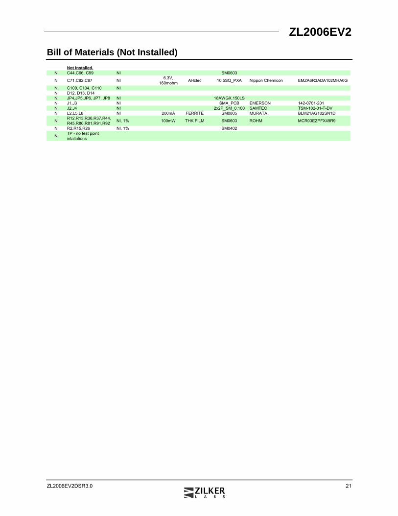
Bill of Materials (Not Installed)
Not installed.NI C44,C66, C99 NI SM0603
NI C71,C82,C87 NI 6.3V,160mohm Al-Elec 10.5SQ_PXA Nippon Chemicon EMZA6R3ADA102MHA0G
NI C100, C104, C110 NINI D12, D13, D14NI JP4,JP5,JP6, JP7, JP8 NI 18AWGX.150LSNI J1,J3 NI SMA_PCB EMERSON 142-0701-201NI J2,J4 NI 2x2P_SM_0.100 SAMTEC TSM-102-01-T-DVNI L2,L5,L8 NI 200mA FERRITE SM0805 MURATA BLM21AG102SN1D
NI R12,R13,R36,R37,R44,R45,R80,R81,R91,R92 NI, 1% 100mW THK FILM SM0603 ROHM MCR03EZPFX49R9
NI R2,R15,R26 NI, 1% SM0402
NI TP - no test point intallations
ZL2006EV2
22 ZL2006EV2DSR3.0
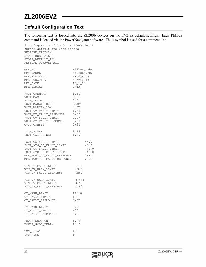
Default Configuration Text The following text is loaded into the ZL2006 devices on the EV2 as default settings. Each PMBus command is loaded via the PowerNavigator software. The # symbol is used for a comment line. # Configuration file for ZL2006EV2-Ch1A #Erase default and user stores RESTORE_FACTORY STORE_USER_ALL STORE_DEFAULT_ALL RESTORE_DEFAULT_ALL MFR_ID Zilker_Labs MFR_MODEL ZL2006EV2R2 MFR_REVISION Prod_Rev8 MFR_LOCATION Austin_TX MFR_DATE 10_1_08 MFR_SERIAL ch1A VOUT_COMMAND 1.80 VOUT_MAX 3.65 VOUT_DROOP 0.5 VOUT_MARGIN_HIGH 1.89 VOUT_MARGIN_LOW 1.71 VOUT_UV_FauLT_LIMIT 1.53 VOUT_UV_FAULT_RESPONSE 0x80 VOUT_OV_FauLT_LIMIT 2.07 VOUT_OV_FAULT_RESPONSE 0x80 OVUV_CONFIG 0x80 IOUT_SCALE 1.13 IOUT_CAL_OFFSET 1.00 IOUT_OC_FAULT_LIMIT 45.0 IOUT_AVG_OC_FAULT_LIMIT 40.0 IOUT_UC_FAULT_LIMIT -40.0 IOUT_AVG_UC_FAULT_LIMIT -40.0 MFR_IOUT_OC_FAULT_RESPONSE 0xBF MFR_IOUT_UC_FAULT_RESPONSE 0xBF VIN_OV_FAULT_LIMIT 14.0 VIN_OV_WARN_LIMIT 13.5 VIN_OV_FAULT_RESPONSE 0x80 VIN_UV_WARN_LIMIT 4.641 VIN_UV_FAULT_LIMIT 4.50 VIN_UV_FAULT_RESPONSE 0x80 OT_WARN_LIMIT 110.0 OT_FAULT_LIMIT 120 OT_FAULT_RESPONSE 0xBF UT_WARN_LIMIT -20 UT_FAULT_LIMIT -30 UT_FAULT_RESPONSE 0xBF POWER_GOOD_ON 1.35 POWER_GOOD_DELAY 10.0 TON_DELAY 15 TON_RISE 5
ZL2006EV2
ZL2006EV2DSR3.0 23
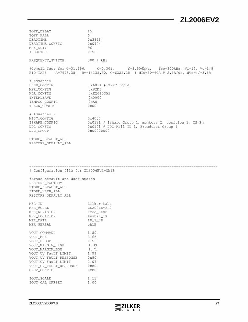
TOFF_DELAY 15 TOFF_FALL 5 DEADTIME 0x3838 DEADTIME_CONFIG 0x0404 MAX_DUTY 96 INDUCTOR 0.56 FREQUENCY_SWITCH 300 # kHz #CompZL Taps for G=31.596, Q=0.301, f=3.506kHz, fsw=300kHz, Vi=12, Vo=1.8 PID_TAPS A=7948.25, B=-14135.50, C=6225.25 # dIo=30-60A @ 2.5A/us, dVo=+/-3.5% # Advanced USER_CONFIG 0x6051 # SYNC Input MFR_CONFIG 0x82D4 NLR_CONFIG 0xE2010355 INTERLEAVE 0x0000 TEMPCO_CONFIG 0xA8 TRACK_CONFIG 0x00 # Advanced 2 MISC_CONFIG 0x4080 ISHARE_CONFIG 0x0121 # Ishare Group 1, members 2, position 1, CS En DDC_CONFIG 0x0101 # DDC Rail ID 1, Broadcast Group 1 DDC_GROUP 0x00000000 STORE_DEFAULT_ALL RESTORE_DEFAULT_ALL
-------------------------------------------------------------------------------------- # Configuration file for ZL2006EV2-Ch1B #Erase default and user stores RESTORE_FACTORY STORE_DEFAULT_ALL STORE_USER_ALL RESTORE_DEFAULT_ALL MFR_ID Zilker_Labs MFR_MODEL ZL2006EV2R2 MFR_REVISION Prod_Rev8 MFR_LOCATION Austin_TX MFR_DATE 10_1_08 MFR_SERIAL ch1B VOUT_COMMAND 1.80 VOUT_MAX 3.65 VOUT_DROOP 0.5 VOUT_MARGIN_HIGH 1.89 VOUT_MARGIN_LOW 1.71 VOUT_UV_FauLT_LIMIT 1.53 VOUT_UV_FAULT_RESPONSE 0x80 VOUT_OV_FauLT_LIMIT 2.07 VOUT_OV_FAULT_RESPONSE 0x80 OVUV_CONFIG 0x80 IOUT_SCALE 1.13 IOUT_CAL_OFFSET 1.00

ZL2006EV2
24 ZL2006EV2DSR3.0
IOUT_OC_FAULT_LIMIT 45.0 IOUT_AVG_OC_FAULT_LIMIT 40.0 IOUT_UC_FAULT_LIMIT -40.0 IOUT_AVG_UC_FAULT_LIMIT -40.0 MFR_IOUT_OC_FAULT_RESPONSE 0xBF MFR_IOUT_UC_FAULT_RESPONSE 0xBF VIN_OV_FAULT_LIMIT 14.0 VIN_OV_WARN_LIMIT 13.5 VIN_OV_FAULT_RESPONSE 0x80 VIN_UV_WARN_LIMIT 4.641 VIN_UV_FAULT_LIMIT 4.50 VIN_UV_FAULT_RESPONSE 0x80 OT_WARN_LIMIT 110.0 OT_FAULT_LIMIT 120.0 OT_FAULT_RESPONSE 0xBF UT_WARN_LIMIT -20 UT_FAULT_LIMIT -30 UT_FAULT_RESPONSE 0xBF POWER_GOOD_ON 1.35 POWER_GOOD_DELAY 10.0 TON_DELAY 5 TON_RISE 5 TOFF_DELAY 5 TOFF_FALL 5 DEADTIME 0x3838 DEADTIME_CONFIG 0x0404 MAX_DUTY 96 INDUCTOR 0.56 FREQUENCY_SWITCH 300 # kHz #CompZL Taps for G=31.596, Q=0.301, f=3.506kHz, fsw=300kHz, Vi=12, Vo=1.8 PID_TAPS A=7948.25, B=-14135.50, C=6225.25 # dIo=30-60A @ 2.5A/us, dVo=+/-3.5% # Advanced USER_CONFIG 0x0051 # SYNC INPUT MFR_CONFIG 0x82D4 NLR_CONFIG 0xE2010355 INTERLEAVE 0x0000 TEMPCO_CONFIG 0xA8 TRACK_CONFIG 0x00 # Advanced 2 MISC_CONFIG 0x4080 ISHARE_CONFIG 0x0125 # Ishare Group 1, members 2, position 2, CS En DDC_CONFIG 0x0101 # DDC Rail ID 1, Broadcast Group 1 DDC_GROUP 0x00000000 STORE_DEFAULT_ALL RESTORE_DEFAULT_ALL
ZL2006EV2
ZL2006EV2DSR3.0 25
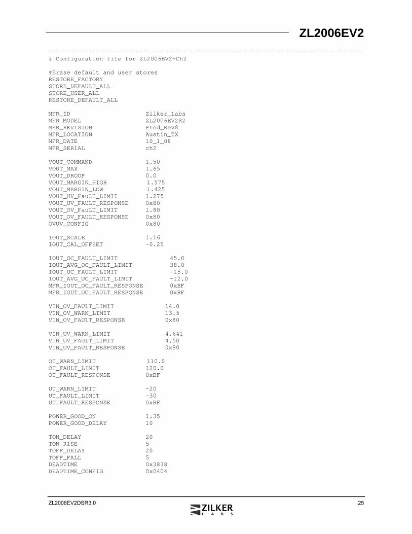
-------------------------------------------------------------------------------------- # Configuration file for ZL2006EV2-Ch2 #Erase default and user stores RESTORE_FACTORY STORE_DEFAULT_ALL STORE_USER_ALL RESTORE_DEFAULT_ALL MFR_ID Zilker_Labs MFR_MODEL ZL2006EV2R2 MFR_REVISION Prod_Rev8 MFR_LOCATION Austin_TX MFR_DATE 10_1_08 MFR_SERIAL ch2 VOUT_COMMAND 1.50 VOUT_MAX 1.65 VOUT_DROOP 0.0 VOUT_MARGIN_HIGH 1.575 VOUT_MARGIN_LOW 1.425 VOUT_UV_FauLT_LIMIT 1.275 VOUT_UV_FAULT_RESPONSE 0x80 VOUT_OV_FauLT_LIMIT 1.80 VOUT_OV_FAULT_RESPONSE 0x80 OVUV_CONFIG 0x80 IOUT_SCALE 1.16 IOUT_CAL_OFFSET -0.25 IOUT_OC_FAULT_LIMIT 45.0 IOUT_AVG_OC_FAULT_LIMIT 38.0 IOUT_UC_FAULT_LIMIT -15.0 IOUT_AVG_UC_FAULT_LIMIT -12.0 MFR_IOUT_OC_FAULT_RESPONSE 0xBF MFR_IOUT_UC_FAULT_RESPONSE 0xBF VIN_OV_FAULT_LIMIT 14.0 VIN_OV_WARN_LIMIT 13.5 VIN_OV_FAULT_RESPONSE 0x80 VIN_UV_WARN_LIMIT 4.641 VIN_UV_FAULT_LIMIT 4.50 VIN_UV_FAULT_RESPONSE 0x80 OT_WARN_LIMIT 110.0 OT_FAULT_LIMIT 120.0 OT_FAULT_RESPONSE 0xBF UT_WARN_LIMIT -20 UT_FAULT_LIMIT -30 UT_FAULT_RESPONSE 0xBF POWER_GOOD_ON 1.35 POWER_GOOD_DELAY 10 TON_DELAY 20 TON_RISE 5 TOFF_DELAY 20 TOFF_FALL 5 DEADTIME 0x3838 DEADTIME_CONFIG 0x0404
ZL2006EV2
26 ZL2006EV2DSR3.0
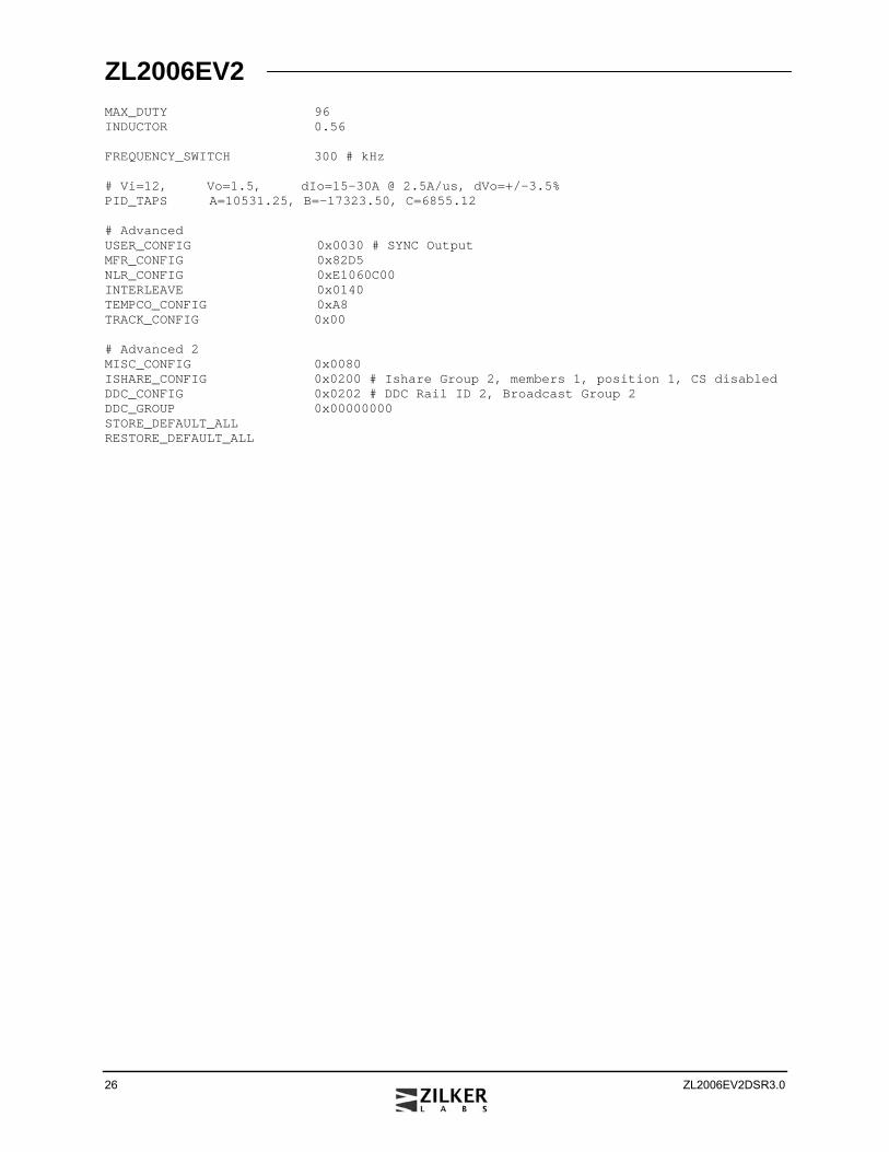
MAX_DUTY 96 INDUCTOR 0.56 FREQUENCY_SWITCH 300 # kHz # Vi=12, Vo=1.5, dIo=15-30A @ 2.5A/us, dVo=+/-3.5% PID_TAPS A=10531.25, B=-17323.50, C=6855.12 # Advanced USER_CONFIG 0x0030 # SYNC Output MFR_CONFIG 0x82D5 NLR_CONFIG 0xE1060C00 INTERLEAVE 0x0140 TEMPCO_CONFIG 0xA8 TRACK_CONFIG 0x00 # Advanced 2 MISC_CONFIG 0x0080 ISHARE_CONFIG 0x0200 # Ishare Group 2, members 1, position 1, CS disabled DDC_CONFIG 0x0202 # DDC Rail ID 2, Broadcast Group 2 DDC_GROUP 0x00000000 STORE_DEFAULT_ALL RESTORE_DEFAULT_ALL
ZL2006EV2
ZL2006EV2DSR3.0 27
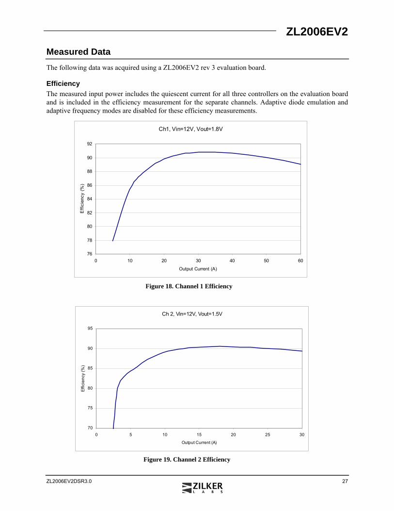
Measured Data The following data was acquired using a ZL2006EV2 rev 3 evaluation board.
Efficiency The measured input power includes the quiescent current for all three controllers on the evaluation board and is included in the efficiency measurement for the separate channels. Adaptive diode emulation and adaptive frequency modes are disabled for these efficiency measurements.
Figure 19. Channel 2 Efficiency
Figure 18. Channel 1 Efficiency
Ch1, Vin=12V, Vout=1.8V
76
78
80
82
84
86
88
90
92
0 10 20 30 40 50 60
Output Current (A)
Effi
cien
cy (%
)
Ch 2, Vin=12V, Vout=1.5V
70
75
80
85
90
95
0 5 10 15 20 25 30
Output Current (A)
Effic
ienc
y (%
)
ZL2006EV2
28 ZL2006EV2DSR3.0
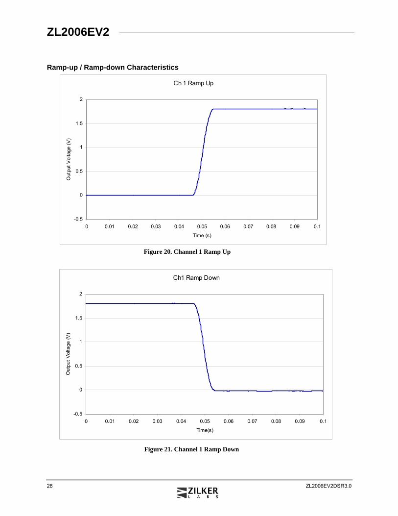
Ramp-up / Ramp-down Characteristics
Figure 20. Channel 1 Ramp Up
Figure 21. Channel 1 Ramp Down
Ch 1 Ramp Up
-0.5
0
0.5
1
1.5
2
0 0.01 0.02 0.03 0.04 0.05 0.06 0.07 0.08 0.09 0.1
Time (s)
Out
put V
olta
ge (V
)
Ch1 Ramp Down
-0.5
0
0.5
1
1.5
2
0 0.01 0.02 0.03 0.04 0.05 0.06 0.07 0.08 0.09 0.1
Time(s)
Out
put V
olta
ge (V
)
ZL2006EV2
ZL2006EV2DSR3.0 29
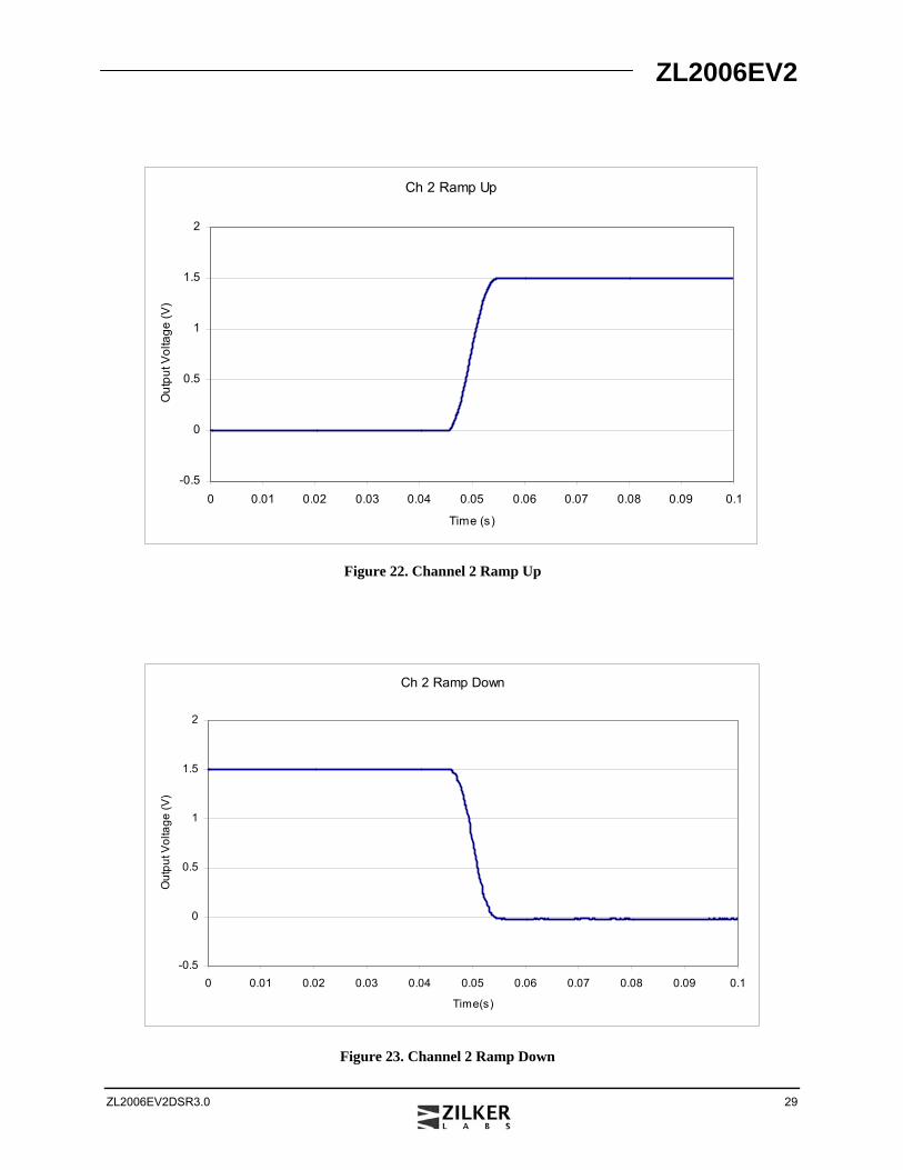
Figure 22. Channel 2 Ramp Up
Figure 23. Channel 2 Ramp Down
Ch 2 Ramp Up
-0.5
0
0.5
1
1.5
2
0 0.01 0.02 0.03 0.04 0.05 0.06 0.07 0.08 0.09 0.1
Time (s)
Out
put V
olta
ge (V
)
Ch 2 Ramp Down
-0.5
0
0.5
1
1.5
2
0 0.01 0.02 0.03 0.04 0.05 0.06 0.07 0.08 0.09 0.1
Time(s)
Out
put V
olta
ge (V
)
ZL2006EV2
30 ZL2006EV2DSR3.0
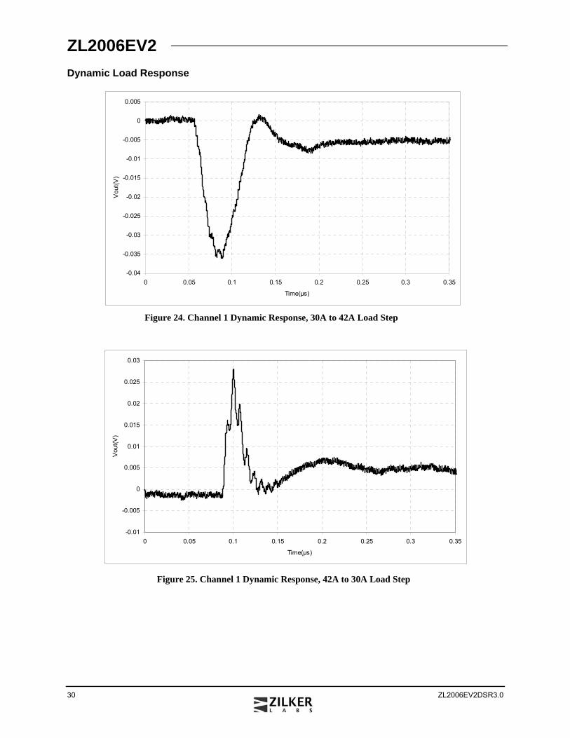
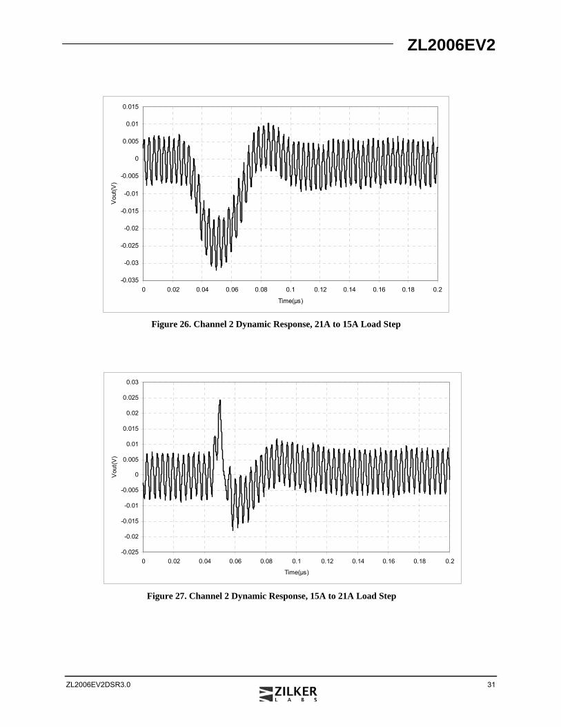
Dynamic Load Response
Figure 24. Channel 1 Dynamic Response, 30A to 42A Load Step
-0.04
-0.035
-0.03
-0.025
-0.02
-0.015
-0.01
-0.005
0
0.005
0 0.05 0.1 0.15 0.2 0.25 0.3 0.35
Time(μs)
Vou
t(V)
-0.01
-0.005
0
0.005
0.01
0.015
0.02
0.025
0.03
0 0.05 0.1 0.15 0.2 0.25 0.3 0.35
Time(μs)
Vou
t(V)
Figure 25. Channel 1 Dynamic Response, 42A to 30A Load Step
ZL2006EV2
ZL2006EV2DSR3.0 31
Figure 27. Channel 2 Dynamic Response, 15A to 21A Load Step
-0.035
-0.03
-0.025
-0.02
-0.015
-0.01
-0.005
0
0.005
0.01
0.015
0 0.02 0.04 0.06 0.08 0.1 0.12 0.14 0.16 0.18 0.2
Time(μs)
Vou
t(V)
Figure 26. Channel 2 Dynamic Response, 21A to 15A Load Step
-0.025
-0.02
-0.015
-0.01
-0.005
0
0.005
0.01
0.015
0.02
0.025
0.03
0 0.02 0.04 0.06 0.08 0.1 0.12 0.14 0.16 0.18 0.2
Time(μs)
Vou
t(V)
ZL2006EV2
32 ZL2006EV2DSR3.0
References [1] ZL2006 Data Sheet, Zilker Labs, Inc., 2008.
[2] AN33 – PMBus™ Command Set, Zilker Labs, Inc., 2008.
Ordering Information
Orderable Part Number Description
ZL2006EVK2 ZL2006 Two Channel Evaluation Kit (EVB, USB Adapter, Cable, Software)
ZL2006EV2 ZL2006 Two Channel Evaluation board only
ZL2006EV2
ZL2006EV2DSR3.0 33
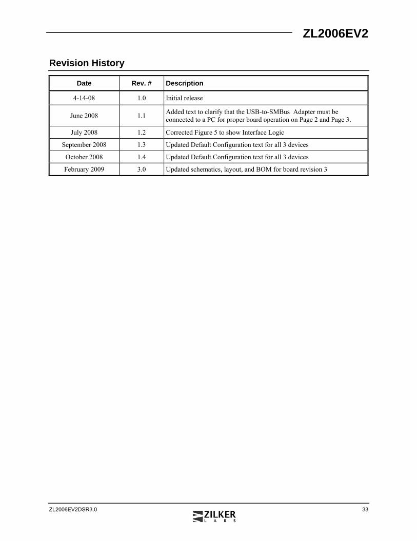
Revision History
Date Rev. # Description
4-14-08 1.0 Initial release
June 2008 1.1 Added text to clarify that the USB-to-SMBus Adapter must be connected to a PC for proper board operation on Page 2 and Page 3.
July 2008 1.2 Corrected Figure 5 to show Interface Logic
September 2008 1.3 Updated Default Configuration text for all 3 devices
October 2008 1.4 Updated Default Configuration text for all 3 devices
February 2009 3.0 Updated schematics, layout, and BOM for board revision 3

ZL2006EV2
34 ZL2006EV2DSR3.0
Intersil Corporation 4301 Westbank Drive
Building A-100 Austin, TX 78746
Tel: 512-382-8300 Fax: 512-382-8329
www.intersil.com
© 2009, Intersil Americas, Inc. All rights reserved. Zilker Labs, Digital-DC, PowerNavigator, and the Zilker Labs Logo are trademarks of Intersil Americas, Inc. All other products or brand names mentioned herein are trademarks of their respective holders.
Pricing, specifications and availability are subject to change without notice. Please see www.zilkerlabs.com for updated information. This product is not intended for use in connection with any high-risk activity, including without limitation, air travel, life critical medical operations, nuclear facilities or equipment, or the like.
The reference designs contained in this document are for reference and example purposes only. THE REFER-ENCE DESIGNS ARE PROVIDED "AS IS" AND "WITH ALL FAULTS" AND ZILKER LABS DISCLAIMS ALL WARRANTIES, WHETHER EXPRESS OR IMPLIED. ZILKER LABS SHALL NOT BE LIABLE FOR ANY DAMAGES, WHETHER DIRECT, INDIRECT, CONSEQUENTIAL (INCLUDING LOSS OF PROF-ITS), OR OTHERWISE, RESULTING FROM THE REFERENCE DESIGNS OR ANY USE THEREOF. Any use of such reference designs is at your own risk and you agree to indemnify Intersil for any damages resulting from such use.