renesas promotional board for rl78g13 demo user manual
TRANSCRIPT
All information contained in these materials, including products and product specifications, represents information on the product at the time of publication and is subject to change by Renesas Electronics Corp. without notice. Please review the latest information published by Renesas Electronics Corp. through various means, including the Renesas Technology Corp. website (http://www.renesas.com).
www.renesas.com
RL78/G13 Stick (YRPBRL78G13) 16-bit Microcontroller
RL78/G13 R5F100LEAFB
R01UH0243ED0000, Rev. 1.0 March 25, 2011
User M
anual
16
R01UH0243ED0000 Rev. 1.0 2 User Manual
Notice 1. All information included in this document is current as of the date this document is issued. Such
information, however, is subject to change without any prior notice. Before purchasing or using any Renesas Electronics products listed herein, please confirm the latest product information with a Renesas Electronics sales office. Also, please pay regular and careful attention to additional and different information to be disclosed by Renesas Electronics such as that disclosed through our website.
2. Renesas Electronics does not assume any liability for infringement of patents, copyrights, or other intellectual property rights of third parties by or arising from the use of Renesas Electronics products or technical information described in this document. No license, express, implied or otherwise, is granted hereby under any patents, copyrights or other intellectual property rights of Renesas Electronics or others.
3. You should not alter, modify, copy, or otherwise misappropriate any Renesas Electronics product, whether in whole or in part.
4. Descriptions of circuits, software and other related information in this document are provided only to illustrate the operation of semiconductor products and application examples. You are fully responsible for the incorporation of these circuits, software, and information in the design of your equipment. Renesas Electronics assumes no responsibility for any losses incurred by you or third parties arising from the use of these circuits, software, or information.
5. When exporting the products or technology described in this document, you should comply with the applicable export control laws and regulations and follow the procedures required by such laws and regulations. You should not use Renesas Electronics products or the technology described in this document for any purpose relating to military applications or use by the military, including but not limited to the development of weapons of mass destruction. Renesas Electronics products and technology may not be used for or incorporated into any products or systems whose manufacture, use, or sale is prohibited under any applicable domestic or foreign laws or regulations.
6. Renesas Electronics has used reasonable care in preparing the information included in this document, but Renesas Electronics does not warrant that such information is error free. Renesas Electronics assumes no liability whatsoever for any damages incurred by you resulting from errors in or omissions from the information included herein.
7. Renesas Electronics products are classified according to the following three quality grades: “Standard”, “High Quality”, and “Specific”. The recommended applications for each Renesas Electronics product depends on the product’s quality grade, as indicated below. You must check the quality grade of each Renesas Electronics product before using it in a particular application. You may not use any Renesas Electronics product for any application categorized as “Specific” without the prior written consent of Renesas Electronics. Further, you may not use any Renesas Electronics product for any application for which it is not intended without the prior written consent of Renesas Electronics. Renesas Electronics shall not be in any way liable for any damages or losses incurred by you or third parties arising from the use of any Renesas Electronics product for an application categorized as “Specific” or for which the product is not intended where you have failed to obtain the prior written consent of Renesas Electronics.

R01UH0243ED0000 Rev. 1.0 3 User Manual
8. The quality grade of each Renesas Electronics product is “Standard” unless otherwise expressly specified in a Renesas Electronics data sheets or data books, etc.
“Standard”: Computers; office equipment; communications equipment; test and measurement equipment; audio and visual equipment; home electronic appliances; machine tools; personal electronic equipment; and industrial robots.
“High Quality”: Transportation equipment (automobiles, trains, ships, etc.); traffic control systems; anti-disaster systems; anti- crime systems; safety equipment; and medical equipment not specifically designed for life support.
“Specific”: Aircraft; aerospace equipment; submersible repeaters; nuclear reactor control systems;medical equipment or systems for life support (e.g. artificial life support devices or systems), surgical implantations, or healthcare intervention (e.g. excision, etc.), and any other applications or purposes that pose a direct threat to human life.
9. You should use the Renesas Electronics products described in this document within the range specified by Renesas Electronics, especially with respect to the maximum rating, operating supply voltage range, movement power voltage range, heat radiation characteristics, installation and other product characteristics. Renesas Electronics shall have no liability for malfunctions or damages arising out of the use of Renesas Electronics products beyond such specified ranges.
10. Although Renesas Electronics endeavors to improve the quality and reliability of its products, semiconductor products have specific characteristics such as the occurrence of failure at a certain rate and malfunctions under certain use conditions. Further, Renesas Electronics products are not subject to radiation resistance design. Please be sure to implement safety measures to guard them against the possibility of physical injury, and injury or damage caused by fire in the event of the failure of a Renesas Electronics product, such as safety design for hardware and software including but not limited to redundancy, fire control and malfunction prevention, appropriate treatment for aging degradation or any other appropriate measures. Because the evaluation of microcomputer software alone is very difficult, please evaluate the safety of the final products or system manufactured by you.
11. Please contact a Renesas Electronics sales office for details as to environmental matters such as the environmental compatibility of each Renesas Electronics product. Please use Renesas Electronics products in compliance with all applicable laws and regulations that regulate the inclusion or use of controlled substances, including without limitation, the EU RoHS Directive. Renesas Electronics assumes no liability for damages or losses occurring as a result of your noncompliance with applicable laws and regulations.
12. This document may not be reproduced or duplicated, in any form, in whole or in part, without prior written consent of Renesas Electronics.
13. Please contact a Renesas Electronics sales office if you have any questions regarding the information contained in this document or Renesas Electronics products, or if you have any other inquiries.
(Note 1) “Renesas Electronics” as used in this document means Renesas Electronics Corporation and also includes its majority- owned subsidiaries.
(Note 2) “Renesas Electronics product(s)” means any product developed or manufactured by or for Renesas Electronics.

R01UH0243ED0000 Rev. 1.0 4 User Manual
General Precautions in the Handling of MPU/MCU Products
The following usage notes are applicable to all MPU/MCU products from Renesas. For detailed usage notes on the products covered by this manual, refer to the relevant sections of the manual. If the descriptions under General Precautions in the Handling of MPU/MCU Products and in the body of the manual differ from each other, the description in the body of the manual takes precedence.
1. Handling of Unused Pins Handle unused pins in accord with the directions given under Handling of Unused Pins in the manual.
The input pins of CMOS products are generally in the high-impedance state. In operation with an unused pin in the open-circuit state, extra electromagnetic noise is induced in the vicinity of LSI, an associated shoot-through current flows internally, and malfunctions occur due to the false recognition of the pin state as an input signal become possible. Unused pins should be handled as described under Handling of Unused Pins in the manual.
2. Processing at Power-on The state of the product is undefined at the moment when power is supplied.
The states of internal circuits in the LSI are indeterminate and the states of register settings and pins are undefined at the moment when power is supplied. In a finished product where the reset signal is applied to the external reset pin, the states of pins are not guaranteed from the moment when power is supplied until the reset process is completed. In a similar way, the states of pins in a product that is reset by an on-chip power-on reset function are not guaranteed from the moment when power is supplied until the power reaches the level at which resetting has been specified.
3. Prohibition of Access to Reserved Addresses Access to reserved addresses is prohibited.
The reserved addresses are provided for the possible future expansion of functions. Do not access these addresses; the correct operation of LSI is not guaranteed if they are accessed.
4. Clock Signals After applying a reset, only release the reset line after the operating clock signal has become stable. When switching the clock signal during program execution, wait until the target clock signal has stabilized.
When the clock signal is generated with an external resonator (or from an external oscillator) during a reset, ensure that the reset line is only released after full stabilization of the clock signal. Moreover, when switching to a clock signal produced with an external resonator (or by an external oscillator) while program execution is in progress, wait until the target clock signal is stable.
5. Differences between Products Before changing from one product to another, i.e. to one with a different part number, confirm that the change will not lead to problems.
The characteristics of MPU/MCU in the same group but having different part numbers may differ because of the differences in internal memory capacity and layout pattern. When changing to products of different part numbers, implement a system-evaluation test for each of the products.
R01UH0243ED0000 Rev. 1.0 5 User Manual
Regional Information
Some information contained in this document may vary from country to country. Before using any Renesas Electronics product in your application, please contact the Renesas Electronics office in your country to obtain a list of authorized representatives and distributors. They will verify:
• • Device availability
• • Ordering information
• • Product release schedule
• • Availability of related technical literature
• • Development environment specifications (for example, specifications for third-party tools and components, host computers, power plugs, AC supply voltages, and so forth)
• • Network requirements
In addition, trademarks, registered trademarks, export restrictions, and other legal issues may also vary from country to country.
Visit
http://www.renesas.com
to get in contact with your regional representatives and distributors.
R01UH0243ED0000 Rev. 1.0 6 User Manual
Preface This manual is intended for users who want to understand the functions of the
concerned microcontrollers.
This manual presents the hardware manual for the concerned microcontrollers.
This system specification describes the following sections:
• Pin function
• CPU function
• Internal peripheral function
These microcontrollers may contain several instances of a dedicated module. In general the different instances of such modules are identified by the index “n”, where “n” counts from 0 to the number of instances minus one.
Symbols and notation are used as follows:
• Weight in data notation: Left is high order column, right is low order column
• Active low notation: xxx (pin or signal name is over-scored) or /xxx (slash before signal name) or _xxx
• Memory map address: High order at high stage and low order at low stage
Additional remark or tip
Item deserving extra attention
Binary: xxxx or xxxB
Decimal: xxxx
Hexadecimal xxxxH or 0x xxxx
representing powers of 2 (address space, memory capacity):
K (kilo): 210 = 1024
M (mega): 220 = 1024² = 1,048,576
G (giga): 230 = 1024³ = 1,073,741,824
X, x = don’t care
Block diagrams do not necessarily show the exact wiring in hardware but the functional structure. Timing diagrams are for functional explanation purposes only, without any relevance to the real hardware implementation.
Readers
Purpose
Organisation
Module instances
Legend
Note
Caution Numeric notation
Numeric prefixes
Register contents
Diagrams
R01UH0243ED0000 Rev. 1.0 7 User Manual
How to Use This Manual
(1) Purpose and Target Readers
This manual is designed to provide the user with an understanding of the hardware functions and electrical characteristics of the MCU. It is intended for users designing application systems incorporating the MCU. A basic knowledge of electric circuits, logical circuits, and MCUs is necessary in order to use this manual. The manual comprises an overview of the product; descriptions of the CPU, system control functions, peripheral functions, and electrical characteristics; and usage notes.
Particular attention should be paid to the precautionary notes when using the manual. These notes occur within the body of the text, at the end of each section, and in the Usage Notes section.
The revision history summarizes the locations of revisions and additions. It does not list all revisions. Refer to the text of the manual for details.
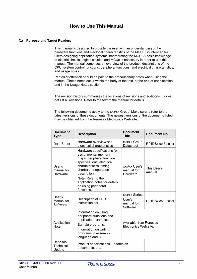
The following documents apply to the xxx/xx Group. Make sure to refer to the latest versions of these documents. The newest versions of the documents listed may be obtained from the Renesas Electronics Web site.
Document Type Description Document
Title Document No.
Data Sheet Hardware overview and electrical characteristics
xxx/xx Group Datasheet R01DSxxxxEJxxxx
User’s manual for Hardware
Hardware specifications (pin assignments, memory maps, peripheral function specifications, electrical characteristics, timing charts) and operation description. Note: Refer to the application notes for details on using peripheral functions.
xxx/xx User’s manual for Hardware
This User’s manual
User’s manual for Software
Description of CPU instruction set
xxx/xx Series User’s manual for Software
R01USxxxxEJxxxx
Application Note
Information on using peripheral functions and application examples. Sample programs. Information on writing programs in assembly language and C.
Available from Renesas Electronics Web site.
Renesas Technical Update
Product specifications, updates on documents, etc.
R01UH0243ED0000 Rev. 1.0 8 User Manual
(2) Notation of Numbers and Symbols
Not applicable.
(3) Register Notation
Not applicable.
R01UH0243ED0000 Rev. 1.0 9 User Manual
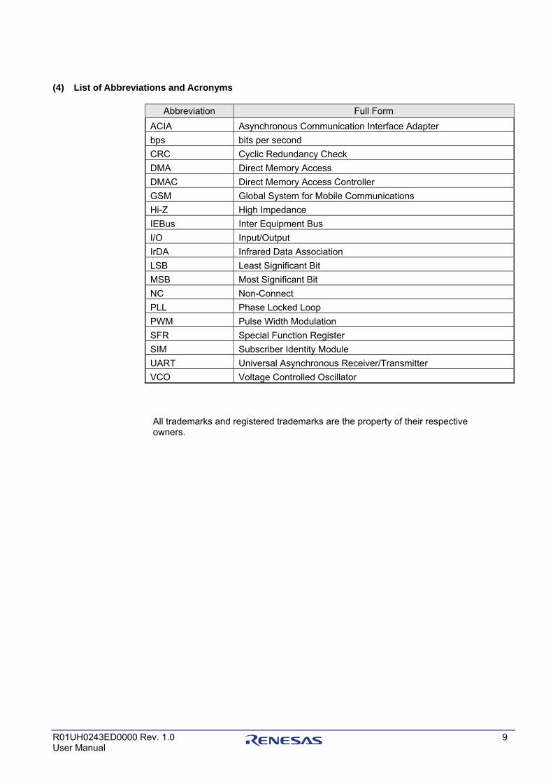
(4) List of Abbreviations and Acronyms
Abbreviation Full Form ACIA Asynchronous Communication Interface Adapter bps bits per second CRC Cyclic Redundancy Check DMA Direct Memory Access DMAC Direct Memory Access Controller GSM Global System for Mobile Communications Hi-Z High Impedance IEBus Inter Equipment Bus I/O Input/Output IrDA Infrared Data Association LSB Least Significant Bit MSB Most Significant Bit NC Non-Connect PLL Phase Locked Loop PWM Pulse Width Modulation SFR Special Function Register SIM Subscriber Identity Module UART Universal Asynchronous Receiver/Transmitter VCO Voltage Controlled Oscillator
All trademarks and registered trademarks are the property of their respective owners.
R01UH0243ED0000 Rev. 1.0 10 User Manual
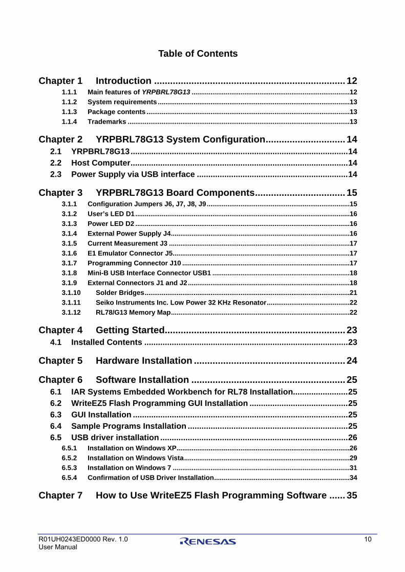
Table of Contents
Chapter 1 Introduction ........................................................................ 12 1.1.1 Main features of YRPBRL78G13 ....................................................................................12 1.1.2 System requirements ......................................................................................................13 1.1.3 Package contents ............................................................................................................13 1.1.4 Trademarks ......................................................................................................................13
Chapter 2 YRPBRL78G13 System Configuration.............................. 14 2.1 YRPBRL78G13...............................................................................................14 2.2 Host Computer...............................................................................................14 2.3 Power Supply via USB interface ..................................................................14
Chapter 3 YRPBRL78G13 Board Components.................................. 15 3.1.1 Configuration Jumpers J6, J7, J8, J9............................................................................15 3.1.2 User’s LED D1..................................................................................................................16 3.1.3 Power LED D2 ..................................................................................................................16 3.1.4 External Power Supply J4...............................................................................................16 3.1.5 Current Measurement J3 ................................................................................................17 3.1.6 E1 Emulator Connector J5..............................................................................................17 3.1.7 Programming Connector J10 .........................................................................................17 3.1.8 Mini-B USB Interface Connector USB1 .........................................................................18 3.1.9 External Connectors J1 and J2......................................................................................18 3.1.10 Solder Bridges.............................................................................................................21 3.1.11 Seiko Instruments Inc. Low Power 32 KHz Resonator............................................22 3.1.12 RL78/G13 Memory Map...............................................................................................22
Chapter 4 Getting Started.................................................................... 23 4.1 Installed Contents .........................................................................................23
Chapter 5 Hardware Installation ......................................................... 24
Chapter 6 Software Installation .......................................................... 25 6.1 IAR Systems Embedded Workbench for RL78 Installation........................25 6.2 WriteEZ5 Flash Programming GUI Installation ...........................................25 6.3 GUI Installation ..............................................................................................25 6.4 Sample Programs Installation ......................................................................25 6.5 USB driver installation ..................................................................................26
6.5.1 Installation on Windows XP............................................................................................26 6.5.2 Installation on Windows Vista........................................................................................29 6.5.3 Installation on Windows 7 ..............................................................................................31 6.5.4 Confirmation of USB Driver Installation........................................................................34
Chapter 7 How to Use WriteEZ5 Flash Programming Software ...... 35
R01UH0243ED0000 Rev. 1.0 11 User Manual
Chapter 8 On-Board Debugging (OCD).............................................. 42 8.1 Monitor Resources ........................................................................................42
8.1.1 TOOL0...............................................................................................................................42 8.1.2 Memory Area....................................................................................................................43
8.2 IAR Sample Program Description ................................................................43 8.2.1 General Introduction .......................................................................................................43 8.2.2 Functionality ....................................................................................................................44 8.2.3 Required Resources........................................................................................................44 8.2.4 Project Structure .............................................................................................................44
8.3 IAR Sample Debugging Session ..................................................................45 8.4 Debugging using E1 Emulator in IAR ..........................................................52
Chapter 9 GUI Description .................................................................. 53 9.1 Running the RL78/G13 Demo .......................................................................53 9.2 GUI Demo Sections .......................................................................................55 9.3 ADC Demonstration ......................................................................................57 9.4 Real Time Clock Demonstration...................................................................58 9.5 Memory Demonstration ................................................................................59 9.6 Low Power Demonstration ...........................................................................60
9.6.1 HALT Mode.......................................................................................................................61 9.6.2 STOP Mode.......................................................................................................................61 9.6.3 SNOOZE Mode .................................................................................................................62 9.6.4 Typical Current Consumption Figures..........................................................................63
9.7 Self-Test Functions Demonstration .............................................................64
Chapter 10 Troubleshooting ................................................................. 66
Chapter 11 Schematics ......................................................................... 68
Chapter 12 Bill of Materials................................................................... 71
Chapter 13 Resonator from Seiko Instruments Inc. ........................... 72 13.1 Features of the 32 KHz Resonator............................................................72 13.2 Product Name and Specifications ............................................................72 13.3 Web URL.....................................................................................................72 13.4 Contact Addresses ....................................................................................73
R01UH0243ED0000 Introduction
R01UH0243ED0000 Rev. 1.0 12 User Manual
Chapter 1 Introduction
The YRPBRL78G13 is a promotion board for the new Renesas RL78 microcontroller family. It supports On-Board debugging, flash programming, and is pre-programmed to work with the GUI provided on the DVD to demonstrate the low power capabilities of the Renesas RL78 MCU.
1.1.1 Main features of YRPBRL78G13
• Easy to use device demonstration capabilities
YRPBRL78G13 contains elements to easily demonstrate simple I/O-functions (i.e. LED output, I/O lines, UART serial interface) together with the key functions such as Real Time Clock (RTC), ADC, Timers, safety functions and on-chip data flash.
• Power supply via USB interface
YRPBRL78G13 is powered via USB interface. No separate power supply is needed although a connector is provided to supply an external power supply if needed.
• On-Board debug function
The YRPBRL78G13 supports an On-Board debug function by using the IAR C-SPY debugger, without the need of additional debug hardware. It allows Flash programming and supports standard debug functions such as code execution, single stepping, software breakpoints, memory manipulation etc.
• WriteEZ5, Flash programming software
Windows based Flash programming software allows the user to select and download application programs to the YRPBRL78G13 board for evaluation purposes.
• Applilet3, Device driver code generator Software tool used to generate device driver code to initialize and use on-chip peripherals. Please note that the WriteEZ5 and Applilet3 software versions provided are only preliminary versions and therefore should only be used with the YRPBRL78G13 board. We recommend not to upgrade these software tools in order to guarantee operation with the stick. Please also note that documentation is not supplied for these pre release versions but will be available to download from the Renesas website once final versions are released.
• Various input / output signals available, such as
° All I/O ports prepared to be connected to user hardware ° Virtual UART interface, via the µPD78F0730 78K0 8-bit microcontroller
with on-board USB interface ° 1 LED connected to a RL78/G13 port for visualization.
• The IAR Embedded Workbench for RL78 and the IAR C-SPY debugger are
included. These packages are restricted in such that maximum program code size is limited to 16 Kbytes.
Please note that only the IAR Embedded Workbench for RL78 1.10 version provided on the DVD should be used with the YRPBRL78G13 stick and will be supported.
Caution
Caution
R01UH0243ED0000 Introduction
R01UH0243ED0000 Rev. 1.0 13 User Manual
• Full documentation is included for the Renesas software tools and the RL78/G13 device.
YRPBRL78G13 is not intended for code development. Renesas does not allow and does not support in any way any attempt to use YRPBRL78G13 in a commercial or technical product.
1.1.2 System requirements
HOST PC A PC supporting Windows XP, Windows Vista or 7 is required for the GUI
and development tools installation. A Pentium processor with at least 1 GHz CPU performance, with at least 256 Mbytes of RAM, allowing you to fully utilize and take advantage of the product features. 350 Mbytes of free disk space and an additional 10 Mbytes of free disk space on the Windows system drive. A web browser and Adobe Acrobat Reader to be able to access all the product documentation.
Host interface USB interface that enables communication based on USB (Ver1.1 or later)
1.1.3 Package contents
• YRPBRL78G13 • USB Type A / Mini-B cable • Screwdriver to adjust the potentiometer voltage • DVD containing all the software, tools and documentation needed to quickly
start evaluating the product.
If any part is missing or seems to be damaged, please contact the dealer from whom you received your YRPBRL78G13 starter kit.
1.1.4 Trademarks
IAR Embedded Workbench, VisualSTATE, IAR MakeApp and C-SPY are registered trademarks of IAR Systems AB. Microsoft and Windows are registered trademarks of Microsoft Corporation. Adobe and Acrobat Reader are registered trademarks of Adobe Systems Incorporated.
All other product names are trademarks or registered trademarks of their respective owners.
R01UH0243ED0000 YRPBRL78G13 System Configuration
R01UH0243ED0000 Rev. 1.0 14 User Manual
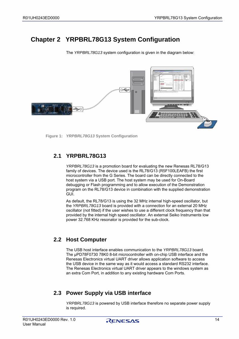
Chapter 2 YRPBRL78G13 System Configuration
The YRPBRL78G13 system configuration is given in the diagram below:
YRPBRL78G13 System Configuration
2.1 YRPBRL78G13 YRPBRL78G13 is a promotion board for evaluating the new Renesas RL78/G13 family of devices. The device used is the RL78/G13 (R5F100LEAFB) the first microcontroller from the G Series. The board can be directly connected to the host system via a USB port. The host system may be used for On-Board debugging or Flash programming and to allow execution of the Demonstration program on the RL78/G13 device in combination with the supplied demonstration GUI.
As default, the RL78/G13 is using the 32 MHz internal high-speed oscillator, but the YRPBRL78G13 board is provided with a connection for an external 20 MHz oscillator (not fitted) if the user wishes to use a different clock frequency than that provided by the internal high speed oscillator. An external Seiko Instruments low power 32.768 KHz resonator is provided for the sub-clock.
2.2 Host Computer The USB host interface enables communication to the YRPBRL78G13 board. The µPD78F0730 78K0 8-bit microcontroller with on-chip USB interface and the Renesas Electronics virtual UART driver allows application software to access the USB device in the same way as it would access a standard RS232 interface. The Renesas Electronics virtual UART driver appears to the windows system as an extra Com Port, in addition to any existing hardware Com Ports.
2.3 Power Supply via USB interface YRPBRL78G13 is powered by USB interface therefore no separate power supply is required.
Figure 1:
R01UH0243ED0000 YRPBRL78G13 Board Components
R01UH0243ED0000 Rev. 1.0 15 User Manual
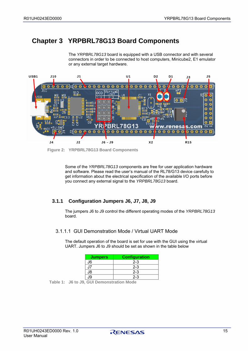
Chapter 3 YRPBRL78G13 Board Components
The YRPBRL78G13 board is equipped with a USB connector and with several connectors in order to be connected to host computers, Minicube2, E1 emulator or any external target hardware.
YRPBRL78G13 Board Components
Some of the YRPBRL78G13 components are free for user application hardware and software. Please read the user’s manual of the RL78/G13 device carefully to get information about the electrical specification of the available I/O ports before you connect any external signal to the YRPBRL78G13 board.
3.1.1 Configuration Jumpers J6, J7, J8, J9
The jumpers J6 to J9 control the different operating modes of the YRPBRL78G13 board.
3.1.1.1 GUI Demonstration Mode / Virtual UART Mode
The default operation of the board is set for use with the GUI using the virtual UART. Jumpers J6 to J9 should be set as shown in the table below
Jumpers Configuration
J6 2-3 J7 2-3 J8 2-3 J9 2-3
J6 to J9, GUI Demonstration Mode
Figure 2:
Table 1:
J4
J3
J6 – J9
D1 D2
J2
J5 USB1 J1 U1 J10
X2 R15
R01UH0243ED0000 YRPBRL78G13 Board Components
R01UH0243ED0000 Rev. 1.0 16 User Manual
3.1.1.2 On-Board Debug (OCD) Mode / Flash Programming Mode
The YRPBRL78G13 starter kit supports on-board debug mode achieved by a dedicated monitor running on the RL78/G13 device. By using the IAR C-SPY debugger, flash programming and standard debug functions i.e. code execution, single stepping, software breakpoints, memory manipulation etc. are supported.
Additionally the built-in Flash memory of the RL78/G13 device can be re-programmed by using the WriteEZ5 Flash programming GUI. Configure jumpers J6 to J9 as following to use the on-board debug or Flash programming mode:
Jumpers Configuration J6 1-2 J7 1-2 J8 1-2 J9 1-2
J6 to J9, On-Board Debug / Flash Programming Mode
For more details please refer to Chapter 8 - On-Board Debugging (OCD) of this document.
3.1.2 User’s LED D1
D1 is the Power LED. D1 is activated if power is supplied to the YRPBRL78G13 board.
3.1.3 Power LED D2
D2 is connected to the port pin “P77” of the RL78/G13. It can be used by the user for any purpose.
3.1.4 External Power Supply J4
External power can be supplied by connecting a regulated 5V DC to the connector J4 (not assembled). The operation of the stick is as follows: - USB power only Or - External supply only (Board can only be operated as stand alone only, no USB power connection). When external power supply (Vext) is used, make sure that you follow these guidelines: - Solder bridge NO1 is closed (Default is open) - Solder bridge NF1 is closed to power the 78K0/USB circuitry (Default is closed) - Vext can only be used if the stick is not connected to the PC - USB connection is not permitted (if both USB and external power supplies are used, then it can damage the board). Please refer to the schematic and the assembly drawing of the board to locate the above components.
Table 2:
R01UH0243ED0000 YRPBRL78G13 Board Components
R01UH0243ED0000 Rev. 1.0 17 User Manual
External Power Supply, Connector J4
Note: Pin number 1 is marked with a square on the assembly drawing
3.1.5 Current Measurement J3
Jumper J3 connects the 5V power supply to the VDD pin of the RL78/G13 microcontroller. The jumper can be replaced by the two leads of a Multi-meter to measure the current consumed by the RL78 device. To use this function please make sure that the Multi-meter is connected before supplying power to the starter kit. The current can be measured for all the different low power modes by using the demonstration GUI supplied to enter all different power and standby modes.
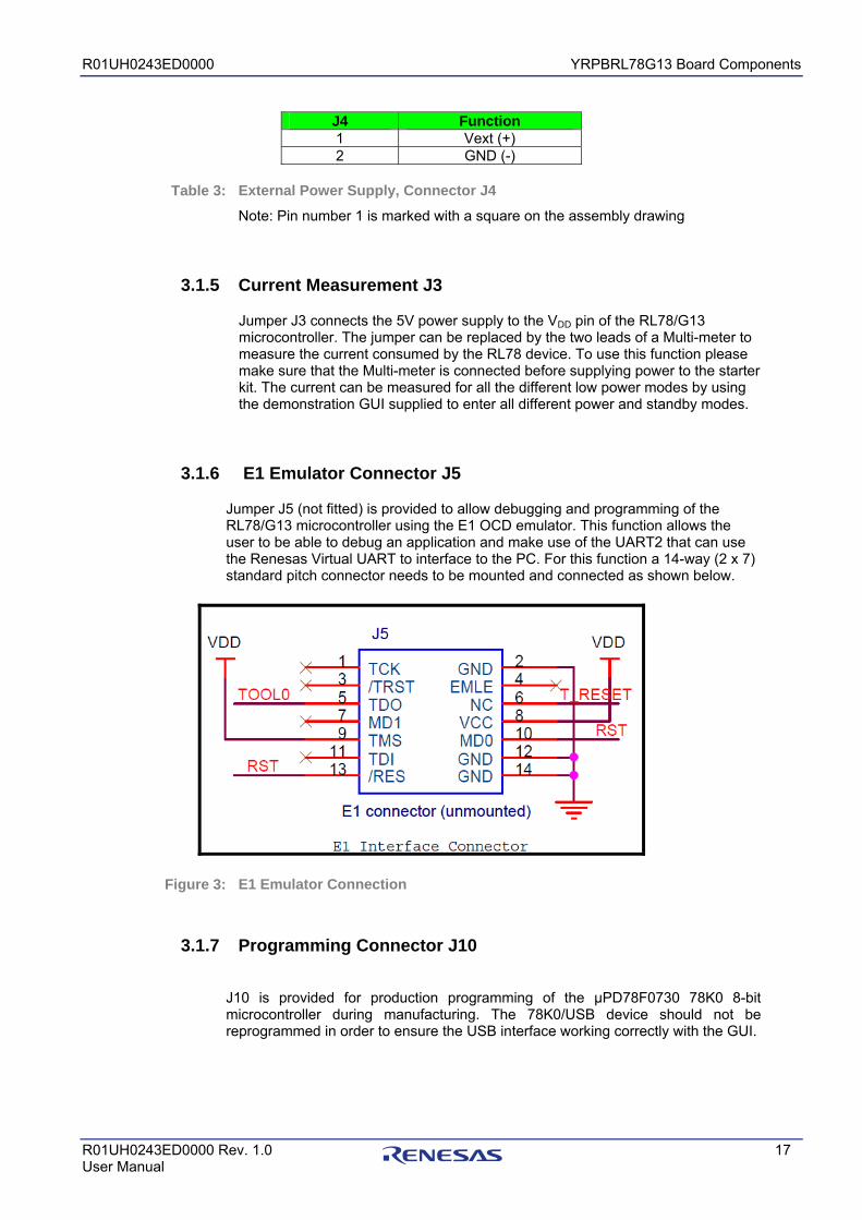
3.1.6 E1 Emulator Connector J5
Jumper J5 (not fitted) is provided to allow debugging and programming of the RL78/G13 microcontroller using the E1 OCD emulator. This function allows the user to be able to debug an application and make use of the UART2 that can use the Renesas Virtual UART to interface to the PC. For this function a 14-way (2 x 7) standard pitch connector needs to be mounted and connected as shown below.
E1 Emulator Connection
3.1.7 Programming Connector J10
J10 is provided for production programming of the µPD78F0730 78K0 8-bit microcontroller during manufacturing. The 78K0/USB device should not be reprogrammed in order to ensure the USB interface working correctly with the GUI.
J4 Function 1 Vext (+) 2 GND (-)
Table 3:
Figure 3:
R01UH0243ED0000 YRPBRL78G13 Board Components
R01UH0243ED0000 Rev. 1.0 18 User Manual
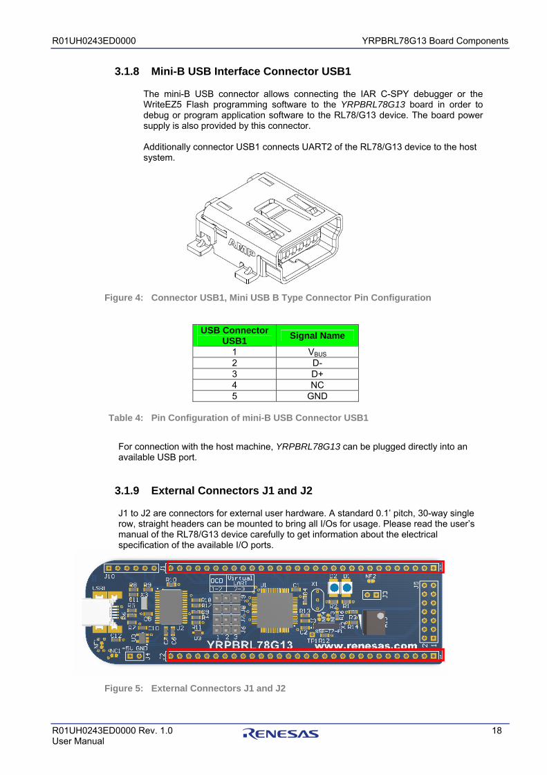
3.1.8 Mini-B USB Interface Connector USB1
The mini-B USB connector allows connecting the IAR C-SPY debugger or the WriteEZ5 Flash programming software to the YRPBRL78G13 board in order to debug or program application software to the RL78/G13 device. The board power supply is also provided by this connector.
Additionally connector USB1 connects UART2 of the RL78/G13 device to the host system.
Connector USB1, Mini USB B Type Connector Pin Configuration
USB Connector USB1 Signal Name
1 VBUS 2 D- 3 D+ 4 NC 5 GND
Pin Configuration of mini-B USB Connector USB1
For connection with the host machine, YRPBRL78G13 can be plugged directly into an available USB port.
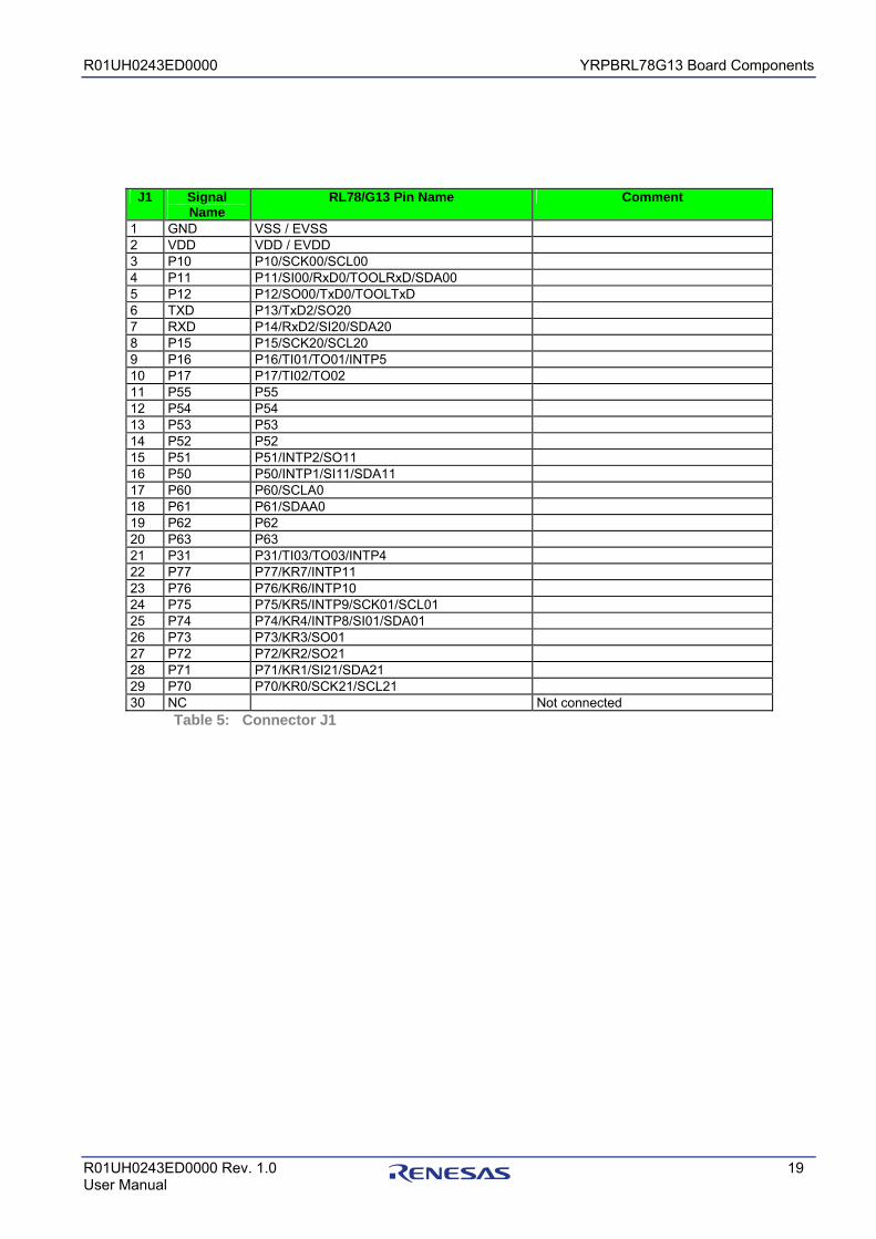
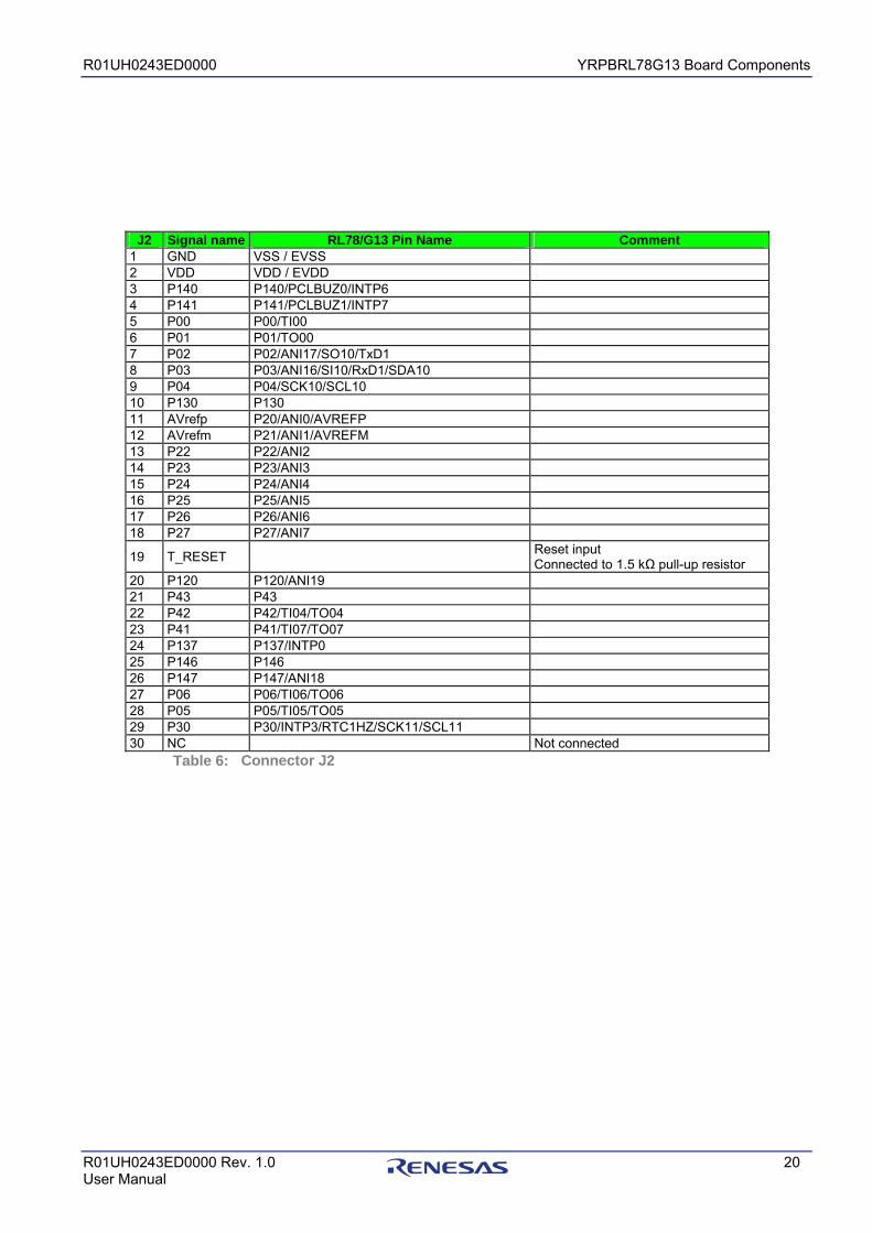
3.1.9 External Connectors J1 and J2
J1 to J2 are connectors for external user hardware. A standard 0.1’ pitch, 30-way single row, straight headers can be mounted to bring all I/Os for usage. Please read the user’s manual of the RL78/G13 device carefully to get information about the electrical specification of the available I/O ports.
External Connectors J1 and J2
Figure 4:
Table 4:
Figure 5:
R01UH0243ED0000 YRPBRL78G13 Board Components
R01UH0243ED0000 Rev. 1.0 19 User Manual
J1 Signal Name
RL78/G13 Pin Name Comment
1 GND VSS / EVSS 2 VDD VDD / EVDD 3 P10 P10/SCK00/SCL00 4 P11 P11/SI00/RxD0/TOOLRxD/SDA00 5 P12 P12/SO00/TxD0/TOOLTxD 6 TXD P13/TxD2/SO20 7 RXD P14/RxD2/SI20/SDA20 8 P15 P15/SCK20/SCL20 9 P16 P16/TI01/TO01/INTP5 10 P17 P17/TI02/TO02 11 P55 P55 12 P54 P54 13 P53 P53 14 P52 P52 15 P51 P51/INTP2/SO11 16 P50 P50/INTP1/SI11/SDA11 17 P60 P60/SCLA0 18 P61 P61/SDAA0 19 P62 P62 20 P63 P63 21 P31 P31/TI03/TO03/INTP4 22 P77 P77/KR7/INTP11 23 P76 P76/KR6/INTP10 24 P75 P75/KR5/INTP9/SCK01/SCL01 25 P74 P74/KR4/INTP8/SI01/SDA01 26 P73 P73/KR3/SO01 27 P72 P72/KR2/SO21 28 P71 P71/KR1/SI21/SDA21 29 P70 P70/KR0/SCK21/SCL21 30 NC Not connected
Connector J1
Table 5:
R01UH0243ED0000 YRPBRL78G13 Board Components
R01UH0243ED0000 Rev. 1.0 20 User Manual
J2 Signal name RL78/G13 Pin Name Comment 1 GND VSS / EVSS 2 VDD VDD / EVDD 3 P140 P140/PCLBUZ0/INTP6 4 P141 P141/PCLBUZ1/INTP7 5 P00 P00/TI00 6 P01 P01/TO00 7 P02 P02/ANI17/SO10/TxD1 8 P03 P03/ANI16/SI10/RxD1/SDA10 9 P04 P04/SCK10/SCL10 10 P130 P130 11 AVrefp P20/ANI0/AVREFP 12 AVrefm P21/ANI1/AVREFM 13 P22 P22/ANI2 14 P23 P23/ANI3 15 P24 P24/ANI4 16 P25 P25/ANI5 17 P26 P26/ANI6 18 P27 P27/ANI7
19 T_RESET Reset input Connected to 1.5 kΩ pull-up resistor
20 P120 P120/ANI19 21 P43 P43 22 P42 P42/TI04/TO04 23 P41 P41/TI07/TO07 24 P137 P137/INTP0 25 P146 P146 26 P147 P147/ANI18 27 P06 P06/TI06/TO06 28 P05 P05/TI05/TO05 29 P30 P30/INTP3/RTC1HZ/SCK11/SCL11 30 NC Not connected
Connector J2
Table 6:
R01UH0243ED0000 YRPBRL78G13 Board Components
R01UH0243ED0000 Rev. 1.0 21 User Manual
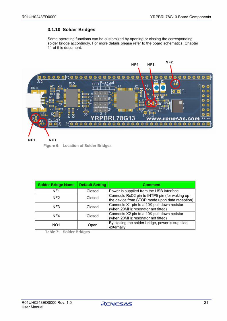
3.1.10 Solder Bridges
Some operating functions can be customized by opening or closing the corresponding solder bridge accordingly. For more details please refer to the board schematics, Chapter 11 of this document.
Location of Solder Bridges
Solder Bridge Name Default Setting Comment NF1 Closed Power is supplied from the USB interface
NF2 Closed Connects RxD2 pin to INTP5 pin (for waking up the device from STOP mode upon data reception)
NF3 Closed Connects X1 pin to a 10K pull-down resistor (when 20MHz resonator not fitted)
NF4 Closed Connects X2 pin to a 10K pull-down resistor (when 20MHz resonator not fitted)
NO1 Open By closing the solder bridge, power is supplied externally
Solder Bridges
Figure 6:
Table 7:
NO1 NF1
NF2 NF3 NF4
R01UH0243ED0000 YRPBRL78G13 Board Components
R01UH0243ED0000 Rev. 1.0 22 User Manual
3.1.11 Seiko Instruments Inc. Low Power 32 KHz Resonator
The YRPBRL78G13 board is fitted with an external 32 KHz resonator (X2) characterized specifically for the RL78/G13 device supplied by Seiko Instruments Inc. This is a specially designed low power resonator designed to support the very low power consumption of the RL78/G13 family. For more technical details on this device and contact details for Seiko Instruments, please refer to chapter 13.
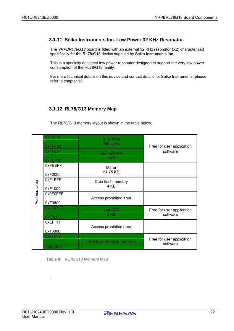
3.1.12 RL78/G13 Memory Map
The RL78/G13 memory layout is shown in the table below.
0xFFFFF 0xFFF00
SFR Area 256 bytes Free for user application
0xFFEFF software 0xFEF00
Internal RAM 4KB
0xFEEFF 0xF2000
Mirror 51.75 KB
0xF1FFF 0xF1000
Data flash memory 4 KB
0x0F0FFF
0xF0800 Access prohibited area
0x0F07FF 0xF0000
2nd SFR 2 KB
Free for user application software
0xEFFFF Access prohibited area 0x10000 0x0FFFF 64 KB code flash memory
Add
ress
are
a
0x00000
Free for user application software
RL78/G13 Memory Map
.
Table 8:
R01UH0243ED0000 Getting Started
R01UH0243ED0000 Rev. 1.0 23 User Manual
Chapter 4 Getting Started
The default setting of the YRPBRL78G13 board is set for demonstration use with the GUI. The DVD included and quick start guide will take the user through the installation procedure Initially the user will be required to select between the two installation options that are available to the user:
1. Quick Start Installation This will just install the GUI, drivers and associated documentation.
2. Complete Installation
This will install the GUI full documentation and all of the development tools.
The Quick Start Guide will automatically open after the installation process to guide the user through the initial set-up and connection to the PC and GUI. Please note as the communication interface between the host computer and the YRPBRL78G13 board is the USB port interface, the hardware and software must be installed properly.
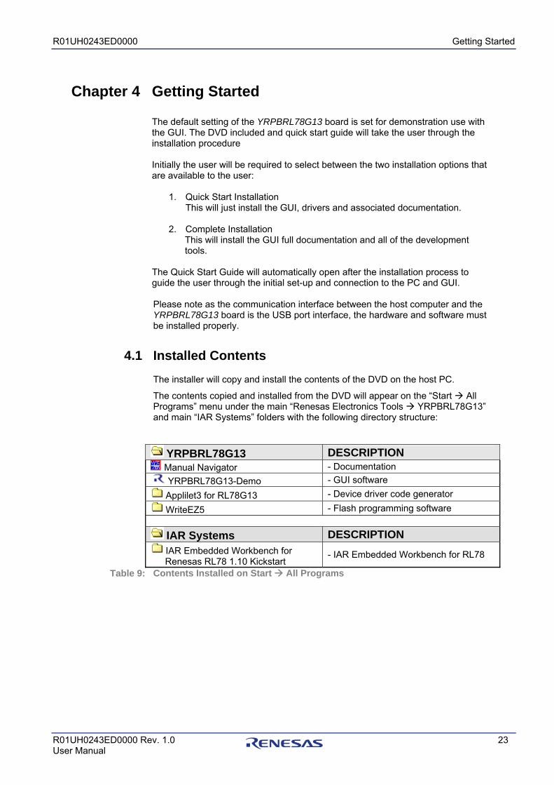
4.1 Installed Contents The installer will copy and install the contents of the DVD on the host PC.
The contents copied and installed from the DVD will appear on the “Start All Programs” menu under the main “Renesas Electronics Tools YRPBRL78G13” and main “IAR Systems” folders with the following directory structure:
YRPBRL78G13 DESCRIPTION Manual Navigator - Documentation
YRPBRL78G13-Demo - GUI software
Applilet3 for RL78G13 - Device driver code generator
WriteEZ5 - Flash programming software
IAR Systems DESCRIPTION IAR Embedded Workbench for Renesas RL78 1.10 Kickstart
- IAR Embedded Workbench for RL78
Contents Installed on Start All Programs
Table 9:
R01UH0243ED0000 Hardware Installation
R01UH0243ED0000 Rev. 1.0 24 User Manual
Chapter 5 Hardware Installation
After unpacking the YRPBRL78G13 promotion board, connect the USB cable supplied to the board. The connection of the board to the Host PC should be done in conjunction with Chapter 6.5 - USB Driver Installation. This driver must be installed before the user can use the GUI or debugger.
R01UH0243ED0000 Software Installation
R01UH0243ED0000 Rev. 1.0 25 User Manual
Chapter 6 Software Installation
The YRPBRL78G13 package comes with several software demonstration packages:
o IAR Systems Embedded Workbench for RL78, including C compiler, assembler, linker, librarian and IAR C-SPY debugger
o A project built for use with the IAR debugger is included
o WriteEZ5 Flash programming GUI software to allow Flash programming of the RL78/G13 internal Flash memory
o GUI to be run with the main demonstration programs
o Source code for the demonstration and debugger programs
The IAR Systems Embedded Workbench environment and the WriteEZ5 Flash programming GUI must be installed on your PC. For detailed installation hints, refer to the following chapters and to the corresponding documentation of the IAR Embedded Workbench for RL78 and WriteEZ5.
6.1 IAR Systems Embedded Workbench for RL78 Installation This program will be installed automatically by the installer on the DVD when the full installation is selected. If the quick install (GUI) was previously selected, please insert the DVD again and select the full installation.
6.2 WriteEZ5 Flash Programming GUI Installation This program will be installed automatically by the installer on the DVD when the full installation is selected. If the quick install (GUI) was selected, please insert the DVD again and select the full installation.
6.3 GUI Installation This program will be installed automatically by the installer on the DVD for both quick start and full installation.
6.4 Sample Programs Installation The DVD installer will automatically install the sample debugger programs and the demonstration source code when the full installation is selected. If the quick start installation was previously selected, then please insert the DVD again and select the full installation.
The programs will be located in the following directories on the host PC:
C:\Workspace\RPB\RL78G13\IAR Sample Projects\Debugging Project\ C:\Workspace\RPB\RL78G13\IAR Sample Projects\GUI Demo Source Code\
R01UH0243ED0000 Software Installation
R01UH0243ED0000 Rev. 1.0 26 User Manual
6.5 USB driver installation In order to use the YRPBRL78G13 board in combination with IAR C-SPY debugger or the WriteEZ5 Flash programming GUI software, “Renesas Electronics Starter Kit Virtual UART” USB driver must be installed on the host machine.
Please follow according to version of Windows OS. Please check your Windows version, and follow the instructions:
Installation on Windows XP Chapter 6.5.1
Installation on Windows Vista Chapter 6.5.2
Installation on Windows 7 Chapter 6.5.3
Please insert the YRPBRL78G13 DVD in your DVD drive in order to proceed with the USB driver installation.
After the installation, please go to Chapter 6.5.4 – Confirmation of USB Driver Installation.
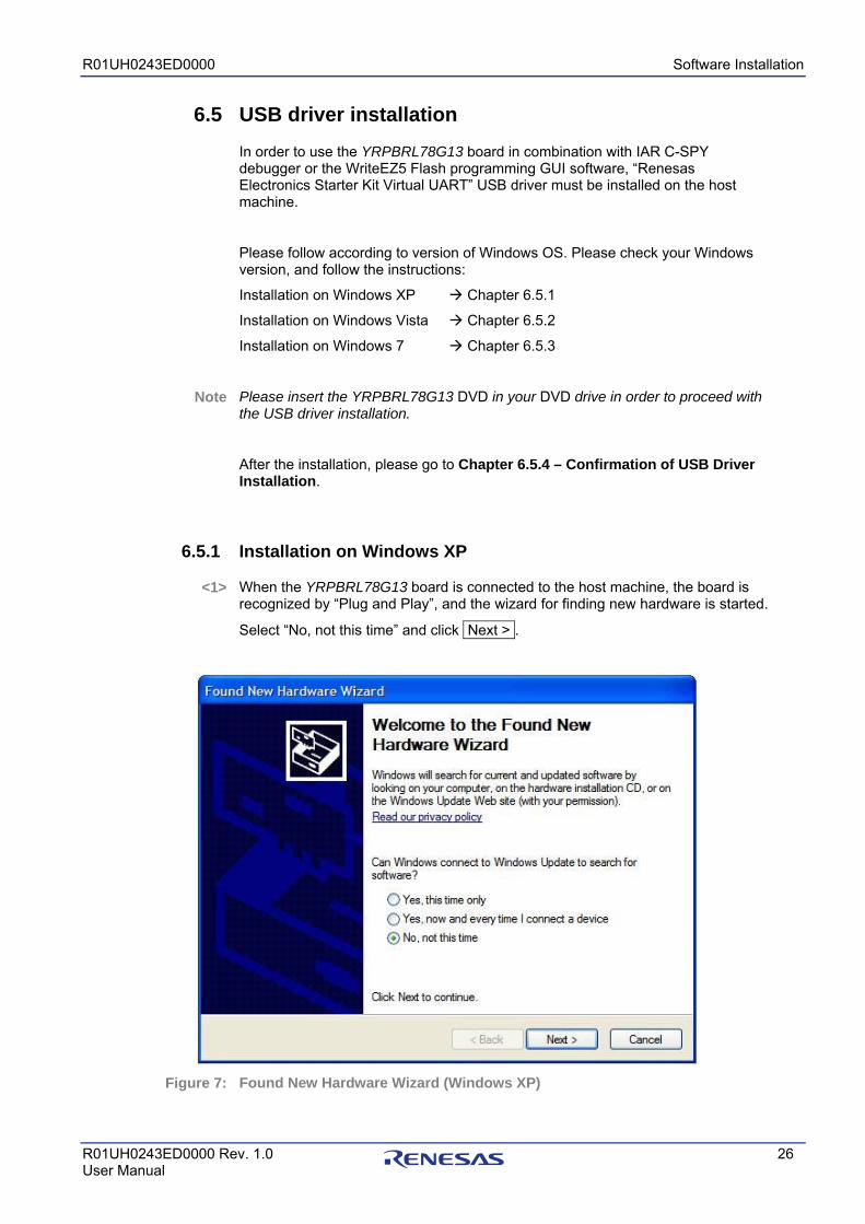
6.5.1 Installation on Windows XP
When the YRPBRL78G13 board is connected to the host machine, the board is recognized by “Plug and Play”, and the wizard for finding new hardware is started.
Select “No, not this time” and click Next > .
Found New Hardware Wizard (Windows XP)
Note
<1>
Figure 7:
R01UH0243ED0000 Software Installation
R01UH0243ED0000 Rev. 1.0 27 User Manual
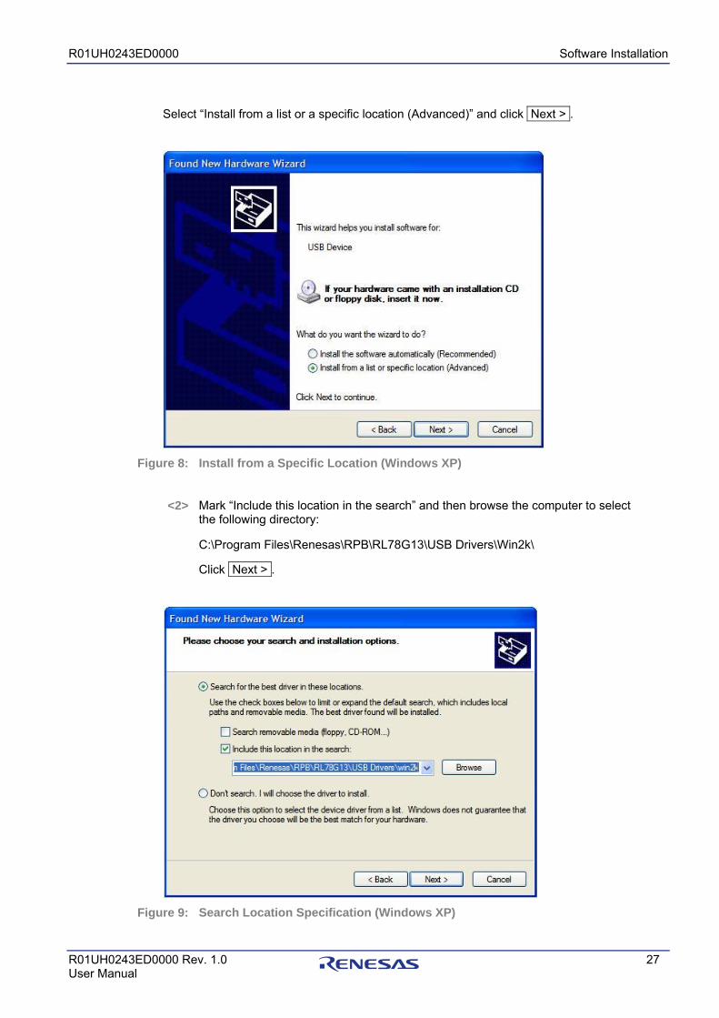
Select “Install from a list or a specific location (Advanced)” and click Next > .
Install from a Specific Location (Windows XP)
Mark “Include this location in the search” and then browse the computer to select the following directory:
C:\Program Files\Renesas\RPB\RL78G13\USB Drivers\Win2k\
Click Next > .
Search Location Specification (Windows XP)
Figure 8:
<2>
Figure 9:
R01UH0243ED0000 Software Installation
R01UH0243ED0000 Rev. 1.0 28 User Manual
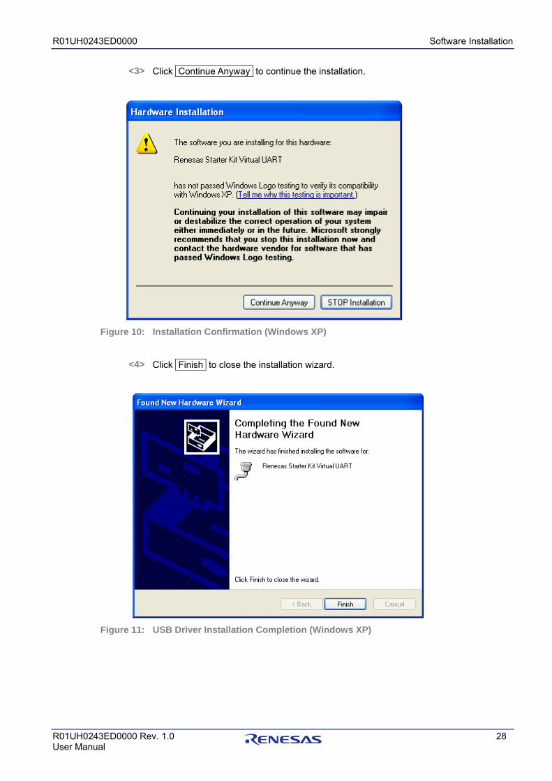
Click Continue Anyway to continue the installation.
Installation Confirmation (Windows XP)
Click Finish to close the installation wizard.
USB Driver Installation Completion (Windows XP)
<3>
Figure 10:
<4>
Figure 11:
R01UH0243ED0000 Software Installation
R01UH0243ED0000 Rev. 1.0 29 User Manual
6.5.2 Installation on Windows Vista
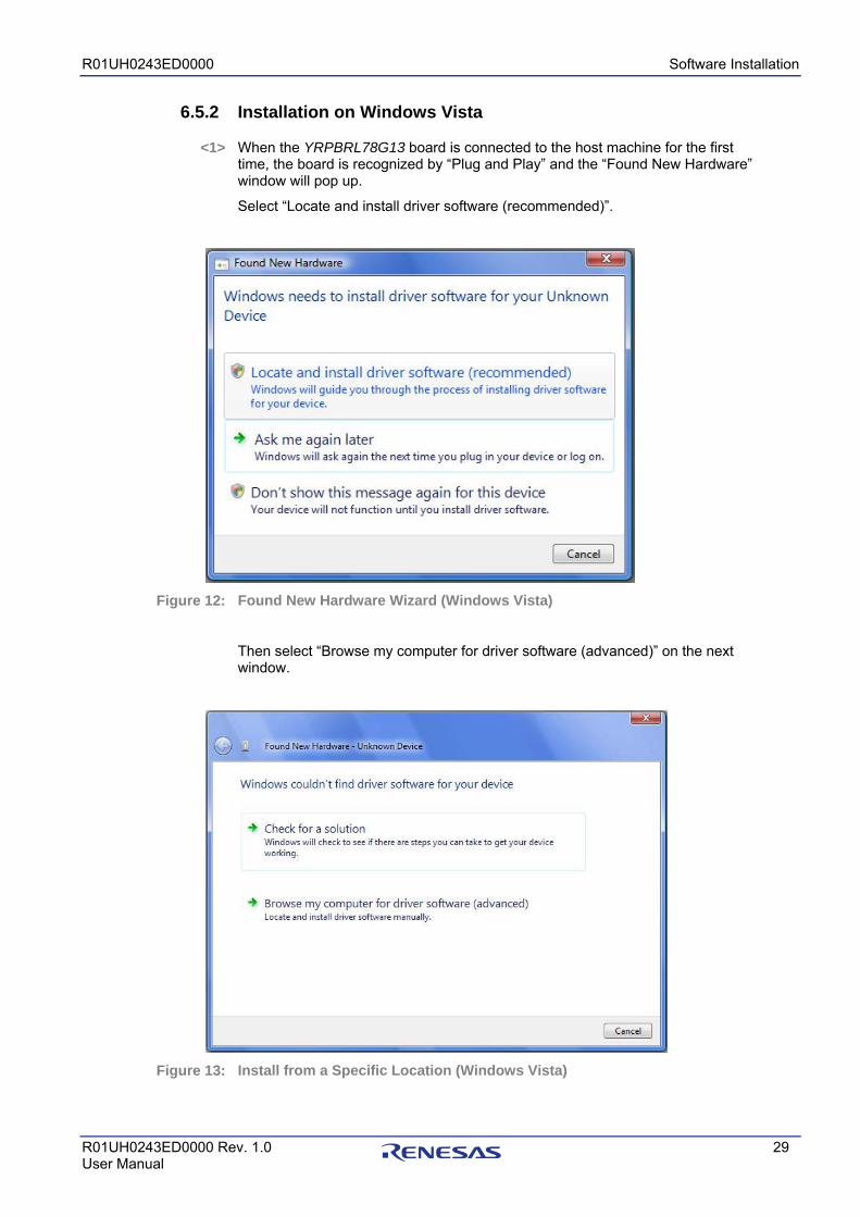
When the YRPBRL78G13 board is connected to the host machine for the first time, the board is recognized by “Plug and Play” and the “Found New Hardware” window will pop up.
Select “Locate and install driver software (recommended)”.
Found New Hardware Wizard (Windows Vista)
Then select “Browse my computer for driver software (advanced)” on the next window.
Install from a Specific Location (Windows Vista)
<1>
Figure 12:
Figure 13:
R01UH0243ED0000 Software Installation
R01UH0243ED0000 Rev. 1.0 30 User Manual
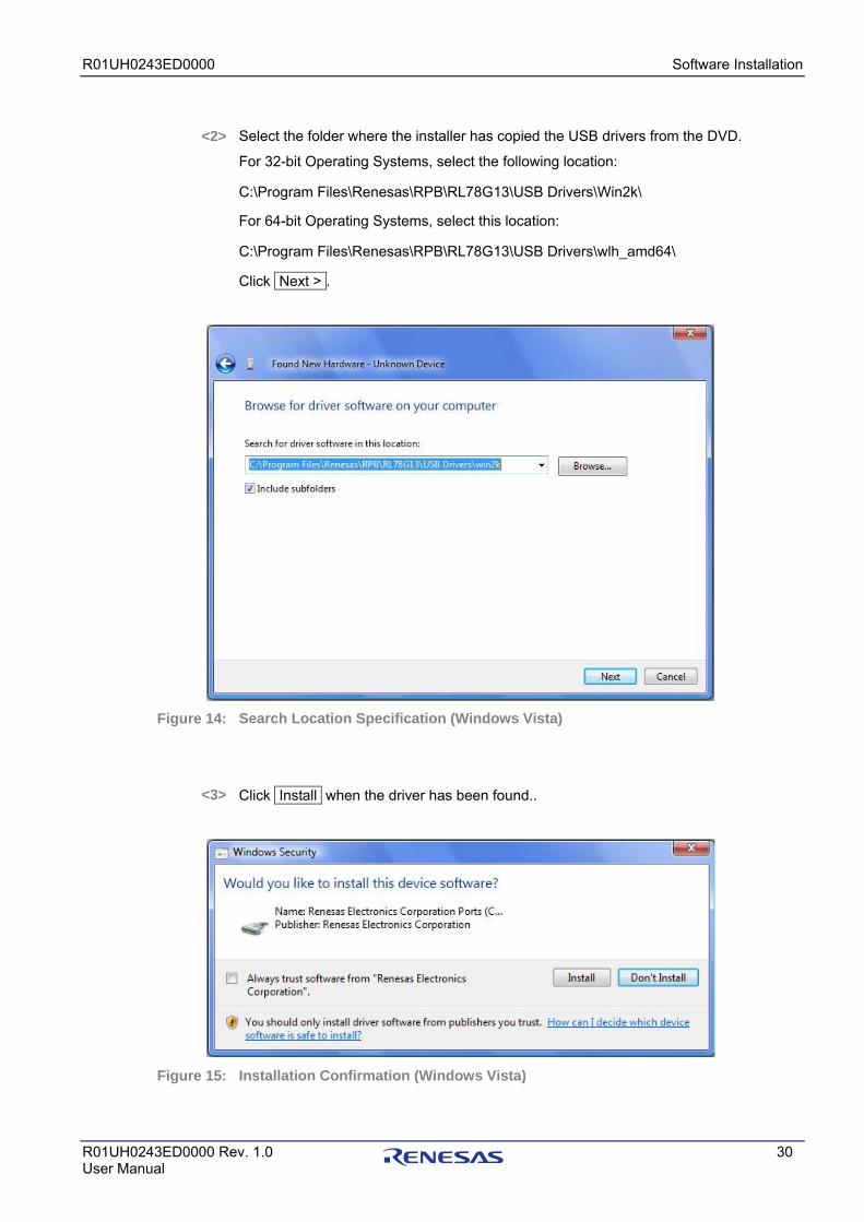
Select the folder where the installer has copied the USB drivers from the DVD.
For 32-bit Operating Systems, select the following location:
C:\Program Files\Renesas\RPB\RL78G13\USB Drivers\Win2k\
For 64-bit Operating Systems, select this location:
C:\Program Files\Renesas\RPB\RL78G13\USB Drivers\wlh_amd64\
Click Next > .
Search Location Specification (Windows Vista)
Click Install when the driver has been found..
Installation Confirmation (Windows Vista)
<2>
Figure 14:
<3>
Figure 15:
R01UH0243ED0000 Software Installation
R01UH0243ED0000 Rev. 1.0 31 User Manual
Click Close to close the installation wizard.
USB Driver Installation Completion (Windows Vista)
6.5.3 Installation on Windows 7
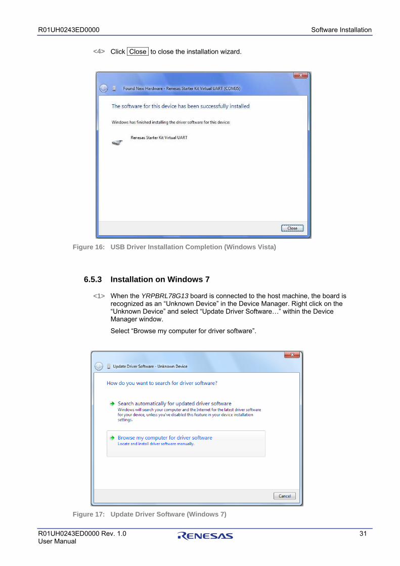
When the YRPBRL78G13 board is connected to the host machine, the board is recognized as an “Unknown Device” in the Device Manager. Right click on the “Unknown Device” and select “Update Driver Software…” within the Device Manager window.
Select “Browse my computer for driver software”.
Update Driver Software (Windows 7)
<4>
Figure 16:
<1>
Figure 17:
R01UH0243ED0000 Software Installation
R01UH0243ED0000 Rev. 1.0 32 User Manual
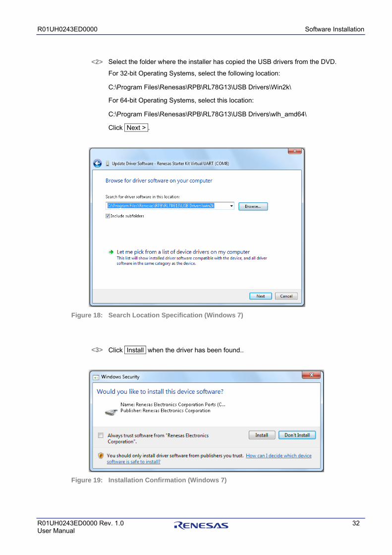
Select the folder where the installer has copied the USB drivers from the DVD.
For 32-bit Operating Systems, select the following location:
C:\Program Files\Renesas\RPB\RL78G13\USB Drivers\Win2k\
For 64-bit Operating Systems, select this location:
C:\Program Files\Renesas\RPB\RL78G13\USB Drivers\wlh_amd64\
Click Next > .
Search Location Specification (Windows 7)
Click Install when the driver has been found..
Installation Confirmation (Windows 7)
<2>
Figure 18:
<3>
Figure 19:
R01UH0243ED0000 Software Installation
R01UH0243ED0000 Rev. 1.0 33 User Manual
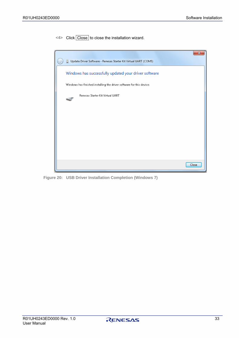
Click Close to close the installation wizard.
USB Driver Installation Completion (Windows 7)
<4>
Figure 20:
R01UH0243ED0000 Software Installation
R01UH0243ED0000 Rev. 1.0 34 User Manual
6.5.4 Confirmation of USB Driver Installation
After installing the USB driver, check that the driver has been installed correctly, according to the procedure below.
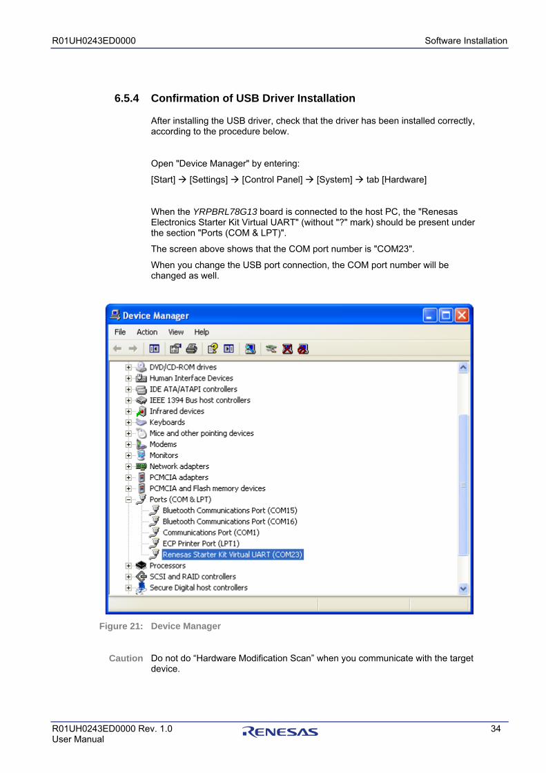
Open "Device Manager" by entering:
[Start] [Settings] [Control Panel] [System] tab [Hardware]
When the YRPBRL78G13 board is connected to the host PC, the "Renesas Electronics Starter Kit Virtual UART" (without "?" mark) should be present under the section "Ports (COM & LPT)".
The screen above shows that the COM port number is "COM23".
When you change the USB port connection, the COM port number will be changed as well.
Device Manager
Do not do “Hardware Modification Scan” when you communicate with the target device.
Figure 21:
Caution
R01UH0243ED0000 How to Use WriteEZ5 Flash Programming Software
R01UH0243ED0000 Rev. 1.0 35 User Manual
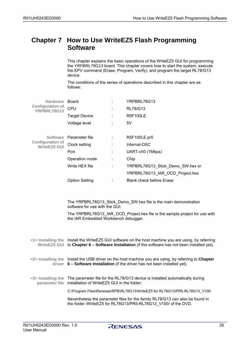
Chapter 7 How to Use WriteEZ5 Flash Programming Software
This chapter explains the basic operations of the WriteEZ5 GUI for programming the YRPBRL78G13 board. This chapter covers how to start the system, execute the EPV command (Erase, Program, Verify), and program the target RL78/G13 device.
The conditions of the series of operations described in this chapter are as follows:
Board : YRPBRL78G13
CPU : RL78/G13
Target Device : R5F100LE
Voltage level : 5V
Parameter file : R5F100LE.pr5
Clock setting : Internal-OSC
Port : UART-ch0 (1Mbps)
Operation mode : Chip
Write HEX file : YRPBRL78G13_Stick_Demo_SW.hex or
YRPBRL78G13_IAR_OCD_Project.hex
Option Setting : Blank check before Erase
The YRPBRL78G13_Stick_Demo_SW.hex file is the main demonstration software for use with the GUI.
The YRPBRL78G13_IAR_OCD_Project.hex file is the sample project for use with the IAR Embedded Workbench debugger.
Install the WriteEZ5 GUI software on the host machine you are using, by referring to Chapter 6 – Software Installation (if the software has not been installed yet).
Install the USB driver on the host machine you are using, by referring to Chapter 6 – Software Installation (if the driver has not been installed yet).
The parameter file for the RL78/G13 device is installed automatically during installation of WriteEZ5 GUI in the folder:
C:\Program Files\Renesas\RPB\RL78G13\WriteEZ5 for RL78G13\PR5-RL78G13_V100
Nevertheless the parameter files for the family RL78/G13 can also be found in the folder /WriteEZ5 for RL78G13/PR5-RL78G13_V100/ of the DVD.
Hardware Configuration of
YRPBRL78G13
Software Configuration of
WriteEZ5 GUI
<1> Installing the WriteEZ5 GUI
<2> Installing the driver
<3> Installing the parameter file
R01UH0243ED0000 How to Use WriteEZ5 Flash Programming Software
R01UH0243ED0000 Rev. 1.0 36 User Manual
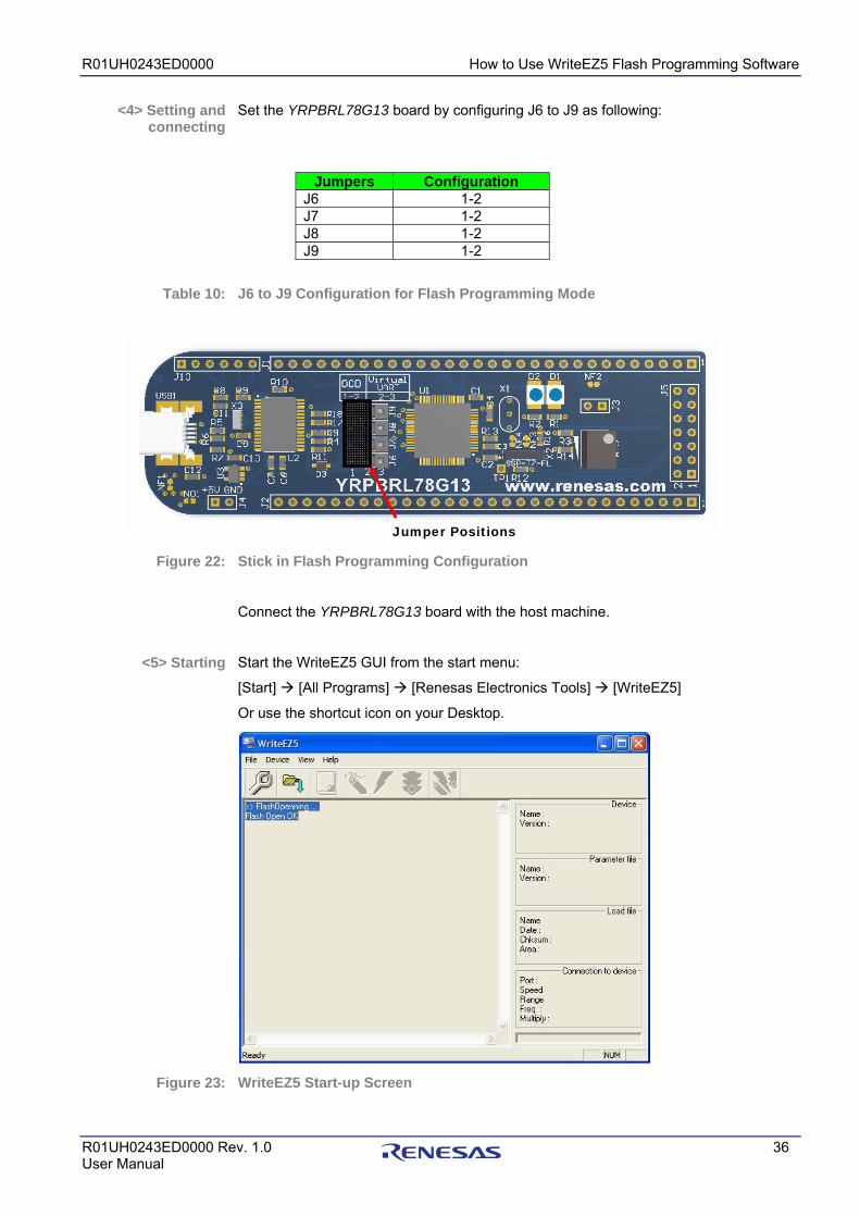
Set the YRPBRL78G13 board by configuring J6 to J9 as following:
Jumpers Configuration
J6 1-2 J7 1-2 J8 1-2 J9 1-2
J6 to J9 Configuration for Flash Programming Mode
Stick in Flash Programming Configuration
Connect the YRPBRL78G13 board with the host machine.
Start the WriteEZ5 GUI from the start menu:
[Start] [All Programs] [Renesas Electronics Tools] [WriteEZ5]
Or use the shortcut icon on your Desktop.
WriteEZ5 Start-up Screen
<4> Setting and connecting
Table 10:
Figure 22:
<5> Starting
Figure 23:
Jumper Positions
R01UH0243ED0000 How to Use WriteEZ5 Flash Programming Software
R01UH0243ED0000 Rev. 1.0 37 User Manual
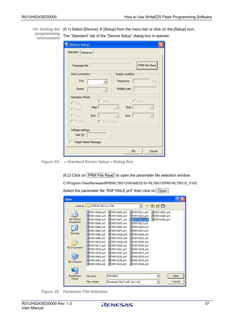
(6.1) Select [Device] [Setup] from the menu bar or click on the [Setup] icon.
The “Standard” tab of the “Device Setup” dialog box is opened:
« Standard Device Setup » Dialog Box
(6.2) Click on PRM File Read to open the parameter file selection window.
C:\Program Files\Renesas\RPB\RL78G13\WriteEZ5 for RL78G13\PR5-RL78G13_V100
Select the parameter file “R5F100LE.pr5” then click on Open .
Parameter File Selection
<6> Setting the programming environment
Figure 24:
Figure 25:
R01UH0243ED0000 How to Use WriteEZ5 Flash Programming Software
R01UH0243ED0000 Rev. 1.0 38 User Manual
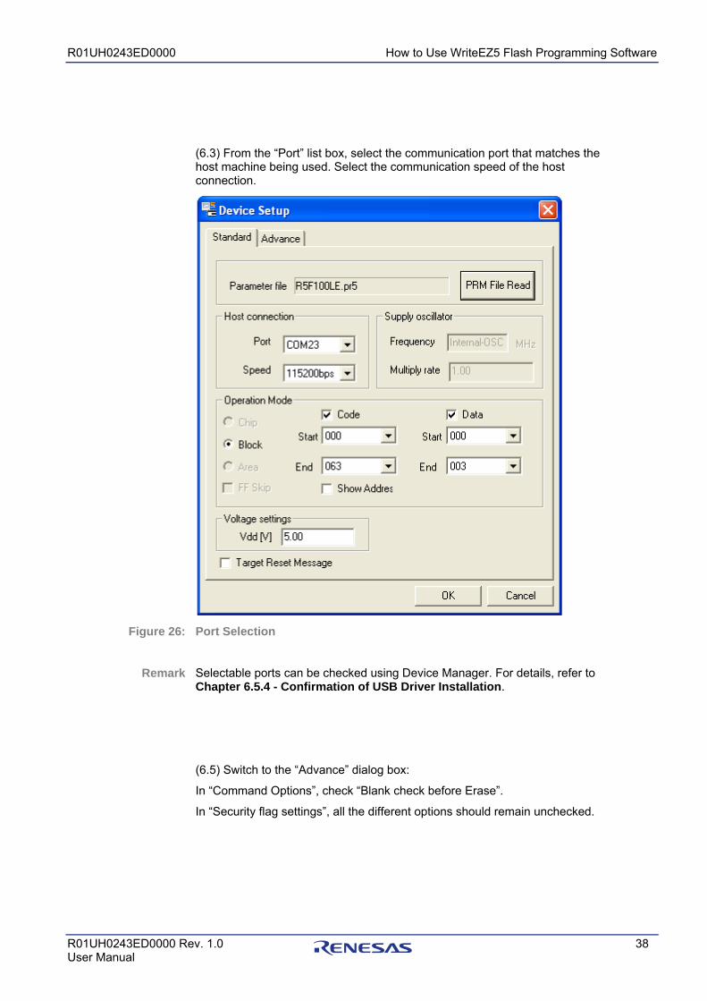
(6.3) From the “Port” list box, select the communication port that matches the host machine being used. Select the communication speed of the host connection.
Port Selection
Selectable ports can be checked using Device Manager. For details, refer to Chapter 6.5.4 - Confirmation of USB Driver Installation.
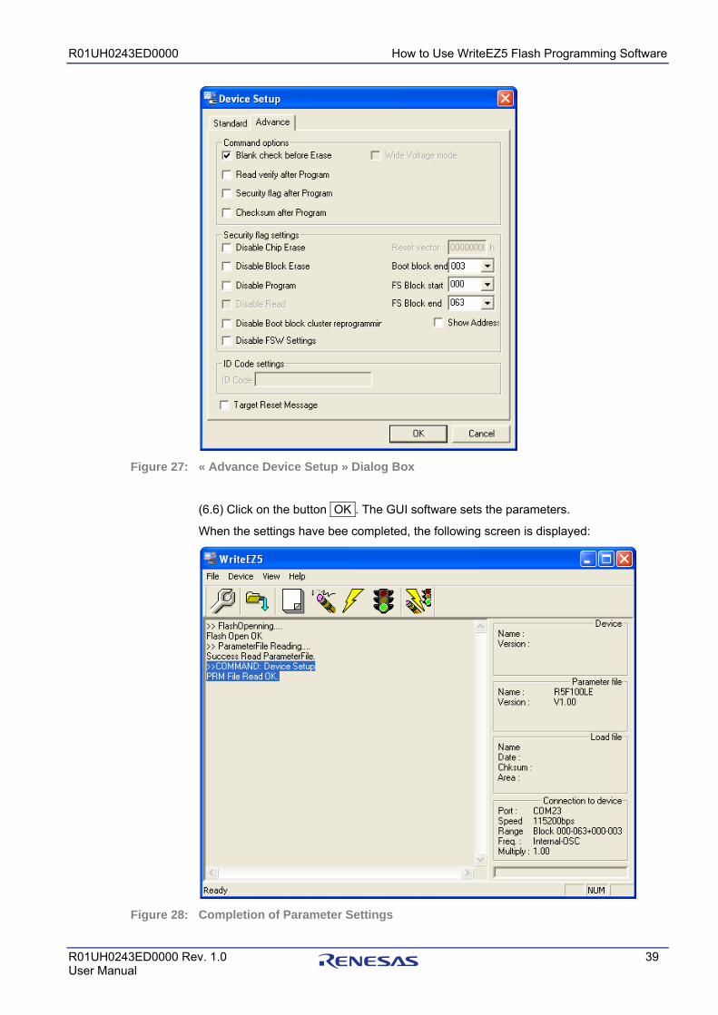
(6.5) Switch to the “Advance” dialog box:
In “Command Options”, check “Blank check before Erase”.
In “Security flag settings”, all the different options should remain unchecked.
Figure 26:
Remark
R01UH0243ED0000 How to Use WriteEZ5 Flash Programming Software
R01UH0243ED0000 Rev. 1.0 39 User Manual
« Advance Device Setup » Dialog Box
(6.6) Click on the button OK . The GUI software sets the parameters.
When the settings have bee completed, the following screen is displayed:
Completion of Parameter Settings
Figure 27:
Figure 28:
R01UH0243ED0000 How to Use WriteEZ5 Flash Programming Software
R01UH0243ED0000 Rev. 1.0 40 User Manual
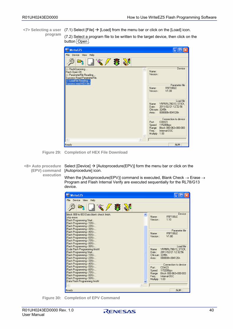
(7.1) Select [File] [Load] from the menu bar or click on the [Load] icon.
(7.2) Select a program file to be written to the target device, then click on the button Open .
Completion of HEX File Download
Select [Device] [Autoprocedure(EPV)] form the menu bar or click on the [Autoprocedure] icon.
When the [Autoprocedure(EPV)] command is executed, Blank Check → Erase → Program and Flash Internal Verify are executed sequentially for the RL78/G13 device.
Completion of EPV Command
<7> Selecting a user program
Figure 29:
<8> Auto procedure (EPV) command
execution
Figure 30:
R01UH0243ED0000 How to Use WriteEZ5 Flash Programming Software
R01UH0243ED0000 Rev. 1.0 41 User Manual
Select [File] [Quit] to terminate the GUI software. All settings executed so are saved, so that those settings can be reused when the WriteEZ5 GUI is restarted.
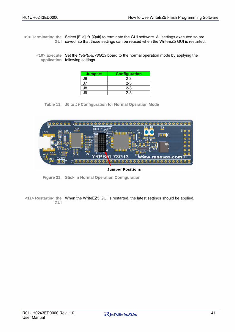
Set the YRPBRL78G13 board to the normal operation mode by applying the following settings.
Jumpers Configuration J6 2-3 J7 2-3 J8 2-3 J9 2-3
J6 to J9 Configuration for Normal Operation Mode
Stick in Normal Operation Configuration
When the WriteEZ5 GUI is restarted, the latest settings should be applied.
<9> Terminating the GUI
<10> Execute application
Table 11:
Figure 31:
<11> Restarting the GUI
Jumper Positions
R01UH0243ED0000 On-Board Debugging (OCD)
R01UH0243ED0000 Rev. 1.0 42 User Manual
Chapter 8 On-Board Debugging (OCD)
Before using the On-Board debug function of the YRPBRL78G13 board together with the IAR C-SPY debugger please ensure that the Virtual UART USB driver has been installed. Please refer to section 6.5 for the installation of the USB driver.
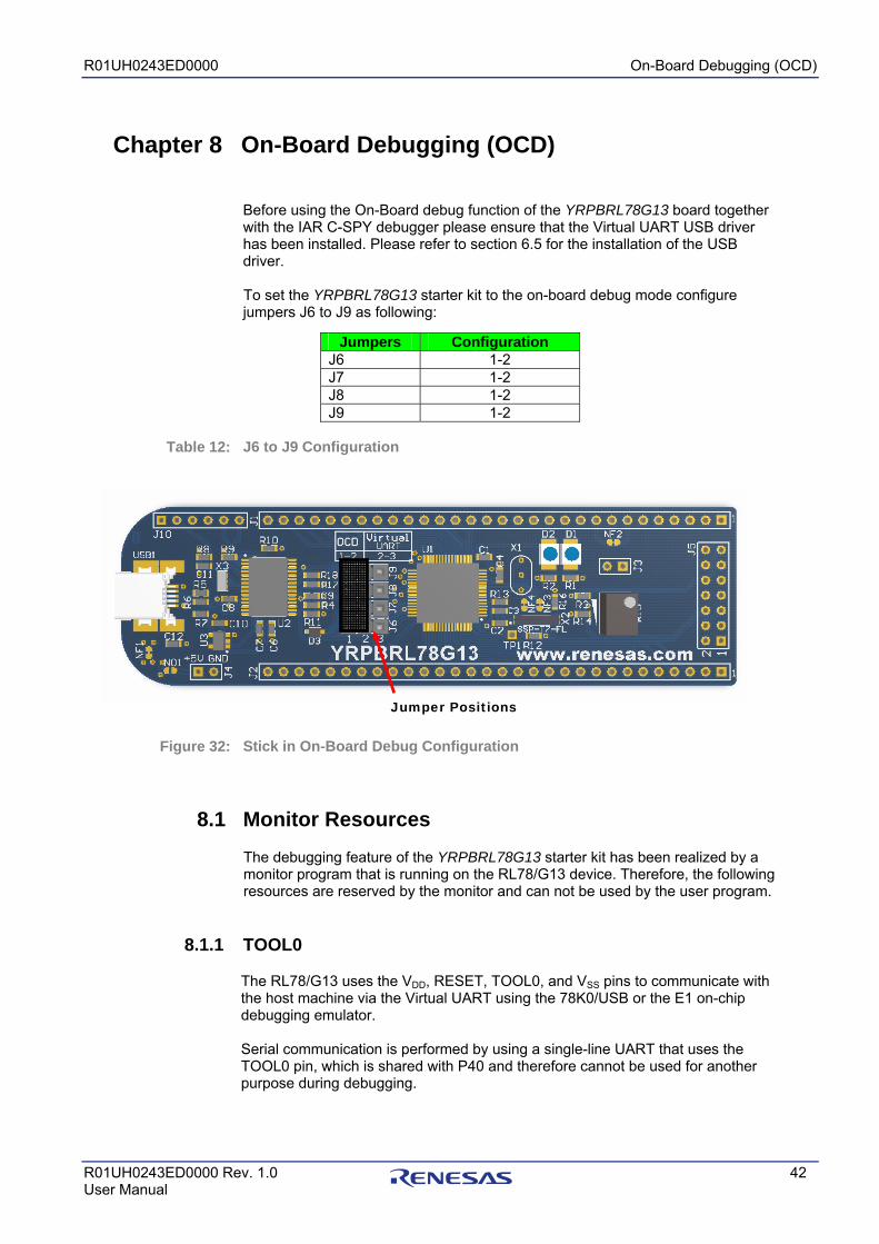
To set the YRPBRL78G13 starter kit to the on-board debug mode configure jumpers J6 to J9 as following:
J6 to J9 Configuration
Stick in On-Board Debug Configuration
8.1 Monitor Resources The debugging feature of the YRPBRL78G13 starter kit has been realized by a monitor program that is running on the RL78/G13 device. Therefore, the following resources are reserved by the monitor and can not be used by the user program.
8.1.1 TOOL0
The RL78/G13 uses the VDD, RESET, TOOL0, and VSS pins to communicate with the host machine via the Virtual UART using the 78K0/USB or the E1 on-chip debugging emulator. Serial communication is performed by using a single-line UART that uses the TOOL0 pin, which is shared with P40 and therefore cannot be used for another purpose during debugging.
Jumpers Configuration J6 1-2 J7 1-2 J8 1-2 J9 1-2
Table 12:
Figure 32:
Jumper Positions
R01UH0243ED0000 On-Board Debugging (OCD)
R01UH0243ED0000 Rev. 1.0 43 User Manual
8.1.2 Memory Area
Four different areas (24 bytes in total) are reserved for placing the debug monitor program in the flash memory of the RL78/G13 device, so user programs or data cannot be allocated in these spaces. When using the on-chip debug function, these spaces must be secured so as not to be used by the user program. Moreover, this area must not be rewritten by the user program. The monitor reserves 6 bytes of the global stack area by halting the user program, caused by a forcible break (debugger stop command) or a software breakpoint.
8.2 IAR Sample Program Description
8.2.1 General Introduction
The sample program is located in a single directory, which will be called main-directory of the sample. This main directory contains the complete project including all output files of the development tool. The workspace file “YRPBRL78G13_IAR_OCD_Project” is located on top of the sample program directories. The project has been created using the Applilet software tool to generate the different source and header files. Any changes that the user wishes to make to the project’s peripheral initializations should ideally be done by changing the settings in the Applilet tool.
YRPBRL78G13_IAR_OCD_Project RL78/G13 project and output files
Debug Debug output files for IAR C-SPY debugger
applilet3_src C source files, header files and Linker control file
Release Release output files, i.e. Intel HEX file
settings Configuration files, IAR Embedded Workbench
user_src Empty directory available for new user source files
YRPBRL78G13_IAR_OCD_Project.dep Dependency information file, IAR Embedded Workbench
YRPBRL78G13_IAR_OCD_Project.ewd Project setting file, IAR C-SPY debugger
YRPBRL78G13_IAR_OCD_Project.ewp Project file, IAR Embedded Workbench
YRPBRL78G13_IAR_OCD_Project.eww Workspace file, IAR Embedded Workbench RL78
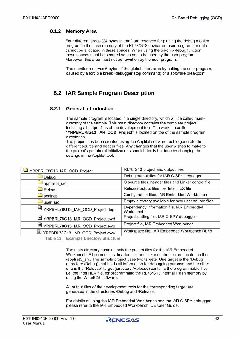
Example Directory Structure
The main directory contains only the project files for the IAR Embedded Workbench. All source files, header files and linker control file are located in the /applilet3_src. The sample project uses two targets. One target is the “Debug” (directory /Debug) that holds all information for debugging purpose and the other one is the “Release” target (directory /Release) contains the programmable file, i.e. the Intel HEX file, for programming the RL78/G13 internal Flash memory by using the WriteEZ5 software.
All output files of the development tools for the corresponding target are generated in the directories /Debug and /Release.
For details of using the IAR Embedded Workbench and the IAR C-SPY debugger please refer to the IAR Embedded Workbench IDE User Guide.
Table 13:
R01UH0243ED0000 On-Board Debugging (OCD)
R01UH0243ED0000 Rev. 1.0 44 User Manual
8.2.2 Functionality
The sample project shows a simple demonstration of Interval Timer usage, ADC usage and interrupts handling. Interval Timer is setup to generate an interrupt every 200 milliseconds which toggles the LED on P77. When turning the potentiometer to increase the ADC input voltage, the timer interrupt interval is reduced which results in toggling the LED faster.
8.2.3 Required Resources
The sample program uses the following peripheral resources of the R5F100LE device: • Interval Timer • ADC (Potentiometer input) • Port 7 Pin 7 (P77)
8.2.4 Project Structure
The project consists of the following software modules:
8.2.4.1 System Initialization
All the system initialization including Clock, ADC, Interval Timer, Port, and On-board OCD resources are within this module. The files generated for this module are: • CG_ad.c • CG_it.c • CG_port.c • CG_system.c • CG_systeminit.c
8.2.4.2 Main Loop
This module includes the main loop and additional system initialization such as Security ID for OCD and Option Byes settings The file generated for this module is:
• CG_main.c
8.2.4.3 Interrupt Handling
This module includes the interrupt handling of ADC and interval interrupt of the Interval Timer. The files generated for this module are: • CG_ad_user.c • CG_it_user.c
R01UH0243ED0000 On-Board Debugging (OCD)
R01UH0243ED0000 Rev. 1.0 45 User Manual
8.3 IAR Sample Debugging Session When everything is set up correctly the IAR Embedded Workbench for RL78 can be started. To do so, start the IAR Embedded Workbench from Windows “Start” menu > “All Programs” > folder “IAR Systems” > “IAR Embedded Workbench for Renesas RL78 1.10 Kickstart”. The following screen appears:
IAR Embedded Workbench for RL78
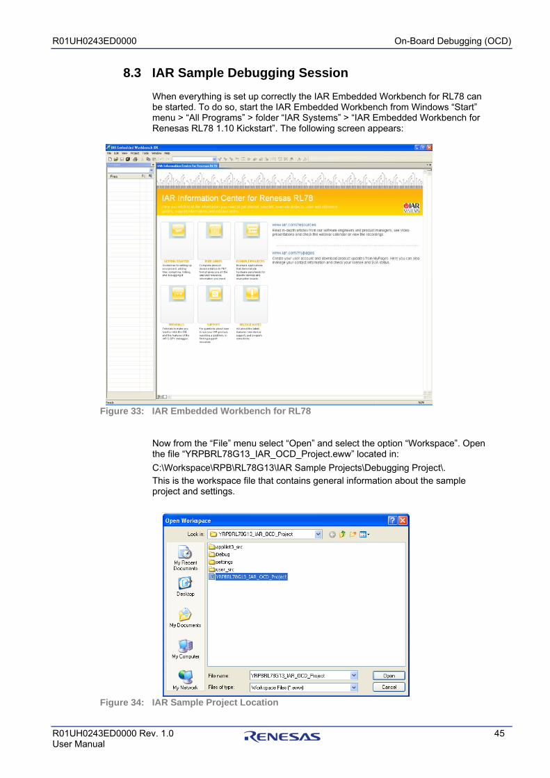
Now from the “File” menu select “Open” and select the option “Workspace”. Open the file “YRPBRL78G13_IAR_OCD_Project.eww” located in: C:\Workspace\RPB\RL78G13\IAR Sample Projects\Debugging Project\. This is the workspace file that contains general information about the sample project and settings.
IAR Sample Project Location
Figure 33:
Figure 34:
R01UH0243ED0000 On-Board Debugging (OCD)
R01UH0243ED0000 Rev. 1.0 46 User Manual
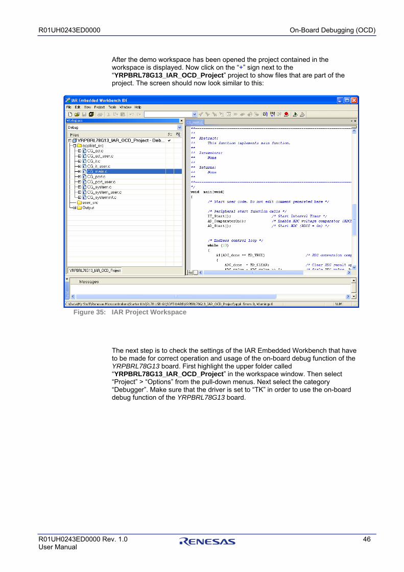
After the demo workspace has been opened the project contained in the workspace is displayed. Now click on the “+” sign next to the “YRPBRL78G13_IAR_OCD_Project” project to show files that are part of the project. The screen should now look similar to this:
IAR Project Workspace
The next step is to check the settings of the IAR Embedded Workbench that have to be made for correct operation and usage of the on-board debug function of the YRPBRL78G13 board. First highlight the upper folder called “YRPBRL78G13_IAR_OCD_Project” in the workspace window. Then select “Project” > “Options” from the pull-down menus. Next select the category “Debugger”. Make sure that the driver is set to “TK” in order to use the on-board debug function of the YRPBRL78G13 board.
Figure 35:
R01UH0243ED0000 On-Board Debugging (OCD)
R01UH0243ED0000 Rev. 1.0 47 User Manual
IAR Debugger Options
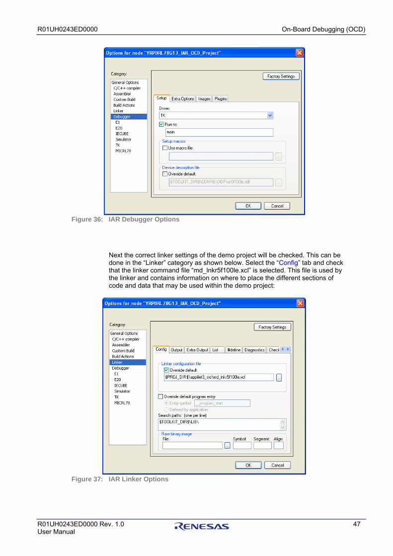
Next the correct linker settings of the demo project will be checked. This can be done in the “Linker” category as shown below. Select the “Config” tab and check that the linker command file “md_lnkr5f100le.xcl” is selected. This file is used by the linker and contains information on where to place the different sections of code and data that may be used within the demo project:
IAR Linker Options
Figure 36:
Figure 37:
R01UH0243ED0000 On-Board Debugging (OCD)
R01UH0243ED0000 Rev. 1.0 48 User Manual
Now after everything has been setup correctly it’s time to build (compile + link) the demonstration project. Close the Options menu and select “Rebuild All” from the “Project” menu. If the project is compiled and linked without errors or warnings it can now be downloaded to the YRPBRL78G13 board and debugged.
To start the IAR C-SPY debugger select the option “Debug” from the “Project”
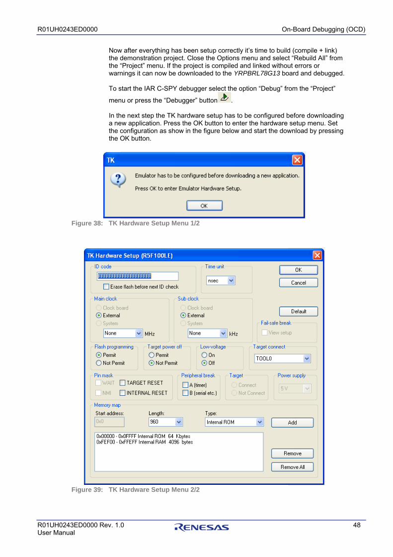
menu or press the “Debugger” button . In the next step the TK hardware setup has to be configured before downloading a new application. Press the OK button to enter the hardware setup menu. Set the configuration as show in the figure below and start the download by pressing the OK button.
TK Hardware Setup Menu 1/2
TK Hardware Setup Menu 2/2
Figure 38:
Figure 39:
R01UH0243ED0000 On-Board Debugging (OCD)
R01UH0243ED0000 Rev. 1.0 49 User Manual
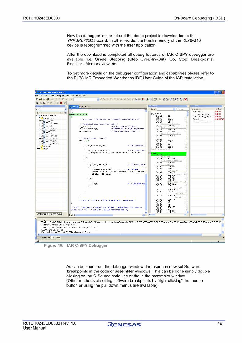
Now the debugger is started and the demo project is downloaded to the YRPBRL78G13 board. In other words, the Flash memory of the RL78/G13 device is reprogrammed with the user application.
After the download is completed all debug features of IAR C-SPY debugger are available, i.e. Single Stepping (Step Over/-In/-Out), Go, Stop, Breakpoints, Register / Memory view etc.
To get more details on the debugger configuration and capabilities please refer to the RL78 IAR Embedded Workbench IDE User Guide of the IAR installation.
IAR C-SPY Debugger
As can be seen from the debugger window, the user can now set Software breakpoints in the code or assembler windows. This can be done simply double clicking on the C-Source code line or the in the assembler window (Other methods of setting software breakpoints by “right clicking” the mouse button or using the pull down menus are available).
Figure 40:
R01UH0243ED0000 On-Board Debugging (OCD)
R01UH0243ED0000 Rev. 1.0 50 User Manual
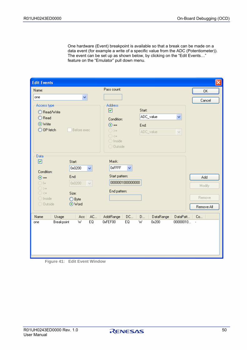
One hardware (Event) breakpoint is available so that a break can be made on a data event (for example a write of a specific value from the ADC (Potentiometer)). The event can be set up as shown below, by clicking on the “Edit Events…” feature on the “Emulator” pull down menu.
Edit Event Window
Figure 41:
R01UH0243ED0000 On-Board Debugging (OCD)
R01UH0243ED0000 Rev. 1.0 51 User Manual
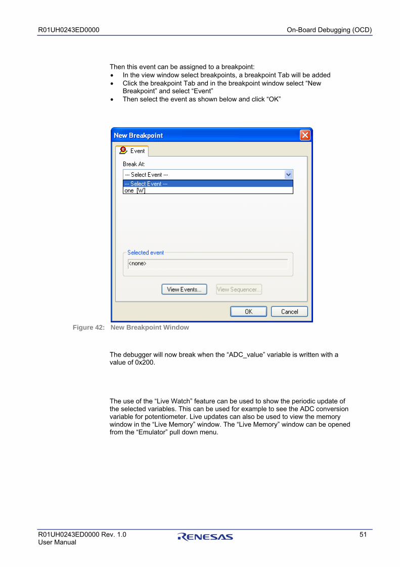
Then this event can be assigned to a breakpoint: • In the view window select breakpoints, a breakpoint Tab will be added • Click the breakpoint Tab and in the breakpoint window select “New
Breakpoint” and select “Event” • Then select the event as shown below and click “OK”
New Breakpoint Window The debugger will now break when the “ADC_value” variable is written with a value of 0x200.
The use of the “Live Watch” feature can be used to show the periodic update of the selected variables. This can be used for example to see the ADC conversion variable for potentiometer. Live updates can also be used to view the memory window in the “Live Memory” window. The “Live Memory” window can be opened from the “Emulator” pull down menu.
Figure 42:
R01UH0243ED0000 On-Board Debugging (OCD)
R01UH0243ED0000 Rev. 1.0 52 User Manual
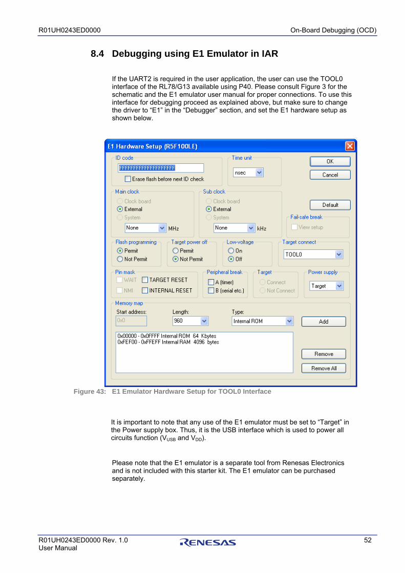
8.4 Debugging using E1 Emulator in IAR If the UART2 is required in the user application, the user can use the TOOL0 interface of the RL78/G13 available using P40. Please consult Figure 3 for the schematic and the E1 emulator user manual for proper connections. To use this interface for debugging proceed as explained above, but make sure to change the driver to “E1” in the “Debugger” section, and set the E1 hardware setup as shown below.
E1 Emulator Hardware Setup for TOOL0 Interface
It is important to note that any use of the E1 emulator must be set to “Target” in the Power supply box. Thus, it is the USB interface which is used to power all circuits function (VUSB and VDD).
Please note that the E1 emulator is a separate tool from Renesas Electronics and is not included with this starter kit. The E1 emulator can be purchased separately.
Figure 43:
R01UH0243ED0000 GUI Description
R01UH0243ED0000 Rev. 1.0 53 User Manual
Chapter 9 GUI Description
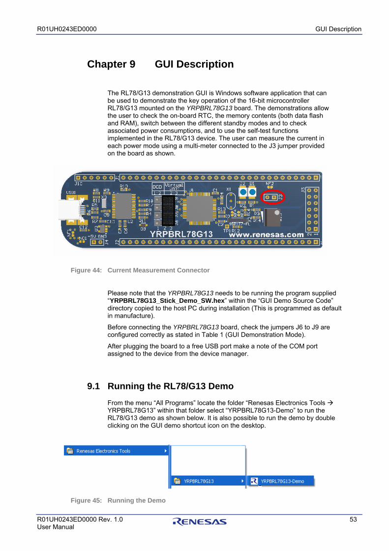
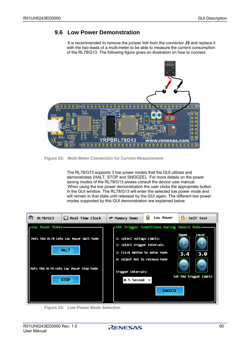
The RL78/G13 demonstration GUI is Windows software application that can be used to demonstrate the key operation of the 16-bit microcontroller RL78/G13 mounted on the YRPBRL78G13 board. The demonstrations allow the user to check the on-board RTC, the memory contents (both data flash and RAM), switch between the different standby modes and to check associated power consumptions, and to use the self-test functions implemented in the RL78/G13 device. The user can measure the current in each power mode using a multi-meter connected to the J3 jumper provided on the board as shown.
Current Measurement Connector
Please note that the YRPBRL78G13 needs to be running the program supplied “YRPBRL78G13_Stick_Demo_SW.hex” within the “GUI Demo Source Code” directory copied to the host PC during installation (This is programmed as default in manufacture).
Before connecting the YRPBRL78G13 board, check the jumpers J6 to J9 are configured correctly as stated in Table 1 (GUI Demonstration Mode).
After plugging the board to a free USB port make a note of the COM port assigned to the device from the device manager.
9.1 Running the RL78/G13 Demo
From the menu “All Programs” locate the folder “Renesas Electronics Tools YRPBRL78G13” within that folder select “YRPBRL78G13-Demo” to run the RL78/G13 demo as shown below. It is also possible to run the demo by double clicking on the GUI demo shortcut icon on the desktop.
Running the Demo
Figure 44:
Figure 45:
R01UH0243ED0000 GUI Description
R01UH0243ED0000 Rev. 1.0 54 User Manual
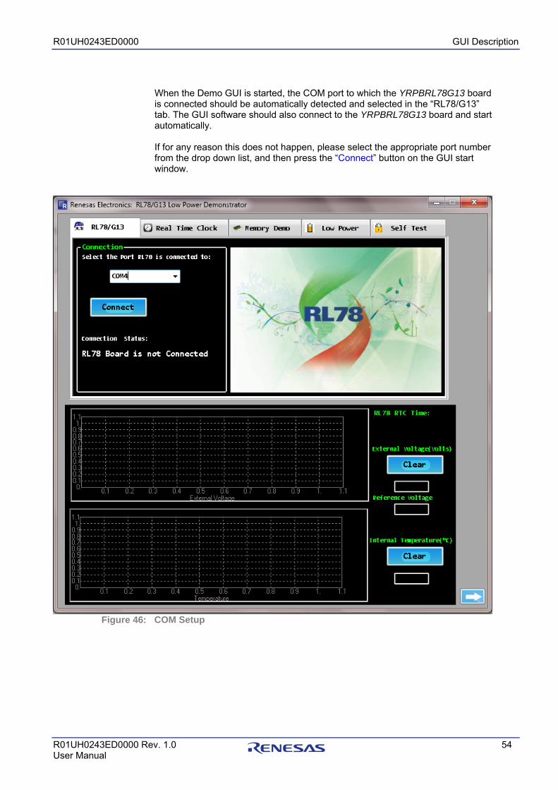
When the Demo GUI is started, the COM port to which the YRPBRL78G13 board is connected should be automatically detected and selected in the “RL78/G13” tab. The GUI software should also connect to the YRPBRL78G13 board and start automatically. If for any reason this does not happen, please select the appropriate port number from the drop down list, and then press the “Connect” button on the GUI start window.
COM Setup
Figure 46:
R01UH0243ED0000 GUI Description
R01UH0243ED0000 Rev. 1.0 55 User Manual
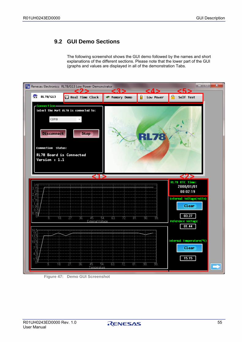
9.2 GUI Demo Sections
The following screenshot shows the GUI demo followed by the names and short explanations of the different sections. Please note that the lower part of the GUI (graphs and values are displayed in all of the demonstration Tabs.
Demo GUI Screenshot
Figure 47:
<2> <3> <4> <5>
<1> <2>
R01UH0243ED0000 GUI Description
R01UH0243ED0000 Rev. 1.0 56 User Manual
<1> ADC – External Voltage & Temperature Graphs This section displays the external voltage (measured from the potentiometer on the board) and the temperature reported by the internal temperature sensor of the RL78/G13. The measurements are performed by the 10-bit ADC of the RL78/G13. The graphs can be reinitialized by clicking the “Clear” buttons on the right hand side of the window. Note that the graphs are re-scaled automatically when the “Clear” buttons are pressed, so a more detailed look of the reported values can be made.
<2> Real Time Clock
This section displays the date and time reported by the on-board RTC. The RL78/G13 RTC registers can be synchronized with the PC system date and time by clicking the “Sync” button. The user can also set and enable the interval interrupt and the alarm functions.
<3> Memory – Data Flash & RAM Content
When the “Enable” button is pressed, the RL78 writes 4 bytes of data to the internal data flash memory for every ADC measurement (~ 5 sec). The data saved are the converted ADC values for the external voltage (Potentiometer) and internal temperature sensor. The GUI window shows the current 64 bytes window of the current data flash block that is being written into. Data flash contents are retained even when the power is removed from the device. This section also displays the data RAM content read from the RL78/G13 RAM variable memory and an 8 byte user area which can written and read by the user. RAM content is not lost even when the RL78/G13 enters the lowest power mode (STOP mode) providing power is not removed from the board.
<4> Low Power – Low Power Mode Selection: Three different standby modes are implemented in the RL78/G13 device, HALT mode, STOP mode and the new SNOOZE mode. Buttons are used to switch the operational mode of the RL78/G13 to the standby mode selected. The button clicked will set the RL78 into the selected low power mode and change caption to “Release”. The RL78 will remain in the selected low power mode until button is clicked again to release the RL78/G13 to the active mode, except for the Snooze mode which requires the user to adjust the external potentiometer to exit. Detailed explanations about each of the low power modes are provided in the section 9.6 Low Power Demo, please refer to it.
<5> Self-Test Function:
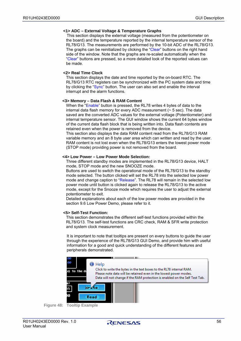
This section demonstrates the different self-test functions provided within the RL78/G13. The self-test functions are CRC check, RAM & SFR write protection and system clock measurement. It is important to note that tooltips are present on every buttons to guide the user through the experience of the RL78/G13 GUI Demo, and provide him with useful information for a good and quick understanding of the different features and peripherals demonstrated.
Tooltip Example Figure 48:
R01UH0243ED0000 GUI Description
R01UH0243ED0000 Rev. 1.0 57 User Manual
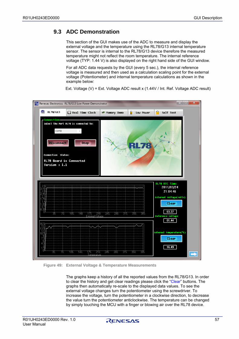
9.3 ADC Demonstration This section of the GUI makes use of the ADC to measure and display the external voltage and the temperature using the RL78/G13 internal temperature sensor. The sensor is internal to the RL78/G13 device therefore the measured temperature might not reflect the room temperature. The internal reference voltage (TYP: 1.44 V) is also displayed on the right hand side of the GUI window.
For all ADC data requests by the GUI (every 5 sec.), the internal reference voltage is measured and then used as a calculation scaling point for the external voltage (Potentiometer) and internal temperature calculations as shown in the example below:
Ext. Voltage (V) = Ext. Voltage ADC result x (1.44V / Int. Ref. Voltage ADC result)
External Voltage & Temperature Measurements The graphs keep a history of all the reported values from the RL78/G13. In order to clear the history and get clear readings please click the “Clear” buttons. The graphs then automatically re-scale to the displayed data values. To see the external voltage changes turn the potentiometer using the screwdriver. To increase the voltage, turn the potentiometer in a clockwise direction, to decrease the value turn the potentiometer anticlockwise. The temperature can be changed by simply touching the MCU with a finger or blowing air over the RL78 device.
Figure 49:
R01UH0243ED0000 GUI Description
R01UH0243ED0000 Rev. 1.0 58 User Manual
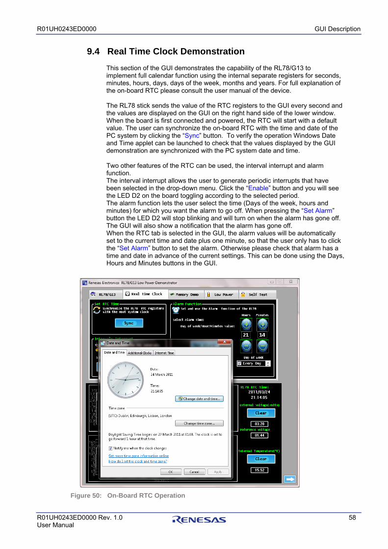
9.4 Real Time Clock Demonstration This section of the GUI demonstrates the capability of the RL78/G13 to implement full calendar function using the internal separate registers for seconds, minutes, hours, days, days of the week, months and years. For full explanation of the on-board RTC please consult the user manual of the device. The RL78 stick sends the value of the RTC registers to the GUI every second and the values are displayed on the GUI on the right hand side of the lower window. When the board is first connected and powered, the RTC will start with a default value. The user can synchronize the on-board RTC with the time and date of the PC system by clicking the “Sync” button. To verify the operation Windows Date and Time applet can be launched to check that the values displayed by the GUI demonstration are synchronized with the PC system date and time. Two other features of the RTC can be used, the interval interrupt and alarm function. The interval interrupt allows the user to generate periodic interrupts that have been selected in the drop-down menu. Click the “Enable” button and you will see the LED D2 on the board toggling according to the selected period. The alarm function lets the user select the time (Days of the week, hours and minutes) for which you want the alarm to go off. When pressing the “Set Alarm” button the LED D2 will stop blinking and will turn on when the alarm has gone off. The GUI will also show a notification that the alarm has gone off. When the RTC tab is selected in the GUI, the alarm values will be automatically set to the current time and date plus one minute, so that the user only has to click the “Set Alarm” button to set the alarm. Otherwise please check that alarm has a time and date in advance of the current settings. This can be done using the Days, Hours and Minutes buttons in the GUI.
On-Board RTC Operation Figure 50:
R01UH0243ED0000 GUI Description
R01UH0243ED0000 Rev. 1.0 59 User Manual
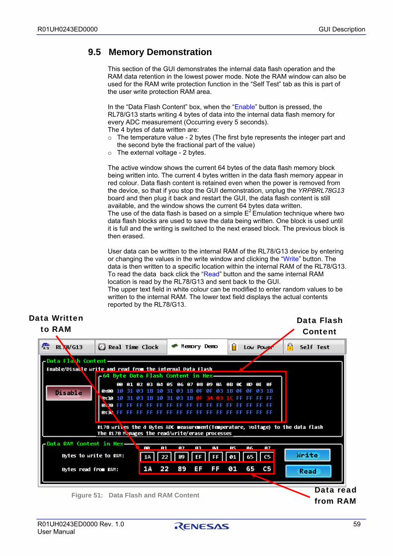
9.5 Memory Demonstration This section of the GUI demonstrates the internal data flash operation and the RAM data retention in the lowest power mode. Note the RAM window can also be used for the RAM write protection function in the “Self Test” tab as this is part of the user write protection RAM area. In the “Data Flash Content” box, when the “Enable” button is pressed, the RL78/G13 starts writing 4 bytes of data into the internal data flash memory for every ADC measurement (Occurring every 5 seconds). The 4 bytes of data written are: o The temperature value - 2 bytes (The first byte represents the integer part and
the second byte the fractional part of the value) o The external voltage - 2 bytes. The active window shows the current 64 bytes of the data flash memory block being written into. The current 4 bytes written in the data flash memory appear in red colour. Data flash content is retained even when the power is removed from the device, so that if you stop the GUI demonstration, unplug the YRPBRL78G13 board and then plug it back and restart the GUI, the data flash content is still available, and the window shows the current 64 bytes data written. The use of the data flash is based on a simple E2 Emulation technique where two data flash blocks are used to save the data being written. One block is used until it is full and the writing is switched to the next erased block. The previous block is then erased. User data can be written to the internal RAM of the RL78/G13 device by entering or changing the values in the write window and clicking the “Write” button. The data is then written to a specific location within the internal RAM of the RL78/G13. To read the data back click the “Read” button and the same internal RAM location is read by the RL78/G13 and sent back to the GUI. The upper text field in white colour can be modified to enter random values to be written to the internal RAM. The lower text field displays the actual contents reported by the RL78/G13.
Data Flash and RAM Content
Figure 51:
Data Written to RAM
Data read from RAM
Data Flash Content
R01UH0243ED0000 GUI Description
R01UH0243ED0000 Rev. 1.0 60 User Manual
9.6 Low Power Demonstration It is recommended to remove the jumper link from the connector J3 and replace it with the two leads of a multi-meter to be able to measure the current consumption of the RL78/G13. The following figure gives an illustration on how to connect.
Multi-Meter Connection for Current Measurement The RL78/G13 supports 3 low power modes that the GUI utilizes and demonstrates (HALT, STOP and SNOOZE). For more details on the power saving modes of the RL78/G13 please consult the device user manual. When using the low power demonstration the user clicks the appropriate button in the GUI window. The RL78/G13 will enter the selected low power mode and will remain in that state until released by the GUI again. The different low power modes supported by this GUI demonstration are explained below.
Low Power Mode Selection
Figure 52:
Figure 53:
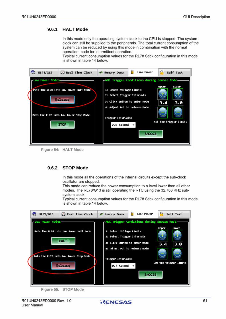
R01UH0243ED0000 GUI Description
R01UH0243ED0000 Rev. 1.0 61 User Manual
9.6.1 HALT Mode
In this mode only the operating system clock to the CPU is stopped. The system clock can still be supplied to the peripherals. The total current consumption of the system can be reduced by using this mode in combination with the normal operation mode for intermittent operation. Typical current consumption values for the RL78 Stick configuration in this mode is shown in table 14 below.
HALT Mode
9.6.2 STOP Mode
In this mode all the operations of the internal circuits except the sub-clock oscillator are stopped. This mode can reduce the power consumption to a level lower than all other modes. The RL78/G13 is still operating the RTC using the 32.768 KHz sub-system clock. Typical current consumption values for the RL78 Stick configuration in this mode is shown in table 14 below.
STOP Mode
Figure 54:
Figure 55:
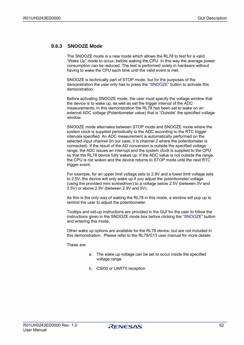
R01UH0243ED0000 GUI Description
R01UH0243ED0000 Rev. 1.0 62 User Manual
9.6.3 SNOOZE Mode
The SNOOZE mode is a new mode which allows the RL78 to test for a valid “Wake Up” mode to occur, before waking the CPU. In this way the average power consumption can be reduced. The test is performed solely in hardware without having to wake the CPU each time until the valid event is met. SNOOZE is technically part of STOP mode, but for the purposes of the demonstration the user only has to press the “SNOOZE” button to activate this demonstration. Before activating SNOOZE mode, the user must specify the voltage window that the device is to wake up, as well as set the trigger interval of the ADC measurements. In this demonstration the RL78 has been set to wake on an external ADC voltage (Potentiometer value) that is “Outside” the specified voltage window. SNOOZE mode alternates between STOP mode and SNOOZE mode where the system clock is supplied periodically to the ADC according to the RTC trigger intervals specified. An ADC measurement is automatically performed on the selected input channel (In our case, it is channel 2 where the potentiometer is connected). If the result of the AD conversion is outside the specified voltage range, the ADC issues an interrupt and the system clock is supplied to the CPU so that the RL78 device fully wakes up. If the ADC value is not outside the range, the CPU is not woken and the device returns to STOP mode until the next RTC trigger event. For example, for an upper limit voltage sets to 2.9V and a lower limit voltage sets to 2.5V, the device will only wake up if you adjust the potentiometer voltage (using the provided mini screwdriver) to a voltage below 2.5V (between 0V and 2.5V) or above 2.9V (between 2.9V and 5V). As this is the only way of waking the RL78 in this mode, a window will pop up to remind the user to adjust the potentiometer. Tooltips and set-up instructions are provided in the GUI for the user to follow the instructions given in the SNOOZE mode box before clicking the “SNOOZE” button and entering this mode. Other wake up options are available for the RL78 device, but are not included in this demonstration. Please refer to the RL78/G13 user manual for more details. These are:
a. The wake up voltage can be set to occur inside the specified voltage range
b. CSI00 or UART0 reception
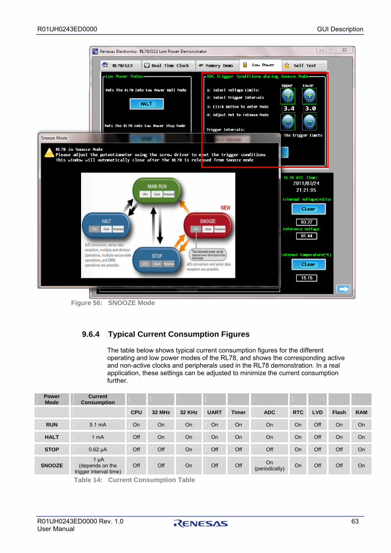
R01UH0243ED0000 GUI Description
R01UH0243ED0000 Rev. 1.0 63 User Manual
SNOOZE Mode
9.6.4 Typical Current Consumption Figures
The table below shows typical current consumption figures for the different operating and low power modes of the RL78, and shows the corresponding active and non-active clocks and peripherals used in the RL78 demonstration. In a real application, these settings can be adjusted to minimize the current consumption further.
Power Mode
Current Consumption
CPU 32 MHz 32 KHz UART Timer ADC RTC LVD Flash RAM
RUN 5.1 mA On On On On On On On Off On On
HALT 1 mA Off On On On On On On Off On On
STOP 0.62 µA Off Off On Off Off Off On Off Off On
SNOOZE 1 µA
(depends on the trigger interval time)
Off Off On Off Off On (periodically) On Off Off On
Current Consumption Table
Figure 56:
Table 14:
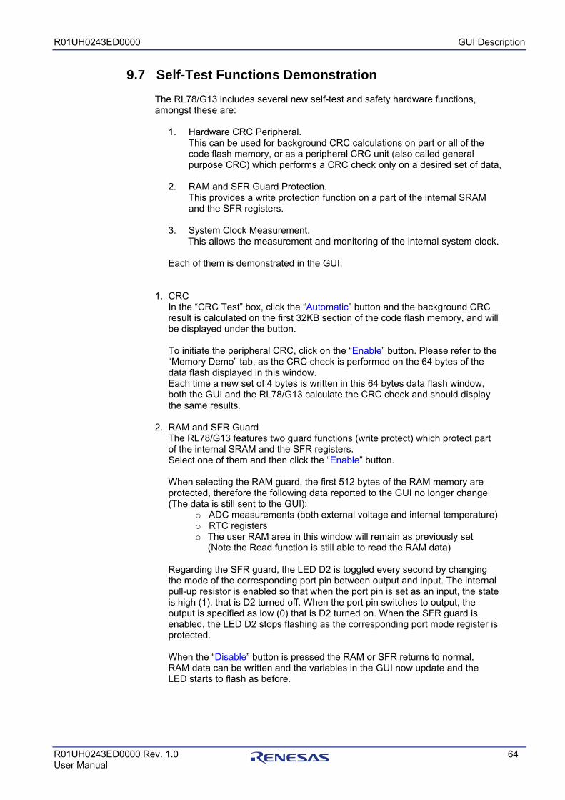
R01UH0243ED0000 GUI Description
R01UH0243ED0000 Rev. 1.0 64 User Manual
9.7 Self-Test Functions Demonstration The RL78/G13 includes several new self-test and safety hardware functions, amongst these are:
1. Hardware CRC Peripheral. This can be used for background CRC calculations on part or all of the code flash memory, or as a peripheral CRC unit (also called general purpose CRC) which performs a CRC check only on a desired set of data,
2. RAM and SFR Guard Protection.
This provides a write protection function on a part of the internal SRAM and the SFR registers.
3. System Clock Measurement. This allows the measurement and monitoring of the internal system clock.
Each of them is demonstrated in the GUI.
1. CRC
In the “CRC Test” box, click the “Automatic” button and the background CRC result is calculated on the first 32KB section of the code flash memory, and will be displayed under the button. To initiate the peripheral CRC, click on the “Enable” button. Please refer to the “Memory Demo” tab, as the CRC check is performed on the 64 bytes of the data flash displayed in this window. Each time a new set of 4 bytes is written in this 64 bytes data flash window, both the GUI and the RL78/G13 calculate the CRC check and should display the same results.
2. RAM and SFR Guard
The RL78/G13 features two guard functions (write protect) which protect part of the internal SRAM and the SFR registers. Select one of them and then click the “Enable” button. When selecting the RAM guard, the first 512 bytes of the RAM memory are protected, therefore the following data reported to the GUI no longer change (The data is still sent to the GUI):
o ADC measurements (both external voltage and internal temperature) o RTC registers o The user RAM area in this window will remain as previously set
(Note the Read function is still able to read the RAM data) Regarding the SFR guard, the LED D2 is toggled every second by changing the mode of the corresponding port pin between output and input. The internal pull-up resistor is enabled so that when the port pin is set as an input, the state is high (1), that is D2 turned off. When the port pin switches to output, the output is specified as low (0) that is D2 turned on. When the SFR guard is enabled, the LED D2 stops flashing as the corresponding port mode register is protected. When the “Disable” button is pressed the RAM or SFR returns to normal, RAM data can be written and the variables in the GUI now update and the LED starts to flash as before.
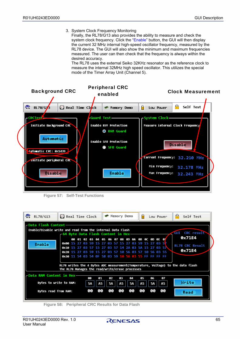
R01UH0243ED0000 GUI Description
R01UH0243ED0000 Rev. 1.0 65 User Manual
3. System Clock Frequency Monitoring Finally, the RL78/G13 also provides the ability to measure and check the system clock frequency. Click the “Enable” button, the GUI will then display the current 32 MHz internal high-speed oscillator frequency, measured by the RL78 device. The GUI will also show the minimum and maximum frequencies measured. The user can then check that the frequency is always within the desired accuracy. The RL78 uses the external Seiko 32KHz resonator as the reference clock to measure the internal 32MHz high speed oscillator. This utilizes the special mode of the Timer Array Unit (Channel 5).
Self-Test Functions
Peripheral CRC Results for Data Flash
Figure 57:
Figure 58:
Background CRC Peripheral CRC
enabled Clock Measurement
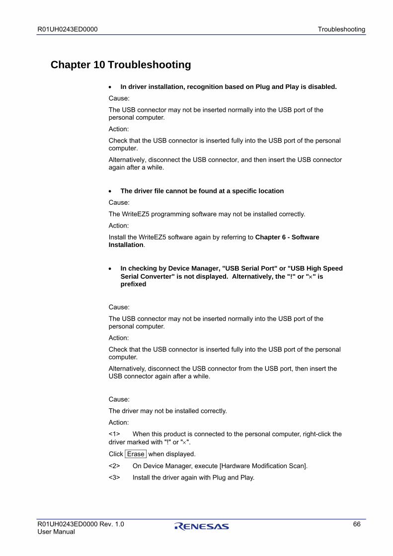
R01UH0243ED0000 Troubleshooting
R01UH0243ED0000 Rev. 1.0 66 User Manual
Chapter 10 Troubleshooting
• In driver installation, recognition based on Plug and Play is disabled.
Cause:
The USB connector may not be inserted normally into the USB port of the personal computer.
Action:
Check that the USB connector is inserted fully into the USB port of the personal computer.
Alternatively, disconnect the USB connector, and then insert the USB connector again after a while.
• The driver file cannot be found at a specific location Cause:
The WriteEZ5 programming software may not be installed correctly.
Action:
Install the WriteEZ5 software again by referring to Chapter 6 - Software Installation.
• In checking by Device Manager, "USB Serial Port" or "USB High Speed Serial Converter" is not displayed. Alternatively, the "!" or "×" is prefixed
Cause:
The USB connector may not be inserted normally into the USB port of the personal computer.
Action:
Check that the USB connector is inserted fully into the USB port of the personal computer.
Alternatively, disconnect the USB connector from the USB port, then insert the USB connector again after a while.
Cause:
The driver may not be installed correctly.
Action:
<1> When this product is connected to the personal computer, right-click the driver marked with "!" or "×".
Click Erase when displayed.
<2> On Device Manager, execute [Hardware Modification Scan].
<3> Install the driver again with Plug and Play.
R01UH0243ED0000 Troubleshooting
R01UH0243ED0000 Rev. 1.0 67 User Manual
Cause:
The device may not be recognized (in the case of connection with the USB hub).
Action:
Try the following:
• Disconnect the USB connector, then insert the USB connector again.
• Connect the USB connector to another port of the USB hub.
If the same symptom occurs, do not use the USB hub, but directly connect the connector to the USB port of the personal computer.
• When this product is connected with a personal computer, the "Add New Hardware Wizard" screen is displayed
Cause:
If the USB connector of this product is not inserted into the USB port used at the installation time but into another USB port, this product may be recognized as a new hardware item.
Action:
Install the driver by referring to Chapter 6 - Software Installation
• Communication with the YRPBRL78G13 is disabled Cause:
The driver may not be installed correctly.
Action:
Check if the USB driver is installed correctly by referring to Chapter 6 – Software Installation.
Cause:
The COM port selected via the “Port list box” within device setup menu of WriteEZ5 may not be set correctly.
Action:
Set the port checked using Device Manager.
Cause:
The YRPBRL78G13 board is operating in GUI Demo / Virtual UART mode.
Action:
Set the board to the On-Board Debugging / Flash Programming mode.
Cause:
The PRM file selected in [Device Setup] may be incorrect.
Action:
Use the corresponding PRM file that matches the target device. For information about the PRM file, refer to Chapter 7 – How to Use WriteEZ5 Flash Programming Software.
R01UH0243ED0000 Schematics
R01UH0243ED0000 Rev. 1.0 68 User Manual
Chapter 11 Schematics
YRPBRL78G13 Board Schematics 1/2 Figure 59:
R01UH0243ED0000 Schematics
R01UH0243ED0000 Rev. 1.0 69 User Manual
YRPBRL78G13 Board Schematics 2/2 Figure 60:
R01UH0243ED0000 Schematics
R01UH0243ED0000 Rev. 1.0 70 User Manual
YRPBRL78G13 Board Assembly Drawing
Figure 61:
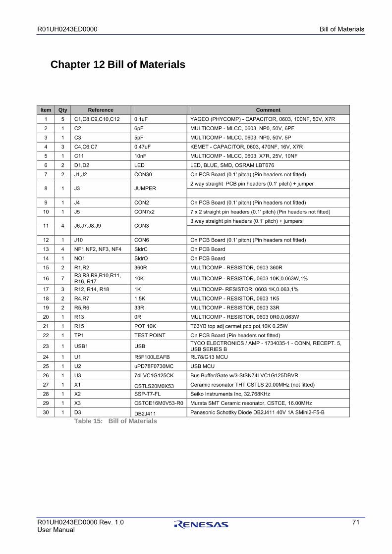
R01UH0243ED0000 Bill of Materials
R01UH0243ED0000 Rev. 1.0 71 User Manual
Chapter 12 Bill of Materials
Item Qty Reference Comment
1 5 C1,C8,C9,C10,C12 0.1uF YAGEO (PHYCOMP) - CAPACITOR, 0603, 100NF, 50V, X7R
2 1 C2 6pF MULTICOMP - MLCC, 0603, NP0, 50V, 6PF
3 1 C3 5pF MULTICOMP - MLCC, 0603, NP0, 50V, 5P
4 3 C4,C6,C7 0.47uF KEMET - CAPACITOR, 0603, 470NF, 16V, X7R
5 1 C11 10nF MULTICOMP - MLCC, 0603, X7R, 25V, 10NF
6 2 D1,D2 LED LED, BLUE, SMD, OSRAM LBT676
7 2 J1,J2 CON30 On PCB Board (0.1' pitch) (Pin headers not fitted)
2 way straight PCB pin headers (0.1' pitch) + jumper 8 1 J3 JUMPER
9 1 J4 CON2 On PCB Board (0.1' pitch) (Pin headers not fitted)
10 1 J5 CON7x2 7 x 2 straight pin headers (0.1' pitch) (Pin headers not fitted)
3 way straight pin headers (0.1' pitch) + jumpers 11 4 J6,J7,J8,J9 CON3
12 1 J10 CON6 On PCB Board (0.1' pitch) (Pin headers not fitted)
13 4 NF1,NF2, NF3, NF4 SldrC On PCB Board
14 1 NO1 SldrO On PCB Board
15 2 R1,R2 360R MULTICOMP - RESISTOR, 0603 360R
16 7 R3,R8,R9,R10,R11, R16, R17 10K MULTICOMP - RESISTOR, 0603 10K,0.063W,1%
17 3 R12, R14, R18 1K MULTICOMP- RESISTOR, 0603 1K,0.063,1%
18 2 R4,R7 1.5K MULTICOMP - RESISTOR, 0603 1K5
19 2 R5,R6 33R MULTICOMP - RESISTOR, 0603 33R
20 1 R13 0R MULTICOMP - RESISTOR, 0603 0R0,0.063W
21 1 R15 POT 10K T63YB top adj cermet pcb pot,10K 0.25W
22 1 TP1 TEST POINT On PCB Board (Pin headers not fitted)
23 1 USB1 USB TYCO ELECTRONICS / AMP - 1734035-1 - CONN, RECEPT. 5, USB SERIES B
24 1 U1 R5F100LEAFB RL78/G13 MCU
25 1 U2 uPD78F0730MC USB MCU
26 1 U3 74LVC1G125CK Bus Buffer/Gate w/3-StSN74LVC1G125DBVR
27 1 X1 CSTLS20M0X53 Ceramic resonator THT CSTLS 20.00MHz (not fitted)
28 1 X2 SSP-T7-FL Seiko Instruments Inc, 32.768KHz
29 1 X3 CSTCE16M0V53-R0 Murata SMT Ceramic resonator, CSTCE, 16.00MHz
30 1 D3 DB2J411 Panasonic Schottky Diode DB2J411 40V 1A SMini2-F5-B
Bill of Materials Table 15:
R01UH0243ED0000 Resonator from Seiko Instruments Inc.
R01UH0243ED0000 Rev. 1.0 72 User Manual
Chapter 13 Resonator from Seiko Instruments Inc.
13.1 Features of the 32 KHz Resonator The SSP-T7-FL is a tuning fork 32 KHz low CL crystal resonator from Seiko Instruments Inc. designed for the new low power RL78 MCU family. Microcontrollers from the RL78 family using this 32 KHz low CL resonator achieves ultra low power oscillation circuit (0.2 μA max.) with fast start-up time (within 1 sec.), high accuracy (±10 sec. per month), and high efficiency (oscillation allowance up to 20%).
13.2 Product Name and Specifications The different product names offered by Seiko Instruments Inc. for the RL78 microcontrollers are: • SSP-T7-FL (SMD type low CL resonator) • VT-200-FL (Cylinder type Low CL resonator) The main specifications are as follows: 32.768 KHz ± 20ppm CL 4.4pF.
13.3 Web URL
Fore more information about those products, please refer to the following URL: www.sii-components.com/quartz/renesas/
R01UH0243ED0000 Resonator from Seiko Instruments Inc.
R01UH0243ED0000 Rev. 1.0 73 User Manual
13.4 Contact Addresses
(Japan) Contact person name: Katsuyuki Masuko Quartz Crystal Sales, Electronic Components Business Unit Tel. number: +81-43-211-1207 Email address: [email protected] Company name: Seiko Instruments Inc. Address: 8,Nakase 1-choume,Mihama-ku,CHiba-shi, Chiba 261-8507,Japan (China) Contact person name: Kensei Nozu Tel. number: +86-775-82462680-307 Email address: [email protected] Company name: Seiko Instruments (H.K.) Ltd. Shenzhen Rep. office Address: 2212-2215 Diwang commercial building, Shunhin square 5002, Shennan Est Rd., Shenzhen, Guangdong, China (Americas) Contact person name: Jim Schlumpberger Tel. number: +01-310-517-7884 Email address: [email protected] Company name: Seiko Instruments U.S.A. Inc. Address: 2990 Lomita Blvd. Torrance, CA 90505, U.S.A. (Europe) Contact person name: Michael Bertsch Tel. number: +49-6102-297-303 Email address: [email protected] Company name: Seiko Instruments GmbH Address: Siemensstr. 9, D-63263 Neu Isenburg, Germany (Korea) To be informed later Contact person name: Sungnam Chung / Choi Kyonghoan Tel. number: +82-2-565-8006 Email address: [email protected] / [email protected] Company name: Seiko Instruments Korea Inc.
Address: #507,508, Korea City Air Terminal Bldg, 159-6, Samsung-dong, Gangnam-gu, Seoul, 135-728 Korea
(Taiwan) Contact person name: Shawn Yang Tel. number: +886 2 2516-8518 ext: 239 Email address: [email protected] Company name: Seiko Instruments Taiwan Inc. Address: 6F,No.236,Sec.2,Jianguo N.Rd.,Taipei 104,Taiwan
R01UH0243ED0000
R01UH0243ED0000 Rev. 1.0 74 User Manual
REVISION HISTORY RL78/G13 Stick User’s Manual: Hardware
Description Rev. Date Page Summary
1.00 Mar 25, 2011 ⎯ First Edition issued
R01UH0243ED0000
R01UH0243ED0000 Rev. 1.0 75 User Manual
RL78/G13 Stick User’s Manual: Hardware Publication Date: Rev.1.00 Mar 25, 2011 Published by: Renesas Electronics Corporation
R01UH0243ED0000
R01UH0243ED0000 Rev. 1.0 76 User Manual
SALES OFFICES http://www.renesas.com Refer to "http://www.renesas.com/" for the latest and detailed information. Renesas Electronics America Inc. 2880 Scott Boulevard Santa Clara, CA 95050-2554, U.S.A. Tel: +1-408-588-6000, Fax: +1-408-588-6130 Renesas Electronics Canada Limited 1101 Nicholson Road, Newmarket, Ontario L3Y 9C3, Canada Tel: +1-905-898-5441, Fax: +1-905-898-3220 Renesas Electronics Europe Limited Dukes Meadow, Millboard Road, Bourne End, Buckinghamshire, SL8 5FH, U.K Tel: +44-1628-585-100, Fax: +44-1628-585-900 Renesas Electronics Europe GmbH Arcadiastrasse 10, 40472 Düsseldorf, Germany Tel: +49-211-65030, Fax: +49-211-6503-1327 Renesas Electronics (China) Co., Ltd. 7th Floor, Quantum Plaza, No.27 ZhiChunLu Haidian District, Beijing 100083, P.R.China Tel: +86-10-8235-1155, Fax: +86-10-8235-7679 Renesas Electronics (Shanghai) Co., Ltd. Unit 204, 205, AZIA Center, No.1233 Lujiazui Ring Rd., Pudong District, Shanghai 200120, China Tel: +86-21-5877-1818, Fax: +86-21-6887-7858 / -7898 Renesas Electronics Hong Kong Limited Unit 1601-1613, 16/F., Tower 2, Grand Century Place, 193 Prince Edward Road West, Mongkok, Kowloon, Hong Kong Tel: +852-2886-9318, Fax: +852 2886-9022/9044 Renesas Electronics Taiwan Co., Ltd. 7F, No. 363 Fu Shing North Road Taipei, Taiwan Tel: +886-2-8175-9600, Fax: +886 2-8175-9670 Renesas Electronics Singapore Pte. Ltd. 1 harbourFront Avenue, #06-10, keppel Bay Tower, Singapore 098632 Tel: +65-6213-0200, Fax: +65-6278-8001 Renesas Electronics Malaysia Sdn.Bhd. Unit 906, Block B, Menara Amcorp, Amcorp Trade Centre, No. 18, Jln Persiaran Barat, 46050 Petaling Jaya, Selangor Darul Ehsan, Malaysia Tel: +60-3-7955-9390, Fax: +60-3-7955-9510 Renesas Electronics Korea Co., Ltd. 11F., Samik Lavied' or Bldg., 720-2 Yeoksam-Dong, Kangnam-Ku, Seoul 135-080, Korea Tel: +82-2-558-3737, Fax: +82-2-558-5141
© 2010 Renesas Electronics Corporation. All rights reserved. Colophon 1.0
R01UH0243ED0000
RL78/G13 Stick