adc0804s030/040/050 - renesas
TRANSCRIPT
ADC0804S030/040/050Single 8 bits ADC, up to 30 MHz, 40 MHz or 50 MHzRev. 03 — 2 July 2012 Product data sheet
1. General description
The ADC0806030/040/050 are a family of 8-bit high-speed, low-power Analog-to-Digital Converters (ADC) for professional video and other applications. It converts the analog input signal into 8-bit binary coded digital signals at a maximum sampling rate of 50 MHz. All digital inputs and outputs are Transistor-Transistor Logic (TTL) and CMOS compatible, although a low-level sine wave clock input signal can also be used.
The device requires an external source to drive its reference ladder. If the application requires that the reference is driven via internal sources, IDT recommends you use one of the ADC1003S030/040/050 family.
2. Features
8-bit resolution
Sampling rate up to 50 MHz
DC sampling allowed
One clock cycle conversion only
High signal-to-noise ratio over a large analog input frequency range (7.8 effective bits at 4.43 MHz full-scale input at fclk = 40 MHz)
No missing codes guaranteed
In-Range (IR) CMOS output
TTL and CMOS levels compatible digital inputs
3 V to 5 V CMOS digital outputs
Low-level AC clock input signal allowed
External reference voltage regulator
Power dissipation only 175 mW (typical)
Low analog input capacitance, no buffer amplifier required
No sample-and-hold circuit required
3. Applications
Video data digitizing
Radar
Transient signal analysis
modulators
Medical imaging
Barcode scanner
Global Positioning System (GPS) receiver
®
Integrated Device Technology ADC0804S030/040/050Single 8 bits ADC, up to 30 MHz, 40 MHz or 50 MHz
Cellular base stations
4. Quick reference data
Table 1. Quick reference data VCCA = V3 to V4 = 4.75 V to 5.25 V; VCCD = V11 to V12 and V28 to V27 = 4.75 V to 5.25 V; VCCO = V13 to V14 = 3.0 V to 5.25 V; AGND and DGND shorted together; Tamb = 0 C to 70 C; typical values measured at VCCA = VCCD = 5 V and VCCO = 3.3 V, Vi(a)(p-p) = 2.0 V; CL = 15 pF and Tamb = 25 C; unless otherwise specified.
Symbol Parameter Conditions Min Typ Max Unit
VCCA analog supply voltage 4.75 5.0 5.25 V
VCCD digital supply voltage 4.75 5.0 5.25 V
VCCO output supply voltage 3.0 3.3 5.25 V
ICCA analog supply current - 18 24 mA
ICCD digital supply current - 16 21 mA
ICCO output supply current fclk = 40 MHz; ramp input
- 1 2 mA
INL integral non-linearity fclk = 40 MHz ramp input
- 0.2 0.5 LSB
DNL differential non-linearity fclk = 40 MHz ramp input
- 0.12 0.22 LSB
fclk(max) maximum clock frequency
ADC0804S030TS 30 - - MHz
ADC0804S040TS 40 - - MHz
ADC0804S050TS 50 - - MHz
Ptot total power dissipation fclk = 40 MHz; ramp input
- 175 247 mW
5. Ordering information
Table 2. Ordering information
Type number Package Sampling frequency (MHz)
Name Description Version
ADC0804S030TS SSOP28 plastic shrink small outline package; 28 leads; body width 5.3 mm
SOT341-1 30
ADC0804S040TS SSOP28 plastic shrink small outline package; 28 leads; body width 5.3 mm
SOT341-1 40
ADC0804S050TS SSOP28 plastic shrink small outline package; 28 leads; body width 5.3 mm
SOT341-1 50
ADC0804S030_040_050_3 © IDT 2012. All rights reserved.
Product data sheet Rev. 03 — 2 July 2012 2 of 18
Integrated Device Technology ADC0804S030/040/050Single 8 bits ADC, up to 30 MHz, 40 MHz or 50 MHz
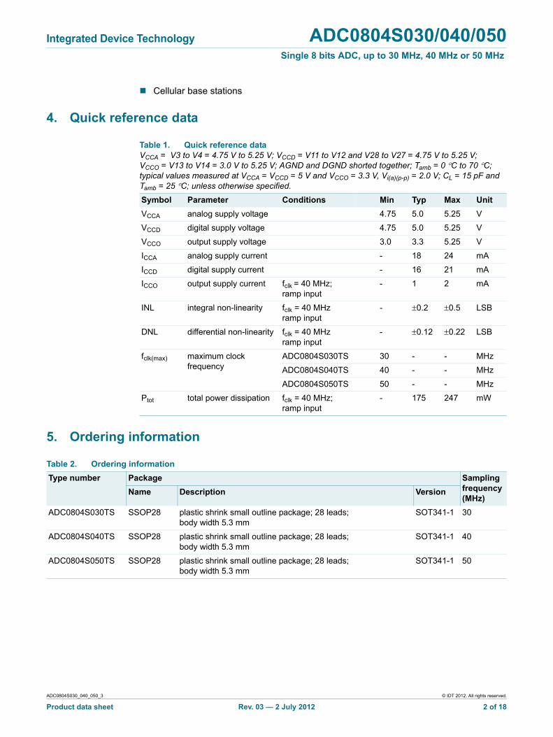
6. Block diagram
12
DGND2
6
8
Rlad
7
9
RB
RM
RT
VI
11
VCCD2
3
26
VCCA
21
22
23
24
20 D2
D3
D4
D5
D6
19
18
25
2
D1
D0
D7
IN-RANGE LATCH
CMOSOUTPUTS
LATCHES
CLOCK DRIVER
014aaa550
1
CLK
10
OE
TC
ADC0804S030
13VCCO
4
AGND
analog ground digital ground digital ground
27
DGND1
14
OGND
output ground
analogvoltage input
data outputs
LSB
MSB
28VCCD1
IR output
ANALOG - TO - DIGITALCONVERTER
CMOS OUTPUT
Fig 1. Block diagram
ADC0804S030_040_050_3 © IDT 2012. All rights reserved.
Product data sheet Rev. 03 — 2 July 2012 3 of 18
Integrated Device Technology ADC0804S030/040/050Single 8 bits ADC, up to 30 MHz, 40 MHz or 50 MHz
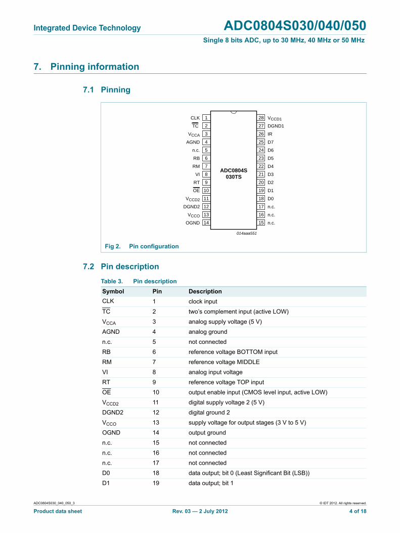
7. Pinning information
7.1 Pinning
ADC0804S030TS
CLK VCCD1
TC DGND1
VCCA IR
AGND D7
n.c. D6
RB D5
RM D4
VI D3
RT D2
OE D1
VCCD2 D0
DGND2 n.c.
VCCO n.c.
OGND n.c.
014aaa551
1
2
3
4
5
6
7
8
9
10
11
12
13
14
16
15
18
17
20
19
22
21
24
23
26
25
28
27
Fig 2. Pin configuration
7.2 Pin description
Table 3. Pin description
Symbol Pin Description
CLK 1 clock input
TC 2 two’s complement input (active LOW)
VCCA 3 analog supply voltage (5 V)
AGND 4 analog ground
n.c. 5 not connected
RB 6 reference voltage BOTTOM input
RM 7 reference voltage MIDDLE
VI 8 analog input voltage
RT 9 reference voltage TOP input
OE 10 output enable input (CMOS level input, active LOW)
VCCD2 11 digital supply voltage 2 (5 V)
DGND2 12 digital ground 2
VCCO 13 supply voltage for output stages (3 V to 5 V)
OGND 14 output ground
n.c. 15 not connected
n.c. 16 not connected
n.c. 17 not connected
D0 18 data output; bit 0 (Least Significant Bit (LSB))
D1 19 data output; bit 1
ADC0804S030_040_050_3 © IDT 2012. All rights reserved.
Product data sheet Rev. 03 — 2 July 2012 4 of 18
Integrated Device Technology ADC0804S030/040/050Single 8 bits ADC, up to 30 MHz, 40 MHz or 50 MHz
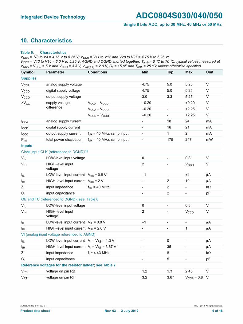
8. Limiting values
Table 4. Limiting valuesIn accordance with the Absolute Maximum Rating System (IEC 60134).
Symbol Parameter Conditions Min Max Unit
VCCA analog supply voltage [1] 0.3 +7.0 V
VCCD digital supply voltage [1] 0.3 +7.0 V
VCCO output supply voltage [1] 0.3 +7.0 V
VCC supply voltage difference VCCA VCCD 1.0 +1.0 V
VCCD VCCO 1.0 +4.0 V
VCCA VCCO 1.0 +4.0 V
VI input voltage referenced to AGND 0.3 +7.0 V
Vi(clk)(p-p) peak-to-peak clock input voltage
referenced to DGND - VCCD V
IO output current - 10 mA
Tstg storage temperature 55 +150 C
Tamb ambient temperature 40 +85 C
Tj junction temperature - 150 C
[1] The supply voltages VCCA, VCCD and VCCO may have any value between 0.3 V and +7.0 V provided that the supply voltage differences VCC are respected.
9. Thermal characteristics
Table 5. Thermal characteristics
Symbol Parameter Conditions Typ Unit
Rth(j-a) thermal resistance from junction to ambient
in free air 110 K/W
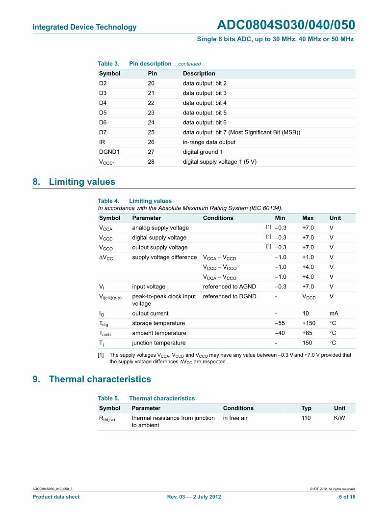
D2 20 data output; bit 2
D3 21 data output; bit 3
D4 22 data output; bit 4
D5 23 data output; bit 5
D6 24 data output; bit 6
D7 25 data output; bit 7 (Most Significant Bit (MSB))
IR 26 in-range data output
DGND1 27 digital ground 1
VCCD1 28 digital supply voltage 1 (5 V)
Table 3. Pin description …continued
Symbol Pin Description
ADC0804S030_040_050_3 © IDT 2012. All rights reserved.
Product data sheet Rev. 03 — 2 July 2012 5 of 18
Integrated Device Technology ADC0804S030/040/050Single 8 bits ADC, up to 30 MHz, 40 MHz or 50 MHz
10. Characteristics
Table 6. CharacteristicsVCCA = V3 to V4 = 4.75 V to 5.25 V; VCCD = V11 to V12 and V28 to V27 = 4.75 V to 5.25 V; VCCO = V13 to V14 = 3.0 V to 5.25 V; AGND and DGND shorted together; Tamb = 0 C to 70 C; typical values measured at VCCA = VCCD = 5 V and VCCO = 3.3 V, Vi(a)(p-p) = 2.0 V; CL = 15 pF and Tamb = 25 C; unless otherwise specified.
Symbol Parameter Conditions Min Typ Max Unit
Supplies
VCCA analog supply voltage 4.75 5.0 5.25 V
VCCD digital supply voltage 4.75 5.0 5.25 V
VCCO output supply voltage 3.0 3.3 5.25 V
VCC supply voltage difference
VCCA VCCD 0.20 - +0.20 V
VCCA VCCO 0.20 - +2.25 V
VCCD VCCO 0.20 - +2.25 V
ICCA analog supply current - 18 24 mA
ICCD digital supply current - 16 21 mA
ICCO output supply current fclk = 40 MHz; ramp input - 1 2 mA
Ptot total power dissipation fclk = 40 MHz; ramp input - 175 247 mW
Inputs
Clock input CLK (referenced to DGND)[1]
VIL LOW-level input voltage 0 - 0.8 V
VIH HIGH-level input voltage
2 - VCCD V
IIL LOW-level input current Vclk = 0.8 V 1 - +1 A
IIH HIGH-level input current Vclk = 2 V - 2 10 A
Zi input impedance fclk = 40 MHz - 2 - k
Ci input capacitance - 2 - pF
OE and TC (referenced to DGND); see Table 8
VIL LOW-level input voltage 0 - 0.8 V
VIH HIGH-level input voltage
2 - VCCD V
IIL LOW-level input current VIL = 0.8 V 1 - - A
IIH HIGH-level input current VIH = 2.0 V - - 1 A
VI (analog input voltage referenced to AGND)
IIL LOW-level input current VI = VRB = 1.3 V - 0 - A
IIH HIGH-level input current VI = VRT = 3.67 V - 35 - A
Zi input impedance fi = 4.43 MHz - 8 - k
Ci input capacitance - 5 - pF
Reference voltages for the resistor ladder; see Table 7
VRB voltage on pin RB 1.2 1.3 2.45 V
VRT voltage on pin RT 3.2 3.67 VCCA 0.8 V
ADC0804S030_040_050_3 © IDT 2012. All rights reserved.
Product data sheet Rev. 03 — 2 July 2012 6 of 18
Integrated Device Technology ADC0804S030/040/050Single 8 bits ADC, up to 30 MHz, 40 MHz or 50 MHz
Vref(dif) differential reference voltage
VRT VRB 2.0 2.37 3.0 V
Iref reference current VRT VRB = 2.37 V - 9.7 - mA
Rlad ladder resistance - 245 -
TCRlad ladder resistor temperature coefficient
- 456 - m/K
Voffset offset voltage BOTTOM; VRT VRB = 2.37 V
[2] - 175 - mV
TOP; VRT VRB = 2.37 V [2] - 175 - mV
Vi(a)(p-p) peak-to-peak analog input voltage
[3] 1.7 2.02 2.55 V
Digital outputs D7 to D0 and IR (referenced to OGND)
VOL LOW-level output voltage
IOL = 1 mA 0 - 0.5 V
VOH HIGH-level output voltage
IOH = 1 mA VCCO 0.5 - VCCO V
Io output current in 3-state mode; 0.5 V < VO < VCCO
20 - +20 A
Switching characteristics; Clock input CLK; see Figure 4[1]
fclk(max) maximum clock frequency
ADC0804S030TS 30 - - MHz
ADC0804S040TS 40 - - MHz
ADC0804S050TS 50 - - MHz
tw(clk)H HIGH clock pulse width full effective bandwidth 8.5 - - ns
tw(clk)L LOW clock pulse width full effective bandwidth 5.5 - - ns
Analog signal processing
Linearity
INL integral non-linearity fclk = 40 MHz; ramp input - 0.2 0.5 LSB
DNL differential non-linearity fclk = 40 MHz; ramp input - 0.12 0.22 LSB
Eoffset offset error middle code; VRB = 1.3 V; VRT = 3.67 V
- 0.25 - LSB
EG gain error from device to device; VRB = 1.3 V; VRT = 3.67 V
[4] - 0.1 - %
Bandwidth (fclk = 40 MHz)
B bandwidth full-scale sine wave [5] - 15 - MHz
75 % full-scale sine wave - 20 - MHz
small signal at mid-scale; VI = 10 LSB at code 512
- 350 - MHz
ts(LH) LOW to HIGH settling time
full-scale square wave; see Figure 6
[6] - 1.5 3.0 ns
ts(HL) HIGH to LOW settling time
- 1.5 3.0 ns
Table 6. CharacteristicsVCCA = V3 to V4 = 4.75 V to 5.25 V; VCCD = V11 to V12 and V28 to V27 = 4.75 V to 5.25 V; VCCO = V13 to V14 = 3.0 V to 5.25 V; AGND and DGND shorted together; Tamb = 0 C to 70 C; typical values measured at VCCA = VCCD = 5 V and VCCO = 3.3 V, Vi(a)(p-p) = 2.0 V; CL = 15 pF and Tamb = 25 C; unless otherwise specified.
Symbol Parameter Conditions Min Typ Max Unit
ADC0804S030_040_050_3 © IDT 2012. All rights reserved.
Product data sheet Rev. 03 — 2 July 2012 7 of 18
Integrated Device Technology ADC0804S030/040/050Single 8 bits ADC, up to 30 MHz, 40 MHz or 50 MHz
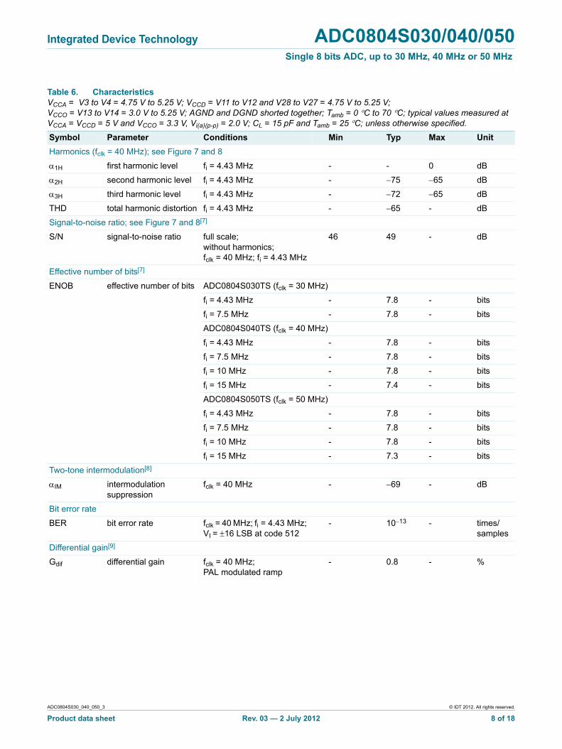
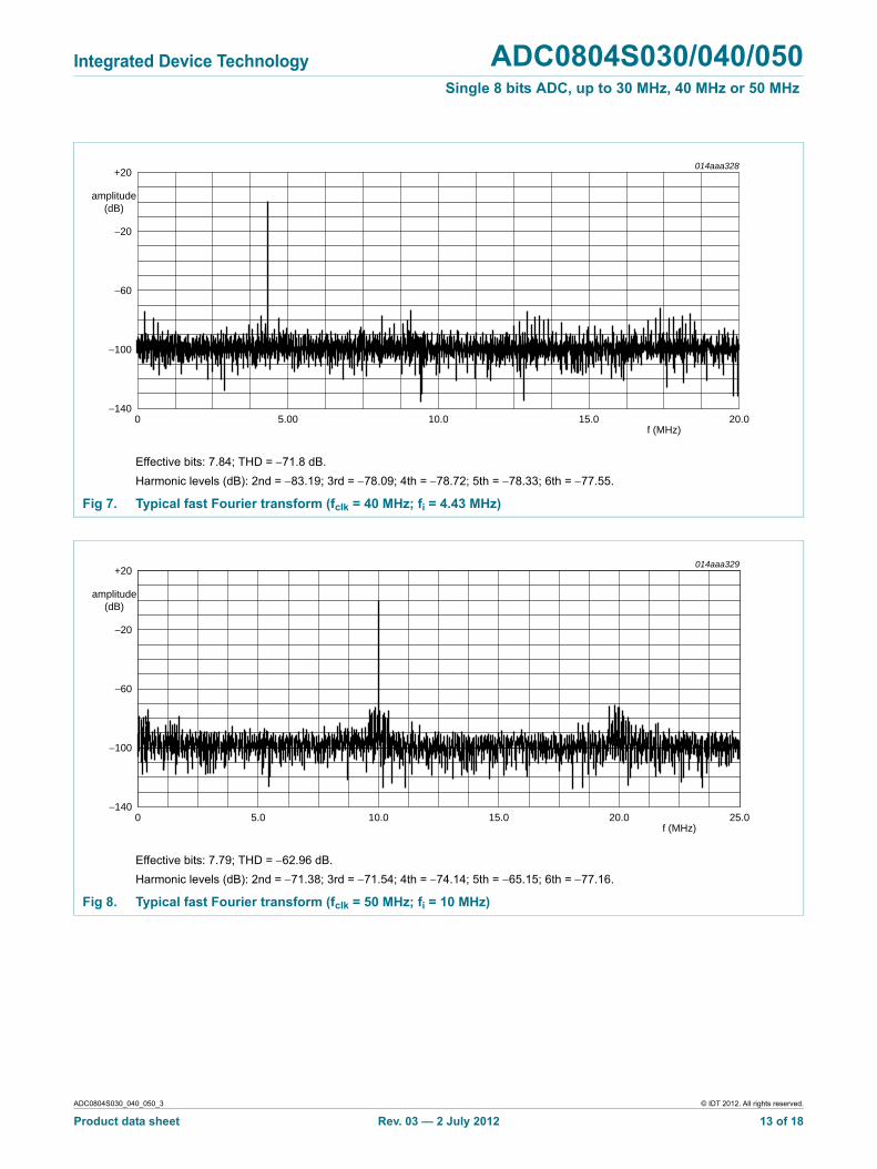
Harmonics (fclk = 40 MHz); see Figure 7 and 8
1H first harmonic level fi = 4.43 MHz - - 0 dB
2H second harmonic level fi = 4.43 MHz - 75 65 dB
3H third harmonic level fi = 4.43 MHz - 72 65 dB
THD total harmonic distortion fi = 4.43 MHz - 65 - dB
Signal-to-noise ratio; see Figure 7 and 8[7]
S/N signal-to-noise ratio full scale; without harmonics; fclk = 40 MHz; fi = 4.43 MHz
46 49 - dB
Effective number of bits[7]
ENOB effective number of bits ADC0804S030TS (fclk = 30 MHz)
fi = 4.43 MHz - 7.8 - bits
fi = 7.5 MHz - 7.8 - bits
ADC0804S040TS (fclk = 40 MHz)
fi = 4.43 MHz - 7.8 - bits
fi = 7.5 MHz - 7.8 - bits
fi = 10 MHz - 7.8 - bits
fi = 15 MHz - 7.4 - bits
ADC0804S050TS (fclk = 50 MHz)
fi = 4.43 MHz - 7.8 - bits
fi = 7.5 MHz - 7.8 - bits
fi = 10 MHz - 7.8 - bits
fi = 15 MHz - 7.3 - bits
Two-tone intermodulation[8]
IM intermodulation suppression
fclk = 40 MHz - 69 - dB
Bit error rate
BER bit error rate fclk = 40 MHz; fi = 4.43 MHz; VI = 16 LSB at code 512
- 1013 - times/ samples
Differential gain[9]
Gdif differential gain fclk = 40 MHz; PAL modulated ramp
- 0.8 - %
Table 6. CharacteristicsVCCA = V3 to V4 = 4.75 V to 5.25 V; VCCD = V11 to V12 and V28 to V27 = 4.75 V to 5.25 V; VCCO = V13 to V14 = 3.0 V to 5.25 V; AGND and DGND shorted together; Tamb = 0 C to 70 C; typical values measured at VCCA = VCCD = 5 V and VCCO = 3.3 V, Vi(a)(p-p) = 2.0 V; CL = 15 pF and Tamb = 25 C; unless otherwise specified.
Symbol Parameter Conditions Min Typ Max Unit
ADC0804S030_040_050_3 © IDT 2012. All rights reserved.
Product data sheet Rev. 03 — 2 July 2012 8 of 18

Integrated Device Technology ADC0804S030/040/050Single 8 bits ADC, up to 30 MHz, 40 MHz or 50 MHz
[1] In addition to a good layout of the digital and analog ground, it is recommended that the rise and fall times of the clock must not be less than 0.5 ns.
[2] Analog input voltages producing code 0 up to and including code 255:
a) Voffset BOTTOM is the difference between the analog input which produces data equal to 00 and the reference voltage on pin RB (VRB) at Tamb = 25 C.
b) Voffset TOP is the difference between the reference voltage on pin RT (VRT) and the analog input which produces data outputs equal to code 255 at Tamb = 25 C.
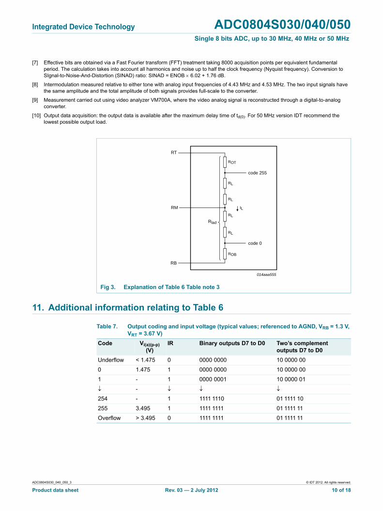
[3] To ensure the optimum linearity performance of such a converter architecture the lower and upper extremities of the converter reference resistor ladder are connected to pins RB and RT via offset resistors ROB and ROT as shown in Figure 3.
a) The current flowing into the resistor ladder is IVRT VRB–
ROB RL ROT+ +---------------------------------------= and the full-scale input range at the converter, to cover code 0
to 255 is VI RL ILRL
ROB RL ROT+ +--------------------------------------- VRT VRB+ 0.852 VRT VRB– = = =
b) Since RL, ROB and ROT have similar behavior with respect to process and temperature variation, the ratio RL
ROB RL ROT+ +---------------------------------------
will be kept reasonably constant from device to device. Consequently, the variation of the output codes at a given input voltage depends mainly on the difference VRT VRB and its variation with temperature and supply voltage. When several ADCs are connected in parallel and fed with the same reference source, the matching between each of them is optimized.
[4] EGV1023 V0– Vi p p– –
Vi p p– ------------------------------------------------------- 100=
[5] The analog bandwidth is defined as the maximum input sine wave frequency which can be applied to the device. No glitches greater than 0.5 LSB, neither any significant attenuation are observed in the reconstructed signal.
[6] The analog input settling time is the minimum time required for the input signal to be stabilized after a sharp full-scale input (square wave signal) in order to sample the signal and obtain correct output data.
Differential phase[9]
dif differential phase fclk = 40 MHz; PAL modulated ramp
- 0.4 - deg
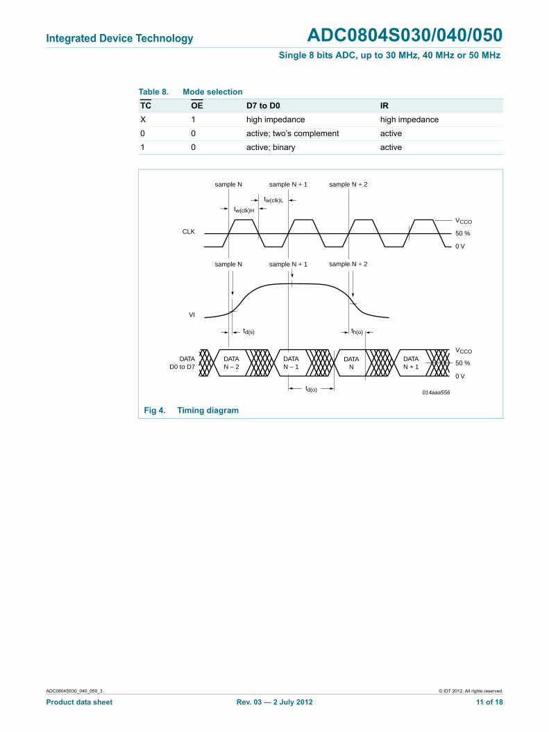
Timing (fclk = 40 MHz; Ci = 15 pF); see Figure 4[10]
td(s) sampling delay time - 3 - ns
th(o) output hold time 4 - - ns
td(o) output delay time VCCO = 4.75 V - 10 13 ns
VCCO = 3.15 V - 12 15 ns
CL load capacitance - - 15 pF
3-state output delay times; see Figure 5
tdZH float to active HIGH delay time
- 5.5 8.5 ns
tdZL float to active LOW delay time
- 12 15 ns
tdHZ active HIGH to float delay time
- 19 24 ns
tdLZ active LOW to float delay time
- 12 15 ns
Table 6. CharacteristicsVCCA = V3 to V4 = 4.75 V to 5.25 V; VCCD = V11 to V12 and V28 to V27 = 4.75 V to 5.25 V; VCCO = V13 to V14 = 3.0 V to 5.25 V; AGND and DGND shorted together; Tamb = 0 C to 70 C; typical values measured at VCCA = VCCD = 5 V and VCCO = 3.3 V, Vi(a)(p-p) = 2.0 V; CL = 15 pF and Tamb = 25 C; unless otherwise specified.
Symbol Parameter Conditions Min Typ Max Unit
ADC0804S030_040_050_3 © IDT 2012. All rights reserved.
Product data sheet Rev. 03 — 2 July 2012 9 of 18
Integrated Device Technology ADC0804S030/040/050Single 8 bits ADC, up to 30 MHz, 40 MHz or 50 MHz
[7] Effective bits are obtained via a Fast Fourier transform (FFT) treatment taking 8000 acquisition points per equivalent fundamental period. The calculation takes into account all harmonics and noise up to half the clock frequency (Nyquist frequency). Conversion to SIgnal-to-Noise-And-Distortion (SINAD) ratio: SINAD = ENOB 6.02 + 1.76 dB.
[8] Intermodulation measured relative to either tone with analog input frequencies of 4.43 MHz and 4.53 MHz. The two input signals have the same amplitude and the total amplitude of both signals provides full-scale to the converter.
[9] Measurement carried out using video analyzer VM700A, where the video analog signal is reconstructed through a digital-to-analog converter.
[10] Output data acquisition: the output data is available after the maximum delay time of td(0). For 50 MHz version IDT recommend the lowest possible output load.
014aaa555
RT
RB
RM
Rlad
ROT
RL
RL
RL
RL
IL
ROB
code 255
code 0
Fig 3. Explanation of Table 6 Table note 3
11. Additional information relating to Table 6
Table 7. Output coding and input voltage (typical values; referenced to AGND, VRB = 1.3 V, VRT = 3.67 V)
Code Vi(a)(p-p) (V)
IR Binary outputs D7 to D0 Two’s complement outputs D7 to D0
Underflow < 1.475 0 0000 0000 10 0000 00
0 1.475 1 0000 0000 10 0000 00
1 - 1 0000 0001 10 0000 01
-
254 - 1 1111 1110 01 1111 10
255 3.495 1 1111 1111 01 1111 11
Overflow > 3.495 0 1111 1111 01 1111 11
ADC0804S030_040_050_3 © IDT 2012. All rights reserved.
Product data sheet Rev. 03 — 2 July 2012 10 of 18
Integrated Device Technology ADC0804S030/040/050Single 8 bits ADC, up to 30 MHz, 40 MHz or 50 MHz
Table 8. Mode selection
TC OE D7 to D0 IR
X 1 high impedance high impedance
0 0 active; two’s complement active
1 0 active; binary active
014aaa556
CLK
VI
DATAN − 2
DATAD0 to D7
DATAN − 1
DATAN
DATAN + 1
sample N + 2sample N + 1
VCCO
sample N
sample N + 2sample N + 1sample N
tw(clk)H
tw(clk)L
td(s)
td(o)
th(o)
50 %
0 V
VCCO
50 %
0 V
Fig 4. Timing diagram
ADC0804S030_040_050_3 © IDT 2012. All rights reserved.
Product data sheet Rev. 03 — 2 July 2012 11 of 18

Integrated Device Technology ADC0804S030/040/050Single 8 bits ADC, up to 30 MHz, 40 MHz or 50 MHz
LOW
HIGH
HIGH
LOW
ADC0804S030
VCCD
VCCD
S1
OE
OE
outputdata
outputdata
10 %
50 %
50 %
90 %
50 %
tdLZ tdZL
tdHZ tdZH
15 pF
3.3 kΩ
S1TEST
VCCDtdLZ
VCCDtdZL
DGNDtdZH
tdHZ DGND
014aaa552
frequency on pin OE = 100 kHz
Fig 5. Timing diagram and test conditions of 3-state output delay time
014aaa400
code 255
code 0
50 % 50 %CLK
VI
ts(LH) ts(HL)
50 % 50 %
2 ns 2 ns
0.5 ns 0.5 ns
Fig 6. Analog input settling time diagram
ADC0804S030_040_050_3 © IDT 2012. All rights reserved.
Product data sheet Rev. 03 — 2 July 2012 12 of 18
Integrated Device Technology ADC0804S030/040/050Single 8 bits ADC, up to 30 MHz, 40 MHz or 50 MHz
014aaa328
−60
−100
−20
+20
amplitude(dB)
−140
f (MHz)0 20.015.05.00 10.0
Effective bits: 7.84; THD = 71.8 dB.
Harmonic levels (dB): 2nd = 83.19; 3rd = 78.09; 4th = 78.72; 5th = 78.33; 6th = 77.55.
Fig 7. Typical fast Fourier transform (fclk = 40 MHz; fi = 4.43 MHz)
0f (MHz)
20.0 25.015.05.0 10.0
014aaa329
−60
−100
−20
+20
amplitude(dB)
−140
Effective bits: 7.79; THD = 62.96 dB.
Harmonic levels (dB): 2nd = 71.38; 3rd = 71.54; 4th = 74.14; 5th = 65.15; 6th = 77.16.
Fig 8. Typical fast Fourier transform (fclk = 50 MHz; fi = 10 MHz)
ADC0804S030_040_050_3 © IDT 2012. All rights reserved.
Product data sheet Rev. 03 — 2 July 2012 13 of 18
Integrated Device Technology ADC0804S030/040/050Single 8 bits ADC, up to 30 MHz, 40 MHz or 50 MHz
014aaa557
VCCO
D7 to D0IR
OGND
VCCA
VI
AGND
014aaa526
Fig 9. CMOS data and in-range outputs Fig 10. Analog inputs
014aaa553
VCCO
OGND
OETC
VCCA
RT
RM
RB
AGND
014aaa331
RL
RL
RL
RL
Fig 11. OE and TC input Fig 12. RB, RM and RT
VCCD
CLK 1.5 V
DGND
014aaa399
Fig 13. CLK input
ADC0804S030_040_050_3 © IDT 2012. All rights reserved.
Product data sheet Rev. 03 — 2 July 2012 14 of 18
Integrated Device Technology ADC0804S030/040/050Single 8 bits ADC, up to 30 MHz, 40 MHz or 50 MHz
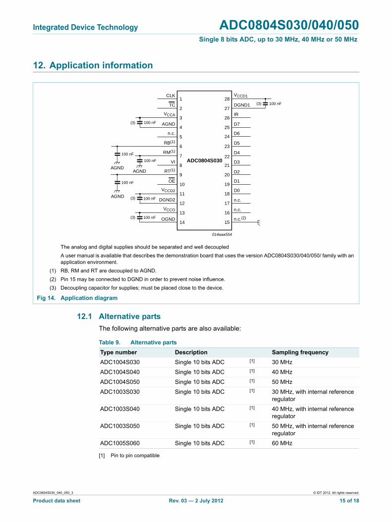
12. Application information
ADC0804S030
CLK VCCD1
TC DGND1
VCCA IR
AGND D7
n.c. D6
RB(1) D5
RM(1) D4
VI D3
RT(1) D2
OE D1
VCCD2 D0
DGND2 n.c.
VCCO n.c.
OGND n.c.(2)
014aaa554
1
2
3
4
5
6
7
8
9
10
11
12
13
14
16
15
18
17
20
19
22
21
24
23
26
25
28
27100 nF
100 nF
100 nF
100 nF
100 nF
100 nF
100 nF
(3)
(3)
(3)
(3)
AGND
AGND
AGND
The analog and digital supplies should be separated and well decoupled
A user manual is available that describes the demonstration board that uses the version ADC0804S030/040/050/ family with an application environment.
(1) RB, RM and RT are decoupled to AGND.
(2) Pin 15 may be connected to DGND in order to prevent noise influence.
(3) Decoupling capacitor for supplies; must be placed close to the device.
Fig 14. Application diagram
12.1 Alternative parts
The following alternative parts are also available:
Table 9. Alternative parts
Type number Description Sampling frequency
ADC1004S030 Single 10 bits ADC [1] 30 MHz
ADC1004S040 Single 10 bits ADC [1] 40 MHz
ADC1004S050 Single 10 bits ADC [1] 50 MHz
ADC1003S030 Single 10 bits ADC [1] 30 MHz, with internal reference regulator
ADC1003S040 Single 10 bits ADC [1] 40 MHz, with internal reference regulator
ADC1003S050 Single 10 bits ADC [1] 50 MHz, with internal reference regulator
ADC1005S060 Single 10 bits ADC [1] 60 MHz
[1] Pin to pin compatible
ADC0804S030_040_050_3 © IDT 2012. All rights reserved.
Product data sheet Rev. 03 — 2 July 2012 15 of 18
Integrated Device Technology ADC0804S030/040/050Single 8 bits ADC, up to 30 MHz, 40 MHz or 50 MHz
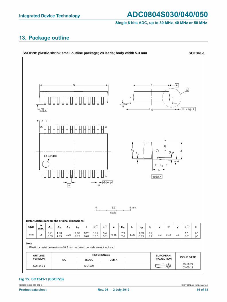
13. Package outline
UNIT A1 A2 A3 bp c D(1) E(1) (1)e HE L Lp Q Zywv θ
REFERENCESOUTLINEVERSION
EUROPEANPROJECTION ISSUE DATE
IEC JEDEC JEITA
mm 0.210.05
1.801.65
0.380.25
0.200.09
10.410.0
5.45.2
0.65 1.257.97.6
0.90.7
1.10.7
80
o
o0.13 0.10.2
DIMENSIONS (mm are the original dimensions)
Note
1. Plastic or metal protrusions of 0.2 mm maximum per side are not included.
1.030.63
SOT341-1 MO-15099-12-2703-02-19
X
w M
θ
AA1
A2
bp
D
HE
Lp
Q
detail X
E
Z
e
c
L
v M A
(A )3
A
1 14
28 15
0.25
y
pin 1 index
0 2.5 5 mm
scale
SSOP28: plastic shrink small outline package; 28 leads; body width 5.3 mm SOT341-1
Amax.
2
Fig 15. SOT341-1 (SSOP28)
ADC0804S030_040_050_3 © IDT 2012. All rights reserved.
Product data sheet Rev. 03 — 2 July 2012 16 of 18
Integrated Device Technology ADC0804S030/040/050Single 8 bits ADC, up to 30 MHz, 40 MHz or 50 MHz
14. Revision history
Table 10. Revision history
Document ID Release date Data sheet status Change notice
Supersedes
ADC0804S030_040_050_3 20120702 Product data sheet - ADC0804S030_040_050_2
ADC0804S030_040_050_2 20080814 Product data sheet - ADC0804S030_040_050_1
Modifications: Paragraph added to Section• 1.
Corrections to descriptions of rows RB and RM in Table• 3.
Corrections to Table• 6.
Corrections to Figure• 9, 10 and 12.
ADC0804S030_040_050_1 20080616 Product data sheet - -
15. Contact information
For more information or sales office addresses, please visit: http://www.idt.com
ADC0804S030_040_050_3 © IDT 2012. All rights reserved.
Product data sheet Rev. 03 — 2 July 2012 17 of 18
Integrated Device Technology ADC0804S030/040/050Single 8 bits ADC, up to 30 MHz, 40 MHz or 50 MHz
16. Contents
1 General description . . . . . . . . . . . . . . . . . . . . . . 1
2 Features . . . . . . . . . . . . . . . . . . . . . . . . . . . . . . . 1
3 Applications . . . . . . . . . . . . . . . . . . . . . . . . . . . . 1
4 Quick reference data . . . . . . . . . . . . . . . . . . . . . 2
5 Ordering information. . . . . . . . . . . . . . . . . . . . . 2
6 Block diagram . . . . . . . . . . . . . . . . . . . . . . . . . . 3
7 Pinning information. . . . . . . . . . . . . . . . . . . . . . 47.1 Pinning . . . . . . . . . . . . . . . . . . . . . . . . . . . . . . . 47.2 Pin description . . . . . . . . . . . . . . . . . . . . . . . . . 4
8 Limiting values. . . . . . . . . . . . . . . . . . . . . . . . . . 5
9 Thermal characteristics . . . . . . . . . . . . . . . . . . 5
10 Characteristics . . . . . . . . . . . . . . . . . . . . . . . . . 6
11 Additional information relating to Table 6 . . 10
12 Application information . . . . . . . . . . . . . . . . . 1512.1 Alternative parts . . . . . . . . . . . . . . . . . . . . . . . 15
13 Package outline. . . . . . . . . . . . . . . . . . . . . . . . 16
14 Revision history . . . . . . . . . . . . . . . . . . . . . . . 17
15 Contact information . . . . . . . . . . . . . . . . . . . . 17
16 Contents. . . . . . . . . . . . . . . . . . . . . . . . . . . . . . 18
ADC0804S030_040_050_3 © IDT 2012. All rights reserved.
Product data sheet Rev. 03 — 2 July 2012 18 of 18