m16c/29 group hardware manual - renesas
TRANSCRIPT
To our customers,
Old Company Name in Catalogs and Other Documents
On April 1st, 2010, NEC Electronics Corporation merged with Renesas Technology
Corporation, and Renesas Electronics Corporation took over all the business of both companies. Therefore, although the old company name remains in this document, it is a valid Renesas Electronics document. We appreciate your understanding.
Renesas Electronics website: http://www.renesas.com
April 1st, 2010 Renesas Electronics Corporation
Issued by: Renesas Electronics Corporation (http://www.renesas.com)
Send any inquiries to http://www.renesas.com/inquiry.
Notice 1. All information included in this document is current as of the date this document is issued. Such information, however, is
subject to change without any prior notice. Before purchasing or using any Renesas Electronics products listed herein, please confirm the latest product information with a Renesas Electronics sales office. Also, please pay regular and careful attention to additional and different information to be disclosed by Renesas Electronics such as that disclosed through our website.
2. Renesas Electronics does not assume any liability for infringement of patents, copyrights, or other intellectual property rights of third parties by or arising from the use of Renesas Electronics products or technical information described in this document. No license, express, implied or otherwise, is granted hereby under any patents, copyrights or other intellectual property rights of Renesas Electronics or others.
3. You should not alter, modify, copy, or otherwise misappropriate any Renesas Electronics product, whether in whole or in part. 4. Descriptions of circuits, software and other related information in this document are provided only to illustrate the operation of
semiconductor products and application examples. You are fully responsible for the incorporation of these circuits, software, and information in the design of your equipment. Renesas Electronics assumes no responsibility for any losses incurred by you or third parties arising from the use of these circuits, software, or information.
5. When exporting the products or technology described in this document, you should comply with the applicable export control laws and regulations and follow the procedures required by such laws and regulations. You should not use Renesas Electronics products or the technology described in this document for any purpose relating to military applications or use by the military, including but not limited to the development of weapons of mass destruction. Renesas Electronics products and technology may not be used for or incorporated into any products or systems whose manufacture, use, or sale is prohibited under any applicable domestic or foreign laws or regulations.
6. Renesas Electronics has used reasonable care in preparing the information included in this document, but Renesas Electronics does not warrant that such information is error free. Renesas Electronics assumes no liability whatsoever for any damages incurred by you resulting from errors in or omissions from the information included herein.
7. Renesas Electronics products are classified according to the following three quality grades: “Standard”, “High Quality”, and “Specific”. The recommended applications for each Renesas Electronics product depends on the product’s quality grade, as indicated below. You must check the quality grade of each Renesas Electronics product before using it in a particular application. You may not use any Renesas Electronics product for any application categorized as “Specific” without the prior written consent of Renesas Electronics. Further, you may not use any Renesas Electronics product for any application for which it is not intended without the prior written consent of Renesas Electronics. Renesas Electronics shall not be in any way liable for any damages or losses incurred by you or third parties arising from the use of any Renesas Electronics product for an application categorized as “Specific” or for which the product is not intended where you have failed to obtain the prior written consent of Renesas Electronics. The quality grade of each Renesas Electronics product is “Standard” unless otherwise expressly specified in a Renesas Electronics data sheets or data books, etc.
“Standard”: Computers; office equipment; communications equipment; test and measurement equipment; audio and visual equipment; home electronic appliances; machine tools; personal electronic equipment; and industrial robots.
“High Quality”: Transportation equipment (automobiles, trains, ships, etc.); traffic control systems; anti-disaster systems; anti-crime systems; safety equipment; and medical equipment not specifically designed for life support.
“Specific”: Aircraft; aerospace equipment; submersible repeaters; nuclear reactor control systems; medical equipment or systems for life support (e.g. artificial life support devices or systems), surgical implantations, or healthcare intervention (e.g. excision, etc.), and any other applications or purposes that pose a direct threat to human life.
8. You should use the Renesas Electronics products described in this document within the range specified by Renesas Electronics, especially with respect to the maximum rating, operating supply voltage range, movement power voltage range, heat radiation characteristics, installation and other product characteristics. Renesas Electronics shall have no liability for malfunctions or damages arising out of the use of Renesas Electronics products beyond such specified ranges.
9. Although Renesas Electronics endeavors to improve the quality and reliability of its products, semiconductor products have specific characteristics such as the occurrence of failure at a certain rate and malfunctions under certain use conditions. Further, Renesas Electronics products are not subject to radiation resistance design. Please be sure to implement safety measures to guard them against the possibility of physical injury, and injury or damage caused by fire in the event of the failure of a Renesas Electronics product, such as safety design for hardware and software including but not limited to redundancy, fire control and malfunction prevention, appropriate treatment for aging degradation or any other appropriate measures. Because the evaluation of microcomputer software alone is very difficult, please evaluate the safety of the final products or system manufactured by you.
10. Please contact a Renesas Electronics sales office for details as to environmental matters such as the environmental compatibility of each Renesas Electronics product. Please use Renesas Electronics products in compliance with all applicable laws and regulations that regulate the inclusion or use of controlled substances, including without limitation, the EU RoHS Directive. Renesas Electronics assumes no liability for damages or losses occurring as a result of your noncompliance with applicable laws and regulations.
11. This document may not be reproduced or duplicated, in any form, in whole or in part, without prior written consent of Renesas Electronics.
12. Please contact a Renesas Electronics sales office if you have any questions regarding the information contained in this document or Renesas Electronics products, or if you have any other inquiries.
(Note 1) “Renesas Electronics” as used in this document means Renesas Electronics Corporation and also includes its majority-owned subsidiaries.
(Note 2) “Renesas Electronics product(s)” means any product developed or manufactured by or for Renesas Electronics.
M16C/29 GroupHardware Manual
16
Rev.1.12 2007.03
RENESAS MCUM16C FAMILY / M16C/Tiny SERIES
All information contained in these materials, including products and product specifications, represents information on the product at the time of publication and is subject to change by Renesas Electronics Corp. without notice. Please review the latest information published by Renesas Electronics Corp. through various means, including the Renesas Electronics Corp. website (http://www.renesas.com).
User’s M
anual

1. This document is provided for reference purposes only so that Renesas customers may select the appropriate Renesas products for their use. Renesas neither makes warranties or representations with respect to the accuracy or completeness of the information contained in this document nor grants any license to any intellectual property rights or any other rights of Renesas or any third party with respect to the information in this document. 2. Renesas shall have no liability for damages or infringement of any intellectual property or other rights arising out of the use of any information in this document, including, but not limited to, product data, diagrams, charts, programs, algorithms, and application circuit examples.3. You should not use the products or the technology described in this document for the purpose of military applications such as the development of weapons of mass destruction or for the purpose of any other military use. When exporting the products or technology described herein, you should follow the applicable export control laws and regulations, and procedures required by such laws and regulations.4. All information included in this document such as product data, diagrams, charts, programs, algorithms, and application circuit examples, is current as of the date this document is issued. Such information, however, is subject to change without any prior notice. Before purchasing or using any Renesas products listed in this document, please confirm the latest product information with a Renesas sales office. Also, please pay regular and careful attention to additional and different information to be disclosed by Renesas such as that disclosed through our website. (http://www.renesas.com )5. Renesas has used reasonable care in compiling the information included in this document, but Renesas assumes no liability whatsoever for any damages incurred as a result of errors or omissions in the information included in this document.6. When using or otherwise relying on the information in this document, you should evaluate the information in light of the total system before deciding about the applicability of such information to the intended application. Renesas makes no representations, warranties or guaranties regarding the suitability of its products for any particular application and specifically disclaims any liability arising out of the application and use of the information in this document or Renesas products. 7. With the exception of products specified by Renesas as suitable for automobile applications, Renesas products are not designed, manufactured or tested for applications or otherwise in systems the failure or malfunction of which may cause a direct threat to human life or create a risk of human injury or which require especially high quality and reliability such as safety systems, or equipment or systems for transportation and traffic, healthcare, combustion control, aerospace and aeronautics, nuclear power, or undersea communication transmission. If you are considering the use of our products for such purposes, please contact a Renesas sales office beforehand. Renesas shall have no liability for damages arising out of the uses set forth above.8. Notwithstanding the preceding paragraph, you should not use Renesas products for the purposes listed below: (1) artificial life support devices or systems (2) surgical implantations (3) healthcare intervention (e.g., excision, administration of medication, etc.) (4) any other purposes that pose a direct threat to human life Renesas shall have no liability for damages arising out of the uses set forth in the above and purchasers who elect to use Renesas products in any of the foregoing applications shall indemnify and hold harmless Renesas Technology Corp., its affiliated companies and their officers, directors, and employees against any and all damages arising out of such applications. 9. You should use the products described herein within the range specified by Renesas, especially with respect to the maximum rating, operating supply voltage range, movement power voltage range, heat radiation characteristics, installation and other product characteristics. Renesas shall have no liability for malfunctions or damages arising out of the use of Renesas products beyond such specified ranges.10. Although Renesas endeavors to improve the quality and reliability of its products, IC products have specific characteristics such as the occurrence of failure at a certain rate and malfunctions under certain use conditions. Please be sure to implement safety measures to guard against the possibility of physical injury, and injury or damage caused by fire in the event of the failure of a Renesas product, such as safety design for hardware and software including but not limited to redundancy, fire control and malfunction prevention, appropriate treatment for aging degradation or any other applicable measures. Among others, since the evaluation of microcomputer software alone is very difficult, please evaluate the safety of the final products or system manufactured by you. 11. In case Renesas products listed in this document are detached from the products to which the Renesas products are attached or affixed, the risk of accident such as swallowing by infants and small children is very high. You should implement safety measures so that Renesas products may not be easily detached from your products. Renesas shall have no liability for damages arising out of such detachment.12. This document may not be reproduced or duplicated, in any form, in whole or in part, without prior written approval from Renesas. 13. Please contact a Renesas sales office if you have any questions regarding the information contained in this document, Renesas semiconductor products, or if you have any other inquiries.
Notes regarding these materials

General Precautions in the Handling of MPU/MCU Products
The following usage notes are applicable to all MPU/MCU products from Renesas. For detailed usage notes on the products covered by this manual, refer to the relevant sections of the manual. If the descriptions under General Precautions in the Handling of MPU/MCU Products and in the body of the manual differ from each other, the description in the body of the manual takes precedence.
1. Handling of Unused Pins Handle unused pins in accord with the directions given under Handling of Unused Pins in the manual. The input pins of CMOS products are generally in the high-impedance state. In operation
with an unused pin in the open-circuit state, extra electromagnetic noise is induced in the vicinity of LSI, an associated shoot-through current flows internally, and malfunctions occur due to the false recognition of the pin state as an input signal become possible. Unused pins should be handled as described under Handling of Unused Pins in the manual.
2. Processing at Power-on The state of the product is undefined at the moment when power is supplied. The states of internal circuits in the LSI are indeterminate and the states of register
settings and pins are undefined at the moment when power is supplied. In a finished product where the reset signal is applied to the external reset pin, the states of pins are not guaranteed from the moment when power is supplied until the reset process is completed. In a similar way, the states of pins in a product that is reset by an on-chip power-on reset function are not guaranteed from the moment when power is supplied until the power reaches the level at which resetting has been specified.
3. Prohibition of Access to Reserved Addresses Access to reserved addresses is prohibited. The reserved addresses are provided for the possible future expansion of functions. Do
not access these addresses; the correct operation of LSI is not guaranteed if they are accessed.
4. Clock Signals After applying a reset, only release the reset line after the operating clock signal has become stable. When switching the clock signal during program execution, wait until the target clock signal has stabilized. When the clock signal is generated with an external resonator (or from an external
oscillator) during a reset, ensure that the reset line is only released after full stabilization of the clock signal. Moreover, when switching to a clock signal produced with an external resonator (or by an external oscillator) while program execution is in progress, wait until the target clock signal is stable.
5. Differences between Products Before changing from one product to another, i.e. to one with a different part number, confirm that the change will not lead to problems. The characteristics of MPU/MCU in the same group but having different part numbers may
differ because of the differences in internal memory capacity and layout pattern. When changing to products of different part numbers, implement a system-evaluation test for each of the products.
How to Use This Manual1. Purpose and Target Readers
This manual is designed to provide the user with an understanding of the hardware functions and electricalcharacteristics of the MCU. It is intended for users designing application systems incorporating the MCU. A basicknowledge of electric circuits, logical circuits, and MCUs is necessary in order to use this manual.The manual comprises an overview of the product; descriptions of the CPU, system control functions, peripheralfunctions, and electrical characteristics; and usage notes.
Particular attention should be paid to the precautionary notes when using the manual. These notes occurwithin the body of the text, at the end of each section, and in the Usage Notes section.
The revision history summarizes the locations of revisions and additions. It does not list all revisions. Referto the text of the manual for details.
The following documents apply to the M16C/29 Group. Make sure to refer to the latest versions of these documents.The newest versions of the documents listed may be obtained from the Renesas Technology Web site.
Document Type Description Document Title Document No.Hardware manual Hardware specifications (pin assignments,
memory maps, peripheral function specifications, electrical characteristics, timing charts) and operation descriptionNote: Refer to the application notes for details on using peripheral functions.
M16C/29 Group Hardware Manual
This hardware manual
Software manual Description of CPU instruction set M16C/60, M16C/20, M16C/Tiny Series Software Manual
REJ09B0137
Application note Information on using peripheral functions and application examplesSample programsInformation on writing programs in assembly language and C
Available from Renesas Technology Web site.
Renesas technical update
Product specifications, updates on documents, etc.
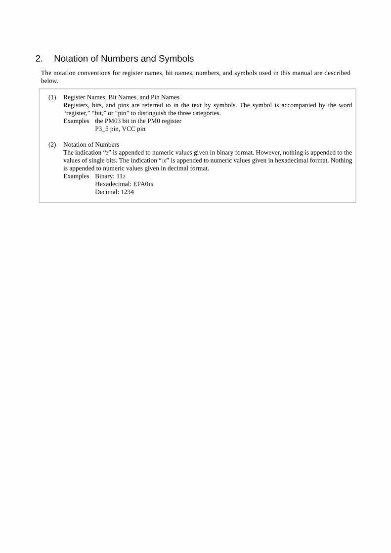
2. Notation of Numbers and SymbolsThe notation conventions for register names, bit names, numbers, and symbols used in this manual are describedbelow.
(1) Register Names, Bit Names, and Pin NamesRegisters, bits, and pins are referred to in the text by symbols. The symbol is accompanied by the word“register,” “bit,” or “pin” to distinguish the three categories.Examples the PM03 bit in the PM0 register
P3_5 pin, VCC pin
(2) Notation of NumbersThe indication “2” is appended to numeric values given in binary format. However, nothing is appended to thevalues of single bits. The indication “16” is appended to numeric values given in hexadecimal format. Nothingis appended to numeric values given in decimal format.Examples Binary: 112
Hexadecimal: EFA016
Decimal: 1234
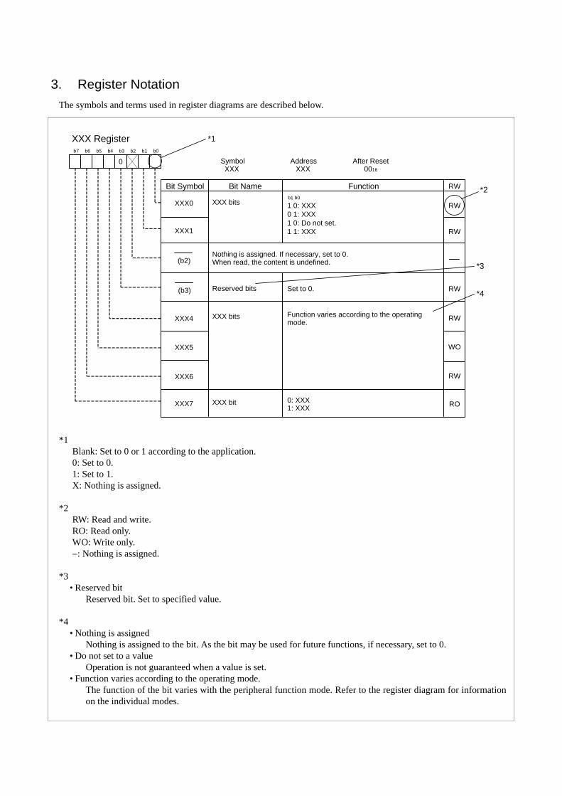
3. Register NotationThe symbols and terms used in register diagrams are described below.
*1Blank: Set to 0 or 1 according to the application.0: Set to 0.1: Set to 1.X: Nothing is assigned.
*2RW: Read and write.RO: Read only.WO: Write only.−: Nothing is assigned.
*3• Reserved bit
Reserved bit. Set to specified value.
*4• Nothing is assigned
Nothing is assigned to the bit. As the bit may be used for future functions, if necessary, set to 0.• Do not set to a value
Operation is not guaranteed when a value is set.• Function varies according to the operating mode.
The function of the bit varies with the peripheral function mode. Refer to the register diagram for informationon the individual modes.
XXX Register
Symbol Address After Reset XXX XXX 0016
Bit NameBit Symbol RW
b7 b6 b5 b4 b3 b2 b1 b0
XXX bits 1 0: XXX0 1: XXX1 0: Do not set.1 1: XXX
b1 b0
XXX1
XXX0
XXX4
Reserved bits
XXX5
XXX7
XXX6
Function
Nothing is assigned. If necessary, set to 0.When read, the content is undefined.
XXX bit
Function varies according to the operatingmode.
Set to 0.
0
(b3)
(b2)
RW
RW
RW
RW
WO
RW
RO
XXX bits
0: XXX1: XXX
*1
*2
*3
*4
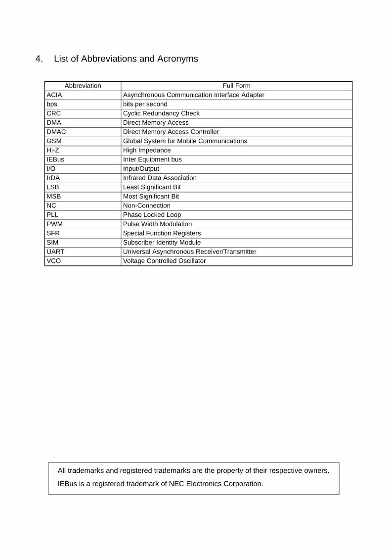
4. List of Abbreviations and Acronyms
Abbreviation Full FormACIA Asynchronous Communication Interface Adapterbps bits per secondCRC Cyclic Redundancy CheckDMA Direct Memory AccessDMAC Direct Memory Access ControllerGSM Global System for Mobile CommunicationsHi-Z High ImpedanceIEBus Inter Equipment busI/O Input/OutputIrDA Infrared Data AssociationLSB Least Significant BitMSB Most Significant BitNC Non-ConnectionPLL Phase Locked LoopPWM Pulse Width ModulationSFR Special Function RegistersSIM Subscriber Identity ModuleUART Universal Asynchronous Receiver/TransmitterVCO Voltage Controlled Oscillator
All trademarks and registered trademarks are the property of their respective owners.
IEBus is a registered trademark of NEC Electronics Corporation.
A-1
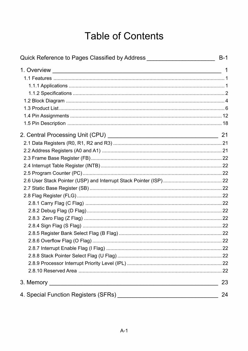
Table of Contents
Quick Reference to Pages Classified by Address _____________________ B-1
1. Overview ____________________________________________________ 11.1 Features ........................................................................................................................... 1
1.1.1 Applications ................................................................................................................ 11.1.2 Specifications ............................................................................................................. 2
1.2 Block Diagram .................................................................................................................. 41.3 Product List ....................................................................................................................... 61.4 Pin Assignments ............................................................................................................. 121.5 Pin Description ............................................................................................................... 18
2. Central Processing Unit (CPU) __________________________________ 212.1 Data Registers (R0, R1, R2 and R3) .............................................................................. 212.2 Address Registers (A0 and A1) ...................................................................................... 212.3 Frame Base Register (FB) .............................................................................................. 222.4 Interrupt Table Register (INTB) ....................................................................................... 222.5 Program Counter (PC) .................................................................................................... 222.6 User Stack Pointer (USP) and Interrupt Stack Pointer (ISP) .......................................... 222.7 Static Base Register (SB) ............................................................................................... 222.8 Flag Register (FLG) ........................................................................................................ 22
2.8.1 Carry Flag (C Flag) .................................................................................................. 222.8.2 Debug Flag (D Flag) ................................................................................................. 222.8.3 Zero Flag (Z Flag) ................................................................................................... 222.8.4 Sign Flag (S Flag) .................................................................................................... 222.8.5 Register Bank Select Flag (B Flag) .......................................................................... 222.8.6 Overflow Flag (O Flag) ............................................................................................. 222.8.7 Interrupt Enable Flag (I Flag) ................................................................................... 222.8.8 Stack Pointer Select Flag (U Flag) ........................................................................... 222.8.9 Processor Interrupt Priority Level (IPL) .................................................................... 222.8.10 Reserved Area ....................................................................................................... 22
3. Memory ____________________________________________________ 23
4. Special Function Registers (SFRs) _______________________________ 24
A-2
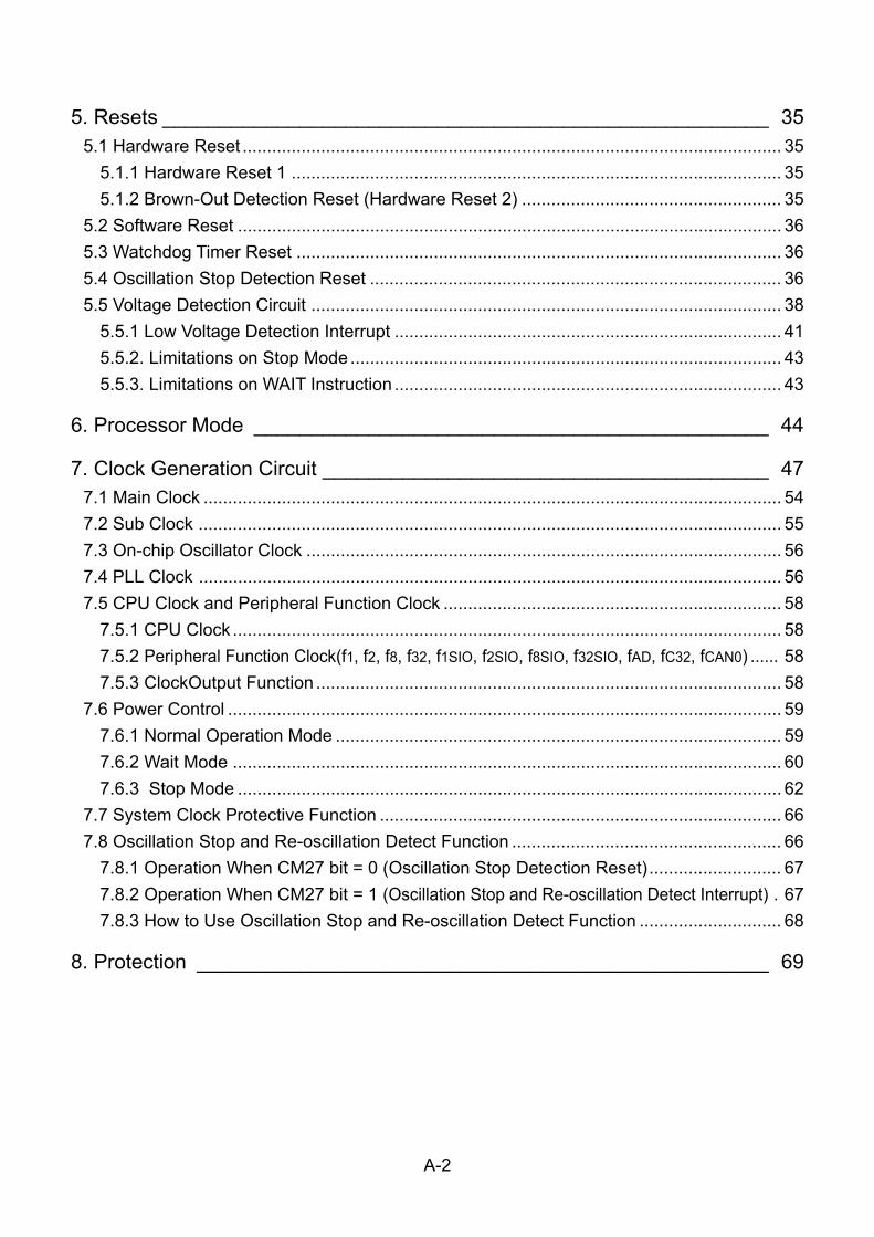
5. Resets _____________________________________________________ 355.1 Hardware Reset .............................................................................................................. 35
5.1.1 Hardware Reset 1 .................................................................................................... 355.1.2 Brown-Out Detection Reset (Hardware Reset 2) ..................................................... 35
5.2 Software Reset ............................................................................................................... 365.3 Watchdog Timer Reset ................................................................................................... 365.4 Oscillation Stop Detection Reset .................................................................................... 365.5 Voltage Detection Circuit ................................................................................................ 38
5.5.1 Low Voltage Detection Interrupt ............................................................................... 415.5.2. Limitations on Stop Mode ........................................................................................ 435.5.3. Limitations on WAIT Instruction ............................................................................... 43
6. Processor Mode _____________________________________________ 44
7. Clock Generation Circuit _______________________________________ 477.1 Main Clock ...................................................................................................................... 547.2 Sub Clock ....................................................................................................................... 557.3 On-chip Oscillator Clock ................................................................................................. 567.4 PLL Clock ....................................................................................................................... 567.5 CPU Clock and Peripheral Function Clock ..................................................................... 58
7.5.1 CPU Clock ................................................................................................................ 587.5.2 Peripheral Function Clock(f1, f2, f8, f32, f1SIO, f2SIO, f8SIO, f32SIO, fAD, fC32, fCAN0) ...... 587.5.3 ClockOutput Function ............................................................................................... 58
7.6 Power Control ................................................................................................................. 597.6.1 Normal Operation Mode ........................................................................................... 597.6.2 Wait Mode ................................................................................................................ 607.6.3 Stop Mode ............................................................................................................... 62
7.7 System Clock Protective Function .................................................................................. 667.8 Oscillation Stop and Re-oscillation Detect Function ....................................................... 66
7.8.1 Operation When CM27 bit = 0 (Oscillation Stop Detection Reset)........................... 677.8.2 Operation When CM27 bit = 1 (Oscillation Stop and Re-oscillation Detect Interrupt) . 677.8.3 How to Use Oscillation Stop and Re-oscillation Detect Function ............................. 68
8. Protection __________________________________________________ 69
A-3
9. Interrupts ___________________________________________________ 709.1 Type of Interrupts ............................................................................................................ 70
9.1.1 Software Interrupts ................................................................................................... 719.1.2 Hardware Interrupts ................................................................................................. 72
9.2 Interrupts and Interrupt Vector ........................................................................................ 739.2.1 Fixed Vector Tables .................................................................................................. 739.2.2 Relocatable Vector Tables ........................................................................................ 74
9.3 Interrupt Control .............................................................................................................. 759.3.1 I Flag ........................................................................................................................ 789.3.2 IR Bit ........................................................................................................................ 789.3.3 ILVL2 to ILVL0 Bits and IPL...................................................................................... 78
9.4 Interrupt Sequence ......................................................................................................... 799.4.1 Interrupt Response Time .......................................................................................... 809.4.2 Variation of IPL when Interrupt Request is Accepted ............................................... 809.4.3 Saving Registers ...................................................................................................... 819.4.4 Returning from an Interrupt Routine ......................................................................... 83
9.5 Interrupt Priority .............................................................................................................. 839.5.1 Interrupt Priority Resolution Circuit .......................................................................... 83
______
9.6 INT Interrupt ................................................................................................................... 85______
9.7 NMI Interrupt ................................................................................................................... 869.8 Key Input Interrupt .......................................................................................................... 869.9 CAN0 Wake-up Interrupt ................................................................................................ 879.10 Address Match Interrupt ............................................................................................... 87
10. Watchdog Timer ____________________________________________ 8910.1 Count Source Protective Mode..................................................................................... 90
11. DMAC ____________________________________________________ 9111.1 Transfer Cycles ............................................................................................................ 96
11.1.1 Effect of Source and Destination Addresses ......................................................... 9611.1.2 Effect of Software Wait .......................................................................................... 96
11.2. DMA Transfer Cycles ................................................................................................... 9811.3 DMA Enable .................................................................................................................. 9911.4 DMA Request ................................................................................................................ 9911.5 Channel Priority and DMA Transfer Timing ................................................................ 100
A-4
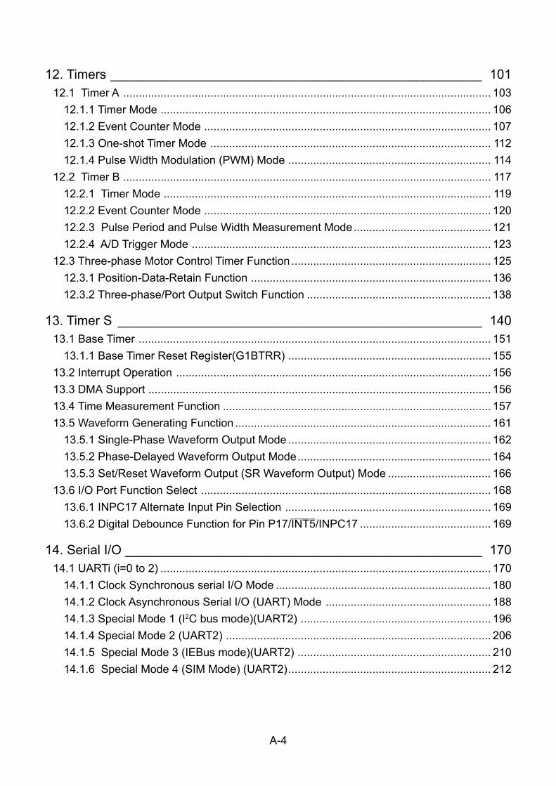
12. Timers ___________________________________________________ 10112.1 Timer A ...................................................................................................................... 103
12.1.1 Timer Mode .......................................................................................................... 10612.1.2 Event Counter Mode ............................................................................................ 10712.1.3 One-shot Timer Mode .......................................................................................... 11212.1.4 Pulse Width Modulation (PWM) Mode ................................................................. 114
12.2 Timer B ...................................................................................................................... 11712.2.1 Timer Mode ......................................................................................................... 11912.2.2 Event Counter Mode ............................................................................................ 12012.2.3 Pulse Period and Pulse Width Measurement Mode............................................ 12112.2.4 A/D Trigger Mode ................................................................................................ 123
12.3 Three-phase Motor Control Timer Function ................................................................ 12512.3.1 Position-Data-Retain Function ............................................................................. 13612.3.2 Three-phase/Port Output Switch Function ........................................................... 138
13. Timer S __________________________________________________ 14013.1 Base Timer ................................................................................................................. 151
13.1.1 Base Timer Reset Register(G1BTRR) ................................................................. 15513.2 Interrupt Operation ..................................................................................................... 15613.3 DMA Support .............................................................................................................. 15613.4 Time Measurement Function ...................................................................................... 15713.5 Waveform Generating Function .................................................................................. 161
13.5.1 Single-Phase Waveform Output Mode ................................................................. 16213.5.2 Phase-Delayed Waveform Output Mode.............................................................. 16413.5.3 Set/Reset Waveform Output (SR Waveform Output) Mode ................................. 166
13.6 I/O Port Function Select ............................................................................................. 16813.6.1 INPC17 Alternate Input Pin Selection .................................................................. 169
________
13.6.2 Digital Debounce Function for Pin P17/INT5/INPC17 .......................................... 169
14. Serial I/O _________________________________________________ 17014.1 UARTi (i=0 to 2) .......................................................................................................... 170
14.1.1 Clock Synchronous serial I/O Mode ..................................................................... 18014.1.2 Clock Asynchronous Serial I/O (UART) Mode ..................................................... 18814.1.3 Special Mode 1 (I2C bus mode)(UART2) ............................................................. 19614.1.4 Special Mode 2 (UART2) ..................................................................................... 20614.1.5 Special Mode 3 (IEBus mode)(UART2) .............................................................. 21014.1.6 Special Mode 4 (SIM Mode) (UART2)................................................................. 212
A-5
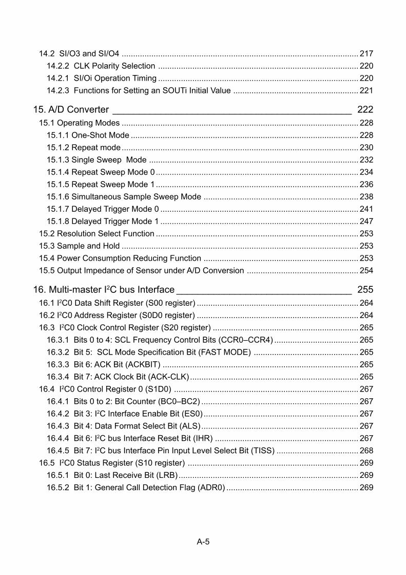
14.2 SI/O3 and SI/O4 ........................................................................................................ 21714.2.2 CLK Polarity Selection ........................................................................................ 22014.2.1 SI/Oi Operation Timing ........................................................................................ 22014.2.3 Functions for Setting an SOUTi Initial Value ....................................................... 221
15. A/D Converter _____________________________________________ 22215.1 Operating Modes ........................................................................................................ 228
15.1.1 One-Shot Mode .................................................................................................... 22815.1.2 Repeat mode........................................................................................................ 23015.1.3 Single Sweep Mode ............................................................................................ 23215.1.4 Repeat Sweep Mode 0 ......................................................................................... 23415.1.5 Repeat Sweep Mode 1 ......................................................................................... 23615.1.6 Simultaneous Sample Sweep Mode .................................................................... 23815.1.7 Delayed Trigger Mode 0 ....................................................................................... 24115.1.8 Delayed Trigger Mode 1 ....................................................................................... 247
15.2 Resolution Select Function ......................................................................................... 25315.3 Sample and Hold ........................................................................................................ 25315.4 Power Consumption Reducing Function .................................................................... 25315.5 Output Impedance of Sensor under A/D Conversion ................................................. 254
16. Multi-master I2C bus Interface _________________________________ 25516.1 I2C0 Data Shift Register (S00 register) ....................................................................... 26416.2 I2C0 Address Register (S0D0 register) ....................................................................... 26416.3 I2C0 Clock Control Register (S20 register) ................................................................ 265
16.3.1 Bits 0 to 4: SCL Frequency Control Bits (CCR0–CCR4) ..................................... 26516.3.2 Bit 5: SCL Mode Specification Bit (FAST MODE) .............................................. 26516.3.3 Bit 6: ACK Bit (ACKBIT) ...................................................................................... 26516.3.4 Bit 7: ACK Clock Bit (ACK-CLK) .......................................................................... 265
16.4 I2C0 Control Register 0 (S1D0) ................................................................................. 26716.4.1 Bits 0 to 2: Bit Counter (BC0–BC2) ..................................................................... 26716.4.2 Bit 3: I2C Interface Enable Bit (ES0) .................................................................... 26716.4.3 Bit 4: Data Format Select Bit (ALS)..................................................................... 26716.4.4 Bit 6: I2C bus Interface Reset Bit (IHR) ............................................................... 26716.4.5 Bit 7: I2C bus Interface Pin Input Level Select Bit (TISS) .................................... 268
16.5 I2C0 Status Register (S10 register) ........................................................................... 26916.5.1 Bit 0: Last Receive Bit (LRB) ............................................................................... 26916.5.2 Bit 1: General Call Detection Flag (ADR0) .......................................................... 269
A-6
16.5.3 Bit 2: Slave Address Comparison Flag (AAS) ..................................................... 26916.5.4 Bit 3: Arbitration Lost Detection Flag (AL) ........................................................... 26916.5.5 Bit 4: I2C bus Interface Interrupt Request Bit (PIN) ............................................. 27016.5.6 Bit 5: Bus Busy Flag (BB) .................................................................................... 27016.5.7 Bit 6: Communication Mode Select Bit (Transfer Direction Select Bit: TRX)....... 27116.5.8 Bit 7: Communication mode select bit (master/slave select bit: MST) ................ 271
16.6 I2C0 Control Register 1 (S3D0 register) .................................................................... 27216.6.1 Bit 0 : Interrupt Enable Bit by STOP Condition (SIM ) ......................................... 27216.6.2 Bit 1: Interrupt Enable Bit at the Completion of Data Receive (WIT) .................. 27216.6.3 Bits 2,3 : Port Function Select Bits PED, PEC .................................................... 27316.6.4 Bits 4,5 : SDA/SCL Logic Output Value Monitor Bits SDAM/SCLM .................... 27416.6.5 Bits 6,7 : I2C System Clock Select Bits ICK0, ICK1 ............................................ 27416.6.6 Address Receive in STOP/WAIT Mode ............................................................... 274
16.7 I2C0 Control Register 2 (S4D0 Register) ................................................................... 27516.7.1 Bit0: Time-Out Detection Function Enable Bit (TOE) .......................................... 27616.7.2 Bit1: Time-Out Detection Flag (TOF ).................................................................. 27616.7.3 Bit2: Time-Out Detection Period Select Bit (TOSEL) .......................................... 27616.7.4 Bits 3,4,5: I2C System Clock Select Bits (ICK2-4) ............................................... 27616.7.5 Bit7: STOP Condition Detection Interrupt Request Bit (SCPIN).......................... 276
16.8 I2C0 START/STOP Condition Control Register (S2D0 Register) ............................... 27716.8.1 Bit0-Bit4: START/STOP Condition Setting Bits (SSC0-SSC4) ............................ 27716.8.2 Bit5: SCL/SDA Interrupt Pin Polarity Select Bit (SIP) .......................................... 27716.8.3 Bit6 : SCL/SDA Interrupt Pin Select Bit (SIS) ...................................................... 27716.8.4 Bit7: START/STOP Condition Generation Select Bit (STSPSEL) ....................... 277
16.9 START Condition Generation Method ....................................................................... 27816.10 START Condition Duplicate Protect Function ........................................................... 27916.11 STOP Condition Generation Method ........................................................................ 27916.12 START/STOP Condition Detect Operation ............................................................... 28116.13 Address Data Communication ................................................................................. 282
16.13.1 Example of Master Transmit ............................................................................. 28216.13.2 Example of Slave Receive ................................................................................ 283
16.14 Precautions ............................................................................................................... 284
17. CAN Module ______________________________________________ 28717.1 CAN Module-Related Registers ................................................................................. 288
17.1.1 CAN0 Message Box ............................................................................................. 28917.1.2 Acceptance Mask Registers ................................................................................. 29117.1.3 CAN SFR Registers ............................................................................................. 292
A-7
17.2 Operating Modes ........................................................................................................ 30017.2.1 CAN Reset/Initialization Mode ............................................................................. 30017.2.2 CAN Operating Mode ........................................................................................... 30117.2.3 CAN Sleep Mode ................................................................................................. 30117.2.4 CAN Interface Sleep Mode .................................................................................. 30217.2.5 Bus Off State ........................................................................................................ 302
17.3 Configuration of the CAN Module System Clock ........................................................ 30317.3.1 Bit Timing Configuration ....................................................................................... 30317.3.2 Bit-rate .................................................................................................................. 304
17.4 Acceptance Filtering Function and Masking Function ................................................ 30517.5 Acceptance Filter Support Unit (ASU) ........................................................................ 30617.6 BasicCAN Mode ......................................................................................................... 30717.7 Return from Bus off Function ...................................................................................... 30817.8 Time Stamp Counter and Time Stamp Function ......................................................... 30817.9 Listen-Only Mode ....................................................................................................... 30817.10 Reception and Transmission .................................................................................... 309
17.10.1 Reception ........................................................................................................... 31017.10.2 Transmission ...................................................................................................... 311
17.11 CAN Interrupts .......................................................................................................... 312
18. CRC Calculation Circuit _____________________________________ 31318.1 CRC Snoop ................................................................................................................ 313
19. Programmable I/O Ports _____________________________________ 31619.1 Port Pi Direction Register (PDi Register, i = 0 to 3, 6 to 10) ....................................... 31619.2 Port Pi Register (Pi Register, i = 0 to 3, 6 to 10) ......................................................... 31619.3 Pull-up Control Register 0 to 2 (PUR0 to PUR2 Registers) ........................................ 31619.4 Port Control Register (PCR Register) ......................................................................... 31619.5 Pin Assignment Control Register (PACR) ................................................................... 31719.6 Digital Debounce Function ......................................................................................... 317
20. Flash Memory Version ______________________________________ 33020.1 Flash Memory Performance ....................................................................................... 330
20.1.1 Boot Mode ........................................................................................................... 33120.2 Memory Map............................................................................................................... 33220.3 Functions To Prevent Flash Memory from Rewriting .................................................. 335
20.3.1 ROM Code Protect Function ................................................................................ 33520.3.2 ID Code Check Function ...................................................................................... 335
A-8
20.4 CPU Rewrite Mode ..................................................................................................... 33720.4.1 EW Mode 0 .......................................................................................................... 33820.4.2 EW Mode 1 .......................................................................................................... 338
20.5 Register Description ................................................................................................... 33920.5.1 Flash Memory Control Register 0 (FMR0) ........................................................... 33920.5.2 Flash Memory Control Register 1 (FMR1) ........................................................... 34020.5.3 Flash Memory Control Register 4 (FMR4) ........................................................... 340
20.6 Precautions in CPU Rewrite Mode ............................................................................. 34520.6.1 Operation Speed .................................................................................................. 34520.6.2 Prohibited Instructions.......................................................................................... 34520.6.3 Interrupts .............................................................................................................. 34520.6.4 How to Access...................................................................................................... 34520.6.5 Writing in the User ROM Area .............................................................................. 34520.6.6 DMA Transfer ....................................................................................................... 34620.6.7 Writing Command and Data ................................................................................. 34620.6.8 Wait Mode ............................................................................................................ 34620.6.9 Stop Mode ............................................................................................................ 34620.6.10 Low Power Consumption Mode and On-Chip Oscillator-Low Power Consumption Mode ... 346
20.7 Software Commands .................................................................................................. 34720.7.1 Read Array Command (FF16)............................................................................... 34720.7.2 Read Status Register Command (7016) ............................................................... 34720.7.3 Clear Status Register Command (5016) ............................................................... 34720.7.4 Program Command (4016) ................................................................................... 34820.7.5 Block Erase .......................................................................................................... 349
20.8 Status Register ........................................................................................................... 35120.8.1 Sequence Status (SR7 and FMR00 Bits ) ............................................................ 35120.8.2 Erase Status (SR5 and FMR07 Bits) ................................................................... 35120.8.3 Program Status (SR4 and FMR06 Bits) ............................................................... 35120.8.4 Full Status Check ................................................................................................. 352
20.9 Standard Serial I/O Mode ........................................................................................... 35420.9.1 ID Code Check Function ...................................................................................... 35420.9.2 Example of Circuit Application in Standard Serial I/O Mode ................................ 358
20.10 Parallel I/O Mode ...................................................................................................... 36020.10.1 ROM Code Protect Function .............................................................................. 360
20.11 CAN I/O Mode .......................................................................................................... 36120.11.1 ID code check function ....................................................................................... 36120.11.2 Example of Circuit Application in CAN I/O Mode ................................................ 365
A-9
21. Electrical Characteristics _____________________________________ 36621.1 Normal version ........................................................................................................... 36621.2 T version ..................................................................................................................... 38721.3 V Version .................................................................................................................... 408
22. Usage Notes ______________________________________________ 42122.1 SFRs........................................................................................................................... 421
22.1.1 For 80-Pin Package ............................................................................................. 42122.1.2 For 64-Pin Package ............................................................................................. 42122.1.3 Register Setting .................................................................................................... 421
22.2 Clock Generation Circuit ............................................................................................. 42222.2.1 PLL Frequency Synthesizer ................................................................................. 42222.2.2 Power Control ...................................................................................................... 423
22.3 Protection ................................................................................................................... 42522.4 Interrupts .................................................................................................................... 426
22.4.1 Reading Address 0000016 .....................................................................................................42622.4.2 Setting the SP ...................................................................................................... 426
_______
22.4.3 NMI Interrupt ....................................................................................................... 42622.4.4 Changing the Interrupt Generate Factor .............................................................. 426
______
22.4.5 INT Interrupt ......................................................................................................... 42722.4.6 Rewrite the Interrupt Control Register .................................................................. 42822.4.7 Watchdog Timer Interrupt ..................................................................................... 428
22.5 DMAC ......................................................................................................................... 42922.5.1 Write to DMAE Bit in DMiCON Register ............................................................... 429
22.6 Timers ......................................................................................................................... 43022.6.1 Timer A ................................................................................................................. 43022.6.2 Timer B ................................................................................................................. 43322.6.3 Three-phase Motor Control Timer Function ......................................................... 434
22.7 Timer S ....................................................................................................................... 43522.7.1 Rewrite the G1IR Register .................................................................................. 43522.7.2 Rewrite the ICOCiIC Register ............................................................................. 43622.7.3 Waveform Generating Function .......................................................................... 43622.7.4 IC/OC Base Timer Interrupt .................................................................................. 436
22.8 Serial I/O..................................................................................................................... 43722.8.1 Clock-Synchronous Serial I/O .............................................................................. 43722.8.2 UART Mode.......................................................................................................... 43822.8.3 SI/O3, SI/O4 ......................................................................................................... 438
A-10
22.9 A/D Converter ............................................................................................................. 43922.10 Multi-Master I2C bus Interface ................................................................................. 441
22.10.1 Writing to the S00 Register ................................................................................ 44122.10.2 AL Flag ............................................................................................................... 441
22.11 CAN Module ............................................................................................................. 44222.11.1 Reading C0STR Register ................................................................................... 44222.11.2 CAN Transceiver in Boot Mode .......................................................................... 444
22.12 Programmable I/O Ports ........................................................................................... 44522.13 Electric Characteristic Differences Between Mask ROM.......................................... 44622.14 Mask ROM Version................................................................................................... 447
22.14.1 Internal ROM Area ............................................................................................. 44722.14.2 Reserved Bit ....................................................................................................... 447
22.15 Flash Memory Version .............................................................................................. 44822.15.1 Functions to Inhibit Rewriting Flash Memory Rewrite ........................................ 44822.15.2 Stop Mode .......................................................................................................... 44822.15.3 Wait Mode .......................................................................................................... 44822.15.4 Low PowerDissipation Mode, On-Chip Oscillator Low Power Dissipation Mode .. 44822.15.5 Writing Command and Data ............................................................................... 44822.15.6 Program Command ............................................................................................ 44822.15.7 Operation Speed ................................................................................................ 44822.15.8 Instructions Inhibited Against Use ...................................................................... 44822.15.9 Interrupts ............................................................................................................ 44922.15.10 How to Access.................................................................................................. 44922.15.11 Writing in the User ROM Area .......................................................................... 44922.15.12 DMA Transfer ................................................................................................... 44922.15.13 Regarding Programming/Erasure Times and Execution Time ......................... 44922.15.14 Definition of Programming/Erasure Times ....................................................... 45022.15.15 Flash Memory Version Electrical Characteristics 10,000 E/W cycle products ( Normal: U7, U9; T-ver./V-ver.: U7) ............................................. 45022.15.16 Boot Mode ........................................................................................................ 450
22.16 Noise ........................................................................................................................ 45122.17 Instruction for a Device Use ..................................................................................... 452

A-11
Appendix 1. Package Dimensions ________________________________ 453
Appendix 2. Functional Comparison _______________________________ 454Appendix 2.1 Difference between M16C/28 Group and M16C/29 Group (Normal-ver.) .... 454Appendix 2.2 Difference between M16C/28 and M16C/29 Group (T-ver./V-ver.) ............... 455
Register Index ________________________________________________ 456
B-1
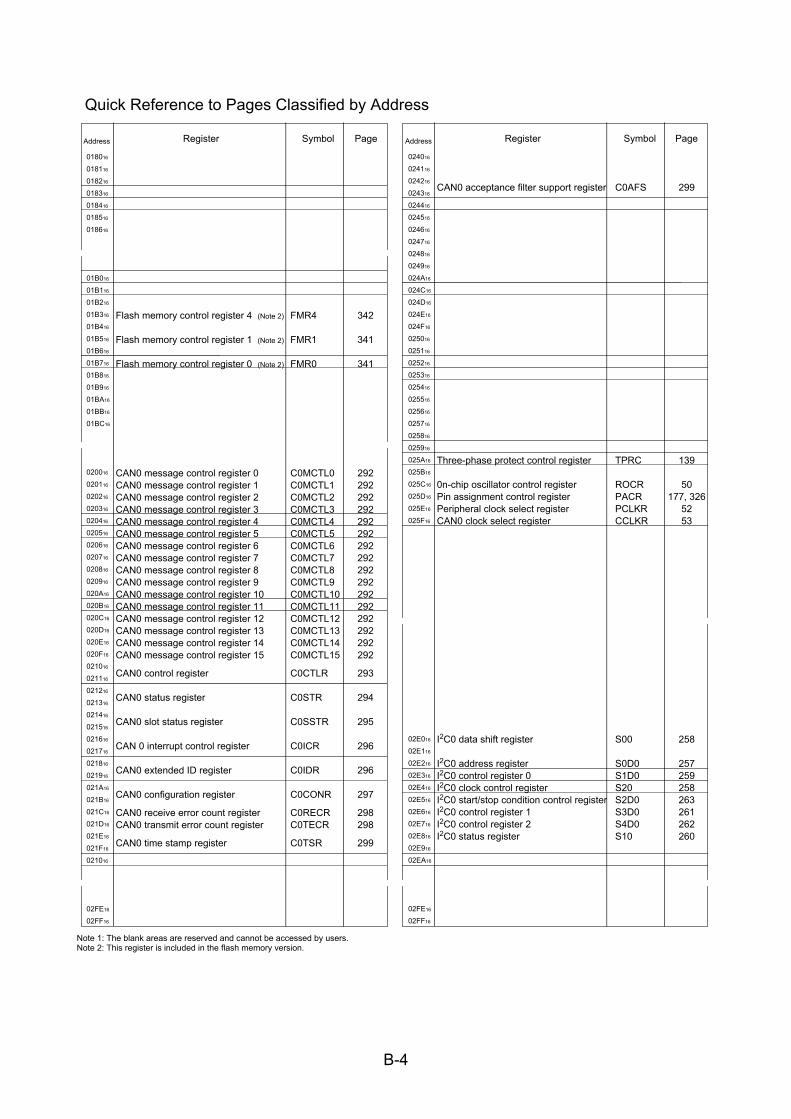
Quick Reference to Pages Classified by Address
CAN0 wakeup interrupt control register C01WKIC 76CAN0 successful reception interrupt control register C0RECIC 76CAN0 successful transmission interrupt control regiser C0TRMIC 76INT3 interrupt control register INT3IC 76IC/OC 0 interrupt control register ICOC0IC 76IC/OC 1 interrupt control register, ICOC1IC 76I2C bus interface interrupt control register IICIC 76IC/OC base timer interrupt control register, BTIC 76SCLSDA interrupt control register SCLDAIC 76SI/O4 interrupt control register, S4IC 76INT5 interrupt control register INT5IC 76SI/O3 interrupt control register, S3IC 76INT4 interrupt control register INT4IC 76UART2 Bus collision detection interrupt control register BCNIC 76DMA0 interrupt control register DM0IC 76DMA1 interrupt control register DM1IC 76CAN0 error interrupt control register C01ERRIC 76A/D conversion interrupt control register ADIC 76Key input interrupt control register KUPIC 76UART2 transmit interrupt control register S2TIC 76UART2 receive interrupt control register S2RIC 76UART0 transmit interrupt control register S0TIC 76UART0 receive interrupt control register S0RIC 76UART1 transmit interrupt control register S1TIC 76UART1 receive interrupt control register S1RIC 76Timer A0 interrupt control register TA0IC 76Timer A1 interrupt control register TA1IC 76Timer A2 interrupt control register TA2IC 76Timer A3 interrupt control register TA3IC 76Timer A4 interrupt control register TA4IC 76Timer B0 interrupt control register TB0IC 76Timer B1 interrupt control register TB1IC 76Timer B2 interrupt control register TB2IC 76INT0 interrupt control register INT0IC 76INT1 interrupt control register INT1IC 76INT2 interrupt control register INT2IC 76
CAN0 message box 0: Identifier/DLC 289
CAN 0 message box 0: Data field 289
CAN0 message box 0: Time stamp 289
CAN0 message box 1: Identifier/DLC 289
CAN 0 message box 1: Data field 289
CAN0 message box 1: Time stamp 289
000016
000116
000216
000316
000416
000516
000616
000716
000816
000916
000A16
000B16
000C16
000D16
000E16
000F16
001016
001116
001216
001316
001416
001516
001616
001716
001816
001916
001A16
001B16
001C16
001D16
001E16
001F16
002016
002116
002216
002316
002416
002516
002616
002716
002816
002916
002A16
002B16
002C16
002D16
002E16
002F16
003016
003116
003216
003316
003416
003516
003616
003716
003816
003916
003A16
003B16
003C16
003D16
003E16
003F16
Address
Note: The blank areas are reserved and cannot be accessed by users.
Register Symbol Page
004016
004116
004216
004316
004416
004516
004616
004716
004816
004916
004A16
004B16
004C16
004D16
004E16
004F16
005016
005116
005216
005316
005416
005516
005616
005716
005816
005916
005A16
005B16
005C16
005D16
005E16
005F16
006016
006116
006216
006316
006416
006516
006616
006716
006816
006916
006A16
006B16
006C16
006D16
006E16
006F16
007016
007116
007216
007316
007416
007516
007616
007716
007816
007916
007A16
007B16
007C16
007D16
007E16
007F16
Processor mode register 0 PM0 44Processor mode register 1 PM1 44System clock control register 0 CM0 49System clock control register 1 CM1 50
Address match interrupt enable register AIER 88Protect register PRCR 69
Oscillation stop detection register CM2 51
Watchdog timer start register WDTS 90Watchdog timer control register WDC 90
Address match interrupt register 0 RMAD0 88
Address match interrupt register 1 RMAD1 88
Voltage detection register 1 VCR1 41Voltage detection register 2 VCR2 41
PLL control register 0 PLC0 53
Processor mode register 2 PM2 52Low voltage detection interrupt register D4INT 42
DMA0 source pointer SAR0 95
DMA0 destination pointer DAR0 95
DMA0 transfer counter TCR0 95
DMA0 control register DM0CON 94
DMA1 source pointer SAR1 95
DMA1 destination pointer DAR1 95
DMA1 transfer counter TCR1 95
DMA1 control register DM1CON 94
Address Register Symbol Page
B-2
Quick Reference to Pages Classified by Address
008016
008116
008216
008316
008416
008516
008616
008716
008816
008916
008A16
008B16
008C16
008D16
008E16
008F16
009016
009116
009216
009316
009416
009516
009616
009716
009816
009916
009A16
009B16
009C16
009D16
009E16
009F16
00A016
00A116
00A216
00A316
00A416
00A516
00A616
00A716
00A816
00A916
00AA16
00AB16
00AC16
00AD16
00AE16
00AF16
00B016
00B116
00B216
00B316
00B416
00B516
00B616
00B716
00B816
00B916
00BA16
00BB16
00BC16
00BD16
00BE16
00BF16
Address
Note: The blank areas are reserved and cannot be accessed by users.
Register Symbol Page
00C016
00C116
00C216
00C316
00C416
00C516
00C616
00C716
00C816
00C916
00CA16
00CB16
00CC16
00CD16
00CE16
00CF16
00D016
00D116
00D216
00D316
00D416
00D516
00D616
00D716
00D816
00D916
00DA16
00DB16
00DC16
00DD16
00DE16
00DF16
00E016
00E116
00E216
00E316
00E416
00E516
00E616
00E716
00E816
00E916
00EA16
00EB16
00EC16
00ED16
00EE16
00EF16
00F016
00F116
00F216
00F316
00F416
00F516
00F616
00F716
00F816
00F916
00FA16
00FB16
00FC16
00FD16
00FE16
00FF16
CAN0 message box 2: Identifier/DLC 289
CAN0 message box 2: Data field 289
CAN0 message box 2: time stamp 289
CAN0 message box 3: Identifier/DLC 289
CAN0 message box 3: Data field 289
CAN0 message box 3: time stamp 289
CAN0 message box 4: Identifier/DLC 289
CAN0 message box 4: Data field 289
CAN0 message box 4: time stamp 289
CAN0 message box 5: Identifier/DLC 289
CAN0 message box 5: Data field 289
CAN0 message box 5: time stamp 289
Address Register Symbol Page
CAN0 message box 6: Identifier/DLC 289
CAN0 message box 6: Data field 289
CAN0 message box 6: time stamp 289
CAN0 message box 7: Identifier/DLC 289
CAN0 message box 7: Data field 289
CAN0 message box 7: time stamp 289
CAN0 message box 8: Identifier/DLC 289
CAN0 message box 8: Data field 289
CAN0 message box 8: time stamp 289
CAN0 message box 9: Identifier/DLC 289
CAN0 message box 9: Data field 289
CAN0 message box 9: time stamp 289
B-3
Quick Reference to Pages Classified by Address
010016
010116
010216
010316
010416
010516
010616
010716
010816
010916
010A16
010B16
010C16
010D16
010E16
010F16
011016
011116
011216
011316
011416
011516
011616
011716
011816
011916
011A16
011B16
011C16
011D16
011E16
011F16
012016
012116
012216
012316
012416
012516
012616
012716
012816
012916
012A16
012B16
012C16
012D16
012E16
012F16
013016
013116
013216
013316
013416
013516
013616
013716
013816
013916
013A16
013B16
013C16
013D16
013E16
013F16
Address
Note: The blank areas are reserved and cannot be accessed by users.
Register Symbol Page
014016
014116
014216
014316
014416
014516
014616
014716
014816
014916
014A16
014B16
014C16
014D16
014E16
014F16
015016
015116
015216
015316
015416
015516
015616
015716
015816
015916
015A16
015B16
015C16
015D16
015E16
015F16
016016
016116
016216
016316
016416
016516
016616
016716
016816
016916
016A16
016B16
016C16
016D16
016E16
016F16
017016
017116
017216
017316
017416
017516
017616
017716
017816
017916
017A16
017B16
017C16
017D16
017E16
017F16
CAN0 message box 10: Identifer/DLC 289
CAN0 message box 10: Data field 289
CAN0 message box 10: time stamp 289
CAN0 message box 11: Identifier/DLC 289
CAN0 message box 11: Data field 289
CAN0 message box 11: time stamp 289
CAN0 message box 12: Identifier/DLC 289
CAN0 message box 12: Data field 289
CAN0 message box 12: time stamp 289
CAN0 message box 13: Identifier/DLC 289
CAN0 message box 13: Data field 289
CAN0 message box 13: time stamp 289
Address Register Symbol Page
CAN0 message box 14: Identifier/DLC 289
CAN0 message box 14: Data field 289
CAN0 message box 14: time stamp 289
CAN0 message box 15: Identifier/DLC 289
CAN0 message box 15: Data field 289
CAN0 message box 15: time stamp 289
CAN0 global mask register C0GMR 291
CAN0 local mask A register C0LMAR 291
CAN0 local mask B register C0LMBR 291
B-4
Quick Reference to Pages Classified by Address
Note 1: The blank areas are reserved and cannot be accessed by users.Note 2: This register is included in the flash memory version.
018016
018116
018216
018316
018416
018516
018616
01B016
01B116
01B216
01B316
01B416
01B516
01B616
01B716
01B816
01B916
01BA16
01BB16
01BC16
020016
020116
020216
020316
020416
020516
020616
020716
020816
020916
020A16
020B16
020C16
020D16
020E16
020F16
021016
021116
021216
021316
021416
021516
021616
021716
021816
021916
021A16
021B16
021C16
021D16
021E16
021F16
021016
02FE16
02FF16
Address Register Symbol Page
Flash memory control register 4 (Note 2) FMR4 342
Flash memory control register 1 (Note 2) FMR1 341
Flash memory control register 0 (Note 2) FMR0 341
CAN0 message control register 0 C0MCTL0 292CAN0 message control register 1 C0MCTL1 292CAN0 message control register 2 C0MCTL2 292CAN0 message control register 3 C0MCTL3 292CAN0 message control register 4 C0MCTL4 292CAN0 message control register 5 C0MCTL5 292CAN0 message control register 6 C0MCTL6 292CAN0 message control register 7 C0MCTL7 292CAN0 message control register 8 C0MCTL8 292CAN0 message control register 9 C0MCTL9 292CAN0 message control register 10 C0MCTL10 292CAN0 message control register 11 C0MCTL11 292CAN0 message control register 12 C0MCTL12 292CAN0 message control register 13 C0MCTL13 292CAN0 message control register 14 C0MCTL14 292CAN0 message control register 15 C0MCTL15 292
CAN0 control register C0CTLR 293
CAN0 status register C0STR 294
CAN0 slot status register C0SSTR 295
CAN 0 interrupt control register C0ICR 296
CAN0 extended ID register C0IDR 296
CAN0 configuration register C0CONR 297
CAN0 receive error count register C0RECR 298CAN0 transmit error count register C0TECR 298
CAN0 time stamp register C0TSR 299
024016
024116
024216
024316
024416
024516
024616
024716
024816
024916
024A16
024C16
024D16
024E16
024F16
025016
025116
025216
025316
025416
025516
025616
025716
025816
025916
025A16
025B16
025C16
025D16
025E16
025F16
02E016
02E116
02E216
02E316
02E416
02E516
02E616
02E716
02E816
02E916
02EA16
02FE16
02FF16
Address Register Symbol Page
CAN0 acceptance filter support register C0AFS 299
Three-phase protect control register TPRC 139
0n-chip oscillator control register ROCR 50Pin assignment control register PACR 177, 326Peripheral clock select register PCLKR 52CAN0 clock select register CCLKR 53
I2C0 data shift register S00 258
I2C0 address register S0D0 257I2C0 control register 0 S1D0 259I2C0 clock control register S20 258I2C0 start/stop condition control register S2D0 263I2C0 control register 1 S3D0 261I2C0 control register 2 S4D0 262I2C0 status register S10 260
B-5
Quick Reference to Pages Classified by Address
Note : The blank areas are reserved and cannot be accessed by users.
034016
034116
034216
034316
034416
034516
034616
034716
034816
034916
034A16
034B16
034C16
034D16
034E16
034F16
035016
035116
035216
035316
035416
035516
035616
035716
035816
035916
035A16
035B16
035C16
035D16
035E16
035F16
036016
036116
036216
036316
036416
036516
036616
036716
036816
036916
036A16
036B16
036C16
036D16
036E16
036F16
037016
037116
037216
037316
037416
037516
037616
037716
037816
037916
037A16
037B16
037C16
037D16
037E16
037F16
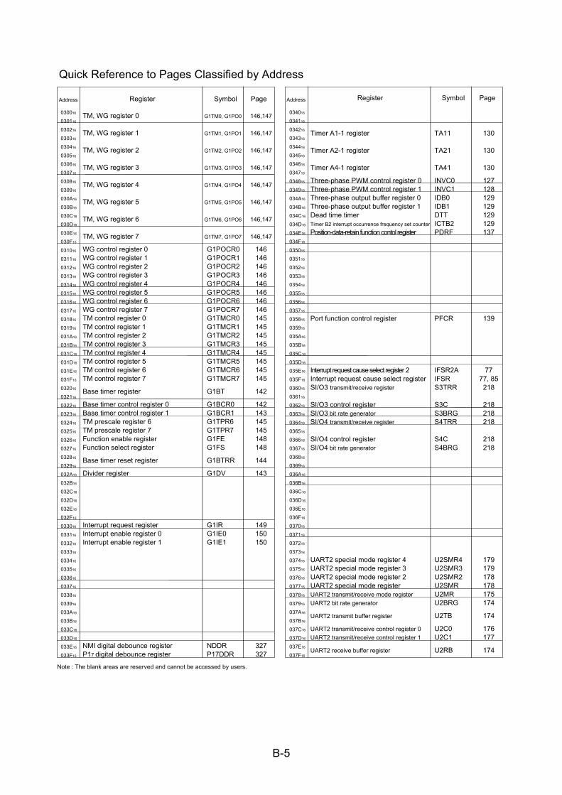
Timer A1-1 register TA11 130
Timer A2-1 register TA21 130
Timer A4-1 register TA41 130
Three-phase PWM control register 0 INVC0 127Three-phase PWM control register 1 INVC1 128Three-phase output buffer register 0 IDB0 129Three-phase output buffer register 1 IDB1 129Dead time timer DTT 129Timer B2 interrupt occurrence frequency set counter ICTB2 129Position-data-retain function contol register PDRF 137
Port function control register PFCR 139
Interrupt request cause select register 2 IFSR2A 77Interrupt request cause select register IFSR 77, 85SI/O3 transmit/receive register S3TRR 218
SI/O3 control register S3C 218SI/O3 bit rate generator S3BRG 218SI/O4 transmit/receive register S4TRR 218
SI/O4 control register S4C 218SI/O4 bit rate generator S4BRG 218
UART2 special mode register 4 U2SMR4 179UART2 special mode register 3 U2SMR3 179UART2 special mode register 2 U2SMR2 178UART2 special mode register U2SMR 178UART2 transmit/receive mode register U2MR 175UART2 bit rate generator U2BRG 174
UART2 transmit buffer register U2TB 174
UART2 transmit/receive control register 0 U2C0 176UART2 transmit/receive control register 1 U2C1 177
UART2 receive buffer register U2RB 174
Address Register Symbol Page
030016
030116
030216
030316
030416
030516
030616
030716
030816
030916
030A16
030B16
030C16
030D16
030E16
030F16
031016
031116
031216
031316
031416
031516
031616
031716
031816
031916
031A16
031B16
031C16
031D16
031E16
031F16
032016
032116
032216
032316
032416
032516
032616
032716
032816
032916
032A16
032B16
032C16
032D16
032E16
032F16
033016
033116
033216
033316
033416
033516
033616
033716
033816
033916
033A16
033B16
033C16
033D16
033E16
033F16
Address Register Symbol Page
TM, WG register 0 G1TM0, G1PO0 146,147
TM, WG register 1 G1TM1, G1PO1 146,147
TM, WG register 2 G1TM2, G1PO2 146,147
TM, WG register 3 G1TM3, G1PO3 146,147
TM, WG register 4 G1TM4, G1PO4 146,147
TM, WG register 5 G1TM5, G1PO5 146,147
TM, WG register 6 G1TM6, G1PO6 146,147
TM, WG register 7 G1TM7, G1PO7 146,147
WG control register 0 G1POCR0 146WG control register 1 G1POCR1 146WG control register 2 G1POCR2 146WG control register 3 G1POCR3 146WG control register 4 G1POCR4 146WG control register 5 G1POCR5 146WG control register 6 G1POCR6 146WG control register 7 G1POCR7 146TM control register 0 G1TMCR0 145TM control register 1 G1TMCR1 145TM control register 2 G1TMCR2 145TM control register 3 G1TMCR3 145TM control register 4 G1TMCR4 145TM control register 5 G1TMCR5 145TM control register 6 G1TMCR6 145TM control register 7 G1TMCR7 145
Base timer register G1BT 142
Base timer control register 0 G1BCR0 142Base timer control register 1 G1BCR1 143TM prescale register 6 G1TPR6 145TM prescale register 7 G1TPR7 145Function enable register G1FE 148Function select register G1FS 148
Base timer reset register G1BTRR 144
Divider register G1DV 143
Interrupt request register G1IR 149Interrupt enable register 0 G1IE0 150Interrupt enable register 1 G1IE1 150
NMI digital debounce register NDDR 327P17 digital debounce register P17DDR 327
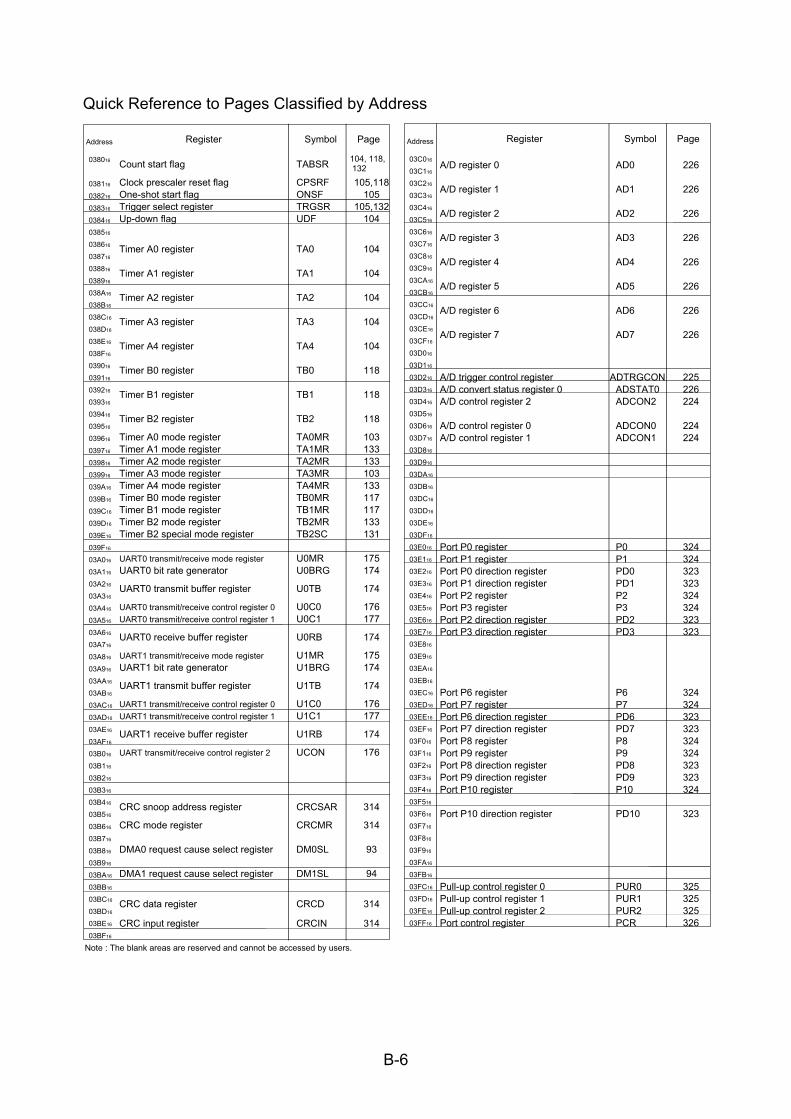
B-6
Note : The blank areas are reserved and cannot be accessed by users.
03C016
03C116
03C216
03C316
03C416
03C516
03C616
03C716
03C816
03C916
03CA16
03CB16
03CC16
03CD16
03CE16
03CF16
03D016
03D116
03D216
03D316
03D416
03D516
03D616
03D716
03D816
03D916
03DA16
03DB16
03DC16
03DD16
03DE16
03DF16
03E016
03E116
03E216
03E316
03E416
03E516
03E616
03E716
03E816
03E916
03EA16
03EB16
03EC16
03ED16
03EE16
03EF16
03F016
03F116
03F216
03F316
03F416
03F516
03F616
03F716
03F816
03F916
03FA16
03FB16
03FC16
03FD16
03FE16
03FF16
A/D register 0 AD0 226
A/D register 1 AD1 226
A/D register 2 AD2 226
A/D register 3 AD3 226
A/D register 4 AD4 226
A/D register 5 AD5 226
A/D register 6 AD6 226
A/D register 7 AD7 226
A/D trigger control register ADTRGCON 225A/D convert status register 0 ADSTAT0 226A/D control register 2 ADCON2 224
A/D control register 0 ADCON0 224A/D control register 1 ADCON1 224
Port P0 register P0 324Port P1 register P1 324Port P0 direction register PD0 323Port P1 direction register PD1 323Port P2 register P2 324Port P3 register P3 324Port P2 direction register PD2 323Port P3 direction register PD3 323
Port P6 register P6 324Port P7 register P7 324Port P6 direction register PD6 323Port P7 direction register PD7 323Port P8 register P8 324Port P9 register P9 324Port P8 direction register PD8 323Port P9 direction register PD9 323Port P10 register P10 324
Port P10 direction register PD10 323
Pull-up control register 0 PUR0 325Pull-up control register 1 PUR1 325Pull-up control register 2 PUR2 325Port control register PCR 326
Address Register Symbol Page
038016
038116
038216
038316
038416
038516
038616
038716
038816
038916
038A16
038B16
038C16
038D16
038E16
038F16
039016
039116
039216
039316
039416
039516
039616
039716
039816
039916
039A16
039B16
039C16
039D16
039E16
039F16
03A016
03A116
03A216
03A316
03A416
03A516
03A616
03A716
03A816
03A916
03AA16
03AB16
03AC16
03AD16
03AE16
03AF16
03B016
03B116
03B216
03B316
03B416
03B516
03B616
03B716
03B816
03B916
03BA16
03BB16
03BC16
03BD16
03BE16
03BF16
Count start flag TABSR
Clock prescaler reset flag CPSRF 105,118One-shot start flag ONSF 105Trigger select register TRGSR 105,132Up-down flag UDF 104
Timer A0 register TA0 104
Timer A1 register TA1 104
Timer A2 register TA2 104
Timer A3 register TA3 104
Timer A4 register TA4 104
Timer B0 register TB0 118
Timer B1 register TB1 118
Timer B2 register TB2 118
Timer A0 mode register TA0MR 103Timer A1 mode register TA1MR 133Timer A2 mode register TA2MR 133Timer A3 mode register TA3MR 103Timer A4 mode register TA4MR 133Timer B0 mode register TB0MR 117Timer B1 mode register TB1MR 117Timer B2 mode register TB2MR 133Timer B2 special mode register TB2SC 131
UART0 transmit/receive mode register U0MR 175UART0 bit rate generator U0BRG 174
UART0 transmit buffer register U0TB 174
UART0 transmit/receive control register 0 U0C0 176UART0 transmit/receive control register 1 U0C1 177
UART0 receive buffer register U0RB 174
UART1 transmit/receive mode register U1MR 175UART1 bit rate generator U1BRG 174
UART1 transmit buffer register U1TB 174
UART1 transmit/receive control register 0 U1C0 176UART1 transmit/receive control register 1 U1C1 177
UART1 receive buffer register U1RB 174
UART transmit/receive control register 2 UCON 176
CRC snoop address register CRCSAR 314
CRC mode register CRCMR 314
DMA0 request cause select register DM0SL 93
DMA1 request cause select register DM1SL 94
CRC data register CRCD 314
CRC input register CRCIN 314
104, 118, 132
Address Register Symbol Page
Quick Reference to Pages Classified by Address
M16C/29 GroupSINGLE-CHIP 16-BIT CMOS MICROCOMPUTER
page 1 854fo7002,03.raM21.1.veR2110-1010B90JER
1. Overview1.1 Features
The M16C/29 Group of single-chip control MCU incorporates the M16C/60 series CPU core, employing thehigh-performance silicon gate CMOS technology and sophisticated instructions for a high level of effi-ciency. The M16C/29 Group is housed in 64-pin and 80-pin plastic molded LQFP packages. These single-chip MCUs operate using sophisticated instructions featuring a high level of instruction efficiency. ThisMCU is capable of executing instructions at high speed and it has one CAN module, makes it suitable forcontrol of cars and LAN system of FA. In addition, the CPU core boasts a multiplier and DMAC for high-speed processing to make adequate for office automation, communication devices, and other high-speedprocessing applications.
1.1.1 Applications
Automotive body, car audio, LAN system of FA, etc.
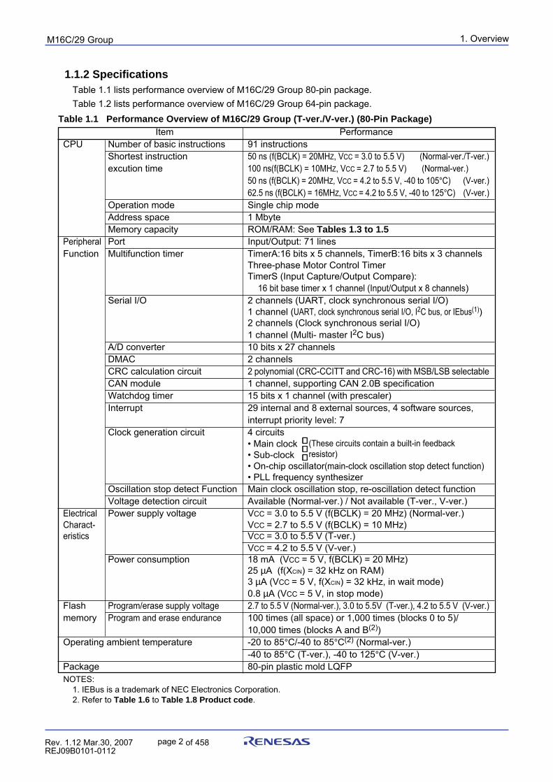
1. Overview
page 2
puorG92/C61M
854fo7002,03.raM21.1.veR2110-1010B90JER
Item PerformanceCPU Number of basic instructions 91 instructions
Shortest instruction 50 ns (f(BCLK) = 20MHZ, VCC = 3.0 to 5.5 V) (Normal-ver./T-ver.)excution time 100 ns(f(BCLK) = 10MHZ, VCC = 2.7 to 5.5 V) (Normal-ver.)
50 ns (f(BCLK) = 20MHZ, VCC = 4.2 to 5.5 V, -40 to 105°C) (V-ver.)62.5 ns (f(BCLK) = 16MHZ, VCC = 4.2 to 5.5 V, -40 to 125°C) (V-ver.)
Operation mode Single chip modeAddress space 1 MbyteMemory capacity ROM/RAM: See Tables 1.3 to 1.5
Peripheral Port Input/Output: 71 linesFunction Multifunction timer TimerA:16 bits x 5 channels, TimerB:16 bits x 3 channels
Three-phase Motor Control TimerTimerS (Input Capture/Output Compare): 16 bit base timer x 1 channel (Input/Output x 8 channels)
Serial I/O 2 channels (UART, clock synchronous serial I/O)1 channel (UART, clock synchronous serial I/O, I2C bus, or IEbus(1))2 channels (Clock synchronous serial I/O)1 channel (Multi- master I2C bus)
A/D converter 10 bits x 27 channelsDMAC 2 channelsCRC calculation circuit 2 polynomial (CRC-CCITT and CRC-16) with MSB/LSB selectableCAN module 1 channel, supporting CAN 2.0B specificationWatchdog timer 15 bits x 1 channel (with prescaler)Interrupt 29 internal and 8 external sources, 4 software sources,
interrupt priority level: 7Clock generation circuit 4 circuits
• Main clock• Sub-clock• On-chip oscillator(main-clock oscillation stop detect function)• PLL frequency synthesizer
Oscillation stop detect Function Main clock oscillation stop, re-oscillation detect functionVoltage detection circuit Available (Normal-ver.) / Not available (T-ver., V-ver.)
Electrical Power supply voltage VCC = 3.0 to 5.5 V (f(BCLK) = 20 MHz) (Normal-ver.)Charact- VCC = 2.7 to 5.5 V (f(BCLK) = 10 MHz)eristics VCC = 3.0 to 5.5 V (T-ver.)
VCC = 4.2 to 5.5 V (V-ver.)Power consumption 18 mA (VCC = 5 V, f(BCLK) = 20 MHz)
25 µA (f(XCIN) = 32 kHz on RAM)3 µA (VCC = 5 V, f(XCIN) = 32 kHz, in wait mode)0.8 µA (VCC = 5 V, in stop mode)
Flash Program/erase supply voltage 2.7 to 5.5 V (Normal-ver.), 3.0 to 5.5V (T-ver.), 4.2 to 5.5 V (V-ver.)memory Program and erase endurance 100 times (all space) or 1,000 times (blocks 0 to 5)/
10,000 times (blocks A and B(2))Operating ambient temperature -20 to 85°C/-40 to 85°C(2) (Normal-ver.)
-40 to 85°C (T-ver.), -40 to 125°C (V-ver.)Package 80-pin plastic mold LQFP
Table 1.1 Performance Overview of M16C/29 Group (T-ver./V-ver.) (80-Pin Package)
1.1.2 SpecificationsTable 1.1 lists performance overview of M16C/29 Group 80-pin package.Table 1.2 lists performance overview of M16C/29 Group 64-pin package.
(These circuits contain a built-in feedbackresistor)
NOTES: 1. IEBus is a trademark of NEC Electronics Corporation. 2. Refer to Table 1.6 to Table 1.8 Product code.
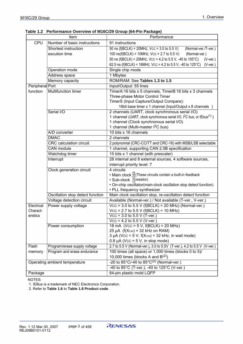
1. Overview
page 3
puorG92/C61M
854fo7002,03.raM21.1.veR2110-1010B90JER
Table 1.2 Performance Overview of M16C/29 Group (64-Pin Package) Item Performance
CPU Number of basic instructions 91 instructionsShortest instruction 50 ns (f(BCLK) = 20MHZ, VCC = 3.0 to 5.5 V) (Normal-ver./T-ver.)excution time 100 ns(f(BCLK) = 10MHZ, VCC = 2.7 to 5.5 V) (Normal-ver.)
50 ns (f(BCLK) = 20MHZ, VCC = 4.2 to 5.5 V, -40 to 105°C) (V-ver.)62.5 ns (f(BCLK) = 16MHZ, VCC = 4.2 to 5.5 V, -40 to 125°C) (V-ver.)
Operation mode Single chip modeAddress space 1 MbytesMemory capacity ROM/RAM: See Tables 1.3 to 1.5
Peripheral Port Input/Output: 55 linesfunction Multifunction timer TimerA:16 bits x 5 channels, TimerB:16 bits x 3 channels
Three-phase Motor Control TimerTimerS (Input Capture/Output Compare):
16bit base timer x 1 channel (Input/Output x 8 channels )Serial I/O 2 channels (UART, clock synchronous serial I/O)
1 channel (UART, clock synchronous serial I/O, I2C bus, or IEbus(1) )1 channel (Clock synchronous serial I/O)1 channel (Multi-master I2C bus)
A/D converter 10 bits x 16 channelsDMAC 2 channelsCRC calculation circuit 2 polynomial (CRC-CCITT and CRC-16) with MSB/LSB selectableCAN module 1 channel, supporting CAN 2.0B specificationWatchdog timer 15 bits x 1 channel (with prescaler)Interrupt 28 internal and 8 external sources, 4 software sources,
interrupt priority level: 7Clock generation circuit 4 circuits
• Main clock• Sub-clock• On-chip oscillator(main-clock oscillation stop detect function)• PLL frequency synthesizer
Oscillation stop detect function Main clock oscillation stop, re-oscillation detect functionVoltage detection circuit Available (Normal-ver.) / Not available (T-ver., V-ver.)
Electrical Power supply voltage VCC = 3.0 to 5.5 V (f(BCLK) = 20 MHz) (Normal-ver.)Charact- VCC = 2.7 to 5.5 V (f(BCLK) = 10 MHz)eristics VCC = 3.0 to 5.5 V (T-ver.)
VCC = 4.2 to 5.5 V (V-ver.)Power consumption 18 mA (VCC = 5 V, f(BCLK) = 20 MHz)
25 µA (f(XCIN) = 32 kHz on RAM)3 µA (VCC = 5 V, f(XCIN) = 32 kHz, in wait mode)0.8 µA (VCC = 5 V, in stop mode)
Flash Program/erase supply voltage 2.7 to 5.5 V (Normal-ver.), 3.0 to 5.5V (T-ver.), 4.2 to 5.5 V (V-ver.)memory Program and erase endurance 100 times (all space) or 1,000 times (blocks 0 to 5)/
10,000 times (blocks A and B(2))Operating ambient temperature -20 to 85°C/-40 to 85°C(2) (Normal-ver.)
-40 to 85°C (T-ver.), -40 to 125°C (V-ver.)Package 64-pin plastic mold LQFP
(These circuits contain a built-in feedbackresistor)
NOTES: 1. IEBus is a trademark of NEC Electronics Corporation. 2. Refer to Table 1.6 to Table 1.8 Product code.
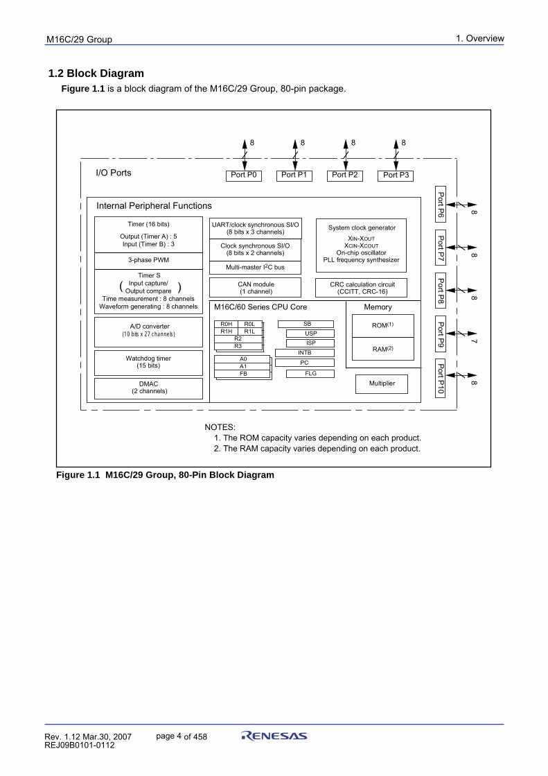
1. Overview
page 4
puorG92/C61M
854fo7002,03.raM21.1.veR2110-1010B90JER
1.2 Block DiagramFigure 1.1 is a block diagram of the M16C/29 Group, 80-pin package.
Figure 1.1 M16C/29 Group, 80-Pin Block Diagram
O
u
t
p
u
t
(
T
i
m
e
r
A
)
:
5I
n
p
u
t
(
T
i
m
e
r
B
)
:
3
I n
t
e
r
n
a
l
P
e
r
i
p
h
e
r
a
l
F
u
n
c
t
i
o
n
s
W
a
t
c
h
d
o
g
t
i
m
e
r(
1
5
b
i
t
s
)
DMAC (2 channels)
M
e
m
o
r
y
ROM(1)
RAM(2)
A
/
D
c
o
n
v
e
r
t
e
r(
1
0
b
i
t
s
x
2
7
c
h
a
n
n
e
l
s
)
U
A
R
T
/
c
l
o
c
k
s
y
n
c
h
r
o
n
o
u
s
S
I
/
O(
8
b
i
t
s
x
3
c
h
a
n
n
e
l
s
) System clock generator
XI
N-
XO
U
TXC
I
N-
XC
O
U
TO
n
-
c
h
i
p
o
s
c
i
l
l
a
t
o
rP
L
L
f
r
e
q
u
e
n
c
y
s
y
n
t
h
e
s
i
z
e
r
M
1
6
C
/
6
0
S
e
r
i
e
s
C
P
U
C
o
r
e
R0LR0HR1H R1L
R
2R3
A
0A
1F
B
S
B
ISPUSP
INTB
Multiplier
8
P o
r
t
P
1
0
7
P o
r
t
P
9
8
P o
r
t
P
8
P o
r
t
P
7 8
P o
r
t
P
6 8
Port P2
8
PC
FLG
T
i
m
e
r
(
1
6
b
i
t
s
)
3
-
p
h
a
s
e
P
W
M
Port P3
8
Port P1
8
I /
O
P
o
r
t
s Port P0
8
C
l
o
c
k
s
y
n
c
h
r
o
n
o
u
s
S
I
/
O(
8
b
i
t
s
x
2
c
h
a
n
n
e
l
s
)
M
u
l
t
i
-
m
a
s
t
e
r
I2C
b
u
s
( )
T
i
m
e
r
S
I
n
p
u
t
c
a
p
t
u
r
e
/O
u
t
p
u
t
c
o
m
p
a
r
eT
i
m
e
m
e
a
s
u
r
e
m
e
n
t
:
8
c
h
a
n
n
e
l
sW
a
v
e
f
o
r
m
g
e
n
e
r
a
t
i
n
g
:
8
c
h
a
n
n
e
l
s
C
A
N
m
o
d
u
l
e(
1
c
h
a
n
n
e
l
)CRC calculation circuit
(CCITT, CRC-16)
NOTES: 1. The ROM capacity varies depending on each product. 2. The RAM capacity varies depending on each product.
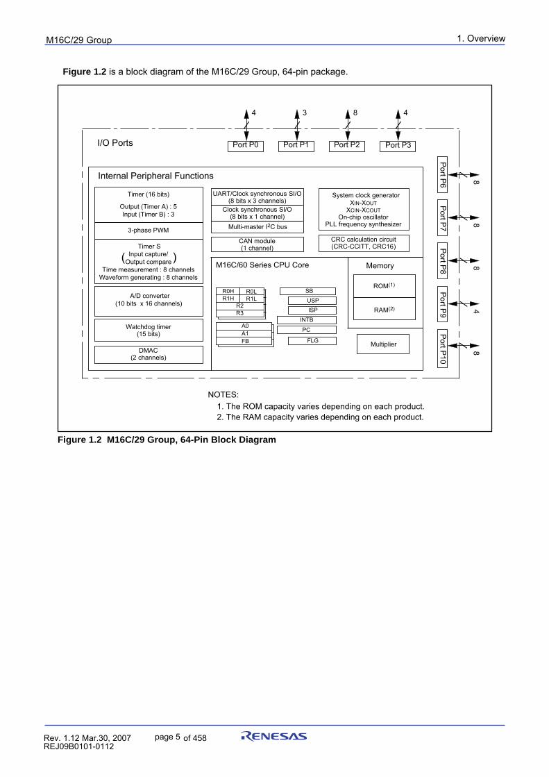
1. Overview
page 5
puorG92/C61M
854fo7002,03.raM21.1.veR2110-1010B90JER
Figure 1.2 is a block diagram of the M16C/29 Group, 64-pin package.
Figure 1.2 M16C/29 Group, 64-Pin Block Diagram
O
u
t
p
u
t
(
T
i
m
e
r
A
)
:
5I
n
p
u
t
(
T
i
m
e
r
B
)
:
3
I n
t
e
r
n
a
l
P
e
r
i
p
h
e
r
a
l
F
u
n
c
t
i
o
n
s
W
a
t
c
h
d
o
g
t
i
m
e
r(
1
5
b
i
t
s
)
D
M
A
C(
2
c
h
a
n
n
e
l
s
)
Memory
ROM(1)
R
A
M(
2
)
U
A
R
T
/
C
l
o
c
k
s
y
n
c
h
r
o
n
o
u
s
S
I
/
O(
8
b
i
t
s
x
3
c
h
a
n
n
e
l
s
)System clock generator
XI
N-
XO
U
TXC
I
N-
XC
O
U
TO
n
-
c
h
i
p
o
s
c
i
l
l
a
t
o
rP
L
L
f
r
e
q
u
e
n
c
y
s
y
n
t
h
e
s
i
z
e
r
M
1
6
C
/
6
0
S
e
r
i
e
s
C
P
U
C
o
r
e
R0LR0HR1H R1L
R2R3
A0A1FB
SB
ISPU
S
P
INTB
Multiplier 8
P o
r
t
P
1
0
4
P o
r
t
P
9
8
P o
r
t
P
8
P o
r
t
P
7 8
P o
r
t
P
6 8
Port P2
8
P
C
FLG
T
i
m
e
r
(
1
6
b
i
t
s
)
3
-
p
h
a
s
e
P
W
M
P
o
r
t
P
3
4
Port P1
3
I /
O
P
o
r
t
s Port P0
4
T
i
m
e
r
SI
n
p
u
t
c
a
p
t
u
r
e
/O
u
t
p
u
t
c
o
m
p
a
r
eT
i
m
e
m
e
a
s
u
r
e
m
e
n
t
:
8
c
h
a
n
n
e
l
sW
a
v
e
f
o
r
m
g
e
n
e
r
a
t
i
n
g
:
8
c
h
a
n
n
e
l
s
C
l
o
c
k
s
y
n
c
h
r
o
n
o
u
s
S
I
/
O(
8
b
i
t
s
x
1
c
h
a
n
n
e
l
)M
u
l
t
i
-
m
a
s
t
e
r
I2C
b
u
s
( )
A
/
D
c
o
n
v
e
r
t
e
r(
1
0
b
i
t
s
x
1
6
c
h
a
n
n
e
l
s
)
CRC calculation circuit(CRC-CCITT, CRC16)
CAN module(1 channel)
NOTES: 1. The ROM capacity varies depending on each product. 2. The RAM capacity varies depending on each product.
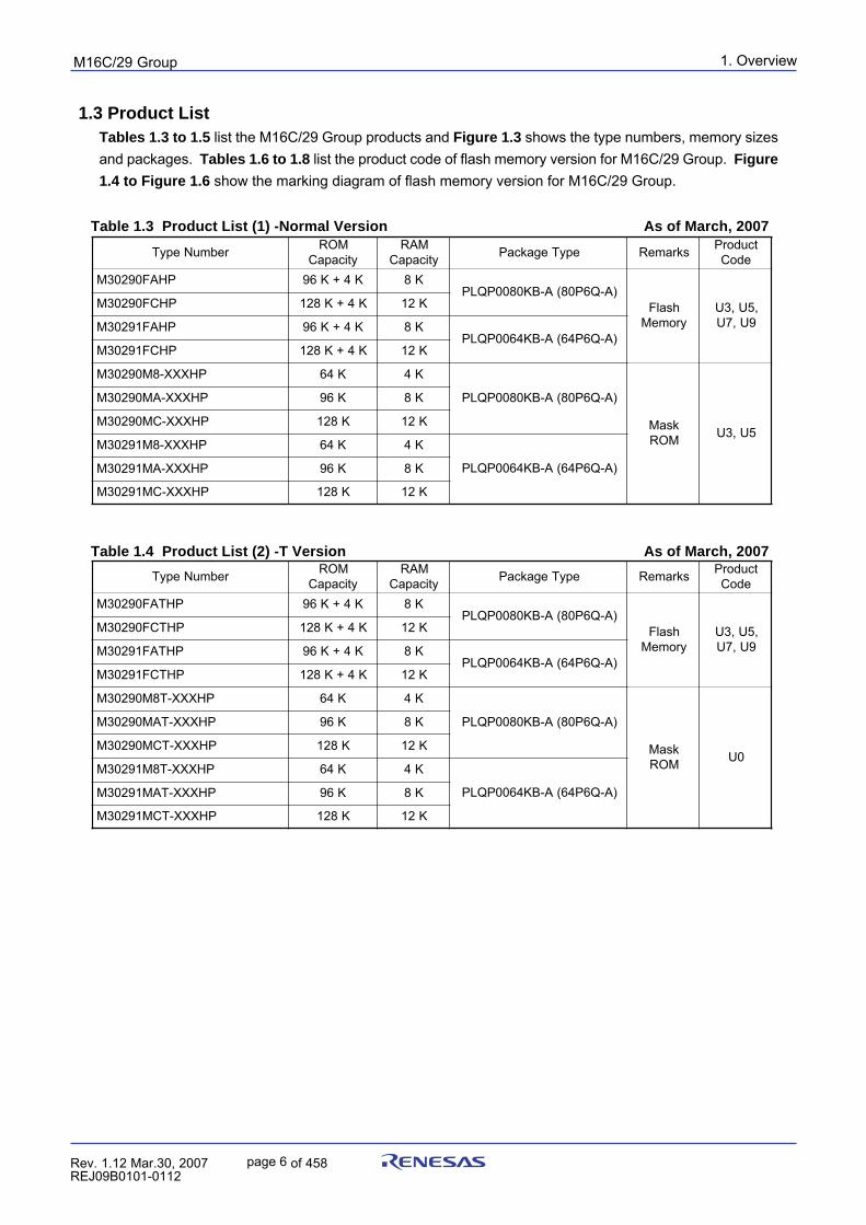
1. Overview
page 6
puorG92/C61M
854fo7002,03.raM21.1.veR2110-1010B90JER
1.3 Product ListTables 1.3 to 1.5 list the M16C/29 Group products and Figure 1.3 shows the type numbers, memory sizesand packages. Tables 1.6 to 1.8 list the product code of flash memory version for M16C/29 Group. Figure
1.4 to Figure 1.6 show the marking diagram of flash memory version for M16C/29 Group.
Table 1.3 Product List (1) -Normal Version As of March, 2007
rebmuNepyT MORyticapaC
MARyticapaC epyTegakcaP skrameR tcudorP
edoCPHAF09203M K4+K69 K8
)A-Q6P08(A-BK0800PQLPhsalF
yromeM,5U,3U
9U,7UPHCF09203M K4+K821 K21
PHAF19203M K4+K69 K8)A-Q6P46(A-BK4600PQLP
PHCF19203M K4+K821 K21
PHXXX-8M09203M K46 K4
)A-Q6P08(A-BK0800PQLP
ksaMMOR 5U,3U
PHXXX-AM09203M K69 K8
PHXXX-CM09203M K821 K21
PHXXX-8M19203M K46 K4
)A-Q6P46(A-BK4600PQLPPHXXX-AM19203M K69 K8
PHXXX-CM19203M K821 K21
rebmuNepyT MORyticapaC
MARyticapaC epyTegakcaP skrameR tcudorP
edoCPHTAF09203M K4+K69 K8
)A-Q6P08(A-BK0800PQLPhsalF
yromeM,5U,3U
9U,7UPHTCF09203M K4+K821 K21
PHTAF19203M K4+K69 K8)A-Q6P46(A-BK4600PQLP
PHTCF19203M K4+K821 K21
PHXXX-T8M09203M K46 K4
)A-Q6P08(A-BK0800PQLP
ksaMMOR 0U
PHXXX-TAM09203M K69 K8
PHXXX-TCM09203M K821 K21
PHXXX-T8M19203M K46 K4
)A-Q6P46(A-BK4600PQLPPHXXX-TAM19203M K69 K8
PHXXX-TCM19203M K821 K21
Table 1.4 Product List (2) -T Version As of March, 2007
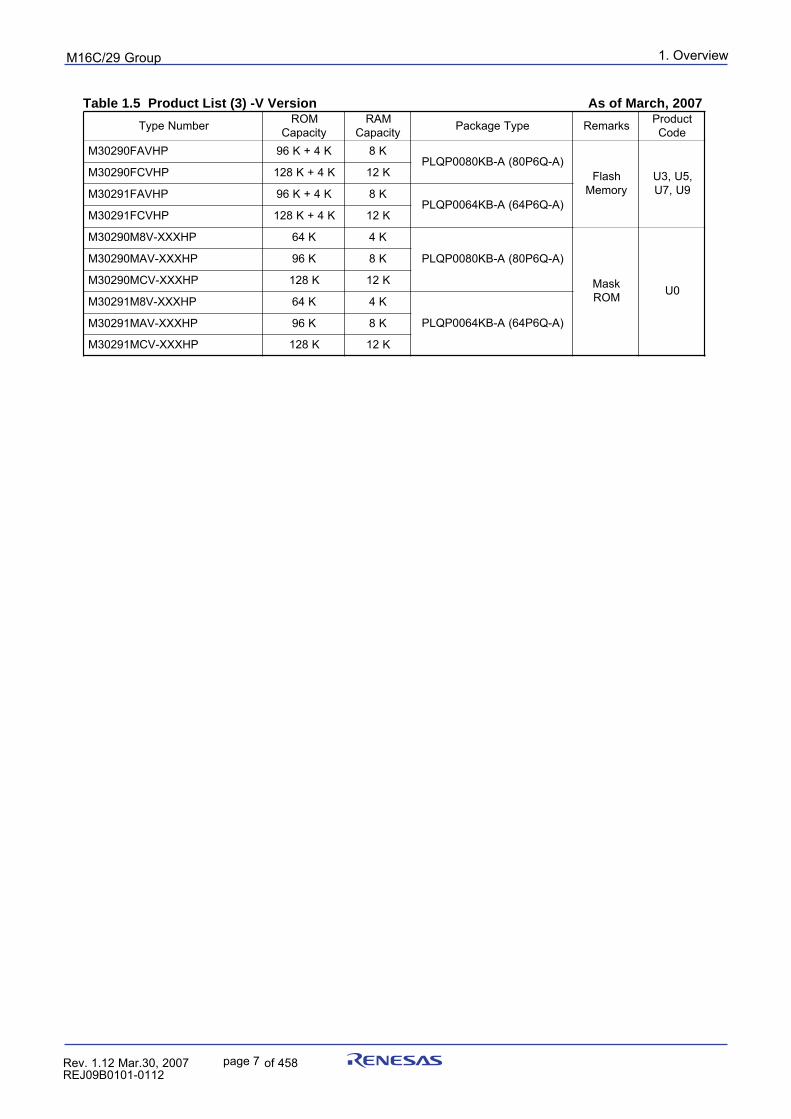
1. Overview
page 7
puorG92/C61M
854fo7002,03.raM21.1.veR2110-1010B90JER
rebmuNepyT MORyticapaC
MARyticapaC epyTegakcaP skrameR tcudorP
edoCPHVAF09203M K4+K69 K8
)A-Q6P08(A-BK0800PQLPhsalF
yromeM,5U,3U
9U,7UPHVCF09203M K4+K821 K21
PHVAF19203M K4+K69 K8)A-Q6P46(A-BK4600PQLP
PHVCF19203M K4+K821 K21
PHXXX-V8M09203M K46 K4
)A-Q6P08(A-BK0800PQLP
ksaMMOR 0U
PHXXX-VAM09203M K69 K8
PHXXX-VCM09203M K821 K21
PHXXX-V8M19203M K46 K4
)A-Q6P46(A-BK4600PQLPPHXXX-VAM19203M K69 K8
PHXXX-VCM19203M K821 K21
Table 1.5 Product List (3) -V Version As of March, 2007
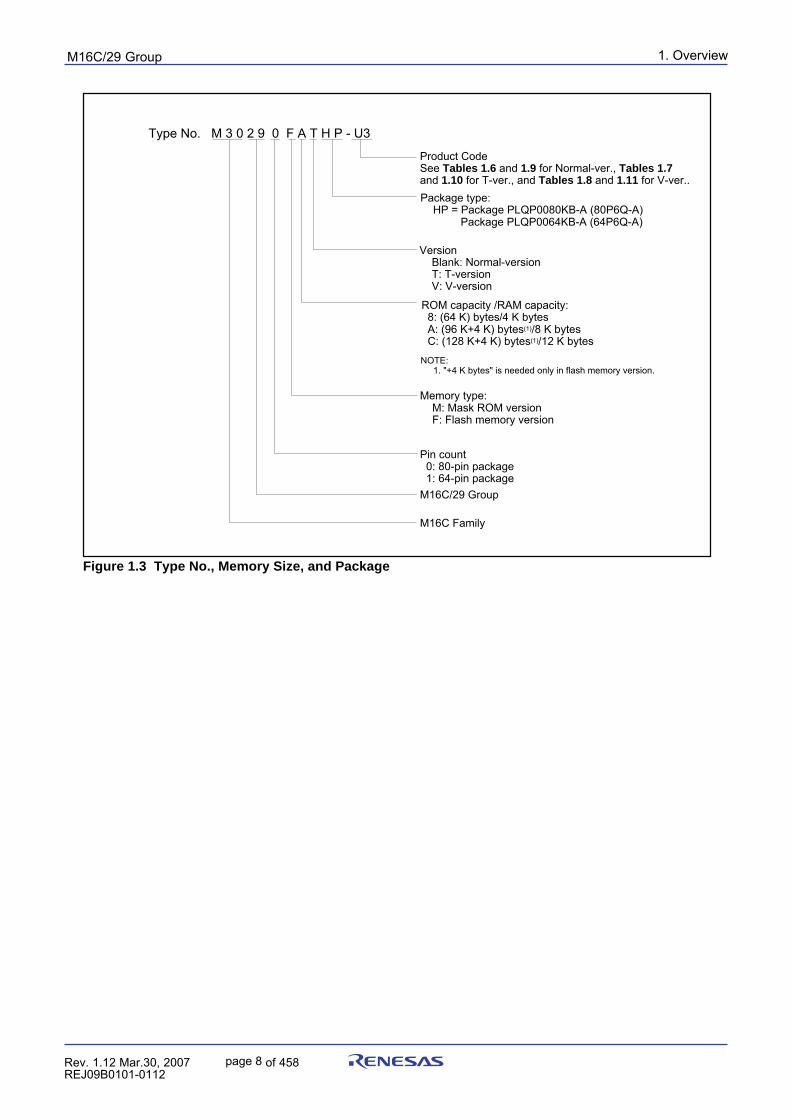
1. Overview
page 8
puorG92/C61M
854fo7002,03.raM21.1.veR2110-1010B90JER
Figure 1.3 Type No., Memory Size, and Package
Version Blank: Normal-version T: T-version V: V-version
ROM capacity /RAM capacity: 8: (64 K) bytes/4 K bytes A: (96 K+4 K) bytes(1)/8 K bytes C: (128 K+4 K) bytes(1)/12 K bytes
Memory type: M: Mask ROM version F: Flash memory version
Type No. M 3 0 2 9 0 F A T H P - U3
M16C/29 Group
M16C Family
Pin count 0: 80-pin package 1: 64-pin package
Product CodeSee Tables 1.6 and 1.9 for Normal-ver., Tables 1.7 and 1.10 for T-ver., and Tables 1.8 and 1.11 for V-ver..Package type: HP = Package PLQP0080KB-A (80P6Q-A) Package PLQP0064KB-A (64P6Q-A)
NOTE: 1. "+4 K bytes" is needed only in flash memory version.
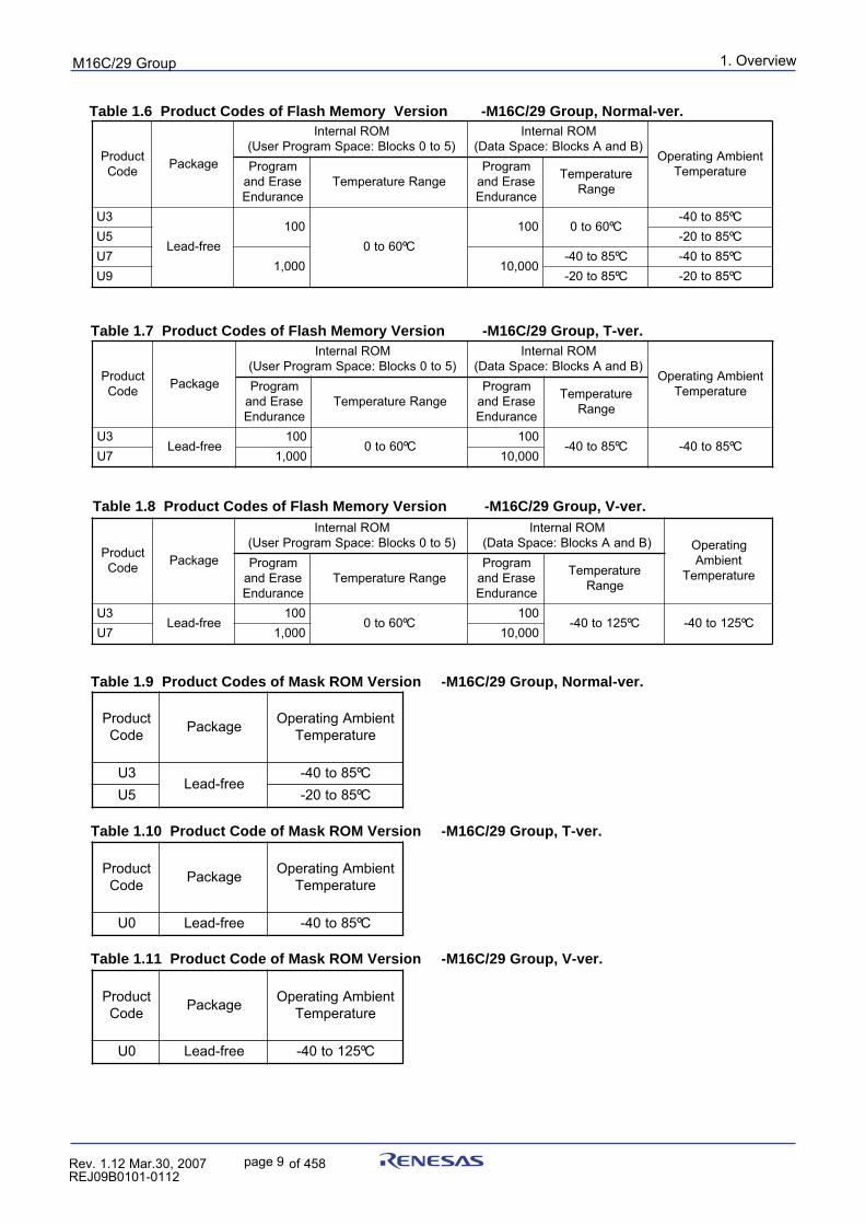
1. Overview
page 9
puorG92/C61M
854fo7002,03.raM21.1.veR2110-1010B90JER
Table 1.6 Product Codes of Flash Memory Version -M16C/29 Group, Normal-ver.
tcudorPedoC egakcaP
MORlanretnI)5ot0skcolB:ecapSmargorPresU(
MORlanretnI)BdnaAskcolB:ecapSataD(
tneibmAgnitarepOerutarepmeTmargorP
esarEdnaecnarudnE
egnaRerutarepmeTmargorP
esarEdnaecnarudnE
erutarepmeTegnaR
3U
eerf-daeL001
Cº06ot0001 Cº06ot0
Cº58ot04-5U Cº58ot02-7U
000,1 000,01Cº58ot04- Cº58ot04-
9U Cº58ot02- Cº58ot02-
Table 1.7 Product Codes of Flash Memory Version -M16C/29 Group, T-ver.
Table 1.8 Product Codes of Flash Memory Version -M16C/29 Group, V-ver.
tcudorPedoC egakcaP
MORlanretnI)5ot0skcolB:ecapSmargorPresU(
MORlanretnI)BdnaAskcolB:ecapSataD(
tneibmAgnitarepOerutarepmeTmargorP
esarEdnaecnarudnE
egnaRerutarepmeTmargorP
esarEdnaecnarudnE
erutarepmeTegnaR
3Ueerf-daeL
001Cº06ot0
001Cº58ot04- Cº58ot04-
7U 000,1 000,01
tcudorPedoC egakcaP
MORlanretnI)5ot0skcolB:ecapSmargorPresU(
MORlanretnI)BdnaAskcolB:ecapSataD( gnitarepO
tneibmAerutarepmeT
margorPesarEdnaecnarudnE
egnaRerutarepmeTmargorP
esarEdnaecnarudnE
erutarepmeTegnaR
3Ueerf-daeL
001Cº06ot0
001Cº521ot04- Cº521ot04-
7U 000,1 000,01
tcudorPedoC egakcaP tneibmAgnitarepO
erutarepmeT
3Ueerf-daeL
Cº58ot04-5U Cº58ot02-
tcudorPedoC egakcaP tneibmAgnitarepO
erutarepmeT
0U eerf-daeL Cº58ot04-
tcudorPedoC egakcaP tneibmAgnitarepO
erutarepmeT
0U eerf-daeL Cº521ot04-
Table 1.9 Product Codes of Mask ROM Version -M16C/29 Group, Normal-ver.
Table 1.10 Product Code of Mask ROM Version -M16C/29 Group, T-ver.
Table 1.11 Product Code of Mask ROM Version -M16C/29 Group, V-ver.
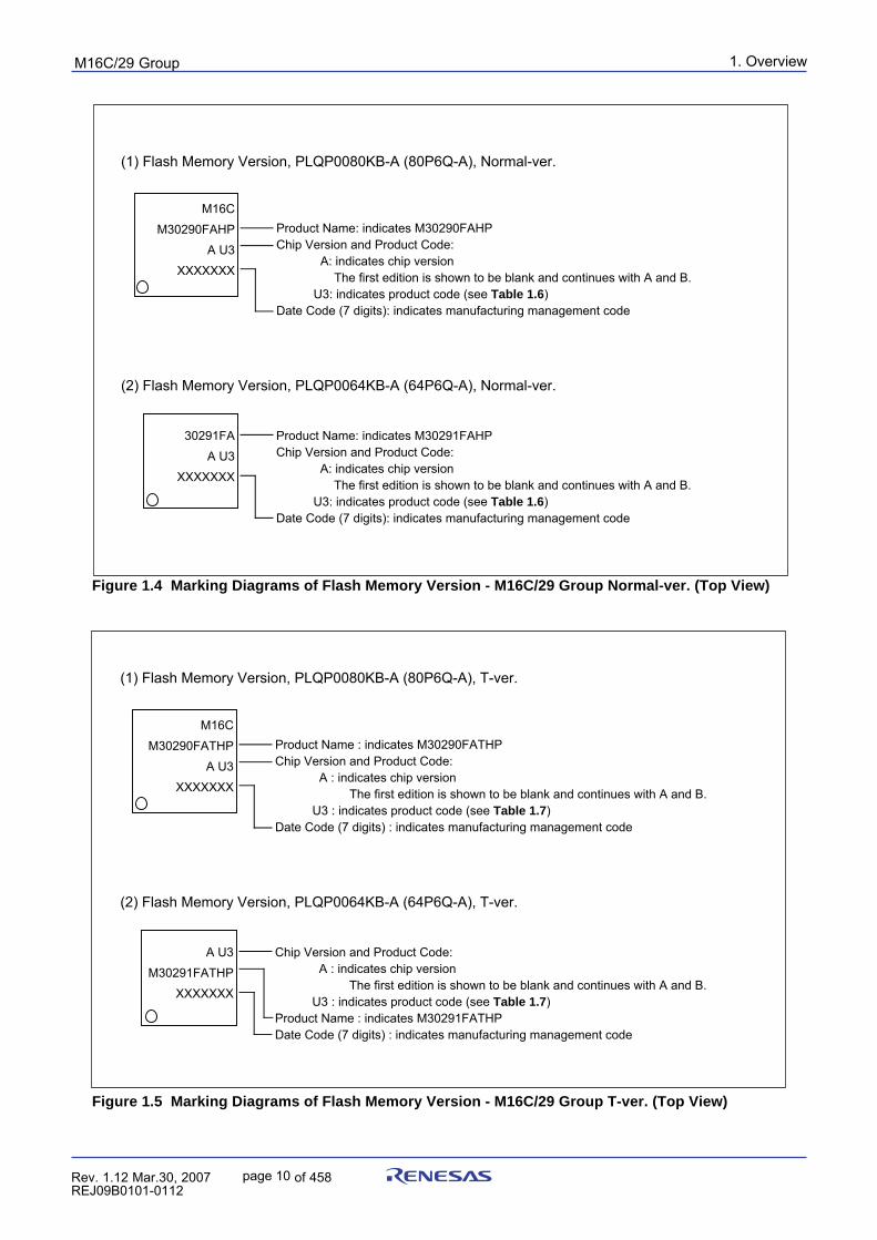
1. Overview
page 10
puorG92/C61M
854fo7002,03.raM21.1.veR2110-1010B90JER
M16C
M30290FAHP
A U3
XXXXXXX
Product Name: indicates M30290FAHPChip Version and Product Code:
A: indicates chip version The first edition is shown to be blank and continues with A and B.U3: indicates product code (see Table 1.6)
Date Code (7 digits): indicates manufacturing management code
30291FA
A U3
XXXXXXX
Product Name: indicates M30291FAHPChip Version and Product Code:
A: indicates chip version The first edition is shown to be blank and continues with A and B.U3: indicates product code (see Table 1.6)
Date Code (7 digits): indicates manufacturing management code
(1) Flash Memory Version, PLQP0080KB-A (80P6Q-A), Normal-ver.
(2) Flash Memory Version, PLQP0064KB-A (64P6Q-A), Normal-ver.
M16C
M30290FATHP
A U3
XXXXXXX
Product Name : indicates M30290FATHPChip Version and Product Code:
A : indicates chip versionThe first edition is shown to be blank and continues with A and B.
U3 : indicates product code (see Table 1.7)Date Code (7 digits) : indicates manufacturing management code
A U3
M30291FATHP
XXXXXXX
Chip Version and Product Code: A : indicates chip version
The first edition is shown to be blank and continues with A and B.U3 : indicates product code (see Table 1.7)
Product Name : indicates M30291FATHPDate Code (7 digits) : indicates manufacturing management code
(1) Flash Memory Version, PLQP0080KB-A (80P6Q-A), T-ver.
(2) Flash Memory Version, PLQP0064KB-A (64P6Q-A), T-ver.
Figure 1.4 Marking Diagrams of Flash Memory Version - M16C/29 Group Normal-ver. (Top View)
Figure 1.5 Marking Diagrams of Flash Memory Version - M16C/29 Group T-ver. (Top View)
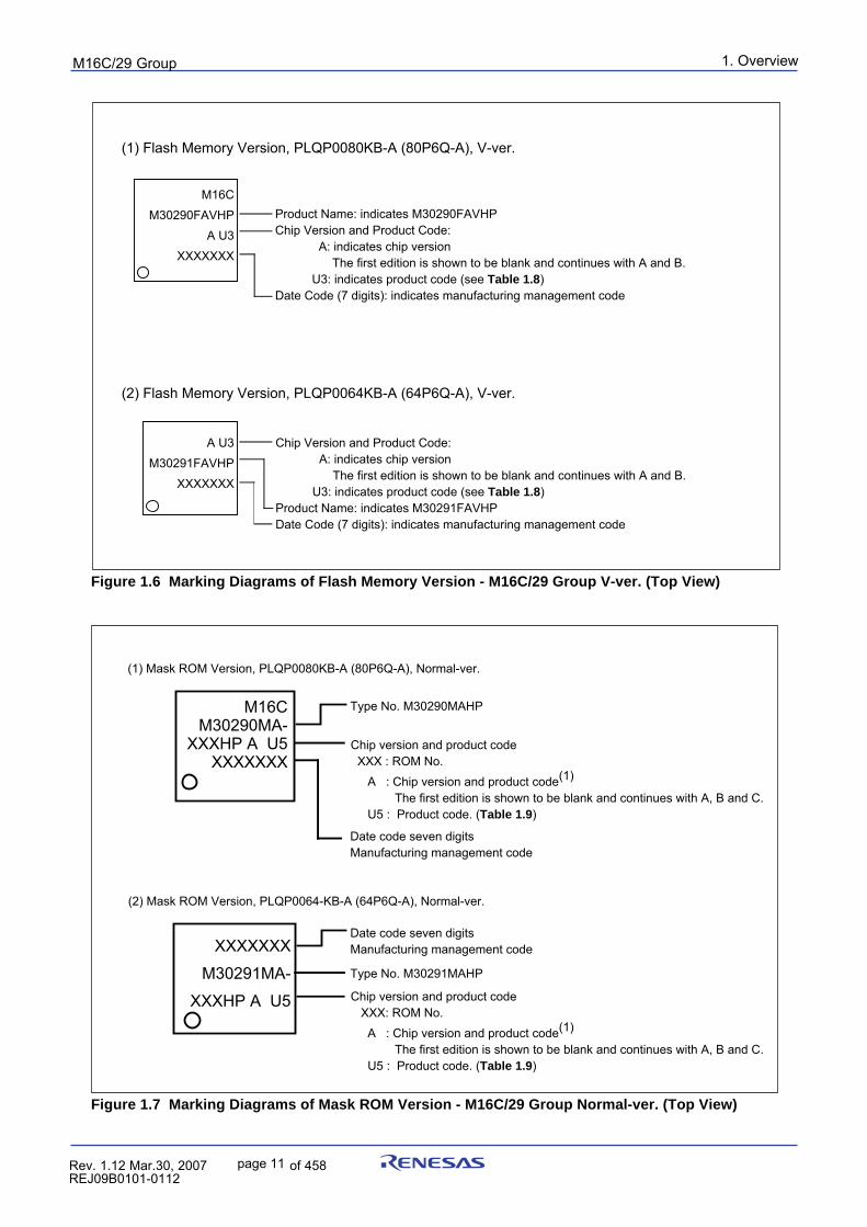
1. Overview
page 11
puorG92/C61M
854fo7002,03.raM21.1.veR2110-1010B90JER
M16C
M30290FAVHP
A U3
XXXXXXX
Product Name: indicates M30290FAVHPChip Version and Product Code:
A: indicates chip version The first edition is shown to be blank and continues with A and B.U3: indicates product code (see Table 1.8)
Date Code (7 digits): indicates manufacturing management code
A U3
M30291FAVHP
XXXXXXX
Chip Version and Product Code: A: indicates chip version The first edition is shown to be blank and continues with A and B.U3: indicates product code (see Table 1.8)
Product Name: indicates M30291FAVHPDate Code (7 digits): indicates manufacturing management code
(1) Flash Memory Version, PLQP0080KB-A (80P6Q-A), V-ver.
(2) Flash Memory Version, PLQP0064KB-A (64P6Q-A), V-ver.
Figure 1.6 Marking Diagrams of Flash Memory Version - M16C/29 Group V-ver. (Top View)
M16CM30290MA-
XXXHP A U5XXXXXXX
Type No. M30290MAHP
Chip version and product code XXX : ROM No.
A : Chip version and product code(1)
The first edition is shown to be blank and continues with A, B and C. U5 : Product code. (Table 1.9)
Date code seven digitsManufacturing management code
(1) Mask ROM Version, PLQP0080KB-A (80P6Q-A), Normal-ver.
XXXXXXX
M30291MA-
XXXHP A U5
Type No. M30291MAHP
Date code seven digitsManufacturing management code
(2) Mask ROM Version, PLQP0064-KB-A (64P6Q-A), Normal-ver.
Chip version and product code XXX: ROM No.
A : Chip version and product code(1)
The first edition is shown to be blank and continues with A, B and C. U5 : Product code. (Table 1.9)
Figure 1.7 Marking Diagrams of Mask ROM Version - M16C/29 Group Normal-ver. (Top View)
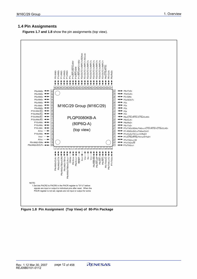
1. Overview
page 12
puorG92/C61M
854fo7002,03.raM21.1.veR2110-1010B90JER
M16C/29 Group (M16C/29)
PLQP0080KB-A(80P6Q-A)(top view)
Figure 1.8 Pin Assignment (Top View) of 80-Pin Package
1 2 3 4 5 6 7 8 9 10 11 12 13 14 15 16 17 18 19 20
21
2223
24
2526
2728
29
30
3132
33
34
3536
3738
39
40
41424344454647484950515253545557585960
61
62
6364
65
66
67
68
6970
71
7273
74
75
7677
78
79
80
56
P61
/CLK
0P35
P34
P33
P32/SOUT3
P31/SIN3
P37
P67/TXD1
P71/RXD2/SCL2/TA0IN/CLK1P72/CLK2/TA1OUT/V/RxD1P73/CTS2/RTS2/TA1IN/V/TxD1
P65/CLK1
P66/RxD1
P64/CTS1/RTS1/CTS0/CLKS1
P70/TXD2/SDA2/TA0OUT/CTS1/RTS1/CTS0/CLKS1
P75/TA2IN/W
P30/CLK3
P74/TA2OUT/W
P10
/AN
20P
11/A
N21
P12
/AN
22
P15
/INT3
/AD
TRG
/IDV
P1 6
/INT4
/IDW
P17
/INT5
/INP
C17
/IDU
P20
/OU
TC10
/INP
C10
/SD
AM
M
P21
/OU
TC11
/INP
C11
/SC
LMM
P22
/OU
TC12
/INP
C12
P23
/OU
TC13
/INP
C13
P24
/OU
TC14
/INP
C14
P25
/OU
TC15
/INP
C15
P26
/OU
TC16
/INP
C16
P27
/OU
TC17
/INP
C17
P60
/CTS
0/R
TS0
VC
C
XIN
XO
UT
VS
S
RE
SE
T
CN
Vss
P87
/XC
IN
P86
/XC
OU
T
P76/TA3OUT
P77
/TA
3IN
P92
/AN
32/T
B2I
N/C
RX
P9 3
/AN
24/C
TXP
95/A
N25
/CLK
4
P91
/AN
31/T
B1I
N
P82
/INT0
P83
/INT1
P81
/TA
4IN/U
P84
/INT2
/ZP
P8 0
/TA
4OU
T/U
P85
/NM
I/SD
P00/AN00
P01/AN01
P02/AN02
P03/AN03
P04/AN04
P05/AN05
P06/AN06
P07
/AN
07
VREF
AVSS
AVcc
P100/AN0
P101/AN1
P102/AN2
P103/AN3
P104/AN4/KI0P105/AN5/KI1P106/AN6/KI2P107/AN7/KI3
P96/AN26/SOUT4
P97/AN27/SIN4
P90
/AN
30/T
B0I
N/C
LKO
UT
P63/TXD0
P62
/RxD
0P36
P13
/AN
23P
14
NOTE: 1.Set bits PACR2 to PACR0 in the PACR register to "0112" before
signals are input or output to individual pins after reset. When the PACR register is not set, signals are not input or output for some
1.4 Pin AssignmentsFigures 1.7 and 1.8 show the pin assignments (top view).
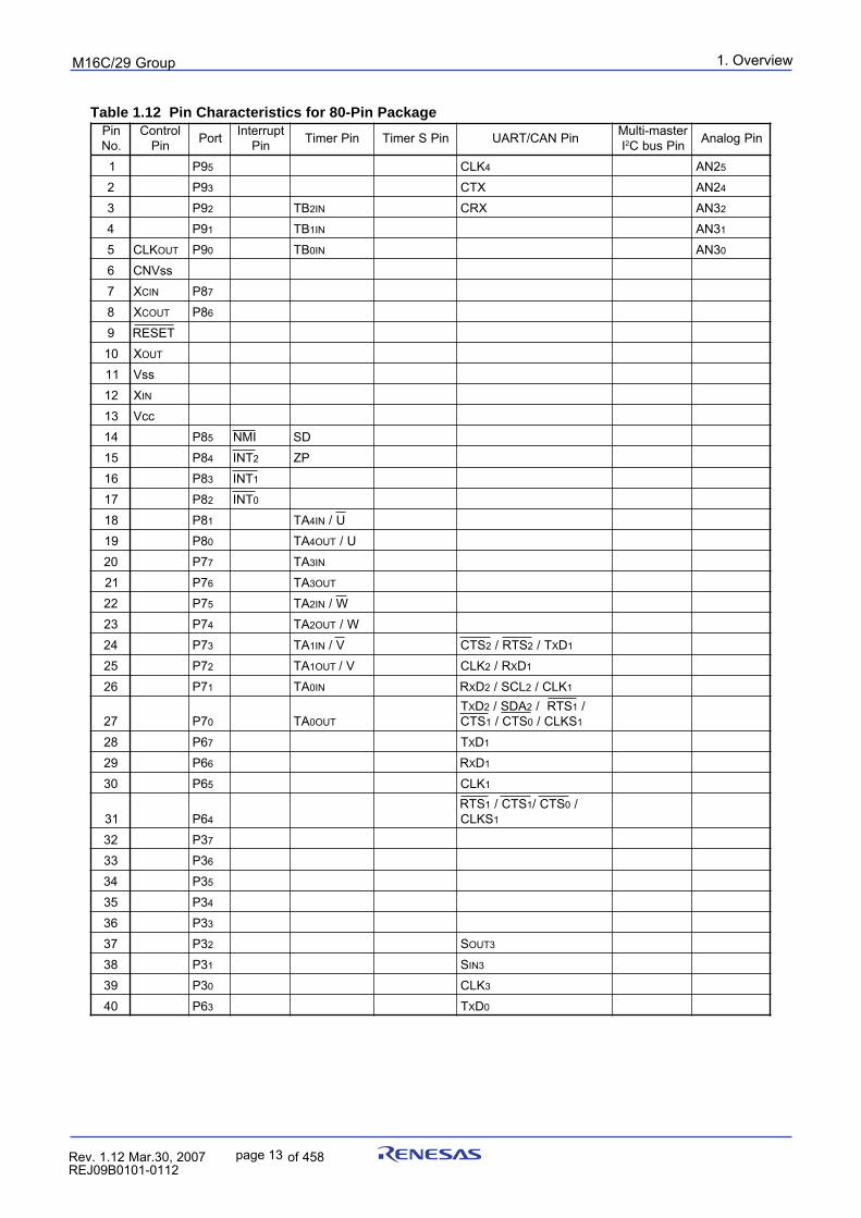
1. Overview
page 13
puorG92/C61M
854fo7002,03.raM21.1.veR2110-1010B90JER
Table 1.12 Pin Characteristics for 80-Pin PackageniP.oN
lortnoCniP troP tpurretnI
niP niPremiT niPSremiT niPNAC/TRAU retsam-itluMI2 niPsubC niPgolanA
1 9P 5 KLC 4 2NA 5
2 9P 3 XTC 2NA 4
3 9P 2 BT NI2 XRC 3NA 2
4 9P 1 BT NI1 3NA 1
5 KLC TUO 9P 0 BT NI0 3NA 0
6 ssVNC7 X NIC 8P 7
8 X TUOC 8P 6
9 TESER01 X TUO
11 ssV21 X NI
31 ccV41 8P 5 IMN DS51 8P 4 TNI 2 PZ61 8P 3 TNI 1
71 8P 2 TNI 0
81 8P 1 AT NI4 U/91 8P 0 AT TUO4 U/02 7P 7 AT NI3
12 7P 6 AT TUO3
22 7P 5 AT NI2 W/32 7P 4 AT TUO2 W/42 7P 3 AT NI1 V/ STC 2 STR/ 2 T/ XD1
52 7P 2 AT TUO1 V/ KLC 2 R/ XD1
62 7P 1 AT NI0 RXD2 LCS/ 2 KLC/ 1
72 7P 0 AT TUO0TXD2 ADS/ 2 STR/ 1 /
STC 1 STC/ 0 SKLC/ 1
82 6P 7 TXD1
92 6P 6 RXD1
03 6P 5 KLC 1
13 6P 4STR 1 STC/ 1 STC/ 0 /
SKLC 1
23 3P 7
33 3P 6
43 3P 5
53 3P 4
63 3P 3
73 3P 2 S 3TUO
83 3P 1 S 3NI
93 3P 0 KLC 3
04 6P 3 TXD0
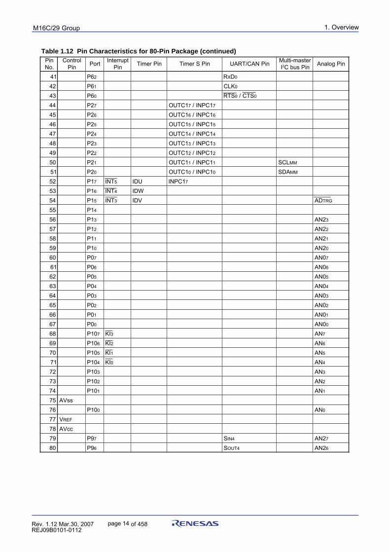
1. Overview
page 14
puorG92/C61M
854fo7002,03.raM21.1.veR2110-1010B90JER
Table 1.12 Pin Characteristics for 80-Pin Package (continued)niP.oN
lortnoCniP troP tpurretnI
niP niPremiT niPSremiT niPNAC/TRAU retsam-itluMI2 niPsubC niPgolanA
14 6P 2 RXD0
24 6P 1 KLC 0
34 6P 0 STR 0 STC/ 0
44 2P 7 1CTUO 7 1CPNI/ 7
54 2P 6 1CTUO 6 1CPNI/ 6
64 2P 5 1CTUO 5 1CPNI/ 5
74 2P 4 1CTUO 4 1CPNI/ 4
84 2P 3 1CTUO 3 1CPNI/ 3
94 2P 2 1CTUO 2 1CPNI/ 2
05 2P 1 1CTUO 1 1CPNI/ 1 LCS MM
15 2P 0 1CTUO 0 1CPNI/ 0 ADS MM
25 1P 7 TNI 5 UDI 1CPNI 7
35 1P 6 TNI 4 WDI45 1P 5 TNI 3 VDI DA GRT
55 1P 4
65 1P 3 2NA 3
75 1P 2 2NA 2
85 1P 1 2NA 1
95 1P 0 2NA 0
06 0P 7 0NA 7
16 0P 6 0NA 6
26 0P 5 0NA 5
36 0P 4 0NA 4
46 0P 3 0NA 3
56 0P 2 0NA 2
66 0P 1 0NA 1
76 0P 0 0NA 0
86 01P 7 IK 3 NA 7
96 01P 6 IK 2 NA 6
07 01P 5 IK 1 NA 5
17 01P 4 IK 0 NA 4
27 01P 3 NA 3
37 01P 2 NA 2
47 01P 1 NA 1
57 ssVA67 01P 0 NA 0
77 V FER
87 ccVA97 9P 7 S 4NI 2NA 7
08 9P 6 S 4TUO 2NA 6
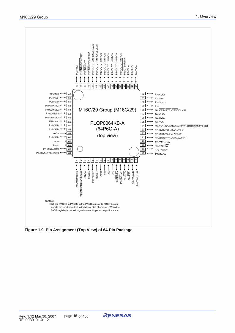
1. Overview
page 15
puorG92/C61M
854fo7002,03.raM21.1.veR2110-1010B90JER
Figure 1.9 Pin Assignment (Top View) of 64-Pin Package
32
31
3029
28
26
2524
2322
2120
19
18
17
4950
51
52
53
5455
5657
58
5960
61
6263
27
64
48 47 46 45 43 42 41 40 39 38 37 36 35 34 3344
1 2 3 4 5 6 7 8 9 10 11 12 13 14 15 16
P03
/AN
03
P15
/INT3
/AD
TRG
/IDV
P1 6
/INT4
/IDW
P17
/INT5
/INP
C17
/IDU
P20
/OU
TC10
/INP
C10
/SD
AM
M
P21
/OU
TC11
/INP
C11
/SC
LMM
P22
/OU
TC12
/INP
C12
P25
/OU
TC15
/INP
C15
P23
/OU
TC13
/INP
C13
P24
/OU
TC14
/INP
C14
P26
/OU
TC16
/INP
C16
P66/RxD1
P30/CLK3
P31/SIN3
P32/SOUT3
P33
P64/CTS1/RTS1/CTS0/CLKS1
P65/CLK1
P67/TxD1
P70/TxD2/SDA2/TA0OUT/RTS1/CTS1/CTS0/CLKS1
P71/RxD2/SCL2/TA0IN/CLK1
P76/TA3OUT
P74/TA2OUT/WP75/TA2IN/W
P72/CLK2/TA1OUT/V/RxD1
P73/CTS2/RTS2/TA1IN/V/TxD1
P00/AN00
P107/AN7/KI3
P104/AN4/KI0P103/AN3
P102/AN2
P101/AN1
AVSS
P100/AN0
VREF
AVCC
P93/AN24/CTX
P92/AN32/TB2IN/CRX
P02/AN02
P01/AN01
P106/AN6/KI2P105/AN5/KI1
P90
/AN
30/T
B0I
N/C
LKO
UT
CN
VS
S
P87
/XC
IN
P86
/XC
OU
T
RE
SE
T
XO
UT
XIN
VC
C
P84
/INT2
/ZP
P85
/NM
I/SD
P8 1
/TA
4IN/U
P80
/TA
4OU
T/U
P77/TA3IN
P91
/AN
31/T
B1I
N
P83
/INT1VS
S
P27
/OU
TC17
/INP
C17
P60
/CTS
0/R
TS0
P61
/CLK
0
P62
/RxD
0
P63
/TxD
0
P82
/INT0
NOTES: 1.Set bits PACR2 to PACR0 in the PACR register to "0102" before
signals are input or output to individual pins after reset. When the PACR register is not set, signals are not input or output for some
M16C/29 Group (M16C/29)
PLQP0064KB-A(64P6Q-A)(top view)
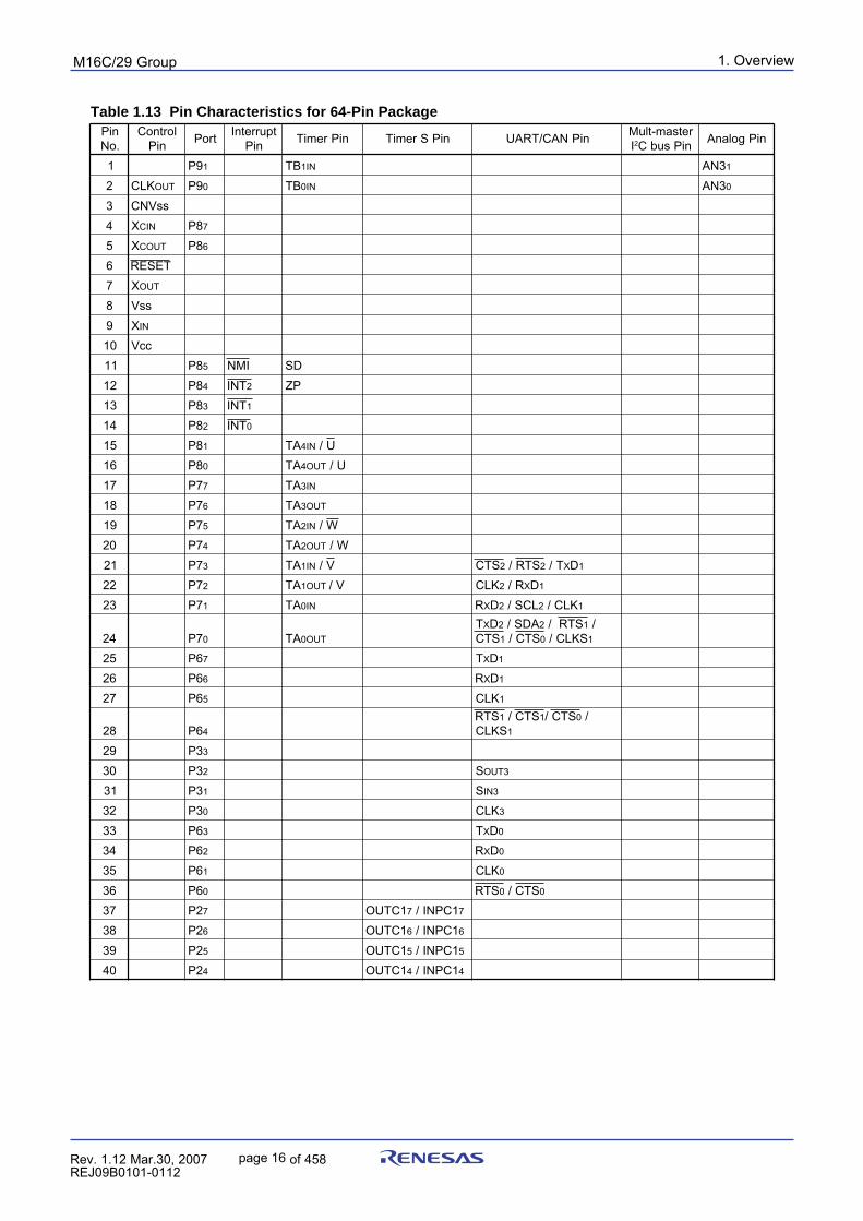
1. Overview
page 16
puorG92/C61M
854fo7002,03.raM21.1.veR2110-1010B90JER
Table 1.13 Pin Characteristics for 64-Pin PackageniP.oN
lortnoCniP troP tpurretnI
niP niPremiT niPSremiT niPNAC/TRAU retsam-tluMI2 niPsubC niPgolanA
1 9P 1 BT NI1 3NA 1
2 KLC TUO 9P 0 BT NI0 3NA 0
3 ssVNC4 X NIC 8P 7
5 X TUOC 8P 6
6 TESER7 X TUO
8 ssV9 X NI
01 ccV11 8P 5 IMN DS21 8P 4 TNI 2 PZ31 8P 3 TNI 1
41 8P 2 TNI 0
51 8P 1 AT NI4 U/61 8P 0 AT TUO4 U/71 7P 7 AT NI3
81 7P 6 AT TUO3
91 7P 5 AT NI2 W/02 7P 4 AT TUO2 W/12 7P 3 AT NI1 V/ STC 2 STR/ 2 T/ XD1
22 7P 2 AT TUO1 V/ KLC 2 R/ XD1
32 7P 1 AT NI0 RXD2 LCS/ 2 KLC/ 1
42 7P 0 AT TUO0TXD2 ADS/ 2 STR/ 1 /
STC 1 STC/ 0 SKLC/ 1
52 6P 7 TXD1
62 6P 6 RXD1
72 6P 5 KLC 1
82 6P 4STR 1 STC/ 1 STC/ 0 /
SKLC 1
92 3P 3
03 3P 2 S 3TUO
13 3P 1 S 3NI
23 3P 0 KLC 3
33 6P 3 TXD0
43 6P 2 RXD0
53 6P 1 KLC 0
63 6P 0 STR 0 STC/ 0
73 2P 7 1CTUO 7 1CPNI/ 7
83 2P 6 1CTUO 6 1CPNI/ 6
93 2P 5 1CTUO 5 1CPNI/ 5
04 2P 4 1CTUO 4 1CPNI/ 4
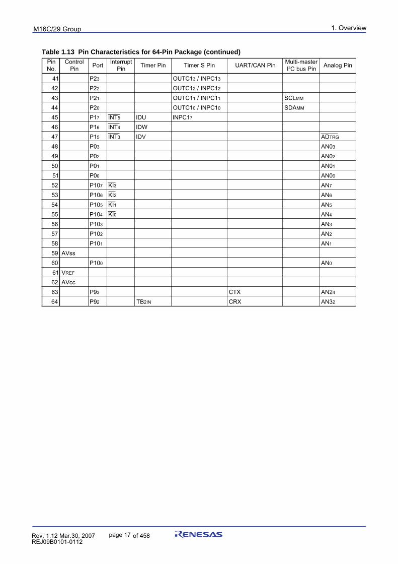
1. Overview
page 17
puorG92/C61M
854fo7002,03.raM21.1.veR2110-1010B90JER
Table 1.13 Pin Characteristics for 64-Pin Package (continued)niP.oN
lortnoCniP troP tpurretnI
niP niPremiT niPSremiT niPNAC/TRAU retsam-itluMI2 niPsubC niPgolanA
14 2P 3 1CTUO 3 1CPNI/ 3
24 2P 2 1CTUO 2 1CPNI/ 2
34 2P 1 1CTUO 1 1CPNI/ 1 LCS MM
44 2P 0 1CTUO 0 1CPNI/ 0 ADS MM
54 1P 7 TNI 5 UDI 1CPNI 7
64 1P 6 TNI 4 WDI74 1P 5 TNI 3 VDI DA GRT
84 0P 3 0NA 3
94 0P 2 0NA 2
05 0P 1 0NA 1
15 0P 0 0NA 0
25 01P 7 IK 3 NA 7
35 01P 6 IK 2 NA 6
45 01P 5 IK 1 NA 5
55 01P 4 IK 0 NA 4
65 01P 3 NA 3
75 01P 2 NA 2
85 01P 1 NA 1
95 ssVA06 01P 0 NA 0
16 V FER
26 ccVA36 9P 3 XTC 2NA 4
46 9P 2 BT NI2 XRC 3NA 2
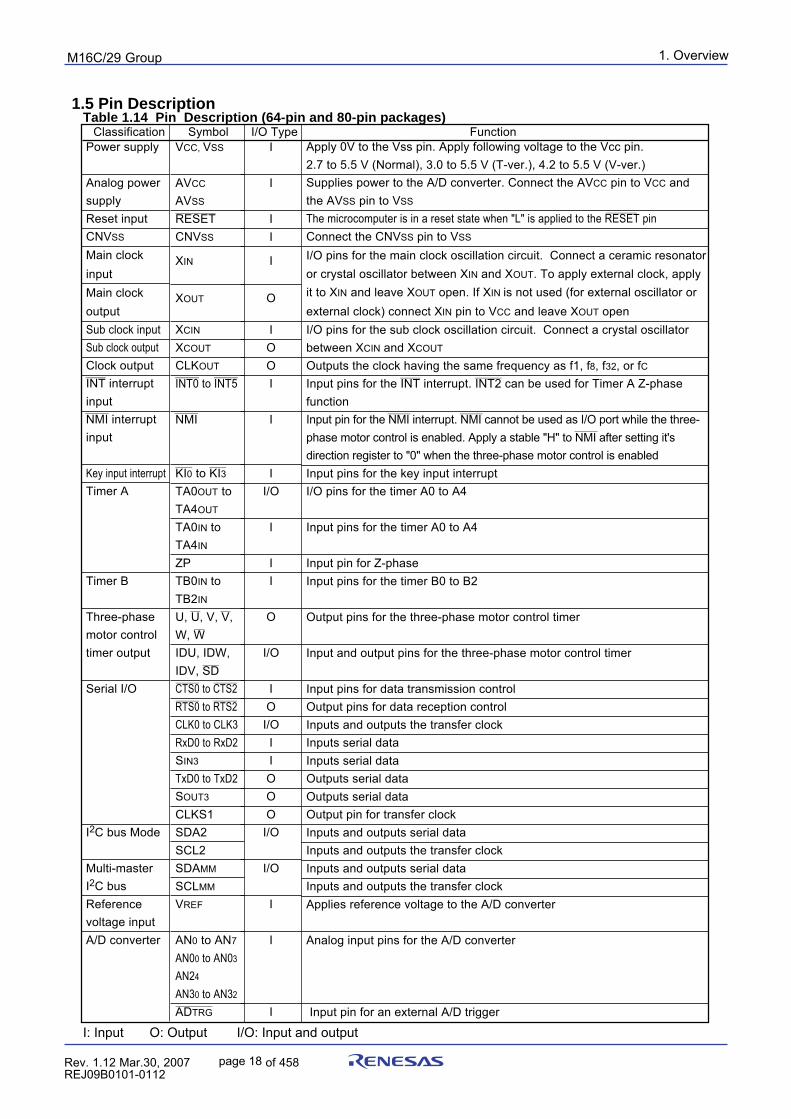
1. OverviewpuorG92/C61M
page 18 854fo7002,03.raM21.1.veR2110-1010B90JER
1.5 Pin Description
Apply 0V to the Vss pin. Apply following voltage to the Vcc pin.2.7 to 5.5 V (Normal), 3.0 to 5.5 V (T-ver.), 4.2 to 5.5 V (V-ver.)Supplies power to the A/D converter. Connect the AVCC pin to VCC andthe AVSS pin to VSS
___________
The microcomputer is in a reset state when "L" is applied to the RESET pinConnect the CNVSS pin to VSS
I/O pins for the main clock oscillation circuit. Connect a ceramic resonatoror crystal oscillator between XIN and XOUT. To apply external clock, applyit to XIN and leave XOUT open. If XIN is not used (for external oscillator orexternal clock) connect XIN pin to VCC and leave XOUT openI/O pins for the sub clock oscillation circuit. Connect a crystal oscillatorbetween XCIN and XCOUT
Outputs the clock having the same frequency as f1, f8, f32, or fC______ ________
Input pins for the INT interrupt. INT2 can be used for Timer A Z-phasefunction
_______ _______
Input pin for the NMI interrupt. NMI cannot be used as I/O port while the three-_______
phase motor control is enabled. Apply a stable "H" to NMI after setting it'sdirection register to "0" when the three-phase motor control is enabledInput pins for the key input interruptI/O pins for the timer A0 to A4
Input pins for the timer A0 to A4
Input pin for Z-phaseInput pins for the timer B0 to B2
Output pins for the three-phase motor control timer
Input and output pins for the three-phase motor control timer
Input pins for data transmission controlOutput pins for data reception controlInputs and outputs the transfer clockInputs serial dataInputs serial dataOutputs serial dataOutputs serial dataOutput pin for transfer clockInputs and outputs serial dataInputs and outputs the transfer clockInputs and outputs serial dataInputs and outputs the transfer clockApplies reference voltage to the A/D converter
Analog input pins for the A/D converter
Input pin for an external A/D trigger
VCC, VSS
AVCC
AVSS____________
RESETCNVSS
XIN
XOUT
XCIN
XCOUT
CLKOUT________ ________
INT0 to INT5
_______
NMI
_____ _____
KI0 to KI3TA0OUT toTA4OUT
TA0IN toTA4IN
ZPTB0IN toTB2IN
___ ___
U, U, V, V,___
W, WIDU, IDW,
_____
IDV, SD_________ _________
CTS0 to CTS2_________ _________
RTS0 to RTS2CLK0 to CLK3RxD0 to RxD2SIN3
TxD0 to TxD2SOUT3
CLKS1SDA2SCL2SDAMM
SCLMM
VREF
AN0 to AN7
AN00 to AN03
AN24
AN30 to AN32___________
ADTRG
Power supply
Analog powersupplyReset inputCNVSS
Main clockinputMain clockoutputSub clock inputSub clock outputClock output______
INT interruptinput_______
NMI interruptinput
Key input interruptTimer A
Timer B
Three-phasemotor controltimer output
Serial I/O
I2C bus Mode
Multi-masterI2C busReferencevoltage inputA/D converter
I
I
II
I
O
IOOI
I
II/O
I
II
O
I/O
IO
I/OIIOOO
I/O
I/O
I
I
I
I: Input O: Output I/O: Input and output
Classification Symbol I/O Type FunctionTable 1.14 Pin Description (64-pin and 80-pin packages)
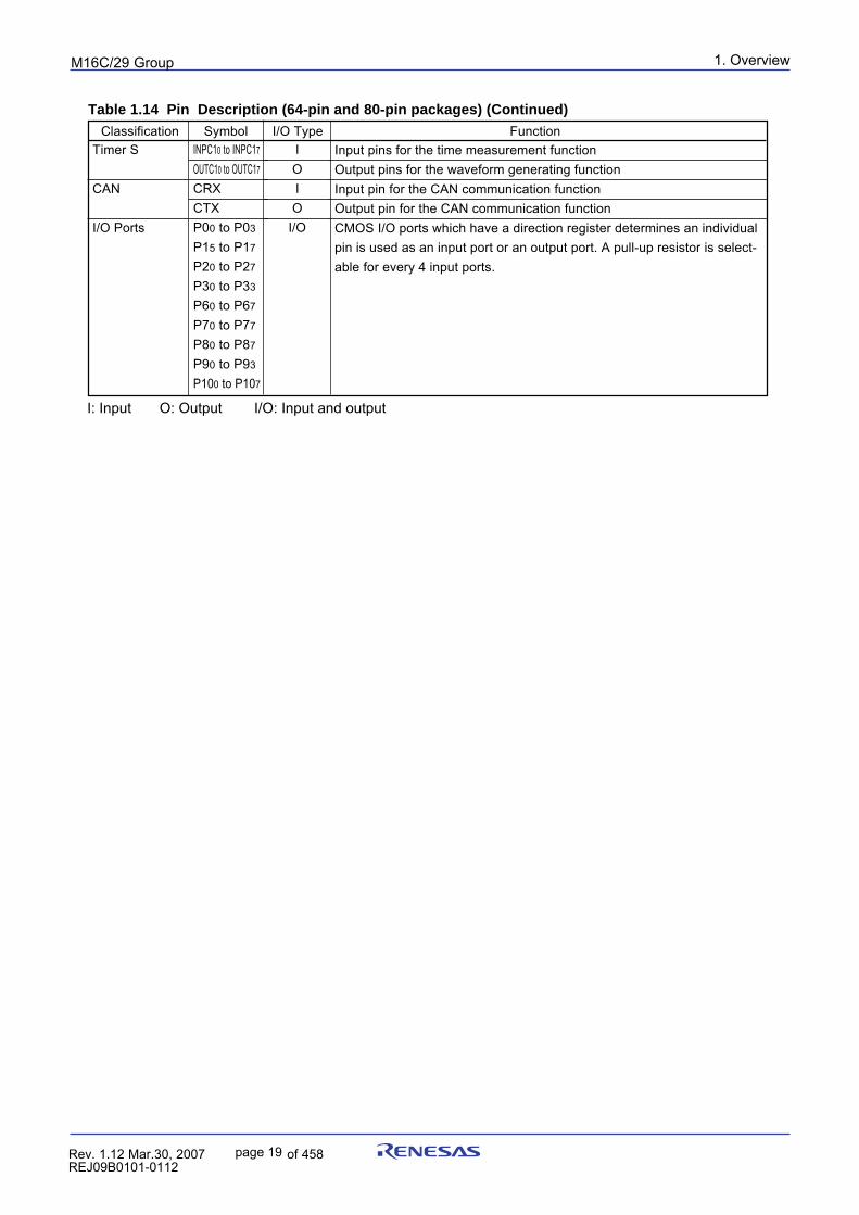
1. OverviewpuorG92/C61M
page 19 854fo7002,03.raM21.1.veR2110-1010B90JER
Input pins for the time measurement functionOutput pins for the waveform generating functionInput pin for the CAN communication functionOutput pin for the CAN communication functionCMOS I/O ports which have a direction register determines an individualpin is used as an input port or an output port. A pull-up resistor is select-able for every 4 input ports.
INPC10 to INPC17
OUTC10 to OUTC17
CRXCTXP00 to P03
P15 to P17
P20 to P27
P30 to P33
P60 to P67
P70 to P77
P80 to P87
P90 to P93
P100 to P107
Timer S
CAN
I/O Ports
IOIO
I/O
I: Input O: Output I/O: Input and output
Classification Symbol I/O Type FunctionTable 1.14 Pin Description (64-pin and 80-pin packages) (Continued)
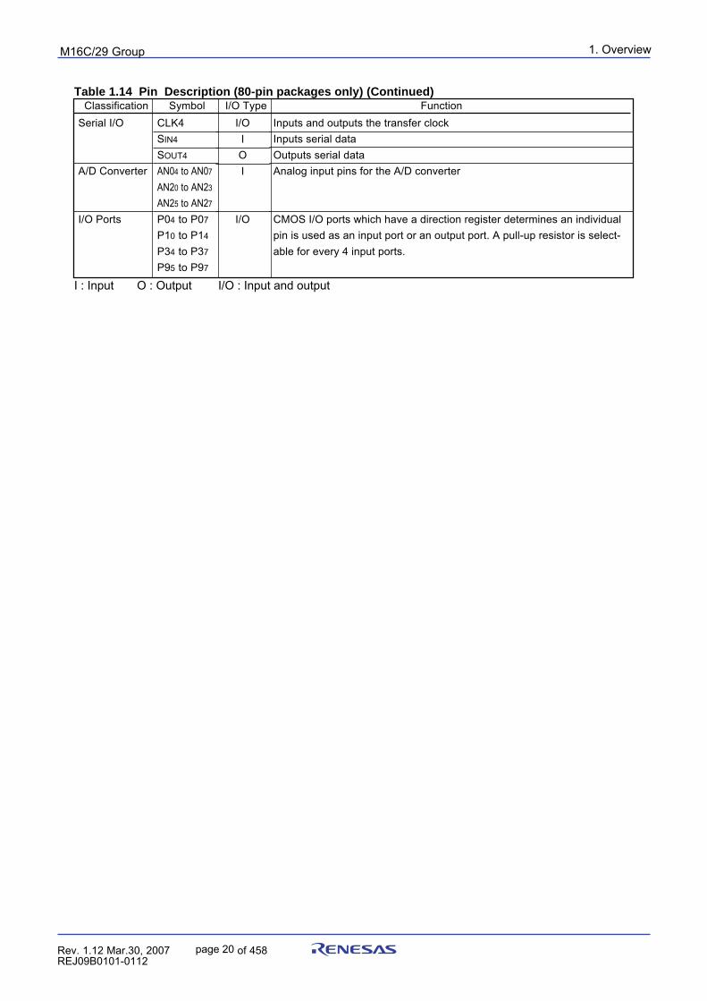
1. OverviewpuorG92/C61M
page 20 854fo7002,03.raM21.1.veR2110-1010B90JER
Inputs and outputs the transfer clockInputs serial dataOutputs serial dataAnalog input pins for the A/D converter
CMOS I/O ports which have a direction register determines an individualpin is used as an input port or an output port. A pull-up resistor is select-able for every 4 input ports.
CLK4SIN4
SOUT4
AN04 to AN07
AN20 to AN23
AN25 to AN27
P04 to P07
P10 to P14
P34 to P37
P95 to P97
Serial I/O
A/D Converter
I/O Ports
I/OIOI
I/O
Classification Symbol I/O Type FunctionTable 1.14 Pin Description (80-pin packages only) (Continued)
I : Input O : Output I/O : Input and output
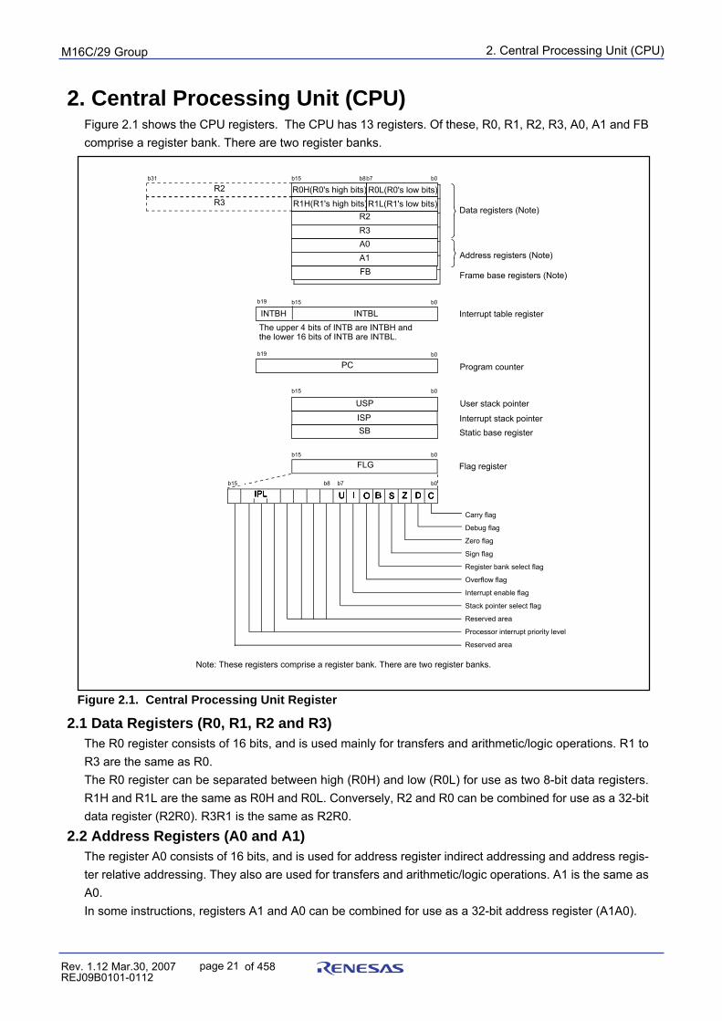
2. Central Processing Unit (CPU)
page 21 854fo7002,03.raM21.1.veR2110-1010B90JER
puorG92/C61M
2. Central Processing Unit (CPU)Figure 2.1 shows the CPU registers. The CPU has 13 registers. Of these, R0, R1, R2, R3, A0, A1 and FBcomprise a register bank. There are two register banks.
Figure 2.1. Central Processing Unit Register
2.1 Data Registers (R0, R1, R2 and R3)The R0 register consists of 16 bits, and is used mainly for transfers and arithmetic/logic operations. R1 toR3 are the same as R0.The R0 register can be separated between high (R0H) and low (R0L) for use as two 8-bit data registers.R1H and R1L are the same as R0H and R0L. Conversely, R2 and R0 can be combined for use as a 32-bitdata register (R2R0). R3R1 is the same as R2R0.
2.2 Address Registers (A0 and A1)The register A0 consists of 16 bits, and is used for address register indirect addressing and address regis-ter relative addressing. They also are used for transfers and arithmetic/logic operations. A1 is the same asA0.In some instructions, registers A1 and A0 can be combined for use as a 32-bit address register (A1A0).
Data registers (Note)
Address registers (Note)
Frame base registers (Note)
Program counter
Interrupt table register
User stack pointer
Interrupt stack pointerStatic base register
Flag register
Note: These registers comprise a register bank. There are two register banks.
R0H(R0's high bits)b15 b8 b7 b0
R3
INTBH
USP
ISPSB
R0L(R0's low bits)R1H(R1's high bits)R1L(R1's low bits)
R2b31
R3R2
A1A0
FB
b19
INTBLb15 b0
PCb19 b0
b15 b0
FLGb15 b0
b15 b0 b7 b8 b
Reserved area
Carry flag
Debug flag
Zero flag
Sign flag
Register bank select flag
Overflow flag
Interrupt enable flag
Stack pointer select flag
Reserved area
Processor interrupt priority level
The upper 4 bits of INTB are INTBH and the lower 16 bits of INTB are INTBL.
2. Central Processing Unit (CPU)
page 22 854fo7002,03.raM21.1.veR2110-1010B90JER
puorG92/C61M
2.3 Frame Base Register (FB)FB is configured with 16 bits, and is used for FB relative addressing.
2.4 Interrupt Table Register (INTB)INTB is configured with 20 bits, indicating the start address of an interrupt vector table.
2.5 Program Counter (PC)PC is configured with 20 bits, indicating the address of an instruction to be executed.
2.6 User Stack Pointer (USP) and Interrupt Stack Pointer (ISP)Stack pointer (SP) comes in two types: USP and ISP, each configured with 16 bits.Your desired type of stack pointer (USP or ISP) can be selected by the U flag of FLG.
2.7 Static Base Register (SB)SB is configured with 16 bits, and is used for SB relative addressing.
2.8 Flag Register (FLG)FLG consists of 11 bits, indicating the CPU status.
2.8.1 Carry Flag (C Flag)
This flag retains a carry, borrow, or shift-out bit that has occurred in the arithmetic/logic unit.
2.8.2 Debug Flag (D Flag)
The D flag is used exclusively for debugging purpose. During normal use, it must be set to 0.
2.8.3 Zero Flag (Z Flag)
This flag is set to 1 when an arithmetic operation resulted in 0; otherwise, it is 0.
2.8.4 Sign Flag (S Flag)
This flag is set to 1 when an arithmetic operation resulted in a negative value; otherwise, it is 0.
2.8.5 Register Bank Select Flag (B Flag)
Register bank 0 is selected when this flag is 0 ; register bank 1 is selected when this flag is 1.
2.8.6 Overflow Flag (O Flag)
This flag is set to 1 when the operation resulted in an overflow; otherwise, it is 0.
2.8.7 Interrupt Enable Flag (I Flag)
This flag enables a maskable interrupt.Maskable interrupts are disabled when the I flag is 0, and are enabled when the I flag is 1.The I flag is cleared to 0 when the interrupt request is accepted.
2.8.8 Stack Pointer Select Flag (U Flag)
ISP is selected when the U flag is 0; USP is selected when the U flag is 1.The U flag is cleared to 0 when a hardware interrupt request is accepted or an INT instruction for softwareinterrupt Nos. 0 to 31 is executed.
2.8.9 Processor Interrupt Priority Level (IPL)
IPL is configured with three bits, for specification of up to eight processor interrupt priority levels from level0 to level 7.If a requested interrupt has priority greater than IPL, the interrupt is enabled.
2.8.10 Reserved Area
When write to this bit, write 0. When read, its content is undefined.
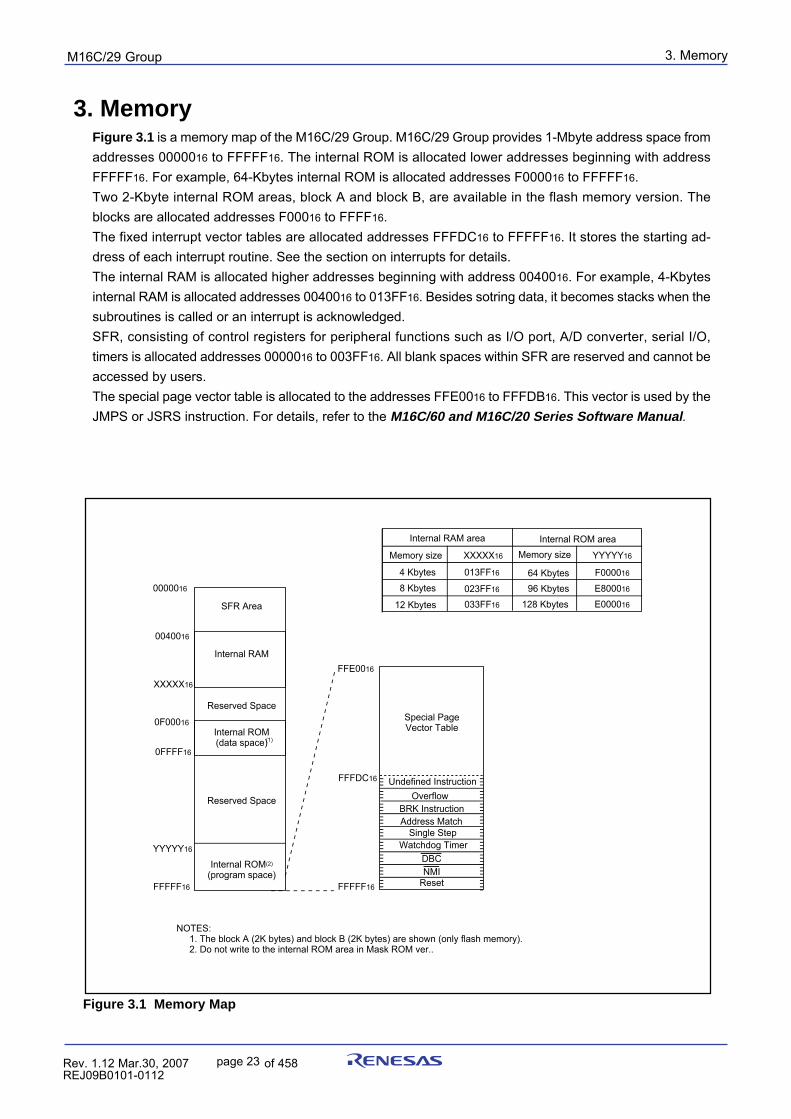
3. MemorypuorG92/C61M
page 23 854fo7002,03.raM21.1.veR2110-1010B90JER
3. MemoryFigure 3.1 is a memory map of the M16C/29 Group. M16C/29 Group provides 1-Mbyte address space fromaddresses 0000016 to FFFFF16. The internal ROM is allocated lower addresses beginning with addressFFFFF16. For example, 64-Kbytes internal ROM is allocated addresses F000016 to FFFFF16.Two 2-Kbyte internal ROM areas, block A and block B, are available in the flash memory version. Theblocks are allocated addresses F00016 to FFFF16.The fixed interrupt vector tables are allocated addresses FFFDC16 to FFFFF16. It stores the starting ad-dress of each interrupt routine. See the section on interrupts for details.The internal RAM is allocated higher addresses beginning with address 0040016. For example, 4-Kbytesinternal RAM is allocated addresses 0040016 to 013FF16. Besides sotring data, it becomes stacks when thesubroutines is called or an interrupt is acknowledged.SFR, consisting of control registers for peripheral functions such as I/O port, A/D converter, serial I/O,timers is allocated addresses 0000016 to 003FF16. All blank spaces within SFR are reserved and cannot beaccessed by users.The special page vector table is allocated to the addresses FFE0016 to FFFDB16. This vector is used by theJMPS or JSRS instruction. For details, refer to the M16C/60 and M16C/20 Series Software Manual.
Figure 3.1 Memory Map
0000016
XXXXX16
FFFFF16
0040016
YYYYY16
Internal ROM(2)
(program space)
SFR Area
Internal RAMFFE0016
FFFDC16
FFFFF16
Undefined InstructionOverflow
BRK InstructionAddress Match
Single StepWatchdog Timer
Reset
Special PageVector Table
DBC
Reserved Space
Internal ROM(data space)
Reserved Space
0F00016
XXXXX16 YYYYY16
Internal RAM area Internal ROM area
Memory size
013FF16
023FF16
F0000164 Kbytes 64 Kbytes
Memory size
E80001696 Kbytes
NOTES: 1. The block A (2K bytes) and block B (2K bytes) are shown (only flash memory). 2. Do not write to the internal ROM area in Mask ROM ver..
(1)
0FFFF16
NMI
033FF16
8 Kbytes
E000016128 Kbytes12 Kbytes
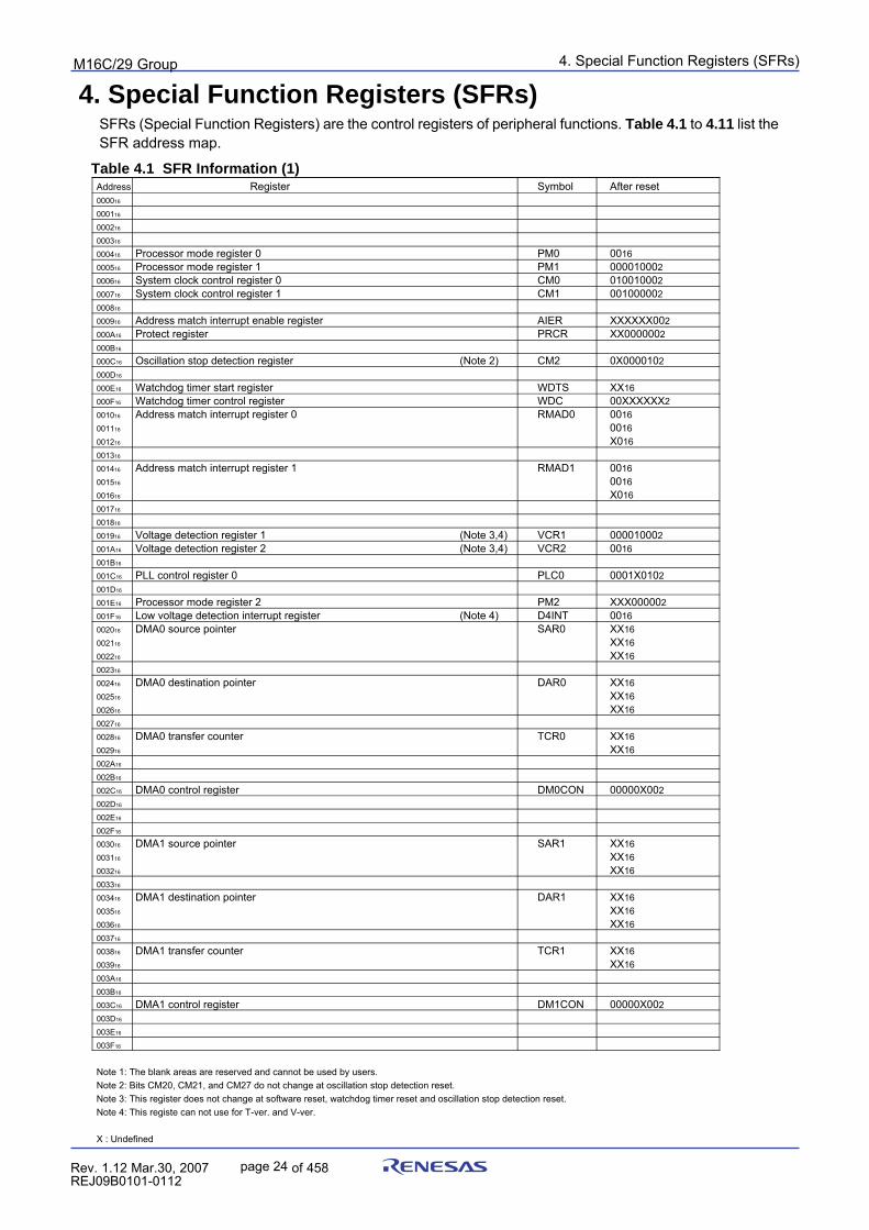
4. Special Function Registers (SFRs)puorG92/C61M
page 24 854fo7002,03.raM21.1.veR2110-1010B90JER
Address Register Symbol After reset000016
000116
000216
000316
000416 Processor mode register 0 PM0 0016000516 Processor mode register 1 PM1 000010002000616 System clock control register 0 CM0 010010002000716 System clock control register 1 CM1 001000002000816
000916 Address match interrupt enable register AIER XXXXXX002000A16 Protect register PRCR XX0000002000B16
000C16 Oscillation stop detection register (Note 2) CM2 0X0000102000D16
000E16 Watchdog timer start register WDTS XX16000F16 Watchdog timer control register WDC 00XXXXXX2 001016 Address match interrupt register 0 RMAD0 0016001116 0016001216 X016001316
001416 Address match interrupt register 1 RMAD1 0016001516 0016 001616 X016 001716
001816
001916 Voltage detection register 1 (Note 3,4) VCR1 000010002001A16 Voltage detection register 2 (Note 3,4) VCR2 0016001B16
001C16 PLL control register 0 PLC0 0001X0102001D16
001E16 Processor mode register 2 PM2 XXX000002001F16 Low voltage detection interrupt register (Note 4) D4INT 0016002016 DMA0 source pointer SAR0 XX16002116 XX16002216 XX16002316
002416 DMA0 destination pointer DAR0 XX16002516 XX16002616 XX16002716
002816 DMA0 transfer counter TCR0 XX16002916 XX16002A16
002B16
002C16 DMA0 control register DM0CON 00000X002002D16
002E16
002F16
003016 DMA1 source pointer SAR1 XX16003116 XX16003216 XX16003316
003416 DMA1 destination pointer DAR1 XX16003516 XX16003616 XX16003716
003816 DMA1 transfer counter TCR1 XX16003916 XX16003A16
003B16
003C16 DMA1 control register DM1CON 00000X002003D16
003E16
003F16
Note 1: The blank areas are reserved and cannot be used by users.Note 2: Bits CM20, CM21, and CM27 do not change at oscillation stop detection reset.Note 3: This register does not change at software reset, watchdog timer reset and oscillation stop detection reset.Note 4: This registe can not use for T-ver. and V-ver.
X : Undefined
4. Special Function Registers (SFRs)SFRs (Special Function Registers) are the control registers of peripheral functions. Table 4.1 to 4.11 list theSFR address map.
Table 4.1 SFR Information (1)
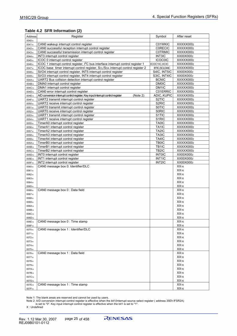
4. Special Function Registers (SFRs)puorG92/C61M
page 25 854fo7002,03.raM21.1.veR2110-1010B90JER
Address Register Symbol After reset004016
004116 CAN0 wakeup interrupt control register C01WKIC XXXXX0002
004216 CAN0 successful reception interrupt control register C0RECIC XXXXX0002
004316 CAN0 successful transmission interrupt control register C0TRMIC XXXXX0002
004416 INT3 interrupt control register INT3IC XX00X0002
004516 ICOC 0 interrupt control register ICOC0IC XXXXX0002
004616 ICOC 1 interrupt control register, I2C bus interface interrupt control register 1 ICOC1IC,IICIC XXXXX0002
004716 ICOC base timer interrupt control register, SCL/SDA interrupt control register 2 BTIC,SCLDAIC XXXXX0002
004816 SI/O4 interrupt control register, INT5 interrupt control register S4IC, INT5IC XX00X0002
004916 SI/O3 interrupt control register, INT4 interrupt control register S3IC, INT4IC XX00X0002
004A16 UART2 Bus collision detection interrupt control register BCNIC XXXXX0002
004B16 DMA0 interrupt control register DM0IC XXXXX0002
004C16 DMA1 interrupt control register DM1IC XXXXX0002
004D16 CAN0 error interrupt control register C01ERRIC XXXXX0002
004E16 A/D conversion interrupt control register, Key input interrupt control register (Note 2) ADIC, KUPIC XXXXX0002
004F16 UART2 transmit interrupt control register S2TIC XXXXX0002
005016 UART2 receive interrupt control register S2RIC XXXXX0002
005116 UART0 transmit interrupt control register S0TIC XXXXX0002
005216 UART0 receive interrupt control register S0RIC XXXXX0002
005316 UART1 transmit interrupt control register S1TIC XXXXX0002
005416 UART1 receive interrupt control register S1RIC XXXXX0002
005516 TimerA0 interrupt control register TA0IC XXXXX0002
005616 TimerA1 interrupt control register TA1IC XXXXX0002
005716 TimerA2 interrupt control register TA2IC XXXXX0002
005816 TimerA3 interrupt control register TA3IC XXXXX0002
005916 TimerA4 interrupt control register TA4IC XXXXX0002
005A16 TimerB0 interrupt control register TB0IC XXXXX0002
005B16 TimerB1 interrupt control register TB1IC XXXXX0002
005C16 TimerB2 interrupt control register TB2IC XXXXX0002
005D16 INT0 interrupt control register INT0IC XX00X0002
005E16 INT1 interrupt control register INT1IC XX00X0002
005F16 INT2 interrupt control register INT2IC XX00X0002
006016 CAN0 message box 0: Identifier/DLC XX16
006116 XX16
006216 XX16
006316 XX16
006416 XX16
006516 XX16
006616 CAN0 message box 0 : Data field XX16
006716 XX16
006816 XX16
006916 XX16
006A16 XX16
006B16 XX16
006C16 XX16
006D16 XX16
006E16 CAN0 message box 0 : Time stamp XX16
006F16 XX16
007016 CAN0 message box 1 : Identifier/DLC XX16
007116 XX16
007216 XX16
007316 XX16
007416 XX16
007516 XX16
007616 CAN0 message box 1 : Data field XX16
007716 XX16
007816 XX16
007916 XX16
007A16 XX16
007B16 XX16
007C16 XX16
007D16 XX16
007E16 CAN0 message box 1 : Time stamp XX16
007F16 XX16
Note 1: The blank areas are reserved and cannot be used by users.Note 2: A/D conversion interrupt control register is effective when the bit1(Interrupt source select register ( address 35Eh IFSR2A) is set to "0". Key input interrupt control register is effective when the bit1 is set to "1".X : Undefined
Table 4.2 SFR Information (2)
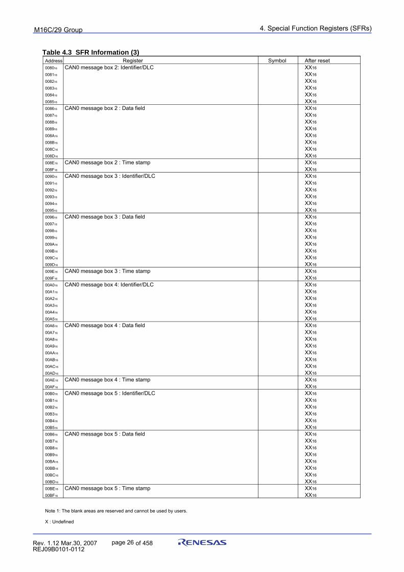
4. Special Function Registers (SFRs)puorG92/C61M
page 26 854fo7002,03.raM21.1.veR2110-1010B90JER
Address Register Symbol After reset008016 CAN0 message box 2: Identifier/DLC XX16
008116 XX16
008216 XX16
008316 XX16
008416 XX16
008516 XX16
008616 CAN0 message box 2 : Data field XX16
008716 XX16
008816 XX16
008916 XX16
008A16 XX16
008B16 XX16
008C16 XX16
008D16 XX16
008E16 CAN0 message box 2 : Time stamp XX16
008F16 XX16
009016 CAN0 message box 3 : Identifier/DLC XX16
009116 XX16
009216 XX16
009316 XX16
009416 XX16
009516 XX16
009616 CAN0 message box 3 : Data field XX16
009716 XX16
009816 XX16
009916 XX16
009A16 XX16
009B16 XX16
009C16 XX16
009D16 XX16
009E16 CAN0 message box 3 : Time stamp XX16
009F16 XX16
00A016 CAN0 message box 4: Identifier/DLC XX16
00A116 XX16
00A216 XX16
00A316 XX16
00A416 XX16
00A516 XX16
00A616 CAN0 message box 4 : Data field XX16
00A716 XX16
00A816 XX16
00A916 XX16
00AA16 XX16
00AB16 XX16
00AC16 XX16
00AD16 XX16
00AE16 CAN0 message box 4 : Time stamp XX16
00AF16 XX16
00B016 CAN0 message box 5 : Identifier/DLC XX16
00B116 XX16
00B216 XX16
00B316 XX16
00B416 XX16
00B516 XX16
00B616 CAN0 message box 5 : Data field XX16
00B716 XX16
00B816 XX16
00B916 XX16
00BA16 XX16
00BB16 XX16
00BC16 XX16
00BD16 XX16
00BE16 CAN0 message box 5 : Time stamp XX16
00BF16 XX16
Note 1: The blank areas are reserved and cannot be used by users.
X : Undefined
Table 4.3 SFR Information (3)
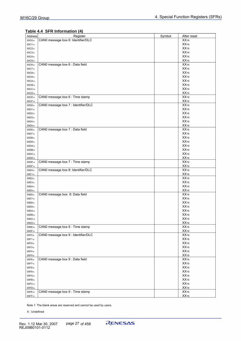
4. Special Function Registers (SFRs)puorG92/C61M
page 27 854fo7002,03.raM21.1.veR2110-1010B90JER
Address Register Symbol After reset00C016 CAN0 message box 6: Identifier/DLC XX16
00C116 XX16
00C216 XX16
00C316 XX16
00C416 XX16
00C516 XX16
00C616 CAN0 message box 6 : Data field XX16
00C716 XX16
00C816 XX16
00C916 XX16
00CA16 XX16
00CB16 XX16
00CC16 XX16
00CD16 XX16
00CE16 CAN0 message box 6 : Time stamp XX16
00CF16 XX16
00D016 CAN0 message box 7 : Identifier/DLC XX16
00D116 XX16
00D216 XX16
00D316 XX16
00D416 XX16
00D516 XX16
00D616 CAN0 message box 7 : Data field XX16
00D716 XX16
00D816 XX16
00D916 XX16
00DA16 XX16
00DB16 XX16
00DC16 XX16
00DD16 XX16
00DE16 CAN0 message box 7 : Time stamp XX16
00DF16 XX16
00E016 CAN0 message box 8: Identifier/DLC XX16
00E116 XX16
00E216 XX16
00E316 XX16
00E416 XX16
00E516 XX16
00E616 CAN0 message box 8: Data field XX16
00E716 XX16
00E816 XX16
00E916 XX16
00EA16 XX16
00EB16 XX16
00EC16 XX16
00ED16 XX16
00EE16 CAN0 message box 8 : Time stamp XX16
00EF16 XX16
00F016 CAN0 message box 9 : Identifier/DLC XX16
00F116 XX16
00F216 XX16
00F316 XX16
00F416 XX16
00F516 XX16
00F616 CAN0 message box 9 : Data field XX16
00F716 XX16
00F816 XX16
00F916 XX16
00FA16 XX16
00FB16 XX16
00FC16 XX16
00FD16 XX16
00FE16 CAN0 message box 9 : Time stamp XX16
00FF16 XX16
Note 1: The blank areas are reserved and cannot be used by users.
X : Undefined
Table 4.4 SFR Information (4)
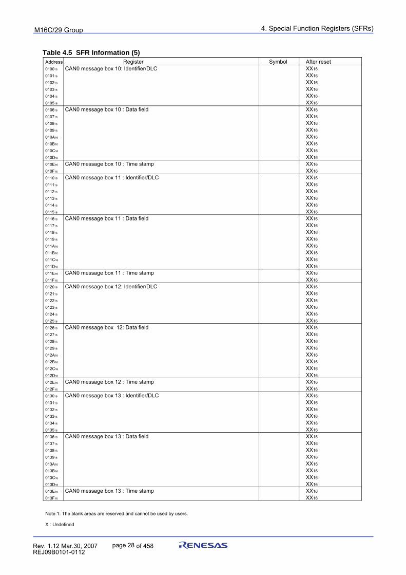
4. Special Function Registers (SFRs)puorG92/C61M
page 28 854fo7002,03.raM21.1.veR2110-1010B90JER
Address Register Symbol After reset010016 CAN0 message box 10: Identifier/DLC XX16
010116 XX16
010216 XX16
010316 XX16
010416 XX16
010516 XX16
010616 CAN0 message box 10 : Data field XX16
010716 XX16
010816 XX16
010916 XX16
010A16 XX16
010B16 XX16
010C16 XX16
010D16 XX16
010E16 CAN0 message box 10 : Time stamp XX16
010F16 XX16
011016 CAN0 message box 11 : Identifier/DLC XX16
011116 XX16
011216 XX16
011316 XX16
011416 XX16
011516 XX16
011616 CAN0 message box 11 : Data field XX16
011716 XX16
011816 XX16
011916 XX16
011A16 XX16
011B16 XX16
011C16 XX16
011D16 XX16
011E16 CAN0 message box 11 : Time stamp XX16
011F16 XX16
012016 CAN0 message box 12: Identifier/DLC XX16
012116 XX16
012216 XX16
012316 XX16
012416 XX16
012516 XX16
012616 CAN0 message box 12: Data field XX16
012716 XX16
012816 XX16
012916 XX16
012A16 XX16
012B16 XX16
012C16 XX16
012D16 XX16
012E16 CAN0 message box 12 : Time stamp XX16
012F16 XX16
013016 CAN0 message box 13 : Identifier/DLC XX16
013116 XX16
013216 XX16
013316 XX16
013416 XX16
013516 XX16
013616 CAN0 message box 13 : Data field XX16
013716 XX16
013816 XX16
013916 XX16
013A16 XX16
013B16 XX16
013C16 XX16
013D16 XX16
013E16 CAN0 message box 13 : Time stamp XX16
013F16 XX16
Note 1: The blank areas are reserved and cannot be used by users.
X : Undefined
Table 4.5 SFR Information (5)
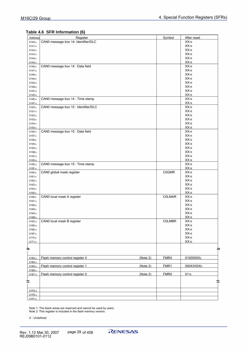
4. Special Function Registers (SFRs)puorG92/C61M
page 29 854fo7002,03.raM21.1.veR2110-1010B90JER
Address Register Symbol After reset014016 CAN0 message box 14: Identifier/DLC XX16
014116 XX16
014216 XX16
014316 XX16
014416 XX16
014516 XX16
014616 CAN0 message box 14 : Data field XX16
014716 XX16
014816 XX16
014916 XX16
014A16 XX16
014B16 XX16
014C16 XX16
014D16 XX16
014E16 CAN0 message box 14 : Time stamp XX16
014F16 XX16
015016 CAN0 message box 15 : Identifier/DLC XX16
015116 XX16
015216 XX16
015316 XX16
015416 XX16
015516 XX16
015616 CAN0 message box 15 : Data field XX16
015716 XX16
015816 XX16
015916 XX16
015A16 XX16
015B16 XX16
015C16 XX16
015D16 XX16
015E16 CAN0 message box 15 : Time stamp XX16
015F16 XX16
016016 CAN0 global mask register C0GMR XX16
016116 XX16
016216 XX16
016316 XX16
016416 XX16
016516 XX16
016616 CAN0 local mask A register C0LMAR XX16
016716 XX16
016816 XX16
016916 XX16
016A16 XX16
016B16 XX16
016C16 CAN0 local mask B register C0LMBR XX16
016D16 XX16
016E16 XX16
016F16 XX16
017016 XX16
017116 XX16
01B316 Flash memory control register 4 (Note 2) FMR4 0100000X2
01B416
01B516 Flash memory control register 1 (Note 2) FMR1 000XXX0X2
01B616
01B716 Flash memory control register 0 (Note 2) FMR0 0116
01FD16
01FE16
01FF16
Note 1: The blank areas are reserved and cannot be used by users.Note 2: This register is included in the flash memory version.
X : Undefined
~~ ~~
~~~~
Table 4.6 SFR Information (6)
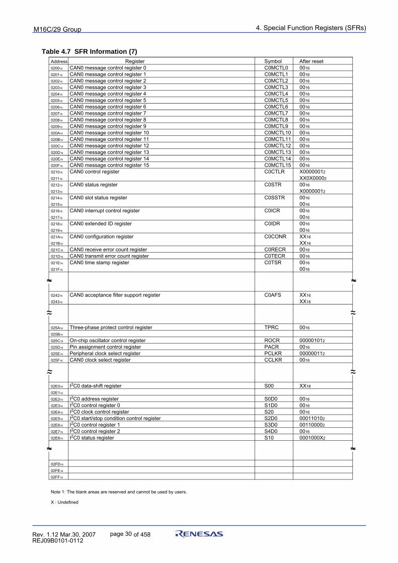
4. Special Function Registers (SFRs)puorG92/C61M
page 30 854fo7002,03.raM21.1.veR2110-1010B90JER
Address Register Symbol After reset020016 CAN0 message control register 0 C0MCTL0 0016
020116 CAN0 message control register 1 C0MCTL1 0016
020216 CAN0 message control register 2 C0MCTL2 0016
020316 CAN0 message control register 3 C0MCTL3 0016
020416 CAN0 message control register 4 C0MCTL4 0016
020516 CAN0 message control register 5 C0MCTL5 0016
020616 CAN0 message control register 6 C0MCTL6 0016
020716 CAN0 message control register 7 C0MCTL7 0016
020816 CAN0 message control register 8 C0MCTL8 0016
020916 CAN0 message control register 9 C0MCTL9 0016
020A16 CAN0 message control register 10 C0MCTL10 0016
020B16 CAN0 message control register 11 C0MCTL11 0016
020C16 CAN0 message control register 12 C0MCTL12 0016
020D16 CAN0 message control register 13 C0MCTL13 0016
020E16 CAN0 message control register 14 C0MCTL14 0016
020F16 CAN0 message control register 15 C0MCTL15 0016
021016 CAN0 control register C0CTLR X00000012 021116 XX0X00002
021216 CAN0 status register C0STR 0016
021316 X00000012
021416 CAN0 slot status register C0SSTR 0016
021516 0016
021616 CAN0 interrupt control register C0ICR 0016
021716 0016
021816 CAN0 extended ID register C0IDR 0016
021916 0016
021A16 CAN0 configuration register C0CONR XX16
021B16 XX16
021C16 CAN0 receive error count register C0RECR 0016
021D16 CAN0 transmit error count register C0TECR 0016
021E16 CAN0 time stamp register C0TSR 0016
021F16 0016
024216 CAN0 acceptance filter support register C0AFS XX16
024316 XX16
025A16 Three-phase protect control register TPRC 0016
025B16
025C16 On-chip oscillator control register ROCR 000001012
025D16 Pin assignment control register PACR 0016
025E16 Peripheral clock select register PCLKR 000000112
025F16 CAN0 clock select register CCLKR 0016
02E016 I2C0 data-shift register S00 XX16
02E116
02E216 I2C0 address register S0D0 0016
02E316 I2C0 control register 0 S1D0 0016
02E416 I2C0 clock control register S20 0016
02E516 I2C0 start/stop condition control register S2D0 000110102
02E616 I2C0 control register 1 S3D0 001100002
02E716 I2C0 control register 2 S4D0 0016
02E816 I2C0 status register S10 0001000X2
02FD16
02FE16
02FF16
Note 1: The blank areas are reserved and cannot be used by users.
X : Undefined
~~
~~
~~
~~ ~~
~~
~~
~~
Table 4.7 SFR Information (7)
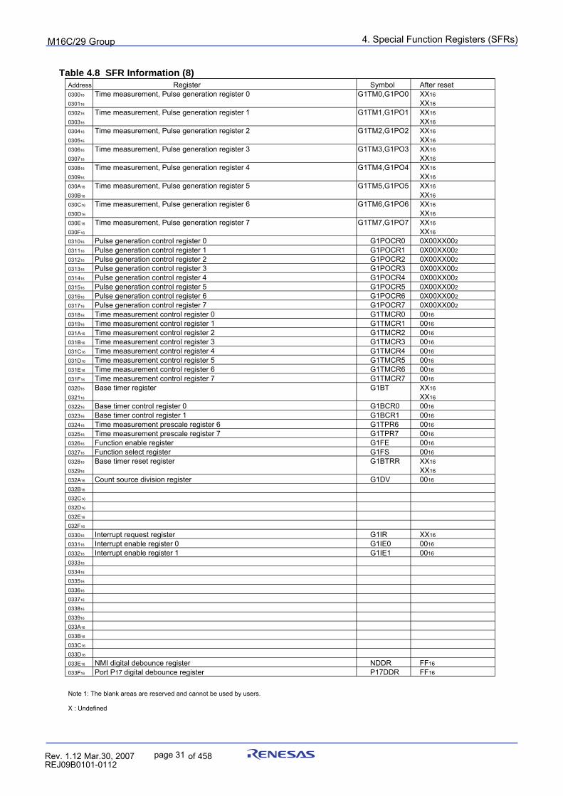
4. Special Function Registers (SFRs)puorG92/C61M
page 31 854fo7002,03.raM21.1.veR2110-1010B90JER
Address Register Symbol After reset030016 Time measurement, Pulse generation register 0 G1TM0,G1PO0 XX16
030116 XX16
030216 Time measurement, Pulse generation register 1 G1TM1,G1PO1 XX16
030316 XX16
030416 Time measurement, Pulse generation register 2 G1TM2,G1PO2 XX16
030516 XX16
030616 Time measurement, Pulse generation register 3 G1TM3,G1PO3 XX16
030716 XX16
030816 Time measurement, Pulse generation register 4 G1TM4,G1PO4 XX16
030916 XX16
030A16 Time measurement, Pulse generation register 5 G1TM5,G1PO5 XX16
030B16 XX16
030C16 Time measurement, Pulse generation register 6 G1TM6,G1PO6 XX16
030D16 XX16
030E16 Time measurement, Pulse generation register 7 G1TM7,G1PO7 XX16
030F16 XX16
031016 Pulse generation control register 0 G1POCR0 0X00XX002
031116 Pulse generation control register 1 G1POCR1 0X00XX002
031216 Pulse generation control register 2 G1POCR2 0X00XX002
031316 Pulse generation control register 3 G1POCR3 0X00XX002
031416 Pulse generation control register 4 G1POCR4 0X00XX002
031516 Pulse generation control register 5 G1POCR5 0X00XX002
031616 Pulse generation control register 6 G1POCR6 0X00XX002
031716 Pulse generation control register 7 G1POCR7 0X00XX002
031816 Time measurement control register 0 G1TMCR0 0016
031916 Time measurement control register 1 G1TMCR1 0016
031A16 Time measurement control register 2 G1TMCR2 0016
031B16 Time measurement control register 3 G1TMCR3 0016
031C16 Time measurement control register 4 G1TMCR4 0016
031D16 Time measurement control register 5 G1TMCR5 0016
031E16 Time measurement control register 6 G1TMCR6 0016
031F16 Time measurement control register 7 G1TMCR7 0016
032016 Base timer register G1BT XX16
032116 XX16
032216 Base timer control register 0 G1BCR0 0016
032316 Base timer control register 1 G1BCR1 0016
032416 Time measurement prescale register 6 G1TPR6 0016
032516 Time measurement prescale register 7 G1TPR7 0016
032616 Function enable register G1FE 0016
032716 Function select register G1FS 0016
032816 Base timer reset register G1BTRR XX16
032916 XX16
032A16 Count source division register G1DV 0016
032B16
032C16
032D16
032E16
032F16
033016 Interrupt request register G1IR XX16
033116 Interrupt enable register 0 G1IE0 0016
033216 Interrupt enable register 1 G1IE1 0016
033316
033416
033516
033616
033716
033816
033916
033A16
033B16
033C16
033D16
033E16 NMI digital debounce register NDDR FF16
033F16 Port P17 digital debounce register P17DDR FF16
Note 1: The blank areas are reserved and cannot be used by users.
X : Undefined
Table 4.8 SFR Information (8)
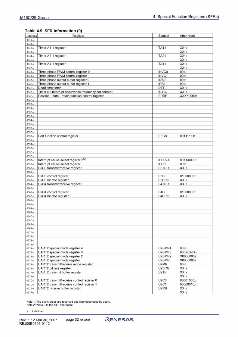
4. Special Function Registers (SFRs)puorG92/C61M
page 32 854fo7002,03.raM21.1.veR2110-1010B90JER
Address Register Symbol After reset034016
034116
034216 Timer A1-1 register TA11 XX16
034316 XX16
034416 Timer A2-1 register TA21 XX16
034516 XX16
034616 Timer A4-1 register TA41 XX16
034716 XX16
034816 Three phase PWM control register 0 INVC0 0016
034916 Three phase PWM control register 1 INVC1 0016
034A16 Three phase output buffer register 0 IDB0 0016
034B16 Three phase output buffer register 1 IDB1 0016
034C16 Dead time timer DTT XX16
034D16 Timer B2 Interrupt occurrence frequency set counter ICTB2 XX16
034E16 Position - data - retain function control register PDRF XXXX00002
034F16
035016
035116
035216
035316
035416
035516
035616
035716
035816 Port function control register PFCR 001111112 035916
035A16
035B16
035C16
035D16
035E16 Interrupt cause select register 2(2) IFSR2A 00XXX0002
035F16 Interrupt cause select register IFSR 0016
036016 SI/O3 transmit/receive register S3TRR XX16
036116
036216 SI/O3 control register S3C 010000002
036316 SI/O3 bit rate register S3BRG XX16
036416 SI/O4 transmit/receive register S4TRR XX16
036516
036616 SI/O4 control register S4C 010000002
036716 SI/O4 bit rate register S4BRG XX16
036816
036916
036A16
036B16
036C16
036D16
036E16
036F16
037016
037116
037216
037316
037416 UART2 special mode register 4 U2SMR4 0016
037516 UART2 special mode register 3 U2SMR3 000X0X0X2
037616 UART2 special mode register 2 U2SMR2 X00000002
037716 UART2 special mode register U2SMR X00000002
037816 UART2 transmit/receive mode register U2MR 0016
037916 UART2 bit rate register U2BRG XX16
037A16 UART2 transmit buffer register U2TB XX16
037B16 XX16
037C16 UART2 transmit/receive control register 0 U2C0 000010002
037D16 UART2 transmit/receive control register 1 U2C1 000000102
037E16 UART2 receive buffer register U2RB XX16
037F16 XX16
Note 1: The blank areas are reserved and cannot be used by users.Note 2: Write 0 to the bit 0 after reset.
X : Undefined
Table 4.9 SFR Information (9)
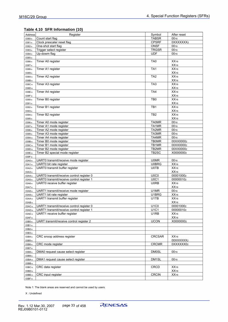
4. Special Function Registers (SFRs)puorG92/C61M
page 33 854fo7002,03.raM21.1.veR2110-1010B90JER
Address Register Symbol After reset038016 Count start flag TABSR 0016
038116 Clock prescaler reset flag CPSRF 0XXXXXXX2
038216 One-shot start flag ONSF 0016
038316 Trigger select register TRGSR 0016
038416 Up-dowm flag UDF 0016
038516
038616 Timer A0 register TA0 XX16
038716 XX16
038816 Timer A1 register TA1 XX16
038916 XX16
038A16 Timer A2 register TA2 XX16
038B16 XX16
038C16 Timer A3 register TA3 XX16
038D16 XX16
038E16 Timer A4 register TA4 XX16
038F16 XX16
039016 Timer B0 register TB0 XX16
039116 XX16
039216 Timer B1 register TB1 XX16
039316 XX16
039416 Timer B2 register TB2 XX16
039516 XX16
039616 Timer A0 mode register TA0MR 0016
039716 Timer A1 mode register TA1MR 0016
039816 Timer A2 mode register TA2MR 0016
039916 Timer A3 mode register TA3MR 0016
039A16 Timer A4 mode register TA4MR 0016
039B16 Timer B0 mode register TB0MR 00XX00002
039C16 Timer B1 mode register TB1MR 00XX00002
039D16 Timer B2 mode register TB2MR 00XX00002
039E16 Timer B2 special mode register TB2SC X00000002
039F16
03A016 UART0 transmit/receive mode register U0MR 0016
03A116 UART0 bit rate register U0BRG XX16
03A216 UART0 transmit buffer register U0TB XX16
03A316 XX16
03A416 UART0 transmit/receive control register 0 U0C0 000010002
03A516 UART0 transmit/receive control register 1 U0C1 000000102
03A616 UART0 receive buffer register U0RB XX16
03A716 XX16
03A816 UART1 transmit/receive mode register U1MR 0016
03A916 UART1 bit rate register U1BRG XX16
03AA16 UART1 transmit buffer register U1TB XX16
03AB16 XX16
03AC16 UART1 transmit/receive control register 0 U1C0 000010002
03AD16 UART1 transmit/receive control register 1 U1C1 000000102
03AE16 UART1 receive buffer register U1RB XX16
03AF16 XX16
03B016 UART transmit/receive control register 2 UCON X00000002
03B116
03B216
03B316
03B416 CRC snoop address register CRCSAR XX16
03B516 00XXXXXX2
03B616 CRC mode register CRCMR 0XXXXXX02
03B716
03B816 DMA0 request cause select register DM0SL 0016
03B916
03BA16 DMA1 request cause select register DM1SL 0016
03BB16
03BC16 CRC data register CRCD XX16
03BD16 XX16
03BE16 CRC input register CRCIN XX16
03BF16
Note 1: The blank areas are reserved and cannot be used by users.
X : Undefined
Table 4.10 SFR Information (10)
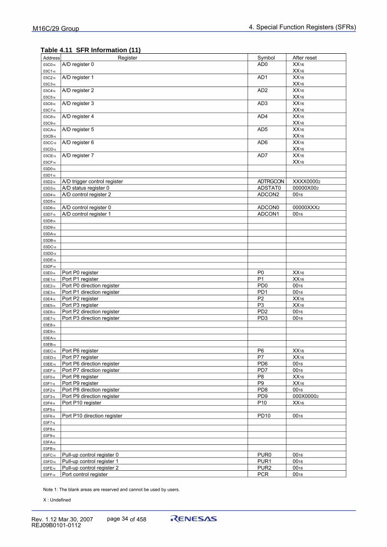
4. Special Function Registers (SFRs)puorG92/C61M
page 34 854fo7002,03.raM21.1.veR2110-1010B90JER
Address Register Symbol After reset03C016 A/D register 0 AD0 XX16
03C116 XX16
03C216 A/D register 1 AD1 XX16
03C316 XX16
03C416 A/D register 2 AD2 XX16
03C516 XX16
03C616 A/D register 3 AD3 XX16
03C716 XX16
03C816 A/D register 4 AD4 XX16
03C916 XX16
03CA16 A/D register 5 AD5 XX16
03CB16 XX16
03CC16 A/D register 6 AD6 XX16
03CD16 XX16
03CE16 A/D register 7 AD7 XX16
03CF16 XX16
03D016
03D116
03D216 A/D trigger control register ADTRGCON XXXX00002
03D316 A/D status register 0 ADSTAT0 00000X002
03D416 A/D control register 2 ADCON2 0016
03D516
03D616 A/D control register 0 ADCON0 00000XXX2
03D716 A/D control register 1 ADCON1 0016
03D816
03D916
03DA16
03DB16
03DC16
03DD16
03DE16
03DF16
03E016 Port P0 register P0 XX16
03E116 Port P1 register P1 XX16
03E216 Port P0 direction register PD0 0016
03E316 Port P1 direction register PD1 0016
03E416 Port P2 register P2 XX16
03E516 Port P3 register P3 XX16
03E616 Port P2 direction register PD2 0016
03E716 Port P3 direction register PD3 0016
03E816
03E916
03EA16
03EB16
03EC16 Port P6 register P6 XX16
03ED16 Port P7 register P7 XX16
03EE16 Port P6 direction register PD6 0016
03EF16 Port P7 direction register PD7 0016
03F016 Port P8 register P8 XX16
03F116 Port P9 register P9 XX16
03F216 Port P8 direction register PD8 0016
03F316 Port P9 direction register PD9 000X00002
03F416 Port P10 register P10 XX16
03F516
03F616 Port P10 direction register PD10 0016
03F716
03F816
03F916
03FA16
03FB16
03FC16 Pull-up control register 0 PUR0 0016
03FD16 Pull-up control register 1 PUR1 0016
03FE16 Pull-up control register 2 PUR2 0016
03FF16 Port control register PCR 0016
Note 1: The blank areas are reserved and cannot be used by users.
X : Undefined
Table 4.11 SFR Information (11)
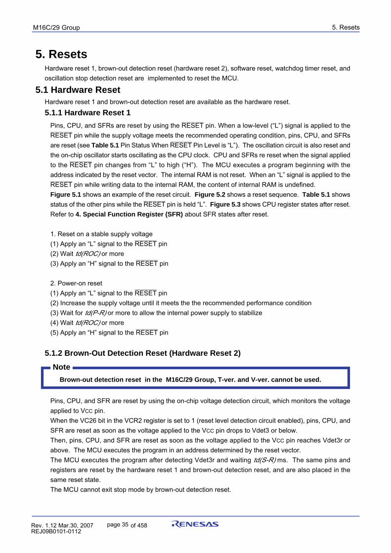
5. ResetspuorG92/C61M
page 35 854fo7002,03.raM21.1.veR2110-1010B90JER
5. ResetsHardware reset 1, brown-out detection reset (hardware reset 2), software reset, watchdog timer reset, andoscillation stop detection reset are implemented to reset the MCU.
5.1 Hardware ResetHardware reset 1 and brown-out detection reset are available as the hardware reset.
5.1.1 Hardware Reset 1____________
Pins, CPU, and SFRs are reset by using the RESET pin. When a low-level (“L”) signal is applied to the____________
RESET pin while the supply voltage meets the recommended operating condition, pins, CPU, and SFRs____________
are reset (see Table 5.1 Pin Status When RESET Pin Level is “L”). The oscillation circuit is also reset andthe on-chip oscillator starts oscillating as the CPU clock. CPU and SFRs re reset when the signal applied
____________
to the RESET pin changes from “L” to high (“H”). The MCU executes a program beginning with theaddress indicated by the reset vector. The internal RAM is not reset. When an “L” signal is applied to the____________
RESET pin while writing data to the internal RAM, the content of internal RAM is undefined.Figure 5.1 shows an example of the reset circuit. Figure 5.2 shows a reset sequence. Table 5.1 shows
____________
status of the other pins while the RESET pin is held “L”. Figure 5.3 shows CPU register states after reset.Refer to 4. Special Function Register (SFR) about SFR states after reset.
1. Reset on a stable supply voltage____________
(1) Apply an “L” signal to the RESET pin(2) Wait td(ROC) or more
____________
(3) Apply an “H” signal to the RESET pin
2. Power-on reset____________
(1) Apply an “L” signal to the RESET pin(2) Increase the supply voltage until it meets the the recommended performance condition(3) Wait for td(P-R) or more to allow the internal power supply to stabilize(4) Wait td(ROC) or more
____________
(5) Apply an “H” signal to the RESET pin
5.1.2 Brown-Out Detection Reset (Hardware Reset 2)
Note
Brown-out detection reset in the M16C/29 Group, T-ver. and V-ver. cannot be used.
Pins, CPU, and SFR are reset by using the on-chip voltage detection circuit, which monitors the voltageapplied to VCC pin.When the VC26 bit in the VCR2 register is set to 1 (reset level detection circuit enabled), pins, CPU, andSFR are reset as soon as the voltage applied to the VCC pin drops to Vdet3 or below.Then, pins, CPU, and SFR are reset as soon as the voltage applied to the VCC pin reaches Vdet3r orabove. The MCU executes the program in an address determined by the reset vector.The MCU executes the program after detecting Vdet3r and waiting td(S-R) ms. The same pins andregisters are reset by the hardware reset 1 and brown-out detection reset, and are also placed in thesame reset state.The MCU cannot exit stop mode by brown-out detection reset.
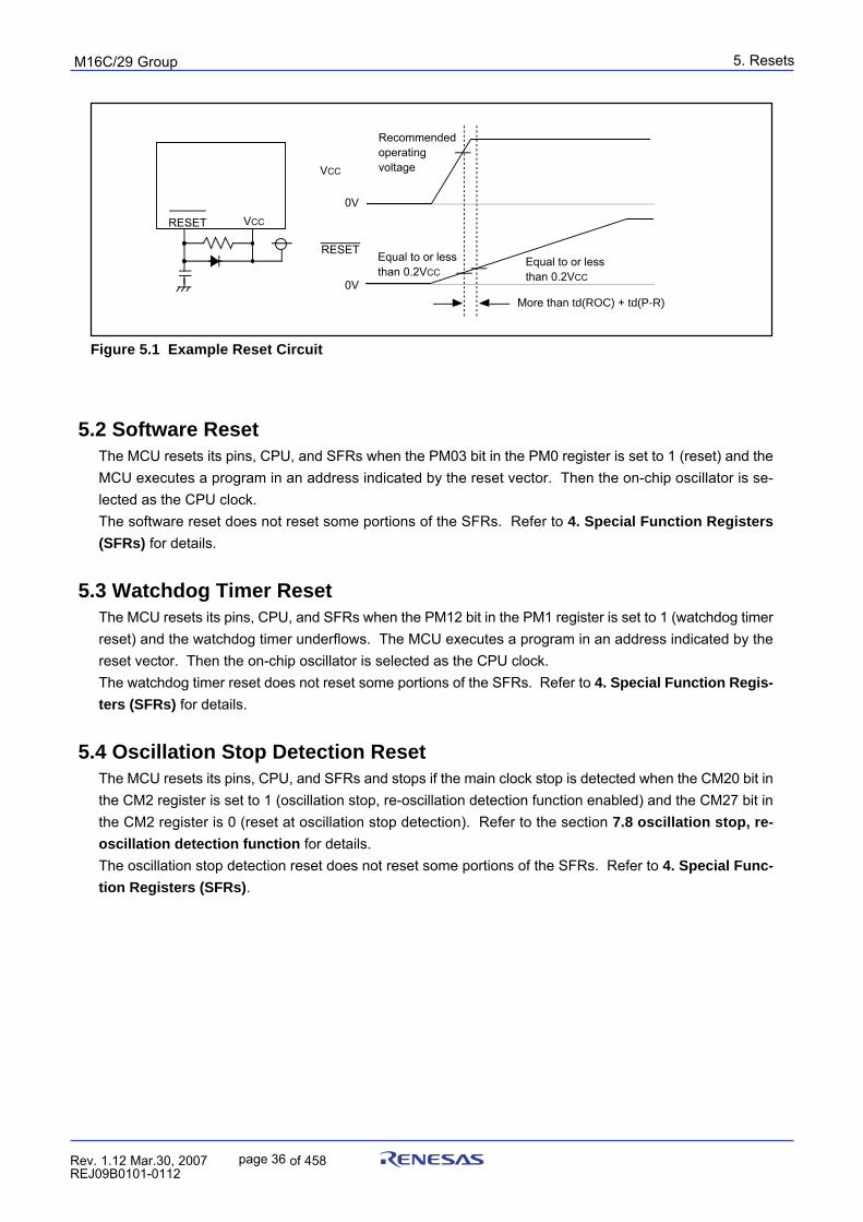
5. ResetspuorG92/C61M
page 36 854fo7002,03.raM21.1.veR2110-1010B90JER
5.2 Software ResetThe MCU resets its pins, CPU, and SFRs when the PM03 bit in the PM0 register is set to 1 (reset) and theMCU executes a program in an address indicated by the reset vector. Then the on-chip oscillator is se-lected as the CPU clock.The software reset does not reset some portions of the SFRs. Refer to 4. Special Function Registers
(SFRs) for details.
5.3 Watchdog Timer ResetThe MCU resets its pins, CPU, and SFRs when the PM12 bit in the PM1 register is set to 1 (watchdog timerreset) and the watchdog timer underflows. The MCU executes a program in an address indicated by thereset vector. Then the on-chip oscillator is selected as the CPU clock.The watchdog timer reset does not reset some portions of the SFRs. Refer to 4. Special Function Regis-
ters (SFRs) for details.
5.4 Oscillation Stop Detection ResetThe MCU resets its pins, CPU, and SFRs and stops if the main clock stop is detected when the CM20 bit inthe CM2 register is set to 1 (oscillation stop, re-oscillation detection function enabled) and the CM27 bit inthe CM2 register is 0 (reset at oscillation stop detection). Refer to the section 7.8 oscillation stop, re-
oscillation detection function for details.The oscillation stop detection reset does not reset some portions of the SFRs. Refer to 4. Special Func-
tion Registers (SFRs).
Figure 5.1 Example Reset Circuit
RESET VCC
RESET
VCC
0V
0V
More than td(ROC) + td(P-R)
Equal to or less than 0.2VCC
Equal to or less than 0.2VCC
Recommended operatingvoltage
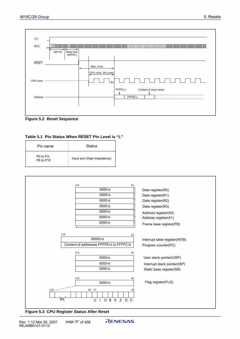
5. ResetspuorG92/C61M
page 37 854fo7002,03.raM21.1.veR2110-1010B90JER
____________
Table 5.1 Pin Status When RESET Pin Level is “L”
StatusPin name
P0 to P3,P6 to P10 Input port (high impedance)
Figure 5.3 CPU Register Status After Reset
b15 b0
Data register(R0)
Address register(A0)
Frame base register(FB)
Program counter(PC)Interrupt table register(INTB)
User stack pointer(USP)
Interrupt stack pointer(ISP)Static base register(SB)
Flag register(FLG)
000016
000016
000016
AAAAAA
AAAAAAAA
AAAAAAAAAAAAAAAA
AAAAAAAAAAAAAA
CDZSBOIUIPL
000016
000016
000016
000016
000016
b19 b0
Content of addresses FFFFE16 to FFFFC16
b15 b0
b15 b0
b15 b0 b7 b8
0000016
Data register(R1)Data register(R2)
Data register(R3)
Address register(A1)
000016
000016
000016
Figure 5.2 Reset Sequence
td(P-R) More than td(ROC)
CPU clock
Address
ROC
RESET
Content of reset vector
CPU clock: 28 cycles
FFFFE16
FFFFC16
VCC
Max. 2 ms
5. ResetspuorG92/C61M
page 38 854fo7002,03.raM21.1.veR2110-1010B90JER
5.5 Voltage Detection CircuitNoteVCC = 5 V is assumed in 5.5 Voltage Detection Circuit.
Voltage detection circuit in the M16C/29 Group, T-ver. and V-ver. cannot be used.
The voltage detection circuit has the reset level detection circuit and the low voltage detection circuit. Thereset level detection circuit monitors the voltage applied to the VCC pin. The MCU is reset if the reset leveldetection circuit detects VCC is Vdet3 or below. Use bits VC27 and VC26 in the VCR2 register to determinewhether the individual circuit is enabled.Use the reset level detection circuit for brown-out detection reset.The low voltage detection circuit also monitors the voltage applied to the VCC pin. The low voltage detec-tion circuit use the VC13 bit in the VCR1 register to detect VCC is above or below Vdet4. The low voltagedetection interrupt can be used in the voltage detection circuit.
Figure 5.4 Voltage Detection Circuit Block
b7 b6
VCR2 Register RESET
CM10 Bit=1(Stop Mode)
+>Vdet3
+>Vdet4
ENoise Rejection
Low VoltageDetect Signal
b3
VCR1 Register
VC13 Bit
>T
Q
1 shot
Internal Reset Signal (“L” active)
E
VCC
td(S-R)
Brown-out Detect Reset(Hardware Reset 2 Release Wait Time)
Reset level detection circuit
Low voltage detection circuit
5. ResetspuorG92/C61M
page 39 854fo7002,03.raM21.1.veR2110-1010B90JER
Figure 5.5 VCR1 Register and VCR2 Register
V
C
1
3
V
o
l
t
a
g
e
D
e
t
e
c
t
i
o
n
R
e
g
i
s
t
e
r
1S
y
m
b
o
l A
d
d
r
e
s
s A
f
t
e
r
R
e
s
e
t
(
2
)
V
C
R
1 0
0
1
91
6 0
0
0
0
1
0
0
02
Low voltage monitor flag (1)
B
i
t
S
y
m
b
o
l R
W
b 7 b
6 b
5 b
4 b
3 b
2 b
1 b
0
N
O
T
E
S
:
1
.
T
h
e
V
C
1
3
b
i
t
i
s
u
s
e
f
u
l
w
h
e
n
t
h
e
V
C
2
7
b
i
t
o
f
V
C
R
2
r
e
g
i
s
t
e
r
i
s
s
e
t
t
o
1
(
l
o
w
v
o
l
t
a
g
e
d
e
t
e
c
t
i
o
n
c
i
r
c
u
i
t
e
n
a
b
l
e
)
.
T
h
e
V
C
1
3
b
i
t
i
s
a
l
w
a
y
s
1
(
VC
C≥
V
d
e
t
4
)
w
h
e
n
t
h
e
V
C
2
7
b
i
t
i
n
t
h
e
V
C
R
2
r
e
g
i
s
t
e
r
i
s
s
e
t
t
o
0
(
l
o
w
v
o
l
t
a
g
e
d
e
t
e
c
t
i
o
n
c
i
r
c
u
i
t
d
i
s
a
b
l
e
)
.
2
.
T
h
i
s
r
e
g
i
s
t
e
r
d
o
e
s
n
o
t
c
h
a
n
g
e
a
t
s
o
f
t
w
a
r
e
r
e
s
e
t
,
w
a
t
c
h
d
o
g
t
i
m
e
r
r
e
s
e
t
a
n
d
o
s
c
i
l
l
a
t
i
o
n
s
t
o
p
d
e
t
e
c
t
i
o
n
r
e
s
e
t
.
0:VCC < Vdet41:VCC ≥ Vdet4 RO
0 0 0 0 0 0 0
RW
R
W
R
e
s
e
r
v
e
d
b
i
t
R
e
s
e
r
v
e
d
b
i
t
S
e
t
t
o
0
S
e
t
t
o
0
V
o
l
t
a
g
e
D
e
t
e
c
t
i
o
n
R
e
g
i
s
t
e
r
2
(
1
)
S
y
m
b
o
l A
d
d
r
e
s
s A
f
t
e
r
R
e
s
e
t
(
5
)
V
C
R
2 0
0
1
A1
6 0
01
6
Bit NameB
i
t
S
y
m
b
o
l
b 7 b
6 b
5 b
4 b
3 b
2 b
1 b
0
N
O
T
E
S
:1
.
W
r
i
t
e
t
o
t
h
i
s
r
e
g
i
s
t
e
r
a
f
t
e
r
s
e
t
t
i
n
g
t
h
e
P
R
C
3
b
i
t
i
n
t
h
e
P
R
C
R
r
e
g
i
s
t
e
r
t
o
1
(
w
r
i
t
e
e
n
a
b
l
e
)
.2
.
S
e
t
t
h
e
V
C
2
6
b
i
t
t
o
1
t
o
u
s
e
b
r
o
w
n
-
o
u
t
r
e
s
e
t
.
3
.
V
C
2
6
b
i
t
i
s
d
i
s
a
b
l
e
d
i
n
s
t
o
p
m
o
d
e
.
(
T
h
e
M
C
U
i
s
n
o
t
r
e
s
e
t
e
v
e
n
i
f
t
h
e
v
o
l
t
a
g
e
i
n
p
u
t
t
o
V
c
c
p
i
n
b
e
c
o
m
e
s
l
o
w
e
r
t
h
a
n
V
d
e
t
3
.
)4
.
W
h
e
n
t
h
e
V
C
1
3
b
i
t
i
n
t
h
e
V
C
R
1
r
e
g
i
s
t
e
r
a
n
d
D
4
2
b
i
t
i
n
t
h
e
D
4
I
N
T
r
e
g
i
s
t
e
r
a
r
e
u
s
e
d
o
r
t
h
e
D
4
0
b
i
t
i
s
s
e
t
t
o
1
(
l
o
w
v
o
l
t
a
g
e
d
e
t
e
c
t
i
o
n
i
n
t
e
r
r
u
p
t
e
n
a
b
l
e
)
,
s
e
t
t
h
e
V
C
2
7
b
i
t
t
o
1
.5
.
T
h
i
s
r
e
g
i
s
t
e
r
d
o
e
s
n
o
t
c
h
a
n
g
e
a
t
s
o
f
t
w
a
r
e
r
e
s
e
t
,
w
a
t
c
h
d
o
g
t
i
m
e
r
r
e
s
e
t
a
n
d
o
s
c
i
l
l
a
t
i
o
n
s
t
o
p
d
e
t
e
c
t
i
o
n
r
e
s
e
t
.6
.
T
h
e
d
e
t
e
c
t
i
o
n
c
i
r
c
u
i
t
d
o
e
s
n
o
t
s
t
a
r
t
o
p
e
r
a
t
i
o
n
u
n
t
i
l
t
d
(
E
-
A
)
e
l
a
p
s
e
s
a
f
t
e
r
t
h
e
V
C
2
6
b
i
t
o
r
V
C
2
7
b
i
t
i
s
s
e
t
t
o
1
.
VC26
V
C
2
7
RW
RW
R
W
RW
0 0 0 0 0
Function
R
e
s
e
r
v
e
d
b
i
t Se
t
t
o
0
R
e
s
e
t
l
e
v
e
l
m
o
n
i
t
o
r
b
i
t
(
2
,
3
,
6
)
0: Disable reset level detection circuit 1: Enable reset level detection circuit
Lo
w
v
o
l
t
a
g
e
m
o
n
i
t
o
r
b
i
t
(
4
,
6
)
0
:
D
i
s
a
b
l
e
l
o
w
v
o
l
t
a
g
e
d
e
t
e
c
t
i
o
n
c
i
r
c
u
i
t
1
:
E
n
a
b
l
e
l
o
w
v
o
l
t
a
g
e
d
e
t
e
c
t
i
o
n
c
i
r
c
u
i
t
( b
2
-
b
0
)
( b
7
-
b
4
)
(b5-b0)
0
FunctionBit Name
5. ResetspuorG92/C61M
page 40 854fo7002,03.raM21.1.veR2110-1010B90JER
Figure 5.7 Typical Operation of Brown-Out Detection Reset (Hardware Reset 2)
Figure 5.6 D4INT Register
D
4
0
Lo
w
V
o
l
t
a
g
e
D
e
t
e
c
t
i
o
n
I
n
t
e
r
r
u
p
t
R
e
g
i
s
t
e
r
(
1
)
Symbol Address After Reset D4INT 001F16 0016
Low voltage detection interrupt enable bit (5)
B
i
t
N
a
m
eBit Symbol
b7 b 6
b
5
b
4
b
3
b
2
b
1
b
0
0
:
D
i
s
a
b
l
e1
:
E
n
a
b
l
e
D
4
1 S
T
O
P
m
o
d
e
d
e
a
c
t
i
v
a
t
i
o
n
c
o
n
t
r
o
l
b
i
t
(
4
)0: Disable (do not use the low voltage detection interrupt to exit stop mode)
1: Enable (use the low voltage detection interrupt to exit stop mode)
D
4
2 V
o
l
t
a
g
e
c
h
a
n
g
e
d
e
t
e
c
t
i
o
n
f
l
a
g
(
2
)0 :
N
o
t
d
e
t
e
c
t
e
d
1
:
V
d
e
t
4
p
a
s
s
i
n
g
d
e
t
e
c
t
i
o
n
D
4
3 W
D
T
o
v
e
r
f
l
o
w
d
e
t
e
c
t
f
l
a
g 0: Not detected1: Detected
D
F
0 S
a
m
p
l
i
n
g
c
l
o
c
k
s
e
l
e
c
t
b
i
t00 : CPU clock divided by 801 : CPU clock divided by 1610 : CPU clock divided by 3211 : CPU clock divided by 64DF1
NOTES: 1. Write to this register after setting the PRC3 bit in the PRCR register to 1 (write enable). 2. Useful when the VC27 bit in the VCR2 register is set to 1 (low voltage detection circuit enabled). If the VC27
bit is set to 0 (low voltage detection circuit disable), the D42 bit is set to 0 (Not detect). 3. This bit is set to 0 by writing a 0 in a program. (Writing 1 has no effect.) 4. If the low voltage detection interrupt needs to be used to get out of stop mode again after once used for that
purpose, reset the D41 bit by writing a 0 and then a 1. 5. The D40 bit is effective when the VC27 bit in the VCR2 register is set to 1. To set the D40 bit to 1, follow the
procedure described below.(1) Set the VC27 bit to 1.(2) Wait for td(E-A) until the detection circuit is actuated.(3) Wait for the sampling time (refer to Table 5.3 Sampling Clock Periods).(4) Set the D40 bit to 1.
b5b
4
R
W
R
W
R
W
R
W(3)
R
W
R
W
RW
( b
7
-
b
6
)
Function
(3)
N
o
t
h
i
n
g
i
s
a
s
s
i
g
n
e
d
.
I
f
n
e
c
e
s
s
a
r
y
s
e
t
t
o
0
.
W
h
e
n
r
e
a
d
,
t
h
e
c
o
n
t
e
n
t
i
s
0
Vdet4
Vdet3
5.0V 5.0V
VCC
Internal Reset Signal
VC13 bit in VCR1 register
VC26 bit in VCR2 register (1)
VC27 bit in VCR2 register
Set to 1 by program (reset level detect circuit enable)
Set to 1 by program (low voltage detection circuit enable)
VSS
Undefined
RESET
Vdet3s
Vdet3r
NOTES : 1. VC26 bit is invalid in stop mode. (the MCU is not reset even if input voltage of VCC pin
becomes lower than Vdet3).
Undefined
Undefined
5. ResetspuorG92/C61M
page 41 854fo7002,03.raM21.1.veR2110-1010B90JER
5.5.1 Low Voltage Detection InterruptIf the D40 bit in the D4INT register is set to 1 (low voltge detection interrupt enabled), a low voltagedetection interrupt request is generated when voltage applied to the VCC pin is above or below Vdet4.The low voltage detection interrupt shares the same interrupt vector with watchdog timer interrupt andoscillation stop, re-oscillation detection interrupt.Set the D41 bit in the D4INT register to 1 (enabled) to use the low voltage detection interrupt to exit stopmode, set the D41 bit in the D4INT register to 1 (enable).The D42 bit in the D4INT register is set to 1 (above or below Vdet4 detected) as soon as voltage appliedto the VCC pin goes above or below Vdet4 due to the voltage change. When the D42 bit setting changes0 to 1, a low voltage detection interrupt is generated. Set the D42 bit to 0 (not detected) by program.However, when the D41 bit is set to 1 and the MCU is in stop mode, a low voltage detection interruptrequest is generated, regardless of the D42 bit setting, if voltage applies to the VCC pin is detected to riseabove or drop below Vdet4. The MCU then exits stop mode.Table 5.2 shows how a low voltage detection interrupt request is generated.Bits DF1 and DF0 in the D4INT register determine sampling period that detects voltage applied to theVCC pin rises above or drops below Vdet4. Table 5.3 shows sampling periods.
Table 5.2 Voltage Detection Interrupt Request Generation Conditions
Table 5.3 Sampling Clock Periods
D41 bitVC27 bitOperation Mode D40 bit D42 bit CM02 bit VC13 bit
Normaloperation mode(1)
Wait mode(2)
Stop mode(2)
NOTES: 1. The status except the wait mode and stop mode is handled as the normal mode. (Refer to 7. Clock generating circuit) 2. Refer to 5.5.2 Limitations on stop mode and 5.5.3 Limitations on wait mode. 3. An interrupt request for voltage reduction is generated a sampling time after the value of the VC13 bit has changed. Refer to the Figure 5.9 for details.
0 to 1
10
1
1
0
1 to 00 to 11 to 00 to 1
0 to 1
0 to 1
0 to 1
1
(3)
– : 0 or 1
(3)
(3)
(3)
CPUclock(MHz) DF1 to DF0=00
(CPU clock divided by 8)
Sampling clock (µs)
16 3.0 6.0 12.0 24.0
DF1 to DF0=01(CPU clock divided by 16)
DF1 to DF0=10(CPU clock divided by 32)
DF1 to DF0=11(CPU clock divided by 64)
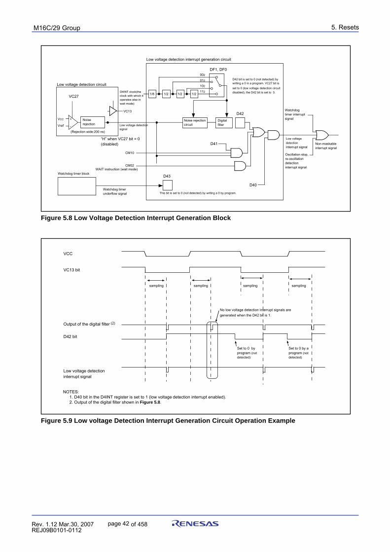
5. ResetspuorG92/C61M
page 42 854fo7002,03.raM21.1.veR2110-1010B90JER
Figure 5.8 Low Voltage Detection Interrupt Generation Block
Figure 5.9 Low voltage Detection Interrupt Generation Circuit Operation Example
Low voltage detection interrupt generation circuit
Watchdog timer interrupt signal
D42 bit is set to 0 (not detected) by writing a 0 in a program. VC27 bit is
set to 0 (low voltage detection circuit disabled), the D42 bit is set to 0.
VC27
VC13
Low voltage detection circuit
D4INT clock(the clock with which it operates also in wait mode)
D42
DF1, DF0
1/2
002
012
102
1121/21/21/8
Non-maskableinterrupt signal
Oscillation stop, re-oscillation detectioninterrupt signal
Low voltage detection interrupt signal
Watchdog timer block
This bit is set to 0 (not detected) by writing a 0 by program.Watchdog timer underflow signal
D43
D41
CM02WAIT instruction (wait mode)
D40
VCC
Vref
+
-
Noise rejection
(Rejection wide:200 ns)
Low voltage detection signal
“H” when VC27 bit = 0 (disabled)
Noise rejection circuit
Digitalfilter
CM10
Output of the digital filter (2)
D42 bit
L
o
w
v
o
l
t
a
g
e
d
e
t
e
c
t
i
o
ni
n
t
e
r
r
u
p
t
s
i
g
n
a
l
N
o
l
o
w
v
o
l
t
a
g
e
d
e
t
e
c
t
i
o
n
i
n
t
e
r
r
u
p
t
s
i
g
n
a
l
s
a
r
e
g
e
n
e
r
a
t
e
d
w
h
e
n
t
h
e
D
4
2
b
i
t
i
s
1
.
s a
m
p
l
i
n
g
S
e
t
t
o
0
b
y
p
r
o
g
r
a
m
(
n
o
t
d
e
t
e
c
t
e
d
)
VC13 bit
VCC
sampling s a
m
p
l
i
n
g s
a
m
p
l
i
n
g
S
e
t
t
o
0
b
y
a
p
r
o
g
r
a
m
(
n
o
t
d
e
t
e
c
t
e
d
)
NOTES:1. D40 bit in the D4INT register is set to 1 (low voltage detection interrupt enabled).2. Output of the digital filter shown in Figure 5.8.
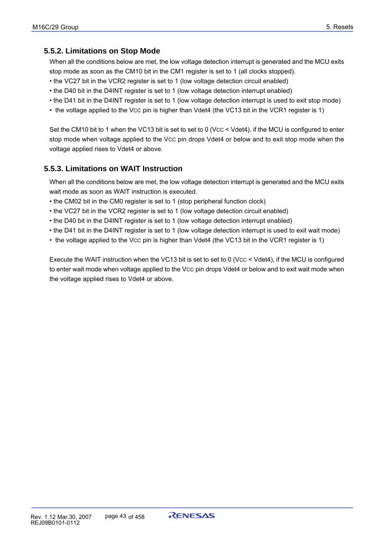
5. ResetspuorG92/C61M
page 43 854fo7002,03.raM21.1.veR2110-1010B90JER
5.5.2. Limitations on Stop ModeWhen all the conditions below are met, the low voltage detection interrupt is generated and the MCU exitsstop mode as soon as the CM10 bit in the CM1 register is set to 1 (all clocks stopped).• the VC27 bit in the VCR2 register is set to 1 (low voltage detection circuit enabled)• the D40 bit in the D4INT register is set to 1 (low voltage detection interrupt enabled)• the D41 bit in the D4INT register is set to 1 (low voltage detection interrupt is used to exit stop mode)• the voltage applied to the VCC pin is higher than Vdet4 (the VC13 bit in the VCR1 register is 1)
Set the CM10 bit to 1 when the VC13 bit is set to set to 0 (VCC < Vdet4), if the MCU is configured to enterstop mode when voltage applied to the VCC pin drops Vdet4 or below and to exit stop mode when thevoltage applied rises to Vdet4 or above.
5.5.3. Limitations on WAIT Instruction
When all the conditions below are met, the low voltage detection interrupt is generated and the MCU exitswait mode as soon as WAIT instruction is executed.• the CM02 bit in the CM0 register is set to 1 (stop peripheral function clock)• the VC27 bit in the VCR2 register is set to 1 (low voltage detection circuit enabled)• the D40 bit in the D4INT register is set to 1 (low voltage detection interrupt enabled)• the D41 bit in the D4INT register is set to 1 (low voltage detection interrupt is used to exit wait mode)• the voltage applied to the VCC pin is higher than Vdet4 (the VC13 bit in the VCR1 register is 1)
Execute the WAIT instruction when the VC13 bit is set to set to 0 (VCC < Vdet4), if the MCU is configuredto enter wait mode when voltage applied to the VCC pin drops Vdet4 or below and to exit wait mode whenthe voltage applied rises to Vdet4 or above.
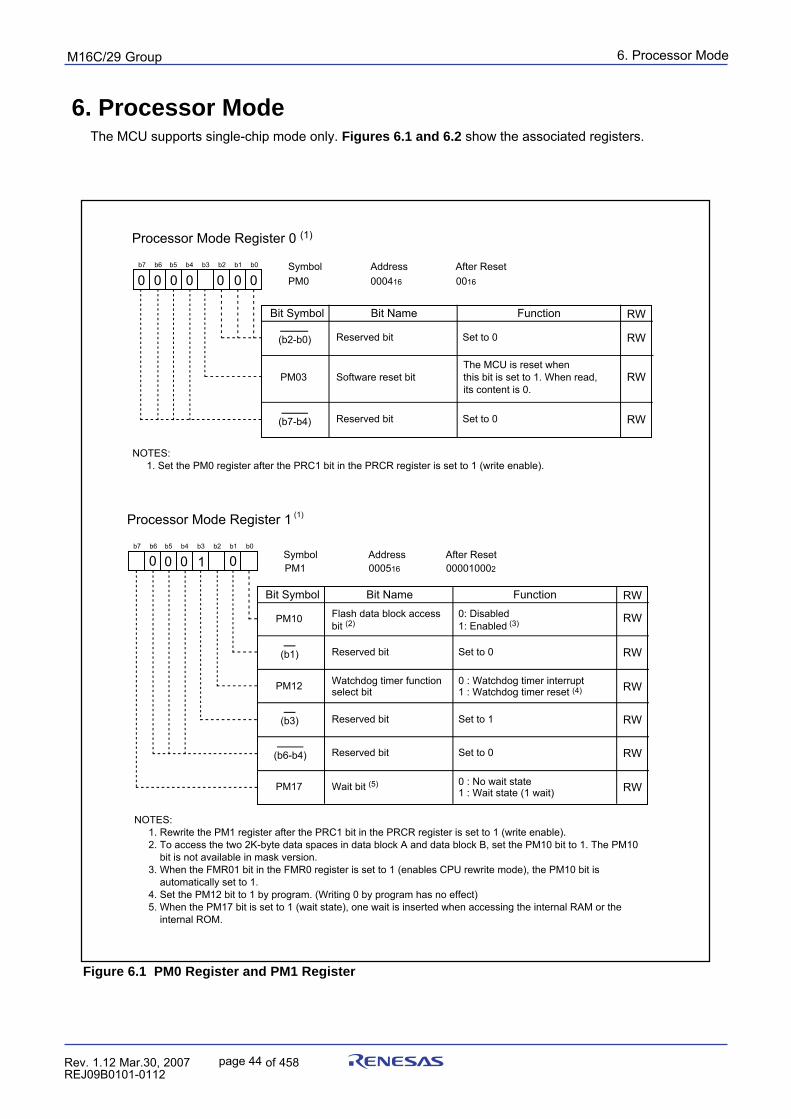
6. Processor ModepuorG92/C61M
page 44 854fo7002,03.raM21.1.veR2110-1010B90JER
Processor Mode Register 1 (1)
Symbol Address After ResetPM1 000516 000010002
Bit Name FunctionBit Symbol RW
b7 b6 b5 b4 b3 b2 b1 b0
Flash data block accessbit (2)
0: Disabled1: Enabled (3)PM10 RW
PM17 Wait bit (5) 0 : No wait state 1 : Wait state (1 wait)
0 : Watchdog timer interrupt1 : Watchdog timer reset (4)
Watchdog timer functionselect bitPM12
RW
RW
RW
RW
RW
NOTES: 1. Rewrite the PM1 register after the PRC1 bit in the PRCR register is set to 1 (write enable). 2. To access the two 2K-byte data spaces in data block A and data block B, set the PM10 bit to 1. The PM10 bit is not available in mask version. 3. When the FMR01 bit in the FMR0 register is set to 1 (enables CPU rewrite mode), the PM10 bit is automatically set to 1. 4. Set the PM12 bit to 1 by program. (Writing 0 by program has no effect) 5. When the PM17 bit is set to 1 (wait state), one wait is inserted when accessing the internal RAM or the internal ROM.
Set to 0(b1) Reserved bit
Set to 1Reserved bit
Set to 0(b6-b4) Reserved bit
(b3)
0 1 00 0
6. Processor ModeThe MCU supports single-chip mode only. Figures 6.1 and 6.2 show the associated registers.
Figure 6.1 PM0 Register and PM1 Register
Processor Mode Register 0 (1)
Symbol Address After ResetPM0 000416 0016
Bit Name FunctionBit Symbol RW
b7 b6 b5 b4 b3 b2 b1 b0
The MCU is reset when this bit is set to 1. When read, its content is 0.
Software reset bitPM03
RW
RW
RW
NOTES: 1. Set the PM0 register after the PRC1 bit in the PRCR register is set to 1 (write enable).
Set to 0(b2-b0) Reserved bit
Set to 0(b7-b4) Reserved bit
0 0 000 0 0
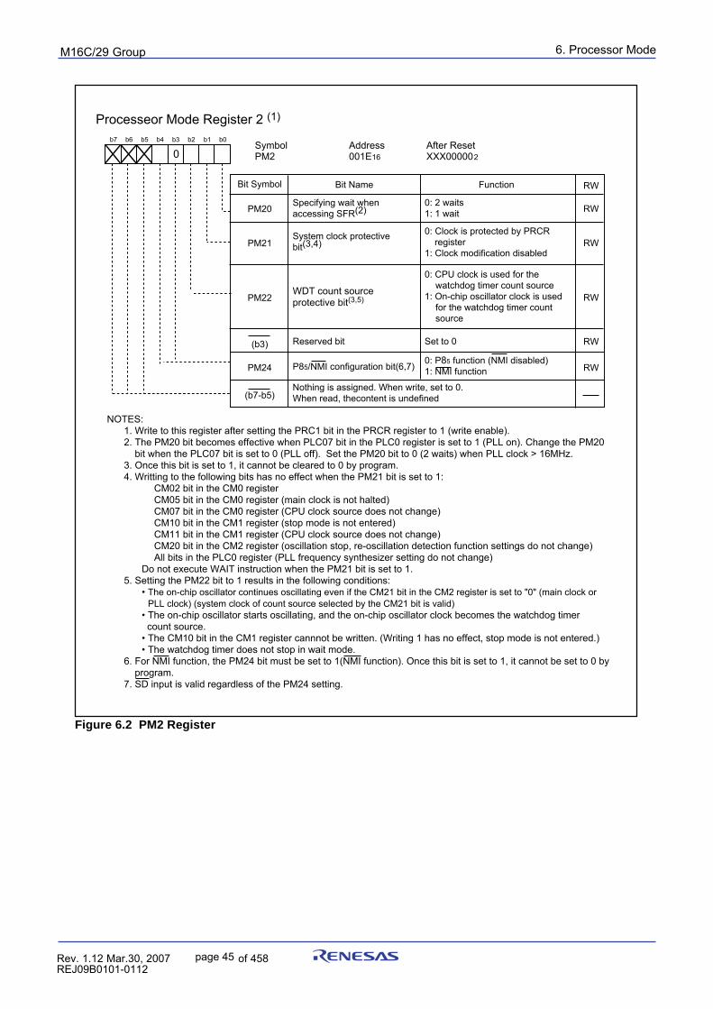
6. Processor ModepuorG92/C61M
page 45 854fo7002,03.raM21.1.veR2110-1010B90JER
Figure 6.2 PM2 Register
NOTES:1. Write to this register after setting the PRC1 bit in the PRCR register to 1 (write enable).2. The PM20 bit becomes effective when PLC07 bit in the PLC0 register is set to 1 (PLL on). Change the PM20
bit when the PLC07 bit is set to 0 (PLL off). Set the PM20 bit to 0 (2 waits) when PLL clock > 16MHz.3. Once this bit is set to 1, it cannot be cleared to 0 by program.4. Writting to the following bits has no effect when the PM21 bit is set to 1: CM02 bit in the CM0 register CM05 bit in the CM0 register (main clock is not halted) CM07 bit in the CM0 register (CPU clock source does not change) CM10 bit in the CM1 register (stop mode is not entered) CM11 bit in the CM1 register (CPU clock source does not change) CM20 bit in the CM2 register (oscillation stop, re-oscillation detection function settings do not change) All bits in the PLC0 register (PLL frequency synthesizer setting do not change) Do not execute WAIT instruction when the PM21 bit is set to 1.5. Setting the PM22 bit to 1 results in the following conditions:
• The on-chip oscillator continues oscillating even if the CM21 bit in the CM2 register is set to "0" (main clock or PLL clock) (system clock of count source selected by the CM21 bit is valid)
• The on-chip oscillator starts oscillating, and the on-chip oscillator clock becomes the watchdog timer count source.
• The CM10 bit in the CM1 register cannnot be written. (Writing 1 has no effect, stop mode is not entered.) • The watchdog timer does not stop in wait mode.
6. For NMI function, the PM24 bit must be set to 1(NMI function). Once this bit is set to 1, it cannot be set to 0 by program.
7. SD input is valid regardless of the PM24 setting.
FunctionBit Symbol Bit Name
Processeor Mode Register 2 (1)
Symbol Address After Reset PM2 001E16 XXX000002
RW
b7 b6 b5 b4 b3 b2 b1 b0
PM20
0
PM21
RW
RW
RW
(b7-b5)
PM22
PM24
(b3) Reserved bit Set to 0 RW
RW
Nothing is assigned. When write, set to 0. When read, thecontent is undefined
0: CPU clock is used for the watchdog timer count source
1: On-chip oscillator clock is used for the watchdog timer count source
0: 2 waits1: 1 wait
Specifying wait when accessing SFR(2)
System clock protective bit(3,4)
WDT count source protective bit(3,5)
0: Clock is protected by PRCR register
1: Clock modification disabled
P85/NMI configuration bit(6,7) 0: P85 function (NMI disabled)1: NMI function
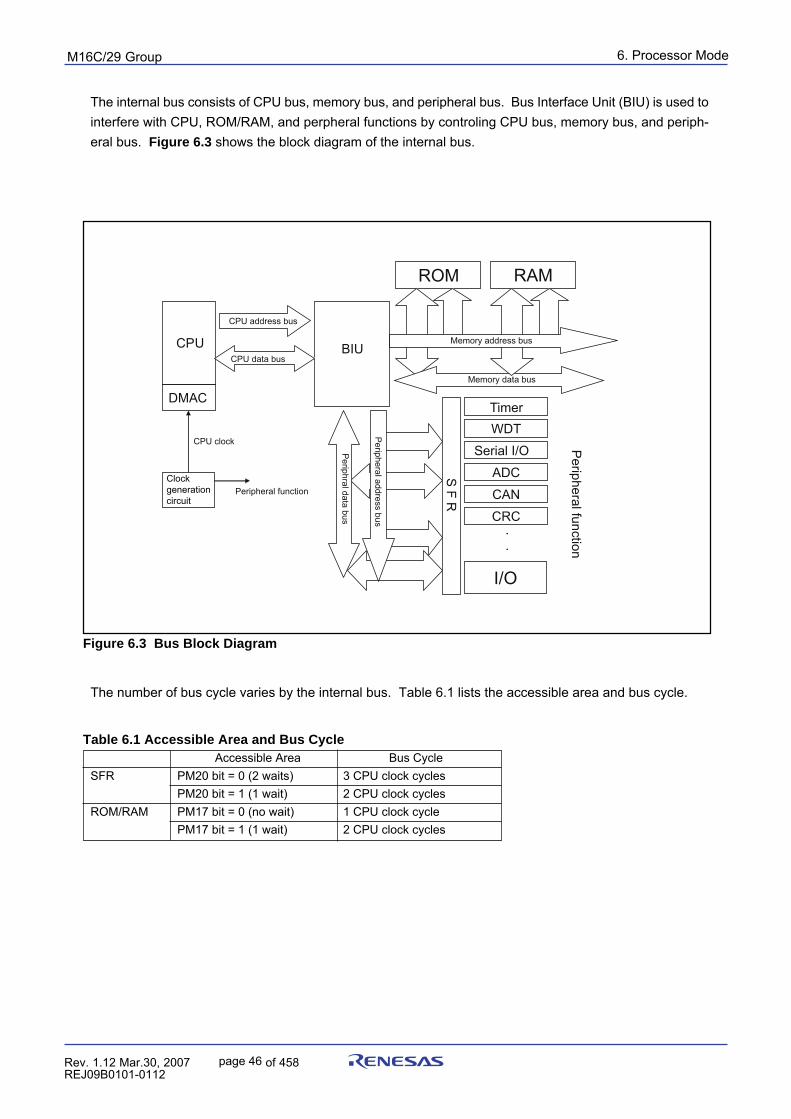
6. Processor ModepuorG92/C61M
page 46 854fo7002,03.raM21.1.veR2110-1010B90JER
The internal bus consists of CPU bus, memory bus, and peripheral bus. Bus Interface Unit (BIU) is used tointerfere with CPU, ROM/RAM, and perpheral functions by controling CPU bus, memory bus, and periph-eral bus. Figure 6.3 shows the block diagram of the internal bus.
CPU
ROM
BIU
I/O
CPU address bus
Memory data bus
Periphral data bus
DMAC
Memory address bus
Peripheral address bus
TimerWDT
Serial I/O
ADC
CAN
CRC
Peripheral function
CPU clock
RAM
CPU data bus
Peripheral function
.
.
Clock generation circuit
S F R
Figure 6.3 Bus Block Diagram
Table 6.1 Accessible Area and Bus Cycle
The number of bus cycle varies by the internal bus. Table 6.1 lists the accessible area and bus cycle.
Accessible Area Bus CycleSFR PM20 bit = 0 (2 waits) 3 CPU clock cycles
PM20 bit = 1 (1 wait) 2 CPU clock cyclesROM/RAM PM17 bit = 0 (no wait) 1 CPU clock cycle
PM17 bit = 1 (1 wait) 2 CPU clock cycles
7. Clock Generation Circuit
page 47 854fo7002,03.raM21.1.veR2110-1010B90JER
puorG92/C61M
- CPU clock source- Peripheral function
clock source
Use of clock
Main Clock Oscillation Circuit
Sub Clock Oscillation CircuitItem
- CPU clock source- Timer A, B's clock
source
Clock frequency 0 to 20 MHz 32.768 kHz
- Ceramic oscillator- Crystal oscillator
Usable oscillator - Crystal oscillator
XIN, XOUTPins to connect oscillator
XCIN, XCOUT
AvailableOscillation stop,restart function
OscillatingOscillator status after reset
Stopped
Externally derived clock can be inputOther
PLL FrequencySynthesizer
10 to 20 MHz
Stopped
Variable On-chip Oscillator
- CPU clock source- Peripheral function clock source- CPU and peripheral function
clock sources when the main clock stops oscillating
Selectable source frequency: f1(ROC), f2(ROC), f3(ROC)Selectable divider: by 2, by 4, by 8
Oscillating
- CPU clock source- Peripheral function clock
source
(CPU clock source)
Available Available Available
7. Clock Generation CircuitThe clock generation circuit contains four oscillator circuits as follows:(1) Main clock oscillation circuit(2) Sub clock oscillation circuit(3) Variable on-chip oscillators(4) PLL frequency synthesizer
Table 7.1 lists the specifications of the clock generation circuit. Figure 7.1 shows the clock generationcircuit. Figures 7.2 to 7.7 show clock-associated registers.
Table 7.1 Clock Generation Circuit Specifications
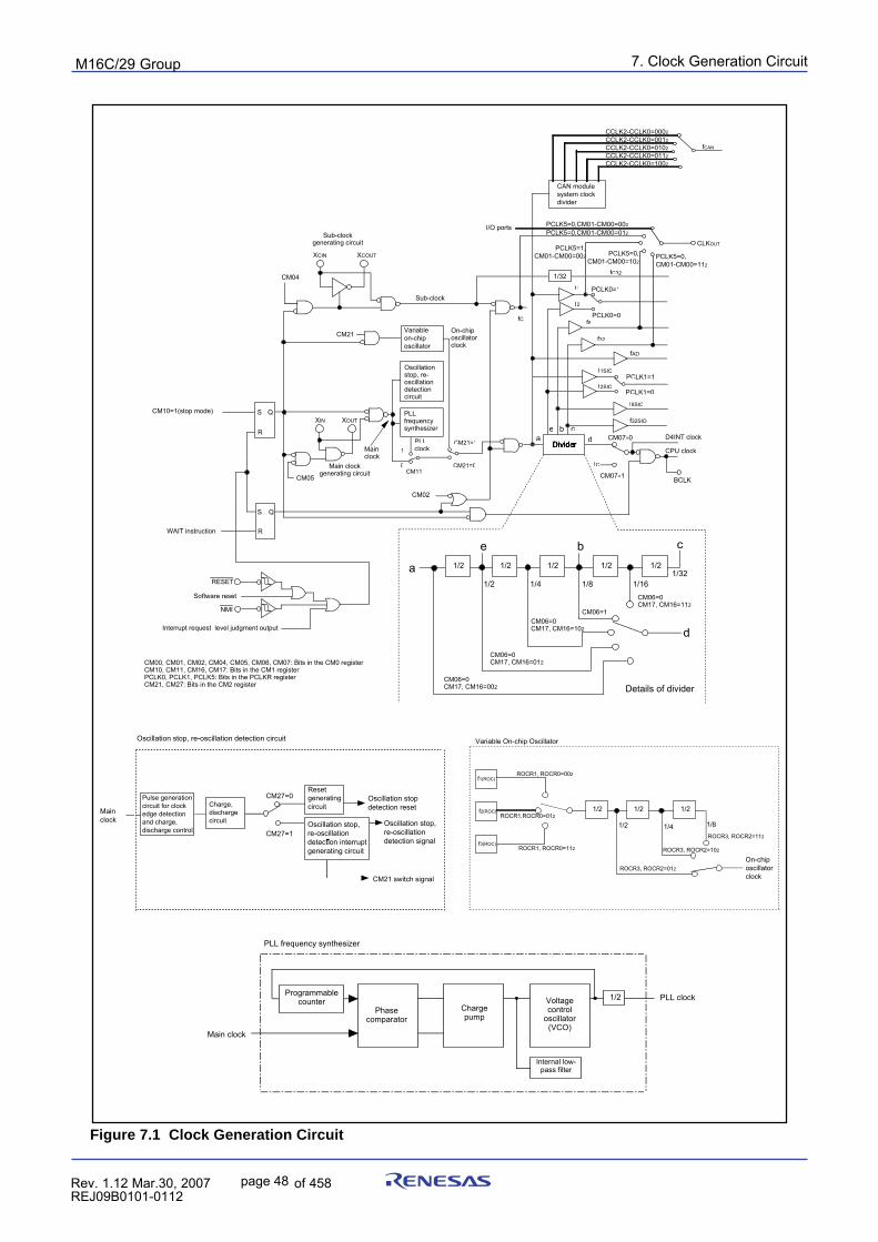
7. Clock Generation Circuit
page 48 854fo7002,03.raM21.1.veR2110-1010B90JER
puorG92/C61M
Figure 7.1 Clock Generation Circuit
Phase comparator
Chargepump
Voltagecontrol
oscillator(VCO)
PLL clock
Main clock
1/2Programmablecounter
Internal low-pass filter
PLL frequency synthesizer
Pulse generation circuit for clock edge detection and charge, discharge control
Charge, dischargecircuit
Resetgenerating circuit
Oscillation stop, re-oscillationdetection interruptgenerating circuit
Mainclock
Oscillation stopdetection reset
CM27=0
CM21 switch signal
Oscillation stop, re-oscillationdetection signal
Oscillation stop, re-oscillation detection circuit
CM27=1
1/2 1/2 1/2
ROCR3, ROCR2=112
On-chip oscillatorclock
1/81/41/2
ROCR3, ROCR2=102
ROCR3, ROCR2=012
ROCR1, ROCR0=002f1(ROC)
f2(ROC)
f3(ROC)
ROCR1,ROCR0=012
ROCR1, ROCR0=112
Variable On-chip Oscillator
Variable on-chiposcillator
fC321/32
Main clockgenerating circuit
fC
CM02
CM04
CM10=1(stop mode) QS
R
WAIT instruction
CM05
QS
R
NMI
Interrupt request level judgment output
RESET
Software reset
fC
CPU clock
CM07=0
CM07=1
ea d
1/2 1/2 1/2 1/2
CM06=0CM17, CM16=002
CM06=0CM17, CM16=012
CM06=0CM17, CM16=102
CM06=1
CM06=0CM17, CM16=112
d
a
Details of divider
Sub-clockgenerating circuit
XCIN XCOUT
XOUTXIN
f8
f32
cb
b1/2
c
f32SIO
f8SIO
fAD
f1
e
e
1/2 1/4 1/8 1/161/32
PCLK0=1
PLL frequency synthesizer
0
1CM21=1
CM11CM21=0
PLLclock
Sub-clock
On-chip oscillatorclock
PCLK0=0
f2
f1SIOPCLK1=1
PCLK1=0f2SIO
Main clock
Oscillation stop, re-oscillation detection circuit
D4INT clock
BCLK
CLKOUT
I/O ports PCLK5=0,CM01-CM00=002
PCLK5=0,CM01-CM00=012
PCLK5=1,CM01-CM00=002 PCLK5=0,
CM01-CM00=102PCLK5=0,CM01-CM00=112
CAN modulesystem clockdivider
fCAN
CCLK2-CCLK0=0002
CCLK2-CCLK0=0012
CCLK2-CCLK0=0102
CCLK2-CCLK0=0112
CCLK2-CCLK0=1002
CM00, CM01, CM02, CM04, CM05, CM06, CM07: Bits in the CM0 registerCM10, CM11, CM16, CM17: Bits in the CM1 register PCLK0, PCLK1, PCLK5: Bits in the PCLKR registerCM21, CM27: Bits in the CM2 register
CM21
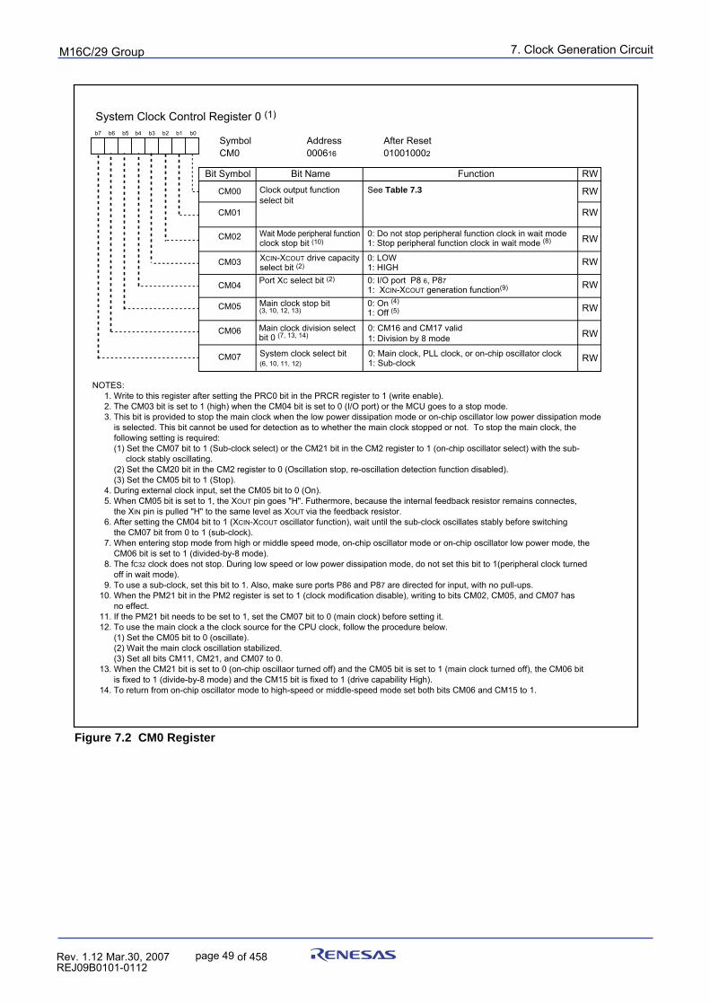
7. Clock Generation Circuit
page 49 854fo7002,03.raM21.1.veR2110-1010B90JER
puorG92/C61M
Figure 7.2 CM0 Register
System Clock Control Register 0 (1)
Bit Name FunctionBit Symbol
b7 b6 b5 b4 b3 b2 b1 b0
CM07
CM05
CM04
CM03
CM02
CM06
Wait Mode peripheral function clock stop bit (10)
0: Do not stop peripheral function clock in wait mode1: Stop peripheral function clock in wait mode (8)
XCIN-XCOUT drive capacityselect bit (2)
0: LOW1: HIGH0: I/O port P8 6, P871: XCIN-XCOUT generation function(9)
Main clock stop bit (3, 10, 12, 13)
0: On (4)
1: Off (5)
Main clock division selectbit 0 (7, 13, 14)
0: CM16 and CM17 valid1: Division by 8 mode
System clock select bit(6, 10, 11, 12)
0: Main clock, PLL clock, or on-chip oscillator clock1: Sub-clock
RW
Port XC select bit (2)
RW
RW
RW
RW
RW
RW
RW
Clock output function select bit
See Table 7.3CM00
CM01
RW
NOTES: 1. Write to this register after setting the PRC0 bit in the PRCR register to 1 (write enable). 2. The CM03 bit is set to 1 (high) when the CM04 bit is set to 0 (I/O port) or the MCU goes to a stop mode. 3. This bit is provided to stop the main clock when the low power dissipation mode or on-chip oscillator low power dissipation mode is selected. This bit cannot be used for detection as to whether the main clock stopped or not. To stop the main clock, the following setting is required: (1) Set the CM07 bit to 1 (Sub-clock select) or the CM21 bit in the CM2 register to 1 (on-chip oscillator select) with the sub- clock stably oscillating. (2) Set the CM20 bit in the CM2 register to 0 (Oscillation stop, re-oscillation detection function disabled). (3) Set the CM05 bit to 1 (Stop). 4. During external clock input, set the CM05 bit to 0 (On). 5. When CM05 bit is set to 1, the XOUT pin goes "H". Futhermore, because the internal feedback resistor remains connectes, the XIN pin is pulled "H" to the same level as XOUT via the feedback resistor. 6. After setting the CM04 bit to 1 (XCIN-XCOUT oscillator function), wait until the sub-clock oscillates stably before switching the CM07 bit from 0 to 1 (sub-clock). 7. When entering stop mode from high or middle speed mode, on-chip oscillator mode or on-chip oscillator low power mode, the CM06 bit is set to 1 (divided-by-8 mode). 8. The fC32 clock does not stop. During low speed or low power dissipation mode, do not set this bit to 1(peripheral clock turned off in wait mode). 9. To use a sub-clock, set this bit to 1. Also, make sure ports P86 and P87 are directed for input, with no pull-ups. 10. When the PM21 bit in the PM2 register is set to 1 (clock modification disable), writing to bits CM02, CM05, and CM07 has no effect. 11. If the PM21 bit needs to be set to 1, set the CM07 bit to 0 (main clock) before setting it. 12. To use the main clock a the clock source for the CPU clock, follow the procedure below. (1) Set the CM05 bit to 0 (oscillate). (2) Wait the main clock oscillation stabilized. (3) Set all bits CM11, CM21, and CM07 to 0. 13. When the CM21 bit is set to 0 (on-chip oscillaor turned off) and the CM05 bit is set to 1 (main clock turned off), the CM06 bit is fixed to 1 (divide-by-8 mode) and the CM15 bit is fixed to 1 (drive capability High). 14. To return from on-chip oscillator mode to high-speed or middle-speed mode set both bits CM06 and CM15 to 1.
Symbol Address After Reset CM0 010010002000616
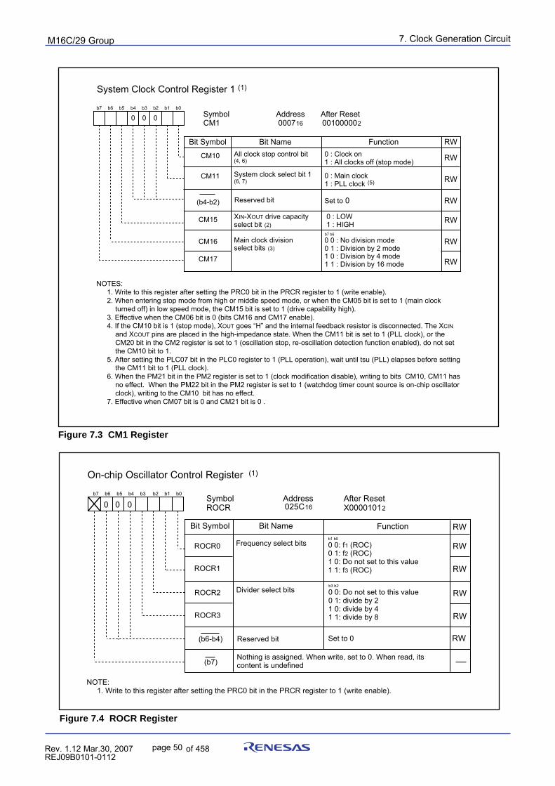
7. Clock Generation Circuit
page 50 854fo7002,03.raM21.1.veR2110-1010B90JER
puorG92/C61M
Figure 7.3 CM1 Register
Figure 7.4 ROCR Register
b7 b6 b5 b4 b3 b2 b1 b0
RW
ROCR0
ROCR1
On-chip Oscillator Control Register (1)
Symbol Address After Reset ROCR 025C16 X00001012
Bit Name FunctionBit Symbol
Frequency select bits RW
RW
Reserved bit
0 00
0 0: f1 (ROC)0 1: f2 (ROC)1 0: Do not set to this value1 1: f3 (ROC)
b1 b0
ROCR2
ROCR3
Divider select bits RW
RW
0 0: Do not set to this value0 1: divide by 21 0: divide by 41 1: divide by 8
b3 b2
NOTE: 1. Write to this register after setting the PRC0 bit in the PRCR register to 1 (write enable).
(b6-b4) Set to 0
Nothing is assigned. When write, set to 0. When read, its content is undefined(b7)
RW
System Clock Control Register 1 (1)
Symbol Address After Reset CM1 000716 001000002
Bit Name FunctionBit Symbol
b7 b6 b5 b4 b3 b2 b1 b0
CM10 All clock stop control bit(4, 6)
0 : Clock on1 : All clocks off (stop mode)
CM15 XIN-XOUT drive capacity select bit (2)
0 : LOW 1 : HIGH
RW
CM16
CM17
Reserved bit Set to 0
Main clock division select bits (3)
0 0 : No division mode0 1 : Division by 2 mode1 0 : Division by 4 mode1 1 : Division by 16 mode
b7 b6
00 0
CM11 System clock select bit 1(6, 7)
0 : Main clock 1 : PLL clock (5)
RW
RW
RW
RW
RW
RW
(b4-b2)
NOTES:1. Write to this register after setting the PRC0 bit in the PRCR register to 1 (write enable).2. When entering stop mode from high or middle speed mode, or when the CM05 bit is set to 1 (main clock
turned off) in low speed mode, the CM15 bit is set to 1 (drive capability high).3. Effective when the CM06 bit is 0 (bits CM16 and CM17 enable).4. If the CM10 bit is 1 (stop mode), XOUT goes “H” and the internal feedback resistor is disconnected. The XCIN
and XCOUT pins are placed in the high-impedance state. When the CM11 bit is set to 1 (PLL clock), or the CM20 bit in the CM2 register is set to 1 (oscillation stop, re-oscillation detection function enabled), do not set the CM10 bit to 1.
5. After setting the PLC07 bit in the PLC0 register to 1 (PLL operation), wait until tsu (PLL) elapses before setting the CM11 bit to 1 (PLL clock).
6. When the PM21 bit in the PM2 register is set to 1 (clock modification disable), writing to bits CM10, CM11 has no effect. When the PM22 bit in the PM2 register is set to 1 (watchdog timer count source is on-chip oscillator clock), writing to the CM10 bit has no effect.
7. Effective when CM07 bit is 0 and CM21 bit is 0 .
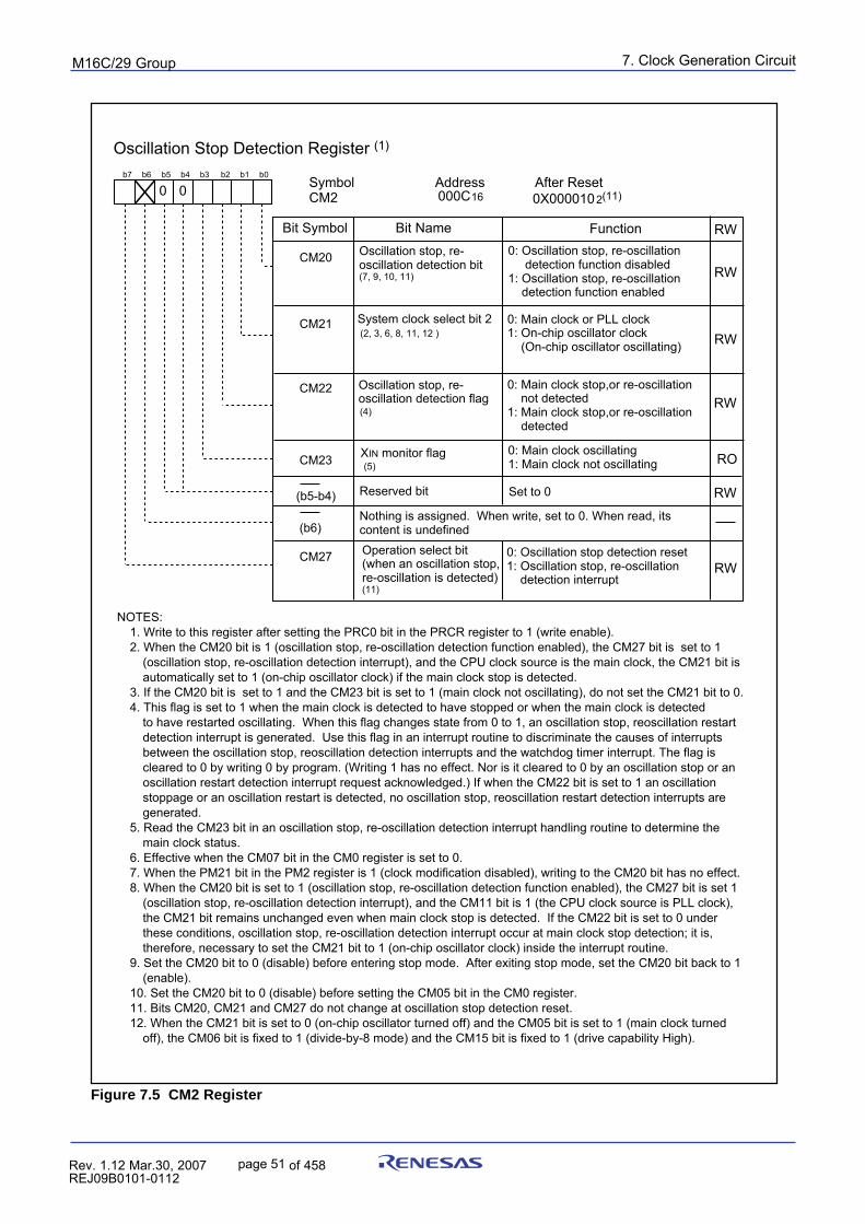
7. Clock Generation Circuit
page 51 854fo7002,03.raM21.1.veR2110-1010B90JER
puorG92/C61M
Figure 7.5 CM2 Register
b7 b6 b5 b4 b3 b2 b1 b0
RW
CM20
CM21
Oscillation Stop Detection Register (1)
Symbol Address After Reset CM2 000C16 0X0000102(11)
Bit Name FunctionBit Symbol
System clock select bit 2 (2, 3, 6, 8, 11, 12 )
0: Oscillation stop, re-oscillation detection function disabled1: Oscillation stop, re-oscillation detection function enabled
0: Main clock or PLL clock 1: On-chip oscillator clock (On-chip oscillator oscillating)
Oscillation stop, re-oscillation detection bit(7, 9, 10, 11)
CM22
CM23
Oscillation stop, re-oscillation detection flag
0: Main clock stop,or re-oscillation not detected1: Main clock stop,or re-oscillation detected
0: Main clock oscillating1: Main clock not oscillating
XIN monitor flag
(4)
CM27 0: Oscillation stop detection reset 1: Oscillation stop, re-oscillation detection interrupt
Nothing is assigned. When write, set to 0. When read, its content is undefinedOperation select bit(when an oscillation stop, re-oscillation is detected)(11)
RW
RW
RW
RW
RO
(b6)
(5)
Reserved bit(b5-b4) Set to 0 RW
0 0
NOTES:1. Write to this register after setting the PRC0 bit in the PRCR register to 1 (write enable). 2. When the CM20 bit is 1 (oscillation stop, re-oscillation detection function enabled), the CM27 bit is set to 1
(oscillation stop, re-oscillation detection interrupt), and the CPU clock source is the main clock, the CM21 bit is automatically set to 1 (on-chip oscillator clock) if the main clock stop is detected.
3. If the CM20 bit is set to 1 and the CM23 bit is set to 1 (main clock not oscillating), do not set the CM21 bit to 0.4. This flag is set to 1 when the main clock is detected to have stopped or when the main clock is detected
to have restarted oscillating. When this flag changes state from 0 to 1, an oscillation stop, reoscillation restart detection interrupt is generated. Use this flag in an interrupt routine to discriminate the causes of interrupts between the oscillation stop, reoscillation detection interrupts and the watchdog timer interrupt. The flag is cleared to 0 by writing 0 by program. (Writing 1 has no effect. Nor is it cleared to 0 by an oscillation stop or an oscillation restart detection interrupt request acknowledged.) If when the CM22 bit is set to 1 an oscillation stoppage or an oscillation restart is detected, no oscillation stop, reoscillation restart detection interrupts are generated.
5. Read the CM23 bit in an oscillation stop, re-oscillation detection interrupt handling routine to determine the main clock status.
6. Effective when the CM07 bit in the CM0 register is set to 0.7. When the PM21 bit in the PM2 register is 1 (clock modification disabled), writing to the CM20 bit has no effect.8. When the CM20 bit is set to 1 (oscillation stop, re-oscillation detection function enabled), the CM27 bit is set 1
(oscillation stop, re-oscillation detection interrupt), and the CM11 bit is 1 (the CPU clock source is PLL clock), the CM21 bit remains unchanged even when main clock stop is detected. If the CM22 bit is set to 0 under these conditions, oscillation stop, re-oscillation detection interrupt occur at main clock stop detection; it is, therefore, necessary to set the CM21 bit to 1 (on-chip oscillator clock) inside the interrupt routine.
9. Set the CM20 bit to 0 (disable) before entering stop mode. After exiting stop mode, set the CM20 bit back to 1 (enable).
10. Set the CM20 bit to 0 (disable) before setting the CM05 bit in the CM0 register.11. Bits CM20, CM21 and CM27 do not change at oscillation stop detection reset.12. When the CM21 bit is set to 0 (on-chip oscillator turned off) and the CM05 bit is set to 1 (main clock turned
off), the CM06 bit is fixed to 1 (divide-by-8 mode) and the CM15 bit is fixed to 1 (drive capability High).
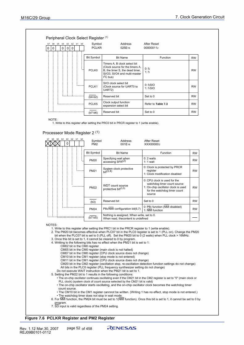
7. Clock Generation Circuit
page 52 854fo7002,03.raM21.1.veR2110-1010B90JER
puorG92/C61M
Figure 7.6 PCLKR Register and PM2 Register
NOTES:1. Write to this register after setting the PRC1 bit in the PRCR register to 1 (write enable).2. The PM20 bit becomes effective when PLC07 bit in the PLC0 register is set to 1 (PLL on). Change the PM20
bit when the PLC07 bit is set to 0 (PLL off). Set the PM20 bit to 0 (2 waits) when PLL clock > 16MHz.3. Once this bit is set to 1, it cannot be cleared to 0 by program.4. Writting to the following bits has no effect when the PM21 bit is set to 1: CM02 bit in the CM0 register CM05 bit in the CM0 register (main clock is not halted) CM07 bit in the CM0 register (CPU clock source does not change) CM10 bit in the CM1 register (stop mode is not entered) CM11 bit in the CM1 register (CPU clock source does not change) CM20 bit in the CM2 register (oscillation stop, re-oscillation detection function settings do not change) All bits in the PLC0 register (PLL frequency synthesizer setting do not change) Do not execute WAIT instruction when the PM21 bit is set to 1.5. Setting the PM22 bit to 1 results in the following conditions:
• The on-chip oscillator continues oscillating even if the CM21 bit in the CM2 register is set to "0" (main clock or PLL clock) (system clock of count source selected by the CM21 bit is valid)
• The on-chip oscillator starts oscillating, and the on-chip oscillator clock becomes the watchdog timer count source.
• The CM10 bit in the CM1 register cannnot be written. (Writing 1 has no effect, stop mode is not entered.) • The watchdog timer does not stop in wait mode.
6. For NMI function, the PM24 bit must be set to 1(NMI function). Once this bit is set to 1, it cannot be set to 0 by program.
7. SD input is valid regardless of the PM24 setting.
FunctionBit Symbol Bit Name
Processeor Mode Register 2 (1)
Symbol Address After Reset PM2 001E16 XXX000002
RW
b7 b6 b5 b4 b3 b2 b1 b0
PM20
0
PM21
RW
RW
RW
(b7-b5)
PM22
PM24
(b3) Reserved bit Set to 0 RW
RW
Nothing is assigned. When write, set to 0. When read, thecontent is undefined
0: CPU clock is used for the watchdog timer count source
1: On-chip oscillator clock is used for the watchdog timer count source
0: 2 waits1: 1 wait
Specifying wait when accessing SFR(2)
System clock protective bit(3,4)
WDT count source protective bit(3,5)
0: Clock is protected by PRCR register
1: Clock modification disabled
P85/NMI configuration bit(6,7) 0: P85 function (NMI disabled)1: NMI function
FunctionBit Symbol Bit Name
Peripheral Clock Select Register (1)
Symbol Address After Reset PCLKR 025E16 000000112
RW
b7 b6 b5 b4 b3 b2 b1 b0
PCLK0 0: f21: f1
0 0 0
Reserved bit Set to 0
NOTE: 1. Write to this register after setting the PRC0 bit in PRCR register to 1 (write enable).
0 0
PCLK1
0: f2SIO1: f1SIO
RW
RW
RW(b4-b2)
Reserved bit Set to 0 RW(b7-b6)
RWPCLK5
Refer to Table 7.3 Clock output function expansion select bit
Timers A, B clock select bit (Clock source for the timers A, B, the timer S, the dead timer, SI/O3, SI/O4 and multi-master I2C bus)
SI/O clock select bit (Clock source for UART0 to UART2)
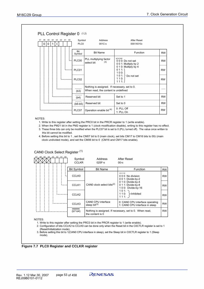
7. Clock Generation Circuit
page 53 854fo7002,03.raM21.1.veR2110-1010B90JER
puorG92/C61M
Figure 7.7 PLC0 Register and CCLKR register
PLC00
PLC01
PLC02
PLC07
(3)
(4)
Function
NOTES: 1. Write to this register after setting the PRC0 bit in the PRCR register to 1 (write enable). 2. When the PM21 bit in the PM2 register is 1 (clock modification disable), writing to this register has no effect. 3. These three bits can only be modified when the PLC07 bit is set to 0 (PLL turned off). The value once written to this bit cannot be modified. 4. Before setting this bit to 1 , set the CM07 bit to 0 (main clock), set bits CM17 to CM16 bits to 002 (main clock undivided mode), and set the CM06 bit to 0 (CM16 and CM17 bits enable).
PLL Control Register 0 (1,2)
PLL multiplying factorselect bit
Nothing is assigned. If necessary, set to 0. When read, the content is undefined
Operation enable bit
0 0 0:0 0 1: Multiply by 20 1 0: Multiply by 40 1 1: 1 0 0: 1 0 1: 1 1 0: 1 1 1:
0: PLL Off1: PLL On
Bit NameBitSymbol
Symbol Address After ResetPLC0 001C16 0001X0102
RW
b1b0b2
Reserved bit Set to 0
Do not set
RW
RW
RW
RW
RW
Reserved bit Set to 1 RW
Do not set
(b4)
(b6-b5)
(b3)
b7 b6 b5 b4 b3 b2 b1 b0
0 10
RW
RW
RW
RW
RW
0 0 0 No division0 0 1: Divide-by-20 1 0: Divide-by-40 1 1: Divide-by-81 0 0: Divide-by-161 0 1:1 1 0: Inhibited1 1 1:
b2 b1 b0
CAN0 clock select bits(2)
CAN0 CPU interfacesleep bit(3)
0: CAN0 CPU interface operating1: CAN0 CPU interface in sleep
Bit Name FunctionBit Symbol RW
CCLK3
CCLK1
CCLK2
CCLK0
Symbol Address After ResetCCLKR 025F16 0016
NOTES:1. Write to this register after setting the PRC0 bit in the PRCR register to 1 (write enable).2. Configuration of bits CCLK2 to CCLK0 can be done only when the Reset bit in the C0CTLR register is set to 1
(Reset/Initialization mode).3. Before setting this bit to 1(CAN0 CPU interface in sleep), set the Sleep bit in C0CTLR register to 1 (Sleep
mode).
CAN0 Clock Select Register (1) b7 b6 b5 b4 b3 b2 b1 b0
(b7-b4) Nothing is assigned. If necessary, set to 0. When read,the content is 0
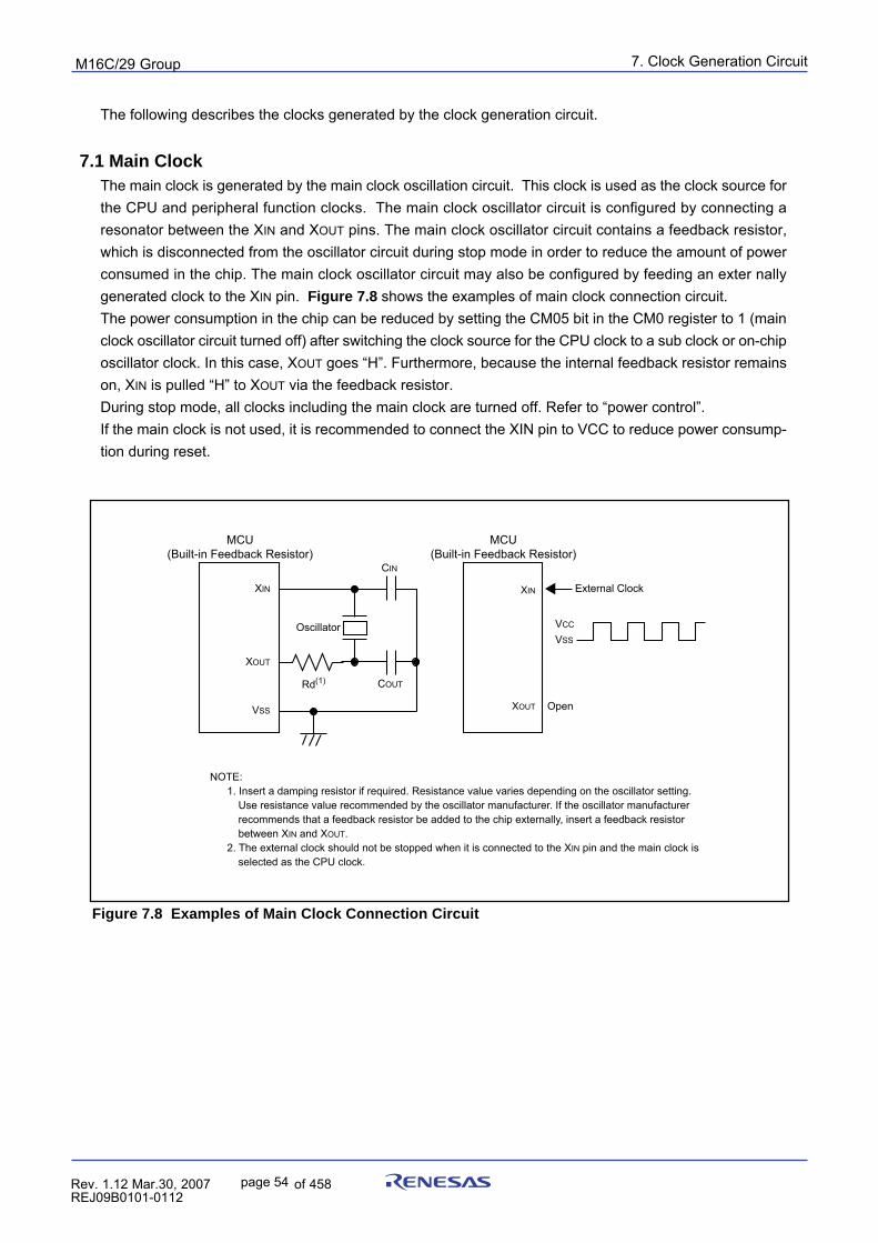
7. Clock Generation Circuit
page 54 854fo7002,03.raM21.1.veR2110-1010B90JER
puorG92/C61M
Figure 7.8 Examples of Main Clock Connection Circuit
The following describes the clocks generated by the clock generation circuit.
7.1 Main ClockThe main clock is generated by the main clock oscillation circuit. This clock is used as the clock source forthe CPU and peripheral function clocks. The main clock oscillator circuit is configured by connecting aresonator between the XIN and XOUT pins. The main clock oscillator circuit contains a feedback resistor,which is disconnected from the oscillator circuit during stop mode in order to reduce the amount of powerconsumed in the chip. The main clock oscillator circuit may also be configured by feeding an exter nallygenerated clock to the XIN pin. Figure 7.8 shows the examples of main clock connection circuit.The power consumption in the chip can be reduced by setting the CM05 bit in the CM0 register to 1 (mainclock oscillator circuit turned off) after switching the clock source for the CPU clock to a sub clock or on-chiposcillator clock. In this case, XOUT goes “H”. Furthermore, because the internal feedback resistor remainson, XIN is pulled “H” to XOUT via the feedback resistor.During stop mode, all clocks including the main clock are turned off. Refer to “power control”.If the main clock is not used, it is recommended to connect the XIN pin to VCC to reduce power consump-tion during reset.
External ClockXIN
XOUT Open
VCC
VSS
NOTE: 1. Insert a damping resistor if required. Resistance value varies depending on the oscillator setting.
Use resistance value recommended by the oscillator manufacturer. If the oscillator manufacturer recommends that a feedback resistor be added to the chip externally, insert a feedback resistor between XIN and XOUT.
2. The external clock should not be stopped when it is connected to the XIN pin and the main clock is selected as the CPU clock.
Oscillator
Rd(1)
CIN
COUT
XIN
XOUT
MCU(Built-in Feedback Resistor)
MCU(Built-in Feedback Resistor)
VSS
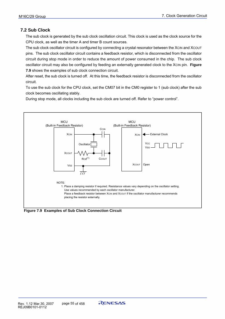
7. Clock Generation Circuit
page 55 854fo7002,03.raM21.1.veR2110-1010B90JER
puorG92/C61M
Figure 7.9 Examples of Sub Clock Connection Circuit
7.2 Sub ClockThe sub clock is generated by the sub clock oscillation circuit. This clock is used as the clock source for theCPU clock, as well as the timer A and timer B count sources.The sub clock oscillator circuit is configured by connecting a crystal resonator between the XCIN and XCOUT
pins. The sub clock oscillator circuit contains a feedback resistor, which is disconnected from the oscillatorcircuit during stop mode in order to reduce the amount of power consumed in the chip. The sub clockoscillator circuit may also be configured by feeding an externally generated clock to the XCIN pin. Figure
7.9 shows the examples of sub clock connection circuit.After reset, the sub clock is turned off. At this time, the feedback resistor is disconnected from the oscillatorcircuit.To use the sub clock for the CPU clock, set the CM07 bit in the CM0 register to 1 (sub clock) after the subclock becomes oscillating stably.During stop mode, all clocks including the sub clock are turned off. Refer to “power control”.
External ClockXCIN
XCOUT Open
VCC
VSS
NOTE: 1. Place a damping resistor if required. Resistance values vary depending on the oscillator setting. Use values recommended by each oscillator manufacturer. Place a feedback resistor between XCIN and XCOUT if the oscillator manufacturer recommends placing the resistor externally.
Oscillator
RCd(1)
CCIN
CCOUT
XCIN
XCOUT
MCU(Built-in Feedback Resistor)
MCU(Built-in Feedback Resistor)
VSS
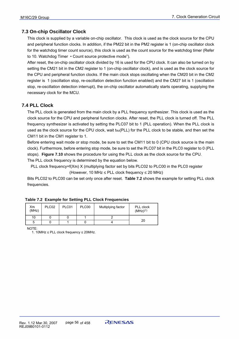
7. Clock Generation Circuit
page 56 854fo7002,03.raM21.1.veR2110-1010B90JER
puorG92/C61M
7.3 On-chip Oscillator ClockThis clock is supplied by a variable on-chip oscillator. This clock is used as the clock source for the CPUand peripheral function clocks. In addition, if the PM22 bit in the PM2 register is 1 (on-chip oscillator clockfor the watchdog timer count source), this clock is used as the count source for the watchdog timer (Referto 10. Watchdog Timer • Count source protective mode”).After reset, the on-chip oscillator clock divided by 16 is used for the CPU clock. It can also be turned on bysetting the CM21 bit in the CM2 register to 1 (on-chip oscillator clock), and is used as the clock source forthe CPU and peripheral function clocks. If the main clock stops oscillating when the CM20 bit in the CM2register is 1 (oscillation stop, re-oscillation detection function enabled) and the CM27 bit is 1 (oscillationstop, re-oscillation detection interrupt), the on-chip oscillator automatically starts operating, supplying thenecessary clock for the MCU.
7.4 PLL ClockThe PLL clock is generated from the main clock by a PLL frequency synthesizer. This clock is used as theclock source for the CPU and peripheral function clocks. After reset, the PLL clock is turned off. The PLLfrequency synthesizer is activated by setting the PLC07 bit to 1 (PLL operation). When the PLL clock isused as the clock source for the CPU clock, wait tsu(PLL) for the PLL clock to be stable, and then set theCM11 bit in the CM1 register to 1.Before entering wait mode or stop mode, be sure to set the CM11 bit to 0 (CPU clock source is the mainclock). Furthermore, before entering stop mode, be sure to set the PLC07 bit in the PLC0 register to 0 (PLLstops). Figure 7.10 shows the procedure for using the PLL clock as the clock source for the CPU.The PLL clock frequency is determined by the equation below.
PLL clock frequency=f(XIN) X (multiplying factor set by bits PLC02 to PLC00 in the PLC0 register (However, 10 MHz ≤ PLL clock frequency ≤ 20 MHz)
Bits PLC02 to PLC00 can be set only once after reset. Table 7.2 shows the example for setting PLL clockfrequencies.
Table 7.2 Example for Setting PLL Clock Frequencies
XIN(MHz)
PLC02 PLC01 PLC00 Multiplying factor PLL clock(MHz)(1)
10 0 0 1 2205 0 1 0 4
NOTE: 1. 10MHz ≤ PLL clock frequency ≤ 20MHz.
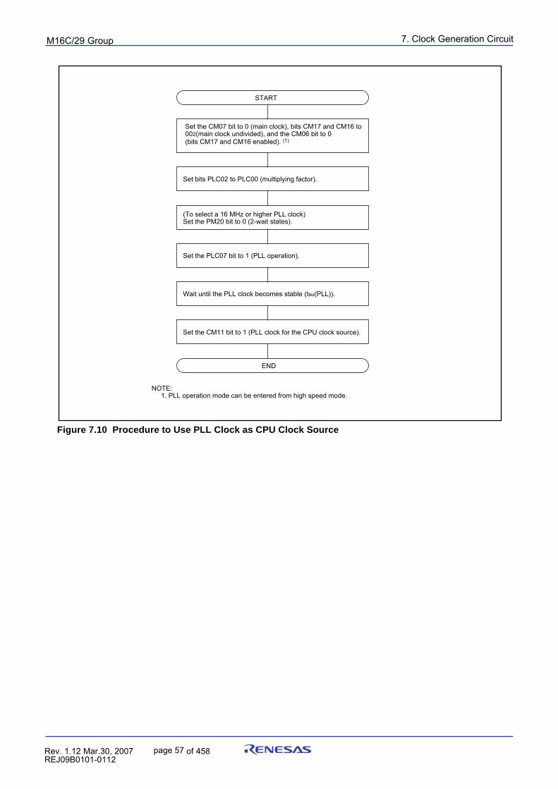
7. Clock Generation Circuit
page 57 854fo7002,03.raM21.1.veR2110-1010B90JER
puorG92/C61M
Figure 7.10 Procedure to Use PLL Clock as CPU Clock Source
START
Set the CM07 bit to 0 (main clock), bits CM17 and CM16 to 002(main clock undivided), and the CM06 bit to 0 (bits CM17 and CM16 enabled). (1)
Set bits PLC02 to PLC00 (multiplying factor).
(To select a 16 MHz or higher PLL clock)Set the PM20 bit to 0 (2-wait states).
Set the PLC07 bit to 1 (PLL operation).
Wait until the PLL clock becomes stable (tsu(PLL)).
Set the CM11 bit to 1 (PLL clock for the CPU clock source).
END
NOTE: 1. PLL operation mode can be entered from high speed mode.
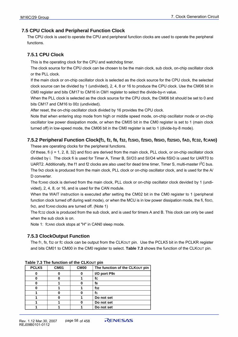
7. Clock Generation Circuit
page 58 854fo7002,03.raM21.1.veR2110-1010B90JER
puorG92/C61M
7.5 CPU Clock and Peripheral Function ClockThe CPU clock is used to operate the CPU and peripheral function clocks are used to operate the peripheralfunctions.
7.5.1 CPU Clock
This is the operating clock for the CPU and watchdog timer.The clock source for the CPU clock can be chosen to be the main clock, sub clock, on-chip oscillator clockor the PLL clock.If the main clock or on-chip oscillator clock is selected as the clock source for the CPU clock, the selectedclock source can be divided by 1 (undivided), 2, 4, 8 or 16 to produce the CPU clock. Use the CM06 bit inCM0 register and bits CM17 to CM16 in CM1 register to select the divide-by-n value.When the PLL clock is selected as the clock source for the CPU clock, the CM06 bit should be set to 0 andbits CM17 and CM16 to 002 (undivided).After reset, the on-chip oscillator clock divided by 16 provides the CPU clock.Note that when entering stop mode from high or middle speed mode, on-chip oscillator mode or on-chiposcillator low power dissipation mode, or when the CM05 bit in the CM0 register is set to 1 (main clockturned off) in low-speed mode, the CM06 bit in the CM0 register is set to 1 (divide-by-8 mode).
7.5.2 Peripheral Function Clock(f1, f2, f8, f32, f1SIO, f2SIO, f8SIO, f32SIO, fAD, fC32, fCAN0)These are operating clocks for the peripheral functions.Of these, fi (i = 1, 2, 8, 32) and fiSIO are derived from the main clock, PLL clock, or on-chip oscillator clockdivided by i. The clock fi is used for Timer A, Timer B, SI/O3 and SI/O4 while fiSIO is used for UART0 toUART2. Additionally, the f1 and f2 clocks are also used for dead time timer, Timer S, multi-master I2C bus.The fAD clock is produced from the main clock, PLL clock or on-chip oscillator clock, and is used for the A/D converter.The fCAN0 clock is derived from the main clock, PLL clock or on-chip oscillator clock devided by 1 (undi-vided), 2, 4, 8, or 16, and is used for the CAN module.When the WAIT instruction is executed after setting the CM02 bit in the CM0 register to 1 (peripheralfunction clock turned off during wait mode), or when the MCU is in low power dissipation mode, the fi, fiSIO,fAD, and fCAN0 clocks are turned off. (Note 1)The fC32 clock is produced from the sub clock, and is used for timers A and B. This clock can only be usedwhen the sub clock is on.Note 1: fCAN0 clock stops at "H" in CAN0 sleep mode.
7.5.3 ClockOutput FunctionThe f1, f8, f32 or fC clock can be output from the CLKOUT pin. Use the PCLK5 bit in the PCLKR registerand bits CM01 to CM00 in the CM0 register to select. Table 7.3 shows the function of the CLKOUT pin.
PCLK5 CM01 CM00 The function of the CLKOUT pin
0 0 0 I/O port P90
0 0 1 fC0 1 0 f80 1 1 f32
1 0 0 f11 0 1 Do not set1 1 0 Do not set1 1 1 Do not set
Table 7.3 The function of the CLKOUT pin
7. Clock Generation Circuit
page 59 854fo7002,03.raM21.1.veR2110-1010B90JER
puorG92/C61M
7.6 Power ControlThere are three power control modes. In this chapter, all modes other than wait and stop modes arereferred to as normal operation mode.
7.6.1 Normal Operation ModeNormal operation mode is further classified into seven modes.In normal operation mode, because the CPU clock and the peripheral function clocks both are on, theCPU and the peripheral functions are operating. Power control is exercised by controlling the CPU clockfrequency. The higher the CPU clock frequency, the greater the processing capability. The lower theCPU clock frequency, the smaller the power consumption in the chip. If the unnecessary oscillator circuitsare turned off, the power consumption is further reduced.Before the clock sources for the CPU clock can be switched over, the new clock source must be in stableoscillation. If the new clock source is the main clock, sub clock or PLL clock, allow a sufficient wait timein a program until it becomes oscillating stably.Note that operation modes cannot be changed directly from low power dissipation mode to on-chip oscil-lator mode or on-chip oscillator low power dissipation mode. Nor can operation modes be changeddirectly from on-chip oscillator mode or on-chip oscillator low power dissipation mode to low power dissi-pation mode.When the CPU clock source is changed from the on-chip oscillator to the main clock, change the opera-tion mode to the medium speed mode (divided by 8 mode) after the clock was divided by 8 (the CM06 bitin the CM0 register was set to 1) in the on-chip oscillator mode.
7.6.1.1 High-speed ModeThe main clock divided by 1 provides the CPU clock. If the sub clock is on, fC32 can be used as thecount source for timers A and B.
7.6.1.2 PLL Operation ModeThe main clock multiplied by 2 or 4 provides the PLL clock, and this PLL clock serves as the CPUclock. If the sub clock is on, fC32 can be used as the count source for timers A and B. PLL operationmode can be entered from high speed mode. If PLL operation mode is to be changed to wait or stopmode, first go to high speed mode before changing.
7.6.1.3 Medium-speed ModeThe main clock divided by 2, 4, 8 or 16 provides the CPU clock. If the sub clock is on, fC32 can be usedas the count source for timers A and B.
7.6.1.4 Low-speed ModeThe sub clock provides the CPU clock. The main clock is used as the clock source for the peripheralfunction clock when the CM21 bit is set to 0 (on-chip oscillator turned off), and the on-chip oscillatorclock is used when the CM21 bit is set to 1 (on-chip oscillator oscillating).The fC32 clock can be used as the count source for timers A and B.
7.6.1.5 Low Power Dissipation ModeIn this mode, the main clock is turned off after being placed in low speed mode. The sub clockprovides the CPU clock. The fC32 clock can be used as the count source for timers A and B. Periph-eral function clock can use only fC32.Simultaneously when this mode is selected, the CM06 bit in the CM0 register becomes 1 (divided by8 mode). In the low power dissipation mode, do not change the CM06 bit. Consequently, the mediumspeed (divided by 8) mode is to be selected when the main clock is operated next.
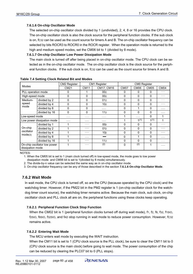
7. Clock Generation Circuit
page 60 854fo7002,03.raM21.1.veR2110-1010B90JER
puorG92/C61M
7.6.1.6 On-chip Oscillator Mode
The selected on-chip oscillator clock divided by 1 (undivided), 2, 4, 8 or 16 provides the CPU clock.The on-chip oscillator clock is also the clock source for the peripheral function clocks. If the sub clockis on, fC32 can be used as the count source for timers A and B. The on-chip oscillator frequency can beselected by bits ROCR3 to ROCR0 in the ROCR register. When the operation mode is returned to thehigh and medium speed modes, set the CM06 bit to 1 (divided by 8 mode).
7.6.1.7 On-chip Oscillator Low Power Dissipation Mode
The main clock is turned off after being placed in on-chip oscillator mode. The CPU clock can be se-lected as in the on-chip oscillator mode. The on-chip oscillator clock is the clock source for the periph-eral function clocks. If the sub clock is on, fC32 can be used as the count source for timers A and B.
Table 7.4 Setting Clock Related Bit and Modes
7.6.2 Wait ModeIn wait mode, the CPU clock is turned off, so are the CPU (because operated by the CPU clock) and thewatchdog timer. However, if the PM22 bit in the PM2 register is 1 (on-chip oscillator clock for the watch-dog timer count source), the watchdog timer remains active. Because the main clock, sub clock, on-chiposcillator clock and PLL clock all are on, the peripheral functions using these clocks keep operating.
7.6.2.1 Peripheral Function Clock Stop Function
When the CM02 bit is 1 (peripheral function clocks turned off during wait mode), f1, f2, f8, f32, f1SIO,f2SIO, f8SIO, f32SIO, and fAD stop running in wait mode to reduce power consumption. However, fC32
remains active.
7.6.2.2 Entering Wait Mode
The MCU enters wait mode by executing the WAIT instruction.When the CM11 bit is set to 1 (CPU clock source is the PLL clock), be sure to clear the CM11 bit to 0(CPU clock source is the main clock) before going to wait mode. The power consumption of the chipcan be reduced by clearing the PLC07 bit to 0 (PLL stops).
1(1)
Modes CM2 Register
CM21CM1 Register
CM11 CM17, CM16CM0 Register
CM07 CM06 CM05 CM04PLL operation mode 0 1 002 0 0High-speed mode 0 0 002 0 0 0Medium-speed mode
0 0 012 0 0 00 0 102 0 0 0
divided by 2
0 0 0 1 00 0 112 0 0 0
Low-speed mode 1 0 1 Low power dissipation mode 1 1
On-chiposcillatormode(3)
1
divided by 4divided by 8divided by 16
On-chip oscillator low power dissipation mode
NOTES: 1. When the CM05 bit is set to 1 (main clock turned off) in low-speed mode, the mode goes to low power dissipation mode and CM06 bit is set to 1(divided by 8 mode) simultaneously. 2. The divide-by-n value can be selected the same way as in on-chip oscillator mode. 3. On-chip oscillator frequency can be any of those described in the section 7.6.1.6 On-chip Oscillator Mode.
0
0
1 012 0 0 01 102 0 0 01 1 01 112 0 0 0
1 002 0 0 0
(2)
divided by 2divided by 4divided by 8divided by 16
divided by 11(1)
(2) 1
0
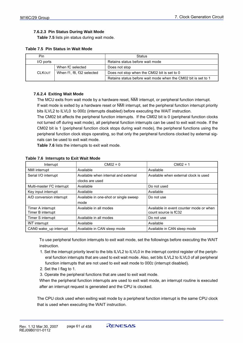
7. Clock Generation Circuit
page 61 854fo7002,03.raM21.1.veR2110-1010B90JER
puorG92/C61M
Table 7.6 Interrupts to Exit Wait Mode
Interrupt CM02 = 0 CM02 = 1NMI interrupt Available AvailableSerial I/O interrupt Available when internal and external Available when external clock is used
clocks are usedMulti-master I2C interrupt Available Do not usedKey input interrupt Available AvailableA/D conversion interrupt Available in one-shot or single sweep Do not use
modeTimer A interrupt Available in all modes Available in event counter mode or whenTimer B interrupt count source is fC32Timer S interrupt Available in all modes Do not use
_______
INT interrupt Available AvailableCAN0 wake_up interrupt Available in CAN sleep mode Available in CAN sleep mode
7.6.2.3 Pin Status During Wait ModeTable 7.5 lists pin status during wait mode.
Table 7.5 Pin Status in Wait Mode
Pin StatusI/O ports Retains status before wait mode
When fC selected Does not stopCLKOUT When f1, f8, f32 selected Does not stop when the CM02 bit is set to 0
Retains status before wait mode when the CM02 bit is set to 1
To use peripheral function interrupts to exit wait mode, set the followings before executing the WAITinstruction.1. Set the interrupt priority level to the bits ILVL2 to ILVL0 in the interrupt control register of the periph-
eral function interrupts that are used to exit wait mode. Also, set bits ILVL2 to ILVL0 of all peripheralfunction interrupts that are not used to exit wait mode to 0002 (interrupt disabled).
2. Set the I flag to 1.3. Operate the peripheral functions that are used to exit wait mode.When the peripheral function interrupts are used to exit wait mode, an interrupt routine is executedafter an interrupt request is generated and the CPU is clocked.
The CPU clock used when exiting wait mode by a peripheral function interrupt is the same CPU clockthat is used when executing the WAIT instruction.
7.6.2.4 Exiting Wait Mode______
The MCU exits from wait mode by a hardware reset, NMI interrupt, or peripheral function interrupt.______
If wait mode is exited by a hardware reset or NMI interrupt, set the peripheral function interrupt prioritybits ILVL2 to ILVL0 to 0002 (interrupts disabled) before executing the WAIT instruction.The CM02 bit affects the peripheral function interrupts. If the CM02 bit is 0 (peripheral function clocksnot turned off during wait mode), all peripheral function interrupts can be used to exit wait mode. If theCM02 bit is 1 (peripheral function clock stops during wait mode), the peripheral functions using theperipheral function clock stops operating, so that only the peripheral functions clocked by external sig-nals can be used to exit wait mode.Table 7.6 lists the interrupts to exit wait mode.
7. Clock Generation Circuit
page 62 854fo7002,03.raM21.1.veR2110-1010B90JER
puorG92/C61M
7.6.3 Stop Mode
In stop mode, all oscillator circuits are turned off, so are the CPU clock and the peripheral function clocks.Therefore, the CPU and the peripheral functions clocked by these clocks stop operating. The least amount ofpower is consumed in this mode. If the voltage applied to Vcc pin is VRAM or more, the internal RAM isretained. When applying 2.7 or less voltage to Vcc pin, make sure Vcc≥VRAM.However, the peripheral functions clocked by external signals keep operating. The following interrupts canbe used to exit stop mode.
______
• NMI interrupt• Key interrupt
______
• INT interrupt• Timer A, Timer B interrupt (when counting external pulses in event counter mode)• Serial I/O interrupt (when external clock is selected)• Low voltage detection interrup (refer to "Low Voltage Detection Interrupt" for an operating condition)• CAN0 Wake_up interrupt (in CAN sleep mode)
7.6.3.1 Entering Stop ModeThe MCU is placed into stop mode by setting the CM10 bit in the CM1 register to 1 (all clocks turned off).At the same time, the CM06 bit in the CM0 register is set to 1 (divide-by-8 mode) and the CM15 bit in theCM10 register is set to 1 (main clock oscillator circuit drive capability high).Before entering stop mode, set the CM20 bit to 0 (oscillation stop, re-oscillation detection function dis-able).Also, if the CM11 bit is 1 (PLL clock for the CPU clock source), set the CM11 bit to 0 (main clock for theCPU clock source) and the PLC07 bit to 0 (PLL turned off) before entering stop mode.
7.6.3.2 Pin Status during Stop ModeThe I/O pins retain their status held just prior to entering stop mode.
7.6.3.3 Exiting Stop Mode______
The MCU is moved out of stop mode by a hardware reset, NMI interrupt or peripheral function interrupt.______
If the MCU is to be moved out of stop mode by a hardware reset or NMI interrupt, set the peripheralfunction interrupt priority bits ILVL2 to ILVL0 to 0002 (interrupts disable) before setting the CM10 bit to 1.If the MCU is to be moved out of stop mode by a peripheral function interrupt, set up the following beforesetting the CM10 bit to 1.
1. In bits ILVL2 to ILVL0 of the interrupt control register, set the interrupt priority level of the peripheralfunction interrupt to be used to exit stop mode.Also, for all of the peripheral function interrupts not used to exit stop mode, set bits ILVL2 to ILVL0 to0002.
2. Set the I flag to 1.3. Enable the peripheral function whose interrupt is to be used to exit stop mode.
In this case, when an interrupt request is generated and the CPU clock is thereby turned on, aninterrupt service routine is executed.
______
Which CPU clock will be used after exiting stop mode by a peripheral function or NMI interrupt is deter-mined by the CPU clock that was on when the MCU was placed into stop mode as follows:If the CPU clock before entering stop mode was derived from the sub clock: sub clockIf the CPU clock before entering stop mode was derived from the main clock: main clock divide-by-8If the CPU clock before entering stop mode was derived from the on-chip oscillator clock: on-chip oscil-lator clock divide-by-8
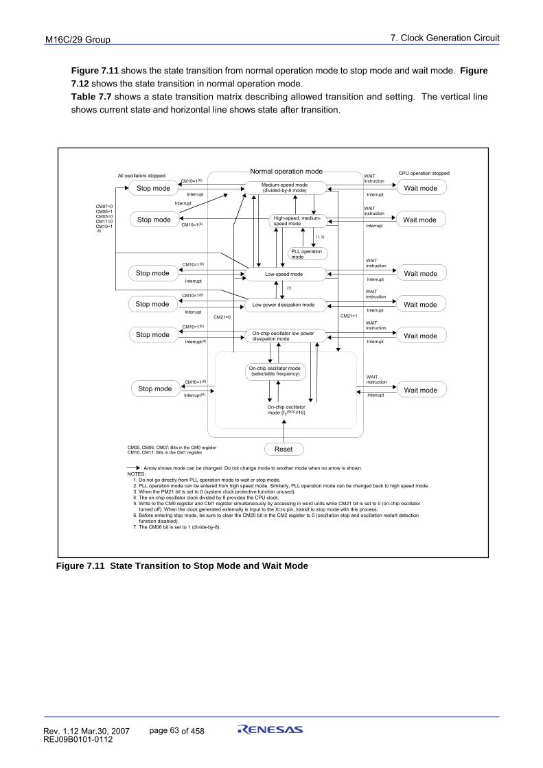
7. Clock Generation Circuit
page 63 854fo7002,03.raM21.1.veR2110-1010B90JER
puorG92/C61M
Figure 7.11 State Transition to Stop Mode and Wait Mode
Reset
Medium-speed mode(divided-by-8 mode)
High-speed, medium-speed modeStop mode Wait mode
Interrupt
Interrupt
Low-speed modeStop mode Interrupt
Wait mode Interrupt
Stop mode
All oscillators stopped
InterruptWait mode
WAIT instruction
Interrupt
CPU operation stopped
PLL operationmode
(1, 2)
Wait mode Interrupt
CM10=1(6)
Interrupt(4)Stop mode
WAIT instruction
WAIT instruction
WAIT instruction
On-chip oscillator mode (selectable frequency)
On-chip oscillatormode (f2
(ROC)/16)
Normal operation mode
CM07=0CM06=1CM05=0CM11=0CM10=1 (5)
On-chip oscillator low powerdissipation mode
Stop mode Interrupt(4)
Wait mode Interrupt
WAIT instruction
CM05, CM06, CM07: Bits in the CM0 registerCM10, CM11: Bits in the CM1 register
CM10=1(6)
CM10=1(6)
CM10=1(6)
CM10=1(6)
Low power dissipation modeStop mode Interrupt
Wait mode Interrupt
WAIT instruction
CM21=1CM21=0
CM10=1(6)
(7)
: Arrow shows mode can be changed. Do not change mode to another mode when no arrow is shown.NOTES:
1. Do not go directly from PLL operation mode to wait or stop mode. 2. PLL operation mode can be entered from high speed mode. Similarly, PLL operation mode can be changed back to high speed mode. 3. When the PM21 bit is set to 0 (system clock protective function unused). 4. The on-chip oscillator clock divided by 8 provides the CPU clock. 5. Write to the CM0 register and CM1 register simultaneously by accessing in word units while CM21 bit is set to 0 (on-chip oscillator
turned off). When the clock generated externally is input to the XCIN pin, transit to stop mode with this process. 6. Before entering stop mode, be sure to clear the CM20 bit in the CM2 register to 0 (oscillation stop and oscillation restart detection
function disabled). 7. The CM06 bit is set to 1 (divide-by-8).
Figure 7.11 shows the state transition from normal operation mode to stop mode and wait mode. Figure7.12 shows the state transition in normal operation mode.Table 7.7 shows a state transition matrix describing allowed transition and setting. The vertical lineshows current state and horizontal line shows state after transition.
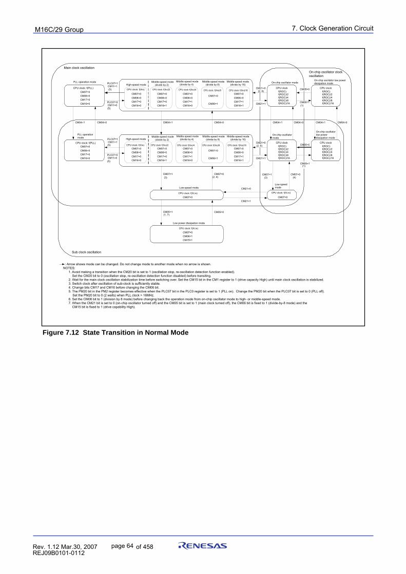
7. Clock Generation Circuit
page 64 854fo7002,03.raM21.1.veR2110-1010B90JER
puorG92/C61M
Figure 7.12 State Transition in Normal Mode
CM04=0
CPU clock: f(PLL)CM07=0CM06=0CM17=0CM16=0
PLL operation mode
CM07=0CM06=0CM17=0CM16=0
CM07=0
CM17=0CM06=0
CM16=0
CM07=0
CM17=0CM06=0
CM16=1
CM07=0
CM17=1CM06=0
CM16=0
CM07=0
CM06=1
CM07=0
CM17=1CM06=0
CM16=1
High-speed mode
CM07=0
CM17=0CM06=0
CM16=0
CM07=0
CM17=0CM06=0
CM16=1
CM07=0
CM17=1CM06=0
CM16=0
CM07=0
CM06=1
CM07=0
CM17=1CM06=0
CM16=1
CM07=0
Low-speed mode
CM07=0
Low power dissipation mode
CM06=1CM15=1
On-chip oscillator mode
CPU clock
On-chip oscillatormode
CPU clock
CPU clock
On-chip oscillator low power dissipation mode
CPU clock
CM07=0
Low-speedmode
PLC07=1CM11=1(5)
PLC07=0CM11=0(5)
CM04=0
PLC07=1CM11=1
PLC07=0CM11=0
CM04=0CM04=1CM04=1 CM04=1 CM04=0CM04=1
CM07=0(2, 4)
CM07=1(3)
CM05=1(1, 7)
CM05=0
CM21=0(2, 6)
CM21=1
CM21=0(2, 6)
CM21=1
CM21=0
CM21=1
Main clock oscillationOn-chip oscillator clock oscillation
Sub clock oscillation
f(ROC)f(ROC)/2f(ROC)/4f(ROC)/8f(ROC)/16
f(ROC)f(ROC)/2f(ROC)/4f(ROC)/8f(ROC)/16
f(ROC)f(ROC)/2f(ROC)/4f(ROC)/8f(ROC)/16
f(ROC)f(ROC)/2f(ROC)/4f(ROC)/8f(ROC)/16
PLL operation mode
CPU clock: f(PLL)CPU clock: f(XIN)
High-speed modeMiddle-speed mode (divide by 2)
CPU clock: f(XIN)/2 CPU clock: f(XIN)/4 CPU clock: f(XIN)/8 CPU clock: f(XIN)/16
CPU clock: f(XCIN)
CPU clock: f(XCIN)
CPU clock: f(XCIN)
CM05=0M0M
CM05=1(1)
CM05=1(1)
CM05=0
(5)
(5)
Middle-speed mode (divide by 4)
Middle-speed mode (divide by 8)
Middle-speed mode (divide by 16)
Middle-speed mode (divide by 2)
Middle-speed mode (divide by 4)
Middle-speed mode (divide by 8)
Middle-speed mode (divide by 16)
CPU clock: f(XIN) CPU clock: f(XIN)/2 CPU clock: f(XIN)/4 CPU clock: f(XIN)/8 CPU clock: f(XIN)/16
On-chip oscillator low power dissipation mode
: Arrow shows mode can be changed. Do not change mode to another mode when no arrow is shown.NOTES: 1. Avoid making a transition when the CM20 bit is set to 1 (oscillation stop, re-oscillation detection function enabled). Set the CM20 bit to 0 (oscillation stop, re-oscillation detection function disabled) before transiting. 2. Wait for the main clock oscillation stabilization time before switching over. Set the CM15 bit in the CM1 register to 1 (drive capacity High) until main clock oscillation is stabilized. 3. Switch clock after oscillation of sub-clock is sufficiently stable. 4. Change bits CM17 and CM16 before changing the CM06 bit. 5. The PM20 bit in the PM2 register becomes effective when the PLC07 bit in the PLC0 register is set to 1 (PLL on). Change the PM20 bit when the PLC07 bit is set to 0 (PLL off). Set the PM20 bit to 0 (2 waits) when PLL clock > 16MHz. 6. Set the CM06 bit to 1 (division by 8 mode) before changing back the operation mode from on-chip oscillator mode to high- or middle-speed mode. 7. When the CM21 bit is set to 0 (on-chip oscillator turned off) and the CM05 bit is set to 1 (main clock turned off), the CM06 bit is fixed to 1 (divide-by-8 mode) and the CM15 bit is fixed to 1 (drive capability High).
CM07=1 (3)
CM07=0 (4)
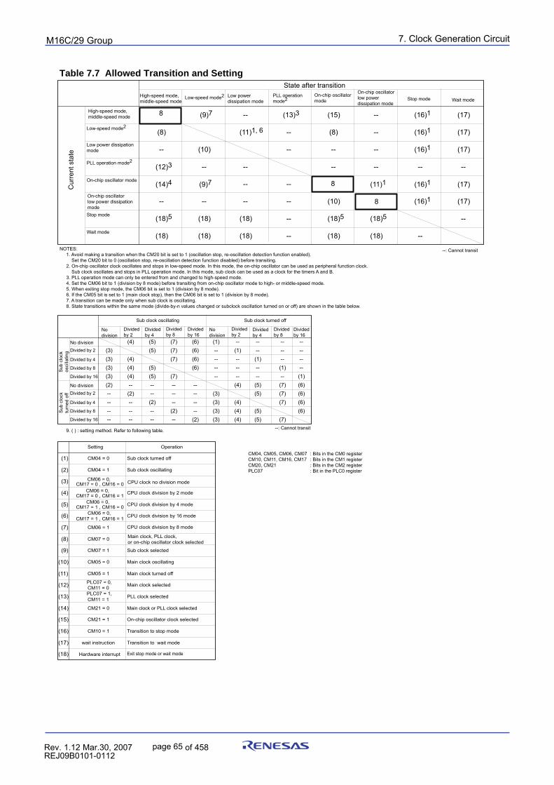
7. Clock Generation Circuit
page 65 854fo7002,03.raM21.1.veR2110-1010B90JER
puorG92/C61M
Table 7.7 Allowed Transition and Setting
High-speed mode, middle-speed mode
On-chip oscillator mode
Stop mode
Wait mode
On-chip oscillatorlow power dissipationmode
PLL operation mode2
Low power dissipationmode
Low-speed mode2
Cur
rent
sta
te
State after transition
8
--
(8)
(18)5
(9)7 --
(10)
(11)1, 6
(12)3
(14)4
--
-- --
--
(13)3 (15) --
--
--
--
--
--
(10)
--
--
--
-- -- --
--
--
(18)(18) --
--
(16)1 (17)
(16)1 (17)
(16)1 (17)
(16)1 (17)
(16)1 (17)
-- --
(18)5 (18)5
(18)(18)(18)(18)(18)
(1)
(2)
(3)
(4)
(5)
(6)
(7)
(8)
(9)
(10)
(11)
(12)
(13)
(14)
(15)
(16)
(17)
(18)
Setting Operation
CM04 = 0 Sub clock turned off
CM04 = 1 Sub clock oscillating
CM06 = 0, CPU clock no division modeCM17 = 0 , CM16 = 0CM06 = 0, CPU clock division by 2 modeCM17 = 0 , CM16 = 1CM06 = 0, CPU clock division by 4 modeCM17 = 1 , CM16 = 0
CM06 = 1 CPU clock division by 8 mode
CM06 = 0, CPU clock division by 16 modeCM17 = 1 , CM16 = 1
CM07 = 0 Main clock, PLL clock, or on-chip oscillator clock selected
CM07 = 1 Sub clock selected
CM05 = 0 Main clock oscillating
CM05 = 1 Main clock turned off
PLC07 = 0,CM11 = 0 Main clock selected
PLC07 = 1,CM11 = 1 PLL clock selected
CM21 = 0 Main clock or PLL clock selected
CM21 = 1 On-chip oscillator clock selected
CM10 = 1 Transition to stop mode
wait instruction Transition to wait mode
Hardware interrupt Exit stop mode or wait mode
NOTES: 1. Avoid making a transition when the CM20 bit is set to 1 (oscillation stop, re-oscillation detection function enabled). Set the CM20 bit to 0 (oscillation stop, re-oscillation detection function disabled) before transiting. 2. On-chip oscillator clock oscillates and stops in low-speed mode. In this mode, the on-chip oscillator can be used as peripheral function clock. Sub clock oscillates and stops in PLL operation mode. In this mode, sub clock can be used as a clock for the timers A and B. 3. PLL operation mode can only be entered from and changed to high-speed mode. 4. Set the CM06 bit to 1 (division by 8 mode) before transiting from on-chip oscillator mode to high- or middle-speed mode. 5. When exiting stop mode, the CM06 bit is set to 1 (division by 8 mode). 6. If the CM05 bit is set to 1 (main clock stop), then the CM06 bit is set to 1 (division by 8 mode). 7. A transition can be made only when sub clock is oscillating. 8. State transitions within the same mode (divide-by-n values changed or subclock oscillation turned on or off) are shown in the table below.
--: Cannot transit
(11)1
High-speed mode, middle-speed mode
On-chip oscillatormode Stop mode Wait mode
On-chip oscillatorlow powerdissipation mode
PLL operationmode2
Low powerdissipation mode
Low-speed mode2
8
8
(3)(3)
(3)(3)
(4)
(4)(4)(4)
(5)(7)(7)
(5)(5)
(5)
(7)
(7)
(6)
(6)(6)(6)
No division
Divided by 2
(3)(3)
(3)(3)
(4)
(4)(4)(4)
(5)
(5)(5)
(5) (7)(7)
(7)
(7)
(6)
(6)(6)(6)
(1)(1)
(1)(1)
(1)(2)
(2)(2)
(2)(2)
----
-- --
--------
------
----
------ -- --
-- --
----
----
----
------
---- --
--
--
----
----
--
--
Sub clock oscillating Sub clock turned off
--: Cannot transit
Divided by 4
Divided by 8
Divided by 16
No division
Divided by 2
Dividedby 4
Divided by 8
Divided by 16
No division
Divided by 4
Sub
clo
ck
osci
llatin
gS
ub c
lock
tu
rned
off
Divided by 8
Divided by 16
Divided by 2
No division
Divided by 4
Divided by 8
Divided by 16
Divided by 2
9. ( ) : setting method. Refer to following table.
CM04, CM05, CM06, CM07 : Bits in the CM0 registerCM10, CM11, CM16, CM17 : Bits in the CM1 registerCM20, CM21 : Bits in the CM2 registerPLC07 : Bit in the PLC0 register
(9)7
(8)
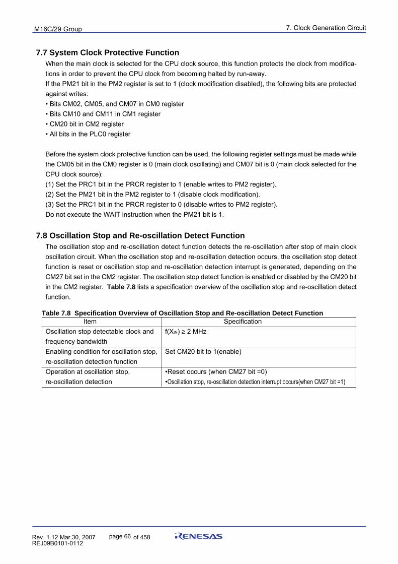
7. Clock Generation Circuit
page 66 854fo7002,03.raM21.1.veR2110-1010B90JER
puorG92/C61M
7.7 System Clock Protective FunctionWhen the main clock is selected for the CPU clock source, this function protects the clock from modifica-tions in order to prevent the CPU clock from becoming halted by run-away.If the PM21 bit in the PM2 register is set to 1 (clock modification disabled), the following bits are protectedagainst writes:• Bits CM02, CM05, and CM07 in CM0 register• Bits CM10 and CM11 in CM1 register• CM20 bit in CM2 register• All bits in the PLC0 register
Before the system clock protective function can be used, the following register settings must be made whilethe CM05 bit in the CM0 register is 0 (main clock oscillating) and CM07 bit is 0 (main clock selected for theCPU clock source):(1) Set the PRC1 bit in the PRCR register to 1 (enable writes to PM2 register).(2) Set the PM21 bit in the PM2 register to 1 (disable clock modification).(3) Set the PRC1 bit in the PRCR register to 0 (disable writes to PM2 register).Do not execute the WAIT instruction when the PM21 bit is 1.
7.8 Oscillation Stop and Re-oscillation Detect FunctionThe oscillation stop and re-oscillation detect function detects the re-oscillation after stop of main clockoscillation circuit. When the oscillation stop and re-oscillation detection occurs, the oscillation stop detectfunction is reset or oscillation stop and re-oscillation detection interrupt is generated, depending on theCM27 bit set in the CM2 register. The oscillation stop detect function is enabled or disabled by the CM20 bitin the CM2 register. Table 7.8 lists a specification overview of the oscillation stop and re-oscillation detectfunction.
Table 7.8 Specification Overview of Oscillation Stop and Re-oscillation Detect FunctionItem Specification
Oscillation stop detectable clock and f(XIN) ≥ 2 MHzfrequency bandwidthEnabling condition for oscillation stop, Set CM20 bit to 1(enable)re-oscillation detection functionOperation at oscillation stop, •Reset occurs (when CM27 bit =0)re-oscillation detection •Oscillation stop, re-oscillation detection interrupt occurs(when CM27 bit =1)
7. Clock Generation Circuit
page 67 854fo7002,03.raM21.1.veR2110-1010B90JER
puorG92/C61M
7.8.1 Operation When CM27 bit = 0 (Oscillation Stop Detection Reset)When main clock stop is detected when the CM20 bit is 1 (oscillation stop, re-oscillation detection func-tion enabled), the MCU is initialized, coming to a halt (oscillation stop reset; refer to “SFR”, “Reset”).This status is reset with hardware reset 1. Also, even when re-oscillation is detected, the MCU can beinitialized and stopped; it is, however, necessary to avoid such usage. (During main clock stop, do not setthe CM20 bit to 1 and the CM27 bit to 0.)
7.8.2 Operation When CM27 bit = 1 (Oscillation Stop and Re-oscillation Detect Interrupt)
When the main clock corresponds to the CPU clock source and the CM20 bit is 1 (oscillation stop and re-oscillation detect function enabled), the system is placed in the following state if the main clock comes toa halt:• Oscillation stop and re-oscillation detect interrupt request occurs.• The on-chip oscillator starts oscillation, and the on-chip oscillator clock becomes the CPU clock and clock source for peripheral functions in place of the main clock.• CM21 bit = 1 (on-chip oscillator clock for CPU clock source)• CM22 bit = 1 (main clock stop detected)• CM23 bit = 1 (main clock stopped)
When the PLL clock corresponds to the CPU clock source and the CM20 bit is 1, the system is placed inthe following state if the main clock comes to a halt: Since the CM21 bit remains unchanged, set it to 1(on-chip oscillator clock) inside the interrupt routine.• Oscillation stop and re-oscillation detect interrupt request occurs.• CM22 bit = 1 (main clock stop detected)• CM23 bit = 1 (main clock stopped)• CM21 bit remains unchanged
When the CM20 bit is 1, the system is placed in the following state if the main clock re-oscillates from thestop condition:• Oscillation stop and re-oscillation detect interrupt request occurs.• CM22 bit = 1 (main clock re-oscillation detected)• CM23 bit = 0 (main clock oscillation)• CM21 bit remains unchanged
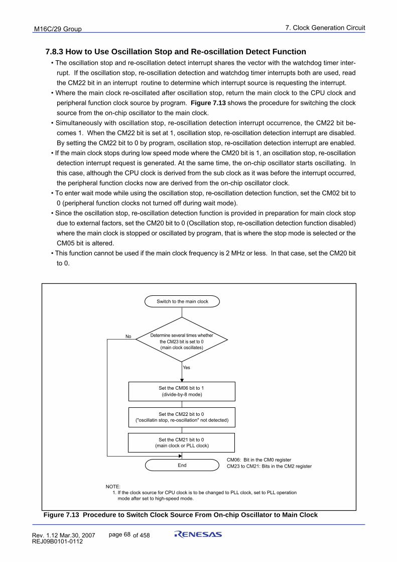
7. Clock Generation Circuit
page 68 854fo7002,03.raM21.1.veR2110-1010B90JER
puorG92/C61M
Switch to the main clock
Determine several times whether the CM23 bit is set to 0 (main clock oscillates)
Set the CM22 bit to 0 ("oscillatin stop, re-oscillation" not detected)
Set the CM06 bit to 1 (divide-by-8 mode)
Set the CM21 bit to 0 (main clock or PLL clock)
CM06: Bit in the CM0 registerCM23 to CM21: Bits in the CM2 register
Yes
No
End
NOTE: 1. If the clock source for CPU clock is to be changed to PLL clock, set to PLL operation mode after set to high-speed mode.
7.8.3 How to Use Oscillation Stop and Re-oscillation Detect Function• The oscillation stop and re-oscillation detect interrupt shares the vector with the watchdog timer inter-
rupt. If the oscillation stop, re-oscillation detection and watchdog timer interrupts both are used, readthe CM22 bit in an interrupt routine to determine which interrupt source is requesting the interrupt.
• Where the main clock re-oscillated after oscillation stop, return the main clock to the CPU clock andperipheral function clock source by program. Figure 7.13 shows the procedure for switching the clocksource from the on-chip oscillator to the main clock.
• Simultaneously with oscillation stop, re-oscillation detection interrupt occurrence, the CM22 bit be-comes 1. When the CM22 bit is set at 1, oscillation stop, re-oscillation detection interrupt are disabled.By setting the CM22 bit to 0 by program, oscillation stop, re-oscillation detection interrupt are enabled.
• If the main clock stops during low speed mode where the CM20 bit is 1, an oscillation stop, re-oscillationdetection interrupt request is generated. At the same time, the on-chip oscillator starts oscillating. Inthis case, although the CPU clock is derived from the sub clock as it was before the interrupt occurred,the peripheral function clocks now are derived from the on-chip oscillator clock.
• To enter wait mode while using the oscillation stop, re-oscillation detection function, set the CM02 bit to0 (peripheral function clocks not turned off during wait mode).
• Since the oscillation stop, re-oscillation detection function is provided in preparation for main clock stopdue to external factors, set the CM20 bit to 0 (Oscillation stop, re-oscillation detection function disabled)where the main clock is stopped or oscillated by program, that is where the stop mode is selected or theCM05 bit is altered.
• This function cannot be used if the main clock frequency is 2 MHz or less. In that case, set the CM20 bitto 0.
Figure 7.13 Procedure to Switch Clock Source From On-chip Oscillator to Main Clock
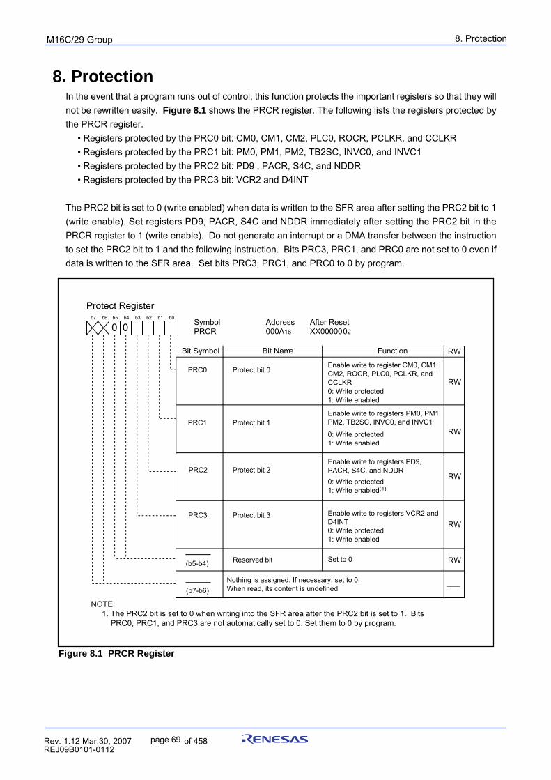
8. ProtectionpuorG92/C61M
page 69 854fo7002,03.raM21.1.veR2110-1010B90JER
8. ProtectionIn the event that a program runs out of control, this function protects the important registers so that they willnot be rewritten easily. Figure 8.1 shows the PRCR register. The following lists the registers protected bythe PRCR register.
• Registers protected by the PRC0 bit: CM0, CM1, CM2, PLC0, ROCR, PCLKR, and CCLKR• Registers protected by the PRC1 bit: PM0, PM1, PM2, TB2SC, INVC0, and INVC1• Registers protected by the PRC2 bit: PD9 , PACR, S4C, and NDDR• Registers protected by the PRC3 bit: VCR2 and D4INT
The PRC2 bit is set to 0 (write enabled) when data is written to the SFR area after setting the PRC2 bit to 1(write enable). Set registers PD9, PACR, S4C and NDDR immediately after setting the PRC2 bit in thePRCR register to 1 (write enable). Do not generate an interrupt or a DMA transfer between the instructionto set the PRC2 bit to 1 and the following instruction. Bits PRC3, PRC1, and PRC0 are not set to 0 even ifdata is written to the SFR area. Set bits PRC3, PRC1, and PRC0 to 0 by program.
Protect Register
Symbol Address After ResetPRCR 000A16 XX0000002
Bit NameBit Symbol
b7 b6 b5 b4 b3 b2 b1 b0
PRC1
PRC0
PRC2
Function RW
0
RW
RW
RW
Nothing is assigned. If necessary, set to 0. When read, its content is undefined
Reserved bit Set to 0 RW
Protect bit 0
Protect bit 1
Protect bit 2
PRC3 RW
Protect bit 3 Enable write to registers VCR2 and D4INT
(b5-b4)
(b7-b6)
0
NOTE: 1. The PRC2 bit is set to 0 when writing into the SFR area after the PRC2 bit is set to 1. Bits PRC0, PRC1, and PRC3 are not automatically set to 0. Set them to 0 by program.
Enable write to register CM0, CM1,CM2, ROCR, PLC0, PCLKR, and CCLKR
Enable write to registers PM0, PM1, PM2, TB2SC, INVC0, and INVC1
0: Write protected1: Write enabled
0: Write protected1: Write enabled
Enable write to registers PD9, PACR, S4C, and NDDR0: Write protected1: Write enabled(1)
0: Write protected1: Write enabled
Figure 8.1 PRCR Register
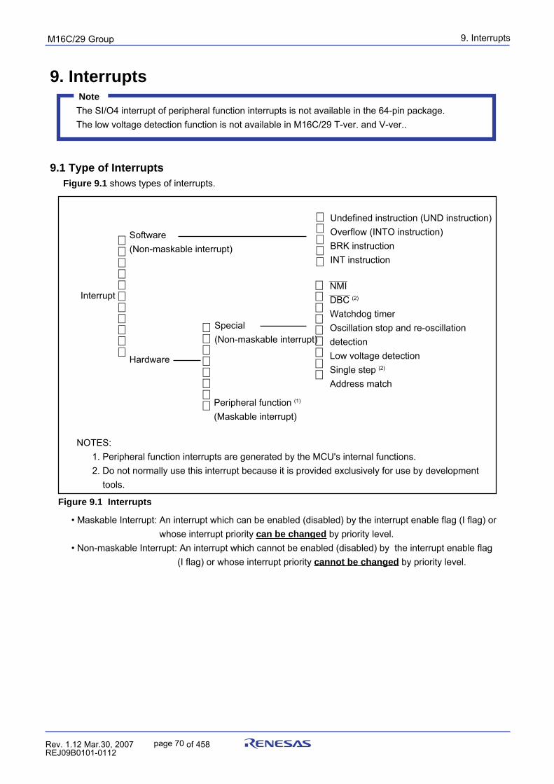
9. InterruptspuorG92/C61M
page 70 854fo7002,03.raM21.1.veR2110-1010B90JER
• Maskable Interrupt: An interrupt which can be enabled (disabled) by the interrupt enable flag (I flag) or whose interrupt priority can be changed by priority level.• Non-maskable Interrupt: An interrupt which cannot be enabled (disabled) by the interrupt enable flag (I flag) or whose interrupt priority cannot be changed by priority level.
Figure 9.1 Interrupts
Interrupt
Software
(Non-maskable interrupt)
Hardware
Special
(Non-maskable interrupt)
Peripheral function (1)
(Maskable interrupt)
Undefined instruction (UND instruction)Overflow (INTO instruction)BRK instructionINT instruction
_______
NMI________
DBC (2)
Watchdog timerOscillation stop and re-oscillationdetectionLow voltage detectionSingle step (2)
Address match
NOTES: 1. Peripheral function interrupts are generated by the MCU's internal functions. 2. Do not normally use this interrupt because it is provided exclusively for use by development tools.
9. Interrupts Note
The SI/O4 interrupt of peripheral function interrupts is not available in the 64-pin package.The low voltage detection function is not available in M16C/29 T-ver. and V-ver..
9.1 Type of InterruptsFigure 9.1 shows types of interrupts.
9. InterruptspuorG92/C61M
page 71 854fo7002,03.raM21.1.veR2110-1010B90JER
9.1.1 Software InterruptsA software interrupt occurs when executing certain instructions. Software interrupts are non-maskableinterrupts.
9.1.1.1 Undefined Instruction Interrupt
An undefined instruction interrupt occurs when executing the UND instruction.
9.1.1.2 Overflow Interrupt
An overflow interrupt occurs when executing the INTO instruction with the O flag set to 1 (the opera-tion resulted in an overflow). The following are instructions whose O flag changes by arithmetic: ABS,ADC, ADCF, ADD, CMP, DIV, DIVU, DIVX, NEG, RMPA, SBB, SHA, SUB
9.1.1.3 BRK Interrupt
A BRK interrupt occurs when executing the BRK instruction.
9.1.1.4 INT Instruction Interrupt
An INT instruction interrupt occurs when executing the INT instruction. Software interrupt Nos. 0 to 63can be specified for the INT instruction. Because software interrupt Nos. 1 to 31 are assigned toperipheral function interrupts, the same interrupt routine as for peripheral function interrupts can beexecuted by executing the INT instruction.In software interrupt Nos. 0 to 31, the U flag is saved to the stack during instruction execution and iscleared to 0 (ISP selected) before executing an interrupt sequence. The U flag is restored from thestack when returning from the interrupt routine. In software interrupt Nos. 32 to 63, the U flag does notchange state during instruction execution, and the SP then selected is used.
9. InterruptspuorG92/C61M
page 72 854fo7002,03.raM21.1.veR2110-1010B90JER
9.1.2 Hardware InterruptsHardware interrupts are classified into two types — special interrupts and peripheral function interrupts.
9.1.2.1 Special Interrupts
Special interrupts are non-maskable interrupts.
_______
9.1.2.1.1 NMI Interrupt_______ _______
An NMI interrupt is generated when input on the NMI pin changes state from high to low. For details_______
about the NMI interrupt, refer to the section "NMI interrupt".
________
9.1.2.1.2 DBC Interrupt
This interrupt is exclusively for debugger, do not use in any other circumstances.
9.1.2.1.3 Watchdog Timer Interrupt
Generated by the watchdog timer. Once a watchdog timer interrupt is generated, be sure to initializethe watchdog timer. For details about the watchdog timer, refer to the section "watchdog timer".
9.1.2.1.4 Oscillation Stop and Re-oscillation Detection Interrupt
Generated by the oscillation stop and re-oscillation detection function. For details about the oscilla-tion stop and re-oscillation detection function, refer to the section "clock generating circuit".
9.1.2.1.5 Low Voltage Detection Interrupt
Generated by the voltage detection circuit. For details about the voltage detection circuit, refer to thesection "voltage detection circuit".
9.1.2.1.6 Single-step Interrupt
Do not normally use this interrupt because it is provided exclusively for use by development tools.
9.1.2.1.7 Address Match Interrupt
An address match interrupt is generated immediately before executing the instruction at the addressindicated by the RMAD0 or RMAD1 register, if the corresponding enable bit (AIER0 or AIER1 bit inthe AIER register) is set to 1. For details about the address match interrupt, refer to the section“address match interrupt”.
9.1.2.2 Peripheral Function Interrupts
Peripheral function interrupts are maskable interrupts and generated by the MCU's internal functions.The interrupt sources for peripheral function interrupts are listed in Table 9.2 Relocatable VectorTables. For details about the peripheral functions, refer to the description of each peripheral functionin this manual.
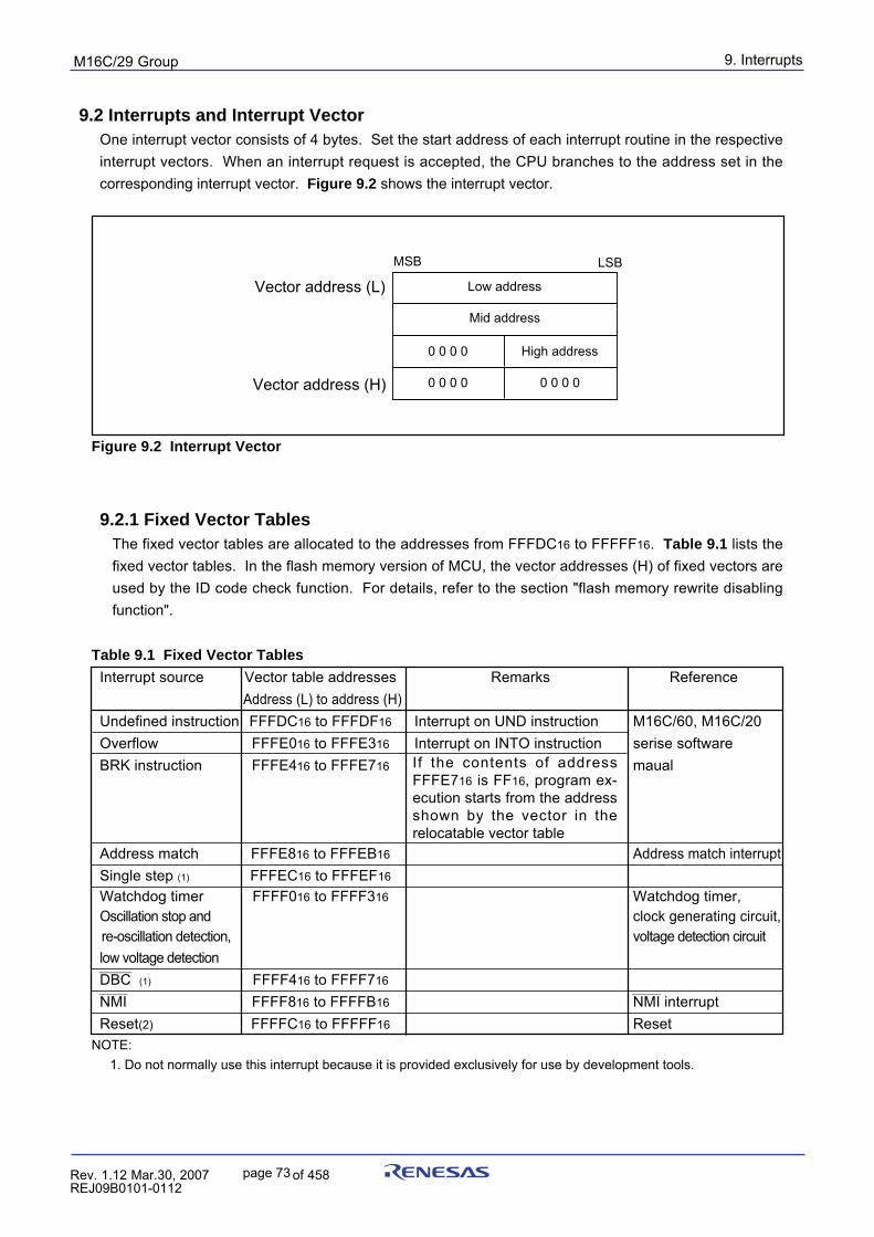
9. InterruptspuorG92/C61M
page 73 854fo7002,03.raM21.1.veR2110-1010B90JER
Interrupt source Vector table addresses Remarks Reference Address (L) to address (H)
Undefined instruction FFFDC16 to FFFDF16 Interrupt on UND instruction M16C/60, M16C/20Overflow FFFE016 to FFFE316 Interrupt on INTO instruction serise softwareBRK instruction FFFE416 to FFFE716 maual
Address match FFFE816 to FFFEB16 Address match interruptSingle step (1) FFFEC16 to FFFEF16
Watchdog timer FFFF016 to FFFF316 Watchdog timer,Oscillation stop and clock generating circuit,
re-oscillation detection, voltage detection circuitlow voltage detection________
DBC (1) FFFF416 to FFFF716_______
NMI FFFF816 to FFFFB16_______
NMI interruptReset(2) FFFFC16 to FFFFF16 Reset
NOTE: 1. Do not normally use this interrupt because it is provided exclusively for use by development tools.
Figure 9.2 Interrupt Vector
9.2 Interrupts and Interrupt VectorOne interrupt vector consists of 4 bytes. Set the start address of each interrupt routine in the respectiveinterrupt vectors. When an interrupt request is accepted, the CPU branches to the address set in thecorresponding interrupt vector. Figure 9.2 shows the interrupt vector.
9.2.1 Fixed Vector TablesThe fixed vector tables are allocated to the addresses from FFFDC16 to FFFFF16. Table 9.1 lists thefixed vector tables. In the flash memory version of MCU, the vector addresses (H) of fixed vectors areused by the ID code check function. For details, refer to the section "flash memory rewrite disablingfunction".
Table 9.1 Fixed Vector Tables
If the contents of addressFFFE716 is FF16, program ex-ecution starts from the addressshown by the vector in therelocatable vector table
Mid address
Low address
0 0 0 0 High address
0 0 0 0 0 0 0 0
Vector address (L)LSBMSB
Vector address (H)
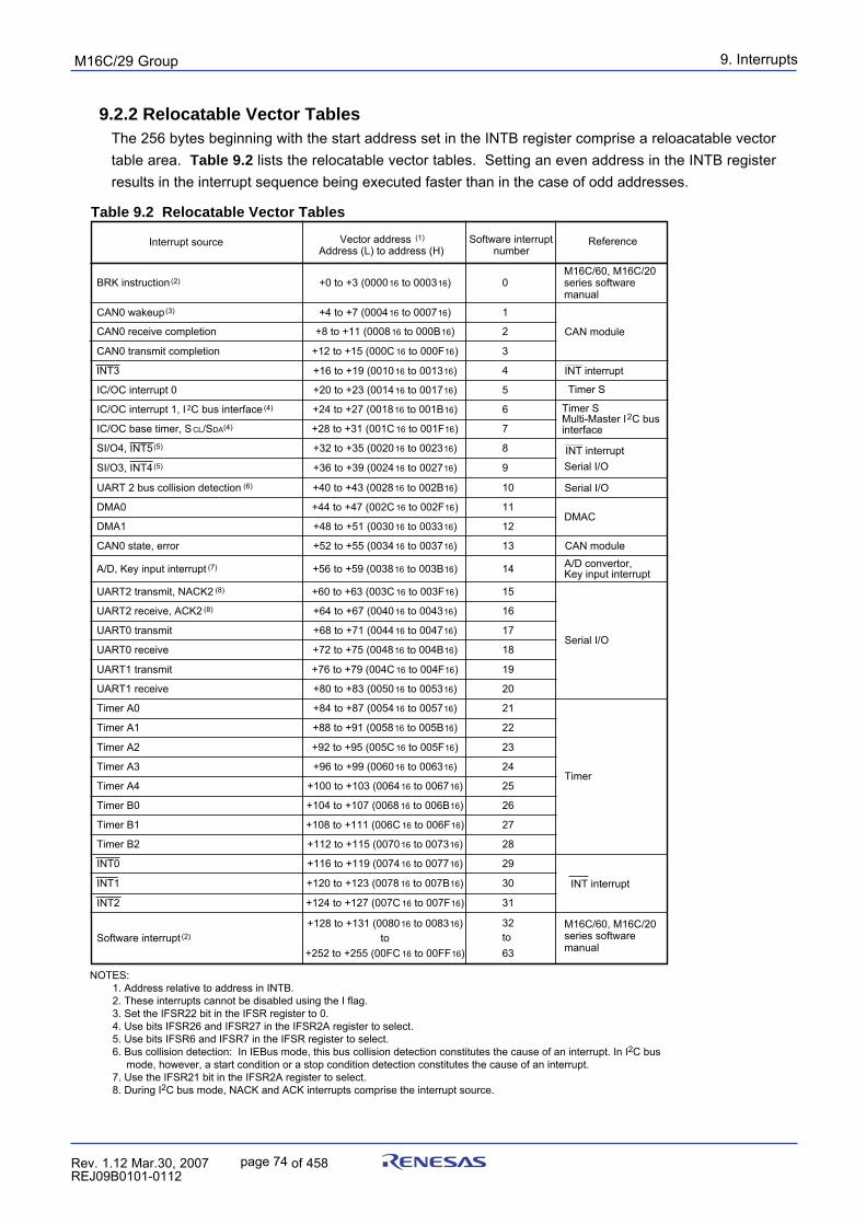
9. InterruptspuorG92/C61M
page 74 854fo7002,03.raM21.1.veR2110-1010B90JER
Table 9.2 Relocatable Vector Tables
9.2.2 Relocatable Vector TablesThe 256 bytes beginning with the start address set in the INTB register comprise a reloacatable vectortable area. Table 9.2 lists the relocatable vector tables. Setting an even address in the INTB registerresults in the interrupt sequence being executed faster than in the case of odd addresses.
Software interrupt number
ReferenceVector address (1)
Address (L) to address (H)
0
11
12
13
14
17
18
19
20
21
22
23
24
25
26
27
28
29
30
31
32
63to
10
15
16
5
6
7
8
4
9
1
Interrupt source
BRK instruction(2)
INT3
SI/O3, INT4(5)
SI/O4, INT5(5)
IC/OC interrupt 1, I 2C bus interface (4)
IC/OC interrupt 0
DMA0
DMA1
A/D, Key input interrupt (7)
UART0 transmit
UART0 receive
UART1 transmit
UART1 receive
Timer A0
Timer A1
Timer A2
Timer A3
Timer A4
Timer B0
Timer B1
Timer B2
INT0
INT1
INT2
Software interrupt (2)
UART 2 bus collision detection (6)
UART2 transmit, NACK2 (8)
UART2 receive, ACK2 (8)
IC/OC base timer, S CL/SDA(4)
M16C/60, M16C/20 series software manual
INT interrupt
Timer SMulti-Master I2C businterface
CAN module
INT interruptSerial I/O
DMAC
A/D convertor,Key input interrupt
Serial I/O
Timer
INT interrupt
M16C/60, M16C/20 series software manual
CAN0 wakeup(3)
+0 to +3 (000016 to 000316)
+44 to +47 (002C 16 to 002F16)
+48 to +51 (003016 to 003316)
+52 to +55 (003416 to 003716)
+56 to +59 (003816 to 003B16)
+68 to +71 (004416 to 004716)
+72 to +75 (004816 to 004B16)
+76 to +79 (004C 16 to 004F16)
+80 to +83 (005016 to 005316)
+84 to +87 (005416 to 005716)
+88 to +91 (005816 to 005B16)
+92 to +95 (005C 16 to 005F16)
+96 to +99 (006016 to 006316)
+100 to +103 (006416 to 006716)
+104 to +107 (0068 16 to 006B16)
+108 to +111 (006C 16 to 006F16)
+112 to +115 (007016 to 007316)
+116 to +119 (007416 to 007716)
+120 to +123 (0078 16 to 007B16)
+124 to +127 (007C 16 to 007F16)
+128 to +131 (008016 to 008316)
+252 to +255 (00FC 16 to 00FF16)
+40 to +43 (002816 to 002B16)
+60 to +63 (003C 16 to 003F16)
+64 to +67 (004016 to 004316)
+20 to +23 (001416 to 001716)
+24 to +27 (001816 to 001B16)
+28 to +31 (001C 16 to 001F16)
+32 to +35 (002016 to 002316)
+16 to +19 (001016 to 001316)
+36 to +39 (002416 to 002716)
to
2
3
+4 to +7 (000416 to 000716)
+8 to +11 (000816 to 000B16)
+12 to +15 (000C 16 to 000F16)
CAN0 receive completion
CAN0 transmit completion
Timer S
Serial I/O
CAN0 state, error CAN module
NOTES:1. Address relative to address in INTB.2. These interrupts cannot be disabled using the I flag.3. Set the IFSR22 bit in the IFSR register to 0.4. Use bits IFSR26 and IFSR27 in the IFSR2A register to select.5. Use bits IFSR6 and IFSR7 in the IFSR register to select.6. Bus collision detection: In IEBus mode, this bus collision detection constitutes the cause of an interrupt. In I2C bus
mode, however, a start condition or a stop condition detection constitutes the cause of an interrupt.7. Use the IFSR21 bit in the IFSR2A register to select.8. During I2C bus mode, NACK and ACK interrupts comprise the interrupt source.
9. InterruptspuorG92/C61M
page 75 854fo7002,03.raM21.1.veR2110-1010B90JER
9.3 Interrupt ControlThe following describes how to enable/disable the maskable interrupts, and how to set the priority in whichorder they are accepted. What is explained here does not apply to nonmaskable interrupts.Use I flag in the the FLG register, IPL, and bits ILVL2 to ILVL0 in the each interrupt control register toenable/disable the maskable interrupts. Whether an interrupt is requested is indicated by the IR bit in eachinterrupt control register.Figure 9.3 shows the interrupt control registers.
Also, the following interrupts share a vector and an interrupt control register.
________
•INT4 and SIO3________
•INT5 and SIO4•A/D converter and key input interrupt•IC/OC base timer and SCL/SDA
•IC/OC interrupt 1 and I2C bus interface
An interrupt request is set by bits IFSR6 and IFSR7 in the IFSR register and bits IFSR27, IFSR26, andIFSR21 in the IFSR2A register. Figure 9.4 shows registers IFSR register and IFSR2A.
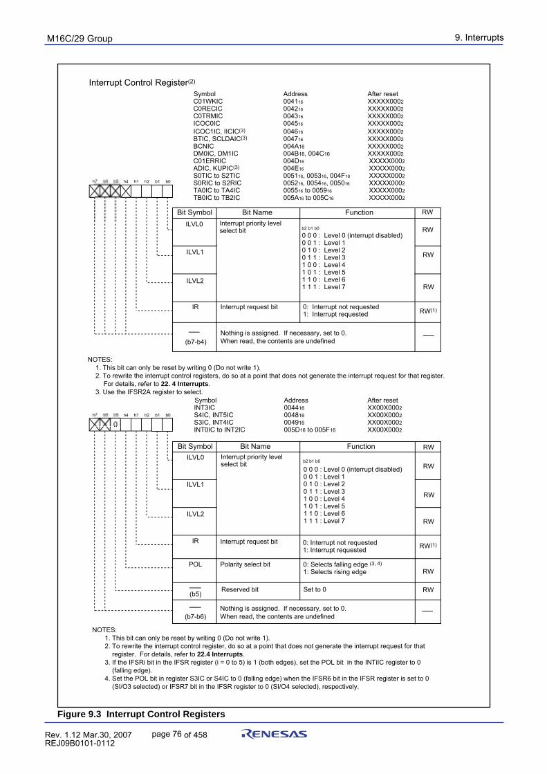
9. InterruptspuorG92/C61M
page 76 854fo7002,03.raM21.1.veR2110-1010B90JER
Figure 9.3 Interrupt Control RegistersC01WKIC, C0RECIC, C0TRMIC, ICOC0IC, ICOC1IC, IICIC, BTIC, SCLDAIC, BCNIC, DM0IC, DM1IC, C01ERRIC, ADIC, KUPIC, S0TIC to S2TIC, S0RIC to S2RIC, TA0IC to TA4IC, TB0IC to TB2IC, INT3IC, S4IC, INT5IC, S31C, INT4IC, INT0IC to INT2IC Registers
Symbol Address After resetINT3IC 004416 XX00X0002S4IC, INT5IC 004816 XX00X0002S3IC, INT4IC 004916 XX00X0002INT0IC to INT2IC 005D16 to 005F16 XX00X0002
Bit Name FunctionBit Symbol
b b4 b3 b2 b1 b0
ILVL0
IR
POL
Interrupt priority level select bit
Interrupt request bit
Polarity select bit
Reserved bit
0: Interrupt not requested1: Interrupt requested
0: Selects falling edge (3, 4)
1: Selects rising edge
Set to 0
ILVL1
ILVL2
Interrupt Control Register(2)
b b4 b3 b2 b1 b0
Bit Name FunctionBit Symbol RW
Symbol Address After reset C01WKIC 004116 XXXXX0002C0RECIC 004216 XXXXX0002C0TRMIC 004316 XXXXX0002ICOC0IC 004516 XXXXX0002ICOC1IC, IICIC(3) 004616 XXXXX0002BTIC, SCLDAIC(3) 004716 XXXXX0002BCNIC 004A16 XXXXX0002DM0IC, DM1IC 004B16, 004C16 XXXXX0002C01ERRIC 004D16 XXXXX0002ADIC, KUPIC(3) 004E16 XXXXX0002S0TIC to S2TIC 005116, 005316, 004F16 XXXXX0002S0RIC to S2RIC 005216, 005416, 005016 XXXXX0002TA0IC to TA4IC 005516 to 005916 XXXXX0002TB0IC to TB2IC 005A16 to 005C16 XXXXX0002
ILVL0
IR
Interrupt priority level select bit
Interrupt request bit 0: Interrupt not requested1: Interrupt requested
ILVL1
ILVL2
0 0 0 : Level 0 (interrupt disabled)0 0 1 : Level 1 0 1 0 : Level 2 0 1 1 : Level 3 1 0 0 : Level 4 1 0 1 : Level 5 1 1 0 : Level 6 1 1 1 : Level 7
b2 b1 b0
0 0 0 : Level 0 (interrupt disabled)0 0 1 : Level 1 0 1 0 : Level 2 0 1 1 : Level 3 1 0 0 : Level 4 1 0 1 : Level 5 1 1 0 : Level 6 1 1 1 : Level 7
b2 b1 b0
0
RW
RW
RW
RW(1)
(b7-b4)
RW
RW
RW
RW
RW
RW
(b7-b6)
(b5)
RW(1)
NOTES:1. This bit can only be reset by writing 0 (Do not write 1). 2. To rewrite the interrupt control registers, do so at a point that does not generate the interrupt request for that register.
For details, refer to 22. 4 Interrupts.3. Use the IFSR2A register to select.
NOTES: 1. This bit can only be reset by writing 0 (Do not write 1). 2. To rewrite the interrupt control register, do so at a point that does not generate the interrupt request for that
register. For details, refer to 22.4 Interrupts. 3. If the IFSRi bit in the IFSR register (i = 0 to 5) is 1 (both edges), set the POL bit in the INTiIC register to 0
(falling edge). 4. Set the POL bit in register S3IC or S4IC to 0 (falling edge) when the IFSR6 bit in the IFSR register is set to 0
(SI/O3 selected) or IFSR7 bit in the IFSR register to 0 (SI/O4 selected), respectively.
Nothing is assigned. If necessary, set to 0.When read, the contents are undefined
Nothing is assigned. If necessary, set to 0.When read, the contents are undefined
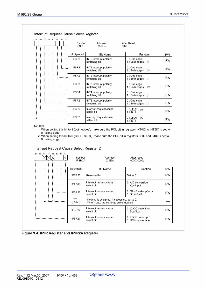
9. InterruptspuorG92/C61M
page 77 854fo7002,03.raM21.1.veR2110-1010B90JER
Figure 9.4 IFSR Register and IFSR2A Register
Interrupt Request Cause Select Register
Bit Name FunctionBit Symbol RW
Symbol Address After Reset IFSR 035F16 0016
IFSR0
b7 b6 b5 b4 b3 b2 b1 b0
INT0 interrupt polarity switching bit
0 : SI/O31 : INT4
0 : SI/O41 : INT5
0 : One edge1 : Both edges
0 : One edge1 : Both edges
0 : One edge1 : Both edges
0 : One edge1 : Both edges
0 : One edge1 : Both edges
INT1 interrupt polarity switching bit
INT2 interrupt polarity switching bit
INT3 interrupt polarity switching bit
INT4 interrupt polarity switching bit
INT5 interrupt polarity switching bit
0 : One edge1 : Both edges
Interrupt request cause select bit
Interrupt request cause select bit
IFSR1
IFSR2
IFSR3
IFSR4
IFSR5
IFSR6
IFSR7
RW
RW
RW
RW
RW
RW
RW
RW
(1)
(1)
(1)
(1)
(1)
(1)
(2)
NOTES:1. When setting this bit to 1 (both edges), make sure the POL bit in registers INT0IC to INT5IC is set to
0 (falling edge).2. When setting this bit to 0 (SI/O3, SI/O4), make sure the POL bit in registers S3IC and S4IC is set to
0 (falling edge).
(2)
Interrupt Request Cause Select Register 2
Bit Name FunctionBit Symbol RW
Symbol Address After reset IFSR2A 035E16 00XXX0002
b7 b6 b5 b4 b3 b2 b1 b0
0: IC/OC base timer1: SCL/SDA
0: IC/OC interrupt 11: I2C bus interface
IFSR26
IFSR27
Interrupt request cause select bit
Interrupt request cause select bit
RW
RW
Set to 0
(b5-b3)Nothing is assigned. If necessary, set to 0.When read, the contents are undefined
IFSR20
0
Reserved bit RW
IFSR21
IFSR22
Interrupt request cause select bit
Interrupt request cause select bit
0: A/D conversion1: Key input
0: CAN0 wakeup/error1: Do not set
RW
RW
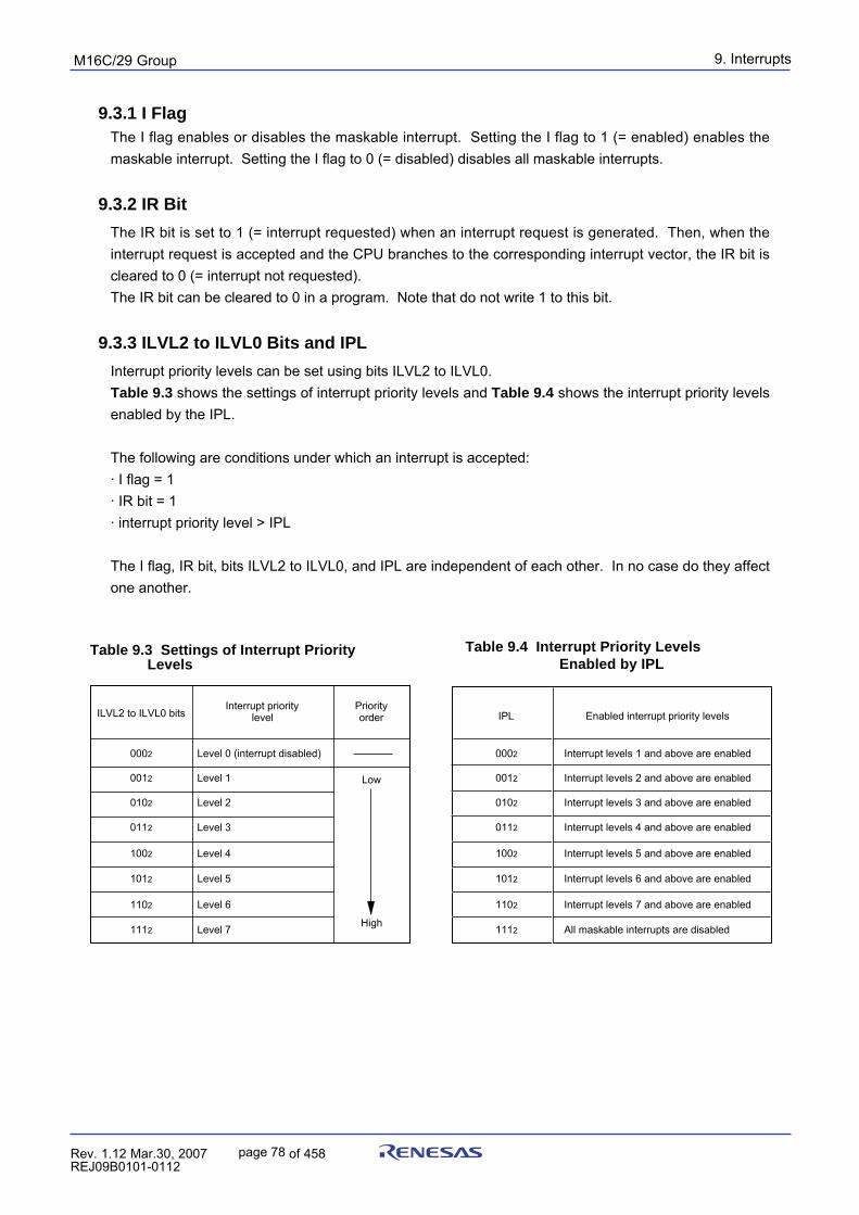
9. InterruptspuorG92/C61M
page 78 854fo7002,03.raM21.1.veR2110-1010B90JER
9.3.1 I FlagThe I flag enables or disables the maskable interrupt. Setting the I flag to 1 (= enabled) enables themaskable interrupt. Setting the I flag to 0 (= disabled) disables all maskable interrupts.
9.3.2 IR Bit
The IR bit is set to 1 (= interrupt requested) when an interrupt request is generated. Then, when theinterrupt request is accepted and the CPU branches to the corresponding interrupt vector, the IR bit iscleared to 0 (= interrupt not requested).The IR bit can be cleared to 0 in a program. Note that do not write 1 to this bit.
9.3.3 ILVL2 to ILVL0 Bits and IPL
Interrupt priority levels can be set using bits ILVL2 to ILVL0.Table 9.3 shows the settings of interrupt priority levels and Table 9.4 shows the interrupt priority levelsenabled by the IPL.
The following are conditions under which an interrupt is accepted:· I flag = 1· IR bit = 1· interrupt priority level > IPL
The I flag, IR bit, bits ILVL2 to ILVL0, and IPL are independent of each other. In no case do they affectone another.
Table 9.4 Interrupt Priority Levels Enabled by IPL
Table 9.3 Settings of Interrupt Priority Levels
ILVL2 to ILVL0 bitsInterrupt priority
levelPriorityorder
0002
0012
0102
0112
1002
1012
1102
1112
Level 0 (interrupt disabled)
Level 1
Level 2
Level 3
Level 4
Level 5
Level 6
Level 7
Low
High
Enabled interrupt priority levels
Interrupt levels 1 and above are enabled
Interrupt levels 2 and above are enabled
Interrupt levels 3 and above are enabled
Interrupt levels 4 and above are enabled
Interrupt levels 5 and above are enabled
Interrupt levels 6 and above are enabled
Interrupt levels 7 and above are enabled
All maskable interrupts are disabled
IPL
0002
0012
0102
0112
1002
1012
1102
1112
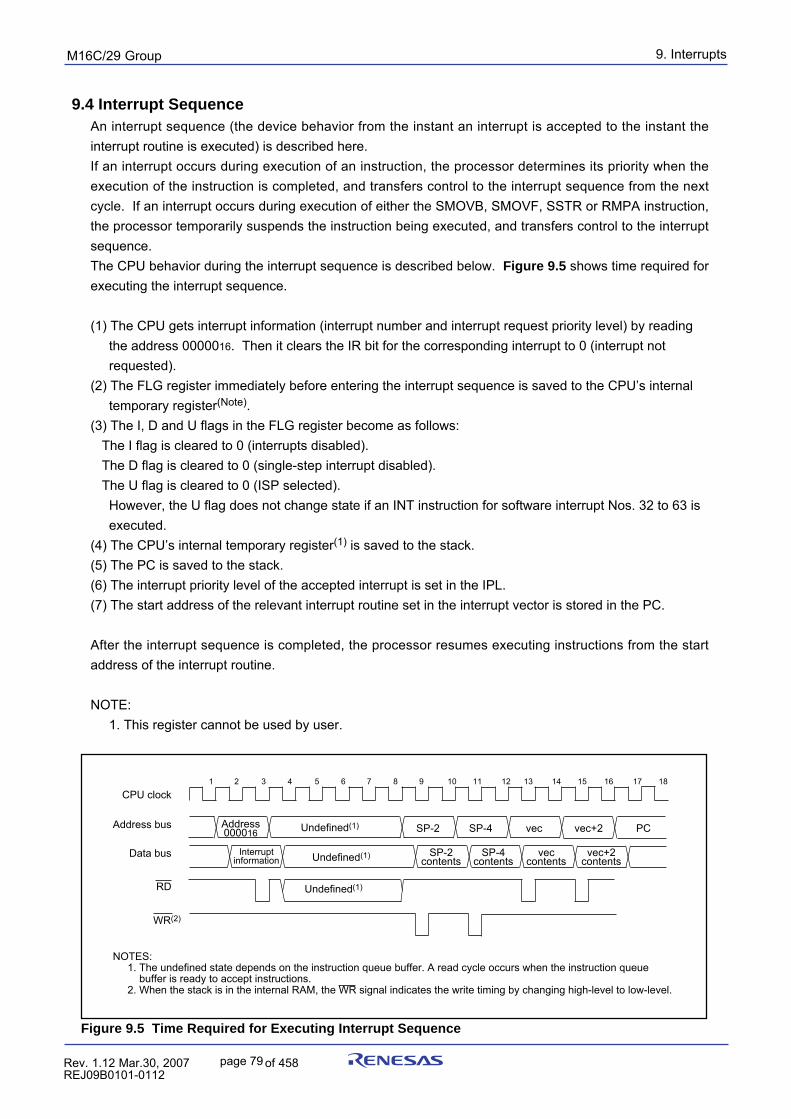
9. InterruptspuorG92/C61M
page 79 854fo7002,03.raM21.1.veR2110-1010B90JER
9.4 Interrupt SequenceAn interrupt sequence (the device behavior from the instant an interrupt is accepted to the instant theinterrupt routine is executed) is described here.If an interrupt occurs during execution of an instruction, the processor determines its priority when theexecution of the instruction is completed, and transfers control to the interrupt sequence from the nextcycle. If an interrupt occurs during execution of either the SMOVB, SMOVF, SSTR or RMPA instruction,the processor temporarily suspends the instruction being executed, and transfers control to the interruptsequence.The CPU behavior during the interrupt sequence is described below. Figure 9.5 shows time required forexecuting the interrupt sequence.
(1) The CPU gets interrupt information (interrupt number and interrupt request priority level) by reading the address 0000016. Then it clears the IR bit for the corresponding interrupt to 0 (interrupt not requested).(2) The FLG register immediately before entering the interrupt sequence is saved to the CPU’s internal temporary register(Note).(3) The I, D and U flags in the FLG register become as follows:
The I flag is cleared to 0 (interrupts disabled).The D flag is cleared to 0 (single-step interrupt disabled).The U flag is cleared to 0 (ISP selected).
However, the U flag does not change state if an INT instruction for software interrupt Nos. 32 to 63 is executed.(4) The CPU’s internal temporary register(1) is saved to the stack.(5) The PC is saved to the stack.(6) The interrupt priority level of the accepted interrupt is set in the IPL.(7) The start address of the relevant interrupt routine set in the interrupt vector is stored in the PC.
After the interrupt sequence is completed, the processor resumes executing instructions from the startaddress of the interrupt routine.
NOTE: 1. This register cannot be used by user.
Figure 9.5 Time Required for Executing Interrupt Sequence
1 2 3 4 5 6 7 8 9 10 11 12 13 14 15 16 17 18
SP-2 contents
SP-4 contents
vec contents
vec+2 contents
Interrupt information
Address 000016 Undefined(1) SP-2 SP-4 vec vec+2 PC
CPU clock
Address bus
Data bus
WR(2)
RD
NOTES: 1. The undefined state depends on the instruction queue buffer. A read cycle occurs when the instruction queue buffer is ready to accept instructions. 2. When the stack is in the internal RAM, the WR signal indicates the write timing by changing high-level to low-level.
Undefined(1)
Undefined(1)
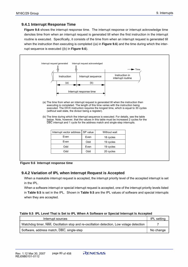
9. InterruptspuorG92/C61M
page 80 854fo7002,03.raM21.1.veR2110-1010B90JER
Interrupt sources_______
Watchdog timer, NMI, Oscillation stop and re-oscillation detection, Low volage detection_________
Software, address match, DBC, single-step
9.4.2 Variation of IPL when Interrupt Request is AcceptedWhen a maskable interrupt request is accepted, the interrupt priority level of the accepted interrupt is setin the IPL.When a software interrupt or special interrupt request is accepted, one of the interrupt priority levels listedin Table 9.5 is set in the IPL. Shown in Table 9.5 are the IPL values of software and special interruptswhen they are accepted.
Table 9.5 IPL Level That is Set to IPL When A Software or Special Interrupt Is Accepted
Figure 9.6 Interrupt response time
9.4.1 Interrupt Response TimeFigure 9.6 shows the interrupt response time. The interrupt response or interrupt acknowledge timedenotes time from when an interrupt request is generated till when the first instruction in the interruptroutine is executed. Specifically, it consists of the time from when an interrupt request is generated tillwhen the instruction then executing is completed ((a) in Figure 9.6) and the time during which the inter-rupt sequence is executed ((b) in Figure 9.6).
Instruction Interrupt sequence Instruction in interrupt routine
Time
Interrupt response time
(a) (b)
Interrupt request acknowledgedInterrupt request generated
(a) The time from when an interrupt request is generated till when the instruction then executing is completed. The length of this time varies with the instruction being executed. The DIVX instruction requires the longest time, which is equal to 30 cycles (without wait state, the divisor being a register).
(b) The time during which the interrupt sequence is executed. For details, see the table
below. Note, however, that the values in this table must be increased 2 cycles for the DBC interrupt and 1 cycle for the address match and single-step interrupts.
Interrupt vector address
Even
Even
Odd
Odd
SP value
Even
Odd
Even
Odd
Without wait
18 cycles
19 cycles
19 cycles
20 cycles
IPL setting
7
No change
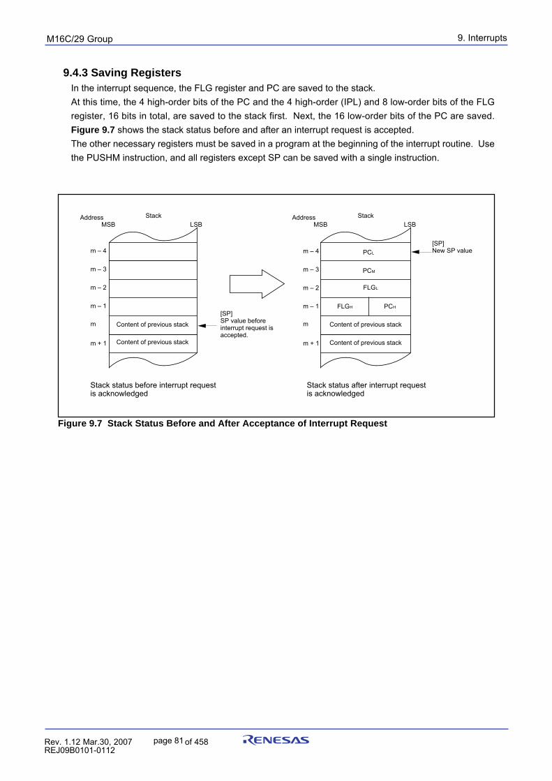
9. InterruptspuorG92/C61M
page 81 854fo7002,03.raM21.1.veR2110-1010B90JER
9.4.3 Saving RegistersIn the interrupt sequence, the FLG register and PC are saved to the stack.At this time, the 4 high-order bits of the PC and the 4 high-order (IPL) and 8 low-order bits of the FLGregister, 16 bits in total, are saved to the stack first. Next, the 16 low-order bits of the PC are saved.Figure 9.7 shows the stack status before and after an interrupt request is accepted.The other necessary registers must be saved in a program at the beginning of the interrupt routine. Usethe PUSHM instruction, and all registers except SP can be saved with a single instruction.
Figure 9.7 Stack Status Before and After Acceptance of Interrupt Request
Address
Content of previous stack
Stack
[SP]SP value beforeinterrupt request is accepted.
m
m – 1
m – 2
m – 3
m – 4
Stack status before interrupt requestis acknowledged
Stack status after interrupt requestis acknowledged
Content of previous stackm + 1
MSB LSB
m
m – 1
m – 2
m – 3
m – 4
Address
FLGL
Content of previous stack
Stack
FLGH PCH
[SP]New SP value
Content of previous stackm + 1
MSB LSB
PCL
PCM
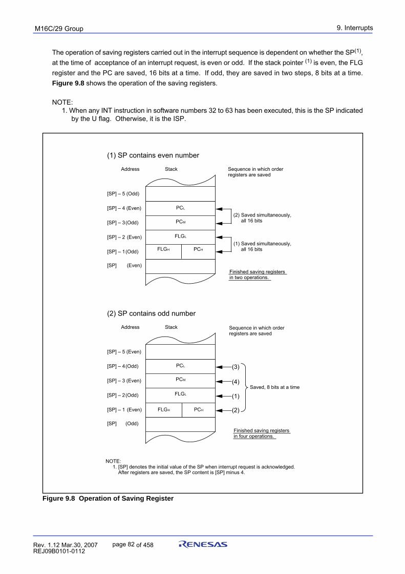
9. InterruptspuorG92/C61M
page 82 854fo7002,03.raM21.1.veR2110-1010B90JER
Figure 9.8 Operation of Saving Register
The operation of saving registers carried out in the interrupt sequence is dependent on whether the SP(1),at the time of acceptance of an interrupt request, is even or odd. If the stack pointer (1) is even, the FLGregister and the PC are saved, 16 bits at a time. If odd, they are saved in two steps, 8 bits at a time.Figure 9.8 shows the operation of the saving registers.
NOTE:1. When any INT instruction in software numbers 32 to 63 has been executed, this is the SP indicated
by the U flag. Otherwise, it is the ISP.
(2) SP contains odd number
[SP] (Odd)
[SP] – 1 (Even)
[SP] – 2 (Odd)
[SP] – 3 (Even)
[SP] – 4 (Odd)
[SP] – 5 (Even)
Address Sequence in which order registers are saved
(2)
(1)
Finished saving registers in four operations.
(3)
(4)
(1) SP contains even number
[SP] (Even)
[SP] – 1 (Odd)
[SP] – 2 (Even)
[SP] – 3 (Odd)
[SP] – 4 (Even)
[SP] – 5 (Odd)
NOTE: 1. [SP] denotes the initial value of the SP when interrupt request is acknowledged. After registers are saved, the SP content is [SP] minus 4.
Address
PCM
Stack
FLGL
PCL
Sequence in which order registers are saved
(2) Saved simultaneously, all 16 bits
(1) Saved simultaneously, all 16 bits
Finished saving registers in two operations.
PCM
Stack
FLGL
PCL
Saved, 8 bits at a time
FLGH PCH
FLGH PCH
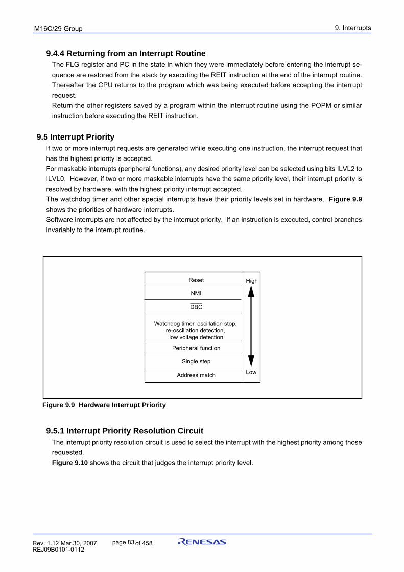
9. InterruptspuorG92/C61M
page 83 854fo7002,03.raM21.1.veR2110-1010B90JER
9.4.4 Returning from an Interrupt RoutineThe FLG register and PC in the state in which they were immediately before entering the interrupt se-quence are restored from the stack by executing the REIT instruction at the end of the interrupt routine.Thereafter the CPU returns to the program which was being executed before accepting the interruptrequest.Return the other registers saved by a program within the interrupt routine using the POPM or similarinstruction before executing the REIT instruction.
9.5 Interrupt PriorityIf two or more interrupt requests are generated while executing one instruction, the interrupt request thathas the highest priority is accepted.For maskable interrupts (peripheral functions), any desired priority level can be selected using bits ILVL2 toILVL0. However, if two or more maskable interrupts have the same priority level, their interrupt priority isresolved by hardware, with the highest priority interrupt accepted.The watchdog timer and other special interrupts have their priority levels set in hardware. Figure 9.9
shows the priorities of hardware interrupts.Software interrupts are not affected by the interrupt priority. If an instruction is executed, control branchesinvariably to the interrupt routine.
Reset
Watchdog timer, oscillation stop, re-oscillation detection,
low voltage detection
Peripheral function
Single step
Address match
High
Low
NMI
DBC
Figure 9.9 Hardware Interrupt Priority
9.5.1 Interrupt Priority Resolution CircuitThe interrupt priority resolution circuit is used to select the interrupt with the highest priority among thoserequested.Figure 9.10 shows the circuit that judges the interrupt priority level.
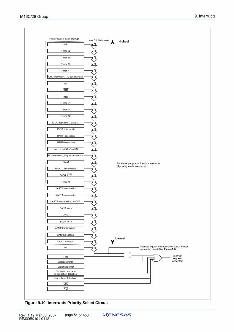
9. InterruptspuorG92/C61M
page 84 854fo7002,03.raM21.1.veR2110-1010B90JER
Timer B2
Timer B0
Timer A3
Timer A1
Timer B1
Timer A4
Timer A2
UART1 reception
UART0 reception
UART2 reception, ACK2
A/D conversion, Key input interrupt
DMA1
UART 2 bus collision
Timer A0
UART1 transmission
UART0 transmission
UART2 transmission, NACK2
CAN 0 error
DMA0
IPL
I flag
INT1
INT2
INT0
Watchdog timer
DBC
NMI
Interrupt request
accepted
Level 0 (initial value)Priority level of each interrupt
Highest
Lowest
Priority of peripheral function interrupts(if priority levels are same)
ICOC interrupt 1, I 2C bus interface
INT3
ICOC base timer, SCL/SDA
ICOC interrupt 0
SI/O4, INT5
SI/O3, INT4
Address match
Interrupt request level resolution output to clock generating circuit (See Figure.7.1)
Oscillation stop and re-oscillation detection
Low voltage detection
CAN 0 wakeup
CAN 0 reception
CAN 0 transmission
Figure 9.10 Interrupts Priority Select Circuit
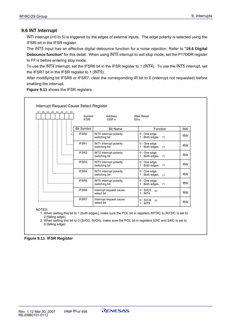
9. InterruptspuorG92/C61M
page 85 854fo7002,03.raM21.1.veR2110-1010B90JER
Interrupt Request Cause Select Register
Bit Name FunctionBit Symbol RW
Symbol Address After Reset IFSR 035F16 0016
IFSR0
b7 b6 b5 b4 b3 b2 b1 b0
INT0 interrupt polarity switching bit
0 : SI/O31 : INT4
0 : SI/O41 : INT5
0 : One edge1 : Both edges
0 : One edge1 : Both edges
0 : One edge1 : Both edges
0 : One edge1 : Both edges
0 : One edge1 : Both edges
INT1 interrupt polarity switching bit
INT2 interrupt polarity switching bit
INT3 interrupt polarity switching bit
INT4 interrupt polarity switching bit
INT5 interrupt polarity switching bit
0 : One edge1 : Both edges
Interrupt request cause select bit
Interrupt request cause select bit
IFSR1
IFSR2
IFSR3
IFSR4
IFSR5
IFSR6
IFSR7
RW
RW
RW
RW
RW
RW
RW
RW
(1)
(1)
(1)
(1)
(1)
(1)
(2)
NOTES:1. When setting this bit to 1 (both edges), make sure the POL bit in registers INT0IC to INT5IC is set to
0 (falling edge).2. When setting this bit to 0 (SI/O3, SI/O4), make sure the POL bit in registers S3IC and S4IC is set to
0 (falling edge).
(2)
______
9.6 INT Interrupt_______
INTi interrupt (i=0 to 5) is triggered by the edges of external inputs. The edge polarity is selected using theIFSRi bit in the IFSR register.
________
The INT5 input has an effective digital debounce function for a noise rejection. Refer to "19.6 Digital________
Debounce function" for this detail. When using INT5 interrupt to exit stop mode, set the P17DDR registerto FF16 before entering stop mode.
________ ________ ________
To use the INT4 interrupt, set the IFSR6 bit in the IFSR register to 1 (INT4). To use the INT5 interrupt, set________
the IFSR7 bit in the IFSR register to 1 (INT5).After modifiying bit IFSR6 or IFSR7, clear the corresponding IR bit to 0 (interrupt not requested) beforeenabling the interrupt.Figure 9.11 shows the IFSR registers.
Figure 9.11 IFSR Register
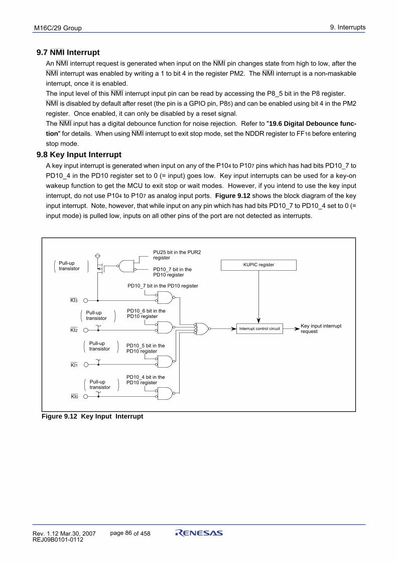
9. InterruptspuorG92/C61M
page 86 854fo7002,03.raM21.1.veR2110-1010B90JER
Interrupt control circuit
KUPIC register
Key input interrupt request
KI3
KI2
KI1
KI0
PU25 bit in the PUR2 register
PD10_7 bit in the PD10 register
Pull-up transistor
PD10_7 bit in the PD10 register
PD10_6 bit in the PD10 register
PD10_5 bit in the PD10 register
PD10_4 bit in the PD10 register
Pull-up transistor
Pull-up transistor
Pull-up transistor
______
9.7 NMI Interrupt_______ _______
An NMI interrupt request is generated when input on the NMI pin changes state from high to low, after the_______ ______
NMI interrupt was enabled by writing a 1 to bit 4 in the register PM2. The NMI interrupt is a non-maskableinterrupt, once it is enabled.
_______
The input level of this NMI interrupt input pin can be read by accessing the P8_5 bit in the P8 register._______
NMI is disabled by default after reset (the pin is a GPIO pin, P85) and can be enabled using bit 4 in the PM2register. Once enabled, it can only be disabled by a reset signal.
_______
The NMI input has a digital debounce function for noise rejection. Refer to "19.6 Digital Debounce func-_______
tion" for details. When using NMI interrupt to exit stop mode, set the NDDR register to FF16 before enteringstop mode.
9.8 Key Input InterruptA key input interrupt is generated when input on any of the P104 to P107 pins which has had bits PD10_7 toPD10_4 in the PD10 register set to 0 (= input) goes low. Key input interrupts can be used for a key-onwakeup function to get the MCU to exit stop or wait modes. However, if you intend to use the key inputinterrupt, do not use P104 to P107 as analog input ports. Figure 9.12 shows the block diagram of the keyinput interrupt. Note, however, that while input on any pin which has had bits PD10_7 to PD10_4 set to 0 (=input mode) is pulled low, inputs on all other pins of the port are not detected as interrupts.
Figure 9.12 Key Input Interrupt
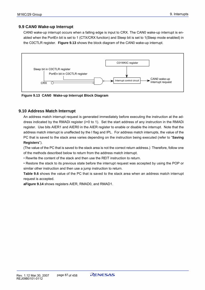
9. InterruptspuorG92/C61M
page 87 854fo7002,03.raM21.1.veR2110-1010B90JER
9.9 CAN0 Wake-up InterruptCAN0 wake-up interrupt occurs when a falling edge is input to CRX. The CAN0 wake-up interrupt is en-abled when the PortEn bit is set to 1 (CTX/CRX function) and Sleep bit is set to 1(Sleep mode enabled) inthe C0CTLR register. Figure 9.13 shows the block diagram of the CAN0 wake-up interrupt.
Figure 9.13 CAN0 Wake-up Interrupt Block Diagram
9.10 Address Match InterruptAn address match interrupt request is generated immediately before executing the instruction at the ad-dress indicated by the RMADi register (i=0 to 1). Set the start address of any instruction in the RMADiregister. Use bits AIER1 and AIER0 in the AIER register to enable or disable the interrupt. Note that theaddress match interrupt is unaffected by the I flag and IPL. For address match interrupts, the value of thePC that is saved to the stack area varies depending on the instruction being executed (refer to “Saving
Registers”).(The value of the PC that is saved to the stack area is not the correct return address.) Therefore, follow oneof the methods described below to return from the address match interrupt.• Rewrite the content of the stack and then use the REIT instruction to return.• Restore the stack to its previous state before the interrupt request was accepted by using the POP orsimilar other instruction and then use a jump instruction to return.Table 9.6 shows the value of the PC that is saved to the stack area when an address match interruptrequest is accepted.aFigure 9.14 shows registers AIER, RMAD0, and RMAD1.
Interrupt control circuit
C01WKIC register
CAN0 wake-up interrupt requestCRX
PortEn bit in C0CTLR registerSleep bit in C0CTLR register
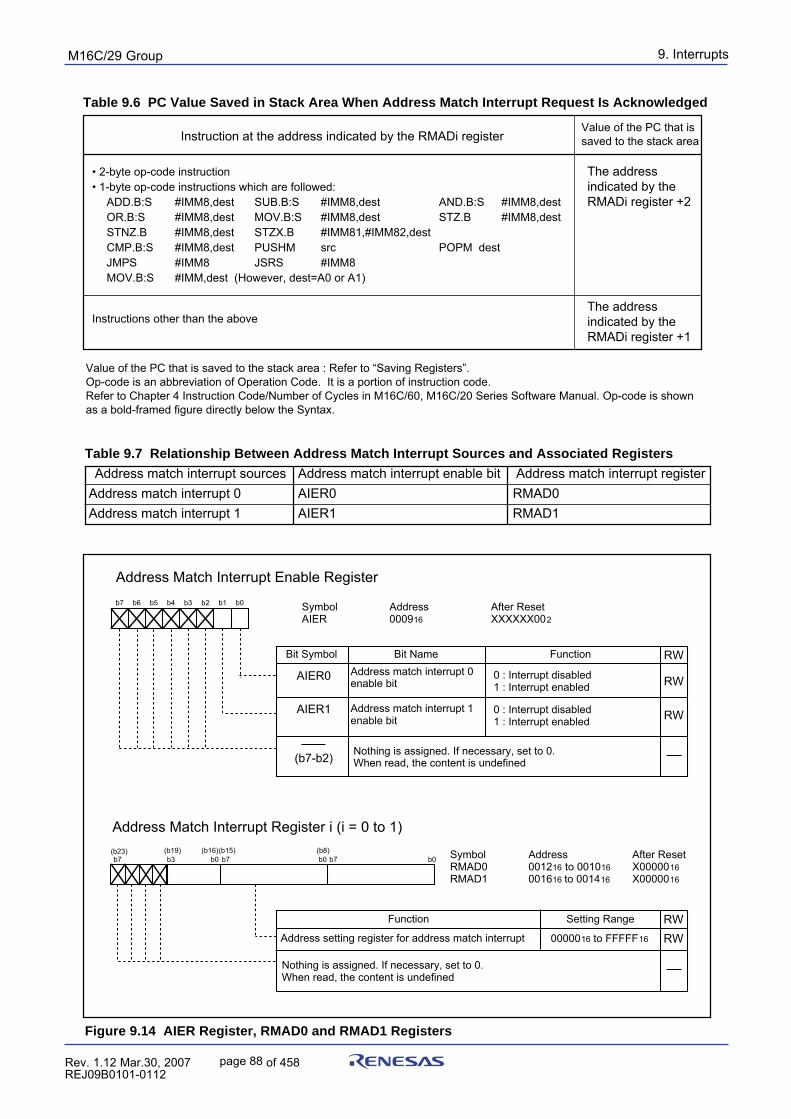
9. InterruptspuorG92/C61M
page 88 854fo7002,03.raM21.1.veR2110-1010B90JER
Figure 9.14 AIER Register, RMAD0 and RMAD1 Registers
• 2-byte op-code instruction• 1-byte op-code instructions which are followed: ADD.B:S #IMM8,dest SUB.B:S #IMM8,dest AND.B:S #IMM8,dest OR.B:S #IMM8,dest MOV.B:S #IMM8,dest STZ.B #IMM8,dest STNZ.B #IMM8,dest STZX.B #IMM81,#IMM82,dest CMP.B:S #IMM8,dest PUSHM src POPM dest JMPS #IMM8 JSRS #IMM8 MOV.B:S #IMM,dest (However, dest=A0 or A1)
Instructions other than the above
Instruction at the address indicated by the RMADi registerValue of the PC that is saved to the stack area
The address indicated by the RMADi register +2
The address indicated by the RMADi register +1
Value of the PC that is saved to the stack area : Refer to “Saving Registers”.Op-code is an abbreviation of Operation Code. It is a portion of instruction code.Refer to Chapter 4 Instruction Code/Number of Cycles in M16C/60, M16C/20 Series Software Manual. Op-code is shown as a bold-framed figure directly below the Syntax.
Table 9.7 Relationship Between Address Match Interrupt Sources and Associated Registers
Address match interrupt sources Address match interrupt enable bit Address match interrupt registerAddress match interrupt 0 AIER0 RMAD0Address match interrupt 1 AIER1 RMAD1
Bit NameBit Symbol
Symbol Address After Reset AIER 000916 XXXXXX002
Address Match Interrupt Enable Register
Function RWAddress match interrupt 0 enable bit
0 : Interrupt disabled1 : Interrupt enabled
AIER0
Address match interrupt 1 enable bit
AIER1
Symbol Address After Reset RMAD0 001216 to 001016 X0000016RMAD1 001616 to 001416 X0000016
b7 b6 b5 b4 b3 b2 b1 b0
Address setting register for address match interrupt
Function Setting Range
Address Match Interrupt Register i (i = 0 to 1)
0000016 to FFFFF16
0 : Interrupt disabled1 : Interrupt enabled
b0 b7 b0b3(b19) (b16)
b7 b0(b15) (b8)
b7(b23)
RW
RW
(b7-b2)
RWRW
Nothing is assigned. If necessary, set to 0. When read, the content is undefined
Nothing is assigned. If necessary, set to 0. When read, the content is undefined
Table 9.6 PC Value Saved in Stack Area When Address Match Interrupt Request Is Acknowledged
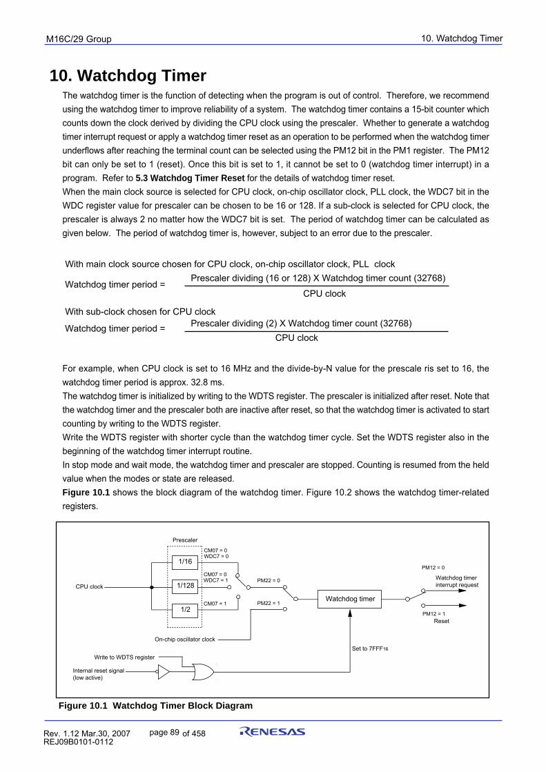
10. Watchdog TimerpuorG92/C61M
page 89 854fo7002,03.raM21.1.veR2110-1010B90JER
Figure 10.1 Watchdog Timer Block Diagram
10. Watchdog TimerThe watchdog timer is the function of detecting when the program is out of control. Therefore, we recommendusing the watchdog timer to improve reliability of a system. The watchdog timer contains a 15-bit counter whichcounts down the clock derived by dividing the CPU clock using the prescaler. Whether to generate a watchdogtimer interrupt request or apply a watchdog timer reset as an operation to be performed when the watchdog timerunderflows after reaching the terminal count can be selected using the PM12 bit in the PM1 register. The PM12bit can only be set to 1 (reset). Once this bit is set to 1, it cannot be set to 0 (watchdog timer interrupt) in aprogram. Refer to 5.3 Watchdog Timer Reset for the details of watchdog timer reset.When the main clock source is selected for CPU clock, on-chip oscillator clock, PLL clock, the WDC7 bit in theWDC register value for prescaler can be chosen to be 16 or 128. If a sub-clock is selected for CPU clock, theprescaler is always 2 no matter how the WDC7 bit is set. The period of watchdog timer can be calculated asgiven below. The period of watchdog timer is, however, subject to an error due to the prescaler.
For example, when CPU clock is set to 16 MHz and the divide-by-N value for the prescale ris set to 16, thewatchdog timer period is approx. 32.8 ms.The watchdog timer is initialized by writing to the WDTS register. The prescaler is initialized after reset. Note thatthe watchdog timer and the prescaler both are inactive after reset, so that the watchdog timer is activated to startcounting by writing to the WDTS register.Write the WDTS register with shorter cycle than the watchdog timer cycle. Set the WDTS register also in thebeginning of the watchdog timer interrupt routine.In stop mode and wait mode, the watchdog timer and prescaler are stopped. Counting is resumed from the heldvalue when the modes or state are released.Figure 10.1 shows the block diagram of the watchdog timer. Figure 10.2 shows the watchdog timer-relatedregisters.
With main clock source chosen for CPU clock, on-chip oscillator clock, PLL clock
Watchdog timer period =
With sub-clock chosen for CPU clockPrescaler dividing (2) X Watchdog timer count (32768)
CPU clock
Watchdog timer period =Prescaler dividing (16 or 128) X Watchdog timer count (32768)
CPU clock
CPU clock
Write to WDTS register
PM12 = 0
Watchdog timer
Set to 7FFF16
1/128
1/16
CM07 = 0WDC7 = 1
CM07 = 0WDC7 = 0
CM07 = 11/2
Prescaler
PM12 = 1 Reset
PM22 = 0
PM22 = 1
On-chip oscillator clock
Internal reset signal (low active)
Watchdog timer interrupt request
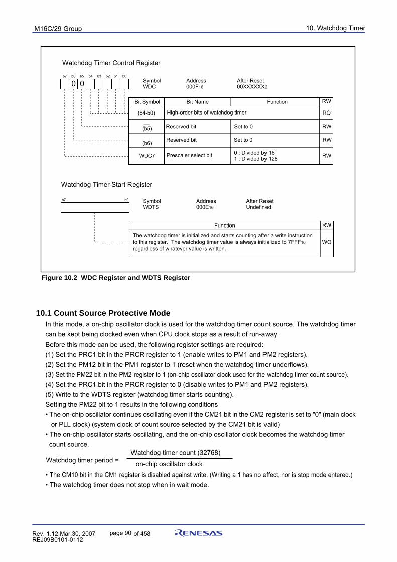
10. Watchdog TimerpuorG92/C61M
page 90 854fo7002,03.raM21.1.veR2110-1010B90JER
Figure 10.2 WDC Register and WDTS Register
10.1 Count Source Protective ModeIn this mode, a on-chip oscillator clock is used for the watchdog timer count source. The watchdog timercan be kept being clocked even when CPU clock stops as a result of run-away.Before this mode can be used, the following register settings are required:(1) Set the PRC1 bit in the PRCR register to 1 (enable writes to PM1 and PM2 registers).(2) Set the PM12 bit in the PM1 register to 1 (reset when the watchdog timer underflows).(3) Set the PM22 bit in the PM2 register to 1 (on-chip oscillator clock used for the watchdog timer count source).(4) Set the PRC1 bit in the PRCR register to 0 (disable writes to PM1 and PM2 registers).(5) Write to the WDTS register (watchdog timer starts counting).Setting the PM22 bit to 1 results in the following conditions• The on-chip oscillator continues oscillating even if the CM21 bit in the CM2 register is set to "0" (main clock
or PLL clock) (system clock of count source selected by the CM21 bit is valid)• The on-chip oscillator starts oscillating, and the on-chip oscillator clock becomes the watchdog timer count source.
• The CM10 bit in the CM1 register is disabled against write. (Writing a 1 has no effect, nor is stop mode entered.)• The watchdog timer does not stop when in wait mode.
Watchdog timer period =Watchdog timer count (32768)
on-chip oscillator clock
Watchdog Timer Start Register
Symbol Address After Reset WDTS 000E16 Undefine d
WO
b7 b0
Function
RW
The watchdog timer is initialized and starts counting after a write instruction to this register. The watchdog timer value is always initialized to 7FFF16 regardless of whatever value is written.
Watchdog Timer Control Register
Symbol Addres s After Reset WDC 000F16 00XXXXXX2
FunctionBit Symbol RW
b7 b6 b5 b4 b3 b2 b1 b0
High-order bits of watchdog timer
WDC7
Bit Name
Prescaler select bit 0 : Divided by 161 : Divided by 128
Reserved bit Set to 0
0
RO
RW
RW
RW
(b4-b0)
(b6)
0
(b5) Reserved bit Set to 0
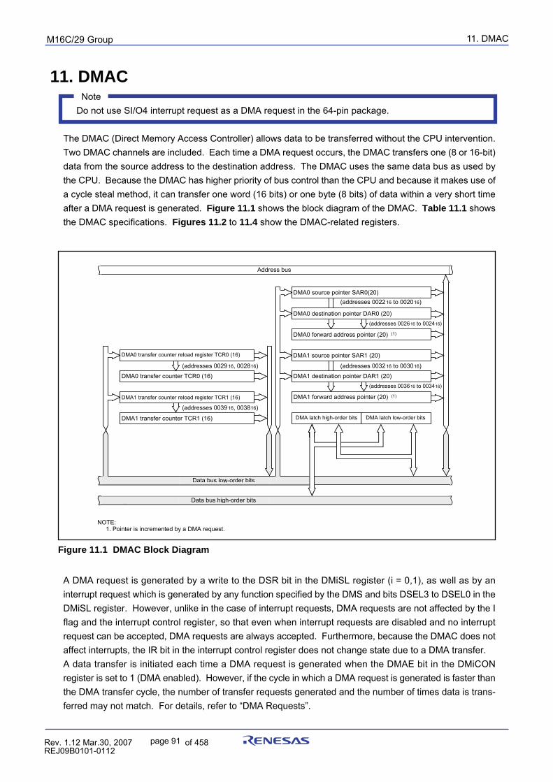
11. DMACpuorG92/C61M
page 91 854fo7002,03.raM21.1.veR2110-1010B90JER
11. DMAC Note
Do not use SI/O4 interrupt request as a DMA request in the 64-pin package.
The DMAC (Direct Memory Access Controller) allows data to be transferred without the CPU intervention.Two DMAC channels are included. Each time a DMA request occurs, the DMAC transfers one (8 or 16-bit)data from the source address to the destination address. The DMAC uses the same data bus as used bythe CPU. Because the DMAC has higher priority of bus control than the CPU and because it makes use ofa cycle steal method, it can transfer one word (16 bits) or one byte (8 bits) of data within a very short timeafter a DMA request is generated. Figure 11.1 shows the block diagram of the DMAC. Table 11.1 showsthe DMAC specifications. Figures 11.2 to 11.4 show the DMAC-related registers.
Figure 11.1 DMAC Block Diagram
A DMA request is generated by a write to the DSR bit in the DMiSL register (i = 0,1), as well as by aninterrupt request which is generated by any function specified by the DMS and bits DSEL3 to DSEL0 in theDMiSL register. However, unlike in the case of interrupt requests, DMA requests are not affected by the Iflag and the interrupt control register, so that even when interrupt requests are disabled and no interruptrequest can be accepted, DMA requests are always accepted. Furthermore, because the DMAC does notaffect interrupts, the IR bit in the interrupt control register does not change state due to a DMA transfer.A data transfer is initiated each time a DMA request is generated when the DMAE bit in the DMiCONregister is set to 1 (DMA enabled). However, if the cycle in which a DMA request is generated is faster thanthe DMA transfer cycle, the number of transfer requests generated and the number of times data is trans-ferred may not match. For details, refer to “DMA Requests”.
Data bus low-order bits
DMA latch high-order bits DMA latch low-order bits
DMA0 source pointer SAR0(20)
DMA0 destination pointer DAR0 (20)
DMA0 forward address pointer (20) (1)
Data bus high-order bits
Address bus
DMA1 destination pointer DAR1 (20)
DMA1 source pointer SAR1 (20)
DMA1 forward address pointer (20) (1)
DMA0 transfer counter reload register TCR0 (16)
DMA0 transfer counter TCR0 (16)
DMA1 transfer counter reload register TCR1 (16)
DMA1 transfer counter TCR1 (16)
(addresses 0029 16, 002816)
(addresses 0039 16, 003816)
(addresses 002216 to 002016)
(addresses 002616 to 002416)
(addresses 003216 to 003016)
(addresses 003616 to 003416)
NOTE: 1. Pointer is incremented by a DMA request.
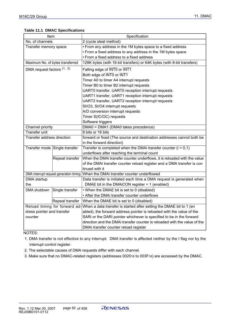
11. DMACpuorG92/C61M
page 92 854fo7002,03.raM21.1.veR2110-1010B90JER
Item SpecificationNo. of channels 2 (cycle steal method)Transfer memory space • From any address in the 1M bytes space to a fixed address
• From a fixed address to any address in the 1M bytes space• From a fixed address to a fixed address
Maximum No. of bytes transferred 128K bytes (with 16-bit transfers) or 64K bytes (with 8-bit transfers)
DMA request factors (1, 2)________ ________
Falling edge of INT0 or INT1________ ________
Both edge of INT0 or INT1Timer A0 to timer A4 interrupt requestsTimer B0 to timer B2 interrupt requestsUART0 transfer, UART0 reception interrupt requestsUART1 transfer, UART1 reception interrupt requestsUART2 transfer, UART2 reception interrupt requestsSI/O3, SI/O4 interrupt requestsA/D conversion interrupt requestsTimer S(IC/OC) requestsSoftware triggers
Channel priority DMA0 > DMA1 (DMA0 takes precedence)Transfer unit 8 bits or 16 bitsTransfer address direction forward or fixed (The source and destination addresses cannot both be
in the forward direction)Transfer mode Single transfer Transfer is completed when the DMAi transfer counter (i = 0,1)
underflows after reaching the terminal countRepeat transfer When the DMAi transfer counter underflows, it is reloaded with the value
of the DMAi transfer counter reload register and a DMA transfer is continued with it
DMA interrupt request generation timing When the DMAi transfer counter underflowedDMA startup Data transfer is initiated each time a DMA request is generated whenthe DMAE bit in the DMAiCON register = 1 (enabled)DMA shutdown Single transfer • When the DMAE bit is set to 0 (disabled)
• After the DMAi transfer counter underflowsRepeat transfer When the DMAE bit is set to 0 (disabled)
When a data transfer is started after setting the DMAE bit to 1 (enabled), the forward address pointer is reloaded with the value of theSARi or the DARi pointer whichever is specified to be in the forwarddirection and the DMAi transfer counter is reloaded with the value of theDMAi transfer counter reload register
Table 11.1 DMAC Specifications
NOTES: 1. DMA transfer is not effective to any interrupt. DMA transfer is affected neither by the I flag nor by the
interrupt control register. 2. The selectable causes of DMA requests differ with each channel. 3. Make sure that no DMAC-related registers (addresses 002016 to 003F16) are accessed by the DMAC.
Reload timing for forward ad-dress pointer and transfercounter
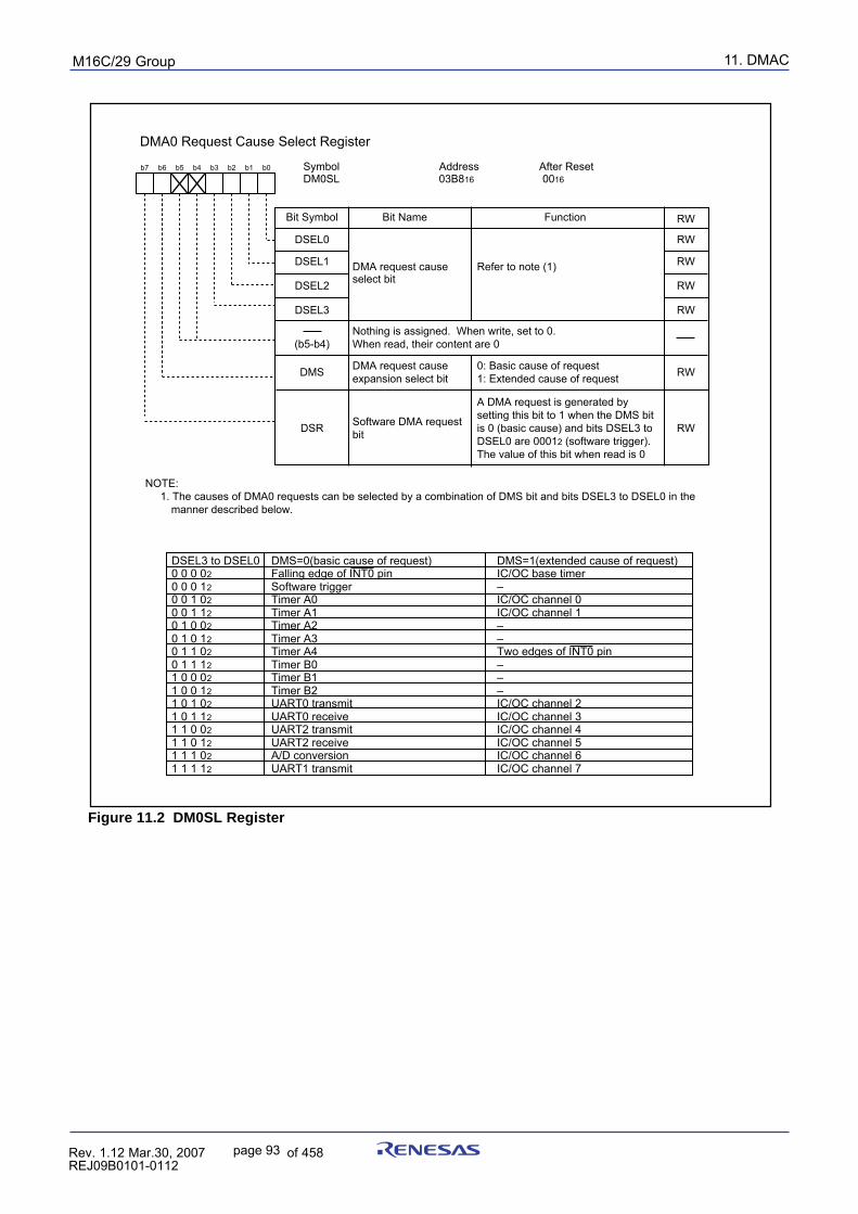
11. DMACpuorG92/C61M
page 93 854fo7002,03.raM21.1.veR2110-1010B90JER
Figure 11.2 DM0SL Register
DMA0 Request Cause Select Register
Symbol Address After Reset DM0SL 03B816 0016
FunctionBit Symbol
b7 b6 b5 b4 b3 b2 b1 b0
DMA request cause select bit
DSEL0
RW
DSEL1
DSEL2
DSEL3
DSR
Bit Name
DMS
RW
RW
RW
RW
RW
RW
(b5-b4)
Refer to note (1)
A DMA request is generated by setting this bit to 1 when the DMS bit is 0 (basic cause) and bits DSEL3 to DSEL0 are 00012 (software trigger). The value of this bit when read is 0
Software DMA request bit
Nothing is assigned. When write, set to 0. When read, their content are 0
DMA request cause expansion select bit
0: Basic cause of request1: Extended cause of request
NOTE: 1. The causes of DMA0 requests can be selected by a combination of DMS bit and bits DSEL3 to DSEL0 in the
manner described below.
DSEL3 to DSEL0 DMS=0(basic cause of request) DMS=1(extended cause of request)0 0 0 02 Falling edge of INT0 pin IC/OC base timer0 0 0 12 Software trigger – 0 0 1 02 Timer A0 IC/OC channel 00 0 1 12 Timer A1 IC/OC channel 10 1 0 02 Timer A2 –0 1 0 12 Timer A3 –0 1 1 02 Timer A4 Two edges of INT0 pin 0 1 1 12 Timer B0 –1 0 0 02 Timer B1 –1 0 0 12 Timer B2 –1 0 1 02 UART0 transmit IC/OC channel 21 0 1 12 UART0 receive IC/OC channel 31 1 0 02 UART2 transmit IC/OC channel 41 1 0 12 UART2 receive IC/OC channel 51 1 1 02 A/D conversion IC/OC channel 61 1 1 12 UART1 transmit IC/OC channel 7
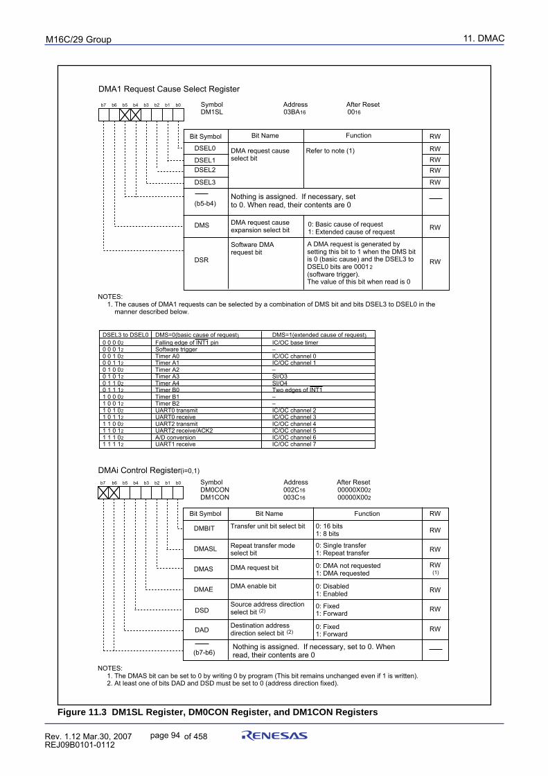
11. DMACpuorG92/C61M
page 94 854fo7002,03.raM21.1.veR2110-1010B90JER
Figure 11.3 DM1SL Register, DM0CON Register, and DM1CON Registers
DMAi Control Register(i=0,1)
Symbol Address After Reset DM0CON 002C16 00000X002DM1CON 003C16 00000X002
Bit Name FunctionBit Symbol
Transfer unit bit select bit
b7 b6 b5 b4 b3 b2 b1 b0
0: 16 bits1: 8 bits
DMBIT
DMASL
DMAS
DMAE
Repeat transfer mode select bit
0: Single transfer 1: Repeat transfer
DMA request bit 0: DMA not requested1: DMA requested
0: Disabled1: Enabled
0: Fixed1: Forward
DMA enable bit
Source address direction select bit (2)
Destination address direction select bit (2)
0: Fixed1: Forward
DSD
DAD
Nothing is assigned. If necessary, set to 0. When read, their contents are 0
NOTES: 1. The DMAS bit can be set to 0 by writing 0 by program (This bit remains unchanged even if 1 is written). 2. At least one of bits DAD and DSD must be set to 0 (address direction fixed).
(1)
DMA1 Request Cause Select Register
Symbol Address After Reset DM1SL 03BA16 0016
FunctionBit Symbol
b7 b6 b5 b4 b3 b2 b1 b0
DMA request cause select bit
DSEL0
RW
DSEL1DSEL2
DSEL3
Software DMA request bit
DSR
DSEL3 to DSEL0 DMS=0(basic cause of request) DMS=1(extended cause of request)0 0 0 02 Falling edge of INT1 pin IC/OC base timer0 0 0 12 Software trigger –0 0 1 02 Timer A0 IC/OC channel 00 0 1 12 Timer A1 IC/OC channel 10 1 0 02 Timer A2 –0 1 0 12 Timer A3 SI/O3 0 1 1 02 Timer A4 SI/O4 0 1 1 12 Timer B0 Two edges of INT1 1 0 0 02 Timer B1 – 1 0 0 12 Timer B2 – 1 0 1 02 UART0 transmit IC/OC channel 2 1 0 1 12 UART0 receive IC/OC channel 31 1 0 02 UART2 transmit IC/OC channel 41 1 0 12 UART2 receive/ACK2 IC/OC channel 5 1 1 1 02 A/D conversion IC/OC channel 6 1 1 1 12 UART1 receive IC/OC channel 7
Bit Name
DMA request cause expansion select bit
DMS
RWRWRW
RW
RW
RW
(b5-b4)
RW
RW
RW
RW
RW
RW
RW
(b7-b6)
NOTES: 1. The causes of DMA1 requests can be selected by a combination of DMS bit and bits DSEL3 to DSEL0 in the manner described below.
Nothing is assigned. If necessary, set to 0. When read, their contents are 0
A DMA request is generated by setting this bit to 1 when the DMS bit is 0 (basic cause) and the DSEL3 to DSEL0 bits are 00012 (software trigger).The value of this bit when read is 0
0: Basic cause of request1: Extended cause of request
Refer to note (1)
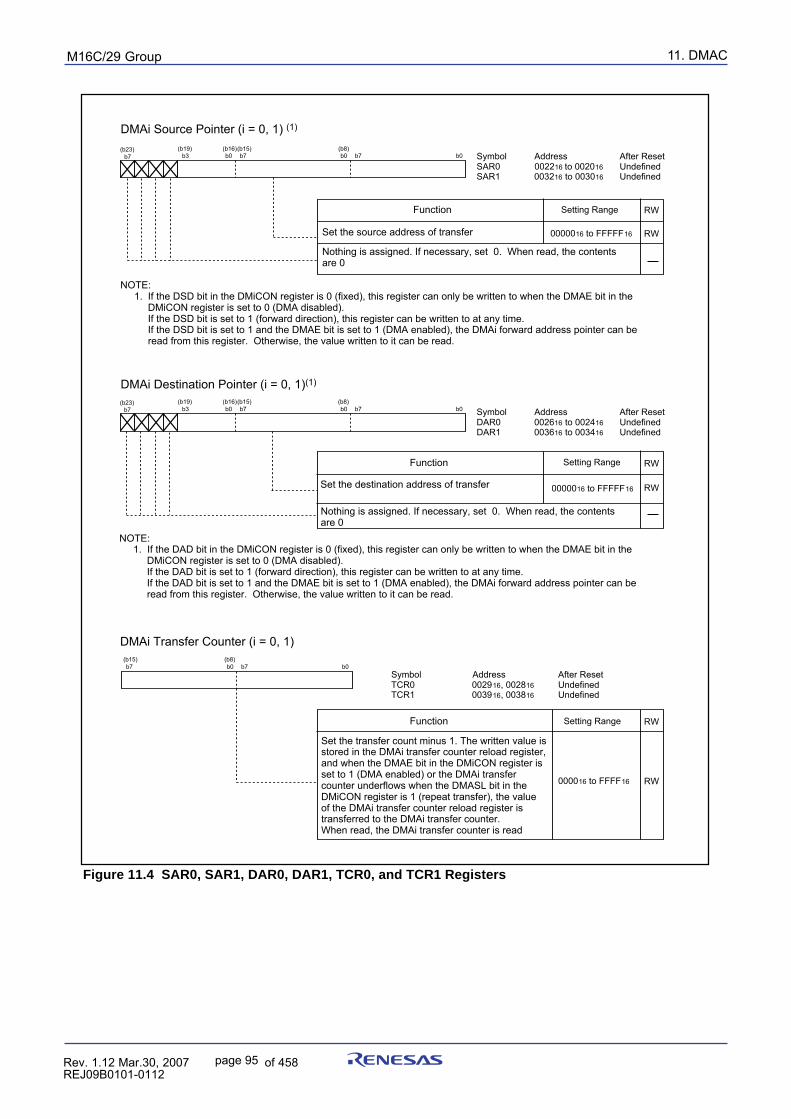
11. DMACpuorG92/C61M
page 95 854fo7002,03.raM21.1.veR2110-1010B90JER
Figure 11.4 SAR0, SAR1, DAR0, DAR1, TCR0, and TCR1 Registers
b7 b0 b7 b0(b8)(b15)
Function
Set the transfer count minus 1. The written value is stored in the DMAi transfer counter reload register, and when the DMAE bit in the DMiCON register is set to 1 (DMA enabled) or the DMAi transfer counter underflows when the DMASL bit in the DMiCON register is 1 (repeat transfer), the value of the DMAi transfer counter reload register is transferred to the DMAi transfer counter.When read, the DMAi transfer counter is read
Symbol Address After Reset TCR0 002916, 002816 Undefined TCR1 003916, 003816 Undefined
DMAi Transfer Counter (i = 0, 1)
Setting Range
000016 to FFFF16
b7(b23)
b3 b0 b7 b0 b7 b0(b8)(b16)(b15)(b19)
Function RW
Set the source address of transfer
Symbol Address After Reset SAR0 002216 to 002016 Undefined SAR1 003216 to 003016 Undefined
DMAi Source Pointer (i = 0, 1) (1)
Setting Range
0000016 to FFFFF16
Nothing is assigned. If necessary, set 0. When read, the contents are 0
Symbol Address After Reset DAR0 002616 to 002416 Undefined DAR1 003616 to 003416 Undefined
b3 b0 b7 b0 b7 b0(b8)(b15)(b16)(b19)
Function
Set the destination address of transfer
DMAi Destination Pointer (i = 0, 1)(1)
Setting Range
0000016 to FFFFF16
b7(b23)
RW
RW
RW
RW
RW
NOTE: 1. If the DSD bit in the DMiCON register is 0 (fixed), this register can only be written to when the DMAE bit in the DMiCON register is set to 0 (DMA disabled). If the DSD bit is set to 1 (forward direction), this register can be written to at any time. If the DSD bit is set to 1 and the DMAE bit is set to 1 (DMA enabled), the DMAi forward address pointer can be read from this register. Otherwise, the value written to it can be read.
Nothing is assigned. If necessary, set 0. When read, the contents are 0
NOTE: 1. If the DAD bit in the DMiCON register is 0 (fixed), this register can only be written to when the DMAE bit in the DMiCON register is set to 0 (DMA disabled). If the DAD bit is set to 1 (forward direction), this register can be written to at any time. If the DAD bit is set to 1 and the DMAE bit is set to 1 (DMA enabled), the DMAi forward address pointer can be read from this register. Otherwise, the value written to it can be read.
11. DMACpuorG92/C61M
page 96 854fo7002,03.raM21.1.veR2110-1010B90JER
11.1 Transfer CyclesThe transfer cycle consists of a memory or SFR read (source read) bus cycle and a write (destination write)bus cycle. The number of read and write bus cycles is affected by the source and destination addresses oftransfer. Furthermore, the bus cycle itself is extended by a software wait.
11.1.1 Effect of Source and Destination Addresses
If the transfer unit is 16 bits and the source address of transfer begins with an odd address, the sourceread cycle consists of one more bus cycle than when the source address of transfer begins with an evenaddress.Similarly, if the transfer unit is 16 bits and the destination address of transfer begins with an odd address,the destination write cycle consists of one more bus cycle than when the destination address of transferbegins with an even address.
11.1.2 Effect of Software Wait
For memory or SFR accesses in which one or more software wait states are inserted, the number of buscycles required for that access increases by an amount equal to software wait states.
Figure 11.5 shows the example of the cycles for a source read. For convenience, the destination writecycle is shown as one cycle and the source read cycles for the different conditions are shown. In reality, thedestination write cycle is subject to the same conditions as the source read cycle, with the transfer cyclechanging accordingly. When calculating transfer cycles, take into consideration each condition for thesource read and the destination write cycle, respectively. For example, when data is transferred in 16 bitunits and when both the source address and destination address are an odd address ((2) in Figure 11.5),two source read bus cycles and two destination write bus cycles are required.
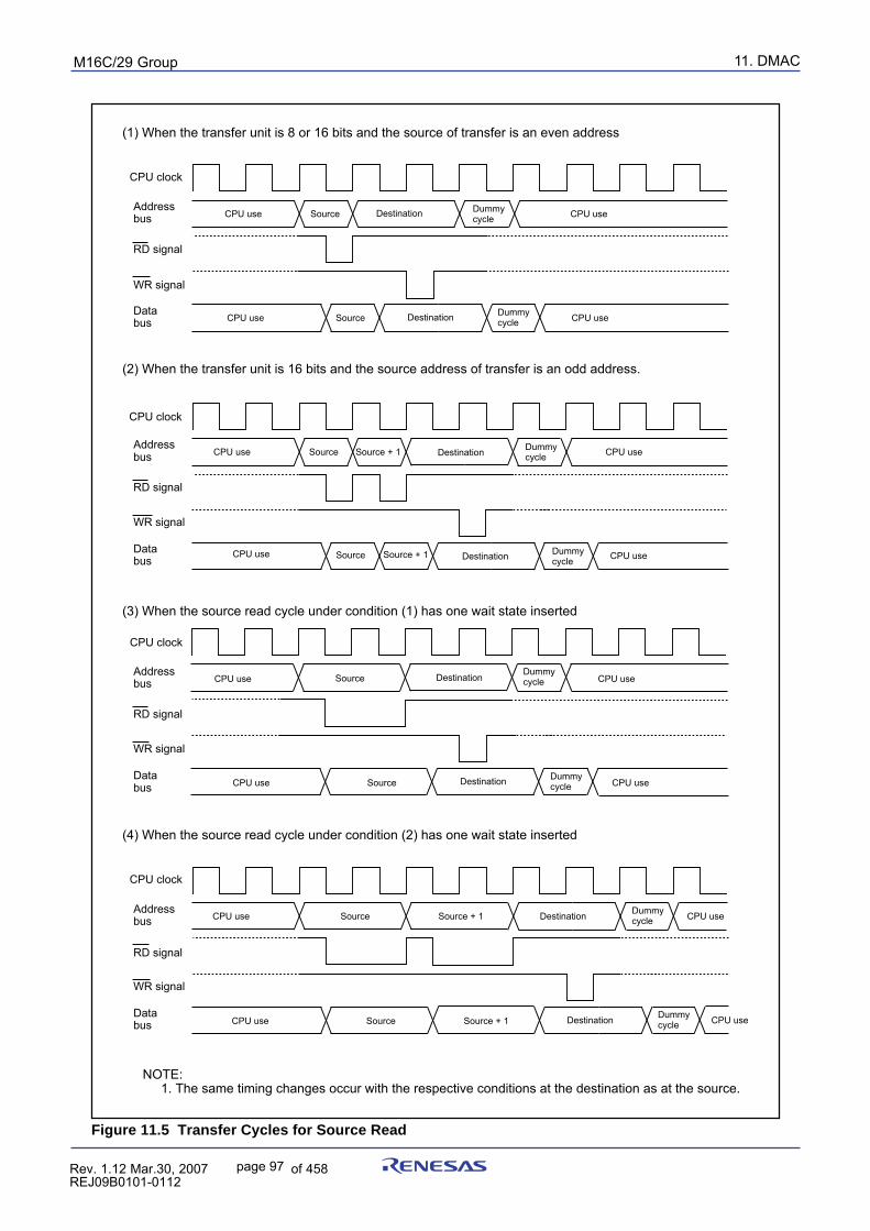
11. DMACpuorG92/C61M
page 97 854fo7002,03.raM21.1.veR2110-1010B90JER
Figure 11.5 Transfer Cycles for Source Read
CPU clock
Address bus
RD signal
WR signal
Data bus
CPU use
CPU use CPU use
CPU useSource
Source
Destination
Destination
Dummy cycle
Dummy cycle
(1) When the transfer unit is 8 or 16 bits and the source of transfer is an even address
Address bus
RD signal
WR signal
Data bus
CPU use
CPU use CPU use
CPU useSource
Source
Destination
Destination
Dummy cycle
Dummy cycle
(3) When the source read cycle under condition (1) has one wait state inserted
Address bus
RD signal
WR signal
Data bus
CPU use
CPU use CPU use
CPU useSource
Source
Destination
Destination
Dummy cycle
Dummy cycle
Source + 1
Source + 1
(2) When the transfer unit is 16 bits and the source address of transfer is an odd address.
Address bus
RD signal
WR signal
Data bus
CPU use
CPU use CPU use
CPU useSource
Source
Destination
Destination
Dummy cycle
Dummy cycle
Source + 1
Source + 1
(4) When the source read cycle under condition (2) has one wait state inserted
NOTE: 1. The same timing changes occur with the respective conditions at the destination as at the source.
CPU clock
CPU clock
CPU clock
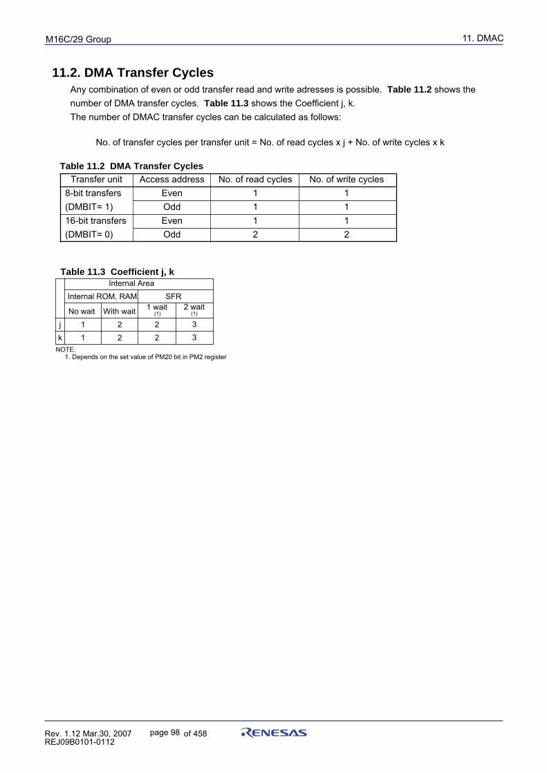
11. DMACpuorG92/C61M
page 98 854fo7002,03.raM21.1.veR2110-1010B90JER
Table 11.2 DMA Transfer Cycles
Table 11.3 Coefficient j, k
11.2. DMA Transfer Cycles Any combination of even or odd transfer read and write adresses is possible. Table 11.2 shows the number of DMA transfer cycles. Table 11.3 shows the Coefficient j, k. The number of DMAC transfer cycles can be calculated as follows:
No. of transfer cycles per transfer unit = No. of read cycles x j + No. of write cycles x k
Transfer unit Access address No. of read cycles No. of write cycles8-bit transfers Even 1 1(DMBIT= 1) Odd 1 116-bit transfers Even 1 1(DMBIT= 0) Odd 2 2
Internal AreaInternal ROM, RAM SFR
No wait With wait11
22
22
jk
33
1 wait 2 wait(1) (1)
NOTE: 1. Depends on the set value of PM20 bit in PM2 register
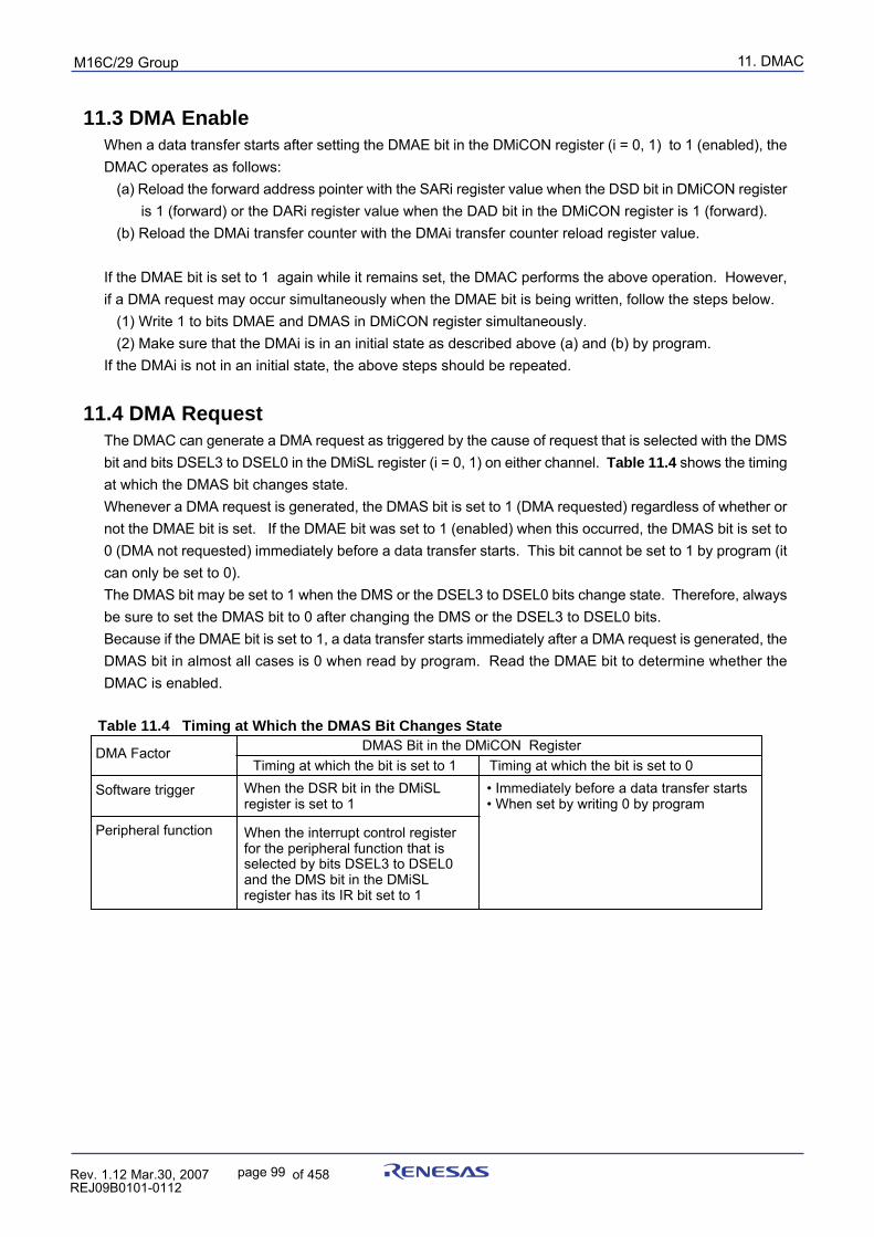
11. DMACpuorG92/C61M
page 99 854fo7002,03.raM21.1.veR2110-1010B90JER
11.3 DMA EnableWhen a data transfer starts after setting the DMAE bit in the DMiCON register (i = 0, 1) to 1 (enabled), theDMAC operates as follows:
(a) Reload the forward address pointer with the SARi register value when the DSD bit in DMiCON register is 1 (forward) or the DARi register value when the DAD bit in the DMiCON register is 1 (forward).(b) Reload the DMAi transfer counter with the DMAi transfer counter reload register value.
If the DMAE bit is set to 1 again while it remains set, the DMAC performs the above operation. However,if a DMA request may occur simultaneously when the DMAE bit is being written, follow the steps below.
(1) Write 1 to bits DMAE and DMAS in DMiCON register simultaneously.(2) Make sure that the DMAi is in an initial state as described above (a) and (b) by program.
If the DMAi is not in an initial state, the above steps should be repeated.
11.4 DMA RequestThe DMAC can generate a DMA request as triggered by the cause of request that is selected with the DMSbit and bits DSEL3 to DSEL0 in the DMiSL register (i = 0, 1) on either channel. Table 11.4 shows the timingat which the DMAS bit changes state.Whenever a DMA request is generated, the DMAS bit is set to 1 (DMA requested) regardless of whether ornot the DMAE bit is set. If the DMAE bit was set to 1 (enabled) when this occurred, the DMAS bit is set to0 (DMA not requested) immediately before a data transfer starts. This bit cannot be set to 1 by program (itcan only be set to 0).The DMAS bit may be set to 1 when the DMS or the DSEL3 to DSEL0 bits change state. Therefore, alwaysbe sure to set the DMAS bit to 0 after changing the DMS or the DSEL3 to DSEL0 bits.Because if the DMAE bit is set to 1, a data transfer starts immediately after a DMA request is generated, theDMAS bit in almost all cases is 0 when read by program. Read the DMAE bit to determine whether theDMAC is enabled.
Table 11.4 Timing at Which the DMAS Bit Changes State
DMA Factor
Software trigger
Peripheral function
Timing at which the bit is set to 1 Timing at which the bit is set to 0 DMAS Bit in the DMiCON Register
When the DSR bit in the DMiSL register is set to 1
When the interrupt control register for the peripheral function that is selected by bits DSEL3 to DSEL0 and the DMS bit in the DMiSL register has its IR bit set to 1
• Immediately before a data transfer starts• When set by writing 0 by program
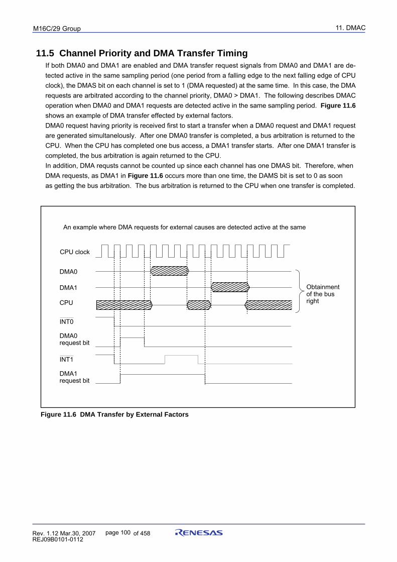
11. DMACpuorG92/C61M
page 100 854fo7002,03.raM21.1.veR2110-1010B90JER
11.5 Channel Priority and DMA Transfer TimingIf both DMA0 and DMA1 are enabled and DMA transfer request signals from DMA0 and DMA1 are de-tected active in the same sampling period (one period from a falling edge to the next falling edge of CPUclock), the DMAS bit on each channel is set to 1 (DMA requested) at the same time. In this case, the DMArequests are arbitrated according to the channel priority, DMA0 > DMA1. The following describes DMACoperation when DMA0 and DMA1 requests are detected active in the same sampling period. Figure 11.6
shows an example of DMA transfer effected by external factors.DMA0 request having priority is received first to start a transfer when a DMA0 request and DMA1 requestare generated simultanelously. After one DMA0 transfer is completed, a bus arbitration is returned to theCPU. When the CPU has completed one bus access, a DMA1 transfer starts. After one DMA1 transfer iscompleted, the bus arbitration is again returned to the CPU.In addition, DMA requsts cannot be counted up since each channel has one DMAS bit. Therefore, whenDMA requests, as DMA1 in Figure 11.6 occurs more than one time, the DAMS bit is set to 0 as soonas getting the bus arbitration. The bus arbitration is returned to the CPU when one transfer is completed.
Figure 11.6 DMA Transfer by External Factors
DMA0
DMA1
DMA0request bit
DMA1request bit
CPU
INT0
INT1
Obtainment of the bus right
An example where DMA requests for external causes are detected active at the same
CPU clock
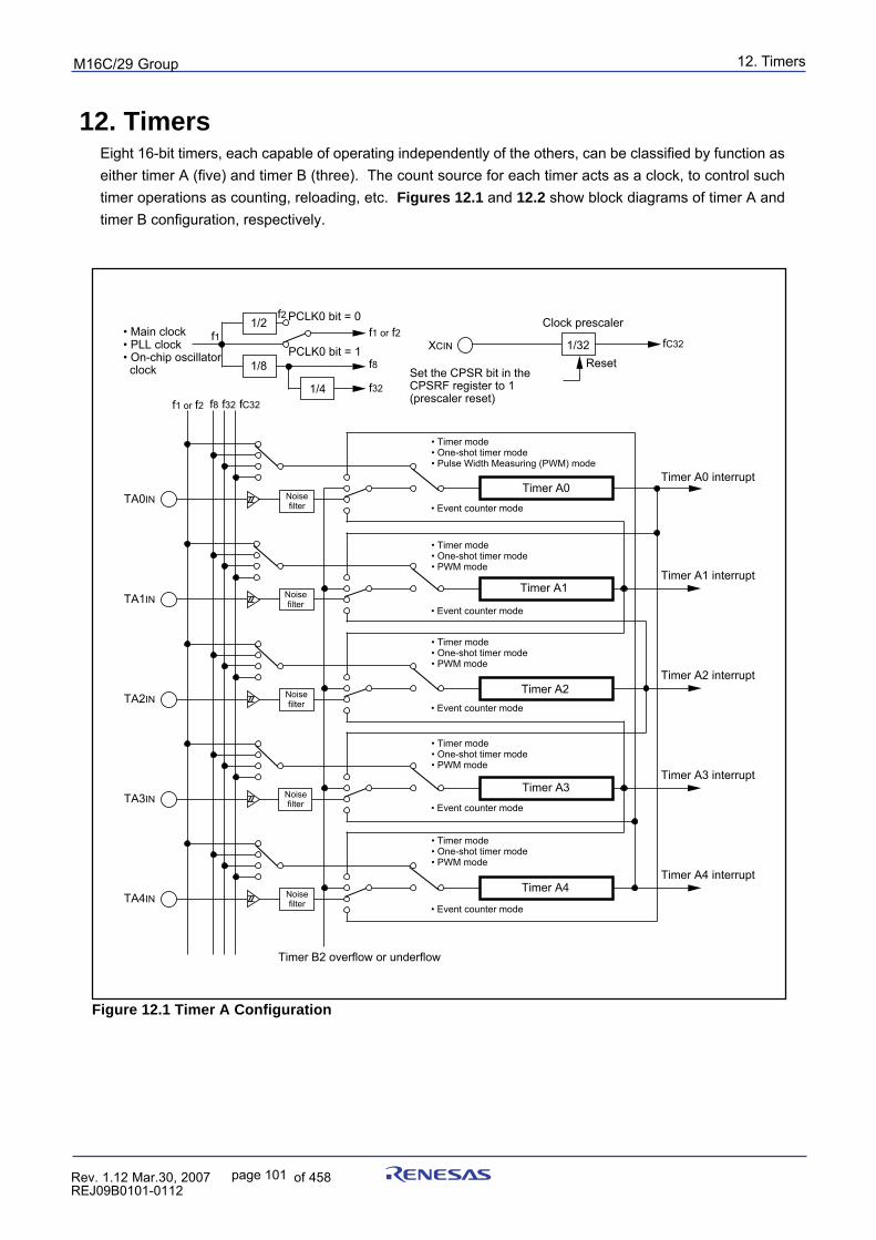
12. TimerspuorG92/C61M
page 101 854fo7002,03.raM21.1.veR2110-1010B90JER
12. TimersEight 16-bit timers, each capable of operating independently of the others, can be classified by function aseither timer A (five) and timer B (three). The count source for each timer acts as a clock, to control suchtimer operations as counting, reloading, etc. Figures 12.1 and 12.2 show block diagrams of timer A andtimer B configuration, respectively.
Figure 12.1 Timer A Configuration
• Timer mode• One-shot timer mode• Pulse Width Measuring (PWM) mode
• Timer mode• One-shot timer mode• PWM mode
• Timer mode• One-shot timer mode• PWM mode
• Timer mode• One-shot timer mode• PWM mode
• Timer mode• One-shot timer mode• PWM mode
• Event counter mode
• Event counter mode
• Event counter mode
• Event counter mode
• Event counter mode
TA0IN
TA1IN
TA2IN
TA3IN
TA4IN
Timer A0
Timer A1
Timer A2
Timer A3
Timer A4
f8 f32 fC32
Timer A0 interrupt
Timer A1 interrupt
Timer A2 interrupt
Timer A3 interrupt
Timer A4 interrupt
Noise filter
Noise filter
Noise filter
Noise filter
Noise filter
1/32 fC32
1/8
1/4
f1 or f2
f8
f32
• Main clock• PLL clock• On-chip oscillator clock
XCIN
Set the CPSR bit in the CPSRF register to 1 (prescaler reset)
Reset
Clock prescaler
Timer B2 overflow or underflow
1/2f1
f2 PCLK0 bit = 0
PCLK0 bit = 1
f1 or f2
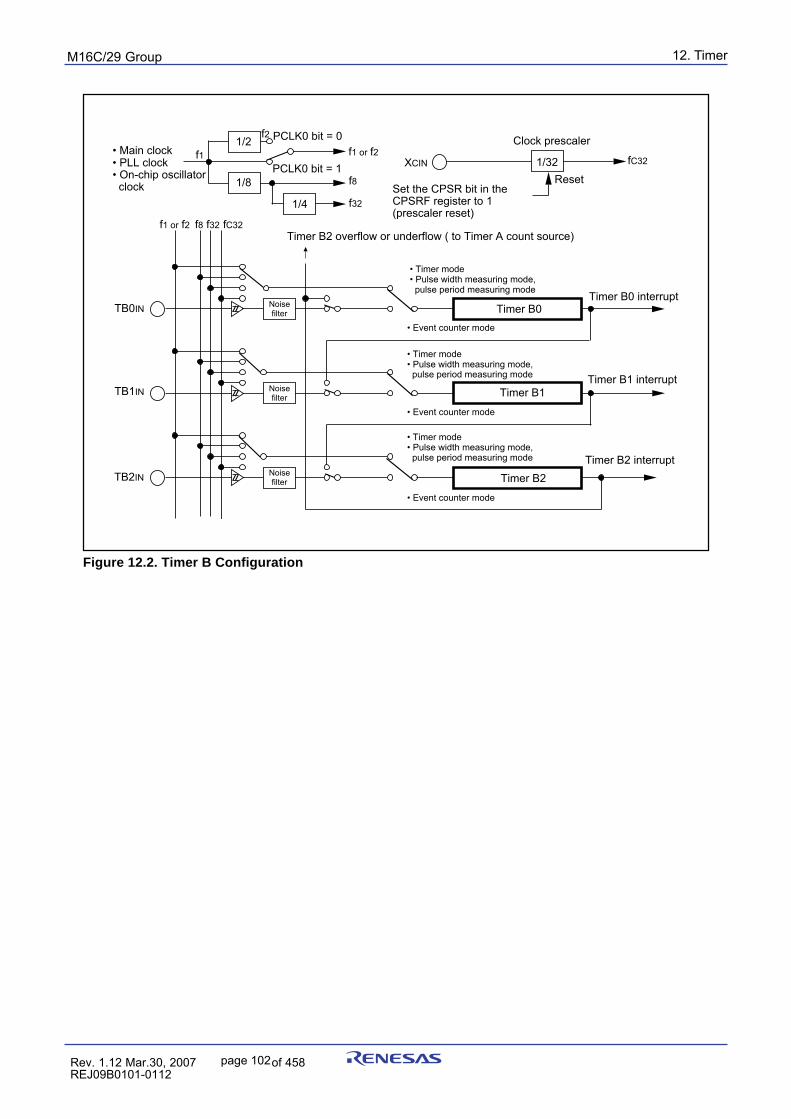
12. Timer
page 102
puorG92/C61M
854fo7002,03.raM21.1.veR2110-1010B90JER
Figure 12.2. Timer B Configuration
• Event counter mode
• Event counter mode
• Event counter mode
• Timer mode • Pulse width measuring mode, pulse period measuring mode
• Timer mode • Pulse width measuring mode, pulse period measuring mode
• Timer mode • Pulse width measuring mode, pulse period measuring mode
TB0IN
TB1IN
TB2IN
Timer B0
Timer B1
Timer B2
f8 f32 fC32
Timer B0 interruptNoise filter
Noise filter
Noise filter
1/32 fC32XCIN
Reset
Clock prescaler
Timer B2 overflow or underflow ( to Timer A count source)
Timer B1 interrupt
Timer B2 interrupt
1/8
1/4
f8
f32
1/2f1 or f2• Main clock
• PLL clock• On-chip oscillator clock Set the CPSR bit in the
CPSRF register to 1 (prescaler reset)
f1
f2 PCLK0 bit = 0
PCLK0 bit = 1
f1 or f2
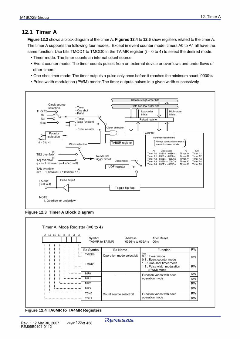
12. Timer A
page 103
puorG92/C61M
854fo7002,03.raM21.1.veR2110-1010B90JER
12.1 Timer AFigure 12.3 shows a block diagram of the timer A. Figures 12.4 to 12.6 show registers related to the timer A.The timer A supports the following four modes. Except in event counter mode, timers A0 to A4 all have thesame function. Use bits TMOD1 to TMOD0 in the TAiMR register (i = 0 to 4) to select the desired mode.
• Timer mode: The timer counts an internal count source.• Event counter mode: The timer counts pulses from an external device or overflows and underflows of
other timers.• One-shot timer mode: The timer outputs a pulse only once before it reaches the minimum count 000016.• Pulse width modulation (PWM) mode: The timer outputs pulses in a given width successively.
Figure 12.4 TA0MR to TA4MR Registers
Figure 12.3 Timer A Block Diagram
TABSR register
Increment/decrement
TAi Addresses TAj TAkTimer A0 038716 - 038616 Timer A4 Timer A1Timer A1 038916 - 038816 Timer A0 Timer A2Timer A2 038B16 - 038A16 Timer A1 Timer A3Timer A3 038D16 - 038C16 Timer A2 Timer A4Timer A4 038F16 - 038E16 Timer A3 Timer A0
Always counts down except in event counter mode
Reload register
Counter
Low-order 8 bits
High-order 8 bits
Clock source selection
• Timer (gate function)
• Timer • One shot • PWM
f1 or f2f8f32
TAiIN (i = 0 to 4)
TB2 overflow
• Event counter
fC32
Clock selection
TAj overflow (j = i – 1. however, j = 4 when i = 0)
Pulse output
Toggle flip-flop
TAiOUT (i = 0 to 4)
Data bus low-order bits
Data bus high-order bits
UDF register
Decrement
TAk overflow (k = i + 1. however, k = 0 when i = 4)
Polarity selection
To external trigger circuit
(1)
(1)
NOTE: 1. Overflow or underflow
Clock selection
Timer Ai Mode Register (i=0 to 4)
Symbol Address After Reset TA0MR to TA4MR 039616 to 039A16 0016
Bit Name FunctionBit Symbol RW
b7 b6 b5 b4 b3 b2 b1 b0
0 0 : Timer mode 0 1 : Event counter mode 1 0 : One-shot timer mode 1 1 : Pulse width modulation (PWM) mode
b1 b0
TCK1
MR3
MR2
MR1
TMOD1
MR0
TMOD0
TCK0
Function varies with each operation mode
Count source select bit
Operation mode select bit RW
RW
RWRWRWRW
RWRW
Function varies with each operation mode
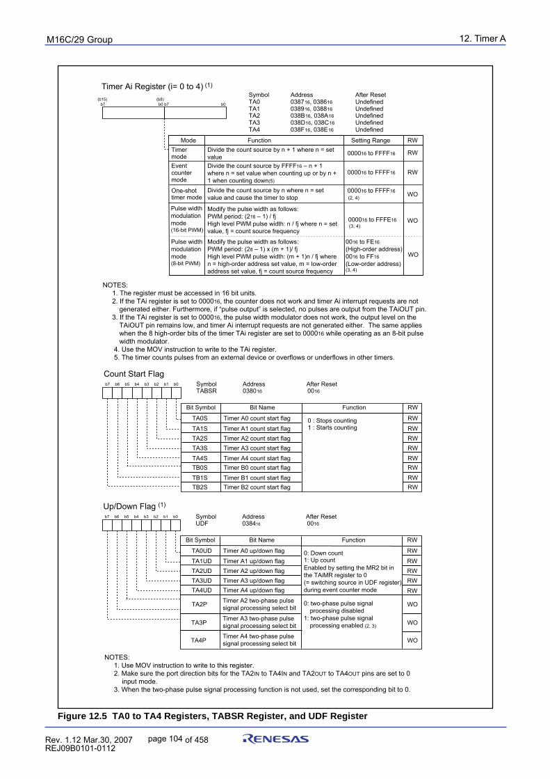
12. Timer ApuorG92/C61M
page 104 854fo7002,03.raM21.1.veR2110-1010B90JER
Figure 12.5 TA0 to TA4 Registers, TABSR Register, and UDF Register
Symbol Address After Reset TA0 038716, 038616 Undefined TA1 038916, 038816 Undefined TA2 038B16, 038A16 Undefined TA3 038D16, 038C16 Undefined TA4 038F16, 038E16 Undefined
b7 b0 b7 b0(b15) (b8)
Timer Ai Register (i= 0 to 4) (1)
Function Setting RangeTimer modeEvent counter mode
One-shot timer mode
Mode RW
WO
RW
RW
WO
WO
Symbol Address After Reset TABSR 038016 0016
Count Start Flagb7 b6 b5 b4 b3 b2 b1 b0
NOTES: 1. The register must be accessed in 16 bit units. 2. If the TAi register is set to 000016, the counter does not work and timer Ai interrupt requests are not
generated either. Furthermore, if “pulse output” is selected, no pulses are output from the TAiOUT pin. 3. If the TAi register is set to 000016, the pulse width modulator does not work, the output level on the
TAiOUT pin remains low, and timer Ai interrupt requests are not generated either. The same applies when the 8 high-order bits of the timer TAi register are set to 000016 while operating as an 8-bit pulse width modulator.
4. Use the MOV instruction to write to the TAi register. 5. The timer counts pulses from an external device or overflows or underflows in other timers.
Divide the count source by n + 1 where n = set value
000016 to FFFE16(3, 4)
000016 to FFFF16
000016 to FFFF16
000016 to FFFF16 (2, 4)
0016 to FE16(High-order address)0016 to FF16(Low-order address)(3, 4)
Modify the pulse width as follows:PWM period: (28 – 1) x (m + 1)/ fjHigh level PWM pulse width: (m + 1)n / fj where n = high-order address set value, m = low-order address set value, fj = count source frequency
Modify the pulse width as follows:PWM period: (216 – 1) / fjHigh level PWM pulse width: n / fj where n = set value, fj = count source frequency
Divide the count source by n where n = set value and cause the timer to stop
Divide the count source by FFFF16 – n + 1 where n = set value when counting up or by n + 1 when counting down(5)
Pulse width modulation mode(16-bit PWM)
Pulse width modulation mode(8-bit PWM)
Bit Name FunctionBit Symbol
0 : Stops counting1 : Starts counting
Timer B2 count start flagTB2STimer B1 count start flagTB1STimer B0 count start flagTB0STimer A4 count start flagTA4STimer A3 count start flagTA3STimer A2 count start flagTA2STimer A1 count start flagTA1S
Timer A0 count start flagTA0S
RW
RW
RWRWRWRWRWRWRW
Symbol Address After Reset UDF 038416 0016
Up/Down Flag (1) b7 b6 b5 b4 b3 b2 b1 b0
Bit Name FunctionBit Symbol
0: Down count1: Up count
TA4P
TA3P
TA2P
Timer A4 up/down flagTA4UDTimer A3 up/down flagTA3UDTimer A2 up/down flagTA2UDTimer A1 up/down flagTA1UD
Timer A0 up/down flagTA0UD
RW
RW
RWRWRWRW
WO
WO
WO
Enabled by setting the MR2 bit in the TAiMR register to 0 (= switching source in UDF register) during event counter mode
0: two-phase pulse signal processing disabled
1: two-phase pulse signal processing enabled (2, 3)
Timer A2 two-phase pulse signal processing select bit
Timer A3 two-phase pulse signal processing select bit
Timer A4 two-phase pulse signal processing select bit
NOTES: 1. Use MOV instruction to write to this register. 2. Make sure the port direction bits for the TA2IN to TA4IN and TA2OUT to TA4OUT pins are set to 0
input mode. 3. When the two-phase pulse signal processing function is not used, set the corresponding bit to 0.
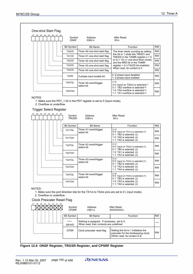
12. Timer ApuorG92/C61M
page 105 854fo7002,03.raM21.1.veR2110-1010B90JER
Figure 12.6 ONSF Register, TRGSR Register, and CPSRF Register
Symbol Address After Reset CPSRF 038116 0XXXXXXX2
Clock Prescaler Reset Flag
Bit Name FunctionBit Symbol
b7 b6 b5 b4 b3 b2 b1 b0
Clock prescaler reset flag Setting this bit to 1 initializes the prescaler for the timekeeping clock. (When read, its content is 0)
CPSR
Nothing is assigned. If necessary, set to 0.When read, their contents are undefined
TA1TGL
Symbol Address After Reset TRGSR 038316 0016
Timer A1 event/trigger select bit 0 0: Input on TA1IN is selected (1)
0 1: TB2 is selected (2)1 0: TA0 is selected (2)1 1: TA2 is selected (2)
Trigger Select Register
Bit Name FunctionBit Symbol
b7 b6 b5 b4 b3 b2 b1 b0
0 0: Input on TA2IN is selected (1) 0 1: TB2 is selected (2) 1 0: TA1 is selected (2) 1 1: TA3 is selected (2)
0 0: Input on TA3IN is selected (1)0 1: TB2 is selected (2)1 0: TA2 is selected (2) 1 1: TA4 is selected (2)
0 0: Input on TA4IN is selected (1)0 1: TB2 is selected (2) 1 0: TA3 is selected (2) 1 1: TA0 is selected (2)
Timer A2 event/trigger select bit
Timer A3 event/trigger select bit
Timer A4 event/trigger select bit
TA1TGH
TA2TGL
TA2TGH
TA3TGL
TA3TGH
TA4TGL
TA4TGH
b1 b0
b3 b2
b5 b4
b7 b6
TA1OS
TA2OS
TA0OS
One-shot Start Flag
Symbol Address After Reset ONSF 038216 0016
Timer A0 one-shot start flag
Timer A1 one-shot start flag
Timer A2 one-shot start flag
Timer A3 one-shot start flag
Timer A4 one-shot start flag
TA3OS
TA4OS
Bit Name FunctionBit Symbol
b7 b6 b5 b4 b3 b2 b1 b0
TA0TGL
TA0TGH
0 0: Input on TA0IN is selected(1)
0 1: TB2 overflow is selected (2)
1 0: TA4 overflow is selected (2)
1 1: TA1 overflow is selected (2)
Timer A0 event/triggerselect bit
b7 b6
RW
The timer starts counting by setting this bit to 1 while bits TMOD1 and TMOD0 in the TAiMR register (i = 0 to 4) = 102 (= one-shot timer mode) and the MR2 bit in the TAiMR register = 0 (=TAiOS bit enabled). When read, its content is 0
Z-phase input enable bitTAZIE 0: Z-phase input disabled1: Z-phase input enabled
RW
RW
RW
RW
RW
RW
RW
RW
RW
RW
RW
RW
RW
RW
RW
RW
RW
RW
RW
(b6-b0)
NOTES: 1. Make sure the PD7_1 bit in the PD7 register is set to 0 (input mode). 2. Overflow or underflow.
NOTES: 1. Make sure the port direction bits for the TA1IN to TA4IN pins are set to 0 ( input mode). 2. Overflow or underflow.
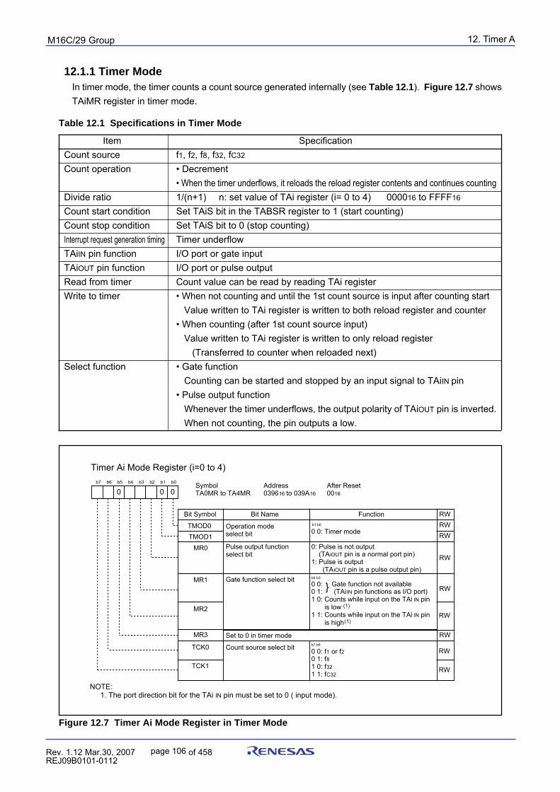
12. Timer ApuorG92/C61M
page 106 854fo7002,03.raM21.1.veR2110-1010B90JER
Item SpecificationCount source f1, f2, f8, f32, fC32
Count operation • Decrement• When the timer underflows, it reloads the reload register contents and continues counting
Divide ratio 1/(n+1) n: set value of TAi register (i= 0 to 4) 000016 to FFFF16
Count start condition Set TAiS bit in the TABSR register to 1 (start counting)Count stop condition Set TAiS bit to 0 (stop counting)Interrupt request generation timing Timer underflowTAiIN pin function I/O port or gate inputTAiOUT pin function I/O port or pulse outputRead from timer Count value can be read by reading TAi registerWrite to timer • When not counting and until the 1st count source is input after counting start
Value written to TAi register is written to both reload register and counter• When counting (after 1st count source input)
Value written to TAi register is written to only reload register(Transferred to counter when reloaded next)
Select function • Gate functionCounting can be started and stopped by an input signal to TAiIN pin
• Pulse output functionWhenever the timer underflows, the output polarity of TAiOUT pin is inverted.When not counting, the pin outputs a low.
12.1.1 Timer ModeIn timer mode, the timer counts a count source generated internally (see Table 12.1). Figure 12.7 showsTAiMR register in timer mode.
Table 12.1 Specifications in Timer Mode
Figure 12.7 Timer Ai Mode Register in Timer Mode
NOTE: 1. The port direction bit for the TAi IN pin must be set to 0 ( input mode).
Timer Ai Mode Register (i=0 to 4)
Symbol Address After Reset TA0MR to TA4MR 039616 to 039A16 0016
Bit Name FunctionBit Symbol RW
b7 b6 b5 b4 b3 b2 b1 b0
Operation mode select bit 0 0: Timer mode
b1 b0
TMOD1TMOD0
MR0 Pulse output function select bit
0: Pulse is not output (TAiOUT pin is a normal port pin)1: Pulse is output (TAiOUT pin is a pulse output pin)
Gate function select bit0 0: Gate function not available0 1: (TAiIN pin functions as I/O port)1 0: Counts while input on the TAi IN pin is low (1)
1 1: Counts while input on the TAi IN pin is high(1)
b4 b3
MR2
MR1
MR3 Set to 0 in timer mode
0 0: f1 or f2 0 1: f8 1 0: f32 1 1: fC32
b7 b6
TCK1
TCK0 Count source select bit
0 00
RWRW
RW
RW
RW
RW
RW
RW
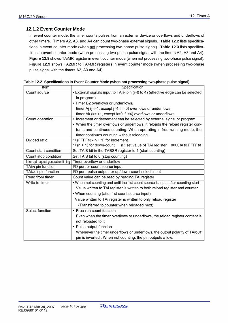
12. Timer ApuorG92/C61M
page 107 854fo7002,03.raM21.1.veR2110-1010B90JER
Item SpecificationCount source • External signals input to TAiIN pin (i=0 to 4) (effective edge can be selected
in program)• Timer B2 overflows or underflows,
timer Aj (j=i-1, except j=4 if i=0) overflows or underflows,timer Ak (k=i+1, except k=0 if i=4) overflows or underflows
Count operation • Increment or decrement can be selected by external signal or program• When the timer overflows or underflows, it reloads the reload register con-
tents and continues counting. When operating in free-running mode, thetimer continues counting without reloading.
Divided ratio 1/ (FFFF16 - n + 1) for increment1/ (n + 1) for down-count n : set value of TAi register 000016 to FFFF16
Count start condition Set TAiS bit in the TABSR register to 1 (start counting)Count stop condition Set TAiS bit to 0 (stop counting)Interrupt request generation timing Timer overflow or underflowTAiIN pin function I/O port or count source inputTAiOUT pin function I/O port, pulse output, or up/down-count select inputRead from timer Count value can be read by reading TAi registerWrite to timer • When not counting and until the 1st count source is input after counting start
Value written to TAi register is written to both reload register and counter • When counting (after 1st count source input)
Value written to TAi register is written to only reload register(Transferred to counter when reloaded next)
Select function • Free-run count functionEven when the timer overflows or underflows, the reload register content isnot reloaded to it
• Pulse output functionWhenever the timer underflows or underflows, the output polarity of TAiOUT
pin is inverted . When not counting, the pin outputs a low.
12.1.2 Event Counter ModeIn event counter mode, the timer counts pulses from an external device or overflows and underflows ofother timers. Timers A2, A3, and A4 can count two-phase external signals. Table 12.2 lists specifica-tions in event counter mode (when not processing two-phase pulse signal). Table 12.3 lists specifica-tions in event counter mode (when processing two-phase pulse signal with the timers A2, A3 and A4).Figure 12.8 shows TAiMR register in event counter mode (when not processing two-phase pulse signal).Figure 12.9 shows TA2MR to TA4MR registers in event counter mode (when processing two-phasepulse signal with the timers A2, A3 and A4).
Table 12.2 Specifications in Event Counter Mode (when not processing two-phase pulse signal)
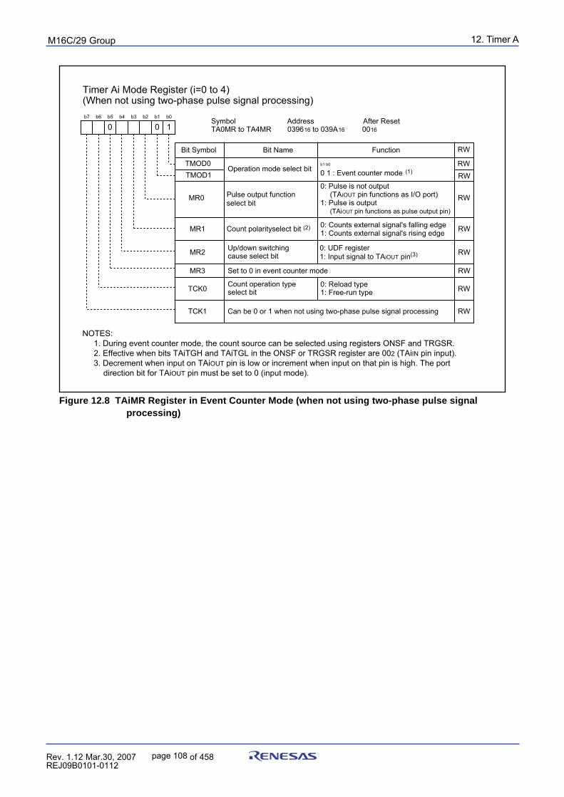
12. Timer ApuorG92/C61M
page 108 854fo7002,03.raM21.1.veR2110-1010B90JER
Figure 12.8 TAiMR Register in Event Counter Mode (when not using two-phase pulse signalprocessing)
Symbol Address After Reset TA0MR to TA4MR 039616 to 039A16 0016
WR
b7 b6 b5 b4 b3 b2 b1 b0
Operation mode select bit 0 1 : Event counter mode (1)b1 b0 TMOD0
MR0 0: Pulse is not output (TAiOUT pin functions as I/O port)1: Pulse is output (TAiOUT pin functions as pulse output pin)
MR2
MR1
MR3 Set to 0 in event counter mode
TCK0 Count operation type select bit
0 10
0: Counts external signal's falling edge1: Counts external signal's rising edge
Up/down switching cause select bit
0: Reload type1: Free-run type
Bit Symbol Bit Name Function RW
TCK1 Can be 0 or 1 when not using two-phase pulse signal processing
TMOD1
Timer Ai Mode Register (i=0 to 4)(When not using two-phase pulse signal processing)
RW
RW
RW
RW
RW
RW
RW
RW
NOTES: 1. During event counter mode, the count source can be selected using registers ONSF and TRGSR. 2. Effective when bits TAiTGH and TAiTGL in the ONSF or TRGSR register are 002 (TAiIN pin input). 3. Decrement when input on TAiOUT pin is low or increment when input on that pin is high. The port
direction bit for TAiOUT pin must be set to 0 (input mode).
Pulse output function select bit
Count polarityselect bit (2)
0: UDF register1: Input signal to TAiOUT pin(3)
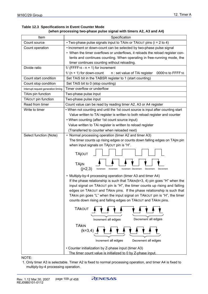
12. Timer ApuorG92/C61M
page 109 854fo7002,03.raM21.1.veR2110-1010B90JER
Item SpecificationCount source • Two-phase pulse signals input to TAiIN or TAiOUT pins (i = 2 to 4)Count operation • Increment or down-count can be selected by two-phase pulse signal
• When the timer overflows or underflows, it reloads the reload register con-tents and continues counting. When operating in free-running mode, thetimer continues counting without reloading.
Divide ratio 1/ (FFFF16 - n + 1) for increment1/ (n + 1) for down-count n : set value of TAi register 000016 to FFFF16
Count start condition Set TAiS bit in the TABSR register to 1 (start counting)Count stop condition Set TAiS bit to 0 (stop counting)Interrupt request generation timing Timer overflow or underflowTAiIN pin function Two-phase pulse inputTAiOUT pin function Two-phase pulse inputRead from timer Count value can be read by reading timer A2, A3 or A4 registerWrite to timer • When not counting and until the 1st count source is input after counting start
Value written to TAi register is written to both reload register and counter • When counting (after 1st count source input)
Value written to TAi register is written to reload register(Transferred to counter when reloaded next)
Select function (Note) • Normal processing operation (timer A2 and timer A3)The timer counts up rising edges or counts down falling edges on TAjIN pinwhen input signals on TAjOUT pin is “H”.
• Multiply-by-4 processing operation (timer A3 and timer A4)If the phase relationship is such that TAkIN(k=3, 4) pin goes “H” when theinput signal on TAkOUT pin is “H”, the timer counts up rising and fallingedges on TAkOUT and TAkIN pins. If the phase relationship is such thatTAkIN pin goes “L” when the input signal on TAkOUT pin is “H”, the timercounts down rising and falling edges on TAkOUT and TAkIN pins.
Table 12.3 Specifications in Event Counter Mode (when processing two-phase pulse signal with timers A2, A3 and A4)
• Counter initialization by Z-phase input (timer A3)The timer count value is initialized to 0 by Z-phase input.
NOTE: 1. Only timer A3 is selectable. Timer A2 is fixed to normal processing operation, and timer A4 is fixed to
multiply-by-4 processing operation.
TAjOUT
Increment Increment Increment Decrement Decrement Decrement
TAjIN(j=2,3)
TAkOUT
TAkIN(k=3,4)
Increment all edges
Increment all edges
Decrement all edges
Decrement all edges
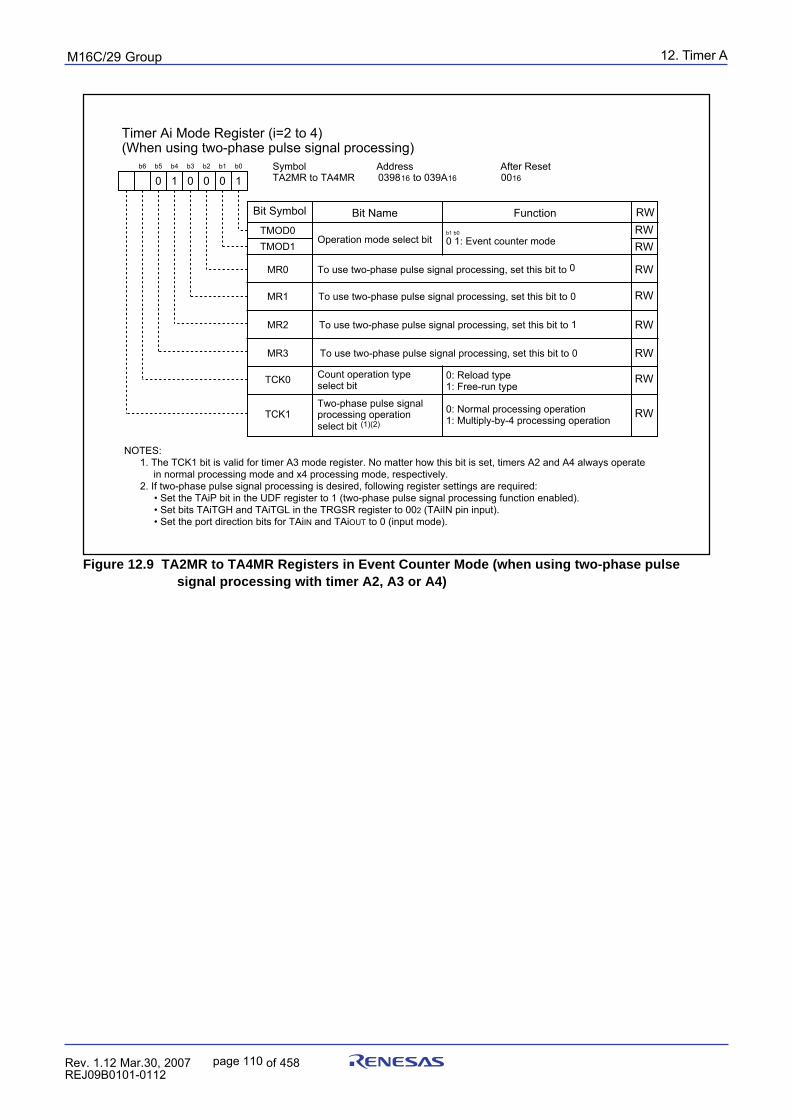
12. Timer ApuorG92/C61M
page 110 854fo7002,03.raM21.1.veR2110-1010B90JER
Figure 12.9 TA2MR to TA4MR Registers in Event Counter Mode (when using two-phase pulsesignal processing with timer A2, A3 or A4)
Timer Ai Mode Register (i=2 to 4) (When using two-phase pulse signal processing)
Symbol Address After Reset TA2MR to TA4MR 039816 to 039A16 0016
b6 b5 b4 b3 b2 b1 b0
Operation mode select bit 0 1: Event counter modeb1 b0
TMOD1TMOD0
MR0 To use two-phase pulse signal processing, set this bit to 0
MR2
MR1
MR3
TCK1
TCK0
0 10
Bit Name Function RW
Count operation type select bit
Two-phase pulse signal processing operation select bit (1)(2)
0: Reload type1: Free-run type
0: Normal processing operation1: Multiply-by-4 processing operation
001
To use two-phase pulse signal processing, set this bit to 0
To use two-phase pulse signal processing, set this bit to 1
To use two-phase pulse signal processing, set this bit to 0
Bit Symbol
RWRW
RW
RW
RW
RW
RW
RW
NOTES:1. The TCK1 bit is valid for timer A3 mode register. No matter how this bit is set, timers A2 and A4 always operate
in normal processing mode and x4 processing mode, respectively.2. If two-phase pulse signal processing is desired, following register settings are required: • Set the TAiP bit in the UDF register to 1 (two-phase pulse signal processing function enabled). • Set bits TAiTGH and TAiTGL in the TRGSR register to 002 (TAiIN pin input). • Set the port direction bits for TAiIN and TAiOUT to 0 (input mode).
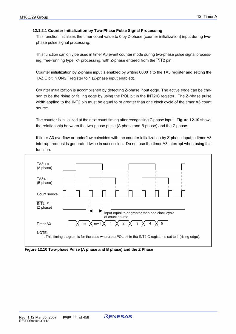
12. Timer ApuorG92/C61M
page 111 854fo7002,03.raM21.1.veR2110-1010B90JER
12.1.2.1 Counter Initialization by Two-Phase Pulse Signal Processing
This function initializes the timer count value to 0 by Z-phase (counter initialization) input during two-phase pulse signal processing.
This function can only be used in timer A3 event counter mode during two-phase pulse signal process-_______
ing, free-running type, x4 processing, with Z-phase entered from the INT2 pin.
Counter initialization by Z-phase input is enabled by writing 000016 to the TA3 register and setting theTAZIE bit in ONSF register to 1 (Z-phase input enabled).
Counter initialization is accomplished by detecting Z-phase input edge. The active edge can be cho-sen to be the rising or falling edge by using the POL bit in the INT2IC register. The Z-phase pulse
_______
width applied to the INT2 pin must be equal to or greater than one clock cycle of the timer A3 countsource.
The counter is initialized at the next count timing after recognizing Z-phase input. Figure 12.10 showsthe relationship between the two-phase pulse (A phase and B phase) and the Z phase.
If timer A3 overflow or underflow coincides with the counter initialization by Z-phase input, a timer A3interrupt request is generated twice in succession. Do not use the timer A3 interrupt when using thisfunction.
Figure 12.10 Two-phase Pulse (A phase and B phase) and the Z Phase
m m+1 1 2 3 4 5
TA3OUT(A phase)
Count source
TA3IN(B phase)
Timer A3
INT2 (Z phase)
(1)
Input equal to or greater than one clock cycle of count source
NOTE: 1. This timing diagram is for the case where the POL bit in the INT2IC register is set to 1 (rising edge).
12. Timer ApuorG92/C61M
page 112 854fo7002,03.raM21.1.veR2110-1010B90JER
Item SpecificationCount source f1, f2, f8, f32, fC32
Count operation • Decrement• When the counter reaches 000016, it stops counting after reloading a new value• If a trigger occurs when counting, the timer reloads a new count and restarts counting
Divide ratio 1/n n : set value of TAi register 000016 to FFFF16
However, the counter does not work if the divide-by-n value is set to 000016.Count start condition TAiS bit in the TABSR register is set to 1 (start counting) and one of the
following triggers occurs.• External trigger input from the TAiIN pin• Timer B2 overflow or underflow,
timer Aj (j=i-1, except j=4 if i=0) overflow or underflow,timer Ak (k=i+1, except k=0 if i=4) overflow or underflow
• The TAiOS bit in the ONSF register is set to 1 (timer starts)Count stop condition • When the counter is reloaded after reaching 000016
• TAiS bit is set to 0 (stop counting)Interrupt request generation timing When the counter reaches 000016
TAiIN pin function I/O port or trigger inputTAiOUT pin function I/O port or pulse outputRead from timer An undefined value is read by reading TAi registerWrite to timer • When not counting and until the 1st count source is input after counting start
Value written to TAi register is written to both reload register and counter• When counting (after 1st count source input)
Value written to TAi register is written to only reload register(Transferred to counter when reloaded next)
Select function • Pulse output functionThe timer outputs a low when not counting and a high when counting.
Table 12.4 Specifications in One-shot Timer Mode
12.1.3 One-shot Timer ModeIn one-shot timer mode, the timer is activated only once by one trigger. (See Table 12.4) When thetrigger occurs, the timer starts up and continues operating for a given period. Figure 12.11 shows theTAiMR register in one-shot timer mode.
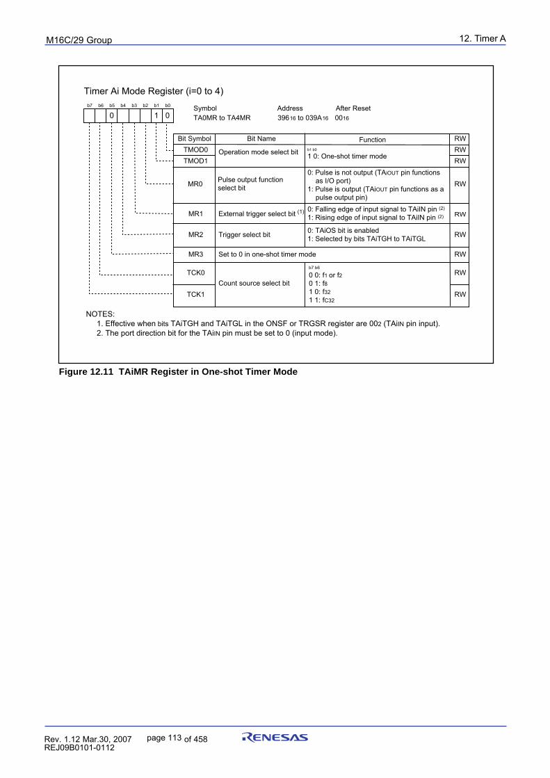
12. Timer ApuorG92/C61M
page 113 854fo7002,03.raM21.1.veR2110-1010B90JER
Figure 12.11 TAiMR Register in One-shot Timer Mode
Bit Name
Timer Ai Mode Register (i=0 to 4)
Symbol Address After Reset TA0MR to TA4MR 39616 to 039A16 0016
Function Bit Symbol
b7 b6 b5 b4 b3 b2 b1 b0
Operation mode select bit 1 0: One-shot timer modeb1 b0
TMOD1TMOD0
MR0
MR2
MR1
MR3 Set to 0 in one-shot timer mode
TCK1
TCK0Count source select bit
1 00
Trigger select bit
External trigger select bit (1)
RWRWRW
RW
RW
RW
RW
RW
RW
NOTES: 1. Effective when bits TAiTGH and TAiTGL in the ONSF or TRGSR register are 002 (TAiIN pin input). 2. The port direction bit for the TAiIN pin must be set to 0 (input mode).
0: Pulse is not output (TAiOUT pin functions as I/O port)
1: Pulse is output (TAiOUT pin functions as a pulse output pin)
0: TAiOS bit is enabled1: Selected by bits TAiTGH to TAiTGL
0: Falling edge of input signal to TAiIN pin (2)
1: Rising edge of input signal to TAiIN pin (2)
Pulse output function select bit
b7 b6
0 0: f1 or f20 1: f81 0: f321 1: fC32
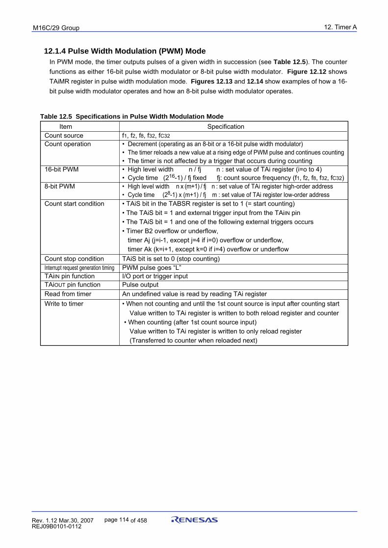
12. Timer ApuorG92/C61M
page 114 854fo7002,03.raM21.1.veR2110-1010B90JER
12.1.4 Pulse Width Modulation (PWM) ModeIn PWM mode, the timer outputs pulses of a given width in succession (see Table 12.5). The counterfunctions as either 16-bit pulse width modulator or 8-bit pulse width modulator. Figure 12.12 showsTAiMR register in pulse width modulation mode. Figures 12.13 and 12.14 show examples of how a 16-bit pulse width modulator operates and how an 8-bit pulse width modulator operates.
Table 12.5 Specifications in Pulse Width Modulation Mode
Item SpecificationCount source f1, f2, f8, f32, fC32Count operation • Decrement (operating as an 8-bit or a 16-bit pulse width modulator)
• The timer reloads a new value at a rising edge of PWM pulse and continues counting• The timer is not affected by a trigger that occurs during counting
16-bit PWM • High level width n / fj n : set value of TAi register (i=o to 4)• Cycle time (216-1) / fj fixed fj: count source frequency (f1, f2, f8, f32, fC32)
8-bit PWM • High level width n x (m+1) / fj n : set value of TAi register high-order address• Cycle time (28-1) x (m+1) / fj m : set value of TAi register low-order address
Count start condition • TAiS bit in the TABSR register is set to 1 (= start counting)• The TAiS bit = 1 and external trigger input from the TAiIN pin• The TAiS bit = 1 and one of the following external triggers occurs• Timer B2 overflow or underflow,
timer Aj (j=i-1, except j=4 if i=0) overflow or underflow,timer Ak (k=i+1, except k=0 if i=4) overflow or underflow
Count stop condition TAiS bit is set to 0 (stop counting)Interrupt request generation timing PWM pulse goes “L”TAiIN pin function I/O port or trigger inputTAiOUT pin function Pulse outputRead from timer An undefined value is read by reading TAi registerWrite to timer • When not counting and until the 1st count source is input after counting start
Value written to TAi register is written to both reload register and counter• When counting (after 1st count source input)
Value written to TAi register is written to only reload register(Transferred to counter when reloaded next)
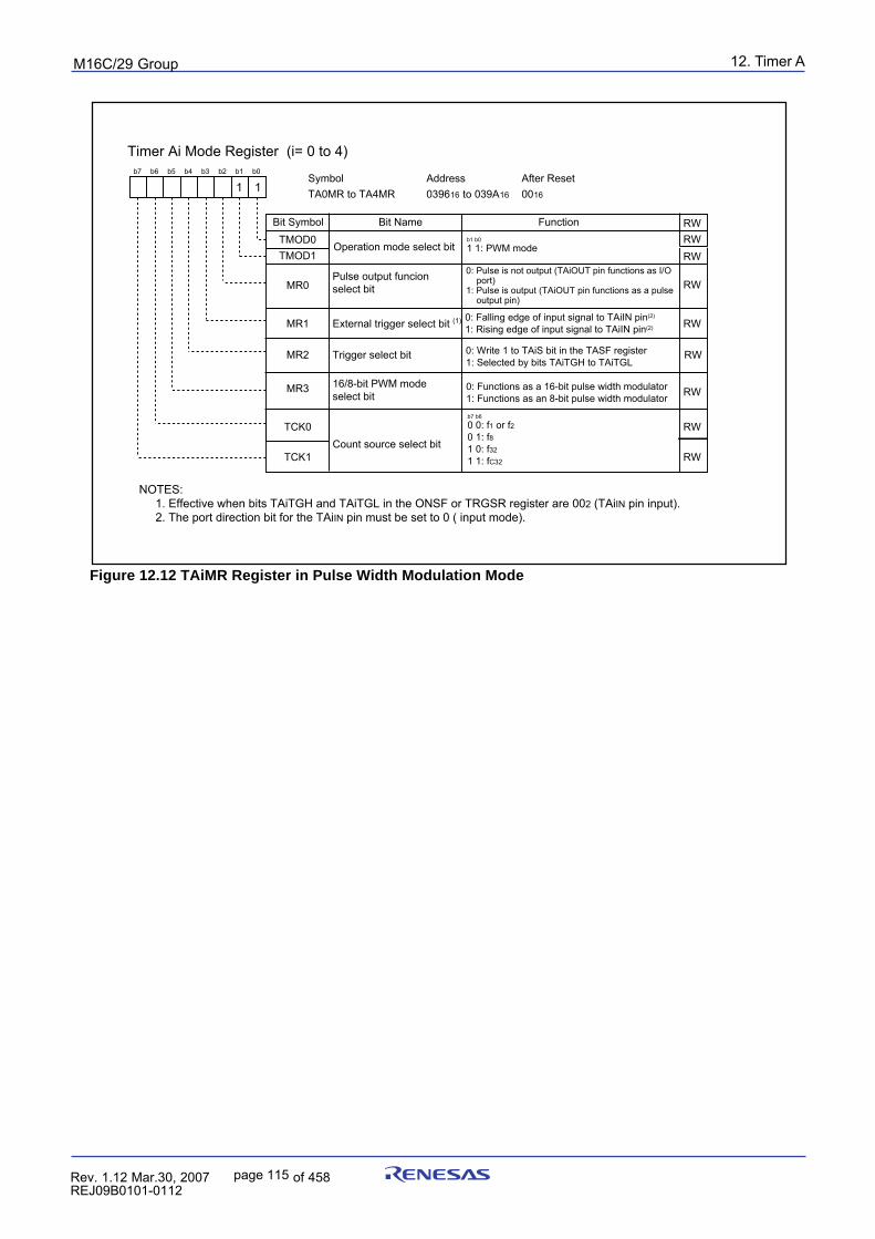
12. Timer ApuorG92/C61M
page 115 854fo7002,03.raM21.1.veR2110-1010B90JER
Figure 12.12 TAiMR Register in Pulse Width Modulation Mode
Bit Name
Timer Ai Mode Register (i= 0 to 4)
Symbol Address After Reset TA0MR to TA4MR 039616 to 039A16 0016
FunctionBit Symbol
b7 b6 b5 b4 b3 b2 b1 b0
b1 b0
1 1: PWM modeTMOD1TMOD0
MR0
MR2
MR1
MR3
TCK1
TCK0Count source select bit
RW
1 1
0: Functions as a 16-bit pulse width modulator1: Functions as an 8-bit pulse width modulator
Trigger select bit
External trigger select bit (1)
RWRW
RW
RW
RW
RW
RW
RW
0: Write 1 to TAiS bit in the TASF register1: Selected by bits TAiTGH to TAiTGL
NOTES: 1. Effective when bits TAiTGH and TAiTGL in the ONSF or TRGSR register are 002 (TAiIN pin input). 2. The port direction bit for the TAiIN pin must be set to 0 ( input mode).
16/8-bit PWM mode select bit
Pulse output funcion select bit
Operation mode select bit
0: Falling edge of input signal to TAiIN pin(2)
1: Rising edge of input signal to TAiIN pin(2)
b7 b6
0 0: f1 or f20 1: f81 0: f32
1 1: fC32
0: Pulse is not output (TAiOUT pin functions as I/O port)
1: Pulse is output (TAiOUT pin functions as a pulse output pin)
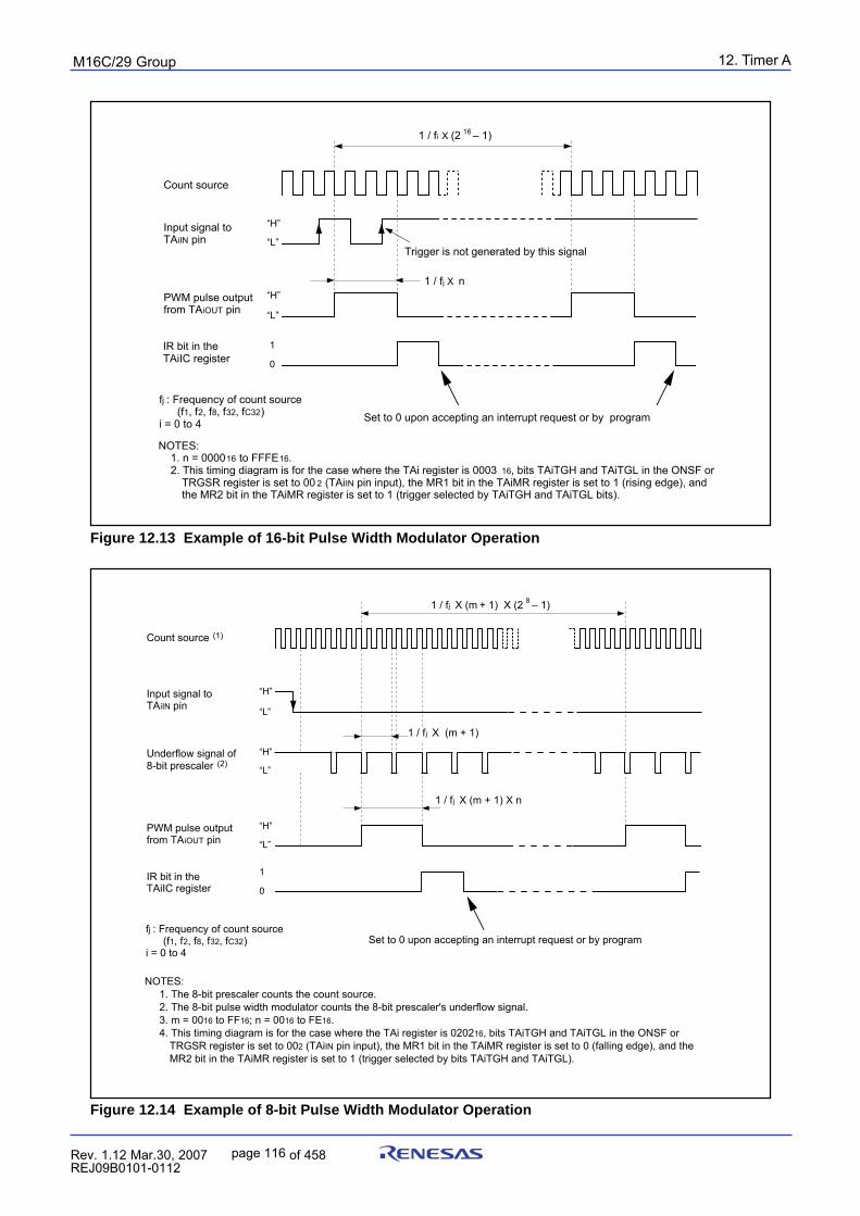
12. Timer ApuorG92/C61M
page 116 854fo7002,03.raM21.1.veR2110-1010B90JER
Figure 12.13 Example of 16-bit Pulse Width Modulator Operation
Figure 12.14 Example of 8-bit Pulse Width Modulator Operation
1 / fi X (2 – 1) 16
Count source
Input signal to TAiIN pin
PWM pulse output from TAiOUT pin
Trigger is not generated by this signal
“H”
“H”
“L”
“L”
IR bit in the TAiIC register
1
0
fj : Frequency of count source (f1, f2, f8, f32, fC32)i = 0 to 4
NOTES: 1. n = 000016 to FFFE16. 2. This timing diagram is for the case where the TAi register is 0003 16, bits TAiTGH and TAiTGL in the ONSF or
TRGSR register is set to 00 2 (TAiIN pin input), the MR1 bit in the TAiMR register is set to 1 (rising edge), and the MR2 bit in the TAiMR register is set to 1 (trigger selected by TAiTGH and TAiTGL bits).
1 / fj X n
Set to 0 upon accepting an interrupt request or by program
Count source (1)
Input signal to TAiIN pin
Underflow signal of 8-bit prescaler (2)
PWM pulse output from TAiOUT pin
“H”
“H”
“H”
“L”
“L”
“L”
1
0
Set to 0 upon accepting an interrupt request or by program
1 / fj X (m + 1) X (2 – 1) 8
1 / fj X (m + 1) X n
1 / fj X (m + 1)
IR bit in the TAiIC register
fj : Frequency of count source (f1, f2, f8, f32, fC32)i = 0 to 4
NOTES: 1. The 8-bit prescaler counts the count source. 2. The 8-bit pulse width modulator counts the 8-bit prescaler's underflow signal. 3. m = 0016 to FF16; n = 0016 to FE16. 4. This timing diagram is for the case where the TAi register is 020216, bits TAiTGH and TAiTGL in the ONSF or
TRGSR register is set to 002 (TAiIN pin input), the MR1 bit in the TAiMR register is set to 0 (falling edge), and the MR2 bit in the TAiMR register is set to 1 (trigger selected by bits TAiTGH and TAiTGL).
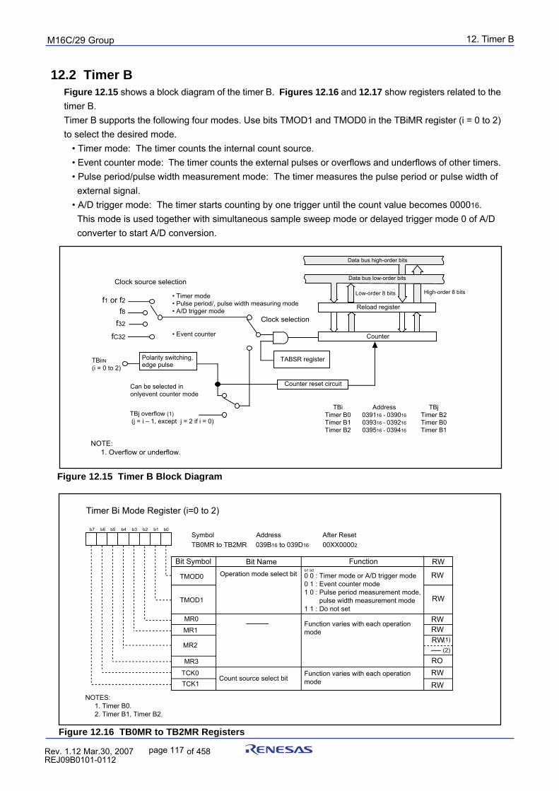
12. Timer BpuorG92/C61M
page 117 854fo7002,03.raM21.1.veR2110-1010B90JER
12.2 Timer BFigure 12.15 shows a block diagram of the timer B. Figures 12.16 and 12.17 show registers related to thetimer B.Timer B supports the following four modes. Use bits TMOD1 and TMOD0 in the TBiMR register (i = 0 to 2)to select the desired mode.
• Timer mode: The timer counts the internal count source.• Event counter mode: The timer counts the external pulses or overflows and underflows of other timers.• Pulse period/pulse width measurement mode: The timer measures the pulse period or pulse width of external signal.• A/D trigger mode: The timer starts counting by one trigger until the count value becomes 000016. This mode is used together with simultaneous sample sweep mode or delayed trigger mode 0 of A/D converter to start A/D conversion.
Figure 12.15 Timer B Block Diagram
Figure 12.16 TB0MR to TB2MR Registers
Clock source selection
• Event counter
Reload register
Low-order 8 bits High-order 8 bits
Data bus low-order bits
Data bus high-order bits
f8
TABSR registerPolarity switching, edge pulse
Counter reset circuit
Counter
Clock selection
• Timer mode• Pulse period/, pulse width measuring mode• A/D trigger mode
f1 or f2
fC32
f32
TBj overflow (1) (j = i – 1, except j = 2 if i = 0)
Can be selected in onlyevent counter mode
TBiIN(i = 0 to 2)
NOTE: 1. Overflow or underflow.
TBi Address TBj Timer B0 039116 - 039016 Timer B2 Timer B1 039316 - 039216 Timer B0 Timer B2 039516 - 039416 Timer B1
Timer Bi Mode Register (i=0 to 2)
Symbol After Reset TB0MR to TB2MR
Bit Name Function Bit Symbol RW
b7 b6 b5 b4 b3 b2 b1 b0
b1 b0
TCK1
MR3
MR2
MR1
TMOD1
MR0
TMOD0
TCK0
Operation mode select bit
(1)
(2)
RW
RW
RW RWRW
RW RW
RO
NOTES: 1. Timer B0. 2. Timer B1, Timer B2.
Function varies with each operation modeCount source select bit
Function varies with each operation mode
Address 039B16 to 039D16 00XX00002
0 0 : Timer mode or A/D trigger mode0 1 : Event counter mode1 0 : Pulse period measurement mode, pulse width measurement mode1 1 : Do not set
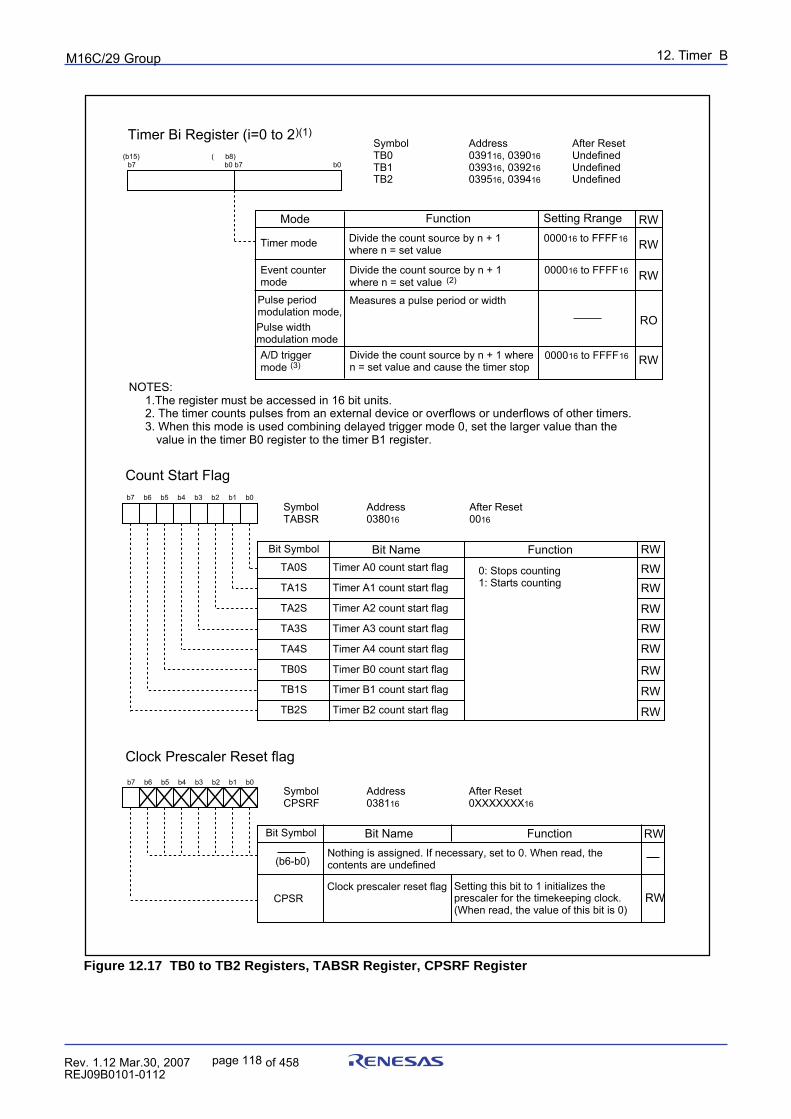
12. Timer BpuorG92/C61M
page 118 854fo7002,03.raM21.1.veR2110-1010B90JER
Figure 12.17 TB0 to TB2 Registers, TABSR Register, CPSRF Register
Symbol Address After Reset TABSR 038016 0016
Count Start Flag
Bit NameBit Symbol
b7 b6 b5 b4 b3 b2 b1 b0
Timer B2 count start flag
Timer B1 count start flag
Timer B0 count start flag
Timer A4 count start flag
Timer A3 count start flag
Timer A2 count start flag
Timer A1 count start flag
Timer A0 count start flag 0: Stops counting1: Starts counting
TB2S
TB1S
TB0S
TA4S
TA3S
TA2S
TA1S
TA0SFunction RW
RWRW
RW
RW
RW
RW
RW
RW
Symbol Address After Reset CPSRF 038116 0XXXXXXX16
Clock Prescaler Reset flag
Bit Name FunctionBit Symbol
b7 b6 b5 b4 b3 b2 b1 b0
Clock prescaler reset flagCPSR
Nothing is assigned. If necessary, set to 0. When read, thecontents are undefined
RW
RW
(b6-b0)
Setting this bit to 1 initializes the prescaler for the timekeeping clock.(When read, the value of this bit is 0)
Symbol Address After Reset TB0 039116, 039016 Undefined TB1 039316, 039216 Undefined TB2 039516, 039416 Undefined
b7 b0 b7 b0(b15) ( b8)
Timer Bi Register (i=0 to 2)(1)
RW
Measures a pulse period or width
Function
RW
RW
RO
NOTES: 1.The register must be accessed in 16 bit units. 2. The timer counts pulses from an external device or overflows or underflows of other timers. 3. When this mode is used combining delayed trigger mode 0, set the larger value than the
value in the timer B0 register to the timer B1 register.
Divide the count source by n + 1 where n = set value
Timer mode
Event counter mode
000016 to FFFF16
Divide the count source by n + 1 where n = set value (2)
000016 to FFFF16
Pulse periodmodulation mode,Pulse width modulation mode
Mode Setting Rrange
A/D trigger mode (3)
Divide the count source by n + 1 wheren = set value and cause the timer stop RW000016 to FFFF16
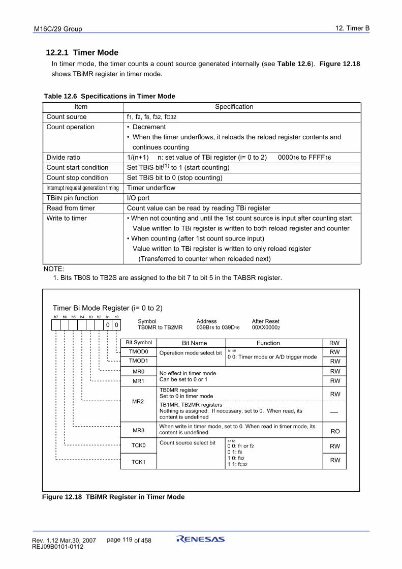
12. Timer BpuorG92/C61M
page 119 854fo7002,03.raM21.1.veR2110-1010B90JER
Item SpecificationCount source f1, f2, f8, f32, fC32
Count operation • Decrement• When the timer underflows, it reloads the reload register contents and
continues countingDivide ratio 1/(n+1) n: set value of TBi register (i= 0 to 2) 000016 to FFFF16
Count start condition Set TBiS bit(1) to 1 (start counting)Count stop condition Set TBiS bit to 0 (stop counting)Interrupt request generation timing Timer underflowTBiIN pin function I/O portRead from timer Count value can be read by reading TBi registerWrite to timer • When not counting and until the 1st count source is input after counting start
Value written to TBi register is written to both reload register and counter• When counting (after 1st count source input)
Value written to TBi register is written to only reload register(Transferred to counter when reloaded next)
NOTE: 1. Bits TB0S to TB2S are assigned to the bit 7 to bit 5 in the TABSR register.
12.2.1 Timer ModeIn timer mode, the timer counts a count source generated internally (see Table 12.6). Figure 12.18
shows TBiMR register in timer mode.
Table 12.6 Specifications in Timer Mode
Figure 12.18 TBiMR Register in Timer Mode
Timer Bi Mode Register (i= 0 to 2)
Symbol Address After ResetTB0MR to TB2MR 039B16 to 039D16 00XX00002
Bit Name FunctionBit Symbol RW
b7 b6 b5 b4 b3 b2 b1 b0
AAA
Operation mode select bit0 0: Timer mode or A/D trigger modeb1 b0
TMOD1TMOD0
MR0 No effect in timer mode Can be set to 0 or 1
MR2
MR1
MR3
0 0: f1 or f20 1: f81 0: f321 1: fC32TCK1
TCK0 Count source select bit
00
TB0MR registerSet to 0 in timer mode
b7 b6
RWRWRWRW
RW
RW
RW
RO
TB1MR, TB2MR registersNothing is assigned. If necessary, set to 0. When read, its content is undefined
When write in timer mode, set to 0. When read in timer mode, its content is undefined
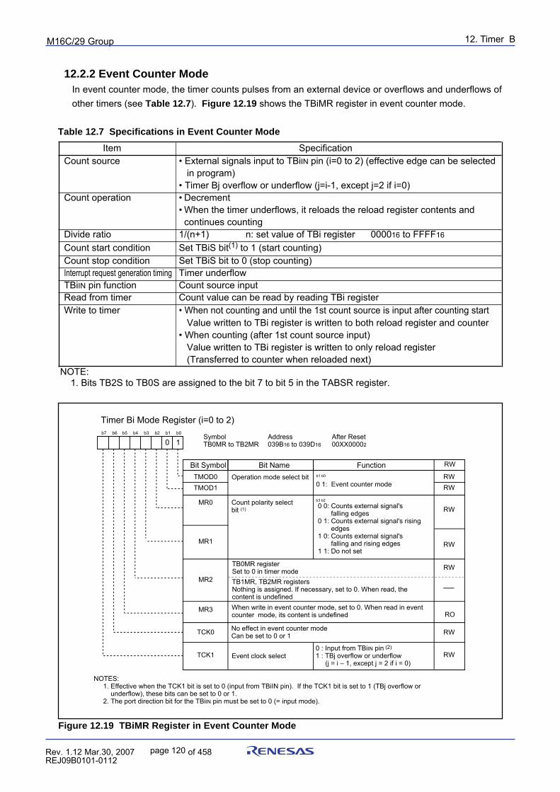
12. Timer BpuorG92/C61M
page 120 854fo7002,03.raM21.1.veR2110-1010B90JER
Item SpecificationCount source • External signals input to TBiIN pin (i=0 to 2) (effective edge can be selected
in program)• Timer Bj overflow or underflow (j=i-1, except j=2 if i=0)
Count operation • Decrement• When the timer underflows, it reloads the reload register contents and
continues countingDivide ratio 1/(n+1) n: set value of TBi register 000016 to FFFF16
Count start condition Set TBiS bit(1) to 1 (start counting)Count stop condition Set TBiS bit to 0 (stop counting)Interrupt request generation timing Timer underflowTBiIN pin function Count source inputRead from timer Count value can be read by reading TBi registerWrite to timer • When not counting and until the 1st count source is input after counting start
Value written to TBi register is written to both reload register and counter• When counting (after 1st count source input)
Value written to TBi register is written to only reload register(Transferred to counter when reloaded next)
NOTE: 1. Bits TB2S to TB0S are assigned to the bit 7 to bit 5 in the TABSR register.
12.2.2 Event Counter ModeIn event counter mode, the timer counts pulses from an external device or overflows and underflows ofother timers (see Table 12.7). Figure 12.19 shows the TBiMR register in event counter mode.
Table 12.7 Specifications in Event Counter Mode
Figure 12.19 TBiMR Register in Event Counter Mode
Timer Bi Mode Register (i=0 to 2)
Symbol Address After ResetTB0MR to TB2MR 039B16 to 039D16 00XX00002
Bit Name FunctionBit Symbol RW
b7 b6 b5 b4 b3 b2 b1 b0
A
Operation mode select bit0 1: Event counter mode b1 b0
TMOD1TMOD0
MR0 Count polarity select bit (1)
MR2
MR1
MR3
TCK1
TCK0
0 1
0 0: Counts external signal's falling edges
0 1: Counts external signal's rising edges
1 0: Counts external signal's falling and rising edges
1 1: Do not set
b3 b2
NOTES: 1. Effective when the TCK1 bit is set to 0 (input from TBiIN pin). If the TCK1 bit is set to 1 (TBj overflow or underflow), these bits can be set to 0 or 1. 2. The port direction bit for the TBiIN pin must be set to 0 (= input mode).
No effect in event counter modeCan be set to 0 or 1
Event clock select0 : Input from TBiIN pin (2)
1 : TBj overflow or underflow(j = i – 1, except j = 2 if i = 0)
RWRW
RW
RW
RW
RW
RW
RO
TB0MR registerSet to 0 in timer modeTB1MR, TB2MR registersNothing is assigned. If necessary, set to 0. When read, the content is undefinedWhen write in event counter mode, set to 0. When read in event counter mode, its content is undefined
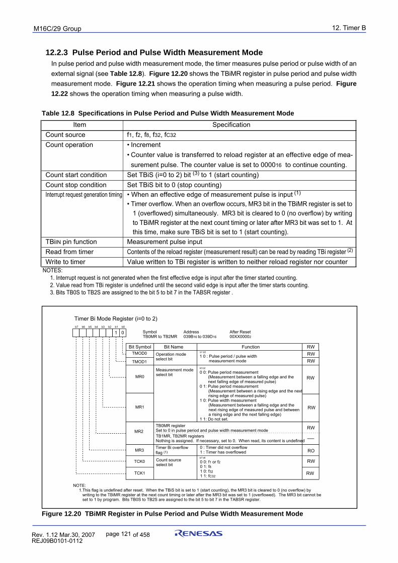
12. Timer BpuorG92/C61M
page 121 854fo7002,03.raM21.1.veR2110-1010B90JER
Item SpecificationCount source f1, f2, f8, f32, fC32
Count operation • Increment• Counter value is transferred to reload register at an effective edge of mea-
surement pulse. The counter value is set to 000016 to continue counting.Count start condition Set TBiS (i=0 to 2) bit (3) to 1 (start counting)Count stop condition Set TBiS bit to 0 (stop counting)Interrupt request generation timing • When an effective edge of measurement pulse is input (1)
• Timer overflow. When an overflow occurs, MR3 bit in the TBiMR register is set to1 (overflowed) simultaneously. MR3 bit is cleared to 0 (no overflow) by writingto TBiMR register at the next count timing or later after MR3 bit was set to 1. Atthis time, make sure TBiS bit is set to 1 (start counting).
TBiIN pin function Measurement pulse inputRead from timer Contents of the reload register (measurement result) can be read by reading TBi register (2)
Write to timer Value written to TBi register is written to neither reload register nor counterNOTES: 1. Interrupt request is not generated when the first effective edge is input after the timer started counting. 2. Value read from TBi register is undefined until the second valid edge is input after the timer starts counting. 3. Bits TB0S to TB2S are assigned to the bit 5 to bit 7 in the TABSR register .
12.2.3 Pulse Period and Pulse Width Measurement ModeIn pulse period and pulse width measurement mode, the timer measures pulse period or pulse width of anexternal signal (see Table 12.8). Figure 12.20 shows the TBiMR register in pulse period and pulse widthmeasurement mode. Figure 12.21 shows the operation timing when measuring a pulse period. Figure
12.22 shows the operation timing when measuring a pulse width.
Table 12.8 Specifications in Pulse Period and Pulse Width Measurement Mode
Figure 12.20 TBiMR Register in Pulse Period and Pulse Width Measurement Mode
Timer Bi Mode Register (i=0 to 2)
Symbol Address After ResetTB0MR to TB2MR 039B16 to 039D16 00XX00002
Bit NameBit Symbol RW
b7 b6 b5 b4 b3 b2 b1 b0
Operation mode select bit 1 0 : Pulse period / pulse width
measurement mode
b1 b0
TMOD1
TMOD0
MR0Measurement mode select bit
MR2
MR1
MR3
TCK1
TCK0
01
0 0: Pulse period measurement(Measurement between a falling edge and the next falling edge of measured pulse)
0 1: Pulse period measurement(Measurement between a rising edge and the next rising edge of measured pulse)
1 0: Pulse width measurement(Measurement between a falling edge and the next rising edge of measured pulse and between a rising edge and the next falling edge)
1 1: Do not set.
Function
b3 b2
Count source select bit
Timer Bi overflow flag (1)
0 : Timer did not overflow1 : Timer has overflowed
0 0: f1 or f20 1: f81 0: f321 1: fC32
b7 b6
NOTE: 1.This flag is undefined after reset. When the TBiS bit is set to 1 (start counting), the MR3 bit is cleared to 0 (no overflow) by
writing to the TBiMR register at the next count timing or later after the MR3 bit was set to 1 (overflowed). The MR3 bit cannot be set to 1 by program. Bits TB0S to TB2S are assigned to the bit 5 to bit 7 in the TABSR register.
RO
TB0MR registerSet to 0 in pulse period and pulse width measurement modeTB1MR, TB2MR registersNothing is assigned. If necessary, set to 0. When read, its content is undefined
RWRW
RW
RW
RW
RW
RW
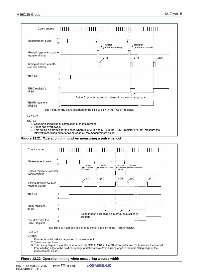
12. Timer BpuorG92/C61M
page 122 854fo7002,03.raM21.1.veR2110-1010B90JER
Figure 12.22 Operation timing when measuring a pulse width
Figure 12.21 Operation timing when measuring a pulse period
Count source
Measurement pulse
TBiS bit
TBiIC register'sIR bit
Timing at which counter reaches 000016
“H”
1
Transfer (undefined value)
“L”
0
0
TBiMR register'sMR3 bit
1
0
NOTES: 1. Counter is initialized at completion of measurement. 2. Timer has overflowed. 3. This timing diagram is for the case where bits MR1 and MR0 in the TBiMR register are 002 (measure the interval from falling edge to falling edge of the measurement pulse).
(1)(1) (2)
Transfer(measured value)
1
Reload register counter transfer timing
Bits TB0S to TB2S are assigned to the bit 5 to bit 7 in the TABSR register.
Set to 0 upon accepting an interrupt request or by program
i = 0 to 2
Measurement pulse“H”
Count source
Timing at which counter reaches 000016
1
1
Transfer (measured value)
Transfer(measured value)
“L”
0
0
1
0
(1)(1)(1)
Transfer (measured value)
(1) (1)
Transfer (undefined value)
Reload register counter transfer timing
TBiS bit
TBiIC register'sIR bit
The MR3 bit in the TBiMR register
NOTES: 1. Counter is initialized at completion of measurement. 2. Timer has overflowed. 3. This timing diagram is for the case where bits MR1 to MR0 in the TBiMR register are 102 (measure the interval from a falling edge to the next rising edge and the interval from a rising edge to the next falling edge of the measurement pulse).
Bits TB0S to TB2S are assigned to the bit 5 to bit 7 in the TABSR register.
Set to 0 upon accepting an interrupt request or by program
i = 0 to 2
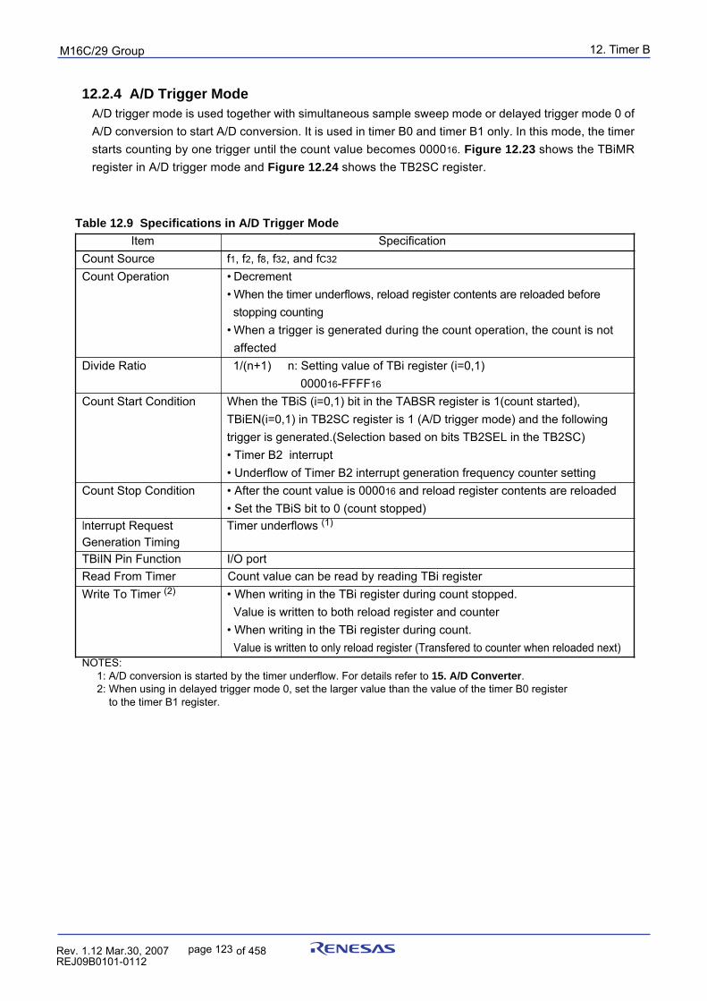
12. Timer BpuorG92/C61M
page 123 854fo7002,03.raM21.1.veR2110-1010B90JER
12.2.4 A/D Trigger ModeA/D trigger mode is used together with simultaneous sample sweep mode or delayed trigger mode 0 ofA/D conversion to start A/D conversion. It is used in timer B0 and timer B1 only. In this mode, the timerstarts counting by one trigger until the count value becomes 000016. Figure 12.23 shows the TBiMRregister in A/D trigger mode and Figure 12.24 shows the TB2SC register.
Item SpecificationCount Source f1, f2, f8, f32, and fC32
Count Operation • Decrement• When the timer underflows, reload register contents are reloaded before stopping counting• When a trigger is generated during the count operation, the count is not affected
Divide Ratio 1/(n+1) n: Setting value of TBi register (i=0,1) 000016-FFFF16
Count Start Condition When the TBiS (i=0,1) bit in the TABSR register is 1(count started),TBiEN(i=0,1) in TB2SC register is 1 (A/D trigger mode) and the followingtrigger is generated.(Selection based on bits TB2SEL in the TB2SC)• Timer B2 interrupt• Underflow of Timer B2 interrupt generation frequency counter setting
Count Stop Condition • After the count value is 000016 and reload register contents are reloaded• Set the TBiS bit to 0 (count stopped)
Interrupt Request Timer underflows (1)
Generation TimingTBiIN Pin Function I/O portRead From Timer Count value can be read by reading TBi registerWrite To Timer (2) • When writing in the TBi register during count stopped.
Value is written to both reload register and counter• When writing in the TBi register during count.
Value is written to only reload register (Transfered to counter when reloaded next)NOTES: 1: A/D conversion is started by the timer underflow. For details refer to 15. A/D Converter. 2: When using in delayed trigger mode 0, set the larger value than the value of the timer B0 register to the timer B1 register.
Table 12.9 Specifications in A/D Trigger Mode
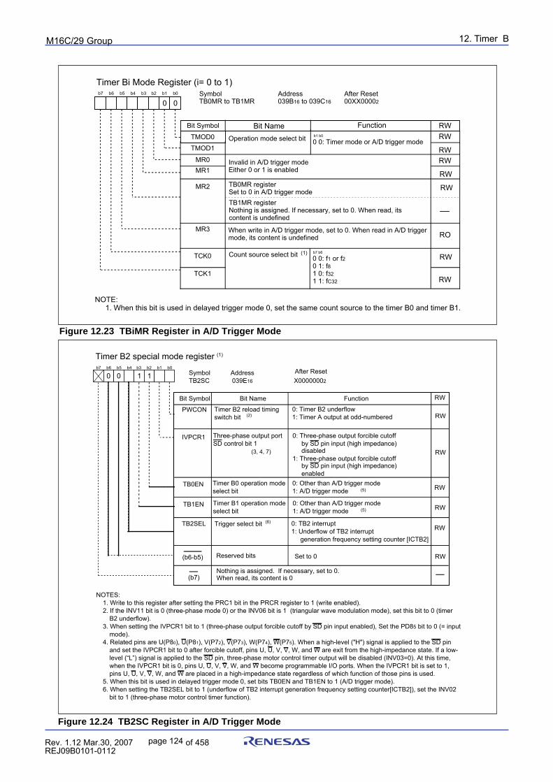
12. Timer BpuorG92/C61M
page 124 854fo7002,03.raM21.1.veR2110-1010B90JER
Figure 12.23 TBiMR Register in A/D Trigger Mode
Figure 12.24 TB2SC Register in A/D Trigger Mode
Timer Bi Mode Register (i= 0 to 1)Symbol Address After ResetTB0MR to TB1MR 039B16 to 039C16 00XX00002
Bit Name FunctionBit Symbol RW
b7 b6 b5 b4 b3 b2 b1 b0
AAAAAA
Operation mode select bit 0 0: Timer mode or A/D trigger modeb1 b0
TMOD1TMOD0
MR0 Invalid in A/D trigger modeEither 0 or 1 is enabled
MR2
MR1
MR3
0 0: f1 or f20 1: f81 0: f321 1: fC32
TCK1
TCK0 Count source select bit
00
TB0MR registerSet to 0 in A/D trigger mode
b7 b6
RO
TB1MR registerNothing is assigned. If necessary, set to 0. When read, itscontent is undefined
When write in A/D trigger mode, set to 0. When read in A/D trigger mode, its content is undefined
NOTE: 1. When this bit is used in delayed trigger mode 0, set the same count source to the timer B0 and timer B1.
(1)
RW
RWRW
RW
RW
RW
RW
PWCON
Symbol AddressTB2SC 039E16 X00000002
Timer B2 reload timing switch bit
0: Timer B2 underflow1: Timer A output at odd-numbered
Timer B2 special mode register (1)
Bit Name FunctionBit Symbol
b7 b6 b5 b4 b3 b2 b1 b0
IVPCR1 Three-phase output port SD control bit 1
0: Three-phase output forcible cutoff by SD pin input (high impedance) disabled1: Three-phase output forcible cutoff by SD pin input (high impedance) enabled
RW
RW
RW
Nothing is assigned. If necessary, set to 0.When read, its content is 0(b7)
TB2SEL Trigger select bit 0: TB2 interrupt1: Underflow of TB2 interrupt generation frequency setting counter [ICTB2]
RW
RW
TB0EN Timer B0 operation modeselect bit
0: Other than A/D trigger mode1: A/D trigger mode RW
TB1EN Timer B1 operation modeselect bit
0: Other than A/D trigger mode1: A/D trigger mode RW
(2)
(3, 4, 7)
(5)
(5)
(6)
(b6-b5) Reserved bits Set to 0
0 0 1 1After Reset
NOTES:1. Write to this register after setting the PRC1 bit in the PRCR register to 1 (write enabled).2. If the INV11 bit is 0 (three-phase mode 0) or the INV06 bit is 1 (triangular wave modulation mode), set this bit to 0 (timer
B2 underflow). 3. When setting the IVPCR1 bit to 1 (three-phase output forcible cutoff by SD pin input enabled), Set the PD85 bit to 0 (= input
mode).4. Related pins are U(P80), U(P81), V(P72), V(P73), W(P74), W(P75). When a high-level ("H") signal is applied to the SD pin
and set the IVPCR1 bit to 0 after forcible cutoff, pins U, U, V, V, W, and W are exit from the high-impedance state. If a low-level (“L”) signal is applied to the SD pin, three-phase motor control timer output will be disabled (INV03=0). At this time, when the IVPCR1 bit is 0, pins U, U, V, V, W, and W become programmable I/O ports. When the IVPCR1 bit is set to 1, pins U, U, V, V, W, and W are placed in a high-impedance state regardless of which function of those pins is used.
5. When this bit is used in delayed trigger mode 0, set bits TB0EN and TB1EN to 1 (A/D trigger mode).6. When setting the TB2SEL bit to 1 (underflow of TB2 interrupt generation frequency setting counter[ICTB2]), set the INV02
bit to 1 (three-phase motor control timer function).
12. Timer (Three-phase Motor Control Timer Function)puorG92/C61M
page 125 854fo7002,03.raM21.1.veR2110-1010B90JER
12.3 Three-phase Motor Control Timer FunctionTimers A1, A2, A4 and B2 can be used to output three-phase motor drive waveforms. Table 12.10 lists thespecifications of the three-phase motor control timer function. Figure 12.24 shows the block diagram forthree-phase motor control timer function. Also, the related registers are shown on Figures 12.26 to 12.32.
Table 12.10 Three-phase Motor Control Timer Function Specifications Item SpecificationThree-phase waveform output pin
___ ___ ___
Six pins (U, U, V, V, W, W)Forced cutoff input (1)
_____
Input “L” to SD pinUsed Timers Timer A4, A1, A2 (used in the one-shot timer mode)
___
Timer A4: U- and U-phase waveform control___
Timer A1: V- and V-phase waveform control___
Timer A2: W- and W-phase waveform controlTimer B2 (used in the timer mode)
Carrier wave cycle controlDead time timer (3 eight-bit timer and shared reload register)
Dead time controlOutput waveform Triangular wave modulation, Sawtooth wave modification
Enable to output “H” or “L” for one cycleEnable to set positive-phase level and negative-phaselevel respectively
Carrier wave cycle Triangular wave modulation: count source x (m+1) x 2Sawtooth wave modulation: count source x (m+1)
m: Setting value of TB2 register, 0 to 65535Count source: f1, f2, f8, f32, fC32
Three-phase PWM output width Triangular wave modulation: count source x n x 2Sawtooth wave modulation: count source x n
n: Setting value of TA4, TA1 and TA2 register (of TA4, TA41, TA1, TA11, TA2 and TA21 registers when setting the INV11 bit to 1), 1 to 65535Count source: f1, f2, f8, f32, fC32
Dead time Count source x p, or no dead timep: Setting value of DTT register, 1 to 255
Count source: f1, f2, f1 divided by 2, f2 divided by 2Active level Eable to select “H” or “L”Positive and negative-phase concurrent Positive and negative-phases concurrent active disable
functionPositive and negative-phases concurrent active detect func-tion
Interrupt frequency For Timer B2 interrupt, select a carrier wave cycle-to-cyclebasis through 15 times carrier wave cycle-to-cycle basis
NOTE: 1. When the INV02 bit in the INVC0 register is set to 1 (three-phase motor control timer function), the_____ _____
SD function of the P85/SD pin is enabled. At this time, the P85 pin cannot be used as a programmable_____ _____
I/O port. When the SD function is not used, apply “H” to the P85/SD pin. _____
When the IVPCR1 bit in the TB2SC register is set to 1 (enable three-phase output forced cutoff by SD_____
pin input), and “L” is applied to the SD pin, the related pins enter high-impedance state regardless ofthe functions which are used. When the IVPCR1 bit is set to 0 (disabled three-phase output forced_____ _____
cutoff by SD pin input) and “L” is applied to the SD pin, the related pins can be selected as a program-mable I/O port and the setting of the port and port direction registers are enable.
Related pins: P72/CLK2/TA1OUT/V/RXD1_________ _________ ___
P73/CTS2/RTS2/TA1IN/V/TXD1P74/TA2OUT/W
____
P75/TA2IN/WP80/TA4OUT/U
___
P81/TA4IN/U
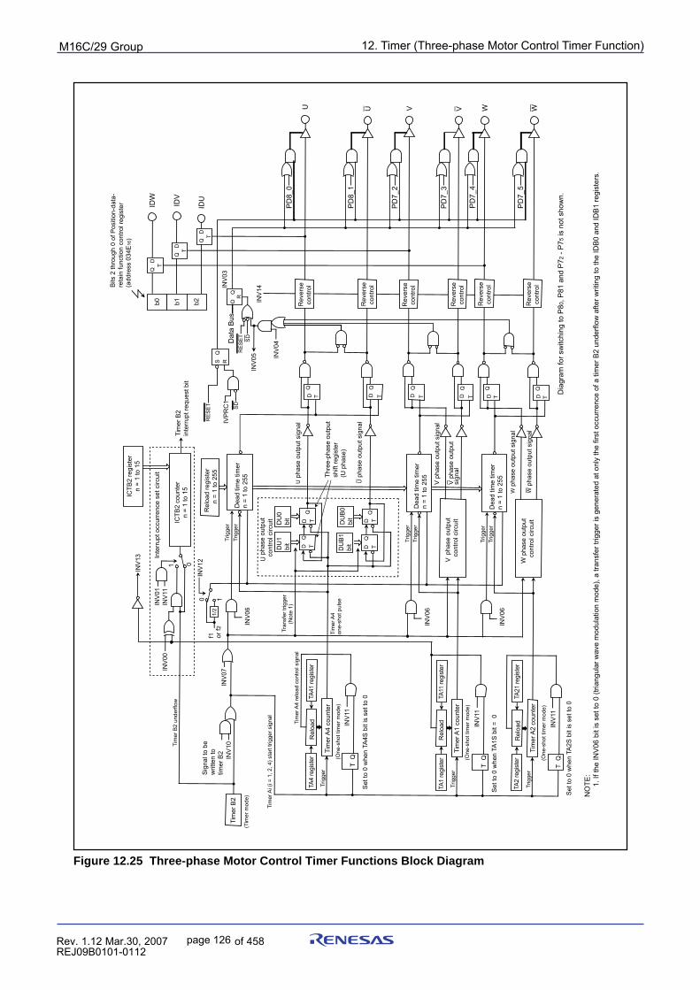
12. Timer (Three-phase Motor Control Timer Function)puorG92/C61M
page 126 854fo7002,03.raM21.1.veR2110-1010B90JER
Figure 12.25 Three-phase Motor Control Timer Functions Block Diagram
DR
Q
0IN
V12
1
Trig
ger
Trig
ger
Tim
er B
2
(Tim
er m
ode)
Sig
nal t
o be
w
ritte
n to
tim
er B
2
1Ti
mer
B2
inte
rrup
t req
uest
bit
DU
1bi
t D TQ
Q Q
U
Thre
e-ph
ase
outp
ut
shift
regi
ster
(U
pha
se)
Dea
d tim
e tim
ern
= 1
to 2
55
Trig
ger
Trig
ger
Rel
oad
regi
ster
Trig
ger
Trig
ger
U p
hase
out
put s
igna
l
U p
hase
out
put s
igna
l
V
W p
hase
out
put s
igna
l
W p
hase
out
put s
igna
lW
pha
se o
utpu
t co
ntro
l circ
uit
DQ
TDQ
T
W
DQ
TDQ
T
V
DQ
TDQ
T
U WVU
Rel
oad
Tim
er A
1 co
unte
r(O
ne-s
hot t
imer
mod
e)
Trig
ger
TQ
Rel
oad
Tim
er A
2 co
unte
r(O
ne-s
hot t
imer
mod
e)
Trig
ger
TQ
Rel
oad
Tim
er A
4 co
unte
r(O
ne-s
hot t
imer
mod
e)
Trig
ger
TQ
Tran
sfer
trig
ger
(Not
e 1)
Tim
er B
2 un
derfl
ow
DU
0bi
t
DU
B0
bit
TA4
regi
ster
TA41
regi
ster
TA1
regi
ster
TA11
regi
ster
TA2
regi
ster
TA21
regi
ster
Tim
er A
i (i =
1, 2
, 4) s
tart
trigg
er s
igna
l
Tim
er A
4 re
load
con
trol s
igna
l
Tim
er A
4on
e-sh
ot p
ulse
DU
B1
bit
Dea
d tim
e tim
ern
= 1
to 2
55
Dea
d tim
e tim
ern
= 1
to 2
55
Inte
rrup
t occ
urre
nce
set c
ircui
t
ICTB
2 re
gist
ern
= 1
to 1
5
0
INV
13
ICTB
2 co
unte
rn
= 1
to 1
5
SD
RE
SE
T
INV
03
INV
14IN
V05 IN
V04
INV
00IN
V01
INV
11
INV
11
INV
11
INV
11
INV
06
INV
06
INV
06
INV
07IN
V10
1/2
f1
or f2
pha
se o
utpu
t co
ntro
l circ
uit
pha
se o
utpu
t co
ntro
l circ
uit
V p
hase
out
put s
igna
l
V p
hase
out
put
sign
al
Rev
erse
con
trol
Rev
erse
con
trol
Rev
erse
con
trol
Rev
erse
con
trol
Rev
erse
con
trol
D T
D TQ
D T
Rev
erse
con
trol
IDW
IDV
IDU
DQ
T
DQ
T
DQ
T
b2b0 b1
Bits
2 th
roug
h 0
of P
ositi
on-d
ata-
reta
in fu
nctio
n co
ntro
l reg
iste
r(a
ddre
ss 0
34E
16)
PD
8_0
PD
8_1
PD
7_2
PD
7_3
PD
7_4
PD
7_5
SQ
R
RE
SE
T SD
IVP
RC
1D
ata
Bus
n =
1 to
255
NO
TE:
1
. If t
he IN
V06
bit
is s
et to
0 (t
riang
ular
wav
e m
odul
atio
n m
ode)
, a tr
ansf
er tr
igge
r is
gene
rate
d at
onl
y th
e fir
st o
ccur
renc
e of
a ti
mer
B2
unde
rflow
afte
r writ
ing
to th
e ID
B0
and
IDB
1 re
gist
ers.
Set
to 0
whe
n TA
2S b
it is
set
to 0
Set
to 0
whe
n TA
1S b
it =
0
Set
to 0
whe
n TA
4S b
it is
set
to 0
Dia
gram
for s
witc
hing
to P
80, P
81 a
nd P
72 -
P75
is n
ot s
how
n.
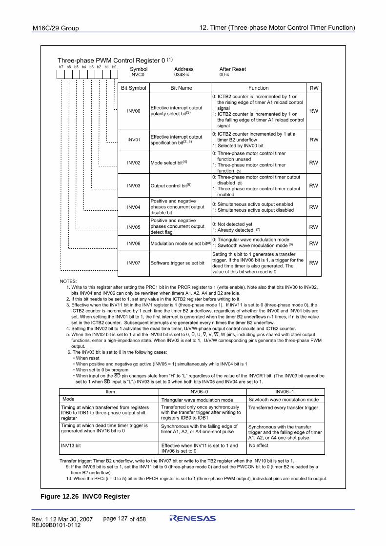
12. Timer (Three-phase Motor Control Timer Function)puorG92/C61M
page 127 854fo7002,03.raM21.1.veR2110-1010B90JER
Figure 12.26 INVC0 Register
Three-phase PWM Control Register 0 (1)
Symbol Address After Reset INVC0 034816 0016
b7 b6 b5 b4 b3 b2 b1 b0
INV00
Bit Symbol Bit Name Function RW
INV01
INV02 Mode select bit(4)
INV04
INV07 Software trigger select bit
INV06 Modulation mode select bit(8)
INV05
INV03 Output control bit(6)
RW
RW
RW
RW
RW
RW
RW
RW
ItemMode
Timing at which transferred from registers IDB0 to IDB1 to three-phase output shift registerTiming at which dead time timer trigger is generated when INV16 bit is 0
INV13 bit
INV06=0
Triangular wave modulation modeTransferred only once synchronously with the transfer trigger after writing to registers IDB0 to IDB1
Synchronous with the falling edge of timer A1, A2, or A4 one-shot pulse
Effective when INV11 is set to 1 and INV06 is set to 0
INV06=1Sawtooth wave modulation mode
Transferred every transfer trigger
Synchronous with the transfer trigger and the falling edge of timer A1, A2, or A4 one-shot pulseNo effect
NOTES: 1. Write to this register after setting the PRC1 bit in the PRCR register to 1 (write enable). Note also that bits INV00 to INV02,
bits INV04 and INV06 can only be rewritten when timers A1, A2, A4 and B2 are idle. 2. If this bit needs to be set to 1, set any value in the ICTB2 register before writing to it. 3. Effective when the INV11 bit in the INV1 register is 1 (three-phase mode 1). If INV11 is set to 0 (three-phase mode 0), the
ICTB2 counter is incremented by 1 each time the timer B2 underflows, regardless of whether the INV00 and INV01 bits are set. When setting the INV01 bit to 1, the first interrupt is generated when the timer B2 underflows n-1 times, if n is the value set in the ICTB2 counter. Subsequent interrupts are generated every n times the timer B2 underflow.
4. Setting the INV02 bit to 1 activates the dead time timer, U/V/W-phase output control circuits and ICTB2 counter. 5. When the INV02 bit is set to 1 and the INV03 bit is set to 0, U, U, V, V, W, W pins, including pins shared with other output
functions, enter a high-impedance state. When INV03 is set to 1, U/V/W corresponding pins generate the three-phase PWM output.
6. The INV03 bit is set to 0 in the following cases:• When reset• When positive and negative go active (INV05 = 1) simultaneously while INV04 bit is 1• When set to 0 by program• When input on the SD pin changes state from “H” to “L” regardless of the value of the INVCR1 bit. (The INV03 bit cannot be set to 1 when SD input is “L”.) INV03 is set to 0 when both bits INV05 and INV04 are set to 1.
Effective interrupt output polarity select bit(3)
Effective interrupt output specification bit(2, 3)
0: ICTB2 counter incremented by 1 at a timer B2 underflow
1: Selected by INV00 bit0: Three-phase motor control timer
function unused1: Three-phase motor control timer
function (5)0: Three-phase motor control timer output
disabled (5)1: Three-phase motor control timer output
enabledPositive and negative phases concurrent output disable bitPositive and negative phases concurrent output detect flag
0: Not detected yet1: Already detected (7)
0: Simultaneous active output enabled1: Simultaneous active output disabled
0: Triangular wave modulation mode1: Sawtooth wave modulation mode (9)
Setting this bit to 1 generates a transfer trigger. If the INV06 bit is 1, a trigger for the dead time timer is also generated. The value of this bit when read is 0
0: ICTB2 counter is incremented by 1 on the rising edge of timer A1 reload control signal
1: ICTB2 counter is incremented by 1 on the falling edge of timer A1 reload control signal
Transfer trigger: Timer B2 underflow, write to the INV07 bit or write to the TB2 register when the INV10 bit is set to 1. 9: If the INV06 bit is set to 1, set the INV11 bit to 0 (three-phase mode 0) and set the PWCON bit to 0 (timer B2 reloaded by a
timer B2 underflow)10. When the PFCi (i = 0 to 5) bit in the PFCR register is set to 1 (three-phase PWM output), individual pins are enabled to output.
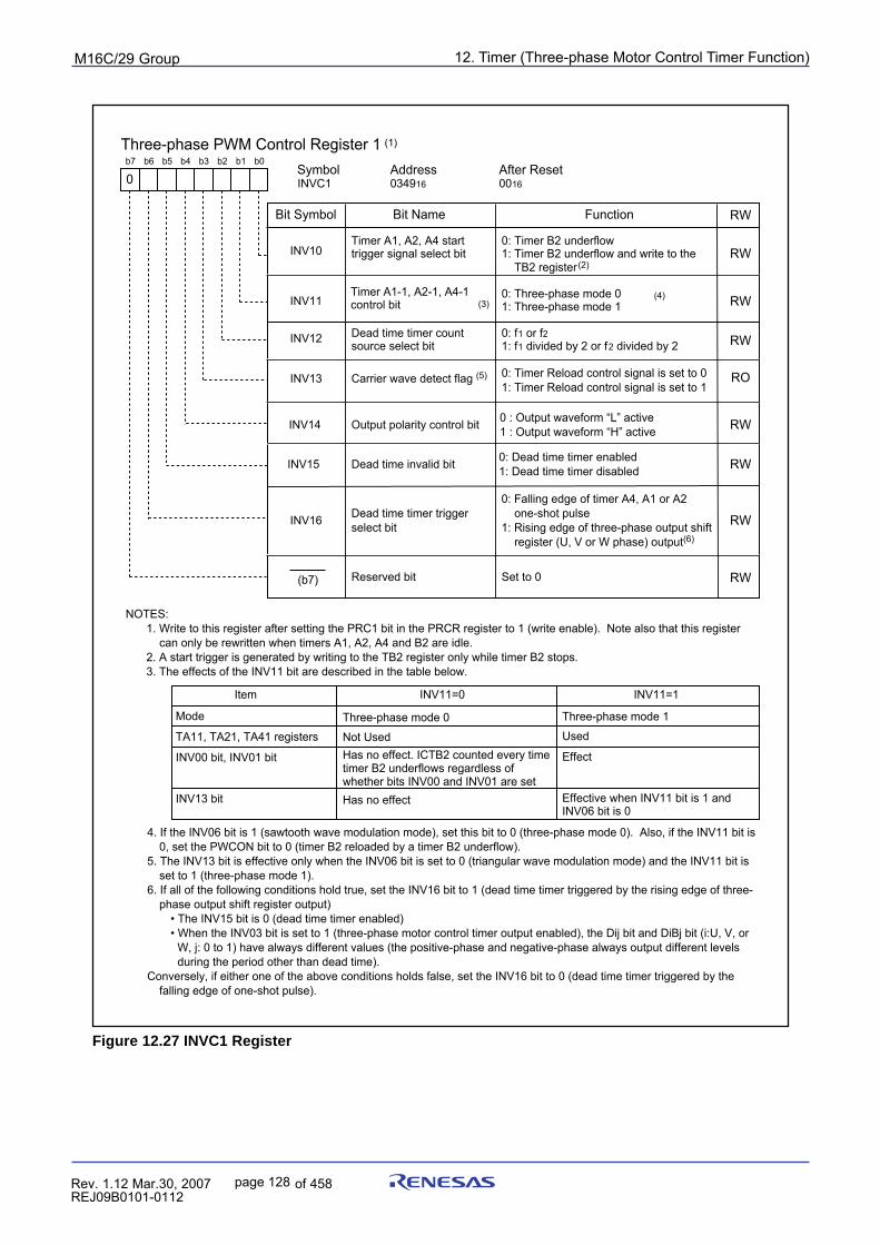
12. Timer (Three-phase Motor Control Timer Function)puorG92/C61M
page 128 854fo7002,03.raM21.1.veR2110-1010B90JER
Figure 12.27 INVC1 Register
Three-phase PWM Control Register 1 (1)
Symbol Address After Reset INVC1 034916 0016
b7 b6 b5 b4 b3 b2 b1 b0
Timer A1, A2, A4 start trigger signal select bitINV10
Bit Symbol Bit Name Function RW
INV11
Timer A1-1, A2-1, A4-1 control bit
INV12 Dead time timer count source select bit
INV14 Output polarity control bit
(b7) Reserved bit
INV16
INV15 Dead time invalid bit
INV13 Carrier wave detect flag (5)
0: Timer B2 underflow1: Timer B2 underflow and write to the TB2 register(2)
0: Three-phase mode 01: Three-phase mode 1
0: f1 or f21: f1 divided by 2 or f2 divided by 2
0: Timer Reload control signal is set to 01: Timer Reload control signal is set to 1
0 : Output waveform “L” active1 : Output waveform “H” active
0: Dead time timer enabled1: Dead time timer disabled
Set to 0
RW
RW
RW
RW
RW
RW
RW
RO
(3)
Item
Mode
TA11, TA21, TA41 registers
INV00 bit, INV01 bit
INV13 bit
INV11=0
Three-phase mode 1Three-phase mode 0
Not UsedHas no effect. ICTB2 counted every time timer B2 underflows regardless of whether bits INV00 and INV01 are setHas no effect
INV11=1
Used
Effect
Effective when INV11 bit is 1 and INV06 bit is 0
(4)
0
4. If the INV06 bit is 1 (sawtooth wave modulation mode), set this bit to 0 (three-phase mode 0). Also, if the INV11 bit is 0, set the PWCON bit to 0 (timer B2 reloaded by a timer B2 underflow).
5. The INV13 bit is effective only when the INV06 bit is set to 0 (triangular wave modulation mode) and the INV11 bit is set to 1 (three-phase mode 1).
6. If all of the following conditions hold true, set the INV16 bit to 1 (dead time timer triggered by the rising edge of three-phase output shift register output)
• The INV15 bit is 0 (dead time timer enabled)• When the INV03 bit is set to 1 (three-phase motor control timer output enabled), the Dij bit and DiBj bit (i:U, V, or
W, j: 0 to 1) have always different values (the positive-phase and negative-phase always output different levels during the period other than dead time).
Conversely, if either one of the above conditions holds false, set the INV16 bit to 0 (dead time timer triggered by the falling edge of one-shot pulse).
NOTES:1. Write to this register after setting the PRC1 bit in the PRCR register to 1 (write enable). Note also that this register
can only be rewritten when timers A1, A2, A4 and B2 are idle.2. A start trigger is generated by writing to the TB2 register only while timer B2 stops.3. The effects of the INV11 bit are described in the table below.
0: Falling edge of timer A4, A1 or A2 one-shot pulse
1: Rising edge of three-phase output shift register (U, V or W phase) output(6)
Dead time timer trigger select bit
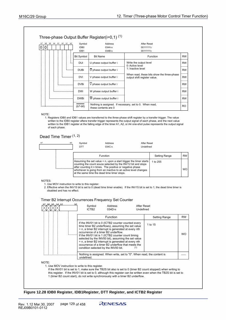
12. Timer (Three-phase Motor Control Timer Function)puorG92/C61M
page 129 854fo7002,03.raM21.1.veR2110-1010B90JER
Figure 12.28 IDB0 Register, IDB1Register, DTT Register, and ICTB2 Register
Three-phase Output Buffer Register(i=0,1) (1)
Symbol Address After Reset IDB0 034A16 001111112 IDB1 034B16 001111112
RW
RW
RW
RWBit Name FunctionBit Symbol
DUi
DUBi
DVi
U phase output buffer i
NOTE: 1. Registers IDB0 and IDB1 values are transferred to the three-phase shift register by a transfer trigger. The value written to the IDB0 register aftera transfer trigger represents the output signal of each phase, and the next value written to the IDB1 register at the falling edge of the timer A1, A2, or A4 one-shot pulse represents the output signal of each phase.
(b7-b6)
RWDVBi
Nothing is assigned. If necessary, set to 0. When read,these contents are 0
Write the output level0: Active level1: Inactive level
When read, these bits show the three-phaseoutput shift register value.
DWi
DWBi
RW
RW
U phase output buffer i
V phase output buffer i
V phase output buffer i
W phase output buffer i
W phase output buffer i
b7 b4 b3 b2 b1 b0
Dead Time Timer (1, 2)
Symbol Address After Reset DTT 034C16 Undefined
WO
RWFunction Setting Range
NOTES: 1. Use MOV instruction to write to this register. 2. Effective when the INV15 bit is set to 0 (dead time timer enable). If the INV15 bit is set to 1, the dead time timer is
disabled and has no effect.
1 to 255
b7 b0
Assuming the set value = n, upon a start trigger the timer startscounting the count souce selected by the INV12 bit and stops after counting it n times. The positive or negative phase whichever is going from an inactive to an active level changesat the same time the dead time timer stops.
RO
0
Timer B2 Interrupt Occurrences Frequency Set Counter SymbolICTB2
Address034D16
After ResetUndefined
Function Setting Range
b7 b6 b5 b4 b0
If the INV01 bit is 0 (ICTB2 counter counted every time timer B2 underflows), assuming the set value = n, a timer B2 interrupt is generated at every nth occurrence of a timer B2 underflow. If the INV01 bit is 1 (ICTB2 counter count timing selected by the INV00 bit), assuming the set value = n, a timer B2 interrupt is generated at every nth occurrence of a timer B2 underflow that meets the condition selected by the INV00 bit.
1 to 15
NOTE: 1. Use MOV instruction to write to this register. If the INV01 bit is set to 1, make sure the TB2S bit also is set to 0 (timer B2 count stopped) when writing to this register. If the INV01 bit is set to 0, although this register can be written even when the TB2S bit is set to 1 (timer B2 count start), do not write synchronously with a timer B2 underflow.
RW
WO
(1)
Nothing is assigned. When write, set to "0". When read, the content is undefined.
b3
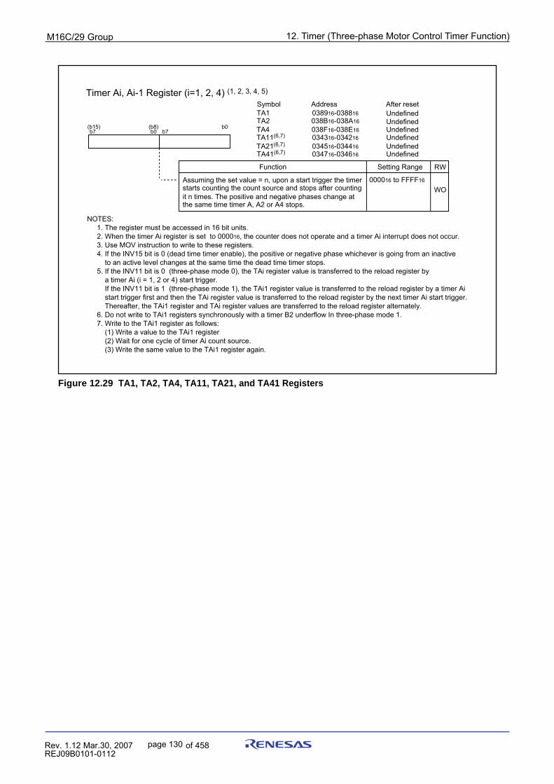
12. Timer (Three-phase Motor Control Timer Function)puorG92/C61M
page 130 854fo7002,03.raM21.1.veR2110-1010B90JER
Figure 12.29 TA1, TA2, TA4, TA11, TA21, and TA41 Registers
Symbol Address After reset TA1 038916-038816 Undefined TA2 038B16-038A16 Undefined
TA4 038F16-038E16 Undefined TA11(6,7) 034316-034216 Undefined TA21(6,7) 034516-034416 Undefined TA41(6,7) 034716-034616 Undefined
b7 b0 b7b0(b15) (b8)
RW
Assuming the set value = n, upon a start trigger the timer starts counting the count source and stops after counting it n times. The positive and negative phases change at the same time timer A, A2 or A4 stops.
Function Setting Range
Timer Ai, Ai-1 Register (i=1, 2, 4) (1, 2, 3, 4, 5)
NOTES: 1. The register must be accessed in 16 bit units. 2. When the timer Ai register is set to 000016, the counter does not operate and a timer Ai interrupt does not occur. 3. Use MOV instruction to write to these registers. 4. If the INV15 bit is 0 (dead time timer enable), the positive or negative phase whichever is going from an inactive to an active level changes at the same time the dead time timer stops. 5. If the INV11 bit is 0 (three-phase mode 0), the TAi register value is transferred to the reload register by a timer Ai (i = 1, 2 or 4) start trigger. If the INV11 bit is 1 (three-phase mode 1), the TAi1 register value is transferred to the reload register by a timer Ai start trigger first and then the TAi register value is transferred to the reload register by the next timer Ai start trigger. Thereafter, the TAi1 register and TAi register values are transferred to the reload register alternately. 6. Do not write to TAi1 registers synchronously with a timer B2 underflow In three-phase mode 1. 7. Write to the TAi1 register as follows: (1) Write a value to the TAi1 register (2) Wait for one cycle of timer Ai count source. (3) Write the same value to the TAi1 register again.
WO000016 to FFFF16
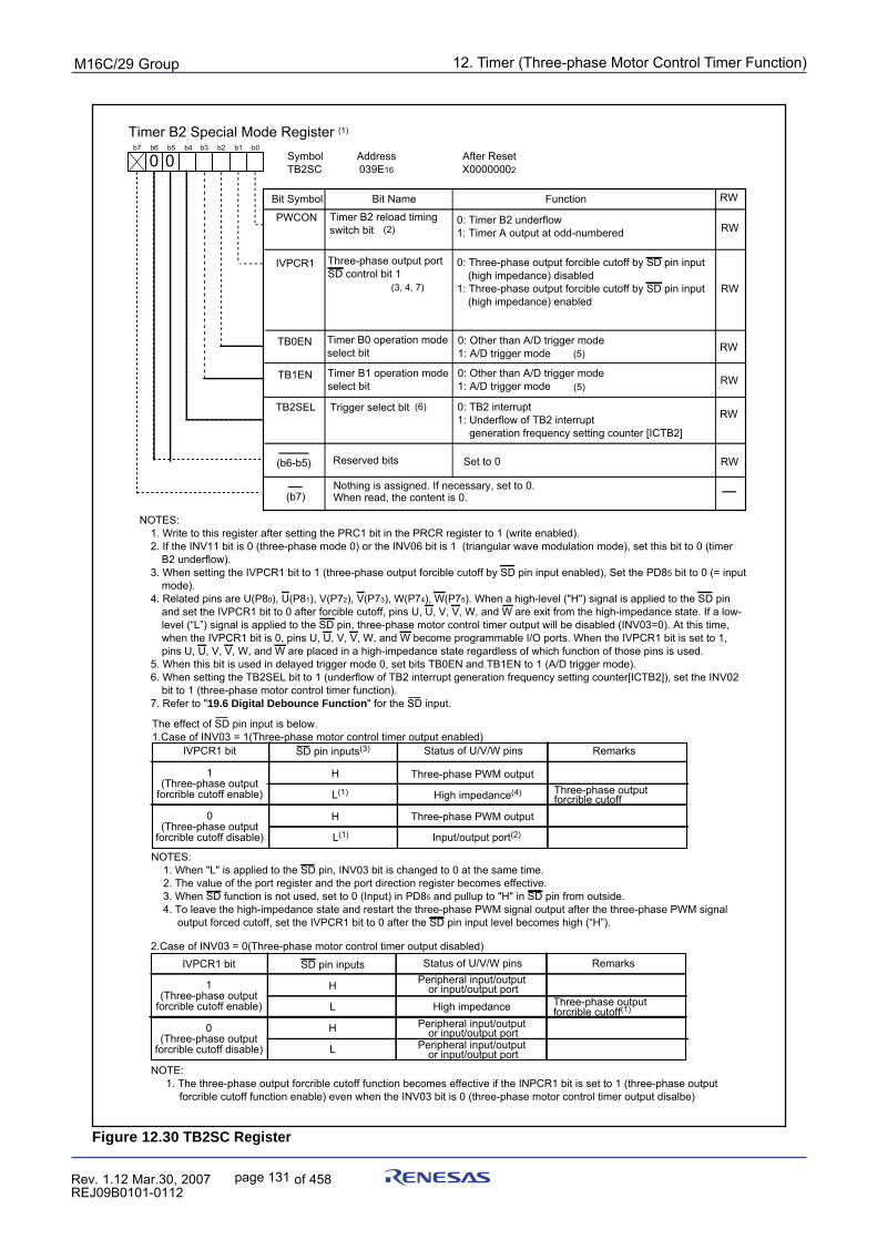
12. Timer (Three-phase Motor Control Timer Function)puorG92/C61M
page 131 854fo7002,03.raM21.1.veR2110-1010B90JER
Figure 12.30 TB2SC Register
0: Three-phase output forcible cutoff by SD pin input (high impedance) disabled
1: Three-phase output forcible cutoff by SD pin input (high impedance) enabled
NOTES:1. When "L" is applied to the SD pin, INV03 bit is changed to 0 at the same time.2. The value of the port register and the port direction register becomes effective.3. When SD function is not used, set to 0 (Input) in PD85 and pullup to "H" in SD pin from outside.4. To leave the high-impedance state and restart the three-phase PWM signal output after the three-phase PWM signal
output forced cutoff, set the IVPCR1 bit to 0 after the SD pin input level becomes high (“H”).
IVPCR1 bit Status of U/V/W pins RemarksSD pin inputs
1(Three-phase output
forcrible cutoff enable)
0(Three-phase output
forcrible cutoff disable)
H
L
H
L
High impedance
Peripheral input/output or input/output port
Peripheral input/output or input/output port
Peripheral input/output or input/output port
Three-phase outputforcrible cutoff(1)
IVPCR1 bit Status of U/V/W pins RemarksSD pin inputs(3)
1(Three-phase output
forcrible cutoff enable)
0(Three-phase output
forcrible cutoff disable)
H
L(1)
H
L(1)
High impedance(4) Three-phase outputforcrible cutoff
Input/output port(2)
Three-phase PWM output
Three-phase PWM output
The effect of SD pin input is below.1.Case of INV03 = 1(Three-phase motor control timer output enabled)
PWCON
Symbol Address After ResetTB2SC 039E16 X00000002
Timer B2 reload timingswitch bit
Timer B2 Special Mode Register (1)
Bit Name FunctionBit Symbol
b7 b6 b5 b4 b3 b2 b1 b0
IVPCR1 Three-phase output port SD control bit 1
RW
RW
RW
Nothing is assigned. If necessary, set to 0.When read, the content is 0.(b7)
TB2SEL Trigger select bit 0: TB2 interrupt1: Underflow of TB2 interrupt generation frequency setting counter [ICTB2]
RW
RW
TB0EN Timer B0 operation modeselect bit
0: Other than A/D trigger mode1: A/D trigger mode RW
TB1EN Timer B1 operation modeselect bit
0: Other than A/D trigger mode1: A/D trigger mode RW
(2)
(3, 4, 7)
(5)
(5)
(6)
(b6-b5) Reserved bits Set to 0
00
NOTES:1. Write to this register after setting the PRC1 bit in the PRCR register to 1 (write enabled).2. If the INV11 bit is 0 (three-phase mode 0) or the INV06 bit is 1 (triangular wave modulation mode), set this bit to 0 (timer
B2 underflow). 3. When setting the IVPCR1 bit to 1 (three-phase output forcible cutoff by SD pin input enabled), Set the PD85 bit to 0 (= input
mode).4. Related pins are U(P80), U(P81), V(P72), V(P73), W(P74), W(P75). When a high-level ("H") signal is applied to the SD pin
and set the IVPCR1 bit to 0 after forcible cutoff, pins U, U, V, V, W, and W are exit from the high-impedance state. If a low-level (“L”) signal is applied to the SD pin, three-phase motor control timer output will be disabled (INV03=0). At this time, when the IVPCR1 bit is 0, pins U, U, V, V, W, and W become programmable I/O ports. When the IVPCR1 bit is set to 1, pins U, U, V, V, W, and W are placed in a high-impedance state regardless of which function of those pins is used.
5. When this bit is used in delayed trigger mode 0, set bits TB0EN and TB1EN to 1 (A/D trigger mode).6. When setting the TB2SEL bit to 1 (underflow of TB2 interrupt generation frequency setting counter[ICTB2]), set the INV02
bit to 1 (three-phase motor control timer function).7. Refer to "19.6 Digital Debounce Function" for the SD input.
NOTE:1. The three-phase output forcrible cutoff function becomes effective if the INPCR1 bit is set to 1 (three-phase output
forcrible cutoff function enable) even when the INV03 bit is 0 (three-phase motor control timer output disalbe)
2.Case of INV03 = 0(Three-phase motor control timer output disabled)
0: Timer B2 underflow1: Timer A output at odd-numbered
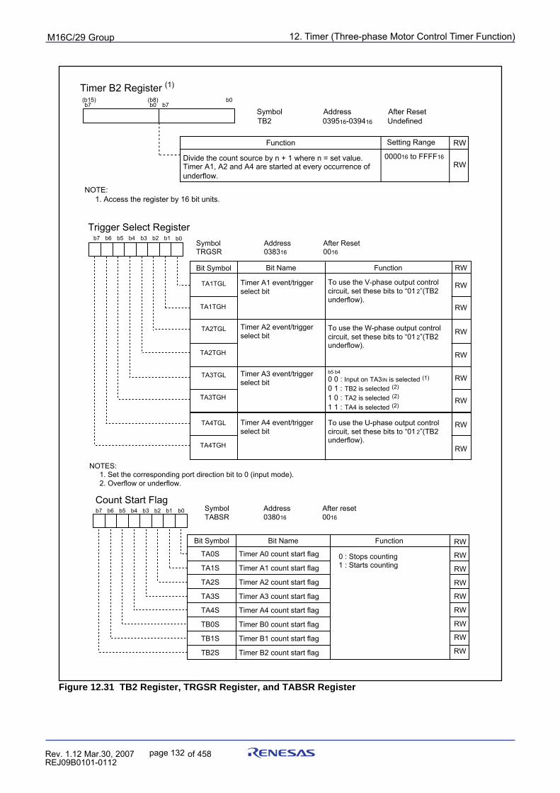
12. Timer (Three-phase Motor Control Timer Function)puorG92/C61M
page 132 854fo7002,03.raM21.1.veR2110-1010B90JER
Figure 12.31 TB2 Register, TRGSR Register, and TABSR Register
Symbol Address After Reset TB2 039516-039416 Undefined
b7 b0 b7b0(b15) (b8)
RW
000016 to FFFF16
Function Setting Range
Timer B2 Register (1)
NOTE: 1. Access the register by 16 bit units.
RWDivide the count source by n + 1 where n = set value. Timer A1, A2 and A4 are started at every occurrence of underflow.
TA1TGL
Symbol Address After Reset TRGSR 038316 0016
Timer A1 event/trigger select bit
To use the V-phase output control circuit, set these bits to “01 2”(TB2 underflow).
Trigger Select Register
Bit Name FunctionBit Symbol
b0
To use the W-phase output control circuit, set these bits to “01 2”(TB2 underflow).
0 0 : Input on TA3IN is selected (1)
0 1 : TB2 is selected (2)
1 0 : TA2 is selected (2) 1 1 : TA4 is selected (2)
To use the U-phase output control circuit, set these bits to “01 2”(TB2 underflow).
Timer A2 event/trigger select bit
Timer A3 event/trigger select bit
Timer A4 event/trigger select bit
RW
TA1TGH
TA2TGL
TA2TGH
TA3TGL
TA3TGH
TA4TGL
TA4TGH
b5 b4
NOTES: 1. Set the corresponding port direction bit to 0 (input mode). 2. Overflow or underflow.
b7 b6 b5 b4 b3 b2 b1
Symbol Address After reset TABSR 038016 0016
Count Start Flag
Bit Name FunctionBit Symbol
b7 b6 b5 b4 b3 b2 b1 b0
Timer B2 count start flag
Timer B1 count start flag
Timer B0 count start flag
Timer A4 count start flag
Timer A3 count start flag
Timer A2 count start flag
Timer A1 count start flag
Timer A0 count start flag 0 : Stops counting1 : Starts counting
TB2S
TB1S
TB0S
TA4S
TA3S
TA2S
TA1S
TA0S
RW
RW
RW
RW
RW
RW
RW
RW
RW
RW
RW
RW
RW
RW
RW
RW
RW
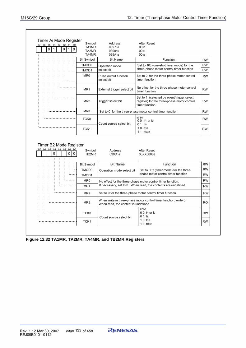
12. Timer (Three-phase Motor Control Timer Function)puorG92/C61M
page 133 854fo7002,03.raM21.1.veR2110-1010B90JER
Figure 12.32 TA1MR, TA2MR, TA4MR, and TB2MR Registers
Bit Name
Timer Ai Mode Register Symbol Address After Reset TA1MR 039716 0016 TA2MR 039816 0016 TA4MR 039A16 0016
Function Bit Symbol
b7 b6 b5 b4 b3 b2 b1 b0
Operation mode select bit
Set to 102 (one-shot timer mode) for the three-phase motor control timer function TMOD1
TMOD0
MR0 Pulse output function select bit
Set to 0 for the three-phase motor control timer function
MR2
MR1
MR3 Set to 0 for the three-phase motor control timer function
0 0 : f1 or f20 1 : f81 0 : f321 1 : fC32
b7 b6
TCK1
TCK0Count source select bit
1 00
Set to 1 (selected by event/trigger select register) for the three-phase motor control timer function
Trigger select bit
External trigger select bit
RW
Timer B2 Mode Register Symbol Address After Reset TB2MR 039D16 00XX00002
Bit Name FunctionBit Symbol RW
b7 b6 b5 b4 b3 b2 b1 b0
Operation mode select bit Set to 002 (timer mode) for the three-phase motor control timer function TMOD1
TMOD0
MR0
MR2
MR1
MR3
TCK1
TCK0Count source select bit
00
1
0
No effect for the three-phase motor control timer function
RWRW
RW
RW
RW
RW
RW
RW
RW
RW
RW
RW
RW
RW
RO
No effect for the three-phase motor control timer function.If necessary, set to 0. When read, the contents are undefined
Set to 0 for the three-phase motor control timer function
0
RW
When write in three-phase motor control timer function, write 0.When read, the content is undefined
b7 b6 0 0: f1 or f20 1: f81 0: f321 1: fC32
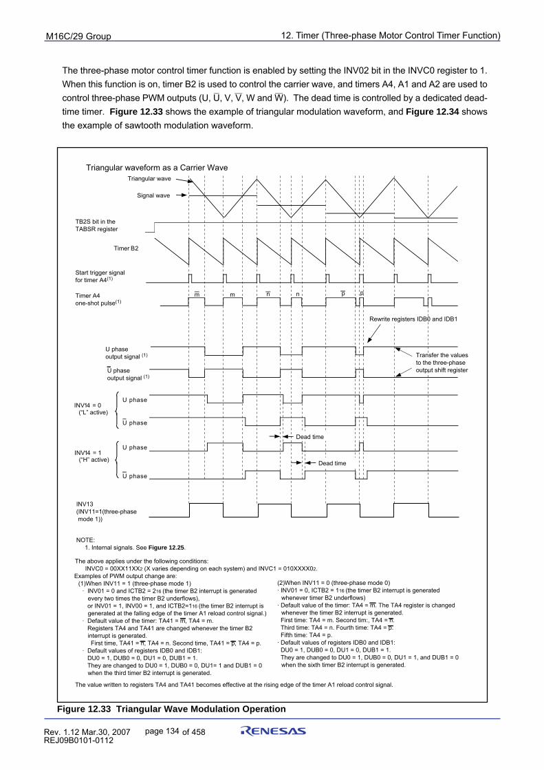
12. Timer (Three-phase Motor Control Timer Function)puorG92/C61M
page 134 854fo7002,03.raM21.1.veR2110-1010B90JER
Figure 12.33 Triangular Wave Modulation Operation
The three-phase motor control timer function is enabled by setting the INV02 bit in the INVC0 register to 1.When this function is on, timer B2 is used to control the carrier wave, and timers A4, A1 and A2 are used to
__ ___ ___
control three-phase PWM outputs (U, U, V, V, W and W). The dead time is controlled by a dedicated dead-time timer. Figure 12.33 shows the example of triangular modulation waveform, and Figure 12.34 showsthe example of sawtooth modulation waveform.
Start trigger signal for timer A4(1)
Timer B2
U phase
Triangular wave
Signal wave
U phase output signal (1)
m n n p pm
U phase
U phase
U phase
INV14 = 0
Triangular waveform as a Carrier Wave
Timer A4one-shot pulse(1)
INV14 = 1
Dead time
Dead time
Rewrite registers IDB0 and IDB1
NOTE: 1. Internal signals. See Figure 12.25.
Examples of PWM output change are:(1)When INV11 = 1 (three-phase mode 1)
· INV01 = 0 and ICTB2 = 216 (the timer B2 interrupt is generated every two times the timer B2 underflows),
or INV01 = 1, INV00 = 1, and ICTB2=116 (the timer B2 interrupt is generated at the falling edge of the timer A1 reload control signal.)
· Default value of the timer: TA41 = m, TA4 = m. Registers TA4 and TA41 are changed whenever the timer B2
interrupt is generated. First time, TA41 = n, TA4 = n. Second time, TA41 = p, TA4 = p.· Default values of registers IDB0 and IDB1: DU0 = 1, DUB0 = 0, DU1 = 0, DUB1 = 1. They are changed to DU0 = 1, DUB0 = 0, DU1= 1 and DUB1 = 0
when the third timer B2 interrupt is generated.
(2)When INV11 = 0 (three-phase mode 0)· INV01 = 0, ICTB2 = 116 (the timer B2 interrupt is generated
whenever timer B2 underflows)· Default value of the timer: TA4 = m. The TA4 register is changed
whenever the timer B2 interrupt is generated. First time: TA4 = m. Second tim:, TA4 = n. Third time: TA4 = n. Fourth time: TA4 = p. Fifth time: TA4 = p.· Default values of registers IDB0 and IDB1: DU0 = 1, DUB0 = 0, DU1 = 0, DUB1 = 1. They are changed to DU0 = 1, DUB0 = 0, DU1 = 1, and DUB1 = 0
when the sixth timer B2 interrupt is generated.
TB2S bit in the TABSR register
INV13(INV11=1(three-phase mode 1))
The above applies under the following conditions: INVC0 = 00XX11XX2 (X varies depending on each system) and INVC1 = 010XXXX02.
U phase output signal (1)
(“L” active)
(“H” active)
The value written to registers TA4 and TA41 becomes effective at the rising edge of the timer A1 reload control signal.
Transfer the values to the three-phaseoutput shift register
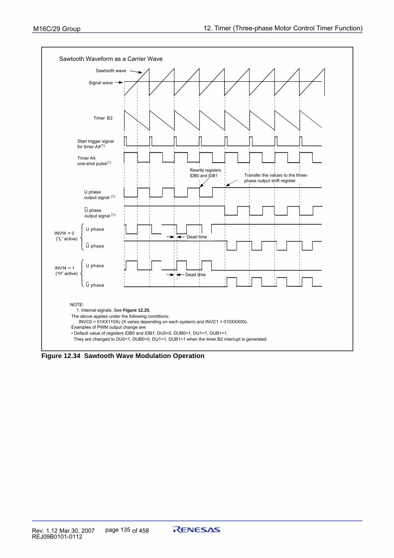
12. Timer (Three-phase Motor Control Timer Function)puorG92/C61M
page 135 854fo7002,03.raM21.1.veR2110-1010B90JER
Figure 12.34 Sawtooth Wave Modulation Operation
Timer B2
U phase
Sawtooth wave
Signal wave
U phase output signal (1)
U phase
U phase output signal (1)
U phase
U phase
INV14 = 0
Sawtooth Waveform as a Carrier Wave
INV14 = 1
NOTE: 1. Internal signals. See Figure 12.25.The above applies under the following conditions: INVC0 = 01XX110X2 (X varies depending on each system) and INVC1 = 010XXX002. Examples of PWM output change are:• Default value of registers IDB0 and IDB1: DU0=0, DUB0=1, DU1=1, DUB1=1. They are changed to DU0=1, DUB0=0, DU1=1, DUB1=1 when the timer B2 interrupt is generated.
Start trigger signal for timer A4(1)
Timer A4one-shot pulse(1)
Dead time
Dead time(“H” active)
(“L” active)
Transfer the values to the three-phase output shift register
Rewrite registers IDB0 and IDB1
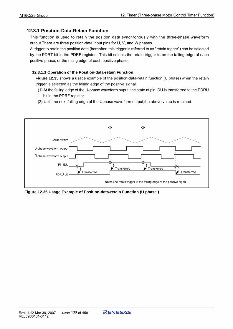
12. Timer (Three-phase Motor Control Timer Function)puorG92/C61M
page 136 854fo7002,03.raM21.1.veR2110-1010B90JER
12.3.1 Position-Data-Retain FunctionThis function is used to retain the position data synchronously with the three-phase waveformoutput.There are three position-data input pins for U, V, and W phases.A trigger to retain the position data (hereafter, this trigger is referred to as "retain trigger") can be selectedby the PDRT bit in the PDRF register. This bit selects the retain trigger to be the falling edge of eachpositive phase, or the rising edge of each positive phase.
12.3.1.1 Operation of the Position-data-retain Function
Figure 12.35 shows a usage example of the position-data-retain function (U phase) when the retaintrigger is selected as the falling edge of the positive signal.
(1) At the falling edge of the U-phase waveform ouput, the state at pin IDU is transferred to the PDRU bit in the PDRF register.(2) Until the next falling edge of the Uphase waveform output,the above value is retained.
Transferred
Carrier wave
U-phase waveform output
U-phase waveform output
1 2
TransferredTransferred
Transferred
Pin IDU
Note:Note: The retain trigger is the falling edge of the positive signal.
PDRU bit
Figure 12.35 Usage Example of Position-data-retain Function (U phase )
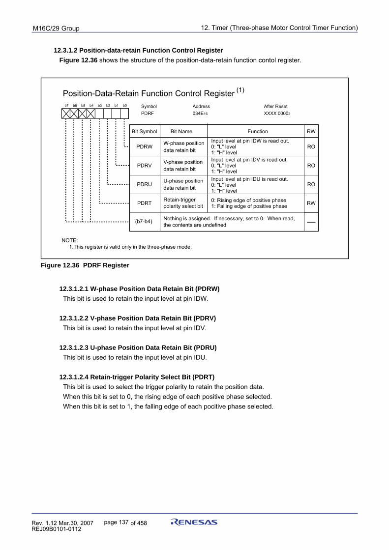
12. Timer (Three-phase Motor Control Timer Function)puorG92/C61M
page 137 854fo7002,03.raM21.1.veR2110-1010B90JER
12.3.1.2 Position-data-retain Function Control Register
Figure 12.36 shows the structure of the position-data-retain function contol register.
Figure 12.36 PDRF Register
12.3.1.2.1 W-phase Position Data Retain Bit (PDRW)
This bit is used to retain the input level at pin IDW.
12.3.1.2.2 V-phase Position Data Retain Bit (PDRV)
This bit is used to retain the input level at pin IDV.
12.3.1.2.3 U-phase Position Data Retain Bit (PDRU)
This bit is used to retain the input level at pin IDU.
12.3.1.2.4 Retain-trigger Polarity Select Bit (PDRT)
This bit is used to select the trigger polarity to retain the position data.When this bit is set to 0, the rising edge of each positive phase selected.When this bit is set to 1, the falling edge of each pocitive phase selected.
Position-Data-Retain Function Control Register (1)
Symbol Address After Reset PDRF 034E16 XXXX 00002
RO
RO
RO
RWBit Name FunctionBit Symbol
PDRW
PDRV
PDRU
W-phase positiondata retain bit
Input level at pin IDU is read out.0: "L" level1: "H" level
NOTE: 1.This register is valid only in the three-phase mode.
Retain-triggerpolarity select bit
(b7-b4)
RWPDRT
V-phase positiondata retain bit
Nothing is assigned. If necessary, set to 0. When read,the contents are undefined
U-phase positiondata retain bit
Input level at pin IDV is read out.0: "L" level1: "H" level
Input level at pin IDW is read out.0: "L" level1: "H" level
0: Rising edge of positive phase1: Falling edge of positive phase
b7 b3 b2 b1 b0
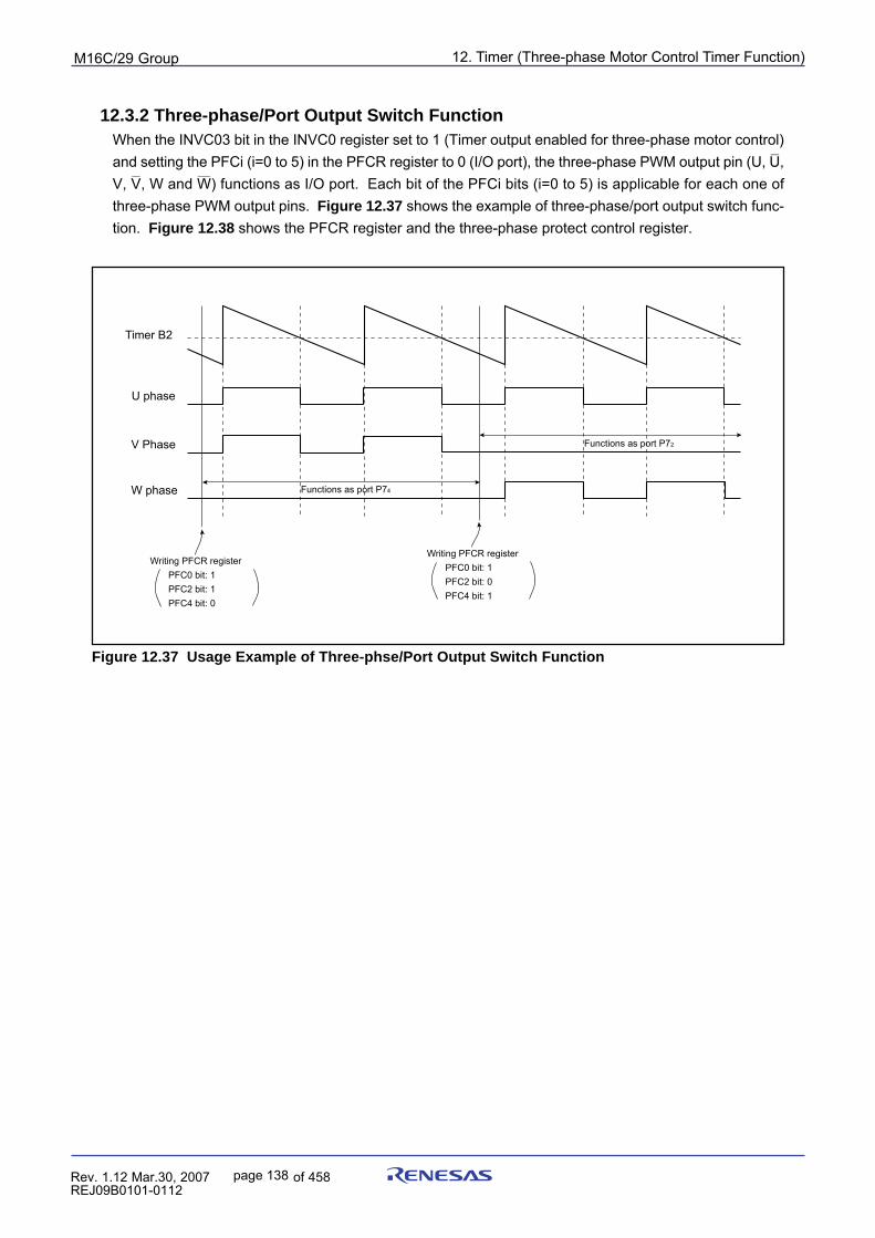
12. Timer (Three-phase Motor Control Timer Function)puorG92/C61M
page 138 854fo7002,03.raM21.1.veR2110-1010B90JER
12.3.2 Three-phase/Port Output Switch FunctionWhen the INVC03 bit in the INVC0 register set to 1 (Timer output enabled for three-phase motor control)
__
and setting the PFCi (i=0 to 5) in the PFCR register to 0 (I/O port), the three-phase PWM output pin (U, U,__ ___
V, V, W and W) functions as I/O port. Each bit of the PFCi bits (i=0 to 5) is applicable for each one ofthree-phase PWM output pins. Figure 12.37 shows the example of three-phase/port output switch func-tion. Figure 12.38 shows the PFCR register and the three-phase protect control register.
Figure 12.37 Usage Example of Three-phse/Port Output Switch Function
Timer B2
U phase
V Phase
W phase
Writing PFCR register PFC0 bit: 1 PFC2 bit: 1 PFC4 bit: 0
Functions as port P74
Functions as port P72
Writing PFCR register PFC0 bit: 1 PFC2 bit: 0 PFC4 bit: 1
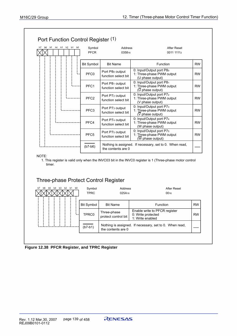
12. Timer (Three-phase Motor Control Timer Function)puorG92/C61M
page 139 854fo7002,03.raM21.1.veR2110-1010B90JER
Figure 12.38 PFCR Register, and TPRC Register
Port Function Control Register (1)
Symbol Address After Reset PFCR 035816 0011 11112
RW
RW
RW
RWBit Name FunctionBit Symbol
PFC0
PFC1
PFC2
Port P80 output function select bit
NOTE: 1. This register is valid only when the INVC03 bit in the INVC0 register is 1 (Three-phase motor control
timer.
(b7-b6)
RWPFC3
Nothing is assigned. If necessary, set to 0. When read,the contents are 0
0: Input/Output port P80
1: Three-phase PWM output (U phase output)
PFC4
PFC5
RW
RW
Port P81 output function select bit
Port P72 output function select bit
Port P73 output function select bit
Port P74 output function select bit
Port P75 output function select bit
0: Input/Output port P81
1: Three-phase PWM output (U phase output)0: Input/Output port P72
1: Three-phase PWM output (V phase output)0: Input/Output port P73
1: Three-phase PWM output (V phase output)0: Input/Output port P74
1: Three-phase PWM output (W phase output)0: Input/Output port P75
1: Three-phase PWM output (W phase output)
b7 b5 b4 b3 b2 b1 b0
Three-phase Protect Control RegisterSymbol Address After Reset TPRC 025A16 0016
RW
RWBit Name FunctionBit Symbol
TPRC0Three-phase protect control bit
(b7-b1) Nothing is assigned. If necessary, set to 0. When read,the contents are 0
Enable write to PFCR register0: Write protected1: Write enabled
b7 b3 b2 b1 b0
13. Timer SpuorG92/C61M
page 140 854fo7002,03.raM21.1.veR2110-1010B90JER
13. Timer SThe Timer S (Input Capture/Output Compare : here after, Timer S is referred to as "IC/OC".) is a high-performance I/O port for time measurement and waveform generation.The IC/OC has one 16-bit base timer for free-running operation and eight 16-bit registers for time measure-ment and waveform generation.Table 13.1 lists functions and channels of the IC/OC.
Table 13.1 IC/OC Functions and ChannelsFunction Description
Time measurement (1) 8 channels
Digital filter 8 channels
Trigger input prescaler 2 channels
Trigger input gate 2 channels
Waveform generation (1) 8 channels
Single-phase waveform output Available
Phase-delayed waveform output Available
Set/Reset waveform output Available
NOTE:1. The time measurement function and the waveform generating function share a pin. The time measurement function or waveform generating function can be selected for each channel.
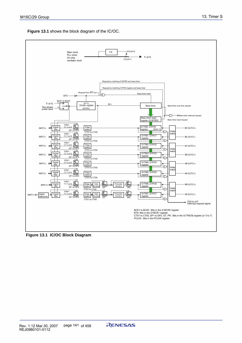
13. Timer SpuorG92/C61M
page 141 854fo7002,03.raM21.1.veR2110-1010B90JER
Figure 13.1 IC/OC Block Diagram
BTS: Bits in the G1BCR1 registerCTS1 to CTS0, DF1 to DF0, GT, PR : Bits in the G1TMCRj register (j= 0 to 7) PCLK0 : Bits in the PCLKR register
G1TM0, G1PO0register
G1TM1, G1PO1register
G1TM2, G1PO2register
G1TM3, G1PO3register
G1TM4, G1PO4register
G1TM5, G1PO5register
G1TM6, G1PO6register
G1TM7, G1PO7register
PWMoutput
PWMoutput
PWMoutput
PWMoutput
Base timer reset
(n+1)Divider register
Edgeselect
Digitalfilter
Gatefunction
Edgeselect
Digitalfilter
Gatefunction
Edgeselect
Digitalfilter
Edgeselect
DigitalfilterINPC10
INPC11
INPC16
(G1DV)
GT
GT PR
PR
Ch0 to ch7 interrupt request signal
OUTC10
OUTC11
OUTC14
OUTC15
Prescalerfunction
Prescalerfunction
OUTC16
OUTC17
OUTC12
OUTC13
(Note 1)
Base timerfBT1
Edgeselect
DigitalfilterINPC12
Two-phasepulse input
BCK1 to BCK0 : Bits in the G1BCR0 register
Request from INT1 pin
BTS
Request by matching G1PO0 register and base timer
Base timer over flow request
BCK1 to BCK011
10
00
10:fBT111: f1 or f2
DF1 to DF0CTS1 to CTS0
CTS1 to CTS0
CTS1 to CTS0
00
DF1 to DF000
DF1 to DF0
00
DF1 to DF000 0
0
1
0
1
0
11
DF1 to DF0
Base timer resetregister (G1BTRR)
Request by matching G1BTRR and base timer
00
CTS1 to CTS0DF1 to DF0
Edgeselect
DigitalfilterINPC13
DF1 to DF0
Edgeselect
DigitalfilterINPC14
CTS1 to CTS0
DF1 to DF0
Edgeselect
DigitalfilterINPC15
CTS1 to CTS0
INPC17 Digitaldebounce
Base timer reset request
Base timer interrupt request
00
00
CTS1 to CTS0
CTS1 to CTS0
1/2 PCLK0=0
PCLK0=1
f1 or f2
f1 or f2
Main clock,PLL clock,On-chiposcillator clock
10:fBT111: f1 or f2
10:fBT111: f1 or f2
10:fBT111: f1 or f2
10:fBT111: f1 or f2
10:fBT111: f1 or f2
10:fBT111: f1 or f2
10:fBT111: f1 or f2
Figure 13.1 shows the block diagram of the IC/OC.
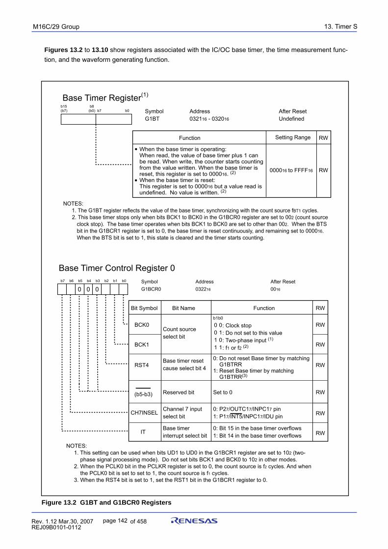
13. Timer SpuorG92/C61M
page 142 854fo7002,03.raM21.1.veR2110-1010B90JER
Figures 13.2 to 13.10 show registers associated with the IC/OC base timer, the time measurement func-tion, and the waveform generating function.
Figure 13.2 G1BT and G1BCR0 Registers
Base Timer Register(1)
Symbol Address After Reset G1BT 032116 - 032016 Undefined
RW
RW
Function
(b7) b0
Setting Range
000016 to FFFF16
b8b15b7(b0)
When the base timer is operating:When read, the value of base timer plus 1 can be read. When write, the counter starts counting from the value written. When the base timer is reset, this register is set to 000016. (2)
When the base timer is reset:This register is set to 000016 but a value read is undefined. No value is written. (2)
NOTES: 1. The G1BT register reflects the value of the base timer, synchronizing with the count source fBT1 cycles.
2. This base timer stops only when bits BCK1 to BCK0 in the G1BCR0 register are set to 002 (count source clock stop). The base timer operates when bits BCK1 to BCK0 are set to other than 002. When the BTS bit in the G1BCR1 register is set to 0, the base timer is reset continuously, and remaining set to 000016. When the BTS bit is set to 1, this state is cleared and the timer starts counting.
Base Timer Control Register 0Symbol Address After Reset G1BCR0 032216 0016
RW
RW
RW
RW
RW
RWBit Name FunctionBit Symbol
: Clock stop: Do not set to this value : Two-phase input (1)
: f1 or f2 (2)
b1
0011
b0
0101
BCK0
BCK1
RST4
Count sourceselect bit
Channel 7 inputselect bit
ITBase timer interrupt select bit
0: Bit 15 in the base timer overflows1: Bit 14 in the base timer overflows
CH7INSEL
0: Do not reset Base timer by matching G1BTRR1: Reset Base timer by matching G1BTRR(3)
NOTES: 1. This setting can be used when bits UD1 to UD0 in the G1BCR1 register are set to 102 (two- phase signal processing mode). Do not set bits BCK1 and BCK0 to 102 in other modes. 2. When the PCLK0 bit in the PCLKR register is set to 0, the count source is f2 cycles. And when the PCLK0 bit is set to set to 1, the count source is f1 cycles. 3. When the RST4 bit is set to 1, set the RST1 bit in the G1BCR1 register to 0.
Base timer resetcause select bit 4
0: P27/OUTC17/INPC17 pin1: P17/INT5/INPC17/IDU pin
Reserved bit Set to 0(b5-b3) RW
b7 b6 b5 b4 b3 b2 b1 b0
000
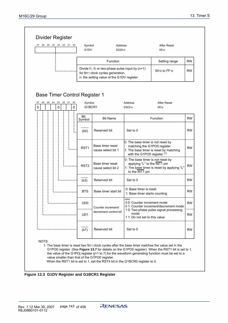
13. Timer SpuorG92/C61M
page 143 854fo7002,03.raM21.1.veR2110-1010B90JER
Figure 13.3 G1DV Register and G1BCR1 Register
Divider RegisterSymbol Address After Reset G1DV 032A16 0016
b7 b6 b5 b4 b3 b2 b1 b0
RW
RW
Function Setting range
Divide f1, f2 or two-phase pulse input by (n+1) for fBT1 clock cycles generation.n: the setting value of the G1DV register
0016 to FF16
RST1
0: The base timer is not reset by applying "L" to the INT1 pin
1: The base timer is reset by applying "L" to the INT1 pin
Base Timer Control Register 1Symbol Address After Reset G1BCR1 032316 0016
RW
RW
RW
RW
RW
RW
RW
RW
Bit Name FunctionBit Symbol
b6
001
1
b5
010
1
(b0)
RST2
BTS
UD0
UD1
Base timer resetcause select bit 1
Base timer resetcause select bit 2
Counter increment/decrement control bit
0: Base timer is reset1: Base timer starts counting
: Counter increment mode: Counter increment/decrement mode: Two-phase pulse signal processing mode : Do not set to this value
NOTS: 1. The base timer is reset two fBT1 clock cycles after the base timer matches the value set in the
G1PO0 register. (See Figure 13.7 for details on the G1PO0 register) When the RST1 bit is set to 1, the value of the G1POj register (j=1 to 7) for the waveform generating function must be set to a value smaller than that of the G1PO0 register.
When the RST1 bit is set to 1, set the RST4 bit in the G1BCR0 register to 0.
Reserved bit Set to 0
0: The base timer is not reset by matching the G1PO0 register
1: The base timer is reset by matching with the G1PO0 register (1)
Reserved bit Set to 0
Reserved bit Set to 0 RW
(b3)
(b7)
Base timer start bit
0 00b7 b6 b5 b4 b3 b2 b1 b0
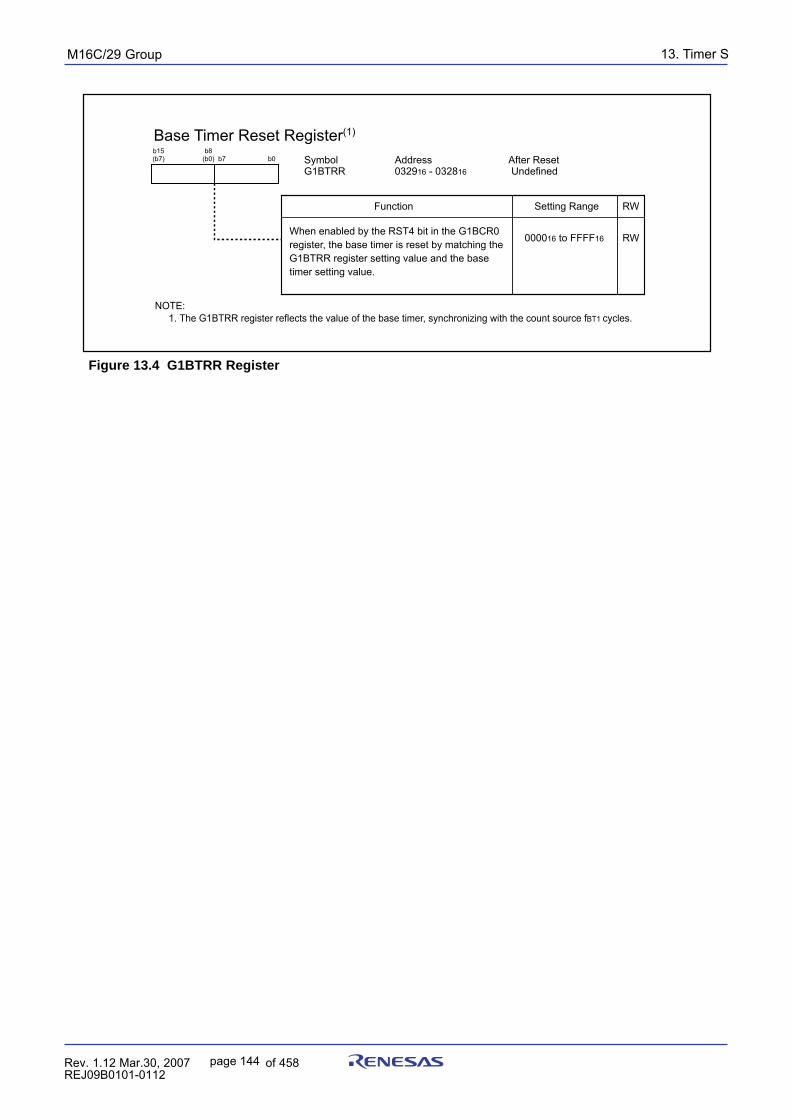
13. Timer SpuorG92/C61M
page 144 854fo7002,03.raM21.1.veR2110-1010B90JER
Figure 13.4 G1BTRR Register
Base Timer Reset Register(1)
Symbol Address After Reset G1BTRR 032916 - 032816 Undefined
RW
RW
Function Setting Range
When enabled by the RST4 bit in the G1BCR0 register, the base timer is reset by matching theG1BTRR register setting value and the base timer setting value.
000016 to FFFF16
b15b0b7
b8(b7) (b0)
NOTE: 1. The G1BTRR register reflects the value of the base timer, synchronizing with the count source fBT1 cycles.
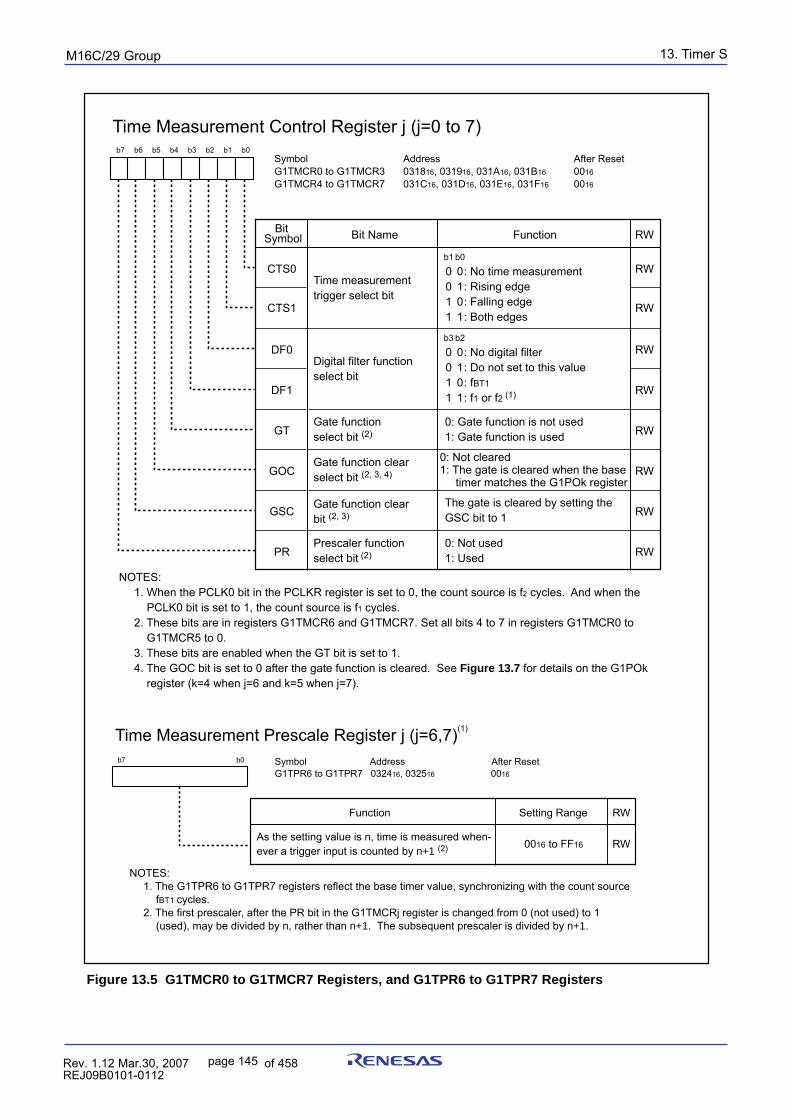
13. Timer SpuorG92/C61M
page 145 854fo7002,03.raM21.1.veR2110-1010B90JER
Figure 13.5 G1TMCR0 to G1TMCR7 Registers, and G1TPR6 to G1TPR7 Registers
Time Measurement Control Register j (j=0 to 7)
Symbol G1TMCR0 to G1TMCR3 G1TMCR4 to G1TMCR7
Address 031816, 031916, 031A16, 031B16 031C16, 031D16, 031E16, 031F16
After Reset 0016
0016
RW
RW
RW
RW
RW
RW
RW
RW
RW
Bit Name FunctionBit Symbol
CTS0
CTS1
DF0
Time measurementtrigger select bit
DF1
Gate functionselect bit (2)GT
GOC
PR
GSC
Digital filter functionselect bit
Gate function clearselect bit (2, 3, 4)
0: Gate function is not used1: Gate function is used
Gate function clearbit (2, 3)
Prescaler functionselect bit (2)
b1
0011
b0
0101
: No time measurement: Rising edge: Falling edge: Both edges
b3
0011
b2
0101
: No digital filter: Do not set to this value : fBT1
: f1 or f2 (1)
0: Not cleared 1: The gate is cleared when the base timer matches the G1POk register
The gate is cleared by setting the GSC bit to 1
0: Not used1: Used
NOTES: 1. When the PCLK0 bit in the PCLKR register is set to 0, the count source is f2 cycles. And when the
PCLK0 bit is set to 1, the count source is f1 cycles. 2. These bits are in registers G1TMCR6 and G1TMCR7. Set all bits 4 to 7 in registers G1TMCR0 to
G1TMCR5 to 0. 3. These bits are enabled when the GT bit is set to 1. 4. The GOC bit is set to 0 after the gate function is cleared. See Figure 13.7 for details on the G1POk
register (k=4 when j=6 and k=5 when j=7).
b7 b6 b5 b4 b3 b2 b1 b0
Time Measurement Prescale Register j (j=6,7)(1)
Symbol Address After Reset G1TPR6 to G1TPR7 032416, 032516 0016
RW
RW
Function Setting Range
As the setting value is n, time is measured when- ever a trigger input is counted by n+1 (2) 0016 to FF16
NOTES: 1. The G1TPR6 to G1TPR7 registers reflect the base timer value, synchronizing with the count source
fBT1 cycles. 2. The first prescaler, after the PR bit in the G1TMCRj register is changed from 0 (not used) to 1
(used), may be divided by n, rather than n+1. The subsequent prescaler is divided by n+1.
b7 b0
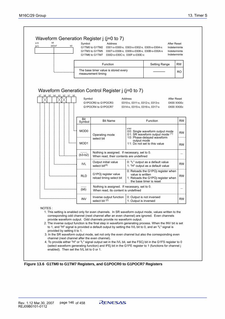
13. Timer SpuorG92/C61M
page 146 854fo7002,03.raM21.1.veR2110-1010B90JER
Figure 13.6 G1TM0 to G1TM7 Registers, and G1POCR0 to G1POCR7 Registers
Waveform Generation Control Register j (j=0 to 7)Symbol Address After Reset G1POCR0 to G1POCR3 031016, 031116, 031216, 031316 0X00 XX002
G1POCR4 to G1POCR7 031416, 031516, 031616, 031716 0X00 XX002
RW
RW
RW
RW
RW
RW
Bit Name FunctionBit Symbol
MOD0
MOD1
Operating modeselect bit
Output initial valueselect bit(4)IVL
RLD
INV
0: "L" output as a default value1: "H" output as a default value
Inverse output function select bit (2)
: Single waveform output mode: SR waveform output mode (1)
: Phase-delayed waveform output mode: Do not set to this value
0: Output is not inversed1: Output is inversed
b1001
1
b0010
1
G1POj register value reload timing select bit
NOTES : 1. This setting is enabled only for even channels. In SR waveform output mode, values written to the
corresponding odd channel (next channel after an even channel) are ignored. Even channels provide waveform output. Odd channels provide no waveform output.
2. The inverse output function is the final step in waveform generating process. When the INV bit is set to 1, and "H" signal is provided a default output by setting the IVL bit to 0, and an "L" signal is provided by setting it to 1.
3. In the SR waveform output mode, set not only the even channel but also the correspoinding even channel (next channel after the even channel).
4. To provide either "H" or "L" signal output set in the IVL bit, set the FSCj bit in the G1FS register to 0 (select waveform generating function) and IFEj bit in the G1FE register to 1 (functions for channel j enabled). Then set the IVL bit to 0 or 1.
Nothing is assigned. If necessary, set to 0. When read, their contents are undefined
Nothing is assigned. If necessary, set to 0. When read, its content is undefined
0: Reloads the G1POj register when value is written
1: Reloads the G1POj register when the base timer is reset
(b3-b2)
(b6)
b7 b6 b5 b4 b3 b2 b1 b0
Waveform Generation Register j (j=0 to 7)Symbol G1TM0 to G1TM2 G1TM3 to G1TM5G1TM6 to G1TM7
RW
RO
Function Setting Range
b15(b7)
b8(b0)
Address 030116-030016, 030316-030216, 030516-030416
030716-030616, 030916-030816, 030B16-030A16
030D16-030C16, 030F16-030E16
After Reset IndeterminteIndeterminteIndeterminte
The base timer value is stored every measurement timing
b7 b0
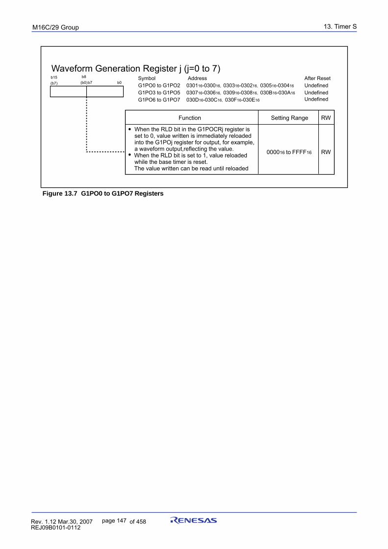
13. Timer SpuorG92/C61M
page 147 854fo7002,03.raM21.1.veR2110-1010B90JER
Figure 13.7 G1PO0 to G1PO7 Registers
Waveform Generation Register j (j=0 to 7)Symbol G1PO0 to G1PO2 G1PO3 to G1PO5G1PO6 to G1PO7
RW
RW
Function Setting Range
b15(b7)
b8(b0)
Address 030116-030016, 030316-030216, 030516-030416
030716-030616, 030916-030816, 030B16-030A16
030D16-030C16, 030F16-030E16
After Reset UndefinedUndefinedUndefined
When the RLD bit in the G1POCRj register is set to 0, value written is immediately reloaded into the G1POj register for output, for example, a waveform output,reflecting the value.
When the RLD bit is set to 1, value reloaded while the base timer is reset.
The value written can be read until reloaded
b7 b0
000016 to FFFF16
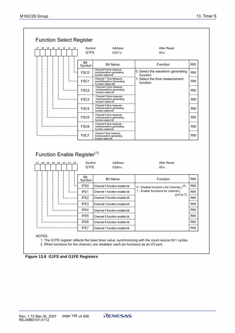
13. Timer SpuorG92/C61M
page 148 854fo7002,03.raM21.1.veR2110-1010B90JER
Figure 13.8 G1FS and G1FE Registers
Function Enable Register(1)
Symbol Address After Reset G1FE 032616 0016
b7 b6 b5 b4 b3 b2 b1 b0
RW
RW
RW
RW
RW
RW
RW
RW
RW
Bit NameBit Symbol
IFE0
IFE1
IFE2
Channel 0 function enable bit
IFE3
IFE4
IFE5
IFE7
Function
IFE6
0 : Disable function s for channel j (2)
1 : Enable functions for channel j (j=0 to 7)
Channel 1 function enable bit
Channel 2 function enable bit
Channel 3 function enable bit
Channel 4 function enable bit
Channel 5 function enable bit
Channel 6 function enable bit
Channel 7 function enable bit
NOTES: 1. The G1FE register reflects the base timer value, synchronizing with the count source fBT1 cycles. 2. When functions for the channel j are disabled, each pin functions as an I/O port.
Function Select RegisterSymbol Address After Reset G1FS 032716 0016
b7 b6 b5 b4 b3 b2 b1 b0
RW
RW
RW
RW
RW
RW
RW
RW
RW
Bit NameBit Symbol
FSC0
FSC1
FSC2
Channel 0 time measure-ment/waveform generating function select bit
FSC3
FSC4
FSC5
FSC7
Function
FSC6
0: Select the waveform generating function1: Select the time measurement function
Channel 1 Time Measure-ment/Waveform GeneratingFunction Select BitChannel 2 time measure-ment/waveform generating function select bitChannel 3 time measure-ment/waveform generating function select bitChannel 4 time measure-ment/waveform generating function select bitChannel 5 time measure-ment/waveform generating function select bitChannel 6 time measure-ment/waveform generating function select bitChannel 7 time measure-ment/waveform generating function select bit
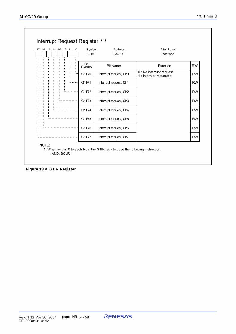
13. Timer SpuorG92/C61M
page 149 854fo7002,03.raM21.1.veR2110-1010B90JER
Figure 13.9 G1IR Register
Interrupt Request Register (1)
Symbol Address After Reset G1IR 033016 Undefined
b7 b6 b5 b4 b3 b2 b1 b0
RW
RW
RW
RW
RW
RW
RW
RW
RW
Bit NameBit Symbol
G1IR0
G1IR1
G1IR2
Interrupt request, Ch0
G1IR3
G1IR4
G1IR5
G1IR7
Function
G1IR6
0 : No interrupt request1 : Interrupt requested
Interrupt request, Ch1
Interrupt request, Ch2
Interrupt request, Ch3
Interrupt request, Ch4
Interrupt request, Ch5
Interrupt request, Ch6
Interrupt request, Ch7
NOTE: 1. When writing 0 to each bit in the G1IR register, use the following instruction: AND, BCLR
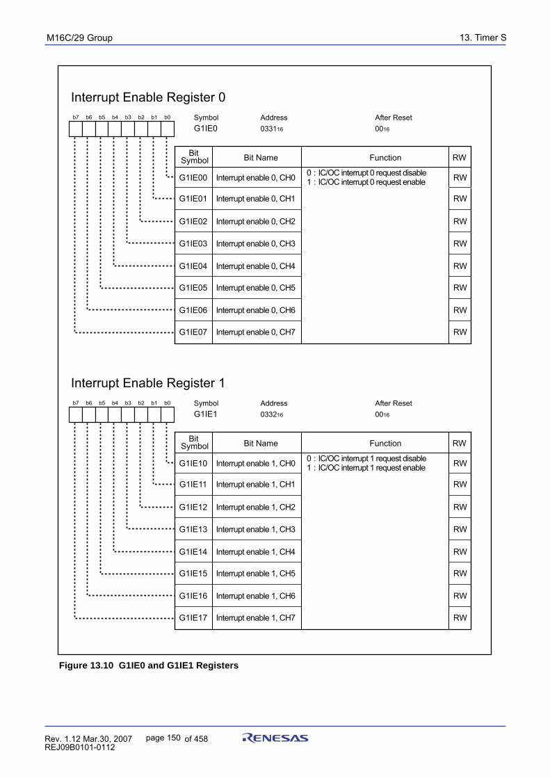
13. Timer SpuorG92/C61M
page 150 854fo7002,03.raM21.1.veR2110-1010B90JER
Figure 13.10 G1IE0 and G1IE1 Registers
Interrupt Enable Register 0Symbol Address After Reset G1IE0 033116 0016
b7 b6 b5 b4 b3 b2 b1 b0
RW
RW
RW
RW
RW
RW
RW
RW
RW
Bit NameBit Symbol
G1IE00
G1IE01
G1IE02
Interrupt enable 0, CH0
G1IE03
G1IE04
G1IE05
G1IE07
Function
G1IE06
0 : IC/OC interrupt 0 request disable1 : IC/OC interrupt 0 request enable
Interrupt enable 0, CH1
Interrupt enable 0, CH2
Interrupt enable 0, CH3
Interrupt enable 0, CH4
Interrupt enable 0, CH5
Interrupt enable 0, CH6
Interrupt enable 0, CH7
Interrupt Enable Register 1Symbol Address After Reset G1IE1 033216 0016
b7 b6 b5 b4 b3 b2 b1 b0
RW
RW
RW
RW
RW
RW
RW
RW
RW
Bit NameBit Symbol
G1IE10
G1IE11
G1IE12
Interrupt enable 1, CH0
G1IE13
G1IE14
G1IE15
G1IE17
Function
G1IE16
0 : IC/OC interrupt 1 request disable1 : IC/OC interrupt 1 request enable
Interrupt enable 1, CH1
Interrupt enable 1, CH2
Interrupt enable 1, CH3
Interrupt enable 1, CH4
Interrupt enable 1, CH5
Interrupt enable 1, CH6
Interrupt enable 1, CH7
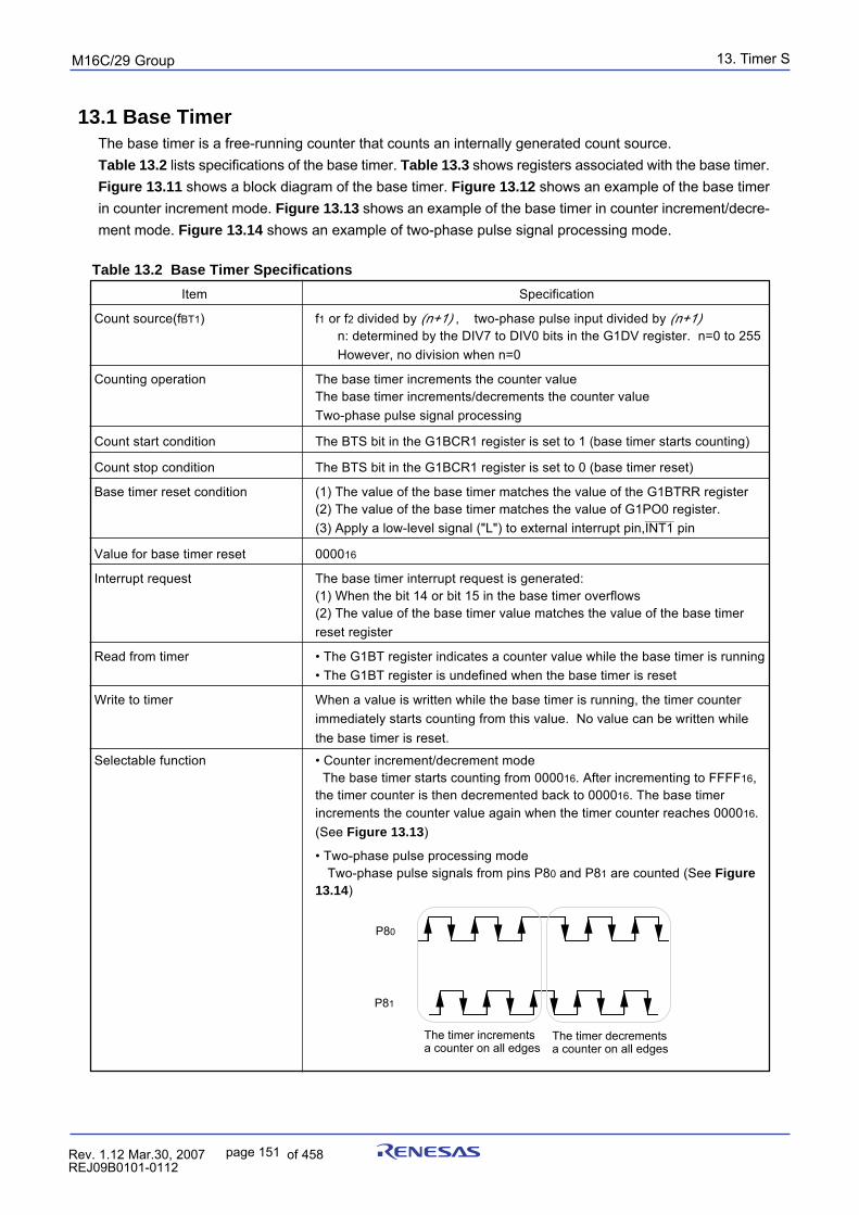
13. Timer SpuorG92/C61M
page 151 854fo7002,03.raM21.1.veR2110-1010B90JER
The timer increments a counter on all edges
The timer decrements a counter on all edges
P80
P81
13.1 Base TimerThe base timer is a free-running counter that counts an internally generated count source.Table 13.2 lists specifications of the base timer. Table 13.3 shows registers associated with the base timer.Figure 13.11 shows a block diagram of the base timer. Figure 13.12 shows an example of the base timerin counter increment mode. Figure 13.13 shows an example of the base timer in counter increment/decre-ment mode. Figure 13.14 shows an example of two-phase pulse signal processing mode.
Table 13.2 Base Timer Specifications
Item Specification
Count source(fBT1) f1 or f2 divided by (n+1) , two-phase pulse input divided by (n+1) n: determined by the DIV7 to DIV0 bits in the G1DV register. n=0 to 255 However, no division when n=0
Counting operation The base timer increments the counter valueThe base timer increments/decrements the counter valueTwo-phase pulse signal processing
Count start condition The BTS bit in the G1BCR1 register is set to 1 (base timer starts counting)
Count stop condition The BTS bit in the G1BCR1 register is set to 0 (base timer reset)
Base timer reset condition (1) The value of the base timer matches the value of the G1BTRR register(2) The value of the base timer matches the value of G1PO0 register.
________
(3) Apply a low-level signal ("L") to external interrupt pin,INT1 pin
Value for base timer reset 000016
Interrupt request The base timer interrupt request is generated:(1) When the bit 14 or bit 15 in the base timer overflows(2) The value of the base timer value matches the value of the base timerreset register
Read from timer • The G1BT register indicates a counter value while the base timer is running• The G1BT register is undefined when the base timer is reset
Write to timer When a value is written while the base timer is running, the timer counterimmediately starts counting from this value. No value can be written whilethe base timer is reset.
Selectable function • Counter increment/decrement mode The base timer starts counting from 000016. After incrementing to FFFF16,the timer counter is then decremented back to 000016. The base timerincrements the counter value again when the timer counter reaches 000016.(See Figure 13.13)
• Two-phase pulse processing modeTwo-phase pulse signals from pins P80 and P81 are counted (See Figure
13.14)
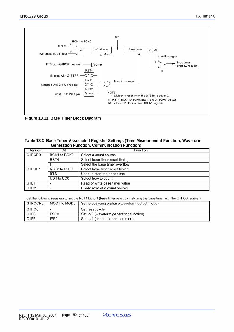
13. Timer SpuorG92/C61M
page 152 854fo7002,03.raM21.1.veR2110-1010B90JER
Table 13.3 Base Timer Associated Register Settings (Time Measurement Function, Waveform Generation Function, Communication Function)
Register Bit FunctionG1BCR0 BCK1 to BCK0 Select a count source
RST4 Select base timer reset timingIT Select the base timer overflow
G1BCR1 RST2 to RST1 Select base timer reset timingBTS Used to start the base timerUD1 to UD0 Select how to count
G1BT - Read or write base timer valueG1DV - Divide ratio of a count source
Set the following registers to set the RST1 bit to 1 (base timer reset by matching the base timer with the G1PO0 register)G1POCR0 MOD1 to MOD0 Set to 002 (single-phase waveform output mode)
G1PO0 - Set reset cycleG1FS FSC0 Set to 0 (waveform generating function)G1FE IFE0 Set to 1 (channel operation start)
Figure 13.11 Base Timer Block Diagram
(n+1) divider
RST4
RST1
RST2
Matched with G1BTRR
Matched with G1PO0 register
Base timer b14 b15
Base timer overflow request
BCK1 to BCK0
IT
BTS bit in G1BCR1 register
Two-phase pulse input Overflow signal
Input "L" to INT1 pin
Base timer reset
11
10
0
1
fBT1
NOTE: 1. Divider is reset when the BTS bit is set to 0.
IT, RST4, BCK1 to BCK0: Bits in the G1BCR0 register RST2 to RST1: Bits in the G1BCR1 register
(Note 1)
f1 or f2
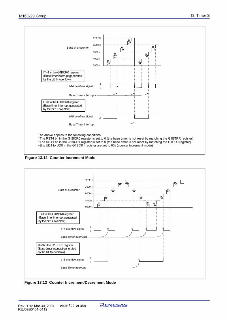
13. Timer SpuorG92/C61M
page 153 854fo7002,03.raM21.1.veR2110-1010B90JER
Figure 13.12 Counter Increment Mode
Figure 13.13 Counter Increment/Decrement Mode
FFFF16
800016
000016
400016
C00016State of a counter
Base Timer interrupts
10
b14 overflow signal
10
b15 overflow signal
Base Timer interrupt
IT=0 in the G1BCR0 register (Base timer interrupt generated by the bit 15 overflow)
IT=1 in the G1BCR0 register (Base timer interrupt generated by the bit 14 overflow)
The above applies to the following conditions. The RST4 bit in the G1BCR0 register is set to 0 (the base timer is not reset by matching the G1BTRR register) The RST1 bit in the G1BCR1 register is set to 0 (the base timer is not reset by matching the G1PO0 register) Bits UD1 to UD0 in the G1BCR1 register are set to 002 (counter increment mode)
FFFF16
800016
400016
C00016
000016
State of a counter
10
Base Timer interrupts
b14 overflow signal
10
b15 overflow signal
Base Timer interrupt
IT=0 in the G1BCR0 register (Base timer interrupt generated by the bit 15 overflow)
IT=1 in the G1BCR0 register (Base timer interrupt generated by the bit 14 overflow)
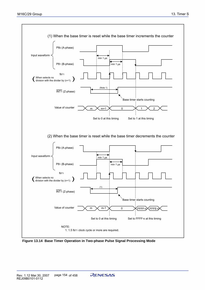
13. Timer SpuorG92/C61M
page 154 854fo7002,03.raM21.1.veR2110-1010B90JER
Figure 13.14 Base Timer Operation in Two-phase Pulse Signal Processing Mode
(1) When the base timer is reset while the base timer increments the counter
(2) When the base timer is reset while the base timer decrements the counter
( )
m
When selects nodivision with the divider by (n+1)
Value of counter
min 1 µs
(Note 1)
min 1 µs
m+1 1 20
Set to 0 at this timing
Base timer starts counting
P80 (A-phase)
P81 (B-phase)
INT1 (Z-phase)
Set to 1 at this timing
min 1 µs
(1)
min 1 µs
m
Input waveform
Value of counter m-1 FFFF16 FFFE160
Set to 0 at this timing
NOTE: 1. 1.5 fBT1 clock cycle or more are required.
Base timer starts counting
P80 (A-phase)
P81 (B-phase)
INT1 (Z-phase)
Set to FFFF16 at this timing
Input waveform
fBT1
fBT1
( )When selects nodivision with the divider by (n+1)
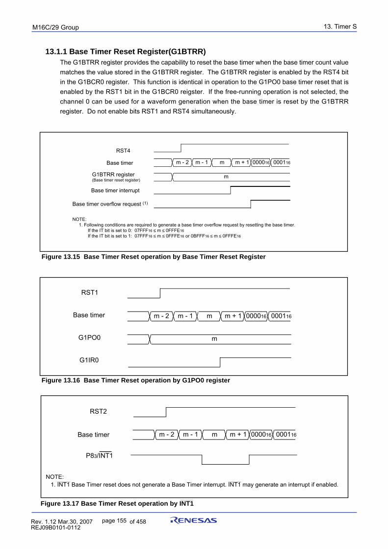
13. Timer SpuorG92/C61M
page 155 854fo7002,03.raM21.1.veR2110-1010B90JER
13.1.1 Base Timer Reset Register(G1BTRR)The G1BTRR register provides the capability to reset the base timer when the base timer count valuematches the value stored in the G1BTRR register. The G1BTRR register is enabled by the RST4 bitin the G1BCR0 register. This function is identical in operation to the G1PO0 base timer reset that isenabled by the RST1 bit in the G1BCR0 reigster. If the free-running operation is not selected, thechannel 0 can be used for a waveform generation when the base timer is reset by the G1BTRRregister. Do not enable bits RST1 and RST4 simultaneously.
Figure 13.15 Base Timer Reset operation by Base Timer Reset Register
Figure 13.16 Base Timer Reset operation by G1PO0 register
_______
Figure 13.17 Base Timer Reset operation by INT1
NOTE:________ ________
1. INT1 Base Timer reset does not generate a Base Timer interrupt. INT1 may generate an interrupt if enabled.
Base timer
G1BTRR register (Base timer reset register)
Base timer interrupt
RST4
m - 2 m - 1 m m + 1 000016
m
Base timer overflow request (1)
NOTE: 1. Following conditions are required to generate a base timer overflow request by resetting the base timer. If the IT bit is set to 0: 07FFF16 ≤ m ≤ 0FFFE16 If the IT bit is set to 1: 07FFF16 ≤ m ≤ 0FFFE16 or 0BFFF16 ≤ m ≤ 0FFFE16
000116
Base timer
G1PO0
G1IR0
RST1
m - 2 m - 1 m m + 1 000016
m
000116
RST2
Base timer
P83/INT1
m - 2 m - 1 m m + 1 000016 000116
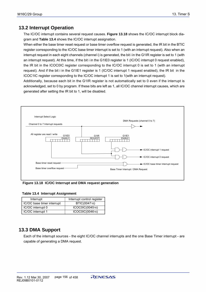
13. Timer SpuorG92/C61M
page 156 854fo7002,03.raM21.1.veR2110-1010B90JER
13.2 Interrupt OperationThe IC/OC interrupt contains several request causes. Figure 13.18 shows the IC/OC interrupt block dia-gram and Table 13.4 shows the IC/OC interrupt assignation.When either the base timer reset request or base timer overflow request is generated, the IR bit in the BTICregister corresponding to the IC/OC base timer interrupt is set to 1 (with an interrupt request). Also when aninterrupt request in each eight channels (channel i) is generated, the bit i in the G1IR register is set to 1 (withan interrupt request). At this time, if the bit i in the G1IE0 register is 1 (IC/OC interrupt 0 request enabled),the IR bit in the ICOC0IC register corresponding to the IC/OC interrupt 0 is set to 1 (with an interruptrequest). And if the bit i in the G1IE1 register is 1 (IC/OC interrupt 1 request enabled), the IR bit in theICOC1IC register corresponding to the IC/OC interrupt 1 is set to 1(with an interrupt request).Additionally, because each bit in the G1IR register is not automatically set to 0 even if the interrupt isacknowledged, set to 0 by program. If these bits are left as 1, all IC/OC channel interrupt causes, which aregenerated after setting the IR bit to 1, will be disabled.
Figure 13.18 IC/OC Interrupt and DMA request generation
Table 13.4 Interrupt Assignment
Interrupt Interrupt control registerIC/OC base timer interrupt BTIC(004716)IC/OC interrupt 0 ICOC0IC(004516)IC/OC interrupt 1 ICOC0IC(004616)
13.3 DMA SupportEach of the interrupt sources - the eight IC/OC channel interrupts and the one Base Timer interrupt - arecapable of generating a DMA request.
Interrupt Select Logic
Channel 0 to 7 Interrupt requestsDMA Requests (channel 0 to 7)
All register are read / write G1IE0 G1IR G1IE1
IC/OC interrupt 1 request
IC/OC interrupt 0 request
IC/OC base timer interrupt requestBase timer reset request
Base timer overflow request Base Timer Interrupt / DMA Request
ENABLE REQUEST ENABLE
13. Timer SpuorG92/C61M
page 157 854fo7002,03.raM21.1.veR2110-1010B90JER
13.4 Time Measurement FunctionIn synchronization with an external trigger input, the value of the base timer is stored into the G1TMjregister (j=0 to 7). Table 13.5 shows specifications of the time measurement function. Table 13.6 showsregister settings associated with the time measurement function. Figures 13.19 and 13.20 display opera-tional timing of the time measurement function. Figure 13.21 shows operational timing of the prescalerfunction and the gate function.
Table 13.5 Time Measurement Function Specifications
Item Specification
Measurement channel Channels 0 to 7
Selecting trigger input polarity Rising edge, falling edge, both edges of the INPC1j pin (1)
Measurement start condition The IFEj bit in the G1FE register should be set to 1 (channels j function
enabled) when the FSCj bit (j=0 to 7) in the G1FS register is set to 1 (time
measurement function selected).
Measurement stop condition The IFEj bit should be set to 0 (channel j function disabled)
Time measurement timing •No prescaler : every time a trigger signal is applied
•Prescaler (for channel 6 and channel 7):
every G1TPRk (k=6,7) register value +1 times a trigger signal is applied
Interrupt request generation timing The G1IRi bit (i=0 to 7) in the interrupt request register (See Figure 13.9) is
set to 1 at time measurement timing
INPC1j pin function (1) Trigger input pin
Selectable function • Digital filter function
The digital filter samples a trigger input signal level every f1, f2 or fBT1
cycles and passes pulse signal matching trigger input signal level three
times
• Prescaler function (for channel 6 and channel 7)
Time measurement is executed every G1TPRk register value +1 times a
trigger signal is applied
• Gate function (for channel 6 and channel 7)
After time measurement by the first trigger input, trigger input cannot be
accepted. However, while the GOC bit in the G1TMCRk register is set to 1
(gate cleared by matching the base timer with the G1POp register (p=4
when k=6, p=5 when k=7)), trigger input can be accepted again by
matching the base timer value with the G1POp register setting
• Digital Debounce function (for channel7)________
See 13.6.2 Digital Debounce Function for P17/INT5/INPC17 and 19.6
Digital Debounce Function for detailsNOTE: 1. The INPC10 to INPC17 pins
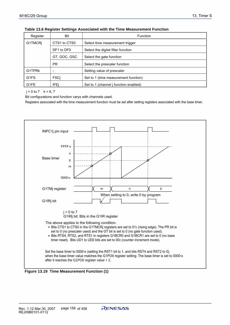
13. Timer SpuorG92/C61M
page 158 854fo7002,03.raM21.1.veR2110-1010B90JER
Table 13.6 Register Settings Associated with the Time Measurement Function
Register Bit Function
G1TMCRj CTS1 to CTS0 Select time measurement trigger
DF1 to DF0 Select the digital filter function
GT, GOC, GSC Select the gate function
PR Select the prescaler function
G1TPRk - Setting value of prescaler
G1FS FSCj Set to 1 (time measurement function)
G1FE IFEj Set to 1 (channel j function enabled)
j = 0 to 7 k = 6, 7Bit configurations and function varys with channels used.Registers associated with the time measurement function must be set after setting registers associated with the base timer.
Figure 13.19 Time Measurement Function (1)
FFFF16
p
p
n
n
m
m
Base timer
INPC1j pin input
000016
G1TMj register
G1IRj bit
When setting to 0, write 0 by program
j = 0 to 7G1IRj bit: Bits in the G1IR register
Set the base timer to 000016 (setting the RST1 bit to 1, and bits RST4 and RST2 to 0), when the base timer value matches the G1PO0 register setting. The base timer is set to 000016 after it reaches the G1PO0 register value + 2.
The above applies to the following condition. Bits CTS1 to CTS0 in the G1TMCRj registers are set to 012 (rising edge). The PR bit is
set to 0 (no prescaler used) and the GT bit is set to 0 (no gate function used). Bits RTS4, RTS2, and RTS1 in registers G1BCR0 and G1BCR1 are set to 0 (no base
timer reset). Bits UD1 to UD0 bits are set to 002 (counter increment mode).
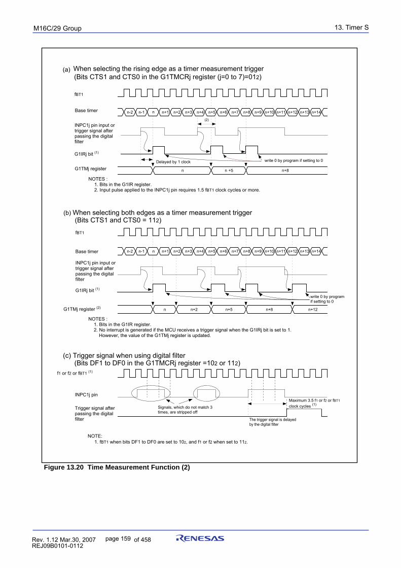
13. Timer SpuorG92/C61M
page 159 854fo7002,03.raM21.1.veR2110-1010B90JER
Figure 13.20 Time Measurement Function (2)
2. No interrupt is generated if the MCU receives a trigger signal when the G1IRj bit is set to 1.
1. Bits in the G1IR register.2. Input pulse applied to the INPC1j pin requires 1.5 fBT1 clock cycles or more.
n-2 n-1 n n+1 n+2 n+3 n+4 n+5 n+6 n+7 n+8 n+9 n+10 n+11 n+12 n+13 n+14
n n +5 n+8
n-2 n-1 n n+1 n+2 n+3 n+4 n+5 n+6 n+7 n+8 n+9 n+10 n+11 n+12 n+13 n+14
n n+2 n+5 n+8 n+12
Delayed by 1 clock
fBT1
Base timer
INPC1j pin input or trigger signal after passing the digital filter
G1TMj register
(a) When selecting the rising edge as a timer measurement trigger (Bits CTS1 and CTS0 in the G1TMCRj register (j=0 to 7)=012)
G1IRj bit (1) write 0 by program if setting to 0
NOTES :
.
(2)
(b) When selecting both edges as a timer measurement trigger (Bits CTS1 and CTS0 = 112)
Maximum 3.5 f1 or f2 or fBT1 clock cycles (1)
(c) Trigger signal when using digital filter (Bits DF1 to DF0 in the G1TMCRj register =102 or 112)
Signals, which do not match 3 times, are stripped off
fBT1
Base timer
INPC1j pin input ortrigger signal after passing the digital filter
G1TMj register (2)
G1IRj bit (1)
f1 or f2 or fBT1 (1)
INPC1j pin
Trigger signal after passing the digital filter
NOTES :
.1. Bits in the G1IR register.
However, the value of the G1TMj register is updated.
NOTE: 1. fBT1 when bits DF1 to DF0 are set to 102, and f1 or f2 when set to 112.
The trigger signal is delayedby the digital filter
write 0 by programif setting to 0
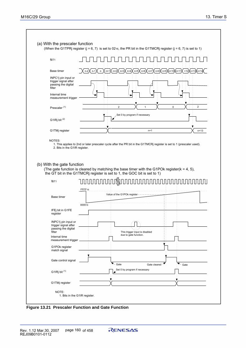
13. Timer SpuorG92/C61M
page 160 854fo7002,03.raM21.1.veR2110-1010B90JER
Figure 13.21 Prescaler Function and Gate Function
NOTE: 1. Bits in the G1IR register.
G1IRj bit (1)
fBT1
fBT1
Base timer
G1IRj bit (2)
G1TMj register
Internal timemeasurement trigger
Prescaler (1)
(a) With the prescaler function (When the G1TPRj register (j = 6, 7) is set to 0216, the PR bit in the G1TMCRj register (j = 6, 7) is set to 1)
Base timer
INPC1j pin input or trigger signal after passing the digital filterInternal time measurement trigger
IFEj bit in G1FE register
G1POk register match signal
Gate control signal
G1TMj register
Value of the G1POk register
This trigger input is disabled due to gate function.
2 1 0
FFFF16
000016
n-2 n-1 n n+2 n+3 n+4 n+5 n+6 n+7 n+8 n+9 n+10 n+11 n+14
n+1 n+13
2
(b) With the gate function (The gate function is cleared by matching the base timer with the G1POk register(k = 4, 5),
the GT bit in the G1TMCRj register is set to 1, the GOC bit is set to 1)
INPC1j pin input or trigger signal after passing the digital filter
Set 0 by program if necessary
Set 0 by program if necessary
Gate GateGate cleared
n+1 +12 n+13
NOTES:1. This applies to 2nd or later prescaler cycle after the PR bit in the G1TMCRj register is set to 1 (prescaler used).2. Bits in the G1IR register.
13. Timer SpuorG92/C61M
page 161 854fo7002,03.raM21.1.veR2110-1010B90JER
13.5 Waveform Generating FunctionWaveforms are generated when the base timer value matches the G1POj (j=0 to 7) register value.The waveform generating function has the following three modes :• Single-phase waveform output mode• Phase-delayed waveform output mode• Set/Reset waveform output (SR waveform output) modeTable 13.7 lists registers associated with the waveform generating function.
Table 13.7 Registers Related to the Waveform Generating Function Settings
Register Bit FunctionG1POCRj MOD1 to MOD0 Select output waveform mode
IVL Select default valueRLD Select G1POj register value reload timingINV Select inverse output
G1POj - Select timing to output waveform invertedG1FS FSCj Set to 0 (waveform generating function)G1FE IFEj Set to 1 (enables function on channel j) j = 0 to 7
Bit configurations and functions vary with channels used.Registers associated with the waveform generating function must be set after setting registers associated with the base timer.
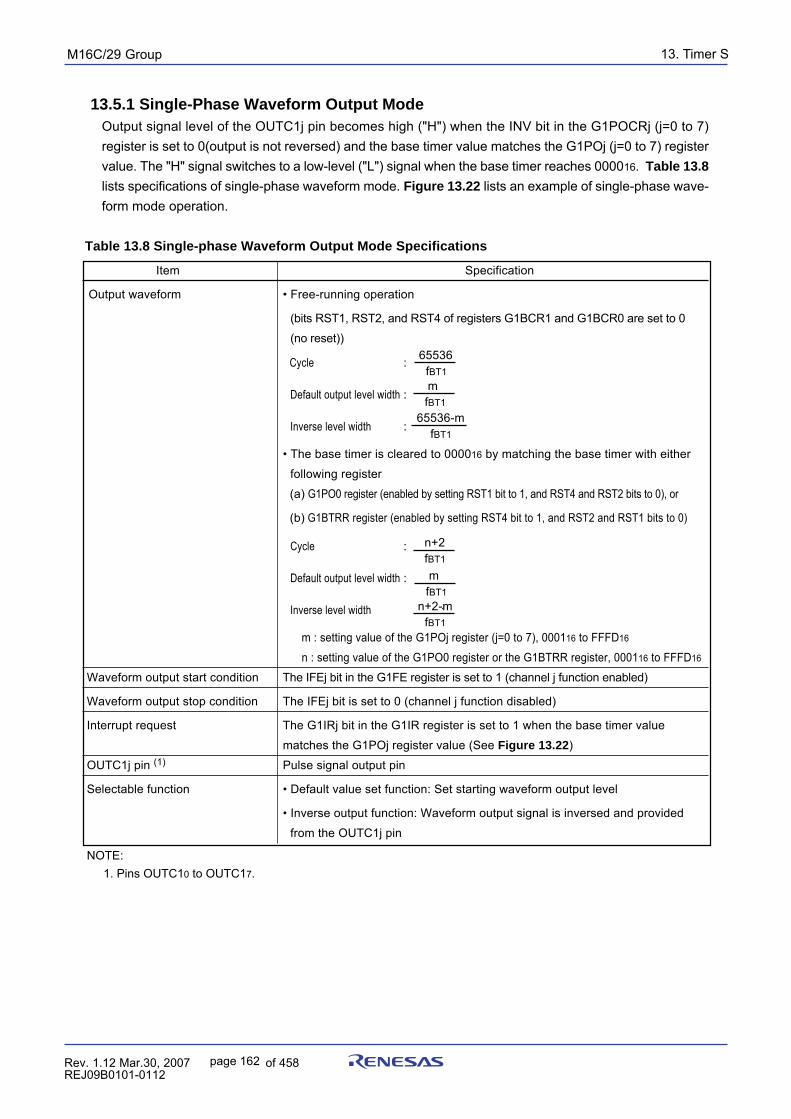
13. Timer SpuorG92/C61M
page 162 854fo7002,03.raM21.1.veR2110-1010B90JER
13.5.1 Single-Phase Waveform Output ModeOutput signal level of the OUTC1j pin becomes high ("H") when the INV bit in the G1POCRj (j=0 to 7)register is set to 0(output is not reversed) and the base timer value matches the G1POj (j=0 to 7) registervalue. The "H" signal switches to a low-level ("L") signal when the base timer reaches 000016. Table 13.8
lists specifications of single-phase waveform mode. Figure 13.22 lists an example of single-phase wave-form mode operation.
Table 13.8 Single-phase Waveform Output Mode Specifications
Item Specification
Output waveform • Free-running operation
(bits RST1, RST2, and RST4 of registers G1BCR1 and G1BCR0 are set to 0
(no reset))
Cycle :
Default output level width :
Inverse level width :
• The base timer is cleared to 000016 by matching the base timer with either
following register
(a) G1PO0 register (enabled by setting RST1 bit to 1, and RST4 and RST2 bits to 0), or
(b) G1BTRR register (enabled by setting RST4 bit to 1, and RST2 and RST1 bits to 0)
Cycle :
Default output level width :
Inverse level width :
m : setting value of the G1POj register (j=0 to 7), 000116 to FFFD16
n : setting value of the G1PO0 register or the G1BTRR register, 000116 to FFFD16
Waveform output start condition The IFEj bit in the G1FE register is set to 1 (channel j function enabled)
Waveform output stop condition The IFEj bit is set to 0 (channel j function disabled)
Interrupt request The G1IRj bit in the G1IR register is set to 1 when the base timer value
matches the G1POj register value (See Figure 13.22)
OUTC1j pin (1) Pulse signal output pin
Selectable function • Default value set function: Set starting waveform output level
• Inverse output function: Waveform output signal is inversed and provided
from the OUTC1j pin
m fBT1
65536-m fBT1
n+2 fBT1
m fBT1n+2-m fBT1
65536 fBT1
NOTE: 1. Pins OUTC10 to OUTC17.
13. Timer SpuorG92/C61M
page 163 854fo7002,03.raM21.1.veR2110-1010B90JER
Figure 13.22 Single-phase Waveform Output Mode
FFFF16
m
mfBT1
65536-m fBT1
Inverse
65536 fBT1
When setting to 0, write 0 by program
Base timer
(1) Free-running operation (The RST4, RST2, and RST1 bits in the G1BCR0 and G1BCR1 registers are set to 0)
(2) The base timer is reset when the base timer matches either following register (a) G1PO0 (enabled by setting bit RST1 to 1, and bits RST4 and RST2 to 0), or (b) G1BTRR (enabled by setting bit RST4 to 1, and bits RST2 and RST1 to 0)
000016
OUTC1j pin
G1IRj bit
G1IRj bit
j=0 to 7m : Setting value of the G1POj registerG1IRj bit : Bits in the G1IR register
OUTC1j pin
FFFF16
m
n+2
Base timer
000016
Inverse
mfBT1
n+2-m fBT1
Inverse
n+2 fBT1
Return to default output level
Write 0 by programif setting to 0
Return to defaultoutput level
InverseInverse
j=1 to 7m : Setting value of the G1POj register n: Setting value of either G1PO0 register or G1BTRR registerG1IRj bit : Bits in the G1IR register
The above applies under the following conditions. -The IVL bit in the G1POCRj register is set to 0 ("L" output as a default value) and the INV bit is set to 0 (not inversed). -Bits UD1 to UD0 are set to 002 (counter increment mode).
The above applies under the following conditions. -The IVL bit in the G1POCRj register is set to 0 ("L" output as a default value) and the INV bit is set to 0
(not inversed). -Bits UD1 to UD0 are set to 002 (counter increment mode).
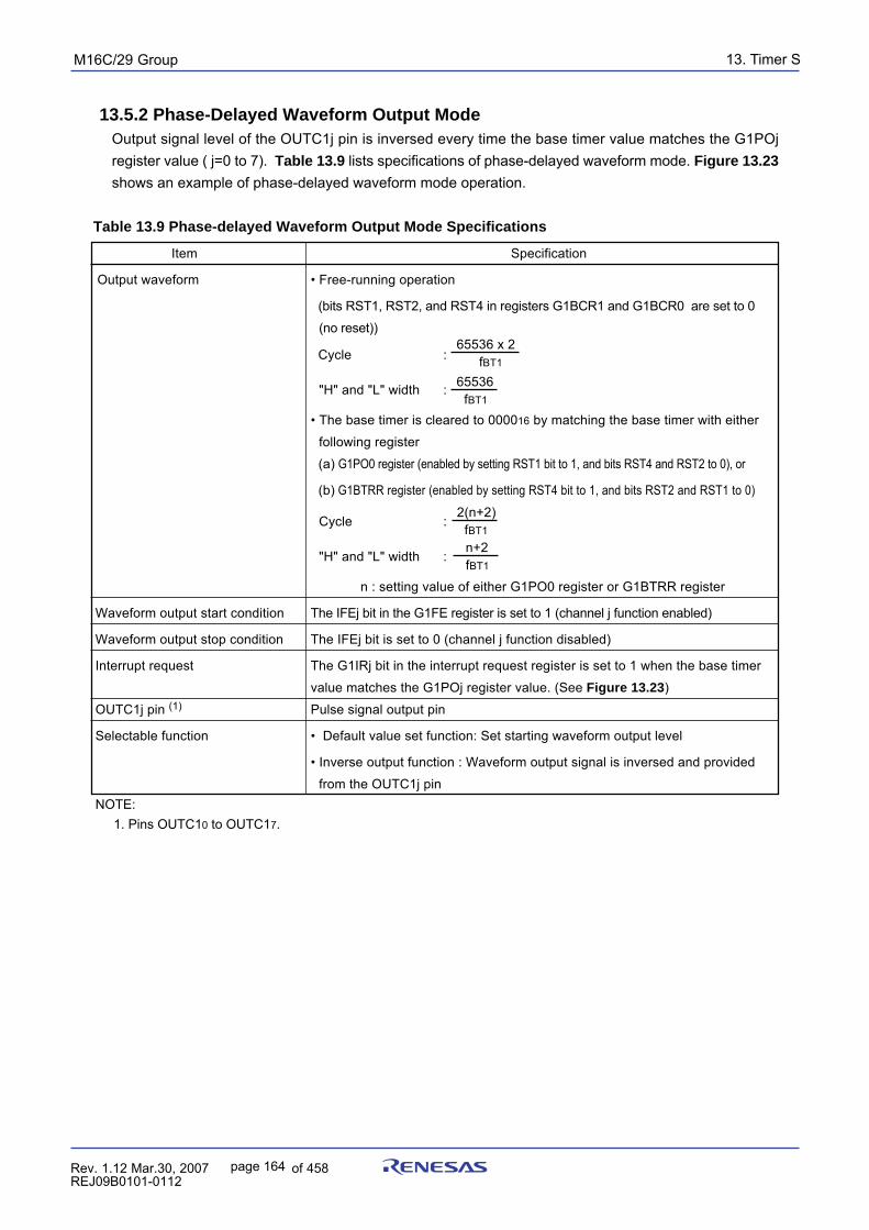
13. Timer SpuorG92/C61M
page 164 854fo7002,03.raM21.1.veR2110-1010B90JER
13.5.2 Phase-Delayed Waveform Output ModeOutput signal level of the OUTC1j pin is inversed every time the base timer value matches the G1POjregister value ( j=0 to 7). Table 13.9 lists specifications of phase-delayed waveform mode. Figure 13.23
shows an example of phase-delayed waveform mode operation.
Table 13.9 Phase-delayed Waveform Output Mode Specifications
Item Specification
Output waveform • Free-running operation
(bits RST1, RST2, and RST4 in registers G1BCR1 and G1BCR0 are set to 0
(no reset))
Cycle :
"H" and "L" width :
• The base timer is cleared to 000016 by matching the base timer with either
following register
(a) G1PO0 register (enabled by setting RST1 bit to 1, and bits RST4 and RST2 to 0), or
(b) G1BTRR register (enabled by setting RST4 bit to 1, and bits RST2 and RST1 to 0)
Cycle :
"H" and "L" width :
n : setting value of either G1PO0 register or G1BTRR register
Waveform output start condition The IFEj bit in the G1FE register is set to 1 (channel j function enabled)
Waveform output stop condition The IFEj bit is set to 0 (channel j function disabled)
Interrupt request The G1IRj bit in the interrupt request register is set to 1 when the base timer
value matches the G1POj register value. (See Figure 13.23)
OUTC1j pin (1) Pulse signal output pin
Selectable function • Default value set function: Set starting waveform output level
• Inverse output function : Waveform output signal is inversed and provided
from the OUTC1j pinNOTE: 1. Pins OUTC10 to OUTC17.
65536 x 2 fBT1
65536 fBT1
2(n+2) fBT1
n+2 fBT1
13. Timer SpuorG92/C61M
page 165 854fo7002,03.raM21.1.veR2110-1010B90JER
Figure 13.23 Phase-delayed Waveform Output Mode
FFFF16
m
65536 fBT1
65536X2 fBT1
000016
FFFF16
m
n+2
000016
65536 fBT1
mfBT1
n+2fBT1
n+2fBT1
2(n+2) fBT1
Base timer
(1) Free-running operation (Bits RST4, RST2, and RST1 in the registers G1BCR0 and G1BCR1 are set to 0)
OUTC1j pin
G1IRj bit
j=0 to 7m : Setting value of the G1POj registerG1IRj bit : Bits in the G1IR register
Inverse
Write 0 by programif setting to 0
Inverse
(2) Base timer is reset when the base timer matches either following register (a) G1PO0 (enabled by setting bit RST1 to 1, and bits RST4 and RST2 to 0), or (b) G1BTRR (enabled by setting bit RST4 to 1, and bits RST2 and RST1 to 0)
G1IRj bit
OUTC1j pin
Base timer
Write 0 by programif setting to 0
Inverse
j=1 to 7m : Setting value of the G1POj register n: Setting value of either register G1PO0 or G1BTRRG1IRj bit : Bits in the G1IR register
The above applies under the following conditions. The IVL bit in the G1POCRj register is set to 0 (L output as a default value). The INV bit is set to 0 (not inversed). Bits UD1 to UD0 are set to 002 (counter increment mode).
The above applies under the following conditions. The IVL bit in the G1POCRj register is set to 0 (L output as a default value). The INV bit is set to 0 (not inversed). Bits UD1 to UD0 are set to 002 (counter increment mode).
InverseInverse
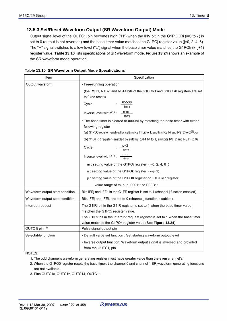
13. Timer SpuorG92/C61M
page 166 854fo7002,03.raM21.1.veR2110-1010B90JER
13.5.3 Set/Reset Waveform Output (SR Waveform Output) ModeOutput signal level of the OUTC1j pin becomes high ("H") when the INV bit in the G1POCRi (i=0 to 7) isset to 0 (output is not reversed) and the base timer value matches the G1POj register value (j=0, 2, 4, 6).The "H" signal switches to a low-level ("L") signal when the base timer value matches the G1POk (k=j+1)register value. Table 13.10 lists specifications of SR waveform mode. Figure 13.24 shows an example ofthe SR waveform mode operation.
Table 13.10 SR Waveform Output Mode Specifications
Item Specification
Output waveform • Free-running operation
(the RST1, RTS2, and RST4 bits of the G1BCR1 and G1BCR0 registers are set
to 0 (no reset))
Cycle :
Inverse level width(1) :
• The base timer is cleared to 000016 by matching the base timer with either
following register
(a) G1PO0 register (enabled by setting RST1 bit to 1, and bits RST4 and RST2 to 0)(2), or
(b) G1BTRR register (enabled by setting RST4 bit to 1, and bits RST2 and RST1 to 0)
Cycle :
Inverse level width(1) :
m : setting value of the G1POj register (j=0, 2, 4, 6 )
n : setting value of the G1POk register (k=j+1)
p : setting value of the G1PO0 register or G1BTRR register
value range of m, n, p: 000116 to FFFD16
Waveform output start condition Bits IFEj and IFEk in the G1FE register is set to 1 (channel j function enabled)
Waveform output stop condition Bits IFEj and IFEk are set to 0 (channel j function disabled)
Interrupt request The G1IRj bit in the G1IR register is set to 1 when the base timer value
matches the G1POj register value.
The G1IRk bit in the interrupt request register is set to 1 when the base timer
value matches the G1POk register value (See Figure 13.24)
OUTC1j pin (3) Pulse signal output pin
Selectable function • Default value set function : Set starting waveform output level
• Inverse output function: Waveform output signal is inversed and provided
from the OUTC1j pinNOTES: 1. The odd channel's waveform generating register must have greater value than the even channel's. 2. When the G1PO0 register resets the base timer, the channel 0 and channel 1 SR waveform generating functions
are not available. 3. Pins OUTC10, OUTC12, OUTC14, OUTC16.
65536 fBT1
n-m fBT1
p+2 fBT1 n-m fBT1
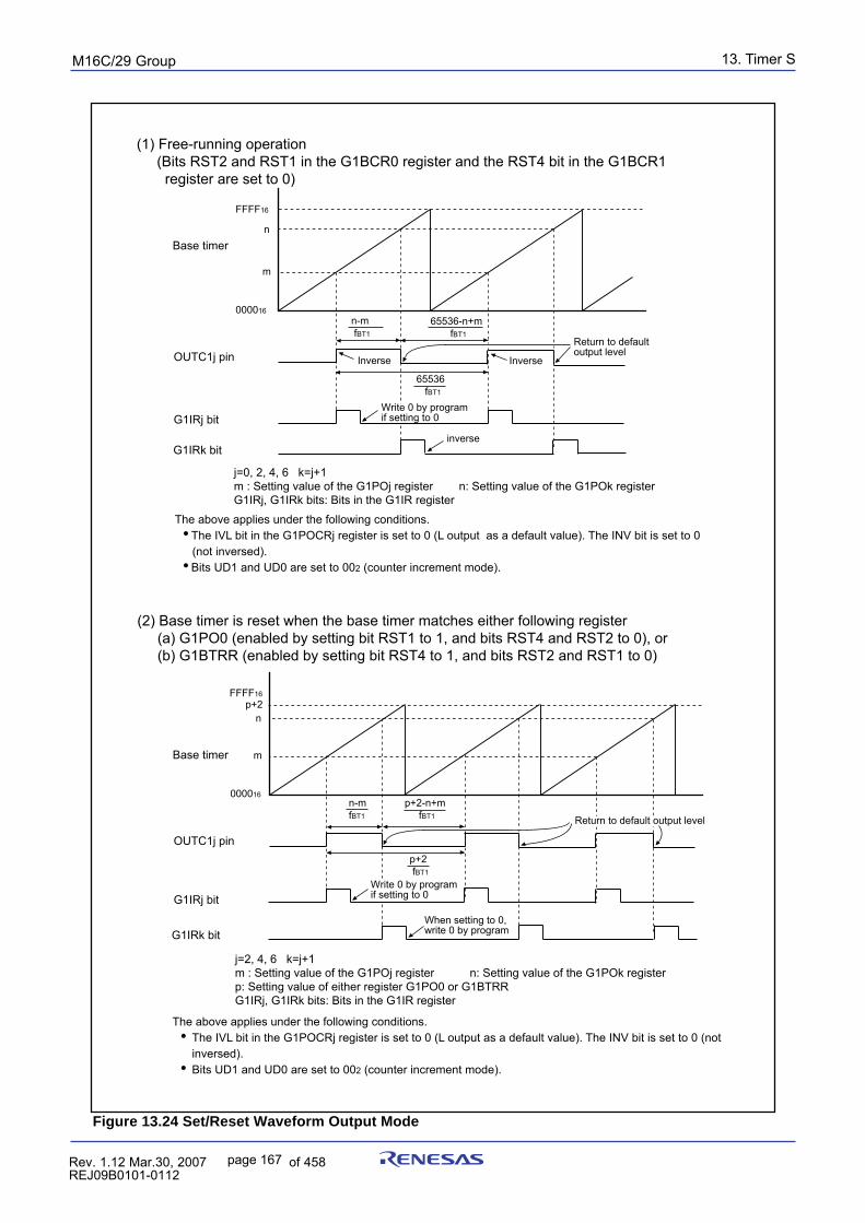
13. Timer SpuorG92/C61M
page 167 854fo7002,03.raM21.1.veR2110-1010B90JER
Figure 13.24 Set/Reset Waveform Output Mode
FFFF16
m
n
n-m fBT1
65536 fBT1
000016
FFFF16
m
p+2n
000016
65536-n+m fBT1
n-mfBT1
p+2-n+m fBT1
p+2 fBT1
(1) Free-running operation (Bits RST2 and RST1 in the G1BCR0 register and the RST4 bit in the G1BCR1 register are set to 0)
j=0, 2, 4, 6 k=j+1m : Setting value of the G1POj register n: Setting value of the G1POk registerG1IRj, G1IRk bits: Bits in the G1IR register
Inverse
Write 0 by programif setting to 0
Inverse
(2) Base timer is reset when the base timer matches either following register (a) G1PO0 (enabled by setting bit RST1 to 1, and bits RST4 and RST2 to 0), or (b) G1BTRR (enabled by setting bit RST4 to 1, and bits RST2 and RST1 to 0)
j=2, 4, 6 k=j+1m : Setting value of the G1POj register n: Setting value of the G1POk registerp: Setting value of either register G1PO0 or G1BTRRG1IRj, G1IRk bits: Bits in the G1IR register
Return to default output level
inverse
Return to default output level
Write 0 by programif setting to 0
When setting to 0, write 0 by program
Base timer
OUTC1j pin
G1IRj bit
G1IRk bit
Base timer
OUTC1j pin
G1IRj bit
G1IRk bit
The above applies under the following conditions. The IVL bit in the G1POCRj register is set to 0 (L output as a default value). The INV bit is set to 0 (not
inversed). Bits UD1 and UD0 are set to 002 (counter increment mode).
The above applies under the following conditions. The IVL bit in the G1POCRj register is set to 0 (L output as a default value). The INV bit is set to 0 (not inversed). Bits UD1 and UD0 are set to 002 (counter increment mode).
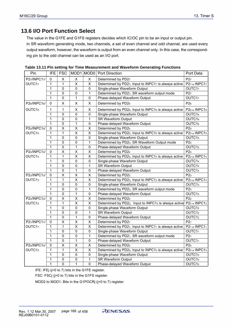
13. Timer SpuorG92/C61M
page 168 854fo7002,03.raM21.1.veR2110-1010B90JER
Pin IFE FSC MOD1 MOD0 Port Direction Port Data P27/INPC17/ 0 X X X Determined by PD27 P27
OUTC17 1 1 X X Determined by PD27, Input to INPC17 is always active P27 or INPC17
1 0 0 0 Single-phase Waveform Output OUTC17
1 0 0 1 Determined by PD27, SR waveform output mode P27
1 0 1 0 Phase-delayed Waveform Output OUTC17
P26/INPC16/ 0 X X X Determined by PD26 P26
OUTC16 1 1 X X Determined by PD26, Input to INPC16 is always active P26 or INPC16
1 0 0 0 Single-phase Waveform Output OUTC16
1 0 0 1 SR Waveform Output OUTC16
1 0 1 0 Phase-delayed Waveform Output OUTC16
P25/INPC15/ 0 X X X Determined by PD25 P25
OUTC15 1 1 X X Determined by PD25, Input to INPC15 is always active P25 or INPC15
1 0 0 0 Single-phase Waveform Output OUTC15
1 0 0 1 Determined by PD25, SR Waveform Output mode P25
1 0 1 0 Phase-delayed Waveform Output OUTC15
P24/INPC14/ 0 X X X Determined by PD24 P24
OUTC14 1 1 X X Determined by PD24, Input to INPC14 is always active P24 or INPC14
1 0 0 0 Single-phase Waveform Output OUTC14
1 0 0 1 SR Waveform Output OUTC14
1 0 1 0 Phase-delayed Waveform Output OUTC14
P23/INPC13/ 0 X X X Determined by PD23 P23
OUTC13 1 1 X X Determined by PD23, Input to INPC13 is always active P23 or INPC13
1 0 0 0 Single-phase Waveform Output OUTC13
1 0 0 1 Determined by PD23, SR waveform output mode P23
1 0 1 0 Phase-delayed Waveform Output OUTC13
P22/INPC12/ 0 X X X Determined by PD22 P22
OUTC12 1 1 X X Determined by PD22, Input to INPC12 is always active P22 or INPC12
1 0 0 0 Single-phase Waveform Output OUTC12
1 0 0 1 SR Waveform Output OUTC12
1 0 1 0 Phase-delayed Waveform Output OUTC12
P21/INPC11/ 0 X X X Determined by PD21 P21
OUTC11 1 1 X X Determined by PD21, Input to INPC11 is always active P21 or INPC11
1 0 0 0 Single-phase Waveform Output OUTC11
1 0 0 1 Determined by PD21, SR waveform output mode P21
1 0 1 0 Phase-delayed Waveform Output OUTC11
P20/INPC10/ 0 X X X Determined by PD20 P20
OUTC10 1 1 X X Determined by PD20, Input to INPC10 is always active P20 or INPC10
1 0 0 0 Single-phase Waveform Output OUTC10
1 0 0 1 SR Waveform Output OUTC10
1 0 1 0 Phase-delayed Waveform Output OUTC10
13.6 I/O Port Function SelectThe value in the G1FE and G1FS registers decides which IC/OC pin to be an input or output pin.In SR waveform generating mode, two channels, a set of even channel and odd channel, are used everyoutput waveform, however, the waveform is output from an even channel only. In this case, the correspond-ing pin to the odd channel can be used as an I/O port.
Table 13.11 Pin setting for Time Measurement and Waveform Generating Functions
IFE: IFEj (j=0 to 7) bits in the G1FE register.FSC: FSCj (j=0 to 7) bits in the G1FS register.
MOD2 to MOD1: Bits in the G1POCRj (j=0 to 7) register.
13. Timer SpuorG92/C61M
page 169 854fo7002,03.raM21.1.veR2110-1010B90JER
13.6.1 INPC17 Alternate Input Pin SelectionThe input capture pin for IC/OC channel 7 can be assigned to one of two package pins. The CH7INSEL
________
bit in the G1BCR0 register selects IC/OC INPC17 from P27/OUTC17/INPC17 or P17/INT5/INPC17/IDU.
________
13.6.2 Digital Debounce Function for Pin P17/INT5/INPC17________ ________
The INT5/INPC17 input from the P17/INT5/INPC17/IDU pin has an effective digital debounce functionagainst a noise rejection. Refer to 19.6 Digital Debounce function for this detail.
14.Serial I/OpuorG92/C61M
page 170 854fo7002,03.raM21.1.veR2110-1010B90JER
14. Serial I/O NoteThe SI/O4 interrupt of peripheral function interrupt is not available in the 64-pin package.
Serial I/O is configured with five channels: UART0 to UART2, SI/O3 and SI/O4.
14.1 UARTi (i=0 to 2)UARTi each have an exclusive timer to generate a transfer clock, so they operate independently of eachother.Figure 14.1 shows the block diagram of UARTi. Figures 14.2 and 14.3 shows the block diagram of theUARTi transmit/receive.
UARTi has the following modes:• Clock synchronous serial I/O mode• Clock asynchronous serial I/O mode (UART mode).• Special mode 1 (I2C bus mode): UART2• Special mode 2: UART2• Special mode 3 (Bus collision detection function, IEBus mode): UART2• Special mode 4 (SIM mode): UART2
Figures 14.4 to 14.9 show the UARTi-related registers.Refer to tables listing each mode for register setting.
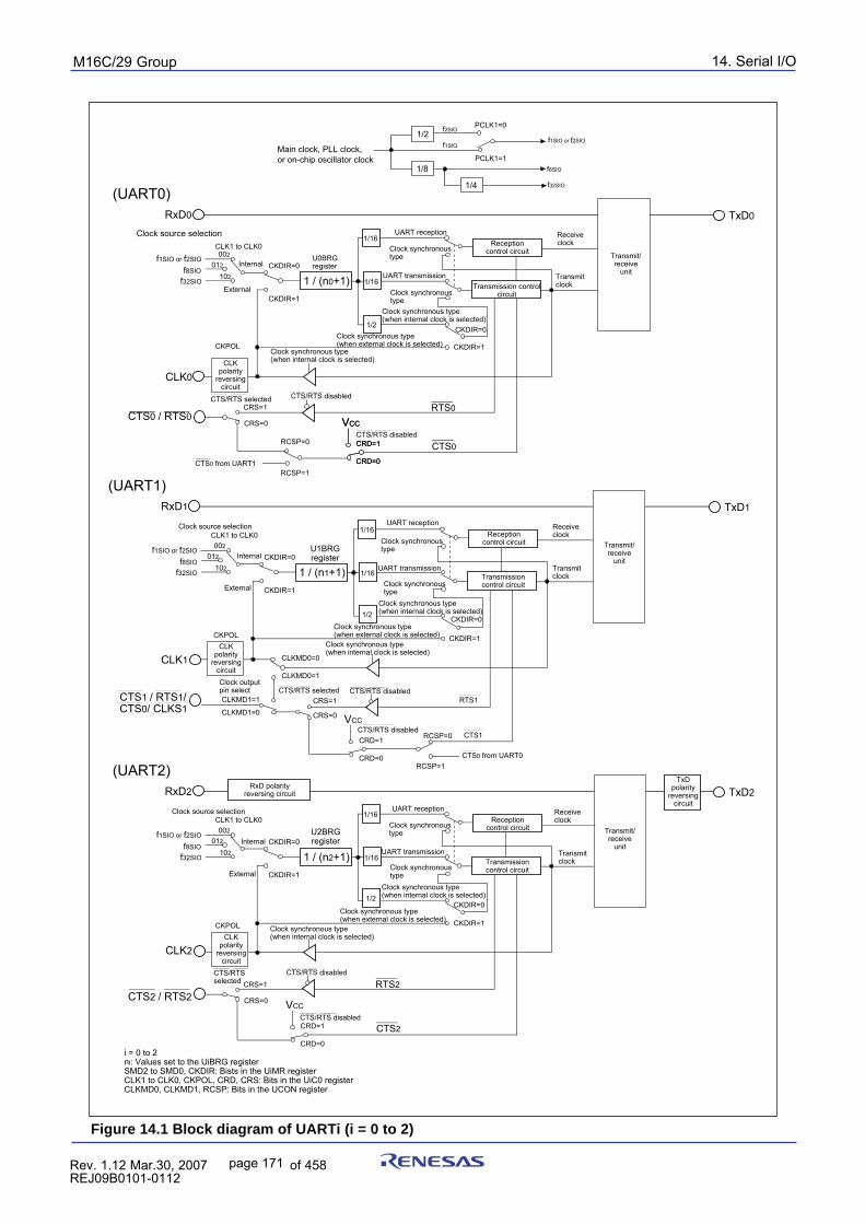
14. Serial I/OpuorG92/C61M
page 171 854fo7002,03.raM21.1.veR2110-1010B90JER
Figure 14.1 Block diagram of UARTi (i = 0 to 2)
Clock synchronous type (when internal clock is selected)
Clock synchronous type(when external clock is selected)
Clock source selection
Internal
External
CTS/RTS disabled
CTS/RTS selected
RxD0
1 / (n0+1)
1/16
1/16
1/2
U0BRG register
CLK0
CTS0 / RTS0
f1SIO or f2SIO
f8SIOf32SIO
VCC
RTS0
CTS0
TxD0
(UART0)
CLK1 to CLK0002
012
102
CKDIR=0
CKDIR=1
CKPOL
CKDIR=0
CKDIR=1
CRS=1
CRS=0
CRD=0
CRD=1RCSP=0
RCSP=1
VCC
CRD=0
CRD=1
UART reception
Clock synchronous type
UART transmission
Clock synchronous type
Clock synchronous type(when internal clock is selected)
Receive clock
Transmit clock
Reception control circuit
Transmission control circuit
Transmit/receive
unit
CLK polarity
reversing circuit
CTS/RTS disabled
CTS0 from UART1
UART reception
Clock synchronous type
RxD1 TxD1
(UART1)
1 / (n1+1)
1/16
1/16
1/2
U1BRGregister
CLK1
f1SIO or f2SIO
f8SIOf32SIO
CLK1 to CLK0002
012
102
CKDIR=0
CKDIR=1
CKPOL
CKDIR=0
CKDIR=1
VCC
CRD=0
CRD=1
CLKMD0=0
CLKMD1=0CRS=1
CRS=0
RCSP=0
RCSP=1
CLKMD0=1
CLKMD1=1
Clock source selection
Internal
External
UART transmission
Clock synchronous type
Clock synchronous type(when internal clock is selected)
Receive clock
Transmit clock
Reception control circuit
Transmission control circuit
Transmit/receive
unit
Clock synchronous type (when external clock is selected)
Clock synchronous type (when internal clock is selected)
CLK polarity
reversing circuit
RTS1
CTS1
Clock output pin select CTS/RTS disabled
CTS/RTS disabled
CTS/RTS selected
CTS0 from UART0
CTS1 / RTS1/CTS0/ CLKS1
i = 0 to 2ni: Values set to the UiBRG registerSMD2 to SMD0, CKDIR: Bists in the UiMR registerCLK1 to CLK0, CKPOL, CRD, CRS: Bits in the UiC0 registerCLKMD0, CLKMD1, RCSP: Bits in the UCON register
RxD2
CLK2
CTS2 / RTS2RTS2
CTS2
TxD2
(UART2)
1 / (n2+1)
1/16
1/16
1/2
U2BRG register
f1SIO or f2SIO
f8SIOf32SIO
CLK1 to CLK0002
012
102
CKDIR=0
CKDIR=1
CKPOL
CKDIR=0
CKDIR=1
CRS=1
CRS=0 VCC
CRD=0
CRD=1
Reception control circuit
Transmission control circuit
UART reception
Clock synchronous type
UART transmission
Clock synchronous type
Clock synchronous type(when internal clock is selected)
Receive clock
Transmit clock
RxD polarity reversing circuit
Internal
External
Clock source selection
TxD polarity
reversing circuit
Transmit/receive
unit
Clock synchronous type (when internal clock is selected)
Clock synchronous type (when external clock is selected)
CLKpolarity
reversing circuit
CTS/RTS disabled
CTS/RTS disabledCTS/RTS selected
Main clock, PLL clock,or on-chip oscillator clock
1/2
1/8
1/4
f1SIO
f2SIO
f8SIO
f32SIO
f1SIO or f2SIO
PCLK1=1
PCLK1=0
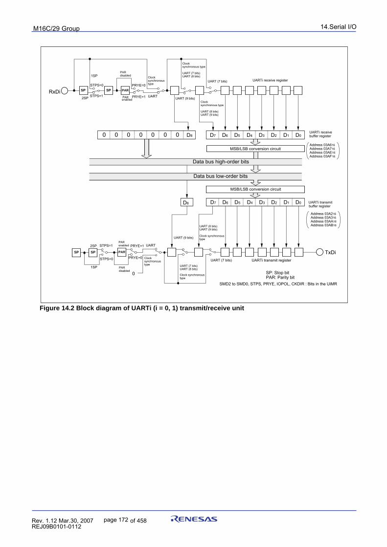
14.Serial I/OpuorG92/C61M
page 172 854fo7002,03.raM21.1.veR2110-1010B90JER
Figure 14.2 Block diagram of UARTi (i = 0, 1) transmit/receive unit
SP SP PAR
2SP
1SP
UART
UART (7 bits)UART (8 bits)
UART (7 bits)
UART (9 bits)
Clock synchronous type
Clock synchronous type
TxDiUARTi transmit register
PAR enabled
PAR disabled
D8 D7 D6 D5 D4 D3 D2 D1 D0
SP: Stop bitPAR: Parity bit
UARTi transmitbuffer register
MSB/LSB conversion circuit
UART (8 bits)UART (9 bits)
Clock synchronous type
UARTi receive buffer register
UARTi receive register
2SP
1SP
STPS=0
PAR enabled
PAR
disabled
UART
UART (7 bits)
UART (9 bits)
Clock synchronous type
Clock synchronous type
UART (7 bits)UART (8 bits)
RxDi
Clock synchronous type
UART (8 bits)UART (9 bits)
Address 03A616Address 03A716Address 03AE16Address 03AF16
Address 03A216Address 03A316Address 03AA16Address 03AB16
Data bus low-order bits
MSB/LSB conversion circuit
D7 D6 D5 D4 D3 D2 D1 D0D80 0 0 0 0 0 0
SP SP PAR
0
Data bus high-order bits
STPS=1
PRYE=0
PRYE=1
STPS=0
STPS=1
PRYE=0
PRYE=1
SMD2 to SMD0, STPS, PRYE, IOPOL, CKDIR : Bits in the UiMR
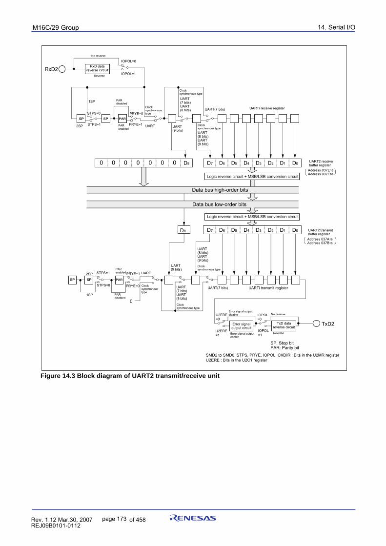
14. Serial I/OpuorG92/C61M
page 173 854fo7002,03.raM21.1.veR2110-1010B90JER
Figure 14.3 Block diagram of UART2 transmit/receive unit
SP SP PAR
2SP
1SP
UART
UART(7 bits)UART(8 bits)
UART(7 bits)
UART(9 bits)
Clock synchronous type
Clock synchronous type
Data bus low-order bits
TxD2
UARTi transmit register
PAR disabled
PAR enabled
D8 D7 D6 D5 D4 D3 D2 D1 D0 UART2 transmit buffer register
UART(8 bits)UART(9 bits)Clock synchronous type
UART2 receive buffer register
UARTi receive register
2SP
1SPUART(7 bits)UART(8 bits) UART(7 bits)
UART(9 bits)
Clock synchronous type
Clock synchronous type
RxD2
UART(8 bits)UART(9 bits)
Address 037E16Address 037F16
Address 037A16Address 037B16
Data bus high-order bits
D7 D6 D5 D4 D3 D2 D1 D0D80 0 0 0 0 0 0
SP SP PAR
0
Reverse
No reverse
Error signal output circuit
RxD datareverse circuit
Error signal output enable
Error signal output disable
Reverse
No reverse
Logic reverse circuit + MSB/LSB conversion circuit
Logic reverse circuit + MSB/LSB conversion circuit
PAR enabled
PAR disabled
UART
Clock synchronous type
TxD datareverse circuit
SP: Stop bitPAR: Parity bit
STPS=0
STPS=1
PRYE=0
PRYE=1
STPS=0
STPS=1
PRYE=0
PRYE=1
IOPOL=0
IOPOL=1
IOPOL=0
IOPOL=1
U2ERE=0
U2ERE=1
SMD2 to SMD0, STPS, PRYE, IOPOL, CKDIR : Bits in the U2MR registerU2ERE : Bits in the U2C1 register
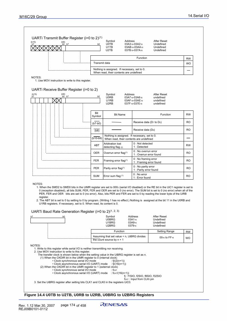
14.Serial I/OpuorG92/C61M
page 174 854fo7002,03.raM21.1.veR2110-1010B90JER
Figure 14.4 U0TB to U2TB, U0RB to U2RB, U0BRG to U2BRG Registers
(b15)b7 b0
(b8)b7 b0
UARTi Transmit Buffer Register (i=0 to 2)(1)
Function
Transmit data
Nothing is assigned. If necessary, set to 0. When read, their contents are undefined
Symbol Address After Reset U0TB 03A316-03A216 Undefined U1TB 03AB16-03AA16 Undefined U2TB 037B16-037A16 Undefined
NOTES: 1. Use MOV instruction to write to this register.
RW
WO
b7
UARTi Baud Rate Generation Register (i=0 to 2)(1, 2, 3)
b0 Symbol Address After Reset U0BRG 03A116 Undefined U1BRG 03A916 Undefined U2BRG 037916 Undefined
Function
Assuming that set value = n, UiBRG divides the count source by n + 1
Setting Range
NOTES: 1. Write to this register while serial I/O is neither transmitting nor receiving. 2. Use MOV instruction to write to this register. The transfer clock is shown below when the setting value in the UiBRG register is set as n. (1) When the CKDIR bit in the UiMR register to 0 (internal clock) • Clock synchronous serial I/O mode : fj/(2(n+1)) • Clock asynchronous serial I/O (UART) mode : fj/(16(n+1)) (2) When the CKDIR bit in the UiMR register to 1 (external clock) • Clock synchronous serial I/O mode : fEXT
• Clock asynchronous serial I/O (UART) mode : fEXT/(16(n+1)) fj : f1SIO, f2SIO, f8SIO, f32SIO fEXT : Input from CLKi pin 3. Set the UiBRG register after setting bits CLK1 and CLK0 in the registers UiC0.
RW
WO
(b15) Symbol Address After Reset U0RB 03A716-03A616 undefined U1RB 03AF16-03AE16 undefinedU2RB 037F16-037E16 undefined
b7 b0(b8)
b7 b0
UARTi Receive Buffer Register (i=0 to 2)
FunctionBit NameBit Symbol
0 : No framing error1 : Framing error found0 : No parity error1 : Parity error found
0 : No error1 : Error found
OER
FER
PER
SUM
Overrun error flag(1)
Framing error flag(1)
Parity error flag(1)
Error sum flag (1)
0 : No overrun error1 : Overrun error found
ABT Arbitration lost detecting flag (2)
0 : Not detected1 : Detected
(b7-b0)
(b10-b9)
(b8)
Nothing is assigned. If necessary, set to 0. When read, their contents are undefined
RW
RO
RW
RO
RO
RO
RO
RO
0016 to FF16
Receive data (D8)
Receive data (D7 to D0)
NOTES: 1. When the SMD2 to SMD0 bits in the UiMR register are set to 0002 (serial I/O disabled) or the RE bit in the UiC1 register is set to
0 (reception disabled), all bits SUM, PER, FER and OER are set to 0 (no error). The SUM bit is set to 0 (no error) when all of the PER, FER and OER bits are set to 0 (no error). Also, bits PER and FER are set to 0 by reading the lower byte of the UiRB register.
2. The ABT bit is set to 0 by setting to 0 by program. (Writing 1 has no effect.) Nothing is assigned at the bit 11 in the U0RB and U1RB registers. If necessary, set to 0. When read, its content is 0.
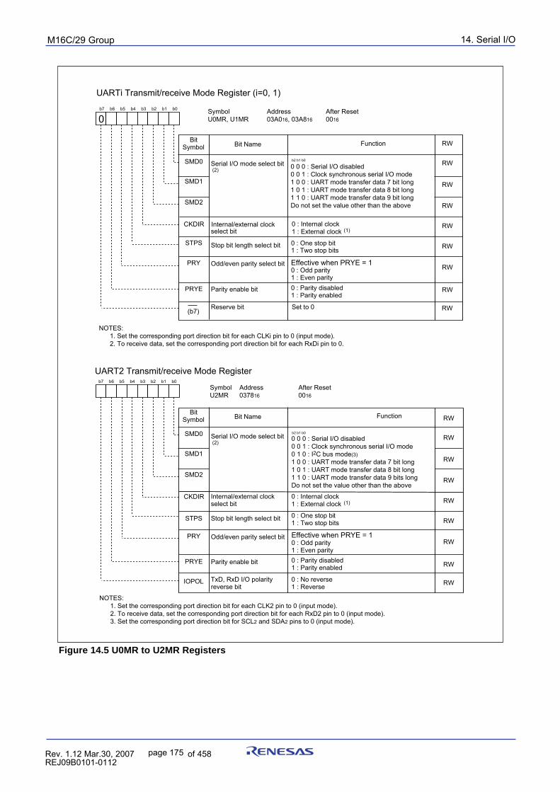
14. Serial I/OpuorG92/C61M
page 175 854fo7002,03.raM21.1.veR2110-1010B90JER
Figure 14.5 U0MR to U2MR Registers
UARTi Transmit/receive Mode Register (i=0, 1)b7 b6 b5 b4 b3 b2 b1 b0
Bit NameBit
Symbol
CKDIR
SMD1
SMD0 Serial I/O mode select bit (2)
SMD2
Internal/external clock select bit
STPS
PRY
PRYE
(b7)
Parity enable bit
0 : Internal clock1 : External clock (1)
Stop bit length select bit
Odd/even parity select bit
Reserve bit
0 : One stop bit1 : Two stop bits
0 : Parity disabled1 : Parity enabled
b2 b1 b0
Effective when PRYE = 1 0 : Odd parity1 : Even parity
Set to 0
Function
RW
RW
RW
RW
RW
RW
RW
RW
RW
UART2 Transmit/receive Mode Registerb7 b6 b5 b4 b3 b2 b1 b0
Bit NameBit
Symbol
CKDIR
SMD1
SMD0 Serial I/O mode select bit (2)
SMD2
Internal/external clock select bit
STPS
PRY
PRYE
IOPOL
Parity enable bit
0 : Internal clock1 : External clock (1)
Stop bit length select bit
Odd/even parity select bit
TxD, RxD I/O polarity reverse bit
0 : One stop bit1 : Two stop bits
0 : Parity disabled1 : Parity enabled
b2 b1 b0
Effective when PRYE = 1 0 : Odd parity1 : Even parity
0 : No reverse1 : Reverse
Function RW
RW
RW
RW
RW
RW
RW
RW
RW
0
Symbol Address After ResetU2MR 037816 0016
NOTES: 1. Set the corresponding port direction bit for each CLKi pin to 0 (input mode). 2. To receive data, set the corresponding port direction bit for each RxDi pin to 0.
Symbol Address After Reset U0MR, U1MR 03A016, 03A816 0016
NOTES: 1. Set the corresponding port direction bit for each CLK2 pin to 0 (input mode). 2. To receive data, set the corresponding port direction bit for each RxD2 pin to 0 (input mode). 3. Set the corresponding port direction bit for SCL2 and SDA2 pins to 0 (input mode).
0 0 0 : Serial I/O disabled0 0 1 : Clock synchronous serial I/O mode0 1 0 : I2C bus mode(3)1 0 0 : UART mode transfer data 7 bit long1 0 1 : UART mode transfer data 8 bit long 1 1 0 : UART mode transfer data 9 bits longDo not set the value other than the above
0 0 0 : Serial I/O disabled0 0 1 : Clock synchronous serial I/O mode1 0 0 : UART mode transfer data 7 bit long1 0 1 : UART mode transfer data 8 bit long 1 1 0 : UART mode transfer data 9 bit longDo not set the value other than the above
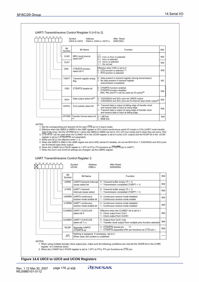
14.Serial I/OpuorG92/C61M
page 176 854fo7002,03.raM21.1.veR2110-1010B90JER
UARTi Transmit/receive Control Rregister 0 (i=0 to 2)
Symbol Address After Reset U0C0 to U2C0 03A416, 03AC16, 037C16 000010002
b7 b6 b5 b4 b3 b2 b1 b0
Function
TXEPT
CLK1
CLK0
CRS
CRD
NCH
CKPOL
BRG count source select bit(7)
Transmit register empty flag
0 : Transmit data is output at falling edge of transfer clock and receive data is input at rising edge 1 : Transmit data is output at rising edge of transfer clock and receive data is input at falling edge
CLK polarity select bit
CTS/RTS function select bit
CTS/RTS disable bit
Data output select bit(5)
0 0 : f1SIO or f2SIO is selected0 1 : f8SIO is selected1 0 : f32SIO is selected1 1 : Do not set
b1 b0
0 : LSB first1 : MSB first
0 : Data present in transmit register (during transmission)1 : No data present in transmit register (transmission completed)
0 : CTS/RTS function enabled1 : CTS/RTS function disabled (P60, P64 and P73 can be used as I/O ports)(6)
0 : TxD2/SDA2 and SCLi pins are CMOS output1 : TxD2/SDA2 and SCLi pins are N-channel open-drain output(4)
UFORM Transfer format select bit(2)
Effective when CRD is set to 00 : CTS function is selected (1)
1 : RTS function is selected
Bit NameBit Symbol
RW
RW
RW
RW
RW
RW
RW
RW
RO
(3)
NOTES: 1. Set the corresponding port direction bit for each CTSi pin to 0 (input mode). 2. Effective when bits SMD2 to SMD0 in the UMR register to 0012 (clock synchronous serial I/O mode) or 0102 (UART mode transfer
data 8 bits long). Set the UFORM bit to 1 when bits SMD2 to SMD0 are set to 1012 (I2C bus mode) and 0 when they are set to 1002. 3. CTS1/RTS1 can be used when the CLKMD1 bit in the UCON register is set to 0 (only CLK1 output) and the RCSP bit in the UCON
register is set to 0 (CTS0/RTS0 not separated). 4. SDA2 and SCL2 are effective when i = 2. 5. When bits SMD2 to SMD in the UiMR regiser are set to 0002 (serial I/O disable), do not set NCH bit to 1 (TxDi/SDA2 and SCL2 pins
are N-channel open-drain output). 6. When the U1MAP bit in PACR register is 1 (P73 to P70), P70 functions as CTS/RTS pin in UART1. 7. When the CLK1 and CLK0 bit settings are changed, set the UiBRG register.
UART Transmit/receive Control Register 2
Symbol Address After Reset UCON 03B016 X00000002
b7 b6 b5 b4 b3 b2 b1 b0
Bit NameBit Symbol RWFunction
CLKMD0
CLKMD1
Nothing is assigned. If necessary, set to 0. When read, the content is undefined
U0IRS
U1IRS
U0RRM
U1RRM
RCSP
(b7)
RW
RW
RW
RW
RW
RW
RW
0 : Output from CLK1 only1 : Transfer clock output from multiple pins function selected
Effective when the CLKMD1 bit is set to 1 0 : Clock output from CLK11 : Clock output from CLKS1
0 : Transmit buffer empty (Tl = 1) 1 : Transmission completed (TXEPT = 1)
0 : Transmit buffer empty (Tl = 1)1 : Transmission completed (TXEPT = 1)
0 : Continuous receive mode disabled1 : Continuous receive mode enable
0 : Continuous receive mode disabled1 : Continuous receive mode enabled
UART1 transmit interrupt cause select
UART0 continuous receive mode enable bit
UART0 transmit interrupt cause select bit
UART1 continuous receive mode enable bit
UART1 CLK/CLKS select bit 0
UART1 CLK/CLKS select bit 1 (1)
Separate UART0 CTS/RTS bit
0 : CTS/RTS shared pin1 : CTS/RTS separated (P64 pin functions as CTS0 pin )
(2)
NOTES: 1. When using multiple transfer clock output pins, make sure the following conditions are met:set the CKDIR bit in the U1MR
register to 0 (internal clock) 2. When the U1MAP bit in PACR register is set to 1 (P73 to P70), P70 pin functions as CTS0 pin.
Figure 14.6 U0C0 to U2C0 and UCON Registers
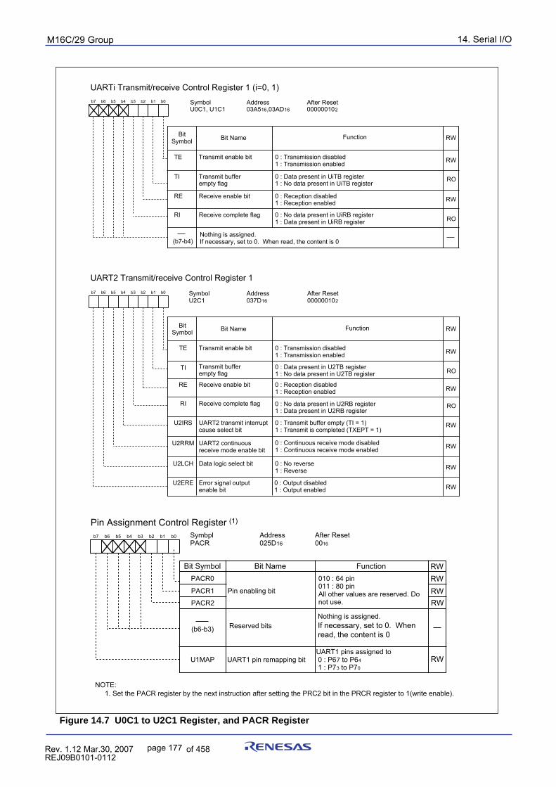
14. Serial I/OpuorG92/C61M
page 177 854fo7002,03.raM21.1.veR2110-1010B90JER
Figure 14.7 U0C1 to U2C1 Register, and PACR Register
UARTi Transmit/receive Control Register 1 (i=0, 1)
Symbol Address After Reset U0C1, U1C1 03A516,03AD16 000000102
b7 b6 b5 b4 b3 b2 b1 b0
Bit NameBit Symbol RWFunction
TE
TI
RE
RI
Transmit enable bit
Receive enable bit
Receive complete flag
Transmit buffer empty flag
0 : Transmission disabled1 : Transmission enabled
0 : Data present in UiTB register 1 : No data present in UiTB register
0 : Reception disabled1 : Reception enabled
0 : No data present in UiRB register 1 : Data present in UiRB register
Nothing is assigned.If necessary, set to 0. When read, the content is 0
UART2 Transmit/receive Control Register 1
Symbol Address After Reset U2C1 037D16 000000102
b7 b6 b5 b4 b3 b2 b1 b0
Bit NameBit Symbol
Function
TE
TI
RE
RI
Transmit enable bit
Receive enable bit
Receive complete flag
Transmit buffer empty flag
0 : Transmission disabled1 : Transmission enabled
0 : Reception disabled1 : Reception enabled
U2IRS UART2 transmit interrupt cause select bit
0 : Transmit buffer empty (TI = 1) 1 : Transmit is completed (TXEPT = 1)
U2RRM UART2 continuous receive mode enable bit
0 : Continuous receive mode disabled1 : Continuous receive mode enabled
Data logic select bit 0 : No reverse1 : Reverse
U2LCH
U2ERE Error signal output enable bit
0 : Output disabled1 : Output enabled
RW
RW
RO
RO
RW
RW
RW
RW
RW
RW
RW
RO
RO
(b7-b4)
0 : Data present in U2TB register 1 : No data present in U2TB register
0 : No data present in U2RB register 1 : Data present in U2RB register
Pin Assignment Control Register (1)
Symbpl Address After ResetPACR 025D16 0016
Bit Name FunctionBit Symbol RW
b7 b6 b5 b4 b3 b2 b1 b0
Pin enabling bit
RW
(b6-b3)
010 : 64 pin011 : 80 pinAll other values are reserved. Do not use.
PACR0
PACR1
PACR2
RWRW
Reserved bits
U1MAP UART1 pin remapping bitUART1 pins assigned to 0 : P67 to P64 1 : P73 to P70
RW
NOTE: 1. Set the PACR register by the next instruction after setting the PRC2 bit in the PRCR register to 1(write enable).
Nothing is assigned. If necessary, set to 0. When read, the content is 0
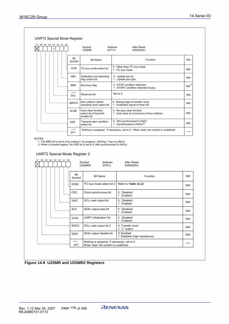
14.Serial I/OpuorG92/C61M
page 178 854fo7002,03.raM21.1.veR2110-1010B90JER
UART2 Special Mode Register 2
Symbol Address After Reset U2SMR2 037616 X00000002
b7 b6 b5 b4 b3 b2 b1 b0
Bit NameBit Symbol RWFunction
STAC
SWC2
SDHI
I C bus mode select bit 2
SCL2 wait output bit 0 : Disabled1 : Enabled
SDA2 output stop bit
UART initialization bit
Clock-synchronous bit
Refer to Table 14.13
0 : Disabled1 : Enabled
IICM2
CSC
SWC
ALS 0 : Disabled1 : Enabled
SDA2 output disable bit
SCL2 wait output bit 2
0: Enabled1: Disabled (high impedance)
0 : Disabled1 : Enabled
0: Transfer clock1: “L” output
2
Nothing is assigned. If necessary, set to 0. When read, the content is undefined
RW
RW
RW
RW
RW
RW
RW
(b7)
UART2 Special Mode Register
Symbol Address After Reset U2SMR 037716 X00000002
b7 b6 b5 b4 b3 b2 b1 b0
Bit NameBit Symbol Function
ABSCS
ACSE
SSS
Bus busy flag 0 : STOP condition detected1 : START condition detected (busy)
Bus collision detectsampling clock select bit
Arbitration lost detecting flag control bit
0 : Update per bit1 : Update per byte
IICM
ABC
BBS
0 : Not synchronized to RxD21 : Synchronized to RxD2(2)
Set to 0
Transmit start condition select bit
0 : Rising edge of transfer clock 1 : Underflow signal of timer A0
Auto clear function select bit of transmit enable bit
0 : No auto clear function1 : Auto clear at occurrence of bus collision
NOTES: 1: The BBS bit is set to 0 by writing 0 by program. (Writing 1 has no effect). 2: When a transfer begins, the SSS bit is set to 0 (Not synchronized to RxD2).
(1)
Nothing is assigned. If necessary, set to 0. When read, the content is undefined
RW
RW
RW
RW
RW
RW
RW
RW
(b7)
0
(b3) Reserved bit
0 : Other than I2C bus mode1 : I2C bus modeI2C bus mode select bit
Figure 14.8 U2SMR and U2SMR2 Registers
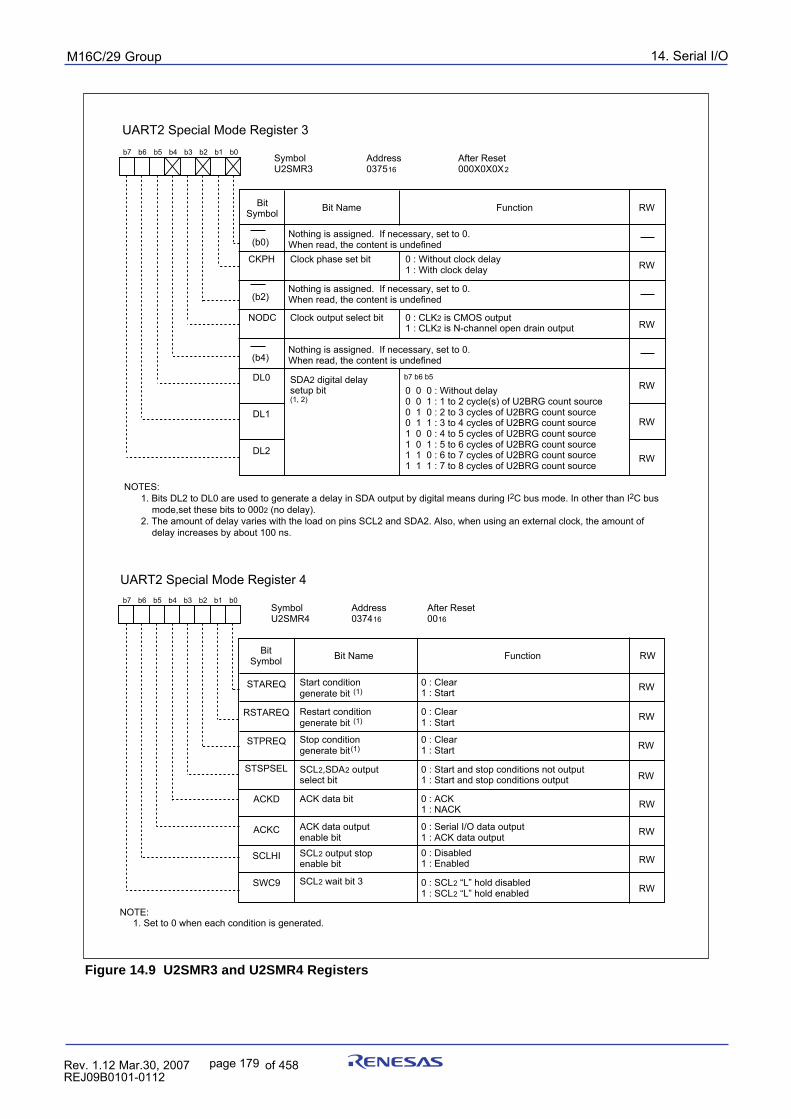
14. Serial I/OpuorG92/C61M
page 179 854fo7002,03.raM21.1.veR2110-1010B90JER
Figure 14.9 U2SMR3 and U2SMR4 Registers
UART2 Special Mode Register 3
Symbol Address After Reset U2SMR3 037516 000X0X0X2
b7 b6 b5 b4 b3 b2 b1 b0
Bit NameBit Symbol Function
DL2
SDA2 digital delay setup bit(1, 2)
DL0
DL1
0 0 0 : Without delay0 0 1 : 1 to 2 cycle(s) of U2BRG count source0 1 0 : 2 to 3 cycles of U2BRG count source0 1 1 : 3 to 4 cycles of U2BRG count source1 0 0 : 4 to 5 cycles of U2BRG count source1 0 1 : 5 to 6 cycles of U2BRG count source1 1 0 : 6 to 7 cycles of U2BRG count source1 1 1 : 7 to 8 cycles of U2BRG count source
Nothing is assigned. If necessary, set to 0.When read, the content is undefined
b7 b6 b5
0 : Without clock delay1 : With clock delay
Clock phase set bit
0 : CLK2 is CMOS output1 : CLK2 is N-channel open drain output
Clock output select bit
CKPH
NODC
RW
RW
RW
RW
RW
RW
(b0)
Nothing is assigned. If necessary, set to 0.When read, the content is undefined
Nothing is assigned. If necessary, set to 0.When read, the content is undefined
(b2)
(b4)
NOTES:1. Bits DL2 to DL0 are used to generate a delay in SDA output by digital means during I2C bus mode. In other than I2C bus
mode,set these bits to 0002 (no delay). 2. The amount of delay varies with the load on pins SCL2 and SDA2. Also, when using an external clock, the amount of
delay increases by about 100 ns.
UART2 Special Mode Register 4
Symbol Address After Reset U2SMR4 037416 0016
b7 b6 b5 b4 b3 b2 b1 b0
Bit NameBit Symbol RWFunction
ACKC
SCLHI
SWC9
Start conditiongenerate bit (1)
Stop conditiongenerate bit(1)
0 : Clear1 : Start
SCL2,SDA2 outputselect bit
ACK data bit
Restart conditiongenerate bit (1)
0 : Clear1 : Start
0 : Clear1 : Start
STAREQ
RSTAREQ
STPREQ
ACKD
0 : Start and stop conditions not output1 : Start and stop conditions output
SCL2 output stopenable bit
ACK data outputenable bit
0 : Disabled1 : Enabled
0 : ACK1 : NACK
0 : Serial I/O data output1 : ACK data output
NOTE: 1. Set to 0 when each condition is generated.
STSPSEL
0 : SCL2 “L” hold disabled1 : SCL2 “L” hold enabled
SCL2 wait bit 3
RW
RW
RW
RW
RW
RW
RW
RW
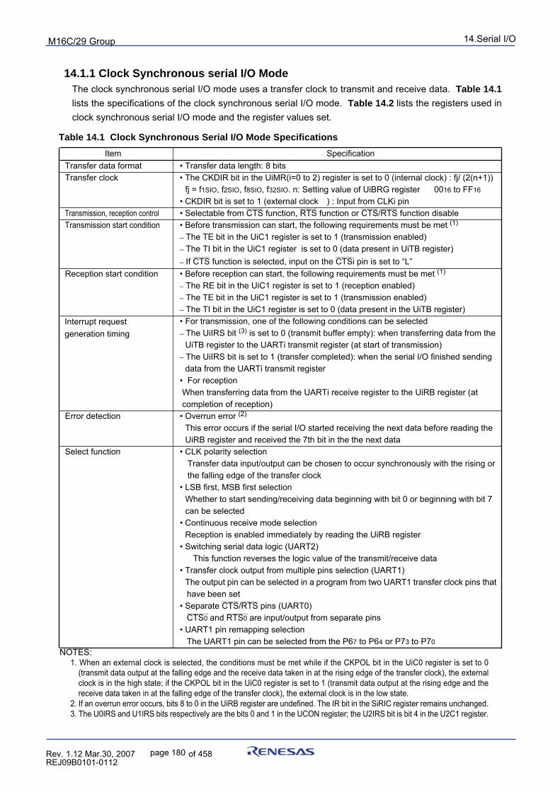
14.Serial I/OpuorG92/C61M
page 180 854fo7002,03.raM21.1.veR2110-1010B90JER
14.1.1 Clock Synchronous serial I/O ModeThe clock synchronous serial I/O mode uses a transfer clock to transmit and receive data. Table 14.1
lists the specifications of the clock synchronous serial I/O mode. Table 14.2 lists the registers used inclock synchronous serial I/O mode and the register values set.
Item SpecificationTransfer data format • Transfer data length: 8 bitsTransfer clock • The CKDIR bit in the UiMR(i=0 to 2) register is set to 0 (internal clock) : fj/ (2(n+1))
fj = f1SIO, f2SIO, f8SIO, f32SIO. n: Setting value of UiBRG register 0016 to FF16
• CKDIR bit is set to 1 (external clock ) : Input from CLKi pinTransmission, reception control
_______ _______ _______ _______
• Selectable from CTS function, RTS function or CTS/RTS function disableTransmission start condition • Before transmission can start, the following requirements must be met (1)
_ The TE bit in the UiC1 register is set to 1 (transmission enabled)_ The TI bit in the UiC1 register is set to 0 (data present in UiTB register)
_______ ________ If CTS function is selected, input on the CTSi pin is set to “L”
Reception start condition • Before reception can start, the following requirements must be met (1)
_ The RE bit in the UiC1 register is set to 1 (reception enabled)_ The TE bit in the UiC1 register is set to 1 (transmission enabled)_ The TI bit in the UiC1 register is set to 0 (data present in the UiTB register)• For transmission, one of the following conditions can be selected_ The UiIRS bit (3) is set to 0 (transmit buffer empty): when transferring data from the
UiTB register to the UARTi transmit register (at start of transmission)_ The UiIRS bit is set to 1 (transfer completed): when the serial I/O finished sending
data from the UARTi transmit register• For reception When transferring data from the UARTi receive register to the UiRB register (at completion of reception)
Error detection • Overrun error (2)
This error occurs if the serial I/O started receiving the next data before reading theUiRB register and received the 7th bit in the the next data
Select function • CLK polarity selection Transfer data input/output can be chosen to occur synchronously with the rising or the falling edge of the transfer clock
• LSB first, MSB first selectionWhether to start sending/receiving data beginning with bit 0 or beginning with bit 7can be selected
• Continuous receive mode selectionReception is enabled immediately by reading the UiRB register
• Switching serial data logic (UART2)This function reverses the logic value of the transmit/receive data
• Transfer clock output from multiple pins selection (UART1)The output pin can be selected in a program from two UART1 transfer clock pins that
have been set_______ _______
• Separate CTS/RTS pins (UART0)_________ _________
CTS0 and RTS0 are input/output from separate pins• UART1 pin remapping selection The UART1 pin can be selected from the P67 to P64 or P73 to P70
NOTES:1. When an external clock is selected, the conditions must be met while if the CKPOL bit in the UiC0 register is set to 0
(transmit data output at the falling edge and the receive data taken in at the rising edge of the transfer clock), the externalclock is in the high state; if the CKPOL bit in the UiC0 register is set to 1 (transmit data output at the rising edge and thereceive data taken in at the falling edge of the transfer clock), the external clock is in the low state.
2. If an overrun error occurs, bits 8 to 0 in the UiRB register are undefined. The IR bit in the SiRIC register remains unchanged.3. The U0IRS and U1IRS bits respectively are the bits 0 and 1 in the UCON register; the U2IRS bit is bit 4 in the U2C1 register.
Interrupt requestgeneration timing
Table 14.1 Clock Synchronous Serial I/O Mode Specifications
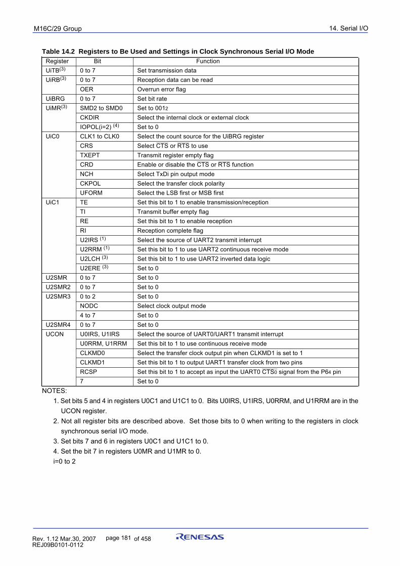
14. Serial I/OpuorG92/C61M
page 181 854fo7002,03.raM21.1.veR2110-1010B90JER
Table 14.2 Registers to Be Used and Settings in Clock Synchronous Serial I/O ModeRegister Bit FunctionUiTB(3) 0 to 7 Set transmission dataUiRB(3) 0 to 7 Reception data can be read
OER Overrun error flagUiBRG 0 to 7 Set bit rateUiMR(3) SMD2 to SMD0 Set to 0012
CKDIR Select the internal clock or external clockIOPOL(i=2) (4) Set to 0
UiC0 CLK1 to CLK0 Select the count source for the UiBRG registerCRS
_______ _______
Select CTS or RTS to useTXEPT Transmit register empty flagCRD
_______ _______
Enable or disable the CTS or RTS functionNCH Select TxDi pin output modeCKPOL Select the transfer clock polarityUFORM Select the LSB first or MSB first
UiC1 TE Set this bit to 1 to enable transmission/receptionTI Transmit buffer empty flagRE Set this bit to 1 to enable receptionRI Reception complete flagU2IRS (1) Select the source of UART2 transmit interruptU2RRM (1) Set this bit to 1 to use UART2 continuous receive modeU2LCH (3) Set this bit to 1 to use UART2 inverted data logicU2ERE (3) Set to 0
U2SMR 0 to 7 Set to 0U2SMR2 0 to 7 Set to 0U2SMR3 0 to 2 Set to 0
NODC Select clock output mode4 to 7 Set to 0
U2SMR4 0 to 7 Set to 0UCON U0IRS, U1IRS Select the source of UART0/UART1 transmit interrupt
U0RRM, U1RRM Set this bit to 1 to use continuous receive modeCLKMD0 Select the transfer clock output pin when CLKMD1 is set to 1CLKMD1 Set this bit to 1 to output UART1 transfer clock from two pinsRCSP
_________
Set this bit to 1 to accept as input the UART0 CTS0 signal from the P64 pin7 Set to 0
NOTES:1. Set bits 5 and 4 in registers U0C1 and U1C1 to 0. Bits U0IRS, U1IRS, U0RRM, and U1RRM are in the
UCON register.2. Not all register bits are described above. Set those bits to 0 when writing to the registers in clock
synchronous serial I/O mode.3. Set bits 7 and 6 in registers U0C1 and U1C1 to 0.4. Set the bit 7 in registers U0MR and U1MR to 0.i=0 to 2
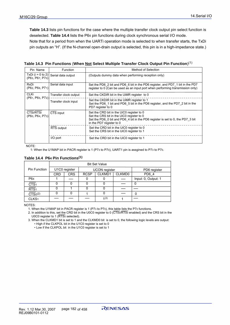
14.Serial I/OpuorG92/C61M
page 182 854fo7002,03.raM21.1.veR2110-1010B90JER
Table 14.3 lists pin functions for the case where the multiple transfer clock output pin select function isdeselected. Table 14.4 lists the P64 pin functions during clock synchronous serial I/O mode.Note that for a period from when the UARTi operation mode is selected to when transfer starts, the TxDipin outputs an “H”. (If the N-channel open-drain output is selected, this pin is in a high-impedance state.)
Table 14.3 Pin Functions (When Not Select Multiple Transfer Clock Output Pin Function)(1)
Table 14.4 P64 Pin Functions(1)
Pin Name Function Method of SelectionTxDi (i = 0 to 2)(P63, P67, P70)
Serial data output
Serial data input
Transfer clock output
Transfer clock input
I/O port
(Outputs dummy data when performing reception only)
RxDi(P62, P66, P71)
CLKi(P61, P65, P72)
Set the CKDIR bit in the UiMR register to 0
Set the CKDIR bit in the UiMR register to 1Set the PD6_1 bit and PD6_5 bit in the PD6 register, and the PD7_2 bit in the PD7 register to 0
Set the PD6_2 bit and PD6_6 bit in the PD6 register, and PD7_1 bit in the PD7 register to 0 (Can be used as an input port when performing transmission only)
Set the CRD bit in the UiC0 register to 0 Set the CRS bit in the UiC0 register to 0Set the PD6_0 bit and PD6_4 bit in the PD6 register is set to 0, the PD7_3 bit in the PD7 register to 0Set the CRD bit in the UiC0 register to 0Set the CRS bit in the UiC0 register to 1
Set the CRD bit in the UiC0 register to 1
CTS input
RTS output
CTSi/RTSi(P60, P64, P73)
NOTE: 1: When the U1MAP bit in PACR register is 1 (P73 to P70), UART1 pin is assgined to P73 to P70.
Pin Function Bit Set Value
U1C0 register UCON register PD6 register CRD CRS RCSP CLKMD1 CLKMD0 PD6_4
P64 1 0 0 Input: 0, Output: 1
CTS1 0 0 0 0
RTS1 1 0 0
CTS0(2) 0
CLKS1
000 0
11 0
1(3)
NOTES: 1. When the U1MAP bit in PACR register is 1 (P73 to P70), this table lists the P70 functions.2. In addition to this, set the CRD bit in the U0C0 register to 0 (CT00/RT00 enabled) and the CRS bit in the
U0C0 register to 1 (RTS0 selected). 3. When the CLKMD1 bit is set to 1 and the CLKMD0 bit is set to 0, the following logic levels are output: • High if the CLKPOL bit in the U1C0 register is set to 0 • Low if the CLKPOL bit in the U1C0 register is set to 1
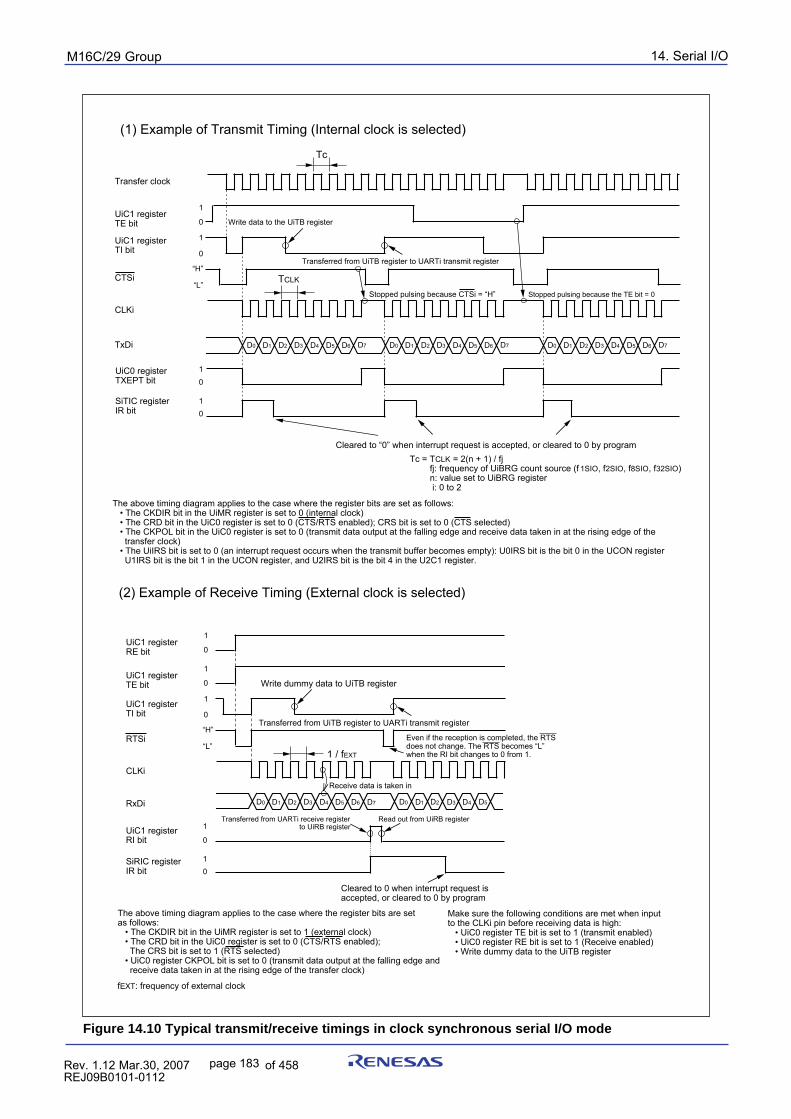
14. Serial I/OpuorG92/C61M
page 183 854fo7002,03.raM21.1.veR2110-1010B90JER
Figure 14.10 Typical transmit/receive timings in clock synchronous serial I/O mode
D0 D1 D2 D3 D4 D5 D6 D7 D0 D1 D2 D3 D4 D5 D6 D7 D0 D1 D2 D3 D4 D5 D6 D7
Tc
TCLK
Stopped pulsing because the TE bit = 0
Write data to the UiTB register
Tc = TCLK = 2(n + 1) / fj fj: frequency of UiBRG count source (f 1SIO, f2SIO, f8SIO, f32SIO) n: value set to UiBRG register i: 0 to 2
Transfer clock
UiC1 registerTE bit
UiC1 registerTI bit
CLKi
TxDi
“H”
“L”
01
0
1
0
1
CTSi
01
Stopped pulsing because CTSi = “H”
1 / fEXT
Write dummy data to UiTB registerUiC1 registerTE bit
UiC1 registerTI bit
CLKi
RxDi
UiC1 registerRI bit
RTSi“H”
“L”
0
1
0
1
0
1
UiC1 registerRE bit 0
1
Receive data is taken in
Transferred from UiTB register to UARTi transmit register
Read out from UiRB register
fEXT: frequency of external clock
Transferred from UARTi receive registerto UiRB register
SiRIC registerIR bit 0
1
D0 D1 D2 D3 D4 D5 D6 D7 D0 D1 D2 D3 D4 D5
Transferred from UiTB register to UARTi transmit register
Make sure the following conditions are met when input to the CLKi pin before receiving data is high: • UiC0 register TE bit is set to 1 (transmit enabled) • UiC0 register RE bit is set to 1 (Receive enabled) • Write dummy data to the UiTB register
The above timing diagram applies to the case where the register bits are set as follows: • The CKDIR bit in the UiMR register is set to 0 (internal clock) • The CRD bit in the UiC0 register is set to 0 (CTS/RTS enabled); CRS bit is set to 0 (CTS selected) • The CKPOL bit in the UiC0 register is set to 0 (transmit data output at the falling edge and receive data taken in at the rising edge of the transfer clock) • The UiIRS bit is set to 0 (an interrupt request occurs when the transmit buffer becomes empty): U0IRS bit is the bit 0 in the UCON register U1IRS bit is the bit 1 in the UCON register, and U2IRS bit is the bit 4 in the U2C1 register.
Cleared to 0 when interrupt request is accepted, or cleared to 0 by program
Cleared to “0” when interrupt request is accepted, or cleared to 0 by program
The above timing diagram applies to the case where the register bits are set as follows: • The CKDIR bit in the UiMR register is set to 1 (external clock) • The CRD bit in the UiC0 register is set to 0 (CTS/RTS enabled); The CRS bit is set to 1 (RTS selected) • UiC0 register CKPOL bit is set to 0 (transmit data output at the falling edge and receive data taken in at the rising edge of the transfer clock)
UiC0 registerTXEPT bit
SiTIC registerIR bit
Even if the reception is completed, the RTS does not change. The RTS becomes “L” when the RI bit changes to 0 from 1.
(1) Example of Transmit Timing (Internal clock is selected)
(2) Example of Receive Timing (External clock is selected)
14.Serial I/OpuorG92/C61M
page 184 854fo7002,03.raM21.1.veR2110-1010B90JER
14.1.1.1 Counter Measure for Communication Error Occurs
If a communication error occurs while transmitting or receiving in clock synchronous serial I/O mode,follow the procedures below.•Resetting the UiRB register (i=0 to 2) (1) Set the RE bit in the UiC1 register to 0 (reception disabled) (2) Set bits SMD2 to SMD0 in the UiMR register to 0002 (Serial I/O disabled) (3) Set bits SMD2 to SMD0 in the UiMR register to 0012 (Clock synchronous serial I/O mode) (4) Set the RE bit in the UiC1 register to 1 (reception enabled)
•Resetting the UiTB register (i=0 to 2) (1) Set bits SMD2 to SMD0 in the UiMR register to 0002 (Serial I/O disabled) (2) Set bits SMD2 to SMD0 in the UiMR register to 0012 (Clock synchronous serial I/O mode) (3) 1 is written to TE bit in the UiC1 register (reception enabled), regardless to the TE bit.
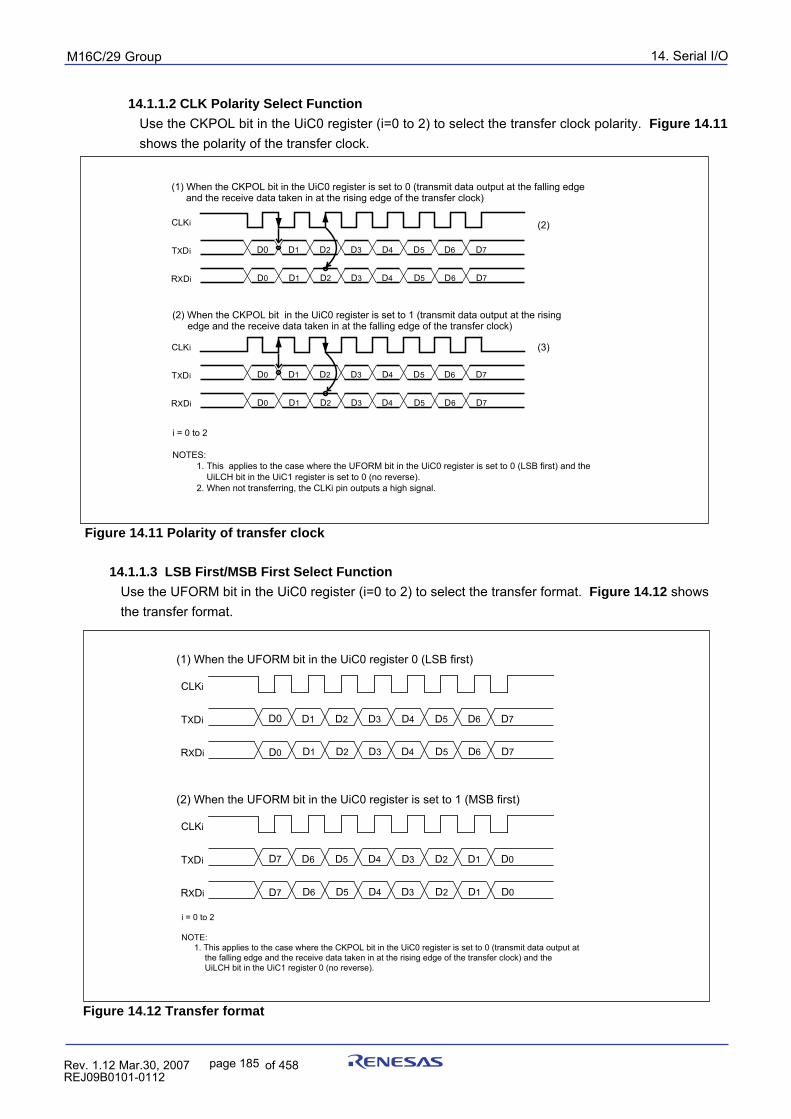
14. Serial I/OpuorG92/C61M
page 185 854fo7002,03.raM21.1.veR2110-1010B90JER
14.1.1.2 CLK Polarity Select Function
Use the CKPOL bit in the UiC0 register (i=0 to 2) to select the transfer clock polarity. Figure 14.11
shows the polarity of the transfer clock.
Figure 14.11 Polarity of transfer clock
14.1.1.3 LSB First/MSB First Select Function
Use the UFORM bit in the UiC0 register (i=0 to 2) to select the transfer format. Figure 14.12 showsthe transfer format.
Figure 14.12 Transfer format
(2) When the CKPOL bit in the UiC0 register is set to 1 (transmit data output at the rising edge and the receive data taken in at the falling edge of the transfer clock)
D1 D2 D3 D4 D5 D6 D7
D1 D2 D3 D4 D5 D6 D7
D0
D0
TXDi
RXDi
CLKi
(1) When the CKPOL bit in the UiC0 register is set to 0 (transmit data output at the falling edge and the receive data taken in at the rising edge of the transfer clock)
D1 D2 D3 D4 D5 D6 D7D0
D1 D2 D3 D4 D5 D6 D7D0
TXDi
RXDi
CLKi (2)
(3)
i = 0 to 2
NOTES: 1. This applies to the case where the UFORM bit in the UiC0 register is set to 0 (LSB first) and the
UiLCH bit in the UiC1 register is set to 0 (no reverse). 2. When not transferring, the CLKi pin outputs a high signal.
(1) When the UFORM bit in the UiC0 register 0 (LSB first)
D0
D0
D1 D2 D3 D4 D5 D6 D7
D1 D2 D3 D4 D5 D6 D7
TXDi
RXDi
CLKi
(2) When the UFORM bit in the UiC0 register is set to 1 (MSB first)
D6 D5 D4 D3 D2 D1 D0D7
D7 D6 D5 D4 D3 D2 D1 D0
TXDi
RXDi
CLKi
i = 0 to 2
NOTE: 1. This applies to the case where the CKPOL bit in the UiC0 register is set to 0 (transmit data output at
the falling edge and the receive data taken in at the rising edge of the transfer clock) and the UiLCH bit in the UiC1 register 0 (no reverse).
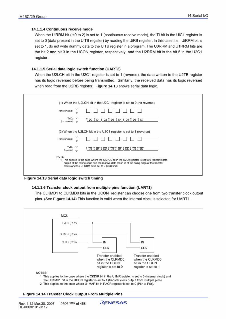
14.Serial I/OpuorG92/C61M
page 186 854fo7002,03.raM21.1.veR2110-1010B90JER
14.1.1.4 Continuous receive mode
When the UiRRM bit (i=0 to 2) is set to 1 (continuous receive mode), the TI bit in the UiC1 register isset to 0 (data present in the UiTB register) by reading the UiRB register. In this case, i.e., UiRRM bit isset to 1, do not write dummy data to the UiTB register in a program. The U0RRM and U1RRM bits arethe bit 2 and bit 3 in the UCON register, respectively, and the U2RRM bit is the bit 5 in the U2C1register.
14.1.1.5 Serial data logic switch function (UART2)
When the U2LCH bit in the U2C1 register is set to 1 (reverse), the data written to the U2TB registerhas its logic reversed before being transmitted. Similarly, the received data has its logic reversedwhen read from the U2RB register. Figure 14.13 shows serial data logic.
Figure 14.13 Serial data logic switch timing
14.1.1.6 Transfer clock output from multiple pins function (UART1)
The CLKMD1 to CLKMD0 bits in the UCON register can choose one from two transfer clock outputpins. (See Figure 14.14) This function is valid when the internal clock is selected for UART1.
Figure 14.14 Transfer Clock Output From Multiple Pins
D0 D1 D2 D3 D4 D5 D6 D7
Transfer clock
TxD2(no reverse)
“H”
“L”
“H”
“L”
TxD2(reverse) D0 D1 D2 D3 D4 D5 D6 D7
“H”
“L”
(1) When the U2LCH bit in the U2C1 register is set to 0 (no reverse)
Transfer clock“H”
“L”
(2) When the U2LCH bit in the U2C1 register is set to 1 (reverse)
NOTE: 1. This applies to the case where the CKPOL bit in the U2C0 register is set to 0 (transmit data
output at the falling edge and the receive data taken in at the rising edge of the transfer clock) and the UFORM bit is set to 0 (LSB first).
MCU
TXD1 (P67)
CLKS1 (P64)
CLK1 (P65) IN
CLK
IN
CLK
Transfer enabled when the CLKMD0 bit in the UCON register is set to 0
Transfer enabled when the CLKMD0 bit in the UCON register is set to 1
NOTES:1. This applies to the case where the CKDIR bit in the U1MRregister is set to 0 (internal clock) and
the CLKMD1 bit in the UCON register is set to 1 (transfer clock output from multiple pins). 2. This applies to the case where U1MAP bit in PACR register is set to 0 (P67 to P64).
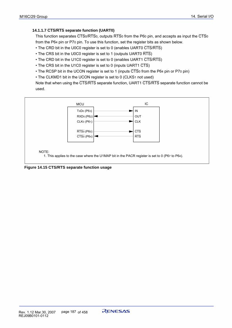
14. Serial I/OpuorG92/C61M
page 187 854fo7002,03.raM21.1.veR2110-1010B90JER
_______ _______
14.1.1.7 CTS/RTS separate function (UART0)_______ _______ _______ _______
This function separates CTS0/RTS0, outputs RTS0 from the P60 pin, and accepts as input the CTS0
from the P64 pin or P70 pin. To use this function, set the register bits as shown below._______ _______
• The CRD bit in the U0C0 register is set to 0 (enables UART0 CTS/RTS)_______
• The CRS bit in the U0C0 register is set to 1 (outputs UART0 RTS)_______ _______
• The CRD bit in the U1C0 register is set to 0 (enables UART1 CTS/RTS)_______
• The CRS bit in the U1C0 register is set to 0 (inputs UART1 CTS)_______
• The RCSP bit in the UCON register is set to 1 (inputs CTS0 from the P64 pin or P70 pin)• The CLKMD1 bit in the UCON register is set to 0 (CLKS1 not used)
_______ _______ _______ _______
Note that when using the CTS/RTS separate function, UART1 CTS/RTS separate function cannot beused.
Figure 14.15 CTS/RTS separate function usage
MCU
TXD0 (P63)
CLK0 (P61)
CTS0 (P64)
IC
IN
OUT
CLK
RXD0 (P62)
RTS0 (P60) CTSRTS
NOTE: 1. This applies to the case where the U1MAP bit in the PACR register is set to 0 (P67 to P64).
14.Serial I/OpuorG92/C61M
page 188 854fo7002,03.raM21.1.veR2110-1010B90JER
Item SpecificationTransfer data format • Character bit (transfer data): Selectable from 7, 8 or 9 bits
• Start bit: 1 bit• Parity bit: Selectable from odd, even, or none• Stop bit: Selectable from 1 or 2 bits
Transfer clock • The CKDIR bit in the UiMR(i=0 to 2) register is set to 0 (internal clock) : fj/ (16(n+1))fj = f1SIO, f2SIO, f8SIO, f32SIO. n: Setting value of UiBRG register 0016 to FF16
• CKDIR bit is set to 1 (external clock ) : fEXT/16(n+1)fEXT: Input from CLKi pin. n :Setting value of UiBRG register 0016 to FF16
Transmission, reception control_______ _______ _______ _______
• Selectable from CTS function, RTS function or CTS/RTS function disableTransmission start condition • Before transmission can start, the following requirements must be met
_ The TE bit in the UiC1 register is set to 1 (transmission enabled)_ The TI bit in the UiC1 register is set to 0 (data present in UiTB register)
_______ ________ If CTS function is selected, input on the CTSi pin is set to “L”
Reception start condition • Before reception can start, the following requirements must be met"_ The RE bit in the UiC1 register is set to 1 (reception enabled)_ Start bit detection• For transmission, one of the following conditions can be selected_ The UiIRS bit (2) is set to 0 (transmit buffer empty): when transferring data from the
UiTB register to the UARTi transmit register (at start of transmission)_ The UiIRS bit is set to1 (transfer completed): when the serial I/O finished sending
data from the UARTi transmit register• For reception When transferring data from the UARTi receive register to the UiRB register (at completion of reception)
Error detection • Overrun error (1)
This error occurs if the serial I/O started receiving the next data before reading theUiRB register and received the bit one before the last stop bit in the the next data• Framing error
This error occurs when the number of stop bits set is not detected• Parity error
This error occurs when if parity is enabled, the number of 1 in parity andcharacter bits does not match the number of 1 set
• Error sum flagThis flag is set to 1 when any of the overrun, framing, and parity errors is encountered
Select function • LSB first, MSB first selectionWhether to start sending/receiving data beginning with bit 0 or beginning with bit 7can be selected
• Serial data logic switch (UART2)This function reverses the logic of the transmit/receive data. The start and stop bitsare not reversed.
• TXD, RXD I/O polarity switch (UART2)This function reverses the polarities of hte TXD pin output and RXD pin input. Thelogic levels of all I/O data is reversed.
_______ _______
• Separate CTS/RTS pins (UART0)_________ _________
CTS0 and RTS0 are input/output from separate pins• UART1 pin remapping selection The UART1 pin can be selected from the P67 to P64 or P73 to P70
NOTES: 1. If an overrun error occurs, bits 8 to 0 in the UiRB register are undefined. The IR bit in the SiRIC register remains unchange. 2. Bits U0IRS and U1IRS respectively are the UCON register bits 0 and 1; the U2IRS bit is the U2C1 register bit 4.
14.1.2 Clock Asynchronous Serial I/O (UART) ModeThe UART mode allows transmitting and receiving data after setting the desired bit rate and transfer dataformat. Table 14.5 lists the specifications of the UART mode.
Table 14.5 UART Mode Specifications
Interrupt requestgeneration timing
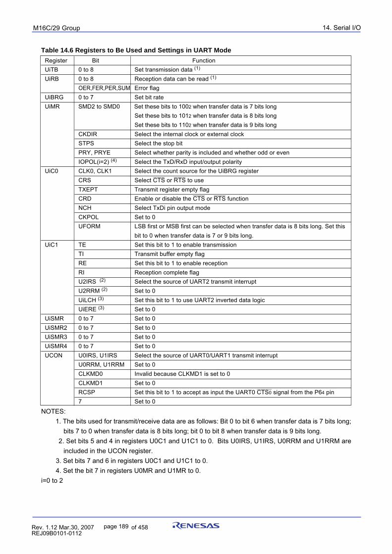
14. Serial I/OpuorG92/C61M
page 189 854fo7002,03.raM21.1.veR2110-1010B90JER
Table 14.6 Registers to Be Used and Settings in UART Mode
Register Bit FunctionUiTB 0 to 8 Set transmission data (1)
UiRB 0 to 8 Reception data can be read (1)
OER,FER,PER,SUM Error flagUiBRG 0 to 7 Set bit rateUiMR SMD2 to SMD0 Set these bits to 1002 when transfer data is 7 bits long
Set these bits to 1012 when transfer data is 8 bits longSet these bits to 1102 when transfer data is 9 bits long
CKDIR Select the internal clock or external clockSTPS Select the stop bitPRY, PRYE Select whether parity is included and whether odd or evenIOPOL(i=2) (4) Select the TxD/RxD input/output polarity
UiC0 CLK0, CLK1 Select the count source for the UiBRG registerCRS
_______ _______
Select CTS or RTS to useTXEPT Transmit register empty flagCRD
_______ _______
Enable or disable the CTS or RTS functionNCH Select TxDi pin output modeCKPOL Set to 0UFORM LSB first or MSB first can be selected when transfer data is 8 bits long. Set this
bit to 0 when transfer data is 7 or 9 bits long.UiC1 TE Set this bit to 1 to enable transmission
TI Transmit buffer empty flagRE Set this bit to 1 to enable receptionRI Reception complete flagU2IRS (2) Select the source of UART2 transmit interruptU2RRM (2) Set to 0UiLCH (3) Set this bit to 1 to use UART2 inverted data logicUiERE (3) Set to 0
UiSMR 0 to 7 Set to 0UiSMR2 0 to 7 Set to 0UiSMR3 0 to 7 Set to 0UiSMR4 0 to 7 Set to 0UCON U0IRS, U1IRS Select the source of UART0/UART1 transmit interrupt
U0RRM, U1RRM Set to 0CLKMD0 Invalid because CLKMD1 is set to 0CLKMD1 Set to 0RCSP
_________
Set this bit to 1 to accept as input the UART0 CTS0 signal from the P64 pin7 Set to 0
NOTES: 1. The bits used for transmit/receive data are as follows: Bit 0 to bit 6 when transfer data is 7 bits long;
bits 7 to 0 when transfer data is 8 bits long; bit 0 to bit 8 when transfer data is 9 bits long. 2. Set bits 5 and 4 in registers U0C1 and U1C1 to 0. Bits U0IRS, U1IRS, U0RRM and U1RRM are
included in the UCON register. 3. Set bits 7 and 6 in registers U0C1 and U1C1 to 0. 4. Set the bit 7 in registers U0MR and U1MR to 0.i=0 to 2
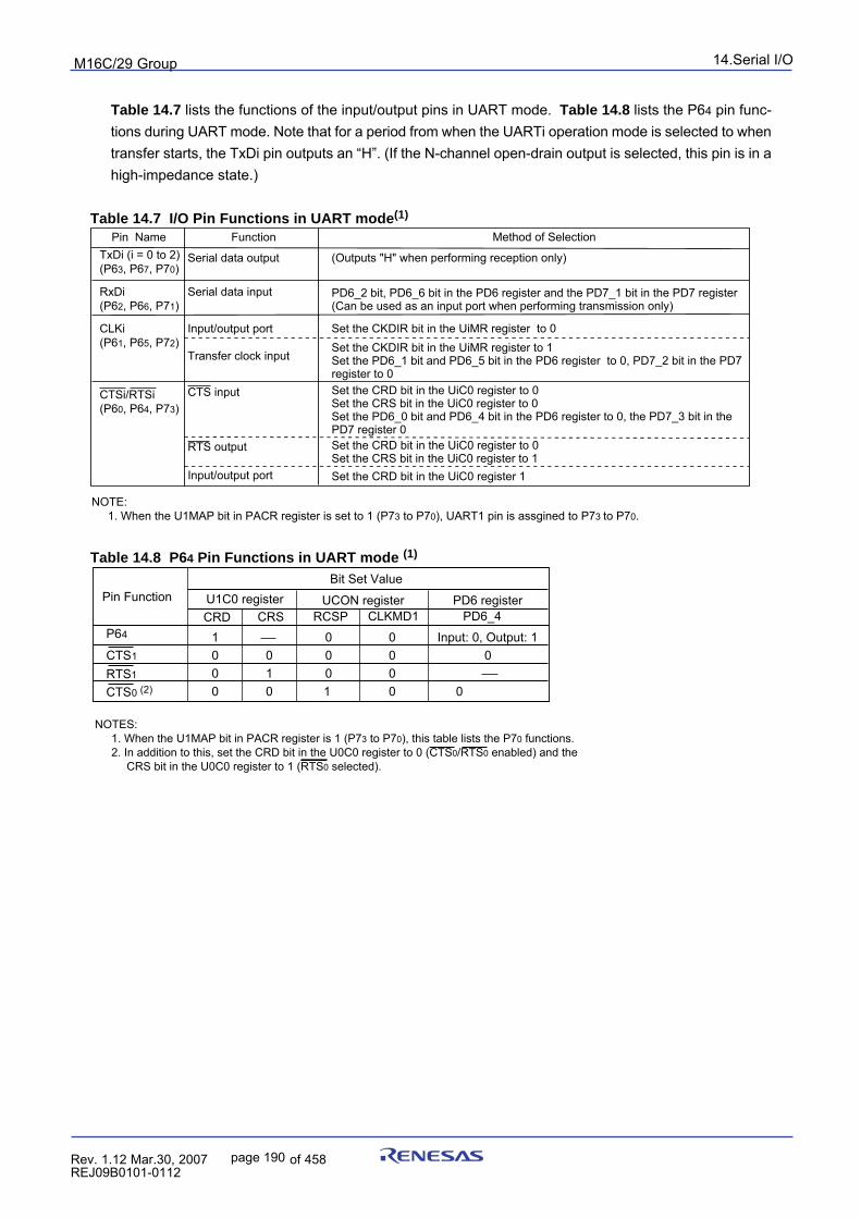
14.Serial I/OpuorG92/C61M
page 190 854fo7002,03.raM21.1.veR2110-1010B90JER
Table 14.7 lists the functions of the input/output pins in UART mode. Table 14.8 lists the P64 pin func-tions during UART mode. Note that for a period from when the UARTi operation mode is selected to whentransfer starts, the TxDi pin outputs an “H”. (If the N-channel open-drain output is selected, this pin is in ahigh-impedance state.)
Table 14.7 I/O Pin Functions in UART mode(1)
Table 14.8 P64 Pin Functions in UART mode (1)
Pin Name Function Method of SelectionTxDi (i = 0 to 2)(P63, P67, P70)
Serial data output
Serial data input
Input/output port
Transfer clock input
Input/output port
(Outputs "H" when performing reception only)
RxDi(P62, P66, P71)
CLKi(P61, P65, P72)
Set the CKDIR bit in the UiMR register to 0Set the CKDIR bit in the UiMR register to 1Set the PD6_1 bit and PD6_5 bit in the PD6 register to 0, PD7_2 bit in the PD7 register to 0
PD6_2 bit, PD6_6 bit in the PD6 register and the PD7_1 bit in the PD7 register(Can be used as an input port when performing transmission only)
Set the CRD bit in the UiC0 register to 0Set the CRS bit in the UiC0 register to 0Set the PD6_0 bit and PD6_4 bit in the PD6 register to 0, the PD7_3 bit in the PD7 register 0Set the CRD bit in the UiC0 register to 0Set the CRS bit in the UiC0 register to 1Set the CRD bit in the UiC0 register 1
CTS input
RTS output
CTSi/RTSi(P60, P64, P73)
NOTE: 1. When the U1MAP bit in PACR register is set to 1 (P73 to P70), UART1 pin is assgined to P73 to P70.
Pin Function Bit Set Value
U1C0 register UCON register PD6 register CRD CRS RCSP CLKMD1 PD6_4
P64 1 0 0 Input: 0, Output: 1CTS1 0 0 0 0RTS1 1 0 0CTS0 (2) 0
000 0 1 0
NOTES: 1. When the U1MAP bit in PACR register is 1 (P73 to P70), this table lists the P70 functions. 2. In addition to this, set the CRD bit in the U0C0 register to 0 (CTS0/RTS0 enabled) and the
CRS bit in the U0C0 register to 1 (RTS0 selected).
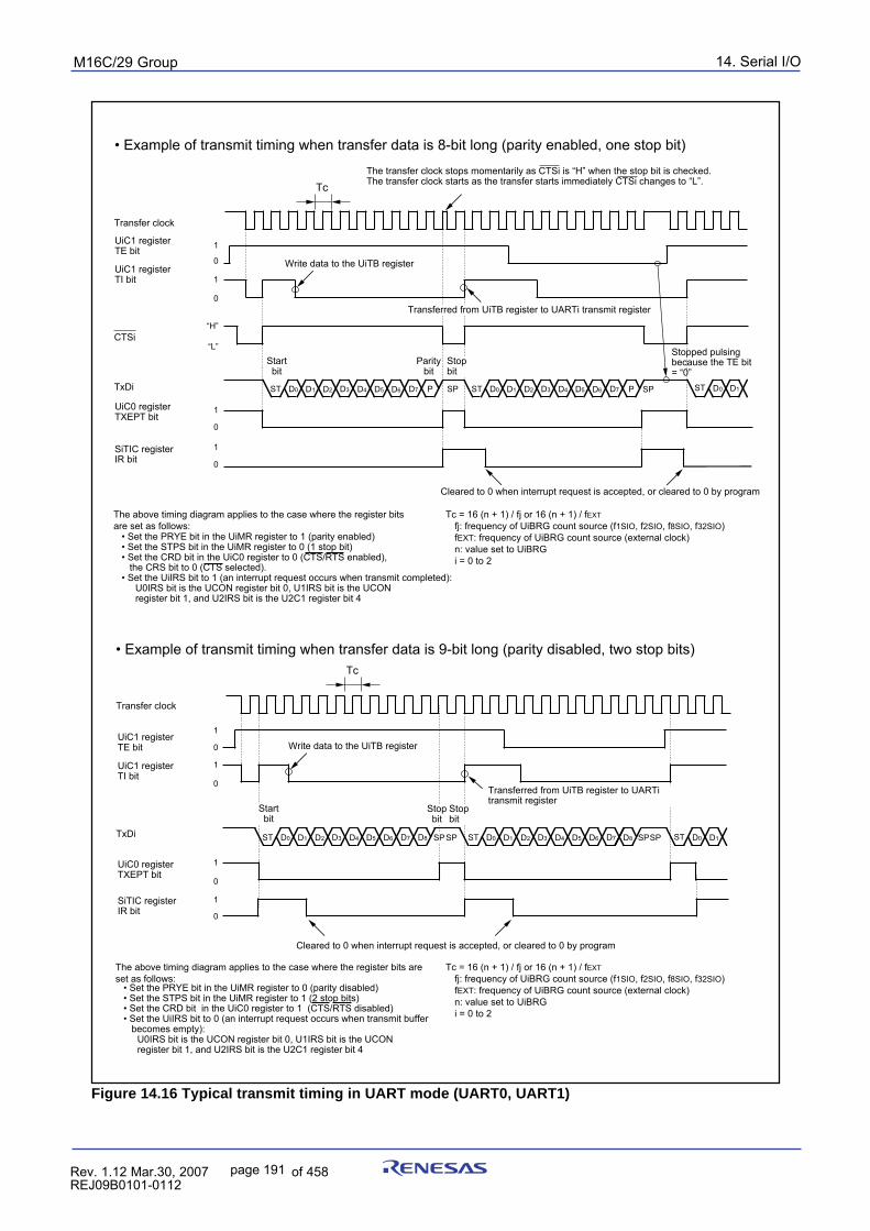
14. Serial I/OpuorG92/C61M
page 191 854fo7002,03.raM21.1.veR2110-1010B90JER
Figure 14.16 Typical transmit timing in UART mode (UART0, UART1)
Startbit
Parity bit
TxDi
CTSi
1
0
1
“L”
“H”
0
1
0
1
TxDi
0
1
0
1
0
1
Transfer clock
Tc
0
1
Tc
Transfer clock
D0 D1 D2 D3 D4 D5 D6 D7ST P D0 D1 D2 D3 D4 D5 D6 D7SP ST P SP D0 D1ST
Stop bit
Start bit
The transfer clock stops momentarily as CTSi is “H” when the stop bit is checked. The transfer clock starts as the transfer starts immediately CTSi changes to “L”.
D0 D1 D2 D3 D4 D5 D6 D7ST SPD8 D0 D1 D2 D3 D4 D5 D6 D7ST D8 D0 D1STSPSP
Stop bit
Stop bit
0
SP
Stopped pulsing because the TE bit = “0”
Write data to the UiTB register
UiC1 registerTE bit
UiC1 registerTI bit
UiC0 registerTXEPT bit
SiTIC registerIR bit
Transferred from UiTB register to UARTi transmit register
The above timing diagram applies to the case where the register bits are set as follows: • Set the PRYE bit in the UiMR register to 1 (parity enabled) • Set the STPS bit in the UiMR register to 0 (1 stop bit) • Set the CRD bit in the UiC0 register to 0 (CTS/RTS enabled), the CRS bit to 0 (CTS selected). • Set the UiIRS bit to 1 (an interrupt request occurs when transmit completed): U0IRS bit is the UCON register bit 0, U1IRS bit is the UCON register bit 1, and U2IRS bit is the U2C1 register bit 4
Cleared to 0 when interrupt request is accepted, or cleared to 0 by program
UiC1 registerTE bit
UiC1 registerTI bit
UiC0 registerTXEPT bit
SiTIC registerIR bit
Cleared to 0 when interrupt request is accepted, or cleared to 0 by program
Write data to the UiTB register
Transferred from UiTB register to UARTi transmit register
The above timing diagram applies to the case where the register bits are set as follows: • Set the PRYE bit in the UiMR register to 0 (parity disabled) • Set the STPS bit in the UiMR register to 1 (2 stop bits) • Set the CRD bit in the UiC0 register to 1 (CTS/RTS disabled) • Set the UiIRS bit to 0 (an interrupt request occurs when transmit buffer becomes empty): U0IRS bit is the UCON register bit 0, U1IRS bit is the UCON register bit 1, and U2IRS bit is the U2C1 register bit 4
• Example of transmit timing when transfer data is 9-bit long (parity disabled, two stop bits)
• Example of transmit timing when transfer data is 8-bit long (parity enabled, one stop bit)
Tc = 16 (n + 1) / fj or 16 (n + 1) / fEXT fj: frequency of UiBRG count source (f1SIO, f2SIO, f8SIO, f32SIO) fEXT: frequency of UiBRG count source (external clock) n: value set to UiBRG i = 0 to 2
Tc = 16 (n + 1) / fj or 16 (n + 1) / fEXT fj: frequency of UiBRG count source (f1SIO, f2SIO, f8SIO, f32SIO) fEXT: frequency of UiBRG count source (external clock) n: value set to UiBRG i = 0 to 2
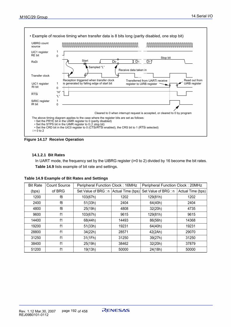
14.Serial I/OpuorG92/C61M
page 192 854fo7002,03.raM21.1.veR2110-1010B90JER
• Example of receive timing when transfer data is 8 bits long (parity disabled, one stop bit)
Figure 14.17 Receive Operation
D0Start bit
Sampled “L”
UiBRG count source
RxDi
Transfer clock
RTSi
Stop bit
10
01
“H”“L”
01
Reception triggered when transfer clock is generated by falling edge of start bit
UiC1 registerRE bit
UiC1 registerRI bit
SiRIC registerIR bit
Cleared to 0 when interrupt request is accepted, or cleared to 0 by program
Receive data taken in
D7D1
Transferred from UARTi receive register to UiRB register
The above timing diagram applies to the case where the register bits are set as follows: • Set the PRYE bit in the UiMR register to 0 (parity disabled) • Set the STPS bit in the UiMR register to 0 (1 stop bit) • Set the CRD bit in the UiC0 register to 0 (CTSi/RTSi enabled), the CRS bit to 1 (RTSi selected) i = 0 to 2
Read out from UiRB register
14.1.2.1 Bit Rates
In UART mode, the frequency set by the UiBRG register (i=0 to 2) divided by 16 become the bit rates.Table 14.9 lists example of bit rate and settings.
Table 14.9 Example of Bit Rates and Settings
Bit Rate Count Source Peripheral Function Clock : 16MHz Peripheral Function Clock : 20MHz(bps) of BRG Set Value of BRG : n Actual Time (bps) Set Value of BRG : n Actual Time (bps)
1200 f8 103(67h) 1202 129(81h) 12022400 f8 51(33h) 2404 64(40h) 24044800 f8 25(19h) 4808 32(20h) 47359600 f1 103(67h) 9615 129(81h) 9615
14400 f1 68(44h) 14493 86(56h) 1436819200 f1 51(33h) 19231 64(40h) 1923128800 f1 34(22h) 28571 42(2Ah) 2907031250 f1 31(1Fh) 31250 39(27h) 3125038400 f1 25(19h) 38462 32(20h) 3787951200 f1 19(13h) 50000 24(18h) 50000
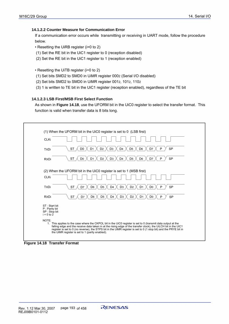
14. Serial I/OpuorG92/C61M
page 193 854fo7002,03.raM21.1.veR2110-1010B90JER
(1) When the UFORM bit in the UiC0 register is set to 0 (LSB first)
(2) When the UFORM bit in the UiC0 register is set to 1 (MSB first)
NOTE: 1. This applies to the case where the CKPOL bit in the UiC0 register is set to 0 (transmit data output at the
falling edge and the receive data taken in at the rising edge of the transfer clock), the UiLCH bit in the UiC1 register is set to 0 (no reverse), the STPS bit in the UiMR register is set to 0 (1 stop bit) and the PRYE bit in the UiMR register is set to 1 (parity enabled).
D1 D2 D3 D4 D5 D6 SPD0
D1 D2 D3 D4 D5 D6 SPD0
TXDi
RXDi
CLKi
D6 D5 D4 D3 D2 D1 D0D7
TXDi
RXDi
CLKi
ST
ST
D7 P
D7 P
SP
SP
ST
ST
P
P
D6 D5 D4 D3 D2 D1 D0D7
ST : Start bitP : Parity bitSP : Stop biti = 0 to 2
14.1.2.2 Counter Measure for Communication Error
If a communication error occurs while transmitting or receiving in UART mode, follow the procedurebelow.• Resetting the UiRB register (i=0 to 2) (1) Set the RE bit in the UiC1 register to 0 (reception disabled) (2) Set the RE bit in the UiC1 register to 1 (reception enabled)
• Resetting the UiTB register (i=0 to 2) (1) Set bits SMD2 to SMD0 in UiMR register 0002 (Serial I/O disabled) (2) Set bits SMD2 to SMD0 in UiMR register 0012, 1012, 1102
(3) 1 is written to TE bit in the UiC1 register (reception enabled), regardless of the TE bit
14.1.2.3 LSB First/MSB First Select Function
As shown in Figure 14.18, use the UFORM bit in the UiC0 register to select the transfer format. Thisfunction is valid when transfer data is 8 bits long.
Figure 14.18 Transfer Format
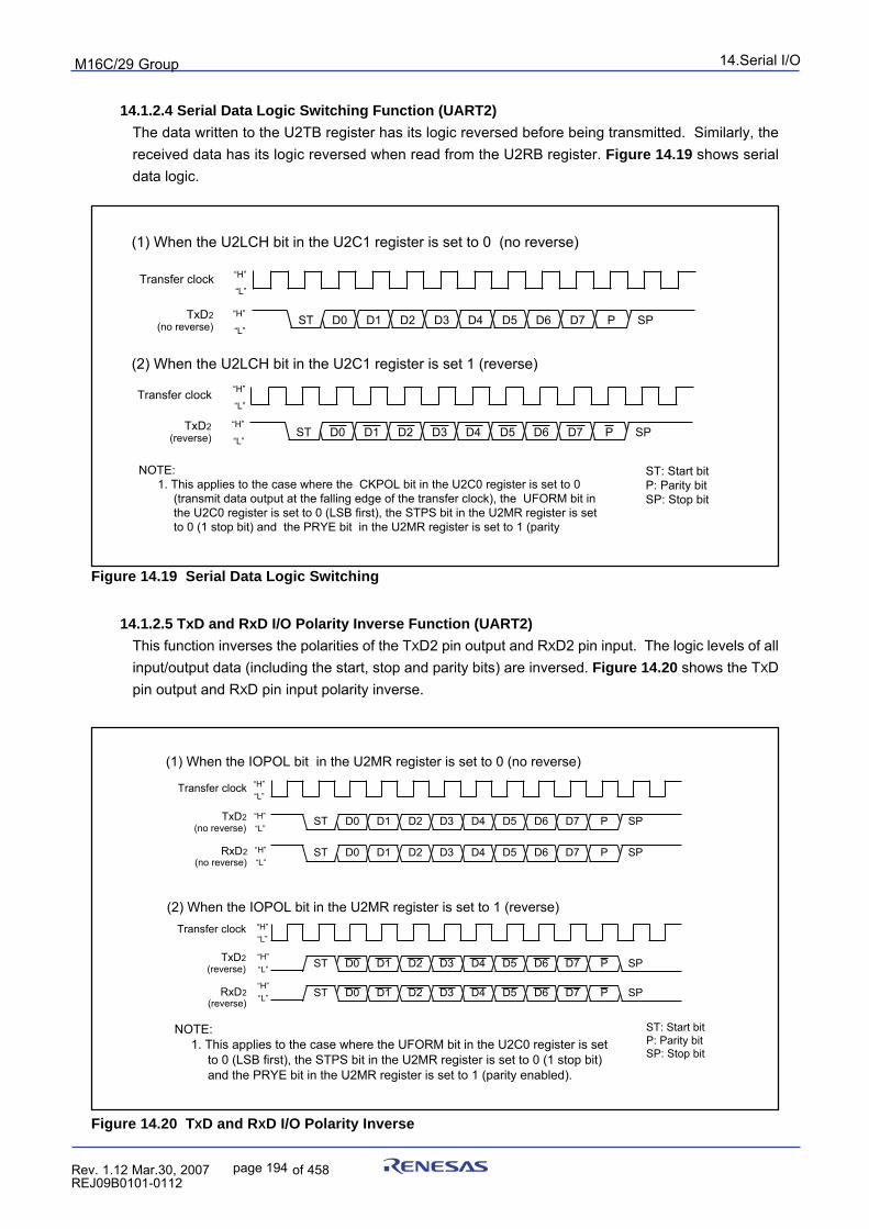
14.Serial I/OpuorG92/C61M
page 194 854fo7002,03.raM21.1.veR2110-1010B90JER
Transfer clock “H”
“L”
D0 D1 D2 D3 D4 D5 D6 D7 P SPSTTxD2(no reverse)
“H”
“L”
TxD2(reverse) SPST D3 D4 D5 D6 D7 PD0 D1 D2
“H”
“L”
(1) When the U2LCH bit in the U2C1 register is set to 0 (no reverse)
(2) When the U2LCH bit in the U2C1 register is set 1 (reverse)
Transfer clock “H”
“L”
NOTE: 1. This applies to the case where the CKPOL bit in the U2C0 register is set to 0
(transmit data output at the falling edge of the transfer clock), the UFORM bit in the U2C0 register is set to 0 (LSB first), the STPS bit in the U2MR register is set to 0 (1 stop bit) and the PRYE bit in the U2MR register is set to 1 (parity
ST: Start bitP: Parity bitSP: Stop bit
(1) When the IOPOL bit in the U2MR register is set to 0 (no reverse)
(2) When the IOPOL bit in the U2MR register is set to 1 (reverse)
ST: Start bitP: Parity bitSP: Stop bit
D0 D1 D2 D3 D4 D5 D6 D7 P SPST
SPST D3 D4 D5 D6 D7 PD0 D1 D2
D0 D1 D2 D3 D4 D5 D6 D7 P SPST“H”
SPST D3 D4 D5 D6 D7 PD0 D1 D2
Transfer clock
TxD2(no reverse)
RxD2(no reverse)
Transfer clock
TxD2(reverse)
RxD2(reverse)
“L”
“H”“L”
“H”“L”
“H”“L”
“H”“L”
“H”“L”
NOTE: 1. This applies to the case where the UFORM bit in the U2C0 register is set
to 0 (LSB first), the STPS bit in the U2MR register is set to 0 (1 stop bit) and the PRYE bit in the U2MR register is set to 1 (parity enabled).
14.1.2.4 Serial Data Logic Switching Function (UART2)
The data written to the U2TB register has its logic reversed before being transmitted. Similarly, thereceived data has its logic reversed when read from the U2RB register. Figure 14.19 shows serialdata logic.
Figure 14.19 Serial Data Logic Switching
14.1.2.5 TxD and RxD I/O Polarity Inverse Function (UART2)
This function inverses the polarities of the TXD2 pin output and RXD2 pin input. The logic levels of allinput/output data (including the start, stop and parity bits) are inversed. Figure 14.20 shows the TXDpin output and RXD pin input polarity inverse.
Figure 14.20 TXD and RXD I/O Polarity Inverse
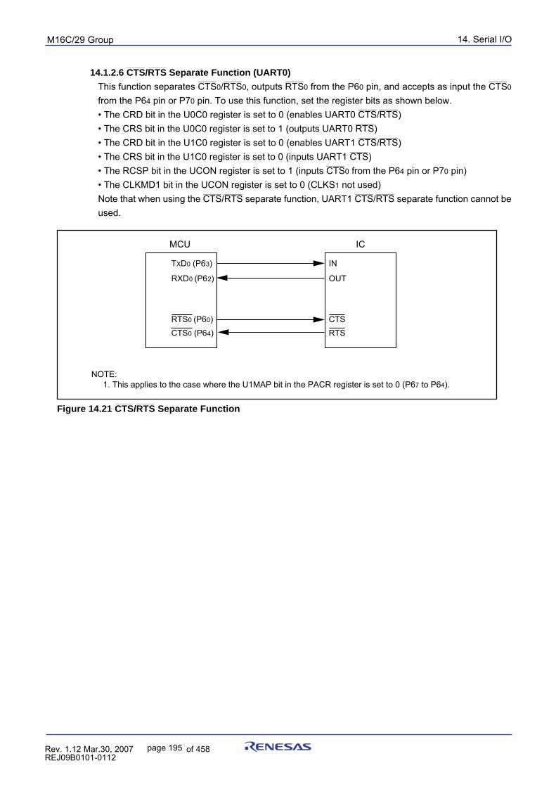
14. Serial I/OpuorG92/C61M
page 195 854fo7002,03.raM21.1.veR2110-1010B90JER
_______ _______
14.1.2.6 CTS/RTS Separate Function (UART0)_______ _______ _______ _______
This function separates CTS0/RTS0, outputs RTS0 from the P60 pin, and accepts as input the CTS0
from the P64 pin or P70 pin. To use this function, set the register bits as shown below._______ _______
• The CRD bit in the U0C0 register is set to 0 (enables UART0 CTS/RTS)_______
• The CRS bit in the U0C0 register is set to 1 (outputs UART0 RTS)_______ _______
• The CRD bit in the U1C0 register is set to 0 (enables UART1 CTS/RTS)_______
• The CRS bit in the U1C0 register is set to 0 (inputs UART1 CTS)_______
• The RCSP bit in the UCON register is set to 1 (inputs CTS0 from the P64 pin or P70 pin)• The CLKMD1 bit in the UCON register is set to 0 (CLKS1 not used)
_______ _______ _______ _______
Note that when using the CTS/RTS separate function, UART1 CTS/RTS separate function cannot beused.
_______ _______
Figure 14.21 CTS/RTS Separate Function
MCU
TXD0 (P63)
CTS0 (P64)
IC
IN
OUTRXD0 (P62)
RTS0 (P60) CTSRTS
NOTE: 1. This applies to the case where the U1MAP bit in the PACR register is set to 0 (P67 to P64).
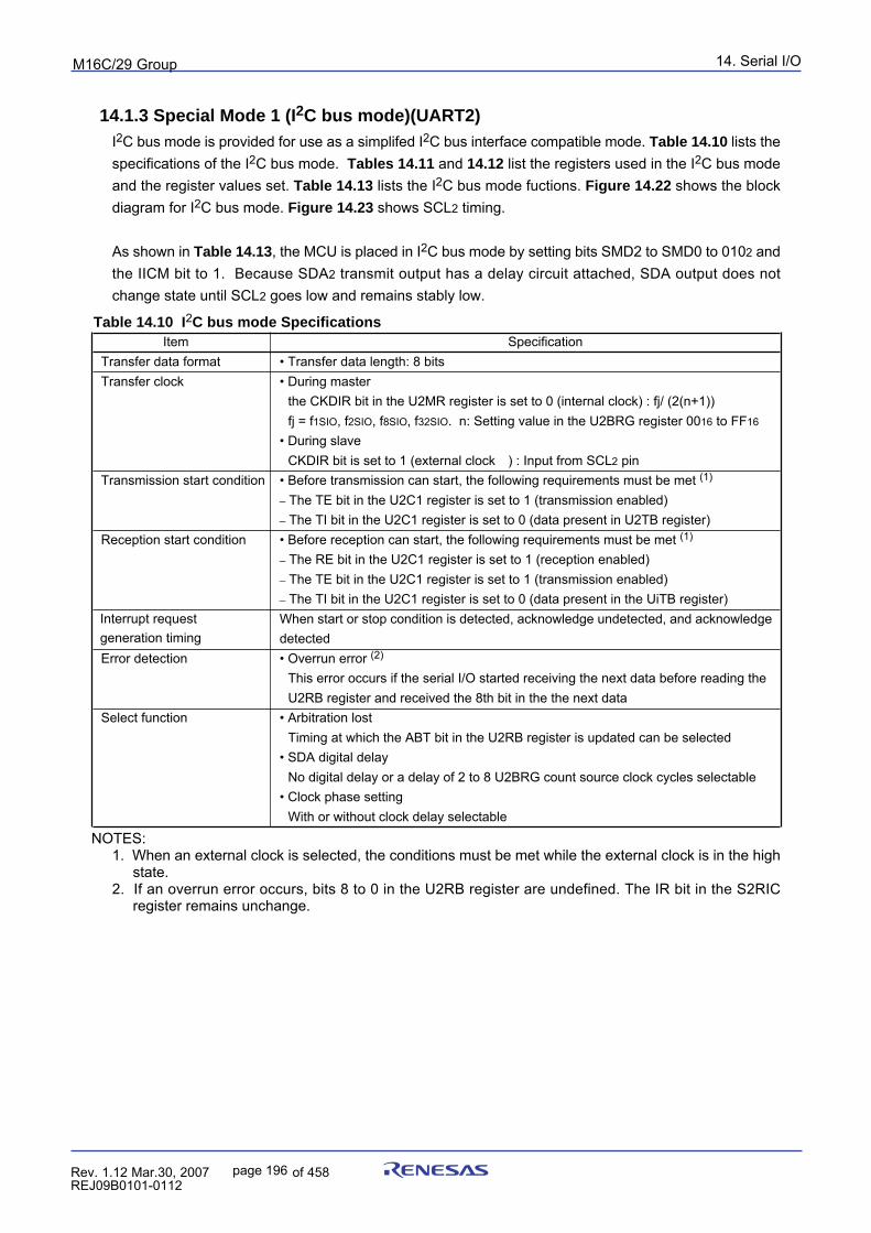
14. Serial I/OpuorG92/C61M
page 196 854fo7002,03.raM21.1.veR2110-1010B90JER
14.1.3 Special Mode 1 (I2C bus mode)(UART2)I2C bus mode is provided for use as a simplifed I2C bus interface compatible mode. Table 14.10 lists thespecifications of the I2C bus mode. Tables 14.11 and 14.12 list the registers used in the I2C bus modeand the register values set. Table 14.13 lists the I2C bus mode fuctions. Figure 14.22 shows the blockdiagram for I2C bus mode. Figure 14.23 shows SCL2 timing.
As shown in Table 14.13, the MCU is placed in I2C bus mode by setting bits SMD2 to SMD0 to 0102 andthe IICM bit to 1. Because SDA2 transmit output has a delay circuit attached, SDA output does notchange state until SCL2 goes low and remains stably low.
Table 14.10 I2C bus mode SpecificationsItem Specification
Transfer data format • Transfer data length: 8 bitsTransfer clock • During master
the CKDIR bit in the U2MR register is set to 0 (internal clock) : fj/ (2(n+1))fj = f1SIO, f2SIO, f8SIO, f32SIO. n: Setting value in the U2BRG register 0016 to FF16
• During slaveCKDIR bit is set to 1 (external clock ) : Input from SCL2 pin
Transmission start condition • Before transmission can start, the following requirements must be met (1)
_ The TE bit in the U2C1 register is set to 1 (transmission enabled)_ The TI bit in the U2C1 register is set to 0 (data present in U2TB register)
Reception start condition • Before reception can start, the following requirements must be met (1)
_ The RE bit in the U2C1 register is set to 1 (reception enabled)_ The TE bit in the U2C1 register is set to 1 (transmission enabled)_ The TI bit in the U2C1 register is set to 0 (data present in the UiTB register)When start or stop condition is detected, acknowledge undetected, and acknowledgedetected
Error detection • Overrun error (2)
This error occurs if the serial I/O started receiving the next data before reading theU2RB register and received the 8th bit in the the next data
Select function • Arbitration lostTiming at which the ABT bit in the U2RB register is updated can be selected
• SDA digital delayNo digital delay or a delay of 2 to 8 U2BRG count source clock cycles selectable
• Clock phase settingWith or without clock delay selectable
Interrupt requestgeneration timing
NOTES:1. When an external clock is selected, the conditions must be met while the external clock is in the high
state.2. If an overrun error occurs, bits 8 to 0 in the U2RB register are undefined. The IR bit in the S2RIC
register remains unchange.
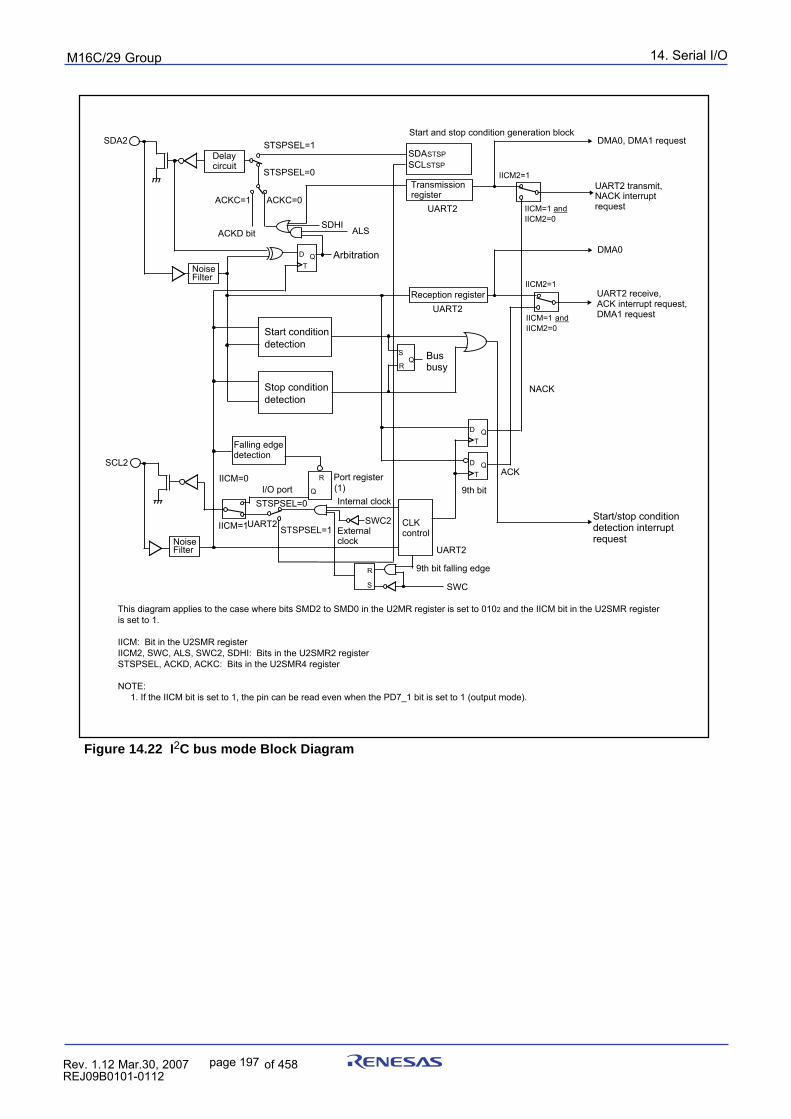
14. Serial I/OpuorG92/C61M
page 197 854fo7002,03.raM21.1.veR2110-1010B90JER
Figure 14.22 I2C bus mode Block Diagram
CLK control
Falling edge detection
External clock
Internal clock
Start/stop condition detection interrupt request
Start condition detection
Stop condition detection
Reception register
Bus busy
Transmission register
ArbitrationNoiseFilter
SDA2
SCL2
UART2
DT
Q
DT
Q
DT
Q
NACK
ACK
UART2
UART2
UART2
R
UART2 transmit, NACK interrupt request
UART2 receive,ACK interrupt request,DMA1 request
IICM=1 andIICM2=0
S
RQ
ALS
R
S SWC
IICM=1 and IICM2=0
IICM2=1
IICM2=1
SWC2
SDHI
DMA0, DMA1 request
NoiseFilter
IICM=0
IICM=1
DMA0
STSPSEL=0
STSPSEL=1
STSPSEL=1
STSPSEL=0
SDASTSPSCLSTSP
ACKC=1 ACKC=0
Q
Port register(1)I/O port
9th bit falling edge
9th bit
ACKD bit
Delay circuit
Start and stop condition generation block
This diagram applies to the case where bits SMD2 to SMD0 in the U2MR register is set to 0102 and the IICM bit in the U2SMR register is set to 1.
IICM : Bit in the U2SMR register IICM2, SWC, ALS, SWC2, SDHI : Bits in the U2SMR2 register STSPSEL, ACKD, ACKC : Bits in the U2SMR4 register
NOTE: 1. If the IICM bit is set to 1, the pin can be read even when the PD7_1 bit is set to 1 (output mode).
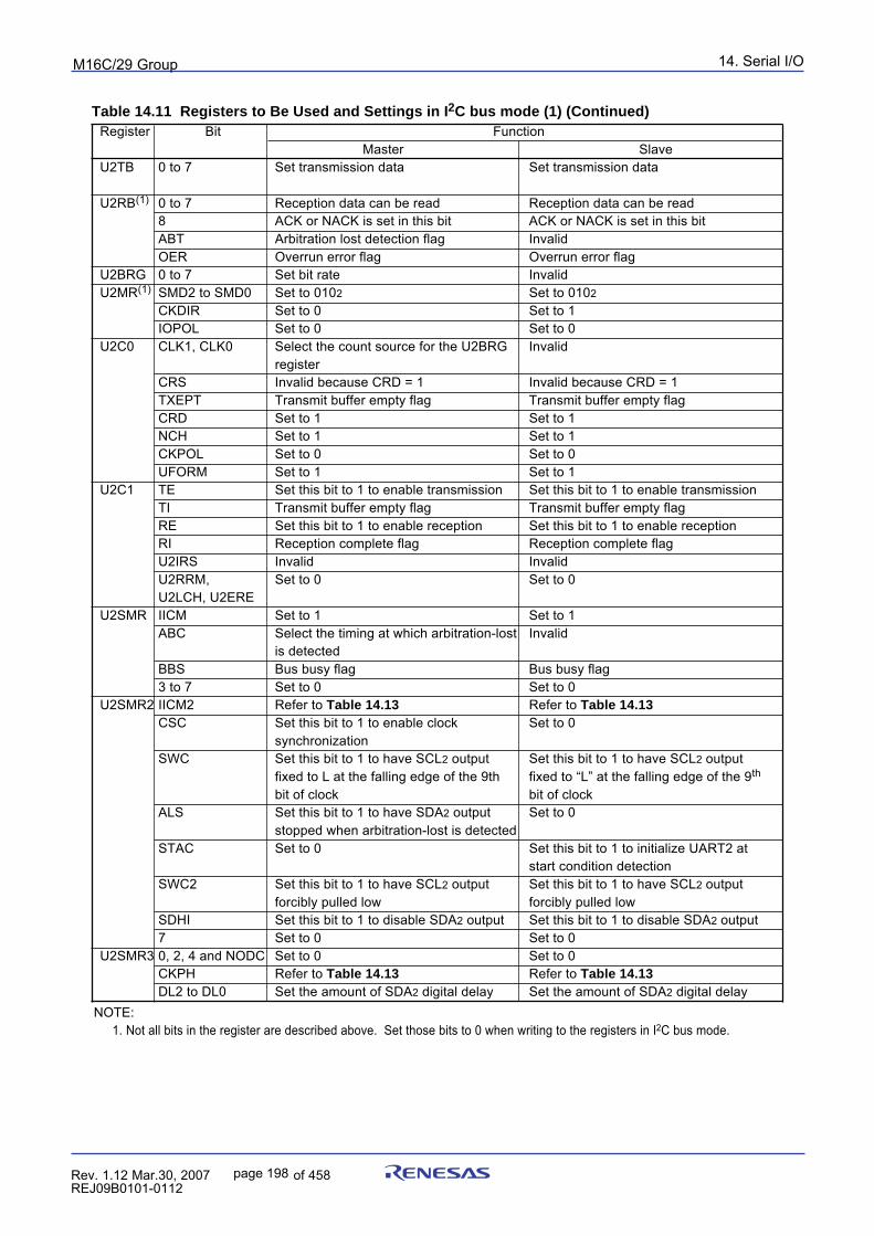
14. Serial I/OpuorG92/C61M
page 198 854fo7002,03.raM21.1.veR2110-1010B90JER
Table 14.11 Registers to Be Used and Settings in I2C bus mode (1) (Continued)Register Bit Function
Master SlaveU2TB 0 to 7 Set transmission data Set transmission data
U2RB(1) 0 to 7 Reception data can be read Reception data can be read8 ACK or NACK is set in this bit ACK or NACK is set in this bitABT Arbitration lost detection flag InvalidOER Overrun error flag Overrun error flag
U2BRG 0 to 7 Set bit rate InvalidU2MR(1) SMD2 to SMD0 Set to 0102 Set to 0102
CKDIR Set to 0 Set to 1IOPOL Set to 0 Set to 0
U2C0 CLK1, CLK0 Select the count source for the U2BRG Invalidregister
CRS Invalid because CRD = 1 Invalid because CRD = 1TXEPT Transmit buffer empty flag Transmit buffer empty flagCRD Set to 1 Set to 1NCH Set to 1 Set to 1CKPOL Set to 0 Set to 0UFORM Set to 1 Set to 1
U2C1 TE Set this bit to 1 to enable transmission Set this bit to 1 to enable transmissionTI Transmit buffer empty flag Transmit buffer empty flagRE Set this bit to 1 to enable reception Set this bit to 1 to enable receptionRI Reception complete flag Reception complete flagU2IRS Invalid InvalidU2RRM, Set to 0 Set to 0U2LCH, U2ERE
U2SMR IICM Set to 1 Set to 1ABC Select the timing at which arbitration-lost Invalid
is detectedBBS Bus busy flag Bus busy flag3 to 7 Set to 0 Set to 0
U2SMR2 IICM2 Refer to Table 14.13 Refer to Table 14.13CSC Set this bit to 1 to enable clock Set to 0
synchronizationSWC Set this bit to 1 to have SCL2 output Set this bit to 1 to have SCL2 output
fixed to L at the falling edge of the 9th fixed to “L” at the falling edge of the 9th
bit of clock bit of clockALS Set this bit to 1 to have SDA2 output Set to 0
stopped when arbitration-lost is detectedSTAC Set to 0 Set this bit to 1 to initialize UART2 at
start condition detectionSWC2 Set this bit to 1 to have SCL2 output Set this bit to 1 to have SCL2 output
forcibly pulled low forcibly pulled lowSDHI Set this bit to 1 to disable SDA2 output Set this bit to 1 to disable SDA2 output7 Set to 0 Set to 0
U2SMR3 0, 2, 4 and NODC Set to 0 Set to 0CKPH Refer to Table 14.13 Refer to Table 14.13DL2 to DL0 Set the amount of SDA2 digital delay Set the amount of SDA2 digital delay
NOTE: 1. Not all bits in the register are described above. Set those bits to 0 when writing to the registers in I2C bus mode.
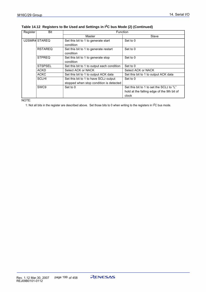
14. Serial I/OpuorG92/C61M
page 199 854fo7002,03.raM21.1.veR2110-1010B90JER
U2SMR4 STAREQ Set this bit to 1 to generate start Set to 0condition
RSTAREQ Set this bit to 1 to generate restart Set to 0condition
STPREQ Set this bit to 1 to generate stop Set to 0condition
STSPSEL Set this bit to 1 to output each condition Set to 0ACKD Select ACK or NACK Select ACK or NACKACKC Set this bit to 1 to output ACK data Set this bit to 1 to output ACK dataSCLHI Set this bit to 1 to have SCL2 output Set to 0
stopped when stop condition is detectedSWC9 Set to 0 Set this bit to 1 to set the SCL2 to “L”
hold at the falling edge of the 9th bit ofclock
Register Bit FunctionMaster Slave
Table 14.12 Registers to Be Used and Settings in I2C bus Mode (2) (Continued)
NOTE: 1: Not all bits in the register are described above. Set those bits to 0 when writing to the registers in I2C bus mode.
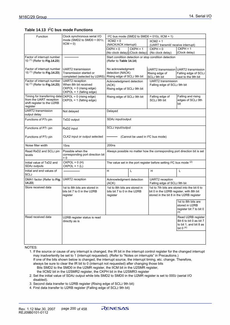
14. Serial I/OpuorG92/C61M
page 200 854fo7002,03.raM21.1.veR2110-1010B90JER
Table 14.13 I2C bus mode Functions
Function I2C bus mode (SMD2 to SMD0 = 0102, IICM = 1)Clock synchronous serial I/O mode (SMD2 to SMD0 = 0012, IICM = 0)
Factor of interrupt number 15 (1) (Refer to Fig.14.23)
No acknowledgment detection (NACK) Rising edge of SCL2 9th bit
Factor of interrupt number 16 (1) (Refer to Fig.14.23)
Start condition detection or stop condition detection(Refer to Table 14.14)
UART2 transmission output delayFunctions of P70 pin
Noise filter width
Read RxD2 and SCL2 pin levels
Factor of interrupt number 10 (1) (Refer to Fig.14.23)
Acknowledgment detection (ACK) Rising edge of SCL2 9th bit
Initial value of TxD2 and SDA2 outputs
UART2 transmissionTransmission started or completed (selected by U2IRS)UART2 receptionWhen 8th bit receivedCKPOL = 0 (rising edge)CKPOL = 1 (falling edge)
Not delayed
TxD2 output
RxD2 input
CLK2 input or output selected
15ns
Possible when the corresponding port direction bit = 0CKPOL = 0 (H)CKPOL = 1 (L)
Delayed
SDA2 input/output
SCL2 input/output
(Cannot be used in I2C bus mode)
Initial and end values of SCL2
H
200ns
Always possible no matter how the corresponding port direction bit is set
The value set in the port register before setting I2C bus mode (2)
Timing for transferring data from the UART reception shift register to the U2RB register
IICM2 = 0 (NACK/ACK interrupt)
IICM2 = 1(UART transmit/ receive interrupt)
CKPH = 1(Clock delay)
CKPH = 1(Clock delay)
UART2 transmissionRising edge of SCL2 9th bit
UART2 transmissionFalling edge of SCL2 next to the 9th bit
UART2 transmissionFalling edge of SCL2 9th bit
CKPOL = 0 (rising edge)CKPOL = 1 (falling edge)
Rising edge of SCL2 9th bit Falling edge of SCL2 9th bit
Falling and rising edges of SCL2 9th bit
..
DMA1 factor (Refer to Fig. 14.23)
UART2 reception Acknowledgment detection (ACK)
UART2 receptionFalling edge of SCL2 9th bit
Store received data 1st to 8th bits are stored in bits bit 7 to 0 in the U2RB register
1st to 8th bits are stored in bits bit 7 to 0 in the U2RB register
1st to 7th bits are stored into the bit 6 to bit 0 in the U2RB register, with 8th bit stored in the bit 8 in the U2RB register
L
Read U2RB register Bit 6 to bit 0 as bit 7 to bit 1, and bit 8 as bit 0 (4)
Read received data U2RB register status is read directly as is
CKPH = 0(No clock delay)
CKPH = 0(No clock delay)
HL
1st to 8th bits are stored in U2RB register bit 7 to bit 0 (3)
Functions of P71 pin
Functions of P72 pin
NOTES: 1. If the source or cause of any interrupt is changed, the IR bit in the interrupt control register for the changed interrupt may inadvertently be set to 1 (interrupt requested). (Refer to “Notes on interrupts” in Precautions.) If one of the bits shown below is changed, the interrupt source, the interrupt timing, etc. change. Therefore, always be sure to clear the IR bit to 0 (interrupt not requested) after changing those bits Bits SMD2 to the SMD0 in the U2MR register, the IICM bit in the U2SMR register, the IICM2 bit in the U2SMR2 register, the CKPH bit in the U2SMR3 register 2. Set the initial value of SDA2 output while bits SMD2 to SMD0 in the U2MR register is set to 0002 (serial I/O disabled). 3. Second data transfer to U2RB register (Rising edge of SCL2 9th bit) 4. First data transfer to U2RB register (Falling edge of SCL2 9th bit)
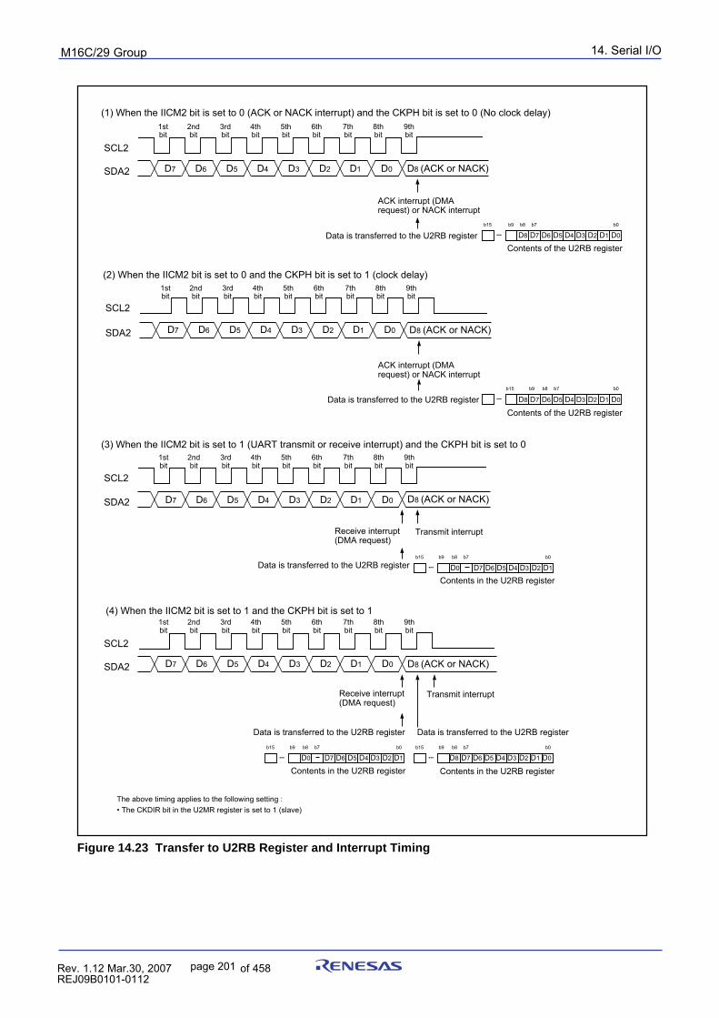
14. Serial I/OpuorG92/C61M
page 201 854fo7002,03.raM21.1.veR2110-1010B90JER
Figure 14.23 Transfer to U2RB Register and Interrupt Timing
(4) When the IICM2 bit is set to 1 and the CKPH bit is set to 1
(3) When the IICM2 bit is set to 1 (UART transmit or receive interrupt) and the CKPH bit is set to 0
SDA2
SCL2
Receive interrupt (DMA request)
Transmit interrupt
SDA2
SCL2
The above timing applies to the following setting :• The CKDIR bit in the U2MR register is set to 1 (slave)
(1) When the IICM2 bit is set to 0 (ACK or NACK interrupt) and the CKPH bit is set to 0 (No clock delay)
D6 D5 D4 D3 D2 D1 D8 (ACK or NACK)D7SDA2
SCL2
D0
ACK interrupt (DMA request) or NACK interrupt
(2) When the IICM2 bit is set to 0 and the CKPH bit is set to 1 (clock delay)
SDA2
SCL2
1stbit
2nd bit
3rdbit
4thbit
5thbit
6thbit
7thbit
8thbit
9thbit
b15
•••
b9 b8 b7 b0
D8
Contents of the U2RB register
b15
•••
b9 b8 b7 b0
b15
•••
b9 b8 b7 b0
b15
•••
b9 b8 b7 b0 b15
•••
b9 b8 b7 b0
D7 D6 D5 D4 D3 D2 D1 D0
D6 D5 D4 D3 D2 D1D7 D0
ACK interrupt (DMA request) or NACK interrupt
D8 D7 D6 D5 D4 D3 D2 D1 D0
D6 D5 D4 D3 D2 D1D7 D0
D7 D6 D5 D4 D3 D2 D1D0
D6 D5 D4 D3 D2 D1D7 D0
D7 D6 D5 D4 D3 D2 D1D0 D8 D7 D6 D5 D4 D3 D2 D1 D0
D8 (ACK or NACK)
1stbit
2nd bit
3rdbit
4thbit
5thbit
6thbit
7thbit
8thbit
9thbit
D8 (ACK or NACK)
1stbit
2nd bit
3rdbit
4thbit
5thbit
6thbit
7thbit
8thbit
9thbit
D8 (ACK or NACK)
1stbit
2nd bit
3rdbit
4thbit
5thbit
6thbit
7thbit
8thbit
9thbit
Data is transferred to the U2RB register
Data is transferred to the U2RB register
Data is transferred to the U2RB register
Receive interrupt (DMA request)
Transmit interrupt
Data is transferred to the U2RB register
Data is transferred to the U2RB register
Contents of the U2RB register
Contents in the U2RB register
Contents in the U2RB registerContents in the U2RB register
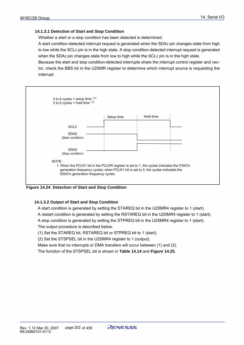
14. Serial I/OpuorG92/C61M
page 202 854fo7002,03.raM21.1.veR2110-1010B90JER
14.1.3.1 Detection of Start and Stop Condition
Whether a start or a stop condition has been detected is determined.A start condition-detected interrupt request is generated when the SDA2 pin changes state from highto low while the SCL2 pin is in the high state. A stop condition-detected interrupt request is generatedwhen the SDA2 pin changes state from low to high while the SCL2 pin is in the high state.Because the start and stop condition-detected interrupts share the interrupt control register and vec-tor, check the BBS bit in the U2SMR register to determine which interrupt source is requesting theinterrupt.
Figure 14.24 Detection of Start and Stop Condition
14.1.3.2 Output of Start and Stop Condition
A start condition is generated by setting the STAREQ bit in the U2SMR4 register to 1 (start).A restart condition is generated by setting the RSTAREQ bit in the U2SMR4 register to 1 (start).A stop condition is generated by setting the STPREQ bit in the U2SMR4 register to 1 (start).The output procedure is described below.(1) Set the STAREQ bit, RSTAREQ bit or STPREQ bit to 1 (start).(2) Set the STSPSEL bit in the U2SMR4 register to 1 (output).Make sure that no interrupts or DMA transfers will occur between (1) and (2).The function of the STSPSEL bit is shown in Table 14.14 and Figure 14.25.
Setup time Hold time
SCL2
SDA2(Start condition)
SDA2(Stop condition)
3 to 6 cycles < setup time (1)
3 to 6 cycles < hold time (1)
NOTE: 1. When the PCLK1 bit in the PCLKR register is set to 1, the cycles indicates the f1SIO's
generation frequency cycles; when PCLK1 bit is set to 0, the cycles indicated the f2SIO's generation frequency cycles.
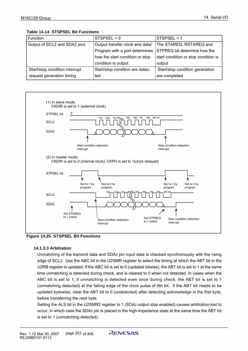
14. Serial I/OpuorG92/C61M
page 203 854fo7002,03.raM21.1.veR2110-1010B90JER
Table 14.14 STSPSEL Bit Functions
Figure 14.25 STSPSEL Bit Functions
FunctionOutput of SCL2 and SDA2 pins
Start/stop condition interruptrequest generation timing
STSPSEL = 0Output transfer clock and data/Program with a port determineshow the start condition or stopcondition is outputStart/stop condition are detec-ted
STSPSEL = 1The STAREQ, RSTAREQ andSTPREQ bit determine how thestart condition or stop condition isoutput Start/stop condition generationare completed
14.1.3.3 Arbitration
Unmatching of the transmit data and SDA2 pin input data is checked synchronously with the risingedge of SCL2. Use the ABC bit in the U2SMR register to select the timing at which the ABT bit in theU2RB register is updated. If the ABC bit is set to 0 (updated bitwise), the ABT bit is set to 1 at the sametime unmatching is detected during check, and is cleared to 0 when not detected. In cases when theABC bit is set to 1, if unmatching is detected even once during check, the ABT bit is set to 1(unmatching detected) at the falling edge of the clock pulse of 9th bit. If the ABT bit needs to beupdated bytewise, clear the ABT bit to 0 (undetected) after detecting acknowledge in the first byte,before transferring the next byte.Setting the ALS bit in the U2SMR2 register to 1 (SDA2 output stop enabled) causes arbitration-lost tooccur, in which case the SDA2 pin is placed in the high-impedance state at the same time the ABT bitis set to 1 (unmatching detected).
SDA2
(1) In slave mode, CKDIR is set to 1 (external clock)
SCL2
SDA2
Start condition detectioninterrupt
Stop condition detection interrupt
(2) In master mode, CKDIR is set to 0 (internal clock), CKPH is set to 1(clock delayed)
SCL2
Set STAREQ to 1 (start) Set STPREQ
to 1 (start)
STPSEL bit 0
STPSEL bit
Set to 1 by program
Set to 0 by program
Set to 1 by program
Set to 0 by program
1st 2nd 3rd 5th 6th 7th 8th 9th bit
1st 2nd 3rd 5th 6th 7th 8th 9th bit
4th
4th
Start condition detectioninterrupt
Stop condition detection interrupt
14. Serial I/OpuorG92/C61M
page 204 854fo7002,03.raM21.1.veR2110-1010B90JER
14.1.3.4 Transfer Clock
Data is transmitted/received using a transfer clock like the one shown in Figure 14.25.The CSC bit in the U2SMR2 register is used to synchronize the internally generated clock (internalSCL2) and an external clock supplied to the SCL2 pin. In cases when the CSC bit is set to 1 (clocksynchronization enabled), if a falling edge on the SCL2 pin is detected while the internal SCL2 is high,the internal SCL2 goes low, at which time the U2BRG register value is reloaded with and starts count-ing in the low-level interval. If the internal SCL2 changes state from low to high while the SCL2 pin islow, counting stops, and when the SCL2 pin goes high, counting restarts.In this way, the UART2 transfer clock is comprised of the logical product of the internal SCL2 and SCL2
pin signal. The transfer clock works from a half period before the falling edge of the internal SCL2 1stbit to the rising edge of the 9th bit. To use this function, select an internal clock for the transfer clock.The SWC bit in the U2SMR2 register allows to select whether the SCL2 pin should be fixed to or freedfrom low-level output at the falling edge of the 9th clock pulse.If the SCLHI bit in the U2SMR4 register is set to 1 (enabled), SCL2 output is turned off (placed in thehigh-impedance state) when a stop condition is detected.Setting the SWC2 bit in the U2SMR2 register is set to 1 (0 output) makes it possible to forcibly outputa low-level signal from the SCL2 pin even while sending or receiving data. Clearing the SWC2 bit to 0(transfer clock) allows the transfer clock to be output from or supplied to the SCL2 pin, instead ofoutputting a low-level signal.If the SWC9 bit in the U2SMR4 register is set to 1 (SCL2 hold low enabled) when the CKPH bit in theU2SMR3 register is set to 1, the SCL2 pin is fixed to low-level output at the falling edge of the clockpulse next to the ninth. Setting the SWC9 bit to 0 (SCL2 hold low disabled) frees the SCL2 pin fromlow-level output.
14.1.3.5 SDA Output
The data written to the bit 7 to bit 0 (D7 to D0) in the U2TB register is sequentially output beginningwith D7. The ninth bit (D8) is ACK or NACK.The initial value of SDA2 transmit output can only be set when IICM is set to 1 (I2C bus mode) and bitsSMD2 to SMD0 in the U2MR register is set to 0002 (serial I/O disabled).Bits DL2 to DL0 in the U2SMR3 register allow to add no delays or a delay of 2 to 8 U2BRG countsource clock cycles to SDA2 output.Setting the SDHI bit in the U2SMR2 register to 1 (SDA2 output disabled) forcibly places the SDA2 pinin the high-impedance state. Do not write to the SDHI bit synchronously with the rising edge of theUART2 transfer clock. This is because the ABT bit may inadvertently be set to 1 (detected).
14.1.3.6 SDA Input
When the IICM2 bit is set to 0, the 1st to 8th bits (D7 to D0) in the received data are stored in bits 7 to0 in the U2RB register. The 9th bit (D8) is ACK or NACK.When the IICM2 bit is set to 1, the 1st to 7th bits (D7 to D1) in the received data are stored in the bit 6to bit 0 in the U2RB register and the 8th bit (D0) is stored in the bit 8 in the U2RB register. Even whenthe IICM2 bit is set to 1, providing the CKPH bit is set to 1, the same data as when the IICM2 bit is setto 0 can be read out by reading the U2RB register after the rising edge of the corresponding clockpulse of 9th bit.
14. Serial I/OpuorG92/C61M
page 205 854fo7002,03.raM21.1.veR2110-1010B90JER
14.1.3.7 ACK and NACK
If the STSPSEL bit in the U2SMR4 register is set to 0 (start and stop conditions not generated) and theACKC bit in the U2SMR4 register is set to 1 (ACK data output), the value of the ACKD bit in theU2SMR4 register is output from the SDA2 pin.If the IICM2 bit is set to 0, a NACK interrupt request is generated if the SDA2 pin remains high at therising edge of the 9th bit of transmit clock pulse. An ACK interrupt request is generated if the SDA2 pinis low at the rising edge of the 9th bit of transmit clock pulse.If ACK2 is selected for the cause of DMA1 request, a DMA transfer can be activated by detection of anacknowledge.
14.1.3.8 Initialization of Transmission/Reception
If a start condition is detected while the STAC bit is set to 1 (UART2 initialization enabled), the serial I/O operates as described below.- The transmit shift register is initialized, and the content of the U2TB register is transferred to the transmit shift register. In this way, the serial I/O starts sending data synchronously with the next clock pulse applied. However, the UART2 output value does not change state and remains the same as when a start condition was detected until the first bit in the data is output synchronously with the input clock.- The receive shift register is initialized, and the serial I/O starts receiving data synchronously with the next clock pulse applied.- The SWC bit is set to 1 (SCL2 wait output enabled). Consequently, the SCL2 pin is pulled low at the falling edge of the ninth clock pulse.Note that when UART2 transmission/reception is started using this function, the TI does not changestate. Note also that when using this function, the selected transfer clock should be an external clock.
14. Serial I/OpuorG92/C61M
page 206 854fo7002,03.raM21.1.veR2110-1010B90JER
14.1.4 Special Mode 2 (UART2)Multiple slaves can be serially communicated from one master. Transfer clock polarity and phase areselectable. Table 14.15 lists the specifications of Special Mode 2. Table 14.16 lists the registers used inSpecial Mode 2 and the register values set. Figure 14.26 shows communication control example forSpecial Mode 2.
Table 14.15 Special Mode 2 SpecificationsItem Specification
Transfer data format • Transfer data length: 8 bitsTransfer clock • Master mode
the CKDIR bit in the U2MR register is set to 0 (internal clock) : fj/ (2(n+1))fj = f1SIO, f2SIO, f8SIO, f32SIO. n: Setting value in the U2BRG register 0016 to FF16
• Slave modeCKDIR bit is set to 1 (external clock selected) : Input from CLK2 pin
Transmit/receive control Controlled by input/output portsTransmission start condition • Before transmission can start, the following requirements must be met (1)
_ The TE bit in the U2C1 register is set to 1 (transmission enabled)_ The TI bit in the U2C1 register is set to 0 (data present in U2TB register)
Reception start condition • Before reception can start, the following requirements must be met (1)
_ The RE bit in the U2C1 register is set to 1 (reception enabled)_ The TE bit in the U2C1 register is set to 1 (transmission enabled)_ The TI bit in the U2C1 register is set to 0 (data present in the U2TB register)• For transmission, one of the following conditions can be selected_ The U2IRS bit in the U2C1 register is set to 0 (transmit buffer empty): when trans
ferring data from the U2TB register to the UART2 transmit register (at start of transmission)_ The U2IRS bit is set to 1 (transfer completed): when the serial I/O finished sending
data from the UART2 transmit register• For reception When transferring data from the UART2 receive register to the U2RB register (at completion of reception)
Error detection • Overrun error (2)
This error occurs if the serial I/O started receiving the next data before reading theU2RB register and received the 7th bit in the the next data
Select function • Clock phase settingSelectable from four combinations of transfer clock polarities and phases
Interrupt requestgeneration timing
NOTES: 1. When an external clock is selected, the conditions must be met while if the CKPOL bit in the U2C0 register is set to
0 (transmit data output at the falling edge and the receive data taken in at the rising edge of the transfer clock), theexternal clock is in the high state; if the CKPOL bit in the U2C0 register is set to 1 (transmit data output at the risingedge and the receive data taken in at the falling edge of the transfer clock), the external clock is in the low state.
2. If an overrun error occurs, bits 8 to 0 in the U2RB register are undefined. The IR bit in the S2RIC register remainsunchanged.
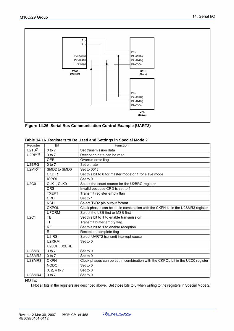
14. Serial I/OpuorG92/C61M
page 207 854fo7002,03.raM21.1.veR2110-1010B90JER
Table 14.16 Registers to Be Used and Settings in Special Mode 2Register Bit FunctionU2TB(1) 0 to 7 Set transmission dataU2RB(1) 0 to 7 Reception data can be read
OER Overrun error flagU2BRG 0 to 7 Set bit rateU2MR(1) SMD2 to SMD0 Set to 0012
CKDIR Set this bit to 0 for master mode or 1 for slave modeIOPOL Set to 0
U2C0 CLK1, CLK0 Select the count source for the U2BRG registerCRS Invalid because CRD is set to 1TXEPT Transmit register empty flagCRD Set to 1NCH Select TxD2 pin output formatCKPOL Clock phases can be set in combination with the CKPH bit in the U2SMR3 registerUFORM Select the LSB first or MSB first
U2C1 TE Set this bit to 1 to enable transmissionTI Transmit buffer empty flagRE Set this bit to 1 to enable receptionRI Reception complete flagU2IRS Select UART2 transmit interrupt causeU2RRM, Set to 0U2LCH, U2ERE
U2SMR 0 to 7 Set to 0U2SMR2 0 to 7 Set to 0U2SMR3 CKPH Clock phases can be set in combination with the CKPOL bit in the U2C0 register
NODC Set to 00, 2, 4 to 7 Set to 0
U2SMR4 0 to 7 Set to 0NOTE: 1.Not all bits in the registers are described above. Set those bits to 0 when writing to the registers in Special Mode 2.
Figure 14.26 Serial Bus Communication Control Example (UART2)
P13
P12
P70(TxD2)
P72(CLK2)P71(RxD2)
P93
P70(TxD2)
P72(CLK2)P71(RxD2)
P93
P70(TxD2)
P72(CLK2)P71(RxD2)
MCU (Master)
MCU (Slave)
MCU (Slave)
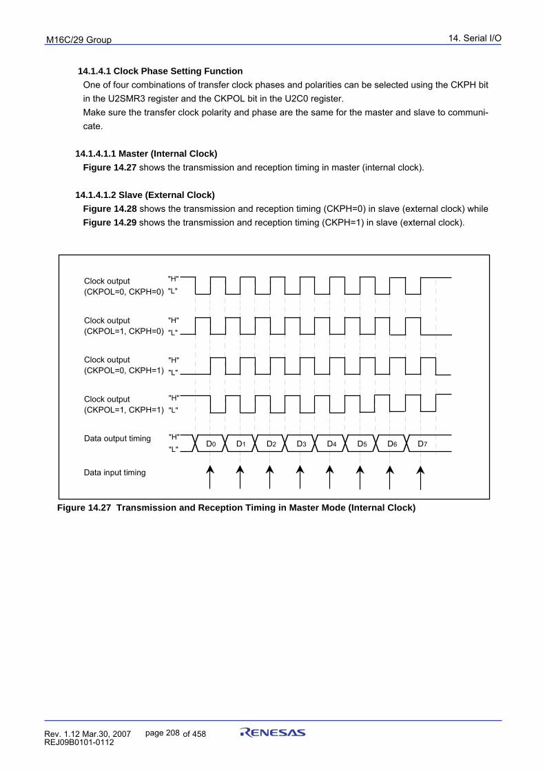
14. Serial I/OpuorG92/C61M
page 208 854fo7002,03.raM21.1.veR2110-1010B90JER
14.1.4.1 Clock Phase Setting Function
One of four combinations of transfer clock phases and polarities can be selected using the CKPH bitin the U2SMR3 register and the CKPOL bit in the U2C0 register.Make sure the transfer clock polarity and phase are the same for the master and slave to communi-cate.
14.1.4.1.1 Master (Internal Clock)
Figure 14.27 shows the transmission and reception timing in master (internal clock).
14.1.4.1.2 Slave (External Clock)
Figure 14.28 shows the transmission and reception timing (CKPH=0) in slave (external clock) whileFigure 14.29 shows the transmission and reception timing (CKPH=1) in slave (external clock).
Figure 14.27 Transmission and Reception Timing in Master Mode (Internal Clock)
D
a
t
a
o
u
t
p
u
t
t
i
m
i
n
g
D
a
t
a
i
n
p
u
t
t
i
m
i
n
g
D0 D1 D2 D3 D4 D6 D7D5
C
l
o
c
k
o
u
t
p
u
t(
C
K
P
O
L
=
0
,
C
K
P
H
=
0
)" H
"
" L
"
C
l
o
c
k
o
u
t
p
u
t(
C
K
P
O
L
=
1
,
C
K
P
H
=
0
)" H
"
" L
"
C
l
o
c
k
o
u
t
p
u
t(
C
K
P
O
L
=
0
,
C
K
P
H
=
1
)" H
"
" L
"
Clock output(CKPOL=1, CKPH=1)
"H"" L
"
"H"
"L"
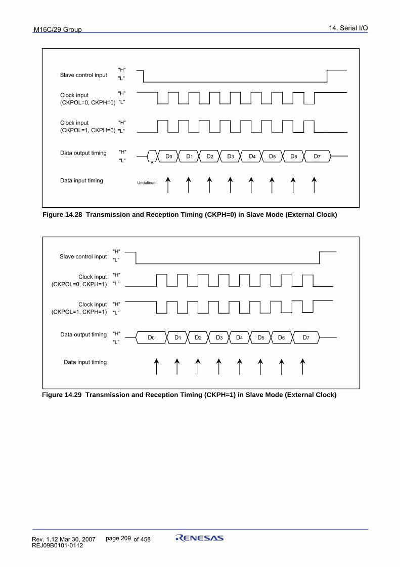
14. Serial I/OpuorG92/C61M
page 209 854fo7002,03.raM21.1.veR2110-1010B90JER
Figure 14.28 Transmission and Reception Timing (CKPH=0) in Slave Mode (External Clock)
Figure 14.29 Transmission and Reception Timing (CKPH=1) in Slave Mode (External Clock)
Slave control input
Clock input(CKPOL=0, CKPH=0)
Clock input(CKPOL=1, CKPH=0)
Data output timing
Data input timing
"H""L"
"H""L"
"H""L"
"H""L"
D0 D1 D2 D3 D4 D6 D7D5
Undefined
Clock input(CKPOL=0, CKPH=1)
Clock input(CKPOL=1, CKPH=1)
Data output timing
Data input timing
"H""L"
"H""L"
"H""L"
"H""L"
D0 D1 D2 D3 D6 D7D4 D5
Slave control input
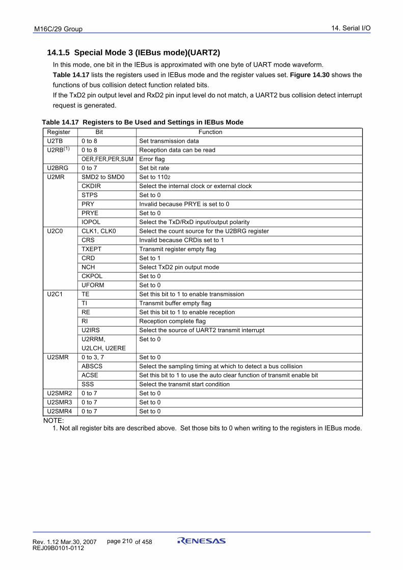
14. Serial I/OpuorG92/C61M
page 210 854fo7002,03.raM21.1.veR2110-1010B90JER
14.1.5 Special Mode 3 (IEBus mode)(UART2)In this mode, one bit in the IEBus is approximated with one byte of UART mode waveform.Table 14.17 lists the registers used in IEBus mode and the register values set. Figure 14.30 shows thefunctions of bus collision detect function related bits.If the TxD2 pin output level and RxD2 pin input level do not match, a UART2 bus collision detect interruptrequest is generated.
Table 14.17 Registers to Be Used and Settings in IEBus ModeRegister Bit FunctionU2TB 0 to 8 Set transmission dataU2RB(1) 0 to 8 Reception data can be read
OER,FER,PER,SUM Error flagU2BRG 0 to 7 Set bit rateU2MR SMD2 to SMD0 Set to 1102
CKDIR Select the internal clock or external clockSTPS Set to 0PRY Invalid because PRYE is set to 0PRYE Set to 0IOPOL Select the TxD/RxD input/output polarity
U2C0 CLK1, CLK0 Select the count source for the U2BRG registerCRS Invalid because CRDis set to 1TXEPT Transmit register empty flagCRD Set to 1NCH Select TxD2 pin output modeCKPOL Set to 0UFORM Set to 0
U2C1 TE Set this bit to 1 to enable transmissionTI Transmit buffer empty flagRE Set this bit to 1 to enable receptionRI Reception complete flagU2IRS Select the source of UART2 transmit interruptU2RRM, Set to 0U2LCH, U2ERE
U2SMR 0 to 3, 7 Set to 0ABSCS Select the sampling timing at which to detect a bus collisionACSE Set this bit to 1 to use the auto clear function of transmit enable bitSSS Select the transmit start condition
U2SMR2 0 to 7 Set to 0U2SMR3 0 to 7 Set to 0U2SMR4 0 to 7 Set to 0
NOTE: 1. Not all register bits are described above. Set those bits to 0 when writing to the registers in IEBus mode.
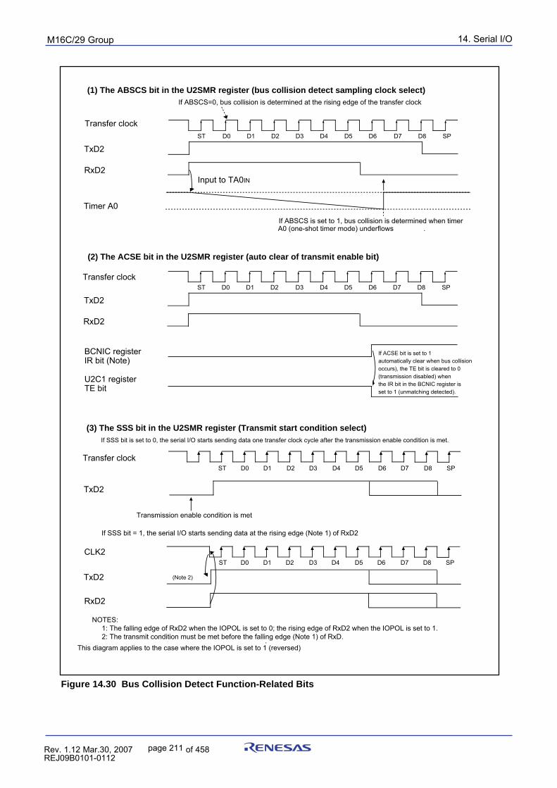
14. Serial I/OpuorG92/C61M
page 211 854fo7002,03.raM21.1.veR2110-1010B90JER
Figure 14.30 Bus Collision Detect Function-Related Bits
(2) The ACSE bit in the U2SMR register (auto clear of transmit enable bit)
(1) The ABSCS bit in the U2SMR register (bus collision detect sampling clock select)If ABSCS=0, bus collision is determined at the rising edge of the transfer clock
Transfer clock
Timer A0
(3) The SSS bit in the U2SMR register (Transmit start condition select)
Transmission enable condition is met
If SSS bit = 1, the serial I/O starts sending data at the rising edge (Note 1) of RxD2
TxD2
CLK2
TxD2
RxD2
TxD2
RxD2
ST D0 D1 D2 D3 D4 D5 D6 D7 D8 SP
Input to TA0IN
If ABSCS is set to 1, bus collision is determined when timer A0 (one-shot timer mode) underflows .
TxD2
RxD2
ST D0 D1 D2 D3 D4 D5 D6 D7 D8 SP
ST D0 D1 D2 D3 D4 D5 D6 D7 D8 SP
ST D0 D1 D2 D3 D4 D5 D6 D7 D8 SP
Transfer clock
BCNIC registerIR bit (Note)
U2C1 registerTE bit
If ACSE bit is set to 1 automatically clear when bus collision occurs), the TE bit is cleared to 0(transmission disabled) when the IR bit in the BCNIC register is set to 1 (unmatching detected).
If SSS bit is set to 0, the serial I/O starts sending data one transfer clock cycle after the transmission enable condition is met.
Transfer clock
(Note 2)
NOTES: 1: The falling edge of RxD2 when the IOPOL is set to 0; the rising edge of RxD2 when the IOPOL is set to 1. 2: The transmit condition must be met before the falling edge (Note 1) of RxD.
This diagram applies to the case where the IOPOL is set to 1 (reversed).
14. Serial I/OpuorG92/C61M
page 212 854fo7002,03.raM21.1.veR2110-1010B90JER
Item SpecificationTransfer data format • Direct format
• Inverse formatTransfer clock • The CKDIR bit in the U2MR register is set to 0 (internal clock) : fi/ (16(n+1))
fi = f1SIO, f2SIO, f8SIO, f32SIO. n: Setting value of U2BRG register 0016 to FF16
• The CKDIR bit is set to 1 (external clock ) : fEXT/16(n+1)fEXT: Input from CLK2 pin. n: Setting value of U2BRG register 0016 to FF16
Transmission start condition • Before transmission can start, the following requirements must be met_ The TE bit in the U2C1 register is set to 1 (transmission enabled)_ The TI bit in the U2C1 register is set to 0 (data present in U2TB register)
Reception start condition • Before reception can start, the following requirements must be met_ The RE bit in the U2C1 register is set to 1 (reception enabled)_ Start bit detection• For transmission
When the serial I/O finished sending data from the U2TB transfer register (U2IRS bit =1)• For reception
When transferring data from the UART2 receive register to the U2RB register (atcompletion of reception)
Error detection • Overrun error (1)
This error occurs if the serial I/O started receiving the next data before reading theU2RB register and received the bit one before the last stop bit in the the next data
• Framing errorThis error occurs when the number of stop bits set is not detected
• Parity errorDuring reception, if a parity error is detected, parity error signal is output from theTxD2 pin.During transmission, a parity error is detected by the level of input to the RXD2 pinwhen a transmission interrupt occurs
• Error sum flagThis flag is set to 1 when any of the overrun, framing, and parity errors is encountered
NOTES:1. If an overrun error occurs, bits 8 to 0 in the U2RB register are undefined. The IR bit in the S2RIC
register remains unchanged.2. A transmit interrupt request is generated by setting the U2IRS bit in the U2C1 register to 1 (trans-
mission complete) and U2ERE bit to 1 (error signal output) after reset. Therefore, when using SIMmode, be sure to clear the IR bit to 0 (no interrupt request) after setting these bits.
14.1.6 Special Mode 4 (SIM Mode) (UART2)Based on UART mode, this is an SIM interface compatible mode. Direct and inverse formats can beimplemented, and this mode allows output of a low from the TxD2 pin when a parity error is detected.Table 14.18 lists the specifications of SIM mode. Table 14.19 lists the registers used in the SIM modeand the register values set.
Table 14.18 SIM Mode Specifications
Interrupt requestgeneration timing (2)
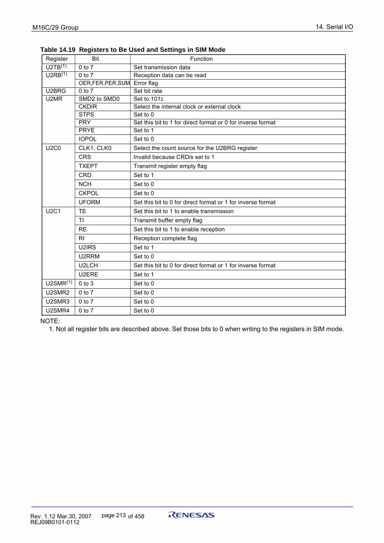
14. Serial I/OpuorG92/C61M
page 213 854fo7002,03.raM21.1.veR2110-1010B90JER
Table 14.19 Registers to Be Used and Settings in SIM ModeRegister Bit FunctionU2TB(1) 0 to 7 Set transmission dataU2RB(1) 0 to 7 Reception data can be read
OER,FER,PER,SUM Error flagU2BRG 0 to 7 Set bit rateU2MR SMD2 to SMD0 Set to 1012
CKDIR Select the internal clock or external clockSTPS Set to 0PRY Set this bit to 1 for direct format or 0 for inverse formatPRYE Set to 1IOPOL Set to 0
U2C0 CLK1, CLK0 Select the count source for the U2BRG registerCRS Invalid because CRDis set to 1TXEPT Transmit register empty flagCRD Set to 1NCH Set to 0CKPOL Set to 0UFORM Set this bit to 0 for direct format or 1 for inverse format
U2C1 TE Set this bit to 1 to enable transmissionTI Transmit buffer empty flagRE Set this bit to 1 to enable receptionRI Reception complete flagU2IRS Set to 1U2RRM Set to 0U2LCH Set this bit to 0 for direct format or 1 for inverse formatU2ERE Set to 1
U2SMR(1) 0 to 3 Set to 0U2SMR2 0 to 7 Set to 0U2SMR3 0 to 7 Set to 0U2SMR4 0 to 7 Set to 0
NOTE: 1. Not all register bits are described above. Set those bits to 0 when writing to the registers in SIM mode.
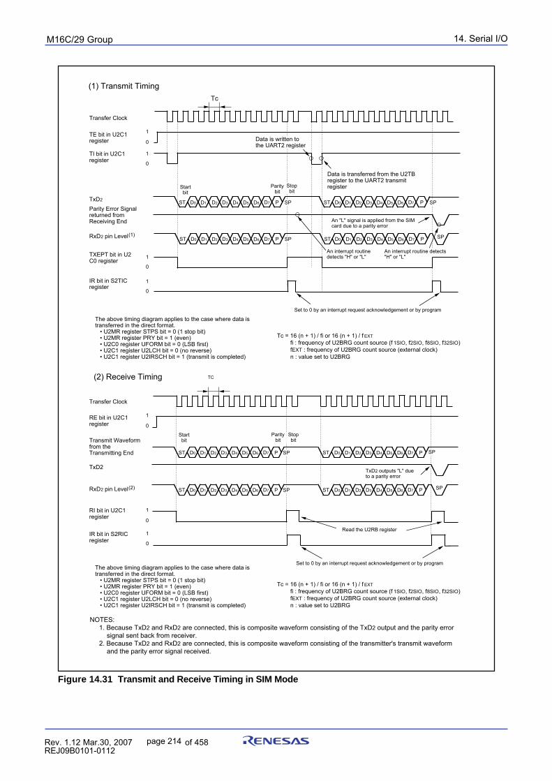
14. Serial I/OpuorG92/C61M
page 214 854fo7002,03.raM21.1.veR2110-1010B90JER
Figure 14.31 Transmit and Receive Timing in SIM Mode
D0 D1 D2 D3 D4 D5 D6 D7ST P D0 D1 D2 D3 D4 D5 D6 D7ST PSP
D0 D1 D2 D3 D4 D5 D6 D7ST P D0 D1 D2 D3 D4 D5 D6 D7ST PSP
D0 D1 D2 D3 D4 D5 D6 D7ST P D0 D1 D2 D3 D4 D5 D6 D7ST P SPSP
D0 D1 D2 D3 D4 D5 D6 D7ST P D0 D1 D2 D3 D4 D5 D6 D7ST P SPSP
Start bit
Parity bit
0
1
0
1
0
1
Set to 0 by an interrupt request acknowledgement or by program
Tc
Transfer Clock
Stop bit
Data is written to the UART2 register
An "L" signal is applied from the SIM card due to a parity error
An interrupt routine detects "H" or "L"
TxD2
0
1
Transfer Clock
Read the U2RB register
RxD2 pin Level(2)
TxD2
RxD2 pin Level(1)
Data is transferred from the U2TB register to the UART2 transmit register
RE bit in U2C1 register
RI bit in U2C1 register
IR bit in S2RIC register
TE bit in U2C1 register
TI bit in U2C1 register
TXEPT bit in U2C0 register
IR bit in S2TIC register
Start bit
Set to 0 by an interrupt request acknowledgement or by program
Stop bit
TxD2 outputs "L" due to a parity error
Parity bit
0
1
0
0
1
(1) Transmit Timing
(2) Receive Timing
Parity Error Signal returned from Receiving End
Transmit Waveformfrom the Transmitting End
1
SP
An interrupt routine detects "H" or "L"
SP
TC
The above timing diagram applies to the case where data is transferred in the direct format. • U2MR register STPS bit = 0 (1 stop bit) • U2MR register PRY bit = 1 (even) • U2C0 register UFORM bit = 0 (LSB first) • U2C1 register U2LCH bit = 0 (no reverse) • U2C1 register U2IRSCH bit = 1 (transmit is completed)
Tc = 16 (n + 1) / fi or 16 (n + 1) / f EXT fi : frequency of U2BRG count source (f 1SIO, f2SIO, f8SIO, f32SIO) fEXT : frequency of U2BRG count source (external clock) n : value set to U2BRG
NOTES:1. Because TxD2 and RxD2 are connected, this is composite waveform consisting of the TxD2 output and the parity error
signal sent back from receiver.2. Because TxD2 and RxD2 are connected, this is composite waveform consisting of the transmitter's transmit waveform
and the parity error signal received.
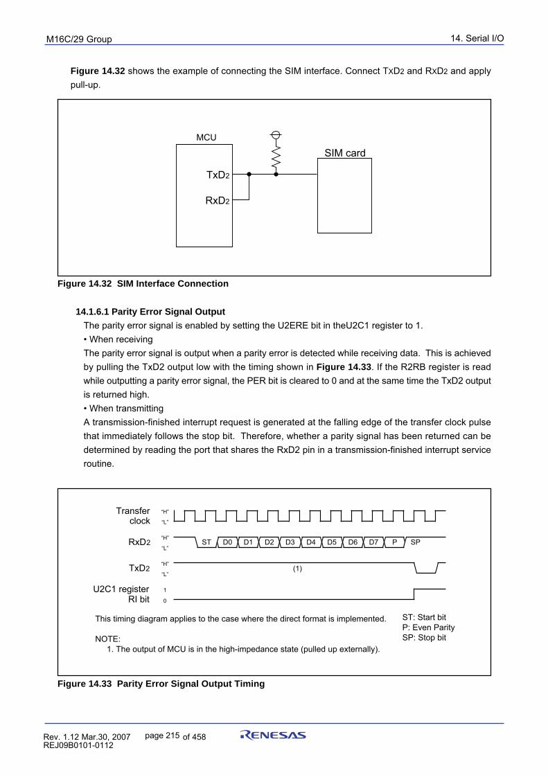
14. Serial I/OpuorG92/C61M
page 215 854fo7002,03.raM21.1.veR2110-1010B90JER
Figure 14.32 shows the example of connecting the SIM interface. Connect TXD2 and RXD2 and applypull-up.
Figure 14.32 SIM Interface Connection
14.1.6.1 Parity Error Signal Output
The parity error signal is enabled by setting the U2ERE bit in theU2C1 register to 1.• When receivingThe parity error signal is output when a parity error is detected while receiving data. This is achievedby pulling the TxD2 output low with the timing shown in Figure 14.33. If the R2RB register is readwhile outputting a parity error signal, the PER bit is cleared to 0 and at the same time the TxD2 outputis returned high.• When transmittingA transmission-finished interrupt request is generated at the falling edge of the transfer clock pulsethat immediately follows the stop bit. Therefore, whether a parity signal has been returned can bedetermined by reading the port that shares the RxD2 pin in a transmission-finished interrupt serviceroutine.
Figure 14.33 Parity Error Signal Output Timing
MCU
SIM card
TxD2
RxD2
D0 D1 D2 D3 D4 D5 D6 D7 P SPST
(1)
Transfer clock
RxD2
TxD2
U2C1 registerRI bit
“H”
“L”
“H”
“L”
“H”
“L”
1
0
This timing diagram applies to the case where the direct format is implemented.
NOTE: 1. The output of MCU is in the high-impedance state (pulled up externally).
ST: Start bitP: Even ParitySP: Stop bit
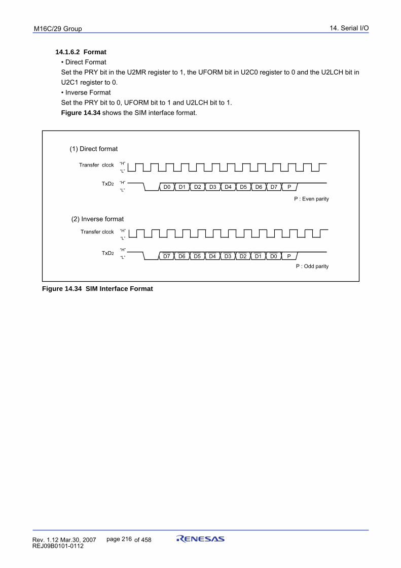
14. Serial I/OpuorG92/C61M
page 216 854fo7002,03.raM21.1.veR2110-1010B90JER
14.1.6.2 Format
• Direct FormatSet the PRY bit in the U2MR register to 1, the UFORM bit in U2C0 register to 0 and the U2LCH bit inU2C1 register to 0.• Inverse FormatSet the PRY bit to 0, UFORM bit to 1 and U2LCH bit to 1.Figure 14.34 shows the SIM interface format.
Figure 14.34 SIM Interface Format
P : Even parity
D0 D1 D2 D3 D4 D5 D6 D7 P
Transfer clcck
TxD2
TxD2 D7 D6 D5 D4 D3 D2 D1 D0 P
Transfer clcck
(1) Direct format
“H”
“L”
“H”
“L”
(2) Inverse format
P : Odd parity
“H”
“L”
“H”
“L”
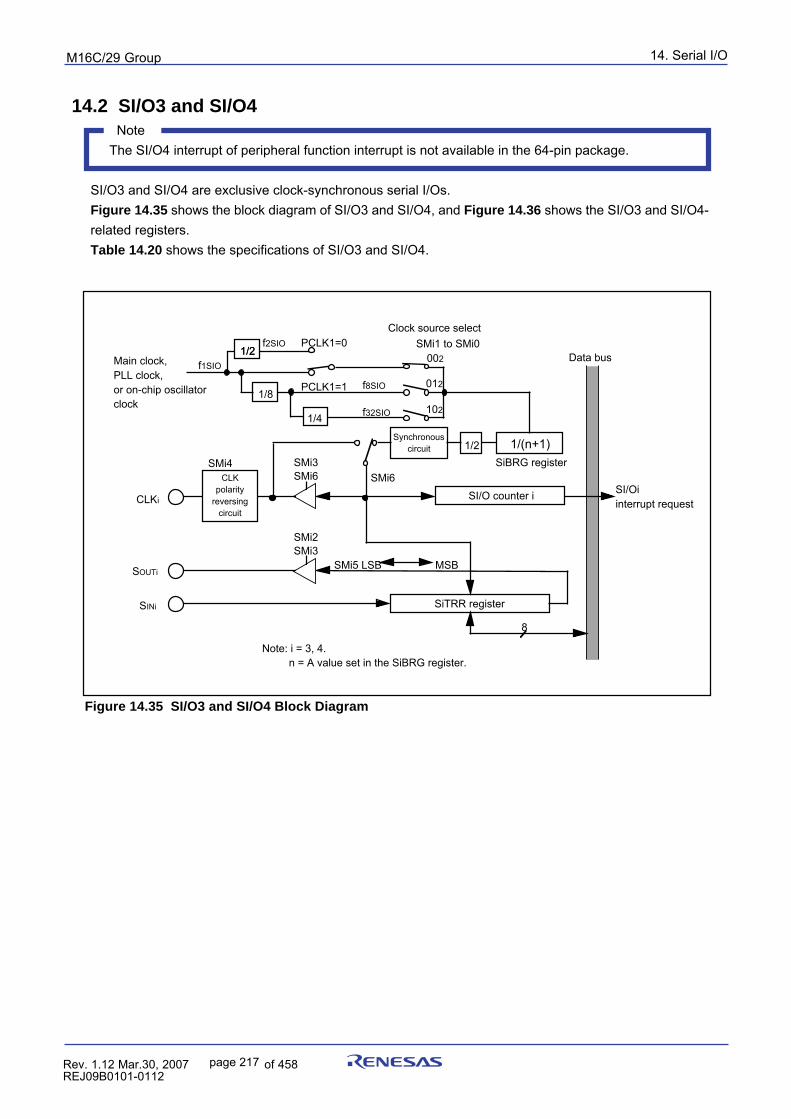
14. Serial I/OpuorG92/C61M
page 217 854fo7002,03.raM21.1.veR2110-1010B90JER
14.2 SI/O3 and SI/O4 NoteThe SI/O4 interrupt of peripheral function interrupt is not available in the 64-pin package.
SI/O3 and SI/O4 are exclusive clock-synchronous serial I/Os.Figure 14.35 shows the block diagram of SI/O3 and SI/O4, and Figure 14.36 shows the SI/O3 and SI/O4-related registers.Table 14.20 shows the specifications of SI/O3 and SI/O4.
Figure 14.35 SI/O3 and SI/O4 Block Diagram
Data bus
SI/Oi interrupt request
Note: i = 3, 4. n = A value set in the SiBRG register.
SiTRR register
SI/O counter i
8
SMi5 LSB MSB
SMi2SMi3
SMi3SMi6
SMi1 to SMi0
CLKi
SOUTi
SINi
SiBRG registerSMi6
1/(n+1)1/2
1/2Main clock,PLL clock, or on-chip oscillator clock
f1SIO1/2
1/8
1/4
f8SIO
f32SIO
f2SIO PCLK1=0
PCLK1=1
SMi4
002
012
102
Clock source select
Synchronous circuit
CLK polarity
reversing circuit
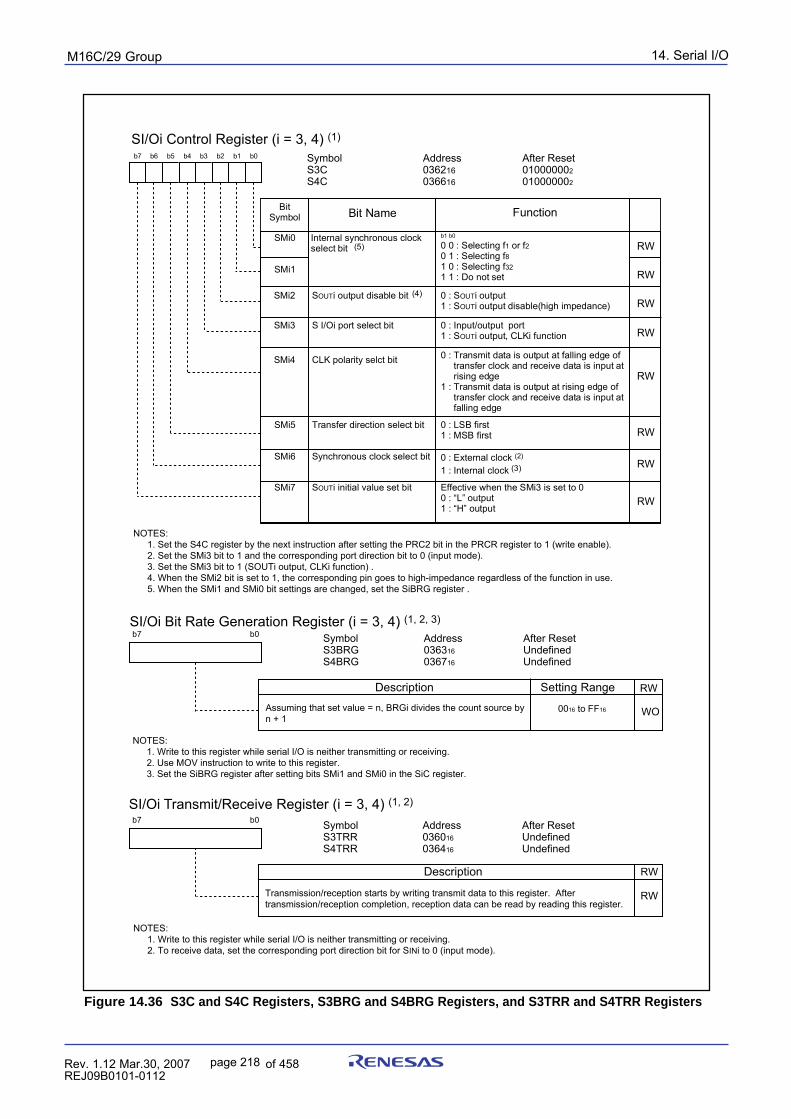
14. Serial I/OpuorG92/C61M
page 218 854fo7002,03.raM21.1.veR2110-1010B90JER
Figure 14.36 S3C and S4C Registers, S3BRG and S4BRG Registers, and S3TRR and S4TRR Registers
b7 b0 Symbol Address After ResetS3BRG 036316 UndefinedS4BRG 036716 Undefined
0
01
6
t
o
F
F1
6
b
7 b
0 Symbol Address After ResetS3TRR 036016 UndefinedS4TRR 036416 Undefined
S
y
m
b
o
l A
d
d
r
e
s
s A
f
t
e
r
R
e
s
e
t
S
3
C 0
3
6
21
6 0
1
0
0
0
0
0
02
S
4
C 0
3
6
61
6 0
1
0
0
0
0
0
02
b 7 b
6 b
5 b
4 b
3 b
2 b
1 b
0
RWFunction
SMi5
S
M
i
1
SMi0
S
M
i
3
SMi6
S
M
i
7
Internal synchronous clock select bit
Transfer direction select bit
S
I
/
O
i
p
o
r
t
s
e
l
e
c
t
b
i
t
SO
U
Ti
i
n
i
t
i
a
l
v
a
l
u
e
s
e
t
b
i
t
0 0 : Selecting f1 or f20 1 : Selecting f81 0 : Selecting f321 1 : Do not set
b1 b0
0 : External clock (2)
1 : Internal clock (3)
Effective when the SMi3 is set to 00 : “L” output1 : “H” output
0 : Input/output port1 : SOUTi output, CLKi function
Bit NameB
i
tS
y
m
b
o
l
Synchronous clock select bit
0 : LSB first1 : MSB first
S
M
i
2 SO
U
Ti
o
u
t
p
u
t
d
i
s
a
b
l
e
b
i
t 0 : SOUTi output1 : SOUTi output disable(high impedance)
S
M
i
4 C
L
K
p
o
l
a
r
i
t
y
s
e
l
c
t
b
i
t 0 : Transmit data is output at falling edge of transfer clock and receive data is input at rising edge
1 : Transmit data is output at rising edge of transfer clock and receive data is input at falling edge
RW
RW
RW
RW
RW
RW
RW
RW
RW
RW
RW
W
O
( 4
)
(5)
NOTES: 1. Set the S4C register by the next instruction after setting the PRC2 bit in the PRCR register to 1 (write enable). 2. Set the SMi3 bit to 1 and the corresponding port direction bit to 0 (input mode). 3. Set the SMi3 bit to 1 (SOUTi output, CLKi function) . 4. When the SMi2 bit is set to 1, the corresponding pin goes to high-impedance regardless of the function in use. 5. When the SMi1 and SMi0 bit settings are changed, set the SiBRG register .
NOTES:1. Write to this register while serial I/O is neither transmitting or receiving.2. To receive data, set the corresponding port direction bit for SINi to 0 (input mode).
NOTES:1. Write to this register while serial I/O is neither transmitting or receiving.2. Use MOV instruction to write to this register.3. Set the SiBRG register after setting bits SMi1 and SMi0 in the SiC register.
Transmission/reception starts by writing transmit data to this register. After transmission/reception completion, reception data can be read by reading this register.
Assuming that set value = n, BRGi divides the count source by n + 1
Setting RangeDescription
Description
SI/Oi Control Register (i = 3, 4) (1)
SI/Oi Bit Rate Generation Register (i = 3, 4) (1, 2, 3)
SI/Oi Transmit/Receive Register (i = 3, 4) (1, 2)
14. Serial I/OpuorG92/C61M
page 219 854fo7002,03.raM21.1.veR2110-1010B90JER
Item SpecificationTransfer data format • Transfer data length: 8 bitsTransfer clock • The SMi6 bit in the SiC (i=3, 4) register is set to 1 (internal clock) : fj/ (2(n+1))
fj = f1SIO, f2SIO, f8SIO, f32SIO. n=Setting value of SiBRG register 0016 to FF16.• SMi6 bit is set to 0 (external clock) : Input from CLKi pin (1)
Transmission/reception • Before transmission/reception can start, the following requirements must be metstart condition Write transmit data to the SiTRR register (2, 3)
• When the SMi4 bit in the SiC register is set to 0The rising edge of the last transfer clock pulse (4)
• When SMi4 is set to 1The falling edge of the last transfer clock pulse (4)
CLKi pin fucntion I/O port, transfer clock input, transfer clock outputSOUTi pin function I/O port, transmit data output, high-impedanceSINi pin function I/O port, receive data inputSelect function • LSB first or MSB first selection
Whether to start sending/receiving data beginning with bit 0 or beginning with bit 7can be selected
• Function for setting an SOUTi initial value set functionWhen the SMi6 bit in the SiC register is set to 0 (external clock), the SOUTi pinoutput level while not tranmitting can be selected.
• CLK polarity selectionWhether transmit data is output/input timing at the rising edge or falling edge oftransfer clock can be selected.
NOTE:1. To set the SMi6 bit in the SiC register to 0 (external clock), follow the procedure described below.
• If the SMi4 bit in the SiC register is set to 0, write transmit data to the SiTRR register while input on the CLKipin is high. The same applies when rewriting the SMi7 bit in the SiC register.
• If the SMi4 bit is set to 1, write transmit data to the SiTRR register while input on the CLKi pin is low. The sameapplies when rewriting the SMi7 bit.
• Because shift operation continues as long as the transfer clock is supplied to the SI/Oi circuit, stop the transferclock 2. Unlike UART0 to UART2, SI/Oi (i = 3 to 4) is not separated between the transfer register and buffer.Therefore, do not write the next transmit data to the SiTRR register during transmission.
3. When the SMi6 bit in the SiC register is set to 1 (internal clock), SOUTi retains the last data for a 1/2 transferclock period after completion of transfer and, thereafter, goes to a high-impedance state. However, if transmitdata is written to the SiTRR register during this period, SOUTi immediately goes to a high-impedance state, withthe data hold time thereby reduced.
4. When the SMi6 bit in the SiC register is set to 1 (internal clock), the transfer clock stops in the high state if theSMi4 bit is set to 0, or stops in the low state if the SMi4 bit is set to 1.
Table 14.20 SI/O3 and SI/O4 Specifications
Interrupt requestgeneration timing
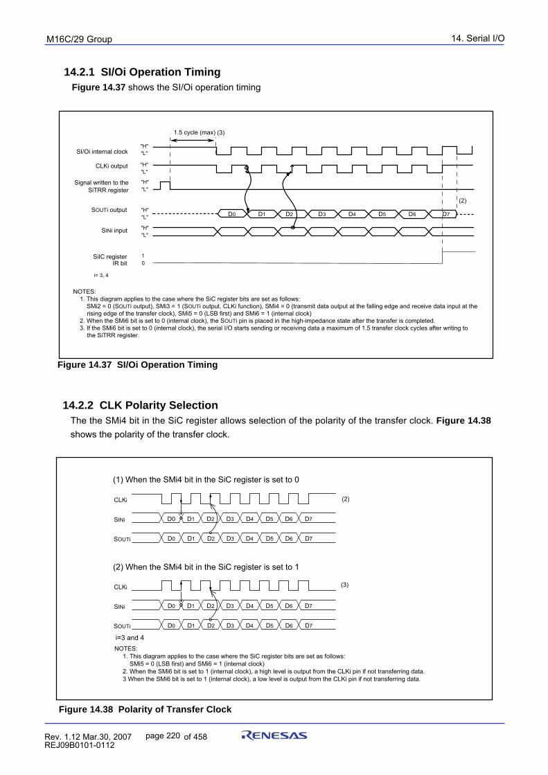
14. Serial I/OpuorG92/C61M
page 220 854fo7002,03.raM21.1.veR2110-1010B90JER
14.2.1 SI/Oi Operation TimingFigure 14.37 shows the SI/Oi operation timing
Figure 14.37 SI/Oi Operation Timing
14.2.2 CLK Polarity SelectionThe the SMi4 bit in the SiC register allows selection of the polarity of the transfer clock. Figure 14.38
shows the polarity of the transfer clock.
Figure 14.38 Polarity of Transfer Clock
D7D0 D1 D2 D3 D4 D5 D6
i= 3, 4
1.5 cycle (max)
SI/Oi internal clock
CLKi output
Signal written to the SiTRR register
SOUTi output
SINi input
SiIC registerIR bit
(2)
"H""L"
"H""L"
"H""L"
"H""L"
"H""L"
10
(3)
NOTES: 1. This diagram applies to the case where the SiC register bits are set as follows: SMi2 = 0 (SOUTi output), SMi3 = 1 (SOUTi output, CLKi function), SMi4 = 0 (transmit data output at the falling edge and receive data input at the
rising edge of the transfer clock), SMi5 = 0 (LSB first) and SMi6 = 1 (internal clock) 2. When the SMi6 bit is set to 0 (internal clock), the SOUTi pin is placed in the high-impedance state after the transfer is completed. 3. If the SMi6 bit is set to 0 (internal clock), the serial I/O starts sending or receiving data a maximum of 1.5 transfer clock cycles after writing to
the SiTRR register.
(2) When the SMi4 bit in the SiC register is set to 1
(3)
D1 D2 D3 D4 D5 D6 D7
D1 D2 D3 D4 D5 D6 D7
D0
D0
SINi
SOUTi
CLKi
(1) When the SMi4 bit in the SiC register is set to 0
D1 D2 D3 D4 D5 D6 D7D0
D1 D2 D3 D4 D5 D6 D7D0
SINi
SOUTi
CLKi (2)
i=3 and 4NOTES:
1. This diagram applies to the case where the SiC register bits are set as follows: SMi5 = 0 (LSB first) and SMi6 = 1 (internal clock) 2. When the SMi6 bit is set to 1 (internal clock), a high level is output from the CLKi pin if not transferring data. 3 When the SMi6 bit is set to 1 (internal clock), a low level is output from the CLKi pin if not transferring data.
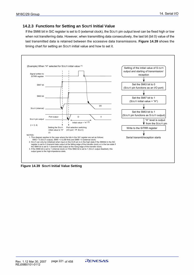
14. Serial I/OpuorG92/C61M
page 221 854fo7002,03.raM21.1.veR2110-1010B90JER
14.2.3 Functions for Setting an SOUTi Initial ValueIf the SMi6 bit in SiC register is set to 0 (external clock), the SOUTi pin output level can be fixed high or lowwhen not transferring data. However, when transmitting data consecutively, the last bit (bit 0) value of thelast transmitted data is retained between the sccessive data transmissions. Figure 14.39 shows thetiming chart for setting an SOUTi initial value and how to set it.
Figure 14.39 SOUTi Initial Value Setting
S
i
g
n
a
l
w
r
i
t
t
e
n
t
o
S
i
T
R
R
r
e
g
i
s
t
e
r
SO
U
Ti
(
i
n
t
e
r
n
a
l
)
S
M
i
7
b
i
t
SOUTi pin output
S
M
i
3
b
i
t
S
e
t
t
i
n
g
t
h
e
SO
U
Ti
i
n
i
t
i
a
l
v
a
l
u
e
t
o
“
H
”Port selection switching(I/O port SOUTi)
D
0
( i
=
3
,
4
)
I n
i
t
i
a
l
v
a
l
u
e
=
“
H
”
(
3
)
Port output D 0
( E
x
a
m
p
l
e
)
W
h
e
n
“
H
”
s
e
l
e
c
t
e
d
f
o
r
SO
U
Ti
i
n
i
t
i
a
l
v
a
l
u
e
(
1
)
( 2
)
NOTES: 1. This diagram applies to the case where the bits in the SiC register are set as follows: SMi2 = 0 (SOUTi output), SMi5 = 0 (LSB first) and SMi6 = 0 (external clock) 2. SOUTi can only be initialized when input on the CLKi pin is in the high state if the SMi4bit in the SiC
register is set to 0 (transmit data output at the falling edge of the transfer clock) or in the low state if the SMi4 bit is set to 1 (transmit data output at the rising edge of the transfer clock).
3. If the SMi6 bit is set to 1 (internal clock) or if the SMi2 bit is set to 1 (SOUTi output disabled), this output goes to the high-impedance state.
Setting of the initial value of S OUTi output and starting of transmission/
reception
Set the SMi3 bit to 0 (SOUTi pin functions as an I/O port)
Write to the SiTRR register
Serial transmit/reception starts
Set the SMi7 bit to 1 (SOUTi initial value = “H”)
Set the SMi3 bit to 1 (SOUTi pin functions as S OUTi output)
“H” level is output from the SOUTi pin
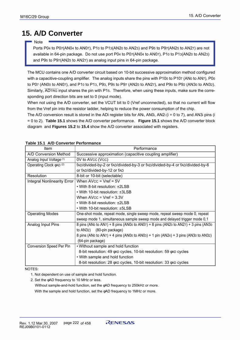
15. A/D ConverterpuorG92/C61M
page 222 854fo7002,03.raM21.1.veR2110-1010B90JER
15. A/D Converter Note
Ports P04 to P07(AN04 to AN07), P10 to P13(AN20 to AN23) and P95 to P97(AN25 to AN27) are notavailable in 64-pin package. Do not use port P04 to P07(AN04 to AN07), P10 to P13(AN20 to AN23)and P95 to P97(AN25 to AN27) as analog input pins in 64-pin package.
The MCU contains one A/D converter circuit based on 10-bit successive approximation method configuredwith a capacitive-coupling amplifier. The analog inputs share the pins with P100 to P107 (AN0 to AN7), P00
to P07 (AN00 to AN07), and P10 to P13, P93, P95 to P97 (AN20 to AN27), and P90 to P92 (AN30 to AN32).____________
Similarly, ADTRG input shares the pin with P15. Therefore, when using these inputs, make sure the corre-sponding port direction bits are set to 0 (input mode).When not using the A/D converter, set the VCUT bit to 0 (Vref unconnected), so that no current will flowfrom the Vref pin into the resistor ladder, helping to reduce the power consumption of the chip.The A/D conversion result is stored in the ADi register bits for ANi, AN0i, AN2i (i = 0 to 7), and AN3i pins (i= 0 to 2). Table 15.1 shows the A/D converter performance. Figure 15.1 shows the A/D converter blockdiagram and Figures 15.2 to 15.4 show the A/D converter associated with registers.
Item PerformanceA/D Conversion Method Successive approximation (capacitive coupling amplifier)Analog Input Voltage (1) 0V to AVCC (VCC)Operating Clock φAD (2) fAD/divided-by-2 or fAD/divided-by-3 or fAD/divided-by-4 or fAD/divided-by-6
or fAD/divided-by-12 or fAD
Resolution 8-bit or 10-bit (selectable)Integral Nonlinearity Error When AVCC = Vref = 5V
• With 8-bit resolution: ±2LSB• With 10-bit resolution: ±3LSBWhen AVCC = Vref = 3.3V• With 8-bit resolution: ±2LSB• With 10-bit resolution: ±5LSB
Operating Modes One-shot mode, repeat mode, single sweep mode, repeat sweep mode 0, repeatsweep mode 1, simultaneous sample sweep mode and delayed trigger mode 0,1
Analog Input Pins 8 pins (AN0 to AN7) + 8 pins (AN00 to AN07) + 8 pins (AN20 to AN27) + 3 pins (AN30
to AN32) (80-pin package)8 pins (AN0 to AN7) + 4 pins (AN00 to AN03) + 1 pin (AN24) + 3 pins (AN30 to AN32) (64-pin package)
Conversion Speed Per Pin • Without sample and hold function8-bit resolution: 49 φAD cycles, 10-bit resolution: 59 φAD cycles
• With sample and hold function8-bit resolution: 28 φAD cycles, 10-bit resolution: 33 φAD cycles
Table 15.1 A/D Converter Performance
NOTES:1. Not dependent on use of sample and hold function.2. Set the φAD frequency to 10 MHz or less.
Without sample-and-hold function, set the φAD frequency to 250kHZ or more. With the sample and hold function, set the φAD frequency to 1MHZ or more.
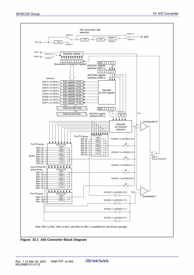
15. A/D ConverterpuorG92/C61M
page 223 854fo7002,03.raM21.1.veR2110-1010B90JER
Figure 15.1 A/D Converter Block Diagram
=0002
=0012=0102
=0112=1002
=1012=1102
=1112
AN0AN1AN2AN3AN4AN5AN6AN7
AN00AN01AN02AN03AN04AN05AN06AN07
Vref
VIN
CH2 to CH0
Decoderfor channel selection
A/D register 0(16)
Data bus low-order
VREF
AVSSVCUT=0
VCUT=1
Data bus high-order
Port P10 group
ADGSEL1 to ADGSEL0=102
ADGSEL1 to ADGSEL0=002
ADGSEL1 to ADGSEL0=112
fAD
CKS0=1
CKS0=0
CKS1=1
CKS1=01/3
CKS2=0
CKS2=1
1/21/2øAD
A/D conversion rate selection
(03C116 to 03C016)(03C316 to 03C216)(03C516 to 03C416)(03C716 to 03C616)(03C916 to 03C816)(03CB16 to 03CA16)(03CD16 to 03CC16)(03CF16 to 03CE16)
Resistor ladder
Successive conversion register
ADCON0 register (address 03D616)
ADCON1 register (address 03D716)
Comparator 0
Addresses
Decoder for A/D register
A/D register 1(16)A/D register 2(16)A/D register 3(16)A/D register 4(16)A/D register 5(16)A/D register 6(16)A/D register 7(16)
ADCON2 register (address 03D416)
Port P0 group=0002
=0012=0102
=0112=1002
=1012=1102
=1112
CH2 to CH0
SSE = 1CH2 to CH0=0012
Comparator 1
ADGSEL1 to ADGSEL0=002
ADGSEL1 to ADGSEL0=102
ADGSEL1 to ADGSEL0=112
VIN1
Port P1/Port P9 group
AN20AN21AN22AN23AN24AN25AN26AN27
=0002
=0012=0102
=0112=1002
=1012=1102
=1112
CH2 to CH0(Note)
Note: AN04 to AN07, AN20 to AN23, and AN25 to AN27, is available for only 80-pin package.
(Note)
Port P9 group
AN30AN31AN32
=0002
=0012=0102
CH2 to CH0
ADGSEL1 to ADGSEL0=012
ADGSEL1 to ADGSEL0=012
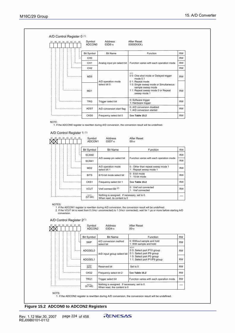
15. A/D ConverterpuorG92/C61M
page 224 854fo7002,03.raM21.1.veR2110-1010B90JER
Figure 15.2 ADCON0 to ADCON2 Registers
A/D Control Register 0 (1)
Symbol Address After Reset ADCON0 03D616 00000XXX2
b7 b6 b5 b4 b3 b2 b1 b0
Analog input pin select bit
CH0
Bit Symbol Bit Name Function
CH1
CH2
A/D operation mode select bit 0
MD0
MD1
Trigger select bit 0: Software trigger1: Hardware triggerTRG
ADST A/D conversion start flag 0: A/D conversion disabled1: A/D conversion started
Frequency select bit 0 See Table 15.2 CKS0
RW
NOTE: 1. If the ADCON0 register is rewritten during A/D conversion, the conversion result will be undefined.
RW
RW
RW
RW
RW
RW
RW
RW
Function varies with each operation mode
b4 b3
0 0: One-shot mode or Delayed trigger mode 0,1
0 1: Repeat mode1 0: Single sweep mode or Simultaneous
sample sweep mode 1 1: Repeat sweep mode 0 or Repeat
sweep mode 1
A/D Control Register 1 (1)
Symbol Address After Reset ADCON1 03D716 0016
Bit Name FunctionBit Symbol
b7 b6 b5 b4 b3 b2 b1 b0
A/D sweep pin select bitSCAN0
SCAN1
MD2
BITS 8/10-bit mode select bit 0 : 8-bit mode1 : 10-bit mode
VCUT
A/D operation mode select bit 1
0 : Other than repeat sweep mode 11 : Repeat sweep mode 1
0 : Vref not connected1 : Vref connected
Frequency select bit 1CKS1
RW
RW
RW
RW
RW
RW
RW
Function varies with each operation mode
See Table 15.2
Nothing is assigned. If necessary, set to 0.When read, its content is 0(b7-b6)
NOTES: 1. If the ADCON1 register is rewritten during A/D conversion, the conversion result will be undefined. 2. If the VCUT bit is reset from 0 (VREF unconnected) to 1 (VREF connected), wait for 1 µs or more before starting A/D
conversion.
Vref connect Bit (2)
0
A/D Control Register 2(1) Symbol Address After Reset ADCON2 03D416 0016
Bit Name FunctionBit Symbol
b7 b6 b5 b4 b3 b2 b1 b0
A/D conversion method select bit
SMP
Reserved bit Set to 0
TRG1
A/D input group select bit
b2 b1
0 0: Select port P10 group 0 1: Select port P9 group1 0: Select port P0 group1 1: Select port P1/P9 group
Function varies with each operation mode
Frequency select bit 2CKS2
RW
RW
RW
RW
RW
RW
RW
0: Without sample and hold1: With sample and hold
See Table 15.2
Nothing is assigned. If necessary, set to 0.When read, the content is 0(b7-b6)
NOTS: 1. If the ADCON2 register is rewritten during A/D conversion, the conversion result will be undefined.
Trigger select bit
ADGSEL0
ADGSEL1
(b3)
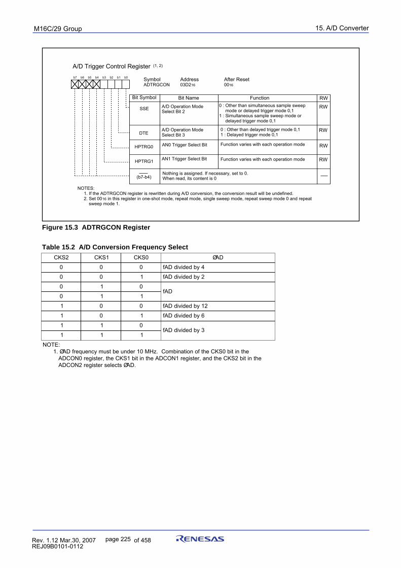
15. A/D ConverterpuorG92/C61M
page 225 854fo7002,03.raM21.1.veR2110-1010B90JER
Figure 15.3 ADTRGCON Register
Table 15.2 A/D Conversion Frequency Select2SKC 1SKC 0SKC DAØ
0 0 0 4ybdedividDAf
0 0 1 2ybdedividDAf
0 1 0DAf
0 1 1
1 0 0 21ybdedividDAf
1 0 1 6ybdedividDAf
1 1 03ybdedividDAf
1 1 1
:ETON.1 Ø ehtnitib0SKCehtfonoitanibmoC.zHM01rednuebtsumycneuqerfDA
ehtnitib2SKCehtdna,retsiger1NOCDAehtnitib1SKCeht,retsiger0NOCDAstcelesretsiger2NOCDA .DAØ
A/D Trigger Control Register (1, 2)
Symbol Address After ResetADTRGCON 03D216 0016
b7 b6 b5 b4 b3 b2 b1 b0
A/D Operation Mode Select Bit 2
0 : Other than simultaneous sample sweep mode or delayed trigger mode 0,11 : Simultaneous sample sweep mode or delayed trigger mode 0,1
Bit Symbol Bit Name Function RW
SSE
A/D Operation Mode Select Bit 3
HPTRG1
DTE
HPTRG0
RW
RW
RW
RW
Nothing is assigned. If necessary, set to 0.When read, its content is 0(b7-b4)
0 : Other than delayed trigger mode 0,11 : Delayed trigger mode 0,1
NOTES: 1. If the ADTRGCON register is rewritten during A/D conversion, the conversion result will be undefined. 2. Set 0016 in this register in one-shot mode, repeat mode, single sweep mode, repeat sweep mode 0 and repeat sweep mode 1.
AN1 Trigger Select Bit
AN0 Trigger Select Bit Function varies with each operation mode
Function varies with each operation mode
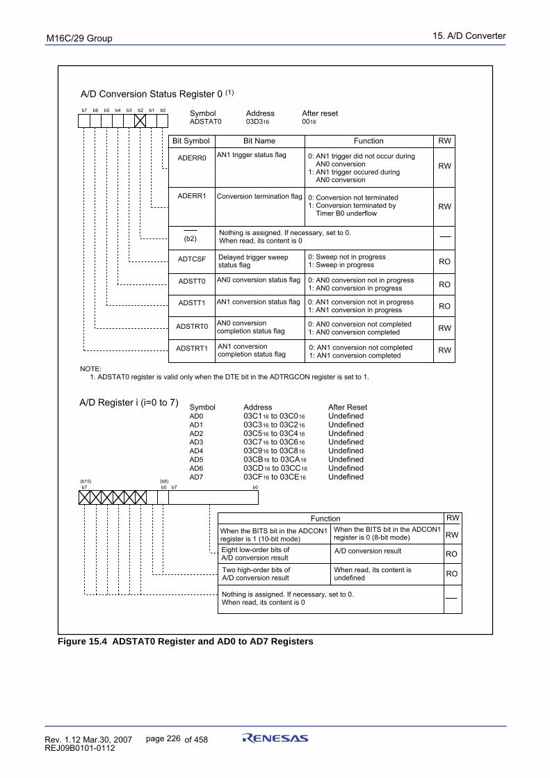
15. A/D ConverterpuorG92/C61M
page 226 854fo7002,03.raM21.1.veR2110-1010B90JER
Figure 15.4 ADSTAT0 Register and AD0 to AD7 Registers
A/D Register i (i=0 to 7) Symbol Address After ResetAD0 03C116 to 03C016 UndefinedAD1 03C316 to 03C216 Undefined AD2 03C516 to 03C416 Undefined AD3 03C716 to 03C616 Undefined AD4 03C916 to 03C816 Undefined AD5 03CB16 to 03CA16 Undefined AD6 03CD16 to 03CC16 Undefined AD7 03CF16 to 03CE16 Undefined
Eight low-order bits of A/D conversion result
Function
(b15)b7b7 b0 b0
(b8)
When the BITS bit in the ADCON1 register is 1 (10-bit mode)
Nothing is assigned. If necessary, set to 0.When read, its content is 0
When read, its content is undefined
RW
RO
ROTwo high-order bits of A/D conversion result
When the BITS bit in the ADCON1register is 0 (8-bit mode)
A/D conversion result
A/D Conversion Status Register 0 (1)
Symbol Address After resetADSTAT0 03D316 0016
b7 b6 b5 b4 b3 b2 b1 b0
AN1 trigger status flag 0: AN1 trigger did not occur during AN0 conversion1: AN1 trigger occured during AN0 conversion
Bit Symbol Bit Name Function RW
ADERR0
Conversion termination flag
AN0 conversion status flagADSTT0
ADERR1
ADTCSF
RW
RO
RW
RO
RO
Nothing is assigned. If necessary, set to 0.When read, its content is 0(b2)
ADSTRT0 AN0 conversion completion status flag
0: Conversion not terminated1: Conversion terminated by Timer B0 underflow
Delayed trigger sweep status flag
0: Sweep not in progress1: Sweep in progress
0: AN0 conversion not in progress1: AN0 conversion in progress
ADSTT1
RW0: AN0 conversion not completed1: AN0 conversion completed
ADSTRT1 RW
AN1 conversion status flag 0: AN1 conversion not in progress1: AN1 conversion in progress
AN1 conversion completion status flag
0: AN1 conversion not completed1: AN1 conversion completed
NOTE: 1. ADSTAT0 register is valid only when the DTE bit in the ADTRGCON register is set to 1.
RW
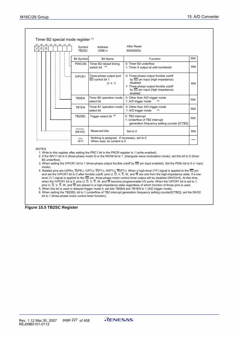
15. A/D ConverterpuorG92/C61M
page 227 854fo7002,03.raM21.1.veR2110-1010B90JER
Figure 15.5 TB2SC Register
PWCON
Symbol AddressTB2SC 039E16 X00000002
Timer B2 reload timing switch bit
0: Timer B2 underflow1: Timer A output at odd-numbered
Timer B2 special mode register (1)
Bit Name FunctionBit Symbol
b7 b6 b5 b4 b3 b2 b1 b0
IVPCR1 Three-phase output port SD control bit 1
0: Three-phase output forcible cutoff by SD pin input (high impedance) disabled1: Three-phase output forcible cutoff by SD pin input (high impedance) enabled
RW
RW
RW
Nothing is assigned. If necessary, set to 0.When read, its content is 0(b7)
TB2SEL Trigger select bit 0: TB2 interrupt1: Underflow of TB2 interrupt generation frequency setting counter [ICTB2]
RW
RW
TB0EN Timer B0 operation modeselect bit
0: Other than A/D trigger mode1: A/D trigger mode RW
TB1EN Timer B1 operation modeselect bit
0: Other than A/D trigger mode1: A/D trigger mode RW
(2)
(3, 4, 7)
(5)
(5)
(6)
(b6-b5) Reserved bits Set to 0
0 0After Reset
NOTES:1. Write to this register after setting the PRC1 bit in the PRCR register to 1 (write enabled).2. If the INV11 bit is 0 (three-phase mode 0) or the INV06 bit is 1 (triangular wave modulation mode), set this bit to 0 (timer
B2 underflow). 3. When setting the IVPCR1 bit to 1 (three-phase output forcible cutoff by SD pin input enabled), Set the PD85 bit to 0 (= input
mode).4. Related pins are U(P80), U(P81), V(P72), V(P73), W(P74), W(P75). When a high-level ("H") signal is applied to the SD pin
and set the IVPCR1 bit to 0 after forcible cutoff, pins U, U, V, V, W, and W are exit from the high-impedance state. If a low-level (“L”) signal is applied to the SD pin, three-phase motor control timer output will be disabled (INV03=0). At this time, when the IVPCR1 bit is 0, pins U, U, V, V, W, and W become programmable I/O ports. When the IVPCR1 bit is set to 1, pins U, U, V, V, W, and W are placed in a high-impedance state regardless of which function of those pins is used.
5. When this bit is used in delayed trigger mode 0, set bits TB0EN and TB1EN to 1 (A/D trigger mode).6. When setting the TB2SEL bit to 1 (underflow of TB2 interrupt generation frequency setting counter[ICTB2]), set the INV02
bit to 1 (three-phase motor control timer function).
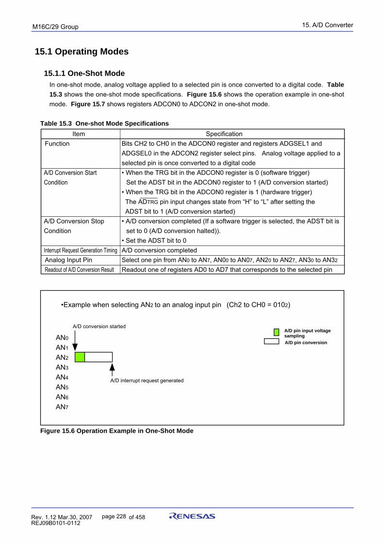
15. A/D ConverterpuorG92/C61M
page 228 854fo7002,03.raM21.1.veR2110-1010B90JER
15.1 Operating Modes
15.1.1 One-Shot ModeIn one-shot mode, analog voltage applied to a selected pin is once converted to a digital code. Table
15.3 shows the one-shot mode specifications. Figure 15.6 shows the operation example in one-shotmode. Figure 15.7 shows registers ADCON0 to ADCON2 in one-shot mode.
Table 15.3 One-shot Mode Specifications
Item SpecificationFunction Bits CH2 to CH0 in the ADCON0 register and registers ADGSEL1 and
ADGSEL0 in the ADCON2 register select pins. Analog voltage applied to aselected pin is once converted to a digital code
A/D Conversion Start • When the TRG bit in the ADCON0 register is 0 (software trigger)Condition Set the ADST bit in the ADCON0 register to 1 (A/D conversion started)
• When the TRG bit in the ADCON0 register is 1 (hardware trigger) The ADTRG pin input changes state from “H” to “L” after setting the ADST bit to 1 (A/D conversion started)
A/D Conversion Stop • A/D conversion completed (If a software trigger is selected, the ADST bit isCondition set to 0 (A/D conversion halted)).
• Set the ADST bit to 0Interrupt Request Generation Timing A/D conversion completedAnalog Input Pin Select one pin from AN0 to AN7, AN00 to AN07, AN20 to AN27, AN30 to AN32
Readout of A/D Conversion Result Readout one of registers AD0 to AD7 that corresponds to the selected pin
Figure 15.6 Operation Example in One-Shot Mode
•Example when selecting AN2 to an analog input pin (Ch2 to CH0 = 0102)
AN0
AN1
AN2
AN3
AN4
AN5
AN6
AN7
A/D conversion started
A/D interrupt request generated
A/D pin input voltage samplingA/D pin conversion
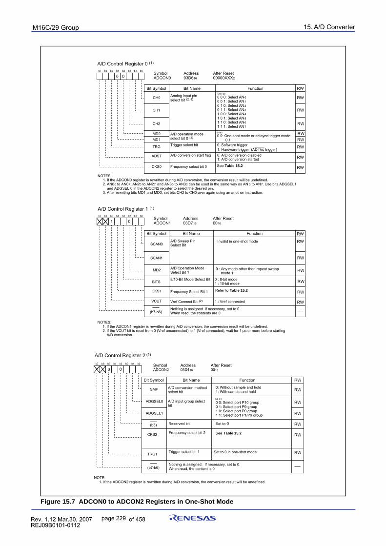
15. A/D ConverterpuorG92/C61M
page 229 854fo7002,03.raM21.1.veR2110-1010B90JER
Figure 15.7 ADCON0 to ADCON2 Registers in One-Shot Mode
A/D Control Register 0 (1)
Symbol Address After ResetADCON0 03D616 00000XXX2
b7 b6 b5 b4 b3 b2 b1 b0
Analog input pin select bit (2, 3)CH0
Bit Symbol Bit Name Function
CH1
CH2
A/D operation mode select bit 0 (3)
MD0MD1
Trigger select bitTRG
ADST A/D conversion start flag 0: A/D conversion disabled1: A/D conversion started
Frequency select bit 0CKS0
RW
A/D Control Register 1 (1)
Symbol Address After ResetADCON1 03D716 0016
Bit Name FunctionBit Symbol
b7 b6 b5 b4 b3 b2 b1 b0
A/D Sweep Pin Select BitSCAN0
SCAN1
MD2
BITS8/10-Bit Mode Select Bit 0 : 8-bit mode
1 : 10-bit mode
VCUT Vref Connect Bit (2)
A/D Operation Mode Select Bit 1
1 : Vref connected
0
0
0 0: One-shot mode or delayed trigger mode 0,1
b4 b3
1
Frequency Select Bit 1CKS1
0 : Any mode other than repeat sweep mode 1
RW
RW
RW
RWRW
RW
RW
RW
RW
RW
RW
RW
RW
RW
RW
See Table 15.2
Refer to Table 15.2
(b7-b6)
0
b2 b1 b0
0 0 0: Select AN00 0 1: Select AN10 1 0: Select AN20 1 1: Select AN31 0 0: Select AN41 0 1: Select AN51 1 0: Select AN61 1 1: Select AN7
NOTES: 1. If the ADCON0 register is rewritten during A/D conversion, the conversion result will be undefined. 2. AN00 to AN07, AN20 to AN27, and AN30 to AN32 can be used in the same way as AN 0 to AN7. Use bits ADGSEL1 and ADGSEL 0 in the ADCON2 register to select the desired pin. 3. After rewriting bits MD1 and MD0, set bits CH2 to CH0 over again using an another instruction.
0: Software trigger1: Hardware trigger (AD TRG trigger)
Invalid in one-shot mode
Nothing is assigned. If necessary, set to 0.When read, the contents are 0
NOTES: 1. If the ADCON1 register is rewritten during A/D conversion, the conversion result will be undefined. 2. If the VCUT bit is reset from 0 (Vref unconnected) to 1 (Vref connected), wait for 1 µs or more before starting A/D conversion.
NOTE: 1. If the ADCON2 register is rewritten during A/D conversion, the conversion result will be undefined.
A/D Control Register 2 (1)
Symbol Address After ResetADCON2 03D416 0016
b7 b6 b5 b4 b3 b2 b1 b0
A/D conversion method select bit
Bit Symbol Bit Name Function RW
SMP
Reserved bit Set to 0
0
A/D input group selectbit
0 0: Select port P10 group 0 1: Select port P9 group1 0: Select port P0 group 1 1: Select port P1/P9 group
b2 b1
Frequency select bit 2 CKS2
ADGSEL0
ADGSEL1
RW
RW
RW
RW
RW
(b3)
Nothing is assigned. If necessary, set to 0. When read, the content is 0(b7-b6)
RWTRG1 Trigger select bit 1
0: Without sample and hold1: With sample and hold
Set to 0 in one-shot mode
See Table 15.2
0
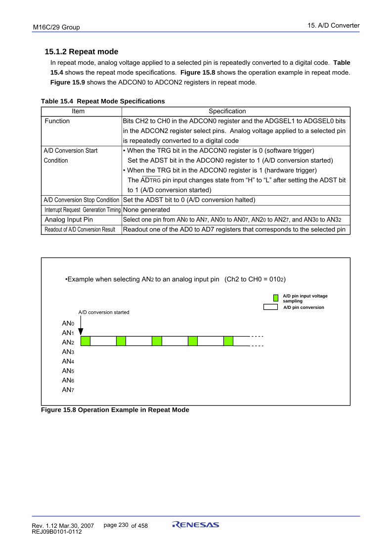
15. A/D ConverterpuorG92/C61M
page 230 854fo7002,03.raM21.1.veR2110-1010B90JER
15.1.2 Repeat modeIn repeat mode, analog voltage applied to a selected pin is repeatedly converted to a digital code. Table
15.4 shows the repeat mode specifications. Figure 15.8 shows the operation example in repeat mode.Figure 15.9 shows the ADCON0 to ADCON2 registers in repeat mode.
Item SpecificationFunction Bits CH2 to CH0 in the ADCON0 register and the ADGSEL1 to ADGSEL0 bits
in the ADCON2 register select pins. Analog voltage applied to a selected pinis repeatedly converted to a digital code
A/D Conversion Start • When the TRG bit in the ADCON0 register is 0 (software trigger)Condition Set the ADST bit in the ADCON0 register to 1 (A/D conversion started)
• When the TRG bit in the ADCON0 register is 1 (hardware trigger)The ADTRG pin input changes state from “H” to “L” after setting the ADST bitto 1 (A/D conversion started)
A/D Conversion Stop Condition Set the ADST bit to 0 (A/D conversion halted)Interrupt Request Generation Timing None generatedAnalog Input Pin Select one pin from AN0 to AN7, AN00 to AN07, AN20 to AN27, and AN30 to AN32
Readout of A/D Conversion Result Readout one of the AD0 to AD7 registers that corresponds to the selected pin
Table 15.4 Repeat Mode Specifications
Figure 15.8 Operation Example in Repeat Mode
•Example when selecting AN2 to an analog input pin (Ch2 to CH0 = 0102)
A/D conversion started
AN0
AN1
AN2
AN3
AN4
AN5
AN6
AN7
A/D pin input voltage samplingA/D pin conversion
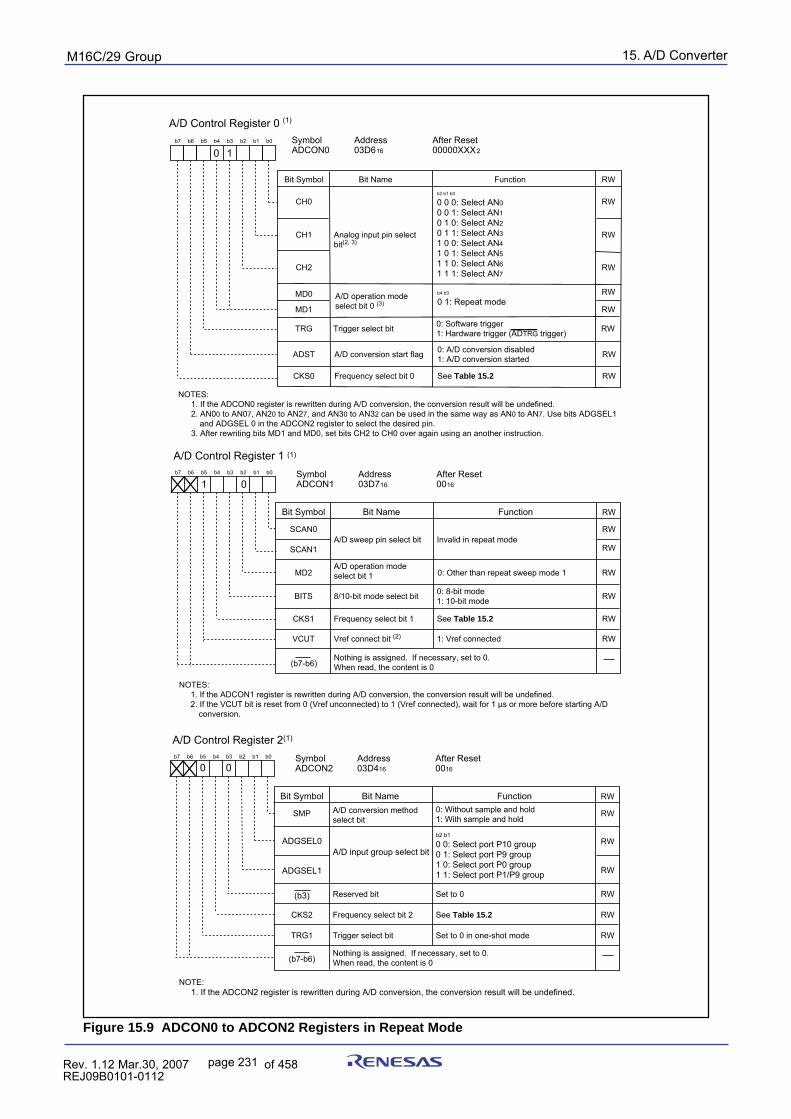
15. A/D ConverterpuorG92/C61M
page 231 854fo7002,03.raM21.1.veR2110-1010B90JER
Figure 15.9 ADCON0 to ADCON2 Registers in Repeat Mode
A/D Control Register 0 (1)
Symbol Address After Reset ADCON0 03D616 00000XXX2
b7 b6 b5 b4 b3 b2 b1 b0
Analog input pin select bit(2, 3)
CH0
Bit Symbol Bit Name Function
CH1
CH2
A/D operation mode select bit 0 (3)
MD0
MD1
Trigger select bit 0: Software trigger1: Hardware trigger (ADTRG trigger)TRG
ADST A/D conversion start flag 0: A/D conversion disabled1: A/D conversion started
Frequency select bit 0 See Table 15.2 CKS0
RW
RW
RW
RW
RW
RW
RW
RW
RW
A/D Control Register 1 (1)
Symbol Address After Reset ADCON1 03D716 0016
Bit Name FunctionBit Symbol
b7 b6 b5 b4 b3 b2 b1 b0
A/D sweep pin select bitSCAN0
SCAN1
MD2
BITS 8/10-bit mode select bit 0: 8-bit mode1: 10-bit mode
VCUT
A/D operation mode select bit 1 0: Other than repeat sweep mode 1
1: Vref connected
Frequency select bit 1CKS1
RW
RW
RW
RW
RW
RW
RW
Invalid in repeat mode
See Table 15.2
Nothing is assigned. If necessary, set to 0.When read, the content is 0(b7-b6)
NOTES: 1. If the ADCON1 register is rewritten during A/D conversion, the conversion result will be undefined. 2. If the VCUT bit is reset from 0 (Vref unconnected) to 1 (Vref connected), wait for 1 µs or more before starting A/D
conversion.
Vref connect bit (2)
0
A/D Control Register 2(1) Symbol Address After Reset ADCON2 03D416 0016
Bit Name FunctionBit Symbol
b7 b6 b5 b4 b3 b2 b1 b0
A/D conversion method select bit
SMP
Reserved bit Set to 0
TRG1
A/D input group select bit
b2 b1
0 0: Select port P10 group 0 1: Select port P9 group1 0: Select port P0 group1 1: Select port P1/P9 group
Set to 0 in one-shot mode
Frequency select bit 2CKS2
RW
RW
RW
RW
RW
RW
RW
0: Without sample and hold1: With sample and hold
See Table 15.2
Nothing is assigned. If necessary, set to 0.When read, the content is 0(b7-b6)
NOTE: 1. If the ADCON2 register is rewritten during A/D conversion, the conversion result will be undefined.
Trigger select bit
ADGSEL0
ADGSEL1
(b3)
1 0
0 0
b2 b1 b0
0 0 0: Select AN00 0 1: Select AN10 1 0: Select AN20 1 1: Select AN31 0 0: Select AN41 0 1: Select AN51 1 0: Select AN6 1 1 1: Select AN7
b4 b3
0 1: Repeat mode
NOTES: 1. If the ADCON0 register is rewritten during A/D conversion, the conversion result will be undefined. 2. AN00 to AN07, AN20 to AN27, and AN30 to AN32 can be used in the same way as AN0 to AN7. Use bits ADGSEL1
and ADGSEL 0 in the ADCON2 register to select the desired pin. 3. After rewriting bits MD1 and MD0, set bits CH2 to CH0 over again using an another instruction.
0 1
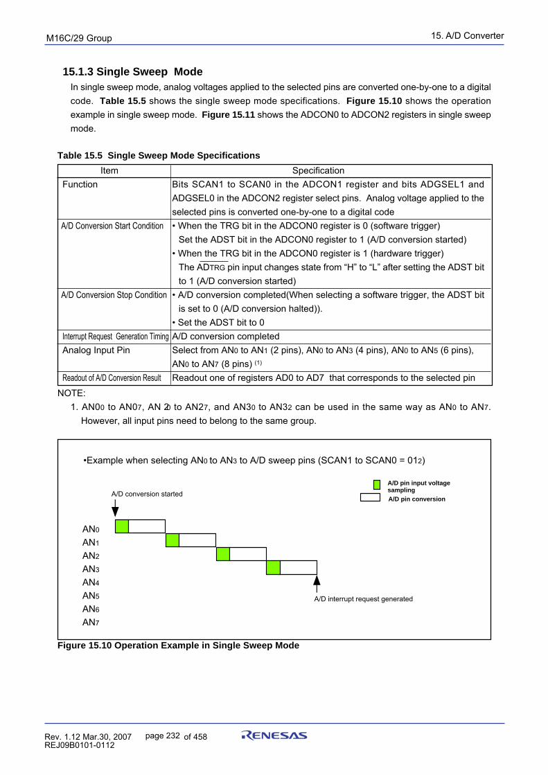
15. A/D ConverterpuorG92/C61M
page 232 854fo7002,03.raM21.1.veR2110-1010B90JER
15.1.3 Single Sweep ModeIn single sweep mode, analog voltages applied to the selected pins are converted one-by-one to a digitalcode. Table 15.5 shows the single sweep mode specifications. Figure 15.10 shows the operationexample in single sweep mode. Figure 15.11 shows the ADCON0 to ADCON2 registers in single sweepmode.
Item SpecificationFunction Bits SCAN1 to SCAN0 in the ADCON1 register and bits ADGSEL1 and
ADGSEL0 in the ADCON2 register select pins. Analog voltage applied to theselected pins is converted one-by-one to a digital code
A/D Conversion Start Condition • When the TRG bit in the ADCON0 register is 0 (software trigger)Set the ADST bit in the ADCON0 register to 1 (A/D conversion started)
• When the TRG bit in the ADCON0 register is 1 (hardware trigger)The ADTRG pin input changes state from “H” to “L” after setting the ADST bitto 1 (A/D conversion started)
A/D Conversion Stop Condition • A/D conversion completed(When selecting a software trigger, the ADST bitis set to 0 (A/D conversion halted)).
• Set the ADST bit to 0Interrupt Request Generation Timing A/D conversion completedAnalog Input Pin Select from AN0 to AN1 (2 pins), AN0 to AN3 (4 pins), AN0 to AN5 (6 pins),
AN0 to AN7 (8 pins) (1)
Readout of A/D Conversion Result Readout one of registers AD0 to AD7 that corresponds to the selected pin
Table 15.5 Single Sweep Mode Specifications
NOTE:1. AN00 to AN07, AN 20 to AN27, and AN30 to AN32 can be used in the same way as AN0 to AN7.
However, all input pins need to belong to the same group.
Figure 15.10 Operation Example in Single Sweep Mode
A/D conversion started
A/D interrupt request generated
AN0
AN1
AN2
AN3
AN4
AN5
AN6
AN7
A/D pin input voltage samplingA/D pin conversion
•Example when selecting AN0 to AN3 to A/D sweep pins (SCAN1 to SCAN0 = 012)

15. A/D ConverterpuorG92/C61M
page 233 854fo7002,03.raM21.1.veR2110-1010B90JER
Figure 15.11 ADCON0 to ADCON2 Registers in Single Sweep Mode
A/D Control Register 0 (1)
Symbol Address After Reset ADCON0 03D616 00000XXX2
b7 b6 b5 b4 b3 b2 b1 b0
Analog input pin select bit
CH0
Bit Symbol Bit Name Function
CH1
CH2
A/D operation mode select bit 0
MD0
MD1
Trigger select bit 0: Software trigger1: Hardware trigger (ADTRG trigger)TRG
ADST A/D conversion start flag 0: A/D conversion disabled1: A/D conversion started
Frequency select bit 0 See Table 15.2 CKS0
RW
NOTE: 1. If the ADCON0 register is rewritten during A/D conversion, the conversion result will be undefined.
RW
RW
RW
RW
RW
RW
RW
RW
Invalid in single sweep mode
b4 b3
1 0: Single sweep mode or Simultaneous sample sweep mode
A/D Control Register 1 (1)
Symbol Address After Reset ADCON1 03D716 0016
Bit Name FunctionBit Symbol
b7 b6 b5 b4 b3 b2 b1 b0
A/D sweep pin select bit (2)
SCAN0
SCAN1
MD2
BITS 8/10-bit mode select bit 0: 8-bit mode1: 10-bit mode
VCUT
A/D operation mode select bit 1 0: Other than repeat sweep mode 1
1: Vref connected
Frequency select bit 1CKS1
RW
RW
RW
RW
RW
RW
RW
See Table 15.2
Nothing is assigned. If necessary, set to 0.When read, the content is 0(b7-b6)
NOTES: 1. If the ADCON1 register is rewritten during A/D conversion, the conversion result will be undefined. 2. AN00 to AN07, AN20 to AN27, and AN30 to AN32 can be used in the same way as AN0 to AN7. Use bits ADGSEL1
and ADGSEL 0 in the ADCON2 register to select the desired pin.3. If the VCUT bit is reset from 0 (Vref unconnected) to 1 (Vref connected), wait for 1 µs or more before starting A/D
conversion.
Vref connect Bit (3)
A/D Control Register 2(1) Symbol Address After Reset ADCON2 03D416 0016
Bit Name FunctionBit Symbol
b7 b6 b5 b4 b3 b2 b1 b0
A/D conversion method select bit
SMP
Reserved bit Set to 0
TRG1
A/D input group select bit
b2 b1
0 0: Select port P10 group 0 1: Select port P9 group1 0: Select port P0 group1 1: Select port P1/P9 group
Set to 0 in single sweep mode
Frequency select bit 2CKS2
RW
RW
RW
RW
RW
RW
RW
0: Without sample and hold1: With sample and hold
See Table 15.2
Nothing is assigned. If necessary, set to 0.When read, the content is 0(b7-b6)
NOTE: 1. If the ADCON2 register is rewritten during A/D conversion, the conversion result will be undefined.
Trigger select bit
ADGSEL0
ADGSEL1
(b3)
1 0
1 0
When single sweep mode is selected,b1 b0
0 0: AN0 to AN1 (2 pins) 0 1: AN0 to AN3 (4 pins)1 0: AN0 to AN5 (6 pins)1 1: AN0 to AN7 (8 pins)
0 0
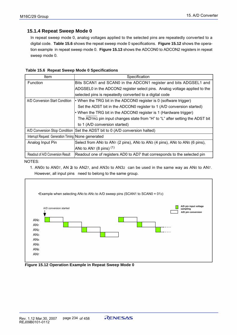
15. A/D ConverterpuorG92/C61M
page 234 854fo7002,03.raM21.1.veR2110-1010B90JER
Item SpecificationFunction Bits SCAN1 and SCAN0 in the ADCON1 register and bits ADGSEL1 and
ADGSEL0 in the ADCON2 register select pins. Analog voltage applied to theselected pins is repeatedly converted to a digital code
A/D Conversion Start Condition • When the TRG bit in the ADCON0 register is 0 (software trigger)Set the ADST bit in the ADCON0 register to 1 (A/D conversion started)
• When the TRG bit in the ADCON0 register is 1 (Hardware trigger)The ADTRG pin input changes state from “H” to “L” after setting the ADST bitto 1 (A/D conversion started)
A/D Conversion Stop Condition Set the ADST bit to 0 (A/D conversion halted)Interrupt Request Generation Timing None generatedAnalog Input Pin Select from AN0 to AN1 (2 pins), AN0 to AN3 (4 pins), AN0 to AN5 (6 pins),
AN0 to AN7 (8 pins) (1)
Readout of A/D Conversion Result Readout one of registers AD0 to AD7 that corresponds to the selected pin
15.1.4 Repeat Sweep Mode 0In repeat sweep mode 0, analog voltages applied to the selected pins are repeatedly converted to adigital code. Table 15.6 shows the repeat sweep mode 0 specifications. Figure 15.12 shows the opera-tion example in repeat sweep mode 0. Figure 15.13 shows the ADCON0 to ADCON2 registers in repeatsweep mode 0.
Table 15.6 Repeat Sweep Mode 0 Specifications
NOTES:1. AN00 to AN07, AN 20 to AN27, and AN30 to AN32 can be used in the same way as AN0 to AN7.
However, all input pins need to belong to the same group.
Figure 15.12 Operation Example in Repeat Sweep Mode 0
•Example when selecting AN0 to AN3 to A/D sweep pins (SCAN1 to SCAN0 = 012)
A/D conversion started
AN0
AN1
AN2
AN3
AN4
AN5
AN6
AN7
A/D pin input voltage samplingA/D pin conversion
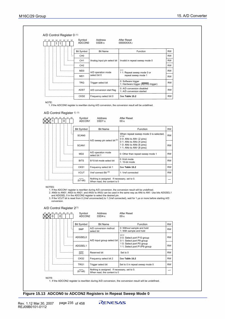
15. A/D ConverterpuorG92/C61M
page 235 854fo7002,03.raM21.1.veR2110-1010B90JER
Figure 15.13 ADCON0 to ADCON2 Registers in Repeat Sweep Mode 0
A/D Control Register 0 (1)
Symbol Address After Reset ADCON0 03D616 00000XXX2
b7 b6 b5 b4 b3 b2 b1 b0
Analog input pin select bit
CH0
Bit Symbol Bit Name Function
CH1
CH2
A/D operation mode select bit 0
MD0
MD1
Trigger select bit 0: Software trigger1: Hardware trigger (ADTRG trigger)TRG
ADST A/D conversion start flag 0: A/D conversion disabled1: A/D conversion started
Frequency select bit 0 See Table 15.2 CKS0
RW
NOTE: 1. If the ADCON0 register is rewritten during A/D conversion, the conversion result will be undefined.
RW
RW
RW
RW
RW
RW
RW
RW
Invalid in repeat sweep mode 0
b4 b3
1 1: Repeat sweep mode 0 or repeat sweep mode 1
A/D Control Register 1 (1)
Symbol Address After Reset ADCON1 03D716 0016
Bit Name FunctionBit Symbol
b7 b6 b5 b4 b3 b2 b1 b0
A/D sweep pin select bit (2)
SCAN0
SCAN1
MD2
BITS 8/10-bit mode select bit 0: 8-bit mode1: 10-bit mode
VCUT
A/D operation mode select bit 1 0: Other than repeat sweep mode 1
1: Vref connected
Frequency select bit 1CKS1
RW
RW
RW
RW
RW
RW
RW
See Table 15.2
Nothing is assigned. If necessary, set to 0.When read, the content is 0(b7-b6)
NOTES: 1. If the ADCON1 register is rewritten during A/D conversion, the conversion result will be undefined. 2. AN00 to AN07, AN20 to AN27, and AN30 to AN32 can be used in the same way as AN0 to AN7. Use bits ADGSEL1
and ADGSEL 0 in the ADCON2 register to select the desired pin.3. If the VCUT bit is reset from 0 (Vref unconnected) to 1 (Vref connected), wait for 1 µs or more before starting A/D
conversion.
Vref connect Bit (3)
A/D Control Register 2(1) Symbol Address After Reset ADCON2 03D416 0016
Bit Name FunctionBit Symbol
b7 b6 b5 b4 b3 b2 b1 b0
A/D conversion method select bit
SMP
Reserved bit Set to 0
TRG1
A/D input group select bit
b2 b1
0 0: Select port P10 group 0 1: Select port P9 group1 0: Select port P0 group1 1: Select port P1/P9 group
Set to 0 in repeat sweep mode 0
Frequency select bit 2CKS2
RW
RW
RW
RW
RW
RW
RW
0: Without sample and hold1: With sample and hold
See Table 15.2
Nothing is assigned. If necessary, set to 0.When read, the content is 0(b7-b6)
NOTE: 1. If the ADCON2 register is rewritten during A/D conversion, the conversion result will be undefined.
Trigger select bit
ADGSEL0
ADGSEL1
(b3)
1 1
1 0
When repeat sweep mode 0 is selected,b1 b0
0 0: AN0 to AN1 (2 pins) 0 1: AN0 to AN3 (4 pins)1 0: AN0 to AN5 (6 pins)1 1: AN0 to AN7 (8 pins)
0 0
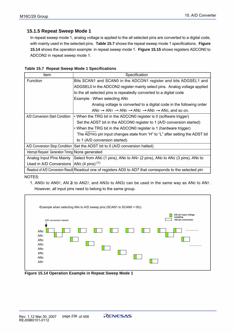
15. A/D ConverterpuorG92/C61M
page 236 854fo7002,03.raM21.1.veR2110-1010B90JER
15.1.5 Repeat Sweep Mode 1In repeat sweep mode 1, analog voltage is applied to the all selected pins are converted to a digital code,with mainly used in the selected pins. Table 15.7 shows the repeat sweep mode 1 specifications. Figure
15.14 shows the operation example in repeat sweep mode 1. Figure 15.15 shows registers ADCON0 toADCON2 in repeat sweep mode 1.
Table 15.7 Repeat Sweep Mode 1 Specifications
Item SpecificationFunction Bits SCAN1 and SCAN0 in the ADCON1 register and bits ADGSEL1 and
ADGSEL0 in the ADCON2 register mainly select pins. Analog voltage appliedto the all selected pins is repeatedly converted to a digital codeExample : When selecting AN0
Analog voltage is converted to a digital code in the following orderAN0 AN1 AN0 AN2 AN0 AN3, and so on.
A/D Conversion Start Condition • When the TRG bit in the ADCON0 register is 0 (software trigger)Set the ADST bit in the ADCON0 register to 1 (A/D conversion started)
• When the TRG bit in the ADCON0 register is 1 (hardware trigger) The ADTRG pin input changes state from “H” to “L” after setting the ADST bit
to 1 (A/D conversion started)A/D Conversion Stop Condition Set the ADST bit to 0 (A/D conversion halted)Interrupt Request Generation Timing None generatedAnalog Input Pins Mainly Select from AN0 (1 pins), AN0 to AN1 (2 pins), AN0 to AN2 (3 pins), AN0 toUsed in A/D Conversions AN3 (4 pins) (1)
Readout of A/D Conversion Result Readout one of registers AD0 to AD7 that corresponds to the selected pin
NOTES:1. AN00 to AN07, AN 20 to AN27, and AN30 to AN32 can be used in the same way as AN0 to AN7.
However, all input pins need to belong to the same group.
Figure 15.14 Operation Example in Repeat Sweep Mode 1
•Example when selecting AN0 to A/D sweep pins (SCAN1 to SCAN0 = 002)
AN0
AN1
AN2
AN3
AN4
AN5
AN6
AN7
A/D conversion started
A/D pin input voltage samplingA/D pin conversion

15. A/D ConverterpuorG92/C61M
page 237 854fo7002,03.raM21.1.veR2110-1010B90JER
Figure 15.15 ADCON0 to ADCON2 Registers in Repeat Sweep Mode 1
A/D Control Register 0 (1)
Symbol Address After Reset ADCON0 03D616 00000XXX2
b7 b6 b5 b4 b3 b2 b1 b0
Analog input pin select bit
CH0
Bit Symbol Bit Name Function
CH1
CH2
A/D operation mode select bit 0
MD0
MD1
Trigger select bit 0: Software trigger1: Hardware trigger (ADTRG trigger)TRG
ADST A/D conversion start flag 0: A/D conversion disabled1: A/D conversion started
Frequency select bit 0 See Table 15.2 CKS0
RW
NOTE: 1. If the ADCON0 register is rewritten during A/D conversion, the conversion result will be undefined.
RW
RW
RW
RW
RW
RW
RW
RW
Invalid in repeat sweep mode 1
b4 b3
1 1: Repeat sweep mode 0 or repeat sweep mode 1
A/D Control Register 1 (1)
Symbol Address After Reset ADCON1 03D716 0016
Bit Name FunctionBit Symbol
b7 b6 b5 b4 b3 b2 b1 b0
A/D sweep pin select bit (2)
SCAN0
SCAN1
MD2
BITS 8/10-bit mode select bit 0: 8-bit mode1: 10-bit mode
VCUT
A/D operation mode select bit 1 1: Repeat sweep mode 1
1: Vref connected
Frequency select bit 1CKS1
RW
RW
RW
RW
RW
RW
RW
See Table 15.2
Nothing is assigned. If necessary, set to 0.When read, the content is 0(b7-b6)
NOTES: 1. If the ADCON1 register is rewritten during A/D conversion, the conversion result will be undefined. 2. AN00 to AN07, AN20 to AN27, and AN30 to AN32 can be used in the same way as AN0 to AN7. Use bits ADGSEL1
and ADGSEL 0 in the ADCON2 register to select the desired pin.3. If the VCUT bit is reset from 0 (Vref unconnected) to 1 (Vref connected), wait for 1 µs or more before starting A/D
conversion.
Vref connect Bit (3)
A/D Control Register 2(1) Symbol Address After Reset ADCON2 03D416 0016
Bit Name FunctionBit Symbol
b7 b6 b5 b4 b3 b2 b1 b0
A/D conversion method select bit
SMP
Reserved bit Set to 0
TRG1
A/D input group select bit
b2 b1
0 0: Select port P10 group 0 1: Select port P9 group1 0: Select port P0 group1 1: Select port P1/P9 group
Set to 0 in repeat sweep mode 1
Frequency select bit 2CKS2
RW
RW
RW
RW
RW
RW
RW
0: Without sample and hold1: With sample and hold
See Table 15.2
Nothing is assigned. If necessary, set to 0.When read, the content is 0(b7-b6)
NOTE: 1. If the ADCON2 register is rewritten during A/D conversion, the conversion result will be undefined.
Trigger select bit
ADGSEL0
ADGSEL1
(b3)
1 1
1 0
When repeat sweep mode 0 is selected,b1 b0
0 0: AN0 (1 pin) 0 1: AN0 to AN1 (2 pins)1 0: AN0 to AN2 (3 pins)1 1: AN0 to AN3 (4 pins)
0 0
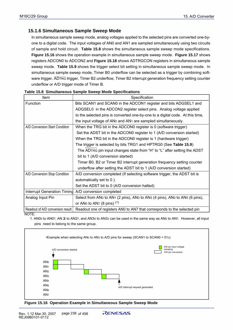
15. A/D ConverterpuorG92/C61M
page 238 854fo7002,03.raM21.1.veR2110-1010B90JER
Item SpecificationFunction Bits SCAN1 and SCAN0 in the ADCON1 register and bits ADGSEL1 and
ADGSEL0 in the ADCON2 register select pins. Analog voltage appliedto the selected pins is converted one-by-one to a digital code. At this time,the input voltage of AN0 and AN1 are sampled simultaneously.
A/D Conversion Start Condition When the TRG bit in the ADCON0 register is 0 (software trigger) Set the ADST bit in the ADCON0 register to 1 (A/D conversion started)When the TRG bit in the ADCON0 register is 1 (hardware trigger)The trigger is selected by bits TRG1 and HPTRG0 (See Table 15.9) The ADTRG pin input changes state from “H” to “L” after setting the ADST bit to 1 (A/D conversion started) Timer B0, B2 or Timer B2 interrupt generation frequency setting counter underflow after setting the ADST bit to 1 (A/D conversion started)
A/D Conversion Stop Condition A/D conversion completed (If selecting software trigger, the ADST bit isautomatically set to 0 ).Set the ADST bit to 0 (A/D conversion halted)
Interrupt Generation Timing A/D conversion completedAnalog Input Pin Select from AN0 to AN1 (2 pins), AN0 to AN3 (4 pins), AN0 to AN5 (6 pins),
or AN0 to AN7 (8 pins) (1)
Readout of A/D conversion result Readout one of registers AN0 to AN7 that corresponds to the selected pinNOTE:
1. AN00 to AN07, AN 20 to AN27, and AN30 to AN32 can be used in the same way as AN0 to AN7. However, all inputpins need to belong to the same group.
15.1.6 Simultaneous Sample Sweep ModeIn simultaneous sample sweep mode, analog voltages applied to the selected pins are converted one-by-one to a digital code. The input voltages of AN0 and AN1 are sampled simultaneously using two circuitsof sample and hold circuit. Table 15.8 shows the simultaneous sample sweep mode specifications.Figure 15.16 shows the operation example in simultaneous sample sweep mode. Figure 15.17 showsregisters ADCON0 to ADCON2 and Figure 15.18 shows ADTRGCON registers in simultaneous samplesweep mode. Table 15.9 shows the trigger select bit setting in simultaneous sample sweep mode. Insimultaneous sample sweep mode, Timer B0 underflow can be selected as a trigger by combining soft-
___________
ware trigger, ADTRG trigger, Timer B2 underflow, Timer B2 interrupt generation frequency setting counterunderflow or A/D trigger mode of Timer B.
Figure 15.16 Operation Example in Simultaneous Sample Sweep Mode
Table 15.8 Simultaneous Sample Sweep Mode Specifications
•Example when selecting AN0 to AN3 to A/D pins for sweep (SCAN1 to SCAN0 = 012)
A/D conversion started
A/D interrupt request generated
AN0
AN1
AN2
AN3
AN4
AN5
AN6
AN7
A/D pin input voltage samplingA/D pin conversion
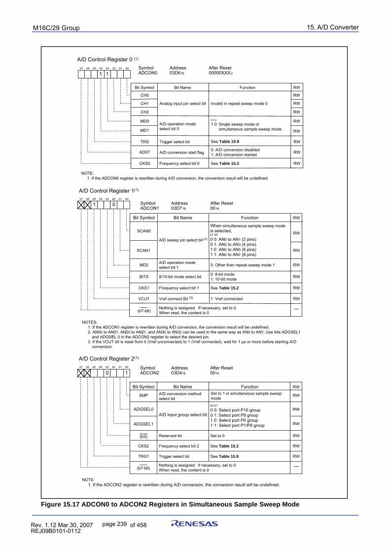
15. A/D ConverterpuorG92/C61M
page 239 854fo7002,03.raM21.1.veR2110-1010B90JER
Figure 15.17 ADCON0 to ADCON2 Registers in Simultaneous Sample Sweep Mode
A/D Control Register 0 (1)
Symbol Address After Reset ADCON0 03D616 00000XXX2
b7 b6 b5 b4 b3 b2 b1 b0
Analog input pin select bit
CH0
Bit Symbol Bit Name Function
CH1
CH2
A/D operation mode select bit 0
MD0
MD1
Trigger select bitTRG
ADST A/D conversion start flag 0: A/D conversion disabled1: A/D conversion started
Frequency select bit 0 See Table 15.2 CKS0
RW
NOTE: 1. If the ADCON0 register is rewritten during A/D conversion, the conversion result will be undefined.
RW
RW
RW
RW
RW
RW
RW
RW
Invalid in repeat sweep mode 0
b4 b3
1 0: Single sweep mode or simultaneous sample sweep mode
A/D Control Register 1(1)
Symbol Address After Reset ADCON1 03D716 0016
Bit Name FunctionBit Symbol
b7 b6 b5 b4 b3 b2 b1 b0
A/D sweep pin select bit (2)
SCAN0
SCAN1
MD2
BITS 8/10-bit mode select bit 0: 8-bit mode1: 10-bit mode
VCUT
A/D operation mode select bit 1 0: Other than repeat sweep mode 1
Frequency select bit 1CKS1
RW
RW
RW
RW
RW
RW
RW
See Table 15.2
Nothing is assigned. If necessary, set to 0.When read, the content is 0(b7-b6)
NOTES: 1. If the ADCON1 register is rewritten during A/D conversion, the conversion result will be undefined. 2. AN00 to AN07, AN20 to AN27, and AN30 to AN32 can be used in the same way as AN0 to AN7. Use bits ADGSEL1
and ADGSEL 0 in the ADCON2 register to select the desired pin.3. If the VCUT bit is reset from 0 (Vref unconnected) to 1 (Vref connected), wait for 1 µs or more before starting A/D
conversion.
Vref connect Bit (3)
A/D Control Register 2(1) Symbol Address After Reset ADCON2 03D416 0016
Bit Name FunctionBit Symbol
b7 b6 b5 b4 b3 b2 b1 b0
A/D conversion method select bit
SMP
Reserved bit Set to 0
TRG1
A/D input group select bit
b2 b1
0 0: Select port P10 group 0 1: Select port P9 group1 0: Select port P0 group1 1: Select port P1/P9 group
See Table 15.9
Frequency select bit 2CKS2
RW
RW
RW
RW
RW
RW
RW
Set to 1 in simultaneous sample sweep mode
See Table 15.2
Nothing is assigned. If necessary, set to 0.When read, the content is 0(b7-b6)
NOTE: 1. If the ADCON2 register is rewritten during A/D conversion, the conversion result will be undefined.
Trigger select bit
ADGSEL0
ADGSEL1
(b3)
1 1
1 0
10
1: Vref connected
When simultaneous sample sweep mode is selected,b1 b0
0 0: AN0 to AN1 (2 pins) 0 1: AN0 to AN3 (4 pins)1 0: AN0 to AN5 (6 pins)1 1: AN0 to AN7 (8 pins)
See Table 15.9
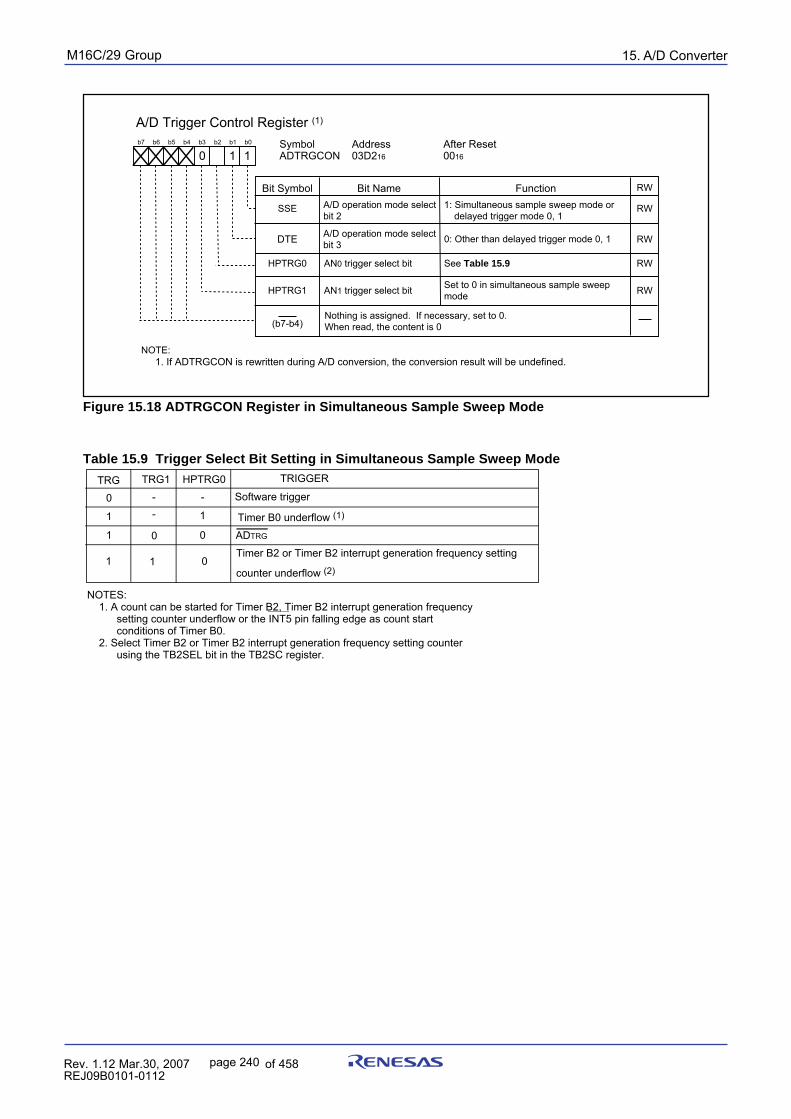
15. A/D ConverterpuorG92/C61M
page 240 854fo7002,03.raM21.1.veR2110-1010B90JER
Figure 15.18 ADTRGCON Register in Simultaneous Sample Sweep Mode
Table 15.9 Trigger Select Bit Setting in Simultaneous Sample Sweep Mode
TRG HPTRG0TRG1 TRIGGER
0
1
1
1
-
1
0
0
Software trigger
Timer B0 underflow (1)
Timer B2 or Timer B2 interrupt generation frequency setting
counter underflow (2)
ADTRG
--
1
0
NOTES: 1. A count can be started for Timer B2, Timer B2 interrupt generation frequency setting counter underflow or the INT5 pin falling edge as count start conditions of Timer B0. 2. Select Timer B2 or Timer B2 interrupt generation frequency setting counter using the TB2SEL bit in the TB2SC register.
A/D Trigger Control Register (1) Symbol Address After Reset ADTRGCON 03D216 0016
Bit Name FunctionBit Symbol
b7 b6 b5 b4 b3 b2 b1 b0
A/D operation mode selectbit 2
SSE
AN0 trigger select bit See Table 15.9
HPTRG1 AN1 trigger select bit
HPTRG0
RW
RW
RW
RW
RW
Nothing is assigned. If necessary, set to 0.When read, the content is 0(b7-b4)
NOTE: 1. If ADTRGCON is rewritten during A/D conversion, the conversion result will be undefined.
DTE
10 1
1: Simultaneous sample sweep mode or delayed trigger mode 0, 1
A/D operation mode select bit 3 0: Other than delayed trigger mode 0, 1
Set to 0 in simultaneous sample sweep mode
15. A/D ConverterpuorG92/C61M
page 241 854fo7002,03.raM21.1.veR2110-1010B90JER
NOTES:1. Set the larger value than the value of the timer B0 register to the timer B1 register. The count source for timer B0
and timer B1 must be the same.2. Do not write 1 (A/D conversion started) to the ADST bit in delayed trigger mode 0. When write 1, unexpected
interrupts may be generated.3. AN00 to AN07, AN 20 to AN27, and AN30 to AN32 can be used in the same way as AN0 to AN7. However, all input
pins need to belong to the same group.
15.1.7 Delayed Trigger Mode 0In delayed trigger mode 0, analog voltages applied to the selected pins are converted one-by-one to adigital code. The delayed trigger mode 0 used in combination with A/D trigger mode of Timer B. TheTimer B0 underflow starts a single sweep conversion. After completing the AN0 pin conversion, the AN1
pin is not sampled and converted until the Timer B1 underflow is generated. When the Timer B1 under-flow is generated, the single sweep conversion is restarted with the AN1 pin. Table 15.10 shows thedelayed trigger mode 0 specifications. Figure 15.19 shows the operation example in delayed triggermode 0. Figures 15.20 and 15.21 show each flag operation in the ADSTAT0 register that corresponds tothe operation example. Figure 15.22 shows registers ADCON0 to ADCON2 in delayed trigger mode 0.Figure 15.23 shows the ADTRGCON register in delayed trigger mode 0 and Table 15.11 shows thetrigger select bit setting in delayed trigger mode 0.
Item Specification Function Bits SCAN1 and SCAN0 in the ADCON1 register and bits ADGSEL1 and ADGSEL0
in the ADCON2 register select pins. Analog voltage applied to the input voltage ofthe selected pins are converted one-by-one to the digital code. At this time, timer B0underflow generation starts AN0 pin conversion. Timer B1 underflow generationstarts conversion after the AN1 pin. (1)
A/D Conversion Start AN0 pin conversion start condition •When Timer B0 underflow is generated if Timer B0 underflow is generated again before Timer B1 underflow is generated , the conversion is not affected •When Timer B0 underflow is generated during A/D conversion of pins after the AN1 pin, conversion is halted and the sweep is restarted from the AN0 pin againAN1 pin conversion start condition •When Timer B1 underflow is generated during A/D conversion of the AN0 pin, the input voltage of the AN1 pin is sampled. The AN1 conversion and the rest of the sweep start when AN0 conversion is completed.
A/D Conversion Stop •When single sweep conversion from the AN0 pin is completed Condition •Set the ADST bit to 0 (A/D conversion halted)(2)
Interrupt request A/D conversion completed generation timing
Analog input pin Select from AN0 to AN1 (2 pins), AN0 to AN3 (4 pins), AN0 to AN5 (6 pins)and AN0 to AN7 (8 pins)(3)
Readout of A/D conversion Readout one of registers AN0 to AN7 that corresponds to the selected pins result
Table 15.10 Delayed Trigger Mode 0 Specifications
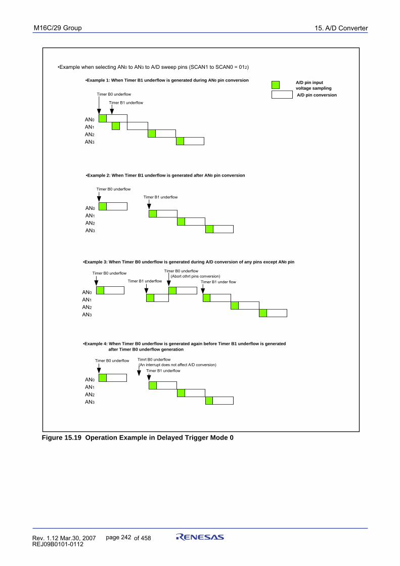
15. A/D ConverterpuorG92/C61M
page 242 854fo7002,03.raM21.1.veR2110-1010B90JER
Figure 15.19 Operation Example in Delayed Trigger Mode 0
AN0
AN1
AN2
AN3
Timer B0 underflow
A/D pin input voltage sampling
A/D pin conversion
AN0
AN1
AN2
AN3
Timrt B0 underflow (An interrupt does not affect A/D conversion)
Timer B0 underflow
Timer B1 underflow
Timer B1 underflow
•Example when selecting AN0 to AN3 to A/D sweep pins (SCAN1 to SCAN0 = 012)
•Example 1: When Timer B1 underflow is generated during AN0 pin conversion
AN0
AN1
AN2
AN3
Timer B0 underflow
Timer B1 underflow
•Example 2: When Timer B1 underflow is generated after AN0 pin conversion
AN0
AN1
AN2
AN3
Timer B0 underflow (Abort othrt pins conversion)
Timer B0 underflow
Timer B1 under flowTimer B1 underflow
•Example 3: When Timer B0 underflow is generated during A/D conversion of any pins except AN0 pin
•Example 4: When Timer B0 underflow is generated again before Timer B1 underflow is generated after Timer B0 underflow generation
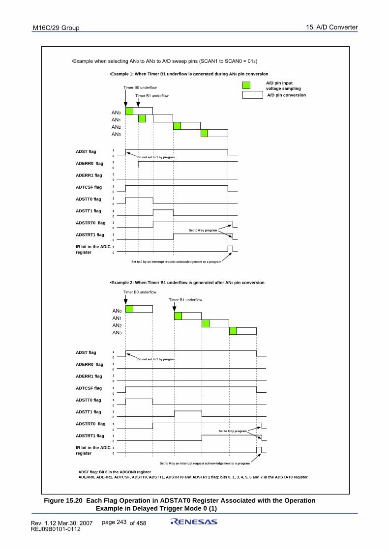
15. A/D ConverterpuorG92/C61M
page 243 854fo7002,03.raM21.1.veR2110-1010B90JER
Figure 15.20 Each Flag Operation in ADSTAT0 Register Associated with the Operation Example in Delayed Trigger Mode 0 (1)
AN0
AN1
AN2
AN3
Timer B0 underflow
1
0
1
0
1
0
1
0
1
0
1
0
1
0
1
0
1
0
AN0
AN1
AN2
AN3
1
0
1
0
1
0
1
0
1
0
1
0
1
0
1
0
1
0
A/D pin input voltage sampling
A/D pin conversion
Do not set to 1 by program
Do not set to 1 by program
Set to 0 by an interrupt request acknowledgement or a program
Set to 0 by an interrupt request acknowledgement or a program
Set to 0 by program
Set to 0 by program
ADST flag: Bit 6 in the ADCON0 registerADERR0, ADERR1, ADTCSF, ADSTT0, ADSTT1, ADSTRT0 and ADSTRT1 flag: bits 0, 1, 3, 4, 5, 6 and 7 in the ADSTAT0 register
ADST flag
ADERR0 flag
ADERR1 flag
ADTCSF flag
ADSTT0 flag
ADSTT1 flag
ADSTRT0 flag
ADSTRT1 flag
IR bit in the ADIC register
ADST flag
ADERR0 flag
ADERR1 flag
ADTCSF flag
ADSTT0 flag
ADSTT1 flag
ADSTRT0 flag
ADSTRT1 flag
IR bit in the ADIC register
Timer B0 underflow
Timer B1 underflow
Timer B1 underflow
•Example when selecting AN0 to AN3 to A/D sweep pins (SCAN1 to SCAN0 = 012)
•Example 1: When Timer B1 underflow is generated during AN0 pin conversion
•Example 2: When Timer B1 underflow is generated after AN0 pin conversion
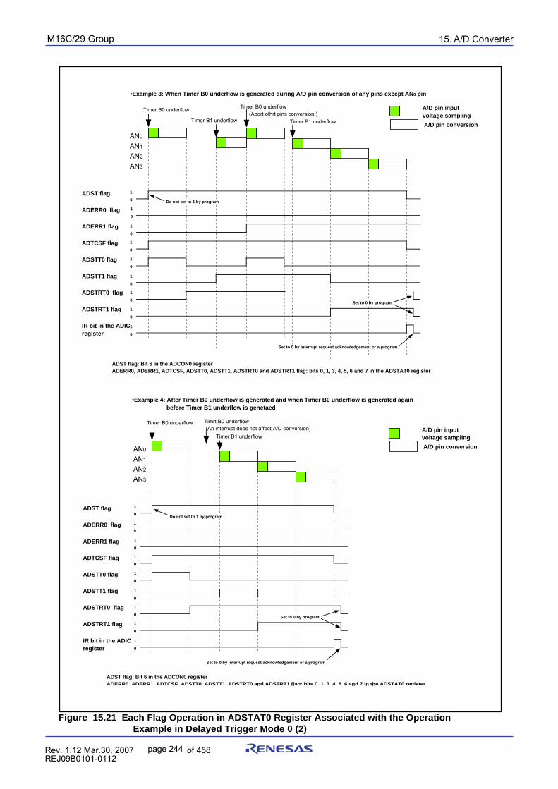
15. A/D ConverterpuorG92/C61M
page 244 854fo7002,03.raM21.1.veR2110-1010B90JER
Figure 15.21 Each Flag Operation in ADSTAT0 Register Associated with the Operation Example in Delayed Trigger Mode 0 (2)
AN0
AN1
AN2
AN3
Timer B0 underflow (Abort othrt pins conversion )
1
0
1
0
1
0
1
0
1
0
1
0
1
0
1
0
1
0
AN0
AN1
AN2
AN3
Timrt B0 underflow (An interrupt does not affect A/D conversion)
1
0
1
0
1
0
1
0
1
0
1
0
1
0
1
0
1
0
A/D pin input voltage sampling
A/D pin conversion
A/D pin input voltage sampling
A/D pin conversion
Do not set to 1 by program
Do not set to 1 by program
Set to 0 by interrupt request acknowledgement or a program
Set to 0 by interrupt request acknowledgement or a program
Set to 0 by program
Set to 0 by program
ADST flag: Bit 6 in the ADCON0 registerADERR0, ADERR1, ADTCSF, ADSTT0, ADSTT1, ADSTRT0 and ADSTRT1 flag: bits 0, 1, 3, 4, 5, 6 and 7 in the ADSTAT0 register
ADST flag: Bit 6 in the ADCON0 registerADERR0, ADERR1, ADTCSF, ADSTT0, ADSTT1, ADSTRT0 and ADSTRT1 flag: bits 0, 1, 3, 4, 5, 6 and 7 in the ADSTAT0 register
ADST flag
ADERR0 flag
ADERR1 flag
ADTCSF flag
ADSTT0 flag
ADSTT1 flag
ADSTRT0 flag
ADSTRT1 flag
IR bit in the ADIC register
ADST flag
ADERR0 flag
ADERR1 flag
ADTCSF flag
ADSTT0 flag
ADSTT1 flag
ADSTRT0 flag
ADSTRT1 flag
IR bit in the ADIC register
Timer B0 underflow
Timer B0 underflow
Timer B1 underflow
Timer B1 underflowTimer B1 underflow
•Example 3: When Timer B0 underflow is generated during A/D pin conversion of any pins except AN0 pin
•Example 4: After Timer B0 underflow is generated and when Timer B0 underflow is generated again before Timer B1 underflow is genetaed
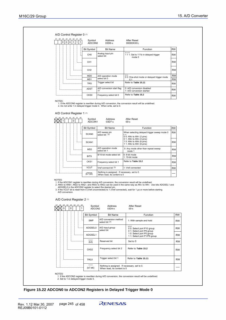
15. A/D ConverterpuorG92/C61M
page 245 854fo7002,03.raM21.1.veR2110-1010B90JER
Figure 15.22 ADCON0 to ADCON2 Registers in Delayed Trigger Mode 0
A/D Control Register 0 (1)
Symbol Address After ResetADCON0 03D616 00000XXX2
b7 b6 b5 b4 b3 b2 b1 b0
Analog input pin select bitCH0
Bit Symbol Bit Name Function
CH1
CH2
A/D operation mode select bit 0
MD0MD1
Trigger select bit Refer to Table 15.11 TRG
ADST A/D conversion start flag (2)
0: A/D conversion disabled1: A/D conversion started
Frequency select bit 0CKS0
RW
A/D Control Register 1 (1)
Symbol Address After ResetADCON1 03D716 0016
Bit Name FunctionBit Symbol
b7 b6 b5 b4 b3 b2 b1 b0
A/D sweep pin select bit (2)SCAN0
SCAN1
MD2
BITS8/10-bit mode select bit 0: 8-bit mode
1: 10-bit mode
VCUT Vref connect bit (3)
A/D operation mode select bit 1
1: Vref connected
0 1
When selecting delayed trigger sweep mode 0
0
1 1 1: Set to 111b in delayed trigger mode 0
b2 b1 b0
0 0: One-shot mode or delayed trigger mode 0,1
b4 b3
1
Frequency select bit 1CKS1
0: Any mode other than repeat sweep mode 1
RW
RW
RW
RWRW
RW
RW
RW
RW
RW
RW
RW
RW
RW
RW
Refer to Table 15.2
NOTES: 1. If the ADCON0 register is rewritten during A/D conversion, the conversion result will be undefined. 2. Do not write 1 in delayed trigger mode 0. When write, set to 0.
NOTES: 1. If the ADCON1 register is rewritten during A/D conversion, the conversion result will be undefined. 2. AN00 to AN07, AN20 to AN27, and AN30 to AN32 can be used in the same way as AN 0 to AN7. Use bits ADGSEL1 and ADGSEL0 in the ADCON2 register to select the desired pin. 3. If the VCUT bit is reset from 0 (Vref unconnected) to 1 (Vref connected), wait for 1 µs or more before starting A/D conversion.
Refer to Table 15.2
(b7-b6)
110
b1 b0
0 0: AN0 to AN1 (2 pins)0 1: AN0 to AN3 (4 pins)1 0: AN0 to AN5 (6 pins)1 1: AN0 to AN7 (8 pins)
Nothing is assigned. If necessary, set to 0.When read, its content is 0
0
NOTES: 1. If the ADCON2 register is rewritten during A/D conversion, the conversion result will be undefined. 2. Set to 1 in delayed trigger mode 0.
A/D Control Register 2 (1)
Symbol Address After ResetADCON2 03D416 0016
b7 b6 b5 b4 b3 b2 b1 b0
A/D conversion method select bit (2) 1: With sample and hold
Bit Symbol Bit Name Function RW
SMP
Reserved bit Set to 0
0
A/D input group select bit
0 0: Select port P10 group 0 1: Select port P9 group1 0: Select port P0 group 1 1: Select port P1/P9 group
b2 b1
Frequency select bit 2 CKS2
ADGSEL0
ADGSEL1
RW
RW
RW
RW
RW
(b3)
Nothing is assigned. If necessary, set to 0.When read, its content is 0(b7-b6)
Refer to Table 15.2
RWTRG1 Trigger select bit 1
1
Refer to Table 15.11
0
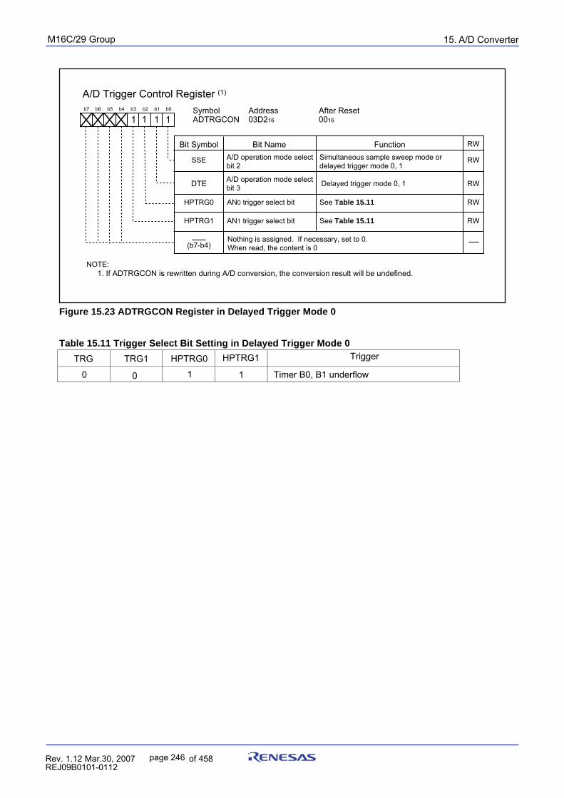
15. A/D ConverterpuorG92/C61M
page 246 854fo7002,03.raM21.1.veR2110-1010B90JER
Figure 15.23 ADTRGCON Register in Delayed Trigger Mode 0
Table 15.11 Trigger Select Bit Setting in Delayed Trigger Mode 0Trigger
Timer B0, B1 underflow
TRG
0
HPTRG0
1
TRG1
0
HPTRG1
1
A/D Trigger Control Register (1) Symbol Address After Reset ADTRGCON 03D216 0016
Bit Name FunctionBit Symbol
b7 b6 b5 b4 b3 b2 b1 b0
A/D operation mode selectbit 2
SSE
AN0 trigger select bit See Table 15.11
HPTRG1 AN1 trigger select bit
HPTRG0
RW
RW
RW
RW
RW
See Table 15.11
Nothing is assigned. If necessary, set to 0.When read, the content is 0(b7-b4)
NOTE: 1. If ADTRGCON is rewritten during A/D conversion, the conversion result will be undefined.
DTE
11 1
Simultaneous sample sweep mode or delayed trigger mode 0, 1
A/D operation mode select bit 3 Delayed trigger mode 0, 1
1
15. A/D ConverterpuorG92/C61M
page 247 854fo7002,03.raM21.1.veR2110-1010B90JER
NOTES:___________
1. Do not generate the next ADTRG pin falling edge after the AN1 pin conversion is started until all selected pins___________
complete A/D conversion. When an ADTRG pin falling edge is generated again during A/D conversion, its trigger___________
is ignored. The falling edge of ADTRG pin, which was input after all selected pins complete A/D conversion, isconsidered to be the next AN0 pin conversion start condition.
___________ ___________
2. The ADTRG pin falling edge is detected synchronized with the operation clock fAD. Therefore, when the ADTRG pin___________
falling edge is generated in shorter periods than fAD, the second ADTRG pin falling edge may not be detected. Do___________
not generate the ADTRG pin falling edge in shorter periods than fAD.3. Do not write 1 (A/D conversion started) to the ADST bit in delayed trigger mode 1. When write 1,unexpected
interrupts may be generated.4. AN00 to AN07, AN 20 to AN27, and AN30 to AN32 can be used in the same way as AN0 to AN7. However, all input
pins need to belong to the same group.
15.1.8 Delayed Trigger Mode 1In delayed trigger mode 1, analog voltages applied to the selected pins are converted one-by-one to a
___________
digital code. When the input of the ADTRG pin (falling edge) changes state from “H” to “L”, a single sweepconversion is started. After completing the AN0 pin conversion, the AN1 pin is not sampled and converted
___________
until the second ADTRG pin falling edge is generated. When the second ADTRG falling edge is generated,the single sweep conversion of the pins after the AN1 pin is restarted. Table 15.12 shows the delayedtrigger mode 1 specifications. Figure 15.24 shows the operation example of delayed trigger mode 1.Figure 15.25 and 15.26 show each flag operation in the ADSTAT0 register that corresponds to theoperation example. Figure 15.27 shows registers ADCON0 to ADCON2 in delayed trigger mode 1.Figure 15.28 shows the ADTRGCON register in delayed trigger mode 1. Table 15.13 shows the triggerselect bit setting in delayed trigger mode 1.
Table 15.12 Delayed Trigger Mode 1 Specifications
Item Specification Function Bits SCAN1 and SCAN0 in the ADCON1 register and bits ADGSEL1 and ADGSEL0 in the ADCON2 register select pins. Analog voltages applied to the selected
___________
pins are converted one-by-one to a digital code. At this time, the ADTRG pin___________
falling edge starts AN0 pin conversion and the second ADTRG pin falling edgestarts conversion of the pins after AN1 pin
A/D Conversion Start AN0 pin conversion start condition Condition
___________
The ADTRG pin input changes state from “H” to “L” (falling edge) (1)
AN1 pin conversion start condition (2)___________
The ADTRG pin input changes state from “H” to “L” (falling edge)___________
•When the second ADTRG pin falling edge is generated during A/D conversion of___________
the AN0 pin, input voltage of AN1 pin is sampled or after at the time of ADTRG
falling edge. The conversion of AN1 and the rest of the sweep starts when AN0
conversion is completed.___________
•When the ADTRG pin falling edge is generated again during single sweep conversion of pins after the AN1 pin, the conversion is not affected
A/D Conversion Stop •A/D conversion completed Condition •Set the ADST bit to 0 (A/D conversion halted) (3)
Interrupt Request Single sweep conversion completed
Generation Timing
Analog Input Pin Select from AN0 to AN1 (2 pins), AN0 to AN3 (4 pins), AN0 to AN5 (6 pins)and AN0 to AN7 (8 pins) (4)
Readout of A/D Conversion Result Readout one of registers AN0 to AN7 that corresponds to the selected pins
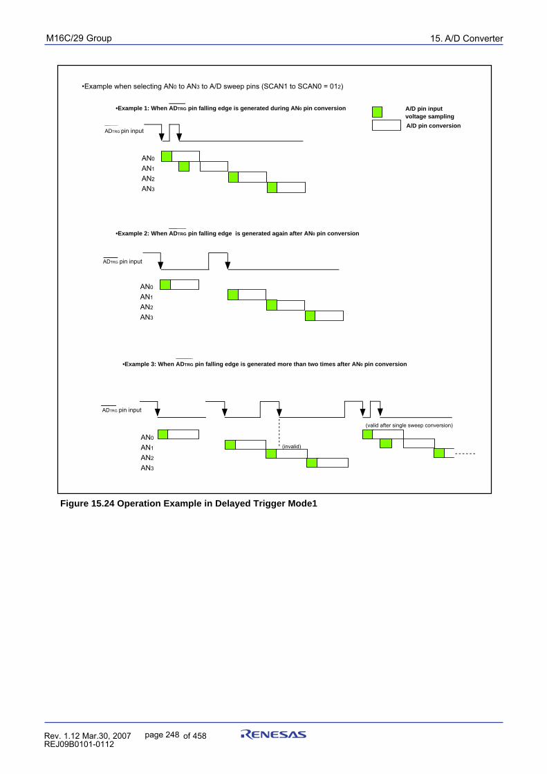
15. A/D ConverterpuorG92/C61M
page 248 854fo7002,03.raM21.1.veR2110-1010B90JER
Figure 15.24 Operation Example in Delayed Trigger Mode1
•Example when selecting AN0 to AN3 to A/D sweep pins (SCAN1 to SCAN0 = 012)
A/D pin input voltage sampling
A/D pin conversion
AN0
AN1
AN2
AN3
ADTRG pin input
•Example 1: When ADTRG pin falling edge is generated during AN0 pin conversion
AN0
AN1
AN2
AN3
•Example 2: When ADTRG pin falling edge is generated again after AN0 pin conversion
ADTRG pin input
•Example 3: When ADTRG pin falling edge is generated more than two times after AN0 pin conversion
AN0
AN1
AN2
AN3
(invalid)
(valid after single sweep conversion)
ADTRG pin input
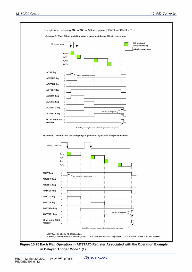
15. A/D ConverterpuorG92/C61M
page 249 854fo7002,03.raM21.1.veR2110-1010B90JER
Figure 15.25 Each Flag Operation in ADSTAT0 Register Associated with the Operation Example
in Delayed Trigger Mode 1 (1)
•Example when selecting AN0 to AN3 to A/D sweep pins (SCAN1 to SCAN0 = 012)
A/D pin input voltage sampling
A/D pin conversion
AN0
AN1
AN2
AN3
ADTRG pin input
•Example 1: When ADTRG pin falling edge is generated during AN0 pin conversion
ADST flag
ADERR0 flag
ADERR1 flag
ADTCSF flag
ADSTT0 flag
ADSTT1 flag
ADSTRT0 flag
ADSTRT1 flag
IR bit in the ADIC register
1
0
1
0
1
0
1
0
1
0
1
0
1
0
1
0
1
0
Set to 0 by interrupt request acknowledgement or a program
Set to 0 by program
Do not set to 1 by program
AN0
AN1
AN2
AN3
•Example 2: When ADTRG pin falling edge is generated again after AN0 pin conversion
ADST flag
ADERR0 flag
ADERR1 flag
ADTCSF flag
ADSTT0 flag
ADSTT1 flag
ADSTRT0 flag
ADSTRT1 flag
IR bit in the ADIC register
1
0
1
0
1
0
1
0
1
0
1
0
1
0
1
0
1
0
ADST flag: Bit 6 in the ADCON0 registerADERR0, ADERR1, ADTCSF, ADSTT0, ADSTT1, ADSTRT0 and ADSTRT1 flag: bits 0, 1, 3, 4, 5, 6 and 7 in the ADSTAT0 register
Set to 0 by interrupt request acknowledgment or a program
Set to 0 by program
Do not set to 1 by program
ADTRG pin input
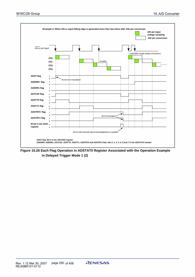
15. A/D ConverterpuorG92/C61M
page 250 854fo7002,03.raM21.1.veR2110-1010B90JER
Figure 15.26 Each Flag Operation in ADSTAT0 Register Associated with the Operation Example
in Delayed Trigger Mode 1 (2)
•Example 3: When ADTRG input falling edge is generated more than two times after AN0 pin conversion
AN0
AN1
AN2
AN3
(invalid)
(valid after single sweep conversion)
ADST flag
ADERR0 flag
ADERR1 flag
ADTCSF flag
ADSTT0 flag
ADSTT1 flag
ADSTRT0 flag
ADSTRT1 flag
IR bit in the ADIC register
1
0
1
0
1
0
1
0
1
0
1
0
1
0
1
0
1
0
Set to 0 when interrupt request acknowledgement or a program
Set to 0 by program
Do not set to 1 by program
A/D pin input voltage sampling
A/D pin conversion
ADST flag: Bit 6 in the ADCON0 registerADERR0, ADERR1, ADTCSF, ADSTT0, ADSTT1, ADSTRT0 and ADSTRT1 flag: bits 0, 1, 3, 4, 5, 6 and 7 in the ADSTAT0 register
ADTRG pin input
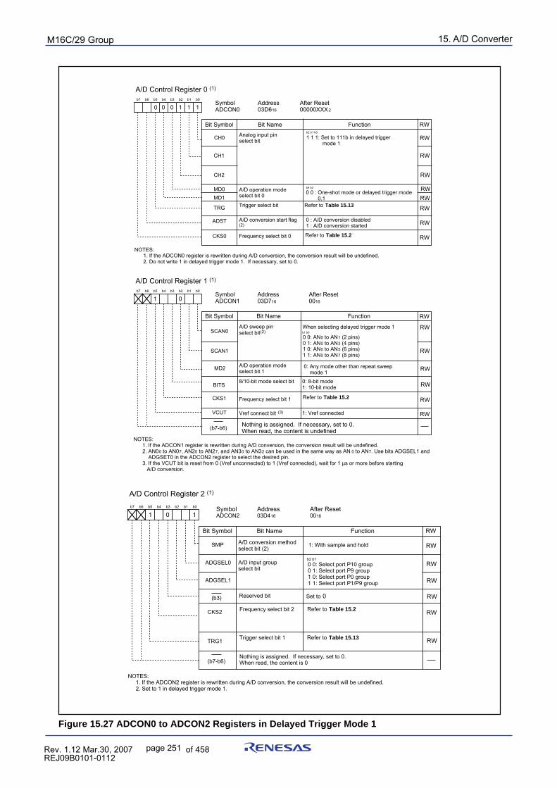
15. A/D ConverterpuorG92/C61M
page 251 854fo7002,03.raM21.1.veR2110-1010B90JER
Figure 15.27 ADCON0 to ADCON2 Registers in Delayed Trigger Mode 1
A/D Control Register 0 (1)
Symbol Address After ResetADCON0 03D616 00000XXX2
b7 b6 b5 b4 b3 b2 b1 b0
Analog input pin select bitCH0
Bit Symbol Bit Name Function
CH1
CH2
A/D operation mode select bit 0
MD0MD1
Trigger select bit Refer to Table 15.13 TRG
ADST A/D conversion start flag(2)
0 : A/D conversion disabled1 : A/D conversion started
Frequency select bit 0CKS0
RW
A/D Control Register 1 (1)
Symbol Address After ResetADCON1 03D716 0016
Bit Name FunctionBit Symbol
b7 b6 b5 b4 b3 b2 b1 b0
A/D sweep pinselect bit(2)SCAN0
SCAN1
MD2
BITS8/10-bit mode select bit 0: 8-bit mode
1: 10-bit mode
VCUT Vref connect bit (3)
A/D operation mode select bit 1
1: Vref connected
0 1
When selecting delayed trigger mode 1
0
1 1 1: Set to 111b in delayed trigger mode 1
b2 b1 b0
0 0 : One-shot mode or delayed trigger mode 0,1
b4 b3
1
Frequency select bit 1CKS1
0: Any mode other than repeat sweep mode 1
RW
RW
RW
RWRW
RW
RW
RW
RW
RW
RW
RW
RW
RW
RW
Refer to Table 15.2
NOTES: 1. If the ADCON0 register is rewritten during A/D conversion, the conversion result will be undefined. 2. Do not write 1 in delayed trigger mode 1. If necessary, set to 0.
NOTES: 1. If the ADCON1 register is rewritten during A/D conversion, the conversion result will be undefined. 2. AN00 to AN07, AN20 to AN27, and AN30 to AN32 can be used in the same way as AN 0 to AN7. Use bits ADGSEL1 and ADGSET0 in the ADCON2 register to select the desired pin. 3. If the VCUT bit is reset from 0 (Vref unconnected) to 1 (Vref connected), wait for 1 µs or more before starting A/D conversion.
Refer to Table 15.2
(b7-b6)
110
b1 b0
0 0: AN0 to AN1 (2 pins)0 1: AN0 to AN3 (4 pins)1 0: AN0 to AN5 (6 pins)1 1: AN0 to AN7 (8 pins)
0
Nothing is assigned. If necessary, set to 0. When read, the content is undefined
NOTES: 1. If the ADCON2 register is rewritten during A/D conversion, the conversion result will be undefined. 2. Set to 1 in delayed trigger mode 1.
A/D Control Register 2 (1)
Symbol Address After ResetADCON2 03D416 0016
b7 b6 b5 b4 b3 b2 b1 b0
A/D conversion method select bit (2) 1: With sample and hold
Bit Symbol Bit Name Function RW
SMP
Reserved bit Set to 0
0
A/D input group select bit
0 0: Select port P10 group0 1: Select port P9 group1 0: Select port P0 group 1 1: Select port P1/P9 group
b2 b1
Frequency select bit 2 CKS2
ADGSEL0
ADGSEL1
RW
RW
RW
RW
RW
(b3)
Nothing is assigned. If necessary, set to 0.When read, the content is 0(b7-b6)
Refer to Table 15.2
RWTRG1 Trigger select bit 1
1
Refer to Table 15.13
1
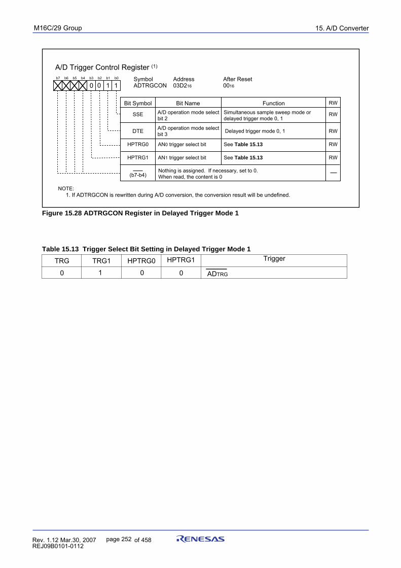
15. A/D ConverterpuorG92/C61M
page 252 854fo7002,03.raM21.1.veR2110-1010B90JER
Figure 15.28 ADTRGCON Register in Delayed Trigger Mode 1
Table 15.13 Trigger Select Bit Setting in Delayed Trigger Mode 1TriggerTRG
0
HPTRG0
0
TRG1
1 ADTRG
HPTRG1
0
A/D Trigger Control Register (1) Symbol Address After Reset ADTRGCON 03D216 0016
Bit Name FunctionBit Symbol
b7 b6 b5 b4 b3 b2 b1 b0
A/D operation mode selectbit 2
SSE
AN0 trigger select bit See Table 15.13
HPTRG1 AN1 trigger select bit
HPTRG0
RW
RW
RW
RW
RW
See Table 15.13
Nothing is assigned. If necessary, set to 0.When read, the content is 0(b7-b4)
NOTE: 1. If ADTRGCON is rewritten during A/D conversion, the conversion result will be undefined.
DTE
10 1
Simultaneous sample sweep mode or delayed trigger mode 0, 1
A/D operation mode select bit 3 Delayed trigger mode 0, 1
0
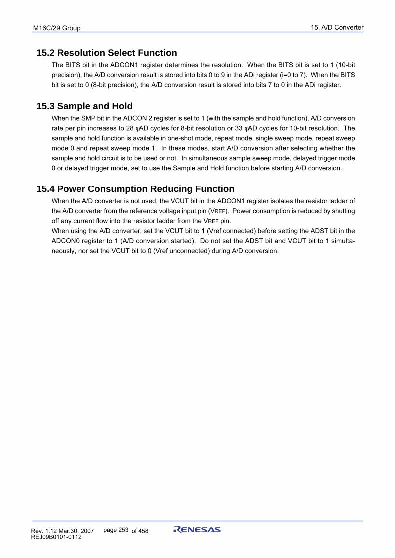
15. A/D ConverterpuorG92/C61M
page 253 854fo7002,03.raM21.1.veR2110-1010B90JER
15.2 Resolution Select FunctionThe BITS bit in the ADCON1 register determines the resolution. When the BITS bit is set to 1 (10-bitprecision), the A/D conversion result is stored into bits 0 to 9 in the ADi register (i=0 to 7). When the BITSbit is set to 0 (8-bit precision), the A/D conversion result is stored into bits 7 to 0 in the ADi register.
15.3 Sample and HoldWhen the SMP bit in the ADCON 2 register is set to 1 (with the sample and hold function), A/D conversionrate per pin increases to 28 φAD cycles for 8-bit resolution or 33 φAD cycles for 10-bit resolution. Thesample and hold function is available in one-shot mode, repeat mode, single sweep mode, repeat sweepmode 0 and repeat sweep mode 1. In these modes, start A/D conversion after selecting whether thesample and hold circuit is to be used or not. In simultaneous sample sweep mode, delayed trigger mode0 or delayed trigger mode, set to use the Sample and Hold function before starting A/D conversion.
15.4 Power Consumption Reducing FunctionWhen the A/D converter is not used, the VCUT bit in the ADCON1 register isolates the resistor ladder ofthe A/D converter from the reference voltage input pin (VREF). Power consumption is reduced by shuttingoff any current flow into the resistor ladder from the VREF pin.When using the A/D converter, set the VCUT bit to 1 (Vref connected) before setting the ADST bit in theADCON0 register to 1 (A/D conversion started). Do not set the ADST bit and VCUT bit to 1 simulta-neously, nor set the VCUT bit to 0 (Vref unconnected) during A/D conversion.
15. A/D ConverterpuorG92/C61M
page 254 854fo7002,03.raM21.1.veR2110-1010B90JER
Figure 15.29 Analog Input Pin and External Sensor Equivalent Circuit
15.5 Output Impedance of Sensor under A/D ConversionTo carry out A/D conversion properly, charging the internal capacitor C shown in Figure 15.29 has to becompleted within a specified period of time. T (sampling time) as the specified time. Let output imped-ance of sensor equivalent circuit be R0, MCU’s internal resistance be R, precision (error) of the A/Dconverter be X, and the A/D converter’s resolution be Y (Y is 1024 in the 10-bit mode, and 256 in the 8-bit mode).
VC is generally VC = VIN1-e c(R0+R)
And when t = T, VC=VIN- VIN=VIN(1- )
e c(R0+R) =
- T = ln
Hence, R0 = - - R
Figure 15.29 shows analog input pin and externalsensor equivalent circuit. When the difference be-tween VIN and VC becomes 0.1 LSB, we find impedance R0 when voltage between pins. VC changesfrom 0 to VIN-(0.1/1024) VIN in timer T. (0.1/1024) means that A/D precision drop due to insufficientcapacitor chage is held to 0.1LSB at time of A/D conversion in the 10-bit mode. Actual error however isthe value of absolute precision added to 0.1LSB. When f(XIN) = 10MHz, T=0.3µs in the A/D conversionmode with sample & hold. Output inpedance R0 for sufficiently charging capacitor C within time T isdetermined as follows.
T = 0.3µs, R = 7.8kΩ, C = 1.5pF, X = 0.1, and Y = 1024. Hence,
R0 = - - 7.8 X 10³ ≅ 13.9 X 10³
Thus, the allowable output impedance of the sensor circuit capable of thoroughly driving the A/D con-verter turns out of be approximately 13.9kΩ.
1
1 T
t
C(R0+R)1 X
Y
XY
XY
XY
TC•ln X
Y
1.5X10⁻¹²•ln0.11024
0.3X10⁻⁶
R0 R (7.8kΩ)
C (1.5pF)VIN
VC
Sampling time
Sample-and-hold function enabled:
Sample-and-hold function disabled:
3φAD
MCU
Sensor equivalent circuit
2φAD
(1)
(1)
NOTE: 1. Reference value
16. MULTI-MASTER I2C bus INTERFACEpuorG92/C61M
page 255 854fo7002,03.raM21.1.veR2110-1010B90JER
Item FunctionFormat Based on Philips I2C bus standard:
7-bit addressing formatHigh-speed clock modeStandard clock mode
Communication mode Based on Philips I2C bus standard:Master transmitMaster receiveSlave transmitSlave receive
SCL clock frequency 16.1kHz to 400kHz (at VIIC (1)= 4MHz)I/O pin Serial data line SDAMM(SDA)
Serial clock line SDLMM(SCL)
16. Multi-master I2C bus InterfaceThe multi-master I2C bus interface is a serial communication circuit based on Philips I2C bus data transferformat, equipped with arbitration lost detection and synchronous functions. Figure 16.1 shows a blockdiagram of the multi-master I2C bus interface and Table 16.1 lists the multi-master I2C bus interface func-tions.The multi-master I2C bus interface consists of the S0D0 register, the S00 register, the S20 register, theS3D0 register, the S4D0 register, the S10 register, the S2D0 register and other control circuits.Figures 16.2 to 16.8 show the registers associated with the multi-master I2C bus.
Table 16.1 Multi-master I2C bus interface functions
NOTE: 1. VIIC=I2C system clock
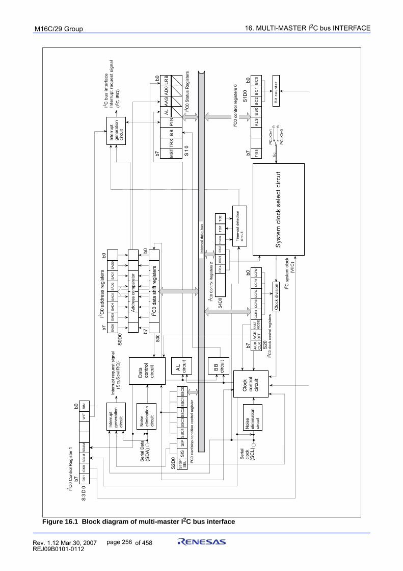
16. MULTI-MASTER I2C bus INTERFACEpuorG92/C61M
page 256 854fo7002,03.raM21.1.veR2110-1010B90JER
Figure 16.1 Block diagram of multi-master I2C bus interface
Ser
ial D
ata
(SD
A)
BB
circ
uit
Noi
seel
imin
atio
nci
rcui
t(S
CL)
b7b0
AC
KC
LKA
CK
BIT
FAS
TM
OD
EC
CR
4C
CR
3C
CR
2C
CR
1C
CR
0
Inte
rnal
dat
a bu
s
Clo
ck d
ivis
ion
S20
b7b0
SA
D6
SA
D5
SA
D4
SA
D3
SA
D2
SA
D1
SA
D0
Add
ress
com
para
tor
b7
b0
S00
S0D
0
(S
CLS
DAIR
Q)
b7b0
ICK
1IC
K0
SC
LMS
DA
MW
ITS
IMS
3D
0
Inte
rrup
tge
nera
tion
circ
uit
b7 MS
TTR
XB
BP
INA
LA
AS
AD
0LR
Bb0
S1
0
b7b0
TIS
SA
LSB
C2
BC
1E
S0
I2 C s
yste
m c
lock
(V
IIC)
Tim
e-ou
t det
ectio
n ci
rcui
tTO
FT
OEIC
K4
ICK
3IC
K2
TOS
EL
Sys
tem
clo
ck s
elec
t circ
ut
I2 C0
Con
trol R
egis
ter 1
I2 C0
star
t/sto
p co
nditi
on c
ontro
l reg
iste
r
S2D
0ST
SPSE
LSI
SSI
PSS
C4
SSC
3SS
C2
SSC
1SS
C0
I2 C0
addr
ess
regi
ster
s
I2 C0
data
shi
ft re
gist
ers
I2 C0
Con
trol R
egis
ters
2
S4D
0
I2 C0
cloc
k co
ntro
l reg
iste
rs
I2 C0
Stat
us R
egis
ters
I2 C0
cont
rol r
egis
ters
0
S1D
0
I2 C b
us in
terf
ace
Inte
rrup
t req
uest
sig
nal
Bit
cou
nter
(I2 C I
RQ
)
Ser
ial
cloc
k
BC
0
Clo
ckco
ntro
lci
rcui
t
AL
circ
uit
Noi
seel
imin
atio
nci
rcui
t
Dat
aco
ntro
lci
rcui
t
Inte
rrup
t req
uest
sig
nal
Inte
rrup
tge
nera
tion
circ
uit
f1 f2
PCLK
0=1
fIIC
PCLK
0=0
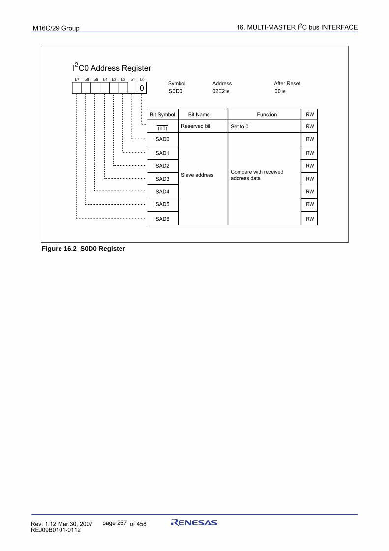
16. MULTI-MASTER I2C bus INTERFACEpuorG92/C61M
page 257 854fo7002,03.raM21.1.veR2110-1010B90JER
Figure 16.2 S0D0 Register
SAD6
SAD5
SAD4
SAD3
SAD2
SAD1
SAD0
Reserved bit
FunctionBit NameBit Symbol
Address After ResetSymbol
C0 Address Register
S0D0 02E216 0016
b7 b6 b5 b4 b3 b2 b1 b0
I2
Slave address
Set to 0
Compare with received address data
RW
RW
RW
RW
RW
RW
RW
RW
RW
(b0)
0
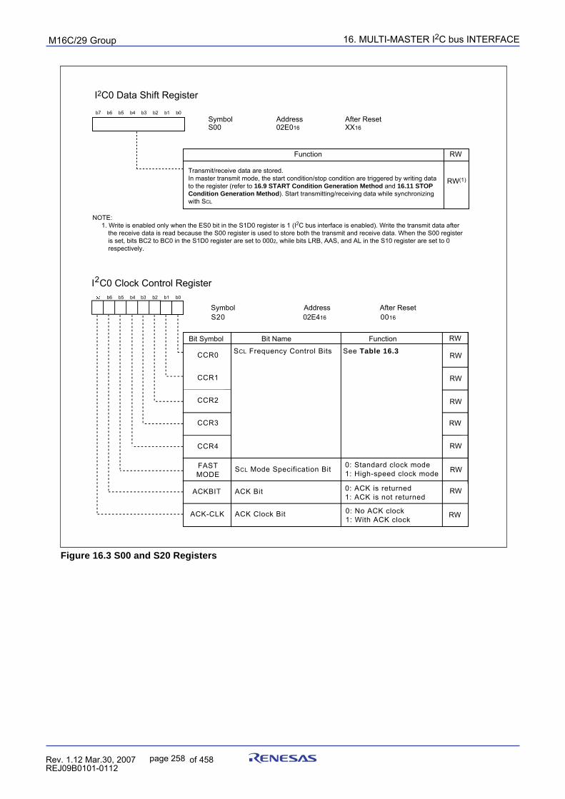
16. MULTI-MASTER I2C bus INTERFACEpuorG92/C61M
page 258 854fo7002,03.raM21.1.veR2110-1010B90JER
Figure 16.3 S00 and S20 Registers
0: Standard clock mode1: High-speed clock mode
0: ACK is returned1: ACK is not returned
0: No ACK clock1: With ACK clock
ACK Clock Bit
ACK Bit
SCL Mode Specification Bit
SCL Frequency Control BitsCCR0
CCR1
CCR2
CCR3
CCR4
FASTMODE
ACKBIT
ACK-CLK
FunctionBit NameBit Symbol
0016
After Reset02E416
AddressSymbolS20
b7 b6 b5 b4 b3 b2 b1 b0
C0 Clock Control RegisterI2
RW
See Table 16.3 RW
RW
RW
RW
RW
RW
RW
RW
Symbol Address After ResetS00 02E016 XX16
b 7 b
6 b
5 b
4 b
3 b
2 b
1 b
0
RWFunction
RW
(
1
)
NOTE: 1. Write is enabled only when the ES0 bit in the S1D0 register is 1 (I2C bus interface is enabled). Write the transmit data after
the receive data is read because the S00 register is used to store both the transmit and receive data. When the S00 register is set, bits BC2 to BC0 in the S1D0 register are set to 0002, while bits LRB, AAS, and AL in the S10 register are set to 0 respectively.
Transmit/receive data are stored.In master transmit mode, the start condition/stop condition are triggered by writing data to the register (refer to 16.9 START Condition Generation Method and 16.11 STOP Condition Generation Method). Start transmitting/receiving data while synchronizing with SCL
I2C0 Data Shift Register
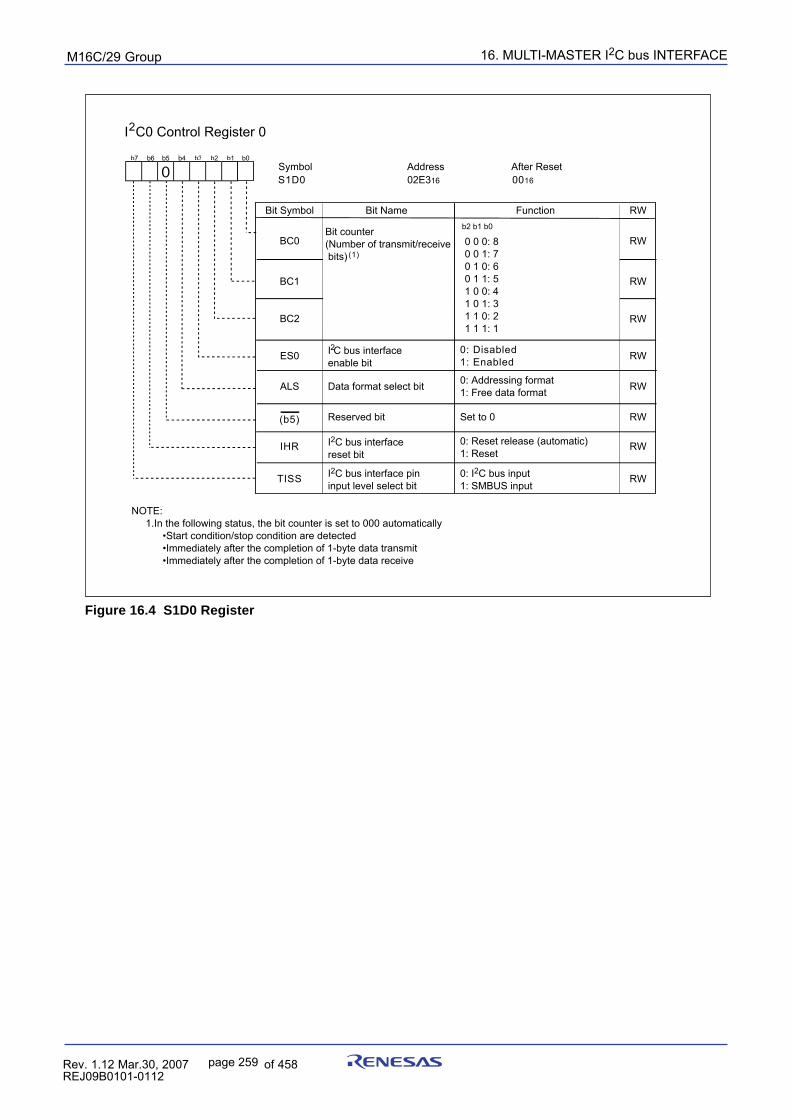
16. MULTI-MASTER I2C bus INTERFACEpuorG92/C61M
page 259 854fo7002,03.raM21.1.veR2110-1010B90JER
Figure 16.4 S1D0 Register
0: Disabled1: Enabled
0: Addressing format1: Free data format
Set to 0
0: Reset release (automatic)1: Reset
NOTE: 1.In the following status, the bit counter is set to 000 automatically •Start condition/stop condition are detected •Immediately after the completion of 1-byte data transmit •Immediately after the completion of 1-byte data receive
I2C bus interface pininput level select bit
I2C bus interfacereset bit
Reserved bit
Data format select bit
I C bus interfaceenable bit2
Bit counter(Number of transmit/receive bits)
BC2
TISS
IHR
(b5)
ALS
ES0
BC1
BC0
FunctionBit NameBit Symbol
0016
After Reset02E316
AddressSymbolS1D0
C0 Control Register 0I 2
b7 b3 b2 b1 b0
(1)
RW
0: I2C bus input1: SMBUS input
RW
RW
RW
RW
RW
RW
RW
RW
b2 b1 b0
0 0 0: 8 0 0 1: 7 0 1 0: 6 0 1 1: 5 1 0 0: 4 1 0 1: 3 1 1 0: 2 1 1 1: 1
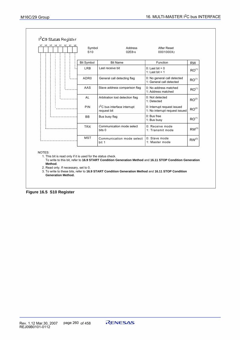
16. MULTI-MASTER I2C bus INTERFACEpuorG92/C61M
page 260 854fo7002,03.raM21.1.veR2110-1010B90JER
Figure 16.5 S10 Register
NOTES: 1. This bit is read only if it is used for the status check. To write to this bit, refer to 16.9 START Condition Generation Method and 16.11 STOP Condition Generation Method. 2. Read only. If necessary, set to 0. 3. To write to these bits, refer to 16.9 START Condition Generation Method and 16.11 STOP Condition Generation Method.
0: Bus free1: Bus busy
0: Interrupt request issued1: No interrupt request issued
0: Not detected1: Detected
0: No address matched1: Address matched
0: No general call detected1: General call detected
0: Last bit = 01: Last bit = 1
Communication mode select bits 0
Bus busy flag
I C bus interface interruptrequest bit2
Arbitration lost detection flag
Slave address comparison flag
General call detecting flag
Last receive bit
MST
TRX
BB
PIN
AL
AAS
ADR0
LRB
FunctionBit NameBit Symbol
0001000X2
After Reset02E816
AddressSymbolS10
C0 Status RegisterI2
RW
0: Receive mode1: Transmit mode
b7 b6 b5 b4 b3 b2 b1 b0
RO(1)
RO(1)
RO(1)
RO(2)
RO(1)
RO(2)
RW(3)
RW(3)0: Slave mode1: Master mode
Communication mode selectbit 1
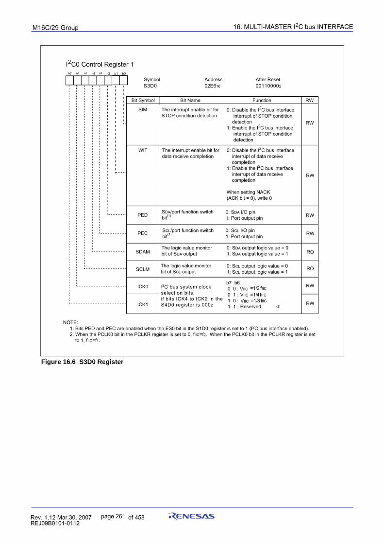
16. MULTI-MASTER I2C bus INTERFACEpuorG92/C61M
page 261 854fo7002,03.raM21.1.veR2110-1010B90JER
Figure 16.6 S3D0 Register
0: SCL output logic value = 01: SCL output logic value = 1
0: SDA output logic value = 01: SDA output logic value = 1
0: SCL I/O pin 1: Port output pin
0: SDA I/O pin 1: Port output pin
0: Disable the I2C bus interface interrupt of data receive completion1: Enable the I2C bus interface interrupt of data receive completion When setting NACK(ACK bit = 0), write 0
0: Disable the I2C bus interface interrupt of STOP condition detection1: Enable the I2C bus interface interrupt of STOP condition detection
I C bus system clockselection bits,if bits ICK4 to ICK2 in the S4D0 register is 0002
2
The logic value monitorbit of SCL output
The logic value monitorbit of SDA output
SCL/port function switchbit(1)
SDA/port function switchbit(1)
The interrupt enable bit fordata receive completion
The interrupt enable bit forSTOP condition detection
ICK1
ICK0
SCLM
SDAM
PEC
PED
WIT
SIM
FunctionBit NameBit Symbol
001100002
After Reset02E616
AddressSymbolS3D0
C0 Control Register 1I2
b7 b6 b5 b4 b3 b2 b1 b0
RW
b7 b6 0 0 : 0 1 : 1 0 :
VIIC =1/2 fIIC=1/4fIIC =1/8 fIIC
1 1 : Reserved
VIICVIIC
RW
RW
RW
RW
RO
RO
RW
RW
NOTE: 1. Bits PED and PEC are enabled when the ES0 bit in the S1D0 register is set to 1 (I2C bus interface enabled). 2. When the PCLK0 bit in the PCLKR register is set to 0, fIIC=f2. When the PCLK0 bit in the PCLKR register is set to 1, fIIC=f1.
(2)
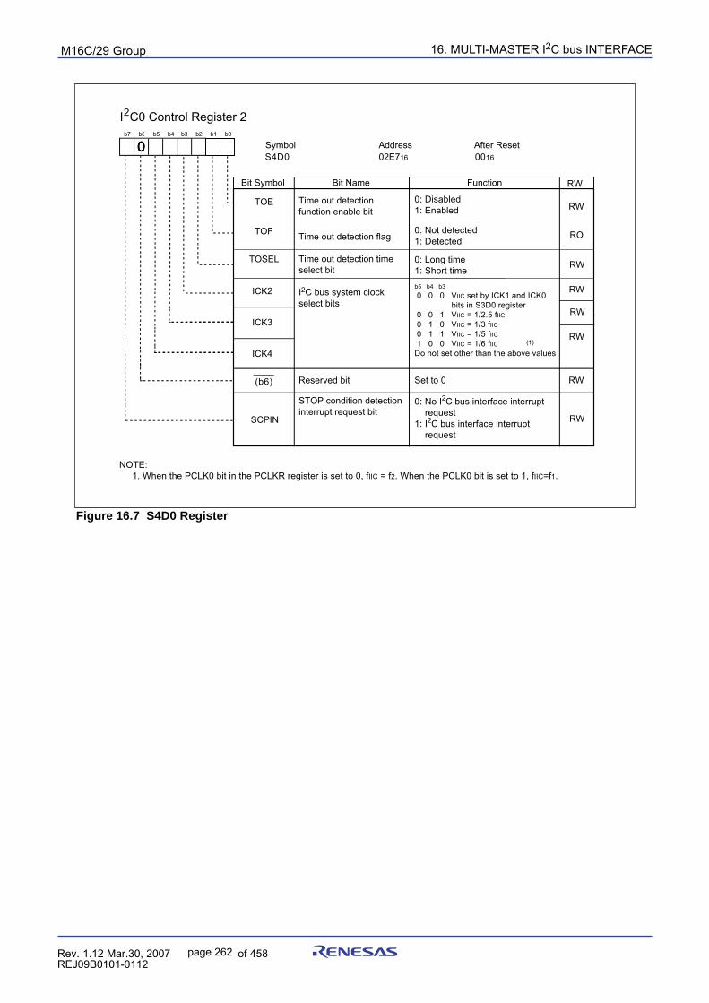
16. MULTI-MASTER I2C bus INTERFACEpuorG92/C61M
page 262 854fo7002,03.raM21.1.veR2110-1010B90JER
Figure 16.7 S4D0 Register
SCPIN
Reserved bit
ICK4
ICK3
ICK2
TOSEL
TOF
TOE
FunctionBit NameBit Symbol
0016
After Reset02E716
AddressSymbolS4D0
C0 Control Register 2I2
RW
b7 b6 b5 b4 b3 b2 b1 b0
0: Long time1: Short time
STOP condition detection interrupt request bit
Set to 0
b5 b4 b3 0 0 0 VIIC set by ICK1 and ICK0 bits in S3D0 register 0 0 1 VIIC = 1/2.5 fIIC 0 1 0 VIIC = 1/3 fIIC 0 1 1 VIIC = 1/5 fIIC 1 0 0 VIIC = 1/6 fIICDo not set other than the above values
Time out detection time select bit
Time out detection flag
Time out detection function enable bit
I2C bus system clock select bits
0: No I2C bus interface interrupt request1: I2C bus interface interrupt request
0: Not detected1: Detected
0: Disabled1: Enabled RW
RO
RW
RW
RW
RW
RW
RW
(b6)
(1)
NOTE: 1. When the PCLK0 bit in the PCLKR register is set to 0, fIIC = f2. When the PCLK0 bit is set to 1, fIIC=f1.
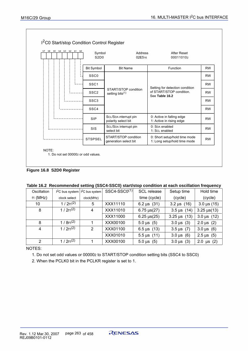
16. MULTI-MASTER I2C bus INTERFACEpuorG92/C61M
page 263 854fo7002,03.raM21.1.veR2110-1010B90JER
Figure 16.8 S2D0 Register
NOTES: 1. Do not set odd values or 000002 to START/STOP condition setting bits (SSC4 to SSC0) 2. When the PCLK0 bit in the PCLKR register is set to 1.
Oscillation I2C bus system I2C bus system SSC4-SSC0(1) SCL release Setup time Hold timef1 (MHz) clock select clock(MHz) time (cycle) (cycle) (cycle)
10 1 / 2f1(2) 5 XXX11110 6.2 µs (31) 3.2 µs (16) 3.0 µs (15) 8 1 / 2f1(2) 4 XXX11010 6.75 µs(27) 3.5 µs (14) 3.25 µs(13)
XXX11000 6.25 µs(25) 3.25 µs (13) 3.0 µs (12) 8 1 / 8f1(2) 1 XXX00100 5.0 µs (5) 3.0 µs (3) 2.0 µs (2) 4 1 / 2f1(2) 2 XXX01100 6.5 µs (13) 3.5 µs (7) 3.0 µs (6)
XXX01010 5.5 µs (11) 3.0 µs (6) 2.5 µs (5) 2 1 / 2f1(2) 1 XXX00100 5.0 µs (5) 3.0 µs (3) 2.0 µs (2)
Table 16.2 Recommended setting (SSC4-SSC0) start/stop condition at each oscillation frequency
0: Short setup/hold time mode1: Long setup/hold time mode
0: SDA enabled1: SCL enabled
0: Active in falling edge1: Active in rising edge
START/STOP conditiongeneration select bit
SCL/SDA interrupt pin select bit
SCL/SDA interrupt pin polarity select bit
START/STOP condition setting bits(1)
STSPSEL
SIS
SIP
SSC4
SSC3
SSC2
SSC1
SSC0
FunctionBit NameBit Symbol
000110102
After Reset02E516
AddressSymbolS2D0
C0 Start/stop Condition Control RegisterI 2
RW
b7 b6 b5 b4 b3 b2 b1 b0
NOTE: 1. Do not set 000002 or odd values.
RW
RW
RW
RW
RW
RW
RW
RW
Setting for detection conditionof START/STOP condition.See Table 16.2
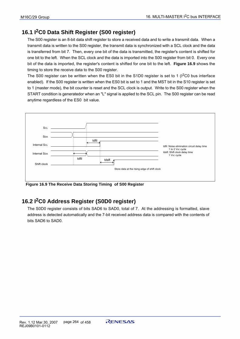
16. MULTI-MASTER I2C bus INTERFACEpuorG92/C61M
page 264 854fo7002,03.raM21.1.veR2110-1010B90JER
16.2 I2C0 Address Register (S0D0 register)The S0D0 register consists of bits SAD6 to SAD0, total of 7. At the addressing is formatted, slaveaddress is detected automatically and the 7-bit received address data is compared with the contents ofbits SAD6 to SAD0.
16.1 I2C0 Data Shift Register (S00 register)The S00 register is an 8-bit data shift register to store a received data and to write a transmit data. When atransmit data is written to the S00 register, the transmit data is synchronized with a SCL clock and the datais transferred from bit 7. Then, every one bit of the data is transmitted, the register's content is shifted forone bit to the left. When the SCL clock and the data is imported into the S00 register from bit 0. Every onebit of the data is imported, the register's content is shifted for one bit to the left. Figure 16.9 shows thetiming to store the receive data to the S00 register.The S00 register can be written when the ES0 bit in the S1D0 register is set to 1 (I2C0 bus interfaceenabled). If the S00 register is written when the ES0 bit is set to 1 and the MST bit in the S10 register is setto 1 (master mode), the bit counter is reset and the SCL clock is output. Write to the S00 register when theSTART condition is generatedor when an "L" signal is applied to the SCL pin. The S00 register can be readanytime regardless of the ES0 bit value.
Figure 16.9 The Receive Data Storing Timing of S00 Register
Internal SCL
tdfil
Store data at the rising edge of shift clock
Internal SDA
Shift clock
SCL
SDA
tdfil tdsft
tdfil: Noise elimination circuit delay time 1 to 2 VIIC cycletdsft: Shift clock delay time 1 VIIC cycle
16. MULTI-MASTER I2C bus INTERFACEpuorG92/C61M
page 265 854fo7002,03.raM21.1.veR2110-1010B90JER
16.3 I2C0 Clock Control Register (S20 register)The S20 register is used to set theACK control, SCL mode and the SCL frequency.
16.3.1 Bits 0 to 4: SCL Frequency Control Bits (CCR0–CCR4)
These bits control the SCL frequency. See Table 16.3 .
16.3.2 Bit 5: SCL Mode Specification Bit (FAST MODE)The FAST MODE bit selects SCL mode. When the FAST MODE bit is set to 0, standard clock modeis entered. When it is set to 1, high-speed clock mode is entered.When using the high-speed clock mode I2C bus standard (400 kbit/s maximum) to connect buses, setthe FAST MODE bit to 1 (select SCL mode as high-speed clock mode) and use the I2C bus systemclock (VIIC) at 4 MHz or more frequency.
16.3.3 Bit 6: ACK Bit (ACKBIT)The ACKBIT bit sets the SDA status when an ACK clock(1) is generated. When the ACKBIT bit is setto 0, ACK is returned and te clock applied to SDA becomes "L" when ACK clock is generated. Whenit is set to 1, ACK is not returned and the clock clock applied to SDA maintains "H" at ACK clockgeneration.When the ACKBIT bit is set to 0, the address data is received. When the slave address matches withthe address data, SDA becomes "L" automatically (ACK is returned). When the slave address and theaddress data are not matched, SDA becomes "H" (ACK is not returned). NOTE: 1. ACK clock: Clock for acknowledgment
16.3.4 Bit 7: ACK Clock Bit (ACK-CLK)The ACK-CLK bit set a clock for data transfer acknowledgement. When the ACK-CLK bit is set to 0,ACK clock is not generated after data is transferred. When it is set to 1, a master generates ACK clockevery one-bit data transfer is completed. The device, which transmits address data and control data,leave SDA pin open (apply "H" signal to SDA) when ACK clock is generated. The device whichreceives data, receives the generated ACKBIT bit. NOTE: 1.Do not rewrite the S20 register, other than the ACKBIT bit during data transfer. If data is written
to other than the ACKBIT bit during transfer, the I2C bus clock circuit is reset and the data maynot be transferred successfully.
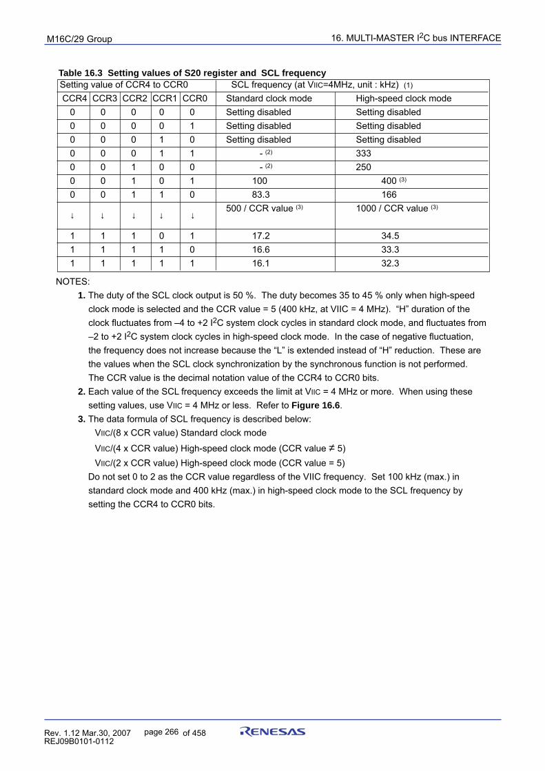
16. MULTI-MASTER I2C bus INTERFACEpuorG92/C61M
page 266 854fo7002,03.raM21.1.veR2110-1010B90JER
Setting value of CCR4 to CCR0 SCL frequency (at VIIC=4MHz, unit : kHz) (1)
CCR4 CCR3 CCR2 CCR1 CCR0 Standard clock mode High-speed clock mode 0 0 0 0 0 Setting disabled Setting disabled 0 0 0 0 1 Setting disabled Setting disabled 0 0 0 1 0 Setting disabled Setting disabled 0 0 0 1 1 - (2) 333 0 0 1 0 0 - (2) 250 0 0 1 0 1 100 400 (3)
0 0 1 1 0 83.3 166500 / CCR value (3) 1000 / CCR value (3)
1 1 1 0 1 17.2 34.5 1 1 1 1 0 16.6 33.3 1 1 1 1 1 16.1 32.3
NOTES:1. The duty of the SCL clock output is 50 %. The duty becomes 35 to 45 % only when high-speed
clock mode is selected and the CCR value = 5 (400 kHz, at VIIC = 4 MHz). “H” duration of theclock fluctuates from –4 to +2 I2C system clock cycles in standard clock mode, and fluctuates from–2 to +2 I2C system clock cycles in high-speed clock mode. In the case of negative fluctuation,the frequency does not increase because the “L” is extended instead of “H” reduction. These arethe values when the SCL clock synchronization by the synchronous function is not performed.The CCR value is the decimal notation value of the CCR4 to CCR0 bits.
2. Each value of the SCL frequency exceeds the limit at VIIC = 4 MHz or more. When using thesesetting values, use VIIC = 4 MHz or less. Refer to Figure 16.6.
3. The data formula of SCL frequency is described below:VIIC/(8 x CCR value) Standard clock mode
VIIC/(4 x CCR value) High-speed clock mode (CCR value ≠ 5)VIIC/(2 x CCR value) High-speed clock mode (CCR value = 5)
Do not set 0 to 2 as the CCR value regardless of the VIIC frequency. Set 100 kHz (max.) instandard clock mode and 400 kHz (max.) in high-speed clock mode to the SCL frequency bysetting the CCR4 to CCR0 bits.
Table 16.3 Setting values of S20 register and SCL frequency
→ → → → →
16. MULTI-MASTER I2C bus INTERFACEpuorG92/C61M
page 267 854fo7002,03.raM21.1.veR2110-1010B90JER
16.4 I2C0 Control Register 0 (S1D0)The S1D0 register controls data communication format.
16.4.1 Bits 0 to 2: Bit Counter (BC0–BC2)
Bits BC2 to BC0 decide how many bits are in one byte data transferred next. After the selected num-bers of bits are transferred successfully, I2C bus interface interrupt request is gnerated and bits BC2 toBC0 are reset to 0002. At this time, if the ACK-CLK bit in the S20 register is set to 1 (with ACK clock),one bit for ACK clock is added to the numbers of bits selected by the BC2 to BC0 bits.In addition, bits BC2 to BC0 become 0002 even though the START condition is detected and theaddress data is transferred in 8 bits.
16.4.2 Bit 3: I2C Interface Enable Bit (ES0)
The ES0 bit enables to use the multi-master I2C bus interface. When the ES0 bit is set to 0, I2C businterface is disabled and the SDA and SCL pins are placed in a high-h-impedance state. When theES0 bit is set to 1, the interface is enabled.When the ES0 bit is set to 0, the process is followed.1)The bits in the S10 register are set as MST = 0, TRX = 0, PIN = 1, BB = 0, AL = 0, AAS = 0, ADR0 = 02)The S00 register cannot be written.3)The TOF bit in the S4D0 register is set to 0 (time-out detection flag is not detected)4)The I2C system clock (VIIC) stops counting while the internal counter and flags are reset.
16.4.3 Bit 4: Data Format Select Bit (ALS)The ALS bit determines whether the salve address is recognized. When the ALS bit is set to 0, anaddressing format is selected and a address data is recognized. Only if the comparison is matchedbetween the slave address stored into the S0D0 register and the received address data or if thegeneral call is received, the data is transferred. When the ALS bit is set to 1, the free data format isselected and the slave address is not recognized.
16.4.4 Bit 6: I2C bus Interface Reset Bit (IHR)The IHR bit is used to reset the I2C bus interface circuit when the error communication occurs.When the ES0 bit in the S1D0 register is set to 1 (I2C bus interface is enabled), the hardware is resetby writing 1 to the IHR bit. Flags are processed as follows:1)The bits in the S10 register are set as MST = 0, TRX = 0, PIN to 1, BB = 0, AL = 0, AAS = 0, and ADR0 = 02)The TOF bit in the S4D0 register is set to 0 (time-out detection flag is not detected)3)The internal counter and flags are reset.The I2C bus interface circuit is reset after 2.5 VIIC cycles or less, and the IHR bit becomes 0 automati-cally by writing 1 to the IHR bit. Figure 16.10 shows the reset timing.
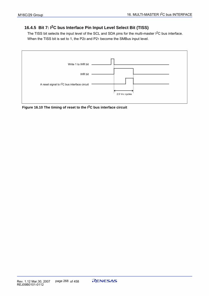
16. MULTI-MASTER I2C bus INTERFACEpuorG92/C61M
page 268 854fo7002,03.raM21.1.veR2110-1010B90JER
Figure 16.10 The timing of reset to the I2C bus interface circuit
A reset signal to I2C bus interface circuit
Write 1 to IHR bit
IHR bit
2.5 VIIC cycles
16.4.5 Bit 7: I2C bus Interface Pin Input Level Select Bit (TISS)The TISS bit selects the input level of the SCL and SDA pins for the multi-master I2C bus interface.When the TISS bit is set to 1, the P20 and P21 become the SMBus input level.
16. MULTI-MASTER I2C bus INTERFACEpuorG92/C61M
page 269 854fo7002,03.raM21.1.veR2110-1010B90JER
16.5 I2C0 Status Register (S10 register)The S10 register monitors the I2C bus interface status. When using the S10 register to check the status,use the 6 low-order bits for read only.
16.5.1 Bit 0: Last Receive Bit (LRB)The LRB bit stores the last bit value of received data. It can also be used to confirm whether ACK isreceived. If the ACK-CLK bit in the S20 register is set to 1 (with ACK clock) and ACK is returned when theACK clock is generated, the LRB bit is set to 0. If ACK is not returned, the LRB bit is set to 1. When theACK-CLK bit is set to 0 (no ACK clock), the last bit value of received data is input. When writing data tothe S00 register, the LRB bit is set to 0.
16.5.2 Bit 1: General Call Detection Flag (ADR0)When the ALS bit in the S1D0 register is set to 0 (addressing format), this ADR0 flag is set to 1 byreceiving the general calls(1),whose address data are all 0, in slave mode.The ADR0 flag is set to 0 when STOP or START conditions is detected or when the IHR bit in the S1D0register is set to 1 (reset).
NOTE: 1. General call: A master device transmits the general call address 0016 to all slaves. When the
master device transmits the general call, all slave devices receive the controlled data after generalcall.
16.5.3 Bit 2: Slave Address Comparison Flag (AAS)The AAS flag indicates a comparison result of the slave address data after enabled by setting the ALS bitin the S1D0 register to 0 (addressing format).The AAS flag is set to 1 when the 7 bits of the address data are matched with the slave address storedinto the S0D0 register, or when a general call is received, in slave receive mode. The AAS flag is set to0 by writing data to the S00 register. When the ES0 bit in the S1D0 register is set to 0 (I2C bus interfacedisabled) or when the IHR bit in the S1D0 register is set to 1 (reset), the AAS flag is also set to 0.
16.5.4 Bit 3: Arbitration Lost Detection Flag (AL)(1)
In master transmit mode, if an "L" signal is applied to the SDA pin by other than the MCU, the AL flag is setto 1 by determining that the arbitration is los and the TRX bit in the S10 register is set to 0 (receive mode)at the same time. The MST bit in the S10 register is set to 0 (slave mode) after transferring the byteswhich lost the arbitration.The arbitration lost can be detected only in master transmit mode. When writing data to the S00 register,the AL flag is set to 0. When the ES0 bit in the S1D0 register is set to 0 (I2C bus interface disabled) orwhen the IHR bit in the S1D0 register is set to 1 (reset), the AL flag is set to 0.
NOTE: 1. Arbitration lost: communication disabled as a master
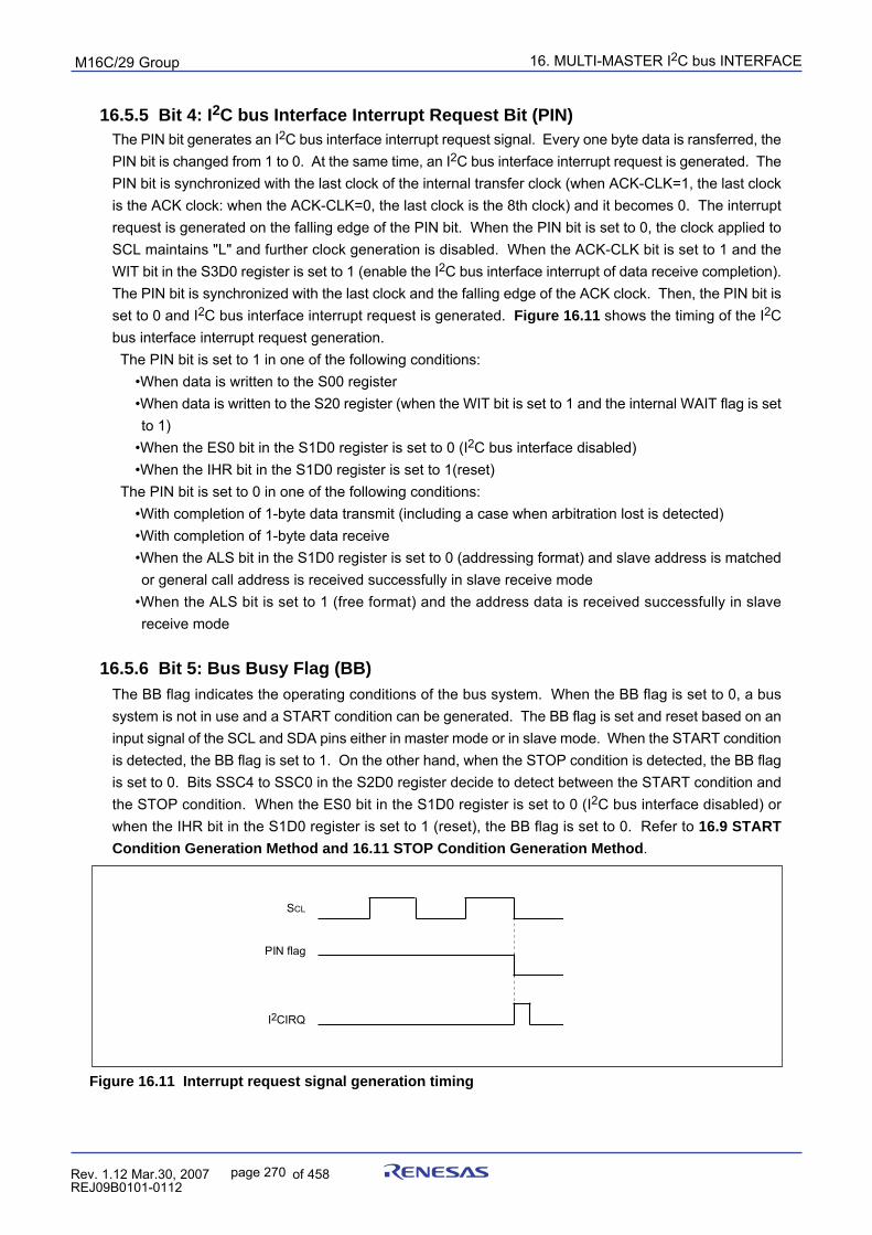
16. MULTI-MASTER I2C bus INTERFACEpuorG92/C61M
page 270 854fo7002,03.raM21.1.veR2110-1010B90JER
16.5.5 Bit 4: I2C bus Interface Interrupt Request Bit (PIN)The PIN bit generates an I2C bus interface interrupt request signal. Every one byte data is ransferred, thePIN bit is changed from 1 to 0. At the same time, an I2C bus interface interrupt request is generated. ThePIN bit is synchronized with the last clock of the internal transfer clock (when ACK-CLK=1, the last clockis the ACK clock: when the ACK-CLK=0, the last clock is the 8th clock) and it becomes 0. The interruptrequest is generated on the falling edge of the PIN bit. When the PIN bit is set to 0, the clock applied toSCL maintains "L" and further clock generation is disabled. When the ACK-CLK bit is set to 1 and theWIT bit in the S3D0 register is set to 1 (enable the I2C bus interface interrupt of data receive completion).The PIN bit is synchronized with the last clock and the falling edge of the ACK clock. Then, the PIN bit isset to 0 and I2C bus interface interrupt request is generated. Figure 16.11 shows the timing of the I2Cbus interface interrupt request generation. The PIN bit is set to 1 in one of the following conditions:
•When data is written to the S00 register•When data is written to the S20 register (when the WIT bit is set to 1 and the internal WAIT flag is setto 1)
•When the ES0 bit in the S1D0 register is set to 0 (I2C bus interface disabled)•When the IHR bit in the S1D0 register is set to 1(reset)
The PIN bit is set to 0 in one of the following conditions:•With completion of 1-byte data transmit (including a case when arbitration lost is detected)•With completion of 1-byte data receive•When the ALS bit in the S1D0 register is set to 0 (addressing format) and slave address is matchedor general call address is received successfully in slave receive mode
•When the ALS bit is set to 1 (free format) and the address data is received successfully in slavereceive mode
16.5.6 Bit 5: Bus Busy Flag (BB)The BB flag indicates the operating conditions of the bus system. When the BB flag is set to 0, a bussystem is not in use and a START condition can be generated. The BB flag is set and reset based on aninput signal of the SCL and SDA pins either in master mode or in slave mode. When the START conditionis detected, the BB flag is set to 1. On the other hand, when the STOP condition is detected, the BB flagis set to 0. Bits SSC4 to SSC0 in the S2D0 register decide to detect between the START condition andthe STOP condition. When the ES0 bit in the S1D0 register is set to 0 (I2C bus interface disabled) orwhen the IHR bit in the S1D0 register is set to 1 (reset), the BB flag is set to 0. Refer to 16.9 START
Condition Generation Method and 16.11 STOP Condition Generation Method.
Figure 16.11 Interrupt request signal generation timing
SC
L
PIN flag
I2C
I
R
Q
16. MULTI-MASTER I2C bus INTERFACEpuorG92/C61M
page 271 854fo7002,03.raM21.1.veR2110-1010B90JER
16.5.7 Bit 6: Communication Mode Select Bit (Transfer Direction Select Bit: TRX)This TRX bit decides a transfer direction for data communication. When the TRX bit is set to 0, receivemode is entered and data is received from a transmit device. When the TRX bit is set to 1, transmit modeis entered, and address data and control data are output to the SDAMM, synchronized with a clock gener-ated in the SCLMM.The TRX bit is set to 1 automatically in the following condition: •In slave mode, when the ALS in the S1D0 register to 0(addressing format), the AAS flag is set to
___
1 (address match) after the address data is received, and the received R/W bit is set to 1The TRX bit is set to 0 in one of the following conditions: •When an arbitration lost is detected •When a STOP condition is detected •When a START condition is detected •When a START condition is disabled by the START condition duplicate protect function (1)
•When the MST bit in the S10 register is set to 0(slave mode) and a start condition is detected •When the MST bit is set to 0 and the ACK non-return is detected •When the ES0 bit is set to 0(I2C bus interface disabled) •When the IHR bit in the S1D0 register is set to 1(reset)
16.5.8 Bit 7: Communication mode select bit (master/slave select bit: MST)
The MST bit selects either master mode or slave mode for data communication. When the MST bit is setto 0, slave mode is entered and the START/STOP condition generated by a master device are received.The data communication is synchronized with the clock generted by the master. When the MST bit is setto 1, master mode is entered and the START/STOP condition is generated.Additionally, clocks required for the data communication are generated on the SCLMM.The MST bit is set to 0 in one of the following conditions.
•After 1-byte data of a master whose arbtration is lost if arbitration lost is detected•When a STOP condition is detected•When a START condition is detected•When a start condition is disabled by the START condition duplicate protect function (1)
•When the IHR bit in the S1D0 register is set to 1(reset)•When the ES0 bit is set to 0(I2C bus interface disabled)
NOTE: 1. START condition duplicate protect function:
When the START condition is generated, after confirming that the BB flag in the S1D0 register isset to 0 (bus free), all the MST, TRX and BB flags are set to 1 at the same time. However, if theBB flag is set to 1 immediately after the BB flag setting is confirmed because a START conditionis generated by other master device, bits MST and TRX cannot be written. The duplicate protectfunction is valid from the rising edge of the BB flag until slave address is received. Refer to 16.9
START Condition Generation Method for details.
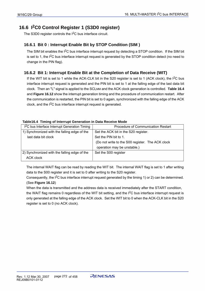
16. MULTI-MASTER I2C bus INTERFACEpuorG92/C61M
page 272 854fo7002,03.raM21.1.veR2110-1010B90JER
16.6 I2C0 Control Register 1 (S3D0 register)The S3D0 register controls the I2C bus interface circuit.
16.6.1 Bit 0 : Interrupt Enable Bit by STOP Condition (SIM )
The SIM bit enables the I2C bus interface interrupt request by detecting a STOP condition. If the SIM bitis set to 1, the I2C bus interface interrupt request is generated by the STOP condition detect (no need tochange in the PIN flag).
16.6.2 Bit 1: Interrupt Enable Bit at the Completion of Data Receive (WIT)If the WIT bit is set to 1 while the ACK-CLK bit in the S20 register is set to 1 (ACK clock), the I2C businterface interrupt request is generated and the PIN bit is set to 1 at the falling edge of the last data bitclock. Then an "L" signal is applied to the SCLMM and the ACK clock generation is controlled. Table 16.4
and Figure 16.12 show the interrupt generation timing and the procedure of communication restart. Afterthe communication is restarted, the PIN bit is set to 0 again, synchronized with the falling edge of the ACKclock, and the I2C bus interface interrupt request is generated.
Table16.4 Timing of Interrupt Generation in Data Receive Mode
The internal WAIT flag can be read by reading the WIT bit. The internal WAIT flag is set to 1 after writingdata to the S00 register and it is set to 0 after writing to the S20 register.Consequently, the I2C bus interface interrupt request generated by the timing 1) or 2) can be determined.(See Figure 16.12)When the data is transmitted and the address data is received immediately after the START condition,the WAIT flag remains 0 regardless of the WIT bit setting, and the I2C bus interface interrupt request isonly generated at the falling edge of the ACK clock. Set the WIT bit to 0 when the ACK-CLK bit in the S20register is set to 0 (no ACK clock).
I2C bus Interface Interrupt Generation Timing Procedure of Communication Restart 1) Synchronized with the falling edge of the Set the ACK bit in the S20 register. last data bit clock Set the PIN bit to 1.
(Do not write to the S00 register. The ACK clock operation may be unstable.)
2) Synchronized with the falling edge of the Set the S00 register ACK clock
16. MULTI-MASTER I2C bus INTERFACEpuorG92/C61M
page 273 854fo7002,03.raM21.1.veR2110-1010B90JER
Figure 16.12 The timing of the interrupt generation at the completion of the data receive
16.6.3 Bits 2,3 : Port Function Select Bits PED, PECIf the ES0 bit in the S1D0 register is set to 1 (I2C bus interface enabled), the SDAMM functions as anoutput port. When the PED bit is set to 1 and the SCLMM functions as an output port when the PEC bit isset to 1. Then the setting values of bits P2_0 and P2_1 in the port P2 register are output to the I2C bus,regardless of he internal SCL/SDA output signals. (SCL/SDA pins are onnected to I2C bus interfacecircuit)The bus data can be read by reading the port pi direction register in input mode, regardless of the settingvalues of the PED and PEC bits. Table 16.5 shows the port specification.
Table 16.5 Port specifications
In receive mode, ACK bit = 1 WIT bit = 0
7 clock 8 clock ACKclock
1 clock
1 bit7 bit 8 bit ACK bit
SCL
SDA
ACKBIT bit
PIN flag
Internal WAIT flag
I2C bus interface interrupt request signal
The writing signal of the S00 register
7 clock 8 clock ACKclock
1 bit7 bit 8 bit
SCL
SDA
ACKBIT bit
PIN flag
Internal WAIT flag
I2C bus interface interrupt request signal
The writing signal of the S00 register
The writing signal of the S20 register
1)
NOTE: 1. Do not write to the I2C0 clock control register except the bit ACK-BIT.
In receive mode, ACK bit = 1 WIT bit = 1
2)
emaNniP tiB9SE tiBDEP 2P 0 noitceriDtroPretsigeR noitcnuF
2P 0
0 - 1/0 noitcnufO/ItroP
1 0 - S AD noitcnufO/I
1 1 - S AD noitcnuftuptuotrop,noitcnuftupni
emaNniP tiB0SE tiBCEP 2P 1 noitceriDtroPretsigeR noitcnuF
2P 1
0 - 1/0 noitcnufO/ItroP
1 0 - S LC noitcnufO/I
1 1 - S LC noicnuftuptuotrop,noitcnuftupni
16. MULTI-MASTER I2C bus INTERFACEpuorG92/C61M
page 274 854fo7002,03.raM21.1.veR2110-1010B90JER
16.6.6 Address Receive in STOP/WAIT ModeWhen WAIT mode is entered after the CM02 bit in the CM0 register is set to 0 (do not stop the peripheralfunction clock in wait mode), the I2C bus interface circuit can receive address data in WAIT mode. How-ever, the I2C bus interface circuit is not operated in STOP mode or in low power consumption mode,because the I2C bus system clock VIIC is not supplied.
16.6.4 Bits 4,5 : SDA/SCL Logic Output Value Monitor Bits SDAM/SCLMBits SDAM/SCLM can monitor the logic value of the SDA and SCL output signals from the I2C businterface circuit. The SDAM bit monitors the SDA output logic value. The SCLM bit monitors the SCLoutput logic value. The SDAM and SCLM bits are read-only. If necessary, set them to 0.
16.6.5 Bits 6,7 : I2C System Clock Select Bits ICK0, ICK1The ICK1 bit, ICK0 bit, bits ICK4 to ICK2 in the S4D0 register, and the PCLK0 bit in the PCLKR registercan select the system clock (VIIC) of the I2C bus interface circuit.The I2C bus system clock VIIC can be selected among 1/2 fIIC, 1/2.5 fIIC, 1/3 fIIC, 1/4 fIIC, 1/5 fIIC, 1/6 fIICand 1/8 fIIC. fIIC can be selected between f1 and f2 by the PCLK0 bit setting.
I3CK4[S4D0] ICK3[S4D0] ICK2[S4D0] ICK1[S3D0] ICK0[S3D0] I2C system clock0 0 0 0 0 VIIC = 1/2 fIIC0 0 0 0 1 VIIC = 1/4 fIIC0 0 0 1 0 VIIC = 1/8 fIIC0 0 1 X X VIIC = 1/2.5 fIIC0 1 0 X X VIIC = 1/3 fIIC0 1 1 X X VIIC = 1/5 fIIC1 0 0 X X VIIC = 1/6 fIIC
Table 16.6 I2C system clock select bits
( Do not set the combination other than the above)
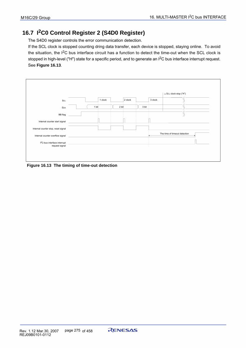
16. MULTI-MASTER I2C bus INTERFACEpuorG92/C61M
page 275 854fo7002,03.raM21.1.veR2110-1010B90JER
16.7 I2C0 Control Register 2 (S4D0 Register)The S4D0 register controls the error communication detection.If the SCL clock is stopped counting dring data transfer, each device is stopped, staying online. To avoidthe situation, the I2C bus interface circuit has a function to detect the time-out when the SCL clock isstopped in high-level ("H") state for a specific period, and to generate an I2C bus interface interrupt request.See Figure 16.13.
Figure 16.13 The timing of time-out detection
1 clock
1 bit
SCL
SDA
BB flag
Internal counter start signal
Internal counter stop, reset signal
Internal counter overflow signal
I2C-bus interface interrupt request signal
2 bit 3 bit
2 clock 3 clock
SCL clock stop (“H”)
The time of timeout detection
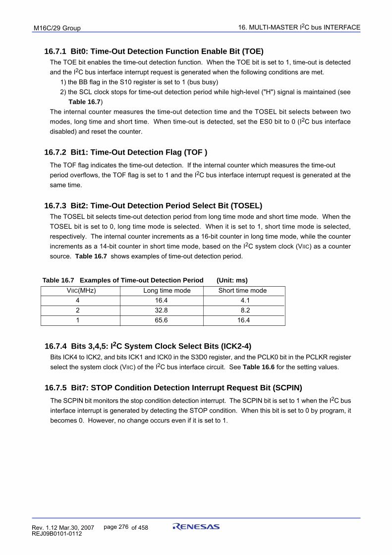
16. MULTI-MASTER I2C bus INTERFACEpuorG92/C61M
page 276 854fo7002,03.raM21.1.veR2110-1010B90JER
16.7.1 Bit0: Time-Out Detection Function Enable Bit (TOE)The TOE bit enables the time-out detection function. When the TOE bit is set to 1, time-out is detectedand the I2C bus interface interrupt request is generated when the following conditions are met.
1) the BB flag in the S10 register is set to 1 (bus busy)2) the SCL clock stops for time-out detection period while high-level ("H") signal is maintained (see
Table 16.7)The internal counter measures the time-out detection time and the TOSEL bit selects between twomodes, long time and short time. When time-out is detected, set the ES0 bit to 0 (I2C bus interfacedisabled) and reset the counter.
16.7.2 Bit1: Time-Out Detection Flag (TOF )
The TOF flag indicates the time-out detection. If the internal counter which measures the time-outperiod overflows, the TOF flag is set to 1 and the I2C bus interface interrupt request is generated at thesame time.
16.7.3 Bit2: Time-Out Detection Period Select Bit (TOSEL)The TOSEL bit selects time-out detection period from long time mode and short time mode. When theTOSEL bit is set to 0, long time mode is selected. When it is set to 1, short time mode is selected,respectively. The internal counter increments as a 16-bit counter in long time mode, while the counterincrements as a 14-bit counter in short time mode, based on the I2C system clock (VIIC) as a countersource. Table 16.7 shows examples of time-out detection period.
Table 16.7 Examples of Time-out Detection Period (Unit: ms)
16.7.4 Bits 3,4,5: I2C System Clock Select Bits (ICK2-4)Bits ICK4 to ICK2, and bits ICK1 and ICK0 in the S3D0 register, and the PCLK0 bit in the PCLKR registerselect the system clock (VIIC) of the I2C bus interface circuit. See Table 16.6 for the setting values.
16.7.5 Bit7: STOP Condition Detection Interrupt Request Bit (SCPIN)
The SCPIN bit monitors the stop condition detection interrupt. The SCPIN bit is set to 1 when the I2C businterface interrupt is generated by detecting the STOP condition. When this bit is set to 0 by program, itbecomes 0. However, no change occurs even if it is set to 1.
VIIC(MHz) Long time mode Short time mode 4 16.4 4.1 2 32.8 8.2 1 65.6 16.4
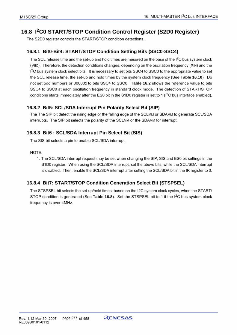
16. MULTI-MASTER I2C bus INTERFACEpuorG92/C61M
page 277 854fo7002,03.raM21.1.veR2110-1010B90JER
16.8 I2C0 START/STOP Condition Control Register (S2D0 Register)The S2D0 register controls the START/STOP condition detections.
16.8.1 Bit0-Bit4: START/STOP Condition Setting Bits (SSC0-SSC4)
The SCL release time and the set-up and hold times are mesured on the base of the I2C bus system clock(VIIC). Therefore, the detection conditions changes, depending on the oscillation frequency (XIN) and theI2C bus system clock select bits. It is necessary to set bits SSC4 to SSC0 to the appropriate value to setthe SCL release time, the set-up and hold times by the system clock frequency (See Table 16.10). Donot set odd numbers or 000002 to bits SSC4 to SSC0. Table 16.2 shows the reference value to bitsSSC4 to SSC0 at each oscillation frequency in standard clock mode. The detection of START/STOPconditions starts immediately after the ES0 bit in the S1D0 register is set to 1 (I2C bus interface enabled).
16.8.2 Bit5: SCL/SDA Interrupt Pin Polarity Select Bit (SIP)The The SIP bit detect the rising edge or the falling edge of the SCLMM or SDAMM to generate SCL/SDAinterrupts. The SIP bit selects the polarity of the SCLMM or the SDAMM for interrupt.
16.8.3 Bit6 : SCL/SDA Interrupt Pin Select Bit (SIS)
The SIS bit selects a pin to enable SCL/SDA interrupt.
NOTE: 1. The SCL/SDA interrupt request may be set when changing the SIP, SIS and ES0 bit settings in the
S1D0 register. When using the SCL/SDA interrupt, set the above bits, while the SCL/SDA interruptis disabled. Then, enable the SCL/SDA interrupt after setting the SCL/SDA bit in the IR register to 0.
16.8.4 Bit7: START/STOP Condition Generation Select Bit (STSPSEL)
The STSPSEL bit selects the set-up/hold times, based on the I2C system clock cycles, when the START/STOP condition is generated (See Table 16.8). Set the STSPSEL bit to 1 if the I2C bus system clockfrequency is over 4MHz.
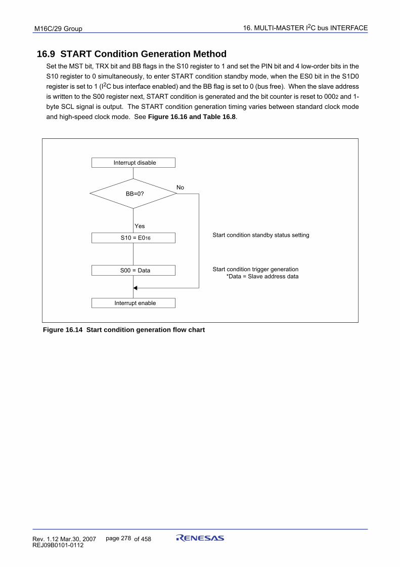
16. MULTI-MASTER I2C bus INTERFACEpuorG92/C61M
page 278 854fo7002,03.raM21.1.veR2110-1010B90JER
16.9 START Condition Generation MethodSet the MST bit, TRX bit and BB flags in the S10 register to 1 and set the PIN bit and 4 low-order bits in theS10 register to 0 simultaneously, to enter START condition standby mode, when the ES0 bit in the S1D0register is set to 1 (I2C bus interface enabled) and the BB flag is set to 0 (bus free). When the slave addressis written to the S00 register next, START condition is generated and the bit counter is reset to 0002 and 1-byte SCL signal is output. The START condition generation timing varies between standard clock modeand high-speed clock mode. See Figure 16.16 and Table 16.8.
Figure 16.14 Start condition generation flow chart
I
n
t
e
r
r
u
p
t
d
i
s
a
b
l
e
BB=0?
S10 = E016
S00 = Data
Interrupt enable
N
o
Yes
Start condition trigger generation
Start condition standby status setting
*Data = Slave address data
16. MULTI-MASTER I2C bus INTERFACEpuorG92/C61M
page 279 854fo7002,03.raM21.1.veR2110-1010B90JER
16.11 STOP Condition Generation MethodWhen the ES0 bit in the S1D0 register is set to 1 (I2C bus interface enabled) and bits MST and TRX in theS10 register are set to 1 at the same time, set the BB flag, PIN bit and 4 low-order bits in the S10 register to0 simultaneously, to enter STOP condition standby mode. When dummy data is written to the S00 registernext, the STOP condition is generated. The STOP condition generation timing varies between standardclock mode and high-speed clock mode. See Figure 16.17 and Table 16.8.Until the BB flag in the S10 register becomes 0 (bus free) after an instruction to generate the STOP condi-tion is executed, do not write data to registers S10 and S00. Otherwise, the STOP condition waveform maynot be generated correctly.If an input signal level of the SCL pin is set to low ("L") after the instruction to generate the STOP conditionis executed, a signal level of the SCL pin becomes high ("H"), and the BB flag is set to 0 (bus free), the MCUoutputs an "L" signal to SCL pin.In that case, the MCU can stop an "L" signal output to the SCL pin by generating the STOP condition, writing0 to the ES0 bit in the S1D0 register (disabled), or writing 1 to the IHR bit in the S1D0 register (resetrelease).
16.10 START Condition Duplicate Protect FunctionA START condition is generated when verifying that the BB flag in the S10 register does not use buses.However, if the BB flag is set to 1 (bus busy) by the START condition which other master device generatesimmediately after the BB flag is verified, the START condition is suspended by the START condition dupli-cate protect function. When the START condition duplicate protect function starts, it operates as follows:
•Disable the start condition standby settingIf the function has already been set, first exit START condition standby mode and then set bits MST andTRX in the S10 register to 0.•Writing to the S00 register is disabled. (The START condition trigger generation is disabled)•If the START condition generation is interrupted, the AL flag in the S10 register becomes 1.(arbitrationlost detection)
The START condition duplicate protect function is valid between the SDA falling edge of the START condi-tion and the receive completion of the slave address. Figure16.15 shows the duration of the STARTcondition duplicate protect function.
Figure 16.15 The duration of the start condition duplicate protect function
1 clock
1 bit
SCL
SDA
BB flag
2 bit 3 bit
2 clock 3 clock
8 bit ACK bit
The duration of start condition duplicate protect
8 clock ACK clock
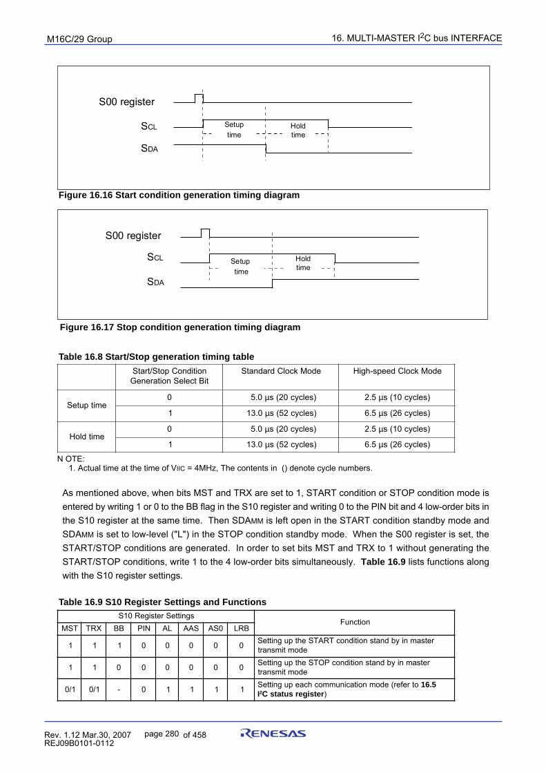
16. MULTI-MASTER I2C bus INTERFACEpuorG92/C61M
page 280 854fo7002,03.raM21.1.veR2110-1010B90JER
Figure 16.16 Start condition generation timing diagram
Figure 16.17 Stop condition generation timing diagram
Table 16.8 Start/Stop generation timing table
As mentioned above, when bits MST and TRX are set to 1, START condition or STOP condition mode isentered by writing 1 or 0 to the BB flag in the S10 register and writing 0 to the PIN bit and 4 low-order bits inthe S10 register at the same time. Then SDAMM is left open in the START condition standby mode andSDAMM is set to low-level ("L") in the STOP condition standby mode. When the S00 register is set, theSTART/STOP conditions are generated. In order to set bits MST and TRX to 1 without generating theSTART/STOP conditions, write 1 to the 4 low-order bits simultaneously. Table 16.9 lists functions alongwith the S10 register settings.
N OTE: 1. Actual time at the time of VIIC = 4MHz, The contents in () denote cycle numbers.
Table 16.9 S10 Register Settings and Functions
S
0
0
r
e
g
i
s
t
e
r
SC
L
SD
A
Holdtime
S
e
t
u
pt
i
m
e
S00 register
SC
L
SDA
Setup time
H
o
l
dt
i
m
e
noitidnoCpotS/tratStiBtceleSnoitareneG
edoMkcolCdradnatS edoMkcolCdeeps-hgiH
emitputeS0 0.5 µ )selcyc02(s 5.2 µ )selcyc01(s
1 0.31 µ )selcyc25(s 5.6 µ )selcyc62(s
emitdloH0 0.5 µ )selcyc02(s 5.2 µ )selcyc01(s
1 0.31 µ )selcyc25(s 5.6 µ )selcyc62(s
sgnitteSretsigeR01SnoitcnuF
TSM XRT BB NIP LA SAA 0SA BRL
1 1 1 0 0 0 0 0 retsamniybdnatsnoitidnocTRATSehtpugnitteSedomtimsnart
1 1 0 0 0 0 0 0 retsamniybdnatsnoitidnocPOTSehtpugnitteSedomtimsnart
1/0 1/0 - 0 1 1 1 1 otrefer(edomnoitacinummochcaepugnitteS 5.61I2 retsigersutatsC )
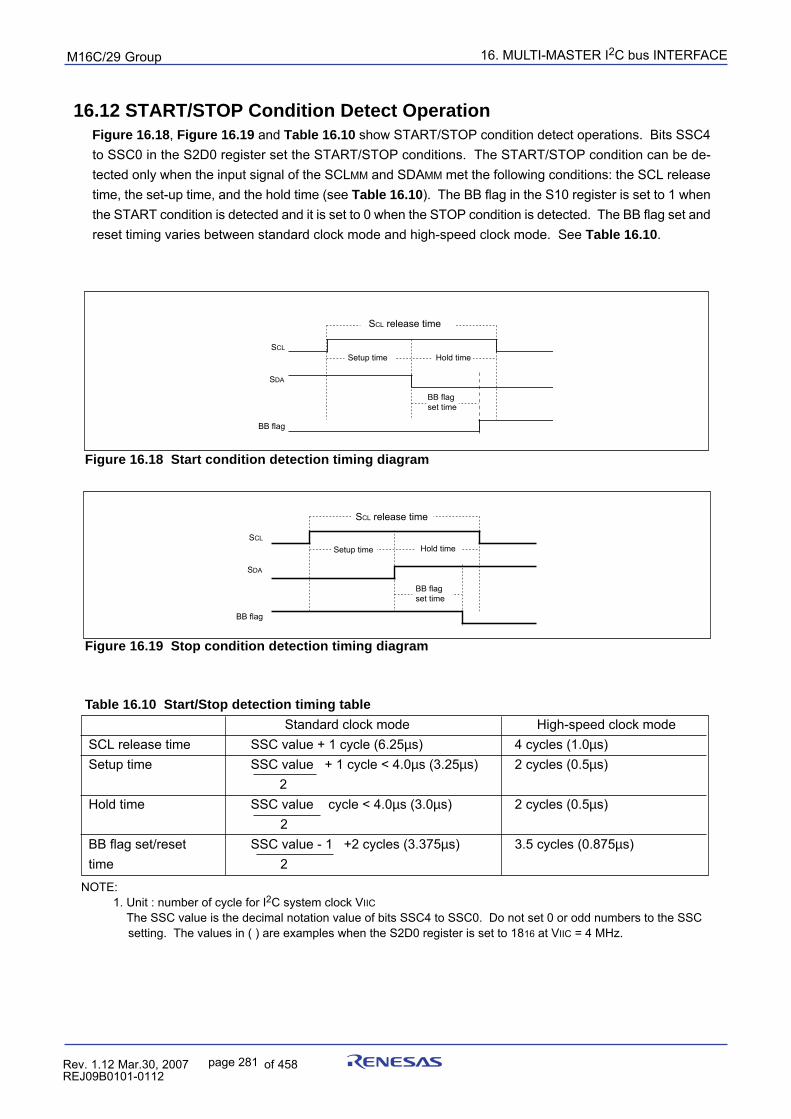
16. MULTI-MASTER I2C bus INTERFACEpuorG92/C61M
page 281 854fo7002,03.raM21.1.veR2110-1010B90JER
16.12 START/STOP Condition Detect OperationFigure 16.18, Figure 16.19 and Table 16.10 show START/STOP condition detect operations. Bits SSC4to SSC0 in the S2D0 register set the START/STOP conditions. The START/STOP condition can be de-tected only when the input signal of the SCLMM and SDAMM met the following conditions: the SCL releasetime, the set-up time, and the hold time (see Table 16.10). The BB flag in the S10 register is set to 1 whenthe START condition is detected and it is set to 0 when the STOP condition is detected. The BB flag set andreset timing varies between standard clock mode and high-speed clock mode. See Table 16.10.
Figure 16.18 Start condition detection timing diagram
Figure 16.19 Stop condition detection timing diagram
Standard clock mode High-speed clock modeSCL release time SSC value + 1 cycle (6.25µs) 4 cycles (1.0µs)Setup time SSC value + 1 cycle < 4.0µs (3.25µs) 2 cycles (0.5µs)
2Hold time SSC value cycle < 4.0µs (3.0µs) 2 cycles (0.5µs)
2BB flag set/reset SSC value - 1 +2 cycles (3.375µs) 3.5 cycles (0.875µs)time 2
Table 16.10 Start/Stop detection timing table
SCL release time
Hold timeSetup time
BB flag set time
BB flag
SDA
SCL
BB flag
SDA
SCL
SCL release time
Hold timeSetup time
BB flag set time
NOTE:1. Unit : number of cycle for I2C system clock VIIC The SSC value is the decimal notation value of bits SSC4 to SSC0. Do not set 0 or odd numbers to the SSC
setting. The values in ( ) are examples when the S2D0 register is set to 1816 at VIIC = 4 MHz.
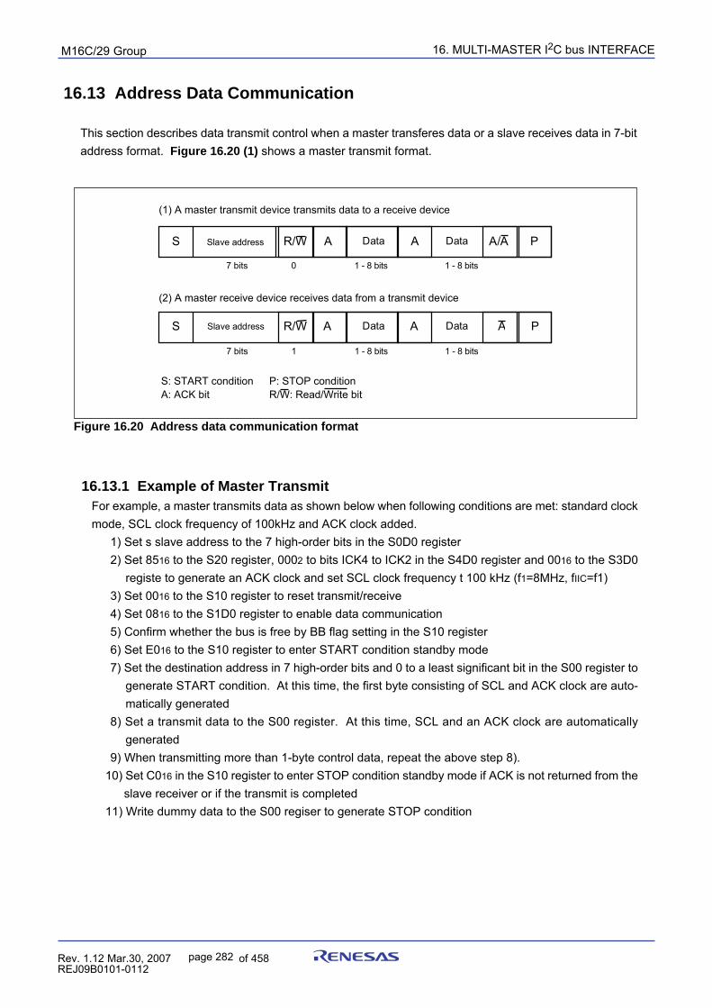
16. MULTI-MASTER I2C bus INTERFACEpuorG92/C61M
page 282 854fo7002,03.raM21.1.veR2110-1010B90JER
16.13 Address Data Communication
This section describes data transmit control when a master transferes data or a slave receives data in 7-bitaddress format. Figure 16.20 (1) shows a master transmit format.
Figure 16.20 Address data communication format
16.13.1 Example of Master TransmitFor example, a master transmits data as shown below when following conditions are met: standard clockmode, SCL clock frequency of 100kHz and ACK clock added.
1) Set s slave address to the 7 high-order bits in the S0D0 register2) Set 8516 to the S20 register, 0002 to bits ICK4 to ICK2 in the S4D0 register and 0016 to the S3D0
registe to generate an ACK clock and set SCL clock frequency t 100 kHz (f1=8MHz, fIIC=f1)3) Set 0016 to the S10 register to reset transmit/receive4) Set 0816 to the S1D0 register to enable data communication5) Confirm whether the bus is free by BB flag setting in the S10 register6) Set E016 to the S10 register to enter START condition standby mode7) Set the destination address in 7 high-order bits and 0 to a least significant bit in the S00 register to
generate START condition. At this time, the first byte consisting of SCL and ACK clock are auto-matically generated
8) Set a transmit data to the S00 register. At this time, SCL and an ACK clock are automaticallygenerated
9) When transmitting more than 1-byte control data, repeat the above step 8).10) Set C016 in the S10 register to enter STOP condition standby mode if ACK is not returned from the
slave receiver or if the transmit is completed11) Write dummy data to the S00 regiser to generate STOP condition
1 - 8 bits
S: START condition P: STOP conditionA: ACK bit R/W: Read/Write bit
S S
l
a
v
e
a
d
d
r
e
s
s R/W A D
a
t
a A A/A P
S R/W A A A P
1
D
a
t
a
D
a
t
aD
a
t
aS
l
a
v
e
a
d
d
r
e
s
s
7 bits
(1) A master transmit device transmits data to a receive device
(2) A master receive device receives data from a transmit device
1 - 8 bits
1 - 8 bits 07 bits 1 - 8 bits
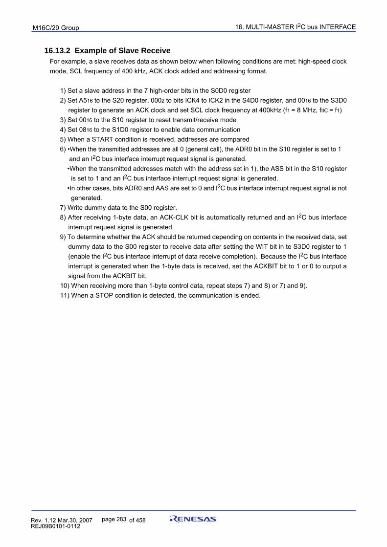
16. MULTI-MASTER I2C bus INTERFACEpuorG92/C61M
page 283 854fo7002,03.raM21.1.veR2110-1010B90JER
16.13.2 Example of Slave ReceiveFor example, a slave receives data as shown below when following conditions are met: high-speed clockmode, SCL frequency of 400 kHz, ACK clock added and addressing format.
1) Set a slave address in the 7 high-order bits in the S0D0 register2) Set A516 to the S20 register, 0002 to bits ICK4 to ICK2 in the S4D0 register, and 0016 to the S3D0
register to generate an ACK clock and set SCL clock frequency at 400kHz (f1 = 8 MHz, fIIC = f1)3) Set 0016 to the S10 register to reset transmit/receive mode4) Set 0816 to the S1D0 register to enable data communication5) When a START condition is received, addresses are compared6) •When the transmitted addresses are all 0 (general call), the ADR0 bit in the S10 register is set to 1
and an I2C bus interface interrupt request signal is generated.•When the transmitted addresses match with the address set in 1), the ASS bit in the S10 register
is set to 1 and an I2C bus interface interrupt request signal is generated.•In other cases, bits ADR0 and AAS are set to 0 and I2C bus interface interrupt request signal is not
generated.7) Write dummy data to the S00 register.8) After receiving 1-byte data, an ACK-CLK bit is automatically returned and an I2C bus interface
interrupt request signal is generated.9) To determine whether the ACK should be returned depending on contents in the received data, set
dummy data to the S00 register to receive data after setting the WIT bit in te S3D0 register to 1(enable the I2C bus interface interrupt of data receive completion). Because the I2C bus interfaceinterrupt is generated when the 1-byte data is received, set the ACKBIT bit to 1 or 0 to output asignal from the ACKBIT bit.
10) When receiving more than 1-byte control data, repeat steps 7) and 8) or 7) and 9).11) When a STOP condition is detected, the communication is ended.
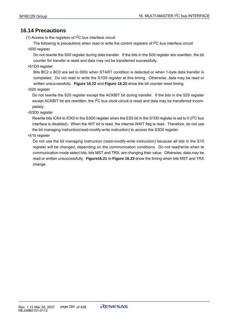
16. MULTI-MASTER I2C bus INTERFACEpuorG92/C61M
page 284 854fo7002,03.raM21.1.veR2110-1010B90JER
16.14 Precautions(1) Access to the registers of I2C bus interface circuit
The following is precautions when read or write the control registers of I2C bus interface circuit •S00 register
Do not rewrite the S00 register during data transfer. If the bits in the S00 register are rewritten, the bitcounter for transfer is reset and data may not be transferred successfully.
•S1D0 registerBits BC2 o BC0 are set to 0002 when START condition is detected or when 1-byte data transfer iscompleted. Do not read or write the S1D0 register at this timing. Otherwise, data may be read orwritten unsuccessfully. Figure 16.22 and Figure 16.23 show the bit counter reset timing.
•S20 registerDo not rewrite the S20 register except the ACKBIT bit during transfer. If the bits in the S20 registerexcept ACKBIT bit are rewritten, the I2C bus clock circuit is reset and data may be transferred incom-pletely.
•S3D0 registerRewrite bits ICK4 to ICK0 in the S3D0 register when the ES0 bit in the S1D0 register is set to 0 (I2C businterface is disabled). When the WIT bit is read, the internal WAIT flag is read. Therefore, do not usethe bit managing instruction(read-modify-write instruction) to access the S3D0 register.
•S10 registerDo not use the bit managing instruction (read-modify-write instruction) because all bits in the S10register will be changed, depending on the communication conditions. Do not read/write when tecommunication mode select bits, bits MST and TRX, are changing their value. Otherwise, data may beread or written unsuccessfully. Figure16.21 to Figure 16.23 show the timing when bits MST and TRXchange.
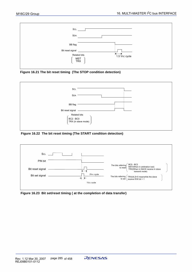
16. MULTI-MASTER I2C bus INTERFACEpuorG92/C61M
page 285 854fo7002,03.raM21.1.veR2110-1010B90JER
Figure 16.21 The bit reset timing (The STOP condition detection)
Figure 16.22 The bit reset timing (The START condition detection)
MST
TRX
BB flag
SDA
SCL
Bit reset signal
Related bits 1.5 VIIC cycle
BB flag
SDA
SCL
Bit reset signal
BC2 - BC0TRX (in slave mode)
Related bits
Figure 16.23 Bit set/reset timing ( at the completion of data transfer)
SCL
Bit set signal
AAA1VIIC cycle
PIN bit
AA2VIIC cycle
Bit reset signal
AAAAAAAAAABC0 - BC2
MST(When in arbitration lost)TRX(When in NACK receive in slave transmit mode)
The bits referringto reset
AAAAAAAAAA
TRX(ALS=0 meanwhile the slavereceive R/W bit = 1
The bits referringto set
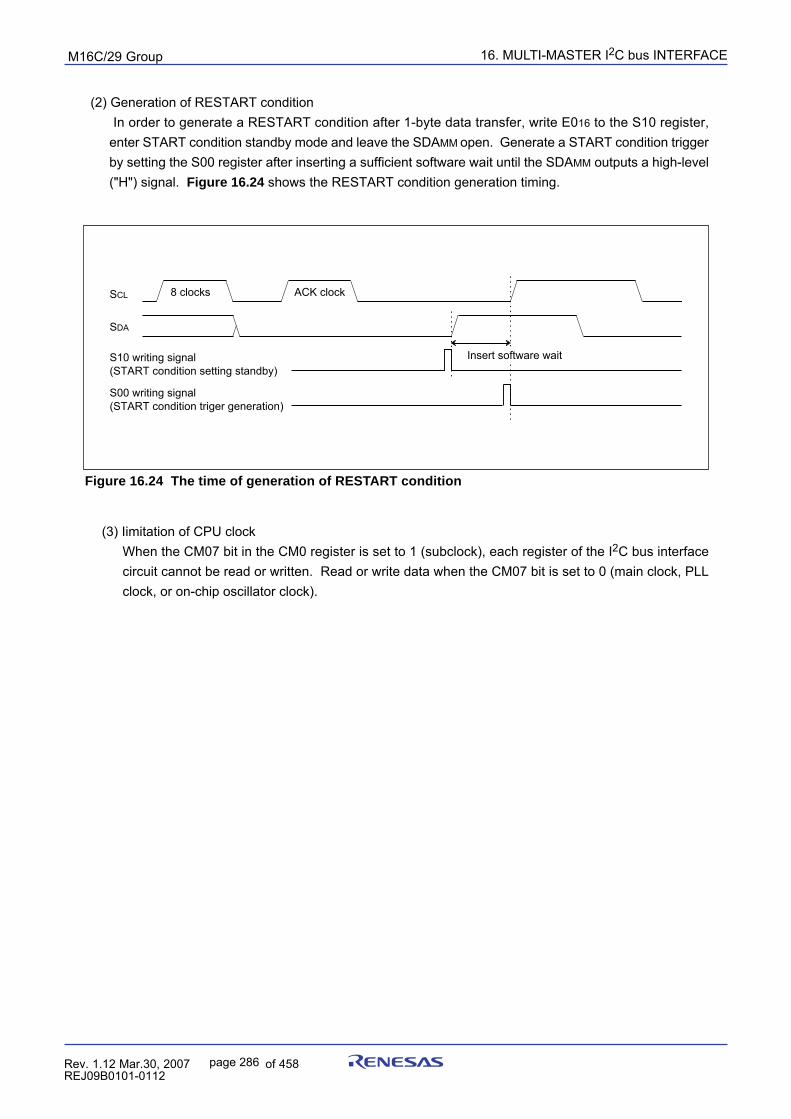
16. MULTI-MASTER I2C bus INTERFACEpuorG92/C61M
page 286 854fo7002,03.raM21.1.veR2110-1010B90JER
(2) Generation of RESTART condition In order to generate a RESTART condition after 1-byte data transfer, write E016 to the S10 register,enter START condition standby mode and leave the SDAMM open. Generate a START condition triggerby setting the S00 register after inserting a sufficient software wait until the SDAMM outputs a high-level("H") signal. Figure 16.24 shows the RESTART condition generation timing.
Figure 16.24 The time of generation of RESTART condition
8 clocks
ACK clockSCL
S10 writing signal(START condition setting standby)
SDA
S00 writing signal(START condition triger generation)
Insert software wait
(3) Iimitation of CPU clockWhen the CM07 bit in the CM0 register is set to 1 (subclock), each register of the I2C bus interfacecircuit cannot be read or written. Read or write data when the CM07 bit is set to 0 (main clock, PLLclock, or on-chip oscillator clock).
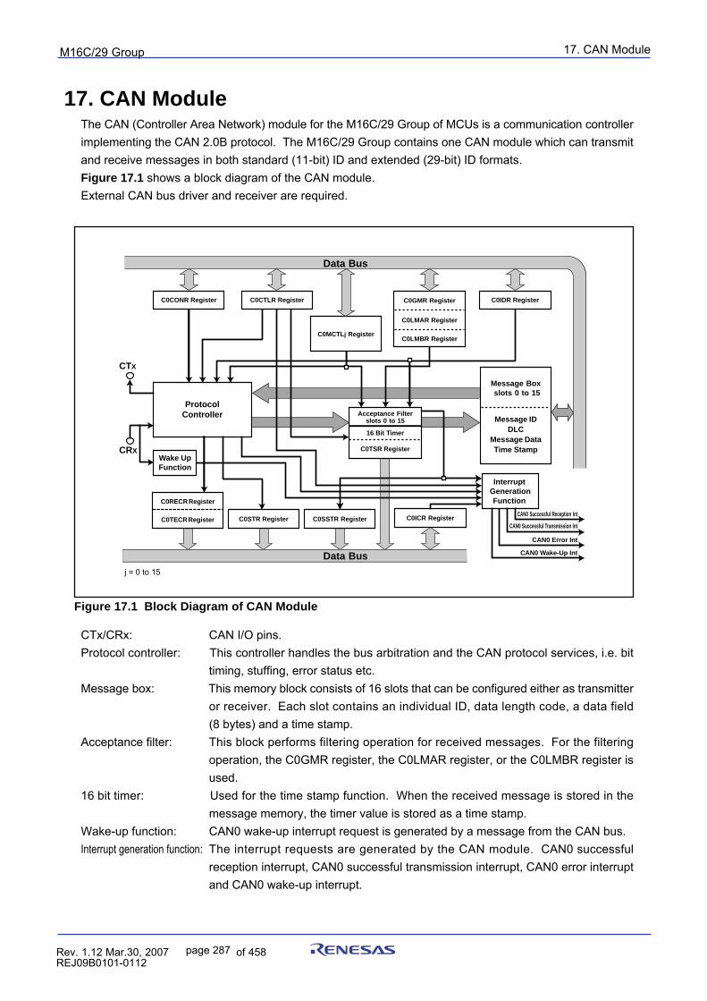
17. CAN ModulepuorG92/C61M
page 287 854fo7002,03.raM21.1.veR2110-1010B90JER
17. CAN ModuleThe CAN (Controller Area Network) module for the M16C/29 Group of MCUs is a communication controllerimplementing the CAN 2.0B protocol. The M16C/29 Group contains one CAN module which can transmitand receive messages in both standard (11-bit) ID and extended (29-bit) ID formats.Figure 17.1 shows a block diagram of the CAN module.External CAN bus driver and receiver are required.
Figure 17.1 Block Diagram of CAN Module
CTx/CRx: CAN I/O pins.Protocol controller: This controller handles the bus arbitration and the CAN protocol services, i.e. bit
timing, stuffing, error status etc.Message box: This memory block consists of 16 slots that can be configured either as transmitter
or receiver. Each slot contains an individual ID, data length code, a data field(8 bytes) and a time stamp.
Acceptance filter: This block performs filtering operation for received messages. For the filteringoperation, the C0GMR register, the C0LMAR register, or the C0LMBR register isused.
16 bit timer: Used for the time stamp function. When the received message is stored in themessage memory, the timer value is stored as a time stamp.
Wake-up function: CAN0 wake-up interrupt request is generated by a message from the CAN bus.Interrupt generation function: The interrupt requests are generated by the CAN module. CAN0 successful
reception interrupt, CAN0 successful transmission interrupt, CAN0 error interruptand CAN0 wake-up interrupt.
C0CONR Register C0CTLR Register C0IDR Register
j = 0 to 15
Interrupt Generation
Function
Message Box slots 0 to 15
Message IDDLC
Message DataTime Stamp
CTX
CRX
C0GMR Register
C0LMAR Register
C0LMBR Register
CAN0 Successful Reception Int
CAN0 Successful Transmission Int
CAN0 Error Int
CAN0 Wake-Up Int
Data Bus
Data Bus
C0MCTLj Register
C0TSR Register
16 Bit Timer
Acceptance Filterslots 0 to 15
ProtocolController
Wake UpFunction
C0SSTR Register C0ICR RegisterC0STR Register
C0RECR Register
C0TECR Register
17. CAN ModulepuorG92/C61M
page 288 854fo7002,03.raM21.1.veR2110-1010B90JER
17.1 CAN Module-Related RegistersThe CAN0 module has the following registers.
(1) CAN Message Box
A CAN module is equipped with 16 slots (16 bytes or 8 words each). Slots 14 and 15 can be used as BasicCAN.
• Priority of the slots: The smaller the number of the slot, the higher the priority, in both transmission andreception.
• A program can define whether a slot is defined as transmitter or receiver.
(2) Acceptance Mask Registers
A CAN module is equipped with 3 masks for the acceptance filter.• CAN0 global mask register (C0GMR register: 6 bytes)
Configuration of the masking condition for acceptance filtering processing to slots 0 to 13• CAN0 local mask A register (C0LMAR register: 6 bytes)
Configuration of the masking condition for acceptance filtering processing to slot 14• CAN0 local mask B register (C0LMBR register: 6 bytes)
Configuration of the masking condition for acceptance filtering processing to slot 15
(3) CAN SFR Registers
• CAN0 message control register j (C0MCTLj register: 8 bits 16) (j = 0 to 15)Control of transmission and reception of a corresponding slot
• CANi control register (CiCTLR register: 16 bits) (i = 0, 1)Control of the CAN protocol
• CAN0 status register (C0STR register: 16 bits)Indication of the protocol status
• CAN0 slot status register (C0SSTR register: 16 bits)Indication of the status of contents of each slot
• CAN0 interrupt control register (C0ICR register: 16 bits)Selection of “interrupt enabled or disabled” for each slot
• CAN0 extended ID register (C0IDR register: 16 bits)Selection of ID format (standard or extended) for each slot
• CAN0 configuration register (C0CONR register: 16 bits)Configuration of the bus timing
• CAN0 receive error count register (C0RECR register: 8 bits)Indication of the error status of the CAN module in reception: the counter value is incremented ordecremented according to the error occurrence.
• CAN0 transmit error count register (C0TECR register: 8 bits)Indication of the error status of the CAN module in transmission: the counter value is incremented ordecremented according to the error occurrence.
• CAN0 time stamp register (C0TSR register: 16 bits)Indication of the value of the time stamp counter
• CAN0 acceptance filter support register (C0AFS register: 16 bits)Decoding the received ID for use by the acceptance filter support unit
Explanation of each register is given as follows.
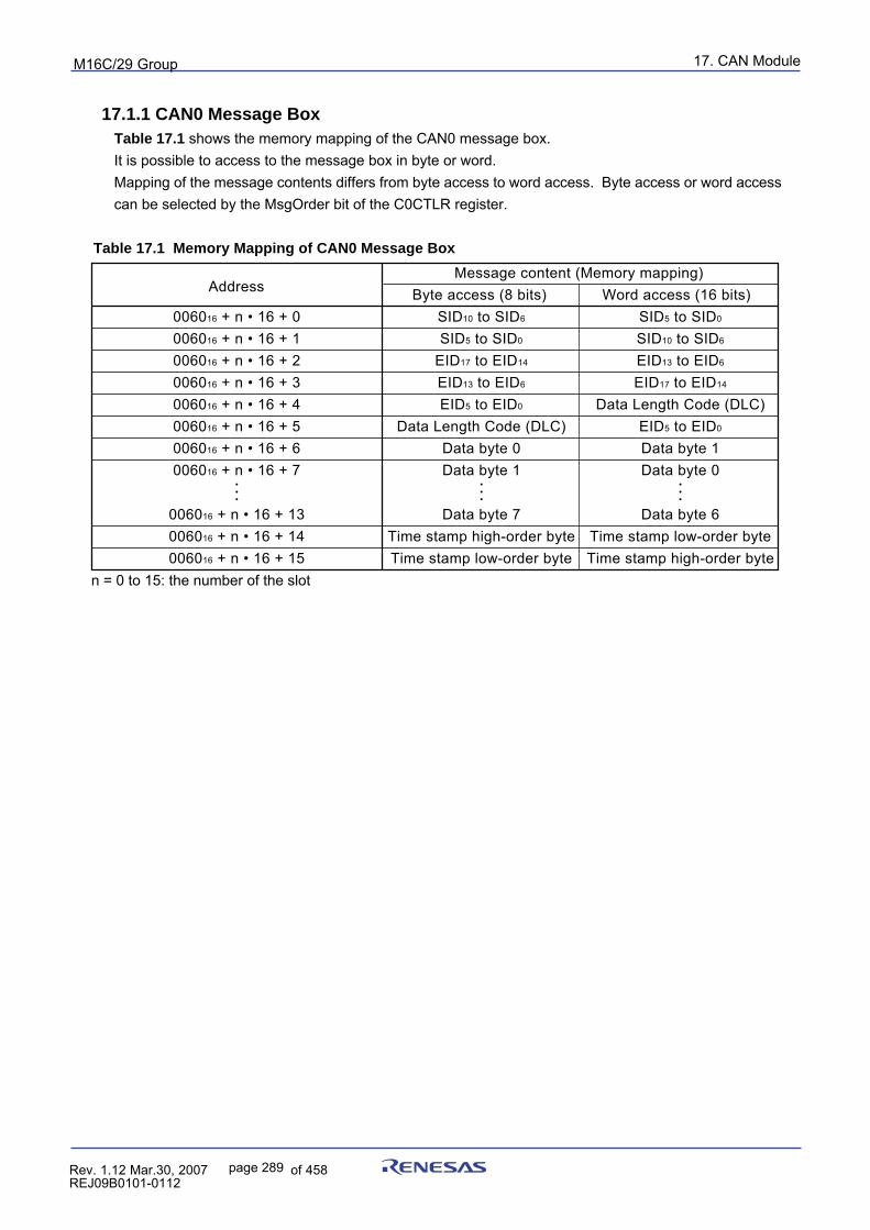
17. CAN ModulepuorG92/C61M
page 289 854fo7002,03.raM21.1.veR2110-1010B90JER
17.1.1 CAN0 Message BoxTable 17.1 shows the memory mapping of the CAN0 message box.It is possible to access to the message box in byte or word.Mapping of the message contents differs from byte access to word access. Byte access or word accesscan be selected by the MsgOrder bit of the C0CTLR register.
Table 17.1 Memory Mapping of CAN0 Message Box
Message content (Memory mapping)Byte access (8 bits) Word access (16 bits)
006016 + n • 16 + 0 SID10 to SID6 SID5 to SID0
006016 + n • 16 + 1 SID5 to SID0 SID10 to SID6
006016 + n • 16 + 2 EID17 to EID14 EID13 to EID6
006016 + n • 16 + 3 EID13 to EID6 EID17 to EID14
006016 + n • 16 + 4 EID5 to EID0 Data Length Code (DLC)006016 + n • 16 + 5 Data Length Code (DLC) EID5 to EID0
006016 + n • 16 + 6 Data byte 0 Data byte 1006016 + n • 16 + 7 Data byte 1 Data byte 0
• • •• • •• • •
006016 + n • 16 + 13 Data byte 7 Data byte 6006016 + n • 16 + 14 Time stamp high-order byte Time stamp low-order byte006016 + n • 16 + 15 Time stamp low-order byte Time stamp high-order byte
Address
n = 0 to 15: the number of the slot
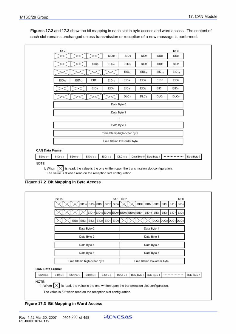
17. CAN ModulepuorG92/C61M
page 290 854fo7002,03.raM21.1.veR2110-1010B90JER
Figures 17.2 and 17.3 show the bit mapping in each slot in byte access and word access. The content ofeach slot remains unchanged unless transmission or reception of a new message is performed.
Figure 17.2 Bit Mapping in Byte Access
Figure 17.3 Bit Mapping in Word Access
bit 7 bit 0
SID10 SID9 SID8 SID7 SID6
SID5 SID4 SID3 SID2 SID1 SID0
EID17 EID16 EID15 EID14
EID13 EID12 EID11 EID10 EID9 EID8 EID7 EID6
EID5 EID4 EID3 EID2 EID1 EID0
DLC3 DLC2 DLC1 DLC0
Data Byte 0
Data Byte 1
Data Byte 7
NOTE:1. When
The value is 0 when read on the reception slot configuration.is read, the value is the one written upon the transmission slot configuration.
CAN Data Frame:
Time Stamp high-order byte
Time Stamp low-order byte
SID10 to 6 SID5 to 0 EID17 to 14 EID13 to 6 EID5 to 0 DLC3 to 0 Data Byte 0 Data Byte 1 Data Byte 7
bit 15 bit 0
SID10 SID9 SID8 SID7 SID6 SID5 SID4 SID3 SID2 SID1 SID0
bit 8 bit 7
EID17 EID16 EID15 EID14 EID13 EID12 EID11 EID10 EID9 EID8 EID7 EID6
EID5 EID4 EID3 EID2 EID1 EID0 DLC3 DLC2 DLC1 DLC0
Data Byte 0 Data Byte 1
Time Stamp high-order byte Time Stamp low-order byte
CAN Data Frame:
Data Byte 2 Data Byte 3
Data Byte 4 Data Byte 5
Data Byte 6 Data Byte 7
NOTE: 1.
SID10 to 6 SID5 to 0 EID17 to 14 EID13 to 6 EID5 to 0 DLC3 to 0
When
The value is "0" when read on the reception slot configuration.
is read, the value is the one written upon the transmission slot configuration.
Data Byte 0 Data Byte 1 Data Byte 7
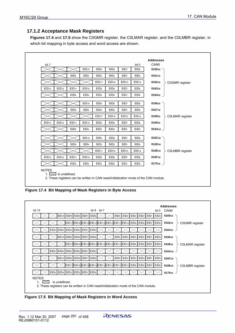
17. CAN ModulepuorG92/C61M
page 291 854fo7002,03.raM21.1.veR2110-1010B90JER
Figure 17.4 Bit Mapping of Mask Registers in Byte Access
17.1.2 Acceptance Mask RegistersFigures 17.4 and 17.5 show the C0GMR register, the C0LMAR register, and the C0LMBR register, inwhich bit mapping in byte access and word access are shown.
Figure 17.5 Bit Mapping of Mask Registers in Word Access
bit 7 bit 0SID10 SID9 SID8 SID7 SID6
SID5 SID4 SID3 SID2 SID1 SID0
EID17 EID16 EID15 EID14
EID13 EID12 EID11 EID10 EID9 EID8 EID7 EID6
EID5 EID4 EID3 EID2 EID1 EID0
SID10 SID9 SID8 SID7 SID6
SID5 SID4 SID3 SID2 SID1 SID0
EID17 EID16 EID15 EID14
EID13 EID12 EID11 EID10 EID9 EID8 EID7 EID6
EID5 EID4 EID3 EID2 EID1 EID0
SID10 SID9 SID8 SID7 SID6
SID5 SID4 SID3 SID2 SID1 SID0
EID17 EID16 EID15 EID14
EID13 EID12 EID11 EID10 EID9 EID8 EID7 EID6
EID5 EID4 EID3 EID2 EID1 EID0
C0GMR register
C0LMAR register
C0LMBR register
016016
016116
016216
016316
016416
016616
016716
016816
016916
016A16
016C16
016D16
016E16
016F16
017016
AddressesCAN0
NOTES 1. is undefined. 2. These registers can be written in CAN reset/initialization mode of the CAN module.
bit 15 bit 0
SID10 SID9 SID8 SID7 SID6 SID5 SID4 SID3 SID2 SID1 SID0
bit 8 bit 7
EID17 EID16 EID15 EID14 EID13 EID12 EID11 EID10 EID9 EID8 EID7 EID6
EID5 EID4 EID3 EID2 EID1 EID0
SID10 SID9 SID8 SID7 SID6 SID5 SID4 SID3 SID2 SID1 SID0
EID17 EID16 EID15 EID14 EID13 EID12 EID11 EID10 EID9 EID8 EID7 EID6
EID5 EID4 EID3 EID2 EID1 EID0
SID10 SID9 SID8 SID7 SID6 SID5 SID4 SID3 SID2 SID1 SID0
EID17 EID16 EID15 EID14 EID13 EID12 EID11 EID10 EID9 EID8 EID7 EID6
EID5 EID4 EID3 EID2 EID1 EID0
C0GMR register
C0LMAR register
C0LMBR register
016016
016216
016416
016616
016816
016A16
016C16
016E16
017016
AddressesCAN0
NOTES: 1. is undefined. 2. These registers can be written in CAN reset/initialization mode of the CAN module.
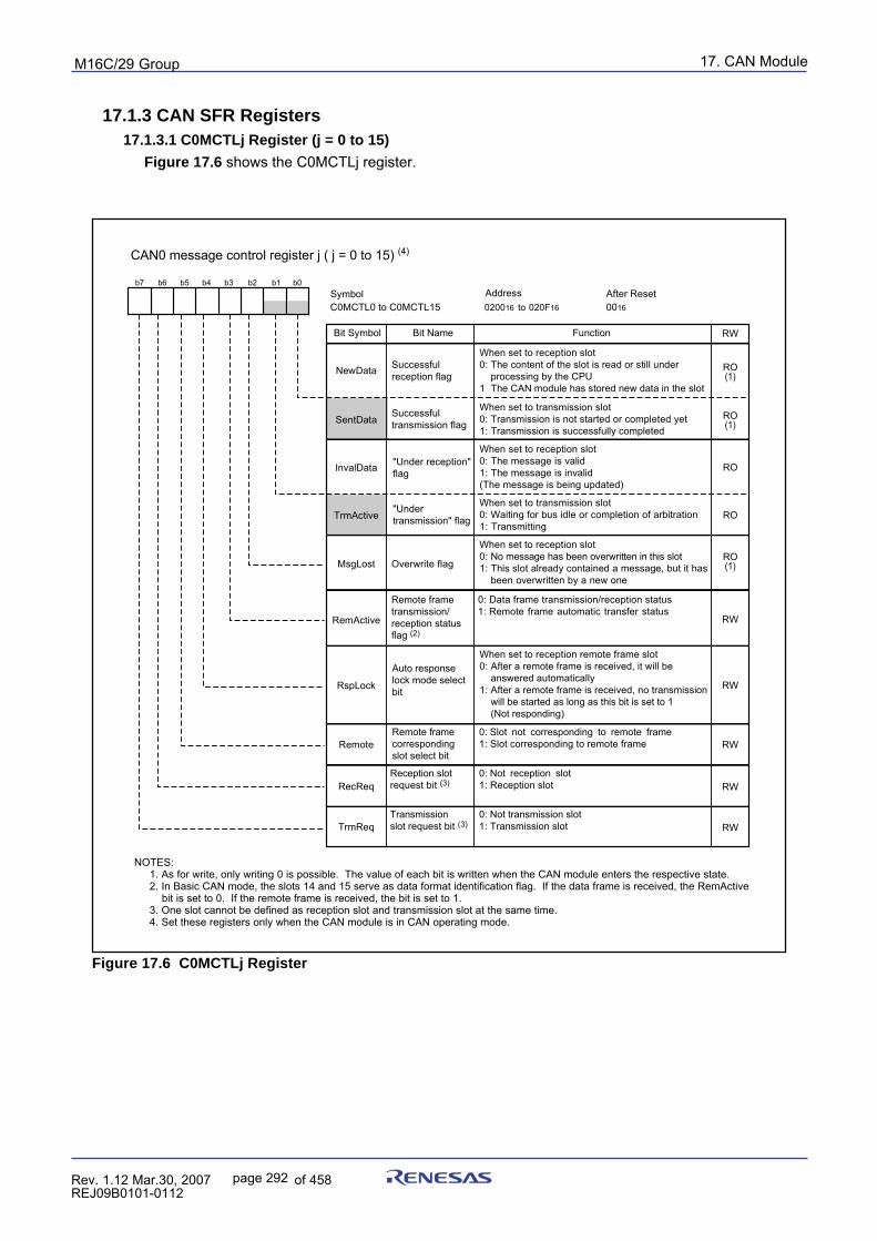
17. CAN ModulepuorG92/C61M
page 292 854fo7002,03.raM21.1.veR2110-1010B90JER
17.1.3 CAN SFR Registers17.1.3.1 C0MCTLj Register (j = 0 to 15)
Figure 17.6 shows the C0MCTLj register.
Figure 17.6 C0MCTLj Register
b7 b6 b5 b4 b3 b2 b1 b0
Bit Symbol Bit Name Function RW
RO(1)
RO(1)
RO
RO
RO(1)
NewData Successfulreception flag
SentDataSuccessfultransmission flag
When set to reception slot0: The content of the slot is read or still under processing by the CPU1 The CAN module has stored new data in the slot
When set to reception slot0: The message is valid1: The message is invalid(The message is being updated)
When set to reception slot0: No message has been overwritten in this slot1: This slot already contained a message, but it has been overwritten by a new one
When set to transmission slot0: Transmission is not started or completed yet1: Transmission is successfully completed
When set to transmission slot0: Waiting for bus idle or completion of arbitration1: Transmitting
InvalData
TrmActive
"Under reception"flag
"Under transmission" flag
MsgLost Overwrite flag
Remote frametransmission/reception status flag (2)
0: Data frame transmission/reception status1: Remote frame automatic transfer status
RemActive
RspLock
Auto response lock mode selectbit
Remote framecorrespondingslot select bit
When set to reception remote frame slot0: After a remote frame is received, it will be answered automatically1: After a remote frame is received, no transmission will be started as long as this bit is set to 1 (Not responding)
0: Slot not corresponding to remote frame1: Slot corresponding to remote frameRemote
0: Not reception slot1: Reception slotRecReq
Reception slotrequest bit (3)
0: Not transmission slot1: Transmission slotTrmReq
Transmission slot request bit (3)
NOTES: 1. As for write, only writing 0 is possible. The value of each bit is written when the CAN module enters the respective state. 2. In Basic CAN mode, the slots 14 and 15 serve as data format identification flag. If the data frame is received, the RemActive bit is set to 0. If the remote frame is received, the bit is set to 1. 3. One slot cannot be defined as reception slot and transmission slot at the same time. 4. Set these registers only when the CAN module is in CAN operating mode.
CAN0 message control register j ( j = 0 to 15) (4)
SymbolC0MCTL0 to C0MCTL15 to 020F16020016 0016
After ResetAddress
RW
RW
RW
RW
RW
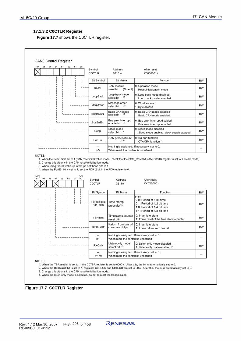
17. CAN ModulepuorG92/C61M
page 293 854fo7002,03.raM21.1.veR2110-1010B90JER
Figure 17.7 C0CTLR Register
17.1.3.2 C0CTLR Register
Figure 17.7 shows the C0CTLR register.
Bit Symbol Bit Name Function
ResetCAN module reset bit (Note 1)
Loop back mode LoopBack select bit (2)
Message order MsgOrder
BasicCANBasic CAN mode
select bit (2)
select bit (2)
BusErrEnBus error interruptenable bit (2)
Sleep Sleep mode select bit (2, 3)
CAN port enable bit (2, 3)PortEn
-(b7)
CAN0 Control Register
Symbol Address After resetC0CTLR X00000012021016
b7 b6 b5 b4 b3 b2 b1 b0
NOTES: 1. When the Reset bit is set to 1 (CAN reset/initialization mode), check that the State_Reset bit in the C0STR register is set to 1 (Reset mode). 2. Change this bit only in the CAN reset/initialization mode. 3. When using CAN0 wake-up interrupt, set these bits to 1. 4. When the PortEn bit is set to 1, set the PD9_2 bit in the PD9 register to 0.
RW
RW
RW
RW
RW
RW
RW
RW
-
0: Operation mode1: Reset/initialization mode
0: Word access1: Byte access
0: Basic CAN mode disabled1: Basic CAN mode enabled
0: Loop back mode disabled 1: Loop back mode enabled
0: Bus error interrupt disabled1: Bus error interrupt enabled
0: Sleep mode disabled1: Sleep mode enabled; clock supply stopped
0: I/O port function1: CTx/CRx function(4)
(b15) (b8)b7 b6 b5 b4 b3 b2 b1 b0
Bit Symbol Bit Name Function
TSPreScaleBit1, Bit0
TSReset
RXOnly
RetBusOff
Nothing is assigned. If necessary, set to 0.When read, the content is undefined
Nothing is assigned. If necessary, set to 0.When read, the content is undefined
XX0X00002
Symbol Address After resetC0CTLR 021116
b1 b0
NOTES: 1. When the TSReset bit is set to 1, the C0TSR register is set to 000016. After this, the bit is automatically set to 0. 2. When the RetBusOff bit is set to 1, registers C0RECR and C0TECR are set to 0016. After this, the bit is automatically set to 0. 3. Change this bit only in the CAN reset/initialization mode. 4. When the listen-only mode is selected, do not request the transmission.
RW
RW
RW
RW
-
RW
-
0 0: Period of 1 bit time0 1: Period of 1/2 bit time1 0: Period of 1/4 bit time1 1: Period of 1/8 bit time0: In an idle state1: Force reset of the time stamp counter
0: Listen-only mode disabled1: Listen-only mode enabled (4)
0: In an idle state1: Force return from bus off
Time stampprescaler(3)
Time stamp counterreset bit(1)
Return from bus offcommand bit(2)
Listen-only modeselect bit (3)
Nothing is assigned. If necessary, set to 0.When read, the content is undefined
-(b4)
-(b7-b6)
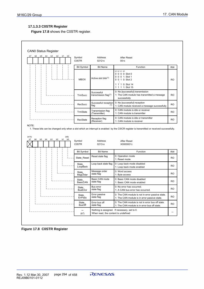
17. CAN ModulepuorG92/C61M
page 294 854fo7002,03.raM21.1.veR2110-1010B90JER
Figure 17.8 C0STR Register
17.1.3.3 C0STR Register
Figure 17.8 shows the C0STR register.
(b15) (b8)b7 b6 b5 b4 b3 b2 b1 b0
Bit Symbol Bit Name Function
Reset state flag
Loop back state flag
Message orderstate flag
Basic CAN modestate flag
Bus errorstate flag
Error passivestate flag
Error bus offstate flag
0: Operation mode1: Reset mode
0: Word access1: Byte access
0: Basic CAN mode disabled1: Basic CAN mode enabled
0: No error has occurred.1: A CAN bus error has occurred.
0: Loop back mode disabled1: Loop back mode enabled
0: The CAN module is not in error passive state.1: The CAN module is in error passive state.
0: The CAN module is not in error bus off state.1: The CAN module is in error bus off state.
Nothing is assigned. If necessary, set to 0. When read, the content is undefined
RW
RO
RO
RO
RO
RO
RO
RO
-
Symbol AddressC0STR 021316 X00000012
After Reset
CAN0 Status Register
NOTE: 1. These bits can be changed only when a slot which an interrupt is enabled by the C0ICR register is transmitted or received successfully.
b7 b6 b5 b4 b3 b2 b1 b0
Bit Symbol Bit Name Function
Active slot bits(1)
b3 b2 b1 b0
RW
RO
RO
RO
RO
RO
Successful receptionflag (1)
Transmission flag(Transmitter)
Reception flag(Receiver)
0 0 0 0: Slot 0 0 0 0 1: Slot 1 0 0 1 0: Slot 2 . . . 1 1 1 0: Slot 14 1 1 1 1: Slot 15
0: No [successful] reception1: CAN module received a message successfully
0: CAN module is idle or receiver1: CAN module is transmitter
0: CAN module is idle or transmitter1: CAN module is receiver
Successfultransmission flag(1)
0: No [successful] transmission1: The CAN module has transmitted a message successfully
Symbol AddressC0STR 021216 0016
After Reset
State_Reset
State_LoopBack
State_MsgOrder
State_BasicCAN
State_BusError
State_ErrPass
State_BusOff
-(b7)
MBOX
TrmSucc
RecSucc
TrmState
RecState
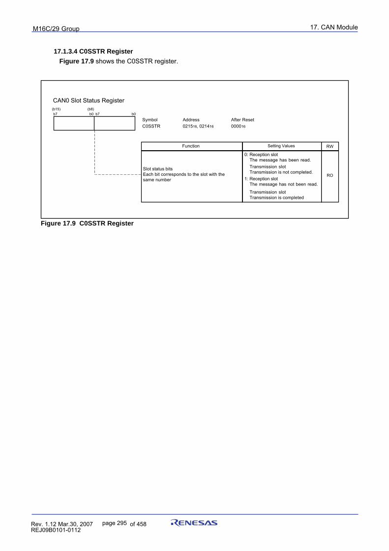
17. CAN ModulepuorG92/C61M
page 295 854fo7002,03.raM21.1.veR2110-1010B90JER
Figure 17.9 C0SSTR Register
17.1.3.4 C0SSTR Register
Figure 17.9 shows the C0SSTR register.
(b15) (b8)b7 b0 b7 b0
Function
Slot status bitsEach bit corresponds to the slot with the same number
0: Reception slot The message has been read. Transmission slot Transmission is not completed.1: Reception slot The message has not been read. Transmission slot Transmission is completed
CAN0 Slot Status Register
RW
RO
Symbol Address After ResetC0SSTR 021516, 021416 000016
Setting Values
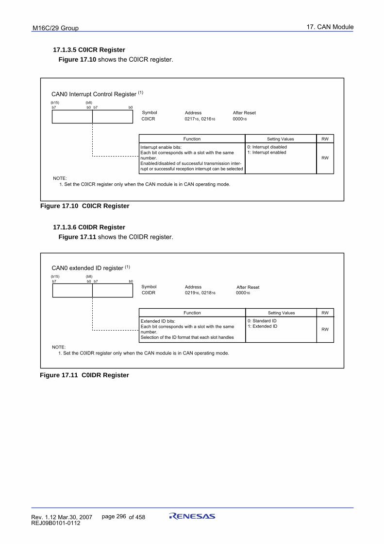
17. CAN ModulepuorG92/C61M
page 296 854fo7002,03.raM21.1.veR2110-1010B90JER
Figure 17.10 C0ICR Register
17.1.3.6 C0IDR Register
Figure 17.11 shows the C0IDR register.
17.1.3.5 C0ICR Register
Figure 17.10 shows the C0ICR register.
Figure 17.11 C0IDR Register
CAN0 Interrupt Control Register (1)
(b15) (b8)b0b0 b7b7
Function Setting Values
Interrupt enable bits:Each bit corresponds with a slot with the same number.Enabled/disabled of successful transmission inter-rupt or successful reception interrupt can be selected
0: Interrupt disabled1: Interrupt enabled
RW
RW
Symbol Address After ResetC0ICR 021716, 021616 000016
NOTE: 1. Set the C0ICR register only when the CAN module is in CAN operating mode.
CAN0 extended ID register (1)
Symbol Address After ResetC0IDR 021916, 021816 000016
(b15) (b8)
Function Setting Values
b0b0 b7b7
RW
RW
Extended ID bits:Each bit corresponds with a slot with the samenumber.Selection of the ID format that each slot handles
0: Standard ID1: Extended ID
NOTE: 1. Set the C0IDR register only when the CAN module is in CAN operating mode.
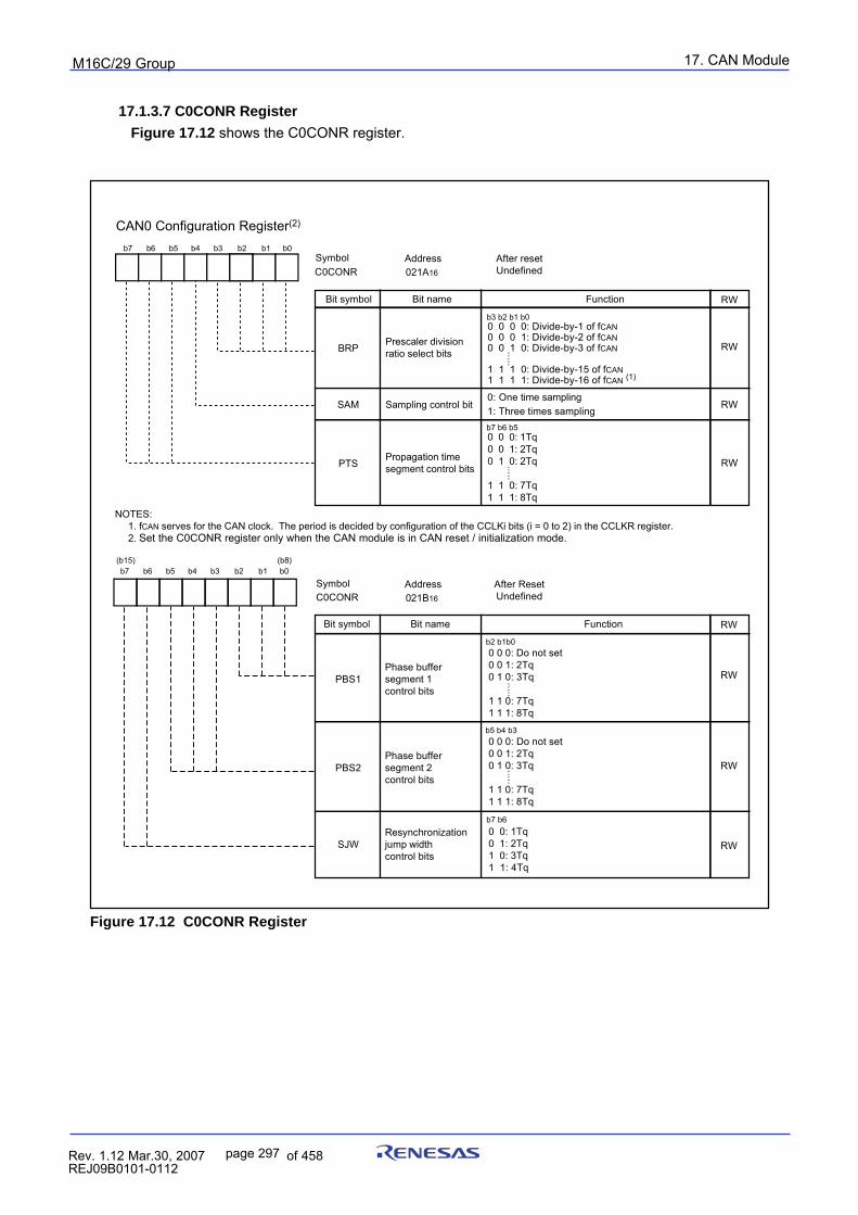
17. CAN ModulepuorG92/C61M
page 297 854fo7002,03.raM21.1.veR2110-1010B90JER
Figure 17.12 C0CONR Register
17.1.3.7 C0CONR Register
Figure 17.12 shows the C0CONR register.
C0CONR
b7 b6 b5 b4 b3 b2 b1 b0
Bit symbol Bit name Function
0: One time sampling1: Three times sampling
0 0 0 0: Divide-by-1 of fCAN0 0 0 1: Divide-by-2 of fCAN0 0 1 0: Divide-by-3 of fCAN
1 1 1 0: Divide-by-15 of fCAN1 1 1 1: Divide-by-16 of fCAN (1)
.....
0 0 0: 1Tq0 0 1: 2Tq0 1 0: 2Tq
1 1 0: 7Tq1 1 1: 8Tq
(b15) (b8)b7 b6 b5 b4 b3 b2 b1 b0
Bit symbol Bit name Function RW
RW
RW
RW
Phase buffersegment 1control bits
Phase buffer segment 2 control bits
Resynchronizationjump width control bits
.....
CAN0 Configuration Register(2)
C0CONR
b3 b2 b1 b0
b7 b6 b5
b2 b1b0
b5 b4 b3
b7 b6
021A16
NOTES: 1. fCAN serves for the CAN clock. The period is decided by configuration of the CCLKi bits (i = 0 to 2) in the CCLKR register. 2. Set the C0CONR register only when the CAN module is in CAN reset / initialization mode.
Symbol Address
Symbol Address
Prescaler divisionratio select bits
Propagation timesegment control bits
RW
RW
RW
RW
..... .....
021B16
0 0 0: Do not set0 0 1: 2Tq0 1 0: 3Tq
1 1 0: 7Tq1 1 1: 8Tq
0 0 0: Do not set0 0 1: 2Tq0 1 0: 3Tq
1 1 0: 7Tq1 1 1: 8Tq
0 0: 1Tq0 1: 2Tq1 0: 3Tq1 1: 4Tq
After resetUndefined
After ResetUndefined
BRP
SAM
PTS
PBS1
PBS2
SJW
Sampling control bit
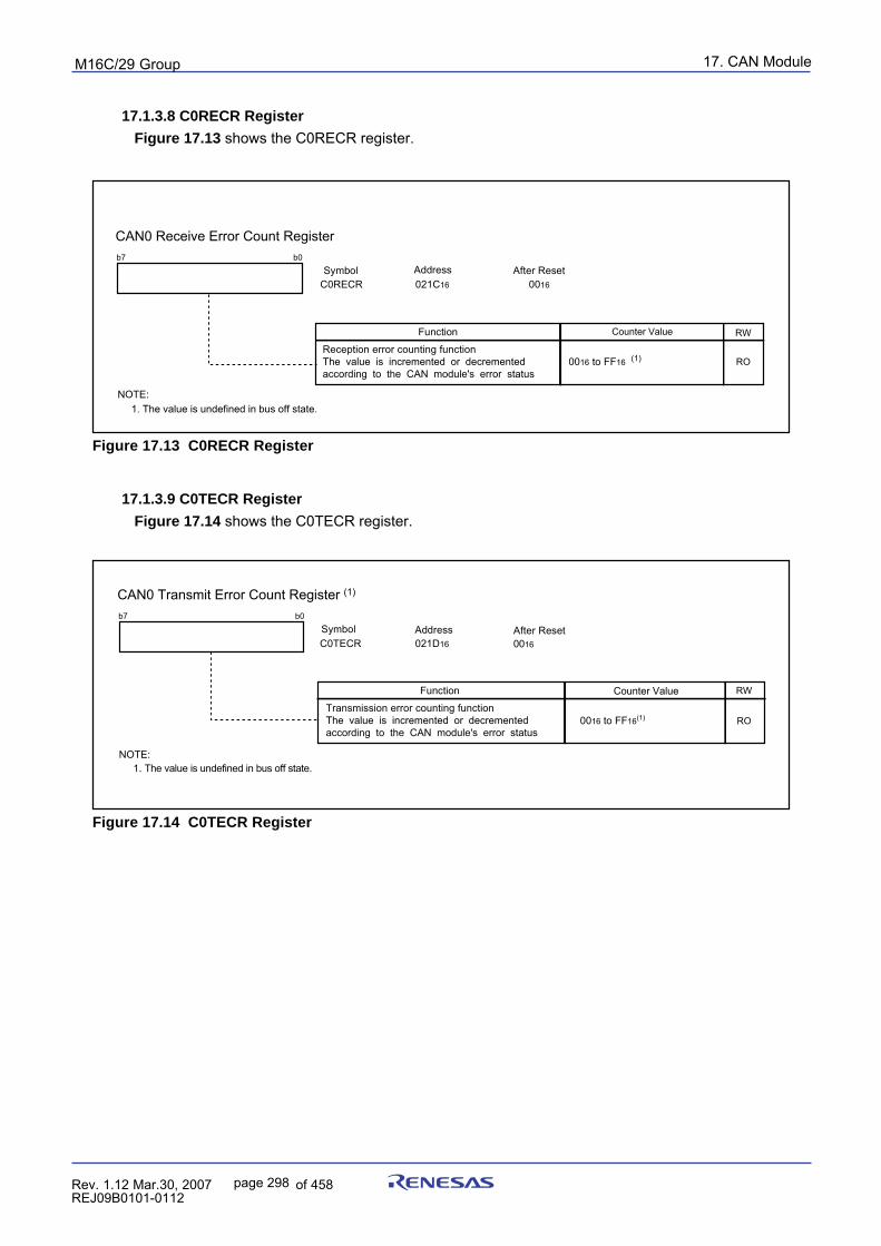
17. CAN ModulepuorG92/C61M
page 298 854fo7002,03.raM21.1.veR2110-1010B90JER
Figure 17.13 C0RECR Register
17.1.3.9 C0TECR Register
Figure 17.14 shows the C0TECR register.
Figure 17.14 C0TECR Register
17.1.3.8 C0RECR Register
Figure 17.13 shows the C0RECR register.
Reception error counting functionThe value is incremented or decremented according to the CAN module's error status
0016 to FF16 (1)
CAN0 Receive Error Count Register
AddressSymbol After ResetC0RECR 021C16 0016
b7 b0
Function Counter Value
NOTE: 1. The value is undefined in bus off state.
RW
RO
C0TECR 021D16 0016
CAN0 Transmit Error Count Register (1)
NOTE: 1. The value is undefined in bus off state.
b7 b0
Function
0016 to FF16(1)
Counter Value RW
RO
Symbol Address After Reset
Transmission error counting functionThe value is incremented or decremented according to the CAN module's error status
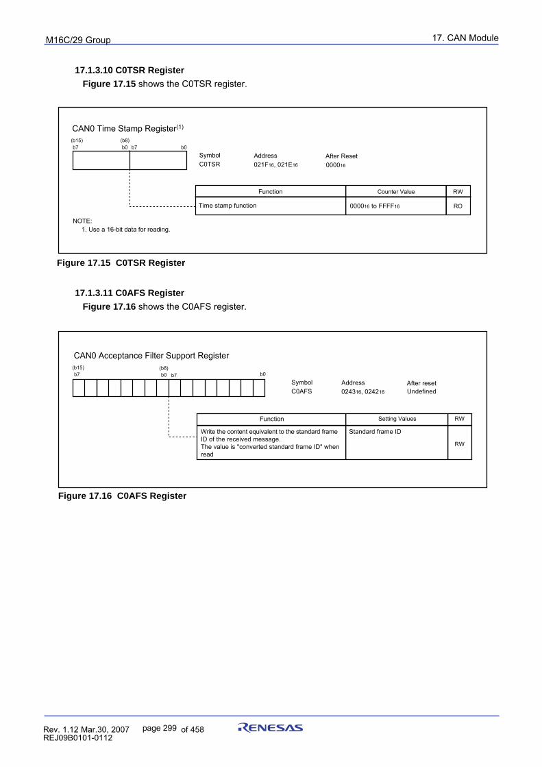
17. CAN ModulepuorG92/C61M
page 299 854fo7002,03.raM21.1.veR2110-1010B90JER
Figure 17.15 C0TSR Register
17.1.3.11 C0AFS Register
Figure 17.16 shows the C0AFS register.
17.1.3.10 C0TSR Register
Figure 17.15 shows the C0TSR register.
000016 to FFFF16
CAN0 Time Stamp Register(1)
C0TSR 021F16, 021E16 000016
(b15) (b8)
Function Counter Value
b0b0 b7b7
Time stamp function
Symbol Address After Reset
RW
RO
NOTE: 1. Use a 16-bit data for reading.
Figure 17.16 C0AFS Register
(b15)b7
(b8)b0 b7 b0
Function Setting Values
CAN0 Acceptance Filter Support Register
C0AFSAddress024316, 024216
RW
RW
Symbol
Write the content equivalent to the standard frameID of the received message.The value is "converted standard frame ID" when read
Standard frame ID
UndefinedAfter reset
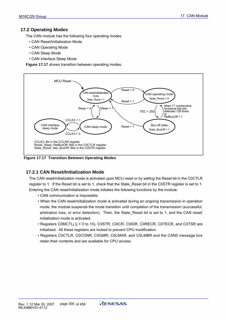
17. CAN ModulepuorG92/C61M
page 300 854fo7002,03.raM21.1.veR2110-1010B90JER
17.2 Operating ModesThe CAN module has the following four operating modes.
• CAN Reset/Initialization Mode• CAN Operating Mode• CAN Sleep Mode• CAN Interface Sleep Mode
Figure 17.17 shows transition between operating modes.
Figure 17.17 Transition Between Operating Modes
17.2.1 CAN Reset/Initialization ModeThe CAN reset/initialization mode is activated upon MCU reset or by setting the Reset bit in the C0CTLRregister to 1. If the Reset bit is set to 1, check that the State_Reset bit in the C0STR register is set to 1.Entering the CAN reset/initialization mode initiates the following functions by the module:
• CAN communication is impossible.• When the CAN reset/initialization mode is activated during an ongoing transmission in operation
mode, the module suspends the mode transition until completion of the transmission (successful,arbitration loss, or error detection). Then, the State_Reset bit is set to 1, and the CAN reset/initialization mode is activated.
• Registers C0MCTLj (j = 0 to 15), C0STR, C0ICR, C0IDR, C0RECR, C0TECR, and C0TSR areinitialized. All these registers are locked to prevent CPU modification.
• Registers C0CTLR, C0CONR, C0GMR, C0LMAR, and C0LMBR and the CAN0 message boxretain their contents and are available for CPU access.
MCU Reset
CAN reset/initializationmode
State_Reset = 1
CAN operating modeState_Reset = 0
CAN sleep modeCAN interfacesleep mode
Bus off stateState_BusOff = 1
Reset = 0
CCLK3 = 1
Sleep = 1
Sleep = 0TEC > 255
when 11 consecutive recessive bits are detected 128 timesorRetBusOff = 1
CCLK3 = 0
Reset = 1
Reset = 1
CCLK3: Bit in the CCLKR registerReset, Sleep, RetBusOff: Bits in the C0CTLR registerState_Reset, tate_BusOff: Bits in the C0STR register
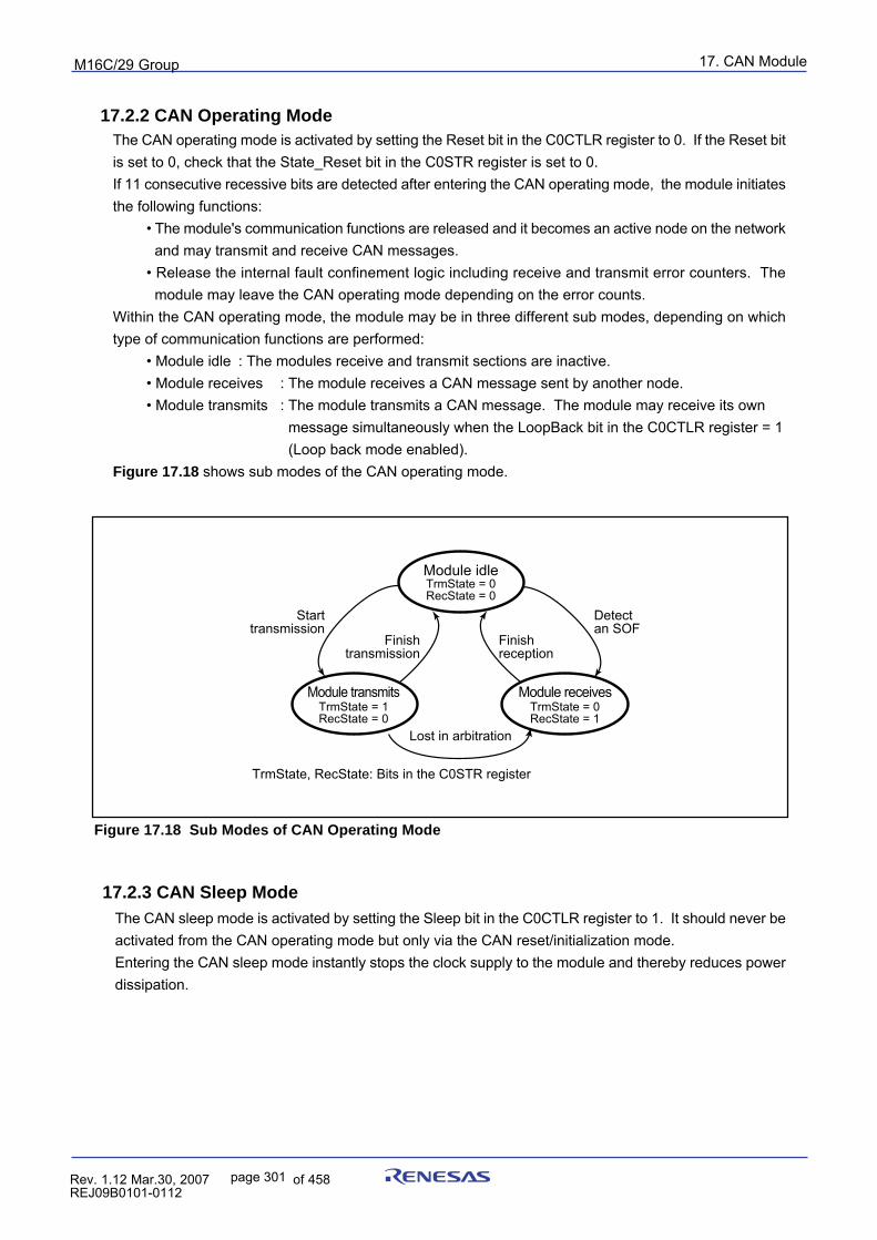
17. CAN ModulepuorG92/C61M
page 301 854fo7002,03.raM21.1.veR2110-1010B90JER
17.2.2 CAN Operating ModeThe CAN operating mode is activated by setting the Reset bit in the C0CTLR register to 0. If the Reset bitis set to 0, check that the State_Reset bit in the C0STR register is set to 0.If 11 consecutive recessive bits are detected after entering the CAN operating mode, the module initiatesthe following functions:
• The module's communication functions are released and it becomes an active node on the networkand may transmit and receive CAN messages.
• Release the internal fault confinement logic including receive and transmit error counters. Themodule may leave the CAN operating mode depending on the error counts.
Within the CAN operating mode, the module may be in three different sub modes, depending on whichtype of communication functions are performed:
• Module idle : The modules receive and transmit sections are inactive.• Module receives : The module receives a CAN message sent by another node.• Module transmits : The module transmits a CAN message. The module may receive its own
message simultaneously when the LoopBack bit in the C0CTLR register = 1 (Loop back mode enabled).
Figure 17.18 shows sub modes of the CAN operating mode.
Finish reception
Module idleTrmState = 0RecState = 0
TrmState = 1RecState = 0
Finishtransmission
Detect an SOF
Starttransmission
Lost in arbitration
Module transmitsTrmState = 0RecState = 1
Module receives
TrmState, RecState: Bits in the C0STR register
Figure 17.18 Sub Modes of CAN Operating Mode
17.2.3 CAN Sleep ModeThe CAN sleep mode is activated by setting the Sleep bit in the C0CTLR register to 1. It should never beactivated from the CAN operating mode but only via the CAN reset/initialization mode.Entering the CAN sleep mode instantly stops the clock supply to the module and thereby reduces powerdissipation.
17. CAN ModulepuorG92/C61M
page 302 854fo7002,03.raM21.1.veR2110-1010B90JER
17.2.4 CAN Interface Sleep ModeThe CAN interface sleep mode is activated by setting the CCLK3 bit in the CCLKR register to 1. It shouldnever be activated but only via the CAN sleep mode.Entering the CAN interface sleep mode instantly stops the clock supply to the CPU Interface in the mod-ule and thereby reduces power dissipation.
17.2.5 Bus Off State
The bus off state is entered according to the fault confinement rules of the CAN specification. Whenreturning to the CAN operating mode from the bus off state, the module has the following two cases.In this time, the value of any CAN registers, except registers C0STR, C0RECR, and C0TECR, does notchange.
(1) When 11 consecutive recessive bits are detected 128 timesThe module enters instantly into error active state and the CAN communication becomes possibleimmediately.
(2) When the RetBusOff bit in the C0CTLR register = 1 (Force return from buss off)The module enters instantly into error active state, and the CAN communication becomes possibleagain after 11 consecutive recessive bits are detected.
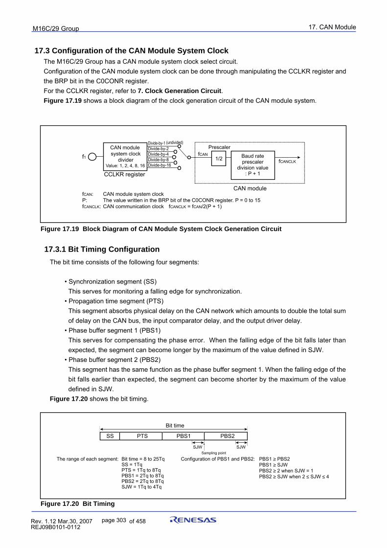
17. CAN ModulepuorG92/C61M
page 303 854fo7002,03.raM21.1.veR2110-1010B90JER
17.3 Configuration of the CAN Module System ClockThe M16C/29 Group has a CAN module system clock select circuit.Configuration of the CAN module system clock can be done through manipulating the CCLKR register andthe BRP bit in the C0CONR register.For the CCLKR register, refer to 7. Clock Generation Circuit.Figure 17.19 shows a block diagram of the clock generation circuit of the CAN module system.
Figure 17.20 Bit Timing
1/2
Divide-by-1 (undivided)Divide-by-2Divide-by-4 Divide-by-8Divide-by-16
Prescaler
Baud rateprescaler
division value: P + 1
fCAN
fCANCLK
fCAN: CAN module system clockP: The value written in the BRP bit of the C0CONR register. P = 0 to 15fCANCLK: CAN communication clock fCANCLK = fCAN/2(P + 1)
CAN module system clock
divider
CCLKR register Value: 1, 2, 4, 8, 16
CAN module
f1
The range of each segment: Bit time = 8 to 25TqSS = 1TqPTS = 1Tq to 8TqPBS1 = 2Tq to 8TqPBS2 = 2Tq to 8TqSJW = 1Tq to 4Tq
Configuration of PBS1 and PBS2: PBS1 ≥ PBS2PBS1 ≥ SJWPBS2 ≥ 2 when SJW = 1PBS2 ≥ SJW when 2 ≤ SJW ≤ 4
Bit time
SS PTS PBS1
SJWSampling point
PBS2
SJW
Figure 17.19 Block Diagram of CAN Module System Clock Generation Circuit
17.3.1 Bit Timing Configuration
The bit time consists of the following four segments:
• Synchronization segment (SS)This serves for monitoring a falling edge for synchronization.
• Propagation time segment (PTS)This segment absorbs physical delay on the CAN network which amounts to double the total sumof delay on the CAN bus, the input comparator delay, and the output driver delay.
• Phase buffer segment 1 (PBS1)This serves for compensating the phase error. When the falling edge of the bit falls later thanexpected, the segment can become longer by the maximum of the value defined in SJW.
• Phase buffer segment 2 (PBS2)This segment has the same function as the phase buffer segment 1. When the falling edge of thebit falls earlier than expected, the segment can become shorter by the maximum of the valuedefined in SJW.
Figure 17.20 shows the bit timing.
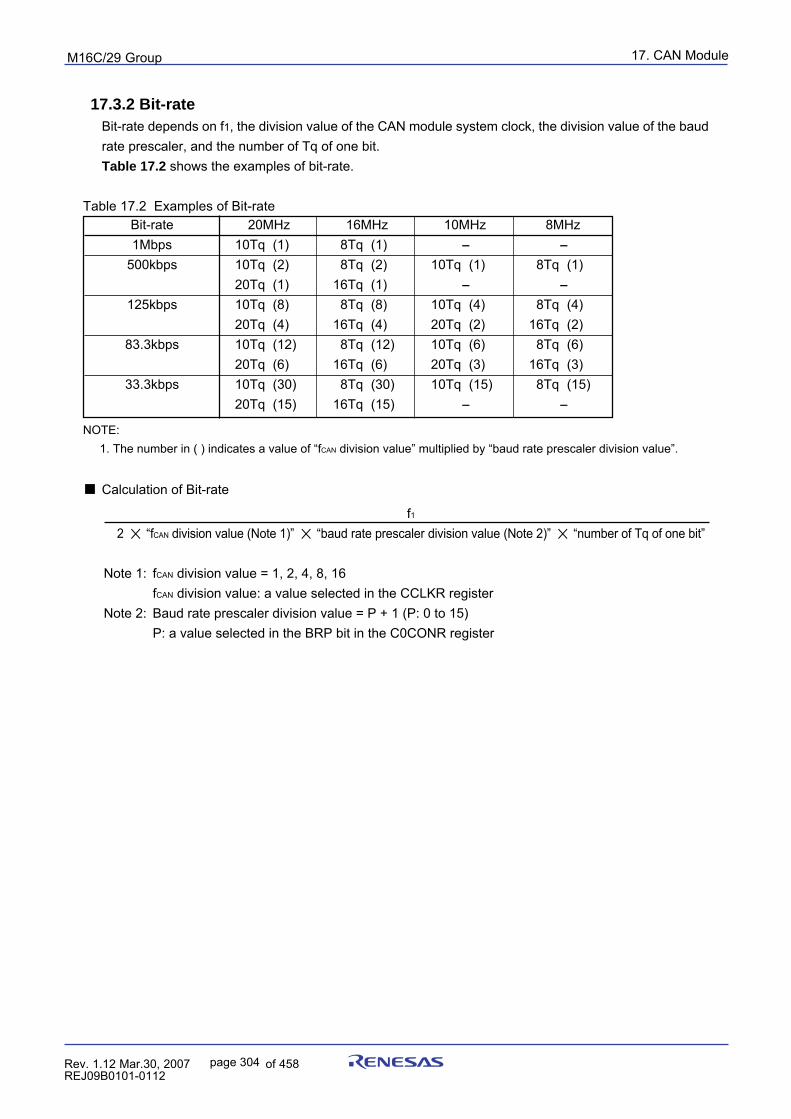
17. CAN ModulepuorG92/C61M
page 304 854fo7002,03.raM21.1.veR2110-1010B90JER
17.3.2 Bit-rateBit-rate depends on f1, the division value of the CAN module system clock, the division value of the baudrate prescaler, and the number of Tq of one bit.Table 17.2 shows the examples of bit-rate.
Table 17.2 Examples of Bit-rate
Calculation of Bit-rate
f12 “fCAN division value (Note 1)” “baud rate prescaler division value (Note 2)” “number of Tq of one bit”
Note 1: fCAN division value = 1, 2, 4, 8, 16fCAN division value: a value selected in the CCLKR register
Note 2: Baud rate prescaler division value = P + 1 (P: 0 to 15)P: a value selected in the BRP bit in the C0CONR register
NOTE: 1. The number in ( ) indicates a value of “fCAN division value” multiplied by “baud rate prescaler division value”.
Bit-rate 20MHz 16MHz 10MHz 8MHz1Mbps 10Tq (1) 8Tq (1) - -
500kbps 10Tq (2) 8Tq (2) 10Tq (1) 8Tq (1)20Tq (1) 16Tq (1) - -
125kbps 10Tq (8) 8Tq (8) 10Tq (4) 8Tq (4)20Tq (4) 16Tq (4) 20Tq (2) 16Tq (2)
83.3kbps 10Tq (12) 8Tq (12) 10Tq (6) 8Tq (6)20Tq (6) 16Tq (6) 20Tq (3) 16Tq (3)
33.3kbps 10Tq (30) 8Tq (30) 10Tq (15) 8Tq (15)20Tq (15) 16Tq (15) - -
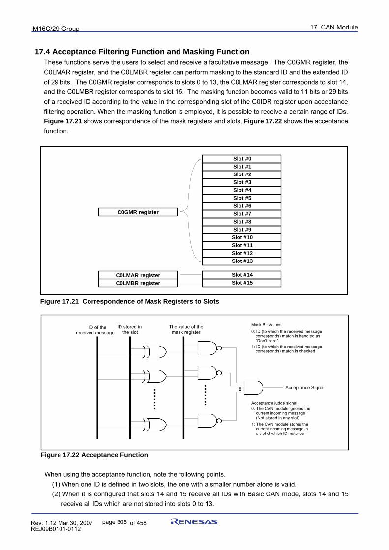
17. CAN ModulepuorG92/C61M
page 305 854fo7002,03.raM21.1.veR2110-1010B90JER
Figure 17.21 Correspondence of Mask Registers to Slots
Figure 17.22 Acceptance Function
When using the acceptance function, note the following points.(1) When one ID is defined in two slots, the one with a smaller number alone is valid.(2) When it is configured that slots 14 and 15 receive all IDs with Basic CAN mode, slots 14 and 15
receive all IDs which are not stored into slots 0 to 13.
17.4 Acceptance Filtering Function and Masking FunctionThese functions serve the users to select and receive a facultative message. The C0GMR register, theC0LMAR register, and the C0LMBR register can perform masking to the standard ID and the extended IDof 29 bits. The C0GMR register corresponds to slots 0 to 13, the C0LMAR register corresponds to slot 14,and the C0LMBR register corresponds to slot 15. The masking function becomes valid to 11 bits or 29 bitsof a received ID according to the value in the corresponding slot of the C0IDR register upon acceptancefiltering operation. When the masking function is employed, it is possible to receive a certain range of IDs.Figure 17.21 shows correspondence of the mask registers and slots, Figure 17.22 shows the acceptancefunction.
Slot #0Slot #1Slot #2Slot #3Slot #4Slot #5Slot #6Slot #7Slot #8Slot #9Slot #10Slot #11Slot #12
Slot #14Slot #15
C0GMR register
Slot #13
C0LMAR registerC0LMBR register
ID of thereceived message
ID stored in the slot
The value of the mask register
Acceptance Signal
Mask Bit Values
Acceptance judge signal0: The CAN module ignores the
current incoming message(Not stored in any slot)
1: The CAN module stores the current incoming message in a slot of which ID matches
0: ID (to which the received messagecorresponds) match is handled as "Don't care"
1: ID (to which the received messagecorresponds) match is checked
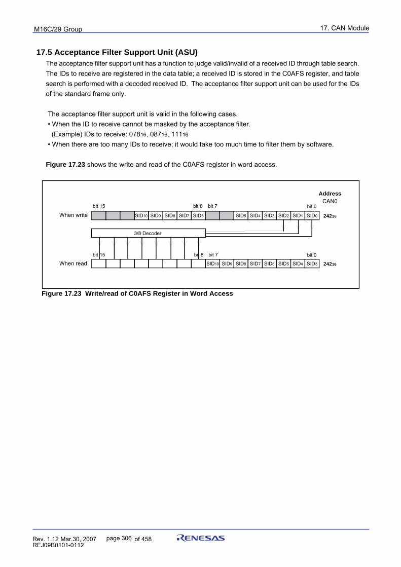
17. CAN ModulepuorG92/C61M
page 306 854fo7002,03.raM21.1.veR2110-1010B90JER
17.5 Acceptance Filter Support Unit (ASU)The acceptance filter support unit has a function to judge valid/invalid of a received ID through table search.The IDs to receive are registered in the data table; a received ID is stored in the C0AFS register, and tablesearch is performed with a decoded received ID. The acceptance filter support unit can be used for the IDsof the standard frame only.
The acceptance filter support unit is valid in the following cases.• When the ID to receive cannot be masked by the acceptance filter. (Example) IDs to receive: 07816, 08716, 11116
• When there are too many IDs to receive; it would take too much time to filter them by software.
Figure 17.23 shows the write and read of the C0AFS register in word access.
Figure 17.23 Write/read of C0AFS Register in Word Access
bit 15 bit 0
When read SID10 SID9 SID8 SID7 SID6 SID5 SID4 SID3
bit 15 bit 0
SID10 SID9 SID8 SID7 SID6 SID5 SID4 SID3 SID2 SID1 SID0When write
3/8 Decoder
24216
24216
AddressCAN0
bit 8 bit 7
bit 8 bit 7
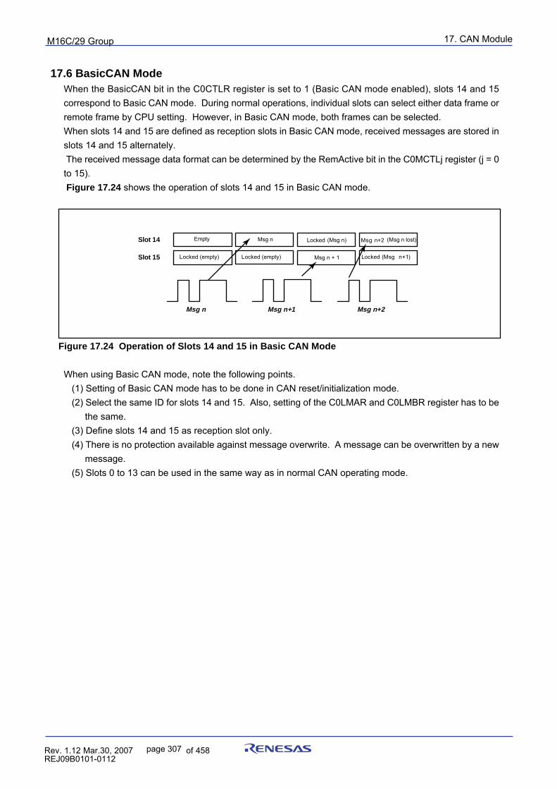
17. CAN ModulepuorG92/C61M
page 307 854fo7002,03.raM21.1.veR2110-1010B90JER
17.6 BasicCAN ModeWhen the BasicCAN bit in the C0CTLR register is set to 1 (Basic CAN mode enabled), slots 14 and 15correspond to Basic CAN mode. During normal operations, individual slots can select either data frame orremote frame by CPU setting. However, in Basic CAN mode, both frames can be selected.When slots 14 and 15 are defined as reception slots in Basic CAN mode, received messages are stored inslots 14 and 15 alternately. The received message data format can be determined by the RemActive bit in the C0MCTLj register (j = 0to 15). Figure 17.24 shows the operation of slots 14 and 15 in Basic CAN mode.
Figure 17.24 Operation of Slots 14 and 15 in Basic CAN Mode
When using Basic CAN mode, note the following points.(1) Setting of Basic CAN mode has to be done in CAN reset/initialization mode.(2) Select the same ID for slots 14 and 15. Also, setting of the C0LMAR and C0LMBR register has to be
the same.(3) Define slots 14 and 15 as reception slot only.(4) There is no protection available against message overwrite. A message can be overwritten by a new
message.(5) Slots 0 to 13 can be used in the same way as in normal CAN operating mode.
Slot 14
Slot 15
Msg n Msg n+1 Msg n+2
Empty
Locked (empty) Locked (empty)
Msg n Locked
Msg n + 1
Msg n+2 (Msg n lost)
Locked (Msg n+1)
(Msg n)
17. CAN ModulepuorG92/C61M
page 308 854fo7002,03.raM21.1.veR2110-1010B90JER
17.7 Return from Bus off FunctionWhen the protocol controller enters bus off state, it is possible to make it forced return from bus off state bysetting the RetBusOff bit in the C0CTLR register to 1 (Force return from bus off). At this time, the error statechanges from bus off state to error active state. If the RetBusOff bit is set to 1, registers C0RECR andC0TECR are initialized and the State_Reset bit in the C0STR register is set to 0 (The CAN module is not inerror bus off state). However, registers of the CAN module such as C0CONR register and the content ofeach slot are not initialized.
17.8 Time Stamp Counter and Time Stamp FunctionWhen the C0TSR register is read, the value of the time stamp counter at the moment is read. The period ofthe time stamp counter reference clock is the same as that of 1 bit time that is configured by the C0CONRregister. The time stamp counter functions as a free run counter.The 1 bit time period can be divided by 1 (undivided), 2, 4 or 8 to produce the time stamp counter referenceclock. Use the TSPreScale bit in the C0CTLR register to select the divide-by-n value.The time stamp counter is equipped with a register that captures the counter value when the protocolcontroller regards it as a successful reception. The captured value is stored when a time stamp value isstored in a reception slot.
17.9 Listen-Only ModeWhen the RXOnly bit in the C0CTLR register is set to 1, the module enters listen-only mode.In listen-only mode, no transmission -- data frames, error frames, and ACK response -- is performed to bus.When listen-only mode is selected, do not request the transmission.
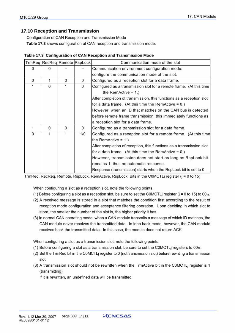
17. CAN ModulepuorG92/C61M
page 309 854fo7002,03.raM21.1.veR2110-1010B90JER
17.10 Reception and TransmissionConfiguration of CAN Reception and Transmission ModeTable 17.3 shows configuration of CAN reception and transmission mode.
Table 17.3 Configuration of CAN Reception and Transmission Mode
TrmReq, RecReq, Remote, RspLock, RemActive, RspLock: Bits in the C0MCTLj register (j = 0 to 15)
When configuring a slot as a reception slot, note the following points.(1) Before configuring a slot as a reception slot, be sure to set the C0MCTLj register (j = 0 to 15) to 0016.(2) A received message is stored in a slot that matches the condition first according to the result of
reception mode configuration and acceptance filtering operation. Upon deciding in which slot tostore, the smaller the number of the slot is, the higher priority it has.
(3) In normal CAN operating mode, when a CAN module transmits a message of which ID matches, theCAN module never receives the transmitted data. In loop back mode, however, the CAN modulereceives back the transmitted data. In this case, the module does not return ACK.
When configuring a slot as a transmission slot, note the following points.(1) Before configuring a slot as a transmission slot, be sure to set the C0MCTLj registers to 0016.(2) Set the TrmReq bit in the C0MCTLj register to 0 (not transmission slot) before rewriting a transmission
slot.(3) A transmission slot should not be rewritten when the TrmActive bit in the C0MCTLj register is 1
(transmitting).If it is rewritten, an undefined data will be transmitted.
TrmReq RecReq Remote RspLock Communication mode of the slot0 0 - - Communication environment configuration mode:
configure the communication mode of the slot.0 1 0 0 Configured as a reception slot for a data frame.1 0 1 0 Configured as a transmission slot for a remote frame. (At this time
the RemActive = 1.)After completion of transmission, this functions as a reception slotfor a data frame. (At this time the RemActive = 0.)However, when an ID that matches on the CAN bus is detectedbefore remote frame transmission, this immediately functions asa reception slot for a data frame.
1 0 0 0 Configured as a transmission slot for a data frame.0 1 1 1/0 Configured as a reception slot for a remote frame. (At this time
the RemActive = 1.)After completion of reception, this functions as a transmission slotfor a data frame. (At this time the RemActive = 0.)However, transmission does not start as long as RspLock bitremains 1; thus no automatic response.Response (transmission) starts when the RspLock bit is set to 0.
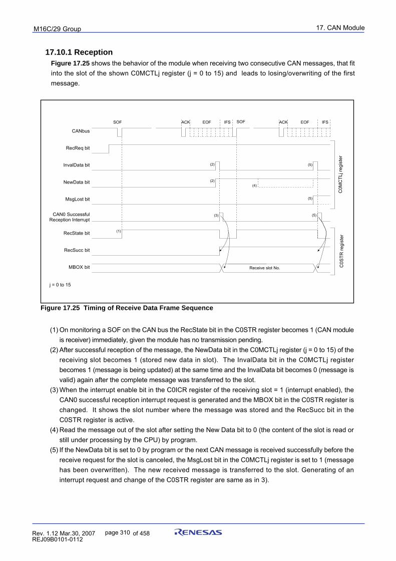
17. CAN ModulepuorG92/C61M
page 310 854fo7002,03.raM21.1.veR2110-1010B90JER
17.10.1 ReceptionFigure 17.25 shows the behavior of the module when receiving two consecutive CAN messages, that fitinto the slot of the shown C0MCTLj register (j = 0 to 15) and leads to losing/overwriting of the firstmessage.
CANbus
RecReq bit
InvalData bit
CAN0 SuccessfulReception Interrupt
RecState bit
RecSucc bit
MBOX bit
NewData bit
SOF ACK EOF EOFIFS IFSSOF
Receive slot No.
MsgLost bit
C0M
CTL
j reg
iste
rC
0STR
regi
ster
(1)
(2)
(2)
(3)
(4)
(5)
(5)
(5)
j = 0 to 15
ACK
Figure 17.25 Timing of Receive Data Frame Sequence
(1) On monitoring a SOF on the CAN bus the RecState bit in the C0STR register becomes 1 (CAN moduleis receiver) immediately, given the module has no transmission pending.
(2) After successful reception of the message, the NewData bit in the C0MCTLj register (j = 0 to 15) of thereceiving slot becomes 1 (stored new data in slot). The InvalData bit in the C0MCTLj registerbecomes 1 (message is being updated) at the same time and the InvalData bit becomes 0 (message isvalid) again after the complete message was transferred to the slot.
(3) When the interrupt enable bit in the C0ICR register of the receiving slot = 1 (interrupt enabled), theCAN0 successful reception interrupt request is generated and the MBOX bit in the C0STR register ischanged. It shows the slot number where the message was stored and the RecSucc bit in theC0STR register is active.
(4) Read the message out of the slot after setting the New Data bit to 0 (the content of the slot is read orstill under processing by the CPU) by program.
(5) If the NewData bit is set to 0 by program or the next CAN message is received successfully before thereceive request for the slot is canceled, the MsgLost bit in the C0MCTLj register is set to 1 (messagehas been overwritten). The new received message is transferred to the slot. Generating of aninterrupt request and change of the C0STR register are same as in 3).
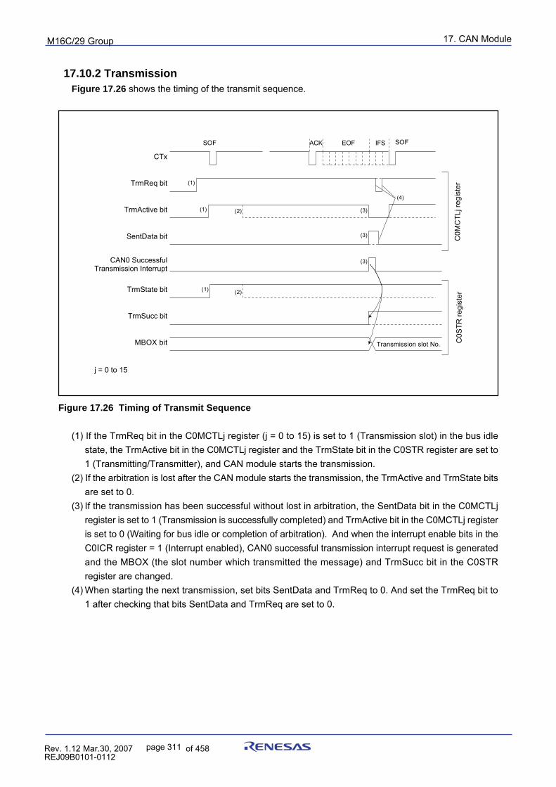
17. CAN ModulepuorG92/C61M
page 311 854fo7002,03.raM21.1.veR2110-1010B90JER
17.10.2 TransmissionFigure 17.26 shows the timing of the transmit sequence.
CTx
TrmReq bit
TrmActive bit
CAN0 SuccessfulTransmission Interrupt
TrmState bit
TrmSucc bit
MBOX bit
SentData bit
SOF SOF
Transmission slot No.
C0M
CTL
j reg
iste
rC
0STR
regi
ster
EOF IFS
(1)
(2)
(2)(1)
(1)
(3)
(4)
(3)
(3)
j = 0 to 15
ACK
Figure 17.26 Timing of Transmit Sequence
(1) If the TrmReq bit in the C0MCTLj register (j = 0 to 15) is set to 1 (Transmission slot) in the bus idlestate, the TrmActive bit in the C0MCTLj register and the TrmState bit in the C0STR register are set to1 (Transmitting/Transmitter), and CAN module starts the transmission.
(2) If the arbitration is lost after the CAN module starts the transmission, the TrmActive and TrmState bitsare set to 0.
(3) If the transmission has been successful without lost in arbitration, the SentData bit in the C0MCTLjregister is set to 1 (Transmission is successfully completed) and TrmActive bit in the C0MCTLj registeris set to 0 (Waiting for bus idle or completion of arbitration). And when the interrupt enable bits in theC0ICR register = 1 (Interrupt enabled), CAN0 successful transmission interrupt request is generatedand the MBOX (the slot number which transmitted the message) and TrmSucc bit in the C0STRregister are changed.
(4) When starting the next transmission, set bits SentData and TrmReq to 0. And set the TrmReq bit to1 after checking that bits SentData and TrmReq are set to 0.
17. CAN ModulepuorG92/C61M
page 312 854fo7002,03.raM21.1.veR2110-1010B90JER
17.11 CAN InterruptsThe CAN module provides the following CAN interrupts.
• CAN0 Successful Reception Interrupt• CAN0 Successful Transmission Interrupt• CAN0 Error Interrupt
Error Passive State Error BusOff State Bus Error (this feature can be disabled separately)
• CAN0 Wake-up InterruptWhen the CPU detects the CAN0 successful reception/transmission interrupt request, the MBOX bit in theC0STR register must be read to determine which slot has generated the interrupt request.
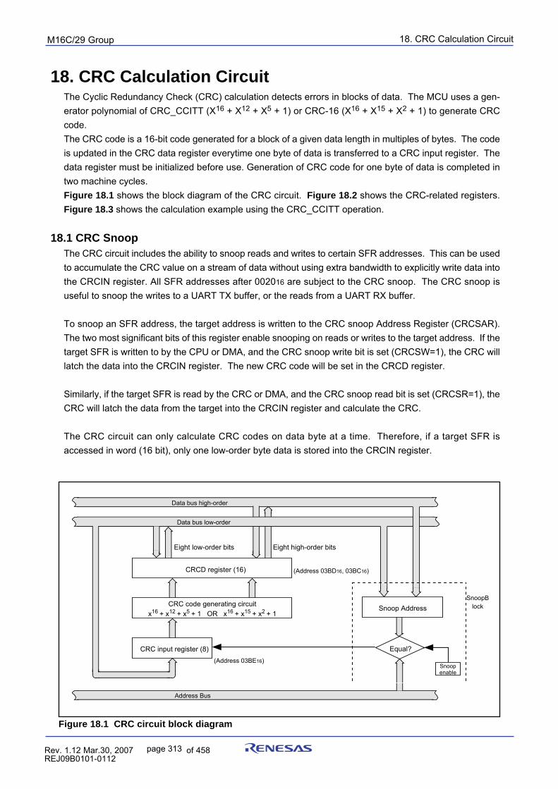
18. CRC Calculation CircuitpuorG92/C61M
page 313 854fo7002,03.raM21.1.veR2110-1010B90JER
18. CRC Calculation CircuitThe Cyclic Redundancy Check (CRC) calculation detects errors in blocks of data. The MCU uses a gen-erator polynomial of CRC_CCITT (X16 + X12 + X5 + 1) or CRC-16 (X16 + X15 + X2 + 1) to generate CRCcode.The CRC code is a 16-bit code generated for a block of a given data length in multiples of bytes. The codeis updated in the CRC data register everytime one byte of data is transferred to a CRC input register. Thedata register must be initialized before use. Generation of CRC code for one byte of data is completed intwo machine cycles.Figure 18.1 shows the block diagram of the CRC circuit. Figure 18.2 shows the CRC-related registers.Figure 18.3 shows the calculation example using the CRC_CCITT operation.
18.1 CRC SnoopThe CRC circuit includes the ability to snoop reads and writes to certain SFR addresses. This can be usedto accumulate the CRC value on a stream of data without using extra bandwidth to explicitly write data intothe CRCIN register. All SFR addresses after 002016 are subject to the CRC snoop. The CRC snoop isuseful to snoop the writes to a UART TX buffer, or the reads from a UART RX buffer.
To snoop an SFR address, the target address is written to the CRC snoop Address Register (CRCSAR).The two most significant bits of this register enable snooping on reads or writes to the target address. If thetarget SFR is written to by the CPU or DMA, and the CRC snoop write bit is set (CRCSW=1), the CRC willlatch the data into the CRCIN register. The new CRC code will be set in the CRCD register.
Similarly, if the target SFR is read by the CRC or DMA, and the CRC snoop read bit is set (CRCSR=1), theCRC will latch the data from the target into the CRCIN register and calculate the CRC.
The CRC circuit can only calculate CRC codes on data byte at a time. Therefore, if a target SFR isaccessed in word (16 bit), only one low-order byte data is stored into the CRCIN register.
Figure 18.1 CRC circuit block diagram
AAAAAEight low-order bits AAAAAEight high-order bits
Data bus high-order
Data bus low-order
AAAAAAAAAAAAAAAAAAAA
AAAAAAAAAAAA
CRCD register (16)
CRC input register (8)
AAAAAAAAAAAAAAAAAAAACRC code generating circuit
x16 + x12 + x5 + 1 OR x16 + x15 + x2 + 1
Address Bus
SnoopBlock
Snoop enable
Snoop Address
AAAAAAAAAAAAAAAAAAAAAAAAAAAAAAAAAAAAAAAAAAAAAAAAAAAAAAAA
Equal?
(Address 03BD16, 03BC16)
(Address 03BE16)
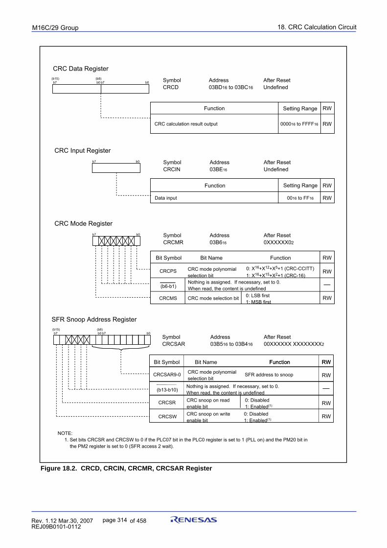
18. CRC Calculation CircuitpuorG92/C61M
page 314 854fo7002,03.raM21.1.veR2110-1010B90JER
Figure 18.2. CRCD, CRCIN, CRCMR, CRCSAR Register
Symbol Address After ResetCRCD 03BD16 to 03BC16 Undefined
b7 b0 b7 b0(b15) (b8)
CRC Data Register
Function Setting Range
000016 to FFFF16
RW
RW
Symbol Address After ResetCRCIN 03BE16 Undefined
b7 b0
CRC Input Register
Data input
Function
0016 to FF16
RW
RW
Setting Range
CRC calculation result output
Symbol Address After ResetCRCMR 03B616 0XXXXXX02
b7 b0
CRC Mode Register
CRC mode polynomialselection bit
Function
0: LSB first1: MSB first
RW
RW
Bit nameBit symbol
CRC mode selection bit
CRCPS
CRCMS RW
Nothing is assigned.Write "0" when writing to this bit. The value is indeterminate if read.
0: X16+X12+X5+1 (CRC-CCITT)
1: X16+X15+X2+1 (CRC-16) CRC mode polynomialselection bit
Function
0: LSB first1: MSB first
RW
RW
Bit NameBit Symbol
CRC mode selection bit
CRCPS
CRCMS RW
Nothing is assigned. If necessary, set to 0.When read, the content is undefined
0: X16+X12+X5+1 (CRC-CCITT)
1: X16+X15+X2+1 (CRC-16)
(b6-b1)
Symbol Address After ResetCRCSAR 03B516 to 03B416 00XXXXXX XXXXXXXX2
b7 b0 b7 b0(b15) (b8)
SFR Snoop Address Register
CRC mode polynomialselection bit
Function RW
RW
Bit NameBit Symbol
CRCSR RW
Nothing is assigned. If necessary, set to 0.When read, the content is undefined
SFR address to snoop
Function
0: Disabled1: Enabled(1)
RW
CRCSW
CRCSAR9-0
CRC snoop on read enable bitCRC snoop on write enable bit
0: Disabled1: Enabled(1)
RW
(b13-b10)
NOTE: 1. Set bits CRCSR and CRCSW to 0 if the PLC07 bit in the PLC0 register is set to 1 (PLL on) and the PM20 bit in the PM2 register is set to 0 (SFR access 2 wait).
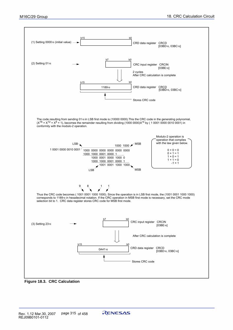
18. CRC Calculation CircuitpuorG92/C61M
page 315 854fo7002,03.raM21.1.veR2110-1010B90JER
Figure 18.3. CRC Calculation
(1) Setting 000016 (initial value)b15 b0
1 0001 0000 0010 0001 1000 0000 0000 0000 0000 00001000 1000 0001 0000 1 1000 0001 0000 1000 0 1000 1000 0001 0000 1 1001 0001 1000 1000
1000 1000 MSB
Modulo-2 operation is operation that complies with the law given below.
0 + 0 = 00 + 1 = 11 + 0 = 11 + 1 = 0 -1 = 1
The code resulting from sending 0116 in LSB first mode is (10000 0000).This the CRC code in the generating polynomial,(X16 + X12 + X5 + 1), becomes the remainder resulting from dividing (1000 0000)X16 by ( 1 0001 0000 0010 0001) inconformity with the modulo-2 operation.
(2) Setting 0116
b0b7
b15 b0
118916
2 cycles After CRC calculation is complete
Thus the CRC code becomes ( 1001 0001 1000 1000). Since the operation is in LSB first mode, the (1001 0001 1000 1000)corresponds to 118916 in hexadecimal notation. If the CRC operation in MSB first mode is necessary, set the CRC mode selection bit to 1. CRC data register stores CRC code for MSB first mode.
CRD data register CRCD [03BD16, 03BC16]
CRC input register CRCIN[03BE16]
CRD data register CRCD [03BD16, 03BC16]
CRC input register CRCIN[03BE16](3) Setting 2316
b0b7
b15 b0
0A4116
After CRC calculation is complete
CRD data register CRCD [03BD16, 03BC16]
9 8 1 1
MSB
LSB
LSB
Stores CRC code
Stores CRC code
19. Programmable I/O PortspuorG92/C61M
page 316 854fo7002,03.raM21.1.veR2110-1010B90JER
19. Programmable I/O Ports Note
Ports P04 to P07, P10 to P14 , P34 to P37 and P95 to P97 are not available in 64-pin package.
The programmable input/output ports (hereafter referred to simply as “I/O ports”) consist of 71 lines P0, P1,P2, P3, P6, P7, P8, P9, P10 (except P94) for the 80-pin package, or 55 lines P00 to P03, P15 to P17, P2, P30
to P33, P6, P7, P8, P90 to P93, P10 for the 64-pin package. Each port can be set for input or output everyline by using a direction register, and can also be chosen to be or not be pulled high in sets of 4 lines.Figures 19.1 to 19.4 show the I/O ports. Figure 19.5 shows the I/O pins.Each pin functions as an I/O port, a peripheral function input/output.For details on how to set peripheral functions, refer to each functional description in this manual. If any pinis used as a peripheral function input, set the direction bit for that pin to 0 (input mode). Any pin used as anoutput pin for peripheral functions is directed for output no matter how the corresponding direction bit is set.
19.1 Port Pi Direction Register (PDi Register, i = 0 to 3, 6 to 10)
Figure 19.6 shows the direction registers.This register selects whether the I/O port is to be used for input or output. The bits in this register corre-spond one for one to each port.
19.2 Port Pi Register (Pi Register, i = 0 to 3, 6 to 10)
Figure 19.7 shows the Pi registers.Data input/output to and from external devices are accomplished by reading and writing to the Pi register.The Pi register consists of a port latch to hold the output data and a circuit to read the pin status. For portsset for input mode, the input level of the pin can be read by reading the corresponding Pi register, and datacan be written to the port latch by writing to the Pi register.For ports set for output mode, the port latch can be read by reading the corresponding Pi register, and datacan be written to the port latch by writing to the Pi register. The data written to the port latch is output fromthe pin. The bits in the Pi register correspond one for one to each port.
19.3 Pull-up Control Register 0 to 2 (PUR0 to PUR2 Registers)Figure 19.8 shows registers PUR0 to PUR2.Registers PUR0 to PUR2 select whether the pins, divided into groups of four pins, are pulled up or not. Thepins, selected by setting the bits in registers PUR0 to PUR2 to 1 (pull-up), are pulled up when the directionregisters are set to 0 (input mode). The pins are pulled up regardless of the pins’ function.
19.4 Port Control Register (PCR Register)Figure 19.9 shows the port control register.When the P1 register is read after setting the PCR0 bit in the PCR register to 1, the corresponding port latchcan be read no matter how the PD1 register is set.
19. Programmable I/O PortspuorG92/C61M
page 317 854fo7002,03.raM21.1.veR2110-1010B90JER
19.5 Pin Assignment Control Register (PACR)Figure 19.10 shows the PACR register. After reset, set bits PACR2 to PACR0 in the PACR register beforea signal is input or output to each pin. When bits PACR2 to PACR0 are not set, some pins do not functionas I/O ports.
Bits PACR2 to PACR0: control pins to be usedValue after reset: 0002.To select the 80-pin package, set the bits to 0112.To select the 64-pin package, set the bits to 0102.
U1MAP bit: controls pin assignments for the UART1 function._________ _________
To assign the UART1 function to P64/CTS1/RTS1, P65/CLK1, P66/RxD1, and P67/TxD1, set the U1MAPbit to 0 (P67 to P64).
________ ________
To assign the function to P70/CTS1/RTS1, P71/CLK1, P72/RxD1, and P73/TxD1, set the U1MAP bit to 1(P73 to P70)
The PRC2 bit in the PRCR protects the PACR register. Set the PACR register after setting the PRC2 bit inthe PRCR register.
19.6 Digital Debounce Function
Two digital debounce function circuits are provided. Level is determined when level is held, after applyingeither a falling edge or rising edge to the pin, longer than the programmed filter width time. This enablesnoise reduction.
________ _______ _____
This function is assigned to INT5/INPC17 and NMI/SD. Digital filter width is set in the NDDR register andthe P17DDR register respectively. Figure 19.11 shows the NDDR register and the P17DDR register.Additionally, a digital debounce function is disabled to the port P17 input and the port P85 input.
Filter width : (n+1) x 1/f8 n: count value set in the NDDR register and P17DDR register
The NDDR register and the P17DDR register decrement count value with f8 as the count source. TheNDDR register and the P17DDR register indicate count time. Count value is reloaded if a falling edge or arising edge is applied to the pin.The NDDR register and the P17DDR register can be set 0016 to FF16 when using the digital debouncefunction. Setting to FF16 disables the digital filter. See Figure 19.12 for details.
19. Programmable I/O PortspuorG92/C61M
page 318 854fo7002,03.raM21.1.veR2110-1010B90JER
Figure 19.1 I/O Ports (1)
P10 to P13
P15, P16
P22 to P27, P30, P60, P61, P64, P65, P74 to P76, P80, P81
P00 to P07, P100 to P103
P30 to P37
(inside dotted-line included)
(inside dotted-line not included)
Data bus
Data bus
(1)
Analog input
Pull-up selection
Direction register
Port latch
P14 (inside dotted-line not included)
(inside dotted-line included)
P17
(inside dotted-line not included)
(inside dotted-line included)
P32 (inside dotted-line not included)
(inside dotted-line included)
Data bus
Direction register
Port latch
Pull-up selection
(1)
Port P1 control register
Analog input
Direction register
Port latch
Pull-up selection
(1)
Port P1 control register
Input to respective peripheral functions
Digital debounceINPC17/INT5
"1"
OutputData bus
Direction register
Port latch
Pull-up selection
(1)
Input to respective peripheral functionsNOTE:
1. symbolizes a parasitic diode. Make sure the input voltage on each port will not exceed Vcc.
19. Programmable I/O PortspuorG92/C61M
page 319 854fo7002,03.raM21.1.veR2110-1010B90JER
Figure 19.2 I/O Ports (2)
P82 to P84
P31, P62, P66, P77
Data bus
Pull-up selection
Direction register
Port latch
Data bus
Pull-up selection
Direction register
Port latch
Input to respective peripheral functions
Input to respective peripheral functions
P20, P21, P70 to P73 "1"
OutputData bus
Direction register
Port latch
Pull-up selection
(1)
Input to respective peripheral functions
Switching betweenCMOS andNch
(1)
(1)
NOTE:1. symbolizes a parasitic diode. Make sure the input voltage on each port will not exceed Vcc.
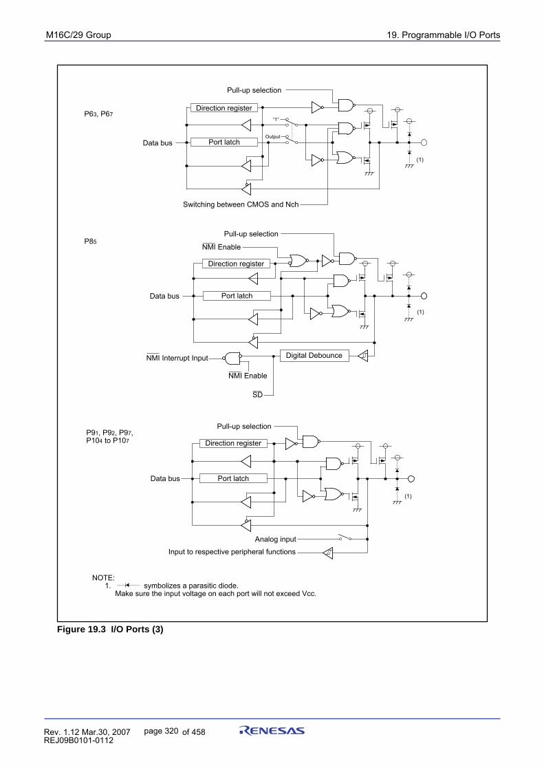
19. Programmable I/O PortspuorG92/C61M
page 320 854fo7002,03.raM21.1.veR2110-1010B90JER
Figure 19.3 I/O Ports (3)
P85
P63, P67
Output
“1”
Data bus
Pull-up selection
Direction register
Port latch
Switching between CMOS and Nch
NOTE:1. symbolizes a parasitic diode. Make sure the input voltage on each port will not exceed Vcc.
Data bus
Pull-up selection
Direction register
Port latch
NMI Interrupt Input
NMI Enable
Digital Debounce
NMI Enable
SD
(1)
(1)
Data bus
Direction register
Pull-up selection
Port latch
Analog input
Input to respective peripheral functions
P91, P92, P97, P104 to P107
(1)
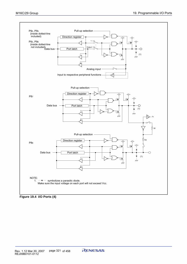
19. Programmable I/O PortspuorG92/C61M
page 321 854fo7002,03.raM21.1.veR2110-1010B90JER
Figure 19.4 I/O Ports (4)
1
Output
Direction register
Data bus Port latch
Analog input
Pull-up selection
(1)
P87
P86
fc
Rf
Rd
Data bus
Direction register
Pull-up selection
Port latch
Direction register
Pull-up selection
Port latchData bus(1)
(1)
Input to respective peripheral functions
P90, P95 (inside dotted-line included)
P93, P96 (inside dotted-line not included)
NOTE:1. symbolizes a parasitic diode. Make sure the input voltage on each port will not exceed Vcc.
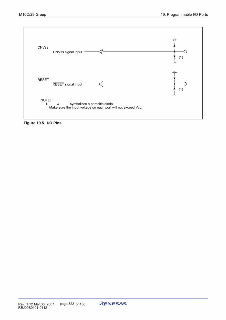
19. Programmable I/O PortspuorG92/C61M
page 322 854fo7002,03.raM21.1.veR2110-1010B90JER
Figure 19.5 I/O Pins
CNVSS
CNVSS signal input
RESETRESET signal input
(1)
(1)
NOTE: 1. symbolizes a parasitic diode.
Make sure the input voltage on each port will not exceed Vcc.
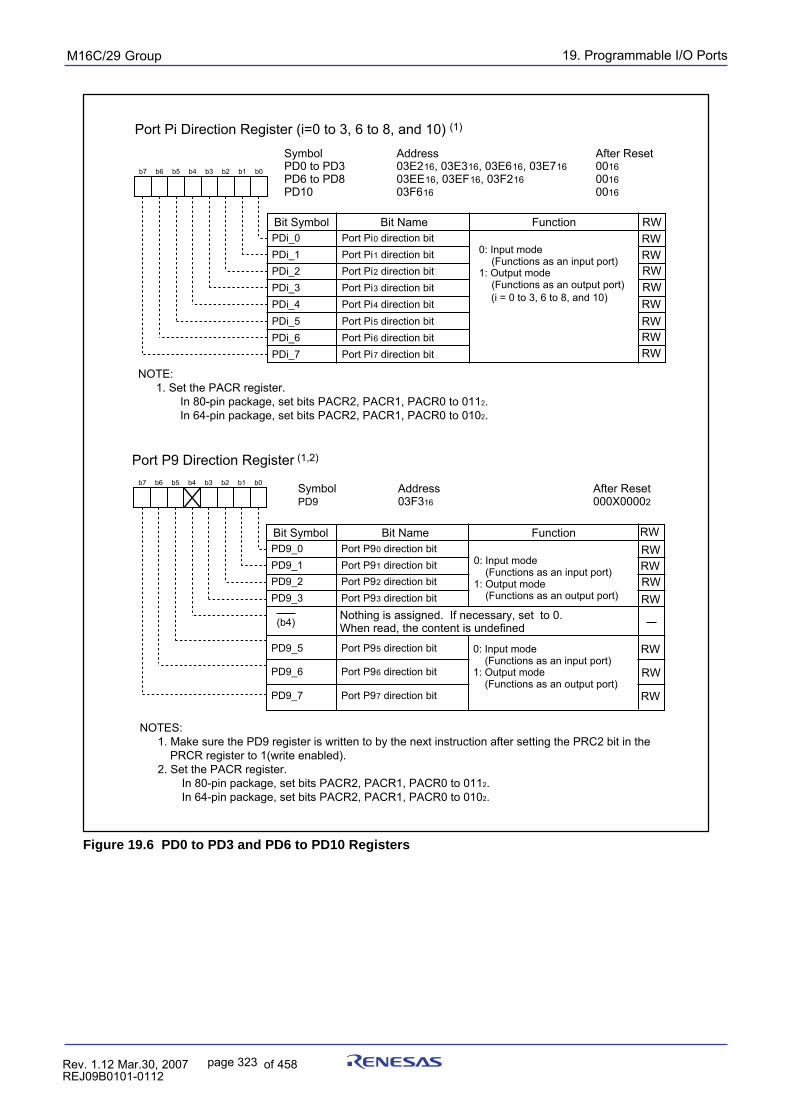
19. Programmable I/O PortspuorG92/C61M
page 323 854fo7002,03.raM21.1.veR2110-1010B90JER
Figure 19.6 PD0 to PD3 and PD6 to PD10 Registers
Port Pi Direction Register (i=0 to 3, 6 to 8, and 10) (1)
Symbol Address After ResetPD0 to PD3 03E216, 03E316, 03E616, 03E716 0016PD6 to PD8 03EE16, 03EF16, 03F216 0016PD10 03F616 0016
Bit Name FunctionBit Symbol RW
b7 b6 b5 b4 b3 b2 b1 b0
PDi_0 Port Pi0 direction bitPDi_1 Port Pi1 direction bitPDi_2 Port Pi2 direction bitPDi_3 Port Pi3 direction bitPDi_4 Port Pi4 direction bitPDi_5 Port Pi5 direction bitPDi_6 Port Pi6 direction bitPDi_7 Port Pi7 direction bit
0: Input mode (Functions as an input port) 1: Output mode (Functions as an output port)
(i = 0 to 3, 6 to 8, and 10)
Port P9 Direction Register (1,2)
Symbol Address After ResetPD9 03F316 000X00002
Bit Name FunctionBit Symbol
b7 b6 b5 b4 b3 b2 b1 b0
PD9_0 Port P90 direction bitPD9_1 Port P91 direction bitPD9_2 Port P92 direction bitPD9_3 Port P93 direction bit
0: Input mode (Functions as an input port)1: Output mode (Functions as an output port)
0: Input mode (Functions as an input port)1: Output mode (Functions as an output port)
RWRWRWRWRWRWRWRW
RWRWRW
RWRW
PD9_5 Port P95 direction bit RW
PD9_6 Port P96 direction bit RW
PD9_7 Port P97 direction bit RW
Nothing is assigned. If necessary, set to 0.When read, the content is undefined(b4)
NOTES: 1. Make sure the PD9 register is written to by the next instruction after setting the PRC2 bit in the
PRCR register to 1(write enabled). 2. Set the PACR register. In 80-pin package, set bits PACR2, PACR1, PACR0 to 0112. In 64-pin package, set bits PACR2, PACR1, PACR0 to 0102.
NOTE: 1. Set the PACR register. In 80-pin package, set bits PACR2, PACR1, PACR0 to 0112. In 64-pin package, set bits PACR2, PACR1, PACR0 to 0102.
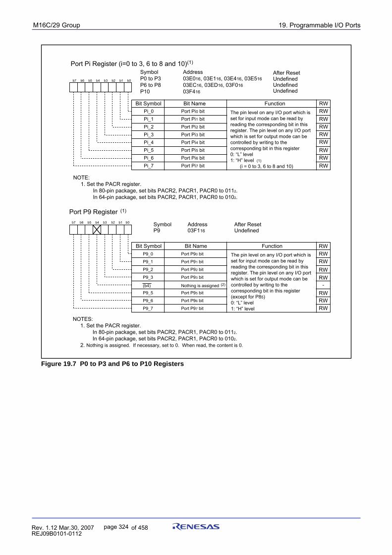
19. Programmable I/O PortspuorG92/C61M
page 324 854fo7002,03.raM21.1.veR2110-1010B90JER
Figure 19.7 P0 to P3 and P6 to P10 Registers
Port Pi Register (i=0 to 3, 6 to 8 and 10) (1)
After Reset Undefined Undefined
Undefined
Bit Name FunctionBit Symbol RW
b7 b6 b5 b4 b3 b2 b1 b0
Pi_0 Port Pi0 bitPi_1 Port Pi1 bitPi_2 Port Pi2 bitPi_3 Port Pi3 bitPi_4 Port Pi4 bitPi_5 Port Pi5 bitPi_6 Port Pi6 bitPi_7 Port Pi7 bit
Port P9 Register (1)
Symbol Address After ResetP9 03F116 Undefined
Bit Name FunctionBit Symbol
b7 b6 b5 b4 b3 b2 b1 b0
P9_0 Port P90 bit
P9_1 Port P91 bit
P9_2 Port P92 bit
P9_3 Port P93 bit
(b4) Nothing is assigned (2)
P9_5 Port P95 bit
P9_6 Port P96 bit
P9_7 Port P97 bit
RWRWRWRWRWRWRWRW
RWRWRWRW
-RW
RWRW
RW
The pin level on any I/O port which is set for input mode can be read by reading the corresponding bit in this register. The pin level on any I/O port which is set for output mode can be controlled by writing to the corresponding bit in this register 0: “L” level 1: “H” level (1) (i = 0 to 3, 6 to 8 and 10)
The pin level on any I/O port which is set for input mode can be read by reading the corresponding bit in this register. The pin level on any I/O port which is set for output mode can be controlled by writing to the corresponding bit in this register (except for P85)0: “L” level1: “H” level
Address 03E016, 03E116, 03E416, 03E516 03EC16, 03ED16, 03F016 03F416
SymbolP0 to P3P6 to P8P10
NOTE: 1. Set the PACR register. In 80-pin package, set bits PACR2, PACR1, PACR0 to 0112.
In 64-pin package, set bits PACR2, PACR1, PACR0 to 0102.
NOTES: 1. Set the PACR register. In 80-pin package, set bits PACR2, PACR1, PACR0 to 0112. In 64-pin package, set bits PACR2, PACR1, PACR0 to 0102. 2. Nothing is assigned. If necessary, set to 0. When read, the content is 0.
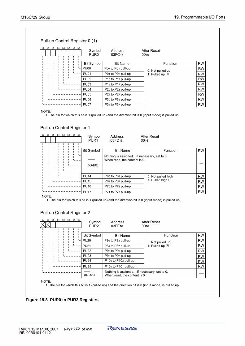
19. Programmable I/O PortspuorG92/C61M
page 325 854fo7002,03.raM21.1.veR2110-1010B90JER
Figure 19.8 PUR0 to PUR2 Registers
Pull-up Control Register 0 (1)
Symbol Address After ResetPUR0 03FC16 0016
Bit Name Function Bit Symbol RW
b7 b6 b5 b4 b3 b2 b1 b0
PU00 P00 to P03 pull-up
PU01 P04 to P07 pull-upPU02 P10 to P13 pull-upPU03 P14 to P17 pull-upPU04 P20 to P23 pull-upPU05 P24 to P27 pull-upPU06 P30 to P33 pull-upPU07 P34 to P37 pull-up
0: Not pulled up 1: Pulled up (1)
Pull-up Control Register 1
Symbol Address After ResetPUR1 03FD16 0016
Bit Name Function Bit Symbol
b7 b6 b5 b4 b3 b2 b1 b0
PU14 P60 to P63 pull-upPU15 P64 to P67 pull-upPU16 P70 to P73 pull-up
PU17 P74 to P77 pull-up
0: Not pulled high 1: Pulled high (1)
NOTE: 1. The pin for which this bit is 1 (pulled up) and the direction bit is 0 (input mode) is pulled up.
RWRWRWRWRWRWRWRW
RW
RWRWRWRW
NOTE: 1. The pin for which this bit is 1 (pulled up) and the direction bit is 0 (input mode) is pulled up.
Pull-up Control Register 2
Symbol Address After ResetPUR2 03FE16 0016
Bit Name FunctionBit Symbol
b7 b6 b5 b4 b3 b2 b1 b0
PU20 P80 to P83 pull-up
PU21 P84 to P87 pull-upPU22 P90 to P93 pull-upPU23 P95 to P97 pull-upPU24 P100 to P103 pull-up
PU25 P104 to P107 pull-upNothing is assigned. If necessary, set to 0.When read, the content is 0
0: Not pulled up 1: Pulled up (1)
RWRWRWRWRWRWRW
(b7-b6)
NOTE: 1. The pin for which this bit is 1 (pulled up) and the direction bit is 0 (input mode) is pulled up.
Nothing is assigned. If necessary, set to 0.When read, the content is 0
(b3-b0)
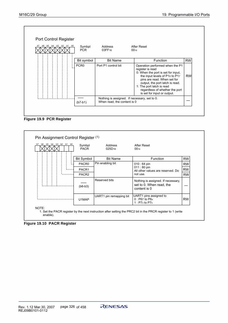
19. Programmable I/O PortspuorG92/C61M
page 326 854fo7002,03.raM21.1.veR2110-1010B90JER
Figure 19.9 PCR Register
Figure 19.10 PACR Register
Pin Assignment Control Register (1)
Symbpl Address After ResetPACR 025D16 0016
Bit Name FunctionBit Symbol RW
b7 b6 b5 b4 b3 b2 b1 b0
Pin enabling bit
Nothing is assigned. If necessary, set to 0. When read, the content is 0
RW
(b6-b3)
010 : 64 pin011 : 80 pinAll other values are reserved. Do not use.
PACR0
PACR1PACR2
RWRW
Reserved bits
U1MAPUART1 pin remapping bit UART1 pins assigned to
0 : P67 to P64
1 : P73 to P70RW
NOTE: 1. Set the PACR register by the next instruction after setting the PRC2 bit in the PRCR register to 1 (write enable).
Port Control Register
Symbpl Address After ResetPCR 03FF16 0016
Bit Name FunctionBit symbol RW
b7 b6 b5 b4 b3 b2 b1 b0
PCR0 Port P1 control bit
RW
(b7-b1)
Operation performed when the P1 register is read 0: When the port is set for input,
the input levels of P10 to P17 pins are read. When set for output, the port latch is read.
1: The port latch is read regardless of whether the port is set for input or output.
Nothing is assigned. If necessary, set to 0.When read, the content is 0
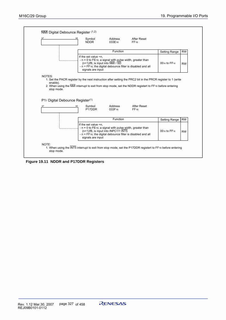
19. Programmable I/O PortspuorG92/C61M
page 327 854fo7002,03.raM21.1.veR2110-1010B90JER
Figure 19.11 NDDR and P17DDR Registers
NMI Digital Debounce Register (1,2)
Symbol Address After ResetNDDR 033E16 FF16
RW
b7 b0
Function RWSetting Range
0016 to FF16
If the set value =n, - n = 0 to FE16; a signal with pulse width, greater than (n+1)/f8, is input into NMI / SD - n = FF16; the digital debounce filter is disabled and all signals are input
P17 Digital Debounce Register(1)
Symbol Address After ResetP17DDR 033F16 FF16
RW
b7 b0
Function RWSetting Range
0016 to FF16
If the set value =n, - n = 0 to FE16; a signal with pulse width, greater than (n+1)/f8, is input into INPC17/ INT5 - n = FF16; the digital debounce filter is disabled and all signals are input
NOTES: 1. Set the PACR register by the next instruction after setting the PRC2 bit in the PRCR register to 1 (write enable). 2. When using the NMI interrupt to exit from stop mode, set the NDDR registert to FF16 before entering stop mode.
NOTE: 1. When using the INT5 interrupt to exit from stop mode, set the P17DDR registert to FF16 before entering stop mode.
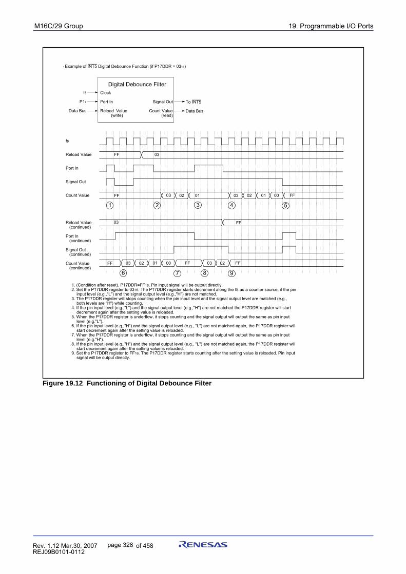
19. Programmable I/O PortspuorG92/C61M
page 328 854fo7002,03.raM21.1.veR2110-1010B90JER
Figure 19.12 Functioning of Digital Debounce Filter
f8
P17
Data Bus
1. (Condition after reset). P17DDR=FF16. Pin input signal will be output directly.2. Set the P17DDR register to 0316. The P17DDR register starts decrement along the f8 as a counter source, if the pin
input level (e.g.,"L") and the signal output level (e.g.,"H") are not matched.3. The P17DDR register will stops counting when the pin input level and the signal output level are matched (e.g.,
both levels are "H") while counting.4. If the pin input level (e.g.,"L") and the signal output level (e.g.,"H") are not matched the P17DDR register will start
decrement again after the setting value is reloaded.5. When the P17DDR register is underflow, it stops counting and the signal output will output the same as pin input
level (e.g."L").6. If the pin input level (e.g.,"H") and the signal output level (e.g., "L") are not matched again, the P17DDR register will
start decrement again after the setting value is reloaded.7. When the P17DDR register is underflow, it stops counting and the signal output will output the same as pin input
level (e.g."H").8. If the pin input level (e.g.,"H") and the signal output level (e.g., "L") are not matched again, the P17DDR register will
start decrement again after the setting value is reloaded.9. Set the P17DDR register to FF16. The P17DDR register starts counting after the setting value is reloaded. Pin input
signal will be output directly.
Clock
Port In
Reload Value (write)
Digital Debounce Filter
Signal Out
Count Value(read)
To INT5
Data Bus
f8
Reload Value
Port In
Signal Out
Count Value
Reload Value (continued)
Port In (continued)
Signal Out (continued)
Count Value (continued)
FF 03
FF 03 02 01 03 02 01 00 FF
03 FF
03 02 01 00FF FF 03 02 FF
1 2 3 4 5
6 7 8 9
• Example of INT5 Digital Debounce Function (if P17DDR = 0316)
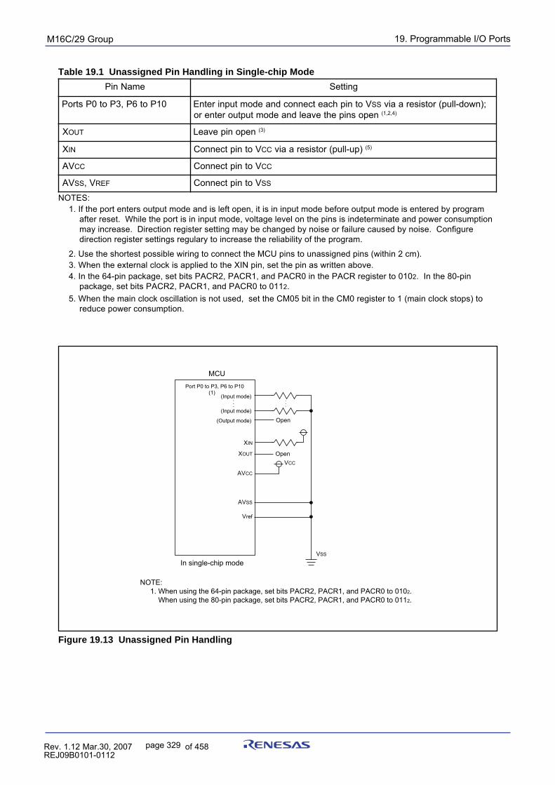
19. Programmable I/O PortspuorG92/C61M
page 329 854fo7002,03.raM21.1.veR2110-1010B90JER
Table 19.1 Unassigned Pin Handling in Single-chip Mode
Figure 19.13 Unassigned Pin Handling
(Input mode) · · ·
(Input mode)
(Output mode)
XOUT
AVCC
AVSS
Vref
MCU
VCC
VSS
In single-chip mode
Open
Open
···
(1)Port P0 to P3, P6 to P10
XIN
NOTE: 1. When using the 64-pin package, set bits PACR2, PACR1, and PACR0 to 0102. When using the 80-pin package, set bits PACR2, PACR1, and PACR0 to 0112.
emaNniP gnitteS
01Pot6P,3Pot0PstroP VotniphcaetcennocdnaedomtupniretnE SS ;)nwod-llup(rotsiseraaivneposnipehtevaeldnaedomtuptuoretnero )4,2,1(
X TUO neponipevaeL )3(
X NI VotniptcennoC CC )pu-llup(rotsiseraaiv )5(
VA CC VotniptcennoC CC
VA SS V, FER VotniptcennoC SS
NOTES:1. If the port enters output mode and is left open, it is in input mode before output mode is entered by program
after reset. While the port is in input mode, voltage level on the pins is indeterminate and power consumptionmay increase. Direction register setting may be changed by noise or failure caused by noise. Configuredirection register settings regulary to increase the reliability of the program.
2. Use the shortest possible wiring to connect the MCU pins to unassigned pins (within 2 cm).3. When the external clock is applied to the XIN pin, set the pin as written above.4. In the 64-pin package, set bits PACR2, PACR1, and PACR0 in the PACR register to 0102. In the 80-pin
package, set bits PACR2, PACR1, and PACR0 to 0112.5. When the main clock oscillation is not used, set the CM05 bit in the CM0 register to 1 (main clock stops) to
reduce power consumption.
20. Flash Memory VersionpuorG92/C61M
page 330 854fo7002,03.raM21.1.veR2110-1010B90JER
20. Flash Memory Version20.1 Flash Memory Performance
In the flash memory version, rewrite operation to the flash memory can be performed in four modes: CPUrewrite mode, standard serial I/O mode, parallel I/O mode, and CAN I/O mode.Table 20.1 lists specifications of the flash memory version. (Refer to Table 1.1 or Table 1.2 for the itemsnot listed in Table 20.1.
Item
Flash memory operating mode
Erase block
Program method
Erase method
Program, erase control method
Protect method
Number of commands
Program/EraseEndurance(1)
ROM code protection
Specification
4 modes (CPU rewrite, standard serial I/O, parallel I/O, CAN I/O)(3)
See Figures 20.1 to 20.3 Flash Memory Block Diagram
In units of word
Block erase
Program and erase controlled by software command
Blocks 0 to 5 are write protected by FMR16 bit. In addition, the block 0 and block 1 are write protected by FMR02 bit5 commands100 times 1,000 times (See Tables 1.6 to 1.8)100 times 10,000 times (See Tables 1.6 to 1.8)
Parallel I/O, standard serial I/O, and CAN I/O modes are supported.
Data Retention 20 years (Topr = 55ϒC)
Block 0 to 5 (program area)Block A and B (data are) (2)
NOTES:1. Program and erase endurance definition Program and erase endurance are the erase endurance of each block. If the program and erase endurance are n
times (n=100,1000,10000), each block can be erased n times. For example, if a 2-Kbyte block A is erased after writing 1 word data 1024 times, each to different addresses, this is counted as one program and erasure. However, data cannot be written to the same address more than once without erasing the block. (Rewrite disabled)
2. To use the limited number of erasure efficiently, write to unused address within the block instead of rewrite. Erase block only after all possible address are used. For example, an 8-word program can be written 128 times before erase is necessary. Maintaining an equal number of erasure between Block A and B will also improve efficiency. We recommend keeping track of the number of times erasure is used.
3. The M16C/29 Group, T-ver./V-ver. does not support the CAN I/O mode.
Table 20.1 Flash Memory Version Specifications
20. Flash Memory VersionpuorG92/C61M
page 331 854fo7002,03.raM21.1.veR2110-1010B90JER
Table 20.2. Flash Memory Rewrite Modes Overview
Flash memory CPU rewrite mode Standard serial I/O Parallel I/O mode CAN I/O moderewrite mode modeFunction The user ROM area is The user ROM area The user ROM areas The user ROM areas is
rewritten when the CPU is rewritten using a are rewritten using a rewritten using aexcutes software dedicated serial dedicated parallel dedicated CAN pro-command programmer. programmer. grammer.from the CPU. Standard serial I/OEW0 mode: mode 1: Rewrite in area other Clock synchronous than flash memory serial I/OEW1 mode: Standard serial I/O Rewrite in flash mode 2: memory UART
Areas which User ROM area User ROM area User ROM area User ROM areacan be rewrittenOperation Single chip mode Boot mode Parallel I/O mode Boot modemodeROM None Serial programmer Parallel programmer CAN programmerprogrammer
20.1.1 Boot ModeThe MCU enters boot mode when a hardware reset is performed while a high-level ("H") signal is appliedto pins CNVSS and P86 or while an "H" signal is applied to pins CNVSS and P16 and a low-level ("L")signal is applied to the P85. A program in the boot ROM area is executed.The boot ROM area is reserved. The boot ROM area stores the rewrite control program for a standardserial I/O mode before shipping. Do not rewrite the boot ROM area.
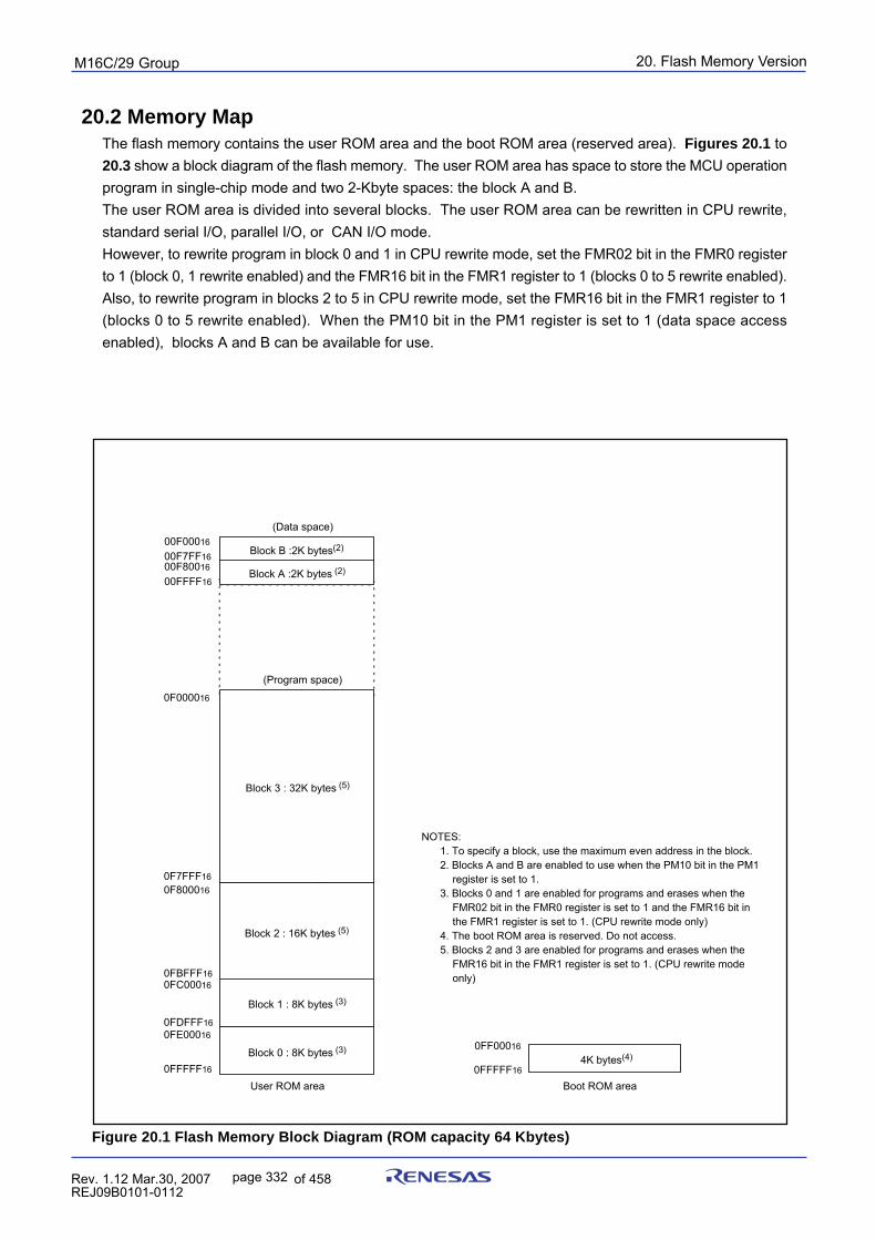
20. Flash Memory VersionpuorG92/C61M
page 332 854fo7002,03.raM21.1.veR2110-1010B90JER
20.2 Memory MapThe flash memory contains the user ROM area and the boot ROM area (reserved area). Figures 20.1 to20.3 show a block diagram of the flash memory. The user ROM area has space to store the MCU operationprogram in single-chip mode and two 2-Kbyte spaces: the block A and B.The user ROM area is divided into several blocks. The user ROM area can be rewritten in CPU rewrite,standard serial I/O, parallel I/O, or CAN I/O mode.However, to rewrite program in block 0 and 1 in CPU rewrite mode, set the FMR02 bit in the FMR0 registerto 1 (block 0, 1 rewrite enabled) and the FMR16 bit in the FMR1 register to 1 (blocks 0 to 5 rewrite enabled).Also, to rewrite program in blocks 2 to 5 in CPU rewrite mode, set the FMR16 bit in the FMR1 register to 1(blocks 0 to 5 rewrite enabled). When the PM10 bit in the PM1 register is set to 1 (data space accessenabled), blocks A and B can be available for use.
00FFFF16
Block B :2K bytes(2)00F00016
4K bytes(4)0FF00016
0FFFFF16
Boot ROM area
0FE00016
0FC00016
0FDFFF16
0F800016Block 2 : 16K bytes
0FBFFF16
0F7FFF16
0F000016
0FFFFF16
User ROM area
Block A :2K bytes (2)
Block 2 : 16K bytes (5)
Block 3 : 32K bytes (5)
Block 1 : 8K bytes (3)
Block 0 : 8K bytes (3)
00F7FF1600F80016
NOTES:1. To specify a block, use the maximum even address in the block.2. Blocks A and B are enabled to use when the PM10 bit in the PM1
register is set to 1. 3. Blocks 0 and 1 are enabled for programs and erases when the
FMR02 bit in the FMR0 register is set to 1 and the FMR16 bit in the FMR1 register is set to 1. (CPU rewrite mode only)
4. The boot ROM area is reserved. Do not access.5. Blocks 2 and 3 are enabled for programs and erases when the
FMR16 bit in the FMR1 register is set to 1. (CPU rewrite mode only)
(Data space)
(Program space)
Figure 20.1 Flash Memory Block Diagram (ROM capacity 64 Kbytes)
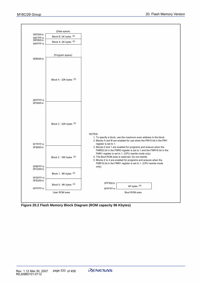
20. Flash Memory VersionpuorG92/C61M
page 333 854fo7002,03.raM21.1.veR2110-1010B90JER
00FFFF16
Block B :2K bytes (2)00F00016
4K bytes (4)0FF00016
0FFFFF16
Boot ROM area
0FE00016
0FC00016
0FDFFF16
0F800016Block 2 : 16K bytes
0FBFFF16
0F7FFF16
0F0000160EFFFF16
0FFFFF16
User ROM area
0E800016
Block A :2K bytes (2)
Block 2 : 16K bytes (5)
Block 4 : 32K bytes (5)
Block 3 : 32K bytes (5)
Block 1 : 8K bytes (3)
Block 0 : 8K bytes (3)
00F7FF1600F80016
NOTES:1. To specify a block, use the maximum even address in the block.2. Blocks A and B are enabled for use when the PM10 bit in the PM1
register is set to 1. 3. Blocks 0 and 1 are enabled for programs and erasure when the
FMR02 bit in the FMR0 register is set to 1 and the FMR16 bit in the FMR1 register is set to 1. (CPU rewrite mode only)
4. The Boot ROM area is reserved. Do not rewrite.5. Blocks 2 to 4 are enabled for programs and erasure when the
FMR16 bit in the FMR1 register is set to 1. (CPU rewrite mode only)
(Data space)
(Program space)
Figure 20.2 Flash Memory Block Diagram (ROM capacity 96 Kbytes)
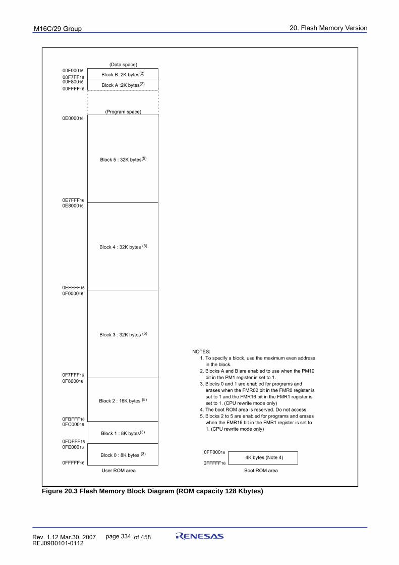
20. Flash Memory VersionpuorG92/C61M
page 334 854fo7002,03.raM21.1.veR2110-1010B90JER
00FFFF16
Block B :2K bytes(2)00F00016
4K bytes (Note 4)0FF00016
0FFFFF16
Boot ROM area
0FE00016
0FC00016
0FDFFF16
0F800016Block 2 : 16K bytes
0FBFFF16
0F7FFF16
0F0000160EFFFF16
0FFFFF16
User ROM area
0E800016
Block A :2K bytes(2)
Block 2 : 16K bytes (5)
Block 4 : 32K bytes (5)
Block 3 : 32K bytes (5)
Block 1 : 8K bytes(3)
Block 0 : 8K bytes (3)
00F7FF1600F80016
0E7FFF16
0E000016
Block 5 : 32K bytes(5)
NOTES:1. To specify a block, use the maximum even address
in the block.2. Blocks A and B are enabled to use when the PM10
bit in the PM1 register is set to 1. 3. Blocks 0 and 1 are enabled for programs and
erases when the FMR02 bit in the FMR0 register is set to 1 and the FMR16 bit in the FMR1 register is set to 1. (CPU rewrite mode only)
4. The boot ROM area is reserved. Do not access.5. Blocks 2 to 5 are enabled for programs and erases
when the FMR16 bit in the FMR1 register is set to 1. (CPU rewrite mode only)
(Data space)
(Program space)
Figure 20.3 Flash Memory Block Diagram (ROM capacity 128 Kbytes)
20. Flash Memory VersionpuorG92/C61M
page 335 854fo7002,03.raM21.1.veR2110-1010B90JER
20.3 Functions To Prevent Flash Memory from RewritingThe flash memory has a built-in ROM code protect function for parallel I/O mode and a built-in ID codecheck function for standard input/output mode to prevent the flash memory from reading or rewriting.
20.3.1 ROM Code Protect FunctionThe ROM code protect function disables reading or changing the contents of the on-chip flash memory inparallel I/O mode. Figure 20.4 shows the ROMCP address. The ROMCP address is located in a userROM area. To enable ROM code protect, set the ROMCP1 bit to “002”, “012”, or “102” and set the bit 5 tobit 0 to “1111112”.To cancel ROM code protect, erase the block including the the ROMCP register in CPU rewrite mode orstandard serial I/O mode.
20.3.2 ID Code Check Function
Use the ID code check function in standard serial input/output mode. Unless the flash memory is blank,the ID code sent from the programmer and the 7-byte ID code written in the flash memory are comparedfor match. If the ID codes do not match, the commands sent from the programmer are not acknowledged.The ID code consists of 8-bit data, starting with the first byte, into addresses, 0FFFDF16, 0FFFE316,0FFFEB16, 0FFFEF16, 0FFFF316, 0FFFF716, and 0FFFFB16. The flash memory must have a programwith the ID code set in these addresses.
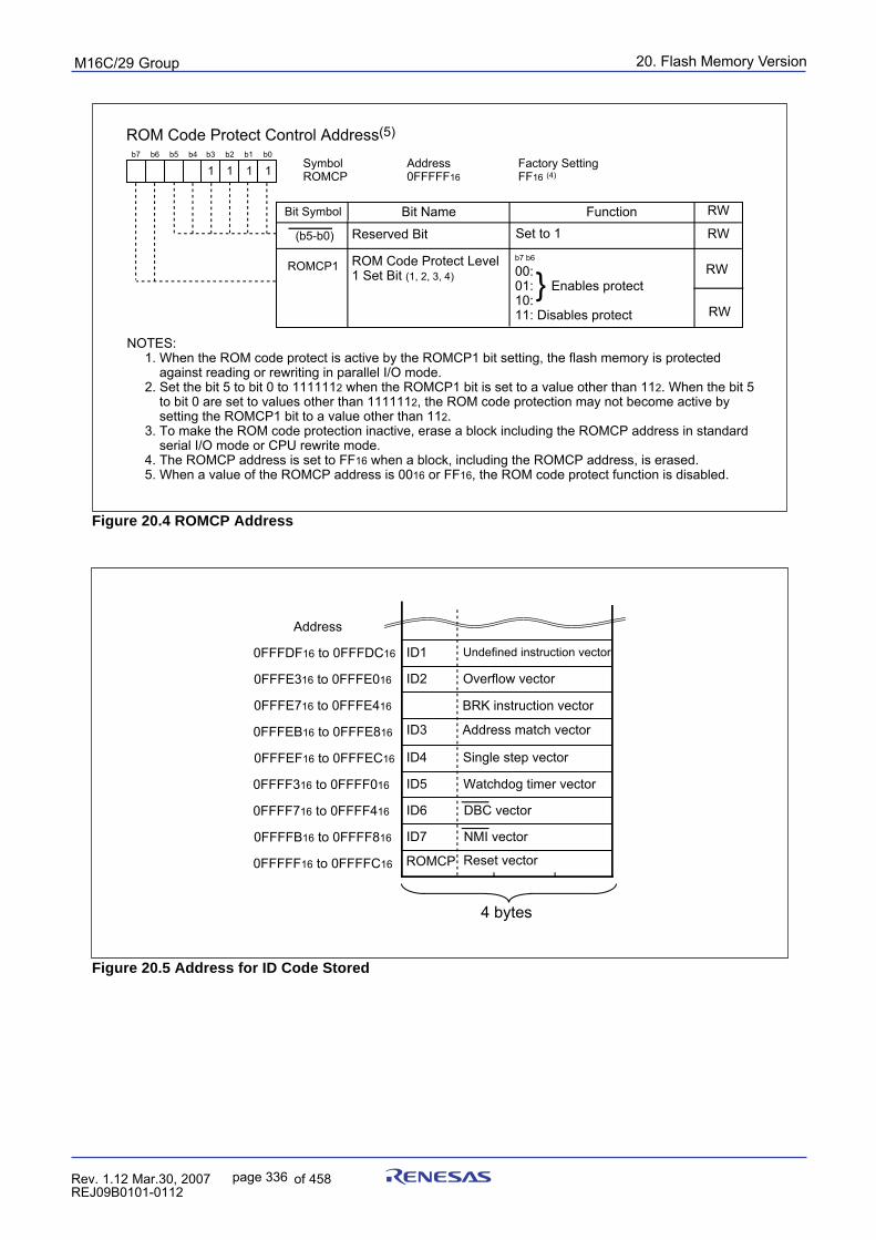
20. Flash Memory VersionpuorG92/C61M
page 336 854fo7002,03.raM21.1.veR2110-1010B90JER
Symbol Address Factory SettingROMCP 0FFFFF16 FF16 (4)
ROM Code Protect Control Address(5)
Bit Name FunctionBit Symbol
b7 b6 b5 b4 b3 b2 b1 b0
00: 01: 10: 11: Disables protect
ROM Code Protect Level 1 Set Bit (1, 2, 3, 4)
ROMCP1b7 b6
11
Reserved Bit Set to 1
Enables protectNOTES:
1. When the ROM code protect is active by the ROMCP1 bit setting, the flash memory is protected against reading or rewriting in parallel I/O mode.
2. Set the bit 5 to bit 0 to 1111112 when the ROMCP1 bit is set to a value other than 112. When the bit 5 to bit 0 are set to values other than 1111112, the ROM code protection may not become active by setting the ROMCP1 bit to a value other than 112.
3. To make the ROM code protection inactive, erase a block including the ROMCP address in standard serial I/O mode or CPU rewrite mode.
4. The ROMCP address is set to FF16 when a block, including the ROMCP address, is erased.5. When a value of the ROMCP address is 0016 or FF16, the ROM code protect function is disabled.
11
RW
RW
RW
RW
(b5-b0)
Reset vector
Watchdog timer vector
Single step vector
Address match vector
BRK instruction vector
Overflow vector
Undefined instruction vector
ID7
ID6
ID5
ID4
ID3
ID2
ID1
DBC vector
NMI vector
0FFFFF16 to 0FFFFC16
0FFFFB16 to 0FFFF816
0FFFF716 to 0FFFF416
0FFFF316 to 0FFFF016
0FFFEF16 to 0FFFEC16
0FFFEB16 to 0FFFE816
0FFFE716 to 0FFFE416
0FFFE316 to 0FFFE016
0FFFDF16 to 0FFFDC16
4 bytes
Address
ROMCP
Figure 20.4 ROMCP Address
Figure 20.5 Address for ID Code Stored
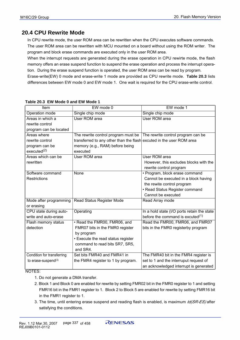
20. Flash Memory VersionpuorG92/C61M
page 337 854fo7002,03.raM21.1.veR2110-1010B90JER
Item EW mode 0 EW mode 1Operation mode Single chip mode Single chip modeAreas in which a User ROM area User ROM arearewrite controlprogram can be locatedAreas where The rewrite control program must be The rewrite control program can berewrite control transferred to any other than the flash excuted in the user ROM areaprogram can be memory (e.g., RAM) before beingexecuted(2) executedAreas which can be User ROM area User ROM arearewritten However, this excludes blocks with the
rewrite control programSoftware command None • Program, block erase commandRestrictions Cannot be executed in a block having
the rewite control program• Read Status Register commandCannot be executed
Mode after programming Read Status Register Mode Read Array modeor erasingCPU state during auto- Operating In a hold state (I/O ports retain the statewrite and auto-erase before the command is excuted(1)
Flash memory status • Read the FMR00, FMR06, and Read the FMR00, FMR06, and FMR07detection FMR07 bits in the FMR0 register bits in the FMR0 registerby program
by program• Execute the read status registercommand to read bits SR7, SR5,and SR4.
Condition for transferring Set bits FMR40 and FMR41 in The FMR40 bit in the FMR4 register is to erase-suspend(3) the FMR4 register to 1 by program. set to 1 and the interruput request of
an acknowledged interrupt is generatedNOTES:
1. Do not generate a DMA transfer.2. Block 1 and Block 0 are enabled for rewrite by setting FMR02 bit in the FMR0 register to 1 and setting
FMR16 bit in the FMR1 register to 1. Block 2 to Block 5 are enabled for rewrite by setting FMR16 bitin the FMR1 register to 1.
3. The time, until entering erase suspend and reading flash is enabled, is maximum td(SR-ES) aftersatisfying the conditions.
20.4 CPU Rewrite ModeIn CPU rewrite mode, the user ROM area can be rewritten when the CPU executes software commands.The user ROM area can be rewritten with MCU mounted on a board without using the ROM writer. Theprogram and block erase commands are executed only in the user ROM area.When the interrupt requests are generated during the erase operation in CPU rewirte mode, the flashmemory offers an erase suspend function to suspend the erase operation and process the interrupt opera-tion. During the erase suspend function is operated, the user ROM area can be read by program.Erase-write(EW) 0 mode and erase-write 1 mode are provided as CPU rewrite mode. Table 20.3 listsdifferences between EW mode 0 and EW mode 1. One wait is required for the CPU erase-write control.
Table 20.3 EW Mode 0 and EW Mode 1
20. Flash Memory VersionpuorG92/C61M
page 338 854fo7002,03.raM21.1.veR2110-1010B90JER
20.4.1 EW Mode 0The MCU enters CPU rewrite mode by setting the FMR01 bit in the FMR0 register to 1 (CPU rewrite modeenabled) and is ready to accept software commands. EW mode 0 is selected by setting the FMR11 bit inthe FMR1 register to 0.To set the FMR01 bit to 1, set to 1 after first writing 0. The software commands control programming anderasing. The FMR0 register or the status register indicates whether a programming or erasing operationsis completed.When entering the erase-suspend during the auto-erasing, set the FMR40 bit to 1 (erase-suspend en-abled) and the FMR41 bit to 1 (suspend request). After waiting for td(SR-ES) and verifying the FMR46 bitis set to 1 (auto-erase stop), access to the user ROM area. When setting the FMR41 bit to 0 (eraserestart), auto-erasing is restarted.
20.4.2 EW Mode 1
EW mode 1 is selected by setting the FMR11 bit to 1 after the FMR01 bit is set to 1 (set to 1 after firstwriting 0).The FMR0 register indicates whether or not a programming or an erasing operation is completed. Readstatus register cannot be read in EW mode 1.When an erase/program command is initiated, the CPU halts all program execution until the commandoperation is completed or erase-suspend request is generated.When enabling an erase-suspend function, set the FMR40 bit to 1 (erase suspend enabled) and executeblock erase commands. Also, the interrupt to transfer to erase-suspend must be set enabled preliminar-ily. When entering erase-suspend after td(SR-ES) from an interrupt is requested, interrupts can be ac-cepted.When an interrupt request is generated, the FMR41 bit is automatically set to 1 (suspend request) and anauto-erasing is suspended. If an auto-erasing has not completed (when the FMR00 bit is 0) after aninterrupt process is completed, set the FMR41 bit to 0 (erase restart) and execute block erase commandsagain.
20. Flash Memory VersionpuorG92/C61M
page 339 854fo7002,03.raM21.1.veR2110-1010B90JER
20.5 Register DescriptionFigure 20.6 shows the flash memory control register 0 and flash memory control register 1. Figure 20.7
shows the flash memory control register 4.
20.5.1 Flash Memory Control Register 0 (FMR0)•FMR 00 Bit
The FMR00 bit indicates the operating state of the flash memory. Its value is 0 while the program,erase, or erase-suspend command is being executed, otherwise, it is 1.
•FMR01 BitThe MCU can accept commands when the FMR01 bit is set to 1 (CPU rewrite mode). To set theFMR01 bit to 1, first set it to 0 and then 1. The FMR01 bit is set to 0 only by writing 0.
•FMR02 BitThe combined settings of bits FMR02 and FMR16 enable program and erase in the user ROM area.See Table 20.4 for setting details. To set the FMR02 bit to 1, first set it to 0 and then 1. The FMR02bit is valid only when the FMR01 bit is set to 1 (CPU rewrite mode enable).
•FMSTP BitThe FMSTP bit initializes the flash memory control circuits and minimizes power consumption in theflash memory. Access to the on-chip flash memory is disabled when the FMSTP bit is set to 1. Set theFMSTP bit by program in a space other than the flash memory.Set the FMSTP bit to 1 if one of the following occurs:•A flash memory access error occurs during erasing or programming in EW mode 0 (FMR00 bit does not switch back to 1 (ready)).•Low-power consumption mode or on-chip oscillator low-power consumption mode is entered. Figure 20.10 shows a flow chart illustrating how to start and stop the flash memory before and after entering low power mode. Follow the procedure in this flow chart. When entering stop or wait mode while the CPU rewrite mode is disabled, do not set the FMR0 register because the on-chip flash memory is automatically turned off and turned back on whenexiting.
•FMR06 BitThe FMR06 bit is a read-only bit indicating an auto-program operation state. The FMR06 bit is set to1 when a program error occurs; otherwise, it is set to 0. For details, refer to 20.8.4 Full Status Check.
•FMR07 BitThe FMR07 bit is a read-only bit indicating an auto-erase operation status. The FMR07 bit is set to 1when an erase error occurs; otherwise, it is set to 0. For details, refer to 20.8.4 Full Status Check.
Figure 20.8 shows a EW mode 0 set/reset flowchart, Figure 20.9 shows a EW mode 1 set/reset flow-chart.
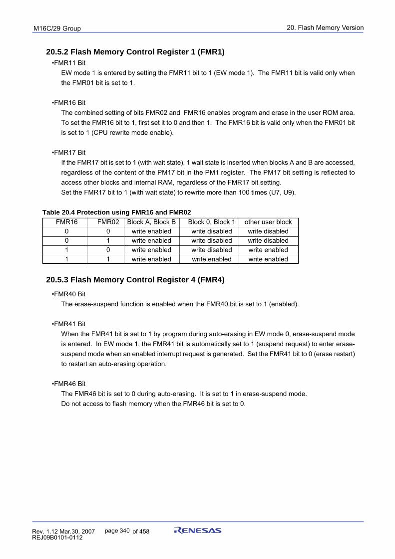
20. Flash Memory VersionpuorG92/C61M
page 340 854fo7002,03.raM21.1.veR2110-1010B90JER
20.5.2 Flash Memory Control Register 1 (FMR1)•FMR11 Bit
EW mode 1 is entered by setting the FMR11 bit to 1 (EW mode 1). The FMR11 bit is valid only whenthe FMR01 bit is set to 1.
•FMR16 BitThe combined setting of bits FMR02 and FMR16 enables program and erase in the user ROM area.To set the FMR16 bit to 1, first set it to 0 and then 1. The FMR16 bit is valid only when the FMR01 bitis set to 1 (CPU rewrite mode enable).
•FMR17 BitIf the FMR17 bit is set to 1 (with wait state), 1 wait state is inserted when blocks A and B are accessed,regardless of the content of the PM17 bit in the PM1 register. The PM17 bit setting is reflected toaccess other blocks and internal RAM, regardless of the FMR17 bit setting.Set the FMR17 bit to 1 (with wait state) to rewrite more than 100 times (U7, U9).
Table 20.4 Protection using FMR16 and FMR02FMR16 FMR02 Block A, Block B Block 0, Block 1 other user block
0 0 write enabled write disabled write disabled0 1 write enabled write disabled write disabled1 0 write enabled write disabled write enabled1 1 write enabled write enabled write enabled
20.5.3 Flash Memory Control Register 4 (FMR4)
•FMR40 BitThe erase-suspend function is enabled when the FMR40 bit is set to 1 (enabled).
•FMR41 BitWhen the FMR41 bit is set to 1 by program during auto-erasing in EW mode 0, erase-suspend modeis entered. In EW mode 1, the FMR41 bit is automatically set to 1 (suspend request) to enter erase-suspend mode when an enabled interrupt request is generated. Set the FMR41 bit to 0 (erase restart)to restart an auto-erasing operation.
•FMR46 BitThe FMR46 bit is set to 0 during auto-erasing. It is set to 1 in erase-suspend mode.Do not access to flash memory when the FMR46 bit is set to 0.
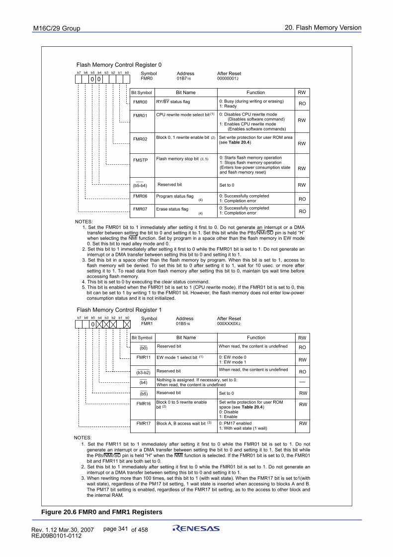
20. Flash Memory VersionpuorG92/C61M
page 341 854fo7002,03.raM21.1.veR2110-1010B90JER
Figure 20.6 FMR0 and FMR1 Registers
NOTES:
Flash Memory Control Register 0Symbol Address After ResetFMR0 01B716 000000012
b7 b6 b5 b4 b3 b2 b1 b0
FMR00
Bit Symbol Bit Name Function RW
0: Busy (during writing or erasing)1: Ready
CPU rewrite mode select bit (1) 0: Disables CPU rewrite mode (Disables software command)1: Enables CPU rewrite mode (Enables software commands)
FMR01
Block 0, 1 rewrite enable bit (2) Set write protection for user ROM area(see Table 20.4)
Flash memory stop bit (3, 5)
FMR02
FMSTP
0
RY/BY status flag
Reserved bit Set to 0
0: Successfully completed1: Completion error
Program status flagFMR06
0: Successfully completed1: Completion error
Erase status flagFMR07
RW
RW
RW
RW
RO
RO
RO
(b5-b4)
0: Starts flash memory operation1: Stops flash memory operation(Enters low-power consumption state and flash memory reset)
0
(4)
(4)
Flash Memory Control Register 1Symbol Address After ResetFMR1 01B516 000XXX0X2
b7 b6 b5 b4 b3 b2 b1 b0
Bit Symbol Bit Name Function
EW mode 1 select bit (1) 0: EW mode 01: EW mode 1
FMR11
Block A, B access wait bit (3)
Reserved bit When read, the content is undefined
Reserved bit Set to 0
Nothing is assigned. If necessary, set to 0.When read, the content is undefined
RW
RO
RW
RW
RW
(b0)
(b4)
Reserved bit(b3-b2) RO
NOTES:
(b5)
FMR16 RWBlock 0 to 5 rewrite enable bit (2)
FMR17
Set write protection for user ROM space (see Table 20.4)0: Disable1: Enable0: PM17 enabled1: With wait state (1 wait)
When read, the content is undefined
0
1. Set the FMR11 bit to 1 immediately after setting it first to 0 while the FMR01 bit is set to 1. Do not generate an interrupt or a DMA transfer between setting the bit to 0 and setting it to 1. Set this bit while the P85/NMI/SD pin is held "H" when the NMI function is selected. If the FMR01 bit is set to 0, the FMR01 bit and FMR11 bit are both set to 0.
2. Set this bit to 1 immediately after setting it first to 0 while the FMR01 bit is set to 1. Do not generate an interrupt or a DMA transfer between setting this bit to 0 and setting it to 1.
3. When rewriting more than 100 times, set this bit to 1 (with wait state). When the FMR17 bit is set to1(with wait state), regardless of the PM17 bit setting, 1 wait state is inserted when accessing to blocks A and B. The PM17 bit setting is enabled, regardless of the FMR17 bit setting, as to the access to other block and the internal RAM.
1. Set the FMR01 bit to 1 immediately after setting it first to 0. Do not generate an interrupt or a DMA transfer between setting the bit to 0 and setting it to 1. Set this bit while the P85/NMI/SD pin is held “H” when selecting the NMI function. Set by program in a space other than the flash memory in EW mode 0. Set this bit to read alley mode and 0.
2. Set this bit to 1 immediately after setting it first to 0 while the FMR01 bit is set to 1. Do not generate an interrupt or a DMA transfer between setting this bit to 0 and setting it to 1.
3. Set this bit in a space other than the flash memory by program. When this bit is set to 1, access to flash memory will be denied. To set this bit to 0 after setting it to 1, wait for 10 usec. or more after setting it to 1. To read data from flash memory after setting this bit to 0, maintain tps wait time before accessing flash memory.
4. This bit is set to 0 by executing the clear status command.5. This bit is enabled when the FMR01 bit is set to 1 (CPU rewrite mode). If the FMR01 bit is set to 0, this
bit can be set to 1 by writing 1 to the FMR01 bit. However, the flash memory does not enter low-power consumption status and it is not initialized.
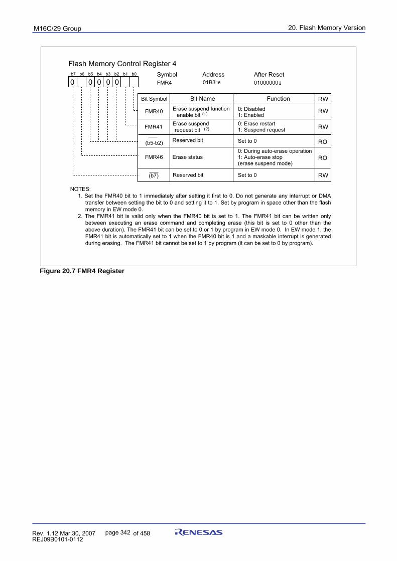
20. Flash Memory VersionpuorG92/C61M
page 342 854fo7002,03.raM21.1.veR2110-1010B90JER
Figure 20.7 FMR4 Register
Flash Memory Control Register 4Symbol Address After ResetFMR4 01B316 01000000 2
b7 b6 b5 b4 b3 b2 b1 b0
Bit Symbol Bit Name Function
Erase suspend request bit (2)
0: Erase restart1: Suspend requestFMR41
0
Reserved bit Set to 0
Erase suspend function enable bit (1)
0: Disabled1: Enabled
Reserved bit Set to 0
00
RW
RW
RW
RO
RW
FMR40
(b5-b2)
(b7)
RO
FMR46
0 0
Erase status0: During auto-erase operation1: Auto-erase stop (erase suspend mode)
NOTES: 1. Set the FMR40 bit to 1 immediately after setting it first to 0. Do not generate any interrupt or DMA
transfer between setting the bit to 0 and setting it to 1. Set by program in space other than the flash memory in EW mode 0.
2. The FMR41 bit is valid only when the FMR40 bit is set to 1. The FMR41 bit can be written only between executing an erase command and completing erase (this bit is set to 0 other than the above duration). The FMR41 bit can be set to 0 or 1 by program in EW mode 0. In EW mode 1, the FMR41 bit is automatically set to 1 when the FMR40 bit is 1 and a maskable interrupt is generated during erasing. The FMR41 bit cannot be set to 1 by program (it can be set to 0 by program).
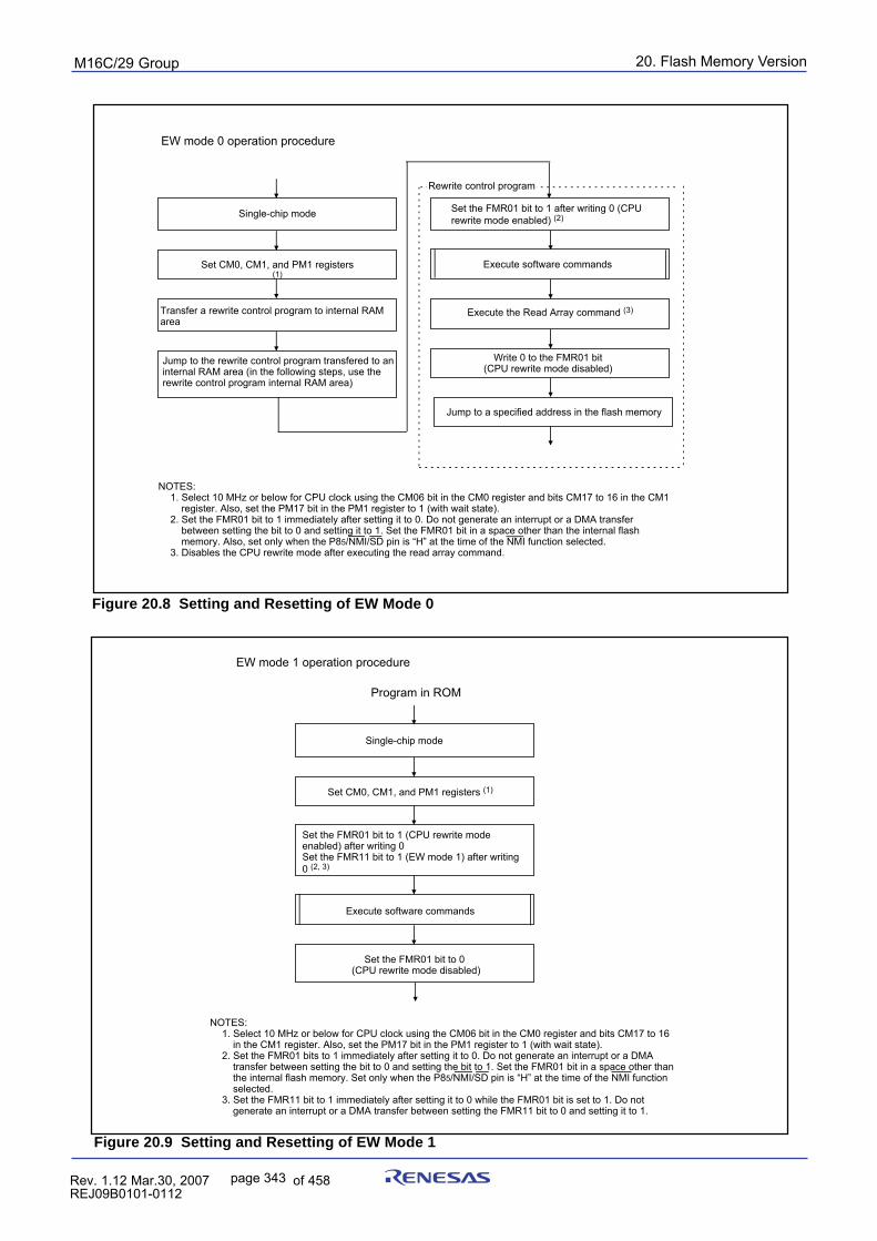
20. Flash Memory VersionpuorG92/C61M
page 343 854fo7002,03.raM21.1.veR2110-1010B90JER
Figure 20.8 Setting and Resetting of EW Mode 0
Figure 20.9 Setting and Resetting of EW Mode 1
Execute the Read Array command (3)
Single-chip mode
Set CM0, CM1, and PM1 registers (1)
Execute software commands
Jump to the rewrite control program transfered to an internal RAM area (in the following steps, use the rewrite control program internal RAM area)
Transfer a rewrite control program to internal RAM area
Write 0 to the FMR01 bit(CPU rewrite mode disabled)
Set the FMR01 bit to 1 after writing 0 (CPU rewrite mode enabled) (2)
EW mode 0 operation procedure
Rewrite control program
Jump to a specified address in the flash memory
NOTES:1. Select 10 MHz or below for CPU clock using the CM06 bit in the CM0 register and bits CM17 to 16 in the CM1
register. Also, set the PM17 bit in the PM1 register to 1 (with wait state).2. Set the FMR01 bit to 1 immediately after setting it to 0. Do not generate an interrupt or a DMA transfer
between setting the bit to 0 and setting it to 1. Set the FMR01 bit in a space other than the internal flash memory. Also, set only when the P85/NMI/SD pin is “H” at the time of the NMI function selected.
3. Disables the CPU rewrite mode after executing the read array command.
Single-chip mode
Set CM0, CM1, and PM1 registers (1)
Set the FMR01 bit to 1 (CPU rewrite mode enabled) after writing 0Set the FMR11 bit to 1 (EW mode 1) after writing 0 (2, 3)
Program in ROM
EW mode 1 operation procedure
Execute software commands
Set the FMR01 bit to 0(CPU rewrite mode disabled)
NOTES:1. Select 10 MHz or below for CPU clock using the CM06 bit in the CM0 register and bits CM17 to 16
in the CM1 register. Also, set the PM17 bit in the PM1 register to 1 (with wait state).2. Set the FMR01 bits to 1 immediately after setting it to 0. Do not generate an interrupt or a DMA
transfer between setting the bit to 0 and setting the bit to 1. Set the FMR01 bit in a space other than the internal flash memory. Set only when the P85/NMI/SD pin is “H” at the time of the NMI function selected.
3. Set the FMR11 bit to 1 immediately after setting it to 0 while the FMR01 bit is set to 1. Do not generate an interrupt or a DMA transfer between setting the FMR11 bit to 0 and setting it to 1.
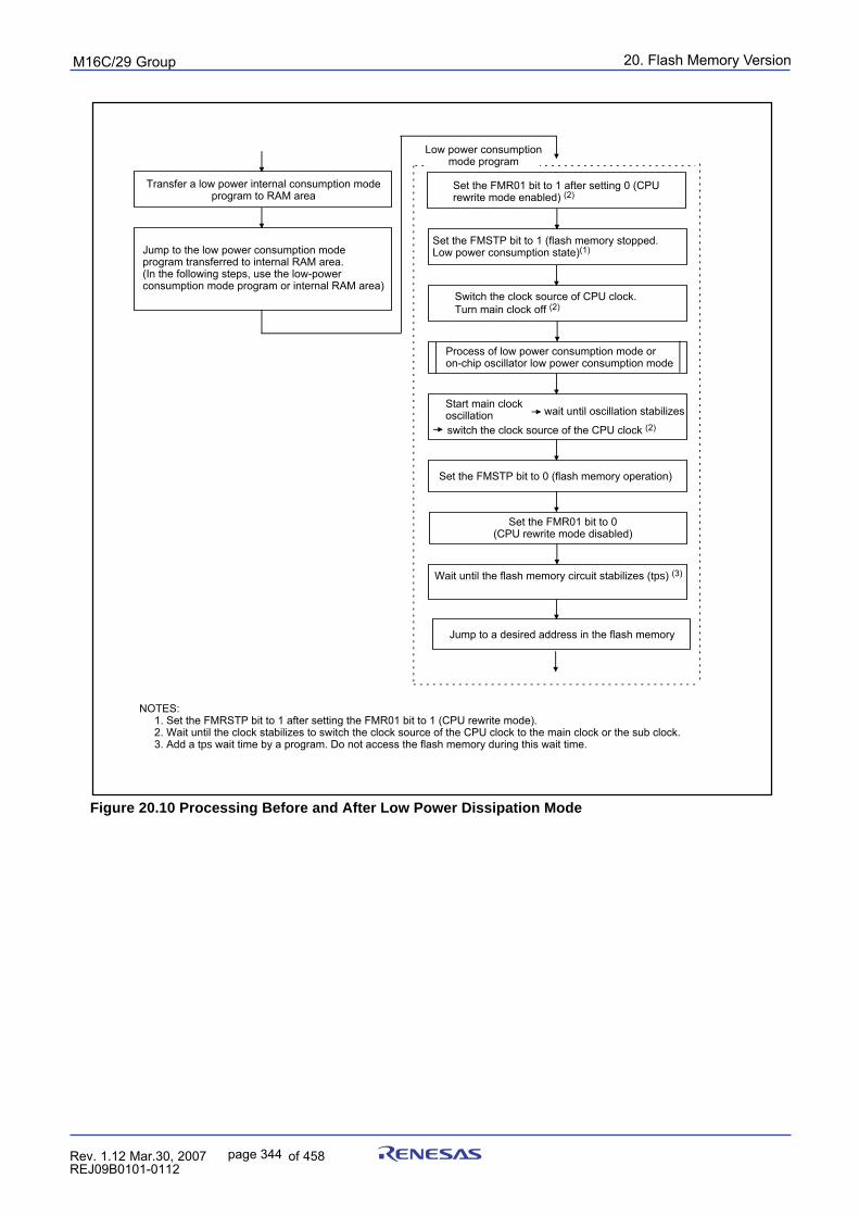
20. Flash Memory VersionpuorG92/C61M
page 344 854fo7002,03.raM21.1.veR2110-1010B90JER
Figure 20.10 Processing Before and After Low Power Dissipation Mode
Start main clock oscillation
Transfer a low power internal consumption mode program to RAM area
Switch the clock source of CPU clock.Turn main clock off (2)
Jump to the low power consumption mode program transferred to internal RAM area.(In the following steps, use the low-power consumption mode program or internal RAM area)
Wait until the flash memory circuit stabilizes (tps) (3)
Set the FMSTP bit to 0 (flash memory operation)
Set the FMSTP bit to 1 (flash memory stopped. Low power consumption state)(1)
Process of low power consumption mode or on-chip oscillator low power consumption mode
switch the clock source of the CPU clock (2)
Low power consumption mode program
Set the FMR01 bit to 0(CPU rewrite mode disabled)
Set the FMR01 bit to 1 after setting 0 (CPU rewrite mode enabled) (2)
Jump to a desired address in the flash memory
wait until oscillation stabilizes
NOTES: 1. Set the FMRSTP bit to 1 after setting the FMR01 bit to 1 (CPU rewrite mode). 2. Wait until the clock stabilizes to switch the clock source of the CPU clock to the main clock or the sub clock. 3. Add a tps wait time by a program. Do not access the flash memory during this wait time.
20. Flash Memory VersionpuorG92/C61M
page 345 854fo7002,03.raM21.1.veR2110-1010B90JER
20.6 Precautions in CPU Rewrite ModeDescribed below are the precautions to be observed when rewriting the flash memory in CPU rewrite mode.
20.6.1 Operation Speed
When the CPU clock source is the main clock, set the CPU clock frequency at 10 MHz or less with theCM06 bit in the CM0 register and bits CM17 and CM16 in the CM1 register, before entering CPU rewritemode (EW mode 0 or EW mode 1). Also, when selecting f3(ROC) of a on-chip oscillator as a CPU clocksource, set bits ROCR3 and ROCR2 in the ROCR register to the CPU clock division rate at “divide-by-4”or “divide-by-8”, before entering CPU rewrite mode (EW mode 0 or EW mode 1).In both cases, set the PM17 bit in the PM1 register to 1 (with wait state).
20.6.2 Prohibited Instructions
The following instructions cannot be used in EW mode 0 because the CPU tries to read data in the flashmemory: UND instruction, INTO instruction, JMPS instruction, JSRS instruction, and BRK instruction
20.6.3 Interrupts
EW Mode 0• To use interrupts having vectors in a relocatable vector table, the vectors must be relocated to the
RAM area._______
• The NMI and watchdog timer interrupts are available since registers FMR0 and FMR1 are forciblyreset when either interrupt occurs. However, the interrupt program, which allocates the jumpaddresses for each interrupt routine to the fixed vector table, is needed. Flash memory rewrite
_______
operation is aborted when the NMI or watchdog timer interrupt occurs. Set the FMR01 bit to 1 andexecute the rewrite and erase program again after exiting the interrupt routine.
• The address match interrupt can not be used since the CPU tries to read data in the flash memory.EW Mode 1
• Do not acknowledge any interrupts with vectors in the relocatable vector table or the addressmatch interrupt during the auto program period or auto erase period with erase-suspend functiondisabled.
20.6.4 How to AccessTo set bit FMR01, FMR02, FMR11 or FMR16 to 1, write 1 immediately after setting to 0. Do not generatean interrupt or a DMA transfer between the instruction to set the bit to 0 and the instruction to set it to 1.
_______ _______ _____
When the NMI function is selected, set the bit while an “H” signal is applied to the P85/NMI/SD pin.
20.6.5 Writing in the User ROM Area20.6.5.1 EW Mode 0
• If the supply voltage drops while rewriting the block where the rewrite control program is stored,the flash memory can not be rewritten, because the rewrite control program is not correctly rewrit-ten. If this error occurs, rewrite the user ROM area in standard serial I/O mode or parallel I/Omode.
20.6.5.2 EW Mode 1
• Do not rewrite the block where the rewrite control program is stored.
20. Flash Memory VersionpuorG92/C61M
page 346 854fo7002,03.raM21.1.veR2110-1010B90JER
20.6.6 DMA TransferIn EW mode 1, do not generate a DMA transfer while the FMR00 bit in the FMR0 register is set to 0.(during the auto-programming or auto-erasing).
20.6.7 Writing Command and Data
Write the command codes and data to even addresses in the user ROM area.
20.6.8 Wait ModeWhen entering wait mode, set the FMR01 bit to 0 (CPU rewrite mode disabled) before executing theWAIT instruction.
20.6.9 Stop Mode
When entering stop mode, the following settings are required:• Set the FMR01 bit to 0 (CPU rewrite mode disabled) and disable the DMA transfer before setting the CM10 bit to 1 (stop mode).
20.6.10 Low Power Consumption Mode and On-Chip Oscillator-Low Power Consumption ModeIf the CM05 bit is set to 1 (main clock stopped), do not execute the following commands.• Program• Block erase
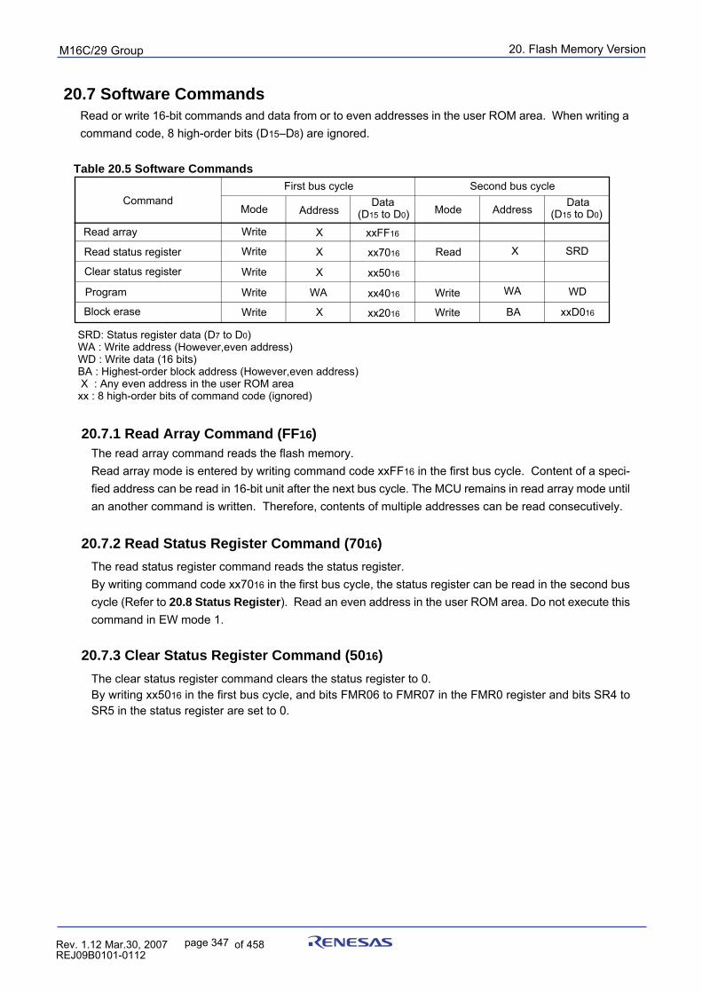
20. Flash Memory VersionpuorG92/C61M
page 347 854fo7002,03.raM21.1.veR2110-1010B90JER
Command
Program
Clear status register
Read array
Read status register
First bus cycle Second bus cycle
Block erase
Write
Write
Write
Write
Write
Mode
Read
Write
Write
Mode
X
WA
BA
Address
SRD
WD
xxD016
Data(D15 to D0)
xxFF16
xx7016
xx5016
xx4016
xx2016
Data(D15 to D0)
X
X
X
WA
X
Address
SRD: Status register data (D7 to D0)WA : Write address (However,even address)WD : Write data (16 bits)BA : Highest-order block address (However,even address) X : Any even address in the user ROM areaxx : 8 high-order bits of command code (ignored)
20.7 Software CommandsRead or write 16-bit commands and data from or to even addresses in the user ROM area. When writing acommand code, 8 high-order bits (D15–D8) are ignored.
Table 20.5 Software Commands
20.7.1 Read Array Command (FF16)The read array command reads the flash memory.Read array mode is entered by writing command code xxFF16 in the first bus cycle. Content of a speci-fied address can be read in 16-bit unit after the next bus cycle. The MCU remains in read array mode untilan another command is written. Therefore, contents of multiple addresses can be read consecutively.
20.7.2 Read Status Register Command (7016)
The read status register command reads the status register.By writing command code xx7016 in the first bus cycle, the status register can be read in the second buscycle (Refer to 20.8 Status Register). Read an even address in the user ROM area. Do not execute thiscommand in EW mode 1.
20.7.3 Clear Status Register Command (5016)
The clear status register command clears the status register to 0.By writing xx5016 in the first bus cycle, and bits FMR06 to FMR07 in the FMR0 register and bits SR4 toSR5 in the status register are set to 0.
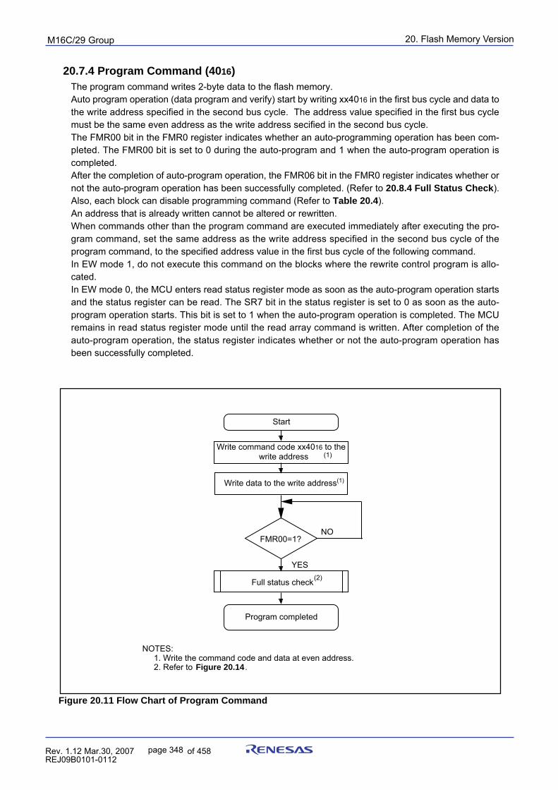
20. Flash Memory VersionpuorG92/C61M
page 348 854fo7002,03.raM21.1.veR2110-1010B90JER
20.7.4 Program Command (4016)The program command writes 2-byte data to the flash memory.Auto program operation (data program and verify) start by writing xx4016 in the first bus cycle and data tothe write address specified in the second bus cycle. The address value specified in the first bus cyclemust be the same even address as the write address secified in the second bus cycle.The FMR00 bit in the FMR0 register indicates whether an auto-programming operation has been com-pleted. The FMR00 bit is set to 0 during the auto-program and 1 when the auto-program operation iscompleted.After the completion of auto-program operation, the FMR06 bit in the FMR0 register indicates whether ornot the auto-program operation has been successfully completed. (Refer to 20.8.4 Full Status Check).Also, each block can disable programming command (Refer to Table 20.4).An address that is already written cannot be altered or rewritten.When commands other than the program command are executed immediately after executing the pro-gram command, set the same address as the write address specified in the second bus cycle of theprogram command, to the specified address value in the first bus cycle of the following command.In EW mode 1, do not execute this command on the blocks where the rewrite control program is allo-cated.In EW mode 0, the MCU enters read status register mode as soon as the auto-program operation startsand the status register can be read. The SR7 bit in the status register is set to 0 as soon as the auto-program operation starts. This bit is set to 1 when the auto-program operation is completed. The MCUremains in read status register mode until the read array command is written. After completion of theauto-program operation, the status register indicates whether or not the auto-program operation hasbeen successfully completed.
Figure 20.11 Flow Chart of Program Command
Start
Program completed
YES
NO
NOTES: 1. Write the command code and data at even address. 2. Refer to Figure 20.14 .
Write command code xx4016 to the write address (1)
Write data to the write address(1)
FMR00=1?
Full status check(2)
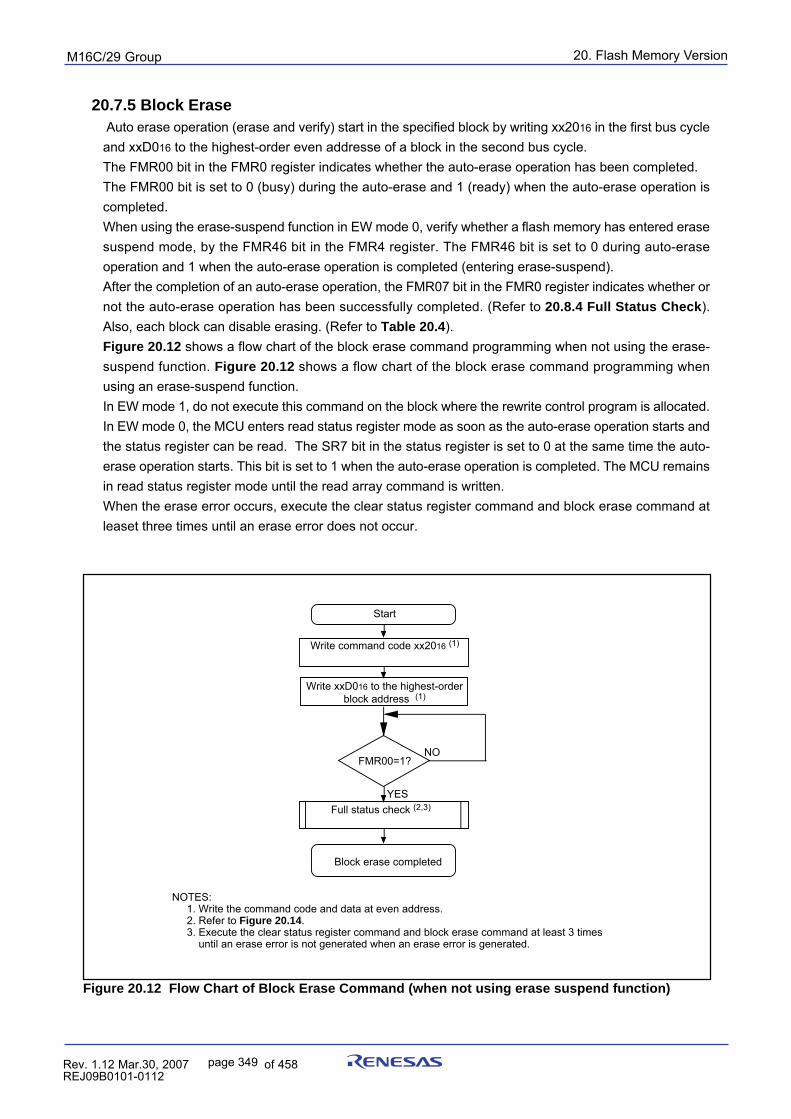
20. Flash Memory VersionpuorG92/C61M
page 349 854fo7002,03.raM21.1.veR2110-1010B90JER
20.7.5 Block Erase Auto erase operation (erase and verify) start in the specified block by writing xx2016 in the first bus cycleand xxD016 to the highest-order even addresse of a block in the second bus cycle.The FMR00 bit in the FMR0 register indicates whether the auto-erase operation has been completed.The FMR00 bit is set to 0 (busy) during the auto-erase and 1 (ready) when the auto-erase operation iscompleted.When using the erase-suspend function in EW mode 0, verify whether a flash memory has entered erasesuspend mode, by the FMR46 bit in the FMR4 register. The FMR46 bit is set to 0 during auto-eraseoperation and 1 when the auto-erase operation is completed (entering erase-suspend).After the completion of an auto-erase operation, the FMR07 bit in the FMR0 register indicates whether ornot the auto-erase operation has been successfully completed. (Refer to 20.8.4 Full Status Check).Also, each block can disable erasing. (Refer to Table 20.4).Figure 20.12 shows a flow chart of the block erase command programming when not using the erase-suspend function. Figure 20.12 shows a flow chart of the block erase command programming whenusing an erase-suspend function.In EW mode 1, do not execute this command on the block where the rewrite control program is allocated.In EW mode 0, the MCU enters read status register mode as soon as the auto-erase operation starts andthe status register can be read. The SR7 bit in the status register is set to 0 at the same time the auto-erase operation starts. This bit is set to 1 when the auto-erase operation is completed. The MCU remainsin read status register mode until the read array command is written.When the erase error occurs, execute the clear status register command and block erase command atleaset three times until an erase error does not occur.
Figure 20.12 Flow Chart of Block Erase Command (when not using erase suspend function)
NOTES: 1. Write the command code and data at even address. 2. Refer to Figure 20.14. 3. Execute the clear status register command and block erase command at least 3 times until an erase error is not generated when an erase error is generated.
Write xxD016 to the highest-order block address (1)
Start
Block erase completed
YES
NO
Write command code xx2016 (1)
FMR00=1?
Full status check (2,3)
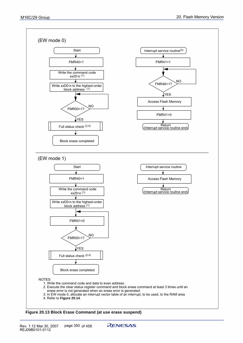
20. Flash Memory VersionpuorG92/C61M
page 350 854fo7002,03.raM21.1.veR2110-1010B90JER
Figure 20.13 Block Erase Command (at use erase suspend)
NOTES: 1. Write the command code and data to even address. 2. Execute the clear status register command and block erase command at least 3 times until an erase error is not generated when an erase error is generated. 3. In EW mode 0, allocate an interrupt vector table of an interrupt, to be used, to the RAM area 4. Refer to Figure 20.14.
Start
Block erase completed
Write the command code xx2016 (1)
Write xxD016 to the highest-order block address (1)
YES
NOFMR00=1?
Full status check (2,4)
FMR40=1
Interrupt service routine(3)
FMR41=1
YES
NOFMR46=1?
Access Flash Memory
Return (Interrupt service routine end)
FMR41=0
(EW mode 0)
(EW mode 1)
Start
Block erase completed
Write the command code xx2016 (1)
Write xxD016 to the highest-order block address (1)
YES
NOFMR00=1?
Full status check (2,4)
FMR40=1
FMR41=0
Interrupt service routine
Access Flash Memory
Return (Interrupt service routine end)
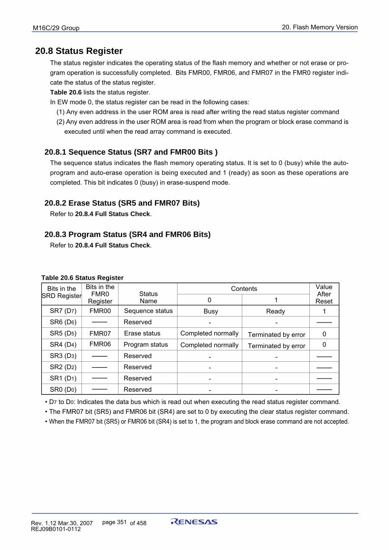
20. Flash Memory VersionpuorG92/C61M
page 351 854fo7002,03.raM21.1.veR2110-1010B90JER
20.8 Status RegisterThe status register indicates the operating status of the flash memory and whether or not erase or pro-gram operation is successfully completed. Bits FMR00, FMR06, and FMR07 in the FMR0 register indi-cate the status of the status register.Table 20.6 lists the status register.In EW mode 0, the status register can be read in the following cases:
(1) Any even address in the user ROM area is read after writing the read status register command(2) Any even address in the user ROM area is read from when the program or block erase command is
executed until when the read array command is executed.
20.8.1 Sequence Status (SR7 and FMR00 Bits )The sequence status indicates the flash memory operating status. It is set to 0 (busy) while the auto-program and auto-erase operation is being executed and 1 (ready) as soon as these operations arecompleted. This bit indicates 0 (busy) in erase-suspend mode.
20.8.2 Erase Status (SR5 and FMR07 Bits)Refer to 20.8.4 Full Status Check.
20.8.3 Program Status (SR4 and FMR06 Bits)Refer to 20.8.4 Full Status Check.
Table 20.6 Status Register
• D7 to D0: Indicates the data bus which is read out when executing the read status register command.• The FMR07 bit (SR5) and FMR06 bit (SR4) are set to 0 by executing the clear status register command.• When the FMR07 bit (SR5) or FMR06 bit (SR4) is set to 1, the program and block erase command are not accepted.
Bits in the SRD Register
SR4 (D4)
SR5 (D5)
SR7 (D7)
SR6 (D6)
Status Name
Contents
SR1 (D1)
SR2 (D2)
SR3 (D3)
SR0 (D0)
Program status
Erase status
Sequence status
Reserved
Reserved
Reserved
Reserved
1
Ready
Terminated by error
Terminated by error
-
-
-
-
-
0
Busy
Completed normally
Completed normally
-
-
-
-
-Reserved
Bits in the FMR0
RegisterFMR00
FMR07FMR06
Value AfterReset
1
00
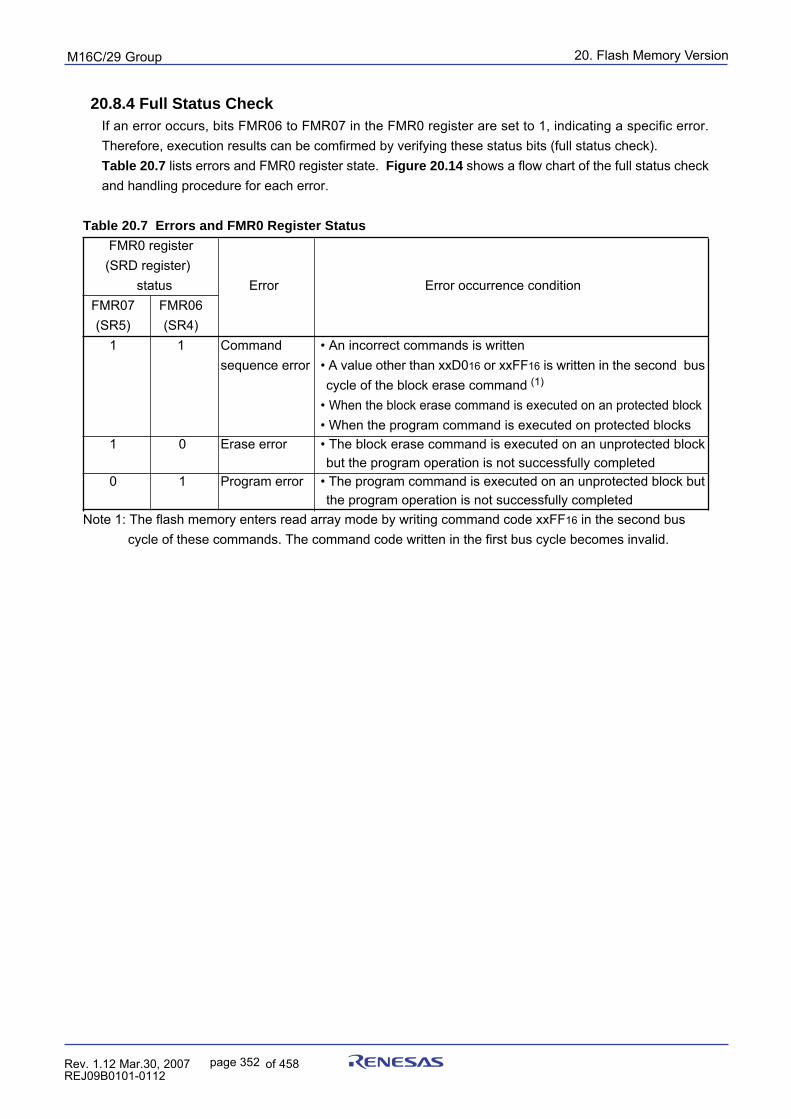
20. Flash Memory VersionpuorG92/C61M
page 352 854fo7002,03.raM21.1.veR2110-1010B90JER
20.8.4 Full Status CheckIf an error occurs, bits FMR06 to FMR07 in the FMR0 register are set to 1, indicating a specific error.Therefore, execution results can be comfirmed by verifying these status bits (full status check).Table 20.7 lists errors and FMR0 register state. Figure 20.14 shows a flow chart of the full status checkand handling procedure for each error.
Table 20.7 Errors and FMR0 Register Status
FMR0 register (SRD register)
status Error Error occurrence conditionFMR07 FMR06(SR5) (SR4)
1 1 Command • An incorrect commands is writtensequence error • A value other than xxD016 or xxFF16 is written in the second bus
cycle of the block erase command (1)
• When the block erase command is executed on an protected block• When the program command is executed on protected blocks
1 0 Erase error • The block erase command is executed on an unprotected blockbut the program operation is not successfully completed
0 1 Program error • The program command is executed on an unprotected block butthe program operation is not successfully completed
Note 1: The flash memory enters read array mode by writing command code xxFF16 in the second bus cycle of these commands. The command code written in the first bus cycle becomes invalid.
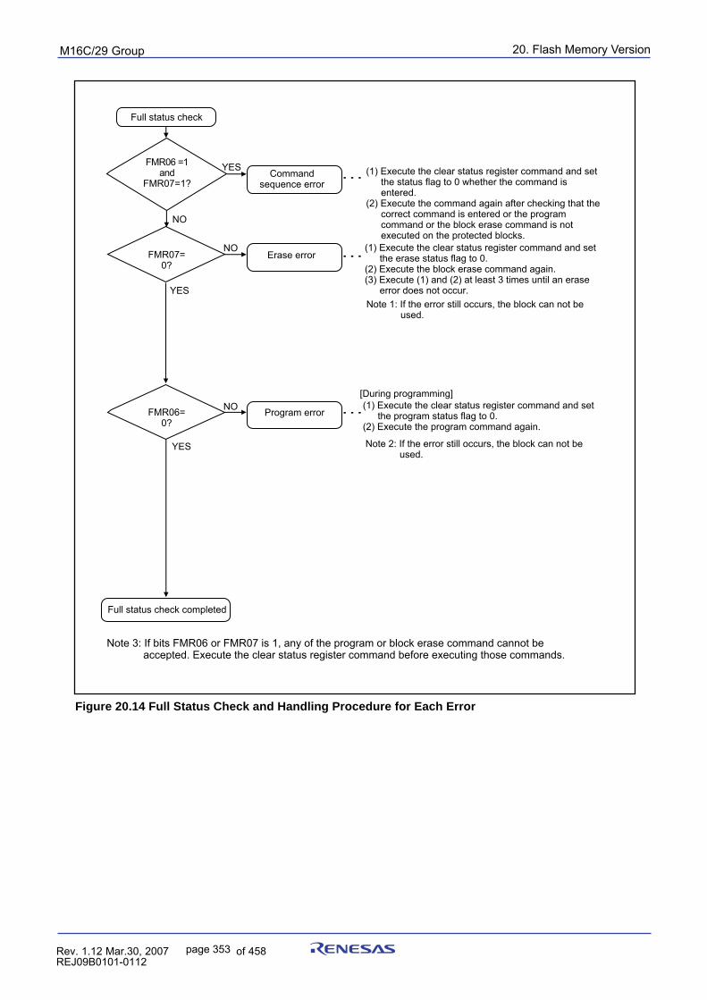
20. Flash Memory VersionpuorG92/C61M
page 353 854fo7002,03.raM21.1.veR2110-1010B90JER
Figure 20.14 Full Status Check and Handling Procedure for Each Error
Full status check
FMR06 =1and
FMR07=1?
NO
Command sequence error
YES
FMR07=0?
YES
Erase errorNO
(1) Execute the clear status register command and set the status flag to 0 whether the command is entered.
(2) Execute the command again after checking that the correct command is entered or the program command or the block erase command is not executed on the protected blocks.
(1) Execute the clear status register command and set the erase status flag to 0.
(2) Execute the block erase command again.(3) Execute (1) and (2) at least 3 times until an erase
error does not occur.
Note 3: If bits FMR06 or FMR07 is 1, any of the program or block erase command cannot be accepted. Execute the clear status register command before executing those commands.
FMR06=0?
YES
Program errorNO
Full status check completed
Note 1: If the error still occurs, the block can not be used.
(1) Execute the clear status register command and set the program status flag to 0.
(2) Execute the program command again.
Note 2: If the error still occurs, the block can not be used.
[During programming]
20. Flash Memory VersionpuorG92/C61M
page 354 854fo7002,03.raM21.1.veR2110-1010B90JER
20.9 Standard Serial I/O ModeIn standard serial I/O mode, the serial programmer supporting the M16C/29 group can be used to rewritethe flash memory user ROM area, while the MCU is mounted on a board. For more information about theserial programmer, contact your serial programmer manufacturer. Refer to the user’s manual included withyour serial programmer for instruction.Table 20.8 lists pin description (flash memory standard serial input/output mode). Figures 20.15 and 20.16
show pin connections for standard serial input/output mode.
20.9.1 ID Code Check FunctionThe ID code check function determines whether or not the ID codes sent from the serial programmermatches those written in the flash memory. (Refer to 20.3 Functions To Prevent Flash Memory from
Rewriting.)
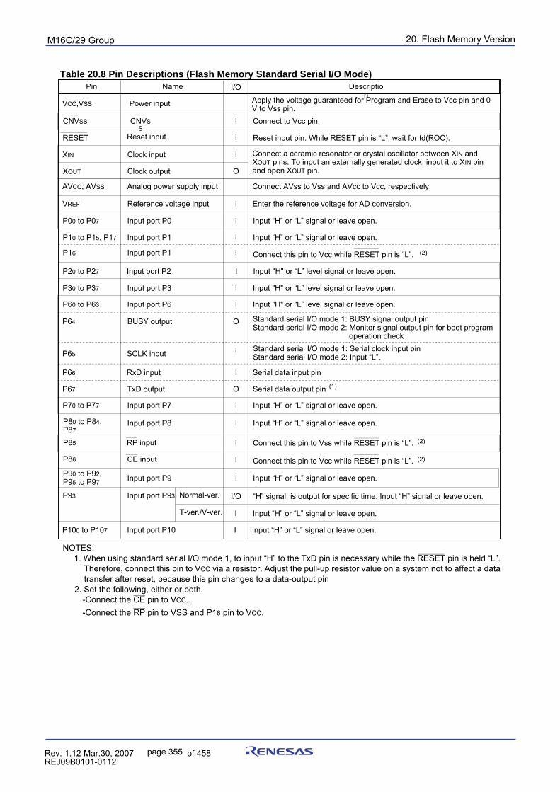
20. Flash Memory VersionpuorG92/C61M
page 355 854fo7002,03.raM21.1.veR2110-1010B90JER
Table 20.8 Pin Descriptions (Flash Memory Standard Serial I/O Mode)
NOTES:___________
1. When using standard serial I/O mode 1, to input “H” to the TxD pin is necessary while the RESET pin is held “L”.Therefore, connect this pin to VCC via a resistor. Adjust the pull-up resistor value on a system not to affect a datatransfer after reset, because this pin changes to a data-output pin
2. Set the following, either or both._____
-Connect the CE pin to VCC._____
-Connect the RP pin to VSS and P16 pin to VCC.
Pin Description
VCC,VSS Apply the voltage guaranteed for Program and Erase to Vcc pin and 0 V to Vss pin.
CNVSS Connect to Vcc pin.
RESET
XIN Connect a ceramic resonator or crystal oscillator between XIN and XOUT pins. To input an externally generated clock, input it to XIN pin and open XOUT pin.XOUT
AVCC, AVSS
VREF
Connect AVss to Vss and AVcc to Vcc, respectively.
Enter the reference voltage for AD conversion.
P00 to P07 Input “H” or “L” signal or leave open.
P10 to P15, P17 Input “H” or “L” signal or leave open.
P30 to P37 Input "H" or “L” level signal or leave open.
P60 to P63 Input "H" or “L” level signal or leave open.
P64 Standard serial I/O mode 1: BUSY signal output pinStandard serial I/O mode 2: Monitor signal output pin for boot program
operation check
P65
P66 Serial data input pin
P67 Serial data output pin
P70 to P77 Input “H” or “L” signal or leave open.
P80 to P84,P87
Input “H” or “L” signal or leave open.
P90 to P92,P95 to P97 Input “H” or “L” signal or leave open.
Name
Power input
CNVSS
Reset input
Clock input
Clock output
Analog power supply input
Reference voltage input
Input port P0
Input port P1
Input port P3
Input port P6
BUSY output
SCLK input
RxD input
TxD output
Input port P7
Input port P8
Input port P9
I/O
I
I
I
O
I
I
I
I
I
O
I
I
O
I
I
I
P100 to P107 Input “H” or “L” signal or leave open.Input port P10 I
P85 RP input I Connect this pin to Vss while RESET pin is “L”. (2)
Standard serial I/O mode 1: Serial clock input pinStandard serial I/O mode 2: Input “L”.
Reset input pin. While RESET pin is “L”, wait for td(ROC).
(1)
P20 to P27 Input port P2 Input "H" or “L” level signal or leave open.I
P86 CE input I Connect this pin to Vcc while RESET pin is “L”. (2)
P16 Input port P1 I Connect this pin to Vcc while RESET pin is “L”. (2)
P93
Input “H” or “L” signal or leave open.
Input port P93
I
“H” signal is output for specific time. Input “H” signal or leave open.I/O
T-ver./V-ver.
Normal-ver.
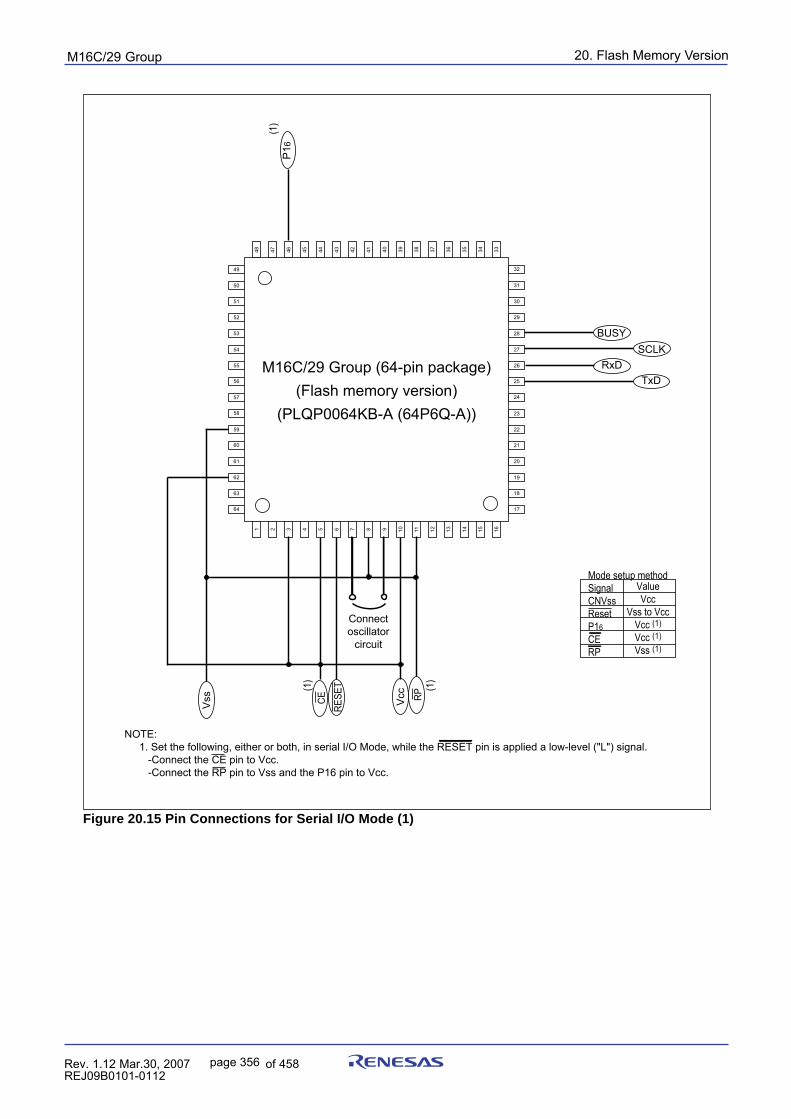
20. Flash Memory VersionpuorG92/C61M
page 356 854fo7002,03.raM21.1.veR2110-1010B90JER
1 2 3 4 5 6 7 8 9 10 11 12 13 14 15 16
21
22
23
24
25
26
27
28
29
30
31
32
3334353637383940
60
59
58
57
56
55
54
53
52
51
50
49
48 47 46 45 44 43 42 41
64
63
62
61
17
18
19
20
BUSYSCLK
RxDTxD
Vcc
Vss
RESE
T
Connectoscillator
circuit
CE(1
)
RP(1
)
NOTE: 1. Set the following, either or both, in serial I/O Mode, while the RESET pin is applied a low-level ("L") signal. -Connect the CE pin to Vcc. -Connect the RP pin to Vss and the P16 pin to Vcc.
P16
(1)
Mode setup methodSignalCNVssResetP16CERP
ValueVcc
Vss to VccVcc (1)
Vcc (1)
Vss (1)
M16C/29 Group (64-pin package)(Flash memory version)
(PLQP0064KB-A (64P6Q-A))
Figure 20.15 Pin Connections for Serial I/O Mode (1)
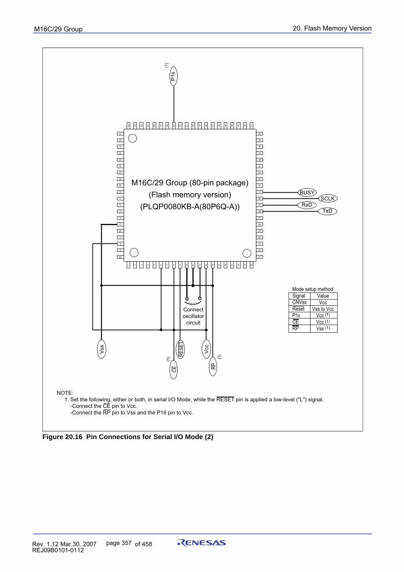
20. Flash Memory VersionpuorG92/C61M
page 357 854fo7002,03.raM21.1.veR2110-1010B90JER
1 2 3 4 5 6 7 8 9 10 11 12 13 14 15 16 17 18 19 20
21
22
23
24
25
26
27
28
29
30
31
32
33
34
35
36
37
38
39
40
60 59 58 57 56 55 54 53 52 51 50 49 48 47 46 45 44 43 42 41
80
79
78
77
76
75
74
73
72
71
70
69
68
67
66
65
64
63
62
61
BUSYSCLK
RxDTxD
Connectoscillator
circuit
Vcc
Vss
RESE
TCE
(1)
RP(1
)
NOTE: 1. Set the following, either or both, in serial I/O Mode, while the RESET pin is applied a low-level ("L") signal. -Connect the CE pin to Vcc. -Connect the RP pin to Vss and the P16 pin to Vcc.
P16
(1)
Mode setup methodSignalCNVssResetP16CERP
ValueVcc
Vss to VccVcc (1)
Vcc (1)
Vss (1)
M16C/29 Group (80-pin package)(Flash memory version)
(PLQP0080KB-A(80P6Q-A))
Figure 20.16 Pin Connections for Serial I/O Mode (2)
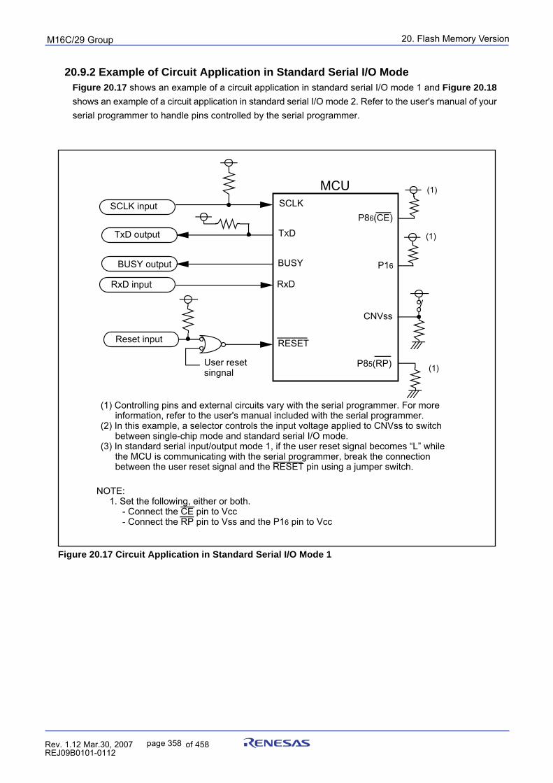
20. Flash Memory VersionpuorG92/C61M
page 358 854fo7002,03.raM21.1.veR2110-1010B90JER
SCLK input
BUSY output
TxD output
RxD input
BUSY
SCLK
TXD
CNVss
P86(CE)
RESET
RxD
Reset input
User reset singnal
MCU
(1) Controlling pins and external circuits vary with the serial programmer. For more information, refer to the user's manual included with the serial programmer.
(2) In this example, a selector controls the input voltage applied to CNVss to switch between single-chip mode and standard serial I/O mode.
(3) In standard serial input/output mode 1, if the user reset signal becomes “L” while the MCU is communicating with the serial programmer, break the connection between the user reset signal and the RESET pin using a jumper switch.
P85(RP)
(1)
(1)
NOTE: 1. Set the following, either or both. - Connect the CE pin to Vcc - Connect the RP pin to Vss and the P16 pin to Vcc
(1)
P16
20.9.2 Example of Circuit Application in Standard Serial I/O ModeFigure 20.17 shows an example of a circuit application in standard serial I/O mode 1 and Figure 20.18
shows an example of a circuit application in standard serial I/O mode 2. Refer to the user's manual of yourserial programmer to handle pins controlled by the serial programmer.
Figure 20.17 Circuit Application in Standard Serial I/O Mode 1
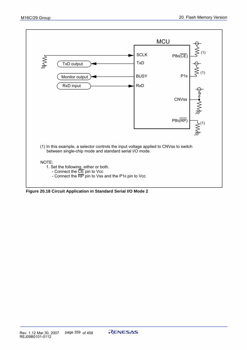
20. Flash Memory VersionpuorG92/C61M
page 359 854fo7002,03.raM21.1.veR2110-1010B90JER
Monitor output
RxD input
TxD output
BUSY
SCLK
TxD
CNVss
P86(CE)
RxD
MCU
(1) In this example, a selector controls the input voltage applied to CNVss to switch between single-chip mode and standard serial I/O mode.
P85(RP) (1)
(1)
NOTE: 1. Set the following, either or both. - Connect the CE pin to Vcc - Connect the RP pin to Vss and the P16 pin to Vcc
P16(1)
Figure 20.18 Circuit Application in Standard Serial I/O Mode 2
20. Flash Memory VersionpuorG92/C61M
page 360 854fo7002,03.raM21.1.veR2110-1010B90JER
20.10 Parallel I/O ModeIn parallel input/output mode, the user ROM can be rewritten by a parallel programmer supporting theM16C/29 group. Contact your parallel programmer manufacturer for more information on the parallel pro-grammer. Refer to the user’s manual included with your parallel programmer for instructions.
20.10.1 ROM Code Protect Function
The ROM code protect function prevents the flash memory from being read or rewritten. (Refer to 20.3
Functions To Prevent Flash Memory from Rewriting).
20. Flash Memory VersionpuorG92/C61M
page 361 854fo7002,03.raM21.1.veR2110-1010B90JER
20.11 CAN I/O Mode
In CAN I/O mode, the user ROM area can be rewritten while the MCU is mounted on-board by using a CANprogrammer which is applicable for the M16C/29 group. For more information about CAN programmers,contact the manufacturer of your CAN programmer. For details on how to use, refer to the user’s manualincluded with your CAN programmer.Table 20.9 lists pin functions for CAN I/O mode. Figures 20.19 and 20.20 show pin connections for CAN I/O mode.
20.11.1 ID code check function
This function determines whether the ID codes sent from the CAN programmer and those written in theflash memory match.(Refer to 20.3 Functions To Prevent Flash Memory from Rewriting.)
Note The CAN I/O mode is not available in M16C/29 T-ver./V-ver.
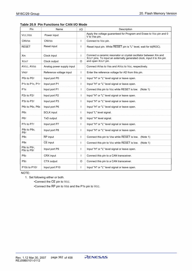
20. Flash Memory VersionpuorG92/C61M
page 362 854fo7002,03.raM21.1.veR2110-1010B90JER
Pin Description
VCC,VSSApply the voltage guaranteed for Program and Erase to Vcc pin and 0 V to Vss pin.
CNVSS Connect to Vcc pin.
RESET
XIN Connect a ceramic resonator or crystal oscillator between XIN and XOUT pins. To input an externally generated clock, input it to XIN pin and open XOUT pin.XOUT
AVCC, AVSS
VREF
Connect AVss to Vss and AVcc to Vcc, respectively.
Enter the reference voltage for AD from this pin.
P00 to P07 Input "H" or "L" level signal or leave open.
P10 to P15, P17 Input "H" or "L" level signal or leave open.
P30 to P37 Input "H" or "L" level signal or leave open.
P60 to P64, P66 Input "H" or "L" level signal or leave open.
P65
P67 Input "H" level signal.
P70 to P77 Input "H" or "L" level signal or leave open.
P80 to P84,P87
Input "H" or "L" level signal or leave open.
P90 to P91,P95 to P97 Input "H" or "L" level signal or leave open.
P100 to P107 Input "H" or "L" level signal or leave open.
Name
Power input
CNVSS
Reset input
Clock input
Clock output
Analog power supply input
Reference voltage input
Input port P0
Input port P1
Input port P3
Input port P6
SCLK input
TxD output
Input port P7
Input port P8
Input port P9
Input port P10
I/O
I
I
I
O
I
I
I
I
I
I
O
I
I
I
I
P85 RP input I Connect this pin to Vss while RESET is low. (Note 1)
Input "L" level signal.
Reset input pin. While RESET pin is "L" level, wait for td(ROC).
P20 to P27 Input port P2 Input "H" or "L" level signal or leave open.I
P86 CE input I Connect this pin to Vcc while RESET is low. (Note 1)
P92 Connect this pin to a CAN transceiver.
P93 Connect this pin to a CAN transceiver.
CRX input
CTX output
I
O
Connect this pin to Vcc while RESET is low. (Note 1)P16 Input port P1 I
Table 20.9 Pin Functions for CAN I/O Mode
NOTE: 1. Set following either or both.
_____
•Connect the CE pin to VCC._____
•Connect the RP pin to VSS and the P16 pin to VCC.
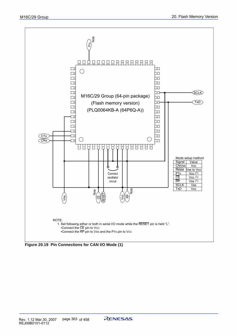
20. Flash Memory VersionpuorG92/C61M
page 363 854fo7002,03.raM21.1.veR2110-1010B90JER
1 2 3 4 5 6 7 8 9 10 11 12 13 14 15 16
21
22
23
24
25
26
27
28
29
30
31
32
3334353637383940
60
59
58
57
56
55
54
53
52
51
50
49
48 47 46 45 44 43 42 41
64
63
62
61
17
18
19
20
CTx
SCLK
CRx
TxD
Vcc
Vss
RESE
T
Connectoscillator
circuit
Mode setup methodSignalCNVssResetP16CERPSCLKTxD
ValueVcc
Vss to VccVcc (1)
Vcc (1)
Vss (1)
VssVcc
CENo
te
RPNo
te
P16 No
te
NOTE: 1. Set following either or both in serial I/O mode while the RESET pin is held “L”. •Connect the CE pin to VCC •Connect the RP pin to VSS and the P16 pin to VCC
M16C/29 Group (64-pin package)(Flash memory version)
(PLQ0064KB-A (64P6Q-A))
Figure 20.19 Pin Connections for CAN I/O Mode (1)
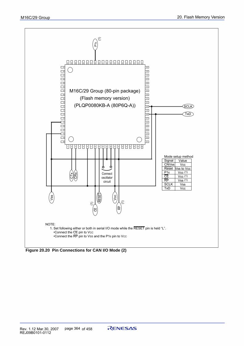
20. Flash Memory VersionpuorG92/C61M
page 364 854fo7002,03.raM21.1.veR2110-1010B90JER
1 2 3 4 5 6 7 8 9 10 11 12 13 14 15 16 17 18 19 2021
22
23
24
25
26
27
28
29
30
31
32
33
34
35
36
37
38
39
4060 59 58 57 56 55 54 53 52 51 50 49 48 47 46 45 44 43 42 41
80
79
78
77
76
75
74
73
72
71
70
69
68
67
66
65
64
63
62
61
SCLK
TxD
CTx
CR
x Connectoscillator
circuit
Vcc
Vss
RESE
TCE
(1)
RP(1
)
NOTE: 1. Set following either or both in serial I/O mode while the RESET pin is held “L”. •Connect the CE pin to VCC •Connect the RP pin to VSS and the P16 pin to VCC
Mode setup methodSignalCNVssResetP16CERPSCLKTxD
ValueVcc
Vss to VccVcc (1)
Vcc (1)
Vss (1)
VssVcc
P16
(1)
M16C/29 Group (80-pin package)(Flash memory version)
(PLQP0080KB-A (80P6Q-A))
Figure 20.20 Pin Connections for CAN I/O Mode (2)
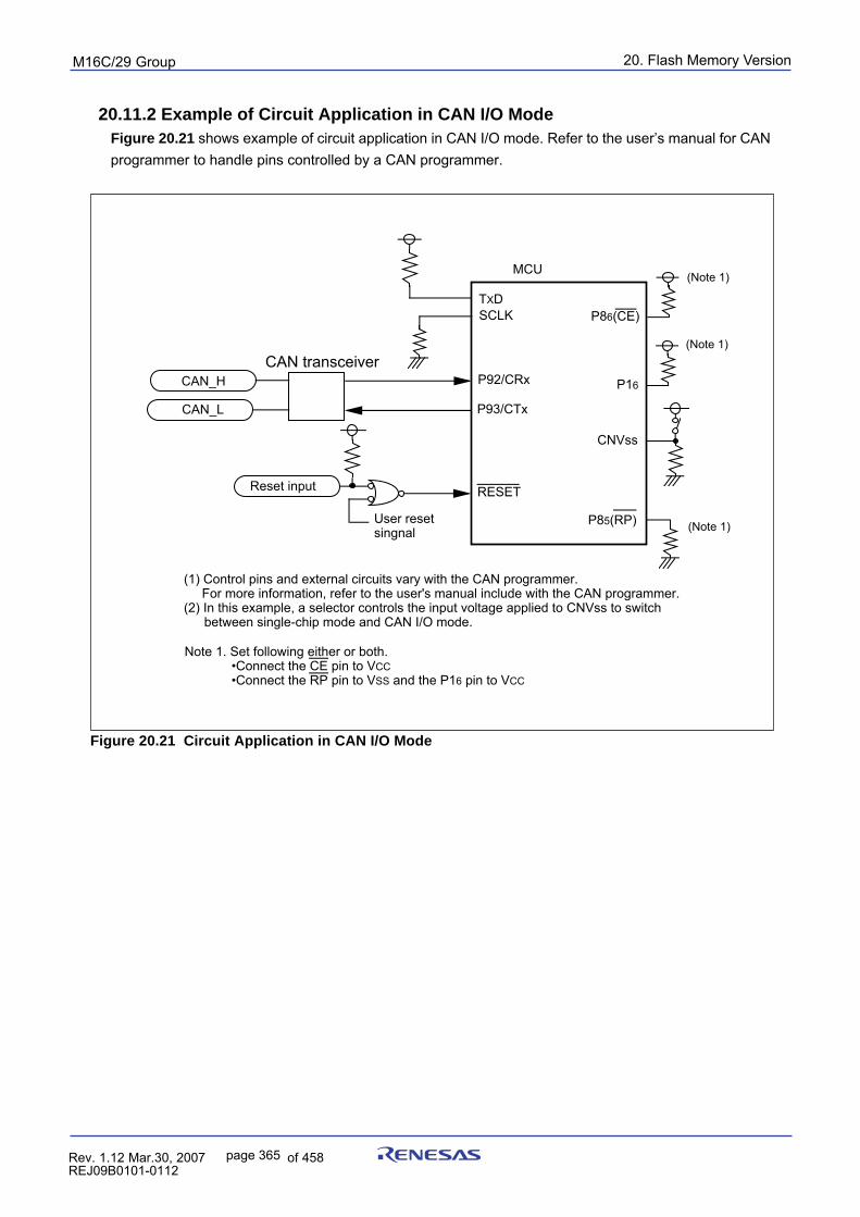
20. Flash Memory VersionpuorG92/C61M
page 365 854fo7002,03.raM21.1.veR2110-1010B90JER
CAN_H
CAN_L
P92/CRx
SCLKTXD
CNVss
P86(CE)
RESET
P93/CTx
Reset input
User reset singnal
MCU
(1) Control pins and external circuits vary with the CAN programmer. For more information, refer to the user's manual include with the CAN programmer.(2) In this example, a selector controls the input voltage applied to CNVss to switch
between single-chip mode and CAN I/O mode.
P85(RP)
(Note 1)
(Note 1)
CAN transceiverP16
(Note 1)
Note 1. Set following either or both.•Connect the CE pin to VCC•Connect the RP pin to VSS and the P16 pin to VCC
20.11.2 Example of Circuit Application in CAN I/O ModeFigure 20.21 shows example of circuit application in CAN I/O mode. Refer to the user’s manual for CANprogrammer to handle pins controlled by a CAN programmer.
Figure 20.21 Circuit Application in CAN I/O Mode
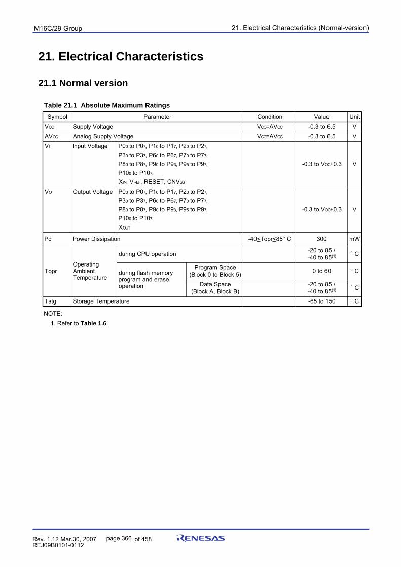
21. Electrical Characteristics (Normal-version)puorG92/C61M
page 366 854fo7002,03.raM21.1.veR2110-1010B90JER
21. Electrical Characteristics
21.1 Normal version
Table 21.1 Absolute Maximum Ratings
lobmyS retemaraP noitidnoC eulaV tinU
V CC egatloVylppuS V CC VA= CC 5.6ot3.0- V
VA CC egatloVylppuSgolanA V CC VA= CC 5.6ot3.0- VVI egatloVtupnI 0P 0 0Pot 7 1P, 0 1Pot 7 2P, 0 2Pot 7,
3P 0 3Pot 7 6P, 0 6Pot 7 7P, 0 7Pot 7,8P 0 8Pot 7 9P, 0 9Pot 3 9P, 5 9Pot 7,01P 0 01Pot 7,
X NI V, FER VNC,TESER, SS
Vot3.0- CC 3.0+ V
VO egatloVtuptuO 0P 0 0Pot 7 1P, 0 1Pot 7 2P, 0 2Pot 7,3P 0 3Pot 7 6P, 0 6Pot 7 7P, 0 7Pot 7,8P 0 8Pot 7 9P, 0 9Pot 3 9P, 5 9Pot 7,01P 0 01Pot 7,
X TUO
Vot3.0- CC 3.0+ V
dP noitapissiDrewoP 04- < rpoT < C°58 003 Wm
rpoTgnitarepO
tneibmAerutarepmeT
noitarepoUPCgnirud /58ot02-58ot04- )1( C°
yromemhsalfgnirudesarednamargorp
noitarepo
ecapSmargorP)5kcolBot0kcolB( 06ot0 C°
ecapSataD)BkcolB,AkcolB(
/58ot02-58ot04- )1( C°
gtsT erutarepmeTegarotS 051ot56- C°
NOTE: 1. Refer to Table 1.6.
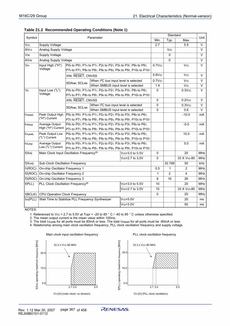
21. Electrical Characteristics (Normal-version)puorG92/C61M
page 367 854fo7002,03.raM21.1.veR2110-1010B90JER
Table 21.2 Recommended Operating Conditions (Note 1)
lobmyS retemaraPdradnatS
tinU.niM .pyT .xaM
V CC egatloVylppuS 7.2 5.5 VVA CC egatloVylppuSgolanA V CC V
V SS egatloVylppuS 0 VVA SS egatloVylppuSgolanA 0 V
V HI )"H"(hgiHtupnIegatloV
0P 0 0Pot 7 1P, 0 1Pot 7 2P, 0 2Pot 7 3P, 0 3Pot 7 6P, 0 6Pot 7,7P 0 7Pot 7 8P, 0 8Pot 7 9P, 0 9Pot 3 9P, 5 9Pot 7 01P, 0 01Pot 7
V7.0 CC V CC V
SSVNC,TESER,NIX V8.0 CC V CC V
ADS MM LCS, MMInehW 2 detcelessileveltupnisubC V7.0 CC V CC V
detcelessileveltupniSUBMSnehW 4.1 V CC VV LI )"L"(woLtupnI
egatloV0P 0 0Pot 7 1P, 0 1Pot 7 2P, 0 2Pot 7 3P, 0 3Pot 7 6P, 0 6Pot 7,7P 0 7Pot 7 8P, 0 8Pot 7 9P, 0 9Pot 3 9P, 5 9Pot 7 01P, 0 01Pot 7
0 V3.0 CC V
SSVNC,TESER,NIX 0 V2.0 CC V
ADS MM LCS, MMInehW 2 detcelessileveltupnisubC 0 3.0 V CC V
detcelessileveltupniSUBMSnehW 0 6.0 VI )kaep(HO hgiHtuptuOkaeP
tnerruC)"H"(0P 0 0Pot 7 1P, 0 1Pot 7 2P, 0 2Pot 7 3P, 0 3Pot 7 6P, 0 6Pot 7,7P 0 7Pot 7 8P, 0 8Pot 7 9P, 0 9Pot 3 9P, 5 9Pot 7 01P, 0 01Pot 7
0.01- Am
I )gva(HO tuptuOegarevAtnerruC)"H"(hgiH
0P 0 0Pot 7 1P, 0 1Pot 7 2P, 0 2Pot 7 3P, 0 3Pot 7 6P, 0 6Pot 7,7P 0 7Pot 7 8P, 0 8Pot 7 9P, 0 9Pot 3 9P, 5 9Pot 7 01P, 0 01Pot 7
0.5- Am
I )kaep(LO woLtuptuOkaePtnerruC)"L"(
0P 0 0Pot 7 1P, 0 1Pot 7 2P, 0 2Pot 7 3P, 0 3Pot 7 6P, 0 6Pot 7,7P 0 7Pot 7 8P, 0 8Pot 7 9P, 0 9Pot 3 9P, 5 9Pot 7 01P, 0 01Pot 7
0.01 Am
I )gva(LO tuptuOegarevAtnerruC)"L"(woL
0P 0 0Pot 7 1P, 0 1Pot 7 2P, 0 2Pot 7 3P, 0 3Pot 7 6P, 0 6Pot 7,7P 0 7Pot 7 8P, 0 8Pot 7 9P, 0 9Pot 3 9P, 5 9Pot 7 01P, 0 01Pot 7
0.5 Am
X(f NI ) ycneuqerFnoitallicsOtupnIkcolCniaM )4( V CC V5.5ot0.3= 0 02 zHMV CC V0.3ot7.2= 0 VX33 CC 08- zHM
X(f NIC ) ycneuqerFnoitallicsOkcolCbuS 867.23 05 zHkf1 )COR( 1ycneuqerFrotallicsOpihc-nO 5.0 1 2 zHM
)COR(2f 2ycneuqerFrotallicsOpihc-nO 1 2 4 zHM)COR(3f 3ycneuqerFrotallicsOpihc-nO 8 61 62 zHM
)LLP(f ycneuqerFnoitallicsOkcolCLLP )4( V CC V5.5ot0.3= 01 02 zHMV CC V0.3ot7.2= 01 VX33 CC 08- zHM
)KLCB(f ycneuqerFkcolCnoitarepOUPC 0 02 zHMt US )LLP( rezisehtnySycneuqerFLLPezilibatSotemiTtiaW V CC V0.5= 02 sm
V CC V0.3= 05 sm:SETON
VotdecnerefeR.1 CC .deificepsesiwrehtosselnuC°58ot04-/C°58ot02-=rpoTtaV5.5ot7.2=.sm001nihtiweulavnaemehtsitnerructuptuonaemehT.2
IlatotehT.3 )kaep(LO IlatotehT.sselroAm08ebtsumstropllarof )kaep(HO .sselroAm08-ebtsumstropllarof.egatlovylppusdnaycneuqerfnoitallicsokcolcLLP,ycneuqerfnoitallicsokcolcniamgnomapihsnoitaleR.4
Main clock input oscillation frequency
f(XIN
) ope
ratin
g m
axim
um fr
eque
ncy
[MH
Z]
VCC[V] (main clock: no division)
PLL clock oscillation frequency
f(PLL
) ope
ratin
g m
axim
um fr
eque
ncy
[MH
Z]
VCC[V] (PLL clock oscillation)
AAAAAAAAAAAAAAAAAAAAAAAAAAAAAA20.0
0.05.53.0
10.0
2.7
33.3 x VCC-80 MHZ
20.0
0.05.5
10.0
2.7 3.0
33.3 x VCC-80 MHZ
AAAAAAAAAAAAAAAAAAAA
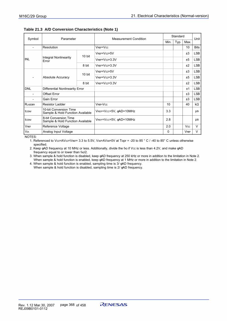
21. Electrical Characteristics (Normal-version)puorG92/C61M
page 368 854fo7002,03.raM21.1.veR2110-1010B90JER
Table 21.3 A/D Conversion Characteristics (Note 1)
lobmyS retemaraP noitidnoCtnemerusaeMdradnatS
tinU.niM .pyT .xaM
- noituloseR V FER V= CC 01 stiB
LNI ytiraenilnoNlargetnIrorrE
tib01V FER V= CC V5= 3± BSL
V FER V= CC V3.3= 5± BSL
tib8 V FER V= CC V3.3= 2± BSL
- ycaruccAetulosbAtib01
V FER V= CC V5= 3± BSL
V FER V= CC V3.3= 5± BSL
tib8 V FER V= CC V3.3= 2± BSL
LND rorrEytiraenilnoNlaitnereffiD 1± BSL- rorrEtesffO 3± BSL- rorrEniaG 3± BSL
R REDDAL reddaLrotsiseR V =FER V CC 01 04 kΩ
t VNOCemiTnoisrevnoCtib-01
elbaliavAnoitcnuFdloH&elpmaS V FER V= CC ,V5= φ zHM01=DA 3.3 µs
t VNOCemiTnoisrevnoCtib-8
elbaliavAnoitcnuFdloH&elpmaS V FER V= CC ,V5= φ zHM01=DA 8.2 µs
V FER egatloVecnerefeR 0.2 V CC VV AI egatloVtupnIgolanA 0 V FER V
:SETONVotdecnerefeR.1 CC VA= CC V= FER V,V5.5ot3.3= SS VA= SS esiwrehtosselnuC°58ot04-/C°58ot02-=rpoTtaV0=
.deificepspeeK.2 φ fehtedivid,yllanoitiddA.sselrozHM01taycneuqerfDA DA Vfi CC ekamdna,V2.4nahtsselsi φ DA
fnahtrewolrootlauqeycneuqerf DA .2/.3 peek,delbasidsinoitcnufdloh&elpmasnehW φ .2etoNninoitatimilehtotnoitiddanieromrozHk052taycneuqerfDA
peek,delbanesinoitcnufdloh&elpmasnehW φ .2etoNninoitatimilehtotnoitiddanieromrozHM1taycneuqerfDA/3siemitgnilpmas,delbanesinoitcnufdloh&elpmasnehW.4 φ .ycneuqerfDA/2siemitgnilpmas,delbasidsinoitcnufdloh&elpmasnehW φ .ycneuqerfDA
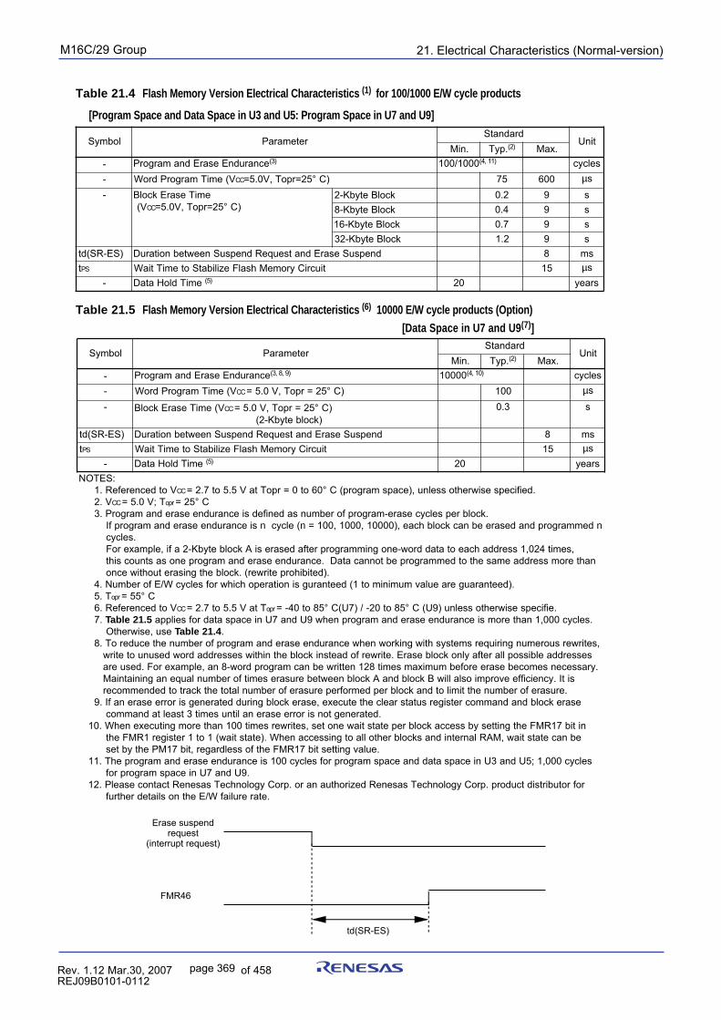
21. Electrical Characteristics (Normal-version)puorG92/C61M
page 369 854fo7002,03.raM21.1.veR2110-1010B90JER
Table 21.4 Flash Memory Version Electrical Characteristics (1) for 100/1000 E/W cycle products
[Program Space and Data Space in U3 and U5: Program Space in U7 and U9]
Table 21.5 Flash Memory Version Electrical Characteristics (6) 10000 E/W cycle products (Option)
[Data Space in U7 and U9(7)]
Erase suspend request
(interrupt request)
FMR46
td(SR-ES)
lobmyS retemaraPdradnatS
tinU.niM .pyT )2( .xaM
- ecnarudnEesarEdnamargorP )3( 0001/001 )11,4( selcyc- V(emiTmargorPdroW CC 52=rpoT,V0.5= C° ) 57 006 µs
- emiTesarEkcolBV( CC 52=rpoT,V0.5= C° )
kcolBetybK-2 2.0 9 skcolBetybK-8 4.0 9 skcolBetybK-61 7.0 9 skcolBetybK-23 2.1 9 s
)SE-RS(dt dnepsuSesarEdnatseuqeRdnepsuSneewtebnoitaruD 8 smt SP tiucriCyromeMhsalFezilibatSotemiTtiaW 51 µs
- emiTdloHataD )5( 02 sraey
lobmyS retemaraPdradnatS
tinU.niM .pyT )2( .xaM
- ecnarudnEesarEdnamargorP )9,8,3( 00001 )01,4( selcyc- V(emiTmargorPdroW CC 52=rpoT,V0.5= C° ) 001 µs
- emiTesarEkcolB V( CC 52=rpoT,V0.5= C° ))kcolbetybK-2(
3.0 s
)SE-RS(dt dnepsuSesarEdnatseuqeRdnepsuSneewtebnoitaruD 8 smt SP tiucriCyromeMhsalFezilibatSotemiTtiaW 51 µs
- emiTdloHataD )5( 02 sraey:SETON
VotdecnerefeR.1 CC °06ot0=rpoTtaV5.5ot7.2= .deificepsesiwrehtosselnu,)ecapsmargorp(CV.2 CC T;V0.5= rpo C°52=
.kcolbrepselcycesare-margorpforebmunsadenifedsiecnarudneesarednamargorP.3siecnarudneesarednamargorpfI n (elcyc n demmargorpdnadesareebnackcolbhcae,)00001,0001,001= n
.selcyc,semit420,1sserddahcaeotataddrow-enognimmargorpretfadesaresiAkcolbetybK-2afi,elpmaxeroF
nahteromsserddaemasehtotdemmargorpebtonnacataD.ecnarudneesarednamargorpenosastnuocsiht.)detibihorpetirwer(.kcolbehtgnisaretuohtiwecno
.)deetnaraugeraeulavmuminimot1(deetnarugsinoitarepohcihwrofselcycW/EforebmuN.4T.5 rpo C°55=
VotdecnerefeR.6 CC TtaV5.5ot7.2= rpo .eificepsesiwrehtosselnu)9U(C°58ot02-/)7U(C°58ot04-=.7 5.12elbaT .selcyc000,1nahteromsiecnarudneesarednamargorpnehw9Udna7Uniecapsatadrofseilppa
esu,esiwrehtO 4.12elbaT .,setirwersuoremungniriuqersmetsyshtiwgnikrownehwecnarudneesarednamargorpforebmunehtecuderoT.8
sesserddaelbissopllaretfaylnokcolbesarE.etirwerfodaetsnikcolbehtnihtiwsesserddadrowdesunuotetirw.yrassecensemocebesareerofebmumixamsemit821nettirwebnacmargorpdrow-8na,elpmaxeroF.desuera
sitI.ycneiciffeevorpmioslalliwBkcolbdnaAkcolbneewteberusaresemitforebmunlauqenagniniatniaM.erusareforebmunehttimilotdnakcolbrepdemrofreperusareforebmunlatotehtkcartotdednemmocer
esarekcolbdnadnammocretsigersutatsraelcehtetucexe,esarekcolbgniruddetarenegsirorreesarenafI.9.detarenegtonsirorreesarenalitnusemit3tsaeltadnammoc
nitib71RMFehtgnittesybsseccakcolbrepetatstiawenotes,setirwersemit001nahteromgnitucexenehW.01ebnacetatstiaw,MARlanretnidnaskcolbrehtollaotgnisseccanehW.)etatstiaw(1ot1retsiger1RMFeht
.eulavgnittestib71RMFehtfosseldrager,tib71MPehtybtesselcyc000,1;5Udna3Uniecapsataddnaecapsmargorprofselcyc001siecnarudneesarednamargorpehT.11
.9Udna7Uniecapsmargorprofrofrotubirtsidtcudorp.proCygolonhceTsaseneRdezirohtuanaro.proCygolonhceTsaseneRtcatnocesaelP.21
.etareruliafW/Eehtnosliatedrehtruf
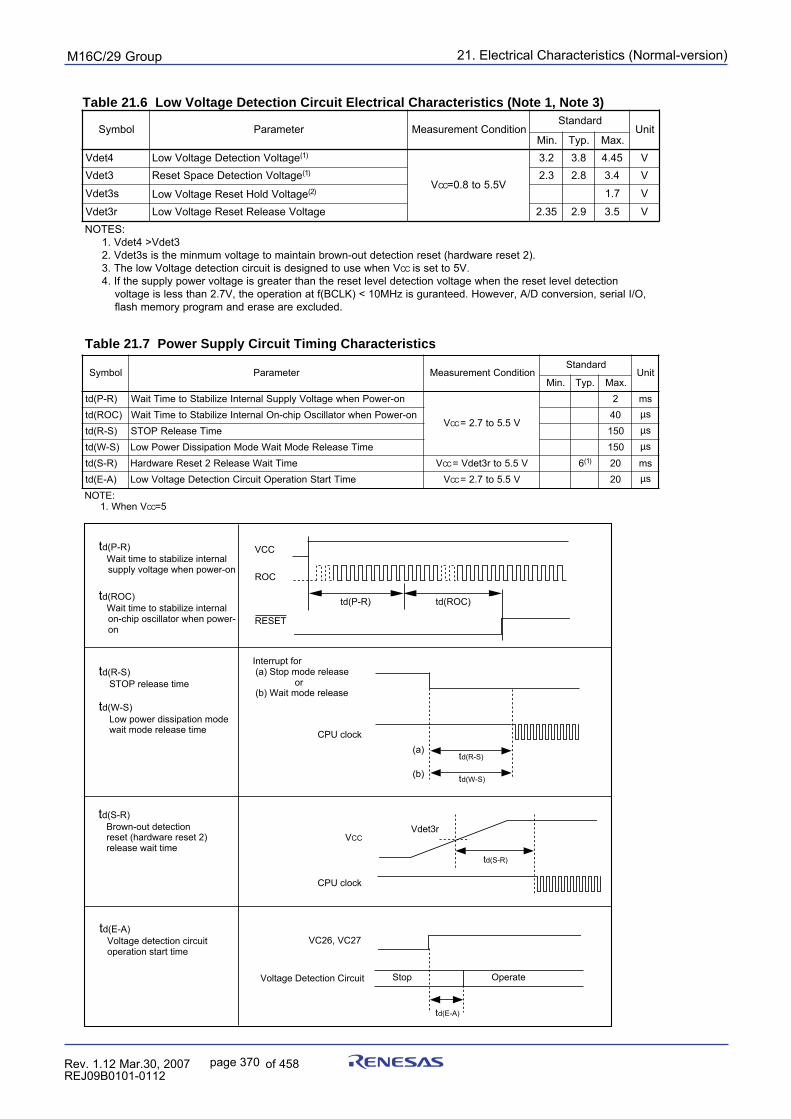
21. Electrical Characteristics (Normal-version)puorG92/C61M
page 370 854fo7002,03.raM21.1.veR2110-1010B90JER
Table 21.6 Low Voltage Detection Circuit Electrical Characteristics (Note 1, Note 3)
Table 21.7 Power Supply Circuit Timing Characteristics
lobmyS retemaraP noitidnoCtnemerusaeMdradnatS
tinU.niM .pyT .xaM
4tedV egatloVnoitceteDegatloVwoL )1(
V CC V5.5ot8.0=
2.3 8.3 54.4 V3tedV egatloVnoitceteDecapSteseR )1( 3.2 8.2 4.3 V
s3tedV egatloVdloHteseRegatloVwoL )2( 7.1 V
r3tedV egatloVesaeleRteseRegatloVwoL 53.2 9.2 5.3 V:SETON
3tedV>4tedV.1.)2tesererawdrah(tesernoitcetedtuo-nworbniatniamotegatlovmumnimehtsis3tedV.2
VnehwesuotdengisedsitiucricnoitcetedegatloVwolehT.3 CC .V5ottessinoitcetedlevelteserehtnehwegatlovnoitcetedlevelteserehtnahtretaergsiegatlovrewopylppusehtfI.4
,O/Ilaires,noisrevnocD/A,revewoH.deetnarugsizHM01<)KLCB(ftanoitarepoeht,V7.2nahtsselsiegatlov.dedulcxeeraesarednamargorpyromemhsalf
lobmyS retemaraP noitidnoCtnemerusaeMdradnatS
tinU.niM .pyT .xaM
)R-P(dt no-rewoPnehwegatloVylppuSlanretnIezilibatSotemiTtiaW
V CC V5.5ot7.2=
2 sm)COR(dt no-rewoPnehwrotallicsOpihc-nOlanretnIezilibatSotemiTtiaW 04 µs
)S-R(dt emiTesaeleRPOTS 051 µs
)S-W(dt emiTesaeleRedoMtiaWedoMnoitapissiDrewoPwoL 051 µs
)R-S(dt emiTtiaWesaeleR2teseRerawdraH V CC V5.5otr3tedV= 6 )1( 02 sm)A-E(dt emiTtratSnoitarepOtiucriCnoitceteDegatloVwoL V CC V5.5ot7.2= 02 µs
:ETONVnehW.1 CC 5=
td(P-R) Wait time to stabilize internal
supply voltage when power-on
CPU clock
td(R-S)(a)
(b) td(W-S)
td(R-S) STOP release time
td(W-S) Low power dissipation mode wait mode release time
td(S-R)
Vdet3rVCC
CPU clock
VC26, VC27
td(E-A)
Stop Operate
Interrupt for (a) Stop mode release or (b) Wait mode release
td(S-R) Brown-out detection reset (hardware reset 2) release wait time
td(E-A) Voltage detection circuit operation start time
Voltage Detection Circuit
td(ROC) Wait time to stabilize internal
on-chip oscillator when power-on
ROC
RESET
VCC
td(P-R) td(ROC)
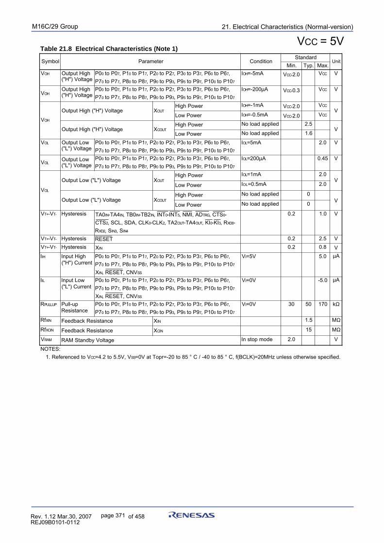
21. Electrical Characteristics (Normal-version)puorG92/C61M
page 371 854fo7002,03.raM21.1.veR2110-1010B90JER
Table 21.8 Electrical Characteristics (Note 1)VCC = 5V
lobmyS retemaraP noitidnoCdradnatS
tinU.niM .pyT .xaM
V HO hgiHtuptuOegatloV)"H"(
0P 0 0Pot 7 1P, 0 1Pot 7 2P, 0 2Pot 7 3P, 0 3Pot 7 6P, 0 6Pot 7,7P 0 7Pot 7 8P, 0 8Pot 7 9P, 0 9Pot 3 9P, 5 9Pot 7 01P, 0 01Pot 7
I HO Am5-= V CC - 0.2 V CC V
V HOhgiHtuptuOegatloV)"H"(
0P 0 0Pot 7 1P, 0 1Pot 7 2P, 0 2Pot 7 3P, 0 3Pot 7 6P, 0 6Pot 7,7P 0 7Pot 7 8P, 0 8Pot 7 9P, 0 9Pot 3 9P, 5 9Pot 7 01P, 0 01Pot 7
I HO 002-= µA V CC - 3.0 V CC V
V HO
egatloV)"H"(hgiHtuptuO X TUOrewoPhgiH I HO Am1-= V CC - 0.2 V CC
VrewoPwoL I HO Am5.0-= V CC - 0.2 V CC
egatloV)"H"(hgiHtuptuO X TUOCrewoPhgiH deilppadaoloN 5.2
VrewoPwoL deilppadaoloN 6.1
V LO woLtuptuOegatloV)"L"(
0P 0 0Pot 7 1P, 0 1Pot 7 2P, 0 2Pot 7 3P, 0 3Pot 7 6P, 0 6Pot 7,7P 0 7Pot 7 8P, 0 8Pot 7 9P, 0 9Pot 3 9P, 5 9Pot 7 01P, 0 01Pot 7
I LO Am5= 0.2 V
V LOwoLtuptuO
egatloV)"L"(0P 0 0Pot 7 1P, 0 1Pot 7 2P, 0 2Pot 7 3P, 0 3Pot 7 6P, 0 6Pot 7,7P 0 7Pot 7 8P, 0 8Pot 7 9P, 0 9Pot 3 9P, 5 9Pot 7 01P, 0 01Pot 7
I LO 002= µA 54.0 V
V LO
egatloV)"L"(woLtuptuO X TUOrewoPhgiH I LO Am1= 0.2
VrewoPwoL I LO Am5.0= 0.2
egatloV)"L"(woLtuptuO X TUOCrewoPhgiH deilppadaoloN 0
VrewoPwoL deilppadaoloN 0
V +T V- -T siseretsyH 0AT NI 4AT- NI 0BT, NI 2BT- NI TNI, 0 TNI- 5 DA,IMN, GRT STC, 0-STC 2 KLC,ADS,LCS, 0 KLC- 2 2AT, TUO 4AT- TUO IK, 0 IK- 3 R, 0DX -
R 2DX S, 3NI S, 4NI
2.0 0.1 V
V +T V- -T siseretsyH TESER 2.0 5.2 VV +T V- -T siseretsyH X NI 2.0 8.0 VI HI hgiHtupnI
tnerruC)"H"(0P 0 0Pot 7 1P, 0 1Pot 7 2P, 0 2Pot 7 3P, 0 3Pot 7 6P, 0 6Pot 7,7P 0 7Pot 7 8P, 0 8Pot 7 9P, 0 9Pot 3 9P, 5 9Pot 7 01P, 0 01Pot 7
X NI VNC,TESER, SS
VI V5= 0.5 µA
I LI woLtupnItnerruC)"L"(
0P 0 0Pot 7 1P, 0 1Pot 7 2P, 0 2Pot 7 3P, 0 3Pot 7 6P, 0 6Pot 7,7P 0 7Pot 7 8P, 0 8Pot 7 9P, 0 9Pot 3 9P, 5 9Pot 7 01P, 0 01Pot 7
X NI VNC,TESER, SS
VI V0= 0.5- µA
R PULLUP pu-lluPecnatsiseR
0P 0 0Pot 7 1P, 0 1Pot 7 2P, 0 2Pot 7 3P, 0 3Pot 7 6P, 0 6Pot 7,7P 0 7Pot 7 8P, 0 8Pot 7 9P, 0 9Pot 3 9P, 5 9Pot 7 01P, 0 01Pot 7
VI V0= 03 05 071 kΩ
fR NIX ecnatsiseRkcabdeeF X NI 5.1 MΩ
fR NICX ecnatsiseRkcabdeeF X NIC 51 MΩ
V MAR egatloVybdnatSMAR edompotsnI 0.2 V
:SETONotdecnerefeR.1 V CC V,V5.5ot2.4= SS .deificepsesiwrehtosselnuzHM02=)KLCB(f,C°58ot04-/C°58ot02-=rpoTtaV0=
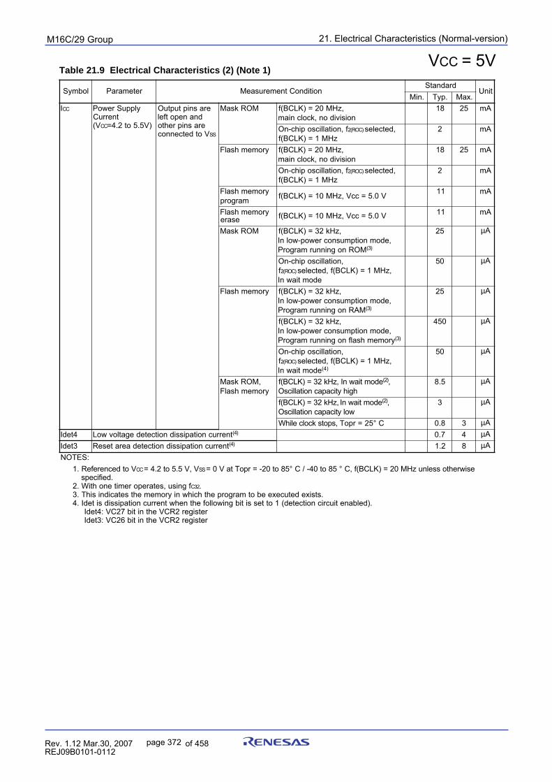
21. Electrical Characteristics (Normal-version)puorG92/C61M
page 372 854fo7002,03.raM21.1.veR2110-1010B90JER
VCC = 5VTable 21.9 Electrical Characteristics (2) (Note 1)
lobmyS retemaraP noitidnoCtnemerusaeMdradnatS
tinU.niM .pyT .xaM
I CC ylppuSrewoPtnerruC
V( CC )V5.5ot2.4=
erasniptuptuOdnanepotfelerasniprehtoVotdetcennoc SS
MORksaM (f KLCB ,zHM02=)noisividon,kcolcniam
81 52 Am
f,noitallicsopihc-nO )COR(2 ,detceleszHM1=)KLCB(f
2 Am
yromemhsalF (f KLCB ,zHM02=)noisividon,kcolcniam
81 52 Am
f,noitallicsopihc-nO )COR(2 ,detceleszHM1=)KLCB(f
2 Am
yromemhsalFmargorp V0.5=ccV,zHM01=)KLCB(f 11 Am
yromemhsalFesare V0.5=ccV,zHM01=)KLCB(f 11 Am
MORksaM zHk23=)KLCB(f ,edomnoitpmusnocrewop-wolnI ,
MORnogninnurmargorP )3(
52 µA
,noitallicsopihc-nOf )COR(2 ,zHM1=)KLCB(f,detceles
edomtiawnI
05 µA
yromemhsalF zHk23=)KLCB(f ,edomnoitpmusnocrewop-wolnI ,
MARnogninnurmargorP )3(
52 µA
,zHk23=)KLCB(f,edomnoitpmusnocrewop-wolnIyromemhsalfnogninnurmargorP )3(
054 µA
,noitallicsopihc-nOf )COR(2 ,zHM1=)KLCB(f,detceles
edomtiawnI )4(
05 µA
,MORksaMyromemhsalF
edomtiawnI,zHk23=)KLCB(f )2( ,hgihyticapacnoitallicsO
5.8 µA
,zHk23=)KLCB(f edomtiawnI )2( ,wolyticapacnoitallicsO
3 µA
,spotskcolcelihW 52=rpoT C° 8.0 3 µA4tedI tnerrucnoitapissidnoitcetedegatlovwoL )4( 7.0 4 µA3tedI tnerrucnoitapissidnoitcetedaerateseR )4( 2.1 8 µA
:SETON.1 otdecnerefeR V CC V,V5.5ot2.4= SS esiwrehtosselnuzHM02=)KLCB(f,C°58ot04-/C°58ot02-=rpoTtaV0=
.deificepsfgnisu,setareporemitenohtiW.2 23C .
.stsixedetucexeebotmargorpehthcihwniyromemehtsetacidnisihT.3.)delbanetiucricnoitceted(1ottessitibgniwollofehtnehwtnerrucnoitapissidsitedI.4
retsiger2RCVehtnitib72CV:4tedIretsiger2RCVehtnitib62CV:3tedI
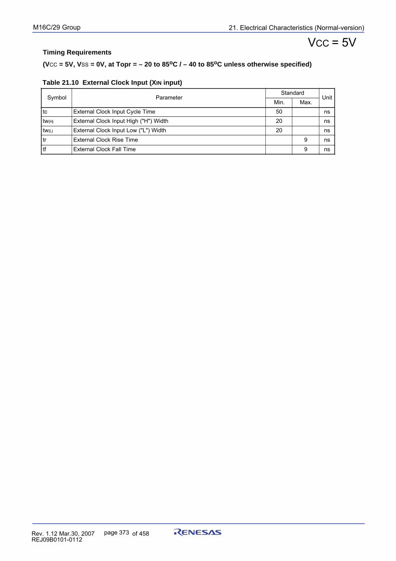
21. Electrical Characteristics (Normal-version)puorG92/C61M
page 373 854fo7002,03.raM21.1.veR2110-1010B90JER
VCC = 5VTiming Requirements
(VCC = 5V, VSS = 0V, at Topr = – 20 to 85oC / – 40 to 85oC unless otherwise specified)
Table 21.10 External Clock Input (XIN input)
lobmyS retemaraPdradnatS
tinU.niM .xaM
ct emiTelcyCtupnIkcolClanretxE 05 snwt )H( htdiW)"H"(hgiHtupnIkcolClanretxE 02 snwt )L( htdiW)"L"(woLtupnIkcolClanretxE 02 snrt emiTesiRkcolClanretxE 9 snft emiTllaFkcolClanretxE 9 sn
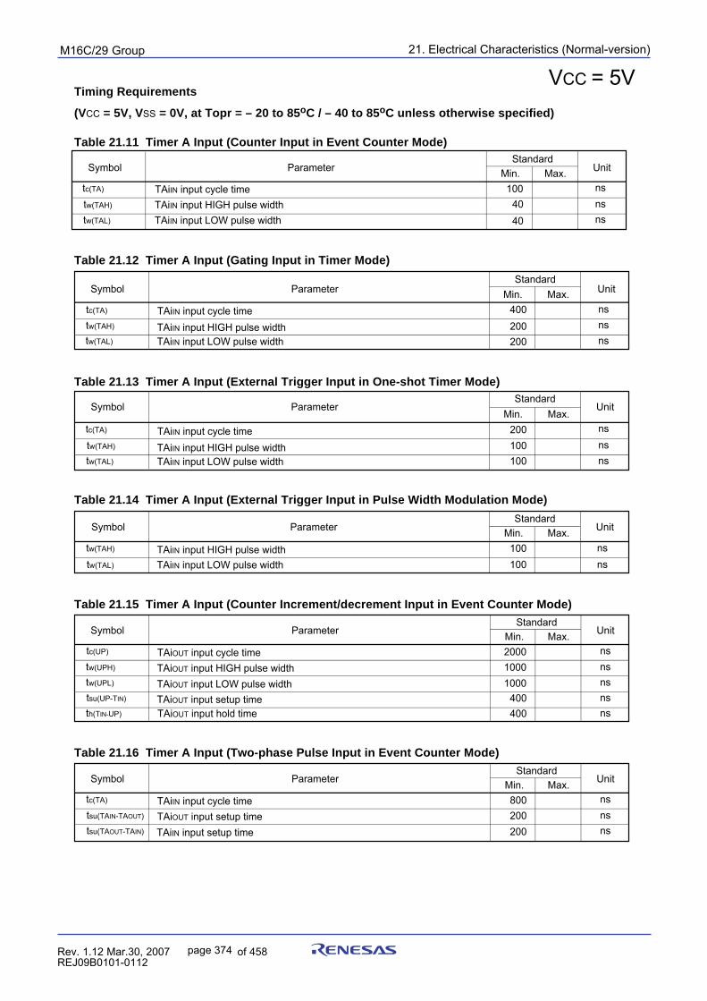
21. Electrical Characteristics (Normal-version)puorG92/C61M
page 374 854fo7002,03.raM21.1.veR2110-1010B90JER
VCC = 5VTiming Requirements
(VCC = 5V, VSS = 0V, at Topr = – 20 to 85oC / – 40 to 85oC unless otherwise specified)
Table 21.12 Timer A Input (Gating Input in Timer Mode)
Table 21.13 Timer A Input (External Trigger Input in One-shot Timer Mode)
Table 21.14 Timer A Input (External Trigger Input in Pulse Width Modulation Mode)
Table 21.15 Timer A Input (Counter Increment/decrement Input in Event Counter Mode)
Table 21.11 Timer A Input (Counter Input in Event Counter Mode)
Table 21.16 Timer A Input (Two-phase Pulse Input in Event Counter Mode)
StandardMax.
nsTAiIN input LOW pulse widthtw(TAL)
Min.nsns
Unit
TAiIN input HIGH pulse widthtw(TAH)
ParameterSymbol
tc(TA) TAiIN input cycle time
40
10040
StandardMax.Min.
nsnsns
Unit
TAiIN input cycle timeTAiIN input HIGH pulse widthTAiIN input LOW pulse width
tc(TA)
tw(TAH)
tw(TAL)
Symbol Parameter
400200200
StandardMax.Min.
nsnsns
Unit
TAiIN input cycle timeTAiIN input HIGH pulse widthTAiIN input LOW pulse width
tc(TA)
tw(TAH)
tw(TAL)
Symbol Parameter
200100100
StandardMax.Min.
nsns
Unit
tw(TAH)
tw(TAL)
Symbol Parameter
TAiIN input HIGH pulse widthTAiIN input LOW pulse width
100100
StandardMax.Min.
nsnsns
Unit
nsns
Symbol Parameter
TAiOUT input cycle timeTAiOUT input HIGH pulse widthTAiOUT input LOW pulse widthTAiOUT input setup timeTAiOUT input hold time
tc(UP)
tw(UPH)
tw(UPL)
tsu(UP-TIN)
th(TIN-UP)
200010001000
400400
StandardMax.Min.
nsnsns
UnitSymbol Parameter
TAiIN input cycle timeTAiOUT input setup timeTAiIN input setup time
tc(TA)
tsu(TAIN-TAOUT)
tsu(TAOUT-TAIN)
800200200
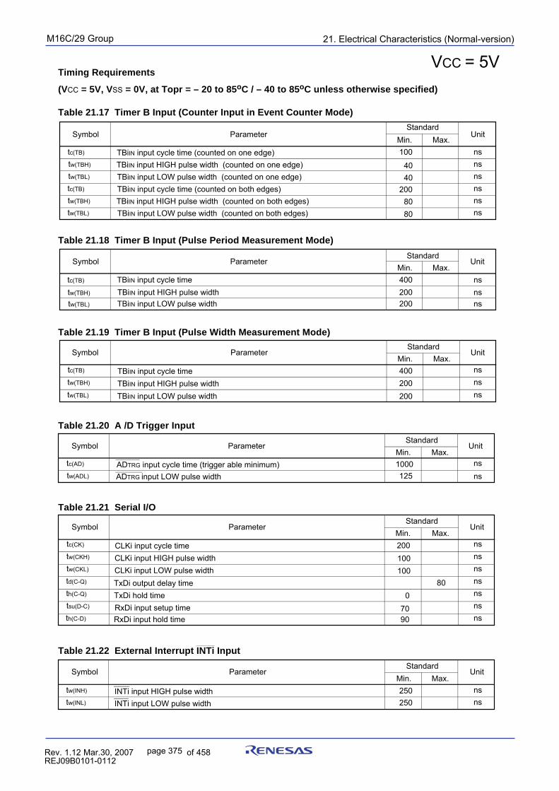
21. Electrical Characteristics (Normal-version)puorG92/C61M
page 375 854fo7002,03.raM21.1.veR2110-1010B90JER
Timing Requirements
(VCC = 5V, VSS = 0V, at Topr = – 20 to 85oC / – 40 to 85oC unless otherwise specified)
Table 21.17 Timer B Input (Counter Input in Event Counter Mode)
Table 21.18 Timer B Input (Pulse Period Measurement Mode)
Table 21.19 Timer B Input (Pulse Width Measurement Mode)
Table 21.20 A /D Trigger Input
Table 21.21 Serial I/O
_______
Table 21.22 External Interrupt INTi Input
VCC = 5V
nsnsnsnsnsnsns
StandardMax.Min.
TBiIN input cycle time (counted on one edge)TBiIN input HIGH pulse width (counted on one edge)TBiIN input LOW pulse width (counted on one edge)
nsnsns
tc(TB)
tw(TBH)
tw(TBL)
ParameterSymbol Unit
tc(TB)
tw(TBL)
tw(TBH)
nsnsns
TBiIN input HIGH pulse width (counted on both edges)TBiIN input LOW pulse width (counted on both edges)
TBiIN input cycle time (counted on both edges)
StandardMax.Min.
nsns
tc(TB)
tw(TBH)
Symbol Parameter Unit
tw(TBL) nsTBiIN input HIGH pulse widthTBiIN input cycle time
TBiIN input LOW pulse width
StandardMax.Min.
nsns
tc(TB)
Symbol Parameter Unit
tw(TBL) nstw(TBH)
TBiIN input cycle timeTBiIN input HIGH pulse widthTBiIN input LOW pulse width
StandardMax.Min.
nsns
tc(AD)
tw(ADL)
Symbol Parameter Unit
ADTRG input cycle time (trigger able minimum)ADTRG input LOW pulse width
StandardMax.Min.
nsns
tw(INH)
tw(INL)
Symbol Parameter Unit
INTi input LOW pulse widthINTi input HIGH pulse width
StandardMax.Min.
CLKi input cycle timeCLKi input HIGH pulse widthCLKi input LOW pulse width
tc(CK)
tw(CKH)
tw(CKL)
ParameterSymbol Unit
td(C-Q)
tsu(D-C)
th(C-Q) TxDi hold timeRxDi input setup time
TxDi output delay time
th(C-D) RxDi input hold time
100
4040
8080
200
400200200
400200200
1000125
250250
200100100
07090
80
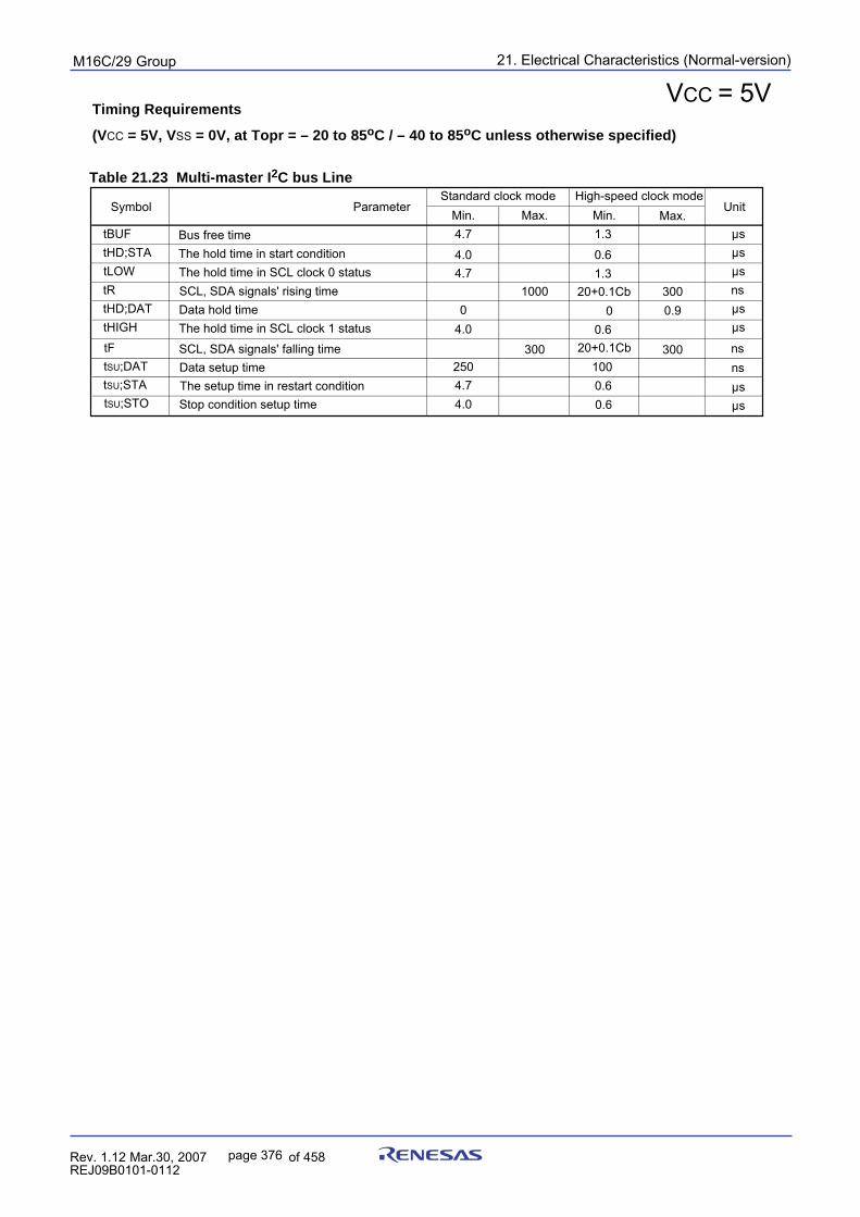
21. Electrical Characteristics (Normal-version)puorG92/C61M
page 376 854fo7002,03.raM21.1.veR2110-1010B90JER
Table 21.23 Multi-master I2C bus Line
VCC = 5VTiming Requirements
(VCC = 5V, VSS = 0V, at Topr = – 20 to 85oC / – 40 to 85oC unless otherwise specified)
High-speed clock modeMax.Min.
Bus free timeThe hold time in start conditionThe hold time in SCL clock 0 status
µsµsµs
tBUFtHD;STAtLOW
ParameterSymbol Unit
tR
tHIGHtHD;DAT
nsµsµs
Data hold timeThe hold time in SCL clock 1 status
SCL, SDA signals' rising time
1.3
0.61.3
00.6
20+0.1Cb
tF SCL, SDA signals' falling timetSU;DAT Data setup timetSU;STA The setup time in restart conditiontSU;STO Stop condition setup time
Standard clock modeMax.Min.
4.7
4.04.7
04.0
2504.74.0
1000
3001000.6
20+0.1Cb
0.6
300
300
0.9
nsnsµsµs
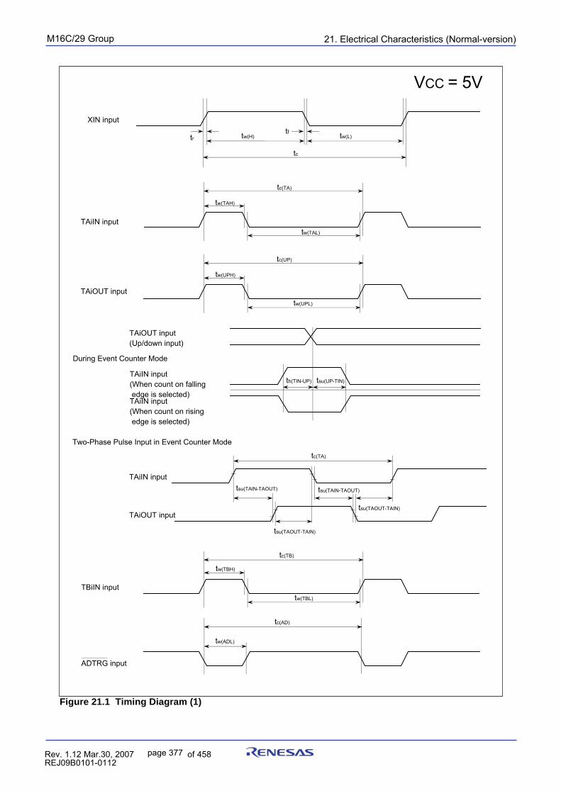
21. Electrical Characteristics (Normal-version)puorG92/C61M
page 377 854fo7002,03.raM21.1.veR2110-1010B90JER
VCC = 5V
Figure 21.1 Timing Diagram (1)
TAiIN input
TAiOUT input
During Event Counter Mode
TBiIN input
ADTRG input
tc(TA)
tw(TAH)
tw(TAL)
tc(UP)
tw(UPH)
tw(UPL)
tc(TB)
tw(TBH)
tw(TBL)
tc(AD)
tw(ADL)
th(TIN-UP) tsu(UP-TIN)TAiIN input(When count on falling edge is selected)TAiIN input (When count on rising edge is selected)
TAiOUT input(Up/down input)
TAiIN input
Two-Phase Pulse Input in Event Counter Mode
tc(TA)
tsu(TAIN-TAOUT)
tsu(TAOUT-TAIN)
tsu(TAIN-TAOUT)
tsu(TAOUT-TAIN)TAiOUT input
XIN input
tw(H) tw(L)trtf
tc
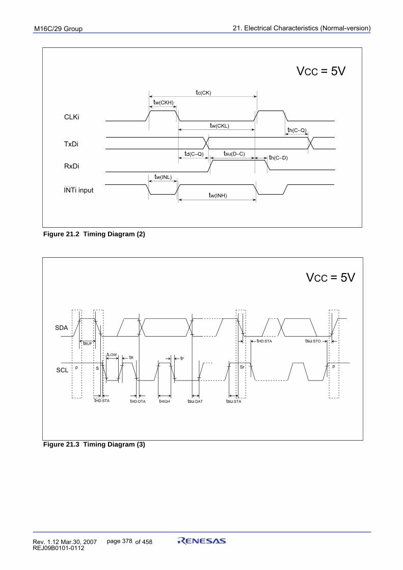
21. Electrical Characteristics (Normal-version)puorG92/C61M
page 378 854fo7002,03.raM21.1.veR2110-1010B90JER
VCC = 5V
Figure 21.2 Timing Diagram (2)
tsu(D–C)
CLKi
TxDi
RxDi
tc(CK)
tw(CKH)
tw(CKL)
tw(INL)
tw(INH)
td(C–Q) th(C–D)
th(C–Q)
INTi input
tBUF
tHD:STA tHD:DTA
tLOW tR tF
tHIGH tsu:DAT tsu:STA
tHD:STA tsu:STO
SCL p S Sr p
SDA
Figure 21.3 Timing Diagram (3)
VCC = 5V
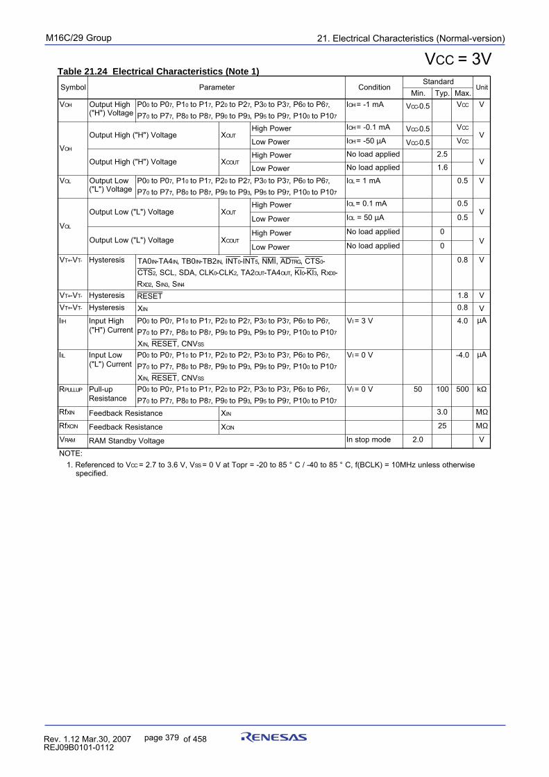
21. Electrical Characteristics (Normal-version)puorG92/C61M
page 379 854fo7002,03.raM21.1.veR2110-1010B90JER
VCC = 3VTable 21.24 Electrical Characteristics (Note 1)
lobmyS retemaraP noitidnoCdradnatS
tinU.niM .pyT .xaM
V HO hgiHtuptuOegatloV)"H"(
0P 0 0Pot 7 1P, 0 1Pot 7 2P, 0 2Pot 7 3P, 0 3Pot 7 6P, 0 6Pot 7,7P 0 7Pot 7 8P, 0 8Pot 7 9P, 0 9Pot 3 9P, 5 9Pot 7 01P, 0 01Pot 7
I HO Am1-= V CC - 5.0 V CC V
V HO
egatloV)"H"(hgiHtuptuO X TUOrewoPhgiH I HO Am1.0-= V CC - 5.0 V CC
VrewoPwoL I HO 05-= µA V CC - 5.0 V CC
egatloV)"H"(hgiHtuptuO X TUOCrewoPhgiH deilppadaoloN 5.2
VrewoPwoL deilppadaoloN 6.1
V LO woLtuptuOegatloV)"L"(
0P 0 0Pot 7 1P, 0 1Pot 7 2P, 0 2Pot 7 3P, 0 3Pot 7 6P, 0 6Pot 7,7P 0 7Pot 7 8P, 0 8Pot 7 9P, 0 9Pot 3 9P, 5 9Pot 7 01P, 0 01Pot 7
I LO Am1= 5.0 V
V LO
egatloV)"L"(woLtuptuO X TUOrewoPhgiH I LO Am1.0= 5.0
VrewoPwoL I LO 05= µA 5.0
egatloV)"L"(woLtuptuO X TUOCrewoPhgiH deilppadaoloN 0
VrewoPwoL deilppadaoloN 0
V +T V- -T siseretsyH 0AT NI 4AT- NI 0BT, NI 2BT- NI TNI, 0 TNI- 5 DA,IMN, GRT STC, 0-STC 2 KLC,ADS,LCS, 0 KLC- 2 2AT, TUO 4AT- TUO IK, 0 IK- 3 R, 0DX -
R 2DX S, 3NI S, 4NI
8.0 V
V +T V- -T siseretsyH TESER 8.1 VV +T V- -T siseretsyH X NI 8.0 VI HI hgiHtupnI
tnerruC)"H"(0P 0 0Pot 7 1P, 0 1Pot 7 2P, 0 2Pot 7 3P, 0 3Pot 7 6P, 0 6Pot 7,7P 0 7Pot 7 8P, 0 8Pot 7 9P, 0 9Pot 3 9P, 5 9Pot 7 01P, 0 01Pot 7
X NI VNC,TESER, SS
VI V3= 0.4 µA
I LI woLtupnItnerruC)"L"(
0P 0 0Pot 7 1P, 0 1Pot 7 2P, 0 2Pot 7 3P, 0 3Pot 7 6P, 0 6Pot 7,7P 0 7Pot 7 8P, 0 8Pot 7 9P, 0 9Pot 3 9P, 5 9Pot 7 01P, 0 01Pot 7
X NI VNC,TESER, SS
VI V0= 0.4- µA
R PULLUP pu-lluPecnatsiseR
0P 0 0Pot 7 1P, 0 1Pot 7 2P, 0 2Pot 7 3P, 0 3Pot 7 6P, 0 6Pot 7,7P 0 7Pot 7 8P, 0 8Pot 7 9P, 0 9Pot 3 9P, 5 9Pot 7 01P, 0 01Pot 7
VI V0= 05 001 005 kΩ
fR NIX ecnatsiseRkcabdeeF X NI 0.3 MΩ
fR NICX ecnatsiseRkcabdeeF X NIC 52 MΩ
V MAR egatloVybdnatSMAR edompotsnI 0.2 V
:ETONotdecnerefeR.1 V CC V,V6.3ot7.2= SS esiwrehtosselnuzHM01=)KLCB(f,C°58ot04-/C°58ot02-=rpoTtaV0=
.deificeps
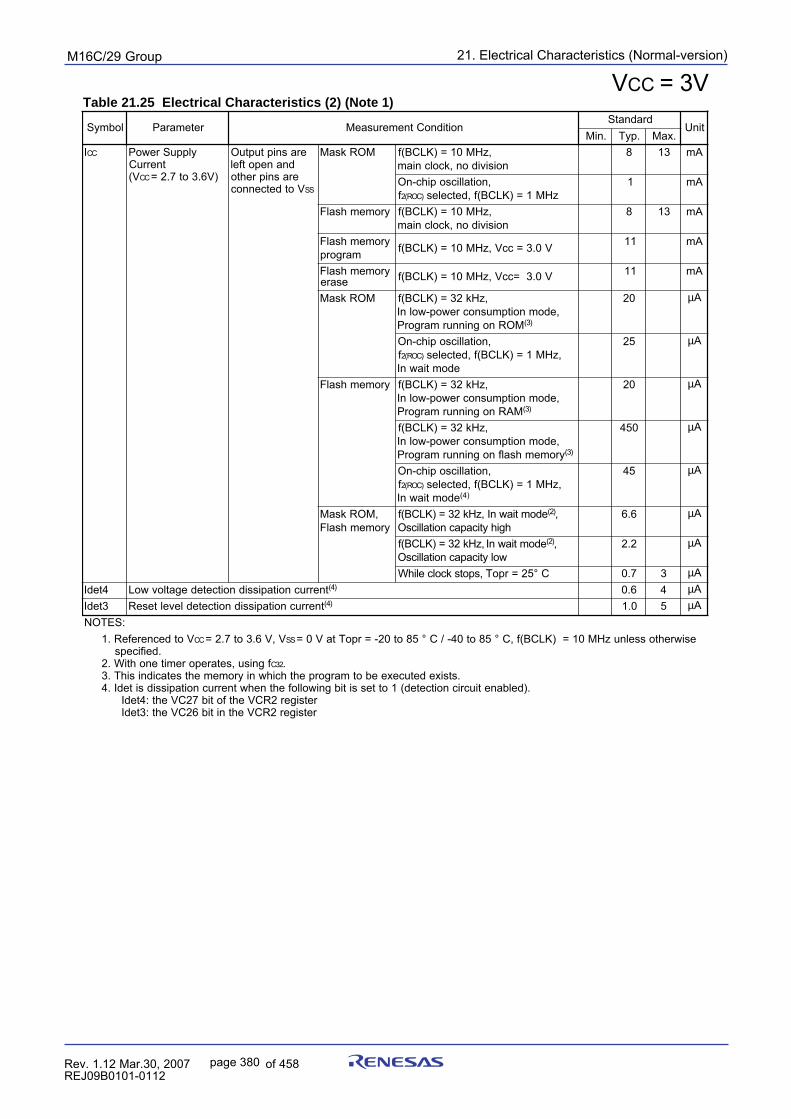
21. Electrical Characteristics (Normal-version)puorG92/C61M
page 380 854fo7002,03.raM21.1.veR2110-1010B90JER
Table 21.25 Electrical Characteristics (2) (Note 1)VCC = 3V
lobmyS retemaraP noitidnoCtnemerusaeMdradnatS
tinU.niM .pyT .xaM
I CC ylppuSrewoPtnerruC
V( CC )V6.3ot7.2=
erasniptuptuOdnanepotfelerasniprehtoVotdetcennoc SS
MORksaM (f KLCB ,zHM01=)noisividon,kcolcniam
8 31 Am
,noitallicsopihc-nOf )COR(2 zHM1=)KLCB(f,detceles
1 Am
yromemhsalF ,zHM01=)KLCB(fnoisividon,kcolcniam
8 31 Am
yromemhsalFmargorp V0.3=ccV,zHM01=)KLCB(f 11 Am
yromemhsalFesare V0.3=ccV,zHM01=)KLCB(f 11 Am
MORksaM zHk23=)KLCB(f ,edomnoitpmusnocrewop-wolnI ,
MORnogninnurmargorP )3(
02 µA
,noitallicsopihc-nOf )COR(2 ,zHM1=)KLCB(f,detceles
edomtiawnI
52 µA
yromemhsalF zHk23=)KLCB(f ,edomnoitpmusnocrewop-wolnI ,
MARnogninnurmargorP )3(
02 µA
,zHk23=)KLCB(f,edomnoitpmusnocrewop-wolnIyromemhsalfnogninnurmargorP )3(
054 µA
,noitallicsopihc-nOf )COR(2 ,zHM1=)KLCB(f,detceles
edomtiawnI )4(
54 µA
,MORksaMyromemhsalF
edomtiawnI,zHk23=)KLCB(f )2( ,hgihyticapacnoitallicsO
6.6 µA
,zHk23=)KLCB(f edomtiawnI )2( ,wolyticapacnoitallicsO
2.2 µA
,spotskcolcelihW 52=rpoT C° 7.0 3 µA4tedI tnerrucnoitapissidnoitcetedegatlovwoL )4( 6.0 4 µA3tedI tnerrucnoitapissidnoitcetedlevelteseR )4( 0.1 5 µA
:SETONotdecnerefeR.1 V CC V,V6.3ot7.2= SS esiwrehtosselnuzHM01=)KLCB(f,C°58ot04-/C°58ot02-=rpoTtaV0=
.deificepsfgnisu,setareporemitenohtiW.2 23C .
.stsixedetucexeebotmargorpehthcihwniyromemehtsetacidnisihT.3.)delbanetiucricnoitceted(1ottessitibgniwollofehtnehwtnerrucnoitapissidsitedI.4
retsiger2RCVehtfotib72CVeht:4tedIretsiger2RCVehtnitib62CVeht:3tedI
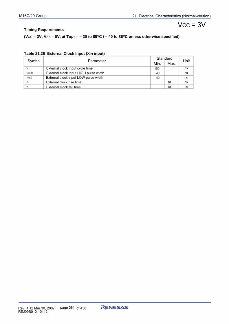
21. Electrical Characteristics (Normal-version)puorG92/C61M
page 381 854fo7002,03.raM21.1.veR2110-1010B90JER
VCC = 3VTiming Requirements
(VCC = 3V, VSS = 0V, at Topr = – 20 to 85oC / – 40 to 85oC unless otherwise specified)
Table 21.26 External Clock Input (XIN input)
Max.
External clock rise time nstr
Min.External clock input cycle timeExternal clock input HIGH pulse widthExternal clock input LOW pulse width
External clock fall time
nsnsns
ns
tctw(H)tw(L)
tf
ParameterSymbol UnitStandard
1004040
1818
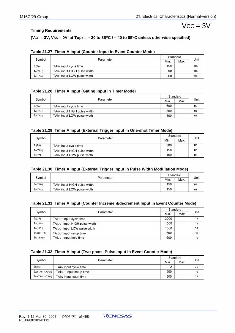
21. Electrical Characteristics (Normal-version)puorG92/C61M
page 382 854fo7002,03.raM21.1.veR2110-1010B90JER
VCC = 3VTiming Requirements
(VCC = 3V, VSS = 0V, at Topr = – 20 to 85oC / – 40 to 85oC unless otherwise specified)
Table 21.27 Timer A Input (Counter Input in Event Counter Mode)
Table 21.28 Timer A Input (Gating Input in Timer Mode)
Table 21.29 Timer A Input (External Trigger Input in One-shot Timer Mode)
Table 21.30 Timer A Input (External Trigger Input in Pulse Width Modulation Mode)
Table 21.31 Timer A Input (Counter Increment/decrement Input in Event Counter Mode)
Table 21.32 Timer A Input (Two-phase Pulse Input in Event Counter Mode)
StandardMax.
nsTAiIN input LOW pulse widthtw(TAL)
Min.nsns
Unit
TAiIN input HIGH pulse widthtw(TAH)
ParameterSymbol
tc(TA) TAiIN input cycle time
60
15060
StandardMax.Min.
nsnsns
Unit
TAiIN input cycle timeTAiIN input HIGH pulse widthTAiIN input LOW pulse width
tc(TA)
tw(TAH)
tw(TAL)
Symbol Parameter
600300300
StandardMax.Min.
nsnsns
Unit
TAiIN input cycle timeTAiIN input HIGH pulse widthTAiIN input LOW pulse width
tc(TA)
tw(TAH)
tw(TAL)
Symbol Parameter
300150150
StandardMax.Min.
nsns
Unit
tw(TAH)
tw(TAL)
Symbol Parameter
TAiIN input HIGH pulse widthTAiIN input LOW pulse width
150150
StandardMax.Min.
nsnsns
Unit
nsns
Symbol Parameter
TAiOUT input cycle timeTAiOUT input HIGH pulse widthTAiOUT input LOW pulse widthTAiOUT input setup timeTAiOUT input hold time
tc(UP)
tw(UPH)
tw(UPL)
tsu(UP-TIN)
th(TIN-UP)
300015001500600600
StandardMax.Min.
µsnsns
UnitSymbol Parameter
TAiIN input cycle timeTAiOUT input setup timeTAiIN input setup time
tc(TA)
tsu(TAIN-TAOUT)
tsu(TAOUT-TAIN)
2500500
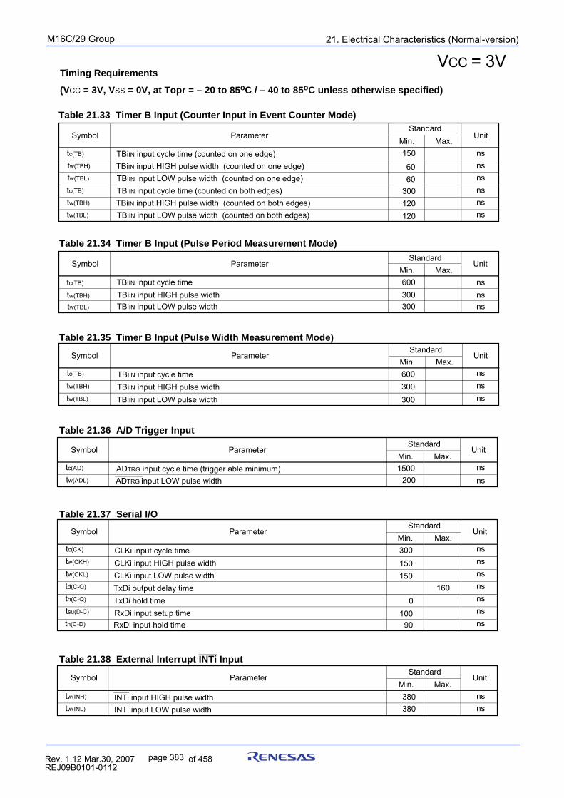
21. Electrical Characteristics (Normal-version)puorG92/C61M
page 383 854fo7002,03.raM21.1.veR2110-1010B90JER
VCC = 3V
Table 21.33 Timer B Input (Counter Input in Event Counter Mode)
Table 21.34 Timer B Input (Pulse Period Measurement Mode)
Table 21.35 Timer B Input (Pulse Width Measurement Mode)
Table 21.36 A/D Trigger Input
Table 21.37 Serial I/O
_______
Table 21.38 External Interrupt INTi Input
Timing Requirements
(VCC = 3V, VSS = 0V, at Topr = – 20 to 85oC / – 40 to 85oC unless otherwise specified)
nsnsnsnsnsnsns
StandardMax.Min.
TBiIN input cycle time (counted on one edge)TBiIN input HIGH pulse width (counted on one edge)TBiIN input LOW pulse width (counted on one edge)
nsnsns
tc(TB)
tw(TBH)
tw(TBL)
ParameterSymbol Unit
tc(TB)
tw(TBL)
tw(TBH)
nsnsns
TBiIN input HIGH pulse width (counted on both edges)TBiIN input LOW pulse width (counted on both edges)
TBiIN input cycle time (counted on both edges)
StandardMax.Min.
nsns
tc(TB)
tw(TBH)
Symbol Parameter Unit
tw(TBL) nsTBiIN input HIGH pulse widthTBiIN input cycle time
TBiIN input LOW pulse width
StandardMax.Min.
nsns
tc(TB)
Symbol Parameter Unit
tw(TBL) nstw(TBH)
TBiIN input cycle timeTBiIN input HIGH pulse widthTBiIN input LOW pulse width
StandardMax.Min.
nsns
tc(AD)
tw(ADL)
Symbol Parameter Unit
ADTRG input cycle time (trigger able minimum)ADTRG input LOW pulse width
StandardMax.Min.
nsns
tw(INH)
tw(INL)
Symbol Parameter Unit
INTi input LOW pulse widthINTi input HIGH pulse width
StandardMax.Min.
CLKi input cycle timeCLKi input HIGH pulse widthCLKi input LOW pulse width
tc(CK)
tw(CKH)
tw(CKL)
ParameterSymbol Unit
td(C-Q)
tsu(D-C)
th(C-Q) TxDi hold timeRxDi input setup time
TxDi output delay time
th(C-D) RxDi input hold time
150
6060
120120
300
600300300
600300300
1500200
380380
300150150
0
90
160
100
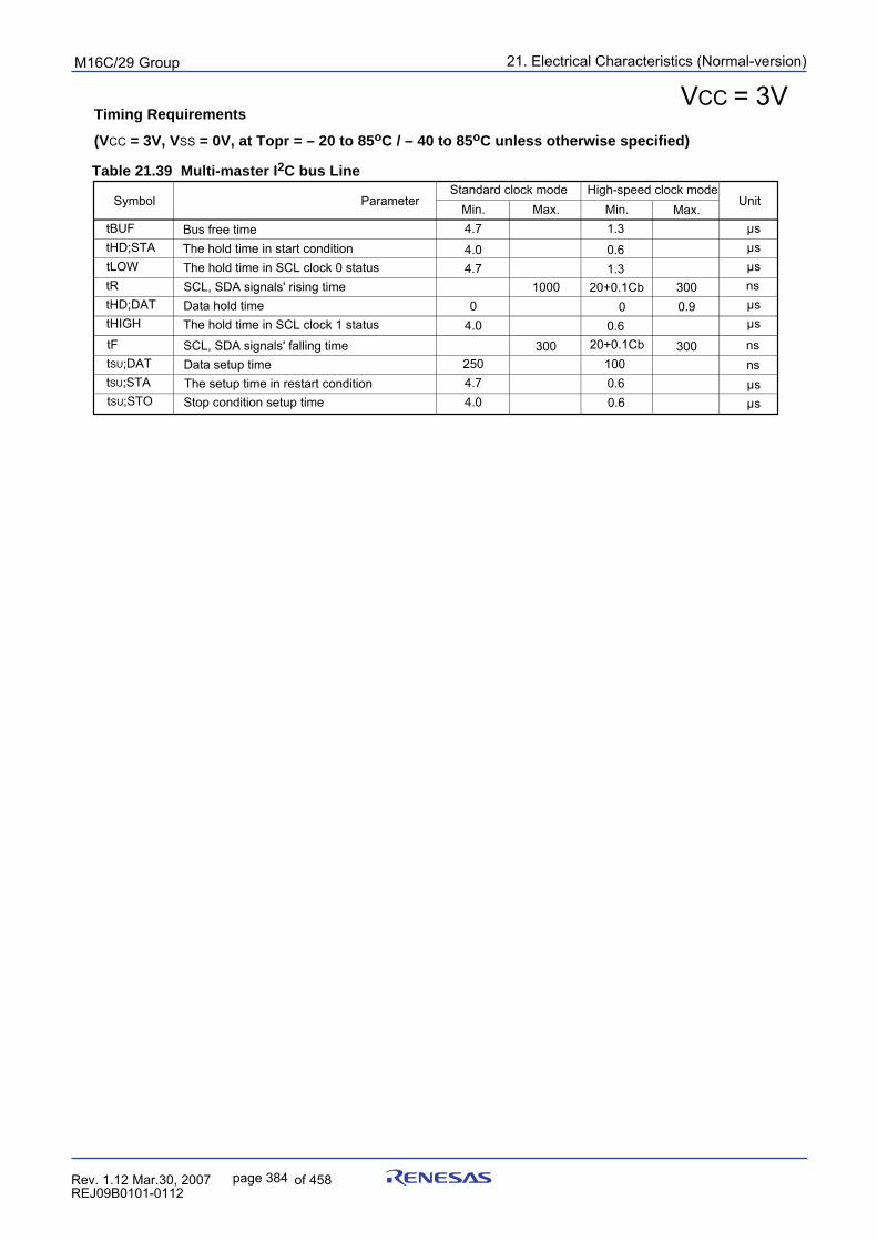
21. Electrical Characteristics (Normal-version)puorG92/C61M
page 384 854fo7002,03.raM21.1.veR2110-1010B90JER
VCC = 3VTiming Requirements
(VCC = 3V, VSS = 0V, at Topr = – 20 to 85oC / – 40 to 85oC unless otherwise specified)
Table 21.39 Multi-master I2C bus LineHigh-speed clock mode
Max.Min.Bus free timeThe hold time in start conditionThe hold time in SCL clock 0 status
µsµsµs
tBUFtHD;STAtLOW
ParameterSymbol Unit
tR
tHIGHtHD;DAT
nsµsµs
Data hold timeThe hold time in SCL clock 1 status
SCL, SDA signals' rising time
1.3
0.61.3
00.6
20+0.1Cb
tF SCL, SDA signals' falling timetSU;DAT Data setup timetSU;STA The setup time in restart conditiontSU;STO Stop condition setup time
Standard clock modeMax.Min.
4.7
4.04.7
04.0
2504.74.0
1000
3001000.6
20+0.1Cb
0.6
300
300
0.9
nsnsµsµs
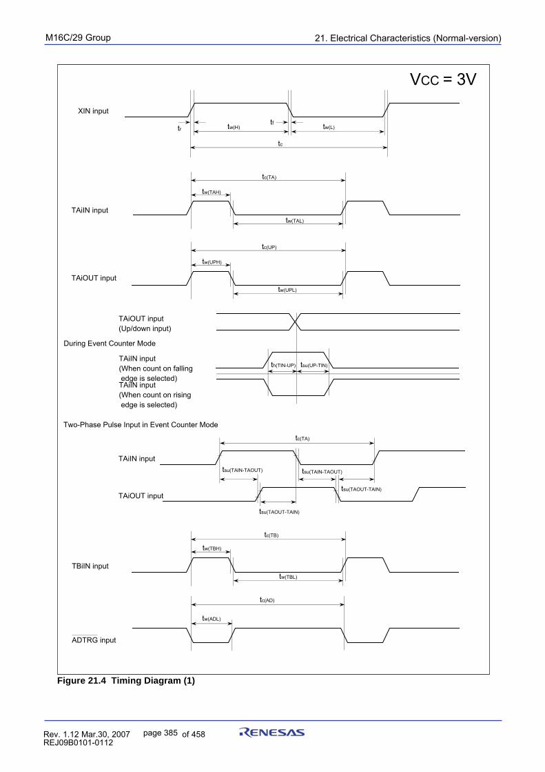
21. Electrical Characteristics (Normal-version)puorG92/C61M
page 385 854fo7002,03.raM21.1.veR2110-1010B90JER
VCC = 3V
Figure 21.4 Timing Diagram (1)
TAiIN input
TAiOUT input
During Event Counter Mode
TBiIN input
ADTRG input
tc(TA)
tw(TAH)
tw(TAL)
tc(UP)
tw(UPH)
tw(UPL)
tc(TB)
tw(TBH)
tw(TBL)
tc(AD)
tw(ADL)
th(TIN-UP) tsu(UP-TIN)TAiIN input(When count on falling edge is selected)TAiIN input (When count on rising edge is selected)
TAiOUT input(Up/down input)
TAiIN input
Two-Phase Pulse Input in Event Counter Mode
tc(TA)
tsu(TAIN-TAOUT)
tsu(TAOUT-TAIN)
tsu(TAIN-TAOUT)
tsu(TAOUT-TAIN)TAiOUT input
XIN input
tw(H) tw(L)trtf
tc
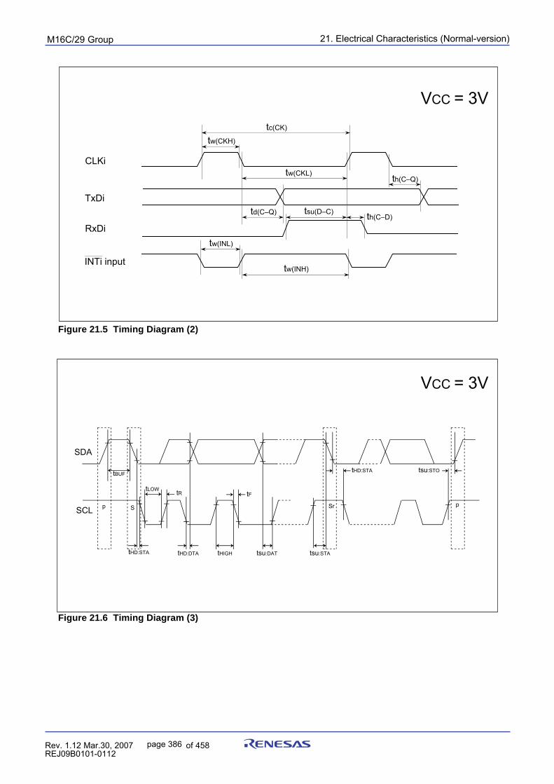
21. Electrical Characteristics (Normal-version)puorG92/C61M
page 386 854fo7002,03.raM21.1.veR2110-1010B90JER
VCC = 3V
Figure 21.5 Timing Diagram (2)
tsu(D–C)
CLKi
TxDi
RxDi
tc(CK)
tw(CKH)
tw(CKL)
tw(INL)
tw(INH)
td(C–Q) th(C–D)
th(C–Q)
INTi input
tBUF
tHD:STA tHD:DTA
tLOW tR tF
tHIGH tsu:DAT tsu:STA
tHD:STA tsu:STO
SCL p S Sr p
SDA
Figure 21.6 Timing Diagram (3)
VCC = 3V
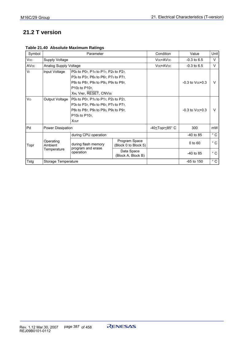
21. Electrical Characteristics (T-version)puorG92/C61M
page 387 854fo7002,03.raM21.1.veR2110-1010B90JER
21.2 T version
lobmyS retemaraP noitidnoC eulaV tinU
V CC egatloVylppuS V CC VA= CC 5.6ot3.0- V
VA CC egatloVylppuSgolanA V CC VA= CC 5.6ot3.0- VVI egatloVtupnI 0P 0 0Pot 7 1P, 0 1Pot 7 2P, 0 2Pot 7,
3P 0 3Pot 7 6P, 0 6Pot 7 7P, 0 7Pot 7,8P 0 8Pot 7 9P, 0 9Pot 3 9P, 5 9Pot 7,
01P 0 01Pot 7,X NI V, FER VNC,TESER, SS
Vot3.0- CC 3.0+ V
VO egatloVtuptuO 0P 0 0Pot 7 1P, 0 1Pot 7 2P, 0 2Pot 7,3P 0 3Pot 7 6P, 0 6Pot 7 7P, 0 7Pot 7,8P 0 8Pot 7 9P, 0 9Pot 3 9P, 5 9Pot 7,
01P 0 01Pot 7,X TUO
Vot3.0- CC 3.0+ V
dP noitapissiDrewoP 04- < rpoT < C°58 003 Wm
rpoTgnitarepO
tneibmAerutarepmeT
noitarepoUPCgnirud 58ot04- C°
yromemhsalfgnirudesarednamargorp
noitarepo
ecapSmargorP)5kcolBot0kcolB( 06ot0 C°
ecapSataD)BkcolB,AkcolB( 58ot04- C°
gtsT erutarepmeTegarotS 051ot56- C°
Table 21.40 Absolute Maximum Ratings
21. Electrical Characteristics (T-version)puorG92/C61M
page 388 854fo7002,03.raM21.1.veR2110-1010B90JER
lobmyS retemaraPdradnatS
tinU.niM .pyT .xaM
V CC egatloVylppuS 0.3 5.5 VVA CC egatloVylppuSgolanA V CC V
V SS egatloVylppuS 0 VVA SS egatloVylppuSgolanA 0 V
V HI )"H"(hgiHtupnIegatloV
0P 0 0Pot 7 1P, 0 1Pot 7 2P, 0 2Pot 7 3P, 0 3Pot 7 6P, 0 6Pot 7,7P 0 7Pot 7 8P, 0 8Pot 7 9P, 0 9Pot 3 9P, 5 9Pot 7 01P, 0 01Pot 7
V7.0 CC V CC V
SSVNC,TESER,NIX V8.0 CC V CC V
ADS MM LCS, MMInehW 2 detcelessileveltupnisubC V7.0 CC V CC V
detcelessileveltupniSUBMSnehW 4.1 V CC VV LI )"L"(woLtupnI
egatloV0P 0 0Pot 7 1P, 0 1Pot 7 2P, 0 2Pot 7 3P, 0 3Pot 7 6P, 0 6Pot 7,7P 0 7Pot 7 8P, 0 8Pot 7 9P, 0 9Pot 3 9P, 5 9Pot 7 01P, 0 01Pot 7
0 V3.0 CC V
SSVNC,TESER,NIX 0 V2.0 CC V
ADS MM LCS, MMInehW 2 detcelessileveltupnisubC 0 3.0 V CC V
detcelessileveltupniSUBMSnehW 0 6.0 VI )kaep(HO hgiHtuptuOkaeP
tnerruC)"H"(0P 0 0Pot 7 1P, 0 1Pot 7 2P, 0 2Pot 7 3P, 0 3Pot 7 6P, 0 6Pot 7,7P 0 7Pot 7 8P, 0 8Pot 7 9P, 0 9Pot 3 9P, 5 9Pot 7 01P, 0 01Pot 7
0.01- Am
I )gva(HO tuptuOegarevAtnerruC)"H"(hgiH
0P 0 0Pot 7 1P, 0 1Pot 7 2P, 0 2Pot 7 3P, 0 3Pot 7 6P, 0 6Pot 7,7P 0 7Pot 7 8P, 0 8Pot 7 9P, 0 9Pot 3 9P, 5 9Pot 7 01P, 0 01Pot 7
0.5- Am
I )kaep(LO woLtuptuOkaePtnerruC)"L"(
0P 0 0Pot 7 1P, 0 1Pot 7 2P, 0 2Pot 7 3P, 0 3Pot 7 6P, 0 6Pot 7,7P 0 7Pot 7 8P, 0 8Pot 7 9P, 0 9Pot 3 9P, 5 9Pot 7 01P, 0 01Pot 7
0.01 Am
I )gva(LO tuptuOegarevAtnerruC)"L"(woL
0P 0 0Pot 7 1P, 0 1Pot 7 2P, 0 2Pot 7 3P, 0 3Pot 7 6P, 0 6Pot 7,7P 0 7Pot 7 8P, 0 8Pot 7 9P, 0 9Pot 3 9P, 5 9Pot 7 01P, 0 01Pot 7
0.5 Am
X(f NI ) ycneuqerFnoitallicsOtupnIkcolCniaM )4( 0 02 zHMX(f NIC ) ycneuqerFnoitallicsOkcolCbuS 867.23 05 zHk
f1 )COR( 1ycneuqerFrotallicsOpihc-nO 5.0 1 2 zHM)COR(2f 2ycneuqerFrotallicsOpihc-nO 1 2 4 zHM)COR(3f 3ycneuqerFrotallicsOpihc-nO 8 61 62 zHM
)LLP(f ycneuqerFnoitallicsOkcolCLLP )4( 01 02 zHM)KLCB(f ycneuqerFkcolCnoitarepOUPC 0 02 zHM
t US )LLP( rezisehtnySycneuqerFLLPezilibatSotemiTtiaW V CC V0.5= 02 smV CC V0.3= 05 sm
:SETONVotdecnerefeR.1 CC .deificepsesiwrehtosselnuC°58ot04-=rpoTtaV5.5ot0.3=
.sm001nihtiweulavnaemehtsitnerructuptuonaemehT.2IlatotehT.3 )kaep(LO IlatotehT.sselroAm08ebtsumstropllarof )kaep(HO .sselroAm08-ebtsumstropllarof
.egatlovylppusdnaycneuqerfnoitallicsokcolcLLP,ycneuqerfnoitallicsokcolcniamgnomapihsnoitaleR.4
Table 21.41 Recommended Operating Conditions (Note 1)
Main clock input oscillation frequency
f(XIN
) ope
ratin
g m
axim
um fr
eque
ncy
[MH
Z]
VCC[V] (main clock: no division)
PLL clock oscillation frequency
f(PLL
) ope
ratin
g m
axim
um fr
eque
ncy
[MH
Z]
VCC[V] (PLL clock oscillation)
20.0
0.05.53.0
10.0
20.0 MHZ
20.0
0.05.5
10.0
3.0
20.0 MHZ
AAAAAAAAAAAAAAAAAAAAAAAA
AAAAAAAAAAAAAAAA
21. Electrical Characteristics (T-version)puorG92/C61M
page 389 854fo7002,03.raM21.1.veR2110-1010B90JER
Table 21.42 A/D Conversion Characteristics (Note 1)
lobmyS retemaraP noitidnoCtnemerusaeMdradnatS
tinU.niM .pyT .xaM
- noituloseR V FER V= CC 01 stiB
LNI ytiraenilnoNlargetnIrorrE
tib01V FER V= CC V5= 3± BSL
V FER V= CC V3.3= 5± BSL
tib8 V FER V= CC V3.3= 2± BSL
- ycaruccAetulosbAtib01
V FER V= CC V5= 3± BSL
V FER V= CC V3.3= 5± BSL
tib8 V FER V= CC V3.3= 2± BSL
LND rorrEytiraenilnoNlaitnereffiD 1± BSL- rorrEtesffO 3± BSL- rorrEniaG 3± BSL
R REDDAL reddaLrotsiseR V FER = V CC 01 04 kΩ
t VNOCemiTnoisrevnoCtib-01
elbaliavAnoitcnuFdloH&elpmaS V FER V= CC zHM01=DAø,V5= 3.3 µs
t VNOCemiTnoisrevnoCtib-8
elbaliavAnoitcnuFdloH&elpmaS V FER V= CC zHM01=DAø,V5= 8.2 µs
V FER egatloVecnerefeR 0.2 V CC VV AI egatloVtupnIgolanA 0 V FER V
:SETONVotdecnerefeR.1 CC VA= CC V= FER V,V5.5ot3.3= SS VA= SS esiwrehtosselnuC°58ot04-=rpoTtaV0=
.deificepspeeK.2 φ fehtedivid,yllanoitiddA.sselrozHM01taycneuqerfDA DA Vfi CC ekamdna,V2.4nahtsselsi φ DA
fnahtrewolrootlauqeycneuqerf DA .2/.3 peek,delbasidsinoitcnufdloh&elpmasnehW φ .2etoNninoitatimilehtotnoitiddanieromrozHk052taycneuqerfDA
peek,delbanesinoitcnufdloh&elpmasnehW φ .2etoNninoitatimilehtotnoitiddanieromrozHM1taycneuqerfDA/3siemitgnilpmas,delbanesinoitcnufdloh&elpmasnehW.4 φ .ycneuqerfDA/2siemitgnilpmas,delbasidsinoitcnufdloh&elpmasnehW φ .ycneuqerfDA
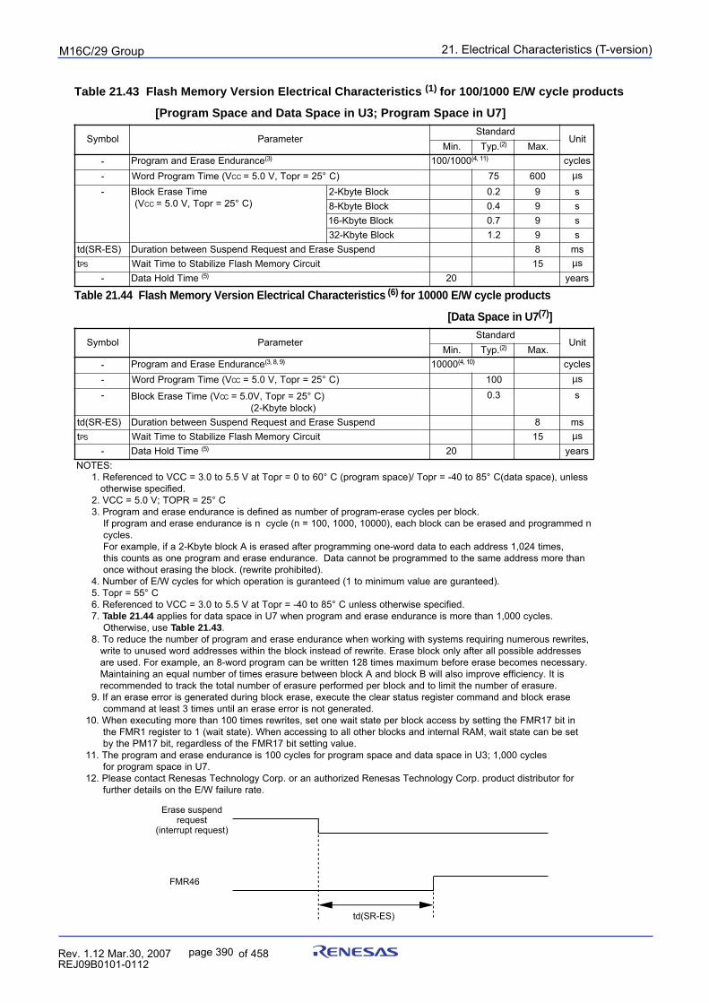
21. Electrical Characteristics (T-version)puorG92/C61M
page 390 854fo7002,03.raM21.1.veR2110-1010B90JER
Table 21.43 Flash Memory Version Electrical Characteristics (1) for 100/1000 E/W cycle products
[Program Space and Data Space in U3; Program Space in U7]
Table 21.44 Flash Memory Version Electrical Characteristics (6) for 10000 E/W cycle products
[Data Space in U7(7)]
Erase suspend request
(interrupt request)
FMR46
td(SR-ES)
lobmyS retemaraPdradnatS
tinU.niM .pyT )2( .xaM
- ecnarudnEesarEdnamargorP )3( 0001/001 )11,4( selcyc- V(emiTmargorPdroW CC 52=rpoT,V0.5= C° ) 57 006 µs
- emiTesarEkcolBV( CC 52=rpoT,V0.5= C° )
kcolBetybK-2 2.0 9 skcolBetybK-8 4.0 9 skcolBetybK-61 7.0 9 skcolBetybK-23 2.1 9 s
)SE-RS(dt dnepsuSesarEdnatseuqeRdnepsuSneewtebnoitaruD 8 smt SP tiucriCyromeMhsalFezilibatSotemiTtiaW 51 µs
- emiTdloHataD )5( 02 sraey
lobmyS retemaraPdradnatS
tinU.niM .pyT )2( .xaM
- ecnarudnEesarEdnamargorP )9,8,3( 00001 )01,4( selcyc- V(emiTmargorPdroW CC 52=rpoT,V0.5= C° ) 001 µs
- emiTesarEkcolB V( CC 52=rpoT,V0.5= C° ))kcolbetybK-2(
3.0 s
)SE-RS(dt dnepsuSesarEdnatseuqeRdnepsuSneewtebnoitaruD 8 smt SP tiucriCyromeMhsalFezilibatSotemiTtiaW 51 µs
- emiTdloHataD )5( 02 sraey:SETON
°06ot0=rpoTtaV5.5ot0.3=CCVotdecnerefeR.1 sselnu,)ecapsatad(C°58ot04-=rpoT/)ecapsmargorp(C.deificepsesiwrehto
C°52=RPOT;V0.5=CCV.2.kcolbrepselcycesare-margorpforebmunsadenifedsiecnarudneesarednamargorP.3
siecnarudneesarednamargorpfI n (elcyc n demmargorpdnadesareebnackcolbhcae,)00001,0001,001= n.selcyc
,semit420,1sserddahcaeotataddrow-enognimmargorpretfadesaresiAkcolbetybK-2afi,elpmaxeroFnahteromsserddaemasehtotdemmargorpebtonnacataD.ecnarudneesarednamargorpenosastnuocsiht
.)detibihorpetirwer(.kcolbehtgnisaretuohtiwecno.)deetnarugeraeulavmuminimot1(deetnarugsinoitarepohcihwrofselcycW/EforebmuN.4
C°55=rpoT.5.deificepsesiwrehtosselnuC°58ot04-=rpoTtaV5.5ot0.3=CCVotdecnerefeR.6
.7 44.12elbaT .selcyc000,1nahteromsiecnarudneesarednamargorpnehw7Uniecapsatadrofseilppaesu,esiwrehtO 34.12elbaT .
,setirwersuoremungniriuqersmetsyshtiwgnikrownehwecnarudneesarednamargorpforebmunehtecuderoT.8sesserddaelbissopllaretfaylnokcolbesarE.etirwerfodaetsnikcolbehtnihtiwsesserddadrowdesunuotetirw
.yrassecensemocebesareerofebmumixamsemit821nettirwebnacmargorpdrow-8na,elpmaxeroF.desuerasitI.ycneiciffeevorpmioslalliwBkcolbdnaAkcolbneewteberusaresemitforebmunlauqenagniniatniaM
.erusareforebmunehttimilotdnakcolbrepdemrofreperusareforebmunlatotehtkcartotdednemmoceresarekcolbdnadnammocretsigersutatsraelcehtetucexe,esarekcolbgniruddetarenegsirorreesarenafI.9
.detarenegtonsirorreesarenalitnusemit3tsaeltadnammocnitib71RMFehtgnittesybsseccakcolbrepetatstiawenotes,setirwersemit001nahteromgnitucexenehW.01
tesebnacetatstiaw,MARlanretnidnaskcolbrehtollaotgnisseccanehW.)etatstiaw(1otretsiger1RMFeht.eulavgnittestib71RMFehtfosseldrager,tib71MPehtyb
selcyc000,1;3Uniecapsataddnaecapsmargorprofselcyc001siecnarudneesarednamargorpehT.11.7Uniecapsmargorprof
rofrotubirtsidtcudorp.proCygolonhceTsaseneRdezirohtuanaro.proCygolonhceTsaseneRtcatnocesaelP.21.etareruliafW/Eehtnosliatedrehtruf
21. Electrical Characteristics (T-version)puorG92/C61M
page 391 854fo7002,03.raM21.1.veR2110-1010B90JER
Table 21.45 Power Supply Circuit Timing Characteristics
lobmyS retemaraP noitidnoCtnemerusaeMdradnatS
tinU.niM .pyT .xaM
)R-P(dt nehwegatloVylppuSlanretnIezilibatSotemiTtiaWno-rewoP
V CC V5.5ot0.3=
2 sm
)COR(dt nehwrotallicsOpihc-nOlanretnIezilibatSotemiTtiaWno-rewoP 04 µs
)S-R(dt emiTesaeleRPOTS )1( 051 µs
)S-W(dt esaeleRedoMtiaWedoMnoitapissiDrewoPwoLemiT 051 µs
td(P-R) Wait time to stabilize internal
supply voltage when power-on
CPU clock
td(R-S)(a)
(b) td(W-S)
td(R-S) STOP release time
td(W-S) Low power dissipation mode wait mode release time
Interrupt for (a) Stop mode release or (b) Wait mode release
td(ROC) Wait time to stabilize internal
on-chip oscillator when power-on
ROC
RESET
VCC
td(P-R) td(ROC)
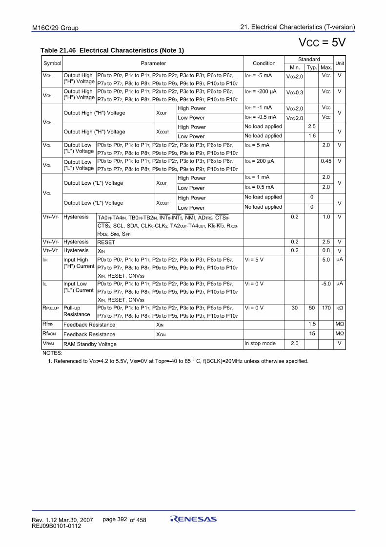
21. Electrical Characteristics (T-version)puorG92/C61M
page 392 854fo7002,03.raM21.1.veR2110-1010B90JER
VCC = 5VTable 21.46 Electrical Characteristics (Note 1)
lobmyS retemaraP noitidnoCdradnatS
tinU.niM .pyT .xaM
V HO hgiHtuptuOegatloV)"H"(
0P 0 0Pot 7 1P, 0 1Pot 7 2P, 0 2Pot 7 3P, 0 3Pot 7 6P, 0 6Pot 7,7P 0 7Pot 7 8P, 0 8Pot 7 9P, 0 9Pot 3 9P, 5 9Pot 7 01P, 0 01Pot 7
I HO Am5-= V CC - 0.2 V CC V
V HOhgiHtuptuOegatloV)"H"(
0P 0 0Pot 7 1P, 0 1Pot 7 2P, 0 2Pot 7 3P, 0 3Pot 7 6P, 0 6Pot 7,7P 0 7Pot 7 8P, 0 8Pot 7 9P, 0 9Pot 3 9P, 5 9Pot 7 01P, 0 01Pot 7
I HO 002-= µA V CC - 3.0 V CC V
V HO
egatloV)"H"(hgiHtuptuO X TUOrewoPhgiH I HO Am1-= V CC - 0.2 V CC
VrewoPwoL I HO Am5.0-= V CC - 0.2 V CC
egatloV)"H"(hgiHtuptuO X TUOCrewoPhgiH deilppadaoloN 5.2
VrewoPwoL deilppadaoloN 6.1
V LO woLtuptuOegatloV)"L"(
0P 0 0Pot 7 1P, 0 1Pot 7 2P, 0 2Pot 7 3P, 0 3Pot 7 6P, 0 6Pot 7,7P 0 7Pot 7 8P, 0 8Pot 7 9P, 0 9Pot 3 9P, 5 9Pot 7 01P, 0 01Pot 7
I LO Am5= 0.2 V
V LOwoLtuptuO
egatloV)"L"(0P 0 0Pot 7 1P, 0 1Pot 7 2P, 0 2Pot 7 3P, 0 3Pot 7 6P, 0 6Pot 7,7P 0 7Pot 7 8P, 0 8Pot 7 9P, 0 9Pot 3 9P, 5 9Pot 7 01P, 0 01Pot 7
I LO 002= µA 54.0 V
V LO
egatloV)"L"(woLtuptuO X TUOrewoPhgiH I LO Am1= 0.2
VrewoPwoL I LO Am5.0= 0.2
egatloV)"L"(woLtuptuO X TUOCrewoPhgiH deilppadaoloN 0
VrewoPwoL deilppadaoloN 0
V +T V- -T siseretsyH 0AT NI 4AT- NI 0BT, NI 2BT- NI TNI, 0 TNI- 5 DA,IMN, GRT STC, 0-STC 2 KLC,ADS,LCS, 0 KLC- 2 2AT, TUO 4AT- TUO IK, 0 IK- 3 R, 0DX -
R 2DX S, 3NI S, 4NI
2.0 0.1 V
V +T V- -T siseretsyH TESER 2.0 5.2 VV +T V- -T siseretsyH X NI 2.0 8.0 VI HI hgiHtupnI
tnerruC)"H"(0P 0 0Pot 7 1P, 0 1Pot 7 2P, 0 2Pot 7 3P, 0 3Pot 7 6P, 0 6Pot 7,7P 0 7Pot 7 8P, 0 8Pot 7 9P, 0 9Pot 3 9P, 5 9Pot 7 01P, 0 01Pot 7
X NI VNC,TESER, SS
VI V5= 0.5 µA
I LI woLtupnItnerruC)"L"(
0P 0 0Pot 7 1P, 0 1Pot 7 2P, 0 2Pot 7 3P, 0 3Pot 7 6P, 0 6Pot 7,7P 0 7Pot 7 8P, 0 8Pot 7 9P, 0 9Pot 3 9P, 5 9Pot 7 01P, 0 01Pot 7
X NI VNC,TESER, SS
VI V0= 0.5- µA
R PULLUP pu-lluPecnatsiseR
0P 0 0Pot 7 1P, 0 1Pot 7 2P, 0 2Pot 7 3P, 0 3Pot 7 6P, 0 6Pot 7,7P 0 7Pot 7 8P, 0 8Pot 7 9P, 0 9Pot 3 9P, 5 9Pot 7 01P, 0 01Pot 7
VI V0= 03 05 071 kΩ
fR NIX ecnatsiseRkcabdeeF X NI 5.1 MΩ
fR NICX ecnatsiseRkcabdeeF X NIC 51 MΩ
V MAR egatloVybdnatSMAR edompotsnI 0.2 V
:SETONotdecnerefeR.1 V CC V,V5.5ot2.4= SS .deificepsesiwrehtosselnuzHM02=)KLCB(f,C°58ot04-=rpoTtaV0=
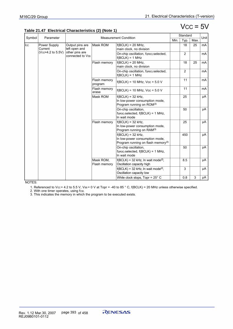
21. Electrical Characteristics (T-version)puorG92/C61M
page 393 854fo7002,03.raM21.1.veR2110-1010B90JER
VCC = 5VTable 21.47 Electrical Characteristics (2) (Note 1)
lobmyS retemaraP noitidnoCtnemerusaeMdradnatS
tinU.niM .pyT .xaM
I CC ylppuSrewoPtnerruC
V( CC )V5.5ot2.4=
erasniptuptuOdnanepotfelerasniprehtoVotdetcennoc SS
MORksaM (f KLCB ,zHM02=)noisividon,kcolcniam
81 52 Am
f,noitallicsopihc-nO )COR(2 ,detceleszHM1=)KLCB(f
2 Am
yromemhsalF (f KLCB ,zHM02=)noisividon,kcolcniam
81 52 Am
f,noitallicsopihc-nO )COR(2 ,detceleszHM1=)KLCB(f
2 Am
yromemhsalFmargorp V0.5=ccV,zHM01=)KLCB(f 11 Am
yromemhsalFesare V0.5=ccV,zHM01=)KLCB(f 11 Am
MORksaM zHk23=)KLCB(f ,edomnoitpmusnocrewop-wolnI ,
MORnogninnurmargorP )3(
52 µA
,noitallicsopihc-nOf )COR(2 ,zHM1=)KLCB(f,detceles
edomtiawnI
05 µA
yromemhsalF zHk23=)KLCB(f ,edomnoitpmusnocrewop-wolnI ,
MARnogninnurmargorP )3(
52 µA
,zHk23=)KLCB(f,edomnoitpmusnocrewop-wolnIyromemhsalfnogninnurmargorP )3(
054 µA
,noitallicsopihc-nOf )COR(2 ,zHM1=)KLCB(f,detceles
edomtiawnI
05 µA
,MORksaMyromemhsalF
edomtiawnI,zHk23=)KLCB(f )2( ,hgihyticapacnoitallicsO
5.8 µA
,zHk23=)KLCB(f edomtiawnI )2( ,wolyticapacnoitallicsO
3 µA
,spotskcolcelihW 52=rpoT C° 8.0 3 µA:SETON
otdecnerefeR.1 V CC V,V5.5ot2.4= SS .deificepsesiwrehtosselnuzHM02=)KLCB(f,C°58ot04-=rpoTtaV0=fgnisu,setareporemitenohtiW.2 23C .
.stsixedetucexeebotmargorpehthcihwniyromemehtsetacidnisihT.3
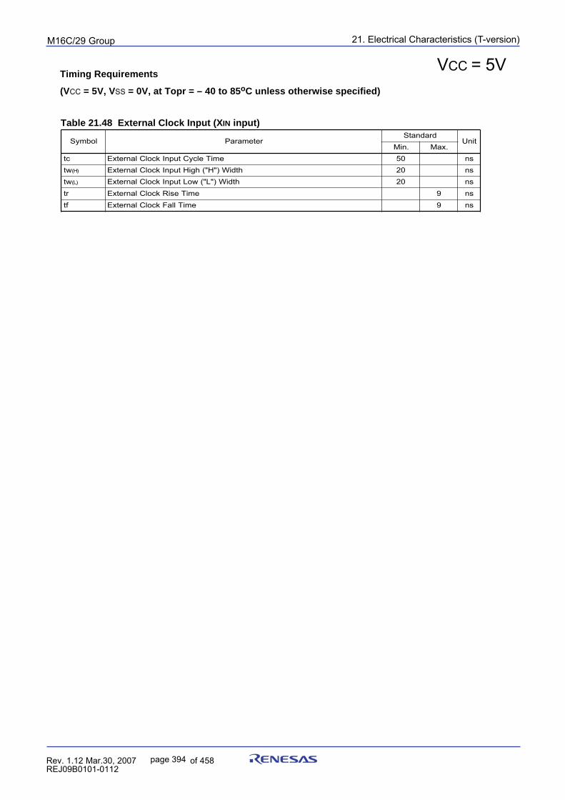
21. Electrical Characteristics (T-version)puorG92/C61M
page 394 854fo7002,03.raM21.1.veR2110-1010B90JER
VCC = 5VTiming Requirements
(VCC = 5V, VSS = 0V, at Topr = – 40 to 85oC unless otherwise specified)
Table 21.48 External Clock Input (XIN input)
lobmyS retemaraPdradnatS
tinU.niM .xaM
ct emiTelcyCtupnIkcolClanretxE 05 snwt )H( htdiW)"H"(hgiHtupnIkcolClanretxE 02 snwt )L( htdiW)"L"(woLtupnIkcolClanretxE 02 snrt emiTesiRkcolClanretxE 9 snft emiTllaFkcolClanretxE 9 sn
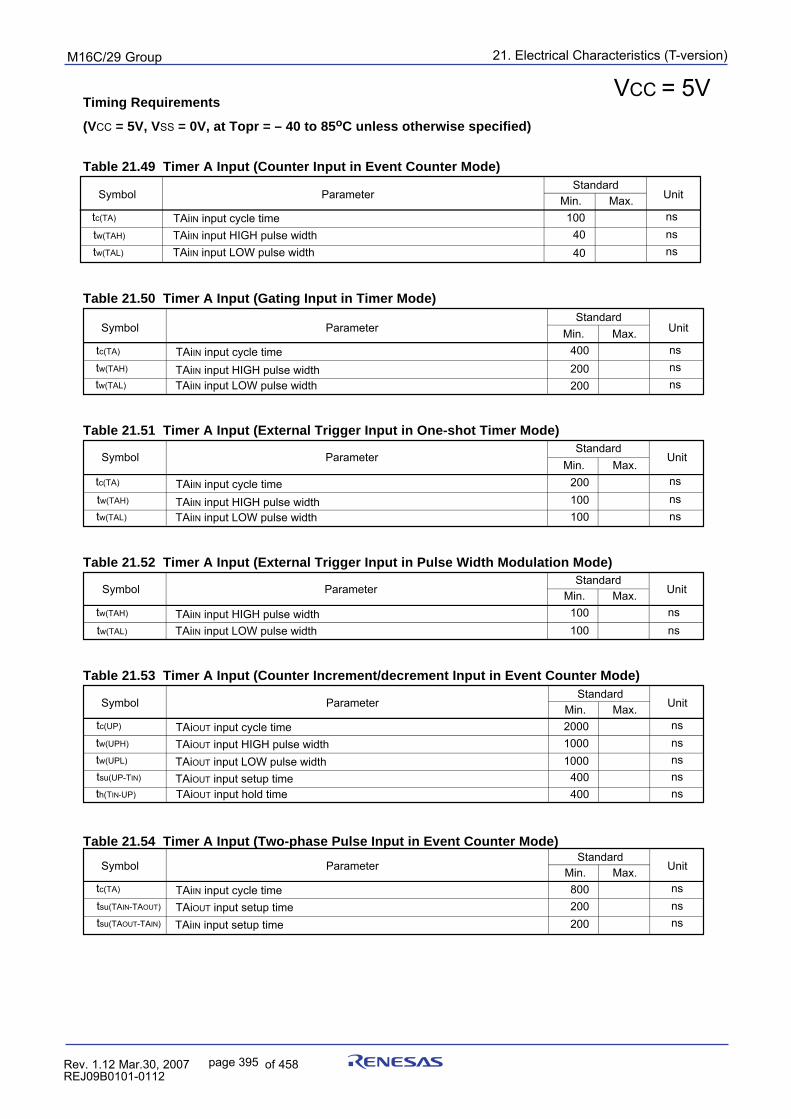
21. Electrical Characteristics (T-version)puorG92/C61M
page 395 854fo7002,03.raM21.1.veR2110-1010B90JER
VCC = 5VTiming Requirements
(VCC = 5V, VSS = 0V, at Topr = – 40 to 85oC unless otherwise specified)
Table 21.50 Timer A Input (Gating Input in Timer Mode)
Table 21.51 Timer A Input (External Trigger Input in One-shot Timer Mode)
Table 21.52 Timer A Input (External Trigger Input in Pulse Width Modulation Mode)
Table 21.53 Timer A Input (Counter Increment/decrement Input in Event Counter Mode)
Table 21.49 Timer A Input (Counter Input in Event Counter Mode)
Table 21.54 Timer A Input (Two-phase Pulse Input in Event Counter Mode)
StandardMax.
nsTAiIN input LOW pulse widthtw(TAL)
Min.nsns
Unit
TAiIN input HIGH pulse widthtw(TAH)
ParameterSymbol
tc(TA) TAiIN input cycle time
40
10040
StandardMax.Min.
nsnsns
Unit
TAiIN input cycle timeTAiIN input HIGH pulse widthTAiIN input LOW pulse width
tc(TA)
tw(TAH)
tw(TAL)
Symbol Parameter
400200200
StandardMax.Min.
nsnsns
Unit
TAiIN input cycle timeTAiIN input HIGH pulse widthTAiIN input LOW pulse width
tc(TA)
tw(TAH)
tw(TAL)
Symbol Parameter
200100100
StandardMax.Min.
nsns
Unit
tw(TAH)
tw(TAL)
Symbol Parameter
TAiIN input HIGH pulse widthTAiIN input LOW pulse width
100100
StandardMax.Min.
nsnsns
Unit
nsns
Symbol Parameter
TAiOUT input cycle timeTAiOUT input HIGH pulse widthTAiOUT input LOW pulse widthTAiOUT input setup timeTAiOUT input hold time
tc(UP)
tw(UPH)
tw(UPL)
tsu(UP-TIN)
th(TIN-UP)
200010001000
400400
StandardMax.Min.
nsnsns
UnitSymbol Parameter
TAiIN input cycle timeTAiOUT input setup timeTAiIN input setup time
tc(TA)
tsu(TAIN-TAOUT)
tsu(TAOUT-TAIN)
800200200
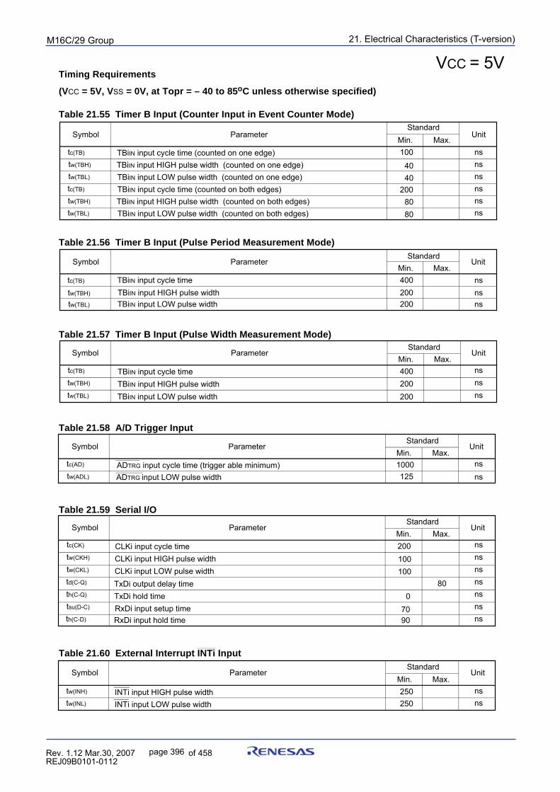
21. Electrical Characteristics (T-version)puorG92/C61M
page 396 854fo7002,03.raM21.1.veR2110-1010B90JER
Timing Requirements
(VCC = 5V, VSS = 0V, at Topr = – 40 to 85oC unless otherwise specified)
Table 21.55 Timer B Input (Counter Input in Event Counter Mode)
Table 21.56 Timer B Input (Pulse Period Measurement Mode)
Table 21.57 Timer B Input (Pulse Width Measurement Mode)
Table 21.58 A/D Trigger Input
Table 21.59 Serial I/O
_______
Table 21.60 External Interrupt INTi Input
VCC = 5V
nsnsnsnsnsnsns
StandardMax.Min.
TBiIN input cycle time (counted on one edge)TBiIN input HIGH pulse width (counted on one edge)TBiIN input LOW pulse width (counted on one edge)
nsnsns
tc(TB)
tw(TBH)
tw(TBL)
ParameterSymbol Unit
tc(TB)
tw(TBL)
tw(TBH)
nsnsns
TBiIN input HIGH pulse width (counted on both edges)TBiIN input LOW pulse width (counted on both edges)
TBiIN input cycle time (counted on both edges)
StandardMax.Min.
nsns
tc(TB)
tw(TBH)
Symbol Parameter Unit
tw(TBL) nsTBiIN input HIGH pulse widthTBiIN input cycle time
TBiIN input LOW pulse width
StandardMax.Min.
nsns
tc(TB)
Symbol Parameter Unit
tw(TBL) nstw(TBH)
TBiIN input cycle timeTBiIN input HIGH pulse widthTBiIN input LOW pulse width
StandardMax.Min.
nsns
tc(AD)
tw(ADL)
Symbol Parameter Unit
ADTRG input cycle time (trigger able minimum)ADTRG input LOW pulse width
StandardMax.Min.
nsns
tw(INH)
tw(INL)
Symbol Parameter Unit
INTi input LOW pulse widthINTi input HIGH pulse width
StandardMax.Min.
CLKi input cycle timeCLKi input HIGH pulse widthCLKi input LOW pulse width
tc(CK)
tw(CKH)
tw(CKL)
ParameterSymbol Unit
td(C-Q)
tsu(D-C)
th(C-Q) TxDi hold timeRxDi input setup time
TxDi output delay time
th(C-D) RxDi input hold time
100
4040
8080
200
400200200
400200200
1000125
250250
200100100
07090
80
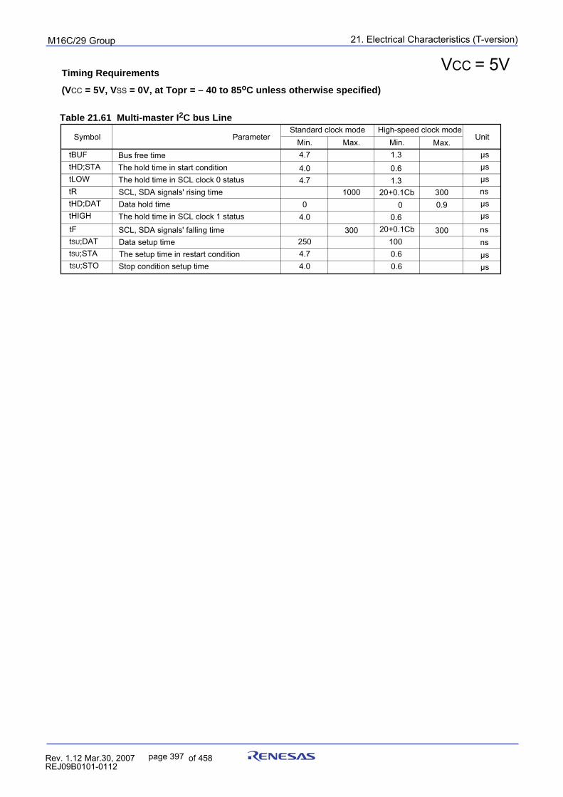
21. Electrical Characteristics (T-version)puorG92/C61M
page 397 854fo7002,03.raM21.1.veR2110-1010B90JER
Timing Requirements
(VCC = 5V, VSS = 0V, at Topr = – 40 to 85oC unless otherwise specified)
Table 21.61 Multi-master I2C bus Line
VCC = 5V
High-speed clock modeMax.Min.
Bus free timeThe hold time in start conditionThe hold time in SCL clock 0 status
µsµsµs
tBUFtHD;STAtLOW
ParameterSymbol Unit
tR
tHIGHtHD;DAT
nsµsµs
Data hold timeThe hold time in SCL clock 1 status
SCL, SDA signals' rising time
1.3
0.61.3
00.6
20+0.1Cb
tF SCL, SDA signals' falling timetSU;DAT Data setup timetSU;STA The setup time in restart conditiontSU;STO Stop condition setup time
Standard clock modeMax.Min.
4.7
4.04.7
04.0
2504.74.0
1000
3001000.6
20+0.1Cb
0.6
300
300
0.9
nsnsµsµs
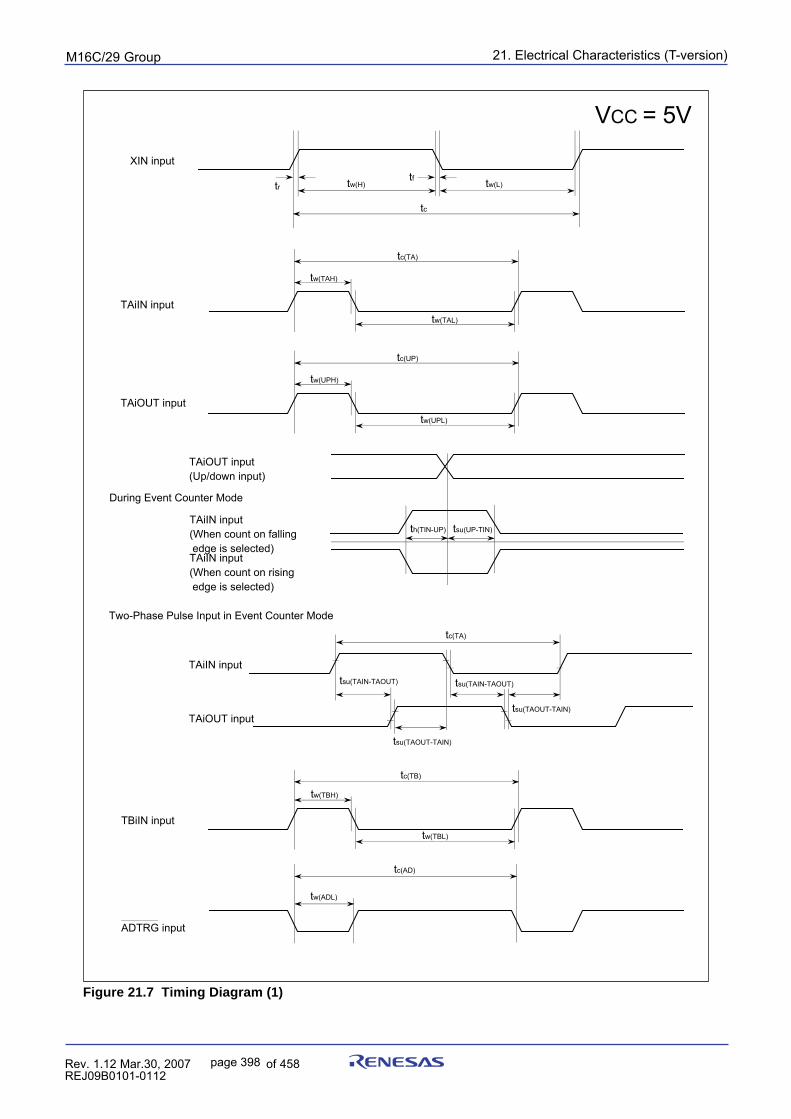
21. Electrical Characteristics (T-version)puorG92/C61M
page 398 854fo7002,03.raM21.1.veR2110-1010B90JER
VCC = 5V
Figure 21.7 Timing Diagram (1)
TAiIN input
TAiOUT input
During Event Counter Mode
TBiIN input
ADTRG input
tc(TA)
tw(TAH)
tw(TAL)
tc(UP)
tw(UPH)
tw(UPL)
tc(TB)
tw(TBH)
tw(TBL)
tc(AD)
tw(ADL)
th(TIN-UP) tsu(UP-TIN)TAiIN input(When count on falling edge is selected)TAiIN input (When count on rising edge is selected)
TAiOUT input(Up/down input)
TAiIN input
Two-Phase Pulse Input in Event Counter Mode
tc(TA)
tsu(TAIN-TAOUT)
tsu(TAOUT-TAIN)
tsu(TAIN-TAOUT)
tsu(TAOUT-TAIN)TAiOUT input
XIN input
tw(H) tw(L)trtf
tc
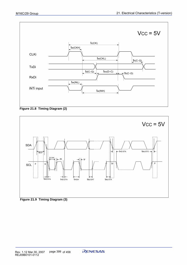
21. Electrical Characteristics (T-version)puorG92/C61M
page 399 854fo7002,03.raM21.1.veR2110-1010B90JER
VCC = 5V
Figure 21.8 Timing Diagram (2)
tsu(D–C)
CLKi
TxDi
RxDi
tc(CK)
tw(CKH)
tw(CKL)
tw(INL)
tw(INH)
td(C–Q) th(C–D)
th(C–Q)
INTi input
tBUF
tHD:STA tHD:DTA
tLOW tR tF
tHIGH tsu:DAT tsu:STA
tHD:STA tsu:STO
SCL p S Sr p
SDA
Figure 21.9 Timing Diagram (3)
VCC = 5V

21. Electrical Characteristics (T-version)puorG92/C61M
page 400 854fo7002,03.raM21.1.veR2110-1010B90JER
VCC = 3VTable 21.62 Electrical Characteristics (Note)
lobmyS retemaraP noitidnoCdradnatS
tinU.niM .pyT .xaM
V HO hgiHtuptuOegatloV)"H"(
0P 0 0Pot 7 1P, 0 1Pot 7 2P, 0 2Pot 7 3P, 0 3Pot 7 6P, 0 6Pot 7,7P 0 7Pot 7 8P, 0 8Pot 7 9P, 0 9Pot 3 9P, 5 9Pot 7 01P, 0 01Pot 7
I HO Am1-= V CC - 5.0 V CC V
V HO
egatloV)"H"(hgiHtuptuO X TUOrewoPhgiH I HO Am1.0-= V CC - 5.0 V CC
VrewoPwoL I HO 05-= µA V CC - 5.0 V CC
egatloV)"H"(hgiHtuptuO X TUOCrewoPhgiH deilppadaoloN 5.2
VrewoPwoL deilppadaoloN 6.1
V LO woLtuptuOegatloV)"L"(
0P 0 0Pot 7 1P, 0 1Pot 7 2P, 0 2Pot 7 3P, 0 3Pot 7 6P, 0 6Pot 7,7P 0 7Pot 7 8P, 0 8Pot 7 9P, 0 9Pot 3 9P, 5 9Pot 7 01P, 0 01Pot 7
I LO Am1= 5.0 V
V LO
egatloV)"L"(woLtuptuO X TUOrewoPhgiH I LO Am1.0= 5.0
VrewoPwoL I LO 05= µA 5.0
egatloV)"L"(woLtuptuO X TUOCrewoPhgiH deilppadaoloN 0
VrewoPwoL deilppadaoloN 0
V +T V- -T siseretsyH 0AT NI 4AT- NI 0BT, NI 2BT- NI TNI, 0 TNI- 5 DA,IMN, GRT STC, 0-STC 2 KLC,ADS,LCS, 0 KLC- 2 2AT, TUO 4AT- TUO IK, 0 IK- 3 R, 0DX -
R 2DX S, 3NI S, 4NI
8.0 V
V +T V- -T siseretsyH TESER 8.1 VV +T V- -T siseretsyH X NI 8.0 VI HI hgiHtupnI
tnerruC)"H"(0P 0 0Pot 7 1P, 0 1Pot 7 2P, 0 2Pot 7 3P, 0 3Pot 7 6P, 0 6Pot 7,7P 0 7Pot 7 8P, 0 8Pot 7 9P, 0 9Pot 3 9P, 5 9Pot 7 01P, 0 01Pot 7
X NI VNC,TESER, SS
VI V3= 0.4 µA
I LI woLtupnItnerruC)"L"(
0P 0 0Pot 7 1P, 0 1Pot 7 2P, 0 2Pot 7 3P, 0 3Pot 7 6P, 0 6Pot 7,7P 0 7Pot 7 8P, 0 8Pot 7 9P, 0 9Pot 3 9P, 5 9Pot 7 01P, 0 01Pot 7
X NI VNC,TESER, SS
VI V0= 0.4- µA
R PULLUP pu-lluPecnatsiseR
0P 0 0Pot 7 1P, 0 1Pot 7 2P, 0 2Pot 7 3P, 0 3Pot 7 6P, 0 6Pot 7,7P 0 7Pot 7 8P, 0 8Pot 7 9P, 0 9Pot 3 9P, 5 9Pot 7 01P, 0 01Pot 7
VI V0= 05 001 005 kΩ
fR NIX ecnatsiseRkcabdeeF X NI 0.3 MΩ
fR NICX ecnatsiseRkcabdeeF X NIC 52 MΩ
V MAR egatloVybdnatSMAR edompotsnI 0.2 V
:ETONotdecnerefeR.1 V CC V,V6.3ot0.3= SS .deificepsesiwrehtosselnuzHM02=)KLCB(f,C°58ot04-=rpoTtaV0=
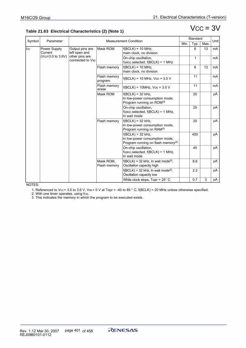
21. Electrical Characteristics (T-version)puorG92/C61M
page 401 854fo7002,03.raM21.1.veR2110-1010B90JER
VCC = 3VlobmyS retemaraP noitidnoCtnemerusaeM
dradnatStinU
.niM .pyT .xaMI CC ylppuSrewoP
tnerruCV( CC )V6.3ot0.3=
erasniptuptuOdnanepotfelerasniprehtoVotdetcennoc SS
MORksaM (f KLCB ,zHM01=)noisividon,kcolcniam
8 31 Am
,noitallicsopihc-nOf )COR(2 zHM1=)KLCB(f,detceles
1 Am
yromemhsalF (f KLCB ,zHM01=)noisividon,kcolcniam
8 31 Am
yromemhsalFmargorp V0.3=ccV,zHM01=)KLCB(f 11 Am
yromemhsalFesare V0.3=ccV,zHM01=)KLCB(f 11 Am
MORksaM zHk23=)KLCB(f ,edomnoitpmusnocrewop-wolnI ,
MORnogninnurmargorP )3(
02 µA
,noitallicsopihc-nOf )COR(2 ,zHM1=)KLCB(f,detceles
edomtiawnI
52 µA
yromemhsalF zHk23=)KLCB(f ,edomnoitpmusnocrewop-wolnI ,
MARnogninnurmargorP )3(
02 µA
,zHk23=)KLCB(f,edomnoitpmusnocrewop-wolnIyromemhsalfnogninnurmargorP )3(
054 µA
,noitallicsopihc-nOf )COR(2 ,zHM1=)KLCB(f,detceles
edomtiawnI
54 µA
,MORksaMyromemhsalF
edomtiawnI,zHk23=)KLCB(f )2( ,hgihyticapacnoitallicsO
6.6 µA
,zHk23=)KLCB(f edomtiawnI )2( ,wolyticapacnoitallicsO
2.2 µA
,spotskcolcelihW 52=rpoT C° 7.0 3 µA:SETON
otdecnerefeR.1 V CC V,V6.3ot0.3= SS .deificepsesiwrehtosselnuzHM02=)KLCB(f,C°58ot04-=rpoTtaV0=fgnisu,setareporemitenohtiW.2 23C .
.stsixedetucexeebotmargorpehthcihwniyromemehtsetacidnisihT.3
Table 21.63 Electrical Characteristics (2) (Note 1)
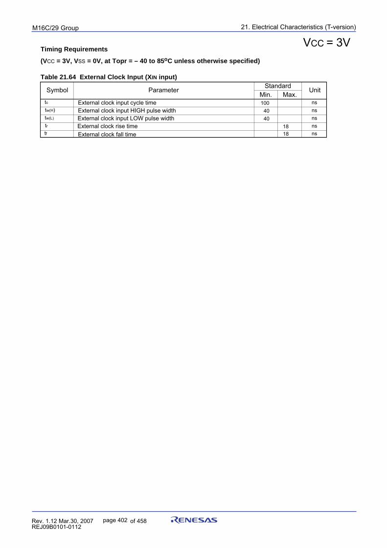
21. Electrical Characteristics (T-version)puorG92/C61M
page 402 854fo7002,03.raM21.1.veR2110-1010B90JER
Timing Requirements
(VCC = 3V, VSS = 0V, at Topr = – 40 to 85oC unless otherwise specified)
Table 21.64 External Clock Input (XIN input)
Max.
External clock rise time nstr
Min.External clock input cycle timeExternal clock input HIGH pulse widthExternal clock input LOW pulse width
External clock fall time
nsnsns
ns
tctw(H)tw(L)
tf
ParameterSymbol UnitStandard
1004040
1818
VCC = 3V
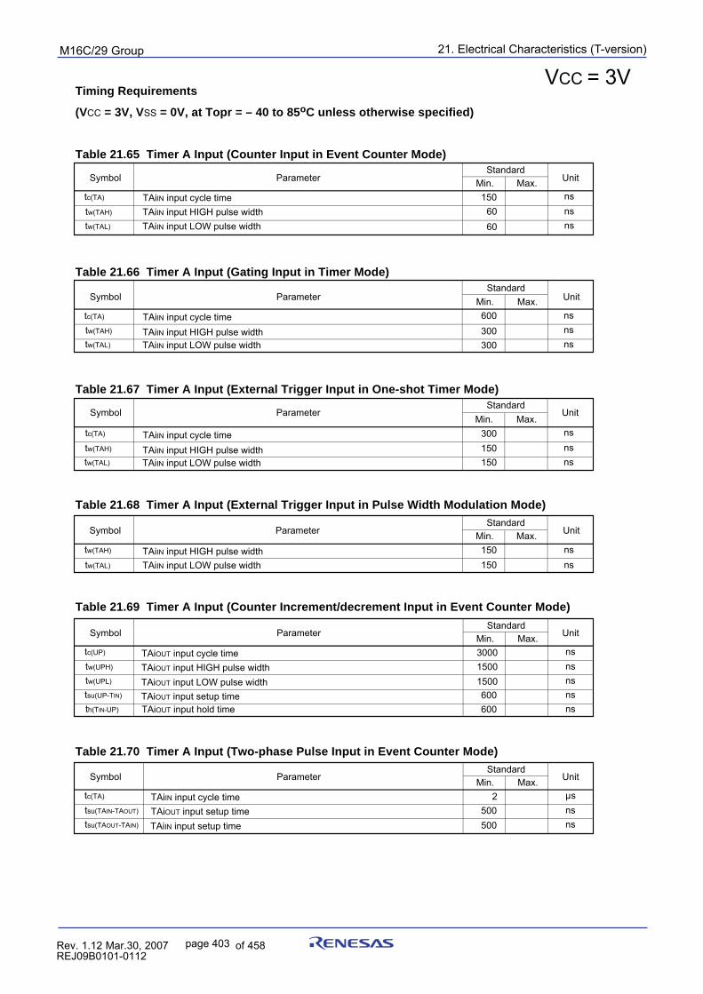
21. Electrical Characteristics (T-version)puorG92/C61M
page 403 854fo7002,03.raM21.1.veR2110-1010B90JER
VCC = 3VTiming Requirements
(VCC = 3V, VSS = 0V, at Topr = – 40 to 85oC unless otherwise specified)
Table 21.65 Timer A Input (Counter Input in Event Counter Mode)
Table 21.66 Timer A Input (Gating Input in Timer Mode)
Table 21.67 Timer A Input (External Trigger Input in One-shot Timer Mode)
Table 21.68 Timer A Input (External Trigger Input in Pulse Width Modulation Mode)
Table 21.69 Timer A Input (Counter Increment/decrement Input in Event Counter Mode)
Table 21.70 Timer A Input (Two-phase Pulse Input in Event Counter Mode)
StandardMax.
nsTAiIN input LOW pulse widthtw(TAL)
Min.nsns
Unit
TAiIN input HIGH pulse widthtw(TAH)
ParameterSymbol
tc(TA) TAiIN input cycle time
60
15060
StandardMax.Min.
nsnsns
Unit
TAiIN input cycle timeTAiIN input HIGH pulse widthTAiIN input LOW pulse width
tc(TA)
tw(TAH)
tw(TAL)
Symbol Parameter
600300300
StandardMax.Min.
nsnsns
Unit
TAiIN input cycle timeTAiIN input HIGH pulse widthTAiIN input LOW pulse width
tc(TA)
tw(TAH)
tw(TAL)
Symbol Parameter
300150150
StandardMax.Min.
nsns
Unit
tw(TAH)
tw(TAL)
Symbol Parameter
TAiIN input HIGH pulse widthTAiIN input LOW pulse width
150150
StandardMax.Min.
nsnsns
Unit
nsns
Symbol Parameter
TAiOUT input cycle timeTAiOUT input HIGH pulse widthTAiOUT input LOW pulse widthTAiOUT input setup timeTAiOUT input hold time
tc(UP)
tw(UPH)
tw(UPL)
tsu(UP-TIN)
th(TIN-UP)
300015001500600600
StandardMax.Min.
µsnsns
UnitSymbol Parameter
TAiIN input cycle timeTAiOUT input setup timeTAiIN input setup time
tc(TA)
tsu(TAIN-TAOUT)
tsu(TAOUT-TAIN)
2500500
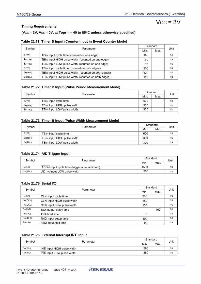
21. Electrical Characteristics (T-version)puorG92/C61M
page 404 854fo7002,03.raM21.1.veR2110-1010B90JER
VCC = 3V
Table 21.71 Timer B Input (Counter Input in Event Counter Mode)
Table 21.72 Timer B Input (Pulse Period Measurement Mode)
Table 21.73 Timer B Input (Pulse Width Measurement Mode)
Table 21.74 A/D Trigger Input
Table 21.75 Serial I/O
_______
Table 21.76 External Interrupt INTi Input
Timing Requirements
(VCC = 3V, VSS = 0V, at Topr = – 40 to 85oC unless otherwise specified)
nsnsnsnsnsnsns
StandardMax.Min.
TBiIN input cycle time (counted on one edge)TBiIN input HIGH pulse width (counted on one edge)TBiIN input LOW pulse width (counted on one edge)
nsnsns
tc(TB)
tw(TBH)
tw(TBL)
ParameterSymbol Unit
tc(TB)
tw(TBL)
tw(TBH)
nsnsns
TBiIN input HIGH pulse width (counted on both edges)TBiIN input LOW pulse width (counted on both edges)
TBiIN input cycle time (counted on both edges)
StandardMax.Min.
nsns
tc(TB)
tw(TBH)
Symbol Parameter Unit
tw(TBL) nsTBiIN input HIGH pulse widthTBiIN input cycle time
TBiIN input LOW pulse width
StandardMax.Min.
nsns
tc(TB)
Symbol Parameter Unit
tw(TBL) nstw(TBH)
TBiIN input cycle timeTBiIN input HIGH pulse widthTBiIN input LOW pulse width
StandardMax.Min.
nsns
tc(AD)
tw(ADL)
Symbol Parameter Unit
ADTRG input cycle time (trigger able minimum)ADTRG input LOW pulse width
StandardMax.Min.
nsns
tw(INH)
tw(INL)
Symbol Parameter Unit
INTi input LOW pulse widthINTi input HIGH pulse width
StandardMax.Min.
CLKi input cycle timeCLKi input HIGH pulse widthCLKi input LOW pulse width
tc(CK)
tw(CKH)
tw(CKL)
ParameterSymbol Unit
td(C-Q)
tsu(D-C)
th(C-Q) TxDi hold timeRxDi input setup time
TxDi output delay time
th(C-D) RxDi input hold time
150
6060
120120
300
600300300
600300300
1500200
380380
300150150
0
90
160
100

21. Electrical Characteristics (T-version)puorG92/C61M
page 405 854fo7002,03.raM21.1.veR2110-1010B90JER
VCC = 3VTiming Requirements
(VCC = 3V, VSS = 0V, at Topr = – 40 to 85oC unless otherwise specified)
Table 21.77 Multi-master I2C bus Line
High-speed clock modeMax.Min.
Bus free timeThe hold time in start conditionThe hold time in SCL clock 0 status
µsµsµs
tBUFtHD;STAtLOW
ParameterSymbol Unit
tR
tHIGHtHD;DAT
nsµsµs
Data hold timeThe hold time in SCL clock 1 status
SCL, SDA signals' rising time
1.3
0.61.3
00.6
20+0.1Cb
tF SCL, SDA signals' falling timetSU;DAT Data setup timetSU;STA The setup time in restart conditiontSU;STO Stop condition setup time
Standard clock modeMax.Min.
4.7
4.04.7
04.0
2504.74.0
1000
3001000.6
20+0.1Cb
0.6
300
300
0.9
nsnsµsµs
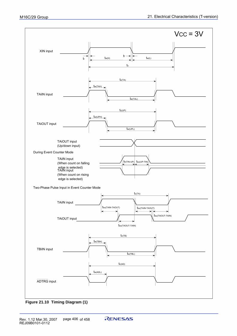
21. Electrical Characteristics (T-version)puorG92/C61M
page 406 854fo7002,03.raM21.1.veR2110-1010B90JER
VCC = 3V
Figure 21.10 Timing Diagram (1)
TAiIN input
TAiOUT input
During Event Counter Mode
TBiIN input
ADTRG input
tc(TA)
tw(TAH)
tw(TAL)
tc(UP)
tw(UPH)
tw(UPL)
tc(TB)
tw(TBH)
tw(TBL)
tc(AD)
tw(ADL)
th(TIN-UP) tsu(UP-TIN)TAiIN input(When count on falling edge is selected)TAiIN input (When count on rising edge is selected)
TAiOUT input(Up/down input)
TAiIN input
Two-Phase Pulse Input in Event Counter Mode
tc(TA)
tsu(TAIN-TAOUT)
tsu(TAOUT-TAIN)
tsu(TAIN-TAOUT)
tsu(TAOUT-TAIN)TAiOUT input
XIN input
tw(H) tw(L)trtf
tc
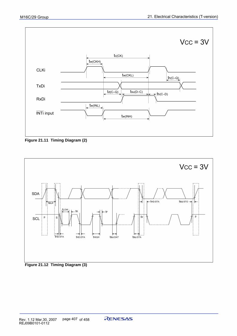
21. Electrical Characteristics (T-version)puorG92/C61M
page 407 854fo7002,03.raM21.1.veR2110-1010B90JER
VCC = 3V
Figure 21.11 Timing Diagram (2)
tsu(D–C)
CLKi
TxDi
RxDi
tc(CK)
tw(CKH)
tw(CKL)
tw(INL)
tw(INH)
td(C–Q) th(C–D)
th(C–Q)
INTi input
tBUF
tHD:STA tHD:DTA
tLOW tR tF
tHIGH tsu:DAT tsu:STA
tHD:STA tsu:STO
SCL p S Sr p
SDA
Figure 21.12 Timing Diagram (3)
VCC = 3V
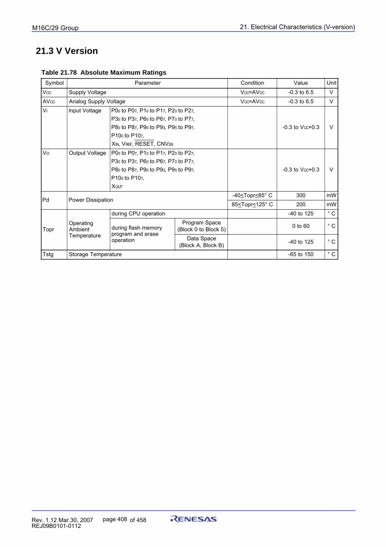
21. Electrical Characteristics (V-version)puorG92/C61M
page 408 854fo7002,03.raM21.1.veR2110-1010B90JER
21.3 V Version
Table 21.78 Absolute Maximum Ratings
lobmyS retemaraP noitidnoC eulaV tinU
V CC egatloVylppuS V CC VA= CC 5.6ot3.0- V
VA CC egatloVylppuSgolanA V CC VA= CC 5.6ot3.0- VVI egatloVtupnI 0P 0 0Pot 7 1P, 0 1Pot 7 2P, 0 2Pot 7,
3P 0 3Pot 7 6P, 0 6Pot 7 7P, 0 7Pot 7,8P 0 8Pot 7 9P, 0 9Pot 3 9P, 5 9Pot 7,
01P 0 01Pot 7,X NI V, FER VNC,TESER, SS
Vot3.0- CC 3.0+ V
VO egatloVtuptuO 0P 0 0Pot 7 1P, 0 1Pot 7 2P, 0 2Pot 7,3P 0 3Pot 7 6P, 0 6Pot 7 7P, 0 7Pot 7,8P 0 8Pot 7 9P, 0 9Pot 3 9P, 5 9Pot 7,
01P 0 01Pot 7,X TUO
Vot3.0- CC 3.0+ V
dP noitapissiDrewoP04- < rpoT < C°58 003 Wm
58 < rpoT < C°521 002 Wm
rpoTgnitarepO
tneibmAerutarepmeT
noitarepoUPCgnirud 521ot04- C°
yromemhsalfgnirudesarednamargorp
noitarepo
ecapSmargorP)5kcolBot0kcolB( 06ot0 C°
ecapSataD)BkcolB,AkcolB( 521ot04- C°
gtsT erutarepmeTegarotS 051ot56- C°
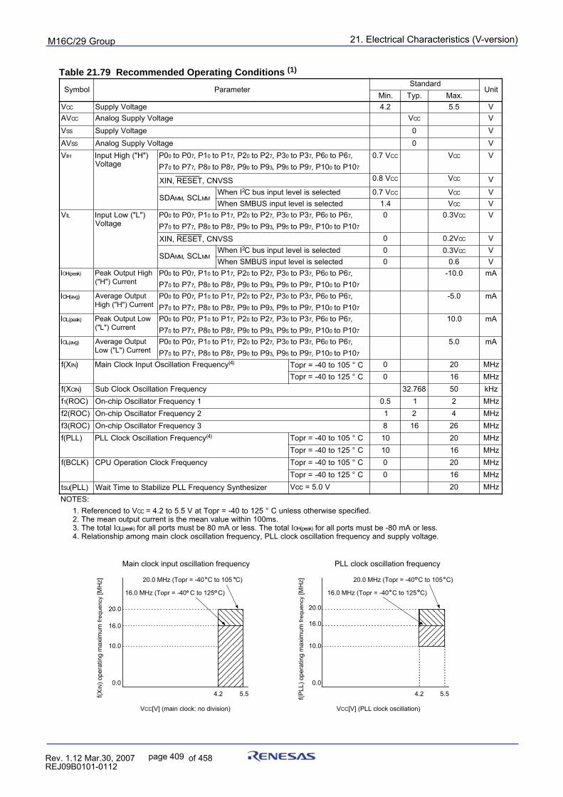
21. Electrical Characteristics (V-version)puorG92/C61M
page 409 854fo7002,03.raM21.1.veR2110-1010B90JER
Table 21.79 Recommended Operating Conditions (1)
lobmyS retemaraPdradnatS
tinU.niM .pyT .xaM
V CC egatloVylppuS 2.4 5.5 VVA CC egatloVylppuSgolanA V CC V
V SS egatloVylppuS 0 VVA SS egatloVylppuSgolanA 0 V
V HI )"H"(hgiHtupnIegatloV
0P 0 0Pot 7 1P, 0 1Pot 7 2P, 0 2Pot 7 3P, 0 3Pot 7 6P, 0 6Pot 7,7P 0 7Pot 7 8P, 0 8Pot 7 9P, 0 9Pot 3 9P, 5 9Pot 7 01P, 0 01Pot 7
V7.0 CC V CC V
SSVNC,TESER,NIX V8.0 CC V CC V
ADS MM LCS, MMInehW 2 detcelessileveltupnisubC V7.0 CC V CC V
detcelessileveltupniSUBMSnehW 4.1 V CC VV LI )"L"(woLtupnI
egatloV0P 0 0Pot 7 1P, 0 1Pot 7 2P, 0 2Pot 7 3P, 0 3Pot 7 6P, 0 6Pot 7,7P 0 7Pot 7 8P, 0 8Pot 7 9P, 0 9Pot 3 9P, 5 9Pot 7 01P, 0 01Pot 7
0 V3.0 CC V
SSVNC,TESER,NIX 0 V2.0 CC V
ADS MM LCS, MMInehW 2 detcelessileveltupnisubC 0 3.0 V CC V
detcelessileveltupniSUBMSnehW 0 6.0 VI )kaep(HO hgiHtuptuOkaeP
tnerruC)"H"(0P 0 0Pot 7 1P, 0 1Pot 7 2P, 0 2Pot 7 3P, 0 3Pot 7 6P, 0 6Pot 7,7P 0 7Pot 7 8P, 0 8Pot 7 9P, 0 9Pot 3 9P, 5 9Pot 7 01P, 0 01Pot 7
0.01- Am
I )gva(HO tuptuOegarevAtnerruC)"H"(hgiH
0P 0 0Pot 7 1P, 0 1Pot 7 2P, 0 2Pot 7 3P, 0 3Pot 7 6P, 0 6Pot 7,7P 0 7Pot 7 8P, 0 8Pot 7 9P, 0 9Pot 3 9P, 5 9Pot 7 01P, 0 01Pot 7
0.5- Am
I )kaep(LO woLtuptuOkaePtnerruC)"L"(
0P 0 0Pot 7 1P, 0 1Pot 7 2P, 0 2Pot 7 3P, 0 3Pot 7 6P, 0 6Pot 7,7P 0 7Pot 7 8P, 0 8Pot 7 9P, 0 9Pot 3 9P, 5 9Pot 7 01P, 0 01Pot 7
0.01 Am
I )gva(LO tuptuOegarevAtnerruC)"L"(woL
0P 0 0Pot 7 1P, 0 1Pot 7 2P, 0 2Pot 7 3P, 0 3Pot 7 6P, 0 6Pot 7,7P 0 7Pot 7 8P, 0 8Pot 7 9P, 0 9Pot 3 9P, 5 9Pot 7 01P, 0 01Pot 7
0.5 Am
X(f NI ) ycneuqerFnoitallicsOtupnIkcolCniaM )4( C°501ot04-=rpoT 0 02 zHMC°521ot04-=rpoT 0 61 zHM
X(f NIC ) ycneuqerFnoitallicsOkcolCbuS 867.23 05 zHkf1 )COR( 1ycneuqerFrotallicsOpihc-nO 5.0 1 2 zHM
)COR(2f 2ycneuqerFrotallicsOpihc-nO 1 2 4 zHM)COR(3f 3ycneuqerFrotallicsOpihc-nO 8 61 62 zHM
)LLP(f ycneuqerFnoitallicsOkcolCLLP )4( C°501ot04-=rpoT 01 02 zHMC°521ot04-=rpoT 01 61 zHM
)KLCB(f ycneuqerFkcolCnoitarepOUPC C°501ot04-=rpoT 0 02 zHMC°521ot04-=rpoT 0 61 zHM
t US )LLP( rezisehtnySycneuqerFLLPezilibatSotemiTtiaW V0.5=ccV 02 zHM:SETON
VotdecnerefeR.1 CC .deificepsesiwrehtosselnuC°521ot04-=rpoTtaV5.5ot2.4=.sm001nihtiweulavnaemehtsitnerructuptuonaemehT.2
IlatotehT.3 )kaep(LO IlatotehT.sselroAm08ebtsumstropllarof )kaep(HO .sselroAm08-ebtsumstropllarof.egatlovylppusdnaycneuqerfnoitallicsokcolcLLP,ycneuqerfnoitallicsokcolcniamgnomapihsnoitaleR.4
Main clock input oscillation frequency
f(XIN
) ope
ratin
g m
axim
um fr
eque
ncy
[MH
Z]
VCC[V] (main clock: no division)
PLL clock oscillation frequency
f(PLL
) ope
ratin
g m
axim
um fr
eque
ncy
[MH
Z]
VCC[V] (PLL clock oscillation)
20.0
0.0
5.5
10.0
20.0
0.0
5.5
10.0
16.0
4.2AAAAAAAAAAAAAAA
AAAAAAAAAAAA
20.0 MHz (Topr = -40 C to 105 C)
16.0 MHz (Topr = -40 C to 125 C)
20.0 MHz (Topr = -40 C to 105 C)
16.0 MHz (Topr = -40 C to 125 C)
AAAAAA
4.2
16.0
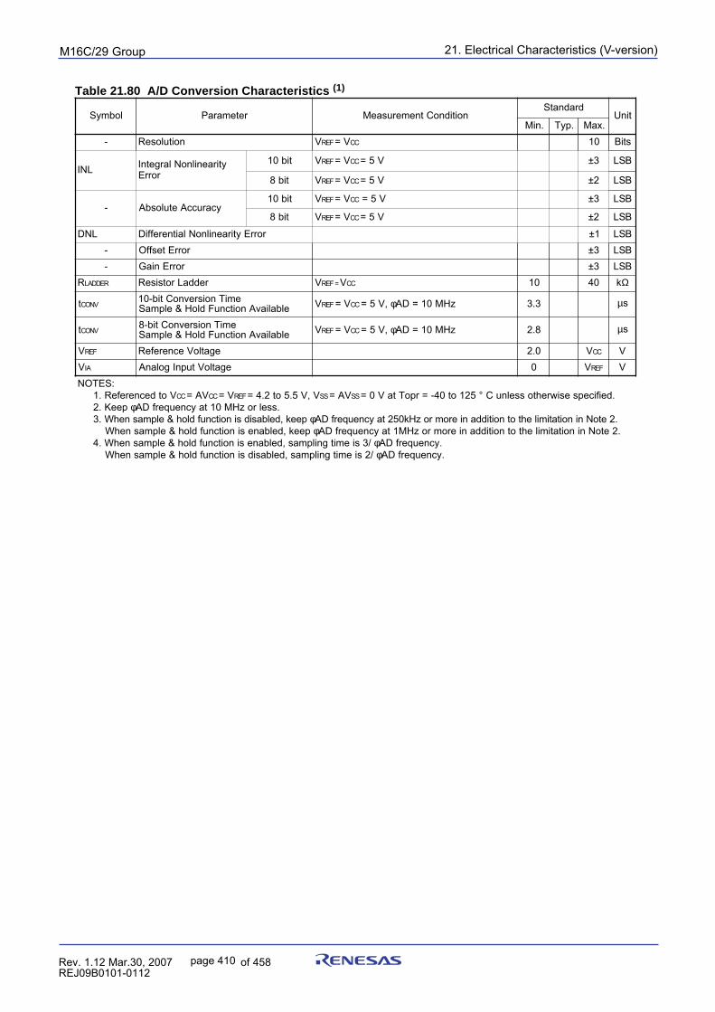
21. Electrical Characteristics (V-version)puorG92/C61M
page 410 854fo7002,03.raM21.1.veR2110-1010B90JER
Table 21.80 A/D Conversion Characteristics (1)
lobmyS retemaraP noitidnoCtnemerusaeMdradnatS
tinU.niM .pyT .xaM
- noituloseR V FER V= CC 01 stiB
LNI ytiraenilnoNlargetnIrorrE
tib01 V FER V= CC V5= 3± BSL
tib8 V FER V= CC V5= 2± BSL
- ycaruccAetulosbAtib01 V FER V= CC V5= 3± BSL
tib8 V FER V= CC V5= 2± BSL
LND rorrEytiraenilnoNlaitnereffiD 1± BSL- rorrEtesffO 3± BSL- rorrEniaG 3± BSL
R REDDAL reddaLrotsiseR V =FER V CC 01 04 kΩ
t VNOCemiTnoisrevnoCtib-01
elbaliavAnoitcnuFdloH&elpmaS V FER V= CC ,V5= φ zHM01=DA 3.3 µs
t VNOCemiTnoisrevnoCtib-8
elbaliavAnoitcnuFdloH&elpmaS V FER V= CC ,V5= φ zHM01=DA 8.2 µs
V FER egatloVecnerefeR 0.2 V CC VV AI egatloVtupnIgolanA 0 V FER V
:SETONVotdecnerefeR.1 CC VA= CC V= FER V,V5.5ot2.4= SS VA= SS .deificepsesiwrehtosselnuC°521ot04-=rpoTtaV0=
peeK.2 φ .sselrozHM01taycneuqerfDA.3 peek,delbasidsinoitcnufdloh&elpmasnehW φ .2etoNninoitatimilehtotnoitiddanieromrozHk052taycneuqerfDA
peek,delbanesinoitcnufdloh&elpmasnehW φ .2etoNninoitatimilehtotnoitiddanieromrozHM1taycneuqerfDA/3siemitgnilpmas,delbanesinoitcnufdloh&elpmasnehW.4 φ .ycneuqerfDA/2siemitgnilpmas,delbasidsinoitcnufdloh&elpmasnehW φ .ycneuqerfDA
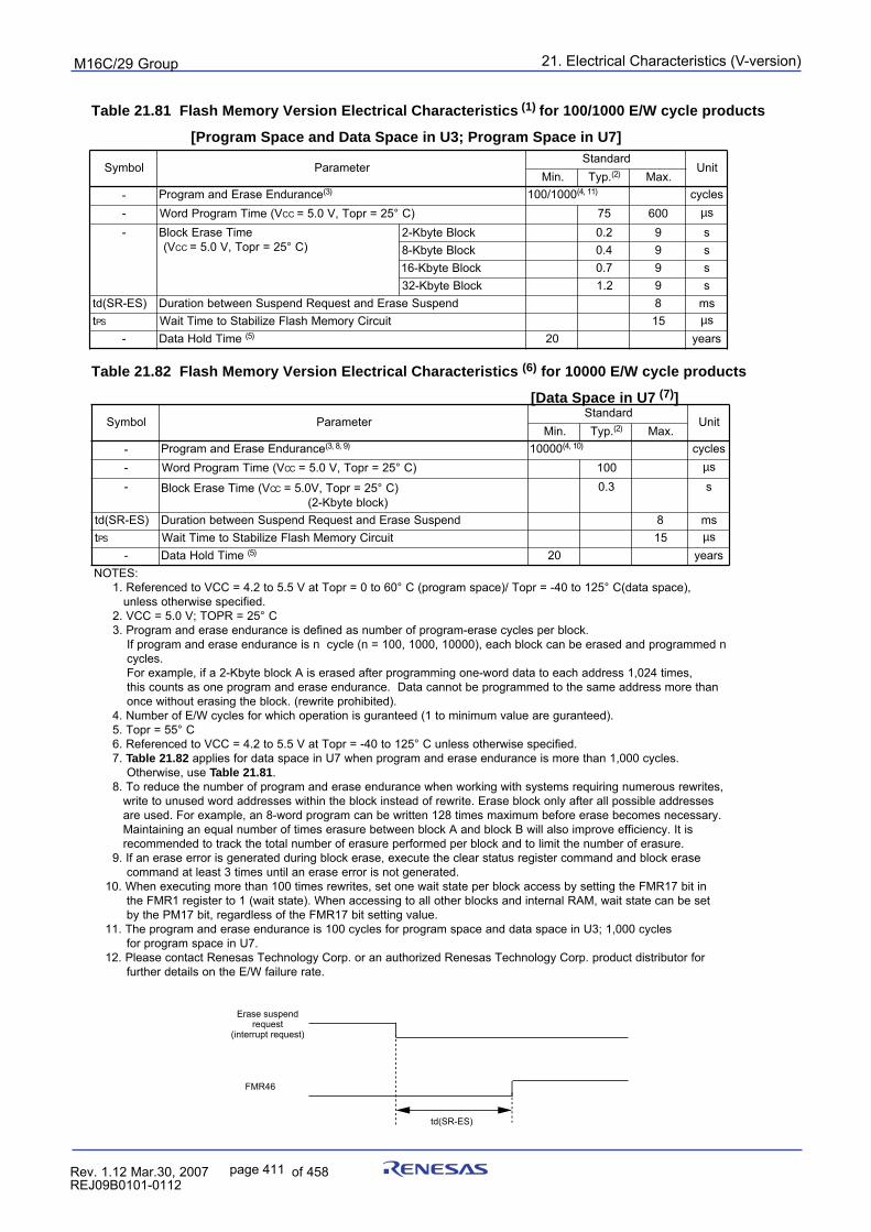
21. Electrical Characteristics (V-version)puorG92/C61M
page 411 854fo7002,03.raM21.1.veR2110-1010B90JER
Table 21.81 Flash Memory Version Electrical Characteristics (1) for 100/1000 E/W cycle products
[Program Space and Data Space in U3; Program Space in U7]
Table 21.82 Flash Memory Version Electrical Characteristics (6) for 10000 E/W cycle products
[Data Space in U7 (7)]
lobmyS retemaraPdradnatS
tinU.niM .pyT )2( .xaM
- ecnarudnEesarEdnamargorP )3( 0001/001 )11,4( selcyc- V(emiTmargorPdroW CC 52=rpoT,V0.5= C° ) 57 006 µs
- emiTesarEkcolBV( CC 52=rpoT,V0.5= C° )
kcolBetybK-2 2.0 9 skcolBetybK-8 4.0 9 skcolBetybK-61 7.0 9 skcolBetybK-23 2.1 9 s
)SE-RS(dt dnepsuSesarEdnatseuqeRdnepsuSneewtebnoitaruD 8 smt SP tiucriCyromeMhsalFezilibatSotemiTtiaW 51 µs
- emiTdloHataD )5( 02 sraey
lobmyS retemaraPdradnatS
tinU.niM .pyT )2( .xaM
- ecnarudnEesarEdnamargorP )9,8,3( 00001 )01,4( selcyc- V(emiTmargorPdroW CC 52=rpoT,V0.5= C° ) 001 µs
- emiTesarEkcolB V( CC 52=rpoT,V0.5= C° ))kcolbetybK-2(
3.0 s
)SE-RS(dt dnepsuSesarEdnatseuqeRdnepsuSneewtebnoitaruD 8 smt SP tiucriCyromeMhsalFezilibatSotemiTtiaW 51 µs
- emiTdloHataD )5( 02 sraey:SETON
°06ot0=rpoTtaV5.5ot2.4=CCVotdecnerefeR.1 ,)ecapsatad(C°521ot04-=rpoT/)ecapsmargorp(C.deificepsesiwrehtosselnuC°52=RPOT;V0.5=CCV.2
.kcolbrepselcycesare-margorpforebmunsadenifedsiecnarudneesarednamargorP.3siecnarudneesarednamargorpfI n (elcyc n demmargorpdnadesareebnackcolbhcae,)00001,0001,001= n
.selcyc,semit420,1sserddahcaeotataddrow-enognimmargorpretfadesaresiAkcolbetybK-2afi,elpmaxeroF
nahteromsserddaemasehtotdemmargorpebtonnacataD.ecnarudneesarednamargorpenosastnuocsiht.)detibihorpetirwer(.kcolbehtgnisaretuohtiwecno
.)deetnarugeraeulavmuminimot1(deetnarugsinoitarepohcihwrofselcycW/EforebmuN.4C°55=rpoT.5
.deificepsesiwrehtosselnuC°521ot04-=rpoTtaV5.5ot2.4=CCVotdecnerefeR.6.7 28.12elbaT .selcyc000,1nahteromsiecnarudneesarednamargorpnehw7Uniecapsatadrofseilppa
esu,esiwrehtO 18.12elbaT .,setirwersuoremungniriuqersmetsyshtiwgnikrownehwecnarudneesarednamargorpforebmunehtecuderoT.8
sesserddaelbissopllaretfaylnokcolbesarE.etirwerfodaetsnikcolbehtnihtiwsesserddadrowdesunuotetirw.yrassecensemocebesareerofebmumixamsemit821nettirwebnacmargorpdrow-8na,elpmaxeroF.desuera
sitI.ycneiciffeevorpmioslalliwBkcolbdnaAkcolbneewteberusaresemitforebmunlauqenagniniatniaM.erusareforebmunehttimilotdnakcolbrepdemrofreperusareforebmunlatotehtkcartotdednemmocer
esarekcolbdnadnammocretsigersutatsraelcehtetucexe,esarekcolbgniruddetarenegsirorreesarenafI.9.detarenegtonsirorreesarenalitnusemit3tsaeltadnammoc
nitib71RMFehtgnittesybsseccakcolbrepetatstiawenotes,setirwersemit001nahteromgnitucexenehW.01tesebnacetatstiaw,MARlanretnidnaskcolbrehtollaotgnisseccanehW.)etatstiaw(1otretsiger1RMFeht
.eulavgnittestib71RMFehtfosseldrager,tib71MPehtybselcyc000,1;3Uniecapsataddnaecapsmargorprofselcyc001siecnarudneesarednamargorpehT.11
.7Uniecapsmargorprofrofrotubirtsidtcudorp.proCygolonhceTsaseneRdezirohtuanaro.proCygolonhceTsaseneRtcatnocesaelP.21
.etareruliafW/Eehtnosliatedrehtruf
Erase suspend request
(interrupt request)
FMR46
td(SR-ES)
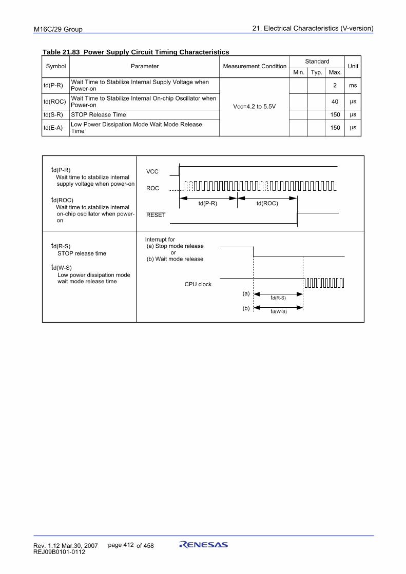
21. Electrical Characteristics (V-version)puorG92/C61M
page 412 854fo7002,03.raM21.1.veR2110-1010B90JER
Table 21.83 Power Supply Circuit Timing Characteristics
lobmyS retemaraP noitidnoCtnemerusaeMdradnatS
tinU.niM .pyT .xaM
)R-P(dt nehwegatloVylppuSlanretnIezilibatSotemiTtiaWno-rewoP
V CC V5.5ot2.4=
2 sm
)COR(dt nehwrotallicsOpihc-nOlanretnIezilibatSotemiTtiaWno-rewoP 04 µs
)R-S(dt emiTesaeleRPOTS 051 µs
)A-E(dt esaeleRedoMtiaWedoMnoitapissiDrewoPwoLemiT 051 µs
td(P-R) Wait time to stabilize internal
supply voltage when power-on
CPU clock
td(R-S)(a)
(b) td(W-S)
td(R-S) STOP release time
td(W-S) Low power dissipation mode wait mode release time
Interrupt for (a) Stop mode release or (b) Wait mode release
td(ROC) Wait time to stabilize internal
on-chip oscillator when power-on
ROC
RESET
VCC
td(P-R) td(ROC)
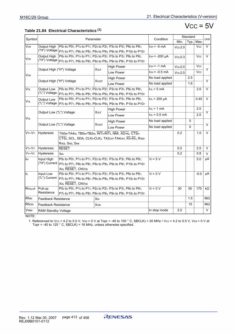
21. Electrical Characteristics (V-version)puorG92/C61M
page 413 854fo7002,03.raM21.1.veR2110-1010B90JER
Table 21.84 Electrical Characteristics (1)VCC = 5V
lobmyS retemaraP noitidnoCdradnatS
tinU.niM .pyT .xaM
V HO hgiHtuptuOegatloV)"H"(
0P 0 0Pot 7 1P, 0 1Pot 7 2P, 0 2Pot 7 3P, 0 3Pot 7 6P, 0 6Pot 7,7P 0 7Pot 7 8P, 0 8Pot 7 9P, 0 9Pot 3 9P, 5 9Pot 7 01P, 0 01Pot 7
I HO Am5-= V CC - 0.2 V CC V
V HOhgiHtuptuOegatloV)"H"(
0P 0 0Pot 7 1P, 0 1Pot 7 2P, 0 2Pot 7 3P, 0 3Pot 7 6P, 0 6Pot 7,7P 0 7Pot 7 8P, 0 8Pot 7 9P, 0 9Pot 3 9P, 5 9Pot 7 01P, 0 01Pot 7
I HO 002-= µA V CC - 3.0 V CC V
V HO
egatloV)"H"(hgiHtuptuO X TUOrewoPhgiH I HO Am1-= V CC - 0.2 V CC
VrewoPwoL I HO Am5.0-= V CC - 0.2 V CC
egatloV)"H"(hgiHtuptuO X TUOCrewoPhgiH deilppadaoloN 5.2
VrewoPwoL deilppadaoloN 6.1
V LO woLtuptuOegatloV)"L"(
0P 0 0Pot 7 1P, 0 1Pot 7 2P, 0 2Pot 7 3P, 0 3Pot 7 6P, 0 6Pot 7,7P 0 7Pot 7 8P, 0 8Pot 7 9P, 0 9Pot 3 9P, 5 9Pot 7 01P, 0 01Pot 7
I LO Am5= 0.2 V
V LOwoLtuptuO
egatloV)"L"(0P 0 0Pot 7 1P, 0 1Pot 7 2P, 0 2Pot 7 3P, 0 3Pot 7 6P, 0 6Pot 7,7P 0 7Pot 7 8P, 0 8Pot 7 9P, 0 9Pot 3 9P, 5 9Pot 7 01P, 0 01Pot 7
I LO 002= µA 54.0 V
V LO
egatloV)"L"(woLtuptuO X TUOrewoPhgiH I LO Am1= 0.2
VrewoPwoL I LO Am5.0= 0.2
egatloV)"L"(woLtuptuO X TUOCrewoPhgiH deilppadaoloN 0
VrewoPwoL deilppadaoloN 0
V +T V- -T siseretsyH 0AT NI 4AT- NI 0BT, NI 2BT- NI TNI, 0 TNI- 5 DA,IMN, GRT STC, 0-STC 2 KLC,ADS,LCS, 0 KLC- 2 2AT, TUO 4AT- TUO IK, 0 IK- 3 R, 0DX -
R 2DX S, 3NI S, 4NI
2.0 0.1 V
V +T V- -T siseretsyH TESER 2.0 5.2 VV +T V- -T siseretsyH X NI 2.0 8.0 VI HI hgiHtupnI
tnerruC)"H"(0P 0 0Pot 7 1P, 0 1Pot 7 2P, 0 2Pot 7 3P, 0 3Pot 7 6P, 0 6Pot 7,7P 0 7Pot 7 8P, 0 8Pot 7 9P, 0 9Pot 3 9P, 5 9Pot 7 01P, 0 01Pot 7
X NI VNC,TESER, SS
VI V5= 0.5 µA
I LI woLtupnItnerruC)"L"(
0P 0 0Pot 7 1P, 0 1Pot 7 2P, 0 2Pot 7 3P, 0 3Pot 7 6P, 0 6Pot 7,7P 0 7Pot 7 8P, 0 8Pot 7 9P, 0 9Pot 3 9P, 5 9Pot 7 01P, 0 01Pot 7
X NI VNC,TESER, SS
VI V0= 0.5- µA
R PULLUP pu-lluPecnatsiseR
0P 0 0Pot 7 1P, 0 1Pot 7 2P, 0 2Pot 7 3P, 0 3Pot 7 6P, 0 6Pot 7,7P 0 7Pot 7 8P, 0 8Pot 7 9P, 0 9Pot 3 9P, 5 9Pot 7 01P, 0 01Pot 7
VI V0= 03 05 071 kΩ
fR NIX ecnatsiseRkcabdeeF X NI 5.1 MΩ
fR NICX ecnatsiseRkcabdeeF X NIC 51 MΩ
V MAR egatloVybdnatSMAR edompotsnI 0.2 V
:ETONotdecnerefeR.1 V CC V,V5.5ot2.4= SS V/zHM02=)KLCB(f,C°501ot04-=rpoTtaV0= CC V,V5.5ot2.4= SS taV0=
.deificepsesiwrehtosselnu,zHM61=)KLCB(f,C°521ot04-=rpoT
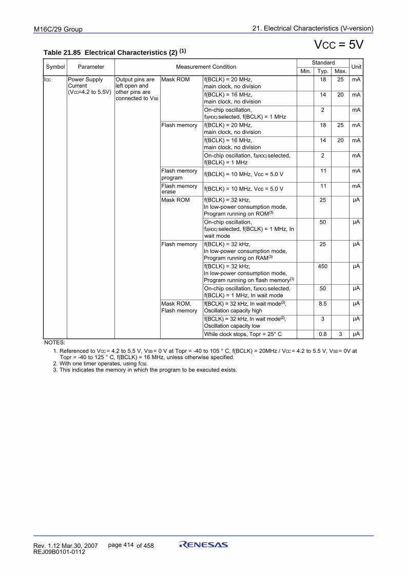
21. Electrical Characteristics (V-version)puorG92/C61M
page 414 854fo7002,03.raM21.1.veR2110-1010B90JER
Table 21.85 Electrical Characteristics (2) (1)VCC = 5V
lobmyS retemaraP noitidnoCtnemerusaeMdradnatS
tinU.niM .pyT .xaM
I CC ylppuSrewoPtnerruC
V( CC )V5.5ot2.4=
erasniptuptuOdnanepotfelerasniprehtoVotdetcennoc SS
MORksaM ,zHM02=)KLCB(fnoisividon,kcolcniam
81 52 Am
,zHM61=)KLCB(fnoisividon,kcolcniam
41 02 Am
,noitallicsopihc-nOf )COR(2 zHM1=)KLCB(f,detceles
2 Am
yromemhsalF ,zHM02=)KLCB(fnoisividon,kcolcniam
81 52 Am
,zHM61=)KLCB(fnoisividon,kcolcniam
41 02 Am
f,noitallicsopihc-nO )COR(2 ,detceleszHM1=)KLCB(f
2 Am
yromemhsalFmargorp V0.5=ccV,zHM01=)KLCB(f 11 Am
yromemhsalFesare V0.5=ccV,zHM01=)KLCB(f 11 Am
MORksaM zHk23=)KLCB(f ,edomnoitpmusnocrewop-wolnI ,
MORnogninnurmargorP )3(
52 µA
,noitallicsopihc-nOf )COR(2 nI,zHM1=)KLCB(f,detceles
edomtiaw
05 µA
yromemhsalF zHk23=)KLCB(f ,edomnoitpmusnocrewop-wolnI ,
MARnogninnurmargorP )3(
52 µA
,zHk23=)KLCB(f,edomnoitpmusnocrewop-wolnIyromemhsalfnogninnurmargorP )3(
054 µA
f,noitallicsopihc-nO )COR(2 ,detcelesedomtiawnI,zHM1=)KLCB(f
05 µA
,MORksaMyromemhsalF
edomtiawnI,zHk23=)KLCB(f )2( ,hgihyticapacnoitallicsO
5.8 µA
,zHk23=)KLCB(f edomtiawnI )2( ,wolyticapacnoitallicsO
3 µA
,spotskcolcelihW 52=rpoT C° 8.0 3 µA:SETON
otdecnerefeR.1 V CC V,V5.5ot2.4= SS V/zHM02=)KLCB(f,C°501ot04-=rpoTtaV0= CC V,V5.5ot2.4= SS taV0=.deificepsesiwrehtosselnu,zHM61=)KLCB(f,C°521ot04-=rpoT
fgnisu,setareporemitenohtiW.2 23C ..stsixedetucexeebotmargorpehthcihwniyromemehtsetacidnisihT.3
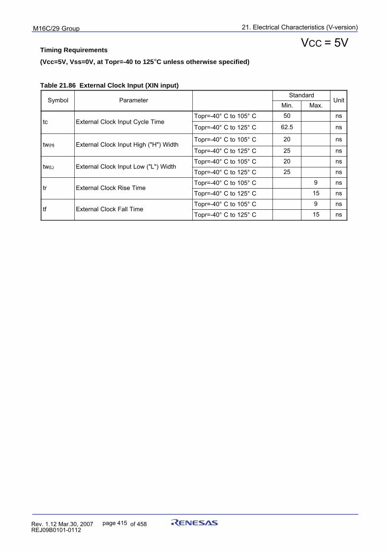
21. Electrical Characteristics (V-version)puorG92/C61M
page 415 854fo7002,03.raM21.1.veR2110-1010B90JER
Timing Requirements
(Vcc=5V, Vss=0V, at Topr=-40 to 125°C unless otherwise specified)
Table 21.86 External Clock Input (XIN input)
VCC = 5V
lobmyS retemaraPdradnatS
tinU.niM .xaM
ct emiTelcyCtupnIkcolClanretxE04-=rpoT C° 501ot C° 05 sn
04-=rpoT C° 521ot C° 5.26 sn
wt )H( htdiW)"H"(hgiHtupnIkcolClanretxE04-=rpoT C° 501ot C° 02 sn
04-=rpoT C° 521ot C° 52 sn
wt )L( htdiW)"L"(woLtupnIkcolClanretxE04-=rpoT C° 501ot C° 02 sn
04-=rpoT C° 521ot C° 52 sn
rt emiTesiRkcolClanretxE04-=rpoT C° 501ot C° 9 sn
04-=rpoT C° 521ot C° 51 sn
ft emiTllaFkcolClanretxE04-=rpoT C° 501ot C° 9 sn
04-=rpoT C° 521ot C° 51 sn
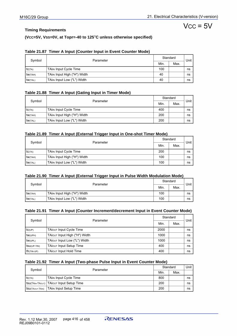
21. Electrical Characteristics (V-version)puorG92/C61M
page 416 854fo7002,03.raM21.1.veR2110-1010B90JER
lobmyS retemaraPdradnatS
tinU.niM .xaM
ct )AT( iAT NI emiTelcyCtupnI 001 snwt )HAT( iAT NI htdiW)"H"(hgiHtupnI 04 snwt )LAT( iAT NI htdiW)"L"(woLtupnI 04 sn
lobmyS retemaraPdradnatS
tinU.niM .xaM
ct )AT( iAT NI emiTelcyCtupnI 004 snwt )HAT( iAT NI htdiW)"H"(hgiHtupnI 002 snwt )LAT( iAT NI htdiW)"L"(woLtupnI 002 sn
lobmyS retemaraPdradnatS
tinU.niM .xaM
ct )AT( iAT NI emiTelcyCtupnI 002 sn
wt )HAT( iAT NI htdiW)"H"(hgiHtupnI 001 sn
wt )LAT( iAT NI htdiW)"L"(woLtupnI 001 sn
lobmyS retemaraPdradnatS
tinU.niM .xaM
wt )HAT( iAT NI htdiW)"H"(hgiHtupnI 001 snwt )LAT( iAT NI htdiW)"L"(woLtupnI 001 sn
lobmyS retemaraPdradnatS
tinU.niM .xaM
ct )PU( iAT TUO emiTelcyCtupnI 0002 sn
wt )HPU( iAT TUO htdiW)"H"(hgiHtupnI 0001 snwt )LPU( iAT TUO htdiW)"L"(woLtupnI 0001 snust )NIT-PU( iAT TUO emiTputeStupnI 004 sn
ht )PU-NIT( iAT TUO emiTdloHtupnI 004 sn
lobmyS retemaraPdradnatS tinU
.niM .xaMct )AT( iAT NI emiTelcyCtupnI 008 snust AT( NI AT- TUO ) iAT TUO emiTputeStupnI 002 snust AT( -TUO AT NI ) iAT NI emiTputeStupnI 002 sn
Timing Requirements
(VCC=5V, VSS=0V, at Topr=-40 to 125°C unless otherwise specified)
Table 21.87 Timer A Input (Counter Input in Event Counter Mode)
Table 21.88 Timer A Input (Gating Input in Timer Mode)
Table 21.89 Timer A Input (External Trigger Input in One-shot Timer Mode)
Table 21.90 Timer A Input (External Trigger Input in Pulse Width Modulation Mode)
Table 21.91 Timer A Input (Counter Increment/decrement Input in Event Counter Mode)
Table 21.92 Timer A Input (Two-phase Pulse Input in Event Counter Mode)
VCC = 5V
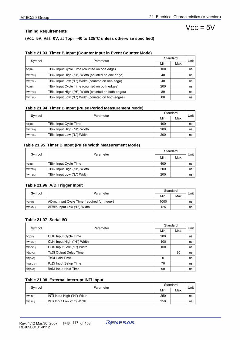
21. Electrical Characteristics (V-version)puorG92/C61M
page 417 854fo7002,03.raM21.1.veR2110-1010B90JER
Timing Requirements
(VCC=5V, VSS=0V, at Topr=-40 to 125°C unless otherwise specified)
Table 21.93 Timer B Input (Counter Input in Event Counter Mode)
lobmyS retemaraPdradnatS
tinU.niM .xaM
ct )BT( iBT NI )egdeenonodetnuoc(emiTelcyCtupnI 001 sn
wt )HBT( iBT NI )egdeenonodetnuoc(htdiW)"H"(hgiHtupnI 04 sn
wt )LBT( iBT NI )egdeenonodetnuoc(htdiW)"L"(woLtupnI 04 snct )BT( iBT NI )segdehtobnodetnuoc(emiTelcyCtupnI 002 snwt )HBT( iBT NI )segdehtobnodetnuoc(htdiW)"H"(hgiHtupnI 08 snwt )LBT( iBT NI )segdehtobnodetnuoc(htdiW)"L"(woLtupnI 08 sn
lobmyS retemaraPdradnatS
tinU.niM .xaM
ct )BT( iBT NI emiTelcyCtupnI 004 snwt )HBT( iBT NI htdiW)"H"(hgiHtupnI 002 snwt )LBT( iBT NI htdiW)"L"(woLtupnI 002 sn
lobmyS retemaraPdradnatS
tinU.niM .xaM
ct )BT( iBT NI emiTelcyCtupnI 004 snwt )HBT( iBT NI htdiW)"H"(hgiHtupnI 002 snwt )LBT( iBT NI htdiW)"L"(woLtupnI 002 sn
lobmyS retemaraPdradnatS
tinU.niM xaM
ct )DA( DA GRT )reggirtrofderiuqer(emiTelcyCtupnI 0001 snwt )LDA( DA GRT htdiW)"L"(woLtupnI 521 sn
lobmyS retemaraPdradnatS
tinU.niM .xaM
ct )KC( emiTelcyCtupnIiKLC 002 snwt )HKC( htdiW)"H"(hgiHtupnIiKLC 001 snwt )LKC( htdiW)"L"(woLtupnIiKLC 001 sndt )Q-C( emiTyaleDtuptuOiDxT 08 snht )Q-C( emiTdloHiDxT 0 snust )C-D( emiTputeStupnIiDxR 07 sn
ht )Q-C( emiTdloHtupnIiDxR 09 sn
lobmyS retemaraPdradnatS
tinU.niM .xaM
wt )HNI( htdiW)"H"(hgiHtupnIiTNI 052 snwt )LNI( htdiW)"L"(woLtupnIiTNI 052 sn
Table 21.94 Timer B Input (Pulse Period Measurement Mode)
Table 21.95 Timer B Input (Pulse Width Measurement Mode)
Table 21.96 A/D Trigger Input
Table 21.97 Serial I/O
Table 21.98 External Interrupt INTi Input
VCC = 5V
21. Electrical Characteristics (V-version)puorG92/C61M
page 418 854fo7002,03.raM21.1.veR2110-1010B90JER
Timing Requirements
(VCC=5V, VSS=0V, at Topr=-40 to 125°C unless otherwise specified)
Table 21.99 Multi-master I2C Bus LineHigh-speed clock mode
Max.Min.Bus free timeThe hold time in start conditionThe hold time in SCL clock "0" status
µsµsµs
tBUFtHD;STAtLOW
ParameterSymbol Unit
tR
tHIGHtHD;DAT
nsµsµs
Data hold timeThe hold time in SCL clock "1" status
SCL, SDA signals' rising time
1.3
0.61.3
00.6
20+0.1Cb
tF SCL, SDA signals' falling timetSU;DAT Data setup timetSU;STA The setup time in restart conditiontSU;STO Stop condition setup time
Standard clock modeMax.Min.
4.7
4.04.7
04.0
2504.74.0
1000
3001000.6
20+0.1Cb
0.6
300
300
0.9
nsnsµsµs
VCC = 5V
21. Electrical Characteristics (V-version)puorG92/C61M
page 419 854fo7002,03.raM21.1.veR2110-1010B90JER
Figure 21.13 Timing Diagram (1)
VCC = 5V
TAiIN input
TAiOUT input
In event counter mode
tc(TA)
tw(TAH)
tw(TAL)
tc(UP)
tw(UPH)
tw(UPL)
th(TIN–UP) tsu(UP–TIN)TAiIN input(When count on falling edge)
TAiIN input(When count on rising edge)
TAiOUT input(Counter increment/decrement input)
TBiIN input
tc(TB)
tw(TBH)
tw(TBL)
tc(AD)
tw(ADL)
ADTRG input
tc(TA)
tsu(TAIN-TAOUT)
tsu(TAOUT-TAIN)
tsu(TAOUT-TAIN)
Two-phase pulse input in event counter mode
TAiIN input
TAiOUT input
tsu(TAIN-TAOUT)
XIN inputtw(H) tw(L)tr
tf
tc
21. Electrical Characteristics (V-version)puorG92/C61M
page 420 854fo7002,03.raM21.1.veR2110-1010B90JER
Figure 21.14 Timing Diagram (2)
Figure 21.15 Timing Diagram (3)
VCC = 5V
VCC = 5V
tsu(D–C)
CLKi
TxDi
RxDi
tc(CK)
tw(CKH)
tw(CKL)
tw(INL)
tw(INH)
td(C–Q) th(C–D)
th(C–Q)
INTi input
tBUF
tHD:STA tHD:DTA
tLOW tR tF
tHIGH tsu:DAT tsu:STA
tHD:STA tsu:STO
SCL p S Sr p
SDA
puorG92/C61M 22. Usage Notes
page 421 854fo7002,03.raM21.1.veR2110-1010B90JER
22. Usage Notes22.1 SFRs
22.1.1 For 80-Pin PackageSet the IFSR20 bit in the IFSR2A register to 0 after reset and set bits PACR2 to PACR0 in the PACRregister to 0112.
22.1.2 For 64-Pin Package
Set the IFSR20bit in the IFSR2A register to 0 after reset and set bits PACR2 to PACR0 in the PACRregister to 0102.
22.1.3 Register Setting
Immediate values should be set in the registers containing write-only bits. When establishing a new valueby modifying a previous value, write the previous value into RAM as well as the register. Change thecontents of the RAM and then transfer the new value to the register.
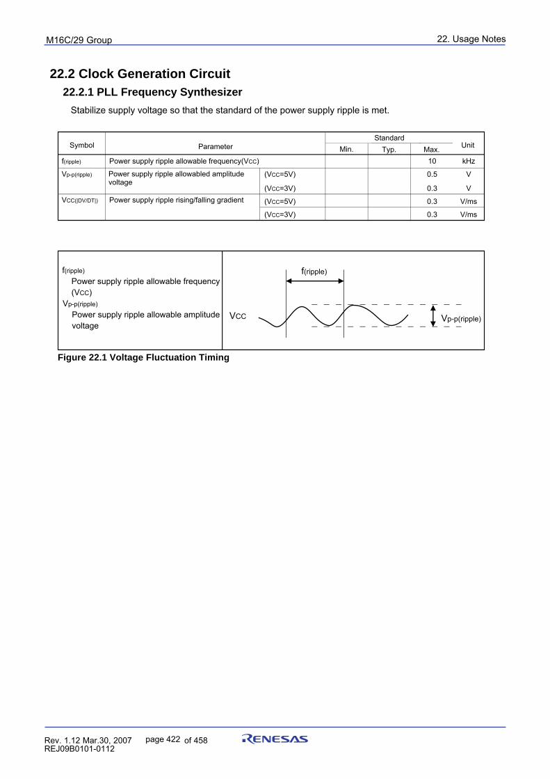
puorG92/C61M 22. Usage Notes
page 422 854fo7002,03.raM21.1.veR2110-1010B90JER
10Typ. Max. UnitParameter
f(ripple) Power supply ripple allowable frequency(VCC)
Symbol Min.Standard
kHz
Power supply ripple allowabled amplitude voltage
Power supply ripple rising/falling gradient
(VCC=5V)
(VCC=3V)
(VCC=5V)
(VCC=3V)
Vp-p(ripple)
VCC(|DV/DT|)
0.5
0.3
0.3
0.3
V
V/ms
V/ms
V
Vp-p(ripple)
f(ripple)
VCC
f(ripple)
Power supply ripple allowable frequency (VCC)Vp-p(ripple)
Power supply ripple allowable amplitude voltage
22.2 Clock Generation Circuit22.2.1 PLL Frequency Synthesizer
Stabilize supply voltage so that the standard of the power supply ripple is met.
Figure 22.1 Voltage Fluctuation Timing
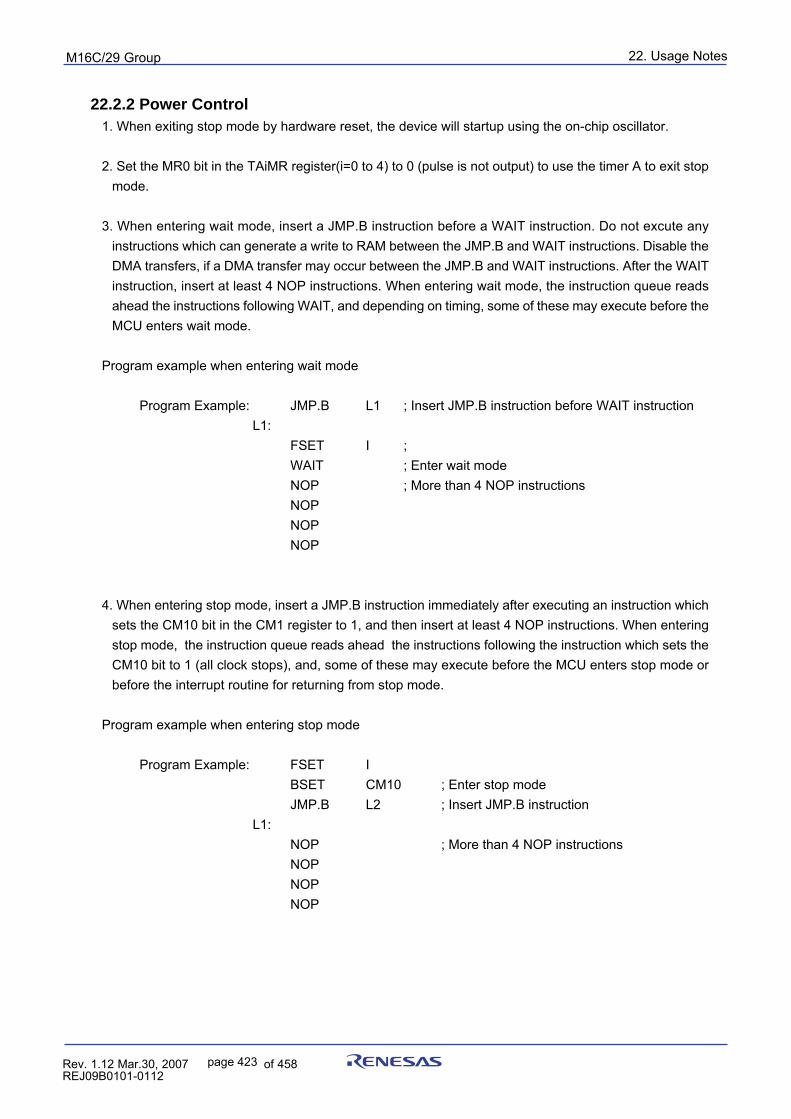
puorG92/C61M 22. Usage Notes
page 423 854fo7002,03.raM21.1.veR2110-1010B90JER
22.2.2 Power Control1. When exiting stop mode by hardware reset, the device will startup using the on-chip oscillator.
2. Set the MR0 bit in the TAiMR register(i=0 to 4) to 0 (pulse is not output) to use the timer A to exit stopmode.
3. When entering wait mode, insert a JMP.B instruction before a WAIT instruction. Do not excute anyinstructions which can generate a write to RAM between the JMP.B and WAIT instructions. Disable theDMA transfers, if a DMA transfer may occur between the JMP.B and WAIT instructions. After the WAITinstruction, insert at least 4 NOP instructions. When entering wait mode, the instruction queue readsahead the instructions following WAIT, and depending on timing, some of these may execute before theMCU enters wait mode.
Program example when entering wait mode
Program Example: JMP.B L1 ; Insert JMP.B instruction before WAIT instructionL1:
FSET I ;WAIT ; Enter wait modeNOP ; More than 4 NOP instructionsNOPNOPNOP
4. When entering stop mode, insert a JMP.B instruction immediately after executing an instruction whichsets the CM10 bit in the CM1 register to 1, and then insert at least 4 NOP instructions. When enteringstop mode, the instruction queue reads ahead the instructions following the instruction which sets theCM10 bit to 1 (all clock stops), and, some of these may execute before the MCU enters stop mode orbefore the interrupt routine for returning from stop mode.
Program example when entering stop mode
Program Example: FSET IBSET CM10 ; Enter stop modeJMP.B L2 ; Insert JMP.B instruction
L1:NOP ; More than 4 NOP instructionsNOPNOPNOP
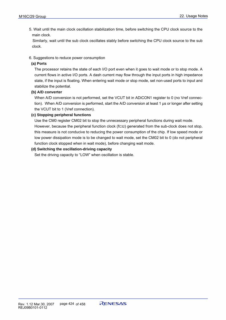
puorG92/C61M 22. Usage Notes
page 424 854fo7002,03.raM21.1.veR2110-1010B90JER
5. Wait until the main clock oscillation stabilization time, before switching the CPU clock source to themain clock.
Similarly, wait until the sub clock oscillates stably before switching the CPU clock source to the subclock.
6. Suggestions to reduce power consumption(a) Ports
The processor retains the state of each I/O port even when it goes to wait mode or to stop mode. Acurrent flows in active I/O ports. A dash current may flow through the input ports in high impedancestate, if the input is floating. When entering wait mode or stop mode, set non-used ports to input andstabilize the potential.
(b) A/D converter
When A/D conversion is not performed, set the VCUT bit in ADiCON1 register to 0 (no Vref connec-tion). When A/D conversion is performed, start the A/D conversion at least 1 µs or longer after settingthe VCUT bit to 1 (Vref connection).
(c) Stopping peripheral functions
Use the CM0 register CM02 bit to stop the unnecessary peripheral functions during wait mode.However, because the peripheral function clock (fC32) generated from the sub-clock does not stop,this measure is not conducive to reducing the power consumption of the chip. If low speed mode orlow power dissipation mode is to be changed to wait mode, set the CM02 bit to 0 (do not peripheralfunction clock stopped when in wait mode), before changing wait mode.
(d) Switching the oscillation-driving capacity
Set the driving capacity to “LOW” when oscillation is stable.

puorG92/C61M 22. Usage Notes
page 425 854fo7002,03.raM21.1.veR2110-1010B90JER
22.3 ProtectionSet the PRC2 bit to 1 (write enabled) and then write to any address, and the PRC2 bit will be cleared to 0(write protected). The registers protected by the PRC2 bit should be changed in the next instruction aftersetting the PRC2 bit to 1. Make sure no interrupts or DMA transfers will occur between the instruction inwhich the PRC2 bit is set to 1 and the next instruction.
puorG92/C61M 22. Usage Notes
page 426 854fo7002,03.raM21.1.veR2110-1010B90JER
22.4 Interrupts22.4.1 Reading Address 0000016
Do not read the address 0000016 in a program. When a maskable interrupt request is accepted, the CPUreads interrupt information (interrupt number and interrupt request priority level) from the address0000016 during the interrupt sequence. At this time, the IR bit for the accepted interrupt is cleared to 0.If the address 0000016 is read in a program, the IR bit for the interrupt which has the highest priorityamong the enabled interrupts is cleared to 0. This causes a problem that the interrupt is canceled, or anunexpected interrupt request is generated.
22.4.2 Setting the SP
Set any value in the SP(USP, ISP) before accepting an interrupt. The SP(USP, ISP) is cleared to 000016
after reset. Therefore, if an interrupt is accepted before setting any value in the SP(USP, ISP), the pro-gram may go out of control.
_______
22.4.3 NMI Interrupt_______ _______
1. The NMI interrupt is invalid after reset. The NMI interrupt becomes effective by setting the PM24 bit in_______
the PM2 register to “1”. Set the PM24 bit to "1" when a high-level signal ("H") is applied to the NMI pin._______ _______
If the PM24 bit is set to "1" when a low-level signal ("L") is applied, NMI interrupt is generated. Once NMIinterrupt is enabled, it will not be disabled unless a reset is applied.
_______
2. The input level of the NMI pin can be read by accessing the P8_5 bit in the P8 register._______ _______
3. When selecting NMI function, stop mode cannot be entered into while input on the NMI pin is low. This_______
is because while input on the NMI pin is low the CM1 register’s CM10 bit is fixed to 0._______ _______
4. When selecting NMI function, do not go to wait mode while input on the NMI pin is low. This is because_______
when input on the NMI pin goes low, the CPU stops but CPU clock remains active; therefore, the currentconsumption in the chip does not drop. In this case, normal condition is restored by an interrupt gener-ated thereafter.
_______ _______
5. When selecting NMI function, the low and high level durations of the input signal to the NMI pin musteach be 2 CPU clock cycles + 300 ns or more.
_______
6. When using the NMI interrupt for exiting stop mode, set the NDDR register to FF16 (disable digitaldebounce filter) before entering stop mode.
22.4.4 Changing the Interrupt Generate FactorIf the interrupt generate factor is changed, the IR bit in the interrupt control register for the changedinterrupt may inadvertently be set to 1 (interrupt requested). If you changed the interrupt generate factorfor an interrupt that needs to be used, be sure to clear the IR bit for that interrupt to 0 (interrupt notrequested).“Changing the interrupt generate factor” referred to here means any act of changing the source, polarityor timing of the interrupt assigned to each software interrupt number. Therefore, if a mode change of anyperipheral function involves changing the generate factor, polarity or timing of an interrupt, be sure toclear the IR bit for that interrupt to 0 (interrupt not requested) after making such changes. Refer to thedescription of each peripheral function for details about the interrupts from peripheral functions.Figure 22.2 shows the procedure for changing the interrupt generate factor.
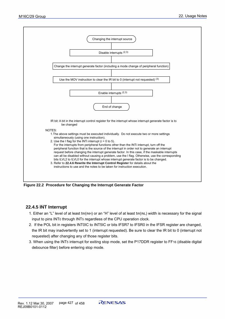
puorG92/C61M 22. Usage Notes
page 427 854fo7002,03.raM21.1.veR2110-1010B90JER
NOTES: 1.The above settings must be executed individually. Do not execute two or more settings simultaneously (using one instruction). 2. Use the I flag for the INTi interrupt (i = 0 to 5). For the interrupts from peripheral functions other than the INTi interrupt, turn off the peripheral function that is the source of the interrupt in order not to generate an interrupt request before changing the interrupt generate factor. In this case, if the maskable interrupts can all be disabled without causing a problem, use the I flag. Otherwise, use the corresponding bits ILVL2 to ILVL0 for the interrupt whose interrupt generate factor is to be changed. 3. Refer to 22.4.6 Rewrite the Interrupt Control Register for details about the instructions to use and the notes to be taken for instruction execution.
Changing the interrupt source
Disable interrupts (2,3)
Use the MOV instruction to clear the IR bit to 0 (interrupt not requested) (3)
Change the interrupt generate factor (including a mode change of peripheral function)
Enable interrupts (2,3)
End of change
IR bit: A bit in the interrupt control register for the interrupt whose interrupt generate factor is to be changed
Figure 22.2 Procedure for Changing the Interrupt Generate Factor
______
22.4.5 INT Interrupt1. Either an “L” level of at least tW(INH) or an “H” level of at least tW(INL) width is necessary for the signal
input to pins INT0 through INT5 regardless of the CPU operation clock.2. If the POL bit in registers INT0IC to INT5IC or bits IFSR7 to IFSR0 in the IFSR register are changed,
the IR bit may inadvertently set to 1 (interrupt requested). Be sure to clear the IR bit to 0 (interrupt notrequested) after changing any of those register bits.
3. When using the INT5 interrupt for exiting stop mode, set the P17DDR register to FF16 (disable digitaldebounce filter) before entering stop mode.
puorG92/C61M 22. Usage Notes
page 428 854fo7002,03.raM21.1.veR2110-1010B90JER
22.4.6 Rewrite the Interrupt Control Register(1) The interrupt control register for any interrupt should be modified in places where no requests for that
interrupt may occur. Otherwise, disable the interrupt before rewriting the interrupt control register.(2) To rewrite the interrupt control register for any interrupt after disabling that interrupt, be careful with the
instruction to be used.
Changing any bit other than the IR bit
If while executing an instruction, a request for an interrupt controlled by the register being modifiedoccurs, the IR bit in the register may not be set to 1 (interrupt requested), with the result that theinterrupt request is ignored. If such a situation presents a problem, use the instructions shown belowto modify the register.Usable instructions: AND, OR, BCLR, BSET
Changing the IR bit
Depending on the instruction used, the IR bit may not always be cleared to 0 (interrupt not requested).Therefore, be sure to use the MOV instruction to clear the IR bit.
(3) When using the I flag to disable an interrupt, refer to the sample program fragments shown below asyou set the I flag. (Refer to (2) for details about rewrite the interrupt control registers in the sampleprogram fragments.)
22.4.7 Watchdog Timer InterruptInitialize the watchdog timer after the watchdog timer interrupt occurs.
Examples 1 through 3 show how to prevent the I flag from being set to 1 (interrupts enabled) before theinterrupt control register is rewrited, due to the internal bus and the instruction queue buffer.
Example 1: Using the NOP instruction to keep the program waiting until the interrupt control register is modified
INT_SWITCH1: FCLR I ; Disable interrupts AND.B #00h, 0055h ;Set the TA0IC register to 0016 NOP ; NOP FSET I ; Enable interrupts
The number of NOP instruction is as follows. PM20 = 1 (1 wait) : 2, PM20 = 0 (2 waits): 3
Example 2:Using the dummy read to keep the FSET instruction waiting INT_SWITCH2: FCLR I ; Disable interrupts AND.B #00h, 0055h ; Set the TA0IC register to 0016 MOV.W MEM, R0 ; Dummy read FSET I ; Enable interrupts
Example 3:Using the POPC instruction to changing the I flag INT_SWITCH3: PUSHC FLG FCLR I ; Disable interrupts AND.B #00h, 0055h ; Set the TA0IC register to 0016 POPC FLG ; Enable interrupts
puorG92/C61M 22. Usage Notes
page 429 854fo7002,03.raM21.1.veR2110-1010B90JER
22.5 DMAC22.5.1 Write to DMAE Bit in DMiCON Register
When both of the conditions below are met, follow the steps below.
(a) Conditions • The DMAE bit is set to 1 again while it remains set (DMAi is in an active state). • A DMA request may occur simultaneously when the DMAE bit is being written.(b) Procedure (1) Write 1 to the DMAE bit and DMAS bit in DMiCON register simultaneously(1). (2) Make sure that the DMAi is in an initial state(2) in a program.If the DMAi is not in an initial state, the above steps should be repeated.
NOTES: 1. The DMAS bit remains unchanged even if 1 is written. However, if 0 is written to this bit, it is
set to 0 (DMA not requested). In order to prevent the DMAS bit from being modified to 0, 1should be written to the DMAS bit when 1 is written to the DMAE bit. In this way the state of theDMAS bit immediately before being written can be maintained.Similarly, when writing to the DMAE bit with a read-modify-write instruction, 1 should be written tothe DMAS bit in order to maintain a DMA request which is generated during execution.
2. Read the TCRi register to verify whether the DMAi is in an initial state. If the read value is equal toa value which was written to the TCRi register before DMA transfer start, the DMAi is in an initialstate. (If a DMA request occurs after writing to the DMAE bit, the value written to the TCRi registeris 1.) If the read value is a value in the middle of transfer, the DMAi is not in an initial state.
puorG92/C61M 22. Usage Notes
page 430 854fo7002,03.raM21.1.veR2110-1010B90JER
22.6 Timers22.6.1 Timer A
22.6.1.1 Timer A (Timer Mode)
1. The timer remains idle after reset. Set the mode, count source, counter value, etc. using the TAiMR(i = 0 to 4) register and the TAi register before setting the TAiS bit in the TABSR register to 1 (countstarts).Always make sure the TAiMR register is modified while the TAiS bit remains 0 (count stops) regard-less whether after reset or not.
2. While counting is in progress, the counter value can be read out at any time by reading the TAiregister. However, if the TAi register is read at the same time the counter is reloaded, the read valueis always FFFF16. If the TAi register is read after setting a value in it, but before the counter startscounting, the read value is the one that has been set in the register.
_____
3. If a low-level signal is applied to the SD pin when the IVPCR1 bit in the TB2SC register is set to 1_____
(three-phase output forcible cutoff by input on SD pin enabled), the TA1OUT, TA2OUT and TA4OUT
pins go to a high-impedance state.
22.6.1.2 Timer A (Event Counter Mode)
1. The timer remains idle after reset. Set the mode, count source, counter value, etc. using the TAiMR(i = 0 to 4) register, the TAi register, the UDF register, bits TAZIE, TA0TGL, and TA0TGH in theONSF register and the TRGSR register before setting the TAiS bit in the TABSR register to 1 (countstarts).Always make sure bits TAZIE, TA0TGL, and TA0TGH in the TAiMR register, the UDF register, theONSF register, and the TRGSR register are modified while the TAiS bit remains 0 (count stops)regardless whether after reset or not.
2. While counting is in progress, the counter value can be read out at any time by reading the TAiregister. However, if the TAi register is read at the same time the counter is reloaded, the read valueis always FFFF16 when the timer counter underflows and 000016 when the timer counter overflows.If the TAi register is read after setting a value in it, but before the counter starts counting, the readvalue is the one that has been set in the register.
_____
3. If a low-level signal is applied to the SD pin when the IVPCR1 bit in the TB2SC register is set to 1_____
(three-phase output forcible cutoff by input on SD pin enabled), the TA1OUT, TA2OUT and TA4OUT
pins go to a high-impedance state.
puorG92/C61M 22. Usage Notes
page 431 854fo7002,03.raM21.1.veR2110-1010B90JER
22.6.1.3 Timer A (One-shot Timer Mode)
1. The timer remains idle after reset. Set the mode, count source, counter value, etc. using the TAiMR(i = 0 to 4) register, the TAi register, bits TA0TGL and TA0TGH in the ONSF register and theTRGSR register before setting the TAiS bit in the TABSR register to 1 (count starts).Always make sure bits TA0TGL and TA0TGH in the TAiMR register, the ONSF register, and theTRGSR register are modified while the TAiS bit remains 0 (count stops) regardless whether afterreset or not.
2. When setting TAiS bit to 0 (count stop), the followings occur:• A counter stops counting and a content of reload register is reloaded.• TAiOUT pin outputs “L”.• After one cycle of the CPU clock, the IR bit in TAiIC register is set to 1 (interrupt request).
3. Output in one-shot timer mode synchronizes with a count source internally generated. When theexternal trigger has been selected, a maximun delay of one cycle of the count source occurs be-tween the trigger input to TAiIN pin and output in one-shot timer mode.
4. The IR bit is set to 1 when timer operation mode is set with any of the following procedures:• Select one-shot timer mode after reset.• Change an operation mode from timer mode to one-shot timer mode.• Change an operation mode from event counter mode to one-shot timer mode.
To use the timer Ai interrupt (the IR bit), set the IR bit to 0 after the changes listed above have beenmade.
5. When a trigger occurs while the timer is counting, the counter reloads the reload register value, andcontinues counting after a second trigger is generated and the counter is decremented once. Togenerate a trigger while counting, space more than one cycle of the timer count source from the firsttrigger and generate again.
6. When selecting the external trigger for the count start conditions in timer A one-shot timer mode, dogenerate an external trigger 300ns before the count value of timer A is set to 000016. The one-shottimer does not continue counting and may stop.
7._____
If a low-level signal is applied to the SD pin when the IVPCR1 bit in the TB2SC register is set to 1_____
(three-phase output forcible cutoff by input on SD pin enabled), the TA1OUT, TA2OUT and TA4OUT
pins go to a high-impedance state.
puorG92/C61M 22. Usage Notes
page 432 854fo7002,03.raM21.1.veR2110-1010B90JER
22.6.1.4 Timer A (Pulse Width Modulation Mode)
1. The timer remains idle after reset. Set the mode, count source, counter value, etc. using bitsTA0TGL and TA0TGH in the TAiMR (i = 0 to 4) register, the TAi register, the ONSF register and theTRGSR register before setting the TAiS bit in the TABSR register to 1 (count starts).Always make sure bits TA0TGL and TA0TGH in the TAiMR register, the ONSF register and theTRGSR register are modified while the TAiS bit remains 0 (count stops) regardless whether afterreset or not.
2. The IR bit is set to 1 when setting a timer operation mode with any of the following procedures:• Select the PWM mode after reset.• Change an operation mode from timer mode to PWM mode.• Change an operation mode from event counter mode to PWM mode.
To use the timer Ai interrupt (interrupt request bit), set the IR bit to 0 by program after the abovelisted changes have been made.
3. When setting TAiS register to 0 (count stop) during PWM pulse output, the following action occurs:• Stop counting.• When TAiOUT pin is output “H”, output level is set to “L” and the IR bit is set to 1.• When TAiOUT pin is output “L”, both output level and the IR bit remains unchanged.
_____
4. If a low-level signal is applied to the SD pin when the IVPCR1 bit in the TB2SC register is set to 1_____
(three-phase output forcible cutoff by input on SD pin enabled), the TA1OUT, TA2OUT and TA4OUT
pins go to a high-impedance state.
puorG92/C61M 22. Usage Notes
page 433 854fo7002,03.raM21.1.veR2110-1010B90JER
22.6.2 Timer B22.6.2.1 Timer B (Timer Mode)
1. The timer remains idle after reset. Set the mode, count source, counter value, etc. using the TBiMR(i = 0 to 2) register and TBi register before setting the TBiS bit in the TABSR register to 1 (countstarts).Always make sure the TBiMR register is modified while the TBiS bit remains 0 (count stops) regard-less whether after reset or not.
2. The counter value can be read out at any time by reading the TBi register. However, if this registeris read at the same time the counter is reloaded, the read value is always FFFF16. If the TBi registeris read after setting a value in it but before the counter starts counting, the read value is the one thathas been set in the register.
22.6.2.2 Timer B (Event Counter Mode)
1. The timer remains idle after reset. Set the mode, count source, counter value, etc. using the TBiMR(i = 0 to 2) register and TBi register before setting the TBiS bit in the TABSR register to 1 (countstarts).Always make sure the TBiMR register is modified while the TBiS bit remains 0 (count stops) regard-less whether after reset or not.
2. The counter value can be read out at any time by reading the TBi register. However, if this registeris read at the same time the counter is reloaded, the read value is always FFFF16. If the TBi registeris read after setting a value in it but before the counter starts counting, the read value is the one thathas been set in the register.
22.6.2.3 Timer B (Pulse Period/pulse Width Measurement Mode)
1. The timer remains idle after reset. Set the mode, count source, etc. using the TBiMR (i = 0 to 2)register before setting the TBiS bit in the TABSR or the TBSR register to 1 (count starts).Always make sure the TBiMR register is modified while the TBiS bit remains 0 (count stops) regard-less whether after reset or not. To clear the MR3 bit to 0 by writing to the TBiMR register while theTBiS bit is set to 1 (count starts), be sure to write the same value as previously written to bitsTM0D0, TM0D1, MR0, MR1, TCK0, and TCK1 and a 0 to the MR2 bit.
2. The IR bit in TBiIC register (i=0 to 2) goes to 1 (interrupt request), when an effective edge of ameasurement pulse is input or timer Bi is overflowed. The factor of interrupt request can be deter-mined by use of the MR3 bit in TBiMR register within the interrupt routine.
3. If the source of interrupt cannot be identified by the MR3 bit such as when the measurement pulseinput and a timer overflow occur at the same time, use another timer to count the number of timestimer B has overflowed.
4. To set the MR3 bit to 0 (no overflow), set TBiMR register with setting the TBiS bit to 1 and countingthe next count source after setting the MR3 bit to 1 (overflow).
5. Use the IR bit in TBiIC register to detect only overflows. Use the MR3 bit only to determine theinterrupt factor within the interrupt routine.
puorG92/C61M 22. Usage Notes
page 434 854fo7002,03.raM21.1.veR2110-1010B90JER
6. When a count is started and the first effective edge is input, an undefined value is transferred to thereload register. At this time, timer Bi interrupt request is not generated.
7. A value of the counter is undefined at the beginning of a count. MR3 may be set to 1 and timer Biinterrupt request may be generated between a count start and an effective edge input.
8. For pulse width measurement, pulse widths are successively measured. Use program to checkwhether the measurement result is an “H” level width or an “L” level width.
22.6.3 Three-phase Motor Control Timer Function
When the IVPCR1 bit in the TB2SC register is set to 1 (three-phase output forced cutoff by SD pin input(high-impedance) enabled), the INV03 bit in the INVC0 register is set to 1 (three-phase motor control
_____
timer output enabled), and a low-level ("L") signal is applied to the SD pin while a three-phase PWM___ ___ ___
signal is output, the MCU is forced to cutoff and pins U, U, V, V, W, and W are placed in a high-impedancestate and the INV03 bit is set to 0 (three-phase motor control timer output disabled).
___ ___ ___
To resume the three-phase PWM signal output from pins U, U, V, V, W, and W, set the INV03 bit to 1 and_____
the IVPCR1 bit to 0 (three-phase output forced cutoff disabled) after the SD pin level becomes "H". Thenset the IVPCR1 bit to 1 (three-phase output forced cutoff enabled) in order to enable the three-phaseoutput forced cutoff function by input to the SD pin again.
_____
The INV03 bit cannot be set to 1 while an "L" signal is input to the SD pin. To set the INV03 bit to 1 afterforcible cutoff, write 1 to the INV03 bit and read the bit to ensure that it is set to 1 by program. Then set theIVPCR1 bit to 1 after setting it to 0.
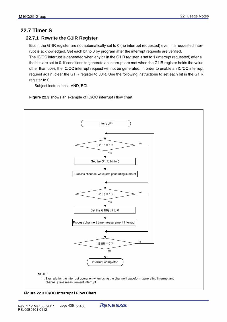
puorG92/C61M 22. Usage Notes
page 435 854fo7002,03.raM21.1.veR2110-1010B90JER
22.7 Timer S22.7.1 Rewrite the G1IR Register
Bits in the G1IR register are not automatically set to 0 (no interrupt requested) even if a requested inter-rupt is acknowledged. Set each bit to 0 by program after the interrupt requests are verified.The IC/OC interrupt is generated when any bit in the G1IR register is set to 1 (interrupt requested) after allthe bits are set to 0. If conditions to generate an interrupt are met when the G1IR register holds the valueother than 0016, the IC/OC interrupt request will not be generated. In order to enable an IC/OC interruptrequest again, clear the G1IR register to 0016. Use the following instructions to set each bit in the G1IRregister to 0. Subject instructions: AND, BCL
Figure 22.3 shows an example of IC/OC interrupt i flow chart.
Interrupt(1)
Set the G1IRi bit to 0
Set the G1IRj bit to 0
Process channel i waveform generating interrupt
Process channel j time measurement interrupt
Interrupt completed
NOTE: 1. Example for the interrupt operation when using the channel i waveform generating interrupt and channel j time measurement interrupt.
G1IRi = 1 ?
G1IRj = 1 ?
G1IR = 0 ?
No
No
No
Yes
Yes
Yes
Figure 22.3 IC/OC Interrupt i Flow Chart
puorG92/C61M 22. Usage Notes
page 436 854fo7002,03.raM21.1.veR2110-1010B90JER
retsigeR0RCB1GehtnitiBTI retsigeRRRTB1G
)swolfrevoremitesabehtni51tib(0 FFF70 61 EFFF0ot 61
)swolfrevoremitesabehtni41tib(1FFF30 61 EFFF0ot 61 roFFFB0 61 EFFF0ot 61
22.7.2 Rewrite the ICOCiIC RegisterWhen the interrupt request to the ICOCiIC register is generated during the instruction process, the IR bitmay not be set to 1 (interrupt requested) and the interrupt request may not be acknowledged. At that time,when the bit in the G1IR register is held to 1 (interrupt requested), the following IC/OC interrupt requestwill not be generated. When changing the ICOCiIC register settiing, use the following instruction. Subject instructions: AND, OR, BCLR, BSET
When initializing Timer S, change the ICOCiIC register setting with the request again after setting regis-ters IOCiIC and G1IR to 0016.
22.7.3 Waveform Generating Function
1. If the BTS bit in the G1BCR1 register is set to 0 (base timer is reset) when the waveform is generatingand the base timer is stopped counting, the waveform output pin keeps the same output level. The outputlevel will be changed when the base timer and the G1POj register match the setting value next time afterthe base timer starts counting again.2. If the G1POCRj register is set when the waveform is generated, the same setting value of the IVL bit isapplied to the waveform generating pin. Do not set the G1POCRj register when the waveform is generat-ing.3. When the RST1 bit in the G1BCR1 register is set to 1 (the base timer is reset by matching the G1PO0
register), the base timer is reset after two clock cycles of fBT1 when the base timer value matches theG1PO0 register value. A high-level ("H") signal is applied to the OUTC10 pin between the base timervalue match to the base timer reset.
22.7.4 IC/OC Base Timer InterruptIf the MCU is operated in the combination selected from Table 22.1 for use when the RST4 bit in theG1BCR0 register is set to 1 (reset the base timer that matches the G1BTRR register) to reset the basetimer, an IC/OC base timer interrupt request is generated twice.
Table 22.1 Uses of IT Bit in the G1BCR0 Register and G1BTRR Register
The second IC/OC base timer interrupt request is generated because the base timer overflow request isgenerated after one fBT1 clock cycle as soon as the base timer is reset.
One of the following conditions must be met in order not to generate the IC/OC base timer interruptrequest twice:1) When the RST4 bit is set to 1, set the G1BTRR register with a combination other than what is listed in
Table 22.1.2) Do not reset the base timer by matching the G1BTRR register. Reset the base timer by matching the
G1P00 register. In other words, do not set the RST4 bit to 1 to reset the base timer. Set the RST1 bit inthe G1BCR1 register to 1 (reset the base timer that matches the G1P00 register).
puorG92/C61M 22. Usage Notes
page 437 854fo7002,03.raM21.1.veR2110-1010B90JER
22.8 Serial I/O22.8.1 Clock-Synchronous Serial I/O
22.8.1.1 Transmission/reception_______ ________
1. With an external clock selected, and choosing the RTS function, the output level of the RTSi pingoes to “L” when the data-receivable status becomes ready, which informs the transmission side
________
that the reception has become ready. The output level of the RTSi pin goes to “H” when reception________ ________
starts. So if the RTSi pin is connected to the CTSi pin on the transmission side, the circuit can_______
transmission and reception data with consistent timing. With the internal clock, the RTS functionhas no effect.
_____
2. If a low-level signal is applied to the SD pin when the IVPCR1 bit in the TB2SC register is set to 1_____
(three-phase output forcible cutoff by input on SD pin enabled), the P73/RTS2/TxD1(when theU1MAP bit in PACR register is 1) and CLK2 pins go to a high-impedance state.
22.8.1.2 TransmissionWhen an external clock is selected, the conditions must be met while if the CKPOL bit in the UiC0register is set to 0 (transmit data output at the falling edge and the receive data taken in at the risingedge of the transfer clock), the external clock is in the high state; if the CKPOL bit in the UiC0 registeris set to 1 (transmit data output at the rising edge and the receive data taken in at the falling edge of thetransfer clock), the external clock is in the low state.
• The TE bit in UiC1 register is set to 1 (transmission enabled)• The TI bit in UiC1 register is set to 0 (data present in UiTB register)
_______ _______
• If CTS function is selected, input on the CTSi pin is set to “L”
22.8.1.3 Reception1. In operating the clock-synchronous serial I/O, operating a transmitter generates a shift clock. Fix
settings for transmission even when using the device only for reception. Dummy data is output tothe outside from the TxDi pin when receiving data.
2. When an internal clock is selected, set the TE bit in the UiC1 register (i = 0 to 2) to 1 (transmissionenabled) and write dummy data to the UiTB register, and the shift clock will thereby be generated.When an external clock is selected, set the TE bit in the UiC1 register (i = 0 to 2) to 1 and write dummydata to the UiTB register, and the shift clock will be generated when the external clock is fed to the CLKiinput pin.
3. When successively receiving data, if all bits of the next receive data are prepared in the UARTireceive register while the RE bit in the UiC1 register (i = 0 to 2) is set to 1 (data present in the UiRBregister), an overrun error occurs and the UiRB register OER bit is set to 1 (overrun error occurred).In this case, because the content of the UiRB register is undefined, a corrective measure must betaken by programs on the transmit and receive sides so that the valid data before the overrun erroroccurred will be retransmitted. Note that when an overrun error occurred, the SiRIC register IR bitdoes not change state.
4. To receive data in succession, set dummy data in the lower-order byte of the UiTB register everytime reception is made.
5. When an external clock is selected, make sure the external clock is in high state if the CKPOL bit isset to 0, and in low state if the CKPOL bit is set to 1 before the following conditions are met:• The RE bit in the UiC1 register is set to 1 (reception enabled)• The TE bit in the UiC1 register is set to 1 (transmission enabled)• The TI bit in the UiC1 register= 0 (data present in the UiTB register)
puorG92/C61M 22. Usage Notes
page 438 854fo7002,03.raM21.1.veR2110-1010B90JER
22.8.2 UART Mode22.8.2.1 Special Mode 1 (I2C bus Mode)
When generating start, stop and restart conditions, set the STSPSEL bit in the U2SMR4 register to 0and wait for more than half cycle of the transfer clock before setting each condition generate bit(STAREQ, RSTAREQ and STPREQ) from 0 to 1.
22.8.2.2 Special Mode 2_____
If a low-level signal is applied to the SD pin when the IVPCR1 bit in the TB2SC register is set to 1_____
(three-phase output forcible cutoff by input on SD pin enabled), the RTS2 and CLK2 pins go to a high-impedance state.
22.8.2.3 Special Mode 4 (SIM Mode)
A transmit interrupt request is generated by setting the U2C1 register U2IRS bit to 1 (transmissioncomplete) and U2ERE bit to 1 (error signal output) after reset. Therefore, when using SIM mode, besure to clear the IR bit to 0 (no interrupt request) after setting these bits.
22.8.3 SI/O3, SI/O4
The SOUTi default value which is set to the SOUTi pin by the SMi7 bit approximately 10ns may be outputwhen changing the SMi3 bit from 0 (I/O port) to 1 (SOUTi output and CLKfunction) while the SMi2 bit inthe SiC (i=3 and 4) to 0 (SOUTi output) and the SMi6 bit is set to 1 (internal clock). And then the SOUTipin is held high-impedance.If the level which is output from the SOUTi pin is a problem when changing the SMi3 bit from 0 to 1, set thedefault value of the SOUTi pin by the SMi7 bit.
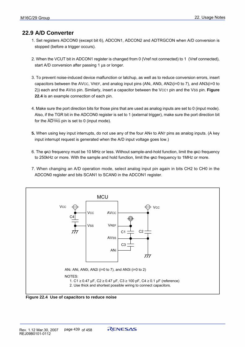
puorG92/C61M 22. Usage Notes
page 439 854fo7002,03.raM21.1.veR2110-1010B90JER
MCU
VCC
VSS
AVCC
AVSS
VREF
ANi
C4
C1 C2
C3
VCC VCC
NOTES:1. C1 ≥ 0.47 µF, C2 ≥ 0.47 µF, C3 ≥ 100 pF, C4 ≥ 0.1 µF (reference)2. Use thick and shortest possible wiring to connect capacitors.
ANi: ANi, AN0i, AN2i (i=0 to 7), and AN3i (i=0 to 2)
22.9 A/D Converter1. Set registers ADCON0 (except bit 6), ADCON1, ADCON2 and ADTRGCON when A/D conversion is
stopped (before a trigger occurs).
2. When the VCUT bit in ADCON1 register is changed from 0 (Vref not connected) to 1 (Vref connected),start A/D conversion after passing 1 µs or longer.
3. To prevent noise-induced device malfunction or latchup, as well as to reduce conversion errors, insertcapacitors between the AVCC, VREF, and analog input pins (ANi, AN0i, AN2i(i=0 to 7), and AN3i(i=0 to2)) each and the AVSS pin. Similarly, insert a capacitor between the VCC1 pin and the VSS pin. Figure
22.4 is an example connection of each pin.
4. Make sure the port direction bits for those pins that are used as analog inputs are set to 0 (input mode).Also, if the TGR bit in the ADCON0 register is set to 1 (external trigger), make sure the port direction bit
___________
for the ADTRG pin is set to 0 (input mode).
5. When using key input interrupts, do not use any of the four AN4 to AN7 pins as analog inputs. (A keyinput interrupt request is generated when the A/D input voltage goes low.)
6. The φAD frequency must be 10 MHz or less. Without sample-and-hold function, limit the φAD frequencyto 250kHZ or more. With the sample and hold function, limit the φAD frequency to 1MHZ or more.
7. When changing an A/D operation mode, select analog input pin again in bits CH2 to CH0 in theADCON0 register and bits SCAN1 to SCAN0 in the ADCON1 register.
Figure 22.4 Use of capacitors to reduce noise
puorG92/C61M 22. Usage Notes
page 440 854fo7002,03.raM21.1.veR2110-1010B90JER
8. If the CPU reads the ADi register (i = 0 to 7) at the same time the conversion result is stored in the ADiregister after completion of A/D conversion, an incorrect value may be stored in the ADi register. Thisproblem occurs when a divide-by-n clock derived from the main clock or a subclock is selected for CPUclock.
• When operating in one-shot, single-sweep mode, simultaneous sample sweep mode, delayedtrigger mode 0 or delayed trigger mode 1
Check to see that A/D conversion is completed before reading the target ADi register. (Check theADIC register’s IR bit to see if A/D conversion is completed.)
• When operating in repeat mode or repeat sweep mode 0 or 1Use the main clock for CPU clock directly without dividing it.
9. If A/D conversion is forcibly terminated while in progress by setting the ADST bit in the ADCON0register to 0 (A/D conversion halted), the conversion result of the A/D converter is undefined. Thecontents of ADi registers irrelevant to A/D conversion may also become undefined. If while A/D conver-sion is underway the ADST bit is cleared to 0 in a program, ignore the values of all ADi registers.
10. When setting the ADST bit in the ADCON register to 0 and terminating forcefully by a program insingle sweep conversion mode, A/D delayed trigger mode 0 and A/D delayed trigger mode 1 during
A/D converting operation, the A/D interrupt request may be generated. If this causes a problem, set theADST bit to 0 after an interrupt is disabled.
puorG92/C61M 22. Usage Notes
page 441 854fo7002,03.raM21.1.veR2110-1010B90JER
22.10 Multi-Master I2C bus Interface22.10.1 Writing to the S00 Register
When the start condition is not generated, the SCL pin may output the short low-signal ("L") by setting theS00 register. Set the register when the SCL pin outputs an "L" signal.
22.10.2 AL Flag
When the arbitration lost is generated and the AL flag in the S10 register is set to 1 (detected), the AL flagcan be cleared to 0 (not detected) by writing a transmit data to the S00 register. The AL flag should becleared at the timing when master geneates the start condition to start a new transfer.
puorG92/C61M 22. Usage Notes
page 442 854fo7002,03.raM21.1.veR2110-1010B90JER
22.11 CAN Module22.11.1 Reading C0STR Register
The CAN module on the M16C/29 Group updates the status of the C0STR register in a certain period.When the CPU and the CAN module access to the C0STR register at the same time, the CPU has theaccess priority; the access from the CAN module is disabled. Consequently, when the updating period ofthe CAN module matches the access period from the CPU, the status of the CAN module cannot beupdated. (See Figure 22.5)Accordingly, be careful about the following points so that the access period from the CPU should notmatch the updating period of the CAN module:
(1) There should be a wait time of 3fCAN or longer (see Table 22.2) before the CPU reads the C0STR register. (See Figure 22.6)(2) When the CPU polls the C0STR register, the polling period must be 3fCAN or longer. (See Figure
22.7)
Table 22.2 CAN Module Status Updating Period3fCAN period = 3 XIN (Original oscillation period) Division value of the CAN clock (CCLK)
(Example 1) Condition XIN 16 MHz CCLK: Divided by 1 3fCAN period = 3 62.5 ns 1 = 187.5 ns(Example 2) Condition XIN 16 MHz CCLK: Divided by 2 3fCAN period = 3 62.5 ns 2 = 375 ns(Example 3) Condition XIN 16 MHz CCLK: Divided by 4 3fCAN period = 3 62.5 ns 4 = 750 ns(Example 4) Condition XIN 16 MHz CCLK: Divided by 8 3fCAN period = 3 62.5 ns 8 = 1.5 µs(Example 5) Condition XIN 16 MHz CCLK: Divided by 16 3fCAN period = 3 62.5 ns 16 = 3 µs
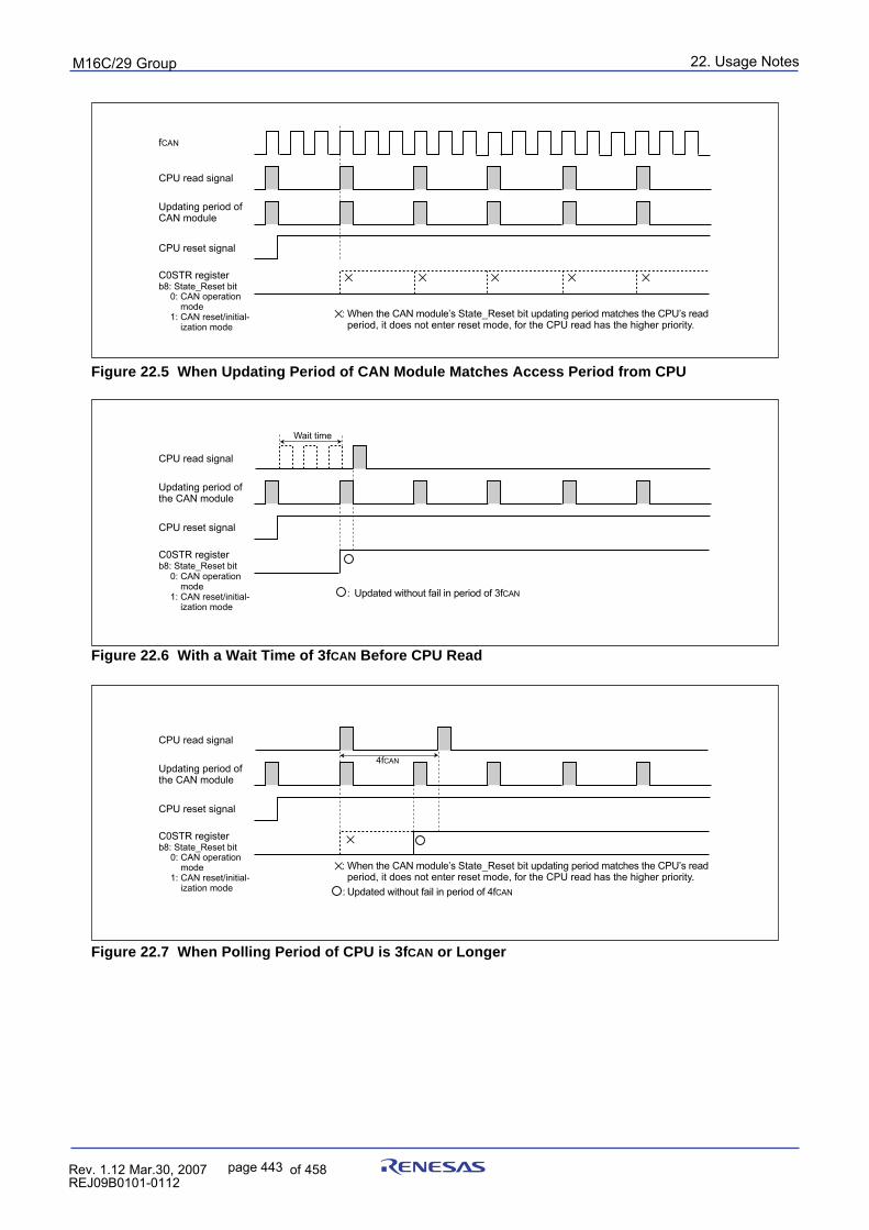
puorG92/C61M 22. Usage Notes
page 443 854fo7002,03.raM21.1.veR2110-1010B90JER
Figure 22.5 When Updating Period of CAN Module Matches Access Period from CPU
Figure 22.6 With a Wait Time of 3fCAN Before CPU Read
Figure 22.7 When Polling Period of CPU is 3fCAN or Longer
fCAN
: When the CAN module’s State_Reset bit updating period matches the CPU’s readperiod, it does not enter reset mode, for the CPU read has the higher priority.
CPU read signal
CPU reset signal
Updating period ofCAN module
C0STR registerb8: State_Reset bit
0: CAN operation mode
1: CAN reset/initial-ization mode
: Updated without fail in period of 3fCAN
CPU read signal
CPU reset signal
Updating period ofthe CAN module
C0STR registerb8: State_Reset bit
Wait time
0: CAN operation mode
1: CAN reset/initial-ization mode
CPU read signal
CPU reset signal
Updating period ofthe CAN module
C0STR registerb8: State_Reset bit
4fCAN
0: CAN operation mode
1: CAN reset/initial-ization mode : Updated without fail in period of 4fCAN
: When the CAN module’s State_Reset bit updating period matches the CPU’s readperiod, it does not enter reset mode, for the CPU read has the higher priority.
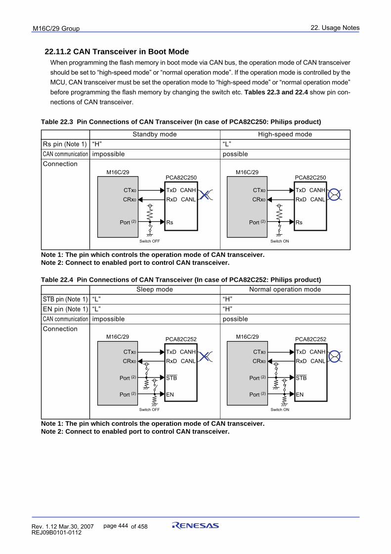
puorG92/C61M 22. Usage Notes
page 444 854fo7002,03.raM21.1.veR2110-1010B90JER
22.11.2 CAN Transceiver in Boot ModeWhen programming the flash memory in boot mode via CAN bus, the operation mode of CAN transceivershould be set to “high-speed mode” or “normal operation mode”. If the operation mode is controlled by theMCU, CAN transceiver must be set the operation mode to “high-speed mode” or “normal operation mode”before programming the flash memory by changing the switch etc. Tables 22.3 and 22.4 show pin con-nections of CAN transceiver.
Table 22.3 Pin Connections of CAN Transceiver (In case of PCA82C250: Philips product)
Standby mode High-speed modeRs pin (Note 1) “H” “L”CAN communication impossible possibleConnection
M16C/29PCA82C250
CTx0
CRx0
Port (2)
TxDRxD
Rs
CANHCANL
Switch OFF
M16C/29PCA82C250
CTx0
CRx0
TxDRxD
Rs
CANHCANL
Port (2)
Switch ON
Sleep mode Normal operation mode_______
STB pin (Note 1) “L” “H”EN pin (Note 1) “L” “H”CAN communication impossible possibleConnection
M16C/29 PCA82C252
CTx0
CRx0
TxDRxD
STB
CANHCANL
EN
Switch OFF
Port (2)
Port (2)
M16C/29 PCA82C252
CTx0
CRx0
TxDRxD
STB
CANHCANL
EN
Port (2)
Port (2)
Switch ON
Note 1: The pin which controls the operation mode of CAN transceiver.Note 2: Connect to enabled port to control CAN transceiver.
Table 22.4 Pin Connections of CAN Transceiver (In case of PCA82C252: Philips product)
Note 1: The pin which controls the operation mode of CAN transceiver.Note 2: Connect to enabled port to control CAN transceiver.
puorG92/C61M 22. Usage Notes
page 445 854fo7002,03.raM21.1.veR2110-1010B90JER
22.12 Programmable I/O Ports_____
1. If a low-level signal is applied to the SD pin when the IVPCR1 bit in the TB2SC register is set to 1_____
(three-phase output forcible cutoff by input on SD pin enabled), the P72 to P75, P80 and P81 pins go toa high-impedance state.
2. The input threshold voltage of pins differs between programmable input/output ports and peripheralfunctions.Therefore, if any pin is shared by a programmable input/output port and a peripheral function and theinput level at this pin is outside the range of recommended operating conditions VIH and VIL (neither“high” nor “low”), the input level may be determined differently depending on which side—the program-mable input/output port or the peripheral function—is currently selected.
3.When the SM32 bit in the S3C register is set to 1, the P32 pin goes to high-impedance state. When theSM42 bit in the S4C register is set to 1, the P96 pin goes to high-imepdance state.
4. When the INV03 bit in the INVC0 register is 1(three-phase motor control timer output enabled), an "L"_______ _____
input on the P85 /NMI/SD pin, has the following effect.
•When the TB2SC register IVPCR1 bit is set to 1 (three-phase output forcible cutoff by input on_____ __ __ ___
SD pin enabled), the U/ U/ V/ V/ W/ W pins go to a high-impedance state.•When the TB2SC register IVPCR1 bit is set to 0 (three-phase output forcible cutoff by input on
_____ __ __ ___
SD pin disabled), the U/ U/ V/ V/ W/ W pins go to a normal port.
Therefore, the P85 pin can not be used as programmable I/O port when the INV03 bit is set to 1._____ _______ _____
When the SD function isn't used, set to 0 (Input) in PD85 and pullup to H in the P85 /NMI/SD pin fromoutside.

puorG92/C61M 22. Usage Notes
page 446 854fo7002,03.raM21.1.veR2110-1010B90JER
22.13 Electric Characteristic Differences Between Mask ROM
and Flash Memory VersionFlash memory version and mask ROM version may have different characteristics, operating margin, noisetolerated dose, noise width dose in electrical characteristics due to internal ROM, different layout pattern,etc. When switching to the mask ROM version, conduct equivalent tests as system evaluation tests con-ducted in the flash memory version.
puorG92/C61M 22. Usage Notes
page 447 854fo7002,03.raM21.1.veR2110-1010B90JER
22.14 Mask ROM Version22.14.1 Internal ROM Area
In the masked ROM version, do not write to internal ROM area. Writing to the area may increase powerconsumption.
22.14.2 Reserved Bit
The b3 to b0 in addresses 0FFFFF16 are reserved bits. Set these bits to 11112.
puorG92/C61M 22. Usage Notes
page 448 854fo7002,03.raM21.1.veR2110-1010B90JER
22.15 Flash Memory Version22.15.1 Functions to Inhibit Rewriting Flash Memory Rewrite
ID codes are stored in addresses 0FFFDF16, 0FFFE316, 0FFFEB16, 0FFFEF16, 0FFFF316, 0FFFF716,and 0FFFFB16. If wrong data are written to theses addresses, the flash memory cannot be read or writtenin standard serial I/O mode.The ROMCP register is mapped in address 0FFFFF16. If wrong data is written to this address, the flashmemory cannot be read or written in parallel I/O mode.In the flash memory version of MCU, these addresses are allocated to the vector addresses ("H") of fixedvectors. The b3 to b0 in address 0FFFFF16 are reserved bits. Set these bits to 11112.
22.15.2 Stop ModeWhen the MCU enters stop mode, execute the instruction which sets the CM10 bit to 1 (stop mode) aftersetting the FMR01 bit to 0 (CPU rewrite mode disabled) and disabling the DMA transfer.
22.15.3 Wait Mode
When the MCU enters wait mode, excute the WAIT instruction after setting the FMR01 bit to 0 (CPUrewrite mode disabled).
22.15.4 Low PowerDissipation Mode, On-Chip Oscillator Low Power Dissipation Mode
If the CM05 bit is set to 1 (main clock stop), the following commands must not be executed.• Program• Block erase
22.15.5 Writing Command and DataWrite the command code and data at even addresses.
22.15.6 Program CommandWrite xx4016 in the first bus cycle and write data to the write address in the second bus cycle, and an autoprogram operation (data program and verify) will start. Make sure the address value specified in the firstbus cycle is the same even address as the write address specified in the second bus cycle.
22.15.7 Operation SpeedWhen CPU clock source is main clock, before entering CPU rewrite mode (EW mode 0 or 1), select 10MHz or less for BCLK using the CM06 bit in the CM0 register and bits CM17 to CM16 in the CM1 register.Also, when CPU clock is f3(ROC) on-chip oscillator clock, before entering CPU rewrite mode (EW mode0 or 1), set the ROCR3 to ROCR2 bits in the ROCR register to “divied by 4” or “divide by 8”.On both cases, set the PM17 bit in the PM1 register to 1 (with wait state).
22.15.8 Instructions Inhibited Against UseThe following instructions cannot be used in EW mode 0 because the flash memory’s internal data isreferenced: UND instruction, INTO instruction, JMPS instruction, JSRS instruction, and BRK instruction
puorG92/C61M 22. Usage Notes
page 449 854fo7002,03.raM21.1.veR2110-1010B90JER
22.15.9 InterruptsEW Mode 0
• Any interrupt which has a vector in the variable vector table can be used providing that its vector istransferred into the RAM area.
_______
• The NMI and watchdog timer interrupts can be used because the FMR0 register and FMR1 registerare initialized when one of those interrupts occurs. The jump addresses for those interrupt serviceroutines should be set in the fixed vector table.
_______
Because the rewrite operation is halted when a NMI or watchdog timer interrupt occurs, the rewriteprogram must be executed again after exiting the interrupt service routine.
• The address match interrupt cannot be used because the flash memory’s internal data is referenced.EW Mode 1
• Make sure that any interrupt which has a vector in the variable vector table or address match inter-rupt will not be accepted during the auto program period or auto erase period with erase-suspendfunction disabled.
_______
• The NMI interrupt can be used because the FMR0 register and FMR1 register are initialized whenthis interrupt occurs. The jump address for the interrupt service routine should be set in the fixedvector table.
_______
Because the rewrite operation is halted when a NMI interrupt occurs, the rewrite program must beexecuted again after exiting the interrupt service routine.
22.15.10 How to Access
To set the FMR01, FMR02, FMR11 or FMR16 bit to 1, set the subject bit to 1 immediately after setting to0. Do not generate an interrupt or a DMA transfer between the instruction to set the bit to 0 and the
_______
instruction to set the bit to 1. Set the bit when the PM24 bit is set to 1 (NMI funciton) and an high-level (“H”)_______
signal is applied to the NMI pin.
22.15.11 Writing in the User ROM Area
EW Mode 0• If the power supply voltage drops while rewriting any block in which the rewrite control program is
stored, a problem may occur that the rewrite control program is not correctly rewritten and, conse-quently, the flash memory becomes unable to be rewritten thereafter. In this case, standard serial I/O or parallel I/O mode should be used.
EW Mode 1• Avoid rewriting any block in which the rewrite control program is stored.
22.15.12 DMA TransferIn EW mode 1, make sure that no DMA transfers will occur while the FMR00 bit in the FMR0 register is setto 0(during the auto program or auto erase period).
22.15.13 Regarding Programming/Erasure Times and Execution Time
As the number of programming/erasure times increases, so does the execution time for software com-mands (Program, and Block Erase).The software commands are aborted by hardware reset 1, brown-out detection reset (hardware reset 2),_______
NMI interrupt, and watchdog timer interrupt. If a software command is aborted by such reset or interrupt,the affected block must be erased before reexecuting the aborted command.
puorG92/C61M 22. Usage Notes
page 450 854fo7002,03.raM21.1.veR2110-1010B90JER
22.15.14 Definition of Programming/Erasure Times"Number of programs and erasure" refers to the number of erasure per block.If the number of program and erasure is n (n=100 1,000 10,000) each block can be erased n times.For example, if a 2K byte block A is erased after writing 1 word data 1024 times, each to a differentaddress, this is counted as one program and erasure. However, data cannot be written to the sameadrress more than once without erasing the block. (Rewrite prohibited)
22.15.15 Flash Memory Version Electrical Characteristics 10,000 E/W cycle products (
Normal: U7, U9; T-ver./V-ver.: U7)When Block A or B E/W cycles exceed 100, set the FMR17 bit in the FMR1 register to 1 (1 wait) to selectone wait state per block access for products U7 and U9. When the FMR17 bit is set to 1, one wait state isinserted per access to Block A or B - regardless of the value of the PM17 bit. Wait state insertion duringaccess to all other blocks, as well as to internal RAM, is controlled by the PM17 bit - regardless of thesetting of the FMR17 bit.To use the limited number of erasure efficiently, write to unused address within the block instead ofrewite. Erase block only after all possible address are used. For example, an 8-word program can bewritten 128 times before erase becomes necessary.Maintaining an equal number of erasure between Block A and B will also improve efficiency.We recommend keeping track of the number of times erasure is used.
22.15.16 Boot Mode
An undefined value is sometimes output in the I/O port until the internal power supply becomes stable_____________
when "H" is applied to the CNVSS pin and "L" is applied to the RESET pin.When setting the CNVSS pin to "H", the following procedure is required:
____________
(1) Apply an "L" signal to the RESET pin and the CNVSS pin.(2) Bring VCC to more than 2.7V, and wait at least 2 msec. (Internal power supply stable waiting time)(3) Apply an "H" signal to the CNVSS pin.
____________
(4) Apply an "H" signal to the RESET pin.
When the CNVSS pin is “H” and RESET pin is “L”, P67 pin is connected to the pull-up resister.
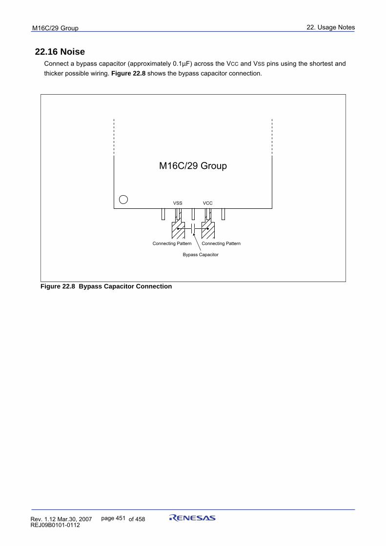
puorG92/C61M 22. Usage Notes
page 451 854fo7002,03.raM21.1.veR2110-1010B90JER
M16C/29 Group
Bypass Capacitor
Connecting PatternConnecting Pattern
VSS VCC
22.16 NoiseConnect a bypass capacitor (approximately 0.1µF) across the VCC and VSS pins using the shortest andthicker possible wiring. Figure 22.8 shows the bypass capacitor connection.
Figure 22.8 Bypass Capacitor Connection
puorG92/C61M 22. Usage Notes
page 452 854fo7002,03.raM21.1.veR2110-1010B90JER
22.17 Instruction for a Device UseWhen handling a device, extra attention is necessary to prevent it from crashing during the electrostaticdischarge period.
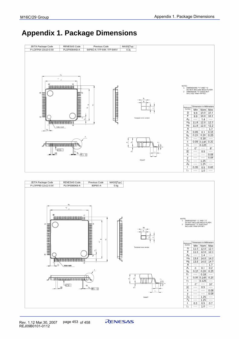
puorG92/C61M Appendix 1. Package Dimensions
page 453 854fo7002,03.raM21.1.veR2110-1010B90JER
Appendix 1. Package Dimensions
Terminal cross section
c 1
p
c
2.
1. *2"NOTE)
INCLUDE TRIM OFFSET.
F
*1
*2
HEE
HD
D
Z
ZE
Detail F
A cA2
A1
L1
L
P-LQFP64-10x10-0.50 0.3g
MASS[Typ.]
64P6Q-A / FP-64K / FP-64KVPLQP0064KB-A
RENESAS CodeJEITA Package Code Previous Code
1.0
0.125
0.18
1.25
1.25
0.08
0.200.1450.09
0.200.15
MaxNomMinSymbolReference
10.110.09.9D
10.110.09.9E
A
12.212.011.8
12.011.8
1.7A
0.150.10.05
0.650.50.35L
x
8°0°
c
0.5e
0.08y
HD
E
A1
p
b1
c1
ZD
ZE
L1
Detail F
cA
L1
LA1
A2
*2
*1
F
41
0
20
ZE
E HE
D
HD
2.
1. DIMENSIONS "*1" AND "*2"NOTE)
DIMENSION "*3" DOES NOTINCLUDE TRIM OFFSET.
Previous CodeJEITA Package Code RENESAS Code
PLQP0080KB-A 80P6Q-A
MASS[Typ.]
0.5gP-LQFP80-12x12-0.50
1.0
0.125
0.18
1.25
1.25
0.08
0.200.1450.09
0.250.200.15
MaxNomMin
Dimension in MillimetersSymbol
Reference
12.112.011.9D
12.112.011.9E
1.4A
14.214.013.8
14.214.013.8
1.7
0.20.10
0.70.50.3L
x
10°0°
c
0.5e
0.08y
HD
E
A1
p
b1
c1
ZD
ZE
L1
Terminal cross section
c 1
1
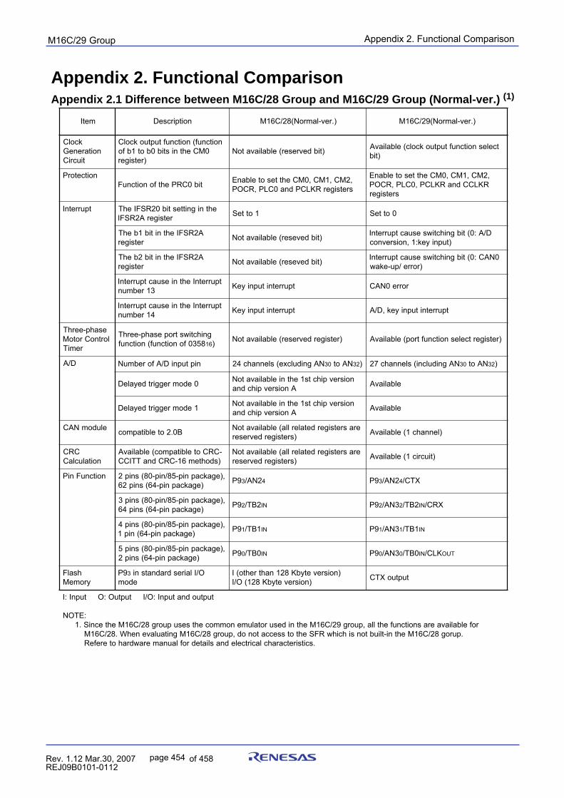
puorG92/C61M Appendix 2. Functional Comparison
page 454 854fo7002,03.raM21.1.veR2110-1010B90JER
metI noitpircseD ).rev-lamroN(82/C61M ).rev-lamroN(92/C61M
kcolCnoitareneG
tiucriC
noitcnuf(noitcnuftuptuokcolC0MCehtnistib0bot1bfo
)retsiger)tibdevreser(elbaliavatoN tcelesnoitcnuftuptuokcolc(elbaliavA
)tib
noitcetorPtib0CRPehtfonoitcnuF ,2MC,1MC,0MCehttesotelbanE
sretsigerRKLCPdna0CLP,RCOP
,2MC,1MC,0MCehttesotelbanERKLCCdnaRKLCP,0CLP,RCOP
sretsiger
tpurretnI ehtnignittestib02RSFIehTretsigerA2RSFI 1otteS 0otteS
A2RSFIehtnitib1behTretsiger )tibdeveser(elbaliavatoN D/A:0(tibgnihctiwsesuactpurretnI
)tupniyek:1,noisrevnoc
A2RSFIehtnitib2behTretsiger )tibdeveser(elbaliavatoN 0NAC:0(tibgnihctiwsesuactpurretnI
)rorre/pu-ekaw
tpurretnIehtniesuactpurretnI31rebmun tpurretnitupniyeK rorre0NAC
tpurretnIehtniesuactpurretnI41rebmun tpurretnitupniyeK tpurretnitupniyek,D/A
esahp-eerhTlortnoCrotoM
remiT
gnihctiwstropesahp-eerhT8530fonoitcnuf(noitcnuf 61 ) )retsigerdevreser(elbaliavatoN )retsigertcelesnoitcnuftrop(elbaliavA
D/A niptupniD/AforebmuN NAgnidulcxe(slennahc42 03 NAot 23 ) NAgnidulcni(slennahc72 03 NAot 23 )
0edomreggirtdeyaleD noisrevpihcts1ehtnielbaliavatoNAnoisrevpihcdna elbaliavA
1edomreggirtdeyaleD noisrevpihcts1ehtnielbaliavatoNAnoisrevpihcdna elbaliavA
eludomNAC B0.2otelbitapmoc erasretsigerdetalerlla(elbaliavatoN)sretsigerdevreser )lennahc1(elbaliavA
CRCnoitaluclaC
-CRCotelbitapmoc(elbaliavA)sdohtem61-CRCdnaTTICC
erasretsigerdetalerlla(elbaliavatoN)sretsigerdevreser )tiucric1(elbaliavA
noitcnuFniP ,)egakcapnip-58/nip-08(snip2)egakcapnip-46(snip26 9P 3 2NA/ 4 9P 3 2NA/ 4 XTC/
,)egakcapnip-58/nip-08(snip3)egakcapnip-46(snip46 9P 2 2BT/ NI 9P 2 3NA/ 2 2BT/ NI XRC/
,)egakcapnip-58/nip-08(snip4)egakcapnip-46(nip1 9P 1 1BT/ NI 9P 1 3NA/ 1 1BT/ NI
,)egakcapnip-58/nip-08(snip5)egakcapnip-46(snip2 9P 0 0BT/ NI 9P 0 3NA/ 0 0BT/ NI KLC/ TUO
hsalFyromeM
9P 3 O/Ilairesdradnatsniedom
)noisrevetybK821nahtrehto(I)noisrevetybK821(O/I tuptuoXTC
tuptuodnatupnI:O/ItuptuO:OtupnI:I
:ETONrofelbaliavaerasnoitcnufehtlla,puorg92/C61Mehtnidesurotalumenommocehtsesupuorg82/C61MehtecniS.1
.purog82/C61Mehtni-tliubtonsihcihwRFSehtotsseccatonod,puorg82/C61MgnitaulavenehW.82/C61M.scitsiretcarahclacirtcelednasliatedroflaunamerawdrahoterefeR
Appendix 2. Functional ComparisonAppendix 2.1 Difference between M16C/28 Group and M16C/29 Group (Normal-ver.) (1)
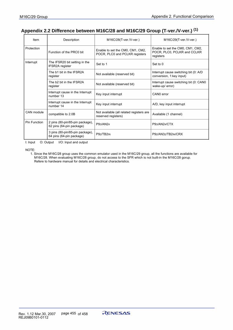
puorG92/C61M Appendix 2. Functional Comparison
page 455 854fo7002,03.raM21.1.veR2110-1010B90JER
metI noitpircseD ).rev-V/.rev-T(82/C61M ).rev-V/.rev-T(92/C61M
noitcetorPtib0CRPehtfonoitcnuF ,2MC,1MC,0MCehttesotelbanE
sretsigerRKLCPdna0CLP,RCOP
,2MC,1MC,0MCehttesotelbanERKLCCdnaRKLCP,0CLP,RCOP
sretsiger
tpurretnI ehtnignittestib02RSFIehTretsigerA2RSFI 1otteS 0otteS
A2RSFIehtnitib1behTretsiger )tibdevreser(elbaliavatoN D/A:0(tibgnihctiwsesuactpurretnI
)tupniyek:1,noisrevnoc
A2RSFIehtnitib2behTretsiger )tibdevreser(elbaliavatoN 0NAC:0(tibgnihctiwsesuactpurretnI
)rorre/pu-ekaw
tpurretnIehtniesuactpurretnI31rebmun tpurretnitupniyeK rorre0NAC
tpurretnIehtniesuactpurretnI41rebmun tpurretnitupniyeK tpurretnitupniyek,D/A
eludomNAC B0.2otelbitapmoc erasretsigerdetalerlla(elbaliavatoN)sretsigerdevreser )lennahc1(elbaliavA
noitcnuFniP ,)egakcapnip-58/nip-08(snip2)egakcapnip-46(snip26 9P 3 2NA/ 4 9P 3 2NA/ 4 XTC/
,)egakcapnip-58/nip-08(snip3)egakcapnip-46(snip46 9P 2 2BT/ NI 9P 2 3NA/ 2 2BT/ NI XRC/
tuptuodnatupnI:O/ItuptuO:OtupnI:I
:ETONrofelbaliavaerasnoitcnufehtlla,puorg92/C61Mehtnidesurotalumenommocehtsesupuorg82/C61MehtecniS.1
.purog82/C61Mehtni-tliubtonsihcihwRFSehtotsseccatonod,puorg82/C61MgnitaulavenehW.82/C61M.scitsiretcarahclacirtcelednasliatedroflaunamerawdrahoterefeR
Appendix 2.2 Difference between M16C/28 and M16C/29 Group (T-ver./V-ver.) (1)
Register IndexpuorG92/C61M
page 456 854fo7002,03.raM21.1.veR2110-1010B90JER
Register IndexA
AD0 to AD7 226
ADCON0 to ADCON2 224
ADIC 76
ADSTAT0 226
ADTRGCON 225
AIER 88
B
BCNIC 76
BTIC 76
C
C01ERRIC 76
C01WKIC 76
C0AFS 299
C0CONR 297
C0CTLR 293
C0ICR 296
C0IDR 296
C0MCTLj 292
C0RECIC 76
C0RECR 298
C0SSTR 295
C0STR 294
C0TECR 298
C0TRMIC 76
C0TSR 299
CCLKR 53
CM0 49
CM1 50
CM2 51
CPSRF 105, 118
CRCD 314
CRCIN 314
CRCMR 314
CRCSAR 314
D
D4INT 40
DAR0 95
DAR1 95
DM0CON 94
DM0IC 76
DM0SL 93
DM1CON 94
DM1IC 76
DM1SL 94
DTT 129
F
FMR0 341
FMR1 341
FMR4 342
G
G1BCR0 142
G1BCR1 143
G1BT 142
G1BTRR 144
G1DV 143
G1FE 148
G1FS 148
G1IE0 150
G1IE1 150
G1IR 149
G1PO0 to G1PO7 147
G1POCR0 to G1POCR7 146
G1TM0 to G1TM7 146
G1TMCR0 to G1TMCR7 145
G1TPR6 to G1TPR7 145
I
ICOC0IC 76
ICOC1IC 76
ICTB2 129, 130
IDB0 129
IDB1 129
IFSR 77, 85
IFSR2A 77
IICIC 76
INT0IC to INT2IC 76
INT3IC 76
INT4IC 76
INT5IC 76
INVC0 127
INVC1 128
Register IndexpuorG92/C61M
page 457 854fo7002,03.raM21.1.veR2110-1010B90JER
K
KUPIC 76
N
NDDR 327
O
ONSF 105
P
P0 to P3 324
P17DDR 327
P6 to P10 324
PACR 177, 326
PCLKR 52
PCR 326
PD0 to PD3 323
PD6 to PD10 323
PDRF 137
PFCR 139
PLC0 53
PM0 44
PM1 44
PM2 45, 52
PRCR 69
PUR0 to PUR2 325
R
RMAD0 88
RMAD1 88
ROCR 50
ROMCP 336
S
S00 258
S0D0 257
S0RIC to S2RIC 76
S0TIC to S2TIC 76
S10 260
S1D0 259
S20 258
S2D0 263
S31C 76
S3BRG 218
S3C 218
S3D0 261
S3TRR 218
S4BRG 218
S4C 218
S4D0 262
S4IC 76
S4TRR 218
SAR0 95
SAR1 95
SCLDAIC 76
T
TA0 to TA4 104
TA0IC to TA4IC 76
TA0MR to TA4MR 103
TA11 130
TA1MR 133
TA2 130
TA21 130
TA2MR 133
TA4 130
TA41 130
TA4MR 133
TABSR 104, 118, 132
TB0 to TB2 118
TB0IC to TB2IC 76
TB0MR to TB2MR 117
TB2 132
TB2MR 133
TB2SC 131, 227
TCR0 95
TCR1 95
TPRC 139
TRGSR 105, 132
U
U0BRG to U2BRG 174
U0C0 to U2C0 176
U0C1 to U2C1 177
U0MR to U2MR 175
U0RB to U2RB 174
U0TB to U2TB 174
U2SMR 178
U2SMR2 178
U2SMR3 179
U2SMR4 179
UCON 176
UDF 104
Register IndexpuorG92/C61M
page 458 854fo7002,03.raM21.1.veR2110-1010B90JER
V
VCR1 39
VCR2 39
W
WDC 90
WDTS 90
REVISION HISTORY M16C/29 Hardware Manual
Rev. Date DescriptionPage Summary
C-1
0.70 Mar/ 29/Y04 1 “1. Overview” and “1.1. Application” are partly revised.2, 3 Table 1.2.1 and 1.2.2 are partly revised.8, 9 Figure 1.5.1 and 1.5.2 are partly revised.10 Table 1.6.1 is revised.22 Figure 4.8 is partly revised.28 Section “5.5 Voltage Detection Circuit” and Figure 5.5.2 are partly revised.30 Figure 5.5.3 is partly revised.31 Figure 5.5.4 is partly revised.32 Section “5.5.1 Voltage Detection Interrupt” and “5.5.1.1.1 Limitations of Stop
Mode” are partly revised.36 Figure 7.1 is partly revised.37 Figure 7.2 is partly revised.38 Figure 7.3 is partly revised.39 Figure 7.5 is partly revised.40 Figure 7.6 is partly revised.41 “CCLKR register” of Figure 7.7 is partly revised.42 Section “7.1 Main clock” is partly revised.45 Figure 7.4.1 is partly revised.46 Section “7.5 CPU Clock and Peripheral Function Clock” and “7.5.2 Peripheral
Function Clock” are partly revised.54 Section “7.7 System Clock Protective Function” and “7.8 Oscillation Stop and Re-
oscillation Detect Function” are partly revised.57 Figure 8.1 is partly revised.64 Figure 9.3.1 is partly revised.65 IFSR2A registerin Figure 9.3.2 is partly revised.66 Section “9.3.2 IR Bit” is partly revised.67 Section “9.4 Interrupt Sequence” is partly revised.68 Section “9.4.1 Interrupt Response Time” and Figure9.4.1.1 are partly revised.73 Section “9.6 INT Interrupt” is partly revised.74 Section “9.9 CAN0 Wake-up Interrupt” is partly revised.94 “Divide ratio” of Table 12.1.1.1 is partly revised.102 “8-bit PWM” of Table 12.1.4.1 is partly revised.106 “Timer Bi register” in Figure 12.2.3 is partly revised.111 Section “12.2.4 A-D Trigger mode” and Table 12.2.4.1 are partly revised.112 Figure 12.2.4.2 is partly revised.115 Figure 12.3.2 is partly revised.117 “Timer B2 interrupt occurences fequency set counter” in Figure 12.3.4 is partly
revised.119 Figure 12.3.6 is partly revised.
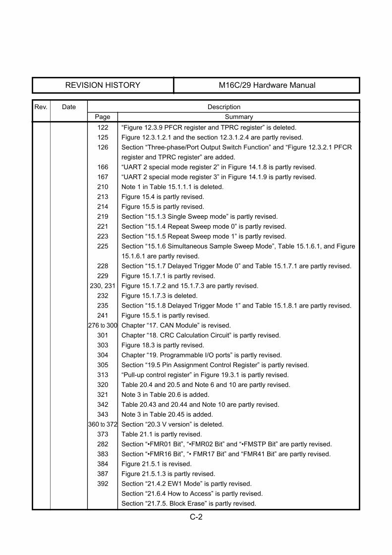
REVISION HISTORY M16C/29 Hardware Manual
Rev. Date DescriptionPage Summary
C-2
122 “Figure 12.3.9 PFCR register and TPRC register” is deleted.125 Figure 12.3.1.2.1 and the section 12.3.1.2.4 are partly revised.126 Section “Three-phase/Port Output Switch Function” and “Figure 12.3.2.1 PFCR
register and TPRC register” are added.166 “UART 2 special mode register 2” in Figure 14.1.8 is partly revised.167 “UART 2 special mode register 3” in Figure 14.1.9 is partly revised.210 Note 1 in Table 15.1.1.1 is deleted.213 Figure 15.4 is partly revised.214 Figure 15.5 is partly revised.219 Section “15.1.3 Single Sweep mode” is partly revised.221 Section “15.1.4 Repeat Sweep mode 0” is partly revised.223 Section “15.1.5 Repeat Sweep mode 1” is partly revised.225 Section “15.1.6 Simultaneous Sample Sweep Mode”, Table 15.1.6.1, and Figure
15.1.6.1 are partly revised.228 Section “15.1.7 Delayed Trigger Mode 0” and Table 15.1.7.1 are partly revised.229 Figure 15.1.7.1 is partly revised.
230, 231 Figure 15.1.7.2 and 15.1.7.3 are partly revised.232 Figure 15.1.7.3 is deleted.235 Section “15.1.8 Delayed Trigger Mode 1” and Table 15.1.8.1 are partly revised.241 Figure 15.5.1 is partly revised.
276 to 300 Chapter “17. CAN Module” is revised.301 Chapter “18. CRC Calculation Circuit” is partly revised.303 Figure 18.3 is partly revised.304 Chapter “19. Programmable I/O ports” is partly revised.305 Section “19.5 Pin Assignment Control Register” is partly revised.313 “Pull-up control register” in Figure 19.3.1 is partly revised.320 Table 20.4 and 20.5 and Note 6 and 10 are partly revised.321 Note 3 in Table 20.6 is added.342 Table 20.43 and 20.44 and Note 10 are partly revised.343 Note 3 in Table 20.45 is added.
360 to 372 Section “20.3 V version” is deleted.373 Table 21.1 is partly revised.282 Section “•FMR01 Bit”, “•FMR02 Bit” and “•FMSTP Bit” are partly revised.383 Section “•FMR16 Bit”, “• FMR17 Bit” and “FMR41 Bit” are partly revised.384 Figure 21.5.1 is revised.387 Figure 21.5.1.3 is partly revised.392 Section “21.4.2 EW1 Mode” is partly revised.
Section “21.6.4 How to Access” is partly revised.Section “21.7.5. Block Erase” is partly revised.
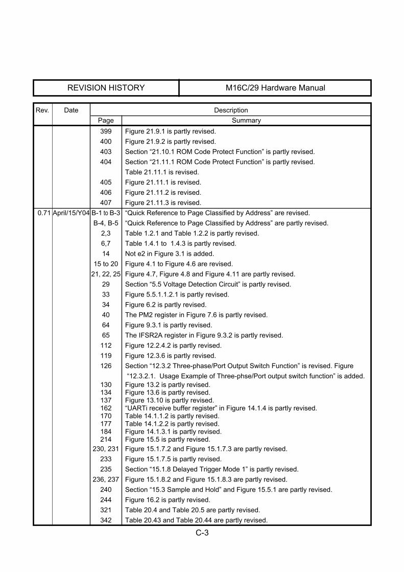
REVISION HISTORY M16C/29 Hardware Manual
Rev. Date DescriptionPage Summary
C-3
399 Figure 21.9.1 is partly revised.400 Figure 21.9.2 is partly revised.403 Section “21.10.1 ROM Code Protect Function” is partly revised.404 Section “21.11.1 ROM Code Protect Function” is partly revised.
Table 21.11.1 is revised.405 Figure 21.11.1 is revised.406 Figure 21.11.2 is revised.407 Figure 21.11.3 is revised.
0.71 April/15/Y04 B-1 to B-3 “Quick Reference to Page Classified by Address” are revised.B-4, B-5 “Quick Reference to Page Classified by Address” are partly revised.
2,3 Table 1.2.1 and Table 1.2.2 is partly revised.6,7 Table 1.4.1 to 1.4.3 is partly revised.14 Not e2 in Figure 3.1 is added.
15 to 20 Figure 4.1 to Figure 4.6 are revised.21, 22, 25 Figure 4.7, Figure 4.8 and Figure 4.11 are partly revised.
29 Section “5.5 Voltage Detection Circuit” is partly revised.33 Figure 5.5.1.1.2.1 is partly revised.34 Figure 6.2 is partly revised.40 The PM2 register in Figure 7.6 is partly revised.64 Figure 9.3.1 is partly revised.65 The IFSR2A register in Figure 9.3.2 is partly revised.112 Figure 12.2.4.2 is partly revised.119 Figure 12.3.6 is partly revised.126 Section “12.3.2 Three-phase/Port Output Switch Function” is revised. Figure
“12.3.2.1. Usage Example of Three-phse/Port output switch function” is added.130 Figure 13.2 is partly revised.134 Figure 13.6 is partly revised.137 Figure 13.10 is partly revised.162 “UARTi receive buffer register” in Figure 14.1.4 is partly revised.170 Table 14.1.1.2 is partly revised.177 Table 14.1.2.2 is partly revised.184 Figure 14.1.3.1 is partly revised.214 Figure 15.5 is partly revised.
230, 231 Figure 15.1.7.2 and Figure 15.1.7.3 are partly revised.233 Figure 15.1.7.5 is partly revised.235 Section “15.1.8 Delayed Trigger Mode 1” is partly revised.
236, 237 Figure 15.1.8.2 and Figure 15.1.8.3 are partly revised.240 Section “15.3 Sample and Hold” and Figure 15.5.1 are partly revised.244 Figure 16.2 is partly revised.321 Table 20.4 and Table 20.5 are partly revised.342 Table 20.43 and Table 20.44 are partly revised.
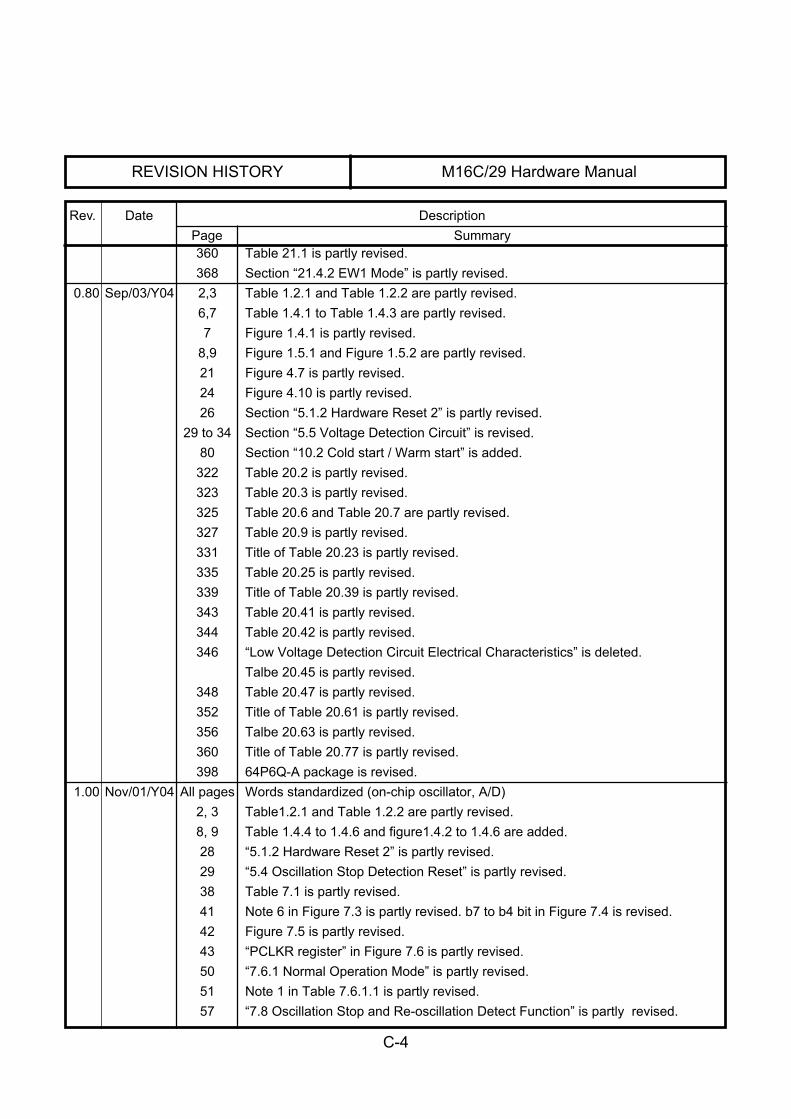
REVISION HISTORY M16C/29 Hardware Manual
Rev. Date DescriptionPage Summary
C-4
360 Table 21.1 is partly revised.368 Section “21.4.2 EW1 Mode” is partly revised.
0.80 Sep/03/Y04 2,3 Table 1.2.1 and Table 1.2.2 are partly revised.6,7 Table 1.4.1 to Table 1.4.3 are partly revised.7 Figure 1.4.1 is partly revised.
8,9 Figure 1.5.1 and Figure 1.5.2 are partly revised.21 Figure 4.7 is partly revised.24 Figure 4.10 is partly revised.26 Section “5.1.2 Hardware Reset 2” is partly revised.
29 to 34 Section “5.5 Voltage Detection Circuit” is revised.80 Section “10.2 Cold start / Warm start” is added.322 Table 20.2 is partly revised.323 Table 20.3 is partly revised.325 Table 20.6 and Table 20.7 are partly revised.327 Table 20.9 is partly revised.331 Title of Table 20.23 is partly revised.335 Table 20.25 is partly revised.339 Title of Table 20.39 is partly revised.343 Table 20.41 is partly revised.344 Table 20.42 is partly revised.346 “Low Voltage Detection Circuit Electrical Characteristics” is deleted.
Talbe 20.45 is partly revised.348 Table 20.47 is partly revised.352 Title of Table 20.61 is partly revised.356 Talbe 20.63 is partly revised.360 Title of Table 20.77 is partly revised.398 64P6Q-A package is revised.
1.00 Nov/01/Y04 All pages Words standardized (on-chip oscillator, A/D)2, 3 Table1.2.1 and Table 1.2.2 are partly revised.8, 9 Table 1.4.4 to 1.4.6 and figure1.4.2 to 1.4.6 are added.28 “5.1.2 Hardware Reset 2” is partly revised.29 “5.4 Oscillation Stop Detection Reset” is partly revised.38 Table 7.1 is partly revised.41 Note 6 in Figure 7.3 is partly revised. b7 to b4 bit in Figure 7.4 is revised.42 Figure 7.5 is partly revised.43 “PCLKR register” in Figure 7.6 is partly revised.50 “7.6.1 Normal Operation Mode” is partly revised.51 Note 1 in Table 7.6.1.1 is partly revised.57 “7.8 Oscillation Stop and Re-oscillation Detect Function” is partly revised.
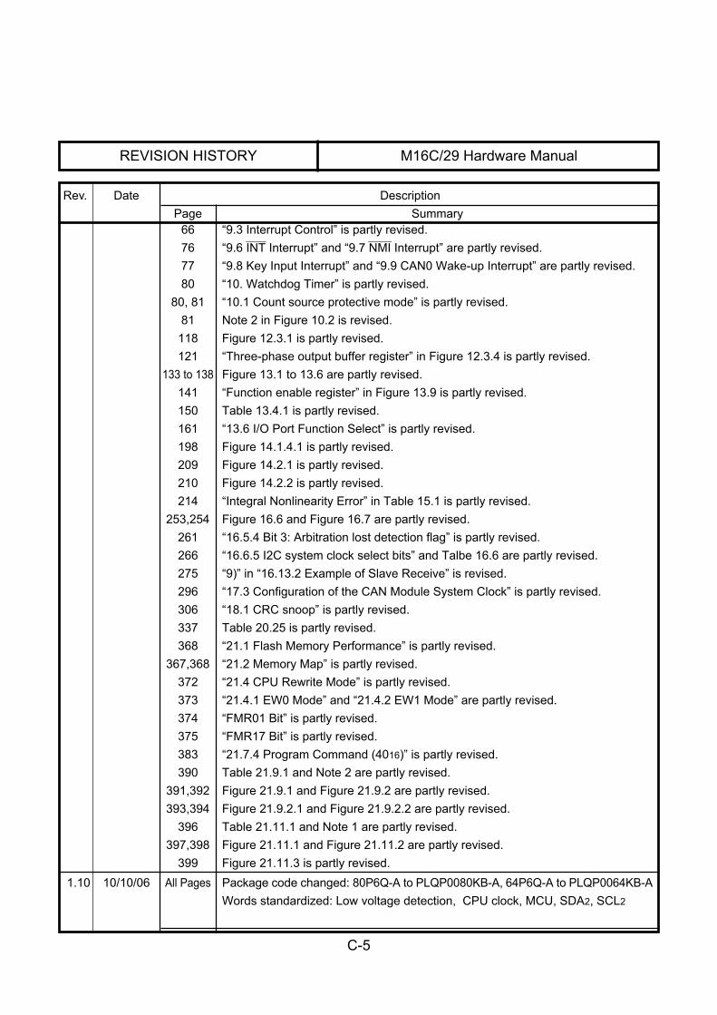
REVISION HISTORY M16C/29 Hardware Manual
Rev. Date DescriptionPage Summary
C-5
66 “9.3 Interrupt Control” is partly revised.76
______ _______
“9.6 INT Interrupt” and “9.7 NMI Interrupt” are partly revised.77 “9.8 Key Input Interrupt” and “9.9 CAN0 Wake-up Interrupt” are partly revised.80 “10. Watchdog Timer” is partly revised.
80, 81 “10.1 Count source protective mode” is partly revised.81 Note 2 in Figure 10.2 is revised.118 Figure 12.3.1 is partly revised.121 “Three-phase output buffer register” in Figure 12.3.4 is partly revised.
133 to 138 Figure 13.1 to 13.6 are partly revised.141 “Function enable register” in Figure 13.9 is partly revised.150 Table 13.4.1 is partly revised.161 “13.6 I/O Port Function Select” is partly revised.198 Figure 14.1.4.1 is partly revised.209 Figure 14.2.1 is partly revised.210 Figure 14.2.2 is partly revised.214 “Integral Nonlinearity Error” in Table 15.1 is partly revised.
253,254 Figure 16.6 and Figure 16.7 are partly revised.261 “16.5.4 Bit 3: Arbitration lost detection flag” is partly revised.266 “16.6.5 I2C system clock select bits” and Talbe 16.6 are partly revised.275 “9)” in “16.13.2 Example of Slave Receive” is revised.296 “17.3 Configuration of the CAN Module System Clock” is partly revised.306 “18.1 CRC snoop” is partly revised.337 Table 20.25 is partly revised.368 “21.1 Flash Memory Performance” is partly revised.
367,368 “21.2 Memory Map” is partly revised.372 “21.4 CPU Rewrite Mode” is partly revised.373 “21.4.1 EW0 Mode” and “21.4.2 EW1 Mode” are partly revised.374 “FMR01 Bit” is partly revised.375 “FMR17 Bit” is partly revised.383 “21.7.4 Program Command (4016)” is partly revised.390 Table 21.9.1 and Note 2 are partly revised.
391,392 Figure 21.9.1 and Figure 21.9.2 are partly revised.393,394 Figure 21.9.2.1 and Figure 21.9.2.2 are partly revised.
396 Table 21.11.1 and Note 1 are partly revised.397,398 Figure 21.11.1 and Figure 21.11.2 are partly revised.
399 Figure 21.11.3 is partly revised.1.10 10/10/06 All Pages Package code changed: 80P6Q-A to PLQP0080KB-A, 64P6Q-A to PLQP0064KB-A
Words standardized: Low voltage detection, CPU clock, MCU, SDA2, SCL2
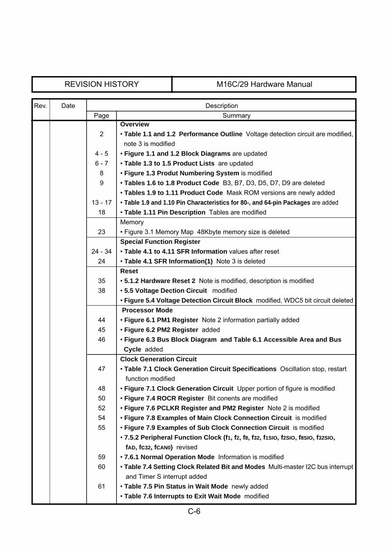
REVISION HISTORY M16C/29 Hardware Manual
Rev. Date DescriptionPage Summary
C-6
Overview
2 • Table 1.1 and 1.2 Performance Outline Voltage detection circuit are modified, note 3 is modified
4 - 5 • Figure 1.1 and 1.2 Block Diagrams are updated6 - 7 • Table 1.3 to 1.5 Product Lists are updated
8 • Figure 1.3 Produt Numbering System is modified9 • Tables 1.6 to 1.8 Product Code B3, B7, D3, D5, D7, D9 are deleted
• Tables 1.9 to 1.11 Product Code Mask ROM versions are newly added13 - 17 • Table 1.9 and 1.10 Pin Characteristics for 80-, and 64-pin Packages are added
18 • Table 1.11 Pin Description Tables are modifiedMemory
23 • Figure 3.1 Memory Map 48Kbyte memory size is deletedSpecial Function Register
24 - 34 • Table 4.1 to 4.11 SFR Information values after reset24 • Table 4.1 SFR Information(1) Note 3 is deleted
Reset
35 • 5.1.2 Hardware Reset 2 Note is modified, description is modified38 • 5.5 Voltage Dection Circuit modified
• Figure 5.4 Voltage Detection Circuit Block modified, WDC5 bit circuit deleted Processor Mode
44 • Figure 6.1 PM1 Register Note 2 information partially added45 • Figure 6.2 PM2 Register added46 • Figure 6.3 Bus Block Diagram and Table 6.1 Accessible Area and Bus
Cycle addedClock Generation Circuit
47 • Table 7.1 Clock Generation Circuit Specifications Oscillation stop, restart function modified
48 • Figure 7.1 Clock Generation Circuit Upper portion of figure is modified50 • Figure 7.4 ROCR Register Bit conents are modified52 • Figure 7.6 PCLKR Register and PM2 Register Note 2 is modified54 • Figure 7.8 Examples of Main Clock Connection Circuit is modified55 • Figure 7.9 Examples of Sub Clock Connection Circuit is modified
• 7.5.2 Peripheral Function Clock (f1, f2, f8, f32, f1SIO, f2SIO, f8SIO, f32SIO,
fAD, fc32, fCAN0) revised59 • 7.6.1 Normal Operation Mode Information is modified60 • Table 7.4 Setting Clock Related Bit and Modes Multi-master I2C bus interrupt
and Timer S interrupt added61 • Table 7.5 Pin Status in Wait Mode newly added
• Table 7.6 Interrupts to Exit Wait Mode modified
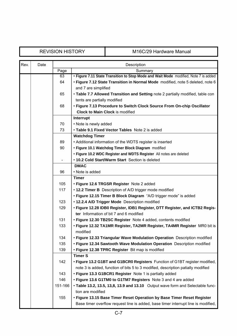
REVISION HISTORY M16C/29 Hardware Manual
Rev. Date DescriptionPage Summary
C-7
63 • Figure 7.11 State Transition to Stop Mode and Wait Mode modified, Note 7 is added64 • Figure 7.12 State Transition in Normal Mode modified, note 5 deleted, note 6
and 7 are simplified65 • Table 7.7 Allowed Transition and Setting note 2 partially modified, table con
tents are partially modified68 • Figure 7.13 Procedure to Switch Clock Source From On-chip Oscillator
Clock to Main Clock is modifiedInterrupt
70 • Note is newly added73 • Table 9.1 Fixed Vector Tables Note 2 is added
Watchdog Timer
89 • Additional information of the WDTS register is inserted90 • Figure 10.1 Watchdog Timer Block Diagram modified
• Figure 10.2 WDC Register and WDTS Register All notes are deleted- • 10.2 Cold Start/Warm Start Section is deleted
DMAC
96 • Note is addedTimer
105 • Figure 12.6 TRGSR Register Note 2 added117 • 12.2 Timer B Description of A/D trigger mode modified
• Figure 12.15 Timer B Block Diagram “A/D trigger mode” is added123 • 12.2.4 A/D Trigger Mode Description modified129 • Figure 12.28 IDB0 Register, IDB1 Register, DTT Register, and ICTB2 Regis-
ter Information of bit 7 and 6 modified131 • Figure 12.30 TB2SC Register Note 4 added, contents modified133 • Figure 12.32 TA1MR Register, TA2MR Register, TA4MR Register MR0 bit is
modified134 • Figure 12.33 Triangular Wave Modulation Operation Description modified135 • Figure 12.34 Sawtooth Wave Modulation Operation Description modified139 • Figure 12.38 TPRC Register Bit map is modified
Timer S
142 • Figure 13.2 G1BT and G1BCR0 Registers Function of G1BT register modified,note 3 is added, function of bits 5 to 3 modified, description patially modified
143 • Figure 13.3 G1BCR1 Register Note 1 is partially added146 • Figure 13.6 G1TM0 to G1TM7 Registers Note 3 and 4 are added
151-166 • Table 13.2, 13.5, 13,8, 13.9 and 13.10 Output wave form and Selectable func-tion are modified
155 • Figure 13.15 Base Timer Reset Operation by Base Timer Reset Register
Base timer overflow request line is added, base timer interrupt line is modified,
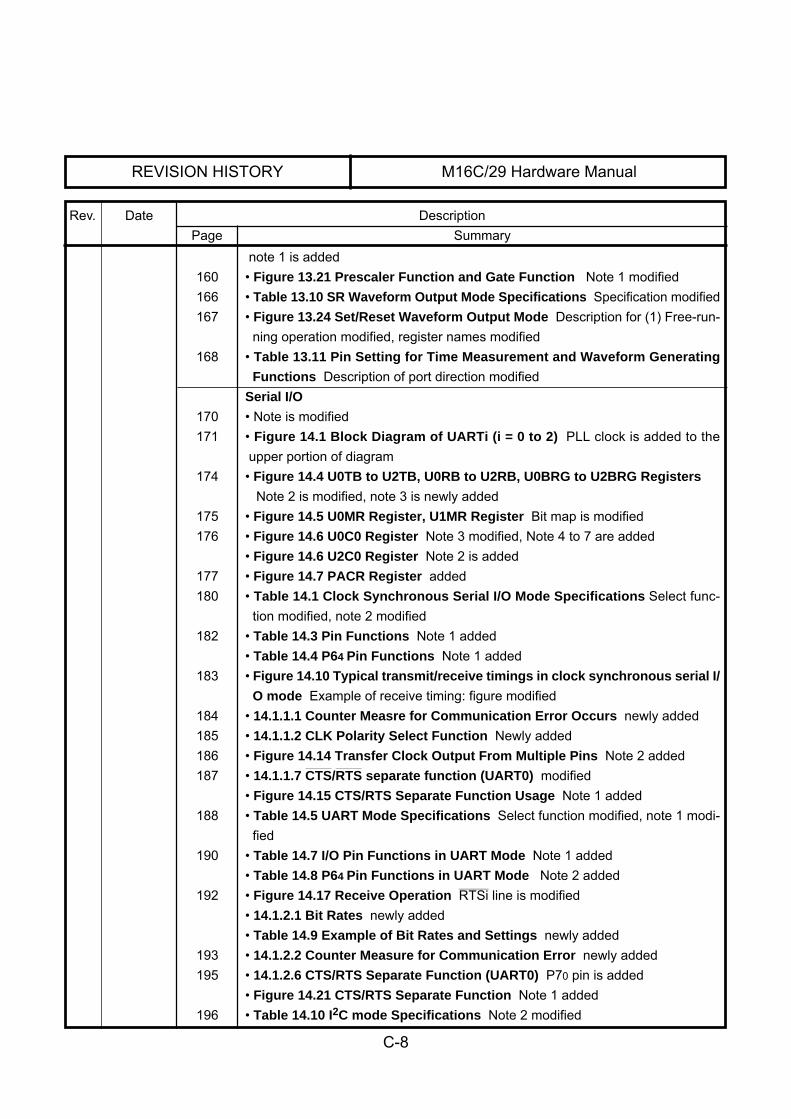
REVISION HISTORY M16C/29 Hardware Manual
Rev. Date DescriptionPage Summary
C-8
note 1 is added160 • Figure 13.21 Prescaler Function and Gate Function Note 1 modified166 • Table 13.10 SR Waveform Output Mode Specifications Specification modified167 • Figure 13.24 Set/Reset Waveform Output Mode Description for (1) Free-run-
ning operation modified, register names modified168 • Table 13.11 Pin Setting for Time Measurement and Waveform Generating
Functions Description of port direction modifiedSerial I/O
170 • Note is modified171 • Figure 14.1 Block Diagram of UARTi (i = 0 to 2) PLL clock is added to the
upper portion of diagram174 • Figure 14.4 U0TB to U2TB, U0RB to U2RB, U0BRG to U2BRG Registers
Note 2 is modified, note 3 is newly added175 • Figure 14.5 U0MR Register, U1MR Register Bit map is modified176 • Figure 14.6 U0C0 Register Note 3 modified, Note 4 to 7 are added
• Figure 14.6 U2C0 Register Note 2 is added177 • Figure 14.7 PACR Register added180 • Table 14.1 Clock Synchronous Serial I/O Mode Specifications Select func-
tion modified, note 2 modified182 • Table 14.3 Pin Functions Note 1 added
• Table 14.4 P64 Pin Functions Note 1 added183 • Figure 14.10 Typical transmit/receive timings in clock synchronous serial I/
O mode Example of receive timing: figure modified184 • 14.1.1.1 Counter Measre for Communication Error Occurs newly added185 • 14.1.1.2 CLK Polarity Select Function Newly added186 • Figure 14.14 Transfer Clock Output From Multiple Pins Note 2 added187
_______ _______
• 14.1.1.7 CTS/RTS separate function (UART0) modified• Figure 14.15 CTS/RTS Separate Function Usage Note 1 added
188 • Table 14.5 UART Mode Specifications Select function modified, note 1 modi-fied
190 • Table 14.7 I/O Pin Functions in UART Mode Note 1 added• Table 14.8 P64 Pin Functions in UART Mode Note 2 added
192________
• Figure 14.17 Receive Operation RTSi line is modified• 14.1.2.1 Bit Rates newly added• Table 14.9 Example of Bit Rates and Settings newly added
193 • 14.1.2.2 Counter Measure for Communication Error newly added195 • 14.1.2.6 CTS/RTS Separate Function (UART0) P70 pin is added
• Figure 14.21 CTS/RTS Separate Function Note 1 added196 • Table 14.10 I2C mode Specifications Note 2 modified
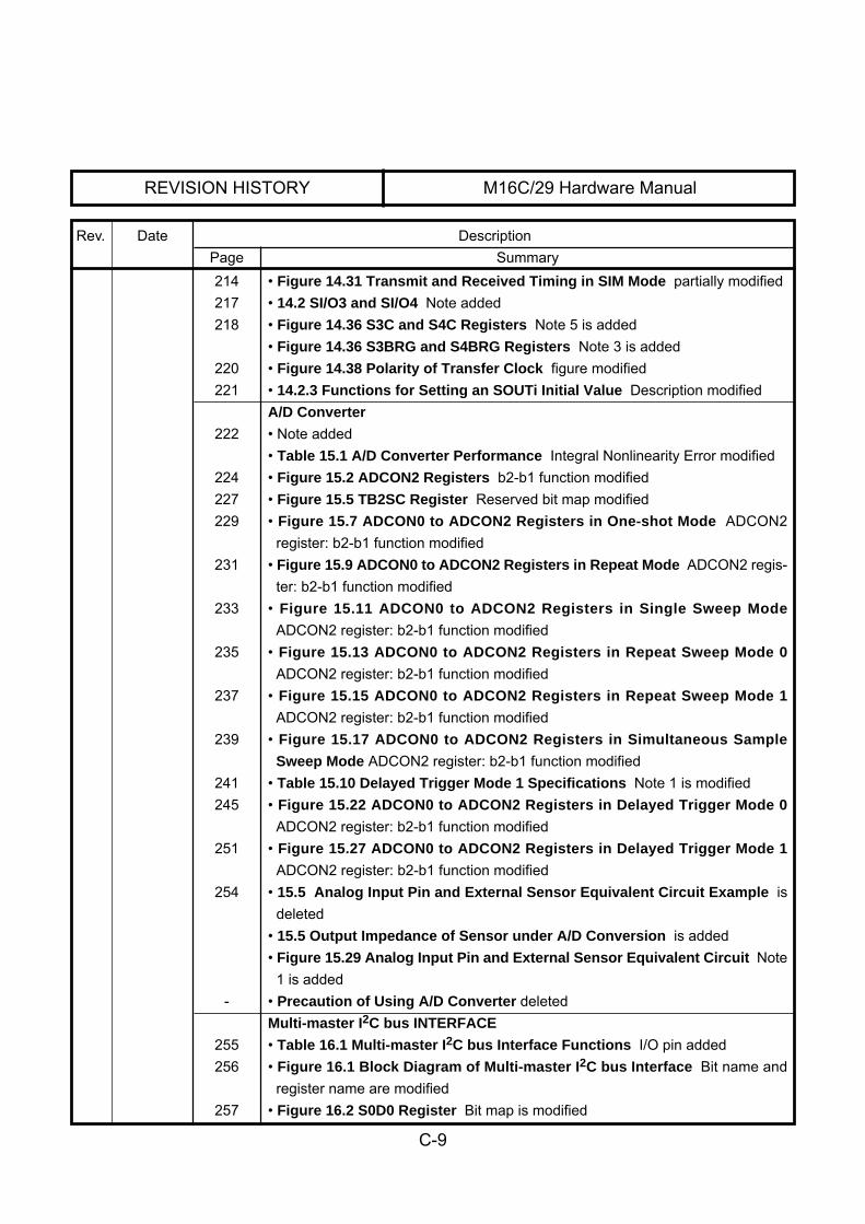
REVISION HISTORY M16C/29 Hardware Manual
Rev. Date DescriptionPage Summary
C-9
214 • Figure 14.31 Transmit and Received Timing in SIM Mode partially modified217 • 14.2 SI/O3 and SI/O4 Note added218 • Figure 14.36 S3C and S4C Registers Note 5 is added
• Figure 14.36 S3BRG and S4BRG Registers Note 3 is added220 • Figure 14.38 Polarity of Transfer Clock figure modified221 • 14.2.3 Functions for Setting an SOUTi Initial Value Description modified
A/D Converter
222 • Note added• Table 15.1 A/D Converter Performance Integral Nonlinearity Error modified
224 • Figure 15.2 ADCON2 Registers b2-b1 function modified227 • Figure 15.5 TB2SC Register Reserved bit map modified229 • Figure 15.7 ADCON0 to ADCON2 Registers in One-shot Mode ADCON2
register: b2-b1 function modified231 • Figure 15.9 ADCON0 to ADCON2 Registers in Repeat Mode ADCON2 regis-
ter: b2-b1 function modified233 • Figure 15.11 ADCON0 to ADCON2 Registers in Single Sweep Mode
ADCON2 register: b2-b1 function modified235 • Figure 15.13 ADCON0 to ADCON2 Registers in Repeat Sweep Mode 0
ADCON2 register: b2-b1 function modified237 • Figure 15.15 ADCON0 to ADCON2 Registers in Repeat Sweep Mode 1
ADCON2 register: b2-b1 function modified239 • Figure 15.17 ADCON0 to ADCON2 Registers in Simultaneous Sample
Sweep Mode ADCON2 register: b2-b1 function modified241 • Table 15.10 Delayed Trigger Mode 1 Specifications Note 1 is modified245 • Figure 15.22 ADCON0 to ADCON2 Registers in Delayed Trigger Mode 0
ADCON2 register: b2-b1 function modified251 • Figure 15.27 ADCON0 to ADCON2 Registers in Delayed Trigger Mode 1
ADCON2 register: b2-b1 function modified254 • 15.5 Analog Input Pin and External Sensor Equivalent Circuit Example is
deleted• 15.5 Output Impedance of Sensor under A/D Conversion is added• Figure 15.29 Analog Input Pin and External Sensor Equivalent Circuit Note
1 is added- • Precaution of Using A/D Converter deleted
Multi-master I2C bus INTERFACE
255 • Table 16.1 Multi-master I2C bus Interface Functions I/O pin added256 • Figure 16.1 Block Diagram of Multi-master I2C bus Interface Bit name and
register name are modified257 • Figure 16.2 S0D0 Register Bit map is modified
REVISION HISTORY M16C/29 Hardware Manual
Rev. Date DescriptionPage Summary
C-10
258 • Figure 16.3 S00 Register Note is modified259 • Figure 16.4 S1D0 Register Reserved bit map modified260 • Figure 16.5 S10 Register b7-b6 modified262 • Figure 16.7 S4D0 Register Bit reserved map is modified269 • 16.5.1 Bit 0: Last Receive Bit (LRB) modified
• 16.5.2 Bit 1: General call detection flag (ADR0) modified, note 1 modified• 16.5.3 Bit 2: Slave address comparison flag (AAS) modified
270 • 16.5.5 Bit 4: I2C Bus Interface Interrupt Request Bit (PIN) modified• 16.5.6 Bit 5: Bus Busy Flag (BB) Bit names are modified
271 • 16.5.8 Bit 7: Communication Mode Select bit (MST) modified276 • 16.7.1 Bit0: Time-Out Detection Function Enable Bit (TOE) is modified
• 16.7.5 Bit7: STOP Condition Detection Interrupt Request Bit (SCPIN) ismodified
279 • 16.11 Stop Condition Generation Method Description added282 • 16.13 Address Data Communication modified
CAN Module
292 • Figure 17.6 C0MCTLj Register RspLock bit’s name changed, note 2 revised293 • Figure 17.7 C0CTLR Register Note 4 added, functions partially modified294 • Figure 17.8 C0STR Register Note 1 deleted, functions partially modified298 • Figure 17.13 C0RECR Register Note 2 deleted, note 1 partially modified
• Figure 17.14 C0TECR Register Note 1 modified, note is relocated299 • Figure 17.15 C0TSR Register Note 1 modified300 • Figure 17.17 Transition Between Operational Modes Partially modified301 • 17.2.3 CAN Sleep Mode Partially deleted304 • Table 17.2 Example of Bit-Rate 24-MHz is deleted308 • 17.8 Time Stamp Counter and Time Stamp Function Partially deleted310 • Figure 17.25 Timing of Receive Data Frame Sequence IF to IFS311 • Figure 17.26 Timing of Transmit Sequence IF to IFS
CRC Calculation Circuit
313 • 18.1 CRC Snoop Description partially addedProgrammable I/O Ports
316 • Note added• 19.3 Pull-up Control Register 0 to 2 Description partially added
317 • 19.6 Digital Debounce Function Filter width formula modified318-321 • Figure 19.1 I/O Ports (1) to Figure 19.4 I/O Ports (4) are modified
326 • Figure 19.10 PACR Register Note 1 is modified327 • Figure 19.11 NDDR and P17DDR Register Functions modified, notes are added328 • Figure 19.12 Functioning of Digital Debounce Filter modified, procedure note
modified
REVISION HISTORY M16C/29 Hardware Manual
Rev. Date DescriptionPage Summary
C-11
329 • Table 19.1 Unassigned Pin Handling in Single-chip Mode Note 5 addedFlash Memory Version
330 • 20.1 Flash Memory Performance Description partially deleted• Table 20.14 Flash Memory Version Specifications Note 3 added
331 • 20.1.1 Boot Mode added332 • 20.2 Memory Map Description is modified335 • 20.3.1 ROM Code Protect Function Description is modified336 • Figure 20.4 ROMCP Address is modified337 • Table 20.3 EW Mode 0 and EW Mode 1 Note 2 is modified339 • 20.5.1 Flash Memory Control Register 0 FMR01 Bit and FMR02 Bit: descrip-
tion is modified340 • 20.5.2 Flash Memory Control Register 1 (FMR1) FMR6 Bit is modified,
FMR17 Bit is modified341 • Figure 20.6 FMR0 and FMR1 Registers FMR0 register: note 3 modified, value
after reset modified; FMR1 register: note 3 modified, reserved bit map modified342 • Figure 20.7 FMR4 Register Note 2 is modified345 • 20.6.3 Interrupts EW1 mode modified
• 20.6.4 How to Access FMR16 bit is added346 • 20.6.9 Stop Mode modified352 • Table 20.7 Errors and FMR0 Register Status Register name modified355 • Table 20.8 Pin Functions Pin settings are partially modified
Electrical Characteristics
• V version is newly added
366 • Table 21.1 Absolute Maximum Ratings Parameters of Pd and Topr are modi-fied
367 • Table 21.2 Recommended Operating Conditions VIH and VIL are modified368 • Table 21.3 A/D Conversion Characeristics tSAMP deleted, note 4 added369 • Table 21.4 Flash Memory Version Electrical Characteristics: Standard val-
ues of Program and Erase Endrance cycle modified, tps added• Table 21.5 Flash Memory Version Electrical Characteristics: tps added, data
hold time added, note 1, 3, 8 modified, note 11 and 12 added370 • Table 21.6 Low Voltage Detection Circuit Electrical Characteristics Note 4
added• Table 21.7 Power Supply Circuit from Timing CharacteristicsL Note 2 & 3
are deleted, figure modified372 • Table 21.9 Electrical Characteristics(2) Note 5 is added380 • Table 21.25 Electrical Characteristics(2) Note 5 is added387 • Table 21.40 Absolute Maximum Ratings Parameters of Pd and Topr are modi-
fied
REVISION HISTORY M16C/29 Hardware Manual
Rev. Date DescriptionPage Summary
C-12
388 • Table 21.41 Recommended Operating Conditions VIH and VIL are modified389 • Table 21.42 A/D Conversion Characeristics tSAMP deleted, note 4 added390 • Table 21.43 Flash Memory Version Electrical Characteristics: Standard val-
ues of Program and Erase Endrance cycle modified, tps added• Table 21.44 Flash Memory Version Electrical Characteristics: tps added,
data hold time added, note 1, 3, 8 modified, note 11 and 12 added391 • Table 21.45 Power Supply Circuit from Timing CharacteristicsL Note 2 & 3
are deleted, td(S-R) and td(E-A) are deleted, figure modified393 • Table 21.47 Electrical Characteristics(2) Note 4 is added401 • Table 21.63 Electrical Characteristics(2) Note 4 is added
Precautions
422 • 22.2.1 PLL Frequency Synthesizer modified423 • 22.2.2 Power Control Subsection sequence modified, 2., 3. and 4. information
modified425
______
• 22.4.3 NMI Interrupt 2. information partially deleted, 6. information added426
______
• 22.4.5 INT Interrupt 3. information added427 • 22.4.6 Rewrite the Interrupt Control Register Example 1 is modified431 • 22.6.1.3 Timer A (One-shot Timer Mode) 6. information added434 • 22.6.3 Three-phase Motor Control Timer Function newly added435 • 22.7.1 Rewrite the G1 IR Register description modified
• Figure 22.3 IC/OC Interrupt Flow Chart newly added436 • 22.7.2 Rewrite the ICOCiIC Register newly added
• 22.7.3 Waveform Generating Function newly added• 22.7.4 IC/OC Base Timer Interrupt newly added
438 • 22.8.2.1 Special Mode (I2C bus Mode) added• 22.8.2.3 SI/O3, SI/O4 added
441 • 22.10 Multi-master I2C bus Interface added445 • 22.12 Programmable I/O Ports 2. and 3. information modified447 • 20.14 Mask ROM Version is added448 • 22.15.1 Functions to Inhibit Rewriting Flash Memory Rewrite modified
• 22.15.2 Stop Mode modified• 22.16.4 Low Power Disspation Mode, On-chip Oscillator Low Power Dissi-
pation Mode modified• 22.15.7 Operating Speed modified
449 • 22.15.9 Interrupts modified• 22.15.13 Regarding Programming/Erasure Times and Execution Time
modified450 • 22.15.14 Definition of Programming/Erasure Times added
• 22.15.15 Flash Memory version Electrical Characteristics 10,000 E/W cycle
REVISION HISTORY M16C/29 Hardware Manual
Rev. Date DescriptionPage Summary
C-13
products (U7, U9) added• 22.15.16 Boot Mode added
451 • 22.16 Noise added452 • 20.17 Instruction fo Device Use added
Appendix 1. Package Dimensions
453 • Dimensions are updated454-455 Appendix 2. Functional Comparison added
Clock Generation Circuit
54 • Figure 7.8 Examples of Main Clock Connection Circuit Note 2 addedInterrupts
88 • Table 9.6 PC Value Saved in Stack Area When Address Match Interrupt
Request Is Acknowledged Table contents partially modified, note addedSerial I/O
198 • Table 14.11 Registers to Be Used and Settings in I2C bus Mode Note Relo-cated
CAN Module
297 • Figure 17.12 C0CONR Register Note 2 modifiedElectrical Characteristics
372 • Table 21.9 Electrical Characteristics (2) Mask ROM data added, value par-tially changed: 420 to 450
379 • Table 21.24 Electrical Characteristics Note 1 modified380 • Table 21.25 Electrical Characteristics Mask ROM data added, note 1 modified391 • Table 21.45 Power Supply Circuit Timing Characteristics figure for td(P-R)
and td(ROC) added, Mask ROM data added393 • Table 21.47 Electrical Characteristics (2) Mask ROM data added, value
paritally changed400 • Table 21.62 Electrical Characteristics Note 1 modified401 • Table 21.63 Electrical Characteristics Mask ROM data added, note 1 modified412 • Table 21.83 Power Supply Circuit Timing Characteristics figure for td(P-R)
and td(ROC) added, Mask ROM data added414 • Table 21.85 Electrical Characteristics (2) Mask ROM data added, value
paritally changedUsage Notes
- • Table numbers and Figure numbers are revised421 • 22.1.3 Register Setting added447 • 22.14.1 Internal ROM Area Description added
Overview
1 • 1.1 Features modified2, 3 • note on trademark modified
1.11 Dec.11,2006
1.12 Mar.30, 2007
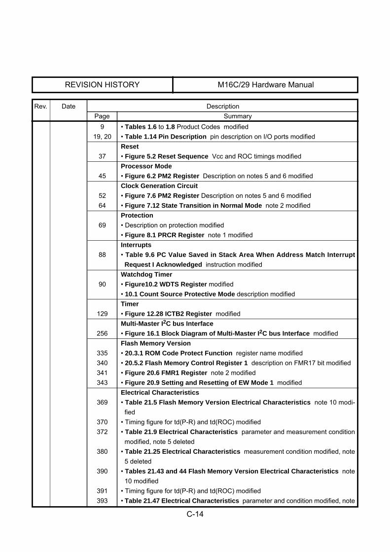
REVISION HISTORY M16C/29 Hardware Manual
Rev. Date DescriptionPage Summary
C-14
9 • Tables 1.6 to 1.8 Product Codes modified19, 20 • Table 1.14 Pin Description pin description on I/O ports modified
Reset
37 • Figure 5.2 Reset Sequence Vcc and ROC timings modifiedProcessor Mode
45 • Figure 6.2 PM2 Register Description on notes 5 and 6 modifiedClock Generation Circuit
52 • Figure 7.6 PM2 Register Description on notes 5 and 6 modified64 • Figure 7.12 State Transition in Normal Mode note 2 modified
Protection
69 • Description on protection modified• Figure 8.1 PRCR Register note 1 modifiedInterrupts
88 • Table 9.6 PC Value Saved in Stack Area When Address Match Interrupt
Request I Acknowledged instruction modifiedWatchdog Timer
90 • Figure10.2 WDTS Register modified• 10.1 Count Source Protective Mode description modifiedTimer
129 • Figure 12.28 ICTB2 Register modifiedMulti-Master I2C bus Interface
256 • Figure 16.1 Block Diagram of Multi-Master I2C bus Interface modifiedFlash Memory Version
335 • 20.3.1 ROM Code Protect Function register name modified340 • 20.5.2 Flash Memory Control Register 1 description on FMR17 bit modified341 • Figure 20.6 FMR1 Register note 2 modified343 • Figure 20.9 Setting and Resetting of EW Mode 1 modified
Electrical Characteristics
369 • Table 21.5 Flash Memory Version Electrical Characteristics note 10 modi-fied
370 • Timing figure for td(P-R) and td(ROC) modified372 • Table 21.9 Electrical Characteristics parameter and measurement condition
modified, note 5 deleted380 • Table 21.25 Electrical Characteristics measurement condition modified, note
5 deleted390 • Tables 21.43 and 44 Flash Memory Version Electrical Characteristics note
10 modified391 • Timing figure for td(P-R) and td(ROC) modified393 • Table 21.47 Electrical Characteristics parameter and condition modified, note
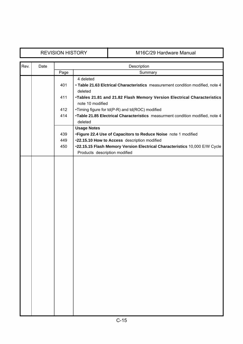
REVISION HISTORY M16C/29 Hardware Manual
Rev. Date DescriptionPage Summary
C-15
4 deleted401 • Table 21.63 Elctrical Characteristics measurement condition modified, note 4
deleted411 •Tables 21.81 and 21.82 Flash Memory Version Electrical Characteristics
note 10 modified412 •Timing figure for td(P-R) and td(ROC) modified414 •Table 21.85 Electrical Characteristics measurment condition modified, note 4
deletedUsage Notes
439 •Figure 22.4 Use of Capacitors to Reduce Noise note 1 modified449 •22.15.10 How to Access description modified450 •22.15.15 Flash Memory Version Electrical Characteristics 10,000 E/W Cycle
Products description modified

RENESAS 16-BIT SINGLE-CHIP MICROCOMPUTERHARDWARE MANUALM16C/29 Group
Publication Data : Rev.0.70 Mar. 29, 2004Rev.1.12 Mar. 30, 2007
Published by : Sales Strategic Planning Div.Renesas Technology Corp.
© 2007. Renesas Technology Corp., All rights reserved. Printed in Japan.
1753, Shimonumabe, Nakahara-ku, Kawasaki-shi, Kanagawa 211-8668 Japan
M16C/29 Group
REJ09B0101-0112
Hardware Manual