icm7242 datasheet - renesas
TRANSCRIPT
FN2866Rev 5.00
September 14, 2015
ICM7242Long Range Fixed Timer
DATASHEET
The ICM7242 is a CMOS timer/counter circuit consisting of an RC oscillator followed by an 8-bit binary counter. It will replace the 2242 in most applications, with a significant reduction in the number of external components.
Three outputs are provided. They are the oscillator output, and buffered outputs from the first and eighth counters.
Features
• Replaces the 2242 in Most Applications
• Timing From Microseconds to Days
• Cascadable
• Monostable or Astable Operation
• Wide Supply Voltage Range . . . . . . . . . . . . . . . 2V to 16V
• Low Supply Current . . . . . . . . . . . . . . . . . . . . 115µA at 5V
• Pb-Free Plus Anneal Available (RoHS Compliant)
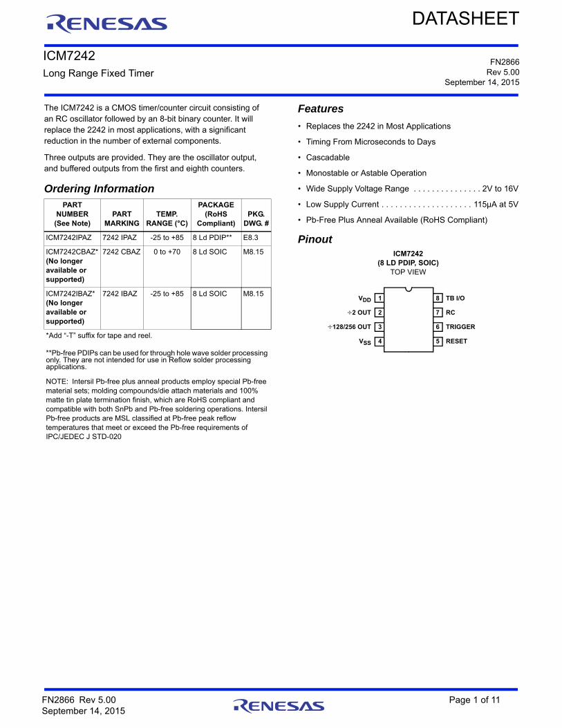
PinoutICM7242
(8 LD PDIP, SOIC)TOP VIEW
Ordering InformationPART
NUMBER(See Note)
PART MARKING
TEMP. RANGE (°C)
PACKAGE(RoHS
Compliant)PKG.
DWG. #
ICM7242IPAZ 7242 IPAZ -25 to +85 8 Ld PDIP** E8.3
ICM7242CBAZ* (No longer available or supported)
7242 CBAZ 0 to +70 8 Ld SOIC M8.15
ICM7242IBAZ* (No longer available or supported)
7242 IBAZ -25 to +85 8 Ld SOIC M8.15
*Add “-T” suffix for tape and reel.
**Pb-free PDIPs can be used for through hole wave solder processing only. They are not intended for use in Reflow solder processing applications.
NOTE: Intersil Pb-free plus anneal products employ special Pb-free material sets; molding compounds/die attach materials and 100% matte tin plate termination finish, which are RoHS compliant and compatible with both SnPb and Pb-free soldering operations. Intersil Pb-free products are MSL classified at Pb-free peak reflow temperatures that meet or exceed the Pb-free requirements of IPC/JEDEC J STD-020
VDD
2 OUT
128/256 OUT
VSS
1
2
3
4
8
7
6
5
TB I/O
RC
TRIGGER
RESET
FN2866 Rev 5.00 Page 1 of 11September 14, 2015
ICM7242
Functional Block Diagram
+
-
+
-
RQ
Q
S
R
1 4 8 5 6 2 3
TRIGGERRESET ÷2 OUTTB I/OVSS
Q
QS
CL
Q
QS
CL
Q
QS
CL
Q
QS
CL
÷128/256OUTPUT
R150k
R286k
R350k
VDD
RC
7
Q
QS
CL
Q
QS
CL
Q
QS
CL
Q
QS
CL
FN2866 Rev 5.00 Page 2 of 11September 14, 2015
ICM7242
Absolute Maximum Ratings Thermal Information
Supply Voltage (VDD to VSS). . . . . . . . . . . . . . . . . . . . . . . . . . . .18VInput Voltage (Note 1)
Terminals (Pins 5, 6, 7, 8). . . . . . . . . . (VSS -0.3V) to (VDD +0.3V)Continuous Output Current (Each Output). . . . . . . . . . . . . . . . 50mA
Operating ConditionsTemperature Range
ICM7242I . . . . . . . . . . . . . . . . . . . . . . . . . . . . . . . .-25°C to +85°CICM7242C . . . . . . . . . . . . . . . . . . . . . . . . . . . . . . . . 0°C to +70°C
Thermal Resistance (Typical, Note2) JA (°C/W)
PDIP Package* . . . . . . . . . . . . . . . . . . . . . . . . . . . . 100SOIC Package . . . . . . . . . . . . . . . . . . . . . . . . . . . . . 160
Maximum Storage Temperature Range . . . . . . . . . -65°C to +150°CMaximum Junction Temperature (Plastic Package) . . . . . . . +150°CPb-free reflow profile . . . . . . . . . . . . . . . . . . . . . . . . . .see link below
http://www.intersil.com/pbfree/Pb-FreeReflow.asp*Pb-free PDIPs can be used for through hole wave solderprocessing only. They are not intended for use in Reflow solderprocessing applications.
CAUTION: Stresses above those listed in “Absolute Maximum Ratings” may cause permanent damage to the device. This is a stress only rating and operation of thedevice at these or any other conditions above those indicated in the operational sections of this specification is not implied.
NOTES:
1. Due to the SCR structure inherent in the CMOS process, connecting any terminal to voltages greater than VDD or less than VSS may cause destructive device latchup. For this reason, it is recommended that no inputs from external sources not operating on the same supply be applied to the device before its supply is established and, that in multiple supply systems, the supply to the ICM7242 be turned on first.
2. JA is measured with the component mounted on an evaluation PC board in free air.
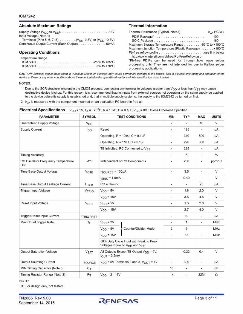
Electrical Specifications VDD = 5V, TA = +25°C, R = 10k, C = 0.1µF, VSS = 0V, Unless Otherwise Specified
PARAMETER SYMBOL TEST CONDITIONS MIN TYP MAX UNITS
Guaranteed Supply Voltage VDD 2 - 16 V
Supply Current IDD Reset - 125 - µA
Operating, R = 10k, C = 0.1µF - 340 800 µA
Operating, R = 1M, C = 0.1µF - 220 600 µA
TB Inhibited, RC Connected to VSS - 225 - µA
Timing Accuracy - 5 - %
RC Oscillator Frequency Temperature Drift
f/t Independent of RC Components - 250 - ppm/°C
Time Base Output Voltage VOTB ISOURCE = 100µA - 3.5 - V
ISINK = 1.0mA - 0.40 - V
Time Base Output Leakage Current ITBLK RC = Ground - - 25 µA
Trigger Input Voltage VTRIG VDD = 5V - 1.6 2.0 V
VDD = 15V - 3.5 4.5 V
Reset Input Voltage VRST VDD = 5V - 1.3 2.0 V
VDD = 15V - 2.7 4.0 V
Trigger/Reset Input Current ITRIG, IRST - 10 - µA
Max Count Toggle Rate fT VDD = 2V
Counter/Divider Mode
- 1 - MHz
VDD = 5V 2 6 - MHz
VDD = 15V - 13 - MHz
50% Duty Cycle Input with Peak to Peak Voltages Equal to VDD and VSS
Output Saturation Voltage VSAT All Outputs Except TB Output VDD = 5V, IOUT = 3.2mA
- 0.22 0.4 V
Output Sourcing Current ISOURCE VDD = 5V Terminals 2 and 3, VOUT = 1V - 300 - µA
MIN Timing Capacitor (Note 3) CT 10 - - pF
Timing Resistor Range (Note 3) RT VDD = 2 - 16V 1k - 22M
NOTE:
3. For design only, not tested.
FN2866 Rev 5.00 Page 3 of 11September 14, 2015
ICM7242
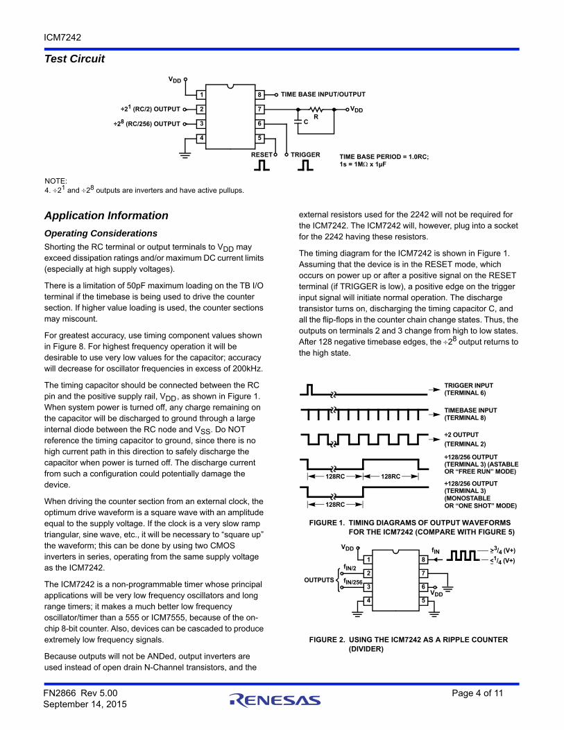
Test Circuit
Application Information
Operating Considerations
Shorting the RC terminal or output terminals to VDD may exceed dissipation ratings and/or maximum DC current limits (especially at high supply voltages).
There is a limitation of 50pF maximum loading on the TB I/O terminal if the timebase is being used to drive the counter section. If higher value loading is used, the counter sections may miscount.
For greatest accuracy, use timing component values shown in Figure 8. For highest frequency operation it will be desirable to use very low values for the capacitor; accuracy will decrease for oscillator frequencies in excess of 200kHz.
The timing capacitor should be connected between the RC pin and the positive supply rail, VDD, as shown in Figure 1. When system power is turned off, any charge remaining on the capacitor will be discharged to ground through a large internal diode between the RC node and VSS. Do NOT reference the timing capacitor to ground, since there is no high current path in this direction to safely discharge the capacitor when power is turned off. The discharge current from such a configuration could potentially damage the device.
When driving the counter section from an external clock, the optimum drive waveform is a square wave with an amplitude equal to the supply voltage. If the clock is a very slow ramp triangular, sine wave, etc., it will be necessary to “square up” the waveform; this can be done by using two CMOS inverters in series, operating from the same supply voltage as the ICM7242.
The ICM7242 is a non-programmable timer whose principal applications will be very low frequency oscillators and long range timers; it makes a much better low frequency oscillator/timer than a 555 or ICM7555, because of the on-chip 8-bit counter. Also, devices can be cascaded to produce extremely low frequency signals.
Because outputs will not be ANDed, output inverters are used instead of open drain N-Channel transistors, and the
external resistors used for the 2242 will not be required for the ICM7242. The ICM7242 will, however, plug into a socket for the 2242 having these resistors.
The timing diagram for the ICM7242 is shown in Figure 1. Assuming that the device is in the RESET mode, which occurs on power up or after a positive signal on the RESET terminal (if TRIGGER is low), a positive edge on the trigger input signal will initiate normal operation. The discharge transistor turns on, discharging the timing capacitor C, and all the flip-flops in the counter chain change states. Thus, the outputs on terminals 2 and 3 change from high to low states. After 128 negative timebase edges, the 28 output returns to the high state.
NOTE:4. 21 and 28 outputs are inverters and have active pullups.
VDD÷21 (RC/2) OUTPUT
1
2
3
4
8
7
6
5
TIME BASE INPUT/OUTPUT
R
TRIGGERRESET
C
VDD
÷28 (RC/256) OUTPUT
TIME BASE PERIOD = 1.0RC;1s = 1M x 1µF
TRIGGER INPUT(TERMINAL 6)
TIMEBASE INPUT(TERMINAL 8)
÷2 OUTPUT
(TERMINAL 2)
÷128/256 OUTPUT(TERMINAL 3) (ASTABLEOR “FREE RUN” MODE)
÷128/256 OUTPUT(TERMINAL 3)
OR “ONE SHOT” MODE)(MONOSTABLE
128RC
128RC 128RC
FIGURE 1. TIMING DIAGRAMS OF OUTPUT WAVEFORMS FOR THE ICM7242 (COMPARE WITH FIGURE 5)
OUTPUTS
1
2
3
4
8
7
6
5
>3/4 (V+)VDD fIN
VDD
fIN/2
fIN/256
<1/4 (V+)
FIGURE 2. USING THE ICM7242 AS A RIPPLE COUNTER(DIVIDER)
FN2866 Rev 5.00 Page 4 of 11September 14, 2015
ICM7242
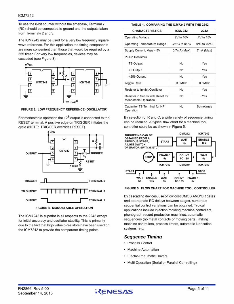
To use the 8-bit counter without the timebase, Terminal 7 (RC) should be connected to ground and the outputs taken from Terminals 2 and 3.
The ICM7242 may be used for a very low frequency square wave reference. For this application the timing components are more convenient than those that would be required by a 555 timer. For very low frequencies, devices may be cascaded (see Figure 3).
For monostable operation the 28 output is connected to the RESET terminal. A positive edge on TRIGGER initiates the cycle (NOTE: TRIGGER overrides RESET).
The ICM7242 is superior in all respects to the 2242 except for initial accuracy and oscillator stability. This is primarily due to the fact that high value p-resistors have been used on the ICM7242 to provide the comparator timing points.
By selection of R and C, a wide variety of sequence timing can be realized. A typical flow chart for a machine tool controller could be as shown in Figure 5.
By cascading devices, use of low cost CMOS AND/OR gates and appropriate RC delays between stages, numerous sequential control variations can be obtained. Typical applications include injection molding machine controllers, phonograph record production machines, automatic sequencers (no metal contacts or moving parts), milling machine controllers, process timers, automatic lubrication systems, etc.
Sequence Timing• Process Control
• Machine Automation
• Electro-Pneumatic Drivers
• Multi Operation (Serial or Parallel Controlling)
1
2
3
4
8
7
6
5
VDD
CR 1
2
3
4
8
7
6
5
ICM7242ICM7242
f = RC/216
FIGURE 3. LOW FREQUENCY REFERENCE (OSCILLATOR)
OUTPUT TERMINAL 3
TB OUTPUT
TRIGGER
TERMINAL 8
TERMINAL 6
1
2
3
4
8
7
6
5
VDD
CR
ICM7242OUTPUT
100k
TRIGGER
RESET
S1
FIGURE 4. MONOSTABLE OPERATION
TABLE 1. COMPARING THE ICM7242 WITH THE 2242
CHARACTERISTICS ICM7242 2242
Operating Voltage 2V to 16V 4V to 15V
Operating Temperature Range -25°C to 85°C 0°C to 70°C
Supply Current, VDD = 5V 0.7mA (Max) 7mA (Max)
Pullup Resistors
TB Output No Yes
2 Output No Yes
256 Output No Yes
Toggle Rate 3.0MHz 0.5MHz
Resistor to Inhibit Oscillator No Yes
Resistor in Series with Reset for Monostable Operation
No Yes
Capacitor TB Terminal for HF Operation
No Sometimes
TRIGGERING CAN BEOBTAINED FROM APREVIOUS STAGE,A LIMIT SWITCH, OPERATOR SWITCH, ETC.
ENABLE10s
WAIT5sSTART
ICM7242 ICM7242
WAIT5s
COUNTTO 185
ENABLE5s
ICM7242 ICM7240 ICM7242
STOP
START STOP
WAIT5s
WAIT5s
ENABLE5s
COUNTTO 185
ENABLE10s
FIGURE 5. FLOW CHART FOR MACHINE TOOL CONTROLLER
-
FN2866 Rev 5.00 Page 5 of 11September 14, 2015
ICM7242
VDD
VDD
A
ICM7242
R (NOTE)C
A
6 3
5
33k
100pF
10k
1µF
VDD
B
ICM7242
R (NOTE)C
B
6 3
5
33k
100pF
10k
1µF
VDD
C
ICM7242
R (NOTE)C
6 3
5
33k
100pF
10k
1µFTRIGGER
S1
VDD
D
ICM7242
R (NOTE)C
6 3
5
33k
100pF
TRIGGER
PUSH S1 TO START SEQUENCE:
OUTPUT A (NOTE)
OUTPUT B (NOTE)
OUTPUT C (NOTE)
OUTPUT D (NOTE)
MUST BE SHORTER THAN “ON TIMEA”
ON TIMEA
128RC
128RC
ON TIMEB
ON TIMECON TIMED
128RC
128RC
50k
C D
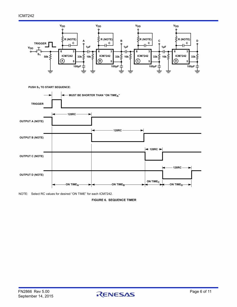
NOTE: Select RC values for desired “ON TIME” for each ICM7242.
FIGURE 6. SEQUENCE TIMER
FN2866 Rev 5.00 Page 6 of 11September 14, 2015
ICM7242
Typical Performance Curves
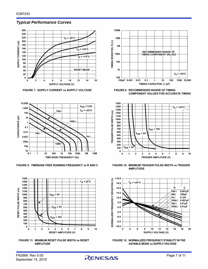
FIGURE 7. SUPPLY CURRENT vs SUPPLY VOLTAGE FIGURE 8. RECOMMENDED RANGE OF TIMING COMPONENT VALUES FOR ACCURATE TIMING
FIGURE 9. TIMEBASE FREE RUNNING FREQUENCY vs R AND C FIGURE 10. MINIMUM TRIGGER PULSE WIDTH vs TRIGGER AMPLITUDE
FIGURE 11. MINIMUM RESET PULSE WIDTH vs RESETAMPLITUDE
FIGURE 12. NORMALIZED FREQUENCY STABILITY IN THE ASTABLE MODE vs SUPPLY VOLTAGE
SUPPLY VOLTAGE (V)
0 2 4 6 8 10 12 14 160
260
240
220
200
180
160
140
120
100
80
60
40
20
SU
PP
LY C
UR
RE
NT
(µ
A)
TA = -20°C
RESET MODE
TA = +25°C
TA = +75°C
TIMING CAPACITOR, C (µF)
100pF 0.01 1 10 100 1000 10,000100
100M
10M
1M
100k
10k
1k
TIM
ING
RE
SIS
TO
R, R
(
)
0.10.001
RECOMMENDED RANGE OFTIMING COMPONENT VALUES
TA = +25°C
10M
TIME BASE FREQUENCY (Hz)
0.1 1 10 100 1k 10k 100k 1M 10M
10,000
CA
PA
CIT
AN
CE
(µ
F)
VDD = 5.0V
TA = +25°C
100k
10k
1k1M
1,000
100
10
1
0.1
0.01
0.001
100p
10p
1p
TRIGGER AMPLITUDE (V)
0 1 2 3 4 5 6 7 8 9 100
150014001300120011001000
900800700600500400300200100
TR
IGG
ER
PU
LS
E W
IDT
H (
ns)
TA = +25°C
VDD = 5V
VDD = 2V
VDD = 16V
RESET AMPLITUDE (V)0 1 2 3 4 5 6 7 8 9 10
0
150014001300120011001000
900800700600500400300200100
RE
SE
T P
UL
SE
WID
TH
(n
s)
TA = 25°C
VDD = 5V
VDD = 2V
VDD = 16V
SUPPLY VOLTAGE (V)
2 10 12 14 16 18 20
+10.0
+8.0
+6.0
+4.0
+2.0
0.0
-2.0
-4.0
-6.0
-8.0
-10.0NO
RM
AL
IZE
D F
RE
QU
EN
CY
DE
VIA
TIO
N (
%)
TA = +25°C
R
864
C
10k1M1k100k10k100k
0.001µF100pF0.1µF0.001µF0.01µF0.01µF
FN2866 Rev 5.00 Page 7 of 11September 14, 2015
ICM7242
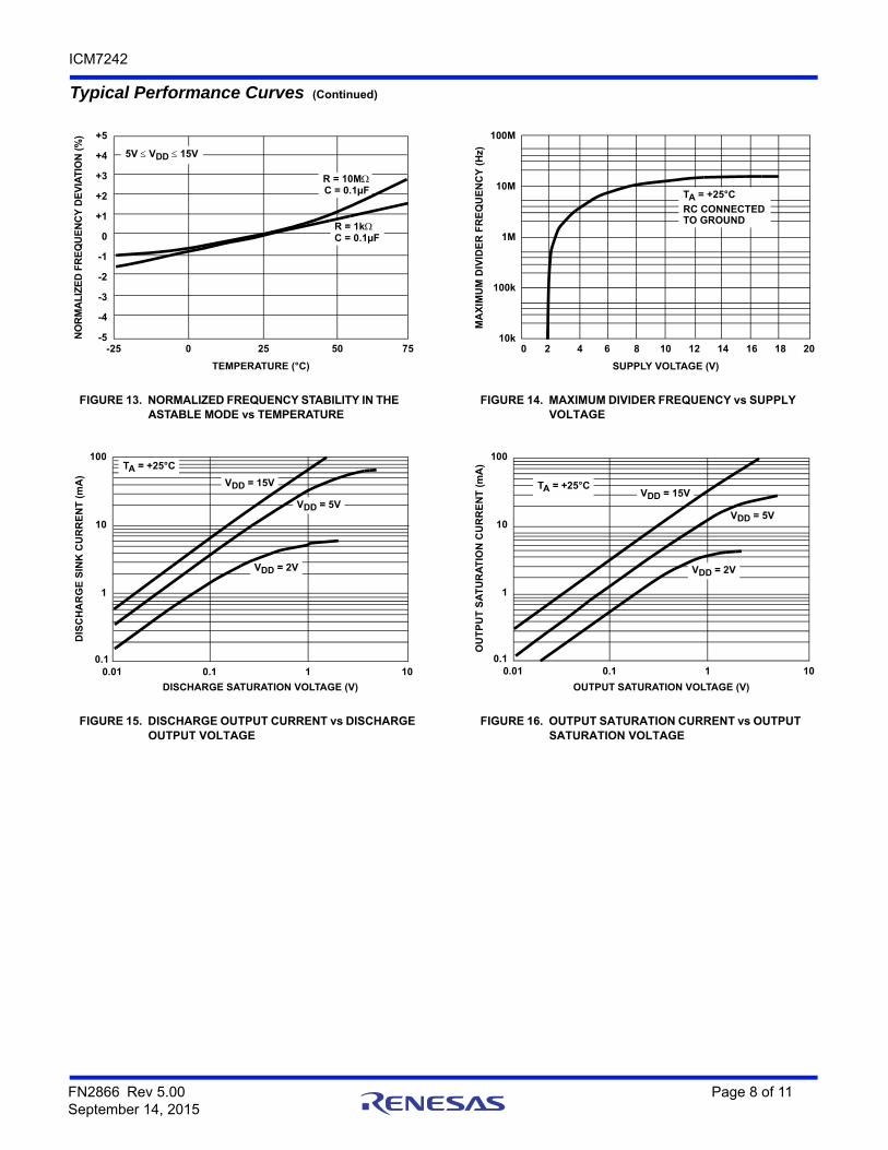
FIGURE 13. NORMALIZED FREQUENCY STABILITY IN THE ASTABLE MODE vs TEMPERATURE
FIGURE 14. MAXIMUM DIVIDER FREQUENCY vs SUPPLY VOLTAGE
FIGURE 15. DISCHARGE OUTPUT CURRENT vs DISCHARGE OUTPUT VOLTAGE
FIGURE 16. OUTPUT SATURATION CURRENT vs OUTPUT SATURATION VOLTAGE
Typical Performance Curves (Continued)
TEMPERATURE (°C)
-25 0 25 50 75
+5
+4
+3
+2
+1
0
-1
-2
-3
-4
-5NO
RM
AL
IZE
D F
RE
QU
EN
CY
DE
VIA
TIO
N (
%)
5V VDD 15V
R = 10MC = 0.1µF
R = 1kC = 0.1µF
SUPPLY VOLTAGE (V)
2 10 12 14 16 18 20
100M
10M
1M
100k
10k
MA
XIM
UM
DIV
IDE
R F
RE
QU
EN
CY
(H
z)
TA = +25°C
864
RC CONNECTEDTO GROUND
0
DISCHARGE SATURATION VOLTAGE (V)
0.01 0.1 1 100.1
100
10
1
DIS
CH
AR
GE
SIN
K C
UR
RE
NT
(m
A)
TA = +25°C
VDD = 5V
VDD = 2V
VDD = 15V
OUTPUT SATURATION VOLTAGE (V)
0.01 0.1 1 100.1
100
10
1
OU
TP
UT
SA
TU
RA
TIO
N C
UR
RE
NT
(m
A)
TA = +25°C
VDD = 5V
VDD = 2V
VDD = 15V
FN2866 Rev 5.00 Page 8 of 11September 14, 2015

ICM7242
About IntersilIntersil Corporation is a leading provider of innovative power management and precision analog solutions. The company's products address some of the largest markets within the industrial and infrastructure, mobile computing and high-end consumer markets.
For the most updated datasheet, application notes, related documentation and related parts, please see the respective product information page found at www.intersil.com.
You may report errors or suggestions for improving this datasheet by visiting www.intersil.com/ask.
Reliability reports are also available from our website at www.intersil.com/support.
Revision HistoryThe revision history provided is for informational purposes only and is believed to be accurate, but not warranted. Please go to the web to make sure that you have the latest revision.
DATE REVISION CHANGE
September 14, 2015 FN2866.5 - Ordering Information Table on page 1.- Added Revision History and About Intersil sections.
FN2866 Rev 5.00 Page 9 of 11September 14, 2015
ICM7242
FN2866 Rev 5.00 Page 10 of 11September 14, 2015
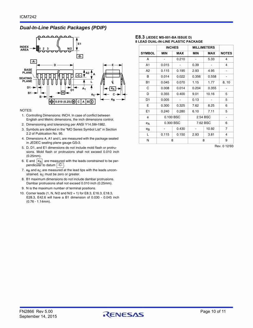
Dual-In-Line Plastic Packages (PDIP)
CL
E
eA
C
eB
eC
-B-
E1INDEX
1 2 3 N/2
N
AREA
SEATING
BASEPLANE
PLANE
-C-
D1
B1B
e
D
D1
AA2
L
A1
-A-
0.010 (0.25) C AM B S
NOTES:
1. Controlling Dimensions: INCH. In case of conflict between English and Metric dimensions, the inch dimensions control.
2. Dimensioning and tolerancing per ANSI Y14.5M-1982.
3. Symbols are defined in the “MO Series Symbol List” in Section 2.2 of Publication No. 95.
4. Dimensions A, A1 and L are measured with the package seated in JEDEC seating plane gauge GS-3.
5. D, D1, and E1 dimensions do not include mold flash or protru-sions. Mold flash or protrusions shall not exceed 0.010 inch(0.25mm).
6. E and are measured with the leads constrained to be per-pendicular to datum .
7. eB and eC are measured at the lead tips with the leads uncon-strained. eC must be zero or greater.
8. B1 maximum dimensions do not include dambar protrusions. Dambar protrusions shall not exceed 0.010 inch (0.25mm).
9. N is the maximum number of terminal positions.
10. Corner leads (1, N, N/2 and N/2 + 1) for E8.3, E16.3, E18.3, E28.3, E42.6 will have a B1 dimension of 0.030 - 0.045 inch(0.76 - 1.14mm).
eA-C-
E8.3 (JEDEC MS-001-BA ISSUE D)8 LEAD DUAL-IN-LINE PLASTIC PACKAGE
SYMBOL
INCHES MILLIMETERS
NOTESMIN MAX MIN MAX
A - 0.210 - 5.33 4
A1 0.015 - 0.39 - 4
A2 0.115 0.195 2.93 4.95 -
B 0.014 0.022 0.356 0.558 -
B1 0.045 0.070 1.15 1.77 8, 10
C 0.008 0.014 0.204 0.355 -
D 0.355 0.400 9.01 10.16 5
D1 0.005 - 0.13 - 5
E 0.300 0.325 7.62 8.25 6
E1 0.240 0.280 6.10 7.11 5
e 0.100 BSC 2.54 BSC -
eA 0.300 BSC 7.62 BSC 6
eB - 0.430 - 10.92 7
L 0.115 0.150 2.93 3.81 4
N 8 8 9
Rev. 0 12/93
FN2866 Rev 5.00 Page 11 of 11September 14, 2015
ICM7242
Intersil products are manufactured, assembled and tested utilizing ISO9001 quality systems as notedin the quality certifications found at www.intersil.com/en/support/qualandreliability.html
Intersil products are sold by description only. Intersil may modify the circuit design and/or specifications of products at any time without notice, provided that such modification does not, in Intersil's sole judgment, affect the form, fit or function of the product. Accordingly, the reader is cautioned to verify that datasheets are current before placing orders. Information furnished by Intersil is believed to be accurate and reliable. However, no responsibility is assumed by Intersil or its subsidiaries for its use; nor for any infringements of patents or other rights of third parties which may result from its use. No license is granted by implication or otherwise under any patent or patent rights of Intersil or its subsidiaries.
For information regarding Intersil Corporation and its products, see www.intersil.com
For additional products, see www.intersil.com/en/products.html
© Copyright Intersil Americas LLC 1996-2015. All Rights Reserved.All trademarks and registered trademarks are the property of their respective owners.
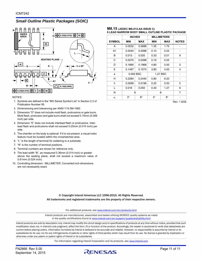
Small Outline Plastic Packages (SOIC)
INDEXAREA
E
D
N
1 2 3
-B-
0.25(0.010) C AM B S
e
-A-
L
B
M
-C-
A1
A
SEATING PLANE
0.10(0.004)
h x 45°
C
H 0.25(0.010) BM M
NOTES:
1. Symbols are defined in the “MO Series Symbol List” in Section 2.2 of Publication Number 95.
2. Dimensioning and tolerancing per ANSI Y14.5M-1982.
3. Dimension “D” does not include mold flash, protrusions or gate burrs. Mold flash, protrusion and gate burrs shall not exceed 0.15mm (0.006inch) per side.
4. Dimension “E” does not include interlead flash or protrusions. Inter-lead flash and protrusions shall not exceed 0.25mm (0.010 inch) perside.
5. The chamfer on the body is optional. If it is not present, a visual index feature must be located within the crosshatched area.
6. “L” is the length of terminal for soldering to a substrate.
7. “N” is the number of terminal positions.
8. Terminal numbers are shown for reference only.
9. The lead width “B”, as measured 0.36mm (0.014 inch) or greater above the seating plane, shall not exceed a maximum value of0.61mm (0.024 inch).
10. Controlling dimension: MILLIMETER. Converted inch dimensions are not necessarily exact.
M8.15 (JEDEC MS-012-AA ISSUE C)8 LEAD NARROW BODY SMALL OUTLINE PLASTIC PACKAGE
SYMBOL
INCHES MILLIMETERS
NOTESMIN MAX MIN MAX
A 0.0532 0.0688 1.35 1.75 -
A1 0.0040 0.0098 0.10 0.25 -
B 0.013 0.020 0.33 0.51 9
C 0.0075 0.0098 0.19 0.25 -
D 0.1890 0.1968 4.80 5.00 3
E 0.1497 0.1574 3.80 4.00 4
e 0.050 BSC 1.27 BSC -
H 0.2284 0.2440 5.80 6.20 -
h 0.0099 0.0196 0.25 0.50 5
L 0.016 0.050 0.40 1.27 6
N 8 8 7
0° 8° 0° 8° -
Rev. 1 6/05