adc0808s ser datasheet - renesas
TRANSCRIPT
ADC0808S125/250Single 8-bit ADC, up to 125 MHz or 250 MHzRev. 04 — 2 July 2012 Product data sheet
1. General description
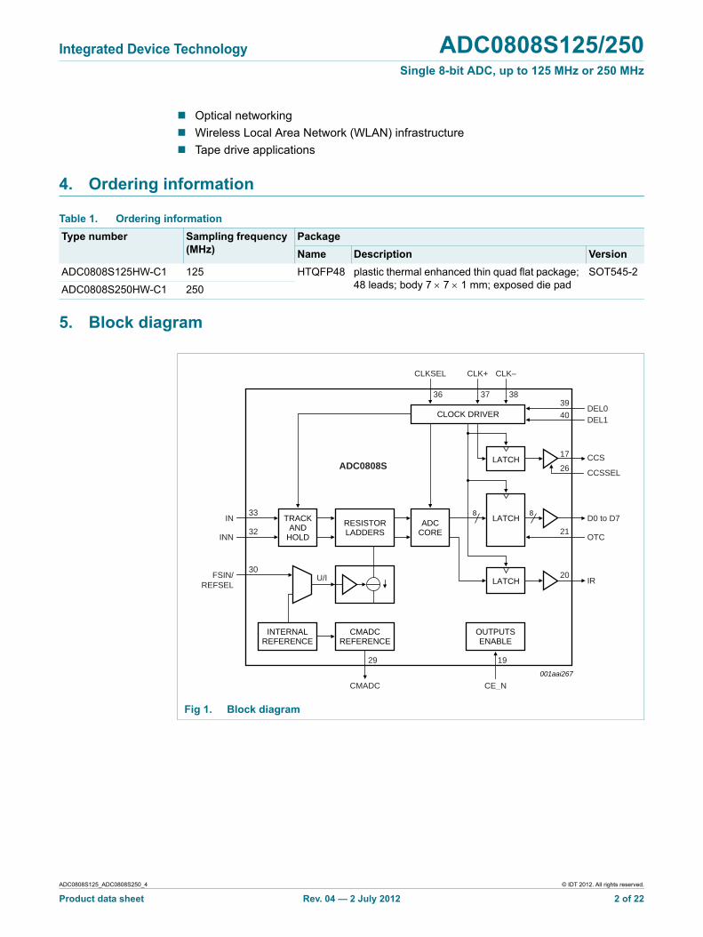
The ADC0808S is a differential, high-speed, 8-bit Analog-to-Digital Converter (ADC) optimized for telecommunication transmission control systems and tape drive applications. It allows signal sampling frequencies up to 250 MHz.
The ADC0808S clock inputs are selectable between 1.8 V Complementary Metal Oxide Semiconductor (CMOS) or Low-Voltage Differential Signals (LVDS). The data output signal levels are 1.8 V CMOS.
All static digital inputs (CLKSEL, CCSSEL, CE_N, OTC, DEL0 and DEL1) are 1.8 V CMOS compatible.
The ADC0808S offers the most flexible acquisition control system possible due to its programmable Complete Conversion Signal (CCS) which allows the delay time of the acquisition clock and acquisition clock frequency to be adjusted.
The ADC0808S is supplied in an HTQFP48 package.
2. Features
8-bit resolution
High-speed sampling rate up to 250 MHz
Maximum analog input frequency up to 560 MHz
Programmable acquisition output clock (complete conversion signal)
Differential analog input
Integrated voltage regulator or external control for analog input full-scale
Integrated voltage regulator for input common-mode reference
Selectable 1.8 V CMOS or LVDS clock input
1.8 V CMOS digital outputs
1.8 V CMOS compatible static digital inputs
Binary or 2’s complement CMOS outputs
Only 2 clock cycles latency
Industrial temperature range from 40 C to +85 C HTQFP48 package
3. Applications
2.5G and 3G cellular base infrastructure radio transceivers
Wireless access systems
Fixed telecommunications
®
Integrated Device Technology ADC0808S125/250Single 8-bit ADC, up to 125 MHz or 250 MHz
Optical networking
Wireless Local Area Network (WLAN) infrastructure
Tape drive applications
4. Ordering information
Table 1. Ordering information
Type number Sampling frequency (MHz)
Package
Name Description Version
ADC0808S125HW-C1 125 HTQFP48 plastic thermal enhanced thin quad flat package; 48 leads; body 7 7 1 mm; exposed die pad
SOT545-2
ADC0808S250HW-C1 250
5. Block diagram
8 8
001aai267
TRACKAND
HOLD
ADCCORE
LATCH
LATCHRESISTORLADDERS
CLOCK DRIVER
OUTPUTSENABLE
CMADCREFERENCE
INTERNALREFERENCE
ADC0808S
U/I
INN
IN
DEL0DEL1
CCS17
3938
1929
33
32
30FSIN/
REFSEL
3736
40
26
21
20
CCSSEL
D0 to D7
OTC
IR
CMADC
CLKSEL CLK+ CLK−
CE_N
LATCH
Fig 1. Block diagram
ADC0808S125_ADC0808S250_4 © IDT 2012. All rights reserved.
Product data sheet Rev. 04 — 2 July 2012 2 of 22
Integrated Device Technology ADC0808S125/250Single 8-bit ADC, up to 125 MHz or 250 MHz
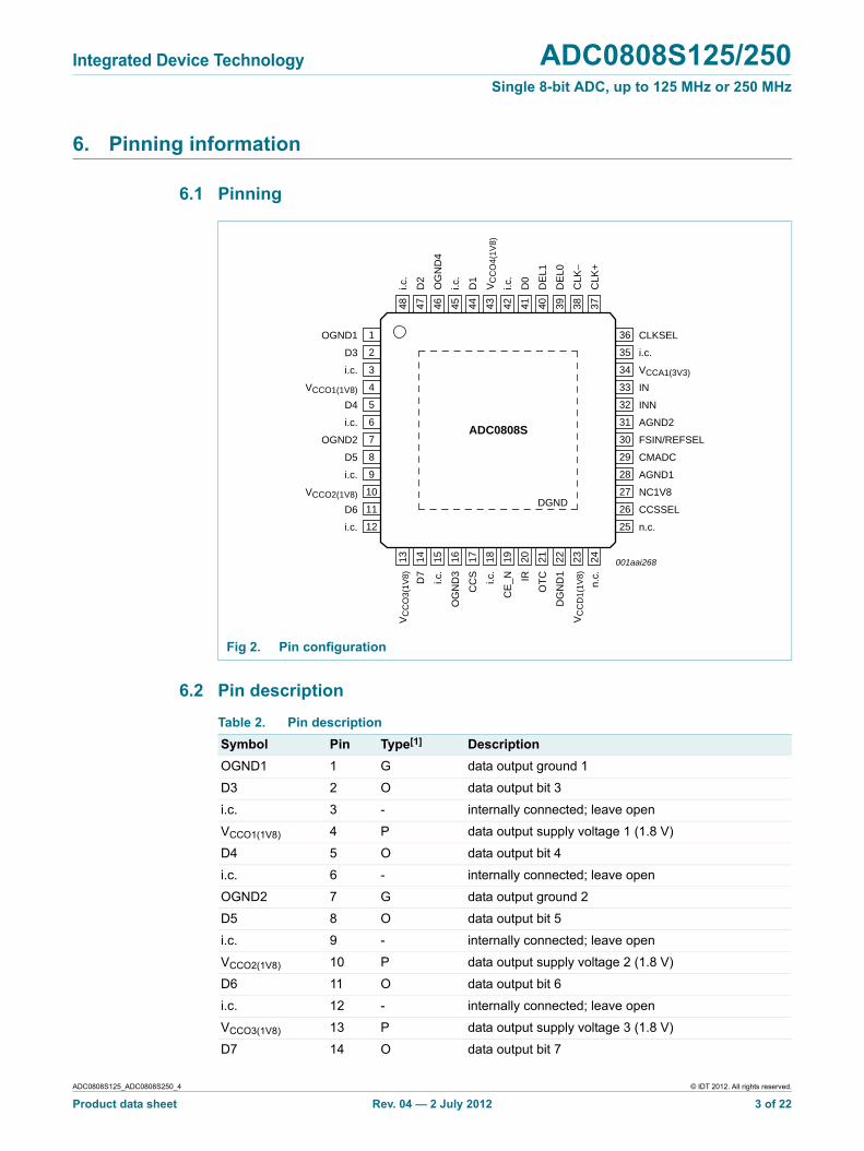
6. Pinning information
6.1 Pinning
ADC0808S
OGND1 CLKSEL
D3 i.c.
i.c. VCCA1(3V3)
VCCO1(1V8) IN
D4 INN
i.c. AGND2
OGND2 FSIN/REFSEL
D5 CMADC
i.c. AGND1
DGNDVCCO2(1V8) NC1V8
D6 CCSSEL
i.c. n.c.
VC
CO
3(1V
8)i.c
.
D7
D2
i.c.
OG
ND
4
OG
ND
3i.c
.
CC
SD
1
i.c.
VC
CO
4(1V
8)
CE
_Ni.c
.
IRD
0
OT
CD
EL1
DG
ND
1D
EL0
VC
CD
1(1V
8)
n.c.
CLK
−
CLK
+
001aai268
1
2
3
4
5
6
7
8
9
10
11
12
36
35
34
33
32
31
30
29
28
27
26
25
13 14 15 16 17 18 19 20 21 22 23
48 47 46 45 44 43 42 41 40 39 38 3724
Fig 2. Pin configuration
6.2 Pin description
Table 2. Pin description
Symbol Pin Type[1] Description
OGND1 1 G data output ground 1
D3 2 O data output bit 3
i.c. 3 - internally connected; leave open
VCCO1(1V8) 4 P data output supply voltage 1 (1.8 V)
D4 5 O data output bit 4
i.c. 6 - internally connected; leave open
OGND2 7 G data output ground 2
D5 8 O data output bit 5
i.c. 9 - internally connected; leave open
VCCO2(1V8) 10 P data output supply voltage 2 (1.8 V)
D6 11 O data output bit 6
i.c. 12 - internally connected; leave open
VCCO3(1V8) 13 P data output supply voltage 3 (1.8 V)
D7 14 O data output bit 7
ADC0808S125_ADC0808S250_4 © IDT 2012. All rights reserved.
Product data sheet Rev. 04 — 2 July 2012 3 of 22
Integrated Device Technology ADC0808S125/250Single 8-bit ADC, up to 125 MHz or 250 MHz
[1] See Table 3.
i.c. 15 - internally connected; leave open
OGND3 16 G data output ground 3
CCS 17 O complete conversion signal output
i.c. 18 - internally connected; leave open
CE_N 19 I(CMOS) chip enable input (active LOW)
IR 20 O(CMOS) in-range output
OTC 21 I(CMOS) control input for 2’s complement output
DGND1 22 G digital ground 1
VCCD1(1V8) 23 P digital supply voltage 1 (1.8 V)
n.c. 24 - not connected
n.c. 25 - not connected
CCSSEL 26 I(CMOS) control input for CCS frequency selection
NC1V8 27 I not connected or connected to VCCD1(1V8)
AGND1 28 G analog ground 1
CMADC 29 O regulator common-mode ADC output
FSIN/REFSEL 30 I full-scale reference voltage input/internal or external reference selection
AGND2 31 G analog ground 2
INN 32 I complementary analog input
IN 33 I analog input
VCCA1(3V3) 34 P analog supply voltage 1 (3.3 V)
i.c. 35 - internally connected; leave open
CLKSEL 36 I(CMOS) control input for clock input selection
CLK+ 37 I clock input
CLK 38 I complementary clock input
DEL0 39 I(CMOS) complete conversion signal delay input 0
DEL1 40 I(CMOS) complete conversion signal delay input 1
D0 41 O data output bit 0
i.c. 42 - internally connected; leave open
VCCO4(1V8) 43 P data output supply voltage 4 (1.8 V)
D1 44 O data output bit 1
i.c. 45 - internally connected; leave open
OGND4 46 G data output ground 4
D2 47 O data output bit 2
i.c. 48 - internally connected; leave open
DGND - G digital ground; exposed die pad
Table 2. Pin description …continued
Symbol Pin Type[1] Description
ADC0808S125_ADC0808S250_4 © IDT 2012. All rights reserved.
Product data sheet Rev. 04 — 2 July 2012 4 of 22
Integrated Device Technology ADC0808S125/250Single 8-bit ADC, up to 125 MHz or 250 MHz
Table 3. Pin type description
Type Description
I input
O output
I(CMOS) 1.8 V CMOS level input
O(CMOS) 1.8 V CMOS level output
P power supply
G ground
7. Functional description
7.1 CMOS/LVDS clock input
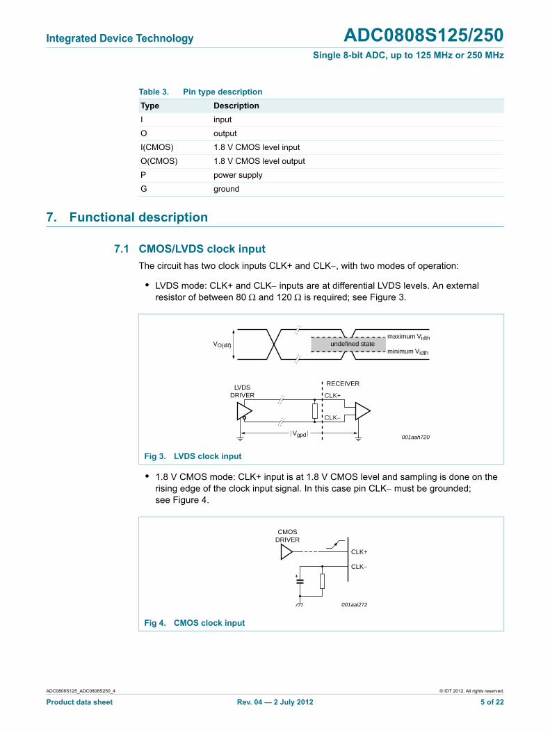
The circuit has two clock inputs CLK+ and CLK, with two modes of operation:
• LVDS mode: CLK+ and CLK inputs are at differential LVDS levels. An external resistor of between 80 and 120 is required; see Figure 3.
001aah720
LVDSDRIVER
RECEIVER
Vgpd
VO(dif) undefined stateminimum Vidth
maximum Vidth
CLK+
CLK−
Fig 3. LVDS clock input
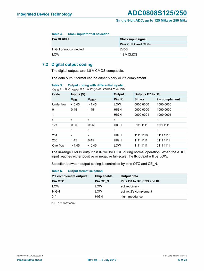
• 1.8 V CMOS mode: CLK+ input is at 1.8 V CMOS level and sampling is done on the rising edge of the clock input signal. In this case pin CLK must be grounded; see Figure 4.
001aai272
CMOSDRIVER
CLK−
CLK+
Fig 4. CMOS clock input
ADC0808S125_ADC0808S250_4 © IDT 2012. All rights reserved.
Product data sheet Rev. 04 — 2 July 2012 5 of 22
Integrated Device Technology ADC0808S125/250Single 8-bit ADC, up to 125 MHz or 250 MHz
Table 4. Clock input format selection
Pin CLKSEL Clock input signal
Pins CLK+ and CLK
HIGH or not connected LVDS
LOW 1.8 V CMOS
7.2 Digital output coding
The digital outputs are 1.8 V CMOS compatible.
The data output format can be either binary or 2’s complement.
Table 5. Output coding with differential inputs Vi(p-p) = 2.0 V; Vref(fs) = 1.25 V; typical values to AGND.
Code Inputs (V) Output Outputs D7 to D0
Vi(IN) Vi(INN) Pin IR Binary 2’s complement
Underflow < 0.45 > 1.45 LOW 0000 0000 1000 0000
0 0.45 1.45 HIGH 0000 0000 1000 0000
1 - - HIGH 0000 0001 1000 0001
: : : : : :
127 0.95 0.95 HIGH 0111 1111 1111 1111
: : : : : :
254 - - HIGH 1111 1110 0111 1110
255 1.45 0.45 HIGH 1111 1111 0111 1111
Overflow > 1.45 < 0.45 LOW 1111 1111 0111 1111
The in-range CMOS output pin IR will be HIGH during normal operation. When the ADC input reaches either positive or negative full-scale, the IR output will be LOW.
Selection between output coding is controlled by pins OTC and CE_N.
Table 6. Output format selection
2’s complement outputs Chip enable Output data
Pin OTC Pin CE_N Pins D0 to D7, CCS and IR
LOW LOW active; binary
HIGH LOW active; 2’s complement
X [1] HIGH high-impedance
[1] X = don’t care.
ADC0808S125_ADC0808S250_4 © IDT 2012. All rights reserved.
Product data sheet Rev. 04 — 2 July 2012 6 of 22
Integrated Device Technology ADC0808S125/250Single 8-bit ADC, up to 125 MHz or 250 MHz
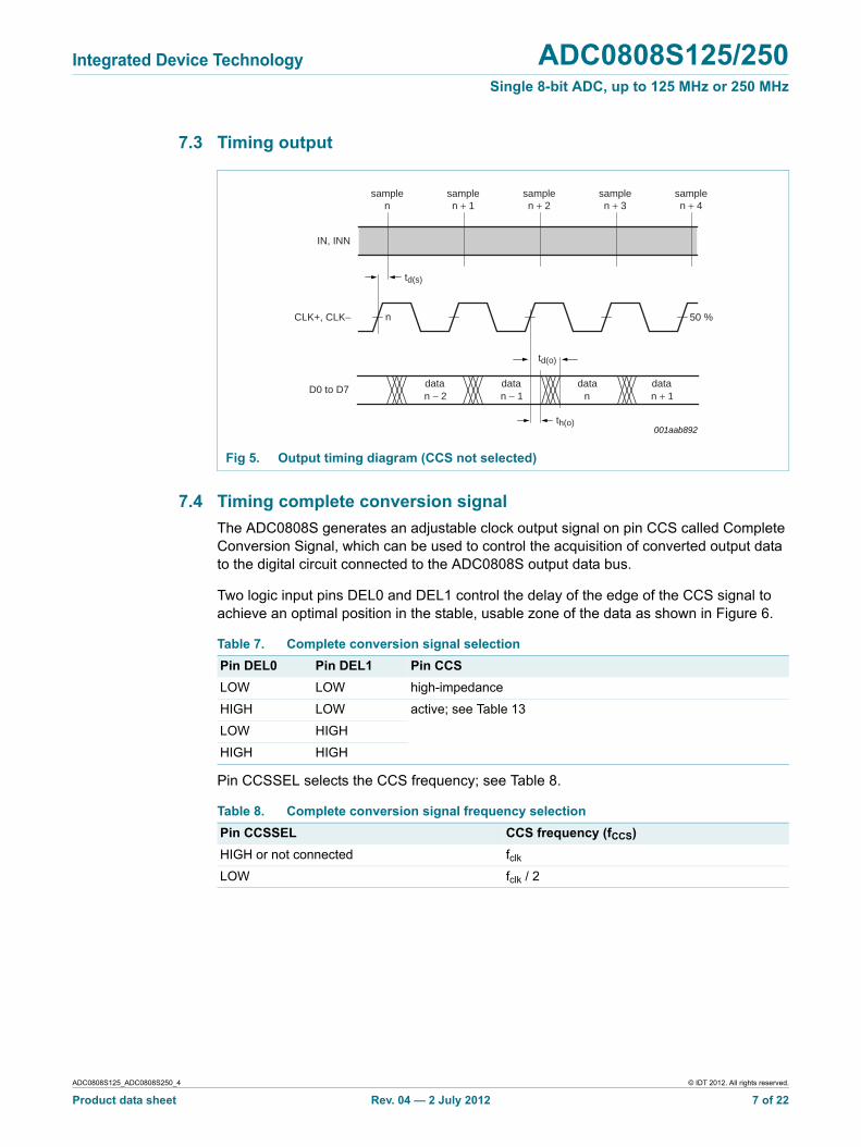
7.3 Timing output
IN, INN
CLK+, CLK− n
D0 to D7
50 %
datan − 2 n − 1
data data datan + 1n
td(o)
td(s)
th(o)001aab892
samplen
samplen + 1
samplen + 2
samplen + 3
samplen + 4
Fig 5. Output timing diagram (CCS not selected)
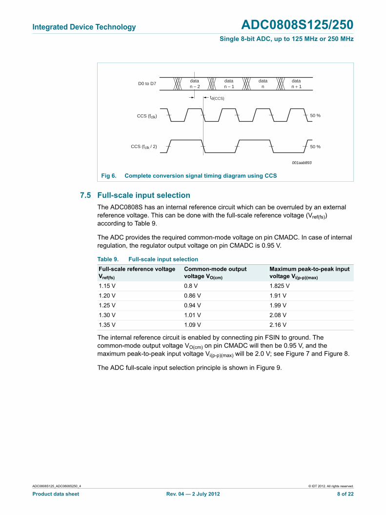
7.4 Timing complete conversion signal
The ADC0808S generates an adjustable clock output signal on pin CCS called Complete Conversion Signal, which can be used to control the acquisition of converted output data to the digital circuit connected to the ADC0808S output data bus.
Two logic input pins DEL0 and DEL1 control the delay of the edge of the CCS signal to achieve an optimal position in the stable, usable zone of the data as shown in Figure 6.
Table 7. Complete conversion signal selection
Pin DEL0 Pin DEL1 Pin CCS
LOW LOW high-impedance
HIGH LOW active; see Table 13
LOW HIGH
HIGH HIGH
Pin CCSSEL selects the CCS frequency; see Table 8.
Table 8. Complete conversion signal frequency selection
Pin CCSSEL CCS frequency (fCCS)
HIGH or not connected fclk
LOW fclk / 2
ADC0808S125_ADC0808S250_4 © IDT 2012. All rights reserved.
Product data sheet Rev. 04 — 2 July 2012 7 of 22
Integrated Device Technology ADC0808S125/250Single 8-bit ADC, up to 125 MHz or 250 MHz
001aab893
CCS (fclk)
CCS (fclk / 2)
D0 to D7
50 %
50 %
datan − 2 n − 1
data data datan + 1n
td(CCS)
Fig 6. Complete conversion signal timing diagram using CCS
7.5 Full-scale input selection
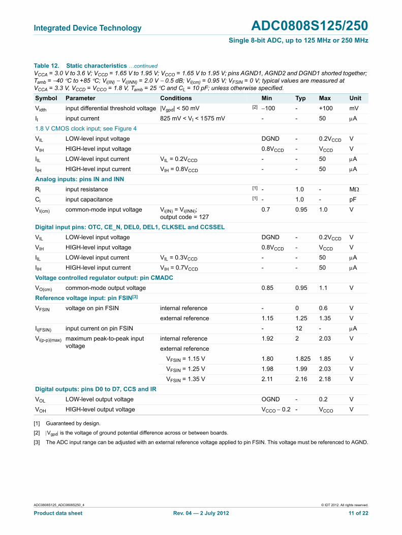
The ADC0808S has an internal reference circuit which can be overruled by an external reference voltage. This can be done with the full-scale reference voltage (Vref(fs)) according to Table 9.
The ADC provides the required common-mode voltage on pin CMADC. In case of internal regulation, the regulator output voltage on pin CMADC is 0.95 V.
Table 9. Full-scale input selection
Full-scale reference voltage Vref(fs)
Common-mode output voltage VO(cm)
Maximum peak-to-peak input voltage Vi(p-p)(max)
1.15 V 0.8 V 1.825 V
1.20 V 0.86 V 1.91 V
1.25 V 0.94 V 1.99 V
1.30 V 1.01 V 2.08 V
1.35 V 1.09 V 2.16 V
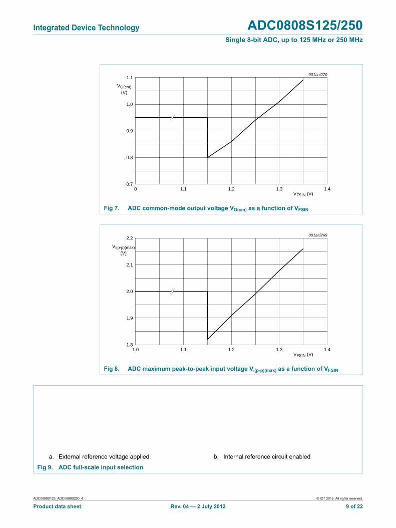
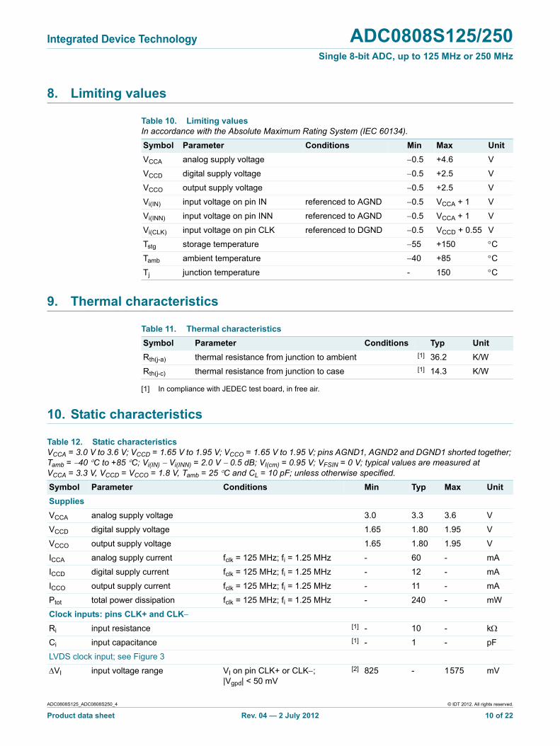
The internal reference circuit is enabled by connecting pin FSIN to ground. The common-mode output voltage VO(cm) on pin CMADC will then be 0.95 V, and the maximum peak-to-peak input voltage Vi(p-p)(max) will be 2.0 V; see Figure 7 and Figure 8.
The ADC full-scale input selection principle is shown in Figure 9.
ADC0808S125_ADC0808S250_4 © IDT 2012. All rights reserved.
Product data sheet Rev. 04 — 2 July 2012 8 of 22
Integrated Device Technology ADC0808S125/250Single 8-bit ADC, up to 125 MHz or 250 MHz
VFSIN (V)0 1.41.31.21.1
001aai270
0.9
0.8
1.0
1.1
VO(cm)(V)
0.7
Fig 7. ADC common-mode output voltage VO(cm) as a function of VFSIN
VFSIN (V)1.0 1.41.31.21.1
001aai269
2.0
1.9
2.1
2.2
Vi(p-p)(max)(V)
1.8
Fig 8. ADC maximum peak-to-peak input voltage Vi(p-p)(max) as a function of VFSIN
a. External reference voltage applied b. Internal reference circuit enabled
Fig 9. ADC full-scale input selection
ADC0808S125_ADC0808S250_4 © IDT 2012. All rights reserved.
Product data sheet Rev. 04 — 2 July 2012 9 of 22
Integrated Device Technology ADC0808S125/250Single 8-bit ADC, up to 125 MHz or 250 MHz
8. Limiting values
Table 10. Limiting values In accordance with the Absolute Maximum Rating System (IEC 60134).
Symbol Parameter Conditions Min Max Unit
VCCA analog supply voltage 0.5 +4.6 V
VCCD digital supply voltage 0.5 +2.5 V
VCCO output supply voltage 0.5 +2.5 V
Vi(IN) input voltage on pin IN referenced to AGND 0.5 VCCA + 1 V
Vi(INN) input voltage on pin INN referenced to AGND 0.5 VCCA + 1 V
Vi(CLK) input voltage on pin CLK referenced to DGND 0.5 VCCD + 0.55 V
Tstg storage temperature 55 +150 C
Tamb ambient temperature 40 +85 C
Tj junction temperature - 150 C
9. Thermal characteristics
Table 11. Thermal characteristics
Symbol Parameter Conditions Typ Unit
Rth(j-a) thermal resistance from junction to ambient [1] 36.2 K/W
Rth(j-c) thermal resistance from junction to case [1] 14.3 K/W
[1] In compliance with JEDEC test board, in free air.
10. Static characteristics
Table 12. Static characteristics VCCA = 3.0 V to 3.6 V; VCCD = 1.65 V to 1.95 V; VCCO = 1.65 V to 1.95 V; pins AGND1, AGND2 and DGND1 shorted together; Tamb = 40 C to +85 C; Vi(IN) Vi(INN) = 2.0 V 0.5 dB; VI(cm) = 0.95 V; VFSIN = 0 V; typical values are measured at VCCA = 3.3 V, VCCD = VCCO = 1.8 V, Tamb = 25 C and CL = 10 pF; unless otherwise specified.
Symbol Parameter Conditions Min Typ Max Unit
Supplies
VCCA analog supply voltage 3.0 3.3 3.6 V
VCCD digital supply voltage 1.65 1.80 1.95 V
VCCO output supply voltage 1.65 1.80 1.95 V
ICCA analog supply current fclk = 125 MHz; fi = 1.25 MHz - 60 - mA
ICCD digital supply current fclk = 125 MHz; fi = 1.25 MHz - 12 - mA
ICCO output supply current fclk = 125 MHz; fi = 1.25 MHz - 11 - mA
Ptot total power dissipation fclk = 125 MHz; fi = 1.25 MHz - 240 - mW
Clock inputs: pins CLK+ and CLK
Ri input resistance [1] - 10 - k
Ci input capacitance [1] - 1 - pF
LVDS clock input; see Figure 3
VI input voltage range VI on pin CLK+ or CLK; |Vgpd| < 50 mV
[2] 825 - 1 575 mV
ADC0808S125_ADC0808S250_4 © IDT 2012. All rights reserved.
Product data sheet Rev. 04 — 2 July 2012 10 of 22
Integrated Device Technology ADC0808S125/250Single 8-bit ADC, up to 125 MHz or 250 MHz
[1] Guaranteed by design.
[2] Vgpd is the voltage of ground potential difference across or between boards.
[3] The ADC input range can be adjusted with an external reference voltage applied to pin FSIN. This voltage must be referenced to AGND.
Vidth input differential threshold voltage |Vgpd| < 50 mV [2] 100 - +100 mV
II input current 825 mV < VI < 1 575 mV - - 50 A
1.8 V CMOS clock input; see Figure 4
VIL LOW-level input voltage DGND - 0.2VCCD V
VIH HIGH-level input voltage 0.8VCCD - VCCD V
IIL LOW-level input current VIL = 0.2VCCD - - 50 A
IIH HIGH-level input current VIH = 0.8VCCD - - 50 A
Analog inputs: pins IN and INN
Ri input resistance [1] - 1.0 - M
Ci input capacitance [1] - 1.0 - pF
VI(cm) common-mode input voltage Vi(IN) = Vi(INN); output code = 127
0.7 0.95 1.0 V
Digital input pins: OTC, CE_N, DEL0, DEL1, CLKSEL and CCSSEL
VIL LOW-level input voltage DGND - 0.2VCCD V
VIH HIGH-level input voltage 0.8VCCD - VCCD V
IIL LOW-level input current VIL = 0.3VCCD - - 50 A
IIH HIGH-level input current VIH = 0.7VCCD - - 50 A
Voltage controlled regulator output: pin CMADC
VO(cm) common-mode output voltage 0.85 0.95 1.1 V
Reference voltage input: pin FSIN[3]
VFSIN voltage on pin FSIN internal reference - 0 0.6 V
external reference 1.15 1.25 1.35 V
Ii(FSIN) input current on pin FSIN - 12 - A
Vi(p-p)(max) maximum peak-to-peak input voltage
internal reference 1.92 2 2.03 V
external reference
VFSIN = 1.15 V 1.80 1.825 1.85 V
VFSIN = 1.25 V 1.98 1.99 2.03 V
VFSIN = 1.35 V 2.11 2.16 2.18 V
Digital outputs: pins D0 to D7, CCS and IR
VOL LOW-level output voltage OGND - 0.2 V
VOH HIGH-level output voltage VCCO 0.2 - VCCO V
Table 12. Static characteristics …continuedVCCA = 3.0 V to 3.6 V; VCCD = 1.65 V to 1.95 V; VCCO = 1.65 V to 1.95 V; pins AGND1, AGND2 and DGND1 shorted together; Tamb = 40 C to +85 C; Vi(IN) Vi(INN) = 2.0 V 0.5 dB; VI(cm) = 0.95 V; VFSIN = 0 V; typical values are measured at VCCA = 3.3 V, VCCD = VCCO = 1.8 V, Tamb = 25 C and CL = 10 pF; unless otherwise specified.
Symbol Parameter Conditions Min Typ Max Unit
ADC0808S125_ADC0808S250_4 © IDT 2012. All rights reserved.
Product data sheet Rev. 04 — 2 July 2012 11 of 22
Integrated Device Technology ADC0808S125/250Single 8-bit ADC, up to 125 MHz or 250 MHz
11. Dynamic characteristics
Table 13. Dynamic characteristics VCCA = 3.0 V to 3.6 V; VCCD = 1.65 V to 1.95 V; VCCO = 1.65 V to 1.95 V; pins AGND1, AGND2 and DGND1 shorted together; Tamb = 40 C to +85 C; Vi(IN) Vi(INN) = 2.0 V 0.5 dB; VI(cm) = 0.95 V; VFSIN = 0 V; typical values are measured at VCCA = 3.3 V, VCCD = VCCO = 1.8 V, Tamb = 25 C and CL = 10 pF; unless otherwise specified.
Symbol Parameter Conditions Min Typ Max Unit
Clock timing input: pins CLK+ and CLK
fclk(min) minimum clock frequency - - 1 MHz
fclk(max) maximum clock frequency 250 - - MHz
tw(clk) clock pulse width fclk = 125 MHz 1.8 - - ns
Timing output: pins D0 to D7 and IR[1]; see Figure 5
td(s) sampling delay time 1.8 V CMOS clock - 1.3 - ns
LVDS clock - 1.65 - ns
th(o) output hold time 1.8 V CMOS clock 3.3 4.4 - ns
LVDS clock 4.2 4.8 - ns
td(o) output delay time 1.8 V CMOS clock - 5.4 6.9 ns
LVDS clock - 5.8 7.3 ns
Timing complete conversion signal: pin CCS; see Figure 6
fCCS(max) maximum CCS frequency 125 - - MHz
td(CCS) CCS delay time DEL0 = HIGH; DEL1 = LOW - 0.3 - ns
DEL0 = LOW; DEL1 = HIGH - 0.8 - ns
DEL0 = HIGH; DEL1 = HIGH - 1.9 - ns
3-state output delay time: pins CCS, IR and D7 to D0
tdZH float to active HIGH delay time - 2.1 - ns
tdZL float to active LOW delay time - 2.2 - ns
tdHZ active HIGH to float delay time - 3.3 - ns
tdLZ active LOW to float delay time - 2.9 - ns
Analog signal processing (50 % clock duty factor); see Section 12
INL integral non-linearity fclk = 20 MHz; fi = 21.4 MHz - 0.82 - LSB
DNL differential non-linearity fclk = 20 MHz; fi = 21.4 MHz; no missing code guaranteed
- 0.4 - LSB
EO offset error VCCA = 3.3 V; VCCD = 1.8 V; Tamb = 25 C; output code = 127
- 2.5 - mV
EG gain error spread from device to device; VCCA = 3.3 V; VCCD = 1.8 V; Tamb = 25 C
- 1.85 - %
B bandwidth fclk = 125 MHz; 3 dB; full-scale input
[2] - 560 - MHz
THD total harmonic distortion fclk = 125 MHz; fi = 78 MHz [3] - 53 - dB
fclk = 250 MHz; fi = 125 MHz - 53 - dB
Nth(RMS) RMS thermal noise shorted input; fclk = 125 MHz - 0.5 - LSB
S/N signal-to-noise ratio fclk = 125 MHz; fi = 78 MHz [4] - 48 - dBc
fclk = 250 MHz; fi = 125 MHz - 47 - dBc
ADC0808S125_ADC0808S250_4 © IDT 2012. All rights reserved.
Product data sheet Rev. 04 — 2 July 2012 12 of 22
Integrated Device Technology ADC0808S125/250Single 8-bit ADC, up to 125 MHz or 250 MHz
[1] Output data acquisition: the output data is available after the maximum delay of td(o).
[2] The 3 dB analog bandwidth is determined by the 3 dB reduction in the reconstructed output, the input being a full-scale sine wave.
[3] The total harmonic distortion is obtained with the addition of the first five harmonics.
[4] The signal-to-noise ratio takes into account all harmonics above five and noise up to Nyquist frequency.
[5] Intermodulation measured relative to either tone with analog input frequencies f1 and f2. The two input signals have the same amplitude and the total amplitude of both signals provides full-scale to the converter (6 dB below full-scale for each input signal). IMD3 is the ratio of the RMS value of either input tone to the RMS value of the worst case third-order intermodulation product.
12. Definitions
12.1 Static parameters
12.1.1 Integral non-linearity
Integral non-linearity (INL) is defined as the deviation of the transfer function from a best-fit straight line (linear regression computation). The INL of the code is obtained from the equation:
INL i Vin i Vin ideal –
S-----------------------------------------------= (1)
where: S corresponds to the slope of the ideal straight line (code width), i corresponds to the code value, Vin is the input voltage.
12.1.2 Differential non-linearity
Differential non-linearity (DNL) is the deviation in code width from the value of 1 LSB.
DNL i Vin i 1+ Vin i –
S--------------------------------------------= (2)
where: Vin is the input voltage; i is a code value from 0 to (2n 2).
12.2 Dynamic parameters
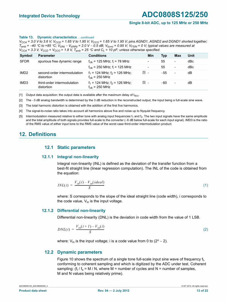
Figure 10 shows the spectrum of a single tone full-scale input sine wave of frequency ft, conforming to coherent sampling and which is digitized by the ADC under test. Coherent sampling: (ft / fs = M / N, where M = number of cycles and N = number of samples, M and N values being relatively prime).
SFDR spurious free dynamic range fclk = 125 MHz; fi = 78 MHz - 55 - dBc
fclk = 250 MHz; fi = 125 MHz - 55 - dBc
IMD2 second-order intermodulation distortion
f1 = 124 MHz; f2 = 126 MHz; fclk = 250 MHz
[5] - 55 - dB
IMD3 third-order intermodulation distortion
f1 = 124 MHz; f2 = 126 MHz; fclk = 250 MHz
[5] - 60 - dB
Table 13. Dynamic characteristics …continuedVCCA = 3.0 V to 3.6 V; VCCD = 1.65 V to 1.95 V; VCCO = 1.65 V to 1.95 V; pins AGND1, AGND2 and DGND1 shorted together; Tamb = 40 C to +85 C; Vi(IN) Vi(INN) = 2.0 V 0.5 dB; VI(cm) = 0.95 V; VFSIN = 0 V; typical values are measured at VCCA = 3.3 V, VCCD = VCCO = 1.8 V, Tamb = 25 C and CL = 10 pF; unless otherwise specified.
Symbol Parameter Conditions Min Typ Max Unit
ADC0808S125_ADC0808S250_4 © IDT 2012. All rights reserved.
Product data sheet Rev. 04 — 2 July 2012 13 of 22
Integrated Device Technology ADC0808S125/250Single 8-bit ADC, up to 125 MHz or 250 MHz
a2
a1
mag
nitu
de
frequency001aag627
SFDR
ak
s
a3
a = harmonic.
s = single tone.
Fig 10. Single tone spectrum of full-scale input sine wave of frequency ft
Remark: Pnoise in the equations in the following sections, is the sum of noise sources which include random noise, non-linearities, sampling time errors, and quantization noise.
12.2.1 Signal-to-Noise And Distortion (SINAD)
SINAD is the ratio of the output signal power to the noise plus distortion power for a given sample rate and input frequency, excluding the DC component:
SINAD dB 10log10Psignal
Pnoise distortion+---------------------------------------- = (3)
12.2.2 Effective Number Of Bits (ENOB)
ENOB is derived from SINAD and gives the theoretical resolution required by an ideal ADC to obtain the same SINAD measured on the real ADC. A good approximation gives:
ENOBSINAD 1.76–
6.02----------------------------------= (4)
12.2.3 Total Harmonic Distortion (THD)
THD is the ratio of the power of the harmonics to the power of the fundamental. For k 1 harmonics the THD is:
THD dB 10log10PharmonicsPsignal
------------------------- = (5)
where:
ADC0808S125_ADC0808S250_4 © IDT 2012. All rights reserved.
Product data sheet Rev. 04 — 2 July 2012 14 of 22
Integrated Device Technology ADC0808S125/250Single 8-bit ADC, up to 125 MHz or 250 MHz
Pharmonics a22a32 ak
2+ + +=
Psignal a12
=
(6)
(7)
The value of k is usually 6 (THD is calculated based on the first 5 harmonics).
12.2.4 Signal-to-Noise ratio (S/N)
S/N is the ratio of the output signal power to the noise power, excluding the harmonics and the DC component:
S N 10log10PsignalPnoise---------------- = (8)
12.2.5 Spurious Free Dynamic Range (SFDR)
The SFDR value specifies the available signal range as the spectral distance between the amplitude of the fundamental (a1) and the amplitude of the largest spurious harmonic and non-harmonic (max (s)), excluding the DC component:
SFDR dB 20log10a1
max s ------------------ = (9)
12.2.6 InterModulation Distortion (IMD)
f1 − f2
2f2 − f12f1 − f2
f1 + f2
2f2 2f1
f2 f1
f1 + 2f2
3f2
2f1 + f2
3f1
mag
nitu
de
frequency001aag628
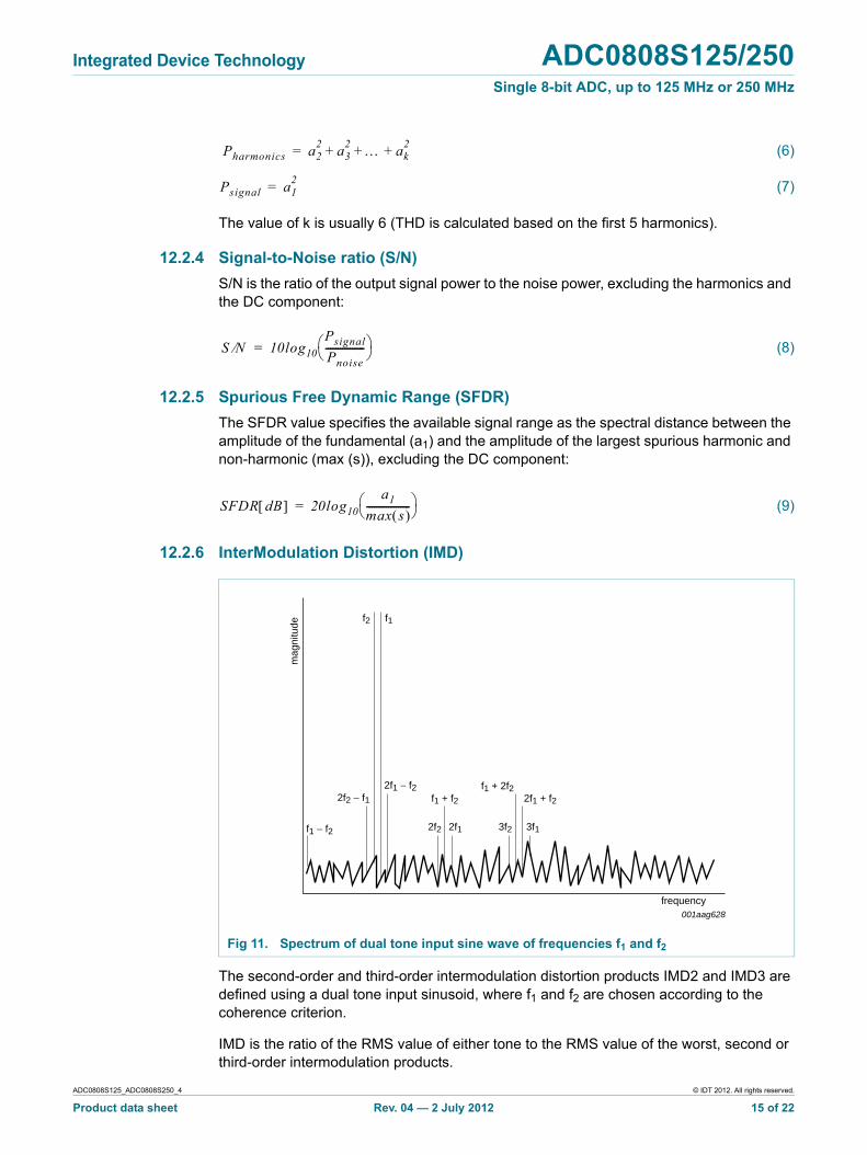
Fig 11. Spectrum of dual tone input sine wave of frequencies f1 and f2
The second-order and third-order intermodulation distortion products IMD2 and IMD3 are defined using a dual tone input sinusoid, where f1 and f2 are chosen according to the coherence criterion.
IMD is the ratio of the RMS value of either tone to the RMS value of the worst, second or third-order intermodulation products.
ADC0808S125_ADC0808S250_4 © IDT 2012. All rights reserved.
Product data sheet Rev. 04 — 2 July 2012 15 of 22
Integrated Device Technology ADC0808S125/250Single 8-bit ADC, up to 125 MHz or 250 MHz
The total intermodulation distortion is given by:
IMD dB 10log10PintermodPsignal
---------------------- = (10)
where:
Pintermod aim f1 f2– 2
aim f1 f2+ 2
– aim f1 2f2– 2
aim f1 2f2+ 2 + + +=
a+ im 2f1 f2– 2
aim 2f1 f2+ 2
+(11)
where aim fn 2
is the power in the intermodulation component at fn.
Psignal af12
af22
+= (12)
ADC0808S125_ADC0808S250_4 © IDT 2012. All rights reserved.
Product data sheet Rev. 04 — 2 July 2012 16 of 22
Integrated Device Technology ADC0808S125/250Single 8-bit ADC, up to 125 MHz or 250 MHz
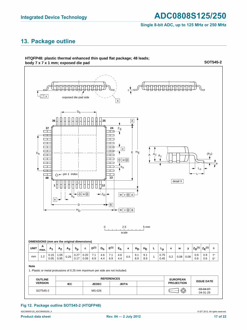
13. Package outline
UNITA
max. A1 A2 A3 bp HD HE Lp ZD(1) ZE
(1)c e L ywv θ
REFERENCESOUTLINEVERSION
EUROPEANPROJECTION ISSUE DATE
IEC JEDEC JEITA
mm 1.2 0.150.05
1.050.95
0.250.270.17
0.200.09
7.16.9
0.59.18.9
0.90.6
7°0°
0.08 0.080.21
DIMENSIONS (mm are the original dimensions)
Note
1. Plastic or metal protrusions of 0.25 mm maximum per side are not included.
0.750.45
SOT545-2 MS-026 03-04-0704-01-29
D(1) E(1)
7.16.9
9.18.9
Dh Eh
4.64.4
4.64.4
0.90.6
bpe
θ
EA1A
Lp
detail X
L
B
121
48
37
DH
bp
EHA2
v M B
D
ZD
A
c
ZE
e
v M A
X
2536
24
13
y
pin 1 index
w M
w M
0 2.5 5 mm
scale
HTQFP48: plastic thermal enhanced thin quad flat package; 48 leads;body 7 x 7 x 1 mm; exposed die pad SOT545-2
Dh
Eh
exposed die pad side
(A )3
Fig 12. Package outline SOT545-2 (HTQFP48)
ADC0808S125_ADC0808S250_4 © IDT 2012. All rights reserved.
Product data sheet Rev. 04 — 2 July 2012 17 of 22
Integrated Device Technology ADC0808S125/250Single 8-bit ADC, up to 125 MHz or 250 MHz
14. Soldering of SMD packages
This text provides a very brief insight into a complex technology. A more in-depth account of soldering ICs can be found in Application Note AN10365 “Surface mount reflow soldering description”.
14.1 Introduction to soldering
Soldering is one of the most common methods through which packages are attached to Printed Circuit Boards (PCBs), to form electrical circuits. The soldered joint provides both the mechanical and the electrical connection. There is no single soldering method that is ideal for all IC packages. Wave soldering is often preferred when through-hole and Surface Mount Devices (SMDs) are mixed on one printed wiring board; however, it is not suitable for fine pitch SMDs. Reflow soldering is ideal for the small pitches and high densities that come with increased miniaturization.
14.2 Wave and reflow soldering
Wave soldering is a joining technology in which the joints are made by solder coming from a standing wave of liquid solder. The wave soldering process is suitable for the following:
• Through-hole components
• Leaded or leadless SMDs, which are glued to the surface of the printed circuit board
Not all SMDs can be wave soldered. Packages with solder balls, and some leadless packages which have solder lands underneath the body, cannot be wave soldered. Also, leaded SMDs with leads having a pitch smaller than ~0.6 mm cannot be wave soldered, due to an increased probability of bridging.
The reflow soldering process involves applying solder paste to a board, followed by component placement and exposure to a temperature profile. Leaded packages, packages with solder balls, and leadless packages are all reflow solderable.
Key characteristics in both wave and reflow soldering are:
• Board specifications, including the board finish, solder masks and vias
• Package footprints, including solder thieves and orientation
• The moisture sensitivity level of the packages
• Package placement
• Inspection and repair
• Lead-free soldering versus SnPb soldering
14.3 Wave soldering
Key characteristics in wave soldering are:
• Process issues, such as application of adhesive and flux, clinching of leads, board transport, the solder wave parameters, and the time during which components are exposed to the wave
• Solder bath specifications, including temperature and impurities
ADC0808S125_ADC0808S250_4 © IDT 2012. All rights reserved.
Product data sheet Rev. 04 — 2 July 2012 18 of 22
Integrated Device Technology ADC0808S125/250Single 8-bit ADC, up to 125 MHz or 250 MHz
14.4 Reflow soldering
Key characteristics in reflow soldering are:
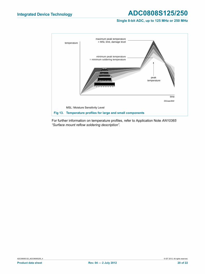
• Lead-free versus SnPb soldering; note that a lead-free reflow process usually leads to higher minimum peak temperatures (see Figure 13) than a SnPb process, thus reducing the process window
• Solder paste printing issues including smearing, release, and adjusting the process window for a mix of large and small components on one board
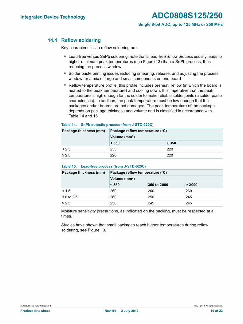
• Reflow temperature profile; this profile includes preheat, reflow (in which the board is heated to the peak temperature) and cooling down. It is imperative that the peak temperature is high enough for the solder to make reliable solder joints (a solder paste characteristic). In addition, the peak temperature must be low enough that the packages and/or boards are not damaged. The peak temperature of the package depends on package thickness and volume and is classified in accordance with Table 14 and 15
Table 14. SnPb eutectic process (from J-STD-020C)
Package thickness (mm) Package reflow temperature (C)
Volume (mm3)
< 350 350
< 2.5 235 220
2.5 220 220
Table 15. Lead-free process (from J-STD-020C)
Package thickness (mm) Package reflow temperature (C)
Volume (mm3)
< 350 350 to 2 000 > 2 000
< 1.6 260 260 260
1.6 to 2.5 260 250 245
> 2.5 250 245 245
Moisture sensitivity precautions, as indicated on the packing, must be respected at all times.
Studies have shown that small packages reach higher temperatures during reflow soldering, see Figure 13.
ADC0808S125_ADC0808S250_4 © IDT 2012. All rights reserved.
Product data sheet Rev. 04 — 2 July 2012 19 of 22
Integrated Device Technology ADC0808S125/250Single 8-bit ADC, up to 125 MHz or 250 MHz
001aac844
temperature
time
minimum peak temperature= minimum soldering temperature
maximum peak temperature= MSL limit, damage level
peak temperature
MSL: Moisture Sensitivity Level
Fig 13. Temperature profiles for large and small components
For further information on temperature profiles, refer to Application Note AN10365 “Surface mount reflow soldering description”.
ADC0808S125_ADC0808S250_4 © IDT 2012. All rights reserved.
Product data sheet Rev. 04 — 2 July 2012 20 of 22
Integrated Device Technology ADC0808S125/250Single 8-bit ADC, up to 125 MHz or 250 MHz
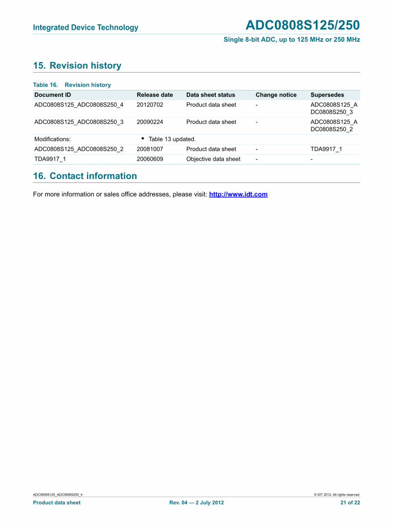
15. Revision history
Table 16. Revision history
Document ID Release date Data sheet status Change notice Supersedes
ADC0808S125_ADC0808S250_4 20120702 Product data sheet - ADC0808S125_ADC0808S250_3
ADC0808S125_ADC0808S250_3 20090224 Product data sheet - ADC0808S125_ADC0808S250_2
Modifications: Table• 13 updated.
ADC0808S125_ADC0808S250_2 20081007 Product data sheet - TDA9917_1
TDA9917_1 20060609 Objective data sheet - -
16. Contact information
For more information or sales office addresses, please visit: http://www.idt.com
ADC0808S125_ADC0808S250_4 © IDT 2012. All rights reserved.
Product data sheet Rev. 04 — 2 July 2012 21 of 22
Integrated Device Technology ADC0808S125/250Single 8-bit ADC, up to 125 MHz or 250 MHz
17. Contents
1 General description . . . . . . . . . . . . . . . . . . . . . . 1
2 Features . . . . . . . . . . . . . . . . . . . . . . . . . . . . . . . 1
3 Applications . . . . . . . . . . . . . . . . . . . . . . . . . . . . 1
4 Ordering information. . . . . . . . . . . . . . . . . . . . . 2
5 Block diagram . . . . . . . . . . . . . . . . . . . . . . . . . . 2
6 Pinning information. . . . . . . . . . . . . . . . . . . . . . 36.1 Pinning . . . . . . . . . . . . . . . . . . . . . . . . . . . . . . . 36.2 Pin description . . . . . . . . . . . . . . . . . . . . . . . . . 3
7 Functional description . . . . . . . . . . . . . . . . . . . 57.1 CMOS/LVDS clock input. . . . . . . . . . . . . . . . . . 57.2 Digital output coding . . . . . . . . . . . . . . . . . . . . . 67.3 Timing output . . . . . . . . . . . . . . . . . . . . . . . . . . 77.4 Timing complete conversion signal. . . . . . . . . . 77.5 Full-scale input selection . . . . . . . . . . . . . . . . . 8
8 Limiting values. . . . . . . . . . . . . . . . . . . . . . . . . 10
9 Thermal characteristics . . . . . . . . . . . . . . . . . 10
10 Static characteristics. . . . . . . . . . . . . . . . . . . . 10
11 Dynamic characteristics . . . . . . . . . . . . . . . . . 12
12 Definitions . . . . . . . . . . . . . . . . . . . . . . . . . . . . 13
12.1 Static parameters . . . . . . . . . . . . . . . . . . . . . . 1312.1.1 Integral non-linearity . . . . . . . . . . . . . . . . . . . 1312.1.2 Differential non-linearity . . . . . . . . . . . . . . . . . 1312.2 Dynamic parameters . . . . . . . . . . . . . . . . . . . 1312.2.1 Signal-to-Noise And Distortion (SINAD) . . . . 1412.2.2 Effective Number Of Bits (ENOB) . . . . . . . . . 1412.2.3 Total Harmonic Distortion (THD) . . . . . . . . . . 1412.2.4 Signal-to-Noise ratio (S/N) . . . . . . . . . . . . . . . 1512.2.5 Spurious Free Dynamic Range (SFDR). . . . . 1512.2.6 InterModulation Distortion (IMD) . . . . . . . . . . 15
13 Package outline. . . . . . . . . . . . . . . . . . . . . . . . 17
14 Soldering of SMD packages. . . . . . . . . . . . . . 1814.1 Introduction to soldering. . . . . . . . . . . . . . . . . 1814.2 Wave and reflow soldering. . . . . . . . . . . . . . . 1814.3 Wave soldering . . . . . . . . . . . . . . . . . . . . . . . 1814.4 Reflow soldering . . . . . . . . . . . . . . . . . . . . . . 19
15 Revision history . . . . . . . . . . . . . . . . . . . . . . . 21
16 Contact information . . . . . . . . . . . . . . . . . . . . 21
17 Contents. . . . . . . . . . . . . . . . . . . . . . . . . . . . . . 22
ADC0808S125_ADC0808S250_4 © IDT 2012. All rights reserved.
Product data sheet Rev. 04 — 2 July 2012 22 of 22