datasheet - l99dz200g - stmicroelectronics
TRANSCRIPT

April 2021 DS13220 Rev 5 1/198
L99DZ200G
Automotive front door device with LIN and CAN providing dual H-bridge driving
Datasheet - production data
Features
AEC-Q100 qualified
2 configurable half bridges for 7.5 A load(RON = 150 mΩ) or 3 A load (RON = 300 mΩ)
2 half bridges for 0.5 A load (RON = 2000 mΩ)
1 configurable high-side driver for up to 1.5 A(RON = 500 mΩ) or 0.35 A (RON = 1600 mΩ)load
1 configurable high-side driver for 0.7 A(RON = 800 mΩ) or 0.35 A (RON = 1600 mΩ)load
3 configurable high-side drivers for0.15 A/0.35 A (RON =2 Ω)
1 configurable high-side driver for 0.25 A/0.5 A(RON = 2 Ω) to supply EC Glass MOSFET
1 configurable P-channel high-side drivers for0.15 A/0.25 A (RON = 5 Ω)
Internal 10-bit PWM timer for each stand-alonehigh-side driver
Buffered supply for voltage regulators and 1high-side driver (OUT15 P-channel) to supplye.g. external contacts
Programmable soft-start function to drive loadswith higher inrush currents as current limitationvalue for OUT1-6 (i.e. motors) and OUT7,OUT8 (i.e. bulbs) with thermal expirationfeature
Flexible HS drivers (OUT7, OUT8 and OUT9)suitable to drive external LED modules withhigh input capacitance
All the embedded outputs come with protectionand supervision features:
– Current Monitor (high-side only)
– Open-load and Overcurrent
– Thermal warning and Thermal shutdown
2 fully protected drivers for external MOSFETs inH-bridge configuration, dual Half bridgeconfiguration and combined configuration todrive 3 motors
Fully protected driver for external high-sideMOSFET
Control block for electro-chromic element
One 5 V voltage regulators for microcontrollersupply
One 5 V voltage tracker for peripheral supply
Programmable reset generator for power-onand under voltage
Configurable window watchdog
LIN 2.2a compliant (SAEJ2602 compatible andSAE J2962-1 compliant) transceiver
Advanced high speed CAN transceiver (ISO11898-2:2003 /-5:2007 and SAE J2284 & SAEJ2962-2 compliant) with local failure and busfailure; HS-CAN Transceiver ConformanceTest according to «Interoperability testspecification for high-speed CAN transceiver orequivalent devices IOPT.CAN v02d00»
Separated (Isolated) fail-safe block with 2 LS(RON = 1 Ω) to pull down the gates of theexternal HS MOSFETs
Thermal clusters
A/D conversion of supply voltages and internaltemperature sensors
Embedded and programmable VS duty cycleadjustment for LED driver outputs
Generator Mode for Power Trunk/Tailgateapplications
www.st.com

Contents L99DZ200G
2/198 DS13220 Rev 5
Contents
1 Description . . . . . . . . . . . . . . . . . . . . . . . . . . . . . . . . . . . . . . . . . . . . . . . . 12
2 Block diagram and pin descriptions . . . . . . . . . . . . . . . . . . . . . . . . . . . 13
3 Electrical specifications . . . . . . . . . . . . . . . . . . . . . . . . . . . . . . . . . . . . . 18
3.1 Absolute maximum ratings . . . . . . . . . . . . . . . . . . . . . . . . . . . . . . . . . . . . 18
3.2 ESD protection . . . . . . . . . . . . . . . . . . . . . . . . . . . . . . . . . . . . . . . . . . . . . 20
3.3 Thermal data . . . . . . . . . . . . . . . . . . . . . . . . . . . . . . . . . . . . . . . . . . . . . . 20
3.3.1 LQFP64 thermal data . . . . . . . . . . . . . . . . . . . . . . . . . . . . . . . . . . . . . . 21
3.4 Electrical characteristics . . . . . . . . . . . . . . . . . . . . . . . . . . . . . . . . . . . . . . 24
3.4.1 Supply and supply monitoring . . . . . . . . . . . . . . . . . . . . . . . . . . . . . . . . 24
3.4.2 Oscillator . . . . . . . . . . . . . . . . . . . . . . . . . . . . . . . . . . . . . . . . . . . . . . . . 26
3.4.3 Power-on reset (VSREG) . . . . . . . . . . . . . . . . . . . . . . . . . . . . . . . . . . . 26
3.4.4 Voltage regulator V1 . . . . . . . . . . . . . . . . . . . . . . . . . . . . . . . . . . . . . . . 27
3.4.5 Voltage regulator V2 . . . . . . . . . . . . . . . . . . . . . . . . . . . . . . . . . . . . . . . 28
3.4.6 Reset output . . . . . . . . . . . . . . . . . . . . . . . . . . . . . . . . . . . . . . . . . . . . . 29
3.4.7 Watchdog timing . . . . . . . . . . . . . . . . . . . . . . . . . . . . . . . . . . . . . . . . . . 30
3.4.8 Current monitor output (CM) . . . . . . . . . . . . . . . . . . . . . . . . . . . . . . . . . 32
3.4.9 Charge pump . . . . . . . . . . . . . . . . . . . . . . . . . . . . . . . . . . . . . . . . . . . . . 33
3.4.10 Outputs OUT1 - OUT15, ECV, ECDR . . . . . . . . . . . . . . . . . . . . . . . . . . 34
3.4.11 Power outputs switching times . . . . . . . . . . . . . . . . . . . . . . . . . . . . . . . 35
3.4.12 Current Monitoring . . . . . . . . . . . . . . . . . . . . . . . . . . . . . . . . . . . . . . . . . 37
3.4.13 Heater . . . . . . . . . . . . . . . . . . . . . . . . . . . . . . . . . . . . . . . . . . . . . . . . . . 40
3.4.14 H-bridge driver . . . . . . . . . . . . . . . . . . . . . . . . . . . . . . . . . . . . . . . . . . . . 40
3.4.15 Gate drivers for the external Power-MOS switching times . . . . . . . . . . 41
3.4.16 Drain source monitoring external H-bridges . . . . . . . . . . . . . . . . . . . . . 45
3.4.17 Drain source monitoring external heater MOSFET . . . . . . . . . . . . . . . . 45
3.4.18 Open-load monitoring external H-bridges . . . . . . . . . . . . . . . . . . . . . . . 46
3.4.19 Open-load monitoring external heater MOSFET . . . . . . . . . . . . . . . . . . 46
3.4.20 Electro-chrome mirror driver . . . . . . . . . . . . . . . . . . . . . . . . . . . . . . . . . 46
3.4.21 Fail safe low-side switch . . . . . . . . . . . . . . . . . . . . . . . . . . . . . . . . . . . . 47
3.4.22 Wake up input WU . . . . . . . . . . . . . . . . . . . . . . . . . . . . . . . . . . . . . . . . . 48
3.4.23 High speed CAN transceiver . . . . . . . . . . . . . . . . . . . . . . . . . . . . . . . . . 48
3.4.24 LIN transceiver . . . . . . . . . . . . . . . . . . . . . . . . . . . . . . . . . . . . . . . . . . . . 54

DS13220 Rev 5 3/198
L99DZ200G Contents
6
3.4.25 SPI . . . . . . . . . . . . . . . . . . . . . . . . . . . . . . . . . . . . . . . . . . . . . . . . . . . . . 58
3.4.26 Inputs TxD_C and TxD_L for Flash mode . . . . . . . . . . . . . . . . . . . . . . . 63
3.4.27 PWMH(1/2)A, PWMH(1/2)B and DIR inputs . . . . . . . . . . . . . . . . . . . . . 64
3.4.28 ADC characteristics . . . . . . . . . . . . . . . . . . . . . . . . . . . . . . . . . . . . . . . . 64
3.4.29 Temperature diode characteristics . . . . . . . . . . . . . . . . . . . . . . . . . . . . . 65
3.4.30 Interrupt outputs . . . . . . . . . . . . . . . . . . . . . . . . . . . . . . . . . . . . . . . . . . . 65
3.4.31 Timer1 and Timer2 . . . . . . . . . . . . . . . . . . . . . . . . . . . . . . . . . . . . . . . . . 67
3.4.32 SGND loss comparator . . . . . . . . . . . . . . . . . . . . . . . . . . . . . . . . . . . . . 67
4 Application information . . . . . . . . . . . . . . . . . . . . . . . . . . . . . . . . . . . . . 68
4.1 Supply Vs, Vsreg . . . . . . . . . . . . . . . . . . . . . . . . . . . . . . . . . . . . . . . . . . . 68
4.2 Voltage Regulators . . . . . . . . . . . . . . . . . . . . . . . . . . . . . . . . . . . . . . . . . . 68
4.2.1 Voltage regulator: V1 . . . . . . . . . . . . . . . . . . . . . . . . . . . . . . . . . . . . . . . 68
4.2.2 Voltage regulator: V2 . . . . . . . . . . . . . . . . . . . . . . . . . . . . . . . . . . . . . . . 68
4.2.3 Voltage Regulator Failure . . . . . . . . . . . . . . . . . . . . . . . . . . . . . . . . . . . 69
4.2.4 Short to ground detection . . . . . . . . . . . . . . . . . . . . . . . . . . . . . . . . . . . 69
4.2.5 Voltage regulator behavior . . . . . . . . . . . . . . . . . . . . . . . . . . . . . . . . . . . 70
4.3 Operating Modes . . . . . . . . . . . . . . . . . . . . . . . . . . . . . . . . . . . . . . . . . . . 70
4.3.1 Active Mode . . . . . . . . . . . . . . . . . . . . . . . . . . . . . . . . . . . . . . . . . . . . . . 71
4.3.2 Flash Modes . . . . . . . . . . . . . . . . . . . . . . . . . . . . . . . . . . . . . . . . . . . . . 71
4.3.3 SW-Debug Mode . . . . . . . . . . . . . . . . . . . . . . . . . . . . . . . . . . . . . . . . . . 71
4.3.4 V1_Standby mode . . . . . . . . . . . . . . . . . . . . . . . . . . . . . . . . . . . . . . . . . 73
4.3.5 Interrupt . . . . . . . . . . . . . . . . . . . . . . . . . . . . . . . . . . . . . . . . . . . . . . . . . 74
4.3.6 CAN wake-up signalization . . . . . . . . . . . . . . . . . . . . . . . . . . . . . . . . . . 75
4.3.7 VBAT_Standby mode . . . . . . . . . . . . . . . . . . . . . . . . . . . . . . . . . . . . . . 75
4.4 Wake up from Standby Modes . . . . . . . . . . . . . . . . . . . . . . . . . . . . . . . . . 75
4.4.1 Wake up inputs . . . . . . . . . . . . . . . . . . . . . . . . . . . . . . . . . . . . . . . . . . . 76
4.5 Functional Overview (truth table) . . . . . . . . . . . . . . . . . . . . . . . . . . . . . . . 77
4.6 Configurable Window Watchdog . . . . . . . . . . . . . . . . . . . . . . . . . . . . . . . 78
4.6.1 Change Watchdog timing . . . . . . . . . . . . . . . . . . . . . . . . . . . . . . . . . . . . 81
4.7 Fail Safe Mode . . . . . . . . . . . . . . . . . . . . . . . . . . . . . . . . . . . . . . . . . . . . . 81
4.7.1 Temporary Failures . . . . . . . . . . . . . . . . . . . . . . . . . . . . . . . . . . . . . . . . 81
4.7.2 Non-recoverable failures – forced VBAT_Standby mode . . . . . . . . . . . 82
4.8 Reset output (NReset) . . . . . . . . . . . . . . . . . . . . . . . . . . . . . . . . . . . . . . . 84
4.9 LIN Bus Interface . . . . . . . . . . . . . . . . . . . . . . . . . . . . . . . . . . . . . . . . . . . 85
4.9.1 Features . . . . . . . . . . . . . . . . . . . . . . . . . . . . . . . . . . . . . . . . . . . . . . . . . 85

Contents L99DZ200G
4/198 DS13220 Rev 5
4.9.2 Error Handling . . . . . . . . . . . . . . . . . . . . . . . . . . . . . . . . . . . . . . . . . . . . 86
4.9.3 Wake up from Standby Modes . . . . . . . . . . . . . . . . . . . . . . . . . . . . . . . . 86
4.9.4 Receive-only mode . . . . . . . . . . . . . . . . . . . . . . . . . . . . . . . . . . . . . . . . 87
4.10 High-speed CAN bus transceiver . . . . . . . . . . . . . . . . . . . . . . . . . . . . . . . 88
4.10.1 Features . . . . . . . . . . . . . . . . . . . . . . . . . . . . . . . . . . . . . . . . . . . . . . . . . 88
4.10.2 CAN Transceiver operating modes . . . . . . . . . . . . . . . . . . . . . . . . . . . . 89
4.10.3 Automatic Voltage Biasing . . . . . . . . . . . . . . . . . . . . . . . . . . . . . . . . . . . 90
4.10.4 Wake up by CAN . . . . . . . . . . . . . . . . . . . . . . . . . . . . . . . . . . . . . . . . . . 90
4.10.5 CAN looping . . . . . . . . . . . . . . . . . . . . . . . . . . . . . . . . . . . . . . . . . . . . . . 91
4.10.6 Pretended Networking . . . . . . . . . . . . . . . . . . . . . . . . . . . . . . . . . . . . . . 91
4.10.7 CAN Error Handling . . . . . . . . . . . . . . . . . . . . . . . . . . . . . . . . . . . . . . . . 91
4.11 Serial Peripheral Interface (ST SPI Standard) . . . . . . . . . . . . . . . . . . . . . 92
4.12 Power Supply Fail . . . . . . . . . . . . . . . . . . . . . . . . . . . . . . . . . . . . . . . . . . 93
4.12.1 Vs supply failure . . . . . . . . . . . . . . . . . . . . . . . . . . . . . . . . . . . . . . . . . . 93
4.12.2 Vsreg supply failure . . . . . . . . . . . . . . . . . . . . . . . . . . . . . . . . . . . . . . . . 94
4.13 Temperature warning and thermal shut-down . . . . . . . . . . . . . . . . . . . . . 96
4.14 Power Outputs OUT1…15 . . . . . . . . . . . . . . . . . . . . . . . . . . . . . . . . . . . 97
4.15 Auto-recovery alert and thermal expiration . . . . . . . . . . . . . . . . . . . . . . . 98
4.16 Charge Pump . . . . . . . . . . . . . . . . . . . . . . . . . . . . . . . . . . . . . . . . . . . . . 100
4.17 Inductive Loads . . . . . . . . . . . . . . . . . . . . . . . . . . . . . . . . . . . . . . . . . . . 100
4.18 Open-load detection . . . . . . . . . . . . . . . . . . . . . . . . . . . . . . . . . . . . . . . . 100
4.19 Overcurrent Management: Recovery or Latch . . . . . . . . . . . . . . . . . . . . 100
4.20 Overcurrent Recovery and Short-Circuit detection . . . . . . . . . . . . . . . . . 101
4.21 Constant current mode . . . . . . . . . . . . . . . . . . . . . . . . . . . . . . . . . . . . . . 103
4.22 Current monitor and direct drive input . . . . . . . . . . . . . . . . . . . . . . . . . . 104
4.23 PWM-Mode of the Power-Outputs . . . . . . . . . . . . . . . . . . . . . . . . . . . . . 105
4.24 Cross-current protection . . . . . . . . . . . . . . . . . . . . . . . . . . . . . . . . . . . . . 105
4.25 Programmable soft-start function to drive loads with higher inrush current . . . . . . . . . . . . . . . . . . . . . . . . . . . . . . . . . . . . . . . . . . . . . . . . . . . . . . . . 105
4.26 H-bridge control . . . . . . . . . . . . . . . . . . . . . . . . . . . . . . . . . . . . . . . . . . . 106
4.27 H-Bridge Driver Slew-Rate Control . . . . . . . . . . . . . . . . . . . . . . . . . . . . 108
4.28 Resistive low . . . . . . . . . . . . . . . . . . . . . . . . . . . . . . . . . . . . . . . . . . . . . 109
4.29 Short circuit detection / drain source monitoring . . . . . . . . . . . . . . . . . . 109
4.30 H-Bridge-Monitoring in Off-Mode . . . . . . . . . . . . . . . . . . . . . . . . . . . . . .110
4.31 Programmable cross current protection . . . . . . . . . . . . . . . . . . . . . . . . . .113

DS13220 Rev 5 5/198
L99DZ200G Contents
6
4.32 Power window H-bridge safety switch off block . . . . . . . . . . . . . . . . . . .114
4.33 Generator mode . . . . . . . . . . . . . . . . . . . . . . . . . . . . . . . . . . . . . . . . . . . .116
4.33.1 Generator Mode in Active Mode . . . . . . . . . . . . . . . . . . . . . . . . . . . . . 116
4.33.2 Generator Mode in Standby Modes . . . . . . . . . . . . . . . . . . . . . . . . . . . 116
4.34 Heater MOSFET Driver . . . . . . . . . . . . . . . . . . . . . . . . . . . . . . . . . . . . . .117
4.35 Controller of electro-chromic glass . . . . . . . . . . . . . . . . . . . . . . . . . . . . . .118
4.36 Temperature warning and shutdown . . . . . . . . . . . . . . . . . . . . . . . . . . . 120
4.37 Thermal clusters . . . . . . . . . . . . . . . . . . . . . . . . . . . . . . . . . . . . . . . . . . 120
4.38 VS compensation (duty cycle adjustment) module . . . . . . . . . . . . . . . . 122
4.39 Analog digital converter . . . . . . . . . . . . . . . . . . . . . . . . . . . . . . . . . . . . . 123
5 Serial Peripheral Interface (SPI) . . . . . . . . . . . . . . . . . . . . . . . . . . . . . . 125
5.1 ST SPI 4.0 . . . . . . . . . . . . . . . . . . . . . . . . . . . . . . . . . . . . . . . . . . . . . . . 125
5.1.1 Physical Layer . . . . . . . . . . . . . . . . . . . . . . . . . . . . . . . . . . . . . . . . . . . 126
5.2 Signal description . . . . . . . . . . . . . . . . . . . . . . . . . . . . . . . . . . . . . . . . . 126
5.2.1 Clock and data characteristics . . . . . . . . . . . . . . . . . . . . . . . . . . . . . . . 127
5.2.2 Communication Protocol . . . . . . . . . . . . . . . . . . . . . . . . . . . . . . . . . . . 128
5.2.3 Address Definition . . . . . . . . . . . . . . . . . . . . . . . . . . . . . . . . . . . . . . . . 131
5.2.4 Protocol Failure Detection . . . . . . . . . . . . . . . . . . . . . . . . . . . . . . . . . . 137
6 Application . . . . . . . . . . . . . . . . . . . . . . . . . . . . . . . . . . . . . . . . . . . . . . . 139
7 SPI registers . . . . . . . . . . . . . . . . . . . . . . . . . . . . . . . . . . . . . . . . . . . . . 140
7.1 Global Status Byte GSB . . . . . . . . . . . . . . . . . . . . . . . . . . . . . . . . . . . . . 140
7.2 Control register overview . . . . . . . . . . . . . . . . . . . . . . . . . . . . . . . . . . . . 144
7.3 Status register overview . . . . . . . . . . . . . . . . . . . . . . . . . . . . . . . . . . . . . 148
7.4 Control registers . . . . . . . . . . . . . . . . . . . . . . . . . . . . . . . . . . . . . . . . . . . 150
7.4.1 Control Register CR1 (0x01) . . . . . . . . . . . . . . . . . . . . . . . . . . . . . . . . 150
7.4.2 Control Register CR2 (0x02) . . . . . . . . . . . . . . . . . . . . . . . . . . . . . . . . 153
7.4.3 Control Register CR3 (0x03) . . . . . . . . . . . . . . . . . . . . . . . . . . . . . . . . 156
7.4.4 Control Register CR4 (0x04) . . . . . . . . . . . . . . . . . . . . . . . . . . . . . . . . 158
7.4.5 Control Register CR5 (0x05) . . . . . . . . . . . . . . . . . . . . . . . . . . . . . . . . 159
7.4.6 Control Register CR6 (0x06) . . . . . . . . . . . . . . . . . . . . . . . . . . . . . . . . 161
7.4.7 Control Register CR7 (0x07) . . . . . . . . . . . . . . . . . . . . . . . . . . . . . . . . 162
7.4.8 Control Register CR8 (0x08) . . . . . . . . . . . . . . . . . . . . . . . . . . . . . . . . 163
7.4.9 Control Register CR9 (0x09) . . . . . . . . . . . . . . . . . . . . . . . . . . . . . . . . 166

Contents L99DZ200G
6/198 DS13220 Rev 5
7.4.10 Control Register CR10 (0x0A) . . . . . . . . . . . . . . . . . . . . . . . . . . . . . . . 167
7.4.11 Control Register CR11 (0x0B) . . . . . . . . . . . . . . . . . . . . . . . . . . . . . . . 169
7.4.12 Control Register CR12 (0x0C) . . . . . . . . . . . . . . . . . . . . . . . . . . . . . . . 170
7.4.13 Control Register CR13 (0x0D) to CR16 (0x10) . . . . . . . . . . . . . . . . . . 172
7.4.14 Control Register CR17 (0x11) to CR20 (0x14) . . . . . . . . . . . . . . . . . . 173
7.4.15 Control Register CR21 (0x15) . . . . . . . . . . . . . . . . . . . . . . . . . . . . . . . 174
7.4.16 Control Register CR22 (0x16) . . . . . . . . . . . . . . . . . . . . . . . . . . . . . . . 176
7.4.17 Configuration Register (0x3F) . . . . . . . . . . . . . . . . . . . . . . . . . . . . . . . 177
7.5 Status registers . . . . . . . . . . . . . . . . . . . . . . . . . . . . . . . . . . . . . . . . . . . 180
7.5.1 Status Register SR1 (0x31) . . . . . . . . . . . . . . . . . . . . . . . . . . . . . . . . . 180
7.5.2 Status Register SR2 (0x32) . . . . . . . . . . . . . . . . . . . . . . . . . . . . . . . . . 182
7.5.3 Status Register SR3 (0x33) . . . . . . . . . . . . . . . . . . . . . . . . . . . . . . . . . 184
7.5.4 Status Register SR4 (0x34) . . . . . . . . . . . . . . . . . . . . . . . . . . . . . . . . . 186
7.5.5 Status Register SR5 (0x35) . . . . . . . . . . . . . . . . . . . . . . . . . . . . . . . . . 187
7.5.6 Status Register SR6 (0x36) . . . . . . . . . . . . . . . . . . . . . . . . . . . . . . . . . 188
7.5.7 Status Register SR7 (0x37) to SR9 (0x39) . . . . . . . . . . . . . . . . . . . . . 189
7.5.8 Status Register SR10 (0x3A) . . . . . . . . . . . . . . . . . . . . . . . . . . . . . . . . 190
7.5.9 Status Register SR11 (0x3B) . . . . . . . . . . . . . . . . . . . . . . . . . . . . . . . . 191
7.5.10 Status Register SR12 (0x3C) . . . . . . . . . . . . . . . . . . . . . . . . . . . . . . . 192
8 Package information . . . . . . . . . . . . . . . . . . . . . . . . . . . . . . . . . . . . . . . 193
8.1 LQFP-64 package information . . . . . . . . . . . . . . . . . . . . . . . . . . . . . . . . 193
8.2 LQFP-64 marking information . . . . . . . . . . . . . . . . . . . . . . . . . . . . . . . . 195
9 Order code . . . . . . . . . . . . . . . . . . . . . . . . . . . . . . . . . . . . . . . . . . . . . . . 196
10 Revision history . . . . . . . . . . . . . . . . . . . . . . . . . . . . . . . . . . . . . . . . . . 197

DS13220 Rev 5 7/198
L99DZ200G List of tables
9
List of tables
Table 1. Pin definition and functions. . . . . . . . . . . . . . . . . . . . . . . . . . . . . . . . . . . . . . . . . . . . . . . . . 13Table 2. Absolute maximum ratings . . . . . . . . . . . . . . . . . . . . . . . . . . . . . . . . . . . . . . . . . . . . . . . . . 18Table 3. ESD protection . . . . . . . . . . . . . . . . . . . . . . . . . . . . . . . . . . . . . . . . . . . . . . . . . . . . . . . . . . 20Table 4. Operating junction temperature . . . . . . . . . . . . . . . . . . . . . . . . . . . . . . . . . . . . . . . . . . . . . 20Table 5. Temperature Warning and Thermal Shutdown. . . . . . . . . . . . . . . . . . . . . . . . . . . . . . . . . . 21Table 6. Electrical parameters numbering . . . . . . . . . . . . . . . . . . . . . . . . . . . . . . . . . . . . . . . . . . . . 24Table 7. Supply and supply monitoring. . . . . . . . . . . . . . . . . . . . . . . . . . . . . . . . . . . . . . . . . . . . . . . 24Table 8. Oscillator . . . . . . . . . . . . . . . . . . . . . . . . . . . . . . . . . . . . . . . . . . . . . . . . . . . . . . . . . . . . . . . 26Table 9. Power-on reset (VSREG) . . . . . . . . . . . . . . . . . . . . . . . . . . . . . . . . . . . . . . . . . . . . . . . . . . 26Table 10. Voltage regulator V1 . . . . . . . . . . . . . . . . . . . . . . . . . . . . . . . . . . . . . . . . . . . . . . . . . . . . . . 27Table 11. Voltage Regulator V2 . . . . . . . . . . . . . . . . . . . . . . . . . . . . . . . . . . . . . . . . . . . . . . . . . . . . . 28Table 12. Voltage Tracker V2 . . . . . . . . . . . . . . . . . . . . . . . . . . . . . . . . . . . . . . . . . . . . . . . . . . . . . . 29Table 13. Reset output . . . . . . . . . . . . . . . . . . . . . . . . . . . . . . . . . . . . . . . . . . . . . . . . . . . . . . . . . . . . 29Table 14. Watchdog timing . . . . . . . . . . . . . . . . . . . . . . . . . . . . . . . . . . . . . . . . . . . . . . . . . . . . . . . . . 30Table 15. Current monitor output (CM). . . . . . . . . . . . . . . . . . . . . . . . . . . . . . . . . . . . . . . . . . . . . . . . 32Table 16. Charge pump electrical characteristics . . . . . . . . . . . . . . . . . . . . . . . . . . . . . . . . . . . . . . . 33Table 17. Outputs OUT1 - OUT15, ECV and ECDR . . . . . . . . . . . . . . . . . . . . . . . . . . . . . . . . . . . . . 34Table 18. Power outputs switching times . . . . . . . . . . . . . . . . . . . . . . . . . . . . . . . . . . . . . . . . . . . . . . 35Table 19. Current monitoring . . . . . . . . . . . . . . . . . . . . . . . . . . . . . . . . . . . . . . . . . . . . . . . . . . . . . . . 37Table 20. Heater . . . . . . . . . . . . . . . . . . . . . . . . . . . . . . . . . . . . . . . . . . . . . . . . . . . . . . . . . . . . . . . . . 40Table 21. H-bridge driver . . . . . . . . . . . . . . . . . . . . . . . . . . . . . . . . . . . . . . . . . . . . . . . . . . . . . . . . . . 40Table 22. Gate drivers for the external Power-MOS switching times . . . . . . . . . . . . . . . . . . . . . . . . 41Table 23. Drain source monitoring external H-bridge . . . . . . . . . . . . . . . . . . . . . . . . . . . . . . . . . . . . . 45Table 24. Drain source monitoring external heater MOSFET. . . . . . . . . . . . . . . . . . . . . . . . . . . . . . . 45Table 25. Open-load monitoring external H-bridge. . . . . . . . . . . . . . . . . . . . . . . . . . . . . . . . . . . . . . . 46Table 26. Open-load monitoring external heater MOSFET . . . . . . . . . . . . . . . . . . . . . . . . . . . . . . . . 46Table 27. Electro-chrome mirror driver . . . . . . . . . . . . . . . . . . . . . . . . . . . . . . . . . . . . . . . . . . . . . . . . 47Table 28. Fail safe low-side switch . . . . . . . . . . . . . . . . . . . . . . . . . . . . . . . . . . . . . . . . . . . . . . . . . . 47Table 29. Wake-up inputs. . . . . . . . . . . . . . . . . . . . . . . . . . . . . . . . . . . . . . . . . . . . . . . . . . . . . . . . . . 48Table 30. CAN communication operating range. . . . . . . . . . . . . . . . . . . . . . . . . . . . . . . . . . . . . . . . . 49Table 31. CAN transmit data input: pin TxD_C. . . . . . . . . . . . . . . . . . . . . . . . . . . . . . . . . . . . . . . . . . 49Table 32. CAN receive data output: Pin RxD_C. . . . . . . . . . . . . . . . . . . . . . . . . . . . . . . . . . . . . . . . . 49Table 33. CAN transmitter dominant output characteristics . . . . . . . . . . . . . . . . . . . . . . . . . . . . . . . . 50Table 34. CAN transmitter recessive output characteristics, CAN normal mode . . . . . . . . . . . . . . . . 51Table 35. CAN transmitter recessive output characteristics, CAN low-power mode,
biasing active . . . . . . . . . . . . . . . . . . . . . . . . . . . . . . . . . . . . . . . . . . . . . . . . . . . . . . . . . . . 51Table 36. CAN transmitter recessive output characteristics, CAN low-power mode, biasing inactive 51Table 37. CAN receiver input characteristics during CAN normal mode . . . . . . . . . . . . . . . . . . . . . . 52Table 38. CAN receiver input characteristics during CAN low power mode, biasing active . . . . . . . . 52Table 39. CAN Receiver input characteristics during CAN Low power mode, biasing inactive . . . . . 52Table 40. CAN receiver input resistance biasing active . . . . . . . . . . . . . . . . . . . . . . . . . . . . . . . . . . . 53Table 41. CAN transceiver delay . . . . . . . . . . . . . . . . . . . . . . . . . . . . . . . . . . . . . . . . . . . . . . . . . . . . 53Table 42. Maximum leakage currents on CAN_H and CAN_L, unpowered . . . . . . . . . . . . . . . . . . . . 54Table 43. Biasing control timings . . . . . . . . . . . . . . . . . . . . . . . . . . . . . . . . . . . . . . . . . . . . . . . . . . . . 54Table 44. LIN transmit data input: pin TxD_L . . . . . . . . . . . . . . . . . . . . . . . . . . . . . . . . . . . . . . . . . . . 55Table 45. LIN receive data output: pin RxD_L . . . . . . . . . . . . . . . . . . . . . . . . . . . . . . . . . . . . . . . . . . 55Table 46. LIN transmitter and receiver: pin LIN . . . . . . . . . . . . . . . . . . . . . . . . . . . . . . . . . . . . . . . . . 55Table 47. LIN transceiver timing . . . . . . . . . . . . . . . . . . . . . . . . . . . . . . . . . . . . . . . . . . . . . . . . . . . . 56

List of tables L99DZ200G
8/198 DS13220 Rev 5
Table 48. Input: CSN . . . . . . . . . . . . . . . . . . . . . . . . . . . . . . . . . . . . . . . . . . . . . . . . . . . . . . . . . . . . . 58Table 49. Inputs: CLK, DI . . . . . . . . . . . . . . . . . . . . . . . . . . . . . . . . . . . . . . . . . . . . . . . . . . . . . . . . . . 58Table 50. DI, CLK and CSN timing . . . . . . . . . . . . . . . . . . . . . . . . . . . . . . . . . . . . . . . . . . . . . . . . . . . 59Table 51. Output: DO . . . . . . . . . . . . . . . . . . . . . . . . . . . . . . . . . . . . . . . . . . . . . . . . . . . . . . . . . . . . . 59Table 52. DO timing . . . . . . . . . . . . . . . . . . . . . . . . . . . . . . . . . . . . . . . . . . . . . . . . . . . . . . . . . . . . . . 59Table 53. CSN timing . . . . . . . . . . . . . . . . . . . . . . . . . . . . . . . . . . . . . . . . . . . . . . . . . . . . . . . . . . . . . 60Table 54. Inputs: TxD_C and TxD_L for Flash mode . . . . . . . . . . . . . . . . . . . . . . . . . . . . . . . . . . . . . 64Table 55. Inputs PWMH1A, PWMH2A, PWMH1B, PWMH2B, DIR . . . . . . . . . . . . . . . . . . . . . . . . . . 64Table 56. ADC characteristics . . . . . . . . . . . . . . . . . . . . . . . . . . . . . . . . . . . . . . . . . . . . . . . . . . . . . . 64Table 57. Temperature diode characteristics . . . . . . . . . . . . . . . . . . . . . . . . . . . . . . . . . . . . . . . . . . . 65Table 58. Interrupt outputs . . . . . . . . . . . . . . . . . . . . . . . . . . . . . . . . . . . . . . . . . . . . . . . . . . . . . . . . . 65Table 59. Timer1 and Timer2 . . . . . . . . . . . . . . . . . . . . . . . . . . . . . . . . . . . . . . . . . . . . . . . . . . . . . . . 67Table 60. SGND loss comparator . . . . . . . . . . . . . . . . . . . . . . . . . . . . . . . . . . . . . . . . . . . . . . . . . . . . 67Table 61. CAN wake-up signalization. . . . . . . . . . . . . . . . . . . . . . . . . . . . . . . . . . . . . . . . . . . . . . . . . 75Table 62. Wake-up events description . . . . . . . . . . . . . . . . . . . . . . . . . . . . . . . . . . . . . . . . . . . . . . . . 76Table 63. Status of different functions/features vs operating modes . . . . . . . . . . . . . . . . . . . . . . . . . 77Table 64. Temporary failures description . . . . . . . . . . . . . . . . . . . . . . . . . . . . . . . . . . . . . . . . . . . . . . 82Table 65. Non-recoverable failure . . . . . . . . . . . . . . . . . . . . . . . . . . . . . . . . . . . . . . . . . . . . . . . . . . . 83Table 66. Power output settings . . . . . . . . . . . . . . . . . . . . . . . . . . . . . . . . . . . . . . . . . . . . . . . . . . . . . 98Table 67. Current Monitor/Direct configurations . . . . . . . . . . . . . . . . . . . . . . . . . . . . . . . . . . . . . . . . 105Table 68. H-bridge y (y = A, B) control truth table in Single mode (DMy = 0). . . . . . . . . . . . . . . . . . 107Table 69. H-bridge y (y = A, B) control truth table in Dual Mode (DMy = 1) for the leg x (x= 1, 2) . . 108Table 70. H-bridge monitoring in off-mode . . . . . . . . . . . . . . . . . . . . . . . . . . . . . . . . . . . . . . . . . . . 112Table 71. Wake UP for Generator Mode . . . . . . . . . . . . . . . . . . . . . . . . . . . . . . . . . . . . . . . . . . . . . 116Table 72. Wake UP for Generator Mode . . . . . . . . . . . . . . . . . . . . . . . . . . . . . . . . . . . . . . . . . . . . . 117Table 73. Heater MOSFET control truth table . . . . . . . . . . . . . . . . . . . . . . . . . . . . . . . . . . . . . . . . . 118Table 74. Thermal cluster definition . . . . . . . . . . . . . . . . . . . . . . . . . . . . . . . . . . . . . . . . . . . . . . . . . 122Table 75. Operating Codes. . . . . . . . . . . . . . . . . . . . . . . . . . . . . . . . . . . . . . . . . . . . . . . . . . . . . . . . 128Table 76. Global Status Byte . . . . . . . . . . . . . . . . . . . . . . . . . . . . . . . . . . . . . . . . . . . . . . . . . . . . . . 130Table 77. Device application access . . . . . . . . . . . . . . . . . . . . . . . . . . . . . . . . . . . . . . . . . . . . . . . . 131Table 78. Device information read access . . . . . . . . . . . . . . . . . . . . . . . . . . . . . . . . . . . . . . . . . . . . 131Table 79. RAM address range . . . . . . . . . . . . . . . . . . . . . . . . . . . . . . . . . . . . . . . . . . . . . . . . . . . . . 131Table 80. ROM address range . . . . . . . . . . . . . . . . . . . . . . . . . . . . . . . . . . . . . . . . . . . . . . . . . . . . . 132Table 81. Information Registers Map . . . . . . . . . . . . . . . . . . . . . . . . . . . . . . . . . . . . . . . . . . . . . . . . 133Table 82. SPI Mode Register . . . . . . . . . . . . . . . . . . . . . . . . . . . . . . . . . . . . . . . . . . . . . . . . . . . . . . 134Table 83. Burst Read Bit. . . . . . . . . . . . . . . . . . . . . . . . . . . . . . . . . . . . . . . . . . . . . . . . . . . . . . . . . . 134Table 84. SPI Data Length . . . . . . . . . . . . . . . . . . . . . . . . . . . . . . . . . . . . . . . . . . . . . . . . . . . . . . . . 134Table 85. Data Consistency Check . . . . . . . . . . . . . . . . . . . . . . . . . . . . . . . . . . . . . . . . . . . . . . . . . 135Table 86. WD Type/Timing . . . . . . . . . . . . . . . . . . . . . . . . . . . . . . . . . . . . . . . . . . . . . . . . . . . . . . . . 135Table 87. WD bit position . . . . . . . . . . . . . . . . . . . . . . . . . . . . . . . . . . . . . . . . . . . . . . . . . . . . . . . . . 136Table 88. Global Status Byte (GSB) . . . . . . . . . . . . . . . . . . . . . . . . . . . . . . . . . . . . . . . . . . . . . . . . . 140Table 89. Global Status Byte (GSB) description. . . . . . . . . . . . . . . . . . . . . . . . . . . . . . . . . . . . . . . . 140Table 90. Control register overview . . . . . . . . . . . . . . . . . . . . . . . . . . . . . . . . . . . . . . . . . . . . . . . . . 144Table 91. Status register overview . . . . . . . . . . . . . . . . . . . . . . . . . . . . . . . . . . . . . . . . . . . . . . . . . . 148Table 92. CR1 signals description . . . . . . . . . . . . . . . . . . . . . . . . . . . . . . . . . . . . . . . . . . . . . . . . . . 150Table 93. Wake-up input1 filter configuration . . . . . . . . . . . . . . . . . . . . . . . . . . . . . . . . . . . . . . . . . . 152Table 94. CAN transceiver mode . . . . . . . . . . . . . . . . . . . . . . . . . . . . . . . . . . . . . . . . . . . . . . . . . . . 152Table 95. Voltage regulator V2 configuration . . . . . . . . . . . . . . . . . . . . . . . . . . . . . . . . . . . . . . . . . . 152Table 96. Standby transition configuration . . . . . . . . . . . . . . . . . . . . . . . . . . . . . . . . . . . . . . . . . . . . 153Table 97. CR2 signals description . . . . . . . . . . . . . . . . . . . . . . . . . . . . . . . . . . . . . . . . . . . . . . . . . . 153Table 98. Configuration of Timer x on-time . . . . . . . . . . . . . . . . . . . . . . . . . . . . . . . . . . . . . . . . . . . 155Table 99. CR3 signals description . . . . . . . . . . . . . . . . . . . . . . . . . . . . . . . . . . . . . . . . . . . . . . . . . . 157

DS13220 Rev 5 9/198
L99DZ200G List of tables
9
Table 100. CR4 signals description . . . . . . . . . . . . . . . . . . . . . . . . . . . . . . . . . . . . . . . . . . . . . . . . . . 158Table 101. CR5 signals description . . . . . . . . . . . . . . . . . . . . . . . . . . . . . . . . . . . . . . . . . . . . . . . . . . 160Table 102. OUTx Configuration bits . . . . . . . . . . . . . . . . . . . . . . . . . . . . . . . . . . . . . . . . . . . . . . . . . . 160Table 103. CR6 signals description . . . . . . . . . . . . . . . . . . . . . . . . . . . . . . . . . . . . . . . . . . . . . . . . . . 161Table 104. CR7 signals description . . . . . . . . . . . . . . . . . . . . . . . . . . . . . . . . . . . . . . . . . . . . . . . . . . 162Table 105. CR8 signals description . . . . . . . . . . . . . . . . . . . . . . . . . . . . . . . . . . . . . . . . . . . . . . . . . . 164Table 106. CR9 signals description . . . . . . . . . . . . . . . . . . . . . . . . . . . . . . . . . . . . . . . . . . . . . . . . . . 166Table 107. CR10 signals description . . . . . . . . . . . . . . . . . . . . . . . . . . . . . . . . . . . . . . . . . . . . . . . . . 167Table 108. CR11 signals description . . . . . . . . . . . . . . . . . . . . . . . . . . . . . . . . . . . . . . . . . . . . . . . . . 169Table 109. CR12 signals description . . . . . . . . . . . . . . . . . . . . . . . . . . . . . . . . . . . . . . . . . . . . . . . . . 171Table 110. CR13 to CR16 signals description . . . . . . . . . . . . . . . . . . . . . . . . . . . . . . . . . . . . . . . . . . 172Table 111. CR17 to CR20 signals description . . . . . . . . . . . . . . . . . . . . . . . . . . . . . . . . . . . . . . . . . . 173Table 112. CR21 signals description . . . . . . . . . . . . . . . . . . . . . . . . . . . . . . . . . . . . . . . . . . . . . . . . . 175Table 113. CR22 signals description . . . . . . . . . . . . . . . . . . . . . . . . . . . . . . . . . . . . . . . . . . . . . . . . . 176Table 114. Configuration Register signals description . . . . . . . . . . . . . . . . . . . . . . . . . . . . . . . . . . . . 177Table 115. SR1 signals description . . . . . . . . . . . . . . . . . . . . . . . . . . . . . . . . . . . . . . . . . . . . . . . . . . 180Table 116. SR2 signals description . . . . . . . . . . . . . . . . . . . . . . . . . . . . . . . . . . . . . . . . . . . . . . . . . . 182Table 117. SR3 signals description . . . . . . . . . . . . . . . . . . . . . . . . . . . . . . . . . . . . . . . . . . . . . . . . . . 185Table 118. SR4 signals description . . . . . . . . . . . . . . . . . . . . . . . . . . . . . . . . . . . . . . . . . . . . . . . . . . 186Table 119. SR5 signals description . . . . . . . . . . . . . . . . . . . . . . . . . . . . . . . . . . . . . . . . . . . . . . . . . . 187Table 120. SR6 signals description . . . . . . . . . . . . . . . . . . . . . . . . . . . . . . . . . . . . . . . . . . . . . . . . . . 188Table 121. SR7 to SR9 signals description . . . . . . . . . . . . . . . . . . . . . . . . . . . . . . . . . . . . . . . . . . . . 189Table 122. SR10 signals description . . . . . . . . . . . . . . . . . . . . . . . . . . . . . . . . . . . . . . . . . . . . . . . . . 190Table 123. SR11 signals description . . . . . . . . . . . . . . . . . . . . . . . . . . . . . . . . . . . . . . . . . . . . . . . . . 191Table 124. SR12 signals description . . . . . . . . . . . . . . . . . . . . . . . . . . . . . . . . . . . . . . . . . . . . . . . . . 192Table 125. LQFP-64 mechanical data . . . . . . . . . . . . . . . . . . . . . . . . . . . . . . . . . . . . . . . . . . . . . . . . 193Table 126. Ordering information . . . . . . . . . . . . . . . . . . . . . . . . . . . . . . . . . . . . . . . . . . . . . . . . . . . . . 196Table 127. Document revision history . . . . . . . . . . . . . . . . . . . . . . . . . . . . . . . . . . . . . . . . . . . . . . . . 197

List of figures L99DZ200G
10/198 DS13220 Rev 5
List of figures
Figure 1. Block diagram . . . . . . . . . . . . . . . . . . . . . . . . . . . . . . . . . . . . . . . . . . . . . . . . . . . . . . . . . . . 13Figure 2. Pin Connection (top view) . . . . . . . . . . . . . . . . . . . . . . . . . . . . . . . . . . . . . . . . . . . . . . . . . . 17Figure 3. Activation profile . . . . . . . . . . . . . . . . . . . . . . . . . . . . . . . . . . . . . . . . . . . . . . . . . . . . . . . . . 22Figure 4. Activation profile (first cycle) . . . . . . . . . . . . . . . . . . . . . . . . . . . . . . . . . . . . . . . . . . . . . . . . 23Figure 5. LQFP64 package and PCB thermal configuration . . . . . . . . . . . . . . . . . . . . . . . . . . . . . . . 23Figure 6. Voltage regulator V1 characteristics (quiescent current and accuracy) . . . . . . . . . . . . . . . 28Figure 7. Watchdog timing . . . . . . . . . . . . . . . . . . . . . . . . . . . . . . . . . . . . . . . . . . . . . . . . . . . . . . . . . 31Figure 8. Watchdog early, late and safe windows . . . . . . . . . . . . . . . . . . . . . . . . . . . . . . . . . . . . . . . 32Figure 9. H-driver delay times . . . . . . . . . . . . . . . . . . . . . . . . . . . . . . . . . . . . . . . . . . . . . . . . . . . . . . 43Figure 10. IGHxr ranges . . . . . . . . . . . . . . . . . . . . . . . . . . . . . . . . . . . . . . . . . . . . . . . . . . . . . . . . . . . 44Figure 11. IGHxf ranges. . . . . . . . . . . . . . . . . . . . . . . . . . . . . . . . . . . . . . . . . . . . . . . . . . . . . . . . . . . . 44Figure 12. LIN transmit, receive timing . . . . . . . . . . . . . . . . . . . . . . . . . . . . . . . . . . . . . . . . . . . . . . . . 58Figure 13. SPI – transfer timing diagram . . . . . . . . . . . . . . . . . . . . . . . . . . . . . . . . . . . . . . . . . . . . . . . 61Figure 14. SPI input timing. . . . . . . . . . . . . . . . . . . . . . . . . . . . . . . . . . . . . . . . . . . . . . . . . . . . . . . . . . 61Figure 15. SPI output timing . . . . . . . . . . . . . . . . . . . . . . . . . . . . . . . . . . . . . . . . . . . . . . . . . . . . . . . . 62Figure 16. SPI CSN - output timing . . . . . . . . . . . . . . . . . . . . . . . . . . . . . . . . . . . . . . . . . . . . . . . . . . . 63Figure 17. SPI – CSN high to low transition and global status bit access . . . . . . . . . . . . . . . . . . . . . . 63Figure 18. Voltage regulator behavior and diagnosis during supply voltage . . . . . . . . . . . . . . . . . . . . 70Figure 19. Sequence to disable/enable the watchdog in CAN Flash mode. . . . . . . . . . . . . . . . . . . . . 71Figure 20. Sequence to enter in SW-Debug mode . . . . . . . . . . . . . . . . . . . . . . . . . . . . . . . . . . . . . . . 73Figure 21. NINT pins . . . . . . . . . . . . . . . . . . . . . . . . . . . . . . . . . . . . . . . . . . . . . . . . . . . . . . . . . . . . . . 74Figure 22. Main operating modes . . . . . . . . . . . . . . . . . . . . . . . . . . . . . . . . . . . . . . . . . . . . . . . . . . . . 78Figure 23. Watchdog in normal operating mode (no errors) . . . . . . . . . . . . . . . . . . . . . . . . . . . . . . . . 80Figure 24. Watchdog with error conditions . . . . . . . . . . . . . . . . . . . . . . . . . . . . . . . . . . . . . . . . . . . . . 80Figure 25. Watchdog in Flash mode . . . . . . . . . . . . . . . . . . . . . . . . . . . . . . . . . . . . . . . . . . . . . . . . . . 81Figure 26. NReset pin . . . . . . . . . . . . . . . . . . . . . . . . . . . . . . . . . . . . . . . . . . . . . . . . . . . . . . . . . . . . . 84Figure 27. RxD_L pin . . . . . . . . . . . . . . . . . . . . . . . . . . . . . . . . . . . . . . . . . . . . . . . . . . . . . . . . . . . . . . 85Figure 28. Wake-up behavior according to LIN 2.2a . . . . . . . . . . . . . . . . . . . . . . . . . . . . . . . . . . . . . . 87Figure 29. RxD_C pin . . . . . . . . . . . . . . . . . . . . . . . . . . . . . . . . . . . . . . . . . . . . . . . . . . . . . . . . . . . . . 88Figure 30. CAN transceiver state diagram. . . . . . . . . . . . . . . . . . . . . . . . . . . . . . . . . . . . . . . . . . . . . . 89Figure 31. CAN wake up capabilities . . . . . . . . . . . . . . . . . . . . . . . . . . . . . . . . . . . . . . . . . . . . . . . . . . 91Figure 32. Thermal shutdown protection and diagnosis . . . . . . . . . . . . . . . . . . . . . . . . . . . . . . . . . . . 96Figure 33. Example of long auto-recovery on OUT7. Temperature acquisition starts after tAR, . . . . . . .
thermal expiration occurs after ∆=30°. . . . . . . . . . . . . . . . . . . . . . . . . . . . . . . . . . . . . . . . . 99Figure 34. Block diagram of physical realization of AR alert and thermal expiration . . . . . . . . . . . . . . 99Figure 35. Charge pump low filtering and start up implementation . . . . . . . . . . . . . . . . . . . . . . . . . . 100Figure 36. Example of programmable soft start function for inductive loads and incandescent bulbs101Figure 37. Typical working current for a motor connected to OUT1 and OUT6 in low on resistance and
related over-current and short circuit thresholds . . . . . . . . . . . . . . . . . . . . . . . . . . . . . . . 102Figure 38. Triggering cases of over-current and short circuit thresholds . . . . . . . . . . . . . . . . . . . . . . 103Figure 39. Constant current mode . . . . . . . . . . . . . . . . . . . . . . . . . . . . . . . . . . . . . . . . . . . . . . . . . . . 104Figure 40. Software strategy for half bridges before applying auto-recovery mode. . . . . . . . . . . . . . 106Figure 41. H-bridge GSHx slope . . . . . . . . . . . . . . . . . . . . . . . . . . . . . . . . . . . . . . . . . . . . . . . . . . . . 109Figure 42. H-bridge diagnosis . . . . . . . . . . . . . . . . . . . . . . . . . . . . . . . . . . . . . . . . . . . . . . . . . . . . . . 110Figure 43. H-bridge open-load-detection (no open-load detected) . . . . . . . . . . . . . . . . . . . . . . . . . . 111Figure 44. H-bridge open-load-detection (open-load detected) . . . . . . . . . . . . . . . . . . . . . . . . . . . . . 111Figure 45. H-bridge open-load-detection (short to ground detected) . . . . . . . . . . . . . . . . . . . . . . . . . 112Figure 46. H-bridge open-load-detection (short to Vs detected) . . . . . . . . . . . . . . . . . . . . . . . . . . . . 112

DS13220 Rev 5 11/198
L99DZ200G List of figures
11
Figure 47. PWMH cross current protection time implementation. . . . . . . . . . . . . . . . . . . . . . . . . . . . 113Figure 48. LSx_FSO: low-side driver “passively” turned on, taking supply from output pin . . . . . . . . . .
(if main supply fails), can guarantee VLSx_FSO < VOUT_max . . . . . . . . . . . . . . . . . . . . 115Figure 49. Safety concept . . . . . . . . . . . . . . . . . . . . . . . . . . . . . . . . . . . . . . . . . . . . . . . . . . . . . . . . . 115Figure 50. Heater MOSFET open-load and short-circuit to GND detection. . . . . . . . . . . . . . . . . . . . 118Figure 51. Electro-chrome control block . . . . . . . . . . . . . . . . . . . . . . . . . . . . . . . . . . . . . . . . . . . . . . 120Figure 52. Thermal clusters identification . . . . . . . . . . . . . . . . . . . . . . . . . . . . . . . . . . . . . . . . . . . . . 122Figure 53. Block diagram Vs compensation (duty cycle adjustment) module . . . . . . . . . . . . . . . . . . 123Figure 54. Sequential ADC Read Out for VSREG, VS, WU and THCL1... THCL6 . . . . . . . . . . . . . . 124Figure 55. SPI pin description . . . . . . . . . . . . . . . . . . . . . . . . . . . . . . . . . . . . . . . . . . . . . . . . . . . . . . 126Figure 56. SDO pin . . . . . . . . . . . . . . . . . . . . . . . . . . . . . . . . . . . . . . . . . . . . . . . . . . . . . . . . . . . . . . 127Figure 57. SPI signal description . . . . . . . . . . . . . . . . . . . . . . . . . . . . . . . . . . . . . . . . . . . . . . . . . . . . 127Figure 58. SDI Frame . . . . . . . . . . . . . . . . . . . . . . . . . . . . . . . . . . . . . . . . . . . . . . . . . . . . . . . . . . . . 128Figure 59. SDO frame . . . . . . . . . . . . . . . . . . . . . . . . . . . . . . . . . . . . . . . . . . . . . . . . . . . . . . . . . . . . 130Figure 60. Window watchdog operation. . . . . . . . . . . . . . . . . . . . . . . . . . . . . . . . . . . . . . . . . . . . . . . 136Figure 61. Typical application diagram . . . . . . . . . . . . . . . . . . . . . . . . . . . . . . . . . . . . . . . . . . . . . . . 139Figure 62. Control Register CR1 . . . . . . . . . . . . . . . . . . . . . . . . . . . . . . . . . . . . . . . . . . . . . . . . . . . . 150Figure 63. Control Register CR2 . . . . . . . . . . . . . . . . . . . . . . . . . . . . . . . . . . . . . . . . . . . . . . . . . . . . 153Figure 64. Timer_x controlled by DIR . . . . . . . . . . . . . . . . . . . . . . . . . . . . . . . . . . . . . . . . . . . . . . . . 156Figure 65. Control Register CR3 . . . . . . . . . . . . . . . . . . . . . . . . . . . . . . . . . . . . . . . . . . . . . . . . . . . . 156Figure 66. Control Register CR4 . . . . . . . . . . . . . . . . . . . . . . . . . . . . . . . . . . . . . . . . . . . . . . . . . . . . 158Figure 67. Control Register CR5 . . . . . . . . . . . . . . . . . . . . . . . . . . . . . . . . . . . . . . . . . . . . . . . . . . . . 159Figure 68. Control Register CR6 . . . . . . . . . . . . . . . . . . . . . . . . . . . . . . . . . . . . . . . . . . . . . . . . . . . . 161Figure 69. Control Register CR7 . . . . . . . . . . . . . . . . . . . . . . . . . . . . . . . . . . . . . . . . . . . . . . . . . . . . 162Figure 70. Control Register CR8 . . . . . . . . . . . . . . . . . . . . . . . . . . . . . . . . . . . . . . . . . . . . . . . . . . . . 163Figure 71. Control Register CR9 . . . . . . . . . . . . . . . . . . . . . . . . . . . . . . . . . . . . . . . . . . . . . . . . . . . . 166Figure 72. Control Register CR10 . . . . . . . . . . . . . . . . . . . . . . . . . . . . . . . . . . . . . . . . . . . . . . . . . . . 167Figure 73. Control Register CR11 . . . . . . . . . . . . . . . . . . . . . . . . . . . . . . . . . . . . . . . . . . . . . . . . . . . 169Figure 74. Control Register CR12 . . . . . . . . . . . . . . . . . . . . . . . . . . . . . . . . . . . . . . . . . . . . . . . . . . . 170Figure 75. Control Register CR13 to CR16 . . . . . . . . . . . . . . . . . . . . . . . . . . . . . . . . . . . . . . . . . . . . 172Figure 76. Control Registers CR17-CR20 . . . . . . . . . . . . . . . . . . . . . . . . . . . . . . . . . . . . . . . . . . . . . 173Figure 77. Control Register CR21 . . . . . . . . . . . . . . . . . . . . . . . . . . . . . . . . . . . . . . . . . . . . . . . . . . . 174Figure 78. Control Register CR22 . . . . . . . . . . . . . . . . . . . . . . . . . . . . . . . . . . . . . . . . . . . . . . . . . . . 176Figure 79. Configuration Register . . . . . . . . . . . . . . . . . . . . . . . . . . . . . . . . . . . . . . . . . . . . . . . . . . . 177Figure 80. Status Register SR1 (0x31) . . . . . . . . . . . . . . . . . . . . . . . . . . . . . . . . . . . . . . . . . . . . . . . 180Figure 81. Status Register SR2 (0x32) . . . . . . . . . . . . . . . . . . . . . . . . . . . . . . . . . . . . . . . . . . . . . . . 182Figure 82. Status Register SR3 (0x33) . . . . . . . . . . . . . . . . . . . . . . . . . . . . . . . . . . . . . . . . . . . . . . . 184Figure 83. Status Register SR4 (0x34) . . . . . . . . . . . . . . . . . . . . . . . . . . . . . . . . . . . . . . . . . . . . . . . 186Figure 84. Status Register SR5 (0x35) . . . . . . . . . . . . . . . . . . . . . . . . . . . . . . . . . . . . . . . . . . . . . . . 187Figure 85. Status Register SR6 (0x36) . . . . . . . . . . . . . . . . . . . . . . . . . . . . . . . . . . . . . . . . . . . . . . . 188Figure 86. Status Register SR7 (0x37) to SR9 (0x39) . . . . . . . . . . . . . . . . . . . . . . . . . . . . . . . . . . . . 189Figure 87. Status Register SR10 (0x3A) . . . . . . . . . . . . . . . . . . . . . . . . . . . . . . . . . . . . . . . . . . . . . . 190Figure 88. Status Register SR11 (0x3B) . . . . . . . . . . . . . . . . . . . . . . . . . . . . . . . . . . . . . . . . . . . . . . 191Figure 89. Status Register SR12 (0x3C) . . . . . . . . . . . . . . . . . . . . . . . . . . . . . . . . . . . . . . . . . . . . . . 192Figure 90. LQFP-64 package dimension . . . . . . . . . . . . . . . . . . . . . . . . . . . . . . . . . . . . . . . . . . . . . . 193Figure 91. LQFP-64 footprint . . . . . . . . . . . . . . . . . . . . . . . . . . . . . . . . . . . . . . . . . . . . . . . . . . . . . . . 195Figure 92. LQFP-64 marking information. . . . . . . . . . . . . . . . . . . . . . . . . . . . . . . . . . . . . . . . . . . . . . 195

Description L99DZ200G
12/198 DS13220 Rev 5
1 Description
The L99DZ200G is a door zone systems IC providing electronic control modules with enhanced power management power supply functionality, including various standby modes, as well as LIN and HS CAN physical communication layers.
The two low-drop voltage regulators of the device supply the system microcontroller and external peripheral loads such as sensors and provide enhanced system standby functionality with programmable local and remote wake-up capability. In addition 5 high-side drivers to supply LEDs, 2 high-side drivers to supply bulbs increase the system integration level.
Three High Side drivers can be configured to support the so-called Constant Current mode conceived to supply external LED modules with huge decoupling capacitors.
Up to 3 DC motors and 8 external MOS transistors (4 for each of the 2 H-bridges) in H-bridge configuration can be driven. An additional gate drive can control an external MOSFET in high-side configuration to supply a resistive load connected to GND (e.g. mirror heater). An electro-chromic mirror glass can be controlled using the integrated SPI-driven module in conjunction with an external MOS transistor. All outputs are SC protected and implement an open-load diagnosis.
The ST standard SPI interface (4.0) allows control and diagnosis of the device and enables generic software development.

DS13220 Rev 5 13/198
L99DZ200G Block diagram and pin descriptions
197
2 Block diagram and pin descriptions
Figure 1. Block diagram
Driv
er In
terf
ace,
Log
ic &
Dia
gnos
tic
CP
CP1MCP1PCP2M
CP2
P
VS
2 xGL(1/2)A
PGND
GH(1/2)A
SH(1/2)AHS
HS
HS
HS
HS
PWMH1A
HS
GND (SGND)
ChargePump
GAPG0508151130CFT
H-Bridge A
PWMH2A
LSA_FSOFail SafeLSB_FSO
SPI
Inte
rfac
eTO
Wat
chd
og
CSNCLK
DODI
CM/DIR
NRESET
LINRxD_L/NINT
TxD_LLIN
HS-CAN
CAN SUPRxD_C/NINT
TxD_CCAN_HCAN_L
5V_1 VREG1
VTRK25V_2
VSREG
2 xGL(1/2)B
GH(1/2)B
SH(1/2)B
PWMH1B
H-Bridge B
PWMH2B
EC GlassControl Block
6BIT SPI controlled ECVECDR
GHheater
SHheater
Buff
ered
VS
Direct Drive
WUNINT
10 BitADC/SAR
VSREGVS
4 x TjCl 1..42 x TjCl 5..6
HSP-Channel
GeneratorMode
GeneratorMode
Table 1. Pin definition and functions
Pin Symbol Function
1 WUWake-up Input: Input pin for static or cyclic monitoring of external contacts or Vbat measurement (configurable via SPI)
2 GL1B Gate driver for PowerMOS low-side switch in half-bridge 1 (H-bridge B)
3 SH1B Source of high-side switch in half-bridge 1 (H-bridge B)
4 GH1B Gate driver for PowerMOS high-side switch in half-bridge 1 (H-bridge B)

Block diagram and pin descriptions L99DZ200G
14/198 DS13220 Rev 5
5 GH2B Gate driver for PowerMOS high-side switch in half-bridge 2 (H-bridge B)
6 SH2B Source of high-side switch in half-bridge 2 (H-bridge B)
7 GL2B Gate driver for PowerMOS low-side switch in half-bridge 2 (H-bridge B)
8 CP2M Charge pump pin for capacitor 2, negative side
9 CP2P Charge pump pin for capacitor 2, positive side
10 CP Charge pump output
11 CP1P Charge pump pin for capacitor 1, positive side
12 CP1M Charge pump pin for capacitor 1, negative side
13 GHheaterGate driver for external power N-Channel MOSFET in high-side configuration to control the heater
14 SHheater Source of high-side MOSFET to control the heater
15 LSA_FSO Fail Safe low-side switch (Active low)
16 LSB_FSO Fail Safe low-side switch (Active low)
17 VS
Power supply voltage for power stage outputs (external reverse battery protection required). For this input a ceramic capacitor as close as possible to GND is recommended. Important: for the capability of driving the full current at the outputs, all pins of VS must be externally connected!
18 VS; 2nd pin Current capability (pin description see above)
19 OUT13 High-side-driver output to drive LEDs
20 OUT10High-side-driver-output; Important: Beside the bits OUT10_x (CR 5) this output can be switched on setting the ECON bit for electro-chrome control mode with higher priority.
21 OUT9High-side-driver output to drive LEDs; it can be configured to work in Constant Current Mode.
22 OUT7High-side-driver output to drive LEDs or a 10 Watt bulb (programmable Rdson); it can be configured to work in Constant Current Mode.
23 OUT6
Half-bridge outputs: the output is built by a high-side and a low-side switch which are internally connected. The output stage of both switches is a power DMOS transistor. Each driver has an internal parasitic reverse diode (bulk-drain-diode: high-side driver from output to VS, low-side driver from GND to output)
24OUT6; 2nd
pinCurrent capability (pin description see above)
25 OUT1
Half-bridge outputs: the output is built by a high-side and a low-side switch which are internally connected. The output stage of both switches is a power DMOS transistor. Each driver has an internal parasitic reverse diode (bulk-drain-diode: high-side driver from output to VS, low-side driver from GND to output)
26OUT1; 2nd
pinCurrent capability (pin description see above)
27 OUT8High-side-driver output to drive LEDs or a 5 Watt bulb (programmable Rdson); it can be configured to work in Constant Current Mode.
Table 1. Pin definition and functions (continued)
Pin Symbol Function

DS13220 Rev 5 15/198
L99DZ200G Block diagram and pin descriptions
197
28 OUT2
Half-bridge outputs: the output is built by a high-side and a low-side switch which are internally connected. The output stage of both switches is a power DMOS transistor. Each driver has an internal parasitic reverse diode (bulk-drain-diode: high-side driver from output to VS, low-side driver from GND to output)
29 OUT3
Half-bridge outputs: the output is built by a high-side and a low-side switch which are internally connected. The output stage of both switches is a power DMOS transistor. Each driver has an internal parasitic reverse diode (bulk-drain-diode: high-side driver from output to VS, low-side driver
from GND to output)
30 VS; 3rd pin Current capability (for the pin description see above)
31 OUT14 High-side-driver output to drive LEDs
32 PGND Power Ground
33 ECVECV: using the device in EC control mode this pin is used as voltage monitor input. For fast discharge an additional low-side-switch is implemented
34 ECDRECDR: using the device in EC control mode this pin is used to control the gate of an external N-Channel MOSFET
35 OUT15P-Channel High-side-driver output to drive LEDs or to supply contacts even in standby mode; supplied by VSREG
36 VSREG
Power supply voltage to supply the internal voltage regulator, the internal voltage tracker and OUT15 (external reverse battery protection required / Diode) for this input a ceramic capacitor as close as possible to GND and an electrolytic back up capacitor is recommended.
37 SGND Signal Ground
38 CM / DIR
Current monitor output / DIR input: depending on the selected multiplexer bits CM_SEL_x (CR 7) of the Control Register, this output sources an image of the instant current; through the corresponding high-side driver with a fixed ratio. This pin is bidirectional. The Microcontroller can overdrive the current monitor signal to provide the Direct Drive Input.
39 CLK SPI: serial clock input
40 DO SPI: serial data output (push pull output stage)
41 DI SPI: serial data input
42 CSN SPI: chip select not input
43 TxD_L LIN Transmit data input
44 RxD_L/NINTRxD_L -> LIN receive data output; NINT -> indicates local/remote wake-up events (push pull output stage)
45 TxD_C CAN transmit data input
46 RxD_C/NINTCAN receive data output; NINT -> indicates local/remote wake-up events (push pull output stage)
47 NINTInterrupt output (low active; push-pull output stage) to indicate VSREG early warning (Active mode); indicates wake-up events from V1_Standby mode
48 PWMH1BPWMH1 input for H-bridge B: this input signal can be used to control the H-bridge B Gate Drivers.
Table 1. Pin definition and functions (continued)
Pin Symbol Function

Block diagram and pin descriptions L99DZ200G
16/198 DS13220 Rev 5
49 PWMH2BPWMH2 input for H-bridge B: this input signal can be used to control the H-bridge B Gate Drivers.
50 PWMH1APWMH1 input for H-bridge A: this input signal can be used to control the H-bridge A Gate Drivers.
51 PWMH2APWMH2 input for H-bridge A: this input signal can be used to control the H-bridge A Gate Drivers.
52 NRESETNReset output to microcontroller; (reset state = LOW) (Low-side switch with drain connected to the output pin and internal pull up resistance to 5V_1)
53 5V_1 Voltage regulator 1 output: 5 V supply e.g. microcontroller, CAN transceiver
54 CAN_SUP CAN supply input; to allow external CAN supply from V1 regulator
55 CAN_L CAN low level voltage I/O
56 CAN_H CAN high level voltage I/O
57 LIN LIN bus line
58 GL1A Gate driver for PowerMOS low-side switch in half-bridge 1 (H-bridge A)
59 SH1A Source of high-side switch in half-bridge 1 (H-bridge A)
60 GH1A Gate driver for PowerMOS high-side switch in half-bridge 1 (H-bridge A)
61 GH2A Gate driver for PowerMOS high-side switch in half-bridge 2 (H-bridge A)
62 SH2A Source of high-side switch in half-bridge 2 (H-bridge A)
63 GL2A Gate driver for PowerMOS low-side switch in half-bridge 2 (H-bridge A)
64 5V_2Voltage Regulator or Tracker 2 output: 5 V supply for external loads (potentiometer, sensors). 5V_2 pin is protected against short to ground or to battery
TAB Connect to ground
Table 1. Pin definition and functions (continued)
Pin Symbol Function

DS13220 Rev 5 17/198
L99DZ200G Block diagram and pin descriptions
197
Figure 2. Pin Connection (top view)
1
GL2
ASH
2A
5V_2
GH
1AG
H2A
SH1A
GH1BSH1B
GH2B
CL1B
SH2B
CP2MGL2B
OU
T13
CP2P
CP1M
CPCP1P
WU
GL1
ALI
N
TxD_LRxD_L/NINT
CM/DIR
DODI
CLK
PWMH1B
RxD_C/NINTNINT
TxD_C
VSREG
PWM
H2B
NR
ESET
CAN
_LOUT15
PWM
H1A
PWM
H2A
SGND
ECV
VS VSO
UT1
4
CAN
_SU
PECDR
VS
GHheaterSHheater
CAN
_H
CSN
LSB_FSOLSA_FSO
5V_1
GAPG0508151137CFT
OU
T10
OU
T9O
UT7
OU
T6O
UT6
OU
T1O
UT1
OU
T8O
UT2
OU
T3
2345678910111213141516
17 18 19 20 21 22 23 24 25 26 27 28 29 30 31 32
48474645444342414039383736353433
64 63 62 61 60 59 58 57 56 55 54 53 52 51 50 49
Tab
PGN
D
L99DZ200GLQFP-64

Electrical specifications L99DZ200G
18/198 DS13220 Rev 5
3 Electrical specifications
3.1 Absolute maximum ratings
Stressing the device above the rating listed in Table 2 may cause permanent damage to the device. These are stress ratings only and operation of the device at these or any other conditions above those indicated in the operating sections of this specification is not implied. Exposure to Absolute Maximum Rating conditions for extended periods may affect device reliability.
Table 2. Absolute maximum ratings
Symbol Parameter / Test condition Value [DC Voltage] Unit
VS, VSREGDC supply voltage / “jump start” -0.3 to +28 V
Load dump -0.3 to +40 V
5V_1 Stabilized supply voltage, logic supply -0.3 to 6.5 V1 < VSREG V
5V_2(1) Stabilized supply voltage -0.3 to +28(2) V
VDI , VCLK,VCSN,VDO,
VRXDL/NINT, VRXDC,
VNRESET, VCM, VDIR, VPWMH, VINT
Logic input / output voltage range -0.3 to V1+0.3 V
VTXDC, VTXDL Multi-Level Inputs -0.3 to 40 V
VLSA_FSO, VLSB_FSO Output voltage range of Fail-Safe Low-side Switches -0.3 to 35 V
VWUDC Wake up input voltage / “jump start” -0.3 to +28 V
Load dump -0.3 to +40 V
VLIN LIN bus I/O voltage range -20 to +40 V
IInput(3) Current injection into VS related input pins 20 mA
IOUT_INJ(3) Current injection into VS related outputs 20 mA
VCANSUP(4) CAN supply -0.3 to +5.25 V
VCANH, VCANL CAN bus I/O voltage range -27 to +40 V
VCANH - VCANL Differential CAN-Bus Voltage -5 to +10 V
VOUTn, VECDR, VECV Output voltage (n = 1,2,3,6,7,8,9,10,13,14,15) -0.3 to VS+0.3 V
VGH1, VGH2 (VGHx) High Voltage Signal PinsVSHx-0.3 to VSHx+13;
VCP+0.3V
VGL1, VGL2 (VGLx) High Voltage Signal Pins -0.3 to 13; V
VSH1, VSH2 (VSHx)
High Voltage Signal Pins -1 to VS+0.3 V
High Voltage Signal Pins; single pulse with tmax = 200 ns
-5 to 40 V
VCP1P High Voltage Signal Pins VS-0.3 to VS+14 V
VCP2P High Voltage Signal Pins VS-0.6 to VS+14 V
VCP1M, VCP2M High Voltage Signal Pins -0.3 to VS+0.3 V
VCP High Voltage Signal Pin VS ≤ 26 V VS-0.3 to VS+14 V

DS13220 Rev 5 19/198
L99DZ200G Electrical specifications
197
Note: All maximum ratings are absolute ratings. Leaving the limitation of any of these values may cause an irreversible damage of the integrated circuit!
High Voltage Signal Pin VS > 26 V VS-0.3 to +40 V
VGH_heaterVSheater-0.3 to
VSheater+13; VCP+0.3V
VSH_heater -0.3 to Vs+0.3 V
IOUT2, IOUT3, IOUT8, IOUT9,
IOUT10, IOUT13, IOUT14
Output current(2)
±2.5 A
IOUT7 ±5 A
IECV, IOUT15 ±1.25 A
IOUT1,6 ±10 A
IVScum Maximum cumulated current at VS drawn by OUT1(2) 10 A
IVScum Maximum cumulated current at VS drawn by OUT6(2) 10 A
IVScumMaximum cumulated current at VS drawn by OUT3 & OUT14(2) 2.5 A
IVScumMaximum cumulated current at VS drawn by OUT2 & OUT8(2) 2.5 A
IVScum Maximum cumulated current at VS drawn by OUT7(2) 5 A
IVScumMaximum cumulated current at VS drawn by OUT9, OUT10, OUT13 and CP
2.5 A
IVSREGMaximum current at VSREG pin(2) (5V_1. 5V_2) & OUT15
±1.25 A
IPGNDcumMaximum cumulated current at PGND drawn by OUT1(2) 10 A
IPGNDcumMaximum cumulated current at PGND drawn by OUT6(2) 10 A
IPGNDcumMaximum cumulated current at PGND drawn by OUT2(2) 2.5 A
IPGNDcumMaximum cumulated current at PGND drawn by OUT3 & ECV(2) 2.5 A
ISGND Maximum current at SGND(2) ±1.25 A
GND pins PGND versus SGND -0.3 to 0.3 V
1. 5V_2 is robust against SC to 28 V only in case VSREG is supplied.
2. Values for the absolute maximum DC current through the bond wires. This value does not consider maximum power dissipation or other limits.
3. Guaranteed by design.
4. When CAN_SUP pin is directly connected to the 5V_1 pin, the relevant absolute maximum rating becomes [-0.3V, 5.25V] for both the connected pins.
Table 2. Absolute maximum ratings (continued)
Symbol Parameter / Test condition Value [DC Voltage] Unit

Electrical specifications L99DZ200G
20/198 DS13220 Rev 5
Note: Loss of ground or ground shift with externally grounded loads: ESD structures are configured for nominal currents only. If external loads are connected to different grounds, the current load must be limited to this nominal current.
3.2 ESD protection
3.3 Thermal data
Table 3. ESD protection
Parameter Value Unit
All pins(1)
1. HBM (human body model, 100pF, 1.5 k ) according to AEC-Q100-002.
+/-2 kV
All power output pins(2): OUT1-15, ECV
2. HBM with all none zapped pins grounded.
+/-4 kV
LIN
+/-25(3)
3. Air discharge for LIN (according to SAE J2962-1, July 2019) C = 150pF, R = 2kΩ and ST ESDLIN1524BJ.
kV
+/-15(4)
4. Air discharge for LIN (according to SAE J2962-1, July 2019) C = 330pF, R = 2kΩ and ST ESDLIN1524BJ.
+/-8(2)
+/-8(5)
5. Indirect ESD Test according to IEC 61000-4-2 (150pF, 330Ω) and 'Hardware Requirements for LIN, CAN and Flexray Interfaces in Automotive Applications' (version 1.3, May 2012).
+/-6(6)
6. Direct ESD Test according to IEC 61000-4-2 (150pF, 330Ω) and 'Hardware Requirements for LIN, CAN and Flexray Interfaces in Automotive Applications' (version 1.3, May 2012).
CAN_H, CAN_L
+/-15(7)
7. Air discharge for CAN (according to SAE J2962-2, July 2019) C = 330pF, R = 2kΩ and ST ESDCAN04-2BWY.
kV
+/-8 (2)kV
+/-6(6)
All pins(8)
8. Charged Device Model according to AEC-Q100-011.
+/-500 V
Corner pins(8) +/-750 V
Table 4. Operating junction temperature
Symbol Parameter Value Unit
Tj Operating junction temperature -40 to 175 °C

DS13220 Rev 5 21/198
L99DZ200G Electrical specifications
197
All parameters are guaranteed in the junction temperature range -40 to 150°C (unless otherwise specified); the device is still operative and functional at higher temperatures (up to 175°C).
Note: Parameters limits at higher junction temperatures than 150°C may change with respect to what is specified as per the standard temperature range.
Note: Device functionality at high junction temperature is guaranteed by characterization.
3.3.1 LQFP64 thermal data
L99DZ200G embeds a multitude of junctions (i.e. Outputs based on a Power MOSFET stage) housed in a relatively small piece of silicon. The devices contain, among all the described features, 4 Half-bridges (8 N-Channel PowerMOS), 7 high-sides, two voltage regulators (one of which can work as voltage tracker); all the other derivatives, even if smaller than the family super set device, still contain a significant number of junctions.
For this reason, using the Thermal Impedance of a single junction (i.e. voltage regulator or major power dissipation contributor) does not allow to predict thermal behavior of the whole device and therefore it is not possible to assess if a device is thermally suitable for a given activation profile and loads characteristics.
Thermal information is provided as temperature reading by different clusters placed close to the most dissipative junctions.
Some representative and realistic worst-case thermal profiles are described in the below paragraph.
The following measurement methods can be easily implemented, by the final user, for a specific activation profile.
L99DZ200G thermal profiles
Activation Profile
Table 5. Temperature Warning and Thermal Shutdown
Item(1) Symbol Parameter Min. Typ. Max. Unit
F.025 TW Thermal warning threshold Tj (2) 140 150 160 °C
F.026
TSD1Thermal shutdown junction temperature 1
Tj (2)
Cluster 1-4165 175 185
°C
F.027 Tj (2)
Cluster 5-6165 175 193
F.028 TSD2 Thermal shutdown junction temperature 2
Tj (2) 175 185 198 °C
F.029 TSD12hys Hysteresis 5 °C
F.030 Tjtft (3) Thermal warning / shutdown filter time 32 µs
1. The Item numbering is described in Section 3.4: Electrical characteristics.
2. Non-overlapping.
3. Tested by scan.

Electrical specifications L99DZ200G
22/198 DS13220 Rev 5
Battery Voltage: 16 V, ambient temperature start: 85°C
DC activation
V1 charged with 70 mA (DC activation)
V2 charged with 30 mA (DC activation)
OUT7: 1 x10W bulb (DC activation)
OUT8: 1 x 5W bulb (DC activation)
OUT13: 300 Ω resistor (DC activation
OUT14: 300 Ω resistor (DC activation)
Cyclic activation
OUT1 – OUT6: 5.6 Ω resistor placed across those outputs
– 2 activations of Fold/Unfold. (3s ON; 1s OFF; 2x)
– OUT1 and OUT6 configured with the lowest Rdson
Test execution:
Once thermal equilibrium is reached with all DC load active, the “Cyclic Activation” sequence is applied.
Figure 3. Activation profile

DS13220 Rev 5 23/198
L99DZ200G Electrical specifications
197
Figure 4. Activation profile (first cycle)
Figure 5. LQFP64 package and PCB thermal configuration
Note: Layout condition for Thermal Characterization (board finishing thickness 1.5 mm +/- 10%, board four layers, board dimension 77 mm x 114 mm, board material FR4, Cu thickness 0,070 mm for outer layers, 0.0035 mm for inner layers, thermal vias separation 1.2 mm).

Electrical specifications L99DZ200G
24/198 DS13220 Rev 5
3.4 Electrical characteristics
For an efficient and easy tracking, numbering has been added to each electrical parameter.
Device features are split into categories, see Table 6, and each of them is represented by a letter (A, B, C, etc.); all parameters will be completely identified by a letter and a three digit number (e.g. B.125, C.096…) for their whole lifetime.
New inserted parameters will continue with the numbering of the related category, no matter where they are placed.
To facilitate insertion, the last number inserted for each category is also reported in Table 6.
Due to these rules and taking into account that deleted parameter numbers will be no more reassigned, numbering inside each category may be not sequential.
3.4.1 Supply and supply monitoring
All SPI communication, logic and oscillator parameters are working down to VSREG = 3.5 V and parameters are as specified in the following chapters (guaranteed by design).
SPI thresholds
Oscillator frequency (delay times correctly elapsed)
Internal register status correctly kept (reset at default values for VSREG< VPOR)
Reset threshold correctly detected
The voltages are referred to ground and currents are assumed positive, when the current flows into the pin. 6 V ≤ VS ≤ 28 V; 6 V ≤ VSREG ≤ 28 V; Tj = -40 °C to 150 °C, unless otherwise specified.
Table 6. Electrical parameters numbering
Category Parameters numbering Last Inserted
Analog I/O A.xxx A.188
Digital I/O B.xxx B.034
Voltage Regulators C.xxx C.056
Outputs D.xxx D.093
Transceivers E.xxx E.092
Others F.xxx F.030
Table 7. Supply and supply monitoring
Item Symbol Parameter Test condition Min. Typ. Max. Unit
A.001 VSUV VS undervoltage threshold VS increasing / decreasing 4.7 5.4 V
A.002 Vhyst_UV VS undervoltage hysteresis 0.04 0.1 0.2 V
A.003VSOV VS overvoltage threshold
VS increasing 19.5 22.5V
A.004 VS decreasing 18.5 22.5
A.005 Vhyst_OV VS overvoltage hysteresis 0.5 1 1.5 V

DS13220 Rev 5 25/198
L99DZ200G Electrical specifications
197
A.185VSOV_DET
VS OverVoltage Detection threshold
VS increasing 22.5 24 25.5V
A.186 VS decreasing 21 23 25
A.187 Vhyst_OV_DETVS OverVoltage Detection hysteresis
0.5 1 1.5 V
A.006 VSREG_UVVSREG undervoltage threshold
VSREG increasing / decreasing 4.2 4.9 V
A.007 Vhyst_UVVSREG undervoltage hysteresis
0.04 0.1 0.2 V
A.008VSREG_OV VSREG overvoltage threshold
VSREG increasing 19.5 22.5V
A.009 VSREG decreasing 18.5 22.5
A.010 Vhyst_OV VSREG overvoltage hysteresis 0.5 1 1.5 V
A.011 tovuv_filtVS/VSREG over/undervoltage filter time
64 µs
A.188 tFOV VS OV Detection Filter Time GENERATOR_MODE_EN = 1 64 µs
A.012 IV(act)Current consumption in Active mode
VS = VSREG = 12 V;
TxD CAN = high;
TxD LIN = high;
V1 = ON;
V2 = ON;
HS/LS Driver OFF; CP = ON
11 15 mA
A.013 IV(BAT)Current consumption in VBAT_Standby mode(1)
VS = 12 V;
Both voltage regulators deactivated;
HS/LS Driver OFF;
No CAN communication;
CAN automatic voltage biasing enabled
8 21 38 µA
A.014 IV(BAT)CS
Current consumption in VBAT_Standby mode with cyclic sense enabled(1)
VS = 12 V;
Both voltage regulators deactivated;
T = 50 ms, tON = 100 µs
40 100 143 µA
A.015 IV(BAT)CW
Current consumption in VBAT_Standby mode with cyclic wake enabled(1)
VS = 12 V; Both voltage regulators deactivated during standby phase
40 100 143 µA
A.016
IV(V1stby)
Current consumption in V1_Standby mode(1)
VS = 12 V; Voltage regulator V1 active; (IV1 = 0); HS/LS Driver OFF
16 56 86 µA
A.017Current consumption in V1_Standby mode(1)(2)
VS = 12 V; Voltage regulator V1 active; (IV1 = ICMP); HS/LS Driver OFF
146 µA
A.019 IqCANQuiescent current adder for CAN wake up activated
Guaranteed by design 0 µA
Table 7. Supply and supply monitoring (continued)
Item Symbol Parameter Test condition Min. Typ. Max. Unit

Electrical specifications L99DZ200G
26/198 DS13220 Rev 5
3.4.2 Oscillator
The voltages are referred to ground and currents are assumed positive, when the current flows into the pin. 6 V ≤ VS ≤ 28 V; 6 V ≤ VSREG ≤ 28 V; Tj = -40 °C to 150 °C, unless otherwise specified.
3.4.3 Power-on reset (VSREG)
All outputs open; Tj = -40 °C to 150 °C, unless otherwise specified.
A.020 IqLINQuiescent current adder for LIN wake up activated
Guaranteed by design 0 µA
A.021 IOUT15_DIR
Quiescent current adder if OUT15 i s configured for Direct Drive; value during output off
Guaranteed by design 0 5 µA
A.022 Itimer
Quiescent current adder if timer1 and/or timer 2 are active to provide interrupt on NINT upon timer expiration
Guaranteed by design 65 110 µA
1. Conditions for specified current consumption:VLIN > (VS-1.5 V)(VCAN_H – VCAN_L) < 0.4 V or (VCAN_H – VCAN_L) > 1.2 VVWU < 1 V or VWU > (VSREG – 1.5 V)
2. Iq = Iq0 + 0.1% * ILOAD; see also Figure 6: Voltage regulator V1 characteristics (quiescent current and accuracy).
Table 7. Supply and supply monitoring (continued)
Item Symbol Parameter Test condition Min. Typ. Max. Unit
Table 8. Oscillator
Item Symbol Parameter Test condition Min. Typ. Max. Unit
A.023 fCLK1(1) Oscillation frequency OSC1 1.66 2.0 2.34 MHz
A.024 fCLK2(2) Oscillation frequency OSC2 26.8 32.0 37.2 MHz
1. OSC1: charge pump, SPI, output drivers, watchdog.
2. OSC2: ADC, CAN.
Table 9. Power-on reset (VSREG)
Item Symbol Parameter Test condition Min. Typ. Max. Unit
A.025 VPOR_R VPOR threshold rising VSREG rising 3.45 4.5 V
A.026VPOR_F VPOR threshold falling
VSREG falling(1) Tj = 25 ºC to 150 ºC 2.45 3.5V
A.184 VSREG falling(1) Tj = -40 ºC 2.1 3.5
1. This threshold is valid if VSREG had already reached VPOR_R (max) previously.

DS13220 Rev 5 27/198
L99DZ200G Electrical specifications
197
3.4.4 Voltage regulator V1
The voltages are referred to ground and currents are assumed positive, when the current flows into the pin. 4.5 V ≤ VS ≤ 28 V; 4.5 V ≤ VSREG ≤ 28 V; Tj = -40 °C to 150 °C, unless otherwise specified.
Table 10. Voltage regulator V1
Item Symbol Parameter Test condition Min. Typ. Max. Unit
C.001 V1 Output voltage VSREG = 13.5V 5.0 V
C.002VSREG_abs
min
VSREG absolute minimum value for controlling NRESET output
VSREG rising/falling 2 V
C.004 V1_hi_accOutput voltage tolerance High accuracy mode
ILOAD = 0 to 100 mA;
VSREG = 13.5 V-2 2 %
C.005 V1_250mAOutput voltage tolerance (100 to 250 mA)
ILOAD = 250 mA; VSREG = 13.5 V
-3 3 %
C.006
VDP1 Drop-out Voltage
ILOAD = 50 mA; VSREG = 5 V 0.2 0.4 V
C.007 ILOAD = 100 mA; VSREG = 5 V 0.3 0.5 V
C.008 ILOAD = 150 mA; VSREG = 5 V 0.45 0.6 V
C.009 ICC1Output current in Active mode
Max. continuous load current 250 mA
C.010 ICCmax1Short circuit output current
Current limitation 340 600 900 mA
C.011 Cload1 Load capacitor1 Ceramic (+/- 20%) 0.22(1) 10 µF
C.012 tTSDV1 deactivation time after thermal shut-down
Tested by scan 1 sec
C.013 ICMP_risCurrent comp. rising thresh
Rising current 2 4.9 7 mA
C.014 ICMP_falCurrent comp. falling threshold
Falling current 1.5 4 6 mA
C.015 ICMP_hysCurrent comp. Hysteresis
0.9 mA
C.019 V1fail V1 fail threshold V1 forced 2 V
C.020 tV1fail V1 fail filter time Tested by scan 2 µs
C.021 tV1short V1 short filter time Tested by scan 4 ms
C.022 tV1FS V1 Fail-Safe Filter Time Tested by scan 2 ms
C.023 tV1off
V1 deactivation time after 8 consecutive WD failures
Tested by scan 150 200 250 ms
1. Nominal capacitor value required for stability of the regulator. Tested with 220 nF ceramic (+/- 20%). Capacitor must be located close to the regulator output pin. A 2.2 µF capacitor is recommended to minimize the DPI stress in the application.

Electrical specifications L99DZ200G
28/198 DS13220 Rev 5
Figure 6. Voltage regulator V1 characteristics (quiescent current and accuracy)
1. The 0.1% reported in the slope is Typical value.
3.4.5 Voltage regulator V2
The voltages are referred to ground and currents are assumed positive, when the current flows into the pin. 4.5 V ≤ VS ≤ 28 V; 4.5 V ≤ VSREG ≤ 28 V; Tj = -40 °C to 150 °C, unless otherwise specified.
In case the V2 regulator works as a classical voltage regulator (default case), the electrical specifications are reported in Table 11; in case V2 is configured to work as voltage tracker of V1, the electrical specifications are reported in Table 12.
High accuracy(V1 = 5V ± 2%)V1stdby / WD off
Active mode / WD on
High accuracy(V1 = 5V ± 2%)V1stdby / WD on
Active mode / WD on
Iq
Iq0
ICMP ILOAD
Slope = 0.1% * I LOAD(1)
Table 11. Voltage Regulator V2
Item Symbol Parameter Test condition Min. Typ. Max. Unit
C.024 V2 Output voltage VSREG = 13.5 V 5.0 V
C.025 V2_1mAOutput voltage tolerance (0 to 1 mA)
ILOAD = 1 mA; VSREG = 13.5 V -6.5 6.5 %
C.026 V2_25mAOutput voltage tolerance (1 to 25 mA)
ILOAD = 25 mA; VSREG = 13.5 V -3 3 %
C.027 V2_50mA
Output voltage tolerance (25 to 50 mA)
ILOAD = 50 mA; VSREG = 13.5 V -4 4 %
C.028 V2_100mA
Output voltage tolerance (50 to 100 mA)
ILOAD = 100 mA; VSREG = 13.5 V -4 4 %
C.029
VDP2 Drop-out voltage
ILOAD = 25 mA; VSREG = 5.25 V 0.3 0.4 V
C.030 ILOAD = 50 mA; VSREG = 5.25 V 0.4 0.8 V
C.031 ILOAD = 100 mA; VSREG = 13.5 V 1 1.6 V
C.032 ICC2Output current in Active mode
Max. continuous load current 100 mA
C.033 ICCmax2Short circuit output current
Current limitation 100 150 250 mA

DS13220 Rev 5 29/198
L99DZ200G Electrical specifications
197
3.4.6 Reset output
The voltages are referred to ground and currents are assumed positive, when the current flows into the pin. 4 V ≤ VSREG ≤ 28 V; Tj = -40 °C to 150 °C, unless otherwise specified.
C.034 Cload Load capacitor Ceramic (+/- 20%) 0.22(1) 10 μF
C.035 V2fail V2 fail threshold V2 forced 2 V
C.036 tV2fail V2 fail filter time Tested by scan 2 µs
C.037 tV2short V2 short filter time Tested by scan 4 ms
1. Nominal capacitor value required for stability of the regulator. Tested with 220 nF ceramic (+/- 20%). Capacitor must be located close to the regulator output pin. A 2.2 µF capacitor is recommended to minimize the DPI stress in the application.
Table 11. Voltage Regulator V2 (continued)
Item Symbol Parameter Test condition Min. Typ. Max. Unit
Table 12. Voltage Tracker V2
Item Symbol Parameter Test condition Min. Typ. Max. Unit
C.038
ΔVoOutput voltage tracking accuracy
Icc2_trk = 100 μA to 50 mA, Icc1=30mA,
Vsreg = 6.5 V to 21 V -15 15 mV
C.056Icc2_trk = 100 μA to 50 mA, Icc1=30mA,
Vsreg = 21 V to 28 V -20 20 mV
C.039 VDP2Tracker Drop-out voltage
Icc2_trk = 25 mA; VSREG = 5.25 V 0.3 0.4 V
C.040 ICC2_trkTracker Output current in Active mode
Max. continuous load current 100 mA
C.041 ICCmax2_trkTracker Output Current Limitation 100 150 250 mA
C.042 Cload_trk Tracker Load capacitor Ceramic (+/- 20%) 0.22(1)
10 μF
C.043 V2fail_trk
V2 Tracker Short Circuit voltage to switch V2 off and set SPI bit (V2FAIL)
2 3 V
C.044 tV2short_trkV2 tracker short filter time
Tested by scan 4 ms
1. Nominal capacitor value required for stability of the regulator. Tested with 220 nF ceramic (+/- 20%). Capacitor must be located close to the regulator output pin. A 2.2 µF capacitor is recommended to minimize the DPI stress in the application.
Table 13. Reset output
Item Symbol Parameter Test condition Min. Typ. Max. Unit
C.045 VRT1falling Reset threshold voltage1 VV1 decreasing 3.25 3.5 3.7 V
C.046 VRT2falling Reset threshold voltage2 VV1 decreasing 3.55 3.8 4 V
C.047 VRT3falling Reset threshold voltage3 VV1 decreasing 3.75 4.0 4.2 V
C.048 VRT4falling Reset threshold voltage4 VV1 decreasing 4.1 4.3 4.5 V
C.049 VRTrising Reset threshold voltage4 VV1 increasing 4.67 4.8 4.87 V

Electrical specifications L99DZ200G
30/198 DS13220 Rev 5
3.4.7 Watchdog timing
4.5 V ≤ VSREG ≤ 28 V; Tj = -40 °C to 150 °C, unless otherwise specified.
C.050 VRESET Reset Pin low output voltage V1 > 1 V; IRESET = 5 mA 0.2 0.4 V
C.051 RRESET Reset pull up int. resistor 10 20 30 kΩ
C.052 tRR Reset reaction timeILOAD = 1 mA, Tested by scan
6 40 µs
C.053 tUV1 V1 undervoltage filter time Tested by scan 16 µs
C.054 tV1R
Reset pulse duration (V1 undervoltage and V1 power on reset)
Tested by scan 1.5 2.0 2.5 ms
C.055 tWDRReset pulse duration (watchdog failure)
Tested by scan 3 4 5 ms
Table 13. Reset output (continued)
Item Symbol Parameter Test condition Min. Typ. Max. Unit
Table 14. Watchdog timing
Item Symbol Parameter Test condition Min. Typ. Max. Unit
A.027 tLW Long open window Tested by scan 160 200 240 ms
A.028 TEFW1 Early Failure Window 1 Tested by scan 4.5 ms
A.029 TLFW1 Late Failure Window 1 Tested by scan 20 ms
A.030 TSW1 Safe Window 1 Tested by scan 7.5 12 ms
A.031 TEFW2 Early Failure Window 2 Tested by scan 22.3 ms
A.032 TLFW2 Late Failure Window 2 Tested by scan 100 ms
A.033 TSW2 Safe Window 2 Tested by scan 37.5 60 ms
A.034 TEFW3 Early Failure Window 3 Tested by scan 45 ms
A.035 TLFW3 Late Failure Window 3 Tested by scan 200 ms
A.036 TSW3 Safe Window 3 Tested by scan 75 120 ms
A.037 TEFW4 Early Failure Window 4 Tested by scan 90 ms
A.038 TLFW4 Late Failure Window 4 Tested by scan 400 ms
A.039 TSW4 Safe Window 4 Tested by scan 150 240 ms

DS13220 Rev 5 31/198
L99DZ200G Electrical specifications
197
Figure 7. Watchdog timing

Electrical specifications L99DZ200G
32/198 DS13220 Rev 5
Figure 8. Watchdog early, late and safe windows
3.4.8 Current monitor output (CM)
The voltages are referred to ground and currents are assumed positive, when the current flows into the pin. 6 V ≤ VS ≤ 28 V; 6 V ≤ VSREG ≤ 28 V; Tj = -40 °C to 150 °C, unless otherwise specified.
TSWn_max
TLFWn = Late failure window #1..4TEFWn = Early Failure window #1..4 TSWn = Safe window #1..4
TLFWn_ min
TSWn_min
TEFWn_max
failurewatchdogLate
time
undefinedsafe trigger areaundefined
failureWatchdogEarly
Table 15. Current monitor output (CM)
Item Symbol Parameter Test condition Min. Typ. Max. Unit
A.040 VCM Functional voltage range 0 V1-1V V
A.041
ICMr
Current monitor output ratio: ICM/IOUT1,6 and 7(low RON)
0 V ≤ VCM ≤ (V1 - 1 V)
1/10000
A.042Current monitor output ratio: ICM/IOUT1,6 (high RON)
1/5000
A.043Current monitor output ratio: ICM/IOUT8 (low RON)
1/6500
A.044Current monitor output ratio: ICM/IOUT 2,3 and ICM/IOUT7,8 (high RON)
1/2000
A.045Current monitor output ratio: ICM/IOUT9,10,13,14,15
1/1000

DS13220 Rev 5 33/198
L99DZ200G Electrical specifications
197
3.4.9 Charge pump
The voltages are referred to ground and currents are assumed positive, when the current flows into the pin. 6 V ≤ VS ≤ 28V; Tj = -40 °C to 150 °C, unless otherwise specified.
A.046
ICM acc_2ol
Current monitor accuracy accICMOUT1,6 and 7
(low RON)
0 V ≤ VCM ≤ (V1 - 1 V);
IOUTmin(1) = 2 * IOLD1,6,7; IOUT1,6max = 7.4 A;
IOUT7max = 1.4 A
-8% - 2% FS(2)
8% + 2%
FS(2)
A.047Current monitor accuracy accICMOUT 8
(low on-resistance)
0 V ≤ VCM ≤ (V1 - 1 V);
IOUTmin(1)= 2 * IOLD8; IOUT8max = 0.6 A
A.048Current monitor accuracy accICMOUT 1,6
(high RON)
0 V ≤ VCM ≤ (V1 - 1 V);
IOUTmin(1)= 2 * IOLD1,6;
IOUT1,6max = 2.9 A;
A.049Current monitor accuracy accICMOUT2, 3, 9, 13,14,15
and OUT7,8 (high RON)
0 V ≤ VCM ≤ (V1 - 1 V);
IOUT.min(1) = 2*IOLD2,3,9,13,
14,15;
IOUT2,3max = 0.4 A; IOUT9,13,14max = 0.3 A; IOUT15 = 0.2 A;
IOUT7,8 max = 0.3 A
A.050Current monitor accuracy accICMOUT10
0 V ≤ VCM ≤ (V1 - 1 V);
IOUT.min(1) = 2 * IOLD10;
IOUT10max = 0.4 A
A.051 tcmbCurrent monitor blanking time
Tested by scan 32 µs
1. IOUTmin = 2 * IOLDmax for OUT9, 10, 13, 14 and 15 in low current mode. IOUTmin = 2 * IOLDtyp for the other cases.
2. FS (full scale) = IOUTmax * ICMr.
Table 15. Current monitor output (CM) (continued)
Item Symbol Parameter Test condition Min. Typ. Max. Unit
Table 16. Charge pump electrical characteristics
Item Symbol Parameter Test condition Min. Typ. Max. Unit
A.052VCP
Charge pump output voltage
VS = 6 V, ICP = -15 mA VS+6 VS+7 V
A.053 VS ≥ 10 V, ICP = -15 mA VS+11 VS+12 VS+13.5 V
A.054 ICPCharge pump output current(1)
VCP = VS + 10 V; VS = 13.5 V;
C1 = C2 = CCP = 100 nF22.5 mA
A.055 ICPlimCharge pump output current limitation(2)
VCP = VS; VS = 13.5 V;
C1 = C2 = CCP = 100 nF70 mA
A.056 VCP_lowCharge pump low threshold voltage
VS+4.5 VS+5 VS+5.5 V

Electrical specifications L99DZ200G
34/198 DS13220 Rev 5
3.4.10 Outputs OUT1 - OUT15, ECV, ECDR
The voltages are referred to power ground and currents are assumed positive, when the current flows into the pin. 6 V ≤ VS ≤ 28 V; 6 V ≤ VSREG ≤ 28 V, all outputs open; Tj = -40 °C to 150 °C, unless otherwise specified.
A.057 TCP Charge pump low filter time Tested by scan 64 µs
A.058 fCP Charge Pump frequency Tested by scan 400 kHz
1. ICP is the minimum current the device can provide to an external circuit without VCP going below VS + 10 V.
2. ICPlim is the maximum current, which flows out of the device in case of a short to VS.
Table 16. Charge pump electrical characteristics (continued)
Item Symbol Parameter Test condition Min. Typ. Max. Unit
Table 17. Outputs OUT1 - OUT15, ECV and ECDR
Item Symbol Parameter Test condition Min. Typ. Max. Unit
D.001rON OUT1,6
(low rdson)
On-resistance to supply or GND
VS = 13.5 V; Tj = 25°C; IOUT1,6 = ±3 A
150 mΩ
D.002VS = 13.5 V; Tj = 130°C IOUT1,6 = ±1.5 A and ±3 A(1)
300 mΩ
D.003rON OUT1,6
(high rdson)
On-resistance to supply or GND
VS = 13.5 V; Tj = 25°C; IOUT1,6 = ±1.5 A
300 mΩ
D.004VS = 13.5 V; Tj = 130°C IOUT1,6 = ±1.5 A
600 mΩ
D.005
rON OUT2,3On-resistance to supply or GND
VS = 13.5 V; Tj = 25 °C; IOUT2,3 = ±0.25 A
2000 mΩ
D.006VS = 13.5 V; Tj = 130 °C; IOUT2,3 = ±0.25 A
4000 mΩ
D.007
rON OUT7
On-resistance to supply in low resistance mode
VS = 13.5 V; Tj = 25 °C; IOUT7 = -0.8 A
500 mΩ
D.008VS = 13.5 V; Tj = 130 °C; IOUT7 = -0.8 A
1000 mΩ
D.009On-resistance to supply in high resistance mode
VS = 13.5 V; Tj = 25°C; IOUT7 = -0.2 A
1600 mΩ
D.010VS = 13.5 V; Tj = 130 °C; IOUT7 = -0.2 A
3200 mΩ
D.011
rON OUT8
On-resistance to supply in low resistance mode
VS = 13.5 V; Tj = 25 °C; IOUT8 = -0.4 A
800 mΩ
D.012VS = 13.5 V; Tj = 130 °C; IOUT8 = -0.4 A
1600 mΩ
D.013On-resistance to supply in high resistance mode
VS = 13.5 V; Tj = 25 °C; IOUT8 = -0.2 A
1600 mΩ
D.014VS = 13.5 V; Tj = 130 °C; IOUT8 = -0.2 A
3200 mΩ

DS13220 Rev 5 35/198
L99DZ200G Electrical specifications
197
3.4.11 Power outputs switching times
The voltages are referred to power ground and currents are assumed positive, when the current flows into the pin. 6 V ≤ VS ≤ 28 V; 6 V ≤ VSREG ≤ 28 V; Tj = -40 °C to 150 °C, unless otherwise specified.
D.015 rON
OUT9,10,13,14
On-resistance to supply
VS = 13.5 V; Tj = 25 °C; IOUT9,10,13,14 = -75 mA
2000 mΩ
D.016VS = 13.5 V; Tj = 130 °C; IOUT9,10,13,14 = -75 mA
4000 mΩ
D.017
rON OUT15 On-resistance to supply
VS = 13.5 V; Tj = 25 °C; IOUT15 = -75 mA
5 Ω
D.018VS = 13.5 V; Tj = 130 °C; IOUT15 = -75 mA
10 Ω
D.019
rON ECV On-resistance to GND
VS = 13.5 V; Tj = 25 °C; IOUTECV,ECFD = +0.4 A
1600 2200 mΩ
D.020VS = 13.5 V; Tj = 130 °C; IOUTECV,ECFD = +0.4 A
2500 3400 mΩ
D.021IQLH
Switched-off output current high-side drivers of OUT7- 8-9-10-13-14-15
VOUT = 0 V; standby mode -5 µA
D.022 VOUT = 0 V; active mode -10 µA
D.023IQLH
Switched-off output current high-side drivers of OUT1-2-3-6
VOUT = 0 V; standby mode -5 µA
D.024 VOUT = 0 V; active mode -100 µA
D.025
IQLL
Switched-off output current low-side drivers of OUT1-2-3-6
VOUT = VS; standby mode 165 µA
D.026VOUT = VS - 0.5 V; active mode
-100 µA
D.027Switched-off output current low-side driver of ECV
VOUT = VS - 2.5 V with ECDR = VS; standby mode
-15 15 µA
D.028VOUT = VS - 2.5 V with ECDR = VS; active mode
-10 µA
1. Guaranteed by design.
Table 17. Outputs OUT1 - OUT15, ECV and ECDR (continued)
Item Symbol Parameter Test condition Min. Typ. Max. Unit
Table 18. Power outputs switching times
Item Symbol Parameter Test condition Min. Typ. Max. Unit
D.029
td ON H
Output delay time high-side driver on (OUT1,2,3,6)
VS = 13.5 V; V1 = 5 V;
corresponding low-side driver is not active (1)(2)(3)(from CSN 50% to OUT 50% see Figure 16: SPI CSN - output timing)
15 40 80 µs
D.030Output delay time high-side driver on (OUT7,8)
20 40 90 µs

Electrical specifications L99DZ200G
36/198 DS13220 Rev 5
D.031
td OFF H
Output delay time high-side driver off (OUT1,6)
VS = 13.5 V; V1 = 5 V(1)(3) (from CSN 50% to
OUT 50%) see Figure 16: SPI CSN - output timing
20 150 300 µs
D.032Output delay time high-side driver off (OUT2,3, 7,8)
10 70 130 µs
D.033 td ON H
Output delay time high-side driver on (OUT9, OUT10, OUT13, OUT14, OUT15)
VS/VSREG = 13.5 V;
V1 = 5 V; (from CSN 80% to OUT 80%)
30 µs
D.034 td OFF H
Output switch off delay time high- side driver on (OUT9, OUT10, OUT13, OUT14, OUT15)
VS/VSREG = 13.5 V;
V1 = 5 V; (from CSN 80% to OUT 20%)
35 µs
D.035 td ON LOutput delay time low-side driver (OUT1-2-3-6, ECV) on
VS = 13.5 V; V1 = 5 V;
corresponding high-side driver is not active(1)(3)
(from CSN 50% to OUT 50%) see Figure 16: SPI CSN - output timing
15 30 70 µs
D.036
td OFF L
Output delay time low-side driver (OUT1-2-3-6) off
VS = 13.5 V; V1 = 5 V(1)(3) (from CSN 50% to
OUT 50%) see Figure 16: SPI CSN - output timing
40 150 300 µs
D.037Output delay time low-side driver (ECV) off
VS = 13.5 V; V1 = 5 V(1)(2)(3) (from CSN 50% to
OUT 50%) see Figure 16: SPI CSN - output timing
15 45 110 µs
D.038 td HL Cross current protection time (OUT1-2-3-6)
tcc ONLS_OFFHS – td OFF L(4)
50 200 480 µsD.039 td LH tcc ONHS_OFFLS – td OFF L (4)
D.040 dVOUT/dtSlew rate of OUT1-OUT8, ECV
VS = 13.5 V; V1 = 5 V(1)(2)(3) 0.1 0.2 0.6 V/µs
D.041 dVmax/dt
Maximum external applied slew rate on OUT1-2-3-6 without switching on the LS and HS (only in Active mode)
Guaranteed by design 20 V/µs
D.042 dVOUT/dtSlew rate of OUT9, OUT10, OUT13, OUT14-OUT15
VS/VSREG = 13.5 V; V1 = 5 V (1)(3) 1 2 3 V/µs
D.043 fPWMx(00) PWM switching frequencyVS/VSREG = 13.5 V; V1 = 5 V
Tested by scan100 Hz
D.044 fPWMx(01) PWM switching frequencyVS/VSREG = 13.5 V; V1 = 5 V Tested by scan
200 Hz
D.045 fPWMx(10) PWM switching frequencyVS/VSREG = 13.5 V; V1 = 5 V Tested by scan
330 Hz
D.046 fPWMx(11) PWM switching frequencyVS/VSREG = 13.5 V; V1 = 5 V Tested by scan
500 Hz
1. RLOAD = 16 Ω at OUT1,6 in high on-resistance mode and OUT7,8 in low on-resistance mode.
Table 18. Power outputs switching times (continued)
Item Symbol Parameter Test condition Min. Typ. Max. Unit

DS13220 Rev 5 37/198
L99DZ200G Electrical specifications
197
3.4.12 Current Monitoring
The voltages are referred to power ground and currents are assumed positive, when the current flows into the pin. 6 V ≤ VS ≤ 28 V; 6 V ≤ VSREG ≤ 28 V; Tj = -40 °C to 150 °C, unless otherwise specified.
2. RLOAD = 4 Ω at OUT4,5 1,6 in low on-resistance mode.
3. RLOAD = 128 Ω at OUT2,3,4,9,10,13,14, 15, ECV and OUT7,8 in high on-resistance mode.
4. tCC is the switch-on delay time if complement in half bridge has to switch off.
Table 19. Current monitoring
Item Symbol Parameter Test condition Min. Typ. Max. Unit
D.047|ISC_OUT2|,
|ISC_OUT3|Short-circuit threshold HS & LS
VS = 13.5 V, V1 = 5 V, sink
Full VS ranges guaranteed by design
1.05 1.8 A
D.048
|ISC_OUT1|,
|ISC_OUT6|
Short-circuit threshold HS & LS in low on resistance mode VS = 13.5 V, V1 = 5 V, sink
Full VS ranges guaranteed by design
11 17 A
D.049Short-circuit threshold HS & LS in high on resistance mode
5.5 9 A
D.050|IOC2|,
|IOC3|Over-current threshold HS & LS
VS = 13.5 V, V1 = 5 V, sink
Full VS ranges guaranteed by design
0.5 1 A
D.051
|IOC1|,
|IOC6|
Over- current threshold HS & LS in low on resistance mode
VS = 13.5 V, V1 = 5 V,sink and source; Tj = -40 °C to 130 °C
7.5 11 A
D.052Over - current threshold HS & LS in high on resistance mode
VS = 13.5 V, V1 = 5 V, sink
Full VS ranges guaranteed by design
3 5 A

Electrical specifications L99DZ200G
38/198 DS13220 Rev 5
D.053
|IOC7|
Overcurrent threshold HS in low on- resistance mode
VS/VSREG = 13.5 V;
V1 = 5 V; source
1.5 2.5 A
D.054Overcurrent threshold HS in high on-resistance mode
0.35 0.65 A
D.055
|IOC8|
Overcurrent threshold HS in low on- resistance mode
0.7 1.3 A
D.056Overcurrent threshold HS in high on-resistance mode
0.35 0.65 A
D.057 |IOC9|,
|IOC13|, |IOC14|
Overcurrent threshold HS in high current mode
0.35 0.7 A
D.058Overcurrent threshold to HS in low current mode
0.15 0.3 A
D.059
|IOC10|
Overcurrent threshold HS in high current mode
0.5 1 A
D.060Overcurrent threshold HS in low current mode
0.25 0.5 A
D.061
|IOC15|
Overcurrent threshold HS in high current mode
0.25 0.5 A
D.062Overcurrent threshold HS in low current mode
0.15 0.3 A
D.063 |IOCECV| output current threshold LS VS = 13.5 V; V1= 5 V; sink 0.5 1.0 A
D.064|ICCM8|
|ICCM9|Constant Current value for OUT8 and OUT9
VS = 13.5 V; VOUTx > 3.0 V ;
OUTx_CCM_EN = 1 (x= 8, 9)100 175 250 mA
D.093 |ICCM7|Constant Current value for OUT7
VS = 13.5 V; VOUT7 > 3.0V ;
OUT7_CCM_EN = 1(1) 80 175 250 mA
D.065 tCCMtimeoutConstant Current Mode expiration time
OUTx_CCM_EN = 1 (x= 7, 8, 9) (2) (3) 10 ms
D.066 tFSCFilter time of short-circuit signal in all drivers
(2) 1 2 3 µs
D.067 tBLK
Blanking time of over-current signal in Half Bridges and in High Sides
Guaranteed by design 40 µs
D.068 tOCR00
Over Current Filter Time for Half Bridges and High Side Drivers 7, 8 and 15
OUTxx_OCR_TON = 00(2)(3) 88 µs
D.069 tOCR01 OUTxx_OCR_TON = 01(2)(3) 80 µs
D.070 tOCR10 OUTxx_OCR_TON = 10(2)(3) 72 µs
D.071 tOCR11 OUTxx_OCR_TON = 11(2)(3) 64 µs
D.072 frec00
Recovery frequency for OC configurable in CR8
OUTxx_OCR_FREQ = 00(2)(3) 1.7 kHz
D.073 frec01OUTxx_OCR_FREQ = 01 (2)(3) 2.2 kHz
D.074 frec10 OUTxx_OCR_FREQ = 10(2)(3) 3 kHz
D.075 frec11 OUTxx_OCR_FREQ = 11(2)(3) 4.4 kHz
Table 19. Current monitoring (continued)
Item Symbol Parameter Test condition Min. Typ. Max. Unit

DS13220 Rev 5 39/198
L99DZ200G Electrical specifications
197
D.076 tAR_HB
Auto recovery time limit for Half Bridges (OUT1, OUT2, OUT3, OUT6)
Tested by scan 100
ms
D.077 tAR_HS
Auto recovery time limit for High Sides (OUT7, OUT8, OUT15)
Tested by scan 120
D.078|IOLD2|,
|IOLD3|Under-current threshold HS & LS
VS = 13.5 V, V1 = 5 V,sink and source
6 20 30 mA
D.079
|IOLD1|,
|IOLD6|
Under-current threshold HS & LS in low on-resistance mode
VS = 13.5 V, V1 = 5 V,sink and source
40 150 300 mA
D.080Under-current threshold HS & LS in high on-resistance mode
6 30 90 mA
D.081
|IOLD7|
Under-current threshold HS in low on-resistance mode
VS/VSREG = 13.5 V;
V1 = 5 V; source
15 40 60
mA
D.082Under-current threshold HS in high on-resistance mode
5 10 15
D.083
|IOLD8|
Under-current threshold HS in low on-resistance mode
10 30 45
mA
D.084Under-current threshold HS in high on-resistance mode
5 10 15
D.085 |IOLD9|,
|IOLD13|,
|IOLD14|
Under-current threshold HS in high current mode
6 12
mA
D.086Under-current threshold HS in low current mode
0.25 4
D.087
|IOLD10|
Under -current threshold HS in high current mode
10 30
mA
D.088Under -current threshold HS in low current mode
0.8 4
D.089
|IOLD15|
Under -current threshold HS in high current mode
6 12
mA
D.090Under -current threshold HS in low current mode
0.5 4
D.091 |IOLDECV| Under-current threshold LS VS = 13.5 V; V1 = 5 V; sink 6 20 30 mA
D.092 tOL_out Filter time of open-load signalDuration of open-load condition to set the status bit (2)
150 200 250 µs
1. OUT7 in high on-resistance mode.
2. Tested by scan.
3. Where xx = HB, 7, 8, 15.
Table 19. Current monitoring (continued)
Item Symbol Parameter Test condition Min. Typ. Max. Unit

Electrical specifications L99DZ200G
40/198 DS13220 Rev 5
3.4.13 Heater
The voltages are referred to power ground and currents are assumed positive, when the current flows into the pin. 6 V ≤ VS ≤ 28 V; Tj = -40 °C to 150 °C, unless otherwise specified.
3.4.14 H-bridge driver
The voltages are referred to power ground and currents are assumed positive, when the current flows into the pin. 6 V ≤ VS ≤ 28 V; 6 V ≤ VSREG ≤ 28 V; Tj = -40°C to 150 °C, unless otherwise specified.
Table 20. Heater
Item Symbol Parameter Test condition Min. Typ. Max. Unit
A.059 IGHheaterAverage charge-current (charge stage)
Tj = 25 °C 0.3 A
A.060
RGLheaterOn-resistance (discharge- stage)
VSLx = 0 V; IGHx = 50 mA; Tj = 25 °C
4 8 10 Ω
A.061VSLx = 0 V; IGHx = 50 mA; Tj = 130 °C
11 14 Ω
A.062
VGHheater Gate-on voltage
VS = SH= 6 V;
ICP = 15 mAVSHheater +
6V
A.063VS = SH = 12 V;
ICP = 15 mAVSHheater +
8VSHeater
+ 10
VSHeater
+ 11.5V
A.064 RGSHeaterPassive gate-clamp resistance
15 kΩ
A.065 TG(HL)xHLPropagation delay time high to low (switch mode)
VS = 13.5 V; VSHx = 0; RG = 0 Ω; CG = 2.7 nF
1.5 µs
A.066 TG(HL)xLHPropagation delay time low to high (switch mode)
VS = 13.5 V; VSLx = 0; RG = 0 Ω; CG = 2.7 nF
1.5 µs
A.067 t0GHheaterr Rise time (switch mode)
VS = 13.5 V;
VSheater = 0; RG = 0 Ω;
CG = 2.7 nF
45 ns
A.068 t0GHheaterf Fall time (switch mode)VS = 13.5 V;
VSheater = 0; RG = 0 Ω; CG = 2.7 nF
85 ns
Table 21. H-bridge driver
Item Symbol Parameter Test condition Min. Typ. Max. Unit
Drivers for external high-side PowerMOS
A.069 IGHx(Ch)
Average charge current (charge stage)
Tj = 25 °C 0.3 A

DS13220 Rev 5 41/198
L99DZ200G Electrical specifications
197
3.4.15 Gate drivers for the external Power-MOS switching times
The voltages are referred to power ground and currents are assumed positive, when the current flows into the pin. 6 V ≤ VS ≤ 28 V; 6 V ≤ VSREG ≤ 28 V; Tj = -40 °C to 150 °C, unless otherwise specified.
A.070
RGHxOn-resistance (discharge- stage)
VSHx = 0 V; IGHx = 50 mA;Tj = 25 °C
4 10 14 Ω
A.071VSHx = 0 V; IGHx = 50 mA; Tj = 130 °C
14 20 Ω
A.072
VGHHx Gate-on voltage
VS = SH = 6 V; ICP = 15 mA VSHx + 6 V
A.073 VS = SH = 12 V; ICP = 15 mA VSHx + 8 VSHx + 10VSHx +
11.5V
A.074 RGSHxPassive gate-clamp resistance
VGHx = 0.5 V 15 kΩ
Drivers for external low-side Power-MOS
A.075 IGLx(Ch)
Average charge-current (charge stage)
Tj = 25 °C 0.3 A
A.076
RGLxOn-resistance (discharge- stage)
VSLx = 0 V; IGHx = 50 mA;Tj = 25 °C
4 10 14 Ω
A.077VSLx = 0 V; IGHx = 50 mA; Tj = 130 °C
14 20 Ω
A.078VGHLx Gate-on voltage
VS = 6 V; ICP = 15 mA VSLx + 6 V
A.079 VS = 12 V; ICP = 15 mA VSLx + 8 VSLx + 10 VSLx + 11.5 V
A.080 RGSLxPassive gate-clamp resistance
15 kΩ
Table 21. H-bridge driver (continued)
Item Symbol Parameter Test condition Min. Typ. Max. Unit
Table 22. Gate drivers for the external Power-MOS switching times
Item Symbol Parameter Test condition Min. Typ. Max. Unit
A.081 TG(HL)xHLPropagation delay time high to low (switch mode)(1)
VS = 13.5 V; VSHx = 0;
RG = 0 Ω; CG = 2.7 nF1.5 µs
A.082 TG(HL)xLHPropagation delay time low to high (switch mode)(1)
VS = 13.5 V; VSLx = 0;
RG = 0 Ω; CG = 2.7 nF1.5 µs
A.083 IGHxrmaxMaximum source current (current mode)
VS = 13.5 V; VSHx = 0;
VGHx = 1 V;
SLEW<4:0> = 1 FH
32 mA
A.084 IGHxfmaxMaximum sink current (current mode)
VS = 13.5 V, VSHx = 0;
VGHx = 2 V;
SLEW<4:0> = 1 FH
32 mA

Electrical specifications L99DZ200G
42/198 DS13220 Rev 5
A.085 dIIGHxr Source current accuracyVS = 13.5 V; VSHx = 0;
VGHx = 1 VSee Figure 10: IGHxr
ranges
A.086 dIIGHxf Sink current accuracyVS = 13.5 V; VSHx = 0;
VGHx = 2 VSee Figure 11: IGHxf
ranges
A.087 VDSHxrSW
Switching voltage (VS-VSH) between current mode and switch mode (rising)
VS = 13.5 V 2.8 V
A.088 VDSHxfSW
Switching voltage (VS-VSH) between switch mode and current mode (falling)
VS = 13.5 V 2.8 V
A.089 t0GHxr Rise time (switch mode)VS = 13.5 V; VSHx = 0;
RG = 0 Ω; CG = 2.7 nF45 ns
A.090 t0GHxf Fall time (switch mode)VS = 13.5 V; VSHx = 0;
RG = 0 Ω; CG = 2.7 nF85 ns
A.091 t0GLxr Rise timeVS = 13.5 V; VSLx = 0;
RG = 0 Ω; CG = 2.7 nF45 ns
A.092 t0GLxf Fall timeVS = 13.5 V; VSLx = 0;
RG = 0 Ω; CG = 2.7 nF85 ns
A.093 tccp0000Programmable cross-current protection time
250 ns
A.094 tccp0001Programmable cross-current protection time
Tested by scan 500 ns
A.095 tccp0010Programmable cross-current protection time
Tested by scan 750 ns
A.096 tccp0011Programmable cross-current protection time
Tested by scan 1000 ns
A.097 tccp0100Programmable cross-current protection time
Tested by scan 1250 ns
A.098 tccp0101Programmable cross-current protection time
Tested by scan 1500 ns
A.099 tccp0110Programmable cross-current protection time
Tested by scan 1750 ns
A.100 tccp0111Programmable cross-current protection time
Tested by scan 2000 ns
A.101 tccp1000Programmable cross-current protection time
Tested by scan 2250 ns
A.102 tccp1001Programmable cross-current protection time
Tested by scan 2500 ns
A.103 tccp1010Programmable cross-current protection time
Tested by scan 2750 ns
A.104 tccp1011Programmable cross-current protection time
Tested by scan 3000 ns
Table 22. Gate drivers for the external Power-MOS switching times (continued)
Item Symbol Parameter Test condition Min. Typ. Max. Unit

DS13220 Rev 5 43/198
L99DZ200G Electrical specifications
197
Figure 9. H-driver delay times
A.105 tccp1100Programmable cross-current protection time
Tested by scan 3250 ns
A.106 tccp1101Programmable cross-current protection time
Tested by scan 3500 ns
A.107 tccp1110Programmable cross-current protection time
Tested by scan 3750 ns
A.108 tccp1111Programmable cross-current protection time
Tested by scan 4000 ns
A.109 fPWMH PWMH switching frequency(1)
VS = 13.5 V; VSLx = 0;
RG = 0 Ω; CG = 2.7 nF;
PWMH-Duty-Cycle = 50%, Tested by scan
50 kHz
1. Without cross-current protection time tCCP.
Table 22. Gate drivers for the external Power-MOS switching times (continued)
Item Symbol Parameter Test condition Min. Typ. Max. Unit
VGS(HL)x
t
VCSN,PWMH, DIR
t
t
20%
80%
50%
VCSN,PWMH, DIR
50%
TG(HL)xLH TG(HL)xHL

Electrical specifications L99DZ200G
44/198 DS13220 Rev 5
Figure 10. IGHxr ranges
Figure 11. IGHxf ranges

DS13220 Rev 5 45/198
L99DZ200G Electrical specifications
197
3.4.16 Drain source monitoring external H-bridges
The voltages are referred to power ground and currents are assumed positive, when the current flows into the pin. 6 V ≤ VS ≤ 28 V; 6 V ≤ VSREG ≤ 28 V; Tj = -40°C to 150 °C, unless otherwise specified.
3.4.17 Drain source monitoring external heater MOSFET
The voltages are referred to power ground and currents are assumed positive, when the current flows into the pin. 6 V ≤ VS ≤ 28 V; 6 V ≤ VSREG ≤ 28 V; Tj = -40 °C to 150 °C, unless otherwise specified.
Table 23. Drain source monitoring external H-bridge
Item Symbol Parameter Test condition Min. Typ. Max. Unit
A.110 VSCd1_HB Drain-source threshold voltage 0.375 0,5 0.625 V
A.111 VSCd2_HB Drain-source threshold voltage 0.6 0,75 0.9 V
A.112 VSCd3_HB Drain-source threshold voltage 0,85 1 1,15 V
A.113 VSCd4_HB Drain-source threshold voltage 1,06 1,25 1,43 V
A.114 VSCd5_HB Drain-source threshold voltage 1,27 1,5 1,73 V
A.115 VSCd6_HB Drain-source threshold voltage 1,49 1,75 2,01 V
A.116 VSCd7_HB Drain-source threshold voltage 1,7 2 2,3 V
A.117 tSCd_HB Drain-source monitor filter time Tested by scan 6 µs
A.118 tscs_HBDrain-source comparator settling time
VS = 13.5 V;
VSH = jump from GND to VS
5 µs
Table 24. Drain source monitoring external heater MOSFET
Item Symbol Parameter Test condition Min. Typ. Max. Unit
A.119 VSCd1_HE Drain-source threshold voltage 160 200 250 mV
A.120 VSCd2_HE Drain-source threshold voltage 200 250 305 mV
A.121 VSCd3_HE Drain-source threshold voltage 240 300 360 mV
A.122 VSCd4_HE Drain-source threshold voltage 280 350 420 mV
A.123 VSCd5_HE Drain-source threshold voltage 320 400 480 mV
A.124 VSCd6_HE Drain-source threshold voltage 360 450 540 mV
A.125 VSCd7_HE Drain-source threshold voltage 400 500 600 mV
A.126 VSCd8_HE Drain-source threshold voltage 440 550 660 mV
A.127 tSCd_HEDrain-source monitor filter time
Tested by scan 6 µs
A.128 tscs_HEDrain-source comparator settling time
VS = 13.5 V; VSH = jump
from GND to VS5 µs
A.129 tscbl_HEDrain-source monitoring blanking time
Tested by scan 8 µs

Electrical specifications L99DZ200G
46/198 DS13220 Rev 5
3.4.18 Open-load monitoring external H-bridges
The voltages are referred to power ground and currents are assumed positive, when the current flows into the pin. 6 V ≤ VS ≤ 28 V; 6 V ≤ VSREG ≤ 28 V; Tj = -40 °C to 150 °C, unless otherwise specified.
3.4.19 Open-load monitoring external heater MOSFET
The voltages are referred to power ground and currents are assumed positive, when the current flows into the pin. 6 V ≤ VS ≤ 28 V; 6 V ≤ VSREG ≤ 28 V; Tj = -40 °C to 150 °C, unless otherwise specified.
3.4.20 Electro-chrome mirror driver
The voltages are referred to ground and currents are assumed positive, when the current flows into the pin. 6 V ≤ VS ≤ 28 V; 6 V ≤ VSREG ≤ 28 V; Tj = -40°C to 150°C, unless otherwise specified.
Table 25. Open-load monitoring external H-bridge
Item Symbol Parameter Test condition Min. Typ. Max. Unit
A.130 VODSLLow-side drain-source monitor low off-threshold voltage
VSLx = 0 V; VS = 13.5 V 0.15 VS V
A.131 VODSHLow-side drain-source monitor high off-threshold voltage
VSLx = 0 V; VS = 13.5 V 0.85 VS V
A.132 VOLSHxOutput voltage of selected SHx in open-load test mode
VSLx = 0 V; VS = 13.5 V 0.5 VS V
A.133 RpdOLPull-down resistance of the non- selected SHx pin in open-load mode
VSLx = 0 V;VS = 13.5 V; VSHX = 4.5 V
20 kΩ
A.134 tOL_HB Open-load filter time Tested by scan 2 ms
Table 26. Open-load monitoring external heater MOSFET
Item Symbol Parameter Test condition Min. Typ. Max. Unit
A.135 VOLheater Open-load -threshold voltage VSLx = 0 V; VS = 13.5 V 2 V
A.136 IOLheaterPull-up current source open-load diagnosis activated
VSLx = 0 V; VS = 13.5 V;
VSHheater = 4.5 V1 mA
A.137 tOL_HE Open-load filter time Tested by scan 2 ms

DS13220 Rev 5 47/198
L99DZ200G Electrical specifications
197
3.4.21 Fail safe low-side switch
The voltages are referred to power ground and currents are assumed positive, when the current flows into the pin. 6 V ≤ VS ≤ 18 V; Tj = 40 °C to 150 °C, unless otherwise specified.
Table 27. Electro-chrome mirror driver
Item Symbol Parameter Test condition Min. Typ. Max. Unit
A.138VCTRLmax
Maximum EC-control voltage
ECV_HV (Config Reg) = 1(1) 1.4 1.6 V
A.139 ECV_HV (Config Reg) = 0(1) 1.12 1.28 V
A.140 DNLECV Differential Non Linearity -2 2 LSB(2)
A.141 IdVECVIVoltage deviation between target and ECV
dVECV =Vtarget(3) -VECV;
IIECDRI < 1 µA-5% -
1LSB(2)+5% + 1LSB(2) mV
A.142 dVECVnr
Difference voltage between target and ECV sets flag if VECV is below it
dVECV = Vtarget(3) - VECV; toggle bitx = 1; status reg. x
120 mV
A.143 dVECVhi
Difference voltage between target and ECV sets flag if VECV is above it
dVECV = Vtarget(3) - VECV; toggle bitx = 1; status reg. x
-135 mV
A.144 tFECVNR ECVNR filter time Tested by scan 32 µs
A.145 tFECVHI ECVHI filter time Tested by scan 32 µs
A.146 VECDRminHIGHOutput voltage range
IECDR = -10 µAV1 -0.3
VV1 V
A.147 VECDRmaxLOW IECDR = 10 µA 0 0.7 V
A.148
IECDR Current into ECDR
Vtarget(3) > VECV + 500 mV;
VECDR = 3.5 V-100 -10 µA
A.149
Vtarget(3) < VECV - 500 mV;
VECDR = 1.0 V;
Vtarget = 0 V; VECV = 0.5 V
10 100 µA
A.150 Recdrdis
Pull-down resistance at ECDR in fast discharge mode and while EC-mode is off
VECDR = 0.7 V; ECON = ‘1’, EC<5:0> = 0 or ECON = ‘0’
10 kΩ
1. Bit ECV_HV (Config Reg) ='1' or ‘0’: ECV voltage, where IIECDR can change sign.
2. 1 LSB (Least Significant Bit) = 23.8 mV typ.
3. Vtarget is set by bits EC<5:0> (CR 11) and bit ECV_HV (Config Reg); tested for each individual bit.
Table 28. Fail safe low-side switch
Item Symbol Parameter Test condition Min. Typ. Max. Unit
A.151 VOUT_maxMax output voltage in case of missing supply
IOUT = 1 mA;
VS = VSREG = 0 V2 2.5 V

Electrical specifications L99DZ200G
48/198 DS13220 Rev 5
3.4.22 Wake up input WU
The voltages are referred to ground and currents are assumed positive, when the current flows into the pin. 6 V ≤ VSREG ≤ 28 V; Tj = 40 °C to 150 °C, unless otherwise specified.
3.4.23 High speed CAN transceiver
ISO 11898-2:2003 and ISO 11898-5:2007 compliant.
SAE J2284 compliant.
A.152RDSON DC output resistance
ILOAD = 250 mA; Tj = 25 °C 1.4 Ω
A.153 ILOAD = 250 mA; Tj = 130°C 2.2 Ω
A.154 IOLimit Overcurrent limitation 8 V < VS < 16 V 500 1500 mA
A.155 tONHLTurn on delay time to 10% VOUT
100 µs
A.156 tOFFLHTurn off delay time to 90% VOUT
100 µs
A.157 tSCF Short circuit filter time Tested by scan 64 µs
A.158 dVmax/dt
Maximum external applied slew rate on LSA_FSO and LSB_FSO without switching on LS
Guaranteed by design 60 V/µs
Table 28. Fail safe low-side switch (continued)
Item Symbol Parameter Test condition Min. Typ. Max. Unit
Table 29. Wake-up inputs
Item Symbol Parameter Test condition Min. Typ. Max. Unit
A.159 VWUthnWake-up negative edge threshold voltage
0.4
VSREG
0.45
VSREG
0.5
VSREGV
A.160 VWUthpWake-up positive edge threshold voltage
0.5
VSREG
0.55
VSREG
0.6
VSREGV
A.161 VHYST Hysteresis0.05
VSREG
0.1
VSREG
0.15
VSREGV
A.162 tWU_stat Static wake filter time Tested by scan 64 µs
A.163 IWU_stdbyInput current in standby mode
VWU < 1 V or
VWU > (VSREG – 1.5 V)5 30 60 μA
A.164 RWU_act
Input resistor to GND in Active mode and in Standby mode during Wake-up input sensing
80 160 300 kΩ
A.165 tWU_cyc Cyclic wake filter time Tested by scan 16 µs

DS13220 Rev 5 49/198
L99DZ200G Electrical specifications
197
The voltages are referred to ground and currents are assumed positive, when the current flows into the pin.
5.5 V ≤ VSREG ≤ 18 V; VCANSUP = V1; Tjunction = -40 °C to 150 °C, unless otherwise specified. -12 V ≤ (VCANH + VCANL) / 2 ≤ 12 V
Table 30. CAN communication operating range
Item Symbol Parameter Test condition Min. Typ. Max. Unit
E.001 VSREG_COM
Supply voltage operating range for CAN communication
VV1 = VCANSUP 5.5 18 V
E.002 VCANSUPlow CAN supply low voltage flag VV1 = VCANSUP decreasing 4.1 4.3 4.5 V
E.003 VCANHL,CM Common mode Bus voltageMeasured with respect to the ground of each CAN node
-12 12 V
Table 31. CAN transmit data input: pin TxD_C
Item Symbol Parameter Test condition Min. Typ. Max. Unit
E.004 VTXDCLOW Input voltage dominant level 1.0 1.45 2.0 V
E.005 VTXDCHIGHInput voltage recessive level
1.2 1.85 2.3 V
E.006 VTXDCHYS VTXDCHIGH-VTXDCLOW 0.2 0.4 0.7 V
E.007 RTXDCPU TXD_C pull up resistor 16 35 60 kΩ
E.008td,TXDC(dom-
rec)
TXDC - CANH,L delay time dominant - recessive
RL = 60 Ω; CL = 100 pF;
70% VRXD – 30% VDIFF; TXDC rise time = 10 ns (10% - 90%)(1)
0 120 ns
E.009td,TXDC(rec-
diff)
TXDC - CANH,L delay time recessive - dominant
RL = 60 Ω; CL = 100 pF;
30% VRXD – 70% VDIFF; TXDC fall time = 10 ns (90% - 10%)(1)
0 120 ns
E.010 tdom(TXDC) TXDC dominant time-out Tested by scan 0.8 2 5 ms
1. Guaranteed by design.
Table 32. CAN receive data output: Pin RxD_C
Item Symbol Parameter Test condition Min. Typ. Max. Unit
E.011 VRXDCLOWOutput voltage dominant level
IRXDC = 2 mA 0 0.2 0.5 V
E.012 VRXDCHIGHOutput voltage recessive level
IRXDC = -2 mA V1 - 0.5V1 - 0.2
V1 V
E.013 tr,RXDC RxD_C rise timeCL = 15 pF;
30% - 70% VRXDC (1) 0 25 ns
E.014 tf,RXDC RxD_C fall timeCL = 15 pF;
30% - 70% VRXDC (1) 0 25 ns

Electrical specifications L99DZ200G
50/198 DS13220 Rev 5
E.015 td,RXDC(dom-rec)CANH,L – RXDC delay time dominant - recessive
CL = 15 pF;
30% - 70% VRXDC (1) 0 120 ns
E.016td,RXDC(rec -
dom)
CANH,L – RXDC delay time recessive - dominant
CL = 15 pF;
30% - 70% VRXDC(1) 0 120 ns
1. Guaranteed by design.
Table 32. CAN receive data output: Pin RxD_C (continued)
Item Symbol Parameter Test condition Min. Typ. Max. Unit
Table 33. CAN transmitter dominant output characteristics
Item Symbol Parameter Test condition Min. Typ. Max. Unit
E.017 VCANHdom
Single ended CANH voltage level in dominant state
VTXDC = VTXDCLOW;
RL = 50 Ω; 65 Ω2.75 3.5 4.5 V
E.018 VCANLdomSingle ended CANL voltage level in dominant state
VTXDC = VTXDCLOW;
RL = 50 Ω; 65 Ω0.5 1.5 2.25 V
E.019 VDIFF,dom
Differential output voltage in dominant state: VCANHdom- VCANLdom
VTXDC = VTXDCLOW;
RL = 50 Ω; 65 Ω1.5 2.0 3 V
E.020 VSYM
Driver symmetry VSYM = VCANHdom +
VCANLdom
Measured over one 250 kHz period (4 µs)
RL = 50 Ω; 65 Ω;
fTXDC = 250 kHz (square wave, 50% duty cycle); (1)
CSPLIT = 4.7 nF (+-5%)
4.5 5 5.5 V
E.021 IOCANH,dom (0V)CANH output current in dominant state
VTXDC = VTXDCLOW; VCANH = 0 V
-100 -75 -45 mA
E.022 IOCANL,dom (5V)CANL output current in dominant state
VTXDC = VTXDCLOW; VCANL = 5 V
45 75 100 mA
E.023 IOCANH,dom (40V)CANH output current in dominant state
VTXDC = VTXDCLOW; VCANH = 40 V; RL = 65 Ω; VS = 40 V
0 5 mA
E.024 IOCANL,dom (40V)CANL output current in dominant state
VTXDC = VTXDCLOW; VCANL = 40 V;
RL = 65 Ω; VS = 40 V0 100 mA
1. Measurement equipment input load <20 pF, >1 MΩ.

DS13220 Rev 5 51/198
L99DZ200G Electrical specifications
197
Note: CAN normal mode: tested in TRX ready state while the device is in active mode.
Note: CAN low power mode, biasing active: tested in TRX BIAS state while the device is in active mode, V1_Standby mode and VBAT_Standby mode.
Table 34. CAN transmitter recessive output characteristics, CAN normal mode
Item Symbol Parameter Test condition Min. Typ. Max. Unit
E.025 VCANHrecCANH voltage level in recessive state
TRX ready state;
VTXDC = VTXDCHIGH; No load
2 2.5 3 V
E.026 VCANLrecCANL voltage level in recessive state
TRX Ready state;
VTXDC = VTXDCHiGH; No load
2 2.5 3 V
E.027 VDIFF,recOUT
Differential output voltage in recessive state VCANHrec-VCANLrec
TRX Ready state;
VTXDC = VTXDCHIGH; No load
-50 50 mV
Table 35. CAN transmitter recessive output characteristics, CAN low-power mode, biasing active
Item Symbol Parameter Test condition Min. Typ. Max. Unit
E.028 VCANHrecLPbiasCANH voltage level in recessive state
TRX BIAS state;
VTXDC = VTXDCHIGH;
No load
2 2.5 3 V
E.029 VCANLrecLPbiasCANL voltage level in recessive state
TRX BIAS state;
VTXDC = VTXDCHiGH; No load
2 2.5 3 V
E.030 VDIFF,recOUTLPbias
Differential output voltage in recessive state VCANHrec-VCANLrec
TRX BIAS state;
VTXDC = VTXDCHIGH; No load
-50 50 mV
Table 36. CAN transmitter recessive output characteristics, CAN low-power mode, biasing inactive
Item Symbol Parameter Test condition Min. Typ. Max. Unit
E.031 VCANHrecLPCANH voltage level in recessive state
TRX Sleep state;
VTXDC = VTXDCHIGH;
No load
-0.1 0 0.1 V
E.032 VCANLrecLPCANL voltage level in recessive state
TRX Sleep state;
VTXDC = VTXDCHIGH;
No load
-0.1 0 0.1 V
E.033 VDIFF,recOUTLP
Differential output voltage in recessive state VCANHrec -VCANLrec
TRX Sleep state;
VTXDC = VTXDCHIGH;
No load
-50 50 mV

Electrical specifications L99DZ200G
52/198 DS13220 Rev 5
Note: CAN Low Power mode, biasing inactive: tested in TRX sleep state while the device is in active mode, V1_Standby mode and VBAT_Standby mode.
Note: CAN normal mode: tested in TRX ready state while the device is in active mode.
Note: CAN low power mode, biasing active: tested in TRX BIAS state while the device is in active mode, V1_Standby mode and VBAT_Standby mode.
Note: CAN Low Power mode, biasing inactive: Tested in TRX Sleep state while the device is in active mode, V1_Standby mode and VBAT_Standby mode.
Table 37. CAN receiver input characteristics during CAN normal mode
Item Symbol Parameter Test condition Min. Typ. Max. Unit
E.034 VTHdom
Differential receiver threshold voltage recessive to dominant state
TRX ready state;
(VCANH + VCANL) / 2 = -12 V, 2.5 V, 12 V(1)
0.5 — 0.9 V
E.035 VTHrec
Differential receiver threshold voltage dominant to recessive state
TRX Ready state;
(VCANH + VCANL) / 2 = -12 V, 2.5 V, 12 V(1)
0.5 — 0.9 V
1. Parameter evaluated with specific RL = 60 Ω; guaranteed by characterization.
Table 38. CAN receiver input characteristics during CAN low power mode, biasing active
Item Symbol Parameter Test condition Min. Typ. Max. Unit
E.036 VTHdomLPbias
Differential receiver threshold voltage recessive to dominant state
TRX BIAS state;
(VCANH + VCANL) / 2 = -12 V, 2.5 V, 12 V(1)
0.5 — 0.9 V
E.037 VTHrecLPbias
Differential receiver threshold voltage dominant to recessive state
TRX BIAS state;
(VCANH + VCANL) / 2 = -12 V, 2.5 V, 12 V(1)
0.5 — 0.9 V
1. Parameter evaluated with specific RL = 60 Ω; guaranteed by characterization.
Table 39. CAN Receiver input characteristics during CAN Low power mode, biasing inactive
Item Symbol Parameter Test condition Min. Typ. Max. Unit
E.038 VTHdomLP
Differential receiver threshold voltage recessive to dominant state
TRX sleep state;
(VCANH + VCANL) / 2 = -12 V; 0 V; 12 V(1)
0.5 — 0.9 V
E.039 VTHrecLP
Differential receiver threshold voltage dominant to recessive state
TRX Sleep state;
(VCANH + VCANL) / 2 = -12 V; 0 V; 12 V(1)
0.5 — 0.9 V
1. Parameter evaluated with specific RL = 60 Ω; guaranteed by characterization.

DS13220 Rev 5 53/198
L99DZ200G Electrical specifications
197
Note: CAN Normal and Low Power mode, biasing active: Tested in TRX Ready and TRX BIAS state while the device is in active and V1 Standby mode.
Table 40. CAN receiver input resistance biasing active
Item Symbol Parameter Test condition Min. Typ. Max. Unit
E.040 RdiffDifferential internal resistance
TRX Ready & TRX BIAS states; VTXDC = VTXDCHIGH; no load
40 60 100 kΩ
E.041RCANH,
CANL
Single ended Internal resistance
TRX Ready & TRX BIAS states; VTXDC = VTXDCHIGH; no load
20 30 50 kΩ
E.042 mR
Internal Resistance matching RCANH,CANL
TRX Ready & TRX BIAS states;
VTXDC = VTXDCHIGH; no load; mR = 2 x (RCAN_H - RCAN_L) / (RCAN_H + RCAN_L)
-0.03 0.03
E.043 CinInternal capacitance
Guaranteed by design 50 pF
E.044 Cin,diffDifferential internal capacitance
Guaranteed by design 10 20 pF
Table 41. CAN transceiver delay
Item Symbol Parameter Test condition Min. Typ. Max. Unit
E.045 tTXpd,hl
Loop delay TxD_C to RxD_C (High to Low)
RL = 60 Ω; CL = 100 pF; 30% VTXDC – 30% VRXDC;
TXDC fall time = 10 ns (90% - 10%); CRXDC = 15 pF; fTXDC = 250 kHz
255 ns
E.046 tTXpd,lh
Loop delay TxD_C to RxD_C (Low to High)
RL = 60Ω; CL = 100pF; 70% VTXD – 70% VRXD;
TXDC rise time = 10 ns (10% - 90%); CRXDC = 15 pF; fTXDC = 250 kHz
255 ns
E.047 TBitrecRecessive Bit symmetry
RL = 60 Ω; CL = 100 pF;
70% VTXDC (rising) - 30% VRXDC
(falling); CRXD = 15 pF; 10 ns (10% -
90%, 90% - 10%); Rectangular pulse signal TTXDC = 6000 ns, high pulse 1000 ns, low pulse 5000 ns
765 1000 1255 ns
E.048 tCANCAN permanent dominant time-out
Tested by scan 500 700 1000 μs
E.049 tWUP-V1(1)
Time between WUP(2) on the CAN bus until V1 goes active
Wake-Up according to
ISO11898- 5:2007;
70% VDIFF – 90% V1(min)
0 200 µs
1. Guaranteed by characterization.
2. Time starts with the end of last dominant phase of the WUP.

Electrical specifications L99DZ200G
54/198 DS13220 Rev 5
3.4.24 LIN transceiver
LIN 2.2 compliant for bit-rates up to 20 kbit/s SAE J2602 compatible.
The voltages are referred to ground and currents are assumed positive, when the current flows into the pin. 6 V ≤ VSREG ≤ 18 V; Tjunction = -40 °C to 150°C unless otherwise specified.
Table 42. Maximum leakage currents on CAN_H and CAN_L, unpowered
Item Symbol Parameter Test condition Min. Typ. Max. Unit
E.050 ILeakage,
CANH
Input leakage current CANH
Unpowered device; VCANH = 5 V;
VCANL = 5 V; VSREG, VCANSUP
connected via 0 Ω to GND; VSREG, VCANSUP connected via 47 kΩ to GND(1)
Tj = -40 °C to 105 °C(2)
-10 10μA
E.051 Tj = 130 °C(3) -12 12
E.052 ILeakage,
CANL
Input leakage current CANL
Unpowered device; VCANH = 5 V;
VCANL = 5 V; VSREG, VCANSUP
connected
via 0 Ω to GND; VSREG, VCANSUP
connected via 47 kΩ to GND(1)
Tj = -40 °C to 105 °C(2)
-10 10μA
E.053 Tj = 130 °C(3) -12 12
1. Guaranteed by design.
2. 105°C is the maximum junction temperature of an unpowered device according to this test condition within the specified ambient temperature range.
3. Used for device test only.
Table 43. Biasing control timings
Item Symbol Parameter Test condition Min. Typ. Max. Unit
E.054 tfilterCAN activity filter time
Tested by scan 0.5 5 μs
E.055 twakeWake-up time out
Tested by scan 0.5 1 5 ms
E.056 tSilence CAN timeout Tested by scan 600 700 1200 ms
E.057 tBIASBias reaction time
RL = 50 Ω, 65 Ω; CL = 100 pF;
CGND (= CSPLIT) = 100 pF; VTXDC = VTXDCLOW;
50% VDIFF - VCANH =VCANL = VCAN(H,L)rec(min)
(1);
Transition TRX Sleep to TRX BIAS in
Active, V1_Standby and VBAT_Standby modes
0 200 µs
1. A wake-up-pattern is sent with a bit length of tfilter. TBIAS is measured from the rising edge after having released the bus at the end of the 2nd dominant bit until CANH and CANL reach the minimum recessive output voltage (VCANHrec, VCANHrec).

DS13220 Rev 5 55/198
L99DZ200G Electrical specifications
197
Table 44. LIN transmit data input: pin TxD_L
Item Symbol Parameter Test condition Min. Typ. Max. Unit
E.058 VTXDLOW Input voltage dominant level Active mode 1.0 V
E.059 VTXDHIGH Input voltage recessive level Active mode 2.3 V
E.060 VTXDHYS VTXDHIGH-VTXDLOW Active mode 0.2 V
E.061 RTXDPU TXD pull up resistor Active mode 13 29 46 kΩ
Table 45. LIN receive data output: pin RxD_L
Item Symbol Parameter Test condition Min. Typ. Max. Unit
E.062 VRXDLOWOutput voltage dominant level
Active mode 0.2 0.5 V
E.063 VRXDHIGHOutput voltage recessive level
Active mode V1-0.5 V1-0.2 V
Table 46. LIN transmitter and receiver: pin LIN
Item Symbol Parameter Test condition Min. Typ. Max. Unit
E.064 VTHdom
Receiver threshold voltage recessive to dominant state
0.4
VSREG
0.45
VSREG
0.5
VSREGV
E.065 VBusdom Receiver dominant state0.4
VSREGV
E.066 VTHrec
Receiver threshold voltage dominant to recessive state
0.5
VSREG
0.55
VSREG
0.6
VSREGV
E.067 VBusrec Receiver recessive state0.6
VSREGV
E.068 VTHhys
Receiver threshold hysteresis: VTHrec -VTHdom
0.07
VSREG
0.1
VSREG
0.175
VSREGV
E.069 VTHcnt
Receiver tolerance center value: (VTHrec
+VTHdom)/2
0.475
VSREG
0.5
VSREG
0.525
VSREGV
E.070 VTHwkupActivation threshold for wake-up comparator
1.0 1.5 2 V
E.071 VTHwkdwnActivation threshold for wake-up comparator
VSREG
- 3.5VSREG
- 2.5VSREG
- 1.5V
E.072 tLINBUSLIN Bus Wake-up Dominant Filter time
Sleep mode; edge: rec-dom; Tested by scan
64 μs
E.073 tdom_LINLIN Bus Wake-up Dominant Filter time
Sleep mode; edge: rec-dom- rec; Tested by scan
28 μs
E.074 ILINDomSCTransmitter input current limit in dominant state
VTXD = VTXDLOW;
VLIN = VBATMAX = 18 V40 100 180 mA

Electrical specifications L99DZ200G
56/198 DS13220 Rev 5
The voltages are referred to ground and currents are assumed positive, when the current flows into the pin. 6V < VS < 28V; Tj = -40 °C to 150 °C, unless otherwise specified.
E.075 Ibus_PAS_dom
Input leakage current at the receiver incl. pull-up resistor
VTXD = VTXDHIGH;
VLIN = 0 V;
VBAT = 12 V; Slave mode
-1 mA
E.076 Ibus_PAS_recTransmitter input current in recessive state
In standby modes;
VTXD = VTXDHIGH;
VLIN > 8 V; VBAT < 18 V; VLIN
≥ VBAT
20 μA
E.077 Ibus_NO_GNDInput current if loss of GND at device
GND = VSREG;
0 V < VLIN < 18 V; VBAT = 12 V
-1 1 mA
E.078
IbusInput current if loss of VBAT at device
GND = VS; 0 V < VLIN < 18 V Tj = -40 °C...105 °C(1) 30 μA
E.079GND = VS; 0 V < VLIN < 18 V
Tj = 130°C(2) 35 μA
E.080 VLINdomLIN voltage level in dominant state
Active mode;
VTXD = VTXDLOW
RBus=500 Ohm
1.2 V
E.081 VLINrecLIN voltage level in recessive state
Active mode;
VTXD = VTXDHIGH;
ILIN = 10 µA
0.8*VS V
E.082 RLINupLIN output pull up resistor
VLIN = 0 V 20 40 60 kΩ
E.083 CLIN LIN input capacitance 30 pF
1. 105°C is the maximum junction temperature of an unpowered device according to this test condition within the specified ambient temperature range.
2. Used for device test only.
Table 46. LIN transmitter and receiver: pin LIN (continued)
Item Symbol Parameter Test condition Min. Typ. Max. Unit
Table 47. LIN transceiver timing
Item Symbol Parameter Test condition Min. Typ. Max. Unit
E.084 tRXpdReceiver propagation delay time
tRXpd = max (tRXpdr, tRXpdf); tRXpdf = t(0.5 VRXD)-t(0.45 VLIN); tRXpdr = t(0.5 VRXD)-t(0.55 VLIN); VSREG = 12 V; CRXD=20 pF;
Rbus = 1 kΩ, Cbus = 1 nF;
Rbus = 660 Ω, Cbus = 6.8 nF;
Rbus = 500 Ω, Cbus = 10 nF
6 μs
E.085 tRXpd_sym
Symmetry of receiver propagation delay time (rising vs. falling edge)
tRXpd_sym = tRXpdr - tRXpdf;
VSRE = 12 V; Rbus = 1 kΩ;
Cbus = 1 nF; CRXD = 20 pF
-2 2 μs

DS13220 Rev 5 57/198
L99DZ200G Electrical specifications
197
E.086 D1 Duty Cycle 1
THRec(max) = 0.744 * VSREG; THDom(max) = 0.581 * VSREG;
VSREG = 7 to 18 V, tbit = 50 µs; D1 = tbus_rec(min) / (2 x tbit); Rbus
= 1 kΩ, Cbus = 1 nF;
Rbus = 660 Ω, Cbus = 6.8 nF; Rbus = 500 Ω, Cbus = 10 nF
0.396
E.087 D2 Duty Cycle 2
THRec(min) = 0.422*VSREG; THDom(min) = 0.284*VSREG;
VSREG = 7.6 to 18 V,
tbit = 50 µs;
D2 = tbus_rec(max) / (2 x tbit);
Rbus = 1 kΩ, Cbus = 1 nF;
Rbus = 660 Ω, Cbus = 6.8 nF;
Rbus = 500 Ω, Cbus = 10 nF
0.581
E.088 D3 Duty Cycle 3
THRec(max) = 0.778* VSREG; THDom(max) = 0.616* VSREG;
VSREG = 7 to 18 V, tbit = 96 µs;
D3 = tbus_rec(min) / (2 x tbit);
Rbus = 1 kΩ, Cbus = 1 nF;
Rbus = 660 Ω, Cbus = 6.8 nF; Rbus = 500 Ω, Cbus = 10 nF
0.417
E.089 D4 Duty Cycle 4
THRec(min) = 0.389*VSREG; THDom(min)= 0.251*VSREG;
VSREG = 7.6 to 18 V, tbit = 96 µs; D4 = tbus_rec(max) / (2 x tbit);
Rbus = 1 kΩ, Cbus = 1 nF;
Rbus = 660 Ω, Cbus = 6.8 nF; Rbus = 500 Ω,
Cbus = 10 nF
0.590
E.090 tdom(TXDL)TXD_L dominant time- out
Tested by scan 12 ms
E.091 tLINLIN permanent recessive time-out
Tested by scan 40 μs
E.092 tdom(bus)LIN Bus permanent dominant time-out
Tested by scan 12 ms
Table 47. LIN transceiver timing (continued)
Item Symbol Parameter Test condition Min. Typ. Max. Unit

Electrical specifications L99DZ200G
58/198 DS13220 Rev 5
Figure 12. LIN transmit, receive timing
3.4.25 SPI
The voltages are referred to ground and currents are assumed positive, when the current flows into the pin. 6 V < VSREG < 18 V; V1 = 5 V; all outputs open; Tj = -40 °C to 150 °C, unless otherwise specified.
time
time
timeVTxD
VLINVTHrec
VTHdom
80%
20%
VRxD
VLINdom
VLINrec
t TXpdf t TXpdr
t RXpdf t RXpdr
GAPG0608151126CFT
Table 48. Input: CSN
Item Symbol Parameter Test condition Min. Typ. Max. Unit
B.001 VCSNLOW Input voltage low level Normal mode 1.0 V
B.002 VCSNHIGH Input voltage high level Normal mode 2.3 V
B.003 VCSNHYS VCSNHIGH - VCSNLOW Normal mode 0.2 V
B.004 ICSNPU CSN Pull up resistor Normal mode 13 29 46 kΩ
Table 49. Inputs: CLK, DI
Item Symbol Parameter Test condition Min. Typ. Max. Unit
B.005 tsetDelay time from standby to Active mode
Time until SPI, ADC and OUT15 are operative
10 µs
B.006 tset_CPDelay time from standby to Active mode
Time until power stages that are supplied by the CP are operative
560 750 960 µs
B.007 Vin_L Input low level 1.0 V
B.008 Vin_H Input high level 2.3 V
B.009 Vin_Hyst Input hysteresis 0.2 V
B.010 IpdinPull down current at input
Vin = 1.5 V 5 30 60 µA

DS13220 Rev 5 59/198
L99DZ200G Electrical specifications
197
Note: See Figure 14: SPI input timing.
B.011 Cin(1) Input capacitance at
input CSN, CLK, DIGuaranteed by design 15 pF
B.012 fCLKSPI input frequency at CLK
Tested by scan 4 MHz
1. Value of input capacity is not measured in production test. Parameter guaranteed by design.
Table 49. Inputs: CLK, DI (continued)
Item Symbol Parameter Test condition Min. Typ. Max. Unit
Table 50. DI, CLK and CSN timing
Item Symbol Parameter Test condition Min. Typ. Max. Unit
B.013 tCLK Clock period Tested by scan 250 ns
B.014 tCLKH Clock high time 100 ns
B.015 tCLKL Clock low time 100 ns
B.016 tset_CSNCSN setup time, CSN low before rising edge of CLK
150 ns
B.017 tset_CLKCLK setup time, CLK high before rising edge of CSN
150 ns
B.018 tset_DI DI setup time 25 ns
B.019 thold_DI DI hold time 25 ns
B.020 tr_inRise time of input signal DI, CLK, CSN
25 ns
B.021 tf_inFall time of input signal DI, CLK, CSN
25 ns
Table 51. Output: DO
Item Symbol Parameter Test condition Min. Typ. Max. Unit
B.022 VDOL Output low level IDO = + 4 mA 0.5 V
B.023 VDOH Output high level IDO = - 4 mA V1 - 0.5 V
B.024 IDOLK3-state leakage current
VCSN = V1, 0 V < VDO < V1 -10 10 μA
B.025 CDO3-state input capacitance
Guaranteed by design 10 15 pF
Table 52. DO timing
Item Symbol Parameter Test condition Min. Typ. Max. Unit
B.026 tr DO DO rise time CL = 50 pF; ILOAD = -1 mA - 25(1) ns
B.027 tf DO DO fall time CL = 50 pF; ILOAD = +1 mA - 25(1) ns

Electrical specifications L99DZ200G
60/198 DS13220 Rev 5
Note: See Figure 15: SPI output timing.
Note: See Figure 15: SPI output timing.
B.028 ten DO tri L
DO enable time from CSN falling edge: 3-state to low level on DO
CL = 50 pF; ILOAD = +1 mA;
pull-up load to V1- 50 100 ns
B.029 tdis DO L tri
DO disable time from CSN rising edge: low level to 3-state on DO
CL = 50 pF; ILOAD = +1 mA;
pull-up load to V1- 50 100 ns
B.030 ten DO tri H
DO enable time from CSN falling edge:
3-state to high level on DO
CL = 50 pF; ILOAD = +1 mA;
pull-up load to V1- 50 100 ns
B.031 tdis DO H tri
From CSN rising with DO at high level to 3-states measured at 0.3 V1
CL = 50 pF; ILOAD = -1 mA;
pull-down load to GND- 50 100 ns
B.032 td DO DO delay timeVDO < 0.3 V1;
VDO > 0.7 V1; CL = 50 pF- 30 60 ns
1. Guaranteed by design.
Table 52. DO timing (continued)
Item Symbol Parameter Test condition Min. Typ. Max. Unit
Table 53. CSN timing
Item Symbol Parameter Test condition Min. Typ. Max. Unit
B.033 tCSN_HI,min
Minimum CSN High time, active mode
Transfer of SPI-command to Input Register
6 μs
B.034 tCSNfail CSN low timeout Tested by scan 20 35 50 ms

DS13220 Rev 5 61/198
L99DZ200G Electrical specifications
197
Figure 13. SPI – transfer timing diagram
The SPI can be driven by a microcontroller with its SPI peripheral running in following mode: CPOL = 0 and CPHA = 0. For this mode input data is sampled by the low to high transition of the clock CLK, and output data is changed from the high to low transition of CLK.
Figure 14. SPI input timing
1234525 24 0 31 30
1234525 24 0
30 29 28 27 26 25 2431
31 30
31 30
CSN
CLK
DI
DO
Input Data
Register
CSN high to low: DO enabled
time
DI: data will be accepted on the rising edge of CLK signal time
time
time
time
DO: data will change on the falling edge of CLK signal
Global Error
CSN low to high: actual data is transfered to output power switches
old data new data
31 30 29 28 27 26
31 30 29 28 27 26
01234 5
XX
XX
XX
Command Byte
Global Status Byte
Data
GAPG0909151612CFT
0.8 VCC
0.8 VCC
0.8 VCC
0.2 VCC
0.2 VCC
0.2 VCCValid Valid
CSN
CLK
DI
tset CSN
tCLKH
tset CLK
tCLKL
thold DI
tset DI

Electrical specifications L99DZ200G
62/198 DS13220 Rev 5
Figure 15. SPI output timing
TfCLK
TrCLK
CLK0.8 Vcc0.5 Vcc0.2 Vcc
DO(low to high)
0.8 Vcc
0.2 Vcc
TrDO
TdDO
0.8 Vcc
0.2 Vcc
TfDO
DO(high to low)
TfCSN
TrCSN
CSN0.8 Vcc0.5 Vcc0.2 Vcc
50 %
50 %Ten
DO_tri_L
TenDO_tri_H
TdisDO_L_tri
TdisDO_H_tri
GAPG0608151112CFT

DS13220 Rev 5 63/198
L99DZ200G Electrical specifications
197
Figure 16. SPI CSN - output timing
Figure 17. SPI – CSN high to low transition and global status bit access
3.4.26 Inputs TxD_C and TxD_L for Flash mode
The voltages are referred to ground and currents are assumed positive, when the current flows into the pin. 6V ≤ VSREG ≤ 18; V1 = 5 V; Tj = -40 °C to 150 °C.
dONt
tr in f int
OFFt
dOFFt
ONt
tCSN_HI,min
GAPG0608151117CFT
of a driverOutput voltage
of a driverOutput voltage
CSN
is transferred to output powers switchesCSN low to high: data from shift register
50%80%
20%
20%
80%50%
50%80%
20%
ON state
OFF state ON state
OFF state
transferred

Electrical specifications L99DZ200G
64/198 DS13220 Rev 5
3.4.27 PWMH(1/2)A, PWMH(1/2)B and DIR inputs
The voltages are referred to ground and currents are assumed positive, when the current flows into the pin. 6 V ≤ VSREG ≤ 18 V; Tj = -40 °C to 150 °C.
DIR Input refers to the CM_DIR pin when working as a Direct Drive Input (see Section 4.22: Current monitor and direct drive input).
3.4.28 ADC characteristics
The voltages are referred to ground and currents are assumed positive, when the current flows into the pin. 6 V ≤ VSREG ≤ 18 V, Tj = -40 °C to 150 °C.
Table 54. Inputs: TxD_C and TxD_L for Flash mode
Item Symbol Parameter Test condition Min. Typ. Max. Unit
A.166 VflashLInput low level (VTXDC/L for exit from Flash mode)
- 6.1 7.25 8.4 V
A.167 VflashHInput high level (VTXDC/L for transition into Flash mode)
- 7.4 8.4 9.4 V
A.168 VflashHYS Input voltage hysteresis - 0.6 0.8 1.0 V
Table 55. Inputs PWMH1A, PWMH2A, PWMH1B, PWMH2B, DIR
Item Symbol Parameter Test condition Min. Typ. Max. Unit
A.169 VIL Input voltage low level VSREG = 13.5 V 1 V
A.170 VIH Input voltage high level VSREG = 13.5 V 2.3 V
A.171 VIHYS Input hysteresis VSREG = 13.5 V 0.2 V
A.172 Iin Input pull-down current VSREG = 13.5 V 5 30 60 µA
A.173 Cin (1)
Input capacitance at input PWMH1A, PWMH2A, PWMH1B and PWMH2B
Guaranteed by design 15 pF
1. Value of input capacitance is not measured in production test. Parameter guaranteed by design.
Table 56. ADC characteristics
Item Symbol Parameter Test condition Min. Typ. Max. Unit
F.001 tcon Conversion time Tested by scan 3 µs
F.002 fADC Clock frequency (see fclk2) Tested by scan 8 MHz

DS13220 Rev 5 65/198
L99DZ200G Electrical specifications
197
3.4.29 Temperature diode characteristics
The voltages are referred to ground and currents are assumed positive, when the current flows into the pin. 6 V ≤ VSREG ≤ 18 V, Tj = -40 °C to 150 °C
3.4.30 Interrupt outputs
The voltages are referred to ground and currents are assumed positive, when the current flows into the pin. 6 V ≤ VSREG ≤ 18 V, Tj = -40 °C to 150°C
F.003
Acc Accuracy
Voltage divider + reference(1) -2 2
%
F.004Overall accuracy for WU input: VWU = 22 V
-3 3
F.005Overall accuracy for WU input: VWU = 18 V
-3.5 3.5
F.006Overall accuracy for WU input: VWU = 6 V
-4 4
F.007Overall accuracy for WU input: VWU = 4.5 V
-4.6 4.6
F.008 IEII Integral linearity error 4 6 LSB
F.009 IEDI Differential linearity error 2 4 LSB
F.010 VAINVSConversion voltage range (VS, VSREG & WU)
1 22 V
F.011 VAINTempConversion voltage range (TCL1 …TCL6)
0 2 V
1. Guaranteed by design.
Table 56. ADC characteristics (continued)
Item Symbol Parameter Test condition Min. Typ. Max. Unit
Table 57. Temperature diode characteristics
Item Symbol Parameter Test condition Min. Typ. Max. Unit
A.174 VTROOM 1-6TSENSE output voltage at 25 °C
VS = 12 V; T = 25 °C — 1.4 V
A.175 VTSENSE1-6TSENSE output voltage
T = 25 °C; T = 130 °C;
T = -40 °C— -4
mV/K
Table 58. Interrupt outputs
Item Symbol Parameter Test condition Min. Typ. Max. Unit
A.176 VINTL Output low level IINT = +4 mA 0.5 V
A.177 VINTH Output high level IINT = -4 mA V1 - 0.5 V
A.178 IINTLK 3-state leakage current 0 V < VINT < V1 -10 10 μA

Electrical specifications L99DZ200G
66/198 DS13220 Rev 5
A.179 tInterrupt
Interrupt pulse duration (NINT, RxD_L/NINT, RxD_C/NINT
Tested by scan 56 μs
A.180 tInt_react Interrupt reaction time Tested by scan 6 40 µs
Table 58. Interrupt outputs (continued)
Item Symbol Parameter Test condition Min. Typ. Max. Unit

DS13220 Rev 5 67/198
L99DZ200G Electrical specifications
197
3.4.31 Timer1 and Timer2
6 V ≤ VSREG ≤ 18 V; Tj = -40 °C to 150 °C
3.4.32 SGND loss comparator
Tj = -40 °C to 150 °C, unless otherwise specified
Table 59. Timer1 and Timer2
Item Symbol Parameter Test condition Min. Typ. Max. Unit
F.012 ton 1 Timer on time Tested by scan - 0.1 - ms
F.013 ton 2 Timer on time Tested by scan - 0.3 - ms
F.014 ton 3 Timer on time Tested by scan - 1 - ms
F.015 ton 4 Timer on time Tested by scan - 10 - ms
F.016 ton 5 Timer on time Tested by scan - 20 - ms
F.017 T1 Timer period Tested by scan - 10 - ms
F.018 T2 Timer period Tested by scan - 20 - ms
F.019 T3 Timer period Tested by scan - 50 - ms
F.020 T4 Timer period Tested by scan - 100 - ms
F.021 T5 Timer period Tested by scan - 200 - ms
F.022 T6 Timer period Tested by scan - 500 - ms
F.023 T7 Timer period Tested by scan - 1000 - ms
F.024 T8 Timer period Tested by scan - 2000 - ms
Table 60. SGND loss comparator
Item Symbol Parameter Test condition Min. Typ. Max. Unit
A.181 VSGNDloss VSGND loss threshold (VSGND – VPGND) 200 420 650 mV
A.183 VSGNDloss_hys 40 70 150 mV
A.182 tSGNDloss VSGND loss filter time Tested by scan - 7 - µs

Application information L99DZ200G
68/198 DS13220 Rev 5
4 Application information
4.1 Supply Vs, Vsreg
VSREG supplies voltage regulator V1, voltage tracker V2, all internal regulated voltages for analog and digital functionality, LIN, CAN, the EC control block and the P-channel high-side switch OUT15. All other high-sides, Fail Safe block and the charge pump are supplied by VS. In case the VSREG pin is disconnected, all power outputs connected to VS are automatically switched off.
4.2 Voltage Regulators
The device contains two independent and fully protected low drop voltage regulators designed for very fast transient response and do not require electrolytic output capacitors for stability.
4.2.1 Voltage regulator: V1
The V1 voltage regulator provides 5 V supply voltage and up to 250 mA continuous load current to supply the system microcontroller and the integrated CAN transceiver. The V1 regulator is embedded in the power management and fail-safe functionality of the device and operates according to the selected operating mode. The V1 voltage regulator is supplied by pin VSREG.
In addition, the V1 regulator supplies the devices internal loads. The voltage regulator is protected against overload and overtemperature. An external reverse current protection has to be provided by the application circuitry to prevent the input capacitor from being discharged by negative transients or low input voltage. Current limitation of the regulator ensures fast charge of external bypass capacitors. The output voltage is stable for ceramic load capacitors >220 nF.
In case the device temperature exceeds the TSD1 threshold (either cluster or grouped mode) the V1 regulator remains on. The microcontroller has the possibility for interaction or error logging. If the chip temperature exceeds the TSD2 threshold (TSD2 > TSD1), V1 will be deactivated and all wake-up sources (CAN, LIN, WU and Timer) are disabled. After tTSD, the voltage regulator will restart automatically. If the restart fails 7 times within one minute the devices enter the Forced VBAT_Standby mode. The status bit FORCED_SLEEP_TSD2/V1SC (SR1) is set.
4.2.2 Voltage regulator: V2
The voltage regulator V2 can be configured by means of the V2_CONFIG bit in the Config Reg as a classical LDO (V2_CONFIG=0, default) or as a tracker of the V1 voltage regulator; when V2 is configured as Voltage Tracker of V1, it provides a 5V output that tracks the V1 regulator output voltage with +-20 mV accuracy with load currents up to 50 mA.
When V2 voltage regulator is configured in Tracking mode, the V1 Reset Threshold shall be configured to be the VRT1 (V1_RESET_1 = 1, V1_RESET_0 = 1 in CR2).

DS13220 Rev 5 69/198
L99DZ200G Application information
197
In both cases the V2 regulator is protected against:
Overload
Overtemperature
Short-circuit (short to ground and battery supply voltage)
Reverse biasing
4.2.3 Voltage Regulator Failure
The V1, and V2 regulator output voltages are monitored.
In case of a drop below the failure thresholds (V1 < V1fail for t > tV1fail, V2 < V2fail (a)for t > tV2fail), the failure bits V1FAIL, V2FAIL (SR 2) are latched.
4.2.4 Short to ground detection
At turn-on of the V1 and V2 regulators, a short-to-GND condition is detected by monitoring the regulator output voltage.
If V1 or V2 is below the V1fail (or V2fail (a)) threshold for t > tV1short (t > tV2short (b)) after turn-on, the devices will identify a short circuit condition and the related regulator will be switched off.
In case of V1 short-to-GND the device enters Forced VBAT_Standby mode automatically. Bits FORCED_SLEEP_TSD2/V1SC (SR 1) and V1FAIL (SR 2) are set.
In case of a V2 short-to-GND failure the V2SC (SR 2) and V2FAIL (SR 2) bits are set.
Once the output voltage of the corresponding regulator exceeded the V1fail (V2fail(a)) threshold the short-to-ground detection is disabled. In case of a short-to-ground condition, the regulator is switched off due to thermal shutdown. V1 is switched off at TSD2, V2 is switched off at TSD1
a. V2fail_trk in case of tracker.
b. t > tV2short_trk.

Application information L99DZ200G
70/198 DS13220 Rev 5
4.2.5 Voltage regulator behavior
Figure 18. Voltage regulator behavior and diagnosis during supply voltage
4.3 Operating Modes
The devices can be operated in the following operating modes:
Active
LIN Flash
CAN Flash
V1_Standby
VBAT_Standby
SW-Debug
100 μs
tV1FS
GAPG0408151424CF
V1FAIL:
VRTH:
VPOR_R/F:
VSregUV:
VsregABSmin:
V1 fail threshold voltage
V1 reset threshold voltage
(rising/falling)Vsreg power-on reset voltage
Vsreg under-voltage
minimum Vsreg to control NReset
tOVUV_filt:
tV1FS:
tV1short:
tv1r:
trr:
tV1fail:
tUV1:
Vsreg over-/undervoltage filter time
V1 fail safe filter time
V1 short filter time
reset pulse duration
reset pulse reaction time
V1 fail filter time
V1 under-voltage filter time
specific Control Registers are set to default values
VsregABS min
V1
VSregUV
V1fail
Low
High
VRTH
VPOR
outputNreset
V1 [ V ]
Vsreg [ V ]
are set to default at VPOR_RRSTB bit is set and registers
(filter time tOVUV_filt)VsregUV bit is set
at VPOR_F set to default
RegistersControl
V1fail bit is setNo Reset generated
Vbatt standbyV1 short detected
If t > tv1short
tv1r
trr trr
tv1r
High Z Grounded
UV1t < t UV1t > t V1failt > t
UV1t > t

DS13220 Rev 5 71/198
L99DZ200G Application information
197
4.3.1 Active Mode
All functions are available and the device is controlled by SPI.
4.3.2 Flash Modes
To program the system microcontroller via LIN or HS CAN bus signals, the devices can be operated in LIN Flash mode or CAN Flash mode. The watchdog is disabled in these modes.
The Flash modes are entered by applying an external voltage at the respective pin:
VTxDL ≥ VFlashH (CAN Flash mode)
VTxDC ≥ VFlashH (LIN Flash mode)
In CAN Flash mode the CAN transceiver is set in TRX READY mode (CAN_GO_TRX_RDY = 1) and TRX Normal mode automatically. During CAN Flash mode, the watchdog can be deactivated by setting CR22: WD_EN = 0. Write access to this bit is only possible during CAN Flash mode in order to prevent accidental deactivation of the watchdog. After setting WD_EN (CR 22) the CAN Flash mode can be left (VTxDL < VFlashL) and the Watchdog will remain deactivated (see Figure 19).
Figure 19. Sequence to disable/enable the watchdog in CAN Flash mode
In LIN Flash mode the maximum bitrate is increased to 100 kbit/s automatically (LIN_HS_EN = 1).
A transition from Flash modes to V1_Standby or VBAT_Standby mode is not possible.
At exit from Flash modes (VTxDL < VFlashL, VTxDC < VFlashL) no NReset pulse is generated. The watchdog starts with a Long Open Window (tLW).
Note: Setting both TxD_L and TxD_C to high voltage levels (> VFlashH) is not allowed. Communication at the respective TxD pin is not possible.
4.3.3 SW-Debug Mode
The SW-Debug mode is conceived to be used during the microcontroller debugging; in this mode, all the L99DZ200G functionalities and operating modes are available and the watchdog is deactivated easing the debug of the microcontroller firmware.
The DEBUG_ACTIVE bit (SR1) indicates if the L99DZ200G is in SW-Debug mode; it is recommended that the system microcontroller reads this bit after every cold start and wake-

Application information L99DZ200G
72/198 DS13220 Rev 5
up events in order to ensure which is the device mode (DEBUG_ACTIVE = 1 for SW-Debug mode, DEBUG_ACTIVE = 0 for Normal mode).
Enter procedure
To enter in SW-Debug mode, the watchdog can be deactivated by applying at the power rising a high-level voltage (5V) on the PWMH1B input pin; this procedure shall be done before the rising edge of the NRESET pin, in order to avoid any possible constraint for the application development. The high voltage on PWMH1B pin can be achieved by tying together both the V1 and the PWMH1B signals; after a time interval tV1R (typ. 2 ms), once the PWMH1B signal is put low, the NRESET output rises at its highest value and the L99DZ200G is from now on in SW-Debug mode (see Figure 20: Sequence to enter in SW-Debug mode).
Exit procedure
When in SW-Debug mode, the microcontroller has the possibility to let the L99DZ200G exit from this mode by setting the DEBUG_EXIT bit in CR22.
When the L99DZ200G is in SW-Debug mode, if the DEBUG_EXIT bit is set to 1, it exits from SW-Debug mode and the watchdog starts a Long Open Window; in this case the DEBUG_EXIT bit remains fixed to 1 (even if the device is already in Normal mode) and the system microcontroller can clear it.
When the L99DZ200G is in Normal mode, setting DEBUG_EXIT bit does not produce any effect on the device.

DS13220 Rev 5 73/198
L99DZ200G Application information
197
Figure 20. Sequence to enter in SW-Debug mode
4.3.4 V1_Standby mode
The transition from Active mode to V1_Standby mode is controlled by SPI.
To supply the microcontroller in a low power mode, the V1 voltage regulator remains active.
After the V1_Standby command (CSN low to high transition), the device enters V1_Standby mode immediately and the watchdog starts a Long Open Window (tLW). The watchdog is deactivated as soon as the V1 load current drops below the ICMP threshold (IV1< Icmp_fal).
The V1 load current monitoring can be deactivated by setting ICMP = 1. In this configuration the watchdog will be deactivated upon transition into V1_Standby mode without monitoring the V1 load current.
Writing ICMP (CR 34) = 1 is only possible with the first SPI command after setting ICMP_CONFIG_EN (Config Reg) = 1.
The ICMP_CONFIG_EN bit is reset to 0 automatically with the next SPI command.
Power outputs (except OUT15 (c)) are switched off in V1_Standby mode. OUT15 remains in the configuration programmed prior to the standby command in order to enable cyclic supply
STEP1: push the jumper & start
To start up in SW-Debug mode, it is stronglyrecommended that 5V_1 and PWMH1B pins are tiedtogether by means of a jumper, avoiding configurations inwhich the 5V for the PWMH1B pin are externally provided.
MCU L99DZ200G
5V_1
PWMH1B
STEP2: pull the jumper
NRESET goes high when PWMH1B is put Iow;from now on PWMH1B can assume whatever value andL99DZ200G remains in SW-Debug mode until a POR orthe DEBUG_Exit bit in CR22 is set 1.
MCU L99DZ200G
5V_1
PWMH1B
SW-Debug mode
VSREG [V]
tV1R = minimum time interval (typ. 2 ms) in which the PWMH1B shall at least be > VIH
V1 [V]
NRESEToutput
input
VPOR
GAPG0408151424CFT
PWMH1B
V1failVRTH
V1
Low (0V)
High (5V)
Low (0V)
High (5V)tV1R
c. This exception applies only if OUT15 is not driven with an internally generated PWM signal
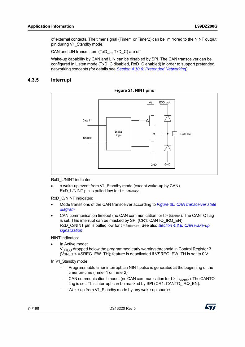
Application information L99DZ200G
74/198 DS13220 Rev 5
of external contacts. The timer signal (Timer1 or Timer2) can be mirrored to the NINT output pin during V1_Standby mode.
CAN and LIN transmitters (TxD_L, TxD_C) are off.
Wake-up capability by CAN and LIN can be disabled by SPI. The CAN transceiver can be configured in Listen mode (TxD_C disabled, RxD_C enabled) in order to support pretended networking concepts (for details see Section 4.10.6: Pretended Networking).
4.3.5 Interrupt
Figure 21. NINT pins
RxD_L/NINT indicates:
a wake-up event from V1_Standby mode (except wake-up by CAN) RxD_L/NINT pin is pulled low for t = tinterrupt.
RxD_C/NINT indicates:
Mode transitions of the CAN transceiver according to Figure 30: CAN transceiver state diagram
CAN communication timeout (no CAN communication for t > tSilence). The CANTO flag is set. This interrupt can be masked by SPI (CR1: CANTO_IRQ_EN).RxD_C/NINT pin is pulled low for t = tinterrupt. See also Section 4.3.6: CAN wake-up signalization
NINT indicates:
In Active mode:VSREG dropped below the programmed early warning threshold in Control Register 3 (VSREG < VSREG_EW_TH); feature is deactivated if VSREG_EW_TH is set to 0 V.
In V1_Standby mode
– Programmable timer interrupt; an NINT pulse is generated at the beginning of the timer on-time (Timer 1 or Timer2)
– CAN communication timeout (no CAN communication for t > t Silence). The CANTO flag is set. This interrupt can be masked by SPI (CR1: CANTO_IRQ_EN).
– Wake-up from V1_Standby mode by any wake-up source
Digitallogic
GND
V1
Data Out
Data In
Enable
GND
ESD prot
GAPG2608151615CFT

DS13220 Rev 5 75/198
L99DZ200G Application information
197
NINT is pulled low for t = tinterrupt
In case of increasing V1 load current during V1_Standby mode (IV1 > Icmp_ris), the device remains in standby mode and the watchdog starts with a Long Open Window. No Interrupt signal is generated.
4.3.6 CAN wake-up signalization
Note: See also Figure 30: CAN transceiver state diagram.
4.3.7 VBAT_Standby mode
The transition from Active mode to VBAT_Standby mode is initiated by an SPI command. In VBAT_Standby mode, the voltage regulators V1 and V2 (depending on configuration in CR 1), the power outputs (except OUT15 (d)) as well as LIN and CAN transmitters are switched off.
An NReset pulse is generated upon wake-up from VBAT_Standby mode.
4.4 Wake up from Standby Modes
A wake-up from standby mode will switch the device to active mode. This can be initiated by one or more of the following events:
Table 61. CAN wake-up signalization
Operating mode Event Mode transition Status flag Interrupt pin
Active
WUP(1) Transition to TRX_Ready WUP(1) RxD_C
CAN Timeout Transition to TRX_Sleep CANTO RxD_C(2)
WUP(3) Transition into TRX_Bias WUP RxD_C and NINT
V1_Standby
WUP(1) Transition into Active mode; TRX_Ready
WAKE_CAN WUP(1) RxD_C and NINT
CAN Timeout Transition to TRX_Sleep CANTO RxD_C and NINT (2)
WUP(3) Transition into TRX_Bias WUP RxD_C and NINT
VBAT_StandbyWUP(1) Transition into Active
mode; TRX_ReadyWAKE_CAN WUP(1)
none
CAN Timeout Transition to TRX_Sleep CANTO
1. PNW_EN = 0:- wake-up according ISO 11898-5:2007 (on WUP)- Flags: WUP (device in all modes), WAKE_CAN (device wake up by CAN from Standby modes)
2. Interrupt can be disabled by SPI (CANTO_IRQ_EN).
3. PWN_EN = 1 (Pretended Networking mode)- no wake-up- after reception of a wake-up patter (WUP) the transceiver enters TRX Bias mode- Flags: WUP
d. This exception applies only if OUT15 is not driven with an internally generated PWM signal

Application information L99DZ200G
76/198 DS13220 Rev 5
To prevent the system from a deadlock condition (no wake up from standby possible) a configuration where the wake up by LIN and HS CAN are both disabled is not allowed; in this case the SPI Error Bit SPIE (Global Status Byte) is set (see Note 1 in Figure 62).
4.4.1 Wake up inputs
The WU input can be configured as wake-up source. The wake-up input is sensitive to any level transition (positive and negative edge) and can be configured for static or cyclic monitoring of the input voltage level.
For static contact monitoring, a filter time of tWU_stat is implemented. The filter is started when the input voltage passes the specified threshold VWU_THP or VWU_THN.
Cyclic contact monitoring allows periodical activation of the wake-up input to read the status of the external contact. The periodical activation can be configured to Timer 1 or Timer 2. The input signal is filtered with a filter time of tWU_CYC after a delay (80% of the configured Timer on-time). A Wake-up will be processed if the status has changed versus the previous cycle. The buffered output OUT15 can be used to supply the external contacts with the timer setting according to the cyclic monitoring of the wake-up input.
In standby modes, the input WU is configurable with an internal pull-up or pull-down current source according to the setup of the external contact. In Active mode the inputs have an internal pull down resistor (RWU_act) and the input status can be read by SPI. Static sense should be configured before the read operation is started in order to reflect the actual input level.
Table 62. Wake-up events description
Wake up source Description
LIN bus activity Can be disabled by SPI
CAN bus activity Can be disabled by SPI
Level change of WU Can be configured or disabled by SPI
IV1 >Icmp_risDevice remains in V1_Standby mode, but watchdog is enabled (If ICMP = 0). No interrupt is generated.
Timer Interrupt / Wake up of µC by TIMER
Programmable by SPI:
V1_Standby mode: configurable timer interrupt. NINT interrupt signal is generated
VBAT_Standby mode: device wakes up after programmable timer expiration, V1 regulator is turned on and NReset signal is generated
SPI AccessAlways active (except in VBAT_Standby mode)
Wake up event: CSN is low and first rising edge on CLK
VS Over VoltageOnly when Generator Mode is enabled (GENERATOR_MODE_EN=1 in CR22 0x16)

DS13220 Rev 5 77/198
L99DZ200G Application information
197
4.5 Functional Overview (truth table)
Table 63. Status of different functions/features vs operating modes
Function Comments
Operating modes
Active mode
V1_Standby static mode (cyclic sense)
VBAT_Standby static mode (cyclic sense)
Voltage regulator V1 VOUT = 5 V On On(1) Off
Voltage tracker V2 VOUT = 5 V On/ Off(2) On(2) / Off On(2) / Off
Reset generator On On Off
Window watchdog V1 monitor OnOff (on if IV1 > ICMP
and ICMP = 0)Off
Wake up Off Active(3) Active(3)
OUT15 HS cyclic supplyOscillator time
baseOn / Off On(2) / Off On(2) / Off
LIN LIN 2.2a On Off(4) Off(4)
HS_CAN On / Off(5) Off(4) Off(4)
Oscillator OSC1 2 MHz On On/Off(6) On/Off(6)
Oscillator OSC2 32 MHz ON Off Off
VSREG-Monitor On (7) (7)
VS-Monitor On Off Off
H Bridge Gate Driver, EC control, bridge drivers, heater driver, all
high-side drivers (except OUT15) supplied by VS
On/ Off(2) Off(8) Off
Fail-safe low-side switches On/ Off(9) On On
Short circuit protection for fail-safe low-side switches (in case LS is
switched on)On On On
OUT15 (P-channel HS) supplied by VSREG
On/ Off(2) On/ Off(2)(9) On/ Off(2)(9)
Charge pump On Off Off
ADC (SPI read out and VSREG
early warning interrupt)On Off Off
Thermal shutdown TSD2 On On Off
Thermal shutdown TSD1x for OUT15 (P-channel HS)
On On/ Off(2) On/ Off(2)
1. Supply the processor in low current mode.
2. According to SPI setting and DIR.
3. Unless disabled by SPI.
4. The bus state is internally stored when going to standby mode. A change of bus state will lead to a wake-up after exceeding of internal filter time (if wake-up by LIN or CAN is not disabled by SPI).
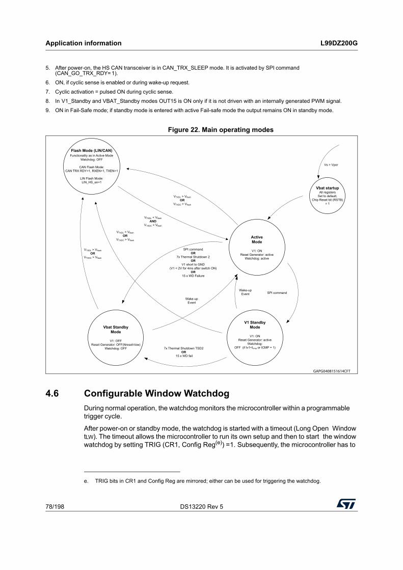
Application information L99DZ200G
78/198 DS13220 Rev 5
Figure 22. Main operating modes
4.6 Configurable Window Watchdog
During normal operation, the watchdog monitors the microcontroller within a programmable trigger cycle.
After power-on or standby mode, the watchdog is started with a timeout (Long Open Window tLW). The timeout allows the microcontroller to run its own setup and then to start the window watchdog by setting TRIG (CR1, Config Reg(e)) =1. Subsequently, the microcontroller has to
5. After power-on, the HS CAN transceiver is in CAN_TRX_SLEEP mode. It is activated by SPI command (CAN_GO_TRX_RDY= 1).
6. ON, if cyclic sense is enabled or during wake-up request.
7. Cyclic activation = pulsed ON during cyclic sense.
8. In V1_Standby and VBAT_Standby modes OUT15 is ON only if it is not driven with an internally generated PWM signal.
9. ON in Fail-Safe mode; if standby mode is entered with active Fail-safe mode the output remains ON in standby mode.
Active
Mode
V1: ONReset Generator: active
Watchdog: active
V1 Standby
Mode
V1: ONReset Generator: active
Watchdog:OFF (if Iv1<Icmp or ICMP = 1)
Vbat Standby
Mode
V1: OFFReset Generator: OFF(Nreset=low)
Watchdog: OFF
Wake-upEvent
Wake-upEvent SPI command
Vbat startupAll registers
Set to default,Chip Reset bit (RSTB)
= 1
Vs > Vpor
7x Thermal Shutdown TSD2 OR
15 x WD fail
Flash Mode (LIN/CAN)
Functionality as in Active ModeWatchdog: OFF
CAN Flash Mode:CAN TRX RDY=1, RXEN=1, TXEN=1
LIN Flash Mode:LIN_HS_en=1
VTXDL > VflashOR
VTXDC > Vflash
VTXDL > VflashOR
VTXDC > Vflash
VTXDL < VflashAND
VTXDC < Vflash
VTXDL > VflashOR
VTXDC > Vflash
SPI commandOR
7x Thermal Shutdown 2OR
V1 short to GND(V1 < 2V for 4ms after switch ON)
OR
15 x WD Failure
GAPG0408151614CFT
e. TRIG bits in CR1 and Config Reg are mirrored; either can be used for triggering the watchdog.

DS13220 Rev 5 79/198
L99DZ200G Application information
197
serve the watchdog by alternating the watchdog trigger bit TRIG (CR1, Config Reg(e)) within the safe trigger area TSWX.
The trigger time is configurable by SPI. A correct watchdog trigger signal will immediately start the next cycle. After 8 watchdog failures in sequence, the V1 regulator is switched off for tV1OFF. After 7 additional watchdog failures the V1 regulator is turned off permanently and the device goes into Forced VBAT_Standby mode. The status bit FORCED_SLEEP_WD (SR 1) is set. A wake-up is possible by any activated wake-up source.
After wake-up from Forced VBAT_Standby mode and the watchdog trigger still fails, the device enters Forced VBAT_Standby mode again after one Long Open Window.
This actually produces an additional watchdog failure but the watchdog fail counter will remain at maximum value of 15 failures.
This sequence is repeated until a valid watchdog trigger event is performed by writing TRIG = 1. In case of a Watchdog failure, the power outputs and V2 are switched off and the status bit WDFAIL (SR1) is set to 1. A reset pulse is generated at NReset output and the device enters Fail-safe mode. Control registers are set to their Fail Safe values and the Fail-safe low-side switches are turned on. Please refer to Section 4.7: Fail Safe Mode for more details.
The following diagrams illustrate the Watchdog behavior of the devices. The diagrams are split into 3 parts. The first diagram shows the functional behavior of the watchdog without any error. The second diagram covers the behavior covering all the error conditions, which can affect the watchdog behavior. Figure 25: Watchdog in Flash mode shows the transition in and out of Flash modes. Watchdog in normal operating mode (no errors)Figure 23: Watchdog in normal operating mode (no errors), Figure 24: Watchdog with error conditions and Figure 25: Watchdog in Flash mode can be overlapped to get all the possible state transitions under all circumstances. For a better readability, they were split in normal operating, operating with errors and Flash mode.

Application information L99DZ200G
80/198 DS13220 Rev 5
Figure 23. Watchdog in normal operating mode (no errors)
Figure 24. Watchdog with error conditions
WD
OFF
long
open
window
Window
Modepropper trigger in
Window mode
Vbat standby mode
Active mode
Active mode
RTx)
Go Vbat stbyOr
go Vbat stby
GAPG0408151639CFT
TRIG = ‚1'
Go V1 stby
Go V1 stby AND I(v1) < Icmp
Wake-upV1 > V(
V1 Standby (I(V1) < ICMP)
GAPG0408151640CFT
WD
OFF
long
open
window
Window
Modepropper trigger in
Window mode
Vbat standby mode
*)
Active mode
Active mode
Event
Event
forced Vbat stby *)
V1 > Vrth
V1 < VrthTRIG = ‚1'
Fail-Safe
Fail-Safe
Short V17x TSD2
forced VBAT: 15x WD fail
Lorem ipsumV1 < Vrth

DS13220 Rev 5 81/198
L99DZ200G Application information
197
Figure 25. Watchdog in Flash mode
Note: Whenever the device is operated without servicing the mandatory watchdog trigger events, a sequence of 15 consecutive reset events is performed and the device enters the Forced VBAT_Standby mode with bit FORCED_SLEEP_WD in SR1 set. If the device is woken up after such a forced VBAT_Standby condition and the watchdog is still not serviced, the device, after one long open watchdog window will re-enter the same Forced VBAT_Standby mode until the next wake up event. In this case, an additional watchdog failure is generated, but the fail counter is not cleared, keeping the maximum number of 15 failures. This sequence is repeated until a valid watchdog trigger event is performed by writing TRIG = 1.
4.6.1 Change Watchdog timing
The watchdog trigger time is configured by setting WD_TIME_x (CR 2). Writing to these bits is possible only using the first SPI command after setting WD_CONFIG_EN = 1 (Config Reg). The WD_CONFIG_EN bit is reset to 0 automatically with the next SPI command.
4.7 Fail Safe Mode
4.7.1 Temporary Failures
The devices enter Fail-safe mode in case of:
Watchdog failure
V1 failure (V1 < VRTxfalling for t > tV1FS)
Thermal Shutdown TSD2
The Fail Safe functionality is also available in V1_Standby mode. During V1_Standby mode the Fail Safe mode is entered in the following cases:
V1 failure (V1 < VRTxfalling for t > tV1FS)
Watchdog failure (if watchdog still running due to IV1 > Icmp_fal)
Thermal Shutdown TSD2
WD
OFF
long
open
window
Window
Mode
FLASH / Debugmode
Active mode
Active mode
EnterFLASH / Debug mode
Exit fromFLASH / Debug mode
EnterFLASH / Debug mode
GAPG0408151643CFT

Application information L99DZ200G
82/198 DS13220 Rev 5
In Fail Safe mode the devices return to a fail safe state. The Fail Safe condition is indicated to the system in the Global Status Byte. The conditions during Fail Safe mode are:
All outputs beside LSA_FSO and LSB_FSO are turned off
All Control Registers are set to fail safe default values except the GEN_MODE_EN
Write operations to Control Registers are blocked until the Fail Safe condition is cleared. The following bits are not WRITE protected:
– TRIG (CR1<bit 0>, Config Register <bit 0>): watchdog trigger bit
– V2_x (CR1<bit 4:5>): Voltage Regulator V2 control
– CAN_GO_TRX_RDY (CR1<bit 8>): activation of CAN bus biasing
– CR2 (bit <8:23>): Timer1 and Timer2 settings
– OUT15_x (CR6<bit 8:11>): OUT15 configuration
– PWMx_freq_y (CR12): PWM frequency configuration
– PWMx_DC_y (CR13 – CR16): PWM duty cycle configuration
LIN and SPI remain on (transmitters are deactivated in case of thermal shutdown TSD1 (TSD1 cluster 5 or 6 in cluster mode)
Corresponding Failure Bits in Status Registers are set
FS Bit (Global Status Byte) is set
LSA_FSO and LSB_FSO will be turned on
Charge pump is switched off
If the Fail Safe mode was entered it keeps active until the Fail safe condition is removed and the Fail Safe was read by SPI. Depending on the root cause of the Fail Safe operation, the actions to exit Fail safe mode are shown in the following table.
4.7.2 Non-recoverable failures – forced VBAT_Standby mode
If the Fail-safe condition persists and all attempts to return to normal system operation fail, the devices enter the forced VBAT_Standby mode in order to prevent damage to the system. The forced VBAT_Standby mode can be terminated by any wake-up source (HS-CAN as well as LIN and WU pin). The root cause of the forced VBAT_Standby mode is indicated in the SPI Status Registers. In forced VBAT_standby mode and with Fail Safe conditions still present at wake-up, the Fails safe low side outputs LSy_FSO (y = A, B) are switched OFF for 25 µs after the wake up event.
Table 64. Temporary failures description
Failure source Failure condition Diagnosis Exit from Fail-safe mode
Microcontroller (oscillator)
Watchdog early write failure or expired
window
FS (Global Status Byte) =1; WDFAIL (SR 1) =1; WDFAIL_CNT_x (SR 1) = n+1
TRIG (CR 1) = 1 during long open window Read&Clear SR1
V1 UndervoltageFS (Global Status Byte) = 1; V1UV (SR 1) = 1; V1fail (SR 2) = 1(1)
V1 >VRTrising; Read&Clear SR1
Temperature Tj > TSD2
FS (Global Status Byte) = 1; TW (SR 2) = 1;
TSD1 (SR 1) =1;
TSD2 (SR 1) =1
Tj < TSD2;
Read&Clear SR1
1. If V1 < V1fail (for t > tV1fail). The Fail-safe Bit is located in the Global Status Register.

DS13220 Rev 5 83/198
L99DZ200G Application information
197
In Forced VBAT_Standby mode, all Control Registers are set to power-on default values.
The Forced VBAT_Standby mode is entered in case of:
Multiple watchdog failures: FORCED_SLEEP_WD (SR 1) = 1 (15 x watchdog failure)
Multiple thermal shutdown 2: FORCED_SLEEP_TSD2/V1SC (SR 1) = 1 (7 x TSD2)
V1 short at turn-on (V1 < V1fail for t > tV1short): FORCED_SLEEP_TSD2/V1SC (SR 1) = 1
SGND Loss: SGND_LOSS (SR 1) = 1
In Forced VBAT_Standby mode:
when Vs OV is detected, in case of non recoverable conditions ( WD, TSD2, V1 short or SGND loss ), the device will stay in Temporary Fail Safe state;
during this state ( VSOV + failure conditions ), diagnosis will be set ( FS, WDFAIL or TW, TSD1, TSD2 or FORCED_SLEEP_TSD2/VS1SC or SGND_LOSS ) even if the device is not in Forced VBAT_Standby mode;
as soon Vs OV disappears, the device will enter in Forced VBAT_Standby mode.
Table 65. Non-recoverable failure
Failure source Failure condition Diagnosis Exit from Fail-safe mode
Microcontroller (Oscillator)
15 consecutive Watchdog Failures
FS (Global Status Byte) = 1;
WDFAIL (SR 1) = 1;
FORCED_SLEEP_WD (SR 1) = 1
Wake-up;
TRIG (CR 1) = 1 during long open window;
Read&Clear SR1
V1 Short at turn-onFS (Global Status Byte) = 1; FORCED_SLEEP_TSD2/V1SC (SR 1) = 1
Wake-up; Read&Clear SR1
Temperature 7 times TSD2
FS (Global Status Byte) =1;
TW (SR 2) = 1;
TSD1 (SR 1) = 1;
TSD2 (SR 1) = 1;
FORCED_SLEEP_TSD2/V1SC (SR 1) = 1
Wake-up; Read&Clear SR1
SGND LossGround Loss at pin
SGNDFS (Global Status Byte) = 1;
SGND_LOSS (SR 1) = 1Wake-up; Read&Clear SR1

Application information L99DZ200G
84/198 DS13220 Rev 5
4.8 Reset output (NReset)
Figure 26. NReset pin
If V1 is turned on and the voltage exceeds the V1 reset threshold, the reset output NReset is pulled up to V1 by an internal pull-up resistor after a reset delay time (tV1R). This is necessary for a defined start of the microcontroller when the application is switched on.
Since the NReset output is realized as an open drain output it is also possible to connect that, instead of the 5V_1, to an external voltage source (it has to be compatible with a 5V rail). As soon as the NReset is released by the devices the watchdog starts with a long open window.
A reset pulse is generated in case of:
V1 drops below VRTxfalling (configurable by SPI) for t > tUV1
Watchdog failure
After turn ON of the V1 regulator (VSREG Power-on or wake-up from VBAT_Standby mode), NReset is kept low for tv1r in order to keep the uC in reset until supply voltage is stable.
Digitallogic
GND
V1
Data Out
Data In
GND
ESD prot
20 kOhms
GAPG2608151608CFT
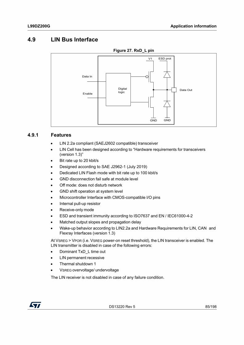
DS13220 Rev 5 85/198
L99DZ200G Application information
197
4.9 LIN Bus Interface
Figure 27. RxD_L pin
4.9.1 Features
LIN 2.2a compliant (SAEJ2602 compatible) transceiver
LIN Cell has been designed according to “Hardware requirements for transceivers (version 1.3)”
Bit rate up to 20 kbit/s
Designed according to SAE J2962-1 (July 2019)
Dedicated LIN Flash mode with bit rate up to 100 kbit/s
GND disconnection fail safe at module level
Off mode: does not disturb network
GND shift operation at system level
Microcontroller Interface with CMOS-compatible I/O pins
Internal pull-up resistor
Receive-only mode
ESD and transient immunity according to ISO7637 and EN / IEC61000-4-2
Matched output slopes and propagation delay
Wake-up behavior according to LIN2.2a and Hardware Requirements for LIN, CAN and Flexray Interfaces (version 1.3)
At VSREG > VPOR (i.e. VSREG power-on reset threshold), the LIN transceiver is enabled. The LIN transmitter is disabled in case of the following errors:
Dominant TxD_L time out
LIN permanent recessive
Thermal shutdown 1
VSREG overvoltage/ undervoltage
The LIN receiver is not disabled in case of any failure condition.
Digital logic
GND
V1
Data Out
Data In
Enable
GND
ESD prot
GAPG2608151615CFT

Application information L99DZ200G
86/198 DS13220 Rev 5
The default bit rate of the transceiver allows communication up to 20 kbit/s. To enable fast flashing via the LIN bus, the transceiver can be operated in high speed mode by setting bit LIN_HS_EN (Config Reg) = 1. This feature is enabled automatically in LIN Flash mode.
4.9.2 Error Handling
The devices LIN transceiver provides the following 3 error handling features.
Dominant TxD_L time out
If TXD_L is in dominant state (low) for t > tdom(TXDL) the transmitter will be disabled, the status bit LIN_TXD_DOM (SR 2) will be set.
The transmitter remains disabled until the status bit is cleared.
The TxD dominant timeout detection can be disabled via SPI (LIN_TXD_TOUT_EN = 0).
Permanent recessive
If TXD_L changes to dominant (low) state but RXD_L signal does not follow within t < tLIN the transmitter will be disabled, the status bit LIN_PERM_REC (SR 2) will be set.
The transmitter remains disabled until the status bit is cleared.
Permanent dominant
If the bus state is dominant (low) for t > tdom(bus) a bus permanent dominant failure will be detected. The status bit LIN_PERM_DOM (SR 2) will be set.
The transmitter will not be disabled.
4.9.3 Wake up from Standby Modes
In low power modes (V1_Standby mode and VBAT_Standby mode) the devices can receive two types of wake up signals from the LIN bus (configurable by SPI bit LIN_WU_CONFIG (Config Reg)):
Recessive-Dominant-recessive pattern with t > tdom_LIN (default, according to LIN 2.2a)
State Change recessive-to-dominant or dominant-to-recessive (according to LIN 2.1)

DS13220 Rev 5 87/198
L99DZ200G Application information
197
Pattern Wake-up (default)
Figure 28. Wake-up behavior according to LIN 2.2a
Status change wake-up - Recessive-to-dominant
Normal wake-up can occur when the LIN transceiver was set in standby mode while LIN was in recessive (high) state. A dominant level at LIN for t > tLINBUS, will switch the devices in Active mode.
Status change wake-up - Dominant-to-recessive
If the LIN transceiver was set in standby mode while LIN was in dominant (low) state, recessive level at LIN for t > tLINBUS, will switch the devices in Active mode.
4.9.4 Receive-only mode
The LIN transmitter can be disabled in Active mode by setting the bit LIN_REC_ONLY (CR2). In this mode it is possible to listen to the bus but not sending to it.
t
GAPG0508151156CFT
Voltage at LIN-Pin of LIN Physical Layer device
sleep mode standby mode
LIN dominant
LIN recessive
dom LIN
Supply0.4 VSupply0.6 V

Application information L99DZ200G
88/198 DS13220 Rev 5
4.10 High-speed CAN bus transceiver
Figure 29. RxD_C pin
4.10.1 Features
ISO 11898-2:2003 and ISO 11898-5:2007 compliant
CAN High Speed Transceiver Conformance Test according to «Interoperability test specification for high-speed CAN transceiver or equivalent devices IOPT.CAN v02d00»
HS-CAN cell has been designed according to “Hardware requirements for transceivers (version 1.3)”
Supports pretended networking
Listen mode (transmitter disabled)
Enhanced Voltage Biasing according to ISO 11898-6:2013
SAE J2284 compliant
Bit rate up to 1Mbit/s
Designed according to SAE J2962-2 (July 2019)
Function range from -27 V to +40 V DC at CAN pins.
GND disconnection fail safe at module level.
GND shift operation at system level.
Microcontroller Interface with CMOS compatible I/O pins.
ESD and transient immunity according to ISO7637 and EN / IEC61000-4-2
Matched output slopes and propagation delay
Digital logic
GND
V1
Data Out
Data In
Enable
GND
ESD prot
GAPG2608151615CFT

DS13220 Rev 5 89/198
L99DZ200G Application information
197
4.10.2 CAN Transceiver operating modes
Figure 30. CAN transceiver state diagram
TRX Ready State
In this state the bus-biasing is on.
The transmitter and receiver can be configured by SPI (RXEN, TXEN) as follows:
TRX Standby (default): transmitter and receiver disabled
TRX Listen: transmitter disabled, receiver enabled
TRX Normal: transmitter enabled, receiver enabled
GAPG0508151158CFT
2)
2)
1)
1)
1)
1)
TRX Sleep
Power-Up Reset
ActiveSBC
Interrupt: RxDC, NINTFlag: WUP
(WUP)wake-up pattern
PNW EN=1
Interrupt: RxDC Flag: CANTO
Time out
CANCommunication
SPI cmd:
GO2TRXRDY = 0
Flags: WUP, WAKE CANWake-up pattern (WUP)
PNW_EN=0:
TRX Ready
PNW EN=1
Interrupt: RxDC, NINTFlag: WUP
(WUP)Wake-up pattern
V1 StandbySBC
TRX Sleep
Note 2): CANTO Interrupt on RxDC and NINT can be masked by SPI (CR1 <CANTO IRQ EN>)
•Interrupt at RxDC and NINT•Transceiver transition into TRX BIAS mode, no SBC mode transition
Note 1): In Pretended Networking configuration (PNW_EN=1) a WUP leads to:
Enable V1 Stby ModeSPI cmd:
TRX BIAS
Vbat StandbySBC
Flag: CANTOTime out
CommunicationCAN
TRX BIAS
TRX Sleep
GO2TRXRDY = 1Or
Interrupt: RxDCFlags: WUP
Wake-up pattern (WUP) PNW_EN=0:
TRX BIAS
Enable Vbat Stby ModeSPI cmd:
Enable VBAT stby modeSPI cmd:
Enable VBAT stby modeSPI cmd:
Interrupt: RxDC, NINTFlag: CANTO
Time outCAN Communication
Interrupt: RxDC, NINTOr
Wake by SPI if GO2TRXRDY=1
Wake by SPI if GO2TRXRDY=0Enable V1 Stby Mode /
GO2TRXRDY = 1PNW EN=1
(Interrupt: None)Flags: WUP, WAKE CAN
(WUP)Wake-up pattern

Application information L99DZ200G
90/198 DS13220 Rev 5
TRX BIAS State
In this transceiver state the bus biasing is on and the Automatic Voltage Biasing is active (i.e. transceiver enters TRX_Sleep at t > tSilence and turns off the biasing).
The CAN transmitter is disabled. The receiver can be configured by SPI (RXEN) as follows:
TRX Standby (default): receiver disabled
TRX Listen: receiver enabled
The CAN receiver is capable of detecting a wake-up pattern (WUP). In V1_Standby mode and Active mode, a wake-up is indicated to the micro-controller by an interrupt signal and the transceiver enters TRX_Ready State (receiver and transmitter according to setting of TXEN and RXEN). After serving the interrupt, the microcontroller can enable the receiver and transmitter by setting TXEN = 1 and RXEN = 1.
TRX SLEEP State
After Power-on the CAN transceiver enters TRX_Sleep state. In this state, the CAN transceiver is disabled and the biasing is turned off. Transmitter and receiver are disabled (TRX_Standby state). After the detection of CAN communication (WUP), an interrupt signal is generated and the transceiver enters TRX_Ready state (if PNWEN = 0) or TRX_BIAS state (if PNWEN = 1). Receiver and transmitter are configured according to setting of TXEN and RXEN.
TRX_Sleep state is entered automatically after a CAN communication timeout (see Section 4.10.3: Automatic Voltage Biasing).
4.10.3 Automatic Voltage Biasing
The Automatic Voltage Biasing is described in ISO 11898-6:2013. This feature is active in all transceiver low-power modes independent of the SBC operating modes.
If there has been no activity on the bus for longer than tSilence, the bus lines are biased towards 0V via the receiver input resistors Rin. If wake-up activity on the bus lines is detected (Wake-up pattern, WUP), the bus lines are biased to VCANHrec respectively VCANLrec via the internal receiver input resistors Rin. The biasing is activated not later than tBias.
4.10.4 Wake up by CAN
The device supports only the wake-up by any bus activity according to ISO 11898-2:2003/-5:2007.
The default setting for the wake up behavior after Power-on reset is the wake-up by regular communication on the CAN bus according to ISO 11898-5:2007. When the CAN transceiver is in a low power mode (TRX_BIAS or TRX_Sleep) the device can be woken up by sending 2 consecutive dominant bits separated by a recessive bit.
A wake-up can be detected if the CAN transceiver was set in standby mode while the CAN bus was in recessive (high) state or dominant (low) state (see Figure 31).

DS13220 Rev 5 91/198
L99DZ200G Application information
197
Figure 31. CAN wake up capabilities
For details, see Figure 30.
4.10.5 CAN looping
If CAN_LOOP_EN (CR 2) is set the TxD_C input is mapped directly to the RxD_C pin. This mode can be used in combination with the CAN Receive-only mode, to run diagnosis for the CAN protocol handler of the microcontroller.
4.10.6 Pretended Networking
To support pretended networking concepts, the devices can be configured as follows:
V1_Standby mode or Active mode (if watchdog is required)
Pretended Networking enabled (PNW_EN (CR 2) = 1)
In this configuration, the microcontroller is supplied by V1 in low current mode. The CAN Automatic Voltage Biasing is active. Upon incoming CAN messages, the biasing is turned on (TRX_BIAS State) and an interrupt is generated. If the device is in V1_Standby mode it remains in this mode.
The incoming CAN frames are passed to the microcontroller via the RxD_C signal line for decoding.
4.10.7 CAN Error Handling
The devices provide the following four error handling features. After Power-on Reset (VS > VPOR) the CAN transceiver is disabled. The transceiver is enabled by setting CAN_GO_TRX_RDY (CR 1) = 1. The CAN transmitter will be disabled automatically in case of the following errors:
Dominant TxD_C time out
CAN permanent recessive
RxD_C permanent recessive
Thermal Shutdown 1
t t t
t t t
< t
< t
GAPG0508151203CFT
STATE
CANRX
STATE
CANRX
CAN pattern wake-up with dominant state before Standby
ACTIVE
ACTIVE
STANDBY
CAN pattern wakeup
STANDBY
ACTIVE
ACTIVE
wake
filter filter filter
wake
filter filter filter

Application information L99DZ200G
92/198 DS13220 Rev 5
The CAN receiver is not disabled in case of any failure condition.
Dominant TxD_C time out
If TXD_C is in dominant state (low) for t > tdom (TxDC) the transmitter will be disabled, CAN_TXD_DOM (SR 2) will be latched and can be read and optionally cleared by SPI. The transmitter remains disabled until the status register is cleared.
CAN Permanent Recessive
If TXD_C changes to dominant (low) state but CAN bus does not follow for 4 times, the transmitter will be disabled, CAN_PERM_REC (SR 2) will be latched and can be read and optionally cleared by SPI. The transmitter remains disabled until the status register is cleared.
CAN Permanent Dominant
If the bus state is dominant (low) for t > tCAN a permanent dominant status will be detected. CAN_PERM_DOM (SR 2) will be latched and can be read and optionally cleared by SPI. The transmitter will not be disabled.
RxD_C Permanent Recessive
If RxD_C pin is clamped to recessive (high) state, the controller is not able to recognize a bus dominant state and could start messages at any time, which results in disturbing the overall bus communication. Therefore, if RXD_C does not follow TXD_C for 4 times the transmitter will be disabled. CAN_RXD_REC (SR 2) will be latched and can be read and optionally cleared by SPI. The transmitter remains disabled until the status register is cleared.
4.11 Serial Peripheral Interface (ST SPI Standard)
A 32-bit SPI is used for bi-directional communication with the microcontroller.
The SPI is driven by a microcontroller with its SPI peripheral running in the following mode: CPOL = 0 and CPHA = 0. For this mode input data is sampled by the low to high transition of the clock CLK, and output data is changed from the high to low transition of CLK.
This device is not limited to microcontroller with a built-in SPI. Only three CMOS-compatible output pins and one input pin are needed to communicate with the device. A fault condition can be detected by setting CSN to low. If CSN = 0, the DO-Pin reflects the global error flag (fault condition) of the device.
Chip Select Not (CSN)The input Pin is used to select the serial interface of this device. When CSN is high, the output Pin (DO) is in high impedance state. A low signal activates the output driver and a serial communication can be started.The state during CSN = 0 is called a communication frame.If CSN = low for t > tCSNfail the DO output is switched to high impedance in order to not block the signal line for other SPI nodes.
Serial Data In (DI)The input Pin is used to transfer data serial into the device. The data applied to the DI is sampled at the rising edge of the CLK signal and shifted into an internal 32-bit shift register. At the rising edge of the CSN signal the content of the shift register is transferred to Data Input Register. The writing to the selected Data Input Register is only

DS13220 Rev 5 93/198
L99DZ200G Application information
197
enabled if exactly 32 bits are transmitted within one communication frame (i.e. CSNlow). If more or less clock pulses are counted within one frame the complete frame is ignored. This safety function is implemented to avoid an activation of the output stages by a wrong communication frame.
Note: Due to this safety functionality a daisy chaining of SPI is not possible. Instead, a parallel operation of the SPI bus by controlling the CSN signal of the connected IC's is recommended.
Serial Data Out (DO)The data output driver is activated by a logical low level at the CSN input and will go from high impedance to a low or high level depending on the global error flag (fault condition). The first rising edge of the CLK input after a high to low transition of the CSN Pin will transfer the content of the selected status register into the data out shift register. Each subsequent falling edge of the CLK will shift the next bit out.
Serial Clock (CLK)The CLK input is used to synchronize the input and output serial bit streams. The data input (DI) is sampled at the rising edge of the CLK and the data output (DO) will change with the falling edge of the CLK signal. The SPI can be driven with a CLK Frequency up to 4 MHz.
4.12 Power Supply Fail
4.12.1 Vs supply failure
Vs overvoltage
If the supply voltages VS reaches the overvoltage threshold VSOV:
LIN remains enabled
CAN remains enabled
OUT1 to OUT14 are turned off (default).
The shutdown of outputs may be disabled by SPI (VS_OV_SD_EN (CR 3) = 0)
Charge pump is disabled (and is switched on automatically in case the supply voltage recovers to normal operating voltage)
H-bridge gate driver and heater MOSFET gate driver are switched into sink condition
ECV is switched in high impedance state and ECDR is discharged by RECDRDIS (to ensure the gate of the external MOSFET is discharged => EC mode considered as off)
Recovery of outputs after overvoltage condition is configurable by SPI:
– VS_LOCK_EN (CR 3) = 1: outputs are off until Read&Clear VS_OV (SR 2).
– VS_LOCK_EN (CR 3) = 0: outputs turned on automatically after VS overvoltage condition has recovered.
The overvoltage bit VS_OV (SR 2) is set and can be cleared with a ‘Read&Clear’ command. The overvoltage bit is reset automatically if VS_LOCK_EN (CR 3) = 0 and the overvoltage condition has recovered.

Application information L99DZ200G
94/198 DS13220 Rev 5
Vs undervoltage
If the supply voltage VS drops below the under voltage threshold voltage (VSUV):
LIN remains enabled
CAN remains enabled
OUT1 to OUT14 are turned off (default).The shutdown of outputs may be disabled by SPI (VS_UV_SD_EN (CR 3) = 0)
H-bridge drivers A and B are turned off (default). The shutdown of H-bridge drivers may be disabled by SPI (VS_UV_SD_EN (CR 3) = 0)
Heater MOSFET gate driver is switched into sink condition
ECV is switched in high impedance state and ECDR is discharged by RECDRDIS (to ensure the gate of the external MOSFET is discharged => EC mode considered as off)
Recovery of outputs and H-bridge drivers after undervoltage condition is configurable by SPI:
– VS_LOCK_EN (CR 3) = 1: outputs and H-bridge drivers are off until Read&Clear VS_UV (SR 2).
– VS_LOCK_EN (CR 3) = 0: outputs and H-bridge drivers turned on automatically after VS undervoltage condition has recovered.
The undervoltage bit VS_UV (SR 2) is set and can be cleared with a ‘Read&Clear’ command. The undervoltage bit is removed automatically if VS_LOCK_EN (CR 3) = 0 and the undervoltage condition has recovered.
4.12.2 Vsreg supply failure
Vsreg Overvoltage
If the supply voltages VSREG reaches the overvoltage threshold VSREG_OV:
LIN transmitter is switched to high impedance
CAN remains enabled
OUT15 is turned off (default).
The shutdown of outputs may be disabled by SPI (VSREG_OV_SD_EN (CR 3) = 0)
Recovery of outputs after overvoltage condition is configurable by SPI:
– VSREG_LOCK_EN (CR 3) = 1: outputs are off until Read&Clear VSREG_OV (SR 2).
– VSREG_LOCK_EN (CR 3) = 0: outputs turned on automatically after VSREG
overvoltage condition has recovered.
The overvoltage bit VSREG_OV (SR 2) is set and can be cleared with a ‘Read&Clear’ command. The overvoltage bit is reset automatically if VSREG_LOCK_EN (CR 3) = 0 and the overvoltage condition has recovered.
Vsreg Undervoltage
If the supply voltage VSREG drops below the under voltage threshold voltage (VSREG_UV):
LIN transmitter is switched to high impedance
CAN remains enabled
OUT15 is turned off (default).

DS13220 Rev 5 95/198
L99DZ200G Application information
197
The shutdown of outputs may be disabled by SPI (VSREG_UV_SD_EN (CR 3) = 0)
Recovery of outputs after undervoltage condition is configurable by SPI:
– VSREG_LOCK_EN (CR 3) = 1: outputs are off until Read&Clear VSREG_UV (SR 2).
– VSREG_LOCK_EN (CR 3) = 0: Outputs turned on automatically after VSREG
undervoltage condition has recovered.
The undervoltage bit VSREG_UV (SR 2) is set and can be cleared with a ‘Read&Clear’ command. The undervoltage bit is removed automatically if VSREG_LOCK_EN (CR 3) = 0 and the undervoltage condition has recovered.

Application information L99DZ200G
96/198 DS13220 Rev 5
4.13 Temperature warning and thermal shut-down
Figure 32. Thermal shutdown protection and diagnosis
Note: The Thermal State machine will recover the same state where it was before entering Standby mode. In case of a TSD2 it will enter TSD1 state.
Active
Mode
Standby Modes
(during cyclic sense)
Temperature
Warning
Diagnosis: TW=1
TSD1
All outputs and V2: off 1)V1: on
Diagnosis: TSD1=1
Tj > TSD1
‚Read and Clear’OR
Power-on reset
TSD2
All outputs and V2: offV1: off for t = tTSD
Diagnosis: TSD2=1
Tj > TSD2
Forced
Vbat_standby
Mode
7x TSD2Wake-up event
Power-on reset
‚Read and Clear’OR
Power-on reset
Tj > Tw
t > tTSD
Power On Reset
All outputs incl V1 off
Vs > Vpor
Note 1): In thermal cluster mode (TSD Config = 1), only the concerned output cluster will be switched off
GAPG0408151633CFT

DS13220 Rev 5 97/198
L99DZ200G Application information
197
4.14 Power Outputs OUT1…15
The component provides a total of 4 half bridges outputs OUT1, OUT2, OUT3 and OUT6 to drive motors and 7 stand alone high-side outputs OUT7, OUT8, OUT9, OUT10, OUT13, OUT14 and OUT15 to drive e.g. LED’s, bulbs or to supply contacts. All high-side outputs beside OUT15 are supplied by the pin VS and OUT15 is supplied by the buffered supply VSREG. Beside OUT15 the high-side switches can be activated only in case of running charge pump.
OUT15 can be activated also in standby modes, except if OUT15 is driven by an internally generated PWM.
All high-side and low-side outputs switch off in case of:
VS (VSREG) overvoltage and undervoltage (depending on configuration, see Section 4.12.2: Vsreg supply failure)
Overcurrent (depending on configuration, auto recovery mode (see below)
Overtemperature (TSD1x/ cluster or single mode)
Fail safe event
Loss of GND at SGND pin
In case of overcurrent or overtemperature (TSD1_CLx (SR 6)) condition, the drivers will switch off. The relative status bit will be latched and can be read and optionally cleared by SPI. The drivers remain off until the status is cleared. In case overvoltage/ undervoltage condition, the drivers will be switched off. The relative status bit will be latched and can be read and optionally cleared by SPI. If VSREG_LOCK_EN (CR 3) respectively VS_LOCK_EN (CR 3) are set, the drivers remain off until the status is cleared. If the VS_LOCK_EN or VSREG_LOCK_EN bit is set to 0, the drivers will switch on automatically if the error condition disappears. Undervoltage and overvoltage shutdown can be disabled by SPI. In case of open-load condition, the relative status register will be latched. The status can be read and optionally cleared by SPI. The high and low-side outputs are not switched off in case of open-load condition.
For OUT1, OUT2, OUT3 and OUT6, OUT7, OUT8 and OUT15 the auto recovery feature (OUTx_OCR (CR 7)) can be enabled. If these bits are set to 1 the driver will automatically restart from an overload condition. This overload recovery feature is intended for loads which have an initial current higher than the overcurrent limit of the output (e.g. Inrush current of cold light bulbs). The SPI bits OUTx_OCR_ALERT (SR4) indicate that the output reached auto-recovery condition.
Note: The maximum voltage and current applied to the High-side Outputs is specified in the ‘Absolute Maximum Ratings’. Appropriate external protection may be required in order to respect these limits under application conditions.
Each of the 7 standalone high-side driver outputs from OUT7 to OUT15 can be driven with an internally generated PWM signal, an internal Timer or through the DIR signal.
Moreover, for OUT7, OUT8 and OUT9 high-side driving LEDs, it is also available the CCM (Constant Current Mode) feature, which is configurable by SPI (CR9) and conceived to provide a constant current to the related output (see more detail in Section 4.21: Constant current mode).
Table 66: Power output settings summarizes the possible configurations for the high-side outputs.

Application information L99DZ200G
98/198 DS13220 Rev 5
4.15 Auto-recovery alert and thermal expiration
The thermal expiration feature provides a robust protection against possible microcontroller malfunction, switching off a given channel if continuously driven in auto-recovery. If the temperature of the related cluster increases by more than 30 °C after reaching the auto- recovery time tAR, the channel is switched off. The thermal expiration status bit OUTx_TH_EX (f) (SR 3) is set.
During auto-recovery condition, OUTx_OCR_ALERT(f) (SR 4) is set. The Alert bit indicates that an overload condition (load in-rush, short-circuit, etc) is present.
The thermal expiration feature can be activated only in combination with Over Current Recovery (or Auto-recovery) mode, by setting to 1 both the OUTx_OCR(f) (CR7) and the OUTx_OCR_THX_EN(f) (CR8) bits.
Table 66. Power output settings
OUTx_3 OUTx_2 OUTx_1 OUTx_0 Description
0 0 0 0 OFF
0 0 0 1 ON
0 0 1 0Timer1 output is controlled by timer1; starting with ON phase after timer restart
0 0 1 1Timer2 output is controlled by timer2; starting with ON phase after timer restart
0 1 0 0 PWM1
0 1 0 1 PWM2
0 1 1 0 PWM3
0 1 1 1 PWM4
1 0 0 0 PWM5
1 0 0 1 PWM6
1 0 1 0 PWM7
1 0 1 1 Not applicable
1 1 0 0 Not applicable
1 1 0 1 Not applicable
1 1 1 0 DIR
1 1 1 1 Not applicable
f. For x = 1, 2, 3, 6, 7, 8, 15.

DS13220 Rev 5 99/198
L99DZ200G Application information
197
Figure 33. Example of long auto-recovery on OUT7. Temperature acquisition starts after tAR, thermal expiration occurs after ∆=30°
Figure 34. Block diagram of physical realization of AR alert and thermal expiration
Batt. supply
Overcurrentcomp.
CurrentSense
Ith
T_data
Lamp Driver IC
Gate driver
ONcommand
Diagnostic
μC
HS_Enab
AR limitreached
OSC
Digital statemachine
ADC
Temp. senseAmp
PowerMOS
GAPG0508151221CFT
OC

Application information L99DZ200G
100/198 DS13220 Rev 5
4.16 Charge Pump
The charge pump uses two external capacitors, which are switched with fCP. The output of the charge pump has a current limitation. In standby mode and after a thermal shutdown has been triggered the charge pump is disabled. If the charge pump output voltage remains too low for longer than TCP, the power-MOS outputs and the EC-control are switched off.
The H-bridge MOSFET gate drivers and the Heater MOSFET gate driver are switched to resistive low and CP_LOW (SR 2) is set. This bit has to be cleared to reactivate the drivers. If the bit CP_LOW_CONFIG (Configuration Register 0x3F) is set to ‘1’, CP_LOW (SR2) behaves as a ‘live’ bit and the outputs are re-activated automatically upon recovery of the charge pump output voltage.
In case of reaching the overvoltage shutdown threshold VSOV the charge pump is disabled and automatically restarted after VS recovered to normal operating voltage.
Figure 35. Charge pump low filtering and start up implementation
4.17 Inductive Loads
Each of the half bridges is built by internally connected high-side and low-side power DMOS transistors. Due to the built-in reverse diodes of the output transistors, inductive loads can be driven at the outputs OUT1...OUT6 without external freewheeling diodes. The high-side drivers OUT7. OUT15 are intended to drive resistive loads only. Therefore only a limited energy (E < 1 mJ) can be dissipated by the internal ESD-diodes in freewheeling condition. For inductive loads (L > 100 μH) an external freewheeling diode connected between GND and the corresponding output is required. The low-side driver at ECV does not have a freewheel diode built into the device.
4.18 Open-load detection
The open-load detection monitors the load current in each activated output stage. If the load current is below the open-load detection threshold for t > tOL_OUT the corresponding open- load bit OUTx_OL_STAT (SR 5) is set in the status register.
4.19 Overcurrent Management: Recovery or Latch
All the embedded outputs of the L99DZ200G, from OUT1 to OUT15, come with the Over Current Detection (Latch); this feature is enabled by default and in case of overcurrent, the corresponding driver switches OFF to reduce the power dissipation and to protect the integrated circuit.
VCPlow
CP -
+Filter Time (T CP )
typ. 64μs
Start Up Blanking Time (tset_CP)typical 750μs
Power Stage Disable
* All power stage (beside P-Channe l) disabled* Gate Drive Outputs disabled
CPlowD
CLK
GAPG0508151227CFT

DS13220 Rev 5 101/198
L99DZ200G Application information
197
For the 7 outputs from OUT1 to OUT8 and OUT15, besides the Over Current protection feature, a mode called Over Current Recovery (OCR) or Auto Recovery is implemented.
The Over Current Recovery allows to automatically switch ON the Outputs that have been switched OFF after an Over Current detection; this method is needed when loads with start-up currents higher than the Over Current limits need to be driven.
If the outputs are not configured in Over Current Recovery mode, once the load current reaches the Over Current threshold, after the time interval (tOCR), the corresponding status bit in SR 3 is latched and the driver is switched OFF too; in this case the microcontroller has to Read & Clear the according status bits in order to reactivate the corresponding output driver.
If the outputs (from OUT1 to OUT8 and OUT15) are configured in Over Current Recovery mode, once the Over Current condition is detected (i.e. the load current reaches the Over Current threshold), the corresponding driver is switched OFF and hence automatically switched ON after a certain time interval. The Over Current Recovery mode can be individually enabled for a given output, i.e. for each of the Half Bridges (OUT1, OUT2, OUT3 and OUT6) and for each of the High Side drivers (OUT7, OUT8 and OUT15) by setting the corresponding OUTx_OCR (CR7) bit.
Figure 36. Example of programmable soft start function for inductive loads and incandescent bulbs
The Activation sequence of a specific Output driver (switch OFF / switch ON) can be seen as composed by the following 3 timings:
tBLK
tOCR
tOFF
The tBLK time, has been designed to be 40 μs (typ); the tOCR time is the filter time (i.e. current needs to be above the OC threshold for t > tOCR to detect an OC condition).
The tOFF is the time interval in which the output driver is switched OFF.
4.20 Overcurrent Recovery and Short-Circuit detection
Over-Current threshold (latch or auto recovery with thermal expiration) is always active. This condition is detected after a blanking time of tBLK and, in case of auto recovery (OUTx_OCR = 1 for x = 1, 2, 3, 6, 7, 8, 15), also after a filter time tOCR, depending on
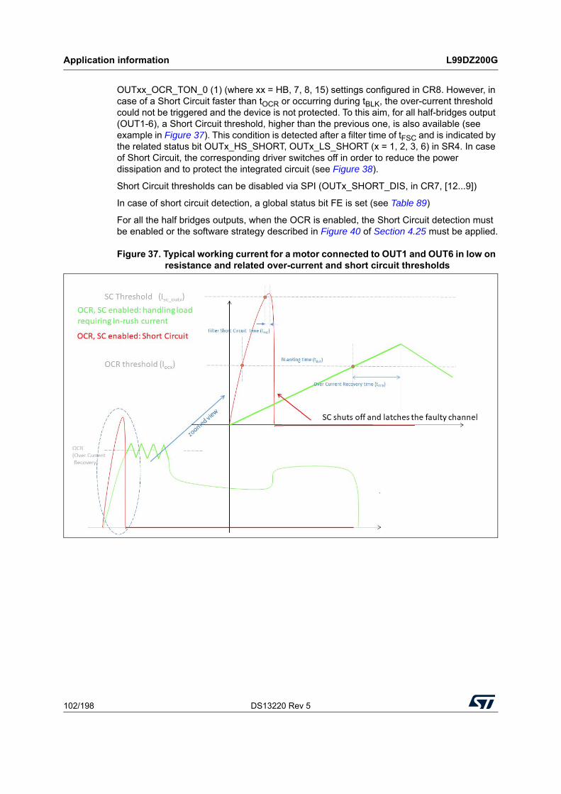
Application information L99DZ200G
102/198 DS13220 Rev 5
OUTxx_OCR_TON_0 (1) (where xx = HB, 7, 8, 15) settings configured in CR8. However, in case of a Short Circuit faster than tOCR or occurring during tBLK, the over-current threshold could not be triggered and the device is not protected. To this aim, for all half-bridges output (OUT1-6), a Short Circuit threshold, higher than the previous one, is also available (see example in Figure 37). This condition is detected after a filter time of tFSC and is indicated by the related status bit OUTx_HS_SHORT, OUTx_LS_SHORT (x = 1, 2, 3, 6) in SR4. In case of Short Circuit, the corresponding driver switches off in order to reduce the power dissipation and to protect the integrated circuit (see Figure 38).
Short Circuit thresholds can be disabled via SPI (OUTx_SHORT_DIS, in CR7, [12...9])
In case of short circuit detection, a global status bit FE is set (see Table 89)
For all the half bridges outputs, when the OCR is enabled, the Short Circuit detection must be enabled or the software strategy described in Figure 40 of Section 4.25 must be applied.
Figure 37. Typical working current for a motor connected to OUT1 and OUT6 in low on resistance and related over-current and short circuit thresholds

DS13220 Rev 5 103/198
L99DZ200G Application information
197
Figure 38. Triggering cases of over-current and short circuit thresholds
4.21 Constant current mode
For the OUT7, OUT8 and OUT9 high side drivers, it is available the CCM (Constant Current Mode) feature, which is conceived to provide a constant current to the related output.
The CCM feature is configurable via SPI, by setting the OUTx_CCM_EN bit (x = 7, 8, 9) in CR9; these bits can be set only if the related driver is in OFF state and when the CCM is enabled, the overcurrent and short circuit detection of the related output is switched OFF while its open load detection is always ON.
The CCM is automatically disabled after an expiration time tCCMtimeout.
The allowed sequences are:
Set OUTx_CCM_EN bit, then turn ON the related driver by SPI or by direct input DIR (the other configurations of the OUTx_3-2-1 are ignored, see Table 102): driver starts in CCM for 10ms, then it switches to ON mode or DIR mode and the OUTx_CCM_EN bit is automatically cleared after this 10 ms;
If OUTx_CCM_EN = 1, the configurations other than “OFF”, “ON” or “DIR” of the OUTx3-2-1-0 (see Table 102) are ignored; in that case, the OUTx3-2-1-0 bits are kept
t
t
t
t
SC threshold
Black peak Current: device cycling as per auto-recovery setting Red peak Current: device shutoff as per SC threshold
OC
= 40 μs t BLK
CURRENT OUTPUT DRIVER
HS_ON
OC threshold
FSC
t = 48 μs OCR
Period = 1/frequency
OFFON
= Period - tONOFF

Application information L99DZ200G
104/198 DS13220 Rev 5
unchanged (at either “0000”=OFF, “0001”=ON or “1110”=DIR) and the SPI_INV_CMD bit (SR2 – 0x32) is set to 1 in order to indicate an invalid setting;
If OUTx_CCM_EN bit is cleared by the microcontroller before timeout, then the driver is itched to ON mode or DIR mode;
If OUTx_CCM_EN bit is set after driver has been started in ON, PWM, Timer or DIR modes, then the OUTx_CCM_EN bit is ignored (i.e. OUTx_CCM_EN = 0); in that case OUTx_CCM_EN remains ‘0’ and the SPI_INV_CMD bit (SR2 - 0x32) is set to ‘1’ in order to indicate an invalid setting.
The Short Circuit and Over Current detection are enabled in ON, PWM, timer and DIR modes, but not in Constant Current Mode.
The default value for the OUTx_CCM_EN bit is 0, i.e. the CCM is disabled by default.
Figure 39. Constant current mode
4.22 Current monitor and direct drive input
The current monitor sources a current image of the power stage output current at the current monitor pin CM, which has a fixed ratio (ICMr) of the instantaneous current of the selected high-side driver. The signal at output CM is blanked for tcmb after switching on the driver until correct settlement of the circuitry. The bits CM_SELx (CR 7) define which of the outputs is multiplexed to the current monitor output CM. The current monitor output allows a more precise analysis of the actual state of the load rather than the detection of an open- load or overload condition. For example, it can be used to detect the motor state (starting, free running, stalled). The current monitor output is enabled after the current-monitor blanking time, when the selected output is switched on. If this output is off, the current monitor output is in high impedance mode.
Current monitor output pin is shared with the Direct Input Drive (DIR) and the activation of the two functionalities is obtained by changing the CM_DIR_CONF_x bit (CR7, x = 0, 1).
Four different modalities are identified and detailed in the following Table 67.
Vout (V)
Iout (A)
t (ms)
t (ms)
ICCMx
tCCMtimeout
Normal high-side driver mode
Iloadn
Iload3Iload2Iload1Iload
Constantcurrentmode
00
00

DS13220 Rev 5 105/198
L99DZ200G Application information
197
4.23 PWM-Mode of the Power-Outputs
Description seeSection 7.3: Status register overview.
4.24 Cross-current protection
The four half-brides of the device are cross-current protected by an internal delay time. If one driver (LS or HS) is turned off, the activation of the other driver of the same half bridge will be automatically delayed by the crosscurrent protection time. After the crosscurrent protection time is expired the slew-rate limited switch-off phase of the driver is changed to a fast turn-off phase and the opposite driver is turned-on with slew-rate limitation. Due to this behavior, it is always guaranteed that the previously activated driver is completely turned off before the opposite driver starts to conduct.
4.25 Programmable soft-start function to drive loads with higher inrush current
Loads with start-up currents higher than the overcurrent limits (e.g. inrush current of lamps, start current of motors) can be driven by using the programmable soft-start function (i.e. overcurrent recovery mode). Each driver has a corresponding overcurrent recovery bit OUTx_OCR (CR 7). If this bit is set, the device automatically switches the outputs on again after a programmable recovery time. The PWM modulated current will provide sufficient average current to power up the load (e.g. heat up the bulb) until the load reaches operating condition. The PWM frequency is defined by CR7<8:12> setting.
The device itself cannot distinguish between a real overload (e.g. short-circuit condition) and a load characterized by operation currents exceeding the over-current threshold.
Examples are non-linear loads like a light bulb used on the HS outputs or a motor used on the half bridge output with inrush and stall currents that shall be limited by the auto recovery feature.
For the bulb, a real overload condition can only be qualified by time. For overload detection the microcontroller can switch on the light bulbs by setting the overcurrent recovery bit for the first e.g. 50 ms. After clearing the recovery bit, the output will be switched off automatically if the overload condition remains.
For the half bridges the high current can be present during all motor activation and another SW strategy must be applied to identify a SC to GND or Supply. Before running the motor e.g. with a first SPI command all bridge LS are switched on (without auto recovery functionality /
Table 67. Current Monitor/Direct configurations
CM_DIR_CONF_1 CM_DIR_CONF_0 Description Pin direction
0 0 CM all the time Output
0 1DIR in Standby mode and CM in Active mode
Input / Output
1 0 DIR all the time Input
1 1 OFF

Application information L99DZ200G
106/198 DS13220 Rev 5
cleared overcurrent recovery bit), all HS are switched off and a SC to Battery can be diagnosed. With a next SPI command, all HS are switched on (without auto recovery functionality/ cleared overcurrent recovery bit) and all LS are switched off. In this sequence, a short to GND can be diagnosed. If in both sequences no overload condition is identified, the motor can be run by switching on the relative HS and LS each configured in auto recovery mode (see Figure 40: Software strategy for half bridges before applying auto-recovery mode).
Such sequence can be applied before any motor activation to identify SC just before operating the motor (in case the delay due to the 2 additional SPI commands is not limiting the application) or in case of power up of the system respectively applied on a certain time base.
Figure 40. Software strategy for half bridges before applying auto-recovery mode
As soon as an output reaches auto-recovery condition, OUTx_OCR_ALERT (SR 4) is set. The Alert bit indicates that an overload condition (load in-rush, short-circuit, etc) is present.
4.26 H-bridge control
The PWMH1y, PWMH2y inputs and the DIRHy bits (DIRHA in CR10, DIRHB in CR21) control the drivers of the external H-bridge transistors (y = A, B); independently from the PWMH frequency (fPWMH) applied by the µC to control the H-bridges A and B, the PWMH On-time shall be higher than 250ns. In Single Motor mode, bit DMy (Config Reg = 0), the motor direction can be chosen with the control bit (DIRHy), the duty cycle and frequency with the PWMH1y input. With the SPI bits SD1y (CR 10) and SDS1y (CR 10) four different
OFF
ON
OUTxHS
OUTxLS OUTyLS
OUTx OUTy
VS
M
GND
OUTyHS
VS
GND
Vbat
ON
OFF
Short to Vs?N
Y
? ?
OFF
ON
OUTxHS
OUTxLS OUTyLS
OUTx OUTy
VS
M
GND
OUTyHS
VS
GND
Vbat
SW Step 2: Short to ground detection
ON
OFF
Short to GND?N
Y
SW Step 1: Short to battery detection
BEGINSW Routine
HS OFF LS ON
SW Step 1
HS ONLS OFF
Keep AR OFFSwitch LS OFF
SW Step 2
ENDSW Routine
Set AR ON
Keep AR OFFSwitch HS OFF
? ?
AR OFF
GAPG0408151459CF
L99DZ200G L99DZ200G L99DZ200G L99DZ200G

DS13220 Rev 5 107/198
L99DZ200G Application information
197
freewheeling modes (via drivers in the active cases or via diodes in the passive cases) can be selected using the high-side or the low-side transistors.
Alternatively, the external H-bridges can be driven in half bridge mode (Dual mode). By setting the dual mode bit DMy (Config Reg) = 1, both the half-bridges of the H-bridge y can be controlled independently.
Table 68. H-bridge y (y = A, B) control truth table in Single mode (DMy = 0)
Control pins
Control
bitsFailure bits Output pins
Nb
PW
MH
1y
PW
MH
2y
DIR
Hy
HE
Ny
DM
y
SD
1y
SD
S1y
SD
2y
S
DS
2y
CP
_L
OW
VS
_O
V
VS
_U
V
DS
TS
D1
GH
1y
GL
1y
GH
2y
GL
2y
1 x x x 0 x x x x x x x x x x RL RL RL RL H-bridge y disabled
2 x x x 1 0 x x x x 1 0 0 0 0 RL RL RL RL Charge pump voltage too low
3 x x x 1 0 x x x x 0 x x x 1 RL RL RL RL Thermal shutdown
4 x x x 1 0 x x x x 0 1 0 0 0 L L L L Overvoltage
5 x x x 1 0 x x x x 0 0 0 1 0L (1) L(1) L(1) L(1) Short-circuit(1)
6 1 x 0 1 0 x x x x 0 0 0 0 0 L H H L Bridge y H2/L1 on
7 0 x x 1 0 0 0 x x 0 0 0 0 0 L H L H Active freewheeling LS1 and LS2 on
8 0 x 0 1 0 0 1 x x 0 0 0 0 0 L H L LPassive freewheeling through LS2 diode
9 0 x 1 1 0 0 1 x x 0 0 0 0 0 L L L HPassive freewheeling through LS1 diode
10 1 x 1 1 0 x x x x 0 0 0 0 0 H L L H Bridge y H1/L2 on
11 0 x x 1 0 1 0 x x 0 0 0 0 0 H L H L Active freewheeling HS1 and HS2 on
12 0 x 0 1 0 1 1 x x 0 0 0 0 0 L L H LPassive freewheeling through HS1 diode
13 0 x 1 1 0 1 1 x x 0 0 0 0 0 H L L LPassive freewheeling through HS2 diode
1. Only the half bridge (low-side and high-side), in which one MOSFET is in short-circuit condition is switched off. Both MOSFETs of the other half bridge remain active and driven by DIRHy control bit and PWMHy pin.

Application information L99DZ200G
108/198 DS13220 Rev 5
During watchdog long-open window, the H-bridge drivers are forced off until the first valid watchdog trigger in window mode (setting TRIG = 0 during safe window). The Control Registers remain accessible during long open window.
4.27 H-Bridge Driver Slew-Rate Control
The rising and falling slope of the drivers for the external high-side Power-MOS can be slew rate controlled. If this mode is enabled the gate of the external high-side Power-MOS is driven by a current source instead of a low-impedance output driver switch as long as the drain-source voltage over this Power-MOS is below the switch threshold. The current is programmed using the bits SLEW_x<4:0> (CR 10), which represent a binary number. This number is multiplied by the minimum current step. This minimum current step is the maximum source-/sink-current (IGHxrmax / IGHxfmax) divided by 31. Programming SLEW_x <4:0> to 0 disables the slew rate control and the output is driven by the low-impedance output driver switch.
Table 69. H-bridge y (y = A, B) control truth table in Dual Mode (DMy = 1) for the leg x (x= 1, 2)
Control
pin
Control
bitsFailure bits Output pin Comment
Nb
PW
MH
xy
HE
Ny
DM
y
DIR
Hy
SD
xy
SD
Sx
y
CP
_L
OW
VS
_O
V
VS
_U
V
DS
TS
D1
GH
xy
GL
xy
1 0 1 1 x 0 0 0 0 0 0 0 L H Active freewheeling LS
2 1 1 1 x 0 0 0 0 0 0 0 H L DRIVE HS
3 0 1 1 x 1 0 0 0 0 0 0 H L Active freewheeling HS
4 1 1 1 x 1 0 0 0 0 0 0 L H DRIVE LS
5 0 1 1 x 0 1 0 0 0 0 0 L L Passive freewheeling
6 1 1 1 x 0 1 0 0 0 0 0 H L DRIVE HS
7 0 1 1 x 1 1 0 0 0 0 0 L L Passive freewheeling
8 1 1 1 x 1 1 0 0 0 0 0 L H DRIVE LS
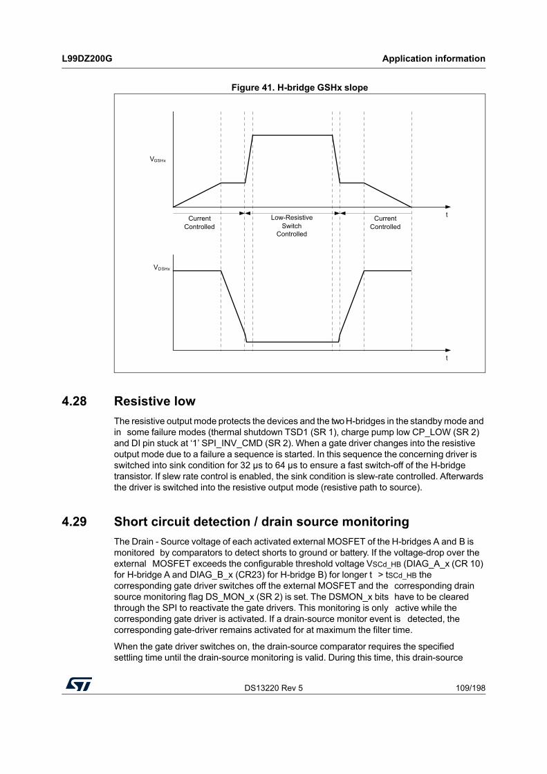
DS13220 Rev 5 109/198
L99DZ200G Application information
197
Figure 41. H-bridge GSHx slope
4.28 Resistive low
The resistive output mode protects the devices and the two H-bridges in the standby mode and in some failure modes (thermal shutdown TSD1 (SR 1), charge pump low CP_LOW (SR 2) and DI pin stuck at ‘1’ SPI_INV_CMD (SR 2). When a gate driver changes into the resistive output mode due to a failure a sequence is started. In this sequence the concerning driver is switched into sink condition for 32 μs to 64 μs to ensure a fast switch-off of the H-bridge transistor. If slew rate control is enabled, the sink condition is slew-rate controlled. Afterwards the driver is switched into the resistive output mode (resistive path to source).
4.29 Short circuit detection / drain source monitoring
The Drain - Source voltage of each activated external MOSFET of the H-bridges A and B is monitored by comparators to detect shorts to ground or battery. If the voltage-drop over the external MOSFET exceeds the configurable threshold voltage VSCd_HB (DIAG_A_x (CR 10) for H-bridge A and DIAG_B_x (CR23) for H-bridge B) for longer t > tSCd_HB the corresponding gate driver switches off the external MOSFET and the corresponding drain source monitoring flag DS_MON_x (SR 2) is set. The DSMON_x bits have to be cleared through the SPI to reactivate the gate drivers. This monitoring is only active while the corresponding gate driver is activated. If a drain-source monitor event is detected, the corresponding gate-driver remains activated for at maximum the filter time.
When the gate driver switches on, the drain-source comparator requires the specified settling time until the drain-source monitoring is valid. During this time, this drain-source
VGSHx
t
VDSHx
tGAPG0508151242CFT
ControlledCurrent
ControlledSwitch
Low-ResistiveControlled
Current

Application information L99DZ200G
110/198 DS13220 Rev 5
monitor event may start the filter time. The threshold voltage VSCd_HB can be programmed using the SPI bits DIAG_A_x (CR 10) or DIAG_B_x (CR 23).
Figure 42. H-bridge diagnosis
4.30 H-Bridge-Monitoring in Off-Mode
The drain source voltages of the two H-bridges A and B driver external transistors can be monitored, while the transistors are switched off. If either bit OL_H1L2_X or OL_H2L1_X (CR 10 for X=A, CR23 for X=B) is set to 1, while bit HEN_X (CR 1) = 1, the H-drivers X (A or B) enter resistive low mode and the drain-source voltages can be monitored. Since the pull-up resistance is equal to the pull-down resistance on both sides of the bridge, a voltage of 2/3 VS on the pull-up high side and 1/3 VS on the low- side is expected, if they drive a low-resistive inductive load (e.g. motor). If the drain source voltage on each of these Power-MOS is less than 1/6 VS, the drain-source monitor bit of the associated driver is set. The open-load filter time is tOL_HB.
M
Vs
GH1
VS
SH1
GL1
VS
GH2
SH2
GL2
20k
20k
Gate Driver HS
Gate Driver LS
DS-Monitoring HS
DS-Monitoring LSOL-Monitoring
VThres
VThres20k
20k
Gate Driver HS
Gate Driver LS
DS-Monitoring HS
DS-Monitoring LSOL-Monitoring
VThres
VThres
GAPG0408151656CFT

DS13220 Rev 5 111/198
L99DZ200G Application information
197
Figure 43. H-bridge open-load-detection (no open-load detected)
Figure 44. H-bridge open-load-detection (open-load detected)
Mm
20k
VTVT
Vs/3 Vs/3
Vs
DSM = 0 DSM = 020k 20k =Vs/6=Vs/6
Mm
20k
VTVT
Vs/2 Open
Vs
DSM = 0 DSM = 120k 20k =Vs/6=Vs/6

Application information L99DZ200G
112/198 DS13220 Rev 5
Figure 45. H-bridge open-load-detection (short to ground detected)
Figure 46. H-bridge open-load-detection (short to Vs detected)
In this specific case the outputs of the 2 comparators are inverted to be compliant to Table 70: H-bridge monitoring in off-mode (Nb = 9).
Mm
20kGND
VTVT
GND
Short
Vs
DSM = 1 DSM = 120k 20k =Vs/6=Vs/6
Mm
20kVs
VTVT
Vs
Short
Vs
DSM = 1 DSM = 120k 20k =(5/6)Vs=(5/6)Vs
Table 70. H-bridge monitoring in off-mode
Control bits Failure bitsComments
Nb OL H1L2 OL H2L1 H OLTH High DSMON LS1 DSMON LS2
1 0 0 0 0 0Drain-Source monitor disabled
2 1 0 x 0 0 No open-load detected
3 1 0 0 0 1 Open-load SH2
4 1 0 0 1 1 Short to GND

DS13220 Rev 5 113/198
L99DZ200G Application information
197
What reported in this chapter applies only to single motor H-bridge configuration; i.e. in the case one H-bridge drives only one motor.
4.31 Programmable cross current protection
The external Power MOSFETs transistors in H-bridge A and B (two half-bridge for each H-bridge) configuration are switched on with an additional delay time tCCP to prevent cross current in the half bridge. The cross current protection time tCCP can be programmed with the SPI bits COPT_x_A<3:0> (CR 10 for H-bridge A) or COPT_x_B <3:0> ( CR 15 for H-bridge B). The timer is started when the gate driver is switched on in the device.
The PWMH module has 2 timers to configure locking time for high-side and freewheeling low-side. The programmable time tCCP-TIM1 / tCCP-TIM2 is the same. Sequence for switching in PWM mode is the following:
HS switch off after locking tCCP-TIM1
LS switch on after 2nd locking tCCP-TIM1
HS switch on after locking tCCP-TIM2 which starts with rising edge on PWM input.
Figure 47. PWMH cross current protection time implementation
5 1 0 1 1 1 Short to VS
6 0 1 x 0 0 No open-load detected
7 0 1 0 1 0 Open-load SH1
8 0 1 0 1 1 Short to GND
9 0 1 1 1 1 Short to VS
Table 70. H-bridge monitoring in off-mode (continued)
Control bits Failure bitsComments
Nb OL H1L2 OL H2L1 H OLTH High DSMON LS1 DSMON LS2
GAPG0303161056CFT
tCCP-TIM1 tCCP-TIM1
tpp > 2 x tccp
PWM
Input
HS Logic
LS Logic
tCCP-TIM1 tCCP-TIM1
tpp < 2 x tccp
Passive
Free Wheeling
Active
Free Wheeling
tpp < t ccp
tCCP-TIM1 tCCP-TIM1
tCCP-TIM2
Passive
Free Wheeling
tCCP-TIM2 tCCP-TIM2
Lorem ipsum

Application information L99DZ200G
114/198 DS13220 Rev 5
4.32 Power window H-bridge safety switch off block
The two LS Switches LSA_FSO and LSB_FSO are intended to be used to switch off the gates of the two external high-side MOSFETs in the power window h-bridges (A and B) if a fatal error happens. This block must work also in case the MOSFET driver and the relative control blocks on the chip are destroyed. Therefore, it is necessary to have a complete separated safety block on the device, which has its own supply and GND connection, separated from the other supplies and GNDs. In the block, an own voltage regulator and an oscillator are implemented.
The safety block is surrounded by a GND isolation ring realized by deep trench isolation. The LS driver must work down to a lower voltage than the other circuits. The block has its own internal supply and an own oscillator for monitoring the failure signals (WWD, V1 fail, SPI fail & Tj) which are Manchester encoded and decoupled by high ohmic resistances. In case of fail-safe event, both LS switches LSA_FSO and LSB_FSO are switched on.
In case of entering V1_Standby mode or VBAT_Standby mode both fail safe low-side switches are switched on to minimize the current drawn by the fail-safe block (e.g. oscillator is switched off and Manchester Encoding is deactivated). Short circuit protection to VS is active in both standby modes limiting the current to IOLimit for a filter of tSCF.
After this filter time the fail-safe switches are switched off and LSx_FSO_OC (SR 3) is set. To reactivate the low-side functionality this bit has to be set back by a read and clear command. In case of VS loss the fail-safe switches are biased by their own output voltage to turn on the low-side switches down to VOUT_max.
To allow verification of the Fail-Safe path, the low-side switches LSA_FSO and LSB_FSO can be turned on by SPI (Configuration Register 0x3F bit 4: FS_FORCED).

DS13220 Rev 5 115/198
L99DZ200G Application information
197
Figure 48. LSx_FSO: low-side driver “passively” turned on, taking supply from output pin (if main supply fails), can guarantee VLSx_FSO < VOUT_max
Figure 49. Safety concept
Filters & State Machine
Enable
LSA_FSO_OC_ _
Clock
&
Watchdog Fail
V1 Failures
Over Temp TSD2
CLEAR LSx_FSO_OC
Tx M
anch
este
rEn
code
d Si
gnal
s(N
orm
ally
Sw
itchi
ng)
Rx
Sign
al
VREG
GND
Supply
Low SideDriver 1
Low SideDriver 2
Fail Safe Block
Complete IC
LSA_FSO_
LSB_FSO
TX S
igna
ls
LSB_FSO_OC
LSA_FSO_OC
LSB_FSO_OC
Tx Signal
Manchester EncodedSignals
Clock
Rx Signal
Normal Operation Fail Safe Clock Failure Data Failure

Application information L99DZ200G
116/198 DS13220 Rev 5
4.33 Generator mode
Generator mode allows the L99DZ200G h-bridge drivers to autonomously switch ON all the external LS MOSFETs of both h-bridges (A and B) when an overvoltage on the VS line is detected. Main purpose of these concurrent activations is to immediately block at the same time both the DC motors connected to the 2 external full bridges (braking function).
Generator Mode is by default enabled at the startup of the device and it is controlled by the GENERATOR_MODE_EN bit in CR22 (0x16); in case the VS OV occurs during standby modes and the generator mode is enabled, the VS_OV_WAKEUP bit in the SR1 (0x31) identifies the OV as source of the wakeup.
Generator mode works when L99DZ200G is in Active, in V1_Standby and in VBAT_Standby modes. Fail safe low side circuitry has not to be activated/connected if the Generator mode will be used
4.33.1 Generator Mode in Active Mode
The below reported Table 71 shows the wake UP True table for the Generator Mode when the device is in active mode:
Table 71. Wake UP for Generator Mode
In Active Mode, Generator Mode is a live functionality, i.e. the Vs is continuously monitored by a "VS Monitor". In case the VS OV is detected, GL1y and GL2y (y = A, B) are switched ON; they are switched OFF as soon as the VS OV is no more detected.
When the Generator Mode is enabled (GENERATOR_MODE_EN=1), the configuration of the h-bridge drivers A and B can be changed even when the VS OV is occurring. The h-bridges A and B will recover the normal h-bridge drive once the VS OV ends; moreover, during this VS OV situation the LS MOSFETs continues to be ON even if a TSD1 or a TSD2 or a Fail Safe event occurs.
4.33.2 Generator Mode in Standby Modes
In V1_Standby or in VBAT_Standby modes, a "VS OV Detector" is used to detect the occurrence of a Vs OV; in this case the thresholds are VSOV_DET (see parameters A.185, A.186 and A.187 in Table 7).
When Vs > VS_OVDET the device is firstly put in Active mode and then the "Vs Monitor" is activated; all this sequence lasts (tOVUV_FILT + tFOV) plus the time needed to start the oscillator at VSOV_DET threshold (around 10 µs) plus the time needed to stabilize the reference voltage (around 10 µs). This means that the VSOV shall be present for a minimum of 148 µs to start the braking function and set the VS_OV_WAKEUP bit (SR1).
The below reported Table 72: Wake UP for Generator Mode shows the Wake UP True table for the Generator Mode when the device is in V1_Standby or in VBAT_Standby mode:
L99DZ200G Status GENERATOR _MODE_EN LS MOSFETs state after VS OV condition Notes
Active1
ON if VS > VSOV Monitoring is done by the "Vs Monitor"Controlled by the h-bridge drv if VS < VSOV
0 Controlled by the h-bridge drv

DS13220 Rev 5 117/198
L99DZ200G Application information
197
In Standby modes:
if the Vs OV is detected, SPI writing to enter in Standby modes will be ignored and a SPI Error will be generated; in this case the SPI_INV_CMD bit (SR2 - 0x32) is set to 1 in order to indicate an invalid setting;
if the Vs OV disappears, a new SPI access will be needed to enter in Standby modes.
4.34 Heater MOSFET Driver
The Heater MOSFET Driver stage is controlled by control bit GH (CR 5). The driver contains two diagnosis features to indicate short-circuit in active mode (external MOSFET switched on) and open-load in off state (External MOSFET switched off).
Short circuit detection in on state is realized by monitoring the drain source voltage of the activated external MOSFET by a comparator to detect a short-circuit of SHheater to ground. If the voltage-drop over the external MOSFET exceeds the programmed threshold voltage VSCd_HE for longer than the drain-source monitor filter time tSCd_HE the gate driver switches off the external MOSFET and the corresponding drain source monitoring flag DSMON_HEAT (SR 5) is set. The drain source-monitoring bit has to be cleared by SPI to reactivate the gate driver. The drain source monitoring is only active while the gate driver is activated. If a drain source monitoring event is detected, the gate-driver remains activated for the maximum filter time. The threshold voltage can be programmed by SPI bits GH_THx (CR 10).
Open-load detection in off state is realized by monitoring the voltage difference between SHheater and GND and supplying SHheater by a pull up current source that can be controlled by SPI bit GH_OL_EN (CR 11). When no load is connected to the external MOSFET source, the voltage will be pulled to VS and in case of exceeding the threshold VOLheater for a time longer than the open-load filter time tOL_He the open-load bit GH_OL (SR 5) will be set.
Table 72. Wake UP for Generator Mode
L99DZ200G Status GENERATOR _MODE_ENWake UP when a
VS OV occurs
LS MOSFETs state after VS OV
condition (VS > VSOV_det)Notes
V1_Standby or VBAT_Standby
1 Yes OFF (1)added around 1 µA conso
0 No OFF
1. Generator Mode wake up at Vs OverVoltage by VS OV Detector (low consumption, 1 µA)

Application information L99DZ200G
118/198 DS13220 Rev 5
Figure 50. Heater MOSFET open-load and short-circuit to GND detection
Note: RL = resistive low, L = active low, H = active high.
4.35 Controller of electro-chromic glass
The voltage of an electro-chromic element connected at pin ECV can be controlled to a target value, which is set by the bits EC_x <5:0> (CR 11). Setting bit ECON (CR 11) enables this function. An on-chip differential amplifier and an external MOS source follower (with its gate connected to pin ECDR) driving the electro-chrome mirror voltage at pin ECV, form the control loop. The drain of the external MOS transistor is supplied by OUT10. A diode from pin ECV (anode) to pin ECDR (cathode) has been placed on the chip to protect the external MOS source follower. A capacitor of at least 5 nF has to be added to pin ECDR for loop-stability.
SPI
Vs
VOLheater
GH_OL
Gate Driver Heater MOSFET
SHHeater
GHHeater
CPIOLheater
VThres
DSMON_HEAT
Table 73. Heater MOSFET control truth table
Control bit Failure bits Output pin
CommentNb GH ON/OFF CP_LOW VS_OV VS_UV DS TSD1 GHheater
1 x 1 x x x x RL Charge pump voltage too low
2 x 0 x x x 1 RL Thermal shutdown
3 x 0 1 x x 0 L Overload
4 1 0 0 x 1 0 L Short-circuit condition
5 x 0 0 1 0 0 L Undervoltage
6 1 0 0 0 0 0 H Heater MOSFET driver
7 0 0 0 0 0 0 L Heater MOSFET driver

DS13220 Rev 5 119/198
L99DZ200G Application information
197
The target voltage is binary coded with a full-scale range of 1.5 V. If bit ECV_HV (Config Reg) is set to 0, the maximum controller output voltage is clamped to 1.2 V without changing the resolution of bits EC_x<5:0> (CR 11). When programming the ECV low-side driver ECV_LS (CR 11) to on-state, the voltage at pin ECV is pulled to ground by a 1.6 Ω low-side switch until the voltage at pin ECV is less than dVECVhi higher than the target voltage (fast discharge). The status of the voltage control loop is reported via SPI. Bit ECV_VHI (SR 6) is set, if the voltage at pin ECV is higher, whereas Bit ECV_VNR (SR 6) is set, if the voltage at pin ECV is lower than the target value. Both status bits are valid, if they are stable for at least the filter time tFECVNR and tFECVHI. Since OUT10 is the output of a high-side driver, it contains the same diagnose functions as the other high-side drivers (e.g. during an overcurrent detection, the control loop is switched off). In electro-chrome mode, OUT10 cannot be controlled by PWM mode. For EMS reasons, the loop capacitor at pin ECDR as well as the capacitor between ECV and GND have to be placed to the respective pins as close as possible (see Figure 51: Electro-chrome control block for details).
Pin ECDR is pulled resistively (RECDRDIS) to ground while not in electro-chrome mode. EC glass control behavior in case of failure on OUT10:
ECON (CR11) = 1 (EC glass control enabled)
OUT10 is turned ON
OUT10 settings in CR5 are ignored (PWM, DIR, TIMERx)
OUT10 settings in CR5 are recovered when ECON is set to 0.
In case of a failure on OUT10 while ECON = 1 (overcurrent, VS overvoltage /undervoltage, TSD1)
OUT10 is turned OFF (regardless of VS_OV_SD_EN and VS_UV_SD_EN in CR3)
DAC is reset: EC_x (CR11) set to ‘000000’
ECDR pin is pulled to GND
ECON (CR11) remains ‘1’
ECV_LS (CR11) remains as programmed Re-start of EC control after OUT10 failure
Read&Clear or automatic restart (if CR3 Vs_LOCK_EN = 0)
Write EC_x (CR11)

Application information L99DZ200G
120/198 DS13220 Rev 5
Figure 51. Electro-chrome control block
4.36 Temperature warning and shutdown
If any of the cluster (see Section 4.37) junction temperatures rises above the temperature warning threshold TW, the temperature warning flag TW (SR 2) is set after the temperature warning filter time tjtft and can be read via SPI. If the junction temperature increases above the temperature shutdown threshold (TSD1), the thermal shutdown bit TSD1 (SR 1) is set and the power transistors of all output stages are switched off to protect the device after the thermal shutdown filter time. The gates of the H-bridge and the heater MOSFET are discharged by the ‘Resistive Low’ mode. After these bits have been cleared, the output stages are reactivated. If the temperature is still above the thermal warning threshold, the thermal warning bit is set after tjtft. Once this bit is set and the temperature is above the temperature shutdown threshold, temperature shutdown is detected after tjtft and the outputs are switched off. Therefore, the minimum time after which the outputs are switched off after the bits have been cleared in case the temperature is still above the thermal shutdown threshold is twice the thermal warning/ thermal shutdown filter time tjtft.
4.37 Thermal clusters
In order to provide an advanced on-chip temperature control, the power outputs are grouped in six clusters with dedicated thermal sensors. The sensors are suitably located on the device (see Figure 52: Thermal clusters identification). In case the temperature of an output cluster reaches the thermal shutdown threshold, the outputs assigned to this cluster are shut down (all other outputs remain active). Each output cluster has a dedicated temperature warning and shutdown flag (SR 6) and the cluster temperature can be read out by SPI.
Hence, the thermal cluster concept allows to identify a group of outputs in which one or more channels are in overload condition.
GAPG0408151702CFT
GND
LogicSPI DAC
VS
ECDR
Voltage not reached
OUT10
ECVVoltage too high
VS compatible110101
200 nF
5 nF
All components must be placed close together and connected with a very low impedance
VS compatible
EC-Mirror

DS13220 Rev 5 121/198
L99DZ200G Application information
197
If thermal shutdown has occurred within an output cluster, or if temperature is rising within a cluster, it may be desired to identify which of the output (s) is (are) determining the temperature increase. An additional evaluation, based on current monitoring and cluster temperature read-out, supports identification of the outputs mainly contributing to the temperature increase. The cluster temperatures are available in SR 7, SR 8 and SR 9 and can be calculated from the binary coded register value using the following formula:
Decimal code = (350 – Temp) / 0.488
Example:
T = -40 °C => decimal code is 799 (0x31F) T = 25 °C => decimal code is 666 (0x29A)
Thermal clusters can be configured using bit TSD_CONFIG (Config Reg):
Standard mode (default): as soon as any cluster reaches thermal threshold the device is switched off. V1 regulator remains on and is switched off reaching TSD2.
Cluster mode: only the cluster that reaches shutdown temperature is switched off.
If Cluster Th_CL6 (global) or Cluster Th_CL5 (Voltage Regulators) reaches TSD1, the whole device is OFF (beside V1).
Note: Clusters related to power outputs (clusters 1 to 4, see Figure 52: Thermal clusters identification) will be managed digitally only, by means of the ADC conversion of related thermal sensors, while clusters 5 and 6 will be managed in an analog way (comparators) since ADC can be off, e.g. in V1_Standby mode. Temperature reading provided by ADC may differ from real junction temperature of a specific output due to spatial placement of thermal sensor. Such an effect is more visible during fast thermal increases of junction temperature. For some of the Power outputs, located between two different sensors, it may happen that temperature raising also affects the adjacent Cluster.

Application information L99DZ200G
122/198 DS13220 Rev 5
Figure 52. Thermal clusters identification
4.38 VS compensation (duty cycle adjustment) module
All stand-alone HS outputs can be programmed to calculate some internal duty cycle adjustment to adapt the duty cycle to a changing supply voltage at VS. This feature is aimed at avoiding LED brightness flickering in case of alternating supply voltage. The correction of the duty cycle is based on the following formula:
1
GL2
ASH
2A
5V_2
GH
1AG
H2A
SH1A
GH1BSH1B
GH2B
CL1B
SH2B
CP2MGL2B
OU
T13
CP2P
CP1M
CPCP1P
WU
GL1
ALI
N
TxD_LRxD_L/NINT
CM/DIR
DODI
CLK
PWMH1B
RxD_C/NINTNINT
TxD_C
VSREG
PWM
H2B
NR
ESET
CAN
_LOUT15
PWM
H1A
PWM
H2A
SGND
ECV
VS VSO
UT1
4
CAN
_SU
PECDR
VS
GHheaterSHheater
CAN
_H
CSN
LSB_FSOLSA_FSO
5V_1
GAPG0508151137CFT
OU
T10
OU
T9O
UT7
OU
T6O
UT6
OU
T1O
UT1
OU
T8O
UT2
OU
T3
2345678910111213141516
17 18 19 20 21 22 23 24 25 26 27 28 29 30 31 32
48474645444342414039383736353433
64 63 62 61 60 59 58 57 56 55 54 53 52 51 50 49
Tab
PGN
D
L99DZ200GLQFP-64
Thermal cluster 1Thermal cluster 2Thermal cluster 3Thermal cluster 4Thermal cluster 5
Table 74. Thermal cluster definition
Th_CL1 Th_CL2 Th_CL3 Th_CL4 Th_CL5 Th_CL6
OUT14+OUT15Mirror-x+ Mirror-y
+ OUT8Folder
(OUT1+OUT6)10W driver high ohmic channels
VREG 1
VREG 2Global
TW & TSD1 Both digitally managed
TW & TSD1 Both digitally managed
TW & TSD1 Both digitally managed
TW & TSD1 Both digitally managed
TW digitally managed TSD1
& TSD2
Both analog managed
TW digitally managed TSD1 Analog managed

DS13220 Rev 5 123/198
L99DZ200G Application information
197
Equation 1 Duty cycle correction
Vth = Duty cycle reference voltage: defined as 10 V
Vbat = Reference voltage: defined as voltage at pin VS VLED = Voltage drop on the external LED
DCnom = Nominal Duty Cycle programmed by SPI< PWMx DCx>
To be compatible to different LED load characteristics the value for VLED can be programmed for each output by a dedicated control register OUT7_VLED … OUT15_VLED (CR 17 to CR 20). Auto compensation features can be activated for all HS outputs each by setting OUTx_AUTOCOMP_EN (CR 17 to CR 20).
The programmed LED voltage (OUTx_VLED (CR17 to CR20)) must be lower than Vth (10 V).
Figure 53. Block diagram Vs compensation (duty cycle adjustment) module
4.39 Analog digital converter
Voltage signals VS, VSREG, VWU and TH_CL1...6 are read out sequentially. The voltage signals are multiplexed to an ADC. The ADC is realized as a 10 Bit SAR, sampled at fADC frequency which is obtained dividing by 4 the main clock fclk2.
Each channel will be converted with a conversion time tcon, therefore an update of the ADC value is available every tcon * 9. In case of WU is directly connected to VProtected (refer to Figure 61), the input must be protected by a series resistance of typical 1 kΩ to sustain reverse battery condition.
DutyCycleVth Vled–
Vbat Vled–----------------------------- x DCnom =
1 0 1 1 1 0 1 1 0 01 0 1 1 1 0 1 1 0 01 0 1 1 1 0 1 1 0 01 0 1 1 1 0 1 1 0 0
10 Register Duty Cycle HS
10 Bit accuracy / Nominal
Voltage @ 10V
SPI
SPIHS Assignment and Load Adaption VS Compensation
Calculation
1 0 1 1 1 0 1 1 0 01 0 1 1 1 0 1 1 0 01 0 1 1 1 0 1 1 0 01 0 1 1 1 0 1 1 0 0
10 Register adjusted
Duty Cycle HS / 10 Bit accuracy
HS1HS2
HS9HS10
ADC / VS
1Internal
Adjustment
ON / OFF
1 0 1 1 0 11 1 0 110 BIT VLED
voltage level
(0V ..10V)
GAPG0508151603CFT

Application information L99DZ200G
124/198 DS13220 Rev 5
Figure 54. Sequential ADC Read Out for VSREG, VS, WU and THCL1... THCL6
Note: As best practice, in order to release valid temperature or voltage information, it is strongly recommended to filter out sequential reading of a relevant channel (i.e. reading from 3 to 5 ADC conversions, excluding a potential outlier, and then weight the remaining data).
Vin
9 Channel Mux
WU
VSREG
VS
THCL1
10 BitSAR
SPI Register
10pF100k
1000k
VREF = 2V
3.3V
THCL6
THCL2THCL3
THCL5THCL4
GAPG0408151647CFT

DS13220 Rev 5 125/198
L99DZ200G Serial Peripheral Interface (SPI)
197
5 Serial Peripheral Interface (SPI)
A 32-bit SPI is used for bi-directional communication with the microcontroller.
The SPI is driven by a microcontroller with its SPI peripheral running in the following mode: CPOL = 0 and CPHA = 0.
For this mode input data is sampled by the low to high transition of the clock CLK, and output data is changed from the high to low transition of CLK. This device is not limited to microcontroller with a built-in SPI. Only three CMOS-compatible output Pins and one input Pin will be needed to communicate with the device. A fault condition can be detected by setting CSN to low. If CSN = 0, the DO-Pin will reflect the global error flag (fault condition) of the device.
Chip Select Not (CSN)The input Pin is used to select the serial interface of this device. When CSN is high, the output Pin (DO) is in high impedance state. A low signal activates the output driver and a serial communication can be started. The state during CSN = 0 is called a communication frame. If CSN = low for t > tCSNfail the DO output will be switched to high impedance in order not to block the signal line for other SPI nodes.
Serial Data In (DI)The input Pin is used to transfer data serial into the device. The data applied to the DI will be sampled at the rising edge of the CLK signal and shifted into an internal 32-bit shift register. At the rising edge of the CSN signal the content of the shift register will be transferred to Data Input Register. The writing to the selected Data Input Register is only enabled if exactly 32 bits are transmitted within one communication frame (i.e. CSN low). If more or less clock pulses are counted within one frame the complete frame will be ignored. This safety function is implemented to avoid an activation of the output stages by a wrong communication frame.
Note: Due to this safety functionality a daisy chaining of SPI is not possible. Instead, a parallel operation of the SPI bus by controlling the CSN signal of the connected IC's is recommended.
Serial Data Out (DO)The data output driver is activated by a logical low level at the CSN input and will go from high impedance to a low or high level depending on the global error flag (fault condition). The first rising edge of the CLK input after a high to low transition of the CSN Pin will transfer the content of the selected status register into the data out shift register. Each subsequent falling edge of the CLK will shift the next bit out.
Serial Clock (CLK)The CLK input is used to synchronize the input and output serial bit streams. The data input (DI) is sampled at the rising edge of the CLK and the data output (DO) will change with the falling edge of the CLK signal. The SPI can be driven with a CLK frequency up to 4 MHz.
5.1 ST SPI 4.0
The ST-SPI is a standard used in ST Automotive ASSP devices.
This chapter describes the SPI protocol standardization. It defines a common structure of the communication frames and defines specific addresses for product and status information.

Serial Peripheral Interface (SPI) L99DZ200G
126/198 DS13220 Rev 5
The ST-SPI allows the use of generic software to operate the devices while maintaining the required flexibility to adapt it to the individual functionality of a particular product. In addition, failsafe mechanisms are implemented to protect the communication from external influences and wrong or unwanted usage.
The devices Serial Peripheral Interface are compliant to the ST SPI Standard Rev. 4.0.
5.1.1 Physical Layer
Figure 55. SPI pin description
5.2 Signal description
Chip Select Not (CSN)The communication interface is de-selected, when this input signal is logically high. A falling edge on CSN enables and starts the communication while a rising edge finishes the communication and the sent command is executed when a valid frame was sent. During communication start and stop the Serial Clock (SCK) has to be logically low.The Serial Data Out (SDO) is in high impedance when CSN is high or a communication timeout was detected.
Serial Clock (SCK)This SCK provides the clock of the SPI. Data present at Serial Data Input (SDI) is latched on the rising edge of Serial Clock (SCK) into the internal shift registers while on the falling edge data from the internal shift registers are shifted out to Serial Data Out (SDO).
Serial Data Input (SDI)This input is used to transfer data serially into the device. Data is latched on the rising edge of Serial Clock (SCK).
Serial Data Output (SDO)This output signal is used to transfer data serially out of the device. Data is shifted out on the falling edge of Serial Clock (SCK).
L99DZ200G
SPI Master
μC
SDO
SDI
SCK
CSN

DS13220 Rev 5 127/198
L99DZ200G Serial Peripheral Interface (SPI)
197
Figure 56. SDO pin
5.2.1 Clock and data characteristics
The ST-SPI can be driven by a microcontroller with its SPI peripheral running in the following mode:
CPOL = 0CPHA = 0
Figure 57. SPI signal description
The communication frame starts with the falling edge of the CSN (Communication Start). SCK has to be low.
The SDI data is then latched at all the subsequent rising SCK edges into the internal shift registers. After Communication Start the SDO will leave 3-state mode and present the MSB of the data shifted out to SDO. At the subsequent SCK falling edges, data are shifted out to SDO through the internal shift registers. The communication frame is finished with the rising edge of CSN. If a valid communication took place (e.g. correct number of SCK cycles,
Digital logic
GND
V1
Data Out
Data In
Enable
GND
ESD prot
GAPG2608151615CFT
GAPG2209151345CFT
SDO
SDI
SCK
CSN
MSB
MSB
LSB
LSB

Serial Peripheral Interface (SPI) L99DZ200G
128/198 DS13220 Rev 5
access to a valid address), the requested operation according to the Operating Code will be performed (Write or Clear operation).
5.2.2 Communication Protocol
SDI Frame
The devices Data-In Frame consist of 32-bit (OpCode (2 bits) + Address (6 bits) + Data Byte 3 + Data Byte 2 + Data Byte 1). The first two transmitted bits (MSB, MSB-1) contain the Operation Code which represents the instruction which will be performed. The following 6 bits (MSB-2 to MSB-7) represent the address on which the operation will be performed. The subsequent bytes contain the payload.
Figure 58. SDI Frame
Operating Code
The operating code is used to distinguish between different access modes to the registers of the slave device.
A Write Operation will lead to a modification of the addressed data by the payload if a write access is allowed (e.g. Control Register, valid data). Beside this a shift out of the content (data present at Communication Start) of the registers is performed.
A Read Operation shifts out the data present in the addressed register at Communication Start. The payload data will be ignored and internal data will not be modified. In addition a Burst Read can be performed.
A5 A4 A3 A2 A1 A0
7 6 5 4 3 2 1 0
time
GAPG2209151357CFT
MSB
OPCODE
OC1 OC0
time
time
time
LSB
DATA Byte 1
DATA Byte 2
ADDRESS DATA Byte 3
time
9 8
1617181920212223
101112131415
Table 75. Operating Codes
OC1 OC0 Description
0 0 Write Operation
0 1 Read Operation
1 0 Read & Clear Operation
1 1 Read Device Information

DS13220 Rev 5 129/198
L99DZ200G Serial Peripheral Interface (SPI)
197
A Read & Clear Operation will lead to a clear of addressed status bits. The bits to be cleared are defined first by address, secondly by payload bits set to ‘1’. Beside this a shift out of the content (data present at Communication Start) of the registers is performed.
Note: Status registers that change status during communication could be cleared by the actual Read & Clear Operation and are neither reported in actual communication nor in the following communications. To avoid a loss of any reported status it is recommended just clear status registers which are already reported in the previous communication (Selective Bitwise Clear).
Advanced Operation Codes
To provide beside the separate write of all control registers and the bitwise clear of all status registers, two Advanced Operation Codes can be used to set all control registers to the default value and to clear all status registers. A ‘set all control registers to default’ command is performed when an OpCode ‘11’ at address b’111111 is performed.
Note: Please consider that potential device specific write protected registers cannot be cleared with this command as a device Power-on-Reset is needed.
A ‘clear all status registers’ command is performed when an OpCode ‘10’ at address b’111111 is performed.
Data-In Payload
The Payload (Data Byte 1 to Data Byte 3) is the data transferred to the devices with every SPI communication. The Payload always follows the OpCode and the Address bits. For Write access the Payload represents the new data written to the addressed register. For Read & Clear operations the Payload defines which bits of the addressed Status Register will be cleared. In case of a ‘1’ at the corresponding bit position the bit will be cleared.
For a Read Operation the Payload is not used. For functional safety reasons it is recommended to set unused Payload to ‘0’.
SDO Frame
The data-out frame consists of 32-bits (GSB + Data Byte 1 to 3).
The first eight transmitted bits contain device related status information and are latched into the shift register at the time of the Communication Start. These 8-bits are transmitted at every SPI transaction. The subsequent bytes contain the payload data and are latched into the shift register with the eighth positive SCK edge. This could lead to an inconsistency of data between the GSB and Payload due to different shift register load times. Anyhow, no unwanted Status Register clear should appear, as status information should just be cleared with a dedicated bit clear after.

Serial Peripheral Interface (SPI) L99DZ200G
130/198 DS13220 Rev 5
Figure 59. SDO frame
Global Status Byte (GSB)
The bits (Bit0 to Bit4) represent a logical OR combination of bits located in the Status Registers. Therefore no direct Read & Clear can be performed on these bits inside the GSB.
Global Status Bit Not (GSBN)
The GSBN is a logically NOR combination of Bit 24 to Bit 30. This bit can also be used as Global Status Flag without starting a complete communication frame as it is present directly after pulling CSN low.
Reset Bit (RSTB)
The RSTB indicates a device reset. In case this bit is set, specific internal Control Registers are set to default and kept in that state until the bit is cleared. The RSTB bit is cleared after a Read & Clear of all the specific bits in the Status Registers which caused the reset event.
SPI Error (SPIE)
The SPIE is a logical OR combination of errors related to a wrong SPI communication.
Physical Layer Error (PLE)
The PLE is a logical OR combination of errors related to the LIN and HS CAN transceivers.
Functional Error (FE)
The FE is a logical OR combination of errors coming from functional blocks (e.g. High-side overcurrent).
9
7 6 5 4 3 2 1 0
8
GAPG2209151401CFT
MSBtime
time
time
LSB
DATA Byte 1
DATA Byte 2
DATA Byte 3
PLESPIEGSBN RSTB GW FSDEFE
Global Status Byte (GSB)
1617181920212223
101112131415
time
Table 76. Global Status Byte
Bit 31 Bit 30 Bit 29 Bit 28 Bit 27 Bit 26 Bit 25 Bit 24
GSBN RSTB SPIE PLE FE DE GW FS

DS13220 Rev 5 131/198
L99DZ200G Serial Peripheral Interface (SPI)
197
Device Error (DE)
The DE is a logical OR combination of errors related to device specific blocks (e.g. VS overvoltage, overtemperature).
Global Warning (GW)
The GW is a logical OR combination of warning flags (e.g. thermal warning).
Fail Safe (FS)
The FS bit indicates that the device was forced into a safe state due to mistreatment or fundamental internal errors (e.g. Watchdog failure, Voltage regulator failure).
Data-Out Payload
The Payload (Data Bytes 1 to 3) is the data transferred from the slave device with every SPI communication to the master device. The Payload always follows the OpCode and the address bits of the actual shifted in data (In-frame-Response).
5.2.3 Address Definition
Table 77. Device application access
Operating Code
OC1 OC0
0 0
0 1
1 0
Table 78. Device information read access
Operating Code
OC1 OC0
1 1
Table 79. RAM address range
RAM Address Description Access
3FH Configuration Register R/W
3CH Status Register 12 R/C
… …
32H Status Register 2 R/C
31H Status Register 1 R/C
… …

Serial Peripheral Interface (SPI) L99DZ200G
132/198 DS13220 Rev 5
Information registers
The Device Information Registers can be read by using OpCode ‘11’. After shifting out the GSB the 8-bit wide payload will be transmitted. By reading Device Information Registers a communication width which is minimum 16-bit plus a multiple by 8 can be used. After shifting out the GSB followed by the 8-bit wide payload a series of ‘0’ is shifted out at the SDO.
22H Control Register 34 R/W
1DH Control Register 29 R/W
… …
02H Control Register 2 R/W
Table 79. RAM address range (continued)
RAM Address Description Access
Table 80. ROM address range
ROM Address Description Access
3FH <Advanced Op.> W
3EH <GSB Options> R
…
20H <SPI CPHA test> R
16H <WD bit pos. 4> R
15H <WD bit pos. 3> R
14H <WD bit pos. 2> R
13H <WD bit pos. 1> R
12H <WD Type 2> R
11H <WD Type 1> R
10H <SPI mode> R
…
0AH <Silicon Ver.> R
…
06H <Device No.5> R
05H <Device No.4> R
04H <Device No.3> R
03H <Device No.2> R
02H <Device No.1> R
01H <Device Family> R
00H <Company Code> R

DS13220 Rev 5 133/198
L99DZ200G Serial Peripheral Interface (SPI)
197
Device Identification Registers
These registers represent a unique signature to identify the device and silicon version.
<Company Code>: 00H (STMicroelectronics)
<Device Family>: 01H (BCD Power Management)
<Device No. 1>: 55H
<Device No. 2>: 42H
<Device No. 3>: 46H
<Device No. 4>: 4BH
<Device No. 5>: 00H
SPI Modes
By reading out the <SPI Mode> register general information of SPI usage of the Device Application Registers can be read.
Table 81. Information Registers Map
ROM
AddressDescription Access Bit 7 Bit 6 Bit 5 Bit 4 Bit 3 Bit 2 Bit 1 Bit 0
3FH <Advanced Op.>
3EH <GSB Options> R → 0 0 0 0 0 0 0 0
…
20H <SPI CPHA test> R → 0 1 0 1 0 1 0 1
16H <WD bit pos. 4> R → C0H
15H <WD bit pos. 3> R → 7FH
14H <WD bit pos. 2> R → C0H
13H <WD bit pos. 1> R → 41H
12H <WD Type 2> R → 91H
11H <WD Type 1> R → 28H
10H <SPI mode> R → B0H
… →
0AH <Silicon Ver.> R → major revision minor revision
… →
06H <Device No.5> R L99DZ200G: 00H
05H <Device No.4> R → 4BH
04H <Device No.3> R → 46H
03H <Device No.2> R → 42H
02H <Device No.1> R → 55H
01H <Device Family> R → 01H
00H <Company Code> R → 00H

Serial Peripheral Interface (SPI) L99DZ200G
134/198 DS13220 Rev 5
<SPI Mode>: B0H (Burst Mode read available, 32 bit, no data consistency check)
SPI Burst Read
The SPI Burst Read bit indicates if a burst read operation is implemented. The intention of a Burst Read is e.g. used to perform a device internal memory dump to the SPI Master.
The start of the Burst Read is like a normal Read Operation. The difference is, that after the SPI Data Length the CSN is not pulled high and the SCK will be continuously clocked. When the normal SCK max count is reached (SPI Data Length) the consecutive addressed data will be latched into the shift register. This procedure is performed every time when the SCK payload length is reached.
In case the automatic incremented address is not used by the device, undefined data is shifted out. An automatic address overflow is implemented when address 3FH is reached. The SPI Burst Read is limited by the CSN low timeout.
SPI Data Length
The SPI Data Length value indicates the length of the SCK count monitor which is running for all accesses to the Device Application Registers. In case a communication frame with an SCK count not equal to the reported one will lead to a SPI Error, the data will be rejected.
Table 82. SPI Mode Register
Bit 7 Bit 6Bit
5Bit 4 Bit 3 Bit 2 Bit 1 Bit 0
BR DL2 DL1 DL0 0 0 S1 S0
1 0 1 1 0 0 0 0
Table 83. Burst Read Bit
Bit 7 Description
0 BR not available
1 BR available
Table 84. SPI Data Length
Bit 6 Bit 5 Bit 4 Description
DL2 DL1 DL0
0 0 0 invalid
0 0 1 16-bit SPI
0 1 0 24-bit SPI
0 1 1 32-bit SPI
…
1 1 1 64-bit SPI

DS13220 Rev 5 135/198
L99DZ200G Serial Peripheral Interface (SPI)
197
Data Consistency Check (Parity/CRC)
Watchdog Definition
In case a watchdog is implemented the default settings can be read out via the Device Information Registers.
<WD Type 1>: 28H (Long Open Window: 200 ms)
<WD Type 2>: 91H (Open Window. 10 ms, Closed Window: 5 ms)
<WD Type 1> indicates the Long Open Window (timeout) which is opened at the start of the watchdog. The binary value of WT[5:0] times 5 ms indicates the typical value of the Timeout Time.
<WD Type 2> describes the default timing of the window watchdog.
The binary value of CW[2:0] times 5 ms defines the typical Closed Window time and OW[2:0] times 5 ms defines the typical Open Window time.
Table 85. Data Consistency Check
Bit 1 Bit 0 Description
S1 S0
0 0 not used
0 1 Parity used
1 0 CRC used
1 1 Invalid
Table 86. WD Type/Timing
Bit 7 Bit 6 Bit 5 Bit 4 Bit 3 Bit 2 Bit 1 Bit 0
WD1 WD0
<WD Type 1/2> 0 0 Register is not used
<WD Type 1> 0 1 WT5 WT4 WT3 WT2 WT1 WT0
1 1 0 1 0 0 0
Watchdog Timeout / Long Open Window WT[5:0] * 5ms
<WD Type 2> 1 0 OW2 OW1 OW0 CW2 CW1 CW0
1 0 0 1 0 0 0 1
Open Window OW[2:0] * 5ms Closed Window CW[2:0] * 5ms
<WD Type 1/2> 1 1 Invalid

Serial Peripheral Interface (SPI) L99DZ200G
136/198 DS13220 Rev 5
Figure 60. Window watchdog operation
The watchdog trigger bit location is defined by the <WD bit pos. X> registers.
tLOW
tCW tOW
tCW tOW
tCW tOW
tLOW
tCW
tLOW
tOWF
WD-Trigger
normal operation
missing trigger
early write time
= correct trigger timing= early trigger timing= missing trigger
tCW = closed windowtLOW = long open window
tOW = open window= tCW + tOW = open window failtOWF
GAPG2708150909CFT
Table 87. WD bit position
Bit 7 Bit 6 Bit 5 Bit 4 Bit 3 Bit 2 Bit 1 Bit 0
WB1 WB0
<WD bit pos. X> 0 0 Register is not used
<WD bit pos. X> 0 1 WBA5 WBA4 WBA3 WBA2 WBA1 WBA0
<WD bit pos. 1> 0 1 0 0 0 0 0 1
<WD bit pos. 3> 0 1 1 1 1 1 1 1
Defines the register addresses of the WD trigger bits
<WD bit pos. X> 1 0 WBA5 WBA4 WBA3 WBA2 WBA1 WBA0
Defines the stop address of the address range (previous
<WD bit pos. X> is a WB = ‘01’). The consecutive <WD bit pos. X> has to be a WB = ‘11’
<WD bit pos. X> 1 1 0 WBP 4 WBP3 WBP2 WBP1 WBP0
<WD bit pos. 2> 1 1 0 0 0 0 0 0
<WD bit pos. 4> 1 1 0 0 0 0 0 0
Defines the binary bit position of the WD trigger bit within the register

DS13220 Rev 5 137/198
L99DZ200G Serial Peripheral Interface (SPI)
197
<WD bit pos 1>: 41H; watchdog trigger bit located at address 01H (CR1)
<WD bit pos 2>: C0H; watchdog trigger bit location is bit0
<WD bit pos 3>: 7FH; watchdog trigger bit located at address 3FH (Config Register)
<WD bit pos 4>: C0H; watchdog trigger bit location is bit0
Device Application Registers (RAM)
The Device Application Registers are all registers accessible using OpCode ‘00’, ‘01’ and ‘10’. The functions of these registers are defined in the device specification.
5.2.4 Protocol Failure Detection
To realize a protocol which covers certain failsafe requirements a basic set of failure detection mechanisms are implemented.
Clock monitor
During communication (CSN low to high phase) a clock monitor counts the valid SCK clock edges. If the SCK edges do not correlate with the SPI Data Length an SPIE is reported with the next command and the actual communication is rejected.
By accessing the Device Information Registers (OpCode = ‘11’) the Clock Monitor is set to a minimum of 16 SCK edges plus a multiple by 8 (e.g. 16, 25, 32 …). Providing no SCK edge during a CSN low to high phase is not recognized as an SPIE. For a SPI Burst Read also the SPI Data Length plus multiple numbers of Payloads SCK edges are assumed as a valid communication.
SCK Polarity (CPOL) check
To detect the wrong polarity access via SCK the internal Clock monitor is used. Providing first a negative edge on SCK during communication (CSN low to high phase) or a positive edge at last will lead to an SPI Error reported in the next communication and the actual data is rejected.
SCK Phase (CPHA) check
To verify, that the SCK Phase of the SPI master is set correctly a special Device Information Register is implemented. By reading this register the data must be 55H. In case AAH is read the CPHA setting of the SPI master is wrong and a proper communication cannot be guaranteed.
CSN timeout
By pulling CSN low the SDO is set active and leaves its 3-state condition. To ensure communication between other SPI devices within the same bus even in case of CSN stuck at low a CSN timeout is implemented. By pulling CSN low an internal timer is started. After timer end is reached the actual communication is rejected and the SDO is set to 3-state condition.
SDI stuck at GND
As a communication with data all-‘0’ and OpCode ‘00’ on address b’000000 cannot be distinguished between a valid command and a SDI stuck at GND this communication is not

Serial Peripheral Interface (SPI) L99DZ200G
138/198 DS13220 Rev 5
allowed. Nevertheless, in case a stuck at GND is detected the communication will be rejected and the SPIE will be set with the next communication.
SDI stuck at HIGH
As a communication with data all-‘1’ and OpCode ‘11’ on address b’111111 cannot be distinguished between a valid command and a SDI stuck at HIGH this communication is not allowed. In case a stuck at HIGH is detected the communication will be rejected and the SPIE will be set with the next communication.
SDO stuck @
The SDO stuck at GND and stuck at HIGH has to be detected by the SPI master. As the definition of the GSB guarantees at least one toggle, a GSB with all-‘0’ or all –‘1’ reports a stuck at error.

DS13220 Rev 5 139/198
L99DZ200G Application
197
6 Application
Figure 61. Typical application diagram

SPI registers L99DZ200G
140/198 DS13220 Rev 5
7 SPI registers
7.1 Global Status Byte GSB
Table 88. Global Status Byte (GSB)
Global Status Byte GSB
Bit 31 Bit 30 Bit 29 Bit 28 Bit 27 Bit 26 Bit 25 Bit 24
1 (R) 0 (R) 0 (R) 0 (R) 0 (R) 0 (R) 0 (R) 0 (R)
GSBN RSTB SPIE PLE FE DE GW FS
Global Status Bit Inverted
Reset SPI ErrorPhysical
Layer Error (CAN,LIN)
Functional Error
Device ErrorGlobal
WarningFail Safe
Table 89. Global Status Byte (GSB) description
Bit Name Description
31 GSBN
Global Status Bit InvertedThe GSBN is a logically NOR combination of GSB Bits 24 to Bit 30(1).
This bit can also be used as Global Status Flag without starting a complete communication frame as it is present at SDO directly after pulling CSN low.
0: error detected (1 or several GSB bits from 24 to 30 are set)
1: no error detected (default after Power-on)
Specific failures may be masked in the Configuration Register 0x3F. A masked failure will still be reported in the GSB by the related failure flag, however it is not reflected in the GSBN (bit 31).
30 RSTB
ResetThe RSTB indicates a device reset and it is set in case of the following events:
– VPOR (SR1 - 0x31)
– WDFAIL (SR1 - 0x31)
– V1UV (SR1 - 0x31)
– FORCED_SLEEP_TSD2/V1SC (SR1 - 0x31)
0: no reset signal has been generated (default)
1: Reset signal has been generated
RSTB is cleared by a Read & Clear command to all bits in Status Register 1 causing the Reset event.
29 SPIE(2)
SPI Error BitThe SPIE indicates errors related to a wrong SPI communication.
– SPI_INV_CMD (SR2 - 0x32)
– SPI_SCK_CNT (SR2 - 0x32)
The bit is also set in case of an SPI CSN Time-out detection
0: no error (default)
1: error detected
SPIE is cleared by a valid SPI command.

DS13220 Rev 5 141/198
L99DZ200G SPI registers
197
28 PLE(2)
Physical Layer Error
The PLE is a logical OR combination of errors related to the LIN and CAN transceivers.
– LIN_PERM_DOM (SR2 - 0x32)
– LIN_TXD_DOM (SR2 - 0x32)
– LIN_PERM_REC (SR2 - 0x32)
– CAN_RXD_REC (SR2 - 0x32)
– CAN_PERM_REC (SR2 - 0x32)
– CAN_PERM_DOM (SR2 - 0x32)
– CAN_TXD_DOM (SR2 - 0x32)
– SYSERR (SR12 - 0x3C)
– FDERR (SR12 - 0x3C)
0: no error (default) 1: error detected
PLE is cleared by a Read & Clear command to all related bits in Status Registers 2 and 12.
27 FE
Functional Error BitThe FE is a logical OR combination of errors coming from functional blocks.
– V2SC (SR2 - 0x32)
– DSMON_HSx_y (x = 1, 2 and y = A, B) (SR2 - 0x32 and SR3 – 0x33)
– DSMON_LSx_y (x = 1, 2 and y = A, B) (SR2 - 0x32 and SR3 – 0x33)
– OUTx_HS_OC_TH_EX (x = 1, 2, 3, 6) (SR3 - 0x33)
– OUTx_LS_OC_TH_EX (x = 1, 2, 3, 6) (SR3 - 0x33)
– OUTx_OC_TH_EX (x = 7, 8, 15) (SR3 - 0x33)
– OUTx_OC_STAT (x = 9, 10, 13, 14) (SR3 - 0x33)
– LSy_FSO_OC (y= a, b) (SR3 - 0x33)
– OUTx_HS_SHORT (x = 1, 2, 3, 6) (SR4 - 0x34)(3)
– OUTx_LS_SHORT (x = 1, 2, 3, 6) (SR4 - 0x34)(3)
– ECV_OC (SR5 - 0x35)
– DSMON_HEAT (SR5 - 0x35)
– OUTx_HS_OL (x = 1, 2, 3, 6) (SR5 - 0x35)(4)
– OUTx_LS_OL (x = 1, 2, 3, 6) (SR5 - 0x35)
– OUTx_OL_STAT (x = 7, 8, 9,10, 13, 14, 15) (SR5 - 0x35)
– GH_OL (SR5 - 0x35)
– ECV_OL (SR5 - 0x35)
0: no error (default)
1: error detected
FE is cleared by a Read & Clear command to all related bits in Status Registers 2, 3, 4, 5
Table 89. Global Status Byte (GSB) description (continued)
Bit Name Description

SPI registers L99DZ200G
142/198 DS13220 Rev 5
26 DE
Device Error BitDE is a logical OR combination of global errors related to the device.
– VS_OV (SR2 - 0x32)
– VS_UV (SR2 - 0x32)
– VSREG_OV (SR2 - 0x32)
– VSREG_UV (SR2 - 0x32)
– CP_LOW (SR2 - 0x32)
– TSD1_CLx (SR6 - 0x36)
0: no error (default)
1: error detected
DE is cleared by a Read & Clear command to all related bits in Status Registers 2 and 6
25 GW(2)
Global Warning BitGW is a logical OR combination of warning flags. Warning bits do not lead to any device state change or switch off of functions.
– VSREG_EW (SR2 - 0x32)
– V1_FAIL (SR2 - 0x32)
– V2_FAIL (SR2 - 0x32)
– CAN_SUP_LOW (SR2 - 0x32)
– TW (3) (SR2 - 0x32)
– SPI_INV_CMD (SR2 - 0x32)
– SPI_SCK_CNT (SR2 - 0x32)
0: no error (default)
1: error detected
GW is cleared by a Read & Clear command to all related bits in Status Register 2.
24 FS
Fail SafeThe FS bit indicates the device was forced into a safe state due to the following failure conditions:
– WDFAIL (SR1 - 0x31)
– V1UV (SR1 - 0x31)
– TSD2 (SR1 - 0x31)
– FORCED_SLEEP_TSD/V1SC (SR1 - 0x31) or SGND_LOSS (SR1 – 0x31)
All Control Registers are set to default
Control Registers are blocked for WRITE access except the following bits:
– TRIG (CR1 - 0x01)
– V2_0 (CR1 - 0x01)
– V2_1 (CR1 - 0x01)
– GoTRXRDY (CR1 - 0x01)
– Timer settings (bits 8…23) (CR2 - 0x02)
– OUT15_x (bits 0…3) (CR6 - 0x06)
– CR12 (0x0C) to CR17 (0x11); PWM frequency and duty cycles
0: Fail Safe inactive (default)
1: Fail Safe active
FS is cleared upon exit from Fail-Safe mode (refer to chapter ‘Fail-Safe mode’)
1. Individual failure flags may be masked in the Configuration Register (0x3F).
2. Bit may be masked in the Configuration Register (0x3F), i.e. the bit will not be included in the Global Status Bit (GSB).
Table 89. Global Status Byte (GSB) description (continued)
Bit Name Description

DS13220 Rev 5 143/198
L99DZ200G SPI registers
197
3. The detection of this error does not set the GSBN.
4. Open load status flags may be masked in the Configuration register (0x3F), i.e. the open load flag will be included in the FE flag, but will not set the GSB. TW failure status flags may be masked in the Configuration register (0x3F), i.e. the TW flag will be included in the GW flag, but will not set the GSB.

SP
I registers
L9
9DZ
20
0G
144/198
DS
1322
0 Rev 5
7.2 Control register overview
Table 90. Control register overview
Bit 31 30 29 28 27 26 25 24 Mode
Global Status GSBN RSTB SPIE PLE FE DE GW FS R
Control Register
Addr. bits
23 22 21 20 19 18 17 16
15 14 13 12 11 10 9 8
7 6 5 4 3 2 1 0
0x00
MSB Reserved
Reserved
LSB Reserved
0x01 CR1
MSB RES WU_EN RES WU_PU RES RES WU_FILT_1 WU_FILT_0
R/WTIMER_NINT_
WAKE_SELTIMER_NINT_EN LIN_WU_EN CAN_WU_EN CANTO_IRQ_EN CAN_RXEN CAN_TXEN
CAN_GO_TRX_RDY
LSB HENA HENB V2_1 V2_0 PARITY STBY_SEL GO_STBY TRIG
0x02 CR2
MSB T1_RESTART T1_DIR T1_ON_2 T1_ON_1 T1_ON_0 T1_PER_2 T1_PER_1 T1_PER_0
R/WT2_RESTART T2_DIR T2_ON_2 T2_ON_1 T2_ON_0 T2_PER_2 T2_PER_1 T2_PER_0
LSB LIN_REC_ONLY
LIN_TXD_TOUT_EN
CAN_LOOP_EN PNW_EN V1_RESET_1 V1_RESET_0 WD_TIME_1 WD_TIME_0
0x03 CR3
MSB VSREG_LOCK _EN
VS_LOCK_ENVSREG_OV_
SD_ENVSREG_UV_SD
_ENVS_OV_SD_EN VS_UV_SD_EN RES RES
R/WRES RES RES RES RES RES VSREG_EWTH_9VSREG_EWTH_
8
LSB VSREG_EWTH_7
VSREG_EWTH_6 VSREG_EWTH_5 VSREG_EWTH_4 VSREG_EWTH_3 VSREG_EWTH_2 VSREG_EWTH_1VSREG_EWTH_
0

L9
9DZ
20
0GS
PI reg
isters
DS
1322
0 Rev 5
145/198
0x04 CR4
MSB RES RES OUT1_HS OUT1_LS RES RES OUT2_HS OUT2_LS
R/WRES RES OUT3_HS OUT3_LS RES RES RES RES
LSB RES RES RES RES RES RES OUT6_HS OUT6_LS
0x05 CR5
MSB OUT7_3 OUT7_2 OUT7_1 OUT7_0 OUT8_3 OUT8_2 OUT8_1 OUT8_0
R/WRES RES RES RES OUT10_3 OUT10_2 OUT10_1 OUT10_0
LSB RES RES RES GH RES RES RES RES
0x06 CR6
MSB OUT9_3 OUT9_2 OUT9_1 OUT9_0 OUT13_3 OUT13_2 OUT13_1 OUT13_0
R/WOUT14_3 OUT14_2 OUT14_1 OUT14_0 OUT15_3 OUT15_2 OUT15_1 OUT15_0
LSB RES RES RES RES RES RES RES RES
0x07 CR7
MSB OUT1_OCR OUT2_OCR OUT3_OCR OUT6_OCR OUT7_OCR OUT8_OCR OUT15_OCR RES
R/WRES RES RES OUT1_SHORT_DIS OUT2_SHORT_DIS OUT3_SHORT_DIS OUT6_SHORT_DIS RES
LSB RES RES CM_DIR_CONF_1 CM_DIR_CONF_0 CM_SEL_3 CM_SEL_2 CM_SEL_1 CM_SEL_0
0x08 CR8
MSB OUT1_OCR_THX_EN
OUT2_OCR_THX_EN
OUT3_OCR_THX_EN
OUT6_OCR_THX_EN
OUT7_OCR_THX_EN
OUT8_OCR_THX_EN
OUT15_OCR_THX_EN
RES
R/WOUT7_OCR_T
ON_1OUT7_OCR_TON_
0OUT8_OCR_TON_
1OUT8_OCR_TON_
0OUT15_OCR_TON_
1OUT15_OCR_TON_
0OUTHB_OCR_TON
_1OUTHB_OCR_T
ON_0
LSB OUT7_OCR_FREQ_1
OUT7_OCR_FREQ_0
OUT8_OCR_FREQ_1
OUT8_OCR_FREQ_0
OUT15_OCR_FREQ_1
OUT15_OCR_FREQ_0
OUTHB_OCR_FREQ_1
OUTHB_OCR_FREQ_0
0x09 CR9
MSB OUT8_RDSON
OUT7_RDSON OUT1_6_RDSON OUT9_CCM_EN OUT8_CCM_EN OUT7_CCM_EN RES RES
R/WRES OUT15_OL OUT14_OL OUT13_OL RES RES OUT10_OL OUT9_OL
LSB RES OUT15_OC OUT14_OC OUT13_OC RES RES OUT10_OC OUT9_OC
0x0ACR1
0
MSB DIAG_2_A DIAG_1_A DIAG_0_A DIRHA SD2B SDS2B SD1B SDS1B
R/WSD2A SDS2A SD1A SDS1A COPT_3_A COPT_2_A COPT_1_A COPT_0_A
LSB H_OLTH_HIGH_A
OL_H1L2_A OL_H2L1_A SLEW_4_A SLEW_3_A SLEW_2_A SLEW_1_A SLEW_0_A
Table 90. Control register overview (continued)

SP
I registers
L9
9DZ
20
0G
146/198
DS
1322
0 Rev 5
0x0BCR1
1
MSB RES RES RES RES RES RES GH_OL_EN GH_TH_2
R/WGH_TH_1 GH_TH_0 ECV_LS ECV_OCR RES RES RES ECON
LSB RES RES EC_5 EC_4 EC_3 EC_2 EC_1 EC_0
0x0CCR1
2
MSB PMW1_FREQ_1
PMW1_FREQ_0 PMW2_FREQ_1 PMW2_FREQ_0 PMW3_FREQ_1 PMW3_FREQ_0 PMW4_FREQ_1 PMW4_FREQ_0
R/WPMW5_FREQ_1
PMW5_FREQ_0 PMW6_FREQ_1 PMW6_FREQ_0 PMW7_FREQ_1 PMW7_FREQ_0 RES RES
LSB RES RES RES RES RES RES RES RES
0x0DCR1
3
MSB RES RES PWM1_DC_9 PWM1_DC_8 PWM1_DC_7 PWM1_DC_6 PWM1_DC_5 PWM1_DC_4
R/WPWM1_DC_3 PWM1_DC_2 PWM1_DC_1 PWM1_DC_0 RES RES PWM2_DC_9 PWM2_DC_8
LSB PWM2_DC_7 PWM2_DC_6 PWM2_DC_5 PWM2_DC_4 PWM2_DC_3 PWM2_DC_2 PWM2_DC_1 PWM2_DC_0
0x0ECR1
4
MSB RES RES PWM3_DC_9 PWM3_DC_8 PWM3_DC_7 PWM3_DC_6 PWM3_DC_5 PWM3_DC_4
R/WPWM3_DC_3 PWM3_DC_2 PWM3_DC_1 PWM3_DC_0 RES RES PWM4_DC_9 PWM4_DC_8
LSB PWM4_DC_7 PWM4_DC_6 PWM4_DC_5 PWM4_DC_4 PWM4_DC_3 PWM4_DC_2 PWM4_DC_1 PWM4_DC_0
0x0FCR1
5
MSB RES RES PWM5_DC_9 PWM5_DC_8 PWM5_DC_7 PWM5_DC_6 PWM5_DC_5 PWM5_DC_4
R/WPWM5_DC_3 PWM5_DC_2 PWM5_DC_1 PWM5_DC_0 RES RES PWM6_DC_9 PWM6_DC_8
LSB PWM6_DC_7 PWM6_DC_6 PWM6_DC_5 PWM6_DC_4 PWM6_DC_3 PWM6_DC_2 PWM6_DC_1 PWM6_DC_0
0x10CR1
6
MSB RES RES PWM7_DC_9 PWM7_DC_8 PWM7_DC_7 PWM7_DC_6 PWM7_DC_5 PWM7_DC_4
R/WPWM7_DC_3 PWM7_DC_2 PWM7_DC_1 PWM7_DC_0 RES RES RES RES
LSB RES RES RES RES RES RES RES RES
0x11CR17
MSB RESOUT7_AUTOCOMP
_ENOUT7_VLED_9 OUT7_VLED_8 OUT7_VLED_7 OUT7_VLED_6 OUT7_VLED_5 OUT7_VLED_4
R/WOUT7_VLED_
3OUT7_VLED_2 OUT7_VLED_1 OUT7_VLED_0 RES
OUT8_AUTOCOMP_EN
OUT8_VLED_9 OUT8_VLED_8
LSB OUT8_VLED_7
OUT8_VLED_6 OUT8_VLED_5 OUT8_VLED_4 OUT8_VLED_3 OUT8_VLED_2 OUT8_VLED_1 OUT8_VLED_0
Table 90. Control register overview (continued)

L9
9DZ
20
0GS
PI reg
isters
DS
1322
0 Rev 5
147/198
0x12CR18
MSB RESOUT9_AUTOCOMP
_ENOUT9_VLED_9 OUT9_VLED_8 OUT9_VLED_7 OUT9_VLED_6 OUT9_VLED_5 OUT9_VLED_4
R/WOUT9_VLED_
3OUT9_VLED_2 OUT9_VLED_1 OUT9_VLED_0 RES
OUT10_AUTOCOMP_EN
OUT10_VLED_9 OUT10_VLED_8
LSB OUT10_VLED_7
OUT10_VLED_6 OUT10_VLED_5 OUT10_VLED_4 OUT10_VLED_3 OUT10_VLED_2 OUT10_VLED_1 OUT10_VLED_0
0x13CR19
MSB RESOUT13_AUTOCOM
P_ENOUT13_VLED_9 OUT13_VLED_8 OUT13_VLED_7 OUT13_VLED_6 OUT13_VLED_5 OUT13_VLED_4
R/WOUT13_VLED
_3OUT13_VLED_2 OUT13_VLED_1 OUT13_VLED_0 RES
OUT14_AUTOCOMP_EN
OUT14_VLED_9 OUT14_VLED_8
LSB OUT14_VLED_7
OUT14_VLED_6 OUT14_VLED_5 OUT14_VLED_4 OUT14_VLED_3 OUT14_VLED_2 OUT14_VLED_1 OUT14_VLED_0
0x14CR20
MSB RESOUT15_AUTOCOM
P_ENOUT15_VLED_9 OUT15_VLED_8 OUT15_VLED_7 OUT15_VLED_6 OUT15_VLED_5 OUT15_VLED_4
R/WOUT15_VLED_3
OUT15_VLED_2 OUT15_VLED_1 OUT15_VLED_0 RES RES RES RES
LSB RES RES RES RES RES RES RES RES
0x15CR21
MSB DIAG_2_B DIAG_1_B DIAG_0_B DIRHB RES RES RES RES
R/WRES RES RES RES COPT_3_B COPT_2_B COPT_1_B COPT_0_B
LSB H_OLTH_HIGH_B
OL_H1L2_B OL_H2L1_B SLEW_4_B SLEW_3_B SLEW_2_B SLEW_1_B SLEW_0_B
0x16CR22
MSB RES RES RES RES RES RES RES RES
R/WRES RES RES RES RES RES RES RES
LSB RES RES RESGENERATOR_MO
DE_ENDEBUG_EXIT CP_OFF ICMP WD_EN
0x3FCon
f
Reg
MSB WU_CONFIG LIN_WU_CONFIG LIN_HS_EN TSD_CONFIG ECV_HV V2_CONFIG ICMP_CONFIG_ENWD_CONFIG_E
N
R/WMASK_OL_HS1
MASK_OL_LS1 MASK_TW MASK_EC_OL MASK_OL MASK_SPIE MASK_PLE MASK_GW
LSB CP_OFF_EN CP_LOW_CONFIG CP_DITH_DIS RES FS_FORCED RES DMA DMB TRIG
Table 90. Control register overview (continued)

SP
I registers
L9
9DZ
20
0G
148/198
DS
1322
0 Rev 5
7.3 Status register overview
Table 91. Status register overview
bit 31 30 29 28 27 26 25 24 Mode
Global Status GSBN RSTB SPIE PLE FE DE GW FS R
Status Register
Addr. bits
23 22 21 20 19 18 17 16
15 14 13 12 11 10 9 8
7 6 5 4 3 2 1 0
0x31 SR1
MSB VS_OV_WAKEUP WU_STATE SGND_LOSS WU_WAKE WAKE_CAN WAKE_LIN WAKE_TIMER DEBUG_ACTIVE
R
V1UV V1_ RESTART_2 V1_ RESTART_1 V1_ RESTART_0 WDFAIL_ CNT_3WDFAIL_
CNT_2WDFAIL_ CNT_1
WDFAIL_CNT_0
LSBDEVICE_ STATE_1
DEVICE_ STATE_0
TSD2 TSD1FORCED_ SLEEP_
TSD2/V1SC
FORCED_SLEEP_WD
WDFAIL VPOR
0x32 SR2
MSB LIN_PERM_ DOM LIN_TXD_DOM LIN_PERM_ REC CAN_RXD _RECCAN_PERM
_RECCAN_PERM
_DOMCAN_TXD _DOM CAN_SUP_LOW
RDSMON_HS2_A DSMON_HS1_A DSMON_LS2_A DSMON_LS1_A SPI_INV_CMD SPI_SCK_CNT CP_LOW TW
LSB V2SC V2FAIL V1FAIL VSREG_EW VSREG_OV VSREG_UV VS_OV VS_UV
0x33 SR3
MSBOUT1_HS_OC_T
H_EXOUT1_LS_OC_TH
_EXOUT2_HS_OC_T
H_EXOUT2_LS_OC_T
H_EXOUT3_HS_OC_T
H_EXOUT3_LS_OC_TH
_EXOUT6_HS_OC_TH_
EXOUT6_LS_OC_TH_EX
ROUT7_OC_TH_EX
OUT8_OC_TH_EX
OUT9_OC_STATOUT10_OC_STA
TOUT13_OC_STAT OUT14_OC_STAT OUT15_OC_TH_EX RES
LSB RES DSMON_HS2_B DSMON_HS1_B DSMON_LS2_B DSMON_LS1_B RES LSB_FSO_OC LSA_FSO_OC
0x34 SR4
MSBOUT1_HS_OCR_
ALERTOUT1_LS_OCR_A
LERTOUT2_HS_OCR_
ALERTOUT2_LS_OCR_
ALERTOUT3_HS_OCR_
ALERTOUT3_LS_OCR_A
LERTOUT6_HS_OCR_AL
ERTOUT6_LS_OCR_ALERT
ROUT7_OCR_ALE
RTOUT8_OCR_ALE
RTOUT15_OCR_AL
ERTRES RES RES RES RES
LSBOUT1_HS_SHOR
TOUT1_LS_SHORT
OUT2_HS_SHORT
OUT2_LS_SHORT
OUT3_HS_SHORT
OUT3_LS_SHORT OUT6_HS_SHORT OUT6_LS_SHORT
0x35 SR5
MSB OUT1_HS_OL OUT1_LS_OL OUT2_HS_OL OUT2_LS_OL OUT3_HS_OL OUT3_LS_OL OUT6_HS_OL OUT6_LS_OL
ROUT7_OL_STAT OUT8_OL_STAT OUT9_OL_STAT OUT10_OL_STAT OUT13_OL_STAT OUT14_OL_STAT OUT15_OL_STAT GH_OL
LSB ECV_OL RES RES RES RES RES DSMON_HEAT ECV_OC

L9
9DZ
20
0GS
PI reg
isters
DS
1322
0 Rev 5
149/198
0x36 SR6
MSBWD_TIMER_STATE_
1WD_TIMER_STATE_
0RES RES RES RES ECV_VNR ECV_VHI
RRES RES TW_CL6 TW_CL5 TW_CL4 TW_CL3 TW_CL2 TW_CL1
LSB RES RES TSD1_CL6 TSD1_CL5 TSD1_CL4 TSD1_CL3 TSD1_CL2 TSD1_CL1
0x37 SR7
MSB RES RES TEMP_CL2_9 TEMP_CL2_8 TEMP_CL2_7 TEMP_CL2_6 TEMP_CL2_5 TEMP_CL2_4
RTEMP_CL2_3 TEMP_CL2_2 TEMP_CL2_1 TEMP_CL2_0 RES RES TEMP_CL1_9 TEMP_CL1_8
LSB TEMP_CL1_7 TEMP_CL1_6 TEMP_CL1_5 TEMP_CL1_4 TEMP_CL1_3 TEMP_CL1_2 TEMP_CL1_1 TEMP_CL1_0
0x38 SR8
MSB RES RES TEMP_CL4_9 TEMP_CL4_8 TEMP_CL4_7 TEMP_CL4_6 TEMP_CL4_5 TEMP_CL4_4
RTEMP_CL4_3 TEMP_CL4_2 TEMP_CL4_1 TEMP_CL4_0 RES RES TEMP_CL3_9 TEMP_CL3_8
LSB TEMP_CL3_7 TEMP_CL3_6 TEMP_CL3_5 TEMP_CL3_4 TEMP_CL3_3 TEMP_CL3_2 TEMP_CL3_1 TEMP_CL3_0
0x39 SR9
MSB RES RES TEMP_CL6_9 TEMP_CL6_8 TEMP_CL6_7 TEMP_CL6_6 TEMP_CL6_5 TEMP_CL6_4
RTEMP_CL6_3 TEMP_CL6_2 TEMP_CL6_1 TEMP_CL6_0 RES RES TEMP_CL5_9 TEMP_CL5_8
LSB TEMP_CL5_7 TEMP_CL5_6 TEMP_CL5_5 TEMP_CL5_4 TEMP_CL5_3 TEMP_CL5_2 TEMP_CL5_1 TEMP_CL5_0
0x3A SR10
RES RES VSREG_9 VSREG_8 VSREG_7 VSREG_6 VSREG_5 VSREG_4
RVSREG_3 VSREG_2 VSREG_1 VSREG_0 RES RES RES RES
RES RES RES RES RES RES RES RES
0x3B SR11
RES RES VS_9 VS_8 VS_7 VS_6 VS_5 VS_4
RVS_3 VS_2 VS_1 VS_0 RES RES VWU_9 VWU_8
VWU_7 VWU_6 VWU_5 VWU_4 VWU_3 VWU_2 VWU_1 VWU_0
0x3C SR12
RES RES RES RES RES RES RES RES
RES RES RES RES RES RES RES RES
RES RES CAN_SILENT RES CANTO WUP RES RES
Table 91. Status register overview (continued)

SPI registers L99DZ200G
150/198 DS13220 Rev 5
7.4 Control registers
7.4.1 Control Register CR1 (0x01)
Figure 62. Control Register CR1
23 22 21 20 19 18 17 16 15 14 13 12 11 10 9 8 7 6 5 4 3 2 1 0
Bit name
Res
erve
d
WU
_EN
Res
erve
d
WU
_PU
Res
erve
d
WU
_F
ILT
_1
WU
_F
ILT
_0
TIM
ER
_NIN
T_
WA
KE
_S
E
TIM
ER
_NIN
T_E
N
LIN
_WU
_EN
(1)
CA
N_W
U_E
N(1
)
CA
NT
O_I
RQ
_EN
CA
N_
RX
EN
CA
N_T
XE
N
CA
N_G
O_T
RX
_RD
Y
HE
NA
HE
NB
V2_
1
V2_
0
PA
RIT
Y
ST
BY
_SE
L
GO
_S
TB
Y
TR
IG
Reset 0 1 0 0 0 0 0 0 0 0 1 1 1 0 0 0 0 0 0 0 0 0 0 0
Access RR/W
RR/W
R R/W
1. Either LIN or CAN must be enabled as wake-up source. Setting both bits 12 and 13 to '0' is an invalid setting; in this case, both bits, WU_EN (bit 22 in CR1) will be set to '1' (wake-up enabled; default) and the SPI Error Bit (SPIE) in the Global Status Byte will be set.
Table 92. CR1 signals description
Bit Name Description
23 Reserved —
22 WU_EN
Wake-up Input 1 (WU) enable(1)
0: WU disabled
1: WU enabled (default)
21 Reserved —
20 WU_PU
Wake-up Input1 Pull-up/down configuration: configuration of internal current source(1)
0: pull-down (default)
1: pull-up
19:18 Reserved ---
17 WU_FILT_1Wake-up Input1 Filter configuration Bits: configuration of input filter(1) See Table 93: Wake-up input1 filter configuration16 WU_FILT_0
15 TIMER_NINT_WAKE_SEL
Select Timer for NINT / Wake: select timer for periodic interrupt in standby modes
0: Timer 2 (default)
1: Timer 1

DS13220 Rev 5 151/198
L99DZ200G SPI registers
197
14 TIMER_NINT_EN
Timer NINT enable: enable timer interrupt in standby modes
0: timer interrupt disabled (default)
1: timer interrupt enabled
V1_Standby mode: periodic NINT pulse generated by timer (NINT pulse at start of timer on-phase)
VBAT_Standby mode: device wakes up after timer expiration and generates NReset
13 LIN_WU_EN(2)LIN Wake-up enable: enable wake-up by LIN(3)
0: disabled
1: enabled (default)
12 CAN_WU_EN(2)
CAN Wake-up enable: enable wake-up by CAN(4)
0: disabled
1: enabled (default)
11 CANTO_IRQ_EN
CANTO Interrupt enable: enables interrupt signal in case of CAN timeout
0: CAN TO interrupt disabled
1: CAN TO interrupt enabled (default)
10 CAN_ RXEN CAN transceiver configuration
See Table 94: CAN transceiver mode9 CAN_TXEN
8 CAN_GO_TRX_RDY
CAN Transceiver transition into TRX READY mode.
0: CAN transceiver in TRX BIAS mode (default)
1: CAN transceiver is sent into TRX READY mode
At Exit from TRX READY mode, this bit is set to '0' automatically. CAN Flash mode: CAN_GO_TRX_RDY is set to '1' automatically
After power-on, this bit should be set to ’0’ and a clear command should be sent to status registers.
7 HENA
Enable H-bridge A
0: H-bridge A disabled (default)
1: H-bridge A enabled
6 HENB
Enable H-bridge B
0: H-bridge B disabled (default)
1: H-bridge B enabled
Refer to chapter H-bridge Control for details
5 V2_1 Voltage Regulator V2 Configuration
See Table 95: Voltage regulator V2 configuration4 V2_0
Table 92. CR1 signals description (continued)
Bit Name Description

SPI registers L99DZ200G
152/198 DS13220 Rev 5
3 PARITY
PARITY: Standby Command Parity Bit STBY SEL: Select Standby mode
GO_STBY: Execute transition into Standby mode
The STBY_SEL and GO_STBY bits are protected by a parity check.
The bits STBY_SEL, GO_STBY and PARITY must represent an even number of '1', otherwise the command is ignored and the SPI_INV_CMD bit is set.
Table 96: Standby transition configuration shows the valid settings. All other settings are invalid; command will be ignored and SPI_INV_CMD will be set. The GO_STBY bit is not cleared automatically after wake-up.
2 STBY_SEL
1 GO_STBY
0 TRIG Watchdog Trigger Bit
1. Setting is only valid if input is configured as wake-up input in Configuration Register (0x3F).
2. Either LIN or CAN must be enabled as wake-up source. Setting both bits 12 and 13 to '0' is an invalid setting. In this case, both bits will be set to '1' (wake-up enabled; default) and the SPI Error Bit (SPIE) in the Global Status Byte will be set.
3. The wake-up behavior is configurable in the Configuration Register (0x3F).
4. Wake-up occurs at a wake –up event according to ISO 11898-5:2007.
Table 92. CR1 signals description (continued)
Bit Name Description
Table 93. Wake-up input1 filter configuration
WU_FILT_1 WU_FILT_0 Description
0 0 Wake-up inputs monitored in static mode (filter time tWU_stat) (default)
0 1Wake- up inputs monitored in cyclic mode with Timer2 (filter time: tWU_cyc; blanking time 80% of timer ON time)
1 0Wake- up inputs monitored in cyclic mode with Timer1 (filter time: tWU_cyc; blanking time 80% of timer ON time)
1 1 Invalid setting; command will be ignored and SPI_INV_CMD will be set
Table 94. CAN transceiver mode
CAN_RXEN CAN_TXEN Description
0 xTRX Standby: Receiver disabled, Transmitter disabled
0 x
1 0 TRX Listen: Receiver enabled, Transmitter disabled
1 1 TRX Normal(1): Receiver enabled, Transmitter enabled
1. CAN Flash mode: TRX Normal Mode functionality is configured automatically but SPI registers are not updated.
Table 95. Voltage regulator V2 configuration
V2_1 V2_0 Description
0 0 V2 OFF in all modes (default)
0 1 V2 ON in Active mode; OFF in Standby modes

DS13220 Rev 5 153/198
L99DZ200G SPI registers
197
7.4.2 Control Register CR2 (0x02)
1 0 V2 ON in Active and V1_Standby; OFF in VBAT_Standby mode
1 1 V2 ON in all modes(1)
1. In VBAT_Standby mode, if V1 is OFF, V2 cannot be a tracker regulator (V2_CONFIG=0 in Config Reg).
Table 95. Voltage regulator V2 configuration (continued)
V2_1 V2_0 Description
Table 96. Standby transition configuration
PARITY STBY_SEL GO_STBY Description
0 1 1 Go to V1_Standby
1 0 1 Go to VBAT_Standby
0 0 0No transition to standby
1 1 0
Figure 63. Control Register CR2
23 22 21 20 19 18 17 16 15 14 13 12 11 10 9 8 7 6 5 4 3 2 1 0
Bit name
T1_
RE
STA
RT
T1_
DIR
T1_
ON
_2
T1_
ON
_1
T1_
ON
_0
T1_
PE
R_2
T1_
PE
R_1
T1_
PE
R_0
T2_
RE
STA
RT
T2_
DIR
T2_
ON
_2
T2_
ON
_1
T2_
ON
_0
T2_
PE
R_2
T2_
PE
R_1
T2_
PE
R_0
LIN
_R
EC
_ON
LY
LIN
_TX
D_T
OU
T_E
N
CA
N_
LOO
P_E
N
PN
W_E
N
V1_
RE
SE
T_1
V1_
RE
SE
T_0
WD
_TIM
E_1
WD
_TIM
E_0
Reset 0 0 0 0 0 0 0 0 0 0 0 0 0 0 0 0 0 1 0 0 0 0 0 0
Access R/W
Table 97. CR2 signals description
Bit Name Description
23 T1_RESTART
Timer 1 Restart: Restart of Timer 1
0: timer is running with period and on-time according to configuration (default)
1: restart of timer at CSN low to high transition; starting with ON phase(1)
Bit is automatically reset with next SPI frame.
22 T1_DIR
T1_DIR: Timer 1 Direct Drive by DIR T1_ON_x: Timer 1 On-Time Bits
Configuration of Timer 1 on-time, for details see Table 98 and Figure 64
21 T1_ON_2
20 T1_ON_1
19 T1_ON_0

SPI registers L99DZ200G
154/198 DS13220 Rev 5
18 T1_PER_2 Configuration of Timer 1 Period
000: T1 (default)
001: T2
010: T3
011: T4
100: T5
101: T6
110: T7
111: T8
17 T1_PER_1
16 T1_PER_0
15 T2_RESTART
Timer 2 Restart: restart of timer 2
0: timer is running with period and on-time according to configuration (default) 1: restart of timer at CSN low to high transition; starting with ON phase(1)
Bit is automatically reset with next SPI frame.
14 T2_DIR
T2_DIR: Timer 2 Direct Drive by DIR T2_ON_x: Timer 2 On-Time Bits
Configuration of Timer 2 on-time, for details see Table 98 and Figure 64
13 T2_ON_2
12 T2_ON_1
11 T2_ON_0
10 T2_PER_2 Configuration of Timer 2 Period
9 T2_PER_1 000: T1 (default)
001: T2
8 T2_PER_0
010: T3
011: T4
100: T5
101: T6
110: T7
111: T8
7 LIN_REC_ONLYLIN Transceiver Receive Only mode
0: LIN receive only mode disabled (default) 1: LIN receive only mode enabled
6 LIN_TXD_TOUT_EN
LIN TxD Timeout Enable
0: LIN TxD timeout detection disabled
1: LIN TxD timeout detection enabled (default)
5 CAN_LOOP_ENCAN Loop Enable: CAN Looping of TxD_C to RxD_C 0: CAN looping disabled (default)
1: CAN looping enabled
4 PNW_EN
CAN Pretended Networking mode
A WUP leads to transition into TRX Bias mode and an interrupt is generated. 0: pretended networking disabled (default)
1: pretended networking enabled This bit can only be set to '1' if CAN RXEN = 1
Table 97. CR2 signals description (continued)
Bit Name Description

DS13220 Rev 5 155/198
L99DZ200G SPI registers
197
3 V1_RESET_1 Voltage Regulator V1 Reset Threshold(2) 00: Vrt4 (default)
01: Vrt3
10: Vrt2
11: Vrt1
thresholds are monitored in Active mode and V1_Standby mode
2 V1_RESET_0
1 WD_TIME_1 Watchdog Trigger Time 00: TSW1 (default)
01: TSW2
10: TSW3
11: TSW4
Writing to WD_TIME_x is blocked unless WD CONFIG EN = 1.
The modified WD Trigger Time is valid immediately after the Write command (CSN transition low-high).
The watchdog timer is reset when the trigger time is modified (restart at CSN transition low-high).
0 WD_TIME_0
1. Timer restart behavior:Write to CR2 when Tx_ON_x and Tx_PERx remain unchanged: Tx_RESTART = 1: timers restart at end of SPI frame, starting with ON time Tx_RESTART = 0: write operation to CR2 has no effect on timersWrite to CR2 when Tx_ON_x and Tx_PERx are modified Tx_RESTART = 1: timers restart at end of SPI frame, starting with ON time and according to new setting (ON time and period) Tx_RESTART = 0: behavior is not defined; if a predictable behavior is needed, it is recommended to set Tx_RESTART = 1
2. When V2 voltage regulator is configured in Tracking mode (V2_CONFIG=1 in Config Reg), the V1 Reset Threshold shall be configured to be the VRT1 (V1_RESET_1=1, V1_RESET_0=1 in CR2).
Table 97. CR2 signals description (continued)
Bit Name Description
Table 98. Configuration of Timer x on-time
Tx_DIR Tx_ON_2 Tx_ON_1 Tx_ON_0 Description
0 0 0 0 ton 1 (default)
0 0 0 1 ton 2
0 0 1 0 ton 3
0 0 1 1 ton 4
0 1 0 0 ton 5
0 1 0 1Invalid setting; command will be ignored and SPI_INV_CMD will be set
0 1 1 0
0 1 1 1
1(1) 0 0 0 ton 1 controlled by DIR input signal (logical AND)
1(1) 0 0 1 ton 2 controlled by DIR input signal (logical AND)
1(1) 0 1 0 ton 3 controlled by DIR input signal (logical AND)
1(1) 0 1 1 ton 4 controlled by DIR input signal (logical AND)
1(1) 1 0 0 ton 5 controlled by DIR input signal (logical AND)

SPI registers L99DZ200G
156/198 DS13220 Rev 5
Figure 64. Timer_x controlled by DIR
7.4.3 Control Register CR3 (0x03)
1(1) 1 0 1Invalid setting; command will be ignored and SPI_INV_CMD will be set
1(1) 1 1 0
1(1) 1 1 1
1. Tx_DIR = 1 is only valid for OUT7-8-9-10-13-14-15 control; the DIR signal has no influence for WU monitoring if WU is monitored by timer.
Table 98. Configuration of Timer x on-time (continued)
Tx_DIR Tx_ON_2 Tx_ON_1 Tx_ON_0 Description
Tx
tonx
Timer X
OUTx
GAPG2708150914CFT
DIR1
TxDIR1 = 1
Figure 65. Control Register CR3
23 22 21 20 19 18 17 16 15 14 13 12 11 1 9 8 7 6 5 4 3 2 1 0
Bit name
VS
RE
G_L
OC
K_E
N
VS
_LO
CK
_EN
VS
RE
G_O
V_S
D_E
N
VS
RE
G_U
V_S
D_E
N
VS
_OV
_SD
_EN
VS
_UV
_SD
_EN
Reserved
VS
RE
G_E
WT
H_9
VS
RE
G_E
WT
H_8
VS
RE
G_E
WT
H_7
VS
RE
G_E
WT
H_6
VS
RE
G_E
WT
H_5
VS
RE
G_E
WT
H_4
VS
RE
G_E
WT
H_3
VS
RE
G_E
WT
H_2
VS
RE
G_E
WT
H_1
VS
RE
G_E
WT
H_0
Reset 1 1 1 1 1 1 0 0 0 0 0 0 0 0 0 0 0 0 0 0 0 0 0 0
Access R/W
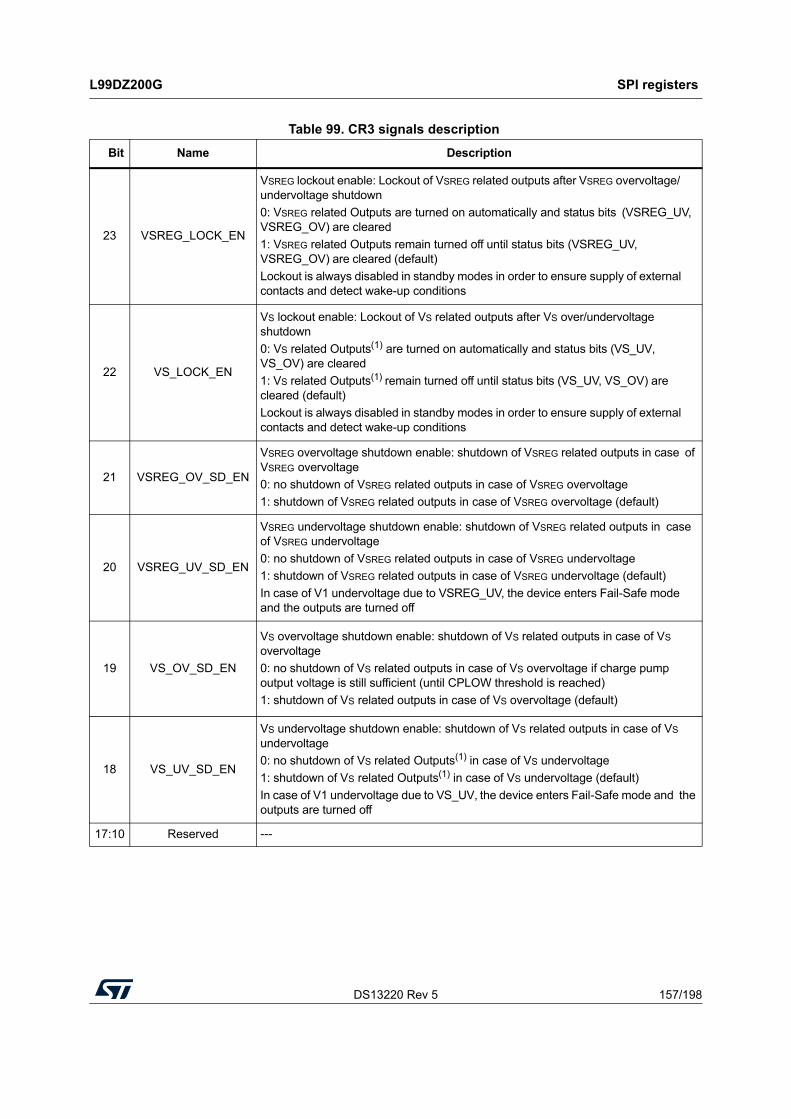
DS13220 Rev 5 157/198
L99DZ200G SPI registers
197
Table 99. CR3 signals description
Bit Name Description
23 VSREG_LOCK_EN
VSREG lockout enable: Lockout of VSREG related outputs after VSREG overvoltage/ undervoltage shutdown
0: VSREG related Outputs are turned on automatically and status bits (VSREG_UV, VSREG_OV) are cleared
1: VSREG related Outputs remain turned off until status bits (VSREG_UV, VSREG_OV) are cleared (default)
Lockout is always disabled in standby modes in order to ensure supply of external contacts and detect wake-up conditions
22 VS_LOCK_EN
VS lockout enable: Lockout of VS related outputs after VS over/undervoltage shutdown
0: VS related Outputs(1) are turned on automatically and status bits (VS_UV, VS_OV) are cleared
1: VS related Outputs(1) remain turned off until status bits (VS_UV, VS_OV) are cleared (default)
Lockout is always disabled in standby modes in order to ensure supply of external contacts and detect wake-up conditions
21 VSREG_OV_SD_EN
VSREG overvoltage shutdown enable: shutdown of VSREG related outputs in case of VSREG overvoltage
0: no shutdown of VSREG related outputs in case of VSREG overvoltage
1: shutdown of VSREG related outputs in case of VSREG overvoltage (default)
20 VSREG_UV_SD_EN
VSREG undervoltage shutdown enable: shutdown of VSREG related outputs in case of VSREG undervoltage
0: no shutdown of VSREG related outputs in case of VSREG undervoltage
1: shutdown of VSREG related outputs in case of VSREG undervoltage (default)
In case of V1 undervoltage due to VSREG_UV, the device enters Fail-Safe mode and the outputs are turned off
19 VS_OV_SD_EN
VS overvoltage shutdown enable: shutdown of VS related outputs in case of VS
overvoltage
0: no shutdown of VS related outputs in case of VS overvoltage if charge pump output voltage is still sufficient (until CPLOW threshold is reached)
1: shutdown of VS related outputs in case of VS overvoltage (default)
18 VS_UV_SD_EN
VS undervoltage shutdown enable: shutdown of VS related outputs in case of VS
undervoltage
0: no shutdown of VS related Outputs(1) in case of VS undervoltage
1: shutdown of VS related Outputs(1) in case of VS undervoltage (default)
In case of V1 undervoltage due to VS_UV, the device enters Fail-Safe mode and the outputs are turned off
17:10 Reserved ---

SPI registers L99DZ200G
158/198 DS13220 Rev 5
7.4.4 Control Register CR4 (0x04)
9 VSREG_EW_TH_9
VSREG early warning threshold.
At VSREG < VSREG_EW_TH, an interrupt is generated at NINT and status bit VSREG_EW in SR2 is set (in Active mode)
0000000000: 0 V (default) feature deactivated
...
1111111111: VAINVS
8 VSREG_EW_TH_8
7 VSREG_EW_TH_7
6 VSREG_EW_TH_6
5 VSREG_EW_TH_5
4 VSREG_EW_TH_4
3 VSREG_EW_TH_3
2 VSREG_EW_TH_2
1 VSREG_EW_TH_1
0 VSREG_EW_TH_0
1. "Vs related outputs" are OUT1 to OUT14 and H-bridge drivers (both A and B)
Table 99. CR3 signals description (continued)
Bit Name Description
Figure 66. Control Register CR4
23 22 21 20 19 18 17 16 15 14 13 12 11 10 9 8 7 6 5 4 3 2 1 0
Bit name
Res
erve
d
OU
T1_
HS
OU
T1
_LS
Res
erve
d
OU
T2_
HS
OU
T2
_LS
Res
erve
d
OU
T3_
HS
OU
T3
_LS
Res
erve
d
OU
T6_
HS
OU
T6
_LS
Reset 0 0 0 0 0 0 0 0 0 0 0 0 0 0 0 0 0 0 0 0 0 0 0 0
Access R/W
Table 100. CR4 signals description
Bit Name Description
23:22 Reserved Reserved
21 OUT1_HS
OUT1 High-Side Driver control
0: OUT1_HS is turned off (default)
1: OUT1_HS is turned on
An internal cross-current protection prevents, that both the low- and high-side drivers of the half-bridge OUT1 are switched on simultaneously.
20 OUT1_LS
OUT1 Low-Side Driver control
0: OUT1_LS is turned off (default)
1: OUT1_LS is turned on
An internal cross-current protection prevents, that both the low- and high-side drivers of the half-bridge OUT1 are switched on simultaneously.
19:18 Reserved Reserved

DS13220 Rev 5 159/198
L99DZ200G SPI registers
197
7.4.5 Control Register CR5 (0x05)
17 OUT2_HS
OUT2 High-Side Driver control
0: OUT2_HS is turned off (default)
1: OUT2_HS is turned on
An internal cross-current protection prevents, that both the low- and high-side drivers of the half-bridge OUT2 are switched on simultaneously.
16 OUT2_LS
OUT2 Low-Side Driver control
0: OUT2_LS is turned off (default)
1: OUT2_LS is turned on
An internal cross-current protection prevents, that both the low- and high-side drivers of the half-bridge OUT2 are switched on simultaneously.
15:14 Reserved Reserved
13 OUT3_HS
OUT3 High-Side Driver control
0: OUT3_HS is turned off (default)
1: OUT3_HS is turned on
An internal cross-current protection prevents, that both the low- and high-side drivers of the half-bridge OUT3 are switched on simultaneously.
12 OUT3_LS
OUT3 Low-Side Driver control
0: OUT3_LS is turned off (default)
1: OUT3_LS is turned on
An internal cross-current protection prevents, that both the low- and high-side drivers of the half-bridge OUT3 are switched on simultaneously.
11:2 Reserved --
1 OUT6_HS
OUT6 High-side Driver control
0: OUT6_HS is turned off (default)
1: OUT6_HS is turned on
An internal cross-current protection prevents, that both the low-side and high-side drivers of the half-bridge OUT6 are switched on simultaneously.
0 OUT6_LS
OUT6 Low-side Driver control
0: OUT6_LS is turned off (default)
1: OUT6_LS is turned on
An internal cross-current protection prevents, that both the low-side and high-side drivers of the half-bridge OUT6 are switched on simultaneously.
Table 100. CR4 signals description (continued)
Bit Name Description
Figure 67. Control Register CR5
23 22 21 20 19 18 17 16 15 14 13 12 11 10 9 8 7 6 5 4 3 2 1 0
Bit name
OU
T7_
3
OU
T7_
2
OU
T7_
1
OU
T7_
0
OU
T8_
3
OU
T8_
2
OU
T8_
1
OU
T8_
0
Res
erv
ed
OU
T10
_3
OU
T10
_2
OU
T10
_1
OU
T10
_0
Res
erv
ed
GH
Res
erv
ed
Reset 0 0 0 0 0 0 0 0 0 0 0 0 0 0 0 0 0 0 0 0 0 0 0 0
Access R/W

SPI registers L99DZ200G
160/198 DS13220 Rev 5
Table 101. CR5 signals description
Bit Name Description
23 OUT7_3
OUT7 Configuration Bits: High-Side Driver OUT7 Configuration
For OUT7 bits configuration see Table 102: OUTx Configuration bits
22 OUT7_2
21 OUT7_1
20 OUT7_0
19 OUT8_3
OUT8 Configuration Bits: High-Side Driver OUT8 Configuration
For OUT8 bits configuration see Table 102: OUTx Configuration bits
18 OUT8_2
17 OUT8_1
16 OUT8_0
15:12 Reserved —
11 OUT10_3
OUT10 Configuration Bits: High-Side Driver OUT10 Configuration
For OUT10 bits configuration see Table 102: OUTx Configuration bits
10 OUT10_2
9 OUT10_1
8 OUT10_0
7:5 Reserved —
4 GH
Gate Heater Control: Control of gate driver for external heater MOSFET
0: GH_heater is turned off (default)
1: GH_heater is turned on
3:0 Reserved —
Table 102. OUTx Configuration bits
OUTx_3 OUTx_2 OUTx_1 OUTx_0 Description
0 0 0 0 Off (default)
0 0 0 1 On
0 0 1 0 Timer1
0 0 1 1 Timer2
0 1 0 0 PWM1
0 1 0 1 PWM2
0 1 1 0 PWM3
0 1 1 1 PWM4
1 0 0 0 PWM5
1 0 0 1 PWM6
1 0 1 0 PWM7
1 0 1 1 Not Applicable

DS13220 Rev 5 161/198
L99DZ200G SPI registers
197
7.4.6 Control Register CR6 (0x06)
1 1 0 0 Not Applicable
1 1 0 1 Not Applicable
1 1 1 0 DIR
1 1 1 1 Not Applicable
Table 102. OUTx Configuration bits (continued)
OUTx_3 OUTx_2 OUTx_1 OUTx_0 Description
Figure 68. Control Register CR6
23 22 21 20 19 18 17 16 15 14 13 12 11 10 9 8 7 6 5 4 3 2 1 0
Bit name
OU
T9_
3
OU
T9_
2
OU
T9_
1
OU
T9_
0
OU
T1
3_3
OU
T1
3_2
OU
T1
3_1
OU
T1
3_0
OU
T1
4_3
OU
T1
4_2
OU
T1
4_1
OU
T1
4_0
OU
T1
5_3
OU
T1
5_2
OU
T1
5_1
OU
T1
5_0
Res
erve
d
Reset 0 0 0 0 0 0 0 0 0 0 0 0 0 0 0 0 0 0 0 0 0 0 0 0
Access R/W
Table 103. CR6 signals description
Bit Name Description
23 OUT9_3
OUT9 Configuration Bits: High-Side Driver OUT9 Configuration
For OUT9 bits configuration see Table 102: OUTx Configuration bits
22 OUT9_2
21 OUT9_1
20 OUT9_0
19 OUT13_3
OUT13 Configuration Bits: High-Side Driver OUT13 Configuration
For OUT13 bits configuration see Table 102: OUTx Configuration bits
18 OUT13_2
17 OUT13_1
16 OUT13_0
15 OUT14_3
OUT14 Configuration Bits: High-Side Driver OUT14 Configuration
For OUT14 bits configuration see Table 102: OUTx Configuration bits
14 OUT14_2
13 OUT14_1
12 OUT14_0
11 OUT15_3
OUT15 Configuration Bits: High-side Driver OUT15 Configuration
For OUT15 bits configuration see Table 102: OUTx Configuration bits
10 OUT15_2
9 OUT15_1
8 OUT15_0
7:0 Reserved —

SPI registers L99DZ200G
162/198 DS13220 Rev 5
7.4.7 Control Register CR7 (0x07)
Figure 69. Control Register CR7
23 22 21 20 19 18 17 1615
14
13 12 1110
9 8 7 6 5 4 3 2 1 0
Bit name
OU
T1_
OC
R
OU
T2_
OC
R
OU
T3_
OC
R
OU
T6_
OC
R
OU
T7_
OC
R
OU
T8_
OC
R
OU
T15
_OC
R
Res
erve
d
OU
T1_
SH
OR
T_D
IS
OU
T2_
SH
OR
T_D
IS
OU
T3_
SH
OR
T_D
IS
OU
T6_
SH
OR
T_D
IS
Res
erve
d
CM
_DIR
_CO
NF
_1
CM
_DIR
_CO
NF
_0
CM
_S
EL
_3
CM
_S
EL
_2
CM
_S
EL
_1
CM
_S
EL
_0
Reset 0 0 0 0 0 0 0 0 0 0 0 0 0 0 0 0 0 0 0 0 0 0 0 0
Access R/W
Table 104. CR7 signals description
Bit Name Description
23 OUT1_OCR
Overcurrent recovery for OUTx
0: overcurrent recovery is turned off (default)
1: overcurrent recovery is turned on
22 OUT2_OCR
21 OUT3_OCR
20 OUT6_OCR
19 OUT7_OCR
18 OUT8_OCR
17 OUT15_OCR
16:13 Reserved —
12 OUT1_SHORT_DISOUTx short circuit threshold disable
0: short circuit threshold is enabled (default)
1: short circuit threshold is disabled
11 OUT2_SHORT_DIS
10 OUT3_SHORT_DIS
9 OUT6_SHORT_DIS
8:6 Reserved —
5 CM_DIR_CONF_1 Current Monitor output or DIR input choice.
CM_DIR_CONF_1 CM_DIR_CONF_0
00: CM all the time (default)
01: DIR when in Standby mode and CM when in Active mode
10: DIR all the time
4 CM_DIR_CONF_0

DS13220 Rev 5 163/198
L99DZ200G SPI registers
197
7.4.8 Control Register CR8 (0x08)
3 CM_SEL_3Current Monitor Select Bits.
A current image of the selected binary coded output is multiplexed to the CM output. If a corresponding output does not exist, the current monitor is deactivated.
CM_SEL_3 CM_SEL_2 CM_SEL_1 CM_SEL_0
0000: OUT1
0001: OUT2
0010: OUT3
0011: NOT AVAILABLE
0100: NOT AVAILABLE
0101: OUT6
0110: OUT7
0111: OUT8
1000: OUT9
1001: OUT10
1010: NOT AVAILABLE
1011: NOT AVAILABLE
1100: OUT13
1101: OUT14
1110: OUT15
1111: NOT AVAILABLE
2 CM_SEL_2
1 CM_SEL_1
0 CM_SEL_0
Table 104. CR7 signals description (continued)
Bit Name Description
Figure 70. Control Register CR8
23 22 21 20 19 18 17 16 1514
13 12 11 10 9 8 7 6 5 4 3 2 1 0
Bit name
OU
T1_
OC
R_T
HX
_E
N
OU
T2_
OC
R_T
HX
_E
N
OU
T3_
OC
R_T
HX
_E
N
OU
T6_
OC
R_T
HX
_E
N
OU
T7_
OC
R_T
HX
_E
N
OU
T8_
OC
R_T
HX
_E
N
OU
T15
_OC
R_T
HX
_EN
Res
erve
d
OU
T7_
OC
R_T
ON
_1
OU
T7
_OC
R_
TO
N _
0
OU
T8_
OC
R_T
ON
_1
OU
T8
_OC
R_
TO
N _
0
OU
T15
_O
CR
_TO
N_
1
OU
T15
_OC
R_T
ON
_0
OU
TH
B_
OC
R_
TO
N_1
OU
TH
B_O
CR
_ T
ON
_0
OU
T7
_OC
R_F
RE
Q_1
OU
T7
_OC
R_
FR
EQ
_0
OU
T8
_OC
R_F
RE
Q_1
OU
T8
_OC
R_
FR
EQ
_0
OU
T15
_OC
R_
FR
EQ
_1
OU
T15
_O
CR
_ F
RE
Q_0
OU
TH
B_O
CR
_FR
EQ
_1
OU
TH
B_O
CR
_ F
RE
Q_
0
Reset 1 1 1 1 1 1 1 0 0 1 0 1 0 1 0 1 0 0 0 0 0 0 0 0
Access R/W

SPI registers L99DZ200G
164/198 DS13220 Rev 5
Table 105. CR8 signals description
Bit Name Description
23 OUT1_OCR_THX_EN
Enable Overcurrent Recovery with Thermal Expiration for OUTx.
0: Overcurrent Recovery with Thermal Expiration is off
1: Overcurrent Recovery with Thermal Expiration is on (default). The output is turned off after Thermal Expiration.
22 OUT2_OCR_THX_EN
21 OUT3_OCR_THX_EN
20 OUT6_OCR_THX_EN
19 OUT7_OCR_THX_EN
18 OUT8_OCR_THX_EN
17 OUT15_OCR_THX_EN
16 Reserved —
15 OUT7_OCR_TON_1 Auto-recovery programmable ON time for OUT7
OUT7_OCR_TON_1 OUT7_OCR_TON_0
00: 88 µs
01:80 µs (default)
10: 72 µs
11: 64 µs
14 OUT7_OCR_ TON _0
13 OUT8_OCR_ TON _1 Auto-recovery programmable ON time for OUT8
OUT8_OCR_TON_1 OUT8_OCR_TON_0
00: 88 µs
01: 80 µs (default)
10: 72 µs
11: 64 µs
12 OUT8_OCR_ TON _0
11 OUT15_OCR_TON _1 Auto-recovery programmable ON time for OUT15
OUT15_OCR_ TON _1 OUT15_OCR_ TON _0
00: 88 µs
01: 80 µs (default)
10: 72 µs
11: 64 µs
10 OUT15_OCR_TON _0
9 OUTHB_OCR_ TON _1 Auto-recovery programmable ON time for HB (OUT1, OUT2, OUT3, OUT6)
OUTHB_OCR_ TON _1 OUTHB_OCR_TON_0
00: 88 µs
01: 80 µs (default)
10: 72 µs
11: 64 µs
8 OUTHB_OCR_TON_0

DS13220 Rev 5 165/198
L99DZ200G SPI registers
197
7 OUT7_OCR_FREQ_1 Auto-recovery programmable frequency for OUT7
OUT7_OCR_FREQ_1 OUT7_OCR_FREQ_0
00: 1.7 kHz (default)
01: 2.2 kHz
10: 3.0 kHz
11: 4.4 kHz
6 OUT7_OCR_FREQ_0
5 OUT8_OCR_FREQ_1 Auto-recovery programmable frequency for OUT8
OUT8_OCR_FREQ_1 OUT8_OCR_FREQ_0
00: 1.7 kHz (default)
01: 2.2 kHz
10: 3.0 kHz
11: 4.4 kHz
4 OUT8_OCR_FREQ_0
3 OUT15_OCR_FREQ_1
Auto-recovery programmable frequency for OUT15
OUT15_OCR_FREQ_1 OUT15_OCR_FREQ_0
00: 1.7 kHz (default)
01: 2.2 kHz
10: 3.0 kHz
11: 4.4 kHz2 OUT15_OCR_FREQ_0
1 OUTHB_OCR_ FREQ_1(1) Auto-recovery programmable frequency for OUTHB (OUT1, OUT2, OUT3, OUT6)
OUTHB_OCR_FREQ_1 OUTHB_OCR_FREQ_0
00: 1.7 kHz (default)
01: 2.2 kHz
10: 3.0 kHz
11: 4.4 kHz
0 OUTHB_OCR_ FREQ_0(1)
1. For OUT1 and OUT6, in case the Short Circuit detection is disabled and the OCR is enabled, the OCR configurations with frequency 3.0 kHz and 4.4kHz (whatever is the configured Ton value) are NOT allowed.
Table 105. CR8 signals description (continued)
Bit Name Description

SPI registers L99DZ200G
166/198 DS13220 Rev 5
7.4.9 Control Register CR9 (0x09)
Figure 71. Control Register CR9
23 22 21 20 19 18 17 16 1514
13 1211
10 9 8 7 6 5 4 3 2 1 0
Bit name
OU
T8_
RD
SO
N
OU
T7_
RD
SO
N
OU
T1
_6_R
DS
ON
OU
T9_
CC
M_E
N
OU
T8_
CC
M_E
N
OU
T7_
CC
M_E
N
Res
erve
d
OU
T15
_OL
OU
T14
_OL
OU
T13
_OL
Res
erve
d
OU
T10
_OL
OU
T9_
OL
Res
erve
d
OU
T15
_OC
OU
T14
_OC
OU
T13
_OC
Res
erve
d
OU
T10
_OC
OU
T9_
OC
Reset 0 0 0 0 0 0 0 0 0 0 0 0 0 0 0 0 0 0 0 0 0 0 0 0
Access R/W
Table 106. CR9 signals description
Bit Name Description
23 OUT8_RDSON
Select Rdson for OUT8
0: ron_low (default)
1: ron_high
22 OUT7_RDSON
Select Rdson for OUT7
0: ron_low (default)
1: ron_high
21 OUT1_6_RDSON
Select Rdson for both OUT6 and OUT1
0: ron_low (default)
1: ron_high
20 OUT9_CCM_EN
Enable Constant Current Mode for OUT9
0: Disable (default)
1: Enable
19 OUT8_CCM_EN
Enable Constant Current Mode for OUT8
0: Disable (default)
1: Enable
18 OUT7_CCM_EN
Enable Constant Current Mode for OUT7
0: Disable (default)
1: Enable
17:15 Reserved —

DS13220 Rev 5 167/198
L99DZ200G SPI registers
197
7.4.10 Control Register CR10 (0x0A)
14 OUT15_OL
Open-load Threshold for OUTx
0: IOLD1; high-current mode (default)
1: IOLD1; low-current mode
13 OUT14_OL
12 OUT13_OL
11:10 Reserved
9 OUT10_OL
8 OUT9_OL
7 Reserved —
6 OUT15_OC
Overcurrent Threshold for OUTx
0: IOC; high-current mode (default)
1: IOC; low-current mode
5 OUT14_OC
4 OUT13_OC
3:2 Reserved
1 OUT10_OC
0 OUT9_OC
Table 106. CR9 signals description (continued)
Bit Name Description
Figure 72. Control Register CR10
23 22 21 20 19 18 17 16 15 14 13 12 11 10 9 8 7 6 5 4 3 2 1 0
Bit name
DIA
G_2
_A
DIA
G_1
_A
DIA
G_0
_A
DIR
HA
SD
2B
SD
S2B
SD
1B
SD
S1B
SD
2A
SD
S2A
SD
1A
SD
S1A
CO
PT
_3_
A
CO
PT
_2_
A
CO
PT
_1_
A
CO
PT
_0_
AH
_O
LTH
_HIG
H_
OL_
H1L
2_A
OL_
H2L
1_A
SL
EW
_4_A
SL
EW
_3_A
SL
EW
_2_A
SL
EW
_1_A
SL
EW
_0_A
Reset 1 1 1 0 0 0 0 0 0 0 0 0 1 1 1 1 0 0 0 0 0 0 0 0
Access R/W
Table 107. CR10 signals description
Bit Name Description
23 DIAG_2_ADrain-source monitoring threshold for external H-bridge A
DIAG_2_A DIAG_1_A DIAG_0_A

SPI registers L99DZ200G
168/198 DS13220 Rev 5
22 DIAG_1_A 000: VSCd1_HB
001: VSCd2_HB
010: VSCd3_HB
011: VSCd4_HB
100: VSCd5_HB
101: VSCd6_HB
110: VSCd7_HB
111: VSCd7_HB (default)
21 DIAG_0_A
20 DIRHA
Direction of the H-Bridge A
0: HS2a and LS1a are ON; HS1a and LS2a are OFF (default)
1: HS1a and LS2a are ON; HS2a and LS1a are OFF
19 SD2B Slow decay for leg 2 of the H-bridge B
18 SDS2B Slow decay Single for leg 2 of the H-bridge B
17 SD1B Slow decay for leg 1 of the H-bridge B
16 SDS1B Slow decay Single for leg 1 of the H-bridge B
15 SD2A Slow decay for leg 2 of the H-bridge A
14 SDS2A Slow decay Single for leg 2 of the H-bridge A
13 SD1A Slow decay for leg 1 of the H-bridge A
12 SDS1A Slow decay Single for leg 1 of the H-bridge A
11 COPT_3_A Cross current protection time (H-Bridge A)
COPT_3_A COPT_2_A COPT_1_A COPT_0_A
0000: tccp0000
0001: tccp0001
0010: tccp0010
0011: tccp0011
0100: tccp0100
0101: tccp0101
0110: tccp0110
0111: tccp0111
1000: tccp1000
1001: tccp1001
1010: tccp1010
1011: tccp1011
1100: tccp1100
1101: tccp1101
1110: tccp1110
1111: tccp1111 (default)
10 COPT_2_A
9 COPT_1_A
8 COPT_0_A
7 H_OLTH_HIGH_A H-bridge A OL high threshold (5/6 * VS) select
6 OL_H1L2_A Test open-load condition between H1 and L2 of the H-Bridge A
5 OL_H2L1_A Test open-load condition between H2 and L1 for H-bridge A
Table 107. CR10 signals description (continued)
Bit Name Description

DS13220 Rev 5 169/198
L99DZ200G SPI registers
197
7.4.11 Control Register CR11 (0x0B)
4 SLEW_4_ABinary coded slew rate of H-bridge A
SLEW_4_A SLEW_3_A SLEW_2_A SLEW_1_A SLEW_0_A
(bit0 = LSB; bit4 = MSB)
00000: Control disabled (default)
11111: IGHxmax
3 SLEW_3_A
2 SLEW_2_A
1 SLEW_1_A
0 SLEW_0_A
Table 107. CR10 signals description (continued)
Bit Name Description
Figure 73. Control Register CR11
23 22 2120
19 18 17 16 1514
13 12 11 10 9 8 7 6 5 4 3 2 1 0
Bit name Reserved
GH
_OL_
EN
GH
_T
H_
2
GH
_T
H_
1
GH
_T
H_
0
EC
V_L
S
EC
V_O
CR
Reserved
EC
ON
Re
serv
ed
EC
_5
EC
_4
EC
_3
EC
_2
EC
_1
EC
_0
Reset 0 0 0 0 0 0 0 1 1 1 0 0 0 0 0 0 0 0 0 0 0 0 0 0
Access R/W
Table 108. CR11 signals description
Bit Name Description
23:18 Reserved —
17 GH_OL_EN
Control open-load diagnosis for Gate Heater output
0: open-load diagnosis off (default)
1: open-load diagnosis on
16 GH_TH_2 Drain source monitoring threshold voltage for external heater MOSFET
GH_TH_2 GH_TH_1 GH_TH_0
000: VSCd1_HE
001: VSCd2_HE
010: VSCd3_HE
011: VSCd4_HE
100: VSCd5_HE
101: VSCd6_HE
110: VSCd7_HE
111: VSCd8_HE (default)
15 GH_TH_1
14 GH_TH_0
13 ECV_LS
Control of ECV low-side switch
0: ECV low-side switch off (default)
1: ECV low-side switch on

SPI registers L99DZ200G
170/198 DS13220 Rev 5
7.4.12 Control Register CR12 (0x0C)
12 ECV_OCR
Overcurrent recovery for output ECV
0: overcurrent recovery is turned off (default)
1: overcurrent recovery is turned on
11:9 Reserved —
8 ECON
Electro-chrome Control
The electro-chrome control enables the driver at pin ECDR and switches OUT10 directly on ignoring the control bits OUT10_x in CR5
0: Electro-chrome control off (default)
1: Electro-chrome control on
7:6 Reserved —
5 EC_5EC Reference Voltage Bits
The reference voltage for the electro-chrome voltage controller at pin ECV is binary coded.
(bit0 = LSB; bit5 = MSB) 00 0000: VECV = 0 V
xx xxxx: VECV = VCTRLmax/63 x register value
11 1111: VECV = VCTRLmax
For ECV_HV (Configuration Register) = 0, the maximum EC control voltage is clamped at lower value (see Section 3.4.20: Electro-chrome mirror driver )
EC_x bits are set to 0 after wake-up from VBAT_Standby mode
4 EC_4
3 EC_3
2 EC_2
1 EC_1
0 EC_0
Table 108. CR11 signals description (continued)
Bit Name Description
Figure 74. Control Register CR12
23 22 21 20 19 18 17 16 15 14 13 12 11 10 9 8 7 6 5 4 3 2 1 0
Bit name
PM
W1_
FR
EQ
_1
PM
W1_
FR
EQ
_0
PM
W2_
FR
EQ
_1
PM
W2_
FR
EQ
_0
PM
W3_
FR
EQ
_1
PM
W3_
FR
EQ
_0
PM
W4_
FR
EQ
_1
PM
W4_
FR
EQ
_0
PM
W5_
FR
EQ
_1
PM
W5_
FR
EQ
_0
PM
W6_
FR
EQ
_1
PM
W6_
FR
EQ
_0
PM
W7_
FR
EQ
_1
PM
W7_
FR
EQ
_0
Res
erv
ed
Reset 0 0 0 0 0 0 0 0 0 0 0 0 0 0 0 0 0 0 0 0 0 0 0 0
Access R/W
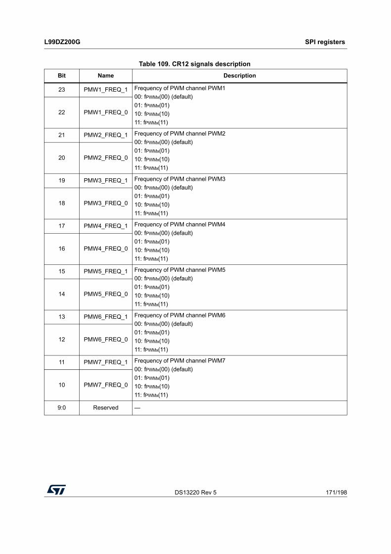
DS13220 Rev 5 171/198
L99DZ200G SPI registers
197
Table 109. CR12 signals description
Bit Name Description
23 PMW1_FREQ_1 Frequency of PWM channel PWM1
00: fPWMx(00) (default)
01: fPWMx(01)
10: fPWMx(10)
11: fPWMx(11)
22 PMW1_FREQ_0
21 PMW2_FREQ_1 Frequency of PWM channel PWM2
00: fPWMx(00) (default)
01: fPWMx(01)
10: fPWMx(10)
11: fPWMx(11)
20 PMW2_FREQ_0
19 PMW3_FREQ_1 Frequency of PWM channel PWM3
00: fPWMx(00) (default)
01: fPWMx(01)
10: fPWMx(10)
11: fPWMx(11)
18 PMW3_FREQ_0
17 PMW4_FREQ_1 Frequency of PWM channel PWM4
00: fPWMx(00) (default)
01: fPWMx(01)
10: fPWMx(10)
11: fPWMx(11)
16 PMW4_FREQ_0
15 PMW5_FREQ_1 Frequency of PWM channel PWM5
00: fPWMx(00) (default)
01: fPWMx(01)
10: fPWMx(10)
11: fPWMx(11)
14 PMW5_FREQ_0
13 PMW6_FREQ_1 Frequency of PWM channel PWM6
00: fPWMx(00) (default)
01: fPWMx(01)
10: fPWMx(10)
11: fPWMx(11)
12 PMW6_FREQ_0
11 PMW7_FREQ_1 Frequency of PWM channel PWM7
00: fPWMx(00) (default)
01: fPWMx(01)
10: fPWMx(10)
11: fPWMx(11)
10 PMW7_FREQ_0
9:0 Reserved —

SPI registers L99DZ200G
172/198 DS13220 Rev 5
7.4.13 Control Register CR13 (0x0D) to CR16 (0x10)
where: x = 1 + (z * 2), z = 0 to 3y = 2 + (z * 2), z = 0 to 2
Figure 75. Control Register CR13 to CR16
23 22 21 20 19 18 17 16 15 14 13 12 11 10 9 8 7 6 5 4 3 2 1 0
Bit name
Res
erve
d
PW
Mx_
DC
_9
PW
Mx_
DC
_8
PW
Mx_
DC
_7
PW
Mx_
DC
_6
PW
Mx_
DC
_5
PW
Mx_
DC
_4
PW
Mx_
DC
_3
PW
Mx_
DC
_2
PW
Mx_
DC
_1
PW
Mx_
DC
_0
Res
erve
d
PW
My_
DC
_9
PW
My_
DC
_8
PW
My_
DC
_7
PW
My_
DC
_6
PW
My_
DC
_5
PW
My_
DC
_4
PW
My_
DC
_3
PW
My_
DC
_2
PW
My_
DC
_1
PW
My_
DC
_0
Reset 0 0 0 0 0 0 0 0 0 0 0 0 0 0 0 0 0 0 0 0 0 0 0 0
Access R/W
Table 110. CR13 to CR16 signals description
Bit Name Description
23:22 Reserved —
21 PWMx_DC_9
Binary coded on-duty cycle of PWM channel PWMx (bit12 = LSB; bit21 = MSB)
00 0000 0000: duty cycle 0% (default)
xx xxxx xxxx: duty cycle 100%/1024 x register value 11 1111 1111. duty cycle 99,9% (1)
20 PWMx_DC_8
19 PWMx_DC_7
18 PWMx_DC_6
17 PWMx_DC_5
16 PWMx_DC_4
15 PWMx_DC_3
14 PWMx_DC_2
13 PWMx_DC_1
12 PWMx_DC_0
11:10 Reserved —
9 PWMy_DC_9
Binary coded on-duty cycle of PWM channel PWMy (bit0 = LSB; bit9 = MSB)
00 0000 0000: duty cycle 0% (default)
xx xxxx xxxx: duty cycle 100%/ 1024 x register value 11 1111 1111. Duty cycle 99,9%(1)
Binary coded on-duty cycle of PWM channel PWMy
8 PWMy_DC_8
7 PWMy_DC_7
6 PWMy_DC_6
5 PWMy_DC_5
4 PWMy_DC_4
3 PWMy_DC_3
2 PWMy_DC_2
1 PWMy_DC_1
0 PWMy_DC_0
1. To have Duty Cycle equal to 100% for the Output X (where X = 7, 8, 9, 10, 13, 14, 15), the related Output Configuration shall be set in ON mode (OUTX_3-2-1-0 = 0001; see Table 102: OUTx Configuration bits).

DS13220 Rev 5 173/198
L99DZ200G SPI registers
197
7.4.14 Control Register CR17 (0x11) to CR20 (0x14)
where: x = 7 + (z * 2), z = 0, 1, 3, 4
y = 8 + (z * 2), z = 0, 1, 3
Figure 76. Control Registers CR17-CR20
23 22 21 20 19 18 17 16 15 14 13 12 11 10 9 8 7 6 5 4 3 2 1 0
Bit name
Res
erve
d
OU
Tx_
AU
TO
CO
MP
_EN
OU
Tx_
VLE
D_
9
OU
Tx_
VLE
D_
8
OU
Tx_
VLE
D_
7
OU
Tx_
VLE
D_
6
OU
Tx_
VLE
D_5
OU
Tx_
VLE
D_
4
OU
Tx_
VLE
D_
3
OU
Tx_
VLE
D_
2
OU
Tx_
VLE
D_
1
OU
Tx_
VLE
D_
0
Res
erve
d
OU
Ty_
AU
TO
CO
MP
_EN
OU
Ty_V
LED
_9
OU
Ty_V
LED
_8
OU
Ty_V
LED
_7
OU
Ty_V
LED
_6
OU
Ty_V
LED
_5
OU
Ty_V
LED
_4
OU
Ty_V
LED
_3
OU
Ty_V
LED
_2
OU
Ty_V
LED
_1
OU
Ty_V
LED
_0
Reset 0 0 0 0 0 0 0 0 0 0 0 0 0 0 0 0 0 0 0 0 0 0 0 0
Access R/W
Table 111. CR17 to CR20 signals description
Bit Name Description
23 Reserved —
22 OUTx_AUTOCOMP_EN Setting this bit to ‘1’ enables the automatic VS compensation for OUTx
21 OUTx_VLED_9
Binary coded nominal LED voltage of OUTx (bit12 = LSB; bit21 = MSB)
00 0000 0000: VLED = 0 V (default)
xx xxxx xxxx: VLED = VAINVS /1024 x register value
01 1101 0000: VLED = VAINVS
VLED is clamped at 10 V (0x1D0h)
20 OUTx_VLED_8
19 OUTx_VLED_7
18 OUTx_VLED_6
17 OUTx_VLED_5
16 OUTx_VLED_4
15 OUTx_VLED_3
14 OUTx_VLED_2
13 OUTx_VLED_1
12 OUTx_VLED_0
11 Reserved —
10 OUTy_AUTOCOMP_EN Setting this bit to ‘1’ enables the automatic VS compensation for OUTy

SPI registers L99DZ200G
174/198 DS13220 Rev 5
7.4.15 Control Register CR21 (0x15)
9 OUTy_VLED_9
Binary coded nominal LED voltage of OUTy (bit0 = LSB; bit9 = MSB)
00 0000 0000: VLED = 0 V (default)
xx xxxx xxxx: VLED = VAINVS /1024 x register value
01 1101 0000: VLED = VAINVS
VLED is clamped at 10 V (0x1D0h)
8 OUTy_VLED_8
7 OUTy_VLED_7
6 OUTy_VLED_6
5 OUTy_VLED_5
4 OUTy_VLED_4
3 OUTy_VLED_3
2 OUTy_VLED_21 OUTy_VLED_1
0 OUTy_VLED_0
Table 111. CR17 to CR20 signals description (continued)
Bit Name Description
Figure 77. Control Register CR21
23 22 21 20 19 18 17 16 15 14 1312
11 10 9 8 7 6 5 4 3 2 1 0
Bit name
DIA
G_2
_B
DIA
G_1
_B
DIA
G_0
_B
DIR
HB
Re
serv
ed
CO
PT
_3_B
CO
PT
_2_B
CO
PT
_1_B
CO
PT
_0_B
H_
OLT
H_H
IGH
_B
OL_
H1L
2_B
OL_
H2L
1_B
SLE
W_4
_B
SLE
W_3
_B
SLE
W_2
_B
SLE
W_1
_B
SLE
W_0
_B
Reset 1 1 1 0 0 0 0 0 0 0 0 0 1 1 1 1 0 0 0 0 0 0 0 0
Access R/W

DS13220 Rev 5 175/198
L99DZ200G SPI registers
197
Table 112. CR21 signals description
Bit Name Description
23 DIAG_2_B Drain-source monitoring threshold for external H-bridge B
DIAG_2_B DIAG_1_B DIAG_0_B
22 DIAG_1_B 000: VSCd1_HB
001: VSCd2_HB
010: VSCd3_HB
011: VSCd4_HB
100: VSCd5_HB
101: VSCd6_HB
110: VSCd7_HB
111: VSCd7_HB (default)
21 DIAG_0_B
20 DIRHBDirection of the H-bridge B
0: HS2b and LS1b are ON; HS1b and LS2b are OFF (default)
1: HS1b and LS2b are ON; HS2b and LS1b are OFF
19:12 Reserved —
11 COPT_3_B Cross current protection time (H-bridge B)
COPT_3_B COPT_2_B COPT_1_B COPT_0_B
0000: tccp0000
0001: tccp0001
0010: tccp0010
0011: tccp0011
0100: tccp0100
0101: tccp0101
0110: tccp0110
0111: tccp0111
1000: tccp1000
1001: tccp1001
1010: tccp1010
1011: tccp1011
1100: tccp1100
1101: tccp1101
1110: tccp1110
1111: tccp1111 (default)
10 COPT_2_B
9 COPT_1_B
8 COPT_0_B
7 H_OLTH_HIGH_B H-bridge B OL high threshold (5/6 * VS) select
6 OL_H1L2_B Test open-load condition between H1 and L2 of the H-Bridge B
5 OL_H2L1_B Test open-load condition between H2 and L1 for H-bridge B

SPI registers L99DZ200G
176/198 DS13220 Rev 5
7.4.16 Control Register CR22 (0x16)
4 SLEW_4_BBinary coded slew rate of H-bridge B
SLEW_4_B SLEW_3_B SLEW_2_B SLEW_1_B SLEW_0_B (bit0 = LSB; bit4 = MSB) 00000: Control disabled (default) 11111: IGHxmax
3 SLEW_3_B
2 SLEW_2_B
1 SLEW_1_B
0 SLEW_0_B
Table 112. CR21 signals description (continued)
Bit Name Description
Figure 78. Control Register CR22
23 22 21 20 19 18 17 16 15 14 13 12 11 10 9 8 7 6 5 4 3 2 1 0
Bit name Reserved
GE
NE
RA
TO
R_
MO
DE
_EN
DE
BU
G_E
XIT
C
P_O
FF
IC
MP
WD
_EN
Reset 0 0 0 0 0 0 0 0 0 0 0 0 0 0 0 0 0 0 0 1 0 0 0 1
Access R/W
Table 113. CR22 signals description
Bit Name Description
23:5 Reserved —
4 GENERATOR_MODE_EN
Generator Mode control enable:
0: Generator Mode is disabled
1: Generator Mode is enabled (default)
3 DEBUG_EXIT
SW-Debug mode exit
0: stay in SW-Debug mode (default)
1: exit from SW Debug mode
When exiting from SW-Debug mode, the watchdog starts with a Long Open Window.
This bit has only effect in SW-Debug mode (no effect in Normal mode)
2 CP_OFF
Charge pump control
0: Enabled; charge pump on in active mode (default)
1: Disabled; charge pump off in active mode
setting CP_OFF = 1 is only possible when CP_OFF_EN = 1

DS13220 Rev 5 177/198
L99DZ200G SPI registers
197
7.4.17 Configuration Register (0x3F)
1 ICMP
V1 load current supervision
0: Enabled; Watchdog is disabled in V1 Standby when IV1 < ICMP (default)
1: Disabled; watchdog is disabled upon transition into V1_Standby mode setting ICMP = 1 is only possible when ICMP_CONFIG_EN = 1
0 WD_EN
Watchdog Enable
0: Watchdog disabled
1: Watchdog enabled (default)
Writing to this bit is only possible during CAN Flash mode (VTxDL > Vflash)
Table 113. CR22 signals description (continued)
Bit Name Description
Figure 79. Configuration Register
23 22 21 20 19 18 17 16 15 14 13 12 11 10 9 8 7 6 5 4 3 2 1 0
Bit name
WU
_CO
NF
IG
LIN
_WU
_CO
NF
IG
LIN
_HS
_E
N
TS
D_C
ON
FIG
EC
V_H
V
V2_
CO
NF
IG
ICM
P_C
ON
FIG
_E
N
WD
_CO
NF
IG_E
N
MA
SK
_OL_
HS
1
MA
SK
_OL_
LS1
MA
SK
_TW
MA
SK
_EC
_OL
MA
SK
_OL
MA
SK
_SP
IE
MA
SK
_PLE
MA
SK
_GW
CP
_OF
F_E
N
CP
_LO
W_
CO
NF
IG
CP
_DIT
H_D
IS
FS
_FO
RC
ED
Res
erve
d
DM
A
DM
B
TR
IG
Reset 1 0 0 0 0 0 0 0 0 0 0 0 0 0 0 0 0 0 0 0 0 0 0 0
Access R/W
Table 114. Configuration Register signals description
Bit Name Description
23 WU_CONFIG
Configuration of input pin WU Input configured as wake-up input
0: WU configured as wake-up input
1: WU configured for input voltage measurement (default)
22 LIN_WU_CONFIG
Configuration of LIN wake-up behavior
0: wake up at recessive - dominant - recessive with tdom > tdom_LIN (default) (according to LIN 2.2a and Hardware Requirements for Transceivers version 1.3)
1: wake up at recessive - dominant transition
21 LIN_HS_EN
Configuration of LIN transceiver bit rate
0: LIN transceiver in normal communication mode (20kbit/s) (default)
1: LIN transceiver in high speed mode for fast Flashing (115kbit/s)
20 TSD_CONFIG
Configuration of thermal shutdown behavior
0: in case of TSD1 all power stages are switched off (default)
1: selective shut down of power stage cluster

SPI registers L99DZ200G
178/198 DS13220 Rev 5
19 ECV_HV
Configuration of maximum voltage of electrochrome controller (see electrical parameter VCTRLmax)
0: maximum electrochrome controller voltage clamped to 1.2V (typ); (default)
1: maximum electrochrome controller voltage set to 1.5V (typ)
18 V2_CONFIG
Configuration of V2
0: V2 is Voltage Regulator (default)
1: V2 is Voltage Tracker of V1
17 ICMP_CONFIG_EN
ICMP configuration Enable
0: writing ICMP = 1 is blocked (writing ICMP=0 is possible); (default)
1: writing ICMP = 1 is possible with next SPI command
bit is automatically reset to 0 after next SPI command
16 WD_CONFIG_EN
Watchdog configuration Enable
0: writing to WD Configuration (CR2 [0:1] is blocked (default)
1: writing to WD Configuration Bits is possible with next SPI command bit is automatically reset to 0 after next SPI command
15 MASK_OL_HS1
Mask Open-load HS1
0: Open-load condition at HS1 is not masked (default)
1: Open-load condition at HS1 is masked
i.e. it is reported as a Functional Error (GSB bit 3) but not as a Global Error (GSB bit 7)
14 MASK_OL_LS1
Mask Open-load LS1
0: Open-load condition at LS1 is not masked (default)
1: Open-load condition at LS1 is masked
i.e. it is reported as a Functional Error (GSB bit 3) but not as a Global Error (GSB bit 7)
13 MASK_TW
Mask Thermal Warning
0: Thermal warning is not masked (default)
1: Thermal warning is masked
i.e. it is reported as a Global Warning (GSB bit 1) but not as a Global Error (GSB bit 7)
12 MASK_EC_OL
Mask Electro-chrome Open-load
0: Open-load condition at ECV and OUT10 is not masked (default)
1: Open-load condition at ECV and OUT10 is masked
i.e. it is reported as a Functional Error (GSB bit 3) but not as a Global Error (GSB bit 7)
11 MASK_OL
Mask open-load
0: Open-load condition at all outputs are not masked (default)
1: Open-load condition at all outputs are masked
i.e. it is reported as a Functional Error (GSB bit 3) but not as a Global Error (GSB bit 7)
10 MASK_SPIE
Mask SPI error
0: SPI errors are not masked (default)
1: SPI errors are masked
i.e. reported as an SPI Error (GSB bit 5) but not as a Global Error (GSB bit 7)
Table 114. Configuration Register signals description (continued)
Bit Name Description

DS13220 Rev 5 179/198
L99DZ200G SPI registers
197
9 MASK_PLE
Mask physical layer error
0: Physical Layer Errors are not masked (default)
1: Physical Layer Errors are masked
i.e. reported as a Physical Layer Error (GSB bit 4) but not as a Global Error (GSB bit 7)
8 MASK_GW
Mask global warning
0: Global Warning conditions are not masked (default)
1: Global Warning conditions are masked
i.e. reported as a Global Warning (GSB bit 1) but not as a Global Error (GSB bit 7)
7 CP_OFF_EN
Charge pump control enable
0: writing CP_OFF = 1 is blocked (writing CP OFF = 0 is possible); (default)
1: writing CP_OFF = 1 is possible with next SPI command
Bit is automatically reset to 0 after next SPI command
6 CP_LOW_CONFIG
Charge pump low configuration
0: CP_low (SR 2, bit 9) is latched and outputs are off until R&C; (default)
1: CP_low (SR 2, bit 9) is a ‘live’ bit; outputs are re-activated automatically upon recovery of the charge pump output voltage
5 CP_DITH_DIS
Charge pump clock dithering
0: CP clock dithering is enabled; (default)
1: CP clock dithering is disabled
4 FS_FORCED
Force LSx_FSO ON
LSx_FSO low-side outputs are forced ON (to allow diagnosis of the fail-safe path)
0: LSx_FSO outputs are controlled by the Fail-safe logic (default)
1: LSx_FSO outputs are forced ON and the device enters Fail-Safe mode; no NReset is generated
3 Reserved —
2:1
DMA
H-bridge A configuration
0: single motor mode (default)
1: dual motor mode
DMB
H-bridge B configuration
0: single motor mode (default)
1: dual motor mode
0 TRIG Watchdog Trigger bit
Table 114. Configuration Register signals description (continued)
Bit Name Description

SPI registers L99DZ200G
180/198 DS13220 Rev 5
7.5 Status registers
7.5.1 Status Register SR1 (0x31)
Figure 80. Status Register SR1 (0x31)
23 22 21 20 19 18 17 16 15 14 13 12 11 10 9 8 7 6 5 4 3 2 1 0
Bit name
VS
_OV
_WA
KE
UP
WU
_STA
TE
SG
ND
_LO
SS
WU
_WA
KE
WA
KE
_CA
N
WA
KE
_LIN
WA
KE
_TIM
ER
DE
BU
G_A
CT
IVE
V1U
V
V1_
RE
STA
RT
_2
V1_
RE
STA
RT
_1
V1_
RE
STA
RT
_0
WD
FA
IL_C
NT
_3
WD
FA
IL_C
NT
_2
WD
FA
IL_C
NT
_1
WD
FA
IL_C
NT
_0
DE
VIC
E_S
TAT
E_1
DE
VIC
E_S
TAT
E_0
TS
D2
TS
D1
FO
RC
ED
_SL
EE
P_
TS
D2
/V1S
C
FO
RC
ED
_S
LE
EP
_W
D
WD
FA
IL
VP
OR
Access R/C R R/C R R/C
Table 115. SR1 signals description
Bit Name Description
23 VS_OV_WAKEUP
Wake-up by VS OV: shows wake up source
1: wake-up
Bits are latched until a “Read and clear” command
22 WU_STATE
State of WU input
0: input level is low
1: input level is high
The bit shows the momentary status of WU and cannot be cleared (“Live bit”) Note: The status is only valid if WU is configured as wake-up input in Configuration Register (0x3F). Otherwise this bit is read at its previous logic
state
21 SGND_LOSS
SGND Loss: shows the Signal GND loss
1: SGND Loss
Bit is latched until a “Read and clear” command
20 WU_WAKE
Wake-up by WU: shows wake up source
1: wake-up
Bits are latched until a “Read and clear” command
19 WAKE_CAN
Wake-up by CAN: shows wake up source
1: wake-up
Bits are latched until a “Read and clear” command
18 WAKE_LIN
Wake-up by LIN: shows wake up source
1: wake-up
Bits are latched until a “Read and clear” command

DS13220 Rev 5 181/198
L99DZ200G SPI registers
197
17 WAKE_TIMER
Wake-up by Timer: shows wake up source
1: wake-up
Bits are latched until a “Read and clear” command
16 DEBUG_ACTIVE
Debug Mode Active: indicates Device is in Debug mode
1: Debug mode
The bit shows the momentary status and cannot be cleared (“Live bit”)
15 V1UV
Indicates undervoltage condition at voltage regulator V1 (V1 < VRTx)
1: undervoltage
Bit is latched until a “Read and clear” command
14 V1_RESTART_2 Indicates the number of TSD2 events which caused a restart of voltage regulator V1
Bits cannot be cleared; counter will be cleared automatically if no additional TSD2 event occurs within 1 minute.
13 V1_RESTART_1
12 V1_RESTART_0
11 WDFAIL_CNT_3
Indicates number of subsequent watchdog failures.
Bits cannot be cleared; will be cleared with a valid watchdog trigger
10 WDFAIL_CNT_2
9 WDFAIL_CNT_1
8 WDFAIL CNT_0
7 DEVICE_STATE_1State from which the device woke up
00: Active mode, after Read&Clear command or after Flash mode state
01: Active mode after wake-up from V1_Standby mode (before Read&Clear command)
10: in Active mode after Power-on or after wake-up from VBAT_Standby mode (before Read&Clear command)
11: Flash mode (LIN Flash or CAN Flash mode)
Bit is latched until a “Read and clear” command
After a “read and clear access”, the device state will be updated
6 DEVICE_STATE_0
5 TSD2Thermal Shutdown 2 was reached
Bit is latched until a "Read and clear" command
4 TSD1
Thermal Shutdown 1 was reached (Logical Or combination of all TSD1_CLx; see status register SR6).
This bit cannot be cleared directly. It is reset if the corresponding TSD1_CLx bits in SR6 are cleared.
3FORCED_SLEEP_
TSD2/V1SC
Device entered Forced VBAT_Standby mode due to:
Thermal shutdown or
Short circuit on V1 during startup
Bit is latched until a "Read and clear" command
2 FORCED_SLEEP_WDDevice entered Forced VBAT_Standby mode due to multiple watchdog failures Bit is latched until a "Read and clear" command
Table 115. SR1 signals description (continued)
Bit Name Description
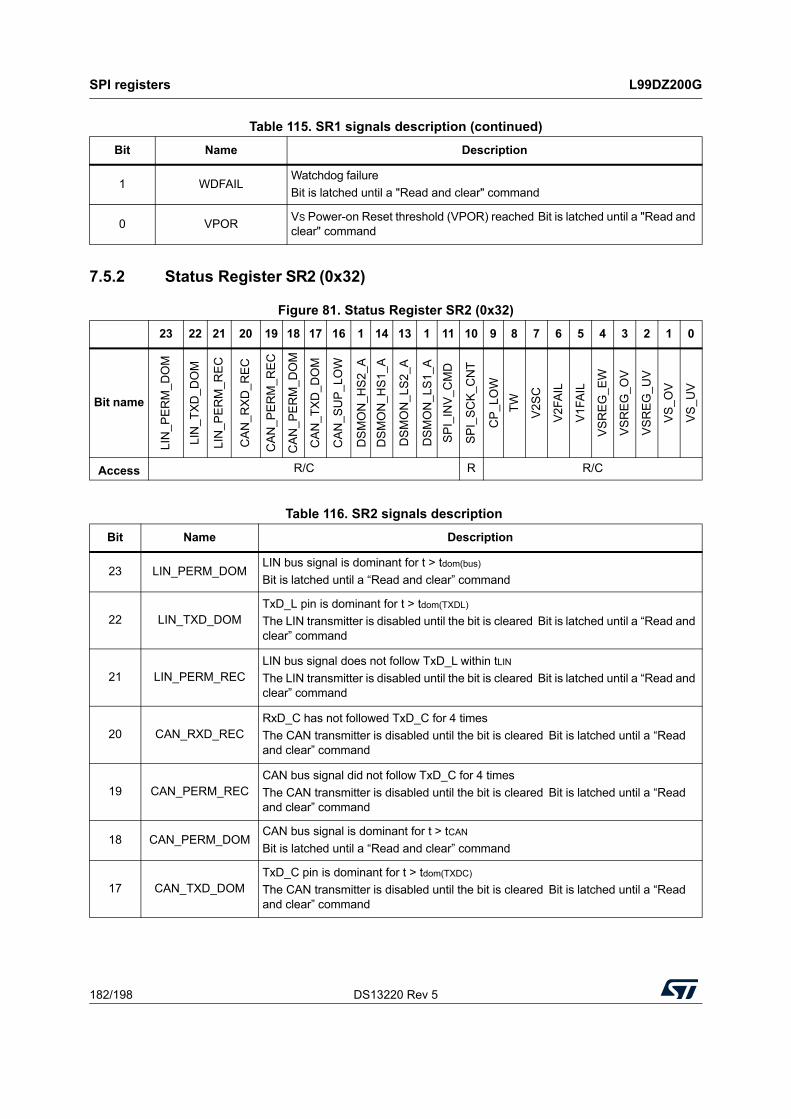
SPI registers L99DZ200G
182/198 DS13220 Rev 5
7.5.2 Status Register SR2 (0x32)
1 WDFAILWatchdog failure
Bit is latched until a "Read and clear" command
0 VPORVS Power-on Reset threshold (VPOR) reached Bit is latched until a "Read and clear" command
Table 115. SR1 signals description (continued)
Bit Name Description
Figure 81. Status Register SR2 (0x32)
23 22 21 20 19 18 17 16 1 14 13 1 11 10 9 8 7 6 5 4 3 2 1 0
Bit name
LIN
_PE
RM
_DO
M
LIN
_TX
D_
DO
M
LIN
_PE
RM
_RE
C
CA
N_
RX
D_R
EC
CA
N_P
ER
M_
RE
C
CA
N_P
ER
M_D
OM
CA
N_T
XD
_DO
M
CA
N_S
UP
_LO
W
DS
MO
N_H
S2_
A
DS
MO
N_H
S1_
A
DS
MO
N_L
S2_
A
DS
MO
N_L
S1_
A
SP
I_IN
V_C
MD
SP
I_S
CK
_CN
T
CP
_LO
W
TW
V2S
C
V2F
AIL
V1F
AIL
VS
RE
G_E
W
VS
RE
G_O
V
VS
RE
G_U
V
VS
_OV
VS
_UV
Access R/C R R/C
Table 116. SR2 signals description
Bit Name Description
23 LIN_PERM_DOMLIN bus signal is dominant for t > tdom(bus)
Bit is latched until a “Read and clear” command
22 LIN_TXD_DOMTxD_L pin is dominant for t > tdom(TXDL)
The LIN transmitter is disabled until the bit is cleared Bit is latched until a “Read and clear” command
21 LIN_PERM_RECLIN bus signal does not follow TxD_L within tLIN
The LIN transmitter is disabled until the bit is cleared Bit is latched until a “Read and clear” command
20 CAN_RXD_RECRxD_C has not followed TxD_C for 4 times
The CAN transmitter is disabled until the bit is cleared Bit is latched until a “Read and clear” command
19 CAN_PERM_RECCAN bus signal did not follow TxD_C for 4 times
The CAN transmitter is disabled until the bit is cleared Bit is latched until a “Read and clear” command
18 CAN_PERM_DOMCAN bus signal is dominant for t > tCAN
Bit is latched until a “Read and clear” command
17 CAN_TXD_DOMTxD_C pin is dominant for t > tdom(TXDC)
The CAN transmitter is disabled until the bit is cleared Bit is latched until a “Read and clear” command

DS13220 Rev 5 183/198
L99DZ200G SPI registers
197
16 CAN_SUP_LOWVoltage at CAN supply pin reached the CAN supply low warning threshold VCANSUP
< VCANSUPlow
Bit is latched until a “Read and clear” command
15 DSMON_HS2_A
Drain-Source Monitoring for H-bridge A
‘1’ indicates a short-circuit or open-load condition was detected Bit is latched until a “Read and clear” command
14 DSMON_HS1_A
13 DSMON_LS2_A
12 DSMON_LS1_A
11 SPI_INV_CMD
Invalid SPI command
‘1’ indicates one of the following conditions was detected:
– access to undefined address
– Write operation to Status Register
– DI stuck at '0' or '1'
– CSN timeout
– Parity failure
– invalid or undefined setting
– SPI access during VS_OV conditions (when Generator_Mode_EN = 1)
The SPI frame is ignored
Bit is latched until a “Read and clear” command
10 SPI_SCK_CNTSPI clock counter
‘1’ indicates an SPI frame with wrong number of CLK cycles was detected Bit is latched until a valid SPI frame
9 CP_LOWCharge pump voltage low
‘1’ indicates that the charge pump voltage is too low Bit is latched until a “Read and clear” command
8 TW
Thermal warning
‘1’ indicates the temperature has reached the thermal warning threshold (logical OR combination of bits TW_CLx in SR6)
Bit is latched until a “Read and clear” command
7 V2SC
V2 short circuit detection
‘1’ indicates a short circuit to GND condition of V2 at turn-on of the regulator (V2 < V2_fail for t > tv2_short)
Bit is latched until a “Read and clear” command
6 V2FAIL
V2 failure detection
‘1’ indicates a V2 fail event occurred since last readout (V2 < V2_fail for t > tv2_fail)
Bit is latched until a “Read and clear” command
5 V1FAIL
V1 failure detection
‘1’ indicates a V1 fail event occurred since last readout (V1 < V1_fail for t > tv1_fail)
Bit is latched until a “Read and clear” command
Table 116. SR2 signals description (continued)
Bit Name Description

SPI registers L99DZ200G
184/198 DS13220 Rev 5
7.5.3 Status Register SR3 (0x33)
4 VSREG_EW
VSREG early warning
‘1’ indicates the voltage at VSREG has reached the early warning threshold (configured in CR3)
In Active mode, an interrupt pulse is generated at NINT Bit is latched until a “Read and clear” command.
Bit needs a "Read and clear" command after wake-up from standby modes
3 VSREG_OVVSREG overvoltage
‘1’ indicates the voltage at VSREG has reached the overvoltage threshold Bit is latched until a “Read and clear” command
2 VSREG_UVVSREG undervoltage
‘1’ indicates the voltage at VSREG has reached the undervoltage threshold Bit is latched until a “Read and clear” command
1 VS_OVVS overvoltage
‘1’ indicates the voltage at VS has reached the overvoltage threshold Bit is latched until a “Read and clear” command
0 VS_UVVS undervoltage
‘1’ indicates the voltage at VS has reached the undervoltage threshold Bit is latched until a “Read and clear” command
Table 116. SR2 signals description (continued)
Bit Name Description
Figure 82. Status Register SR3 (0x33)
23 22 21 20 19 18 17 16 15 14 1 12 11 1 9 8 7 6 5 4 3 2 1 0
Bit name
OU
T1
_HS
_OC
_TH
_EX
OU
T1_
LS_ O
C_T
H_E
X
OU
T2_
HS
_OC
_TH
_EX
OU
T2_
LS
_OC
_TH
_EX
OU
T3
_HS
_OC
_TH
_EX
OU
T3_
LS
_OC
_TH
_EX
OU
T6
_HS
_OC
_TH
_EX
OU
T6_
LS
_OC
_TH
_EX
OU
T7_
OC
_T
H_
EX
OU
T8_
OC
_T
H_
EX
OU
T9_
OC
_S
TAT
OU
T10
_OC
_STA
T
OU
T13
_OC
_STA
T
OU
T14
_OC
_STA
T
OU
T1
5_O
C_T
H_E
X
Re
serv
ed
DS
MO
N_H
S2_
B
DS
MO
N_H
S1_
B
DS
MO
N_L
S2
_B
DS
MO
N_L
S1
_B
Re
serv
ed
LSB
_FS
O_O
C
LSA
_FS
O_O
C
Access R/C R R/C

DS13220 Rev 5 185/198
L99DZ200G SPI registers
197
Table 117. SR3 signals description
Bit Name Description
23 OUT1_HS_OC_TH_EX
Overcurrent shutdown for (OUT1-2-3-6-7-8)
‘1’ indicates the output was shut down due to overcurrent condition. If Overcurrent Recovery is disabled (CR7: OUTx_OCR = 0):
Bit is set upon overcurrent condition and output is turned off. If Overcurrent Recovery is enabled (CR7: OUTx_OCR = 1):
In case of overcurrent condition this bit is not set. The output goes into Overcurrent Recovery mode and OUTx_OCR_alert in SR4 is set to '1' In case of Thermal Expiration enabled (CR8: OUTx_OCR_THx_en = 1):
Bit is set after thermal expiration and output is turned off Bit is latched until a “Read and clear” command
22 OUT1_LS_OC_TH_EX
21 OUT2_HS_OC_TH_EX
20 OUT2_LS_OC_TH_EX
19 OUT3_HS_OC_TH_EX
18 OUT3_LS_OC_TH_EX
17 OUT6_HS_OC_TH_EX
16 OUT6_LS_OC_TH_EX
15 OUT7_OC_TH_EX
14 OUT8_OC_TH_EX
13 OUT9_OC_STAT
Overcurrent shutdown
‘1’ indicates the output was shut down due to overcurrent condition. Bit is latched until a “Read and clear” command
12 OUT10_OC_STAT
11 OUT13_OC_STAT
10 OUT14_OC_STAT
9 OUT15_OC_TH_EX
Overcurrent shutdown for OUT15
‘1’ indicates the output was shut down due to overcurrent condition. If Overcurrent Recovery is disabled (CR7: OUT15_OCR = 0):
Bit is set upon overcurrent condition and output is turned off. If Overcurrent Recovery is enabled (CR7: OUT15_OCR = 1):
In case of overcurrent condition this bit is not set. The output goes into Overcurrent Recovery mode and OUT15_OCR_ALERT in SR4 is set to '1' In case of Thermal Expiration enabled (CR8: OUT15_OCR_THX_EN = 1):
Bit is set after thermal expiration and output is turned off Bit is latched until a “Read and clear” command
8:7 Reserved ---
6 DSMON_HS2_B
Drain-Source Monitoring for H-bridge B
‘1’ indicates a short-circuit or open-load condition was detected Bit is latched until a “Read and clear” command
5 DSMON_HS1_B
4 DSMON_LS2_B
3 DSMON_LS1_B
2 Reserved ---
1 LSB_FSO_OCOvercurrent shutdown
‘1’ indicates the output was shut down due to overcurrent condition. Bit is latched until a “Read and clear” command
0 LSA_FSO_OCOvercurrent shutdown
‘1’ indicates the output was shut down due to overcurrent condition. Bit is latched until a “Read and clear” command

SPI registers L99DZ200G
186/198 DS13220 Rev 5
7.5.4 Status Register SR4 (0x34)
Figure 83. Status Register SR4 (0x34)
23 22 21 20 19 18 17 1 1 14 13 1 11 10 9 8 7 6 5 4 3 2 1 0
Bit name
OU
T1_
HS
_OC
R_A
LER
T
OU
T1_
LS_
OC
R_
ALE
RT
OU
T2_
HS
_OC
R_A
LER
T
OU
T2_
LS_
OC
R_
ALE
RT
OU
T3_
HS
_OC
R_A
LER
T
OU
T3_
LS_
OC
R_
ALE
RT
OU
T6_
HS
_OC
R_A
LER
T
OU
T6_
LS_
OC
R_
ALE
RT
OU
T7_
OC
R_A
LER
T
OU
T8_
OC
R_A
LER
T
OU
T15
_OC
R_A
LER
T
Res
erve
d
OU
T1_
HS
_SH
OR
T
OU
T1_
LS_S
HO
RT
OU
T2_
HS
_SH
OR
T
OU
T2_
LS_S
HO
RT
OU
T3_
HS
_SH
OR
T
OU
T3_
LS_S
HO
RT
OU
T6_
HS
_SH
OR
T
OU
T6_
LS_S
HO
RT
Access R R/C
Table 118. SR4 signals description
Bit Name Description
23 OUT1_HS_OCR_ALERT
Auto recovery Alert
‘1’ indicates that the output reached the overcurrent threshold and is in auto recovery mode
Bit is not latched and cannot be cleared.
22 OUT1_LS_OCR_ALERT
21 OUT2_HS_OCR_ALERT
20 OUT2_LS_OCR_ALERT
19 OUT3_HS_OCR_ALERT
18 OUT3_LS_OCR_ALERT
17 OUT6_HS_OCR_ALERT
16 OUT6_LS_OCR_ALERT
15 OUT7_OCR_ALERT
14 OUT8_OCR_ALERT
13 OUT15_OCR_ALERT
12:8 Reserved --
7 OUT1_HS_SHORT
Short circuit Threshold Alert
‘1’ indicates that the output reached the short circuit threshold
Bit is latched and can be cleared with Read&Clear command
6 OUT1_LS_SHORT
5 OUT2_HS_SHORT
4 OUT2_LS_SHORT
3 OUT3_HS_SHORT
2 OUT3_LS_SHORT
1 OUT6_HS_SHORT
0 OUT6_LS_SHORT

DS13220 Rev 5 187/198
L99DZ200G SPI registers
197
7.5.5 Status Register SR5 (0x35)
Figure 84. Status Register SR5 (0x35)
23 22 21 20 19 18 17 16 15 14 13 12 1 10 9 8 7 6 5 4 3 2 1 0
Bit name
OU
T1_
HS
_O
L
OU
T1_
LS_O
L
OU
T2_
HS
_O
L
OU
T2_
LS_O
L
OU
T3_
HS
_O
L
OU
T3_
LS_O
L
OU
T6_
HS
_O
L
OU
T6_
LS_O
L
OU
T7
_OL_
STA
T
OU
T8
_OL_
STA
T
OU
T9
_OL_
STA
T
OU
T10
_O
L_S
TAT
OU
T13
_O
L_S
TAT
OU
T14
_O
L_S
TAT
OU
T15
_O
L_S
TAT
GH
_OL
EC
V_O
L
Res
erv
ed
DS
MO
N_
HE
AT
EC
V_O
C
Access R/C R R/C
Table 119. SR5 signals description
Bit Name Description
23 OUT1_HS_OL
Open-load
‘1’ indicates an open-load condition was detected at the output
Bit is latched until a “Read and clear” command
22 OUT1_LS_OL
21 OUT2_HS_OL
20 OUT2_LS_OL
19 OUT3_HS_OL
18 OUT3_LS_OL
17 OUT6_HS_OL
16 OUT6_LS_OL
15 OUT7_OL_STAT
14 OUT8_OL_STAT
13 OUT9_OL_STAT
12 OUT10_OL_STAT
11 OUT13_OL_STAT
10 OUT14_OL_STAT
9 OUT15_OL_STAT
8 GH_OL
7 ECV_OL
6:2 Reserved --
1 DSMON_HEATDrain-Source Monitoring Heater output
‘1’ indicates a short-circuit condition was detected
Bit is latched until a “Read and clear” command
0 ECV_OCOvercurrent shutdown
‘1’ indicates the output was shut down due to overcurrent condition. Bit is latched until a “Read and clear” command

SPI registers L99DZ200G
188/198 DS13220 Rev 5
7.5.6 Status Register SR6 (0x36)
Figure 85. Status Register SR6 (0x36)
23 22 21 20 19 18 17 16 15 14 13 12 11 10 9 8 7 6 5 4 3 2 1 0
Bit name
WD
_T
IME
R_S
TAT
E_1
WD
_T
IME
R_S
TAT
E_0
Reserved
EC
V_V
NR
EC
V_V
HI
Res
erv
ed
TW
_CL
6
TW
_CL
5
TW
_CL
4
TW
_CL
3
TW
_CL
2
TW
_CL
1
Res
erv
ed
TS
D1_
CL
6
TS
D1_
CL
5
TS
D1_
CL
4
TS
D1_
CL
3
TS
D1_
CL
2
TS
D1_
CL
1
Access R R/C R R/C
Table 120. SR6 signals description
Bit Name Description
23 WD_TIMER_STATE_1 Watchdog timer status
00: 0 - 33%
01: 33 - 66%
11: 66 - 100%22 WD_TIMER_STATE_0
21:18 Reserved —
17 ECV_VNRElectrochrome Voltage Not Reached:
electrochrome voltage status '1' indicates the electrochrome voltage is not reached. Bit is not latched
16 ECV_VHIElectrochrome Voltage HIgh:
electrochrome voltage status '1' indicates the electrochrome voltage is higher than the target value. Bit is not latched
15:14 Reserved —
13 TW_CL6
Thermal warning for Cluster x
‘1’ indicates Cluster x has reached the thermal warning threshold Bit is latched until a “Read and clear” command
12 TW_CL5
11 TW_CL4
10 TW_CL3
9 TW_CL2
8 TW_CL1
7:6 Reserved —

DS13220 Rev 5 189/198
L99DZ200G SPI registers
197
7.5.7 Status Register SR7 (0x37) to SR9 (0x39)
where:
x = 2 + (z * 2), z = 0 to 2
y = 1 + (z * 2), z = 0 to 2
5 TSD1_CL6
Thermal shutdown of Cluster x
‘1’ indicates Cluster x has reached the thermal shutdown threshold (TSD1) and the output cluster was shut down
Bit is latched until a “Read and clear” command
4 TSD1_CL5
3 TSD1_CL4
2 TSD1_CL3
1 TSD1_CL2
0 TSD1_CL1
Table 120. SR6 signals description (continued)
Bit Name Description
Figure 86. Status Register SR7 (0x37) to SR9 (0x39)
23 22 21 20 19 18 17 16 15 14 13 12 11 10 9 8 7 6 5 4 3 2 1 0
Bit name
Res
erv
ed
TE
MP
_C
Lx_9
TE
MP
_C
Lx_8
TE
MP
_C
Lx_7
TE
MP
_C
Lx_6
TE
MP
_C
Lx_5
TE
MP
_C
Lx_4
TE
MP
_C
Lx_3
TE
MP
_C
Lx_2
TE
MP
_C
Lx_1
TE
MP
_C
Lx_0
Res
erv
ed
TE
MP
_C
Ly_
9
TE
MP
_C
Ly_
8
TE
MP
_C
Ly_
7
TE
MP
_C
Ly_
6
TE
MP
_C
Ly_
5
TE
MP
_C
Ly_
4
TE
MP
_C
Ly_
3
TE
MP
_C
Ly_
2
TE
MP
_C
Ly_
1
TE
MP
_C
Ly_
0
Access R/C R R/C R
Table 121. SR7 to SR9 signals description
Bit Name Description
23:22 Reserved —
21 TEMP_CLx_9
Temperature Cluster x: Binary coded voltage of temperature diode for cluster x (bit12 = LSB; bit21 = MSB) (see Section 4.37)
Bits cannot be cleared.
20 TEMP_CLx_8
19 TEMP_CLx_7
18 TEMP_CLx_6
17 TEMP_CLx_5
16 TEMP_CLx_4
15 TEMP_CLx_3
14 TEMP_CLx_2
13 TEMP_CLx_1
12 TEMP_CLx_0
11:10 Reserved —

SPI registers L99DZ200G
190/198 DS13220 Rev 5
7.5.8 Status Register SR10 (0x3A)
9 TEMP_CLy_9
Temperature Cluster y: binary coded voltage of temperature diode for cluster y (bit0 = LSB; bit9 = MSB) (see Section 4.37)
Bits cannot be cleared.
8 TEMP_CLy_8
7 TEMP_CLy_7
6 TEMP_CLy_6
5 TEMP_CLy_5
4 TEMP_CLy_4
3 TEMP_CLy_3
2 TEMP_CLy_2
1 TEMP_CLy_1
0 TEMP_CLy_0
Table 121. SR7 to SR9 signals description (continued)
Bit Name Description
Figure 87. Status Register SR10 (0x3A)
23 22 21 20 19 18 17 16 15 14 13 12 11 10 9 8 7 6 5 4 3 2 1 0
Bit name
Res
erve
d
VS
RE
G_9
VS
RE
G_8
VS
RE
G_7
VS
RE
G_6
VS
RE
G_5
VS
RE
G_4
VS
RE
G_3
VS
RE
G_2
VS
RE
G_1
VS
RE
G_0
Reserved
Access R/C R R/C
Table 122. SR10 signals description
Bit Name Description
23:22 Reserved —
21 VSREG_9
Binary coded voltage at VSREG pin (bit12 = LSB; bit21 = MSB)
00 0000 0000: 0V
xx xxxx xxxx: VAINVS/1024 x register value 11 1111 1111: VAINVS
Bits cannot be cleared.
20 VSREG_8
19 VSREG_7
18 VSREG_6
17 VSREG_5
16 VSREG_4
15 VSREG_3
14 VSREG_2
13 VSREG_1
12 VSREG_0
11:0 Reserved —

DS13220 Rev 5 191/198
L99DZ200G SPI registers
197
7.5.9 Status Register SR11 (0x3B)
Figure 88. Status Register SR11 (0x3B)
23 22 21 20 19 18 17 16 15 14 13 12 11 10 9 8 7 6 5 4 3 2 1 0
Bit name
Re
serv
ed
VS
_9
VS
_8
VS
_7
VS
_6
VS
_5
VS
_4
VS
_3
VS
_2
VS
_1
VS
_0
Re
serv
ed
VW
U_9
VW
U_8
VW
U_7
VW
U_6
VW
U_5
VW
U_4
VW
U_3
VW
U_2
VW
U_1
VW
U_0
Access R/C R R/C R
Table 123. SR11 signals description
Bit Name Description
23 Reserved —
21 VS_9
Binary coded voltage at VS pin (bit12 = LSB; bit21 = MSB)
00 0000 0000: 0V
xx xxxx xxxx: VAINVS/1023 x register value 11 1111 1111: VAINVS
Bits cannot be cleared.
20 VS_8
19 VS_7
18 VS_6
17 VS_5
16 VS_4
15 VS_3
14 VS_2
13 VS_1
12 VS_0
11:10 Reserved —
9 VWU_9
Binary coded voltage at WU pin (bit0 = LSB; bit9 = MSB)
00 0000 0000: 0V
xx xxxx xxxx: VAINVS/1023 x register value 11 1111 1111: VAINVS
Bits cannot be cleared.
8 VWU_8
7 VWU_7
6 VWU_6
5 VWU_5
4 VWU_4
3 VWU_3
2 VWU_2
1 VWU_1
0 VWU_0

SPI registers L99DZ200G
192/198 DS13220 Rev 5
7.5.10 Status Register SR12 (0x3C)
Figure 89. Status Register SR12 (0x3C)
23 22 21 20 19 18 17 16 15 14 13 12 11 10 9 8 7 6 5 4 3 2 1 0
Bit name
Res
erve
d
CA
N_S
ILE
NT
Res
erve
d
CA
NT
O
WU
P
Res
erve
d
Access R
Table 124. SR12 signals description
Bit Name Description
23:6 Reserved —
5 CAN_SILENTOnline monitoring bit to see if there is silence on the bus for longer than tSilence
This flag shows the actual status of the CAN bus (activity/silence). A microcontroller in Stop mode may check this flag periodically
4 Reserved --
3 CANTO
CAN communication timeout
Bit is set if there is no communication on the bus for t > tSilence
CANTO indicates that there was a transition from TRX BIAS to TRX Sleep Bit is latched until a read and clear access
2 WUPWake up flag for Wake up Pattern
Bit is latched until a read and clear access
1:0 Reserved --

DS13220 Rev 5 193/198
L99DZ200G Package information
197
8 Package information
In order to meet environmental requirements, ST offers these devices in different grades of ECOPACK packages, depending on their level of environmental compliance. ECOPACK specifications, grade definitions and product status are available at: www.st.com. ECOPACK is an ST trademark.
8.1 LQFP-64 package information
Figure 90. LQFP-64 package dimension
GAPG2907151212CFT
Table 125. LQFP-64 mechanical data
SymbolMillimeters/Degrees
Min. Typ. Max.
Θ 0º 3.5° 6°
Θ1 0º 9° 12°
Θ2 11º 12° 13°
Θ3 11º 12° 13°

Package information L99DZ200G
194/198 DS13220 Rev 5
A 1.60
A1 0.05 0.15
A2 1.35 1.40 1.45
b 0.27
b1 0.17 0.20 0.23
c 0.09 0.20
c1 0.09 0.127 0.16
D 12.00 BSC
D1 10.00 BSC
D2 6.85
D3 5.7
e 0.50 BSC
E 12.00 BSC
E1 10.00 BSC
E2 4.79
E3 3.3
L 0.45 0.60 0.75
L1 1.00
N 64
R1 0.08
R2 0.08 0.20
S 0.20
Tolerance of form and position
aaa 0.20
bbb 0.20
ccc 0.08
ddd 0.08
Table 125. LQFP-64 mechanical data (continued)
SymbolMillimeters/Degrees
Min. Typ. Max.

DS13220 Rev 5 195/198
L99DZ200G Package information
197
Figure 91. LQFP-64 footprint
8.2 LQFP-64 marking information
Figure 92. LQFP-64 marking information
Parts marked as ES are not yet qualified and therefore not approved for use in production. ST is not responsible for any consequences resulting from such use. In no event will ST be liable for the customer using any of these engineering samples in production. ST’s Quality department must be contacted to run a qualification activity prior to any decision to use these engineering samples.
GAPG2907151243CFT
Special function digitsES: Engineering sample<blank>: Commercial sample
LQFP-64 TOP VIEW(not in scale)
Marking area
Marking area
GADG1105161103MAG
or

Order code L99DZ200G
196/198 DS13220 Rev 5
9 Order code
Table 126. Ordering information
PackageOrder codes
Tape & Reel Tray
LQFP-64 epad L99DZ200GTR L99DZ200G

DS13220 Rev 5 197/198
L99DZ200G Revision history
197
10 Revision history
Table 127. Document revision history
Date Revision Changes
16-Jan-2020 1 Initial release.
08-Oct-2020 2
Updated:
– Figure 3: Activation profile;
– Figure 4: Activation profile (first cycle);
– Figure 7: Watchdog timing
– Figure 19: Sequence to disable/enable the watchdog in CAN Flashmode;
– Figure 61: Typical application diagram;
– Table 112: CR21 signals description .
Minor text changes.
23-Nov-2020 3
Updated Table 5: Temperature Warning and Thermal Shutdown, Table 10: Voltage regulator V1, Table 18: Power outputs switching times, Table 19: Current monitoring, Table 27: Electro-chrome mirror driver, Figure 61: Typical application diagram, Table 122: SR10 signals description, Table 123: SR11 signals description.
26-Mar-2021 4
Updated:
– Features
– Table 3: ESD protection
– Section 4.9.1: Features
– Section 4.10.1: Features
– Add Section 9: Order code
Changed Figure 61
06-Apr-2021 5 Typos.

L99DZ200G
198/198 DS13220 Rev 5
IMPORTANT NOTICE – PLEASE READ CAREFULLY
STMicroelectronics NV and its subsidiaries (“ST”) reserve the right to make changes, corrections, enhancements, modifications, and improvements to ST products and/or to this document at any time without notice. Purchasers should obtain the latest relevant information on ST products before placing orders. ST products are sold pursuant to ST’s terms and conditions of sale in place at the time of order acknowledgement.
Purchasers are solely responsible for the choice, selection, and use of ST products and ST assumes no liability for application assistance or the design of Purchasers’ products.
No license, express or implied, to any intellectual property right is granted by ST herein.
Resale of ST products with provisions different from the information set forth herein shall void any warranty granted by ST for such product.
ST and the ST logo are trademarks of ST. For additional information about ST trademarks, please refer to www.st.com/trademarks. All other product or service names are the property of their respective owners.
Information in this document supersedes and replaces information previously supplied in any prior versions of this document.
© 2021 STMicroelectronics – All rights reserved