data brief - stdes-50w2cwbc - stmicroelectronics
TRANSCRIPT
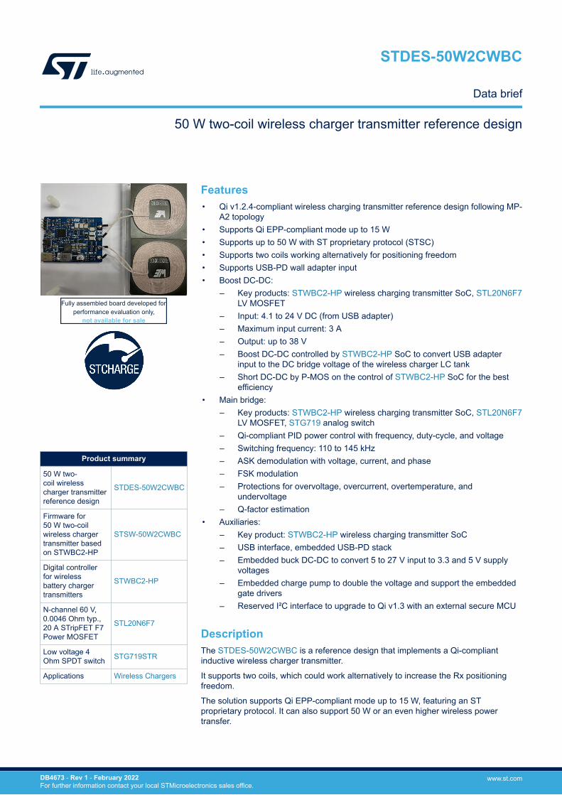
Fully assembled board developed forperformance evaluation only,
not available for sale
Features• Qi v1.2.4-compliant wireless charging transmitter reference design following MP-
A2 topology• Supports Qi EPP-compliant mode up to 15 W• Supports up to 50 W with ST proprietary protocol (STSC)• Supports two coils working alternatively for positioning freedom• Supports USB-PD wall adapter input• Boost DC-DC:
– Key products: STWBC2-HP wireless charging transmitter SoC, STL20N6F7LV MOSFET
– Input: 4.1 to 24 V DC (from USB adapter)– Maximum input current: 3 A– Output: up to 38 V– Boost DC-DC controlled by STWBC2-HP SoC to convert USB adapter
input to the DC bridge voltage of the wireless charger LC tank– Short DC-DC by P-MOS on the control of STWBC2-HP SoC for the best
efficiency• Main bridge:
– Key products: STWBC2-HP wireless charging transmitter SoC, STL20N6F7LV MOSFET, STG719 analog switch
– Qi-compliant PID power control with frequency, duty-cycle, and voltage– Switching frequency: 110 to 145 kHz– ASK demodulation with voltage, current, and phase– FSK modulation– Protections for overvoltage, overcurrent, overtemperature, and
undervoltage– Q-factor estimation
• Auxiliaries:– Key product: STWBC2-HP wireless charging transmitter SoC– USB interface, embedded USB-PD stack– Embedded buck DC-DC to convert 5 to 27 V input to 3.3 and 5 V supply
voltages– Embedded charge pump to double the voltage and support the embedded
gate drivers– Reserved I²C interface to upgrade to Qi v1.3 with an external secure MCU
DescriptionThe STDES-50W2CWBC is a reference design that implements a Qi-compliantinductive wireless charger transmitter.
It supports two coils, which could work alternatively to increase the Rx positioningfreedom.
The solution supports Qi EPP-compliant mode up to 15 W, featuring an STproprietary protocol. It can also support 50 W or an even higher wireless powertransfer.
Product summary
50 W two-coil wirelesscharger transmitterreference design
STDES-50W2CWBC
Firmware for50 W two-coilwireless chargertransmitter basedon STWBC2-HP
STSW-50W2CWBC
Digital controllerfor wirelessbattery chargertransmitters
STWBC2-HP
N-channel 60 V,0.0046 Ohm typ.,20 A STripFET F7Power MOSFET
STL20N6F7
Low voltage 4Ohm SPDT switch STG719STR
Applications Wireless Chargers
50 W two-coil wireless charger transmitter reference design
STDES-50W2CWBC
Data brief
DB4673 - Rev 1 - February 2022For further information contact your local STMicroelectronics sales office.
www.st.com
The STDES-50W2CWBC is based on the STWBC2-HP high-integration, high-performance wireless charger system-on-chip.
It integrates: three pairs of half-bridge gate drivers, the dedicated DC-DC controllersthat support buck, boost and buck-boost topologies, the high-performance Q-factormeasurement hardware, the high-resolution main PWM controller, the dedicated Qicommunication modulator and demodulator, the USB-PD controller, the buck DC-DC,and the charge pump.
It is suitable for one-coil and multicoil solutions in multiple topologies.
The STDES-50W2CWBC is a fully assembled reference design developed forperformance evaluation only, not available for sale.
STDES-50W2CWBC
DB4673 - Rev 1 page 2/8
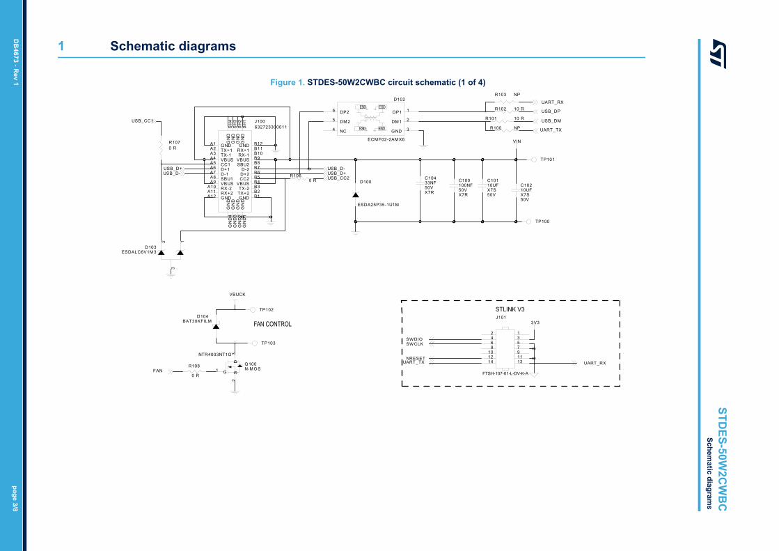
1 Schematic diagrams
Figure 1. STDES-50W2CWBC circuit schematic (1 of 4)
FAN CONTROL
STLINK V3
ESDESD
ESDESD
1DP1
2DM 1
3GND
6 DP2
5 DM 2
4 NC
D102
ECM F02-2AM X6
R102 10 R
R100 NP
D100
ESDA25P35-1U1M
R101 10 R
B12GNDB11RX+1B10RX-1B9VBUSB8SBU2B7
B5B4
A12
B3
SBU1VBUSRX-2RX+2GND
B2B1
A1 GNDA2
D-2D+2CC2
VBUSTX-2
TX+2GND
TX+1A3 TX-1A4 VBUSA5 CC1A6 D+1A7 D-1A8A9
A10A11
GN
D1
GN
DG
ND
2G
ND
GN
D3
GN
D
B6
GN
D4
GN
D
SH
1G
ND
SH
2G
ND
SH
3G
ND
SH
4G
ND
J100632723300011
R1070 R
R1060 R
R103 NP
C100
X7R50V100NF
D104BAT30KFILM
NTR4003NT1G 3D
1 G
2S
Q100N-M OSR108
0 R
C101
X7S50V
10UF C102
X7S50V
10UF
TP101
TP100
TP102
TP103
2 1
3
D103ESDALC6V1M 3
C104
X7R50V33NF
24
810
1357911
6
131214
J101
FTSH-107-01-L-DV-K-A
VIN
USB_DP
USB_DM
USB_D+USB_D-
UART_TX
UART_RX
USB_D+USB_D-
USB_CC2
USB_CC1
VBUCK
FAN
3V3
SW DIOSW CLK
UART_RXUART_TXNRESET
DB
4673 - Rev 1
page 3/8
STDES-50W
2CW
BC
Schematic diagram
s
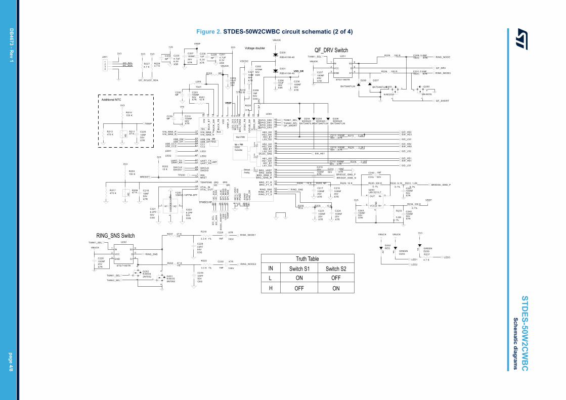
Figure 2. STDES-50W2CWBC circuit schematic (2 of 4)
Truth TableIN Switch S1LH
Voltage doubler
Additional NTC
RING_SNS Switch
QF_DRV Switch
C21150V X7R
330NF
C21350V X7R
330NF
R21910 R
1 X1 3X2
2C
OVE
R2C
OVE
R1
4
Y 20016M HZ-10PPM -8PF
R205 NP
C206
35VX5R
10UF
TP200
R204 10 K
R200 0R1
C203
X7R50V100NF
NTC
R20647 K
R20210 K
C21250V X7R
330NF
R218
3.3 K 1%
R20110 R
R203150 K
R217470 K
D206SOD523
BAT54KFILM
R20810 K
D204SOD523
BAT54KFILM
R209 10 K
/I2C
drive
rga
teBo
ostra
p
drive
rga
teBo
ostra
p
Main PWM
drive
rga
teBo
ostra
p
AnalogDemod
Q- F dr i ver
ControllerDCDCMai n PWM
PD/QC
Buck
USB
ISns
6V
DD
2LD
O_3
V3
3V
RE
F_A
4M
CU
_3V
38
MC
U_V
SS
1
60 USB_DM59 USB_DP
11 XTAL_OUT10 XTAL_IN
12 NRST
5LD
O_1
V8
46 LED1
47 LED2
27V
DD
_DR
23S
PI_
MIS
O24
SP
I_M
OS
I
21 UART_TX28HS1_BT
29HS1_GD30HS1_SW
31LS1_GD
36HS2_BT
35HS2_GD34HS2_SW
32LS2_GD
41G
ND
_DR
9B
UC
K_F
B
14B
UC
K_S
W
15B
UC
K_B
T
16V
IN
22 UART_RX
43G PIO_DR142G PIO_DR0
48 SW DIO49 SW CLK
25S
PI_
NS
S
1 IRQ
68A
GN
D
54BRG_VREF
20S
PI_
CLK
19 TEM PSNS
53BRG_ISNS_P52BRG_ISNS_M
50B
RG
_VS
NS
62I2
C_S
DA
6
STWBC2-HP 3I2
C_S
CL
13P
GN
D
55BRG_IDEM
56BRG_FT_S57BRG_FT_R
7M
CU
_VS
S
64RING_FT_S65RING_FT_R
66Q
F_D
RV
69E
PA
D
33DCDC_SNS
17 VIN_ISNS_P18 VIN_ISNS_N
26V
DO
UB
_SW
37HS3_BT
38HS3_GD39HS3_SW
40LS3_GD
44GPIO_DR245GPIO_DR3
58 CC161 CC2
67RING_SNS
51D
CD
C_F
B
U200
R2071%47 K
D205SOD523
BAT54KFILM
C200NP
L200
10uH
D200
RB541VM -40
D201VDD_DRVDD_DR
RB541VM -40
C216
X7R50V10NF
C221
C0G50V8.2PF
C222
C0G50V8.2PF
C227
X7R50V10NF
C208
C0G50V1NF
C202
X5R50V470NF
C215
X7R
25V100NF
C217
X7R25V100NF
C218
X7R25V100NF
C223
X7R25V100NF
C224
X7R25V100NF
C228
C0G50V33PF
C220 X7R
100V1NF
R220
0 R
NTC
R21147 K
R210150 K
R213470 K
C225
X7R50V10NF
1 IN2 VCC3 GND
6S25D4S1
U202
STG719STR
C226
X7R25V100NF R222
3.3 K 1%
R2231%47 K
C229
C0G50V33PF
C230 X7R
100V1NF
D3
1 G
2S
Q202N-M O S2N7002
D3
1 G
2S
Q201N-M OS2N7002
R2284.7 K
R2274.7 K
C204
16V
10UFX5R C236
X7R25V100NF
C201
X5R6.3V4.7UF
C234NP
C235
X5R6.3V4.7UF
C233NP
R212 2.2R
R225 2.2R
R226 2.2R
C209X7R100V
5.6NF
3 D
1G
S 2Q200
N-M OS
1 IN2 VCC3 GND
6S25D4S1
U201
STG719STR
C237
X7R25V100NF
C231X7R100V
5.6NF
D 3
1G
2 S203BAT54KFILMQ
N-M OS
D208
BAT54KFILM
C214X7R50V10NF
C207
X7R25V100NF
C238
X7R6.3V1UF
C239NP
C210
X7R50V100NF
4 OUT
5 VCC
3IN-
1IN+
2G
ND
U203LM V321ILT
R229 10 K R2300.1%
330 K
C240
COG 50V
1NF
R231
0.1%
1.2KR232
0.1%
9.1K
C241
X7R50V100NF
C242
X7R50V100NF
R233
0.1%5.6K
R234
0.1%
330 K
C243
X7R50V100NF
J201
1234
D203GREEN
D202RED
D207
R235 100 R
R236 100 R
D209GREEN
R237
4.7 K
VBUCK
3V3
3V3
3V3
VBUCK
VIN
VDCDC
USB_DPUSB_DM
SW DIOSW CLK
UART_TXUART_RX
SW _HS2
G D_LS2
NRESET
USB_CC2USB_CC1
GD_HS1SW _HS1
GD_LS1
G D_HS2
GD_HS3SW _HS3
GD_LS3
BRIDGE_ISNS_P
RING_NODE1
I2C
_SC
LI2
C_S
DA
VIN_ISNS_NVIN_ISNS_P
SW _HS1
FA
N
LED1
LED2
3V3
TEM P
TE
MP
TANK1_SELTANK2_SEL
TANK1_SEL
RING_SNS
RING_NODE2
RING_SNS
TANK1_SEL
TANK2_SEL
QF_SHORT
QF
_DR
V
VBUCK
BRIDGE_ISNS_N
3V3 3V3
I2C_SCLI2C_SDA
1V8
1V8
RING_NODE1TANK1_SEL
RING_NODE2
QF_DRV
QF_SHORT
VBUCK
VREFVREF
VREF
3V3 VREF
BRIDGE_ISNS_P
DC
DC
_SH
OR
T
3V3
I2C_SCLI2C_SDA
VBUCKVBUCK
LED1
LED2
LED
3
3V3
LED3
Switch S2
OFF
OFFON
ON
/SPIGPIO
UART
GPIO
DB
4673 - Rev 1
page 4/8
STDES-50W
2CW
BC
Schematic diagram
s
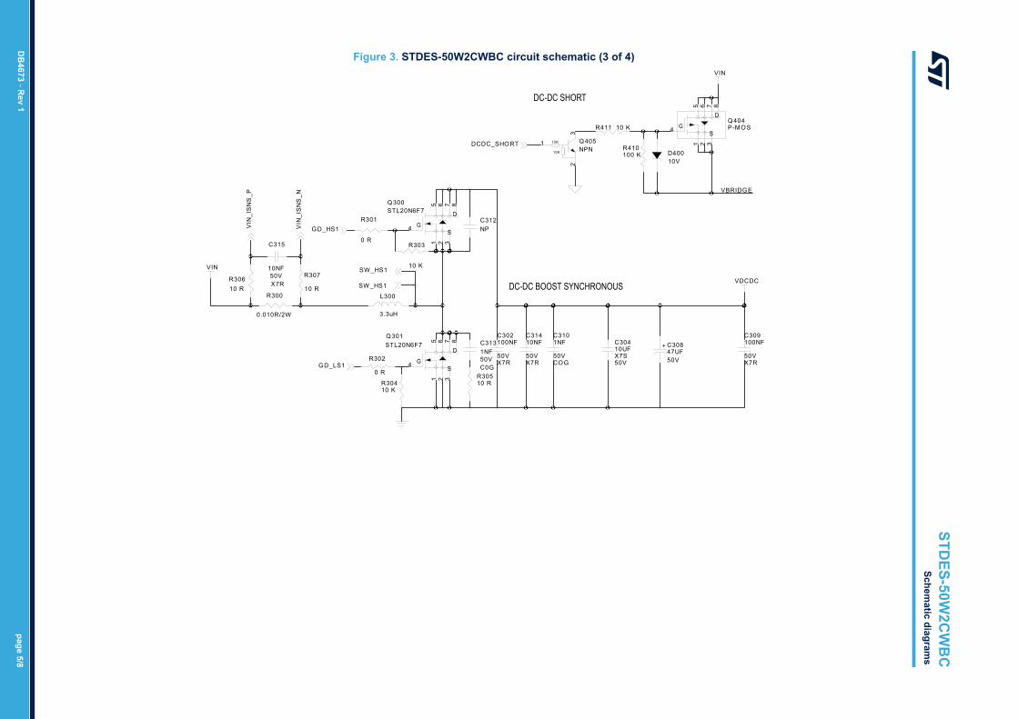
Figure 3. STDES-50W2CWBC circuit schematic (3 of 4)
DC-DC BOOST SYNCHRONOUS
DC-DC SHORT
R30410 K
R302
0 R
R301
0 R
GS
D
5
4
16 7 8
2 3
Q301STL20N6F7
C302
X7R50V
100NF
R303
10 K
R30510 R
GS
D
5
4
16 7 8
2 3
Q300STL20N6F7
R300
0.010R/2W
C312NP
C313
C0G50V1NF
L300
3.3uH
R30610 R
C315
X7R50V
10NFR307
10 R
C309
X7R50V
100NFC314
X7R50V
10NFC310
50VCOG
1NF
R410100 K D400
10V
G
D
S
5
4
16 7 8
2 3
Q404P-M OS
10K
10K
1
23
Q405NPN
R411 10 K
C304
X7S50V
10UF + C30847UF50V
VIN
GD_HS1
GD_LS1
VIN
_IS
NS
_P
VIN
_IS
NS
_N
SW _HS1
SW _HS1
VDCDC
VIN
DCDC_SHORT
VBRIDGE
DB
4673 - Rev 1
page 5/8
STDES-50W
2CW
BC
Schematic diagram
s
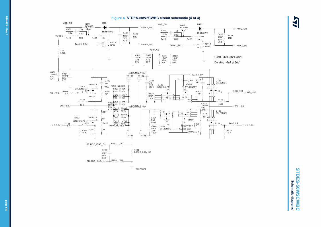
Figure 4. STDES-50W2CWBC circuit schematic (4 of 4)
GND POWER
Derating >7uF at 20V
C419-C420-C421-C422
coil Qi-MPA2 10uH
R406NP
R41310 K
R402NP
L4001uH
R403 0 R
R4080.010R 0.1% 1W
R4040 R
C400
X7R50V100NF
GS
D5
41
6 7 8
2 3
Q400STL20N6F7
R4000 R
R401NP
GS
D
5
4
1
8 7 63 2
Q401STL20N6F7
R41510 K
R412
10 K
R414
10 K
GS
D
5
4
1
8 7 63 2
Q403STL20N6F7
R407 0 RGS
D
5
4
16 7 8Q402
2 3
STL20N6F7
C406
0402NP
C414NP
C413NP
GS
D
5
4
1678
23
Q406STL20N6F7
GS
D
5
4
1678
Q407
23
STL20N6F7
C411
NP
R418
NP
R221 0R
R224 0R
C232DNP50VC0G
GS
D
5
4
1
876
32
Q409
STL20N6F7
GS
D
5
4
1
876
32
Q408STL20N6F7
R424DNP1206
C404
X7S100V
DNP
R420DNP1206
C401
X7S100V
DNP
R416 10K R421 10K
C402
C0G50V1NF
D401
1N4148W S C418
X7R50V10NF
R42247K
R423 10K R425 10K
C423
C0G50V1NF
D402
1N4148W S C425
X7R50V10NF
R42847K
Q411BC856B Q412
BC856B
C431
X7R50V100NF
C432
X7R50V100NF
C433
X7R50V100N
1
coil Qi-MPA2 10uHTP401 TP400
1
C407C0G 100V
100NF
1
TP403
1
TP404
C408 100NFC0G 100V
C409 47NFFC0G 100V
C410C0G 100V
100NF
C412C0G 100V
100NF
C415 47NFC0G 100V
C419
X7S50V
10UFC420
X7S50V
10UFC421
X7S50V
10UFC422
X7S50V
10UF
10K
10K1
23
Q410NPN
10K
10K1
23
Q413NPN
VDCDC
G D_HS3
GD_LS3GD_LS2
GD_HS2
BRIDGE_ISNS_P
SW _HS2 SW _HS3
RING_NODE1
BRIDGE_ISNS_N
RING_NODE2
TANK1_ON
TANK2_ON
TANK1_SEL
VDD_DR
TANK1_ON
TANK2_SEL
VDD_DR
TANK2_O N
VBRIDGE
TANK1_SW
TANK2_SW
TANK1_SW TANK2_SW
DB
4673 - Rev 1
page 6/8
STDES-50W
2CW
BC
Schematic diagram
s
Revision history
Table 1. Document revision history
Date Revision Changes
28-Feb-2022 1 Initial release.
STDES-50W2CWBC
DB4673 - Rev 1 page 7/8
IMPORTANT NOTICE – PLEASE READ CAREFULLY
STMicroelectronics NV and its subsidiaries (“ST”) reserve the right to make changes, corrections, enhancements, modifications, and improvements to STproducts and/or to this document at any time without notice. Purchasers should obtain the latest relevant information on ST products before placing orders. STproducts are sold pursuant to ST’s terms and conditions of sale in place at the time of order acknowledgement.
Purchasers are solely responsible for the choice, selection, and use of ST products and ST assumes no liability for application assistance or the design ofPurchasers’ products.
No license, express or implied, to any intellectual property right is granted by ST herein.
Resale of ST products with provisions different from the information set forth herein shall void any warranty granted by ST for such product.
ST and the ST logo are trademarks of ST. For additional information about ST trademarks, please refer to www.st.com/trademarks. All other product or servicenames are the property of their respective owners.
Information in this document supersedes and replaces information previously supplied in any prior versions of this document.
© 2022 STMicroelectronics – All rights reserved
STDES-50W2CWBC
DB4673 - Rev 1 page 8/8