brain smart hub family - stmicroelectronics
TRANSCRIPT
February 2014 DocID024647 Rev 1 1/138
RM0352Reference manual
Brain smart hub family
IntroductionThis reference manual targets application developers. It provides complete information on
how to use the Brain smart hub microcontroller memory and peripherals.
The Brain is the first chip of smart hub microcontrollers family with different memory sizes,
packages and peripherals.
For ordering information, mechanical and electrical device characteristics please refer to the
datasheet.
For information on the ARM®
Cortex™-M0 core, please refer to the Cortex-M0 technical
reference manual.
Related documents
• Cortex-M0 technical reference manual, available from:
http://infocenter.arm.com/help/topic/com.arm.doc.ddi0432c/DDI0432C_cortex_m0_r0p0
_trm.pdf
• Cortex-M0 generic user guide, available from:
http://infocenter.arm.com/help/topic/com.arm.doc.dui0497a/DUI0497A_cortex_m0_r0p0
_generic_ug.pdf
www.st.com
Contents RM0352
2/138 DocID024647 Rev 1
Contents
1 Referenced document . . . . . . . . . . . . . . . . . . . . . . . . . . . . . . . . . . . . . . . 11
2 System and memory overview . . . . . . . . . . . . . . . . . . . . . . . . . . . . . . . . 12
2.1 System architecture . . . . . . . . . . . . . . . . . . . . . . . . . . . . . . . . . . . . . . . . . 12
2.2 Memory organization . . . . . . . . . . . . . . . . . . . . . . . . . . . . . . . . . . . . . . . . 13
2.3 Embedded SRAM . . . . . . . . . . . . . . . . . . . . . . . . . . . . . . . . . . . . . . . . . . . 15
2.4 Flash memory overview . . . . . . . . . . . . . . . . . . . . . . . . . . . . . . . . . . . . . . 15
2.5 Physical remap . . . . . . . . . . . . . . . . . . . . . . . . . . . . . . . . . . . . . . . . . . . . . 16
3 Interrupts . . . . . . . . . . . . . . . . . . . . . . . . . . . . . . . . . . . . . . . . . . . . . . . . . 17
4 GPIO . . . . . . . . . . . . . . . . . . . . . . . . . . . . . . . . . . . . . . . . . . . . . . . . . . . . . 19
5 Clock and reset management unit . . . . . . . . . . . . . . . . . . . . . . . . . . . . . 21
5.1 Introduction . . . . . . . . . . . . . . . . . . . . . . . . . . . . . . . . . . . . . . . . . . . . . . . 21
5.2 Clock generation . . . . . . . . . . . . . . . . . . . . . . . . . . . . . . . . . . . . . . . . . . . 21
5.2.1 General description . . . . . . . . . . . . . . . . . . . . . . . . . . . . . . . . . . . . . . . . 21
5.2.2 RC 80 MHz clock . . . . . . . . . . . . . . . . . . . . . . . . . . . . . . . . . . . . . . . . . . 23
5.2.3 RC 32 kHz clock . . . . . . . . . . . . . . . . . . . . . . . . . . . . . . . . . . . . . . . . . . 23
5.2.4 External clock . . . . . . . . . . . . . . . . . . . . . . . . . . . . . . . . . . . . . . . . . . . . 23
5.2.5 System clock . . . . . . . . . . . . . . . . . . . . . . . . . . . . . . . . . . . . . . . . . . . . . 23
5.2.6 I2C clocks . . . . . . . . . . . . . . . . . . . . . . . . . . . . . . . . . . . . . . . . . . . . . . . . 23
5.2.7 UART clocks . . . . . . . . . . . . . . . . . . . . . . . . . . . . . . . . . . . . . . . . . . . . . 23
5.2.8 Dual timers clocks . . . . . . . . . . . . . . . . . . . . . . . . . . . . . . . . . . . . . . . . . 23
5.2.9 Watchdog clock . . . . . . . . . . . . . . . . . . . . . . . . . . . . . . . . . . . . . . . . . . . 23
5.2.10 SysTick clock . . . . . . . . . . . . . . . . . . . . . . . . . . . . . . . . . . . . . . . . . . . . . 24
5.2.11 SPI clock . . . . . . . . . . . . . . . . . . . . . . . . . . . . . . . . . . . . . . . . . . . . . . . . 24
5.2.12 APB peripherals . . . . . . . . . . . . . . . . . . . . . . . . . . . . . . . . . . . . . . . . . . . 24
5.3 Reset generation . . . . . . . . . . . . . . . . . . . . . . . . . . . . . . . . . . . . . . . . . . . 24
5.3.1 General description . . . . . . . . . . . . . . . . . . . . . . . . . . . . . . . . . . . . . . . . 24
5.3.2 Power-on reset . . . . . . . . . . . . . . . . . . . . . . . . . . . . . . . . . . . . . . . . . . . 25
5.3.3 ECC reset . . . . . . . . . . . . . . . . . . . . . . . . . . . . . . . . . . . . . . . . . . . . . . . 25
5.3.4 Watchdog reset . . . . . . . . . . . . . . . . . . . . . . . . . . . . . . . . . . . . . . . . . . . 25
5.3.5 System reset request . . . . . . . . . . . . . . . . . . . . . . . . . . . . . . . . . . . . . . . 26
DocID024647 Rev 1 3/138
RM0352 Contents
6
5.3.6 Lockup reset . . . . . . . . . . . . . . . . . . . . . . . . . . . . . . . . . . . . . . . . . . . . . 26
5.3.7 Recall done . . . . . . . . . . . . . . . . . . . . . . . . . . . . . . . . . . . . . . . . . . . . . . 26
5.4 CRMU registers . . . . . . . . . . . . . . . . . . . . . . . . . . . . . . . . . . . . . . . . . . . . 27
6 Embedded Flash memory . . . . . . . . . . . . . . . . . . . . . . . . . . . . . . . . . . . . 31
6.1 Description . . . . . . . . . . . . . . . . . . . . . . . . . . . . . . . . . . . . . . . . . . . . . . . . 31
6.2 Flash controller registers . . . . . . . . . . . . . . . . . . . . . . . . . . . . . . . . . . . . . 31
6.3 Flash controller registers . . . . . . . . . . . . . . . . . . . . . . . . . . . . . . . . . . . . . 32
6.3.1 Interrupt registers . . . . . . . . . . . . . . . . . . . . . . . . . . . . . . . . . . . . . . . . . . 32
6.3.2 Data register . . . . . . . . . . . . . . . . . . . . . . . . . . . . . . . . . . . . . . . . . . . . . 33
6.3.3 Address register . . . . . . . . . . . . . . . . . . . . . . . . . . . . . . . . . . . . . . . . . . . 33
6.3.4 Command register . . . . . . . . . . . . . . . . . . . . . . . . . . . . . . . . . . . . . . . . . 34
6.3.5 CONFIG register . . . . . . . . . . . . . . . . . . . . . . . . . . . . . . . . . . . . . . . . . . 35
6.3.6 Unlock registers . . . . . . . . . . . . . . . . . . . . . . . . . . . . . . . . . . . . . . . . . . . 36
6.3.7 LFSR register . . . . . . . . . . . . . . . . . . . . . . . . . . . . . . . . . . . . . . . . . . . . . 36
6.4 AHB-Lite . . . . . . . . . . . . . . . . . . . . . . . . . . . . . . . . . . . . . . . . . . . . . . . . . . 36
6.5 Flash protection (ready state) . . . . . . . . . . . . . . . . . . . . . . . . . . . . . . . . . . 37
7 Watchdog timer (WDG) . . . . . . . . . . . . . . . . . . . . . . . . . . . . . . . . . . . . . . 38
7.1 Functionality . . . . . . . . . . . . . . . . . . . . . . . . . . . . . . . . . . . . . . . . . . . . . . . 38
7.2 WDG registers . . . . . . . . . . . . . . . . . . . . . . . . . . . . . . . . . . . . . . . . . . . . . 39
7.2.1 Watchdog load register (WDT_LR) . . . . . . . . . . . . . . . . . . . . . . . . . . . . 41
7.2.2 Watchdog value register WDT_VAL . . . . . . . . . . . . . . . . . . . . . . . . . . . 41
7.2.3 Watchdog control register WDT_CR . . . . . . . . . . . . . . . . . . . . . . . . . . . 42
7.2.4 Watchdog interrupt clear register WDT_ICR . . . . . . . . . . . . . . . . . . . . . 42
7.2.5 Watchdog raw interrupt status register WDT_RIS . . . . . . . . . . . . . . . . . 43
7.2.6 Watchdog masked interrupt status register WDT_MIS . . . . . . . . . . . . . 43
7.2.7 Watchdog lock register WDT_LOCK . . . . . . . . . . . . . . . . . . . . . . . . . . . 44
7.2.8 Watchdog peripheral identification register WDTPeriphID0-3 . . . . . . . . 44
7.2.9 Watchdog PCell identification register WDTPCellID0-3 . . . . . . . . . . . . . 45
8 ARM© dual timer module (SP804) . . . . . . . . . . . . . . . . . . . . . . . . . . . . . 47
8.1 Introduction . . . . . . . . . . . . . . . . . . . . . . . . . . . . . . . . . . . . . . . . . . . . . . . 47
8.1.1 About the ARM dual timer module (SP804) . . . . . . . . . . . . . . . . . . . . . . 47
8.1.2 Features . . . . . . . . . . . . . . . . . . . . . . . . . . . . . . . . . . . . . . . . . . . . . . . . . 47
8.1.3 Programmable parameters . . . . . . . . . . . . . . . . . . . . . . . . . . . . . . . . . . 48
Contents RM0352
4/138 DocID024647 Rev 1
8.2 Functional overview . . . . . . . . . . . . . . . . . . . . . . . . . . . . . . . . . . . . . . . . . 48
8.2.1 Overview . . . . . . . . . . . . . . . . . . . . . . . . . . . . . . . . . . . . . . . . . . . . . . . . 48
8.2.2 Functional description . . . . . . . . . . . . . . . . . . . . . . . . . . . . . . . . . . . . . . 50
8.3 Programmer's model . . . . . . . . . . . . . . . . . . . . . . . . . . . . . . . . . . . . . . . . 57
8.3.1 Summary of registers . . . . . . . . . . . . . . . . . . . . . . . . . . . . . . . . . . . . . . . 58
8.3.2 Register descriptions . . . . . . . . . . . . . . . . . . . . . . . . . . . . . . . . . . . . . . . 59
9 System timer (SysTick) . . . . . . . . . . . . . . . . . . . . . . . . . . . . . . . . . . . . . . 67
9.1 About the SysTick . . . . . . . . . . . . . . . . . . . . . . . . . . . . . . . . . . . . . . . . . . 67
9.2 SysTick registers . . . . . . . . . . . . . . . . . . . . . . . . . . . . . . . . . . . . . . . . . . . 67
9.3 SysTick registers descriptions . . . . . . . . . . . . . . . . . . . . . . . . . . . . . . . . . 68
9.3.1 SysTick control and status register (SYST_CSR) . . . . . . . . . . . . . . . . . 68
9.3.2 SysTick reload value register (SYST_RVR) . . . . . . . . . . . . . . . . . . . . . 68
9.3.3 SysTick current value register (SYST_CVR) . . . . . . . . . . . . . . . . . . . . . 69
9.3.4 SysTick calibration value register (SYST_CALIB) . . . . . . . . . . . . . . . . . 69
9.4 Configuring SysTick . . . . . . . . . . . . . . . . . . . . . . . . . . . . . . . . . . . . . . . . . 70
10 I2C bus interface . . . . . . . . . . . . . . . . . . . . . . . . . . . . . . . . . . . . . . . . . . . 71
10.1 I2C registers . . . . . . . . . . . . . . . . . . . . . . . . . . . . . . . . . . . . . . . . . . . . . . . 71
10.2 I2C register descriptions . . . . . . . . . . . . . . . . . . . . . . . . . . . . . . . . . . . . . . 73
10.2.1 I2C control register (I2C_CR) . . . . . . . . . . . . . . . . . . . . . . . . . . . . . . . . 73
10.2.2 I2C slave control register (I2C_SCR) . . . . . . . . . . . . . . . . . . . . . . . . . . . 77
10.2.3 I2C master control register (I2C_MCR) . . . . . . . . . . . . . . . . . . . . . . . . . 77
10.2.4 I2C transmit FIFO register (I2C_TFR) . . . . . . . . . . . . . . . . . . . . . . . . . . 79
10.2.5 I2C status register (I2C_SR) . . . . . . . . . . . . . . . . . . . . . . . . . . . . . . . . . 80
10.2.6 I2C receive FIFO register (I2C_RFR) . . . . . . . . . . . . . . . . . . . . . . . . . . 83
10.2.7 I2C transmit FIFO threshold register (I2C_TFTR) . . . . . . . . . . . . . . . . . 84
10.2.8 I2C receive FIFO threshold register (I2C_RFTR) . . . . . . . . . . . . . . . . . 84
10.2.9 I2C baud-rate counter register (I2C_BRCR) . . . . . . . . . . . . . . . . . . . . . 85
10.2.10 I2C interrupt mask set/clear register (I2C_IMSCR) . . . . . . . . . . . . . . . . 86
10.2.11 I2C raw interrupt status register (I2C_RISR) . . . . . . . . . . . . . . . . . . . . . 88
10.2.12 I2C masked interrupt status register (I2C_MISR) . . . . . . . . . . . . . . . . . 92
10.2.13 I2C interrupt clear register (I2C_ICR) . . . . . . . . . . . . . . . . . . . . . . . . . . 93
10.2.14 I2C hold time data (I2C_THDDAT) . . . . . . . . . . . . . . . . . . . . . . . . . . . . . 93
10.2.15 I2C hold time START condition F/S (I2C_THDSTA_FST_STD) . . . . . . 94
10.2.16 I2C setup time START condition F/S (I2C_TSUSTA_FST_STD) . . . . . . 95
DocID024647 Rev 1 5/138
RM0352 Contents
6
10.2.17 SMBUS slave control register (I2C_SMB_SCR) . . . . . . . . . . . . . . . . . . 95
10.2.18 I2C peripheral identification register 0 (I2C_PERIPHID0) . . . . . . . . . . . 96
10.2.19 I2C peripheral identification register 1 (I2C_PERIPHID1) . . . . . . . . . . . 96
10.2.20 I2C peripheral identification register 2 (I2C_PERIPHID2) . . . . . . . . . . . 97
10.2.21 I2C peripheral identification register 3 (I2C_PERIPHID3) . . . . . . . . . . . 97
10.2.22 I2C PCell identification register 0 (I2C_PCELLID0) . . . . . . . . . . . . . . . . 98
10.2.23 I2C PCell identification register 1 (I2C_PCELLID1) . . . . . . . . . . . . . . . . 98
10.2.24 I2C PCell identification register 2 (I2C_PCELLID2) . . . . . . . . . . . . . . . . 99
10.2.25 I2C PCell identification register 3 (I2C_PCELLID3) . . . . . . . . . . . . . . . . 99
11 SPI (serial peripheral interface) . . . . . . . . . . . . . . . . . . . . . . . . . . . . . . 100
11.1 Features . . . . . . . . . . . . . . . . . . . . . . . . . . . . . . . . . . . . . . . . . . . . . . . . . 100
11.2 Clock prescaler . . . . . . . . . . . . . . . . . . . . . . . . . . . . . . . . . . . . . . . . . . . . 100
11.3 SPI registers . . . . . . . . . . . . . . . . . . . . . . . . . . . . . . . . . . . . . . . . . . . . . . 101
11.4 SPI register descriptions . . . . . . . . . . . . . . . . . . . . . . . . . . . . . . . . . . . . 102
11.4.1 Control register 0, SSPCR0 . . . . . . . . . . . . . . . . . . . . . . . . . . . . . . . . . 102
11.4.2 Control register 1, SSPCR1 . . . . . . . . . . . . . . . . . . . . . . . . . . . . . . . . . 104
11.4.3 Data register, SSPDR . . . . . . . . . . . . . . . . . . . . . . . . . . . . . . . . . . . . . 104
11.4.4 Status register, SSPSR . . . . . . . . . . . . . . . . . . . . . . . . . . . . . . . . . . . . 105
11.4.5 Clock prescale register, SSPCPSR . . . . . . . . . . . . . . . . . . . . . . . . . . . 106
11.4.6 Interrupt mask set or clear register, SSPIMSC . . . . . . . . . . . . . . . . . . 107
11.4.7 Raw interrupt status register, SSPRIS . . . . . . . . . . . . . . . . . . . . . . . . . 108
11.4.8 Masked interrupt status register, SSPMIS . . . . . . . . . . . . . . . . . . . . . . 108
11.4.9 Interrupt clear register, SSPICR . . . . . . . . . . . . . . . . . . . . . . . . . . . . . 109
11.4.10 Peripheral identification registers, SSPPeriphID0-3 . . . . . . . . . . . . . . 109
11.4.11 PrimeCell identification registers, SSPPCellID0-3 . . . . . . . . . . . . . . . . 111
11.5 Interrupts . . . . . . . . . . . . . . . . . . . . . . . . . . . . . . . . . . . . . . . . . . . . . . . . .113
11.5.1 SSPRXINTR . . . . . . . . . . . . . . . . . . . . . . . . . . . . . . . . . . . . . . . . . . . . 114
11.5.2 SSPTXINTR . . . . . . . . . . . . . . . . . . . . . . . . . . . . . . . . . . . . . . . . . . . . . 114
11.5.3 SSPRORINTR . . . . . . . . . . . . . . . . . . . . . . . . . . . . . . . . . . . . . . . . . . . 114
11.5.4 SSPRTINTR . . . . . . . . . . . . . . . . . . . . . . . . . . . . . . . . . . . . . . . . . . . . 114
12 UART (universal asynchronous receive transmit) . . . . . . . . . . . . . . . 115
12.1 Features . . . . . . . . . . . . . . . . . . . . . . . . . . . . . . . . . . . . . . . . . . . . . . . . . .115
12.2 IrDA SIR block . . . . . . . . . . . . . . . . . . . . . . . . . . . . . . . . . . . . . . . . . . . . .116
12.3 Baud rate generator . . . . . . . . . . . . . . . . . . . . . . . . . . . . . . . . . . . . . . . . .116
Contents RM0352
6/138 DocID024647 Rev 1
12.4 Interrupts . . . . . . . . . . . . . . . . . . . . . . . . . . . . . . . . . . . . . . . . . . . . . . . . .116
12.4.1 UARTMSINTR . . . . . . . . . . . . . . . . . . . . . . . . . . . . . . . . . . . . . . . . . . . 117
12.4.2 UARTRXINTR . . . . . . . . . . . . . . . . . . . . . . . . . . . . . . . . . . . . . . . . . . . 117
12.4.3 UARTTXINTR . . . . . . . . . . . . . . . . . . . . . . . . . . . . . . . . . . . . . . . . . . . 117
12.4.4 UARTRTINTR . . . . . . . . . . . . . . . . . . . . . . . . . . . . . . . . . . . . . . . . . . . 118
12.4.5 UARTEINTR . . . . . . . . . . . . . . . . . . . . . . . . . . . . . . . . . . . . . . . . . . . . 118
12.4.6 UARTINTR . . . . . . . . . . . . . . . . . . . . . . . . . . . . . . . . . . . . . . . . . . . . . . 118
12.5 UART registers . . . . . . . . . . . . . . . . . . . . . . . . . . . . . . . . . . . . . . . . . . . . .118
12.6 Register descriptions . . . . . . . . . . . . . . . . . . . . . . . . . . . . . . . . . . . . . . . 120
12.6.1 Data register, UARTDR . . . . . . . . . . . . . . . . . . . . . . . . . . . . . . . . . . . . 120
12.6.2 Receive status register / error clear register, UARTRSR/UARTECR . 121
12.6.3 Flag register, UARTFR . . . . . . . . . . . . . . . . . . . . . . . . . . . . . . . . . . . . 122
12.6.4 IrDA low-power counter register, UARTILPR . . . . . . . . . . . . . . . . . . . . 123
12.6.5 Integer baud rate register, UARTIBRD . . . . . . . . . . . . . . . . . . . . . . . . 124
12.6.6 Fractional baud rate register, UARTFBRD . . . . . . . . . . . . . . . . . . . . . . 124
12.6.7 Line control register, UARTLCR_H . . . . . . . . . . . . . . . . . . . . . . . . . . . 126
12.6.8 Control register, UARTCR . . . . . . . . . . . . . . . . . . . . . . . . . . . . . . . . . . 127
12.6.9 Interrupt FIFO level select register, UARTIFLS . . . . . . . . . . . . . . . . . . 129
12.6.10 Interrupt mask set/clear register, UARTIMSC . . . . . . . . . . . . . . . . . . . 130
12.6.11 Raw interrupt status register, UARTRIS . . . . . . . . . . . . . . . . . . . . . . . 131
12.6.12 Masked interrupt status register, UARTMIS . . . . . . . . . . . . . . . . . . . . . 132
12.6.13 Interrupt clear register, UARTICR . . . . . . . . . . . . . . . . . . . . . . . . . . . . 133
12.6.14 Peripheral identification registers, UARTPeriphID0-3 . . . . . . . . . . . . . 133
12.6.15 PrimeCell identification registers, UARTPCellID0-3 . . . . . . . . . . . . . . 135
13 Revision history . . . . . . . . . . . . . . . . . . . . . . . . . . . . . . . . . . . . . . . . . . 137
DocID024647 Rev 1 7/138
RM0352 List of tables
9
List of tables
Table 1. Referenced document . . . . . . . . . . . . . . . . . . . . . . . . . . . . . . . . . . . . . . . . . . . . . . . . . . . . 11
Table 2. Memory table . . . . . . . . . . . . . . . . . . . . . . . . . . . . . . . . . . . . . . . . . . . . . . . . . . . . . . . . . . . 14
Table 3. Interrupt vectors . . . . . . . . . . . . . . . . . . . . . . . . . . . . . . . . . . . . . . . . . . . . . . . . . . . . . . . . . 17
Table 4. GPIO alternate options . . . . . . . . . . . . . . . . . . . . . . . . . . . . . . . . . . . . . . . . . . . . . . . . . . . 19
Table 5. GPIO configuration registers . . . . . . . . . . . . . . . . . . . . . . . . . . . . . . . . . . . . . . . . . . . . . . . 20
Table 6. Edge/level and rising/falling edge interrupt configuration . . . . . . . . . . . . . . . . . . . . . . . . . . 20
Table 7. CRMU registers . . . . . . . . . . . . . . . . . . . . . . . . . . . . . . . . . . . . . . . . . . . . . . . . . . . . . . . . . 27
Table 8. CRMU_REASON_RESET . . . . . . . . . . . . . . . . . . . . . . . . . . . . . . . . . . . . . . . . . . . . . . . . . 27
Table 9. CRMU_CCR0 . . . . . . . . . . . . . . . . . . . . . . . . . . . . . . . . . . . . . . . . . . . . . . . . . . . . . . . . . . . 28
Table 10. Processor even divide factors. . . . . . . . . . . . . . . . . . . . . . . . . . . . . . . . . . . . . . . . . . . . . . . 28
Table 11. Processor clock selection . . . . . . . . . . . . . . . . . . . . . . . . . . . . . . . . . . . . . . . . . . . . . . . . . . 28
Table 12. Processor clock root selection . . . . . . . . . . . . . . . . . . . . . . . . . . . . . . . . . . . . . . . . . . . . . . 29
Table 13. CRMU_CCR1 . . . . . . . . . . . . . . . . . . . . . . . . . . . . . . . . . . . . . . . . . . . . . . . . . . . . . . . . . . . 29
Table 14. CRMU_CCR2 . . . . . . . . . . . . . . . . . . . . . . . . . . . . . . . . . . . . . . . . . . . . . . . . . . . . . . . . . . . 29
Table 15. CRMU_ECCR0. . . . . . . . . . . . . . . . . . . . . . . . . . . . . . . . . . . . . . . . . . . . . . . . . . . . . . . . . . 30
Table 16. CRMU_ECCR1. . . . . . . . . . . . . . . . . . . . . . . . . . . . . . . . . . . . . . . . . . . . . . . . . . . . . . . . . . 30
Table 17. Flash memory section address. . . . . . . . . . . . . . . . . . . . . . . . . . . . . . . . . . . . . . . . . . . . . . 31
Table 18. Flash APB registers . . . . . . . . . . . . . . . . . . . . . . . . . . . . . . . . . . . . . . . . . . . . . . . . . . . . . . 32
Table 19. Flash interrupt register . . . . . . . . . . . . . . . . . . . . . . . . . . . . . . . . . . . . . . . . . . . . . . . . . . . . 32
Table 20. Flash command register . . . . . . . . . . . . . . . . . . . . . . . . . . . . . . . . . . . . . . . . . . . . . . . . . . . 34
Table 21. Flash CONFIG register . . . . . . . . . . . . . . . . . . . . . . . . . . . . . . . . . . . . . . . . . . . . . . . . . . . . 35
Table 22. Flash 50 ns access time from specifications . . . . . . . . . . . . . . . . . . . . . . . . . . . . . . . . . . . 36
Table 23. Flash address mapping . . . . . . . . . . . . . . . . . . . . . . . . . . . . . . . . . . . . . . . . . . . . . . . . . . . 36
Table 24. Flash locking modes . . . . . . . . . . . . . . . . . . . . . . . . . . . . . . . . . . . . . . . . . . . . . . . . . . . . . . 37
Table 25. Interrupt intervals for WDT_LOAD values using a 32 kHz clock . . . . . . . . . . . . . . . . . . . . 38
Table 26. WDG register list. . . . . . . . . . . . . . . . . . . . . . . . . . . . . . . . . . . . . . . . . . . . . . . . . . . . . . . . . 39
Table 27. Watchdog load register WDT_LR . . . . . . . . . . . . . . . . . . . . . . . . . . . . . . . . . . . . . . . . . . . . 41
Table 28. WDT_LR register bit fields . . . . . . . . . . . . . . . . . . . . . . . . . . . . . . . . . . . . . . . . . . . . . . . . . 41
Table 29. Watchdog value register WDT_VAL . . . . . . . . . . . . . . . . . . . . . . . . . . . . . . . . . . . . . . . . . . 41
Table 30. WDT_VAL register bit fields . . . . . . . . . . . . . . . . . . . . . . . . . . . . . . . . . . . . . . . . . . . . . . . . 41
Table 31. Watchdog control register WDT_CR . . . . . . . . . . . . . . . . . . . . . . . . . . . . . . . . . . . . . . . . . 42
Table 32. WDT_CR register bit fields . . . . . . . . . . . . . . . . . . . . . . . . . . . . . . . . . . . . . . . . . . . . . . . . . 42
Table 33. Watchdog interrupt clear register WDT_ICR . . . . . . . . . . . . . . . . . . . . . . . . . . . . . . . . . . . 42
Table 34. WDT_ICR register bit fields . . . . . . . . . . . . . . . . . . . . . . . . . . . . . . . . . . . . . . . . . . . . . . . . 42
Table 35. Watchdog raw interrupt status register WDT_RIS . . . . . . . . . . . . . . . . . . . . . . . . . . . . . . . 43
Table 36. WDT_RIS register bit fields . . . . . . . . . . . . . . . . . . . . . . . . . . . . . . . . . . . . . . . . . . . . . . . . 43
Table 37. Watchdog masked interrupt status register WDT_MIS. . . . . . . . . . . . . . . . . . . . . . . . . . . . 43
Table 38. WDT_MIS register bit fields . . . . . . . . . . . . . . . . . . . . . . . . . . . . . . . . . . . . . . . . . . . . . . . . 43
Table 39. Watchdog lock register WDT_LOCK . . . . . . . . . . . . . . . . . . . . . . . . . . . . . . . . . . . . . . . . . 44
Table 40. WDT_LOCK register bit fields. . . . . . . . . . . . . . . . . . . . . . . . . . . . . . . . . . . . . . . . . . . . . . . 44
Table 41. Watchdog peripheral identification register WDTPeriphID0-3 - part 1 . . . . . . . . . . . . . . . . 44
Table 42. Watchdog peripheral identification register WDTPeriphID0-3 - part 2 . . . . . . . . . . . . . . . . 45
Table 43. Watchdog peripheral identification register WDTPeriphID0-3 - part 3 . . . . . . . . . . . . . . . . 45
Table 44. Watchdog peripheral identification register WDTPeriphID0-3 - part 4 . . . . . . . . . . . . . . . . 45
Table 45. WDTPeriphID0-3 register bit fields . . . . . . . . . . . . . . . . . . . . . . . . . . . . . . . . . . . . . . . . . . . 45
Table 46. Watchdog PCell identification register WDTPCellID0-3 - part 1 . . . . . . . . . . . . . . . . . . . . . 45
Table 47. Watchdog PCell identification register WDTPCellID0-3 - part 2 . . . . . . . . . . . . . . . . . . . . . 46
Table 48. Watchdog PCell identification register WDTPCellID0-3 - part 3 . . . . . . . . . . . . . . . . . . . . . 46
List of tables RM0352
8/138 DocID024647 Rev 1
Table 49. Watchdog PCell identification register WDTPCellID0-3 - part 4 . . . . . . . . . . . . . . . . . . . . . 46
Table 50. WDTPCellID0-3 register bit fields . . . . . . . . . . . . . . . . . . . . . . . . . . . . . . . . . . . . . . . . . . . . 46
Table 51. Expressions for calculating timer intervals . . . . . . . . . . . . . . . . . . . . . . . . . . . . . . . . . . . . . 57
Table 52. Summary of registers . . . . . . . . . . . . . . . . . . . . . . . . . . . . . . . . . . . . . . . . . . . . . . . . . . . . . 58
Table 53. Control register bit assignments . . . . . . . . . . . . . . . . . . . . . . . . . . . . . . . . . . . . . . . . . . . . . 61
Table 54. Raw interrupt status register bit assignments . . . . . . . . . . . . . . . . . . . . . . . . . . . . . . . . . . . 62
Table 55. Masked interrupt status register bit assignments . . . . . . . . . . . . . . . . . . . . . . . . . . . . . . . . 62
Table 56. Peripheral identification register options. . . . . . . . . . . . . . . . . . . . . . . . . . . . . . . . . . . . . . . 62
Table 57. Timer peripheral ID0 register bit assignments . . . . . . . . . . . . . . . . . . . . . . . . . . . . . . . . . . 63
Table 58. Timer peripheral ID1 register bit assignments . . . . . . . . . . . . . . . . . . . . . . . . . . . . . . . . . . 64
Table 59. Timer peripheral ID2 register bit assignments . . . . . . . . . . . . . . . . . . . . . . . . . . . . . . . . . . 64
Table 60. TimerPeriphID3 register bit assignments . . . . . . . . . . . . . . . . . . . . . . . . . . . . . . . . . . . . . . 64
Table 61. PrimeCell ID0 register bit assignments. . . . . . . . . . . . . . . . . . . . . . . . . . . . . . . . . . . . . . . . 65
Table 62. PrimeCell ID1 register bit assignments . . . . . . . . . . . . . . . . . . . . . . . . . . . . . . . . . . . . . . . 65
Table 63. PrimeCell ID2 register bit assignments. . . . . . . . . . . . . . . . . . . . . . . . . . . . . . . . . . . . . . . . 66
Table 64. PrimeCell ID3 register bit assignments. . . . . . . . . . . . . . . . . . . . . . . . . . . . . . . . . . . . . . . . 66
Table 65. SysTick registers . . . . . . . . . . . . . . . . . . . . . . . . . . . . . . . . . . . . . . . . . . . . . . . . . . . . . . . . 67
Table 66. SysTick control and status register . . . . . . . . . . . . . . . . . . . . . . . . . . . . . . . . . . . . . . . . . . . 68
Table 67. SysTick reload value register . . . . . . . . . . . . . . . . . . . . . . . . . . . . . . . . . . . . . . . . . . . . . . . 68
Table 68. SysTick current value register . . . . . . . . . . . . . . . . . . . . . . . . . . . . . . . . . . . . . . . . . . . . . . 69
Table 69. SysTick calibration value register . . . . . . . . . . . . . . . . . . . . . . . . . . . . . . . . . . . . . . . . . . . . 69
Table 70. I2C register list . . . . . . . . . . . . . . . . . . . . . . . . . . . . . . . . . . . . . . . . . . . . . . . . . . . . . . . . . . 71
Table 71. I2C control register (I2C_CR) . . . . . . . . . . . . . . . . . . . . . . . . . . . . . . . . . . . . . . . . . . . . . . . 73
Table 72. I2C slave control register (I2C_SCR) . . . . . . . . . . . . . . . . . . . . . . . . . . . . . . . . . . . . . . . . . 77
Table 73. I2C master control register (I2C_MCR). . . . . . . . . . . . . . . . . . . . . . . . . . . . . . . . . . . . . . . . 77
Table 74. I2C transmit FIFO register (I2C_TFR . . . . . . . . . . . . . . . . . . . . . . . . . . . . . . . . . . . . . . . . )79
Table 75. I2C status register (I2C_SR) . . . . . . . . . . . . . . . . . . . . . . . . . . . . . . . . . . . . . . . . . . . . . . . . 80
Table 76. I2C receive FIFO register (I2C_RFR) . . . . . . . . . . . . . . . . . . . . . . . . . . . . . . . . . . . . . . . . . 83
Table 77. I2C transmit FIFO threshold register (I2C_TFTR). . . . . . . . . . . . . . . . . . . . . . . . . . . . . . . . 84
Table 78. I2C receive FIFO threshold register (I2C_RFTR) . . . . . . . . . . . . . . . . . . . . . . . . . . . . . . . . 84
Table 79. I2C baud-rate counter register (I2C_BRCR) . . . . . . . . . . . . . . . . . . . . . . . . . . . . . . . . . . . . 85
Table 80. I2C interrupt mask set/clear register (I2C_IMSCR). . . . . . . . . . . . . . . . . . . . . . . . . . . . . . . 86
Table 81. I2C raw interrupt status register (I2C_RISR). . . . . . . . . . . . . . . . . . . . . . . . . . . . . . . . . . . . 88
Table 82. I2C masked interrupt status register (I2C_MISR) . . . . . . . . . . . . . . . . . . . . . . . . . . . . . . . . 92
Table 83. I2C interrupt clear register (I2C_ICR) . . . . . . . . . . . . . . . . . . . . . . . . . . . . . . . . . . . . . . . . . 93
Table 84. I2C hold time data (I2C_THDDAT) . . . . . . . . . . . . . . . . . . . . . . . . . . . . . . . . . . . . . . . . . . . 93
Table 85. I2C hold time START condition F/S (I2C_THDSTA_FST_STD) . . . . . . . . . . . . . . . . . . . . 94
Table 86. I2C setup time START condition F/S (I2C_TSUSTA_FST_STD) . . . . . . . . . . . . . . . . . . . . 95
Table 87. SMBUS slave control register (I2C_SMB_SCR). . . . . . . . . . . . . . . . . . . . . . . . . . . . . . . . . 95
Table 88. I2C peripheral identification register 0 (I2C_PERIPHID0). . . . . . . . . . . . . . . . . . . . . . . . . . 96
Table 89. I2C peripheral identification register 1 (I2C_PERIPHID1). . . . . . . . . . . . . . . . . . . . . . . . . . 96
Table 90. I2C peripheral identification register 2 (I2C_PERIPHID2). . . . . . . . . . . . . . . . . . . . . . . . . . 97
Table 91. I2C peripheral identification register 3 (I2C_PERIPHID3). . . . . . . . . . . . . . . . . . . . . . . . . . 97
Table 92. I2C PCell identification register 0 (I2C_PCELLID0) . . . . . . . . . . . . . . . . . . . . . . . . . . . . . . 98
Table 93. I2C PCell identification register 1 (I2C_PCELLID1) . . . . . . . . . . . . . . . . . . . . . . . . . . . . . . 98
Table 94. I2C PCell identification register 2 (I2C_PCELLID2) . . . . . . . . . . . . . . . . . . . . . . . . . . . . . . 99
Table 95. I2C PCell identification register 3 (I2C_PCELLID3) . . . . . . . . . . . . . . . . . . . . . . . . . . . . . . 99
Table 96. PrimeCell SSP register summary . . . . . . . . . . . . . . . . . . . . . . . . . . . . . . . . . . . . . . . . . . . 101
Table 97. SSPCR0 register bit assignments . . . . . . . . . . . . . . . . . . . . . . . . . . . . . . . . . . . . . . . . . . 102
Table 98. SSPCR1 register bit assignments . . . . . . . . . . . . . . . . . . . . . . . . . . . . . . . . . . . . . . . . . . 104
Table 99. SSPDR register bit assignments . . . . . . . . . . . . . . . . . . . . . . . . . . . . . . . . . . . . . . . . . . . 105
Table 100. SSPSR register bit assignments. . . . . . . . . . . . . . . . . . . . . . . . . . . . . . . . . . . . . . . . . . . . 106
DocID024647 Rev 1 9/138
RM0352 List of tables
9
Table 101. SSPCPSR register bit assignments . . . . . . . . . . . . . . . . . . . . . . . . . . . . . . . . . . . . . . . . . 107
Table 102. SSPIMSC register bit assignments. . . . . . . . . . . . . . . . . . . . . . . . . . . . . . . . . . . . . . . . . . 107
Table 103. SSPRIS register bit assignments . . . . . . . . . . . . . . . . . . . . . . . . . . . . . . . . . . . . . . . . . . . 108
Table 104. SSPMIS register bit assignments . . . . . . . . . . . . . . . . . . . . . . . . . . . . . . . . . . . . . . . . . . . 108
Table 105. SSPICR register bit assignments . . . . . . . . . . . . . . . . . . . . . . . . . . . . . . . . . . . . . . . . . . . 109
Table 106. SSPPeriphID0 register bit assignments . . . . . . . . . . . . . . . . . . . . . . . . . . . . . . . . . . . . . . 110
Table 107. SSPPeriphID1 register bit assignments . . . . . . . . . . . . . . . . . . . . . . . . . . . . . . . . . . . . . . 110
Table 108. SSPPeriphID2 register bit assignments . . . . . . . . . . . . . . . . . . . . . . . . . . . . . . . . . . . . . . 111
Table 109. SSPPeriphID3 register bit assignments . . . . . . . . . . . . . . . . . . . . . . . . . . . . . . . . . . . . . . 111
Table 110. SSPPCellID0 register bit assignments . . . . . . . . . . . . . . . . . . . . . . . . . . . . . . . . . . . . . . . 112
Table 111. SSPPCellID1 register bit assignments . . . . . . . . . . . . . . . . . . . . . . . . . . . . . . . . . . . . . . . 112
Table 112. SSPPCellID2 register bit assignments . . . . . . . . . . . . . . . . . . . . . . . . . . . . . . . . . . . . . . . 113
Table 113. SSPPCellID3 register bit assignments . . . . . . . . . . . . . . . . . . . . . . . . . . . . . . . . . . . . . . . 113
Table 114. UART register summary . . . . . . . . . . . . . . . . . . . . . . . . . . . . . . . . . . . . . . . . . . . . . . . . . . 119
Table 115. UARTDR register . . . . . . . . . . . . . . . . . . . . . . . . . . . . . . . . . . . . . . . . . . . . . . . . . . . . . . . 121
Table 116. UARTRSR/UARTECR register . . . . . . . . . . . . . . . . . . . . . . . . . . . . . . . . . . . . . . . . . . . . . 121
Table 117. UARTFR register . . . . . . . . . . . . . . . . . . . . . . . . . . . . . . . . . . . . . . . . . . . . . . . . . . . . . . . 122
Table 118. UARTILPR register . . . . . . . . . . . . . . . . . . . . . . . . . . . . . . . . . . . . . . . . . . . . . . . . . . . . . . 123
Table 119. UARTIBRD register . . . . . . . . . . . . . . . . . . . . . . . . . . . . . . . . . . . . . . . . . . . . . . . . . . . . . 124
Table 120. UARTFBRD register . . . . . . . . . . . . . . . . . . . . . . . . . . . . . . . . . . . . . . . . . . . . . . . . . . . . . 124
Table 121. Typical baud rates and integer divisors when UARTCLK = 7.3728 MHz . . . . . . . . . . . . . 125
Table 122. Integer and fractional divisors for typical baud rates when
UARTCLK = 4 MHz125
Table 123. UARTLCR_H register . . . . . . . . . . . . . . . . . . . . . . . . . . . . . . . . . . . . . . . . . . . . . . . . . . . . 126
Table 124. Parity truth table . . . . . . . . . . . . . . . . . . . . . . . . . . . . . . . . . . . . . . . . . . . . . . . . . . . . . . . . 127
Table 125. UARTCR register . . . . . . . . . . . . . . . . . . . . . . . . . . . . . . . . . . . . . . . . . . . . . . . . . . . . . . . 127
Table 126. UARTIFLS register . . . . . . . . . . . . . . . . . . . . . . . . . . . . . . . . . . . . . . . . . . . . . . . . . . . . . . 129
Table 127. UARTIMSC register . . . . . . . . . . . . . . . . . . . . . . . . . . . . . . . . . . . . . . . . . . . . . . . . . . . . . 130
Table 128. UARTRIS register . . . . . . . . . . . . . . . . . . . . . . . . . . . . . . . . . . . . . . . . . . . . . . . . . . . . . . . 131
Table 129. UARTMIS register. . . . . . . . . . . . . . . . . . . . . . . . . . . . . . . . . . . . . . . . . . . . . . . . . . . . . . . 132
Table 130. UARTICR register . . . . . . . . . . . . . . . . . . . . . . . . . . . . . . . . . . . . . . . . . . . . . . . . . . . . . . . 133
Table 131. UARTPeriphID0 register . . . . . . . . . . . . . . . . . . . . . . . . . . . . . . . . . . . . . . . . . . . . . . . . . . 134
Table 132. UARTPeriphID1 register . . . . . . . . . . . . . . . . . . . . . . . . . . . . . . . . . . . . . . . . . . . . . . . . . . 134
Table 133. UARTPeriphID2 register . . . . . . . . . . . . . . . . . . . . . . . . . . . . . . . . . . . . . . . . . . . . . . . . . . 134
Table 134. UARTPeriphID3 register . . . . . . . . . . . . . . . . . . . . . . . . . . . . . . . . . . . . . . . . . . . . . . . . . . 135
Table 135. UARTPCellID0 register . . . . . . . . . . . . . . . . . . . . . . . . . . . . . . . . . . . . . . . . . . . . . . . . . . . 135
Table 136. UARTPCellID1 register . . . . . . . . . . . . . . . . . . . . . . . . . . . . . . . . . . . . . . . . . . . . . . . . . . . 135
Table 137. UARTPCellID2 register . . . . . . . . . . . . . . . . . . . . . . . . . . . . . . . . . . . . . . . . . . . . . . . . . . . 136
Table 138. UARTPCellID3 register . . . . . . . . . . . . . . . . . . . . . . . . . . . . . . . . . . . . . . . . . . . . . . . . . . . 136
Table 139. Document revision history . . . . . . . . . . . . . . . . . . . . . . . . . . . . . . . . . . . . . . . . . . . . . . . . 137
List of figures RM0352
10/138 DocID024647 Rev 1
List of figures
Figure 1. System architecture . . . . . . . . . . . . . . . . . . . . . . . . . . . . . . . . . . . . . . . . . . . . . . . . . . . . . . 12
Figure 2. Clock generation. . . . . . . . . . . . . . . . . . . . . . . . . . . . . . . . . . . . . . . . . . . . . . . . . . . . . . . . . 22
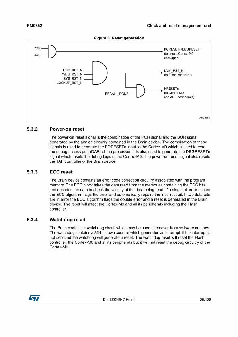
Figure 3. Reset generation . . . . . . . . . . . . . . . . . . . . . . . . . . . . . . . . . . . . . . . . . . . . . . . . . . . . . . . . 25
Figure 4. Flash wrapper state machine operation . . . . . . . . . . . . . . . . . . . . . . . . . . . . . . . . . . . . . . . 37
Figure 5. Simplified block diagram. . . . . . . . . . . . . . . . . . . . . . . . . . . . . . . . . . . . . . . . . . . . . . . . . . . 48
Figure 6. Dual timer module block diagram . . . . . . . . . . . . . . . . . . . . . . . . . . . . . . . . . . . . . . . . . . . . 50
Figure 7. TIMCLK equals PCLK and TIMCLKENX equals one, clock example. . . . . . . . . . . . . . . . . 52
Figure 8. TIMCLK is less than PCLK and TIMCLKENX equals one, clock example . . . . . . . . . . . . . 52
Figure 9. Prescale clock enable generation. . . . . . . . . . . . . . . . . . . . . . . . . . . . . . . . . . . . . . . . . . . . 53
Figure 10. Example timing diagram of prescaler clock enable generation. . . . . . . . . . . . . . . . . . . . . . 53
Figure 11. Example interrupt signal timing. . . . . . . . . . . . . . . . . . . . . . . . . . . . . . . . . . . . . . . . . . . . . . 56
Figure 12. Raw and masked interrupt status . . . . . . . . . . . . . . . . . . . . . . . . . . . . . . . . . . . . . . . . . . . . 56
Figure 13. Peripheral identification register bit assignment . . . . . . . . . . . . . . . . . . . . . . . . . . . . . . . . . 63
Figure 14. PrimeCell identification register bit assignments . . . . . . . . . . . . . . . . . . . . . . . . . . . . . . . . 65
DocID024647 Rev 1 11/138
RM0352 Referenced document
137
1 Referenced document
Table 1. Referenced document
Reference number Name Owner Revision
DUI0497A_cortex_m0_r0p0_generic_ug(1)
1. Refer to http://infocenter.arm.com/help/topic/com.arm.doc.dui0497a/index.html.
“Cortex-M0 Devices Generic User
Guide”
ARM®
r0p0
DDI0432C_cortex_m0_r0p0_trm(2)
2. Refer to http://infocenter.arm.com/help/topic/com.arm.doc.ddi0432c/DDI0432C_cortex_m0_r0p0_trm.pdf
“Cortex-M0 Technical Reference
Manual “
ARM®
r0p0
DDI0419C_arm_architecture_v6m_reference_manual(3)
3. Refer to http://infocenter.arm.com/help/index.jsp?topic=/com.arm.doc.ddi0419c/index.html
“ARMv6-M Architecture Reference
Manual”
ARM®
C
DDI0271D_DualTimer_sp804_r1p0_trm(4)
4. Refer to http://infocenter.arm.com/help/index.jsp?topic=/com.arm.doc.ddi0271d/index.html
“ARM Dual-Timer module (SP804)
Technical Reference Manual”
ARM®
r1p0
DDI0194G_ssp_pl022_r1p3_trm(5)
5. Refer to http://infocenter.arm.com/help/index.jsp?topic=/com.arm.doc.ddi0194g/index.html
“ARM PrimeCell®
Synchronous
Serial Port (PL022) Technical
Reference Manual”
ARM®
r1p3
DDI0183G_uart_pl011_r1p5_trm(6)
6. Refer to http://infocenter.arm.com/help/index.jsp?topic=/com.arm.doc.ddi0183g/index.html
“PrimeCell®
UART(PL011) Technical
Reference Manual”
ARM®
r1p5
System and memory overview RM0352
12/138 DocID024647 Rev 1
2 System and memory overview
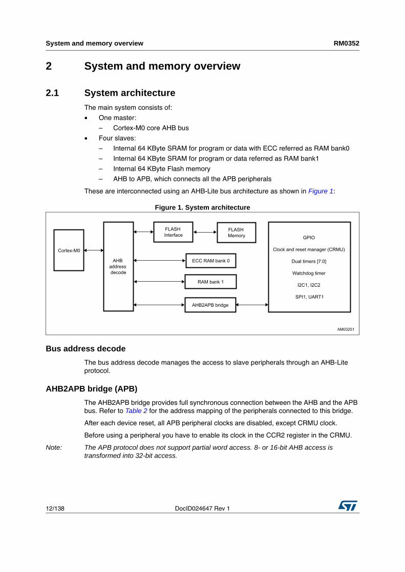
2.1 System architectureThe main system consists of:
• One master:
– Cortex-M0 core AHB bus
• Four slaves:
– Internal 64 KByte SRAM for program or data with ECC referred as RAM bank0
– Internal 64 KByte SRAM for program or data referred as RAM bank1
– Internal 64 KByte Flash memory
– AHB to APB, which connects all the APB peripherals
These are interconnected using an AHB-Lite bus architecture as shown in Figure 1:
Figure 1. System architecture
Bus address decode
The bus address decode manages the access to slave peripherals through an AHB-Lite
protocol.
AHB2APB bridge (APB)
The AHB2APB bridge provides full synchronous connection between the AHB and the APB
bus. Refer to Table 2 for the address mapping of the peripherals connected to this bridge.
After each device reset, all APB peripheral clocks are disabled, except CRMU clock.
Before using a peripheral you have to enable its clock in the CCR2 register in the CRMU.
Note: The APB protocol does not support partial word access. 8- or 16-bit AHB access is transformed into 32-bit access.
DocID024647 Rev 1 13/138
RM0352 System and memory overview
137
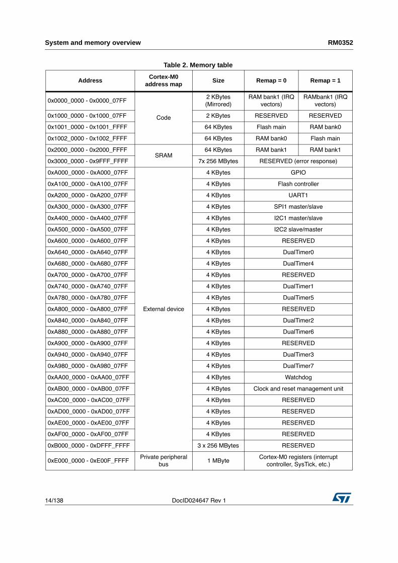
2.2 Memory organization
Introduction
Program memory, data memory, registers and I/O ports are organized within the same linear
4-Gbyte address space.
The bytes are coded in memory in Little Endian format. The lowest numbered byte in a word
is considered the word's least significant byte and the highest numbered byte the most
significant.
The addressable memory space is divided into 16 main blocks, each of 256 MB. All the
memory areas that are not allocated to on-chip memories and peripherals are considered
“RESERVED”.
For the detailed mapping of an available memory and register areas, please refer to the
memory map in Table 2 and to the register lists detailed in each of the peripheral sections
(Table 5 on page 20 in Section 4: GPIO to Table 114 on page 119 in Section 12: UART (universal asynchronous receive transmit)).
System and memory overview RM0352
14/138 DocID024647 Rev 1
Table 2. Memory table
AddressCortex-M0
address mapSize Remap = 0 Remap = 1
0x0000_0000 - 0x0000_07FF
Code
2 KBytes
(Mirrored)
RAM bank1 (IRQ
vectors)
RAMbank1 (IRQ
vectors)
0x1000_0000 - 0x1000_07FF 2 KBytes RESERVED RESERVED
0x1001_0000 - 0x1001_FFFF 64 KBytes Flash main RAM bank0
0x1002_0000 - 0x1002_FFFF 64 KBytes RAM bank0 Flash main
0x2000_0000 - 0x2000_FFFF
SRAM
64 KBytes RAM bank1 RAM bank1
0x3000_0000 - 0x9FFF_FFFF 7x 256 MBytes RESERVED (error response)
0xA000_0000 - 0xA000_07FF
External device
4 KBytes GPIO
0xA100_0000 - 0xA100_07FF 4 KBytes Flash controller
0xA200_0000 - 0xA200_07FF 4 KBytes UART1
0xA300_0000 - 0xA300_07FF 4 KBytes SPI1 master/slave
0xA400_0000 - 0xA400_07FF 4 KBytes I2C1 master/slave
0xA500_0000 - 0xA500_07FF 4 KBytes I2C2 slave/master
0xA600_0000 - 0xA600_07FF 4 KBytes RESERVED
0xA640_0000 - 0xA640_07FF 4 KBytes DualTimer0
0xA680_0000 - 0xA680_07FF 4 KBytes DualTimer4
0xA700_0000 - 0xA700_07FF 4 KBytes RESERVED
0xA740_0000 - 0xA740_07FF 4 KBytes DualTimer1
0xA780_0000 - 0xA780_07FF 4 KBytes DualTimer5
0xA800_0000 - 0xA800_07FF 4 KBytes RESERVED
0xA840_0000 - 0xA840_07FF 4 KBytes DualTimer2
0xA880_0000 - 0xA880_07FF 4 KBytes DualTimer6
0xA900_0000 - 0xA900_07FF 4 KBytes RESERVED
0xA940_0000 - 0xA940_07FF 4 KBytes DualTimer3
0xA980_0000 - 0xA980_07FF 4 KBytes DualTimer7
0xAA00_0000 - 0xAA00_07FF 4 KBytes Watchdog
0xAB00_0000 - 0xAB00_07FF 4 KBytes Clock and reset management unit
0xAC00_0000 - 0xAC00_07FF 4 KBytes RESERVED
0xAD00_0000 - 0xAD00_07FF 4 KBytes RESERVED
0xAE00_0000 - 0xAE00_07FF 4 KBytes RESERVED
0xAF00_0000 - 0xAF00_07FF 4 KBytes RESERVED
0xB000_0000 - 0xDFFF_FFFF 3 x 256 MBytes RESERVED
0xE000_0000 - 0xE00F_FFFF
Private peripheral
bus
1 MByte
Cortex-M0 registers (interrupt
controller, SysTick, etc.)
DocID024647 Rev 1 15/138
RM0352 System and memory overview
137
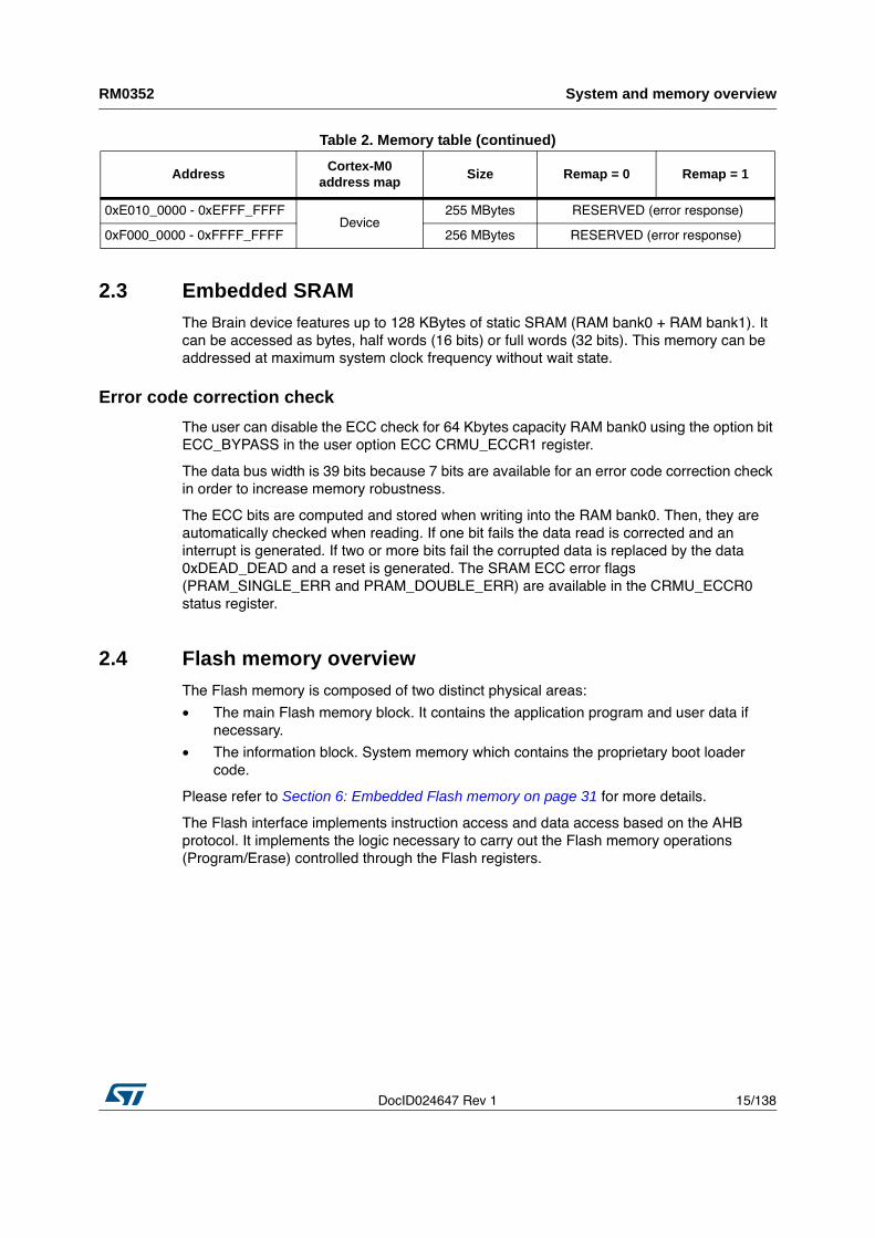
2.3 Embedded SRAMThe Brain device features up to 128 KBytes of static SRAM (RAM bank0 + RAM bank1). It
can be accessed as bytes, half words (16 bits) or full words (32 bits). This memory can be
addressed at maximum system clock frequency without wait state.
Error code correction check
The user can disable the ECC check for 64 Kbytes capacity RAM bank0 using the option bit
ECC_BYPASS in the user option ECC CRMU_ECCR1 register.
The data bus width is 39 bits because 7 bits are available for an error code correction check
in order to increase memory robustness.
The ECC bits are computed and stored when writing into the RAM bank0. Then, they are
automatically checked when reading. If one bit fails the data read is corrected and an
interrupt is generated. If two or more bits fail the corrupted data is replaced by the data
0xDEAD_DEAD and a reset is generated. The SRAM ECC error flags
(PRAM_SINGLE_ERR and PRAM_DOUBLE_ERR) are available in the CRMU_ECCR0
status register.
2.4 Flash memory overviewThe Flash memory is composed of two distinct physical areas:
• The main Flash memory block. It contains the application program and user data if
necessary.
• The information block. System memory which contains the proprietary boot loader
code.
Please refer to Section 6: Embedded Flash memory on page 31 for more details.
The Flash interface implements instruction access and data access based on the AHB
protocol. It implements the logic necessary to carry out the Flash memory operations
(Program/Erase) controlled through the Flash registers.
0xE010_0000 - 0xEFFF_FFFF
Device
255 MBytes RESERVED (error response)
0xF000_0000 - 0xFFFF_FFFF 256 MBytes RESERVED (error response)
Table 2. Memory table (continued)
AddressCortex-M0
address mapSize Remap = 0 Remap = 1
System and memory overview RM0352
16/138 DocID024647 Rev 1
2.5 Physical remapThe application software can switch between two memory mappings (see Table 2: Memory table on page 14). This modification is performed by programming the REMAP bit in the
Flash CONFIG register (see Section 6.3.5 on page 35). It can be used to switch the
execution code from Flash to ECC RAM bank0. A typical use would be to copy the whole
contents of the Flash into the RAM bank0 and then to set the REMAP bit.
DocID024647 Rev 1 17/138
RM0352 Interrupts
137
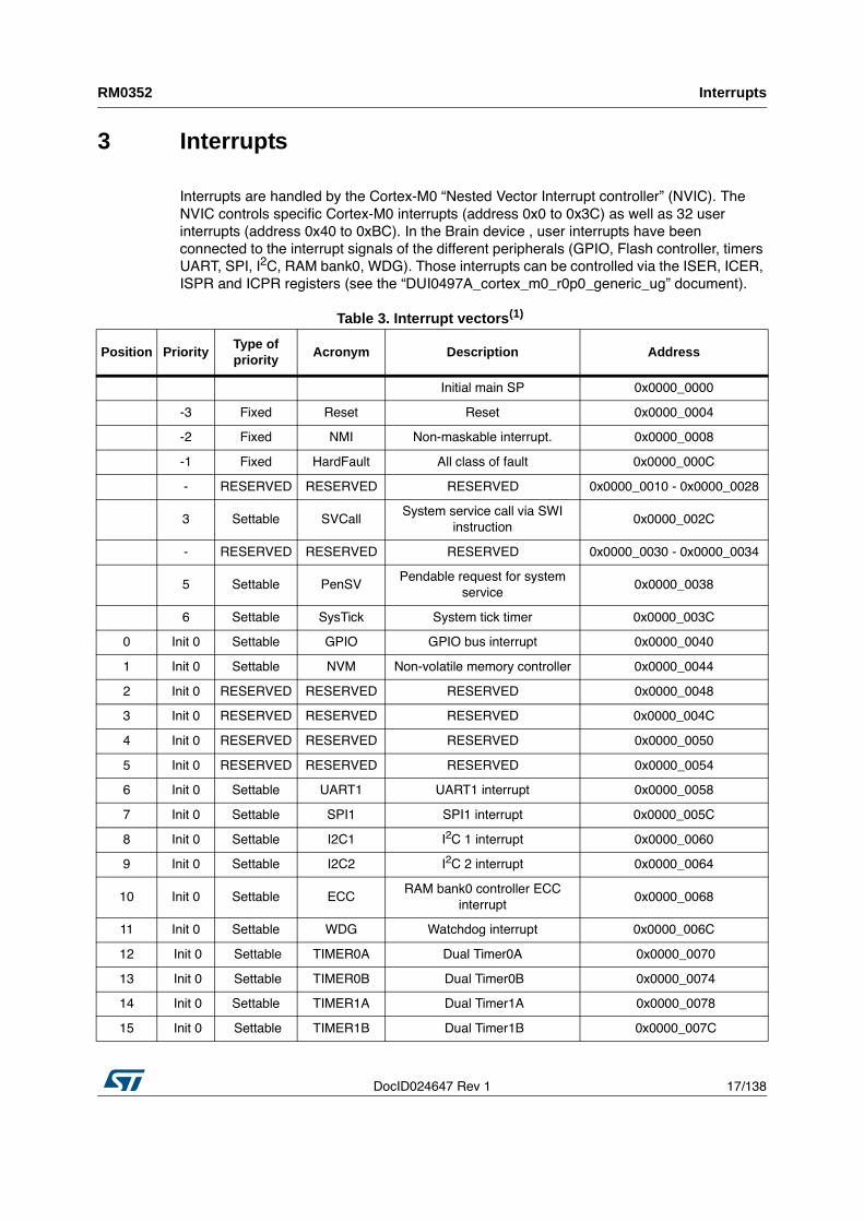
3 Interrupts
Interrupts are handled by the Cortex-M0 “Nested Vector Interrupt controller” (NVIC). The
NVIC controls specific Cortex-M0 interrupts (address 0x0 to 0x3C) as well as 32 user
interrupts (address 0x40 to 0xBC). In the Brain device , user interrupts have been
connected to the interrupt signals of the different peripherals (GPIO, Flash controller, timers
UART, SPI, I2C, RAM bank0, WDG). Those interrupts can be controlled via the ISER, ICER,
ISPR and ICPR registers (see the “DUI0497A_cortex_m0_r0p0_generic_ug” document).
Table 3. Interrupt vectors(1)
Position PriorityType of priority
Acronym Description Address
Initial main SP 0x0000_0000
-3 Fixed Reset Reset 0x0000_0004
-2 Fixed NMI Non-maskable interrupt. 0x0000_0008
-1 Fixed HardFault All class of fault 0x0000_000C
- RESERVED RESERVED RESERVED 0x0000_0010 - 0x0000_0028
3 Settable SVCall
System service call via SWI
instruction
0x0000_002C
- RESERVED RESERVED RESERVED 0x0000_0030 - 0x0000_0034
5 Settable PenSV
Pendable request for system
service
0x0000_0038
6 Settable SysTick System tick timer 0x0000_003C
0 Init 0 Settable GPIO GPIO bus interrupt 0x0000_0040
1 Init 0 Settable NVM Non-volatile memory controller 0x0000_0044
2 Init 0 RESERVED RESERVED RESERVED 0x0000_0048
3 Init 0 RESERVED RESERVED RESERVED 0x0000_004C
4 Init 0 RESERVED RESERVED RESERVED 0x0000_0050
5 Init 0 RESERVED RESERVED RESERVED 0x0000_0054
6 Init 0 Settable UART1 UART1 interrupt 0x0000_0058
7 Init 0 Settable SPI1 SPI1 interrupt 0x0000_005C
8 Init 0 Settable I2C1 I2C 1 interrupt 0x0000_0060
9 Init 0 Settable I2C2 I2C 2 interrupt 0x0000_0064
10 Init 0 Settable ECC
RAM bank0 controller ECC
interrupt
0x0000_0068
11 Init 0 Settable WDG Watchdog interrupt 0x0000_006C
12 Init 0 Settable TIMER0A Dual Timer0A 0x0000_0070
13 Init 0 Settable TIMER0B Dual Timer0B 0x0000_0074
14 Init 0 Settable TIMER1A Dual Timer1A 0x0000_0078
15 Init 0 Settable TIMER1B Dual Timer1B 0x0000_007C
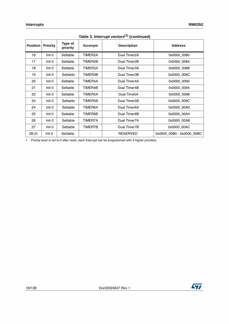
Interrupts RM0352
18/138 DocID024647 Rev 1
16 Init 0 Settable TIMER2A Dual Timer2A 0x0000_0080
17 Init 0 Settable TIMER2B Dual Timer2B 0x0000_0084
18 Init 0 Settable TIMER3A Dual Timer3A 0x0000_0088
19 Init 0 Settable TIMER3B Dual Timer3B 0x0000_008C
20 Init 0 Settable TIMER4A Dual Timer4A 0x0000_0090
21 Init 0 Settable TIMER4B Dual Timer4B 0x0000_0094
22 Init 0 Settable TIMER5A Dual Time5A 0x0000_0098
23 Init 0 Settable TIMER5B Dual Timer5B 0x0000_009C
24 Init 0 Settable TIMER6A Dual Timer6A 0x0000_00A0
25 Init 0 Settable TIMER6B Dual Timer6B 0x0000_00A4
26 Init 0 Settable TIMER7A Dual Timer7A 0x0000_00A8
27 Init 0 Settable TIMER7B Dual Timer7B 0x0000_00AC
28-31 Init 0 Settable - RESERVED 0x0000_00B0 - 0x0000_00BC
1. Priority level is set to 0 after reset, each interrupt can be programmed with 3 higher priorities.
Table 3. Interrupt vectors(1) (continued)
Position PriorityType of priority
Acronym Description Address
DocID024647 Rev 1 19/138
RM0352 GPIO
137
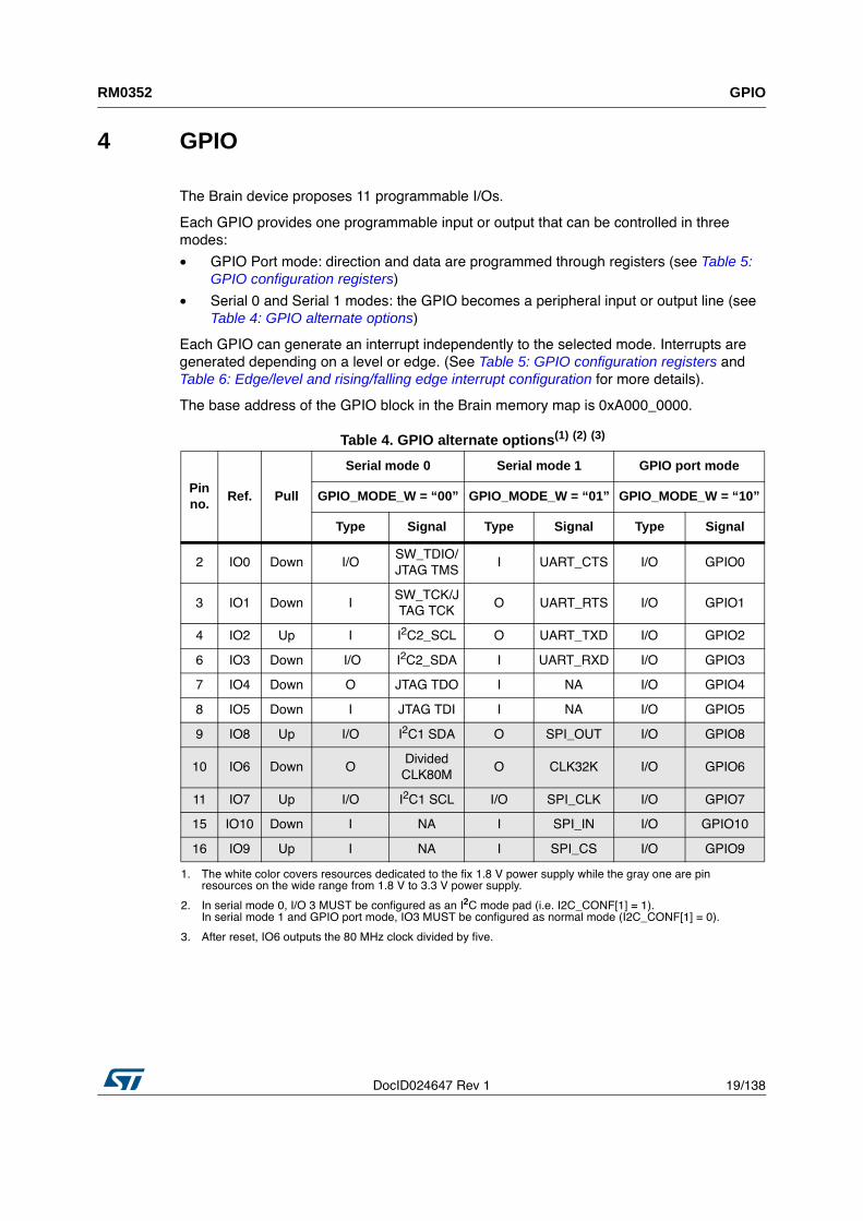
4 GPIO
The Brain device proposes 11 programmable I/Os.
Each GPIO provides one programmable input or output that can be controlled in three
modes:
• GPIO Port mode: direction and data are programmed through registers (see Table 5: GPIO configuration registers)
• Serial 0 and Serial 1 modes: the GPIO becomes a peripheral input or output line (see
Table 4: GPIO alternate options)
Each GPIO can generate an interrupt independently to the selected mode. Interrupts are
generated depending on a level or edge. (See Table 5: GPIO configuration registers and
Table 6: Edge/level and rising/falling edge interrupt configuration for more details).
The base address of the GPIO block in the Brain memory map is 0xA000_0000.
Table 4. GPIO alternate options(1) (2) (3)
1. The white color covers resources dedicated to the fix 1.8 V power supply while the gray one are pin
resources on the wide range from 1.8 V to 3.3 V power supply.
2. In serial mode 0, I/O 3 MUST be configured as an I2C mode pad (i.e. I2C_CONF[1] = 1).
In serial mode 1 and GPIO port mode, IO3 MUST be configured as normal mode (I2C_CONF[1] = 0).
3. After reset, IO6 outputs the 80 MHz clock divided by five.
Pin no.
Ref. Pull
Serial mode 0 Serial mode 1 GPIO port mode
GPIO_MODE_W = “00” GPIO_MODE_W = “01” GPIO_MODE_W = “10”
Type Signal Type Signal Type Signal
2 IO0 Down I/O
SW_TDIO/
JTAG TMS
I UART_CTS I/O GPIO0
3 IO1 Down I
SW_TCK/J
TAG TCK
O UART_RTS I/O GPIO1
4 IO2 Up I I2C2_SCL O UART_TXD I/O GPIO2
6 IO3 Down I/O I2C2_SDA I UART_RXD I/O GPIO3
7 IO4 Down O JTAG TDO I NA I/O GPIO4
8 IO5 Down I JTAG TDI I NA I/O GPIO5
9 IO8 Up I/O I2C1 SDA O SPI_OUT I/O GPIO8
10 IO6 Down O
Divided
CLK80M
O CLK32K I/O GPIO6
11 IO7 Up I/O I2C1 SCL I/O SPI_CLK I/O GPIO7
15 IO10 Down I NA I SPI_IN I/O GPIO10
16 IO9 Up I NA I SPI_CS I/O GPIO9
GPIO RM0352
20/138 DocID024647 Rev 1
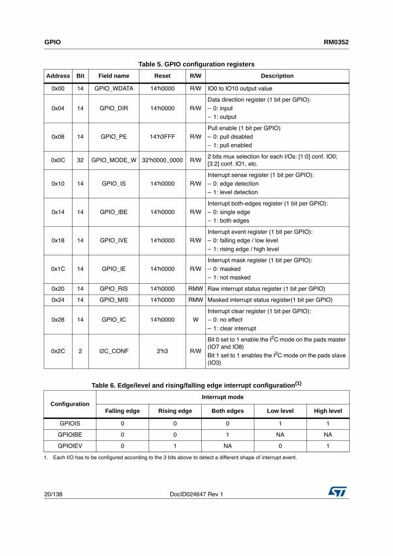
Table 5. GPIO configuration registers
Address Bit Field name Reset R/W Description
0x00 14 GPIO_WDATA 14'h0000 R/W IO0 to IO10 output value
0x04 14 GPIO_DIR 14'h0000 R/W
Data direction register (1 bit per GPIO):
– 0: input
– 1: output
0x08 14 GPIO_PE 14'h3FFF R/W
Pull enable (1 bit per GPIO)
– 0: pull disabled
– 1: pull enabled
0x0C 32 GPIO_MODE_W 32'h0000_0000 R/W
2 bits mux selection for each I/Os: [1:0] conf. IO0;
[3:2] conf. IO1, etc.
0x10 14 GPIO_IS 14'h0000 R/W
Interrupt sense register (1 bit per GPIO):
– 0: edge detection
– 1: level detection
0x14 14 GPIO_IBE 14'h0000 R/W
Interrupt both-edges register (1 bit per GPIO):
– 0: single edge
– 1: both edges
0x18 14 GPIO_IVE 14'h0000 R/W
Interrupt event register (1 bit per GPIO):
– 0: falling edge / low level
– 1: rising edge / high level
0x1C 14 GPIO_IE 14'h0000 R/W
Interrupt mask register (1 bit per GPIO):
– 0: masked
– 1: not masked
0x20 14 GPIO_RIS 14'h0000 RMW Raw interrupt status register (1 bit per GPIO)
0x24 14 GPIO_MIS 14'h0000 RMW Masked interrupt status register(1 bit per GPIO)
0x28 14 GPIO_IC 14'h0000 W
Interrupt clear register (1 bit per GPIO):
– 0: no effect
– 1: clear interrupt
0x2C 2 I2C_CONF 2'h3 R/W
Bit 0 set to 1 enable the I2C mode on the pads master
(IO7 and IO8)
Bit 1 set to 1 enables the I2C mode on the pads slave
(IO3)
Table 6. Edge/level and rising/falling edge interrupt configuration(1)
ConfigurationInterrupt mode
Falling edge Rising edge Both edges Low level High level
GPIOIS 0 0 0 1 1
GPIOIBE 0 0 1 NA NA
GPIOIEV 0 1 NA 0 1
1. Each I/O has to be configured according to the 3 bits above to detect a different shape of interrupt event.
DocID024647 Rev 1 21/138
RM0352 Clock and reset management unit
137
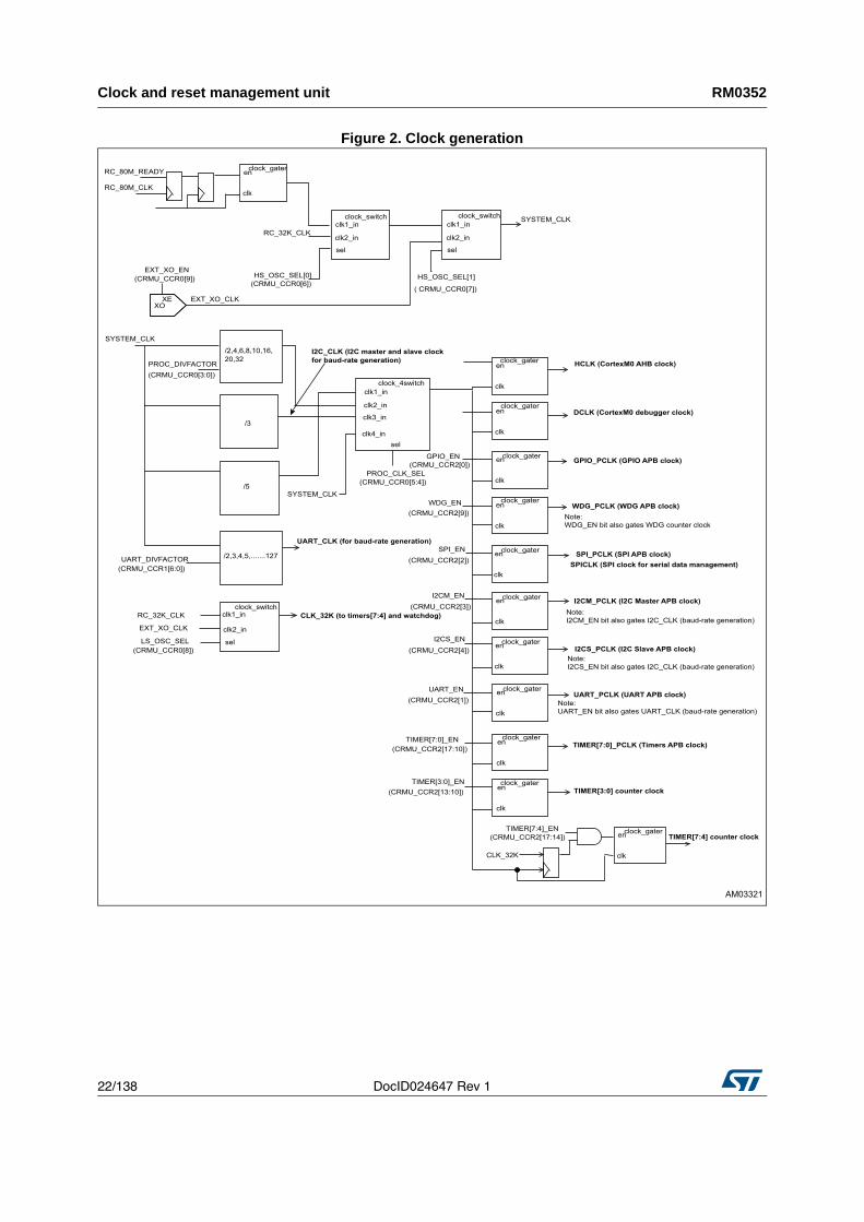
5 Clock and reset management unit
5.1 IntroductionThe Brain CRMU implements the clock and reset generation for the Brain device. The Brain
CRMU is accessible through an APB interface.
5.2 Clock generation
5.2.1 General description
The system clock can be selected from one of three clocks:
• 80 MHz RC oscillator clock
• 32 kHz RC oscillator clock
Note: Real frequency is 32.768 kHz. However, it is called 32 kHz throughout the document to simplify.
• External single ended input clock
There are four clock dividers in the CRMU which divide the system clock before it is used to
generate the clocks for the peripherals, processor, and memories.
The source of the clock for the processor can be selected from four possible sources:
• System clock divided by 5 (default)
• System clock divided by 2, 4, 6, 8, 10, 16, 20, 32
• System clock divided by 3
• System clock
By default the system clock divided by 5 is selected as the root point for the AHB and APB
clocks, this is to meet the access time requirements of the Flash memory which is 50 ns. In
the Brain device the processor boots from the information block of the Flash so it is not
possible to boot with the 80 MHz RC oscillator clock. The user can switch to the high speed
clock after the program has been copied into the program RAM.
The system contains a low speed clock which is used for the timers and the watchdog
circuitry. The low speed clock has 2 possible sources:
• 32 KHz RC oscillator clock
• External single ended input clock
Clock and reset management unit RM0352
22/138 DocID024647 Rev 1
Figure 2. Clock generation
DocID024647 Rev 1 23/138
RM0352 Clock and reset management unit
137
5.2.2 RC 80 MHz clock
The 80 MHz clock is generated by an on-chip RC oscillator and is accurate to within
1 percent.
5.2.3 RC 32 kHz clock
The 32 kHz clock is generated by an on-chip RC oscillator and is accurate to within
1 percent.
5.2.4 External clock
The external clock is generated by a single ended clock source operating up to 80 MHz.
5.2.5 System clock
The system clock has 3 possible sources; the field HS_OSC_SEL in CRMU_CCR0 is used
to switch between the various sources.
• HS_OSC_SEL[0] selects between either RC_32K_CLK or RC_80M_CLK.
• HS_OSC_SEL[1] can be used to select the external clock as source for the system
clock.
• If HS_OSC_SEL[1] is set to 0 which is the default either RC_32K_CLK or
RC_80M_CLK will be selected as system clock.
In order to switch to the external clock the bit EXT_XO_EN in the CRMU_CCR0 register
(see Table 9: CRMU_CCR0 on page 28) must be set to 1 to enable the external clock.
5.2.6 I2C clocks
Each I2C IP has two clock inputs - one for the APB interface which is synchronous to the
processor clock and one for the baud rate generation the source of which is the system
clock divided by 3.
5.2.7 UART clocks
The UART has two clock inputs - one for the APB interface which is synchronous to the
processor clock and one for the baud rate generation the source of which is the system
clock divided by the programmable division factor written to the UART_DIVFACTOR field of
the CRMU_CCR1 register (see Table 13: CRMU_CCR1 on page 29).
5.2.8 Dual timers clocks
The timers 3 to 0 are clocked with a clock synchronous to the processor clock. The
timers 7 to 4 are clocked with the 32 KHz resynchronized on the system clock. When the
system clock is equal or lower than 32 KHz, timers 7 to 4 are not functional. LS_OSC_SEL
bit in the CRMU_CCR0 register (see Table 9: CRMU_CCR0 on page 28) allows choosing
32 KHz source between an internal oscillator and external single ended clock.
5.2.9 Watchdog clock
The watchdog is clocked on 32 KHz. The LS_OSC_SEL bit in the CRMU_CCR0 register
allows choosing 32 KHz source between an internal oscillator and external single ended
clock.
Clock and reset management unit RM0352
24/138 DocID024647 Rev 1
5.2.10 SysTick clock
The SysTick timer is clocked on the processor clock.
5.2.11 SPI clock
The SPI IP has two clock inputs: one for the APB interface and one for the serial
receive/transmit feature. Both are clocked with a clock synchronous to the processor clock.
The serial clock can be divided by a factor of 2 to 254 by a step of two through the
CPSDVSR field of the SSPCPSR register (see Table 101: SSPCPSR register bit assignments on page 107).
5.2.12 APB peripherals
To provide low power implementation all APB peripherals in the Brain device may have their
clocks gated off by writing to a bit in the CRMU_CCR2 register (see Table 14: CRMU_CCR2 on page 29).
5.3 Reset generation
5.3.1 General description
The Brain device contains various sources of reset: a power-on reset signal generated by
the POR circuitry and a brown out reset BOR which occurs when the battery level has fallen
below a certain threshold. In addition there are five internal events which cause various
parts of the chip to be reset.
The processor reset is generated by a combination of the POR, BOR, the error code
correction (ECC) reset, the watchdog reset, the system reset request from the debugger,
the recall done signal output from the Flash controller circuit, and the lockup signal output
from the processor.
The Flash controller is reset by a combination of the POR, BOR, ECC reset, watchdog
reset, system reset request, and lockup event of the processor, the recall signal does not
reset the Flash controller.
The Cortex-M0 debugger is reset only by the POR and the BOR signals this means that
none of the internal reset events should affect the debug session.
The timers are reset by the POR and the BOR signals.
DocID024647 Rev 1 25/138
RM0352 Clock and reset management unit
137
Figure 3. Reset generation
5.3.2 Power-on reset
The power-on reset signal is the combination of the POR signal and the BOR signal
generated by the analog circuitry contained in the Brain device. The combination of these
signals is used to generate the PORESETn input to the Cortex-M0 which is used to reset
the debug access port (DAP) of the processor. It is also used to generate the DBGRESETn
signal which resets the debug logic of the Cortex-M0. The power-on reset signal also resets
the TAP controller of the Brain device.
5.3.3 ECC reset
The Brain device contains an error code correction circuitry associated with the program
memory. The ECC block takes the data read from the memories containing the ECC bits
and decodes the data to check the validity of the data being read. If a single bit error occurs
the ECC algorithm flags the error and automatically repairs the incorrect bit. If two data bits
are in error the ECC algorithm flags the double error and a reset is generated in the Brain
device. The reset will affect the Cortex-M0 and all its peripherals including the Flash
controller.
5.3.4 Watchdog reset
The Brain contains a watchdog circuit which may be used to recover from software crashes.
The watchdog contains a 32-bit down counter which generates an interrupt, if the interrupt is
not serviced the watchdog will generate a reset. The watchdog reset will reset the Flash
controller, the Cortex-M0 and all its peripherals but it will not reset the debug circuitry of the
Cortex-M0.
Clock and reset management unit RM0352
26/138 DocID024647 Rev 1
5.3.5 System reset request
The system reset request is generated by the debug circuitry of the Cortex-M0. The
debugger writes to the SYSRESETREQ bit of the “Application Interrupt and Reset Control
Register” (AIRCR). The system reset request does not affect the debugger thus allowing the
debugger to remain connected during the reset sequence. For more details on the Cortex-
M0 system control and ID registers, refer to section B3.2.2 of “ARMv6-M Architecture Reference Manual”.
5.3.6 Lockup reset
The Cortex-M0 generates an output LOCKUP which indicates that the core is in the
architected lock-up state resulting from an unrecoverable exception. The LOCKUP signal is
used to generate reset in the Brain device. This reset will affect the Cortex-M0, the Flash
controller, and all the peripherals. The LOCKUP signal does not reset the Cortex-M0 debug
circuitry. For more information on the LOCKUP state the reader is referred to section
B1.5.15 of “ARMv6-M Architecture Reference Manual”.
5.3.7 Recall done
The Flash controller must perform the RECALL operation of the Flash memory after power-
up, during this time the trimming codes of the Flash memory are restored from the memory
array to the Flash registers. During the RECALL time the processor is held in reset when the
RECALL_DONE signal is set to one, the processor can leave the reset state and begin
program fetch from Flash.
DocID024647 Rev 1 27/138
RM0352 Clock and reset management unit
137
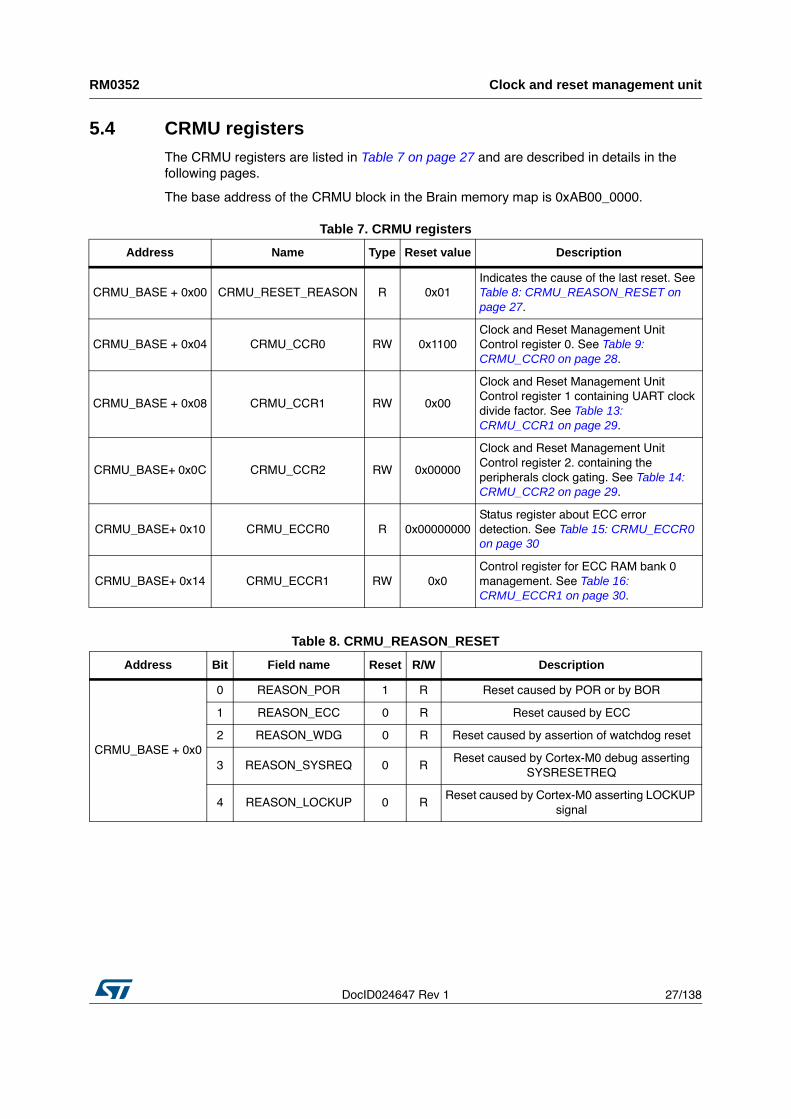
5.4 CRMU registersThe CRMU registers are listed in Table 7 on page 27 and are described in details in the
following pages.
The base address of the CRMU block in the Brain memory map is 0xAB00_0000.
Table 7. CRMU registers
Address Name Type Reset value Description
CRMU_BASE + 0x00 CRMU_RESET_REASON R 0x01
Indicates the cause of the last reset. See
Table 8: CRMU_REASON_RESET on page 27.
CRMU_BASE + 0x04 CRMU_CCR0 RW 0x1100
Clock and Reset Management Unit
Control register 0. See Table 9: CRMU_CCR0 on page 28.
CRMU_BASE + 0x08 CRMU_CCR1 RW 0x00
Clock and Reset Management Unit
Control register 1 containing UART clock
divide factor. See Table 13: CRMU_CCR1 on page 29.
CRMU_BASE+ 0x0C CRMU_CCR2 RW 0x00000
Clock and Reset Management Unit
Control register 2. containing the
peripherals clock gating. See Table 14: CRMU_CCR2 on page 29.
CRMU_BASE+ 0x10 CRMU_ECCR0 R 0x00000000
Status register about ECC error
detection. See Table 15: CRMU_ECCR0 on page 30
CRMU_BASE+ 0x14 CRMU_ECCR1 RW 0x0
Control register for ECC RAM bank 0
management. See Table 16: CRMU_ECCR1 on page 30.
Table 8. CRMU_REASON_RESET
Address Bit Field name Reset R/W Description
CRMU_BASE + 0x0
0 REASON_POR 1 R Reset caused by POR or by BOR
1 REASON_ECC 0 R Reset caused by ECC
2 REASON_WDG 0 R Reset caused by assertion of watchdog reset
3 REASON_SYSREQ 0 R
Reset caused by Cortex-M0 debug asserting
SYSRESETREQ
4 REASON_LOCKUP 0 R
Reset caused by Cortex-M0 asserting LOCKUP
signal
Clock and reset management unit RM0352
28/138 DocID024647 Rev 1
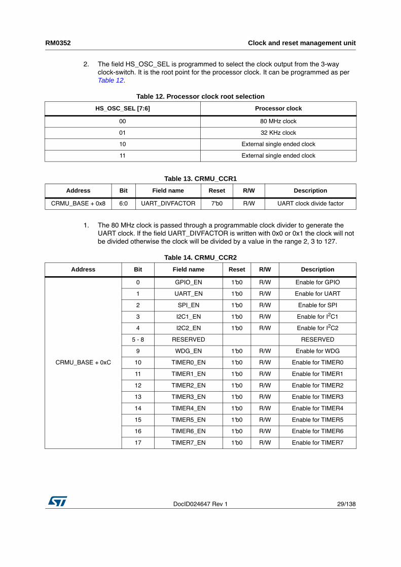
1. The field PROC_CLK_SEL is programmed to select the clock output from the 4-way
clock-switch. It can be programmed as in Table 11.
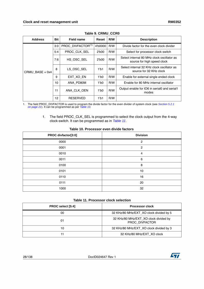
Table 9. CRMU_CCR0
Address Bit Field name Reset R/W Description
CRMU_BASE + 0x4
3:0 PROC_DIVFACTOR(1)
4'b0000 R/W Divide factor for the even clock divider
5:4 PROC_CLK_SEL 2'b00 R/W Select for processor clock switch
7:6 HS_OSC_SEL 2'b00 R/W
Select internal 80 MHz clock oscillator as
source for high speed clock
8 LS_OSC_SEL 1'b1 R/W
Select internal 32 KHz clock oscillator as
source for 32 KHz clock
9 EXT_XO_EN 1'b0 R/W Enable for external single ended clock
10 ANA_PD80M 1'b0 R/W Enable for 80 MHz internal oscillator
11 ANA_CLK_OEN 1'b0 R/W
Output enable for IO6 in serial0 and serial1
modes
12 RESERVED 1'b1 R/W
1. The field PROC_DIVFACTOR is used to program the divide factor for the even divider of system clock (see Section 5.2.1 on page 21). It can be programmed as per Table 10.
Table 10. Processor even divide factors
PROC divfactor[3:0] Division
0000 2
0001 2
0010 4
0011 6
0100 8
0101 10
0110 16
0111 20
1000 32
Table 11. Processor clock selection
PROC select [5:4] Processor clock
00 32 KHz/80 MHz/EXT_XO clock divided by 5
01
32 KHz/80 MHz/EXT_XO clock divided by
PROC_DIVFACTOR
10 32 KHz/80 MHz/EXT_XO clock divided by 3
11 32 KHz/80 MHz/EXT_XO clock
DocID024647 Rev 1 29/138
RM0352 Clock and reset management unit
137
2. The field HS_OSC_SEL is programmed to select the clock output from the 3-way
clock-switch. It is the root point for the processor clock. It can be programmed as per
Table 12.
1. The 80 MHz clock is passed through a programmable clock divider to generate the
UART clock. If the field UART_DIVFACTOR is written with 0x0 or 0x1 the clock will not
be divided otherwise the clock will be divided by a value in the range 2, 3 to 127.
Table 12. Processor clock root selection
HS_OSC_SEL [7:6] Processor clock
00 80 MHz clock
01 32 KHz clock
10 External single ended clock
11 External single ended clock
Table 13. CRMU_CCR1
Address Bit Field name Reset R/W Description
CRMU_BASE + 0x8 6:0 UART_DIVFACTOR 7'b0 R/W UART clock divide factor
Table 14. CRMU_CCR2
Address Bit Field name Reset R/W Description
CRMU_BASE + 0xC
0 GPIO_EN 1'b0 R/W Enable for GPIO
1 UART_EN 1'b0 R/W Enable for UART
2 SPI_EN 1'b0 R/W Enable for SPI
3 I2C1_EN 1'b0 R/W Enable for I2C1
4 I2C2_EN 1'b0 R/W Enable for I2C2
5 - 8 RESERVED RESERVED
9 WDG_EN 1'b0 R/W Enable for WDG
10 TIMER0_EN 1'b0 R/W Enable for TIMER0
11 TIMER1_EN 1'b0 R/W Enable for TIMER1
12 TIMER2_EN 1'b0 R/W Enable for TIMER2
13 TIMER3_EN 1'b0 R/W Enable for TIMER3
14 TIMER4_EN 1'b0 R/W Enable for TIMER4
15 TIMER5_EN 1'b0 R/W Enable for TIMER5
16 TIMER6_EN 1'b0 R/W Enable for TIMER6
17 TIMER7_EN 1'b0 R/W Enable for TIMER7
Clock and reset management unit RM0352
30/138 DocID024647 Rev 1
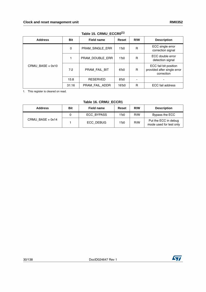
Table 15. CRMU_ECCR0(1)
Address Bit Field name Reset R/W Description
CRMU_BASE + 0x10
0 PRAM_SINGLE_ERR 1'b0 R
ECC single error
correction signal
1 PRAM_DOUBLE_ERR 1'b0 R
ECC double error
detection signal
7:2 PRAM_FAIL_BIT 6'b0 R
ECC fail bit position
provided after single error
correction
15:8 RESERVED 8'b0 - -
31:16 PRAM_FAIL_ADDR 16'b0 R ECC fail address
1. This register is cleared on read.
Table 16. CRMU_ECCR1
Address Bit Field name Reset R/W Description
CRMU_BASE + 0x14
0 ECC_BYPASS 1'b0 R/W Bypass the ECC
1 ECC_DEBUG 1'b0 R/W
Put the ECC in debug
mode used for test only
DocID024647 Rev 1 31/138
RM0352 Embedded Flash memory
137
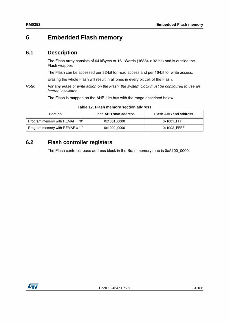
6 Embedded Flash memory
6.1 DescriptionThe Flash array consists of 64 kBytes or 16 kWords (16384 x 32-bit) and is outside the
Flash wrapper.
The Flash can be accessed per 32-bit for read access and per 16-bit for write access.
Erasing the whole Flash will result in all ones in every bit cell of the Flash.
Note: For any erase or write action on the Flash, the system clock must be configured to use an internal oscillator.
The Flash is mapped on the AHB-Lite bus with the range described below:
6.2 Flash controller registersThe Flash controller base address block in the Brain memory map is 0xA100_0000.
Table 17. Flash memory section address
Section Flash AHB start address Flash AHB end address
Program memory with REMAP = ‘0’ 0x1001_0000 0x1001_FFFF
Program memory with REMAP = ‘1’ 0x1002_0000 0x1002_FFFF
Embedded Flash memory RM0352
32/138 DocID024647 Rev 1
6.3 Flash controller registers
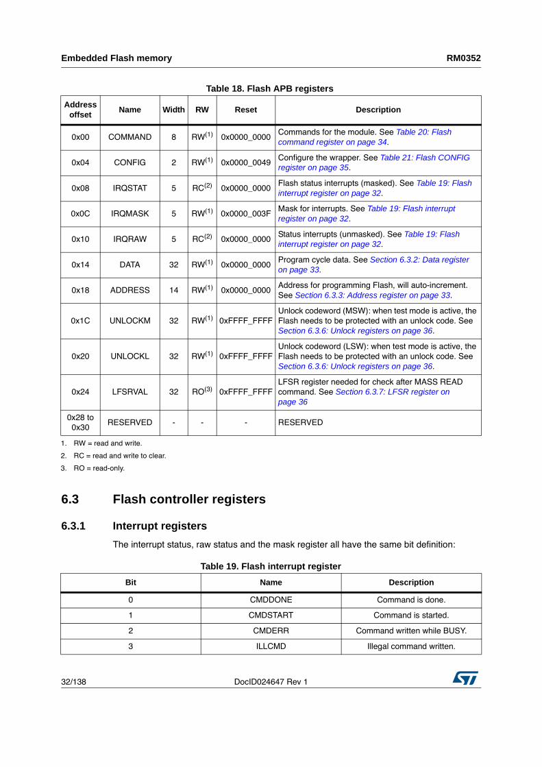
6.3.1 Interrupt registers
The interrupt status, raw status and the mask register all have the same bit definition:
Table 18. Flash APB registers
Address offset
Name Width RW Reset Description
0x00 COMMAND 8 RW(1)
0x0000_0000
Commands for the module. See Table 20: Flash command register on page 34.
0x04 CONFIG 2 RW(1)
0x0000_0049
Configure the wrapper. See Table 21: Flash CONFIG register on page 35.
0x08 IRQSTAT 5 RC(2)
0x0000_0000
Flash status interrupts (masked). See Table 19: Flash interrupt register on page 32.
0x0C IRQMASK 5 RW(1)
0x0000_003F
Mask for interrupts. See Table 19: Flash interrupt register on page 32.
0x10 IRQRAW 5 RC(2)
0x0000_0000
Status interrupts (unmasked). See Table 19: Flash interrupt register on page 32.
0x14 DATA 32 RW(1)
0x0000_0000
Program cycle data. See Section 6.3.2: Data register on page 33.
0x18 ADDRESS 14 RW(1)
0x0000_0000
Address for programming Flash, will auto-increment.
See Section 6.3.3: Address register on page 33.
0x1C UNLOCKM 32 RW(1)
0xFFFF_FFFF
Unlock codeword (MSW): when test mode is active, the
Flash needs to be protected with an unlock code. See
Section 6.3.6: Unlock registers on page 36.
0x20 UNLOCKL 32 RW(1)
0xFFFF_FFFF
Unlock codeword (LSW): when test mode is active, the
Flash needs to be protected with an unlock code. See
Section 6.3.6: Unlock registers on page 36.
0x24 LFSRVAL 32 RO(3)
0xFFFF_FFFF
LFSR register needed for check after MASS READ
command. See Section 6.3.7: LFSR register on page 36
0x28 to
0x30
RESERVED - - - RESERVED
1. RW = read and write.
2. RC = read and write to clear.
3. RO = read-only.
Table 19. Flash interrupt register
Bit Name Description
0 CMDDONE Command is done.
1 CMDSTART Command is started.
2 CMDERR Command written while BUSY.
3 ILLCMD Illegal command written.
DocID024647 Rev 1 33/138
RM0352 Embedded Flash memory
137
The CMDDONE and CMDSTART bits are updated a few clock cycles after the requested
command has been started by writing to the COMMAND register.
Raw status
The raw status register IRQRAW will always show the unmasked condition.
Status
The IRQSTAT register will show the masked version of the raw status register.
Writing an one to the corresponding interrupt status bit will clear the interrupt status bit.
Mask
The mask bit in IRQMASK will mask the condition in the status register IRQSTAT and mask
the generation of the interrupt (output flash_irq).
6.3.2 Data register
The data register needs to be written with:
• The desired value written to the Flash location.
• The desired compare value for a (mass) read operation, the flag READOK will indicate
if there was a match or not. For mass read, all read values must match for READOK.
6.3.3 Address register
Address[13:0] = XADR[7:0] & YADR[5:0].
The 14-bit address is aligned on four bytes (32-bit written for each location).
4 READOK Mass read was OK.
5 FLNREADY Flash not ready (sleep).
Table 19. Flash interrupt register
Bit Name Description
Embedded Flash memory RM0352
34/138 DocID024647 Rev 1
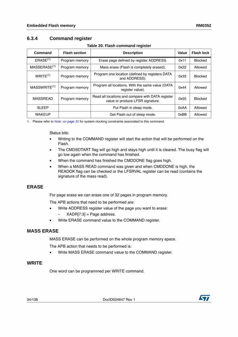
6.3.4 Command register
Status bits:
• Writing to the COMMAND register will start the action that will be performed on the
Flash.
• The CMDSDTART flag will go high and stays high until it is cleared. The busy flag will
go low again when the command has finished.
• When the command has finished the CMDDONE flag goes high.
• When a MASS READ command was given and when CMDDONE is high, the
READOK flag can be checked or the LFSRVAL register can be read (contains the
signature of the mass read).
ERASE
For page erase we can erase one of 32 pages in program memory.
The APB actions that need to be performed are:
• Write ADDRESS register value of the page you want to erase:
– XADR[7:3] = Page address.
• Write ERASE command value to the COMMAND register.
MASS ERASE
MASS ERASE can be performed on the whole program memory space.
The APB action that needs to be performed is:
• Write MASS ERASE command value to the COMMAND register.
WRITE
One word can be programmed per WRITE command.
Table 20. Flash command register
Command Flash section Description Value Flash lock
ERASE(1)
1. Please refer to Note: on page 31 for system clocking constraints associated to this command.
Program memory Erase page defined by register ADDRESS. 0x11 Blocked
MASSERASE(1)
Program memory Mass erase (Flash is completely erased). 0x22 Allowed
WRITE(1)
Program memory
Program one location (defined by registers DATA
and ADDRESS).
0x33 Blocked
MASSWRITE(1)
Program memory
Program all locations. With the same value (DATA
register value).
0x44 Allowed
MASSREAD Program memory
Read all locations and compare with DATA register
value or produce LFSR signature.
0x55 Blocked
SLEEP Put Flash in sleep mode. 0xAA Allowed
WAKEUP Get Flash out of sleep mode. 0xBB Allowed
DocID024647 Rev 1 35/138
RM0352 Embedded Flash memory
137
The APB actions that need to be performed are:
• Write ADDRESS register value of the word you want to write.
• Write DATA register with the value you want to program.
• Write PROGRAM command value to the COMMAND register.
MASS WRITE
One word can be programmed to every location in program memory.
The APB actions that need to be performed are:
• Write DATA register with the value you want to program.
• Write MASS WRITE command value to the COMMAND register.
MASS READ
Every location in program memory can be read with one command.
The APB actions that need to be performed are:
• Write DATA with the value you want to compare with (if READOK flag needs to be
checked). There is no need to write the DATA register to read the signature in the
LFSRVAL register).
• Write MASS READ command value to the COMMAND register.
READOK can be checked to see if all locations matched the DATA register value
(READOK = '1'), or if one or more locations mismatched (READOK = '0').
Every mass read will generate a readable signature (register LFSRVAL).
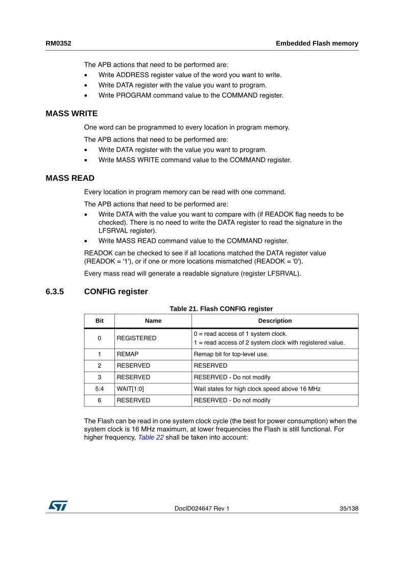
6.3.5 CONFIG register
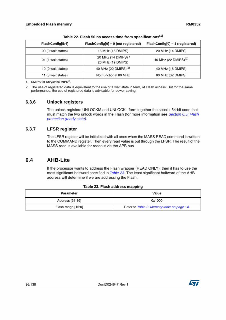
The Flash can be read in one system clock cycle (the best for power consumption) when the
system clock is 16 MHz maximum, at lower frequencies the Flash is still functional. For
higher frequency, Table 22 shall be taken into account:
Table 21. Flash CONFIG register
Bit Name Description
0 REGISTERED
0 = read access of 1 system clock.
1 = read access of 2 system clock with registered value.
1 REMAP Remap bit for top-level use.
2 RESERVED RESERVED
3 RESERVED RESERVED - Do not modify
5:4 WAIT[1:0] Wait states for high clock speed above 16 MHz
6 RESERVED RESERVED - Do not modify
Embedded Flash memory RM0352
36/138 DocID024647 Rev 1
6.3.6 Unlock registers
The unlock registers UNLOCKM and UNLOCKL form together the special 64-bit code that
must match the two unlock words in the Flash (for more information see Section 6.5: Flash protection (ready state).
6.3.7 LFSR register
The LFSR register will be initialized with all ones when the MASS READ command is written
to the COMMAND register. Then every read value is put through the LFSR. The result of the
MASS read is available for readout via the APB bus.
6.4 AHB-LiteIf the processor wants to address the Flash wrapper (READ ONLY), then it has to use the
most significant halfword specified in Table 23. The least significant halfword of the AHB
address will determine if we are addressing the Flash.
Table 22. Flash 50 ns access time from specifications(1)
FlashConfig[5:4] FlashConfig[0] = 0 (not registered) FlashConfig[0] = 1 (registered)
00 (0 wait states) 16 MHz (16 DMIPS) 20 MHz (14 DMIPS)
01 (1 wait states)
20 MHz (14 DMIPS) /
26 MHz (19 DMIPS)
40 MHz (22 DMIPS)(2)
10 (2 wait states) 40 MHz (22 DMIPS)(2)
40 MHz (16 DMIPS)
11 (3 wait states) Not functional 80 MHz 80 MHz (32 DMIPS)
1. DMIPS for Dhrystone MIPS®
.
2. The use of registered data is equivalent to the use of a wait state in term, of Flash access. But for the same
performance, the use of registered data is advisable for power saving.
Table 23. Flash address mapping
Parameter Value
Address [31:16] 0x1000
Flash range [15:0] Refer to Table 2: Memory table on page 14.
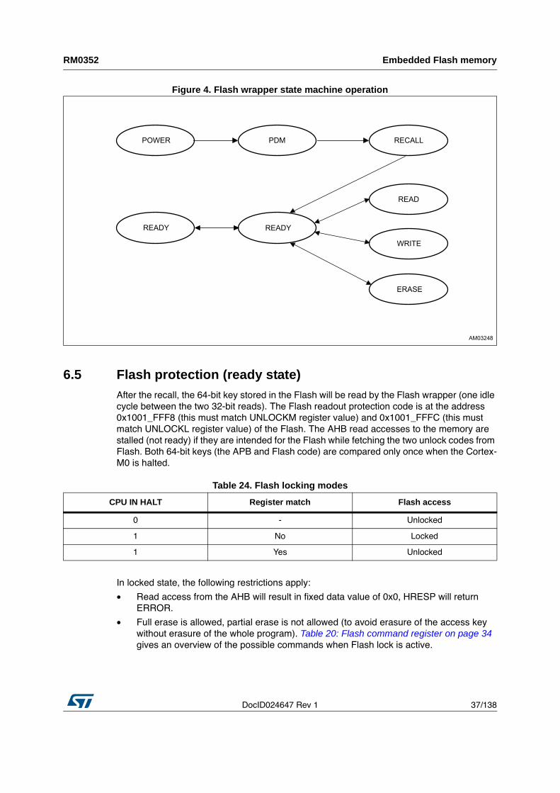
DocID024647 Rev 1 37/138
RM0352 Embedded Flash memory
137
Figure 4. Flash wrapper state machine operation
6.5 Flash protection (ready state)After the recall, the 64-bit key stored in the Flash will be read by the Flash wrapper (one idle
cycle between the two 32-bit reads). The Flash readout protection code is at the address
0x1001_FFF8 (this must match UNLOCKM register value) and 0x1001_FFFC (this must
match UNLOCKL register value) of the Flash. The AHB read accesses to the memory are
stalled (not ready) if they are intended for the Flash while fetching the two unlock codes from
Flash. Both 64-bit keys (the APB and Flash code) are compared only once when the Cortex-
M0 is halted.
In locked state, the following restrictions apply:
• Read access from the AHB will result in fixed data value of 0x0, HRESP will return
ERROR.
• Full erase is allowed, partial erase is not allowed (to avoid erasure of the access key
without erasure of the whole program). Table 20: Flash command register on page 34
gives an overview of the possible commands when Flash lock is active.
Table 24. Flash locking modes
CPU IN HALT Register match Flash access
0 - Unlocked
1 No Locked
1 Yes Unlocked
Watchdog timer (WDG) RM0352
38/138 DocID024647 Rev 1
7 Watchdog timer (WDG)
The watchdog timer (WDG aka WDT) provides a way of recovering from software crashes.
The watchdog clock is used to generate a regular interrupt (WDOGINT), depending on
a programmed value. The watchdog monitors the interrupt and asserts a reset signal
(WDOGRES) if the interrupt remains unserviced for the entire programmed period. You can
enable or disable the watchdog unit as required.
The WDG is counting down at a fixed frequency of 32.768 kHz.
7.1 FunctionalityThe watchdog timer is a 32-bit down counter that divides the clock input to produce an
interrupt. The divide ratio is fully programmable and controls the interrupt interval, which can
be calculated using Equation 1:
Equation 1
Interrupt interval = (WDT_LOAD + 1) / (clock frequency in Hz).
The default ratio is 4294967296 (equivalent to hex value 0xFFFFFFFF + 1). With a
32.768 kHz watchdog clock this generates an interrupt every ~131072 seconds. This
corresponds to the maximum value of WDT_LOAD: 4,294,967,295.
If zero is programmed into WDT_LOAD, an interrupt would always be generated
immediately. Therefore valid values of WDT_LOAD are 1 or higher. Table 25 shows
examples of WDT_LOAD values and the corresponding interrupt interval when using
a 32.768 kHz watchdog clock.
A watchdog interrupt is generated each time the counter reaches 0. The counter is then
reloaded with the content of the WDT_LR register. The interrupt status should be cleared by
writing to the interrupt clear register. When the interrupt is cleared, the counter is reloaded
with WDT_LOAD value. If the interrupt status is not cleared and a new interrupt is
generated, then a watchdog reset is generated, rebooting the system.
The watchdog interrupt and reset generation can be enabled or disabled as required by the
system using the relevant bits in the control register. When the interrupt generation is
Table 25. Interrupt intervals for WDT_LOAD values using a 32 kHz clock
WDT_LOAD Interrupt interval (ms)
4294967295 131072000
65535 2000
32767 1000
4095 125
127 3.90625
63 1.953125
1 0.0610
DocID024647 Rev 1 39/138
RM0352 Watchdog timer (WDG)
137
disabled the watchdog counter is also stopped, and when the interrupt is enabled the
counter will start from the programmed value, not the last count value.
Write access to the registers within the watchdog timer can be disabled by the use of the
watchdog lock register. Writing a value of 0x1ACC_E551 to this WDT_LOCK register allows
write access to all other registers; writing any other value disables write access. This feature
is included to allow some protection against software which might otherwise disable the
watchdog functionality.
7.2 WDG registersThe device communicates to the system via 32-bit-wide control registers accessible via the
AMBA™ rev. 2.0 “Advanced Peripheral Bus” (APB). These registers are listed in Table 26 on page 39 and are described in details on the following pages.
The WDG base address is 0xAA00_0000.
Table 26. WDG register list
Address Name Description
WDG base + 0x000 WDT_LR
Watchdog load value register. See Section 7.2.1: Watchdog load register (WDT_LR) on page 41.
WDG base + 0x004 WDT_VAL
Watchdog current value (read-only) register. See
Section 7.2.2: Watchdog value register WDT_VAL on page 41.
WDG base + 0x008 WDT_CR
Watchdog control register. See Section 7.2.3: Watchdog control register WDT_CR on page 42.
WDG base + 0x00C WDT_ICR
Watchdog interrupt clear register. See Section 7.2.4: Watchdog interrupt clear register WDT_ICR on page 42.
WDG base + 0x010 WDT_RIS
Watchdog raw interrupt status register. See
Section 7.2.5: Watchdog raw interrupt status register WDT_RIS on page 43.
WDG base + 0x014 WDT_MIS
Watchdog masked interrupt status register. See
Section 7.2.6: Watchdog masked interrupt status register WDT_MIS on page 43.
WDG base + 0x01C to 0xBFC - RESERVED
WDG base + 0xC00 WDT_LOCK
Watchdog lock register. See Section 7.2.7: Watchdog lock register WDT_LOCK on page 44.
WDG base + 0xC04 to 0xFDC - RESERVED
WDG base + 0xFE0 WDTPeriphID0
Peripheral identification register bits 7:0. See
Section 7.2.8: Watchdog peripheral identification register WDTPeriphID0-3 on page 44.
WDG base + 0xFE4 WDTPeriphID1
Peripheral identification register bits 15:8. See
Section 7.2.8: Watchdog peripheral identification register WDTPeriphID0-3 on page 44.
WDG base + 0xFE8 WDTPeriphID2
Peripheral identification register bits 23:16. See
Section 7.2.8: Watchdog peripheral identification register WDTPeriphID0-3 on page 44.
Watchdog timer (WDG) RM0352
40/138 DocID024647 Rev 1
WDG base + 0xFEC WDTPeriphID3
Peripheral identification register bits 31:24. See
Section 7.2.8: Watchdog peripheral identification register WDTPeriphID0-3 on page 44.
WDG base + 0xFF0 WDTPCellID0
Cell identification register bits 7:0. See Section 7.2.9: Watchdog PCell identification register WDTPCellID0-3 on page 45.
WDG base + 0xFF4 WDTPCellID1
Cell identification register bits 15:8. See
Section 7.2.9: Watchdog PCell identification register WDTPCellID0-3 on page 45.
WDG base + 0xFF8 WDTPCellID2
Cell identification register bits 23:16. See
Section 7.2.9: Watchdog PCell identification register WDTPCellID0-3 on page 45.
WDG base + 0xFFC WDTPCellID3
Cell identification register bits 31:24. See
Section 7.2.9: Watchdog PCell identification register WDTPCellID0-3 on page 45.
Table 26. WDG register list
Address Name Description
DocID024647 Rev 1 41/138
RM0352 Watchdog timer (WDG)
137
7.2.1 Watchdog load register (WDT_LR)
The WDT_LR register is a 32-bit register containing the value from which the counter is to
decrement. When this register is written to, the count is immediately re-started from the new
value.
The minimum valid value for WDT_LR is 0x1.
Table 27. Watchdog load register WDT_LR
7.2.2 Watchdog value register WDT_VAL
The WDT_VAL register gives the current value of the decrementing watchdog counter.
Table 29. Watchdog value register WDT_VAL
WDT_LR (WDT Base + 0x000) Reset value: 0xFFFF_FFFF
31 30 29 28 27 26 25 24 23 22 21 20 19 18 17 16 15 14 13 12 11 10 9 8 7 6 5 4 3 2 1 0
WDT_LOAD[31:0]
R/W
Table 28. WDT_LR register bit fields
Bit Field Function
WDT_LOAD
Minimum valid value is 0x1.
Watchdog load value
Value from which the counter is to decrement. When this register is written
to, the count is immediately re-started from the new value.
WDT_VAL (WDT Base + 0x004) Reset value: 0xFFFF_FFFF
31 30 29 28 27 26 25 24 23 22 21 20 19 18 17 16 15 14 13 12 11 10 9 8 7 6 5 4 3 2 1 0
WDTVAL[31:0]
R
Table 30. WDT_VAL register bit fields
Bit Field Function
WDTVAL
Watchdog value
When read, returns the current value of the decrementing watchdog
counter. Write has no effect.
Watchdog timer (WDG) RM0352
42/138 DocID024647 Rev 1
7.2.3 Watchdog control register WDT_CR
The WDT_CR register allows configuring the watchdog timer. The bit assignment is listed in
Table 32.
Table 31. Watchdog control register WDT_CR
7.2.4 Watchdog interrupt clear register WDT_ICR
Writing any value to this register will clear the interrupt output from the watchdog, and
reloads the counter from the value in the WDT_LR register.
Table 33. Watchdog interrupt clear register WDT_ICR
WDT_CR (WDT Base + 0x008) Reset value: 0x0000_0000
31 30 29 28 27 26 25 24 23 22 21 20 19 18 17 16 15 14 13 12 11 10 9 8 7 6 5 4 3 2 1 0
RESERVED RESEN INTEN
R R/W R/W
Table 32. WDT_CR register bit fields
Bit field Function
RESEN
Watchdog reset enable
Enable watchdog reset output (WDOGRES). Acts as a mask for the reset out- put.
0b: watchdog reset disabled (default).
1b: watchdog reset enabled.
INTEN
Watchdog interrupt enable
Enable the interrupt event (WDOGINT):
0b: watchdog interrupt disabled (default).
1b: watchdog interrupt enabled.
WDT_ICR (WDT Base + 0x00C) Reset value: 0x0000_0000
31 30 29 28 27 26 25 24 23 22 21 20 19 18 17 16 15 14 13 12 11 10 9 8 7 6 5 4 3 2 1 0
WDT_ICLR
W
Table 34. WDT_ICR register bit fields
Bit Field Function
WDT_ICLR
Watchdog interrupt clear
Writing any value will clear the watchdog interrupt and reloads the counter from the WDT_LR
register.
Reading returns zero.
DocID024647 Rev 1 43/138
RM0352 Watchdog timer (WDG)
137
7.2.5 Watchdog raw interrupt status register WDT_RIS
The WDTRIS register is the raw interrupt status register. This value is ANDed with the
interrupt enable bit from the control register to create the masked interrupt, which is passed
to the interrupt output pin. Table 36 shows the bit assignment of the WDTRIS register.
Table 35. Watchdog raw interrupt status register WDT_RIS
7.2.6 Watchdog masked interrupt status register WDT_MIS
The WDT_MIS register is the masked interrupt status register. This value is the logical AND
of the raw interrupt status with the timer interrupt enable bit from the control register, and is
the same value which is passed to the interrupt output pin. This register is read-only, and all
bits are cleared by a reset.
Table 37. Watchdog masked interrupt status register WDT_MIS
WDT_RIS (WDT Base + 0x010) Reset value: 0x0000_0000
31 30 29 28 27 26 25 24 23 22 21 20 19 18 17 16 15 14 13 12 11 10 9 8 7 6 5 4 3 2 1 0
RESERVED WDTRIS
R R
Table 36. WDT_RIS register bit fields
Bit field Function
WDTRIS
Watchdog raw interrupt status bit
Reflect the status of interrupt status from the watchdog. Read-only bit. Write has no effect.
0b: watchdog interrupt is not set.
1b: watchdog interrupt is set.
WDT_MIS (WDT Base + 0x014) Reset value: 0x0000_0000
31 30 29 28 27 26 25 24 23 22 21 20 19 18 17 16 15 14 13 12 11 10 9 8 7 6 5 4 3 2 1 0
RESERVED WDTMIS
R R
Table 38. WDT_MIS register bit fields
Bit field Function
WDTMIS
Watchdog masked interrupt status bit
Masked value of watchdog interrupt status:
0b: watchdog line interrupt not active.
1b: watchdog line asserting interrupt. Read-only bit. Write has no effect.
Watchdog timer (WDG) RM0352
44/138 DocID024647 Rev 1
7.2.7 Watchdog lock register WDT_LOCK
Use of this register allows write access to all other registers to be disabled. This is to
prevent rogue software from disabling the watchdog functionality. Writing a value of
0x1ACCE551 will enable write access to all other registers; writing any other value will
disable write accesses. A read from this register will return only the least significant bit:
• 0x0 indicates that write access is enabled (not locked)
• 0x1 indicates that write access is disabled (locked).
Table 40 shows the bit assignment of the WDT_LOCK register.
Table 39. Watchdog lock register WDT_LOCK
7.2.8 Watchdog peripheral identification register WDTPeriphID0-3
The WDTPeriphID0-3 registers are four 8-bit registers, that span the address location
0xFE0 to 0xFEC. The registers are read-only.
Table 41. Watchdog peripheral identification register WDTPeriphID0-3 - part 1
WDT_LOCK (WDT Base + 0xC00) Reset value: 0x0000_0000
31 30 29 28 27 26 25 24 23 22 21 20 19 18 17 16 15 14 13 12 11 10 9 8 7 6 5 4 3 2 1 0
LOCKVAL
R/W
Table 40. WDT_LOCK register bit fields
Bit field Function
LOCKVAL
Watchdog lock value
When read, returns the lock status:
0x0: write access to all watchdog other registers is enabled (default).
0x1: write access to all watchdog other registers is disabled.
When written, allows to enable or disable write access to all other watchdog registers:
Writing 0x1ACCE551: Write access to all other registers is enabled. Writing any other value: Write
access to all other registers is disabled.
WDTPeriphID0 (WDT Base + 0xFE0) Reset value: 0x0000_0005
31 30 29 28 27 26 25 24 23 22 21 20 19 18 17 16 15 14 13 12 11 10 9 8 7 6 5 4 3 2 1 0
RESERVED Part number 0
R R
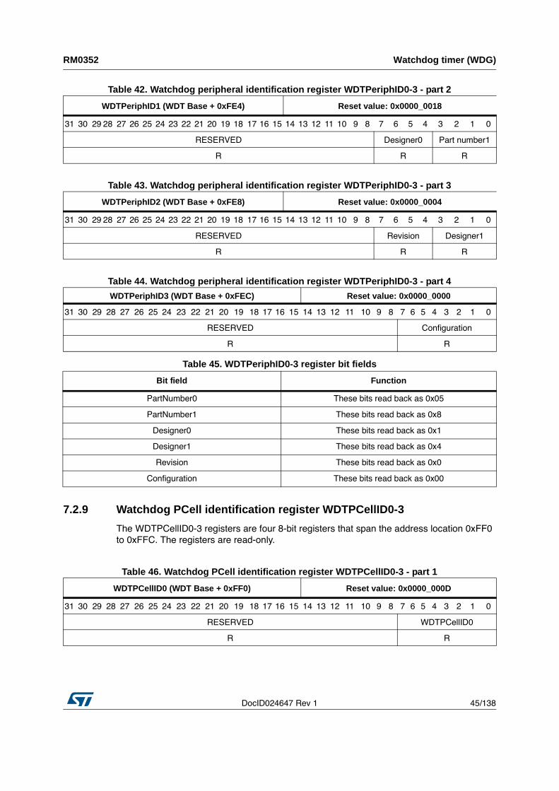
DocID024647 Rev 1 45/138
RM0352 Watchdog timer (WDG)
137
Table 42. Watchdog peripheral identification register WDTPeriphID0-3 - part 2
Table 43. Watchdog peripheral identification register WDTPeriphID0-3 - part 3
Table 44. Watchdog peripheral identification register WDTPeriphID0-3 - part 4
7.2.9 Watchdog PCell identification register WDTPCellID0-3
The WDTPCellID0-3 registers are four 8-bit registers that span the address location 0xFF0
to 0xFFC. The registers are read-only.
Table 46. Watchdog PCell identification register WDTPCellID0-3 - part 1
WDTPeriphID1 (WDT Base + 0xFE4) Reset value: 0x0000_0018
31 30 29 28 27 26 25 24 23 22 21 20 19 18 17 16 15 14 13 12 11 10 9 8 7 6 5 4 3 2 1 0
RESERVED Designer0 Part number1
R R R
WDTPeriphID2 (WDT Base + 0xFE8) Reset value: 0x0000_0004
31 30 29 28 27 26 25 24 23 22 21 20 19 18 17 16 15 14 13 12 11 10 9 8 7 6 5 4 3 2 1 0
RESERVED Revision Designer1
R R R
WDTPeriphID3 (WDT Base + 0xFEC) Reset value: 0x0000_0000
31 30 29 28 27 26 25 24 23 22 21 20 19 18 17 16 15 14 13 12 11 10 9 8 7 6 5 4 3 2 1 0
RESERVED Configuration
R R
Table 45. WDTPeriphID0-3 register bit fields
Bit field Function
PartNumber0 These bits read back as 0x05
PartNumber1 These bits read back as 0x8
Designer0 These bits read back as 0x1
Designer1 These bits read back as 0x4
Revision These bits read back as 0x0
Configuration These bits read back as 0x00
WDTPCellID0 (WDT Base + 0xFF0) Reset value: 0x0000_000D
31 30 29 28 27 26 25 24 23 22 21 20 19 18 17 16 15 14 13 12 11 10 9 8 7 6 5 4 3 2 1 0
RESERVED WDTPCellID0
R R
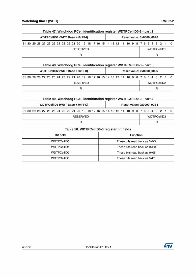
Watchdog timer (WDG) RM0352
46/138 DocID024647 Rev 1
Table 47. Watchdog PCell identification register WDTPCellID0-3 - part 2
Table 48. Watchdog PCell identification register WDTPCellID0-3 - part 3
Table 49. Watchdog PCell identification register WDTPCellID0-3 - part 4
WDTPCellID1 (WDT Base + 0xFF4) Reset value: 0x0000_00F0
31 30 29 28 27 26 25 24 23 22 21 20 19 18 17 16 15 14 13 12 11 10 9 8 7 6 5 4 3 2 1 0
RESERVED WDTPCellID1
R R
WDTPCellID2 (WDT Base + 0xFF8) Reset value: 0x0000_0005
31 30 29 28 27 26 25 24 23 22 21 20 19 18 17 16 15 14 13 12 11 10 9 8 7 6 5 4 3 2 1 0
RESERVED WDTPCellID2
R R
WDTPCellID3 (WDT Base + 0xFFC) Reset value: 0x0000_00B1
31 30 29 28 27 26 25 24 23 22 21 20 19 18 17 16 15 14 13 12 11 10 9 8 7 6 5 4 3 2 1 0
RESERVED WDTPCellID3
R R
Table 50. WDTPCellID0-3 register bit fields
Bit field Function
WDTPCellID0 These bits read back as 0x0D
WDTPCellID1 These bits read back as 0xF0
WDTPCellID2 These bits read back as 0x05
WDTPCellID3 These bits read back as 0xB1
DocID024647 Rev 1 47/138
RM0352 ARM© dual timer module (SP804)
137
8 ARM© dual timer module (SP804)
This section is intended for hardware and software engineers implementing “System-on-
Chip” (SoC) designs.
The SP804 timer is an IP provided by ARM (SP804). Additional details about its functional
blocks may be found in “ARM Dual-Timer module (SP804) Technical Reference Manual”.
8.1 IntroductionThis section introduces the dual timer module (SP804). It contains the following parts:
• About the ARM dual timer module (SP804)
• Features
• Programmable parameters
8.1.1 About the ARM dual timer module (SP804)
The ARM dual timer module is an “Advanced Microcontroller Bus Architecture” (AMBA)
compliant system-on-chip (SoC) peripheral developed, tested and licensed by ARM Limited.
The module is an AMBA slave module and connects to the “Advanced Peripheral Bus”
(APB). The dual timer module consists of two programmable 32/16-bit down counters that
can generate interrupts on reaching zero.
8.1.2 Features
The features of the dual timer module are:
• Compliance to the AMBA Specification (Rev 2.0) for easy integration into SoC
implementation.
• Two 32/16-bit down counters with free running, periodic and one-shot modes.
• Common clock with separate clock-enables for each timer gives flexible control of the
timer intervals.
• Interrupt output generation on timer count reaching zero.
• Identification registers that uniquely identify the dual timer module. These can be used
by software to automatically configure itself.
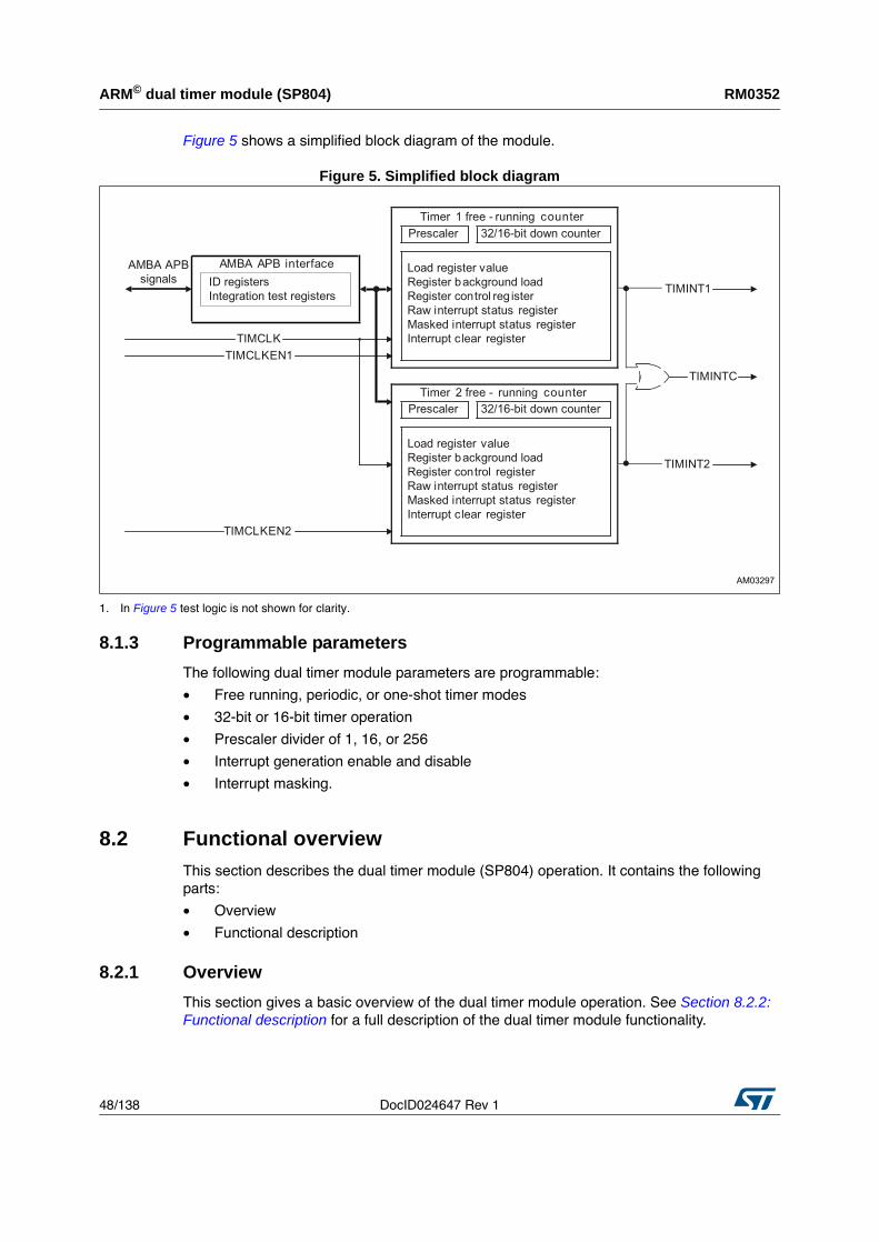
ARM© dual timer module (SP804) RM0352
48/138 DocID024647 Rev 1
Figure 5 shows a simplified block diagram of the module.
Figure 5. Simplified block diagram
1. In Figure 5 test logic is not shown for clarity.
8.1.3 Programmable parameters
The following dual timer module parameters are programmable:
• Free running, periodic, or one-shot timer modes
• 32-bit or 16-bit timer operation
• Prescaler divider of 1, 16, or 256
• Interrupt generation enable and disable
• Interrupt masking.
8.2 Functional overviewThis section describes the dual timer module (SP804) operation. It contains the following
parts:
• Overview
• Functional description
8.2.1 Overview
This section gives a basic overview of the dual timer module operation. See Section 8.2.2: Functional description for a full description of the dual timer module functionality.
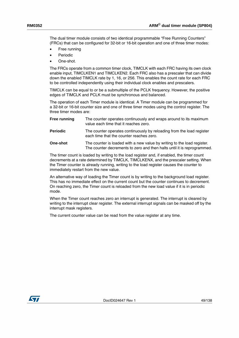
DocID024647 Rev 1 49/138
RM0352 ARM© dual timer module (SP804)
137
The dual timer module consists of two identical programmable “Free Running Counters”
(FRCs) that can be configured for 32-bit or 16-bit operation and one of three timer modes:
• Free running
• Periodic
• One-shot.
The FRCs operate from a common timer clock, TIMCLK with each FRC having its own clock
enable input, TIMCLKEN1 and TIMCLKEN2. Each FRC also has a prescaler that can divide
down the enabled TIMCLK rate by 1, 16, or 256. This enables the count rate for each FRC
to be controlled independently using their individual clock enables and prescalers.
TIMCLK can be equal to or be a submultiple of the PCLK frequency. However, the positive
edges of TIMCLK and PCLK must be synchronous and balanced.
The operation of each Timer module is identical. A Timer module can be programmed for
a 32-bit or 16-bit counter size and one of three timer modes using the control register. The
three timer modes are:
Free running The counter operates continuously and wraps around to its maximum
value each time that it reaches zero.
Periodic The counter operates continuously by reloading from the load register
each time that the counter reaches zero.
One-shot The counter is loaded with a new value by writing to the load register.
The counter decrements to zero and then halts until it is reprogrammed.
The timer count is loaded by writing to the load register and, if enabled, the timer count
decrements at a rate determined by TIMCLK, TIMCLKENX, and the prescaler setting. When
the Timer counter is already running, writing to the load register causes the counter to
immediately restart from the new value.
An alternative way of loading the Timer count is by writing to the background load register.
This has no immediate effect on the current count but the counter continues to decrement.
On reaching zero, the Timer count is reloaded from the new load value if it is in periodic
mode.
When the Timer count reaches zero an interrupt is generated. The interrupt is cleared by
writing to the interrupt clear register. The external interrupt signals can be masked off by the
interrupt mask registers.
The current counter value can be read from the value register at any time.
ARM© dual timer module (SP804) RM0352
50/138 DocID024647 Rev 1
8.2.2 Functional description
The dual timer module block diagram is shown in Figure 6.
Figure 6. Dual timer module block diagram
1. In Figure 6 test logic is not shown for clarity.
The dual timer module is described in the following sections:
• AMBA APB interface
• Free running counter blocks
• Interface reset
• Clock signals and clock enables
• Prescaler operation
• Timer operation on
• Interrupt behavior
• Programming the timer interval
• Identification registers
AMBA APB interface
The AMBA APB slave interface generates read and write decodes for accesses to all
registers in the dual timer module.
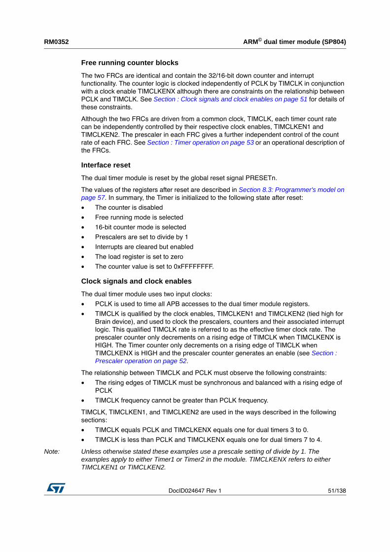
DocID024647 Rev 1 51/138
RM0352 ARM© dual timer module (SP804)
137
Free running counter blocks
The two FRCs are identical and contain the 32/16-bit down counter and interrupt
functionality. The counter logic is clocked independently of PCLK by TIMCLK in conjunction
with a clock enable TIMCLKENX although there are constraints on the relationship between
PCLK and TIMCLK. See Section : Clock signals and clock enables on page 51 for details of
these constraints.
Although the two FRCs are driven from a common clock, TIMCLK, each timer count rate
can be independently controlled by their respective clock enables, TIMCLKEN1 and
TIMCLKEN2. The prescaler in each FRC gives a further independent control of the count
rate of each FRC. See Section : Timer operation on page 53 or an operational description of
the FRCs.
Interface reset
The dual timer module is reset by the global reset signal PRESETn.
The values of the registers after reset are described in Section 8.3: Programmer's model on page 57. In summary, the Timer is initialized to the following state after reset:
• The counter is disabled
• Free running mode is selected
• 16-bit counter mode is selected
• Prescalers are set to divide by 1
• Interrupts are cleared but enabled
• The load register is set to zero
• The counter value is set to 0xFFFFFFFF.
Clock signals and clock enables
The dual timer module uses two input clocks:
• PCLK is used to time all APB accesses to the dual timer module registers.
• TIMCLK is qualified by the clock enables, TIMCLKEN1 and TIMCLKEN2 (tied high for
Brain device), and used to clock the prescalers, counters and their associated interrupt
logic. This qualified TIMCLK rate is referred to as the effective timer clock rate. The
prescaler counter only decrements on a rising edge of TIMCLK when TIMCLKENX is
HIGH. The Timer counter only decrements on a rising edge of TIMCLK when
TIMCLKENX is HIGH and the prescaler counter generates an enable (see Section : Prescaler operation on page 52.
The relationship between TIMCLK and PCLK must observe the following constraints:
• The rising edges of TIMCLK must be synchronous and balanced with a rising edge of
PCLK
• TIMCLK frequency cannot be greater than PCLK frequency.
TIMCLK, TIMCLKEN1, and TIMCLKEN2 are used in the ways described in the following
sections:
• TIMCLK equals PCLK and TIMCLKENX equals one for dual timers 3 to 0.
• TIMCLK is less than PCLK and TIMCLKENX equals one for dual timers 7 to 4.
Note: Unless otherwise stated these examples use a prescale setting of divide by 1. The examples apply to either Timer1 or Timer2 in the module. TIMCLKENX refers to either TIMCLKEN1 or TIMCLKEN2.
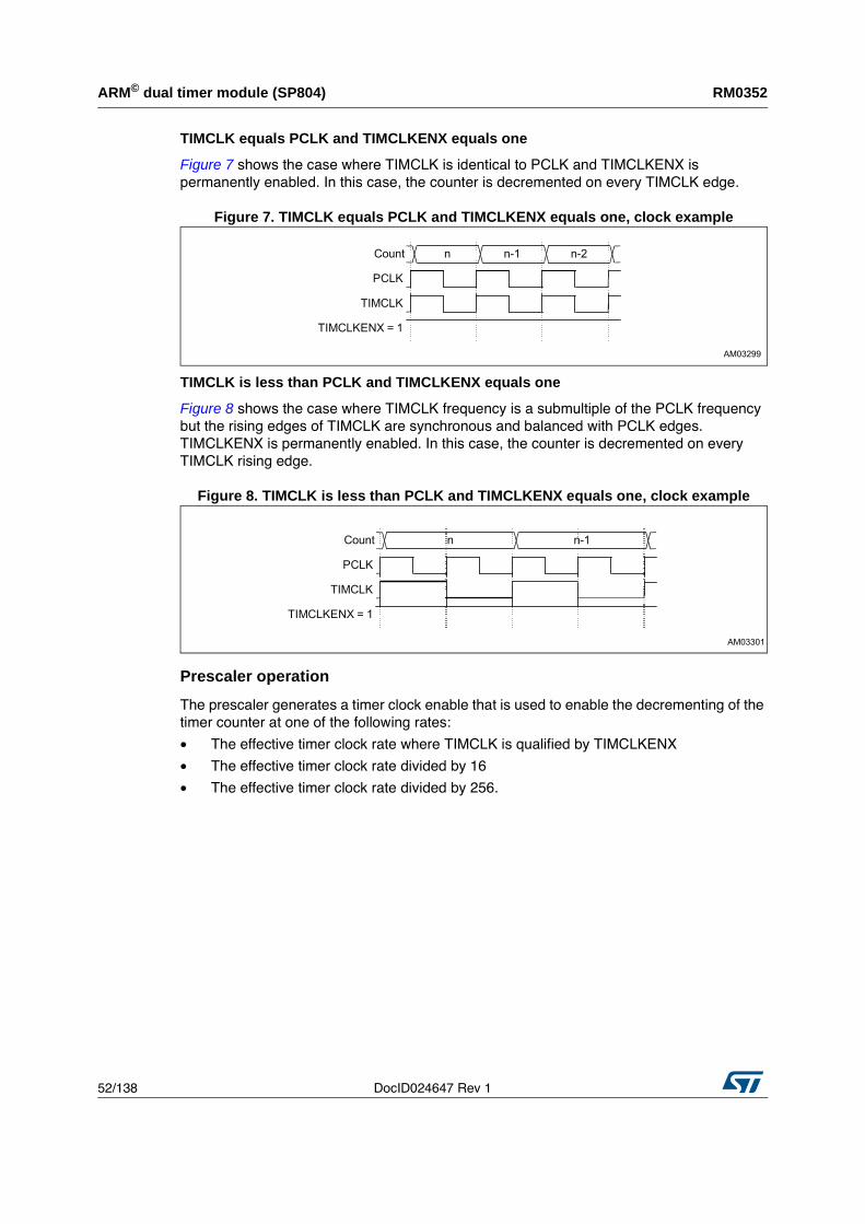
ARM© dual timer module (SP804) RM0352
52/138 DocID024647 Rev 1
TIMCLK equals PCLK and TIMCLKENX equals one
Figure 7 shows the case where TIMCLK is identical to PCLK and TIMCLKENX is
permanently enabled. In this case, the counter is decremented on every TIMCLK edge.
Figure 7. TIMCLK equals PCLK and TIMCLKENX equals one, clock example
TIMCLK is less than PCLK and TIMCLKENX equals one
Figure 8 shows the case where TIMCLK frequency is a submultiple of the PCLK frequency
but the rising edges of TIMCLK are synchronous and balanced with PCLK edges.
TIMCLKENX is permanently enabled. In this case, the counter is decremented on every
TIMCLK rising edge.
Figure 8. TIMCLK is less than PCLK and TIMCLKENX equals one, clock example
Prescaler operation
The prescaler generates a timer clock enable that is used to enable the decrementing of the
timer counter at one of the following rates:
• The effective timer clock rate where TIMCLK is qualified by TIMCLKENX
• The effective timer clock rate divided by 16
• The effective timer clock rate divided by 256.
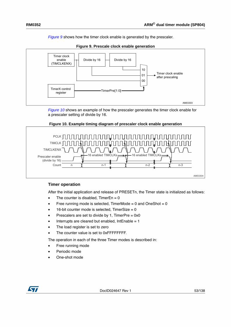
DocID024647 Rev 1 53/138
RM0352 ARM© dual timer module (SP804)
137
Figure 9 shows how the timer clock enable is generated by the prescaler.
Figure 9. Prescale clock enable generation
Figure 10 shows an example of how the prescaler generates the timer clock enable for
a prescaler setting of divide by 16.
Figure 10. Example timing diagram of prescaler clock enable generation
Timer operation
After the initial application and release of PRESETn, the Timer state is initialized as follows:
• The counter is disabled, TimerEn = 0
• Free running mode is selected, TimerMode = 0 and OneShot = 0
• 16-bit counter mode is selected, TimerSize = 0
• Prescalers are set to divide by 1, TimerPre = 0x0
• Interrupts are cleared but enabled, IntEnable = 1
• The load register is set to zero
• The counter value is set to 0xFFFFFFFF.
The operation in each of the three Timer modes is described in:
• Free running mode
• Periodic mode
• One-shot mode
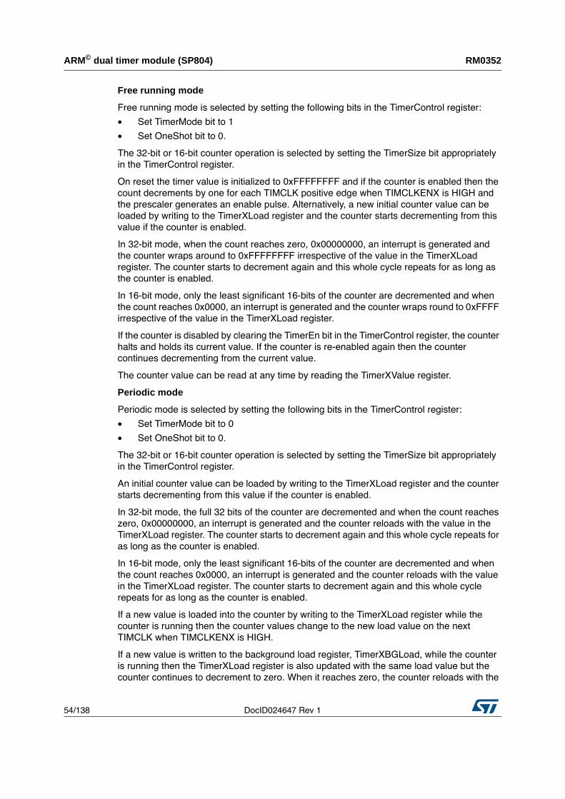
ARM© dual timer module (SP804) RM0352
54/138 DocID024647 Rev 1
Free running mode
Free running mode is selected by setting the following bits in the TimerControl register:
• Set TimerMode bit to 1
• Set OneShot bit to 0.
The 32-bit or 16-bit counter operation is selected by setting the TimerSize bit appropriately
in the TimerControl register.
On reset the timer value is initialized to 0xFFFFFFFF and if the counter is enabled then the
count decrements by one for each TIMCLK positive edge when TIMCLKENX is HIGH and
the prescaler generates an enable pulse. Alternatively, a new initial counter value can be
loaded by writing to the TimerXLoad register and the counter starts decrementing from this
value if the counter is enabled.
In 32-bit mode, when the count reaches zero, 0x00000000, an interrupt is generated and
the counter wraps around to 0xFFFFFFFF irrespective of the value in the TimerXLoad
register. The counter starts to decrement again and this whole cycle repeats for as long as
the counter is enabled.
In 16-bit mode, only the least significant 16-bits of the counter are decremented and when
the count reaches 0x0000, an interrupt is generated and the counter wraps round to 0xFFFF
irrespective of the value in the TimerXLoad register.
If the counter is disabled by clearing the TimerEn bit in the TimerControl register, the counter
halts and holds its current value. If the counter is re-enabled again then the counter
continues decrementing from the current value.
The counter value can be read at any time by reading the TimerXValue register.
Periodic mode
Periodic mode is selected by setting the following bits in the TimerControl register:
• Set TimerMode bit to 0
• Set OneShot bit to 0.
The 32-bit or 16-bit counter operation is selected by setting the TimerSize bit appropriately
in the TimerControl register.
An initial counter value can be loaded by writing to the TimerXLoad register and the counter
starts decrementing from this value if the counter is enabled.
In 32-bit mode, the full 32 bits of the counter are decremented and when the count reaches
zero, 0x00000000, an interrupt is generated and the counter reloads with the value in the
TimerXLoad register. The counter starts to decrement again and this whole cycle repeats for
as long as the counter is enabled.
In 16-bit mode, only the least significant 16-bits of the counter are decremented and when
the count reaches 0x0000, an interrupt is generated and the counter reloads with the value
in the TimerXLoad register. The counter starts to decrement again and this whole cycle
repeats for as long as the counter is enabled.
If a new value is loaded into the counter by writing to the TimerXLoad register while the
counter is running then the counter values change to the new load value on the next
TIMCLK when TIMCLKENX is HIGH.
If a new value is written to the background load register, TimerXBGLoad, while the counter
is running then the TimerXLoad register is also updated with the same load value but the
counter continues to decrement to zero. When it reaches zero, the counter reloads with the
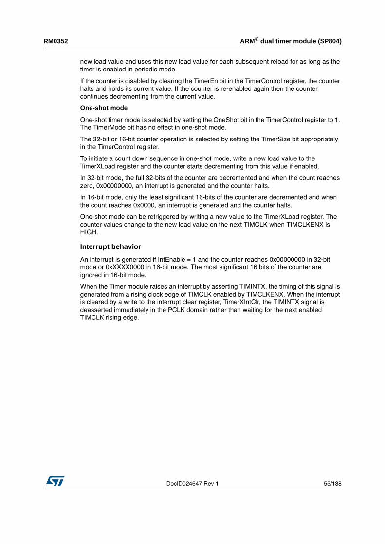
DocID024647 Rev 1 55/138
RM0352 ARM© dual timer module (SP804)
137
new load value and uses this new load value for each subsequent reload for as long as the
timer is enabled in periodic mode.
If the counter is disabled by clearing the TimerEn bit in the TimerControl register, the counter
halts and holds its current value. If the counter is re-enabled again then the counter
continues decrementing from the current value.
One-shot mode
One-shot timer mode is selected by setting the OneShot bit in the TimerControl register to 1.
The TimerMode bit has no effect in one-shot mode.
The 32-bit or 16-bit counter operation is selected by setting the TimerSize bit appropriately
in the TimerControl register.
To initiate a count down sequence in one-shot mode, write a new load value to the
TimerXLoad register and the counter starts decrementing from this value if enabled.
In 32-bit mode, the full 32-bits of the counter are decremented and when the count reaches
zero, 0x00000000, an interrupt is generated and the counter halts.
In 16-bit mode, only the least significant 16-bits of the counter are decremented and when
the count reaches 0x0000, an interrupt is generated and the counter halts.
One-shot mode can be retriggered by writing a new value to the TimerXLoad register. The
counter values change to the new load value on the next TIMCLK when TIMCLKENX is
HIGH.
Interrupt behavior
An interrupt is generated if IntEnable = 1 and the counter reaches 0x00000000 in 32-bit
mode or 0xXXXX0000 in 16-bit mode. The most significant 16 bits of the counter are
ignored in 16-bit mode.
When the Timer module raises an interrupt by asserting TIMINTX, the timing of this signal is
generated from a rising clock edge of TIMCLK enabled by TIMCLKENX. When the interrupt
is cleared by a write to the interrupt clear register, TimerXIntClr, the TIMINTX signal is
deasserted immediately in the PCLK domain rather than waiting for the next enabled
TIMCLK rising edge.
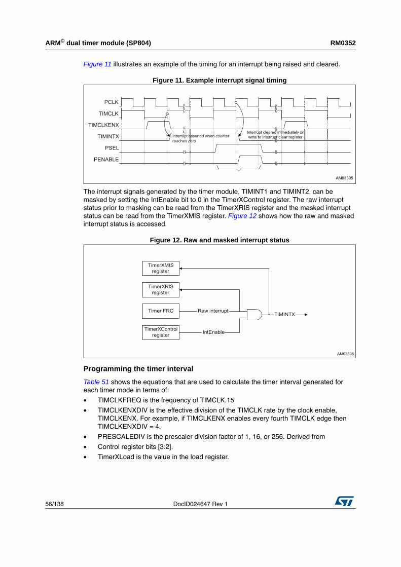
ARM© dual timer module (SP804) RM0352
56/138 DocID024647 Rev 1
Figure 11 illustrates an example of the timing for an interrupt being raised and cleared.
Figure 11. Example interrupt signal timing
The interrupt signals generated by the timer module, TIMINT1 and TIMINT2, can be
masked by setting the IntEnable bit to 0 in the TimerXControl register. The raw interrupt
status prior to masking can be read from the TimerXRIS register and the masked interrupt
status can be read from the TimerXMIS register. Figure 12 shows how the raw and masked
interrupt status is accessed.
Figure 12. Raw and masked interrupt status
Programming the timer interval
Table 51 shows the equations that are used to calculate the timer interval generated for
each timer mode in terms of:
• TIMCLKFREQ is the frequency of TIMCLK.15
• TIMCLKENXDIV is the effective division of the TIMCLK rate by the clock enable,
TIMCLKENX. For example, if TIMCLKENX enables every fourth TIMCLK edge then
TIMCLKENXDIV = 4.
• PRESCALEDIV is the prescaler division factor of 1, 16, or 256. Derived from
• Control register bits [3:2].
• TimerXLoad is the value in the load register.
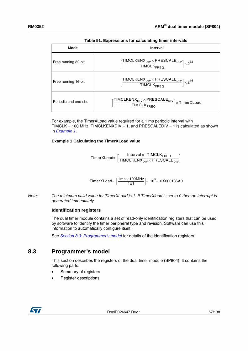
DocID024647 Rev 1 57/138
RM0352 ARM© dual timer module (SP804)
137
For example, the TimerXLoad value required for a 1 ms periodic interval with
TIMCLK = 100 MHz, TIMCLKENXDIV = 1, and PRESCALEDIV = 1 is calculated as shown
in Example 1.
Example 1 Calculating the TimerXLoad value
Note: The minimum valid value for TimerXLoad is 1. If TimerXload is set to 0 then an interrupt is generated immediately.
Identification registers
The dual timer module contains a set of read-only identification registers that can be used
by software to identify the timer peripheral type and revision. Software can use this
information to automatically configure itself.
See Section 8.3: Programmer's model for details of the identification registers.
8.3 Programmer's modelThis section describes the registers of the dual timer module (SP804). It contains the
following parts:
• Summary of registers
• Register descriptions
Table 51. Expressions for calculating timer intervals
Mode Interval
Free running 32-bit
Free running 16-bit
Periodic and one-shot
TIMCLKENXDIV
PRESCALEDIV
×TIMCLK
FREQ
----------------------------------------------------------------------------------------------- 232×
TIMCLKENXDIV
PRESCALEDIV
×TIMCLK
FREQ
----------------------------------------------------------------------------------------------- 216×
TIMCLKENXDIV
PRESCALEDIV
×TIMCLK
FREQ
----------------------------------------------------------------------------------------------- TimerXLoad×
TimerXLoad
Interval × TIMCLKFREQ
TIMCLKENXDIV
PRESCALEDIV
×-----------------------------------------------------------------------------------------------=
TimerXLoad1ms 100MHz×
1x1
----------------------------------------- 105
0X000186A0===
ARM© dual timer module (SP804) RM0352
58/138 DocID024647 Rev 1
8.3.1 Summary of registers
A summary of the registers is provided in Table 52 and base address of each dual timer is
listed below.
The Timer0 base address is 0xA640_0000
The Timer1 base address is 0xA740_0000.
The Timer2 base address is 0xA840_0000.
The Timer3 base address is 0xA940_0000.
The Timer4 base address is 0xA680_0000.
The Timer5 base address is 0xA780_0000.
The Timer6 base address is 0xA880_0000.
The Timer7 base address is 0xA980_0000.
Table 52. Summary of registers
Address Type Width Reset value Name Description
Base+0x00 Read/write 32 0x00000000 Timer1Load
See Section : Load register, TimerXLoad on page 60
Base+0x04 Read 32 0xFFFFFFFF Timer1Value
See Section : Current value register, TimerXValue on page 60
Base+0x08 Read/write 8 0x20 Timer1Control
See Section : Control register, TimerXControl on page 61
Base+0x0C Write - - Timer1IntClr
See Section : Interrupt clear register. TimerXIntClr on page 61
Base+0x10 Read 1 0x0 Timer1RIS
See Section : Raw interrupt status register, TimerXRIS on page 62
Base+0x14 Read 1 0x0 Timer1MIS
See Section : Masked interrupt status register, TimerXMIS on page 62
Base+0x18 Read/write 32 0x00000000 Timer1BGLoad
See Section : Background load register, TimerXBGLoad on page 62
Base+0x20 Read/write 32 0x00000000 Timer2Load
See Section : Load register, TimerXLoad on page 60
Base+0x24 Read 32 0xFFFFFFFF Timer2Value
See Section : Current value register, TimerXValue on page 60
Base+0x28 Read/write 8 0x20 Timer2Control
See Section : Control register, TimerXControl on page 61
Base+0x2C Write - - Timer2IntClr
See Section : Interrupt clear register. TimerXIntClr on page 61
Base+0x30 Read 1 0x0 Timer2RIS
See Section : Raw interrupt status register, TimerXRIS on page 62
Base+0x34 Read 1 0x0 Timer2MIS
See Section : Masked interrupt status register, TimerXMIS on page 62
DocID024647 Rev 1 59/138
RM0352 ARM© dual timer module (SP804)
137
8.3.2 Register descriptions
This section describes the dual timer module registers:
• Load register, TimerXLoad
• Current value register, TimerXValue
• Control register, TimerXControl
• Interrupt clear register. TimerXIntClr
• Raw interrupt status register, TimerXRIS
• Masked interrupt status register, TimerXMIS
• Background load register, TimerXBGLoad
• Peripheral identification registers, TimerPeriphID0-3
• PrimeCell identification registers, TimerPCellID0-3
Note: The letter X used in register names means a register in either FRC1 or FRC2.
Base+0x38 Read/write 32 0x00000000 Timer2BGLoad
See Section : Background load register, TimerXBGLoad on page 62
Base+0x40-
0xEFC
- - - - RESERVED for future expansion
Base+0xF00-
0xF04
- - - - RESERVED for test
Base+0xF08-
0xFDC
- - - - RESERVED for future expansion
Base+0xFE0 Read-only 8 0x04 TimerPeriphID0
See Section : Timer peripheral ID0 register, TimerPeriphID0 on page 63
Base+0xFE4 Read-only 8 0x18 TimerPeriphID1
See Section : Timer peripheral ID1 register, TimerPeriphID1 on page 64
Base+0xFE8 Read-only 8 0x14 TimerPeriphID2
See Section : Timer peripheral ID2 register, TimerPeriphID2 on page 64
Base+0xFEC Read-only 8 0x00 TimerPeriphID3
See Section : Timer peripheral ID3 register, TimerPeriphID3 on page 64
Base+0xFF0 Read-only 8 0x0D TimerPCellID0
See Section : PrimeCell ID0 register, TimerPCellID0 on page 65
Base+0xFF4 Read-only 8 0xF0 TimerPCellID1
See Section : PrimeCell ID1 register, TimerPCellID1 on page 65
Base+0xFF8 Read-only 8 0x05 TimerPCellID2
See Section : PrimeCell ID2 register, TimerPCellID2 on page 66
Base+0xFFC Read-only 8 0xB1 TimerPCellID3
See Section : PrimeCell ID3 register, TimerPCellID3 on page 66
Table 52. Summary of registers (continued)
Address Type Width Reset value Name Description
ARM© dual timer module (SP804) RM0352
60/138 DocID024647 Rev 1
Load register, TimerXLoad
The TimerXLoad register is a 32-bit register that contains the value from which the counter
is to decrement. This is the value used to reload the counter when Periodic mode is
enabled, and the current count reaches zero.
When this register is written to directly, the current count immediately resets to the new
value at the next rising edge of TIMCLK which is enabled by TIMCLKENX.
Note: The minimum valid value for TimerXLoad is 1. If TimerXload is set to 0 then an interrupt is generated immediately.
The value in this register is also overwritten if the TimerXBGLoad register is written to, but
the current count is not immediately affected.
If values are written to both the TimerXLoad and TimerXBGLoad registers before an
enabled rising edge on TIMCLK, then on the next enabled TIMCLK edge the value written to
the TimerXLoad value replaces the current count value. After that, each time the counter
reaches zero the current count value resets to the value written to TimerXBGLoad.
Reading from the TimerXLoad register at any time after the two writes have occurred
retrieves the value written to TimerXBGLoad. That is, the value read from TimerXLoad is
always the value that takes effect for Periodic mode after the next time the counter reaches
zero.
Current value register, TimerXValue
The TimerXValue register is a 32-bit read-only register that gives the current value of the
decrementing counter.
After a load operation has taken place by writing a new load value to TimerXLoad, the
TimerXValue register reflects the new load value immediately in the PCLK clock domain
without waiting for the next TIMCLK edge qualified by TIMCLKENX.
Note: The most significant 16 bits of the 32-bit TimerXValue register are not automatically set to 0 when in 16-bit timer mode. If the timer is in 16-bit mode then the most significant 16 bits of the TimerXValue register might have a non-zero value if the timer was previously in 32-bit mode and a write to the TimerXLoad register has not occurred since the change to 16-bit mode.
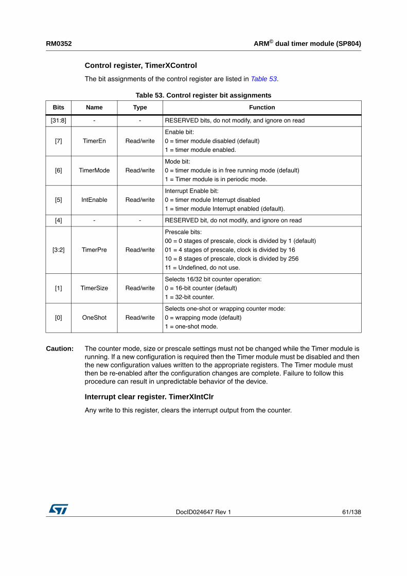
DocID024647 Rev 1 61/138
RM0352 ARM© dual timer module (SP804)
137
Control register, TimerXControl
The bit assignments of the control register are listed in Table 53.
Caution: The counter mode, size or prescale settings must not be changed while the Timer module is
running. If a new configuration is required then the Timer module must be disabled and then
the new configuration values written to the appropriate registers. The Timer module must
then be re-enabled after the configuration changes are complete. Failure to follow this
procedure can result in unpredictable behavior of the device.
Interrupt clear register. TimerXIntClr
Any write to this register, clears the interrupt output from the counter.
Table 53. Control register bit assignments
Bits Name Type Function
[31:8] - - RESERVED bits, do not modify, and ignore on read
[7] TimerEn Read/write
Enable bit:
0 = timer module disabled (default)
1 = timer module enabled.
[6] TimerMode Read/write
Mode bit:
0 = timer module is in free running mode (default)
1 = Timer module is in periodic mode.
[5] IntEnable Read/write
Interrupt Enable bit:
0 = timer module Interrupt disabled
1 = timer module Interrupt enabled (default).
[4] - - RESERVED bit, do not modify, and ignore on read
[3:2] TimerPre Read/write
Prescale bits:
00 = 0 stages of prescale, clock is divided by 1 (default)
01 = 4 stages of prescale, clock is divided by 16
10 = 8 stages of prescale, clock is divided by 256
11 = Undefined, do not use.
[1] TimerSize Read/write
Selects 16/32 bit counter operation:
0 = 16-bit counter (default)
1 = 32-bit counter.
[0] OneShot Read/write
Selects one-shot or wrapping counter mode:
0 = wrapping mode (default)
1 = one-shot mode.
ARM© dual timer module (SP804) RM0352
62/138 DocID024647 Rev 1
Raw interrupt status register, TimerXRIS
The TimerXRIS register indicates the raw interrupt status from the counter. The bit
assignment is listed in Table 54.
Masked interrupt status register, TimerXMIS
The TimerXMIS register indicates the masked interrupt status from the counter. This value is
the logical AND of the raw interrupt status with the Timer Interrupt Enable bit from the
control register, and is the same value which is passed to the interrupt output pin, TIMINTX.
The bit assignment is listed in Table 55.
Background load register, TimerXBGLoad
The TimerXBGLoad register is a 32-bit register that contains the value from which the
counter is to decrement. This is the value used to reload the counter when Periodic mode is
enabled, and the current count reaches zero.
This provides an alternative method of accessing the TimerXLoad register. The difference is
that writes to TimerXBGLoad do not cause the counter to restart from the new value
immediately.
Reading from this register returns the same value returned from TimerXLoad. See Section : Load register, TimerXLoad on page 60 for more information.
Peripheral identification registers, TimerPeriphID0-3
The TimerPeriphID0-3 registers are four 8-bit registers, that span address location 0xFE0 -
0xFEC. The registers can conceptually be treated as a 32-bit register. The read-only
registers provide the peripheral options listed in Table 56.
Table 54. Raw interrupt status register bit assignments
Bits Name Type Function
[31:1] - - RESERVED bits, do not modify, and ignore on read
[0] TimerXRIS Read Raw interrupt status from the counter
Table 55. Masked interrupt status register bit assignments
Bits Name Type Function
[31:1] - - RESERVED bits, do not modify, and ignore on read
[0] TimerXMIS Read Enabled interrupt status from the counter
Table 56. Peripheral identification register options
Bits Function
PartNumber[11:0] This is used to identify the peripheral. The three digits product code 0x804 is used.
Designer ID[19:12] This is the identification of the designer. ARM Limited is 0x41 (ASCII A).
Revision[23:20] This is the revision number of the peripheral. The revision number starts from 0.
Configuration[31:24] This is the configuration option of the peripheral. The configuration value is 0.
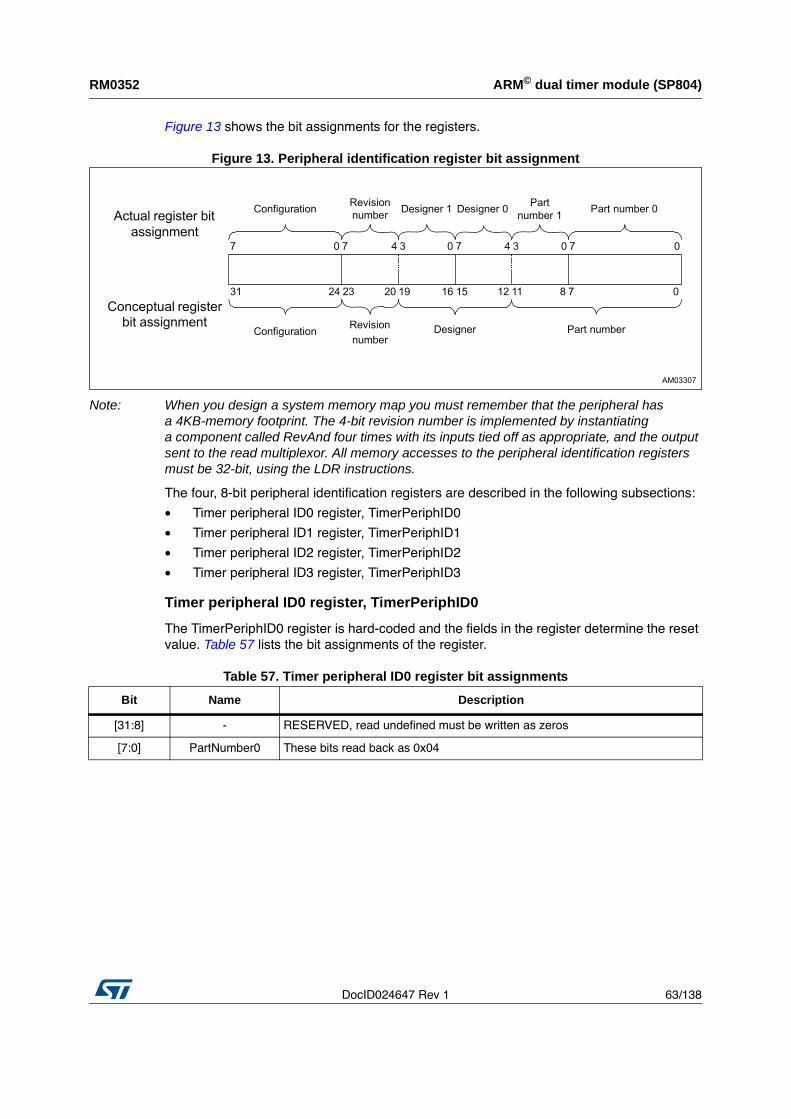
DocID024647 Rev 1 63/138
RM0352 ARM© dual timer module (SP804)
137
Figure 13 shows the bit assignments for the registers.
Figure 13. Peripheral identification register bit assignment
Note: When you design a system memory map you must remember that the peripheral has a 4KB-memory footprint. The 4-bit revision number is implemented by instantiating a component called RevAnd four times with its inputs tied off as appropriate, and the output sent to the read multiplexor. All memory accesses to the peripheral identification registers must be 32-bit, using the LDR instructions.
The four, 8-bit peripheral identification registers are described in the following subsections:
• Timer peripheral ID0 register, TimerPeriphID0
• Timer peripheral ID1 register, TimerPeriphID1
• Timer peripheral ID2 register, TimerPeriphID2
• Timer peripheral ID3 register, TimerPeriphID3
Timer peripheral ID0 register, TimerPeriphID0
The TimerPeriphID0 register is hard-coded and the fields in the register determine the reset
value. Table 57 lists the bit assignments of the register.
Table 57. Timer peripheral ID0 register bit assignments
Bit Name Description
[31:8] - RESERVED, read undefined must be written as zeros
[7:0] PartNumber0 These bits read back as 0x04
ARM© dual timer module (SP804) RM0352
64/138 DocID024647 Rev 1
Timer peripheral ID1 register, TimerPeriphID1
The TimerPeriphID1 register is hard-coded and the fields in the register determine the reset
value.Table 58 lists the bit assignments of the register.
Timer peripheral ID2 register, TimerPeriphID2
The TimerPeriphID2 register is hard-coded and the fields in the register determine the reset
value. Table 59 lists the bit assignment of the register.
Timer peripheral ID3 register, TimerPeriphID3
The TimerPeriphID3 register is hard-coded and the fields in the register determine the reset
value. Table 60 shows the bit assignments of the register.
PrimeCell identification registers, TimerPCellID0-3
The TimerPCellID0-3 registers are four 8-bit registers, that span address locations 0xFF0-
0xFFC. The read-only registers can conceptually be treated as a 32-bit register. The register
is used as a standard cross-peripheral identification system. The TimerPCellID register is
set to 0xB105F00D. Figure 14 shows the bit assignment for the registers.
Table 58. Timer peripheral ID1 register bit assignments
Bit Name Description
[31:8] - RESERVED, read undefined, must be written as zeros
[7:4] Designer0 These bits read back as 0x1
[3:0] PartNumber1 These bits read back as 0x8
Table 59. Timer peripheral ID2 register bit assignments
Bit Name Description
[31:8] - RESERVED, read undefined, must be written as zeros
[7:4] Revision These bits read back as 0x1
[3:0] Designer1 These bits read back as 0x4
Table 60. TimerPeriphID3 register bit assignments
Bit Name Description
[31:8] - RESERVED, read undefined, must be written as zeros
[7:0] Configuration These bits read back as 0x00
DocID024647 Rev 1 65/138
RM0352 ARM© dual timer module (SP804)
137
Figure 14. PrimeCell identification register bit assignments
The four, 8-bit PrimeCell identification registers are described in the following subsections:
• PrimeCell ID0 register, TimerPCellID0
• PrimeCell ID1 register, TimerPCellID1
• PrimeCell ID2 register, TimerPCellID2
• PrimeCell ID3 register, TimerPCellID3
PrimeCell ID0 register, TimerPCellID0
The TimerPCellID0 register is hard-coded and the fields in the register determine the reset
value. Table 61 shows the bit assignments of the register.
PrimeCell ID1 register, TimerPCellID1
The TimerPCellID1 register is hard-coded and the fields in the register determine the reset
value. Table 62 shows the bit assignment of the register.
Table 61. PrimeCell ID0 register bit assignments
Bit Name Description
[31:8] - RESERVED, read undefined, must be written as zeros
[7:0] TimerPCellID0 These bits read back as 0x0D
Table 62. PrimeCell ID1 register bit assignments
Bit Name Description
[31:8] - RESERVED, read undefined, must be written as zeros
[7:0] TimerPCellID1 These bits read back as 0xF0
ARM© dual timer module (SP804) RM0352
66/138 DocID024647 Rev 1
PrimeCell ID2 register, TimerPCellID2
The TimerPCellID2 register is hard-coded and the fields in the register determine the reset
value. Table 63 shows the bit assignment of the TimerPCellID2 register.
PrimeCell ID3 register, TimerPCellID3
The TimerPCellID3 register is hard-coded and the fields in the register determine the reset
value. Table 64 shows the bit assignment of the TimerPCellID3 register.
Table 63. PrimeCell ID2 register bit assignments
Bit Name Description
[31:8] - RESERVED, read undefined, must be written as zeros
[7:0] TimerPCellID2 These bits read back as 0x05
Table 64. PrimeCell ID3 register bit assignments
Bit Name Description
[31:8] - RESERVED, read undefined, must be written as zeros
[7:0] TimerPCellID3 These bits read back as 0xB1
DocID024647 Rev 1 67/138
RM0352 System timer (SysTick)
137
9 System timer (SysTick)
9.1 About the SysTickThe Brain device also includes a system timer (SysTick) that can be used by an operating
system to ease porting from another platform. The SysTick can be polled by software or can
be configured to generate an interrupt. The SysTick interrupt has its own entry in the vector
table and therefore can have its own handler. For more details on SysTick system timer, see
“ARMv6-M Architecture Reference Manual”.
9.2 SysTick registersThe SysTick is configured through the four registers described in Table 65. Those registers
are located in the System Control Space (SCS) memory area of the Cortex-M0 subsystem.
The SysTick base address is 0xE000_E010.
Table 65. SysTick registers
Address Name Type Reset value Description
SysTick base + 0x000 SYST_CSR RW 0x00000004
SysTick control and status.
Basic control of SysTick e.g. enable, clock source,
interrupt or poll. See Section 9.3.1: SysTick control and status register (SYST_CSR) on page 68.
SysTick base + 0x004 SYST_RVR RW -
SysTick reload value.
Value to load current value register when 0 is
reached. See Section 9.3.2: SysTick reload value register (SYST_RVR) on page 68.
SysTick base + 0x008 SYST_CVR RW -
SysTick current value. See Section 9.3.3: SysTick current value register (SYST_CVR) on page 69.
SysTick base + 0x00C SYST_CALIB RO 0x80000000
SysTick calibration value.
Might contain the number of ticks to generate a 10
ms interval and other information, depending on
implementation. See Section 9.3.4: SysTick calibration value register (SYST_CALIB) on page 69.
SysTick base + 0x010
to 0x0FF
RESERVED - - RESERVED
System timer (SysTick) RM0352
68/138 DocID024647 Rev 1
9.3 SysTick registers descriptions
9.3.1 SysTick control and status register (SYST_CSR)
Address: SysTick BaseAddress + 0x000
Type: R/W
Reset: 0x00000004
Description: SysTick control and status register
9.3.2 SysTick reload value register (SYST_RVR)
Address: SysTick BaseAddress + 0x004
Table 66. SysTick control and status register
SysTick control and status register (SYST_CSR)
31 30 29 28 27 26 25 24 23 22 21 20 19 18 17 16 15 14 13 12 11 10 9 8 7 6 5 4 3 2 1 0
RE
SE
RV
ED
CO
UN
TF
LA
G
RE
SE
RV
ED
CLK
SO
UR
CE
TIC
KIN
T
EN
AB
LE
[31:17] RESERVED
[16] COUNTFLAG: returns 1 if timer counted to 0 since the last read of this
register.
[15:3] RESERVED
[2] CLKSOURCE: selects the SysTick timer clock source
0: external reference clock
1: processor clock
[1] TICKINT: enables SysTick exception request
0: counting down to zero does not assert the SysTick exception request.
1: counting down to zero asserts the SysTick exception request.
[0] ENABLE: enables the counter.
0: counter disabled
1: counter enabled
Table 67. SysTick reload value register
SysTick reload value register (SYST_RVR)
31 30 29 28 27 26 25 24 23 22 21 20 19 18 17 16 15 14 13 12 11 10 9 8 7 6 5 4 3 2 1 0
RESERVED RELOAD
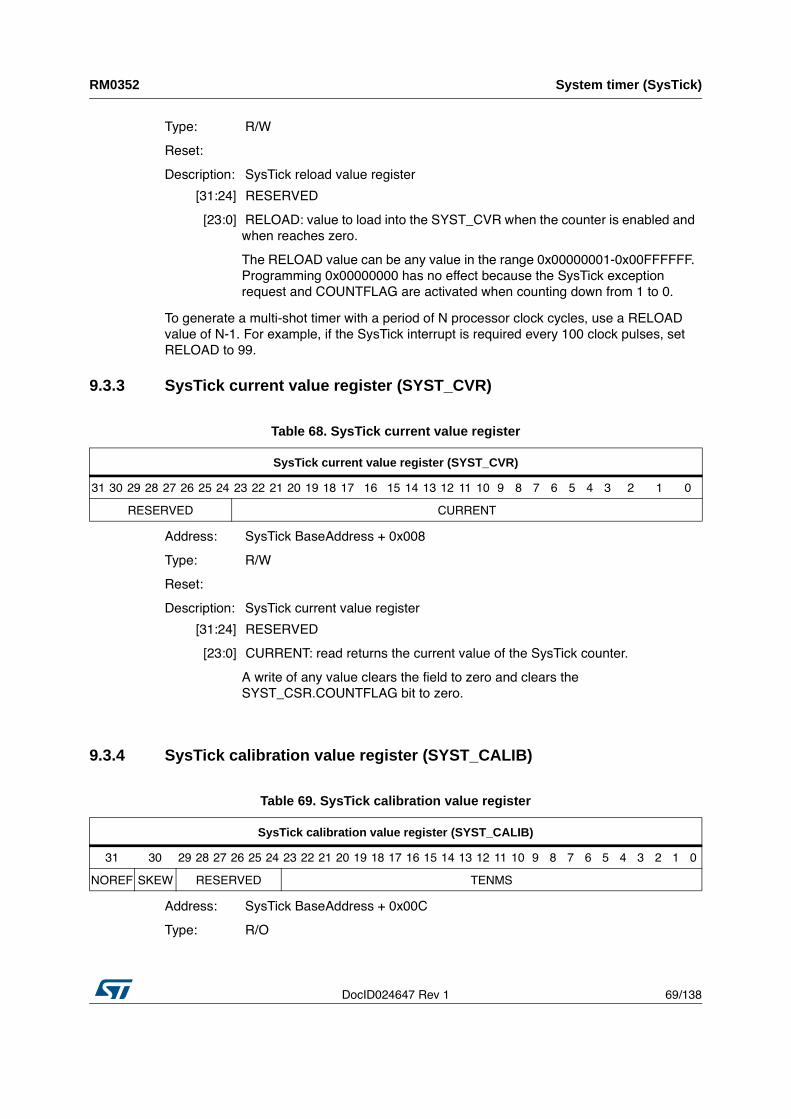
DocID024647 Rev 1 69/138
RM0352 System timer (SysTick)
137
Type: R/W
Reset:
Description: SysTick reload value register
To generate a multi-shot timer with a period of N processor clock cycles, use a RELOAD
value of N-1. For example, if the SysTick interrupt is required every 100 clock pulses, set
RELOAD to 99.
9.3.3 SysTick current value register (SYST_CVR)
Address: SysTick BaseAddress + 0x008
Type: R/W
Reset:
Description: SysTick current value register
9.3.4 SysTick calibration value register (SYST_CALIB)
Address: SysTick BaseAddress + 0x00C
Type: R/O
[31:24] RESERVED
[23:0] RELOAD: value to load into the SYST_CVR when the counter is enabled and
when reaches zero.
The RELOAD value can be any value in the range 0x00000001-0x00FFFFFF.
Programming 0x00000000 has no effect because the SysTick exception
request and COUNTFLAG are activated when counting down from 1 to 0.
Table 68. SysTick current value register
SysTick current value register (SYST_CVR)
31 30 29 28 27 26 25 24 23 22 21 20 19 18 17 16 15 14 13 12 11 10 9 8 7 6 5 4 3 2 1 0
RESERVED CURRENT
[31:24] RESERVED
[23:0] CURRENT: read returns the current value of the SysTick counter.
A write of any value clears the field to zero and clears the
SYST_CSR.COUNTFLAG bit to zero.
Table 69. SysTick calibration value register
SysTick calibration value register (SYST_CALIB)
31 30 29 28 27 26 25 24 23 22 21 20 19 18 17 16 15 14 13 12 11 10 9 8 7 6 5 4 3 2 1 0
NOREF SKEW RESERVED TENMS
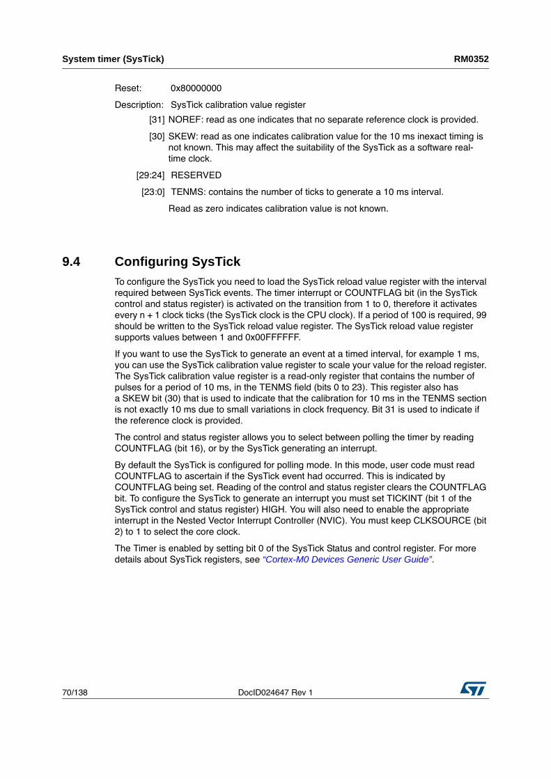
System timer (SysTick) RM0352
70/138 DocID024647 Rev 1
Reset: 0x80000000
Description: SysTick calibration value register
9.4 Configuring SysTickTo configure the SysTick you need to load the SysTick reload value register with the interval
required between SysTick events. The timer interrupt or COUNTFLAG bit (in the SysTick
control and status register) is activated on the transition from 1 to 0, therefore it activates
every n + 1 clock ticks (the SysTick clock is the CPU clock). If a period of 100 is required, 99
should be written to the SysTick reload value register. The SysTick reload value register
supports values between 1 and 0x00FFFFFF.
If you want to use the SysTick to generate an event at a timed interval, for example 1 ms,
you can use the SysTick calibration value register to scale your value for the reload register.
The SysTick calibration value register is a read-only register that contains the number of
pulses for a period of 10 ms, in the TENMS field (bits 0 to 23). This register also has
a SKEW bit (30) that is used to indicate that the calibration for 10 ms in the TENMS section
is not exactly 10 ms due to small variations in clock frequency. Bit 31 is used to indicate if
the reference clock is provided.
The control and status register allows you to select between polling the timer by reading
COUNTFLAG (bit 16), or by the SysTick generating an interrupt.
By default the SysTick is configured for polling mode. In this mode, user code must read
COUNTFLAG to ascertain if the SysTick event had occurred. This is indicated by
COUNTFLAG being set. Reading of the control and status register clears the COUNTFLAG
bit. To configure the SysTick to generate an interrupt you must set TICKINT (bit 1 of the
SysTick control and status register) HIGH. You will also need to enable the appropriate
interrupt in the Nested Vector Interrupt Controller (NVIC). You must keep CLKSOURCE (bit
2) to 1 to select the core clock.
The Timer is enabled by setting bit 0 of the SysTick Status and control register. For more
details about SysTick registers, see “Cortex-M0 Devices Generic User Guide”.
[31] NOREF: read as one indicates that no separate reference clock is provided.
[30] SKEW: read as one indicates calibration value for the 10 ms inexact timing is
not known. This may affect the suitability of the SysTick as a software real-
time clock.
[29:24] RESERVED
[23:0] TENMS: contains the number of ticks to generate a 10 ms interval.
Read as zero indicates calibration value is not known.
DocID024647 Rev 1 71/138
RM0352 I2C bus interface
137
10 I2C bus interface
The Brain device provides two I2C bus interfaces that support following features:
• Slave transmitter/receiver and master transmitter/receiver
• 7- and 10-bit addressing
• Standard (100 KHz) and fast (400 KHz) speeds
• The transmit path is buffered in a 16-byte Tx FIFO and the receive paths is buffered in
a 16-byte Rx FIFO.
In addition to receiving and transmitting data, the interface converts data from serial to
parallel format and vice-versa using an interrupt or polled handshake. The interrupts are
enabled and disabled in software.
10.1 I2C registersThe base address of the I
2C blocks in Brain memory map is 0xA400_0000 for I2C1 and
0xA500_0000 for I2C2.
Table 70. I2C register list(1)
Address Name Description
I2C Base +0x000 I2C_CR
I2C control register. See Section 10.2.1: I2C control register
(I2C_CR) on page 73.
I2C Base +0x004 I2C_SCR
I2C slave control register. See Section 10.2.2: I2C slave control
register (I2C_SCR) on page 77.
I2C Base +0x008 RESERVED This register must not be written and must keep its reset value
I2C Base +0x00C I2C_MCR
I2C master control register. See Section 10.2.3: I2C master
control register (I2C_MCR) on page 77.
I2C Base +0x010 I2C_TFR
I2C transmit FIFO register. See Section 10.2.4: I2C transmit FIFO
register (I2C_TFR) on page 79.
I2C Base +0x014 I2C_SR
I2C status register. See Section 10.2.5: I2C status register
(I2C_SR) on page 80.
I2C Base +0x018 I2C_RFR
I2C receive FIFO register. See Section 10.2.6: I2C receive FIFO
register (I2C_RFR) on page 83.
I2C Base +0x01C I2C_TFTR
I2C transmit FIFO threshold register. See Section 10.2.7: I2C
transmit FIFO threshold register (I2C_TFTR) on page 84.
I2C Base +0x020 I2C_RFTR
I2C receive FIFO threshold register. See Section 10.2.8: I2C
receive FIFO threshold register (I2C_RFTR) on page 84.
I2C Base +0x024 RESERVED This register must not be written and must keep its reset value
I2C Base +0x028 I2C_BRCR
I2C baud rate counter register. See Section 10.2.9: I2C baud-rate
counter register (I2C_BRCR) on page 85.
I2C Base +0x02C I2C_IMSCR
I2C interrupt mask set and clear register. See Section 10.2.10:
I2C interrupt mask set/clear register (I2C_IMSCR) on page 86.
I2C Base +0x030 I2C_RISR
I2C raw interrupt status register. See Section 10.2.11: I2C raw
interrupt status register (I2C_RISR) on page 88.
I2C bus interface RM0352
72/138 DocID024647 Rev 1
I2C Base +0x034 I2C_MISR
I2C masked interrupt status register. See Section 10.2.12: I2C
masked interrupt status register (I2C_MISR) on page 92.
I2C Base +0x038 I2C_ICR
I2C interrupt set and clear register. See Section 10.2.13: I2C
interrupt clear register (I2C_ICR) on page 93.
I2C Base + 0x03C
to 0x048
RESERVED RESERVED for test.
I2C Base +0x04C I2C_THDDAT
I2C hold time data. See Section 10.2.14: I2C hold time data
(I2C_THDDAT) on page 93.
I2C Base +0x050 I2C_THDSTA_FST_STD
I2C hold time START condition F/S. See Section 10.2.15: I2C hold
time START condition F/S (I2C_THDSTA_FST_STD) on page 94.
I2C Base +0x054 RESERVED This register must not be written and must keep its reset value
I2C Base +0x058 I2C_TSUSTA_FST_STD
I2C setup time START condition F/S. See Section 10.2.16: I2C
setup time START condition F/S (I2C_TSUSTA_FST_STD) on page 95.
I2C Base +0x05C RESERVED RESERVED
I2C Base +0x060 I2C_SMB_SCR
SMBUS slave control register. See Section 10.2.17: SMBUS slave control register (I2C_SMB_SCR) on page 95.
I2C Base +0xFE0 I2C_PeriphID0
Peripheral identification register bits 7:0. See Section 10.2.18: I2C peripheral identification register 0 (I2C_PERIPHID0) on page 96.
I2C Base +0xFE4 I2C_PeriphID1
Peripheral identification register bits 15:8. See Section 10.2.19: I2C peripheral identification register 1 (I2C_PERIPHID1) on page 96.
I2C Base +0xFE8 I2C_PeriphID2
Peripheral identification register bits 23:16. See Section 10.2.20: I2C peripheral identification register 2 (I2C_PERIPHID2) on page 97.
I2C Base +0xFEC I2C_PeriphID3
Peripheral identification register bits 31:24. See Section 10.2.21: I2C peripheral identification register 3 (I2C_PERIPHID3) on page 97.
I2C Base +0xFF0 I2C_PCellID0
IPCell identification register bits 7:0. See Section 10.2.22: I2C PCell identification register 0 (I2C_PCELLID0) on page 98.
I2C Base +0xFF4 I2C_PCellID1
IPCell identification register bits 15:8. See Section 10.2.23: I2C PCell identification register 1 (I2C_PCELLID1) on page 98.
I2C Base +0xFF8 I2C_PCellID2
IPCell identification register bits 23:16. See Section 10.2.24: I2C PCell identification register 2 (I2C_PCELLID2) on page 99.
I2C Base +0xFFC I2C_PCellID3
IPCell identification register bits 31:24. See Section 10.2.25: I2C PCell identification register 3 (I2C_PCELLID3) on page 99.
1. All the I2C configuration registers (I2C_CR (excluded PE, FTX and FRX bits, etc.) can be modified only when the device is
disabled (I2C_CR:PE bit is reset) to avoid synchronization problems with the different clock domains (system, I2C clocks).
Table 70. I2C register list(1) (continued)
Address Name Description
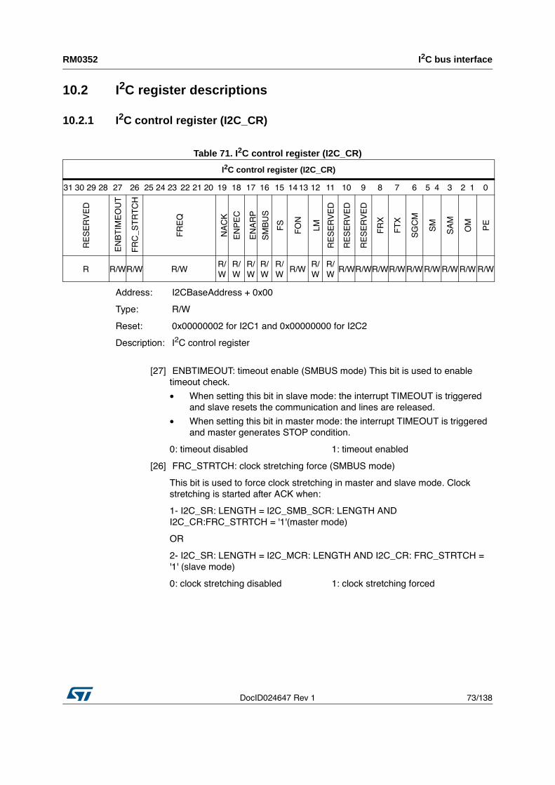
DocID024647 Rev 1 73/138
RM0352 I2C bus interface
137
10.2 I2C register descriptions
10.2.1 I2C control register (I2C_CR)
Table 71. I2C control register (I2C_CR)
Address: I2CBaseAddress + 0x00
Type: R/W
Reset: 0x00000002 for I2C1 and 0x00000000 for I2C2
Description: I2C control register
I2C control register (I2C_CR)
31 30 29 28 27 26 25 24 23 22 21 20 19 18 17 16 15 14 13 12 11 10 9 8 7 6 5 4 3 2 1 0
RE
SE
RV
ED
E
NB
TIM
EO
UT
FR
C_S
TR
TC
H
FR
EQ
NA
CK
EN
PE
C
EN
AR
P
SM
BU
S
FS
FO
N
LM
RE
SE
RV
ED
RE
SE
RV
ED
RE
SE
RV
ED
FR
X
FT
X
SG
CM
SM
SA
M
OM
PE
R R/WR/W R/W
R/
W
R/
W
R/
W
R/
W
R/
W
R/W
R/
W
R/
W
R/WR/WR/WR/WR/W R/W R/W R/W R/W
[27] ENBTIMEOUT: timeout enable (SMBUS mode) This bit is used to enable
timeout check.
• When setting this bit in slave mode: the interrupt TIMEOUT is triggered
and slave resets the communication and lines are released.
• When setting this bit in master mode: the interrupt TIMEOUT is triggered
and master generates STOP condition.
0: timeout disabled 1: timeout enabled
[26] FRC_STRTCH: clock stretching force (SMBUS mode)
This bit is used to force clock stretching in master and slave mode. Clock
stretching is started after ACK when:
1- I2C_SR: LENGTH = I2C_SMB_SCR: LENGTH AND
I2C_CR:FRC_STRTCH = '1'(master mode)
OR
2- I2C_SR: LENGTH = I2C_MCR: LENGTH AND I2C_CR: FRC_STRTCH =
'1' (slave mode)
0: clock stretching disabled 1: clock stretching forced
I2C bus interface RM0352
74/138 DocID024647 Rev 1
[25:20] FREQ: internal clock frequency (SMBUS)
This field must be programmed to generate correct timings it is used to
generate 1 MHZ in internal clock frequency.
000000: not allowed
000001: not allowed
000010: i2c_clk = 2 MHz (kernel clock)
[19] NACK: not-acknowledge enable (SMBUS)
In case of invalid data/command the software choose to cancel transfer by
setting this bit to '1' or to continue reception.
This bit is set and cleared by software and cleared by hardware when
I2C_CR: PE = 0.
0: no not-acknowledge returned
1: not-acknowledge returned after a next byte is received.
[18] ENPEC: PEC enable (SMBUS)
This bit is used to enable or disable the PEC check /send.
0: PEC disabled 1: PEC enabled
[17] ENARP: ARP enable (SMBUS)
0: ARP disable 1: ARP enable
SMBus Device default address recognized
[16] SMBUS: SMBus mode
0: I2C mode 1: SMBus mode
[15] FS: force stop enable bit, When set to 1b, the STOP condition is generated
0: force stop disabled 1: enable force stop
[14:13] FON: Filtering on. FON sets the digital filters on the SDA, SCL line, according
to the I2C bus requirements, when standard open-drain pads are used:
00: no digital filters are inserted.
01: digital filters (filter 1 ck wide spikes) are inserted.
10: digital filters (filter 2 ck wide spikes) are inserted.
11: digital filters (filter 4 ck wide spikes) are inserted.
[12] LM: loopback mode. LM sets the loopback operating mode for the I2C
controller: the Tx FIFO is internally redirect to the Rx FIFO. in order to trace
data stored in the Tx FIFO by reading it from the Rx FIFO.
0: normal mode.
1: loopback mode.
[11] RESERVED
[10] RESERVED
DocID024647 Rev 1 75/138
RM0352 I2C bus interface
137
[9] RESERVED
FRX flushes the receive circuitry (FIFO, fsm). The configuration of the I2C
node (register setting) is not affected by the flushing operation. The flushing
operation is performed on modules working on different clock domains
(system and I2C clocks) and needs several system clock cycles before to be
completed. On the completion, the I2C node (internal logic) clears this bit. The
application must not access to the Rx FIFO during the flushing operation and
should poll on this bit waiting for the completion.
0: flush operation is completed (I2C controller clears the bit)
1: flush operation is started and in progress (set by application).
FRX: flush receive.
[8]
[7] FTX: flush transmit.
FTX flushes the transmit circuitry (FIFO, fsm). The configuration of the I2C
node (register setting) is not affected by the flushing operation. The flushing
operation is performed on modules working on different clock domains
(system and I2C clocks) and needs several system clock cycles before to be
completed. On the completion, the I2C node (internal logic) clears this bit. The
application must not access to the Tx FIFO during the flushing operation and
should poll on this bit waiting for the completion.
0: flush operation is completed (I2C controller clears the bit)
1: flush operation is started and in progress (set by application).
[6] SGCM: slave general call mode. SGCM defines the operating mode of the
slave controller when a general call is received. This setting does not affect
the hardware general call that is always managed in transparent mode.
0: transparent mode, the slave receiver recognizes the general call at any
action is taken by software after the decoding of the message included in the
Rx FIFO.
1: direct mode, the slave receiver recognizes the general call and executes
directly (without software intervention) the related actions. Only the status
code word is stored in the I2C_SR register for notification to the application.
[5:4] SM: Speed Mode. SM defines the speed mode related to the serial bit rate:
00: Standard mode (up to 100 K/s)
01: Fast mode (up to 400 K/s)
10: Reserved
11: Reserved.
[3] SAM: Slave Addressing Mode. SAM defines the slave addressing mode when
the peripheral works in slave or master/slave mode. The received address is
compared with the content of the register I2C_SCR.
0: 7-bit addressing mode
1: 10-bit addressing mode.
I2C bus interface RM0352
76/138 DocID024647 Rev 1
[2:1] OM: Operating Mode.
00: Slave mode. The peripheral can only respond (transmit/receive) when
addresses by a master device.
01: Master mode. The peripheral works in a multi-master system where itself
cannot be addressed by another master device. It can only initiate a new
transfer as master device.
10: Master/Slave mode. The peripheral works in a multi-master system where
itself can be addressed by another master device, besides to initiate a transfer
as a master device.
11: Reserved
[0] PE: Peripheral Enable. PE enables the peripheral to work in the operating
mode set by the I2C_CR.OM register field.:
0: peripheral disabled
1: peripheral enabled.
This bit when deasserted also works as a software reset.
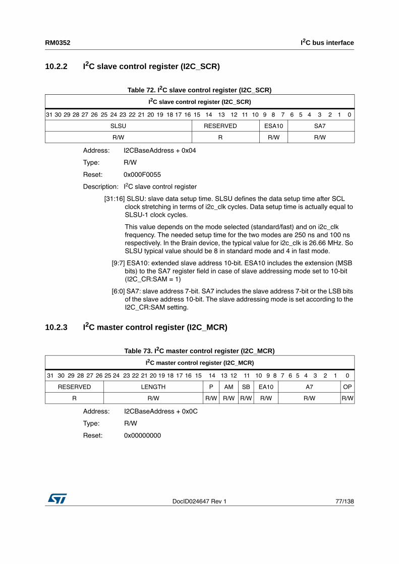
DocID024647 Rev 1 77/138
RM0352 I2C bus interface
137
10.2.2 I2C slave control register (I2C_SCR)
Table 72. I2C slave control register (I2C_SCR)
Address: I2CBaseAddress + 0x04
Type: R/W
Reset: 0x000F0055
Description: I2C slave control register
10.2.3 I2C master control register (I2C_MCR)
Table 73. I2C master control register (I2C_MCR)
Address: I2CBaseAddress + 0x0C
Type: R/W
Reset: 0x00000000
I2C slave control register (I2C_SCR)
31 30 29 28 27 26 25 24 23 22 21 20 19 18 17 16 15 14 13 12 11 10 9 8 7 6 5 4 3 2 1 0
SLSU RESERVED ESA10 SA7
R/W R R/W R/W
[31:16] SLSU: slave data setup time. SLSU defines the data setup time after SCL
clock stretching in terms of i2c_clk cycles. Data setup time is actually equal to
SLSU-1 clock cycles.
This value depends on the mode selected (standard/fast) and on i2c_clk
frequency. The needed setup time for the two modes are 250 ns and 100 ns
respectively. In the Brain device, the typical value for i2c_clk is 26.66 MHz. So
SLSU typical value should be 8 in standard mode and 4 in fast mode.
[9:7] ESA10: extended slave address 10-bit. ESA10 includes the extension (MSB
bits) to the SA7 register field in case of slave addressing mode set to 10-bit
(I2C_CR:SAM = 1)
[6:0] SA7: slave address 7-bit. SA7 includes the slave address 7-bit or the LSB bits
of the slave address 10-bit. The slave addressing mode is set according to the
I2C_CR:SAM setting.
I2C master control register (I2C_MCR)
31 30 29 28 27 26 25 24 23 22 21 20 19 18 17 16 15 14 13 12 11 10 9 8 7 6 5 4 3 2 1 0
RESERVED LENGTH P AM SB EA10 A7 OP
R R/W R/W R/W R/W R/W R/W R/W
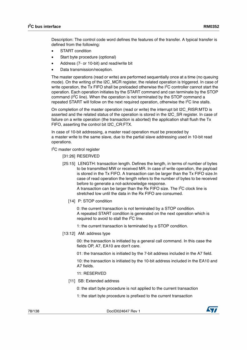
I2C bus interface RM0352
78/138 DocID024647 Rev 1
Description: The control code word defines the features of the transfer. A typical transfer is
defined from the following:
• START condition
• Start byte procedure (optional)
• Address (7- or 10-bit) and read/write bit
• Data transmission/reception.
The master operations (read or write) are performed sequentially once at a time (no queuing
mode). On the writing of the I2C_MCR register, the related operation is triggered. In case of
write operation, the Tx FIFO shall be preloaded otherwise the I2C controller cannot start the
operation. Each operation initiates by the START command and can terminate by the STOP
command (I2C line). When the operation is not terminated by the STOP command a
repeated START will follow on the next required operation, otherwise the I2C line stalls.
On completion of the master operation (read or write) the interrupt bit I2C_RISR:MTD is
asserted and the related status of the operation is stored in the I2C_SR register. In case of
failure on a write operation (the transaction is aborted) the application shall flush the Tx
FIFO, asserting the control bit I2C_CR:FTX.
In case of 10-bit addressing, a master read operation must be preceded by
a master write to the same slave, due to the partial slave addressing used in 10-bit read
operations.
I2C master control register
[31:26] RESERVED
[25:15] LENGTH: transaction length. Defines the length, in terms of number of bytes
to be transmitted MW or received MR. In case of write operation, the payload
is stored in the Tx FIFO. A transaction can be larger than the Tx FIFO size.In
case of read operation the length refers to the number of bytes to be received
before to generate a not-acknowledge response.
A transaction can be larger than the Rx FIFO size. The I2C clock line is
stretched low until the data in the Rx FIFO are consumed.
[14] P: STOP condition
0: the current transaction is not terminated by a STOP condition.
A repeated START condition is generated on the next operation which is
required to avoid to stall the I2C line.
1: the current transaction is terminated by a STOP condition.
[13:12] AM: address type
00: the transaction is initiated by a general call command. In this case the
fields OP, A7, EA10 are don't care.
01: the transaction is initiated by the 7-bit address included in the A7 field.
10: the transaction is initiated by the 10-bit address included in the EA10 and
A7 fields.
11: RESERVED
[11] SB: Extended address
0: the start byte procedure is not applied to the current transaction
1: the start byte procedure is prefixed to the current transaction
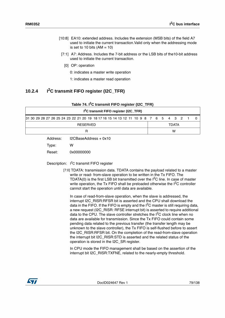
DocID024647 Rev 1 79/138
RM0352 I2C bus interface
137
10.2.4 I2C transmit FIFO register (I2C_TFR)
Table 74. I2C transmit FIFO register (I2C_TFR)
Address: I2CBaseAddress + 0x10
Type: W
Reset: 0x00000000
[10:8] EA10: extended address. Includes the extension (MSB bits) of the field A7
used to initiate the current transaction.Valid only when the addressing mode
is set to 10 bits (AM = 10)
[7:1] A7: Address. Includes the 7-bit address or the LSB bits of the10-bit address
used to initiate the current transaction.
[0] OP: operation
0: indicates a master write operation
1: indicates a master read operation
I2C transmit FIFO register (I2C_TFR)
31 30 29 28 27 26 25 24 23 22 21 20 19 18 17 16 15 14 13 12 11 10 9 8 7 6 5 4 3 2 1 0
RESERVED TDATA
R W
Description: I2C transmit FIFO register
TDATA: transmission data. TDATA contains the payload related to a master
write or read- from-slave operation to be written in the Tx FIFO. The
TDATA(0) is the first LSB bit transmitted over the I2C line. In case of master
write operation, the Tx FIFO shall be preloaded otherwise the I2C controller
cannot start the operation until data are available.
[7:0]
In case of read-from-slave operation, when the slave is addressed, the
interrupt I2C_RISR:RFSR bit is asserted and the CPU shall download the
data in the FIFO. If the FIFO is empty and the I2C master is still requiring data,
a new request (I2C_RISR: RFSE interrupt bit) is asserted to require additional
data to the CPU. The slave controller stretches the I2C clock line when no
data are available for transmission. Since the Tx FIFO could contain some
pending data related to the previous transfer (the transfer length may be
unknown to the slave controller), the Tx FIFO is self-flushed before to assert
the I2C_RISR:RFSR bit. On the completion of the read-from-slave operation
the interrupt bit I2C_RISR:STD is asserted and the related status of the
operation is stored in the I2C_SR register.
In CPU mode the FIFO management shall be based on the assertion of the
interrupt bit I2C_RISR:TXFNE, related to the nearly-empty threshold.
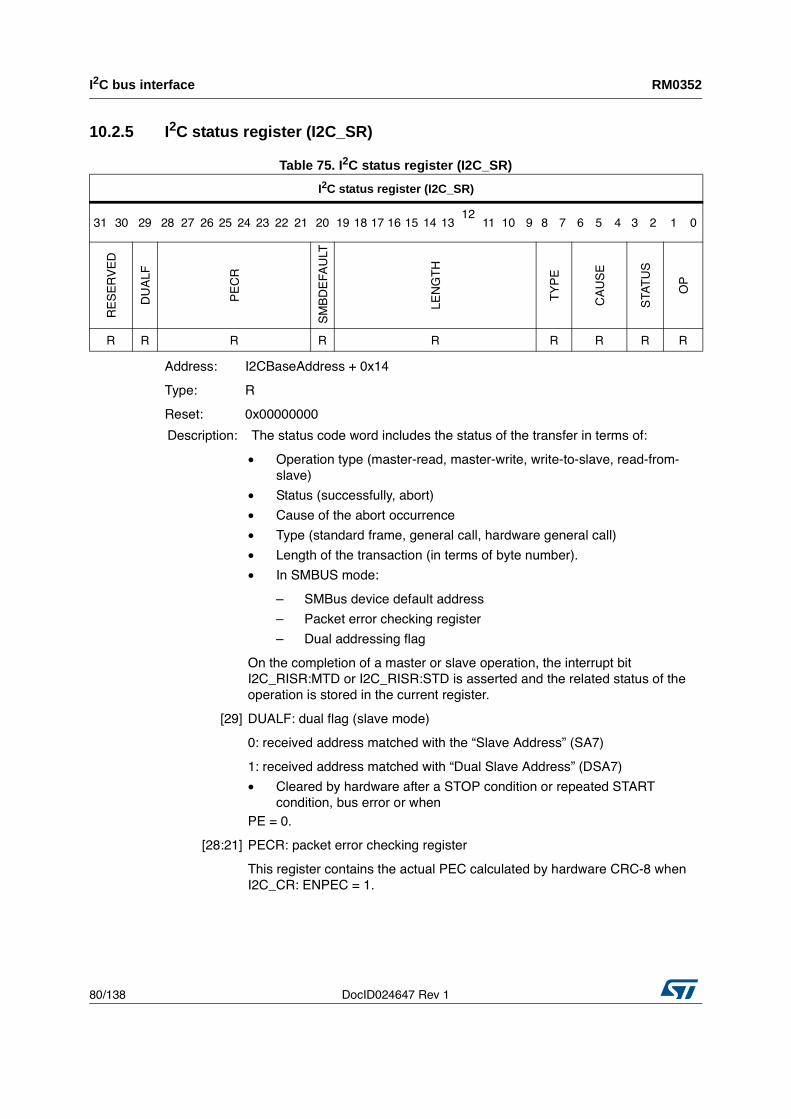
I2C bus interface RM0352
80/138 DocID024647 Rev 1
10.2.5 I2C status register (I2C_SR)
Table 75. I2C status register (I2C_SR)
Address: I2CBaseAddress + 0x14
Type: R
Reset: 0x00000000
I2C status register (I2C_SR)
31 30 29 28 27 26 25 24 23 22 21 20 19 18 17 16 15 14 13
12
11 10 9 8 7 6 5 4 3 2 1 0
RE
SE
RV
ED
DU
AL
F
PE
CR
SM
BD
EF
AU
LT
LE
NG
TH
TY
PE
CA
US
E
STA
TU
S
OP
R R R R R R R R R
Description: The status code word includes the status of the transfer in terms of:
• Operation type (master-read, master-write, write-to-slave, read-from-
slave)
• Status (successfully, abort)
• Cause of the abort occurrence
• Type (standard frame, general call, hardware general call)
• Length of the transaction (in terms of byte number).
• In SMBUS mode:
– SMBus device default address
– Packet error checking register
– Dual addressing flag
On the completion of a master or slave operation, the interrupt bit
I2C_RISR:MTD or I2C_RISR:STD is asserted and the related status of the
operation is stored in the current register.
[29] DUALF: dual flag (slave mode)
0: received address matched with the “Slave Address” (SA7)
1: received address matched with “Dual Slave Address” (DSA7)
• Cleared by hardware after a STOP condition or repeated START
condition, bus error or when
PE = 0.
[28:21] PECR: packet error checking register
This register contains the actual PEC calculated by hardware CRC-8 when
I2C_CR: ENPEC = 1.
DocID024647 Rev 1 81/138
RM0352 I2C bus interface
137
[20] SMBDEFAULT: SMBus device default address (slave mode)
0: no SMBus device default address
1: SMBus device default address received when ENARP = 1
• Cleared by hardware after a STOP condition or repeated START
condition, or when PE = 0.
[19:9] LENGTH: transfer length. For an MR, WTS operation the LENGTH field
defines the actual size of the subsequent payload, in terms of number of
bytes. For an MW, RFS operation the LENGTH field defines the actual
number of bytes transferred by the master/slave device. For a WTS
operation if the transfer length exceeds 2047 bytes, the operation is stopped
by the slave returning a NACK handshake and the flag OVFL is set. For an
RFS operation if the transfer length exceeds 2047 bytes, the operation
continues normally but the LENGTH field is reset to 0.
[8:7] TYPE: receive type. Valid only for the operation WTS
00: FRAME: the slave has received a normal frame
01: GCALL: the slave has received a general call. If the it I2C_CR:SGCM is
set to 1, the general call is directly executed without software intervention
and only the control code word is reported in the FIFO (LENGTH = 0).
10: HW_GCALL: The slave has received a hardware general call.
11: RESERVED
[6:4] CAUSE: abort cause. This field is valid only when the STATUS field contains
the ABORT tag. Others: RESERVED.
000: NACK_ADDR: the master receives a not-acknowledge after the
transmission of the address. Valid for the operations MW, MR.
001: NACK_DATA: the master receives a not-acknowledge during the data
phase of an MW operation. Valid for the operation MW.
010: ACK_MCODE: the master receives an acknowledge after the
transmission of the master code in Hs mode. Valid for the operations MW,
MR in HS mode.
011: ARB_LOST: the master loses the arbitration during a MW or MR
operation. Valid for the operations MW, MR.
100: BERR_START: the slave restarts, a START condition occurs while the
byte transfer is not terminated.
101: BERR_STOP: the slave resets, a STOP condition while the byte
transfer is not terminated.
110: OVFL: the slave receives a frame related to the WTS operation longer
than the maximum size = 2047 bytes. In this case the slave device returns
a NACK to complete the data transfer. Valid for a WTS operation.
I2C bus interface RM0352
82/138 DocID024647 Rev 1
[3:2] STATUS: controller status. Valid for the operations MW, MR, WTS, RFS.
0: NOP: no operation is in progress
1: ON_GOING: an operation is ongoing
10: OK: the operation (OP field) has been completed successfully
11: ABORT: the operation (OP field) has been aborted due to the occurrence
of the event described in the CAUSE field.
[1:0] OP: operation
00: MW: master write operation
01: MR: master read operation
10: WTS: write to slave operation
11: RFS: read from slave operation
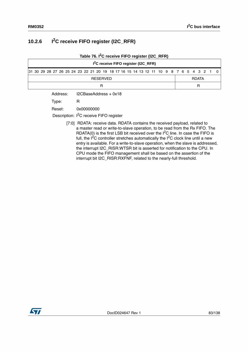
DocID024647 Rev 1 83/138
RM0352 I2C bus interface
137
10.2.6 I2C receive FIFO register (I2C_RFR)
Table 76. I2C receive FIFO register (I2C_RFR)
Address: I2CBaseAddress + 0x18
Type: R
Reset: 0x00000000
I2C receive FIFO register (I2C_RFR)
31 30 29 28 27 26 25 24 23 22 21 20 19 18 17 16 15 14 13 12 11 10 9 8 7 6 5 4 3 2 1 0
RESERVED RDATA
R R
Description: I2C receive FIFO register
[7:0] RDATA: receive data. RDATA contains the received payload, related to
a master read or write-to-slave operation, to be read from the Rx FIFO. The
RDATA(0) is the first LSB bit received over the I2C line. In case the FIFO is
full, the I2C controller stretches automatically the I
2C clock line until a new
entry is available. For a write-to-slave operation, when the slave is addressed,
the interrupt I2C_RISR:WTSR bit is asserted for notification to the CPU. In
CPU mode the FIFO management shall be based on the assertion of the
interrupt bit I2C_RISR:RXFNF, related to the nearly-full threshold.
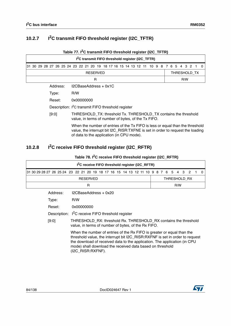
I2C bus interface RM0352
84/138 DocID024647 Rev 1
10.2.7 I2C transmit FIFO threshold register (I2C_TFTR)
Table 77. I2C transmit FIFO threshold register (I2C_TFTR)
10.2.8 I2C receive FIFO threshold register (I2C_RFTR)
Table 78. I2C receive FIFO threshold register (I2C_RFTR)
Address: I2CBaseAddress + 0x20
Type: R/W
Reset: 0x00000000
Description: I2C receive FIFO threshold register
I2C transmit FIFO threshold register (I2C_TFTR)
31 30 29 28 27 26 25 24 23 22 21 20 19 18 17 16 15 14 13 12 11 10 9 8 7 6 5 4 3 2 1 0
RESERVED THRESHOLD_TX
R R/W
Address: I2CBaseAddress + 0x1C
Type: R/W
Reset: 0x00000000
Description: I2C transmit FIFO threshold register
[9:0] THRESHOLD_TX: threshold Tx. THRESHOLD_TX contains the threshold
value, in terms of number of bytes, of the Tx FIFO.
When the number of entries of the Tx FIFO is less or equal than the threshold
value, the interrupt bit I2C_RISR:TXFNE is set in order to request the loading
of data to the application (in CPU mode).
I2C receive FIFO threshold register (I2C_RFTR)
31 30 29 28 27 26 25 24 23 22 21 20 19 18 17 16 15 14 13 12 11 10 9 8 7 6 5 4 3 2 1 0
RESERVED THRESHOLD_RX
R R/W
[9:0] THRESHOLD_RX: threshold Rx. THRESHOLD_RX contains the threshold
value, in terms of number of bytes, of the Rx FIFO.
When the number of entries of the Rx FIFO is greater or equal than the
threshold value, the interrupt bit I2C_RISR:RXFNF is set in order to request
the download of received data to the application. The application (in CPU
mode) shall download the received data based on threshold
(I2C_RISR:RXFNF).
DocID024647 Rev 1 85/138
RM0352 I2C bus interface
137
10.2.9 I2C baud-rate counter register (I2C_BRCR)
Table 79. I2C baud-rate counter register (I2C_BRCR)
Address: I2CBaseAddress + 0x28
Type: R/W
Reset: 0x00000008
Note: A master operating in fast mode can operate with a slave in standard mode(< 100 Kb/s). But in this case, the master should be programmed in standard mode to generate the appropriate bit-rate.
Theoretically the minimum input clock frequency for the I²C
• If the I2C is in standard mode at 100 kHz is 1.4 MHz
• If the I2C is in fast mode at 400 kHz is 7.2 MHz.
I2C baud-rate counter register (I2C_BRCR)
31 30 29 28 27 26 25 24 23 22 21 20 19 18 17 16 15 14 13 12 11 10 9 8 7 6 5 4 3 2 1 0
RESERVED BRCNT2
R/W R/W
Description:
[31:16] RESERVED
[15:0] BRCNT2: baud rate counter 2. BRCNT2 defines the counter value used to
setup the I2C baud rate in standard and fast mode, when the peripheral is
operating in master mode, as described in :
Equation 2
Baud rate (fast) = fi2cclk / ((BRCNT2x3) + Foncycle)
Baud rate (standard) = fi2cclk / ((BRCNT2 x 2) + Foncycle)
The Foncycle means the delay between the SCL/SDA bus and the internal
SCL/SDA (i.e the SCL/SDA after filtering).
I2C_CR:FON = “00” => filter the clock spike wide = 0 => foncycle = 1
I2C_CR:FON = “01” => filter the clock spike wide = 1 => foncycle = 3
I2C_CR:FON = “10” => filter the clock spike wide = 2 => foncycle = 4
I2C_CR:FON = “11” => filter the clock spike wide = 4 => foncycle = 6
I2C bus interface RM0352
86/138 DocID024647 Rev 1
10.2.10 I2C interrupt mask set/clear register (I2C_IMSCR)
Table 80. I2C interrupt mask set/clear register (I2C_IMSCR)
Address: I2CBaseAddress + 0x2C
Type: R/W
Reset: 0x00000000
I2C interrupt mask set/clear register (I2C_IMSCR)
31 30 29 28 27 26 25 24 23 22 21 20 19 18 17 16 15 14 13 12 11 10 9 8 7 6 5 4 3 2 1 0
RE
SE
RV
ED
TIM
EO
UT
M
PE
CE
RR
M
MT
DW
SM
RE
SE
RV
ED
BE
RR
M
MA
LM
SA
LM
RE
SE
RV
ED
ST
DM
MT
DM
WT
SR
M
RF
SE
M
RF
SR
M
LB
RM
RESERVED
RX
FF
M
RX
FN
FM
RX
FE
M
TX
FO
VR
M
TX
FF
M
TX
FN
EM
TX
FE
M
R
R/
W
R/
W
R/
W
R
R/
W
R/
W
R/
W
R/
W
R/
W
R/
W
R/
W
R/
W
R/
W
R/
W
R/
W
R
R/
W
R/
W
R/
W
R/
W
R/
W
R/
W
R/
W
Description: I2C interrupt mask set/clear register
[30] TIMEOUTM: Timeout or Tlow error mask. TIMEOUTM enables the interrupt
bit.
TIMEOUT(SMBUS)
0: TIMEOUT interrupt is disabled, but checked internally.
1: TIMEOUT interrupt is enabled.
[29] PECERRM: PEC error in reception mask. PECERRM enables the interrupt
bit.
PECERR(SMBUS)
0: PECERR interrupt is disabled.
1: PECERR interrupt is enabled.
[28] MTDWSM: master transaction done without stop mask. MTDWSM enables
the interrupt bit.
MTDWS.
0: MTDWS interrupt is disabled.
1: MTDWS interrupt is enabled.
[25] BERRM: bus error mask. BERRM enables the interrupt bit BERR.
0: BERR interrupt is disabled.
1: BERR interrupt is enabled.
[24] MALM: master arbitration lost mask. MALM enables the interrupt bit MAL.
0: MAL interrupt is disabled.
1: MAL interrupt is enabled.
DocID024647 Rev 1 87/138
RM0352 I2C bus interface
137
[23] SALM: slave arbitration lost mask. SALM enables the interrupt bit SAL.
(SMBUS mode)
0: SAL interrupt is disabled.
1: SAL interrupt is enabled.
[20] STDM: slave transaction done mask. STDM enables the interrupt bit STD.
0: STD interrupt is disabled.
1: STD interrupt is enabled.
[19] MTDM: master transaction done mask. MTDM enables the interrupt bit
MTD.
0: MTD interrupt is disabled.
1: MTD interrupt is enabled.
[18] WTSRM: write-to-slave request mask. WTSRM enables the interrupt bit
WTSR.
0: WTSR interrupt is disabled.
1: WTSR interrupt is enabled.
[17] RFSEM: read-from-slave empty mask. RFSEM enables the interrupt bit
RFSE.
0: RFSE interrupt is disabled.
1: RFSE interrupt is enabled.
[16] RFSRM: read-from-slave request mask. RFSRM enables the interrupt bit
RFSR.
0: RFSR interrupt is disabled.
1: RFSR interrupt is enabled.
[15] LBRM: length number of bytes received mask. LBRM enables the interrupt
bit LBR(SMBUS).
0: LBR interrupt is disabled.
1: LBR interrupt is enabled.
[6] RXFFM: Rx FIFO full mask. RXFFM enables the interrupt bit RXFF.
0: RXFF interrupt is disabled.
1: RXFF interrupt is enabled.
[5] RXFNFM: Rx FIFO nearly full mask. RXFN FM enables the interrupt bit
RXFNF.
0: RXFNF interrupt is disabled.
1: RXFNF interrupt is enabled.
[4] RXFEM: Rx FIFO empty mask. RXFEM enables the interrupt bit RXFE.
0: RXFE interrupt is disabled.
1: RXFE interrupt is enabled.
I2C bus interface RM0352
88/138 DocID024647 Rev 1
10.2.11 I2C raw interrupt status register (I2C_RISR)
Table 81. I2C raw interrupt status register (I2C_RISR)
Address: I2CBaseAddress + 0x30
Type: R
Reset: 0x00000013
[3] TXFOVRM: Tx FIFO overrun mask. TXFOVRM enables the interrupt bit
TFXOVR.
0: TXFOVR interrupt is disabled.
1: TXFOVR interrupt is enabled.
[2] TXFFM: Tx FIFO full mask. TXFFM enables the interrupt bit TXFF.
1: TXFF interrupt is enabled.
0: TXFF interrupt is disabled.
[1] TXFNEM: Tx FIFO nearly empty mask. TXFNEM enables the interrupt bit
TXFNE.
0: TXFNE interrupt is disabled.
1: TXFNE interrupt is enabled.
[0] TXFEM: Tx FIFO empty mask. TXFEM enables the interrupt bit TXFE.
0: TXFE interrupt is disabled.
1: TXFE interrupt is enabled.
I2C raw interrupt status register (I2C_RISR)
31 30 29 28 27 26 25 24 23 22 21 20 19 18 17 16 15 14 13 12 11 10 9 8 7 6 5 4 3 2 1 0
RE
SE
RV
ED
TIM
EO
UT
PE
CE
RR
MT
DW
S
RE
SE
RV
ED
BE
RR
MA
L
SA
L
RE
SE
RV
ED
ST
D
MT
D
WT
SR
RF
SE
RF
SR
LB
R
RESERVED
RX
FF
RX
FN
F
RX
FE
TX
FO
VR
TX
FF
TX
FN
E
TX
FE
R R R R R R R R R R R R R R R R R R R R R R R
Description: The I2C_RISR register indicates the interrupt sources prior to masking.
[30] TIMEOUT: timeout or Tlow error (SMBUS mode)
0: no timeout error
1: SCL remained LOW for 25 ms (timeout)
or
master cumulative clock low extend time more than 10 ms (Tlow:mext)
or
DocID024647 Rev 1 89/138
RM0352 I2C bus interface
137
• When set in slave mode: slave resets the communication and lines are
released by hardware.
• When set in master mode: STOP condition sent by hardware.
• Cleared by software writing in I2C_ICR, or by hardware when I2C_CR:
PE = 0.
[29] PECERR: PEC error in reception (SMBUS mode)
0: no PEC error: receiver returns ACK after PEC reception
(if I2C_CR:NACK = 0).
1: PEC error: receiver returns NACK after PEC reception (whatever I2C_CR:
NACK).
• Cleared by software writing in I2C_ICR, or by hardware when I2C_CR:
PE = 0.
[28] MTDWS: master transaction done without stop. MTDWS is set when
a master operation (write or read) has been executed and stop (I2C_MCR: P
field) is not programmed. The application shall read the related transaction
status (I2C_SR register), the pending data in the Rx FIFO (only for a master
read operation) and clear this interrupt (transaction acknowledgment).
A subsequent master operation can be issued (writing the I2C_MCR register)
after the clearing of this interrupt. A subsequent slave operation will be
notified (I2C_RISR: WTSR and I2C_RISR: RFSR interrupt bits assertion)
after the clearing of this interrupt, meanwhile the I2C clock line will be
stretched low. This interrupt is cleared setting the related bit of the I2C_ICR
register.
0: master transaction acknowledged
1: master transaction done (ready for acknowledgment) and stop is not
applied into the I2C bus.
[25] BERR: bus error. BERR is set when an unexpected START/STOP condition
occurs during a transaction. The related actions are different, depending on
the type of operation is in progress (TBD). The status code word in the
I2C_SR contains a specific error tag (CAUSE field) for this error condition.
This interrupt is cleared setting the related bit of the I2C_ICR register.
0: no bus error detection
1: bus error detection
[24] MAL: master arbitration lost. MAL is set when the master loses the arbitration
(only for debugging). The status code word in the I2C_SR contains a specific
error tag (CAUSE field) for this error condition. A collision occurs when 2
stations transmit simultaneously 2 opposite values on the serial line. The
station that is pulling up the line, identifies the collision reading a 0 value on
the sda_in signal, stops the transmission, leaves the bus and waits for the
idle state (STOP condition received) on the bus line before to retry the same
transaction. The station which transmits the first unique zero wins the bus
arbitration. This interrupt is cleared setting the related bit of the I2C_ICR
register.
0: no master arbitration lost.
I2C bus interface RM0352
90/138 DocID024647 Rev 1
1: master arbitration lost.
[23] SAL: slave arbitration lost (SMBUS mode). SAL is set when the slave loses
the arbitration during the data phase. A collision occurs when 2 devices
transmit simultaneously 2 opposite values on the serial dataline. The device
that is pulling up the line, identifies the collision reading a 0 value on the
sda_in signal, stops the transmission, releases the bus and waits for the idle
state (STOP condition received) on the bus line. The device which transmits
the first unique zero wins the bus arbitration. This interrupt is cleared setting
the related bit of the I2C_ICR register.
0: no slave arbitration lost.
1: slave arbitration lost.
[20] STD: slave transaction done. STD is set when a slave operation (write-to-
slave or read-from- slave) has been executed. The application shall read the
related transaction status (I2C_SR register), the pending data in the Rx FIFO
(only for a write-to-slave operation) and clear this interrupt (transaction
acknowledgment). A subsequent slave operation will be notified
(I2C_RISR:WTSR and I2C_RISR:RFSR interrupt bits assertion) after the
clearing of this interrupt, meanwhile the I2C clock line will be stretched low.
A subsequent master operation can be issued (writing the I2C_MCR register)
after the clearing of this interrupt. This interrupt is cleared setting the related
bit of the I2C_ICR register.
0: slave transaction acknowledged.
1: slave transaction done (ready for acknowledgment).
[19] MTD: master transaction done. MTD is set when a master operation (master
write or master read) has been executed after STOP condition. The
application shall read the related transaction status (I2C_SR register), the
pending data in the Rx FIFO (only for a master read operation) and clear this
interrupt (transaction acknowledgment). A subsequent master operation can
be issued (writing the I2C_MCR register) after the clearing of this interrupt.
A subsequent slave operation will be notified (I2C_RISR:WTSR and
I2C_RISR:RFSR interrupt bits assertion) after the clearing of this interrupt,
meanwhile the I2C clock line will be stretched low. This interrupt is cleared
setting the related bit of the I2C_ICR register.
0: master transaction acknowledged.
1: master transaction done (ready for acknowledgment).
[18] WTSR: write-to-slave request. WTSR is set when a write-to-slave operation
is received (I2C slave is addressed) from the I
2C line. This interrupt is cleared
setting the related bit of the I2C_ICR register.
0: none write-to-slave request pending.
1: write-to-slave request is pending.
[17] RFSE: read-from-slave empty. RFSE is set when a read-from-slave operation
is in progress and the Tx FIFO is empty. On the assertion of this interrupt, the
CPU shall download in the Tx FIFO the data required for the slave operation.
This bit is self cleared writing in the Tx FIFO. At the end of the read-from-
slave operation this bit is cleared although the Tx FIFO is empty.
DocID024647 Rev 1 91/138
RM0352 I2C bus interface
137
0: Tx FIFO is not empty.
1: Tx FIFO is empty with the read-from-slave operation in progress.
[16] RFSR: read-from-slave request. RFSR is set when a read-from-slave “slave-
transmitter” request is received (I2C slave is addressed) from the I
2C line. On
the assertion of this interrupt the Tx FIFO is flushed (pending data are
cleared) and the CPU shall put the data in the Tx FIFO. This bit is self-cleared
writing data in the FIFO. In case the FIFO is empty before the completion of
the read operation the I2C_RISR:RFSE interrupt bit is set.This interrupt is
cleared setting the related bit of the I2C_ICR register.
0: read-from-slave request has been served.
1: read-from-slave request is pending.
[15] LBR: length number of bytes received (SMBUS mode). LBR is set in case of
MR or WTS and when the number of bytes received is equal to the
transaction length programmed in the I2C_MCR:LENGTH (master mode) or
I2C_SMB_SCR:LENGTH (slave mode). On the assertion of this interrupt and
when the bit I2C_CR:FRC_STRTCH is set, the hardware starts clock
stretching, the CPU shall download the data byte (command code, Byte
count, data, etc.) from the Rx FIFO, reset the expected length of the
transaction in I2C_SMB_SCR:LENGTH and clear interrupt. When clearing
this interrupt the hardware continues transfer.This interrupt is cleared setting
the related bit of the I2C_ICR register.
0: length number of bytes is not received.
1: length number of bytes received.
[6] RXFF: Rx FIFO full. RXFF is set when a full condition occurs in the Rx FIFO
(only for debugging purpose). This bit is self cleared when the data are read
from the Rx FIFO.
0: Rx FIFO is not full.
1: Rx FIFO is full.
[5] RXFNF: Rx FIFO nearly full. RXFNF is set when the number of entries in the
Rx FIFO is greater or equal than the threshold value programmed in the
I2CRFTR:THRESHOLD_RX register. Its self cleared when the threshold
level is under the programmed threshold.
0: number of entries in the Rx FIFO less than the
I2CRFTR:THRESHOLD_RX register.
1: number of entries in the Rx FIFO greater or equal than the
I2CRFTR:THRESHOLD_RX register.
[4] RXFE: Rx FIFO empty. RXFE is set when the Rx FIFO is empty (only for
debugging purpose).
This bit is self cleared when the slave Rx FIFO is not empty.
0: Rx FIFO is not empty.
1: Rx FIFO is empty.
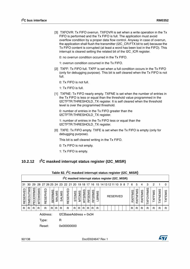
I2C bus interface RM0352
92/138 DocID024647 Rev 1
10.2.12 I2C masked interrupt status register (I2C_MISR)
Table 82. I2C masked interrupt status register (I2C_MISR)
Address: I2CBaseAddress + 0x34
Type: R
Reset: 0x00000000
[3] TXFOVR: Tx FIFO overrun. TXFOVR is set when a write operation in the Tx
FIFO is performed and the Tx FIFO is full. The application must avoid
overflow condition by a proper data flow control. Anyway in case of overrun,
the application shall flush the transmitter (I2C_CR:FTX bit to set) because the
Tx FIFO content is corrupted (at least a word has been lost in the FIFO). This
interrupt is cleared setting the related bit of the I2C_ICR register.
0: no overrun condition occurred in the Tx FIFO.
1: overrun condition occurred in the Tx FIFO.
[2] TXFF: Tx FIFO full. TXFF is set when a full condition occurs in the Tx FIFO
(only for debugging purpose). This bit is self cleared when the Tx FIFO is not
full.
0: Tx FIFO is not full.
1: Tx FIFO is full.
[1] TXFNE: Tx FIFO nearly empty. TXFNE is set when the number of entries in
the Tx FIFO is less or equal than the threshold value programmed in the
I2CTFTR:THRESHOLD_TX register. It is self cleared when the threshold
level is over the programmed threshold.
0: number of entries in the Tx FIFO greater than the
I2CTFTR:THRESHOLD_TX register.
1: number of entries in the Tx FIFO less or equal than the
I2CTFTR:THRESHOLD_TX register.
[0] TXFE: Tx FIFO empty. TXFE is set when the Tx FIFO is empty (only for
debugging purpose).
This bit is self cleared writing in the Tx FIFO.
0: Tx FIFO is not empty.
1: Tx FIFO is empty.
I2C masked interrupt status register (I2C_MISR)
31 30 29 28 27 26 25 24 23 22 21 20 19 18 17 16 15 14 13 12 11 10 9 8 7 6 5 4 3 2 1 0
RE
SE
RV
ED
TIM
EO
UT
MIS
PE
CE
RR
MIS
MT
DW
SM
IS
RE
SE
RV
ED
BE
RR
MIS
MA
LM
IS
SA
LM
IS
RE
SE
RV
ED
ST
DM
IS
MT
DM
IS
WT
SR
MIS
RF
SE
MIS
RF
SR
MIS
LB
RM
IS
RESERVED
RX
FF
MIS
RX
FN
FM
IS
RX
FE
MIS
TX
FO
VR
MIS
TX
FF
MIS
TX
FN
EM
IS
TX
FE
MIS
R R R R R R R R R R R R R R R R R R R R R R
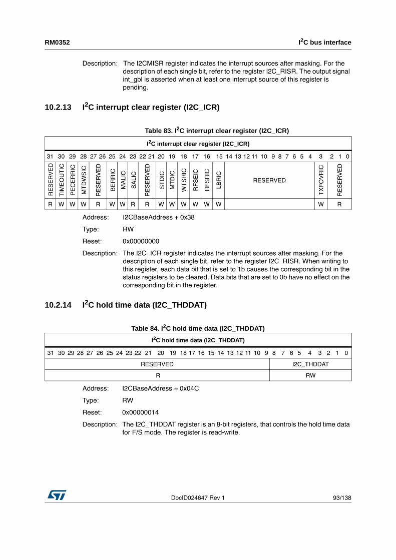
DocID024647 Rev 1 93/138
RM0352 I2C bus interface
137
Description: The I2CMISR register indicates the interrupt sources after masking. For the
description of each single bit, refer to the register I2C_RISR. The output signal
int_gbl is asserted when at least one interrupt source of this register is
pending.
10.2.13 I2C interrupt clear register (I2C_ICR)
Table 83. I2C interrupt clear register (I2C_ICR)
Address: I2CBaseAddress + 0x38
Type: RW
Reset: 0x00000000
Description: The I2C_ICR register indicates the interrupt sources after masking. For the
description of each single bit, refer to the register I2C_RISR. When writing to
this register, each data bit that is set to 1b causes the corresponding bit in the
status registers to be cleared. Data bits that are set to 0b have no effect on the
corresponding bit in the register.
10.2.14 I2C hold time data (I2C_THDDAT)
Table 84. I2C hold time data (I2C_THDDAT)
Address: I2CBaseAddress + 0x04C
Type: RW
Reset: 0x00000014
Description: The I2C_THDDAT register is an 8-bit registers, that controls the hold time data
for F/S mode. The register is read-write.
I2C interrupt clear register (I2C_ICR)
31 30 29 28 27 26 25 24 23 22 21 20 19 18 17 16 15 14 13 12 11 10 9 8 7 6 5 4 3 2 1 0
R
ES
ER
VE
D
TIM
EO
UT
IC
PE
CE
RR
IC
MT
DW
SIC
RE
SE
RV
ED
BE
RR
IC
MA
LIC
SA
LIC
RE
SE
RV
ED
ST
DIC
MT
DIC
WT
SR
IC
RF
SE
IC
RF
SR
IC
LB
RIC
RESERVED
TX
FO
VR
IC
RE
SE
RV
ED
R W W W R W W R R W W W W W W W R
I2C hold time data (I2C_THDDAT)
31 30 29 28 27 26 25 24 23 22 21 20 19 18 17 16 15 14 13 12 11 10 9 8 7 6 5 4 3 2 1 0
RESERVED I2C_THDDAT
R RW
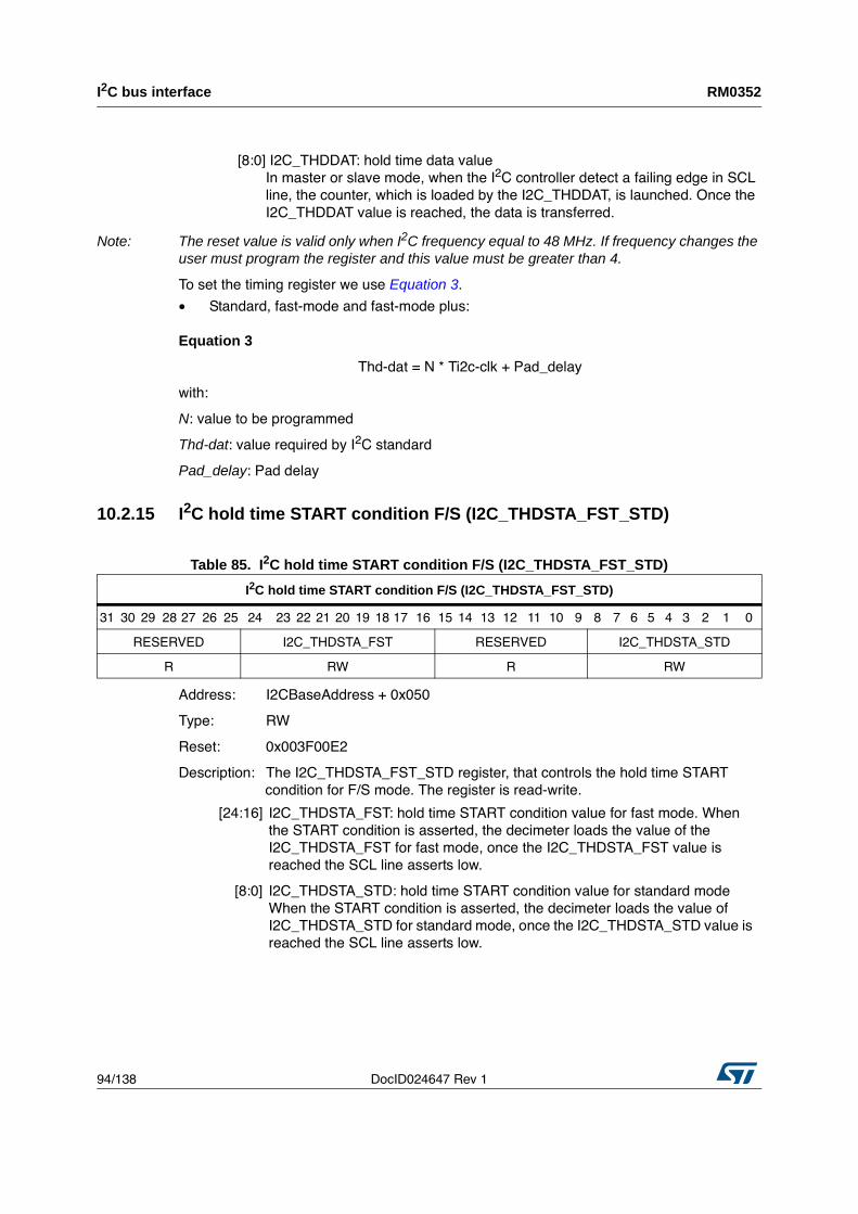
I2C bus interface RM0352
94/138 DocID024647 Rev 1
Note: The reset value is valid only when I2C frequency equal to 48 MHz. If frequency changes the user must program the register and this value must be greater than 4.
To set the timing register we use Equation 3.
• Standard, fast-mode and fast-mode plus:
Equation 3
Thd-dat = N * Ti2c-clk + Pad_delay
with:
N: value to be programmed
Thd-dat: value required by I2C standard
Pad_delay: Pad delay
10.2.15 I2C hold time START condition F/S (I2C_THDSTA_FST_STD)
Table 85. I2C hold time START condition F/S (I2C_THDSTA_FST_STD)
Address: I2CBaseAddress + 0x050
Type: RW
Reset: 0x003F00E2
Description: The I2C_THDSTA_FST_STD register, that controls the hold time START
condition for F/S mode. The register is read-write.
[8:0] I2C_THDDAT: hold time data value
In master or slave mode, when the I2C controller detect a failing edge in SCL
line, the counter, which is loaded by the I2C_THDDAT, is launched. Once the
I2C_THDDAT value is reached, the data is transferred.
I2C hold time START condition F/S (I2C_THDSTA_FST_STD)
31 30 29 28 27 26 25 24 23 22 21 20 19 18 17 16 15 14 13 12 11 10 9 8 7 6 5 4 3 2 1 0
RESERVED I2C_THDSTA_FST RESERVED I2C_THDSTA_STD
R RW R RW
[24:16] I2C_THDSTA_FST: hold time START condition value for fast mode. When
the START condition is asserted, the decimeter loads the value of the
I2C_THDSTA_FST for fast mode, once the I2C_THDSTA_FST value is
reached the SCL line asserts low.
[8:0] I2C_THDSTA_STD: hold time START condition value for standard mode
When the START condition is asserted, the decimeter loads the value of
I2C_THDSTA_STD for standard mode, once the I2C_THDSTA_STD value is
reached the SCL line asserts low.
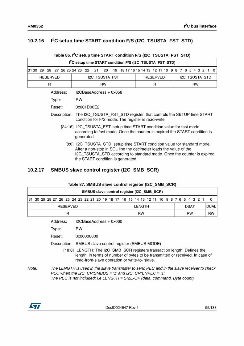
DocID024647 Rev 1 95/138
RM0352 I2C bus interface
137
10.2.16 I2C setup time START condition F/S (I2C_TSUSTA_FST_STD)
Table 86. I2C setup time START condition F/S (I2C_TSUSTA_FST_STD)
Address: I2CBaseAddress + 0x058
Type: RW
Reset: 0x001D00E2
Description: The I2C_TSUSTA_FST_STD register, that controls the SETUP time START
condition for F/S mode. The register is read-write.
10.2.17 SMBUS slave control register (I2C_SMB_SCR)
Table 87. SMBUS slave control register (I2C_SMB_SCR)
Address: I2CBaseAddress + 0x060
Type: RW
Reset: 0x00000000
Description: SMBUS slave control register (SMBUS MODE)
Note: The LENGTH is used in the slave transmitter to send PEC and in the slave receiver to check PEC when the I2C_CR:SMBUS = '1' and I2C_CR:ENPEC = '1'. The PEC is not included: i.e LENGTH = SIZE-OF (data, command, Byte count).
I2C setup time START condition F/S (I2C_TSUSTA_FST_STD)
31 30 29 28 27 26 25 24 23 22 21 20 19 18 17 16 15 14 13 12 11 10 9 8 7 6 5 4 3 2 1 0
RESERVED I2C_TSUSTA_FST RESERVED I2C_TSUSTA_STD
R RW R RW
[24:16] I2C_TSUSTA_FST: setup time START condition value for fast mode
according to fast mode. Once the counter is expired the START condition is
generated.
[8:0] I2C_TSUSTA_STD: setup time START condition value for standard mode.
After a non-stop in SCL line the decimeter loads the value of the
I2C_TSUSTA_STD according to standard mode. Once the counter is expired
the START condition is generated.
SMBUS slave control register (I2C_SMB_SCR)
31 30 29 28 27 26 25 24 23 22 21 20 19 18 17 16 15 14 13 12 11 10 9 8 7 6 5 4 3 2 1 0
RESERVED LENGTH DSA7 DUAL
R RW RW RW
[18:8] LENGTH: The I2C_SMB_SCR registers transaction length. Defines the
length, in terms of number of bytes to be transmitted or received. In case of
read-from-slave operation or write-to- slave.
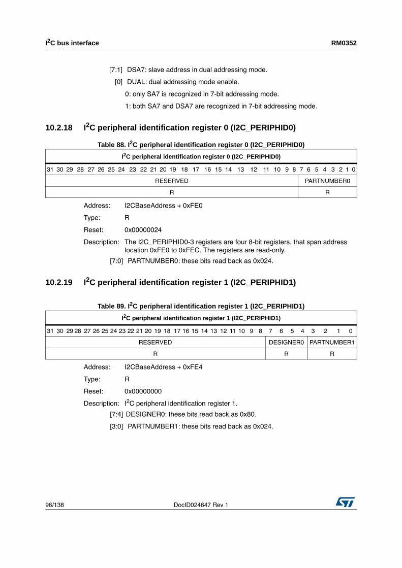
I2C bus interface RM0352
96/138 DocID024647 Rev 1
10.2.18 I2C peripheral identification register 0 (I2C_PERIPHID0)
Table 88. I2C peripheral identification register 0 (I2C_PERIPHID0)
Address: I2CBaseAddress + 0xFE0
Type: R
Reset: 0x00000024
Description: The I2C_PERIPHID0-3 registers are four 8-bit registers, that span address
location 0xFE0 to 0xFEC. The registers are read-only.
10.2.19 I2C peripheral identification register 1 (I2C_PERIPHID1)
Table 89. I2C peripheral identification register 1 (I2C_PERIPHID1)
Address: I2CBaseAddress + 0xFE4
Type: R
Reset: 0x00000000
Description: I2C peripheral identification register 1.
[7:1] DSA7: slave address in dual addressing mode.
[0] DUAL: dual addressing mode enable.
0: only SA7 is recognized in 7-bit addressing mode.
1: both SA7 and DSA7 are recognized in 7-bit addressing mode.
I2C peripheral identification register 0 (I2C_PERIPHID0)
31 30 29 28 27 26 25 24 23 22 21 20 19 18 17 16 15 14 13 12 11 10 9 8 7 6 5 4 3 2 1 0
RESERVED PARTNUMBER0
R R
[7:0] PARTNUMBER0: these bits read back as 0x024.
I2C peripheral identification register 1 (I2C_PERIPHID1)
31 30 29 28 27 26 25 24 23 22 21 20 19 18 17 16 15 14 13 12 11 10 9 8 7 6 5 4 3 2 1 0
RESERVED DESIGNER0 PARTNUMBER1
R R R
[7:4] DESIGNER0: these bits read back as 0x80.
[3:0] PARTNUMBER1: these bits read back as 0x024.
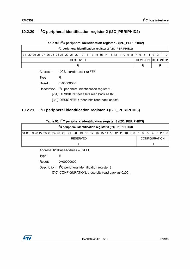
DocID024647 Rev 1 97/138
RM0352 I2C bus interface
137
10.2.20 I2C peripheral identification register 2 (I2C_PERIPHID2)
Table 90. I2C peripheral identification register 2 (I2C_PERIPHID2)
Address: I2CBaseAddress + 0xFE8
Type: R
Reset: 0x00000038
Description: I2C peripheral identification register 2.
10.2.21 I2C peripheral identification register 3 (I2C_PERIPHID3)
Table 91. I2C peripheral identification register 3 (I2C_PERIPHID3)
Address: I2CBaseAddress + 0xFEC
Type: R
Reset: 0x00000000
Description: I2C peripheral identification register 3.
I2C peripheral identification register 2 (I2C_PERIPHID2)
31 30 29 28 27 26 25 24 23 22 21 20 19 18 17 16 15 14 13 12 11 10 9 8 7 6 5 4 3 2 1 0
RESERVED REVISION DESIGNER1
R R R
[7:4] REVISION: these bits read back as 0x3.
[3:0] DESIGNER1: these bits read back as 0x8.
I2C peripheral identification register 3 (I2C_PERIPHID3)
31 30 29 28 27 26 25 24 23 22 21 20 19 18 17 16 15 14 13 12 11 10 9 8 7 6 5 4 3 2 1 0
RESERVED CONFIGURATION
R R
[7:0] CONFIGURATION: these bits read back as 0x00.
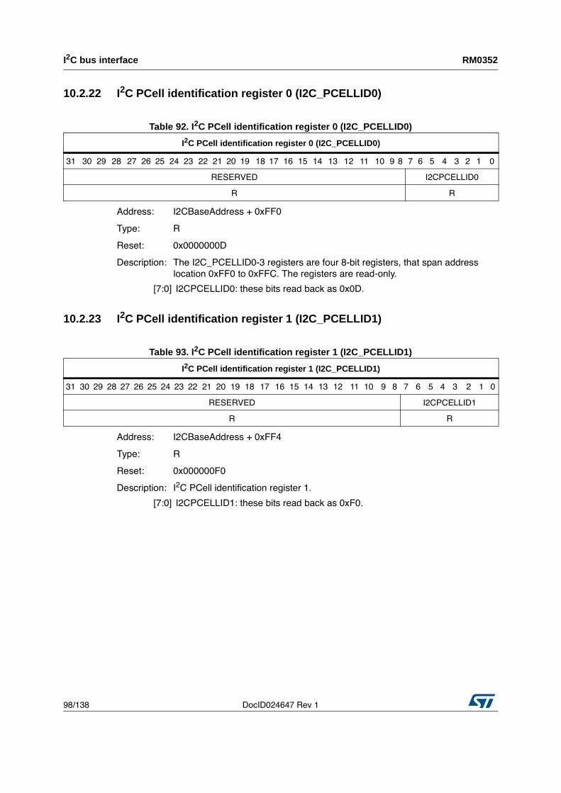
I2C bus interface RM0352
98/138 DocID024647 Rev 1
10.2.22 I2C PCell identification register 0 (I2C_PCELLID0)
Table 92. I2C PCell identification register 0 (I2C_PCELLID0)
Address: I2CBaseAddress + 0xFF0
Type: R
Reset: 0x0000000D
Description: The I2C_PCELLID0-3 registers are four 8-bit registers, that span address
location 0xFF0 to 0xFFC. The registers are read-only.
10.2.23 I2C PCell identification register 1 (I2C_PCELLID1)
Table 93. I2C PCell identification register 1 (I2C_PCELLID1)
Address: I2CBaseAddress + 0xFF4
Type: R
Reset: 0x000000F0
Description: I2C PCell identification register 1.
I2C PCell identification register 0 (I2C_PCELLID0)
31 30 29 28 27 26 25 24 23 22 21 20 19 18 17 16 15 14 13 12 11 10 9 8 7 6 5 4 3 2 1 0
RESERVED I2CPCELLID0
R R
[7:0] I2CPCELLID0: these bits read back as 0x0D.
I2C PCell identification register 1 (I2C_PCELLID1)
31 30 29 28 27 26 25 24 23 22 21 20 19 18 17 16 15 14 13 12 11 10 9 8 7 6 5 4 3 2 1 0
RESERVED I2CPCELLID1
R R
[7:0] I2CPCELLID1: these bits read back as 0xF0.
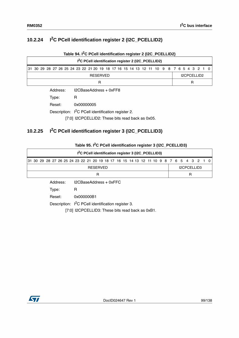
DocID024647 Rev 1 99/138
RM0352 I2C bus interface
137
10.2.24 I2C PCell identification register 2 (I2C_PCELLID2)
Table 94. I2C PCell identification register 2 (I2C_PCELLID2)
Address: I2CBaseAddress + 0xFF8
Type: R
Reset: 0x00000005
Description: I2C PCell identification register 2.
10.2.25 I2C PCell identification register 3 (I2C_PCELLID3)
Table 95. I2C PCell identification register 3 (I2C_PCELLID3)
Address: I2CBaseAddress + 0xFFC
Type: R
Reset: 0x000000B1
Description: I2C PCell identification register 3.
I2C PCell identification register 2 (I2C_PCELLID2)
31 30 29 28 27 26 25 24 23 22 21 20 19 18 17 16 15 14 13 12 11 10 9 8 7 6 5 4 3 2 1 0
RESERVED I2CPCELLID2
R R
[7:0] I2CPCELLID2: These bits read back as 0x05.
I2C PCell identification register 3 (I2C_PCELLID3)
31 30 29 28 27 26 25 24 23 22 21 20 19 18 17 16 15 14 13 12 11 10 9 8 7 6 5 4 3 2 1 0
RESERVED I2CPCELLID3
R R
[7:0] I2CPCELLID3: These bits read back as 0xB1.
SPI (serial peripheral interface) RM0352
100/138 DocID024647 Rev 1
11 SPI (serial peripheral interface)
The SPI block is an IP provided by ARM (PL022 “PrimeCell®
Synchronous Serial Port”).
Additional details about its functional blocks may be found in “ARM PrimeCell® Synchronous Serial Port (PL022) Technical Reference Manual”.
11.1 FeaturesThe SPI is a master or slave interface that enables synchronous serial communication with
slave or master peripherals having one of the following:
• A MOTOROLA SPI-compatible interface
• A TEXAS INSTRUMENTS synchronous serial interface
• A National Semiconductor MICROWIRE®
interface.
The SPI interface operates as a master or slave interface. It supports bit rates up to 2 MHz
and higher in both master and slave configurations. The SPI has the following features:
• Parallel-to-serial conversion on data written to an internal 16-bit wide, 8-location deep
transmit FIFO
• Serial-to-parallel conversion on received data, buffering it in a 16-bit wide, 8-location
deep receive FIFO
• Programmable data frame size from 4 to 16 bits
• Programmable clock bit rate and prescaler. The input clock may be divided by a factor
of 2 to 254 in steps of two to provide the serial output clock
• Programmable clock phase and polarity.
11.2 Clock prescalerWhen configured as a master, an internal prescaler is used to provide the serial output
clock. The prescaler may be programmed through the SSPCPSR register to divide the
SSPCLK by a factor of 2 to 254 in steps of two. As least significant bit of the SSPCPSR
register is not used, division by an odd number is impossible and this ensures a symmetrical
(equal mark space ratio) clock is generated.
The output of this prescaler is further divided by a factor 1 to 256, through the programming
of the SSPCR0 control register, to give a final master output clock.
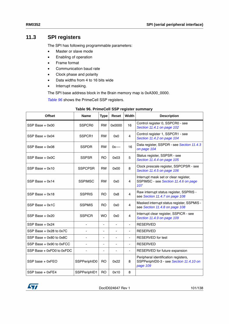
DocID024647 Rev 1 101/138
RM0352 SPI (serial peripheral interface)
137
11.3 SPI registersThe SPI has following programmable parameters:
• Master or slave mode
• Enabling of operation
• Frame format
• Communication baud rate
• Clock phase and polarity
• Data widths from 4 to 16 bits wide
• Interrupt masking.
The SPI base address block in the Brain memory map is 0xA300_0000.
Table 96 shows the PrimeCell SSP registers.
Table 96. PrimeCell SSP register summary
Offset Name Type Reset Width Description
SSP Base + 0x00 SSPCR0 RW 0x0000 16
Control register 0, SSPCR0 - see
Section 11.4.1 on page 102
SSP Base + 0x04 SSPCR1 RW 0x0 4
Control register 1, SSPCR1 - see
Section 11.4.2 on page 104
SSP Base + 0x08 SSPDR RW 0x---- 16
Data register, SSPDR - see Section 11.4.3 on page 104
SSP Base + 0x0C SSPSR RO 0x03 5
Status register, SSPSR - see
Section 11.4.4 on page 105
SSP Base + 0x10 SSPCPSR RW 0x00 8
Clock prescale register, SSPCPSR - see
Section 11.4.5 on page 106
SSP Base + 0x14 SSPIMSC RW 0x0 4
Interrupt mask set or clear register,
SSPIMSC - see Section 11.4.6 on page 107
SSP Base + 0x18 SSPRIS RO 0x8 4
Raw interrupt status register, SSPRIS -
see Section 11.4.7 on page 108
SSP Base + 0x1C SSPMIS RO 0x0 4
Masked interrupt status register, SSPMIS -
see Section 11.4.8 on page 108
SSP Base + 0x20 SSPICR WO 0x0 4
Interrupt clear register, SSPICR - see
Section 11.4.9 on page 109
SSP Base + 0x24 - - - - RESERVED
SSP Base + 0x28 to 0x7C - - - - RESERVED
SSP Base + 0x80 to 0x8C - - - - RESERVED for test
SSP Base + 0x90 to 0xFCC - - - - RESERVED
SSP Base + 0xFD0 to 0xFDC - - - - RESERVED for future expansion
SSP base + 0xFEO SSPPeriphID0 RO 0x22 8
Peripheral identification registers,
SSPPeriphID0-3 - see Section 11.4.10 on page 109
SSP base + 0xFE4 SSPPeriphID1 RO 0x10 8
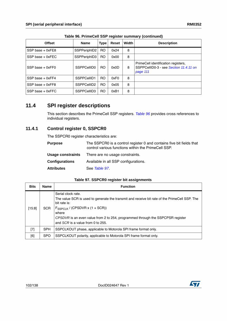
SPI (serial peripheral interface) RM0352
102/138 DocID024647 Rev 1
11.4 SPI register descriptionsThis section describes the PrimeCell SSP registers. Table 96 provides cross references to
individual registers.
11.4.1 Control register 0, SSPCR0
The SSPCR0 register characteristics are:
Purpose The SSPCR0 is a control register 0 and contains five bit fields that
control various functions within the PrimeCell SSP.
Usage constraints There are no usage constraints.
Configurations Available in all SSP configurations.
Attributes See Table 97.
SSP base + 0xFE8 SSPPeriphID2 RO 0x24 8
SSP base + 0xFEC SSPPeriphID3 RO 0x00 8
SSP base + 0xFF0 SSPPCellID0 RO 0x0D 8
PrimeCell identification registers,
SSPPCellID0-3 - see Section 11.4.11 on page 111
SSP base + 0xFF4 SSPPCellID1 RO 0xF0 8
SSP base + 0xFF8 SSPPCellID2 RO 0x05 8
SSP base + 0xFFC SSPPCellID3 RO 0xB1 8
Table 96. PrimeCell SSP register summary (continued)
Offset Name Type Reset Width Description
Table 97. SSPCR0 register bit assignments
Bits Name Function
[15:8] SCR
Serial clock rate.
The value SCR is used to generate the transmit and receive bit rate of the PrimeCell SSP. The
bit rate is:
FSSPCLK
/ (CPSDVR x (1 + SCR))
where
CPSDVR is an even value from 2 to 254, programmed through the SSPCPSR register
and SCR is a value from 0 to 255.
[7] SPH SSPCLKOUT phase, applicable to Motorola SPI frame format only.
[6] SPO SSPCLKOUT polarity, applicable to Motorola SPI frame format only.
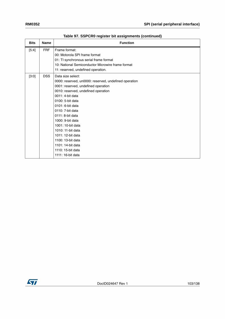
DocID024647 Rev 1 103/138
RM0352 SPI (serial peripheral interface)
137
[5:4] FRF Frame format:
00: Motorola SPI frame format
01: TI synchronous serial frame format
10: National Semiconductor Microwire frame format
11: reserved, undefined operation.
[3:0] DSS Data size select:
0000: reserved, un0000: reserved, undefined operation
0001: reserved, undefined operation
0010: reserved, undefined operation
0011: 4-bit data
0100: 5-bit data
0101: 6-bit data
0110: 7-bit data
0111: 8-bit data
1000: 9-bit data
1001: 10-bit data
1010: 11-bit data
1011: 12-bit data
1100: 13-bit data
1101: 14-bit data
1110: 15-bit data
1111: 16-bit data
Table 97. SSPCR0 register bit assignments (continued)
Bits Name Function
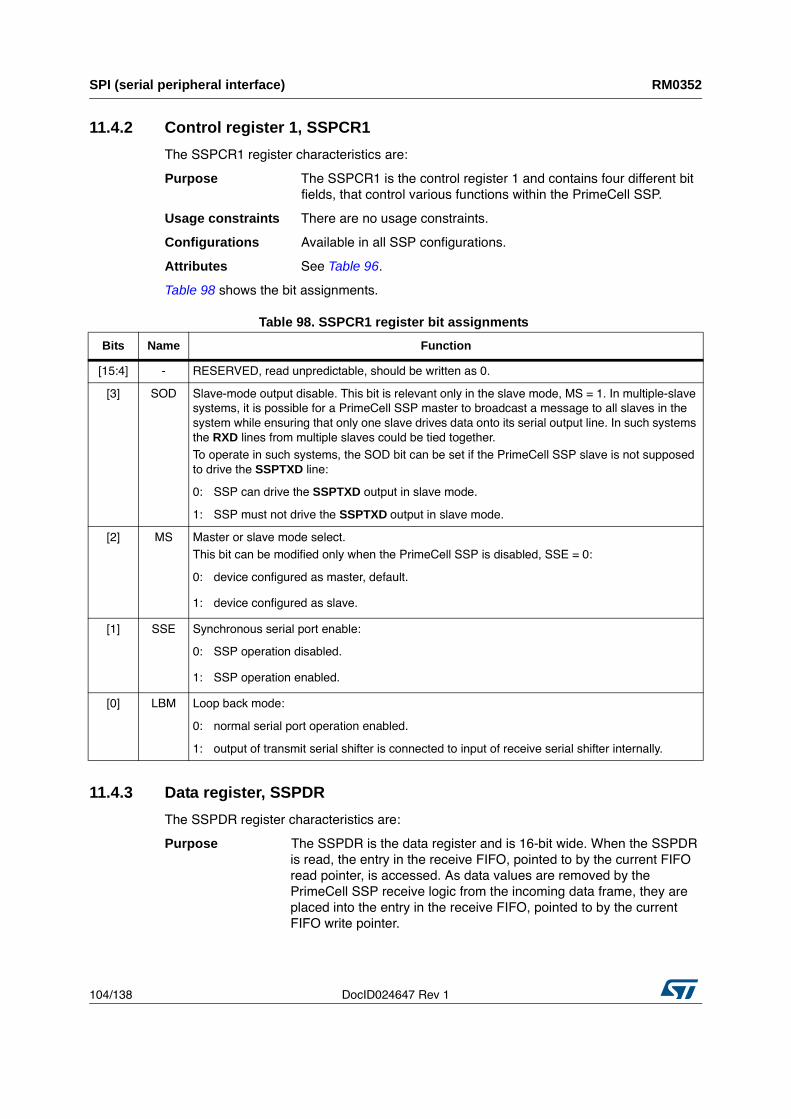
SPI (serial peripheral interface) RM0352
104/138 DocID024647 Rev 1
11.4.2 Control register 1, SSPCR1
The SSPCR1 register characteristics are:
Purpose The SSPCR1 is the control register 1 and contains four different bit
fields, that control various functions within the PrimeCell SSP.
Usage constraints There are no usage constraints.
Configurations Available in all SSP configurations.
Attributes See Table 96.
Table 98 shows the bit assignments.
11.4.3 Data register, SSPDR
The SSPDR register characteristics are:
Purpose The SSPDR is the data register and is 16-bit wide. When the SSPDR
is read, the entry in the receive FIFO, pointed to by the current FIFO
read pointer, is accessed. As data values are removed by the
PrimeCell SSP receive logic from the incoming data frame, they are
placed into the entry in the receive FIFO, pointed to by the current
FIFO write pointer.
Table 98. SSPCR1 register bit assignments
Bits Name Function
[15:4] - RESERVED, read unpredictable, should be written as 0.
[3] SOD Slave-mode output disable. This bit is relevant only in the slave mode, MS = 1. In multiple-slave
systems, it is possible for a PrimeCell SSP master to broadcast a message to all slaves in the
system while ensuring that only one slave drives data onto its serial output line. In such systems
the RXD lines from multiple slaves could be tied together.
To operate in such systems, the SOD bit can be set if the PrimeCell SSP slave is not supposed
to drive the SSPTXD line:
0: SSP can drive the SSPTXD output in slave mode.
1: SSP must not drive the SSPTXD output in slave mode.
[2] MS Master or slave mode select.
This bit can be modified only when the PrimeCell SSP is disabled, SSE = 0:
0: device configured as master, default.
1: device configured as slave.
[1] SSE Synchronous serial port enable:
0: SSP operation disabled.
1: SSP operation enabled.
[0] LBM Loop back mode:
0: normal serial port operation enabled.
1: output of transmit serial shifter is connected to input of receive serial shifter internally.
DocID024647 Rev 1 105/138
RM0352 SPI (serial peripheral interface)
137
When the SSPDR is written to, the entry in the transmit FIFO, pointed
to by the write pointer, is written to. Data values are removed from the
transmit FIFO one value at a time by the transmit logic. It is loaded into
the transmit serial shifter, then serially shifted out onto the SSPTXD
pin at the programmed bit rate.
When a data size of less than 16 bits is selected, the user must right-
justify data written to the transmit FIFO. The transmit logic ignores the
unused bits. Received data less than 16 bits is automatically right-
justified in the receive buffer.
Usage constraints There are no usage constraints.
Configurations Available in all SSP configurations.
Attributes See Table 96 on page 101.
Table 99 shows the bit assignments.
11.4.4 Status register, SSPSR
The SSPSR register characteristics are:
Purpose The SSPSR is an RO status register that contains bits that indicate
the FIFO fill status and the PrimeCell SSP busy status.
Usage constraints There are no usage constraints.
Configurations Available in all SSP configurations.
Attributes See Table 96 on page 101.
Table 99. SSPDR register bit assignments
Bits Name Function
[15:0] DATA Transmit/receive FIFO:
Read: receive FIFO.
Write: transmit FIFO.
You must right-justify data when the PrimeCell SSP is programmed for a data size that is less
than 16 bits. Unused bits at the top are ignored by transmit logic. The receive logic
automatically right-justifies.
SPI (serial peripheral interface) RM0352
106/138 DocID024647 Rev 1
Table 100 shows the bit assignments.
11.4.5 Clock prescale register, SSPCPSR
The SSPCPSR register characteristics are:
Purpose The SSPCPSR is the clock prescale register and specifies the
division factor by which the input SSPCLK must be internally divided
before further use.
The value programmed into this register must be an even number
between 2 - 254. The least significant bit of the programmed number
is hard-coded to zero. If an odd number is written to this register,
data read back from this register has the least significant bit as zero.
Usage constraints There are no usage constraints.
Configurations Available in all SSP configurations.
Attributes See Table 96 on page 101.
Table 100. SSPSR register bit assignments
Bits Name Function
[15:5] - RESERVED, read unpredictable, should be written as 0.
[4] BSY PrimeCell SSP busy flag, RO:
0: SSP is idle.
1: SSP is currently transmitting and/or receiving a frame or the transmit FIFO is not empty.
[3] RFF Receive FIFO full, RO:
0: receive FIFO is not full.
1: receive FIFO is full.
[2] RNE Receive FIFO not empty, RO:
0: receive FIFO is empty.
1: receive FIFO is not empty.
[1] TNF Transmit FIFO not full, RO:
0: transmit FIFO is full.
1: transmit FIFO is not full.
[0] TFE Transmit FIFO empty, RO:
0: transmit FIFO is not empty.
1: transmit FIFO is empty.
DocID024647 Rev 1 107/138
RM0352 SPI (serial peripheral interface)
137
Table 101 shows the bit assignments.
11.4.6 Interrupt mask set or clear register, SSPIMSC
The SSPIMSC register characteristics are:
Purpose The SSPIMSC register is the interrupt mask set or clear register. It is
an RW register.
On a read this register gives the current value of the mask on the
relevant interrupt. A write of 1 to the particular bit sets the mask,
enabling the interrupt to be read. A write of 0 clears the
corresponding mask.
All the bits are cleared to 0 when reset.
Usage constraints There are no usage constraints.
Configurations Available in all SSP configurations.
Attributes See Table 96 on page 101.
Table 102 shows the bit assignments.
Table 101. SSPCPSR register bit assignments
Bits Name Function
[15:8] - RESERVED, read unpredictable, must be written as 0.
[7:0] CPSDVSR Clock prescale divisor. Must be an even number from 2 - 254, depending on the
frequency of SSPCLK. The least significant bit always returns zero on reads.
Table 102. SSPIMSC register bit assignments
Bits Name Function
[15:4] RESERVED RESERVED, read as zero, do not modify.
[3] TXIM Transmit FIFO interrupt mask:
0: transmit FIFO half empty or less condition interrupt is masked.
1: transmit FIFO half empty or less condition interrupt is not masked.
[2] RXIM Receive FIFO interrupt mask:
0: receive FIFO half full or less condition interrupt is masked.
1: receive FIFO half full or less condition interrupt is not masked.
[1] RTIM Receive timeout interrupt mask:
0: receive FIFO not empty and no read prior to timeout period interrupt is masked.
1: receive FIFO not empty and no read prior to timeout period interrupt is not masked.
[0] RORIM Receive overrun interrupt mask:
0: receive FIFO written to while full condition interrupt is masked.
1: receive FIFO written to while full condition interrupt is not masked.
SPI (serial peripheral interface) RM0352
108/138 DocID024647 Rev 1
11.4.7 Raw interrupt status register, SSPRIS
The SSPRIS register characteristics are:
Purpose The SSPRIS register is the raw interrupt status register. It is an RO
register.
On a read this register gives the current raw status value of the
corresponding interrupt prior to masking. A write has no effect.
Usage constraints There are no usage constraints.
Configurations Available in all SSP configurations.
Attributes See Table 96 on page 101.
Table 103 shows the bit assignments.
11.4.8 Masked interrupt status register, SSPMIS
The SSPMIS register characteristics are:
Purpose The SSPMIS register is the masked interrupt status register. It is an
RO register. On a read this register gives the current masked status
value of the corresponding interrupt. A write has no effect.
Usage constraints There are no usage constraints.
Configurations Available in all SSP configurations.
Attributes See Table 96 on page 101.
Table 104 shows the bit assignments.
Table 103. SSPRIS register bit assignments
Bits Name Function
[15:4] RESERVED RESERVED, read as zero, do not modify
[3] TXRIS Gives the raw interrupt state, prior to masking, of the SSPTXINTR interrupt
[2] RXRIS Gives the raw interrupt state, prior to masking, of the SSPRXINTR interrupt
[1] RTRIS Gives the raw interrupt state, prior to masking, of the SSPRTINTR interrupt
[0] RORRIS Gives the raw interrupt state, prior to masking, of the SSPRORINTR interrupt
Table 104. SSPMIS register bit assignments
Bits Name Function
[15:4] RESERVED RESERVED, read as zero, do not modify
[3] TXMIS Gives the transmit FIFO masked interrupt state, after masking, of the SSPTXINTR interrupt
[2] RXMIS Gives the receive FIFO masked interrupt state, after masking, of the SSPRXINTR interrupt
[1] RTMIS Gives the receive timeout masked interrupt state, after masking, of the SSPRTINTR interrupt
[0] RORMIS Gives the receive over run masked interrupt status, after masking, of the SSPRORINTR
interrupt
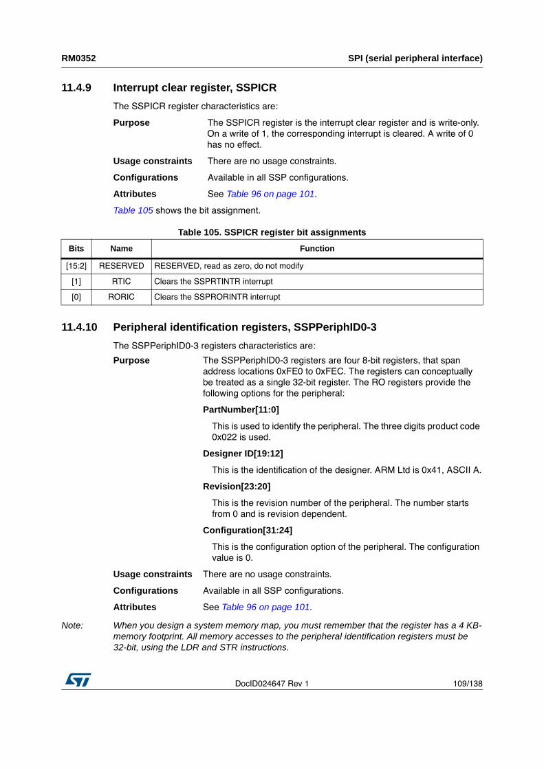
DocID024647 Rev 1 109/138
RM0352 SPI (serial peripheral interface)
137
11.4.9 Interrupt clear register, SSPICR
The SSPICR register characteristics are:
Purpose The SSPICR register is the interrupt clear register and is write-only.
On a write of 1, the corresponding interrupt is cleared. A write of 0
has no effect.
Usage constraints There are no usage constraints.
Configurations Available in all SSP configurations.
Attributes See Table 96 on page 101.
Table 105 shows the bit assignment.
11.4.10 Peripheral identification registers, SSPPeriphID0-3
The SSPPeriphID0-3 registers characteristics are:
Note: When you design a system memory map, you must remember that the register has a 4 KB-memory footprint. All memory accesses to the peripheral identification registers must be 32-bit, using the LDR and STR instructions.
Table 105. SSPICR register bit assignments
Bits Name Function
[15:2] RESERVED RESERVED, read as zero, do not modify
[1] RTIC Clears the SSPRTINTR interrupt
[0] RORIC Clears the SSPRORINTR interrupt
Purpose The SSPPeriphID0-3 registers are four 8-bit registers, that span
address locations 0xFE0 to 0xFEC. The registers can conceptually
be treated as a single 32-bit register. The RO registers provide the
following options for the peripheral:
PartNumber[11:0]
This is used to identify the peripheral. The three digits product code
0x022 is used.
Designer ID[19:12]
This is the identification of the designer. ARM Ltd is 0x41, ASCII A.
Revision[23:20]
This is the revision number of the peripheral. The number starts
from 0 and is revision dependent.
Configuration[31:24]
This is the configuration option of the peripheral. The configuration
value is 0.
Usage constraints There are no usage constraints.
Configurations Available in all SSP configurations.
Attributes See Table 96 on page 101.
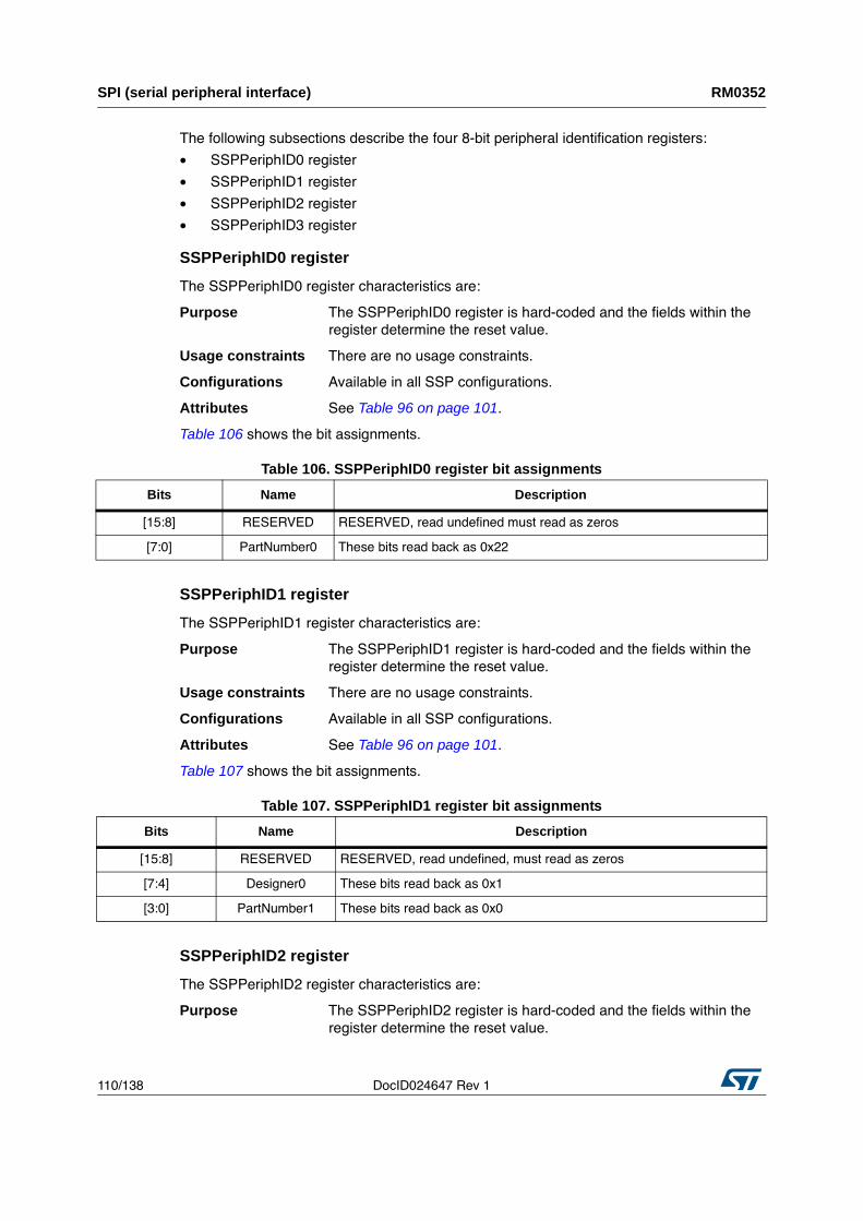
SPI (serial peripheral interface) RM0352
110/138 DocID024647 Rev 1
The following subsections describe the four 8-bit peripheral identification registers:
• SSPPeriphID0 register
• SSPPeriphID1 register
• SSPPeriphID2 register
• SSPPeriphID3 register
SSPPeriphID0 register
The SSPPeriphID0 register characteristics are:
Purpose The SSPPeriphID0 register is hard-coded and the fields within the
register determine the reset value.
Usage constraints There are no usage constraints.
Configurations Available in all SSP configurations.
Attributes See Table 96 on page 101.
Table 106 shows the bit assignments.
SSPPeriphID1 register
The SSPPeriphID1 register characteristics are:
Purpose The SSPPeriphID1 register is hard-coded and the fields within the
register determine the reset value.
Usage constraints There are no usage constraints.
Configurations Available in all SSP configurations.
Attributes See Table 96 on page 101.
Table 107 shows the bit assignments.
SSPPeriphID2 register
The SSPPeriphID2 register characteristics are:
Purpose The SSPPeriphID2 register is hard-coded and the fields within the
register determine the reset value.
Table 106. SSPPeriphID0 register bit assignments
Bits Name Description
[15:8] RESERVED RESERVED, read undefined must read as zeros
[7:0] PartNumber0 These bits read back as 0x22
Table 107. SSPPeriphID1 register bit assignments
Bits Name Description
[15:8] RESERVED RESERVED, read undefined, must read as zeros
[7:4] Designer0 These bits read back as 0x1
[3:0] PartNumber1 These bits read back as 0x0
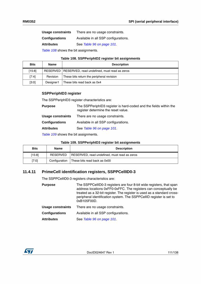
DocID024647 Rev 1 111/138
RM0352 SPI (serial peripheral interface)
137
Usage constraints There are no usage constraints.
Configurations Available in all SSP configurations.
Attributes See Table 96 on page 101.
Table 108 shows the bit assignments.
SSPPeriphID3 register
The SSPPeriphID3 register characteristics are:
Purpose The SSPPeriphID3 register is hard-coded and the fields within the
register determine the reset value.
Usage constraints There are no usage constraints.
Configurations Available in all SSP configurations.
Attributes See Table 96 on page 101.
Table 109 shows the bit assignments.
11.4.11 PrimeCell identification registers, SSPPCellID0-3
The SSPPCellID0-3 registers characteristics are:
Purpose The SSPPCellID0-3 registers are four 8-bit wide registers, that span
address locations 0xFF0-0xFFC. The registers can conceptually be
treated as a 32-bit register. The register is used as a standard cross-
peripheral identification system. The SSPPCellID register is set to
0xB105F00D.
Usage constraints There are no usage constraints.
Configurations Available in all SSP configurations.
Attributes See Table 96 on page 101.
Table 108. SSPPeriphID2 register bit assignments
Bits Name Description
[15:8] RESERVED RESERVED, read undefined, must read as zeros
[7:4] Revision These bits return the peripheral revision
[3:0] Designer1 These bits read back as 0x4
Table 109. SSPPeriphID3 register bit assignments
Bits Name Description
[15:8] RESERVED RESERVED, read undefined, must read as zeros
[7:0] Configuration These bits read back as 0x00
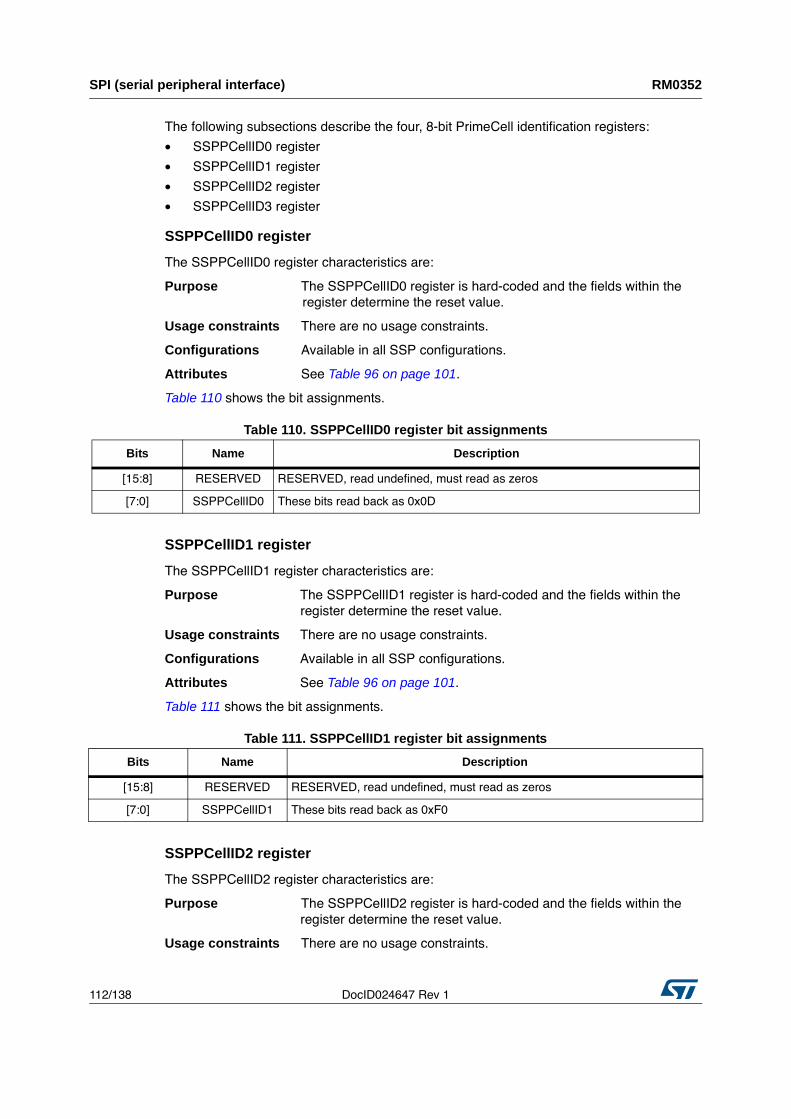
SPI (serial peripheral interface) RM0352
112/138 DocID024647 Rev 1
The following subsections describe the four, 8-bit PrimeCell identification registers:
• SSPPCellID0 register
• SSPPCellID1 register
• SSPPCellID2 register
• SSPPCellID3 register
SSPPCellID0 register
The SSPPCellID0 register characteristics are:
Purpose The SSPPCellID0 register is hard-coded and the fields within the
register determine the reset value.
Usage constraints There are no usage constraints.
Configurations Available in all SSP configurations.
Attributes See Table 96 on page 101.
Table 110 shows the bit assignments.
SSPPCellID1 register
The SSPPCellID1 register characteristics are:
Purpose The SSPPCellID1 register is hard-coded and the fields within the
register determine the reset value.
Usage constraints There are no usage constraints.
Configurations Available in all SSP configurations.
Attributes See Table 96 on page 101.
Table 111 shows the bit assignments.
SSPPCellID2 register
The SSPPCellID2 register characteristics are:
Purpose The SSPPCellID2 register is hard-coded and the fields within the
register determine the reset value.
Usage constraints There are no usage constraints.
Table 110. SSPPCellID0 register bit assignments
Bits Name Description
[15:8] RESERVED RESERVED, read undefined, must read as zeros
[7:0] SSPPCellID0 These bits read back as 0x0D
Table 111. SSPPCellID1 register bit assignments
Bits Name Description
[15:8] RESERVED RESERVED, read undefined, must read as zeros
[7:0] SSPPCellID1 These bits read back as 0xF0
DocID024647 Rev 1 113/138
RM0352 SPI (serial peripheral interface)
137
Configurations Available in all SSP configurations.
Attributes See Table 96 on page 101.
Table 112 shows the bit assignments.
SSPPCellID3 register
The SSPPCellID3 register characteristics are:
Purpose The SSPPCellID3 register is hard-coded and the fields within the
register determine the reset value.
Usage constraints There are no usage constraints.
Configurations Available in all SSP configurations.
Attributes See Table Table 96 on page 101.
Table 113 shows the bit assignments.
11.5 InterruptsThere are five interrupts generated by the PrimeCell SSP. Four of these are individual,
maskable, active-HIGH interrupts as follows:
SSPRXINTR PrimeCell SSP receive FIFO service interrupt request. See Section 11.5.1: SSPRXINTR.
SSPTXINTR PrimeCell SSP transmit FIFO service interrupt request. See Section 11.5.2: SSPTXINTR.
SSPRORINTR PrimeCell SSP receive overrun interrupt request. See Section 11.5.3: SSPRORINTR
SSPRTINTR PrimeCell SSP time out interrupt request. See Section 11.5.4: SSPRTINTR.
The fifth is a combined single interrupt SSPINTR.
You can mask each of the four individual maskable interrupts by setting the appropriate bits
in the SSPIMSC register. Setting the appropriate mask bit HIGH enables the interrupt.
Table 112. SSPPCellID2 register bit assignments
Bits Name Description
[15:8] RESERVED RESERVED, read undefined, must read as zeros
[7:0] SSPPCellID2 These bits read back as 0x05
Table 113. SSPPCellID3 register bit assignments
Bits Name Description
[15:8] RESERVED RESERVED, read undefined, must read as zeros
[7:0] SSPPCellID3 These bits read back as 0xB1
SPI (serial peripheral interface) RM0352
114/138 DocID024647 Rev 1
Provision of the individual outputs in addition to a combined interrupt output, enables the
use of either a global interrupt service routine, or modular device drivers to handle
interrupts.
The transmit and receive dynamic data flow interrupts SSPTXINTR and SSPRXINTR have
been separated from the status interrupts, so that data can be read or written in response to
only the FIFO trigger levels.
The status of the individual interrupt sources can be read from the SSPRIS and SSPMIS
registers.
11.5.1 SSPRXINTR
The receive interrupt is asserted when there are four or more valid entries in the receive
FIFO.
11.5.2 SSPTXINTR
The transmit interrupt is asserted when there are four or fewer valid entries in the transmit
FIFO. The transmitter interrupt SSPTXINTR is not qualified with the PrimeCell SSP enable
signal, and this enables operation in either of the following ways:
• Data can be written to the transmit FIFO prior to enabling the PrimeCell SSP and the
interrupts.
• The PrimeCell SSP and interrupts can be enabled so that data can be written to the
transmit FIFO by an interrupt service routine.
11.5.3 SSPRORINTR
The receive overrun interrupt SSPORINTR is asserted when the FIFO is already full and an
additional data frame is received, causing an overrun of the FIFO. Data is overwritten in the
receive shift register, but not the FIFO.
11.5.4 SSPRTINTR
The receive timeout interrupt is asserted when the receive FIFO is not empty and the
PrimeCell SSP has remained idle for a fixed 32-bit period. This mechanism ensures that the
user is aware that data is still present in the receive FIFO and requires servicing. This
interrupt is deasserted if the receive FIFO becomes empty by subsequent reads, or if new
data is received on SSPRXD. It can also be cleared by writing to the RTIC bit in the SSPICR
register.
The interrupts are also combined into a single output SSPINTR, that is, an OR function of
the individual masked sources. This output is connected to the system interrupt controller
(NVIC) to provide another level of masking on an individual per peripheral basis.
The combined PrimeCell SSP interrupt is asserted if any of the four individual interrupts
above are asserted and enabled.
DocID024647 Rev 1 115/138
RM0352 UART (universal asynchronous receive transmit)
137
12 UART (universal asynchronous receive transmit)
The Brain device has one asynchronous serial ports (UART). The UART block is an IP
provided by ARM (PL011). Additional details about its functional blocks can be found in
“PrimeCell®UART(PL011) Technical Reference Manual”.
12.1 FeaturesThe UART performs:
• Serial-to-parallel conversion on data received from a peripheral device
• Parallel-to-serial conversion on data transmitted to the peripheral device.
The CPU reads and writes data and control/status information through the AMBA APB
interface. The transmit and receive paths are buffered with internal FIFO memories enabling
up to 32-bytes to be stored independently in both transmit and receive modes.
The UART:
• Includes a programmable baud rate generator that generates a common transmit and
receive internal clock from the UART internal reference clock input, UARTCLK
• Offers similar functionality to the industry-standard 16C650 UART device
• Supports the following maximum baud rates:
– 921600 bps, in UART mode
– 460800 bps, in IrDA®
mode
– 115200 bps, in low-power IrDA mode.
The UART operation and baud rate values are controlled by the line control register,
UARTLCR_H - see Section 12.6.7 on page 126 and the baud rate divisor registers (integer
baud rate register, UARTIBRD - see Section 12.6.5 on page 124 and fractional baud rate
register, UARTFBRD - see Section 12.6.6 on page 124).
The UART can generate:
• Individually maskable interrupts from the receive (including timeout), transmit,
• Modem status and error conditions
• A single combined interrupt so that the output is asserted if any of the individual
interrupts are asserted, and unmasked.
If a framing, parity, or break error occurs during reception, the appropriate error bit is set,
and is stored in the FIFO. If an overrun condition occurs, the overrun register bit is set
immediately and FIFO data are prevented from being overwritten.
It is possible to program the FIFOs to be 1-byte deep providing a conventional double
buffered UART interface.
The modem status input signals “Clear To Send” (CTS), “Data Carrier Detect” (DCD), “Data
Set Ready” (DSR), and “Ring Indicator” (RI) are supported. The output modem control lines,
“Request To Send” (RTS), and “Data Terminal Ready” (DTR) are also supported.
There is a programmable hardware flow control feature that uses the nUARTCTS input and
the nUARTRTS output to automatically control the serial data flow.
UART (universal asynchronous receive transmit) RM0352
116/138 DocID024647 Rev 1
12.2 IrDA SIR blockThe IrDA “Serial InfraRed” (SIR) block contains an IrDA SIR protocol ENDEC. The SIR
protocol ENDEC can be enabled for serial communication through signals nSIROUT and
SIRIN to an infrared transducer instead of using the UART signals UARTTXD and
UARTRXD.
If the SIR protocol ENDEC is enabled, the UARTTXD line is held in the passive state (HIGH)
and transitions of the modem status, or the UARTRXD line have no effect. The SIR protocol
ENDEC can receive and transmit, but it is half-duplex only, so it cannot receive while
transmitting, or transmit while receiving.
The IrDA SIR physical layer specifies a minimum 10 ms delay between transmission and
reception.
12.3 Baud rate generatorThe baud rate generator contains free running counters that generate the internal ×16
clocks, Baud16 and IrLPBaud16 signals. Baud16 provides timing information for UART
transmit and receive control. Baud16 is a stream of pulses with a width of one UARTCLK
clock period and a frequency of 16 times the baud rate. IrLPBaud16 provides timing
information to generate the pulse width of the IrDA encoded transmit bit stream when in low-
power IrDA mode.
12.4 InterruptsThere are eleven maskable interrupts generated in the UART. These are combined to
produce five individual interrupt outputs and one that is the OR of the individual outputs:
• UARTRXINTR
• UARTTXINTR
• UARTRTINTR
• UARTMSINTR, that can be caused by:
– UARTRIINTR, because of a change in the nUARTRI modem status
– UARTCTSINTR, because of a change in the nUARTCTS modem status
– UARTDCDINTR, because of a change in the nUARTDCD modem status
– UARTDSRINTR, because of a change in the nUARTDSR modem status.
• UARTEINTR, that can be caused by:
– UARTOEINTR, because of an overrun error
– UARTBEINTR, because of a break in the reception
– UARTPEINTR, because of a parity error in the received character
– UARTFEINTR, because of a framing error in the received character.
• UARTINTR, this is an OR function of the five individual masked outputs.
Changing the mask bits in the interrupt mask set/clear register, UARTIMSC - see
Section 12.6.10 on page 130 enables or disables the individual interrupts. Setting the
appropriate mask bit HIGH enables the interrupt.
Provision of individual outputs and the combined interrupt output, allows using either
a global interrupt service routine, or modular device drivers to handle interrupts.
DocID024647 Rev 1 117/138
RM0352 UART (universal asynchronous receive transmit)
137
The transmit and receive data flow interrupts UARTRXINTR and UARTTXINTR have been
separated from the status interrupts. This enables use of the UARTRXINTR and
UARTTXINTR so that data can be read or written in response to the FIFO trigger levels.
The error interrupt, UARTEINTR, can be triggered when there is an error in the reception of
data. A number of error conditions are possible.
The modem status interrupt, UARTMSINTR, is a combined interrupt of all the individual
modem status signals.
The status of the individual interrupt sources can be read either from the raw interrupt status
register, UARTRIS -see Section 12.6.11 on page 131 or from the masked interrupt status
register, UARTMIS - see Section 12.6.12 on page 132.
12.4.1 UARTMSINTR
The modem status interrupt is asserted if any of the modem status signals (nUARTCTS,
nUARTDCD, nUARTDSR, and nUARTRI) change. It is cleared by writing a 1 to the
corresponding bit(s) in the interrupt clear register, UARTICR - see Section 12.6.13 on page 133, depending on the modem status signals that generated the interrupt.
12.4.2 UARTRXINTR
The receive interrupt changes state when one of the following events occurs:
• If the FIFOs are enabled and the receive FIFO reaches the programmed trigger level.
When this happens, the receive interrupt is asserted HIGH. The receive interrupt is
cleared by reading data from the receive FIFO until it becomes less than the trigger
level, or by clearing the interrupt.
• If the FIFOs are disabled (have a depth of one location) and data is received thereby
filling the location, the receive interrupt is asserted HIGH. The receive interrupt is
cleared by performing a single read of the receive FIFO, or by clearing the interrupt.
12.4.3 UARTTXINTR
The transmit interrupt changes state when one of the following events occurs:
• If the FIFOs are enabled and the transmit FIFO is equal to or lower than the
programmed trigger level then the transmit interrupt is asserted HIGH. The transmit
interrupt is cleared by writing data to the transmit FIFO until it becomes greater than the
trigger level, or by clearing the interrupt.
• If the FIFOs are disabled (have a depth of one location) and there is no data present in
the transmitters single location, the transmit interrupt is asserted HIGH. It is cleared by
performing a single write to the transmit FIFO, or by clearing the interrupt.
UART (universal asynchronous receive transmit) RM0352
118/138 DocID024647 Rev 1
To update the transmit FIFO you must:
• Write data to the transmit FIFO, either prior to enabling the UART and the interrupts, or
after enabling the UART and interrupts.
Note: The transmit interrupt is based on a transition through a level, rather than on the level itself. When the interrupt and the UART is enabled before any data is written to the transmit FIFO the interrupt is not set. The interrupt is only set, after written data leaves the single location of the transmit FIFO and it becomes empty.
12.4.4 UARTRTINTR
The receive timeout interrupt is asserted when the receive FIFO is not empty, and no more
data is received during a 32-bit period. The receive timeout interrupt is cleared either when
the FIFO becomes empty through reading all the data (or by reading the holding register), or
when a 1 is written to the corresponding bit of the interrupt clear register, UARTICR - see
Section 12.6.13 on page 133.
12.4.5 UARTEINTR
The error interrupt is asserted when an error occurs in the reception of data by the UART.
The interrupt can be caused by a number of different error conditions:
• Framing
• Parity
• Break
• Overrun
The cause of the interrupt is visible by reading the raw interrupt status register, UARTRIS -
see Section 12.6.11 on page 131 or the masked interrupt status register, UARTMIS - see
Section 12.6.12 on page 132. It can be cleared by writing to the relevant bits of the interrupt
clear register, UARTICR - see Section 12.6.13 on page 133 (bits 7 to 10 are the error clear
bits).
12.4.6 UARTINTR
The interrupts are also combined into a single output, that is an OR function of the individual
masked sources. This output is connected to the “Nested Vector Interrupt Controller” (NVIC)
to provide another level of masking on a individual peripheral basis (see Table 3 on page 17.
The combined UART interrupt is asserted if any of the individual interrupts are asserted and
enabled.
12.5 UART registersThe UART base address block in the Brain memory map is 0xA200_0000.
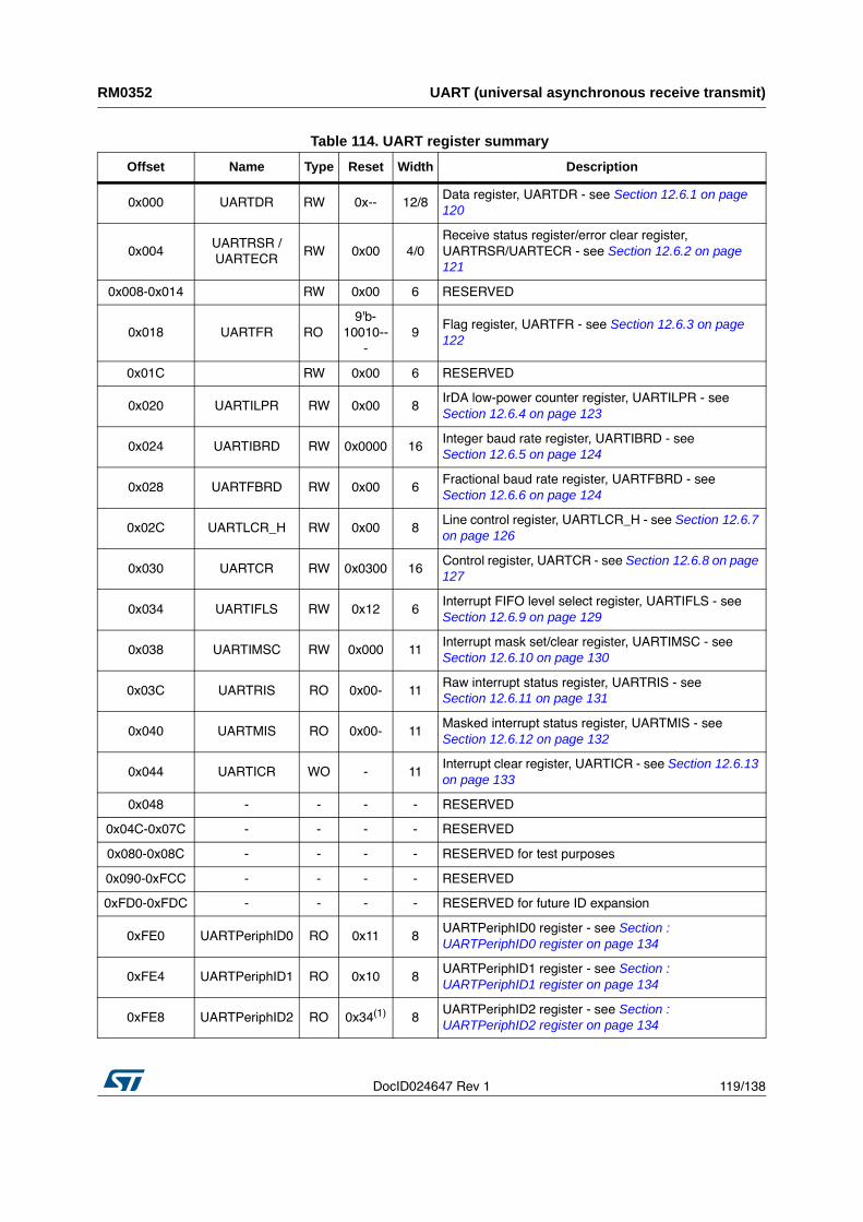
DocID024647 Rev 1 119/138
RM0352 UART (universal asynchronous receive transmit)
137
Table 114. UART register summary
Offset Name Type Reset Width Description
0x000 UARTDR RW 0x-- 12/8
Data register, UARTDR - see Section 12.6.1 on page 120
0x004
UARTRSR /
UARTECR
RW 0x00 4/0
Receive status register/error clear register,
UARTRSR/UARTECR - see Section 12.6.2 on page 121
0x008-0x014 RW 0x00 6 RESERVED
0x018 UARTFR RO
9'b-
10010--
-
9
Flag register, UARTFR - see Section 12.6.3 on page 122
0x01C RW 0x00 6 RESERVED
0x020 UARTILPR RW 0x00 8
IrDA low-power counter register, UARTILPR - see
Section 12.6.4 on page 123
0x024 UARTIBRD RW 0x0000 16
Integer baud rate register, UARTIBRD - see
Section 12.6.5 on page 124
0x028 UARTFBRD RW 0x00 6
Fractional baud rate register, UARTFBRD - see
Section 12.6.6 on page 124
0x02C UARTLCR_H RW 0x00 8
Line control register, UARTLCR_H - see Section 12.6.7 on page 126
0x030 UARTCR RW 0x0300 16
Control register, UARTCR - see Section 12.6.8 on page 127
0x034 UARTIFLS RW 0x12 6
Interrupt FIFO level select register, UARTIFLS - see
Section 12.6.9 on page 129
0x038 UARTIMSC RW 0x000 11
Interrupt mask set/clear register, UARTIMSC - see
Section 12.6.10 on page 130
0x03C UARTRIS RO 0x00- 11
Raw interrupt status register, UARTRIS - see
Section 12.6.11 on page 131
0x040 UARTMIS RO 0x00- 11
Masked interrupt status register, UARTMIS - see
Section 12.6.12 on page 132
0x044 UARTICR WO - 11
Interrupt clear register, UARTICR - see Section 12.6.13 on page 133
0x048 - - - - RESERVED
0x04C-0x07C - - - - RESERVED
0x080-0x08C - - - - RESERVED for test purposes
0x090-0xFCC - - - - RESERVED
0xFD0-0xFDC - - - - RESERVED for future ID expansion
0xFE0 UARTPeriphID0 RO 0x11 8
UARTPeriphID0 register - see Section : UARTPeriphID0 register on page 134
0xFE4 UARTPeriphID1 RO 0x10 8
UARTPeriphID1 register - see Section : UARTPeriphID1 register on page 134
0xFE8 UARTPeriphID2 RO 0x34(1)
8
UARTPeriphID2 register - see Section : UARTPeriphID2 register on page 134
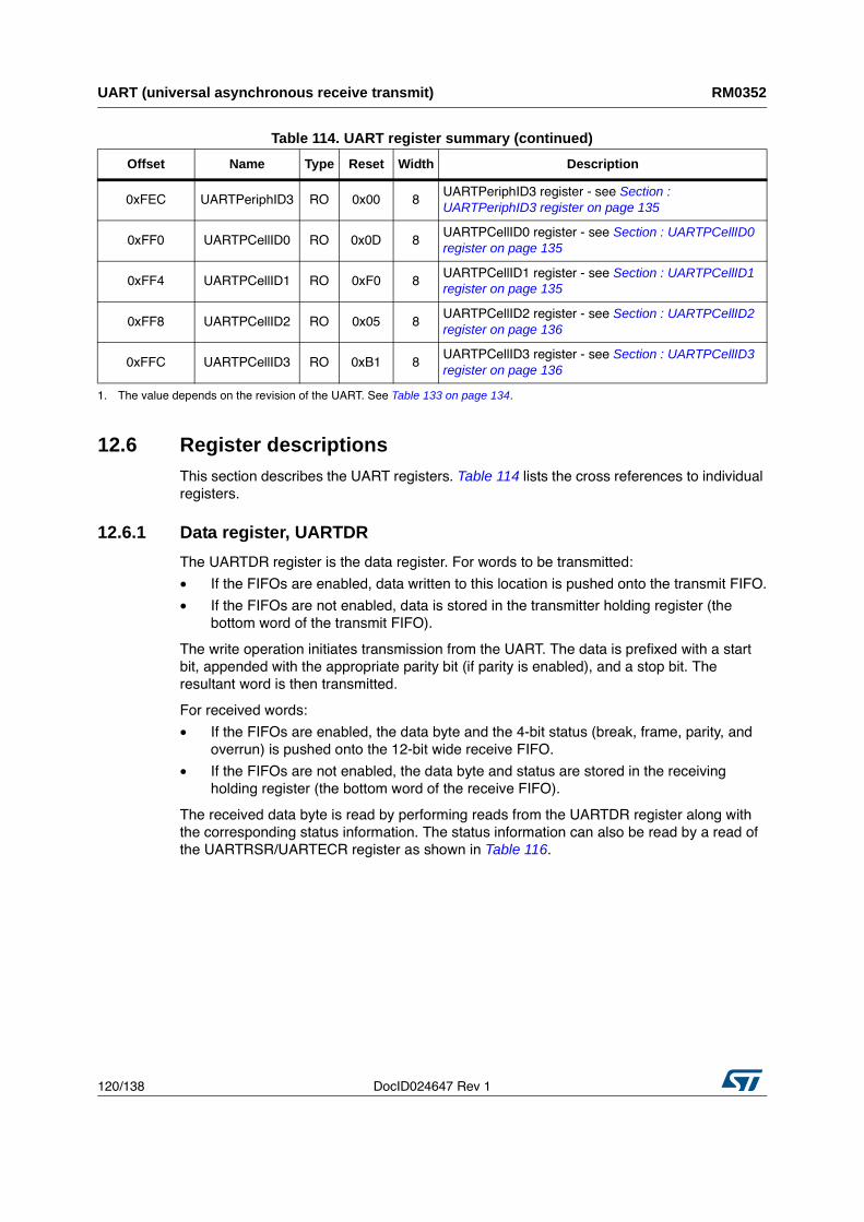
UART (universal asynchronous receive transmit) RM0352
120/138 DocID024647 Rev 1
12.6 Register descriptionsThis section describes the UART registers. Table 114 lists the cross references to individual
registers.
12.6.1 Data register, UARTDR
The UARTDR register is the data register. For words to be transmitted:
• If the FIFOs are enabled, data written to this location is pushed onto the transmit FIFO.
• If the FIFOs are not enabled, data is stored in the transmitter holding register (the
bottom word of the transmit FIFO).
The write operation initiates transmission from the UART. The data is prefixed with a start
bit, appended with the appropriate parity bit (if parity is enabled), and a stop bit. The
resultant word is then transmitted.
For received words:
• If the FIFOs are enabled, the data byte and the 4-bit status (break, frame, parity, and
overrun) is pushed onto the 12-bit wide receive FIFO.
• If the FIFOs are not enabled, the data byte and status are stored in the receiving
holding register (the bottom word of the receive FIFO).
The received data byte is read by performing reads from the UARTDR register along with
the corresponding status information. The status information can also be read by a read of
the UARTRSR/UARTECR register as shown in Table 116.
0xFEC UARTPeriphID3 RO 0x00 8
UARTPeriphID3 register - see Section : UARTPeriphID3 register on page 135
0xFF0 UARTPCellID0 RO 0x0D 8
UARTPCellID0 register - see Section : UARTPCellID0 register on page 135
0xFF4 UARTPCellID1 RO 0xF0 8
UARTPCellID1 register - see Section : UARTPCellID1 register on page 135
0xFF8 UARTPCellID2 RO 0x05 8
UARTPCellID2 register - see Section : UARTPCellID2 register on page 136
0xFFC UARTPCellID3 RO 0xB1 8
UARTPCellID3 register - see Section : UARTPCellID3 register on page 136
1. The value depends on the revision of the UART. See Table 133 on page 134.
Table 114. UART register summary (continued)
Offset Name Type Reset Width Description
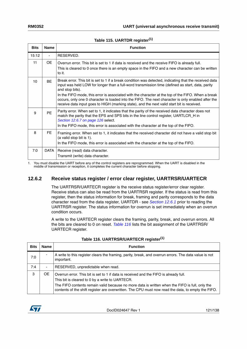
DocID024647 Rev 1 121/138
RM0352 UART (universal asynchronous receive transmit)
137
12.6.2 Receive status register / error clear register, UARTRSR/UARTECR
The UARTRSR/UARTECR register is the receive status register/error clear register.
Receive status can also be read from the UARTRSR register. If the status is read from this
register, then the status information for break, framing and parity corresponds to the data
character read from the data register, UARTDR - see Section 12.6.1 prior to reading the
UARTRSR register. The status information for overrun is set immediately when an overrun
condition occurs.
A write to the UARTECR register clears the framing, parity, break, and overrun errors. All
the bits are cleared to 0 on reset. Table 116 lists the bit assignment of the UARTRSR/
UARTECR register.
Table 115. UARTDR register(1)
Bits Name Function
15:12 - RESERVED.
11 OE Overrun error. This bit is set to 1 if data is received and the receive FIFO is already full.
This is cleared to 0 once there is an empty space in the FIFO and a new character can be written
to it.
10 BEBreak error. This bit is set to 1 if a break condition was detected, indicating that the received data
input was held LOW for longer than a full-word transmission time (defined as start, data, parity
and stop bits).
In the FIFO mode, this error is associated with the character at the top of the FIFO. When a break
occurs, only one 0 character is loaded into the FIFO. The next character is only enabled after the
receive data input goes to HIGH (marking state), and the next valid start bit is received.
9 PEParity error. When set to 1, it indicates that the parity of the received data character does not
match the parity that the EPS and SPS bits in the line control register, UARTLCR_H in
Section 12.6.7 on page 126 select.
In the FIFO mode, this error is associated with the character at the top of the FIFO.
8 FE Framing error. When set to 1, it indicates that the received character did not have a valid stop bit
(a valid stop bit is 1).
In the FIFO mode, this error is associated with the character at the top of the FIFO.
7:0 DATA Receive (read) data character.
Transmit (write) data character.
1. You must disable the UART before any of the control registers are reprogrammed. When the UART is disabled in the
middle of transmission or reception, it completes the current character before stopping.
Table 116. UARTRSR/UARTECR register(1)
Bits Name Function
7:0
- A write to this register clears the framing, parity, break, and overrun errors. The data value is not
important.
7:4 - RESERVED, unpredictable when read.
3 OE Overrun error. This bit is set to 1 if data is received and the FIFO is already full.
This bit is cleared to 0 by a write to UARTECR.
The FIFO contents remain valid because no more data is written when the FIFO is full, only the
contents of the shift register are overwritten. The CPU must now read the data, to empty the FIFO.
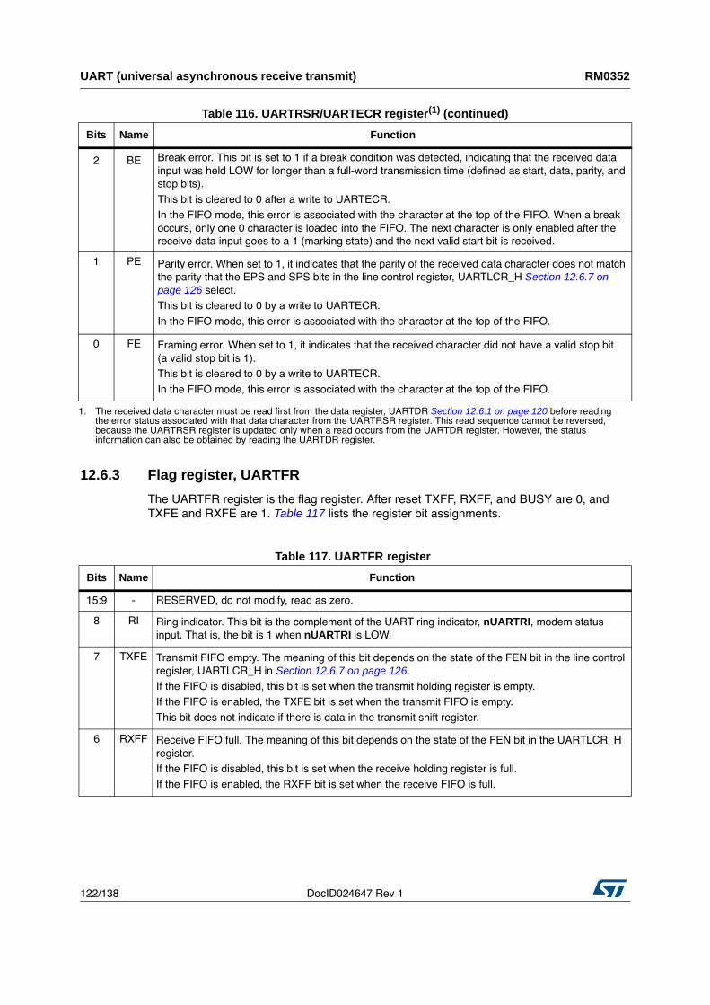
UART (universal asynchronous receive transmit) RM0352
122/138 DocID024647 Rev 1
12.6.3 Flag register, UARTFR
The UARTFR register is the flag register. After reset TXFF, RXFF, and BUSY are 0, and
TXFE and RXFE are 1. Table 117 lists the register bit assignments.
2 BEBreak error. This bit is set to 1 if a break condition was detected, indicating that the received data
input was held LOW for longer than a full-word transmission time (defined as start, data, parity, and
stop bits).
This bit is cleared to 0 after a write to UARTECR.
In the FIFO mode, this error is associated with the character at the top of the FIFO. When a break
occurs, only one 0 character is loaded into the FIFO. The next character is only enabled after the
receive data input goes to a 1 (marking state) and the next valid start bit is received.
1 PE Parity error. When set to 1, it indicates that the parity of the received data character does not match
the parity that the EPS and SPS bits in the line control register, UARTLCR_H Section 12.6.7 on page 126 select.
This bit is cleared to 0 by a write to UARTECR.
In the FIFO mode, this error is associated with the character at the top of the FIFO.
0 FE Framing error. When set to 1, it indicates that the received character did not have a valid stop bit
(a valid stop bit is 1).
This bit is cleared to 0 by a write to UARTECR.
In the FIFO mode, this error is associated with the character at the top of the FIFO.
1. The received data character must be read first from the data register, UARTDR Section 12.6.1 on page 120 before reading
the error status associated with that data character from the UARTRSR register. This read sequence cannot be reversed,
because the UARTRSR register is updated only when a read occurs from the UARTDR register. However, the status
information can also be obtained by reading the UARTDR register.
Table 116. UARTRSR/UARTECR register(1) (continued)
Bits Name Function
Table 117. UARTFR register
Bits Name Function
15:9 - RESERVED, do not modify, read as zero.
8 RI Ring indicator. This bit is the complement of the UART ring indicator, nUARTRI, modem status
input. That is, the bit is 1 when nUARTRI is LOW.
7 TXFE Transmit FIFO empty. The meaning of this bit depends on the state of the FEN bit in the line control
register, UARTLCR_H in Section 12.6.7 on page 126.
If the FIFO is disabled, this bit is set when the transmit holding register is empty.
If the FIFO is enabled, the TXFE bit is set when the transmit FIFO is empty.
This bit does not indicate if there is data in the transmit shift register.
6 RXFF Receive FIFO full. The meaning of this bit depends on the state of the FEN bit in the UARTLCR_H
register.
If the FIFO is disabled, this bit is set when the receive holding register is full.
If the FIFO is enabled, the RXFF bit is set when the receive FIFO is full.
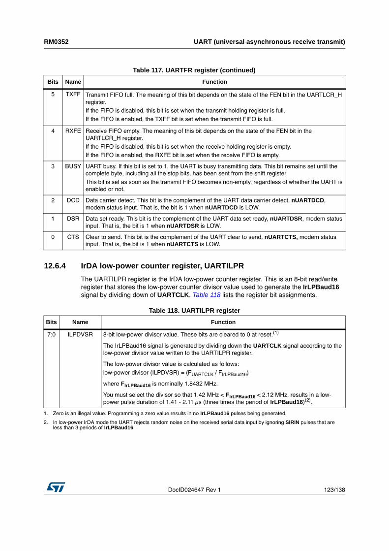
DocID024647 Rev 1 123/138
RM0352 UART (universal asynchronous receive transmit)
137
12.6.4 IrDA low-power counter register, UARTILPR
The UARTILPR register is the IrDA low-power counter register. This is an 8-bit read/write
register that stores the low-power counter divisor value used to generate the IrLPBaud16
signal by dividing down of UARTCLK. Table 118 lists the register bit assignments.
5 TXFF Transmit FIFO full. The meaning of this bit depends on the state of the FEN bit in the UARTLCR_H
register.
If the FIFO is disabled, this bit is set when the transmit holding register is full.
If the FIFO is enabled, the TXFF bit is set when the transmit FIFO is full.
4 RXFE Receive FIFO empty. The meaning of this bit depends on the state of the FEN bit in the
UARTLCR_H register.
If the FIFO is disabled, this bit is set when the receive holding register is empty.
If the FIFO is enabled, the RXFE bit is set when the receive FIFO is empty.
3 BUSY UART busy. If this bit is set to 1, the UART is busy transmitting data. This bit remains set until the
complete byte, including all the stop bits, has been sent from the shift register.
This bit is set as soon as the transmit FIFO becomes non-empty, regardless of whether the UART is
enabled or not.
2 DCD Data carrier detect. This bit is the complement of the UART data carrier detect, nUARTDCD,
modem status input. That is, the bit is 1 when nUARTDCD is LOW.
1 DSR Data set ready. This bit is the complement of the UART data set ready, nUARTDSR, modem status
input. That is, the bit is 1 when nUARTDSR is LOW.
0 CTS Clear to send. This bit is the complement of the UART clear to send, nUARTCTS, modem status
input. That is, the bit is 1 when nUARTCTS is LOW.
Table 117. UARTFR register (continued)
Bits Name Function
Table 118. UARTILPR register
Bits Name Function
7:0 ILPDVSR 8-bit low-power divisor value. These bits are cleared to 0 at reset.(1)
The IrLPBaud16 signal is generated by dividing down the UARTCLK signal according to the
low-power divisor value written to the UARTILPR register.
The low-power divisor value is calculated as follows:
low-power divisor (ILPDVSR) = (FUARTCLK
/ FIrLPBaud16
)
where FIrLPBaud16 is nominally 1.8432 MHz.
You must select the divisor so that 1.42 MHz < FIrLPBaud16 < 2.12 MHz, results in a low-
power pulse duration of 1.41 - 2.11 μs (three times the period of IrLPBaud16)(2)
.
1. Zero is an illegal value. Programming a zero value results in no IrLPBaud16 pulses being generated.
2. In low-power IrDA mode the UART rejects random noise on the received serial data input by ignoring SIRIN pulses that are
less than 3 periods of IrLPBaud16.
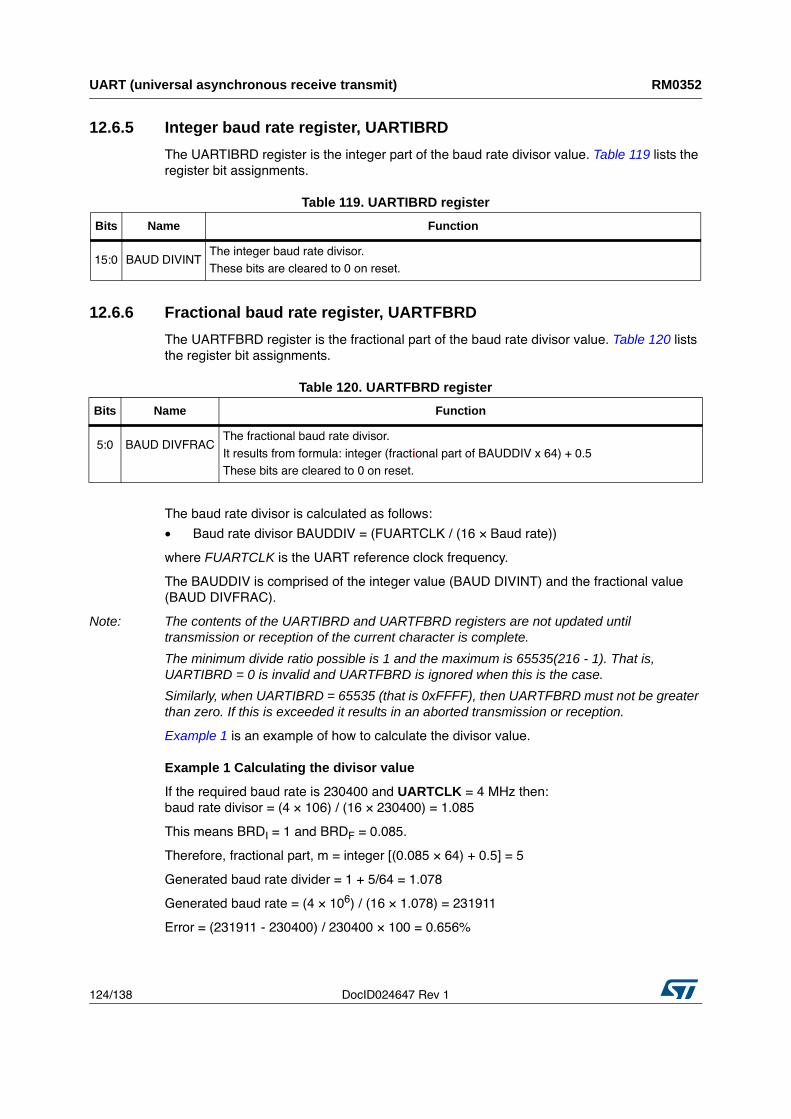
UART (universal asynchronous receive transmit) RM0352
124/138 DocID024647 Rev 1
12.6.5 Integer baud rate register, UARTIBRD
The UARTIBRD register is the integer part of the baud rate divisor value. Table 119 lists the
register bit assignments.
12.6.6 Fractional baud rate register, UARTFBRD
The UARTFBRD register is the fractional part of the baud rate divisor value. Table 120 lists
the register bit assignments.
The baud rate divisor is calculated as follows:
• Baud rate divisor BAUDDIV = (FUARTCLK / (16 × Baud rate))
where FUARTCLK is the UART reference clock frequency.
The BAUDDIV is comprised of the integer value (BAUD DIVINT) and the fractional value
(BAUD DIVFRAC).
Note: The contents of the UARTIBRD and UARTFBRD registers are not updated until transmission or reception of the current character is complete.
The minimum divide ratio possible is 1 and the maximum is 65535(216 - 1). That is, UARTIBRD = 0 is invalid and UARTFBRD is ignored when this is the case.
Similarly, when UARTIBRD = 65535 (that is 0xFFFF), then UARTFBRD must not be greater than zero. If this is exceeded it results in an aborted transmission or reception.
Example 1 is an example of how to calculate the divisor value.
Example 1 Calculating the divisor value
If the required baud rate is 230400 and UARTCLK = 4 MHz then:
baud rate divisor = (4 × 10⁶) / (16 × 230400) = 1.085
This means BRDI = 1 and BRD
F = 0.085.
Therefore, fractional part, m = integer [(0.085 × 64) + 0.5] = 5
Generated baud rate divider = 1 + 5/64 = 1.078
Generated baud rate = (4 × 10⁶) / (16 × 1.078) = 231911
Error = (231911 - 230400) / 230400 × 100 = 0.656%
Table 119. UARTIBRD register
Bits Name Function
15:0 BAUD DIVINT
The integer baud rate divisor.
These bits are cleared to 0 on reset.
Table 120. UARTFBRD register
Bits Name Function
5:0 BAUD DIVFRAC
The fractional baud rate divisor.
It results from formula: integer (fractional part of BAUDDIV x 64) + 0.5
These bits are cleared to 0 on reset.
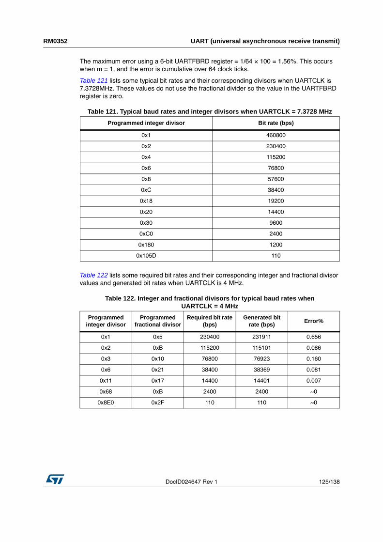
DocID024647 Rev 1 125/138
RM0352 UART (universal asynchronous receive transmit)
137
The maximum error using a 6-bit UARTFBRD register = 1/64 × 100 = 1.56%. This occurs
when m = 1, and the error is cumulative over 64 clock ticks.
Table 121 lists some typical bit rates and their corresponding divisors when UARTCLK is
7.3728MHz. These values do not use the fractional divider so the value in the UARTFBRD
register is zero.
Table 122 lists some required bit rates and their corresponding integer and fractional divisor
values and generated bit rates when UARTCLK is 4 MHz.
Table 121. Typical baud rates and integer divisors when UARTCLK = 7.3728 MHz
Programmed integer divisor Bit rate (bps)
0x1 460800
0x2 230400
0x4 115200
0x6 76800
0x8 57600
0xC 38400
0x18 19200
0x20 14400
0x30 9600
0xC0 2400
0x180 1200
0x105D 110
Table 122. Integer and fractional divisors for typical baud rates when UARTCLK = 4 MHz
Programmed integer divisor
Programmed fractional divisor
Required bit rate (bps)
Generated bit rate (bps)
Error%
0x1 0x5 230400 231911 0.656
0x2 0xB 115200 115101 0.086
0x3 0x10 76800 76923 0.160
0x6 0x21 38400 38369 0.081
0x11 0x17 14400 14401 0.007
0x68 0xB 2400 2400 ~0
0x8E0 0x2F 110 110 ~0
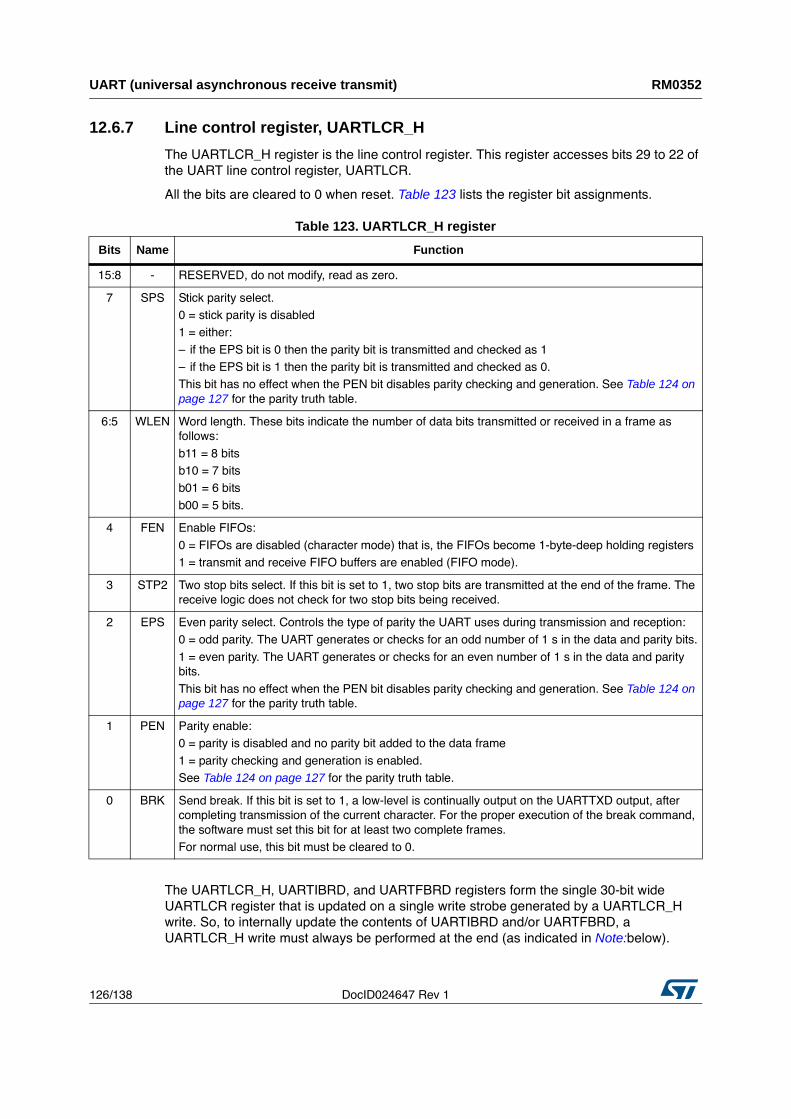
UART (universal asynchronous receive transmit) RM0352
126/138 DocID024647 Rev 1
12.6.7 Line control register, UARTLCR_H
The UARTLCR_H register is the line control register. This register accesses bits 29 to 22 of
the UART line control register, UARTLCR.
All the bits are cleared to 0 when reset. Table 123 lists the register bit assignments.
The UARTLCR_H, UARTIBRD, and UARTFBRD registers form the single 30-bit wide
UARTLCR register that is updated on a single write strobe generated by a UARTLCR_H
write. So, to internally update the contents of UARTIBRD and/or UARTFBRD, a
UARTLCR_H write must always be performed at the end (as indicated in Note:below).
Table 123. UARTLCR_H register
Bits Name Function
15:8 - RESERVED, do not modify, read as zero.
7 SPS Stick parity select.
0 = stick parity is disabled
1 = either:
– if the EPS bit is 0 then the parity bit is transmitted and checked as 1
– if the EPS bit is 1 then the parity bit is transmitted and checked as 0.
This bit has no effect when the PEN bit disables parity checking and generation. See Table 124 on page 127 for the parity truth table.
6:5 WLEN Word length. These bits indicate the number of data bits transmitted or received in a frame as
follows:
b11 = 8 bits
b10 = 7 bits
b01 = 6 bits
b00 = 5 bits.
4 FEN Enable FIFOs:
0 = FIFOs are disabled (character mode) that is, the FIFOs become 1-byte-deep holding registers
1 = transmit and receive FIFO buffers are enabled (FIFO mode).
3 STP2 Two stop bits select. If this bit is set to 1, two stop bits are transmitted at the end of the frame. The
receive logic does not check for two stop bits being received.
2 EPS Even parity select. Controls the type of parity the UART uses during transmission and reception:
0 = odd parity. The UART generates or checks for an odd number of 1 s in the data and parity bits.
1 = even parity. The UART generates or checks for an even number of 1 s in the data and parity
bits.
This bit has no effect when the PEN bit disables parity checking and generation. See Table 124 on page 127 for the parity truth table.
1 PEN Parity enable:
0 = parity is disabled and no parity bit added to the data frame
1 = parity checking and generation is enabled.
See Table 124 on page 127 for the parity truth table.
0 BRK Send break. If this bit is set to 1, a low-level is continually output on the UARTTXD output, after
completing transmission of the current character. For the proper execution of the break command,
the software must set this bit for at least two complete frames.
For normal use, this bit must be cleared to 0.
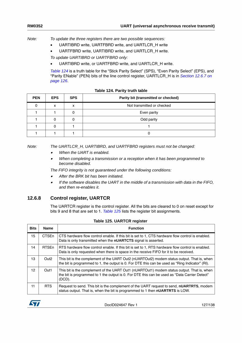
DocID024647 Rev 1 127/138
RM0352 UART (universal asynchronous receive transmit)
137
Note: To update the three registers there are two possible sequences:
• UARTIBRD write, UARTFBRD write, and UARTLCR_H write
• UARTFBRD write, UARTIBRD write, and UARTLCR_H write.
To update UARTIBRD or UARTFBRD only:
• UARTIBRD write, or UARTFBRD write, and UARTLCR_H write.
Table 124 is a truth table for the “Stick Parity Select” (SPS), “Even Parity Select” (EPS), and
“Parity ENable” (PEN) bits of the line control register, UARTLCR_H is in Section 12.6.7 on page 126.
Note: The UARTLCR_H, UARTIBRD, and UARTFBRD registers must not be changed:
• When the UART is enabled.
• When completing a transmission or a reception when it has been programmed to become disabled.
The FIFO integrity is not guaranteed under the following conditions:
• After the BRK bit has been initiated.
• If the software disables the UART in the middle of a transmission with data in the FIFO, and then re-enables it.
12.6.8 Control register, UARTCR
The UARTCR register is the control register. All the bits are cleared to 0 on reset except for
bits 9 and 8 that are set to 1. Table 125 lists the register bit assignments.
Table 124. Parity truth table
PEN EPS SPS Parity bit (transmitted or checked)
0 x x Not transmitted or checked
1 1 0 Even parity
1 0 0 Odd parity
1 0 1 1
1 1 1 0
Table 125. UARTCR register
Bits Name Function
15 CTSEn CTS hardware flow control enable. If this bit is set to 1, CTS hardware flow control is enabled.
Data is only transmitted when the nUARTCTS signal is asserted.
14 RTSEn RTS hardware flow control enable. If this bit is set to 1, RTS hardware flow control is enabled.
Data is only requested when there is space in the receive FIFO for it to be received.
13 Out2 This bit is the complement of the UART Out2 (nUARTOut2) modem status output. That is, when
the bit is programmed to 1, the output is 0. For DTE this can be used as “Ring Indicator” (RI).
12 Out1 This bit is the complement of the UART Out1 (nUARTOut1) modem status output. That is, when
the bit is programmed to 1 the output is 0. For DTE this can be used as “Data Carrier Detect”
(DCD).
11 RTS Request to send. This bit is the complement of the UART request to send, nUARTRTS, modem
status output. That is, when the bit is programmed to 1 then nUARTRTS is LOW.
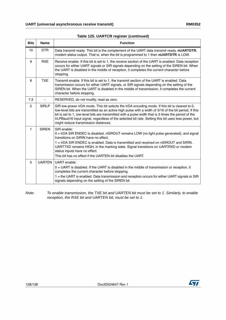
UART (universal asynchronous receive transmit) RM0352
128/138 DocID024647 Rev 1
Note: To enable transmission, the TXE bit and UARTEN bit must be set to 1. Similarly, to enable reception, the RXE bit and UARTEN bit, must be set to 1.
10 DTR Data transmit ready. This bit is the complement of the UART data transmit ready, nUARTDTR,
modem status output. That is, when the bit is programmed to 1 then nUARTDTR is LOW.
9 RXE Receive enable. If this bit is set to 1, the receive section of the UART is enabled. Data reception
occurs for either UART signals or SIR signals depending on the setting of the SIREN bit. When
the UART is disabled in the middle of reception, it completes the current character before
stopping.
8 TXE Transmit enable. If this bit is set to 1, the transmit section of the UART is enabled. Data
transmission occurs for either UART signals, or SIR signals depending on the setting of the
SIREN bit. When the UART is disabled in the middle of transmission, it completes the current
character before stopping.
7:3 - RESERVED, do not modify, read as zero.
2 SIRLP SIR low-power IrDA mode. This bit selects the IrDA encoding mode. If this bit is cleared to 0,
low-level bits are transmitted as an active high pulse with a width of 3/16 of the bit period. If this
bit is set to 1, low-level bits are transmitted with a pulse width that is 3 times the period of the
IrLPBaud16 input signal, regardless of the selected bit rate. Setting this bit uses less power, but
might reduce transmission distances.
1 SIREN SIR enable:
0 = IrDA SIR ENDEC is disabled. nSIROUT remains LOW (no light pulse generated), and signal
transitions on SIRIN have no effect.
1 = IrDA SIR ENDEC is enabled. Data is transmitted and received on nSIROUT and SIRIN.
UARTTXD remains HIGH, in the marking state. Signal transitions on UARTRXD or modem
status inputs have no effect.
This bit has no effect if the UARTEN bit disables the UART.
0 UARTEN UART enable:
0 = UART is disabled. If the UART is disabled in the middle of transmission or reception, it
completes the current character before stopping.
1 = the UART is enabled. Data transmission and reception occurs for either UART signals or SIR
signals depending on the setting of the SIREN bit.
Table 125. UARTCR register (continued)
Bits Name Function
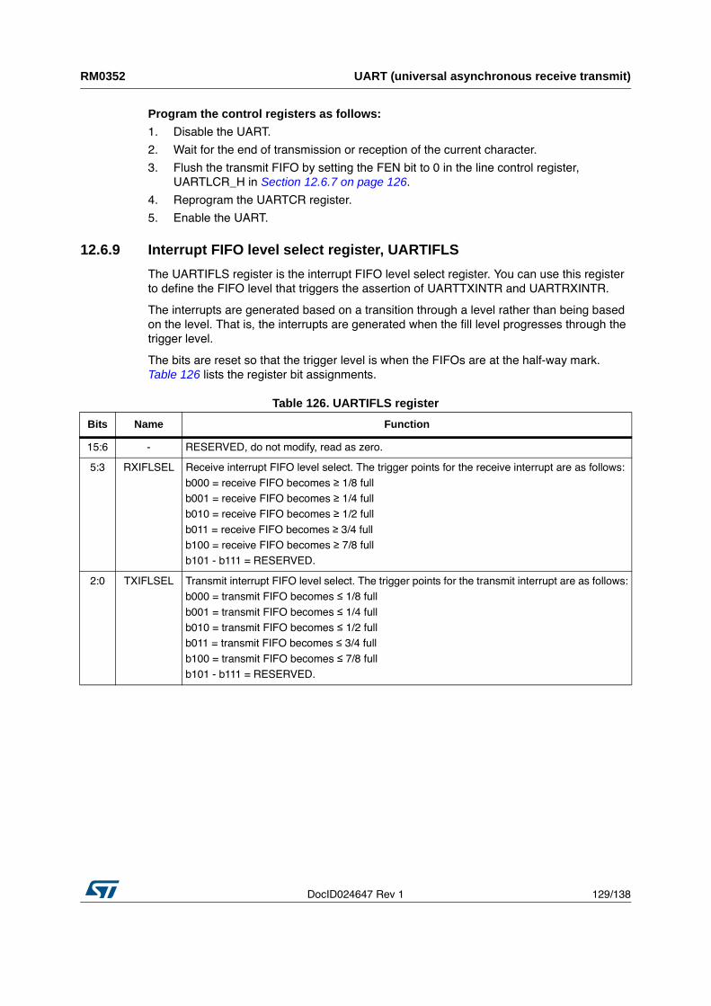
DocID024647 Rev 1 129/138
RM0352 UART (universal asynchronous receive transmit)
137
Program the control registers as follows:
1. Disable the UART.
2. Wait for the end of transmission or reception of the current character.
3. Flush the transmit FIFO by setting the FEN bit to 0 in the line control register,
UARTLCR_H in Section 12.6.7 on page 126.
4. Reprogram the UARTCR register.
5. Enable the UART.
12.6.9 Interrupt FIFO level select register, UARTIFLS
The UARTIFLS register is the interrupt FIFO level select register. You can use this register
to define the FIFO level that triggers the assertion of UARTTXINTR and UARTRXINTR.
The interrupts are generated based on a transition through a level rather than being based
on the level. That is, the interrupts are generated when the fill level progresses through the
trigger level.
The bits are reset so that the trigger level is when the FIFOs are at the half-way mark.
Table 126 lists the register bit assignments.
Table 126. UARTIFLS register
Bits Name Function
15:6 - RESERVED, do not modify, read as zero.
5:3 RXIFLSEL Receive interrupt FIFO level select. The trigger points for the receive interrupt are as follows:
b000 = receive FIFO becomes ≥ 1/8 full
b001 = receive FIFO becomes ≥ 1/4 full
b010 = receive FIFO becomes ≥ 1/2 full
b011 = receive FIFO becomes ≥ 3/4 full
b100 = receive FIFO becomes ≥ 7/8 full
b101 - b111 = RESERVED.
2:0 TXIFLSEL Transmit interrupt FIFO level select. The trigger points for the transmit interrupt are as follows:
b000 = transmit FIFO becomes ≤ 1/8 full
b001 = transmit FIFO becomes ≤ 1/4 full
b010 = transmit FIFO becomes ≤ 1/2 full
b011 = transmit FIFO becomes ≤ 3/4 full
b100 = transmit FIFO becomes ≤ 7/8 full
b101 - b111 = RESERVED.
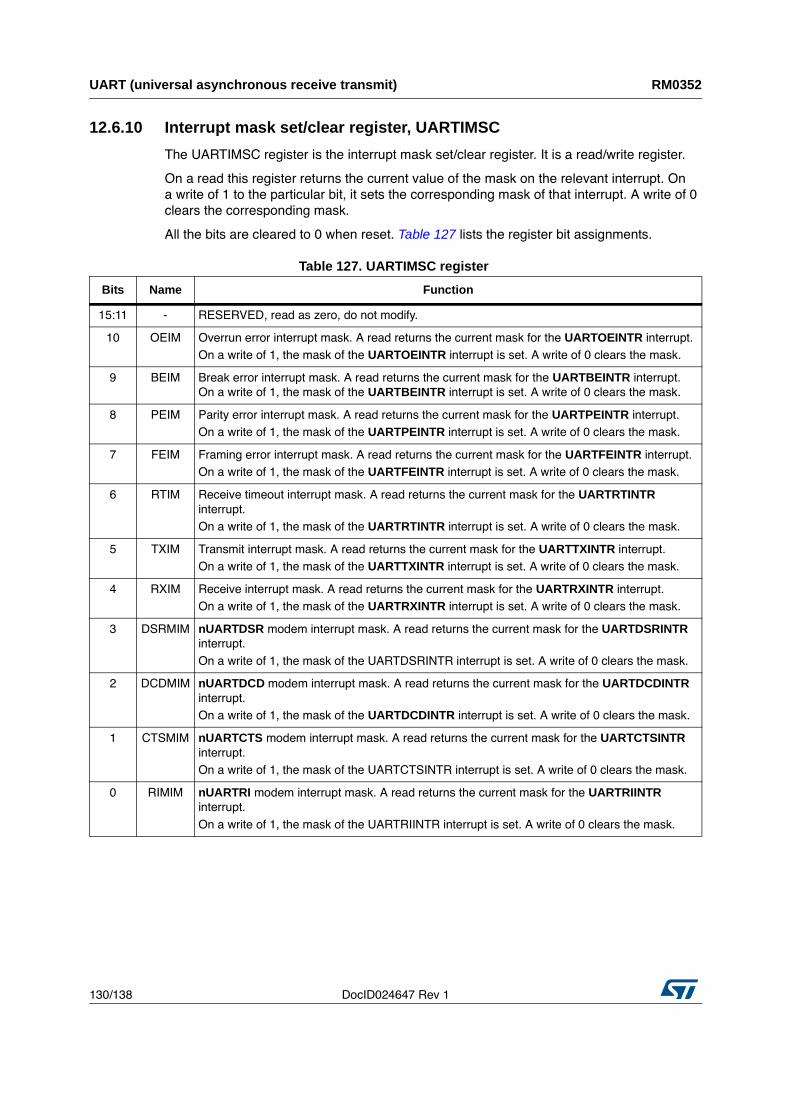
UART (universal asynchronous receive transmit) RM0352
130/138 DocID024647 Rev 1
12.6.10 Interrupt mask set/clear register, UARTIMSC
The UARTIMSC register is the interrupt mask set/clear register. It is a read/write register.
On a read this register returns the current value of the mask on the relevant interrupt. On
a write of 1 to the particular bit, it sets the corresponding mask of that interrupt. A write of 0
clears the corresponding mask.
All the bits are cleared to 0 when reset. Table 127 lists the register bit assignments.
Table 127. UARTIMSC register
Bits Name Function
15:11 - RESERVED, read as zero, do not modify.
10 OEIM Overrun error interrupt mask. A read returns the current mask for the UARTOEINTR interrupt.
On a write of 1, the mask of the UARTOEINTR interrupt is set. A write of 0 clears the mask.
9 BEIM Break error interrupt mask. A read returns the current mask for the UARTBEINTR interrupt.
On a write of 1, the mask of the UARTBEINTR interrupt is set. A write of 0 clears the mask.
8 PEIM Parity error interrupt mask. A read returns the current mask for the UARTPEINTR interrupt.
On a write of 1, the mask of the UARTPEINTR interrupt is set. A write of 0 clears the mask.
7 FEIM Framing error interrupt mask. A read returns the current mask for the UARTFEINTR interrupt.
On a write of 1, the mask of the UARTFEINTR interrupt is set. A write of 0 clears the mask.
6 RTIM Receive timeout interrupt mask. A read returns the current mask for the UARTRTINTR
interrupt.
On a write of 1, the mask of the UARTRTINTR interrupt is set. A write of 0 clears the mask.
5 TXIM Transmit interrupt mask. A read returns the current mask for the UARTTXINTR interrupt.
On a write of 1, the mask of the UARTTXINTR interrupt is set. A write of 0 clears the mask.
4 RXIM Receive interrupt mask. A read returns the current mask for the UARTRXINTR interrupt.
On a write of 1, the mask of the UARTRXINTR interrupt is set. A write of 0 clears the mask.
3 DSRMIM nUARTDSR modem interrupt mask. A read returns the current mask for the UARTDSRINTR
interrupt.
On a write of 1, the mask of the UARTDSRINTR interrupt is set. A write of 0 clears the mask.
2 DCDMIM nUARTDCD modem interrupt mask. A read returns the current mask for the UARTDCDINTR
interrupt.
On a write of 1, the mask of the UARTDCDINTR interrupt is set. A write of 0 clears the mask.
1 CTSMIM nUARTCTS modem interrupt mask. A read returns the current mask for the UARTCTSINTR
interrupt.
On a write of 1, the mask of the UARTCTSINTR interrupt is set. A write of 0 clears the mask.
0 RIMIM nUARTRI modem interrupt mask. A read returns the current mask for the UARTRIINTR
interrupt.
On a write of 1, the mask of the UARTRIINTR interrupt is set. A write of 0 clears the mask.
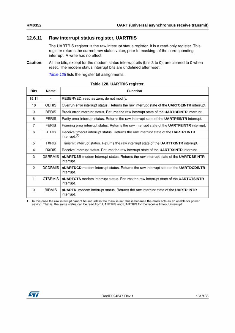
DocID024647 Rev 1 131/138
RM0352 UART (universal asynchronous receive transmit)
137
12.6.11 Raw interrupt status register, UARTRIS
The UARTRIS register is the raw interrupt status register. It is a read-only register. This
register returns the current raw status value, prior to masking, of the corresponding
interrupt. A write has no effect.
Caution: All the bits, except for the modem status interrupt bits (bits 3 to 0), are cleared to 0 when
reset. The modem status interrupt bits are undefined after reset.
Table 128 lists the register bit assignments.
Table 128. UARTRIS register
Bits Name Function
15:11 - RESERVED, read as zero, do not modify.
10 OERIS Overrun error interrupt status. Returns the raw interrupt state of the UARTOEINTR interrupt.
9 BERIS Break error interrupt status. Returns the raw interrupt state of the UARTBEINTR interrupt.
8 PERIS Parity error interrupt status. Returns the raw interrupt state of the UARTPEINTR interrupt.
7 FERIS Framing error interrupt status. Returns the raw interrupt state of the UARTFEINTR interrupt.
6 RTRIS Receive timeout interrupt status. Returns the raw interrupt state of the UARTRTINTR
interrupt.(1)
5 TXRIS Transmit interrupt status. Returns the raw interrupt state of the UARTTXINTR interrupt.
4 RXRIS Receive interrupt status. Returns the raw interrupt state of the UARTRXINTR interrupt.
3 DSRRMIS nUARTDSR modem interrupt status. Returns the raw interrupt state of the UARTDSRINTR
interrupt.
2 DCDRMIS nUARTDCD modem interrupt status. Returns the raw interrupt state of the UARTDCDINTR
interrupt.
1 CTSRMIS nUARTCTS modem interrupt status. Returns the raw interrupt state of the UARTCTSINTR
interrupt.
0 RIRMIS nUARTRI modem interrupt status. Returns the raw interrupt state of the UARTRIINTR
interrupt.
1. In this case the raw interrupt cannot be set unless the mask is set, this is because the mask acts as an enable for power
saving. That is, the same status can be read from UARTMIS and UARTRIS for the receive timeout interrupt.
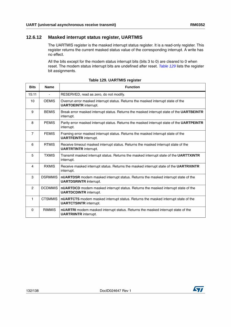
UART (universal asynchronous receive transmit) RM0352
132/138 DocID024647 Rev 1
12.6.12 Masked interrupt status register, UARTMIS
The UARTMIS register is the masked interrupt status register. It is a read-only register. This
register returns the current masked status value of the corresponding interrupt. A write has
no effect.
All the bits except for the modem status interrupt bits (bits 3 to 0) are cleared to 0 when
reset. The modem status interrupt bits are undefined after reset. Table 129 lists the register
bit assignments.
Table 129. UARTMIS register
Bits Name Function
15:11 - RESERVED, read as zero, do not modify.
10 OEMIS Overrun error masked interrupt status. Returns the masked interrupt state of the
UARTOEINTR interrupt.
9 BEMIS Break error masked interrupt status. Returns the masked interrupt state of the UARTBEINTR
interrupt.
8 PEMIS Parity error masked interrupt status. Returns the masked interrupt state of the UARTPEINTR
interrupt.
7 FEMIS Framing error masked interrupt status. Returns the masked interrupt state of the
UARTFEINTR interrupt.
6 RTMIS Receive timeout masked interrupt status. Returns the masked interrupt state of the
UARTRTINTR interrupt.
5 TXMIS Transmit masked interrupt status. Returns the masked interrupt state of the UARTTXINTR
interrupt.
4 RXMIS Receive masked interrupt status. Returns the masked interrupt state of the UARTRXINTR
interrupt.
3 DSRMMIS nUARTDSR modem masked interrupt status. Returns the masked interrupt state of the
UARTDSRINTR interrupt.
2 DCDMMIS nUARTDCD modem masked interrupt status. Returns the masked interrupt state of the
UARTDCDINTR interrupt.
1 CTSMMIS nUARTCTS modem masked interrupt status. Returns the masked interrupt state of the
UARTCTSINTR interrupt.
0 RIMMIS nUARTRI modem masked interrupt status. Returns the masked interrupt state of the
UARTRIINTR interrupt.
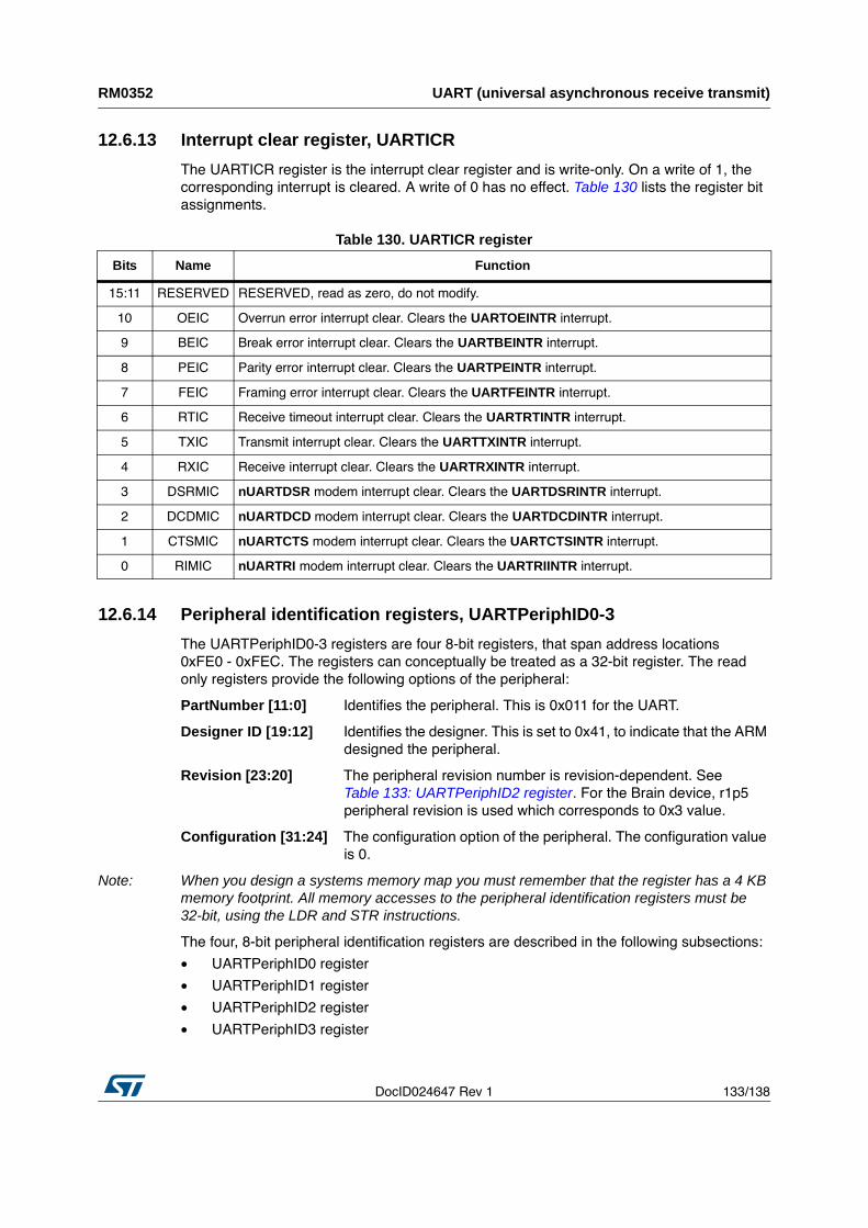
DocID024647 Rev 1 133/138
RM0352 UART (universal asynchronous receive transmit)
137
12.6.13 Interrupt clear register, UARTICR
The UARTICR register is the interrupt clear register and is write-only. On a write of 1, the
corresponding interrupt is cleared. A write of 0 has no effect. Table 130 lists the register bit
assignments.
12.6.14 Peripheral identification registers, UARTPeriphID0-3
The UARTPeriphID0-3 registers are four 8-bit registers, that span address locations
0xFE0 - 0xFEC. The registers can conceptually be treated as a 32-bit register. The read
only registers provide the following options of the peripheral:
PartNumber [11:0] Identifies the peripheral. This is 0x011 for the UART.
Designer ID [19:12] Identifies the designer. This is set to 0x41, to indicate that the ARM
designed the peripheral.
Revision [23:20] The peripheral revision number is revision-dependent. See
Table 133: UARTPeriphID2 register. For the Brain device, r1p5
peripheral revision is used which corresponds to 0x3 value.
Configuration [31:24] The configuration option of the peripheral. The configuration value
is 0.
Note: When you design a systems memory map you must remember that the register has a 4 KB memory footprint. All memory accesses to the peripheral identification registers must be 32-bit, using the LDR and STR instructions.
The four, 8-bit peripheral identification registers are described in the following subsections:
• UARTPeriphID0 register
• UARTPeriphID1 register
• UARTPeriphID2 register
• UARTPeriphID3 register
Table 130. UARTICR register
Bits Name Function
15:11 RESERVED RESERVED, read as zero, do not modify.
10 OEIC Overrun error interrupt clear. Clears the UARTOEINTR interrupt.
9 BEIC Break error interrupt clear. Clears the UARTBEINTR interrupt.
8 PEIC Parity error interrupt clear. Clears the UARTPEINTR interrupt.
7 FEIC Framing error interrupt clear. Clears the UARTFEINTR interrupt.
6 RTIC Receive timeout interrupt clear. Clears the UARTRTINTR interrupt.
5 TXIC Transmit interrupt clear. Clears the UARTTXINTR interrupt.
4 RXIC Receive interrupt clear. Clears the UARTRXINTR interrupt.
3 DSRMIC nUARTDSR modem interrupt clear. Clears the UARTDSRINTR interrupt.
2 DCDMIC nUARTDCD modem interrupt clear. Clears the UARTDCDINTR interrupt.
1 CTSMIC nUARTCTS modem interrupt clear. Clears the UARTCTSINTR interrupt.
0 RIMIC nUARTRI modem interrupt clear. Clears the UARTRIINTR interrupt.
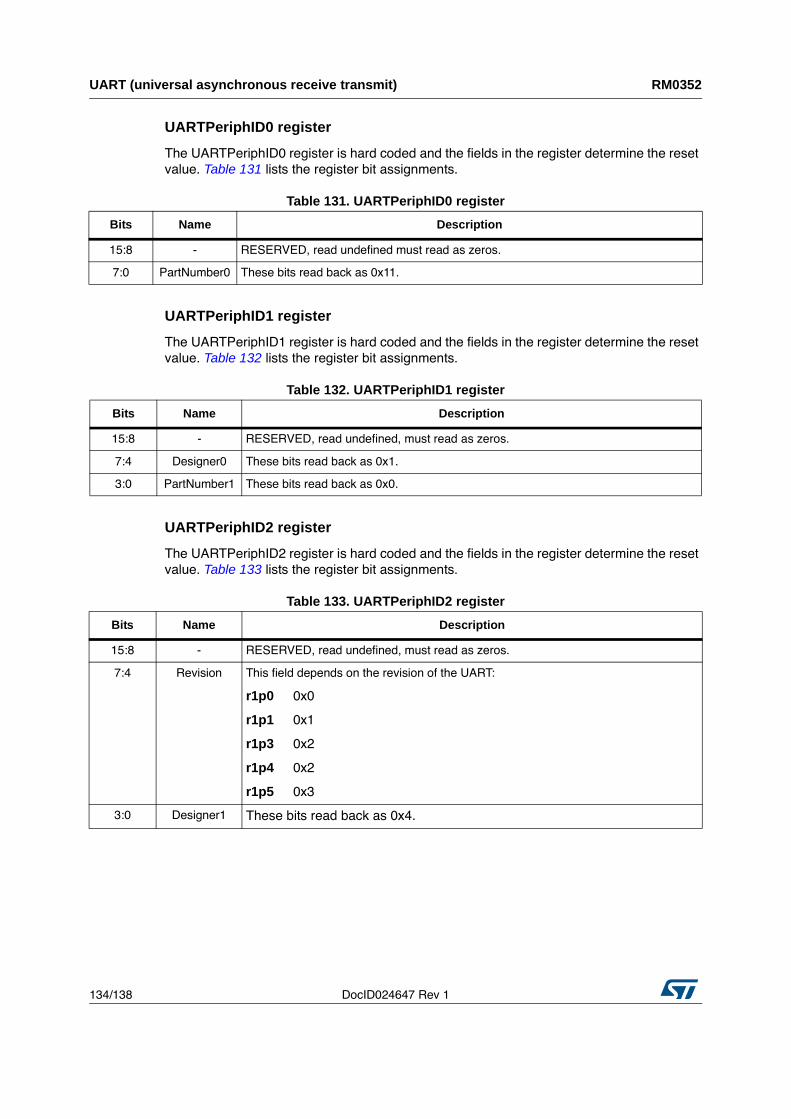
UART (universal asynchronous receive transmit) RM0352
134/138 DocID024647 Rev 1
UARTPeriphID0 register
The UARTPeriphID0 register is hard coded and the fields in the register determine the reset
value. Table 131 lists the register bit assignments.
UARTPeriphID1 register
The UARTPeriphID1 register is hard coded and the fields in the register determine the reset
value. Table 132 lists the register bit assignments.
UARTPeriphID2 register
The UARTPeriphID2 register is hard coded and the fields in the register determine the reset
value. Table 133 lists the register bit assignments.
Table 131. UARTPeriphID0 register
Bits Name Description
15:8 - RESERVED, read undefined must read as zeros.
7:0 PartNumber0 These bits read back as 0x11.
Table 132. UARTPeriphID1 register
Bits Name Description
15:8 - RESERVED, read undefined, must read as zeros.
7:4 Designer0 These bits read back as 0x1.
3:0 PartNumber1 These bits read back as 0x0.
Table 133. UARTPeriphID2 register
Bits Name Description
15:8 - RESERVED, read undefined, must read as zeros.
7:4 Revision This field depends on the revision of the UART:
r1p0 0x0
r1p1 0x1
r1p3 0x2
r1p4 0x2
r1p5 0x3
3:0 Designer1 These bits read back as 0x4.
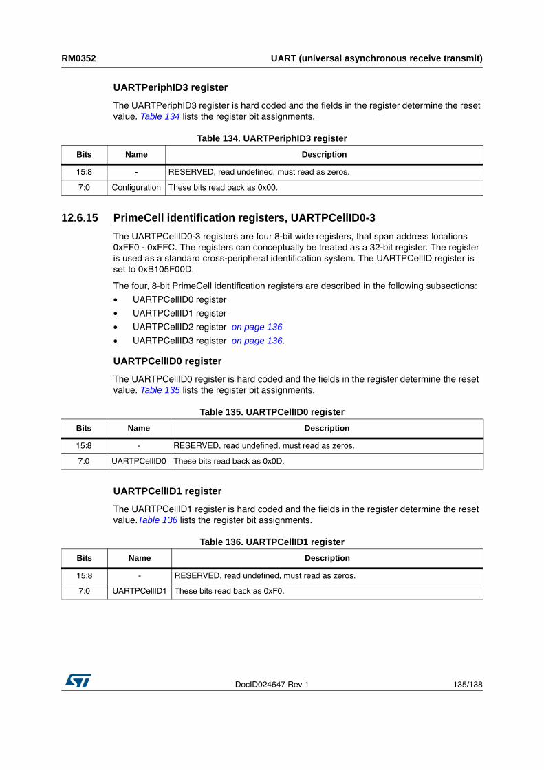
DocID024647 Rev 1 135/138
RM0352 UART (universal asynchronous receive transmit)
137
UARTPeriphID3 register
The UARTPeriphID3 register is hard coded and the fields in the register determine the reset
value. Table 134 lists the register bit assignments.
12.6.15 PrimeCell identification registers, UARTPCellID0-3
The UARTPCellID0-3 registers are four 8-bit wide registers, that span address locations
0xFF0 - 0xFFC. The registers can conceptually be treated as a 32-bit register. The register
is used as a standard cross-peripheral identification system. The UARTPCellID register is
set to 0xB105F00D.
The four, 8-bit PrimeCell identification registers are described in the following subsections:
• UARTPCellID0 register
• UARTPCellID1 register
• UARTPCellID2 register on page 136
• UARTPCellID3 register on page 136.
UARTPCellID0 register
The UARTPCellID0 register is hard coded and the fields in the register determine the reset
value. Table 135 lists the register bit assignments.
UARTPCellID1 register
The UARTPCellID1 register is hard coded and the fields in the register determine the reset
value.Table 136 lists the register bit assignments.
Table 134. UARTPeriphID3 register
Bits Name Description
15:8 - RESERVED, read undefined, must read as zeros.
7:0 Configuration These bits read back as 0x00.
Table 135. UARTPCellID0 register
Bits Name Description
15:8 - RESERVED, read undefined, must read as zeros.
7:0 UARTPCellID0 These bits read back as 0x0D.
Table 136. UARTPCellID1 register
Bits Name Description
15:8 - RESERVED, read undefined, must read as zeros.
7:0 UARTPCellID1 These bits read back as 0xF0.
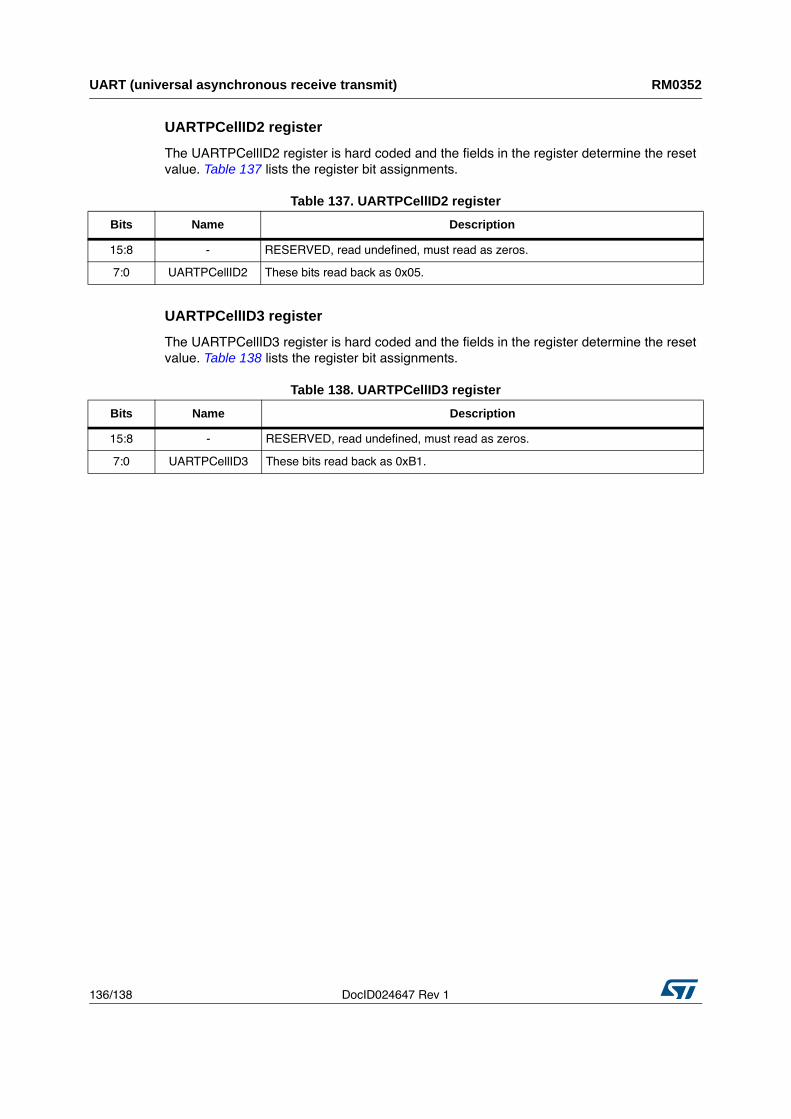
UART (universal asynchronous receive transmit) RM0352
136/138 DocID024647 Rev 1
UARTPCellID2 register
The UARTPCellID2 register is hard coded and the fields in the register determine the reset
value. Table 137 lists the register bit assignments.
UARTPCellID3 register
The UARTPCellID3 register is hard coded and the fields in the register determine the reset
value. Table 138 lists the register bit assignments.
Table 137. UARTPCellID2 register
Bits Name Description
15:8 - RESERVED, read undefined, must read as zeros.
7:0 UARTPCellID2 These bits read back as 0x05.
Table 138. UARTPCellID3 register
Bits Name Description
15:8 - RESERVED, read undefined, must read as zeros.
7:0 UARTPCellID3 These bits read back as 0xB1.
DocID024647 Rev 1 137/138
RM0352 Revision history
137
13 Revision history
Table 139. Document revision history
Date Revision Changes
06-Feb-2014 1 Initial release.
RM0352
138/138 DocID024647 Rev 1
Please Read Carefully:
Information in this document is provided solely in connection with ST products. STMicroelectronics NV and its subsidiaries (“ST”) reserve the
right to make changes, corrections, modifications or improvements, to this document, and the products and services described herein at any
time, without notice.
All ST products are sold pursuant to ST’s terms and conditions of sale.
Purchasers are solely responsible for the choice, selection and use of the ST products and services described herein, and ST assumes no
liability whatsoever relating to the choice, selection or use of the ST products and services described herein.
No license, express or implied, by estoppel or otherwise, to any intellectual property rights is granted under this document. If any part of this
document refers to any third party products or services it shall not be deemed a license grant by ST for the use of such third party products
or services, or any intellectual property contained therein or considered as a warranty covering the use in any manner whatsoever of such
third party products or services or any intellectual property contained therein.
UNLESS OTHERWISE SET FORTH IN ST’S TERMS AND CONDITIONS OF SALE ST DISCLAIMS ANY EXPRESS OR IMPLIEDWARRANTY WITH RESPECT TO THE USE AND/OR SALE OF ST PRODUCTS INCLUDING WITHOUT LIMITATION IMPLIEDWARRANTIES OF MERCHANTABILITY, FITNESS FOR A PARTICULAR PURPOSE (AND THEIR EQUIVALENTS UNDER THE LAWSOF ANY JURISDICTION), OR INFRINGEMENT OF ANY PATENT, COPYRIGHT OR OTHER INTELLECTUAL PROPERTY RIGHT.
ST PRODUCTS ARE NOT DESIGNED OR AUTHORIZED FOR USE IN: (A) SAFETY CRITICAL APPLICATIONS SUCH AS LIFESUPPORTING, ACTIVE IMPLANTED DEVICES OR SYSTEMS WITH PRODUCT FUNCTIONAL SAFETY REQUIREMENTS; (B)AERONAUTIC APPLICATIONS; (C) AUTOMOTIVE APPLICATIONS OR ENVIRONMENTS, AND/OR (D) AEROSPACE APPLICATIONSOR ENVIRONMENTS. WHERE ST PRODUCTS ARE NOT DESIGNED FOR SUCH USE, THE PURCHASER SHALL USE PRODUCTS ATPURCHASER’S SOLE RISK, EVEN IF ST HAS BEEN INFORMED IN WRITING OF SUCH USAGE, UNLESS A PRODUCT ISEXPRESSLY DESIGNATED BY ST AS BEING INTENDED FOR “AUTOMOTIVE, AUTOMOTIVE SAFETY OR MEDICAL” INDUSTRYDOMAINS ACCORDING TO ST PRODUCT DESIGN SPECIFICATIONS. PRODUCTS FORMALLY ESCC, QML OR JAN QUALIFIED AREDEEMED SUITABLE FOR USE IN AEROSPACE BY THE CORRESPONDING GOVERNMENTAL AGENCY.
Resale of ST products with provisions different from the statements and/or technical features set forth in this document shall immediately void
any warranty granted by ST for the ST product or service described herein and shall not create or extend in any manner whatsoever, any
liability of ST.
ST and the ST logo are trademarks or registered trademarks of ST in various countries.
Information in this document supersedes and replaces all information previously supplied.
The ST logo is a registered trademark of STMicroelectronics. All other names are the property of their respective owners.
© 2014 STMicroelectronics - All rights reserved
STMicroelectronics group of companies
Australia - Belgium - Brazil - Canada - China - Czech Republic - Finland - France - Germany - Hong Kong - India - Israel - Italy - Japan -
Malaysia - Malta - Morocco - Philippines - Singapore - Spain - Sweden - Switzerland - United Kingdom - United States of America
www.st.com