70v659/58/57 datasheet - renesas
TRANSCRIPT

1Aug.23.21
CE0R
R/WR
CE1R
BE0R
BE1R
BE2R
BE3R
128/64/32K x 36MEMORYARRAY
AddressDecoder
A16R(1)
A0R
AddressDecoder
CE0L
R/WL
CE1L
BE0L
BE1L
BE2L
BE3L
Dout0-8_LDout9-17_LDout18-26_LDout27-35_L
Dout0-8_RDout9-17_R
Dout18-26_RDout27-35_R
BE0L
BE1L
BE2L
BE3L
BE3R
BE2R
BE1R
BE0R
I/O0L- I/O35L
A16 L(1)
A0L
I/O0R -I/O35RDi n_L
ADDR_L
Di n_R
ADDR_R
OEROEL
ARBITRATIONINTERRUPT
SEMAPHORELOGIC
SEML
INTL(3)
BUSYL(2,3)
M/S
R/WL
OEL
R/WR
OER
CE0LCE1L
CE0RCE1R
BUSYR(2,3)
SEMR
INTR(3)
TMSTCK
TRST
TDI
TDO JTAG
4869 drw 01
Functional Block Diagram
◆◆◆◆◆ Full on-chip hardware support of semaphore signalingbetween ports
◆◆◆◆◆ Fully asynchronous operation from either port◆ Separate byte controls for multiplexed bus and bus
matching compatibility◆◆◆◆◆ Supports JTAG features compliant to IEEE 1149.1◆◆◆◆◆ LVTTL-compatible, single 3.3V (±150mV) power supply for
core◆◆◆◆◆ LVTTL-compatible, selectable 3.3V (±150mV)/2.5V (±100mV)
power supply for I/Os and control signals on each port◆◆◆◆◆ Available in a 208-pin Plastic Quad Flatpack, 208-ball fine
pitch Ball Grid Array, and 256-ball Ball Grid Array◆◆◆◆◆ Industrial temperature range (–40°C to +85°C) is available
for selected speeds◆◆◆◆◆ Green parts available, see ordering information
Features◆◆◆◆◆ True Dual-Port memory cells which allow simultaneous
access of the same memory location◆◆◆◆◆ High-speed access
– Commercial: 10/12/15ns (max.)– Industrial: 12ns (max.)
◆◆◆◆◆ Dual chip enables allow for depth expansion withoutexternal logic
◆◆◆◆◆ IDT70V659/58/57 easily expands data bus width to 72 bitsor more using the Master/Slave select when cascadingmore than one device
◆◆◆◆◆ M/S = VIH for BUSY output flag on Master,M/S = VIL for BUSY input on Slave
◆◆◆◆◆ Busy and Interrupt Flags◆◆◆◆◆ On-chip port arbitration logic
HIGH-SPEED 3.3V128/64/32K x 36ASYNCHRONOUS DUAL-PORTSTATIC RAM
70V659/58/57S
1. A16 is a NC for IDT70V658. Also, Addresses A16 and A15 are NC's for IDT70V657.2. BUSY is an input as a Slave (M/S=VIL) and an output when it is a Master (M/S=VIH).3. BUSY and INT are non-tri-state totem-pole outputs (push-pull).
NOTES:
70V659/58/57SHigh-Speed 3.3V 128/64/32K x 36 Asynchronous Dual-Port Static RAM Industrial and Commercial Temperature Ranges
2Aug.23. 21
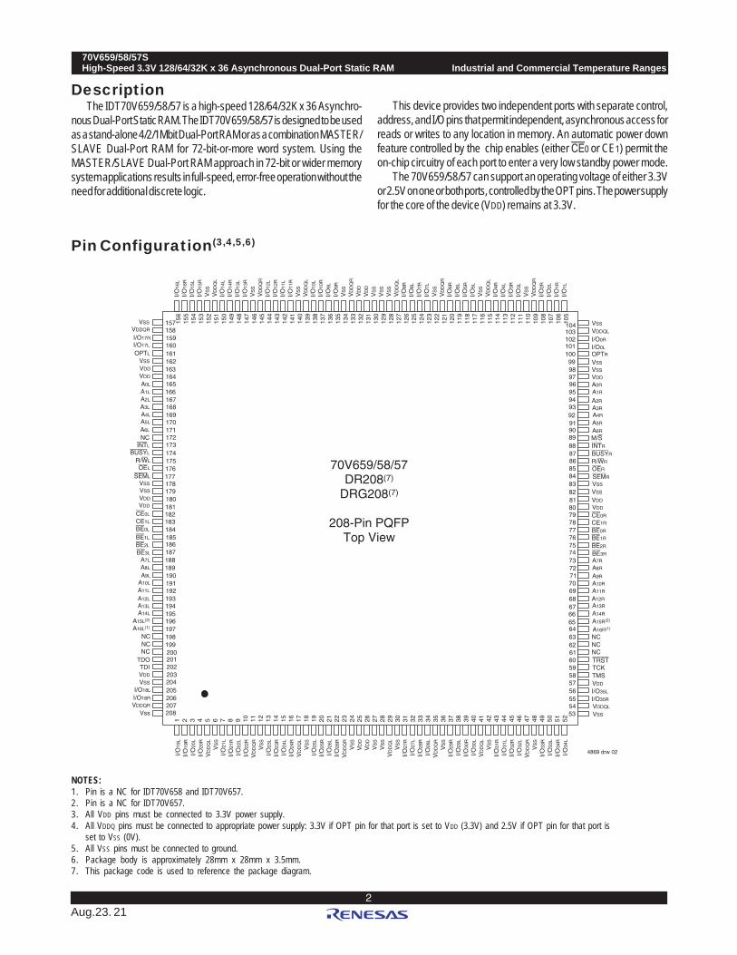
DescriptionThe IDT70V659/58/57 is a high-speed 128/64/32K x 36 Asynchro-
nous Dual-Port Static RAM. The IDT70V659/58/57 is designed to be usedas a stand-alone 4/2/1Mbit Dual-Port RAM or as a combination MASTER/SLAVE Dual-Port RAM for 72-bit-or-more word system. Using theMASTER/SLAVE Dual-Port RAM approach in 72-bit or wider memorysystem applications results in full-speed, error-free operation without theneed for additional discrete logic.
This device provides two independent ports with separate control,address, and I/O pins that permit independent, asynchronous access forreads or writes to any location in memory. An automatic power downfeature controlled by the chip enables (either CE0 or CE1) permit theon-chip circuitry of each port to enter a very low standby power mode.
The 70V659/58/57 can support an operating voltage of either 3.3Vor 2.5V on one or both ports, controlled by the OPT pins. The power supplyfor the core of the device (VDD) remains at 3.3V.
Pin Configuration(3,4,5,6)
1 2 3 4 5 6 7 8 9 10 11 12 13 14 15 16 17 18 19 20 21 22 23 24 25 26 27 28 29 30 31 32 33 34 35 36 37 38 39 40 41 42 43 44 45 46 47 48 49 50 51 52
69
96
156
155
154
153
152
151
150
149
148
147
146
145
144
143
142
141
140
139
138
137
136
135
134
133
132
131
130
129
128
127
126
125
124
123
122
121
120
119
118
117
116
115
114
113
112
111
110
109
108
107
106
105
70V659/58/57DR208(7)
DRG208(7)
208-Pin PQFPTop View
I/O19
L
I/O19
R
I/O20
L
I/O20
R
VD
DQ
L
VS
S
I/O21
L
I/O21
R
I/O22
L
I/O22
R
VD
DQ
R
VS
S
I/O23
L
I/O23
R
I/O24
L
I/O24
R
VD
DQ
L
VS
S
I/O25
L
I/O25
R
I/O26
L
I/O26
R
VD
DQ
R
VS
S
VD
D
VD
D
VS
S
VS
S
VD
DQ
L
VS
S
I/O27
R
I/O27
L
I/O28
R
I/O28
L
VD
DQ
R
VS
S
I/O29
R
I/O29
L
I/O30
R
I/O30
L
VD
DQ
L
VS
S
I/O31
R
I/O31
L
I/O32
R
I/O32
L
VD
DQ
R
VS
S
I/O33
R
I/O33
L
I/O34
R
I/O34
L
I/O16
L
I/O16
R
I/O15
L
I/O15
R
VS
S
VD
DQ
L
I/O14
L
I/O14
R
I/O13
L
I/O13
R
VS
S
VD
DQ
R
I/O12
L
I/O12
R
I/O11
L
I/O11
R
VS
S
VD
DQ
L
I/O10
L
I/O10
R
I/O9L
I/O9R
VS
S
VD
DQ
R
VD
D
VD
D
VS
S
VS
S
VS
S
VD
DQ
L
I/O8R
I/O8L
I/O7R
I/O7L
VS
S
VD
DQ
R
I/O6R
I/O6L
I/O5R
I/O5L
VS
S
VD
DQ
L
I/O4R
I/O4L
I/O3R
I/O3L
VS
S
VD
DQ
R
I/O2R
I/O2L
I/O1R
I/O1L
4869 drw 02
Vss VDDQR
I/O18R
I/O18L
VSS
VDD
TDITDO
NCNCNC
A16L(1)A15L(2)
A14L
A13L
A12L
A11L
A10L
A9L
A8L
A7L
BE3L
BE2L
BE1L
BE0L
CE1L
CE0L
VDD
VDD
VSS
VSS
SEML
OEL
R/WL
BUSYL
INTL
NCA6L
A5L
A4L
A3L
A2L
A1L
A0L
VDD
VDD
VSS
OPTL
I/O17L
I/O17R
VDDQR
VSS
208207206205204203202201200199198197196195194193192191190189188187186185184183182181180179178177176175174173172171170169168167166165164163162161160159158157
VSS
VDDQL
I/O35R
I/O35L
VDD
TMSTCKTRSTNCNCNCA16R(1)
A15R(2)
A14R
A13RA12R
A11R
A10R
A9R
A8R
A7RBE3R
BE2R
BE1R
BE0R
CE1R
CE0R
VDD
VDD
VSS
VSS
SEMR
OER
R/WR
BUSYR
INTR
M/SA6R
A5R
A4RA3R
A2R
A1R
A0R
VDD
VSS
VSS
OPTRI/O0L
I/O0R
VDDQL
VSS104103102101100999897
9594939291908988878685848382818079787776757473727170
68676665646362616059585756555453
NOTES:1. Pin is a NC for IDT70V658 and IDT70V657.2. Pin is a NC for IDT70V657.3. All VDD pins must be connected to 3.3V power supply.4. All VDDQ pins must be connected to appropriate power supply: 3.3V if OPT pin for that port is set to VDD (3.3V) and 2.5V if OPT pin for that port is
set to VSS (0V).5. All VSS pins must be connected to ground.6. Package body is approximately 28mm x 28mm x 3.5mm.7. This package code is used to reference the package diagram.

3
70V659/58/57SHigh-Speed 3.3V 128/64/32K x 36 Asynchronous Dual-Port Static RAM Industrial and Commercial Temperature Ranges
Aug.23.21
Pin Configuration(3,4,5,6),5,6),5,6),5,6),5,6)(con't)
E16
I/O14R
D16
I/O16R
C16
I/O16L
B16
NC
A16
NCA15
NC
B15
I/O17L
C15
I/O17R
D15
I/O15L
E15
I/O14L
E14
I/O13L
D14
I/O15R
D13
VDD
C12
A6L
C14
OPTL
B14
NC
A14
A0L
A12
A5L
B12
A4L
C11
BUSYL
D12
VDDQR
D11
VDDQR
C10
SEML
B11
NC
A11
INTL
D8
VDDQR
C8
BE1L
A9
CE1L
D9
VDDQL
C9
BE0L
B9
CE0L
D10
VDDQL
C7
A7L
B8
BE3L
A8
BE2L
B13
A1L
A13
A2L
A10
OEL
D7
VDDQR
B7
A9L
A7
A8L
B6
A12L
C6
A10L
D6
VDDQL
A5
A14L
B5
C5
A13L
D5
VDDQL
A4
NC
B4
NC
C4
A16L(1)
D4
VDD
A3
NC
B3
TDO
C3
VSS
D3
I/O20L
D2
I/O19R
C2
I/O19L
B2
NC
A2
TDIA1
NC
B1
I/O18L
C1
I/O18R
D1
I/O20R
E1
I/O21R
E2
I/O21L
E3
I/O22L
E4
VDDQL
F1
I/O23L
F2
I/O22R
F3
I/O23R
F4
VDDQL
G1
I/O24R
G2
I/O24L
G3
I/O25L
G4
VDDQR
H1
I/O26L
H2
I/O25R
H3
I/O26R
H4
VDDQR
J1
I/O27L
J2
I/O28R
J3
I/O27R
J4
VDDQL
K1
I/O29R
K2
I/O29L
K3
I/O28L
K4
VDDQL
L1
I/O30L
L2
I/O31R
L3
I/O30R
L4
VDDQR
M1
I/O32R
M2
I/O32L
M3
I/O31L
M4
VDDQR
N1
I/O33L
N2
I/O34R
N3
I/O33R
N4
VDD
P1
I/O35R
P2
I/O34L
P3
TMSP4
A16R(1)
R1
I/O35L
R2
NCR3
TRSTR4
NC
T1
NCT2
TCKT3
NCT4
NC
P5
A13R
R5
A15R(2)
P12
A6R
P8
BE1R
P9
BE0R
R8
BE3R
T8
BE2R
P10
SEMR
T11
INTR
P11
BUSYR
R12
A4R
T12
A5R
P13
A3R
P7
A7R
R13
A1R
T13
A2R
R6
A12R
T5
A14R
T14
A0R
R14
OPTR
P14
I/O0L
P15
I/O0R
R15
NC
T15
NCT16
NC
R16
NC
P16
I/O1L
N16
I/O2R
N15
I/O1R
N14
I/O2L
M16
I/O4L
M15
I/O3L
M14
I/O3R
L16
I/O5R
L15
I/O4R
L14
I/O5L
K16
I/O7L
K15
I/O6L
K14
I/O6R
J16
I/O8L
J15
I/O7R
J14
I/O8R
H16
I/O10R
H15
I/O9L
H14
I/O9R
G16
I/O11R
G15
I/O11L
G14
I/O10L
F16
I/O12L
F14
I/O12R
F15
I/O13R
R9
CE0R
R11
M/S
T6
A11R
T9
CE1R
A6
A11L
B10
R/WL
C13
A3L
P6
A10R
R10
R/WR
R7
A9R
T10
OER
T7
A8R
E5
VDD
E6
VDD
E7
VSS
E8
VSS
E9
VSS
E10
VSS
E11
VDD
E12
VDD
E13
VDDQR
F5
VDD
F6
VSS
F8
VSS
F9
VSS
F10
VSS
F12
VDD
F13
VDDQR
G5
VSS
G6
VSS
G7
VSS
G8
VSS
G9
VSS
G10
VSS
G11
VSS
G12
VSS
G13
VDDQL
H5
VSS
H6
VSS
H7
VSS
H8
VSS
H9
VSS
H10
VSS
H11
VSS
H12
VSS
H13
VDDQL
J5
VSS
J6
VSS
J7
VSS
J8
VSS
J9
VSS
J10
VSS
J11
VSS
J12
VSS
J13
VDDQR
K5
VSS
K6
VSS
K7
VSS
K8
VSS
L5
VDD
L6
VSS
L7
VSS
L8
VSS
M5
VDD
M6
VDD
M7
VSS
M8
VSS
N5
VDDQR
N6
VDDQR
N7
VDDQL
N8
VDDQL
K9
VSS
K10
VSS
K11
VSS
K12
VSS
L9
VSS
L10
VSS
L11
VSS
L12
VDD
M9
VSS
M10
VSS
M11
VDD
M12
VDD
N9
VDDQR
N10
VDDQR
N11
VDDQL
N12
VDDQL
K13
VDDQR
L13
VDDQL
M13
VDDQL
N13
VDD
F7
VSS
F11
VSS
4869 drw 02c
A15L(2)
NOTES:1. Pin is a NC for IDT70V658 and IDT70V657.2. Pin is a NC for IDT70V657.3. All VDD pins must be connected to 3.3V power supply.4. All VDDQ pins must be connected to appropriate power supply: 3.3V if OPT pin for that port is set to VDD (3.3V), and 2.5V if OPT pin for that port is
set to VSS (0V).5. All VSS pins must be connected to ground supply.6. Package body is approximately 17mm x 17mm x 1.4mm, with 1.0mm ball-pitch.7. This package code is used to reference the package diagram.8. This text does not indicate orientation of the actual part-marking.
70V659/58/57BC256(7)
BCG256(7)
256-Pin BGATop View(8)

70V659/58/57SHigh-Speed 3.3V 128/64/32K x 36 Asynchronous Dual-Port Static RAM Industrial and Commercial Temperature Ranges
4Aug.23. 21
Pin Configuration(3,4,5,6) (con't)
1716151412 1310987654321 11
A
B
C
D
E
F
G
H
J
K
L
M
N
P
R
T
U
I/O19L I/O18L VSS A4LINTLSEMLBE1LA8LA12LA16L(1) VSSI/O17LOPTLA0L
I/O20R VSS I/O18R
NC
A1LA5LBUSYLVSSCE0L
CE1L
BE2LA9LA13LNC I/O16LVDDQRVSS
VDDQL I/O19R VDDQR VDD A2LA6LR/WLVSSBE3LA10LA14LNC I/O15LI/O16RVDD
I/O22L VSS I/O21L I/O20L VDDA3LNCOEL
I/O23L I/O22R VDDQR I/O21R
VDDQL I/O23R I/O24L VSS
I/O26L VSS I/O25L I/O24R
VDD I/O26R VDDQR I/O25R
VDDQL VDD VSS VSS
I/O29R I/O28L VDDQR
VDDQL I/O29L I/O30R VSS
I/O14RVDDQL I/O14LA15L(2) A11L A7L BE0L
I/O12L I/O13R VSS I/O13L
VSS I/O12R I/O11L
I/O9L VDDQL I/O10L I/O11R
VDD I/O9R VSS I/O10R
VSS VDDQR
I/O7R VDDQL I/O8R VSS
I/O8LVSSI/O7LI/O6R
A0R
A1R
A2R
A3R
A4R
A5R
A6R
I/O3RI/O31L VSS I/O31R I/O30L
A16R(1) A12R A8R BE1R VDD SEMR INTR
VDDQR
I/O2L I/O3L I/O4L
VSS I/O33L I/O34R NC A13R A9R BE2R CE0R
CE1R
VDD
VSS BUSYR VSS
VDD
VSS
VDDQL I/O1R VDDQR
I/O33R I/O34L VDDQL
NC
NC A14R A10R BE3R VSS
I/O4R
I/O6LVSS I/O5R
I/O2R
VSS I/O35L VDD A15R(2) A11R A7R BE0R OER M/S
R/WR
VDDQL I/O5L
OPTR I/O0L I/O1L
70V659/58/57BF208(7)
BFG208(7)
208-Ball BGATop View(8)
4869 drw 02b
I/O27L
I/O28R VSS I/O27R VSS
I/O32R I/O32L VDDQR I/O35R
A
B
C
D
E
F
G
H
J
K
L
M
N
P
R
T
U
VSS I/O0R
I/O17R
VDDQR
VSSVDD
VSS
I/O15R
VDD
VDD
TDO
TDI
TCK
TMS
TRST VSS
NOTES:1. Pin is a NC for IDT70V658 and IDT70V657.2. Pin is a NC for IDT70V657.3. All VDD pins must be connected to 3.3V power supply.4. All VDDQ pins must be connected to appropriate power supply: 3.3V if OPT pin for that port is set to VDD (3.3V) and 2.5V if OPT pin for that port is
set to VSS (0V).5. All VSS pins must be connected to ground.6. Package body is approximately 15mm x 15mm x 1.4mm with 0.8mm ball pitch.7. This package code is used to reference the package diagram.8. This text does not indicate orientation of the actual part-marking.

5
70V659/58/57SHigh-Speed 3.3V 128/64/32K x 36 Asynchronous Dual-Port Static RAM Industrial and Commercial Temperature Ranges
Aug.23.21
Pin Names
NOTES:1. VDD, OPTX, and VDDQX must be set to appropriate operating levels prior to
applying inputs on I/OX.2. OPTX selects the operating voltage levels for the I/Os and controls on that port.
If OPTX is set to VIH (3.3V), then that port's I/Os and controls will operate at 3.3Vlevels and VDDQX must be supplied at 3.3V. If OPTX is set to VIL (0V), then thatport's I/Os and controls will operate at 2.5V levels and VDDQX must be suppliedat 2.5V. The OPT pins are independent of one another—both ports can operateat 3.3V levels, both can operate at 2.5V levels, or either can operate at 3.3Vwith the other at 2.5V.
3. Addresses A16x is a NC for IDT70V658. Also, Addresses A16x and A15x areNC's for IDT70V657.
4. BUSY is an input as a slave (M/S = VIL).
Left Port Right Port Names
CE0L, CE1L CE0R, CE1R Chip Enables - (Input)
R/WL R/WR Read/Write Enable - (Input)
OEL OER Output Enable - (Input)
A0L - A16L(3) A0R - A16R(3) Address - (Input)
I/O0L - I/O35L I/O0R - I/O35R Data Input/Output
SEML SEMR Semaphore Enable - (Input)
INTL INTR Interrupt Flag - (Output)
BUSYL BUSYR Busy Flag - (Output)(4)
BE0L - BE3L BE0R - BE3R Byte Enables (9-bit bytes) - (Input)
VDDQL VDDQR Power (I/O Bus) (3.3V or 2.5V) - (Input)(1)
OPTL OPTR Option for selecting VDDQX - (Input)(1,2)
M/S Master or Slave Select - (Input)
VDD Power (3.3V) - (Input)(1)
VSS Ground (0V) - (Input)
TDI Test Data Input
TDO Test Data Output
TCK Test Logic Clock (10MHz)
TMS Test Mode Select
TRST Reset (Initialize TAP Controller)4869 tbl 01

70V659/58/57SHigh-Speed 3.3V 128/64/32K x 36 Asynchronous Dual-Port Static RAM Industrial and Commercial Temperature Ranges
6Aug.23. 21
Absolute Maximum Ratings(1)
NOTES:1. Stresses greater than those listed under ABSOLUTE MAXIMUM RATINGS
may cause permanent damage to the device. This is a stress rating onlyand functional operation of the device at these or any other conditions abovethose indicated in the operational sections of this specification is not implied.Exposure to absolute maximum rating conditions for extended periods mayaffect reliability.
2. VTERM must not exceed VDD + 150mV for more than 25% of the cycle timeor 4ns maximum, and is limited to < 20mA for the period of VTERM > VDD+ 150mV.
3. Ambient Temperature under DC Bias. No AC Conditions. Chip Deselected.
Symbol Rating Commercial& Industrial
Unit
VTERM(2)
(VDD)VDD Terminal Voltagewith Respect to GND
-0.5 to + 4.6 V
TBIAS(3) Temperature Under Bias -55 to +125 oC
TSTG Storage Temperature -65 to +150 oC
TJN Junction Temperature +150 oC
IOUT(For VDDQ = 3.3V) DC Output Current 50 mA
IOUT(For VDDQ = 2.5V) DC Output Current 40 mA4869 tbl 05
Recommended DC OperatingConditions with VDDQ at 3.3V
NOTES:1. VIL > -1.5V for pulse width less than 10 ns.2. VTERM must not exceed VDDQ + 150mV.3. To select operation at 3.3V levels on the I/Os and controls of a given port, the
OPT pin for that port must be set to VDD (3.3V), and VDDQX for that port must besupplied as indicated above.
Symbol Parameter Min. Typ. Max. Unit
VDD Core Supply Voltage 3.15 3.3 3.45 V
VDDQ I/O Supply Voltage(3) 3.15 3.3 3.45 V
VSS Ground 0 0 0 V
VIH Input High Voltage(Address & Control Inputs)(3)
2.0 ____ VDDQ + 150mV(2) V
VIH Input High Voltage - I/O(3) 2.0 ____ VDDQ + 150mV(2) V
VIL Input Low Voltage -0.3(1) ____ 0.8 V4869 tbl 07
Recommended DC OperatingConditions with VDDQ at 2.5V
NOTES:1. VIL > -1.5V for pulse width less than 10 ns.2. VTERM must not exceed VDDQ + 100mV.3. To select operation at 2.5V levels on the I/Os and controls of a given port, the
OPT pin for that port must be set to VSS (0V), and VDDQX for that port must besupplied as indicated above.
Symbol Parameter Min. Typ. Max. Unit
VDD Core Supply Voltage 3.15 3.3 3.45 V
VDDQ I/O Supply Voltage(3) 2.4 2.5 2.6 V
VSS Ground 0 0 0 V
VIH Input High Voltage(3)
(Address & Control Inputs)1.7 ____ VDDQ + 100mV(2) V
VIH Input High Voltage - I/O(3) 1.7 ____ VDDQ + 100mV(2) V
VIL Input Low Voltage -0.5(1) ____ 0.7 V4869 tbl 06
Maximum OperatingTemperature and Supply Voltage(1)
NOTE:1. This is the parameter TA. This is the "instant on" case temperature.
GradeAmbient
Temperature GND VDD
Commercial 0OC to +70OC 0V 3.3V + 150mV
Industrial -40OC to +85OC 0V 3.3V + 150mV4869 tbl 04NOTES:
1. These parameters are determined by device characterization, but are notproduction tested.
2. COUT also references CI/O.
Capacitance(1)
(TA = +25°C, F = 1.0MHZ) PQFP ONLYSymbol Parameter Conditions Max. Unit
CIN Input Capacitance VIN = 0V 8 pF
COUT(2) Output Capacitance VOUT = 0V 10.5 pF4869 tbl 08

7
70V659/58/57SHigh-Speed 3.3V 128/64/32K x 36 Asynchronous Dual-Port Static RAM Industrial and Commercial Temperature Ranges
Aug.23.21
NOTES:1. "H" = VIH, "L" = VIL, "X" = Don't Care.2. It is possible to read or write any combination of bytes during a given access. A few representative samples have been illustrated here.
Truth Table I—Read/Write and Enable Control(1,2)
OE SEM CE0 CE1 BE3 BE2 BE1 BE0 R/WByte 3I/O27-35
Byte 2I/O18-26
Byte 1I/O9-17
Byte 0I/O0-8 MODE
X H H X X X X X X High-Z High-Z High-Z High-Z Deselected–Power Down
X H X L X X X X X High-Z High-Z High-Z High-Z Deselected–Power Down
X H L H H H H H X High-Z High-Z High-Z High-Z All Bytes Deselected
X H L H H H H L L High-Z High-Z High-Z DIN Write to Byte 0 Only
X H L H H H L H L High-Z High-Z DIN High-Z Write to Byte 1 Only
X H L H H L H H L High-Z DIN High-Z High-Z Write to Byte 2 Only
X H L H L H H H L DIN High-Z High-Z High-Z Write to Byte 3 Only
X H L H H H L L L High-Z High-Z DIN DIN Write to Lower 2 Bytes Only
X H L H L L H H L DIN DIN High-Z High-Z Write to Upper 2 bytes Only
X H L H L L L L L DIN DIN DIN DIN Write to All Bytes
L H L H H H H L H High-Z High-Z High-Z DOUT Read Byte 0 Only
L H L H H H L H H High-Z High-Z DOUT High-Z Read Byte 1 Only
L H L H H L H H H High-Z DOUT High-Z High-Z Read Byte 2 Only
L H L H L H H H H DOUT High-Z High-Z High-Z Read Byte 3 Only
L H L H H H L L H High-Z High-Z DOUT DOUT Read Lower 2 Bytes Only
L H L H L L H H H DOUT DOUT High-Z High-Z Read Upper 2 Bytes Only
L H L H L L L L H DOUT DOUT DOUT DOUT Read All Bytes
H H L H L L L L X High-Z High-Z High-Z High-Z Outputs Disabled
4869 tbl 02
Truth Table II – Semaphore Read/Write Control(1)
NOTES:1. There are eight semaphore flags written to I/O0 and read from all the I/Os (I/O0-I/O35). These eight semaphore flags are addressed by A0-A2.2. CE = L occurs when CE0 = VIL and CE1 = VIH.3. Each byte is controlled by the respective BEn. To read data BEn = VIL.
Inputs(1) Outputs
ModeCE(2) R/W OE BE3 BE2 BE1 BE0 SEM I/O1-35 I/O0
H H L L L L L L DATAOUT DATAOUT Read Data in Semaphore Flag(3)
H ↑ X X X X L L X DATAIN Write I/O0 into Semaphore Flag
L X X X X X X L ______ ______ Not Allowed4869 tb l 03

70V659/58/57SHigh-Speed 3.3V 128/64/32K x 36 Asynchronous Dual-Port Static RAM Industrial and Commercial Temperature Ranges
8Aug.23. 21
DC Electrical Characteristics Over the OperatingTemperature and Supply Voltage Range (VDD = 3.3V ± 150mV)
NOTE:1. At VDD < - 2.0V input leakages are undefined.2. VDDQ is selectable (3.3V/2.5V) via OPT pins. Refer to p.6 for details.
Symbol Parameter Test Conditions
70V659/58/57S
UnitMin. Max.
|ILI| Input Leakage Current(1) VDDQ = Max., VIN = 0V to VDDQ ___ 10 µA
|ILO| Output Leakage Current CE0 = VIH or CE1 = VIL, VOUT = 0V to VDDQ ___ 10 µA
VOL (3.3V) Output Low Voltage(2) IOL = +4mA, VDDQ = Min. ___ 0.4 V
VOH (3.3V) Output High Voltage(2) IOH = -4mA, VDDQ = Min. 2.4 ___ V
VOL (2.5V) Output Low Voltage(2) IOL = +2mA, VDDQ = Min. ___ 0.4 V
VOH (2.5V) Output High Voltage(2) IOH = -2mA, VDDQ = Min. 2.0 ___ V
4869 tbl 09
DC Electrical Characteristics Over the OperatingTemperature and Supply Voltage Range(3) (VDD = 3.3V ± 150mV)
NOTES:1. At f = fMAX, address and control lines (except Output Enable) are cycling at the maximum frequency read cycle of 1/tRC, using "AC TEST CONDITIONS" at input
levels of GND to 3V.2. f = 0 means no address or control lines change. Applies only to input at CMOS level standby.3. Port "A" may be either left or right port. Port "B" is the opposite from port "A".4. VDD = 3.3V, TA = 25°C for Typ, and are not production tested. IDD DC(f=0) = 120mA (Typ).5. CEX = VIL means CE0X = VIL and CE1X = VIH
CEX = VIH means CE0X = VIH or CE1X = VILCEX < 0.2V means CE0X < 0.2V and CE1X > VDDQ - 0.2VCEX > VDDQ - 0.2V means CE0X > VDDQ - 0.2V or CE1X - 0.2V"X" represents "L" for left port or "R" for right port.
70V659/58/57S10Com'l Only
70V659/58/57S12Com'l& Ind
70V659/58/57S15Com'l& Ind
Symbol Parameter Test Condition Version Typ.(4) Max. Typ.(4) Max. Typ.(4) Max. Unit
IDD Dynamic OperatingCurrent (BothPorts Active)
CEL and CER= VIL,Outputs Disabledf = fMAX(1)
COM'L S 340 500 315 465 300 440 mA
IND S ____ ____ 365 515 350 490
ISB1 Standby Current(Both Ports - TTLLevel Inputs)
CEL = CER = VIHf = fMAX(1)
COM'L S 115 165 90 125 75 100 mA
IND S ____ ____ 115 150 100 125
ISB2 Standby Current(One Port - TTLLevel Inputs)
CE"A" = VIL and CE"B" = VIH(5)
Active Port Outputs Disabled,f=fMAX(1)
COM'L S 225 340 200 325 175 315 mA
IND S ____ ____ 225 365 200 350
ISB3 Full Standby Current(Both Ports - CMOSLevel Inputs)
Both Ports CEL andCER > VDDQ - 0.2V,VIN > VDDQ - 0.2V or VIN < 0.2V, f = 0(2)
COM'L S 3 15 3 15 3 15 mA
IND S ____ ____ 6 15 6 15
ISB4 Full Standby Current(One Port - CMOSLevel Inputs)
CE"A" < 0.2V andCE"B" > VDDQ - 0.2V(5)
VIN > VDDQ - 0.2V or VIN < 0.2V,Active Port, Outputs Disabled,f = fMAX(1)
COM'L S 220 335 195 320 170 310mA
IND S ____ ____ 220 360 195 345
4869 tbl 10

9
70V659/58/57SHigh-Speed 3.3V 128/64/32K x 36 Asynchronous Dual-Port Static RAM Industrial and Commercial Temperature Ranges
Aug.23.21
AC Test Conditions (VDDQ - 3.3V/2.5V)
Figure 1. AC Output Test load.
Figure 2. Output Test Load(For tCKLZ, tCKHZ, tOLZ, and tOHZ).
*Including scope and jig.
Figure 3. Typical Output Derating (Lumped Capacitive Load).
Input Pulse LevelsInput Rise/Fall TimesInput Timing Reference LevelsOutput Reference LevelsOutput Load
GND to 3.0V / GND to 2.5V2ns Max.
1.5V/1.25V1.5V/1.25V
Figures 1 and 24869 tbl 11
1.5V/1.2550Ω50Ω
4869 drw 03
10pF(Tester)
DATAOUT,
4869 drw 04
590Ω
5pF*435Ω
3.3V
DATAOUT
,
833Ω
5pF*770Ω
2.5V
DATAOUT
,
-1
1
2
3
4
5
6
7
20.5 30 50 80 100 200
10.5pF is the I/O capacitance of thisdevice, and 10pF is the AC Test LoadCapacitance.
Capacitance (pF)
ΔtAA(Typical, ns)
4869 drw 05
,

70V659/58/57SHigh-Speed 3.3V 128/64/32K x 36 Asynchronous Dual-Port Static RAM Industrial and Commercial Temperature Ranges
10Aug.23. 21
AC Electrical Characteristics Over theOperating Temperature and Supply Voltage Range(5)
NOTES:1. Transition is measured 0mV from Low or High-impedance voltage with Output Test Load (Figure 2).2. This parameter is guaranteed by device characterization, but is not production tested.3. To access RAM, CE= VIL and SEM = VIH. To access semaphore, CE = VIH and SEM = VIL. Either condition must be valid for the entire tEW time.4. The specification for tDH must be met by the device supplying write data to the RAM under all operating conditions. Although tDH and tOW values will vary over voltage
and temperature, the actual tDH will always be smaller than the actual tOW.5. These values are valid regardless of the power supply level selected for I/O and control signals (3.3V/2.5V). See page 6 for details.
AC Electrical Characteristics Over theOperating Temperature and Supply Voltage(5)
Symbol Parameter
70V659/58/57S10Com'l Only
70V659/58/57S12Com'l& Ind
70V659/58/57S15Com'l& Ind
UnitMin. Max. Min. Max. Min. Max.
READ CYCLE
tRC Read Cycle Time 10 ____ 12 ____ 15 ____ ns
tAA Address Access Time ____ 10 ____ 12 ____ 15 ns
tACE Chip Enable Access Time(3) ____ 10 ____ 12 ____ 15 ns
tABE Byte Enable Access Time(3) ____ 5 ____ 6 ____ 7 ns
tAOE Output Enable Access Time ____ 5 ____ 6 ____ 7 ns
tOH Output Hold from Address Change 3 ____ 3 ____ 3 ____ ns
tLZ Output Low-Z Time(1,2) 0 ____ 0 ____ 0 ____ ns
tHZ Output High-Z Time(1,2) 0 4 0 6 0 8 ns
tPU Chip Enable to Power Up Time(2) 0 ____ 0 ____ 0 ____ ns
tPD Chip Disable to Power Down Time(2) ____ 10 ____ 10 ____ 15 ns
tSOP Semaphore Flag Update Pulse (OE or SEM) ____ 4 ____ 6 ____ 8 ns
tSAA Semaphore Address Access Time 3 10 3 12 3 20 ns
4869 tbl 12
Symbol Parameter
70V659/58/57S10Com'l Only
70V659/58/57S12Com'l& Ind
70V659/58/57S15Com'l& Ind
UnitMin. Max. Min. Max. Min. Max.
WRITE CYCLE
tWC Write Cycle Time 10 ____ 12 ____ 15 ____ ns
tEW Chip Enable to End-of-Write(3) 8 ____ 10 ____ 12 ____ ns
tAW Address Valid to End-of-Write 8 ____ 10 ____ 12 ____ ns
tAS Address Set-up Time(3) 0 ____ 0 ____ 0 ____ ns
tWP Write Pulse Width 8 ____ 10 ____ 12 ____ ns
tWR Write Recovery Time 0 ____ 0 ____ 0 ____ ns
tDW Data Valid to End-of-Write 6 ____ 8 ____ 10 ____ ns
tDH Data Hold Time(4) 0 ____ 0 ____ 0 ____ ns
tWZ Write Enable to Output in High-Z(1,2) ____ 4 ____ 4 ____ 4 ns
tOW Output Active from End-of-Write(1,2,4) 0 ____ 0 ____ 0 ____ ns
tSWRD SEM Flag Write to Read Time 5 ____ 5 ____ 5 ____ ns
tSPS SEM Flag Contention Window 5 ____ 5 ____ 5 ____ ns
4869 tbl 13

11
70V659/58/57SHigh-Speed 3.3V 128/64/32K x 36 Asynchronous Dual-Port Static RAM Industrial and Commercial Temperature Ranges
Aug.23.21
Timing of Power-Up Power-Down
Waveform of Read Cycles(5)
NOTES:1. Timing depends on which signal is asserted last, OE, CE or BEn.2. Timing depends on which signal is de-asserted first CE, OE or BEn.3. tBDD delay is required only in cases where the opposite port is completing a write operation to the same address location. For simultaneous read operations BUSY
has no relation to valid output data.4. Start of valid data depends on which timing becomes effective last tAOE, tACE, tAA or tBDD.5. SEM = VIH.
tRC
R/W
CE
ADDR
tAA
OE
BEn
4869 drw 06
(4)
tACE(4)
tAOE(4)
tABE(4)
(1)tLZtOH
(2)tHZ
(3,4)tBDD
DATAOUT
BUSYOUT
VALID DATA(4)
.
CE
4869 drw 07
tPUICC
ISB
tPD
50% 50% .

70V659/58/57SHigh-Speed 3.3V 128/64/32K x 36 Asynchronous Dual-Port Static RAM Industrial and Commercial Temperature Ranges
12Aug.23. 21
Timing Waveform of Write Cycle No. 1, R/W Controlled Timing(1,5,8)
Timing Waveform of Write Cycle No. 2, CE Controlled Timing(1,5)
NOTES:1. R/W or CE or BEn = VIH during all address transitions.2. A write occurs during the overlap (tEW or tWP) of a CE = VIL and a R/W = VIL for memory array writing cycle.3. tWR is measured from the earlier of CE or R/W (or SEM or R/W) going HIGH to the end of write cycle.4. During this period, the I/O pins are in the output state and input signals must not be applied.5. If the CE or SEM = VIL transition occurs simultaneously with or after the R/W = VIL transition, the outputs remain in the High-impedance state.6. Timing depends on which enable signal is asserted last, CE or R/W.7. This parameter is guaranteed by device characterization, but is not production tested. Transition is measured 0mV from steady state with the Output Test Load
(Figure 2).8. If OE = VIL during R/W controlled write cycle, the write pulse width must be the larger of tWP or (tWZ + tDW) to allow the I/O drivers to turn off and data to be
placed on the bus for the required tDW. If OE = VIH during an R/W controlled write cycle, this requirement does not apply and the write pulse can be as short as thespecified tWP.
9. To access RAM, CE = VIL and SEM = VIH. To access semaphore, CE = VIH and SEM = VIL. tEW must be met for either condition.
R/W
tWC
tHZ
tAW
tWRtAS tWP
DATAOUT
(2)
tWZ
tDW tDH
tOW
OE
ADDRESS
DATAIN
(6)
(4) (4)
(7)
BEn
4869 drw 08
(9)
CE or SEM(9)
(7)
(3)
4869 drw 09
tWC
tAS tWR
tDW tDH
ADDRESS
DATAIN
R/W
tAW
tEW
BEn
(3)(2)(6)
CE or SEM(9)
(9)

13
70V659/58/57SHigh-Speed 3.3V 128/64/32K x 36 Asynchronous Dual-Port Static RAM Industrial and Commercial Temperature Ranges
Aug.23.21
Timing Waveform of Semaphore Read after Write Timing, Either Side(1)
NOTES:1. DOR = DOL = VIL, CEL = CER = VIH. Refer to Truth Table II for appropriate BE controls.2. All timing is the same for left and right ports. Port "A" may be either left or right port. "B" is the opposite from port "A".3. This parameter is measured from R/W"A" or SEM"A" going HIGH to R/W"B" or SEM"B" going HIGH.4. If tSPS is not satisfied, the semaphore will fall positively to one side or the other, but there is no guarantee which side will be granted the semaphore flag.
Timing Waveform of Semaphore Write Contention(1,3,4)
NOTES:1. CE = VIH for the duration of the above timing (both write and read cycle) (Refer to Chip Enable Truth Table). Refer also to Truth Table II for appropriate BE controls.2. "DATAOUT VALID" represents all I/O's (I/O0 - I/O35) equal to the semaphore value.
SEM/BEn(1)
4869 drw 10
tAW
tEW
I/O
VALID ADDRESS
tSAA
R/W
tWR
tOH
tACE
VALID ADDRESS
DATA VALIDINDATAOUT
tDW
tWP tDHtAS
tSWRD tAOE
Read CycleWrite Cycle
A0-A2
OE
VALID(2)
tSOP
tSOP
SEM"A"
4869 drw 11
tSPS
MATCH
R/W"A"
MATCH
A0"A"-A2"A"
SIDE "A"(2)
SEM"B"
R/W"B"
A0"B"-A2"B"
SIDE "B"(2)

70V659/58/57SHigh-Speed 3.3V 128/64/32K x 36 Asynchronous Dual-Port Static RAM Industrial and Commercial Temperature Ranges
14Aug.23. 21
NOTES:1. Port-to-port delay through RAM cells from writing port to reading port, refer to "Timing Waveform of Write with Port-to-Port Read and BUSY (M/S = VIH)".2. To ensure that the earlier of the two ports wins.3. tBDD is a calculated parameter and is the greater of the Max. spec, tWDD – tWP (actual), or tDDD – tDW (actual).4. To ensure that the write cycle is inhibited on port "B" during contention on port "A".5. To ensure that a write cycle is completed on port "B" after contention on port "A".
AC Electrical Characteristics Over theOperating Temperature and Supply Voltage Range
Symbol Parameter
70V659/58/57S10Com'l Only
70V659/58/57S12Com'l& Ind
70V659/58/57S15Com'l& Ind
UnitMin. Max. Min. Max. Min. Max.
BUSY TIMING (M/S=VIH)
tBAA BUSY Access Time from Address Match ____ 10 ____ 12 ____ 15 ns
tBDA BUSY Disable Time from Address Not Matched ____ 10 ____ 12 ____ 15 ns
tBAC BUSY Access Time from Chip Enable Low ____ 10 ____ 12 ____ 15 ns
tBDC BUSY Disable Time from Chip Enable High ____ 10 ____ 12 ____ 15 ns
tAPS Arbitration Priority Set-up Time(2) 5 ____ 5 ____ 5 ____ ns
tBDD BUSY Disable to Valid Data(3) ____ 10 ____ 12 ____ 15 ns
tWH Write Hold After BUSY(5) 8 ____ 10 ____ 12 ____ ns
BUSY TIMING (M/S=VIL)
tWB BUSY Input to Write(4) 0 ____ 0 ____ 0 ____ ns
tWH Write Hold After BUSY(5) 8 ____ 10 ____ 12 ____ ns
PORT-TO-PORT DELAY TIMING
tWDD Write Pulse to Data Delay(1) ____ 22 ____ 25 ____ 30 ns
tDDD Write Data Valid to Read Data Delay(1) ____ 20 ____ 22 ____ 25 ns
4869 tbl 14

15
70V659/58/57SHigh-Speed 3.3V 128/64/32K x 36 Asynchronous Dual-Port Static RAM Industrial and Commercial Temperature Ranges
Aug.23.21
Timing Waveform of Write with Port-to-Port Read and BUSY (M/S = VIH)(2,4,5)
Timing Waveform of Write with BUSY (M/S = VIL)
NOTES:1. tWH must be met for both BUSY input (SLAVE) and output (MASTER).2. BUSY is asserted on port "B" blocking R/W"B", until BUSY"B" goes HIGH.3. tWB is only for the 'slave' version.
NOTES:1. To ensure that the earlier of the two ports wins. tAPS is ignored for M/S = VIL (SLAVE).2. CEL = CER = VIL.3. OE = VIL for the reading port.4. If M/S = VIL (slave), BUSY is an input. Then for this example BUSY"A" = VIH and BUSY"B" input is shown above.5. All timing is the same for left and right ports. Port "A" may be either the left or right port. Port "B" is the port opposite from port "A".
4869 drw 12
tDW
tAPS
ADDR"A"
tWC
DATAOUT "B"
MATCH
tWP
R/W"A"
DATAIN "A"
ADDR"B"
tDH
VALID
(1)
MATCH
BUSY"B"
tBDA
VALID
tBDD
tDDD(3)
tWDD
tBAA
.
4869 drw 13
R/W"A"
BUSY"B"
tWB(3)
R/W"B"
tWH(1)
(2)
tWP

70V659/58/57SHigh-Speed 3.3V 128/64/32K x 36 Asynchronous Dual-Port Static RAM Industrial and Commercial Temperature Ranges
16Aug.23. 21
AC Electrical Characteristics Over theOperating Temperature and Supply Voltage Range
Waveform of BUSY Arbitration Controlled by CE Timing (M/S = VIH)(1)
Waveform of BUSY Arbitration Cycle Controlled by Address MatchTiming (M/S = VIH)(1)
NOTES:1. All timing is the same for left and right ports. Port “A” may be either the left or right port. Port “B” is the port opposite from port “A”.2. If tAPS is not satisfied, the BUSY signal will be asserted on one side or another but there is no guarantee on which side BUSY will be asserted.
4869 drw 14
ADDR"A"and "B" ADDRESSES MATCH
CE"A"
CE"B"
BUSY"B"
tAPS
tBAC tBDC
(2)
4869 drw 15
ADDR"A" ADDRESS "N"
ADDR"B"
BUSY"B"
tAPS
tBAA tBDA
(2)
MATCHING ADDRESS "N"
70V659/58/57S10 Com'l Only
70V659/58/57S12Com'l& Ind
70V659/58/57S15Com'l& Ind
Symbol Parameter Min. Max. Min. Max. Min. Max. Unit
INTERRUPT TIMING
tAS Address Set-up Time 0 ____ 0 ____ 0 ____ ns
tWR Write Recovery Time 0 ____ 0 ____ 0 ____ ns
tINS Interrupt Set Time ____ 10 ____ 12 ____ 15 ns
tINR Interrupt Reset Time ____ 10 ____ 12 ____ 15 ns
4869 tbl 15

17
70V659/58/57SHigh-Speed 3.3V 128/64/32K x 36 Asynchronous Dual-Port Static RAM Industrial and Commercial Temperature Ranges
Aug.23.21
Truth Table III — Interrupt Flag(1,4)
Waveform of Interrupt Timing(1)
NOTES:1. All timing is the same for left and right ports. Port “A” may be either the left or right port. Port “B” is the port opposite from port “A”.2. Refer to Interrupt Truth Table.3. Timing depends on which enable signal (CE or R/W) is asserted last.4. Timing depends on which enable signal (CE or R/W) is de-asserted first.
NOTES:1. Assumes BUSYL = BUSYR =VIH.2. If BUSYL = VIL, then no change.3. If BUSYR = VIL, then no change.4. INTL and INTR must be initialized at power-up.5. A16x is a NC for IDT70V658, therefore Interrupt Addresses are FFFF and FFFE.6. A16x and A15x are NC's for IDT70V657, therefore Interrupt Addresses are 7FFF and 7FFE.
4869 drw 16
ADDR"A" INTERRUPT SET ADDRESS
CE"A"
R/W"A"
tAS
tWC
tWR(3) (4)
tINS(3)
INT"B"
(2)
4869 drw 17
ADDR"B" INTERRUPT CLEAR ADDRESS
CE"B"
OE"B"
tAS
tRC
(3)
tINR(3)
INT"B"
(2)
Left Port Right Port
FunctionR/WL CEL OEL A16L-A0L(5,6) INTL R/WR CER OER A16R-A0R(5,6) INTR
L L X 1FFFF X X X X X L(2) Set Right INTR Flag
X X X X X X L L 1FFFF H(3) Reset Right INTR Flag
X X X X L(3) L L X 1FFFE X Set Left INTL Flag
X L L 1FFFE H(2) X X X X X Reset Left INTL Flag
4869 tbl 16

70V659/58/57SHigh-Speed 3.3V 128/64/32K x 36 Asynchronous Dual-Port Static RAM Industrial and Commercial Temperature Ranges
18Aug.23. 21
Functional DescriptionThe IDT70V659/58/57 provides two ports with separate control,
address and I/O pins that permit independent access for reads or writesto any location in memory. The IDT70V659/58/57 has an automatic powerdown feature controlled by CE. The CE0 and CE1 control the on-chippower down circuitry that permits the respective port to go into a standbymode when not selected (CE = HIGH). When a port is enabled, accessto the entire memory array is permitted.
InterruptsIf the user chooses the interrupt function, a memory location (mail box
or message center) is assigned to each port. The left port interrupt flag(INTL) is asserted when the right port writes to memory location 1FFFE(HEX) (FFFE for IDT70V658 and 7FFE for IDT70V657), where a writeis defined as CER = R/WR = VIL per the Truth Table III. The left port clearsthe interrupt through access of address location 1FFFE (FFFE forIDT70V658 and 7FFE for IDT70V657) when CEL = OEL = VIL, R/W is
Truth Table IV —Address BUSY Arbitration
NOTES:1. Pins BUSYL and BUSYR are both outputs when the part is configured as a master. Both are inputs when configured as a slave. BUSY outputs on the
IDT70V659/58/57 are push-pull, not open drain outputs. On slaves the BUSY input internally inhibits writes.2. "L" if the inputs to the opposite port were stable prior to the address and enable inputs of this port. "H" if the inputs to the opposite port became stable after the address
and enable inputs of this port. If tAPS is not met, either BUSYL or BUSYR = LOW will result. BUSYL and BUSYR outputs can not be LOW simultaneously.3. Writes to the left port are internally ignored when BUSYL outputs are driving LOW regardless of actual logic level on the pin. Writes to the right port are internally ignored
when BUSYR outputs are driving LOW regardless of actual logic level on the pin.4. A16X is a NC for IDT70V658, therefore Address comparison will be for A0 - A15. Also, A16X and A15X are NC's for IDT70V657, therefore Address comparison will
be for A0 - A14.
Inputs Outputs
FunctionCEL CERAOL-A16L(4)
AOR-A16R BUSYL(1) BUSYR(1)
X X NO MATCH H H Normal
H X MATCH H H Normal
X H MATCH H H Normal
L L MATCH (2) (2) Write Inhibit(3)
4869 tbl 17
Truth Table V — Example of Semaphore Procurement Sequence(1,2,3)
NOTES:1. This table denotes a sequence of events for only one of the eight semaphores on the IDT70V659/58/57.2. There are eight semaphore flags written to via I/O0 and read from all I/O's (I/O0-I/O35). These eight semaphores are addressed by A0 - A2.3. CE = VIH, SEM = VIL to access the semaphores. Refer to the Semaphore Read/Write Control Truth Table.
Functions D0 - D35 Left D0 - D35 Right Status
No Action 1 1 Semaphore free
Left Port Writes "0" to Semaphore 0 1 Left port has semaphore token
Right Port Writes "0" to Semaphore 0 1 No change. Right side has no write access to semaphore
Left Port Writes "1" to Semaphore 1 0 Right port obtains semaphore token
Left Port Writes "0" to Semaphore 1 0 No change. Left port has no write access to semaphore
Right Port Writes "1" to Semaphore 0 1 Left port obtains semaphore token
Left Port Writes "1" to Semaphore 1 1 Semaphore free
Right Port Writes "0" to Semaphore 1 0 Right port has semaphore token
Right Port Writes "1" to Semaphore 1 1 Semaphore free
Left Port Writes "0" to Semaphore 0 1 Left port has semaphore token
Left Port Writes "1" to Semaphore 1 1 Semaphore free
4869 tbl 18

19
70V659/58/57SHigh-Speed 3.3V 128/64/32K x 36 Asynchronous Dual-Port Static RAM Industrial and Commercial Temperature Ranges
Aug.23.21
Busy LogicBusy Logic provides a hardware indication that both ports of the RAM
have accessed the same location at the same time. It also allows one of thetwo accesses to proceed and signals the other side that the RAM is “Busy”.The BUSY pin can then be used to stall the access until the operation onthe other side is completed. If a write operation has been attempted fromthe side that receives a BUSY indication, the write signal is gated internallyto prevent the write from proceeding.
The use of BUSY logic is not required or desirable for all applications.In some cases it may be useful to logically OR the BUSY outputs togetherand use any BUSY indication as an interrupt source to flag the event ofan illegal or illogical operation. If the write inhibit function of BUSY logic isnot desirable, the BUSY logic can be disabled by placing the part in slavemode with the M/S pin. Once in slave mode the BUSY pin operates solelyas a write inhibit input pin. Normal operation can be programmed by tyingthe BUSY pins HIGH. If desired, unintended write operations can beprevented to a port by tying the BUSY pin for that port LOW.
The BUSY outputs on the IDT70V659/58/57 RAM in master mode,are push-pull type outputs and do not require pull up resistors to operate.If these RAMs are being expanded in depth, then the BUSY indicationfor the resulting array requires the use of an external AND gate.
If two or more master parts were used when expanding in width, a splitdecision could result with one master indicating BUSY on one side of thearray and another master indicating BUSY on one other side ofthe array. This would inhibit the write operations from one port for part ofa word and inhibit the write operations from the other port for the other partof the word.
The BUSY arbitration on a master is based on the chip enable andaddress signals only. It ignores whether an access is a read or write. Ina master/slave array, both address and chip enable must be valid longenough for a BUSY flag to be output from the master before the actual writepulse can be initiated with the R/W signal. Failure to observe this timingcan result in a glitched internal write inhibit signal and corrupted data in theslave.
SemaphoresThe IDT70V659/58/57 is an extremely fast Dual-Port 128/64/32K x
36 CMOS Static RAM with an additional 8 address locations dedicated tobinary semaphore flags. These flags allow either processor on the left orright side of the Dual-Port RAM to claim a privilege over the other processorfor functions defined by the system designer’s software. As an example,the semaphore can be used by one processor to inhibit the other fromaccessing a portion of the Dual-Port RAM or any other shared resource.
The Dual-Port RAM features a fast access time, with both ports beingcompletely independent of each other. This means that the activity on theleft port in no way slows the access time of the right port. Both ports areidentical in function to standard CMOS Static RAM and can be read fromor written to at the same time with the only possible conflict arising from thesimultaneous writing of, or a simultaneous READ/WRITE of, a non-semaphore location. Semaphores are protected against such ambiguoussituations and may be used by the system program to avoid any conflictsin the non-semaphore portion of the Dual-Port RAM. These devices havean automatic power-down feature controlled by CE, the Dual-Port RAMenable, and SEM, the semaphore enable. The CE and SEM pins controlon-chip power down circuitry that permits the respective port to go intostandby mode when not selected.
Systems which can best use the IDT70V659/58/57 contain multipleprocessors or controllers and are typically very high-speed systemswhich are software controlled or software intensive. These systemscan benefit from a performance increase offered by the IDT70V659/58/57s hardware semaphores, which provide a lockout mechanism withoutrequiring complex programming.
Software handshaking between processors offers the maximum insystem flexibility by permitting shared resources to be allocated in varyingconfigurations. The IDT70V659/58/57 does not use its semaphoreflags to control any resources through hardware, thus allowing the systemdesigner total flexibility in system architecture.
An advantage of using semaphores rather than the more commonmethods of hardware arbitration is that wait states are never incurred ineither processor. This can prove to be a major advantage in very high-speed systems.
4869 drw 18
MASTERDual Port RAM
BUSYR
CE0
MASTERDual Port RAM
BUSYR
SLAVEDual Port RAM
BUSYR
SLAVEDual Port RAM
BUSYR
CE1CE1
CE0
A17(1,2)
BUSYL BUSYL
BUSYL BUSYL
.
a "don't care". Likewise, the right port interrupt flag (INTR) is asserted whenthe left port writes to memory location 1FFFF (HEX) (FFFF for IDT70V658and 7FFF for IDT70V657) and to clear the interrupt flag (INTR), the rightport must read the memory location 1FFFF (FFFF for IDT70V658 and7FFF for IDT70V657). The message (36 bits) at 1FFFE (FFFE forIDT70V658 and 7FFE for IDT70V657)or 1FFFF (FFFF for IDT70V658and 7FFF for IDT70V657) is user-defined since it is an addressableSRAM location. If the interrupt function is not used, address locations1FFFE (FFFE for IDT70V658 and 7FFE for IDT70V657) and 1FFFF(FFFF for IDT70V658 and 7FFF for IDT70V657) are not used as mailboxes, but as part of the random access memory. Refer to Truth Table IIIfor the interrupt operation.
Width Expansion with Busy LogicMaster/Slave Arrays
When expanding an IDT70V659/58/57 RAM array in width whileusing BUSY logic, one master part is used to decide which side of the RAMsarray will receive a BUSY indication, and to output that indication. Any
Figure 3. Busy and chip enable routing for both width and depthexpansion with IDT70V659/58/57 RAMs.
number of slaves to be addressed in the same address range as the masteruse the BUSY signal as a write inhibit signal. Thus on the IDT70V659/58/57 RAM the BUSY pin is an output if the part is used as a master (M/S pin= VIH), and the BUSY pin is an input if the part used as a slave (M/S pin= VIL) as shown in Figure 3.
NOTES:1. A16 for IDT70V658.2. A15 for IDT70V657.

70V659/58/57SHigh-Speed 3.3V 128/64/32K x 36 Asynchronous Dual-Port Static RAM Industrial and Commercial Temperature Ranges
20Aug.23. 21
The semaphore flags are active LOW. A token is requested by writinga zero into a semaphore latch and is released when the same side writesa one to that latch.
The eight semaphore flags reside within the IDT70V659/58/57 in aseparate memory space from the Dual-Port RAM. This address space isaccessed by placing a low input on the SEM pin (which acts as a chip selectfor the semaphore flags) and using the other control pins (Address, CE,R/W and BEo) as they would be used in accessing a standard Static RAM.Each of the flags has a unique address which can be accessed by eitherside through address pins A0 – A2. When accessing the semaphores, noneof the other address pins has any effect.
When writing to a semaphore, only data pin D0 is used. If a low levelis written into an unused semaphore location, that flag will be set to a zeroon that side and a one on the other side (see Truth Table V). Thatsemaphore can now only be modified by the side showing the zero. Whena one is written into the same location from the same side, the flag will beset to a one for both sides (unless a semaphore request from the other sideis pending) and then can be written to by both sides. The fact that the sidewhich is able to write a zero into a semaphore subsequently locks out writesfrom the other side is what makes semaphore flags useful in interprocessorcommunications. (A thorough discussion on the use of this feature followsshortly.) A zero written into the same location from the other side will bestored in the semaphore request latch for that side until the semaphore isfreed by the first side.
When a semaphore flag is read, its value is spread into all data bits sothat a flag that is a one reads as a one in all data bits and a flag containinga zero reads as all zeros. The read value is latched into one side’s outputregister when that side's semaphore select (SEM, BEn) and output enable(OE) signals go active. This serves to disallow the semaphore fromchanging state in the middle of a read cycle due to a write cycle from theother side. Because of this latch, a repeated read of a semaphore in a testloop must cause either signal (SEM or OE) to go inactive or the output willnever change. However, during reads BEn functions only as an outputfor semaphore. It does not have any influence on the semaphore controllogic.
A sequence WRITE/READ must be used by the semaphore in orderto guarantee that no system level contention will occur. A processorrequests access to shared resources by attempting to write a zero into asemaphore location. If the semaphore is already in use, the semaphore
reason for this is easily understood by looking at the simple logic diagramof the semaphore flag in Figure 4. Two semaphore request latches feedinto a semaphore flag. Whichever latch is first to present a zero to thesemaphore flag will force its side of the semaphore flag LOW and the otherside HIGH. This condition will continue until a one is written to the samesemaphore request latch. Should the other side’s semaphore request latchhave been written to a zero in the meantime, the semaphore flag will flipover to the other side as soon as a one is written into the first side’s requestlatch. The second side’s flag will now stay LOW until its semaphore requestlatch is written to a one. From this it is easy to understand that, if a semaphoreis requested and the processor which requested it no longer needs theresource, the entire system can hang up until a one is written into that
The critical case of semaphore timing is when both sides request asingle token by attempting to write a zero into it at the same time. Thesemaphore logic is specially designed to resolve this problem. If simulta-neous requests are made, the logic guarantees that only one side receivesthe token. If one side is earlier than the other in making the request, the firstside to make the request will receive the token. If both requests arrive atthe same time, the assignment will be arbitrarily made to one port or theother.
One caution that should be noted when using semaphores is thatsemaphores alone do not guarantee that access to a resource is secure.As with any powerful programming technique, if semaphores are misusedor misinterpreted, a software error can easily happen.
Initialization of the semaphores is not automatic and must be handledvia the initialization program at power-up. Since any semaphore requestflag which contains a zero must be reset to a one, all semaphores on bothsides should have a one written into them at initialization from both sidesto assure that they will be free when needed.
How the Semaphore Flags WorkThe semaphore logic is a set of eight latches which are independent
of the Dual-Port RAM. These latches can be used to pass a flag, or token,from one port to the other to indicate that a shared resourceis in use. The semaphores provide a hardware assist for a use assignmentmethod called “Token Passing Allocation.” In this method, the state of asemaphore latch is used as a token indicating that a shared resource isin use. If the left processor wants to use this resource, it requests the tokenby setting the latch. This processor then verifies its success in setting thelatch by reading it. If it was successful, it proceeds to assume control overthe shared resource. If it was not successful in setting the latch, it determinesthat the right side processor has set the latch first, has the token and is usingthe shared resource. The left processor can then either repeatedly requestthat semaphore’s status or remove its request for that semaphore toperform another task and occasionally attempt again to gain control of thetoken via the set and test sequence. Once the right side has relinquishedthe token, the left side should succeed in gaining control.
Figure 4. IDT70V659/58/57 Semaphore Logic
D
4869 drw 19
0 D Q
WRITE
D0DQ
WRITE
SEMAPHOREREQUEST FLIP FLOP
SEMAPHOREREQUEST FLIP FLOP
L PORT R PORT
SEMAPHOREREAD
SEMAPHOREREAD
request latch will contain a zero, yet the semaphore flag will appear as one,a fact which the processor will verify by the subsequent read (see TableV). As an example, assume a processor writes a zero to the left port at afree semaphore location. On used instead, system contention problemscould have occurred during the gap between the read and write cycles.
It is important to note that a failed semaphore request must be followedby either repeated reads or by writing a one into the same location. The
semaphore request latch.

21
70V659/58/57SHigh-Speed 3.3V 128/64/32K x 36 Asynchronous Dual-Port Static RAM Industrial and Commercial Temperature Ranges
Aug.23.21
JTAG AC ElectricalCharacteristics(1,2,3,4)
Symbol Parameter Min. Max. Units
tJCYC JTAG Clock Input Period 100 ____ ns
tJCH JTAG Clock HIGH 40 ____ ns
tJCL JTAG Clock Low 40 ____ ns
tJR JTAG Clock Rise Time ____ 3(1) ns
tJF JTAG Clock Fall Time ____ 3(1) ns
tJRST JTAG Reset 50 ____ ns
tJRSR JTAG Reset Recovery 50 ____ ns
tJCD JTAG Data Output ____ 25 ns
tJDC JTAG Data Output Hold 0 ____ ns
tJS JTAG Setup 15 ____ ns
tJH JTAG Hold 15 ____ ns4869 tbl 19
NOTES:1. Guaranteed by design.2. 30pF loading on external output signals.3. Refer to AC Electrical Test Conditions stated earlier in this document.4. JTAG operations occur at one speed (10MHz). The base device may run at
any speed specified in this datasheet.
JTAG Timing Specifications
TCK
Device Inputs(1)/TDI/TMS
Device Outputs(2)/TDO
TRST
tJCD
tJDC
tJRST
tJS tJH
tJCYC
tJRSR
tJF tJCLtJR
tJCH
4869 drw 20
x
NOTES:1. Device inputs = All device inputs except TDI, TMS, and TRST.2. Device outputs = All device outputs except TDO.

70V659/58/57SHigh-Speed 3.3V 128/64/32K x 36 Asynchronous Dual-Port Static RAM Industrial and Commercial Temperature Ranges
22Aug.23. 21
Identification Register DefinitionsInstruction Field Value Description
Revision Number (31:28) 0x0 Reserved for version number
IDT Device ID (27:12) 0x303(1) Defines IDT part number
IDT JEDEC ID (11:1) 0x33 Allows unique identification of device vendor as IDT
ID Register Indicator Bit (Bit 0) 1 Indicates the presence of an ID register4869 tbl 20
Scan Register SizesRegister Name Bit Size
Instruction (IR) 4
Bypass (BYR) 1
Identification (IDR) 32
Boundary Scan (BSR) Note (3)4869 tbl 21
System Interface ParametersInstruction Code Description
EXTEST 0000 Forces contents of the boundary scan cells onto the device outputs(1).Places the boundary scan registe r (BSR) between TDI and TDO.
BYPASS 1111 Places the bypass registe r (BYR) between TDI and TDO.
IDCODE 0010 Loads the ID register (IDR) with the vendor ID code and places theregister between TDI and TDO.
HIGHZ 0100 Places the bypass register (BYR) be tween TDI and TDO. Forces alldevice output drivers to a High-Z state.
CLAMP 0011 Uses BYR. Forces contents of the boundary scan cells onto the deviceoutputs. Places the bypass registe r (BYR) between TDI and TDO.
SAMPLE/PRELOAD 0001 Places the boundary scan registe r (BSR) between TDI and TDO.SAMPLE allows data from device inputs(2) and outputs(1) to be capturedin the boundary scan cells and shifted serially through TDO. PRELOADallows data to be input serially into the boundary scan cells via the TDI.
RESERVED All other codes Several combinations are reserved. Do not use codes other than thoseidentified above.
4869 tbl 22NOTES:1. Device outputs = All device outputs except TDO.2. Device inputs = All device inputs except TDI, TMS, and TRST.3. The Boundary Scan Descriptive Language (BSDL) file for this device is available on the Renesas website (www.renesas.com), or by contacting your local
Renesas sales representative.
NOTE:1. Device ID for IDT70V658 is 0x30B. Device ID for IDT70V657 is 0x323.

23
70V659/58/57SHigh-Speed 3.3V 128/64/32K x 36 Asynchronous Dual-Port Static RAM Industrial and Commercial Temperature Ranges
Aug.23.21
Ordering Information
4869 drw 21
Commercial (0°C to +70°C)Industrial (-40°C to +85°C)
208-ball fpBGA (BF208, BFG208)208-pin PQFP (DR208, DRG208)256-ball BGA (BC256, BCG256)
Standard Power
Speed in nanosecondsCommercial OnlyCommercial & IndustrialCommercial Only
4Mbit (128K x 36) 3.3V Asynchronous Dual-Port RAM 2Mbit (64K x 36) 3.3V Asynchronous Dual-Port RAM 1Mbit (32K x 36) 3.3V Asynchronous Dual-Port RAM
A
Power
999
Speed
A
Package
A
Process/Temperature
Range
BlankI(1)
BFDRBC
101215
S
70V65970V65870V657
XXXXX
DeviceType
A
G(2) Green
A
TrayTape and Reel
Blank8
NOTES:1. Contact your local sales office for Industrial temp range in other speeds, packages and powers.2. Green parts available. For specific speeds, packages and powers contact your local sales office.
LEAD FINISH (SnPb) parts are Obsolete excluding BGA and fpBGA. Product Discontinuation Notice - PDN# SP-17-02 Note that information regarding recently obsoleted parts are included in this datasheet for customer convenience.

70V659/58/57SHigh-Speed 3.3V 128/64/32K x 36 Asynchronous Dual-Port Static RAM Industrial and Commercial Temperature Ranges
24Aug.23. 21
Orderable Part InformationSpeed
(ns) Orderable Part ID Pkg.Code
Pkg.Type
Temp.Grade
10 70V659S10BC BC256 CABGA C
70V659S10BC8 BC256 CABGA C
70V659S10BCG BCG256 CABGA C
70V659S10BF BF208 CABGA C
70V659S10BF8 BF208 CABGA C
70V659S10BFG BFG208 CABGA C
70V659S10BFG8 BFG208 CABGA C
70V659S10DRG DRG208 PQFP C
12 70V659S12BC BC256 CABGA C
70V659S12BC8 BC256 CABGA C
70V659S12BCGI BCG256 CABGA I
70V659S12BCI BC256 CABGA I
70V659S12BCI8 BC256 CABGA I
70V659S12BF BF208 CABGA C
70V659S12BF8 BF208 CABGA C
70V659S12BFGI BFG208 CABGA I
70V659S12BFGI8 BFG208 CABGA I
70V659S12BFI BF208 CABGA I
70V659S12BFI8 BF208 CABGA I
70V659S12DRGI DRG208 PQFP I
15 70V659S15BC BC256 CABGA C
70V659S15BC8 BC256 CABGA C
70V659S15BF BF208 CABGA C
70V659S15BF8 BF208 CABGA C
Speed(ns) Orderable Part ID Pkg.
CodePkg.Type
Temp.Grade
10 70V658S10BC BC256 CABGA C
70V658S10BC8 BC256 CABGA C
70V658S10BCG BCG256 CABGA C
70V658S10BF BF208 CABGA C
70V658S10BF8 BF208 CABGA C
70V658S10BFG BFG208 CABGA C
70V658S10BFG8 BFG208 CABGA C
70V658S10DRG DRG208 PQFP C
12 70V658S12BC BC256 CABGA C
70V658S12BC8 BC256 CABGA C
70V658S12BCI BC256 CABGA I
70V658S12BCI8 BC256 CABGA I
70V658S12BF BF208 CABGA C
70V658S12BF8 BF208 CABGA C
70V658S12BFGI BFG208 CABGA I
70V658S12BFGI8 BFG208 CABGA I
70V658S12BFI BF208 CABGA I
70V658S12BFI8 BF208 CABGA I
15 70V658S15BC BC256 CABGA C
70V658S15BC8 BC256 CABGA C
70V658S15BF BF208 CABGA C
70V658S15BF8 BF208 CABGA C

25
70V659/58/57SHigh-Speed 3.3V 128/64/32K x 36 Asynchronous Dual-Port Static RAM Industrial and Commercial Temperature Ranges
Aug.23.21
Datasheet Document History06/02/00: Initial Public Offering08/11/00: Page 6, 13 & 20 Inserted additional BEn information06/20/01: Page 14 Increased BUSY TIMING parameters tBDA, tBAC, tBDC and tBDD for all speeds
Page 21 Changed maximum value for JTAG AC Electrical Characteristics for tJCD from 20ns to 25ns12/17/01: Page 2, 3 & 4 Added date revision for pin configurations
Page 8, 10, 14 & 16 Removed I-temp 15ns speed from DC & AC Electrical CharacteristicsPage 23 Removed I-temp 15ns speed from ordering information Added I-temp footnotePage 1 & 23 Replaced TM logo with ® logo
03/19/04: Consolidated multiple devices into one data sheetRemoved "Preliminary" Status
03/22/05: Page 1 Added green availability to featuresPage 24 Added green indicator to ordering informationPage 1 & 24 Replaced old IDT TM with new IDT TM logo
07/25/08: Page 9 Corrected a typo in the DC Chars tablePage 24 Removed "IDT" from orderable part numberPage 24 Added T&R indicator to Ordering InformationProduct Discontinuation Notice - PDN# SP-17-02Last time buy expires June 15, 2018Pages 1-26 Rebranded as Renesas datasheetPage 2-4 Updated package codesPage 2 Rotated DRG208 pin configuration to accurately reflect pin 1 orientationPage 1 & 23 Deleted obsoleted industrial 15ns speed gradePage 24-25 Added Orderable Part Information tables
06/18/18:10/23/08:
Orderable Part Information (con't.)Speed
(ns) Orderable Part ID Pkg.Code
Pkg.Type
Temp.Grade
10 70V657S10BC BC256 CABGA C
70V657S10BC8 BC256 CABGA C
70V657S10BCG BCG256 CABGA C
70V657S10BFG BFG208 CABGA C
70V657S10BFG8 BFG208 CABGA C
70V657S10DRG DRG208 PQFP C
12 70V657S12BC BC256 CABGA C
70V657S12BC8 BC256 CABGA C
70V657S12BCGI BCG256 CABGA I
70V657S12BCGI8 BCG256 CABGA I
70V657S12BCI BC256 CABGA I
70V657S12BCI8 BC256 CABGA I
70V657S12BF BF208 CABGA C
70V657S12BF8 BF208 CABGA C
70V657S12BFGI BFG208 CABGA I
70V657S12BFGI8 BFG208 CABGA I
70V657S12BFI BF208 CABGA I
70V657S12BFI8 BF208 CABGA I
70V657S12DRGI DRG208 PQFP I
15 70V657S15BC BC256 CABGA C
70V657S15BC8 BC256 CABGA C
70V657S15BF BF208 CABGA C
70V657S15BF8 BF208 CABGA C
08/23/21:

Corporate HeadquartersTOYOSU FORESIA, 3-2-24 Toyosu,Koto-ku, Tokyo 135-0061, Japanwww.renesas.com
Contact InformationFor further information on a product, technology, the most up-to-date version of a document, or your nearest sales office, please visit:www.renesas.com/contact/
TrademarksRenesas and the Renesas logo are trademarks of Renesas Electronics Corporation. All trademarks and registered trademarks are the property of their respective owners.
IMPORTANT NOTICE AND DISCLAIMER
RENESAS ELECTRONICS CORPORATION AND ITS SUBSIDIARIES (“RENESAS”) PROVIDES TECHNICAL SPECIFICATIONS AND RELIABILITY DATA (INCLUDING DATASHEETS), DESIGN RESOURCES (INCLUDING REFERENCE DESIGNS), APPLICATION OR OTHER DESIGN ADVICE, WEB TOOLS, SAFETY INFORMATION, AND OTHER RESOURCES “AS IS” AND WITH ALL FAULTS, AND DISCLAIMS ALL WARRANTIES, EXPRESS OR IMPLIED, INCLUDING, WITHOUT LIMITATION, ANY IMPLIED WARRANTIES OF MERCHANTABILITY, FITNESS FOR A PARTICULAR PURPOSE, OR NON-INFRINGEMENT OF THIRD PARTY INTELLECTUAL PROPERTY RIGHTS.
These resources are intended for developers skilled in the art designing with Renesas products. You are solely responsible for (1) selecting the appropriate products for your application, (2) designing, validating, and testing your application, and (3) ensuring your application meets applicable standards, and any other safety, security, or other requirements. These resources are subject to change without notice. Renesas grants you permission to use these resources only for development of an application that uses Renesas products. Other reproduction or use of these resources is strictly prohibited. No license is granted to any other Renesas intellectual property or to any third party intellectual property. Renesas disclaims responsibility for, and you will fully indemnify Renesas and its representatives against, any claims, damages, costs, losses, or liabilities arising out of your use of these resources. Renesas' products are provided only subject to Renesas' Terms and Conditions of Sale or other applicable terms agreed to in writing. No use of any Renesas resources expands or otherwise alters any applicable warranties or warranty disclaimers for these products.
(Rev.1.0 Mar 2020)
© 2020 Renesas Electronics Corporation. All rights reserved.