k0 family - renesas
TRANSCRIPT
K0 Family8-Bit Single-Chip Microcontrollers
Programmer's Reference Manual
Document No. U13838EU1V0UM00 (1st edition)Date Published January 1999 N
µPD78014/14Y Subseries µPD78058F/58FY SubseriesµPD78014H Subseries µPD780058/58Y SubseriesµPD78018F/18FY Subseries µPD78064/64Y SubseriesµPD780208 Subseries µPD78064B SubseriesµPD780024/24Y Subseries µPD780308/308Y SubseriesµPD780034/34Y Subseries µPD78078/78Y SubseriesµPD78044F Subseries µPD78075B/75BY SubseriesµPD78044H Subseries µPD78070A/70AY SubseriesµPD78054/54Y Subseries µPD78083 Subseries
© 1999 NEC Electronics Inc. All rights reserved. Printed in U.S.A.

2
[MEMO]

3
NOTES FOR CMOS DEVICES
1 PRECAUTION AGAINST ESD FOR SEMICONDUCTORS
Note:
A strong electric field to which a MOS device is exposed can cause destruction of the gate oxide
and ultimately degrade the device operation. Steps must be taken to stop generation of static
electricity as much as possible and dissipate it at once when it has occurred. Environmental control
must be adequate. When it is dry, a humidifier should be used. It is recommended to avoid using
insulators that easily build static electricity. Semiconductor devices must be stored and transported
in an anti-static container, static-shielding bag, or conductive material. All test and measurement
tools, as well as the work bench and floor, should be grounded. The operator should be grounded
using a wrist strap. Semiconductor devices must not be touched with bare hands. Similar
precautions must be taken for PW boards with semiconductor devices on them.
2 HANDLING OF UNUSED INPUT PINS FOR CMOS
Note:
Nonconnection for CMOS device inputs can be a cause of malfunction. If no connection is provided
to the input pins, it is possible that an internal input level may be generated due to noise, etc., hence
causing malfunction. CMOS devices behave differently from bipolar or NMOS devices. Input levels
of CMOS devices must be fixed high or low by using pull-up or pull-down circuitry. Each unused
pin should be connected to VDD or GND with a resistor, if it is considered to have a possibility of
being an output pin. All handling related to the unused pins must be judged device by device and
according to the specifications governing the devices.
3 STATUS BEFORE INITIALIZATION OF MOS DEVICES
Note:
Power-on does not necessarily define the initial status of a MOS device. The production process
of MOS does not define the initial operational status of the device. Immediately after the power
source is turned ON, devices with a reset function have not yet been initialized. Hence, power-
on does not guarantee out-pin levels, I/O settings, or the contents of registers. A device is not
initialized until the reset signal is received. The reset operation must be executed immediately after
power-on for devices having a reset function.
FIP and IEBus are trademarks of NEC Corporation.

4
Caution: The following products are provided with an I 2C bus interface circuit:
µµµµµPD78014Y Subseries, µµµµµPD78018FY Subseries, µµµµµPD780024Y Subseries, µµµµµPD780034Y Subseries,
µµµµµPD78054Y Subseries, µµµµµPD78058FY Subseries, µµµµµPD780058Y Subseries, µ µ µ µ µPD78064Y Subseries,
µµµµµPD78078Y Subseries, µµµµµPD78075BY Subseries, µ µ µ µ µPD78070AY Subseries, µ µ µ µ µPD780308Y Subseries
Purchase of NEC I2C components conveys a license under the Philips I2C Patent Rights to use thesecomponents in an I2C system, provided that the system conforms to the I2C Standard Specification asdefined by Philips.
In North America : No part of this document may be copied or reproduced in any form or by any means without the prior written consentof NEC Electronics Inc. (NECEL). The information in this document is subject to change without notice. ALL DEVICES SOLD BYNECEL ARE COVERED BY THE PROVISIONS APPEARING IN NECEL TERMS AND CONDITIONS OF SALES ONLY, INCLUDINGTHE LIMITATION OF LIABILITY, WARRANTY, AND PATENT PROVISIONS. NECEL makes no warranty, express, statutory, implied, orby description, regarding information set forth herein or regarding the freedom of the described devices from patent infringement.NECEL assumes no responsibility for any errors that may appear in this document. NECEL makes no commitments to update or tokeep current information contained in this document. The devices listed in this document are not suitable for use in applications suchas, but not limited to, aircraft control systems, aerospace equipment, submarine cables, nuclear reactor control systems, and life-support systems. “Standard” quality grade devices are recommended for computers, office equipment, communication equipment,test and measurement equipment, machine tools, industrial robots, audio and visual equipment, and other consumer products. Forautomotive and transportation equipment, traffic control systems, and anti-disaster and anti-crime systems, it is recommended that thecustomer contact the responsible NECEL salesperson to determine the reliability requirements for any such application and any costadder. NECEL does not recommend or approve use of any of its products in life-support devices or systems or in any application wherefailure could result in injury or death. If customers wish to use NECEL devices in applications not intended by NECEL, customers mustcontact the responsible NECEL salespeople to determine NECEL’s willingness to support a given application.
No part of this document may be copied or reproduced in any form or by any means without the prior written consent of NECCorporation. NEC Corporation assumes no responsibility for any errors that may appear in this document. NEC Corporation does notassume any liability for infringement of patents, copyrights, or other intellectual property rights of third parties by or arising from use ofa device described herein or any other liability arising from use of such device. No license, either express, implied, or otherwise, isgranted under any patents, copyrights, or other intellectual property rights of NEC Corporation or others. Although NEC Corporationhas been making continuous effort to enhance the reliability of its semiconductor devices, the possibility of defects cannot be elimi-nated entirely. To minimize risks of damage or injury to persons or property arising from a defect in an NEC semiconductor device,customers must incorporate sufficient safety measures in its design, such as redundancy, fire-containment, and anti-failure features.NEC devices are classified into the following three quality grades: “Standard,” “Special,” and “Specific.” The Specific quality gradeapplies only to devices developed based on a customer-designated “quality assurance program” for a specific application. The recom-mended applications of a device depend on its quality grade, as indicated below. Customers may check the quality grade of eachdevice before using it in a particular application. Standard: Computers, office equipment, communications equipment, test and mea-surement equipment, audio and visual equipment, home electronic appliances, machine tools, personal electronic equipment, andindustrial robots. Special: Transportation equipment (automobiles, trains, ships, etc.), traffic control systems, anti-disaster systems,anti-crime systems, and safety equipment (not specifically designed for life support). Specific: Aircraft, aerospace equipment, submers-ible repeaters, nuclear reactor control systems, and life-support systems or medical equipment for life support, etc. The quality gradeof NEC devices is “Standard” unless otherwise specified in NEC’s data sheets or data books. If customers intend to use NEC devicesfor applications other than those specified for Standard quality grade, they should contact an NEC sales representative in advance.

5
Regional Information
Some information contained in this document may vary from country to country. Before using any NECproduct in your application, pIease contact the NEC office in your country to obtain a list of authorizedrepresentatives and distributors. They will verify:
• Device availability
• Ordering information
• Product release schedule
• Availability of related technical literature
• Development environment specifications (for example, specifications for third-party tools and components, host computers, power plugs, AC supply voltages, and so forth)
• Network requirements
In addition, trademarks, registered trademarks, export restrictions, and other legal issues may also varyfrom country to country.
NEC Electronics Inc. (U.S.)Santa Clara, CaliforniaTel: 408-588-6000 800-366-9782Fax: 408-588-6130 800-729-9288
NEC Electronics (Germany) GmbHDuesseldorf, GermanyTel: 0211-65 03 02Fax: 0211-65 03 490
NEC Electronics (UK) Ltd.Milton Keynes, UKTel: 01908-691-133Fax: 01908-670-290
NEC Electronics Italiana s.r.1.Milano, ItalyTel: 02-66 75 41Fax: 02-66 75 42 99
NEC Electronics (Germany) GmbHBenelux OfficeEindhoven, The NetherlandsTel: 040-2445845Fax: 040-2444580
NEC Electronics (France) S.A.Velizy-Villacoublay, FranceTel: 01-30-67 58 00Fax: 01-30-67 58 99
NEC Electronics (France) S.A.Spain OfficeMadrid, SpainTel: 01-504-2787Fax: 01-504-2860
NEC Electronics (Germany) GmbHScandinavia OfficeTaeby, SwedenTel: 08-63 80 820Fax: 08-63 80 388
NEC Electronics Hong Kong Ltd.Hong KongTel: 2886-9318Fax: 2886-9022/9044
NEC Electronics Hong Kong Ltd. Seoul BranchSeoul, KoreaTel: 02-528-0303Fax: 02-528-4411
NEC Electronics Singapore Pte. Ltd.United Square, Singapore 1130Tel: 65-253-8311Fax: 65-250-3583
NEC Electronics Taiwan Ltd.Taipei, TaiwanTel: 02-719-2377Fax: 02-719-5951
NEC do Brasil S.A.Cumbica-Guarulhos-SP, BrasilTel: 011-6465-6810Fax: 011-6465-6829
J98. 2

6
[MEMO]
7
CONTENTS
INTRODUCTION ................................................................................................................................. 19
CHAPTER 1 K0 PRODUCT SELECTION GUIDE ............................................................................ 21
CHAPTER 2 ADDRESSING MODES ............................................................................................... 232.1 Data Memory Addressing ................................................................................................... 232.2 Instruction Address Addressing ........................................................................................ 25
2.2.1 Relative Addressing ................................................................................................................. 25
2.2.2 Immediate Addressing .............................................................................................................. 26
2.2.3 Table Indirect Addressing ......................................................................................................... 27
2.2.4 Register Addressing ................................................................................................................. 28
2.3 Operand Address Addressing ............................................................................................ 292.3.1 Implied Addressing ................................................................................................................... 29
2.3.2 Register Addressing ................................................................................................................. 30
2.3.3 Direct Addressing ..................................................................................................................... 31
2.3.4 Short Direct Addressing ........................................................................................................... 32
2.3.5 Special Function Register (SFR) Addressing ........................................................................... 33
2.3.6 Register Indirect Addressing .................................................................................................... 34
2.3.7 Based Addressing .................................................................................................................... 34
2.3.8 Based Indexed Addressing ...................................................................................................... 35
2.3.9 Stack Addressing ..................................................................................................................... 35
CHAPTER 3 REGISTERS AND STACK OPERATION ..................................................................... 373.1 General Purpose Registers ................................................................................................ 373.2 Processor Registers ......................................................................................................... ... 38
3.2.1 Control Registers ...................................................................................................................... 38
(1) Program counter (PC) ........................................................................................................ 38
(2) Program status word (PSW) .............................................................................................. 38
(3) Stack pointer (SP) .............................................................................................................. 39
3.3 Stack Operation ............................................................................................................. ...... 39
CHAPTER 4 INSTRUCTION SET ..................................................................................................... 414.1 Operand Descriptions ........................................................................................................ . 41
4.1.1 Description of “Flag” Column .................................................................................................... 42
4.2 Instruction Set Table ....................................................................................................... ..... 434.3 Instructions Listed by Addressing Type ............................................................................ 51
4.3.1 8-Bit Instructions ....................................................................................................................... 51
4.3.2 16-Bit Instructions ..................................................................................................................... 53
4.3.3 Bit Manipulation Instructions .................................................................................................... 53
4.3.4 Call Instructions/Branch Instructions ........................................................................................ 54
4.3.5 Other Instructions ..................................................................................................................... 54

8
CHAPTER 5 SAMPLE PROGRAM ................................................................................................... 555.1 Test.asm .................................................................................................................... ........... 565.2 Test.bat .................................................................................................................... ............. 585.3 Test.prn .................................................................................................................... ............ 595.4 Test.p ...................................................................................................................... .............. 62
CHAPTER 6 DEVICE MEMORY MAP AND SPECIAL FUNCTION REGISTERS ............................ 656.1 µµµµµPD78014, 78014H, and 78018F Subseries ........................................................................ 66
6.1.1 Documentation Reference Information ..................................................................................... 66
6.1.2 Device Series Differences ........................................................................................................ 66
6.1.3 Memory Address Space ........................................................................................................... 67
6.1.4 Special Function Registers (SFRs) .......................................................................................... 74
(1) Registers controlling port functions ................................................................................... 77
(2) Register controlling clock generator .................................................................................. 79
(3) Registers controlling 16-bit timer/event counter ................................................................ 80
(4) Registers controlling 8-bit timer/event counter .................................................................. 85
(5) Registers controlling watch timer ...................................................................................... 89
(6) Registers controlling watchdog timer ................................................................................ 91
(7) Registers controlling clock output function ........................................................................ 93
(8) Registers controlling buzzer output function ..................................................................... 94
(9) Registers controlling A/D converter ................................................................................... 95
(10)Registers controlling serial interface channel 0 (Non-Y subseries) .................................. 97
(11)Registers controlling serial interface channel 0 (Y subseries) ........................................ 103
(12)Registers controlling serial interface channel 1 ............................................................... 110
(13)Registers controlling interrupt function ............................................................................ 115
(14)Registers controlling test function ................................................................................... 120
(15)Registers controlling external device expansion function ............................................... 122
(16)Register controlling standby function .............................................................................. 124
(17)Reset function .................................................................................................................. 128
(18)Registers controlling ROM correction (mask ROM versions of µPD78018F/18FY
subseries only) ................................................................................................................ 131
(19)Register controlling internal memory capacity ................................................................ 132
(20)Register controlling internal expansion RAM capacity .................................................... 134
6.2 µµµµµPD780208 Subseries ........................................................................................................ 1356.2.1 Documentation Reference Information ................................................................................... 135
6.2.2 Memory Address Space ......................................................................................................... 136
6.2.3 Special Function Registers (SFRs) ........................................................................................ 140
(1) Registers controlling port functions ................................................................................. 142
(2) Registers controlling clock generator .............................................................................. 144
(3) Registers controlling 16-bit timer/event counter .............................................................. 148
(4) Registers controlling 8-bit timer/event counter ................................................................ 152
(5) Registers controlling watch timer .................................................................................... 156
(6) Registers controlling watchdog timer .............................................................................. 158
(7) Registers controlling clock output function ...................................................................... 160
(8) Registers controlling buzzer output function ................................................................... 161
(9) Registers controlling A/D converter ................................................................................. 162
(10)Registers controlling serial interface channel 0 ............................................................... 165
(11)Registers controlling serial interface channel 1 ............................................................... 170
9
(12)Registers controlling FIP controller ................................................................................. 175
(13)Registers controlling interrupt function ............................................................................ 179
(14)Registers controlling test function ................................................................................... 184
(15)Register controlling standby function .............................................................................. 185
(16)Reset function .................................................................................................................. 188
(17)Register controlling internal memory capacity ................................................................ 191
(18)Register controlling internal expansion RAM capacity .................................................... 192
6.3 µµµµµPD780024 and 780034 Subseries .................................................................................... 1936.3.1 Documentation Reference Information ................................................................................... 193
6.3.2 Device Series Differences ...................................................................................................... 193
6.3.3 Memory Address Space ......................................................................................................... 194
6.3.4 Special Function Registers (SFRs) ........................................................................................ 198
(1) Registers controlling port functions ................................................................................. 201
(2) Register controlling clock generator ................................................................................ 203
(3) Registers controlling 16-bit timer/event counter .............................................................. 204
(4) Registers controlling 8-bit timer/event counter ................................................................ 208
(5) Register controlling watch timer ...................................................................................... 211
(6) Registers controlling watchdog timer .............................................................................. 212
(7) Registers controlling clock output function ...................................................................... 214
(8) Registers controlling A/D converter ................................................................................. 215
(9) Registers controlling serial interface (UART0) ................................................................ 217
(10)Register controlling serial interface (SIO3) ...................................................................... 221
(11)Registers controlling serial interface (I2C) ....................................................................... 222
(12)Registers controlling interrupt function ............................................................................ 231
(13)Registers controlling external device expansion function ............................................... 237
(14)Register controlling standby function .............................................................................. 238
(15)Reset function .................................................................................................................. 241
(16)Register controlling internal memory capacity ................................................................ 244
6.4 µµµµµPD78044F and 78044H Subseries ................................................................................... 2456.4.1 Documentation Reference Information ................................................................................... 245
6.4.2 Device Series Differences ...................................................................................................... 245
6.4.3 Memory Address Space ......................................................................................................... 246
6.4.4 Special Function Registers (SFRs) ........................................................................................ 254
(1) Registers controlling port functions ................................................................................. 257
(2) Registers controlling clock generator .............................................................................. 260
(3) Registers controlling 16-bit timer/event counter .............................................................. 263
(4) Registers controlling 8-bit timer/event counter ................................................................ 266
(5) Registers controlling watch timer .................................................................................... 270
(6) Registers controlling watchdog timer .............................................................................. 272
(7) Register controlling 6-bit up/down counter ...................................................................... 274
(8) Registers controlling clock output function ...................................................................... 275
(9) Registers controlling buzzer output function ................................................................... 276
(10)Registers controlling A/D converter ................................................................................. 277
(11)Registers controlling serial interface channel 0 (µPD78044F Subseries only) ............... 280
(12)Registers controlling serial interface channel 1 ............................................................... 285
(13)Registers controlling FIP controller ................................................................................. 292
(14)Registers controlling interrupt function ............................................................................ 294
(15)Registers controlling test function ................................................................................... 302
(16)Register controlling standby function .............................................................................. 303

10
(17)Reset function .................................................................................................................. 308
(18)Register controlling internal memory capacity ................................................................ 311
(19)Register controlling internal expansion RAM capacity .................................................... 313
6.5 µµµµµPD78054, 78058F, and 780058 Subseries ........................................................................ 3156.5.1 Documentation Reference Information ................................................................................... 315
6.5.2 Device Series Differences ...................................................................................................... 315
6.5.3 Memory Address Space ......................................................................................................... 316
6.5.4 Special Function Registers (SFRs) ........................................................................................ 322
(1) Registers controlling port functions ................................................................................. 325
(2) Registers controlling clock generator .............................................................................. 329
(3) Registers controlling 16-bit timer/event counter .............................................................. 331
(4) Registers controlling 8-bit timer/event counter ................................................................ 335
(5) Registers controlling watch timer .................................................................................... 339
(6) Registers controlling watchdog timer .............................................................................. 341
(7) Registers controlling clock output function ...................................................................... 343
(8) Registers controlling buzzer output function ................................................................... 345
(9) Registers controlling A/D converter ................................................................................. 346
(10)Register controlling D/A converter ................................................................................... 349
(11)Registers controlling serial interface channel 0 (Non-Y Subseries) ................................ 350
(12)Registers controlling serial interface channel 0 (Y Subseries) ........................................ 357
(13)Registers controlling serial interface channel 1 ............................................................... 364
(14)Registers controlling serial interface channel 2 ............................................................... 372
(15)Registers controlling real-time output port ...................................................................... 379
(16)Registers controlling interrupt function ............................................................................ 380
(17)Registers controlling test function ................................................................................... 390
(18)Registers controlling external device expansion function ............................................... 392
(19)Register controlling standby function .............................................................................. 394
(20)Reset function .................................................................................................................. 397
(21)Registers controlling ROM correction (µPD78058/58Y, 78058F/58FY, and
780058/58Y only) ............................................................................................................ 400
(22)Register controlling internal memory capacity ................................................................ 401
(23)Register controlling internal expansion RAM capacity .................................................... 406
6.6 µµµµµPD78064, 78064B, and 780308 Subseries ....................................................................... 4076.6.1 Documentation Reference Information ................................................................................... 407
6.6.2 Device Series Differences ...................................................................................................... 407
6.6.3 Memory Address Space ......................................................................................................... 408
6.6.4 Special Function Registers (SFRs) ........................................................................................ 413
(1) Registers controlling port functions ................................................................................. 416
(2) Registers controlling clock generator .............................................................................. 419
(3) Registers controlling 16-bit timer/event counter .............................................................. 422
(4) Registers controlling 8-bit timer/event counters 1 and 2 ................................................. 427
(5) Registers controlling watch timer .................................................................................... 431
(6) Registers controlling watchdog timer .............................................................................. 433
(7) Registers controlling clock output function ...................................................................... 435
(8) Registers controlling buzzer output function ................................................................... 437
(9) Registers controlling A/D converter ................................................................................. 438
(10)Registers controlling serial interface channel 0 (Non-Y Subseries) ................................ 441
(11)Registers controlling serial interface channel 0 (Y Subseries) ........................................ 448

11
(12)Registers controlling serial interface channel 2 ............................................................... 455
(13)Registers controlling serial interface channel 3 (µPD780308/308Y Subseries only) ...... 460
(14)Registers controlling LCD controller/driver ...................................................................... 462
(15)Registers controlling interrupt function ............................................................................ 465
(16)Registers controlling test function ................................................................................... 473
(17)Register controlling standby function .............................................................................. 475
(18)Reset function .................................................................................................................. 478
(19)Register controlling internal memory capacity ................................................................ 481
(20)Register controlling internal expansion RAM capacity (µPD780308/308Y
Subseries only) ................................................................................................................ 484
6.7 µµµµµPD78078, 78075B, and 78070A Subseries ...................................................................... 4856.7.1 Documentation Reference Information ................................................................................... 485
6.7.2 Device Series Differences ...................................................................................................... 485
6.7.3 Memory Address Space ......................................................................................................... 486
6.7.4 Special Function Registers (SFRs) ........................................................................................ 491
(1) Registers controlling port functions ................................................................................. 495
(2) Registers controlling clock generator .............................................................................. 499
(3) Registers controlling 16-bit timer/event counter .............................................................. 502
(4) Registers controlling 8-bit timer/event counters 1 and 2 ................................................. 507
(5) Registers controlling 8-bit timer/event counters 5 and 6 ................................................. 511
(6) Registers controlling watch timer .................................................................................... 515
(7) Registers controlling watchdog timer .............................................................................. 517
(8) Registers controlling clock output function ...................................................................... 519
(9) Registers controlling buzzer output function ................................................................... 521
(10)Registers controlling A/D converter ................................................................................. 522
(11)Register controlling D/A converter ................................................................................... 525
(12)Registers controlling serial interface channel 0 (Non-Y Subseries) ................................ 526
(13)Registers controlling serial interface channel 0 (Y Subseries) ........................................ 532
(14)Registers controlling serial interface channel 1 ............................................................... 539
(15)Registers controlling serial interface channel 2 ............................................................... 546
(16)Registers controlling real-time output port ...................................................................... 551
(17)Registers controlling interrupt function ............................................................................ 552
(18)Registers controlling test function ................................................................................... 558
(19)Registers controlling external device expansion function ............................................... 560
(20)Register controlling standby function .............................................................................. 564
(21)Reset function .................................................................................................................. 567
(22)Registers controlling ROM correction (µPD78078/78Y Subseries only) ......................... 571
(23)Register controlling internal memory capacity ................................................................ 572
(24)Register controlling internal expansion RAM capacity .................................................... 573
6.8 µµµµµPD78083 Subseries .......................................................................................................... 5756.8.1 Documentation Reference Information ................................................................................... 575
6.8.2 Memory Address Space ......................................................................................................... 576
6.8.3 Special Function Registers (SFRs) ........................................................................................ 579
(1) Registers controlling port functions ................................................................................. 581
(2) Registers controlling clock generator .............................................................................. 583
(3) Registers controlling 8-bit timer/event counters 5 and 6 ................................................. 585
12
(4) Registers controlling watchdog timer .............................................................................. 587
(5) Registers controlling clock output function ...................................................................... 589
(6) Registers controlling buzzer output function ................................................................... 590
(7) Registers controlling A/D converter ................................................................................. 591
(8) Registers controlling serial interface channel 2 ............................................................... 594
(9) Registers controlling interrupt function ............................................................................ 599
(10)Register controlling standby function .............................................................................. 605
(11)Reset function .................................................................................................................. 607
(12)Register controlling internal memory capacity ................................................................ 609
APPENDIX A INDEX (ARCHITECTURE) ....................................................................................... 611
APPENDIX B REGISTER INDEX..................................................................................................... 613B.1 µµµµµPD78014/14Y, 78014H, and 78018F/18FY Subseries ...................................................... 613B.2 µµµµµPD780208 Subseries ........................................................................................................ 616B.3 µµµµµPD780024/24Y and 780034/34Y Subseries ..................................................................... 619B.4 µµµµµPD78044F and 78044H Subseries ................................................................................... 622B.5 µµµµµPD78054/54Y, 78058F/58FY, 780058/58Y Subseries ....................................................... 625B.6 µµµµµPD78064/64Y, 78064B, and 780308/308Y Subseries ...................................................... 629B.7 µµµµµPD78078/78Y, 78075B/75BY, and 78070A/70AY Subseries ............................................ 632B.8 µµµµµPD78083 Subseries.......................................................................................................... 636
13
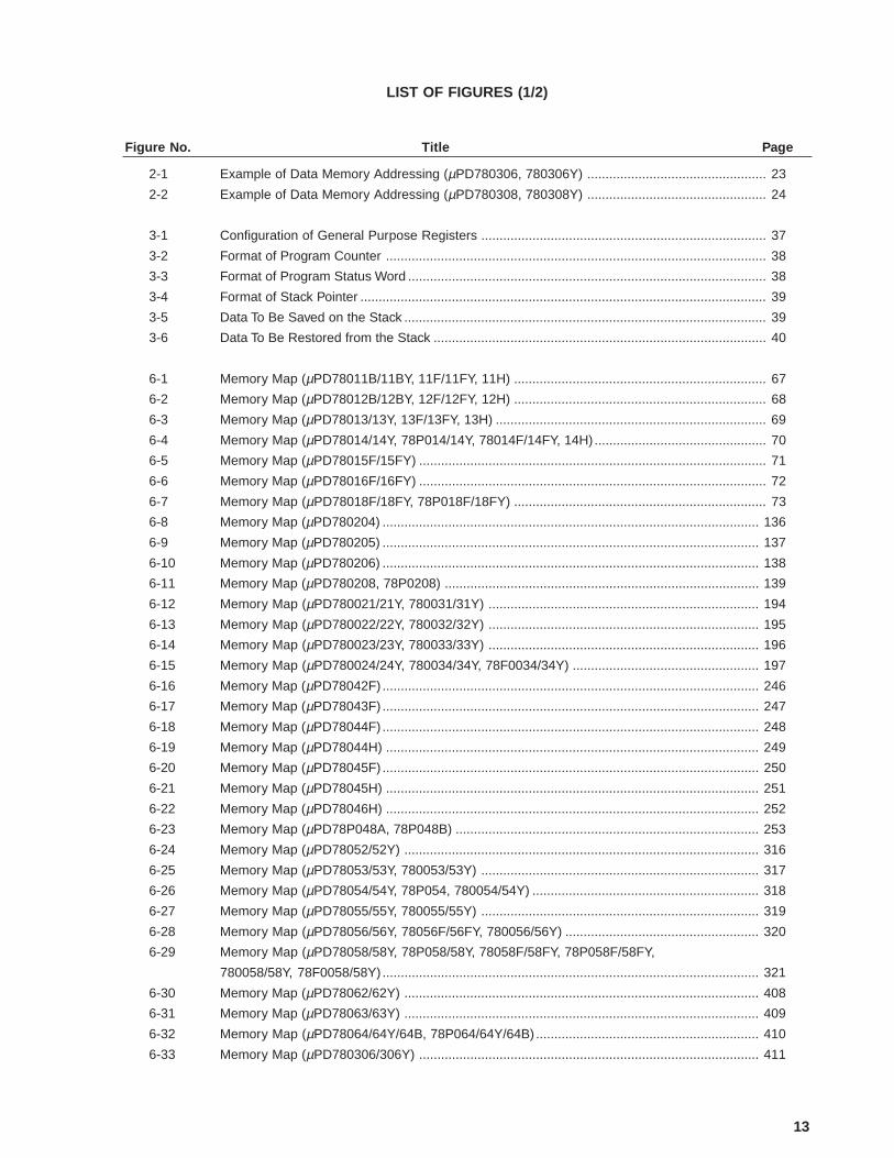
2-1 Example of Data Memory Addressing (µPD780306, 780306Y) ................................................. 23
2-2 Example of Data Memory Addressing (µPD780308, 780308Y) ................................................. 24
3-1 Configuration of General Purpose Registers .............................................................................. 37
3-2 Format of Program Counter ........................................................................................................ 38
3-3 Format of Program Status Word .................................................................................................. 38
3-4 Format of Stack Pointer ............................................................................................................... 39
3-5 Data To Be Saved on the Stack ................................................................................................... 39
3-6 Data To Be Restored from the Stack ........................................................................................... 40
6-1 Memory Map (µPD78011B/11BY, 11F/11FY, 11H) ..................................................................... 67
6-2 Memory Map (µPD78012B/12BY, 12F/12FY, 12H) ..................................................................... 68
6-3 Memory Map (µPD78013/13Y, 13F/13FY, 13H) .......................................................................... 69
6-4 Memory Map (µPD78014/14Y, 78P014/14Y, 78014F/14FY, 14H) ............................................... 70
6-5 Memory Map (µPD78015F/15FY) ............................................................................................... 71
6-6 Memory Map (µPD78016F/16FY) ............................................................................................... 72
6-7 Memory Map (µPD78018F/18FY, 78P018F/18FY) ..................................................................... 73
6-8 Memory Map (µPD780204) ....................................................................................................... 136
6-9 Memory Map (µPD780205) ....................................................................................................... 137
6-10 Memory Map (µPD780206) ....................................................................................................... 138
6-11 Memory Map (µPD780208, 78P0208) ...................................................................................... 139
6-12 Memory Map (µPD780021/21Y, 780031/31Y) .......................................................................... 194
6-13 Memory Map (µPD780022/22Y, 780032/32Y) .......................................................................... 195
6-14 Memory Map (µPD780023/23Y, 780033/33Y) .......................................................................... 196
6-15 Memory Map (µPD780024/24Y, 780034/34Y, 78F0034/34Y) ................................................... 197
6-16 Memory Map (µPD78042F) ....................................................................................................... 246
6-17 Memory Map (µPD78043F) ....................................................................................................... 247
6-18 Memory Map (µPD78044F) ....................................................................................................... 248
6-19 Memory Map (µPD78044H) ...................................................................................................... 249
6-20 Memory Map (µPD78045F) ....................................................................................................... 250
6-21 Memory Map (µPD78045H) ...................................................................................................... 251
6-22 Memory Map (µPD78046H) ...................................................................................................... 252
6-23 Memory Map (µPD78P048A, 78P048B) ................................................................................... 253
6-24 Memory Map (µPD78052/52Y) ................................................................................................. 316
6-25 Memory Map (µPD78053/53Y, 780053/53Y) ............................................................................ 317
6-26 Memory Map (µPD78054/54Y, 78P054, 780054/54Y) .............................................................. 318
6-27 Memory Map (µPD78055/55Y, 780055/55Y) ............................................................................ 319
6-28 Memory Map (µPD78056/56Y, 78056F/56FY, 780056/56Y) ..................................................... 320
6-29 Memory Map (µPD78058/58Y, 78P058/58Y, 78058F/58FY, 78P058F/58FY,
780058/58Y, 78F0058/58Y) ....................................................................................................... 321
6-30 Memory Map (µPD78062/62Y) ................................................................................................. 408
6-31 Memory Map (µPD78063/63Y) ................................................................................................. 409
6-32 Memory Map (µPD78064/64Y/64B, 78P064/64Y/64B) ............................................................. 410
6-33 Memory Map (µPD780306/306Y) ............................................................................................. 411
LIST OF FIGURES (1/2)
Figure No. T itle Page

14
6-34 Memory Map (µPD780308/308Y, 78P0308/308Y) .................................................................... 412
6-35 Memory Map (µPD78070A/70AY) ............................................................................................. 486
6-36 Memory Map (µPD78074B/74BY) ............................................................................................ 487
6-37 Memory Map (µPD78075B/75BY) ............................................................................................ 488
6-38 Memory Map (µPD78076/76Y) ................................................................................................. 489
6-39 Memory Map (µPD78078/78Y, 78P078/78Y) ............................................................................ 490
6-40 Memory Map (µPD78081) ......................................................................................................... 576
6-41 Memory Map (µPD78082) ......................................................................................................... 577
6-42 Memory Map (µPD78P083) ...................................................................................................... 578
LIST OF FIGURES (2/2)
Figure No. T itle Page

15
1-1 K0 Microcontroller Subseries Product Guide .............................................................................. 21
4-1 Operand Descriptions ................................................................................................................. 41
4-2 Instruction Set ............................................................................................................................. 43
4-3 8-Bit Instructions Listed by Operand Type................................................................................... 52
4-4 16-Bit Instructions Listed by Operand Type................................................................................. 53
4-5 Bit Manipulations Listed by Operand Type .................................................................................. 53
4-6 Call and Branch Instructions Listed by Operand Type ................................................................ 54
6-1 Special Function Register List (µPD78014/14Y, 78014H, and 78018F/18FY Subseries) .......... 74
6-2 Interrupt Source List .................................................................................................................. 115
6-3 Interrupt Sources and Flags ...................................................................................................... 116
6-4 Hardware Status After Reset .................................................................................................... 129
6-5 Special Function Register List (µPD780208 Subseries) ........................................................... 140
6-6 Interrupt Source List .................................................................................................................. 179
6-7 Interrupt Sources and Flags ...................................................................................................... 180
6-8 Hardware Status After Reset .................................................................................................... 189
6-9 Special Function Register List (µPD780024/24Y and 780034/34Y Subseries) ........................ 198
6-10 Interrupt Source List .................................................................................................................. 231
6-11 Interrupt Sources and Flags ...................................................................................................... 232
6-12 Hardware Status After Reset .................................................................................................... 242
6-13 Special Function Register List (µPD78044F and 78044H Subseries) ...................................... 254
6-14 Interrupt Source List .................................................................................................................. 294
6-15 Interrupt Source List .................................................................................................................. 295
6-16 Interrupt Sources and Flags ...................................................................................................... 296
6-17 Hardware Status After Reset .................................................................................................... 309
6-18 Special Function Register List (µPD78054/54Y, 78058F/58FY, and 780058/58Y
Subseries) ................................................................................................................................. 322
6-19 Interrupt Source List .................................................................................................................. 380
6-20 Interrupt Source List .................................................................................................................. 381
6-21 Interrupt Sources and Flags ...................................................................................................... 382
6-22 Hardware Status After Reset .................................................................................................... 398
6-23 Special Function Register List (µPD78064/64Y, 78064B, and 780308/308Y Subseries) ......... 413
6-24 Interrupt Source List .................................................................................................................. 465
6-25 Interrupt Sources and Flags ...................................................................................................... 466
6-26 Hardware Status After Reset .................................................................................................... 479
6-27 Special Function Register List (µPD78078/78Y, 78075B/75BY, and 78070A/70AY
Subseries) ................................................................................................................................. 491
6-28 Interrupt Source List .................................................................................................................. 552
6-29 Interrupt Sources and Flags ...................................................................................................... 553
6-30 Hardware Status After Reset .................................................................................................... 568
6-31 Special Function Register List (µPD78083 Subseries) ............................................................. 579
6-32 Interrupt Source List .................................................................................................................. 599
6-33 Interrupt Sources and Flags ...................................................................................................... 600
6-34 Hardware Status After Reset .................................................................................................... 608
LIST OF TABLES (1/1)
Table No. Title Page

16
[MEMO]
17
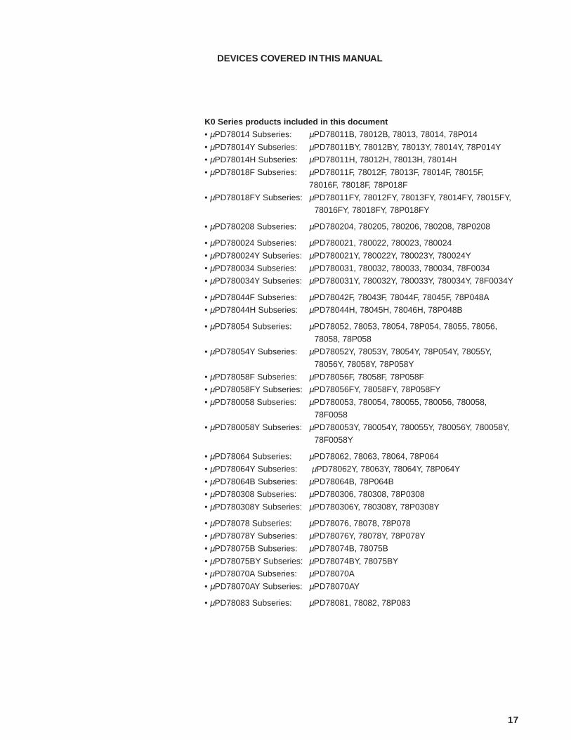
DEVICES COVERED IN THIS MANUAL
K0 Series products included in this document
• µPD78014 Subseries: µPD78011B, 78012B, 78013, 78014, 78P014
• µPD78014Y Subseries: µPD78011BY, 78012BY, 78013Y, 78014Y, 78P014Y
• µPD78014H Subseries: µPD78011H, 78012H, 78013H, 78014H
• µPD78018F Subseries: µPD78011F, 78012F, 78013F, 78014F, 78015F,
78016F, 78018F, 78P018F
• µPD78018FY Subseries: µPD78011FY, 78012FY, 78013FY, 78014FY, 78015FY,
78016FY, 78018FY, 78P018FY
• µPD780208 Subseries: µPD780204, 780205, 780206, 780208, 78P0208
• µPD780024 Subseries: µPD780021, 780022, 780023, 780024
• µPD780024Y Subseries: µPD780021Y, 780022Y, 780023Y, 780024Y
• µPD780034 Subseries: µPD780031, 780032, 780033, 780034, 78F0034
• µPD780034Y Subseries: µPD780031Y, 780032Y, 780033Y, 780034Y, 78F0034Y
• µPD78044F Subseries: µPD78042F, 78043F, 78044F, 78045F, 78P048A
• µPD78044H Subseries: µPD78044H, 78045H, 78046H, 78P048B
• µPD78054 Subseries: µPD78052, 78053, 78054, 78P054, 78055, 78056,
78058, 78P058
• µPD78054Y Subseries: µPD78052Y, 78053Y, 78054Y, 78P054Y, 78055Y,
78056Y, 78058Y, 78P058Y
• µPD78058F Subseries: µPD78056F, 78058F, 78P058F
• µPD78058FY Subseries: µPD78056FY, 78058FY, 78P058FY
• µPD780058 Subseries: µPD780053, 780054, 780055, 780056, 780058,
78F0058
• µPD780058Y Subseries: µPD780053Y, 780054Y, 780055Y, 780056Y, 780058Y,
78F0058Y
• µPD78064 Subseries: µPD78062, 78063, 78064, 78P064
• µPD78064Y Subseries: µPD78062Y, 78063Y, 78064Y, 78P064Y
• µPD78064B Subseries: µPD78064B, 78P064B
• µPD780308 Subseries: µPD780306, 780308, 78P0308
• µPD780308Y Subseries: µPD780306Y, 780308Y, 78P0308Y
• µPD78078 Subseries: µPD78076, 78078, 78P078
• µPD78078Y Subseries: µPD78076Y, 78078Y, 78P078Y
• µPD78075B Subseries: µPD78074B, 78075B
• µPD78075BY Subseries: µPD78074BY, 78075BY
• µPD78070A Subseries: µPD78070A
• µPD78070AY Subseries: µPD78070AY
• µPD78083 Subseries: µPD78081, 78082, 78P083

18
[MEMO]

19
INTRODUCTION
This reference manual is intended for software and firmware engineers already familiar with the K0 device they are
using. They can obtain programming data about the microcontroller without having to refer to the user's manuals for their
device. The document describes the K0 architecture, addressing modes, registers, instruction set, stack operation, and
special function registers (SFRs).
Contents Overview
Chapter 1: Product selection guide
Chapter 2: K0 memory map and addressing modes
Chapter 3: K0 registers and stack operations
Chapter 4: Contains two tables describing the instruction set, and a description of all keywords and operands.
The first table lists all the instructions, their operands, and a description of the operation of each
instruction. The second table is a matrix that the user can look up the first and second operands, and
find a list of all instructions that use both operands
Chapter 5: Example K0 program module and associated listings generated by the assembler
Chapter 6: User Manual document numbers, memory maps, SFR information, status information during halt and
stop modes, and SFR values after a reset for each K0 subseries:
a. µPD78014, µPD014H, and µPD78018F
b. µPD780208
c. µPD780024 and µPD0034
d. µP78044F and µPD78044H
e. µP78054, µPD78058F, and µPD780058
f. µPD78064, µPD78064B and µPD780308
g. µPD78070A, µPD78075B and µPD78078
h. µPD78083
Appendix A: Architecture index for Chapters 2-5
Appendix B: Register index for Chapter 6
Additional Information
Please consult the relevant data sheet and user's manual for specific information about individual devices. For infor-
mation about the instruction set, refer to the 78K0 Instruction Set User's Manual. The most current and up-to-date
information can be obtained by calling 1-800-366-9782 or visiting our web site at www.necel.com.

20
[MEMO]
21
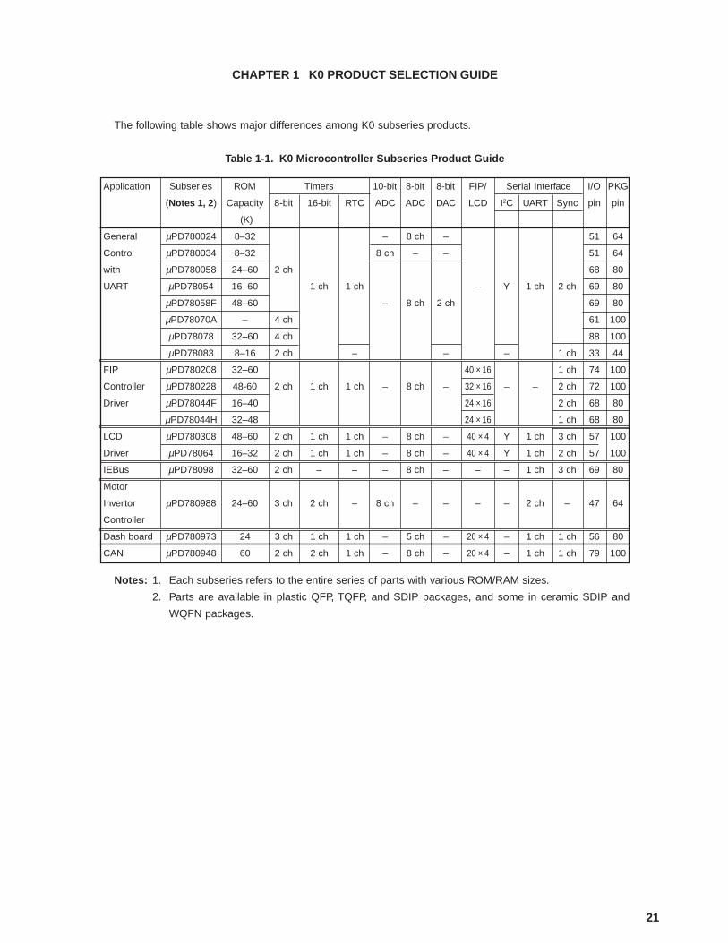
CHAPTER 1 K0 PRODUCT SELECTION GUIDE
The following table shows major differences among K0 subseries products.
Table 1-1. K0 Microcontroller Subseries Product Guide
Application Subseries ROM Timers 10-bit 8-bit 8-bit FIP/ Serial Interface I/O PKG
(Notes 1, 2 ) Capacity 8-bit 16-bit RTC ADC ADC DAC LCD I2C UART Sync pin pin
(K)
General µPD780024 8–32 – 8 ch – 51 64
Control µPD780034 8–32 8 ch – – 51 64
with µPD780058 24–60 2 ch 68 80
UART µPD78054 16–60 1 ch 1 ch – Y 1 ch 2 ch 69 80
µPD78058F 48–60 – 8 ch 2 ch 69 80
µPD78070A – 4 ch 61 100
µPD78078 32–60 4 ch 88 100
µPD78083 8–16 2 ch – – – 1 ch 33 44
FIP µPD780208 32–60 40 × 16 1 ch 74 100
Controller µPD780228 48-60 2 ch 1 ch 1 ch – 8 ch – 32 × 16 – – 2 ch 72 100
Driver µPD78044F 16–40 24 × 16 2 ch 68 80
µPD78044H 32–48 24 × 16 1 ch 68 80
LCD µPD780308 48–60 2 ch 1 ch 1 ch – 8 ch – 40 × 4 Y 1 ch 3 ch 57 100
Driver µPD78064 16–32 2 ch 1 ch 1 ch – 8 ch – 40 × 4 Y 1 ch 2 ch 57 100
IEBus µPD78098 32–60 2 ch – – – 8 ch – – – 1 ch 3 ch 69 80
Motor
Invertor µPD780988 24–60 3 ch 2 ch – 8 ch – – – – 2 ch – 47 64
Controller
Dash board µPD780973 24 3 ch 1 ch 1 ch – 5 ch – 20 × 4 – 1 ch 1 ch 56 80
CAN µPD780948 60 2 ch 2 ch 1 ch – 8 ch – 20 × 4 – 1 ch 1 ch 79 100
Notes: 1. Each subseries refers to the entire series of parts with various ROM/RAM sizes.
2. Parts are available in plastic QFP, TQFP, and SDIP packages, and some in ceramic SDIP and
WQFN packages.

22
[MEMO]
23
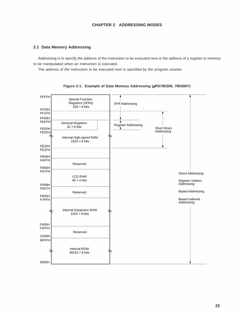
CHAPTER 2 ADDRESSING MODES
2.1 Data Memory Addressing
Addressing is to specify the address of the instruction to be executed next or the address of a register or memory
to be manipulated when an instruction is executed.
The address of the instruction to be executed next is specified by the program counter.
Figure 2-1. Example of Data Memory Addressing ( µµµµµPD780306, 780306Y)
0000H
General Registers32 × 8 bits
Internal ROM49152 × 8 bits
LCD RAM40 × 4 bits
Internal Expansion RAM1024 × 8 bits
C000HBFFFH
FA58HFA57H
FA80HFA7FH
FEE0HFEDFH
FF00HFEFFH
FFFFH
Internal High-speed RAM1024 × 8 bits
Reserved
FB00HFAFFH
FF20HFF1FH
FE20HFE1FH
Special Function Registers (SFRs)
256 × 8 bitsSFR Addressing
Register AddressingShort Direct Addressing
Direct Addressing
Register IndirectAddressing
Based Addressing
Based IndexedAddressing
F800HF7FFH
Reserved
F400HF3FFH
Reserved

CHAPTER 2 ADDRESSING MODES
24
Figure 2-2. Example of Data Memory Addressing ( µµµµµPD780308, 780308Y)
0000H
General Registers32 × 8 bits
Internal ROM61440 × 8 bits
LCD RAM40 × 4 bits
F000HEFFFH
FA58HFA57H
FA80HFA7FH
FEE0HFEDFH
FF00HFEFFH
FFFFH
Internal High-speed RAM1024 × 8 bits
Reserved
FB00HFAFFH
FF20HFF1FH
FE20HFE1FH
Special Function Registers (SFRs)
256 × 8 bitsSFR Addressing
Register AddressingShort Direct Addressing
Direct Addressing
Register IndirectAddressing
Based Addressing
Based IndexedAddressing
F800HF7FFH
Reserved
F400HF3FFH
Reserved
Internal Expansion RAM1024 × 8 bits
25
CHAPTER 2 ADDRESSING MODES
2.2 Instruction Address Addressing
An instruction address is determined by program counter (PC) contents and is normally incremented (+1 for each
byte) automatically according to the number of bytes of an instruction to be fetched each time another instruction
is executed. When a Branch instruction is executed, the branch destination information is set to the PC and branched
by the following types of addressing.
2.2.1 Relative Addressing
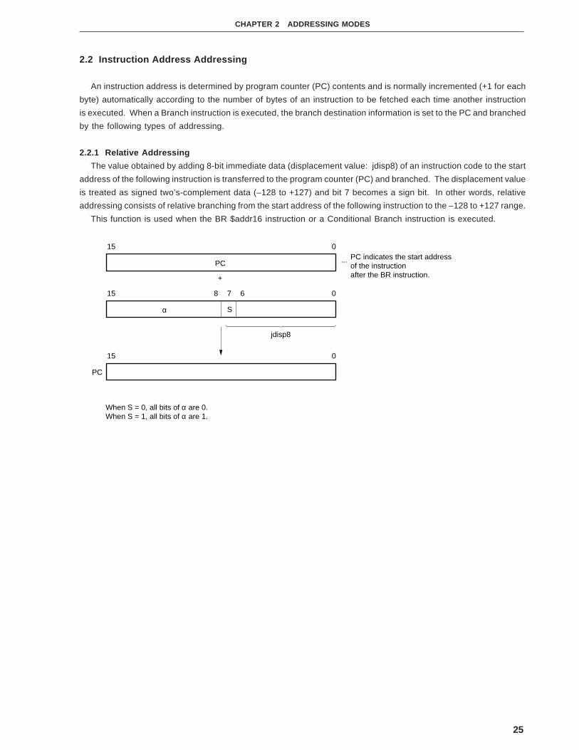
The value obtained by adding 8-bit immediate data (displacement value: jdisp8) of an instruction code to the start
address of the following instruction is transferred to the program counter (PC) and branched. The displacement value
is treated as signed two’s-complement data (–128 to +127) and bit 7 becomes a sign bit. In other words, relative
addressing consists of relative branching from the start address of the following instruction to the –128 to +127 range.
This function is used when the BR $addr16 instruction or a Conditional Branch instruction is executed.
15 0
PC
+
15 08 7 6
S
15 0
PC
α
jdisp8
When S = 0, all bits of α are 0.When S = 1, all bits of α are 1.
PC indicates the start addressof the instructionafter the BR instruction.
...
CHAPTER 2 ADDRESSING MODES
26
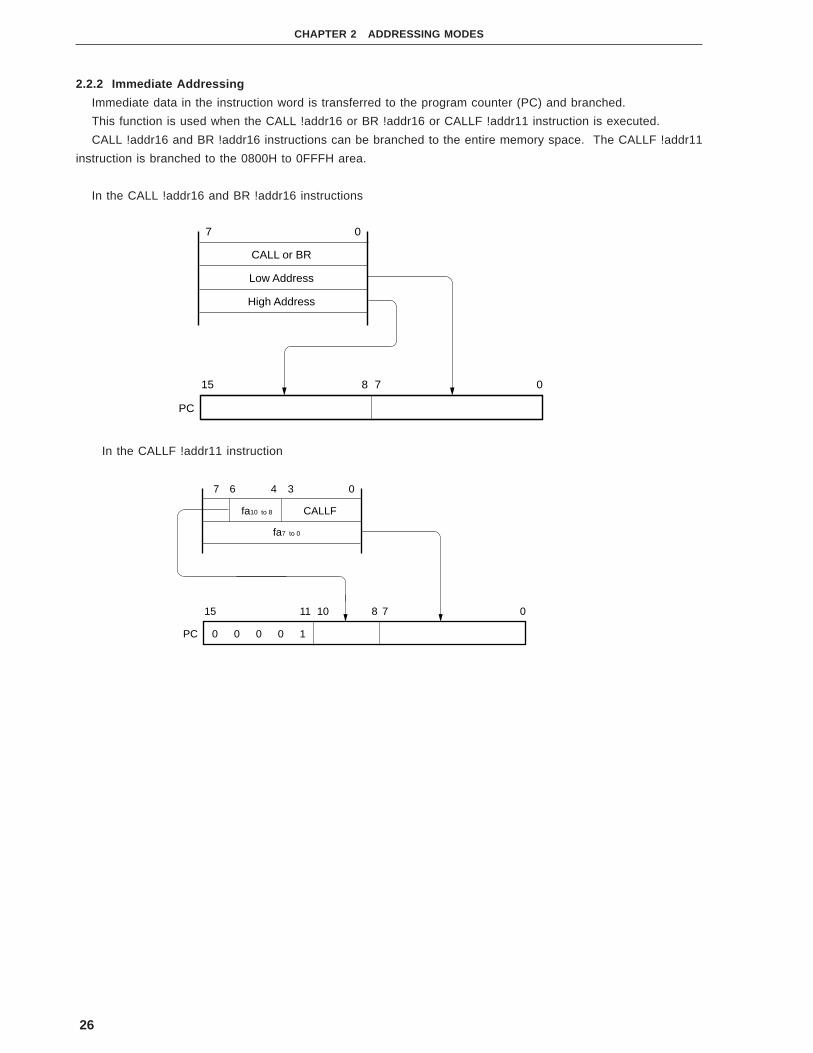
2.2.2 Immediate Addressing
Immediate data in the instruction word is transferred to the program counter (PC) and branched.
This function is used when the CALL !addr16 or BR !addr16 or CALLF !addr11 instruction is executed.
CALL !addr16 and BR !addr16 instructions can be branched to the entire memory space. The CALLF !addr11
instruction is branched to the 0800H to 0FFFH area.
In the CALL !addr16 and BR !addr16 instructions
In the CALLF !addr11 instruction
15 0
PC
8 7
7 0
fa10 to 8
11 10
0 0 0 0 1
6 4 3
CALLF
fa7 to 0
15 0
PC
8 7
7 0
CALL or BR
Low Address
High Address

27
CHAPTER 2 ADDRESSING MODES
2.2.3 Table Indirect Addressing
Table contents (branch destination address) of the particular location are addressed (by bits 1 to 5 of the immediate
data of the opcode) and transferred to the program counter (PC), and the program branches. Table indirect addressing
is used when the CALLT [addr5] instruction is executed.
This instruction references the address stored in the memory table from 40H to 7FH, and allows branching to the
entire memory space.
15 1
15 0
PC
7 0
Low Address
High Address
Memory (Table)
Effective Address +1
Effective Address 0 10 0 0 0 0 0 0 0
8 7
8 7
6 5 0
0
11 1
7 6 5 1 0
ta4 to 0Operation Code

CHAPTER 2 ADDRESSING MODES
28
2.2.4 Register Addressing
Register pair (AX) contents are transferred to the program counter (PC) and the program branches.
This function is used when the BR AX instruction is executed.
7 0
rp
0 7
A X
15 0
PC
8 7
29
CHAPTER 2 ADDRESSING MODES
2.3 Operand Address Addressing
The following methods are available to specify the register and memory (addressing) that are manipulated during
instruction execution.
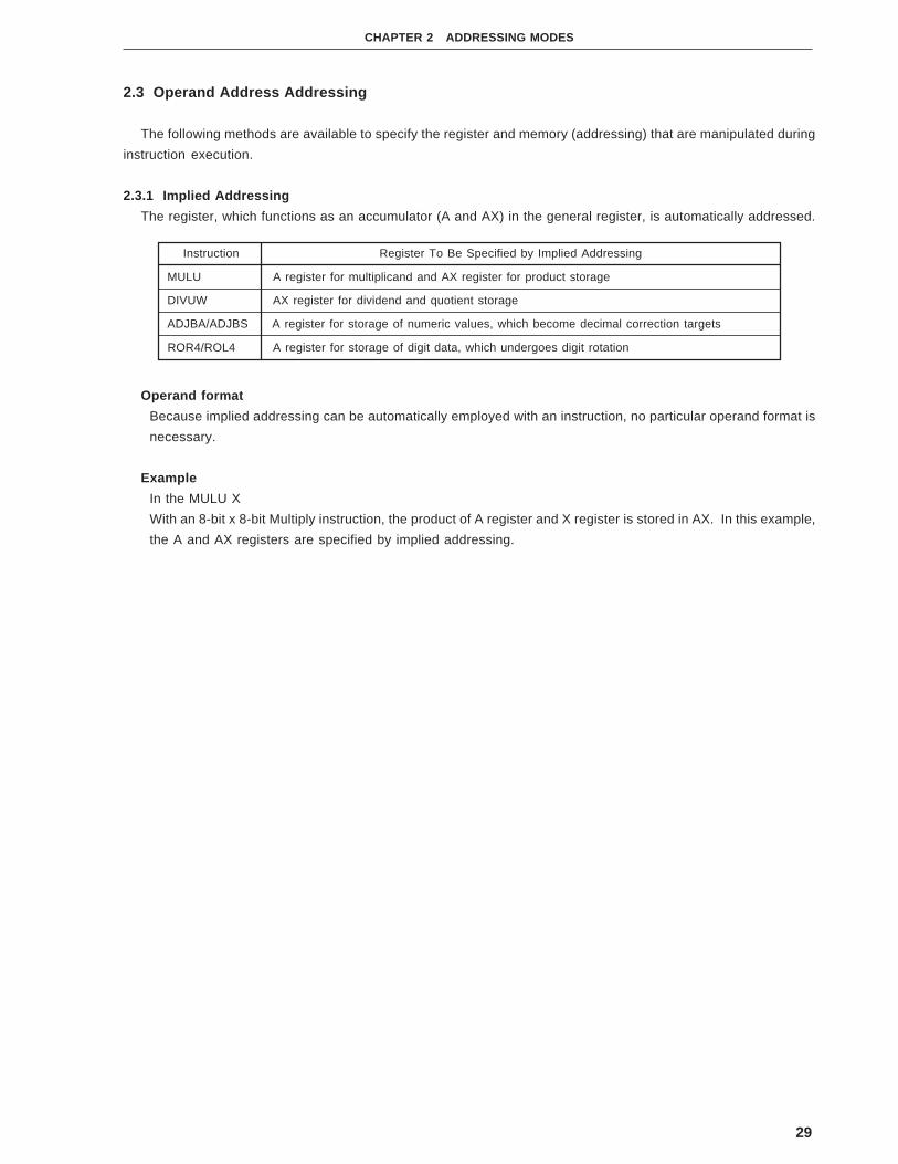
2.3.1 Implied Addressing
The register, which functions as an accumulator (A and AX) in the general register, is automatically addressed.
Instruction Register To Be Specified by Implied Addressing
MULU A register for multiplicand and AX register for product storage
DIVUW AX register for dividend and quotient storage
ADJBA/ADJBS A register for storage of numeric values, which become decimal correction targets
ROR4/ROL4 A register for storage of digit data, which undergoes digit rotation
Operand format
Because implied addressing can be automatically employed with an instruction, no particular operand format is
necessary.
Example
In the MULU X
With an 8-bit x 8-bit Multiply instruction, the product of A register and X register is stored in AX. In this example,
the A and AX registers are specified by implied addressing.
CHAPTER 2 ADDRESSING MODES
30
2.3.2 Register Addressing
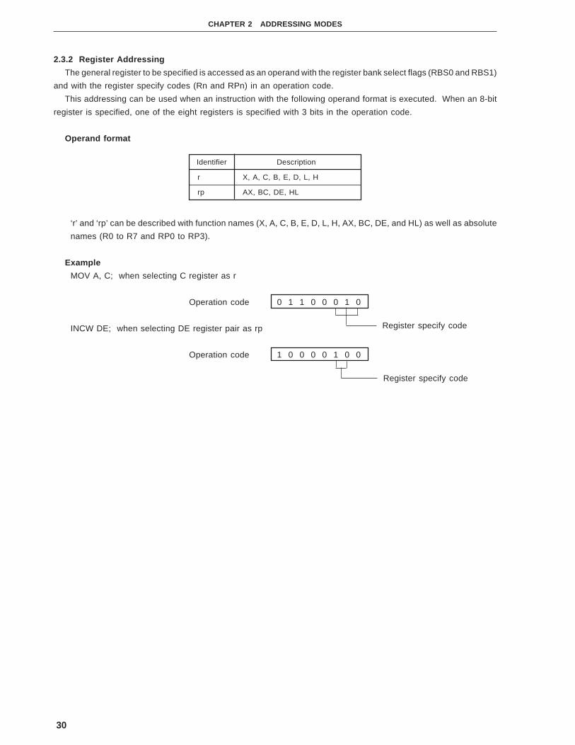
The general register to be specified is accessed as an operand with the register bank select flags (RBS0 and RBS1)
and with the register specify codes (Rn and RPn) in an operation code.
This addressing can be used when an instruction with the following operand format is executed. When an 8-bit
register is specified, one of the eight registers is specified with 3 bits in the operation code.
Operand format
Identifier Description
r X, A, C, B, E, D, L, H
rp AX, BC, DE, HL
‘r’ and ‘rp’ can be described with function names (X, A, C, B, E, D, L, H, AX, BC, DE, and HL) as well as absolute
names (R0 to R7 and RP0 to RP3).
Example
MOV A, C; when selecting C register as r
Operation code 0 1 1 0 0 0 1 0
INCW DE; when selecting DE register pair as rp
Operation code 1 0 0 0 0 1 0 0
Register specify code
Register specify code
31
CHAPTER 2 ADDRESSING MODES
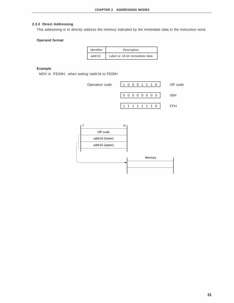
2.3.3 Direct Addressing
This addressing is to directly address the memory indicated by the immediate data in the instruction word.
Operand format
Identifier Description
addr16 Label or 16-bit immediate data
Example
MOV A, !FE00H; when setting !addr16 to FE00H
Operation code 1 0 0 0 1 1 1 0 OP code
0 0 0 0 0 0 0 0 00H
1 1 1 1 1 1 1 0 FFH
Memory
07
addr16 (lower)
addr16 (upper)
OP code
CHAPTER 2 ADDRESSING MODES
32
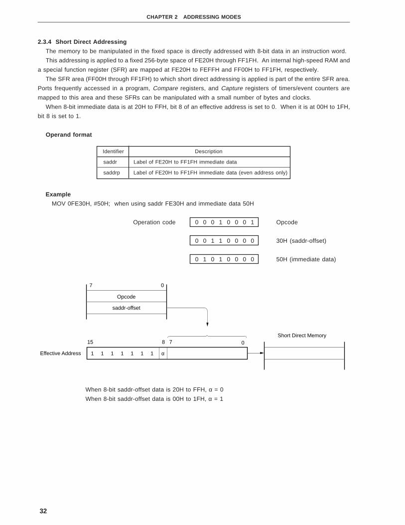
2.3.4 Short Direct Addressing
The memory to be manipulated in the fixed space is directly addressed with 8-bit data in an instruction word.
This addressing is applied to a fixed 256-byte space of FE20H through FF1FH. An internal high-speed RAM and
a special function register (SFR) are mapped at FE20H to FEFFH and FF00H to FF1FH, respectively.
The SFR area (FF00H through FF1FH) to which short direct addressing is applied is part of the entire SFR area.
Ports frequently accessed in a program, Compare registers, and Capture registers of timers/event counters are
mapped to this area and these SFRs can be manipulated with a small number of bytes and clocks.
When 8-bit immediate data is at 20H to FFH, bit 8 of an effective address is set to 0. When it is at 00H to 1FH,
bit 8 is set to 1.
Operand format
Identifier Description
saddr Label of FE20H to FF1FH immediate data
saddrp Label of FE20H to FF1FH immediate data (even address only)
Example
MOV 0FE30H, #50H; when using saddr FE30H and immediate data 50H
Operation code 0 0 0 1 0 0 0 1 Opcode
0 0 1 1 0 0 0 0 30H (saddr-offset)
0 1 0 1 0 0 0 0 50H (immediate data)
When 8-bit saddr-offset data is 20H to FFH, α = 0
When 8-bit saddr-offset data is 00H to 1FH, α = 1
15 0Short Direct Memory
Effective Address 1 1 1 1 1 1 1
8 7
07
Opcode
saddr-offset
α
33
CHAPTER 2 ADDRESSING MODES
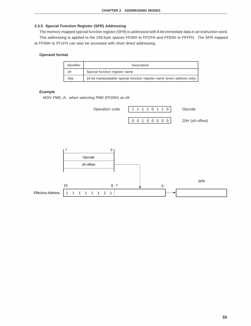
2.3.5 Special Function Register (SFR) Addressing
The memory-mapped special function register (SFR) is addressed with 8-bit immediate data in an instruction word.
This addressing is applied to the 240-byte spaces FF00H to FFCFH and FFE0H to FFFFH. The SFR mapped
at FF00H to FF1FH can also be accessed with short direct addressing.
Operand format
Identifier Description
sfr Special function register name
sfrp 16-bit manipulatable special function register name (even address only)
Example
MOV PM0, A; when selecting PM0 (FF20H) as sfr
Operation code 1 1 1 1 0 1 1 0 Opcode
0 0 1 0 0 0 0 0 20H (sfr-offset)
15 0SFR
Effective Address 1 1 1 1 1 1 1
8 7
07
Opcode
sfr-offset
1
CHAPTER 2 ADDRESSING MODES
34
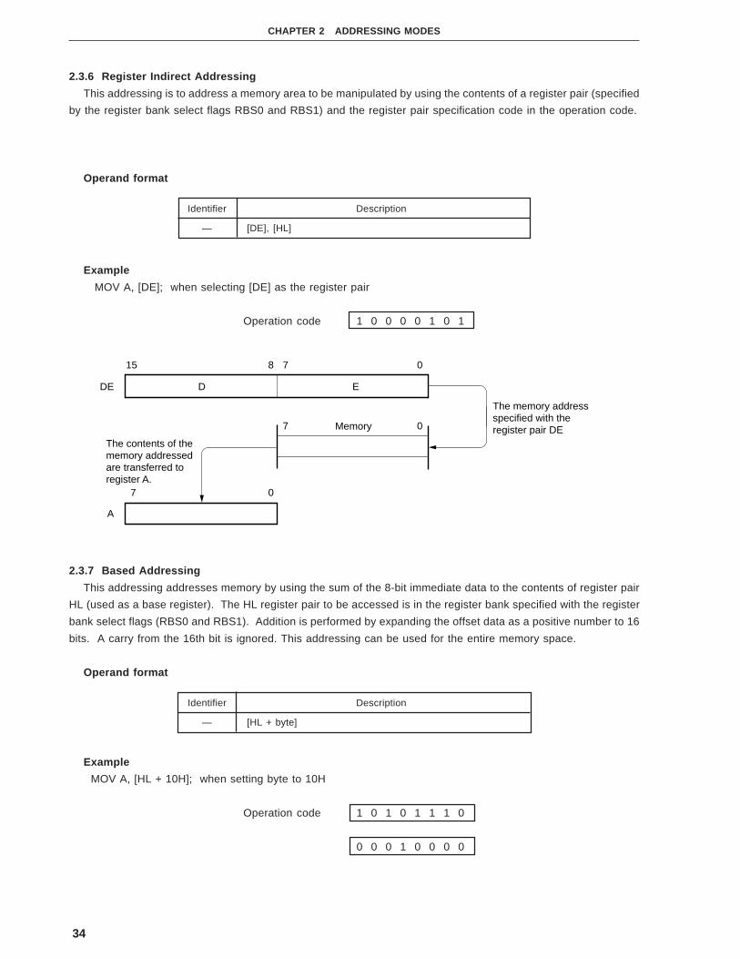
2.3.6 Register Indirect Addressing
This addressing is to address a memory area to be manipulated by using the contents of a register pair (specified
by the register bank select flags RBS0 and RBS1) and the register pair specification code in the operation code.
Operand format
Identifier Description
— [DE], [HL]
Example
MOV A, [DE]; when selecting [DE] as the register pair
Operation code 1 0 0 0 0 1 0 1
2.3.7 Based Addressing
This addressing addresses memory by using the sum of the 8-bit immediate data to the contents of register pair
HL (used as a base register). The HL register pair to be accessed is in the register bank specified with the register
bank select flags (RBS0 and RBS1). Addition is performed by expanding the offset data as a positive number to 16
bits. A carry from the 16th bit is ignored. This addressing can be used for the entire memory space.
Operand format
Identifier Description
— [HL + byte]
Example
MOV A, [HL + 10H]; when setting byte to 10H
Operation code 1 0 1 0 1 1 1 0
0 0 0 1 0 0 0 0
15 08
D
7
E
07
7 0
A
DE
Memory
The contents of the memory addressedare transferred toregister A.
The memory address specified with theregister pair DE
35
CHAPTER 2 ADDRESSING MODES
2.3.8 Based Indexed Addressing
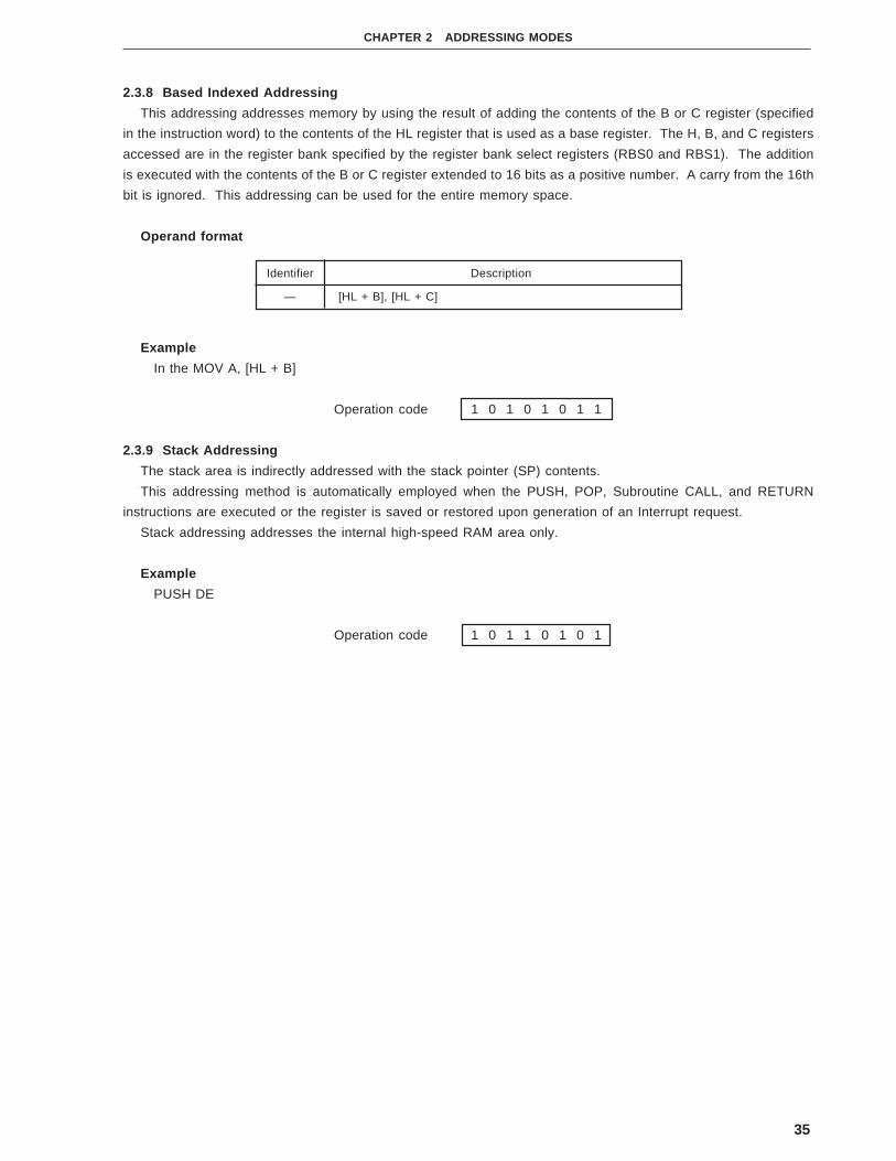
This addressing addresses memory by using the result of adding the contents of the B or C register (specified
in the instruction word) to the contents of the HL register that is used as a base register. The H, B, and C registers
accessed are in the register bank specified by the register bank select registers (RBS0 and RBS1). The addition
is executed with the contents of the B or C register extended to 16 bits as a positive number. A carry from the 16th
bit is ignored. This addressing can be used for the entire memory space.
Operand format
Identifier Description
— [HL + B], [HL + C]
Example
In the MOV A, [HL + B]
Operation code 1 0 1 0 1 0 1 1
2.3.9 Stack Addressing
The stack area is indirectly addressed with the stack pointer (SP) contents.
This addressing method is automatically employed when the PUSH, POP, Subroutine CALL, and RETURN
instructions are executed or the register is saved or restored upon generation of an Interrupt request.
Stack addressing addresses the internal high-speed RAM area only.
Example
PUSH DE
Operation code 1 0 1 1 0 1 0 1

36
[MEMO]
37
CHAPTER 3 REGISTERS AND STACK OPERATION
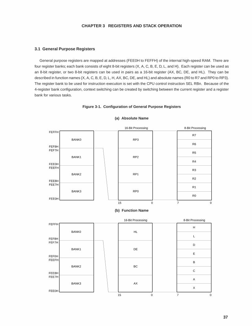
3.1 General Purpose Registers
General purpose registers are mapped at addresses (FEE0H to FEFFH) of the internal high-speed RAM. There are
four register banks; each bank consists of eight 8-bit registers (X, A, C, B, E, D, L, and H). Each register can be used as
an 8-bit register, or two 8-bit registers can be used in pairs as a 16-bit register (AX, BC, DE, and HL). They can be
described in function names (X, A, C, B, E, D, L, H, AX, BC, DE, and HL) and absolute names (R0 to R7 and RP0 to RP3).
The register bank to be used for instruction execution is set with the CPU control instruction SEL RBn. Because of the
4-register bank configuration, context switching can be created by switching between the current register and a register
bank for various tasks.
Figure 3-1. Configuration of General Purpose Registers
(a) Absolute Name
(b) Function Name
BANK0
BANK1
BANK2
BANK3
FEFFH
FEF8HFEF7H
FEE0H
RP3
RP2
RP1
RP0
R7
15 0 7 0
R6
R5
R4
R3
R2
R1
R0
16-Bit Processing 8-Bit Processing
FEE0HFEEFH
FEE8HFEE7H
BANK0
BANK1
BANK2
BANK3
FEFFH
FEF8HFEF7H
FEE0H
HL
DE
BC
AX
H
15 0 7 0
L
D
E
B
C
A
X
16-Bit Processing 8-Bit Processing
FEF0HFEEFH
FEE8HFEE7H

38
CHAPTER 3 REGISTERS AND STACK OPERATION
3.2 Processor Registers
3.2.1 Control Registers
The control registers control the program sequence, statuses, and stack memory. The control registers consist of a
program counter (PC), a program status word (PSW), and a stack pointer (SP).
(1) Program counter (PC)
The program counter is a 16-bit register that holds the address of the next program to be executed.
In normal operation, the PC is automatically incremented by the number of bytes of the current instruction. When
a Branch instruction is executed, immediate data and register contents are set.
RESET sets the Reset vector table values at addresses 0000H and 0001H to the program counter.
Figure 3-2. Format of Program Counter
(2) Program status word (PSW)
The program status word is an 8-bit register consisting of various flags to be set/reset by instruction execution.
The program status word contents are automatically saved on the stack during Interrupt request processing or
when a PUSH PSW instruction is executed. The PSW is automatically restored upon execution of the RETB,
RETI, and POP PSW instructions. RESET sets the PSW to 02H.
Figure 3-3. Format of Program Status Word
(a) Interrupt enable flag (IE)
This flag controls the Interrupt request acknowledge operations of the CPU. When IE = 0, Interrupt requests
are disabled (DI), and all interrupts except the non-maskable interrupt are disabled. When IE = 1, the
interrupts are enabled (EI). At this time, acknowledging Interrupt requests is controlled with an in-service
priority flag (ISP), an interrupt mask flag (for each interrupt source), and a priority specification flag. This flag
is reset (to 0) upon DI instruction execution or interrupt acknowledgment, and is set (to 1) upon EI instruction
execution.
(b) Zero flag (Z)
When the operation result is zero, this flag is set (to 1). It is reset (to 0) in all other cases.
(c) Register bank select flags (RBS0 and RBS1)
These are 2 flag bits that select one of the four register banks. These bits indicate the register bank selected
by an SEL RBn instruction.
15 0
PC15 PC14 PC13 PC12 PC11 PC10 PC9 PC8 PC7 PC6 PC5 PC4 PC3 PC2 PC1 PC0PC
7 0
IE Z RBS1 AC RBS0 0 ISP CYPSW
39
CHAPTER 3 REGISTERS AND STACK OPERATION
(d) Auxiliary carry flag (AC)
If the operation result has a carry from bit 3 or a borrow at bit 3, this flag is set (to 1). It is reset (to 0) in all
other cases.
(e) In-service priority flag (ISP)
This flag manages the priority of acknowledgment of maskable vectored Interrupt requests. When ISP = 0,
the vectored interrupts assigned a low priority (with the priority registers PR0L, PR0H, and PR1L) are
disabled. Acknowledgment of interrupts is controlled with the interrupt enable flag (IE).
(f) Carry flag (CY)
This flag stores overflow and underflow upon Add/Subtract instruction execution. It stores the shift-out value
upon Rotate instruction execution and functions as a bit accumulator during Bit Manipulation instruction
execution.
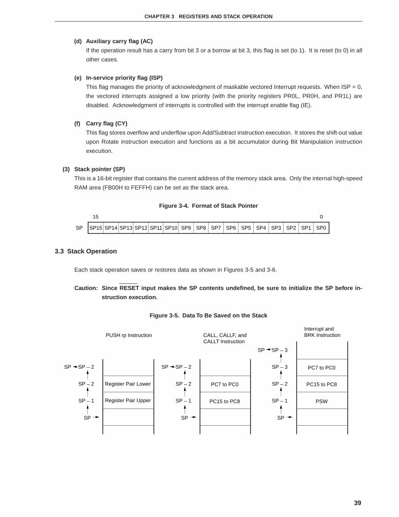
(3) Stack pointer (SP)
This is a 16-bit register that contains the current address of the memory stack area. Only the internal high-speed
RAM area (FB00H to FEFFH) can be set as the stack area.
Figure 3-4. Format of Stack Pointer
3.3 Stack Operation
Each stack operation saves or restores data as shown in Figures 3-5 and 3-6.
Caution: Since RESET input makes the SP contents undefined, be sure to initialize the SP before in-
struction execution.
Figure 3-5. Data To Be Saved on the Stack
15 0
SP15 SP14 SP13 SP12 SP11 SP10 SP9 SP8 SP7 SP6 SP5 SP4 SP3 SP2 SP1 SP0SP
Interrupt andBRK Instruction
PSW
PC15 to PC8
PC15 to PC8
PC7 to PC0Register Pair Lower
SP SP _ 2
SP _ 2
Register Pair Upper
CALL, CALLF, andCALLT Instruction
PUSH rp Instruction
SP _ 1
SP
SP SP _ 2
SP _ 2
SP _ 1
SP
PC7 to PC0SP _ 3
SP _ 2
SP _ 1
SP
SP SP _ 3
40
CHAPTER 3 REGISTERS AND STACK OPERATION
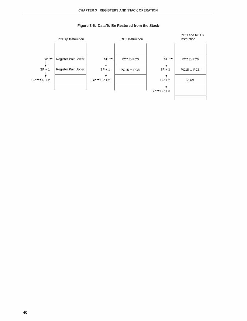
Figure 3-6. Data To Be Restored from the Stack
RETI and RETB Instruction
PSW
PC15 to PC8PC15 to PC8
PC7 to PC0Register Pair Lower
SP SP + 2
SP
Register Pair Upper
RET InstructionPOP rp Instruction
SP + 1
PC7 to PC0
SP SP + 2
SP
SP + 1
SP + 2
SP
SP + 1
SP SP + 3
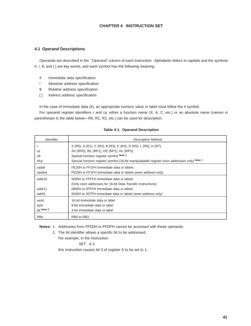
41
CHAPTER 4 INSTRUCTION SET
4.1 Operand Descriptions
Operands are described in the “Operand” column of each instruction. Alphabetic letters in capitals and the symbols
#, !, $, and [ ] are key words, and each symbol has the following meaning.
# Immediate data specification
! Absolute address specification
$ Relative address specification
[ ] Indirect address specification
In the case of immediate data (#), an appropriate numeric value or label must follow the # symbol.
For operand register identifiers r and rp, either a function name (X, A, C, etc.) or an absolute name (names in
parentheses in the table below—R0, R1, R2, etc.) can be used for description.
Table 4-1. Operand Description
Identifier Description Method
r X (R0), A (R1), C (R2), B (R3), E (R4), D (R5), L (R6), H (R7),
rp AX (RP0), BC (RP1), DE (RP2), HL (RP3)
sfr Special function register symbol Note 1
sfrp Special function register symbol (16-bit manipulatable register even addresses only) Note 1
saddr FE20H to FF1FH immediate data or labels
saddrp FE20H to FF1FH immediate data or labels (even address only)
addr16 0000H to FFFFH immediate data or labels
(Only even addresses for 16-bit Data Transfer instructions)
addr11 0800H to 0FFFH immediate data or labels
addr5 0040H to 007FH immediate data or labels (even address only)
word 16-bit immediate data or label
byte 8-bit immediate data or label
bit Note 2 3-bit immediate data or label
RBn RB0 to RB3
Notes: 1. Addresses from FFD0H to FFDFH cannot be accessed with these operands.
2. The bit identifier allows a specific bit to be addressed.
For example, in the instruction:
SET A.3
this instruction causes bit 3 of register A to be set to 1.
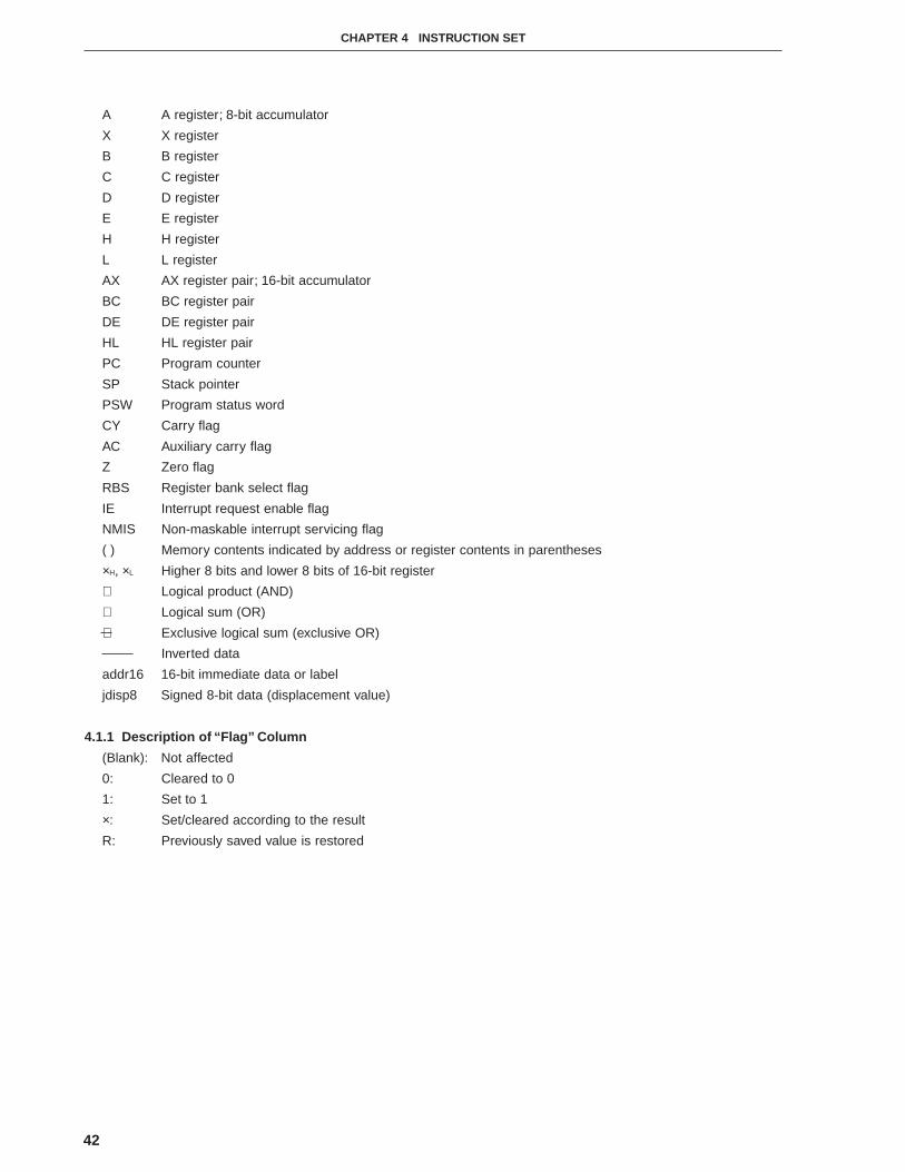
42
CHAPTER 4 INSTRUCTION SET
A A register; 8-bit accumulator
X X register
B B register
C C register
D D register
E E register
H H register
L L register
AX AX register pair; 16-bit accumulator
BC BC register pair
DE DE register pair
HL HL register pair
PC Program counter
SP Stack pointer
PSW Program status word
CY Carry flag
AC Auxiliary carry flag
Z Zero flag
RBS Register bank select flag
IE Interrupt request enable flag
NMIS Non-maskable interrupt servicing flag
( ) Memory contents indicated by address or register contents in parentheses
×H, ×L Higher 8 bits and lower 8 bits of 16-bit register
∧ Logical product (AND)
∨ Logical sum (OR)
∨ Exclusive logical sum (exclusive OR)
Inverted data
addr16 16-bit immediate data or label
jdisp8 Signed 8-bit data (displacement value)
4.1.1 Description of “Flag” Column
(Blank): Not affected
0: Cleared to 0
1: Set to 1
×: Set/cleared according to the result
R: Previously saved value is restored

43
CHAPTER 4 INSTRUCTION SET
Table 4-2. Instruction Set (1/8)
Instruction Mnemonic Operands ByteClock
OperationFlag
Group Note 1 Note 2 Z AC CY
r, #byte 2 4 – r ← byte
saddr, #byte 3 6 7 (saddr) ← byte
sfr, #byte 3 – 7 sfr ← byte
A, r Note 3 1 2 – A ← r
r, A Note 3 1 2 – r ← A
A, saddr 2 4 5 A ← (saddr)
saddr, A 2 4 5 (saddr) ← A
A, sfr 2 – 5 A ← sfr
sfr, A 2 – 5 sfr ← A
A, !addr16 3 8 9 A ← (addr16)
!addr16, A 3 8 9 (addr16) ← A
PSW, #byte 3 – 7 PSW ← byte × × ×
A, PSW 2 – 5 A ← PSW
MOV PSW, A 2 – 5 PSW ← A × × ×
A, [DE] 1 4 5 A ← (DE)
8-bit data [DE], A 1 4 5 (DE) ← A
transfer A, [HL] 1 4 5 A ← (HL)
[HL], A 1 4 5 (HL) ← A
A, [HL + byte] 2 8 9 A ← (HL + byte)
[HL + byte], A 2 8 9 (HL + byte) ← A
A, [HL + B] 1 6 7 A ← (HL + B)
[HL + B], A 1 6 7 (HL + B) ← A
A, [HL + C] 1 6 7 A ← (HL + C)
[HL + C], A 1 6 7 (HL + C) ← A
A, r Note 3 1 2 – A ↔ r
A, saddr 2 4 6 A ↔ (saddr)
A, sfr 2 – 6 A ↔ sfr
A, !addr16 3 8 10 A ↔ (addr16)
XCH A, [DE] 1 4 6 A ↔ (DE)
A, [HL] 1 4 6 A ↔ (HL)
A, [HL + byte] 2 8 10 A ↔ (HL + byte)
A, [HL + B] 2 8 10 A ↔ (HL + B)
A, [HL + C] 2 8 10 A ↔ (HL + C)
Notes: 1. When the internal high-speed RAM area is accessed or there is an instruction with no data access
2. When any area except the internal high-speed RAM area is accessed
3. Except ‘r = A’
Remark: One instruction clock cycle is one cycle of the CPU clock (fCPU) selected by the processor clock control
(PCC) register.
4.2 Instruction Set Table

44
CHAPTER 4 INSTRUCTION SET
Instruction Mnemonic Operands ByteClock
OperationFlag
Group Note 1 Note 2 Z AC CY
rp, #word 3 6 – rp ← word
saddrp, #word 4 8 10 (saddrp) ← word
sfrp, #word 4 – 10 sfrp ← word
AX, saddrp 2 6 8 AX ← (saddrp)
16-bit data saddrp, AX 2 6 8 (saddrp) ← AX
transfer MOVW AX, sfrp 2 – 8 AX ← sfrp
sfrp, AX 2 – 8 sfrp ← AX
AX, rp Note 3 1 4 – AX ← rp
rp, AX Note 3 1 4 – rp ← AX
AX, !addr16 3 10 12 AX ← (addr16)
!addr16, AX 3 10 12 (addr16) ← AX
XCHW AX, rp Note 3 1 4 – AX ↔ rp
A, #byte 2 4 – A, CY ← A + byte × × ×
saddr, #byte 3 6 8 (saddr), CY ← (saddr) + byte × × ×
A, r Note 4 2 4 – A, CY ← A + r × × ×
r, A 2 4 – r, CY ← r + A × × ×
ADD A, saddr 2 4 5 A, CY ← A + (saddr) × × ×
A, !addr16 3 8 9 A, CY ← A + (addr16) × × ×
A, [HL] 1 4 5 A, CY ← A + (HL) × × ×
A, [HL + byte] 2 8 9 A, CY ← A + (HL + byte) × × ×
A, [HL + B] 2 8 9 A, CY ← A + (HL + B) × × ×
8-bit A, [HL + C] 2 8 9 A, CY ← A + (HL + C) × × ×
operation A, #byte 2 4 – A, CY ← A + byte + CY × × ×
saddr, #byte 3 6 8 (saddr), CY ← (saddr) + byte + CY × × ×
A, r Note 4 2 4 – A, CY ← A + r + CY × × ×
r, A 2 4 – r, CY ← r + A + CY × × ×
ADDC A, saddr 2 4 5 A, CY ← A + (saddr) + CY × × ×
A, !addr16 3 8 9 A, CY ← A + (addr16) + CY × × ×
A, [HL] 1 4 5 A, CY ← A + (HL) + CY × × ×
A, [HL + byte] 2 8 9 A, CY ← A + (HL + byte) + CY × × ×
A, [HL + B] 2 8 9 A, CY ← A + (HL + B) + CY × × ×
A, [HL + C] 2 8 9 A, CY ← A + (HL + C) + CY × × ×
Notes: 1. When the internal high-speed RAM area is accessed or there is an instruction with no data access
2. When any area except the internal high-speed RAM area is accessed
3. Only when rp = BC, DE or HL
4. Except ‘r = A’
Remark: One instruction clock cycle is one cycle of the CPU clock (fCPU) selected by the processor clock control
(PCC) register.
Table 4-2. Instruction Set (2/8)

45
CHAPTER 4 INSTRUCTION SET
Instruction Mnemonic Operands ByteClock
OperationFlag
Group Note 1 Note 2 Z AC CY
A, #byte 2 4 – A, CY ← A – byte × × ×
saddr, #byte 3 6 8 (saddr), CY ← (saddr) – byte × × ×
A, r Note 3 2 4 – A, CY ← A – r × × ×
r, A 2 4 – r, CY ← r – A × × ×
SUBA, saddr 2 4 5 A, CY ← A – (saddr) × × ×
A, !addr16 3 8 9 A, CY ← A – (addr16) × × ×
A, [HL] 1 4 5 A, CY ← A – (HL) × × ×
A, [HL + byte] 2 8 9 A, CY ← A – (HL + byte) × × ×
A, [HL + B] 2 8 9 A, CY ← A – (HL + B) × × ×
A, [HL + C] 2 8 9 A, CY ← A – (HL + C) × × ×
A, #byte 2 4 – A, CY ← A – byte – CY × × ×
saddr, #byte 3 6 8 (saddr), CY ← (saddr) – byte – CY × × ×
A, r Note 3 2 4 – A, CY ← A – r – CY × × ×
r, A 2 4 – r, CY ← r – A – CY × × ×
8-bitSUBC
A, saddr 2 4 5 A, CY ← A – (saddr) – CY × × ×
operation A, !addr16 3 8 9 A, CY ← A – (addr16) – CY × × ×
A, [HL] 1 4 5 A, CY ← A – (HL) – CY × × ×
A, [HL + byte] 2 8 9 A, CY ← A – (HL + byte) – CY × × ×
A, [HL + B] 2 8 9 A, CY ← A – (HL + B) – CY × × ×
A, [HL + C] 2 8 9 A, CY ← A – (HL + C) – CY × × ×
A, #byte 2 4 – A ← A ∧ byte ×
saddr, #byte 3 6 8 (saddr) ← (saddr) ∧ byte ×
A, r Note 3 2 4 – A ← A ∧ r ×
r, A 2 4 – r ← r ∧ A ×
ANDA, saddr 2 4 5 A ← A ∧ (saddr) ×
A, !addr16 3 8 9 A ← A ∧ (addr16) ×
A, [HL] 1 4 5 A ← A ∧ (HL) ×
A, [HL + byte] 2 8 9 A ← A ∧ (HL + byte) ×
A, [HL + B] 2 8 9 A ← A ∧ (HL + B) ×
A, [HL + C] 2 8 9 A ← A ∧ (HL + C) ×
Notes: 1. When the internal high-speed RAM area is accessed or there is an instruction with no data access
2. When any area except the internal high-speed RAM area is accessed
3. Except ‘r = A’
Remark: One instruction clock cycle is one cycle of the CPU clock (fCPU) selected by the processor clock control
(PCC) register.
Table 4-2. Instruction Set (3/8)
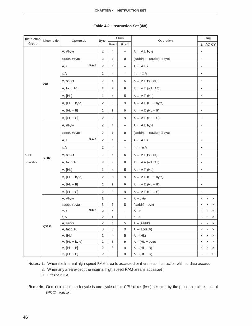
46
CHAPTER 4 INSTRUCTION SET
Instruction Mnemonic Operands ByteClock
OperationFlag
Group Note 1 Note 2 Z AC CY
A, #byte 2 4 – A ← A ∨ byte ×
saddr, #byte 3 6 8 (saddr) ← (saddr) ∨ byte ×
A, r Note 3 2 4 – A ← A ∨ r ×
r, A 2 4 – r ← r ∨ A ×
ORA, saddr 2 4 5 A ← A ∨ (saddr) ×
A, !addr16 3 8 9 A ← A ∨ (addr16) ×
A, [HL] 1 4 5 A ← A ∨ (HL) ×
A, [HL + byte] 2 8 9 A ← A ∨ (HL + byte) ×
A, [HL + B] 2 8 9 A ← A ∨ (HL + B) ×
A, [HL + C] 2 8 9 A ← A ∨ (HL + C) ×
A, #byte 2 4 – A ← A ∨ byte ×
saddr, #byte 3 6 8 (saddr) ← (saddr) ∨ byte ×
A, r Note 3 2 4 – A ← A ∨ r ×
r, A 2 4 – r ← r ∨ A ×
8-bitXOR
A, saddr 2 4 5 A ← A ∨ (saddr) ×
operation A, !addr16 3 8 9 A ← A ∨ (addr16) ×
A, [HL] 1 4 5 A ← A ∨ (HL) ×
A, [HL + byte] 2 8 9 A ← A ∨ (HL + byte) ×
A, [HL + B] 2 8 9 A ← A ∨ (HL + B) ×
A, [HL + C] 2 8 9 A ← A ∨ (HL + C) ×
A, #byte 2 4 – A – byte × × ×
saddr, #byte 3 6 8 (saddr) – byte × × ×
A, r Note 3 2 4 – A – r × × ×
r, A 2 4 – r – A × × ×
CMPA, saddr 2 4 5 A – (saddr) × × ×
A, !addr16 3 8 9 A – (addr16) × × ×
A, [HL] 1 4 5 A – (HL) × × ×
A, [HL + byte] 2 8 9 A – (HL + byte) × × ×
A, [HL + B] 2 8 9 A – (HL + B) × × ×
A, [HL + C] 2 8 9 A – (HL + C) × × ×
Notes: 1. When the internal high-speed RAM area is accessed or there is an instruction with no data access
2. When any area except the internal high-speed RAM area is accessed
3. Except ‘r = A’
Remark: One instruction clock cycle is one cycle of the CPU clock (fCPU) selected by the processor clock control
(PCC) register.
Table 4-2. Instruction Set (4/8)
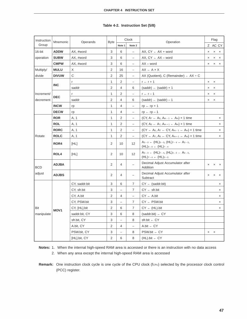
47
CHAPTER 4 INSTRUCTION SET
Instruction Mnemonic Operands ByteClock
OperationFlag
Group Note 1 Note 2 Z AC CY
16-bit ADDW AX, #word 3 6 – AX, CY ← AX + word × × ×
operation SUBW AX, #word 3 6 – AX, CY ← AX – word × × ×
CMPW AX, #word 3 6 – AX – word × × ×
Multiply/ MULU X 2 16 – AX ← A × X
divide DIVUW C 2 25 – AX (Quotient), C (Remainder) ← AX ÷ C
INCr 1 2 – r ← r + 1 × ×
saddr 2 4 6 (saddr) ← (saddr) + 1 × ×
Increment/DEC
r 1 2 – r ← r – 1 × ×
decrement saddr 2 4 6 (saddr) ← (saddr) – 1 × ×
INCW rp 1 4 – rp ← rp + 1
DECW rp 1 4 – rp ← rp – 1
ROR A, 1 1 2 – (CY, A7 ← A0, Am – 1 ← Am) × 1 time ×
ROL A, 1 1 2 – (CY, A0 ← A7, Am + 1 ← Am) × 1 time ×
RORC A, 1 1 2 – (CY ← A0, A7 ← CY, Am – 1 ← Am) × 1 time ×
Rotate ROLC A, 1 1 2 – (CY ← A7, A0 ← CY, Am + 1 ← Am) × 1 time ×
ROR4 [HL] 2 10 12 A3 – 0 ← (HL)3 – 0, (HL)7 – 4 ← A3 – 0,(HL)3 – 0 ← (HL)7 – 4
ROL4 [HL] 2 10 12 A3 – 0 ← (HL)7 – 4, (HL)3 – 0 ← A3 – 0,(HL)7 – 4 ← (HL)3 – 0
ADJBA 2 4 – Decimal Adjust Accumulator after × × ×BCD Addition
adjust ADJBS 2 4 – Decimal Adjust Accumulator after × × ×Subtract
CY, saddr.bit 3 6 7 CY ← (saddr.bit) ×
CY, sfr.bit 3 – 7 CY ← sfr.bit ×
CY, A.bit 2 4 – CY ← A.bit ×
CY, PSW.bit 3 – 7 CY ← PSW.bit ×
BitMOV1
CY, [HL].bit 2 6 7 CY ← (HL).bit ×
manipulate saddr.bit, CY 3 6 8 (saddr.bit) ← CY
sfr.bit, CY 3 – 8 sfr.bit ← CY
A.bit, CY 2 4 – A.bit ← CY
PSW.bit, CY 3 – 8 PSW.bit ← CY × ×
[HL].bit, CY 2 6 8 (HL).bit ← CY
Notes: 1. When the internal high-speed RAM area is accessed or there is an instruction with no data access
2. When any area except the internal high-speed RAM area is accessed
Remark: One instruction clock cycle is one cycle of the CPU clock (fCPU) selected by the processor clock control
(PCC) register.
Table 4-2. Instruction Set (5/8)
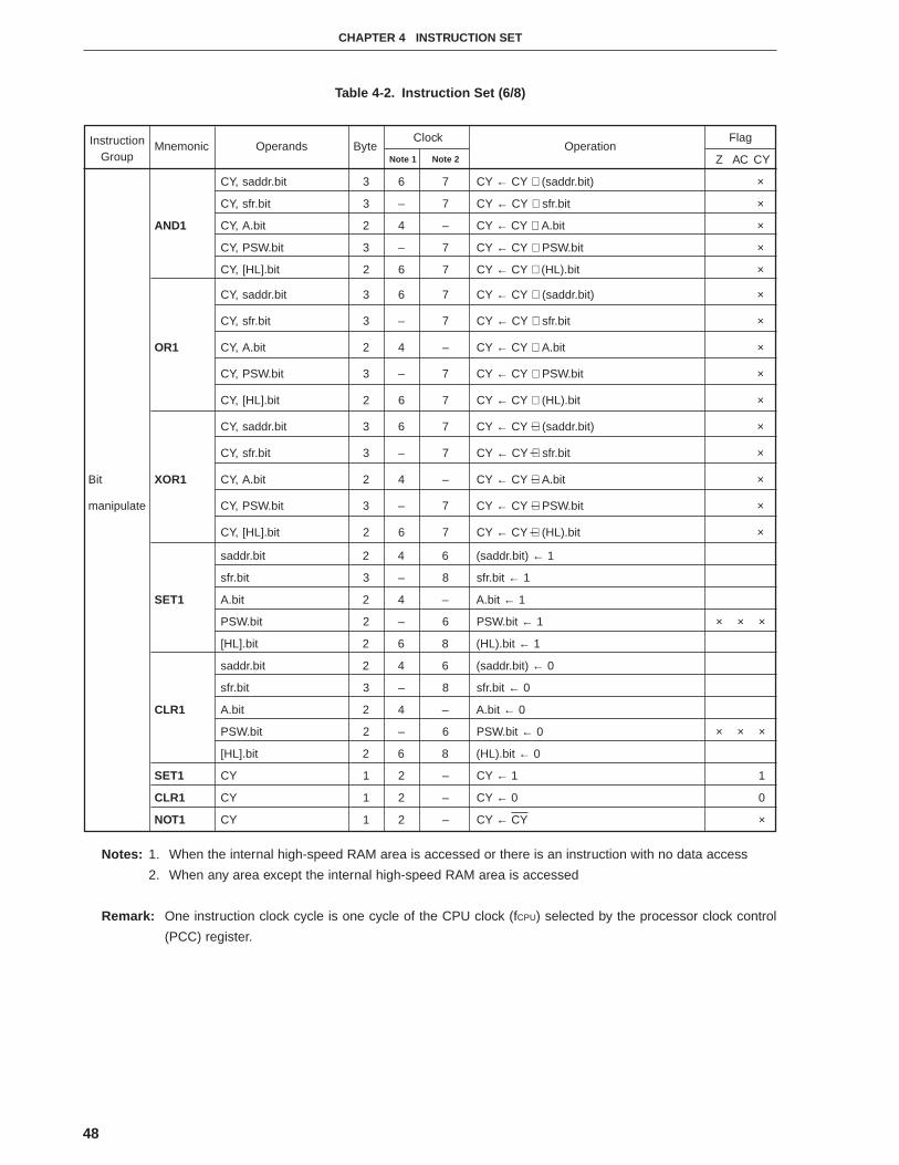
48
CHAPTER 4 INSTRUCTION SET
Instruction Mnemonic Operands ByteClock
OperationFlag
Group Note 1 Note 2 Z AC CY
CY, saddr.bit 3 6 7 CY ← CY ∧ (saddr.bit) ×
CY, sfr.bit 3 – 7 CY ← CY ∧ sfr.bit ×
AND1 CY, A.bit 2 4 – CY ← CY ∧ A.bit ×
CY, PSW.bit 3 – 7 CY ← CY ∧ PSW.bit ×
CY, [HL].bit 2 6 7 CY ← CY ∧ (HL).bit ×
CY, saddr.bit 3 6 7 CY ← CY ∨ (saddr.bit) ×
CY, sfr.bit 3 – 7 CY ← CY ∨ sfr.bit ×
OR1 CY, A.bit 2 4 – CY ← CY ∨ A.bit ×
CY, PSW.bit 3 – 7 CY ← CY ∨ PSW.bit ×
CY, [HL].bit 2 6 7 CY ← CY ∨ (HL).bit ×
CY, saddr.bit 3 6 7 CY ← CY ∨ (saddr.bit) ×
CY, sfr.bit 3 – 7 CY ← CY ∨ sfr.bit ×
Bit XOR1 CY, A.bit 2 4 – CY ← CY ∨ A.bit ×
manipulate CY, PSW.bit 3 – 7 CY ← CY ∨ PSW.bit ×
CY, [HL].bit 2 6 7 CY ← CY ∨ (HL).bit ×
saddr.bit 2 4 6 (saddr.bit) ← 1
sfr.bit 3 – 8 sfr.bit ← 1
SET1 A.bit 2 4 – A.bit ← 1
PSW.bit 2 – 6 PSW.bit ← 1 × × ×
[HL].bit 2 6 8 (HL).bit ← 1
saddr.bit 2 4 6 (saddr.bit) ← 0
sfr.bit 3 – 8 sfr.bit ← 0
CLR1 A.bit 2 4 – A.bit ← 0
PSW.bit 2 – 6 PSW.bit ← 0 × × ×
[HL].bit 2 6 8 (HL).bit ← 0
SET1 CY 1 2 – CY ← 1 1
CLR1 CY 1 2 – CY ← 0 0
NOT1 CY 1 2 – CY ← CY ×
Notes: 1. When the internal high-speed RAM area is accessed or there is an instruction with no data access
2. When any area except the internal high-speed RAM area is accessed
Remark: One instruction clock cycle is one cycle of the CPU clock (fCPU) selected by the processor clock control
(PCC) register.
Table 4-2. Instruction Set (6/8)
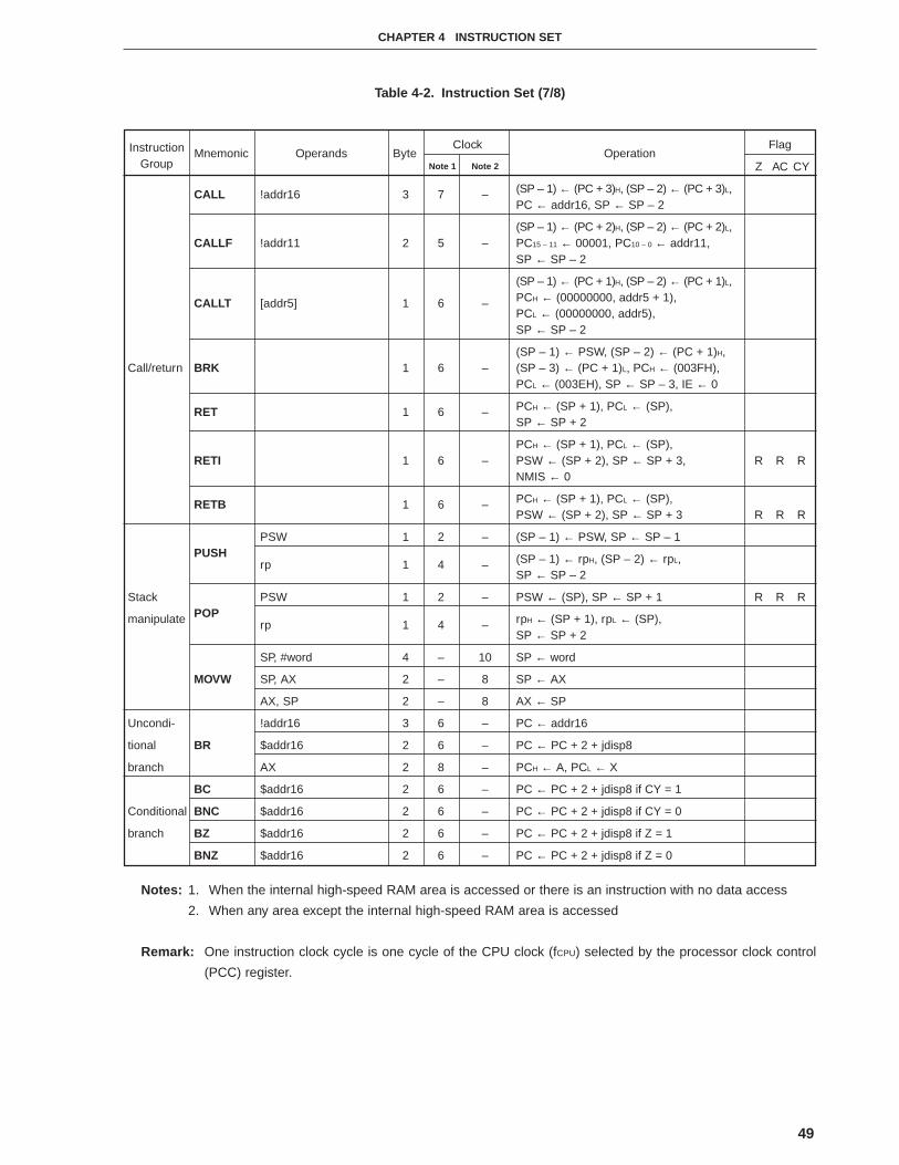
49
CHAPTER 4 INSTRUCTION SET
Instruction Mnemonic Operands ByteClock
OperationFlag
Group Note 1 Note 2 Z AC CY
CALL !addr16 3 7 – (SP – 1) ← (PC + 3)H, (SP – 2) ← (PC + 3)L,PC ← addr16, SP ← SP – 2
(SP – 1) ← (PC + 2)H, (SP – 2) ← (PC + 2)L,CALLF !addr11 2 5 – PC15 – 11 ← 00001, PC10 – 0 ← addr11,
SP ← SP – 2
(SP – 1) ← (PC + 1)H, (SP – 2) ← (PC + 1)L,
CALLT [addr5] 1 6 – PCH ← (00000000, addr5 + 1),PCL ← (00000000, addr5),SP ← SP – 2
(SP – 1) ← PSW, (SP – 2) ← (PC + 1)H,Call/return BRK 1 6 – (SP – 3) ← (PC + 1)L, PCH ← (003FH),
PCL ← (003EH), SP ← SP – 3, IE ← 0
RET 1 6 – PCH ← (SP + 1), PCL ← (SP),SP ← SP + 2
PCH ← (SP + 1), PCL ← (SP),RETI 1 6 – PSW ← (SP + 2), SP ← SP + 3, R R R
NMIS ← 0
RETB 1 6 – PCH ← (SP + 1), PCL ← (SP),PSW ← (SP + 2), SP ← SP + 3 R R R
PSW 1 2 – (SP – 1) ← PSW, SP ← SP – 1PUSH
rp 1 4 – (SP – 1) ← rpH, (SP – 2) ← rpL,SP ← SP – 2
Stack PSW 1 2 – PSW ← (SP), SP ← SP + 1 R R R
manipulate POPrp 1 4 – rpH ← (SP + 1), rpL ← (SP),
SP ← SP + 2
SP, #word 4 – 10 SP ← word
MOVW SP, AX 2 – 8 SP ← AX
AX, SP 2 – 8 AX ← SP
Uncondi- !addr16 3 6 – PC ← addr16
tional BR $addr16 2 6 – PC ← PC + 2 + jdisp8
branch AX 2 8 – PCH ← A, PCL ← X
BC $addr16 2 6 – PC ← PC + 2 + jdisp8 if CY = 1
Conditional BNC $addr16 2 6 – PC ← PC + 2 + jdisp8 if CY = 0
branch BZ $addr16 2 6 – PC ← PC + 2 + jdisp8 if Z = 1
BNZ $addr16 2 6 – PC ← PC + 2 + jdisp8 if Z = 0
Notes: 1. When the internal high-speed RAM area is accessed or there is an instruction with no data access
2. When any area except the internal high-speed RAM area is accessed
Remark: One instruction clock cycle is one cycle of the CPU clock (fCPU) selected by the processor clock control
(PCC) register.
Table 4-2. Instruction Set (7/8)
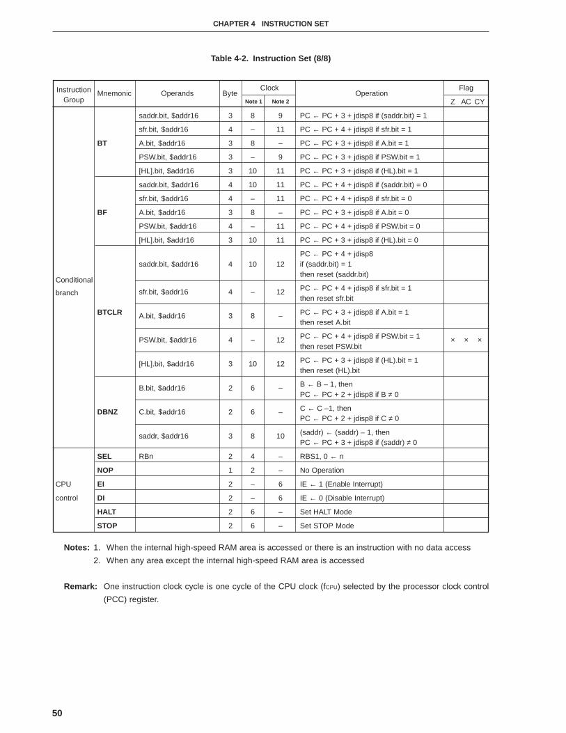
50
CHAPTER 4 INSTRUCTION SET
Instruction Mnemonic Operands ByteClock
OperationFlag
Group Note 1 Note 2 Z AC CY
saddr.bit, $addr16 3 8 9 PC ← PC + 3 + jdisp8 if (saddr.bit) = 1
sfr.bit, $addr16 4 – 11 PC ← PC + 4 + jdisp8 if sfr.bit = 1
BT A.bit, $addr16 3 8 – PC ← PC + 3 + jdisp8 if A.bit = 1
PSW.bit, $addr16 3 – 9 PC ← PC + 3 + jdisp8 if PSW.bit = 1
[HL].bit, $addr16 3 10 11 PC ← PC + 3 + jdisp8 if (HL).bit = 1
saddr.bit, $addr16 4 10 11 PC ← PC + 4 + jdisp8 if (saddr.bit) = 0
sfr.bit, $addr16 4 – 11 PC ← PC + 4 + jdisp8 if sfr.bit = 0
BF A.bit, $addr16 3 8 – PC ← PC + 3 + jdisp8 if A.bit = 0
PSW.bit, $addr16 4 – 11 PC ← PC + 4 + jdisp8 if PSW.bit = 0
[HL].bit, $addr16 3 10 11 PC ← PC + 3 + jdisp8 if (HL).bit = 0
PC ← PC + 4 + jdisp8saddr.bit, $addr16 4 10 12 if (saddr.bit) = 1
Conditionalthen reset (saddr.bit)
sfr.bit, $addr16 4 – 12 PC ← PC + 4 + jdisp8 if sfr.bit = 1branch
then reset sfr.bit
BTCLR A.bit, $addr16 3 8 – PC ← PC + 3 + jdisp8 if A.bit = 1then reset A.bit
PSW.bit, $addr16 4 – 12 PC ← PC + 4 + jdisp8 if PSW.bit = 1 × × ×then reset PSW.bit
[HL].bit, $addr16 3 10 12 PC ← PC + 3 + jdisp8 if (HL).bit = 1then reset (HL).bit
B.bit, $addr16 2 6 – B ← B – 1, thenPC ← PC + 2 + jdisp8 if B ≠ 0
DBNZ C.bit, $addr16 2 6 – C ← C –1, thenPC ← PC + 2 + jdisp8 if C ≠ 0
saddr, $addr16 3 8 10 (saddr) ← (saddr) – 1, thenPC ← PC + 3 + jdisp8 if (saddr) ≠ 0
SEL RBn 2 4 – RBS1, 0 ← n
NOP 1 2 – No Operation
CPU EI 2 – 6 IE ← 1 (Enable Interrupt)
control DI 2 – 6 IE ← 0 (Disable Interrupt)
HALT 2 6 – Set HALT Mode
STOP 2 6 – Set STOP Mode
Notes: 1. When the internal high-speed RAM area is accessed or there is an instruction with no data access
2. When any area except the internal high-speed RAM area is accessed
Remark: One instruction clock cycle is one cycle of the CPU clock (fCPU) selected by the processor clock control
(PCC) register.
Table 4-2. Instruction Set (8/8)

51
CHAPTER 4 INSTRUCTION SET
4.3 Instructions Listed by Addressing Type
The following tables show which instructions can be used with various operands. For example, if the first operand is
r and the second operand is A, the MOV, ADD, ADDC, SUB, SUBC, AND, OR, XOR, and CMP instructions can be used.
4.3.1 8-Bit Instructions
MOV, XCH, ADD, ADDC, SUB, SUBC, AND, OR, XOR, CMP, MULU, DIVUW, INC, DEC, ROR, ROL, RORC,
ROLC, ROR4, ROL4, PUSH, POP, DBNZ
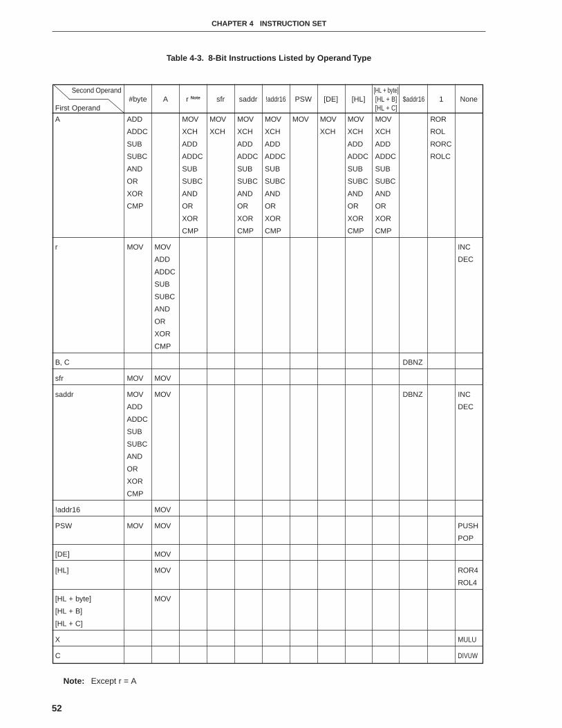
52
CHAPTER 4 INSTRUCTION SET
Second Operand [HL + byte]#byte A r Note sfr saddr !addr16 PSW [DE] [HL] [HL + B] $addr16 1 None
First Operand [HL + C]
A ADD MOV MOV MOV MOV MOV MOV MOV MOV ROR
ADDC XCH XCH XCH XCH XCH XCH XCH ROL
SUB ADD ADD ADD ADD ADD RORC
SUBC ADDC ADDC ADDC ADDC ADDC ROLC
AND SUB SUB SUB SUB SUB
OR SUBC SUBC SUBC SUBC SUBC
XOR AND AND AND AND AND
CMP OR OR OR OR OR
XOR XOR XOR XOR XOR
CMP CMP CMP CMP CMP
r MOV MOV INC
ADD DEC
ADDC
SUB
SUBC
AND
OR
XOR
CMP
B, C DBNZ
sfr MOV MOV
saddr MOV MOV DBNZ INC
ADD DEC
ADDC
SUB
SUBC
AND
OR
XOR
CMP
!addr16 MOV
PSW MOV MOV PUSH
POP
[DE] MOV
[HL] MOV ROR4
ROL4
[HL + byte] MOV
[HL + B]
[HL + C]
X MULU
C DIVUW
Note: Except r = A
Table 4-3. 8-Bit Instructions Listed by Operand Type

53
CHAPTER 4 INSTRUCTION SET
4.3.2 16-Bit Instructions
MOVW, XCHW, ADDW, SUBW, CMPW, PUSH, POP, INCW, DECW
Table 4-4. 16-Bit Instructions Listed by Operand Type
Second Operand
First Operand
AX ADDW MOVW MOVW MOVW MOVW MOVW
SUBW XCHW
CMPW
rp MOVW MOVW Note INCW
DECW
PUSH
POP
sfrp MOVW MOVW
saddrp MOVW MOVW
!addr16 MOVW
SP MOVW MOVW
Note: Only when rp = BC, DE, HL
4.3.3 Bit Manipulation Instructions
MOV1, AND1, OR1, XOR1, SET1, CLR1, NOT1, BT, BF, BTCLR
Table 4-5. Bit Manipulations Listed by Operand Type
Second Operand
First Operand
A.bit MOV1 BT SET1
BF CLR1
BTCLR
sfr.bit MOV1 BT SET1
BF CLR1
BTCLR
saddr.bit MOV1 BT SET1
BF CLR1
BTCLR
PSW.bit MOV1 BT SET1
BF CLR1
BTCLR
[HL].bit MOV1 BT SET1
BF CLR1
BTCLR
CY MOV1 MOV1 MOV1 MOV1 MOV1 SET1
AND1 AND1 AND1 AND1 AND1 CLR1
OR1 OR1 OR1 OR1 OR1 NOT1
XOR1 XOR1 XOR1 XOR1 XOR1
#word AX rp Note sfrp saddrp !addr16 SP None
A.bit sfr.bit saddr.bit PSW.bit [HL].bit CY $addr16 None

54
CHAPTER 4 INSTRUCTION SET
4.3.4 Call Instructions/Branch Instructions
CALL, CALLF, CALLT, BR, BC, BNC, BZ, BNZ, BT, BF, BTCLR, DBNZ
Table 4-6. Call and Branch Instructions Listed by Operand Type
Second Operand
First Operand
Basic instruction BR CALL CALLF CALLT BR
BR BC
BNC
BZ
BNZ
Compound BT
instruction BF
BTCLR
DBNZ
4.3.5 Other instructions
ADJBA, ADJBS, BRK, RET, RETI, RETB, SEL, NOP, EI, DI, HALT, STOP
AX !addr16 !addr11 [addr5] $addr16
55
CHAPTER 5 SAMPLE PROGRAM
This chapter contains a sample program that shows the structure of a typical K0 program module. The text below
describes the sections contained in this chapter.
5.1 This section, entitled Test.asm , contains the source code for a typical module.
The module starts by declaring the label Interval_timer_2 as public. Next, it reserves 23H bytes of RAM.
After that it shows how to tell the assembler how to set up the reset address, external interrupt INTP1, and
an internal interrupt from 8-bit timer/event counter 2 (INTTM2 with the label Interval_timer_2).
The program starts by going through an initialization routine. Next it executes the main_loop program while
waiting for interrupts from timer/event counter 2 and external interrupt INTP1. The end of this module is
designated by the end directive at the bottom of the page.
5.2 This section, entitled Test.bat , contains a batch file to assemble, link, and create a hex file from the Test.asm
program. The batch file also creates an absolute listing using the assembler’s list converter with the
command:
lcnv78k0 test -ltest
5.3 This section, entitled Test.prn , contains a file that is generated when the program is assembled. The
addresses in this file are not absolute addresses.
5.4 The final section, entitled Test.p , contains a file of the program with absolute memory locations. This file
is created by the list converter, which is the last task in the batch file (lcnv78k0 test -ltest ).

56
CHAPTER 5 SAMPLE PROGRAM
5.1 Test.asm
;This example shows the structure of a typical K0 program.
public Interval_timer_2
;**********************************************************
; Short address space saddr = 0FE20h to 0FF1Fh ***
;**********************************************************
dseg saddr ;Data segment saddr
SoftCount_0: ds 1 ;Reserve one byte in saddr
SoftCount_1: ds 2 ;Reserves one word in saddr
;**********************************************************
; High speed RAM Allocation area 0FB00H to 0FEFFH ***
;**********************************************************
dseg IHRAM ;IHRAM is keyword for beginning
;of internal RAM (address 0FB00H)
ds 20h ;Reserve 20 bytes for stack
Stack: ;Declare starting address
;of stack = 0FB20H
;**********************************************************
; Set up reset (start of program) and ***
; interrupt vectors for internal counter 2 ***
; and external interrupt INTP1 ***
;**********************************************************
Vector cseg at 0000h ;Set up Reset address
dw Start ;beginning at Start
org 08h ;Set up external interrupt
dw INTP1 ;address for INTP1.
org 26h ;Set up interrupt address
dw Interval_timer_2 ;of 8-bit timer 2 Interrupt.
Main cseg ;MAIN Routine
Start: mov OSMS,#01H ;Set up clock to divide by 1.
movw SP,#Stack ;Set stack pointer to
;0B20H (IHMEM + 20H)
mov TMC1,#02H ;Enable 8-bit timer 2 clock
mov TCL1,#070H ;Set 8-bit counter clock = 0.8 usec
mov CR20,#250 ;Set time interval time to 200 usec
mov INTM0,#00H ;Sets INTP1 to falling edge

57
CHAPTER 5 SAMPLE PROGRAM
clr1 TMMK2 ;Unmask timer 2 & INTP1
clr1 PMK1 ;Unmask INTP1
EI ;Enable interrupts.
mov SoftCount_0,#50 ;Set 8-bit software
;counter to 10 msec
main_loop:
cmp SoftCount_0,#0 ;Is count = 0?
bnz $main_loop ;No, keep testing.
mov SoftCount_0,#50 ;Yes, reset count to 50.
br $main_loop ;Start testing the count.
;**********************************************************
; Interval timer 2 Interrupt routine ***
; If SoftCount is not equal to 0, decrement ***
; SoftCount by 1. If count = 0, then stop. ***
;**********************************************************
Interval_timer_2: ;8-bit software counter
;Interrupt every 200 usec
cmp SoftCount_0,#0 ;Is count = 0?
bz $it10 ;Yes, take branch.
dec SoftCount_0 ;No, decrement by 1.
it10: reti ;Return from interrupt.
;**************************************************
; Count every negative edge on external ***
; interrupt INTP1 and put the value in ***
; the HL register ***
;**************************************************
INTP1: add a,l ;Add reg L to A.
xch a,l ;Put result in reg L.
mov a,h ;Move reg H to A.
addc a,#0 ;Add any carry to A.
xch a,h ;Put in reg H.
reti
end
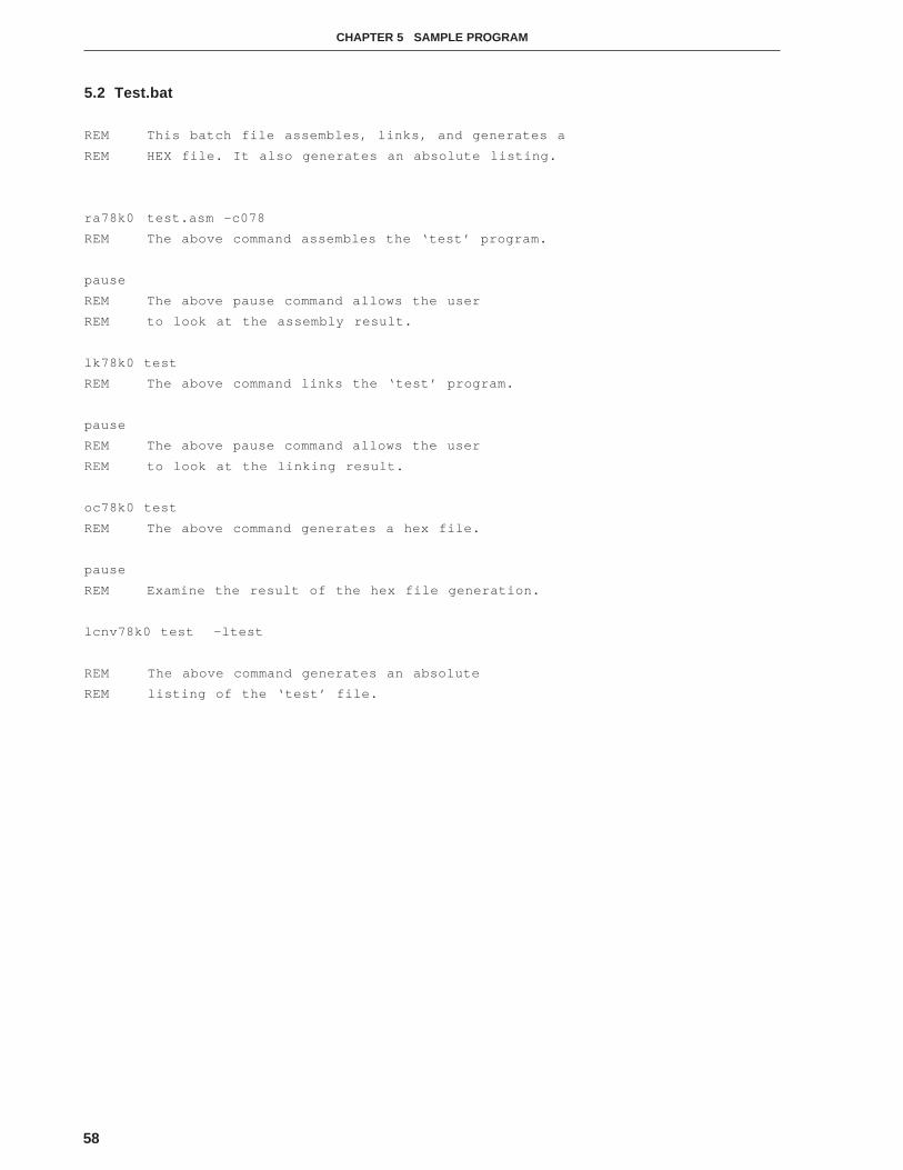
58
CHAPTER 5 SAMPLE PROGRAM
5.2 Test.bat
REM This batch file assembles, links, and generates a
REM HEX file. It also generates an absolute listing.
ra78k0 test.asm -c078
REM The above command assembles the ‘test’ program.
pause
REM The above pause command allows the user
REM to look at the assembly result.
lk78k0 test
REM The above command links the ‘test’ program.
pause
REM The above pause command allows the user
REM to look at the linking result.
oc78k0 test
REM The above command generates a hex file.
pause
REM Examine the result of the hex file generation.
lcnv78k0 test -ltest
REM The above command generates an absolute
REM listing of the ‘test’ file.
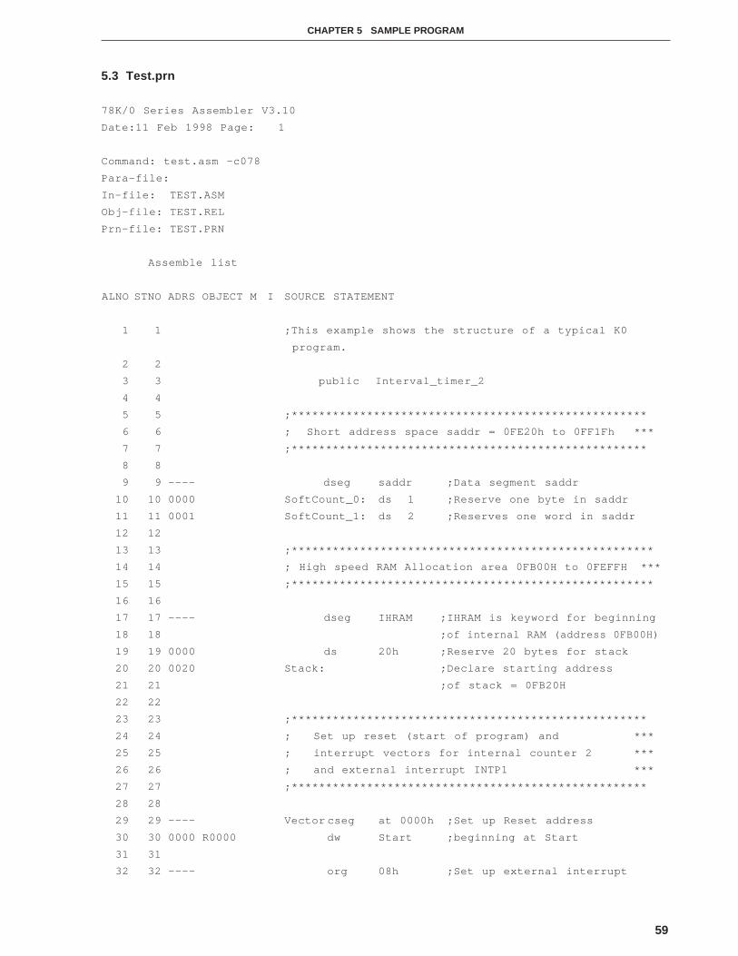
59
CHAPTER 5 SAMPLE PROGRAM
5.3 Test.prn
78K/0 Series Assembler V3.10
Date:11 Feb 1998 Page: 1
Command: test.asm -c078
Para-file:
In-file: TEST.ASM
Obj-file: TEST.REL
Prn-file: TEST.PRN
Assemble list
ALNO STNO ADRS OBJECT M I SOURCE STATEMENT
1 1 ;This example shows the structure of a typical K0
program.
2 2
3 3 public Interval_timer_2
4 4
5 5 ;****************************************************
6 6 ; Short address space saddr = 0FE20h to 0FF1Fh ***
7 7 ;****************************************************
8 8
9 9 ---- dseg saddr ;Data segment saddr
10 10 0000 SoftCount_0: ds 1 ;Reserve one byte in saddr
11 11 0001 SoftCount_1: ds 2 ;Reserves one word in saddr
12 12
13 13 ;*****************************************************
14 14 ; High speed RAM Allocation area 0FB00H to 0FEFFH ***
15 15 ;*****************************************************
16 16
17 17 ---- dseg IHRAM ;IHRAM is keyword for beginning
18 18 ; of internal RAM (address 0FB00H)
19 19 0000 ds 20h ;Reserve 20 bytes for stack
20 20 0020 Stack: ;Declare starting address
21 21 ;of stack = 0FB20H
22 22
23 23 ;****************************************************
24 24 ; Set up reset (start of program) and ***
25 25 ; interrupt vectors for internal counter 2 ***
26 26 ; and external interrupt INTP1 ***
27 27 ;****************************************************
28 28
29 29 ---- Vector cseg at 0000h ;Set up Reset address
30 30 0000 R0000 dw Start ;beginning at Start
31 31
32 32 ---- org 08h ;Set up external interrupt
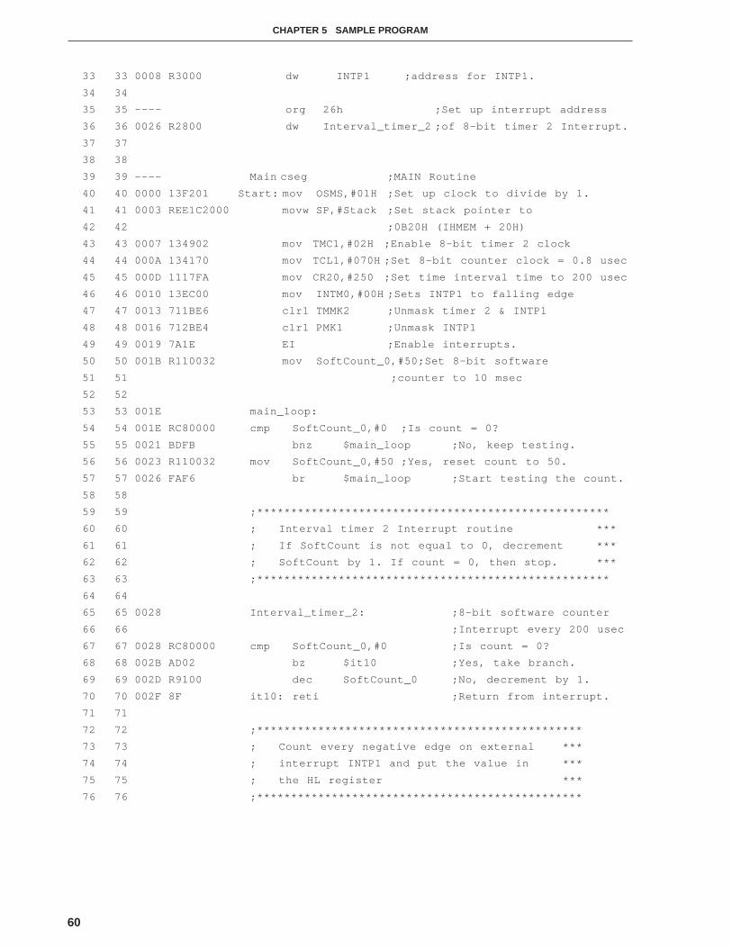
60
CHAPTER 5 SAMPLE PROGRAM
33 33 0008 R3000 dw INTP1 ;address for INTP1.
34 34
35 35 ---- org 26h ;Set up interrupt address
36 36 0026 R2800 dw Interval_timer_2 ;of 8-bit timer 2 Interrupt.
37 37
38 38
39 39 ---- Main cseg ;MAIN Routine
40 40 0000 13F201 Start: mov OSMS,#01H ;Set up clock to divide by 1.
41 41 0003 REE1C2000 movw SP,#Stack ;Set stack pointer to
42 42 ;0B20H (IHMEM + 20H)
43 43 0007 134902 mov TMC1,#02H ;Enable 8-bit timer 2 clock
44 44 000A 134170 mov TCL1,#070H ;Set 8-bit counter clock = 0.8 usec
45 45 000D 1117FA mov CR20,#250 ;Set time interval time to 200 usec
46 46 0010 13EC00 mov INTM0,#00H ;Sets INTP1 to falling edge
47 47 0013 711BE6 clr1 TMMK2 ;Unmask timer 2 & INTP1
48 48 0016 712BE4 clr1 PMK1 ;Unmask INTP1
49 49 0019 7A1E EI ;Enable interrupts.
50 50 001B R110032 mov SoftCount_0,#50;Set 8-bit software
51 51 ;counter to 10 msec
52 52
53 53 001E main_loop:
54 54 001E RC80000 cmp SoftCount_0,#0 ;Is count = 0?
55 55 0021 BDFB bnz $main_loop ;No, keep testing.
56 56 0023 R110032 mov SoftCount_0,#50 ;Yes, reset count to 50.
57 57 0026 FAF6 br $main_loop ;Start testing the count.
58 58
59 59 ;****************************************************
60 60 ; Interval timer 2 Interrupt routine ***
61 61 ; If SoftCount is not equal to 0, decrement ***
62 62 ; SoftCount by 1. If count = 0, then stop. ***
63 63 ;****************************************************
64 64
65 65 0028 Interval_timer_2: ;8-bit software counter
66 66 ;Interrupt every 200 usec
67 67 0028 RC80000 cmp SoftCount_0,#0 ;Is count = 0?
68 68 002B AD02 bz $it10 ;Yes, take branch.
69 69 002D R9100 dec SoftCount_0 ;No, decrement by 1.
70 70 002F 8F it10: reti ;Return from interrupt.
71 71
72 72 ;************************************************
73 73 ; Count every negative edge on external ***
74 74 ; interrupt INTP1 and put the value in ***
75 75 ; the HL register ***
76 76 ;************************************************
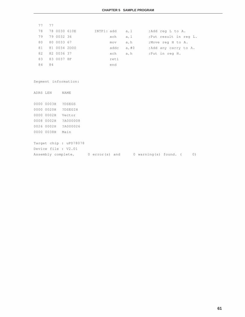
61
CHAPTER 5 SAMPLE PROGRAM
77 77
78 78 0030 610E INTP1: add a,l ;Add reg L to A.
79 79 0032 36 xch a,l ;Put result in reg L.
80 80 0033 67 mov a,h ;Move reg H to A.
81 81 0034 2D00 addc a,#0 ;Add any carry to A.
82 82 0036 37 xch a,h ;Put in reg H.
83 83 0037 8F reti
84 84 end
Segment information:
ADRS LEN NAME
0000 0003H ?DSEGS
0000 0020H ?DSEGIH
0000 0002H Vector
0008 0002H ?A000008
0026 0002H ?A000026
0000 0038H Main
Target chip : uPD78078
Device file : V2.01
Assembly complete, 0 error(s) and 0 warning(s) found. ( 0)
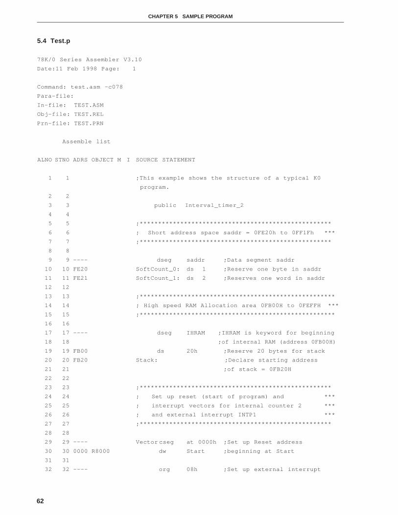
62
CHAPTER 5 SAMPLE PROGRAM
5.4 Test.p
78K/0 Series Assembler V3.10
Date:11 Feb 1998 Page: 1
Command: test.asm -c078
Para-file:
In-file: TEST.ASM
Obj-file: TEST.REL
Prn-file: TEST.PRN
Assemble list
ALNO STNO ADRS OBJECT M I SOURCE STATEMENT
1 1 ;This example shows the structure of a typical K0
program.
2 2
3 3 public Interval_timer_2
4 4
5 5 ;****************************************************
6 6 ; Short address space saddr = 0FE20h to 0FF1Fh ***
7 7 ;****************************************************
8 8
9 9 ---- dseg saddr ;Data segment saddr
10 10 FE20 SoftCount_0: ds 1 ;Reserve one byte in saddr
11 11 FE21 SoftCount_1: ds 2 ;Reserves one word in saddr
12 12
13 13 ;*****************************************************
14 14 ; High speed RAM Allocation area 0FB00H to 0FEFFH ***
15 15 ;*****************************************************
16 16
17 17 ---- dseg IHRAM ;IHRAM is keyword for beginning
18 18 ; of internal RAM (address 0FB00H)
19 19 FB00 ds 20h ;Reserve 20 bytes for stack
20 20 FB20 Stack: ;Declare starting address
21 21 ;of stack = 0FB20H
22 22
23 23 ;****************************************************
24 24 ; Set up reset (start of program) and ***
25 25 ; interrupt vectors for internal counter 2 ***
26 26 ; and external interrupt INTP1 ***
27 27 ;****************************************************
28 28
29 29 ---- Vector cseg at 0000h ;Set up Reset address
30 30 0000 R8000 dw Start ;beginning at Start
31 31
32 32 ---- org 08h ;Set up external interrupt
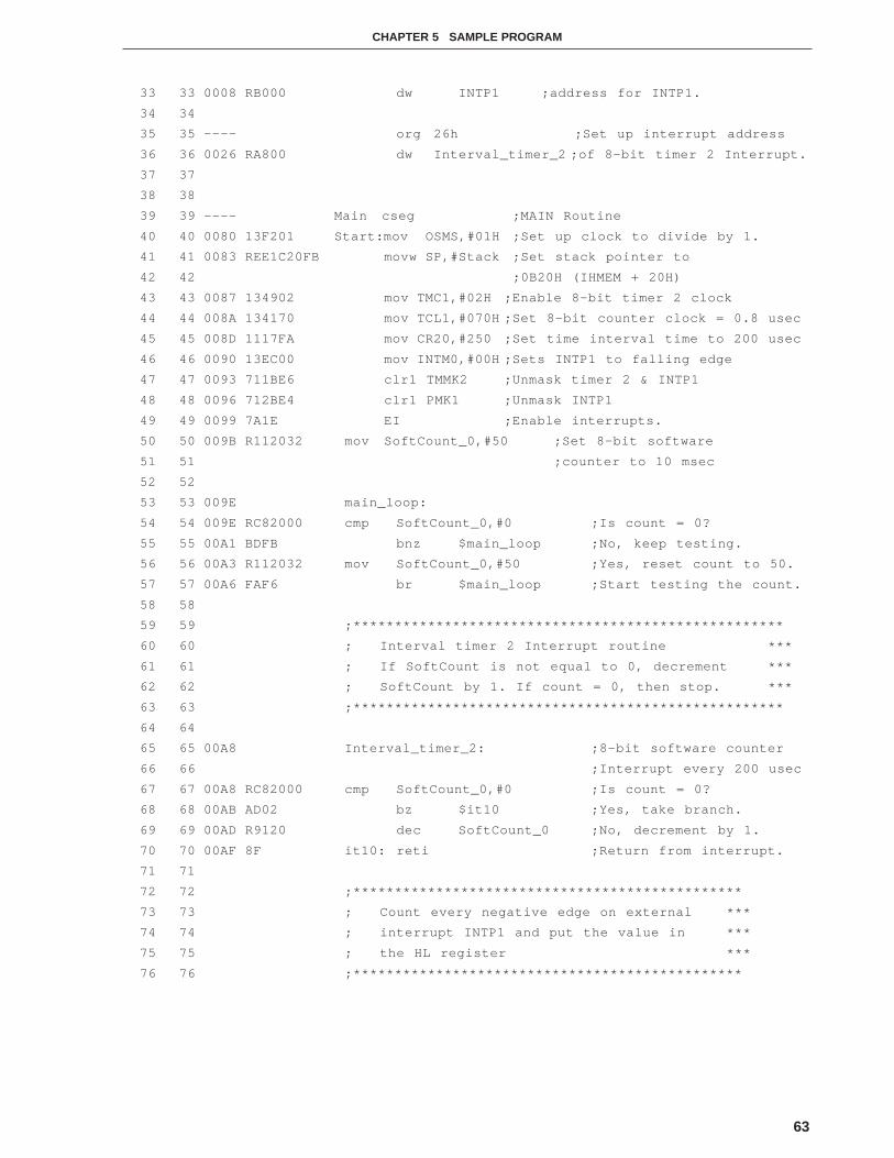
63
CHAPTER 5 SAMPLE PROGRAM
33 33 0008 RB000 dw INTP1 ;address for INTP1.
34 34
35 35 ---- org 26h ;Set up interrupt address
36 36 0026 RA800 dw Interval_timer_2 ;of 8-bit timer 2 Interrupt.
37 37
38 38
39 39 ---- Main cseg ;MAIN Routine
40 40 0080 13F201 Start:mov OSMS,#01H ;Set up clock to divide by 1.
41 41 0083 REE1C20FB movw SP,#Stack ;Set stack pointer to
42 42 ;0B20H (IHMEM + 20H)
43 43 0087 134902 mov TMC1,#02H ;Enable 8-bit timer 2 clock
44 44 008A 134170 mov TCL1,#070H ;Set 8-bit counter clock = 0.8 usec
45 45 008D 1117FA mov CR20,#250 ;Set time interval time to 200 usec
46 46 0090 13EC00 mov INTM0,#00H ;Sets INTP1 to falling edge
47 47 0093 711BE6 clr1 TMMK2 ;Unmask timer 2 & INTP1
48 48 0096 712BE4 clr1 PMK1 ;Unmask INTP1
49 49 0099 7A1E EI ;Enable interrupts.
50 50 009B R112032 mov SoftCount_0,#50 ;Set 8-bit software
51 51 ;counter to 10 msec
52 52
53 53 009E main_loop:
54 54 009E RC82000 cmp SoftCount_0,#0 ;Is count = 0?
55 55 00A1 BDFB bnz $main_loop ;No, keep testing.
56 56 00A3 R112032 mov SoftCount_0,#50 ;Yes, reset count to 50.
57 57 00A6 FAF6 br $main_loop ;Start testing the count.
58 58
59 59 ;****************************************************
60 60 ; Interval timer 2 Interrupt routine ***
61 61 ; If SoftCount is not equal to 0, decrement ***
62 62 ; SoftCount by 1. If count = 0, then stop. ***
63 63 ;****************************************************
64 64
65 65 00A8 Interval_timer_2: ;8-bit software counter
66 66 ;Interrupt every 200 usec
67 67 00A8 RC82000 cmp SoftCount_0,#0 ;Is count = 0?
68 68 00AB AD02 bz $it10 ;Yes, take branch.
69 69 00AD R9120 dec SoftCount_0 ;No, decrement by 1.
70 70 00AF 8F it10: reti ;Return from interrupt.
71 71
72 72 ;***********************************************
73 73 ; Count every negative edge on external ***
74 74 ; interrupt INTP1 and put the value in ***
75 75 ; the HL register ***
76 76 ;***********************************************
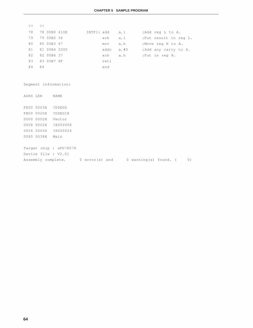
64
CHAPTER 5 SAMPLE PROGRAM
77 77
78 78 00B0 610E INTP1: add a,l ;Add reg L to A.
79 79 00B2 36 xch a,l ;Put result in reg L.
80 80 00B3 67 mov a,h ;Move reg H to A.
81 81 00B4 2D00 addc a,#0 ;Add any carry to A.
82 82 00B6 37 xch a,h ;Put in reg H.
83 83 00B7 8F reti
84 84 end
Segment information:
ADRS LEN NAME
FE00 0003H ?DSEGS
FB00 0020H ?DSEGIH
0000 0002H Vector
0008 0002H ?A000008
0026 0002H ?A000026
0080 0038H Main
Target chip : uPD78078
Device file : V2.01
Assembly complete, 0 error(s) and 0 warning(s) found. ( 0)

65
CHAPTER 6 DEVICE MEMORY MAP AND SPECIAL FUNCTION REGISTERS
This chapter describes the memory maps and special function registers (SFRs) of each K0 Series device. They
are categorized by subseries and shown in each section, as follows:
6.1 µPD78014, 78014H, and 78018F Subseries
6.2 µPD780208 Subseries
6.3 µPD780024 and 780034 Subseries
6.4 µPD78044F and 78044H Subseries
6.5 µPD78054, 78058F, and 780058 Subseries
6.6 µPD78064, 78064B, and 780308 Subseries
6.7 µPD78078, 78075B, and 78070A Subseries
6.8 µPD78083 Subseries
66
CHAPTER 6 DEVICE MEMORY MAP AND SPECIAL FUNCTION REGISTERS
6.1 µµµµµPD78014, 78014H, and 78018F Subseries
6.1.1 Documentation Reference Information
Device Series Number User’s Manual Number Date Published
µPD78014/14Y U10085EJ7V0UM00 October 1997
µPD78014H U12220EJ1V0UM00 May 1997
µPD78018F/18FY U10659EJ4V0UM00 June 1997
Caution: The user should check the current User’s Manual with the information in this section to be sure
of having the most up-to-date information.
6.1.2 Device Series Differences
Device Series Number ROM and RAM Differences Number of
ROM Size RAM Size Serial Channels
µPD78014, 78014Y 8 K/16 K/24 K/32 K 512/1 K 2
µPD78014H 8 K/16 K/24 K/32 K/60 K
µPD78018F, 78018FY 8 K/16 K/24 K/32 K/40 K/48 K/60 K
General Programmer’s Note
The NEC C-compiler and the NEC Assembler are capable of recognizing certain symbolic SFR bit names. These
special bit names are identified in the user manual in one of the four ways shown below:
If a bit number has one of the four symbols around it, the NEC software will recognize the associated symbolic
bit name. For example to set bit 7, the user can write the code in two ways:
1. SET1 MCC
2. SET1 PCC.7
Alternatively since bit 2 does not have any of the four symbols around it, the user can only set this bit as follows:
1. SET1 PCC.2
Note: The attempt to employ a symbolic name of bit-2 (PCC2) will return an error. Thus the use of instruction
SET1 PCC2
is improper since neither the NEC C-compiler nor the NEC Assembler recognizes this symbolic name and
will generate an error.
MCCPCC FRC CLS CSS 0 PCC2 PCC1 PCC0
<7> <6> <5> <4> 3 2 1 0
Example:
1.
2.
3.
4.
<7>
( 7 )
7
7

67
CHAPTER 6 DEVICE MEMORY MAP AND SPECIAL FUNCTION REGISTERS
6.1.3 Memory Address Space
Each model in the µPD78014/14Y, 78014H, and 78018F/18FY Subseries can access a memory space of 64K.
Figures 6-1 through 6-7 show memory maps of the respective models.
Figure 6-1. Memory Map ( µPD78011B/11BY, 11F/11FY, 11H)
0000H
Data memory space
General-purposeregister
32 × 8 bits
Internal ROM8192 × 8 bits
1FFFH
1000H0FFFH
0800H07FFH
0080H007FH
0040H003FH
0000H
CALLF entry area
CALLT table area
Vector table area
Program area
Program areaReserved
External memory55936 × 8 bits
Internal buffer RAM32 × 8 bits
Programmemoryspace
2000H1FFFH
FAC0HFABFH
FAE0HFADFH
FD00HFCFFH
FEE0HFEDFH
FF00HFEFFH
FFFFH
Internal high-speed RAM512 × 8 bits
Special function register (SFR)
256 × 8 bits
Reserved
FA80HFA7FH
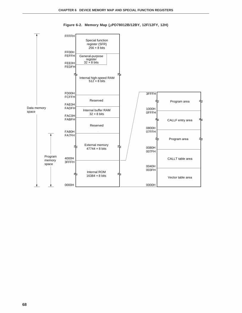
68
CHAPTER 6 DEVICE MEMORY MAP AND SPECIAL FUNCTION REGISTERS
Figure 6-2. Memory Map ( µPD78012B/12BY, 12F/12FY, 12H)
0000H
Data memory space
General-purposeregister
32 × 8 bits
Internal ROM16384 × 8 bits
3FFFH
1000H0FFFH
0800H07FFH
0080H007FH
0040H003FH
0000H
CALLF entry area
CALLT table area
Vector table area
Program area
Program areaReserved
External memory47744 × 8 bits
Internal buffer RAM32 × 8 bits
Programmemoryspace
4000H3FFFH
FAC0HFABFH
FAE0HFADFH
FD00HFCFFH
FEE0HFEDFH
FF00HFEFFH
FFFFH
Internal high-speed RAM512 × 8 bits
Special function register (SFR)
256 × 8 bits
Reserved
FA80HFA7FH
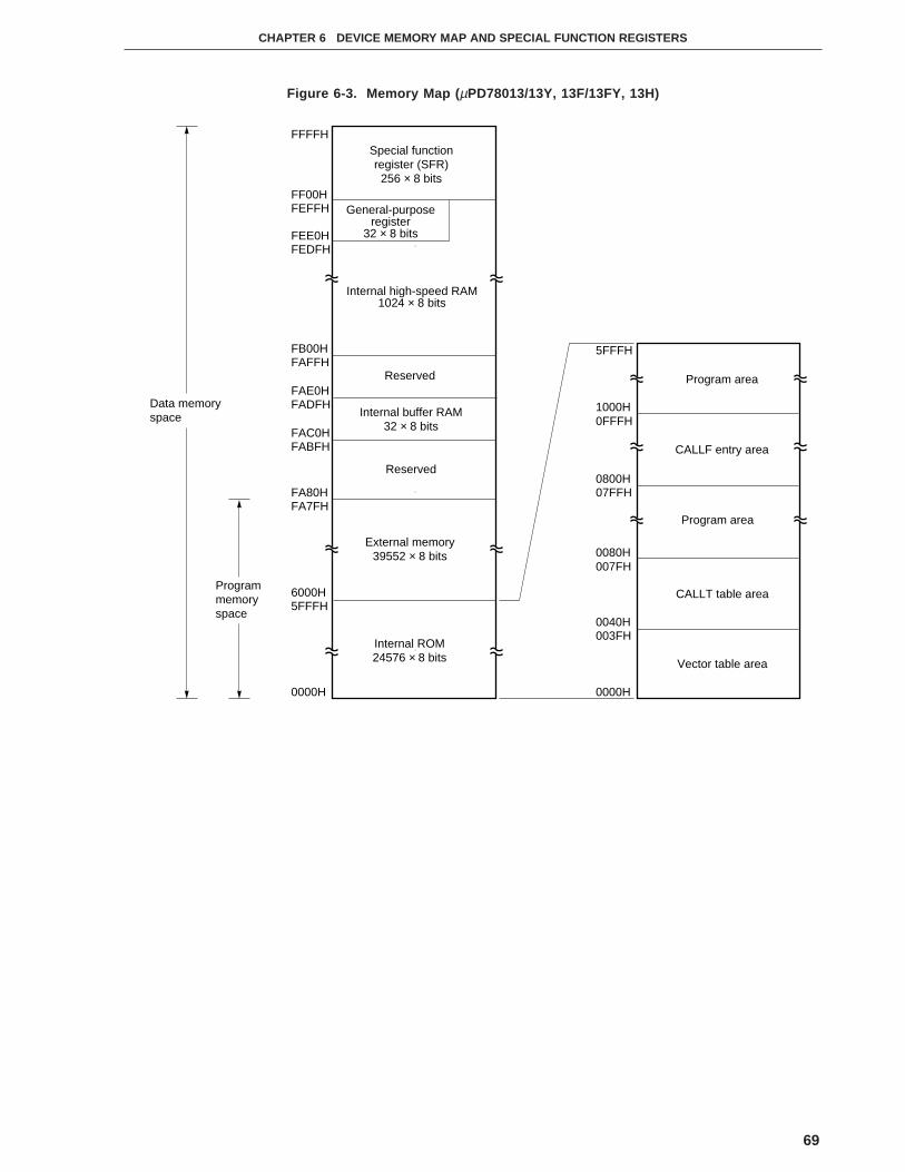
69
CHAPTER 6 DEVICE MEMORY MAP AND SPECIAL FUNCTION REGISTERS
Figure 6-3. Memory Map ( µPD78013/13Y, 13F/13FY, 13H)
0000H
Data memory space
General-purposeregister
32 × 8 bits
Internal ROM24576 × 8 bits
5FFFH
1000H0FFFH
0800H07FFH
0080H007FH
0040H003FH
0000H
CALLF entry area
CALLT table area
Vector table area
Program area
Program areaReserved
External memory39552 × 8 bits
Internal buffer RAM32 × 8 bits
Programmemoryspace
6000H5FFFH
FAC0HFABFH
FAE0HFADFH
FB00HFAFFH
FEE0HFEDFH
FF00HFEFFH
FFFFH
Internal high-speed RAM1024 × 8 bits
Special function register (SFR)
256 × 8 bits
Reserved
FA80HFA7FH
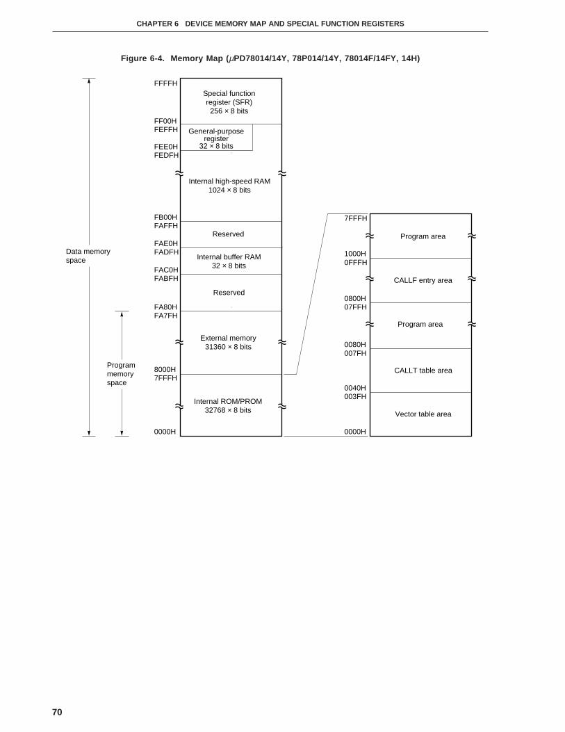
70
CHAPTER 6 DEVICE MEMORY MAP AND SPECIAL FUNCTION REGISTERS
Figure 6-4. Memory Map ( µPD78014/14Y, 78P014/14Y, 78014F/14FY, 14H)
0000H
Data memory space
General-purposeregister
32 × 8 bits
Internal ROM/PROM32768 × 8 bits
7FFFH
1000H0FFFH
0800H07FFH
0080H007FH
0040H003FH
0000H
CALLF entry area
CALLT table area
Vector table area
Program area
Program areaReserved
External memory31360 × 8 bits
Internal buffer RAM32 × 8 bits
Programmemoryspace
8000H7FFFH
FAC0HFABFH
FAE0HFADFH
FB00HFAFFH
FEE0HFEDFH
FF00HFEFFH
FFFFH
Internal high-speed RAM1024 × 8 bits
Special function register (SFR)
256 × 8 bits
Reserved
FA80HFA7FH
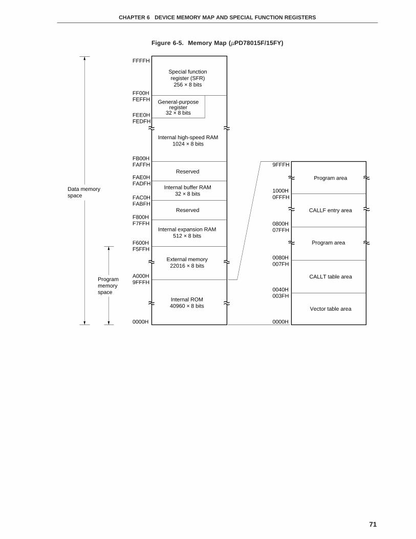
71
CHAPTER 6 DEVICE MEMORY MAP AND SPECIAL FUNCTION REGISTERS
Figure 6-5. Memory Map ( µPD78015F/15FY)
0000H
Data memory space
General-purposeregister
32 × 8 bits
Internal ROM40960 × 8 bits
9FFFH
1000H0FFFH
0800H07FFH
0080H007FH
0040H003FH
0000H
CALLF entry area
CALLT table area
Vector table area
Program area
Program area
External memory22016 × 8 bits
Internal buffer RAM32 × 8 bits
Programmemoryspace
A000H9FFFH
F800HF7FFH
FAE0HFADFH
FB00HFAFFH
FEE0HFEDFH
FF00HFEFFH
FFFFH
Internal high-speed RAM1024 × 8 bits
Special function register (SFR)
256 × 8 bits
Reserved
F600HF5FFH
Internal expansion RAM512 × 8 bits
FAC0HFABFH
Reserved
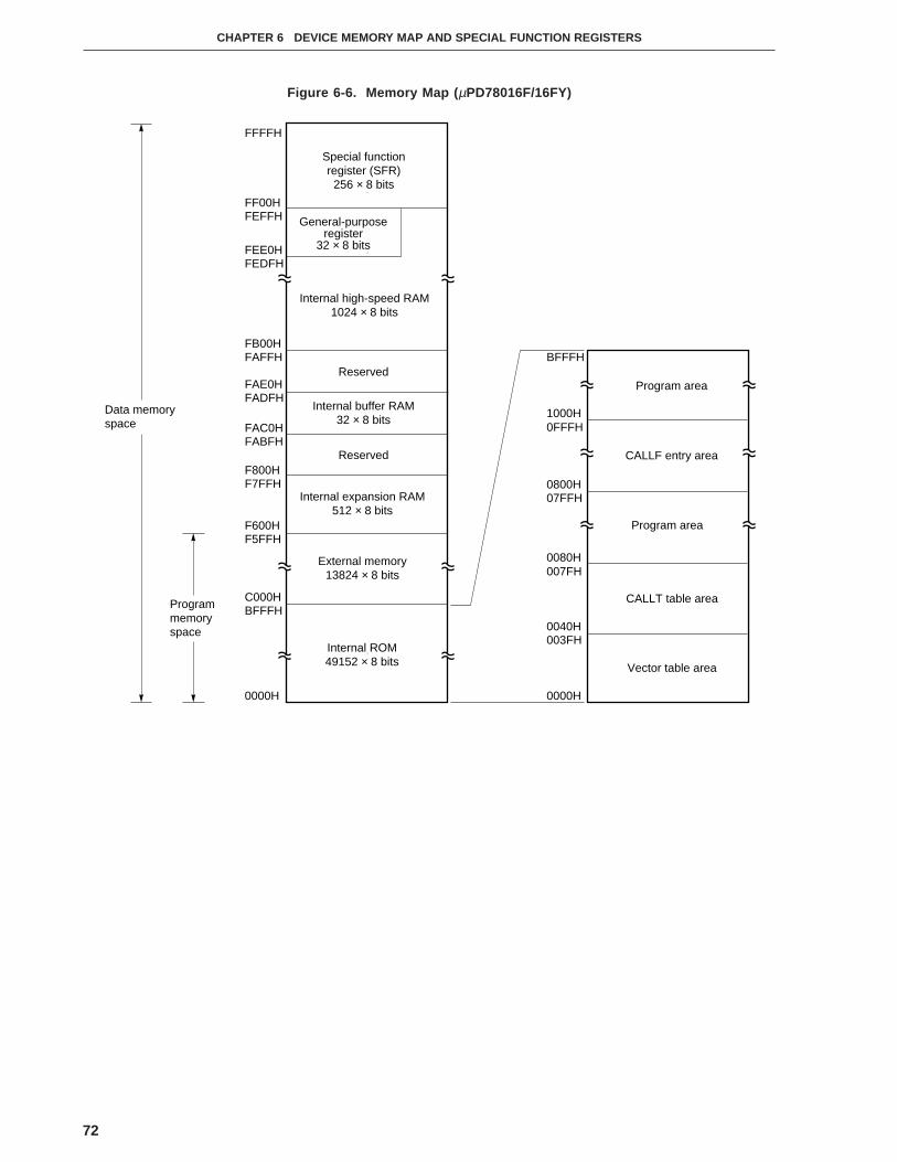
72
CHAPTER 6 DEVICE MEMORY MAP AND SPECIAL FUNCTION REGISTERS
Figure 6-6. Memory Map ( µPD78016F/16FY)
0000H
Data memory space
General-purposeregister
32 × 8 bits
Internal ROM49152 × 8 bits
BFFFH
1000H0FFFH
0800H07FFH
0080H007FH
0040H003FH
0000H
CALLF entry area
CALLT table area
Vector table area
Program area
Program area
External memory13824 × 8 bits
Internal buffer RAM32 × 8 bits
Programmemoryspace
C000HBFFFH
F800HF7FFH
FAE0HFADFH
FB00HFAFFH
FEE0HFEDFH
FF00HFEFFH
FFFFH
Internal high-speed RAM1024 × 8 bits
Special function register (SFR)
256 × 8 bits
Reserved
F600HF5FFH
Internal expansion RAM512 × 8 bits
FAC0HFABFH
Reserved
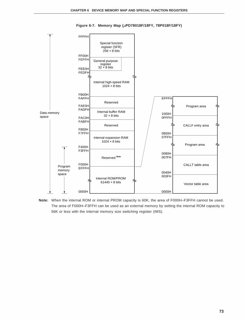
73
CHAPTER 6 DEVICE MEMORY MAP AND SPECIAL FUNCTION REGISTERS
Figure 6-7. Memory Map ( µPD78018F/18FY, 78P018F/18FY)
Note: When the internal ROM or internal PROM capacity is 60K, the area of F000H–F3FFH cannot be used.
The area of F000H–F3FFH can be used as an external memory by setting the internal ROM capacity to
56K or less with the internal memory size switching register (IMS).
0000H
Data memory space
General-purposeregister
32 × 8 bits
Internal ROM/PROM61440 × 8 bits
EFFFH
1000H0FFFH
0800H07FFH
0080H007FH
0040H003FH
0000H
CALLF entry area
CALLT table area
Vector table area
Program area
Program area
Internal buffer RAM32 × 8 bits
Programmemoryspace
F000HEFFFH
F800HF7FFH
FAE0HFADFH
FB00HFAFFH
FEE0HFEDFH
FF00HFEFFH
FFFFH
Internal high-speed RAM1024 × 8 bits
Special function register (SFR)
256 × 8 bits
Reserved
F400HF3FFH
Internal expansion RAM1024 × 8 bits
FAC0HFABFH
Reserved
Reserved Note
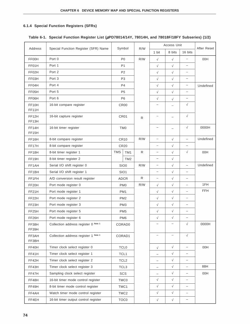
74
CHAPTER 6 DEVICE MEMORY MAP AND SPECIAL FUNCTION REGISTERS
√
√
√
√
√
√
√
–
–
–
–
–
–
–
–
–
–
√
√
√
√
√
√
–
–
√
–
–
–
–
√
√
√
√
–
–
–
–
–
–
–
√
√
√
–
–
√
–
–
–
–
–
–
–
–
–
√
√
–
–
–
–
–
–
–
–
–
FF00H
FF01H
FF02H
FF03H
FF04H
FF05H
FF06H
FF10H
FF11H
FF12H
FF13H
FF14H
FF15H
FF16H
FF17H
FF18H
FF19H
FF1AH
FF1BH
FF1FH
FF20H
FF21H
FF22H
FF23H
FF25H
FF26H
FF38H
FF39H
FF3AH
FF3BH
FF40H
FF41H
FF42H
FF43H
FF47H
FF48H
FF49H
FF4AH
FF4EH
Access UnitAfter Reset
Port 0
Port 1
Port 2
Port 3
Port 4
Port 5
Port 6
16-bit compare register
16-bit capture register
16-bit timer register
8-bit compare register
8-bit compare register
8-bit timer register 1
8-bit timer register 2
Serial I/O shift register 0
Serial I/O shift register 1
A/D conversion result register
Port mode register 0
Port mode register 1
Port mode register 2
Port mode register 3
Port mode register 5
Port mode register 6
Collection address register 0 Note 1
Collection address register 1 Note 1
Timer clock select register 0
Timer clock select register 1
Timer clock select register 2
Timer clock select register 3
Sampling clock select register
16-bit timer mode control register
8-bit timer mode control register
Watch timer mode control register
16-bit timer output control register
Address Special Function Register (SFR) Name Symbol R/W8 bits1 bit
P0
P1
P2
P3
P4
P5
P6
CR00
CR01
TM0
CR10
CR20
TM1
TM2
SIO0
SIO1
ADCR
PM0
PM1
PM2
PM3
PM5
PM6
CORAD0
CORAD1
TCL0
TCL1
TCL2
TCL3
SCS
TMC0
TMC1
TMC2
TOC0
R/W √
√
√
√
√
√
√
–
–
–
√
√
√
√
√
√
√
√
√
√
√
√
√
–
–
√
√
√
√
√
√
√
√
√
00H
Undefined
R
16 bits
0000H
R/W Undefined
RTMS 00H
R/W Undefined
1FH
FFH
R/W
R
88H
00H
00H
6.1.4 Special Function Registers (SFRs)
Table 6-1. Special Function Register List ( µµµµµPD78014/14Y, 78014H, and 78018F/18FY Subseries) (1/2)
0000H
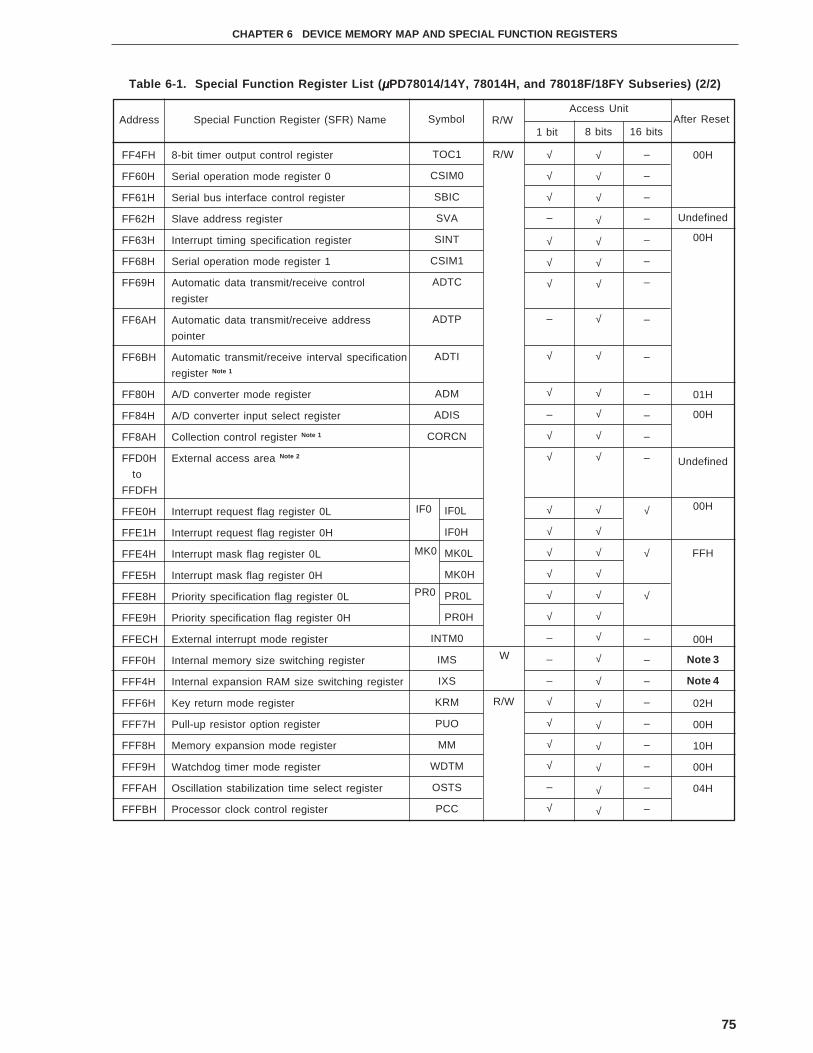
75
CHAPTER 6 DEVICE MEMORY MAP AND SPECIAL FUNCTION REGISTERS
00H
02H
00H
10H
00H
04H
Table 6-1. Special Function Register List ( µµµµµPD78014/14Y, 78014H, and 78018F/18FY Subseries) (2/2)
FF4FH
FF60H
FF61H
FF62H
FF63H
FF68H
FF69H
FF6AH
FF6BH
FF80H
FF84H
FF8AH
FFD0H
to
FFDFH
FFE0H
FFE1H
FFE4H
FFE5H
FFE8H
FFE9H
FFECH
FFF0H
FFF4H
FFF6H
FFF7H
FFF8H
FFF9H
FFFAH
FFFBH
TOC1
CSIM0
SBIC
SVA
SINT
CSIM1
ADTC
ADTP
ADTI
ADM
ADIS
CORCN
IF0L
IF0H
MK0L
MK0H
PR0L
PR0H
INTM0
IMS
IXS
KRM
PUO
MM
WDTM
OSTS
PCC
√
√
√
–
√
√
√
–
√
√
–
√
√
√
√
√
√
√
√
–
–
–
√
√
√
√
–
√
After ResetAddress Special Function Register (SFR) NameAccess Unit
8 bits1 bit
√
√
√
√
√
√
√
√
√
√
√
√
√
√
√
√
√
√
√
√
√
√
√
√
√
√
√
√
Symbol R/W16 bits
Undefined
00H
00H
W
00HIF0
MK0 FFH
PR0
R/W
Note 3
Note 4
01H
Undefined
8-bit timer output control register
Serial operation mode register 0
Serial bus interface control register
Slave address register
Interrupt timing specification register
Serial operation mode register 1
Automatic data transmit/receive control
register
Automatic data transmit/receive address
pointer
Automatic transmit/receive interval specification
register Note 1
A/D converter mode register
A/D converter input select register
Collection control register Note 1
External access area Note 2
Interrupt request flag register 0L
Interrupt request flag register 0H
Interrupt mask flag register 0L
Interrupt mask flag register 0H
Priority specification flag register 0L
Priority specification flag register 0H
External interrupt mode register
Internal memory size switching register
Internal expansion RAM size switching register
Key return mode register
Pull-up resistor option register
Memory expansion mode register
Watchdog timer mode register
Oscillation stabilization time select register
Processor clock control register
R/W 00H–
–
–
–
–
–
–
–
–
–
–
–
–
√
√
√
–
–
–
–
–
–
–
–
–
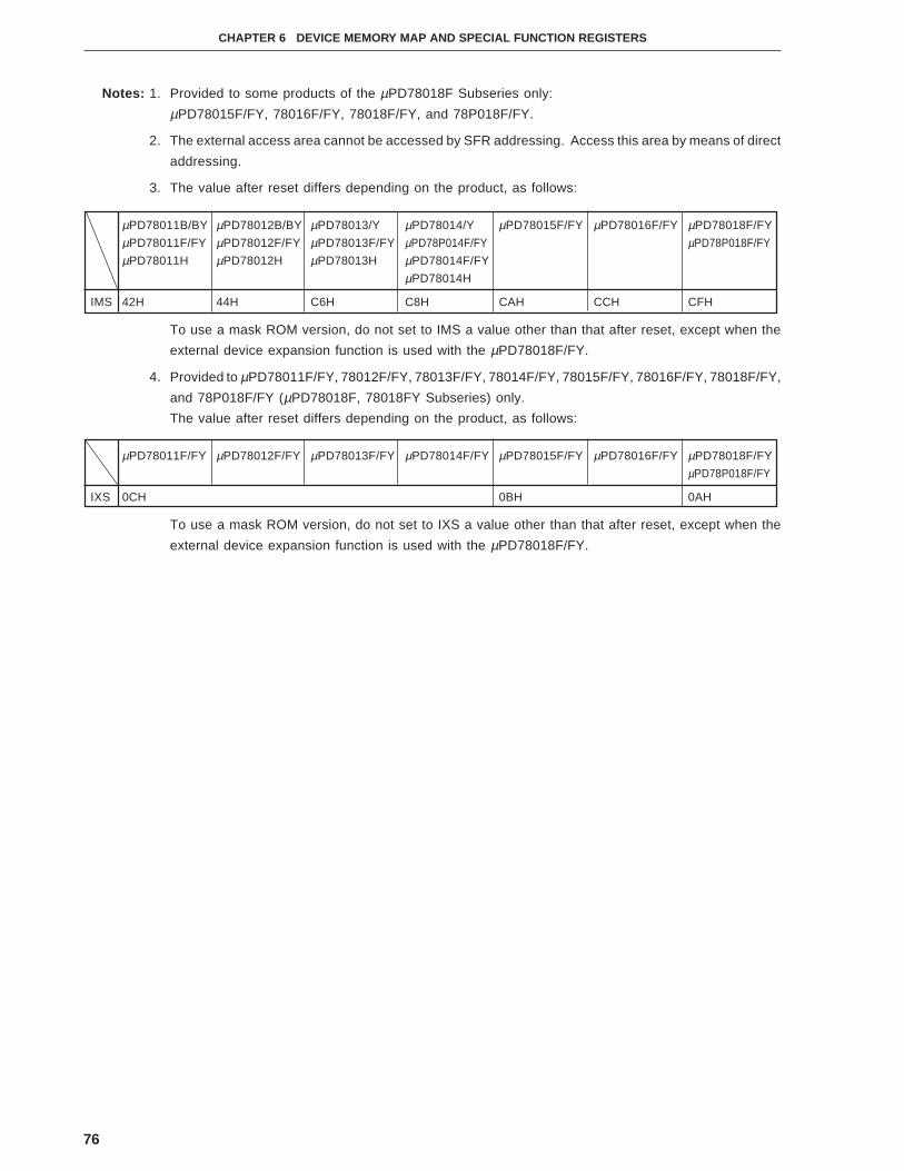
76
CHAPTER 6 DEVICE MEMORY MAP AND SPECIAL FUNCTION REGISTERS
Notes: 1. Provided to some products of the µPD78018F Subseries only:
µPD78015F/FY, 78016F/FY, 78018F/FY, and 78P018F/FY.
2. The external access area cannot be accessed by SFR addressing. Access this area by means of direct
addressing.
3. The value after reset differs depending on the product, as follows:
µPD78011B/BY µPD78012B/BY µPD78013/Y µPD78014/Y µPD78015F/FY µPD78016F/FY µPD78018F/FY
µPD78011F/FY µPD78012F/FY µPD78013F/FY µPD78P014F/FY µPD78P018F/FY
µPD78011H µPD78012H µPD78013H µPD78014F/FY
µPD78014H
IMS 42H 44H C6H C8H CAH CCH CFH
To use a mask ROM version, do not set to IMS a value other than that after reset, except when the
external device expansion function is used with the µPD78018F/FY.
4. Provided to µPD78011F/FY, 78012F/FY, 78013F/FY, 78014F/FY, 78015F/FY, 78016F/FY, 78018F/FY,
and 78P018F/FY (µPD78018F, 78018FY Subseries) only.
The value after reset differs depending on the product, as follows:
µPD78011F/FY µPD78012F/FY µPD78013F/FY µPD78014F/FY µPD78015F/FY µPD78016F/FY µPD78018F/FY
µPD78P018F/FY
IXS 0CH 0BH 0AH
To use a mask ROM version, do not set to IXS a value other than that after reset, except when the
external device expansion function is used with the µPD78018F/FY.

77
CHAPTER 6 DEVICE MEMORY MAP AND SPECIAL FUNCTION REGISTERS
(1) Registers controlling port functions
The following four types of registers control the ports:
• Port mode registers (PM0, PM1, PM2, PM3, PM5, PM6)
• Pull-up resistor option register (PUO)
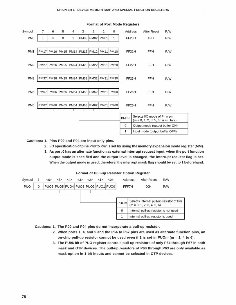
78
CHAPTER 6 DEVICE MEMORY MAP AND SPECIAL FUNCTION REGISTERS
Format of Port Mode Registers
Cautions: 1. Pins P00 and P04 are input-only pins.
2. I/O specification of pins P40 to P47 is set by using the memory expansion mode register (MM).
3. As port 0 has an alternate function as external interrupt request input, when the port function
output mode is specified and the output level is changed, the interrupt request flag is set.
When the output mode is used, therefore, the interrupt mask flag should be set to 1 beforehand.
Format of Pull-up Resistor Option Register
Cautions: 1. The P00 and P04 pins do not incorporate a pull-up resistor.
2. When ports 1, 4, and 5 and the P64 to P67 pins are used as alternate function pins, an
on-chip pull-up resistor cannot be used even if 1 is set in PUOm (m = 1, 4 to 6).
3. The PU06 bit of PUO register controls pull-up resistors of only P64 through P67 in both
mask and OTP devices. The pull-up resistors of P60 through P63 are only available as
mask option in 1-bit inputs and cannot be selected in OTP devices.
PM0
PM1
PM2
0 0 0 1 PM03 PM02 PM01 1
7 6 5 4 3 2 1 0Symbol
PM3
PM6
PM5
PMmn Selects I/O mode of Pmn pin(m = 0, 1, 2, 3, 5, 6 : n = 0 to 7)
0
1
Output mode (output buffer ON)
Input mode (output buffer OFF)
FF20H
FF21H
FF22H
FF23H
FF25H
FF26H
1FH
FFH
FFH
FFH
FFH
FFH
R/W
R/W
R/W
R/W
R/W
R/W
Address After Reset R/W
PM17 PM16 PM15 PM14 PM13 PM12 PM11 PM10
PM27 PM26 PM25 PM24 PM23 PM22 PM21 PM20
PM37 PM36 PM35 PM34 PM33 PM32 PM31 PM30
PM57 PM56 PM55 PM54 PM53 PM52 PM51 PM50
PM67 PM66 PM65 PM64 PM63 PM62 PM61 PM60
0 PUO6 PUO5 PUO4 PUO2 PUO1 PUO0PUO
PUOm Selects internal pull-up resistor of Pm(m = 0, 1, 2, 3, 4, 5, 6)
0
1
Internal pull-up resistor is not used
Internal pull-up resistor is used
FFF7H 00H R/W
<5> <4>Symbol Address After Reset R/W
PUO3
7 <6> <3> <2> <0><1>
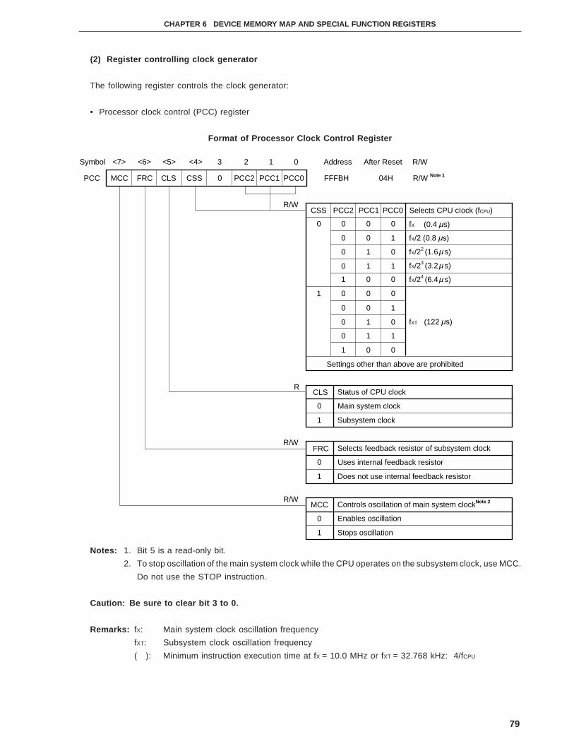
79
CHAPTER 6 DEVICE MEMORY MAP AND SPECIAL FUNCTION REGISTERS
(2) Register controlling clock generator
The following register controls the clock generator:
• Processor clock control (PCC) register
Format of Processor Clock Control Register
Notes: 1. Bit 5 is a read-only bit.
2. To stop oscillation of the main system clock while the CPU operates on the subsystem clock, use MCC.
Do not use the STOP instruction.
Caution: Be sure to clear bit 3 to 0.
Remarks: fX: Main system clock oscillation frequency
fXT: Subsystem clock oscillation frequency
( ): Minimum instruction execution time at fX = 10.0 MHz or fXT = 32.768 kHz: 4/fCPU
MCC FRC CLS CSS PCC2 PCC1 PCC0PCC
CLS
0
1
Main system clock
Subsystem clock
FFFBH 04H R/W Note 1
<6> <5> <4>Symbol Address After Reset R/W
0
<7> 3 2 01
CSS
0
0 fX/2 (0.8 s)
PCC2 Selects CPU cIock (fCPU)PCC1 PCC0
Status of CPU clock
0
0
0
1
0
0
1
1
0
1
1
0
0
0
0
0
0
0
0
1
1
0
0
1
1
0
1
0
µ
fX/22 (1.6 s)µ
fX/23 (3.2 s)µ
fX/24 (6.4 s)µ
fXT (122 s)µ
fX (0.4 s)µ
Settings other than above are prohibited
FRC
0
1
Uses internal feedback resistor
Does not use internal feedback resistor
Selects feedback resistor of subsystem clock
MCC
0
1
Enables oscillation
Stops oscillation
Controls oscillation of main system clockNote 2
R/W
R/W
R/W
R
0
1

80
CHAPTER 6 DEVICE MEMORY MAP AND SPECIAL FUNCTION REGISTERS
(3) Registers controlling 16-bit timer/event counter
The following six registers control the 16-bit timer/event counter:
• Timer clock select register 0 (TCL0)
• 16-bit timer mode control register (TMC0)
• 16-bit timer output control register (TOC0)
• Port mode register 3 (PM3)
- Refer to section (1) for the register format.
• External interrupt mode register (INTM0)
- Refer to section (13) for the register format.
• Sampling clock select register (SCS)
- Refer to section (13) for the register format.
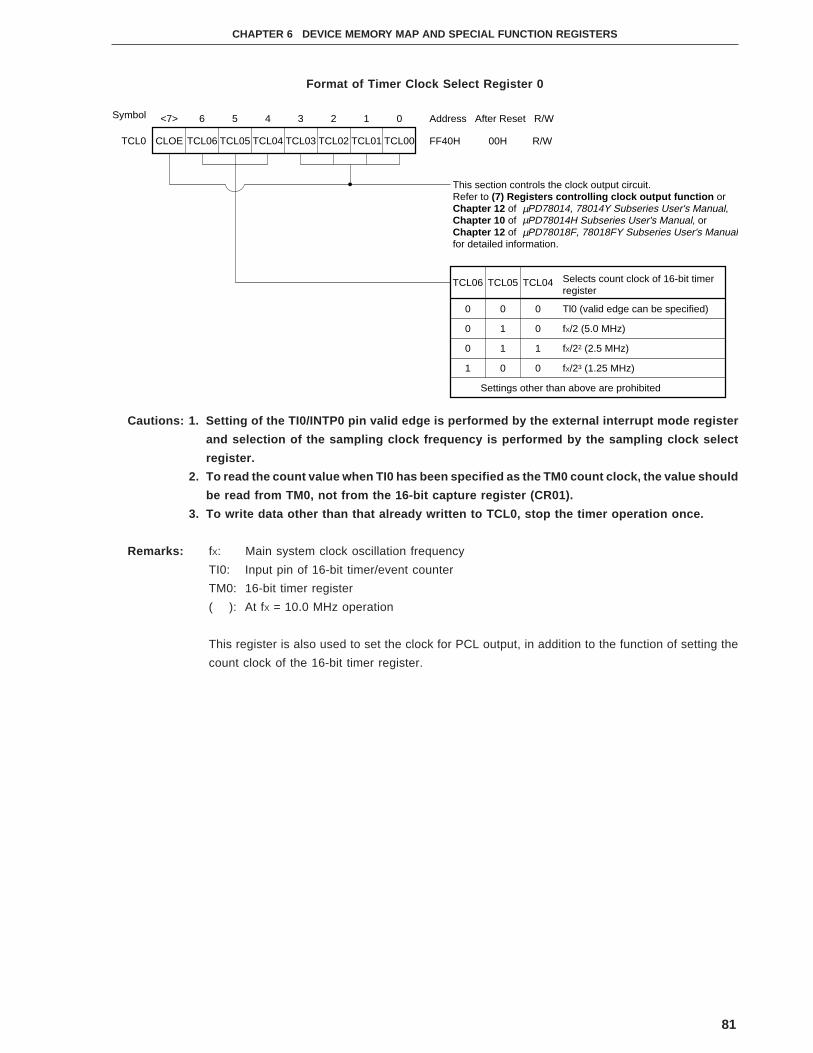
81
CHAPTER 6 DEVICE MEMORY MAP AND SPECIAL FUNCTION REGISTERS
Format of Timer Clock Select Register 0
Cautions: 1. Setting of the TI0/INTP0 pin valid edge is performed by the external interrupt mode register
and selection of the sampling clock frequency is performed by the sampling clock select
register.
2. To read the count value when TI0 has been specified as the TM0 count clock, the value should
be read from TM0, not from the 16-bit capture register (CR01).
3. To write data other than that already written to TCL0, stop the timer operation once.
Remarks: fX: Main system clock oscillation frequency
TI0: Input pin of 16-bit timer/event counter
TM0: 16-bit timer register
( ): At fX = 10.0 MHz operation
This register is also used to set the clock for PCL output, in addition to the function of setting the
count clock of the 16-bit timer register.
6 5 4 3 2 1 0<7>Symbol
TCL0 CLOE TCL06 TCL05 TCL04 TCL03 TCL02 TCL01 TCL00 FF40H 00H R/W
Address After Reset R/W
0
0
Selects count clock of 16-bit timerregister
Tl0 (valid edge can be specified)
fX/2 (5.0 MHz)
1 fX/23 (1.25 MHz)
0 fX/22 (2.5 MHz)
Settings other than above are prohibited
TCL06
0
1
0
1
TCL05
0
0
0
1
TCL04
This section controls the clock output circuit.Refer to (7) Registers controlling clock output function orChapter 12 of PD78014, 78014Y Subseries User's Manual,Chapter 10 of PD78014H Subseries User's Manual, orChapter 12 of PD78018F, 78018FY Subseries User's Manualfor detailed information.
µµµ
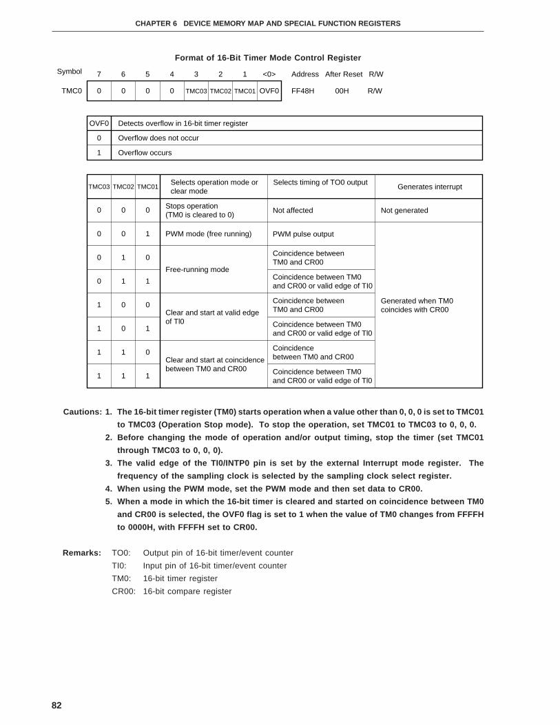
82
CHAPTER 6 DEVICE MEMORY MAP AND SPECIAL FUNCTION REGISTERS
Format of 16-Bit Timer Mode Control Register
Cautions: 1. The 16-bit timer register (TM0) starts operation when a value other than 0, 0, 0 is set to TMC01
to TMC03 (Operation Stop mode). To stop the operation, set TMC01 to TMC03 to 0, 0, 0.
2. Before changing the mode of operation and/or output timing, stop the timer (set TMC01
through TMC03 to 0, 0, 0).
3. The valid edge of the TI0/INTP0 pin is set by the external Interrupt mode register. The
frequency of the sampling clock is selected by the sampling clock select register.
4. When using the PWM mode, set the PWM mode and then set data to CR00.
5. When a mode in which the 16-bit timer is cleared and started on coincidence between TM0
and CR00 is selected, the OVF0 flag is set to 1 when the value of TM0 changes from FFFFH
to 0000H, with FFFFH set to CR00.
Remarks: TO0: Output pin of 16-bit timer/event counter
TI0: Input pin of 16-bit timer/event counter
TM0: 16-bit timer register
CR00: 16-bit compare register
6 5 4 3 2 1 <0>7Symbol
TMC0 0 0 0 0 TMC03 TMC02 TMC01 OVF0
OVF0
0
1
Detects overflow in 16-bit timer register
Overflow does not occur
Overflow occurs
FF48H 00H R/W
Address After Reset R/W
TMC03Selects operation mode orclear mode
TMC02 TMC01
0 Stops operation(TM0 is cleared to 0)
0 0
Selects timing of TO0 output
Not affected
Generated when TM0coincides with CR00
0 PWM mode (free running)0 1 PWM pulse output
0
Free-running mode
1 0 Coincidence betweenTM0 and CR00
0 1 1 Coincidence between TM0and CR00 or valid edge of TI0
1Clear and start at valid edgeof Tl0
0 0 Coincidence betweenTM0 and CR00
1 0 1 Coincidence between TM0and CR00 or valid edge of Tl0
1Clear and start at coincidencebetween TM0 and CR00
1 0 Coincidencebetween TM0 and CR00
1 1 1 Coincidence between TM0and CR00 or valid edge of Tl0
Not generated
Generates interrupt

83
CHAPTER 6 DEVICE MEMORY MAP AND SPECIAL FUNCTION REGISTERS
Format of 16-Bit Timer Output Control Register
Cautions: 1. Be sure to stop the timer operation before setting TOC0.
2. 0 is read from LVS0 and LVR0 after data has been set to these bits.
6 5 4 <3> <2> 1 <0>7Symbol
TOC0 0 0 0 0 LVS0 LVR0 TOC01 TOE0
TOE0
0
1
Controls output of 16-bit timer/event counter
Disables output (Port mode)
Enables output
FF4EH 00H R/W
Address After Reset R/W
0
0
Sets status of timer output F/F of 16-bittimer/event counter
Not affected
Resets timer output F/F to 0
1 Setting prohibited
1 Sets timer output F/F to 1
0
1
1
0
LVS0 LVR0
TOC01
0
PWM mode
Selects active level
High active
1 Low active
Other than PWM mode
Controls timer output F/F
Disables inversion
Enables inversion
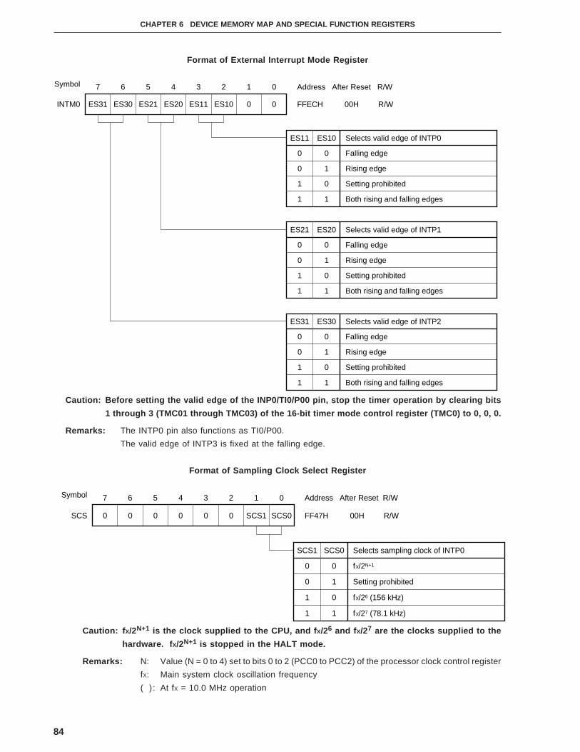
84
CHAPTER 6 DEVICE MEMORY MAP AND SPECIAL FUNCTION REGISTERS
Format of External Interrupt Mode Register
Caution: Before setting the valid edge of the INP0/TI0/P00 pin, stop the timer operation by clearing bits
1 through 3 (TMC01 through TMC03) of the 16-bit timer mode control register (TMC0) to 0, 0, 0.
Remarks: The INTP0 pin also functions as TI0/P00.
The valid edge of INTP3 is fixed at the falling edge.
Format of Sampling Clock Select Register
Caution: f X/2N+1 is the clock supplied to the CPU, and f X/26 and f X/27 are the clocks supplied to the
hardware. f X/2N+1 is stopped in the HALT mode.
Remarks: N: Value (N = 0 to 4) set to bits 0 to 2 (PCC0 to PCC2) of the processor clock control register
fX: Main system clock oscillation frequency
( ) : At fX = 10.0 MHz operation
6 5 4 3 2 1 07Symbol
INTM0 ES31 ES30 ES21 ES20 ES11 ES10 0 0
ES11
0
0
Selects valid edge of INTP0
Falling edge
Rising edge
1 Both rising and falling edges
1 Setting prohibited
FFECH 00H R/W
Address After Reset R/W
ES10
0
1
1
0
ES21
0
0
Selects valid edge of INTP1
Falling edge
Rising edge
1 Both rising and falling edges
1 Setting prohibited
ES20
0
1
1
0
ES31
0
0
Selects valid edge of INTP2
Falling edge
Rising edge
1 Both rising and falling edges
1 Setting prohibited
ES30
0
1
1
0
6 5 4 3 2 1 07Symbol
SCS 0 0 0 0 0 0 SCS1 SCS0
SCS1
0
0
Selects sampling clock of INTP0
fX/2N+1
Setting prohibited
1 fX/27 (78.1 kHz)
1 fX/26 (156 kHz)
FF47H 00H R/W
Address After Reset R/W
SCS0
0
1
1
0

85
CHAPTER 6 DEVICE MEMORY MAP AND SPECIAL FUNCTION REGISTERS
(4) Registers controlling 8-bit timer/event counter
The following four registers control the 8-bit timer/event counters:
• Timer clock select register 1 (TCL1)
• 8-bit timer mode control register (TMC1)
• 8-bit timer output control register (TOC1)
• Port mode register 3 (PM3)
- Refer to section (1) for register format.
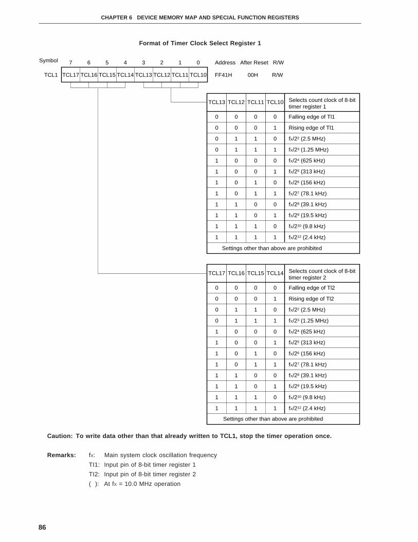
86
CHAPTER 6 DEVICE MEMORY MAP AND SPECIAL FUNCTION REGISTERS
Format of Timer Clock Select Register 1
Caution: To write data other than that already written to TCL1, stop the timer operation once.
Remarks: fX: Main system clock oscillation frequency
TI1: Input pin of 8-bit timer register 1
TI2: Input pin of 8-bit timer register 2
( ): At fX = 10.0 MHz operation
6 5 4 3 2 1 07Symbol
TCL1 TCL17 TCL16 TCL15 TCL14 TCL13 TCL12 TCL11 TCL10
0
0
Selects count clock of 8-bittimer register 1
Falling edge of Tl1
Rising edge of Tl1
0 fX/23 (1.25 MHz)
fX/24 (625 kHz)
fX/26 (156 kHz)
0 fX/22 (2.5 MHz)
1
fX/25 (313 kHz)1
1
fX/27 (78.1 kHz)1
Settings other than above are prohibited
FF41H 00H R/W
Address After Reset R/W
TCL13
0
0
1
1
0
0
0
0
TCL12
0
0
1
1
0
0
1
1
TCL11
0
1
1
0
0
1
0
1
TCL10
fX/28 (39.1 kHz)
fX/210 (9.8 kHz)
1
fX/29 (19.5 kHz)1
1
fX/212 (2.4 kHz)1
1
1
1
1
0
0
1
1
0
1
0
1
0
0
Selects count clock of 8-bittimer register 2
Falling edge of Tl2
Rising edge of Tl2
0 fX/23 (1.25 MHz)
fX/24 (625 kHz)
fX/26 (156 kHz)
0 fX/22 (2.5 MHz)
1
fX/25 (313 kHz)1
1
fX/27 (78.1 kHz)1
TCL17
0
0
1
1
0
0
0
0
TCL16
0
0
1
1
0
0
1
1
TCL15
0
1
1
0
0
1
0
1
TCL14
fX/28 (39.1 kHz)
fX/210 (9.8 kHz)
1
fX/29 (19.5 kHz)1
1
fX/212 (2.4 kHz)1
1
1
1
1
0
0
1
1
0
1
0
1
Settings other than above are prohibited

87
CHAPTER 6 DEVICE MEMORY MAP AND SPECIAL FUNCTION REGISTERS
Format of 8-Bit Timer Mode Control Register
Cautions: 1. Before changing the operation mode, stop the timer operations.
2. When TM1 and TM2 are used together as a 16-bit timer register (TMS), set enable or disable
of the operation by using the TCE1 bit of the 8-bit timer mode control register (TMC1).
6 5 4 3 2 <1> <0>7Symbol
TMC1 0 0 0 0 0 TMC12 TCE2 TCE1
TCE1
0
1
Controls operation of 8-bit timer register 1
Stops operation (TM1 is cleared to 0)
Enables operation
FF49H 00H R/W
Address After Reset R/W
TCE2
0
1
Controls operation of 8-bit timer register 2
Stops operation (TM2 is cleared to 0)
Enables operation
TMC12
0
1
Selects operation mode
8-bit timer register × 2 channel mode (TM1 , TM2)
16-bit timer register × 1 channel mode (TMS)
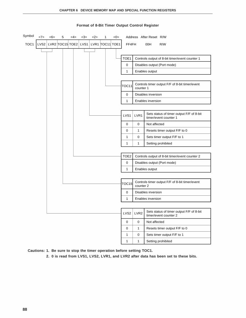
88
CHAPTER 6 DEVICE MEMORY MAP AND SPECIAL FUNCTION REGISTERS
Format of 8-Bit Timer Output Control Register
Cautions: 1. Be sure to stop the timer operation before setting TOC1.
2. 0 is read from LVS1, LVS2, LVR1, and LVR2 after data has been set to these bits.
<6> 5 <4> <3> <2> 1 <0><7>Symbol
TOC1 LVS2 LVR2 TOC15 TOE2 LVS1 LVR1 TOC11 TOE1
TOE1
0
1
Controls output of 8-bit timer/event counter 1
Disables output (Port mode)
Enables output
Controls timer output F/F of 8-bit timer/eventcounter 1
Disables inversion0
Enables inversion1
FF4FH 00H R/W
Address After Reset R/W
0
0
Sets status of timer output F/F of 8-bittimer/event counter 1
Not affected
Resets timer output F/F to 0
1 Setting prohibited
1 Sets timer output F/F to 1
0
1
1
0
LVS1 LVR1
TOC11
TOE2
0
1
Controls output of 8-bit timer/event counter 2
Disables output (Port mode)
Enables output
Controls timer output F/F of 8-bit timer/eventcounter 2
Disables inversion0
Enables inversion1
0
0
Sets status of timer output F/F of 8-bittimer/event counter 2
Not affected
Resets timer output F/F to 0
1 Setting prohibited
1 Sets timer output F/F to 1
0
1
1
0
LVS2 LVR2
TOC15
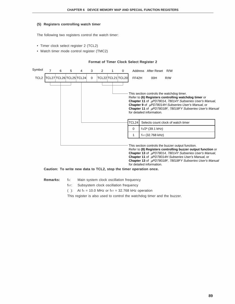
89
CHAPTER 6 DEVICE MEMORY MAP AND SPECIAL FUNCTION REGISTERS
(5) Registers controlling watch timer
The following two registers control the watch timer:
• Timer clock select register 2 (TCL2)
• Watch timer mode control register (TMC2)
Format of Timer Clock Select Register 2
Caution: To write new data to TCL2, stop the timer operation once.
Remarks: fX: Main system clock oscillation frequency
fXT: Subsystem clock oscillation frequency
( ): At fX = 10.0 MHz or fXT = 32.768 kHz operation
This register is also used to control the watchdog timer and the buzzer.
Selects count clock of watch timerTCL24
6 5 4 3 2 1 07Symbol
TCL2 TCL27 TCL26 TCL25 TCL24 0 TCL22 TCL21 TCL20 FF42H 00H R/W
Address After Reset R/W
0
1
fX/28 (39.1 kHz)
fXT (32.768 kHz)
This section controls the watchdog timer.Refer to (6) Registers controlling watchdog timer orChapter 11 of PD78014, 78014Y Subseries User's Manual,Chapter 9 of PD78014H Subseries User's Manual, orChapter 11 of PD78018F, 78018FY Subseries User's Manualfor detailed information.
µµ
µ
This section controls the buzzer output function.Refer to (8) Registers controlling buzzer output function orChapter 13 of PD78014, 78014Y Subseries User's Manual,Chapter 11 of PD78014H Subseries User's Manual, orChapter 13 of PD78018F, 78018FY Subseries User's Manualfor detailed information.
µµµ

90
CHAPTER 6 DEVICE MEMORY MAP AND SPECIAL FUNCTION REGISTERS
Format of Watch Timer Mode Control Register
Note: Do not clear the prescaler frequently when using the watch timer.
Remarks: fW: Watch timer clock frequency (fX/28 or fXT)
( ): At fW = 32.768 kHz operation
A 0.5 or 0.25 second interval can be generated either with an 8.38 MHz main system clock or
a 32.768 KHz subsystem clock.
6 5 4 3 2 1 07Symbol
TMC2 0 TMC26 TMC25 TMC24 TMC23 TMC22 TMC21 TMC20 FF4AH 00H R/W
Address After Reset R/W
TMC23
0
1
Selects set time of watch flag
214/fW (0.5 s)
213/fW (0.25 s)
1
0
0
0
1
1 25/fW (977 s)
TMC20
Controls prescaler operationNoteTMC21
0
1
Clears after operation stopped
Enables operation
Controls 5-bit counter operationTMC22
0
1
Clears after operation stopped
Enables operation
0
0
0 27/fW (3.91 ms)
28/fW (7.81 ms)
0 26/fW (1.95 ms)
1
29/fW (15.6 ms)
0
0
1
1
0
0
1
1
0
0
11 0
µ
24/fW (488 s)µ
TMC26 TMC25 TMC24 Selects interval time of prescaler
24/fW (488 s)µ
25/fW (977 s)µ
Settings other than above are prohibited
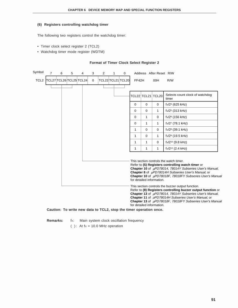
91
CHAPTER 6 DEVICE MEMORY MAP AND SPECIAL FUNCTION REGISTERS
(6) Registers controlling watchdog timer
The following two registers control the watchdog timer:
• Timer clock select register 2 (TCL2)
• Watchdog timer mode register (WDTM)
Format of Timer Clock Select Register 2
Caution: To write new data to TCL2, stop the timer operation once.
Remarks: fX: Main system clock oscillation frequency
( ) : At fX = 10.0 MHz operation
6 5 4 3 2 1 07Symbol
TCL2 TCL27 TCL26 TCL25 TCL24 0 TCL22 TCL21 TCL20
0
0
Selects count clock of watchdogtimer
fX/24 (625 kHz)
fX/25 (313 kHz)
0 fX/27 (78.1 kHz)
fX/28 (39.1 kHz)
fX/210 (9.8 kHz)
0 fX/26 (156 kHz)
1
fX/29 (19.5 kHz)1
1
fX/212 (2.4 kHz)1
FF42H 00H R/W
Address After Reset R/W
TCL22
0
0
1
1
0
0
1
1
TCL21
0
1
1
0
0
1
0
1
TCL20
This section controls the watch timer.Refer to (5) Registers controlling watch timer orChapter 10 of PD78014, 78014Y Subseries User's Manual,Chapter 8 of PD78014H Subseries User's Manual, orChapter 10 of PD78018F, 78018FY Subseries User's Manualfor detailed information.
µµ
µ
This section controls the buzzer output function.Refer to (8) Registers controlling buzzer output function orChapter 13 of PD78014, 78014Y Subseries User's Manual,Chapter 11 of PD78014H Subseries User's Manual, orChapter 13 of PD78018F, 78018FY Subseries User's Manualfor detailed information.
µµµ
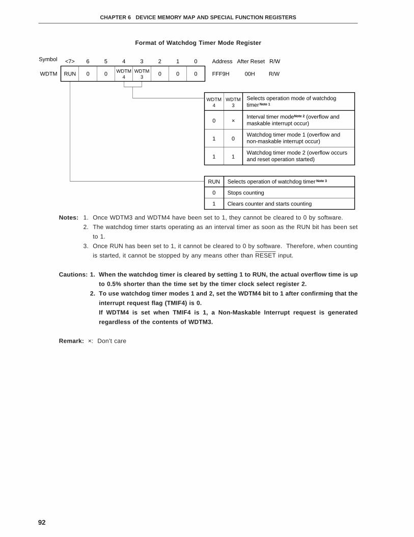
92
CHAPTER 6 DEVICE MEMORY MAP AND SPECIAL FUNCTION REGISTERS
Format of Watchdog Timer Mode Register
Notes: 1. Once WDTM3 and WDTM4 have been set to 1, they cannot be cleared to 0 by software.
2. The watchdog timer starts operating as an interval timer as soon as the RUN bit has been set
to 1.
3. Once RUN has been set to 1, it cannot be cleared to 0 by software. Therefore, when counting
is started, it cannot be stopped by any means other than RESET input.
Cautions: 1. When the watchdog timer is cleared by setting 1 to RUN, the actual overflow time is up
to 0.5% shorter than the time set by the timer clock select register 2.
2. To use watchdog timer modes 1 and 2, set the WDTM4 bit to 1 after confirming that the
interrupt request flag (TMIF4) is 0.
If WDTM4 is set when TMIF4 is 1, a Non-Maskable Interrupt request is generated
regardless of the contents of WDTM3.
Remark: ×: Don’t care
6 5 4 3 2 1 0<7>Symbol
WDTM RUN 0 0 WDTM4
WDTM3
0 0 0
WDTM4
0
Selects operation mode of watchdogtimerNote 1
Interval timer modeNote 2 (overflow andmaskable interrupt occur)
1Watchdog timer mode 2 (overflow occursand reset operation started)
Stops counting
1Watchdog timer mode 1 (overflow andnon-maskable interrupt occur)
Selects operation of watchdog timer Note 3RUN
0
Clears counter and starts counting1
FFF9H 00H R/W
Address After Reset R/W
×
1
0
WDTM3
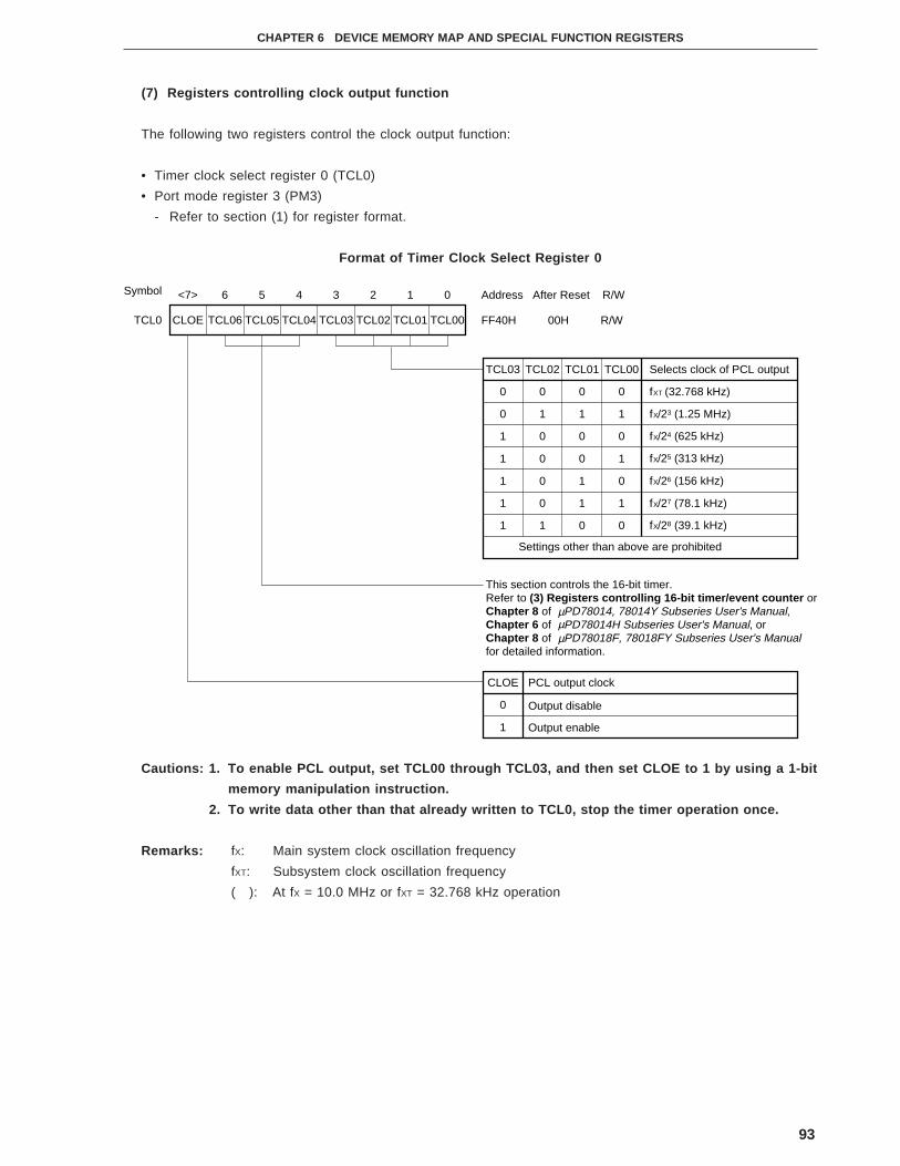
93
CHAPTER 6 DEVICE MEMORY MAP AND SPECIAL FUNCTION REGISTERS
(7) Registers controlling clock output function
The following two registers control the clock output function:
• Timer clock select register 0 (TCL0)
• Port mode register 3 (PM3)
- Refer to section (1) for register format.
Format of Timer Clock Select Register 0
Cautions: 1. To enable PCL output, set TCL00 through TCL03, and then set CLOE to 1 by using a 1-bit
memory manipulation instruction.
2. To write data other than that already written to TCL0, stop the timer operation once.
Remarks: fX: Main system clock oscillation frequency
fXT: Subsystem clock oscillation frequency
( ): At fX = 10.0 MHz or fXT = 32.768 kHz operation
6 5 4 3 2 1 0<7>Symbol
TCL0 CLOE TCL06 TCL05 TCL04 TCL03 TCL02 TCL01 TCL00 FF40H 00H R/W
Address After Reset R/W
0
0
1
1
1
0
1
0
0
0
0
1
0
0
1
11 0
TCL03 TCL02 TCL01 Selects clock of PCL output
fXT (32.768 kHz)
01 1
0
1
1
0
0
1
TCL00
0
fX/23 (1.25 MHz)
fX/24 (625 kHz)
fX/26 (156 kHz)
fX/25 (313 kHz)
fX/27 (78.1 kHz)
fX/28 (39.1 kHz)
0
1
CLOE PCL output clock
Output disable
Output enable
This section controls the 16-bit timer.Refer to (3) Registers controlling 16-bit timer/event counter orChapter 8 of PD78014, 78014Y Subseries User's Manual,Chapter 6 of PD78014H Subseries User's Manual, orChapter 8 of PD78018F, 78018FY Subseries User's Manualfor detailed information.
µµµ
Settings other than above are prohibited
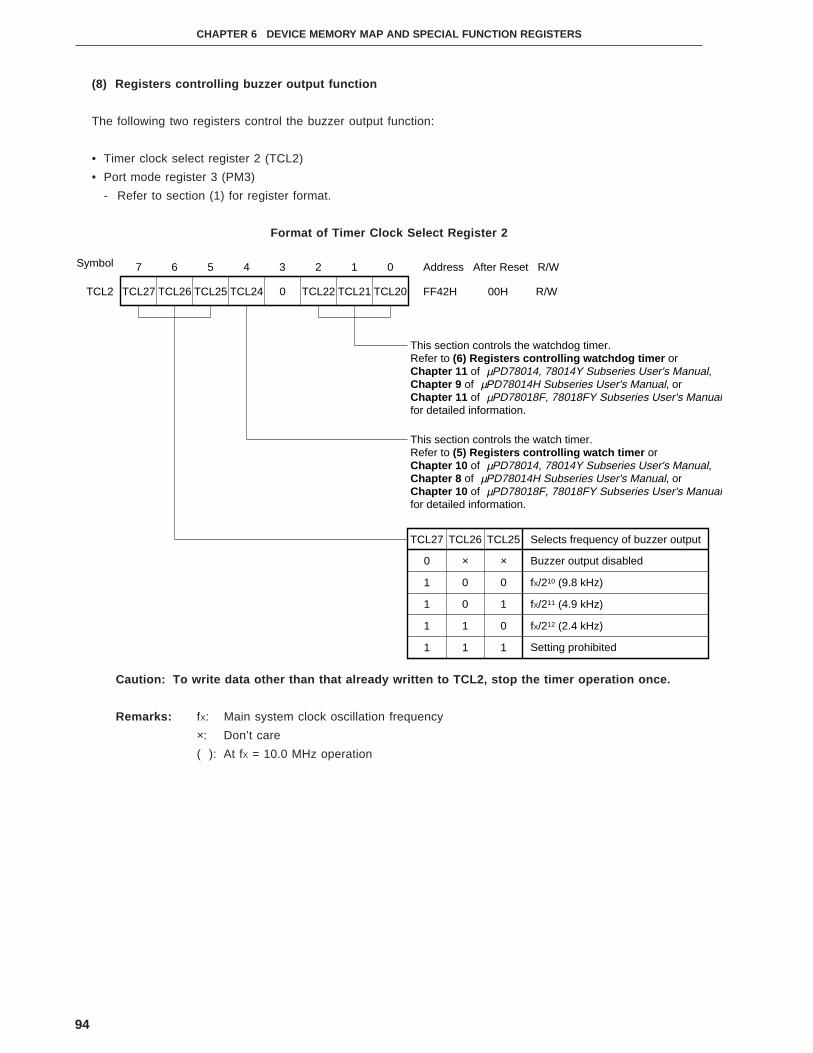
94
CHAPTER 6 DEVICE MEMORY MAP AND SPECIAL FUNCTION REGISTERS
(8) Registers controlling buzzer output function
The following two registers control the buzzer output function:
• Timer clock select register 2 (TCL2)
• Port mode register 3 (PM3)
- Refer to section (1) for register format.
Format of Timer Clock Select Register 2
Caution: To write data other than that already written to TCL2, stop the timer operation once.
Remarks: fX: Main system clock oscillation frequency
×: Don’t care
( ): At fX = 10.0 MHz operation
Selects frequency of buzzer outputTCL27 TCL26 TCL25
6 5 4 3 2 1 07Symbol
TCL2 TCL27 TCL26 TCL25 TCL24 0 TCL22 TCL21 TCL20 FF42H 00H R/W
Address After Reset R/W
0
1
Buzzer output disabled
fX/210 (9.8 kHz)
1 fX/212 (2.4 kHz)
Setting prohibited
1 fX/211 (4.9 kHz)
1
×
0
1
0
1
×
0
0
1
1
This section controls the watchdog timer.Refer to (6) Registers controlling watchdog timer orChapter 11 of PD78014, 78014Y Subseries User's Manual,Chapter 9 of PD78014H Subseries User's Manual, orChapter 11 of PD78018F, 78018FY Subseries User's Manualfor detailed information.
µµ
µ
This section controls the watch timer.Refer to (5) Registers controlling watch timer orChapter 10 of PD78014, 78014Y Subseries User's Manual,Chapter 8 of PD78014H Subseries User's Manual, orChapter 10 of PD78018F, 78018FY Subseries User's Manualfor detailed information.
µµ
µ
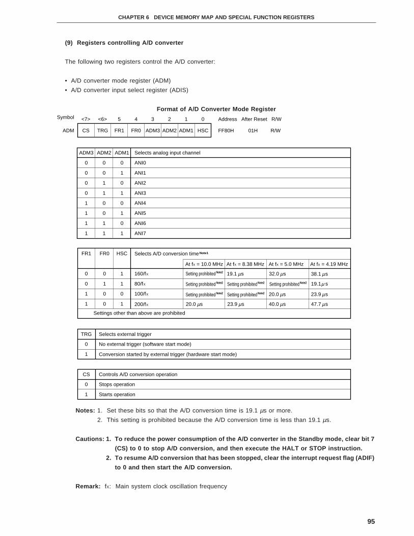
95
CHAPTER 6 DEVICE MEMORY MAP AND SPECIAL FUNCTION REGISTERS
(9) Registers controlling A/D converter
The following two registers control the A/D converter:
• A/D converter mode register (ADM)
• A/D converter input select register (ADIS)
Format of A/D Converter Mode Register
Notes: 1. Set these bits so that the A/D conversion time is 19.1 µs or more.
2. This setting is prohibited because the A/D conversion time is less than 19.1 µs.
Cautions: 1. To reduce the power consumption of the A/D converter in the Standby mode, clear bit 7
(CS) to 0 to stop A/D conversion, and then execute the HALT or STOP instruction.
2. To resume A/D conversion that has been stopped, clear the interrupt request flag (ADIF)
to 0 and then start the A/D conversion.
Remark: fX: Main system clock oscillation frequency
19.1 s
80/fX
<6> 5 4 3 2 1 0<7>Symbol
ADM CS TRG FR1 FR0 ADM3 ADM2 ADM1 HSC FF80H 01H R/W
Address After Reset R/W
0
0
ANI0
ANI1
0 ANI3
ANI4
ANI6
0 ANI2
1
ANI51
1
ANI71
0
0
1
1
0
0
1
1
0
1
1
0
0
1
0
1
ADM3 Selects analog input channelADM2 ADM1
FR1
0
0
Selects A/D conversion timeNote1
160/fX
1
1
HSC
1
1
1
0
µ
100/fX
Selects external triggerTRG
0 No external trigger (software start mode)
Controls A/D conversion operationCS
0
1
Stops operation
Starts operation
1 Conversion started by external trigger (hardware start mode)
FR0
0
1
0
0
200/fX
Setting prohibited Note2
Setting prohibited Note2
Setting prohibited Note2
Setting prohibited Note2
Setting prohibited Note2
Setting prohibited Note2
At fX = 10.0 MHz At fX = 8.38 MHz At fX = 5.0 MHz At fX = 4.19 MHz
32.0 sµ
20.0 sµ 23.9 sµ 40.0 sµ 47.7 sµ
20.0 sµ 23.9 sµ
19.1 sµ
38.1 sµ
Settings other than above are prohibited

96
CHAPTER 6 DEVICE MEMORY MAP AND SPECIAL FUNCTION REGISTERS
Format of A/D Converter Input Select Register
6 5 4 3 2 1 07Symbol
ADIS 0 0 0 0 ADIS3 ADIS2 ADIS1 ADIS0
0
0
Selects number of analog input channels
None (P10 to P17)
1 channel (ANI0, P11 to P17)
0 3 channels (ANI0 to ANI2, P13 to P17)
4 channels (ANI0 to ANI3, P14 to P17)
6 channels (ANI0 to ANI5, P16 to P17)
0 2 channels (ANI0, ANI1, P12 to P17)
0
5 channels (ANI0 to ANI4, P15 to P17)0
0
7 channels (ANI0 to ANI6, P17)0
FF84H 00H R/W
Address After Reset R/W
ADIS3
0
0
0
0
1
1
1
1
ADIS2
0
0
1
1
0
0
1
1
ADIS1
0
1
1
0
0
1
0
1
ADIS0
8 channels (ANI0 to ANI7)1 0 0 0
Settings other than above are prohibited
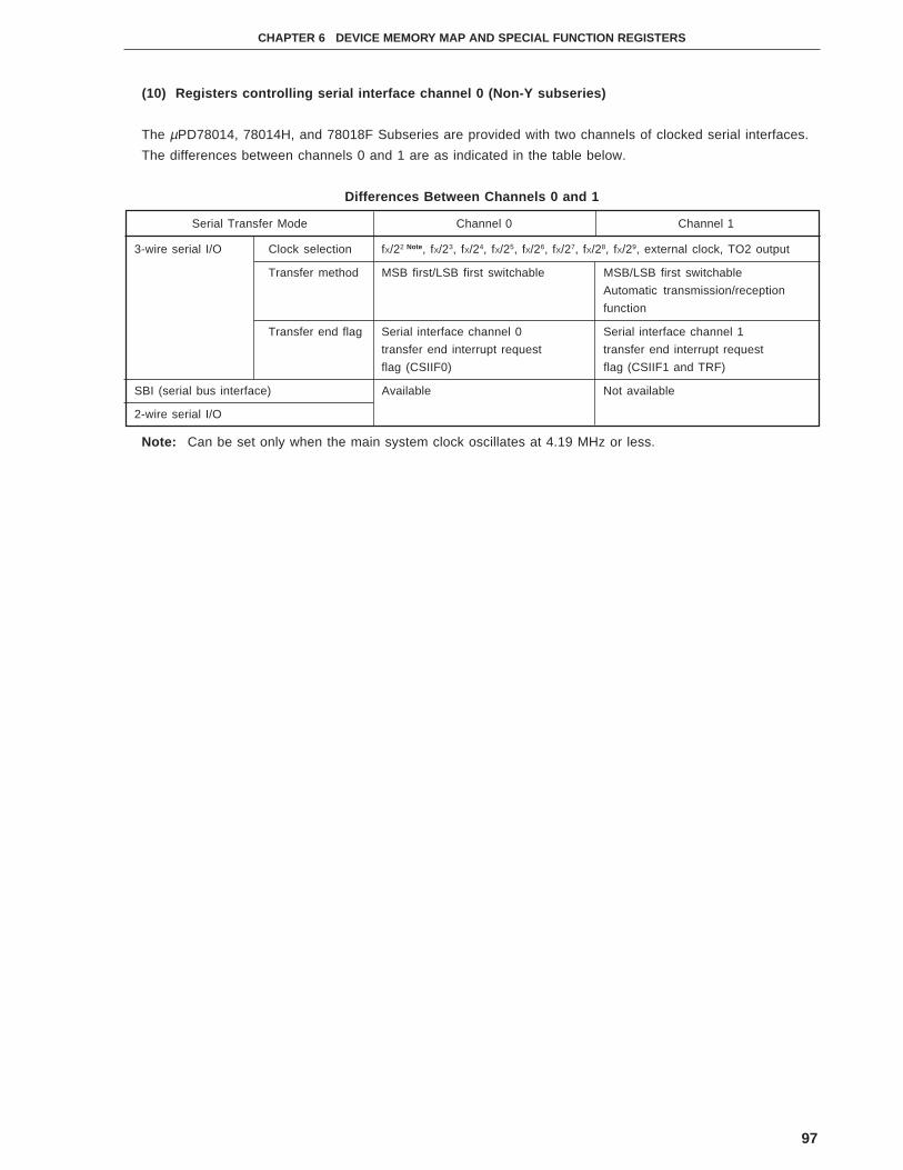
97
CHAPTER 6 DEVICE MEMORY MAP AND SPECIAL FUNCTION REGISTERS
(10) Registers controlling serial interface channel 0 (Non-Y subseries)
The µPD78014, 78014H, and 78018F Subseries are provided with two channels of clocked serial interfaces.
The differences between channels 0 and 1 are as indicated in the table below.
Differences Between Channels 0 and 1
Serial Transfer Mode Channel 0 Channel 1
3-wire serial I/O Clock selection fX/22 Note, fX/23, fX/24, fX/25, fX/26, fX/27, fX/28, fX/29, external clock, TO2 output
Transfer method MSB first/LSB first switchable MSB/LSB first switchable
Automatic transmission/reception
function
Transfer end flag Serial interface channel 0 Serial interface channel 1
transfer end interrupt request transfer end interrupt request
flag (CSIIF0) flag (CSIIF1 and TRF)
SBI (serial bus interface) Available Not available
2-wire serial I/O
Note: Can be set only when the main system clock oscillates at 4.19 MHz or less.
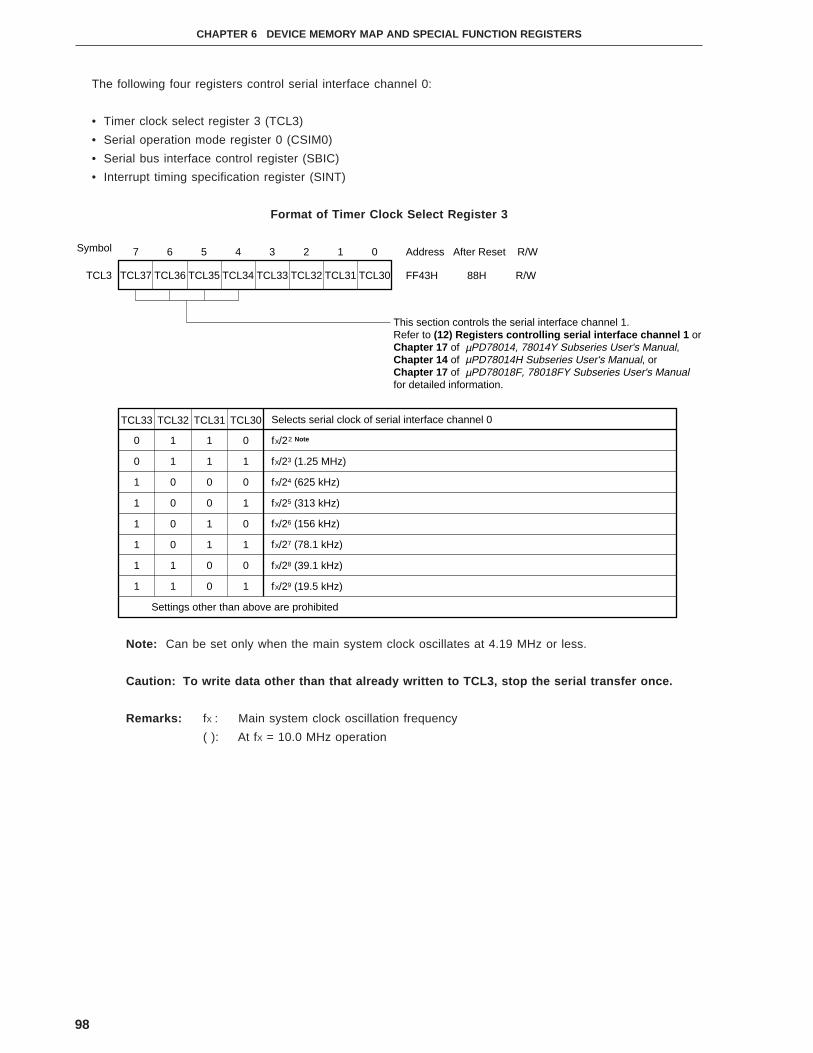
98
CHAPTER 6 DEVICE MEMORY MAP AND SPECIAL FUNCTION REGISTERS
The following four registers control serial interface channel 0:
• Timer clock select register 3 (TCL3)
• Serial operation mode register 0 (CSIM0)
• Serial bus interface control register (SBIC)
• Interrupt timing specification register (SINT)
Format of Timer Clock Select Register 3
Note: Can be set only when the main system clock oscillates at 4.19 MHz or less.
Caution: To write data other than that already written to TCL3, stop the serial transfer once.
Remarks: fX : Main system clock oscillation frequency
( ): At fX = 10.0 MHz operation
6 5 4 3 2 1 07Symbol
TCL3 TCL37 TCL36 TCL35 TCL34 TCL33 TCL32 TCL31 TCL30
0
0
Selects serial clock of serial interface channel 0
fX/2
1
1
1
1
1
1
FF43H 88H R/W
Address After Reset R/W
TCL33
1
1
0
0
0
0
1
1
TCL32
1
1
0
0
1
1
0
0
TCL31
0
1
1
0
0
1
0
1
TCL30
2 Note
fX/23 (1.25 MHz)
fX/25 (313 kHz)
fX/26 (156 kHz)
fX/28 (39.1 kHz)
fX/24 (625 kHz)
fX/27 (78.1 kHz)
fX/2 (19.5 kHz)9
This section controls the serial interface channel 1.Refer to (12) Registers controlling serial interface channel 1 orChapter 17 of PD78014, 78014Y Subseries User's Manual,Chapter 14 of PD78014H Subseries User's Manual, orChapter 17 of PD78018F, 78018FY Subseries User's Manualfor detailed information.
µµµ
Settings other than above are prohibited

99
CHAPTER 6 DEVICE MEMORY MAP AND SPECIAL FUNCTION REGISTERS
Format of Serial Operation Mode Register 0
SBI mode
<6> <5> 4 3 2 1 0<7>Symbol
CSIM0 CSIE0 COI WUP CSIM04 CSIM03 CSIM02 CSIM01 CSIM00
CSIM01
0
1
Selects clock of serial interface channel 0
Clock externally input to SCK0 pin
Output of 8-bit timer register 2 (TM2)
0
0
SCK0(CMOS l/O)
R/W
1 Clock specified by bits 0—3 of timer clock select register 3 (TCL3)
CSIM
04
0
1
CSIM00
×
0
1
FF60H 00H R/W Note 1
Address After Reset R/W
R/W CSIM
03
CSIM
02PM25 P25 PM26 P26 PM27 P27
Operation
modeFirst bit
SI0/SB0/P25
pin function
SO0/SB1/P26
pin function
SCK0/P27
pin function
×
1 0
×
0
×
0
0
×
0
×
0
0
1
1
Note 3 Note 3
Note 3 Note 3
MSB
P25 (CMOS I/O)
SB0(N-ch opendrain I/O)
SB1(N-ch opendrain I/O)
P26 (CMOS I/O)
WUP
0
1
Controls wake-up functionNote 4
Generates interrupt request signal in all modes each time serial transfer is executed
Generates interrupt request signal when address received after bus has been released in SBI mode (when
CMDD = RELD = 1) coincides with data of slave address register
R/W
COI
0
Slave address comparison result flagNote 5
Data of slave address register does not coincide with data of serial l/O shift register 0
Data of slave address register coincides with data of serial l/O shift register 0
R
1
CSIE0
0
Controls operation of serial interface channel 0
Stops operation
Enables operation
R/W
1
1
MSB
LSB1 × 0 0 0 1
3-wire seriall/O mode
SI0(input)
SO0(CMOS output)
SCK0(CMOS l/O)
Note 2
2-wire seriall/O mode
0
SCK0(N-ch opendrain l/O)
1
1 1
×
0
×
0
0
×
0
×
0
0
1
1
Note 3 Note 3
Note 3 Note 3
MSB
P25 (CMOS I/O)
SB0(N-ch opendrain I/O)
SB1(N-ch opendrain I/O)
P26 (CMOS I/O)
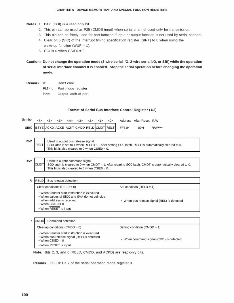
100
CHAPTER 6 DEVICE MEMORY MAP AND SPECIAL FUNCTION REGISTERS
Notes: 1. Bit 6 (COI) is a read-only bit.
2. This pin can be used as P25 (CMOS input) when serial channel used only for transmission.
3. This pin can be freely used for port function if input or output function is not used by serial channel.
4. Clear bit 5 (SIC) of the interrupt timing specification register (SINT) to 0 when using the
wake-up function (WUP = 1).
5. COI is 0 when CSIE0 = 0.
Caution: Do not change the operation mode (3-wire serial I/O, 2-wire serial I/O, or SBI) while the operation
of serial interface channel 0 is enabled. Stop the serial operation before changing the operation
mode.
Remark: ×: Don’t care
PM××: Port mode register
P××: Output latch of port
Format of Serial Bus Interface Control Register (1/2)
Note: Bits 2, 3, and 6 (RELD, CMDD, and ACKD) are read-only bits.
Remark: CSIE0: Bit 7 of the serial operation mode register 0
<6> <5> <4> <3> <2> <1> <0><7>Symbol
SBIC BSYE ACKD ACKE ACKT CMDD RELD CMDT RELT
RELTUsed to output bus release signal. SO0 latch is set to 1 when RELT = 1 . After setting SO0 latch, RELT is automatically cleared to 0. This bit is also cleared to 0 when CSIE0 = 0.
R/W
FF61H 00H R/W Note
Address After Reset R/W
CMDTUsed to output command signal. SO0 latch is cleared to 0 when CMDT = 1. After clearing SO0 latch, CMDT is automatically cleared to 0. This bit is also cleared to 0 when CSIE0 = 0.
R/W
R RELD Bus release detection
Set condition (RELD = 1)Clear conditions (RELD = 0)
• When bus release signal (REL) is detected
• When transfer start instruction is executed • When values of SIO0 and SVA do not coincide when address is received • When CSIE0 = 0
• When RESET is input
R CMDD Command detection
Clearing conditions (CMDD = 0)
• When transfer start instruction is executed • When bus release signal (REL) is detected • When CSIE0 = 0
• When RESET is input
Setting condition (CMDD = 1)
• When command signal (CMD) is detected
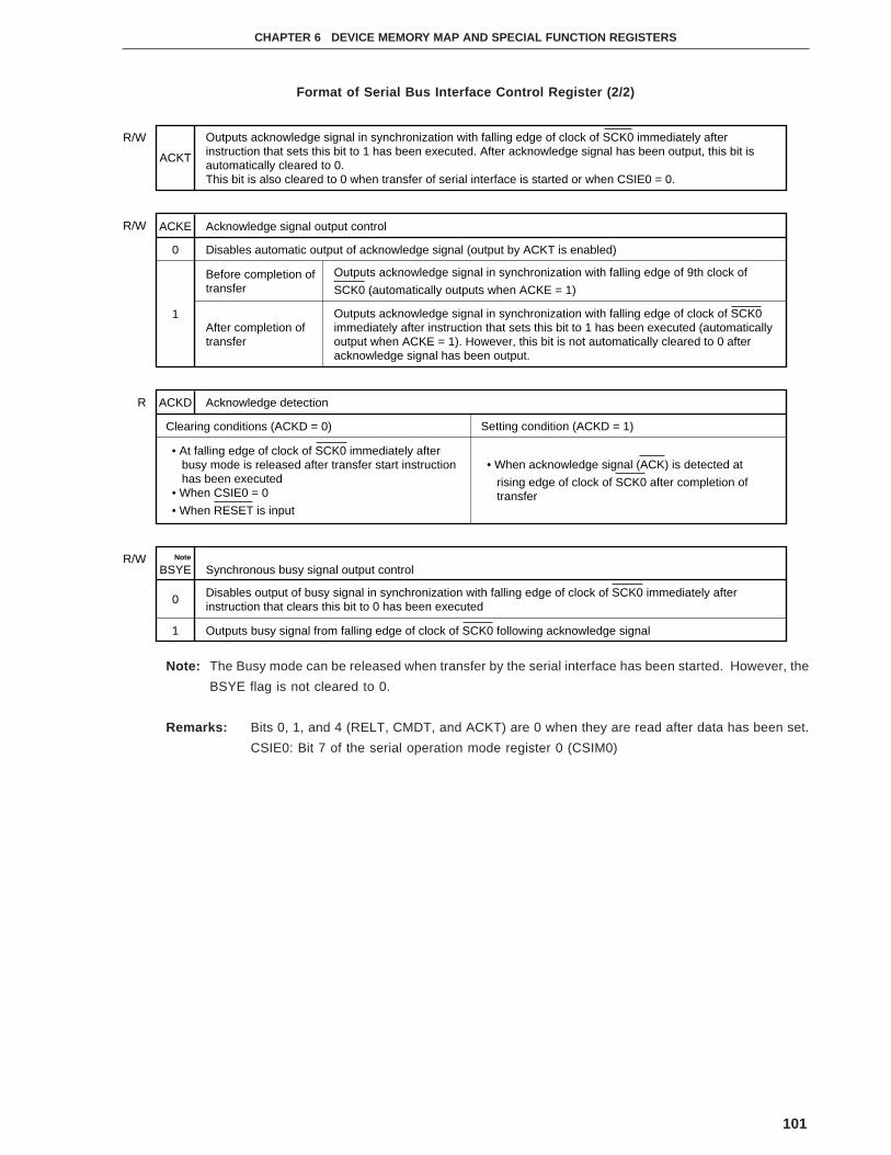
101
CHAPTER 6 DEVICE MEMORY MAP AND SPECIAL FUNCTION REGISTERS
Format of Serial Bus Interface Control Register (2/2)
Note: The Busy mode can be released when transfer by the serial interface has been started. However, the
BSYE flag is not cleared to 0.
Remarks: Bits 0, 1, and 4 (RELT, CMDT, and ACKT) are 0 when they are read after data has been set.
CSIE0: Bit 7 of the serial operation mode register 0 (CSIM0)
ACKT
Outputs acknowledge signal in synchronization with falling edge of clock of SCK0 immediately after instruction that sets this bit to 1 has been executed. After acknowledge signal has been output, this bit is automatically cleared to 0.This bit is also cleared to 0 when transfer of serial interface is started or when CSIE0 = 0.
R/W
ACKE Acknowledge signal output control
0 Disables automatic output of acknowledge signal (output by ACKT is enabled)
Outputs acknowledge signal in synchronization with falling edge of 9th clock of
SCK0 (automatically outputs when ACKE = 1)Before completion oftransfer
Outputs acknowledge signal in synchronization with falling edge of clock of SCK0immediately after instruction that sets this bit to 1 has been executed (automaticallyoutput when ACKE = 1). However, this bit is not automatically cleared to 0 afteracknowledge signal has been output.
After completion oftransfer
1
R/W
R ACKD Acknowledge detection
Clearing conditions (ACKD = 0)
• At falling edge of clock of SCK0 immediately after busy mode is released after transfer start instruction has been executed • When CSIE0 = 0
• When RESET is input
Setting condition (ACKD = 1)
• When acknowledge signal (ACK) is detected at
rising edge of clock of SCK0 after completion of transfer
BSYE Synchronous busy signal output control
0Disables output of busy signal in synchronization with falling edge of clock of SCK0 immediately after instruction that clears this bit to 0 has been executed
R/W Note
1 Outputs busy signal from falling edge of clock of SCK0 following acknowledge signal
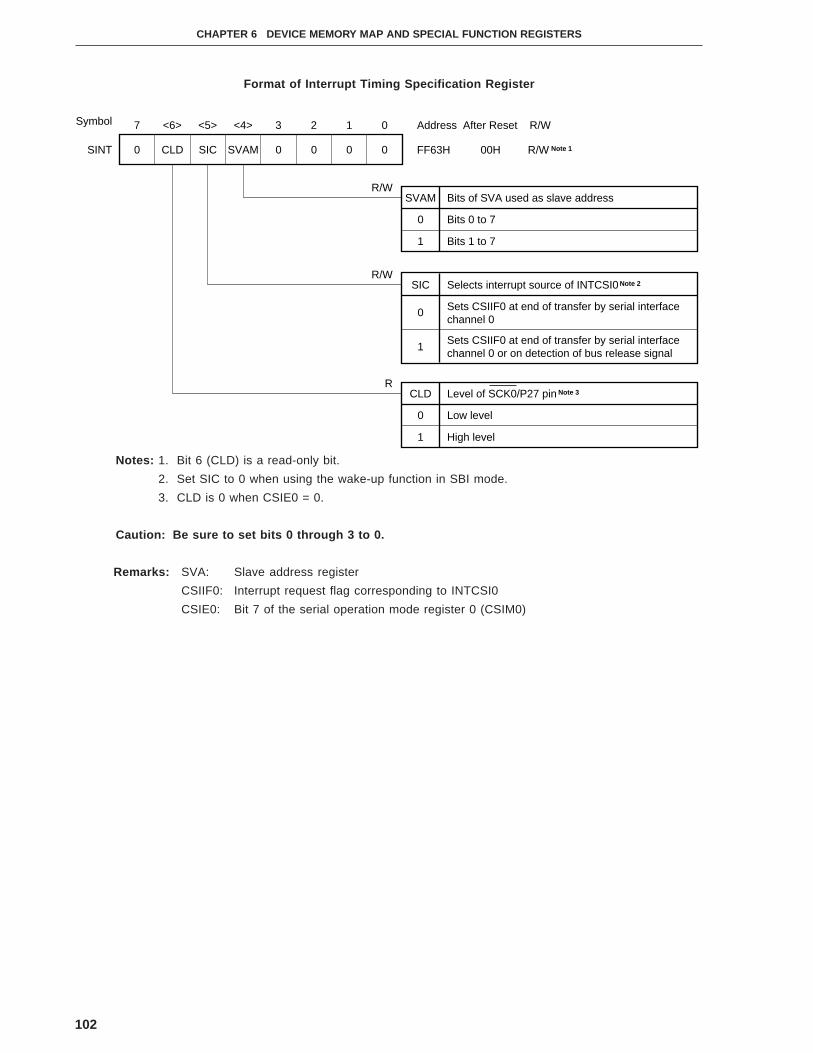
102
CHAPTER 6 DEVICE MEMORY MAP AND SPECIAL FUNCTION REGISTERS
Format of Interrupt Timing Specification Register
Notes: 1. Bit 6 (CLD) is a read-only bit.
2. Set SIC to 0 when using the wake-up function in SBI mode.
3. CLD is 0 when CSIE0 = 0.
Caution: Be sure to set bits 0 through 3 to 0.
Remarks: SVA: Slave address register
CSIIF0: Interrupt request flag corresponding to INTCSI0
CSIE0: Bit 7 of the serial operation mode register 0 (CSIM0)
<6> <5> <4> 3 2 1 07Symbol
SINT 0 CLD SIC SVAM 0 0 0 0 FF63H 00H R/W Note 1
Address After Reset R/W
SVAM
0
1
Bits of SVA used as slave address
Bits 0 to 7
Bits 1 to 7
SIC
0
Selects interrupt source of INTCSI0 Note 2
Sets CSIIF0 at end of transfer by serial interfacechannel 0
Sets CSIIF0 at end of transfer by serial interfacechannel 0 or on detection of bus release signal
CLD
0
1
Level of SCK0/P27 pin Note 3
Low level
High level
R/W
R/W
R
1

103
CHAPTER 6 DEVICE MEMORY MAP AND SPECIAL FUNCTION REGISTERS
(11) Registers controlling serial interface channel 0 (Y subseries)
The µPD78014Y and 78018FY Subseries are provided with two channels of clocked serial interfaces.
The differences between channels 0 and 1 are as indicated in the table below.
Differences Between Channels 0 and 1
Serial Transfer Mode Channel 0 Channel 1
3-wire serial I/O Clock selection fX/22 Note 1, fX/23, fX/24, fX/25, fX/26, fX/27, fX/28, fX/29, external clock, TO2 output
Transfer method MSB first/LSB first switchable MSB/LSB first switchable
Automatic transmission/reception
function
Transfer end flag Serial interface channel 0 Serial interface channel 1
transfer end interrupt request transfer end interrupt request
flag (CSIIF0) flag (CSIIF1 and TRF)
SBI (serial bus interface)Note 2 Available Not available
2-wire serial I/O
I2C bus (inter-IC bus)
Notes: 1. Can be set only when the main system clock oscillates at 4.19 MHz or less.
2. Provided to µPD78014Y Subseries only.
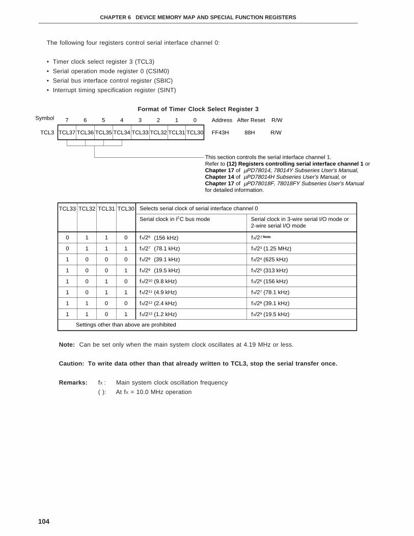
104
CHAPTER 6 DEVICE MEMORY MAP AND SPECIAL FUNCTION REGISTERS
The following four registers control serial interface channel 0:
• Timer clock select register 3 (TCL3)
• Serial operation mode register 0 (CSIM0)
• Serial bus interface control register (SBIC)
• Interrupt timing specification register (SINT)
Format of Timer Clock Select Register 3
Note: Can be set only when the main system clock oscillates at 4.19 MHz or less.
Caution: To write data other than that already written to TCL3, stop the serial transfer once.
Remarks: fX : Main system clock oscillation frequency
( ): At fX = 10.0 MHz operation
6 5 4 3 2 1 07Symbol
TCL3 TCL37 TCL36 TCL35 TCL34 TCL33 TCL32 TCL31 TCL30
0
0
Selects serial clock of serial interface channel 0
fX/2 2 Note
fX/27 (78.1 kHz)
1 fX/29 (19.5 kHz)
fX/210 (9.8 kHz)
fX/212 (2.4 kHz)
1 fX/28 (39.1 kHz)
1
fX/211 (4.9 kHz)1
1
fX/2 (1.2 kHz)1
FF43H 88H R/W
Address After Reset R/W
TCL33
1
1
0
0
0
0
1
1
TCL32
1
1
0
0
1
1
0
0
TCL31
0
1
1
0
0
1
0
1
TCL30
Serial clock in I C bus mode2
13
Serial clock in 3-wire serial I/O mode or2-wire serial I/O mode
fX/2
fX/23 (1.25 MHz)
fX/25 (313 kHz)
fX/26 (156 kHz)
fX/28 (39.1 kHz)
fX/24 (625 kHz)
fX/27 (78.1 kHz)
fX/2 (19.5 kHz)9
6 (156 kHz)
This section controls the serial interface channel 1.Refer to (12) Registers controlling serial interface channel 1 orChapter 17 of PD78014, 78014Y Subseries User's Manual,Chapter 14 of PD78014H Subseries User's Manual, orChapter 17 of PD78018F, 78018FY Subseries User's Manualfor detailed information.
µµµ
Settings other than above are prohibited

105
CHAPTER 6 DEVICE MEMORY MAP AND SPECIAL FUNCTION REGISTERS
Format of Serial Operation Mode Register 0
<6> <5> 4 3 2 1 0<7>Symbol
CSIM0 CSIE0 COI WUP CSIM04 CSIM03 CSIM02 CSIM01 CSIM00
CSIM01
0
1
Selects clock of serial interface channel 0
Clock externally input to SCK0/SCL pin
Output of 8-bit timer register 2 (TM2)
0
R/W
1 Clock specified by bits 0 to 3 of timer clock select register 3 (TCL3)
CSIM
04
0
CSIM00
×
0
1
FF60H 00H R/WNote 1
Address After Reset R/W
R/W CSIM
03
CSIM
02PM25 P25 PM26 P26 PM27 P27
Operating
modeStart bit
SI0/SB0/SDA0/
P25 pin function
SO0/SB1/SDA1/
P26 pin function
SCK0/SCL/P27
pin function
×
WUP
0
1
Controls wake-up function
Generates interrupt request signal in all modes each time serial transfer is executed
Generates interrupt request signal when address received after start condition is detected in I C bus mode
(when CMDD = 1) coincides with data of slave address register
R/W
1
MSB
LSB1 × 0 0 0 1
3-wire seriall/O mode
SI0(input)
SO0(CMOS output)
SCK0(CMOS I/O)
Note 3
SBI mode
0
SCK0(CMOS I/O)
1
1 0
×
0
×
0
0
×
0
×
0
0
1
1
Note 4 Note 4
Note 4 Note 4
MSB
P25 (CMOS I/O)
SB0/SDA0(N-ch open-drain I/O)
SB1/SDA1(N-ch opendrain I/O)
P26 (CMOS I/O)
2-wire seriall/O modeor I C bus
mode0
SCK0/SCL(N-ch open-
drain l/O)
1
1 1
×
0
×
0
0
×
0
×
0
0
1
1
Note 4 Note 4
Note 4 Note 4
MSB
P25 (CMOS I/O)
SB0/SDA0(N-ch open-drain I/O)
SB1/SDA1(N-ch open-drain I/O)
P26 (CMOS I/O)
2
Note 2
2
COI
0
Slave address comparison result flagNote 6
Data of slave address register does not coincide with data of serial l/O shift register 0
Data of slave address register coincides with data of serial l/O shift register 0
R
1
CSIE0
0
Controls operation of serial interface channel 0
Stops operation
Enables operation
R/W
1
Note 5
Note7
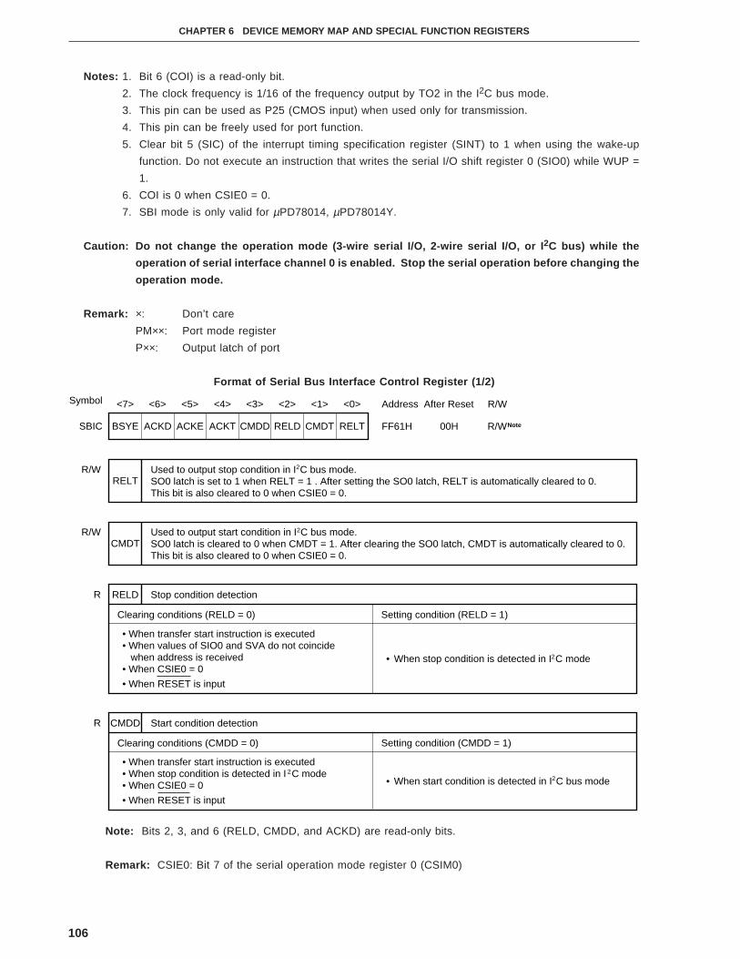
106
CHAPTER 6 DEVICE MEMORY MAP AND SPECIAL FUNCTION REGISTERS
Notes: 1. Bit 6 (COI) is a read-only bit.
2. The clock frequency is 1/16 of the frequency output by TO2 in the I2C bus mode.
3. This pin can be used as P25 (CMOS input) when used only for transmission.
4. This pin can be freely used for port function.
5. Clear bit 5 (SIC) of the interrupt timing specification register (SINT) to 1 when using the wake-up
function. Do not execute an instruction that writes the serial I/O shift register 0 (SIO0) while WUP =
1.
6. COI is 0 when CSIE0 = 0.
7. SBI mode is only valid for µPD78014, µPD78014Y.
Caution: Do not change the operation mode (3-wire serial I/O, 2-wire serial I/O, or I 2C bus) while the
operation of serial interface channel 0 is enabled. Stop the serial operation before changing the
operation mode.
Remark: ×: Don’t care
PM××: Port mode register
P××: Output latch of port
Format of Serial Bus Interface Control Register (1/2)
Note: Bits 2, 3, and 6 (RELD, CMDD, and ACKD) are read-only bits.
Remark: CSIE0: Bit 7 of the serial operation mode register 0 (CSIM0)
<6> <5> <4> <3> <2> <1> <0><7>Symbol
SBIC BSYE ACKD ACKE ACKT CMDD RELD CMDT RELT
RELTUsed to output stop condition in I C bus mode. SO0 latch is set to 1 when RELT = 1 . After setting the SO0 latch, RELT is automatically cleared to 0. This bit is also cleared to 0 when CSIE0 = 0.
R/W
FF61H 00H R/WNote
Address After Reset R/W
CMDTUsed to output start condition in I C bus mode. SO0 latch is cleared to 0 when CMDT = 1. After clearing the SO0 latch, CMDT is automatically cleared to 0. This bit is also cleared to 0 when CSIE0 = 0.
R/W
R RELD Stop condition detection
Setting condition (RELD = 1)Clearing conditions (RELD = 0)
• When stop condition is detected in I C mode
• When transfer start instruction is executed • When values of SIO0 and SVA do not coincide when address is received • When CSIE0 = 0
• When RESET is input
R CMDD Start condition detection
Clearing conditions (CMDD = 0)
• When transfer start instruction is executed • When stop condition is detected in I C mode • When CSIE0 = 0
• When RESET is input
Setting condition (CMDD = 1)
• When start condition is detected in I C bus mode
2
2
2
22

107
CHAPTER 6 DEVICE MEMORY MAP AND SPECIAL FUNCTION REGISTERS
Format of Serial Bus Interface Control Register (2/2)
Notes: 1. Set this bit before starting transfer.
2. Output the acknowledge signal during reception by using ACKT when an 8-clock wait is selected.
3. The wait mode can be released when transfer by the serial interface has been started when an
address signal has been received. However, the BSYE flag is not cleared to 0.
4. Be sure to set BSYE to 1 when using the wake-up function.
Remark: CSIE0: Bit 7 of the serial operation mode register 0 (CSIM0)
ACKT
Makes SDA0 (SDA1) low immediately after execution of setting instruction (ACKT = 1) until falling edge ofnext SCL.Used to generate ACK signal by software when 8-clock wait is selected.This bit is cleared to 0 when transfer of serial interface is started or when CSIE0 = 0.
R/W
ACKE Acknowledge signal automatic output control
0 Disables automatic output of acknowledge signal (output by ACKT is enabled).Used for transmission, or reception with 8-clock wait selected.
Enables automatic output of acknowledge signal. Outputs acknowledge signal in synchronization with falling edge of 9th clock of SCL (automatically outputs when ACKE = 1).This bit is not automatically cleared to 0 after acknowledge signal has been output.Used for reception with 9-clock wait selected.
1
R/W
R ACKD Acknowledge detection
Clearing conditions (ACKD = 0)
• When transfer start instruction is executed• When CSIE0 = 0• When RESET is input
Setting condition (ACKD = 1)
• When acknowledge signal is detected at rising edge of clock of SCL after completion of transfer
BSYE Controls N-ch open-drain output for transmission in I C bus mode
0 Enables output (transmission)
R/W
Note 3
1 Disables output (reception)
Note 1
Note 42
Note 2
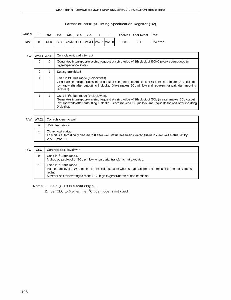
108
CHAPTER 6 DEVICE MEMORY MAP AND SPECIAL FUNCTION REGISTERS
Format of Interrupt Timing Specification Register (1/2)
Notes: 1. Bit 6 (CLD) is a read-only bit.
2. Set CLC to 0 when the I2C bus mode is not used.
<6> <5> <4> <3> <2> 1 07Symbol
SINT 0 CLD SIC SVAM CLC WREL WAT1 WAT0 FF63H 00H R/W Note 1
Address After Reset R/W
WAT1
0
Controls wait and interrupt
Generates interrupt processing request at rising edge of 8th clock of SCK0 (clock output goes tohigh-impedance state)
WREL
0
Controls clearing wait
Wait clear status
Clears wait status.This bit is automatically cleared to 0 after wait status has been cleared (used to clear wait status set byWAT0, WAT1)
CLC
0
1
Controls clock level Note 2
Used in I2C bus mode.Makes output level of SCL pin low when serial transfer is not executed.
Used in I2C bus mode.Puts output level of SCL pin in high-impedance state when serial transfer is not executed (the clock line is high).Master uses this setting to make SCL high to generate start/stop condition.
R/W
R/W
R/W
1
WAT0
0
0 1 Setting prohibited
1 0 Used in I2C bus mode (8-clock wait).Generates interrupt processing request at rising edge of 8th clock of SCL (master makes SCL outputlow and waits after outputting 8 clocks. Slave makes SCL pin low and requests for wait after inputting8 clocks).
1 1 Used in I2C bus mode (9-clock wait).Generates interrupt processing request at rising edge of 9th clock of SCL (master makes SCL outputlow and waits after outputting 9 clocks. Slave makes SCL pin low land requests for wait after inputting9 clocks).
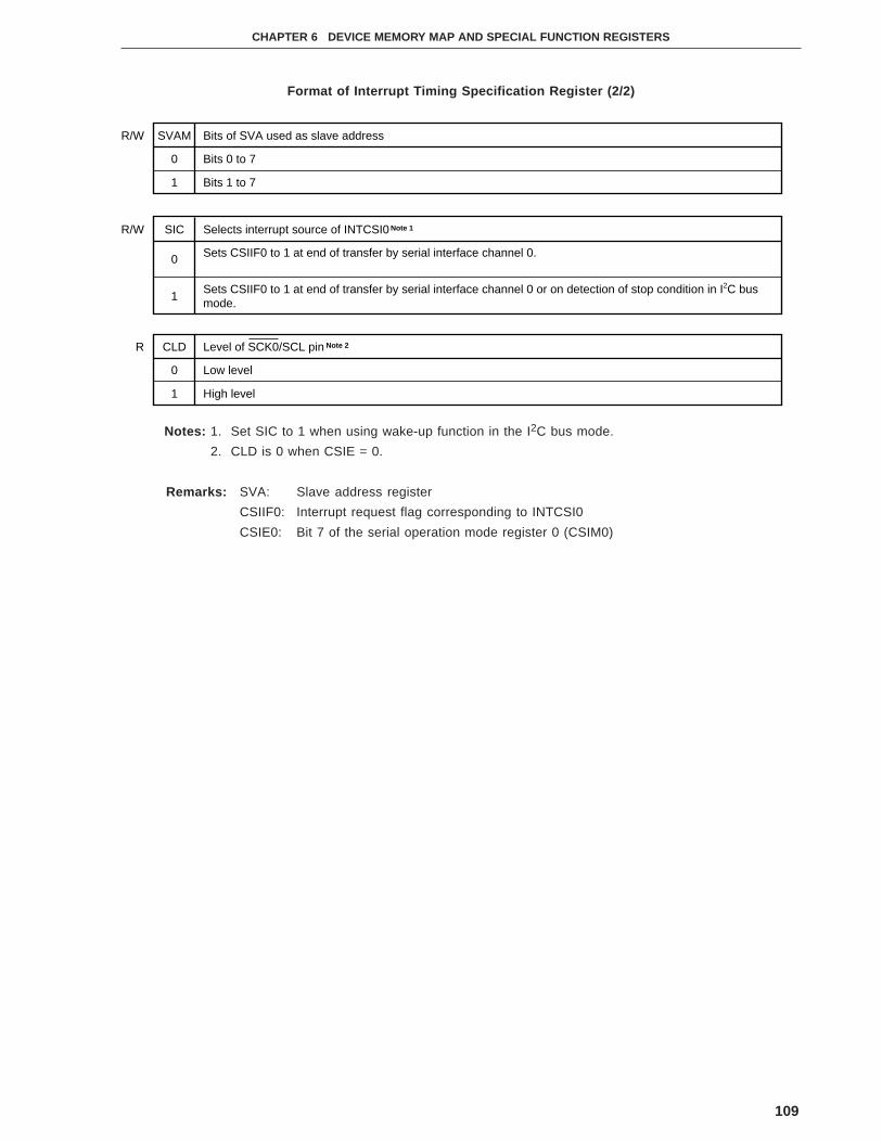
109
CHAPTER 6 DEVICE MEMORY MAP AND SPECIAL FUNCTION REGISTERS
Format of Interrupt Timing Specification Register (2/2)
Notes: 1. Set SIC to 1 when using wake-up function in the I2C bus mode.
2. CLD is 0 when CSIE = 0.
Remarks: SVA: Slave address register
CSIIF0: Interrupt request flag corresponding to INTCSI0
CSIE0: Bit 7 of the serial operation mode register 0 (CSIM0)
SVAM
0
1
Bits of SVA used as slave address
Bits 0 to 7
Bits 1 to 7
SIC
0
Selects interrupt source of INTCSI0 Note 1
Sets CSIIF0 to 1 at end of transfer by serial interface channel 0.
Sets CSIIF0 to 1 at end of transfer by serial interface channel 0 or on detection of stop condition in I2C busmode.
CLD
0
1
Level of SCK0/SCL pin Note 2
Low level
High level
R/W
R/W
R
1
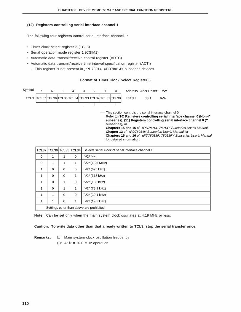
110
CHAPTER 6 DEVICE MEMORY MAP AND SPECIAL FUNCTION REGISTERS
(12) Registers controlling serial interface channel 1
The following four registers control serial interface channel 1:
• Timer clock select register 3 (TCL3)
• Serial operation mode register 1 (CSIM1)
• Automatic data transmit/receive control register (ADTC)
• Automatic data transmit/receive time interval specification register (ADTI)
- This register is not present in µPD78014, µPD78014Y subseries devices.
Format of Timer Clock Select Register 3
Note: Can be set only when the main system clock oscillates at 4.19 MHz or less.
Caution: To write data other than that already written to TCL3, stop the serial transfer once.
Remarks: fX : Main system clock oscillation frequency
( ): At fX = 10.0 MHz operation
6 5 4 3 2 1 07Symbol
TCL3 TCL37 TCL36 TCL35 TCL34 TCL33 TCL32 TCL31 TCL30
0
0
Selects serial clock of serial interface channel 1
fX/2
1
1
1
1
1
1
Settings other than above are prohibited
FF43H 88H R/W
Address After Reset R/W
TCL37
1
1
0
0
0
0
1
1
TCL36
1
1
0
0
1
1
0
0
TCL35
0
1
1
0
0
1
0
1
TCL34
2 Note
fX/23 (1.25 MHz)
fX/25 (313 kHz)
fX/26 (156 kHz)
fX/28 (39.1 kHz)
fX/24 (625 kHz)
fX/27 (78.1 kHz)
fX/2 (19.5 kHz)9
This section controls the serial interface channel 0.Refer to (10) Registers controlling serial interface channel 0 (Non-Ysubseries), (11) Registers controlling serial interface channel 0 (Ysubseries), orChapters 15 and 16 of PD78014, 78014Y Subseries User's Manual,Chapter 13 of PD78014H Subseries User's Manual, orChapters 15 and 16 of PD78018F, 78018FY Subseries User's Manualfor detailed information.
µµ
µ
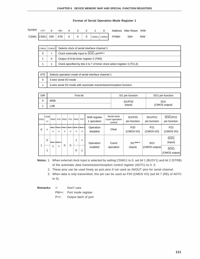
111
CHAPTER 6 DEVICE MEMORY MAP AND SPECIAL FUNCTION REGISTERS
Format of Serial Operation Mode Register 1
Notes: 1. When external clock input is selected by setting CSIM11 to 0, set bit 1 (BUSY1) and bit 2 (STRB)
of the automatic data transmission/reception control register (ADTC) to 0, 0.
2. These pins can be used freely as port pins if not used as IN/OUT pins for serial channel.
3. When data is only transmitted, this pin can be used as P20 (CMOS I/O) (set bit 7 (RE) of ADTC
to 0).
Remarks: ×: Don’t care
PM××: Port mode register
P××: Output latch of port
1 ×Note 3 Note 3
× ×××
6 <5> 4 3 2 1 0<7>Symbol
CSIM1 CSIE1 DIR ATE 0 0 0 CSIM11 CSIM10
CSIM11
0
1
Selects clock of serial interface channel 1
Clock externally input to SCK1 pinNote 1
Output of 8-bit timer register 2 (TM2)
1 Clock specified by bits 4 to 7 of timer clock select register 3 (TCL3)
CSIE1
CSIM10
×
0
1
FF68H 00H R/W
Address After Reset R/W
CSIM
11P20 PM21 P21 PM22
Shift register
1 operation
SO1/P21
pin function
SCK1/P22
pin function
× ×
0 0
Note 2 Note 2 Operation
disabled
ATE
0
Selects operation mode of serial interface channel 1
3-wire serial I/O mode
3-wire serial I/O mode with automatic transmission/reception function1
DIR
0
First bit
MSB
LSB1
SI1 pin function
SI1/P20(input)
SO1 pin function
SO1(CMOS output)
PM20 P22
Note 2 Note 2 Note 2Note 2×0
1
0
1
0
1
1
×
Serial clockcount operation
control
SI1/P20
pin function
ClearP20
(CMOS I/O)
P21
(CMOS I/O)
P22
(CMOS I/O)
Operation
enabled
Count
operation
SI1
(input)
Note 3 SO1
(CMOS output)
SCK1
(input)
SCK1
(CMOS output)
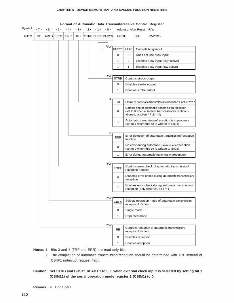
112
CHAPTER 6 DEVICE MEMORY MAP AND SPECIAL FUNCTION REGISTERS
Format of Automatic Data Transmit/Receive Control Register
Notes: 1. Bits 3 and 4 (TRF and ERR) are read-only bits.
2. The completion of automatic transmission/reception should be determined with TRF instead of
CSIIF1 (interrupt request flag).
Caution: Set STRB and BUSY1 of ADTC to 0, 0 when external clock input is selected by setting bit 1
(CSIM11) of the serial operation mode register 1 (CSIM1) to 0.
Remark: ×: Don’t care
<6> <5> <4> <3> <2> <1> <0><7>Symbol
ADTC RE ARLD ERCE ERR TRF STRB BUSY1 BUSY0
BUSY1
0
1
1
Controls busy input
Does not use busy input
Enables busy input (high active)
Enables busy input (low active)
BUSY0
×
0
1
STRB
0
1
Controls strobe output
Disables strobe output
Enables strobe output
TRF
1
Status of automatic transmission/reception function Note 2
Detects end of automatic transmission/reception (set to 0 when automatic transmission/reception is aborted, or when ARLD = 0)
Automatic transmission/reception is in progress(set to 1 when this bit is written to SIO1)
R/W
R/W
R
R
ERR
0
1
Error detection of automatic transmission/reception function
No error during automatic transmission/reception (set to 0 when this bit is written to SIO1)
Error during automatic transmission/reception
R/W
ARLD
0
1
Selects operation mode of automatic transmission/reception function
Single mode
Repeated mode
R/W
RE
0
1
Controls reception of automatic transmission/reception function
Disables reception
Enables reception
R/W
ERCEControls error check of automatic transmission/reception function
Disables error check during automatic transmission/reception
Enables error check during automatic transmission/reception (only when BUSY1 = 1)
0
FF69H 00H R/WNote 1
Address After Reset R/W
0
1
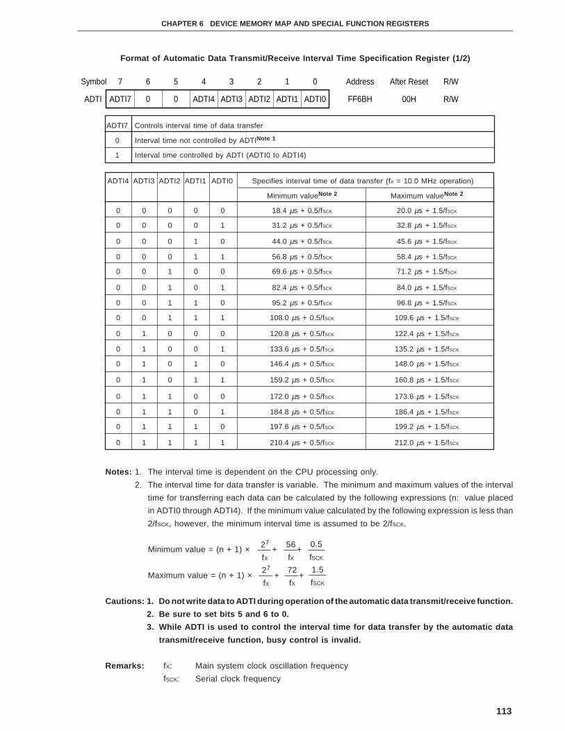
113
CHAPTER 6 DEVICE MEMORY MAP AND SPECIAL FUNCTION REGISTERS
Format of Automatic Data Transmit/Receive Interval Time Specification Register (1/2)
ADTI7 Controls interval time of data transfer
0 Interval time not controlled by ADTINote 1
1 Interval time controlled by ADTI (ADTI0 to ADTI4)
ADTI4 ADTI3 ADTI2 ADTI1 ADTI0 Specifies interval time of data transfer (fX = 10.0 MHz operation)
Minimum valueNote 2 Maximum valueNote 2
0 0 0 0 0 18.4 µs + 0.5/fSCK 20.0 µs + 1.5/fSCK
0 0 0 0 1 31.2 µs + 0.5/fSCK 32.8 µs + 1.5/fSCK
0 0 0 1 0 44.0 µs + 0.5/fSCK 45.6 µs + 1.5/fSCK
0 0 0 1 1 56.8 µs + 0.5/fSCK 58.4 µs + 1.5/fSCK
0 0 1 0 0 69.6 µs + 0.5/fSCK 71.2 µs + 1.5/fSCK
0 0 1 0 1 82.4 µs + 0.5/fSCK 84.0 µs + 1.5/fSCK
0 0 1 1 0 95.2 µs + 0.5/fSCK 96.8 µs + 1.5/fSCK
0 0 1 1 1 108.0 µs + 0.5/fSCK 109.6 µs + 1.5/fSCK
0 1 0 0 0 120.8 µs + 0.5/fSCK 122.4 µs + 1.5/fSCK
0 1 0 0 1 133.6 µs + 0.5/fSCK 135.2 µs + 1.5/fSCK
0 1 0 1 0 146.4 µs + 0.5/fSCK 148.0 µs + 1.5/fSCK
0 1 0 1 1 159.2 µs + 0.5/fSCK 160.8 µs + 1.5/fSCK
0 1 1 0 0 172.0 µs + 0.5/fSCK 173.6 µs + 1.5/fSCK
0 1 1 0 1 184.8 µs + 0.5/fSCK 186.4 µs + 1.5/fSCK
0 1 1 1 0 197.6 µs + 0.5/fSCK 199.2 µs + 1.5/fSCK
0 1 1 1 1 210.4 µs + 0.5/fSCK 212.0 µs + 1.5/fSCK
Notes: 1. The interval time is dependent on the CPU processing only.
2. The interval time for data transfer is variable. The minimum and maximum values of the interval
time for transferring each data can be calculated by the following expressions (n: value placed
in ADTI0 through ADTI4). If the minimum value calculated by the following expression is less than
2/fSCK, however, the minimum interval time is assumed to be 2/fSCK.
Minimum value = (n + 1) × + +
Maximum value = (n + 1) × + +
Cautions: 1. Do not write data to ADTI during operation of the automatic data transmit/receive function.
2. Be sure to set bits 5 and 6 to 0.
3. While ADTI is used to control the interval time for data transfer by the automatic data
transmit/receive function, busy control is invalid.
Remarks: fX: Main system clock oscillation frequency
fSCK: Serial clock frequency
27
fX
56
fX
0.5
fSCK
27
fX
72
fX
1.5
fSCK
7 6 5 4 3 2Symbol 1 0
FF6BHADTI0ADTI ADTI1ADTI3 ADTI2ADTI400ADTI7
Address After Reset R/W
00H R/W

114
CHAPTER 6 DEVICE MEMORY MAP AND SPECIAL FUNCTION REGISTERS
Format of Automatic Data Transmit/Receive Interval Time Specification Register (2/2)
ADTI4 ADTI3 ADTI2 ADTI1 ADTI0 Specifies interval time for data transfer (fX = 10.0 MHz operation)
Minimum valueNote Maximum valueNote
1 0 0 0 0 223.2 µs + 0.5/fSCK 224.8 µs + 1.5/fSCK
1 0 0 0 1 236.0 µs + 0.5/fSCK 237.6 µs + 1.5/fSCK
1 0 0 1 0 248.8 µs + 0.5/fSCK 250.4 µs + 1.5/fSCK
1 0 0 1 1 261.6 µs + 0.5/fSCK 263.2 µs + 1.5/fSCK
1 0 1 0 0 274.4 µs + 0.5/fSCK 276.0 µs + 1.5/fSCK
1 0 1 0 1 287.2 µs + 0.5/fSCK 288.8 µs + 1.5/fSCK
1 0 1 1 0 300.0 µs + 0.5/fSCK 301.6 µs + 1.5/fSCK
1 0 1 1 1 312.8 µs + 0.5/fSCK 314.4 µs + 1.5/fSCK
1 1 0 0 0 325.6 µs + 0.5/fSCK 327.2 µs + 1.5/fSCK
1 1 0 0 1 338.4 µs + 0.5/fSCK 340.0 µs + 1.5/fSCK
1 1 0 1 0 351.2 µs + 0.5/fSCK 352.8 µs + 1.5/fSCK
1 1 0 1 1 364.0 µs + 0.5/fSCK 365.6 µs + 1.5/fSCK
1 1 1 0 0 376.8 µs + 0.5/fSCK 378.4 µs + 1.5/fSCK
1 1 1 0 1 389.6 µs + 0.5/fSCK 391.2 µs + 1.5/fSCK
1 1 1 1 0 402.4 µs + 0.5/fSCK 404.0 µs + 1.5/fSCK
1 1 1 1 1 415.2 µs + 0.5/fSCK 416.8 µs + 1.5/fSCK
Note: The interval time for data transfer is variable. The minimum and maximum values of the interval time
for transferring each data can be calculated by the following expressions (n: value placed in ADTI0
through ADTI4). If the minimum value calculated by the following expression is less than 2/fSCK,
however, the minimum interval time is assumed to be 2/fSCK.
Minimum value = (n + 1) × + +
Maximum value = (n + 1) × + +
Cautions: 1. Do not write data to ADTI during operation of the automatic data transmit/receive function.
2. Be sure to set bits 5 and 6 to 0.
3. While ADTI is used to control the interval time for data transfer by the automatic data
transmit/receive function, busy control is invalid.
Remarks: fX: Main system clock oscillation frequency
fSCK: Serial clock frequency
27
fX
56
fX
0.5
fSCK
27
fX
72
fX
1.5
fSCK
7 6 5 4 3 2Symbol 1 0
FF6BHADTI0ADTI ADTI1ADTI3 ADTI2ADTI400ADTI7
Address After Reset R/W
00H R/W

115
CHAPTER 6 DEVICE MEMORY MAP AND SPECIAL FUNCTION REGISTERS
(13) Registers controlling interrupt function
A total of 14 interrupt sources are provided for the µPD78014/14Y, 78014H, and 78018F/18FY Subseries, including
reset, non-maskable, maskable, and software interrupts.
Table 6-2. Interrupt Source List
Interrupt Default Interrupt Source Internal/ VectorTable
Type Priority Name Trigger External Address
Reset — RESET RESET pin input External 0000H
Non- — INTWDT Overflow of watchdog timer (when watchdog timer Internal 0004H
maskable mode 1 is selected)
Maskable 0 INTWDT Overflow of watchdog timer (when interval timer
mode is selected)
1 INTP0 Pin input edge detection External 0006H
2 INTP1 0008H
3 INTP2 000AH
4 INTP3 000CH
5 INTCSI0 End of transfer of serial interface channel 0 Internal 000EH
6 INTCSI1 End of transfer of serial interface channel 1 0010H
7 INTTM3 Reference time interval signal from watch timer 0012H
8 INTTM0 Generation of coincidence signal from16-bit timer/ 0014H
event counter
9 INTTM1 Generation of coincidence signal from 8-bit timer/ 0016H
event counter 1
10 INTTM2 Generation of coincidence signal from 8-bit timer/ 0018H
event counter 2
11 INTAD End of conversion of A/D converter 001AH
Software — BRK Execution of BRK instruction — 003EH
Note: The default priority is used when two or more Maskable Interrupt requests occur at the same time. 0 is
the highest and 11 is the lowest priority.
Note

116
CHAPTER 6 DEVICE MEMORY MAP AND SPECIAL FUNCTION REGISTERS
The following table gives a listing of interrupt request flags, interrupt mask flags, and priority specification flags
corresponding to interrupt request sources.
Table 6-3. Interrupt Sources and Flags
Interrupt Source Interrupt Request Flag Interrupt Mask Flag Priority Specification Flag
Register Register Register
INTWDT TMIF4 IF0L TMMK4 MK0L TMPR4 PR0L
INTP0 PIF0 PMK0 PPR0
INTP1 PIF1 PMK1 PPR1
INTP2 PIF2 PMK2 PPR2
INTP3 PIF3 PMK3 PPR3
INTCSI0 CSIIF0 CSIMK0 CSIPR0
INTCSI1 CSIIF1 CSIMK1 CSIPR1
INTTM3 TMIF3 TMMK3 TMPR3
INTTM0 TMIF0 IF0H TMMK0 MK0H TMPR0 PR0H
INTTM1 TMIF1 TMMK1 TMPR1
INTTM2 TMIF2 TMMK2 TMPR2
INTAD ADIF ADMK ADPR
The following six types of registers control the interrupt function:
• Interrupt request flag registers (IF0L, IF0H)
• Interrupt mask flag registers (MK0L, MK0H)
• Priority specification flag registers (PR0L, PR0H)
• External interrupt mode register (INTM0)
• Sampling clock select register (SCS)
• Program status word (PSW)
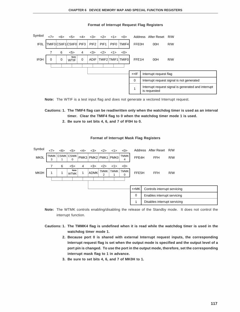
117
CHAPTER 6 DEVICE MEMORY MAP AND SPECIAL FUNCTION REGISTERS
Format of Interrupt Request Flag Registers
Note: The WTIF is a test input flag and does not generate a vectored Interrupt request.
Cautions: 1. The TMIF4 flag can be read/written only when the watchdog timer is used as an interval
timer. Clear the TMIF4 flag to 0 when the watchdog timer mode 1 is used.
2. Be sure to set bits 4, 6, and 7 of IF0H to 0.
Format of Interrupt Mask Flag Registers
Note: The WTMK controls enabling/disabling the release of the Standby mode. It does not control the
interrupt function.
Cautions: 1. The TMMK4 flag is undefined when it is read while the watchdog timer is used in the
watchdog timer mode 1.
2. Because port 0 is shared with external Interrupt request inputs, the corresponding
Interrupt request flag is set when the output mode is specified and the output level of a
port pin is changed. To use the port in the output mode, therefore, set the corresponding
interrupt mask flag to 1 in advance.
3. Be sure to set bits 4, 6, and 7 of MK0H to 1.
IF0H 0 0 ADIF TMIF2 TMIF1 TMIF0
IF0L TMIF3 CSIIF1CSIIF0 PIF3 PIF2 PIF1 PIF0 TMIF4
Symbol
FFE0H 00H R/W
Address After Reset R/W
FFE1H 00H R/WWTIFNote
0
××IF
0
1
Interrupt request flag
Interrupt request signal is not generated
Interrupt request signal is generated and interruptis requested
<6> <5> <4> <3> <2> <1> <0><7>
6 <5> 4 <3> <2> <1> <0>7
MK0H 1 1 ADMK TMMK2
TMMK1
TMMK0
MK0L TMMK3
CSIMK1
CSIMK0
PMK3 PMK2 PMK1 PMK0 TMMK4
Symbol
FFE4H FFH R/W
Address After Reset R/W
FFE5H FFH R/WWTMKNote
1
Controls interrupt servicing××MK
0
1
Enables interrupt servicing
Disables interrupt servicing
<6> <5> <4> <3> <2> <1> <0><7>
6 <5> 4 <3> <2> <1> <0>7

118
CHAPTER 6 DEVICE MEMORY MAP AND SPECIAL FUNCTION REGISTERS
Format of Priority Specification Flag Registers
Cautions: 1. Set the TMPR4 flag to 1 when using the watchdog timer in the watchdog timer mode 1.
2. Be sure to set bits 4 through 7 of PR0H to 1.
Format of External Interrupt Mode Register
Caution: Before setting the valid edges of the INTP0/TI0/P00 pins, stop the timer operation by clearing
bits 1 to 3 (TMC01 to TMC03) of the 16-bit timer mode control register (TMC0) to 0, 0, 0.
Remark: INTP0 pin also functions as TI0/P00.
PR0H 1 1 ADPR TMPR2
TMPR1
TMPR0
PR0L TMPR3
CSIPR1
CSIPR0
PPR3 PPR2 PPR1 PPR0 TMPR4
Symbol
FFE8H FFH R/W
Address After Reset R/W
FFE9H FFH R/W1
××PR
0
Selects priority level
High priority level
Low priority level
1
1
<6> <5> <4> <3> <2> <1> <0><7>
6 5 4 <3> <2> <1> <0>7
6 5 4 3 2 1 07Symbol
INTM0 ES31 ES30 ES21 ES20 ES11 ES10 0 0
ES11
0
0
1
Selects valid edge of INTP0
Falling edge
Rising edge
Setting prohibited
ES10
0
1
0
1 Both rising and falling edges1
ES21
0
0
1
Selects valid edge of INTP1
Falling edge
Rising edge
Setting prohibited
ES20
0
1
0
1 Both rising and falling edges1
ES31
0
0
1
Selects valid edge of INTP2
Falling edge
Rising edge
Setting prohibited
ES30
0
1
0
1 Both rising and falling edges1
FFECH 00H R/W
Address After Reset R/W
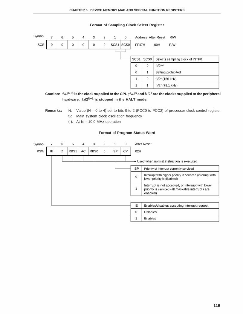
119
CHAPTER 6 DEVICE MEMORY MAP AND SPECIAL FUNCTION REGISTERS
Format of Sampling Clock Select Register
Caution: f X/2N+1 is the clock supplied to the CPU; f X/26 and f X/27 are the clocks supplied to the peripheral
hardware. f X/2N+1 is stopped in the HALT mode.
Remarks: N: Value (N = 0 to 4) set to bits 0 to 2 (PCC0 to PCC2) of processor clock control register
fX: Main system clock oscillation frequency
( ): At fX = 10.0 MHz operation
Format of Program Status Word
6 5 4 3 2 1 07Symbol
SCS 0 0 0 0 0 0 SCS1 SCS0
SCS1
0
0
1
Selects sampling clock of INTP0
fX/2N+1
Setting prohibited
fX/26 (156 kHz)
SCS0
0
1
0
1 fX/27 (78.1 kHz)1
FF47H 00H R/W
Address After Reset R/W
0
6 5 4 3 2 1 07
PSW IE Z RBS1 AC RBS0 0 ISP CY 02H
After Reset
IE
0
1
Enables/disables accepting Interrupt request
Disables
Enables
ISP Priority of interrupt currently serviced
Interrupt with higher priority is serviced (interrupt withlower priority is disabled)
Interrupt is not accepted, or interrupt with lowerpriority is serviced (all maskable interrupts areenabled)
Used when normal instruction is executed
1
Symbol
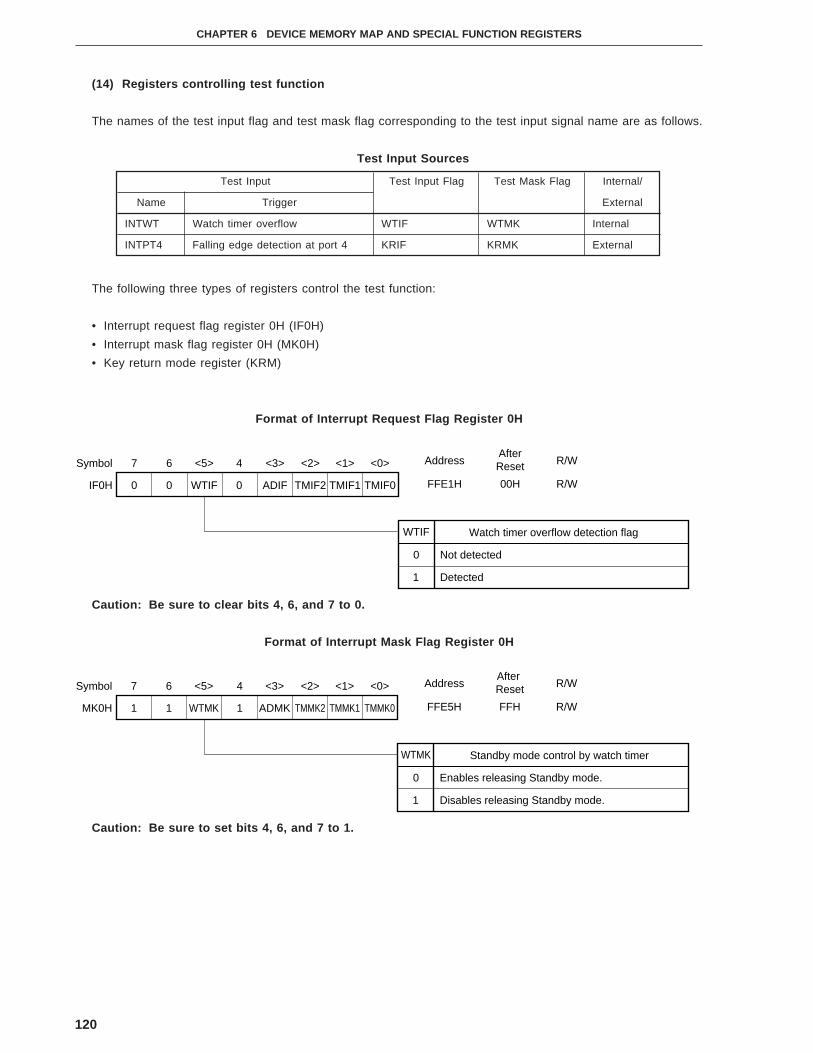
120
CHAPTER 6 DEVICE MEMORY MAP AND SPECIAL FUNCTION REGISTERS
(14) Registers controlling test function
The names of the test input flag and test mask flag corresponding to the test input signal name are as follows.
Test Input Sources
Test Input Test Input Flag Test Mask Flag Internal/
Name Trigger External
INTWT Watch timer overflow WTIF WTMK Internal
INTPT4 Falling edge detection at port 4 KRIF KRMK External
The following three types of registers control the test function:
• Interrupt request flag register 0H (IF0H)
• Interrupt mask flag register 0H (MK0H)
• Key return mode register (KRM)
Format of Interrupt Request Flag Register 0H
Caution: Be sure to clear bits 4, 6, and 7 to 0.
Format of Interrupt Mask Flag Register 0H
Caution: Be sure to set bits 4, 6, and 7 to 1.
7
0
Symbol
IF0H
6
0
<5>
WTIF
4
0
<3>
ADIF
<2>
TMIF2
<1>
TMIF1
<0>
TMIF0
Address
FFE1H 00H
AfterReset R/W
R/W
0
1
Watch timer overflow detection flag
Not detected
Detected
WTIF
7
1
Symbol
MK0H
6
1
<5>
WTMK
4
1
<3>
ADMK
<2>
TMMK2
<1>
TMMK1
<0>
TMMK0
Address
FFE5H FFH
After Reset R/W
R/W
0
1
Standby mode control by watch timer
Enables releasing Standby mode.
Disables releasing Standby mode.
WTMK
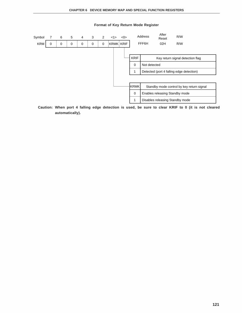
121
CHAPTER 6 DEVICE MEMORY MAP AND SPECIAL FUNCTION REGISTERS
Format of Key Return Mode Register
Caution: When port 4 falling edge detection is used, be sure to clear KRIF to 0 (it is not cleared
automatically).
7
0
Symbol
KRM
6
0
5
0
4
0
3
0
2
0
<1>
KRMK
<0>
KRIF
Address
FFF6H 02H
AfterReset R/W
R/W
0
1
Key return signal detection flag
Not detected
Detected (port 4 falling edge detection)
KRIF
0
1
Standby mode control by key return signal
Enables releasing Standby mode
Disables releasing Standby mode
KRMK

122
CHAPTER 6 DEVICE MEMORY MAP AND SPECIAL FUNCTION REGISTERS
(15) Registers controlling external device expansion function
The following two registers control the external device expansion function:
• Memory expansion mode register (MM)
• Internal memory size switching register (IMS)
Format of Memory Expansion Mode Register
PW1 PW0 Controls wait state
0 0 No wait
0 1 Wait (1 wait state is inserted)
1 0 Setting prohibited
1 1 Wait control by external wait pin
Note: The Full Address mode is a mode in which the entire area of the 64K address space, except the internal
ROM, RAM, SFR, and unused areas, can be externally expanded.
Remark: The P60 to P63 pins can be used in the Port mode, regardless of the single-chip mode and memory
expansion mode.
6 5 4 3 2 1 07Symbol
MM 0 0 PW1 PW0 0 MM2 MM1 MM0
0
0
FFF8H 10H R/W
Address After Reset R/W
AD0 to AD7
MM2 MM1 MM0
0
0
0
1
Selects single-chip/memory expansion
mode
Single-chip mode Portmode
Input
Output
Status of P40 to P47, P50 to P57, P64 to P67 pins
P50 to P53 P54, P55 P56, P57 P64 to P67
Port mode
0 1 1
1 0 0
1 0 1
1 1 1
Memoryexpansion
mode
256-bytemode
4Kmode
16Kmode
Fulladdressmode
Note
Port mode
Port mode
Port mode
A14, A15
A12, A13
A8 to A11
Other than above Setting prohibited
P64 = RD
P65 = WR
P66 = WAIT
P67 = ASTB
P40 to P47

123
CHAPTER 6 DEVICE MEMORY MAP AND SPECIAL FUNCTION REGISTERS
Format of Internal Memory Size Switching Register
Notes: 1. The value of this register after reset differs depending on the product (refer to the table below).
2. Setting prohibited for the µPD78014/14Y and 78014H Subseries.
3. When the external device expansion function of the µPD78018F/18FY is used, set the internal ROM
capacity to 56K or less.
Value of Internal Memory Size Switching Register After Reset
Part Number Value After Reset
µPD78011B/11BY/11F/11FY/11H 42H
µPD78012B/12BY/12F/12FY/12H 44H
µPD78013/13Y/13F/13FY/13H C6H
µPD78014/14Y/P014/P014Y/14F/14FY/14H C8H
µPD78015F/15FY CAH
µPD78016F/16FY CCH
µPD78018F/18FY/P018F/P018FY CFH
RAM2 RAM1 RAM0 0 ROM3 ROM2 ROM1 ROM0IMS
7 6 5 4 3 2 1 0Symbol Address After Reset R/W
FFF0H Note 1 W
ROM3 ROM2
0
0
0
1
0
1
1
0
ROM1 ROM0
1
0
0
0
1
0
0
0
1 0
1
1
1
1
1 1
1 0
0
1
0
0
1 1
Selects internal ROM capacity
8K
16K
24K
32K
40K Note 2
48K Note 2
56K Notes 2, 3
60K Note 2
Settings other than above are prohibited
RAM2 RAM1
0
1
1
1
RAM0
0
0
Selects internal high-speed RAM capacity
512 bytes
1024 bytes
Settings other than above are prohibited
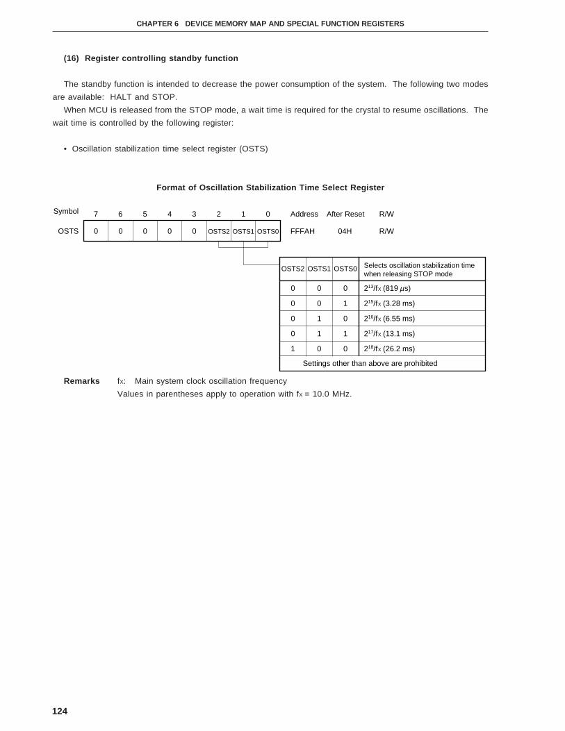
124
CHAPTER 6 DEVICE MEMORY MAP AND SPECIAL FUNCTION REGISTERS
(16) Register controlling standby function
The standby function is intended to decrease the power consumption of the system. The following two modes
are available: HALT and STOP.
When MCU is released from the STOP mode, a wait time is required for the crystal to resume oscillations. The
wait time is controlled by the following register:
• Oscillation stabilization time select register (OSTS)
Format of Oscillation Stabilization Time Select Register
Remarks fX: Main system clock oscillation frequency
Values in parentheses apply to operation with fX = 10.0 MHz.
6 5 4 3 2 1 07Symbol
OSTS 0 0 0 0 0 OSTS2 OSTS1 OSTS0 FFFAH 04H R/W
Address After Reset R/W
OSTS2
0
0
0
OSTS1
0
0
1
0 1
1 0
Selects oscillation stabilization time when releasing STOP mode
213/fX (819 s)
215/fX (3.28 ms)
216/fX (6.55 ms)
OSTS0
0
1
0
217/fX (13.1 ms)1
218/fX (26.2 ms)0
µ
Settings other than above are prohibited

125
CHAPTER 6 DEVICE MEMORY MAP AND SPECIAL FUNCTION REGISTERS
The operation status in the HALT mode is described below.
HALT Mode Operating Status
(a) When HALT instruction is executed while system operates on main system clock
Clock generator Both main system clock and subsystem clock can oscillate.
Supply of clock to CPU is stopped.
CPU Stops operation
Port (output latch) Retains previous status before setting HALT mode
16-bit timer/event counter Operable
8-bit timer/event counter
Watchdog timer
A/D converter
Watch timer Operable when fX/28 is selected as Operable
count clock
Serial interface Other than automatic trans- Operable
mission/reception function
Automatic transmission/ Stops operation
reception function
External interrupt INTP0 Operable when clock to peripheral hardware (fX/26, fX/27) is selected as
sampling clock
INTP1 to INTP3 Operable
AD0 to AD7 High impedance
A8 to A15 Retains previous status before setting HALT mode
ASTB Low level
WR, RD High level
WAIT High impedance
Without Subsystem Clock Note 1 With Subsystem Clock Note 2
Externally
extended bus line
Setting of HALT Mode
Item
Notes: 1. Includes the case in which an external clock is not supplied as the subsystem clock.
2. Includes the case in which an external clock is supplied as the subsystem clock.
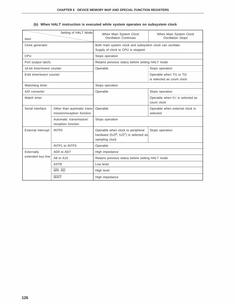
126
CHAPTER 6 DEVICE MEMORY MAP AND SPECIAL FUNCTION REGISTERS
(b) When HALT instruction is executed while system operates on subsystem clock
Clock generator Both main system clock and subsystem clock can oscillate.
Supply of clock to CPU is stopped.
CPU Stops operation
Port (output latch) Retains previous status before setting HALT mode
16-bit timer/event counter Operable Stops operation
8-bit timer/event counter Operable when TI1 or TI2
is selected as count clock
Watchdog timer Stops operation
A/D converter Operable Stops operation
Watch timer Operable when fXT is selected as
count clock
Serial interface Other than automatic trans- Operable Operable when external clock is
mission/reception function selected
Automatic transmission/ Stops operation
reception function
External interrupt INTP0 Operable when clock to peripheral Stops operation
hardware (fX/26, fX/27) is selected as
sampling clock
INTP1 to INTP3 Operable
AD0 to AD7 High impedance
A8 to A15 Retains previous status before setting HALT mode
ASTB Low level
WR, RD High level
WAIT High impedance
Setting of HALT Mode
Item
When Main System ClockOscillation Continues
When Main System ClockOscillation Stops
Externally
extended bus line
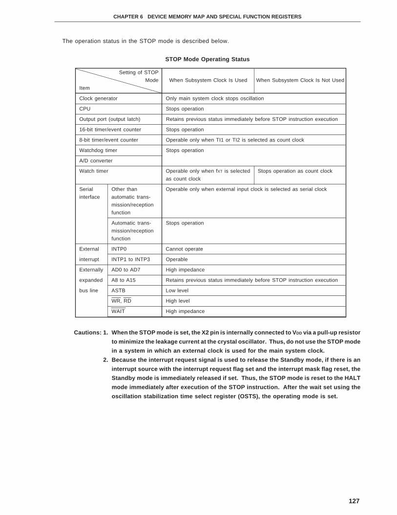
127
CHAPTER 6 DEVICE MEMORY MAP AND SPECIAL FUNCTION REGISTERS
The operation status in the STOP mode is described below.
STOP Mode Operating Status
Setting of STOP
Mode When Subsystem Clock Is Used When Subsystem Clock Is Not Used
Item
Clock generator Only main system clock stops oscillation
CPU Stops operation
Output port (output latch) Retains previous status immediately before STOP instruction execution
16-bit timer/event counter Stops operation
8-bit timer/event counter Operable only when TI1 or TI2 is selected as count clock
Watchdog timer Stops operation
A/D converter
Watch timer Operable only when fXT is selected Stops operation as count clock
as count clock
Serial Other than Operable only when external input clock is selected as serial clock
interface automatic trans-
mission/reception
function
Automatic trans- Stops operation
mission/reception
function
External INTP0 Cannot operate
interrupt INTP1 to INTP3 Operable
Externally AD0 to AD7 High impedance
expanded A8 to A15 Retains previous status immediately before STOP instruction execution
bus line ASTB Low level
WR, RD High level
WAIT High impedance
Cautions: 1. When the STOP mode is set, the X2 pin is internally connected to V DD via a pull-up resistor
to minimize the leakage current at the crystal oscillator. Thus, do not use the STOP mode
in a system in which an external clock is used for the main system clock.
2. Because the interrupt request signal is used to release the Standby mode, if there is an
interrupt source with the interrupt request flag set and the interrupt mask flag reset, the
Standby mode is immediately released if set. Thus, the STOP mode is reset to the HALT
mode immediately after execution of the STOP instruction. After the wait set using the
oscillation stabilization time select register (OSTS), the operating mode is set.
128
CHAPTER 6 DEVICE MEMORY MAP AND SPECIAL FUNCTION REGISTERS
(17) Reset function
The following two operations can be used to generate a reset signal:
• External reset input via the RESET pin
• Internal reset by watchdog timer in the Watchdog Timer mode
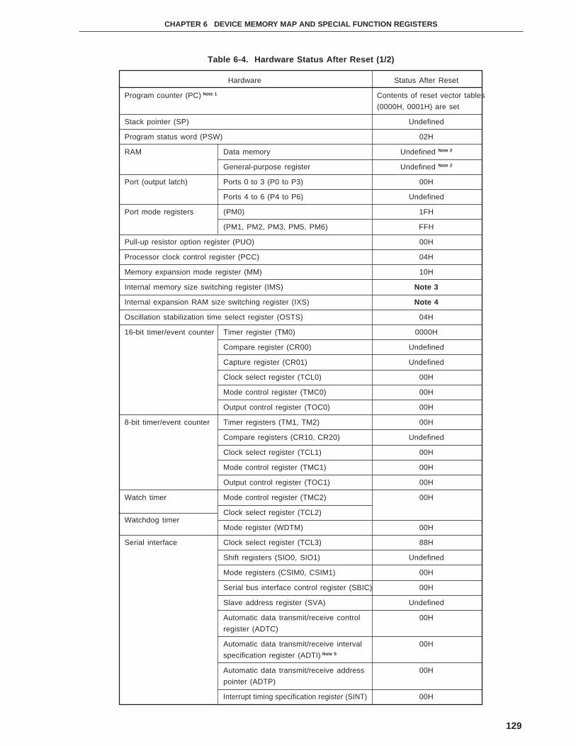
129
CHAPTER 6 DEVICE MEMORY MAP AND SPECIAL FUNCTION REGISTERS
Table 6-4. Hardware Status After Reset (1/2)
Hardware Status After Reset
Program counter (PC) Note 1 Contents of reset vector tables
(0000H, 0001H) are set
Stack pointer (SP) Undefined
Program status word (PSW) 02H
RAM Data memory Undefined Note 2
General-purpose register Undefined Note 2
Port (output latch) Ports 0 to 3 (P0 to P3) 00H
Ports 4 to 6 (P4 to P6) Undefined
Port mode registers (PM0) 1FH
(PM1, PM2, PM3, PM5, PM6) FFH
Pull-up resistor option register (PUO) 00H
Processor clock control register (PCC) 04H
Memory expansion mode register (MM) 10H
Internal memory size switching register (IMS) Note 3
Internal expansion RAM size switching register (IXS) Note 4
Oscillation stabilization time select register (OSTS) 04H
16-bit timer/event counter Timer register (TM0) 0000H
Compare register (CR00) Undefined
Capture register (CR01) Undefined
Clock select register (TCL0) 00H
Mode control register (TMC0) 00H
Output control register (TOC0) 00H
8-bit timer/event counter Timer registers (TM1, TM2) 00H
Compare registers (CR10, CR20) Undefined
Clock select register (TCL1) 00H
Mode control register (TMC1) 00H
Output control register (TOC1) 00H
Watch timer Mode control register (TMC2) 00H
Clock select register (TCL2)Watchdog timer
Mode register (WDTM) 00H
Serial interface Clock select register (TCL3) 88H
Shift registers (SIO0, SIO1) Undefined
Mode registers (CSIM0, CSIM1) 00H
Serial bus interface control register (SBIC) 00H
Slave address register (SVA) Undefined
Automatic data transmit/receive control 00H
register (ADTC)
Automatic data transmit/receive interval 00H
specification register (ADTI) Note 5
Automatic data transmit/receive address 00H
pointer (ADTP)
Interrupt timing specification register (SINT) 00H

130
CHAPTER 6 DEVICE MEMORY MAP AND SPECIAL FUNCTION REGISTERS
Table 6-4. Hardware Status After Reset (2/2)
Hardware Status After Reset
A/D converter Mode register (ADM) 01H
Conversion result register (ADCR) Undefined
Input select register (ADIS) 00H
ROM correction Correction address registers (CORAD0, 0000H
CORAD1)Note 6
Correction control register (CORCN)Note 6 00H
Interrupt Request flag registers (IF0L, IF0H) 00H
Mask flag registers (MK0L, MK0H) FFH
Priority specification flag registers (PR0L, PR0H) FFH
External interrupt mode register (INTM0) 00H
Key return mode register (KRM) 02H
Sampling clock select register (SCS) 00H
Notes: 1. Only the contents of the PC among hardware become undefined during reset input and oscillation
stabilization time wait. The other status is not different from that after reset as above.
2. The status before reset is retained in Standby mode.
3. The value after reset differs depending on the product, as follows:
µPD78011B/BY µPD78012B/BY µPD78013/Y µPD78014/Y µPD78015F/FY µPD78016F/FY µPD78018F/FY
µPD78011F/FY µPD78012F/FY µPD78013F/FY µPD78P014F/FY µPD78P018F/FY
µPD78011H µPD78012H µPD78013H µPD78014F/FY
µPD78014H
IMS 42H 44H C6H C8H CAH CCH CFH
To use a mask ROM version, do not set IMS to a value other than that after reset, except, however,
when the external device expansion function is used with the µPD78018F/FY.
4. Provided to the µPD78011F/FY, 78012F/FY, 78013F/FY, 78014F/FY, 78015F/FY, 78016F/FY, 78018F/
FY, and 78P018F/FY (µPD78018F, 78018FY Subseries) only.
The value after reset differs depending on the product, as follows:
µPD78011F/FY µPD78012F/FY µPD78013F/FY µPD78014F/FY µPD78015F/FY µPD78016F/FY µPD78018F/FY
µPD78P018F/FY
IXS 0CH 0BH 0AH
To use a mask ROM version, do not set IXS to a value other than that after reset, except, however,
when the external device expansion function is used with the µPD78018F/FY.
5. Provided to the µPD78014H and 78018F Subseries only.
6. Provided to some products of the µPD78018F Subseries only:
µPD78015F/FY, 78016F/FY, 78018F/FY, and 78P018F/FY.
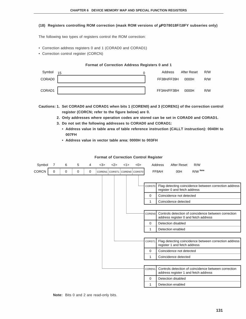
131
CHAPTER 6 DEVICE MEMORY MAP AND SPECIAL FUNCTION REGISTERS
(18) Registers controlling ROM correction (mask ROM versions of µµµµµPD78018F/18FY subseries only)
The following two types of registers control the ROM correction:
• Correction address registers 0 and 1 (CORAD0 and CORAD1)
• Correction control register (CORCN)
Format of Correction Address Registers 0 and 1
Cautions: 1. Set CORAD0 and CORAD1 when bits 1 (COREN0) and 3 (COREN1) of the correction control
register (CORCN; refer to the figure below) are 0.
2. Only addresses where operation codes are stored can be set in CORAD0 and CORAD1.
3. Do not set the following addresses to CORAD0 and CORAD1:
• Address value in table area of table reference instruction (CALLT instruction): 0040H to
007FH
• Address value in vector table area: 0000H to 003FH
Format of Correction Control Register
Note: Bits 0 and 2 are read-only bits.
FF38H/FF39HCORAD0
Address After Reset R/W
0000H R/W
15Symbol 0
FF3AH/FF3BHCORAD1 0000H R/W
7 6 5 4 <3> <2>Symbol <1> <0>
CORST0 Flag detecting coincidence between correction addressregister 0 and fetch address
FF8AHCORST0CORCN COREN0COREN1 CORST10000
Address After Reset R/W
00H R/W Note
0 Coincidence not detected
1 Coincidence detected
COREN0 Controls detection of coincidence between correctionaddress register 0 and fetch address
0 Detection disabled
1 Detection enabled
CORST1 Flag detecting coincidence between correction address register 1 and fetch address
0 Coincidence not detected
1 Coincidence detected
COREN1 Controls detection of coincidence between correctionaddress register 1 and fetch address
0 Detection disabled
1 Detection enabled

132
CHAPTER 6 DEVICE MEMORY MAP AND SPECIAL FUNCTION REGISTERS
(19) Register controlling internal memory capacity
The µPD78P014/14Y and µPD78P018F/18FY (PROM versions) allow users to select the internal memory capacity.
The following register is used to control the internal memory capacity:
• Internal memory size switching register (IMS)
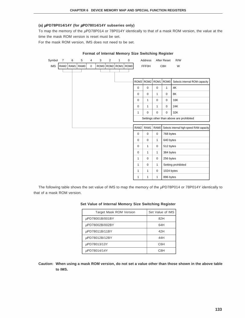
133
CHAPTER 6 DEVICE MEMORY MAP AND SPECIAL FUNCTION REGISTERS
(a) µµµµµPD78P014/14Y (for µµµµµPD78014/14Y subseries only)
To map the memory of the µPD78P014 or 78P014Y identically to that of a mask ROM version, the value at the
time the mask ROM version is reset must be set.
For the mask ROM version, IMS does not need to be set.
Format of Internal Memory Size Switching Register
The following table shows the set value of IMS to map the memory of the µPD78P014 or 78P014Y identically to
that of a mask ROM version.
Set Value of Internal Memory Size Switching Register
Target Mask ROM Version Set Value of IMS
µPD78001B/001BY 82H
µPD78002B/002BY 64H
µPD78011B/11BY 42H
µPD78012B/12BY 44H
µPD78013/13Y C6H
µPD78014/14Y C8H
Caution: When using a mask ROM version, do not set a value other than those shown in the above table
to IMS.
RAM2 RAM1 RAM0 0 ROM3 ROM2 ROM1 ROM0IMS
7 6 5 4 3 2 1 0Symbol Address After Reset R/W
FFF0H C8H W
ROM3 ROM2
0
0
0
0
0
0
1
1
ROM1 ROM0
0
1
1
0
0
1
0
0
1 0 0 0
Selects internal ROM capacity
4K
8K
16K
24K
32K
RAM2 RAM1
0
0
0
0
RAM0
0
1
Selects internal high-speed RAM capacity
768 bytes
640 bytes
0
0
1
1
0
1
512 bytes
384 bytes
1
1
0
0
0
1
256 bytes
Setting prohibited
1
1
1
1
0
1
1024 bytes
896 bytes
Settings other than above are prohibited
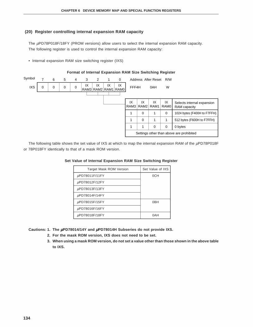
134
CHAPTER 6 DEVICE MEMORY MAP AND SPECIAL FUNCTION REGISTERS
(20) Register controlling internal expansion RAM capacity
The µPD78P018F/18FY (PROM versions) allow users to select the internal expansion RAM capacity.
The following register is used to control the internal expansion RAM capacity:
• Internal expansion RAM size switching register (IXS)
Format of Internal Expansion RAM Size Switching Register
The following table shows the set value of IXS at which to map the internal expansion RAM of the µPD78P018F
or 78P018FY identically to that of a mask ROM version.
Set Value of Internal Expansion RAM Size Switching Register
Target Mask ROM Version Set Value of IXS
µPD78011F/11FY 0CH
µPD78012F/12FY
µPD78013F/13FY
µPD78014F/14FY
µPD78015F/15FY 0BH
µPD78016F/16FY
µPD78018F/18FY 0AH
Cautions: 1. The µµµµµPD78014/14Y and µµµµµPD78014H Subseries do not provide IXS.
2. For the mask ROM version, IXS does not need to be set.
3. When using a mask ROM version, do not set a value other than those shown in the above table
to IXS.
6 5 4 3 2 1 07Symbol
IXS 0 0 0 0 IXRAM3
IXRAM2
IXRAM1
IXRAM0
1
1
Selects internal expansionRAM capacity
1024 bytes (F400H to F7FFH)
512 bytes (F600H to F7FFH)
1 0 bytes
FFF4H 0AH W
Address After Reset R/W
IXRAM3
0
0
1
IXRAM2
1
1
0
IXRAM1
0
1
0
IXRAM0
Settings other than above are prohibited
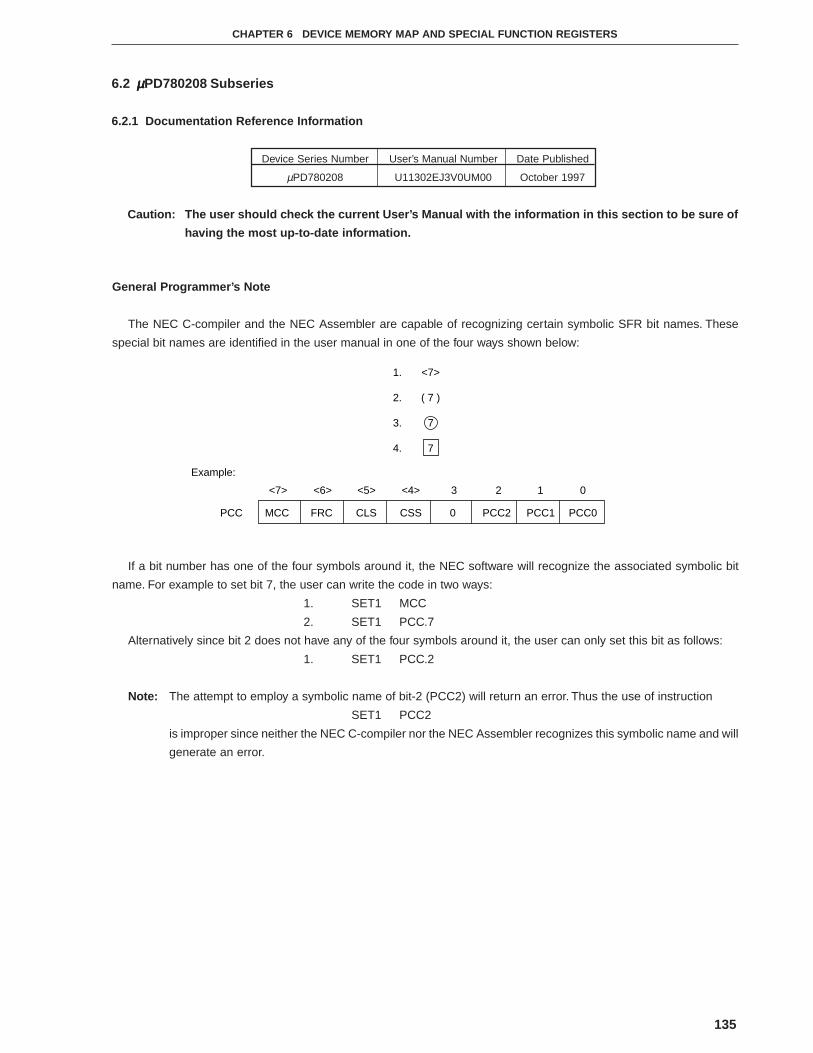
135
CHAPTER 6 DEVICE MEMORY MAP AND SPECIAL FUNCTION REGISTERS
6.2 µµµµµPD780208 Subseries
6.2.1 Documentation Reference Information
Device Series Number User’s Manual Number Date Published
µPD780208 U11302EJ3V0UM00 October 1997
Caution: The user should check the current User’s Manual with the information in this section to be sure of
having the most up-to-date information.
General Programmer’s Note
The NEC C-compiler and the NEC Assembler are capable of recognizing certain symbolic SFR bit names. These
special bit names are identified in the user manual in one of the four ways shown below:
If a bit number has one of the four symbols around it, the NEC software will recognize the associated symbolic bit
name. For example to set bit 7, the user can write the code in two ways:
1. SET1 MCC
2. SET1 PCC.7
Alternatively since bit 2 does not have any of the four symbols around it, the user can only set this bit as follows:
1. SET1 PCC.2
Note: The attempt to employ a symbolic name of bit-2 (PCC2) will return an error. Thus the use of instruction
SET1 PCC2
is improper since neither the NEC C-compiler nor the NEC Assembler recognizes this symbolic name and will
generate an error.
MCCPCC FRC CLS CSS 0 PCC2 PCC1 PCC0
<7> <6> <5> <4> 3 2 1 0
Example:
1.
2.
3.
4.
<7>
( 7 )
7
7
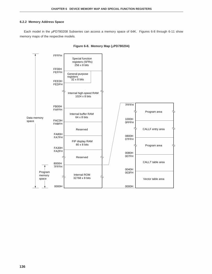
136
CHAPTER 6 DEVICE MEMORY MAP AND SPECIAL FUNCTION REGISTERS
6.2.2 Memory Address Space
Each model in the µPD780208 Subseries can access a memory space of 64K. Figures 6-8 through 6-11 show
memory maps of the respective models.
Figure 6-8. Memory Map ( µPD780204)
0000H
Data memory space
Internal ROM32768 x 8 bits
7FFFH
1000H0FFFH
0800H07FFH
0080H007FH
0040H003FH
0000H
CALLF entry area
CALLT table area
Program area
Program area
Internal high-speed RAM1024 x 8 bits
Reserved
Reserved
Programmemoryspace
8000H7FFFH
FFFFH
General-purpose registers 32 x 8 bits
Special function registers (SFRs) 256 x 8 bits
Vector table area
FA30HFA2FH
FIP display RAM80 x 8 bits
FA80HFA7FH
FAC0HFABFH
Internal buffer RAM64 x 8 bits
FB00HFAFFH
FEE0HFEDFH
FF00HFEFFH
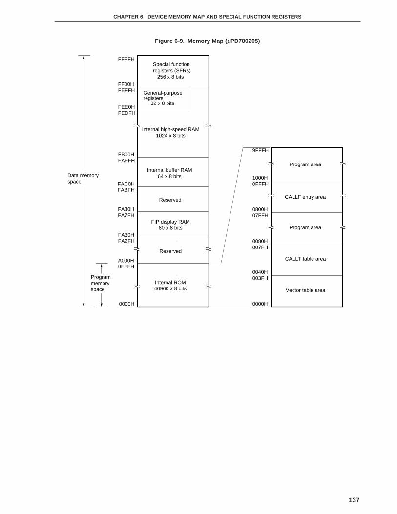
137
CHAPTER 6 DEVICE MEMORY MAP AND SPECIAL FUNCTION REGISTERS
Figure 6-9. Memory Map ( µPD780205)
0000H
Data memory space
Internal ROM40960 x 8 bits
9FFFH
1000H0FFFH
0800H07FFH
0080H007FH
0040H003FH
0000H
CALLF entry area
CALLT table area
Program area
Program area
Internal high-speed RAM1024 x 8 bits
Reserved
Reserved
Programmemoryspace
A000H9FFFH
FFFFH
General-purpose registers 32 x 8 bits
Special function registers (SFRs) 256 x 8 bits
Vector table area
FA30HFA2FH
FIP display RAM80 x 8 bits
FA80HFA7FH
FAC0HFABFH
Internal buffer RAM64 x 8 bits
FB00HFAFFH
FEE0HFEDFH
FF00HFEFFH

138
CHAPTER 6 DEVICE MEMORY MAP AND SPECIAL FUNCTION REGISTERS
Figure 6-10. Memory Map ( µPD780206)
Data memoryspace
Special functionregisters (SFRs)
256 x 8 bits
General-purposeregisters
32 x 8 bits
Internal high-speed RAM1024 x 8 bits
Internal buffer RAM64 x 8 bits
Reserved
FIP display RAM80 x 8 bits
Reserved
Internal expansion RAM1024 x 8 bits
Reserved
Internal ROM49152 x 8 bits
Program area
CALLF entry area
Program area
CALLT table area
Vector table area
Programmemory space
0000H
0040H003FH
0080H007FH
0800H07FFH
1000H0FFFH
BFFFH
FFFFH
FF00HFEFFH
FEE0HFEDFH
FB00HFAFFH
FAC0HFABFH
FA80HFA7FH
FA30HFA2FH
F800HF7FFH
F400HF3FFH
C000HBFFFH
0000H

139
CHAPTER 6 DEVICE MEMORY MAP AND SPECIAL FUNCTION REGISTERS
Figure 6-11. Memory Map ( µPD780208, 78P0208)
Data memoryspace
Special functionregisters (SFRs)
256 x 8 bits
General-purposeregisters
32 x 8 bits
Internal high-speed RAM1024 x 8 bits
Internal buffer RAM64 x 8 bits
Reserved
FIP display RAM80 x 8 bits
Reserved
Internal expansion RAM1024 x 8 bits
Reserved
Internal ROM/PROM61440 x 8 bits
Program area
CALLF entry area
Program area
CALLT table area
Vector table area
Programmemory space
FFFFH
FF00HFEFFH
FEE0HFEDFH
FB00HFAFFH
FAC0HFABFH
FA80HFA7FH
FA30HFA2FH
F800HF7FFH
F400HF3FFH
F000HEFFFH
0000H 0000H
0040H003FH
0080H007FH
0800H07FFH
1000H0FFFH
EFFFH

140
CHAPTER 6 DEVICE MEMORY MAP AND SPECIAL FUNCTION REGISTERS
6.2.3 Special Function Registers (SFRs)
Table 6-5. Special Function Register List ( µµµµµPD780208 Subseries) (1/2)
Manipulatable After
Address Special Function Register (SFR) Name Symbol R/W Bit Unit Reset
1 Bit 8 Bits 16 Bits
FF00H Port 0 P0 R/W √ √ – 00H
FF01H Port 1 P1 √ √ –
FF02H Port 2 P2 √ √ –
FF03H Port 3 P3 √ √ –
FF07H Port 7 P7 W √ √ –
FF08H Port 8 P8 √ √ –
FF09H Port 9 P9 √ √ –
FF0AH Port 10 P10 R/W √ √ –
FF0BH Port 11 P11 √ √ –
FF0CH Port 12 P12 √ √ –
FF10H 16-bit compare register CR00 – – √ Undefined
FF11H
FF12H 16-bit capture register CR01 R – – √FF13H
FF14H 16-bit timer register TM0 – – √ 0000H
FF15H
FF16H 8-bit compare register 10 CR10 R/W – √ – Undefined
FF17H 8-bit compare register 20 CR20 – √ –
FF18H 8-bit timer register 1 TMS TM1 R – √ √ 00H
FF19H 8-bit timer register 2 TMS TM2 – √
FF1AH Serial I/O shift register 0 SIO0 R/W – √ – Undefined
FF1BH Serial I/O shift register 1 SIO1 – √ –
FF1FH A/D conversion result register ADCR R – √ –
FF20H Port mode register 0 PM0 R/W √ √ – 1FH
FF21H Port mode register 1 PM1 √ √ – FFH
FF22H Port mode register 2 PM2 √ √ –
FF23H Port mode register 3 PM3 √ √ –
FF27H Port mode register 7 PM7 √ √ – 1FH
FF2AH Port mode register 10 PM10 √ √ – FFH
FF2BH Port mode register 11 PM11 √ √ –
FF2CH Port mode register 12 PM12 √ √ –
FF40H Timer clock select register 0 TCL0 √ √ – 00H
FF41H Timer clock select register 1 TCL1 – √ –
FF42H Timer clock select register 2 TCL2 – √ –
FF43H Timer clock select register 3 TCL3 – √ – 88H
FF47H Sampling clock select register SCS – √ – 00H
FF48H 16-bit timer mode control register TMC0 √ √ –
FF49H 8-bit timer mode control register TMC1 √ √ –
FF4AH Watch timer mode control register TMC2 √ √ –
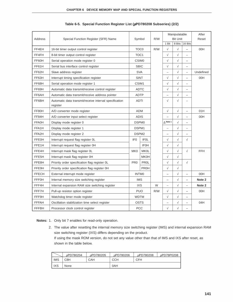
141
CHAPTER 6 DEVICE MEMORY MAP AND SPECIAL FUNCTION REGISTERS
Table 6-5. Special Function Register List ( µµµµµPD780208 Subseries) (2/2)
Manipulatable After
Address Special Function Register (SFR) Name Symbol R/W Bit Unit Reset
1 Bit 8 Bits 16 Bits
FF4EH 16-bit timer output control register TOC0 R/W √ √ – 00H
FF4FH 8-bit timer output control register TOC1 √ √ –
FF60H Serial operation mode register 0 CSIM0 √ √ –
FF61H Serial bus interface control register SBIC √ √ –
FF62H Slave address register SVA – √ – Undefined
FF63H Interrupt timing specification register SINT √ √ – 00H
FF68H Serial operation mode register 1 CSIM1 √ √ –
FF69H Automatic data transmit/receive control register ADTC √ √ –
FF6AH Automatic data transmit/receive address pointer ADTP – √ –
FF6BH Automatic data transmit/receive interval specification ADTI √ √ –
register
FF80H A/D converter mode register ADM √ √ – 01H
FF84H A/D converter input select register ADIS – √ – 00H
FFA0H Display mode register 0 DSPM0 ∆ Note 1 √ –
FFA1H Display mode register 1 DSPM1 – √ –
FFA2H Display mode register 2 DSPM2 – √ –
FFE0H Interrupt request flag register 0L IF0 IF0L √ √ √
FFE1H Interrupt request flag register 0H IF0H √ √
FFE4H Interrupt mask flag register 0L MK0 MK0L √ √ √ FFH
FFE5H Interrupt mask flag register 0H MK0H √ √
FFE8H Priority order specification flag register 0L PR0 PR0L √ √ √
FFE9H Priority order specification flag register 0H PR0H √ √
FFECH External interrupt mode register INTM0 – √ – 00H
FFF0H Internal memory size switching register IMS – √ – Note 2
FFF4H Internal expansion RAM size switching register IXS W – √ – Note 2
FFF7H Pull-up resistor option register PUO R/W √ √ – 00H
FFF9H Watchdog timer mode register WDTM √ √ –
FFFAH Oscillation stabilization time select register OSTS – √ – 04H
FFFBH Processor clock control register PCC √ √ –
Notes: 1. Only bit 7 enables for read-only operation.
2. The value after resetting the internal memory size switching register (IMS) and internal expansion RAM
size switching register (IXS) differs depending on the product.
If using the mask ROM version, do not set any value other than that of IMS and IXS after reset, as
shown in the table below.
µPD780204 µPD780205 µPD780206 µPD780208 µPD78P0208
IMS C8H CAH CCH CFH
IXS None 0AH
142
CHAPTER 6 DEVICE MEMORY MAP AND SPECIAL FUNCTION REGISTERS
(1) Registers controlling port functions
The following two types of registers control the ports:
• Port mode registers (PM0 to PM3, PM7, PM10 to PM12)
• Pull-up resistor option register (PUO)
143
CHAPTER 6 DEVICE MEMORY MAP AND SPECIAL FUNCTION REGISTERS
Format of Port Mode Registers
Format of Pull-up Resistor Option Register
PM0
PM1
PM2
PM37
0
PM127 PM126 PM125 PM124 PM123 PM122 PM121 PM120
0 0 1 PM03 PM02 PM01 1
7 6 5 4 3 2 1 0Symbol
PM16 PM15 PM14 PM13 PM12 PM11
PM26 PM25 PM24 PM23 PM22 PM21
PM36 PM35 PM34 PM33 PM32 PM31
PM17 PM10
PM27
PM3
PM20
PM30
PM12
PMmn Selects I/O mode of Pmn pin(m = 0, 1, 2, 3, 7, 10, 11, 12 : n = 0 to 7)
0
1
Output mode (output buffer ON)
Input mode (output buffer OFF)
FF20H
FF2CH
FF21H
FF22H
FF23H
1FH
FFH
FFH
FFH
FFH
R/W
R/W
R/W
R/W
R/W
Address After Reset R/W
0 PM72 PM710 0 PM74 PM73 PM70PM7 FF27H 1FH R/W
PM117 PM116 PM115 PM114 PM113 PM112 PM111 PM110PM11 FF2BH FFH R/W
PM107 PM102 PM101PM106 PM105 PM104 PM103 PM100PM10 FF2AH FFH R/W
Cautions: 1. P00 and P04 pins do not incorporate a pull-up resistor (Port 0).
2. When port 1 is used as analog input for an A/D converter, an on-chip pull-up resistor cannot be
used even if 1 is set in PUO1.
PUO 0
PUOm Selects internal pull-up resistor of Pm(m = 0, 1, 2, 3)
0
1
Internal pull-up resistor not used
Internal pull-up resistor used
FFF7H 00H R/W
Symbol 7 6 5 4 <3> <2> <0><1>
0 0 0 PUO3 PUO2 PUO1 PUO0
Address After Reset R/W
144
CHAPTER 6 DEVICE MEMORY MAP AND SPECIAL FUNCTION REGISTERS
(2) Registers controlling clock generator
The following three registers control the clock generator:
• Processor clock control register (PCC)
• Display mode register 0 (DSPM0)
• Display mode register 1 (DSPM1)
Format of Processor Clock Control Register
Notes: 1. Bit 5 is a read-only bit.
2. When the CPU is operating from the subsystem clock, MCC should be used to stop the main system
clock oscillation. A STOP instruction should not be used.
Cautions: 1. Bit 3 must be set to 0.
2. Do not set MCC while an external clock is being input. This is because the X2 pin is pulled up to
VDD.
Remarks: fX: Main system clock oscillation frequency
fXT : Subsystem clock oscillation frequency
PCC0PCC
<7> <6> <5> <4> 3 2Symbol 1 0
CSS Selects CPU clock (fCPU)
FFFBHPCC10 PCC2CSSCLSFRCMCC
Address After Reset R/W
04H R/W Note 1
fX
fX/2
fX/22
fX/23
fX/24
fXT/2
CLS Status of CPU clock
0 Main system clock
1 Subsystem clock
FRC Selects feedback resistor of subsystem clock
0 Uses internal feedback resistor
1 Does not use internal feedback resistor
MCC Controls oscillation of main system clock Note 2
0 Enables oscillation
1 Stops oscillation
PCC2
0
0
0
0
1
0
0
1
0
1
PCC1
0
0
1
1
0
0
0
1
1
0
PCC0
0
1
0
1
0
0
1
0
1
0
0
0
R/W
R
R/W
R/W
Settings other than above are prohibited

145
CHAPTER 6 DEVICE MEMORY MAP AND SPECIAL FUNCTION REGISTERS
Format of Display Mode Register 0 (1/2)
R/W SEGS4 SEGS3 SEGS2 SEGS1 SEGS0 Display segment (Display mode 1) Display output total (Display mode 2)
0 0 0 0 0 9 9
0 0 0 0 1 10 10
0 0 0 1 0 11 11
0 0 0 1 1 12 12
0 0 1 0 0 13 13
0 0 1 0 1 14 14
0 0 1 1 0 15 15
0 0 1 1 1 16 16
0 1 0 0 0 17 17
0 1 0 0 1 18 18
0 1 0 1 0 19 19
0 1 0 1 1 20 20
0 1 1 0 0 21 21
0 1 1 0 1 22 22
0 1 1 1 0 23 23
0 1 1 1 1 24 24
1 0 0 0 0 25 25
1 0 0 0 1 26 26
1 0 0 1 0 27 27
1 0 0 1 1 28 28
1 0 1 0 0 29 29
1 0 1 0 1 30 30
1 0 1 1 0 31 31
1 0 1 1 1 32 32
1 1 0 0 0 33 33
1 1 0 0 1 34 34
1 1 0 1 0 35 35
1 1 0 1 1 36 36
1 1 1 0 0 37 37
1 1 1 0 1 38 Note 38
1 1 1 1 0 39 Note 39
1 1 1 1 1 40 Note 40
Note: When the sum of digits and segments is over 53, specification of the number of digits has the priority.
7 1 06 5 4 3 2
KSF SEGS1 SEGS0DSPM06 DSPM05 SEGS4 SEGS3 SEGS2
Symbol
DSPM0 FFA0H 00H R/W
Address After Reset R/W
146
CHAPTER 6 DEVICE MEMORY MAP AND SPECIAL FUNCTION REGISTERS
Format of Display Mode Register 0 (2/2)
R/W DSPM05 Display mode setting
0 Display mode 1 (Segment/character type)
1 Display mode 2 (Type in which a segment spans two or more grids)
R/W DSPM06 Mode of noise elimination circuit for subsystem clock Note 2
0 2.5 MHz < fX ≤ 5.0 MHz
1 1.25 MHz ≤ fX ≤ 2.5 MHz Note 3
R KSF Timing status
0 Display timing
1 Key scan timing
Notes: 1. Bit 7 (KSF) is a read-only bit.
2. Set this bit according to the main system clock oscillation frequency (fX) selected. Noise elimination
circuit is effective during FIP display operation.
3. When fX is used between 1.25 MHz and 2.5 MHz, set bit 6 (DSPM06) to 1 prior to FIP display.
Caution: When the main system clock frequency selected is below 1.25 MHz and the FIP controller/
driver is enabled, make sure to use the main clock for watch timer counting by setting TCL24
to 0.
7 1 06 5 4 3 2
KSF SEGS1 SEGS0DSPM06 DSPM05 SEGS4 SEGS3 SEGS2
Symbol
DSPM0 FFA0H 00H R/W Note 1
Address After Reset R/W
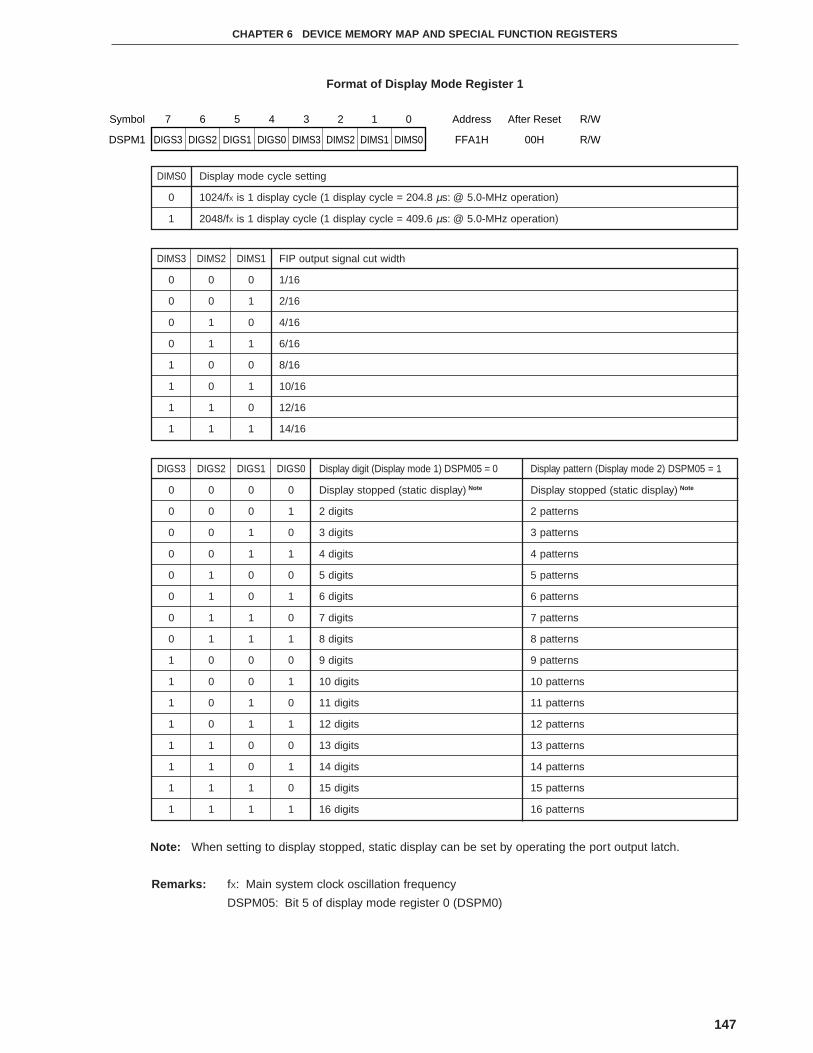
147
CHAPTER 6 DEVICE MEMORY MAP AND SPECIAL FUNCTION REGISTERS
Format of Display Mode Register 1
DIMS0 Display mode cycle setting
0 1024/fX is 1 display cycle (1 display cycle = 204.8 µs: @ 5.0-MHz operation)
1 2048/fX is 1 display cycle (1 display cycle = 409.6 µs: @ 5.0-MHz operation)
DIMS3 DIMS2 DIMS1 FIP output signal cut width
0 0 0 1/16
0 0 1 2/16
0 1 0 4/16
0 1 1 6/16
1 0 0 8/16
1 0 1 10/16
1 1 0 12/16
1 1 1 14/16
DIGS3 DIGS2 DIGS1 DIGS0 Display digit (Display mode 1) DSPM05 = 0 Display pattern (Display mode 2) DSPM05 = 1
0 0 0 0 Display stopped (static display) Note Display stopped (static display) Note
0 0 0 1 2 digits 2 patterns
0 0 1 0 3 digits 3 patterns
0 0 1 1 4 digits 4 patterns
0 1 0 0 5 digits 5 patterns
0 1 0 1 6 digits 6 patterns
0 1 1 0 7 digits 7 patterns
0 1 1 1 8 digits 8 patterns
1 0 0 0 9 digits 9 patterns
1 0 0 1 10 digits 10 patterns
1 0 1 0 11 digits 11 patterns
1 0 1 1 12 digits 12 patterns
1 1 0 0 13 digits 13 patterns
1 1 0 1 14 digits 14 patterns
1 1 1 0 15 digits 15 patterns
1 1 1 1 16 digits 16 patterns
Note: When setting to display stopped, static display can be set by operating the port output latch.
Remarks: fX: Main system clock oscillation frequency
DSPM05: Bit 5 of display mode register 0 (DSPM0)
7 1 06 5 4 3 2
DIGS3 DIMS1 DIMS0DIGS2 DIGS1 DIGS0 DIMS3 DIMS2
Symbol
DSPM1 FFA1H 00H R/W
Address After Reset R/W
148
CHAPTER 6 DEVICE MEMORY MAP AND SPECIAL FUNCTION REGISTERS
(3) Registers controlling 16-bit timer/event counter
The following six registers control the 16-bit timer/event counter:
• Timer clock select register 0 (TCL0)
• 16-bit timer mode control register (TMC0)
• 16-bit timer output control register (TOC0)
• Port mode register 3 (PM3)
- Refer to section (1) for the register format.
• External interrupt mode register (INTM0)
- Refer to section (13) for the register format.
• Sampling clock select register (SCS)
- Refer to section (13) for the register format.

149
CHAPTER 6 DEVICE MEMORY MAP AND SPECIAL FUNCTION REGISTERS
Format of Timer Clock Select Register 0
Cautions: 1. Setting of the TI0/INTP0 pin valid edge is performed by the external interrupt mode register
(INTM0), and selection of the sampling clock frequency is performed by the sampling clock
select register (SCS).
2. To read the count value when TI0 has been specified as the TM0 count clock, the value should
be read from TM0, not from the 16-bit capture register (CR01).
3. To write data other than that already written to TCL0, stop the timer operation once.
Remarks: fX: Main system clock oscillation frequency
TI0 : 16-bit timer/event counter input pin
TM0: 16-bit timer register
Values in parentheses apply to operation with fX = 5.0 MHz.
TCL00TCL0
<7> 6 5 4 3 2Symbol 1 0
FF40HTCL01TCL03 TCL02TCL04TCL05TCL06CLOE
Address After Reset R/W
00H R/W
TCL0616-bit timer register count clockselection
0 TI0 (Valid edge specifiable)
0 fX (5.0 MHz)
0 fX/2 (2.5 MHz)
0 fX/22 (1.25 MHz)
1 fX/23 (625 kHz)
TCL05
0
0
1
1
0
TCL04
0
1
0
1
0
This section controls the clock output circuit.Refer to (7) Registers controlling clock output function orChapter 10 of PD780208 Subseries User's Manualfor detailed information.
µ
Settings other than above are prohibited
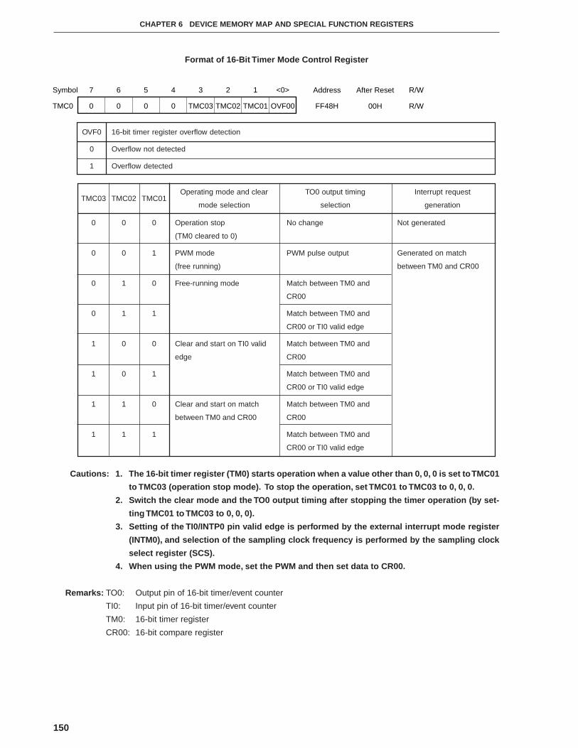
150
CHAPTER 6 DEVICE MEMORY MAP AND SPECIAL FUNCTION REGISTERS
Format of 16-Bit Timer Mode Control Register
OVF0 16-bit timer register overflow detection
0 Overflow not detected
1 Overflow detected
Operating mode and clear TO0 output timing Interrupt requestTMC03 TMC02 TMC01
mode selection selection generation
0 0 0 Operation stop No change Not generated
(TM0 cleared to 0)
0 0 1 PWM mode PWM pulse output Generated on match
(free running) between TM0 and CR00
0 1 0 Free-running mode Match between TM0 and
CR00
0 1 1 Match between TM0 and
CR00 or TI0 valid edge
1 0 0 Clear and start on TI0 valid Match between TM0 and
edge CR00
1 0 1 Match between TM0 and
CR00 or TI0 valid edge
1 1 0 Clear and start on match Match between TM0 and
between TM0 and CR00 CR00
1 1 1 Match between TM0 and
CR00 or TI0 valid edge
Cautions: 1. The 16-bit timer register (TM0) starts operation when a value other than 0, 0, 0 is set to TMC01
to TMC03 (operation stop mode). To stop the operation, set TMC01 to TMC03 to 0, 0, 0.
2. Switch the clear mode and the TO0 output timing after stopping the timer operation (by set-
ting TMC01 to TMC03 to 0, 0, 0).
3. Setting of the TI0/INTP0 pin valid edge is performed by the external interrupt mode register
(INTM0), and selection of the sampling clock frequency is performed by the sampling clock
select register (SCS).
4. When using the PWM mode, set the PWM and then set data to CR00.
Remarks: TO0: Output pin of 16-bit timer/event counter
TI0: Input pin of 16-bit timer/event counter
TM0: 16-bit timer register
CR00: 16-bit compare register
OVF00TMC0
7 6 5 4 3 2Symbol 1 <0>
FF48HTMC01TMC03 TMC020000
Address After Reset R/W
00H R/W
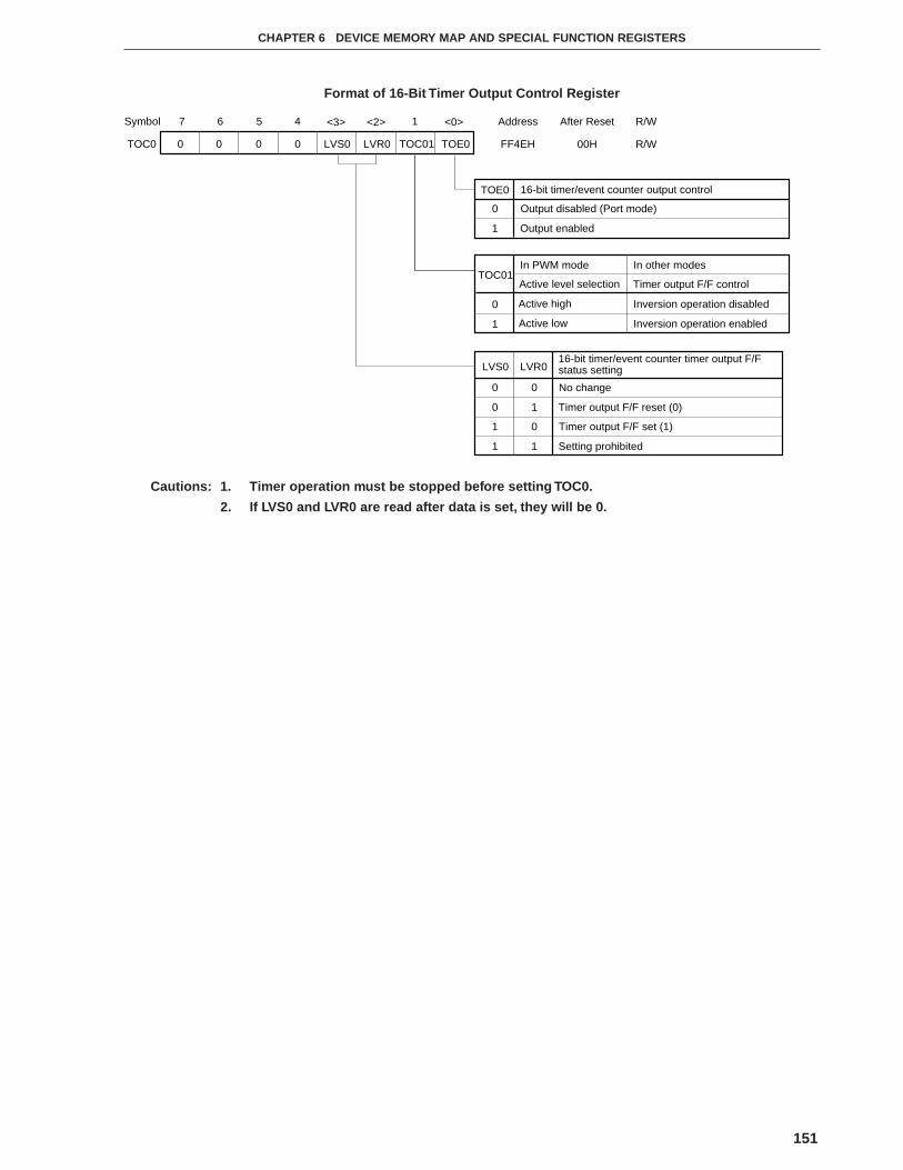
151
CHAPTER 6 DEVICE MEMORY MAP AND SPECIAL FUNCTION REGISTERS
Format of 16-Bit Timer Output Control Register
Cautions: 1. Timer operation must be stopped before setting TOC0.
2. If LVS0 and LVR0 are read after data is set, they will be 0.
TOE0TOC0
7 6 5 4 <3> <2>Symbol 1 <0>
TOE0 16-bit timer/event counter output control
0
1
Output disabled (Port mode)
Output enabled
FF4EHTOC01LVS0
TOC01
LVS016-bit timer/event counter timer output F/Fstatus setting
0
0
No change
Timer output F/F reset (0)
1
1
LVR0
0
1
0
1
Timer output F/F set (1)
Setting prohibited
LVR00
In PWM mode
0
1
Active level selection Timer output F/F control
Active high
Active low
In other modes
Inversion operation disabled
Inversion operation enabled
Address After Reset R/W
00H R/W0 0 0
152
CHAPTER 6 DEVICE MEMORY MAP AND SPECIAL FUNCTION REGISTERS
(4) Registers controlling 8-bit timer/event counter
The following four registers control the 8-bit timer/event counters:
• Timer clock select register 1 (TCL1)
• 8-bit timer mode control register (TMC1)
• 8-bit timer output control register (TOC1)
• Port mode register 3 (PM3)
- Refer to section (1) for the register format.
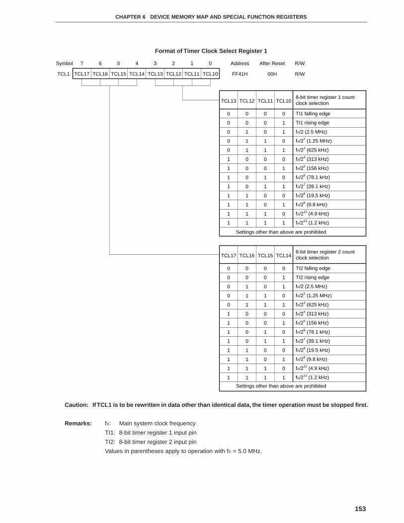
153
CHAPTER 6 DEVICE MEMORY MAP AND SPECIAL FUNCTION REGISTERS
Format of Timer Clock Select Register 1
Caution: If TCL1 is to be rewritten in data other than identical data, the timer operation must be stopped first.
Remarks: fX: Main system clock frequency
TI1: 8-bit timer register 1 input pin
TI2: 8-bit timer register 2 input pin
Values in parentheses apply to operation with fX = 5.0 MHz.
TCL10TCL1
7 6 5 4 3 2Symbol 1 0
TCL138-bit timer register 1 countclock selection
FF41HTCL11TCL13 TCL12TCL14TCL15TCL16TCL17
Address After Reset R/W
00H R/W
0 TI1 falling edge
0 TI1 rising edge
0 fX/2 (2.5 MHz)
0 fX/22 (1.25 MHz)
0 fX/23 (625 kHz)
1 fX/24 (313 kHz)
1 fX/25 (156 kHz)
1 fX/26 (78.1 kHz)
1 fX/27 (39.1 kHz)
1 fX/28 (19.5 kHz)
1 fX/29 (9.8 kHz)
1 fX/210 (4.9 kHz)
1 fX/212 (1.2 kHz)
TCL12
0
0
1
1
1
0
0
0
0
1
1
1
1
TCL11
0
0
0
1
1
0
0
1
1
0
0
1
1
Settings other than above are prohibited
TCL10
0
1
1
0
1
0
1
0
1
0
1
0
1
TCL178-bit timer register 2 countclock selection
0 TI2 falling edge
0 TI2 rising edge
0 fX/2 (2.5 MHz)
0 fX/22 (1.25 MHz)
0 fX/23 (625 kHz)
1 fX/24 (313 kHz)
1 fX/25 (156 kHz)
1 fX/26 (78.1 kHz)
1 fX/27 (39.1 kHz)
1 fX/28 (19.5 kHz)
1 fX/29 (9.8 kHz)
1 fX/210 (4.9 kHz)
1 fX/212 (1.2 kHz)
TCL16
0
0
1
1
1
0
0
0
0
1
1
1
1
TCL15
0
0
0
1
1
0
0
1
1
0
0
1
1
TCL14
0
1
1
0
1
0
1
0
1
0
1
0
1
Settings other than above are prohibited
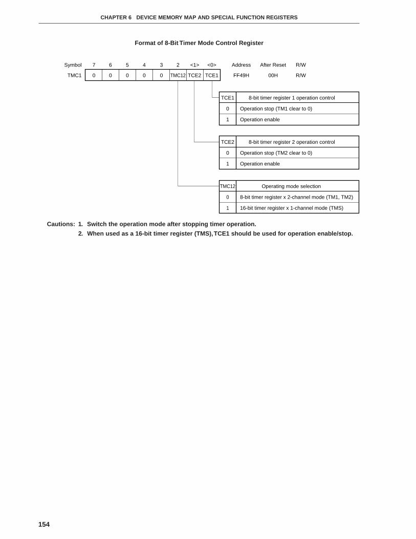
154
CHAPTER 6 DEVICE MEMORY MAP AND SPECIAL FUNCTION REGISTERS
Format of 8-Bit Timer Mode Control Register
Cautions: 1. Switch the operation mode after stopping timer operation.
2. When used as a 16-bit timer register (TMS), TCE1 should be used for operation enable/stop.
7 6 5 4 3 2 <1> <0>
0 0 0 0 0 TMC12 TCE2 TCE1
Symbol
TMC1
Address
FF49H
After Reset
00H
R/W
R/W
TCE1
0
1
8-bit timer register 1 operation control
Operation stop (TM1 clear to 0)
Operation enable
TCE2
0
1
8-bit timer register 2 operation control
Operation stop (TM2 clear to 0)
Operation enable
TMC12
0
1
Operating mode selection
8-bit timer register x 2-channel mode (TM1, TM2)
16-bit timer register x 1-channel mode (TMS)

155
CHAPTER 6 DEVICE MEMORY MAP AND SPECIAL FUNCTION REGISTERS
Format of 8-Bit Timer Output Control Register
Cautions: 1. Be sure to set TOC1 after stopping timer operation.
2. After data setting, 0 can be read from LVS1, LVS2, LVR1, and LVR2.
<7> <6> 5 <4> <3> <2> 1 <0>
LVS2 LVR2 TOC15 TOE2 LVS1 LVR1 TOC11 TOE1
Symbol
TOC1
Address
FF4FH
After Reset
00H
R/W
R/W
TOE1
0
1
8-bit timer/event counter 1 output control
Output disable (Port mode)
Output enable
TOC11
0
1
8-bit timer/event counter 1 timer output F/F control
Inverted operation disable
Inverted operation enable
LVS1
0
0
1
1
Unchanged
Timer output F/F reset (0)
Timer output F/F set (1)
Setting prohibited
TOE2
0
1
8-bit timer/event counter 2 output control
Output disable (Port mode)
Output enable
TOC15
0
1
8-bit timer/event counter 2 timer output F/F control
Inverted operation disable
Inverted operation enable
LVR1
0
1
0
1
8-bit timer/event counter 1 timer output F/Fstatus set
LVS2
0
0
1
1
Unchanged
Timer output F/F reset (0)
Timer output F/F set (1)
Setting prohibited
LVR2
0
1
0
1
8-bit timer/event counter 2 timer output F/Fstatus set
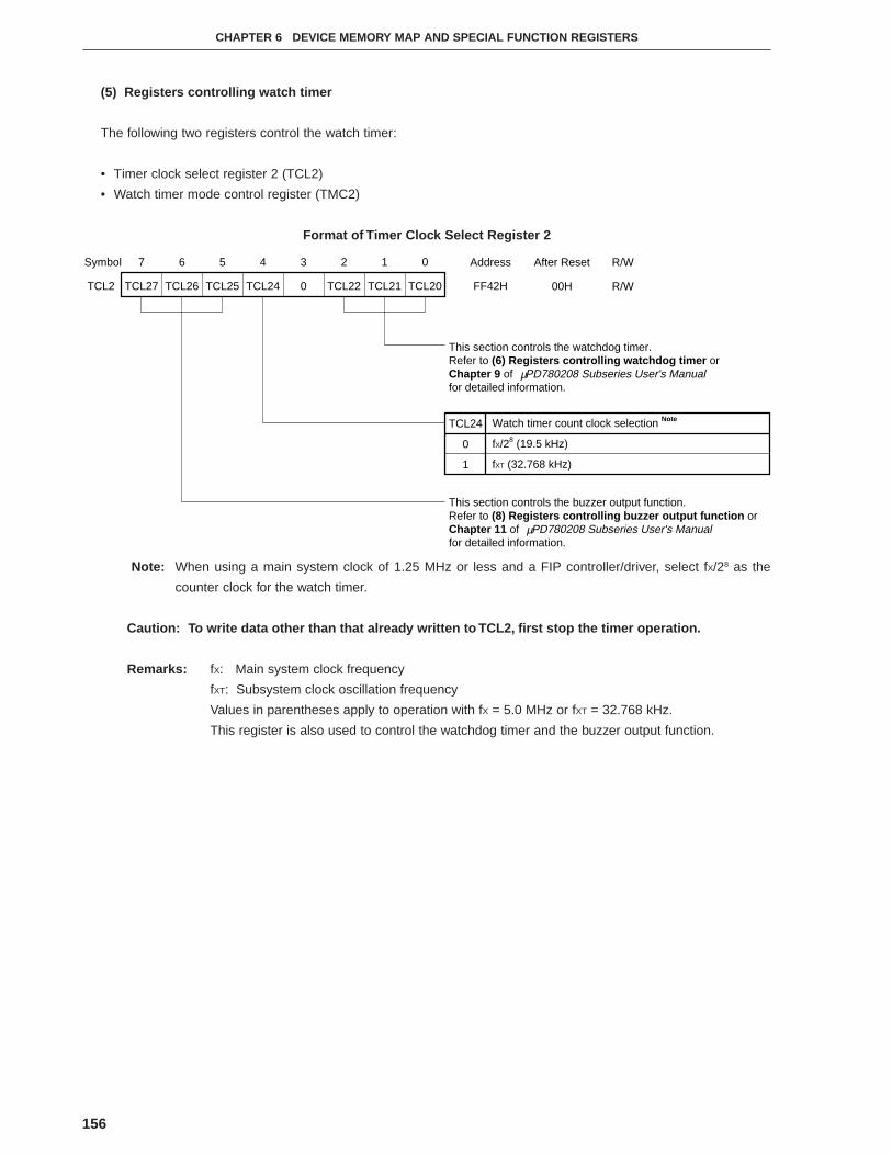
156
CHAPTER 6 DEVICE MEMORY MAP AND SPECIAL FUNCTION REGISTERS
(5) Registers controlling watch timer
The following two registers control the watch timer:
• Timer clock select register 2 (TCL2)
• Watch timer mode control register (TMC2)
Format of Timer Clock Select Register 2
Note: When using a main system clock of 1.25 MHz or less and a FIP controller/driver, select fX/28 as the
counter clock for the watch timer.
Caution: To write data other than that already written to TCL2, first stop the timer operation.
Remarks: fX: Main system clock frequency
fXT: Subsystem clock oscillation frequency
Values in parentheses apply to operation with fX = 5.0 MHz or fXT = 32.768 kHz.
This register is also used to control the watchdog timer and the buzzer output function.
TCL20TCL2
7 6 5 4 3 2Symbol 1 0
FF42HTCL210 TCL22TCL24TCL25TCL26TCL27
Address After Reset R/W
00H R/W
TCL24 Watch timer count clock selection Note
0 fX/28 (19.5 kHz)
1 fXT (32.768 kHz)
This section controls the watchdog timer.Refer to (6) Registers controlling watchdog timer orChapter 9 of PD780208 Subseries User's Manualfor detailed information.
µ
This section controls the buzzer output function.Refer to (8) Registers controlling buzzer output function orChapter 11 of PD780208 Subseries User's Manualfor detailed information.
µ
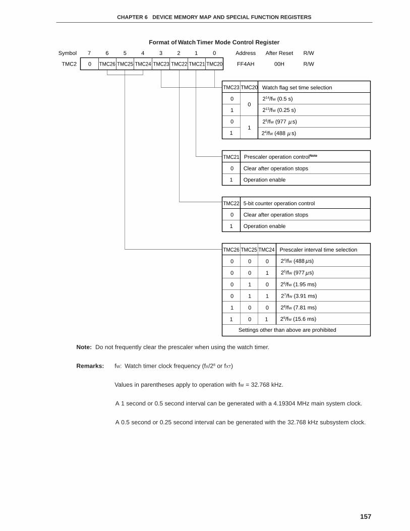
157
CHAPTER 6 DEVICE MEMORY MAP AND SPECIAL FUNCTION REGISTERS
Format of Watch Timer Mode Control Register
Note: Do not frequently clear the prescaler when using the watch timer.
Remarks: fW: Watch timer clock frequency (fX/28 or fXT)
Values in parentheses apply to operation with fW = 32.768 kHz.
A 1 second or 0.5 second interval can be generated with a 4.19304 MHz main system clock.
A 0.5 second or 0.25 second interval can be generated with the 32.768 kHz subsystem clock.
7 6 5 4 3 2 1 0
0 TMC26 TMC25 TMC24 TMC23 TMC22 TMC21 TMC20
Symbol
TMC2
Address
FF4AH
After Reset
00H
R/W
R/W
TMC21
0
1
Prescaler operation controlNote
Clear after operation stops
Operation enable
TMC22
0
1
5-bit counter operation control
Clear after operation stops
Operation enable
TMC23
0
1
0
1
TMC20
0
1
Watch flag set time selection
TMC26
0
0
0
0
1
1
Prescaler interval time selection
24/fW (488 s)
TMC25
0
0
1
1
0
0
214/fW (0.5 s)
µ
TMC24
0
1
0
1
0
1
25/fW (977 s)
213/fW (0.25 s)
24/fW (488 s)
µ
29/fW (15.6 ms)
28/fW (7.81 ms)
27/fW (3.91 ms)
26/fW (1.95 ms)
25/fW (977 s)µ
µ
Settings other than above are prohibited

158
CHAPTER 6 DEVICE MEMORY MAP AND SPECIAL FUNCTION REGISTERS
(6) Registers controlling watchdog timer
The following two registers control the watchdog timer:
• Timer clock select register 2 (TCL2)
• Watchdog timer mode register (WDTM)
Format of Timer Clock Select Register 2
Caution: To write data other than that already written to TCL2, first stop the timer operation.
Remarks: fX: Main system clock frequency
fXT: Subsystem clock oscillation frequency
Values in parentheses apply to operation with fX = 5.0 MHz.
This register is also used to control the watch timer and the buzzer output function.
TCL20TCL2
7 6 5 4 3 2Symbol 1 0
TCL22Count clock selection
FF42HTCL210 TCL22TCL24TCL25TCL26TCL27
Address After Reset R/W
00H R/W
Watchdog Timer mode
0 fX/23 (625 kHz)
0 fX/24 (313 kHz)
0 fX/25 (156 kHz)
0 fX/26 (78.1 kHz)
1 fX/27 (39.1 kHz)
1 fX/28 (19.5 kHz)
1 fX/29 (9.8k Hz)
1 fX/211 (2.4 kHz)
Interval Timer mode
fX/24 (313 kHz)
fX/25 (156 kHz)
fX/26 (78.1 kHz)
fX/27 (39.1 kHz)
fX/28 (19.5 kHz)
fX/29 (9.8 kHz)
fX/210 (4.9 kHz)
fX/212 (1.2 kHz)
TCL21
0
0
1
1
0
0
1
1
TCL20
0
1
0
1
0
1
0
1
This section controls the watch timer.Refer to (5) Registers controlling watch timer orChapter 8 of PD780208 Subseries User's Manual for detailed information.
µ
This section controls the buzzer output function.Refer to (8) Registers controlling buzzer output function orChapter 11 of PD780208 Subseries User's Manualfor detailed information.
µ
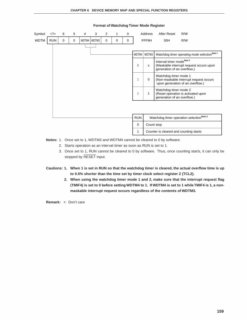
159
CHAPTER 6 DEVICE MEMORY MAP AND SPECIAL FUNCTION REGISTERS
Format of Watchdog Timer Mode Register
Notes: 1. Once set to 1, WDTM3 and WDTM4 cannot be cleared to 0 by software.
2. Starts operation as an interval timer as soon as RUN is set to 1.
3. Once set to 1, RUN cannot be cleared to 0 by software. Thus, once counting starts, it can only be
stopped by RESET input.
Cautions: 1. When 1 is set in RUN so that the watchdog timer is cleared, the actual overflow time is up
to 0.5% shorter than the time set by timer clock select register 2 (TCL2).
2. When using the watchdog timer mode 1 and 2, make sure that the interrupt request flag
(TMIF4) is set to 0 before setting WDTM4 to 1. If WDTM4 is set to 1 while TMIF4 is 1, a non-
maskable interrupt request occurs regardless of the contents of WDTM3.
Remark: ×: Don’t care
<7> 6 5 4 3 2 1 0
RUN 0 0 WDTM4 WDTM3 0 0 0
Symbol
WDTM
Address
FFF9H
After Reset
00H
R/W
R/W
WDTM4
0
1
1
Watchdog timer operating mode selectionNote 1
Interval timer modeNote 2
(Maskable interrupt request occurs upon generation of an overflow.)
Watchdog timer mode 1(Non-maskable interrupt request occurs upon generation of an overflow.)
Watchdog timer mode 2(Reset operation is activated upon generation of an overflow.)
RUN
0
1
Watchdog timer operation selectionNote 3
Count stop
Counter is cleared and counting starts
WDTM3
x
0
1
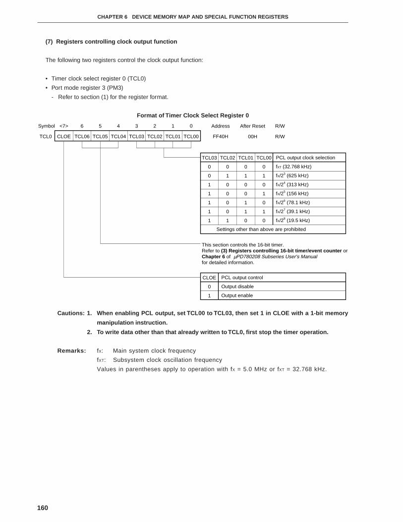
160
CHAPTER 6 DEVICE MEMORY MAP AND SPECIAL FUNCTION REGISTERS
(7) Registers controlling clock output function
The following two registers control the clock output function:
• Timer clock select register 0 (TCL0)
• Port mode register 3 (PM3)
- Refer to section (1) for the register format.
Format of Timer Clock Select Register 0
Cautions: 1. When enabling PCL output, set TCL00 to TCL03, then set 1 in CLOE with a 1-bit memory
manipulation instruction.
2. To write data other than that already written to TCL0, first stop the timer operation.
Remarks: fX: Main system clock frequency
fXT: Subsystem clock oscillation frequency
Values in parentheses apply to operation with fX = 5.0 MHz or fXT = 32.768 kHz.
TCL00TCL0
<7> 6 5 4 3 2Symbol 1 0
TCL03 PCL output clock selection
FF40HTCL01TCL03 TCL02TCL04TCL05TCL06CLOE
Address After Reset R/W
00H R/W
0 fXT (32.768 kHz)
0 fX/23 (625 kHz)
1 fX/24 (313 kHz)
1 fX/25 (156 kHz)
1 fX/26 (78.1 kHz)
1 fX/27 (39.1 kHz)
1 fX/28 (19.5 kHz)
CLOE PCL output control
0 Output disable
1 Output enable
TCL02
0
1
0
0
0
0
1
TCL01
0
1
0
0
1
1
0
TCL00
0
1
0
1
0
1
0
This section controls the 16-bit timer.Refer to (3) Registers controlling 16-bit timer/event counter orChapter 6 of PD780208 Subseries User's Manualfor detailed information.
µ
Settings other than above are prohibited
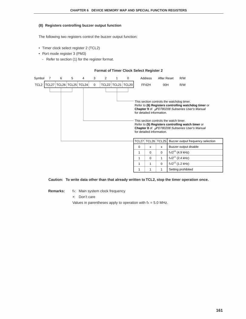
161
CHAPTER 6 DEVICE MEMORY MAP AND SPECIAL FUNCTION REGISTERS
(8) Registers controlling buzzer output function
The following two registers control the buzzer output function:
• Timer clock select register 2 (TCL2)
• Port mode register 3 (PM3)
- Refer to section (1) for the register format.
Format of Timer Clock Select Register 2
Caution: To write data other than that already written to TCL2, stop the timer operation once.
Remarks: fX: Main system clock frequency
×: Don’t care
Values in parentheses apply to operation with fX = 5.0 MHz.
TCL20TCL2
7 6 5 4 3 2Symbol 1 0
FF42HTCL210 TCL22TCL24TCL25TCL26TCL27
Address After Reset R/W
00H R/W
TCL27 Buzzer output frequency selection
0 Buzzer output disable
1 fX/210 (4.9 kHz)
1 fX/211 (2.4 kHz)
1 fX/212 (1.2 kHz)
1 Setting prohibited
TCL26
x
0
0
1
1
TCL25
x
0
1
0
1
This section controls the watchdog timer.Refer to (6) Registers controlling watchdog timer orChapter 9 of PD780208 Subseries User's Manualfor detailed information.
µ
This section controls the watch timer.Refer to (5) Registers controlling watch timer orChapter 8 of PD780208 Subseries User's Manualfor detailed information.
µ
162
CHAPTER 6 DEVICE MEMORY MAP AND SPECIAL FUNCTION REGISTERS
(9) Registers controlling A/D converter
The following two registers control the A/D converter:
• A/D converter mode register (ADM)
• A/D converter input select register (ADIS)

163
CHAPTER 6 DEVICE MEMORY MAP AND SPECIAL FUNCTION REGISTERS
Format of A/D Converter Mode Register
ADM3 ADM2 ADM1 Analog input channel selection
0 0 0 ANI0
0 0 1 ANI1
0 1 0 ANI2
0 1 1 ANI3
1 0 0 ANI4
1 0 1 ANI5
1 1 0 ANI6
1 1 1 ANI7
FR1 FR0A/D conversion time selectionNote 1
When operated at fX = 5.0 MHz When operated at fX = 4.19 MHz
0 0 160/fX (32.0 µs) 160/fX (38.1 µs)
0 1 80/fX (Setting prohibitedNote 2) 80/fX (19.1 µs)
1 0 200/fX (40.0 µs) 200/fX (47.7 µs)
1 1 Setting prohibited
TRG External trigger selection
0 No external trigger (software starts mode)
1 Conversion started by external trigger (hardware starts mode)
CS A/D conversion operation control
0 Operation stop
1 Operation start
Notes: 1. Set so that the A/D conversion time is 19.1 µs or more.
2. Setting prohibited because the A/D conversion time is less than 19.1 µs.
Cautions: 1. In consideration of power consumption reduction at the A/D converter when
the standby function is working, clear bit 7 (CS) of this register to 0 to stop
the A/D conversion operation before executing a HALT or STOP instruction.
2. When restarting the stopped A/D conversion operation, start the A/D conversion
operation after clearing the interrupt request flag (ADIF) to 0.
Remark: fX: Main system clock frequency
<6> 5 4 3 2 1 0<7>Symbol
ADM CS TRG FR1 FR0 ADM3 ADM2 ADM1 1 FF80H
Address After Reset R/W
01H R/W
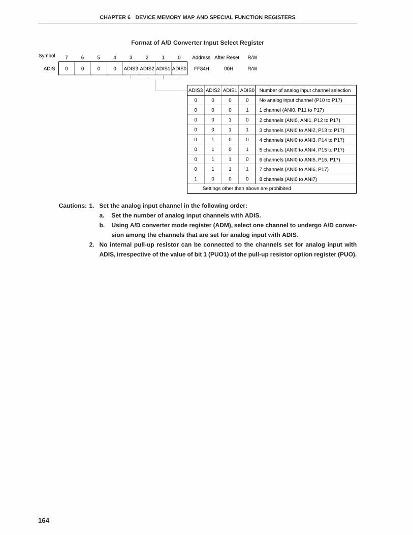
164
CHAPTER 6 DEVICE MEMORY MAP AND SPECIAL FUNCTION REGISTERS
Format of A/D Converter Input Select Register
Cautions: 1. Set the analog input channel in the following order:
a. Set the number of analog input channels with ADIS.
b. Using A/D converter mode register (ADM), select one channel to undergo A/D conver-
sion among the channels that are set for analog input with ADIS.
2. No internal pull-up resistor can be connected to the channels set for analog input with
ADIS, irrespective of the value of bit 1 (PUO1) of the pull-up resistor option register (PUO).
6 5 4 3 2 1 07Symbol
ADIS 0 0 0 0 ADIS3 ADIS2 ADIS1 ADIS0 FF84H
Address After Reset R/W
ADIS3
0
0
0
0
Number of analog input channel selection
No analog input channel (P10 to P17)
1 channel (ANI0, P11 to P17)
2 channels (ANI0, ANI1, P12 to P17)
ADIS2
0
0
0
0
ADIS1
0
0
1
1
0
3 channels (ANI0 to ANI2, P13 to P17)
1 0
0
0
0
4 channels (ANI0 to ANI3, P14 to P17)
6 channels (ANI0 to ANI5, P16, P17)
5 channels (ANI0 to ANI4, P15 to P17)1
1
1
0
1
1
1 0 0
ADIS0
0
1
1
0
0
1
1
0
0
7 channels (ANI0 to ANI6, P17)
8 channels (ANI0 to ANI7)
R/W00H
Settings other than above are prohibited
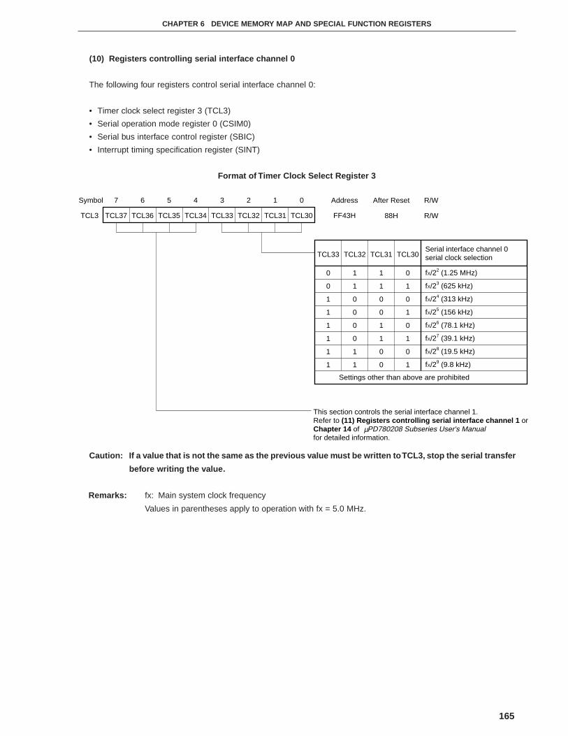
165
CHAPTER 6 DEVICE MEMORY MAP AND SPECIAL FUNCTION REGISTERS
(10) Registers controlling serial interface channel 0
The following four registers control serial interface channel 0:
• Timer clock select register 3 (TCL3)
• Serial operation mode register 0 (CSIM0)
• Serial bus interface control register (SBIC)
• Interrupt timing specification register (SINT)
Format of Timer Clock Select Register 3
Caution: If a value that is not the same as the previous value must be written to TCL3, stop the serial transfer
before writing the value.
Remarks: fx: Main system clock frequency
Values in parentheses apply to operation with fx = 5.0 MHz.
TCL30TCL3
7 6 5 4 3 2Symbol 1 0
TCL33Serial interface channel 0serial clock selection
FF43HTCL31TCL33 TCL32TCL34TCL35TCL36TCL37
Address After Reset R/W
88H R/W
0 fX/22 (1.25 MHz)
0 fX/23 (625 kHz)
1 fX/24 (313 kHz)
1 fX/25 (156 kHz)
1 fX/26 (78.1 kHz)
1 fX/27 (39.1 kHz)
1 fX/28 (19.5 kHz)
1 fX/29 (9.8 kHz)
TCL32
1
1
0
0
0
0
1
1
TCL31
1
1
0
0
1
1
0
0
TCL30
0
1
0
1
0
1
0
1
This section controls the serial interface channel 1.Refer to (11) Registers controlling serial interface channel 1 orChapter 14 of PD780208 Subseries User's Manualfor detailed information.
µ
Settings other than above are prohibited

166
CHAPTER 6 DEVICE MEMORY MAP AND SPECIAL FUNCTION REGISTERS
CSIE0 COI WUP CSIM04
CSIM03
CSIM02
CSIM01
CSIM00
<7> <6> <5> 4 3 2 1 0
CSIM0
Symbol
FF60H 00H R/WNote 1
Address After Reset R/W
Format of Serial Operation Mode Register 0
R/W CSIM CSIMSerial interface channel 0 clock selection
01 00
0 × Input clock to SCK0 pin from off-chip
1 0 8-bit timer register 2 (TM2) output
1 1 Clock specified with bits 0 to 3 of timer clock select register 3 (TCL3)
R/W CSIM CSIM CSIM Operating Start SI0/P25 SO0/P26 SCK0/P2704 03 02 Mode Bit Pin Function Pin Function Pin Function
0 MSB SCK00 × 1 × 0 0 0 1 (CMOS
1 LSB input/output)
Note 3 Note 3 P25 SB10 × × 0 0 0 1 (CMOS (N-ch open-drain
input/output) input/output) SCK01 0 SBI mode MSB (CMOS
Note 3 Note 3 SB0 P26 input/output)1 0 0 × × 0 1 (N-ch open-drain (CMOS input/
input/output) output)
Note 3 Note 3 P25 SB1
0 × × 0 0 0 1 (CMOS (N-ch open-drain SCK0
2-wire serial input/output) input/output) (N-ch open-drain1 1 I/O mode MSB input/ output)
Note 3 Note 3 SB0 P261 0 0 × × 0 1 (N-ch open-drain (CMOS
input/output) input/output)
R/W WUP Wake-up function control Note 4
0 Interrupt request signal generation with each serial transfer in any mode
Interrupt request signal generation when the address received after bus release (when CMDD = RELD = 1) matches the1
slave address register (SVA) in SBI mode
R COI Slave address comparison result flag Note 5
0 Slave address register (SVA) not equal to serial I/O shift register 0 (SIO0) data
1 Slave address register (SVA) equal to serial I/O shift register 0 (SIO0) data
R/W CSIE0 Serial interface channel 0 operation control
0 Operation stopped
1 Operation enable
PM25 P25 PM26 P26 PM27 P27
3-wire serial SI0Note 2 SO0I/O mode (Input) (CMOS output)

167
CHAPTER 6 DEVICE MEMORY MAP AND SPECIAL FUNCTION REGISTERS
Notes: 1. Bit 6 (COI) is a read-only bit.
2. Can be used as P25 (CMOS input) when serial channel is used only for transmission.
3. Can be used freely as a port function when not used in SBI or 2-wire mode.
4. To use the wake-up function (WUP = 1), clear bit 5 (SIC) of the interrupt timing specify register (SINT)
to 0.
5. COI becomes 0 when CSIE0 = 0.
Caution: Do not change the operation mode (3-wire serial I/O, 2-wire serial I/O, or SBI) while the operation of
serial interface channel 0 is enabled. Stop the serial operation before changing the operation
mode.
Remarks: ×: Don’t care
PM××: Port mode register
P××: Port output latch
Format of Serial Bus Interface Control Register (1/2)
<6> <5> <4> <3> <2> <1> <0><7>Symbol
SBIC BSYE ACKD ACKE ACKT CMDD RELD CMDT RELT FF61H 00H R/WNote
Address After Reset R/W
R/W Use for bus release signal output.
RELT When RELT = 1, SO latch is set to 1. After SO latch setting, automatically cleared to 0.
Also cleared to 0 when CSIE0 = 0.
R/W Use for command signal output.
CMDT When CMDT = 1, SO latch is cleared to (0). After SO latch clearance, automatically cleared to (0).
Also cleared to (0) when CSIE0 = 0.
R RELD Bus release detection
Clear Conditions (RELD = 0) Set Condition (RELD = 1)
• When transfer start instruction is executed
• If SIO0 and SVA values do not match in address
reception • When bus release signal (REL) is detected
• When CSIE0 = 0
• When RESET input is applied
R CMDD Command detection
Clear Conditions (CMDD = 0) Set Condition (CMDD = 1)
• When transfer start instruction is executed
• When bus release signal (REL) is detected• When command signal (CMD) is detected
• When CSIE0 = 0
• When RESET input is applied
R/W Acknowledge signal is output in synchronization with the falling-edge clock of SCK0 just after execu-
ACKT tion of the instruction to be set to 1, and after acknowledge signal output, automatically cleared to 0.
Also cleared to 0 upon start of serial interface transfer or when CSIE0 = 0.
Note: Bits 2, 3, and 6 (RELD, CMDD, and ACKD) are read-only bits.
Remark: CSIE0: Bit 7 of the serial operating mode register 0 (CSIM0)

168
CHAPTER 6 DEVICE MEMORY MAP AND SPECIAL FUNCTION REGISTERS
Format of Serial Bus Interface Control Register (2/2)
R/W ACKE Acknowledge signal output control
0 Acknowledge signal automatic output disable (output with ACKT enable)
Before completion Acknowledge signal is output in synchronization with the 9th clock
of transfer falling edge of SCK0 (automatically output when ACKE = 1).
1 Acknowledge signal is output in synchronization with the falling edge of SCK0
After completion just after execution of the instruction to be set to 1 (automatically output when
of transfer ACKE = 1).
However, it is not automatically cleared to 0 after acknowledge signal output.
R ACKD Acknowledge detection
Clear Conditions (ACKD = 0) Set Condition (ACKD = 1)
• At the falling edge of SCK0 immediately after the
busy mode has been released when a transfer • When acknowledge signal (ACK) is detected at the
start instruction is executed rising edge of SCK0 clock after completion of
• When CSIE0 = 0 transfer
• When RESET input is applied
R/W BSYENote Synchronizing busy signal output control
Disables busy signal, which is output in synchronization with the falling edge of SCK0 clock just after0
execution of the instruction to be cleared to 0.
1 Outputs busy signal at the falling edge of SCK0 clock following the acknowledge signal.
Note: Busy mode can be cleared by starting a serial interface transfer. However, the BSYE flag is not
cleared to 0.
Remarks: Bits 0, 1, and 4 (RELT, CMDT, and ACKT) are 0 when read after data setting.
CSIE0: Bit 7 of the serial operating mode register 0 (CSIM0)
<6> <5> <4> <3> <2> <1> <0><7>Symbol
SBIC BSYE ACKD ACKE ACKT CMDD RELD CMDT RELT FF61H 00H R/WNote
Address After Reset R/W

169
CHAPTER 6 DEVICE MEMORY MAP AND SPECIAL FUNCTION REGISTERS
Format of Interrupt Timing Specification Register
Notes: 1. Bit 6 (CLD) is a read-only bit.
2. When using the wake-up function, set SIC to 0.
3. When CSIE = 0, CLD becomes 0.
Caution: Be sure to set bits 0 through 3 to 0.
Remarks: SVA: Slave address register
CSIIF0: Interrupt request flag for INTCSI0
CSIE0: Bit 7 of serial operation mode register 0 (CSIM0)
<6> <5> <4> 3 2 1 07Symbol
SINT 0 CLD SIC SVAM 0 0 0 0 FF63H 00H R/WNote 1
Address After Reset R/W
SVAM
0
1
SVA bit to be used as slave address
Bits 0 to 7
Bits 1 to 7
SIC
0
1
INTCSI0 interrupt factor selectionNote 2
CSIIF0 is set upon termination of a serial interfacechannel 0 transfer
CSIIF0 is set upon bus release detection ortermination of a serial interface channel 0 transfer
CLD
0
1
SCK0 pin levelNote 3
Low level
High level
R/W
R/W
R
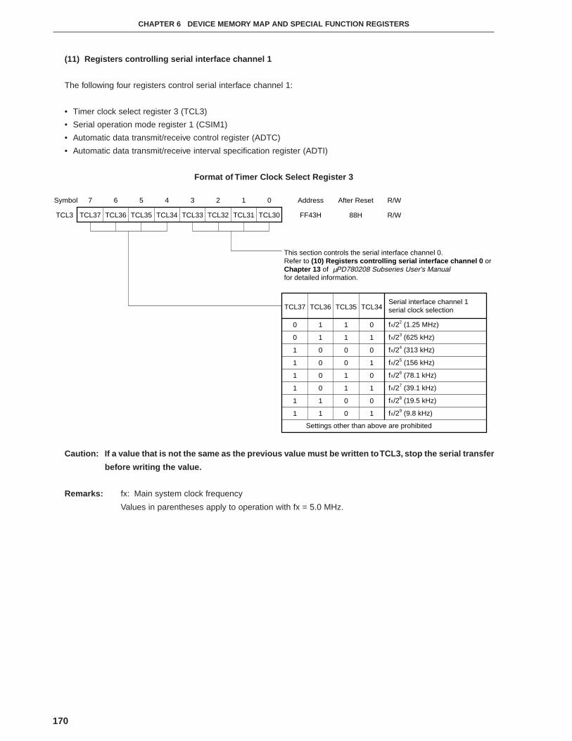
170
CHAPTER 6 DEVICE MEMORY MAP AND SPECIAL FUNCTION REGISTERS
(11) Registers controlling serial interface channel 1
The following four registers control serial interface channel 1:
• Timer clock select register 3 (TCL3)
• Serial operation mode register 1 (CSIM1)
• Automatic data transmit/receive control register (ADTC)
• Automatic data transmit/receive interval specification register (ADTI)
Format of Timer Clock Select Register 3
Caution: If a value that is not the same as the previous value must be written to TCL3, stop the serial transfer
before writing the value.
Remarks: fx: Main system clock frequency
Values in parentheses apply to operation with fx = 5.0 MHz.
TCL30TCL3
7 6 5 4 3 2Symbol 1 0
FF43HTCL31TCL33 TCL32TCL34TCL35TCL36TCL37
Address After Reset R/W
88H R/W
TCL37Serial interface channel 1serial clock selection
0 fX/22 (1.25 MHz)
0 fX/23 (625 kHz)
1 fX/24 (313 kHz)
1 fX/25 (156 kHz)
1 fX/26 (78.1 kHz)
1 fX/27 (39.1 kHz)
1 fX/28 (19.5 kHz)
1 fX/29 (9.8 kHz)
TCL36
1
1
0
0
0
0
1
1
TCL35
1
1
0
0
1
1
0
0
TCL34
0
1
0
1
0
1
0
1
This section controls the serial interface channel 0.Refer to (10) Registers controlling serial interface channel 0 orChapter 13 of PD780208 Subseries User's Manualfor detailed information.
µ
Settings other than above are prohibited
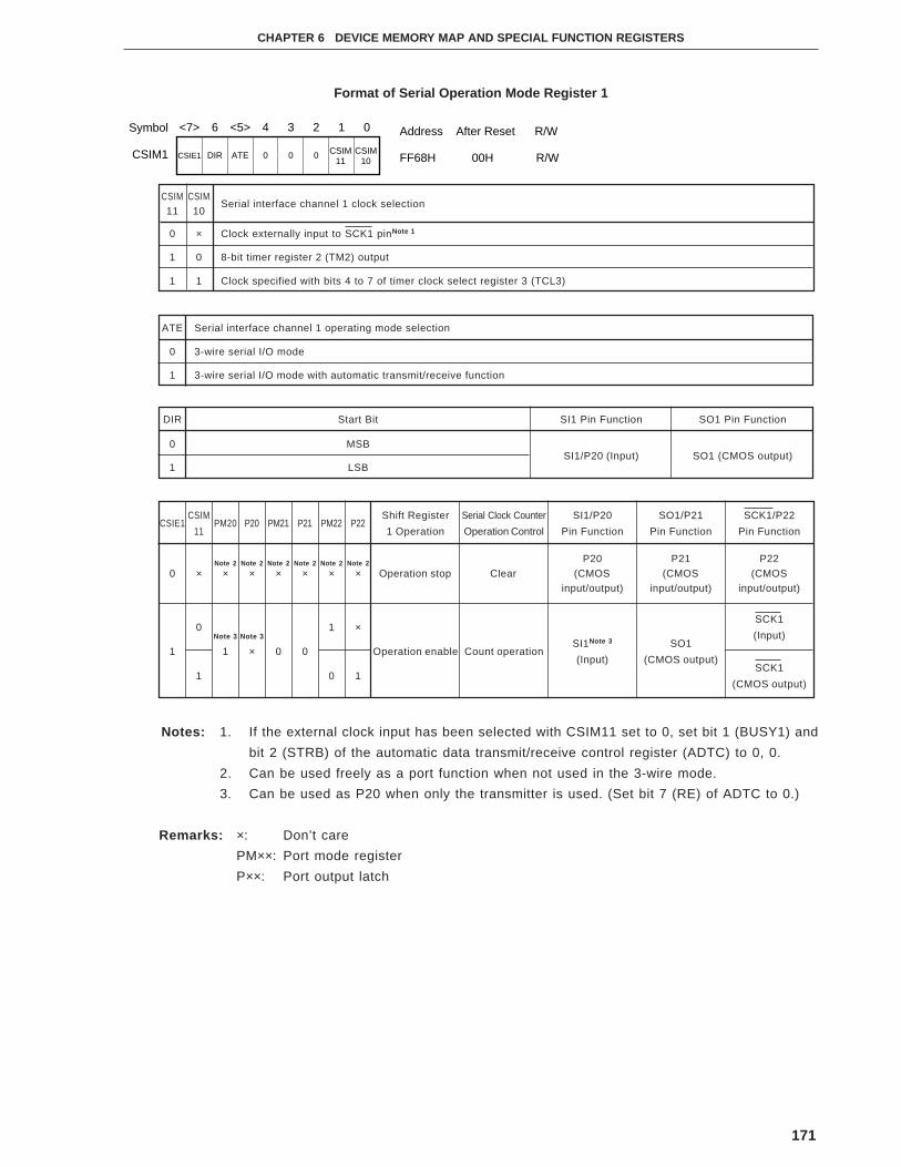
171
CHAPTER 6 DEVICE MEMORY MAP AND SPECIAL FUNCTION REGISTERS
Format of Serial Operation Mode Register 1
CSIM CSIMSerial interface channel 1 clock selection
11 10
0 × Clock externally input to SCK1 pinNote 1
1 0 8-bit timer register 2 (TM2) output
1 1 Clock specified with bits 4 to 7 of timer clock select register 3 (TCL3)
ATE Serial interface channel 1 operating mode selection
0 3-wire serial I/O mode
1 3-wire serial I/O mode with automatic transmit/receive function
DIR Start Bit SI1 Pin Function SO1 Pin Function
0 MSBSI1/P20 (Input) SO1 (CMOS output)
1 LSB
CSIM Shift Register Serial Clock Counter SI1/P20 SO1/P21 SCK1/P22CSIE1 PM20 P20 PM21 P21 PM22 P22
11 1 Operation Operation Control Pin Function Pin Function Pin Function
Note 2 Note 2 Note 2 Note 2 Note 2 Note 2 P20 P21 P220 × × × × × × × Operation stop Clear (CMOS (CMOS (CMOS
input/output) input/output) input/output)
SCK10 1 ×
Note 3 Note 3 (Input)SI1Note 3 SO1
1 1 × 0 0 Operation enable Count operation(Input) (CMOS output)
SCK11 0 1
(CMOS output)
Notes: 1. If the external clock input has been selected with CSIM11 set to 0, set bit 1 (BUSY1) and
bit 2 (STRB) of the automatic data transmit/receive control register (ADTC) to 0, 0.
2. Can be used freely as a port function when not used in the 3-wire mode.
3. Can be used as P20 when only the transmitter is used. (Set bit 7 (RE) of ADTC to 0.)
Remarks: ×: Don’t care
PM××: Port mode register
P××: Port output latch
CSIE1 DIR ATE 0 0 0 CSIM11
CSIM10
<7> 6 <5> 4 3 2 1 0
CSIM1
Symbol
FF68H 00H R/W
Address After Reset R/W

172
CHAPTER 6 DEVICE MEMORY MAP AND SPECIAL FUNCTION REGISTERS
Format of Automatic Data Transmit/Receive Control Register
Notes: 1. Bits 3 and 4 (TRF and ERR) are read-only bits.
2. The termination of automatic transmission/reception should be judged by using TRF, not CSIIF1 (interrupt
request flag).
Caution: When an external clock input is selected with bit 1 (CSIM11) of the serial operating mode register 1
(CSIM1) set to 0, set STRB and BUSY1 of ADTC to 0, 0.
Remark: ×: Don’t care
<6> <5> <4> <3> <2> <1> <0><7>Symbol
ADTC RE ARLD ERCE ERR TRF STRB BUSY1 BUSY0 FF69H 00H R/WNote 1
Address After Reset R/W
BUSY1
0
1
1
Busy input control
Not using busy input
Busy input enable (active high)
Busy input enable (active low)
BUSY0
×
0
1
STRB
0
1
Strobe output control
Strobe output disable
Strobe output enable
TRF
1
Status of automatic transmit/receive functionNote 2
Detection of termination of automatic transmission/reception (This bit is set to 0 upon suspension ofautomatic transmission/reception or when ARLD = 0.)
During automatic transmission/reception(This bit is set to 1 when data is written to SIO1.)
R/W
R/W
R
RERR
0
1
Error detection of automatic transmit/receivefunction
No error(This bit is set to 0 when data is written to SIO1.)
Error occurred
R/WARLD
0
1
Operating mode selection of automatic transmit/receive function
Single operating mode
Repetitive operating mode
R/WRE
0
1
Receive control of automatic transmit/receivefunction
Receive disable
Receive enable
R/WERCE
0
Error check control of automatic transmit/receive function
Error check disable
Error check enable (only when BUSY1 = 1)
0
1
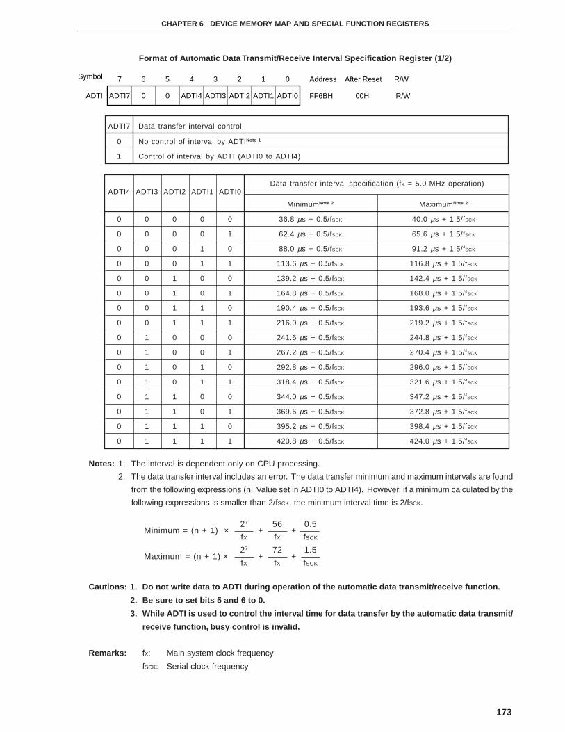
173
CHAPTER 6 DEVICE MEMORY MAP AND SPECIAL FUNCTION REGISTERS
Format of Automatic Data Transmit/Receive Interval Specification Register (1/2)
6 5 4 3 2 1 07Symbol
ADTI ADTI7 0 0 ADTI4 ADTI3 ADTI2 ADTI1 ADTI0 FF6BH 00H R/W
Address After Reset R/W
ADTI7 Data transfer interval control
0 No control of interval by ADTINote 1
1 Control of interval by ADTI (ADTI0 to ADTI4)
Data transfer interval specification (fX = 5.0-MHz operation)ADTI4 ADTI3 ADTI2 ADTI1 ADTI0
MinimumNote 2 MaximumNote 2
0 0 0 0 0 36.8 µs + 0.5/fSCK 40.0 µs + 1.5/fSCK
0 0 0 0 1 62.4 µs + 0.5/fSCK 65.6 µs + 1.5/fSCK
0 0 0 1 0 88.0 µs + 0.5/fSCK 91.2 µs + 1.5/fSCK
0 0 0 1 1 113.6 µs + 0.5/fSCK 116.8 µs + 1.5/fSCK
0 0 1 0 0 139.2 µs + 0.5/fSCK 142.4 µs + 1.5/fSCK
0 0 1 0 1 164.8 µs + 0.5/fSCK 168.0 µs + 1.5/fSCK
0 0 1 1 0 190.4 µs + 0.5/fSCK 193.6 µs + 1.5/fSCK
0 0 1 1 1 216.0 µs + 0.5/fSCK 219.2 µs + 1.5/fSCK
0 1 0 0 0 241.6 µs + 0.5/fSCK 244.8 µs + 1.5/fSCK
0 1 0 0 1 267.2 µs + 0.5/fSCK 270.4 µs + 1.5/fSCK
0 1 0 1 0 292.8 µs + 0.5/fSCK 296.0 µs + 1.5/fSCK
0 1 0 1 1 318.4 µs + 0.5/fSCK 321.6 µs + 1.5/fSCK
0 1 1 0 0 344.0 µs + 0.5/fSCK 347.2 µs + 1.5/fSCK
0 1 1 0 1 369.6 µs + 0.5/fSCK 372.8 µs + 1.5/fSCK
0 1 1 1 0 395.2 µs + 0.5/fSCK 398.4 µs + 1.5/fSCK
0 1 1 1 1 420.8 µs + 0.5/fSCK 424.0 µs + 1.5/fSCK
Notes: 1. The interval is dependent only on CPU processing.
2. The data transfer interval includes an error. The data transfer minimum and maximum intervals are found
from the following expressions (n: Value set in ADTI0 to ADTI4). However, if a minimum calculated by the
following expressions is smaller than 2/fSCK, the minimum interval time is 2/fSCK.
27 56 0.5Minimum = (n + 1) × + +
fX fX fSCK
27 72 1.5Maximum = (n + 1) × + +
fX fX fSCK
Cautions: 1. Do not write data to ADTI during operation of the automatic data transmit/receive function.
2. Be sure to set bits 5 and 6 to 0.
3. While ADTI is used to control the interval time for data transfer by the automatic data transmit/
receive function, busy control is invalid.
Remarks: fX: Main system clock frequency
fSCK: Serial clock frequency
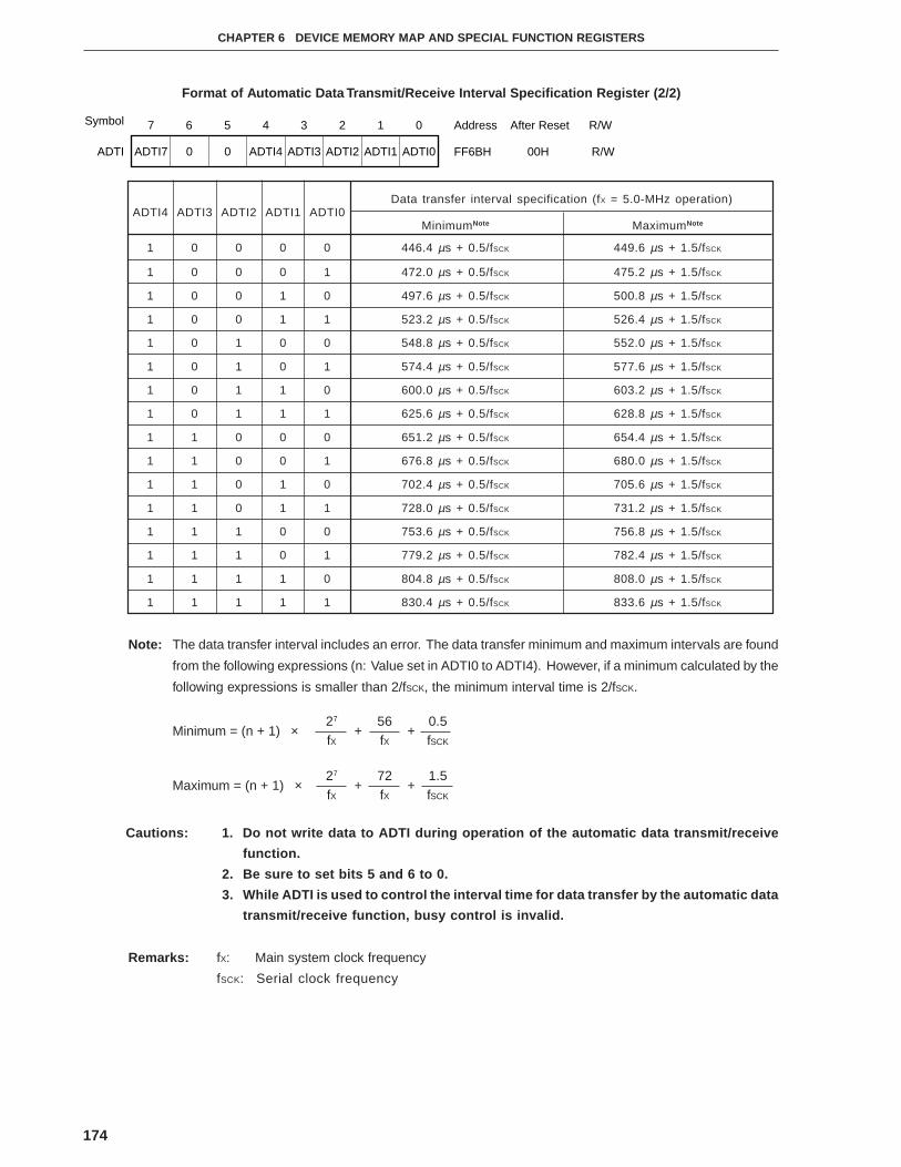
174
CHAPTER 6 DEVICE MEMORY MAP AND SPECIAL FUNCTION REGISTERS
Format of Automatic Data Transmit/Receive Interval Specification Register (2/2)
Data transfer interval specification (fX = 5.0-MHz operation)ADTI4 ADTI3 ADTI2 ADTI1 ADTI0
MinimumNote MaximumNote
1 0 0 0 0 446.4 µs + 0.5/fSCK 449.6 µs + 1.5/fSCK
1 0 0 0 1 472.0 µs + 0.5/fSCK 475.2 µs + 1.5/fSCK
1 0 0 1 0 497.6 µs + 0.5/fSCK 500.8 µs + 1.5/fSCK
1 0 0 1 1 523.2 µs + 0.5/fSCK 526.4 µs + 1.5/fSCK
1 0 1 0 0 548.8 µs + 0.5/fSCK 552.0 µs + 1.5/fSCK
1 0 1 0 1 574.4 µs + 0.5/fSCK 577.6 µs + 1.5/fSCK
1 0 1 1 0 600.0 µs + 0.5/fSCK 603.2 µs + 1.5/fSCK
1 0 1 1 1 625.6 µs + 0.5/fSCK 628.8 µs + 1.5/fSCK
1 1 0 0 0 651.2 µs + 0.5/fSCK 654.4 µs + 1.5/fSCK
1 1 0 0 1 676.8 µs + 0.5/fSCK 680.0 µs + 1.5/fSCK
1 1 0 1 0 702.4 µs + 0.5/fSCK 705.6 µs + 1.5/fSCK
1 1 0 1 1 728.0 µs + 0.5/fSCK 731.2 µs + 1.5/fSCK
1 1 1 0 0 753.6 µs + 0.5/fSCK 756.8 µs + 1.5/fSCK
1 1 1 0 1 779.2 µs + 0.5/fSCK 782.4 µs + 1.5/fSCK
1 1 1 1 0 804.8 µs + 0.5/fSCK 808.0 µs + 1.5/fSCK
1 1 1 1 1 830.4 µs + 0.5/fSCK 833.6 µs + 1.5/fSCK
Note: The data transfer interval includes an error. The data transfer minimum and maximum intervals are found
from the following expressions (n: Value set in ADTI0 to ADTI4). However, if a minimum calculated by the
following expressions is smaller than 2/fSCK, the minimum interval time is 2/fSCK.
27 56 0.5Minimum = (n + 1) × + +
fX fX fSCK
27 72 1.5Maximum = (n + 1) × + +
fX fX fSCK
Cautions: 1. Do not write data to ADTI during operation of the automatic data transmit/receive
function.
2. Be sure to set bits 5 and 6 to 0.
3. While ADTI is used to control the interval time for data transfer by the automatic data
transmit/receive function, busy control is invalid.
Remarks: fX: Main system clock frequency
fSCK: Serial clock frequency
6 5 4 3 2 1 07Symbol
ADTI ADTI7 0 0 ADTI4 ADTI3 ADTI2 ADTI1 ADTI0 FF6BH 00H R/W
Address After Reset R/W

175
CHAPTER 6 DEVICE MEMORY MAP AND SPECIAL FUNCTION REGISTERS
(12) Registers controlling FIP controller
The following three registers control FIP controller:
• Display mode register 0 (DSPM0)
• Display mode register 1 (DSPM1)
• Display mode register 2 (DSPM2)
Format of Display Mode Register 0 (1/2)
R/W SEGS4 SEGS3 SEGS2 SEGS1 SEGS0 Display segment (Display mode 1) Display output total (Display mode 2)
0 0 0 0 0 9 9
0 0 0 0 1 10 10
0 0 0 1 0 11 11
0 0 0 1 1 12 12
0 0 1 0 0 13 13
0 0 1 0 1 14 14
0 0 1 1 0 15 15
0 0 1 1 1 16 16
0 1 0 0 0 17 17
0 1 0 0 1 18 18
0 1 0 1 0 19 19
0 1 0 1 1 20 20
0 1 1 0 0 21 21
0 1 1 0 1 22 22
0 1 1 1 0 23 23
0 1 1 1 1 24 24
1 0 0 0 0 25 25
1 0 0 0 1 26 26
1 0 0 1 0 27 27
1 0 0 1 1 28 28
1 0 1 0 0 29 29
1 0 1 0 1 30 30
1 0 1 1 0 31 31
1 0 1 1 1 32 32
1 1 0 0 0 33 33
1 1 0 0 1 34 34
1 1 0 1 0 35 35
1 1 0 1 1 36 36
1 1 1 0 0 37 37
1 1 1 0 1 38Note 38
1 1 1 1 0 39Note 39
1 1 1 1 1 40Note 40
Note: When the total number of digits and segments together exceeds 53, the digits will have the priority.
7 1 06 5 4 3 2
KSF SEGS1 SEGS0DSPM06 DSPM05 SEGS4 SEGS3 SEGS2
Symbol
DSPM0 FFA0H 00H R/W
Address After Reset R/W
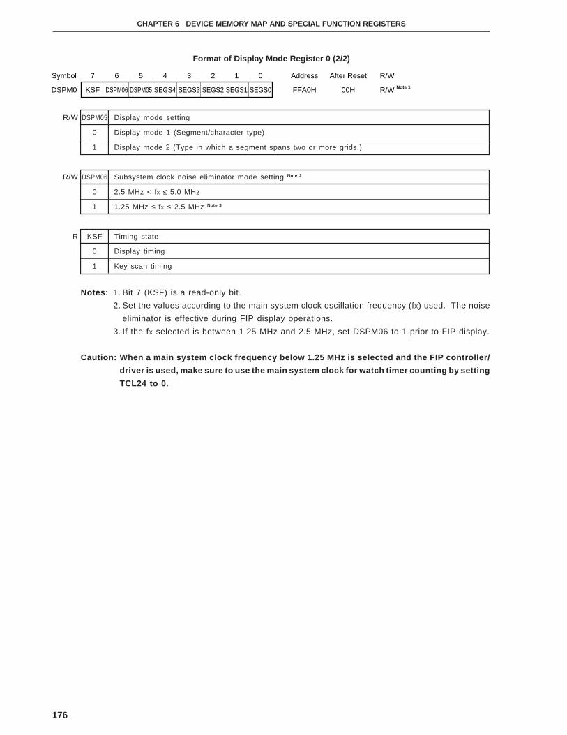
176
CHAPTER 6 DEVICE MEMORY MAP AND SPECIAL FUNCTION REGISTERS
Format of Display Mode Register 0 (2/2)
R/W DSPM05 Display mode setting
0 Display mode 1 (Segment/character type)
1 Display mode 2 (Type in which a segment spans two or more grids.)
R/W DSPM06 Subsystem clock noise eliminator mode setting Note 2
0 2.5 MHz < fX ≤ 5.0 MHz
1 1.25 MHz ≤ fX ≤ 2.5 MHz Note 3
R KSF Timing state
0 Display timing
1 Key scan timing
Notes: 1. Bit 7 (KSF) is a read-only bit.
2. Set the values according to the main system clock oscillation frequency (fX) used. The noise
eliminator is effective during FIP display operations.
3. If the fX selected is between 1.25 MHz and 2.5 MHz, set DSPM06 to 1 prior to FIP display.
Caution: When a main system clock frequency below 1.25 MHz is selected and the FIP controller/
driver is used, make sure to use the main system clock for watch timer counting by setting
TCL24 to 0.
7 1 06 5 4 3 2
KSF SEGS1 SEGS0DSPM06 DSPM05 SEGS4 SEGS3 SEGS2
Symbol
DSPM0 FFA0H 00H R/W Note 1
Address After Reset R/W
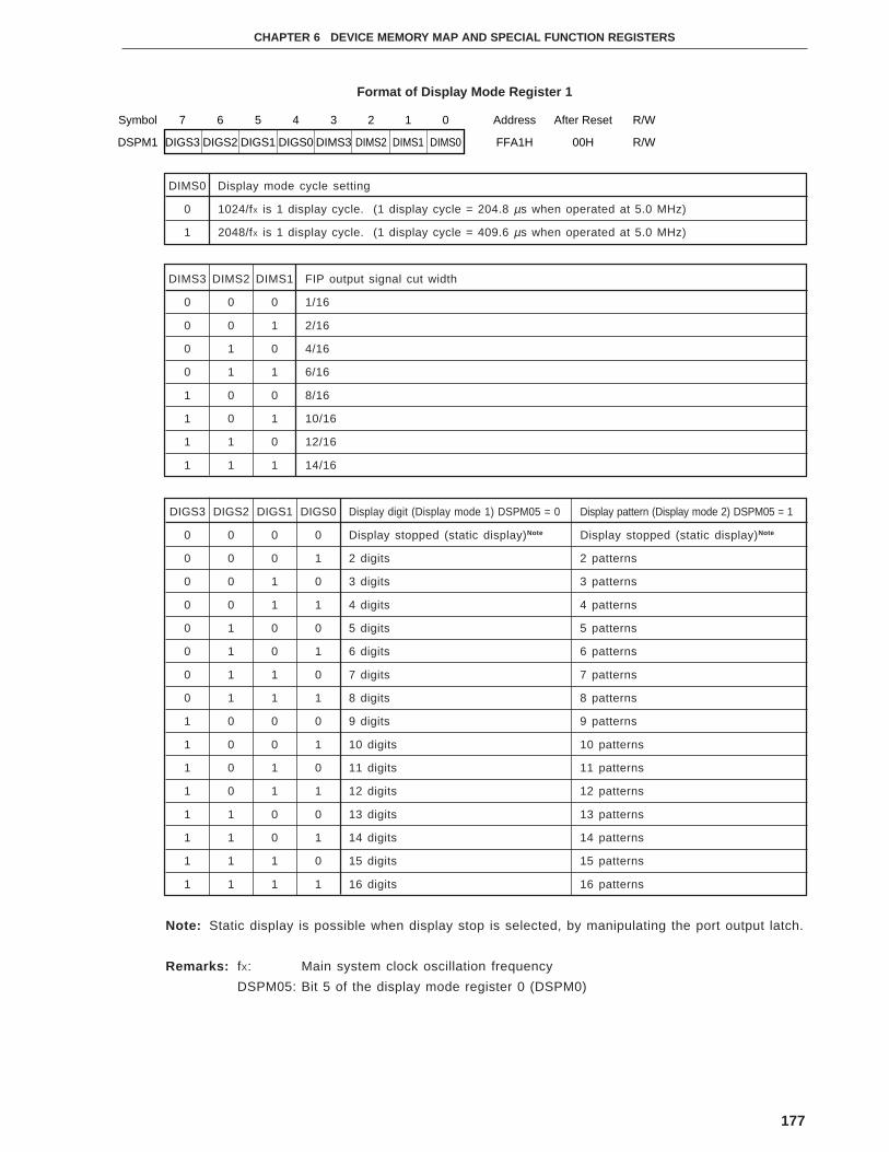
177
CHAPTER 6 DEVICE MEMORY MAP AND SPECIAL FUNCTION REGISTERS
Format of Display Mode Register 1
DIMS0 Display mode cycle setting
0 1024/fX is 1 display cycle. (1 display cycle = 204.8 µs when operated at 5.0 MHz)
1 2048/fX is 1 display cycle. (1 display cycle = 409.6 µs when operated at 5.0 MHz)
DIMS3 DIMS2 DIMS1 FIP output signal cut width
0 0 0 1/16
0 0 1 2/16
0 1 0 4/16
0 1 1 6/16
1 0 0 8/16
1 0 1 10/16
1 1 0 12/16
1 1 1 14/16
DIGS3 DIGS2 DIGS1 DIGS0 Display digit (Display mode 1) DSPM05 = 0 Display pattern (Display mode 2) DSPM05 = 1
0 0 0 0 Display stopped (static display)Note Display stopped (static display)Note
0 0 0 1 2 digits 2 patterns
0 0 1 0 3 digits 3 patterns
0 0 1 1 4 digits 4 patterns
0 1 0 0 5 digits 5 patterns
0 1 0 1 6 digits 6 patterns
0 1 1 0 7 digits 7 patterns
0 1 1 1 8 digits 8 patterns
1 0 0 0 9 digits 9 patterns
1 0 0 1 10 digits 10 patterns
1 0 1 0 11 digits 11 patterns
1 0 1 1 12 digits 12 patterns
1 1 0 0 13 digits 13 patterns
1 1 0 1 14 digits 14 patterns
1 1 1 0 15 digits 15 patterns
1 1 1 1 16 digits 16 patterns
Note: Static display is possible when display stop is selected, by manipulating the port output latch.
Remarks: fX: Main system clock oscillation frequency
DSPM05: Bit 5 of the display mode register 0 (DSPM0)
7 1 06 5 4 3 2
DIGS3 DIMS1 DIMS0DIGS2 DIGS1 DIGS0 DIMS3 DIMS2
Symbol
DSPM1 FFA1H 00H R/W
Address After Reset R/W

178
CHAPTER 6 DEVICE MEMORY MAP AND SPECIAL FUNCTION REGISTERS
Format of Display Mode Register 2
USEG5 USEG4 USEG3 USEG2 USEG1 USEG0 Number of mask bits to be written
0 0 0 0 0 0 None
0 0 0 0 0 1 1
0 0 0 0 1 0 2
0 0 0 0 1 1 3
0 0 0 1 0 0 4
0 0 0 1 0 1 5
0 0 0 1 1 0 6
0 0 0 1 1 1 7
0 0 1 0 0 0 8
0 0 1 0 0 1 9
0 0 1 0 1 0 10
0 0 1 0 1 1 11
0 0 1 1 0 0 12
0 0 1 1 0 1 13
0 0 1 1 1 0 14
0 0 1 1 1 1 15
0 1 0 0 0 0 16
0 1 0 0 0 1 17
0 1 0 0 1 0 18
0 1 0 0 1 1 19
0 1 0 1 0 0 20
0 1 0 1 0 1 21
0 1 0 1 1 0 22
0 1 0 1 1 1 23
0 1 1 0 0 0 24
0 1 1 0 0 1 25
0 1 1 0 1 0 26
0 1 1 0 1 1 27
0 1 1 1 0 0 28
0 1 1 1 0 1 29
0 1 1 1 1 0 30
0 1 1 1 1 1 31
1 0 0 0 0 0 32
1 0 0 0 0 1 33
1 0 0 0 1 0 34
1 0 0 0 1 1 35
1 0 0 1 0 0 36
1 0 0 1 0 1 37
1 0 0 1 1 0 38
1 0 0 1 1 1 39
Settings other than above are prohibited.
7 1 06 5 4 3 2
0 USEG1 USEG00 USEG5 USEG4 USEG3 USEG2
Symbol
DSPM2 FFA2H 00H R/W
Address After Reset R/W

179
CHAPTER 6 DEVICE MEMORY MAP AND SPECIAL FUNCTION REGISTERS
(13) Registers controlling interrupt function
A total of 15 interrupt sources are provided, including non-maskable, maskable, and software interrupts.
Table 6-6. Interrupt Source List
Interrupt Default Interrupt Source Internal/ VectorTable
Type Priority Name Trigger External Address
Non- — RESET Low voltage level External 0000H
maskable INTWDT Watchdog timer overflow (with watchdog timer Internal 0004H
mode 1 selected)
Maskable 0 INTWDT Watchdog timer overflow (with interval timer
mode selected)
1 INTP0 Pin input edge detection External 0006H
2 INTP1 0008H
3 INTP2 000AH
4 INTP3 000CH
5 INTCSI0 End of serial interface channel 0 transfer Internal 000EH
6 INTCSI1 End of serial interface channel 1 transfer 0010H
7 INTTM3 Reference time interval signal from watch timer 0012H
8 INTTM0 Generation of 16-bit timer/event counter 0014H
match signal
9 INTTM1 Generation of 8-bit timer/event counter 1 0016H
match signal
10 INTTM2 Generation of 8-bit timer/event counter 2 0018H
match signal
11 INTAD End of A/D converter conversion 001AH
12 INTKS Key scan timing from FIP controller/driver 001CH
Software — BRK BRK instruction execution — 003EH
Note: Default priorities are intended for two or more simultaneously generated maskable interrupt requests. 0 is the
highest priority and 12 is the lowest priority.
Note
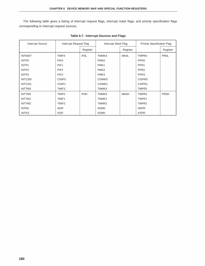
180
CHAPTER 6 DEVICE MEMORY MAP AND SPECIAL FUNCTION REGISTERS
The following table gives a listing of interrupt request flags, interrupt mask flags, and priority specification flags
corresponding to interrupt request sources.
Table 6-7. Interrupt Sources and Flags
Interrupt Source Interrupt Request Flag Interrupt Mask Flag Priority Specification Flag
Register Register Register
INTWDT TMIF4 IF0L TMMK4 MK0L TMPR4 PR0L
INTP0 PIF0 PMK0 PPR0
INTP1 PIF1 PMK1 PPR1
INTP2 PIF2 PMK2 PPR2
INTP3 PIF3 PMK3 PPR3
INTCSI0 CSIIF0 CSIMK0 CSIPR0
INTCSI1 CSIIF1 CSIMK1 CSIPR1
INTTM3 TMIF3 TMMK3 TMPR3
INTTM0 TMIF0 IF0H TMMK0 MK0H TMPR0 PR0H
INTTM1 TMIF1 TMMK1 TMPR1
INTTM2 TMIF2 TMMK2 TMPR2
INTAD ADIF ADMK ADPR
INTKS KSIF KSMK KSPR
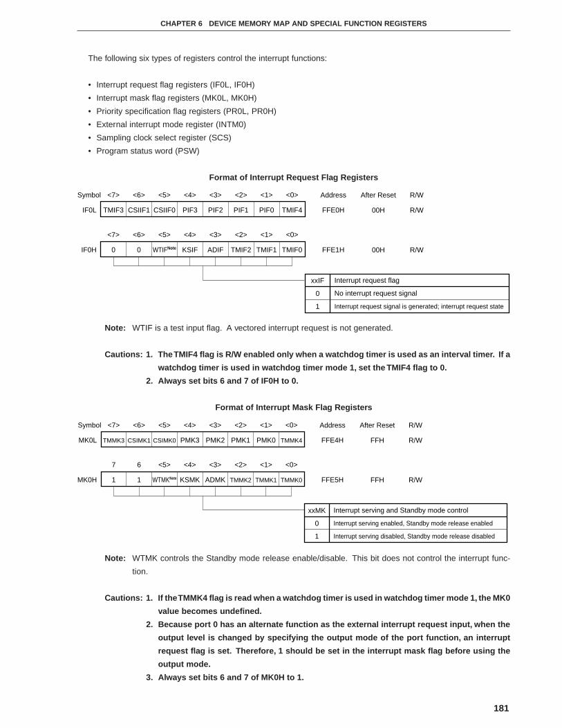
181
CHAPTER 6 DEVICE MEMORY MAP AND SPECIAL FUNCTION REGISTERS
The following six types of registers control the interrupt functions:
• Interrupt request flag registers (IF0L, IF0H)
• Interrupt mask flag registers (MK0L, MK0H)
• Priority specification flag registers (PR0L, PR0H)
• External interrupt mode register (INTM0)
• Sampling clock select register (SCS)
• Program status word (PSW)
Format of Interrupt Request Flag Registers
Note: WTIF is a test input flag. A vectored interrupt request is not generated.
Cautions: 1. The TMIF4 flag is R/W enabled only when a watchdog timer is used as an interval timer. If a
watchdog timer is used in watchdog timer mode 1, set the TMIF4 flag to 0.
2. Always set bits 6 and 7 of IF0H to 0.
Format of Interrupt Mask Flag Registers
Note: WTMK controls the Standby mode release enable/disable. This bit does not control the interrupt func-
tion.
Cautions: 1. If the TMMK4 flag is read when a watchdog timer is used in watchdog timer mode 1, the MK0
value becomes undefined.
2. Because port 0 has an alternate function as the external interrupt request input, when the
output level is changed by specifying the output mode of the port function, an interrupt
request flag is set. Therefore, 1 should be set in the interrupt mask flag before using the
output mode.
3. Always set bits 6 and 7 of MK0H to 1.
TMIF0IF0H
<7> <6> <5> <4> <3> <2> <1> <0>
xxIF Interrupt request flag
FFE1HTMIF1ADIF TMIF2KSIFWTIFNote00 00H R/W
0 No interrupt request signal
1 Interrupt request signal is generated; interrupt request state
TMIF4IF0L
<7> <6> <5> <4> <3> <2>Symbol <1> <0>
FFE0HPIF0PIF2 PIF1PIF3CSIIF0CSIIF1TMIF3
Address After Reset R/W
00H R/W
TMMK0MK0H
7 6 <5> <4> <3> <2> <1> <0>
xxMK Interrupt serving and Standby mode control
FFE5HTMMK1ADMK TMMK2KSMKWTMKNote11 FFH R/W
0 Interrupt serving enabled, Standby mode release enabled
1 Interrupt serving disabled, Standby mode release disabled
TMMK4MK0L
<7> <6> <5> <4> <3> <2>Symbol <1> <0>
FFE4HPMK0PMK2 PMK1PMK3CSIMK0CSIMK1TMMK3
Address After Reset R/W
FFH R/W
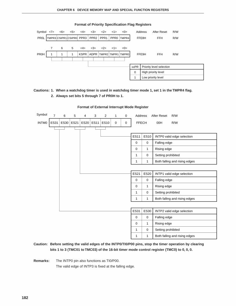
182
CHAPTER 6 DEVICE MEMORY MAP AND SPECIAL FUNCTION REGISTERS
Format of Priority Specification Flag Registers
Cautions: 1. When a watchdog timer is used in watchdog timer mode 1, set 1 in the TMPR4 flag.
2. Always set bits 5 through 7 of PR0H to 1.
Format of External Interrupt Mode Register
Caution: Before setting the valid edges of the INTP0/TI0/P00 pins, stop the timer operation by clearing
bits 1 to 3 (TMC01 to TMC03) of the 16-bit timer mode control register (TMC0) to 0, 0, 0.
Remarks: The INTP0 pin also functions as TI0/P00.
The valid edge of INTP3 is fixed at the falling edge.
TMPR0PR0H
7 6 5 <4> <3> <2> <1> <0>
xxPR Priority level selection
FFE9HTMPR1ADPR TMPR2KSPR111 FFH R/W
0 High priority level
1 Low priority level
TMPR4PR0L
<7> <6> <5> <4> <3> <2>Symbol <1> <0>
FFE8HPPR0PPR2 PPR1PPR3CSIPR0CSIPR1TMPR3
Address After Reset R/W
FFH R/W
6 5 4 3 2 1 07Symbol
INTM0 ES31 ES30 ES21 ES20 ES11 ES10 0 0 FFECH
Address After Reset R/W
ES11
0
0
1
INTP0 valid edge selection
Falling edge
Rising edge
Setting prohibited
ES10
0
1
0
1 Both falling and rising edges1
ES21
0
0
1
INTP1 valid edge selection
Falling edge
Rising edge
Setting prohibited
ES20
0
1
0
1 Both falling and rising edges1
ES31
0
0
1
INTP2 valid edge selection
Falling edge
Rising edge
Setting prohibited
ES30
0
1
0
1 Both falling and rising edges1
00H R/W
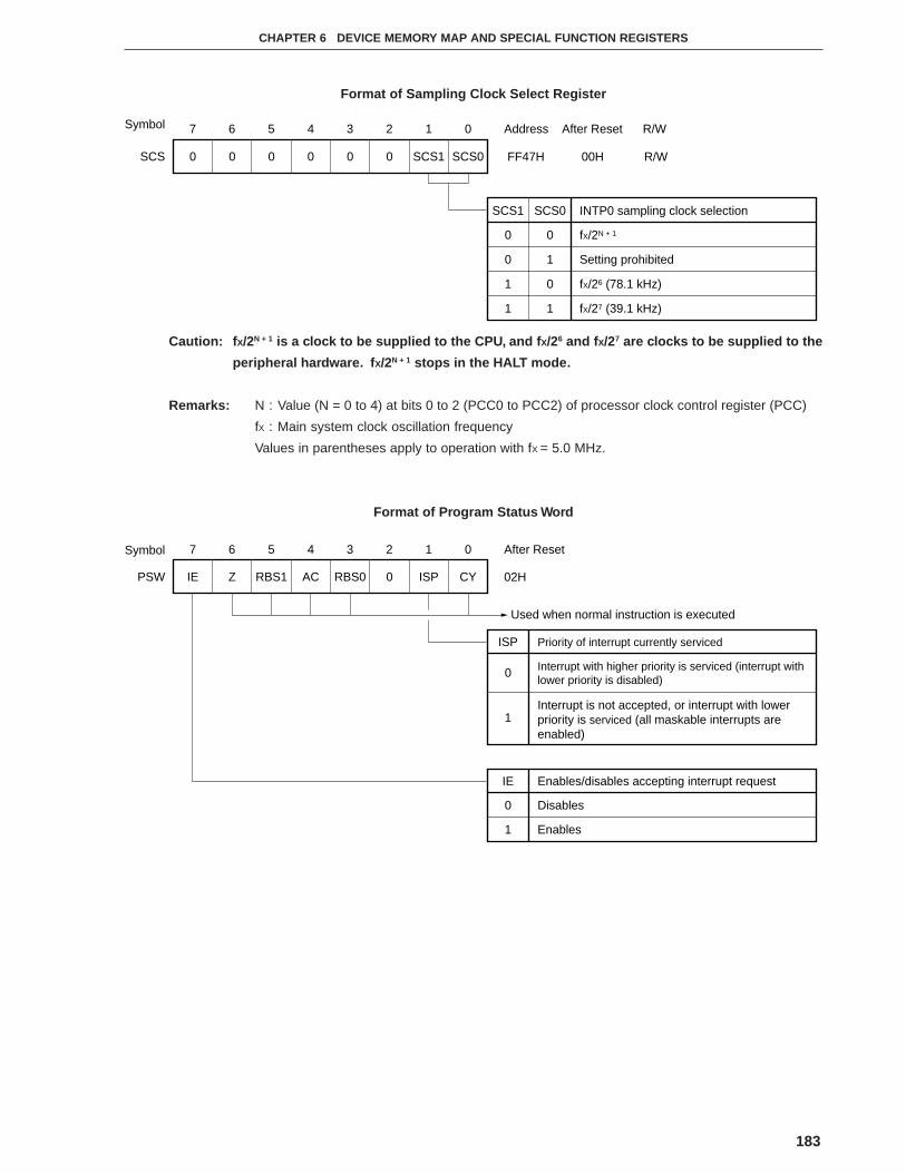
183
CHAPTER 6 DEVICE MEMORY MAP AND SPECIAL FUNCTION REGISTERS
Format of Sampling Clock Select Register
Caution: f X/2N + 1 is a clock to be supplied to the CPU, and f X/26 and f X/27 are clocks to be supplied to the
peripheral hardware. f X/2N + 1 stops in the HALT mode.
Remarks: N : Value (N = 0 to 4) at bits 0 to 2 (PCC0 to PCC2) of processor clock control register (PCC)
fX : Main system clock oscillation frequency
Values in parentheses apply to operation with fX = 5.0 MHz.
Format of Program Status Word
6 5 4 3 2 1 07Symbol
SCS 0 0 0 0 0 0 SCS1 SCS0 FF47H 00H R/W
Address After Reset R/W
SCS1
0
0
1
INTP0 sampling clock selection
fX/2N + 1
Setting prohibited
fX/26 (78.1 kHz)
SCS0
0
1
0
1 fX/27 (39.1 kHz)1
0
6 5 4 3 2 1 07
PSW IE Z RBS1 AC RBS0 0 ISP CY 02H
After Reset
IE
0
1
Enables/disables accepting interrupt request
Disables
Enables
ISP Priority of interrupt currently serviced
Interrupt with higher priority is serviced (interrupt withlower priority is disabled)
Interrupt is not accepted, or interrupt with lowerpriority is serviced (all maskable interrupts areenabled)
Used when normal instruction is executed
1
Symbol
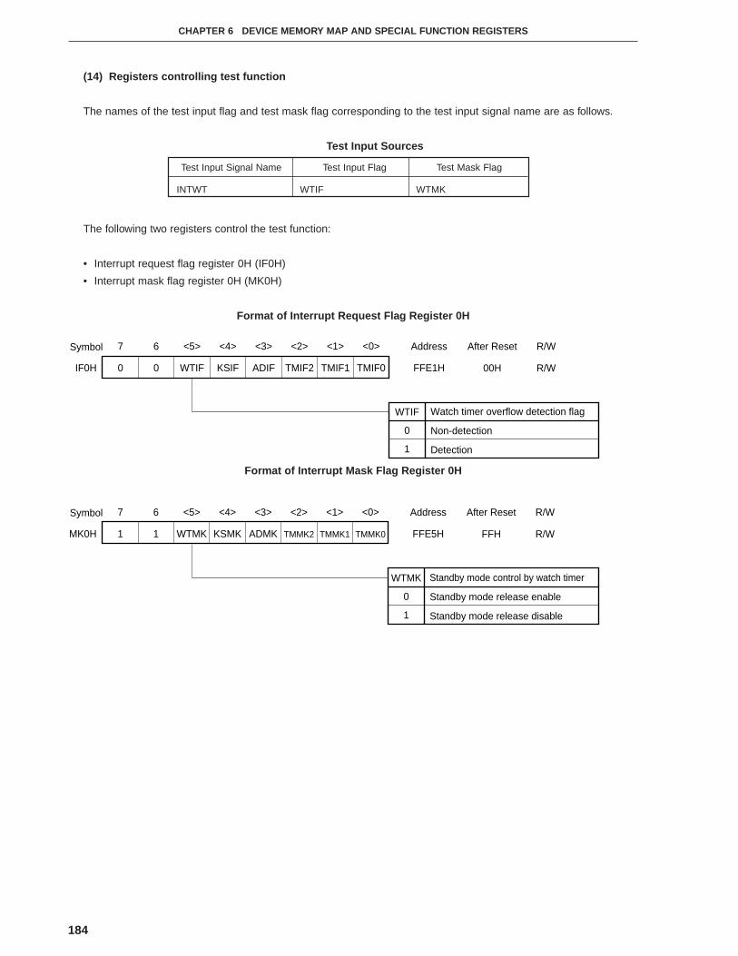
184
CHAPTER 6 DEVICE MEMORY MAP AND SPECIAL FUNCTION REGISTERS
(14) Registers controlling test function
The names of the test input flag and test mask flag corresponding to the test input signal name are as follows.
Test Input Sources
Test Input Signal Name Test Input Flag Test Mask Flag
INTWT WTIF WTMK
The following two registers control the test function:
• Interrupt request flag register 0H (IF0H)
• Interrupt mask flag register 0H (MK0H)
Format of Interrupt Request Flag Register 0H
Format of Interrupt Mask Flag Register 0H
TMMK0MK0H
7 6 <5> <4> <3> <2> <1> <0>
WTMK Standby mode control by watch timer
Standby mode release enable
Standby mode release disable
FFE5HTMMK1ADMK TMMK2KSMKWTMK11 FFH R/W
0
1
Symbol Address After Reset R/W
TMIF0IF0H
7 6 <5> <4> <3> <2> <1> <0>
WTIF Watch timer overflow detection flag
Non-detection
Detection
FFE1HTMIF1ADIF TMIF2KSIFWTIF00 00H R/W
0
1
Symbol Address After Reset R/W
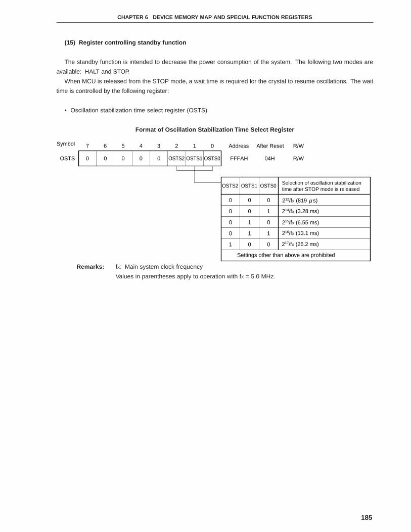
185
CHAPTER 6 DEVICE MEMORY MAP AND SPECIAL FUNCTION REGISTERS
(15) Register controlling standby function
The standby function is intended to decrease the power consumption of the system. The following two modes are
available: HALT and STOP.
When MCU is released from the STOP mode, a wait time is required for the crystal to resume oscillations. The wait
time is controlled by the following register:
• Oscillation stabilization time select register (OSTS)
Format of Oscillation Stabilization Time Select Register
Remarks: fX: Main system clock frequency
Values in parentheses apply to operation with fX = 5.0 MHz.
6 5 4 3 2 1 07Symbol
OSTS 0 0 0 0 0 OSTS2 OSTS1 OSTS0 FFFAH 04H R/W
Address After Reset R/W
OSTS2
0
0
0
OSTS1
0
0
1
0 1
1 0
Selection of oscillation stabilizationtime after STOP mode is released
212/fX (819 s)
OSTS0
0
1
0
1
0 217/fX (26.2 ms)
216/fX (13.1 ms)
215/fX (6.55 ms)
214/fX (3.28 ms)
µ
Settings other than above are prohibited

186
CHAPTER 6 DEVICE MEMORY MAP AND SPECIAL FUNCTION REGISTERS
Clock generator Both the main system clock and subsystem clock can be oscillated.Clock supply to the CPU stops.
CPU Operation stops
Port (output latch) Status before the HALT instruction execution is held
16-bit timer/event counter Operation enabled
8-bit timer/event counter
Watchdog timer
A/D converter
Watch timer
FIP controller/driver Operation disabled
Operation enabled
Operation stops
Operation is enabled when the clocks (fx/26 and fx/27) for theperipheral hardware are selected as sampling clocks.
Operation enabled
The operation status in HALT mode is described below.
HALT Mode Operating Status
Without SubsystemClock Note 1
Operation is enabledwhen fx/28 isselected for thecount clock.
HALT ModeSetting
Item
When HALT Instruction Is Executed DuringMain System Clock Oscillation
When HALT Instruction Is Executed DuringSubsystem Clock Oscillation
When Main SystemClock OscillationContinues
When Main SystemClock Oscillation Stops
Operation stops
Operation is enabledwhen TI1 and TI2 areselected for the countclock.
Operation stops
Operation stops
Operation is enabledwhen fXT is selected forthe count clock.
Operation is enabledwhen external SCK isselected.
Operation stops
SerialInterface
Externalinterrupt
Other thanautomatictransmit/receivefunction
Automatictransmit/receivefunction
INTP0
INTP1 to
INTP3
With SubsystemClock Note 2
Operation enabled
Notes: 1. Including the case where an external clock is not supplied as the subsystem clock
2. Including the case where an external clock is supplied as the subsystem clock

187
CHAPTER 6 DEVICE MEMORY MAP AND SPECIAL FUNCTION REGISTERS
The operation status in the STOP mode is shown below.
STOP Mode Operating Status
STOP Mode Setting With Subsystem Clock Without Subsystem Clock
Item
Clock generator Only the main system clock stops oscillation.
CPU Operation stops
Output port (output latch) Status before the STOP mode setting is held
16-bit timer/event counter Operation stops
8-bit timer/event counter Operation is enabled only when TI1 and TI2 are selected for the count clock.
Watchdog timerOperation stops
A/D converter
Watch timer Operation is enabled only when fXT is Operation stopsselected for the count clock.
FIP controller/driver Operation disabled
Operation is enabled only when an external input clock is selected as the serial clock.
Operation stops
Operation disabled
Operation enabled
Cautions: 1. When the STOP mode is set, the X2 pin is internally connected to V DD via a pull-up resistor to
minimize the leakage current at the crystal oscillator. Thus, do not use the STOP mode in a
system where an external clock is used for the main system clock.
2. Because the interrupt request signal is used to release the Standby mode, if there is an inter-
rupt source with the interrupt request flag set and the interrupt mask flag reset, the Standby
mode is immediately released if set. Thus, the STOP mode is reset to the HALT mode immedi-
ately after execution of the STOP instruction. After the wait set using the oscillation stabiliza-
tion time select register (OSTS), the operating mode is set.
Other than automatictransmit/receivefunction
Automatic transmit/receive function
INTP0
INTP1 to INTP3
Serialinterface
Externalinterrupt
188
CHAPTER 6 DEVICE MEMORY MAP AND SPECIAL FUNCTION REGISTERS
(16) Reset function
The following two operations can be used to generate a reset signal.
• External reset input via the RESET pin
• Internal reset by watchdog timer in Watchdog Timer mode

189
CHAPTER 6 DEVICE MEMORY MAP AND SPECIAL FUNCTION REGISTERS
Table 6-8. Hardware Status After Reset (1/2)
Hardware Status After Reset
The contents of reset
Program counter (PC)Note 1 vector tables (0000H
and 0001H) are set
Stack pointer (SP) Undefined
Program status word (PSW) 02H
Data memory UndefinedNote 2
RAMGeneral register UndefinedNote 2
Port (Output latch) Ports 0 to 3, ports 7 to 12 (P0 toP3, P7 to P12) 00H
(PM0, PM7) 1FHPort mode registers
(PM1, PM2, PM3, PM10, PM11, PM12) FFH
Pull-up resistor option register (PUO) 00H
Processor clock control register (PCC) 04H
Internal memory size switching register (IMS) Note 3
Internal expansion RAM size switching register (IXS) Note 3
Oscillation stabilization time select register (OSTS) 04H
Timer register (TM0) 00H
Compare register (CR00) Undefined
Capture register (CR01) Undefined16-bit timer/event counter
Clock select register (TCL0) 00H
Mode control register (TMC0) 00H
Output control register (TOC0) 00H
Timer registers (TM1, TM2) 00H
Compare registers (CR10, CR20) Undefined
8-bit timer/event counter Clock select register (TCL1) 00H
Mode control registers (TMC1, TMC2) 00H
Output control register (TOC1) 00H
Watch timer Clock select register (TCL2) 00H
Watchdog timerMode register (WDTM) 00H

190
CHAPTER 6 DEVICE MEMORY MAP AND SPECIAL FUNCTION REGISTERS
Table 6-8. Hardware Status After Reset (2/2)
Hardware Status After Reset
Clock select register (TCL3) 88H
Shift registers (SIO0, SIO1) Undefined
Mode registers (CSIM0, CSIM1) 00H
Serial bus interface control register (SBIC) 00H
Serial interface Slave address register (SVA) Undefined
Automatic data transmit/receive control register (ADTC) 00H
Automatic data transmit/receive address pointer (ADTP) 00H
Automatic data transmit/receive interval specification register (ADTI) 00H
Interrupt timing specification register (SINT) 00H
Mode register (ADM) 01H
A/D converter Conversion result register (ADCR) Undefined
Input select register (ADIS) 00H
Display mode register 0 (DSPM0) 00H
FIP controller/driver Display mode register 1 (DSPM1) 00H
Display mode register 2 (DSPM2) 00H
Request flag registers (IF0L, IF0H) 00H
Mask flag registers (MK0L, MK0H) FFH
Interrupt Priority specification flag registers (PR0L, PR0H) FFH
External interrupt mode register (INTM0) 00H
Sampling clock select register (SCS) 00H
Notes: 1. During reset input or an oscillation stabilization time wait, only the PC contents among the hardware
statuses become undefined. All other hardware statuses remain unchanged after a reset.
2. If the reset is applied in the Standby mode, the status before reset will be held after reset.
3. The after-reset values of the internal memory size switching register (IMS) and internal expansion
RAM size switching register (IXS) depend on each subseries member as shown below.
µPD780204 µPD780205 µPD780206 µPD780208 µPD78P0208
IMS C8H CAH CCH CFH CFH
IXS None 0AH
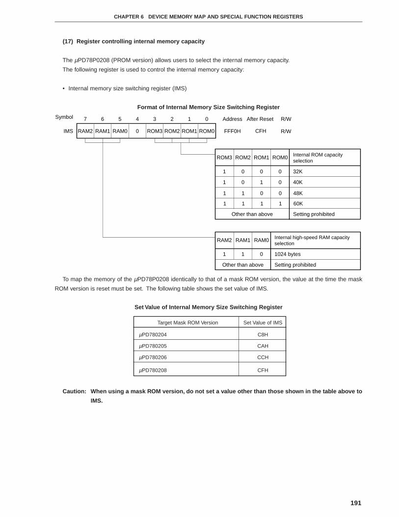
191
CHAPTER 6 DEVICE MEMORY MAP AND SPECIAL FUNCTION REGISTERS
(17) Register controlling internal memory capacity
The µPD78P0208 (PROM version) allows users to select the internal memory capacity.
The following register is used to control the internal memory capacity:
• Internal memory size switching register (IMS)
Format of Internal Memory Size Switching Register
To map the memory of the µPD78P0208 identically to that of a mask ROM version, the value at the time the mask
ROM version is reset must be set. The following table shows the set value of IMS.
Set Value of Internal Memory Size Switching Register
Target Mask ROM Version Set Value of IMS
µPD780204 C8H
µPD780205 CAH
µPD780206 CCH
µPD780208 CFH
Caution: When using a mask ROM version, do not set a value other than those shown in the table above to
IMS.
6 5 4 3 2 1 07Symbol
IMS RAM2 RAM1 RAM0 0 ROM3 ROM2 ROM1 ROM0 FFF0H
Address After Reset R/W
ROM3
1
1
ROM2
0
0
1 1
Internal ROM capacityselection
32K
40K
ROM1
0
1
60K1
Setting prohibited
ROM0
0
0
1
Other than above
RAM2
1
RAM1
1
Other than above
Internal high-speed RAM capacityselection
1024 bytes
RAM0
0
Setting prohibited
CFH R/W
1 1 48K0 0

192
CHAPTER 6 DEVICE MEMORY MAP AND SPECIAL FUNCTION REGISTERS
(18) Register controlling internal expansion RAM capacity
The µPD78P0208 (PROM version) allows users to select the internal expansion RAM capacity.
The following register is used to control the internal expansion RAM capacity:
• Internal expansion RAM size switching register (IXS)
Format of Internal Expansion RAM Size Switching Register
The following table shows the set value of IXS by which to map the internal expansion RAM of the µPD78P0208
identically to that of a mask ROM version.
Set Value of Internal Expansion RAM Size Switching Register
Target Mask ROM Version Set Value of IXS
µPD780204 0CH
µPD780205
µPD780206 0AH
µPD780208
IXS is not incorporated in the µPD780204 and µPD780205.
However, if a write instruction to IXS is executed in the µPD780204 or the µPD780205, the operations are
not affected.
Cautions: 1. The internal expansion RAM size switching register (IXS) is incorporated only in the µµµµµPD780206,
µµµµµPD780208, and µµµµµPD78P0208.
2. When using a mask ROM version, do not set a value other than those shown above to IXS.
IXRAM0IXS
7 6 5 4 3 2Symbol 1 0
IXRAM3
Internal expansion RAMcapacity selection
FFF4HIX
RAM1IX
RAM3IX
RAM20000
Address After Reset R/W
0AH W
1 1024 bytes
1 No internal expansion RAM (0 bytes)
Setting prohibited
IXRAM2
0
1
Other than above
IXRAM1
1
0
IXRAM0
0
0
193
CHAPTER 6 DEVICE MEMORY MAP AND SPECIAL FUNCTION REGISTERS
6.3 µµµµµPD780024 and 780034 Subseries
6.3.1 Documentation Reference Information
Device Series Number User’s Manual Number Date Published
µPD780024, 780034 U12022EJ4V0UM00 January 1998
Caution: The user should check the current User’s Manual with the information in this section to be sure of
having the most up-to-date information.
6.3.2 Device Series Differences
Device Series Number ROM and RAM Differences Number of
ROM Size RAM Size Serial Channels
µPD780024, 780024Y 8K/16K/24K/32K 512/1K 3 Note
µPD780034, 780034Y
Note: Even though each product has three serial channels, there is a difference in the serial interface type between
non-Y subseries products (µPD780024/34) and Y subseries products (µPD780024Y/34Y). See “Differences
Between µµµµµPD780024/34 and µµµµµPD780024Y/34Y subseries ” in (9) Registers controlling serial interface
(UART0).
General Programmer’s Note
The NEC C-compiler and the NEC Assembler are capable of recognizing certain symbolic SFR bit names. These
special bit names are identified in the user manual in one of the four ways shown below:
If a bit number has one of the four symbols around it, the NEC software will recognize the associated symbolic bit
name. For example to set bit 7, the user can write the code in two ways:
1. SET1 MCC
2. SET1 PCC.7
Alternatively since bit 2 does not have any of the four symbols around it, the user can only set this bit as follows:
1. SET1 PCC.2
Note: The attempt to employ a symbolic name of bit-2 (PCC2) will return an error. Thus the use of instruction
SET1 PCC2
is improper since neither the NEC C-compiler nor the NEC Assembler recognizes this symbolic name and will
generate an error.
MCCPCC FRC CLS CSS 0 PCC2 PCC1 PCC0
<7> <6> <5> <4> 3 2 1 0
Example:
1.
2.
3.
4.
<7>
( 7 )
7
7
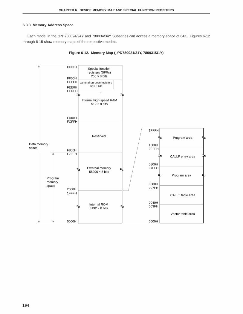
194
CHAPTER 6 DEVICE MEMORY MAP AND SPECIAL FUNCTION REGISTERS
6.3.3 Memory Address Space
Each model in the µPD780024/24Y and 780034/34Y Subseries can access a memory space of 64K. Figures 6-12
through 6-15 show memory maps of the respective models.
Figure 6-12. Memory Map ( µPD780021/21Y, 780031/31Y)
0000H
Data memory space
General-purpose registers32 × 8 bits
Internal ROM8192 × 8 bits
1FFFH
1000H0FFFH
0800H07FFH
0080H 007FH
0040H003FH
0000H
CALLF entry area
CALLT table area
Vector table area
Program area
Program area
External memory55296 × 8 bits
Programmemoryspace
2000H1FFFH
F800HF7FFH
FEE0HFEDFH
FF00HFEFFH
FFFFH
Internal high-speed RAM512 × 8 bits
Special function registers (SFRs)
256 × 8 bits
Reserved
FD00HFCFFH
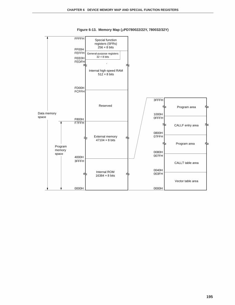
195
CHAPTER 6 DEVICE MEMORY MAP AND SPECIAL FUNCTION REGISTERS
Figure 6-13. Memory Map ( µPD780022/22Y, 780032/32Y)
0000H
Data memory space
Internal ROM16384 × 8 bits
3FFFH
1000H0FFFH
0800H07FFH
0080H 007FH
0040H003FH
0000H
CALLF entry area
CALLT table area
Vector table area
Program area
Program area
External memory47104 × 8 bits
Programmemoryspace
4000H3FFFH
F800HF7FFH
FEE0HFEDFH
FF00HFEFFH
FFFFH
Internal high-speed RAM512 × 8 bits
Special function registers (SFRs)
256 × 8 bits
Reserved
FD00HFCFFH
General-purpose registers32 × 8 bits
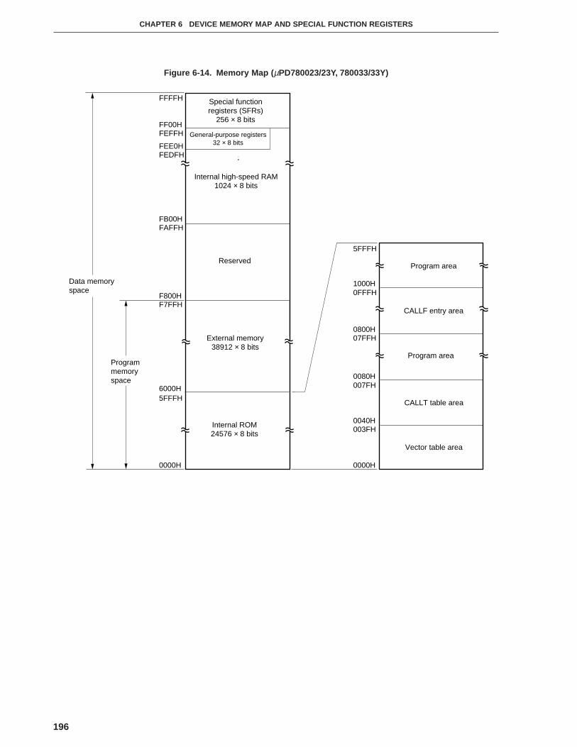
196
CHAPTER 6 DEVICE MEMORY MAP AND SPECIAL FUNCTION REGISTERS
Figure 6-14. Memory Map ( µPD780023/23Y, 780033/33Y)
0000H
Data memory space
Internal ROM24576 × 8 bits
5FFFH
1000H0FFFH
0800H07FFH
0080H 007FH
0040H003FH
0000H
CALLF entry area
CALLT table area
Vector table area
Program area
Program area
External memory38912 × 8 bits
Programmemoryspace
6000H5FFFH
F800HF7FFH
FEE0HFEDFH
FF00HFEFFH
FFFFH
Internal high-speed RAM1024 × 8 bits
Special function registers (SFRs)
256 × 8 bits
Reserved
FB00HFAFFH
General-purpose registers32 × 8 bits
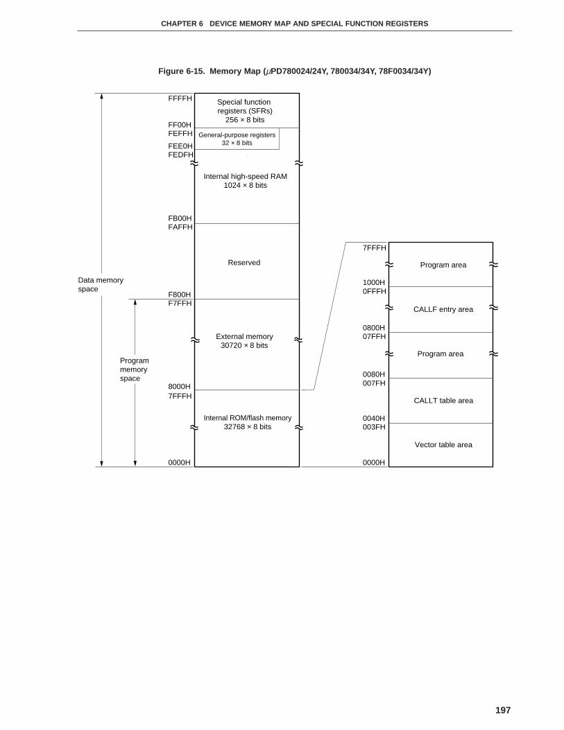
197
CHAPTER 6 DEVICE MEMORY MAP AND SPECIAL FUNCTION REGISTERS
Figure 6-15. Memory Map ( µPD780024/24Y, 780034/34Y, 78F0034/34Y)
0000H
Data memory space
Internal ROM/flash memory32768 × 8 bits
7FFFH
1000H0FFFH
0800H07FFH
0080H 007FH
0040H003FH
0000H
CALLF entry area
CALLT table area
Vector table area
Program area
Program area
External memory30720 × 8 bits
Programmemoryspace
8000H7FFFH
F800HF7FFH
FEE0HFEDFH
FF00HFEFFH
FFFFH
Internal high-speed RAM1024 × 8 bits
Special function registers (SFRs)
256 × 8 bits
Reserved
FB00HFAFFH
General-purpose registers32 × 8 bits
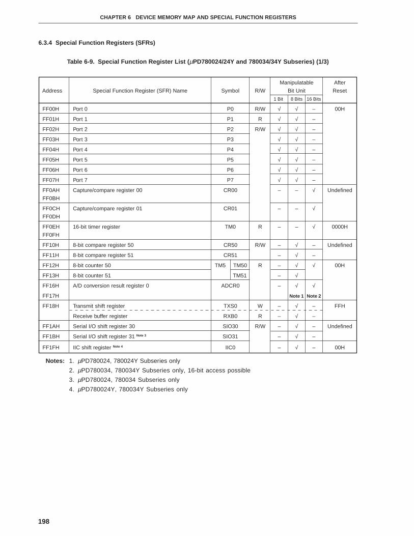
198
CHAPTER 6 DEVICE MEMORY MAP AND SPECIAL FUNCTION REGISTERS
6.3.4 Special Function Registers (SFRs)
Table 6-9. Special Function Register List ( µPD780024/24Y and 780034/34Y Subseries) (1/3)
Manipulatable After
Address Special Function Register (SFR) Name Symbol R/W Bit Unit Reset
1 Bit 8 Bits 16 Bits
FF00H Port 0 P0 R/W √ √ – 00H
FF01H Port 1 P1 R √ √ –
FF02H Port 2 P2 R/W √ √ –
FF03H Port 3 P3 √ √ –
FF04H Port 4 P4 √ √ –
FF05H Port 5 P5 √ √ –
FF06H Port 6 P6 √ √ –
FF07H Port 7 P7 √ √ –
FF0AH Capture/compare register 00 CR00 – – √ Undefined
FF0BH
FF0CH Capture/compare register 01 CR01 – – √FF0DH
FF0EH 16-bit timer register TM0 R – – √ 0000H
FF0FH
FF10H 8-bit compare register 50 CR50 R/W – √ – Undefined
FF11H 8-bit compare register 51 CR51 – √ –
FF12H 8-bit counter 50 TM5 TM50 R – √ √ 00H
FF13H 8-bit counter 51 TMS TM51 – √
FF16H A/D conversion result register 0 ADCR0 – √ √
FF17H Note 1 Note 2
FF18H Transmit shift register TXS0 W – √ – FFH
Receive buffer register RXB0 R – √ –
FF1AH Serial I/O shift register 30 SIO30 R/W – √ – Undefined
FF1BH Serial I/O shift register 31 Note 3 SIO31 – √ –
FF1FH IIC shift register Note 4 IIC0 – √ – 00H
Notes: 1. µPD780024, 780024Y Subseries only
2. µPD780034, 780034Y Subseries only, 16-bit access possible
3. µPD780024, 780034 Subseries only
4. µPD780024Y, 780034Y Subseries only
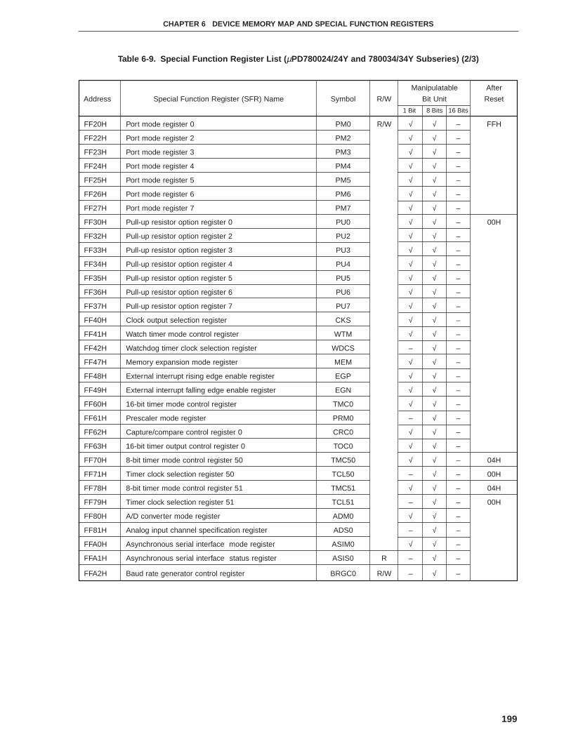
199
CHAPTER 6 DEVICE MEMORY MAP AND SPECIAL FUNCTION REGISTERS
Table 6-9. Special Function Register List ( µPD780024/24Y and 780034/34Y Subseries) (2/3)
Manipulatable After
Address Special Function Register (SFR) Name Symbol R/W Bit Unit Reset
1 Bit 8 Bits 16 Bits
FF20H Port mode register 0 PM0 R/W √ √ – FFH
FF22H Port mode register 2 PM2 √ √ –
FF23H Port mode register 3 PM3 √ √ –
FF24H Port mode register 4 PM4 √ √ –
FF25H Port mode register 5 PM5 √ √ –
FF26H Port mode register 6 PM6 √ √ –
FF27H Port mode register 7 PM7 √ √ –
FF30H Pull-up resistor option register 0 PU0 √ √ – 00H
FF32H Pull-up resistor option register 2 PU2 √ √ –
FF33H Pull-up resistor option register 3 PU3 √ √ –
FF34H Pull-up resistor option register 4 PU4 √ √ –
FF35H Pull-up resistor option register 5 PU5 √ √ –
FF36H Pull-up resistor option register 6 PU6 √ √ –
FF37H Pull-up resistor option register 7 PU7 √ √ –
FF40H Clock output selection register CKS √ √ –
FF41H Watch timer mode control register WTM √ √ –
FF42H Watchdog timer clock selection register WDCS – √ –
FF47H Memory expansion mode register MEM √ √ –
FF48H External interrupt rising edge enable register EGP √ √ –
FF49H External interrupt falling edge enable register EGN √ √ –
FF60H 16-bit timer mode control register TMC0 √ √ –
FF61H Prescaler mode register PRM0 – √ –
FF62H Capture/compare control register 0 CRC0 √ √ –
FF63H 16-bit timer output control register 0 TOC0 √ √ –
FF70H 8-bit timer mode control register 50 TMC50 √ √ – 04H
FF71H Timer clock selection register 50 TCL50 – √ – 00H
FF78H 8-bit timer mode control register 51 TMC51 √ √ – 04H
FF79H Timer clock selection register 51 TCL51 – √ – 00H
FF80H A/D converter mode register ADM0 √ √ –
FF81H Analog input channel specification register ADS0 – √ –
FFA0H Asynchronous serial interface mode register ASIM0 √ √ –
FFA1H Asynchronous serial interface status register ASIS0 R – √ –
FFA2H Baud rate generator control register BRGC0 R/W – √ –
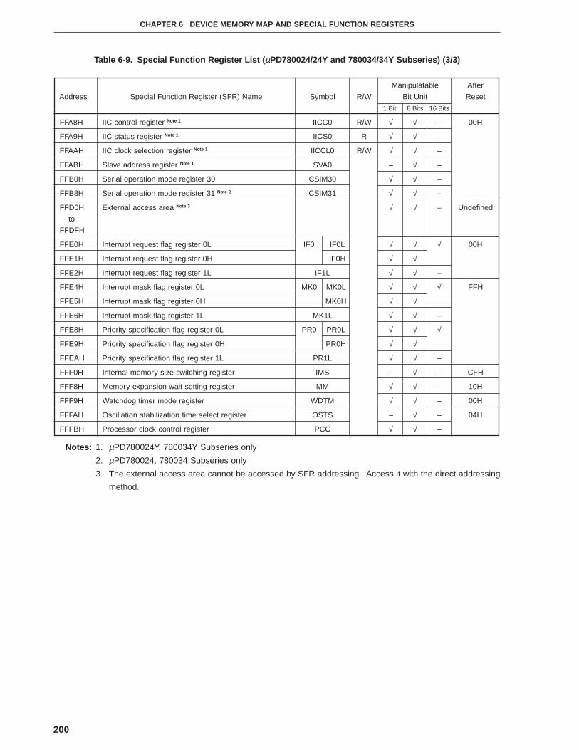
200
CHAPTER 6 DEVICE MEMORY MAP AND SPECIAL FUNCTION REGISTERS
Table 6-9. Special Function Register List ( µPD780024/24Y and 780034/34Y Subseries) (3/3)
Manipulatable After
Address Special Function Register (SFR) Name Symbol R/W Bit Unit Reset
1 Bit 8 Bits 16 Bits
FFA8H IIC control register Note 1 IICC0 R/W √ √ – 00H
FFA9H IIC status register Note 1 IICS0 R √ √ –
FFAAH IIC clock selection register Note 1 IICCL0 R/W √ √ –
FFABH Slave address register Note 1 SVA0 – √ –
FFB0H Serial operation mode register 30 CSIM30 √ √ –
FFB8H Serial operation mode register 31 Note 2 CSIM31 √ √ –
FFD0H External access area Note 3 √ √ – Undefined
to
FFDFH
FFE0H Interrupt request flag register 0L IF0 IF0L √ √ √ 00H
FFE1H Interrupt request flag register 0H IF0H √ √
FFE2H Interrupt request flag register 1L IF1L √ √ –
FFE4H Interrupt mask flag register 0L MK0 MK0L √ √ √ FFH
FFE5H Interrupt mask flag register 0H MK0H √ √
FFE6H Interrupt mask flag register 1L MK1L √ √ –
FFE8H Priority specification flag register 0L PR0 PR0L √ √ √
FFE9H Priority specification flag register 0H PR0H √ √
FFEAH Priority specification flag register 1L PR1L √ √ –
FFF0H Internal memory size switching register IMS – √ – CFH
FFF8H Memory expansion wait setting register MM √ √ – 10H
FFF9H Watchdog timer mode register WDTM √ √ – 00H
FFFAH Oscillation stabilization time select register OSTS – √ – 04H
FFFBH Processor clock control register PCC √ √ –
Notes: 1. µPD780024Y, 780034Y Subseries only
2. µPD780024, 780034 Subseries only
3. The external access area cannot be accessed by SFR addressing. Access it with the direct addressing
method.

201
CHAPTER 6 DEVICE MEMORY MAP AND SPECIAL FUNCTION REGISTERS
(1) Registers controlling port functions
The following two types of registers control the ports:
• Port mode registers (PM0, PM2 to PM7)
• Pull-up resistor option registers (PU0, PU2 to PU7)
Format of Port Mode Registers
Address: FF20H After Reset: FFH R/W
Symbol 7 6 5 4 3 2 1 0
PM0 1 1 1 1 PM03 PM02 PM01 PM00
Address: FF22H After Reset: FFH R/W
Symbol 7 6 5 4 3 2 1 0
PM2 1 1 PM25 PM24 PM23 PM22 PM21 PM20
Address: FF23H After Reset: FFH R/W
Symbol 7 6 5 4 3 2 1 0
PM3 1 PM36 PM35 PM34 PM33 PM32 PM31 PM30
Address: FF24H After Reset: FFH R/W
Symbol 7 6 5 4 3 2 1 0
PM4 PM47 PM46 PM45 PM44 PM43 PM42 PM41 PM40
Address: FF25H After Reset: FFH R/W
Symbol 7 6 5 4 3 2 1 0
PM5 PM57 PM56 PM55 PM54 PM53 PM52 PM51 PM50
Address: FF26H After Reset: FFH R/W
Symbol 7 6 5 4 3 2 1 0
PM6 PM67 PM66 PM65 PM64 1 1 1 1
Address: FF27H After Reset: FFH R/W
Symbol 7 6 5 4 3 2 1 0
PM7 1 1 PM75 PM74 PM73 PM72 PM71 PM70
PMmn Pmn Pin Input/Output Mode Select (m = 0, 2 to 7: n = 0 to 7)
0 Output Mode (Output buffer on)
1 Input Mode (Output buffer off)
Cautions: 1. Pins P10 and P17 are input-only pins.
2. As port 0 has an alternate function as an external interrupt input, when the port function
output mode is specified and the output level is changed, the interrupt request flag is set.
When the output mode is used, therefore, the interrupt mask flag should be set to 1
beforehand.
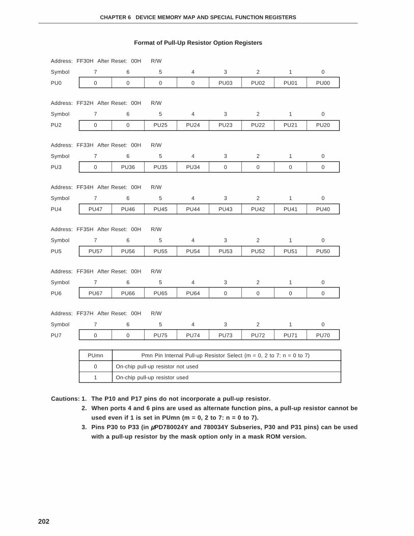
202
CHAPTER 6 DEVICE MEMORY MAP AND SPECIAL FUNCTION REGISTERS
Format of Pull-Up Resistor Option Registers
Address: FF30H After Reset: 00H R/W
Symbol 7 6 5 4 3 2 1 0
PU0 0 0 0 0 PU03 PU02 PU01 PU00
Address: FF32H After Reset: 00H R/W
Symbol 7 6 5 4 3 2 1 0
PU2 0 0 PU25 PU24 PU23 PU22 PU21 PU20
Address: FF33H After Reset: 00H R/W
Symbol 7 6 5 4 3 2 1 0
PU3 0 PU36 PU35 PU34 0 0 0 0
Address: FF34H After Reset: 00H R/W
Symbol 7 6 5 4 3 2 1 0
PU4 PU47 PU46 PU45 PU44 PU43 PU42 PU41 PU40
Address: FF35H After Reset: 00H R/W
Symbol 7 6 5 4 3 2 1 0
PU5 PU57 PU56 PU55 PU54 PU53 PU52 PU51 PU50
Address: FF36H After Reset: 00H R/W
Symbol 7 6 5 4 3 2 1 0
PU6 PU67 PU66 PU65 PU64 0 0 0 0
Address: FF37H After Reset: 00H R/W
Symbol 7 6 5 4 3 2 1 0
PU7 0 0 PU75 PU74 PU73 PU72 PU71 PU70
PUmn Pmn Pin Internal Pull-up Resistor Select (m = 0, 2 to 7: n = 0 to 7)
0 On-chip pull-up resistor not used
1 On-chip pull-up resistor used
Cautions: 1. The P10 and P17 pins do not incorporate a pull-up resistor.
2. When ports 4 and 6 pins are used as alternate function pins, a pull-up resistor cannot be
used even if 1 is set in PUmn (m = 0, 2 to 7: n = 0 to 7).
3. Pins P30 to P33 (in µµµµµPD780024Y and 780034Y Subseries, P30 and P31 pins) can be used
with a pull-up resistor by the mask option only in a mask ROM version.
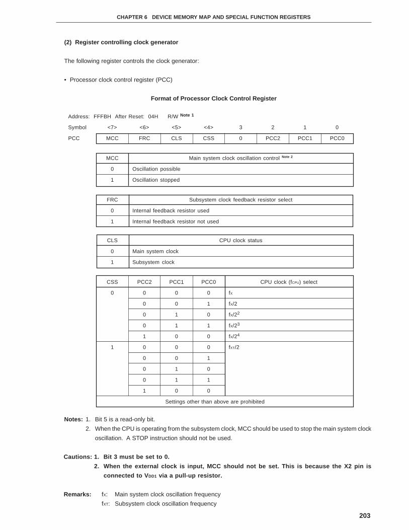
203
CHAPTER 6 DEVICE MEMORY MAP AND SPECIAL FUNCTION REGISTERS
(2) Register controlling clock generator
The following register controls the clock generator:
• Processor clock control register (PCC)
Format of Processor Clock Control Register
Address: FFFBH After Reset: 04H R/W Note 1
Symbol <7> <6> <5> <4> 3 2 1 0
PCC MCC FRC CLS CSS 0 PCC2 PCC1 PCC0
MCC Main system clock oscillation control Note 2
0 Oscillation possible
1 Oscillation stopped
FRC Subsystem clock feedback resistor select
0 Internal feedback resistor used
1 Internal feedback resistor not used
CLS CPU clock status
0 Main system clock
1 Subsystem clock
CSS PCC2 PCC1 PCC0 CPU clock (fCPU) select
0 0 0 0 fX
0 0 1 fX/2
0 1 0 fX/22
0 1 1 fX/23
1 0 0 fX/24
1 0 0 0 fXT/2
0 0 1
0 1 0
0 1 1
1 0 0
Settings other than above are prohibited
Notes: 1. Bit 5 is a read-only bit.
2. When the CPU is operating from the subsystem clock, MCC should be used to stop the main system clock
oscillation. A STOP instruction should not be used.
Cautions: 1. Bit 3 must be set to 0.
2. When the external clock is input, MCC should not be set. This is because the X2 pin is
connected to V DD1 via a pull-up resistor.
Remarks: fX: Main system clock oscillation frequency
fXT: Subsystem clock oscillation frequency

204
CHAPTER 6 DEVICE MEMORY MAP AND SPECIAL FUNCTION REGISTERS
(3) Registers controlling 16-bit timer/event counter
The following five registers control the 16-bit timer/event counter:
• 16-bit timer mode control register (TMC0)
• Capture/compare control register (CRC0)
• 16-bit timer output control register (TOC0)
• Prescaler mode register 0 (PRM0)
• Port mode register 7 (PM7)
- Refer to section (1) for the register format.
Format of 16-Bit Timer Mode Control Register
TMC03 TMC02 TMC01Operating mode
TO0 output timing selection Interrupt request generationand Clear mode selection
0 0 0 Operation stop No change Not generated
0 0 1 (TM0 cleared to 0)
0 1 0 Free-running mode Match between TM0 and
CR00 or match between TM0
and CR01
0 1 1 Match between TM0 and
CR00, match between TM0
and CR01 or TI00 valid edge
1 0 0 Clear and start on TI00 valid —
1 0 1 edge
1 1 0 Clear and start on match Match between TM0 and
between TM0 and CR00 CR00 or match between TM0
and CR01
1 1 1 Match between TM0 and
CR00, match between TM0
and CR01 or TI00 valid edge
OVF0 16-bit Timer Register Overflow Detection
0 Overflow not detected
1 Overflow detected
Cautions: 1. The 16-bit timer register (TM0) starts operation when a value other than 0, 0 is set to TMC02
and TMC03 (Operation Stop mode). To stop the operation, set TMC02 and TMC03 to 0, 0.
2. Timer operation must be stopped before writing to bits other than the OVF0 flag.
3. Set the valid edge of the TI00/TO0/P70 pin with prescaler mode register 0 (PRM0).
4. If Clear and Start mode on a match between TM0 and CR00 is selected, when the set value
of CR00 is FFFFH and the TM0 value changes from FFFFH to 0000H, the OVF0 flag is set
to 1.
Generated on match
between TM0 and CR00, or
match between TM0 and
CR01
7
0
6
0
5
0
4
0
<3>
TMC03
<2>
TMC02
1
TMC01
<0>
OVF0
Symbol
TMC0
Address: FF60H After Reset: 00H R/W

205
CHAPTER 6 DEVICE MEMORY MAP AND SPECIAL FUNCTION REGISTERS
Remarks: TO0: 16-bit timer/event counter output pin
TI00: 16-bit timer/event counter input pin
TM0: 16-bit timer register
CR00: Compare register 00
CR01: Compare register 01
Format of Capture/Compare Control Register 0
Address: FF62H After Reset: 04H R/W
Symbol 7 6 5 4 3 2 1 0
CRC0 0 0 0 0 0 CRC02 CRC01 CRC00
CRC02 CR01 operating mode selection
0 Operates as compare register
1 Operates as capture register
CRC01 CR00 capture trigger selection
0 Captures on valid edge of TI01n
1 Captures on valid edge of TI00n by reverse phase
CRC00 CR00n operating mode selection
0 Operates as compare register
1 Operates as capture register
Cautions 1. Timer operation must be stopped before setting CRC0.
2. When Clear and Start mode on a match between TM0 and CR00 is selected with the 16-bit
timer mode control register (TMC0), CR00 should not be specified as a capture register.
3. If both the rising and falling edges have been selected as the valid edges of TI00, capture
is not performed.
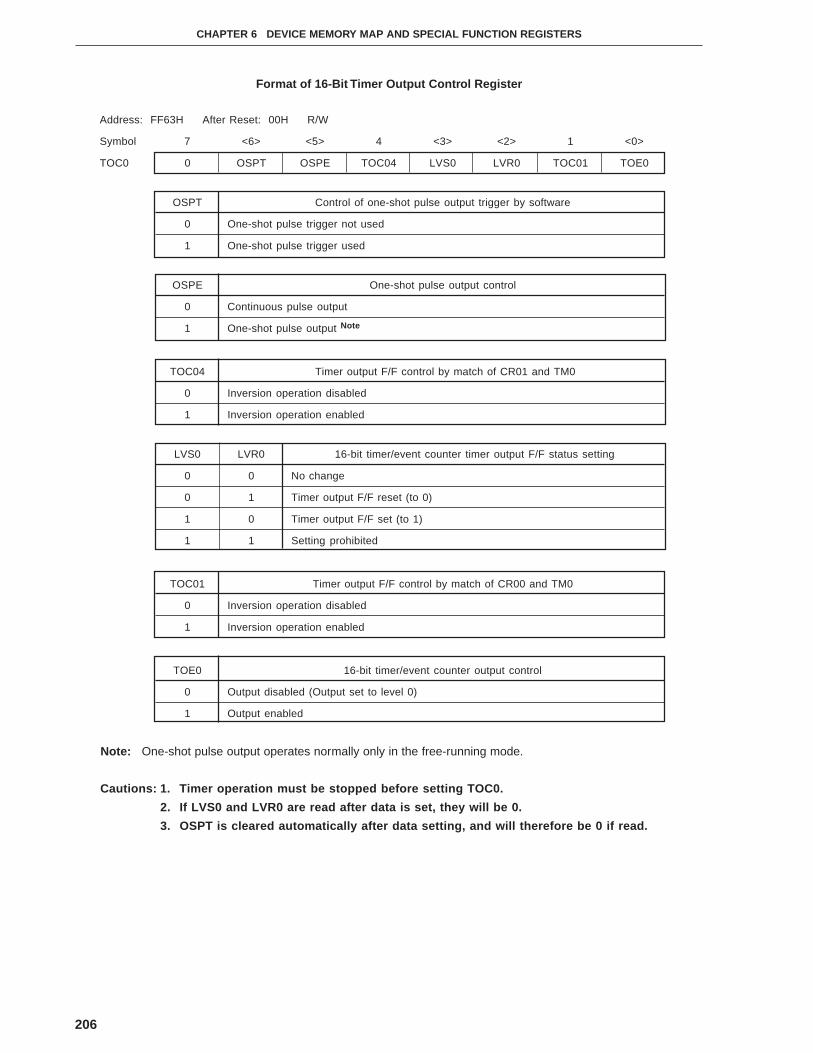
206
CHAPTER 6 DEVICE MEMORY MAP AND SPECIAL FUNCTION REGISTERS
Format of 16-Bit Timer Output Control Register
Address: FF63H After Reset: 00H R/W
Symbol 7 <6> <5> 4 <3> <2> 1 <0>
TOC0 0 OSPT OSPE TOC04 LVS0 LVR0 TOC01 TOE0
OSPT Control of one-shot pulse output trigger by software
0 One-shot pulse trigger not used
1 One-shot pulse trigger used
OSPE One-shot pulse output control
0 Continuous pulse output
1 One-shot pulse output Note
TOC04 Timer output F/F control by match of CR01 and TM0
0 Inversion operation disabled
1 Inversion operation enabled
LVS0 LVR0 16-bit timer/event counter timer output F/F status setting
0 0 No change
0 1 Timer output F/F reset (to 0)
1 0 Timer output F/F set (to 1)
1 1 Setting prohibited
TOC01 Timer output F/F control by match of CR00 and TM0
0 Inversion operation disabled
1 Inversion operation enabled
TOE0 16-bit timer/event counter output control
0 Output disabled (Output set to level 0)
1 Output enabled
Note: One-shot pulse output operates normally only in the free-running mode.
Cautions: 1. Timer operation must be stopped before setting TOC0.
2. If LVS0 and LVR0 are read after data is set, they will be 0.
3. OSPT is cleared automatically after data setting, and will therefore be 0 if read.

207
CHAPTER 6 DEVICE MEMORY MAP AND SPECIAL FUNCTION REGISTERS
Format of Prescaler Mode Register 0
Address: FF61H After Reset: 00H R/W
Symbol 7 6 5 4 3 2 1 0
PRM0 ES11 ES10 ES01 ES00 0 0 PRM01 PRM00
ES11 ES10 TI01 valid edge selection
0 0 Falling edge
0 1 Rising edge
1 0 Setting prohibited
1 1 Both falling and rising edges
ES01 ES00 TI00 valid edge selection
0 0 Falling edge
0 1 Rising edge
1 0 Setting prohibited
1 1 Both falling and rising edges
PRM01 PRM00 count clock selection
0 0 fX (8.38 MHz)
0 1 fX/22 (2.09 MHz)
1 0 fX/26 (131 kHz)
1 1 TI00 valid edge
Cautions: 1. If the valid edge of TI00 is to be set to the count clock, do not set the Clear/Start mode and
the capture trigger at the valid edge of TI00.
Moreover, do not use the P70/TI00/TO0 pins as timer outputs (TO0).
2. Always set data to PRM0 after stopping the timer operation.
3. If the TI00 or TI01 pin is at high level immediately after system reset, the rising edge is
immediately detected after the rising edge or both the rising and falling edges are set as
the valid edge(s) of the TI00 pin or TI01 pin to enable the operation of the 16-bit timer (TM0).
Please be careful when pulling up the TI00 pin or the TI01 pin. However, when re-enabling
operation after the operation has been stopped once, the rising edge is not detected.
Remarks: fX: Main system clock oscillation frequency
TI00, TI01: 16-bit timer/event counter input pins
Values in parentheses are for operation with fX = 8.38 MHz.
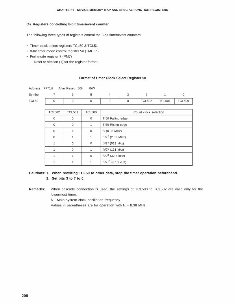
208
CHAPTER 6 DEVICE MEMORY MAP AND SPECIAL FUNCTION REGISTERS
(4) Registers controlling 8-bit timer/event counter
The following three types of registers control the 8-bit timer/event counters:
• Timer clock select registers TCL50 & TCL51
• 8-bit timer mode control register 5n (TMC5n)
• Port mode register 7 (PM7)
- Refer to section (1) for the register format.
Format of Timer Clock Select Register 50
Address: FF71H After Reset: 00H R/W
Symbol 7 6 5 4 3 2 1 0
TCL50 0 0 0 0 0 TCL502 TCL501 TCL500
TCL502 TCL501 TCL500 Count clock selection
0 0 0 TI50 Falling edge
0 0 1 TI50 Rising edge
0 1 0 fX (8.38 MHz)
0 1 1 fX/22 (2.09 MHz)
1 0 0 fX/24 (523 kHz)
1 0 1 fX/26 (131 kHz)
1 1 0 fX/28 (32.7 kHz)
1 1 1 fX/210 (8.18 kHz)
Cautions: 1. When rewriting TCL50 to other data, stop the timer operation beforehand.
2. Set bits 3 to 7 to 0.
Remarks: When cascade connection is used, the settings of TCL500 to TCL502 are valid only for the
lowermost timer.
fX: Main system clock oscillation frequency
Values in parentheses are for operation with fX = 8.38 MHz.
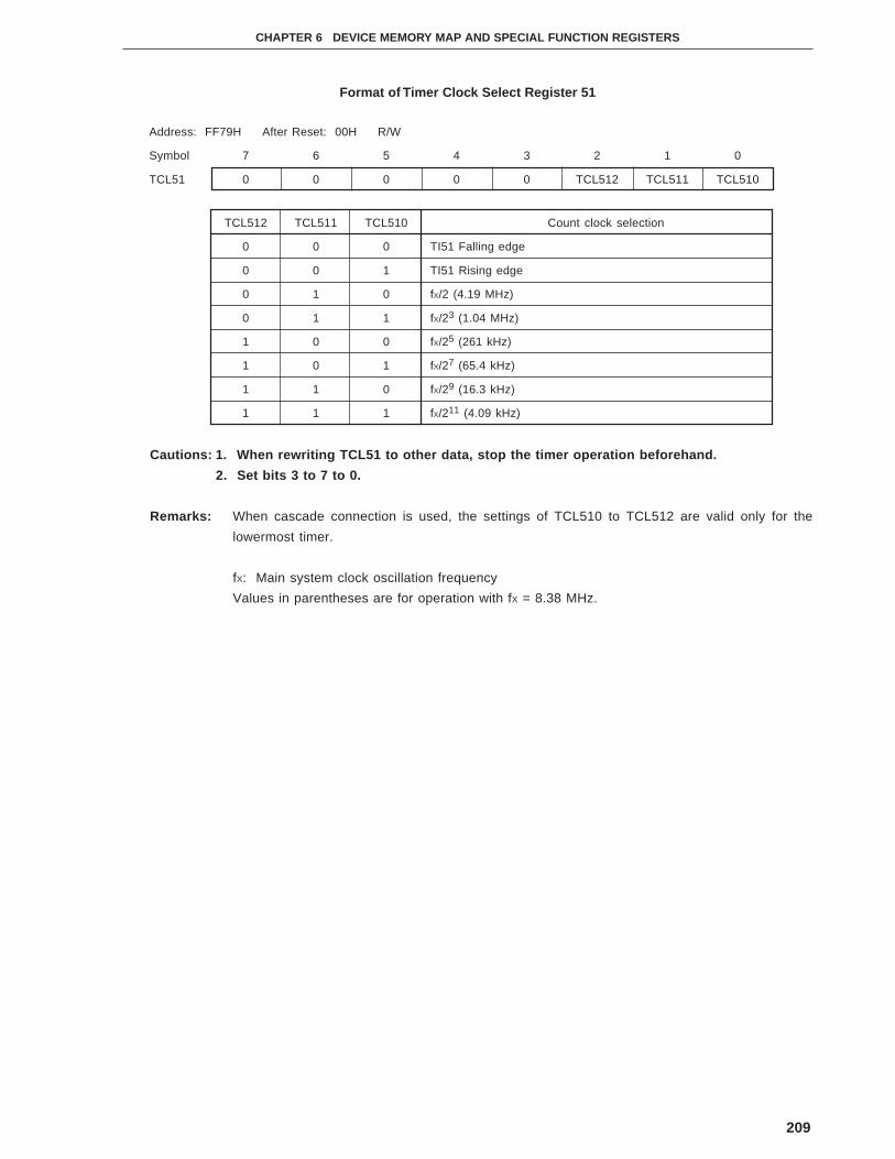
209
CHAPTER 6 DEVICE MEMORY MAP AND SPECIAL FUNCTION REGISTERS
Format of Timer Clock Select Register 51
Address: FF79H After Reset: 00H R/W
Symbol 7 6 5 4 3 2 1 0
TCL51 0 0 0 0 0 TCL512 TCL511 TCL510
TCL512 TCL511 TCL510 Count clock selection
0 0 0 TI51 Falling edge
0 0 1 TI51 Rising edge
0 1 0 fX/2 (4.19 MHz)
0 1 1 fX/23 (1.04 MHz)
1 0 0 fX/25 (261 kHz)
1 0 1 fX/27 (65.4 kHz)
1 1 0 fX/29 (16.3 kHz)
1 1 1 fX/211 (4.09 kHz)
Cautions: 1. When rewriting TCL51 to other data, stop the timer operation beforehand.
2. Set bits 3 to 7 to 0.
Remarks: When cascade connection is used, the settings of TCL510 to TCL512 are valid only for the
lowermost timer.
fX: Main system clock oscillation frequency
Values in parentheses are for operation with fX = 8.38 MHz.
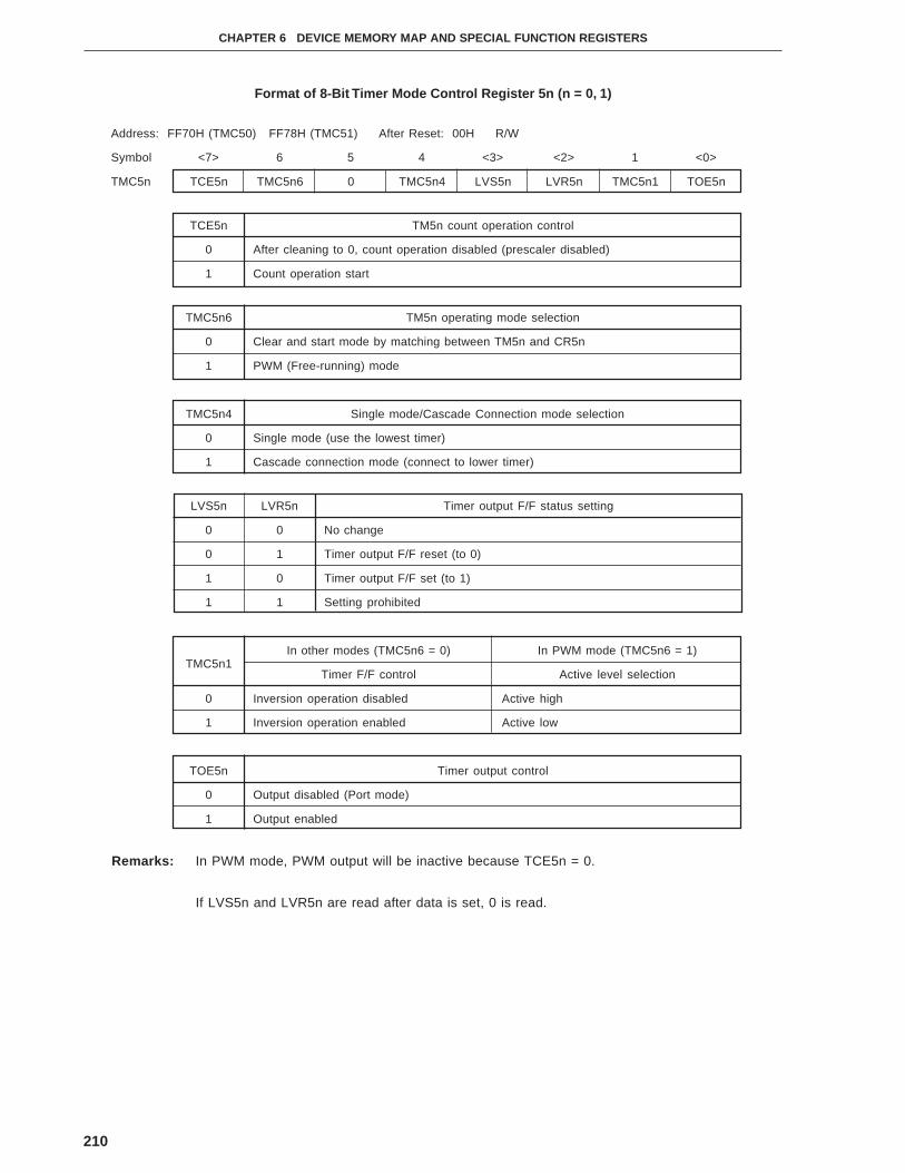
210
CHAPTER 6 DEVICE MEMORY MAP AND SPECIAL FUNCTION REGISTERS
Format of 8-Bit Timer Mode Control Register 5n (n = 0, 1)
Address: FF70H (TMC50) FF78H (TMC51) After Reset: 00H R/W
Symbol <7> 6 5 4 <3> <2> 1 <0>
TMC5n TCE5n TMC5n6 0 TMC5n4 LVS5n LVR5n TMC5n1 TOE5n
TCE5n TM5n count operation control
0 After cleaning to 0, count operation disabled (prescaler disabled)
1 Count operation start
TMC5n6 TM5n operating mode selection
0 Clear and start mode by matching between TM5n and CR5n
1 PWM (Free-running) mode
TMC5n4 Single mode/Cascade Connection mode selection
0 Single mode (use the lowest timer)
1 Cascade connection mode (connect to lower timer)
LVS5n LVR5n Timer output F/F status setting
0 0 No change
0 1 Timer output F/F reset (to 0)
1 0 Timer output F/F set (to 1)
1 1 Setting prohibited
TMC5n1In other modes (TMC5n6 = 0) In PWM mode (TMC5n6 = 1)
Timer F/F control Active level selection
0 Inversion operation disabled Active high
1 Inversion operation enabled Active low
TOE5n Timer output control
0 Output disabled (Port mode)
1 Output enabled
Remarks: In PWM mode, PWM output will be inactive because TCE5n = 0.
If LVS5n and LVR5n are read after data is set, 0 is read.
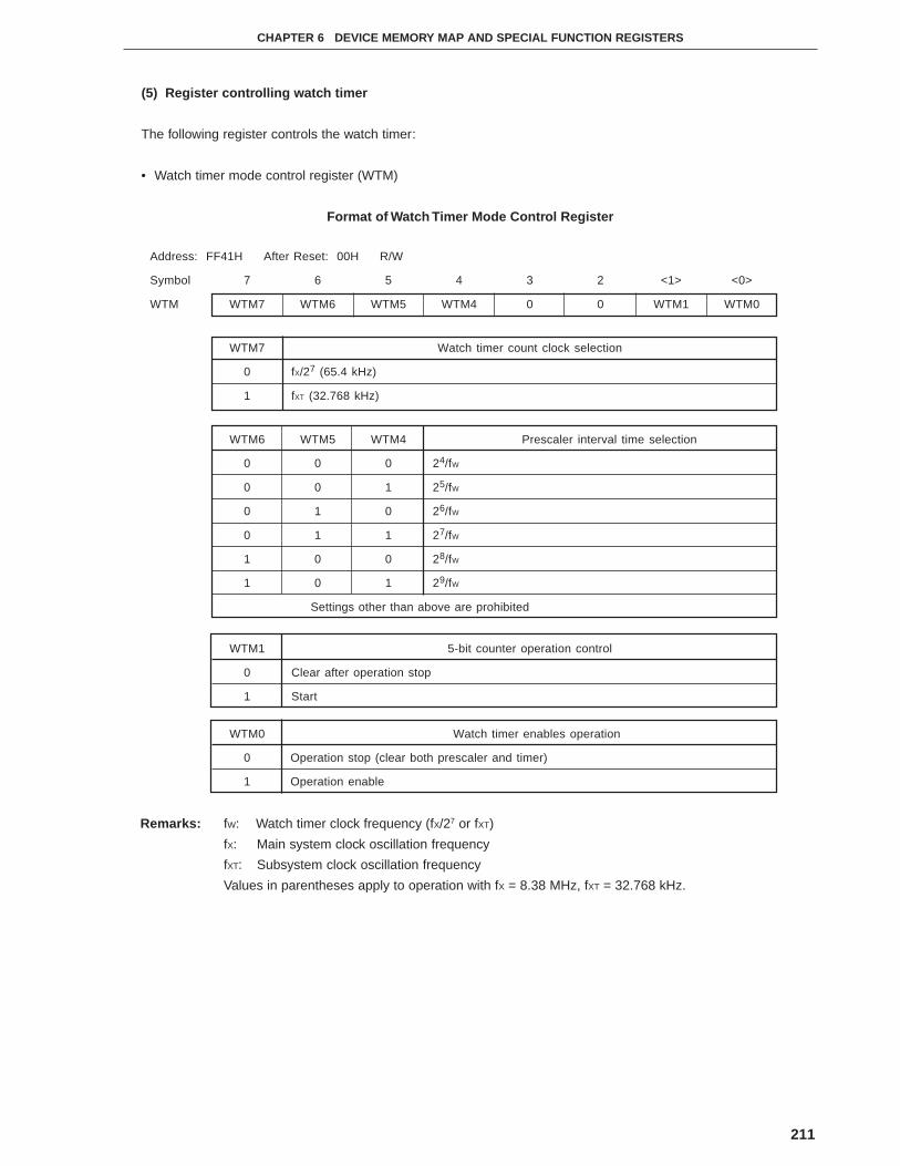
211
CHAPTER 6 DEVICE MEMORY MAP AND SPECIAL FUNCTION REGISTERS
(5) Register controlling watch timer
The following register controls the watch timer:
• Watch timer mode control register (WTM)
Format of Watch Timer Mode Control Register
Address: FF41H After Reset: 00H R/W
Symbol 7 6 5 4 3 2 <1> <0>
WTM WTM7 WTM6 WTM5 WTM4 0 0 WTM1 WTM0
WTM7 Watch timer count clock selection
0 fX/27 (65.4 kHz)
1 fXT (32.768 kHz)
WTM6 WTM5 WTM4 Prescaler interval time selection
0 0 0 24/fW
0 0 1 25/fW
0 1 0 26/fW
0 1 1 27/fW
1 0 0 28/fW
1 0 1 29/fW
Settings other than above are prohibited
WTM1 5-bit counter operation control
0 Clear after operation stop
1 Start
WTM0 Watch timer enables operation
0 Operation stop (clear both prescaler and timer)
1 Operation enable
Remarks: fW: Watch timer clock frequency (fX/27 or fXT)
fX: Main system clock oscillation frequency
fXT: Subsystem clock oscillation frequency
Values in parentheses apply to operation with fX = 8.38 MHz, fXT = 32.768 kHz.
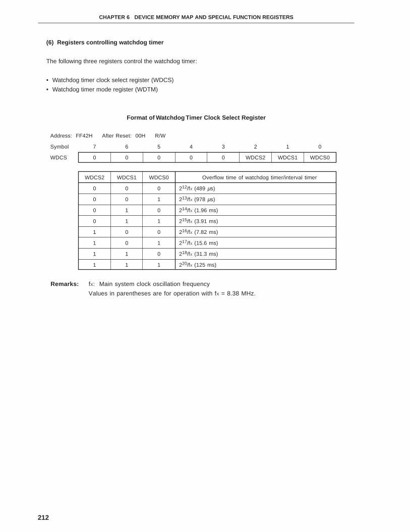
212
CHAPTER 6 DEVICE MEMORY MAP AND SPECIAL FUNCTION REGISTERS
(6) Registers controlling watchdog timer
The following three registers control the watchdog timer:
• Watchdog timer clock select register (WDCS)
• Watchdog timer mode register (WDTM)
Format of Watchdog Timer Clock Select Register
Address: FF42H After Reset: 00H R/W
Symbol 7 6 5 4 3 2 1 0
WDCS 0 0 0 0 0 WDCS2 WDCS1 WDCS0
WDCS2 WDCS1 WDCS0 Overflow time of watchdog timer/interval timer
0 0 0 212/fX (489 µs)
0 0 1 213/fX (978 µs)
0 1 0 214/fX (1.96 ms)
0 1 1 215/fX (3.91 ms)
1 0 0 216/fX (7.82 ms)
1 0 1 217/fX (15.6 ms)
1 1 0 218/fX (31.3 ms)
1 1 1 220/fX (125 ms)
Remarks: fX: Main system clock oscillation frequency
Values in parentheses are for operation with fX = 8.38 MHz.
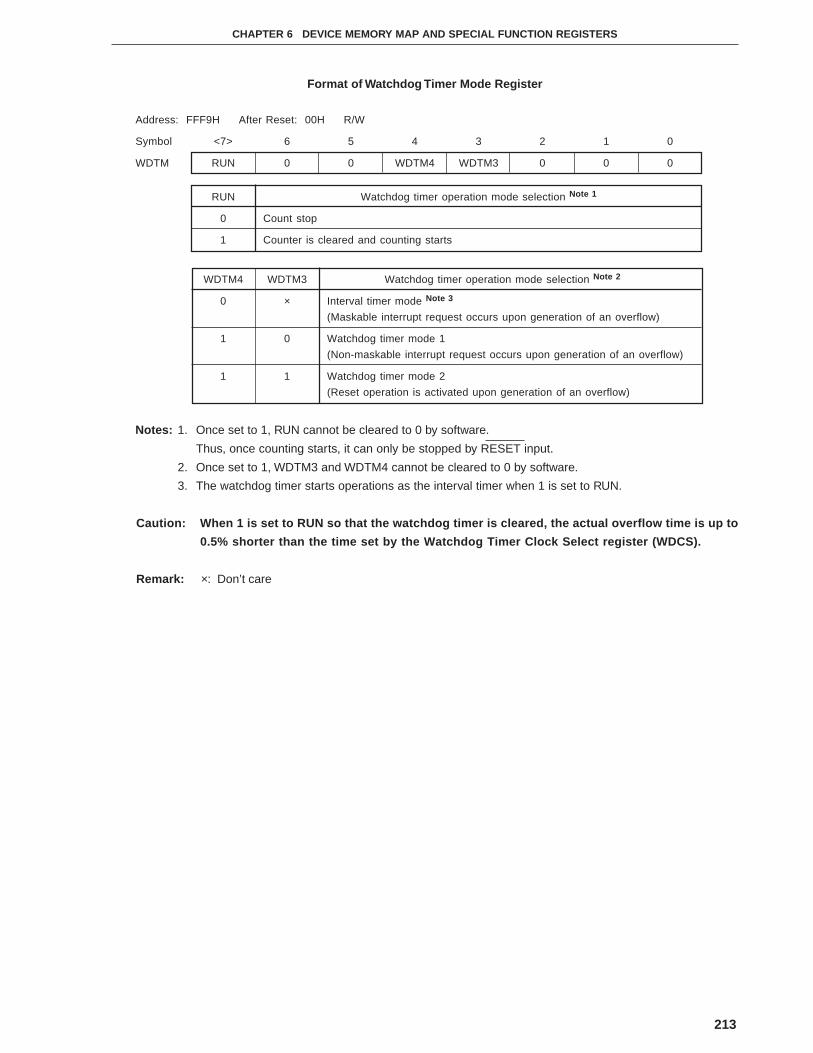
213
CHAPTER 6 DEVICE MEMORY MAP AND SPECIAL FUNCTION REGISTERS
Format of Watchdog Timer Mode Register
Address: FFF9H After Reset: 00H R/W
Symbol <7> 6 5 4 3 2 1 0
WDTM RUN 0 0 WDTM4 WDTM3 0 0 0
RUN Watchdog timer operation mode selection Note 1
0 Count stop
1 Counter is cleared and counting starts
WDTM4 WDTM3 Watchdog timer operation mode selection Note 2
0 × Interval timer mode Note 3
(Maskable interrupt request occurs upon generation of an overflow)
1 0 Watchdog timer mode 1
(Non-maskable interrupt request occurs upon generation of an overflow)
1 1 Watchdog timer mode 2
(Reset operation is activated upon generation of an overflow)
Notes: 1. Once set to 1, RUN cannot be cleared to 0 by software.
Thus, once counting starts, it can only be stopped by RESET input.
2. Once set to 1, WDTM3 and WDTM4 cannot be cleared to 0 by software.
3. The watchdog timer starts operations as the interval timer when 1 is set to RUN.
Caution: When 1 is set to RUN so that the watchdog timer is cleared, the actual overflow time is up to
0.5% shorter than the time set by the Watchdog Timer Clock Select register (WDCS).
Remark: ×: Don’t care
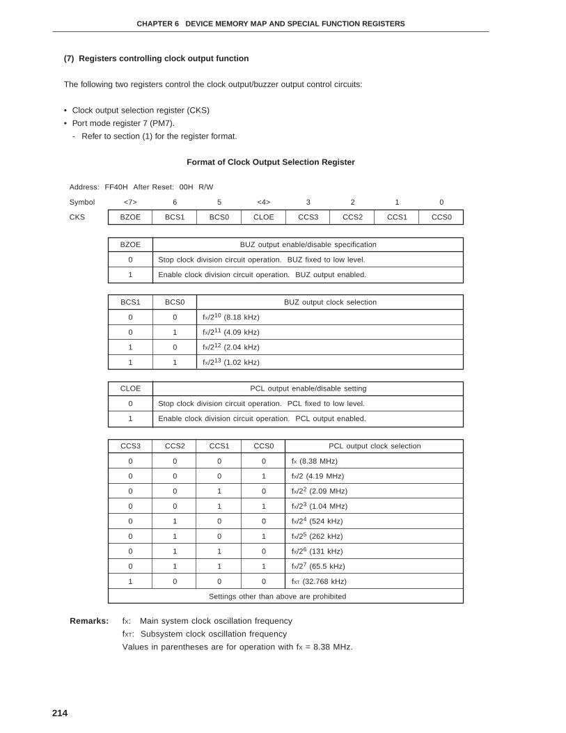
214
CHAPTER 6 DEVICE MEMORY MAP AND SPECIAL FUNCTION REGISTERS
(7) Registers controlling clock output function
The following two registers control the clock output/buzzer output control circuits:
• Clock output selection register (CKS)
• Port mode register 7 (PM7).
- Refer to section (1) for the register format.
Format of Clock Output Selection Register
Address: FF40H After Reset: 00H R/W
Symbol <7> 6 5 <4> 3 2 1 0
CKS BZOE BCS1 BCS0 CLOE CCS3 CCS2 CCS1 CCS0
BZOE BUZ output enable/disable specification
0 Stop clock division circuit operation. BUZ fixed to low level.
1 Enable clock division circuit operation. BUZ output enabled.
BCS1 BCS0 BUZ output clock selection
0 0 fX/210 (8.18 kHz)
0 1 fX/211 (4.09 kHz)
1 0 fX/212 (2.04 kHz)
1 1 fX/213 (1.02 kHz)
CLOE PCL output enable/disable setting
0 Stop clock division circuit operation. PCL fixed to low level.
1 Enable clock division circuit operation. PCL output enabled.
CCS3 CCS2 CCS1 CCS0 PCL output clock selection
0 0 0 0 fX (8.38 MHz)
0 0 0 1 fX/2 (4.19 MHz)
0 0 1 0 fX/22 (2.09 MHz)
0 0 1 1 fX/23 (1.04 MHz)
0 1 0 0 fX/24 (524 kHz)
0 1 0 1 fX/25 (262 kHz)
0 1 1 0 fX/26 (131 kHz)
0 1 1 1 fX/27 (65.5 kHz)
1 0 0 0 fXT (32.768 kHz)
Settings other than above are prohibited
Remarks: fX: Main system clock oscillation frequency
fXT: Subsystem clock oscillation frequency
Values in parentheses are for operation with fX = 8.38 MHz.

215
CHAPTER 6 DEVICE MEMORY MAP AND SPECIAL FUNCTION REGISTERS
(8) Registers controlling A/D converter
The following four registers control the A/D converter:
• A/D converter mode register (ADM0)
• Analog input channel specification register (ADS0)
• External interrupt rising edge enable register (EGP)
- See section (12) for the register format.
• External interrupt falling edge enable register (EGN)
- See section (12) for the register format.
Format of A/D Converter Mode Register
Address: FF80H After Reset: 00H R/W
Symbol <7> <6> 5 4 3 2 1 0
ADM0 ADCS0 TRG0 FR02 FR01 FR00 EGA01 EGA00 0
ADCS0 A/D conversion operation control
0 Stop conversion operation
1 Enable conversion operation
TRG0 Software start/hardware start selection
0 Software start
1 Hardware start
FR02 FR01 FR00 Conversion time selection Note 1
0 0 0 144/fX (17.1 µs)
0 0 1 120/fX (14.3 µs)
0 1 0 96/fX (Setting prohibited Note 2 )
1 0 0 72/fX (Setting prohibited Note 2 )
1 0 1 60/fX (Setting prohibited Note 2 )
1 1 0 48/fX (Setting prohibited Note 2 )
Settings other than above are prohibited
EGA01 EGA00 External trigger signal, edge specification
0 0 No edge detection
0 1 Falling edge detection
1 0 Rising edge detection
1 1 Both falling and rising edge detection
Notes: 1. Set so that the A/D conversion time is 14 µs or more.
2. Setting prohibited because A/D conversion time is less than 14 µs.
Caution: When rewriting FR00 to FR02 to other than the same data, stop A/D conversion operations once
prior to performing rewrite.
Remarks: fX: Main system clock oscillation frequency
Values in parentheses are for operation with fX = 8.38 MHz.
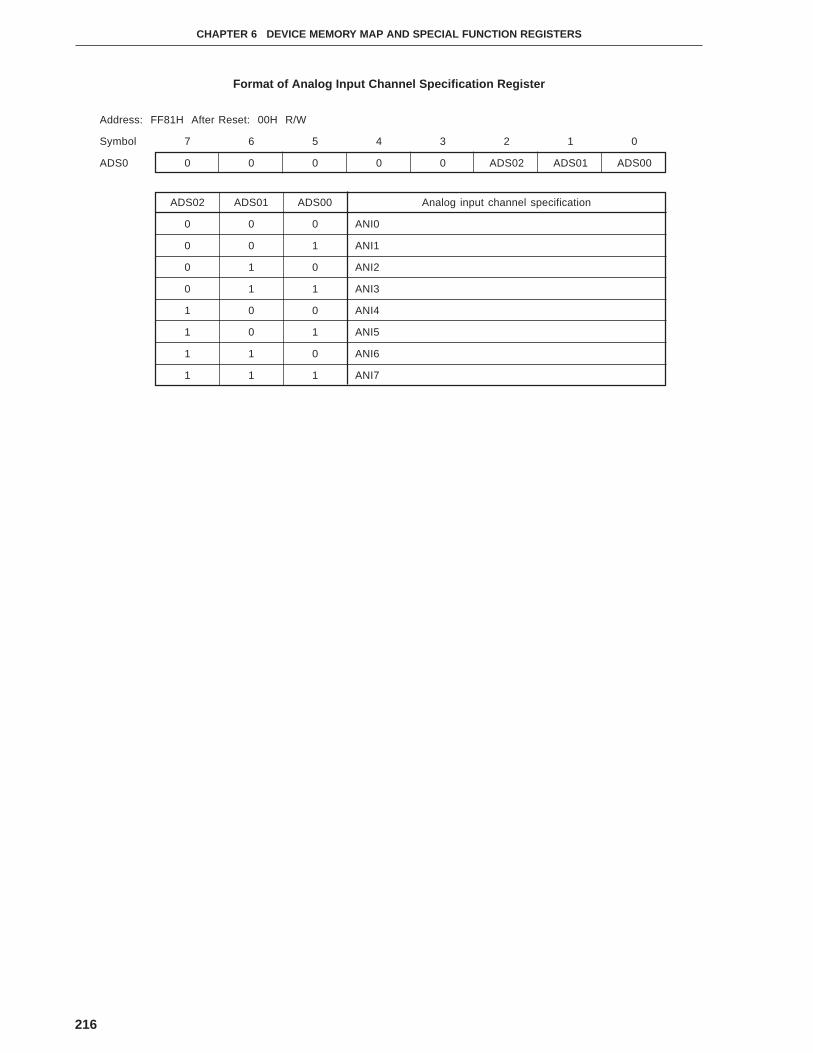
216
CHAPTER 6 DEVICE MEMORY MAP AND SPECIAL FUNCTION REGISTERS
Format of Analog Input Channel Specification Register
Address: FF81H After Reset: 00H R/W
Symbol 7 6 5 4 3 2 1 0
ADS0 0 0 0 0 0 ADS02 ADS01 ADS00
ADS02 ADS01 ADS00 Analog input channel specification
0 0 0 ANI0
0 0 1 ANI1
0 1 0 ANI2
0 1 1 ANI3
1 0 0 ANI4
1 0 1 ANI5
1 1 0 ANI6
1 1 1 ANI7
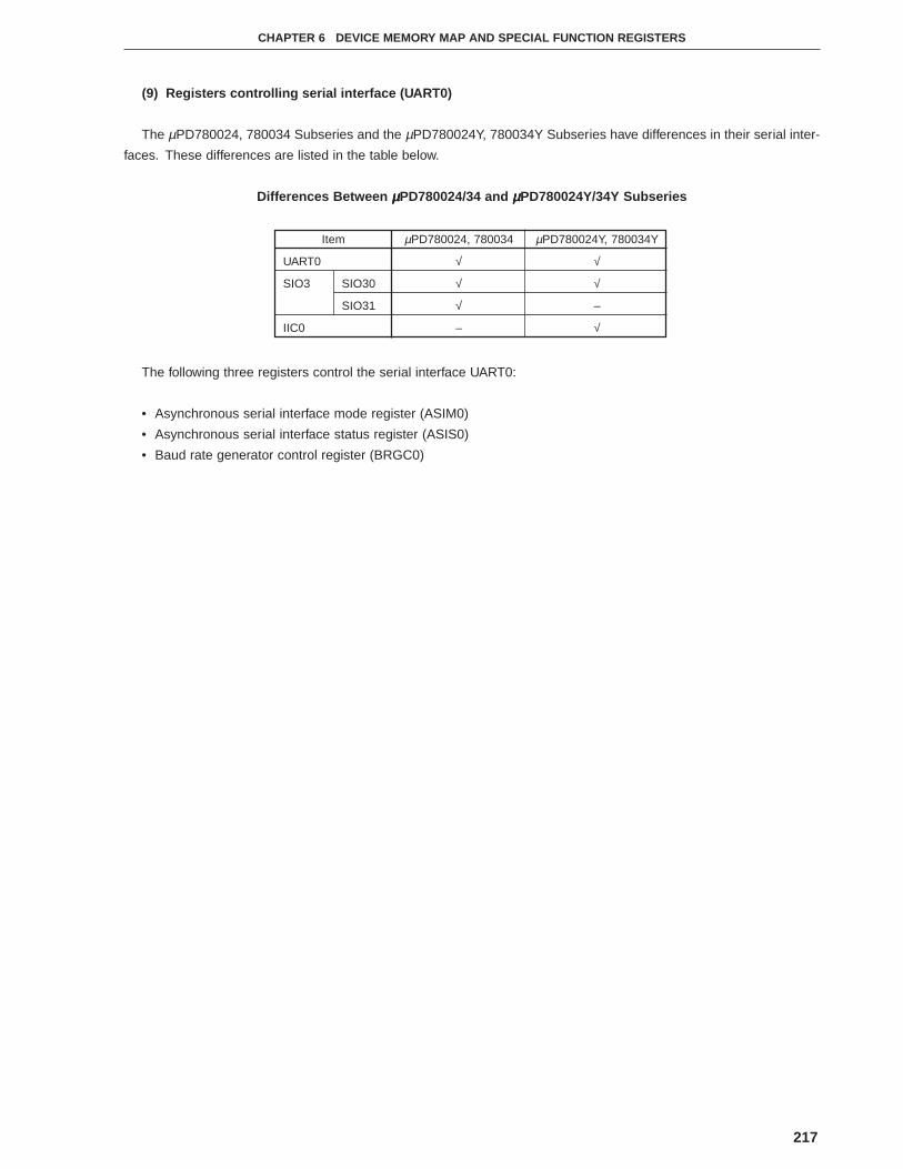
217
CHAPTER 6 DEVICE MEMORY MAP AND SPECIAL FUNCTION REGISTERS
(9) Registers controlling serial interface (UART0)
The µPD780024, 780034 Subseries and the µPD780024Y, 780034Y Subseries have differences in their serial inter-
faces. These differences are listed in the table below.
Differences Between µµµµµPD780024/34 and µµµµµPD780024Y/34Y Subseries
Item µPD780024, 780034 µPD780024Y, 780034Y
UART0 √ √
SIO3 SIO30 √ √
SIO31 √ –
IIC0 – √
The following three registers control the serial interface UART0:
• Asynchronous serial interface mode register (ASIM0)
• Asynchronous serial interface status register (ASIS0)
• Baud rate generator control register (BRGC0)
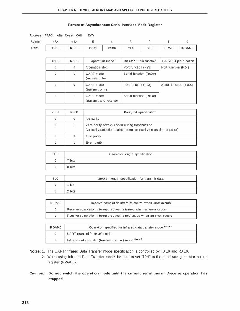
218
CHAPTER 6 DEVICE MEMORY MAP AND SPECIAL FUNCTION REGISTERS
Format of Asynchronous Serial Interface Mode Register
Address: FFA0H After Reset: 00H R/W
Symbol <7> <6> 5 4 3 2 1 0
ASIM0 TXE0 RXE0 PS01 PS00 CL0 SL0 ISRM0 IRDAM0
TXE0 RXE0 Operation mode RxD0/P23 pin function TxD0/P24 pin function
0 0 Operation stop Port function (P23) Port function (P24)
0 1 UART mode Serial function (RxD0)
(receive only)
1 0 UART mode Port function (P23) Serial function (TxD0)
(transmit only)
1 1 UART mode Serial function (RxD0)
(transmit and receive)
PS01 PS00 Parity bit specification
0 0 No parity
0 1 Zero parity always added during transmission
No parity detection during reception (parity errors do not occur)
1 0 Odd parity
1 1 Even parity
CL0 Character length specification
0 7 bits
1 8 bits
SL0 Stop bit length specification for transmit data
0 1 bit
1 2 bits
ISRM0 Receive completion interrupt control when error occurs
0 Receive completion interrupt request is issued when an error occurs
1 Receive completion interrupt request is not issued when an error occurs
IRDAM0 Operation specified for infrared data transfer mode Note 1
0 UART (transmit/receive) mode
1 Infrared data transfer (transmit/receive) mode Note 2
Notes: 1. The UART/Infrared Data Transfer mode specification is controlled by TXE0 and RXE0.
2. When using Infrared Data Transfer mode, be sure to set “10H” to the baud rate generator control
register (BRGC0).
Caution: Do not switch the operation mode until the current serial transmit/receive operation has
stopped.
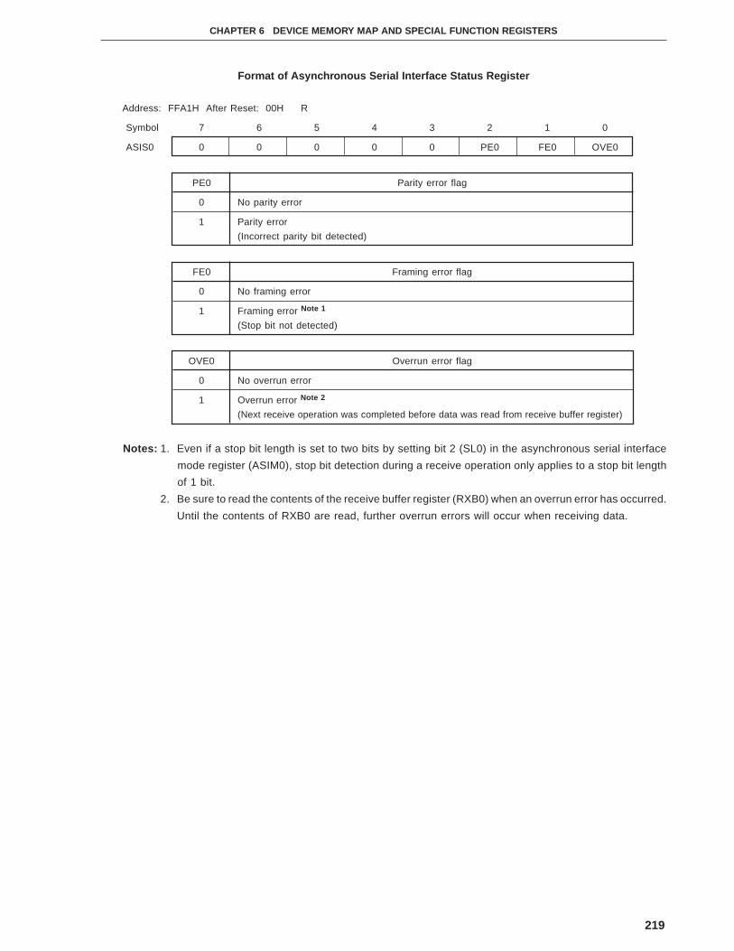
219
CHAPTER 6 DEVICE MEMORY MAP AND SPECIAL FUNCTION REGISTERS
Format of Asynchronous Serial Interface Status Register
Address: FFA1H After Reset: 00H R
Symbol 7 6 5 4 3 2 1 0
ASIS0 0 0 0 0 0 PE0 FE0 OVE0
PE0 Parity error flag
0 No parity error
1 Parity error
(Incorrect parity bit detected)
FE0 Framing error flag
0 No framing error
1 Framing error Note 1
(Stop bit not detected)
OVE0 Overrun error flag
0 No overrun error
1 Overrun error Note 2
(Next receive operation was completed before data was read from receive buffer register)
Notes: 1. Even if a stop bit length is set to two bits by setting bit 2 (SL0) in the asynchronous serial interface
mode register (ASIM0), stop bit detection during a receive operation only applies to a stop bit length
of 1 bit.
2. Be sure to read the contents of the receive buffer register (RXB0) when an overrun error has occurred.
Until the contents of RXB0 are read, further overrun errors will occur when receiving data.

220
CHAPTER 6 DEVICE MEMORY MAP AND SPECIAL FUNCTION REGISTERS
Format of Baud Rate Generator Control Register
Address: FFA2H After Reset: 00H R/W
Symbol 7 6 5 4 3 2 1 0
BRGC0 0 TPS02 TPS01 TPS00 MDL03 MDL02 MDL01 MDL00
(fX = 8.38 MHz)
TPS02 TPS01 TPS00 Source clock selection for 5-bit counter n
0 0 0 P25/ASCK0 0
0 0 1 fX/2 1
0 1 0 fX/22 2
0 1 1 fX/23 3
1 0 0 fX/24 4
1 0 1 fX/25 5
1 1 0 fX/26 6
1 1 1 fX/27 7
MDL03 MDL02 MDL01 MDL00 Input clock selection for baud rate generator k
0 0 0 0 fSCK/16 0
0 0 0 1 fSCK/17 1
0 0 1 0 fSCK/18 2
0 0 1 1 fSCK/19 3
0 1 0 0 fSCK/20 4
0 1 0 1 fSCK/21 5
0 1 1 0 fSCK/22 6
0 1 1 1 fSCK/23 7
1 0 0 0 fSCK/24 8
1 0 0 1 fSCK/25 9
1 0 1 0 fSCK/26 10
1 0 1 1 fSCK/27 11
1 1 0 0 fSCK/28 12
1 1 0 1 fSCK/29 13
1 1 1 0 fSCK/30 14
1 1 1 1 Setting prohibited —
Cautions: 1. Writing to BRGC0 during a communication operation may cause abnormal output from the
baud rate generator and disable further communication operations. Therefore, do not write
to BRGC0 during a communication operation.
2. Set 10H to BRGC0 when using BRGC0 in Infrared Data Transfer mode.
Remarks: fSCK: Source clock for 5-bit counter
n: Value set via TPS00 to TPS02 (0 ≤ n ≤ 7)
k: Value set via MDL00 to MDL03 (0 ≤ k ≤ 14)
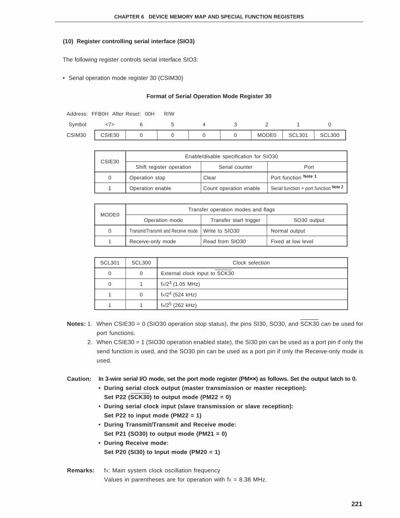
221
CHAPTER 6 DEVICE MEMORY MAP AND SPECIAL FUNCTION REGISTERS
(10) Register controlling serial interface (SIO3)
The following register controls serial interface SIO3:
• Serial operation mode register 30 (CSIM30)
Format of Serial Operation Mode Register 30
Address: FFB0H After Reset: 00H R/W
Symbol <7> 6 5 4 3 2 1 0
CSIM30 CSIE30 0 0 0 0 MODE0 SCL301 SCL300
CSIE30Enable/disable specification for SIO30
Shift register operation Serial counter Port
0 Operation stop Clear Port function Note 1
1 Operation enable Count operation enable Serial function + port function Note 2
MODE0Transfer operation modes and flags
Operation mode Transfer start trigger SO30 output
0 Transmit/Transmit and Receive mode Write to SIO30 Normal output
1 Receive-only mode Read from SIO30 Fixed at low level
SCL301 SCL300 Clock selection
0 0 External clock input to SCK30
0 1 fX/23 (1.05 MHz)
1 0 fX/24 (524 kHz)
1 1 fX/25 (262 kHz)
Notes: 1. When CSIE30 = 0 (SIO30 operation stop status), the pins SI30, SO30, and SCK30 can be used for
port functions.
2. When CSIE30 = 1 (SIO30 operation enabled state), the SI30 pin can be used as a port pin if only the
send function is used, and the SO30 pin can be used as a port pin if only the Receive-only mode is
used.
Caution: In 3-wire serial I/O mode, set the port mode register (PM ××××××××××) as follows. Set the output latch to 0.
• During serial clock output (master transmission or master reception):
Set P22 (SCK30) to output mode (PM22 = 0)
• During serial clock input (slave transmission or slave reception):
Set P22 to input mode (PM22 = 1)
• During Transmit/Transmit and Receive mode:
Set P21 (SO30) to output mode (PM21 = 0)
• During Receive mode:
Set P20 (SI30) to Input mode (PM20 = 1)
Remarks: fX: Main system clock oscillation frequency
Values in parentheses are for operation with fX = 8.38 MHz.
222
CHAPTER 6 DEVICE MEMORY MAP AND SPECIAL FUNCTION REGISTERS
(11) Registers controlling serial interface (I 2C)
Caution: The I 2C option is only available in 78002 ×××××Y/78003×××××Y devices.
The following three registers control serial interface I2C:
• IIC control register (IICC0)
• IIC status register (IICS0)
• IIC clock select register (IICCL0)
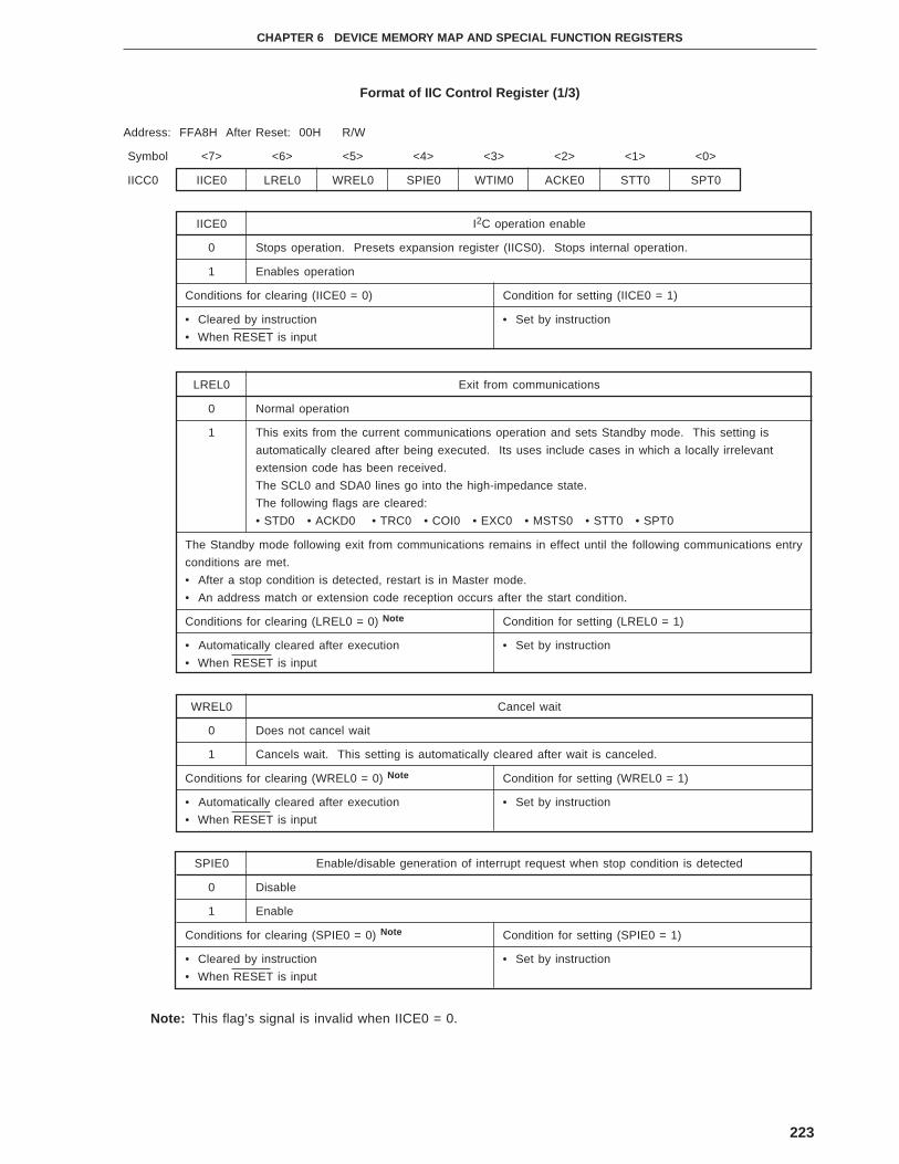
223
CHAPTER 6 DEVICE MEMORY MAP AND SPECIAL FUNCTION REGISTERS
Format of IIC Control Register (1/3)
Address: FFA8H After Reset: 00H R/W
Symbol <7> <6> <5> <4> <3> <2> <1> <0>
IICC0 IICE0 LREL0 WREL0 SPIE0 WTIM0 ACKE0 STT0 SPT0
IICE0 I2C operation enable
0 Stops operation. Presets expansion register (IICS0). Stops internal operation.
1 Enables operation
Conditions for clearing (IICE0 = 0) Condition for setting (IICE0 = 1)
• Cleared by instruction • Set by instruction
• When RESET is input
LREL0 Exit from communications
0 Normal operation
1 This exits from the current communications operation and sets Standby mode. This setting is
automatically cleared after being executed. Its uses include cases in which a locally irrelevant
extension code has been received.
The SCL0 and SDA0 lines go into the high-impedance state.
The following flags are cleared:
• STD0 • ACKD0 • TRC0 • COI0 • EXC0 • MSTS0 • STT0 • SPT0
The Standby mode following exit from communications remains in effect until the following communications entry
conditions are met.
• After a stop condition is detected, restart is in Master mode.
• An address match or extension code reception occurs after the start condition.
Conditions for clearing (LREL0 = 0) Note Condition for setting (LREL0 = 1)
• Automatically cleared after execution • Set by instruction
• When RESET is input
WREL0 Cancel wait
0 Does not cancel wait
1 Cancels wait. This setting is automatically cleared after wait is canceled.
Conditions for clearing (WREL0 = 0) Note Condition for setting (WREL0 = 1)
• Automatically cleared after execution • Set by instruction
• When RESET is input
SPIE0 Enable/disable generation of interrupt request when stop condition is detected
0 Disable
1 Enable
Conditions for clearing (SPIE0 = 0) Note Condition for setting (SPIE0 = 1)
• Cleared by instruction • Set by instruction
• When RESET is input
Note: This flag’s signal is invalid when IICE0 = 0.
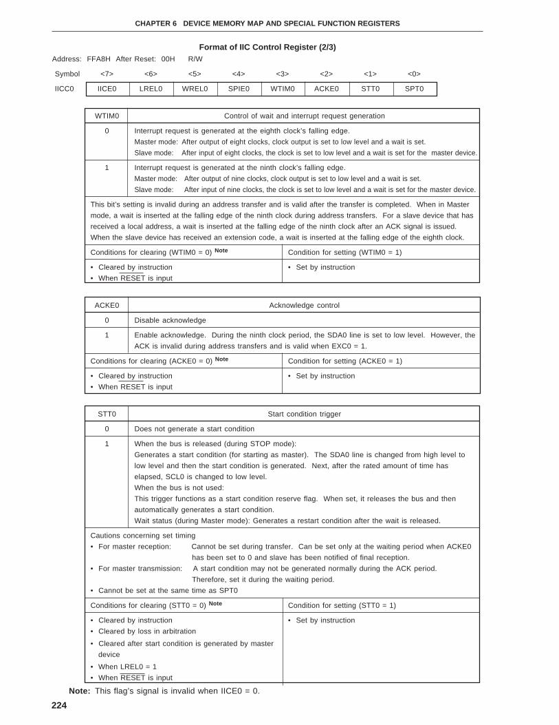
224
CHAPTER 6 DEVICE MEMORY MAP AND SPECIAL FUNCTION REGISTERS
Format of IIC Control Register (2/3)Address: FFA8H After Reset: 00H R/W
Symbol <7> <6> <5> <4> <3> <2> <1> <0>
IICC0 IICE0 LREL0 WREL0 SPIE0 WTIM0 ACKE0 STT0 SPT0
WTIM0 Control of wait and interrupt request generation
0 Interrupt request is generated at the eighth clock’s falling edge.
Master mode: After output of eight clocks, clock output is set to low level and a wait is set.
Slave mode: After input of eight clocks, the clock is set to low level and a wait is set for the master device.
1 Interrupt request is generated at the ninth clock’s falling edge.
Master mode: After output of nine clocks, clock output is set to low level and a wait is set.
Slave mode: After input of nine clocks, the clock is set to low level and a wait is set for the master device.
This bit’s setting is invalid during an address transfer and is valid after the transfer is completed. When in Master
mode, a wait is inserted at the falling edge of the ninth clock during address transfers. For a slave device that has
received a local address, a wait is inserted at the falling edge of the ninth clock after an ACK signal is issued.
When the slave device has received an extension code, a wait is inserted at the falling edge of the eighth clock.
Conditions for clearing (WTIM0 = 0) Note Condition for setting (WTIM0 = 1)
• Cleared by instruction • Set by instruction
• When RESET is input
ACKE0 Acknowledge control
0 Disable acknowledge
1 Enable acknowledge. During the ninth clock period, the SDA0 line is set to low level. However, the
ACK is invalid during address transfers and is valid when EXC0 = 1.
Conditions for clearing (ACKE0 = 0) Note Condition for setting (ACKE0 = 1)
• Cleared by instruction • Set by instruction
• When RESET is input
STT0 Start condition trigger
0 Does not generate a start condition
1 When the bus is released (during STOP mode):
Generates a start condition (for starting as master). The SDA0 line is changed from high level to
low level and then the start condition is generated. Next, after the rated amount of time has
elapsed, SCL0 is changed to low level.
When the bus is not used:
This trigger functions as a start condition reserve flag. When set, it releases the bus and then
automatically generates a start condition.
Wait status (during Master mode): Generates a restart condition after the wait is released.
Cautions concerning set timing
• For master reception: Cannot be set during transfer. Can be set only at the waiting period when ACKE0
has been set to 0 and slave has been notified of final reception.
• For master transmission: A start condition may not be generated normally during the ACK period.
Therefore, set it during the waiting period.
• Cannot be set at the same time as SPT0
Conditions for clearing (STT0 = 0) Note Condition for setting (STT0 = 1)
• Cleared by instruction • Set by instruction
• Cleared by loss in arbitration
• Cleared after start condition is generated by master
device
• When LREL0 = 1
• When RESET is input
Note: This flag’s signal is invalid when IICE0 = 0.
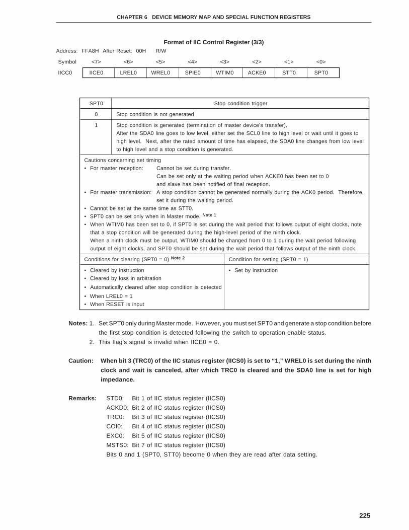
225
CHAPTER 6 DEVICE MEMORY MAP AND SPECIAL FUNCTION REGISTERS
Format of IIC Control Register (3/3)Address: FFA8H After Reset: 00H R/W
Symbol <7> <6> <5> <4> <3> <2> <1> <0>
IICC0 IICE0 LREL0 WREL0 SPIE0 WTIM0 ACKE0 STT0 SPT0
SPT0 Stop condition trigger
0 Stop condition is not generated
1 Stop condition is generated (termination of master device’s transfer).
After the SDA0 line goes to low level, either set the SCL0 line to high level or wait until it goes to
high level. Next, after the rated amount of time has elapsed, the SDA0 line changes from low level
to high level and a stop condition is generated.
Cautions concerning set timing
• For master reception: Cannot be set during transfer.
Can be set only at the waiting period when ACKE0 has been set to 0
and slave has been notified of final reception.
• For master transmission: A stop condition cannot be generated normally during the ACK0 period. Therefore,
set it during the waiting period.
• Cannot be set at the same time as STT0.
• SPT0 can be set only when in Master mode. Note 1
• When WTIM0 has been set to 0, if SPT0 is set during the wait period that follows output of eight clocks, note
that a stop condition will be generated during the high-level period of the ninth clock.
When a ninth clock must be output, WTIM0 should be changed from 0 to 1 during the wait period following
output of eight clocks, and SPT0 should be set during the wait period that follows output of the ninth clock.
Conditions for clearing (SPT0 = 0) Note 2 Condition for setting (SPT0 = 1)
• Cleared by instruction • Set by instruction
• Cleared by loss in arbitration
• Automatically cleared after stop condition is detected
• When LREL0 = 1
• When RESET is input
Notes: 1. Set SPT0 only during Master mode. However, you must set SPT0 and generate a stop condition before
the first stop condition is detected following the switch to operation enable status.
2. This flag’s signal is invalid when IICE0 = 0.
Caution: When bit 3 (TRC0) of the IIC status register (IICS0) is set to “1,” WREL0 is set during the ninth
clock and wait is canceled, after which TRC0 is cleared and the SDA0 line is set for high
impedance.
Remarks: STD0: Bit 1 of IIC status register (IICS0)
ACKD0: Bit 2 of IIC status register (IICS0)
TRC0: Bit 3 of IIC status register (IICS0)
COI0: Bit 4 of IIC status register (IICS0)
EXC0: Bit 5 of IIC status register (IICS0)
MSTS0: Bit 7 of IIC status register (IICS0)
Bits 0 and 1 (SPT0, STT0) become 0 when they are read after data setting.
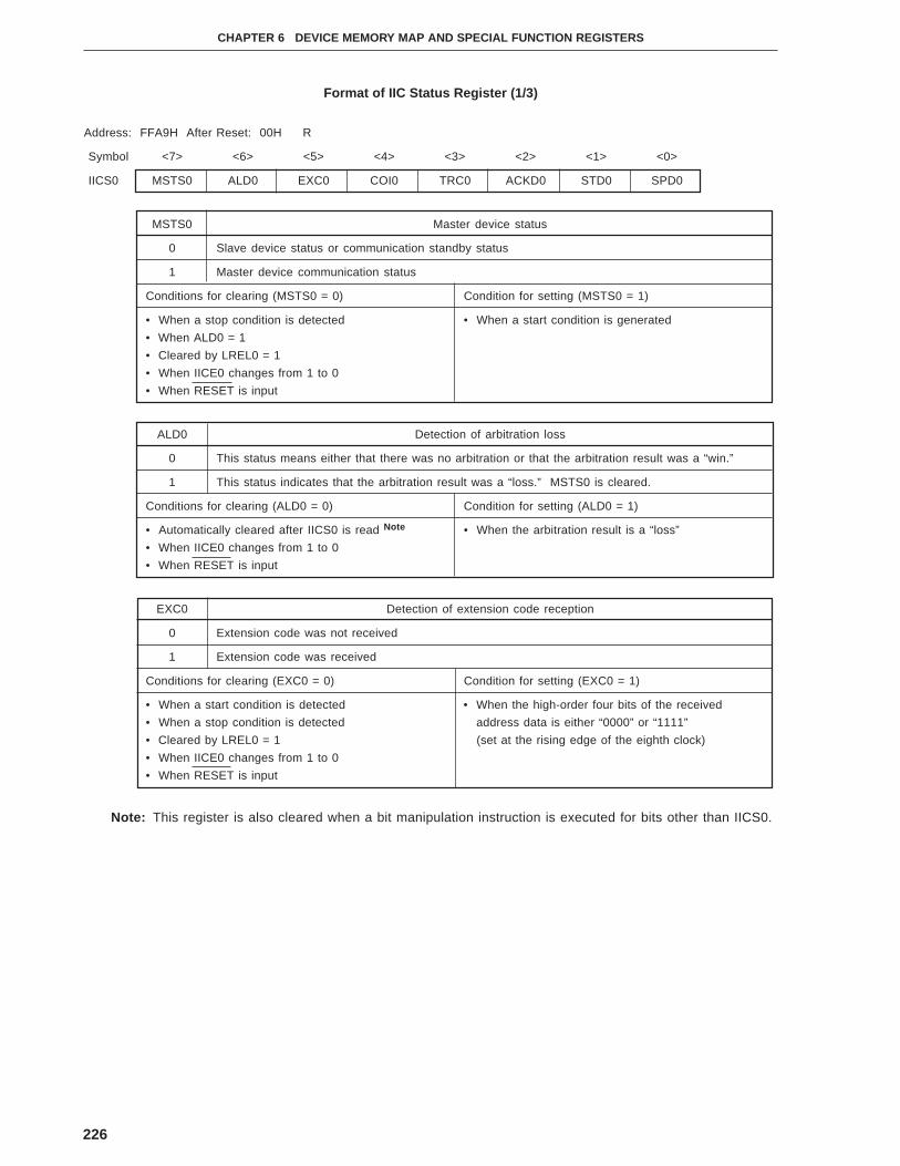
226
CHAPTER 6 DEVICE MEMORY MAP AND SPECIAL FUNCTION REGISTERS
Format of IIC Status Register (1/3)
Address: FFA9H After Reset: 00H R
Symbol <7> <6> <5> <4> <3> <2> <1> <0>
IICS0 MSTS0 ALD0 EXC0 COI0 TRC0 ACKD0 STD0 SPD0
MSTS0 Master device status
0 Slave device status or communication standby status
1 Master device communication status
Conditions for clearing (MSTS0 = 0) Condition for setting (MSTS0 = 1)
• When a stop condition is detected • When a start condition is generated
• When ALD0 = 1
• Cleared by LREL0 = 1
• When IICE0 changes from 1 to 0
• When RESET is input
ALD0 Detection of arbitration loss
0 This status means either that there was no arbitration or that the arbitration result was a “win.”
1 This status indicates that the arbitration result was a “loss.” MSTS0 is cleared.
Conditions for clearing (ALD0 = 0) Condition for setting (ALD0 = 1)
• Automatically cleared after IICS0 is read Note • When the arbitration result is a “loss”
• When IICE0 changes from 1 to 0
• When RESET is input
EXC0 Detection of extension code reception
0 Extension code was not received
1 Extension code was received
Conditions for clearing (EXC0 = 0) Condition for setting (EXC0 = 1)
• When a start condition is detected • When the high-order four bits of the received
• When a stop condition is detected address data is either “0000” or “1111”
• Cleared by LREL0 = 1 (set at the rising edge of the eighth clock)
• When IICE0 changes from 1 to 0
• When RESET is input
Note: This register is also cleared when a bit manipulation instruction is executed for bits other than IICS0.
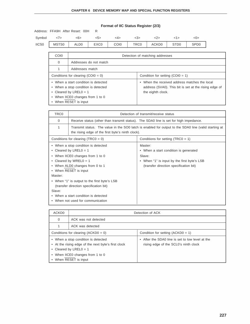
227
CHAPTER 6 DEVICE MEMORY MAP AND SPECIAL FUNCTION REGISTERS
Format of IIC Status Register (2/3)Address: FFA9H After Reset: 00H R
Symbol <7> <6> <5> <4> <3> <2> <1> <0>
IICS0 MSTS0 ALD0 EXC0 COI0 TRC0 ACKD0 STD0 SPD0
COI0 Detection of matching addresses
0 Addresses do not match
1 Addresses match
Conditions for clearing (COI0 = 0) Condition for setting (COI0 = 1)
• When a start condition is detected • When the received address matches the local
• When a stop condition is detected address (SVA0). This bit is set at the rising edge of
• Cleared by LREL0 = 1 the eighth clock.
• When IICE0 changes from 1 to 0
• When RESET is input
TRC0 Detection of transmit/receive status
0 Receive status (other than transmit status). The SDA0 line is set for high impedance.
1 Transmit status. The value in the SO0 latch is enabled for output to the SDA0 line (valid starting at
the rising edge of the first byte’s ninth clock).
Conditions for clearing (TRC0 = 0) Conditions for setting (TRC0 = 1)
• When a stop condition is detected Master:
• Cleared by LREL0 = 1 • When a start condition is generated
• When IICE0 changes from 1 to 0 Slave:
• Cleared by WREL0 = 1 • When “1” is input by the first byte’s LSB
• When ALD0 changes from 0 to 1 (transfer direction specification bit)
• When RESET is input
Master:
• When “1” is output to the first byte’s LSB
(transfer direction specification bit)
Slave:
• When a start condition is detected
• When not used for communication
ACKD0 Detection of ACK
0 ACK was not detected
1 ACK was detected
Conditions for clearing (ACKD0 = 0) Condition for setting (ACKD0 = 1)
• When a stop condition is detected • After the SDA0 line is set to low level at the
• At the rising edge of the next byte’s first clock rising edge of the SCL0’s ninth clock
• Cleared by LREL0 = 1
• When IICE0 changes from 1 to 0
• When RESET is input
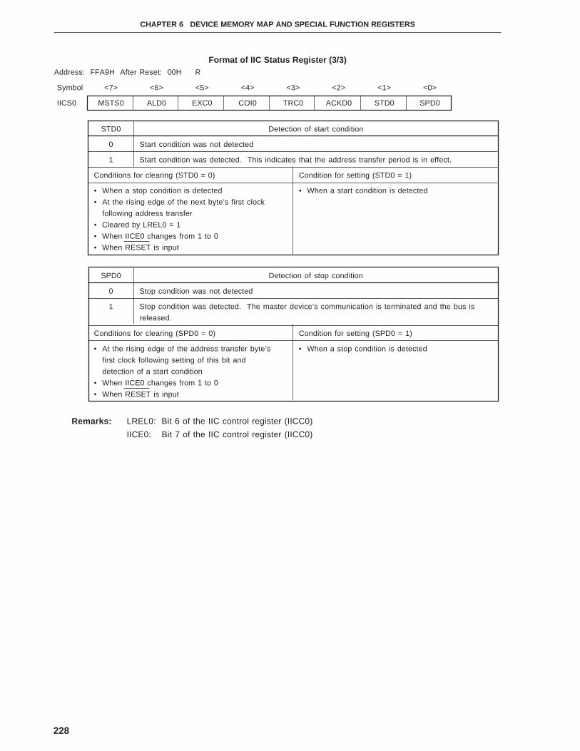
228
CHAPTER 6 DEVICE MEMORY MAP AND SPECIAL FUNCTION REGISTERS
Format of IIC Status Register (3/3)Address: FFA9H After Reset: 00H R
Symbol <7> <6> <5> <4> <3> <2> <1> <0>
IICS0 MSTS0 ALD0 EXC0 COI0 TRC0 ACKD0 STD0 SPD0
STD0 Detection of start condition
0 Start condition was not detected
1 Start condition was detected. This indicates that the address transfer period is in effect.
Conditions for clearing (STD0 = 0) Condition for setting (STD0 = 1)
• When a stop condition is detected • When a start condition is detected
• At the rising edge of the next byte’s first clock
following address transfer
• Cleared by LREL0 = 1
• When IICE0 changes from 1 to 0
• When RESET is input
SPD0 Detection of stop condition
0 Stop condition was not detected
1 Stop condition was detected. The master device’s communication is terminated and the bus is
released.
Conditions for clearing (SPD0 = 0) Condition for setting (SPD0 = 1)
• At the rising edge of the address transfer byte’s • When a stop condition is detected
first clock following setting of this bit and
detection of a start condition
• When IICE0 changes from 1 to 0
• When RESET is input
Remarks: LREL0: Bit 6 of the IIC control register (IICC0)
IICE0: Bit 7 of the IIC control register (IICC0)
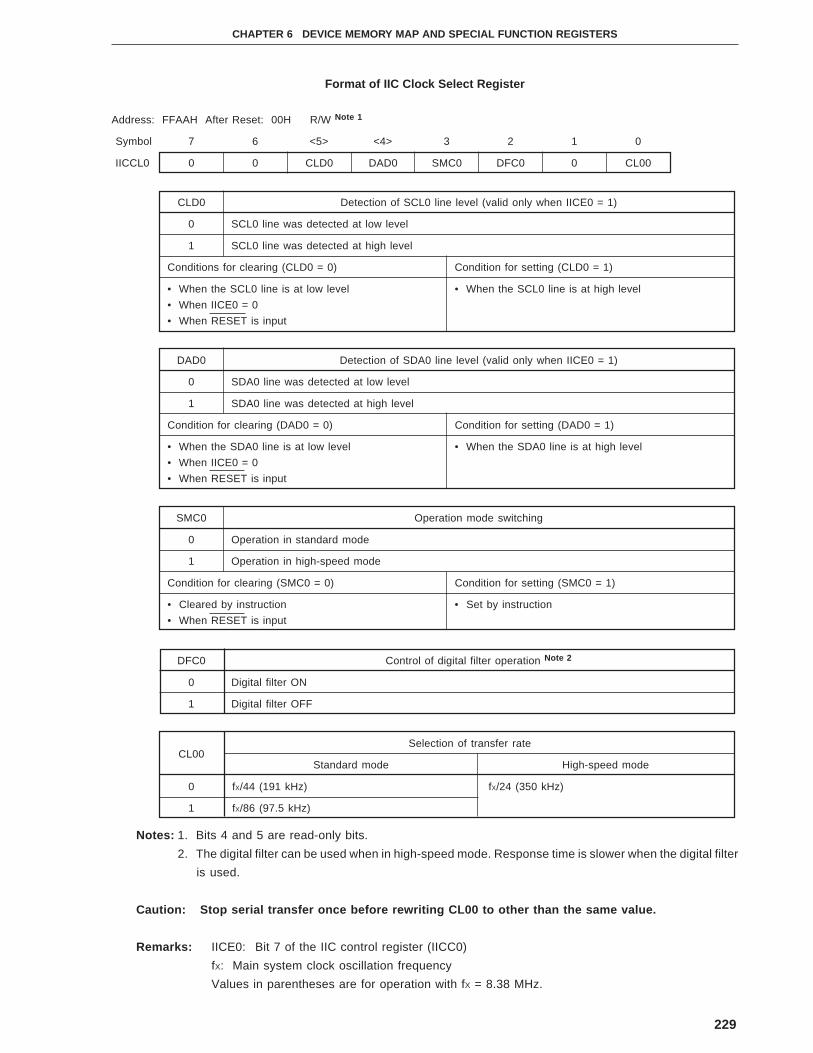
229
CHAPTER 6 DEVICE MEMORY MAP AND SPECIAL FUNCTION REGISTERS
Format of IIC Clock Select Register
Address: FFAAH After Reset: 00H R/W Note 1
Symbol 7 6 <5> <4> 3 2 1 0
IICCL0 0 0 CLD0 DAD0 SMC0 DFC0 0 CL00
CLD0 Detection of SCL0 line level (valid only when IICE0 = 1)
0 SCL0 line was detected at low level
1 SCL0 line was detected at high level
Conditions for clearing (CLD0 = 0) Condition for setting (CLD0 = 1)
• When the SCL0 line is at low level • When the SCL0 line is at high level
• When IICE0 = 0
• When RESET is input
DAD0 Detection of SDA0 line level (valid only when IICE0 = 1)
0 SDA0 line was detected at low level
1 SDA0 line was detected at high level
Condition for clearing (DAD0 = 0) Condition for setting (DAD0 = 1)
• When the SDA0 line is at low level • When the SDA0 line is at high level
• When IICE0 = 0
• When RESET is input
SMC0 Operation mode switching
0 Operation in standard mode
1 Operation in high-speed mode
Condition for clearing (SMC0 = 0) Condition for setting (SMC0 = 1)
• Cleared by instruction • Set by instruction
• When RESET is input
DFC0 Control of digital filter operation Note 2
0 Digital filter ON
1 Digital filter OFF
CL00Selection of transfer rate
Standard mode High-speed mode
0 fX/44 (191 kHz) fX/24 (350 kHz)
1 fX/86 (97.5 kHz)
Notes: 1. Bits 4 and 5 are read-only bits.
2. The digital filter can be used when in high-speed mode. Response time is slower when the digital filter
is used.
Caution: Stop serial transfer once before rewriting CL00 to other than the same value.
Remarks: IICE0: Bit 7 of the IIC control register (IICC0)
fX: Main system clock oscillation frequency
Values in parentheses are for operation with fX = 8.38 MHz.

230
CHAPTER 6 DEVICE MEMORY MAP AND SPECIAL FUNCTION REGISTERS
Format of I 2C Shift Register
Address: FF1FH After Reset: 00H R/W
Symbol 7 6 5 4 3 2 1 0
IIC0
Format of Slave Address Register
Address: FFABH After Reset: 00H R/W
Symbol 7 6 5 4 3 2 1 0
SVA0 0
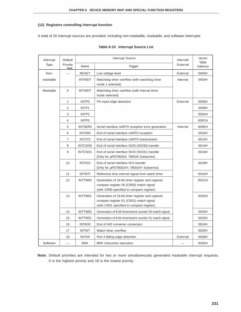
231
CHAPTER 6 DEVICE MEMORY MAP AND SPECIAL FUNCTION REGISTERS
(12) Registers controlling interrupt function
A total of 20 interrupt sources are provided, including non-maskable, maskable, and software interrupts.
Table 6-10. Interrupt Source List
Interrupt Default Interrupt Source Internal/ VectorTable
Type Priority Name Trigger External Address
Non- — RESET Low voltage level External 0000H
maskable INTWDT Watchdog timer overflow (with watchdog timer Internal 0004H
mode 1 selected)
Maskable 0 INTWDT Watchdog timer overflow (with interval timer
mode selected)
1 INTP0 Pin input edge detection External 0006H
2 INTP1 0008H
3 INTP2 000AH
4 INTP3 000CH
5 INTSER0 Serial interface UART0 reception error generation Internal 000EH
6 INTSR0 End of serial interface UART0 reception 0010H
7 INTST0 End of serial interface UART0 transmission 0012H
8 INTCSI30 End of serial interface SIO3 (SIO30) transfer 0014H
9 INTCSI31 End of serial interface SIO3 (SIO31) transfer 0016H
[Only for µPD780024, 780034 Subseries]
10 INTIIC0 End of serial interface IIC0 transfer 0018H
[Only for µPD780024Y, 780034Y Subseries]
11 INTWTI Reference time interval signal from watch timer 001AH
12 INTTM00 Generation of 16-bit timer register and capture/ 001CH
compare register 00 (CR00) match signal
(with CR00 specified to compare register)
13 INTTM01 Generation of 16-bit timer register and capture/ 001EH
compare register 01 (CR01) match signal
(with CR01 specified to compare register)
14 INTTM50 Generation of 8-bit timer/event counter 50 match signal 0020H
15 INTTM51 Generation of 8-bit timer/event counter 51 match signal 0022H
16 INTAD0 End of A/D converter conversion 0024H
17 INTWT Watch timer overflow 0026H
18 INTKR Port 4 falling edge detection External 0028H
Software — BRK BRK instruction execution — 003EH
Note: Default priorities are intended for two or more simultaneously generated maskable interrupt requests.
0 is the highest priority and 18 is the lowest priority.
Note

232
CHAPTER 6 DEVICE MEMORY MAP AND SPECIAL FUNCTION REGISTERS
The following table gives a listing of interrupt request flags, interrupt mask flags, and priority specification flags
corresponding to interrupt request sources.
Table 6-11. Interrupt Sources and Flags
Interrupt Source Interrupt Request Flag Interrupt Mask Flag Priority Specification Flag
Register Register Register
INTWDT WDTIF IF0L WDTMK MK0L WDTPR PR0L
INTP0 PIF0 PMK0 PPR0
INTP1 PIF1 PMK1 PPR1
INTP2 PIF2 PMK2 PPR2
INTP3 PIF3 PMK3 PPR3
INTSER0 SERIF0 SERMK0 SERPR0
INTSR0 SRIF0 SRMK0 SRPR0
INTST0 STIF0 STMK0 STPR0
INTCSI30 CSIIF30 IF0H CSIMK30 MK0H CSIPR30 PR0H
INTCSI31 Note 1 CSIIF31 Note 1 CSIMK31 Note 1 CSIPR31 Note 1
INTIIC0 Note 2 IICIF0 Note 2 IICMK0 Note 2 IICPR0 Note 2
INTWTI WTIIF WTIMK WTIPR
INTTM00 TMIF00 TMMK00 TMPR00
INTTM01 TMIF01 TMMK01 TMPR01
INTTM50 TMIF50 TMMK50 TMPR50
INTTM51 TMIF51 TMMK51 TMPR51
INTAD0 ADIF0 IF1L ADMK0 MK1L ADPR0 PR1L
INTWT WTIF WTMK WTPR
INTKR KRIF KRMK KRPR
Notes: 1. µPD780024, 780034 Subseries only
2. µPD780024Y, 780034Y Subseries only

233
CHAPTER 6 DEVICE MEMORY MAP AND SPECIAL FUNCTION REGISTERS
The following six registers control the interrupt functions:
• Interrupt request flag registers (IF0L, IF0H, IF1L)
• Interrupt mask flag registers (MK0L, MK0H, MK1L)
• Priority specification flag registers (PR0L, PR0H, PR1L)
• External interrupt rising edge enable register (EGP)
• External interrupt falling edge enable register (EGN)
• Program status word (PSW)
Format of Interrupt Request Flag Registers
Address: FFE0H After Reset: 00H R/W
Symbol <7> <6> <5> <4> <3> <2> <1> <0>
IF0L STIF0 SRIF0 SERIF0 PIF3 PIF2 PIF1 PIF0 WDTIF
Address: FFE1H After Reset: 00H R/W
Symbol <7> <6> <5> <4> <3> <2> <1> <0>
IF0H TMIF51 TMIF50 TMIF01 TMIF00 WTIIF IICIF0Note 1 CSIIF31Note 2 CSIIF30
Address: FFE2H After Reset: 00H R/W
Symbol 7 6 5 4 3 <2> <1> <0>
IF1L 0 0 0 0 0 KRIF WTIF ADIF0
XXIFX Interrupt request flag
0 No interrupt request signal is generated
1 Interrupt request is generated; interrupt request status
Notes: 1. Incorporated only in the µPD780024 and 780034 Subseries. Be sure to set 0 for the µPD780024Y,
780034Y Subseries.
2. Incorporated only in the µPD780024Y, 780034Y Subseries. Be sure to set 0 for the µPD780024,
780034 Subseries.
Cautions: 1. The WDTIF flag is R/W enabled only when the watchdog timer is used as the interval timer.
If watchdog timer mode 1 is used, set the WDTIF flag to 0.
2. Be sure to set IF1L bits 3 to 7 to 0.
3. When operating a timer, serial interface, or A/D converter after standby release, run it once
after clearing an interrupt request flag. An interrupt request flag may be set by noise.
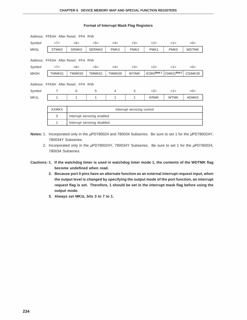
234
CHAPTER 6 DEVICE MEMORY MAP AND SPECIAL FUNCTION REGISTERS
Format of Interrupt Mask Flag Registers
Address: FFE4H After Reset: FFH R/W
Symbol <7> <6> <5> <4> <3> <2> <1> <0>
MK0L STMK0 SRMK0 SERMK0 PMK3 PMK2 PMK1 PMK0 WDTMK
Address: FFE5H After Reset: FFH R/W
Symbol <7> <6> <5> <4> <3> <2> <1> <0>
MK0H TMMK51 TMMK50 TMMK01 TMMK00 WTIMK IICMK0Note 1 CSIMK31Note 2 CSIMK30
Address: FFE6H After Reset: FFH R/W
Symbol 7 6 5 4 3 <2> <1> <0>
MK1L 1 1 1 1 1 KRMK WTMK ADMK0
XXMKX Interrupt servicing control
0 Interrupt servicing enabled
1 Interrupt servicing disabled
Notes: 1. Incorporated only in the µPD780024 and 780034 Subseries. Be sure to set 1 for the µPD780024Y,
780034Y Subseries.
2. Incorporated only in the µPD780024Y, 780034Y Subseries. Be sure to set 1 for the µPD780024,
780034 Subseries.
Cautions: 1. If the watchdog timer is used in watchdog timer mode 1, the contents of the WDTMK flag
become undefined when read.
2. Because port 0 pins have an alternate function as an external interrupt request input, when
the output level is changed by specifying the output mode of the port function, an interrupt
request flag is set. Therefore, 1 should be set in the interrupt mask flag before using the
output mode.
3. Always set MK1L bits 3 to 7 to 1.

235
CHAPTER 6 DEVICE MEMORY MAP AND SPECIAL FUNCTION REGISTERS
Format of Priority Specification Flag Registers
Address: FFE8H After Reset: FFH R/W
Symbol <7> <6> <5> <4> <3> <2> <1> <0>
PR0L STPR0 SRPR0 SERPR0 PPR3 PPR2 PPR1 PPR0 WDTPR
Address: FFE9H After Reset: FFH R/W
Symbol <7> <6> <5> <4> <3> <2> <1> <0>
PR0H TMPR51 TMPR50 TMPR01 TMPR00 WTIPR IICPR0Note 1 CSIPR31Note 2 CSIPR30
Address: FFEAH After Reset: FFH R/W
Symbol 7 6 5 4 3 <2> <1> <0>
PR1L 1 1 1 1 1 KRPR WTPR ADPR0
XXPRX Priority level selection
0 High priority level
1 Low priority level
Notes: 1. Incorporated only in the µPD780024 and 780034 Subseries. Be sure to set 1 for the µPD780024Y,
780034Y Subseries.
2. Incorporated only in the µPD780024Y, 780034Y Subseries. Be sure to set 1 for the µPD780024,
780034 Subseries.
Cautions: 1. When the watchdog timer is used in the watchdog timer 1 mode, set 1 in the WDTPR flag.
2. Always set PR1L bits 3 to 7 to 1.
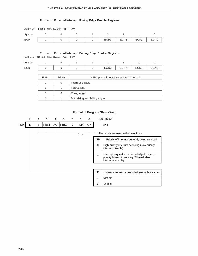
236
CHAPTER 6 DEVICE MEMORY MAP AND SPECIAL FUNCTION REGISTERS
Format of External Interrupt Rising Edge Enable Register
Address: FF48H After Reset: 00H R/W
Symbol 7 6 5 4 3 2 1 0
EGP 0 0 0 0 EGP3 EGP2 EGP1 EGP0
Format of External Interrupt Falling Edge Enable RegisterAddress: FF49H After Reset: 00H R/W
Symbol 7 6 5 4 3 2 1 0
EGN 0 0 0 0 EGN3 EGN2 EGN1 EGN0
EGPn EGNn INTPn pin valid edge selection (n = 0 to 3)
0 0 Interrupt disable
0 1 Falling edge
1 0 Rising edge
1 1 Both rising and falling edges
Format of Program Status Word
7
IE
6
Z
5
RBS1
4
AC
3
RBS0
2
0
1
ISP
0
CYPSW
After Reset
02H
ISP
High-priority interrupt servicing (Low-priority interrupt disable)
IE
0
1
Disable
Priority of interrupt currently being serviced
Interrupt request acknowledge enable/disable
These bits are used with instructions
Enable
Interrupt request not acknowledged, or low-priority interrupt servicing (All maskable interrupts enable)
0
1
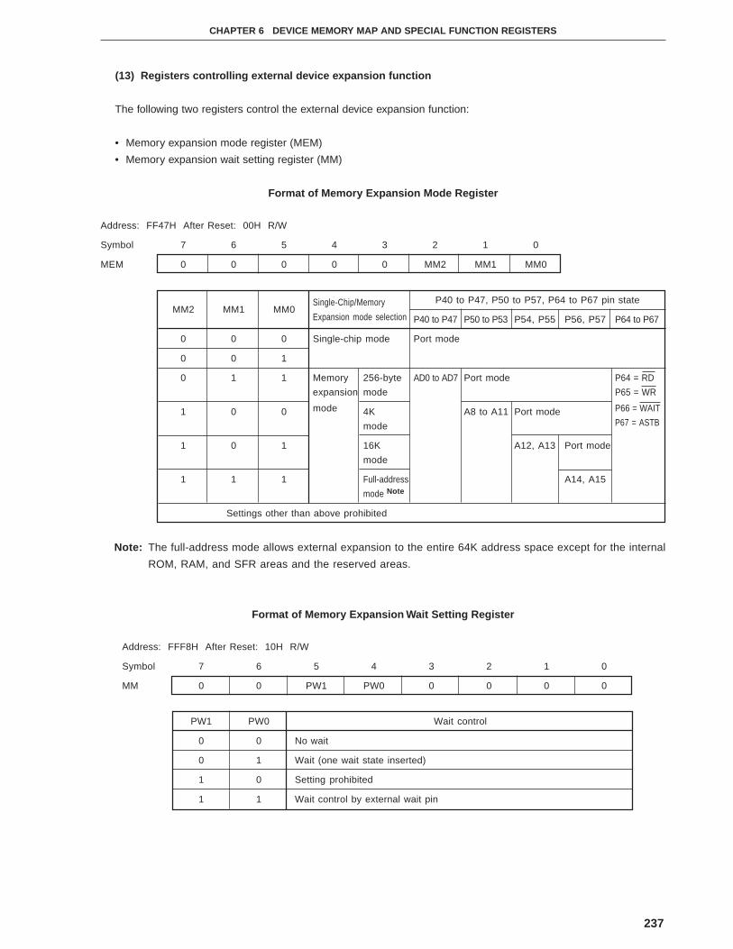
237
CHAPTER 6 DEVICE MEMORY MAP AND SPECIAL FUNCTION REGISTERS
(13) Registers controlling external device expansion function
The following two registers control the external device expansion function:
• Memory expansion mode register (MEM)
• Memory expansion wait setting register (MM)
Format of Memory Expansion Mode Register
Address: FF47H After Reset: 00H R/W
Symbol 7 6 5 4 3 2 1 0
MEM 0 0 0 0 0 MM2 MM1 MM0
MM2 MM1 MM0Single-Chip/Memory P40 to P47, P50 to P57, P64 to P67 pin state
Expansion mode selection P40 to P47 P50 to P53 P54, P55 P56, P57 P64 to P67
0 0 0 Single-chip mode Port mode
0 0 1
0 1 1 Memory 256-byte AD0 to AD7 Port mode P64 = RD
expansion mode P65 = WR
1 0 0 mode 4K A8 to A11 Port mode P66 = WAIT
mode P67 = ASTB
1 0 1 16K A12, A13 Port mode
mode
1 1 1 Full-address A14, A15
mode Note
Settings other than above prohibited
Note: The full-address mode allows external expansion to the entire 64K address space except for the internal
ROM, RAM, and SFR areas and the reserved areas.
Format of Memory Expansion Wait Setting Register
Address: FFF8H After Reset: 10H R/W
Symbol 7 6 5 4 3 2 1 0
MM 0 0 PW1 PW0 0 0 0 0
PW1 PW0 Wait control
0 0 No wait
0 1 Wait (one wait state inserted)
1 0 Setting prohibited
1 1 Wait control by external wait pin

238
CHAPTER 6 DEVICE MEMORY MAP AND SPECIAL FUNCTION REGISTERS
(14) Register controlling standby function
The standby function is intended to decrease the power consumption of the system. The following modes are
available: HALT, STOP, and SUB HALT.
When MCU is released from the STOP mode, a wait time is required for the crystal to resume oscillations. The wait
time is controlled by the following register:
• Oscillation stabilization time select register (OSTS)
Format of Oscillation Stabilization Time Select Register
Address: FFFAH After Reset: 04H R/W
Symbol 7 6 5 4 3 2 1 0
OSTS 0 0 0 0 0 OSTS2 OSTS1 OSTS0
OSTS2 OSTS1 OSTS0 Selection of oscillation stabilization time
0 0 0 212/fX (488 µs)
0 0 1 214/fX (1.95 ms)
0 1 0 215/fX (3.91 ms)
0 1 1 216/fX (7.81 ms)
1 0 0 217/fX (15.6 ms)
Settings other than above prohibited
Remarks: fX: Main system clock oscillation frequency
Values in parentheses are for operation with fX = 8.38 MHz.
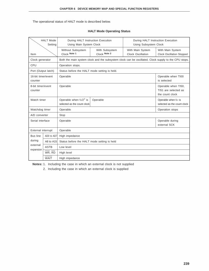
239
CHAPTER 6 DEVICE MEMORY MAP AND SPECIAL FUNCTION REGISTERS
The operational status of HALT mode is described below.
HALT Mode Operating Status
HALT Mode During HALT Instruction Execution During HALT Instruction Execution
Setting Using Main System Clock Using Subsystem Clock
Without Subsystem With Subsystem With Main System With Main System
Item Clock Note 1 Clock Note 2 Clock Oscillation Clock Oscillation Stopped
Clock generator Both the main system clock and the subsystem clock can be oscillated. Clock supply to the CPU stops.
CPU Operation stops.
Port (Output latch) Status before the HALT mode setting is held.
16-bit timer/event Operable Operable when TI00
counter is selected
8-bit timer/event Operable Operable when TI50,
counter TI51 are selected as
the count clock
Watch timer Operable when fX/27 is Operable Operable when fXT is
selected as the count clock selected as the count clock
Watchdog timer Operable Operation stops
A/D converter Stop
Serial interface Operable Operable during
external SCK
External interrupt Operable
Bus line AD0 to AD7 High impedance
during A8 to A15 Status before the HALT mode setting is heldexternal
ASTB Low levelexpansion
WR, RD High level
WAIT High impedance
Notes: 1. Including the case in which an external clock is not supplied
2. Including the case in which an external clock is supplied
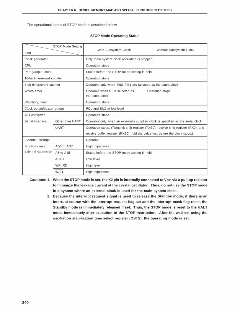
240
CHAPTER 6 DEVICE MEMORY MAP AND SPECIAL FUNCTION REGISTERS
The operational status of STOP Mode is described below.
STOP Mode Operating Status
STOP Mode SettingWith Subsystem Clock Without Subsystem Clock
Item
Clock generator Only main system clock oscillation is stopped.
CPU Operation stops
Port (Output latch) Status before the STOP mode setting is held
16-bit timer/event counter Operation stops
8-bit timer/event counter Operable only when TI50, TI51 are selected as the count clock
Watch timer Operable when fXT is selected as Operation stops
the count clock
Watchdog timer Operation stops
Clock output/buzzer output PCL and BUZ at low level
A/D converter Operation stops
Serial interface Other than UART Operable only when an externally supplied clock is specified as the serial clock
UART Operation stops. (Transmit shift register (TXS0), receive shift register (RX0), and
receive buffer register (RXB0) hold the value just before the clock stops.)
External interrupt Operable
Bus line during AD0 to AD7 High impedance
external expansion A8 to A15 Status before the STOP mode setting is held
ASTB Low level
WR, RD High level
WAIT High impedance
Cautions: 1. When the STOP mode is set, the X2 pin is internally connected to V DD1 via a pull-up resistor
to minimize the leakage current at the crystal oscillator. Thus, do not use the STOP mode
in a system where an external clock is used for the main system clock.
2. Because the interrupt request signal is used to release the Standby mode, if there is an
interrupt source with the interrupt request flag set and the interrupt mask flag reset, the
Standby mode is immediately released if set. Thus, the STOP mode is reset to the HALT
mode immediately after execution of the STOP instruction. After the wait set using the
oscillation stabilization time select register (OSTS), the operating mode is set.

241
CHAPTER 6 DEVICE MEMORY MAP AND SPECIAL FUNCTION REGISTERS
(15) Reset function
The following two operations can generate a reset signal.
• External reset input via the RESET pin
• Internal reset by watchdog timer in Watchdog Timer mode
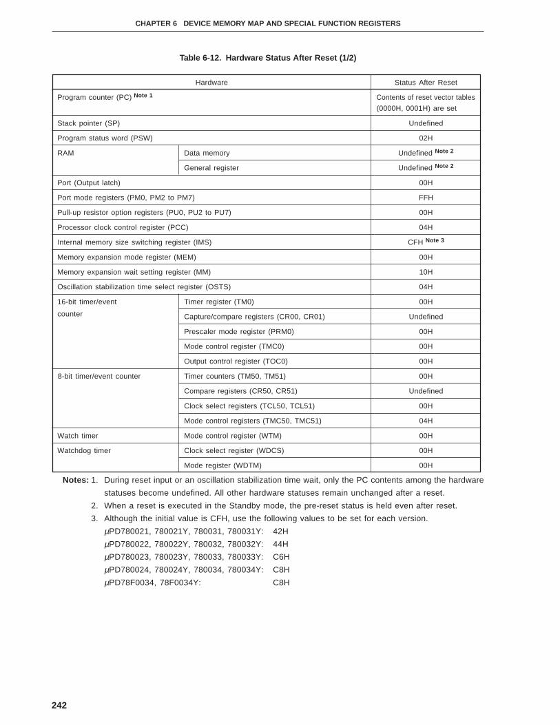
242
CHAPTER 6 DEVICE MEMORY MAP AND SPECIAL FUNCTION REGISTERS
Table 6-12. Hardware Status After Reset (1/2)
Hardware Status After Reset
Program counter (PC) Note 1 Contents of reset vector tables
(0000H, 0001H) are set
Stack pointer (SP) Undefined
Program status word (PSW) 02H
RAM Data memory Undefined Note 2
General register Undefined Note 2
Port (Output latch) 00H
Port mode registers (PM0, PM2 to PM7) FFH
Pull-up resistor option registers (PU0, PU2 to PU7) 00H
Processor clock control register (PCC) 04H
Internal memory size switching register (IMS) CFH Note 3
Memory expansion mode register (MEM) 00H
Memory expansion wait setting register (MM) 10H
Oscillation stabilization time select register (OSTS) 04H
16-bit timer/event Timer register (TM0) 00H
counter Capture/compare registers (CR00, CR01) Undefined
Prescaler mode register (PRM0) 00H
Mode control register (TMC0) 00H
Output control register (TOC0) 00H
8-bit timer/event counter Timer counters (TM50, TM51) 00H
Compare registers (CR50, CR51) Undefined
Clock select registers (TCL50, TCL51) 00H
Mode control registers (TMC50, TMC51) 04H
Watch timer Mode control register (WTM) 00H
Watchdog timer Clock select register (WDCS) 00H
Mode register (WDTM) 00H
Notes: 1. During reset input or an oscillation stabilization time wait, only the PC contents among the hardware
statuses become undefined. All other hardware statuses remain unchanged after a reset.
2. When a reset is executed in the Standby mode, the pre-reset status is held even after reset.
3. Although the initial value is CFH, use the following values to be set for each version.
µPD780021, 780021Y, 780031, 780031Y: 42H
µPD780022, 780022Y, 780032, 780032Y: 44H
µPD780023, 780023Y, 780033, 780033Y: C6H
µPD780024, 780024Y, 780034, 780034Y: C8H
µPD78F0034, 78F0034Y: C8H

243
CHAPTER 6 DEVICE MEMORY MAP AND SPECIAL FUNCTION REGISTERS
Table 6-12. Hardware Status After Reset (2/2)
Hardware Status After Reset
Clock output/buzzer output controller Clock output select register (CKS) 00H
A/D converter Conversion result register (ADCR0) 00H
Mode register (ADM0) 00H
Analog input channel specification register (ADS0) 00H
Serial interface (UART0) Asynchronous serial interface mode register (ASIM0) 00H
Asynchronous serial interface status register (ASIS0) 00H
Baud rate generator control register (BRGC0) 00H
Transmit shift register (TXS0) FFH
Receive buffer register (RXB0)
Serial interface (SIO3) Shift registers (SIO30, SIO31 Note 1 ) Undefined
Operating mode registers (CSIM30, CSIM31 Note 1 ) 00H
Serial interface (IIC0) Note 2 Clock select register (IICCL0) 00H
Shift register (IIC0) 00H
Control register (IICC0) 00H
Status register (IICS0) 00H
Slave address register (SVA0) 00H
Interrupt Request flag registers (IF0L, IF0H, IF1L) 00H
Mask flag registers (MK0L, MK0H, MK1L) FFH
Priority specification flag registers (PR0L, PR0H, PR1L) FFH
External interrupt rising edge enable register (EGP) 00H
External interrupt falling edge enable register (EGN) 00H
Notes: 1. Provided only in the µPD780024, 780034 Subseries
2. Provided only in the µPD780024Y, 780034Y Subseries
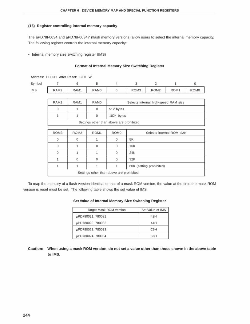
244
CHAPTER 6 DEVICE MEMORY MAP AND SPECIAL FUNCTION REGISTERS
(16) Register controlling internal memory capacity
The µPD78F0034 and µPD78F0034Y (flash memory versions) allow users to select the internal memory capacity.
The following register controls the internal memory capacity:
• Internal memory size switching register (IMS)
Format of Internal Memory Size Switching Register
Address: FFF0H After Reset: CFH W
Symbol 7 6 5 4 3 2 1 0
IMS RAM2 RAM1 RAM0 0 ROM3 ROM2 ROM1 ROM0
RAM2 RAM1 RAM0 Selects internal high-speed RAM size
0 1 0 512 bytes
1 1 0 1024 bytes
Settings other than above are prohibited
ROM3 ROM2 ROM1 ROM0 Selects internal ROM size
0 0 1 0 8K
0 1 0 0 16K
0 1 1 0 24K
1 0 0 0 32K
1 1 1 1 60K (setting prohibited)
Settings other than above are prohibited
To map the memory of a flash version identical to that of a mask ROM version, the value at the time the mask ROM
version is reset must be set. The following table shows the set value of IMS.
Set Value of Internal Memory Size Switching Register
Target Mask ROM Version Set Value of IMS
µPD780021, 780031 42H
µPD780022, 780032 44H
µPD780023, 780033 C6H
µPD780024, 780034 C8H
Caution: When using a mask ROM version, do not set a value other than those shown in the above table
to IMS.

245
CHAPTER 6 DEVICE MEMORY MAP AND SPECIAL FUNCTION REGISTERS
6.4 µµµµµPD78044F and 78044H Subseries
6.4.1 Documentation Reference Information
Device Series Number User’s Manual Number Date Published
µPD78044F U10908EJ2V0UM00 July 1997
µPD78044H U11756EJ1V0UM00 December 1996
Caution: The user should check the current User’s Manual with the information in this section to be sure of
having the most up-to-date information.
6.4.2 Device Series Differences
Device Series Number ROM and RAM Differences Number of
ROM Size RAM Size Serial Channels
µPD78044F 16K/24K/32K/40K/60K 512/1K 2
µPD78044H 32K/40K/48K/60K 1K 1
General Programmer’s Note
The NEC C-compiler and the NEC Assembler are capable of recognizing certain symbolic SFR bit names. These
special bit names are identified in the user manual in one of the four ways shown below:
If a bit number has one of the four symbols around it, the NEC software will recognize the associated symbolic bit
name. For example to set bit 7, the user can write the code in two ways:
1. SET1 MCC
2. SET1 PCC.7
Alternatively since bit 2 does not have any of the four symbols around it, the user can only set this bit as follows:
1. SET1 PCC.2
Note: The attempt to employ a symbolic name of bit-2 (PCC2) will return an error. Thus the use of instruction
SET1 PCC2
is improper since neither the NEC C-compiler nor the NEC Assembler recognizes this symbolic name and will
generate an error.
MCCPCC FRC CLS CSS 0 PCC2 PCC1 PCC0
<7> <6> <5> <4> 3 2 1 0
Example:
1.
2.
3.
4.
<7>
( 7 )
7
7
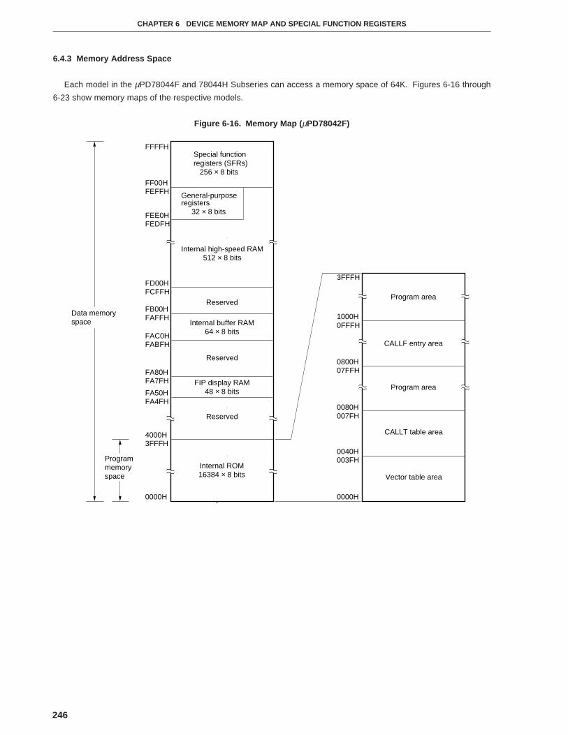
246
CHAPTER 6 DEVICE MEMORY MAP AND SPECIAL FUNCTION REGISTERS
6.4.3 Memory Address Space
Each model in the µPD78044F and 78044H Subseries can access a memory space of 64K. Figures 6-16 through
6-23 show memory maps of the respective models.
Figure 6-16. Memory Map ( µPD78042F)
0000H
Data memory space
Internal ROM16384 × 8 bits
3FFFH
1000H0FFFH
0800H07FFH
0080H007FH
0040H003FH
0000H
CALLF entry area
CALLT table area
Program area
Program area
Internal high-speed RAM512 × 8 bits
Reserved
Reserved
Reserved
Programmemoryspace
4000H3FFFH
FFFFH
General-purpose registers 32 × 8 bits
Special function registers (SFRs) 256 × 8 bits
Vector table area
FA50HFA4FH
FIP display RAM48 × 8 bits
FA80HFA7FH
FAC0HFABFH
FB00HFAFFH
Internal buffer RAM64 × 8 bits
FD00HFCFFH
FEE0HFEDFH
FF00HFEFFH
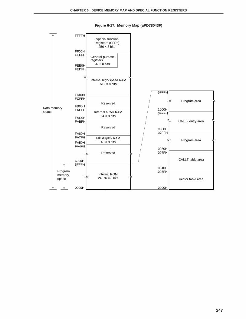
247
CHAPTER 6 DEVICE MEMORY MAP AND SPECIAL FUNCTION REGISTERS
Figure 6-17. Memory Map ( µPD78043F)
0000H
Data memory space
Internal ROM24576 × 8 bits
5FFFH
1000H0FFFH
0800H07FFH
0080H007FH
0040H003FH
0000H
CALLF entry area
CALLT table area
Program area
Program area
Internal high-speed RAM512 × 8 bits
Reserved
Reserved
Reserved
Programmemoryspace
6000H5FFFH
FFFFH
General-purpose registers 32 × 8 bits
Special function registers (SFRs) 256 × 8 bits
Vector table area
FA50HFA4FH
FIP display RAM48 × 8 bits
FA80HFA7FH
FAC0HFABFH
FB00HFAFFH
Internal buffer RAM64 × 8 bits
FD00HFCFFH
FEE0HFEDFH
FF00HFEFFH
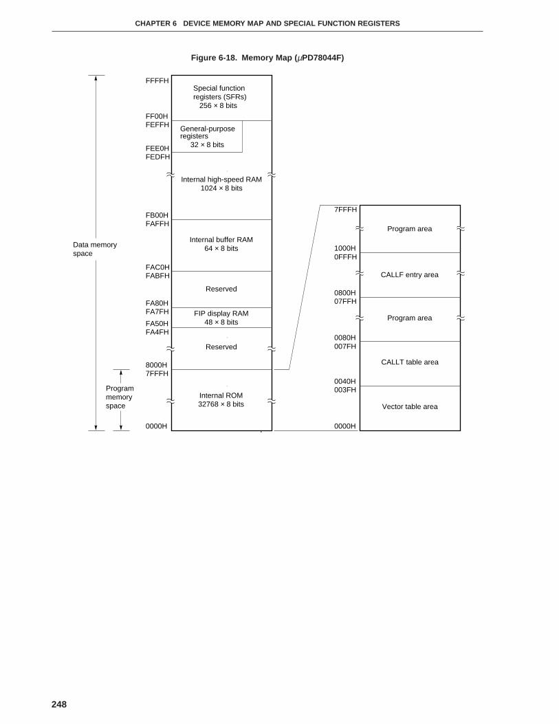
248
CHAPTER 6 DEVICE MEMORY MAP AND SPECIAL FUNCTION REGISTERS
Figure 6-18. Memory Map ( µPD78044F)
0000H
Data memory space
Internal ROM32768 × 8 bits
7FFFH
1000H0FFFH
0800H07FFH
0080H007FH
0040H003FH
0000H
CALLF entry area
CALLT table area
Program area
Program area
Internal high-speed RAM1024 × 8 bits
Reserved
Reserved
Programmemoryspace
8000H7FFFH
FFFFH
General-purpose registers 32 × 8 bits
Special function registers (SFRs) 256 × 8 bits
Vector table area
FA50HFA4FH
FIP display RAM48 × 8 bits
FA80HFA7FH
FAC0HFABFH
Internal buffer RAM64 × 8 bits
FB00HFAFFH
FEE0HFEDFH
FF00HFEFFH
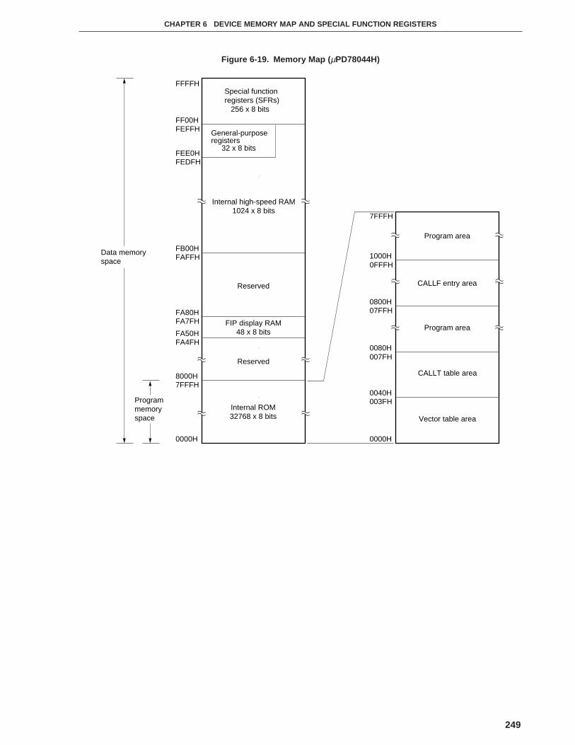
249
CHAPTER 6 DEVICE MEMORY MAP AND SPECIAL FUNCTION REGISTERS
Figure 6-19. Memory Map ( µPD78044H)
0000H
Data memory space
Internal ROM32768 x 8 bits
7FFFH
1000H0FFFH
0800H07FFH
0080H007FH
0040H003FH
0000H
CALLF entry area
CALLT table area
Program area
Program area
Internal high-speed RAM1024 x 8 bits
Programmemoryspace
8000H7FFFH
FFFFH
General-purpose registers 32 x 8 bits
Special function registers (SFRs) 256 x 8 bits
Vector table area
FA50HFA4FH
FIP display RAM48 x 8 bits
FA80HFA7FH
FB00HFAFFH
FEE0HFEDFH
FF00HFEFFH
Reserved
Reserved

250
CHAPTER 6 DEVICE MEMORY MAP AND SPECIAL FUNCTION REGISTERS
Figure 6-20. Memory Map ( µPD78045F)
0000H
Data memory space
Internal ROM40960 × 8 bits
9FFFH
1000H0FFFH
0800H07FFH
0080H007FH
0040H003FH
0000H
CALLF entry area
CALLT table area
Program area
Program area
Internal high-speed RAM1024 × 8 bits
Reserved
Reserved
Programmemoryspace
A000H9FFFH
FFFFH
General-purpose registers 32 × 8 bits
Special function registers (SFRs) 256 × 8 bits
Vector table area
FA50HFA4FH
FIP display RAM48 × 8 bits
FA80HFA7FH
FAC0HFABFH
Internal buffer RAM64 × 8 bits
FB00HFAFFH
FEE0HFEDFH
FF00HFEFFH

251
CHAPTER 6 DEVICE MEMORY MAP AND SPECIAL FUNCTION REGISTERS
Figure 6-21. Memory Map ( µPD78045H)
0000H
Data memory space
Internal ROM40960 x 8 bits
9FFFH
1000H0FFFH
0800H07FFH
0080H007FH
0040H003FH
0000H
CALLF entry area
CALLT table area
Program area
Program area
Internal high-speed RAM1024 x 8 bits
Reserved
Reserved
Programmemoryspace
A000H9FFFH
FFFFH
General-purpose registers 32 x 8 bits
Special function registers (SFRs) 256 x 8 bits
Vector table area
FA50HFA4FH
FIP display RAM48 x 8 bits
FA80HFA7FH
FB00HFAFFH
FEE0HFEDFH
FF00HFEFFH
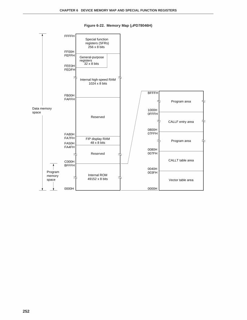
252
CHAPTER 6 DEVICE MEMORY MAP AND SPECIAL FUNCTION REGISTERS
Figure 6-22. Memory Map ( µPD78046H)
0000H
Data memory space
Internal ROM49152 x 8 bits
BFFFH
1000H0FFFH
0800H07FFH
0080H007FH
0040H003FH
0000H
CALLF entry area
CALLT table area
Program area
Program area
Internal high-speed RAM1024 x 8 bits
Reserved
Reserved
Programmemoryspace
C000HBFFFH
FFFFH
General-purpose registers 32 x 8 bits
Special function registers (SFRs) 256 x 8 bits
Vector table area
FA50HFA4FH
FIP display RAM48 x 8 bits
FA80HFA7FH
FB00HFAFFH
FEE0HFEDFH
FF00HFEFFH
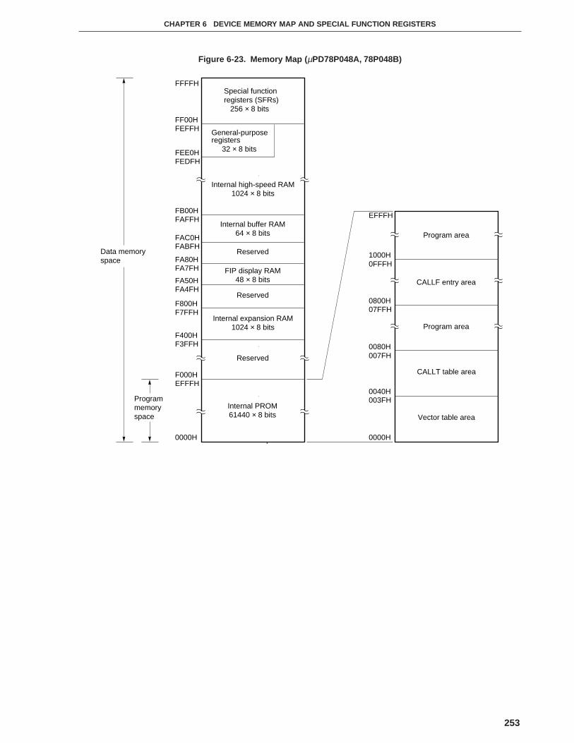
253
CHAPTER 6 DEVICE MEMORY MAP AND SPECIAL FUNCTION REGISTERS
Figure 6-23. Memory Map ( µPD78P048A, 78P048B)
0000H
Data memory space
Internal PROM61440 × 8 bits
EFFFH
1000H0FFFH
0800H07FFH
0080H007FH
0040H003FH
0000H
CALLF entry area
CALLT table area
Program area
Program area
Internal high-speed RAM1024 × 8 bits
Reserved
Reserved
Programmemoryspace
F000HEFFFH
FFFFH
General-purpose registers 32 × 8 bits
Special function registers (SFRs) 256 × 8 bits
Vector table area
FA50HFA4FH
FIP display RAM48 × 8 bits
FA80HFA7FH
FAC0HFABFH
Internal buffer RAM64 × 8 bits
FB00HFAFFH
FEE0HFEDFH
FF00HFEFFH
Internal expansion RAM1024 × 8 bits
F800HF7FFH
F400HF3FFH
Reserved
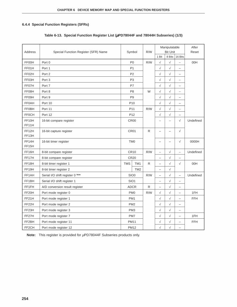
254
CHAPTER 6 DEVICE MEMORY MAP AND SPECIAL FUNCTION REGISTERS
6.4.4 Special Function Registers (SFRs)
Table 6-13. Special Function Register List ( µµµµµPD78044F and 78044H Subseries) (1/3)
Manipulatable After
Address Special Function Register (SFR) Name Symbol R/W Bit Unit Reset
1 Bit 8 Bits 16 Bits
FF00H Port 0 P0 R/W √ √ – 00H
FF01H Port 1 P1 √ √ –
FF02H Port 2 P2 √ √ –
FF03H Port 3 P3 √ √ –
FF07H Port 7 P7 √ √ –
FF08H Port 8 P8 W √ √ –
FF09H Port 9 P9 √ √ –
FF0AH Port 10 P10 √ √ –
FF0BH Port 11 P11 R/W √ √ –
FF0CH Port 12 P12 √ √ –
FF10H 16-bit compare register CR00 – – √ Undefined
FF11H
FF12H 16-bit capture register CR01 R – – √FF13H
FF14H 16-bit timer register TM0 – – √ 0000H
FF15H
FF16H 8-bit compare register CR10 R/W – √ – Undefined
FF17H 8-bit compare register CR20 – √ –
FF18H 8-bit timer register 1 TMS TM1 R – √ √ 00H
FF19H 8-bit timer register 2 TMS TM2 – √
FF1AH Serial I/O shift register 0 Note SIO0 R/W – √ – Undefined
FF1BH Serial I/O shift register 1 SIO1 – √ –
FF1FH A/D conversion result register ADCR R – √ –
FF20H Port mode register 0 PM0 R/W √ √ – 1FH
FF21H Port mode register 1 PM1 √ √ – FFH
FF22H Port mode register 2 PM2 √ √ –
FF23H Port mode register 3 PM3 √ √ –
FF27H Port mode register 7 PM7 √ √ – 1FH
FF2BH Port mode register 11 PM11 √ √ – FFH
FF2CH Port mode register 12 PM12 √ √ –
Note: This register is provided for µPD78044F Subseries products only.
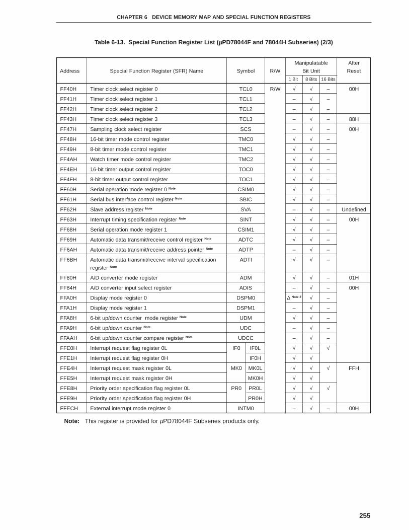
255
CHAPTER 6 DEVICE MEMORY MAP AND SPECIAL FUNCTION REGISTERS
Table 6-13. Special Function Register List ( µµµµµPD78044F and 78044H Subseries) (2/3)
Manipulatable After
Address Special Function Register (SFR) Name Symbol R/W Bit Unit Reset
1 Bit 8 Bits 16 Bits
FF40H Timer clock select register 0 TCL0 R/W √ √ – 00H
FF41H Timer clock select register 1 TCL1 – √ –
FF42H Timer clock select register 2 TCL2 – √ –
FF43H Timer clock select register 3 TCL3 – √ – 88H
FF47H Sampling clock select register SCS – √ – 00H
FF48H 16-bit timer mode control register TMC0 √ √ –
FF49H 8-bit timer mode control register TMC1 √ √ –
FF4AH Watch timer mode control register TMC2 √ √ –
FF4EH 16-bit timer output control register TOC0 √ √ –
FF4FH 8-bit timer output control register TOC1 √ √ –
FF60H Serial operation mode register 0 Note CSIM0 √ √ –
FF61H Serial bus interface control register Note SBIC √ √ –
FF62H Slave address register Note SVA – √ – Undefined
FF63H Interrupt timing specification register Note SINT √ √ – 00H
FF68H Serial operation mode register 1 CSIM1 √ √ –
FF69H Automatic data transmit/receive control register Note ADTC √ √ –
FF6AH Automatic data transmit/receive address pointer Note ADTP – √ –
FF6BH Automatic data transmit/receive interval specification ADTI √ √ –
register Note
FF80H A/D converter mode register ADM √ √ – 01H
FF84H A/D converter input select register ADIS – √ – 00H
FFA0H Display mode register 0 DSPM0 ∆ Note 2 √ –
FFA1H Display mode register 1 DSPM1 – √ –
FFA8H 6-bit up/down counter mode register Note UDM √ √ –
FFA9H 6-bit up/down counter Note UDC – √ –
FFAAH 6-bit up/down counter compare register Note UDCC – √ –
FFE0H Interrupt request flag register 0L IF0 IF0L √ √ √
FFE1H Interrupt request flag register 0H IF0H √ √
FFE4H Interrupt request mask register 0L MK0 MK0L √ √ √ FFH
FFE5H Interrupt request mask register 0H MK0H √ √
FFE8H Priority order specification flag register 0L PR0 PR0L √ √ √
FFE9H Priority order specification flag register 0H PR0H √ √
FFECH External interrupt mode register 0 INTM0 – √ – 00H
Note: This register is provided for µPD78044F Subseries products only.
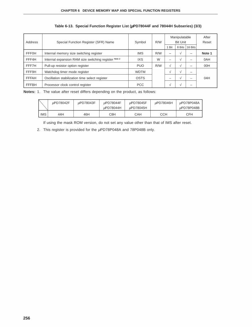
256
CHAPTER 6 DEVICE MEMORY MAP AND SPECIAL FUNCTION REGISTERS
Table 6-13. Special Function Register List ( µµµµµPD78044F and 78044H Subseries) (3/3)
Manipulatable After
Address Special Function Register (SFR) Name Symbol R/W Bit Unit Reset
1 Bit 8 Bits 16 Bits
FFF0H Internal memory size switching register IMS R/W – √ – Note 1
FFF4H Internal expansion RAM size switching register Note 2 IXS W – √ – 0AH
FFF7H Pull-up resistor option register PUO R/W √ √ – 00H
FFF9H Watchdog timer mode register WDTM √ √ –
FFFAH Oscillation stabilization time select register OSTS – √ – 04H
FFFBH Processor clock control register PCC √ √ –
Notes: 1. The value after reset differs depending on the product, as follows:
µPD78042F µPD78043F µPD78044F µPD78045F µPD78046H µPD78P048A
µPD78044H µPD78045H µPD78P048B
IMS 44H 46H C8H CAH CCH CFH
If using the mask ROM version, do not set any value other than that of IMS after reset.
2. This register is provided for the µPD78P048A and 78P048B only.
257
CHAPTER 6 DEVICE MEMORY MAP AND SPECIAL FUNCTION REGISTERS
(1) Registers controlling port functions
The following two types of registers control the ports:
• Port mode registers (PM0 to PM3, PM7, PM11, PM12)
• Pull-up resistor option register (PUO)
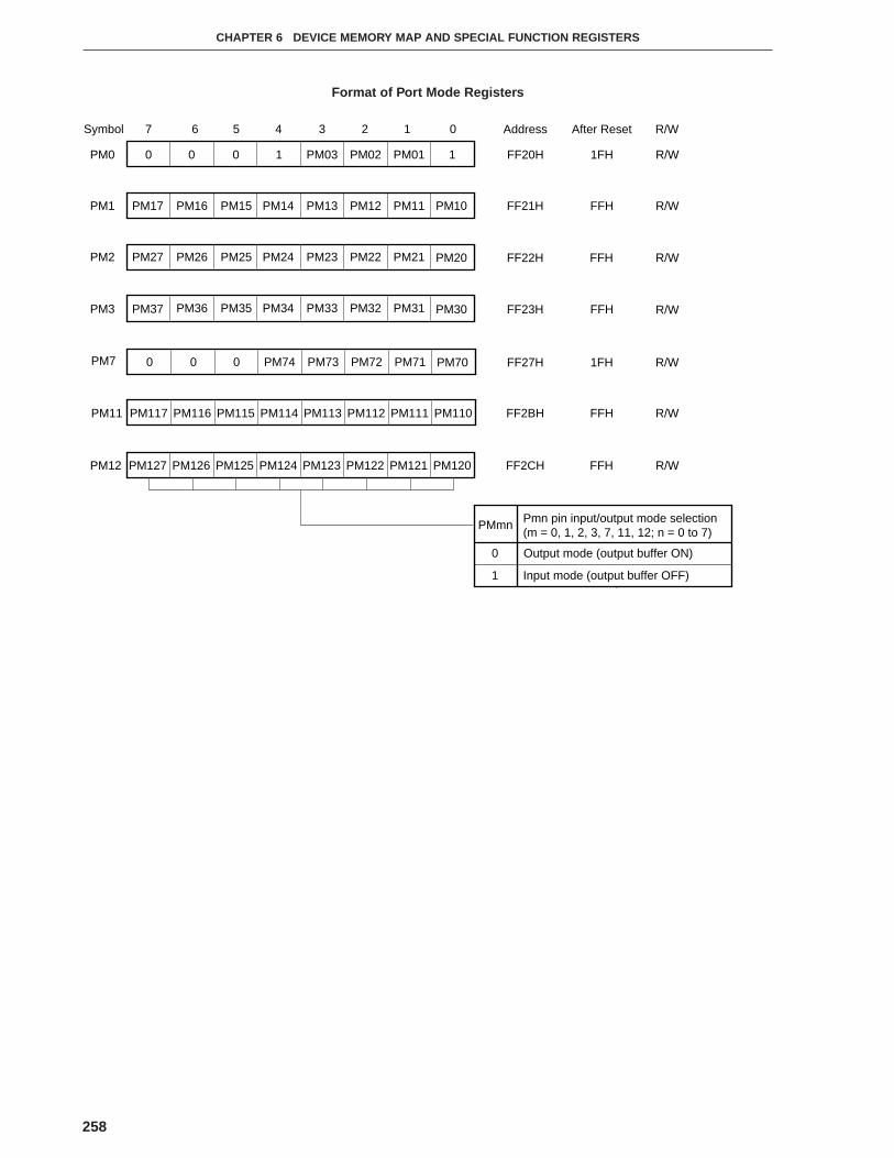
258
CHAPTER 6 DEVICE MEMORY MAP AND SPECIAL FUNCTION REGISTERS
Format of Port Mode Registers
PM0
PM1
PM2
PM37
0
PM127 PM126 PM125 PM124 PM123 PM122 PM121 PM120
0 0 1 PM03 PM02 PM01 1
7 6 5 4 3 2 1 0Symbol
PM16 PM15 PM14 PM13 PM12 PM11
PM26 PM25 PM24 PM23 PM22 PM21
PM36 PM35 PM34 PM33 PM32 PM31
PM17 PM10
PM27
PM3
PM20
PM30
PM12
PMmn Pmn pin input/output mode selection(m = 0, 1, 2, 3, 7, 11, 12; n = 0 to 7)
0
1
Output mode (output buffer ON)
Input mode (output buffer OFF)
FF20H
FF2CH
FF21H
FF22H
FF23H
1FH
FFH
FFH
FFH
FFH
R/W
R/W
R/W
R/W
R/W
Address After Reset R/W
0 PM72 PM710 0 PM74 PM73 PM70PM7 FF27H 1FH R/W
PM117 PM116 PM115 PM114 PM113 PM112 PM111 PM110PM11 FF2BH FFH R/W
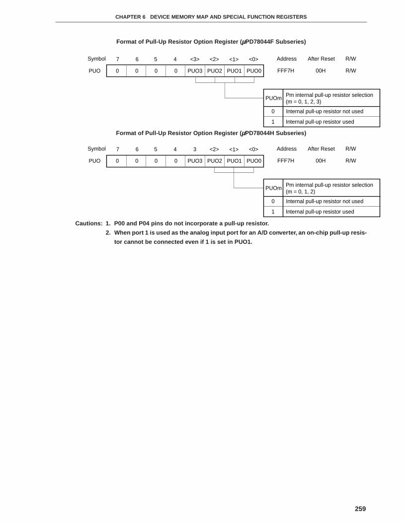
259
CHAPTER 6 DEVICE MEMORY MAP AND SPECIAL FUNCTION REGISTERS
Format of Pull-Up Resistor Option Register ( µµµµµPD78044F Subseries)
Format of Pull-Up Resistor Option Register ( µµµµµPD78044H Subseries)
Cautions: 1. P00 and P04 pins do not incorporate a pull-up resistor.
2. When port 1 is used as the analog input port for an A/D converter, an on-chip pull-up resis-
tor cannot be connected even if 1 is set in PUO1.
PUO 0
PUOm Pm internal pull-up resistor selection(m = 0, 1, 2, 3)
0
1
Internal pull-up resistor not used
Internal pull-up resistor used
FFF7H 00H R/W
Symbol 7 6 5 4 <3> <2> <0><1>
0 0 0 PUO3 PUO2 PUO1 PUO0
Address After Reset R/W
PUO 0
PUOm Pm internal pull-up resistor selection(m = 0, 1, 2)
0
1
Internal pull-up resistor not used
Internal pull-up resistor used
FFF7H 00H R/W
Symbol 7 6 5 4 3 <2> <0><1>
0 0 0 PUO3 PUO2 PUO1 PUO0
Address After Reset R/W
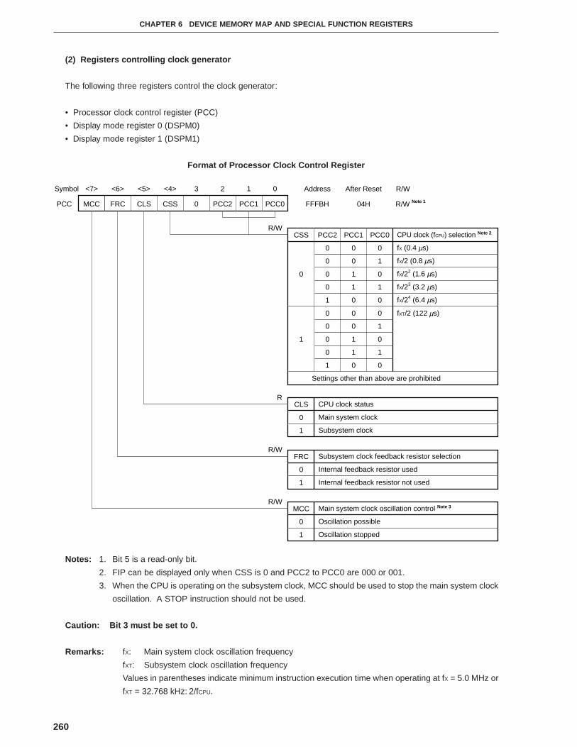
260
CHAPTER 6 DEVICE MEMORY MAP AND SPECIAL FUNCTION REGISTERS
(2) Registers controlling clock generator
The following three registers control the clock generator:
• Processor clock control register (PCC)
• Display mode register 0 (DSPM0)
• Display mode register 1 (DSPM1)
Format of Processor Clock Control Register
Notes: 1. Bit 5 is a read-only bit.
2. FIP can be displayed only when CSS is 0 and PCC2 to PCC0 are 000 or 001.
3. When the CPU is operating on the subsystem clock, MCC should be used to stop the main system clock
oscillation. A STOP instruction should not be used.
Caution: Bit 3 must be set to 0.
Remarks: fX: Main system clock oscillation frequency
fXT: Subsystem clock oscillation frequency
Values in parentheses indicate minimum instruction execution time when operating at fX = 5.0 MHz or
fXT = 32.768 kHz: 2/fCPU.
PCC0PCC
<7> <6> <5> <4> 3 2Symbol 1 0
CSS CPU clock (fCPU) selection Note 2
FFFBHPCC10 PCC2CSSCLSFRCMCC
Address After Reset R/W
04H R/W Note 1
fX (0.4 s)
fX/2 (0.8 s)
fX/22 (1.6 s)
fX/23 (3.2 s)
fX/24 (6.4 s)
fXT/2 (122 s)
Settings other than above are prohibited
CLS CPU clock status
0 Main system clock
1 Subsystem clock
FRC Subsystem clock feedback resistor selection
0 Internal feedback resistor used
1 Internal feedback resistor not used
MCC Main system clock oscillation control Note 3
0 Oscillation possible
1 Oscillation stopped
PCC2
0
0
0
0
1
0
0
1
0
1
PCC1
0
0
1
1
0
0
0
1
1
0
PCC0
0
1
0
1
0
0
1
0
1
0
0
0
R/W
R
R/W
R/W
µ
µ
µ
µ
µ
µ

261
CHAPTER 6 DEVICE MEMORY MAP AND SPECIAL FUNCTION REGISTERS
Format of Display Mode Register 0
Notes: 1. Bit 7 (KSF) is a read-only bit.
2. Set the value following the main system clock frequency (fX) to be used. The noise elimination circuit
is effective when FIP is driven.
Remark: fX: Main system clock oscillation frequency
SEGS0DSPM0
<7> 6 5 4 3 2Symbol 1 0
SEGS3 Display segment
FFA0HSEGS1SEGS3 SEGS200DSPM06KSF
Address After Reset
00H
0 9 segments
0 10 segments
0 11 segments
0 12 segments
0 13 segments
0 14 segments
0 15 segments
0 16 segments
1 17 segments
1 18 segments
1 19 segments
1 20 segments
1 21 segments
1 22 segments
1 23 segments
1 24 segments
DSPM06Subsystem clock noise reduction circuit modesetting Note 2
0 2.5 MHz < fX < 5.0 MHz
1 1.25 MHz < fX < 2.5 MHz
KSF Timing status
0 Display timing
1 Key scan timing
R/W
R/W Note 1
SEGS2
0
0
0
0
1
1
1
1
0
0
0
0
1
1
1
1
SEGS1
0
0
1
1
0
0
1
1
0
0
1
1
0
0
1
1
SEGS0
0
1
0
1
0
1
0
1
0
1
0
1
0
1
0
1

262
CHAPTER 6 DEVICE MEMORY MAP AND SPECIAL FUNCTION REGISTERS
Format of Display Mode Register 1
Note: When setting to the display is stopped, a static display can be set by operating the port output latch.
Remark: fX: Main system clock oscillation frequency
DIMS0DSPM1
7 6 5 4 3 2Symbol 1 0
DIMS0 Display cycle selection
FFA1HDIMS1DIMS3 DIMS2DIGS0DIGS1DIGS2DIGS3
Address After Reset R/W
00H R/W
0 1024/fX is 1 display cycle. (1 display cycle = 204.8 s when operated at 5.0 MHz)
1 2048/fX is 1 display cycle. (1 display cycle = 409.6 s when operated at 5.0 MHz)
DIMS3 Digit signal cut width
0 1/16
0 2/16
0 4/16
0 6/16
1 8/16
1 10/16
1 12/16
1 14/16
DIGS3 Display digit
0 Display stopped (Static display)Note
0 2 digits
0 3 digits
0 4 digits
0 5 digits
0 6 digits
0 7 digits
0 8 digits
1 9 digits
1 10 digits
1 11 digits
1 12 digits
1 13 digits
1 14 digits
1 15 digits
1 16 digits
DIMS2
0
0
1
1
0
0
1
1
DIMS1
0
1
0
1
0
1
0
1
DIGS2
0
0
0
0
1
1
1
1
0
0
0
0
1
1
1
1
DIGS1
0
0
1
1
0
0
1
1
0
0
1
1
0
0
1
1
DIGS0
0
1
0
1
0
1
0
1
0
1
0
1
0
1
0
1
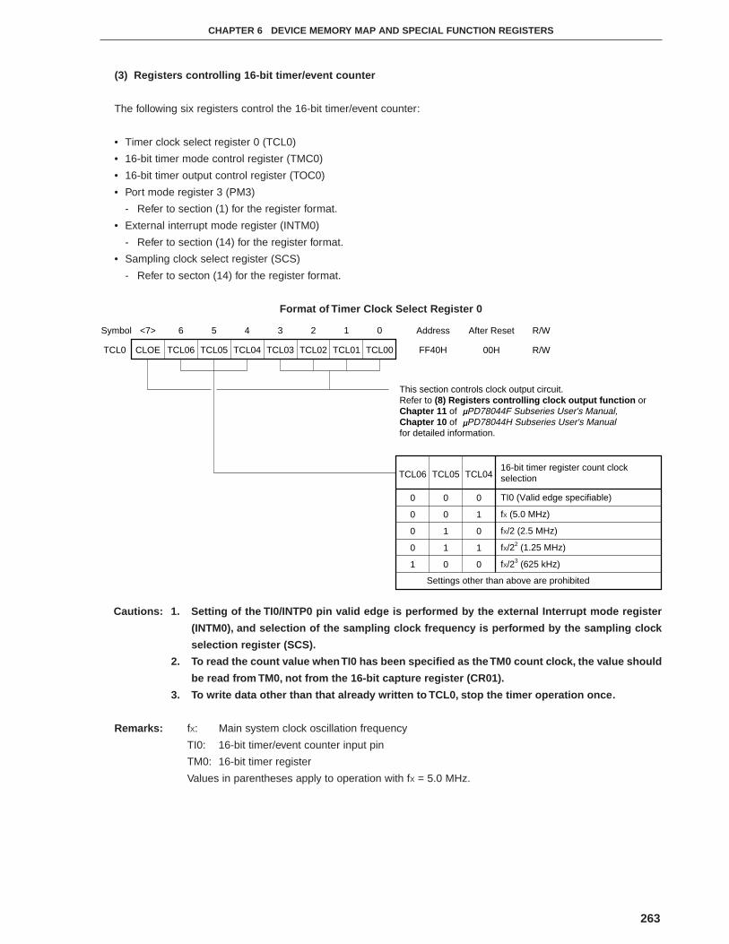
263
CHAPTER 6 DEVICE MEMORY MAP AND SPECIAL FUNCTION REGISTERS
(3) Registers controlling 16-bit timer/event counter
The following six registers control the 16-bit timer/event counter:
• Timer clock select register 0 (TCL0)
• 16-bit timer mode control register (TMC0)
• 16-bit timer output control register (TOC0)
• Port mode register 3 (PM3)
- Refer to section (1) for the register format.
• External interrupt mode register (INTM0)
- Refer to section (14) for the register format.
• Sampling clock select register (SCS)
- Refer to secton (14) for the register format.
Format of Timer Clock Select Register 0
Cautions: 1. Setting of the TI0/INTP0 pin valid edge is performed by the external Interrupt mode register
(INTM0), and selection of the sampling clock frequency is performed by the sampling clock
selection register (SCS).
2. To read the count value when TI0 has been specified as the TM0 count clock, the value should
be read from TM0, not from the 16-bit capture register (CR01).
3. To write data other than that already written to TCL0, stop the timer operation once.
Remarks: fX: Main system clock oscillation frequency
TI0: 16-bit timer/event counter input pin
TM0: 16-bit timer register
Values in parentheses apply to operation with fX = 5.0 MHz.
This section controls clock output circuit.Refer to (8) Registers controlling clock output function orChapter 11 of PD78044F Subseries User's Manual,Chapter 10 of PD78044H Subseries User's Manualfor detailed information.
TCL00TCL0
<7> 6 5 4 3 2Symbol 1 0
FF40HTCL01TCL03 TCL02TCL04TCL05TCL06CLOE
Address After Reset R/W
00H R/W
TCL0616-bit timer register count clockselection
0 TI0 (Valid edge specifiable)
0 fX (5.0 MHz)
0 fX/2 (2.5 MHz)
0 fX/22 (1.25 MHz)
1 fX/23 (625 kHz)
TCL05
0
0
1
1
0
TCL04
0
1
0
1
0
µµµµ
Settings other than above are prohibited

264
CHAPTER 6 DEVICE MEMORY MAP AND SPECIAL FUNCTION REGISTERS
Format of 16-Bit Timer Mode Control Register
Cautions: 1. The 16-bit timer register (TM0) starts operation when a value other than 0, 0, 0 is set to TMC01
to TMC03 (Operation Stop mode). To stop the operation, set TMC01 to TMC03 to 0, 0, 0.
2. Switch the Clear mode and the TO0 output timing after stopping the timer operation (by
setting TMC01 to TMC03 to 0, 0, 0).
3. Set the valid edge of the TI0/INTP0 pin with an external interrupt mode register (INTM0) and
select the sampling clock frequency with the sampling clock select register (SCS).
4. When using the PWM mode, set the PWM and then set data to CR00.
Remarks: TO0: 16-bit timer/event counter output pin
TI0: 16-bit timer/event counter input pin
TM0: 16-bit timer register
CR00: Compare register 00
0 0 0 0 TMC03 TMC02 TMC01 OVF0
7 6 5 4 3 2 1 <0>Symbol
TMC0 FF48H 00H R/W
Address After Reset R/W
OVF0 16-Bit Timer Register Overflow Detection
0 Overflow not detected
1 Overflow detected
TMC03 TMC02 TMC01Operating Mode
Clear Mode SelectionTO0 Output Timing Selection Interrupt Generation
0 0 0 Operation stop(TM0 cleared to 0)
No change Not Generated
0 0 1 PWM mode (free running) PWM pulse output
0 1 0
0 1 1
1 0 0
1 0 1
1 1 0
1 1 1
Free running mode Match between TM0 and CR00
Match between TM0 and CR00or TI0 valid edge
Match between TM0 and CR00
Match between TM0 and CR00or TI0 valid edge
Match between TM0 and CR00
Match between TM0 and CR00or TI0 valid edge
Clear & start on TI0 valid edge
Clear & start on matchbetween TM0 and CR00
Generated on match between TM0 and CR00
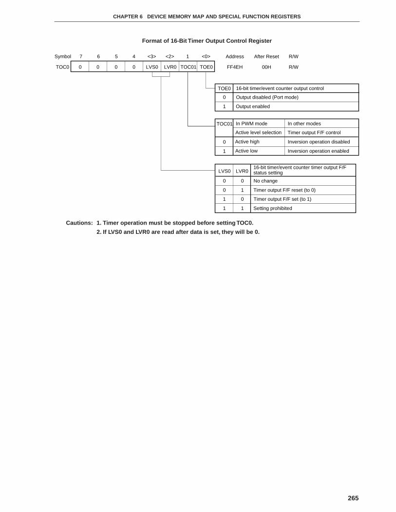
265
CHAPTER 6 DEVICE MEMORY MAP AND SPECIAL FUNCTION REGISTERS
Format of 16-Bit Timer Output Control Register
Cautions: 1. Timer operation must be stopped before setting TOC0.
2. If LVS0 and LVR0 are read after data is set, they will be 0.
TOE0TOC0
7 6 5 4 <3> <2>Symbol 1 <0>
TOE0 16-bit timer/event counter output control
0
1
Output disabled (Port mode)
Output enabled
FF4EHTOC01LVS0
TOC01
LVS016-bit timer/event counter timer output F/Fstatus setting
0
0
No change
Timer output F/F reset (to 0)
1
1
LVR0
0
1
0
1
Timer output F/F set (to 1)
Setting prohibited
LVR00
In PWM mode
0
1
Active level selection Timer output F/F control
Active high
Active low
In other modes
Inversion operation disabled
Inversion operation enabled
Address After Reset R/W
00H R/W0 0 0
266
CHAPTER 6 DEVICE MEMORY MAP AND SPECIAL FUNCTION REGISTERS
(4) Registers controlling 8-bit timer/event counter
The following four registers control the 8-bit timer/event counters:
• Timer clock select register 1 (TCL1)
• 8-bit timer mode control register (TMC1)
• 8-bit timer output control register (TOC1)
• Port mode register 3 (PM3)
- Refer to section (1) for the register format.
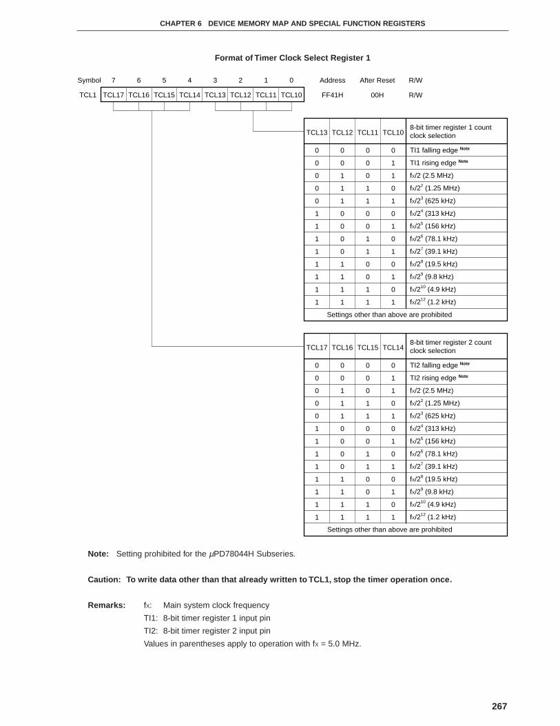
267
CHAPTER 6 DEVICE MEMORY MAP AND SPECIAL FUNCTION REGISTERS
Format of Timer Clock Select Register 1
Note: Setting prohibited for the µPD78044H Subseries.
Caution: To write data other than that already written to TCL1, stop the timer operation once.
Remarks: fX: Main system clock frequency
TI1: 8-bit timer register 1 input pin
TI2: 8-bit timer register 2 input pin
Values in parentheses apply to operation with fX = 5.0 MHz.
TCL10TCL1
7 6 5 4 3 2Symbol 1 0
TCL138-bit timer register 1 countclock selection
FF41HTCL11TCL13 TCL12TCL14TCL15TCL16TCL17
Address After Reset R/W
00H R/W
0 TI1 falling edge Note
0 TI1 rising edge Note
0 fX/2 (2.5 MHz)
0 fX/22 (1.25 MHz)
0 fX/23 (625 kHz)
1 fX/24 (313 kHz)
1 fX/25 (156 kHz)
1 fX/26 (78.1 kHz)
1 fX/27 (39.1 kHz)
1 fX/28 (19.5 kHz)
1 fX/29 (9.8 kHz)
1 fX/210 (4.9 kHz)
1 fX/212 (1.2 kHz)
TCL12
0
0
1
1
1
0
0
0
0
1
1
1
1
TCL11
0
0
0
1
1
0
0
1
1
0
0
1
1
TCL10
0
1
1
0
1
0
1
0
1
0
1
0
1
TCL178-bit timer register 2 countclock selection
0 TI2 falling edge Note
0 TI2 rising edge Note
0 fX/2 (2.5 MHz)
0 fX/22 (1.25 MHz)
0 fX/23 (625 kHz)
1 fX/24 (313 kHz)
1 fX/25 (156 kHz)
1 fX/26 (78.1 kHz)
1 fX/27 (39.1 kHz)
1 fX/28 (19.5 kHz)
1 fX/29 (9.8 kHz)
1 fX/210 (4.9 kHz)
1 fX/212 (1.2 kHz)
TCL16
0
0
1
1
1
0
0
0
0
1
1
1
1
TCL15
0
0
0
1
1
0
0
1
1
0
0
1
1
TCL14
0
1
1
0
1
0
1
0
1
0
1
0
1
Settings other than above are prohibited
Settings other than above are prohibited
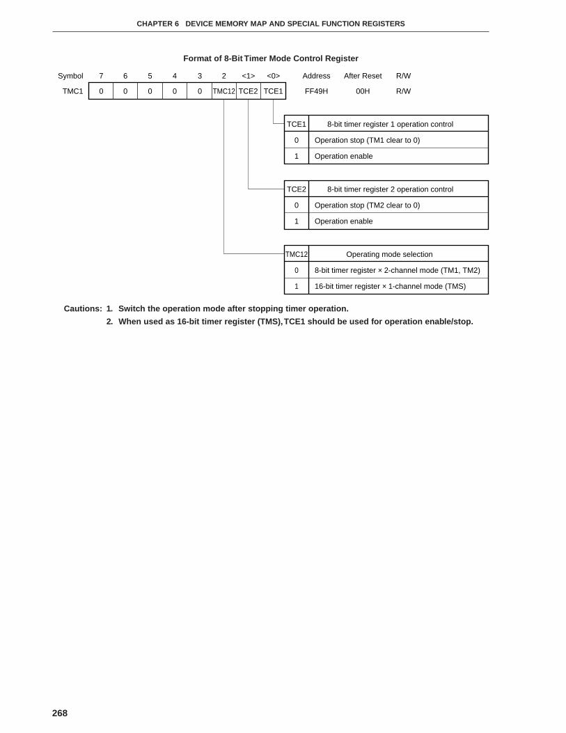
268
CHAPTER 6 DEVICE MEMORY MAP AND SPECIAL FUNCTION REGISTERS
Format of 8-Bit Timer Mode Control Register
Cautions: 1. Switch the operation mode after stopping timer operation.
2. When used as 16-bit timer register (TMS), TCE1 should be used for operation enable/stop.
7 6 5 4 3 2 <1> <0>
0 0 0 0 0 TMC12 TCE2 TCE1
Symbol
TMC1
Address
FF49H
After Reset
00H
R/W
R/W
TCE1
0
1
8-bit timer register 1 operation control
Operation stop (TM1 clear to 0)
Operation enable
TCE2
0
1
8-bit timer register 2 operation control
Operation stop (TM2 clear to 0)
Operation enable
TMC12
0
1
Operating mode selection
8-bit timer register × 2-channel mode (TM1, TM2)
16-bit timer register × 1-channel mode (TMS)

269
CHAPTER 6 DEVICE MEMORY MAP AND SPECIAL FUNCTION REGISTERS
Format of 8-Bit Timer Output Control Register
Cautions: 1. Be sure to set TOC1 after stopping timer operation.
2. After data setting, 0 can be read from LVS1, LVS2, LVR1, and LVR2.
<7> <6> 5 <4> <3> <2> 1 <0>
LVS2 LVR2 TOC15 TOE2 LVS1 LVR1 TOC11 TOE1
Symbol
TOC1
Address
FF4FH
After Reset
00H
R/W
R/W
TOE1
0
1
8-bit timer/event counter 1 output control
Output disable (Port mode)
Output enable
TOC11
0
1
8-bit timer/event counter 1 timer output F/F control
Inverted operation disable
Inverted operation enable
LVS1
0
0
1
1
Unchanged
Timer output F/F reset (to 0)
Timer output F/F set (to 1)
Setting prohibited
TOE2
0
1
8-bit timer/event counter 2 output control
Output disable (Port mode)
Output enable
TOC15
0
1
8-bit timer/event counter 2 timer output F/F control
Inverted operation disable
Inverted operation enable
LVR1
0
1
0
1
8-bit timer/event counter 1 timer output F/Fstatus set
LVS2
0
0
1
1
Unchanged
Timer output F/F reset (to 0)
Timer output F/F set (to 1)
Setting prohibited
LVR2
0
1
0
1
8-bit timer/event counter 2 timer output F/Fstatus set
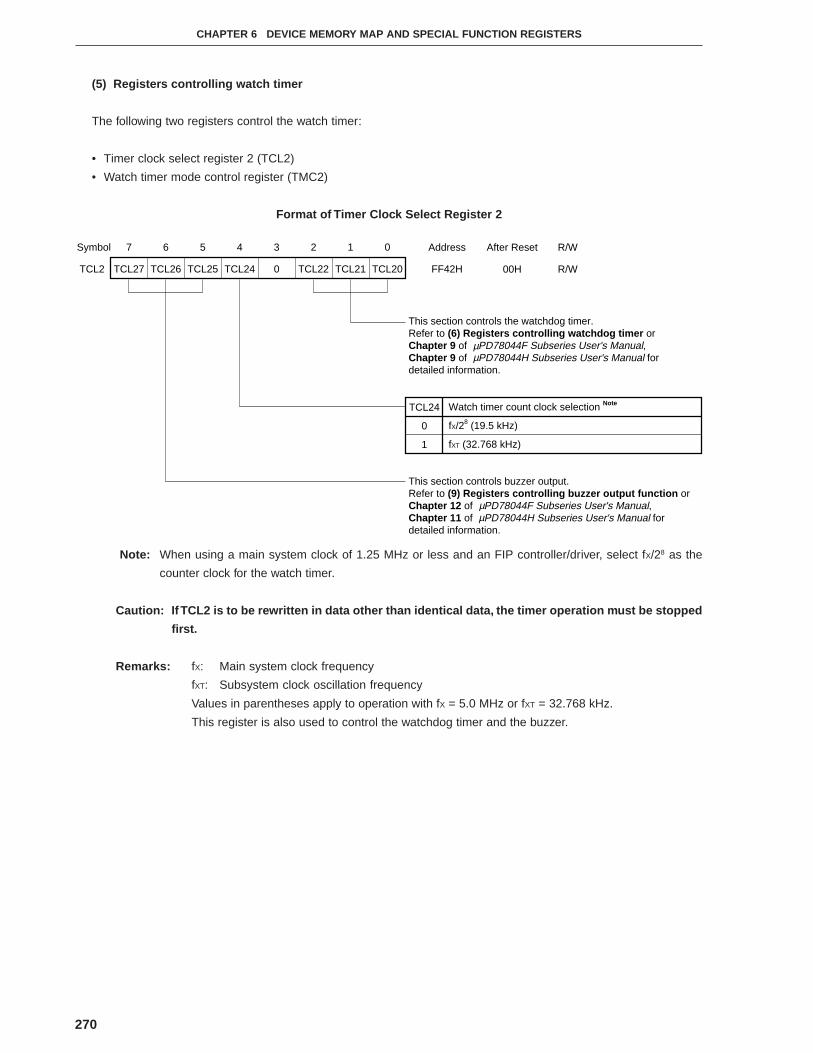
270
CHAPTER 6 DEVICE MEMORY MAP AND SPECIAL FUNCTION REGISTERS
(5) Registers controlling watch timer
The following two registers control the watch timer:
• Timer clock select register 2 (TCL2)
• Watch timer mode control register (TMC2)
Format of Timer Clock Select Register 2
Note: When using a main system clock of 1.25 MHz or less and an FIP controller/driver, select fX/28 as the
counter clock for the watch timer.
Caution: If TCL2 is to be rewritten in data other than identical data, the timer operation must be stopped
first.
Remarks: fX: Main system clock frequency
fXT: Subsystem clock oscillation frequency
Values in parentheses apply to operation with fX = 5.0 MHz or fXT = 32.768 kHz.
This register is also used to control the watchdog timer and the buzzer.
TCL20TCL2
7 6 5 4 3 2Symbol 1 0
FF42HTCL210 TCL22TCL24TCL25TCL26TCL27
Address After Reset R/W
00H R/W
TCL24 Watch timer count clock selection Note
0 fX/28 (19.5 kHz)
1 fXT (32.768 kHz)
This section controls the watchdog timer.Refer to (6) Registers controlling watchdog timer orChapter 9 of PD78044F Subseries User's Manual,Chapter 9 of PD78044H Subseries User's Manual fordetailed information.
µµ
This section controls buzzer output.Refer to (9) Registers controlling buzzer output function orChapter 12 of PD78044F Subseries User's Manual,Chapter 11 of PD78044H Subseries User's Manual fordetailed information.
µµ
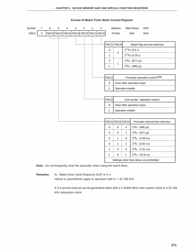
271
CHAPTER 6 DEVICE MEMORY MAP AND SPECIAL FUNCTION REGISTERS
Format of Watch Timer Mode Control Register
Note: Do not frequently clear the prescaler when using the watch timer.
Remarks: fW: Watch timer clock frequency (fX/28 or fXT)
Values in parentheses apply to operation with fW = 32.768 kHz.
A 0.5 second interval can be generated either with a 4.19304 MHz main system clock or a 32.768
kHz subsystem clock.
7 6 5 4 3 2 1 0
0 TMC26 TMC25 TMC24 TMC23 TMC22 TMC21 TMC20
Symbol
TMC2
Address
FF4AH
After Reset
00H
R/W
R/W
TMC21
0
1
Prescaler operation control Note
Clear after operation stops
Operation enable
TMC22
0
1
5-bit counter operation control
Clear after operation stops
Operation enable
TMC23
0
1
0
1
TMC20
0
1
Watch flag set time selection
TMC26
0
0
0
0
1
1
Prescaler interval time selection
24/fW (488 s)
25/fW (977 s)
26/fW (1.95 ms)
27/fW (3.91 ms)
28/fW (7.81 ms)
29/fW (15.6 ms)
TMC25
0
0
1
1
0
0
214/fW (0.5 S)
213/fW (0.25 S)
25/fW (977 s)
24/fW (488 s)
TMC24
0
1
0
1
0
1
µ
µ
µ
µ
Settings other than above are prohibited
272
CHAPTER 6 DEVICE MEMORY MAP AND SPECIAL FUNCTION REGISTERS
(6) Registers controlling watchdog timer
The following two registers control the watchdog timer:
• Timer clock select register 2 (TCL2)
• Watchdog timer mode register (WDTM)
Format of Timer Clock Select Register 2
Caution: If TCL2 is to be rewritten in data other than identical data, the timer operation must be stopped
first.
Remarks: fX: Main system clock frequency
Values in parentheses apply to operation with fX = 5.0 MHz.
This register is also used to control the watch timer and the buzzer.
TCL20TCL2
7 6 5 4 3 2Symbol 1 0
TCL22Count clock selection
FF42HTCL210 TCL22TCL24TCL25TCL26TCL27
Address After Reset R/W
00H R/W
Watchdog Timer mode
0 fX/23 (625 kHz)
0 fX/24 (313 kHz)
0 fX/25 (156 kHz)
0 fX/26 (78.1 kHz)
1 fX/27 (39.1 kHz)
1 fX/28 (19.5 kHz)
1 fX/29 (9.8k Hz)
1 fX/211 (2.4 kHz)
Interval Timer mode
fX/24 (313 kHz)
fX/25 (156 kHz)
fX/26 (78.1 kHz)
fX/27 (39.1 kHz)
fX/28 (19.5 kHz)
fX/29 (9.8 kHz)
fX/210 (4.9 kHz)
fX/212 (1.2 kHz)
TCL21
0
0
1
1
0
0
1
1
TCL20
0
1
0
1
0
1
0
1
This section controls the watch timer.Refer to (5) Registers controlling watch timer orChapter 9 of PD78044F Subseries User's Manual,Chapter 9 of PD78044H Subseries User's Manualfor detailed information.
µµ
This section controls buzzer output.Refer to (9) Registers controlling buzzer output function orChapter 12 of PD78044F Subseries User's Manual,Chapter 11 of PD78044H Subseries User's Manualfor detailed information.
µµ

273
CHAPTER 6 DEVICE MEMORY MAP AND SPECIAL FUNCTION REGISTERS
Format of Watchdog Timer Mode Register
Notes: 1. Once set to 1, WDTM3 and WDTM4 cannot be cleared to 0 by software.
2. The watchdog timer starts operation as an interval timer as soon as RUN has been set to 1.
3. Once set to 1, RUN cannot be cleared to 0 by software. Thus, once counting starts, it can only be
stopped by RESET input.
Cautions: 1. When 1 is set in RUN so that the watchdog timer is cleared, the actual overflow time is up
to 0.5% shorter than the time set by timer clock select register 2 (TCL2).
2. When using the Watchdog Timer mode 1 or 2, set WDTM4 to 1 after confirming that the
interrupt request flag (TMIF4) is 0. If WDTM4 is set to 1 while TMIF4 is 1, the non-maskable
interrupt request is generated regardless of the contents of WDTM3.
Remark: ×: Don’t care
<7> 6 5 4 3 2 1 0
RUN 0 0 WDTM4 WDTM3 0 0 0
Symbol
WDTM
Address
FFF9H
After Reset
00H
R/W
R/W
WDTM4
0
1
1
Watchdog timer operating mode selectionNote 1
Interval timer modeNote 2
(Maskable interrupt request occurs upon generation of an overflow.)
Watchdog timer mode 1(Non-maskable interrupt request occurs upon generation of an overflow.)
Watchdog timer mode 2(Reset operation is activated upon generation of an overflow.)
RUN
0
1
Watchdog timer operation selectionNote 3
Count stops
Counter is cleared and counting starts
WDTM3
x
0
1

274
CHAPTER 6 DEVICE MEMORY MAP AND SPECIAL FUNCTION REGISTERS
(7) Register controlling 6-bit up/down counter
The following register controls the 6-bit up/down counter: (only available for 7804xF and 78P048A)
• 6-bit up/down counter mode register (UDM)
Format of 6-Bit Up/Down Counter Mode Register
Cautions: 1. Do not set the UDM0, UDM1, and UDM3 using the same timings as the effective edges input
to the CI0/P03/INTP3 pin.
2. The UDC is cleared to 0 by writing 1 in the UDM3.
When the UDC is cleared, the UDM3 is automatically cleared to 0.
3. The UDC cannot be read/written until the RESET signal is input and data is set to the UDM.
4. Be sure to stop count operation before setting the 6-bit up/down counter (UDC) or the 6-
bit up/down counter compare register (UDCC).
UDM0UDM
7 6 5 4 3 2Symbol 1 0
UDM0 Valid edge selection
FFA8HUDM1UDM3 UDM2UDM4000
Address After Reset R/W
00H R/W
0 CI0 falling edge
1 CI0 rising edge
UDM1 Operation mode selection
0 Down counter operation
1 Up counter operation
UDM2 Count operation control
0 The count operation is stopped (the count value is retained)
1 The count operation is enabled
UDM3 Counter clear
0 Count operation
1 The counter is cleared
UDM4 INTP3 flag set signal selection
0 Set using the INTP3 interrupt signal
1 Set using the INTUD interrupt signal
275
CHAPTER 6 DEVICE MEMORY MAP AND SPECIAL FUNCTION REGISTERS
(8) Registers controlling clock output function
The following two registers control the clock output function:
• Timer clock select register 0 (TCL0)
• Port mode register 3 (PM3)
- Refer to section (1) for the register format.
Format of Timer Clock Select Register 0
Cautions: 1. When enabling PCL output, set TCL00 to TCL03, then set 1 in CLOE with a 1-bit memory
manipulation instruction.
2. To write data other than that already written to TCL0, stop the timer operation once.
Remarks: fX: Main system clock frequency
fXT: Subsystem clock oscillation frequency
Values in parentheses apply to operation with fX = 5.0 MHz or fXT = 32.768 kHz.
This register is also used to set the count clock of the 16-bit timer, in addition to setting the
clock for PCL output.
TCL00TCL0
<7> 6 5 4 3 2Symbol 1 0
TCL03 PCL output clock selection
FF40HTCL01TCL03 TCL02TCL04TCL05TCL06CLOE
Address After Reset R/W
00H R/W
0 fXT (32.768 kHz)
0 fX/23 (625 kHz)
1 fX/24 (313 kHz)
1 fX/25 (156 kHz)
1 fX/26 (78.1 kHz)
1 fX/27 (39.1 kHz)
1 fX/28 (19.5 kHz)
CLOE PCL output control
0 Output disable
1 Output enable
TCL02
0
1
0
0
0
0
1
TCL01
0
1
0
0
1
1
0
TCL00
0
1
0
1
0
1
0
This section controls the 16-bit timer.Refer to (3) Registers controlling 16-bit timer/event counter orChapter 6 of PD78044F Subseries User's Manual,Chapter 6 of PD78044H Subseries User's Manualfor detailed information.
µµ
Settings other than above are prohibited
276
CHAPTER 6 DEVICE MEMORY MAP AND SPECIAL FUNCTION REGISTERS
(9) Registers controlling buzzer output function
The following two registers control the buzzer output function:
• Timer clock select register 2 (TCL2)
• Port mode register 3 (PM3)
- Refer to section (1) for the register format.
Format of Timer Clock Select Register 2
Caution: If TCL2 is to be rewritten in data other than identical data, the timer operation must be stopped
first.
Remarks: fX: Main system clock frequency
×: Don’t care
Values in parentheses apply to operation with fX = 5.0 MHz.
This register is also used to control the watch timer and the watchdog timer.
TCL20TCL2
7 6 5 4 3 2Symbol 1 0
FF42HTCL210 TCL22TCL24TCL25TCL26TCL27
Address After Reset R/W
00H R/W
TCL27 Buzzer output frequency selection
0 Buzzer output disable
1 fX/210 (4.9 kHz)
1 fX/211 (2.4 kHz)
1 fX/212 (1.2 kHz)
1 Setting prohibited
TCL26
×
0
0
1
1
TCL25
×
0
1
0
1
This section controls the watchdog timer.Refer to (6) Registers controlling watchdog timer orChapter 9 of PD78044F Subseries User's Manual,Chapter 9 of PD78044H Subseries User's Manualfor detailed information.
µµ
This section controls the watch timer.Refer to (5) Registers controlling watch timer orChapter 8 of PD78044F Subseries User's Manual,Chapter 8 of PD78044H Subseries User's Manualfor detailed information.
µµ
277
CHAPTER 6 DEVICE MEMORY MAP AND SPECIAL FUNCTION REGISTERS
(10) Registers controlling A/D converter
The following two registers control the A/D converter:
• A/D converter mode register (ADM)
• A/D converter input select register (ADIS)
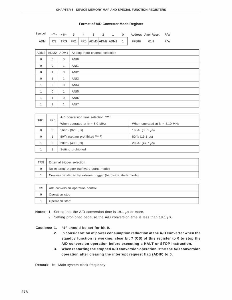
278
CHAPTER 6 DEVICE MEMORY MAP AND SPECIAL FUNCTION REGISTERS
Format of A/D Converter Mode Register
ADM3 ADM2 ADM1 Analog input channel selection
0 0 0 ANI0
0 0 1 ANI1
0 1 0 ANI2
0 1 1 ANI3
1 0 0 ANI4
1 0 1 ANI5
1 1 0 ANI6
1 1 1 ANI7
FR1 FR0A/D conversion time selection Note 1
When operated at fX = 5.0 MHz When operated at fX = 4.19 MHz
0 0 160/fX (32.0 µs) 160/fX (38.1 µs)
0 1 80/fX (setting prohibited Note 2) 80/fX (19.1 µs)
1 0 200/fX (40.0 µs) 200/fX (47.7 µs)
1 1 Setting prohibited
TRG External trigger selection
0 No external trigger (software starts mode)
1 Conversion started by external trigger (hardware starts mode)
CS A/D conversion operation control
0 Operation stop
1 Operation start
Notes: 1. Set so that the A/D conversion time is 19.1 µs or more.
2. Setting prohibited because the A/D conversion time is less than 19.1 µs.
Cautions: 1. “1” should be set for bit 0.
2. In consideration of power consumption reduction at the A/D converter when the
standby function is working, clear bit 7 (CS) of this register to 0 to stop the
A/D conversion operation before executing a HALT or STOP instruction.
3. When restarting the stopped A/D conversion operation, start the A/D conversion
operation after clearing the interrupt request flag (ADIF) to 0.
Remark: fX: Main system clock frequency
<6> 5 4 3 2 1 0<7>Symbol
ADM CS TRG FR1 FR0 ADM3 ADM2 ADM1 1 FF80H
Address After Reset R/W
01H R/W

279
CHAPTER 6 DEVICE MEMORY MAP AND SPECIAL FUNCTION REGISTERS
Format of A/D Converter Input Select Register
Cautions: 1. Set the analog input channel in the following order:
a. Set the number of analog input channels with ADIS.
b. Using the A/D converter mode register (ADM), select one channel to undergo A/D con-
version among the channels that are set for analog input with ADIS.
2. No internal pull-up resistor can be connected to the channels set for analog input with
ADIS, irrespective of the value of bit 1 (PUO1) of the pull-up resistor option register (PUO).
6 5 4 3 2 1 07Symbol
ADIS 0 0 0 0 ADIS3 ADIS2 ADIS1 ADIS0
Address After Reset R/W
ADIS3
0
0
0
0
Number of analog input channel selection
No analog input channel (P10 to P17)
1 channel (ANI0, P11 to P17)
2 channels (ANI0, ANI1, P12 to P17)
ADIS2
0
0
0
0
ADIS1
0
0
1
1
0
3 channels (ANI0 to ANI2, P13 to P17)
1 0
0
0
0
4 channels (ANI0 to ANI3, P14 to P17)
6 channels (ANI0 to ANI5, P16, P17)
5 channels (ANI0 to ANI4, P15 to P17)1
1
1
0
1
1
1 0 0
ADIS0
0
1
1
0
0
1
1
0
0
7 channels (ANI0 to ANI6, P17)
8 channels (ANI0 to ANI7)
FF84H 00H R/W
Settings other than above are prohibited
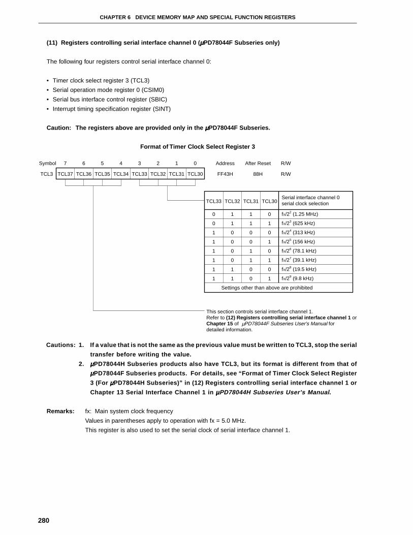
280
CHAPTER 6 DEVICE MEMORY MAP AND SPECIAL FUNCTION REGISTERS
(11) Registers controlling serial interface channel 0 ( µµµµµPD78044F Subseries only)
The following four registers control serial interface channel 0:
• Timer clock select register 3 (TCL3)
• Serial operation mode register 0 (CSIM0)
• Serial bus interface control register (SBIC)
• Interrupt timing specification register (SINT)
Caution: The registers above are provided only in the µµµµµPD78044F Subseries.
Format of Timer Clock Select Register 3
Cautions: 1. If a value that is not the same as the previous value must be written to TCL3, stop the serial
transfer before writing the value.
2. µµµµµPD78044H Subseries products also have TCL3, but its format is different from that of
µµµµµPD78044F Subseries products. For details, see “Format of Timer Clock Select Register
3 (For µµµµµPD78044H Subseries)” in (12) Registers controlling serial interface channel 1 or
Chapter 13 Serial Interface Channel 1 in µµµµµPD78044H Subseries User’s Manual .
Remarks: fx: Main system clock frequency
Values in parentheses apply to operation with fx = 5.0 MHz.
This register is also used to set the serial clock of serial interface channel 1.
TCL30TCL3
7 6 5 4 3 2Symbol 1 0
TCL33Serial interface channel 0serial clock selection
FF43HTCL31TCL33 TCL32TCL34TCL35TCL36TCL37
Address After Reset R/W
88H R/W
0 fX/22 (1.25 MHz)
0 fX/23 (625 kHz)
1 fX/24 (313 kHz)
1 fX/25 (156 kHz)
1 fX/26 (78.1 kHz)
1 fX/27 (39.1 kHz)
1 fX/28 (19.5 kHz)
1 fX/29 (9.8 kHz)
TCL32
1
1
0
0
0
0
1
1
TCL31
1
1
0
0
1
1
0
0
TCL30
0
1
0
1
0
1
0
1
This section controls serial interface channel 1.Refer to (12) Registers controlling serial interface channel 1 orChapter 15 of PD78044F Subseries User's Manual fordetailed information.
µ
Settings other than above are prohibited
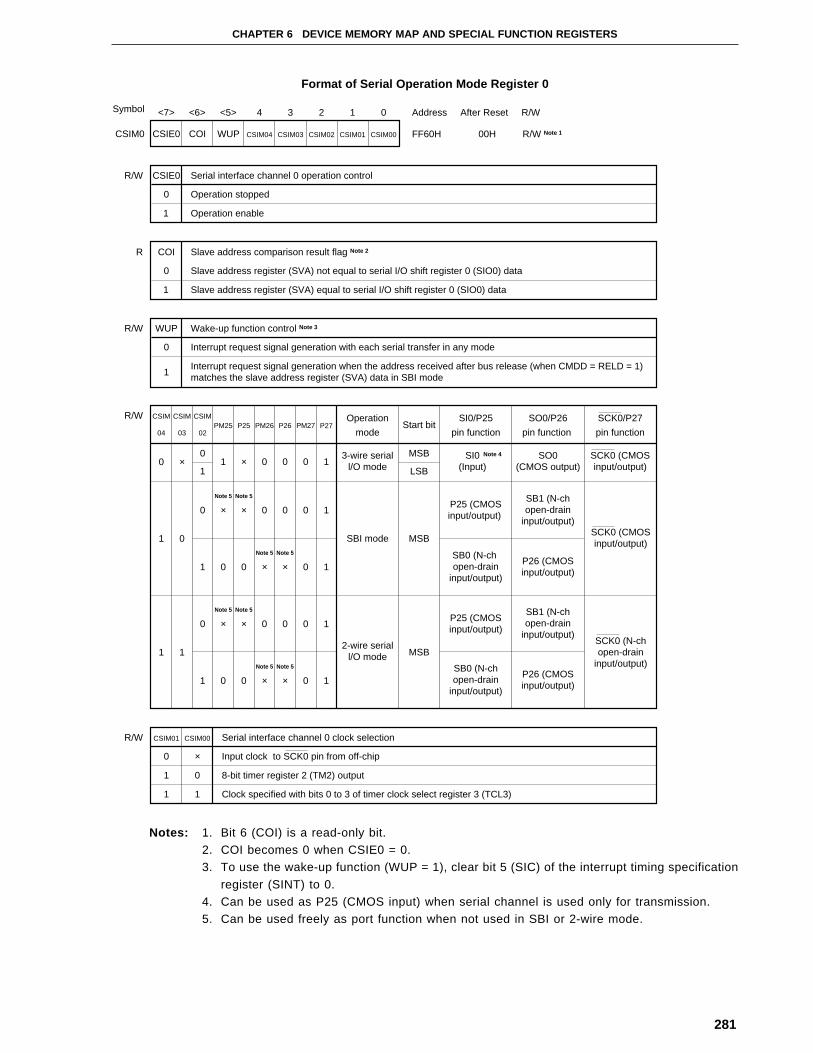
281
CHAPTER 6 DEVICE MEMORY MAP AND SPECIAL FUNCTION REGISTERS
Format of Serial Operation Mode Register 0
Notes: 1. Bit 6 (COI) is a read-only bit.2. COI becomes 0 when CSIE0 = 0.3. To use the wake-up function (WUP = 1), clear bit 5 (SIC) of the interrupt timing specification
register (SINT) to 0.4. Can be used as P25 (CMOS input) when serial channel is used only for transmission.5. Can be used freely as port function when not used in SBI or 2-wire mode.
<6> <5> 4 3 2 1 0<7>Symbol
CSIM0 CSIE0 COI WUP CSIM04 CSIM03 CSIM02 CSIM01 CSIM00 FF60H 00H R/W Note 1
Address After Reset R/W
CSIM01
0
1
Serial interface channel 0 clock selection
Input clock to SCK0 pin from off-chip
8-bit timer register 2 (TM2) output
R/W
1 Clock specified with bits 0 to 3 of timer clock select register 3 (TCL3)
CSIM00
×
0
1
SBI mode
0
0
SCK0 (CMOSinput/output)
CSIM
04
0
1
R/W CSIM
03
CSIM
02PM25 P25 PM26 P26 PM27 P27
Operation
modeStart bit
SI0/P25
pin function
SO0/P26
pin function
SCK0/P27
pin function
×
1 0
×
0
×
0
0
×
0
×
0
0
1
1
Note 5 Note 5
Note 5 Note 5
MSB
P25 (CMOSinput/output)
SB0 (N-ch open-drain
input/output)
SB1 (N-chopen-drain
input/output)
P26 (CMOSinput/output)
1
MSB
LSB1 × 0 0 0 1
3-wire seriall/O mode
SI0(Input)
SO0(CMOS output)
SCK0 (CMOSinput/output)
Note 4
2-wire seriall/O mode
0
SCK0 (N-chopen-drain
input/output)
1
1 1
×
0
×
0
0
×
0
×
0
0
1
1
Note 5 Note 5
Note 5 Note 5
MSB
P25 (CMOSinput/output)
SB0 (N-chopen-drain
input/output)
SB1 (N-chopen-drain
input/output)
P26 (CMOSinput/output)
WUP
0
1
Wake-up function control Note 3
Interrupt request signal generation with each serial transfer in any mode
Interrupt request signal generation when the address received after bus release (when CMDD = RELD = 1) matches the slave address register (SVA) data in SBI mode
R/W
COI
0
1
Slave address comparison result flag Note 2
Slave address register (SVA) not equal to serial I/O shift register 0 (SIO0) data
Slave address register (SVA) equal to serial I/O shift register 0 (SIO0) data
R
CSIE0
0
1
Serial interface channel 0 operation control
Operation stopped
Operation enable
R/W
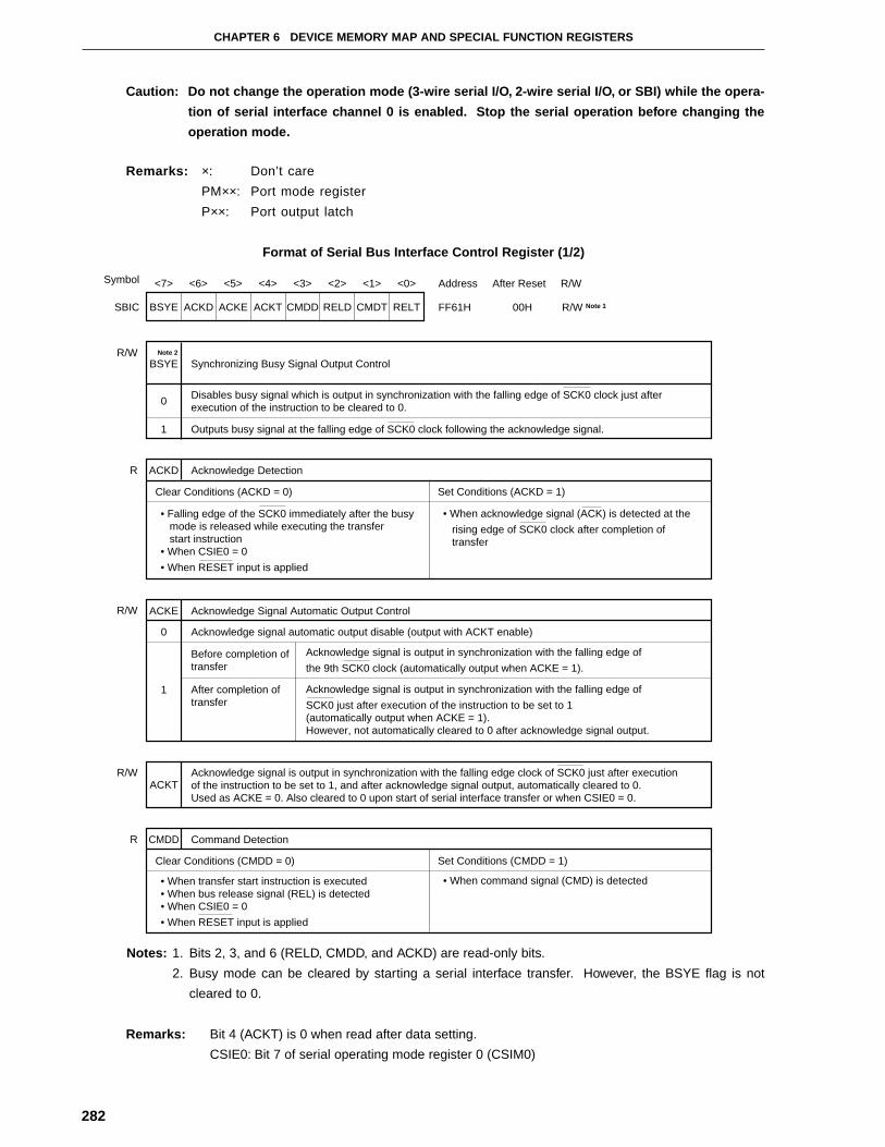
282
CHAPTER 6 DEVICE MEMORY MAP AND SPECIAL FUNCTION REGISTERS
Caution: Do not change the operation mode (3-wire serial I/O, 2-wire serial I/O, or SBI) while the opera-
tion of serial interface channel 0 is enabled. Stop the serial operation before changing the
operation mode.
Remarks: ×: Don’t care
PM××: Port mode register
P××: Port output latch
Format of Serial Bus Interface Control Register (1/2)
Notes: 1. Bits 2, 3, and 6 (RELD, CMDD, and ACKD) are read-only bits.
2. Busy mode can be cleared by starting a serial interface transfer. However, the BSYE flag is not
cleared to 0.
Remarks: Bit 4 (ACKT) is 0 when read after data setting.
CSIE0: Bit 7 of serial operating mode register 0 (CSIM0)
<6> <5> <4> <3> <2> <1> <0><7>Symbol
SBIC BSYE ACKD ACKE ACKT CMDD RELD CMDT RELT FF61H 00H R/W Note 1
Address After Reset R/W
R CMDD Command Detection
Clear Conditions (CMDD = 0)
• When transfer start instruction is executed • When bus release signal (REL) is detected • When CSIE0 = 0
• When RESET input is applied
Set Conditions (CMDD = 1)
• When command signal (CMD) is detected
ACKTAcknowledge signal is output in synchronization with the falling edge clock of SCK0 just after execution of the instruction to be set to 1, and after acknowledge signal output, automatically cleared to 0. Used as ACKE = 0. Also cleared to 0 upon start of serial interface transfer or when CSIE0 = 0.
R/W
R ACKD Acknowledge Detection
Clear Conditions (ACKD = 0)
• Falling edge of the SCK0 immediately after the busy mode is released while executing the transfer start instruction • When CSIE0 = 0
• When RESET input is applied
Set Conditions (ACKD = 1)
• When acknowledge signal (ACK) is detected at the
rising edge of SCK0 clock after completion of transfer
BSYE Synchronizing Busy Signal Output Control
0Disables busy signal which is output in synchronization with the falling edge of SCK0 clock just after execution of the instruction to be cleared to 0.
R/W Note 2
1 Outputs busy signal at the falling edge of SCK0 clock following the acknowledge signal.
ACKE Acknowledge Signal Automatic Output Control
0 Acknowledge signal automatic output disable (output with ACKT enable)
Acknowledge signal is output in synchronization with the falling edge of
the 9th SCK0 clock (automatically output when ACKE = 1).Before completion of transfer
Acknowledge signal is output in synchronization with the falling edge of
SCK0 just after execution of the instruction to be set to 1 (automatically output when ACKE = 1). However, not automatically cleared to 0 after acknowledge signal output.
After completion of transfer
1
R/W
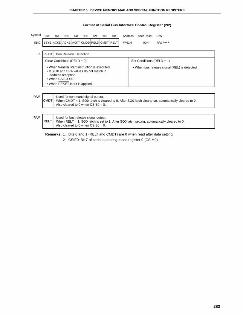
283
CHAPTER 6 DEVICE MEMORY MAP AND SPECIAL FUNCTION REGISTERS
Format of Serial Bus Interface Control Register (2/2)
Remarks: 1. Bits 0 and 1 (RELT and CMDT) are 0 when read after data setting.
2. CSIE0: Bit 7 of serial operating mode register 0 (CSIM0)
RELTUsed for bus release signal output. When RELT = 1, SO0 Iatch is set to 1. After SO0 latch setting, automatically cleared to 0.Also cleared to 0 when CSIE0 = 0.
R/W
CMDTUsed for command signal output. When CMDT = 1, SO0 Iatch is cleared to 0. After SO0 latch clearance, automatically cleared to 0. Also cleared to 0 when CSIE0 = 0.
R/W
R RELD Bus Release Detection
Set Conditions (RELD = 1)Clear Conditions (RELD = 0)
• When bus release signal (REL) is detected• When transfer start instruction is executed • If SIO0 and SVA values do not match in address reception • When CSIE0 = 0
• When RESET input is applied
<6> <5> <4> <3> <2> <1> <0><7>Symbol
SBIC BSYE ACKD ACKE ACKT CMDD RELD CMDT RELT FF61H 00H R/W Note 1
Address After Reset R/W
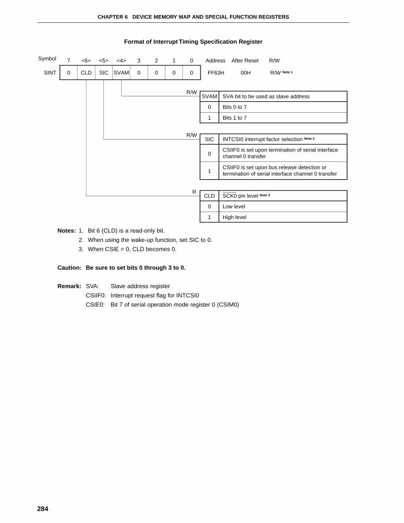
284
CHAPTER 6 DEVICE MEMORY MAP AND SPECIAL FUNCTION REGISTERS
Format of Interrupt Timing Specification Register
Notes: 1. Bit 6 (CLD) is a read-only bit.
2. When using the wake-up function, set SIC to 0.
3. When CSIE = 0, CLD becomes 0.
Caution: Be sure to set bits 0 through 3 to 0.
Remark: SVA: Slave address register
CSIIF0: Interrupt request flag for INTCSI0
CSIE0: Bit 7 of serial operation mode register 0 (CSIM0)
<6> <5> <4> 3 2 1 07Symbol
SINT 0 CLD SIC SVAM 0 0 0 0 FF63H 00H R/W Note 1
Address After Reset R/W
SVAM
0
1
SVA bit to be used as slave address
Bits 0 to 7
Bits 1 to 7
SIC
0
1
INTCSI0 interrupt factor selection Note 2
CSIIF0 is set upon termination of serial interfacechannel 0 transfer
CSIIF0 is set upon bus release detection ortermination of serial interface channel 0 transfer
CLD
0
1
SCK0 pin level Note 3
Low level
High level
R/W
R/W
R
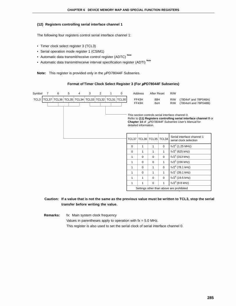
285
CHAPTER 6 DEVICE MEMORY MAP AND SPECIAL FUNCTION REGISTERS
(12) Registers controlling serial interface channel 1
The following four registers control serial interface channel 1:
• Timer clock select register 3 (TCL3)
• Serial operation mode register 1 (CSIM1)
• Automatic data transmit/receive control register (ADTC) Note
• Automatic data transmit/receive interval specification register (ADTI) Note
Note: This register is provided only in the µPD78044F Subseries.
Format of Timer Clock Select Register 3 (For µµµµµPD78044F Subseries)
Caution: If a value that is not the same as the previous value must be written to TCL3, stop the serial
transfer before writing the value.
Remarks: fx: Main system clock frequency
Values in parentheses apply to operation with fx = 5.0 MHz.
This register is also used to set the serial clock of serial interface channel 0.
TCL30TCL3
7 6 5 4 3 2Symbol 1 0
FF43HTCL31TCL33 TCL32TCL34TCL35TCL36TCL37
Address After Reset R/W
88H R/W (7804xF and 78P048A)FF43H 8xH R/W (7804xH and 78P048B)
TCL37Serial interface channel 1serial clock selection
0 fX/22 (1.25 MHz)
0 fX/23 (625 kHz)
1 fX/24 (313 kHz)
1 fX/25 (156 kHz)
1 fX/26 (78.1 kHz)
1 fX/27 (39.1 kHz)
1 fX/28 (19.5 kHz)
1 fX/29 (9.8 kHz)
TCL36
1
1
0
0
0
0
1
1
TCL35
1
1
0
0
1
1
0
0
Settings other than above are prohibited
TCL34
0
1
0
1
0
1
0
1
This section controls serial interface channel 0.Refer to (11) Registers controlling serial interface channel 0 orChapter 14 of PD78044F Subseries User's Manual fordetailed information.
µ
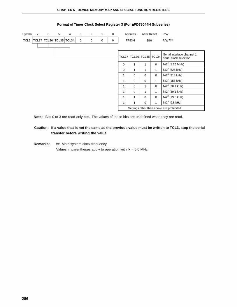
286
CHAPTER 6 DEVICE MEMORY MAP AND SPECIAL FUNCTION REGISTERS
Format of Timer Clock Select Register 3 (For µµµµµPD78044H Subseries)
Note: Bits 0 to 3 are read-only bits. The values of these bits are undefined when they are read.
Caution: If a value that is not the same as the previous value must be written to TCL3, stop the serial
transfer before writing the value.
Remarks: fx: Main system clock frequency
Values in parentheses apply to operation with fx = 5.0 MHz.
0TCL3
7 6 5 4 3 2Symbol 1 0
FF43H00 0TCL34TCL35TCL36TCL37
Address After Reset R/W
88H R/W Note
TCL37Serial interface channel 1serial clock selection
0 fX/22 (1.25 MHz)
0 fX/23 (625 kHz)
1 fX/24 (313 kHz)
1 fX/25 (156 kHz)
1 fX/26 (78.1 kHz)
1 fX/27 (39.1 kHz)
1 fX/28 (19.5 kHz)
1 fX/29 (9.8 kHz)
TCL36
1
1
0
0
0
0
1
1
TCL35
1
1
0
0
1
1
0
0
TCL34
0
1
0
1
0
1
0
1
Settings other than above are prohibited
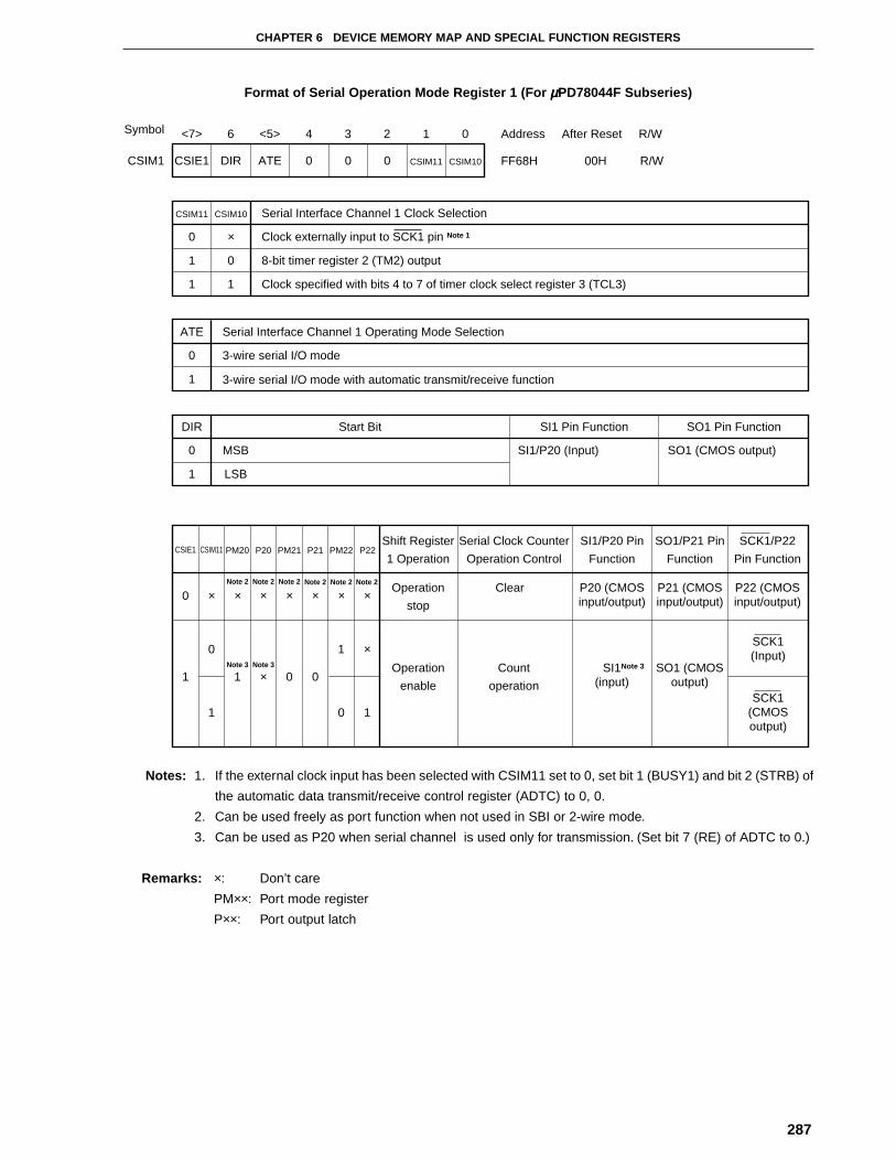
287
CHAPTER 6 DEVICE MEMORY MAP AND SPECIAL FUNCTION REGISTERS
Format of Serial Operation Mode Register 1 (For µµµµµPD78044F Subseries)
Notes: 1. If the external clock input has been selected with CSIM11 set to 0, set bit 1 (BUSY1) and bit 2 (STRB) of
the automatic data transmit/receive control register (ADTC) to 0, 0.
2. Can be used freely as port function when not used in SBI or 2-wire mode.
3. Can be used as P20 when serial channel is used only for transmission. (Set bit 7 (RE) of ADTC to 0.)
Remarks: ×: Don’t care
PM××: Port mode register
P××: Port output latch
Operation
enable
6 <5> 4 3 2 1 0<7>Symbol
CSIM1 CSIE1 DIR ATE 0 0 0 CSIM11 CSIM10
CSIM11
0
1
Serial Interface Channel 1 Clock Selection
Clock externally input to SCK1 pin Note 1
8-bit timer register 2 (TM2) output
SCK1(Input)
1 Clock specified with bits 4 to 7 of timer clock select register 3 (TCL3)
CSIE1
0
CSIM10
×
0
1
FF68H 00H R/W
Address After Reset R/W
CSIM11 P20 PM21 P21 PM22
Note 3
Shift Register
1 Operation
Serial Clock Counter
Operation Control
SI1/P20 Pin
Function
SCK1/P22
Pin Function
×
1
0
1
0
× 0 0
1 ×
1
Note 2 Note 2 Note 2 Note 2
Count
operation
SI1(input)
× × × × ×Operation
stop
Clear P20 (CMOSinput/output)
P22 (CMOSinput/output)
ATE
0
1
Serial Interface Channel 1 Operating Mode Selection
3-wire serial I/O mode
3-wire serial I/O mode with automatic transmit/receive function
DIR
0
1
Start Bit
MSB
LSB
SI1 Pin Function
SI1/P20 (Input)
SO1 Pin Function
SO1 (CMOS output)
×
PM20SO1/P21 Pin
Function
SO1 (CMOSoutput)
P21 (CMOSinput/output)
SCK1(CMOSoutput)
1
Note 2Note 2
Note 3Note 3
P22
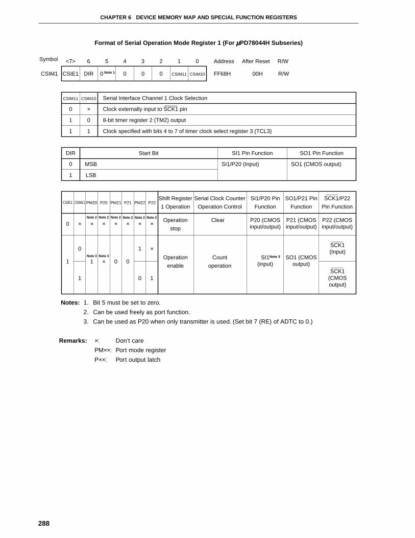
288
CHAPTER 6 DEVICE MEMORY MAP AND SPECIAL FUNCTION REGISTERS
Format of Serial Operation Mode Register 1 (For µµµµµPD78044H Subseries)
Notes: 1. Bit 5 must be set to zero.
2. Can be used freely as port function.
3. Can be used as P20 when only transmitter is used. (Set bit 7 (RE) of ADTC to 0.)
Remarks: ×: Don’t care
PM××: Port mode register
P××: Port output latch
Operation
enable
6 5 4 3 2 1 0<7>Symbol
CSIM1 CSIE1 DIR 0 Note 1 0 0 0 CSIM11 CSIM10
CSIM11
0
1
Serial Interface Channel 1 Clock Selection
Clock externally input to SCK1 pin
8-bit timer register 2 (TM2) output
SCK1(Input)
1 Clock specified with bits 4 to 7 of timer clock select register 3 (TCL3)
CSIE1
0
CSIM10
×
0
1
FF68H 00H R/W
Address After Reset R/W
CSIM11 P20 PM21 P21 PM22
Note 3
Shift Register
1 Operation
Serial Clock Counter
Operation Control
SI1/P20 Pin
Function
SCK1/P22
Pin Function
×
1
0
1
0
× 0 0
1 ×
1
Note 2 Note 2 Note 2 Note 2
Count
operation
SI1(input)
× × × × ×Operation
stop
Clear P20 (CMOSinput/output)
P22 (CMOSinput/output)
DIR
0
1
Start Bit
MSB
LSB
SI1 Pin Function
SI1/P20 (Input)
SO1 Pin Function
SO1 (CMOS output)
×
PM20SO1/P21 Pin
Function
SO1 (CMOSoutput)
P21 (CMOSinput/output)
SCK1(CMOSoutput)
1
Note 2Note 2
Note 3Note 3
P22
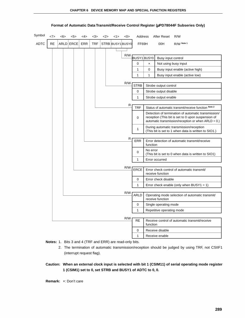
289
CHAPTER 6 DEVICE MEMORY MAP AND SPECIAL FUNCTION REGISTERS
Format of Automatic Data Transmit/Receive Control Register ( µµµµµPD78044F Subseries Only)
Notes: 1. Bits 3 and 4 (TRF and ERR) are read-only bits.
2. The termination of automatic transmission/reception should be judged by using TRF, not CSIIF1
(interrupt request flag).
Caution: When an external clock input is selected with bit 1 (CSIM11) of serial operating mode register
1 (CSIM1) set to 0, set STRB and BUSY1 of ADTC to 0, 0.
Remark: ×: Don’t care
<6> <5> <4> <3> <2> <1> <0><7>Symbol
ADTC RE ARLD ERCE ERR TRF STRB BUSY1 BUSY0
BUSY1
0
1
1
Busy input control
Not using busy input
Busy input enable (active high)
Busy input enable (active low)
BUSY0
×
0
1
STRB
0
1
Strobe output control
Strobe output disable
Strobe output enable
TRF
1
Status of automatic transmit/receive function Note 2
Detection of termination of automatic transmission/reception (This bit is set to 0 upon suspension ofautomatic transmission/reception or when ARLD = 0.)
During automatic transmission/reception(This bit is set to 1 when data is written to SIO1.)
R/W
R/W
R
RERR
0
1
Error detection of automatic transmit/receivefunction
No error(This bit is set to 0 when data is written to SIO1)
Error occurred
R/WARLD
0
1
Operating mode selection of automatic transmit/receive function
Single operating mode
Repetitive operating mode
R/WRE
0
1
Receive control of automatic transmit/receivefunction
Receive disable
Receive enable
R/WERCE
0
Error check control of automatic transmit/receive function
Error check disable
Error check enable (only when BUSY1 = 1)
0
1
Address
FF69H
After Reset
00H
R/W
R/W Note 1
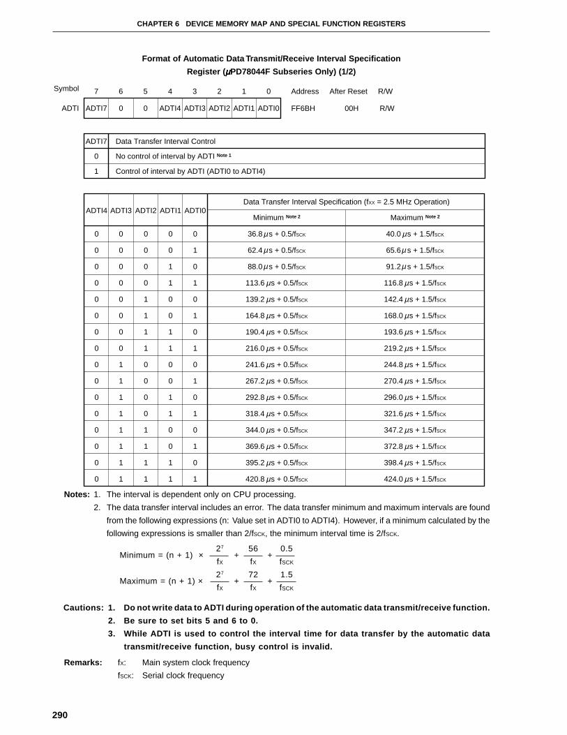
290
CHAPTER 6 DEVICE MEMORY MAP AND SPECIAL FUNCTION REGISTERS
Format of Automatic Data Transmit/Receive Interval Specification
Register ( µµµµµPD78044F Subseries Only) (1/2)
Notes: 1. The interval is dependent only on CPU processing.
2. The data transfer interval includes an error. The data transfer minimum and maximum intervals are found
from the following expressions (n: Value set in ADTI0 to ADTI4). However, if a minimum calculated by the
following expressions is smaller than 2/fSCK, the minimum interval time is 2/fSCK.
27 56 0.5Minimum = (n + 1) × + +
fX fX fSCK
27 72 1.5Maximum = (n + 1) × + +
fX fX fSCK
Cautions: 1. Do not write data to ADTI during operation of the automatic data transmit/receive function.
2. Be sure to set bits 5 and 6 to 0.
3. While ADTI is used to control the interval time for data transfer by the automatic data
transmit/receive function, busy control is invalid.
Remarks: fX: Main system clock frequency
fSCK: Serial clock frequency
Data Transfer Interval Specification (fXX = 2.5 MHz Operation) ADTI4 ADTI3 ADTI2 ADTI1
0
0
0
0
0
0
0
0
0
0
0
0
0
0
0
0
0
0
0
0
0
0
0
0
1
1
1
1
1
1
1
1
0
0
0
0
1
1
1
1
0
0
0
0
1
1
1
1
0
0
1
1
0
0
1
1
0
0
1
1
0
0
1
1
Minimum Note 2
36.8 s + 0.5/fSCK
62.4 s + 0.5/fSCK
88.0 s + 0.5/fSCK
113.6 s + 0.5/fSCK
139.2 s + 0.5/fSCK
164.8 s + 0.5/fSCK
190.4 s + 0.5/fSCK
216.0 s + 0.5/fSCK
241.6 s + 0.5/fSCK
267.2 s + 0.5/fSCK
292.8 s + 0.5/fSCK
318.4 s + 0.5/fSCK
344.0 s + 0.5/fSCK
369.6 s + 0.5/fSCK
395.2 s + 0.5/fSCK
420.8 s + 0.5/fSCK
Maximum Note 2
40.0 s + 1.5/fSCK
65.6 s + 1.5/fSCK
91.2 s + 1.5/fSCK
116.8 s + 1.5/fSCK
142.4 s + 1.5/fSCK
168.0 s + 1.5/fSCK
193.6 s + 1.5/fSCK
219.2 s + 1.5/fSCK
244.8 s + 1.5/fSCK
270.4 s + 1.5/fSCK
296.0 s + 1.5/fSCK
321.6 s + 1.5/fSCK
347.2 s + 1.5/fSCK
372.8 s + 1.5/fSCK
398.4 s + 1.5/fSCK
424.0 s + 1.5/fSCK
6 5 4 3 2 1 07Symbol
ADTI ADTI7 0 0 ADTI4 ADTI3 ADTI2 ADTI1 ADTI0 FF6BH 00H R/W
Address After Reset R/W
ADTI7
0
Data Transfer Interval Control
No control of interval by ADTI Note 1
Control of interval by ADTI (ADTI0 to ADTI4) 1
ADTI0
0
1
0
1
0
1
0
1
0
1
0
1
0
1
0
1
µ
µ
µ
µ
µ
µ
µ
µ
µ
µ
µ
µ
µ
µ
µ
µ
µ
µ
µ
µ
µ
µ
µ
µ
µ
µ
µ
µ
µ
µ
µ
µ

291
CHAPTER 6 DEVICE MEMORY MAP AND SPECIAL FUNCTION REGISTERS
Notes: The data transfer interval includes an error. The data transfer minimum and maximum intervals are found
from the following expressions (n: Value set in ADTI0 to ADTI4). However, if a minimum calculated by the
following expressions is smaller than 2/fSCK, the minimum interval time is 2/fSCK.
27 56 0.5Minimum = (n + 1) × + +
fX fX fSCK
27 72 1.5Maximum = (n + 1) × + +
fX fX fSCK
Cautions: 1. Do not write data to ADTI during operation of the automatic data transmit/receive function.
2. Be sure to set bits 5 and 6 to 0.
3. While ADTI is used to control the interval time for data transfer by the automatic data
transmit/receive function, busy control is invalid.
Remarks: 1. fX: Main system clock frequency
2. fSCK: Serial clock frequency
Format of Automatic Data Transmit/Receive Interval Specification
Register ( µµµµµPD78044F Subseries Only) (2/2)
Data Transfer Interval Specification (fXX = 2.5 MHz Operation) ADTI4 ADTI3 ADTI2 ADTI1
1
1
1
1
1
1
1
1
1
1
1
1
1
1
1
1
0
0
0
0
0
0
0
0
1
1
1
1
1
1
1
1
0
0
0
0
1
1
1
1
0
0
0
0
1
1
1
1
0
0
1
1
0
0
1
1
0
0
1
1
0
0
1
1
Minimum Note
446.4 s + 0.5/fSCK
472.0 s + 0.5/fSCK
497.6 s + 0.5/fSCK
523.2 s + 0.5/fSCK
548.8 s + 0.5/fSCK
574.4 s + 0.5/fSCK
600.0 s + 0.5/fSCK
625.6 s + 0.5/fSCK
651.2 s + 0.5/fSCK
676.8 s + 0.5/fSCK
702.4 s + 0.5/fSCK
728.0 s + 0.5/fSCK
753.6 s + 0.5/fSCK
779.2 s + 0.5/fSCK
804.8 s + 0.5/fSCK
830.4 s + 0.5/fSCK
Maximum Note
449.6 s + 1.5/fSCK
475.2 s + 1.5/fSCK
500.8 s + 1.5/fSCK
526.4 s + 1.5/fSCK
552.0 s + 1.5/fSCK
577.6 s + 1.5/fSCK
603.2 s + 1.5/fSCK
628.8 s + 1.5/fSCK
654.4 s + 1.5/fSCK
680.0 s + 1.5/fSCK
705.6 s + 1.5/fSCK
731.2 s + 1.5/fSCK
756.8 s + 1.5/fSCK
782.4 s + 1.5/fSCK
808.0 s + 1.5/fSCK
833.6 s + 1.5/fSCK
6 5 4 3 2 1 07Symbol
ADTI ADTI7 0 0 ADTI4 ADTI3 ADTI2 ADTI1 ADTI0 FF6BH 00H R/W
Address After Reset R/W
ADTI0
0
1
0
1
0
1
0
1
0
1
0
1
0
1
0
1
µ
µ
µ
µ
µ
µ
µ
µ
µ
µ
µ
µ
µ
µ
µ
µ
µ
µ
µ
µ
µ
µ
µ
µ
µ
µ
µ
µ
µ
µ
µ
µ
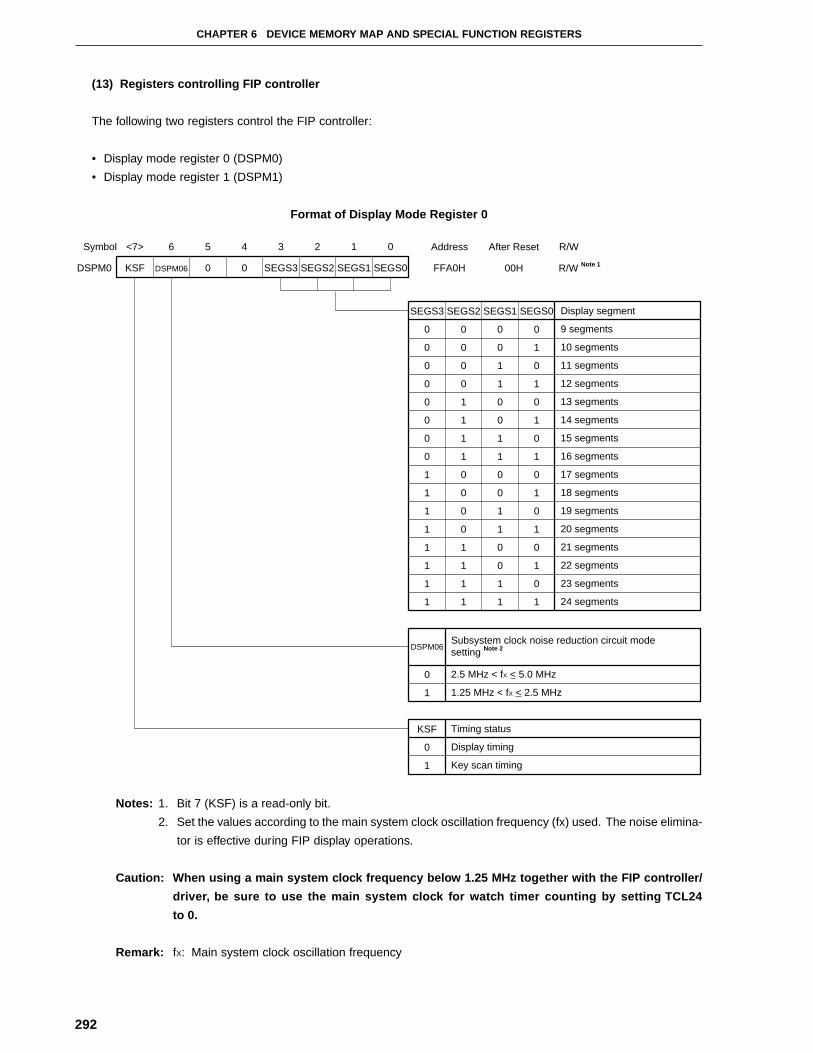
292
CHAPTER 6 DEVICE MEMORY MAP AND SPECIAL FUNCTION REGISTERS
(13) Registers controlling FIP controller
The following two registers control the FIP controller:
• Display mode register 0 (DSPM0)
• Display mode register 1 (DSPM1)
Format of Display Mode Register 0
Notes: 1. Bit 7 (KSF) is a read-only bit.
2. Set the values according to the main system clock oscillation frequency (fx) used. The noise elimina-
tor is effective during FIP display operations.
Caution: When using a main system clock frequency below 1.25 MHz together with the FIP controller/
driver, be sure to use the main system clock for watch timer counting by setting TCL24
to 0.
Remark: fX: Main system clock oscillation frequency
SEGS0DSPM0
<7> 6 5 4 3 2Symbol 1 0
SEGS3 Display segment
FFA0HSEGS1SEGS3 SEGS200DSPM06KSF
Address After Reset
00H
0 9 segments
0 10 segments
0 11 segments
0 12 segments
0 13 segments
0 14 segments
0 15 segments
0 16 segments
1 17 segments
1 18 segments
1 19 segments
1 20 segments
1 21 segments
1 22 segments
1 23 segments
1 24 segments
DSPM06Subsystem clock noise reduction circuit modesetting Note 2
0 2.5 MHz < fX < 5.0 MHz
1 1.25 MHz < fX < 2.5 MHz
KSF Timing status
0 Display timing
1 Key scan timing
R/W
R/W Note 1
SEGS2
0
0
0
0
1
1
1
1
0
0
0
0
1
1
1
1
SEGS1
0
0
1
1
0
0
1
1
0
0
1
1
0
0
1
1
SEGS0
0
1
0
1
0
1
0
1
0
1
0
1
0
1
0
1
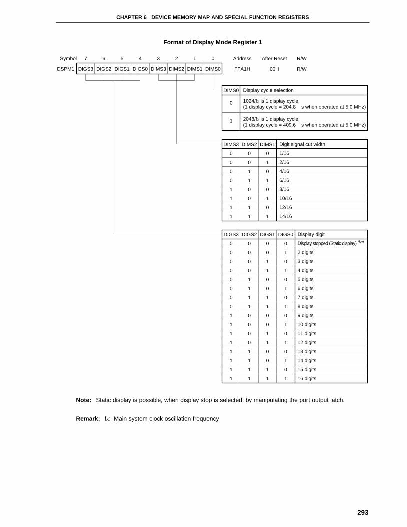
293
CHAPTER 6 DEVICE MEMORY MAP AND SPECIAL FUNCTION REGISTERS
Format of Display Mode Register 1
Note: Static display is possible, when display stop is selected, by manipulating the port output latch.
Remark: fX: Main system clock oscillation frequency
DIMS0DSPM1
7 6 5 4 3 2Symbol 1 0
DIMS0 Display cycle selection
FFA1HDIMS1DIMS3 DIMS2DIGS0DIGS1DIGS2DIGS3
Address After Reset R/W
00H R/W
0 1024/fX is 1 display cycle. (1 display cycle = 204.8 s when operated at 5.0 MHz)
1 2048/fX is 1 display cycle. (1 display cycle = 409.6 s when operated at 5.0 MHz)
DIMS3 Digit signal cut width
0 1/16
0 2/16
0 4/16
0 6/16
1 8/16
1 10/16
1 12/16
1 14/16
DIGS3 Display digit
0 Display stopped (Static display) Note
0 2 digits
0 3 digits
0 4 digits
0 5 digits
0 6 digits
0 7 digits
0 8 digits
1 9 digits
1 10 digits
1 11 digits
1 12 digits
1 13 digits
1 14 digits
1 15 digits
1 16 digits
DIMS2
0
0
1
1
0
0
1
1
DIMS1
0
1
0
1
0
1
0
1
DIGS2
0
0
0
0
1
1
1
1
0
0
0
0
1
1
1
1
DIGS1
0
0
1
1
0
0
1
1
0
0
1
1
0
0
1
1
DIGS0
0
1
0
1
0
1
0
1
0
1
0
1
0
1
0
1
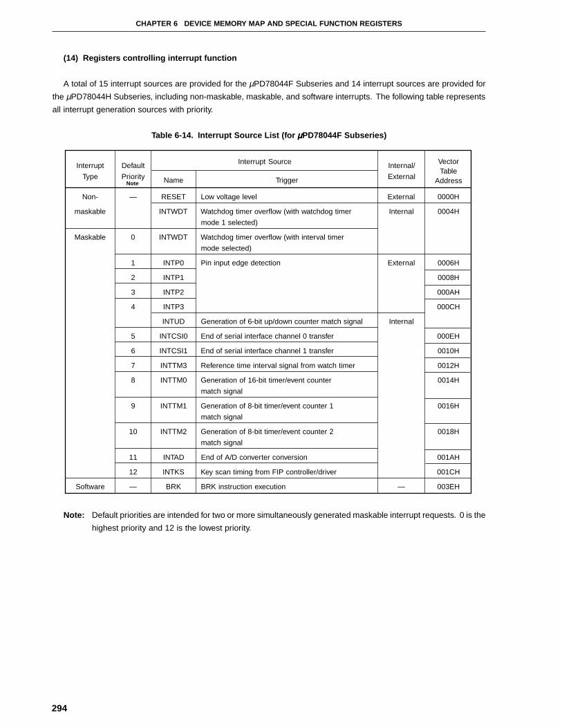
294
CHAPTER 6 DEVICE MEMORY MAP AND SPECIAL FUNCTION REGISTERS
(14) Registers controlling interrupt function
A total of 15 interrupt sources are provided for the µPD78044F Subseries and 14 interrupt sources are provided for
the µPD78044H Subseries, including non-maskable, maskable, and software interrupts. The following table represents
all interrupt generation sources with priority.
Table 6-14. Interrupt Source List (for µµµµµPD78044F Subseries)
Interrupt Default Interrupt Source Internal/ VectorTable
Type Priority Name Trigger External Address
Non- — RESET Low voltage level External 0000H
maskable INTWDT Watchdog timer overflow (with watchdog timer Internal 0004H
mode 1 selected)
Maskable 0 INTWDT Watchdog timer overflow (with interval timer
mode selected)
1 INTP0 Pin input edge detection External 0006H
2 INTP1 0008H
3 INTP2 000AH
4 INTP3 000CH
INTUD Generation of 6-bit up/down counter match signal Internal
5 INTCSI0 End of serial interface channel 0 transfer 000EH
6 INTCSI1 End of serial interface channel 1 transfer 0010H
7 INTTM3 Reference time interval signal from watch timer 0012H
8 INTTM0 Generation of 16-bit timer/event counter 0014H
match signal
9 INTTM1 Generation of 8-bit timer/event counter 1 0016H
match signal
10 INTTM2 Generation of 8-bit timer/event counter 2 0018H
match signal
11 INTAD End of A/D converter conversion 001AH
12 INTKS Key scan timing from FIP controller/driver 001CH
Software — BRK BRK instruction execution — 003EH
Note: Default priorities are intended for two or more simultaneously generated maskable interrupt requests. 0 is the
highest priority and 12 is the lowest priority.
Note
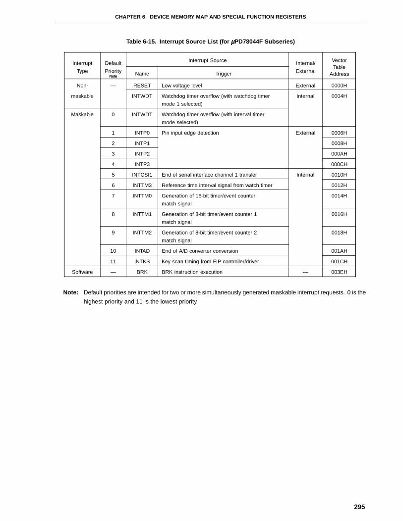
295
CHAPTER 6 DEVICE MEMORY MAP AND SPECIAL FUNCTION REGISTERS
Table 6-15. Interrupt Source List (for µµµµµPD78044F Subseries)
Interrupt Default Interrupt Source Internal/ VectorTable
Type Priority Name Trigger External Address
Non- — RESET Low voltage level External 0000H
maskable INTWDT Watchdog timer overflow (with watchdog timer Internal 0004H
mode 1 selected)
Maskable 0 INTWDT Watchdog timer overflow (with interval timer
mode selected)
1 INTP0 Pin input edge detection External 0006H
2 INTP1 0008H
3 INTP2 000AH
4 INTP3 000CH
5 INTCSI1 End of serial interface channel 1 transfer Internal 0010H
6 INTTM3 Reference time interval signal from watch timer 0012H
7 INTTM0 Generation of 16-bit timer/event counter 0014H
match signal
8 INTTM1 Generation of 8-bit timer/event counter 1 0016H
match signal
9 INTTM2 Generation of 8-bit timer/event counter 2 0018H
match signal
10 INTAD End of A/D converter conversion 001AH
11 INTKS Key scan timing from FIP controller/driver 001CH
Software — BRK BRK instruction execution — 003EH
Note: Default priorities are intended for two or more simultaneously generated maskable interrupt requests. 0 is the
highest priority and 11 is the lowest priority.
Note

296
CHAPTER 6 DEVICE MEMORY MAP AND SPECIAL FUNCTION REGISTERS
The following table lists interrupt request flags, interrupt mask flags, and priority specification flags corresponding to
interrupt request sources.
Table 6-16. Interrupt Sources and Flags
Interrupt Source Interrupt Request Flag Interrupt Mask Flag Priority Specification Flag
Register Register Register
INTWDT TMIF4 IF0L TMMK4 MK0L TMPR4 PR0L
INTP0 PIF0 PMK0 PPR0
INTP1 PIF1 PMK1 PPR1
INTP2 PIF2 PMK2 PPR2
INTP3/INTUD Note PIF3 PMK3 PPR3
INTCSI0 Note CSIIF0 CSIMK0 CSIPR0
INTCSI1 CSIIF1 CSIMK1 CSIPR1
INTTM3 TMIF3 TMMK3 TMPR3
INTTM0 TMIF0 IF0H TMMK0 MK0H TMPR0 PR0H
INTTM1 TMIF1 TMMK1 TMPR1
INTTM2 TMIF2 TMMK2 TMPR2
INTAD ADIF ADMK ADPR
INTKS KSIF KSMK KSPR
Note: The following interrupt sources are not provided for the µPD78044H Subseries:
INTUD, INTCSI0

297
CHAPTER 6 DEVICE MEMORY MAP AND SPECIAL FUNCTION REGISTERS
The following six types of registers control the interrupt functions:
• Interrupt request flag registers (IF0L, IF0H)
• Interrupt mask flag registers (MK0L, MK0H)
• Priority specification flag registers (PR0L, PR0H)
• External interrupt mode register (INTM0)
• Sampling clock select register (SCS)
• Program status word (PSW)
Format of Interrupt Request Flag Registers (For µµµµµPD78044F Subseries)
Note: WTIF is a test input flag. A vectored interrupt request is not generated.
Cautions: 1. The TMIF4 flag is R/W enabled only when a watchdog timer is used as an interval timer. If a
watchdog timer is used in Watchdog Timer mode 1, set the TMIF4 flag to 0.
2. Always set bits 6 and 7 of IF0L to 0.
Format of Interrupt Request Flag Registers (For µµµµµPD78044H Subseries)
Note: WTIF is a test input flag. A vectored interrupt request is not generated.
Cautions: 1. The TMIF4 flag is R/W enabled only when a watchdog timer is used as an interval timer. If a
watchdog timer is used in Watchdog Timer mode 1, set the TMIF4 flag to 0.
2. Always set bit 5 of IF0L and bits 6 and 7 of IF0H to 0.
TMIF0IF0H
7 6 <5> <4> <3> <2> <1> <0>
xxIF Interrupt request flag
FFE1HTMIF1ADIF TMIF2KSIFWTIF Note00 00H R/W
0 No interrupt request signal
1 Interrupt request signal is generated: Interrupt request state
TMIF4IF0L
<7> <6> <5> <4> <3> <2>Symbol <1> <0>
FFE0HPIF0PIF2 PIF1PIF3CSIIF0CSIIF1TMIF3
Address After Reset R/W
00H R/W
TMIF0IF0H
7 6 <5> <4> <3> <2> <1> <0>
xxIF Interrupt request flag
FFE1HTMIF1ADIF TMIF2KSIFWTIF Note00 00H R/W
0 No interrupt request signal
1 Interrupt request signal is generated: Interrupt request state
TMIF4IF0L
<7> <6> 5 <4> <3> <2>Symbol <1> <0>
FFE0HPIF0PIF2 PIF1PIF30CSIIF1TMIF3
Address After Reset R/W
00H R/W
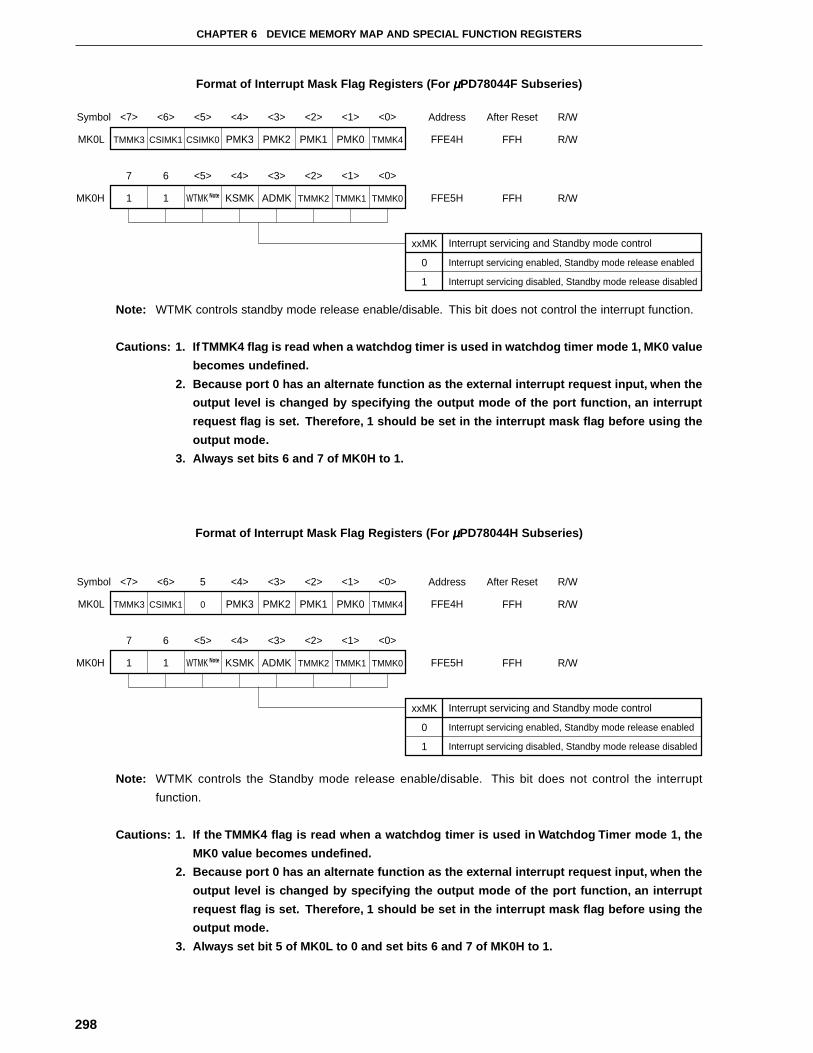
298
CHAPTER 6 DEVICE MEMORY MAP AND SPECIAL FUNCTION REGISTERS
Format of Interrupt Mask Flag Registers (For µµµµµPD78044F Subseries)
Note: WTMK controls standby mode release enable/disable. This bit does not control the interrupt function.
Cautions: 1. If TMMK4 flag is read when a watchdog timer is used in watchdog timer mode 1, MK0 value
becomes undefined.
2. Because port 0 has an alternate function as the external interrupt request input, when the
output level is changed by specifying the output mode of the port function, an interrupt
request flag is set. Therefore, 1 should be set in the interrupt mask flag before using the
output mode.
3. Always set bits 6 and 7 of MK0H to 1.
Format of Interrupt Mask Flag Registers (For µµµµµPD78044H Subseries)
Note: WTMK controls the Standby mode release enable/disable. This bit does not control the interrupt
function.
Cautions: 1. If the TMMK4 flag is read when a watchdog timer is used in Watchdog Timer mode 1, the
MK0 value becomes undefined.
2. Because port 0 has an alternate function as the external interrupt request input, when the
output level is changed by specifying the output mode of the port function, an interrupt
request flag is set. Therefore, 1 should be set in the interrupt mask flag before using the
output mode.
3. Always set bit 5 of MK0L to 0 and set bits 6 and 7 of MK0H to 1.
TMMK0MK0H
7 6 <5> <4> <3> <2> <1> <0>
xxMK Interrupt servicing and Standby mode control
FFE5HTMMK1ADMK TMMK2KSMKWTMK Note11 FFH R/W
0 Interrupt servicing enabled, Standby mode release enabled
1 Interrupt servicing disabled, Standby mode release disabled
TMMK4MK0L
<7> <6> <5> <4> <3> <2>Symbol <1> <0>
FFE4HPMK0PMK2 PMK1PMK3CSIMK0CSIMK1TMMK3
Address After Reset R/W
FFH R/W
TMMK0MK0H
7 6 <5> <4> <3> <2> <1> <0>
xxMK Interrupt servicing and Standby mode control
FFE5HTMMK1ADMK TMMK2KSMKWTMK Note11 FFH R/W
0 Interrupt servicing enabled, Standby mode release enabled
1 Interrupt servicing disabled, Standby mode release disabled
TMMK4MK0L
<7> <6> 5 <4> <3> <2>Symbol <1> <0>
FFE4HPMK0PMK2 PMK1PMK30CSIMK1TMMK3
Address After Reset R/W
FFH R/W
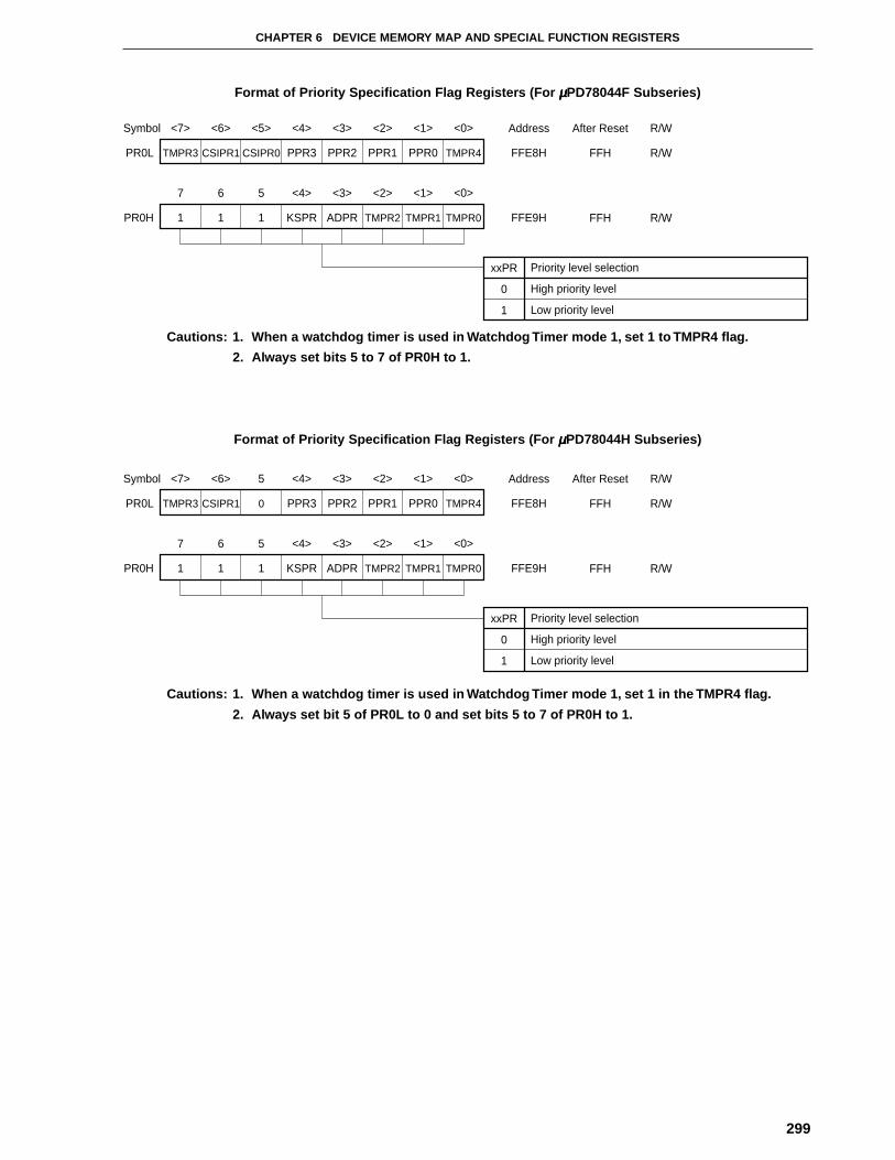
299
CHAPTER 6 DEVICE MEMORY MAP AND SPECIAL FUNCTION REGISTERS
Format of Priority Specification Flag Registers (For µµµµµPD78044F Subseries)
Cautions: 1. When a watchdog timer is used in Watchdog Timer mode 1, set 1 to TMPR4 flag.
2. Always set bits 5 to 7 of PR0H to 1.
Format of Priority Specification Flag Registers (For µµµµµPD78044H Subseries)
Cautions: 1. When a watchdog timer is used in Watchdog Timer mode 1, set 1 in the TMPR4 flag.
2. Always set bit 5 of PR0L to 0 and set bits 5 to 7 of PR0H to 1.
TMPR0PR0H
7 6 5 <4> <3> <2> <1> <0>
xxPR Priority level selection
FFE9HTMPR1ADPR TMPR2KSPR111 FFH R/W
0 High priority level
1 Low priority level
TMPR4PR0L
<7> <6> <5> <4> <3> <2>Symbol <1> <0>
FFE8HPPR0PPR2 PPR1PPR3CSIPR0CSIPR1TMPR3
Address After Reset R/W
FFH R/W
TMPR0PR0H
7 6 5 <4> <3> <2> <1> <0>
xxPR Priority level selection
FFE9HTMPR1ADPR TMPR2KSPR111 FFH R/W
0 High priority level
1 Low priority level
TMPR4PR0L
<7> <6> 5 <4> <3> <2>Symbol <1> <0>
FFE8HPPR0PPR2 PPR1PPR30CSIPR1TMPR3
Address After Reset R/W
FFH R/W
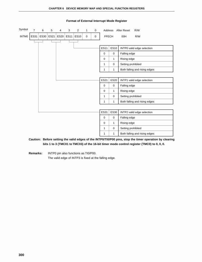
300
CHAPTER 6 DEVICE MEMORY MAP AND SPECIAL FUNCTION REGISTERS
Format of External Interrupt Mode Register
Caution: Before setting the valid edges of the INTP0/TI0/P00 pins, stop the timer operation by clearing
bits 1 to 3 (TMC01 to TMC03) of the 16-bit timer mode control register (TMC0) to 0, 0, 0.
Remarks: INTP0 pin also functions as TI0/P00.
The valid edge of INTP3 is fixed at the falling edge.
6 5 4 3 2 1 07Symbol
INTM0 ES31 ES30 ES21 ES20 ES11 ES10 0 0 FFECH 00H R/W
Address After Reset R/W
ES11
0
0
1
INTP0 valid edge selection
Falling edge
Rising edge
Setting prohibited
ES10
0
1
0
1 Both falling and rising edges1
ES21
0
0
1
INTP1 valid edge selection
Falling edge
Rising edge
Setting prohibited
ES20
0
1
0
1 Both falling and rising edges1
ES31
0
0
1
INTP2 valid edge selection
Falling edge
Rising edge
Setting prohibited
ES30
0
1
0
1 Both falling and rising edges1

301
CHAPTER 6 DEVICE MEMORY MAP AND SPECIAL FUNCTION REGISTERS
Format of Sampling Clock Select Register
Caution: f X/2N+1 is a clock to be supplied to the CPU; f X/26 and f X/27 are clocks to be supplied to the
peripheral hardware. f X/2N+1 stops in the HALT mode.
Remarks: N: Value (N = 0 to 4) at bits 0 to 2 (PCC0 to PCC2) of processor clock control register (PCC)
fX: Main system clock oscillation frequency
Figures in parentheses apply to operation with fX = 5.0 MHz.
Format of Program Status Word
6 5 4 3 2 1 07Symbol
SCS 0 0 0 0 0 0 SCS1 SCS0 FF47H 00H R/W
Address After Reset R/W
SCS1
0
0
1
INTP0 sampling clock selection
fX/2N+1
Setting prohibited
fX/26 (78.1 kHz)
SCS0
0
1
0
1 fX/27 (39.1 kHz)1
0
6 5 4 3 2 1 07
PSW IE Z RBS1 AC RBS0 0 ISP CY 02H
After Reset
IE
0
1
Interrupt request acknowledge enable/disable
Disable
Enable
ISP
1
Priority of interrupt currently being received
High-priority interrupt servicing(low-priority interrupt disable)
Interrupt request not acknowledged or low-priority interrupt servicing (all maskable interrupts enable)
Used when a normal instruction is executed
Symbol

302
CHAPTER 6 DEVICE MEMORY MAP AND SPECIAL FUNCTION REGISTERS
(15) Registers controlling test function
The following two registers control the test function:
• Interrupt request flag register 0H (IF0H)
• Interrupt mask flag register 0H (MK0H)
Format of Interrupt Request Flag Register 0H
Format of Interrupt Mask Flag Register 0H
TMIF0IF0H
7 6 <5> <4> <3> <2> <1> <0>
WTIF Watch timer overflow detection flag
Non-detection
Detection
FFE1HTMIF1ADIF TMIF2KSIFWTIF00 00H R/W
0
1
Symbol Address After Reset R/W
TMMK0MK0H
7 6 <5> <4> <3> <2> <1> <0>
WTMK Standby mode control by watch timer
Standby mode release enable
Standby mode release disable
FFE5HTMMK1ADMK TMMK2KSMKWTMK11 FFH R/W
0
1
Symbol Address After Reset R/W

303
CHAPTER 6 DEVICE MEMORY MAP AND SPECIAL FUNCTION REGISTERS
(16) Register controlling standby function
• Oscillation stabilization time select register (OSTS)
Format of Oscillation Stabilization Time Select Register
Remarks: fX: Main system clock frequency
Values in parentheses apply to operation with fX = 5.0 MHz.
6 5 4 3 2 1 07Symbol
OSTS 0 0 0 0 0 OSTS2 OSTS1 OSTS0 FFFAH 04H R/W
Address After Reset R/W
OSTS2
0
0
0
OSTS1
0
0
1
0 1
1 0
Settings other than above are prohibited
Selection of oscillation stabilizationtime when STOP mode is released
212/fX (819 s)
214/fX (3.28 ms)
215/fX (6.55 ms)
OSTS0
0
1
0
216/fX (13.1 ms)1
217/fX (26.2 ms)0
µ
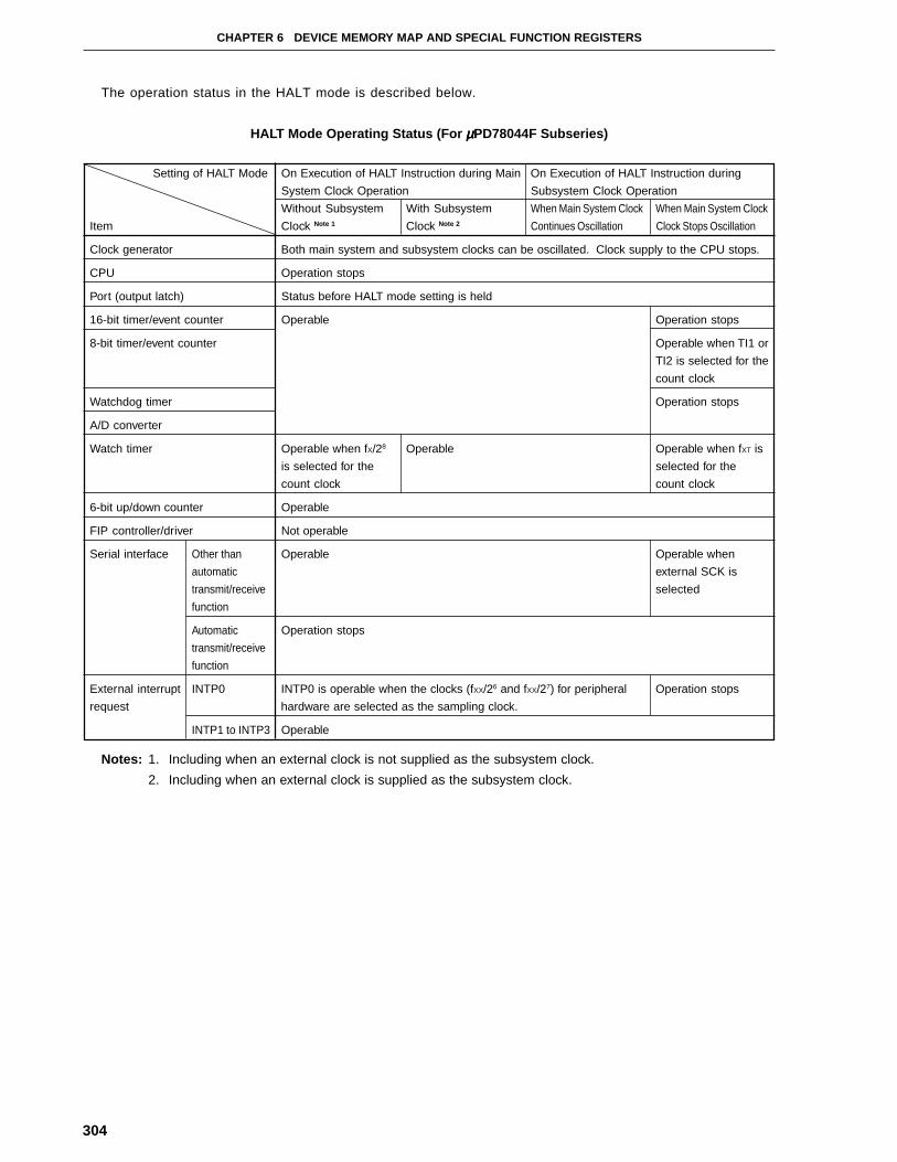
304
CHAPTER 6 DEVICE MEMORY MAP AND SPECIAL FUNCTION REGISTERS
The operation status in the HALT mode is described below.
HALT Mode Operating Status (For µµµµµPD78044F Subseries)
Setting of HALT Mode On Execution of HALT Instruction during Main On Execution of HALT Instruction during
System Clock Operation Subsystem Clock Operation
Without Subsystem With Subsystem When Main System Clock When Main System Clock
Item Clock Note 1 Clock Note 2 Continues Oscillation Clock Stops Oscillation
Clock generator Both main system and subsystem clocks can be oscillated. Clock supply to the CPU stops.
CPU Operation stops
Port (output latch) Status before HALT mode setting is held
16-bit timer/event counter Operable Operation stops
8-bit timer/event counter Operable when TI1 or
TI2 is selected for the
count clock
Watchdog timer Operation stops
A/D converter
Watch timer Operable when fX/28 Operable Operable when fXT is
is selected for the selected for the
count clock count clock
6-bit up/down counter Operable
FIP controller/driver Not operable
Serial interface Other than Operable Operable when
automatic external SCK is
transmit/receive selected
function
Automatic Operation stops
transmit/receive
function
External interrupt INTP0 INTP0 is operable when the clocks (fXX/26 and fXX/27) for peripheral Operation stops
request hardware are selected as the sampling clock.
INTP1 to INTP3 Operable
Notes: 1. Including when an external clock is not supplied as the subsystem clock.
2. Including when an external clock is supplied as the subsystem clock.
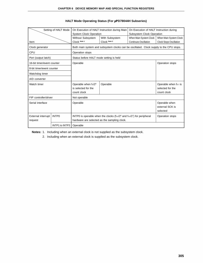
305
CHAPTER 6 DEVICE MEMORY MAP AND SPECIAL FUNCTION REGISTERS
HALT Mode Operating Status (For µµµµµPD78044H Subseries)
Setting of HALT Mode On Execution of HALT Instruction during Main On Execution of HALT Instruction during
System Clock Operation Subsystem Clock Operation
Without Subsystem With Subsystem When Main System Clock When Main System Clock
Item Clock Note 1 Clock Note 2 Continues Oscillation Clock Stops Oscillation
Clock generator Both main system and subsystem clocks can be oscillated. Clock supply to the CPU stops.
CPU Operation stops
Port (output latch) Status before HALT mode setting is held
16-bit timer/event counter Operable Operation stops
8-bit timer/event counter
Watchdog timer
A/D converter
Watch timer Operable when fX/28 Operable Operable when fXT is
is selected for the selected for the
count clock count clock
FIP controller/driver Not operable
Serial interface Operable Operable when
external SCK is
selected
External interrupt INTP0 INTP0 is operable when the clocks (fXX/26 and fXX/27) for peripheral Operation stops
request hardware are selected as the sampling clock.
INTP1 to INTP3 Operable
Notes: 1. Including when an external clock is not supplied as the subsystem clock.
2. Including when an external clock is supplied as the subsystem clock.
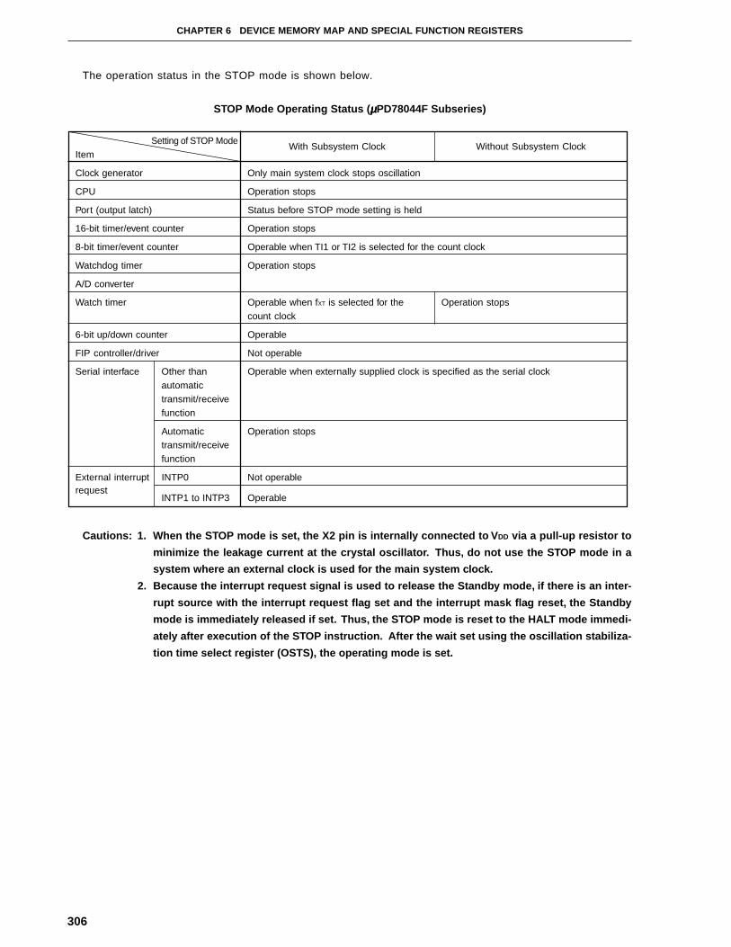
306
CHAPTER 6 DEVICE MEMORY MAP AND SPECIAL FUNCTION REGISTERS
The operation status in the STOP mode is shown below.
STOP Mode Operating Status ( µµµµµPD78044F Subseries)
Setting of STOP ModeWith Subsystem Clock Without Subsystem Clock
Item
Clock generator Only main system clock stops oscillation
CPU Operation stops
Port (output latch) Status before STOP mode setting is held
16-bit timer/event counter Operation stops
8-bit timer/event counter Operable when TI1 or TI2 is selected for the count clock
Watchdog timer Operation stops
A/D converter
Watch timer Operable when fXT is selected for the Operation stopscount clock
6-bit up/down counter Operable
FIP controller/driver Not operable
Serial interface Other than Operable when externally supplied clock is specified as the serial clockautomatictransmit/receivefunction
Automatic Operation stopstransmit/receivefunction
External interrupt INTP0 Not operable
INTP1 to INTP3 Operable
Cautions: 1. When the STOP mode is set, the X2 pin is internally connected to V DD via a pull-up resistor to
minimize the leakage current at the crystal oscillator. Thus, do not use the STOP mode in a
system where an external clock is used for the main system clock.
2. Because the interrupt request signal is used to release the Standby mode, if there is an inter-
rupt source with the interrupt request flag set and the interrupt mask flag reset, the Standby
mode is immediately released if set. Thus, the STOP mode is reset to the HALT mode immedi-
ately after execution of the STOP instruction. After the wait set using the oscillation stabiliza-
tion time select register (OSTS), the operating mode is set.
request
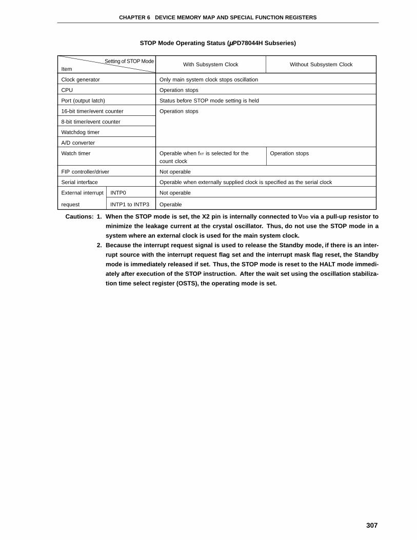
307
CHAPTER 6 DEVICE MEMORY MAP AND SPECIAL FUNCTION REGISTERS
STOP Mode Operating Status ( µµµµµPD78044H Subseries)
Setting of STOP ModeWith Subsystem Clock Without Subsystem Clock
Item
Clock generator Only main system clock stops oscillation
CPU Operation stops
Port (output latch) Status before STOP mode setting is held
16-bit timer/event counter Operation stops
8-bit timer/event counter
Watchdog timer
A/D converter
Watch timer Operable when fXT is selected for the Operation stopscount clock
FIP controller/driver Not operable
Serial interface Operable when externally supplied clock is specified as the serial clock
External interrupt INTP0 Not operable
request INTP1 to INTP3 Operable
Cautions: 1. When the STOP mode is set, the X2 pin is internally connected to V DD via a pull-up resistor to
minimize the leakage current at the crystal oscillator. Thus, do not use the STOP mode in a
system where an external clock is used for the main system clock.
2. Because the interrupt request signal is used to release the Standby mode, if there is an inter-
rupt source with the interrupt request flag set and the interrupt mask flag reset, the Standby
mode is immediately released if set. Thus, the STOP mode is reset to the HALT mode immedi-
ately after execution of the STOP instruction. After the wait set using the oscillation stabiliza-
tion time select register (OSTS), the operating mode is set.
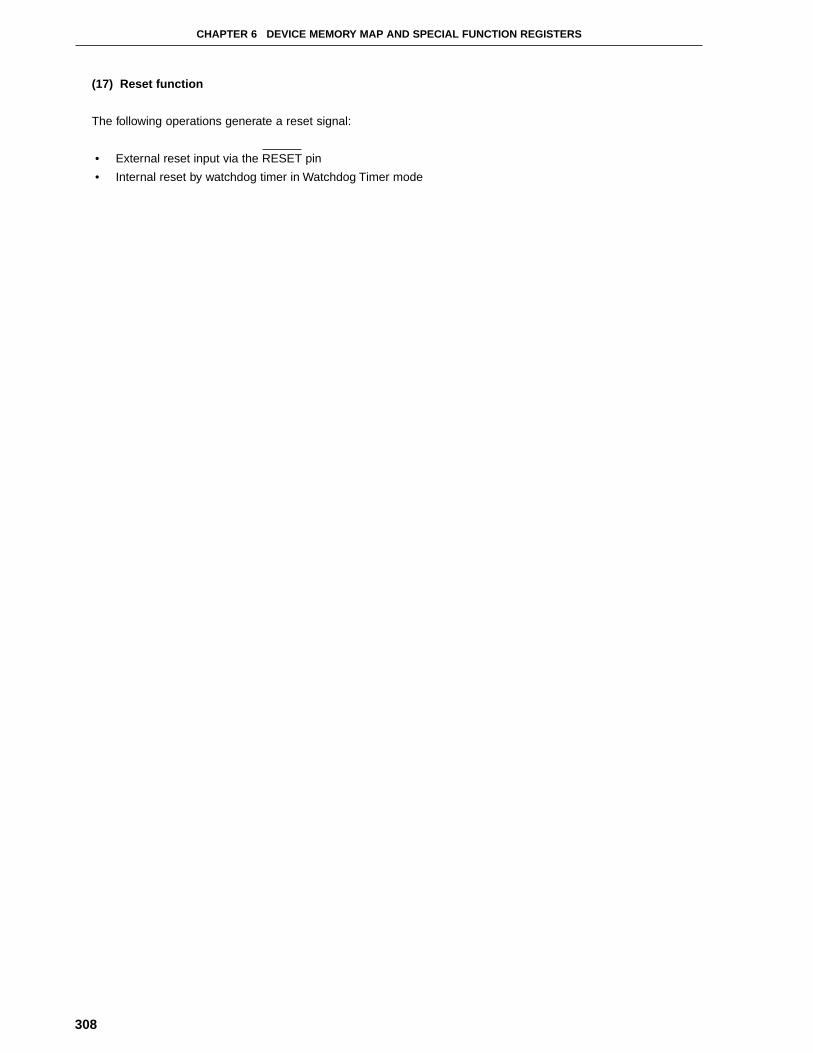
308
CHAPTER 6 DEVICE MEMORY MAP AND SPECIAL FUNCTION REGISTERS
(17) Reset function
The following operations generate a reset signal:
• External reset input via the RESET pin
• Internal reset by watchdog timer in Watchdog Timer mode
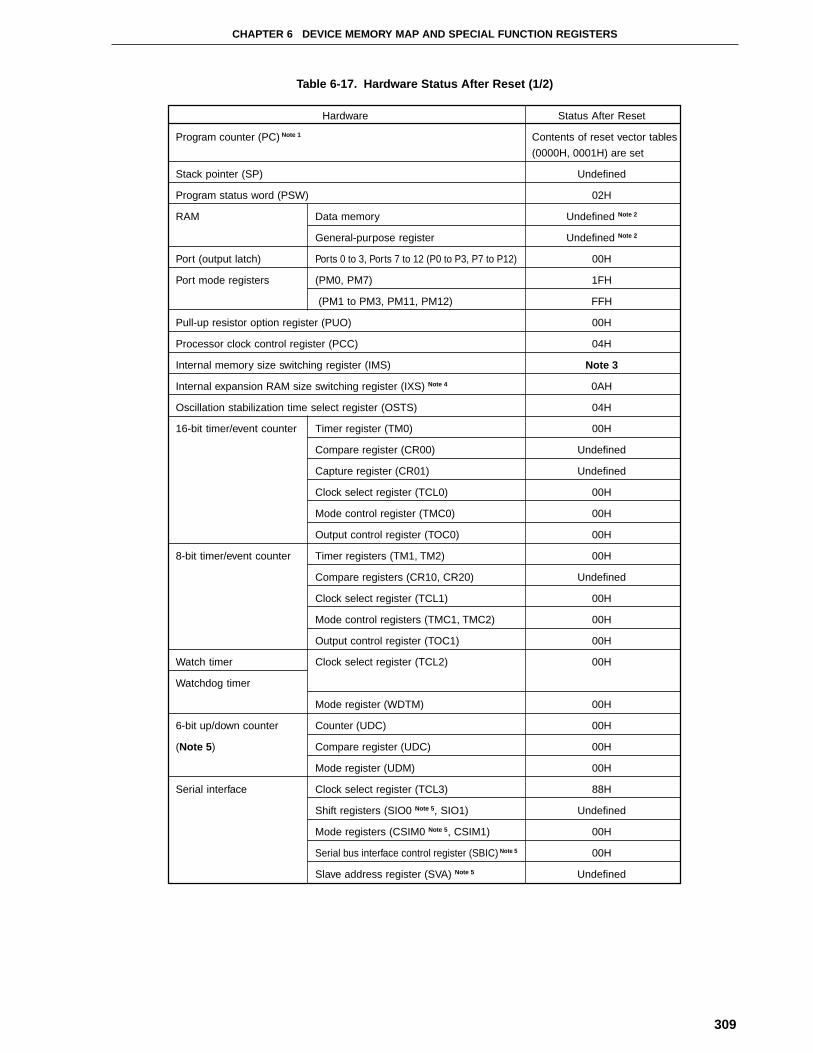
309
CHAPTER 6 DEVICE MEMORY MAP AND SPECIAL FUNCTION REGISTERS
Table 6-17. Hardware Status After Reset (1/2)
Hardware Status After Reset
Program counter (PC) Note 1 Contents of reset vector tables
(0000H, 0001H) are set
Stack pointer (SP) Undefined
Program status word (PSW) 02H
RAM Data memory Undefined Note 2
General-purpose register Undefined Note 2
Port (output latch) Ports 0 to 3, Ports 7 to 12 (P0 to P3, P7 to P12) 00H
Port mode registers (PM0, PM7) 1FH
(PM1 to PM3, PM11, PM12) FFH
Pull-up resistor option register (PUO) 00H
Processor clock control register (PCC) 04H
Internal memory size switching register (IMS) Note 3
Internal expansion RAM size switching register (IXS) Note 4 0AH
Oscillation stabilization time select register (OSTS) 04H
16-bit timer/event counter Timer register (TM0) 00H
Compare register (CR00) Undefined
Capture register (CR01) Undefined
Clock select register (TCL0) 00H
Mode control register (TMC0) 00H
Output control register (TOC0) 00H
8-bit timer/event counter Timer registers (TM1, TM2) 00H
Compare registers (CR10, CR20) Undefined
Clock select register (TCL1) 00H
Mode control registers (TMC1, TMC2) 00H
Output control register (TOC1) 00H
Watch timer Clock select register (TCL2) 00H
Watchdog timer
Mode register (WDTM) 00H
6-bit up/down counter Counter (UDC) 00H
(Note 5 ) Compare register (UDC) 00H
Mode register (UDM) 00H
Serial interface Clock select register (TCL3) 88H
Shift registers (SIO0 Note 5, SIO1) Undefined
Mode registers (CSIM0 Note 5, CSIM1) 00H
Serial bus interface control register (SBIC) Note 5 00H
Slave address register (SVA) Note 5 Undefined
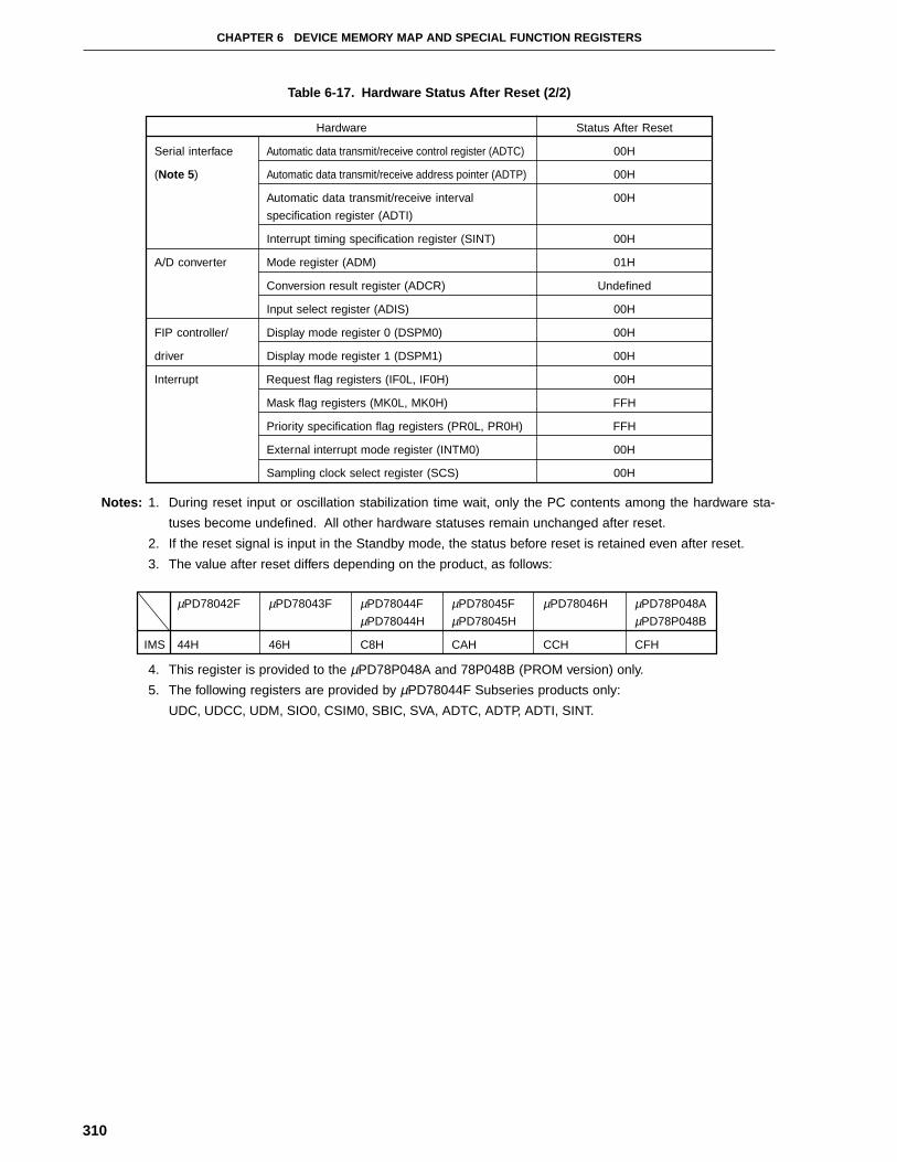
310
CHAPTER 6 DEVICE MEMORY MAP AND SPECIAL FUNCTION REGISTERS
Table 6-17. Hardware Status After Reset (2/2)
Hardware Status After Reset
Serial interface Automatic data transmit/receive control register (ADTC) 00H
(Note 5 ) Automatic data transmit/receive address pointer (ADTP) 00H
Automatic data transmit/receive interval 00H
specification register (ADTI)
Interrupt timing specification register (SINT) 00H
A/D converter Mode register (ADM) 01H
Conversion result register (ADCR) Undefined
Input select register (ADIS) 00H
FIP controller/ Display mode register 0 (DSPM0) 00H
driver Display mode register 1 (DSPM1) 00H
Interrupt Request flag registers (IF0L, IF0H) 00H
Mask flag registers (MK0L, MK0H) FFH
Priority specification flag registers (PR0L, PR0H) FFH
External interrupt mode register (INTM0) 00H
Sampling clock select register (SCS) 00H
Notes: 1. During reset input or oscillation stabilization time wait, only the PC contents among the hardware sta-
tuses become undefined. All other hardware statuses remain unchanged after reset.
2. If the reset signal is input in the Standby mode, the status before reset is retained even after reset.
3. The value after reset differs depending on the product, as follows:
µPD78042F µPD78043F µPD78044F µPD78045F µPD78046H µPD78P048A
µPD78044H µPD78045H µPD78P048B
IMS 44H 46H C8H CAH CCH CFH
4. This register is provided to the µPD78P048A and 78P048B (PROM version) only.
5. The following registers are provided by µPD78044F Subseries products only:
UDC, UDCC, UDM, SIO0, CSIM0, SBIC, SVA, ADTC, ADTP, ADTI, SINT.
311
CHAPTER 6 DEVICE MEMORY MAP AND SPECIAL FUNCTION REGISTERS
(18) Register controlling internal memory capacity
The µPD78P048A and 78P048B allow users to select the internal memory capacity.
The following register is used to control the internal memory capacity:
• Internal memory size switching register (IMS)
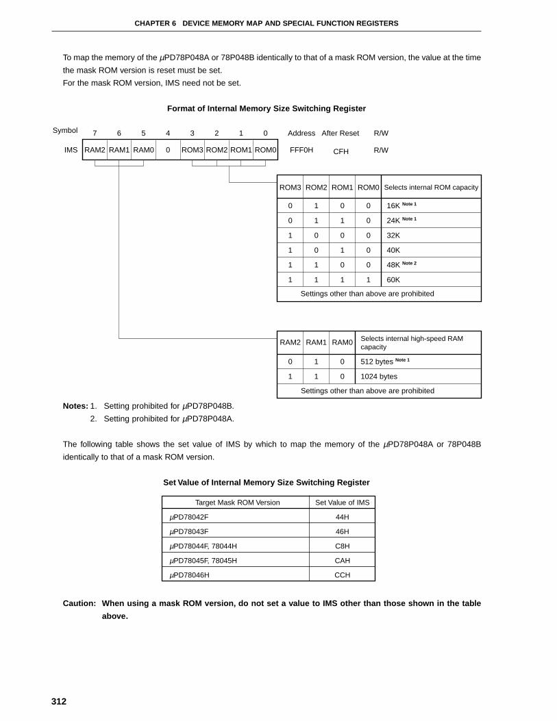
312
CHAPTER 6 DEVICE MEMORY MAP AND SPECIAL FUNCTION REGISTERS
To map the memory of the µPD78P048A or 78P048B identically to that of a mask ROM version, the value at the time
the mask ROM version is reset must be set.
For the mask ROM version, IMS need not be set.
Format of Internal Memory Size Switching Register
Notes: 1. Setting prohibited for µPD78P048B.
2. Setting prohibited for µPD78P048A.
The following table shows the set value of IMS by which to map the memory of the µPD78P048A or 78P048B
identically to that of a mask ROM version.
Set Value of Internal Memory Size Switching Register
Target Mask ROM Version Set Value of IMS
µPD78042F 44H
µPD78043F 46H
µPD78044F, 78044H C8H
µPD78045F, 78045H CAH
µPD78046H CCH
Caution: When using a mask ROM version, do not set a value to IMS other than those shown in the table
above.
6 5 4 3 2 1 07Symbol
IMS RAM2 RAM1 RAM0 0 ROM3 ROM2 ROM1 ROM0 FFF0H
Address After Reset R/W
ROM3
1
1
ROM2
0
0
1 1
Selects internal ROM capacity
32K
40K
ROM1
0
1
48K Note 20
ROM0
0
0
0
1 1 60K1 1
RAM2
1
RAM1
1
Selects internal high-speed RAMcapacity
1024 bytes
RAM0
0
CFH R/W
0 1 24K Note 11 0
0 1 512 bytes Note 10
0 1 16K Note 10 0
Settings other than above are prohibited
Settings other than above are prohibited
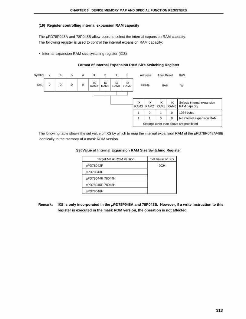
313
CHAPTER 6 DEVICE MEMORY MAP AND SPECIAL FUNCTION REGISTERS
(19) Register controlling internal expansion RAM capacity
The µPD78P048A and 78P048B allow users to select the internal expansion RAM capacity.
The following register is used to control the internal expansion RAM capacity:
• Internal expansion RAM size switching register (IXS)
Format of Internal Expansion RAM Size Switching Register
The following table shows the set value of IXS by which to map the internal expansion RAM of the µPD78P048A/48B
identically to the memory of a mask ROM version.
Set Value of Internal Expansion RAM Size Switching Register
Target Mask ROM Version Set Value of IXS
µPD78042F 0CH
µPD78043F
µPD78044F, 78044H
µPD78045F, 78045H
µPD78046H
Remark: IXS is only incorporated in the µµµµµPD78P048A and 78P048B. However, if a write instruction to this
register is executed in the mask ROM version, the operation is not affected.
IXRAM0IXS
7 6 5 4 3 2Symbol 1 0
IXRAM3
Selects internal expansionRAM capacity
FFF4HIX
RAM1IX
RAM3IX
RAM20000
Address After Reset R/W
0AH W
1 1024 bytes
1 No internal expansion RAM
IXRAM2
0
1
IXRAM1
1
0
IXRAM0
0
0
Settings other than above are prohibited

314
CHAPTER 6 DEVICE MEMORY MAP AND SPECIAL FUNCTION REGISTERS
[MEMO]
315
CHAPTER 6 DEVICE MEMORY MAP AND SPECIAL FUNCTION REGISTERS
6.5 µµµµµPD78054, 78058F, and 780058 Subseries
6.5.1 Documentation Reference Information
Device Series Number User’s Manual Number Date Published
µPD78054, 54Y U11747EJ5V0UM00 April 1998
µPD78058F, 58FY U12068EJ2V0UM00 April 1998
µPD780058, 58Y U12013EJ2V0UM00 February 1998
Caution: The user should check the current User’s Manual with the information in this section to be sure of
having the most up-to-date information.
6.5.2 Device Series Differences
Device Series Number ROM and RAM Differences Number of
ROM Size RAM Size Serial Channels
µPD78054, 78054Y 16K/24K/32K/40K/48K/60K 512/1K 3
µPD78058F, 78058FY 48K/60K 1K
µPD780058, 780058Y 24K/32K/40K/48K/60K
General Programmer’s Note
The NEC C-compiler and the NEC Assembler are capable of recognizing certain symbolic SFR bit names. These
special bit names are identified in the user manual in one of the four ways shown below:
If a bit number has one of the four symbols around it, the NEC software will recognize the associated symbolic bit
name. For example to set bit 7, the user can write the code in two ways:
1. SET1 MCC
2. SET1 PCC.7
Alternatively since bit 2 does not have any of the four symbols around it, the user can only set this bit as follows:
1. SET1 PCC.2
Note: The attempt to employ a symbolic name of bit-2 (PCC2) will return an error. Thus the use of instruction
SET1 PCC2
is improper since neither the NEC C-compiler nor the NEC Assembler recognizes this symbolic name and will
generate an error.
MCCPCC FRC CLS CSS 0 PCC2 PCC1 PCC0
<7> <6> <5> <4> 3 2 1 0
Example:
1.
2.
3.
4.
<7>
( 7 )
7
7
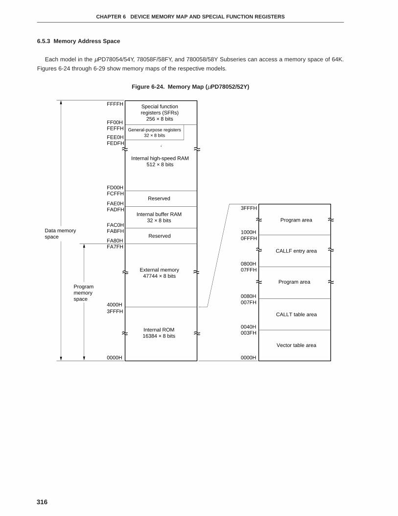
316
CHAPTER 6 DEVICE MEMORY MAP AND SPECIAL FUNCTION REGISTERS
6.5.3 Memory Address Space
Each model in the µPD78054/54Y, 78058F/58FY, and 780058/58Y Subseries can access a memory space of 64K.
Figures 6-24 through 6-29 show memory maps of the respective models.
Figure 6-24. Memory Map ( µPD78052/52Y)
0000H
Data memory space
Internal ROM16384 × 8 bits
3FFFH
1000H0FFFH
0800H07FFH
0080H 007FH
0040H003FH
0000H
CALLF entry area
CALLT table area
Vector table area
Program area
Program areaInternal buffer RAM
32 × 8 bits
External memory47744 × 8 bits
Reserved
Programmemoryspace
4000H3FFFH
FA80HFA7FH
FAC0HFABFH
FAE0HFADFH
FEE0HFEDFH
FF00HFEFFH
FFFFH
Internal high-speed RAM512 × 8 bits
Special function registers (SFRs)
256 × 8 bits
Reserved
FD00HFCFFH
General-purpose registers32 × 8 bits

317
CHAPTER 6 DEVICE MEMORY MAP AND SPECIAL FUNCTION REGISTERS
Figure 6-25. Memory Map ( µPD78053/53Y, 780053/53Y)
0000H
Data memory space
Internal ROM24576 × 8 bits
5FFFH
1000H0FFFH
0800H07FFH
0080H 007FH
0040H003FH
0000H
CALLF entry area
CALLT table area
Vector table area
Program area
Program areaInternal buffer RAM
32 × 8 bits
External memory39552 × 8 bits
Reserved
Programmemoryspace
6000H5FFFH
FA80HFA7FH
FAC0HFABFH
FAE0HFADFH
FEE0HFEDFH
FF00HFEFFH
FFFFH
Internal high-speed RAM1024 × 8 bits
Special function registers (SFRs)
256 × 8 bits
Reserved
FB00HFAFFH
General-purpose registers32 × 8 bits
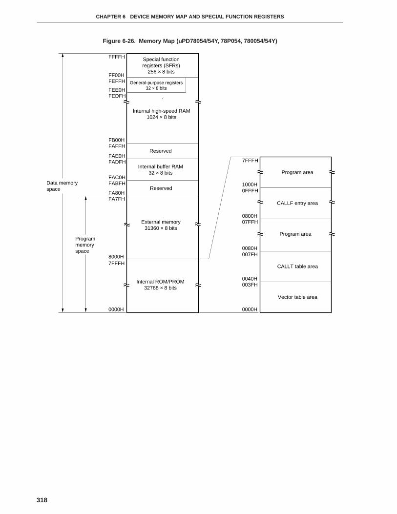
318
CHAPTER 6 DEVICE MEMORY MAP AND SPECIAL FUNCTION REGISTERS
Figure 6-26. Memory Map ( µPD78054/54Y, 78P054, 780054/54Y)
0000H
Data memory space
Internal ROM/PROM32768 × 8 bits
7FFFH
1000H0FFFH
0800H07FFH
0080H 007FH
0040H003FH
0000H
CALLF entry area
CALLT table area
Vector table area
Program area
Program areaInternal buffer RAM
32 × 8 bits
External memory31360 × 8 bits
Reserved
Programmemoryspace
8000H7FFFH
FA80HFA7FH
FAC0HFABFH
FAE0HFADFH
FEE0HFEDFH
FF00HFEFFH
FFFFH
Internal high-speed RAM1024 × 8 bits
Special function registers (SFRs)
256 × 8 bits
Reserved
FB00HFAFFH
General-purpose registers32 × 8 bits
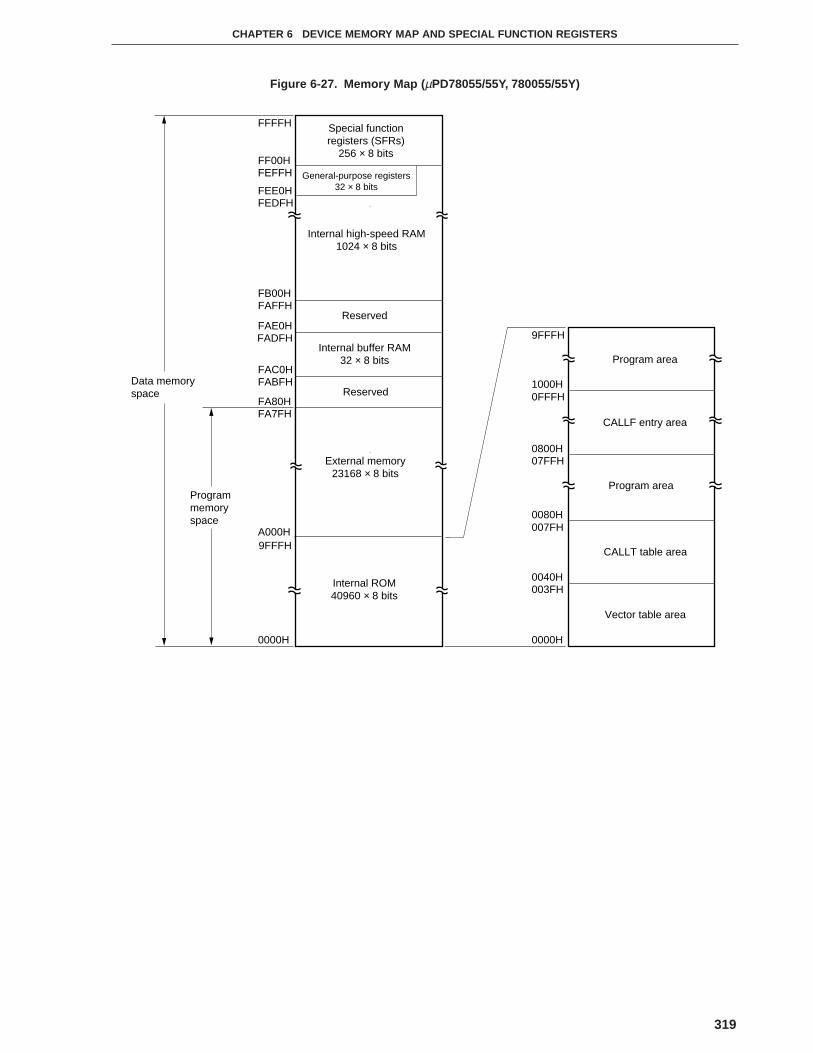
319
CHAPTER 6 DEVICE MEMORY MAP AND SPECIAL FUNCTION REGISTERS
Figure 6-27. Memory Map ( µPD78055/55Y, 780055/55Y)
0000H
Data memory space
Internal ROM40960 × 8 bits
9FFFH
1000H0FFFH
0800H07FFH
0080H 007FH
0040H003FH
0000H
CALLF entry area
CALLT table area
Vector table area
Program area
Program areaInternal buffer RAM
32 × 8 bits
External memory23168 × 8 bits
Reserved
Programmemoryspace
A000H9FFFH
FA80HFA7FH
FAC0HFABFH
FAE0HFADFH
FEE0HFEDFH
FF00HFEFFH
FFFFH
Internal high-speed RAM1024 × 8 bits
Special function registers (SFRs)
256 × 8 bits
Reserved
FB00HFAFFH
General-purpose registers32 × 8 bits

320
CHAPTER 6 DEVICE MEMORY MAP AND SPECIAL FUNCTION REGISTERS
Figure 6-28. Memory Map ( µPD78056/56Y, 78056F/56FY, 780056/56Y)
0000H
Data memory space
Internal ROM49152 × 8 bits
BFFFH
1000H0FFFH
0800H07FFH
0080H 007FH
0040H003FH
0000H
CALLF entry area
CALLT table area
Vector table area
Program area
Program areaInternal buffer RAM
32 × 8 bits
External memory14976 × 8 bits
Reserved
Programmemoryspace
C000HBFFFH
FA80HFA7FH
FAC0HFABFH
FAE0HFADFH
FEE0HFEDFH
FF00HFEFFH
FFFFH
Internal high-speed RAM1024 × 8 bits
Special function registers (SFRs)
256 × 8 bits
Reserved
FB00HFAFFH
General-purpose registers32 × 8 bits
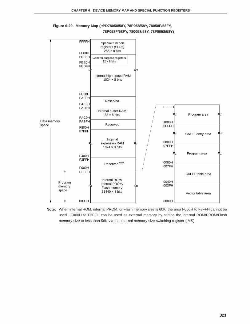
321
CHAPTER 6 DEVICE MEMORY MAP AND SPECIAL FUNCTION REGISTERS
Figure 6-29. Memory Map ( µPD78058/58Y, 78P058/58Y, 78058F/58FY,
78P058F/58FY, 780058/58Y, 78F0058/58Y)
Note: When internal ROM, internal PROM, or Flash memory size is 60K, the area F000H to F3FFH cannot be
used. F000H to F3FFH can be used as external memory by setting the internal ROM/PROM/Flash
memory size to less than 56K via the internal memory size switching register (IMS).
0000H
Data memory space
Internal ROM/Internal PROM/Flash memory61440 × 8 bits
EFFFH
1000H0FFFH
0800H07FFH
0080H 007FH
0040H003FH
0000H
CALLF entry area
CALLT table area
Vector table area
Program area
Program areaInternal buffer RAM
32 × 8 bits
Reserved Note
Reserved
Programmemoryspace
F000HEFFFH
F800HF7FFH
FAC0HFABFH
FAE0HFADFH
FEE0HFEDFH
FF00HFEFFH
FFFFH
Internal high-speed RAM1024 × 8 bits
Special function registers (SFRs)
256 × 8 bits
Internalexpansion RAM
1024 × 8 bits
F400HF3FFH
Reserved
FB00HFAFFH
General-purpose registers32 × 8 bits

322
CHAPTER 6 DEVICE MEMORY MAP AND SPECIAL FUNCTION REGISTERS
6.5.4 Special Function Registers (SFRs)
Table 6-18. Special Function Register List ( µPD78054/54Y, 78058F/58FY, and 780058/58Y Subseries) (1/3)
Manipulatable After
Address Special Function Register (SFR) Name Symbol R/W Bit Unit Reset
1 Bit 8 Bits 16 Bits
FF00H Port 0 P0 R/W √ √ – 00H
FF01H Port 1 P1 √ √ –
FF02H Port 2 P2 √ √ –
FF03H Port 3 P3 √ √ –
FF04H Port 4 P4 √ √ – Undefined
FF05H Port 5 P5 √ √ –
FF06H Port 6 P6 √ √ –
FF07H Port 7 P7 √ √ – 00H
FF0CH Port 12 P12 √ √ –
FF0DH Port 13 P13 √ √ –
FF10H Capture/compare register 00 CR00 – – √ Undefined
FF11H
FF12H Capture/compare register 01 CR01 – – √FF13H
FF14H 16-bit timer register TM0 R – – √ 0000H
FF15H
FF16H Compare register 10 CR10 R/W – √ – Undefined
FF17H Compare register 20 CR20 – √ –
FF18H 8-bit timer register 1 TMS TM1 R – √ √ 00H
FF19H 8-bit timer register 2 TMS TM2 – √
FF1AH Serial I/O shift register 0 SIO0 R/W – √ – Undefined
FF1BH Serial I/O shift register 1 SIO1 – √ –
FF1FH A/D conversion result register ADCR R – √ –
FF20H Port mode register 0 PM0 R/W √ √ – FFH
FF21H Port mode register 1 PM1 √ √ –
FF22H Port mode register 2 PM2 √ √ –
FF23H Port mode register 3 PM3 √ √ –
FF25H Port mode register 5 PM5 √ √ –
FF26H Port mode register 6 PM6 √ √ –
FF27H Port mode register 7 PM7 √ √ –
FF2CH Port mode register 12 PM12 √ √ –
FF2DH Port mode register 13 PM13 √ √ –
FF30H Real-time output buffer register L RTBL – √ – 00H
FF31H Real-time output buffer register H RTBH – √ –
FF34H Real-time output port mode register RTPM √ √ –
FF36H Real-time output port control register RTPC √ √ –
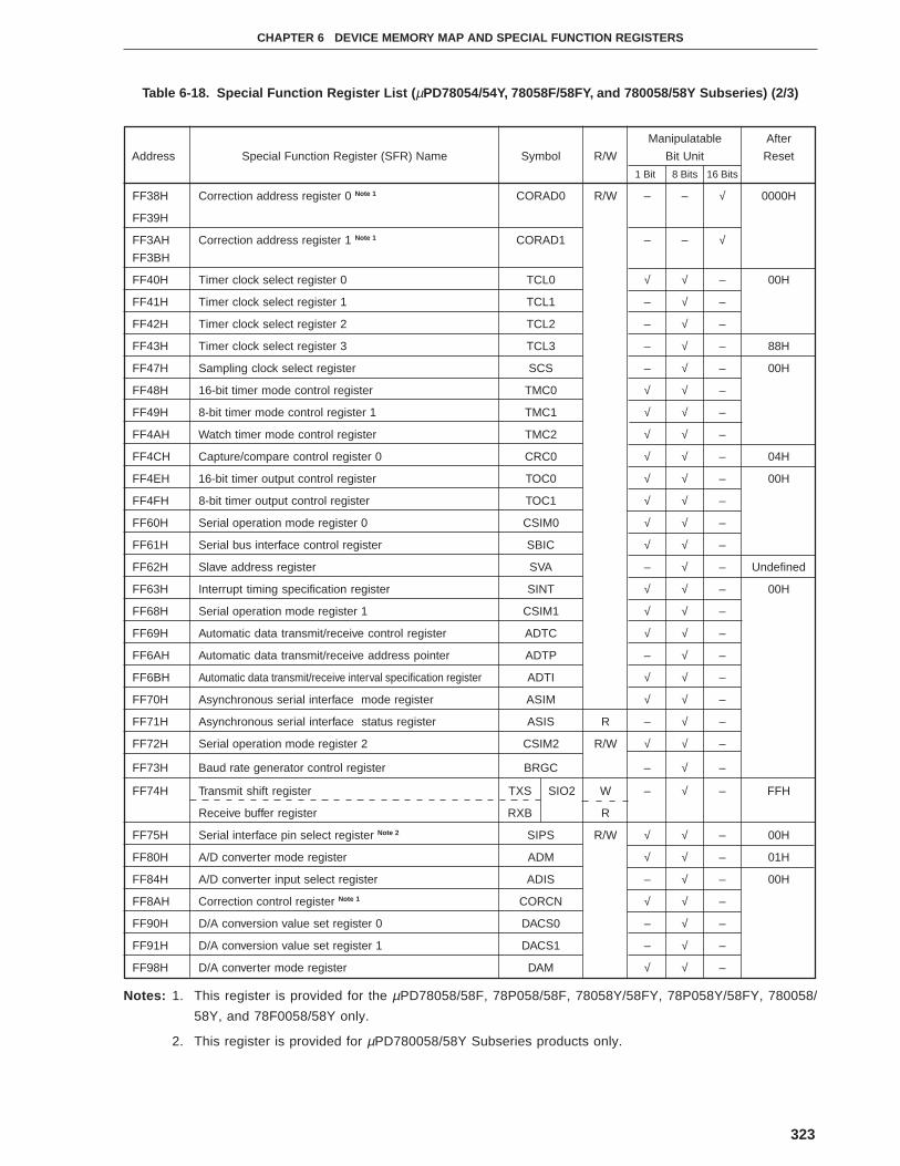
323
CHAPTER 6 DEVICE MEMORY MAP AND SPECIAL FUNCTION REGISTERS
Table 6-18. Special Function Register List ( µPD78054/54Y, 78058F/58FY, and 780058/58Y Subseries) (2/3)
Manipulatable After
Address Special Function Register (SFR) Name Symbol R/W Bit Unit Reset
1 Bit 8 Bits 16 Bits
FF38H Correction address register 0 Note 1 CORAD0 R/W – – √ 0000H
FF39H
FF3AH Correction address register 1 Note 1 CORAD1 – – √FF3BH
FF40H Timer clock select register 0 TCL0 √ √ – 00H
FF41H Timer clock select register 1 TCL1 – √ –
FF42H Timer clock select register 2 TCL2 – √ –
FF43H Timer clock select register 3 TCL3 – √ – 88H
FF47H Sampling clock select register SCS – √ – 00H
FF48H 16-bit timer mode control register TMC0 √ √ –
FF49H 8-bit timer mode control register 1 TMC1 √ √ –
FF4AH Watch timer mode control register TMC2 √ √ –
FF4CH Capture/compare control register 0 CRC0 √ √ – 04H
FF4EH 16-bit timer output control register TOC0 √ √ – 00H
FF4FH 8-bit timer output control register TOC1 √ √ –
FF60H Serial operation mode register 0 CSIM0 √ √ –
FF61H Serial bus interface control register SBIC √ √ –
FF62H Slave address register SVA – √ – Undefined
FF63H Interrupt timing specification register SINT √ √ – 00H
FF68H Serial operation mode register 1 CSIM1 √ √ –
FF69H Automatic data transmit/receive control register ADTC √ √ –
FF6AH Automatic data transmit/receive address pointer ADTP – √ –
FF6BH Automatic data transmit/receive interval specification register ADTI √ √ –
FF70H Asynchronous serial interface mode register ASIM √ √ –
FF71H Asynchronous serial interface status register ASIS R – √ –
FF72H Serial operation mode register 2 CSIM2 R/W √ √ –
FF73H Baud rate generator control register BRGC – √ –
FF74H Transmit shift register TXS SIO2 W – √ – FFH
Receive buffer register RXB R
FF75H Serial interface pin select register Note 2 SIPS R/W √ √ – 00H
FF80H A/D converter mode register ADM √ √ – 01H
FF84H A/D converter input select register ADIS – √ – 00H
FF8AH Correction control register Note 1 CORCN √ √ –
FF90H D/A conversion value set register 0 DACS0 – √ –
FF91H D/A conversion value set register 1 DACS1 – √ –
FF98H D/A converter mode register DAM √ √ –
Notes: 1. This register is provided for the µPD78058/58F, 78P058/58F, 78058Y/58FY, 78P058Y/58FY, 780058/
58Y, and 78F0058/58Y only.
2. This register is provided for µPD780058/58Y Subseries products only.

324
CHAPTER 6 DEVICE MEMORY MAP AND SPECIAL FUNCTION REGISTERS
Table 6-18. Special Function Register List ( µPD78054/54Y, 78058F/58FY, and 780058/58Y Subseries) (3/3)
Manipulatable After
Address Special Function Register (SFR) Name Symbol R/W Bit Unit Reset
1 Bit 8 Bits 16 Bits
FFD0H to External access area Note 1 R/W √ √ – Undefined
FFDFH
FFE0H Interrupt request flag register 0L IF0 IF0L √ √ √ 00H
FFE1H Interrupt request flag register 0H IF0H √ √
FFE2H Interrupt request flag register 1L IF1L √ √ –
FFE4H Interrupt request mask register 0L MK0 MK0L √ √ √ FFH
FFE5H Interrupt request mask register 0H MK0H √ √
FFE6H Interrupt request mask register 1L MK1L √ √ –
FFE8H Priority order specification flag register 0L PR0 PR0L √ √ √
FFE9H Priority order specification flag register 0H PR0H √ √
FFEAH Priority order specification flag register 1L PR1L √ √ –
FFECH External interrupt mode register 0 INTM0 – √ – 00H
FFEDH External interrupt mode register 1 INTM1 – √ –
FFF0H Internal memory size switching register IMS – √ – Note 2
FFF2H Oscillation mode select register OSMS W – √ – 00H
FFF3H Pull-up resistor option register H PUOH R/W √ √ –
FFF4H Internal expansion RAM size switching register Note 3 IXS W – √ – 0AH
FFF6H Key return mode register KRM R/W √ √ – 02H
FFF7H Pull-up resistor option register L PUOL √ √ – 00H
FFF8H Memory expansion mode register MM √ √ – 10H
FFF9H Watchdog timer mode register WDTM √ √ – 00H
FFFAH Oscillation stabilization time select register OSTS – √ – 04H
FFFBH Processor clock control register PCC √ √ –
Notes: 1. The external access area cannot be accessed in SFR addressing. Access the area with direct addressing.
2. The value after reset differs depending on the product, as follows:
µPD78052 µPD78053 µPD78054 µPD78055 µPD78056 µPD78058 µPD78P058
µPD78052Y µPD78053Y µPD78054Y µPD78055Y µPD78056Y µPD78058Y µPD78P058Y
µPD780053 µPD78P054 µPD780055 µPD78056F µPD78058F µPD78P058F
µPD780053Y µPD780054 µPD780055Y µPD78056FY µPD78058FY µPD78P058FY
µPD780054Y µPD780056 µPD780058 µPD78F0058
µPD780056Y µPD780058Y µPD78F0058Y
IMS 44H C6H C8H CAH CCH CFH
3. This register is provided for the µPD78058/58Y, 78058F/58FY, 78P058/58Y, 78P058F/58FY, 780058/
58Y, and 78F0058/58Y only.
325
CHAPTER 6 DEVICE MEMORY MAP AND SPECIAL FUNCTION REGISTERS
(1) Registers controlling port functions
The following four types of registers control the ports:
• Port mode registers (PM0 to PM7, PM12, PM13)
• Pull-up resistor option registers (PUOH, PUOL)
• Memory expansion mode register (MM)
- Refer to section (18) for the register format.
• Key return mode register (KRM)
- Refer to section (17) for the register format.
326
CHAPTER 6 DEVICE MEMORY MAP AND SPECIAL FUNCTION REGISTERS
Format of Port Mode Registers ( µµµµµPD78054/54Y and 78058F/58FY Subseries)
PM0
PM1
PM2
1 PM06 PM03 PM02 PM01 1
7 6 5 4 3 2 1 0Symbol
PM3
PM5
FF20H
FF21H
FF22H
FF23H
FF25H
FFH
FFH
FFH
FFH
FFH
R/W
R/W
R/W
R/W
R/W
AddressAfterReset R/W
PM17 PM16 PM15 PM14 PM13 PM12 PM11 PM10
PM27 PM26 PM25 PM24 PM23 PM22 PM21 PM20
PM37 PM36 PM35 PM34 PM33 PM32 PM31 PM30
PM57 PM56 PM55 PM54 PM53 PM52 PM51 PM50
PM4 FF24H FFH R/WPM47 PM46 PM45 PM44 PM43 PM42 PM41 PM40
PM6
PM7
FF26H
FF27H
FFH
FFH
R/W
R/W
PM67 PM66 PM65 PM64 PM63 PM62 PM61 PM60
1 1 1 1 1 PM72 PM71 PM70
PM05 PM04
PM12
PM13
PMmn Pmn pin input/output mode selection(m = 0 to 3, 5 to 7, 12, 13 : n = 0 to 7)
0
1
Output mode (output buffer ON)
Input mode (output buffer OFF)
FF2CH
FF2DH
FFH
FFH
R/W
R/W
PM122 PM121PM120
1 1 1 1 1 1 PM131 PM130
PM125 PM124 PM123PM127 PM126

327
CHAPTER 6 DEVICE MEMORY MAP AND SPECIAL FUNCTION REGISTERS
Format of Port Mode Registers ( µµµµµPD780058/58Y Subseries)
PM0
PM1
PM2
1 1 PM03 PM02 PM01 1
7 6 5 4 3 2 1 0Symbol
PM3
PM5
FF20H
FF21H
FF22H
FF23H
FF25H
FFH
FFH
FFH
FFH
FFH
R/W
R/W
R/W
R/W
R/W
AddressAfterReset R/W
PM17 PM16 PM15 PM14 PM13 PM12 PM11 PM10
PM27 PM26 PM25 PM24 PM23 PM22 PM21 PM20
PM37 PM36 PM35 PM34 PM33 PM32 PM31 PM30
PM57 PM56 PM55 PM54 PM53 PM52 PM51 PM50
PM4 FF24H FFH R/WPM47 PM46 PM45 PM44 PM43 PM42 PM41 PM40
PM6
PM7
FF26H
FF27H
FFH
FFH
R/W
R/W
PM67 PM66 PM65 PM64 PM63 PM62 PM61 PM60
1 1 1 1 1 PM72 PM71 PM70
PM05 PM04
PM12
PM13
PMmn Pmn pin input/output mode selection(m = 0 to 3, 5 to 7, 12, 13 : n = 0 to 7)
0
1
Output mode (output buffer ON)
Input mode (output buffer OFF)
FF2CH
FF2DH
FFH
FFH
R/W
R/W
PM122 PM121PM120
1 1 1 1 1 1 PM131 PM130
PM125 PM124 PM123PM127 PM126
328
CHAPTER 6 DEVICE MEMORY MAP AND SPECIAL FUNCTION REGISTERS
Format of Pull-up Resistor Option Registers
Cautions: 1. P00 and P07 pins do not incorporate a pull-up resistor.
2. When ports 1, 4, 5, and P64 to P67 pins are used as alternate function pins, an on-chip pull-
up resistor cannot be used even if 1 is set in the PUOm bit of PUOH, PUOL (m = 1, 4 to 6).
3. Pins P60 to P63 can be connected with a pull-up resistor by the mask option only for the
mask ROM version.
4. Bits 0 to 3, 6, and 7 of PUOH should be set to 0.
PUO7 PUO6 PUO5 PUO4 PUO2 PUO1 PUO0PUOL
PUOm Pm internal pull-up resistor selection(m = 0 to 7, 12, 13)
0
1
Internal pull-up resistor not used
Internal pull-up resistor used
FFF7H 00H R/W
<7> <6> <5> <4>
PUO3
<3> <2> <0><1>
0 0 PUO13 PUO12 0 0 0PUOH FFF3H 00H R/W
7 6 <5> <4>Symbol AddressAfterReset R/W
0
7 6 3 2 01
329
CHAPTER 6 DEVICE MEMORY MAP AND SPECIAL FUNCTION REGISTERS
(2) Registers controlling clock generator
The following two registers control the clock generator:
• Processor clock control register (PCC)
• Oscillation mode select register (OSMS)
Format of Processor Clock Control Register
Notes: 1. Bit 5 is a read-only bit.
2. When the CPU is operating on the subsystem clock, MCC should be used to stop the main
system clock oscillation. A STOP instruction should not be used.
Caution: Bit 3 must be set to 0.
Remarks: fXX: Main system clock frequency (fX or fX/2)
fX: Main system clock oscillator frequency
fXT: Subsystem clock oscillator frequency
MCS: Bit 0 of oscillation mode select register (OSMS)
Values in parentheses indicate minimum instruction execution time: 2/fCPU when operating at
fX = 5.0 MHz or fXT = 32.768 kHz.
MCC FRC CLS CSS PCC2 PCC1 PCC0PCC
CLS
0
1
Main system clock
Subsystem clock
FFFBH 04H R/W Note 1
<7> <5> <4>Symbol AddressAfterReset R/W
0
<6> 3 2 01
CSS
0
0 fXX/2
PCC2CPU cIock (fCPU) selection
PCC1 PCC0
CPU clock status
0
0
0
1
0
0
1
1
0
1
1
0
0
0
0
0
0
0
0
1
1
0
0
1
1
0
1
0
fXX/22
fXX/23
fXX/24
fXT/2
fXX
Settings other than above are prohibited
FRC
0
1
Internal feedback resistor used
Internal feedback resistor not used
Subsystem clock feedback resistor selection
MCC
0
1
Oscillation possible
Oscillation stopped
Main system clock oscillation control Note 2
R/W
R/W
R/W
R
fx/2
fx/22
fx/23
fx/24
fx
fx/22
fx/23
fx/24
fx/25
fx /2
MCS = 1 MCS = 0
0
1
(0.4 s)µ
(0.8 s)µ
(1.6 s)µ
(3.2 s)µ
(6.4 s)µ
(0.8 s)µ
(1.6 s)µ
(3.2 s)µ
(6.4 s)µ
(12.8 s)µ
(122 s)µ
330
CHAPTER 6 DEVICE MEMORY MAP AND SPECIAL FUNCTION REGISTERS
Format of Oscillation Mode Select Register
Caution: The main system clock cycle is longer by up to 2/fx only when writing data to OSMS (including
when writing the same data that was written previously). This causes a temporary error in the
count clock cycle of timers in the peripheral hardware that operates with the main system clock.
In addition, when the oscillation mode is changed, the clocks provided for the peripheral hardware
as well as those for the CPU are switched. Therefore, it is recommended that only one-time writing
to OSMS be performed between the reset release and the peripheral hardware operation.
MCS Main system clock scaler control
0
1
Scaler used
Scaler not used
0 0 0 0OSMS FFF2H
7 6 5 4 3 2Symbol 1
0 MCS
0
0
AddressAfterReset R/W
00H W0

331
CHAPTER 6 DEVICE MEMORY MAP AND SPECIAL FUNCTION REGISTERS
(3) Registers controlling 16-bit timer/event counter
The following seven registers control the 16-bit timer/event counter:
• Timer clock select register 0 (TCL0)
• 16-bit timer mode control register (TMC0)
• Capture/compare control register 0 (CRC0)
• 16-bit timer output control register (TOC0)
• Port mode register 3 (PM3)
- Refer to section (1) for the register format.
• External interrupt mode register 0 (INTM0)
- Refer to section (16) for the register format.
• Sampling clock select register (SCS)
- Refer to section (16) for the register format.
Format of Timer Clock Select Register 0
Cautions: 1. Setting of the TI00/INTP0 pin valid edge is performed by external interrupt mode register 0,
and selection of the sampling clock frequency is performed by the sampling clock select
register.
2. To read the count value when TI00 has been specified as the TM0 count clock, the value
should be read from TM0, not from capture/compare register 01 (CR01).
3. To write data other than that already written to TCL0, stop the timer operation once.
Remarks: fXX: Main system clock frequency (fX or fX/2)
fX: Main system clock oscillation frequency
TI00: 16-bit timer/event counter input pin
TM0: 16-bit timer register
MCS: Bit 0 of oscillation mode select register (OSMS)
Values in parentheses apply to operation with fX = 5.0 MHz.
This register is also used to set the clock for PCL output, in addition to setting the count clock of
the 16-bit timer register.
CLOE TCL06 TCL05 TCL04 TCL03 TCL02 TCL01 TCL00
<7> 6 5 4 3 2 1 0Symbol
TCL0 FF40H 00H R/W
Address After Reset R/W
TCL06 TCL05 TCL04
0 0 0 TI00 (Valid edge specifiable)
0 0 1 2fXX Setting prohibited fX (5.0 MHz)
0 1 0 fXX fX (5.0 MHz) fX/2 (2.5 MHz)
0 1 1 fXX/2 fX/2 (2.5 MHz) fX/22 (1.25 MHz)
1 0 0 fXX/22 fX/22(1.25 MHz) fX/23(625 kHz)
1 1 1 Watch timer output (INTTM3)
MCS = 1
16-bit timer register count clock selection
MCS = 0
This section controls the clock output circuit.Refer to (7) Registers controlling clock output function orChapter 12 of PD78054, 78054Y Subseries User's Manual,Chapter 12 of PD78058F, 78058FY Subseries User's Manual, orChapter 12 of PD780058, 780058Y Subseries User's Manualfor detailed information.
µµµ
Settings other than above are prohibited
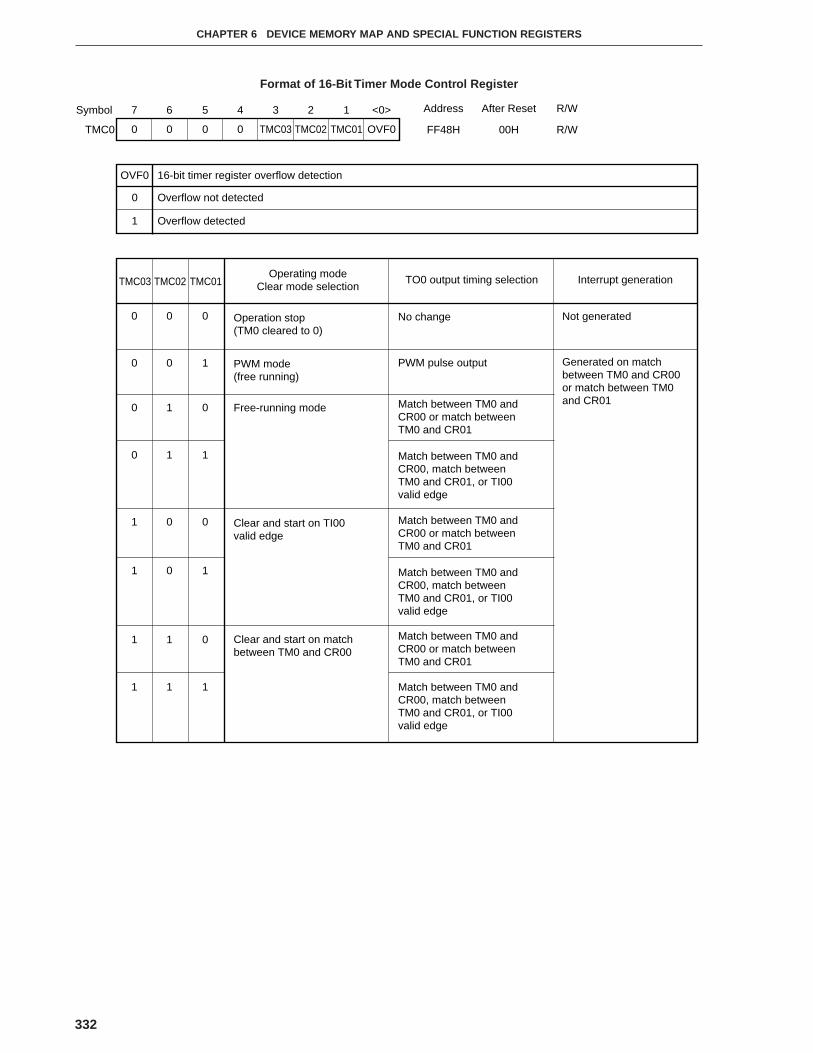
332
CHAPTER 6 DEVICE MEMORY MAP AND SPECIAL FUNCTION REGISTERS
Format of 16-Bit Timer Mode Control Register
0 0 0 0 TMC03 TMC02 TMC01 OVF0
7 6 5 4 3 2 1 <0>Symbol
TMC0 FF48H 00H R/W
Address After Reset R/W
OVF0 16-bit timer register overflow detection
0 Overflow not detected
1 Overflow detected
TMC03 TMC02 TMC01Operating mode
Clear mode selectionTO0 output timing selection Interrupt generation
0 0 0 Operation stop(TM0 cleared to 0)
No change Not generated
0 0 1 PWM mode(free running)
PWM pulse output
0 1 0
0 1 1
1 0 0
1 0 1
1 1 0
1 1 1
Free-running mode Match between TM0 and CR00 or match between TM0 and CR01
Match between TM0 and CR00, match between TM0 and CR01, or TI00valid edge
Match between TM0 and CR00 or match between TM0 and CR01
Match between TM0 and CR00, match between TM0 and CR01, or TI00valid edge
Match between TM0 and CR00 or match between TM0 and CR01
Match between TM0 and CR00, match between TM0 and CR01, or TI00valid edge
Clear and start on TI00 valid edge
Clear and start on matchbetween TM0 and CR00
Generated on match between TM0 and CR00or match between TM0and CR01

333
CHAPTER 6 DEVICE MEMORY MAP AND SPECIAL FUNCTION REGISTERS
Cautions: 1. The 16-bit timer register starts operation when a value other than 0, 0, 0 is set to TMC01 to
TMC03 (Operation Stop mode). To stop the operation, set TMC01 to TMC03 to 0, 0, 0.
2. Switch the Clear mode and the T00 output timing after stopping the timer operation (by setting
TMC01 to TMC03 to 0, 0, 0).
3. Set the valid edge of the TI00/INTP0 pin with an external interrupt mode register 0 and select the
sampling clock frequency with a sampling clock select register.
4. When using the PWM mode, set the PWM mode and then set data to CR00.
5. If Clear and Start mode on a match between TM0 and CR00 is selected, when the set value of
CR00 is FFFFH and the TM0 value changes from FFFFH to 0000H, the OVF0 flag is set to 1.
Remarks: TO0: 16-bit timer/event counter output pin
TI00: 16-bit timer/event counter input pin
TM0: 16-bit timer register
CR00: Compare register 00
CR01: Compare register 01
Format of Capture/Compare Control Register 0
Cautions: 1. Timer operation must be stopped before setting CRC0.
2. When Clear and Start mode on a match between TM0 and CR00 is selected with the 16-bit
timer mode control register, CR00 should not be specified as a capture register.
0 0 0 0 0 CRC02 CRC01 CRC00
7 6 5 4 3 2 1 0Symbol
CRC0 FF4CH 04H R/W
Address After Reset R/W
CRC00 CR00 operating mode selection
0 Operates as compare register
1 Operates as capture register
CRC01 CR00 capture trigger selection
Captures on valid edge of TI01
Captures on valid edge of TI00
0
1
CRC02 CR01 operating mode selection
Operates as compare register
Operates as capture register
0
1
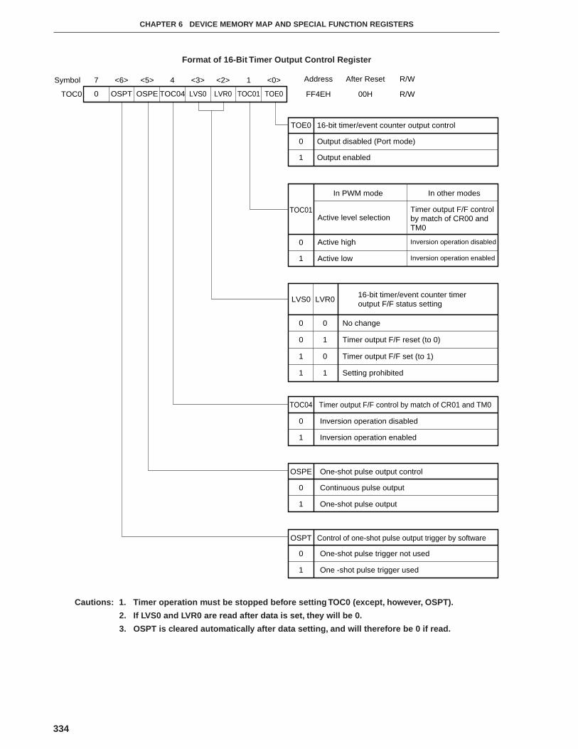
334
CHAPTER 6 DEVICE MEMORY MAP AND SPECIAL FUNCTION REGISTERS
Format of 16-Bit Timer Output Control Register
Cautions: 1. Timer operation must be stopped before setting TOC0 (except, however, OSPT).
2. If LVS0 and LVR0 are read after data is set, they will be 0.
3. OSPT is cleared automatically after data setting, and will therefore be 0 if read.
0 OSPT OSPE TOC04 LVS0 LVR0 TOC01 TOE0
7 <6> <5> 4 <3> <2> 1 <0>Symbol
TOC0 FF4EH 00H R/W
Address After Reset R/W
TOE0 16-bit timer/event counter output control
0 Output disabled (Port mode)
1 Output enabled
TOC01
0
1
In PWM mode In other modes
Active level selectionTimer output F/F control by match of CR00 and TM0
Active high
Active low
Inversion operation disabled
Inversion operation enabled
LVS0 LVR016-bit timer/event counter timer output F/F status setting
0 0 No change
0 1 Timer output F/F reset (to 0)
1 0 Timer output F/F set (to 1)
1 1 Setting prohibited
TOC04 Timer output F/F control by match of CR01 and TM0
0 Inversion operation disabled
1 Inversion operation enabled
OSPE One-shot pulse output control
0 Continuous pulse output
1 One-shot pulse output
OSPT Control of one-shot pulse output trigger by software
0 One-shot pulse trigger not used
1 One -shot pulse trigger used

335
CHAPTER 6 DEVICE MEMORY MAP AND SPECIAL FUNCTION REGISTERS
(4) Registers controlling 8-bit timer/event counter
The following four registers control the 8-bit timer/event counters:
• Timer clock select register 1 (TCL1)
• 8-bit timer mode control register 1 (TMC1)
• 8-bit timer output control register (TOC1)
• Port mode register 3 (PM3)
- Refer to section (1) for the register format.
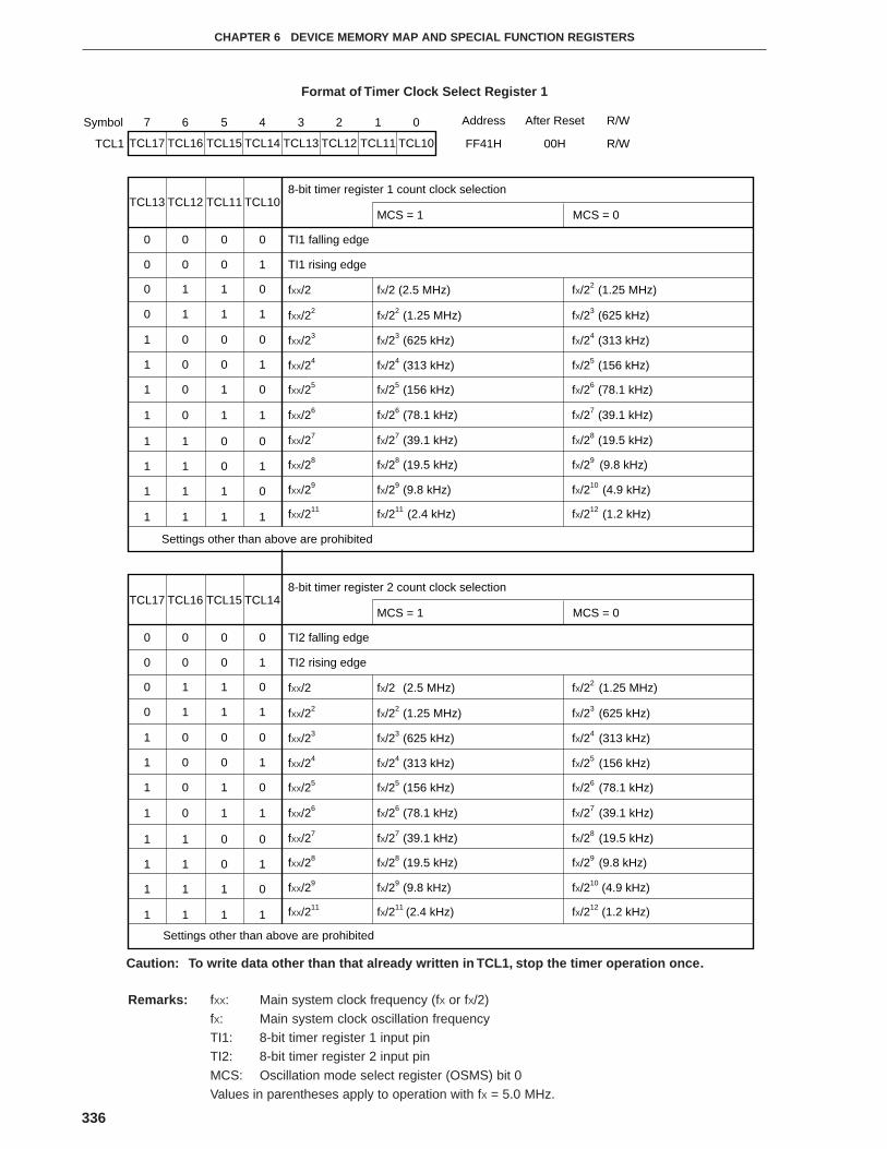
336
CHAPTER 6 DEVICE MEMORY MAP AND SPECIAL FUNCTION REGISTERS
Format of Timer Clock Select Register 1
Caution: To write data other than that already written in TCL1, stop the timer operation once.
Remarks: fXX: Main system clock frequency (fX or fX/2)
fX: Main system clock oscillation frequencyTI1: 8-bit timer register 1 input pinTI2: 8-bit timer register 2 input pin
MCS: Oscillation mode select register (OSMS) bit 0Values in parentheses apply to operation with fX = 5.0 MHz.
TCL17 TCL16 TCL15 TCL14 TCL13 TCL12 TCL11 TCL10
7 6 5 4 3 2 1 0Symbol
TCL1 FF41H 00H R/W
Address After Reset R/W
TCL13 TCL12 TCL11 TCL10
0 0 0 0 TI1 falling edge
0 0 0 1 TI1 rising edge
0 1 1 0
0 1 1 1
fXX/2 fX/2 (2.5 MHz) fX/22 (1.25 MHz)
1 0 0 0
fXX/22 fX/22 (1.25 MHz) fX/23 (625 kHz)
1 0 0 1
fXX/23 fX/23 (625 kHz) fX/24 (313 kHz)
1 0 1 0
fXX/24 fX/24 (313 kHz) fX/25 (156 kHz)
1 0 1 1
fXX/25 fX/25 (156 kHz) fX/26 (78.1 kHz)
1 1 0 0
fXX/26 fX/26 (78.1 kHz) fX/27 (39.1 kHz)
1 1 0 1
fXX/27 fX/27 (39.1 kHz) fX/28 (19.5 kHz)
1 1 1 0
fXX/28 fX/28 (19.5 kHz) fX/29 (9.8 kHz)
1 1 1 1
fXX/29 fX/29 (9.8 kHz) fX/210 (4.9 kHz)
MCS = 1
8-bit timer register 1 count clock selection
MCS = 0
fXX/211 fX/211 (2.4 kHz) fX/212 (1.2 kHz)
TCL17 TCL16 TCL15 TCL14
0 0 0 0 TI2 falling edge
0 0 0 1 TI2 rising edge
0 1 1 0
0 1 1 1
fXX/2 fX/2 (2.5 MHz) fX/22 (1.25 MHz)
1 0 0 0
fXX/22 fX/22 (1.25 MHz) fX/23 (625 kHz)
1 0 0 1
fXX/23 fX/23 (625 kHz) fX/24 (313 kHz)
1 0 1 0
fXX/24 fX/24 (313 kHz) fX/25 (156 kHz)
1 0 1 1
fXX/25 fX/25 (156 kHz) fX/26 (78.1 kHz)
1 1 0 0
fXX/26 fX/26 (78.1 kHz) fX/27 (39.1 kHz)
1 1 0 1
fXX/27 fX/27 (39.1 kHz) fX/28 (19.5 kHz)
1 1 1 0
fXX/28 fX/28 (19.5 kHz) fX/29 (9.8 kHz)
1 1 1 1
fXX/29 fX/29 (9.8 kHz) fX/210 (4.9 kHz)
MCS = 1
8-bit timer register 2 count clock selection
MCS = 0
fXX/211 fX/211 (2.4 kHz) fX/212 (1.2 kHz)
Settings other than above are prohibited
Settings other than above are prohibited

337
CHAPTER 6 DEVICE MEMORY MAP AND SPECIAL FUNCTION REGISTERS
Format of 8-Bit Timer Mode Control Register 1
Cautions: 1. Stop the timer operation before switching the operation mode.
2. When used as a 16-bit timer register, TCE1 should be used to control enable/stop
operations.
<0><1>234567Symbol
TCE1 FF49H 00H R/W
Address After Reset R/W
TCE2TMC1200000TMC1
TCE1 8-bit timer register 1 operation control
0 Operation stop (TM1 clear to 0)
1 Operation enable
TCE2 8-bit timer register 2 operation control
Operation stop (TM2 clear to 0)
Operation enable
0
1
TMC12 Operating mode selection
8-bit timer register × 2 channel mode (TM1, TM2)
16-bit timer register × 1 channel mode (TMS)
0
1

338
CHAPTER 6 DEVICE MEMORY MAP AND SPECIAL FUNCTION REGISTERS
Format of 8-Bit Timer Output Control Register
Cautions: 1. Be sure to set TOC1 after stopping the timer operation.
2. After data setting, 0 can be read from LVS1, LVS2, LVR1, and LVR2.
<0>1<2><3><4>5<6><7>Symbol
TOE1TOC11LVR1LVS1TOE2TOC15LVR2LVS2TOC1 FF4FH 00H R/W
Address After Reset R/W
TOE1 8-bit timer/event counter 1 outptut control
0 Output disable (Port mode)
1 Output enable
TOC11 8-bit timer/event counter 1 timer output F/F control
0 Inverted operation disable
1 Inverted operation enable
LVS1 LVR1 8-bit timer/event counter 1 timer output F/F status set
0 0 Unchanged
0 1 Timer output F/F reset (to 0)
1 0 Timer output F/F set (to 1)
1 1 Setting prohibited
TOE2 8-bit timer/event counter 2 output control
0 Output disable (Port mode)
1 Output enable
TOC15 8-bit timer/event counter 2 timer output F/F control
0 Inverted operation disable
1 Inverted operation enable
LVS2 LVR2 8-bit timer/event counter 2 timer output F/F status set
0 0 Unchanged
0 1 Timer output F/F reset (to 0)
1 0 Timer output F/F set (to 1)
1 1 Setting prohibited
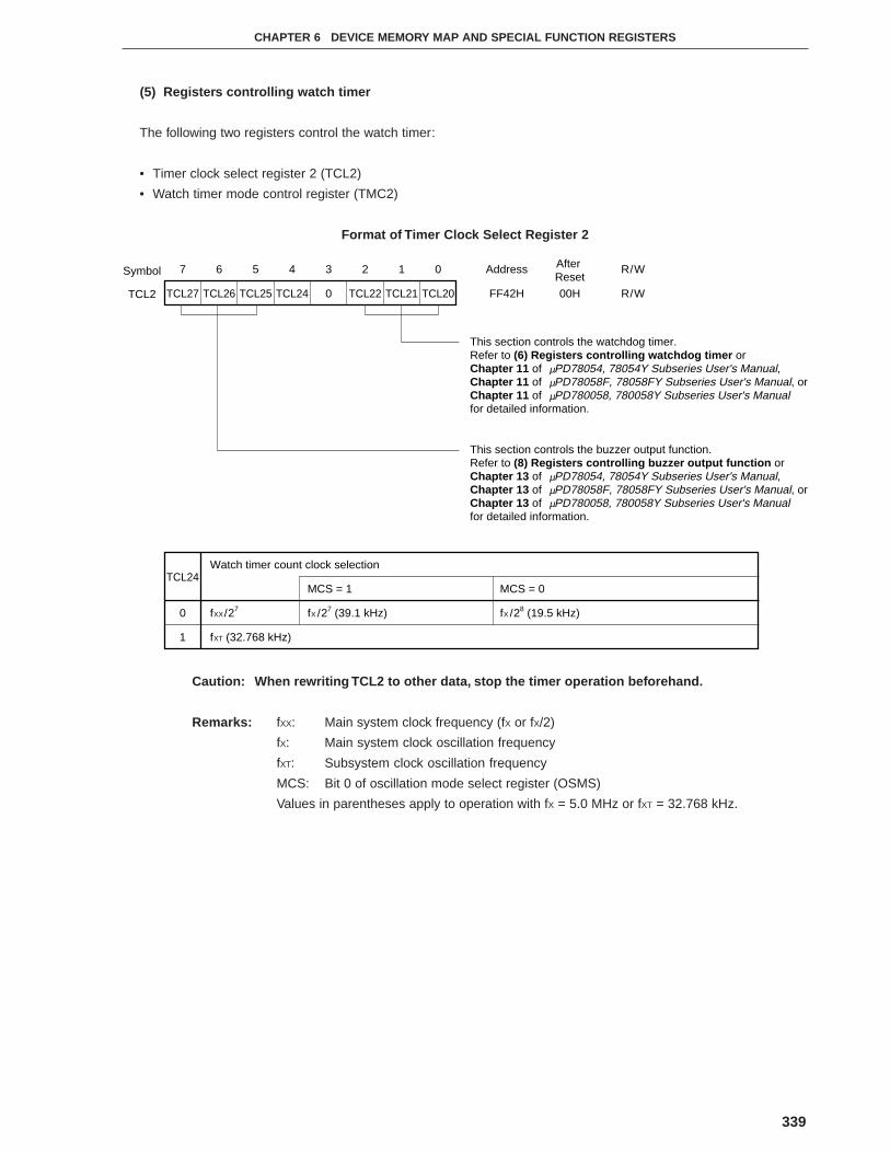
339
CHAPTER 6 DEVICE MEMORY MAP AND SPECIAL FUNCTION REGISTERS
(5) Registers controlling watch timer
The following two registers control the watch timer:
• Timer clock select register 2 (TCL2)
• Watch timer mode control register (TMC2)
Format of Timer Clock Select Register 2
Caution: When rewriting TCL2 to other data, stop the timer operation beforehand.
Remarks: fXX: Main system clock frequency (fX or fX/2)
fX: Main system clock oscillation frequency
fXT: Subsystem clock oscillation frequency
MCS: Bit 0 of oscillation mode select register (OSMS)
Values in parentheses apply to operation with fX = 5.0 MHz or fXT = 32.768 kHz.
TCL27
7
TCL26
6
TCL25 TCL24
4
0
3 2 1 0
FF42H
Address
TCL2
Symbol
TCL22 TCL21 TCL20
5
00H
After Reset
R/W
R/W
0
1
TCL24
fXX/27
fXT (32.768 kHz)
MCS = 1
fX /27 (39.1 kHz)
MCS = 0
fX /28 (19.5 kHz)
Watch timer count clock selection
This section controls the watchdog timer.Refer to (6) Registers controlling watchdog timer orChapter 11 of PD78054, 78054Y Subseries User's Manual,Chapter 11 of PD78058F, 78058FY Subseries User's Manual, orChapter 11 of PD780058, 780058Y Subseries User's Manualfor detailed information.
µ
µµ
This section controls the buzzer output function.Refer to (8) Registers controlling buzzer output function orChapter 13 of PD78054, 78054Y Subseries User's Manual,Chapter 13 of PD78058F, 78058FY Subseries User's Manual, orChapter 13 of PD780058, 780058Y Subseries User's Manualfor detailed information.
µµµ
340
CHAPTER 6 DEVICE MEMORY MAP AND SPECIAL FUNCTION REGISTERS
Format of Watch Timer Mode Control Register
Caution: When the watch timer is used, the prescaler should not be cleared frequently.
Remarks: fW: Watch timer clock frequency (fXX/27 or fXT)
fXX: Main system clock frequency (fX or fX/2)
fX: Main system clock oscillation frequency
fXT: Subsystem clock oscillation frequency
A 0.5 second interval can be generated either with a 4.19304 MHz main system clock
or a 32.768 kHz sub system clock
0
7
TMC26
6
TMC25 TMC24
4
TMC23
3 2 1 0
FF4AH
Address
TMC2
Symbol
TMC22 TMC21 TMC20
5
00H
After Reset
R/W
R/W
0
1
TMC23fXX = 5.0 MHz operation
214/fW (0.4 sec)
213/fW (0.2 sec)
Watch flag set time selection
0
0
0
0
1
1
0
0
1
1
0
0
0
1
0
1
0
1
TMC26 TMC25 TMC24fXX = 5.0 MHz operation
24/fW (410 s)
25/fW (819 s)
26/fW (1.64 ms)
27/fW (3.28 ms)
28/fW (6.55 ms)
29/fW (13.1 ms)
fXX = 4.19 MHz operation
24/fW (488 s)
25/fW (977 s)
26/fW (1.95 ms)
27/fW (3.91 ms)
28/fW (7.81 ms)
29/fW (15.6 ms)
fXT = 32.768 kHz operation
24/fW (488 s)
25/fW (977 s)
26/fW (1.95 ms)
27/fW (3.91 ms)
28/fW (7.81 ms)
29/fW (15.6 ms)
Prescaler interval time selection
µ
µ
µ
µ
µ
µ
fXX = 4.19 MHz operation
214/fW (0.5 sec)
213/fW (0.25 sec)
fXT = 32.768 kHz operation
214/fW (0.5 sec)
213/fW (0.25 sec)
TMC22
0
1
5-bit counter operation control
Clear after operation stop
Operation enable
TMC21
0
1
Prescaler operation control
Clear after operation stop
Operation enable
TMC20
0
1
Watch operating mode selection
Normal operating mode (flag set at fW/214)
Fast feed operating mode (flag set at fW/25)
Settings other than above are prohibited
341
CHAPTER 6 DEVICE MEMORY MAP AND SPECIAL FUNCTION REGISTERS
(6) Registers controlling watchdog timer
The following two registers control the watchdog timer:
• Timer clock select register 2 (TCL2)
• Watchdog timer mode register (WDTM)
Format of Timer Clock Select Register 2
Caution: When rewriting TCL2 to other data, first stop the timer operation.
Remarks: fXX: Main system clock frequency (fX or fX/2)
fX: Main system clock oscillation frequency
MCS: Bit 0 of oscillation mode select register (OSMS)
Values in parentheses apply to operation with fX = 5.0 MHz.
TCL27
7
TCL26
6
TCL25 TCL24
4
0
3 2 1 0
FF42H
Address
TCL2
Symbol
TCL22 TCL21 TCL20
5
00H
After Reset
R/W
R/W
0
0
0
0
1
1
1
1
0
0
1
1
0
0
1
1
0
1
0
1
0
1
0
1
TCL22 TCL21 TCL20MCS = 1
fX /23
fX /24
fX /25
fX /26
fX /27
fX /28
fX /29
fX /211
fXX /23
fXX /24
fXX /25
fXX /26
fXX /27
fXX /28
fXX /29
fXX /211
MCS = 0
fX /24
fX /25
fX /26
fX /27
fX /28
fX /29
fX /210
fX /212
Watchdog timer count clock selection
(625 kHz)
(313 kHz)
(156 kHz)
(78.1 kHz)
(39.1 kHz)
(19.5 kHz)
(9.8 kHz)
(2.4 kHz)
(313 kHz)
(156 kHz)
(78.1 kHz)
(39.1 kHz)
(19.5 kHz)
(9.8 kHz)
(4.9 kHz)
(1.2 kHz)
This section controls the watch timer.Refer to (5) registers controlling watch timer orChapter 10 of PD78054, 78054Y Subseries User's Manual,Chapter 10 of PD78058F, 78058FY Subseries User's Manual, orChapter 10 of PD780058, 780058Y Subseries User's Manualfor detailed information.
µµµ
This section controls the buzzer output function.Refer to (8) Registers controlling buzzer output function orChapter 13 of PD78054, 78054Y Subseries User's Manual,Chapter 13 of PD78058F, 78058FY Subseries User's Manual, orChapter 13 of PD780058, 780058Y Subseries User's Manualfor detailed information.
µµµ
342
CHAPTER 6 DEVICE MEMORY MAP AND SPECIAL FUNCTION REGISTERS
Format of Watchdog Timer Mode Register
Notes: 1. Once set to 1, WDTM3 and WDTM4 cannot be cleared to 0 by software.
2. The watchdog timer starts operating as an interval timer as soon as RUN has been set to 1.
3. Once set to 1, RUN cannot be cleared to 0 by software.
Thus, once counting starts, counting can only be stopped by RESET input.
Cautions: 1. When 1 is set in RUN so that the watchdog timer is cleared, the actual overflow time is up to
0.5% shorter than the time set by timer clock select register 2 (TCL2).
2. To use Watchdog Timer modes 1 and 2, make sure that the interrupt request flag (TMIF4) is
0, and then set WDTM4 to 1.
If WDTM4 is set to 1 when TMIF4 is 1, the non-maskable interrupt request occurs, regard-
less of the contents of WDTM3.
Remark: ×: Don’t care
RUN
<7>
0
6
0 WDTM4
4
WDTM3
3 2 1 0
FFF9H
Address
WDTM
Symbol
0 0 0
5
00H
AfterReset
R/W
R/W
RUN
0
1
Watchdog timer operation mode selection Note 3
Count stops.
Counter is cleared and counting starts.
WDTM3
×
0
1
Watchdog timer operation modeselection Note 1
Interval Timer mode Note 2
(Maskable interrupt request occurs upon generation of an overflow.)
Watchdog Timer mode 1(Non-maskable interrupt request occursupon generation of an overflow.)
Watchdog Timer mode 2(Reset operation is activated upongeneration of an overflow.)
WDTM4
0
1
1
343
CHAPTER 6 DEVICE MEMORY MAP AND SPECIAL FUNCTION REGISTERS
(7) Registers controlling clock output function
The following two registers control the clock output function:
• Timer clock select register 0 (TCL0)
• Port mode register 3 (PM3)
- Refer to section (1) for the register format.
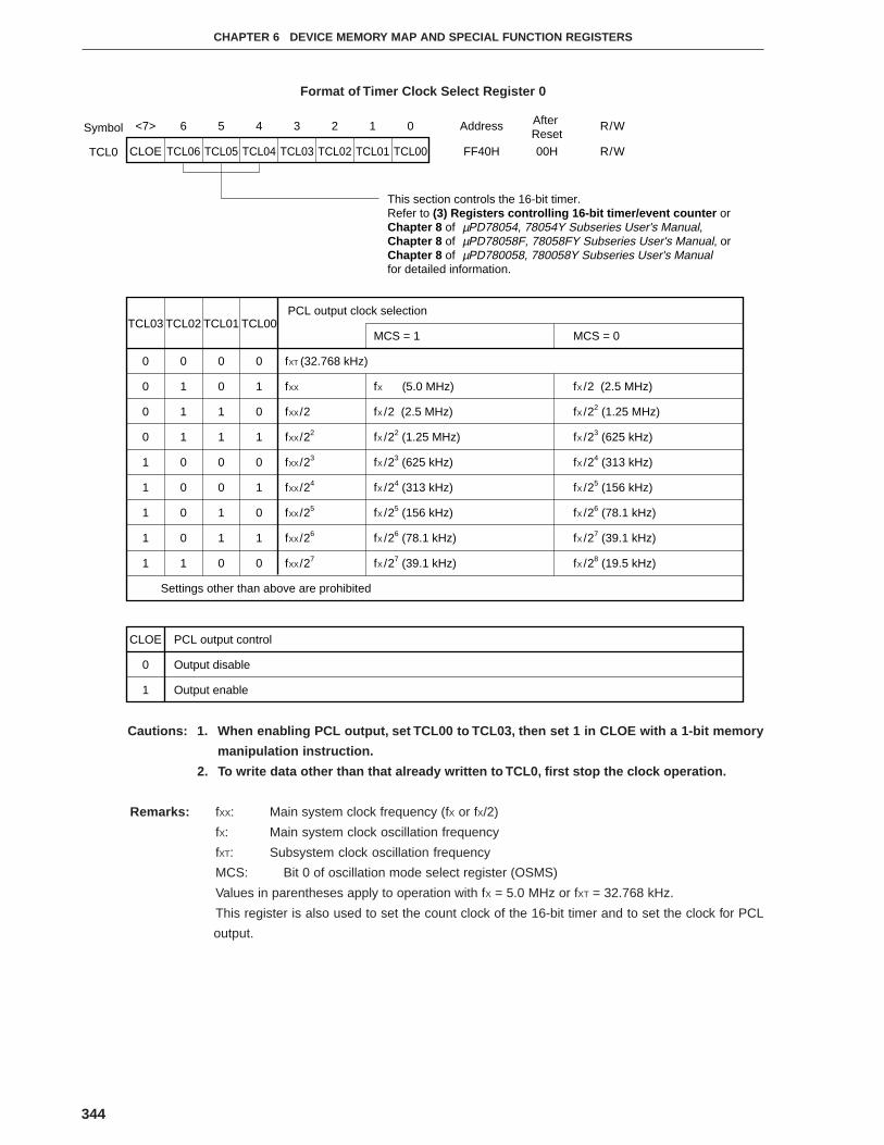
344
CHAPTER 6 DEVICE MEMORY MAP AND SPECIAL FUNCTION REGISTERS
Format of Timer Clock Select Register 0
Cautions: 1. When enabling PCL output, set TCL00 to TCL03, then set 1 in CLOE with a 1-bit memory
manipulation instruction.
2. To write data other than that already written to TCL0, first stop the clock operation.
Remarks: fXX: Main system clock frequency (fX or fX/2)
fX: Main system clock oscillation frequency
fXT: Subsystem clock oscillation frequency
MCS: Bit 0 of oscillation mode select register (OSMS)
Values in parentheses apply to operation with fX = 5.0 MHz or fXT = 32.768 kHz.
This register is also used to set the count clock of the 16-bit timer and to set the clock for PCL
output.
CLOE
<7>
TCL06
6
TCL05 TCL04
4
TCL03
3 2 1 0
FF40H
Address
TCL0
Symbol
TCL02 TCL01 TCL00
5
00H
After Reset
R/W
R/W
CLOE
0
1
PCL output control
Output disable
Output enable
0
0
0
0
1
1
1
1
1
0
1
1
1
0
0
0
0
1
0
0
1
1
0
0
1
1
0
TCL03 TCL02 TCL01
fXT (32.768 kHz)
fXX
fXX/2
fXX/22
fXX/23
fXX/24
fXX/25
fXX/26
fXX/27
MCS = 1
fX (5.0 MHz)
fX /2 (2.5 MHz)
fX /22 (1.25 MHz)
fX /23 (625 kHz)
fX /24 (313 kHz)
fX /25 (156 kHz)
fX /26 (78.1 kHz)
fX /27 (39.1 kHz)
MCS = 0
fX /2 (2.5 MHz)
fX /22 (1.25 MHz)
fX /23 (625 kHz)
fX /24 (313 kHz)
fX /25 (156 kHz)
fX /26 (78.1 kHz)
fX /27 (39.1 kHz)
fX /28 (19.5 kHz)
PCL output clock selectionTCL00
0
1
0
1
0
1
0
1
0
This section controls the 16-bit timer.Refer to (3) Registers controlling 16-bit timer/event counter orChapter 8 of PD78054, 78054Y Subseries User's Manual,Chapter 8 of PD78058F, 78058FY Subseries User's Manual, orChapter 8 of PD780058, 780058Y Subseries User's Manualfor detailed information.
µµµ
Settings other than above are prohibited
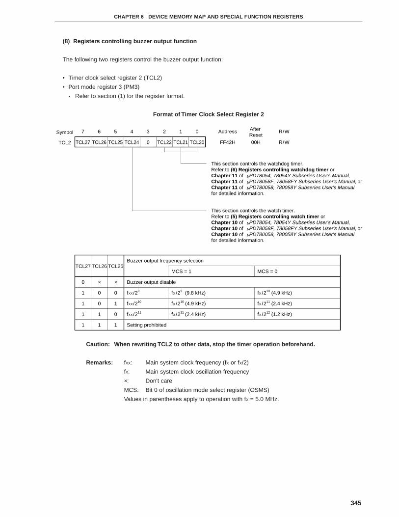
345
CHAPTER 6 DEVICE MEMORY MAP AND SPECIAL FUNCTION REGISTERS
(8) Registers controlling buzzer output function
The following two registers control the buzzer output function:
• Timer clock select register 2 (TCL2)
• Port mode register 3 (PM3)
- Refer to section (1) for the register format.
Format of Timer Clock Select Register 2
Caution: When rewriting TCL2 to other data, stop the timer operation beforehand.
Remarks: fXX: Main system clock frequency (fX or fX/2)
fX: Main system clock oscillation frequency
×: Don't care
MCS: Bit 0 of oscillation mode select register (OSMS)
Values in parentheses apply to operation with fX = 5.0 MHz.
TCL27
7
TCL26
6
TCL25 TCL24
4
0
3 2 1 0
FF42H
Address
TCL2
Symbol
TCL22 TCL21 TCL20
5
00H
After Reset
R/W
R/W
This section controls the watchdog timer.Refer to (6) Registers controlling watchdog timer orChapter 11 of PD78054, 78054Y Subseries User's Manual,Chapter 11 of PD78058F, 78058FY Subseries User's Manual, orChapter 11 of PD780058, 780058Y Subseries User's Manualfor detailed information.
µµµ
This section controls the watch timer.Refer to (5) Registers controlling watch timer orChapter 10 of PD78054, 78054Y Subseries User's Manual,Chapter 10 of PD78058F, 78058FY Subseries User's Manual, orChapter 10 of PD780058, 780058Y Subseries User's Manualfor detailed information.
µµµ
0
1
1
1
1
×
0
0
1
1
×
0
1
0
1
TCL27 TCL26 TCL25
Buzzer output disable
fXX/29
fXX/210
fXX/211
Setting prohibited
MCS = 1
fX /29 (9.8 kHz)
fX /210 (4.9 kHz)
fX /211 (2.4 kHz)
MCS = 0
fX /210 (4.9 kHz)
fX /211 (2.4 kHz)
fX /212 (1.2 kHz)
Buzzer output frequency selection

346
CHAPTER 6 DEVICE MEMORY MAP AND SPECIAL FUNCTION REGISTERS
(9) Registers controlling A/D converter
The following three registers control the A/D converter:
• A/D converter mode register (ADM)
• A/D converter input select register (ADIS)
• External interrupt mode register 1 (INTM1)
- Refer to section (16) for the register format.
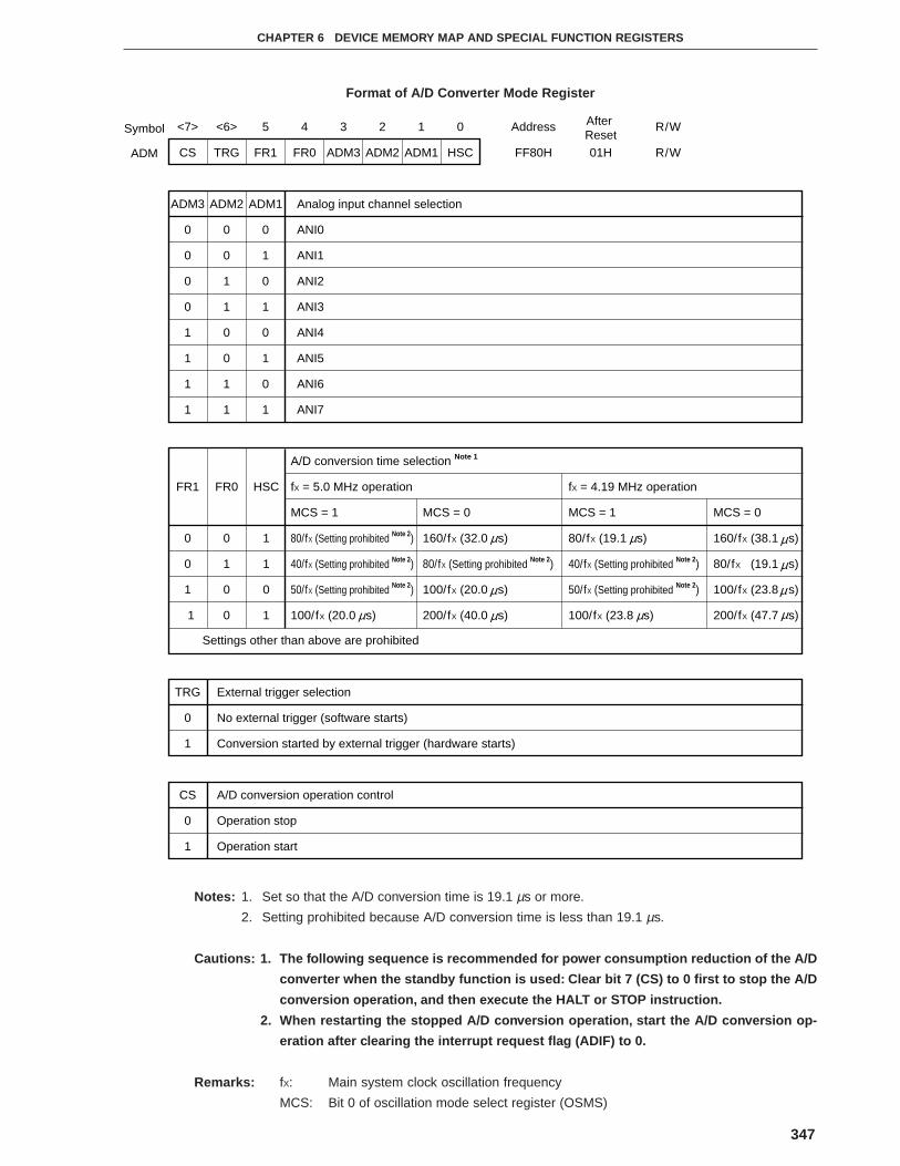
347
CHAPTER 6 DEVICE MEMORY MAP AND SPECIAL FUNCTION REGISTERS
Format of A/D Converter Mode Register
Notes: 1. Set so that the A/D conversion time is 19.1 µs or more.
2. Setting prohibited because A/D conversion time is less than 19.1 µs.
Cautions: 1. The following sequence is recommended for power consumption reduction of the A/D
converter when the standby function is used: Clear bit 7 (CS) to 0 first to stop the A/D
conversion operation, and then execute the HALT or STOP instruction.
2. When restarting the stopped A/D conversion operation, start the A/D conversion op-
eration after clearing the interrupt request flag (ADIF) to 0.
Remarks: fX: Main system clock oscillation frequency
MCS: Bit 0 of oscillation mode select register (OSMS)
CS
<7>
TRG
<6>
FR1 FR0
4
ADM3
3 2 1 0
FF80H
Address
ADM
Symbol
ADM2 ADM1 HSC
5
01H
After Reset
R/W
R/W
ADM3
0
0
0
0
1
1
1
1
ADM2
0
0
1
1
0
0
1
1
ADM1
0
1
0
1
0
1
0
1
Analog input channel selection
ANI0
ANI1
ANI2
ANI3
ANI4
ANI5
ANI6
ANI7
TRG
0
1
External trigger selection
No external trigger (software starts)
Conversion started by external trigger (hardware starts)
FR1
0
0
1
1
FR0
0
1
0
0
A/D conversion time selection Note 1
fX = 5.0 MHz operation
MCS = 1
80/fX (Setting prohibited Note 2)
40/fX (Setting prohibited Note 2)
50/fX (Setting prohibited Note 2)
100/fX (20.0 s)µ
MCS = 0
160/fX (32.0 s)
80/fX (Setting prohibited Note 2)
100/fX (20.0 s)
200/fX (40.0 s)
fX = 4.19 MHz operation
MCS = 1
80/fX (19.1 s)
40/fX (Setting prohibited Note 2)
50/fX (Setting prohibited Note 2)
100/fX (23.8 s)
MCS = 0
160/fX (38.1 s)
80/fX (19.1 s)
100/fX (23.8 s)
200/fX (47.7 s)µ
µ
µ
µ µ
µ
µ
CS
0
1
A/D conversion operation control
Operation stop
Operation start
HSC
1
1
0
1
µ µ
Settings other than above are prohibited
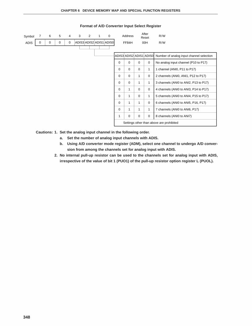
348
CHAPTER 6 DEVICE MEMORY MAP AND SPECIAL FUNCTION REGISTERS
Format of A/D Converter Input Select Register
Cautions: 1. Set the analog input channel in the following order.
a. Set the number of analog input channels with ADIS.
b. Using A/D converter mode register (ADM), select one channel to undergo A/D conver-
sion from among the channels set for analog input with ADIS.
2. No internal pull-up resistor can be used to the channels set for analog input with ADIS,
irrespective of the value of bit 1 (PUO1) of the pull-up resistor option register L (PUOL).
0
7
0
6
0 0
4
ADIS3
3 2 1 0
FF84H
Address
ADIS
Symbol
ADIS2 ADIS1 ADIS0
5
00H
AfterReset
R/W
R/W
ADIS3
0
0
0
0
0
0
0
0
1
Number of analog input channel selection
No analog input channel (P10 to P17)
1 channel (ANI0, P11 to P17)
2 channels (ANI0, ANI1, P12 to P17)
3 channels (ANI0 to ANI2, P13 to P17)
4 channels (ANI0 to ANI3, P14 to P17)
5 channels (ANI0 to ANI4, P15 to P17)
6 channels (ANI0 to ANI5, P16, P17)
7 channels (ANI0 to ANI6, P17)
8 channels (ANI0 to ANI7)
ADIS2
0
0
0
0
1
1
1
1
0
ADIS1
0
0
1
1
0
0
1
1
0
ADIS0
0
1
0
1
0
1
0
1
0
Settings other than above are prohibited
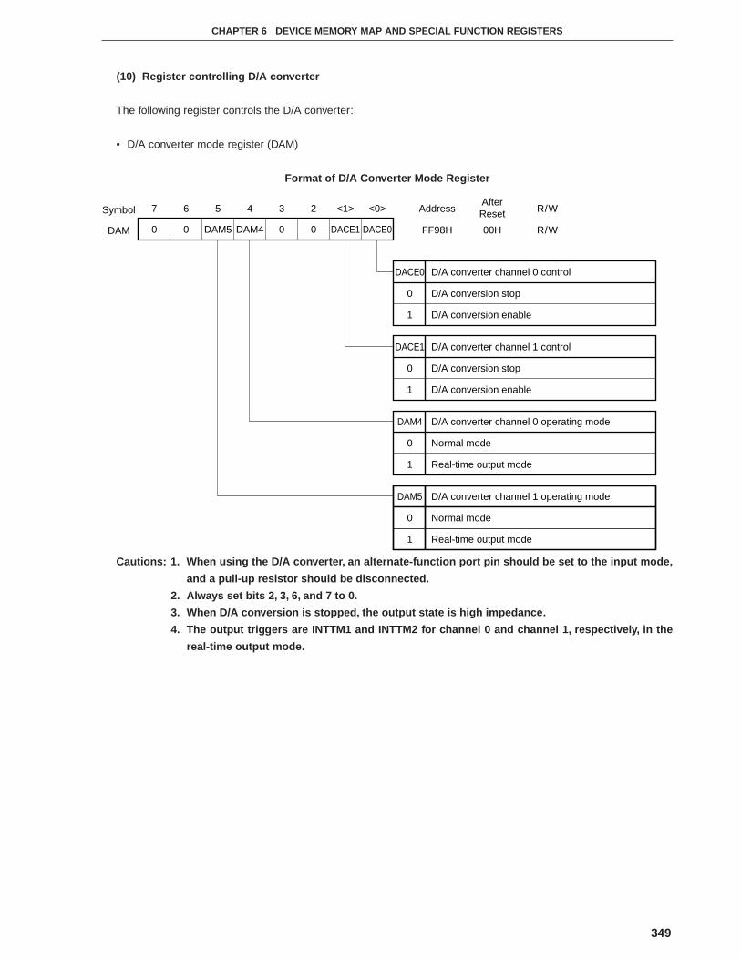
349
CHAPTER 6 DEVICE MEMORY MAP AND SPECIAL FUNCTION REGISTERS
(10) Register controlling D/A converter
The following register controls the D/A converter:
• D/A converter mode register (DAM)
Format of D/A Converter Mode Register
Cautions: 1. When using the D/A converter, an alternate-function port pin should be set to the input mode,
and a pull-up resistor should be disconnected.
2. Always set bits 2, 3, 6, and 7 to 0.
3. When D/A conversion is stopped, the output state is high impedance.
4. The output triggers are INTTM1 and INTTM2 for channel 0 and channel 1, respectively, in the
real-time output mode.
0
7
0
6
DAM5 DAM4
4
0
3 2 <1> <0>
FF98H
Address
DAM
Symbol
0 DACE1 DACE0
5
00H
AfterReset
R/W
R/W
DAM5
0
1
D/A converter channel 1 operating mode
Normal mode
Real-time output mode
DACE0
0
1
D/A converter channel 0 control
D/A conversion stop
D/A conversion enable
DACE1
0
1
D/A converter channel 1 control
D/A conversion stop
D/A conversion enable
DAM4
0
1
D/A converter channel 0 operating mode
Normal mode
Real-time output mode
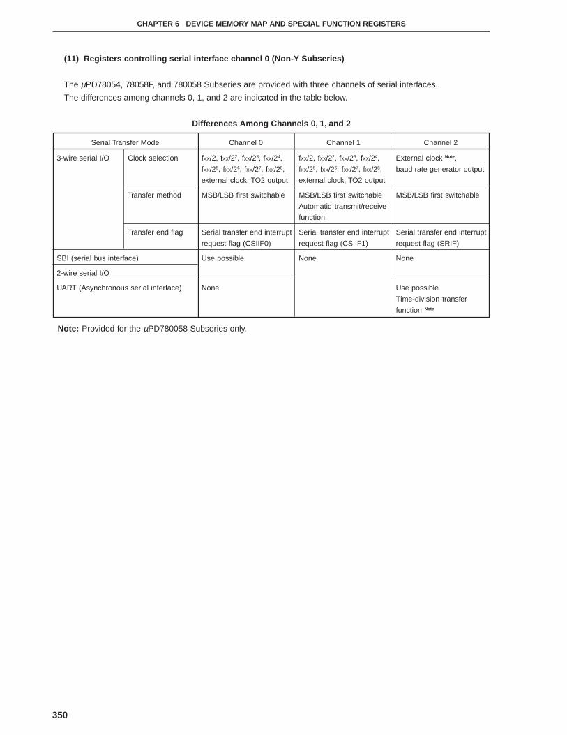
350
CHAPTER 6 DEVICE MEMORY MAP AND SPECIAL FUNCTION REGISTERS
(11) Registers controlling serial interface channel 0 (Non-Y Subseries)
The µPD78054, 78058F, and 780058 Subseries are provided with three channels of serial interfaces.
The differences among channels 0, 1, and 2 are indicated in the table below.
Differences Among Channels 0, 1, and 2
Serial Transfer Mode Channel 0 Channel 1 Channel 2
3-wire serial I/O Clock selection fXX/2, fXX/22, fXX/23, fXX/24, fXX/2, fXX/22, fXX/23, fXX/24, External clock Note,
fXX/25, fXX/26, fXX/27, fXX/28, fXX/25, fXX/26, fXX/27, fXX/28, baud rate generator output
external clock, TO2 output external clock, TO2 output
Transfer method MSB/LSB first switchable MSB/LSB first switchable MSB/LSB first switchable
Automatic transmit/receive
function
Transfer end flag Serial transfer end interrupt Serial transfer end interrupt Serial transfer end interrupt
request flag (CSIIF0) request flag (CSIIF1) request flag (SRIF)
SBI (serial bus interface) Use possible None None
2-wire serial I/O
UART (Asynchronous serial interface) None Use possible
Time-division transfer
function Note
Note: Provided for the µPD780058 Subseries only.
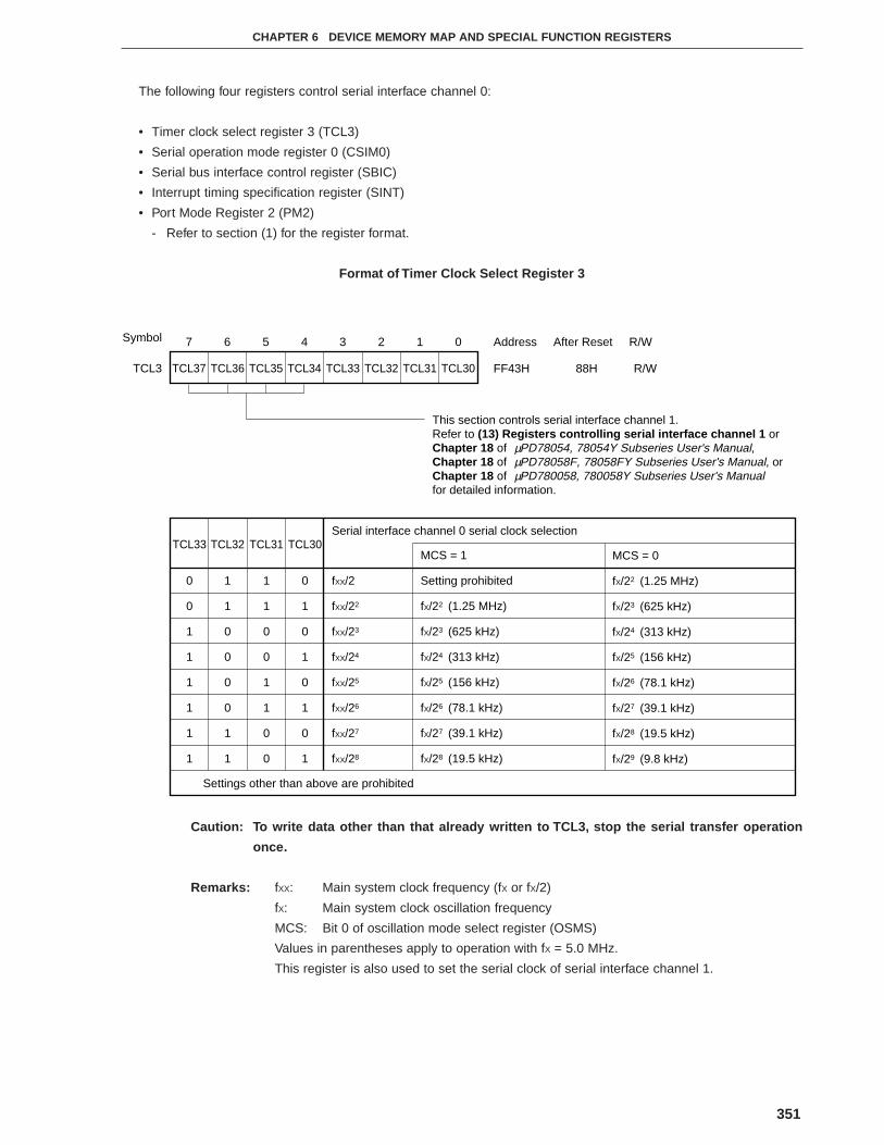
351
CHAPTER 6 DEVICE MEMORY MAP AND SPECIAL FUNCTION REGISTERS
The following four registers control serial interface channel 0:
• Timer clock select register 3 (TCL3)
• Serial operation mode register 0 (CSIM0)
• Serial bus interface control register (SBIC)
• Interrupt timing specification register (SINT)
• Port Mode Register 2 (PM2)
- Refer to section (1) for the register format.
Format of Timer Clock Select Register 3
Caution: To write data other than that already written to TCL3, stop the serial transfer operation
once.
Remarks: fXX: Main system clock frequency (fX or fX/2)
fX: Main system clock oscillation frequency
MCS: Bit 0 of oscillation mode select register (OSMS)
Values in parentheses apply to operation with fX = 5.0 MHz.
This register is also used to set the serial clock of serial interface channel 1.
Serial interface channel 0 serial clock selectionTCL33 TCL32 TCL31 TCL30
0
0
1
1
1
1
1
1
1
1
0
0
0
0
1
1
1
1
0
0
1
1
0
0
0
1
0
1
0
1
0
1
fXX/2
fXX/22
fXX/23
fXX/24
fXX/25
fXX/26
fXX/27
fXX/28
MCS = 1
Setting prohibited
fX/22 (1.25 MHz)
fX/23 (625 kHz)
fX/24 (313 kHz)
fX/25 (156 kHz)
fX/26 (78.1 kHz)
fX/27 (39.1 kHz)
fX/28 (19.5 kHz)
MCS = 0
fX/22 (1.25 MHz)
fX/23 (625 kHz)
fX/24 (313 kHz)
fX/25 (156 kHz)
fX/26 (78.1 kHz)
fX/27 (39.1 kHz)
fX/28 (19.5 kHz)
fX/29 (9.8 kHz)
6 5 4 3 2 1 07Symbol
TCL3 TCL37 TCL36 TCL35 TCL34 TCL33 TCL32 TCL31 TCL30 FF43H 88H R/W
Address After Reset R/W
This section controls serial interface channel 1.Refer to (13) Registers controlling serial interface channel 1 orChapter 18 of PD78054, 78054Y Subseries User's Manual,Chapter 18 of PD78058F, 78058FY Subseries User's Manual, orChapter 18 of PD780058, 780058Y Subseries User's Manualfor detailed information.
µµµ
Settings other than above are prohibited
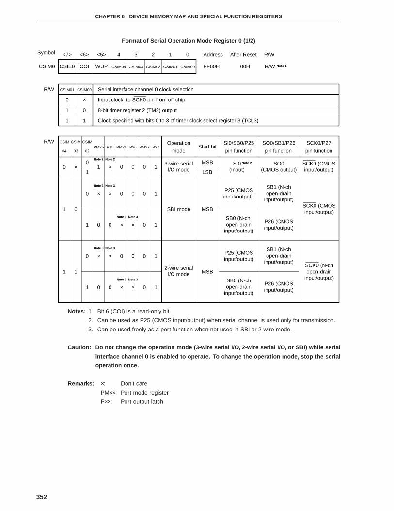
352
CHAPTER 6 DEVICE MEMORY MAP AND SPECIAL FUNCTION REGISTERS
Format of Serial Operation Mode Register 0 (1/2)
Notes: 1. Bit 6 (COI) is a read-only bit.
2. Can be used as P25 (CMOS input/output) when serial channel is used only for transmission.
3. Can be used freely as a port function when not used in SBI or 2-wire mode.
Caution: Do not change the operation mode (3-wire serial I/O, 2-wire serial I/O, or SBI) while serial
interface channel 0 is enabled to operate. To change the operation mode, stop the serial
operation once.
Remarks: ×: Don’t care
PM××: Port mode register
P××: Port output latch
SBI mode
<6> <5> 4 3 2 1 0<7>Symbol
CSIM0 CSIE0 COI WUP CSIM04 CSIM03 CSIM02 CSIM01 CSIM00
CSIM01
0
1
Serial interface channel 0 clock selection
Input clock to SCK0 pin from off chip
8-bit timer register 2 (TM2) output
0
0
SCK0 (CMOSinput/output)
R/W
1 Clock specified with bits 0 to 3 of timer clock select register 3 (TCL3)
CSIM
04
0
1
CSIM00
×
0
1
FF60H 00H R/W Note 1
Address After Reset R/W
R/W CSIM
03
CSIM
02PM25 P25 PM26 P26 PM27 P27
Operation
modeStart bit
SI0/SB0/P25
pin function
SO0/SB1/P26
pin function
SCK0/P27
pin function
×
1 0
×
0
×
0
0
×
0
×
0
0
1
1
Note 3 Note 3
Note 3 Note 3
MSB
P25 (CMOSinput/output)
SB0 (N-ch open-drain
input/output)
SB1 (N-chopen-drain
input/output)
P26 (CMOSinput/output)
1
MSB
LSB1 × 0 0 0 1
Note 2
3-wire seriall/O mode
SI0(Input)
SO0(CMOS output)
SCK0 (CMOSinput/output)
Note 2
2-wire seriall/O mode
0
SCK0 (N-chopen-drain
input/output)
1
1 1
×
0
×
0
0
×
0
×
0
0
1
1
Note 3 Note 3
Note 3 Note 3
MSB
P25 (CMOSinput/output)
SB0 (N-chopen-drain
input/output)
SB1 (N-chopen-drain
input/output)
P26 (CMOSinput/output)
Note 2
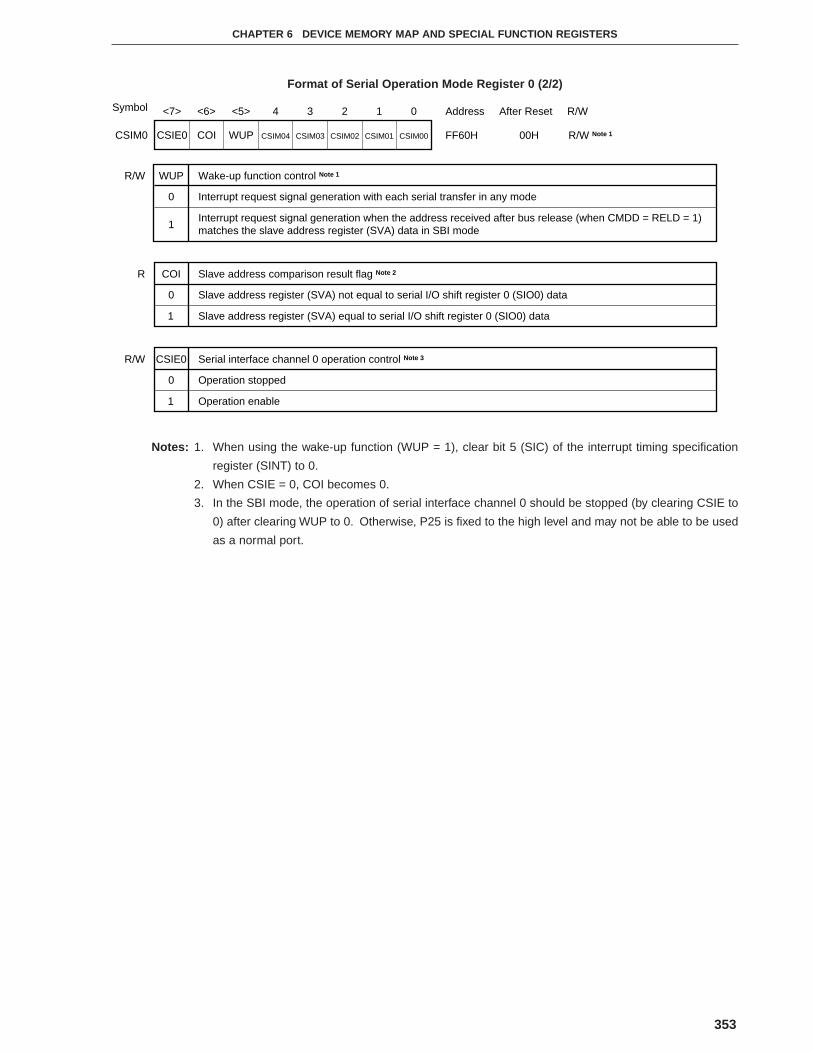
353
CHAPTER 6 DEVICE MEMORY MAP AND SPECIAL FUNCTION REGISTERS
Format of Serial Operation Mode Register 0 (2/2)
Notes: 1. When using the wake-up function (WUP = 1), clear bit 5 (SIC) of the interrupt timing specification
register (SINT) to 0.
2. When CSIE = 0, COI becomes 0.
3. In the SBI mode, the operation of serial interface channel 0 should be stopped (by clearing CSIE to
0) after clearing WUP to 0. Otherwise, P25 is fixed to the high level and may not be able to be used
as a normal port.
WUP
0
1
Wake-up function control Note 1
Interrupt request signal generation with each serial transfer in any mode
Interrupt request signal generation when the address received after bus release (when CMDD = RELD = 1) matches the slave address register (SVA) data in SBI mode
R/W
COI
0
1
Slave address comparison result flag Note 2
Slave address register (SVA) not equal to serial I/O shift register 0 (SIO0) data
Slave address register (SVA) equal to serial I/O shift register 0 (SIO0) data
R
CSIE0
0
1
Serial interface channel 0 operation control Note 3
Operation stopped
Operation enable
R/W
<6> <5> 4 3 2 1 0<7>Symbol
CSIM0 CSIE0 COI WUP CSIM04 CSIM03 CSIM02 CSIM01 CSIM00 FF60H 00H R/W Note 1
Address After Reset R/W
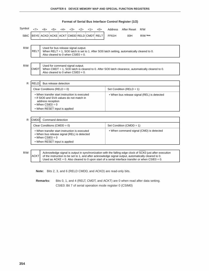
354
CHAPTER 6 DEVICE MEMORY MAP AND SPECIAL FUNCTION REGISTERS
Format of Serial Bus Interface Control Register (1/2)
Note: Bits 2, 3, and 6 (RELD CMDD, and ACKD) are read-only bits.
Remarks: Bits 0, 1, and 4 (RELT, CMDT, and ACKT) are 0 when read after data setting.
CSIE0: Bit 7 of serial operation mode register 0 (CSIM0)
<6> <5> <4> <3> <2> <1> <0><7>Symbol
SBIC BSYE ACKD ACKE ACKT CMDD RELD CMDT RELT
RELTUsed for bus release signal output. When RELT = 1, SO0 Iatch is set to 1. After SO0 latch setting, automatically cleared to 0.Also cleared to 0 when CSIE0 = 0.
R/W
FF61H 00H R/W Note
Address After Reset R/W
CMDTUsed for command signal output. When CMDT = 1, SO0 Iatch is cleared to 0. After SO0 latch clearance, automatically cleared to 0. Also cleared to 0 when CSIE0 = 0.
R/W
R RELD Bus release detection
Set Condition (RELD = 1)Clear Conditions (RELD = 0)
• When bus release signal (REL) is detected• When transfer start instruction is executed • If SIO0 and SVA values do not match in address reception • When CSIE0 = 0
• When RESET input is applied
R CMDD Command detection
Clear Conditions (CMDD = 0)
• When transfer start instruction is executed • When bus release signal (REL) is detected • When CSIE0 = 0
• When RESET input is applied
Set Condition (CMDD = 1)
• When command signal (CMD) is detected
ACKTAcknowledge signal is output in synchronization with the falling edge clock of SCK0 just after execution of the instruction to be set to 1, and after acknowledge signal output, automatically cleared to 0. Used as ACKE = 0. Also cleared to 0 upon start of a serial interface transfer or when CSIE0 = 0.
R/W
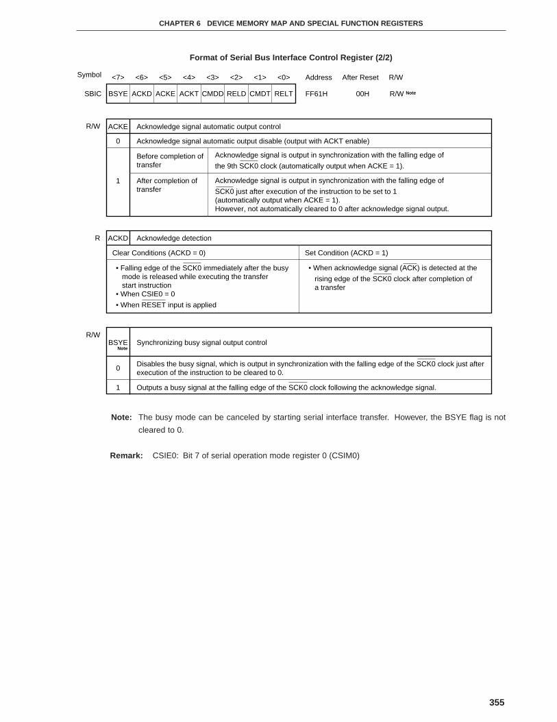
355
CHAPTER 6 DEVICE MEMORY MAP AND SPECIAL FUNCTION REGISTERS
Format of Serial Bus Interface Control Register (2/2)
Note: The busy mode can be canceled by starting serial interface transfer. However, the BSYE flag is not
cleared to 0.
Remark: CSIE0: Bit 7 of serial operation mode register 0 (CSIM0)
ACKE Acknowledge signal automatic output control
0 Acknowledge signal automatic output disable (output with ACKT enable)
Acknowledge signal is output in synchronization with the falling edge of
the 9th SCK0 clock (automatically output when ACKE = 1).Before completion of transfer
Acknowledge signal is output in synchronization with the falling edge of
SCK0 just after execution of the instruction to be set to 1 (automatically output when ACKE = 1). However, not automatically cleared to 0 after acknowledge signal output.
After completion of transfer
1
R/W
R ACKD Acknowledge detection
Clear Conditions (ACKD = 0)
• Falling edge of the SCK0 immediately after the busy mode is released while executing the transfer start instruction • When CSIE0 = 0
• When RESET input is applied
Set Condition (ACKD = 1)
• When acknowledge signal (ACK) is detected at the
rising edge of the SCK0 clock after completion of a transfer
BSYE Synchronizing busy signal output control
0Disables the busy signal, which is output in synchronization with the falling edge of the SCK0 clock just after execution of the instruction to be cleared to 0.
R/W
Note
1 Outputs a busy signal at the falling edge of the SCK0 clock following the acknowledge signal.
<6> <5> <4> <3> <2> <1> <0><7>Symbol
SBIC BSYE ACKD ACKE ACKT CMDD RELD CMDT RELT FF61H 00H R/W Note
Address After Reset R/W

356
CHAPTER 6 DEVICE MEMORY MAP AND SPECIAL FUNCTION REGISTERS
Format of Interrupt Timing Specification Register
Notes: 1. Bit 6 (CLD) is a read-only bit.
2. When using the wake-up function in the SBI mode, set SIC to 0.
3. When CSIE0 = 0, CLD becomes 0.
Caution: Be sure to set bits 0 to 3 to 0.
Remarks: SVA: Slave address register
CSIIF0: Interrupt request flag for INTCSI0
CSIE0: Bit 7 of serial operation mode register 0 (CSIM0)
<6> <5> <4> 3 2 1 07Symbol
SINT 0 CLD SIC SVAM 0 0 0 0 FF63H 00H R/W Note 1
Address After Reset R/W
SVAM
0
1
SVA bit to be used as slave address
Bits 0 to 7
Bits 1 to 7
SIC
0
INTCSI0 interrupt cause selection Note 2
CSIIF0 is set upon termination of serial interfacechannel 0 transfer
CSIIF0 is set upon bus release detection ortermination of serial interface channel 0 transfer
CLD
0
1
SCK0/P27 pin level Note 3
Low level
High level
R/W
R/W
R
1
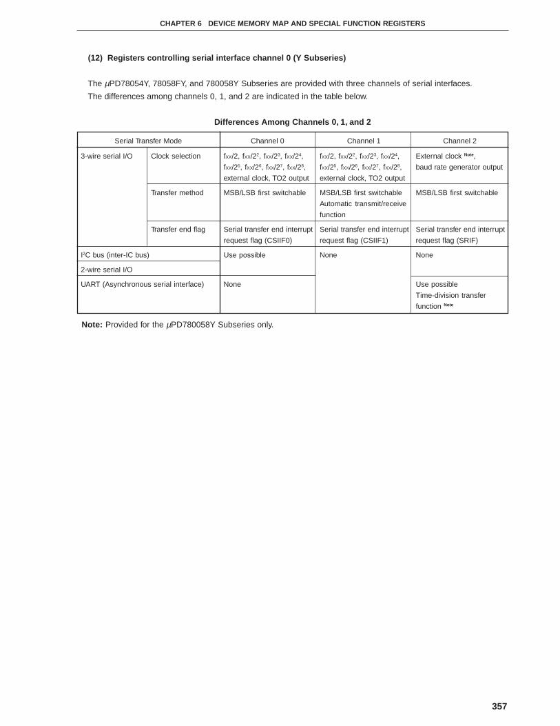
357
CHAPTER 6 DEVICE MEMORY MAP AND SPECIAL FUNCTION REGISTERS
(12) Registers controlling serial interface channel 0 (Y Subseries)
The µPD78054Y, 78058FY, and 780058Y Subseries are provided with three channels of serial interfaces.
The differences among channels 0, 1, and 2 are indicated in the table below.
Differences Among Channels 0, 1, and 2
Serial Transfer Mode Channel 0 Channel 1 Channel 2
3-wire serial I/O Clock selection fXX/2, fXX/22, fXX/23, fXX/24, fXX/2, fXX/22, fXX/23, fXX/24, External clock Note,
fXX/25, fXX/26, fXX/27, fXX/28, fXX/25, fXX/26, fXX/27, fXX/28, baud rate generator output
external clock, TO2 output external clock, TO2 output
Transfer method MSB/LSB first switchable MSB/LSB first switchable MSB/LSB first switchable
Automatic transmit/receive
function
Transfer end flag Serial transfer end interrupt Serial transfer end interrupt Serial transfer end interrupt
request flag (CSIIF0) request flag (CSIIF1) request flag (SRIF)
I2C bus (inter-IC bus) Use possible None None
2-wire serial I/O
UART (Asynchronous serial interface) None Use possible
Time-division transfer
function Note
Note: Provided for the µPD780058Y Subseries only.
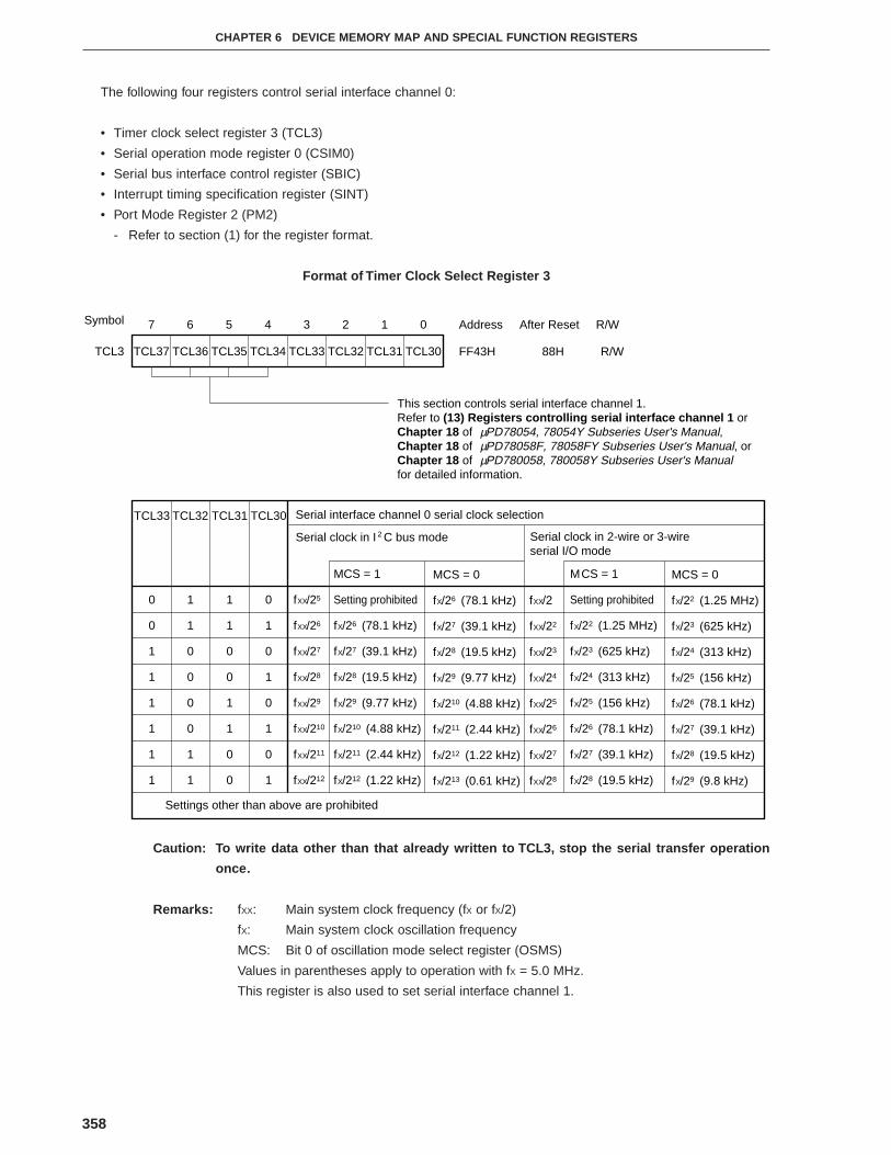
358
CHAPTER 6 DEVICE MEMORY MAP AND SPECIAL FUNCTION REGISTERS
The following four registers control serial interface channel 0:
• Timer clock select register 3 (TCL3)
• Serial operation mode register 0 (CSIM0)
• Serial bus interface control register (SBIC)
• Interrupt timing specification register (SINT)
• Port Mode Register 2 (PM2)
- Refer to section (1) for the register format.
Format of Timer Clock Select Register 3
Caution: To write data other than that already written to TCL3, stop the serial transfer operation
once.
Remarks: fXX: Main system clock frequency (fX or fX/2)
fX: Main system clock oscillation frequency
MCS: Bit 0 of oscillation mode select register (OSMS)
Values in parentheses apply to operation with fX = 5.0 MHz.
This register is also used to set serial interface channel 1.
Serial interface channel 0 serial clock selectionTCL33 TCL32 TCL31 TCL30
0
0
1
1
1
1
1
1
1
1
0
0
0
0
1
1
1
1
0
0
1
1
0
0
0
1
0
1
0
1
0
1
fXX/25
fXX/26
fXX/27
fXX/28
fXX/29
fXX/210
fXX/211
fXX/212
MCS = 1
Setting prohibited
fX/26 (78.1 kHz)
fX/27 (39.1 kHz)
fX/28 (19.5 kHz)
fX/29 (9.77 kHz)
fX/210 (4.88 kHz)
fX/211 (2.44 kHz)
fX/212 (1.22 kHz)
MCS = 1
Setting prohibited
fX/22 (1.25 MHz)
fX/23 (625 kHz)
fX/24 (313 kHz)
fX/25 (156 kHz)
fX/26 (78.1 kHz)
fX/27 (39.1 kHz)
fX/28 (19.5 kHz)
Settings other than above are prohibited
6 5 4 3 2 1 07Symbol
TCL3 TCL37 TCL36 TCL35 TCL34 TCL33 TCL32 TCL31 TCL30 FF43H 88H R/W
Address After Reset R/W
MCS = 0
fX/26 (78.1 kHz)
fX/27 (39.1 kHz)
fX/28 (19.5 kHz)
fX/29 (9.77 kHz)
fX/210 (4.88 kHz)
fX/211 (2.44 kHz)
fX/212 (1.22 kHz)
fX/213 (0.61 kHz)
fXX/2
fXX/22
fXX/23
fXX/24
fXX/25
fXX/26
fXX/27
fXX/28
MCS = 0
fX/22 (1.25 MHz)
fX/23 (625 kHz)
fX/24 (313 kHz)
fX/25 (156 kHz)
fX/26 (78.1 kHz)
fX/27 (39.1 kHz)
fX/28 (19.5 kHz)
fX/29 (9.8 kHz)
Serial clock in I 2 C bus mode Serial clock in 2-wire or 3-wire serial I/O mode
This section controls serial interface channel 1.Refer to (13) Registers controlling serial interface channel 1 orChapter 18 of PD78054, 78054Y Subseries User's Manual,Chapter 18 of PD78058F, 78058FY Subseries User's Manual, orChapter 18 of PD780058, 780058Y Subseries User's Manualfor detailed information.
µµµ
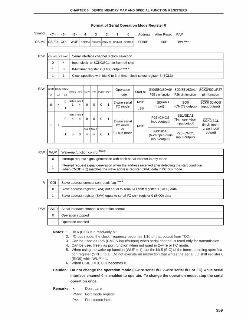
359
CHAPTER 6 DEVICE MEMORY MAP AND SPECIAL FUNCTION REGISTERS
Format of Serial Operation Mode Register 0
Notes: 1. Bit 6 (COI) is a read-only bit.2. I2C bus mode, the clock frequency becomes 1/16 of that output from TO2.3. Can be used as P25 (CMOS input/output) when serial channel is used only for transmission.4. Can be used freely as port function when not used in 2-wire or I2C mode.5. When using the wake-up function (WUP = 1), set the bit 5 (SIC) of the interrupt timing specifica-
tion register (SINT) to 1. Do not execute an instruction that writes the serial I/O shift register 0(SIO0) while WUP = 1.
6. When CSIE0 = 0, COI becomes 0.
Caution: Do not change the operation mode (3-wire serial I/O, 2-wire serial I/O, or I 2C) while serial
interface channel 0 is enabled to operate. To change the operation mode, stop the serial
operation once.
Remarks: ×: Don’t care
PM××: Port mode register
P××: Port output latch
<6> <5> 4 3 2 1 0<7>Symbol
CSIM0 CSIE0 COI WUP CSIM04 CSIM03 CSIM02 CSIM01 CSIM00
CSIM01
0
1
Serial interface channel 0 clock selection
Input clock to SCK0/SCL pin from off chip
8-bit timer register 2 (TM2) output
0
R/W
1 Clock specified with bits 0 to 3 of timer clock select register 3 (TCL3)
CSIM
04
0
CSIM00
×
0
1
FF60H 00H R/W Note 1
Address After Reset R/W
R/W CSIM
03
CSIM
02PM25 P25 PM26 P26 PM27 P27
Operation
modeStart bit
SI0/SB0/SDA0/
P25 pin function
SO0/SB1/SDA1/
P26 pin function
SCK0/SCL/P27
pin function
×1
MSB
LSB1 × 0 0 0 1
Note 3 3-wire seriall/O mode
SI0(Input)
SO0(CMOS output)
SCK0 (CMOSinput/output)
Note 3
2-wire seriall/O mode
orI2C bus mode
0 SCK0/SCL(N-ch open-drain input/
output)1
1 1
×
0
×
0
0
×
0
×
0
0
1
1
Note 4 Note 4
Note 4 Note 4MSB
P25 (CMOSinput/output)
SB0/SDA0(N-ch open-drain
input/output)
SB1/SDA1(N-ch open-drain
input/output)
P26 (CMOSinput/output)
Note 3
WUP
0
1
Wake-up function control Note 5
Interrupt request signal generation with each serial transfer in any mode
Interrupt request signal generation when the address received after detecting the start condition(when CMDD = 1) matches the slave address register (SVA) data in I C bus mode2
R/W
COI
0
1
Slave address comparison result flag Note 6
Slave address register (SVA) not equal to serial I/O shift register 0 (SIO0) data
Slave address register (SVA) equal to serial I/O shift register 0 (SIO0) data
R
CSIE0
0
1
Serial interface channel 0 operation control
Operation stopped
Operation enabled
R/W
Note 2

360
CHAPTER 6 DEVICE MEMORY MAP AND SPECIAL FUNCTION REGISTERS
Format of Serial Bus Interface Control Register (1/2)
Note: Bits 2, 3, and 6 (RELD, CMDD, and ACKD) are read-only bits.
Remark: CSIE0: Bit 7 of serial operation mode register 0 (CSIM0)
<6> <5> <4> <3> <2> <1> <0><7>Symbol
SBIC BSYE ACKD ACKE ACKT CMDD RELD CMDT RELT
RELTUsed for stop condition signal output. When RELT = 1, SO0 Iatch is set to 1. After SO0 latch setting, automatically cleared to 0.Also cleared to 0 when CSIE0 = 0.
R/W
FF61H 00H R/W Note
Address After Reset R/W
CMDTUsed for start condition signal output. When CMDT = 1, SO0 Iatch is cleared to 0. After SO0 latch clearance, automatically cleared to 0. Also cleared to 0 when CSIE0 = 0.
R/W
R RELD Stop condition detection
Set Condition (RELD =1)Clear Conditions (RELD = 0)
• When stop condition signal is detected• When transfer start instruction is executed • If SIO0 and SVA values do not match in address reception • When CSIE0 = 0
• When RESET input is applied
R CMDD Start condition detection
Clear Conditions (CMDD = 0)
• When transfer start instruction is executed • When stop condition signal is detected • When CSIE0 = 0
• When RESET input is applied
Set Condition (CMDD = 1)
• When start condition signal is detected
ACKTUsed to generate the ACK signal by software when an 8-clock wait mode is selected.Keeps SDA0 (SDA1) low from set instruction (ACKT = 1) execution to the next falling edge of SCL.Also cleared to 0 upon start of a serial interface transfer or when CSIE0 = 0.
R/W
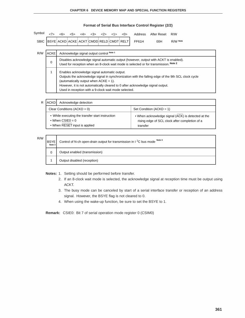
361
CHAPTER 6 DEVICE MEMORY MAP AND SPECIAL FUNCTION REGISTERS
Format of Serial Bus Interface Control Register (2/2)
Notes: 1. Setting should be performed before transfer.
2. If an 8-clock wait mode is selected, the acknowledge signal at reception time must be output using
ACKT.
3. The busy mode can be canceled by start of a serial interface transfer or reception of an address
signal. However, the BSYE flag is not cleared to 0.
4. When using the wake-up function, be sure to set the BSYE to 1.
Remark: CSIE0: Bit 7 of serial operation mode register 0 (CSIM0)
ACKE Acknowledge signal output control
0Disables acknowledge signal automatic output (however, output with ACKT is enabled).Used for reception when an 8-clock wait mode is selected or for transmission.Note 2
Enables acknowledge signal automatic output.Outputs the acknowledge signal in synchronization with the falling edge of the 9th SCL clock cycle(automatically output when ACKE = 1). However, it is not automatically cleared to 0 after acknowledge signal output.Used in reception with a 9-clock wait mode selected.
1
R/W
R ACKD Acknowledge detection
Clear Conditions (ACKD = 0)
• While executing the transfer start instruction
• When CSIE0 = 0
• When RESET input is applied
Set Condition (ACKD = 1)
• When acknowledge signal (ACK) is detected at the
rising edge of SCL clock after completion of a
transfer
BSYE Control of N-ch open-drain output for transmission in I 2C bus mode
0 Output enabled (transmission)
R/W
Note 3
1
Note 4
Output disabled (reception)
Note 1
<6> <5> <4> <3> <2> <1> <0><7>Symbol
SBIC BSYE ACKD ACKE ACKT CMDD RELD CMDT RELT FF61H 00H R/W Note
Address After Reset R/W

362
CHAPTER 6 DEVICE MEMORY MAP AND SPECIAL FUNCTION REGISTERS
Format of Interrupt Timing Specification Register (1/2)
Notes: 1. Bit 6 (CLD) is a read-only bit.
2. When not using the I2C mode, set CLC to 0.
Used in I2C bus mode
Make the SCL pin enter a high-impedance state unless a serial transfer is being performed
(except for the clock line, which is kept high).
Used to enable a master device to generate start condition and stop condition signals.
<6> <5> <4> <3> <2> 1 07Symbol
SINT 0 CLD SIC SVAM CLC WREL WAT1 WAT0 FF63H 00H R/W Note 1
Address After Reset R/W
WREL
0 Wait state has been canceled.
Cancels wait state. Automatically cleared to 0 when the state is canceled.
(Used to cancel the wait state by means of WAT0 and WAT1.)
CLC
0
1
Clock level control Note 2
Used in I2C bus mode
Make output level of SCL pin low unless a serial transfer is being performed.
R/W
1
Wait state cancellation control
R/W
WAT1
0
1
Wait and interrupt control
Generates an interrupt service request at the rising edge of the 8th SCK0 clock cycle
(keeping clock output in high impedance).
R/W WAT0
0
0 Used in I2C bus mode (8-clock wait)
Generates an interrupt service request at the rising edge of the 8th SCK0 clock cycle.
(In the case of a master device, makes SCL output low to enter the wait state after 8 clock pulses are
output. In the case of a slave device, makes SCL output low to request the wait state after 8 clock
pulses are input.)
1 1 Used in I2C bus mode. (9-clock wait)
Generates an interrupt service request at the rising edge of the 9th SCK0 clock cycle.
(In the case of a master device, makes SCL output low to enter the wait state after 9 clock pulses are
output. In the case of a slave device, makes SCL output low to request the wait state after 9 clock
pulses are input.)
0 Setting prohibited1
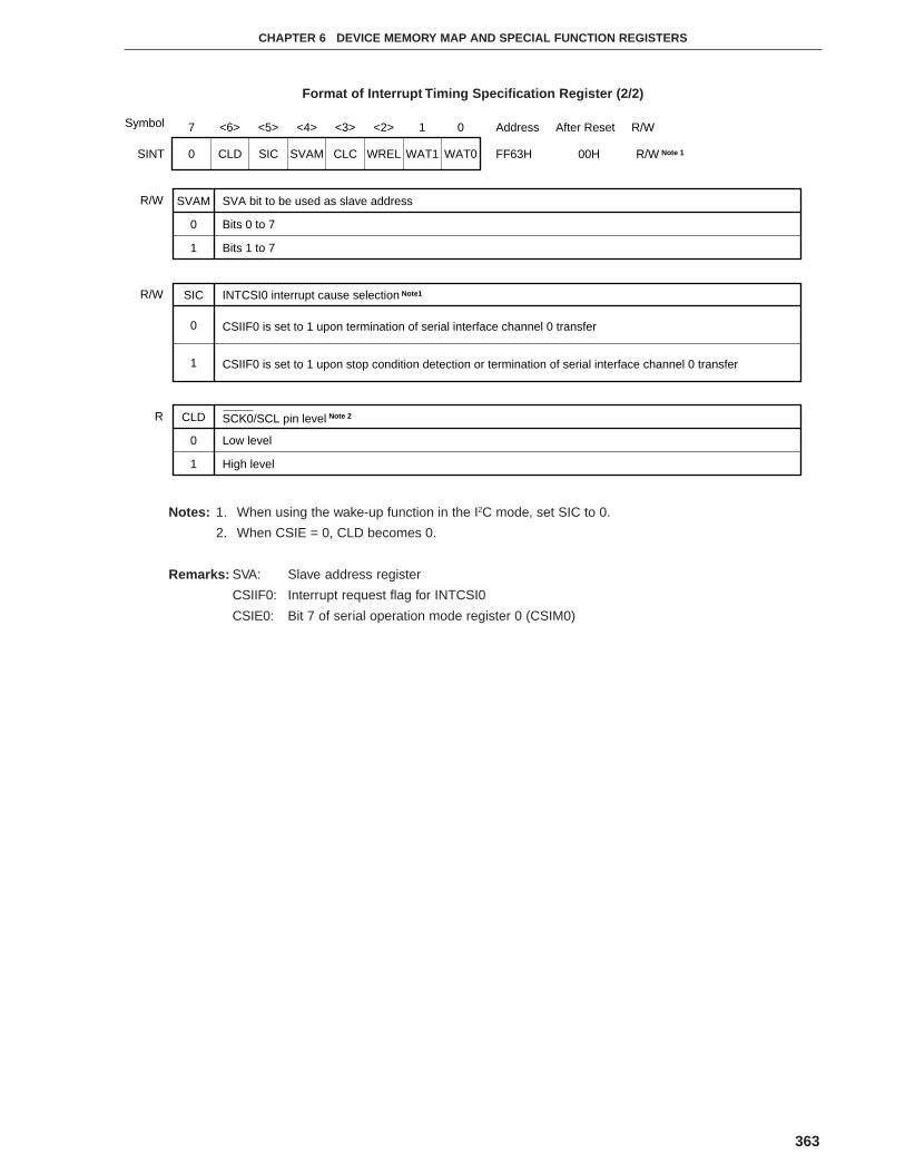
363
CHAPTER 6 DEVICE MEMORY MAP AND SPECIAL FUNCTION REGISTERS
Format of Interrupt Timing Specification Register (2/2)
Notes: 1. When using the wake-up function in the I2C mode, set SIC to 0.
2. When CSIE = 0, CLD becomes 0.
Remarks: SVA: Slave address register
CSIIF0: Interrupt request flag for INTCSI0
CSIE0: Bit 7 of serial operation mode register 0 (CSIM0)
SVAM
0
1
SVA bit to be used as slave address
Bits 0 to 7
Bits 1 to 7
SIC
0
INTCSI0 interrupt cause selection Note1
CSIIF0 is set to 1 upon termination of serial interface channel 0 transfer
CSIIF0 is set to 1 upon stop condition detection or termination of serial interface channel 0 transfer
CLD
0
1
SCK0/SCL pin level Note 2
Low level
High level
R/W
R/W
R
1
<6> <5> <4> <3> <2> 1 07Symbol
SINT 0 CLD SIC SVAM CLC WREL WAT1 WAT0 FF63H 00H R/W Note 1
Address After Reset R/W
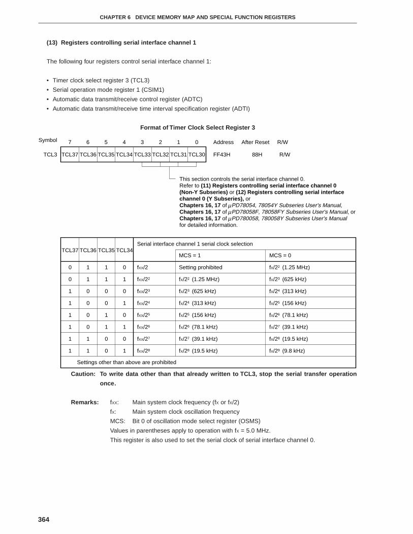
364
CHAPTER 6 DEVICE MEMORY MAP AND SPECIAL FUNCTION REGISTERS
(13) Registers controlling serial interface channel 1
The following four registers control serial interface channel 1:
• Timer clock select register 3 (TCL3)
• Serial operation mode register 1 (CSIM1)
• Automatic data transmit/receive control register (ADTC)
• Automatic data transmit/receive time interval specification register (ADTI)
Format of Timer Clock Select Register 3
Caution: To write data other than that already written to TCL3, stop the serial transfer operation
once.
Remarks: fXX: Main system clock frequency (fX or fX/2)
fX: Main system clock oscillation frequency
MCS: Bit 0 of oscillation mode select register (OSMS)
Values in parentheses apply to operation with fX = 5.0 MHz.
This register is also used to set the serial clock of serial interface channel 0.
6 5 4 3 2 1 07Symbol
TCL3 TCL37 TCL36 TCL35 TCL34 TCL33 TCL32 TCL31 TCL30 FF43H 88H R/W
Address After Reset R/W
Serial interface channel 1 serial clock selectionTCL37 TCL36 TCL35 TCL34
0
0
1
1
1
1
1
1
1
1
0
0
0
0
1
1
1
1
0
0
1
1
0
0
0
1
0
1
0
1
0
1
fXX/2
fXX/22
fXX/23
fXX/24
fXX/25
fXX/26
fXX/27
fXX/28
MCS = 1
Setting prohibited
fX/22 (1.25 MHz)
fX/23 (625 kHz)
fX/24 (313 kHz)
fX/25 (156 kHz)
fX/26 (78.1 kHz)
fX/27 (39.1 kHz)
fX/28 (19.5 kHz)
MCS = 0
fX/22 (1.25 MHz)
fX/23 (625 kHz)
fX/24 (313 kHz)
fX/25 (156 kHz)
fX/26 (78.1 kHz)
fX/27 (39.1 kHz)
fX/28 (19.5 kHz)
fX/29 (9.8 kHz)
Settings other than above are prohibited
µµµ
This section controls the serial interface channel 0.Refer to (11) Registers controlling serial interface channel 0 (Non-Y Subseries) or (12) Registers controlling serial interface channel 0 (Y Subseries), orChapters 16, 17 of PD78054, 78054Y Subseries User's Manual,Chapters 16, 17 of PD78058F, 78058FY Subseries User's Manual, orChapters 16, 17 of PD780058, 780058Y Subseries User's Manualfor detailed information.
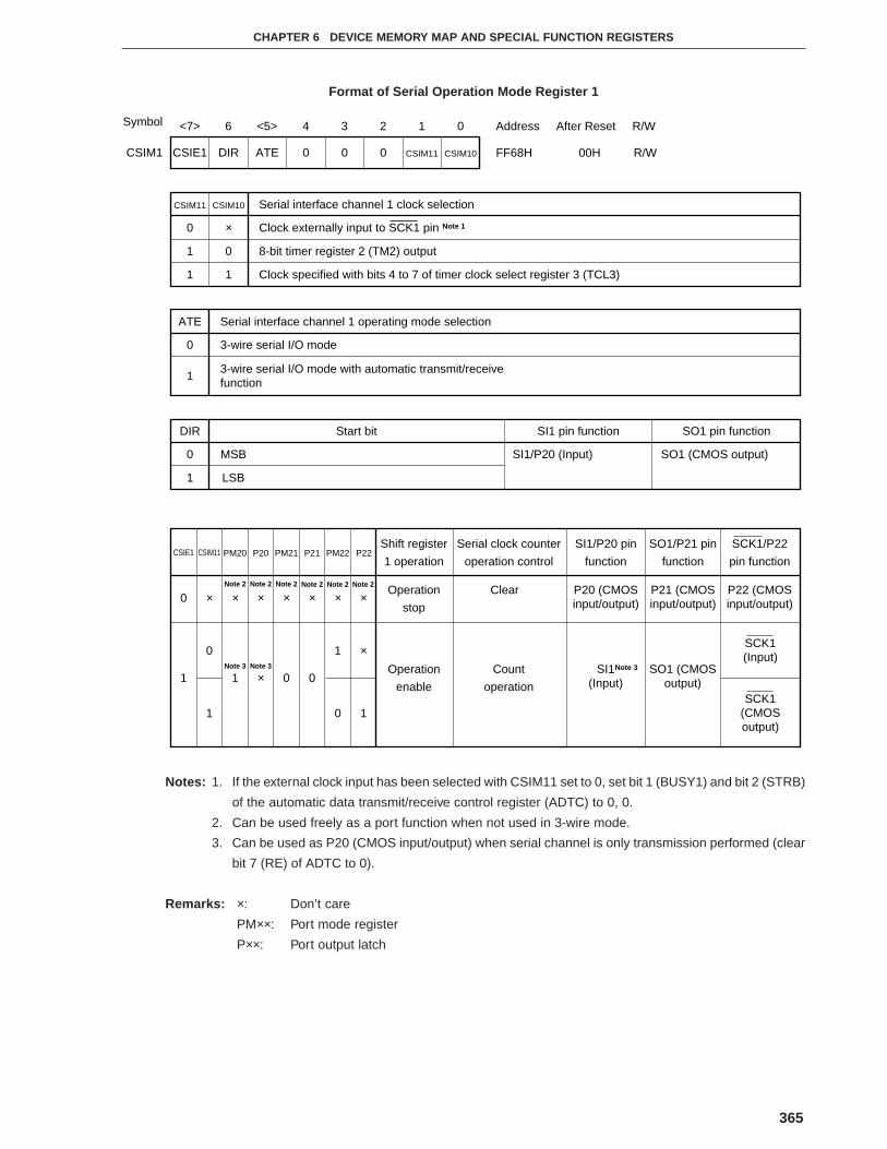
365
CHAPTER 6 DEVICE MEMORY MAP AND SPECIAL FUNCTION REGISTERS
Format of Serial Operation Mode Register 1
Notes: 1. If the external clock input has been selected with CSIM11 set to 0, set bit 1 (BUSY1) and bit 2 (STRB)
of the automatic data transmit/receive control register (ADTC) to 0, 0.
2. Can be used freely as a port function when not used in 3-wire mode.
3. Can be used as P20 (CMOS input/output) when serial channel is only transmission performed (clear
bit 7 (RE) of ADTC to 0).
Remarks: ×: Don’t care
PM××: Port mode register
P××: Port output latch
Operation
enable
6 <5> 4 3 2 1 0<7>Symbol
CSIM1 CSIE1 DIR ATE 0 0 0 CSIM11 CSIM10
CSIM11
0
1
Serial interface channel 1 clock selection
Clock externally input to SCK1 pin Note 1
8-bit timer register 2 (TM2) output
SCK1(Input)
1 Clock specified with bits 4 to 7 of timer clock select register 3 (TCL3)
CSIE1
0
CSIM10
×
0
1
FF68H 00H R/W
Address After Reset R/W
CSIM11 P20 PM21 P21 PM22
Note 3
Shift register
1 operation
Serial clock counter
operation control
SI1/P20 pin
function
SCK1/P22
pin function
×
1
0
1
0
× 0 0
1 ×
1
Note 2 Note 2 Note 2 Note 2
Count
operation
SI1(Input)
× × × × ×Operation
stop
Clear P20 (CMOSinput/output)
P22 (CMOSinput/output)
ATE
0
1
Serial interface channel 1 operating mode selection
3-wire serial I/O mode
3-wire serial I/O mode with automatic transmit/receivefunction
DIR
0
1
Start bit
MSB
LSB
SI1 pin function
SI1/P20 (Input)
SO1 pin function
SO1 (CMOS output)
×
PM20SO1/P21 pin
function
SO1 (CMOSoutput)
P21 (CMOSinput/output)
SCK1(CMOSoutput)
1
Note 2Note 2
Note 3Note 3
P22

366
CHAPTER 6 DEVICE MEMORY MAP AND SPECIAL FUNCTION REGISTERS
Format of Automatic Data Transmit/Receive Control Register
<6> <5> <4> <3> <2> <1> <0><7>Symbol
ADTC RE ARLD ERCE ERR TRF STRB BUSY1 BUSY0 FF69H 00H R/W Note 1
Address After Reset R/W
BUSY1
0
1
1
Busy input control
Not using busy input
Busy input enable (active high)
Busy input enable (active low)
BUSY0
×
0
1
STRB
0
1
Strobe output control
Strobe output disable
Strobe output enable
TRF
1
Status of automatic transmit/receive function Note 2
Detection of termination of automatic transmission/reception (This bit is set to 0 upon suspension ofautomatic transmission/reception or when ARLD = 0.)
During automatic transmission/reception(This bit is set to 1 when data is written to SIO1.)
R/W
R/W
R
RERR
0
1
Error detection of automatic transmit/receivefunction
No error(This bit is set to 0 when data is written to SIO1)
Error occurred
R/WARLD
0
1
Operating mode selection of automatic transmit/receive function
Single operating mode
Repetitive operating mode
R/WRE
0
1
Receive control of automatic transmit/receivefunction
Receive disable
Receive enable
R/WERCE
0
Error check control of automatic transmit/receive function
Error check disable
Error check enable (only when BUSY1 = 1)
0
1
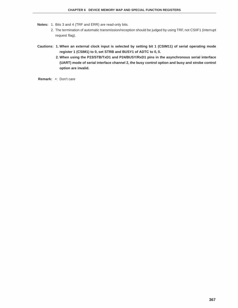
367
CHAPTER 6 DEVICE MEMORY MAP AND SPECIAL FUNCTION REGISTERS
Notes: 1. Bits 3 and 4 (TRF and ERR) are read-only bits.
2. The termination of automatic transmission/reception should be judged by using TRF, not CSIIF1 (interrupt
request flag).
Cautions: 1. When an external clock input is selected by setting bit 1 (CSIM11) of serial operating mode
register 1 (CSIM1) to 0, set STRB and BUSY1 of ADTC to 0, 0.
2. When using the P23/STB/TxD1 and P24/BUSY/RxD1 pins in the asynchronous serial interface
(UART) mode of serial interface channel 2, the busy control option and busy and strobe control
option are invalid.
Remark: ×: Don't care
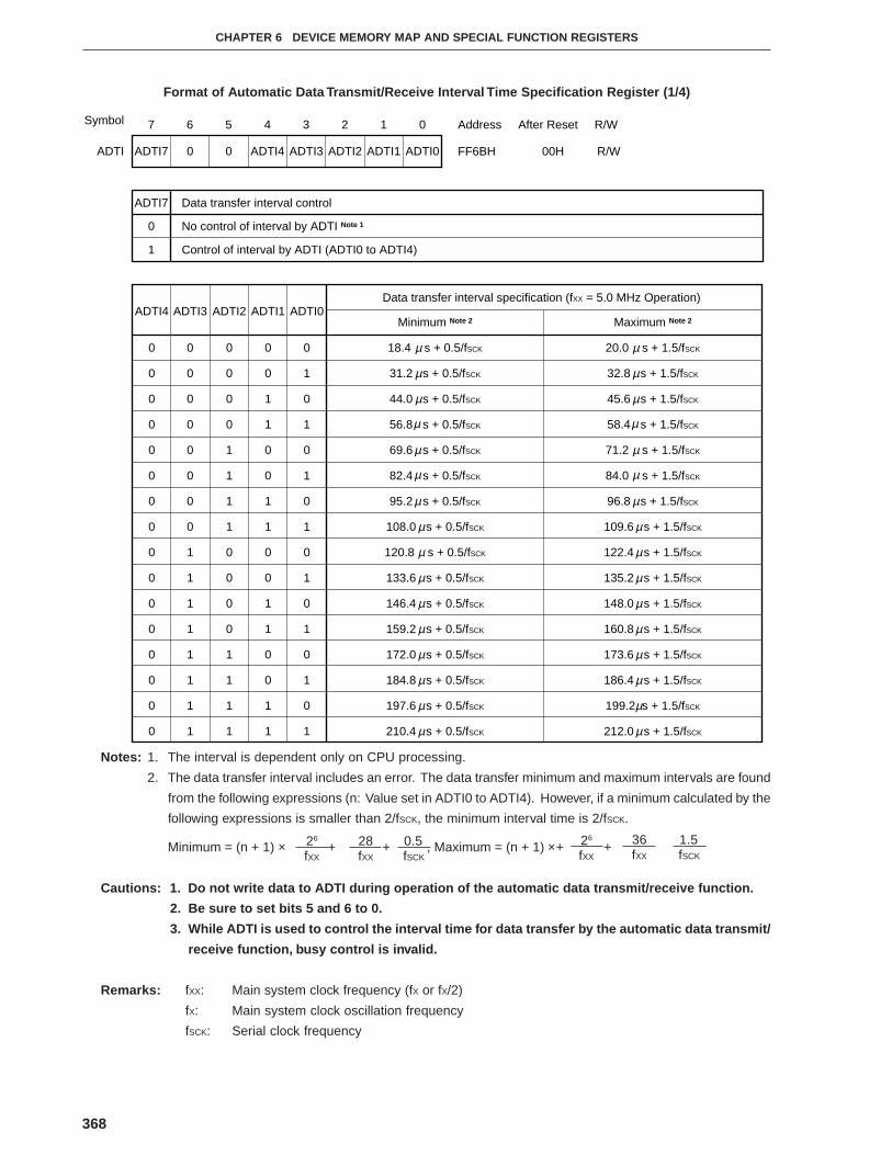
368
CHAPTER 6 DEVICE MEMORY MAP AND SPECIAL FUNCTION REGISTERS
Format of Automatic Data Transmit/Receive Interval Time Specification Register (1/4)
Notes: 1. The interval is dependent only on CPU processing.
2. The data transfer interval includes an error. The data transfer minimum and maximum intervals are found
from the following expressions (n: Value set in ADTI0 to ADTI4). However, if a minimum calculated by the
following expressions is smaller than 2/fSCK, the minimum interval time is 2/fSCK.
Minimum = (n + 1) × + + , Maximum = (n + 1) ×+ +
Cautions: 1. Do not write data to ADTI during operation of the automatic data transmit/receive function.
2. Be sure to set bits 5 and 6 to 0.
3. While ADTI is used to control the interval time for data transfer by the automatic data transmit/
receive function, busy control is invalid.
Remarks: fXX: Main system clock frequency (fX or fX/2)
fX: Main system clock oscillation frequency
fSCK: Serial clock frequency
26 28 0.5fXX fXX fSCK
26
fXX
36fXX
1.5fSCK
Data transfer interval specification (fXX = 5.0 MHz Operation) ADTI4 ADTI3 ADTI2 ADTI1
0
0
0
0
0
0
0
0
0
0
0
0
0
0
0
0
0
0
0
0
0
0
0
0
1
1
1
1
1
1
1
1
0
0
0
0
1
1
1
1
0
0
0
0
1
1
1
1
0
0
1
1
0
0
1
1
0
0
1
1
0
0
1
1
Minimum Note 2
18.4 s + 0.5/fSCK
31.2 s + 0.5/fSCK
44.0 s + 0.5/fSCK
56.8 s + 0.5/fSCK
69.6 s + 0.5/fSCK
82.4 s + 0.5/fSCK
95.2 s + 0.5/fSCK
108.0 s + 0.5/fSCK
120.8 s + 0.5/fSCK
133.6 s + 0.5/fSCK
146.4 s + 0.5/fSCK
159.2 s + 0.5/fSCK
172.0 s + 0.5/fSCK
184.8 s + 0.5/fSCK
197.6 s + 0.5/fSCK
210.4 s + 0.5/fSCK
Maximum Note 2
20.0 s + 1.5/fSCK
32.8 s + 1.5/fSCK
45.6 s + 1.5/fSCK
58.4 s + 1.5/fSCK
71.2 s + 1.5/fSCK
84.0 s + 1.5/fSCK
96.8 s + 1.5/fSCK
109.6 s + 1.5/fSCK
122.4 s + 1.5/fSCK
135.2 s + 1.5/fSCK
148.0 s + 1.5/fSCK
160.8 s + 1.5/fSCK
173.6 s + 1.5/fSCK
186.4 s + 1.5/fSCK
199.2 s + 1.5/fSCK
212.0 s + 1.5/fSCK
6 5 4 3 2 1 07Symbol
ADTI ADTI7 0 0 ADTI4 ADTI3 ADTI2 ADTI1 ADTI0 FF6BH 00H R/W
Address After Reset R/W
ADTI7
0
Data transfer interval control
No control of interval by ADTI Note 1
Control of interval by ADTI (ADTI0 to ADTI4) 1
ADTI0
0
1
0
1
0
1
0
1
0
1
0
1
0
1
0
1
µ
µ
µ
µ
µ
µ
µ
µ
µ
µ
µ
µ
µ
µ
µ
µ
µ
µ
µ
µ
µ
µ
µ
µ
µ
µ
µ
µ
µ
µ
µ
µ
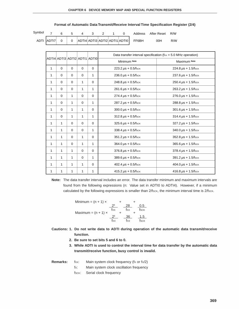
369
CHAPTER 6 DEVICE MEMORY MAP AND SPECIAL FUNCTION REGISTERS
Format of Automatic Data Transmit/Receive Interval Time Specification Register (2/4)
Note: The data transfer interval includes an error. The data transfer minimum and maximum intervals are
found from the following expressions (n: Value set in ADTI0 to ADTI4). However, if a minimum
calculated by the following expressions is smaller than 2/fSCK, the minimum interval time is 2/fSCK.
Minimum = (n + 1) × + +
Maximum = (n + 1) × + +
Cautions: 1. Do not write data to ADTI during operation of the automatic data transmit/receive
function.
2. Be sure to set bits 5 and 6 to 0.
3. While ADTI is used to control the interval time for data transfer by the automatic data
transmit/receive function, busy control is invalid.
Remarks: fXX: Main system clock frequency (fX or fX/2)
fX: Main system clock oscillation frequency
fSCK: Serial clock frequency
26 28 0.5fXX fXX fSCK
26 36 1.5fXX fXX fSCK
Data transfer interval specification (fXX = 5.0 MHz operation) ADTI4 ADTI3 ADTI2 ADTI1
1
1
1
1
1
1
1
1
1
1
1
1
1
1
1
1
0
0
0
0
0
0
0
0
1
1
1
1
1
1
1
1
0
0
0
0
1
1
1
1
0
0
0
0
1
1
1
1
0
0
1
1
0
0
1
1
0
0
1
1
0
0
1
1
Minimum Note
223.2 s + 0.5/fSCK
236.0 s + 0.5/fSCK
248.8 s + 0.5/fSCK
261.6 s + 0.5/fSCK
274.4 s + 0.5/fSCK
287.2 s + 0.5/fSCK
300.0 s + 0.5/fSCK
312.8 s + 0.5/fSCK
325.6 s + 0.5/fSCK
338.4 s + 0.5/fSCK
351.2 s + 0.5/fSCK
364.0 s + 0.5/fSCK
376.8 s + 0.5/fSCK
389.6 s + 0.5/fSCK
402.4 s + 0.5/fSCK
415.2 s + 0.5/fSCK
Maximum Note
224.8 s + 1.5/fSCK
237.6 s + 1.5/fSCK
250.4 s + 1.5/fSCK
263.2 s + 1.5/fSCK
276.0 s + 1.5/fSCK
288.8 s + 1.5/fSCK
301.6 s + 1.5/fSCK
314.4 s + 1.5/fSCK
327.2 s + 1.5/fSCK
340.0 s + 1.5/fSCK
352.8 s + 1.5/fSCK
365.6 s + 1.5/fSCK
378.4 s + 1.5/fSCK
391.2 s + 1.5/fSCK
404.0 s + 1.5/fSCK
416.8 s + 1.5/fSCK
6 5 4 3 2 1 07Symbol
ADTI ADTI7 0 0 ADTI4 ADTI3 ADTI2 ADTI1 ADTI0 FF6BH 00H R/W
Address After Reset R/W
ADTI0
0
1
0
1
0
1
0
1
0
1
0
1
0
1
0
1
µ
µ
µ
µ
µ
µ
µ
µ
µ
µ
µ
µ
µ
µ
µ
µ
µ
µ
µ
µ
µ
µ
µ
µ
µ
µ
µ
µ
µ
µ
µ
µ

370
CHAPTER 6 DEVICE MEMORY MAP AND SPECIAL FUNCTION REGISTERS
Format of Automatic Data Transmit/Receive Interval Time Specification Register (3/4)
Notes: 1. The interval is dependent only on CPU processing.
2. The data transfer interval includes an error. The data transfer minimum and maximum intervals are found
from the following expressions (n: Value set in ADTI0 to ADTI4). However, if a minimum calculated by the
following expressions is smaller than 2/fSCK, the minimum interval time is 2/fSCK.
Minimum = (n + 1) × + + , Maximum = (n + 1) ×+ +
Cautions: 1. Do not write data to ADTI during operation of the automatic data transmit/receive function.
2. Be sure to set bits 5 and 6 to 0.
3. While ADTI is used to control the interval time for data transfer by the automatic data transmit/
receive function, busy control is invalid.
Remarks: fXX: Main system clock frequency (fX or fX/2)
fX: Main system clock oscillation frequency
fSCK: Serial clock frequency
26 28 0.5fXX fXX fSCK
26
fXX
36fXX
1.5fSCK
Data transfer interval specification (fXX = 2.5 MHz operation) ADTI4 ADTI3 ADTI2 ADTI1
0
0
0
0
0
0
0
0
0
0
0
0
0
0
0
0
0
0
0
0
0
0
0
0
1
1
1
1
1
1
1
1
0
0
0
0
1
1
1
1
0
0
0
0
1
1
1
1
0
0
1
1
0
0
1
1
0
0
1
1
0
0
1
1
Minimum Note 2
36.8 s + 0.5/fSCK
62.4 s + 0.5/fSCK
88.0 s + 0.5/fSCK
113.6 s + 0.5/fSCK
139.2 s + 0.5/fSCK
164.8 s + 0.5/fSCK
190.4 s + 0.5/fSCK
216.0 s + 0.5/fSCK
241.6 s + 0.5/fSCK
267.2 s + 0.5/fSCK
292.8 s + 0.5/fSCK
318.4 s + 0.5/fSCK
344.0 s + 0.5/fSCK
369.6 s + 0.5/fSCK
395.2 s + 0.5/fSCK
420.8 s + 0.5/fSCK
Maximum Note 2
40.0 s + 1.5/fSCK
65.6 s + 1.5/fSCK
91.2 s + 1.5/fSCK
116.8 s + 1.5/fSCK
142.4 s + 1.5/fSCK
168.0 s + 1.5/fSCK
193.6 s + 1.5/fSCK
219.2 s + 1.5/fSCK
244.8 s + 1.5/fSCK
270.4 s + 1.5/fSCK
296.0 s + 1.5/fSCK
321.6 s + 1.5/fSCK
347.2 s + 1.5/fSCK
372.8 s + 1.5/fSCK
398.4 s + 1.5/fSCK
424.0 s + 1.5/fSCK
6 5 4 3 2 1 07Symbol
ADTI ADTI7 0 0 ADTI4 ADTI3 ADTI2 ADTI1 ADTI0 FF6BH 00H R/W
Address After Reset R/W
ADTI7
0
Data transfer interval control
No control of interval by ADTI Note 1
Control of interval by ADTI (ADTI0 to ADTI4) 1
ADTI0
0
1
0
1
0
1
0
1
0
1
0
1
0
1
0
1
µ
µ
µ
µ
µ
µ
µ
µ
µ
µ
µ
µ
µ
µ
µ
µ
µ
µ
µ
µ
µ
µ
µ
µ
µ
µ
µ
µ
µ
µ
µ
µ

371
CHAPTER 6 DEVICE MEMORY MAP AND SPECIAL FUNCTION REGISTERS
Format of Automatic Data Transmit/Receive Interval Time Specification Register (4/4)
Note: The data transfer interval includes an error. The data transfer minimum and maximum intervals are
found from the following expressions (n: Value set in ADTI0 to ADTI4). However, if a minimum
calculated by the following expressions is smaller than 2/fSCK, the minimum interval time is 2/fSCK.
Minimum = (n + 1) × + +
Maximum = (n + 1) × + +
Cautions: 1. Do not write data to ADTI during operation of the automatic data transmit/receive func-
tion.
2. Be sure to set bits 5 and 6 to 0.
3. While ADTI is used to control the interval time for data transfer by the automatic data
transmit/receive function, busy control is invalid.
Remarks: fXX: Main system clock frequency (fX or fX/2)
fX: Main system clock oscillation frequency
fSCK: Serial clock frequency
26 28 0.5fXX fXX fSCK
26 36 1.5fXX fSCK
Data transfer interval specification (fXX = 2.5 MHz operation) ADTI4 ADTI3 ADTI2 ADTI1
1
1
1
1
1
1
1
1
1
1
1
1
1
1
1
1
0
0
0
0
0
0
0
0
1
1
1
1
1
1
1
1
0
0
0
0
1
1
1
1
0
0
0
0
1
1
1
1
0
0
1
1
0
0
1
1
0
0
1
1
0
0
1
1
Minimum Note
446.4 s + 0.5/fSCK
472.0 s + 0.5/fSCK
497.6 s + 0.5/fSCK
523.2 s + 0.5/fSCK
548.8 s + 0.5/fSCK
574.4 s + 0.5/fSCK
600.0 s + 0.5/fSCK
625.6 s + 0.5/fSCK
651.2 s + 0.5/fSCK
676.8 s + 0.5/fSCK
702.4 s + 0.5/fSCK
728.0 s + 0.5/fSCK
753.6 s + 0.5/fSCK
779.2 s + 0.5/fSCK
804.8 s + 0.5/fSCK
830.4 s + 0.5/fSCK
Maximum Note
449.6 s + 1.5/fSCK
475.2 s + 1.5/fSCK
500.8 s + 1.5/fSCK
526.4 s + 1.5/fSCK
552.0 s + 1.5/fSCK
577.6 s + 1.5/fSCK
603.2 s + 1.5/fSCK
628.8 s + 1.5/fSCK
654.4 s + 1.5/fSCK
680.0 s + 1.5/fSCK
705.6 s + 1.5/fSCK
731.2 s + 1.5/fSCK
756.8 s + 1.5/fSCK
782.4 s + 1.5/fSCK
808.0 s + 1.5/fSCK
833.6 s + 1.5/fSCK
6 5 4 3 2 1 07Symbol
ADTI ADTI7 0 0 ADTI4 ADTI3 ADTI2 ADTI1 ADTI0 FF6BH 00H R/W
Address After Reset R/W
ADTI0
0
1
0
1
0
1
0
1
0
1
0
1
0
1
0
1
µ
µ
µ
µ
µ
µ
µ
µ
µ
µ
µ
µ
µ
µ
µ
µ
µ
µ
µ
µ
µ
µ
µ
µ
µ
µ
µ
µ
µ
µ
µ
µ
fXX

372
CHAPTER 6 DEVICE MEMORY MAP AND SPECIAL FUNCTION REGISTERS
(14) Registers controlling serial interface channel 2
The following five registers control serial interface channel 2:
• Serial operation mode register 2 (CSIM2)
• Asynchronous serial interface mode register (ASIM)
• Asynchronous serial interface status register (ASIS)
• Baud rate generator control register (BRGC)
• Serial interface pin select register (SIPS) Note
Note: This register is provided only for µPD780058/58Y Subseries products.
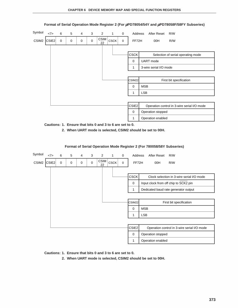
373
CHAPTER 6 DEVICE MEMORY MAP AND SPECIAL FUNCTION REGISTERS
Format of Serial Operation Mode Register 2 (For µµµµµPD78054/54Y and µµµµµPD78058F/58FY Subseries)
Cautions: 1. Ensure that bits 0 and 3 to 6 are set to 0.
2. When UART mode is selected, CSIM2 should be set to 00H.
Format of Serial Operation Mode Register 2 (For 780058/58Y Subseries)
Cautions: 1. Ensure that bits 0 and 3 to 6 are set to 0.
2. When UART mode is selected, CSIM2 should be set to 00H.
6 5 4 3 2 1 0<7>Symbol
CSIM2 CSIE2 0 0 0 0 CSIM22
CSCK 0 FF72H 00H R/W
Address After Reset R/W
CSCK
0
1
Selection of serial operating mode
UART mode
3-wire serial I/O mode
CSIM22
0
1
First bit specification
MSB
LSB
CSIE2
0
1
Operation control in 3-wire serial I/O mode
Operation stopped
Operation enabled
6 5 4 3 2 1 0<7>Symbol
CSIM2 CSIE2 0 0 0 0 CSIM22
CSCK 0 FF72H 00H R/W
Address After Reset R/W
CSCK
0
1
Clock selection in 3-wire serial I/O mode
Input clock from off chip to SCK2 pin
Dedicated baud rate generator output
CSIM22
0
1
First bit specification
MSB
LSB
CSIE2
0
1
Operation control in 3-wire serial I/O mode
Operation stopped
Operation enabled

374
CHAPTER 6 DEVICE MEMORY MAP AND SPECIAL FUNCTION REGISTERS
Format of Asynchronous Serial Interface Mode Register
Note: When SCK is set to 1 and the baud rate generator output is selected, the ASCK pin can be used as an
input/output port.
Cautions: 1. When the 3-wire serial I/O mode is selected, 00H should be set in ASIM.
2. The serial transmit/receive operation must be stopped before changing the operating mode.
<6> 5 4 3 2 1 0<7>Symbol
ASIM TXE RXE PS1 PS0 CL SL ISRM SCK FF70H 00H R/W
Address After Reset R/W
SCK
0
1
Clock selection in asynchronous serial interfacemode
Input clock from off chip to ASCK pin
Dedicated baud rate generator output Note
ISRM
0
1
Control of reception completion interrupt request in case of error generation
Reception completion interrupt request generated in case of error generation
Reception completion interrupt request not generated in case of error generation
SL Transmit data stop bit length specification
CL
1
Character length specification
7 bits
8 bits
RXE
0
1
Receive operation control
Receive operation stopped
Receive operation enabled
TXE
0
1
Transmit operation control
Transmit operation stopped
Transmit operation enabled
PS1
0
1
0 1 bit
1 2 bits
0
Parity bit specification
No parity
Even parity
PS0
0
1
0 parity always added in transmissionNo parity test in reception (parity error notgenerated)
0 1
1 Odd parity0
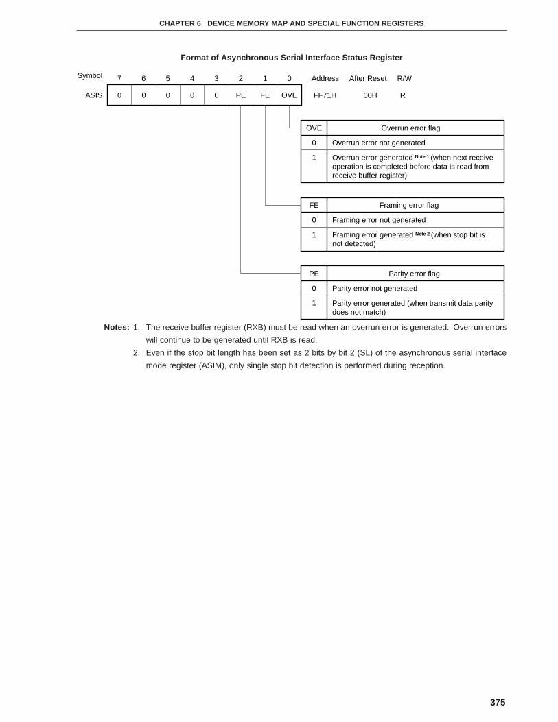
375
CHAPTER 6 DEVICE MEMORY MAP AND SPECIAL FUNCTION REGISTERS
Format of Asynchronous Serial Interface Status Register
Notes: 1. The receive buffer register (RXB) must be read when an overrun error is generated. Overrun errors
will continue to be generated until RXB is read.
2. Even if the stop bit length has been set as 2 bits by bit 2 (SL) of the asynchronous serial interface
mode register (ASIM), only single stop bit detection is performed during reception.
PE
6 5 4 3 2 1 07Symbol
ASIS 0 0 0 0 0 FE OVE FF71H 00H R
Address After Reset R/W
OVE
0
1
Overrun error flag
Overrun error not generated
Overrun error generated Note 1 (when next receive operation is completed before data is read from receive buffer register)
FE
0
1
Framing error flag
Framing error not generated
Framing error generated Note 2 (when stop bit is not detected)
PE
0
1
Parity error flag
Parity error not generated
Parity error generated (when transmit data paritydoes not match)
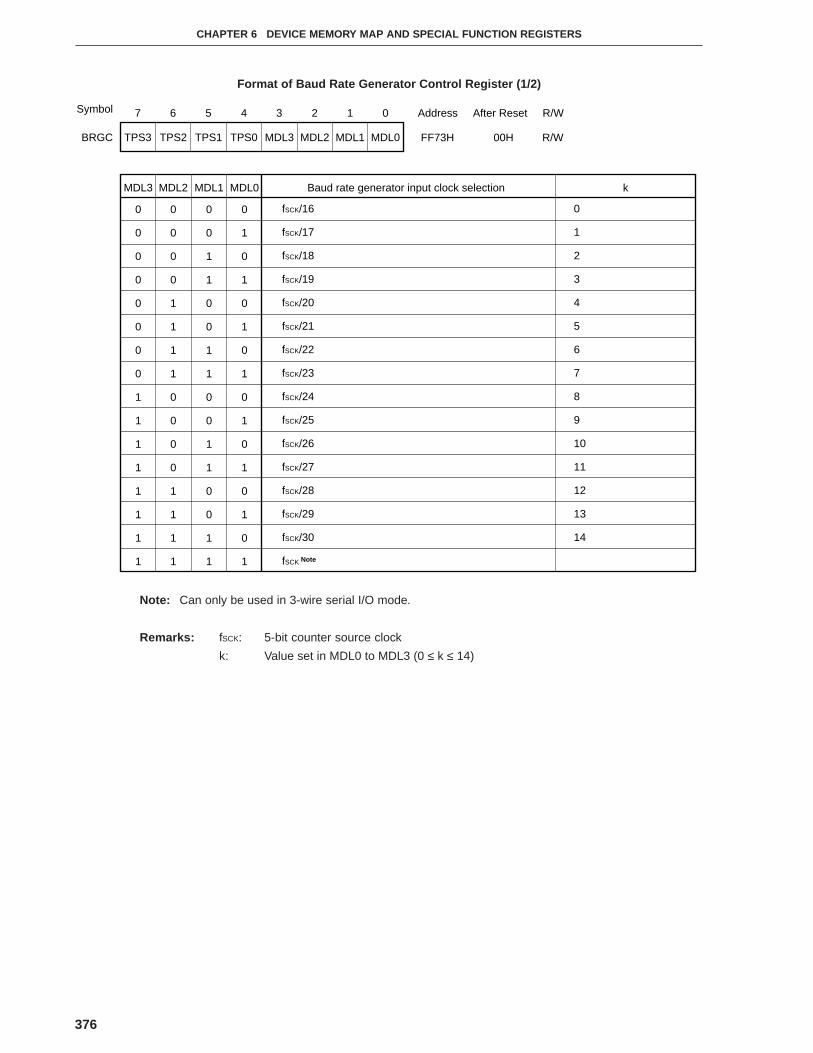
376
CHAPTER 6 DEVICE MEMORY MAP AND SPECIAL FUNCTION REGISTERS
Format of Baud Rate Generator Control Register (1/2)
Note: Can only be used in 3-wire serial I/O mode.
Remarks: fSCK: 5-bit counter source clock
k: Value set in MDL0 to MDL3 (0 ≤ k ≤ 14)
Baud rate generator input clock selectionMDL3 MDL2 MDL1 MDL0
0
0
0
0
0
0
0
0
1
1
1
1
1
1
1
1
0
0
0
0
1
1
1
1
0
0
0
0
1
1
1
1
0
0
1
1
0
0
1
1
0
0
1
1
0
0
1
1
0
1
0
1
0
1
0
1
0
1
0
1
0
1
0
1
fSCK/16
fSCK/17
fSCK/18
fSCK/19
fSCK/20
fSCK/21
fSCK/22
fSCK/23
fSCK/24
fSCK/25
fSCK/26
fSCK/27
fSCK/28
fSCK/29
fSCK/30
fSCK Note
0
1
2
3
4
5
6
7
8
9
10
11
12
13
14
6 5 4 3 2 1 07Symbol
BRGC TPS3 TPS2 TPS1 TPS0 MDL3 MDL2 MDL1 MDL0 FF73H 00H R/W
Address After Reset R/W
k

377
CHAPTER 6 DEVICE MEMORY MAP AND SPECIAL FUNCTION REGISTERS
Format of Baud Rate Generator Control Register (2/2)
TPS3 TPS2 TPS1 TPS0 5-bit counter source clock selection n
MCS = 1 MCS = 0
0 0 0 0 fXX/210 fXX/210 (4.9 kHz) fX/211 (2.4 kHz) 11
0 1 0 1 fXX fX (5.0 MHz) fX/2 (2.5 MHz) 1
0 1 1 0 fXX/2 fX/2 (2.5 MHz) fX/22 (1.25 MHz) 2
0 1 1 1 fXX/22 fX/22 (1.25 MHz) fX/23 (625 kHz) 3
1 0 0 0 fXX/23 fX/23 (625 kHz) fX/24 (313 kHz) 4
1 0 0 1 fXX/24 fX/24 (313 kHz) fX/25 (156 kHz) 5
1 0 1 0 fXX/25 fX/25 (156 kHz) fX/26 (78.1 kHz) 6
1 0 1 1 fXX/26 fX/26 (78.1 kHz) fX/27 (39.1 kHz) 7
1 1 0 0 fXX/27 fX/27 (39.1 kHz) fX/28 (19.5 kHz) 8
1 1 0 1 fXX/28 fX/28 (19.5 kHz) fX/29 (9.8 kHz) 9
1 1 1 0 fXX/29 fX/29 (9.8 kHz) fX/210 (4.9 kHz) 10
Settings other than above are prohibited
Caution: When a write is performed to BRGC during a communication operation, baud rate generator
output is disrupted and communication cannot be performed normally. Therefore, BRGC must
not be written to during a communication operation.
Remarks: fX: Main system clock oscillation frequency
fXX: Main system clock frequency (fX or fX/2)
MCS: Bit 0 of oscillation mode selection register (OSMS)
n: Value set in TPS0 to TPS3 (1 ≤ n ≤ 11)
Values in parentheses apply to operation with fX = 5.0 MHz.
6 5 4 3 2 1 07Symbol
BRGC TPS3 TPS2 TPS1 TPS0 MDL3 MDL2 MDL1 MDL0 FF73H 00H R/W
Address After Reset R/W
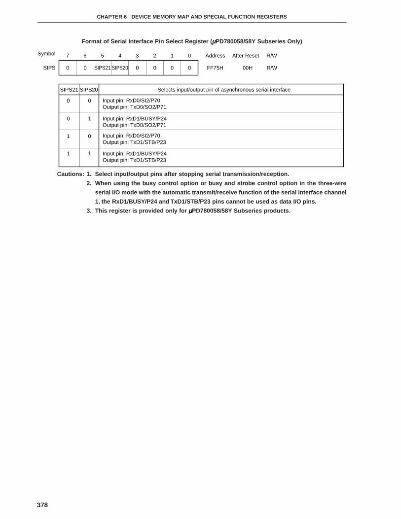
378
CHAPTER 6 DEVICE MEMORY MAP AND SPECIAL FUNCTION REGISTERS
Format of Serial Interface Pin Select Register ( µµµµµPD780058/58Y Subseries Only)
Cautions: 1. Select input/output pins after stopping serial transmission/reception.
2. When using the busy control option or busy and strobe control option in the three-wire
serial I/O mode with the automatic transmit/receive function of the serial interface channel
1, the RxD1/BUSY/P24 and TxD1/STB/P23 pins cannot be used as data I/O pins.
3. This register is provided only for µµµµµPD780058/58Y Subseries products.
6 5 4 3 2 1 07Symbol
SIPS 0 0 SIPS21 SIPS20 0 0 0 0 FF75H 00H R/W
Address After Reset R/W
SIPS21
0
1
Selects input/output pin of asynchronous serial interface
Input pin: RxD0/SI2/P70Output pin: TxD0/SO2/P71
Input pin: RxD1/BUSY/P24Output pin: TxD1/STB/P23
SIPS20
0
1
Input pin: RxD1/BUSY/P24Output pin: TxD0/SO2/P71
0 1
1 Input pin: RxD0/SI2/P70Output pin: TxD1/STB/P23
0

379
CHAPTER 6 DEVICE MEMORY MAP AND SPECIAL FUNCTION REGISTERS
(15) Registers controlling real-time output port
The following three registers control the real-time output port:
• Port mode register 12 (PM12)
- Refer to section (1) for the register format.
• Real-time output port mode register (RTPM)
• Real-time output port control register (RTPC)
Format of Real-Time Output Port Mode Register
Cautions: 1. When using these bits as a real-time output port, set the ports to which real-time output is
performed to the output mode (clear the corresponding bit of Port mode register 12 (PM12)
to 0).
2. In the port specified as a real-time output port, data cannot be set to the output latch.
Therefore, when setting an initial value, data should be set to the output latch before setting
the real-time output mode.
Format of Real-Time Output Port Control Register
7
RTPM7
6
RTPM6
5
RTPM5
4
RTPM4
3
RTPM3
2
RTPM2
1
RTPM1
0
RTPM0
Symbol
RTPM
Address
FF34H 00H
AfterReset R/W
R/W
RTPMn
0
1
Port mode
Real-time output Port mode
Real-time output port selection (n = 0 to 7)
7
0
Symbol
RTPC
6
0
5
0
4
0
3
0
2
0
<1>
BYTE
<0>
EXTR
Address
FF36H 00H
AfterReset R/W
R/W
EXTR
0
1
Real-time output control by INTP2
INTP2 not specified as real-time output trigger
INTP2 specified as real-time output trigger
BYTE
0
1
Real-time output port operating mode
4 bits × 2 channels
8 bits × 1 channel
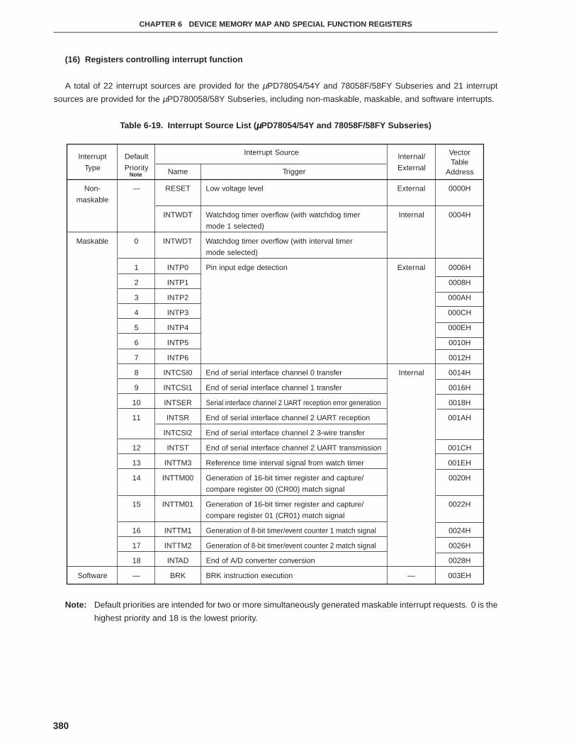
380
CHAPTER 6 DEVICE MEMORY MAP AND SPECIAL FUNCTION REGISTERS
(16) Registers controlling interrupt function
A total of 22 interrupt sources are provided for the µPD78054/54Y and 78058F/58FY Subseries and 21 interrupt
sources are provided for the µPD780058/58Y Subseries, including non-maskable, maskable, and software interrupts.
Table 6-19. Interrupt Source List ( µµµµµPD78054/54Y and 78058F/58FY Subseries)
Interrupt Default Interrupt Source Internal/ VectorTable
Type Priority Name Trigger External Address
Non- — RESET Low voltage level External 0000H
maskable
INTWDT Watchdog timer overflow (with watchdog timer Internal 0004H
mode 1 selected)
Maskable 0 INTWDT Watchdog timer overflow (with interval timer
mode selected)
1 INTP0 Pin input edge detection External 0006H
2 INTP1 0008H
3 INTP2 000AH
4 INTP3 000CH
5 INTP4 000EH
6 INTP5 0010H
7 INTP6 0012H
8 INTCSI0 End of serial interface channel 0 transfer Internal 0014H
9 INTCSI1 End of serial interface channel 1 transfer 0016H
10 INTSER Serial interface channel 2 UART reception error generation 0018H
11 INTSR End of serial interface channel 2 UART reception 001AH
INTCSI2 End of serial interface channel 2 3-wire transfer
12 INTST End of serial interface channel 2 UART transmission 001CH
13 INTTM3 Reference time interval signal from watch timer 001EH
14 INTTM00 Generation of 16-bit timer register and capture/ 0020H
compare register 00 (CR00) match signal
15 INTTM01 Generation of 16-bit timer register and capture/ 0022H
compare register 01 (CR01) match signal
16 INTTM1 Generation of 8-bit timer/event counter 1 match signal 0024H
17 INTTM2 Generation of 8-bit timer/event counter 2 match signal 0026H
18 INTAD End of A/D converter conversion 0028H
Software — BRK BRK instruction execution — 003EH
Note: Default priorities are intended for two or more simultaneously generated maskable interrupt requests. 0 is the
highest priority and 18 is the lowest priority.
Note
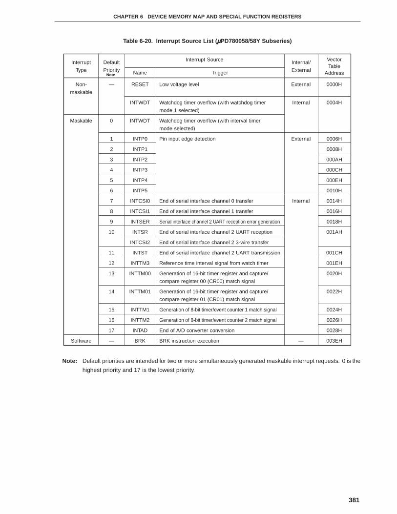
381
CHAPTER 6 DEVICE MEMORY MAP AND SPECIAL FUNCTION REGISTERS
Table 6-20. Interrupt Source List ( µµµµµPD780058/58Y Subseries)
Interrupt Default Interrupt Source Internal/ VectorTable
Type Priority Name Trigger External Address
Non- — RESET Low voltage level External 0000H
maskable
INTWDT Watchdog timer overflow (with watchdog timer Internal 0004H
mode 1 selected)
Maskable 0 INTWDT Watchdog timer overflow (with interval timer
mode selected)
1 INTP0 Pin input edge detection External 0006H
2 INTP1 0008H
3 INTP2 000AH
4 INTP3 000CH
5 INTP4 000EH
6 INTP5 0010H
7 INTCSI0 End of serial interface channel 0 transfer Internal 0014H
8 INTCSI1 End of serial interface channel 1 transfer 0016H
9 INTSER Serial interface channel 2 UART reception error generation 0018H
10 INTSR End of serial interface channel 2 UART reception 001AH
INTCSI2 End of serial interface channel 2 3-wire transfer
11 INTST End of serial interface channel 2 UART transmission 001CH
12 INTTM3 Reference time interval signal from watch timer 001EH
13 INTTM00 Generation of 16-bit timer register and capture/ 0020H
compare register 00 (CR00) match signal
14 INTTM01 Generation of 16-bit timer register and capture/ 0022H
compare register 01 (CR01) match signal
15 INTTM1 Generation of 8-bit timer/event counter 1 match signal 0024H
16 INTTM2 Generation of 8-bit timer/event counter 2 match signal 0026H
17 INTAD End of A/D converter conversion 0028H
Software — BRK BRK instruction execution — 003EH
Note: Default priorities are intended for two or more simultaneously generated maskable interrupt requests. 0 is the
highest priority and 17 is the lowest priority.
Note

382
CHAPTER 6 DEVICE MEMORY MAP AND SPECIAL FUNCTION REGISTERS
The following table gives a listing of interrupt request flags, interrupt mask flags, and priority specification flags
corresponding to interrupt request sources.
Table 6-21. Interrupt Sources and Flags
Interrupt Source Interrupt Request Flag Interrupt Mask Flag Priority Specification Flag
Register Register Register
INTWDT TMIF4 IF0L TMMK4 MK0L TMPR4 PR0L
INTP0 PIF0 PMK0 PPR0
INTP1 PIF1 PMK1 PPR1
INTP2 PIF2 PMK2 PPR2
INTP3 PIF3 PMK3 PPR3
INTP4 PIF4 PMK4 PPR4
INTP5 PIF5 PMK5 PPR5
INTP6 Note PIF6 Note PMK6 Note PPR6 Note
INTCSI0 CSIIF0 IF0H CSIMK0 MK0H CSIPR0 PR0H
INTCSI1 CSIIF1 CSIMK1 CSIPR1
INTSER SERIF SERMK SERPR
INTSR/INTCSI2 SRIF SRMK SRPR
INTST STIF STMK STPR
INTTM3 TMIF3 TMMK3 TMPR3
INTTM00 TMIF00 TMMK00 TMPR00
INTTM01 TMIF01 TMMK01 TMPR01
INTTM1 TMIF1 IF1L TMMK1 MK1L TMPR1 PR1L
INTTM2 TMIF2 TMMK2 TMPR2
INTAD ADIF ADMK ADPR0
Note: Not provided for the µPD780058/58Y Subseries.
The following six types of registers control the interrupt functions:
• Interrupt request flag registers (IF0L, IF0H, IF1L)
• Interrupt mask flag registers (MK0L, MK0H, MK1L)
• Priority specification flag registers (PR0L, PR0H, PR1L)
• External interrupt mode registers (INTM0, INTM1)
• Sampling clock select register (SCS)
• Program status word (PSW)
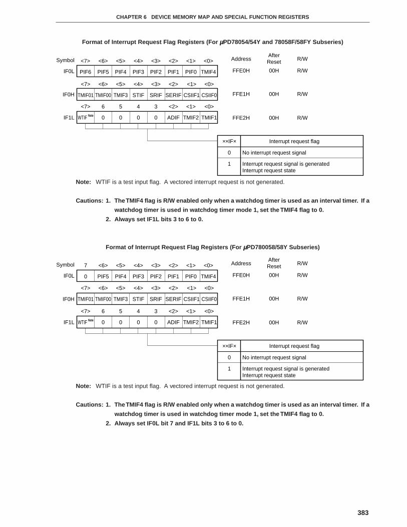
383
CHAPTER 6 DEVICE MEMORY MAP AND SPECIAL FUNCTION REGISTERS
Format of Interrupt Request Flag Registers (For µµµµµPD78054/54Y and 78058F/58FY Subseries)
Note: WTIF is a test input flag. A vectored interrupt request is not generated.
Cautions: 1. The TMIF4 flag is R/W enabled only when a watchdog timer is used as an interval timer. If a
watchdog timer is used in watchdog timer mode 1, set the TMIF4 flag to 0.
2. Always set IF1L bits 3 to 6 to 0.
Format of Interrupt Request Flag Registers (For µµµµµPD780058/58Y Subseries)
Note: WTIF is a test input flag. A vectored interrupt request is not generated.
Cautions: 1. The TMIF4 flag is R/W enabled only when a watchdog timer is used as an interval timer. If a
watchdog timer is used in watchdog timer mode 1, set the TMIF4 flag to 0.
2. Always set IF0L bit 7 and IF1L bits 3 to 6 to 0.
Symbol
IF0L
<6>
PIF5
<7>
PIF6
<5>
PIF4
<4>
PIF3
<3>
PIF2
<2>
PIF1
<1>
PIF0
<0>
TMIF4
Address
FFE0H 00H
AfterReset R/W
R/W
××IF×
0
1
Interrupt request flag
No interrupt request signal
Interrupt request signal is generated Interrupt request state
<7>
TMIF01IF0H
<6>
TMIF00
<5>
TMIF3
<4>
STIF
<3>
SRIF
<2>
SERIF
<1>
CSIIF1
<0>
CSIIF0
<7>
WTIF NoteIF1L
6
0
5
0
4
0
3
0
<2>
ADIF
<1>
TMIF2
<0>
TMIF1
FFE1H 00H R/W
FFE2H 00H R/W
7
0
Symbol
IF0L
<6>
PIF5
<5>
PIF4
<4>
PIF3
<3>
PIF2
<2>
PIF1
<1>
PIF0
<0>
TMIF4
Address
FFE0H 00H
AfterReset R/W
R/W
××IF×
0
1
Interrupt request flag
No interrupt request signal
Interrupt request signal is generated Interrupt request state
<7>
TMIF01IF0H
<6>
TMIF00
<5>
TMIF3
<4>
STIF
<3>
SRIF
<2>
SERIF
<1>
CSIIF1
<0>
CSIIF0
<7>
WTIF NoteIF1L
6
0
5
0
4
0
3
0
<2>
ADIF
<1>
TMIF2
<0>
TMIF1
FFE1H 00H R/W
FFE2H 00H R/W
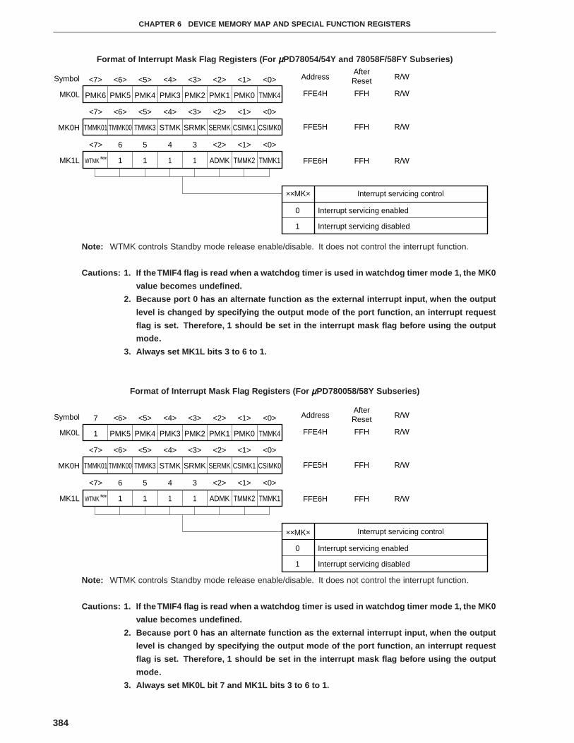
384
CHAPTER 6 DEVICE MEMORY MAP AND SPECIAL FUNCTION REGISTERS
Format of Interrupt Mask Flag Registers (For µµµµµPD78054/54Y and 78058F/58FY Subseries)
Note: WTMK controls Standby mode release enable/disable. It does not control the interrupt function.
Cautions: 1. If the TMIF4 flag is read when a watchdog timer is used in watchdog timer mode 1, the MK0
value becomes undefined.
2. Because port 0 has an alternate function as the external interrupt input, when the output
level is changed by specifying the output mode of the port function, an interrupt request
flag is set. Therefore, 1 should be set in the interrupt mask flag before using the output
mode.
3. Always set MK1L bits 3 to 6 to 1.
Format of Interrupt Mask Flag Registers (For µµµµµPD780058/58Y Subseries)
Note: WTMK controls Standby mode release enable/disable. It does not control the interrupt function.
Cautions: 1. If the TMIF4 flag is read when a watchdog timer is used in watchdog timer mode 1, the MK0
value becomes undefined.
2. Because port 0 has an alternate function as the external interrupt input, when the output
level is changed by specifying the output mode of the port function, an interrupt request
flag is set. Therefore, 1 should be set in the interrupt mask flag before using the output
mode.
3. Always set MK0L bit 7 and MK1L bits 3 to 6 to 1.
Symbol
MK0L
<6>
PMK5
<7>
PMK6
<5>
PMK4
<4>
PMK3
<3>
PMK2
<2>
PMK1
<1>
PMK0
<0>
TMMK4
Address
FFE4H FFH
AfterReset R/W
R/W
××MK×
0
1
Interrupt servicing control
Interrupt servicing enabled
Interrupt servicing disabled
<7>
TMMK01MK0H
<6>
TMMK00
<5>
TMMK3
<4>
STMK
<3>
SRMK
<2>
SERMK
<1>
CSIMK1
<0>
CSIMK0
<7>
WTMK NoteMK1L
6
1
5
1
4
1
3
1
<2>
ADMK
<1>
TMMK2
<0>
TMMK1
FFE5H FFH R/W
FFE6H FFH R/W
7
1
Symbol
MK0L
<6>
PMK5
<5>
PMK4
<4>
PMK3
<3>
PMK2
<2>
PMK1
<1>
PMK0
<0>
TMMK4
Address
FFE4H FFH
AfterReset R/W
R/W
××MK×
0
1
Interrupt servicing control
Interrupt servicing enabled
Interrupt servicing disabled
<7>
TMMK01MK0H
<6>
TMMK00
<5>
TMMK3
<4>
STMK
<3>
SRMK
<2>
SERMK
<1>
CSIMK1
<0>
CSIMK0
<7>
WTMK NoteMK1L
6
1
5
1
4
1
3
1
<2>
ADMK
<1>
TMMK2
<0>
TMMK1
FFE5H FFH R/W
FFE6H FFH R/W
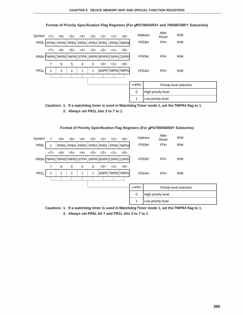
385
CHAPTER 6 DEVICE MEMORY MAP AND SPECIAL FUNCTION REGISTERS
Format of Priority Specification Flag Registers (For µµµµµPD78054/54Y and 78058F/58FY Subseries)
Cautions: 1. If a watchdog timer is used in Watchdog Timer mode 1, set the TMPR4 flag to 1.
2. Always set PR1L bits 3 to 7 to 1.
Format of Priority Specification Flag Registers (For µµµµµPD780058/58Y Subseries)
Cautions: 1. If a watchdog timer is used in Watchdog Timer mode 1, set the TMPR4 flag to 1.
2. Always set PR0L bit 7 and PR1L bits 3 to 7 to 1.
Symbol
PR0L
<6>
PPR5
<7>
PPR6
<5>
PPR4
<4>
PPR3
<3>
PPR2
<2>
PPR1
<1>
PPR0
<0>
TMPR4
Address
FFE8H FFH
AfterReset R/W
R/W
0
1
Priority level selection
High priority level
Low priority level
<7>
TMPR01PR0H
<6>
TMPR00
<5>
TMPR3
<4>
STPR
<3>
SRPR
<2>
SERPR
<1>
CSIPR1
<0>
CSIPR0
7
1PR1L
6
1
5
1
4
1
3
1
<2>
ADPR
<1>
TMPR2
<0>
TMPR1
FFE9H FFH R/W
FFEAH FFH R/W
××PR×
7
1
Symbol
PR0L
<6>
PPR5
<5>
PPR4
<4>
PPR3
<3>
PPR2
<2>
PPR1
<1>
PPR0
<0>
TMPR4
Address
FFE8H FFH
AfterReset R/W
R/W
0
1
Priority level selection
High priority level
Low priority level
<7>
TMPR01PR0H
<6>
TMPR00
<5>
TMPR3
<4>
STPR
<3>
SRPR
<2>
SERPR
<1>
CSIPR1
<0>
CSIPR0
7
1PR1L
6
1
5
1
4
1
3
1
<2>
ADPR
<1>
TMPR2
<0>
TMPR1
FFE9H FFH R/W
FFEAH FFH R/W
××PR×
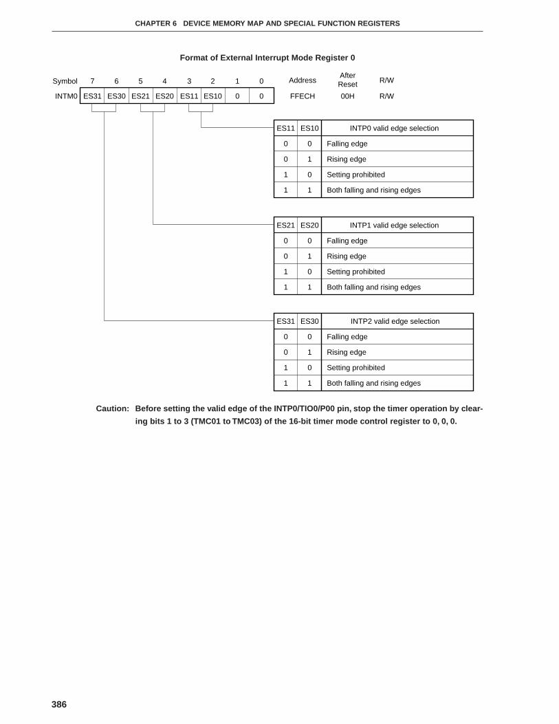
386
CHAPTER 6 DEVICE MEMORY MAP AND SPECIAL FUNCTION REGISTERS
Format of External Interrupt Mode Register 0
Caution: Before setting the valid edge of the INTP0/TIO0/P00 pin, stop the timer operation by clear-
ing bits 1 to 3 (TMC01 to TMC03) of the 16-bit timer mode control register to 0, 0, 0.
Address
FFECH 00H
AfterReset R/W
R/W
0
0
1
1
INTP0 valid edge selection
Falling edge
Rising edge
Setting prohibited
Both falling and rising edges
ES11
7
ES31
Symbol
INTM0
6
ES30
5
ES21
4
ES20
3
ES11
2
ES10
1
0
0
0
0
1
0
1
ES10
0
0
1
1
INTP1 valid edge selection
Falling edge
Rising edge
Setting prohibited
Both falling and rising edges
ES21
0
1
0
1
ES20
0
0
1
1
INTP2 valid edge selection
Falling edge
Rising edge
Setting prohibited
Both falling and rising edges
ES31
0
1
0
1
ES30
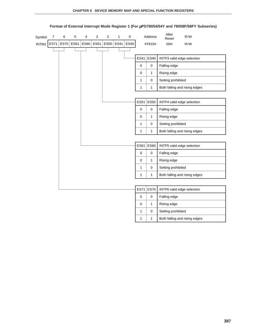
387
CHAPTER 6 DEVICE MEMORY MAP AND SPECIAL FUNCTION REGISTERS
Format of External Interrupt Mode Register 1 (For µµµµµPD78054/54Y and 78058F/58FY Subseries)
ES71
7
ES70
6
ES61 ES60
4
ES51
3 2 1 0
FFEDH
Address
INTM1
Symbol
ES50 ES41 ES40
5
00H
AfterReset
R/W
R/W
ES41
0
0
1
1
ES40
0
1
0
1
INTP3 valid edge selection
Falling edge
Rising edge
Setting prohibited
Both falling and rising edges
ES51
0
0
1
1
ES50
0
1
0
1
INTP4 valid edge selection
Falling edge
Rising edge
Setting prohibited
Both falling and rising edges
ES61
0
0
1
1
ES60
0
1
0
1
INTP5 valid edge selection
Falling edge
Rising edge
Setting prohibited
Both falling and rising edges
ES71
0
0
1
1
ES70
0
1
0
1
INTP6 valid edge selection
Falling edge
Rising edge
Setting prohibited
Both falling and rising edges
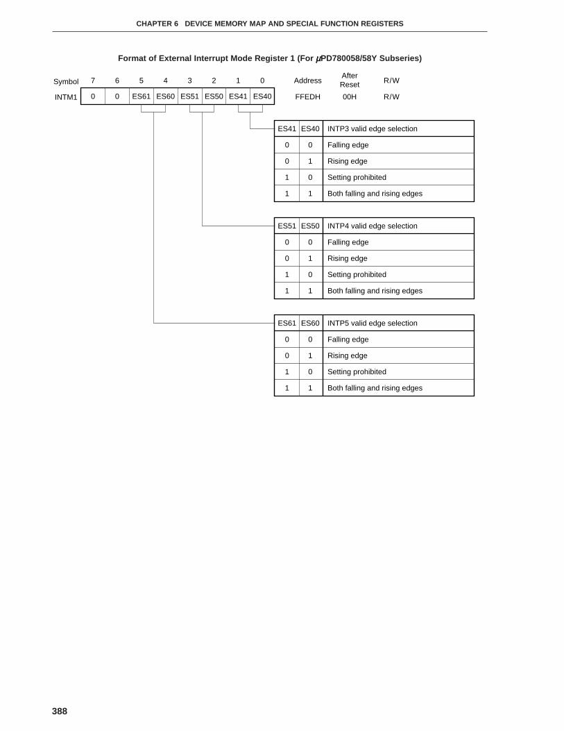
388
CHAPTER 6 DEVICE MEMORY MAP AND SPECIAL FUNCTION REGISTERS
Format of External Interrupt Mode Register 1 (For µµµµµPD780058/58Y Subseries)
0
7
0
6
ES61 ES60
4
ES51
3 2 1 0
FFEDH
Address
INTM1
Symbol
ES50 ES41 ES40
5
00H
AfterReset
R/W
R/W
ES41
0
0
1
1
ES40
0
1
0
1
INTP3 valid edge selection
Falling edge
Rising edge
Setting prohibited
Both falling and rising edges
ES51
0
0
1
1
ES50
0
1
0
1
INTP4 valid edge selection
Falling edge
Rising edge
Setting prohibited
Both falling and rising edges
ES61
0
0
1
1
ES60
0
1
0
1
INTP5 valid edge selection
Falling edge
Rising edge
Setting prohibited
Both falling and rising edges

389
CHAPTER 6 DEVICE MEMORY MAP AND SPECIAL FUNCTION REGISTERS
Format of Sampling Clock Select Register
Caution: f XX/2N is a clock to be supplied to the CPU and f XX/25, fXX/26, and f XX/27 are clocks to be supplied
to the peripheral hardware. f XX/2N stops in the HALT mode.
Remarks: N: Value (N = 0 to 4) at bits 0 to 2 (PCC0 to PCC2) of the processor clock control register
fXX: Main system clock frequency (fX or fX/2)
fX: Main system clock oscillation frequency
MCS: Bit 0 of oscillation mode selection register
Values in parentheses apply to operation with fX = 5.0 MHz.
Format of Program Status Word
Address
FF47H 00H
AfterReset R/W
R/W
0
0
1
1
INTP0 sampling clock selection
fXX/2N
fXX/27
fXX/25
fXX/26
SCS1
7
0
Symbol
SCS
6
0
5
0
4
0
3
0
2
0
1
SCS1
0
SCS0
0
1
0
1
SCS0
MCS = 1 MCS = 0
fX/27 (39.1 kHz)
fX/25 (156.3 kHz)
fX/26 (78.1 kHz)
fX/28 (19.5 kHz)
fX/26 (78.1 kHz)
fX/27 (39.1 kHz)
7
IEPSW
6
Z
5
RBS1
4
AC
3
RBS0
2
0
1
ISP
0
CY 02H
After Reset
ISP
0
Used when a normal instruction is executed
Priority of interrupt currently being received
High-priority interrupt servicing(low-priority interrupt disable)
1 Interrupt request not acknowledged or low-priorityinterrupt servicing(all maskable interrupts enable)
IE Interrupt request acknowledge enable/disable
0 Disable
1 Enable
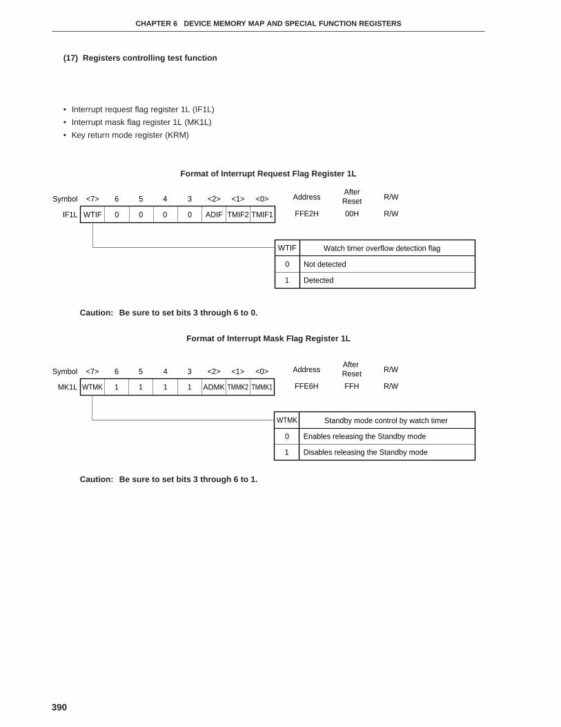
390
CHAPTER 6 DEVICE MEMORY MAP AND SPECIAL FUNCTION REGISTERS
(17) Registers controlling test function
• Interrupt request flag register 1L (IF1L)
• Interrupt mask flag register 1L (MK1L)
• Key return mode register (KRM)
Format of Interrupt Request Flag Register 1L
Caution: Be sure to set bits 3 through 6 to 0.
Format of Interrupt Mask Flag Register 1L
Caution: Be sure to set bits 3 through 6 to 1.
<7>
WTIF
Symbol
IF1L
6
0
5
0
4
0
3
0
<2>
ADIF
<1>
TMIF2
<0>
TMIF1
Address
FFE2H 00H
AfterReset R/W
R/W
0
1
Watch timer overflow detection flag
Not detected
Detected
WTIF
<7>
WTMK
Symbol
MK1L
6
1
5
1
4
1
3
1
<2>
ADMK
<1>
TMMK2
<0>
TMMK1
Address
FFE6H FFH
After Reset R/W
R/W
0
1
Standby mode control by watch timer
Enables releasing the Standby mode
Disables releasing the Standby mode
WTMK
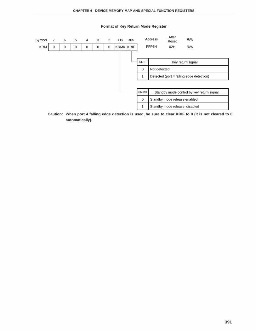
391
CHAPTER 6 DEVICE MEMORY MAP AND SPECIAL FUNCTION REGISTERS
Format of Key Return Mode Register
Caution: When port 4 falling edge detection is used, be sure to clear KRIF to 0 (it is not cleared to 0
automatically).
7
0
Symbol
KRM
6
0
5
0
4
0
3
0
2
0
<1>
KRMK
<0>
KRIF
Address
FFF6H 02H
AfterReset R/W
R/W
0
1
Key return signal
Not detected
Detected (port 4 falling edge detection)
KRIF
0
1
Standby mode control by key return signal
Standby mode release enabled
Standby mode release disabled
KRMK

392
CHAPTER 6 DEVICE MEMORY MAP AND SPECIAL FUNCTION REGISTERS
(18) Registers controlling external device expansion function
The following two registers control the external device expansion function:
• Memory expansion mode register (MM)
• Internal memory size switching register (IMS)
Format of Memory Expansion Mode Register
Note: The full address mode allows external expansion to the entire 64K address space except for the
internal ROM (or PROM, flash memory), RAM, and SFR areas and the reserved areas.
Remark: P60 to P63 are used as port pins without regard to the mode (single-chip mode or memory expansion
mode).
0 0 PW1 0MM FFF8H 10H R/W
7 6 5 4 3 2Symbol AddressAfterReset R/W1
PW0 MM2 MM1 MM0
0
MM2 MM1 MM0
0 0 0
0 0 1
0 1 1
1 0 0
1 0 1
1 1 1
Settings other than above are prohibited
Single-chip/memory expansion modeselection
Single-chip mode
256-bytemode
4Kmode
16K mode
Full
Noteaddressmode
Memoryexpansionmode
AD0 to AD7
Input
Out-put
Portmode
P40 to P47
P40 to P47, P50 to P57, P64 to P67 pin state
PW1 PW0 Wait control
No wait
Wait (one wait state insertion)
Setting prohibited
Wait control by external wait pin
P56, P57 P64 to P67
Port mode
Port mode
Port mode
Port mode
A14, A15
A12, A13
P64 = RD
P65 = WR
P66 = WAIT
P67 = ASTB
P50 to P53 P54, P55
A8 to A11
0
1
0
1
0
0
1
1

393
CHAPTER 6 DEVICE MEMORY MAP AND SPECIAL FUNCTION REGISTERS
Format of Internal Memory Size Switching Register
Notes: 1. The value of this register after reset differs depending on the model (refer to the table below).
2. Setting prohibited for the µPD78058F/58FY Subseries.
3. Setting prohibited for the µPD780058/58Y Subseries.
4. When the external device expansion function of the µPD78058/58Y, 78P058/58Y, 78058F/58FY, 78P058F/
58FY, 780058/58Y, or 78F0058/58Y is used, set the internal ROM capacity to 56K or less.
Value of Internal Memory Size Switching Register After Reset
(µµµµµPD78054/54Y and 78058F/58FY Subseries)
Part Number Value After Reset
µPD78052/52Y 44H
µPD78053/53Y C6H
µPD78054/54Y, 78P054 C8H
µPD78055/55Y CAH
µPD78056/56Y/56F/56FY CCH
µPD78058/58Y/58F/58FY, CFH
78P058/58Y/58F/58FY
Value of Internal Memory Size Switching Register After Reset ( µµµµµPD780058/58Y Subseries)
Part Number Value After Reset
µPD780053/53Y C6H
µPD780054/54Y C8H
µPD780055/55Y CAH
µPD780056/56Y CCH
µPD780058/58Y, 78F0058/58Y CFH
1
1
48K
56K Note 4
1
1
0
1
0
0
7
RAM2
Symbol
IMS
6
RAM1
5
RAM0
4
0
3
ROM3
2
ROM2
1
ROM1
0
ROM0
Address
FFF0H Note 1
AfterReset R/W
R/W
Internal ROM size selectionROM3
60K1
ROM2
1
ROM1
1
ROM0
1
Internal high-speed RAM size selectionRAM2 RAM1 RAM0
1024 bytes1 1 0
512 bytes Notes 2, 30 1 0
1
1
32K Note 2
40K Note 2
0
0
0
1
0
0
0 24K Note 21 1 0
0 16K Notes 2, 31 0 0
Settings other than above are prohibited
Settings other than above are prohibited
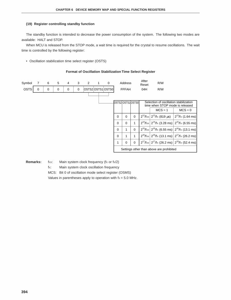
394
CHAPTER 6 DEVICE MEMORY MAP AND SPECIAL FUNCTION REGISTERS
(19) Register controlling standby function
The standby function is intended to decrease the power consumption of the system. The following two modes are
available: HALT and STOP.
When MCU is released from the STOP mode, a wait time is required for the crystal to resume oscillations. The wait
time is controlled by the following register:
• Oscillation stabilization time select register (OSTS)
Format of Oscillation Stabilization Time Select Register
Remarks: fXX: Main system clock frequency (fX or fX/2)
fX: Main system clock oscillation frequency
MCS: Bit 0 of oscillation mode select register (OSMS)
Values in parentheses apply to operation with fX = 5.0 MHz.
Address
FFFAH 04H
AfterReset R/W
R/W
0
0
0
0
1
Selection of oscillation stabilizationtime when STOP mode is released
212/fXX
214/fXX
215/fXX
216/fXX
217/fXX
OSTS2
7
0
Symbol
OSTS
6
0
5
0
4
0
3
0
2
OSTS2
1
OSTS1
0
OSTS0
0
0
1
1
0
OSTS1
MCS = 1 MCS = 0
212/fX (819 s)
214/fX (3.28 ms)
215/fX (6.55 ms)
216/fX (13.1 ms)
217/fX (26.2 ms)
213/fX (1.64 ms)
215/fX (6.55 ms)
216/fX (13.1 ms)
217/fX (26.2 ms)
218/fX (52.4 ms)
µ0
1
0
1
0
OSTS0
Settings other than above are prohibited
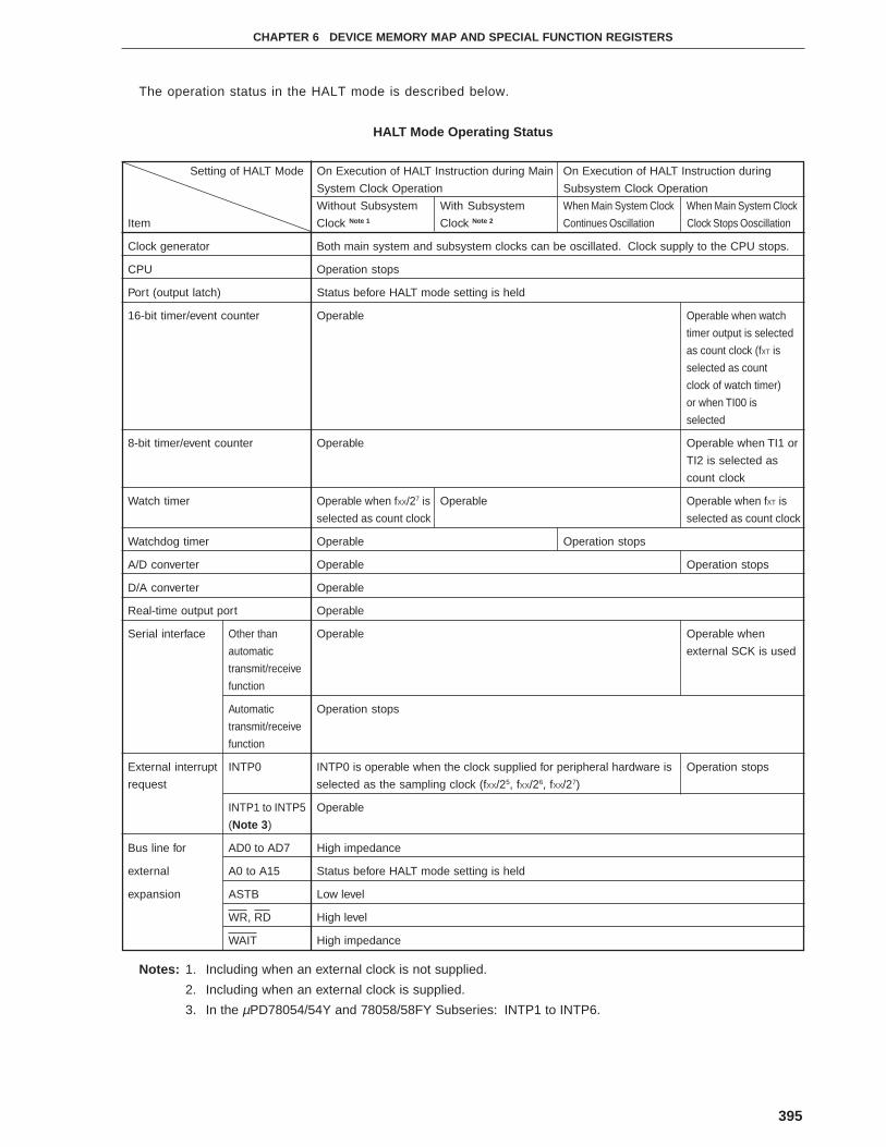
395
CHAPTER 6 DEVICE MEMORY MAP AND SPECIAL FUNCTION REGISTERS
The operation status in the HALT mode is described below.
HALT Mode Operating Status
Setting of HALT Mode On Execution of HALT Instruction during Main On Execution of HALT Instruction during
System Clock Operation Subsystem Clock Operation
Without Subsystem With Subsystem When Main System Clock When Main System Clock
Item Clock Note 1 Clock Note 2 Continues Oscillation Clock Stops Ooscillation
Clock generator Both main system and subsystem clocks can be oscillated. Clock supply to the CPU stops.
CPU Operation stops
Port (output latch) Status before HALT mode setting is held
16-bit timer/event counter Operable Operable when watch
timer output is selected
as count clock (fXT is
selected as count
clock of watch timer)
or when TI00 is
selected
8-bit timer/event counter Operable Operable when TI1 or
TI2 is selected as
count clock
Watch timer Operable when fXX/27 is Operable Operable when fXT is
selected as count clock selected as count clock
Watchdog timer Operable Operation stops
A/D converter Operable Operation stops
D/A converter Operable
Real-time output port Operable
Serial interface Other than Operable Operable when
automatic external SCK is used
transmit/receive
function
Automatic Operation stops
transmit/receive
function
External interrupt INTP0 INTP0 is operable when the clock supplied for peripheral hardware is Operation stops
request selected as the sampling clock (fXX/25, fXX/26, fXX/27)
INTP1 to INTP5 Operable
(Note 3 )
Bus line for AD0 to AD7 High impedance
external A0 to A15 Status before HALT mode setting is held
expansion ASTB Low level
WR, RD High level
WAIT High impedance
Notes: 1. Including when an external clock is not supplied.
2. Including when an external clock is supplied.
3. In the µPD78054/54Y and 78058/58FY Subseries: INTP1 to INTP6.

396
CHAPTER 6 DEVICE MEMORY MAP AND SPECIAL FUNCTION REGISTERS
The operation in the STOP mode is described below.
STOP Mode Operating Status
Setting of STOP ModeWith Subsystem Clock Without Subsystem Clock
Item
Clock generator Only main system clock stops oscillation
CPU Operation stops
Port (output latch) Status before STOP mode setting is held
16-bit timer/event counter Operable when watch timer output is Operation stopsselected as count clock (fXT is selected ascount clock of watch timer)
8-bit timer/event counter Operable when TI1 and TI2 are selected for the count clock
Watch timer Operable when fXT is selected for the Operation stopscount clock
Watchdog timer Operation stops
A/D converter
D/A converter Operable
Real-time output port Operable when external trigger is used or TI1 and TI2 are selected for the 8-bittimer/event counter count clock
Serial interface Other than Operable when an externally supplied clock is specified as the serial clockautomatictransmit/receivefunction andUART
Automatic Operation stopstransmit/receivefunction andUART
External interrupt INTP0 Not operablerequest INTP1 to INTP5 Operable
(Note )
Bus line for AD0 to AD7 High impedanceexternal A0 to A15 Status before STOP mode setting is heldexpansion
ASTB Low level
WR, RD High level
WAIT High impedance
Note: In µPD78054/54Y and 78058F/58FY Subseries: INTP1 to INTP6.
Cautions: 1. When the STOP mode is set, the X2 pin is internally connected to V DD1 via a pull-up resistor to
minimize the leakage current at the crystal oscillator. Thus, do not use the STOP mode in a
system where an external clock is used for the main system clock.
2. Because the interrupt request signal is used to release the Standby mode, if there is an inter-
rupt source with the interrupt request flag set and the interrupt mask flag reset, the Standby
mode is immediately released if set. Thus, the STOP mode is reset to the HALT mode immedi-
ately after execution of the STOP instruction. After the wait set using the oscillation stabiliza-
tion time select register (OSTS), the operating mode is set.
397
CHAPTER 6 DEVICE MEMORY MAP AND SPECIAL FUNCTION REGISTERS
(20) Reset function
The following two operations can generate a reset signal:
• External reset input via the RESET pin
• Internal reset by watchdog timer in Watchdog Timer mode

398
CHAPTER 6 DEVICE MEMORY MAP AND SPECIAL FUNCTION REGISTERS
Table 6-22. Hardware Status After Reset (1/2)
Hardware Status After Reset
Program counter (PC) Note 1 Contents of reset vector tables
(0000H, 0001H) are set
Stack pointer (SP) Undefined
Program status word (PSW) 02H
RAM Data memory Undefined Note 2
General-purpose register Undefined Note 2
Port (output latch) Ports 0 to 3, Ports 7, 12, 13 00H
(P0 to P3, P7, P12, P13)
Ports 4 to 6 (P4 to P6) Undefined
Port mode registers (PM0 to PM7, PM12, PM13) FFH
Pull-up resistor option registers (PUOH, PUOL) 00H
Processor clock control register (PCC) 04H
Oscillation mode select register (OSMS) 00H
Internal memory size switching register (IMS) Note 3
Internal expansion RAM size switching register (IXS) Note 4 0AH
Memory expansion mode register (MM) 10H
Oscillation stabilization time select register (OSTS) 04H
16-bit timer/event counter Timer register (TM0) 00H
Capture/Compare registers (CR00, CR01) Undefined
Clock select register (TCL0) 00H
Mode control register (TMC0) 00H
Capture/Compare control register 0 (CRC0) 04H
Output control register (TOC0) 00H
8-bit timer/event counters Timer registers (TM1, TM2) 00H
1 and 2 Compare registers (CR10, CR20) Undefined
Clock select register (TCL1) 00H
Mode control register (TMC1) 00H
Output control register (TOC1) 00H
Watch timer Mode control register (TMC2) 00H
Clock select register (TCL2) 00HWatchdog timer
Mode register (WDTM) 00H
Serial interface Clock select register (TCL3) 88H
Shift registers (SIO0, SIO1) Undefined
Mode registers (CSIM0, CSIM1, CSIM2) 00H
Serial bus interface control register (SBIC) 00H
Slave address register (SVA) Undefined
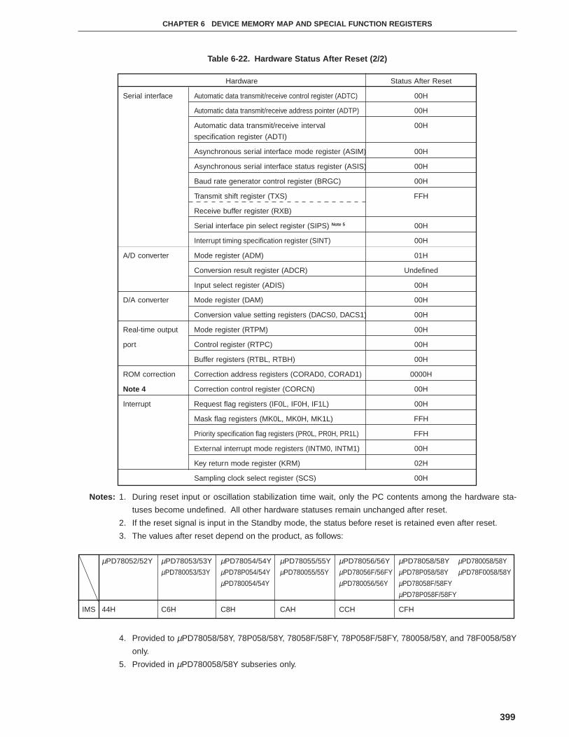
399
CHAPTER 6 DEVICE MEMORY MAP AND SPECIAL FUNCTION REGISTERS
Table 6-22. Hardware Status After Reset (2/2)
Hardware Status After Reset
Serial interface Automatic data transmit/receive control register (ADTC) 00H
Automatic data transmit/receive address pointer (ADTP) 00H
Automatic data transmit/receive interval 00H
specification register (ADTI)
Asynchronous serial interface mode register (ASIM) 00H
Asynchronous serial interface status register (ASIS) 00H
Baud rate generator control register (BRGC) 00H
Transmit shift register (TXS) FFH
Receive buffer register (RXB)
Serial interface pin select register (SIPS) Note 5 00H
Interrupt timing specification register (SINT) 00H
A/D converter Mode register (ADM) 01H
Conversion result register (ADCR) Undefined
Input select register (ADIS) 00H
D/A converter Mode register (DAM) 00H
Conversion value setting registers (DACS0, DACS1) 00H
Real-time output Mode register (RTPM) 00H
port Control register (RTPC) 00H
Buffer registers (RTBL, RTBH) 00H
ROM correction Correction address registers (CORAD0, CORAD1) 0000H
Note 4 Correction control register (CORCN) 00H
Interrupt Request flag registers (IF0L, IF0H, IF1L) 00H
Mask flag registers (MK0L, MK0H, MK1L) FFH
Priority specification flag registers (PR0L, PR0H, PR1L) FFH
External interrupt mode registers (INTM0, INTM1) 00H
Key return mode register (KRM) 02H
Sampling clock select register (SCS) 00H
Notes: 1. During reset input or oscillation stabilization time wait, only the PC contents among the hardware sta-
tuses become undefined. All other hardware statuses remain unchanged after reset.
2. If the reset signal is input in the Standby mode, the status before reset is retained even after reset.
3. The values after reset depend on the product, as follows:
µPD78052/52Y µPD78053/53Y µPD78054/54Y µPD78055/55Y µPD78056/56Y µPD78058/58Y µPD780058/58Y
µPD780053/53Y µPD78P054/54Y µPD780055/55Y µPD78056F/56FY µPD78P058/58Y µPD78F0058/58Y
µPD780054/54Y µPD780056/56Y µPD78058F/58FY
µPD78P058F/58FY
IMS 44H C6H C8H CAH CCH CFH
4. Provided to µPD78058/58Y, 78P058/58Y, 78058F/58FY, 78P058F/58FY, 780058/58Y, and 78F0058/58Y
only.
5. Provided in µPD780058/58Y subseries only.

400
CHAPTER 6 DEVICE MEMORY MAP AND SPECIAL FUNCTION REGISTERS
(21) Registers controlling ROM correction ( µµµµµPD78058/58Y, 78058F/58FY, and 780058/58Y only)
The following two types of registers control the ROM correction:
• Correction address registers 0 and 1 (CORAD0 and CORAD1)
• Correction control register (CORCN)
Format of Correction Address Registers 0 and 1
Cautions: 1. Set CORAD0 and CORAD1 when bits 1 (COREN0) and 3 (COREN1) of the correction control
register (CORCN; refer to the figure below) are 0.
2. Only addresses at which operation codes are stored can be set in CORAD0 and CORAD1.
3. Do not set the following addresses to CORAD0 and CORAD1:
a. Address value in table area of table reference instruction (CALLT instruction): 0040H to
007FH
b. Address value in vector table area: 0000H to 003FH
Format of Correction Control Register
Note: Bits 0 and 2 are read-only bits.
FF3AH/FF3BH 0000H
Symbol 15
CORAD0
0 Address
FF38H/FF39H
After Reset
0000H
R/W
R/W
CORAD1 R/W
7
0
6
0
5
0
4
0 COREN1 CORST1 COREN0 CORST0
Symbol
CORCN
Address
FF8AH
After Reset
COREN0
0
1
CORST0
0
1
COREN1
0
1
CORST1
0
1
R/W
R/W Note00H
Correction address register 0 and fetch address match detection
Not detected
Detected
Correction address register 0 and fetch address match detection control
Disabled
Enabled
Correction address register 1 and fetch address match detection
Not detected
Detected
Correction address register 1 and fetch address match detection control
Disabled
Enabled
<3> <2> <1> <0>
401
CHAPTER 6 DEVICE MEMORY MAP AND SPECIAL FUNCTION REGISTERS
(22) Register controlling internal memory capacity
The µPD78P054, 78P058/58Y/58F/58FY, and 78F0058/58Y allow users to select the internal memory capacity.
The following register is used to control the internal memory capacity:
• Internal memory size switching register (IMS)
Remarks: The µPD78P054 is a PROM version corresponding to the µPD78052/53/54.
The µPD78P058 is a PROM version corresponding to the µPD78055/56/58.

402
CHAPTER 6 DEVICE MEMORY MAP AND SPECIAL FUNCTION REGISTERS
(a) µµµµµPD78P054 (for µµµµµPD78052/52Y, 78053/53Y, 78054/54Y Subseries)
To map the memory of the µPD78P054 identically to that of a mask ROM version, the value at the time the mask ROM
version is reset must be set.
For the mask ROM version, IMS does not need to be set.
Format of Internal Memory Size Switching Register ( µµµµµPD78P054)
The following table shows the set value of IMS to map the memory of the µPD78P054 identically to that of a mask
ROM version.
Set Value of Internal Memory Size Switching Register ( µµµµµPD78P054)
Target Mask ROM Version Set Value of IMS
µPD78052/52Y 44H
µPD78053/53Y C6H
µPD78054/54Y C8H
Caution: When using a mask ROM version, do not set a value to IMS other than those shown in the table
above.
RAM2 RAM1 RAM0 0 ROM3 ROM2 ROM1 ROM0IMS
7 6 5 4 3 2 1 0Symbol Address After Reset R/W
FFF0H C8H W
ROM3 ROM2
0 1
0
1
1
0
ROM1 ROM0
0 0
1
0
0
0
Selects internal ROM capacity
16K
24K
32K
RAM2 RAM1
0
1
1
1
RAM0
0
0
Selects internal high-speed RAM capacity
512 bytes
1024 bytes
Settings other than above are prohibited
Settings other than above are prohibited
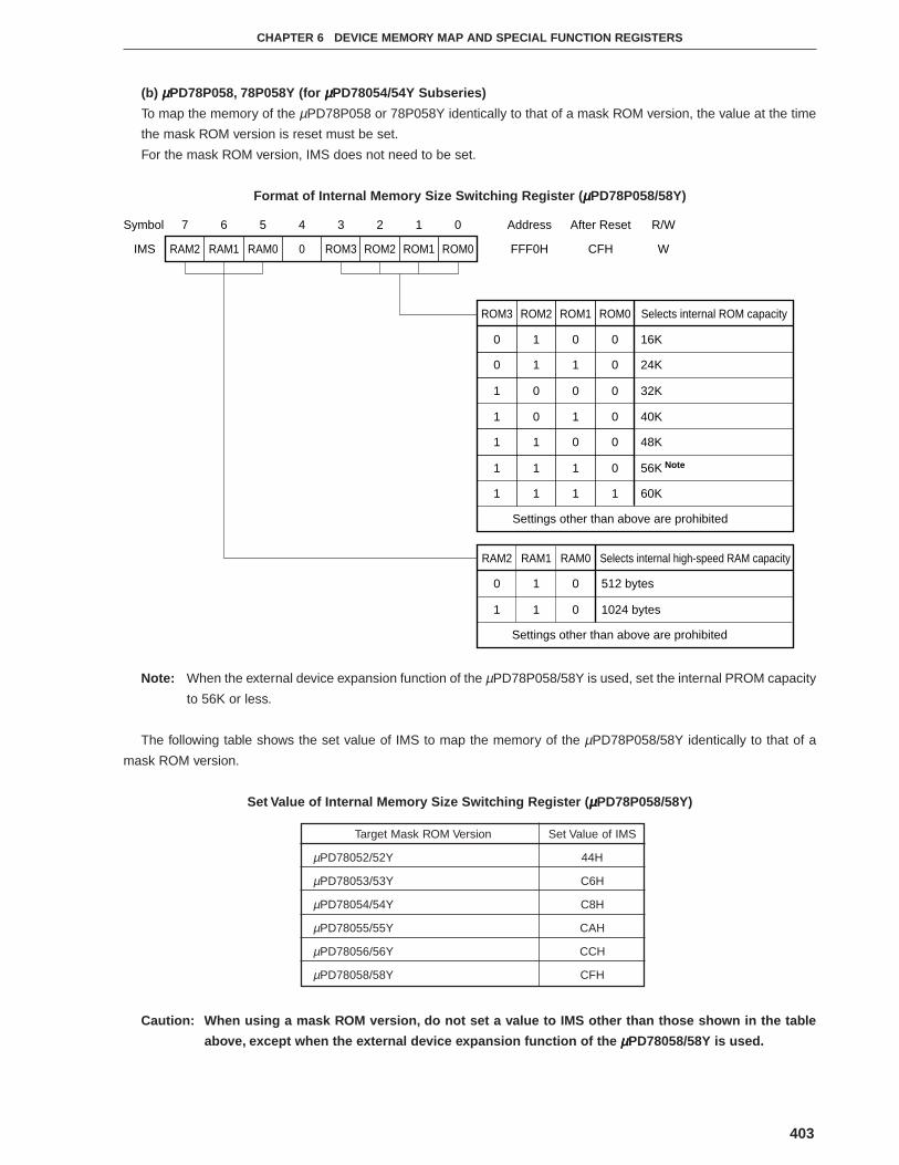
403
CHAPTER 6 DEVICE MEMORY MAP AND SPECIAL FUNCTION REGISTERS
(b) µµµµµPD78P058, 78P058Y (for µµµµµPD78054/54Y Subseries)
To map the memory of the µPD78P058 or 78P058Y identically to that of a mask ROM version, the value at the time
the mask ROM version is reset must be set.
For the mask ROM version, IMS does not need to be set.
Format of Internal Memory Size Switching Register ( µµµµµPD78P058/58Y)
Note: When the external device expansion function of the µPD78P058/58Y is used, set the internal PROM capacity
to 56K or less.
The following table shows the set value of IMS to map the memory of the µPD78P058/58Y identically to that of a
mask ROM version.
Set Value of Internal Memory Size Switching Register ( µµµµµPD78P058/58Y)
Target Mask ROM Version Set Value of IMS
µPD78052/52Y 44H
µPD78053/53Y C6H
µPD78054/54Y C8H
µPD78055/55Y CAH
µPD78056/56Y CCH
µPD78058/58Y CFH
Caution: When using a mask ROM version, do not set a value to IMS other than those shown in the table
above, except when the external device expansion function of the µµµµµPD78058/58Y is used.
RAM2 RAM1 RAM0 0 ROM3 ROM2 ROM1 ROM0IMS
7 6 5 4 3 2 1 0Symbol Address After Reset R/W
FFF0H CFH W
ROM3 ROM2
0 1
0
1
1
0
ROM1 ROM0
0 0
1
0
0
0
1 0
1
1
1
1
1 1
1 0
0
1
0
0
1 1
Selects internal ROM capacity
16K
24K
32K
40K
48K
56K Note
60K
RAM2 RAM1
0
1
1
1
RAM0
0
0
Selects internal high-speed RAM capacity
512 bytes
1024 bytes
Settings other than above are prohibited
Settings other than above are prohibited
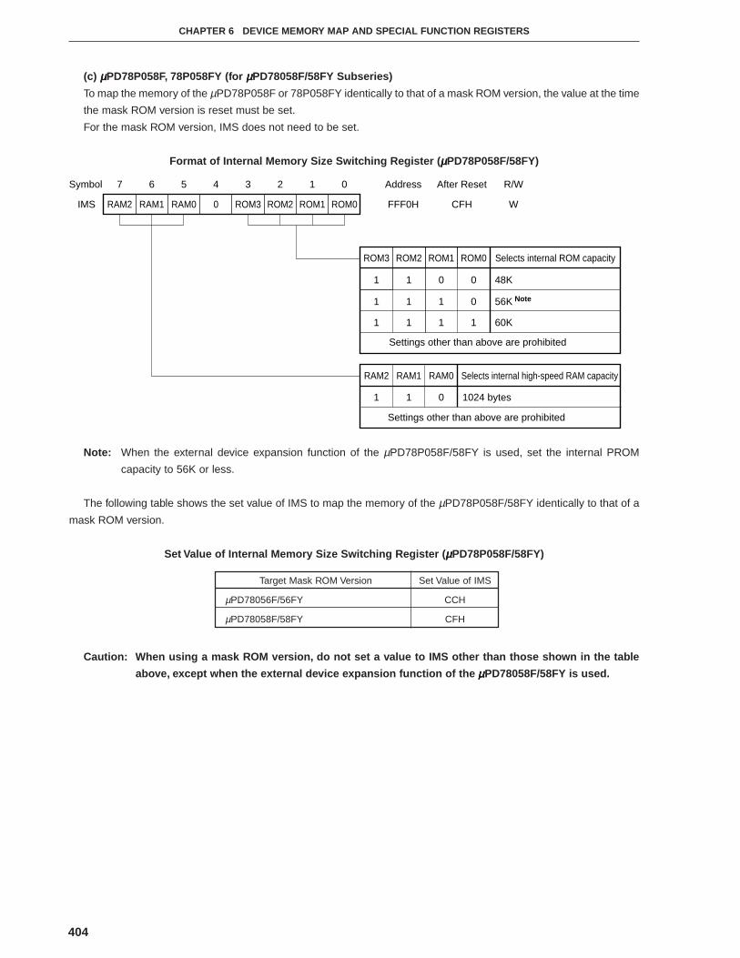
404
CHAPTER 6 DEVICE MEMORY MAP AND SPECIAL FUNCTION REGISTERS
(c) µµµµµPD78P058F, 78P058FY (for µµµµµPD78058F/58FY Subseries)
To map the memory of the µPD78P058F or 78P058FY identically to that of a mask ROM version, the value at the time
the mask ROM version is reset must be set.
For the mask ROM version, IMS does not need to be set.
Format of Internal Memory Size Switching Register ( µµµµµPD78P058F/58FY)
Note: When the external device expansion function of the µPD78P058F/58FY is used, set the internal PROM
capacity to 56K or less.
The following table shows the set value of IMS to map the memory of the µPD78P058F/58FY identically to that of a
mask ROM version.
Set Value of Internal Memory Size Switching Register ( µµµµµPD78P058F/58FY)
Target Mask ROM Version Set Value of IMS
µPD78056F/56FY CCH
µPD78058F/58FY CFH
Caution: When using a mask ROM version, do not set a value to IMS other than those shown in the table
above, except when the external device expansion function of the µµµµµPD78058F/58FY is used.
RAM2 RAM1 RAM0 0 ROM3 ROM2 ROM1 ROM0IMS
7 6 5 4 3 2 1 0Symbol Address After Reset R/W
FFF0H CFH W
ROM3 ROM2 ROM1 ROM0
1
1
1
1
1 1
0
1
0
0
1 1
Selects internal ROM capacity
48K
56K Note
60K
RAM2 RAM1
1 1
RAM0
0
Selects internal high-speed RAM capacity
1024 bytes
Settings other than above are prohibited
Settings other than above are prohibited
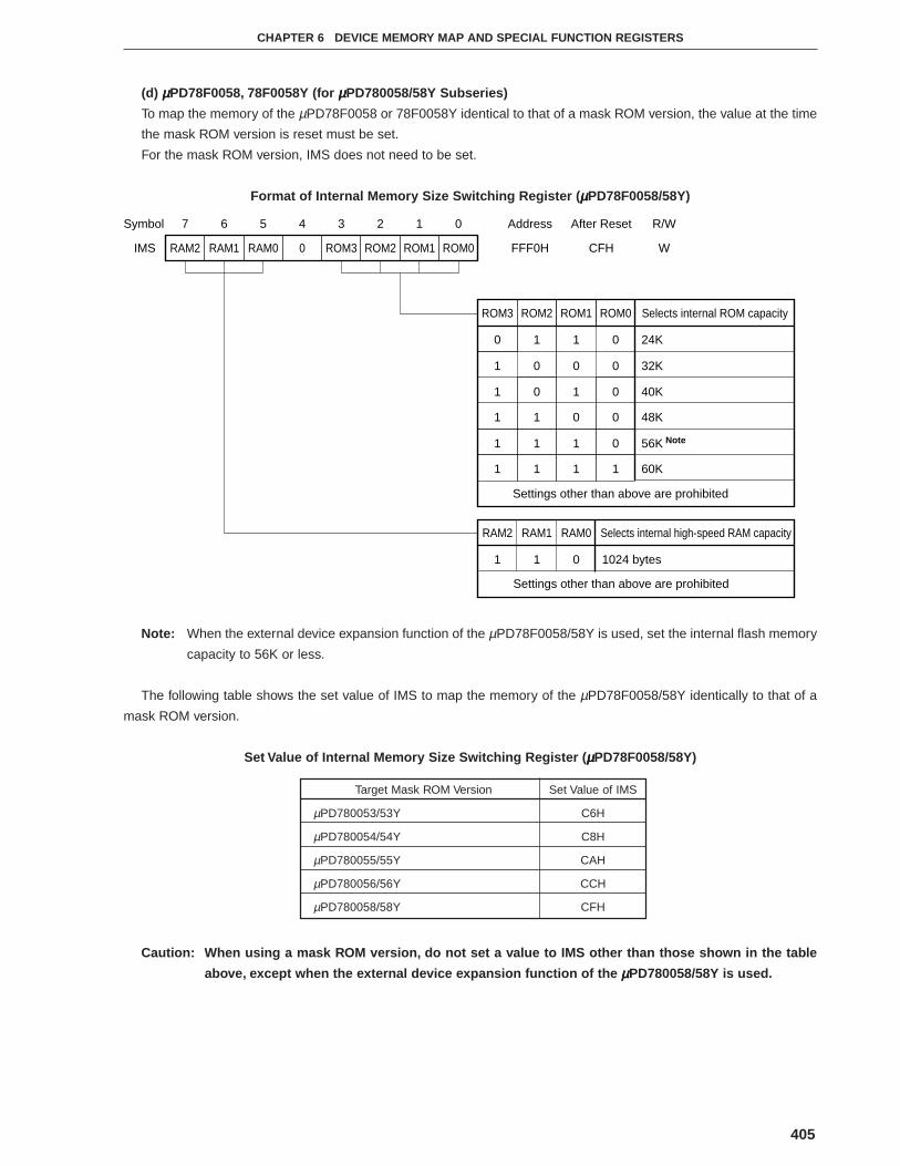
405
CHAPTER 6 DEVICE MEMORY MAP AND SPECIAL FUNCTION REGISTERS
(d) µµµµµPD78F0058, 78F0058Y (for µµµµµPD780058/58Y Subseries)
To map the memory of the µPD78F0058 or 78F0058Y identical to that of a mask ROM version, the value at the time
the mask ROM version is reset must be set.
For the mask ROM version, IMS does not need to be set.
Format of Internal Memory Size Switching Register ( µµµµµPD78F0058/58Y)
Note: When the external device expansion function of the µPD78F0058/58Y is used, set the internal flash memory
capacity to 56K or less.
The following table shows the set value of IMS to map the memory of the µPD78F0058/58Y identically to that of a
mask ROM version.
Set Value of Internal Memory Size Switching Register ( µµµµµPD78F0058/58Y)
Target Mask ROM Version Set Value of IMS
µPD780053/53Y C6H
µPD780054/54Y C8H
µPD780055/55Y CAH
µPD780056/56Y CCH
µPD780058/58Y CFH
Caution: When using a mask ROM version, do not set a value to IMS other than those shown in the table
above, except when the external device expansion function of the µµµµµPD780058/58Y is used.
RAM2 RAM1 RAM0 0 ROM3 ROM2 ROM1 ROM0IMS
7 6 5 4 3 2 1 0Symbol Address After Reset R/W
FFF0H CFH W
ROM3 ROM2
0
1
1
0
ROM1 ROM0
1
0
0
0
1 0
1
1
1
1
1 1
1 0
0
1
0
0
1 1
Selects internal ROM capacity
24K
32K
40K
48K
56K Note
60K
RAM2 RAM1
1 1
RAM0
0
Selects internal high-speed RAM capacity
1024 bytes
Settings other than above are prohibited
Settings other than above are prohibited

406
CHAPTER 6 DEVICE MEMORY MAP AND SPECIAL FUNCTION REGISTERS
(23) Register controlling internal expansion RAM capacity
The µPD78P058/58Y/58F/58FY and 78F0058/58Y allow users to select the internal expansion RAM capacity.
The following register is used to control the internal expansion RAM capacity:
• Internal expansion RAM size switching register (IXS)
Remark: This register is provided only for the µPD78058/58Y, 78P058/58Y, 78058F/58FY, 78P058F/58FY, 780058/
58Y, and 78F0058/58Y.
Format of Internal Expansion RAM Size Switching Register
The following table shows the set value of IXS to map the internal expansion RAM of the µPD78P058/58Y, 78P058F/
58FY, or 78F0058/58Y identically to that of a mask ROM version.
Set Value of Internal Expansion RAM Size Switching Register
Target Mask ROM Version Set Value of IXS
µPD78052/52Y 0CH
µPD78053/53Y, 780053/53Y
µPD78054/54Y, 780054/54Y
µPD78055/55Y, 780055/55Y
µPD78056/56Y/56F/56FY, 780056/56Y
µPD78058/58Y/58F/58FY, 780058/58Y 0AH
Cautions: 1. For the mask ROM version, IXS does not need to be set.
2. When using a mask ROM version, do not set a value to IXS other than those shown in the table
above.
6 5 4 3 2 1 07Symbol
IXS 0 0 0 0 IXRAM3
IXRAM2
IXRAM1
IXRAM0
1
1
Selects internal expansionRAM capacity
0 bytes
FFF4H 0AH W
Address After Reset R/W
IXRAM3
1
IXRAM2
0
IXRAM1
0
1024 bytes0 1 0
IXRAM0
Settings other than above are prohibited
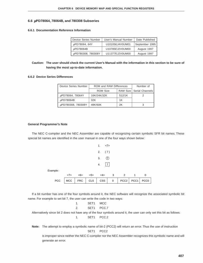
407
CHAPTER 6 DEVICE MEMORY MAP AND SPECIAL FUNCTION REGISTERS
6.6 µµµµµPD78064, 78064B, and 780308 Subseries
6.6.1 Documentation Reference Information
Device Series Number User’s Manual Number Date Published
µPD78064, 64Y U10105EJ4V0UM01 September 1995
µPD78064B U10785EJ2V0UM00 August 1997
µPD780308, 780308Y U11377EJ2V0UM00 August 1997
Caution: The user should check the current User’s Manual with the information in this section to be sure of
having the most up-to-date information.
6.6.2 Device Series Differences
Device Series Number ROM and RAM Differences Number of
ROM Size RAM Size Serial Channels
µPD78064, 78064Y 16K/24K/32K 512/1K 2
µPD78064B 32K 1K
µPD780308, 780308Y 48K/60K 2K 3
General Programmer’s Note
The NEC C-compiler and the NEC Assembler are capable of recognizing certain symbolic SFR bit names. These
special bit names are identified in the user manual in one of the four ways shown below:
If a bit number has one of the four symbols around it, the NEC software will recognize the associated symbolic bit
name. For example to set bit 7, the user can write the code in two ways:
1. SET1 MCC
2. SET1 PCC.7
Alternatively since bit 2 does not have any of the four symbols around it, the user can only set this bit as follows:
1. SET1 PCC.2
Note: The attempt to employ a symbolic name of bit-2 (PCC2) will return an error. Thus the use of instruction
SET1 PCC2
is improper since neither the NEC C-compiler nor the NEC Assembler recognizes this symbolic name and will
generate an error.
MCCPCC FRC CLS CSS 0 PCC2 PCC1 PCC0
<7> <6> <5> <4> 3 2 1 0
Example:
1.
2.
3.
4.
<7>
( 7 )
7
7
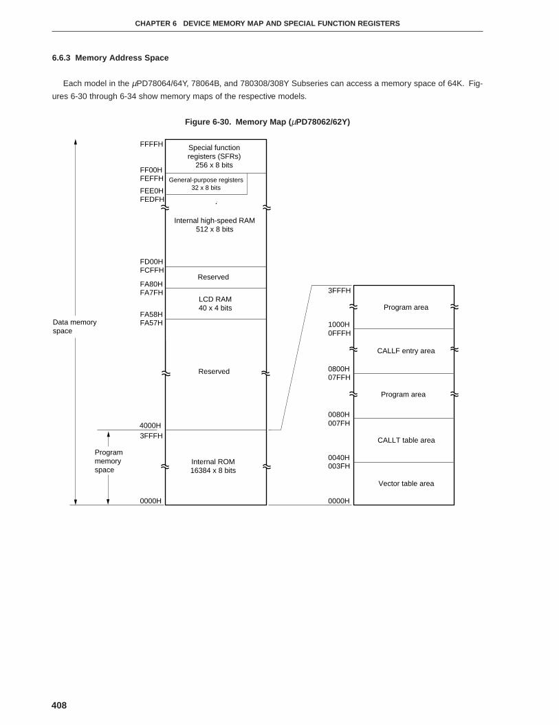
408
CHAPTER 6 DEVICE MEMORY MAP AND SPECIAL FUNCTION REGISTERS
6.6.3 Memory Address Space
Each model in the µPD78064/64Y, 78064B, and 780308/308Y Subseries can access a memory space of 64K. Fig-
ures 6-30 through 6-34 show memory maps of the respective models.
Figure 6-30. Memory Map ( µPD78062/62Y)
0000H
Data memory space
General-purpose registers32 x 8 bits
Internal ROM16384 x 8 bits
3FFFH
1000H0FFFH
0800H07FFH
0080H 007FH
0040H003FH
0000H
CALLF entry area
CALLT table area
Vector table area
Program area
Program areaLCD RAM40 x 4 bits
Reserved
Programmemoryspace
4000H3FFFH
FA58HFA57H
FA80HFA7FH
FEE0HFEDFH
FF00HFEFFH
FFFFH
Internal high-speed RAM512 x 8 bits
Special function registers (SFRs)
256 x 8 bits
Reserved
FD00HFCFFH
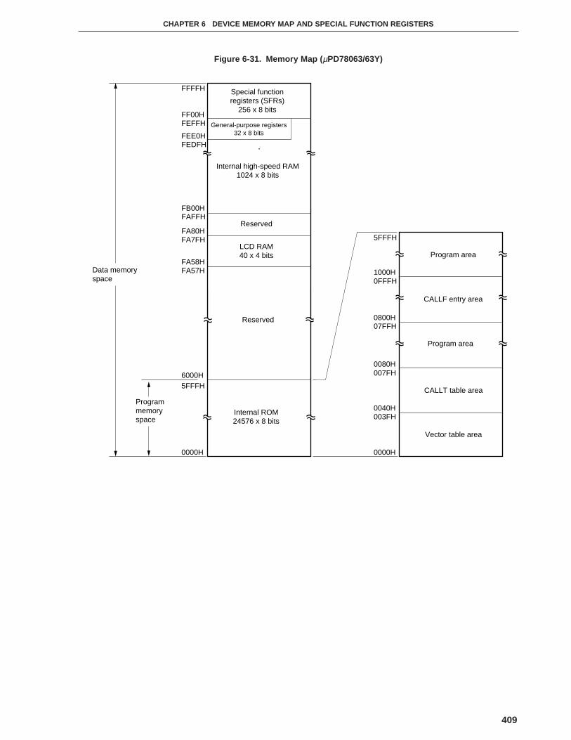
409
CHAPTER 6 DEVICE MEMORY MAP AND SPECIAL FUNCTION REGISTERS
Figure 6-31. Memory Map ( µPD78063/63Y)
0000H
Data memory space
Internal ROM24576 x 8 bits
5FFFH
1000H0FFFH
0800H07FFH
0080H 007FH
0040H003FH
0000H
CALLF entry area
CALLT table area
Vector table area
Program area
Program areaLCD RAM40 x 4 bits
Reserved
Programmemoryspace
6000H5FFFH
FA58HFA57H
FA80HFA7FH
FEE0HFEDFH
FF00HFEFFH
FFFFH
Internal high-speed RAM1024 x 8 bits
Special function registers (SFRs)
256 x 8 bits
Reserved
FB00HFAFFH
General-purpose registers32 x 8 bits
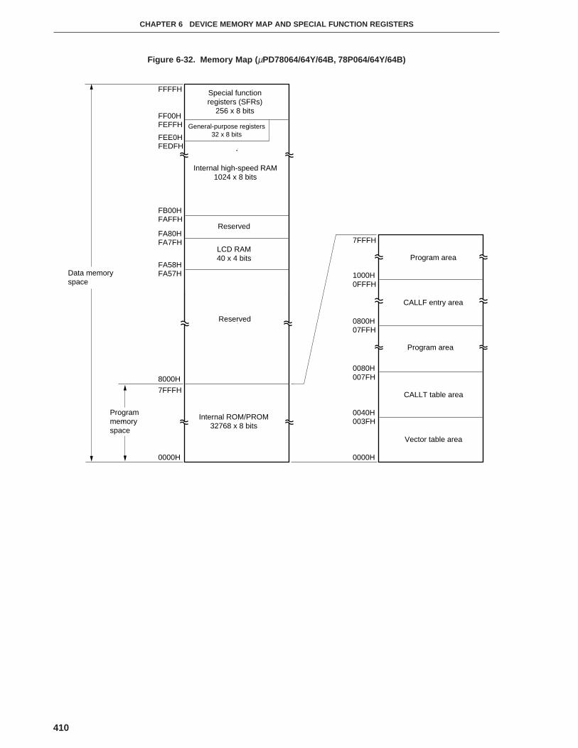
410
CHAPTER 6 DEVICE MEMORY MAP AND SPECIAL FUNCTION REGISTERS
Figure 6-32. Memory Map ( µPD78064/64Y/64B, 78P064/64Y/64B)
0000H
Data memory space
Internal ROM/PROM32768 x 8 bits
7FFFH
1000H0FFFH
0800H07FFH
0080H 007FH
0040H003FH
0000H
CALLF entry area
CALLT table area
Vector table area
Program area
Program areaLCD RAM40 x 4 bits
Reserved
8000H
7FFFH
FA58HFA57H
FA80HFA7FH
FEE0HFEDFH
FF00HFEFFH
FFFFH
Internal high-speed RAM1024 x 8 bits
Special function registers (SFRs)
256 x 8 bits
Reserved
FB00HFAFFH
Programmemoryspace
General-purpose registers32 x 8 bits
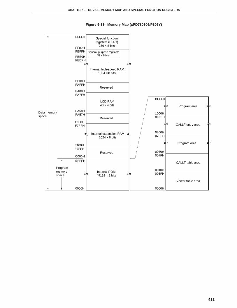
411
CHAPTER 6 DEVICE MEMORY MAP AND SPECIAL FUNCTION REGISTERS
Figure 6-33. Memory Map ( µPD780306/P306Y)
0000H
Data memory space
Internal ROM49152 × 8 bits
BFFFH
1000H0FFFH
0800H07FFH
0080H 007FH
0040H003FH
0000H
CALLF entry area
CALLT table area
Vector table area
Program area
Program area
LCD RAM40 × 4 bits
Reserved
Programmemoryspace
C000HBFFFH
FA58HFA57H
FA80HFA7FH
FEE0HFEDFH
FF00HFEFFH
FFFFH
Internal high-speed RAM1024 × 8 bits
Special function registers (SFRs)
256 × 8 bits
Reserved
FB00HFAFFH
Reserved
Internal expansion RAM1024 × 8 bits
F800HF7FFH
F400HF3FFH
General-purpose registers32 x 8 bits
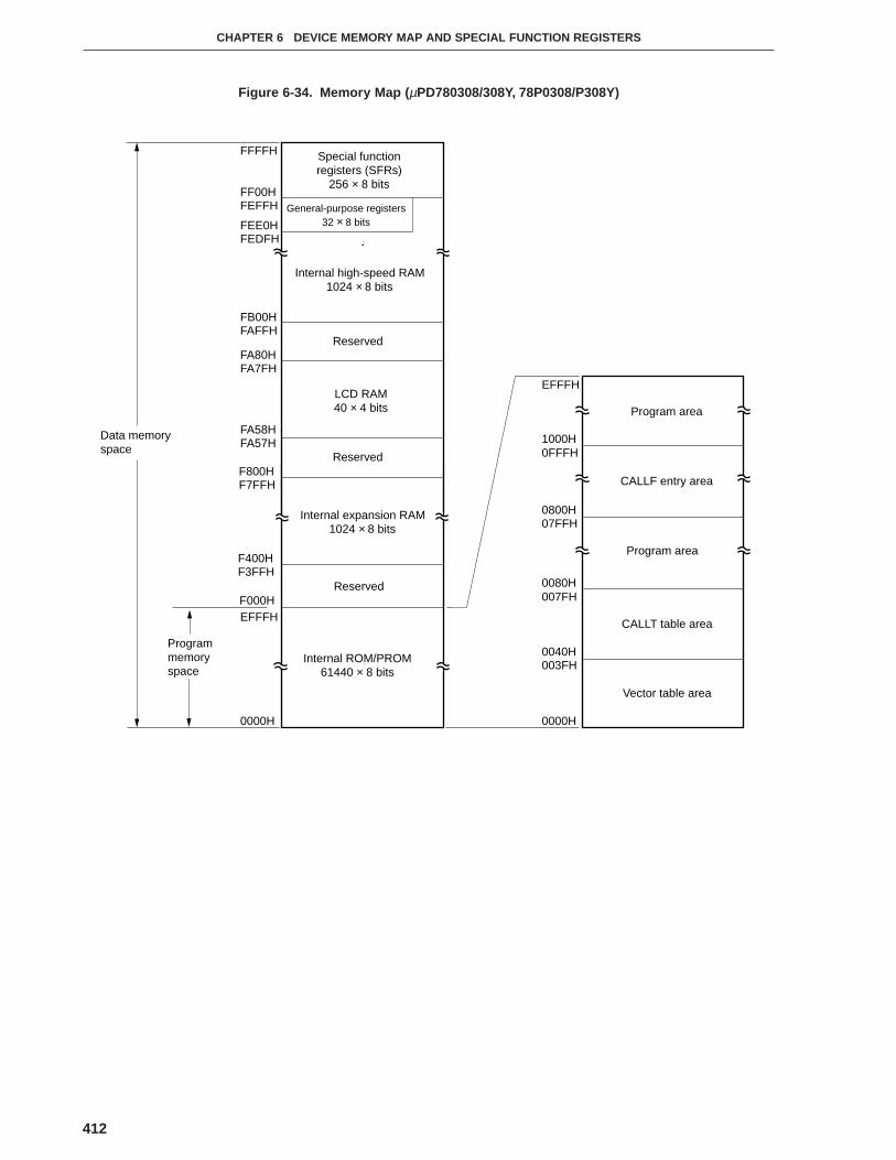
412
CHAPTER 6 DEVICE MEMORY MAP AND SPECIAL FUNCTION REGISTERS
Figure 6-34. Memory Map ( µPD780308/308Y, 78P0308/P308Y)
0000H
Data memory space
Internal ROM/PROM61440 × 8 bits
EFFFH
1000H0FFFH
0800H07FFH
0080H 007FH
0040H003FH
0000H
CALLF entry area
CALLT table area
Vector table area
Program area
Program area
LCD RAM40 × 4 bits
Reserved
Programmemoryspace
F000HEFFFH
FA58HFA57H
FA80HFA7FH
FEE0HFEDFH
FF00HFEFFH
FFFFH
Internal high-speed RAM1024 × 8 bits
Special function registers (SFRs)
256 × 8 bits
Reserved
FB00HFAFFH
Reserved
Internal expansion RAM1024 × 8 bits
F800HF7FFH
F400HF3FFH
General-purpose registers32 × 8 bits
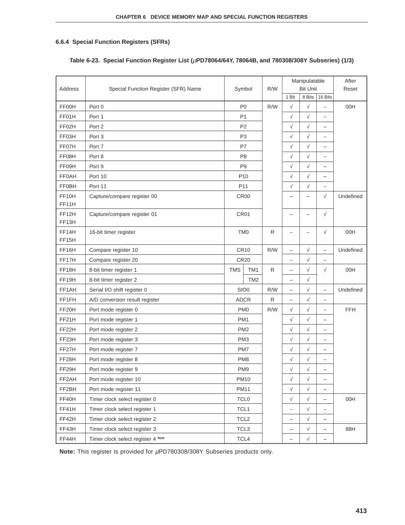
413
CHAPTER 6 DEVICE MEMORY MAP AND SPECIAL FUNCTION REGISTERS
6.6.4 Special Function Registers (SFRs)
Table 6-23. Special Function Register List ( µPD78064/64Y, 78064B, and 780308/308Y Subseries) (1/3)
Manipulatable After
Address Special Function Register (SFR) Name Symbol R/W Bit Unit Reset
1 Bit 8 Bits 16 Bits
FF00H Port 0 P0 R/W √ √ – 00H
FF01H Port 1 P1 √ √ –
FF02H Port 2 P2 √ √ –
FF03H Port 3 P3 √ √ –
FF07H Port 7 P7 √ √ –
FF08H Port 8 P8 √ √ –
FF09H Port 9 P9 √ √ –
FF0AH Port 10 P10 √ √ –
FF0BH Port 11 P11 √ √ –
FF10H Capture/compare register 00 CR00 – – √ Undefined
FF11H
FF12H Capture/compare register 01 CR01 – – √FF13H
FF14H 16-bit timer register TM0 R – – √ 00H
FF15H
FF16H Compare register 10 CR10 R/W – √ – Undefined
FF17H Compare register 20 CR20 – √ –
FF18H 8-bit timer register 1 TMS TM1 R – √ √ 00H
FF19H 8-bit timer register 2 TMS TM2 – √
FF1AH Serial I/O shift register 0 SIO0 R/W – √ – Undefined
FF1FH A/D conversion result register ADCR R – √ –
FF20H Port mode register 0 PM0 R/W √ √ – FFH
FF21H Port mode register 1 PM1 √ √ –
FF22H Port mode register 2 PM2 √ √ –
FF23H Port mode register 3 PM3 √ √ –
FF27H Port mode register 7 PM7 √ √ –
FF28H Port mode register 8 PM8 √ √ –
FF29H Port mode register 9 PM9 √ √ –
FF2AH Port mode register 10 PM10 √ √ –
FF2BH Port mode register 11 PM11 √ √ –
FF40H Timer clock select register 0 TCL0 √ √ – 00H
FF41H Timer clock select register 1 TCL1 – √ –
FF42H Timer clock select register 2 TCL2 – √ –
FF43H Timer clock select register 3 TCL3 – √ – 88H
FF44H Timer clock select register 4 Note TCL4 – √ –
Note: This register is provided for µPD780308/308Y Subseries products only.
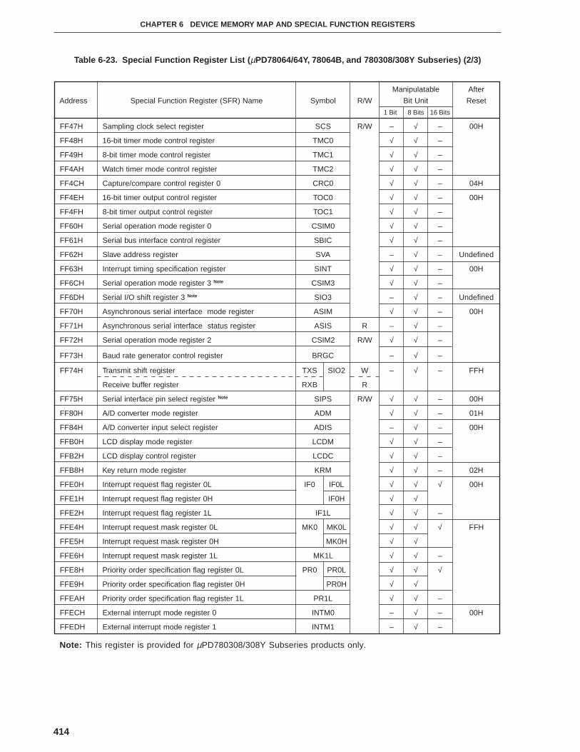
414
CHAPTER 6 DEVICE MEMORY MAP AND SPECIAL FUNCTION REGISTERS
Table 6-23. Special Function Register List ( µPD78064/64Y, 78064B, and 780308/308Y Subseries) (2/3)
Manipulatable After
Address Special Function Register (SFR) Name Symbol R/W Bit Unit Reset
1 Bit 8 Bits 16 Bits
FF47H Sampling clock select register SCS R/W – √ – 00H
FF48H 16-bit timer mode control register TMC0 √ √ –
FF49H 8-bit timer mode control register TMC1 √ √ –
FF4AH Watch timer mode control register TMC2 √ √ –
FF4CH Capture/compare control register 0 CRC0 √ √ – 04H
FF4EH 16-bit timer output control register TOC0 √ √ – 00H
FF4FH 8-bit timer output control register TOC1 √ √ –
FF60H Serial operation mode register 0 CSIM0 √ √ –
FF61H Serial bus interface control register SBIC √ √ –
FF62H Slave address register SVA – √ – Undefined
FF63H Interrupt timing specification register SINT √ √ – 00H
FF6CH Serial operation mode register 3 Note CSIM3 √ √ –
FF6DH Serial I/O shift register 3 Note SIO3 – √ – Undefined
FF70H Asynchronous serial interface mode register ASIM √ √ – 00H
FF71H Asynchronous serial interface status register ASIS R – √ –
FF72H Serial operation mode register 2 CSIM2 R/W √ √ –
FF73H Baud rate generator control register BRGC – √ –
FF74H Transmit shift register TXS SIO2 W – √ – FFH
Receive buffer register RXB R
FF75H Serial interface pin select register Note SIPS R/W √ √ – 00H
FF80H A/D converter mode register ADM √ √ – 01H
FF84H A/D converter input select register ADIS – √ – 00H
FFB0H LCD display mode register LCDM √ √ –
FFB2H LCD display control register LCDC √ √ –
FFB8H Key return mode register KRM √ √ – 02H
FFE0H Interrupt request flag register 0L IF0 IF0L √ √ √ 00H
FFE1H Interrupt request flag register 0H IF0H √ √
FFE2H Interrupt request flag register 1L IF1L √ √ –
FFE4H Interrupt request mask register 0L MK0 MK0L √ √ √ FFH
FFE5H Interrupt request mask register 0H MK0H √ √
FFE6H Interrupt request mask register 1L MK1L √ √ –
FFE8H Priority order specification flag register 0L PR0 PR0L √ √ √
FFE9H Priority order specification flag register 0H PR0H √ √
FFEAH Priority order specification flag register 1L PR1L √ √ –
FFECH External interrupt mode register 0 INTM0 – √ – 00H
FFEDH External interrupt mode register 1 INTM1 – √ –
Note: This register is provided for µPD780308/308Y Subseries products only.
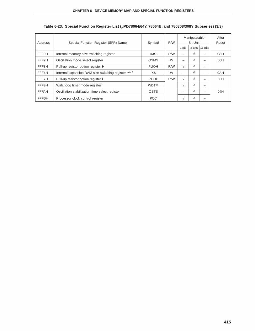
415
CHAPTER 6 DEVICE MEMORY MAP AND SPECIAL FUNCTION REGISTERS
Table 6-23. Special Function Register List ( µPD78064/64Y, 78064B, and 780308/308Y Subseries) (3/3)
Manipulatable After
Address Special Function Register (SFR) Name Symbol R/W Bit Unit Reset
1 Bit 8 Bits 16 Bits
FFF0H Internal memory size switching register IMS R/W – √ – C8H
FFF2H Oscillation mode select register OSMS W – √ – 00H
FFF3H Pull-up resistor option register H PUOH R/W √ √ –
FFF4H Internal expansion RAM size switching register Note 2 IXS W – √ – 0AH
FFF7H Pull-up resistor option register L PUOL R/W √ √ – 00H
FFF9H Watchdog timer mode register WDTM √ √ –
FFFAH Oscillation stabilization time select register OSTS – √ – 04H
FFFBH Processor clock control register PCC √ √ –
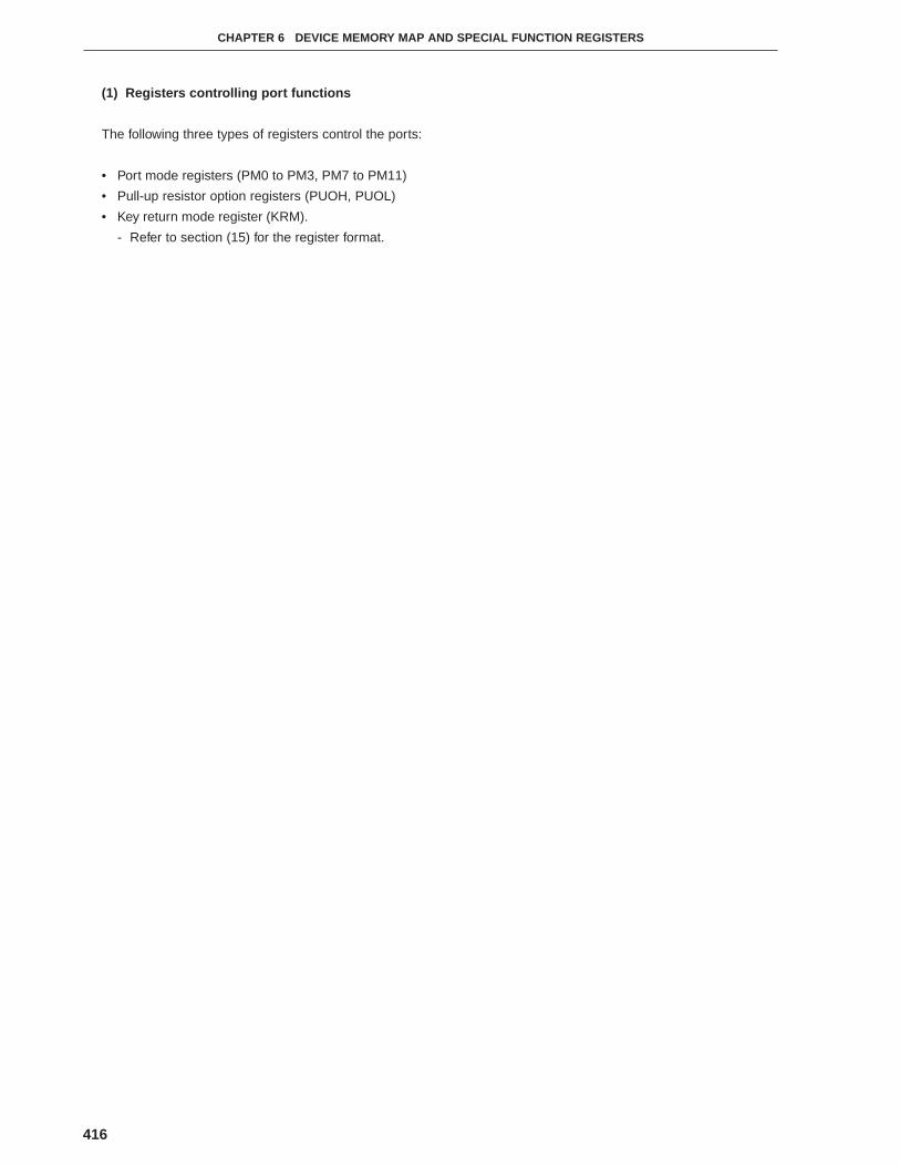
416
CHAPTER 6 DEVICE MEMORY MAP AND SPECIAL FUNCTION REGISTERS
(1) Registers controlling port functions
The following three types of registers control the ports:
• Port mode registers (PM0 to PM3, PM7 to PM11)
• Pull-up resistor option registers (PUOH, PUOL)
• Key return mode register (KRM).
- Refer to section (15) for the register format.
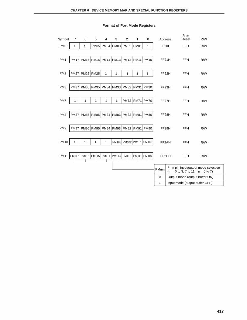
417
CHAPTER 6 DEVICE MEMORY MAP AND SPECIAL FUNCTION REGISTERS
Format of Port Mode Registers
PM0
PM1
PM2
1 1 PM03 PM02 PM01 1
7 6 5 4 3 2 1 0Symbol
PM3
PM8
FF20H
FF21H
FF22H
FF23H
FF28H
FFH
FFH
FFH
FFH
FFH
R/W
R/W
R/W
R/W
R/W
AddressAfterReset R/W
PM17 PM16 PM15 PM14 PM13 PM12 PM11 PM10
PM27 PM26 PM25 1 1 1 1 1
PM37 PM36 PM35 PM34 PM33 PM32 PM31 PM30
PM87 PM86 PM85 PM84 PM83 PM82 PM81 PM80
PM9
PM7
FF29H
FF27H
FFH
FFH
R/W
R/W
PM97 PM96 PM95 PM94 PM93 PM92 PM91 PM90
1 1 1 1 1 PM72 PM71 PM70
PM05 PM04
PM11
PM10
PMmn Pmn pin input/output mode selection(m = 0 to 3, 7 to 11 : n = 0 to 7)
0
1
Output mode (output buffer ON)
Input mode (output buffer OFF)
FF2AH
FF2BH
FFH
FFH
R/W
R/WPM112 PM111 PM110
1 1 1 1 PM101 PM100
PM115 PM114 PM113PM117 PM116
PM103 PM102
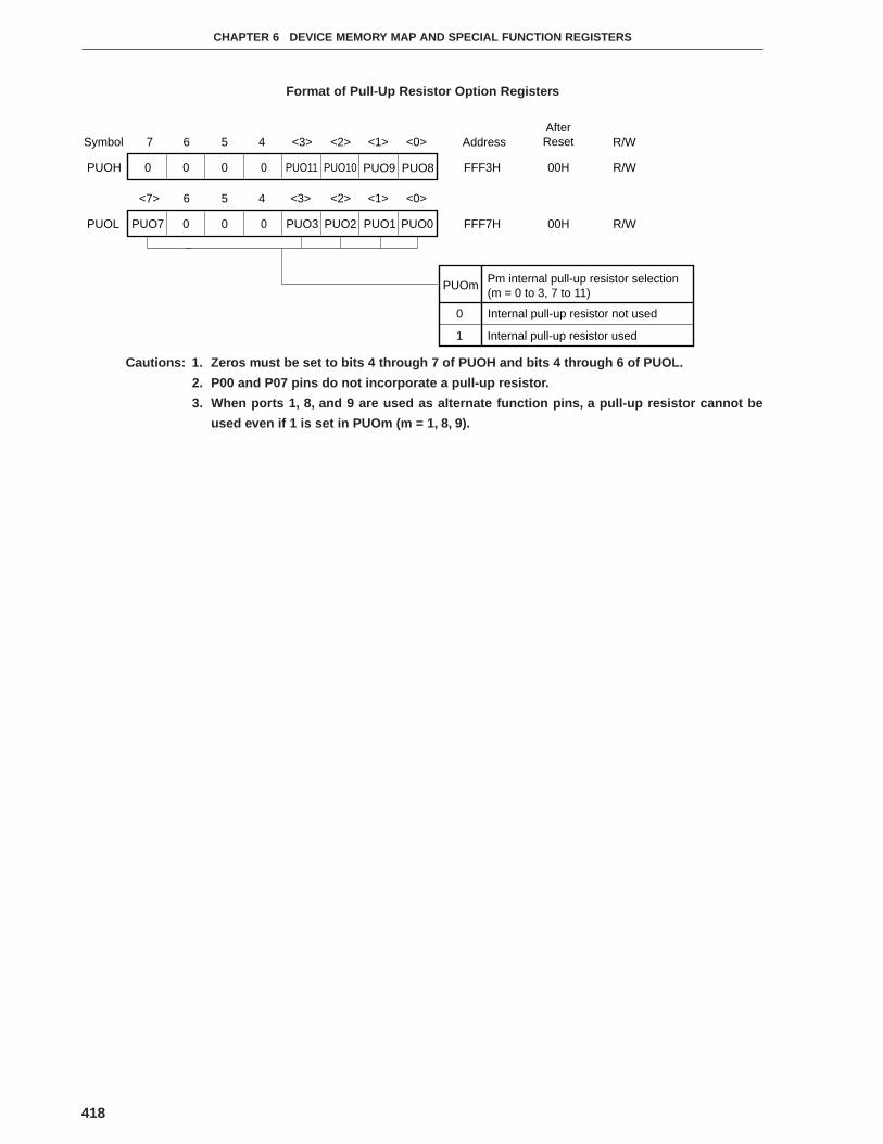
418
CHAPTER 6 DEVICE MEMORY MAP AND SPECIAL FUNCTION REGISTERS
Format of Pull-Up Resistor Option Registers
Cautions: 1. Zeros must be set to bits 4 through 7 of PUOH and bits 4 through 6 of PUOL.
2. P00 and P07 pins do not incorporate a pull-up resistor.
3. When ports 1, 8, and 9 are used as alternate function pins, a pull-up resistor cannot be
used even if 1 is set in PUOm (m = 1, 8, 9).
PUO7 PUO2 PUO1 PUO0PUOL
PUOm Pm internal pull-up resistor selection(m = 0 to 3, 7 to 11)
0
1
Internal pull-up resistor not used
Internal pull-up resistor used
FFF7H 00H R/W
6 5 4
PUO3
<7> <3>
0 0 PUO11 PUO100PUOH FFF3H 00H R/W
7 6 5 4Symbol AddressAfterReset R/W
0
<3> <2>
<2>
<1>
<1> <0>
<0>
PUO9 PUO8
0 00

419
CHAPTER 6 DEVICE MEMORY MAP AND SPECIAL FUNCTION REGISTERS
(2) Registers controlling clock generator
The following two registers control the clock generator:
• Processor clock control register (PCC)
• Oscillation mode select register (OSMS)

420
CHAPTER 6 DEVICE MEMORY MAP AND SPECIAL FUNCTION REGISTERS
Format of Processor Clock Control Register
Notes: 1. Bit 5 is a read-only bit.
2. When the CPU is operating on the subsystem clock, MCC should be used to stop the main
system clock oscillation. A STOP instruction should not be used.
Caution: Bit 3 must be set to 0.
Remarks: fXX: Main system clock frequency (fX or fX/2)
fX: Main system clock oscillator frequency
fXT: Subsystem clock oscillator frequency
MCS: Bit 0 of oscillation mode select register (OSMS)
Values in parentheses indicate minimum instruction execution time: 2/fCPU when operating at
fX = 5.0 MHz or fXT = 32.768 kHz.
MCC FRC CLS CSS PCC2 PCC1 PCC0PCC FFFBH 04H R/W Note 1
Symbol Address R/W
0
3 2 01
FRC
0
1
Internal feedback resistor used
Internal feedback resistor not used
Subsystem clock feedback resistor selectionR/W
MCC
0
1
Oscillation possible
Oscillation stopped
Main system clock oscillation control Note 2R/W
CLS
0
1
Main system clock
Subsystem clock
CPU clock statusR
CSS
0
0 fXX/2
PCC2CPU cIock selection (fCPU)
PCC1 PCC0
0
0
0
1
0
0
1
1
0
1
1
0
0
0
0
0
0
0
0
1
1
0
0
1
1
0
1
0
fXX/22
fXX/23
fXX/24
fXT/2 (122 s)
fXX
R/W
fx/2 (0.8 s)µ
fx/22 (1.6 s)µ
fx/23 (3.2 s)µ
fx/24 (6.4 s)µ
fx (0.4 s)µ
fx/22 (1.6 s)µ
fx/23 (3.2 s)µ
fx/24 (6.4 s)µ
fx/25 (12.8 s)µ
fx /2 (0.8 s)µ
µ
MCS = 1 MCS = 0
0
1
<7> <6> <5> <4> After Reset
Settings other than above are prohibited

421
CHAPTER 6 DEVICE MEMORY MAP AND SPECIAL FUNCTION REGISTERS
Format of Oscillation Mode Select Register
Cautions: 1. Writing to OSMS should be performed only immediately after reset signal release and before
peripheral hardware operation starts. Writing data (including the same data as previously) to
OSMS causes a delay of the main system clock cycle of up to 2/f x during the write operation.
Therefore, if this register is written during the operation, in peripheral hardware that operates
with the main system clock, a temporary error occurs in the count clock cycle of the timer, etc.
In addition, because the oscillation mode is changed by this register, the clocks for peripheral
hardware as well as that for the CPU are switched.
2. When writing “1” to MCS, V DD must be 2.7 V or higher before the write execution.
MCS Main system clock scaler control
0
1
Scaler used
Scaler not used
0 0 0 0OSMS FFF2H
7 6 5 4 3 2Symbol 1
0 MCS
0
0
AddressAfterReset R/W
00H W0
422
CHAPTER 6 DEVICE MEMORY MAP AND SPECIAL FUNCTION REGISTERS
(3) Registers controlling 16-bit timer/event counter
The following seven registers control the 16-bit timer/event counter:
• Timer clock select register 0 (TCL0)
• 16-bit timer mode control register (TMC0)
• Capture/compare control register 0 (CRC0)
• 16-bit timer output control register (TOC0)
• Port mode register 3 (PM3)
- Refer to section (1) for the register format.
• External interrupt mode register 0 (INTM0)
- Refer to section (15) for the register format.
• Sampling clock select register (SCS)
- Refer to section (15) for the register format.
Format of Timer Clock Select Register 0
Cautions: 1. Setting of the TI00/INTP0 pin valid edge is performed by external interrupt mode register 0,
and selection of the sampling clock frequency is performed by the sampling clock select
register.
2. To read the count value when TI00 has been specified as the TM0 count clock, the value
should be read from TM0, not from capture/compare register 01 (CR01).
3. To write data other than that already written to TCL0, stop the timer operation once.
Remarks: fXX: Main system clock frequency (fX or fX/2)
fX: Main system clock oscillation frequency
TI00: 16-bit timer/event counter input pin
TM0: 16-bit timer register
MCS: Bit 0 of oscillation mode select register (OSMS)
Values in parentheses apply to operation with fX = 5.0 MHz.
CLOE TCL06 TCL05 TCL04 TCL03 TCL02 TCL01 TCL00
<7> 6 5 4 3 2 1 0Symbol
TCL0 FF40H 00H R/W
Address After Reset R/W
TCL06 TCL05 TCL04
0 0 0 TI00 (Valid edge specifiable)
0 0 1 2fXX Setting prohibited fX (5.0 MHz)
0 1 0 fXX fX (5.0 MHz) fX/2 (2.5 MHz)
0 1 1 fXX/2 fX/2 (2.5 MHz) fX/22 (1.25 MHz)
1 0 0 fXX/22 fX/22 (1.25 MHz) fX/23 (625 kHz)
1 1 1 Watch timer output (INTTM3)
MCS = 1
16-bit timer register count clock selection
MCS = 0
This section controls the clock output circuit.Refer to (7) Registers controlling clock output function orChapter 12 of PD78064, 78064Y Subseries User's Manual,Chapter 10 of PD78064B Subseries User's Manual, orChapter 12 of PD780308, 780308Y Subseries User's Manualfor detailed information.
µµµ
Settings other than above are prohibited
423
CHAPTER 6 DEVICE MEMORY MAP AND SPECIAL FUNCTION REGISTERS
Format of 16-Bit Timer Mode Control Register
0 0 0 0 TMC03 TMC02 TMC01 OVF0
7 6 5 4 3 2 1 <0>Symbol
TMC0 FF48H 00H R/W
Address After Reset R/W
OVF0 16-bit timer register overflow detection
0 Overflow not detected
1 Overflow detected
TMC03 TMC02 TMC01Operating mode
clear mode selectionTO0 output timing selection Interrupt generation
0 0 0Operation stop(TM0 cleared to 0) No change Not generated
0 0 1PWM mode(free-running)
PWM pulse output
0 1 0
0 1 1
1 0 0
1 0 1
1 1 0
1 1 1
Free-running mode
Match between TM0 and CR00 or match between TM0 and CR01
Match between TM0 and CR00, match between TM0 and CR01, or TI00valid edge
Match between TM0 and CR00 or match between TM0 and CR01
Match between TM0 and CR00, match between TM0 and CR01, or TI00valid edge
Match between TM0 and CR00 or match between TM0 and CR01
Match between TM0 and CR00, match between TM0 and CR01, or TI00valid edge
Clear and start on TI00 valid edge
Clear and start on matchbetween TM0 and CR00
Generated on match between TM0 and CR00and match between TM0and CR01
424
CHAPTER 6 DEVICE MEMORY MAP AND SPECIAL FUNCTION REGISTERS
Cautions: 1. The 16-bit timer register (TM0) starts operation when a value other than 0, 0, 0 is set to TMC01 to
TMC03 (Operation Stop mode). To stop the operation, set TMC01 to TMC03 to 0, 0, 0.
2. Switch the Clear mode and the T00 output timing after stopping the timer operation (by setting
TMC01 to TMC03 to 0, 0, 0).
3. Set the valid edge of the TI00/INTP0 pin with external interrupt mode register 0 and select the
sampling clock frequency with the sampling clock select register.
4. When using the PWM mode, set the PWM mode and then set data to CR00.
5. If Clear and Start mode on a match between TM0 and CR00 is selected, when the set value of
CR00 is FFFFH and the TM0 value changes from FFFFH to 0000H, the OVF0 flag is set to 1.
Remarks: TO0: 16-bit timer/event counter output pin
TI00: 16-bit timer/event counter input pin
TM0: 16-bit timer register
CR00: Compare register 00
CR01: Compare register 01

425
CHAPTER 6 DEVICE MEMORY MAP AND SPECIAL FUNCTION REGISTERS
Format of Capture/Compare Control Register 0
Cautions: 1. Timer operation must be stopped before setting CRC0.
2. When Clear and Start mode on a match between TM0 and CR00 is selected with the 16-bit
timer mode control register, CR00 should not be specified as a capture register.
0 0 0 0 0 CRC02 CRC01 CRC00
7 6 5 4 3 2 1 0Symbol
CRC0 FF4CH 04H R/W
Address After Reset R/W
CRC00 CR00 operating mode selection
0 Operates as compare register
1 Operates as capture register
CRC01 CR00 capture trigger selection
Captures on valid edge of TI01
Captures on valid edge of TI00
0
1
CRC02 CR01 operating mode selection
Operates as compare register
Operates as capture register
0
1
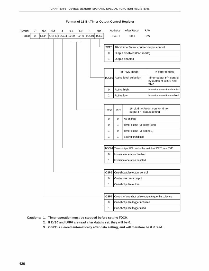
426
CHAPTER 6 DEVICE MEMORY MAP AND SPECIAL FUNCTION REGISTERS
Format of 16-Bit Timer Output Control Register
Cautions: 1. Timer operation must be stopped before setting TOC0.
2. If LVS0 and LVR0 are read after data is set, they will be 0.
3. OSPT is cleared automatically after data setting, and will therefore be 0 if read.
0 OSPT OSPE TOC04 LVS0 LVR0 TOC01 TOE0
7 <6> <5> 4 <3> <2> 1 <0>Symbol
TOC0 FF4EH 00H R/W
Address After Reset R/W
TOE0 16-bit timer/event counter output control
0 Output disabled (Port mode)
1 Output enabled
TOC01
0
1
In PWM mode In other modes
Active level selection Timer output F/F control by match of CR00 and TM0
Active high
Active low
Inversion operation disabled
Inversion operation enabled
LVS0 LVR016-bit timer/event counter timer output F/F status setting
0 0 No change
0 1 Timer output F/F reset (to 0)
1 0 Timer output F/F set (to 1)
1 1 Setting prohibited
TOC04 Timer output F/F control by match of CR01 and TM0
0 Inversion operation disabled
1 Inversion operation enabled
OSPE One-shot pulse output control
0 Continuous pulse output
1 One-shot pulse output
OSPT Control of one-shot pulse output trigger by software
0 One-shot pulse trigger not used
1 One-shot pulse trigger used
427
CHAPTER 6 DEVICE MEMORY MAP AND SPECIAL FUNCTION REGISTERS
(4) Registers controlling 8-bit timer/event counters 1 and 2
The following four registers control the 8-bit timer/event counters:
• Timer clock select register 1 (TCL1)
• 8-bit timer mode control register 1 (TMC1)
• 8-bit timer output control register (TOC1)
• Port mode register 3 (PM3).
- Refer to section (1) for the register format.
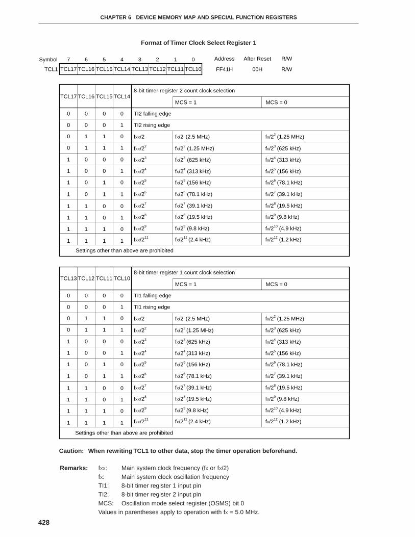
428
CHAPTER 6 DEVICE MEMORY MAP AND SPECIAL FUNCTION REGISTERS
Format of Timer Clock Select Register 1
Caution: When rewriting TCL1 to other data, stop the timer operation beforehand.
Remarks: fXX: Main system clock frequency (fX or fX/2)
fX: Main system clock oscillation frequencyTI1: 8-bit timer register 1 input pinTI2: 8-bit timer register 2 input pin
MCS: Oscillation mode select register (OSMS) bit 0Values in parentheses apply to operation with fX = 5.0 MHz.
TCL17 TCL16 TCL15 TCL14 TCL13 TCL12 TCL11 TCL10
7 6 5 4 3 2 1 0Symbol
TCL1 FF41H 00H R/W
Address After Reset R/W
TCL13 TCL12 TCL11 TCL10
0 0 0 0 TI1 falling edge
0 0 0 1 TI1 rising edge
0 1 1 0
0 1 1 1
fXX/2 fX/2 (2.5 MHz) fX/22 (1.25 MHz)
1 0 0 0
fXX/22 fX/22 (1.25 MHz) fX/23 (625 kHz)
1 0 0 1
fXX/23 fX/23 (625 kHz) fX/24 (313 kHz)
1 0 1 0
fXX/24 fX/24 (313 kHz) fX/25 (156 kHz)
1 0 1 1
fXX/25 fX/25 (156 kHz) fX/26 (78.1 kHz)
1 1 0 0
fXX/26 fX/26 (78.1 kHz) fX/27 (39.1 kHz)
1 1 0 1
fXX/27 fX/27 (39.1 kHz) fX/28 (19.5 kHz)
1 1 1 0
fXX/28 fX/28 (19.5 kHz) fX/29 (9.8 kHz)
1 1 1 1
fXX/29 fX/29 (9.8 kHz) fX/210 (4.9 kHz)
MCS = 1
8-bit timer register 1 count clock selection
MCS = 0
fXX/211 fX/211 (2.4 kHz) fX/212 (1.2 kHz)
TCL17 TCL16 TCL15 TCL14
0 0 0 0 TI2 falling edge
0 0 0 1 TI2 rising edge
0 1 1 0
0 1 1 1
fXX/2 fX/2 (2.5 MHz) fX/22 (1.25 MHz)
1 0 0 0
fXX/22 fX/22 (1.25 MHz) fX/23 (625 kHz)
1 0 0 1
fXX/23 fX/23 (625 kHz) fX/24 (313 kHz)
1 0 1 0
fXX/24 fX/24 (313 kHz) fX/25 (156 kHz)
1 0 1 1
fXX/25 fX/25 (156 kHz) fX/26 (78.1 kHz)
1 1 0 0
fXX/26 fX/26 (78.1 kHz) fX/27 (39.1 kHz)
1 1 0 1
fXX/27 fX/27 (39.1 kHz) fX/28 (19.5 kHz)
1 1 1 0
fXX/28 fX/28 (19.5 kHz) fX/29 (9.8 kHz)
1 1 1 1
fXX/29 fX/29 (9.8 kHz) fX/210 (4.9 kHz)
MCS = 1
8-bit timer register 2 count clock selection
MCS = 0
fXX/211 fX/211 (2.4 kHz) fX/212 (1.2 kHz)
Settings other than above are prohibited
Settings other than above are prohibited

429
CHAPTER 6 DEVICE MEMORY MAP AND SPECIAL FUNCTION REGISTERS
Format of 8-Bit Timer Mode Control Register 1
Cautions: 1. Switch the operating mode after stopping timer operation.
2. When used as a 16-bit timer register, TCE1 should be used to control enable/stop.
<0><1>234567Symbol
TCE1 FF49H 00H R/W
Address After Reset R/W
TCE2TMC1200000TMC1
TCE1 8-bit timer register 1 operation control
0 Operation stop (TM1 clear to 0)
1 Operation enable
TCE2 8-bit timer register 2 operation control
Operation stop (TM2 clear to 0)
Operation enable
0
1
TMC12 Operating mode selection
8-bit timer register × 2 channel mode (TM1, TM2)
16-bit timer register × 1 channel mode (TMS)
0
1
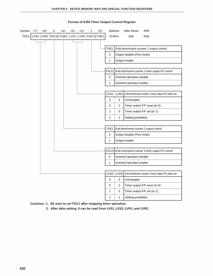
430
CHAPTER 6 DEVICE MEMORY MAP AND SPECIAL FUNCTION REGISTERS
Format of 8-Bit Timer Output Control Register
Cautions: 1. Be sure to set TOC1 after stopping timer operation.
2. After data setting, 0 can be read from LVS1, LVS2, LVR1, and LVR2.
<0>1<2><3><4>5<6><7>Symbol
TOE1TOC11LVR1LVS1TOE2TOC15LVR2LVS2TOC1 FF4FH 00H R/W
Address After Reset R/W
TOE1 8-bit timer/event counter 1 output control
0 Output disable (Port mode)
1 Output enable
TOC11 8-bit timer/event counter 1 timer output F/F control
0 Inverted operation disable
1 Inverted operation enable
LVS1 LVR1 8-bit timer/event counter 1 timer output F/F status set
0 0 Unchanged
0 1 Timer output F/F reset (to 0)
1 0 Timer output F/F set (to 1)
1 1 Setting prohibited
TOE2 8-bit timer/event counter 2 output control
0 Output disable (Port mode)
1 Output enable
TOC15 8-bit timer/event counter 2 timer output F/F control
0 Inverted operation disable
1 Inverted operation enable
LVS2 LVR2 8-bit timer/event counter 2 timer output F/F status set
0 0 Unchanged
0 1 Timer output F/F reset (to 0)
1 0 Timer output F/F set (to 1)
1 1 Setting prohibited
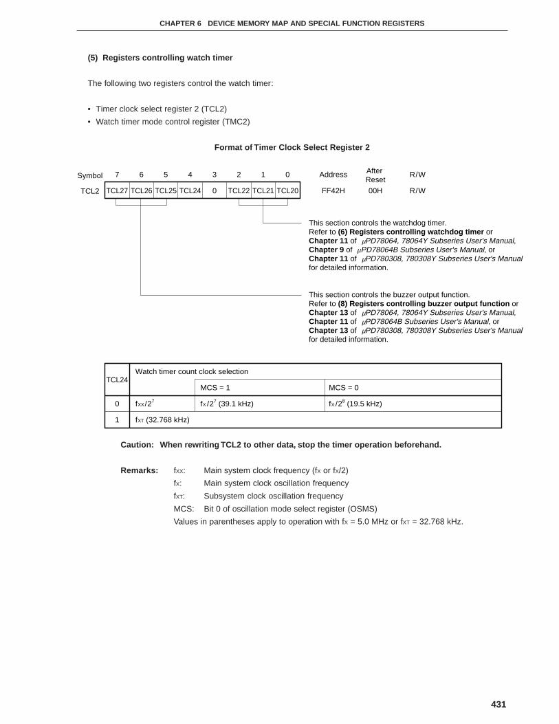
431
CHAPTER 6 DEVICE MEMORY MAP AND SPECIAL FUNCTION REGISTERS
(5) Registers controlling watch timer
The following two registers control the watch timer:
• Timer clock select register 2 (TCL2)
• Watch timer mode control register (TMC2)
Format of Timer Clock Select Register 2
Caution: When rewriting TCL2 to other data, stop the timer operation beforehand.
Remarks: fXX: Main system clock frequency (fX or fX/2)
fX: Main system clock oscillation frequency
fXT: Subsystem clock oscillation frequency
MCS: Bit 0 of oscillation mode select register (OSMS)
Values in parentheses apply to operation with fX = 5.0 MHz or fXT = 32.768 kHz.
TCL27
7
TCL26
6
TCL25 TCL24
4
0
3 2 1 0
FF42H
Address
TCL2
Symbol
TCL22 TCL21 TCL20
5
00H
After Reset
R/W
R/W
0
1
TCL24
fXX/27
fXT (32.768 kHz)
MCS = 1
fX /27 (39.1 kHz)
MCS = 0
fX /28 (19.5 kHz)
Watch timer count clock selection
This section controls the watchdog timer.Refer to (6) Registers controlling watchdog timer orChapter 11 of PD78064, 78064Y Subseries User's Manual,Chapter 9 of PD78064B Subseries User's Manual, orChapter 11 of PD780308, 780308Y Subseries User's Manualfor detailed information.
µ
µµ
This section controls the buzzer output function.Refer to (8) Registers controlling buzzer output function orChapter 13 of PD78064, 78064Y Subseries User's Manual,Chapter 11 of PD78064B Subseries User's Manual, orChapter 13 of PD780308, 780308Y Subseries User's Manualfor detailed information.
µµµ

432
CHAPTER 6 DEVICE MEMORY MAP AND SPECIAL FUNCTION REGISTERS
Format of Watch Timer Mode Control Register
Caution: When the watch timer is used, the prescaler should not be cleared frequently.
Remarks: fW: Watch timer clock frequency (fXX/27 or fXT)
fXX: Main system clock frequency (fX or fX/2)
fX: Main system clock oscillation frequency
fXT: Subsystem clock oscillation frequency
0
7
TMC26
6
TMC25 TMC24
4
TMC23
3 2 1 0
FF4AH
Address
TMC2
Symbol
TMC22 TMC21 TMC20
5
00H
After Reset
R/W
R/W
0
0
0
0
1
1
Settings other than above are prohibited
0
0
1
1
0
0
0
1
0
1
0
1
TMC26 TMC25 TMC24fXX = 5.0 MHz operation
24/fW (410 s)
25/fW (819 s)
26/fW (1.64 ms)
27/fW (3.28 ms)
28/fW (6.55 ms)
29/fW (13.1 ms)
fXX = 4.19 MHz operation
24/fW (488 s)
25/fW (977 s)
26/fW (1.95 ms)
27/fW (3.91 ms)
28/fW (7.81 ms)
29/fW (15.6 ms)
fXT = 32.768 kHz operation
24/fW (488 s)
25/fW (977 s)
26/fW (1.95 ms)
27/fW (3.91 ms)
28/fW (7.81 ms)
29/fW (15.6 ms)
Prescaler interval time selection
µ
µ
µ
µ
µ
µ
0
1
TMC23fXX = 5.0 MHz operation
214/fW (0.4 sec)
213/fW (0.2 sec)
Watch flag set time selection
fXX = 4.19 MHz operation
214/fW (0.5 sec)
213/fW (0.25 sec)
fXT = 32.768 kHz operation
214/fW (0.5 sec)
213/fW (0.25 sec)
TMC22
0
1
5-bit counter operation control
Clear after operation stop
Operation enable
TMC21
0
1
Prescaler operation control
Clear after operation stop
Operation enable
TMC20
0
1
Watch operating mode selection
Normal operating mode (flag set at fW/214)
Fast feed operating mode (flag set at fW/25)
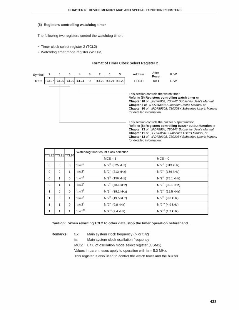
433
CHAPTER 6 DEVICE MEMORY MAP AND SPECIAL FUNCTION REGISTERS
(6) Registers controlling watchdog timer
The following two registers control the watchdog timer:
• Timer clock select register 2 (TCL2)
• Watchdog timer mode register (WDTM)
Format of Timer Clock Select Register 2
Caution: When rewriting TCL2 to other data, stop the timer operation beforehand.
Remarks: fXX: Main system clock frequency (fX or fX/2)
fX: Main system clock oscillation frequency
MCS: Bit 0 of oscillation mode select register (OSMS)
Values in parentheses apply to operation with fX = 5.0 MHz.
This register is also used to control the watch timer and the buzzer.
TCL27
7
TCL26
6
TCL25 TCL24
4
0
3 2 1 0
FF42H
Address
TCL2
Symbol
TCL22 TCL21 TCL20
5
00H
After Reset
R/W
R/W
0
0
0
0
1
1
1
1
0
0
1
1
0
0
1
1
0
1
0
1
0
1
0
1
TCL22 TCL21 TCL20MCS = 1
fX /23
fX /24
fX /25
fX /26
fX /27
fX /28
fX /29
fX /211
fXX /23
fXX /24
fXX /25
fXX /26
fXX /27
fXX /28
fXX /29
fXX /211
MCS = 0
fX /24
fX /25
fX /26
fX /27
fX /28
fX /29
fX /210
fX /212
Watchdog timer count clock selection
(625 kHz)
(313 kHz)
(156 kHz)
(78.1 kHz)
(39.1 kHz)
(19.5 kHz)
(9.8 kHz)
(2.4 kHz)
(313 kHz)
(156 kHz)
(78.1 kHz)
(39.1 kHz)
(19.5 kHz)
(9.8 kHz)
(4.9 kHz)
(1.2 kHz)
This section controls the watch timer.Refer to (5) Registers controlling watch timer orChapter 10 of PD78064, 78064Y Subseries User's Manual,Chapter 8 of PD78064B Subseries User's Manual, orChapter 10 of PD780308, 780308Y Subseries User's Manualfor detailed information.
µµ
µ
This section controls the buzzer output function.Refer to (8) Registers controlling buzzer output function orChapter 13 of PD78064, 78064Y Subseries User's Manual,Chapter 11 of PD78064B Subseries User's Manual, orChapter 13 of PD780308, 780308Y Subseries User's Manualfor detailed information.
µµµ
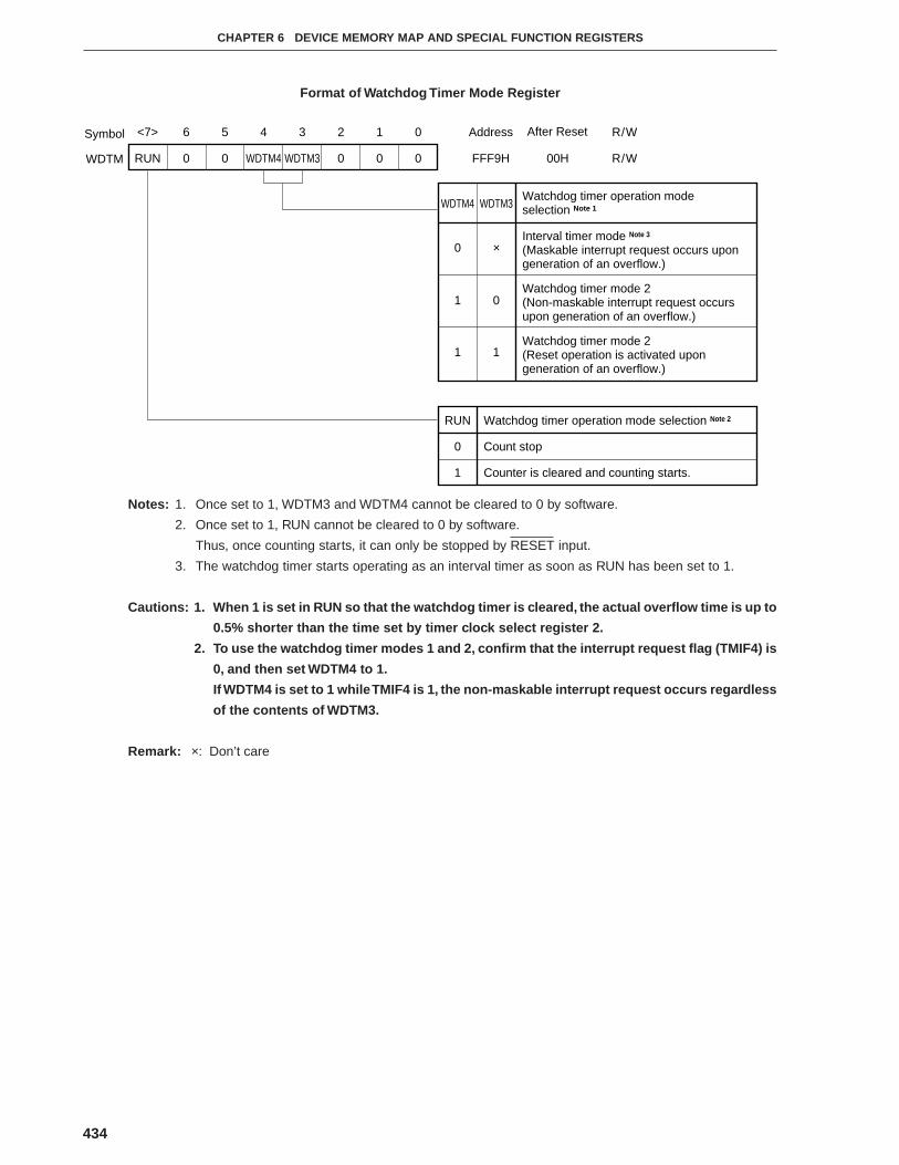
434
CHAPTER 6 DEVICE MEMORY MAP AND SPECIAL FUNCTION REGISTERS
Format of Watchdog Timer Mode Register
Notes: 1. Once set to 1, WDTM3 and WDTM4 cannot be cleared to 0 by software.
2. Once set to 1, RUN cannot be cleared to 0 by software.
Thus, once counting starts, it can only be stopped by RESET input.
3. The watchdog timer starts operating as an interval timer as soon as RUN has been set to 1.
Cautions: 1. When 1 is set in RUN so that the watchdog timer is cleared, the actual overflow time is up to
0.5% shorter than the time set by timer clock select register 2.
2. To use the watchdog timer modes 1 and 2, confirm that the interrupt request flag (TMIF4) is
0, and then set WDTM4 to 1.
If WDTM4 is set to 1 while TMIF4 is 1, the non-maskable interrupt request occurs regardless
of the contents of WDTM3.
Remark: ×: Don’t care
RUN
<7>
0
6
0 WDTM4
4
WDTM3
3 2 1 0
FFF9H
Address
WDTM
Symbol
0 0 0
5
00H R/W
R/W
RUN
0
1
Watchdog timer operation mode selection Note 2
Count stop
Counter is cleared and counting starts.
WDTM3
×
0
1
Watchdog timer operation modeselection Note 1
Interval timer mode Note 3
(Maskable interrupt request occurs upon generation of an overflow.)
Watchdog timer mode 2(Non-maskable interrupt request occursupon generation of an overflow.)
Watchdog timer mode 2(Reset operation is activated upongeneration of an overflow.)
WDTM4
0
1
1
After Reset

435
CHAPTER 6 DEVICE MEMORY MAP AND SPECIAL FUNCTION REGISTERS
(7) Registers controlling clock output function
The following two registers control the clock output function:
• Timer clock select register 0 (TCL0)
• Port mode register 3 (PM3).
- Refer to section (1) for the register format.
Format of Timer Clock Select Register 0
CLOE
<7>
TCL06
6
TCL05 TCL04
4
TCL03
3 2 1 0
FF40H
Address
TCL0
Symbol
TCL02 TCL01 TCL00
5
00H
After Reset
R/W
R/W
CLOE
0
1
PCL output control
Output disable
Output enable
0
0
0
0
1
1
1
1
1
0
1
1
1
0
0
0
0
1
0
0
1
1
0
0
1
1
0
TCL03 TCL02 TCL01
fXT (32.768 kHz)
fXX
fXX/2
fXX/22
fXX/23
fXX/24
fXX/25
fXX/26
fXX/27
MCS = 1
fX (5.0 MHz)
fX /2 (2.5 MHz)
fX /22 (1.25 MHz)
fX /23 (625 kHz)
fX /24 (313 kHz)
fX /25 (156 kHz)
fX /26 (78.1 kHz)
fX /27 (39.1 kHz)
MCS = 0
fX /2 (2.5 MHz)
fX /22 (1.25 MHz)
fX /23 (625 kHz)
fX /24 (313 kHz)
fX /25 (156 kHz)
fX /26 (78.1 kHz)
fX /27 (39.1 kHz)
fX /28 (19.5 kHz)
PCL output clock selectionTCL00
0
1
0
1
0
1
0
1
0
This section controls the 16-bit timer.Refer to (3) Registers controlling 16-bit timer/event counter orChapter 8 of PD78064, 78064Y Subseries User's Manual,Chapter 6 of PD78064B Subseries User's Manual, orChapter 8 of PD780308, 780308Y Subseries User's Manualfor detailed information.
µµµ
Settings other than above are prohibited
436
CHAPTER 6 DEVICE MEMORY MAP AND SPECIAL FUNCTION REGISTERS
Cautions: 1. When enabling PCL output, set TCL00 to TCL03, then set 1 in CLOE with a 1-bit memory ma-
nipulation instruction.
2. To write data other than that already written to TCL0, stop the timer operation once.
Remarks: fXX: Main system clock frequency (fX or fX/2)
fX: Main system clock oscillation frequency
fXT: Subsystem clock oscillation frequency
MCS: Bit 0 of oscillation mode select register (OSMS)
Values in parentheses apply to operation with fX = 5.0 MHz or fXT = 32.768 kHz.
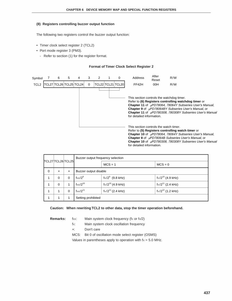
437
CHAPTER 6 DEVICE MEMORY MAP AND SPECIAL FUNCTION REGISTERS
(8) Registers controlling buzzer output function
The following two registers control the buzzer output function:
• Timer clock select register 2 (TCL2)
• Port mode register 3 (PM3).
- Refer to section (1) for the register format.
Format of Timer Clock Select Register 2
Caution: When rewriting TCL2 to other data, stop the timer operation beforehand.
Remarks: fXX: Main system clock frequency (fX or fX/2)
fX: Main system clock oscillation frequency
×: Don't care
MCS: Bit 0 of oscillation mode select register (OSMS)
Values in parentheses apply to operation with fX = 5.0 MHz.
TCL27
7
TCL26
6
TCL25 TCL24
4
0
3 2 1 0
FF42H
Address
TCL2
Symbol
TCL22 TCL21 TCL20
5
00H
After Reset
R/W
R/W
This section controls the watchdog timer.Refer to (6) Registers controlling watchdog timer orChapter 11 of PD78064, 78064Y Subseries User's Manual,Chapter 9 of PD78064BY Subseries User's Manual, orChapter 11 of PD780308, 780308Y Subseries User's Manualfor detailed information.
µµ
µ
This section controls the watch timer.Refer to (5) Registers controlling watch timer orChapter 10 of PD78064, 78064Y Subseries User's Manual,Chapter 8 of PD78064B Subseries User's Manual, orChapter 10 of PD780308, 780308Y Subseries User's Manualfor detailed information.
µµ
µ
0
1
1
1
1
×
0
0
1
1
×
0
1
0
1
TCL27 TCL26 TCL25
Buzzer output disable
fXX/29
fXX/210
fXX/211
Setting prohibited
MCS = 1
fX /29 (9.8 kHz)
fX /210 (4.9 kHz)
fX /211 (2.4 kHz)
MCS = 0
fX /210 (4.9 kHz)
fX /211 (2.4 kHz)
fX /212 (1.2 kHz)
Buzzer output frequency selection

438
CHAPTER 6 DEVICE MEMORY MAP AND SPECIAL FUNCTION REGISTERS
(9) Registers controlling A/D converter
The following three registers control the A/D converter:
• A/D converter mode register (ADM)
• A/D converter input select register (ADIS)
• External interrupt mode register 1 (INTM1)
- Refer to section (15) for the register format.

439
CHAPTER 6 DEVICE MEMORY MAP AND SPECIAL FUNCTION REGISTERS
Format of A/D Converter Mode Register
Notes: 1. Set so that the A/D conversion time is 19.1 µs or more.
2. Setting prohibited because A/D conversion time is less than 19.1 µs.
Cautions: 1. The following sequence is recommended for power consumption reduction of A/D con-
verter when the standby function is used: Clear bit 7 (CS) to 0 first to stop the A/D
conversion operation, and then execute the HALT or STOP instruction.
2. When restarting the stopped A/D conversion operation, start the A/D conversion op-
eration after clearing the interrupt request flag (ADIF) to 0.
Remarks: fX: Main system clock oscillation frequency
MCS: Bit 0 of oscillation mode select register (OSMS)
CS
<7>
TRG
<6>
FR1 FR0
4
ADM3
3 2 1 0
FF80H
Address
ADM
Symbol
ADM2 ADM1 HSC
5
01H
After Reset
R/W
R/W
ADM3
0
0
0
0
1
1
1
1
ADM2
0
0
1
1
0
0
1
1
ADM1
0
1
0
1
0
1
0
1
Analog input channel selection
ANI0
ANI1
ANI2
ANI3
ANI4
ANI5
ANI6
ANI7
TRG
0
1
External trigger selection
No external trigger (software starts)
Conversion started by external trigger (hardware starts)
CS
0
1
A/D conversion operation control
Operation stop
Operation start
FR1
0
0
1
1
1
FR0
0
1
0
0
1
A/D conversion time selection Note 1
fX = 5.0 MHz operation
MCS = 1
80/fX (Setting prohibited Note 2)
40/fX (Setting prohibited Note 2)
50/fX (Setting prohibited Note 2)
100/fX (20.0 s)
Setting prohibited
µ
MCS = 0
160/fX (32.0 s)
80/fX (Setting prohibited Note 2)
100/fX (20.0 s)
200/fX (40.0 s)
fX = 4.19 MHz operation
MCS = 1
80/fX (19.1 s)
40/fX (Setting prohibited Note 2)
50/fX (Setting prohibited Note 2)
100/fX (23.8 s)
MCS = 0
160/fX (38.1 s)
80/fX (19.1 s)
100/fX (23.8 s)
200/fX (47.7 s)µ
µ
µ
µ µ
µ
µ
HSC
1
1
0
0
1
µ µ

440
CHAPTER 6 DEVICE MEMORY MAP AND SPECIAL FUNCTION REGISTERS
Format of A/D Converter Input Select Register
Cautions: 1. Set the analog input channel in the following order:
a. Set the number of analog input channels with ADIS.
b. Using the A/D converter mode register (ADM), select one channel to undergo A/D con-
version from among the channels set for analog input with ADIS.
2. No internal pull-up resistor can be used to the channels set for analog input with ADIS,
irrespective of the value of bit 1 (PUO1) of the pull-up resistor option register L (PUOL).
0
7
0
6
0 0
4
ADIS3
3 2 1 0
FF84H
Address
ADIS
Symbol
ADIS2 ADIS1 ADIS0
5
00H
AfterReset
R/W
R/W
ADIS3
0
0
0
0
0
0
0
0
1
Number of analog input channel selection
No analog input channel (P10 to P17)
1 channel (ANI0, P11 to P17)
2 channels (ANI0, ANI1, P12 to P17)
3 channels (ANI0 to ANI2, P13 to P17)
4 channels (ANI0 to ANI3, P14 to P17)
5 channels (ANI0 to ANI4, P15 to P17)
6 channels (ANI0 to ANI5, P16, P17)
7 channels (ANI0 to ANI6, P17)
8 channels (ANI0 to ANI7)
ADIS2
0
0
0
0
1
1
1
1
0
ADIS1
0
0
1
1
0
0
1
1
0
ADIS0
0
1
0
1
0
1
0
1
0
Settings other than above are prohibited
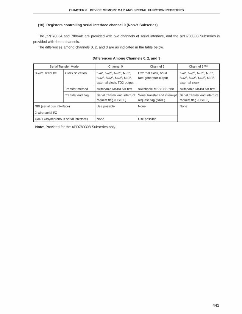
441
CHAPTER 6 DEVICE MEMORY MAP AND SPECIAL FUNCTION REGISTERS
(10) Registers controlling serial interface channel 0 (Non-Y Subseries)
The µPD78064 and 78064B are provided with two channels of serial interface, and the µPD780308 Subseries is
provided with three channels.
The differences among channels 0, 2, and 3 are as indicated in the table below.
Differences Among Channels 0, 2, and 3
Serial Transfer Mode Channel 0 Channel 2 Channel 3 Note
3-wire serial I/O Clock selection fXX/2, fXX/22, fXX/23, fXX/24, External clock, baud fXX/2, fXX/22, fXX/23, fXX/24,
fXX/25, fXX/26, fXX/27, fXX/28, rate generator output fXX/25, fXX/26, fXX/27, fXX/28,
external clock, TO2 output external clock
Transfer method switchable MSB/LSB first switchable MSB/LSB first switchable MSB/LSB first
Transfer end flag Serial transfer end interrupt Serial transfer end interrupt Serial transfer end interrupt
request flag (CSIIF0) request flag (SRIF) request flag (CSIIF3)
SBI (serial bus interface) Use possible None None
2-wire serial I/O
UART (asynchronous serial interface) None Use possible
Note: Provided for the µPD780308 Subseries only.
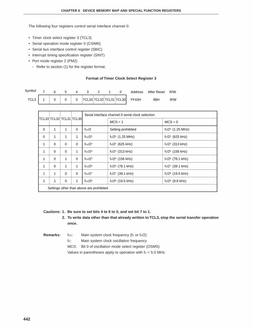
442
CHAPTER 6 DEVICE MEMORY MAP AND SPECIAL FUNCTION REGISTERS
The following four registers control serial interface channel 0:
• Timer clock select register 3 (TCL3)
• Serial operation mode register 0 (CSIM0)
• Serial bus interface control register (SBIC)
• Interrupt timing specification register (SINT)
• Port mode register 2 (PM2)
- Refer to seciton (1) for the register format.
Format of Timer Clock Select Register 3
Cautions: 1. Be sure to set bits 4 to 6 to 0, and set bit 7 to 1.
2. To write data other than that already written to TCL3, stop the serial transfer operation
once.
Remarks: fXX: Main system clock frequency (fX or fX/2)
fX: Main system clock oscillation frequency
MCS: Bit 0 of oscillation mode select register (OSMS)
Values in parentheses apply to operation with fX = 5.0 MHz.
Serial interface channel 0 serial clock selectionTCL33 TCL32 TCL31 TCL30
0
0
1
1
1
1
1
1
1
1
0
0
0
0
1
1
1
1
0
0
1
1
0
0
0
1
0
1
0
1
0
1
fXX/2
fXX/22
fXX/23
fXX/24
fXX/25
fXX/26
fXX/27
fXX/28
MCS = 1
Setting prohibited
fX/22 (1.25 MHz)
fX/23 (625 kHz)
fX/24 (313 kHz)
fX/25 (156 kHz)
fX/26 (78.1 kHz)
fX/27 (39.1 kHz)
fX/28 (19.5 kHz)
MCS = 0
fX/22 (1.25 MHz)
fX/23 (625 kHz)
fX/24 (313 kHz)
fX/25 (156 kHz)
fX/26 (78.1 kHz)
fX/27 (39.1 kHz)
fX/28 (19.5 kHz)
fX/29 (9.8 kHz)
Settings other than above are prohibited
6 5 4 3 2 1 07Symbol
TCL3 1 0 0 0 TCL33 TCL32 TCL31 TCL30 FF43H 88H R/W
Address After Reset R/W
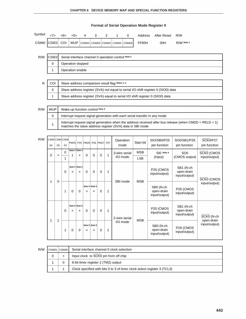
443
CHAPTER 6 DEVICE MEMORY MAP AND SPECIAL FUNCTION REGISTERS
Format of Serial Operation Mode Register 0
<6> <5> 4 3 2 1 0<7>Symbol
CSIM0 CSIE0 COI WUP CSIM04 CSIM03 CSIM02 CSIM01 CSIM00 FF60H 00H R/W Note 1
Address After Reset R/W
CSIM01
0
1
Serial interface channel 0 clock selection
Input clock to SCK0 pin from off chip
8-bit timer register 2 (TM2) output
R/W
1 Clock specified with bits 0 to 3 of timer clock select register 3 (TCL3)
CSIM00
×
0
1
SBI mode
0
0
SCK0 (CMOSinput/output)
CSIM
04
0
1
R/W CSIM
03
CSIM
02PM25 P25 PM26 P26 PM27 P27
Operation
modeStart bit
SIO/SB0/P25
pin function
SO0/SB1/P26
pin function
SCK0/P27
pin function
×
1 0
×
0
×
0
0
×
0
×
0
0
1
1
Note 5 Note 5
Note 5 Note 5
MSB
P25 (CMOSinput/output)
SB0 (N-ch open-drain
input/output)
SB1 (N-chopen-drain
input/output)
P26 (CMOSinput/output)
1
MSB
LSB1 × 0 0 0 1
Note 4
3-wire seriall/O mode
SI0(Input)
SO0(CMOS output)
SCK0 (CMOSinput/output)
Note 4
2-wire seriall/O mode
0
SCK0 (N-chopen-drain
input/output)
1
1 1
×
0
×
0
0
×
0
×
0
0
1
1
Note 5 Note 5
Note 5 Note 5
MSB
P25 (CMOSinput/output)
SB0 (N-chopen-drain
input/output)
SB1 (N-chopen-drain
input/output)
P26 (CMOSinput/output)
Note 4
WUP
0
1
Wake-up function control Note 3
Interrupt request signal generation with each serial transfer in any mode
Interrupt request signal generation when the address received after bus release (when CMDD = RELD = 1) matches the slave address register (SVA) data in SBI mode
R/W
COI
0
1
Slave address comparison result flag Notes 1, 2
Slave address register (SVA) not equal to serial I/O shift register 0 (SIO0) data
Slave address register (SVA) equal to serial I/O shift register 0 (SIO0) data
R
CSIE0
0
1
Serial interface channel 0 operation control Note 3
Operation stopped
Operation enable
R/W

444
CHAPTER 6 DEVICE MEMORY MAP AND SPECIAL FUNCTION REGISTERS
Notes: 1. Bit 6 (COI) is a read-only bit.
2. When CSIE = 0, COI becomes 0.
3. Clear bit 5 (SIC) of the interrupt timing specification register (SINT) to 0 when using the wake-up function
(WUP = 1).
4. Can be used as P25 (CMOS input/output) when channel 0 is used only for transmission.
5. Can be used freely as a port function for SBI or 2-wire mode.
Caution: Do not change the operation mode (3-wire serial I/O, 2-wire serial I/O, or SBI) while serial interface
channel 0 is enabled. To change the operating mode, stop the serial operation once.
Remarks: ×: Don’t care
PM××: Port mode register
P××: Port output latch
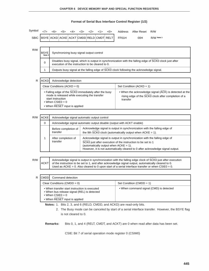
445
CHAPTER 6 DEVICE MEMORY MAP AND SPECIAL FUNCTION REGISTERS
Format of Serial Bus Interface Control Register (1/2)
Notes: 1. Bits 2, 3, and 6 (RELD, CMDD, and ACKD) are read-only bits.
2. The Busy mode can be canceled by start of a serial interface transfer. However, the BSYE flag
is not cleared to 0.
Remarks: Bits 0, 1, and 4 (RELT, CMDT, and ACKT) are 0 when read after data has been set.
CSIE: Bit 7 of serial operation mode register 0 (CSIM0)
<6> <5> <4> <3> <2> <1> <0><7>Symbol
SBIC BSYE ACKD ACKE ACKT CMDD RELD CMDT RELT FF61H 00H R/W Note 1
Address After Reset R/W
ACKTAcknowledge signal is output in synchronization with the falling edge clock of SCK0 just after execution of the instruction to be set to 1, and after acknowledge signal output, automatically cleared to 0. Used as ACKE = 0. Also cleared to 0 upon start of a serial interface transfer or when CSIE0 = 0.
R/W
R ACKD Acknowledge detection
Clear Conditions (ACKD = 0)
• Falling edge of the SCK0 immediately after the busy mode is released while executing the transfer start instruction • When CSIE0 = 0
• When RESET input is applied
Set Condition (ACKD = 1)
• When the acknowledge signal (ACK) is detected at the
rising edge of the SCK0 clock after completion of a transfer
BSYE Synchronizing busy signal output control
0Disables busy signal, which is output in synchronization with the falling edge of SCK0 clock just after execution of the instruction to be cleared to 0.
R/W
Note 2
1 Outputs busy signal at the falling edge of SCK0 clock following the acknowledge signal.
ACKE Acknowledge signal automatic output control
0 Acknowledge signal automatic output disable (output with ACKT enable)
Acknowledge signal is output in synchronization with the falling edge of
the 9th SCK0 clock (automatically output when ACKE = 1).Before completion of transfer
Acknowledge signal is output in synchronization with the falling edge of
SCK0 just after execution of the instruction to be set to 1 (automatically output when ACKE = 1). However, it is not automatically cleared to 0 after acknowledge signal output.
After completion of transfer
1
R/W
R CMDD Command detection
Clear Conditions (CMDD = 0)
• When transfer start instruction is executed • When bus release signal (REL) is detected • When CSIE0 = 0
• When RESET input is applied
Set Condition (CMDD = 1)
• When command signal (CMD) is detected

446
CHAPTER 6 DEVICE MEMORY MAP AND SPECIAL FUNCTION REGISTERS
Format of Serial Bus Interface Control Register (2/2)
RELTUsed for bus release signal output. When RELT = 1, SO Iatch is set to 1. After SO latch setting, automatically cleared to 0.Also cleared to 0 when CSIE0 = 0.
R/W
CMDTUsed for command signal output. When CMDT = 1, SO Iatch is cleared to 0. After SO latch clearance, automatically cleared to 0. Also cleared to 0 when CSIE0 = 0.
R/W
R RELD Bus release detection
Set Condition (RELD = 1)Clear Conditions (RELD = 0)
• When bus release signal (REL) is detected• When transfer start instruction is executed • If SIO0 and SVA values do not match in address reception • When CSIE0 = 0
• When RESET input is applied
<6> <5> <4> <3> <2> <1> <0><7>Symbol
SBIC BSYE ACKD ACKE ACKT CMDD RELD CMDT RELT FF61H 00H R/W Note 1
Address After Reset R/W

447
CHAPTER 6 DEVICE MEMORY MAP AND SPECIAL FUNCTION REGISTERS
Format of Interrupt Timing Specification Register
Notes: 1. Bit 6 (CLD) is a read-only bit.
2. When CSIE0 = 0, CLD becomes 0.
3. When using the wake-up function in the SBI mode, set SIC to 0.
Caution: Be sure to set bits 0 to 3 to 0.
Remarks: SVA: Slave address register
CSIIF0: Interrupt request flag corresponding to INTCSI0
CSIE0: Bit 7 of serial operation mode register 0 (CSIM0)
<6> <5> <4> 3 2 1 07Symbol
SINT 0 CLD SIC SVAM 0 0 0 0 FF63H 00H R/W Note 1
Address After Reset R/W
SVAM
0
1
SVA bit to be used as slave address
Bits 0 to 7
Bits 1 to 7
SIC
0
INTCSI0 interrupt cause selection Note 3
CSIIF0 is set upon termination of serial interface channel 0 transfer
CSIIF0 is set upon bus release detection or termination of serial interface channel 0 transfer
CLD
0
1
SCK0 pin level Note 2
Low level
High level
R/W
R/W
R
1
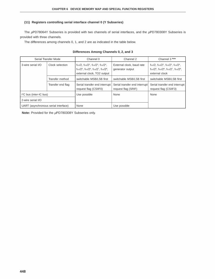
448
CHAPTER 6 DEVICE MEMORY MAP AND SPECIAL FUNCTION REGISTERS
(11) Registers controlling serial interface channel 0 (Y Subseries)
The µPD78064Y Subseries is provided with two channels of serial interfaces, and the µPD780308Y Subseries is
provided with three channels.
The differences among channels 0, 1, and 2 are as indicated in the table below.
Differences Among Channels 0, 2, and 3
Serial Transfer Mode Channel 0 Channel 2 Channel 3 Note
3-wire serial I/O Clock selection fXX/2, fXX/22, fXX/23, fXX/24, External clock, baud rate fXX/2, fXX/22, fXX/23, fXX/24,
fXX/25, fXX/26, fXX/27, fXX/28, generator output fXX/25, fXX/26, fXX/27, fXX/28,
external clock, TO2 output external clock
Transfer method switchable MSB/LSB first switchable MSB/LSB first switchable MSB/LSB first
Transfer end flag Serial transfer end interrupt Serial transfer end interrupt Serial transfer end interrupt
request flag (CSIIF0) request flag (SRIF) request flag (CSIIF3)
I2C bus (inter-IC bus) Use possible None None
2-wire serial I/O
UART (asynchronous serial interface) None Use possible
Note: Provided for the µPD780308Y Subseries only.
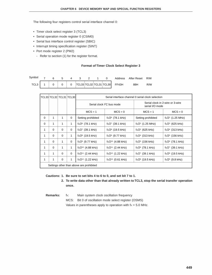
449
CHAPTER 6 DEVICE MEMORY MAP AND SPECIAL FUNCTION REGISTERS
The following four registers control serial interface channel 0:
• Timer clock select register 3 (TCL3)
• Serial operation mode register 0 (CSIM0)
• Serial bus interface control register (SBIC)
• Interrupt timing specification register (SINT)
• Port mode register 2 (PM2)
- Refer to section (1) for the register format.
Format of Timer Clock Select Register 3
Cautions: 1. Be sure to set bits 4 to 6 to 0, and set bit 7 to 1.
2. To write data other than that already written to TCL3, stop the serial transfer operation
once.
Remarks: fX: Main system clock oscillation frequency
MCS: Bit 0 of oscillation mode select register (OSMS)
Values in parentheses apply to operation with fX = 5.0 MHz.
6 5 4 3 2 1 07Symbol
TCL3 1 0 0 0 TCL33 TCL32 TCL31 TCL30 FF43H 88H R/W
Address After Reset R/W
Serial interface channel 0 serial clock selectionTCL33 TCL32 TCL31 TCL30
0
0
1
1
1
1
1
1
1
1
0
0
0
0
1
1
1
1
0
0
1
1
0
0
0
1
0
1
0
1
0
1
Setting prohibited
fX/22 (1.25 MHz)
fX/23 (625 kHz)
fX/24 (313 kHz)
fX/25 (156 kHz)
fX/26 (78.1 kHz)
fX/27 (39.1 kHz)
fX/28 (19.5 kHz)
MCS = 1
Setting prohibited
fX/26 (78.1 kHz)
fX/27 (39.1 kHz)
fX/28 (19.5 kHz)
fX/29 (9.77 kHz)
fX/210 (4.88 kHz)
fX/211 (2.44 kHz)
fX/212 (1.22 kHz)
MCS = 1
Serial clock I2C bus modeSerial clock in 2-wire or 3-wireserial I/O mode
fX/26 (78.1 kHz)
fX/27 (39.1 kHz)
fX/28 (19.5 kHz)
fX/29 (9.77 kHz)
fX/210 (4.88 kHz)
fX/211 (2.44 kHz)
fX/212 (1.22 kHz)
fX/213 (0.61 kHz)
MCS = 0
fX/22 (1.25 MHz)
fX/23 (625 kHz)
fX/24 (313 kHz)
fX/25 (156 kHz)
fX/26 (78.1 kHz)
fX/27 (39.1 kHz)
fX/28 (19.5 kHz)
fX/29 (9.8 kHz)
MCS = 0
Settings other than above are prohibited
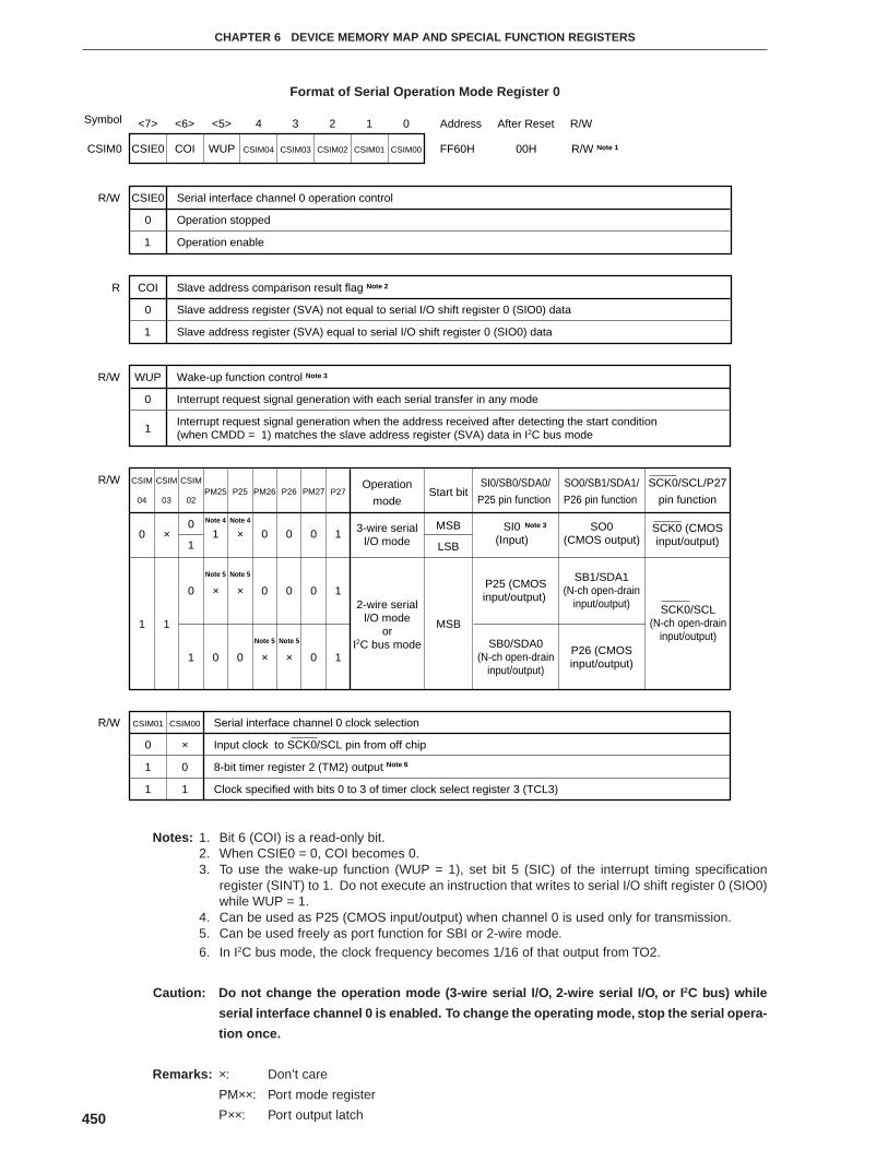
450
CHAPTER 6 DEVICE MEMORY MAP AND SPECIAL FUNCTION REGISTERS
Format of Serial Operation Mode Register 0
Notes: 1. Bit 6 (COI) is a read-only bit.2. When CSIE0 = 0, COI becomes 0.3. To use the wake-up function (WUP = 1), set bit 5 (SIC) of the interrupt timing specification
register (SINT) to 1. Do not execute an instruction that writes to serial I/O shift register 0 (SIO0)while WUP = 1.
4. Can be used as P25 (CMOS input/output) when channel 0 is used only for transmission.5. Can be used freely as port function for SBI or 2-wire mode.6. In I2C bus mode, the clock frequency becomes 1/16 of that output from TO2.
Caution: Do not change the operation mode (3-wire serial I/O, 2-wire serial I/O, or I 2C bus) while
serial interface channel 0 is enabled. To change the operating mode, stop the serial opera-
tion once.
Remarks: ×: Don’t care
PM××: Port mode register
P××: Port output latch
<6> <5> 4 3 2 1 0<7>Symbol
CSIM0 CSIE0 COI WUP CSIM04 CSIM03 CSIM02 CSIM01 CSIM00 FF60H 00H R/W Note 1
Address After Reset R/W
CSIM01
0
1
Serial interface channel 0 clock selection
Input clock to SCK0/SCL pin from off chip
8-bit timer register 2 (TM2) output Note 6
R/W
1 Clock specified with bits 0 to 3 of timer clock select register 3 (TCL3)
CSIM00
×
0
1
0
0
SCK0/SCL(N-ch open-drain
input/output)
CSIM
04
0
1
R/W CSIM
03
CSIM
02PM25 P25 PM26 P26 PM27 P27
Operation
modeStart bit
SO0/SB1/SDA1/
P26 pin function
SI0/SB0/SDA0/
P25 pin function
SCK0/SCL/P27
pin function
×
1 1
×
0
×
0
0
×
0
×
0
0
1
1
Note 5 Note 5
Note 5 Note 5
MSB
P25 (CMOSinput/output)
SB0/SDA0(N-ch open-drain
input/output)
SB1/SDA1(N-ch open-drain
input/output)
P26 (CMOSinput/output)
1
MSB
LSB1 × 0 0 0 1
Note 43-wire serial
l/O modeSI0
(Input)SO0
(CMOS output)SCK0 (CMOSinput/output)
Note 3
2-wire seriall/O mode
orI2C bus mode
Note 4
WUP
0
1
Wake-up function control Note 3
Interrupt request signal generation with each serial transfer in any mode
Interrupt request signal generation when the address received after detecting the start condition(when CMDD = 1) matches the slave address register (SVA) data in I2C bus mode
R/W
COI
0
1
Slave address comparison result flag Note 2
Slave address register (SVA) not equal to serial I/O shift register 0 (SIO0) data
Slave address register (SVA) equal to serial I/O shift register 0 (SIO0) data
R
CSIE0
0
1
Serial interface channel 0 operation control
Operation stopped
Operation enable
R/W
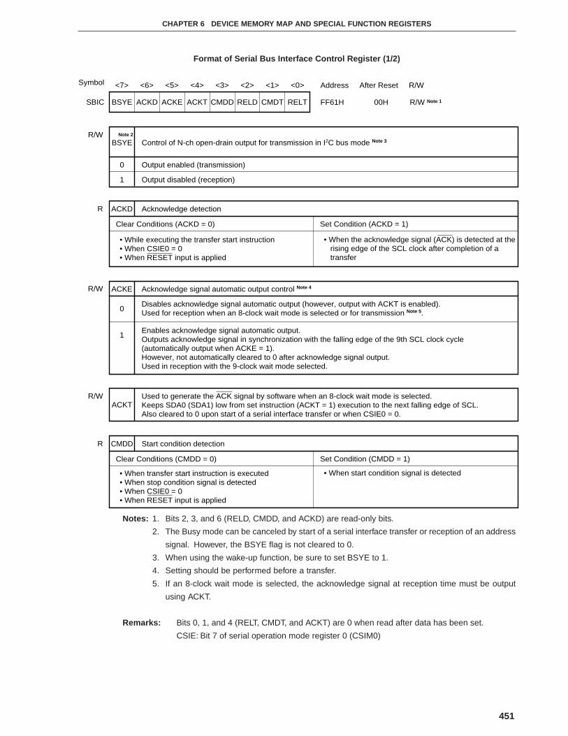
451
CHAPTER 6 DEVICE MEMORY MAP AND SPECIAL FUNCTION REGISTERS
Format of Serial Bus Interface Control Register (1/2)
Notes: 1. Bits 2, 3, and 6 (RELD, CMDD, and ACKD) are read-only bits.
2. The Busy mode can be canceled by start of a serial interface transfer or reception of an address
signal. However, the BSYE flag is not cleared to 0.
3. When using the wake-up function, be sure to set BSYE to 1.
4. Setting should be performed before a transfer.
5. If an 8-clock wait mode is selected, the acknowledge signal at reception time must be output
using ACKT.
Remarks: Bits 0, 1, and 4 (RELT, CMDT, and ACKT) are 0 when read after data has been set.
CSIE: Bit 7 of serial operation mode register 0 (CSIM0)
<6> <5> <4> <3> <2> <1> <0><7>Symbol
SBIC BSYE ACKD ACKE ACKT CMDD RELD CMDT RELT FF61H 00H R/W Note 1
Address After Reset R/W
ACKTUsed to generate the ACK signal by software when an 8-clock wait mode is selected.Keeps SDA0 (SDA1) low from set instruction (ACKT = 1) execution to the next falling edge of SCL.Also cleared to 0 upon start of a serial interface transfer or when CSIE0 = 0.
R/W
BSYE Control of N-ch open-drain output for transmission in I2C bus mode Note 3 R/W Note 2
1 Output disabled (reception)
0 Output enabled (transmission)
R ACKD Acknowledge detection
Clear Conditions (ACKD = 0)
• While executing the transfer start instruction • When CSIE0 = 0 • When RESET input is applied
Set Condition (ACKD = 1)
• When the acknowledge signal (ACK) is detected at the rising edge of the SCL clock after completion of a transfer
ACKE Acknowledge signal automatic output control Note 4
0Disables acknowledge signal automatic output (however, output with ACKT is enabled).Used for reception when an 8-clock wait mode is selected or for transmission Note 5.
1Enables acknowledge signal automatic output.Outputs acknowledge signal in synchronization with the falling edge of the 9th SCL clock cycle(automatically output when ACKE = 1). However, not automatically cleared to 0 after acknowledge signal output.Used in reception with the 9-clock wait mode selected.
R/W
R CMDD Start condition detection
Clear Conditions (CMDD = 0)
• When transfer start instruction is executed • When stop condition signal is detected • When CSIE0 = 0 • When RESET input is applied
Set Condition (CMDD = 1)
• When start condition signal is detected

452
CHAPTER 6 DEVICE MEMORY MAP AND SPECIAL FUNCTION REGISTERS
Format of Serial Bus Interface Control Register (2/2)
Remark: CSIE0: Bit 7 of serial operation mode register 0 (CSIM0)
RELTUsed for stop condition signal output. When RELT = 1, SO Iatch is set to 1. After SO latch setting, automatically cleared to 0.Also cleared to 0 when CSIE0 = 0.
R/W
CMDTUsed for start condition signal output. When CMDT = 1, SO Iatch is cleared to 0. After SO latch clearance, automatically cleared to 0. Also cleared to 0 when CSIE0 = 0.
R/W
R RELD Stop condition detection
Set Condition (RELD = 1)Clear Conditions (RELD = 0)
• When stop condition signal is detected• When transfer start instruction is executed • If SIO0 and SVA values do not match in address reception • When CSIE0 = 0 • When RESET input is applied
<6> <5> <4> <3> <2> <1> <0><7>Symbol
SBIC BSYE ACKD ACKE ACKT CMDD RELD CMDT RELT FF61H 00H R/W Note 1
Address After Reset R/W

453
CHAPTER 6 DEVICE MEMORY MAP AND SPECIAL FUNCTION REGISTERS
Format of Interrupt Timing Specification Register
<6> <5> <4> <3> <2> 1 07Symbol
SINT 0 CLD SIC SVAM CLC WREL WAT1 WAT0 FF63H 00H R/W Note 1
Address After Reset R/W
SVAM
0
1
SVA bit to be used as slave address
Bits 0 to 7
Bits 1 to 7
SIC
0
INTCSI0 interrupt cause selection Note 3
CSIIF0 is set to 1 upon termination of serial interface channel 0 transfer
CSIIF0 is set to 1 upon stop condition detection or termination of serial interface channel 0 transfer
CLD
0
1
SCK0/SCL pin level Note 2
Low level
High level
R/W
CLC
0
Clock level control Note 4
Used in I2C bus mode.Make output level of SCL pin low unless a serial transfer is being performed.
1 Used in I2C bus mode.Make SCL pin enter a high-impedance state unless a serial transfer is being performed(except for clock line, which is kept high).Used to enable a master device to generate start condition and stop condition signals.
R/W
WREL
0
Wait state cancellation control
Wait state has been canceled.
1 Cancels wait state. Automatically cleared to 0 when the state is canceled.(Used to cancel wait state by means of WAT0 and WAT1.)
R/W
R/W
R
1
WAT1
0
Wait and interrupt control
Generates interrupt service request at rising edge of 8th SCK0 clock cycle(keeping clock output in high impedance)
1
WAT0
0
0 Setting prohibited1
0 Used in I2C bus mode (8-clock wait)Generates an interrupt service request at rising edge of 8th SCK0 clock cycle.(In the case of a master device, makes SCL output low to enter wait state after 8 clock pulses areoutput. In the case of a slave device, makes SCL outputlow to request wait state after 8 clock pulsesare input.)
R/W
1 1 Used in I2C bus mode (9-clock wait)Generates interrupt service request at rising edge of 9th SCK0 clock cycle.(In the case of a master device, makes SCL output low to enter wait state after 9 clock pulses areoutput. In the case of a slave device, makes SCL outputlow to request wait state after 9 clock pulsesare input.)
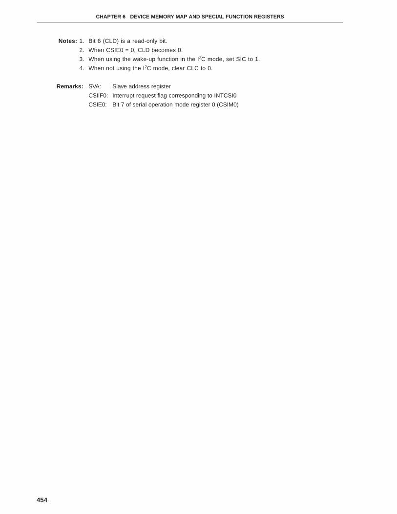
454
CHAPTER 6 DEVICE MEMORY MAP AND SPECIAL FUNCTION REGISTERS
Notes: 1. Bit 6 (CLD) is a read-only bit.
2. When CSIE0 = 0, CLD becomes 0.
3. When using the wake-up function in the I2C mode, set SIC to 1.
4. When not using the I2C mode, clear CLC to 0.
Remarks: SVA: Slave address register
CSIIF0: Interrupt request flag corresponding to INTCSI0
CSIE0: Bit 7 of serial operation mode register 0 (CSIM0)

455
CHAPTER 6 DEVICE MEMORY MAP AND SPECIAL FUNCTION REGISTERS
(12) Registers controlling serial interface channel 2
The following five registers control serial interface channel 2:
• Serial operation mode register 2 (CSIM2)
• Asynchronous serial interface mode register (ASIM)
• Asynchronous serial interface status register (ASIS)
• Baud rate generator control register (BRGC)
• Serial interface pin select register (SIPS) Note
• Port mode register 7 (PM7)
- Refer to section (1) for the register format.
Note: This register is provided only for µPD780308/308Y Subseries products.
Format of Serial Operation Mode Register 2
Cautions: 1. Ensure that bits 0 and 3 to 6 are set to 0.
2. When UART mode is selected, CSIM2 should be set to 00H.
6 5 4 3 2 1 0<7>Symbol
CSIM2 CSIE2 0 0 0 0 CSIM22
CSCK 0
CSCK
0
1
Clock selection in 3-wire serial I/O mode
Input clock from off-chip to SCK2 pin
Dedicated baud rate generator output
CSIM22
0
1
First bit specification
MSB
LSB
CSIE2
0
1
Operation control in 3-wire serial I/O mode
Operation stopped
Operation enabled
FF72H
Address
00H R/W
R/WAfter Reset
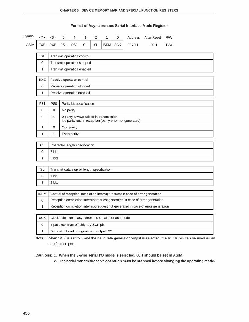
456
CHAPTER 6 DEVICE MEMORY MAP AND SPECIAL FUNCTION REGISTERS
Format of Asynchronous Serial Interface Mode Register
Note: When SCK is set to 1 and the baud rate generator output is selected, the ASCK pin can be used as an
input/output port.
Cautions: 1. When the 3-wire serial I/O mode is selected, 00H should be set in ASIM.
2. The serial transmit/receive operation must be stopped before changing the operating mode.
<6> 5 4 3 2 1 0<7>Symbol
ASIM TXE RXE PS1 PS0 CL SL ISRM SCK FF70H 00H R/W
Address After Reset R/W
SCK
0
1
Clock selection in asynchronous serial interface mode
Input clock from off chip to ASCK pin
Dedicated baud rate generator output Note
ISRM
0
1
Control of reception completion interrupt request in case of error generation
Reception completion interrupt request generated in case of error generation
Reception completion interrupt request not generated in case of error generation
SL Transmit data stop bit length specification
CL
1
Character length specification
7 bits
8 bits
RXE
0
1
Receive operation control
Receive operation stopped
Receive operation enabled
TXE
0
1
Transmit operation control
Transmit operation stopped
Transmit operation enabled
PS1
0
1
0 1 bit
1 2 bits
0
Parity bit specification
No parity
Even parity
PS0
0
1
0 parity always added in transmissionNo parity test in reception (parity error not generated)
0 1
1 Odd parity0
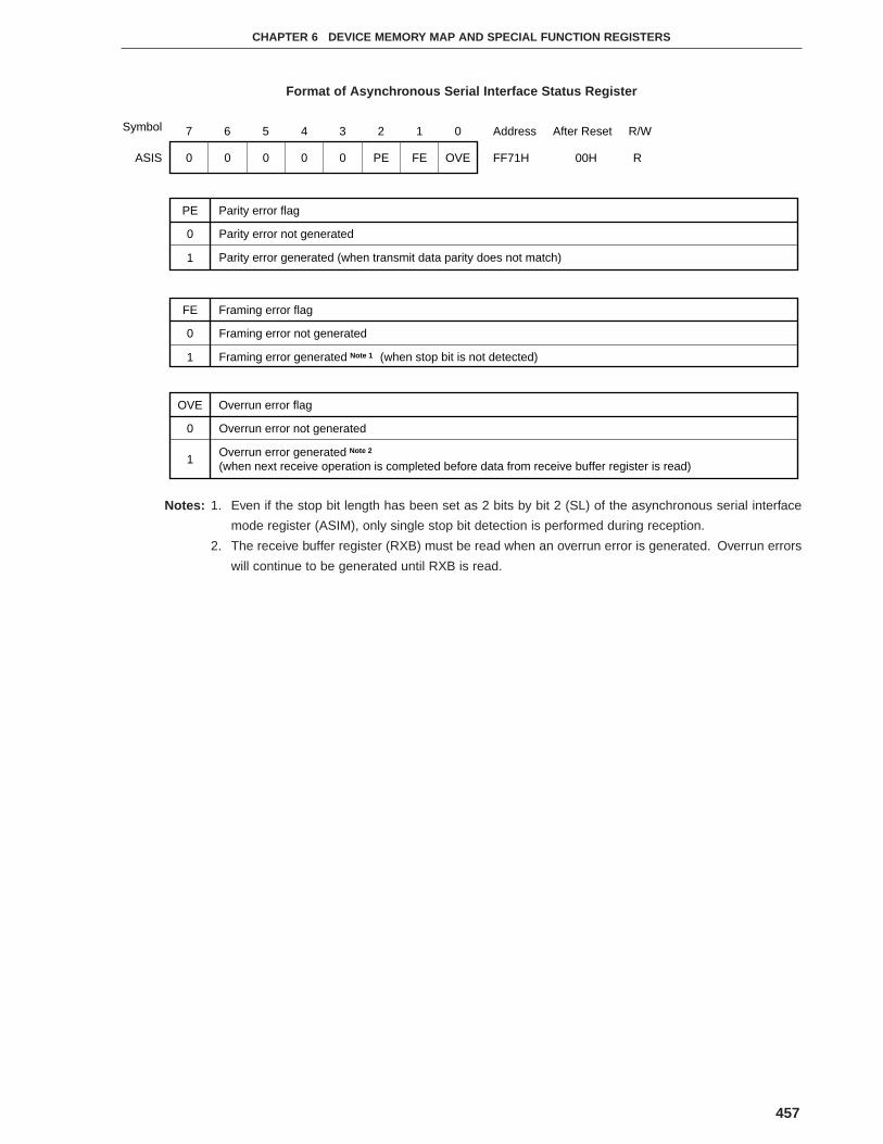
457
CHAPTER 6 DEVICE MEMORY MAP AND SPECIAL FUNCTION REGISTERS
Format of Asynchronous Serial Interface Status Register
Notes: 1. Even if the stop bit length has been set as 2 bits by bit 2 (SL) of the asynchronous serial interface
mode register (ASIM), only single stop bit detection is performed during reception.
2. The receive buffer register (RXB) must be read when an overrun error is generated. Overrun errors
will continue to be generated until RXB is read.
PE
6 5 4 3 2 1 07Symbol
ASIS 0 0 0 0 0 FE OVE FF71H 00H R
Address After Reset R/W
OVE
0
1
Overrun error flag
Overrun error not generated
Overrun error generated(when next receive operation is completed before data from receive buffer register is read)
Note 2
FE
0
1
Framing error flag
Framing error not generated
Framing error generated (when stop bit is not detected)Note 1
PE
0
1
Parity error flag
Parity error not generated
Parity error generated (when transmit data parity does not match)

458
CHAPTER 6 DEVICE MEMORY MAP AND SPECIAL FUNCTION REGISTERS
Format of Baud Rate Generator Control Register
6 5 4 3 2 1 07Symbol
BRGC TPS3 TPS2 TPS1 TPS0 MDL3 MDL2 MDL1 MDL0 FF73H 00H R/W
Address After Reset R/W
Selects source clock of 5-bit counterTPS3 TPS2 TPS1 TPS0
0
0
0
0
1
1
1
1
1
1
1
0
1
1
1
0
0
0
0
1
1
1
0
0
1
1
0
0
1
1
0
0
1
0
1
0
1
0
1
0
1
0
1
0
MCS = 1
fX (5.0 MHz)
fX/210 (4.9 kHz)
fX/2 (2.5 MHz)
fX/22 (1.25 MHz)
fX/23 (625 kHz)
fX/24 (313 kHz)
fX/25 (156 kHz)
fX/26 (78.1 kHz)
fX/27 (39.1 kHz)
fX/28 (19.5 kHz)
fX/29 (9.8 kHz)
fXX
fXX/210
fXX/2
fXX/22
fXX/23
fXX/24
fXX/25
fXX/26
fXX/27
fXX/28
fXX/29
MCS = 0
fX/211 (2.4 kHz)
fX/2 (2.5 MHz)
fX/22 (1.25 MHz)
fX/23 (625 kHz)
fX/24 (313 kHz)
fX/25 (156 kHz)
fX/26 (78.1 kHz)
fX/27 (39.1 kHz)
fX/28 (19.5 kHz)
fX/29 (9.8 kHz)
fX/210 (4.9 kHz)
Settings other than above are prohibited
11
1
2
3
4
5
6
7
8
9
10
n
Baud rate generator input clock selectionMDL3 MDL2 MDL1 MDL0
0
0
0
0
0
0
0
0
1
1
1
1
1
1
1
1
0
0
0
0
1
1
1
1
0
0
0
0
1
1
1
1
0
0
1
1
0
0
1
1
0
0
1
1
0
0
1
1
0
1
0
1
0
1
0
1
0
1
0
1
0
1
0
1
fSCK/16
fSCK/17
fSCK/18
fSCK/19
fSCK/20
fSCK/21
fSCK/22
fSCK/23
fSCK/24
fSCK/25
fSCK/26
fSCK/27
fSCK/28
fSCK/29
fSCK/30
fSCK Note
0
1
2
3
4
5
6
7
8
9
10
11
12
13
14
k

459
CHAPTER 6 DEVICE MEMORY MAP AND SPECIAL FUNCTION REGISTERS
Note: Can only be used in 3-wire serial I/O mode.
Caution: When a write is performed to BRGC during a communication operation, baud rate generator output
is disrupted and communication cannot be performed normally. Therefore, BRGC must not be
written to during a communication operation.
Remarks: fX: Main system clock oscillation frequency
fXX: Main system clock frequency (fx or fx/2)
MCS: Bit 0 of oscillation mode selection register (OSMS)
n: Value set in TPS0 to TPS3 (1 ≤ n ≤ 11)
fSCK: 5-bit counter source clock
k: Value set in MDL0 to MDL3 (0 ≤ k ≤ 14)
Values in parentheses apply to operation with fX = 5.0 MHz.
Format of Serial Interface Pin Select Register (For µµµµµPD780308/308Y Subseries Only)
Cautions: 1. Select input/output pins after stopping serial transmission/reception.
2. Port 11 has a falling edge detection function. Do not specify the pin of this port used in a
mode other than Port mode to input the falling edge. To set input falling edge, refer to
“Format of Key Return Mode Register” in (16) Registers controlling port function.
3. This register is provided only for µµµµµPD780308/308Y Subseries products.
6 5 4 3 2 1 07Symbol
SIPS 0 0 SIPS21 SIPS20 0 0 0 0 FF75H 00H R/W
Address After Reset R/W
SIPS21
0
1
Selects input/output pin of asynchronous serial interface
Input pin: RxD/SI2/P70Output pin: TxD/SO2/P71
Input pin: RxD/P114Output pin: TxD/P113
SIPS20
0
1
Input pin: RxD/P114Output pin: TxD/SO2/P71
0 1
1Input pin: RxD/SI2/P70Output pin: TxD/P113
0
C
460
CHAPTER 6 DEVICE MEMORY MAP AND SPECIAL FUNCTION REGISTERS
(13) Registers controlling serial interface channel 3 ( µµµµµPD780308/308Y Subseries only)
Serial interface channel 3 is available only in the µPD780308/308Y Subseries.
The following three registers control serial interface channel 3:
• Timer clock select register 4 (TCL4)
• Serial operation mode register 3 (CSIM3)
• Port mode register 11 (PM11)
- Refer to section (1) for the format of this register.
Format of Timer Clock Select Register 4
Cautions: 1. Be sure to set bits 0 to 2 to 0, and set bit 3 to 1.
2. To write data other than that already written to TCL4, stop the serial transfer
operation.
Remarks: fX: Main system clock oscillation frequency
MCS: Bit 0 of oscillation mode select register (OSMS)
Values in parentheses apply to operation with fX = 5.0 MHz.
Symbol
TCL4
7
TCL47
6
TCL46
5
TCL45
4
TCL44
3
1
2
0
1
0 0
Address
FF44H
After Reset
88H
R/W
R/W
TCL47 TCL46 TCL45 TCL44Selects serial clock of serial interface channel 3
MCS = 1 MCS = 0
Setting prohibited fX/22 (1.25 MHz)0 1 1 0
fX/22 (1.25 MHz) fX/23 (625 kHz)0 1 1 1
fX/23 (625 kHz) fX/24 (313 kHz)1 0 0 0
fX/24 (313 kHz) fX/25 (156 kHz)1 0 0 1
fX/25 (156 kHz) fX/26 (78.1 kHz)1 0 1 0
fX/26 (78.1 kHz) fX/27 (39.1 kHz)1 0 1 1
fX/27 (39.1 kHz) fX/28 (19.5 kHz)1 1 0 0
fX/28 (19.5 kHz) fX/29 (9.8 kHz)1 1 0 1
0
Settings other than above are prohibited
461
CHAPTER 6 DEVICE MEMORY MAP AND SPECIAL FUNCTION REGISTERS
Format of Serial Operation Mode Register 3
Notes: 1. Be sure to set bit 5 to 0.
2. Can be used freely as port pins.
3. Can be used as P110 (CMOS input/output) when only transmitting data.
Caution: Port 11 has a function to detect the falling edge. To use the SI3/P110, SO3/P111, and SCK3/
P112 pins as the input/output pins of serial interface channel 3, the falling edge detection
function must be disabled by using the key return mode register (KRM). For details, refer to
“Format of Key Return Mode Register” in (16) Registers controlling port function.
Remarks: ×: Don’t care
PM××: Port mode register
P××: Port output latch
SCK3 (Input)
Enablesoperation
Controls operationof serial interface
channel 3
Controls operationof serial clock
counter
SI3/P110
pin functions
SO3/P111
pin functions
SCK3/P112
pin functions
Countoperation
SI3 Note 3
(Input)SO3
(CMOS output)
SCK3(CMOS output)
ClearStops operation
P110
(CMOS I/O)
P111
(CMOS I/O)
P112
(CMOS I/O)
DIR3
0
1
First bit
MSB
LSB
0
CSIE3
0
1
CSIM
31PM110 P110 PM111 P111 PM112 P112
×
11 ×
0 0
1 ×
1
Note 2 Note 2
6 5 4 3 2 1 0<7>Symbol
CSIM3 CSIE3 DIR3 0 0 0 CSIM31 CSIM30 FF6CH 00H R/W
Address After Reset R/W
0Note 1
×Note 2
×Note 2
×Note 2
×Note 2
×Note 2
×Note 2
0
CSIM31
0
1
Selects clock of serial interface channel 3
Clock specified by bits 0 through 3 of timer clock select register 4 (TCL4)
CSIM30
×
1
SI3/P110 pin functions
SI3 Note 3 (Input)
SO3/P111 pin functions
SO3 (CMOS output)
Input clock to SCK3 pin from off chip
Settings other than above are prohibited
462
CHAPTER 6 DEVICE MEMORY MAP AND SPECIAL FUNCTION REGISTERS
(14) Registers controlling LCD controller/driver
The following two registers control the LCD controller/driver:
• LCD display mode register (LCDM)
• LCD display control register (LCDC)
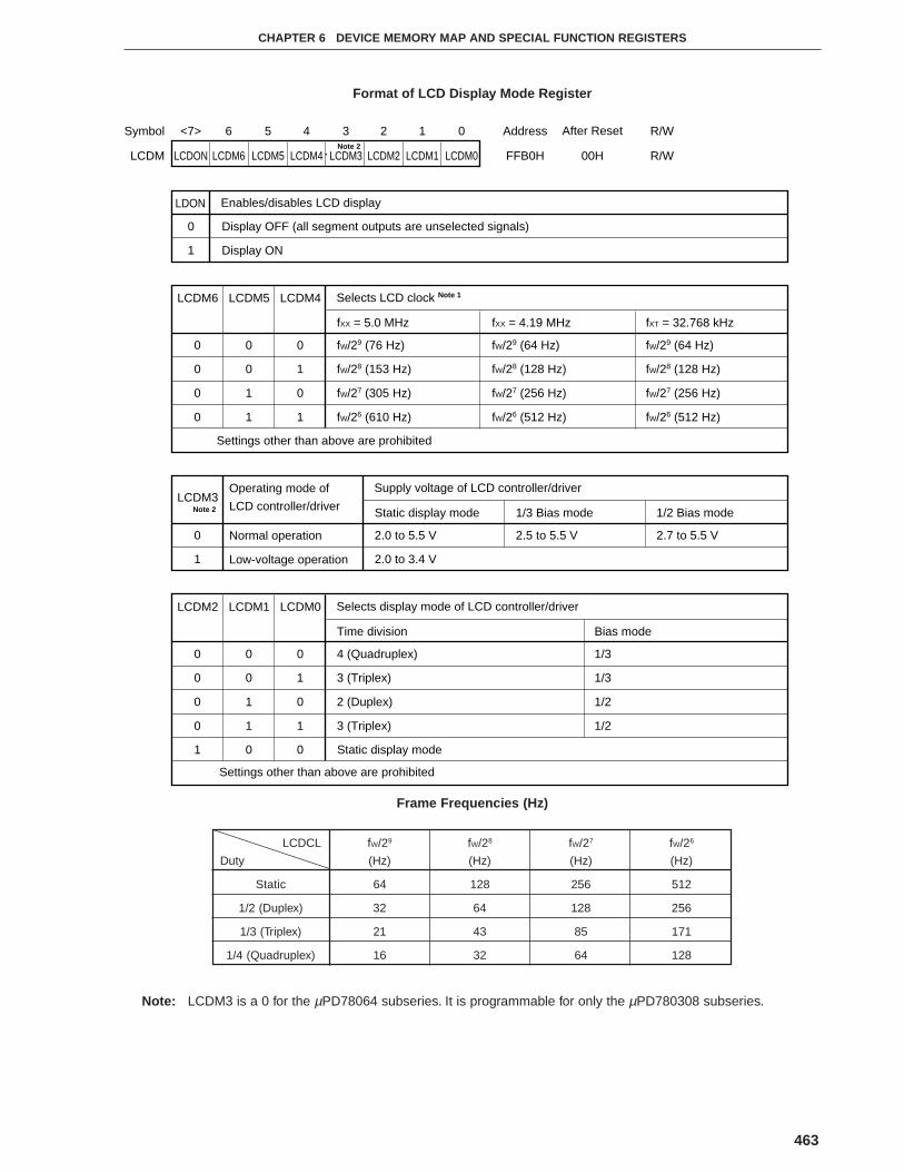
463
CHAPTER 6 DEVICE MEMORY MAP AND SPECIAL FUNCTION REGISTERS
Format of LCD Display Mode Register
Frame Frequencies (Hz)
LCDCL fW/29 fW/28 fW/27 fW/26
Duty (Hz) (Hz) (Hz) (Hz)
Static 64 128 256 512
1/2 (Duplex) 32 64 128 256
1/3 (Triplex) 21 43 85 171
1/4 (Quadruplex) 16 32 64 128
Note: LCDM3 is a 0 for the µPD78064 subseries. It is programmable for only the µPD780308 subseries.
Symbol
LCDM LCDON
6
LCDM6
5
LCDM5
4
LCDM4
3
LCDM3
2
LCDM2
1
LCDM1
0
LCDM0
Address
FFB0H
After Reset
00H
R/W
R/W
<7>
LDON
0
1
Enables/disables LCD display
Display OFF (all segment outputs are unselected signals)
Display ON
LCDM6
0
0
Selects LCD clock Note 1
fW/28 (153 Hz)
fW/29 (76 Hz)
fXX = 5.0 MHz fXX = 4.19 MHz
0 fW/27 (305 Hz)
0
LCDM5
0
0
1
1
Settings other than above are prohibited
LCDM4
0
1
0
1 fW/26 (610 Hz)
fW/28 (128 Hz)
fW/29 (64 Hz)
fW/27 (256 Hz)
fW/26 (512 Hz)
fXT = 32.768 kHz
fW/28 (128 Hz)
fW/29 (64 Hz)
fW/27 (256 Hz)
fW/26 (512 Hz)
LCDM2
0
0
Selects display mode of LCD controller/driver
3 (Triplex)
4 (Quadruplex)
Time division
0 2 (Duplex)
0
LCDM1
0
0
1
1
LCDM0
0
1
0
1
1 0 0 Static display mode
3 (Triplex)
Bias mode
1/3
1/3
1/2
1/2
LCDM3
0
1
Supply voltage of LCD controller/driver
2.0 to 3.4 V
2.0 to 5.5 V
Static display mode 1/3 Bias mode
Operating mode of
LCD controller/driver
Normal operation
Low-voltage operation
2.5 to 5.5 V
1/2 Bias mode
2.7 to 5.5 V
Note 2
Note 2
Settings other than above are prohibited
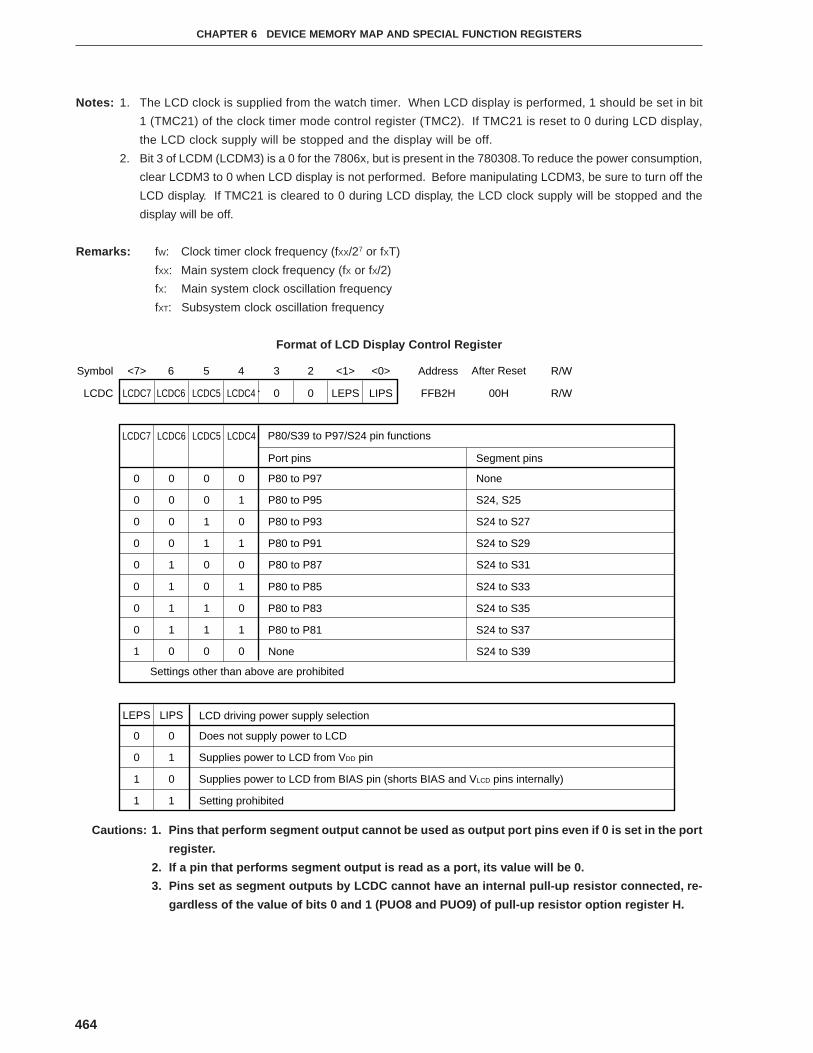
464
CHAPTER 6 DEVICE MEMORY MAP AND SPECIAL FUNCTION REGISTERS
Notes: 1. The LCD clock is supplied from the watch timer. When LCD display is performed, 1 should be set in bit
1 (TMC21) of the clock timer mode control register (TMC2). If TMC21 is reset to 0 during LCD display,
the LCD clock supply will be stopped and the display will be off.
2. Bit 3 of LCDM (LCDM3) is a 0 for the 7806x, but is present in the 780308. To reduce the power consumption,
clear LCDM3 to 0 when LCD display is not performed. Before manipulating LCDM3, be sure to turn off the
LCD display. If TMC21 is cleared to 0 during LCD display, the LCD clock supply will be stopped and the
display will be off.
Remarks: fW: Clock timer clock frequency (fXX/27 or fXT)
fXX: Main system clock frequency (fX or fX/2)
fX: Main system clock oscillation frequency
fXT: Subsystem clock oscillation frequency
Format of LCD Display Control Register
Cautions: 1. Pins that perform segment output cannot be used as output port pins even if 0 is set in the port
register.
2. If a pin that performs segment output is read as a port, its value will be 0.
3. Pins set as segment outputs by LCDC cannot have an internal pull-up resistor connected, re-
gardless of the value of bits 0 and 1 (PUO8 and PUO9) of pull-up resistor option register H.
Symbol
LCDC LCDC7
6
LCDC6
5
LCDC5
4
LCDC4
3
0
2
0
<1>
LEPS
<0>
LIPS
Address
FFB2H
After Reset
00H
R/W
R/W
<7>
P80/S39 to P97/S24 pin functions
P80 to P95
P80 to P97
Port pins
P80 to P93
LCDC7
0
0
0
0
0
0
0
0
1
LCDC6
0
0
0
0
1
1
1
1
0
LCDC5
0
0
1
1
0
0
1
1
0
LCDC4
0
1
0
1
0
1
0
1
0
P80 to P87
P80 to P91
P80 to P85
P80 to P83
None
P80 to P81
S24, S25
None
Segment pins
S24 to S27
S24 to S31
S24 to S29
S24 to S33
S24 to S35
S24 to S39
S24 to S37
Supplies power to LCD from VDD pin
Does not supply power to LCD
LCD driving power supply selection
Supplies power to LCD from BIAS pin (shorts BIAS and VLCD pins internally)
LEPS
0
0
1
1
LIPS
0
1
0
1 Setting prohibited
Settings other than above are prohibited
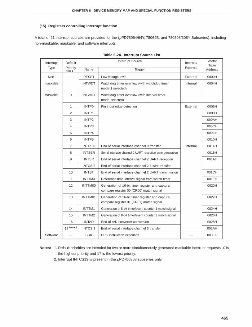
465
CHAPTER 6 DEVICE MEMORY MAP AND SPECIAL FUNCTION REGISTERS
(15) Registers controlling interrupt function
A total of 21 interrupt sources are provided for the (µPD78064/64Y, 78064B, and 780308/308Y Subseries), including
non-maskable, maskable, and software interrupts.
Table 6-24. Interrupt Source List
Interrupt Default Interrupt Source Internal/ VectorTable
Type Priority Name Trigger External Address
Non- — RESET Low voltage level External 0000H
maskable INTWDT Watchdog timer overflow (with watchdog timer Internal 0004H
mode 1 selected)
Maskable 0 INTWDT Watchdog timer overflow (with interval timer
mode selected)
1 INTP0 Pin input edge detection External 0006H
2 INTP1 0008H
3 INTP2 000AH
4 INTP3 000CH
5 INTP4 000EH
6 INTP5 0010H
7 INTCSI0 End of serial interface channel 0 transfer Internal 0014H
8 INTSER Serial interface channel 2 UART reception error generation 0018H
9 INTSR End of serial interface channel 2 UART reception 001AH
INTCSI2 End of serial interface channel 2 3-wire transfer
10 INTST End of serial interface channel 2 UART transmission 001CH
11 INTTM3 Reference time interval signal from watch timer 001EH
12 INTTM00 Generation of 16-bit timer register and capture/ 0020H
compare register 00 (CR00) match signal
13 INTTM01 Generation of 16-bit timer register and capture/ 0022H
compare register 01 (CR01) match signal
14 INTTM1 Generation of 8-bit timer/event counter 1 match signal 0024H
15 INTTM2 Generation of 8-bit timer/event counter 2 match signal 0026H
16 INTAD End of A/D converter conversion 0028H
17 Note 2 INTCSI3 End of serial interface channel 3 transfer 002AH
Software — BRK BRK instruction execution — 003EH
Notes: 1. Default priorities are intended for two or more simultaneously generated maskable interrupt requests. 0 is
the highest priority and 17 is the lowest priority.
2. Interrupt INTCS13 is present in the µPD780308 subseries only.
Note 1
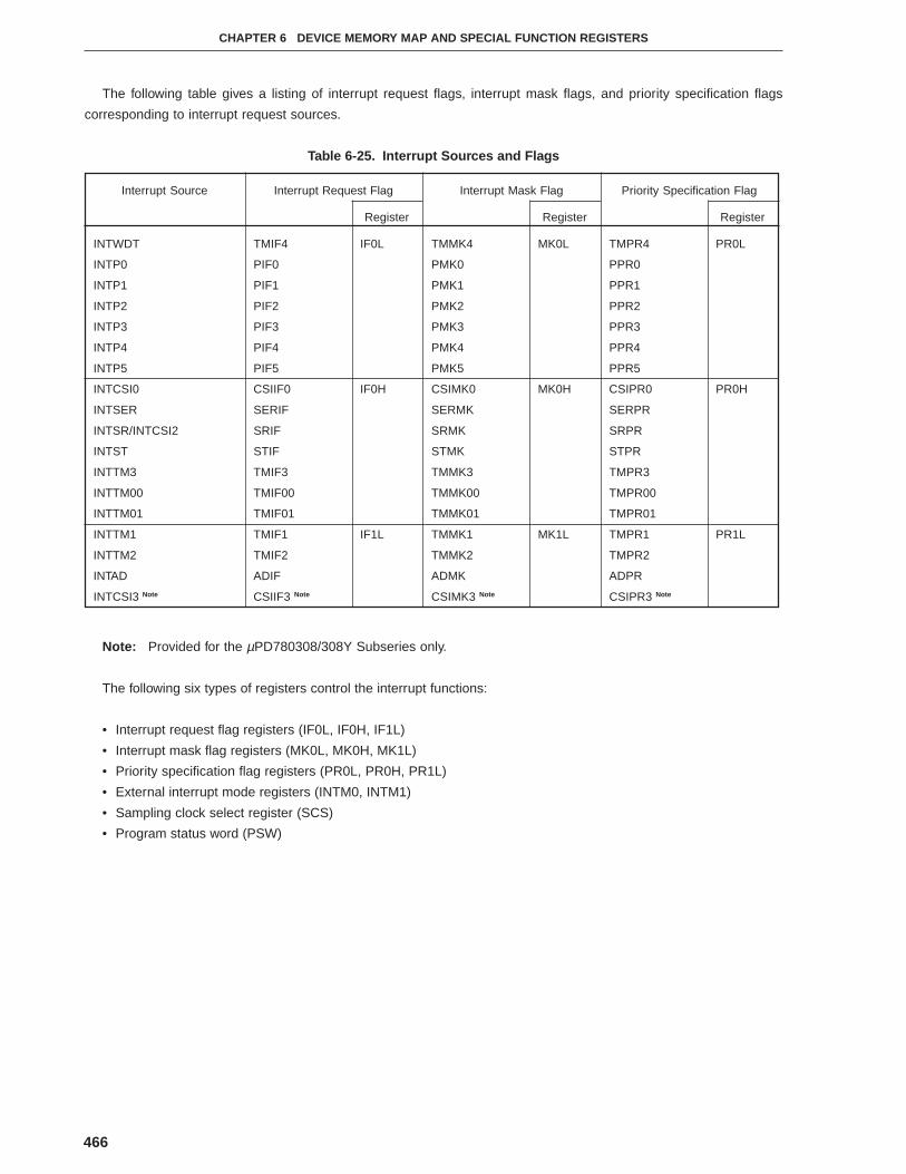
466
CHAPTER 6 DEVICE MEMORY MAP AND SPECIAL FUNCTION REGISTERS
The following table gives a listing of interrupt request flags, interrupt mask flags, and priority specification flags
corresponding to interrupt request sources.
Table 6-25. Interrupt Sources and Flags
Interrupt Source Interrupt Request Flag Interrupt Mask Flag Priority Specification Flag
Register Register Register
INTWDT TMIF4 IF0L TMMK4 MK0L TMPR4 PR0L
INTP0 PIF0 PMK0 PPR0
INTP1 PIF1 PMK1 PPR1
INTP2 PIF2 PMK2 PPR2
INTP3 PIF3 PMK3 PPR3
INTP4 PIF4 PMK4 PPR4
INTP5 PIF5 PMK5 PPR5
INTCSI0 CSIIF0 IF0H CSIMK0 MK0H CSIPR0 PR0H
INTSER SERIF SERMK SERPR
INTSR/INTCSI2 SRIF SRMK SRPR
INTST STIF STMK STPR
INTTM3 TMIF3 TMMK3 TMPR3
INTTM00 TMIF00 TMMK00 TMPR00
INTTM01 TMIF01 TMMK01 TMPR01
INTTM1 TMIF1 IF1L TMMK1 MK1L TMPR1 PR1L
INTTM2 TMIF2 TMMK2 TMPR2
INTAD ADIF ADMK ADPR
INTCSI3 Note CSIIF3 Note CSIMK3 Note CSIPR3 Note
Note: Provided for the µPD780308/308Y Subseries only.
The following six types of registers control the interrupt functions:
• Interrupt request flag registers (IF0L, IF0H, IF1L)
• Interrupt mask flag registers (MK0L, MK0H, MK1L)
• Priority specification flag registers (PR0L, PR0H, PR1L)
• External interrupt mode registers (INTM0, INTM1)
• Sampling clock select register (SCS)
• Program status word (PSW)

467
CHAPTER 6 DEVICE MEMORY MAP AND SPECIAL FUNCTION REGISTERS
Format of Interrupt Request Flag Registers
Notes: 1. WTIF is a test input flag. A vectored interrupt request is not generated.
2. The CSIIF3 flag is present in the µPD780308 subseries only.
3. Bit 3 of IF1L is a 0 in the µPD78064 subseries.
Cautions: 1. The TMIF4 flag is R/W enabled only when a watchdog timer is used as an interval timer. If a
watchdog timer is used in watchdog timer mode 1, set the TMIF4 flag to 0.
2. Always set IF1L bits 4 to 6, IF0L bit 7, and IF0H bit 1 to
<3>
CSIIF3
7
0
Symbol
IF0L
<6>
PIF5
<5>
PIF4
<4>
PIF3
<3>
PIF2
<2>
PIF1
<1>
PIF0
<0>
TMIF4
Address
FFE0H 00H
After Reset R/W
R/W
××IF
0
1
Interrupt request flag
No interrupt request signal
Interrupt request signal is generated; Interrupt request state
<7>
TMIF01IF0H
<6>
TMIF00
<5>
TMIF3
<4>
STIF
<3>
SRIF
<2>
SERIF
1
0
<0>
CSIIF0
<7>
WTIF Note 1 Notes 2, 3
IF1L
6
0
5
0
4
0
<2>
ADIF
<1>
TMIF2
<0>
TMIF1
FFE1H 00H R/W
FFE2H 00H R/W
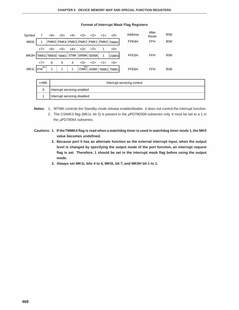
468
CHAPTER 6 DEVICE MEMORY MAP AND SPECIAL FUNCTION REGISTERS
Format of Interrupt Mask Flag Registers
Notes: 1. WTMK controls the Standby mode release enable/disable. It does not control the interrupt function.
2. The CSIMK3 flag (MK1L bit 3) is present in the µPD780308 subseries only. It must be set to a 1 in
the µPD78064 subseries.
Cautions: 1. If the TMMK4 flag is read when a watchdog timer is used in watchdog timer mode 1, the MK0
value becomes undefined.
2. Because port 0 has an alternate function as the external interrupt input, when the output
level is changed by specifying the output mode of the port function, an interrupt request
flag is set. Therefore, 1 should be set in the interrupt mask flag before using the output
mode.
3. Always set MK1L bits 4 to 6, MK0L bit 7, and MK0H bit 1 to 1.
7
1
Symbol
MK0L
<6>
PMK5
<5>
PMK4
<4>
PMK3
<3>
PMK2
<2>
PMK1
<1>
PMK0
<0> Address
FFE4H FFH
AfterReset R/W
R/W
××MK
0
1
Interrupt servicing control
Interrupt servicing enabled
Interrupt servicing disabled
<7>
MK0H
<6> <5> <4>
STMK
<3>
SRMK
<2> 1
1
<0>
<7>
WTMK Note 1 Note 2
MK1L
6
1
5
1
4
1 CSIMK3
<3> <2> <1> <0>
FFE5H FFH R/W
FFE6H FFH R/WADMK TMMK2 TMMK1
CSIMK0SERMKTMMK3TMMK00TMMK01
TMMK4
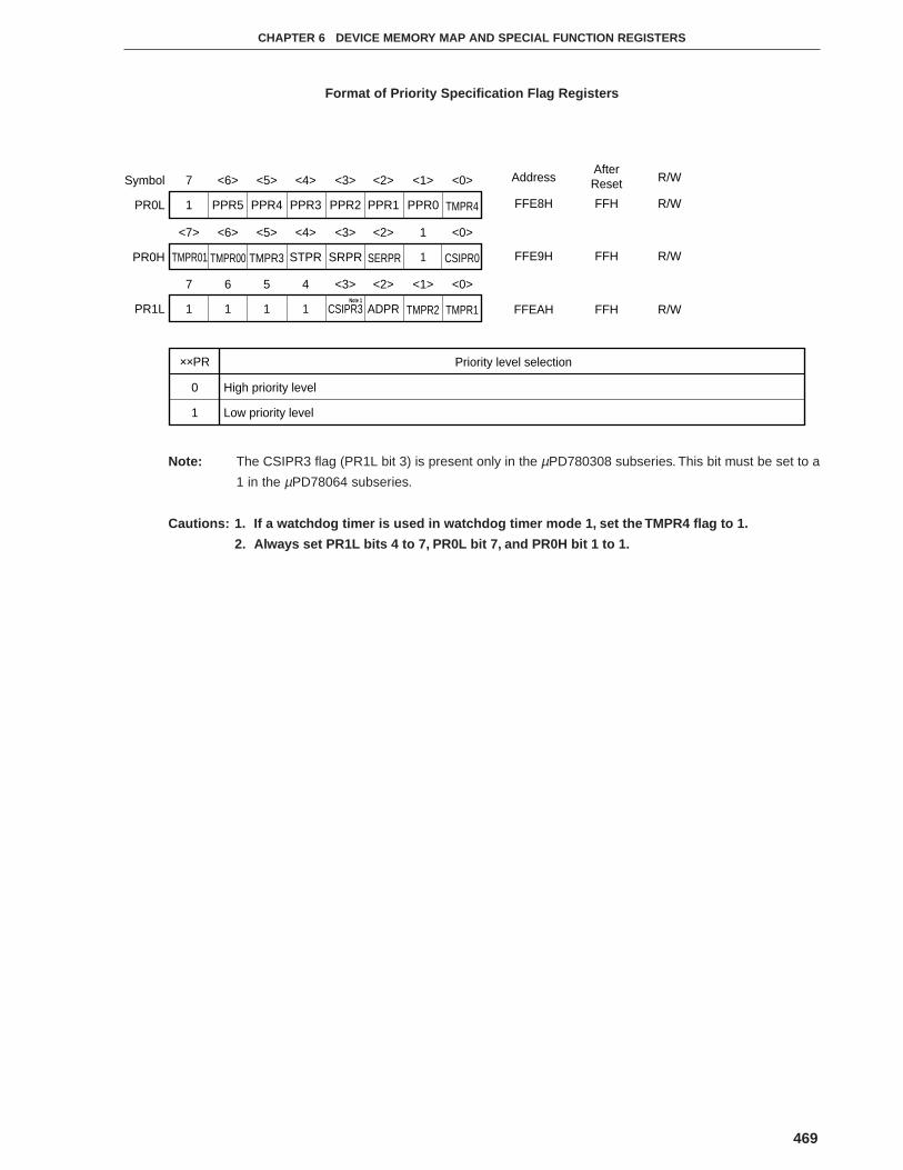
469
CHAPTER 6 DEVICE MEMORY MAP AND SPECIAL FUNCTION REGISTERS
Format of Priority Specification Flag Registers
Note: The CSIPR3 flag (PR1L bit 3) is present only in the µPD780308 subseries. This bit must be set to a
1 in the µPD78064 subseries.
Cautions: 1. If a watchdog timer is used in watchdog timer mode 1, set the TMPR4 flag to 1.
2. Always set PR1L bits 4 to 7, PR0L bit 7, and PR0H bit 1 to 1.
7
1
Symbol
PR0L
<6>
PPR5
<5>
PPR4
<4>
PPR3
<3>
PPR2
<2>
PPR1
<1>
PPR0
<0> Address
FFE8H FFH
AfterReset R/W
R/W
0
1
Priority level selection
High priority level
Low priority level
<7>
PR0H
<6> <5> <4>
STPR
<3>
SRPR
<2> 1
1
<0>
7
1PR1L
6
1
5
1
4
1
<3>
CSIPR3
<2>
ADPR
<1> <0>
FFE9H FFH R/W
FFEAH FFH R/W
××PR
TMPR1TMPR2
SERPR
TMPR4
TMPR01 TMPR00 TMPR3 CSIPR0
Note 1
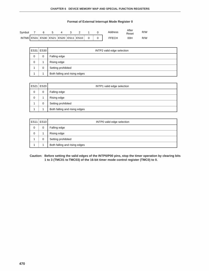
470
CHAPTER 6 DEVICE MEMORY MAP AND SPECIAL FUNCTION REGISTERS
Format of External Interrupt Mode Register 0
Caution: Before setting the valid edges of the INTP0/P00 pins, stop the timer operation by clearing bits1 to 3 (TMC01 to TMC03) of the 16-bit timer mode control register (TMC0) to 0.
Address
FFECH 00H
AfterReset R/W
R/W
0
0
1
1
INTP0 valid edge selection
Falling edge
Rising edge
Setting prohibited
Both falling and rising edges
ES11
7
ES31
Symbol
INTM0
6
ES30
5
ES21
4
ES20
3
ES11
2
ES10
1
0
0
0
0
1
0
1
ES10
0
0
1
1
INTP1 valid edge selection
Falling edge
Rising edge
Setting prohibited
Both falling and rising edges
ES21
0
1
0
1
ES20
0
0
1
1
INTP2 valid edge selection
Falling edge
Rising edge
Setting prohibited
Both falling and rising edges
ES31
0
1
0
1
ES30

471
CHAPTER 6 DEVICE MEMORY MAP AND SPECIAL FUNCTION REGISTERS
Format of External Interrupt Mode Register 1
Address
FFEDH 00H
AfterReset R/W
R/W
0
0
1
1
INTP3 valid edge selection
Falling edge
Rising edge
Setting prohibited
Both falling and rising edges
ES41
7
0
Symbol
INTM1
6
0
5
ES61
4
ES60
3
ES51
2
ES50
1
ES41
0
ES40
0
1
0
1
ES40
0
0
1
1
INTP4 valid edge selection
Falling edge
Rising edge
Setting prohibited
Both falling and rising edges
ES51
0
1
0
1
ES50
0
0
1
1
INTP5 valid edge selection
Falling edge
Rising edge
Setting prohibited
Both falling and rising edges
ES61
0
1
0
1
ES60

472
CHAPTER 6 DEVICE MEMORY MAP AND SPECIAL FUNCTION REGISTERS
Format of Sampling Clock Select Register
Caution: f XX/2N is a clock to be supplied to the CPU and f XX/25, fXX/26, and f XX/27 are clocks to be supplied
to the peripheral hardware. f XX/2N stops in the HALT mode.
Remarks: N: Value (N = 0 to 4) at bits 0 to 2 (PCC0 to PCC2) of processor clock control register
fXX: Main system clock frequency (fX or fX/2)
fX: Main system clock oscillation frequency
MCS: Bit 0 of oscillation mode selection register
Values in parentheses apply to operation with fX = 5.0 MHz.
Format of Program Status Word
Address
FF47H 00H
AfterReset R/W
R/W
0
0
1
1
INTP0 sampling clock selectionSCS1
7
0
Symbol
SCS
6
0
5
0
4
0
3
0
2
0
1
SCS1
0
SCS0
0
1
0
1
SCS0MCS = 1 MCS = 0
fXX/2N
fXX/27
fXX/25
fXX/26
fX/27 (39.1 kHz)
fX/25 (156.3 kHz)
fX/26 (78.1 kHz)
fX/28 (19.5 kHz)
fX/26 (78.1 kHz)
fX/27 (39.1 kHz)
7
IEPSW
6
Z
5
RBS1
4
AC
3
RBS0
2
0
1
ISP
0
CY 02H
After Reset
ISP
0
Used when a normal instruction is executed
Priority of interrupt currently being received
High-priority interrupt servicing(low-priority interrupt disable)
1 Interrupt request not acknowledged or low-priorityinterrupt servicing(all-maskable interrupts enable)
IE Interrupt request acknowledge enable/disable
0 Disable
1 Enable
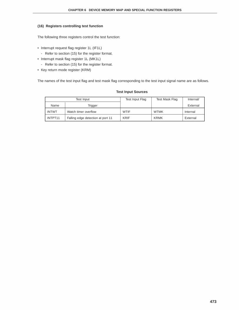
473
CHAPTER 6 DEVICE MEMORY MAP AND SPECIAL FUNCTION REGISTERS
(16) Registers controlling test function
The following three registers control the test function:
• Interrupt request flag register 1L (IF1L)
- Refer to section (15) for the register format.
• Interrupt mask flag register 1L (MK1L)
- Refer to section (15) for the register format.
• Key return mode register (KRM)
The names of the test input flag and test mask flag corresponding to the test input signal name are as follows.
Test Input Sources
Test Input Test Input Flag Test Mask Flag Internal/
Name Trigger External
INTWT Watch timer overflow WTIF WTMK Internal
INTPT11 Falling edge detection at port 11 KRIF KRMK External
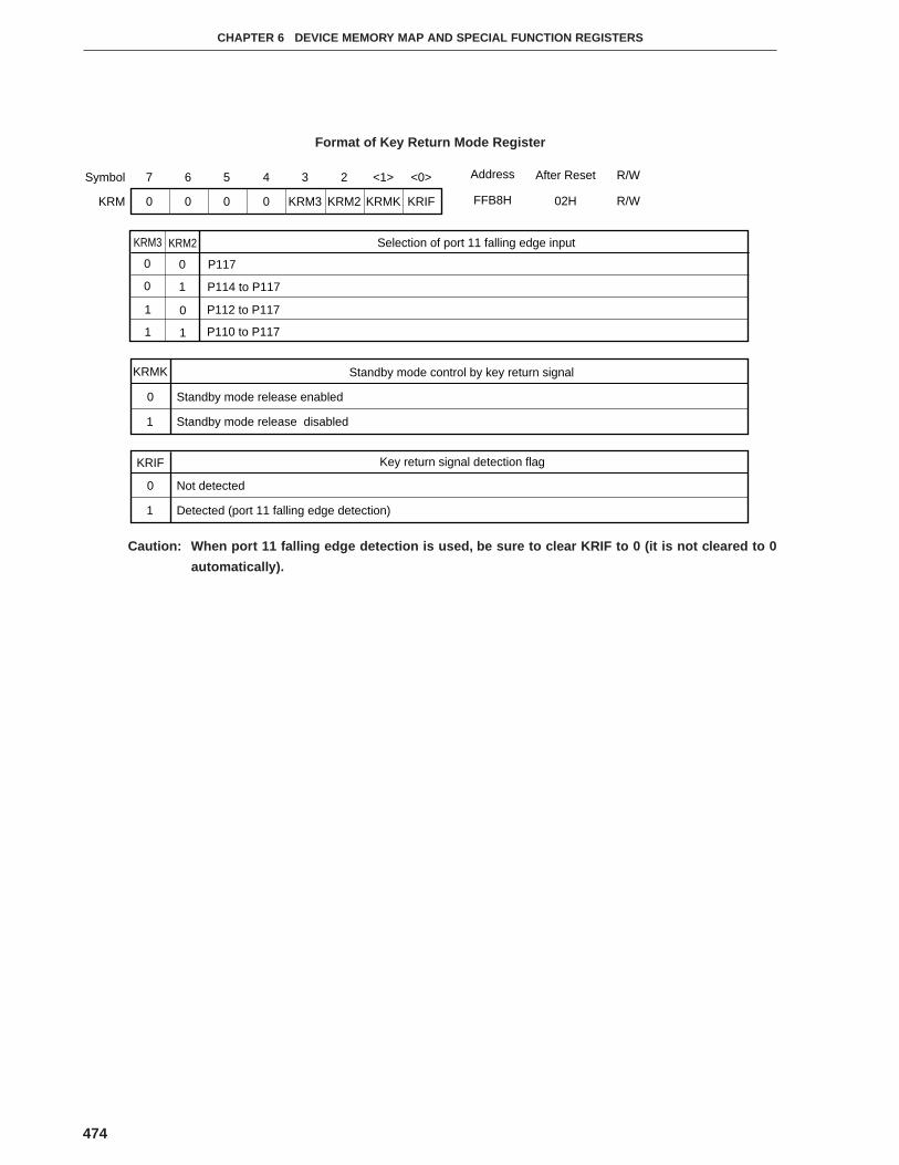
474
CHAPTER 6 DEVICE MEMORY MAP AND SPECIAL FUNCTION REGISTERS
Format of Key Return Mode Register
Caution: When port 11 falling edge detection is used, be sure to clear KRIF to 0 (it is not cleared to 0
automatically).
7
0
Symbol
KRM
6
0
5
0
4
0
3
KRM3
2
KRM2
<1>
KRMK
<0>
KRIF
Address
FFB8H 02H
After Reset R/W
R/W
0
1
Key return signal detection flag
Not detected
Detected (port 11 falling edge detection)
KRIF
0
1
Standby mode control by key return signal
Standby mode release enabled
Standby mode release disabled
KRMK
KRM3 Selection of port 11 falling edge input
0
0
P117
KRM2
0
1
1
1
0
1
P114 to P117
P112 to P117
P110 to P117
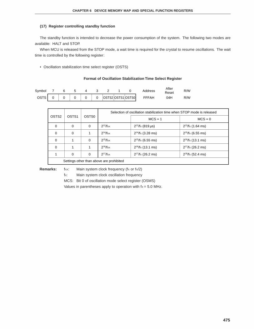
475
CHAPTER 6 DEVICE MEMORY MAP AND SPECIAL FUNCTION REGISTERS
(17) Register controlling standby function
The standby function is intended to decrease the power consumption of the system. The following two modes are
available: HALT and STOP.
When MCU is released from the STOP mode, a wait time is required for the crystal to resume oscillations. The wait
time is controlled by the following register:
• Oscillation stabilization time select register (OSTS)
Format of Oscillation Stabilization Time Select Register
Remarks: fXX: Main system clock frequency (fX or fX/2)
fX: Main system clock oscillation frequency
MCS: Bit 0 of oscillation mode select register (OSMS)
Values in parentheses apply to operation with fX = 5.0 MHz.
Address
FFFAH 04H
AfterReset R/W
R/W
7
0
Symbol
OSTS
6
0
5
0
4
0
3
0
2
OSTS2
1
OSTS1
0
OSTS0
0
0
0
0
1
Selection of oscillation stabilization time when STOP mode is releasedOSTS2
0
0
1
1
0
OSTS1
0
1
0
1
0
212/fXX
214/fXX
215/fXX
216/fXX
217/fXX
OSTS0MCS = 1 MCS = 0
212/fX (819 s)
214/fX (3.28 ms)
215/fX (6.55 ms)
216/fX (13.1 ms)
217/fX (26.2 ms)
213/fX (1.64 ms)
215/fX (6.55 ms)
216/fX (13.1 ms)
217/fX (26.2 ms)
218/fX (52.4 ms)
µ
Settings other than above are prohibited

476
CHAPTER 6 DEVICE MEMORY MAP AND SPECIAL FUNCTION REGISTERS
The operation status in the HALT mode is described below.
HALT Mode Operating Status
Setting of HALT Mode HALT Execution during HALT Execution during
Main System Clock Operation Subsystem Clock Operation
Without Subsystem With Subsystem When Main System Clock When Main System
Item Clock Note 1 Clock Note 2 Continues Oscillation Clock Stops Oscillation
Clock generator Both main system and subsystem clocks can be oscillated. Clock supply to the CPU stops.
CPU Operation stops
Port (output latch) Status before HALT mode setting is held
16-bit timer/event counter Operable Operable when watch
timer output with fXT is
selected as count clock
and fXT is selected as
count clock for
watch timer
8-bit timer/event counters 1 and 2 Operable Operable when TI1 or
TI2 is selected as
count clock
Watch timer Operable when fXX/27 is Operable Operable when fXT is
selected as count clock selected as count clock
Watchdog timer Operable Operation stops
A/D converter Operable Operation stops
Serial interface Operable Operable with external
SCK
LCD controller/driver Operable when fXX/27 is Operable Operable when fXT is
selected as count clock selected as count clock
External interrupt INTP0 Operable when a clock (fXX/25, fXX/26, fXX/27) for the peripheral hardware Operation stops
request is selected as sampling clock
INTP1 to INTP5 Operable
Notes: 1. Including when an external clock is not supplied.
2. Including when an external clock is supplied.

477
CHAPTER 6 DEVICE MEMORY MAP AND SPECIAL FUNCTION REGISTERS
The operation in the STOP mode is described below.
STOP Mode Operating Status
Setting of STOP ModeWith Subsystem Clock Without Subsystem Clock
Item
Clock generator Only main system clock stops oscillation
CPU Operation stops
Port (output latch) Status before STOP mode setting is held
16-bit timer/event counter Operable when watch timer output with fXT Operation stopsis selected as count clock and fXT isselected as count clock for watch timer
8-bit timer/event counters 1 and 2 Operable when TI1 and TI2 are selected for the count clock
Watch timer Operable when fXT is selected for the Operation stopscount clock
Watchdog timer Operation stops
A/D converter
Serial interface Other than UART Operable when externally supplied clock is specified as the serial clock
UART Operation stops
LCD controller/driver Operable when fXT is selected for the Operation stopscount clock
External interrupt INTP0 Not operablerequest INTP1 to INTP5 Operable
Cautions: 1. When the STOP mode is set, the X2 pin is internally connected to V DD1 via a pull-up resistor to
minimize the leakage current at the crystal oscillator. Thus, do not use the STOP mode in a
system where an external CMOS clock is used for the main system clock.
2. Because the interrupt request signal is used to release the Standby mode, if there is an inter-
rupt source with the interrupt request flag set and the interrupt mask flag reset, the Standby
mode is immediately released if set. Thus, the STOP mode is reset to the HALT mode immedi-
ately after execution of the STOP instruction. After the wait set using the oscillation stabiliza-
tion time select register (OSTS), the operating mode is set.

478
CHAPTER 6 DEVICE MEMORY MAP AND SPECIAL FUNCTION REGISTERS
(18) Reset function
The following two operations generate a reset signal:
• External reset input via the RESET pin
• Internal reset by watchdog timer in Watchdog Timer Mode
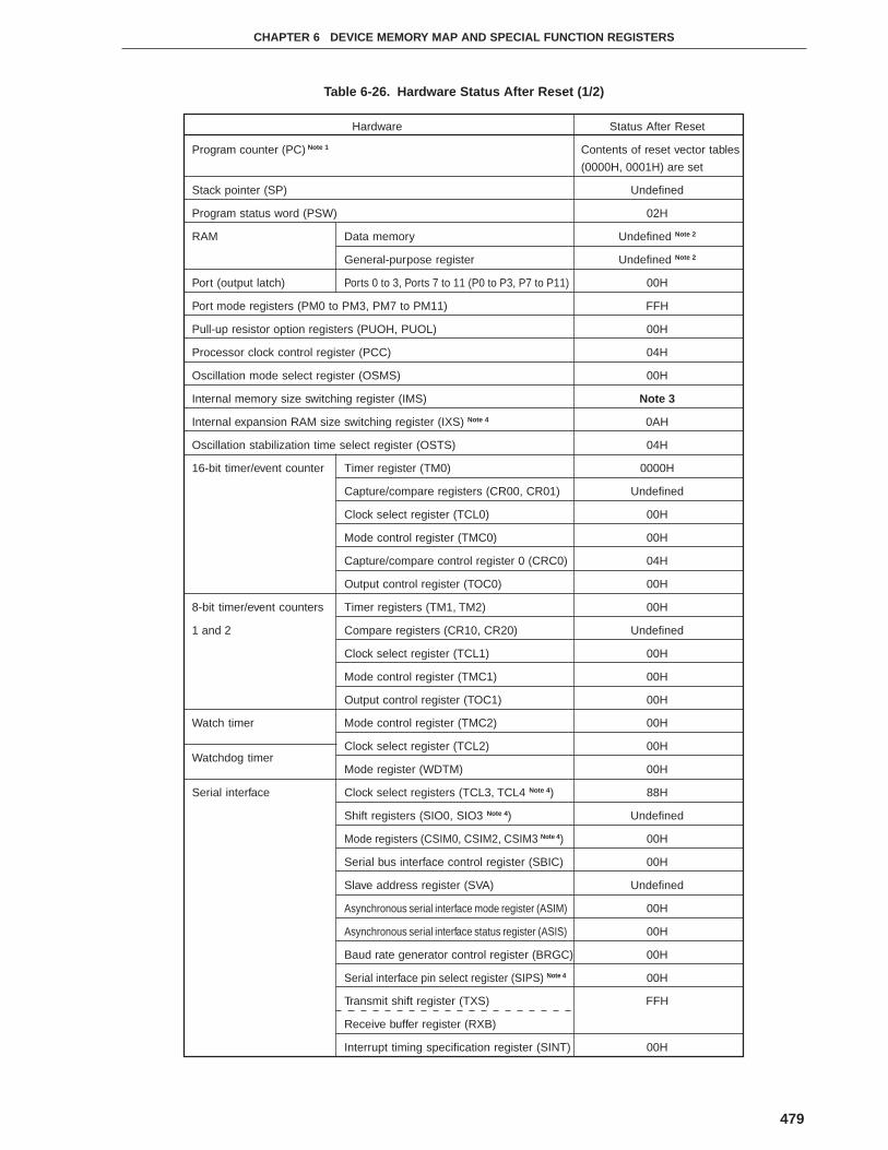
479
CHAPTER 6 DEVICE MEMORY MAP AND SPECIAL FUNCTION REGISTERS
Table 6-26. Hardware Status After Reset (1/2)
Hardware Status After Reset
Program counter (PC) Note 1 Contents of reset vector tables
(0000H, 0001H) are set
Stack pointer (SP) Undefined
Program status word (PSW) 02H
RAM Data memory Undefined Note 2
General-purpose register Undefined Note 2
Port (output latch) Ports 0 to 3, Ports 7 to 11 (P0 to P3, P7 to P11) 00H
Port mode registers (PM0 to PM3, PM7 to PM11) FFH
Pull-up resistor option registers (PUOH, PUOL) 00H
Processor clock control register (PCC) 04H
Oscillation mode select register (OSMS) 00H
Internal memory size switching register (IMS) Note 3
Internal expansion RAM size switching register (IXS) Note 4 0AH
Oscillation stabilization time select register (OSTS) 04H
16-bit timer/event counter Timer register (TM0) 0000H
Capture/compare registers (CR00, CR01) Undefined
Clock select register (TCL0) 00H
Mode control register (TMC0) 00H
Capture/compare control register 0 (CRC0) 04H
Output control register (TOC0) 00H
8-bit timer/event counters Timer registers (TM1, TM2) 00H
1 and 2 Compare registers (CR10, CR20) Undefined
Clock select register (TCL1) 00H
Mode control register (TMC1) 00H
Output control register (TOC1) 00H
Watch timer Mode control register (TMC2) 00H
Clock select register (TCL2) 00HWatchdog timer
Mode register (WDTM) 00H
Serial interface Clock select registers (TCL3, TCL4 Note 4) 88H
Shift registers (SIO0, SIO3 Note 4) Undefined
Mode registers (CSIM0, CSIM2, CSIM3 Note 4) 00H
Serial bus interface control register (SBIC) 00H
Slave address register (SVA) Undefined
Asynchronous serial interface mode register (ASIM) 00H
Asynchronous serial interface status register (ASIS) 00H
Baud rate generator control register (BRGC) 00H
Serial interface pin select register (SIPS) Note 4 00H
Transmit shift register (TXS) FFH
Receive buffer register (RXB)
Interrupt timing specification register (SINT) 00H
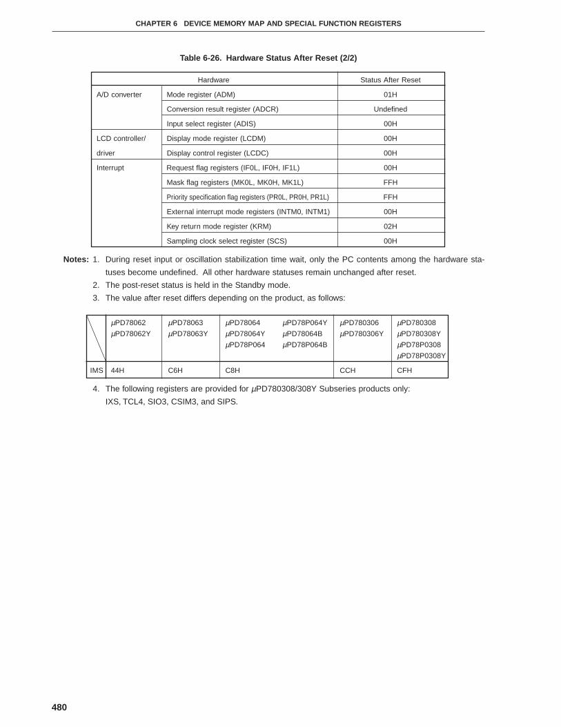
480
CHAPTER 6 DEVICE MEMORY MAP AND SPECIAL FUNCTION REGISTERS
Table 6-26. Hardware Status After Reset (2/2)
Hardware Status After Reset
A/D converter Mode register (ADM) 01H
Conversion result register (ADCR) Undefined
Input select register (ADIS) 00H
LCD controller/ Display mode register (LCDM) 00H
driver Display control register (LCDC) 00H
Interrupt Request flag registers (IF0L, IF0H, IF1L) 00H
Mask flag registers (MK0L, MK0H, MK1L) FFH
Priority specification flag registers (PR0L, PR0H, PR1L) FFH
External interrupt mode registers (INTM0, INTM1) 00H
Key return mode register (KRM) 02H
Sampling clock select register (SCS) 00H
Notes: 1. During reset input or oscillation stabilization time wait, only the PC contents among the hardware sta-
tuses become undefined. All other hardware statuses remain unchanged after reset.
2. The post-reset status is held in the Standby mode.
3. The value after reset differs depending on the product, as follows:
µPD78062 µPD78063 µPD78064 µPD78P064Y µPD780306 µPD780308
µPD78062Y µPD78063Y µPD78064Y µPD78064B µPD780306Y µPD780308Y
µPD78P064 µPD78P064B µPD78P0308
µPD78P0308Y
IMS 44H C6H C8H CCH CFH
4. The following registers are provided for µPD780308/308Y Subseries products only:
IXS, TCL4, SIO3, CSIM3, and SIPS.
481
CHAPTER 6 DEVICE MEMORY MAP AND SPECIAL FUNCTION REGISTERS
(19) Register controlling internal memory capacity
The µPD78P064/64Y, 78P064B, and 78P0308/308Y allow users to select the internal memory capacity.
The following registers are used to control the internal memory capacity:
• Internal memory size switching register (IMS)
• Internal expansion RAM size switching (IXS)
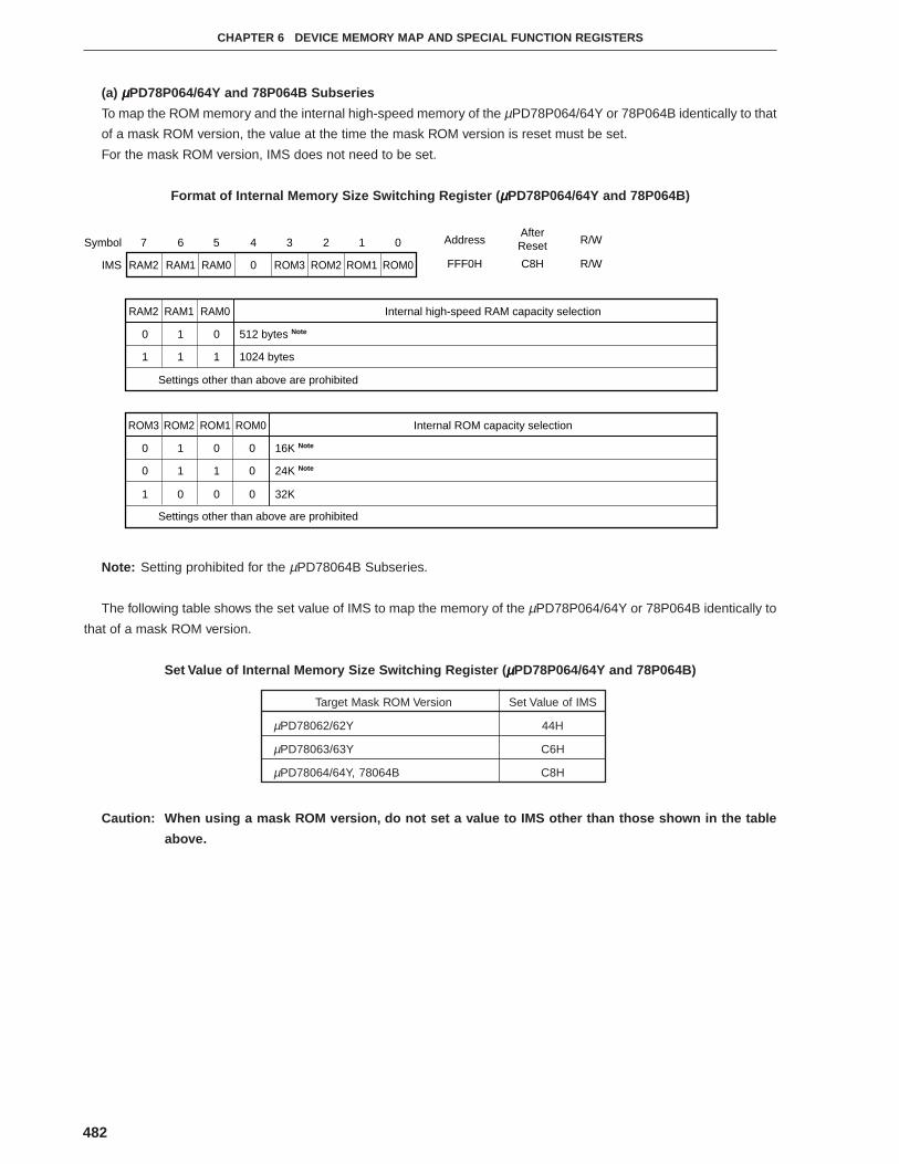
482
CHAPTER 6 DEVICE MEMORY MAP AND SPECIAL FUNCTION REGISTERS
(a) µµµµµPD78P064/64Y and 78P064B Subseries
To map the ROM memory and the internal high-speed memory of the µPD78P064/64Y or 78P064B identically to that
of a mask ROM version, the value at the time the mask ROM version is reset must be set.
For the mask ROM version, IMS does not need to be set.
Format of Internal Memory Size Switching Register ( µµµµµPD78P064/64Y and 78P064B)
Note: Setting prohibited for the µPD78064B Subseries.
The following table shows the set value of IMS to map the memory of the µPD78P064/64Y or 78P064B identically to
that of a mask ROM version.
Set Value of Internal Memory Size Switching Register ( µµµµµPD78P064/64Y and 78P064B)
Target Mask ROM Version Set Value of IMS
µPD78062/62Y 44H
µPD78063/63Y C6H
µPD78064/64Y, 78064B C8H
Caution: When using a mask ROM version, do not set a value to IMS other than those shown in the table
above.
7
RAM2
Symbol
IMS
6
RAM1
5
RAM0
4
0
3
ROM3
2
ROM2
1
ROM1
0
ROM0
Address
FFF0H C8H
AfterReset R/W
R/W
Internal high-speed RAM capacity selectionRAM2 RAM1 RAM0
Settings other than above are prohibited
0 512 bytes Note1 0
1 1024 bytes1 1
Internal ROM capacity selectionROM3 ROM2 ROM1
0 16K Note1 0
0 24K Note1 1
ROM0
0
0
1 32K0 0 0
Settings other than above are prohibited
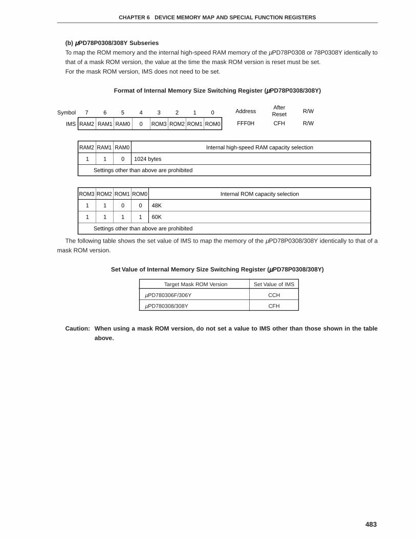
483
CHAPTER 6 DEVICE MEMORY MAP AND SPECIAL FUNCTION REGISTERS
The following table shows the set value of IMS to map the memory of the µPD78P0308/308Y identically to that of a
mask ROM version.
Set Value of Internal Memory Size Switching Register ( µµµµµPD78P0308/308Y)
Target Mask ROM Version Set Value of IMS
µPD780306F/306Y CCH
µPD780308/308Y CFH
Caution: When using a mask ROM version, do not set a value to IMS other than those shown in the table
above.
(b) µµµµµPD78P0308/308Y Subseries
To map the ROM memory and the internal high-speed RAM memory of the µPD78P0308 or 78P0308Y identically to
that of a mask ROM version, the value at the time the mask ROM version is reset must be set.
For the mask ROM version, IMS does not need to be set.
Format of Internal Memory Size Switching Register ( µµµµµPD78P0308/308Y)
7
RAM2
Symbol
IMS
6
RAM1
5
RAM0
4
0
3
ROM3
2
ROM2
1
ROM1
0
ROM0
Address
FFF0H CFH
AfterReset R/W
R/W
Internal high-speed RAM capacity selectionRAM2 RAM1 RAM0
11 1024 bytes0
Internal ROM capacity selectionROM3 ROM2 ROM1
1 48K1 0
1 60K1 1
ROM0
0
1
Settings other than above are prohibited
Settings other than above are prohibited
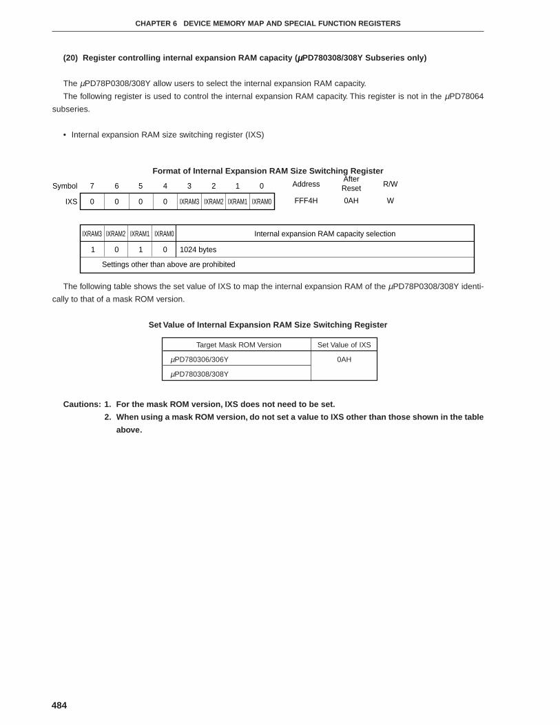
484
CHAPTER 6 DEVICE MEMORY MAP AND SPECIAL FUNCTION REGISTERS
(20) Register controlling internal expansion RAM capacity ( µµµµµPD780308/308Y Subseries only)
The µPD78P0308/308Y allow users to select the internal expansion RAM capacity.
The following register is used to control the internal expansion RAM capacity. This register is not in the µPD78064
subseries.
• Internal expansion RAM size switching register (IXS)
Format of Internal Expansion RAM Size Switching Register
The following table shows the set value of IXS to map the internal expansion RAM of the µPD78P0308/308Y identi-
cally to that of a mask ROM version.
Set Value of Internal Expansion RAM Size Switching Register
Target Mask ROM Version Set Value of IXS
µPD780306/306Y 0AH
µPD780308/308Y
Cautions: 1. For the mask ROM version, IXS does not need to be set.
2. When using a mask ROM version, do not set a value to IXS other than those shown in the table
above.
7
0
Symbol
IXS
6
0
5
0
4
0
3
IXRAM3
2
IXRAM2
1
IXRAM1
0
IXRAM0
Address
FFF4H 0AH
AfterReset R/W
W
Internal expansion RAM capacity selectionIXRAM3 IXRAM2 IXRAM1 IXRAM0
1 1024 bytes0 1 0
Settings other than above are prohibited
485
CHAPTER 6 DEVICE MEMORY MAP AND SPECIAL FUNCTION REGISTERS
6.7 µµµµµPD78078, 78075B, and 78070A Subseries
6.7.1 Documentation Reference Information
Device Series Number User’s Manual Number Date Published
µPD78078, 78Y U10641EJ4V0UM00 December 1997
µPD78075B, 75BY U12560EJ1V0UM00 August 1997
µPD78070A, 70AY U10200EJ2V0UM00 January 1998
Caution: The user should check the current User’s Manual with the information in this section to be sure of
having the most up-to-date information.
6.7.2 Device Series Differences
Device Series Number ROM and RAM Differences External Bus
ROM Size RAM Size Mode
µPD78078, 78078Y 48K/60K Multiplexed
µPD78075B, 78075BY 32K/40K/60K 1K or separate
µPD78070A, 78070AY None Separate
General Programmer’s Note
The NEC C-compiler and the NEC Assembler are capable of recognizing certain symbolic SFR bit names. These
special bit names are identified in the user manual in one of the four ways shown below:
If a bit number has one of the four symbols around it, the NEC software will recognize the associated symbolic bit
name. For example to set bit 7, the user can write the code in two ways:
1. SET1 MCC
2. SET1 PCC.7
Alternatively since bit 2 does not have any of the four symbols around it, the user can only set this bit as follows:
1. SET1 PCC.2
Note: The attempt to employ a symbolic name of bit-2 (PCC2) will return an error. Thus the use of instruction
SET1 PCC2
is improper since neither the NEC C-compiler nor the NEC Assembler recognizes this symbolic name and will
generate an error.
MCCPCC FRC CLS CSS 0 PCC2 PCC1 PCC0
<7> <6> <5> <4> 3 2 1 0
Example:
1.
2.
3.
4.
<7>
( 7 )
7
7
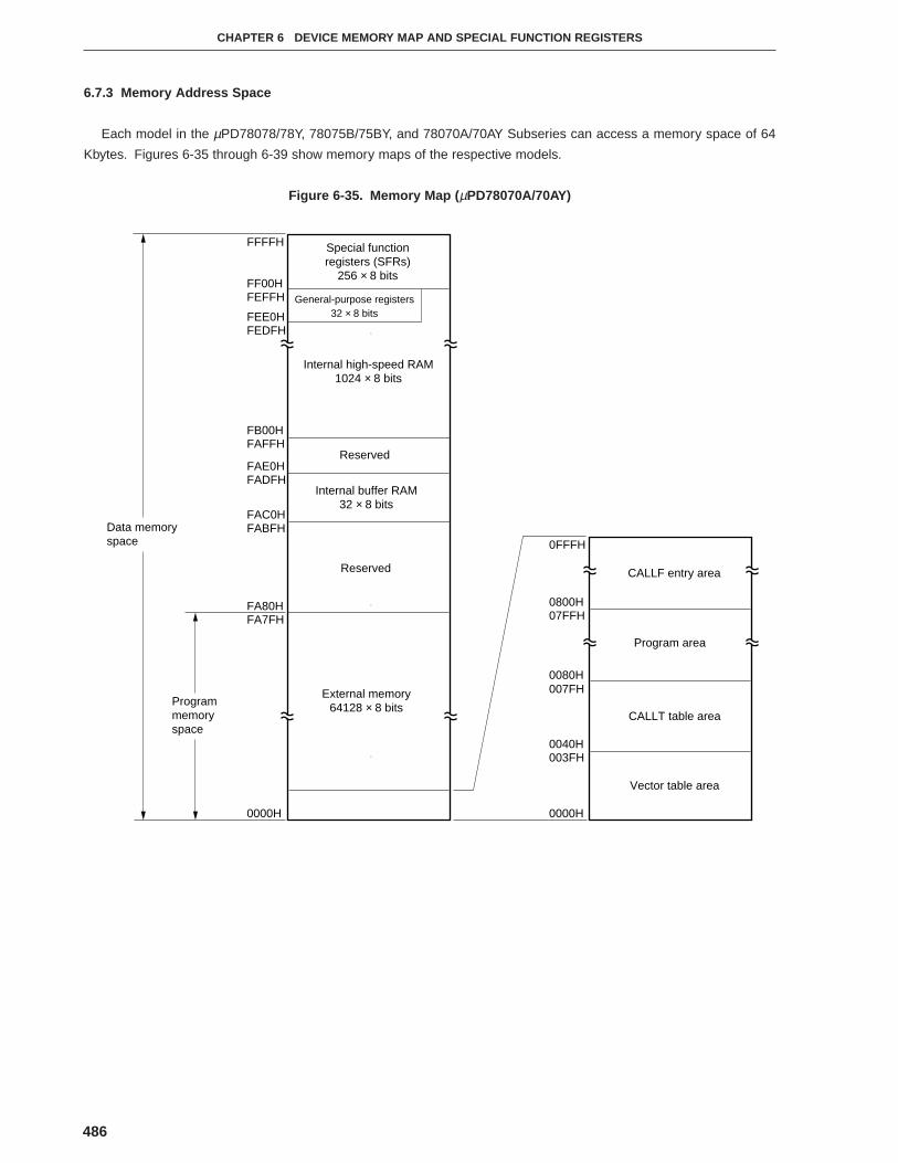
486
CHAPTER 6 DEVICE MEMORY MAP AND SPECIAL FUNCTION REGISTERS
6.7.3 Memory Address Space
Each model in the µPD78078/78Y, 78075B/75BY, and 78070A/70AY Subseries can access a memory space of 64
Kbytes. Figures 6-35 through 6-39 show memory maps of the respective models.
Figure 6-35. Memory Map ( µPD78070A/70AY)
0000H
Data memory space
General-purpose registers32 × 8 bits
0FFFH
0800H07FFH
0080H 007FH
0040H003FH
0000H
CALLF entry area
CALLT table area
Vector table area
Program area
Internal buffer RAM32 × 8 bits
External memory64128 × 8 bits
Reserved
Programmemoryspace
FAC0HFABFH
FAE0HFADFH
FEE0HFEDFH
FF00HFEFFH
FFFFH
Internal high-speed RAM1024 × 8 bits
Special function registers (SFRs)
256 × 8 bits
FA80HFA7FH
Reserved
FB00HFAFFH
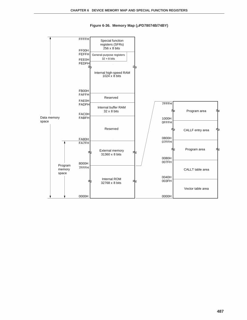
487
CHAPTER 6 DEVICE MEMORY MAP AND SPECIAL FUNCTION REGISTERS
Figure 6-36. Memory Map ( µPD78074B/74BY)
0000H
Data memory space
Internal ROM32768 x 8 bits
7FFFH
1000H0FFFH
0800H07FFH
0080H 007FH
0040H003FH
0000H
CALLF entry area
CALLT table area
Vector table area
Program area
Program areaInternal buffer RAM
32 x 8 bits
External memory31360 x 8 bits
Reserved
Programmemoryspace
8000H7FFFH
FAC0HFABFH
FAE0HFADFH
FEE0HFEDFH
FF00HFEFFH
FFFFH
Internal high-speed RAM1024 x 8 bits
Special function registers (SFRs)
256 x 8 bits
FA80HFA7FH
Reserved
FB00HFAFFH
General-purpose registers32 × 8 bits
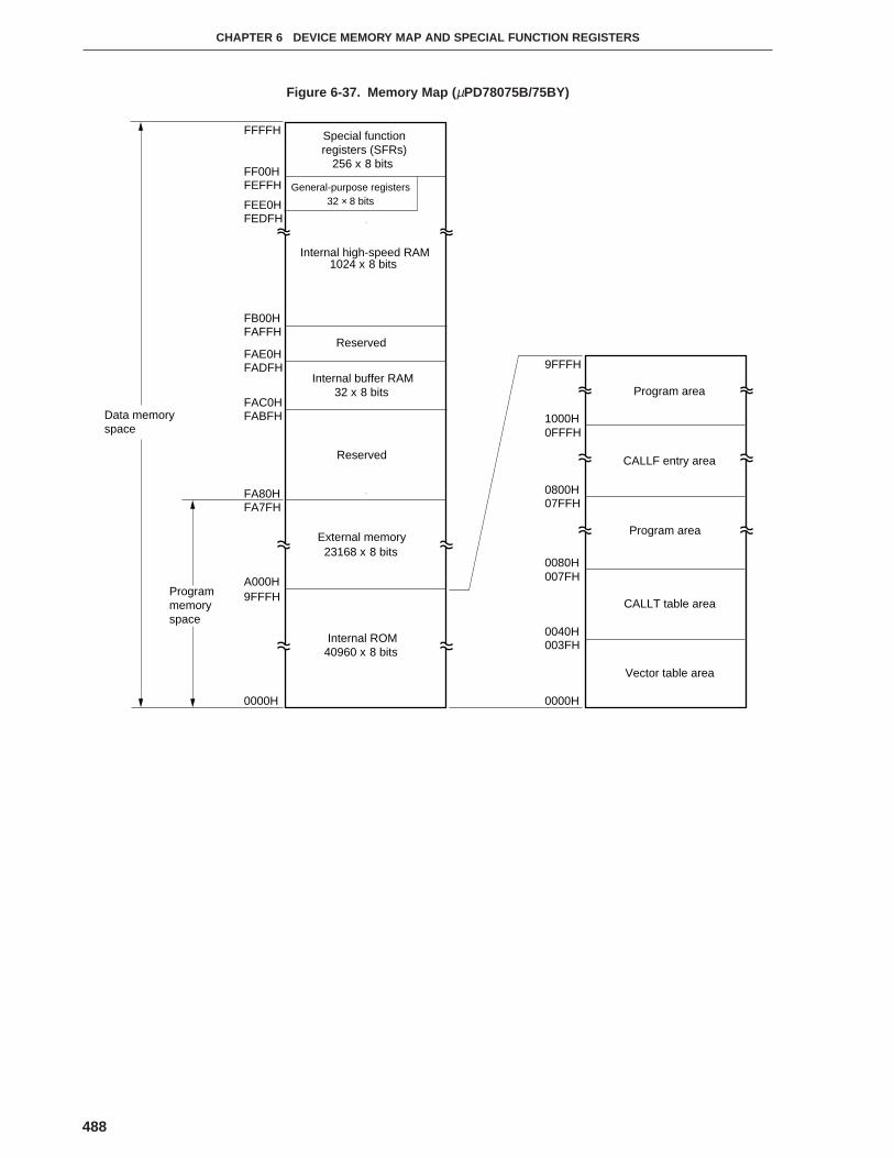
488
CHAPTER 6 DEVICE MEMORY MAP AND SPECIAL FUNCTION REGISTERS
Figure 6-37. Memory Map ( µPD78075B/75BY)
0000H
Data memory space
Internal ROM40960 x 8 bits
23168 x 8 bits
9FFFH
1000H0FFFH
0800H07FFH
0080H 007FH
0040H003FH
0000H
CALLF entry area
CALLT table area
Vector table area
Program area
Program areaInternal buffer RAM
32 x 8 bits
Programmemoryspace
A000H9FFFH
FAC0HFABFH
FAE0HFADFH
FEE0HFEDFH
FF00HFEFFH
FFFFH
Internal high-speed RAM1024 x 8 bits
Special function registers (SFRs)
256 x 8 bits
FA80HFA7FH
Reserved
FB00HFAFFH
Reserved
External memory
General-purpose registers32 × 8 bits
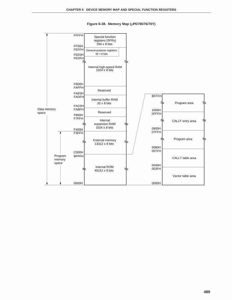
489
CHAPTER 6 DEVICE MEMORY MAP AND SPECIAL FUNCTION REGISTERS
Figure 6-38. Memory Map ( µPD78076/76Y)
0000H
Data memory space
Internal ROM49152 x 8 bits
BFFFH
1000H0FFFH
0800H07FFH
0080H 007FH
0040H003FH
0000H
CALLF entry area
CALLT table area
Vector table area
Program area
Program areaInternal buffer RAM
32 x 8 bits
External memory13312 x 8 bits
Reserved
Programmemoryspace
C000HBFFFH
F800HF7FFH
FAC0HFABFH
FAE0HFADFH
FEE0HFEDFH
FF00HFEFFH
FFFFH
Internal high-speed RAM1024 x 8 bits
Special function registers (SFRs)
256 x 8 bits
Internalexpansion RAM1024 x 8 bits
F400HF3FFH
Reserved
FB00HFAFFH
General-purpose registers32 × 8 bits
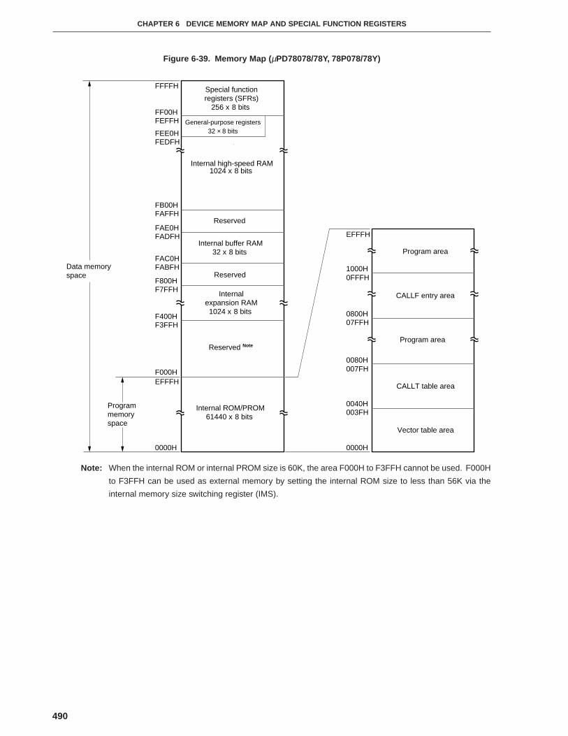
490
CHAPTER 6 DEVICE MEMORY MAP AND SPECIAL FUNCTION REGISTERS
Figure 6-39. Memory Map ( µPD78078/78Y, 78P078/78Y)
Note: When the internal ROM or internal PROM size is 60K, the area F000H to F3FFH cannot be used. F000H
to F3FFH can be used as external memory by setting the internal ROM size to less than 56K via the
internal memory size switching register (IMS).
0000H
Data memory space
Internal ROM/PROM61440 x 8 bits
EFFFH
1000H0FFFH
0800H07FFH
0080H 007FH
0040H003FH
0000H
CALLF entry area
CALLT table area
Vector table area
Program area
Program areaInternal buffer RAM
32 x 8 bits
Reserved Note
Programmemoryspace
F000HEFFFH
F800HF7FFH
FAC0HFABFH
FAE0HFADFH
FEE0HFEDFH
FF00HFEFFH
FFFFH
Internal high-speed RAM1024 x 8 bits
Special function registers (SFRs)
256 x 8 bits
Internalexpansion RAM1024 x 8 bits
F400HF3FFH
Reserved
FB00HFAFFH
Reserved
General-purpose registers32 × 8 bits
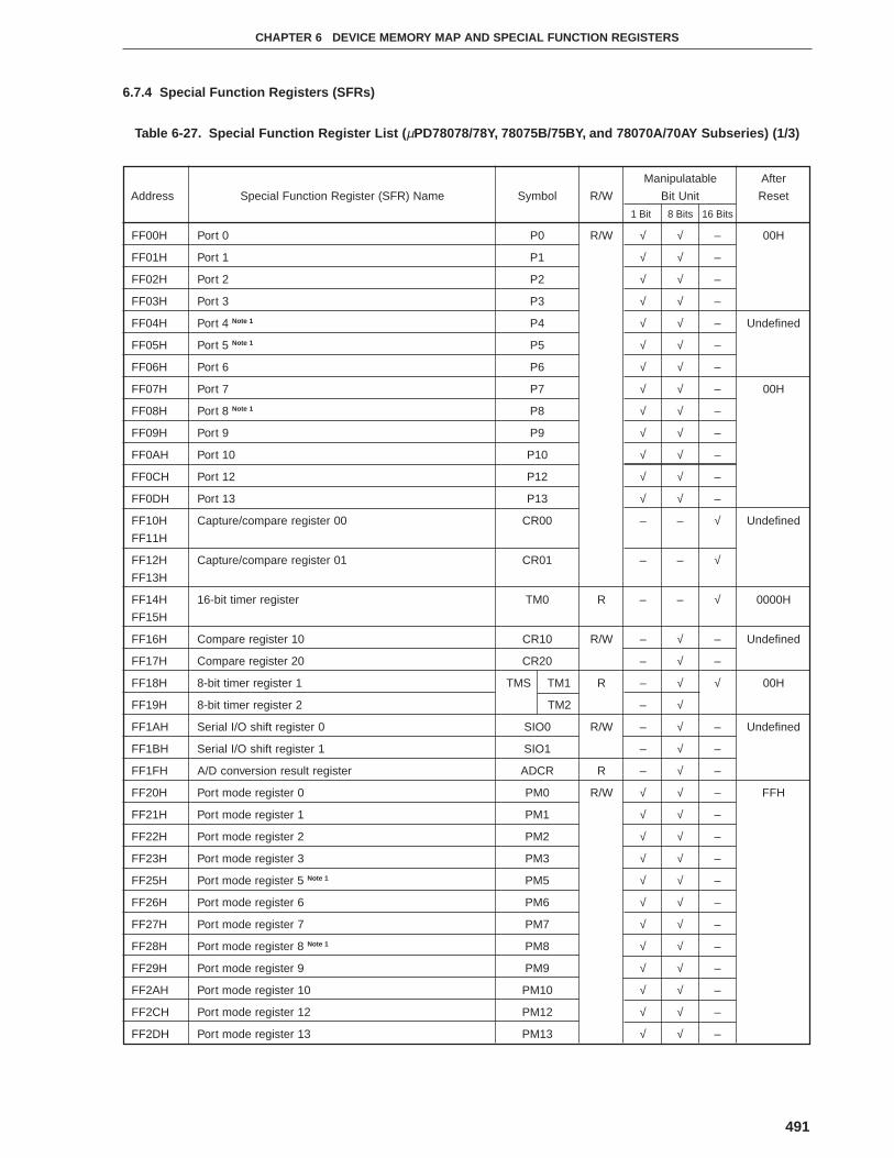
491
CHAPTER 6 DEVICE MEMORY MAP AND SPECIAL FUNCTION REGISTERS
6.7.4 Special Function Registers (SFRs)
Table 6-27. Special Function Register List ( µPD78078/78Y, 78075B/75BY, and 78070A/70AY Subseries) (1/3)
Manipulatable After
Address Special Function Register (SFR) Name Symbol R/W Bit Unit Reset
1 Bit 8 Bits 16 Bits
FF00H Port 0 P0 R/W √ √ – 00H
FF01H Port 1 P1 √ √ –
FF02H Port 2 P2 √ √ –
FF03H Port 3 P3 √ √ –
FF04H Port 4 Note 1 P4 √ √ – Undefined
FF05H Port 5 Note 1 P5 √ √ –
FF06H Port 6 P6 √ √ –
FF07H Port 7 P7 √ √ – 00H
FF08H Port 8 Note 1 P8 √ √ –
FF09H Port 9 P9 √ √ –
FF0AH Port 10 P10 √ √ –
FF0CH Port 12 P12 √ √ –
FF0DH Port 13 P13 √ √ –
FF10H Capture/compare register 00 CR00 – – √ Undefined
FF11H
FF12H Capture/compare register 01 CR01 – – √FF13H
FF14H 16-bit timer register TM0 R – – √ 0000H
FF15H
FF16H Compare register 10 CR10 R/W – √ – Undefined
FF17H Compare register 20 CR20 – √ –
FF18H 8-bit timer register 1 TMS TM1 R – √ √ 00H
FF19H 8-bit timer register 2 TMS TM2 – √
FF1AH Serial I/O shift register 0 SIO0 R/W – √ – Undefined
FF1BH Serial I/O shift register 1 SIO1 – √ –
FF1FH A/D conversion result register ADCR R – √ –
FF20H Port mode register 0 PM0 R/W √ √ – FFH
FF21H Port mode register 1 PM1 √ √ –
FF22H Port mode register 2 PM2 √ √ –
FF23H Port mode register 3 PM3 √ √ –
FF25H Port mode register 5 Note 1 PM5 √ √ –
FF26H Port mode register 6 PM6 √ √ –
FF27H Port mode register 7 PM7 √ √ –
FF28H Port mode register 8 Note 1 PM8 √ √ –
FF29H Port mode register 9 PM9 √ √ –
FF2AH Port mode register 10 PM10 √ √ –
FF2CH Port mode register 12 PM12 √ √ –
FF2DH Port mode register 13 PM13 √ √ –
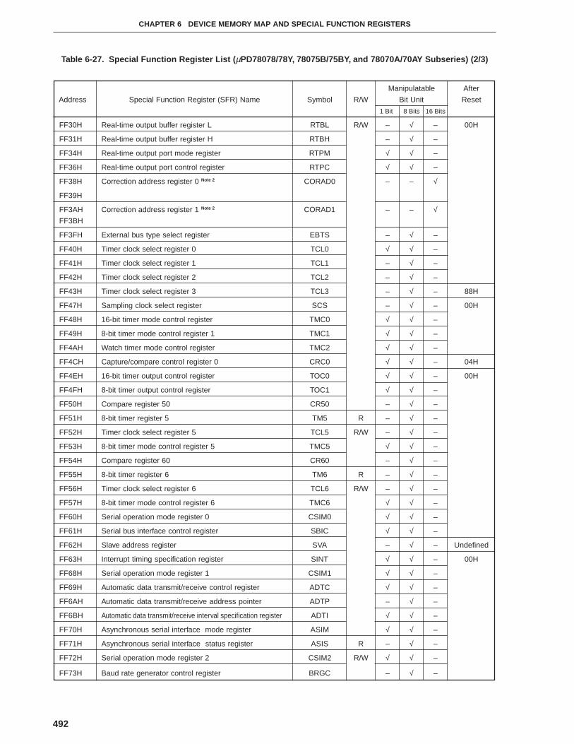
492
CHAPTER 6 DEVICE MEMORY MAP AND SPECIAL FUNCTION REGISTERS
Table 6-27. Special Function Register List ( µPD78078/78Y, 78075B/75BY, and 78070A/70AY Subseries) (2/3)
Manipulatable After
Address Special Function Register (SFR) Name Symbol R/W Bit Unit Reset
1 Bit 8 Bits 16 Bits
FF30H Real-time output buffer register L RTBL R/W – √ – 00H
FF31H Real-time output buffer register H RTBH – √ –
FF34H Real-time output port mode register RTPM √ √ –
FF36H Real-time output port control register RTPC √ √ –
FF38H Correction address register 0 Note 2 CORAD0 – – √
FF39H
FF3AH Correction address register 1 Note 2 CORAD1 – – √FF3BH
FF3FH External bus type select register EBTS – √ –
FF40H Timer clock select register 0 TCL0 √ √ –
FF41H Timer clock select register 1 TCL1 – √ –
FF42H Timer clock select register 2 TCL2 – √ –
FF43H Timer clock select register 3 TCL3 – √ – 88H
FF47H Sampling clock select register SCS – √ – 00H
FF48H 16-bit timer mode control register TMC0 √ √ –
FF49H 8-bit timer mode control register 1 TMC1 √ √ –
FF4AH Watch timer mode control register TMC2 √ √ –
FF4CH Capture/compare control register 0 CRC0 √ √ – 04H
FF4EH 16-bit timer output control register TOC0 √ √ – 00H
FF4FH 8-bit timer output control register TOC1 √ √ –
FF50H Compare register 50 CR50 – √ –
FF51H 8-bit timer register 5 TM5 R – √ –
FF52H Timer clock select register 5 TCL5 R/W – √ –
FF53H 8-bit timer mode control register 5 TMC5 √ √ –
FF54H Compare register 60 CR60 – √ –
FF55H 8-bit timer register 6 TM6 R – √ –
FF56H Timer clock select register 6 TCL6 R/W – √ –
FF57H 8-bit timer mode control register 6 TMC6 √ √ –
FF60H Serial operation mode register 0 CSIM0 √ √ –
FF61H Serial bus interface control register SBIC √ √ –
FF62H Slave address register SVA – √ – Undefined
FF63H Interrupt timing specification register SINT √ √ – 00H
FF68H Serial operation mode register 1 CSIM1 √ √ –
FF69H Automatic data transmit/receive control register ADTC √ √ –
FF6AH Automatic data transmit/receive address pointer ADTP – √ –
FF6BH Automatic data transmit/receive interval specification register ADTI √ √ –
FF70H Asynchronous serial interface mode register ASIM √ √ –
FF71H Asynchronous serial interface status register ASIS R – √ –
FF72H Serial operation mode register 2 CSIM2 R/W √ √ –
FF73H Baud rate generator control register BRGC – √ –
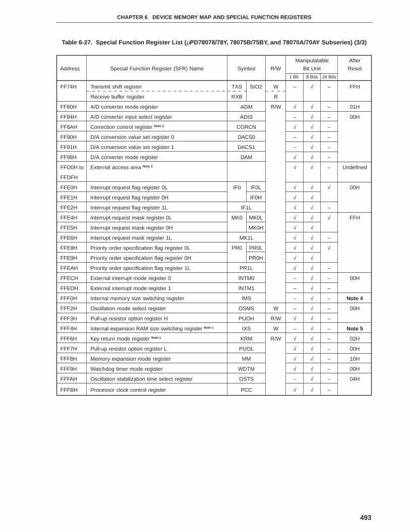
493
CHAPTER 6 DEVICE MEMORY MAP AND SPECIAL FUNCTION REGISTERS
Table 6-27. Special Function Register List ( µPD78078/78Y, 78075B/75BY, and 78070A/70AY Subseries) (3/3)
Manipulatable After
Address Special Function Register (SFR) Name Symbol R/W Bit Unit Reset
1 Bit 8 Bits 16 Bits
FF74H Transmit shift register TXS SIO2 W – √ – FFH
Receive buffer register RXB R
FF80H A/D converter mode register ADM R/W √ √ – 01H
FF84H A/D converter input select register ADIS – √ – 00H
FF8AH Correction control register Note 2 CORCN √ √ –
FF90H D/A conversion value set register 0 DACS0 – √ –
FF91H D/A conversion value set register 1 DACS1 – √ –
FF98H D/A converter mode register DAM √ √ –
FFD0H to External access area Note 3 √ √ – Undefined
FFDFH
FFE0H Interrupt request flag register 0L IF0 IF0L √ √ √ 00H
FFE1H Interrupt request flag register 0H IF0H √ √
FFE2H Interrupt request flag register 1L IF1L √ √ –
FFE4H Interrupt request mask register 0L MK0 MK0L √ √ √ FFH
FFE5H Interrupt request mask register 0H MK0H √ √
FFE6H Interrupt request mask register 1L MK1L √ √ –
FFE8H Priority order specification flag register 0L PR0 PR0L √ √ √
FFE9H Priority order specification flag register 0H PR0H √ √
FFEAH Priority order specification flag register 1L PR1L √ √ –
FFECH External interrupt mode register 0 INTM0 – √ – 00H
FFEDH External interrupt mode register 1 INTM1 – √ –
FFF0H Internal memory size switching register IMS – √ – Note 4
FFF2H Oscillation mode select register OSMS W – √ – 00H
FFF3H Pull-up resistor option register H PUOH R/W √ √ –
FFF4H Internal expansion RAM size switching register Note 1 IXS W – √ – Note 5
FFF6H Key return mode register Note 1 KRM R/W √ √ – 02H
FFF7H Pull-up resistor option register L PUOL √ √ – 00H
FFF8H Memory expansion mode register MM √ √ – 10H
FFF9H Watchdog timer mode register WDTM √ √ – 00H
FFFAH Oscillation stabilization time select register OSTS – √ – 04H
FFFBH Processor clock control register PCC √ √ –
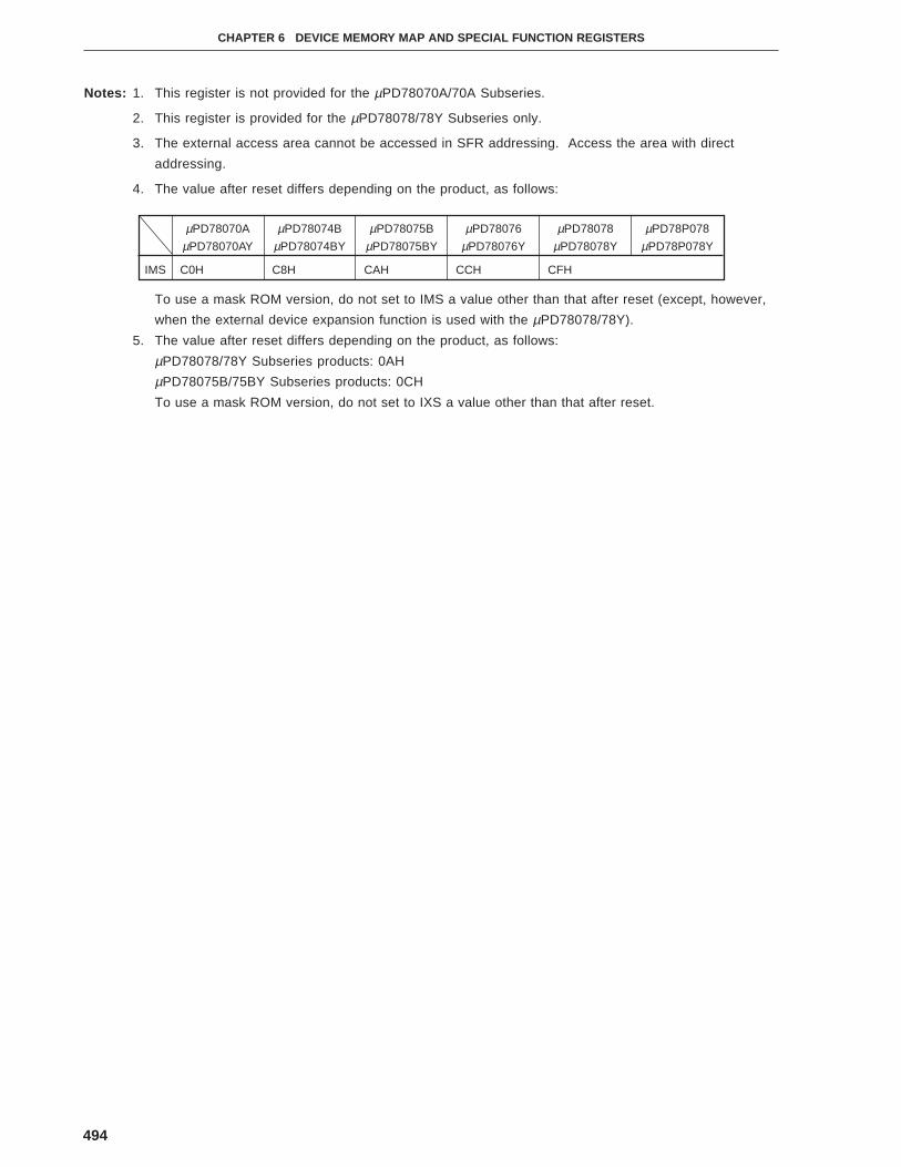
494
CHAPTER 6 DEVICE MEMORY MAP AND SPECIAL FUNCTION REGISTERS
Notes: 1. This register is not provided for the µPD78070A/70A Subseries.
2. This register is provided for the µPD78078/78Y Subseries only.
3. The external access area cannot be accessed in SFR addressing. Access the area with direct
addressing.
4. The value after reset differs depending on the product, as follows:
µPD78070A µPD78074B µPD78075B µPD78076 µPD78078 µPD78P078
µPD78070AY µPD78074BY µPD78075BY µPD78076Y µPD78078Y µPD78P078Y
IMS C0H C8H CAH CCH CFH
To use a mask ROM version, do not set to IMS a value other than that after reset (except, however,
when the external device expansion function is used with the µPD78078/78Y).
5. The value after reset differs depending on the product, as follows:
µPD78078/78Y Subseries products: 0AH
µPD78075B/75BY Subseries products: 0CH
To use a mask ROM version, do not set to IXS a value other than that after reset.
495
CHAPTER 6 DEVICE MEMORY MAP AND SPECIAL FUNCTION REGISTERS
(1) Registers controlling port functions
The following four types of registers control the ports:
• Port mode registers (PM0 to PM3, PM5 to PM10 Note 1, PM12, PM13)
• Pull-up resistor option registers (PUOH, PUOL)
Notes: 1. The µPD78070A/70AY do not have PM5 and PM8.
2. This register is not provided for the µPD78070A/70AY.
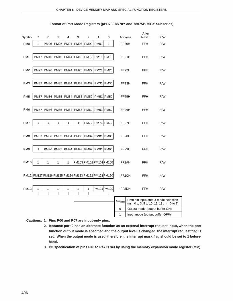
496
CHAPTER 6 DEVICE MEMORY MAP AND SPECIAL FUNCTION REGISTERS
Format of Port Mode Registers ( µµµµµPD78078/78Y and 78075B/75BY Subseries)
Cautions: 1. Pins P00 and P07 are input-only pins.
2. Because port 0 has an alternate function as an external interrupt request input, when the port
function output mode is specified and the output level is changed, the interrupt request flag is
set. When the output mode is used, therefore, the interrupt mask flag should be set to 1 before-
hand .
3. I/O specification of pins P40 to P47 is set by using the memory expansion mode register (MM) .
PM0
PM1
PM2
1 PM06 PM03 PM02 PM01 1
7 6 5 4 3 2 1 0Symbol
PM3
PM5
FF20H
FF21H
FF22H
FF23H
FF25H
FFH
FFH
FFH
FFH
FFH
R/W
R/W
R/W
R/W
R/W
AddressAfter
Reset R/W
PM17 PM16 PM15 PM14 PM13 PM12 PM11 PM10
PM27 PM26 PM25 PM24 PM23 PM22 PM21 PM20
PM37 PM36 PM35 PM34 PM33 PM32 PM31 PM30
PM57 PM56 PM55 PM54 PM53 PM52 PM51 PM50
PM6
PM7
PM8
FF26H
FF27H
FF28H
FFH
FFH
FFH
R/W
R/W
R/W
PM67 PM66 PM65 PM64 PM63 PM62 PM61 PM60
1 1 1 1 1 PM72 PM71 PM70
PM87 PM86 PM85 PM84 PM83 PM82 PM81 PM80
PM05 PM04
PM9 FF29H FFH R/W1 PM96 PM95 PM94 PM93 PM92 PM91 PM90
PM10
PM12
PM13
PMmn Pmn pin input/output mode selection(m = 0 to 3, 5 to 10, 12, 13 : n = 0 to 7)
0
1
Output mode (output buffer ON)
Input mode (output buffer OFF)
FF2AH
FF2CH
FF2DH
FFH
FFH
FFH
R/W
R/W
R/W
1 1 1 1 PM103 PM102 PM101PM100
PM122 PM121PM120
1 1 1 1 1 1 PM131 PM130
PM125 PM124 PM123PM127 PM126
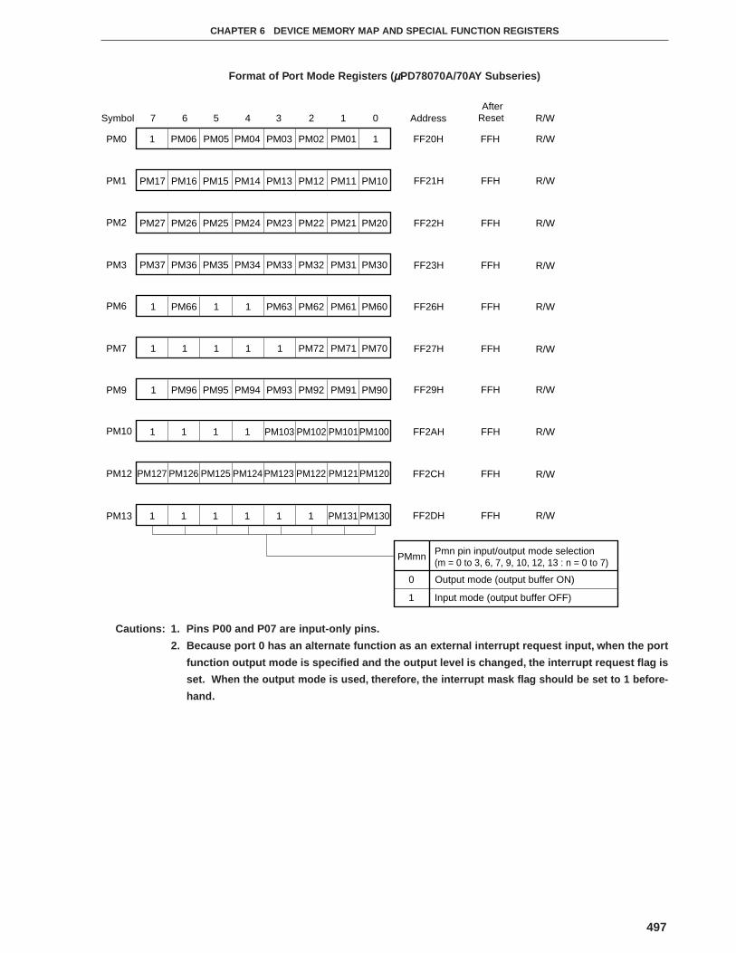
497
CHAPTER 6 DEVICE MEMORY MAP AND SPECIAL FUNCTION REGISTERS
Format of Port Mode Registers ( µµµµµPD78070A/70AY Subseries)
Cautions: 1. Pins P00 and P07 are input-only pins.
2. Because port 0 has an alternate function as an external interrupt request input, when the port
function output mode is specified and the output level is changed, the interrupt request flag is
set. When the output mode is used, therefore, the interrupt mask flag should be set to 1 before-
hand .
PM6
PM7
FF26H
FF27H
FFH
FFH
R/W
R/W
PM66 PM63 PM62 PM61 PM60
1 1 1 1
1 1 1
1 PM72 PM71 PM70
PM0
PM1
PM2
1 PM06 PM03 PM02 PM01 1
7 6 5 4 3 2 1 0Symbol
PM3
FF20H
FF21H
FF22H
FF23H
FFH
FFH
FFH
FFH
R/W
R/W
R/W
R/W
AddressAfter
Reset R/W
PM17 PM16 PM15 PM14 PM13 PM12 PM11 PM10
PM27 PM26 PM25 PM24 PM23 PM22 PM21 PM20
PM37 PM36 PM35 PM34 PM33 PM32 PM31 PM30
PM05 PM04
PM9 FF29H FFH R/W1 PM96 PM95 PM94 PM93 PM92 PM91 PM90
PM10
PM12
PM13
PMmn Pmn pin input/output mode selection(m = 0 to 3, 6, 7, 9, 10, 12, 13 : n = 0 to 7)
0
1
Output mode (output buffer ON)
Input mode (output buffer OFF)
FF2AH
FF2CH
FF2DH
FFH
FFH
FFH
R/W
R/W
R/W
1 1 1 1 PM103 PM102 PM101PM100
PM122 PM121PM120
1 1 1 1 1 1 PM131 PM130
PM125 PM124 PM123PM127 PM126
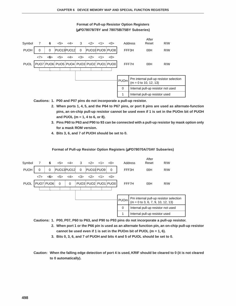
498
CHAPTER 6 DEVICE MEMORY MAP AND SPECIAL FUNCTION REGISTERS
Format of Pull-up Resistor Option Registers
(µµµµµPD78078/78Y and 78075B/75BY Subseries)
Cautions: 1. P00 and P07 pins do not incorporate a pull-up resistor.
2. When ports 1, 4, 5, and the P64 to P67 pins, or port 8 pins are used as alternate-function
pins, an on-chip pull-up resistor cannot be used even if 1 is set in the PUOm bit of PUOH
and PUOL (m = 1, 4 to 6, or 8).
3. Pins P60 to P63 and P90 to 93 can be connected with a pull-up resistor by mask option only
for a mask ROM version.
4. Bits 3, 6, and 7 of PUOH should be set to 0.
Format of Pull-up Resistor Option Registers ( µµµµµPD78070A/70AY Subseries)
Cautions: 1. P00, P07, P60 to P63, and P90 to P93 pins do not incorporate a pull-up resistor.
2. When port 1 or the P66 pin is used as an alternate function pin, an on-chip pull-up resistor
cannot be used even if 1 is set in the PUOm bit of PUOL (m = 1, 6).
3. Bits 0, 3, 6, and 7 of PUOH and bits 4 and 5 of PUOL should be set to 0.
Caution: When the falling edge detection of port 4 is used, KRIF should be cleared to 0 (it is not cleared
to 0 automatically).
PUO7 PUO6 PUO5 PUO4 PUO2 PUO1 PUO0PUOL
PUOm Pm internal pull-up resistor selection(m = 0 to 10, 12, 13)
0
1
Internal pull-up resistor not used
Internal pull-up resistor used
FFF7H 00H R/WPUO3
0 0 PUO13 PUO12 PUO10 PUO9 PUO8PUOH FFF3H 00H R/W
7 6 <5> <4>Symbol AddressAfter
Reset R/W
0
6 3 <2> <0><1>
<7> 6 <5> <4><6> <3> <2> <0><1>
PUO7 PUO6 PUO2 PUO1 PUO0PUOL
PUOm Pm internal pull-up resistor selection(m = 0 to 3, 6, 7, 9, 10, 12, 13)
0
1
Internal pull-up resistor not used
Internal pull-up resistor used
FFF7H 00H R/WPUO3
0 0 PUO13 PUO12 PUO10 PUO9 0PUOH FFF3H 00H R/W
7 6 <5> <4>Symbol AddressAfter
Reset R/W
0
6 3 <2> <0><1>
<7> 6 <5> <4><6> <3> <2> <0><1>
0 0
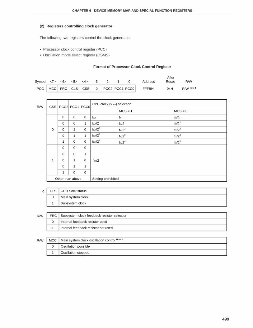
499
CHAPTER 6 DEVICE MEMORY MAP AND SPECIAL FUNCTION REGISTERS
(2) Registers controlling clock generator
The following two registers control the clock generator:
• Processor clock control register (PCC)
• Oscillation mode select register (OSMS)
Format of Processor Clock Control Register
MCC FRC CLS CSS PCC2 PCC1 PCC0PCC
CLS
0
1
Main system clock
Subsystem clock
FFFBH 04H
<7> <6> <5> <4>Symbol AddressAfter
Reset R/W
R/W Note 10
3 2 01
CSS
0
0 fXX/2
PCC2CPU cIock (fCPU) selection
PCC1 PCC0
CPU clock status
0
0
0
1
0
0
1
1
0
1
1
0
0
0
0
0
0
0
0
1
1
0
0
1
1
0
1
0
fXX/22
fXX/23
fXX/24
fXX
Setting prohibitedOther than above
FRC
0
1
Internal feedback resistor used
Internal feedback resistor not used
Subsystem clock feedback resistor selection
MCC
0
1
Oscillation possible
Oscillation stopped
Main system clock oscillation control Note 2
R/W
R/W
R/W
R
fX
fX/2
fX/22
fXT/2
fX/23
fX/24
fX/22
fX/2
fX/23
fX/24
fX/25
MCS = 1 MCS = 0
0
1
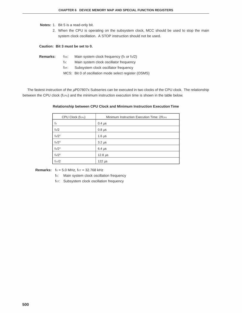
500
CHAPTER 6 DEVICE MEMORY MAP AND SPECIAL FUNCTION REGISTERS
Notes: 1. Bit 5 is a read-only bit.
2. When the CPU is operating on the subsystem clock, MCC should be used to stop the main
system clock oscillation. A STOP instruction should not be used.
Caution: Bit 3 must be set to 0.
Remarks: fXX: Main system clock frequency (fX or fX/2)
fX: Main system clock oscillator frequency
fXT: Subsystem clock oscillator frequency
MCS: Bit 0 of oscillation mode select register (OSMS)
The fastest instruction of the µPD7807x Subseries can be executed in two clocks of the CPU clock. The relationship
between the CPU clock (fCPU) and the minimum instruction execution time is shown in the table below.
Relationship between CPU Clock and Minimum Instruction Execution Time
CPU Clock (fCPU) Minimum Instruction Execution Time: 2/fCPU
fX 0.4 µs
fX/2 0.8 µs
fX/22 1.6 µs
fX/23 3.2 µs
fX/24 6.4 µs
fX/25 12.8 µs
fXT/2 122 µs
Remarks: fX = 5.0 MHz, fXT = 32.768 kHz
fX: Main system clock oscillation frequency
fXT: Subsystem clock oscillation frequency

501
CHAPTER 6 DEVICE MEMORY MAP AND SPECIAL FUNCTION REGISTERS
Format of Oscillation Mode Select Register
Cautions: 1. Writing data (including same data as previous) to OSMS causes a delay of the main system
clock cycle of up to 2/f x during the write operation. Therefore, if this register is written
during the operation, in peripheral hardware that operates with the main system clock a
temporary error occurs in the count clock cycle of the timer, etc. In addition, because the
oscillation mode is changed by this register, the clocks for the peripheral hardware as well
as that for the CPU are switched.
Therefore, writing to OSMS should be performed only immediately after reset signal re-
lease and before peripheral hardware operation starts.
2. When writing “1” to MCS, V DD must be 2.7 V or higher before the write execution.
MCS Main system clock scaler control
0
1
Scaler used
Scaler not used
0 0 0 0OSMS FFF2H
7 6 5 4 3 2Symbol 1
0 MCS
0
0
AddressAfter
Reset R/W
00H W0
502
CHAPTER 6 DEVICE MEMORY MAP AND SPECIAL FUNCTION REGISTERS
(3) Registers controlling 16-bit timer/event counter
The following seven registers control the 16-bit timer/event counter:
• Timer clock select register 0 (TCL0)
• 16-bit timer mode control register (TMC0)
• Capture/compare control register 0 (CRC0)
• 16-bit timer output control register (TOC0)
• Port mode register 3 (PM3)
- Refer to section (1) for the register format.
• External interrupt mode register 0 (INTM0)
- Refer to section (17) for the register format.
• Sampling clock select register (SCS)
- Refer to section (17) for the register format.

503
CHAPTER 6 DEVICE MEMORY MAP AND SPECIAL FUNCTION REGISTERS
Format of Timer Clock Select Register 0
Cautions: 1. External interrupt mode register 0 sets the TI00/INTP0 pin valid edge, and the sampling
clock select register selects the sampling clock frequency.
2. To read the count value when TI00 has been specified as the TM0 count clock, the value
should be read from TM0, not from capture/compare register 01 (CR01).
3. To write data other than that already written to TCL0, stop the timer operation once.
Remarks: fXX: Main system clock frequency (fX or fX/2)
fX: Main system clock oscillation frequency
TI00: 16-bit timer/event counter input pin
TM0: 16-bit timer register
MCS: Bit 0 of oscillation mode select register (OSMS)
Values in parentheses apply to operation with fX = 5.0 MHz.
This section controls the clock output circuit.Refer to (8) Registers controlling clock output function orChapter 13 of PD78078, 78078Y Subseries User's Manual,Chapter 13 of PD78075B, 78075BY Subseries User's Manual, orChapter 13 of PD78070A, 78070AY Subseries User's Manualfor detailed information.
CLOE TCL06 TCL05 TCL04 TCL03 TCL02 TCL01 TCL00
<7> 6 5 4 3 2 1 0Symbol
TCL0 FF40H 00H R/W
Address After Reset R/W
TCL06 TCL05 TCL04
0 0 0 TI00 (Valid edge specifiable)
0 0 1 2fXX Setting prohibited fX (5.0 MHz)
0 1 0 fXX fX (5.0 MHz) fX/2 (2.5 MHz)
0 1 1 fXX/2 fX/2 (2.5 MHz) fX/22 (1.25 MHz)
1 0 0 fXX/22 fX/22 (1.25 MHz) fX/23 (625 kHz)
1 1 1 Watch timer output (INTTM3)
MCS = 1
16-bit timer register count clock selection
MCS = 0
µµµ
Settings other than above are prohibited
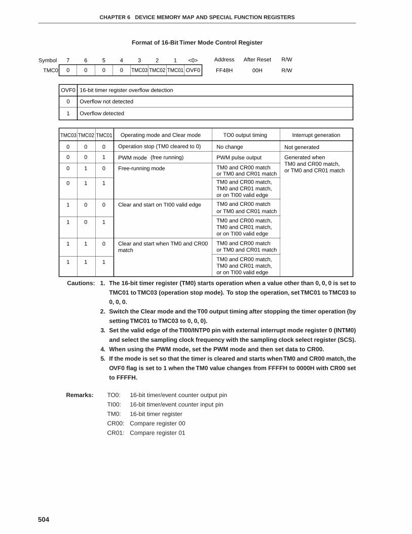
504
CHAPTER 6 DEVICE MEMORY MAP AND SPECIAL FUNCTION REGISTERS
Format of 16-Bit Timer Mode Control Register
Cautions: 1. The 16-bit timer register (TM0) starts operation when a value other than 0, 0, 0 is set to
TMC01 to TMC03 (operation stop mode). To stop the operation, set TMC01 to TMC03 to
0, 0, 0.
2. Switch the Clear mode and the T00 output timing after stopping the timer operation (by
setting TMC01 to TMC03 to 0, 0, 0).
3. Set the valid edge of the TI00/INTP0 pin with external interrupt mode register 0 (INTM0)
and select the sampling clock frequency with the sampling clock select register (SCS).
4. When using the PWM mode, set the PWM mode and then set data to CR00.
5. If the mode is set so that the timer is cleared and starts when TM0 and CR00 match, the
OVF0 flag is set to 1 when the TM0 value changes from FFFFH to 0000H with CR00 set
to FFFFH.
Remarks: TO0: 16-bit timer/event counter output pin
TI00: 16-bit timer/event counter input pin
TM0: 16-bit timer register
CR00: Compare register 00
CR01: Compare register 01
0 0 0 0 TMC03 TMC02 TMC01 OVF0
7 6 5 4 3 2 1 <0>Symbol
TMC0 FF48H 00H R/W
Address After Reset R/W
OVF0 16-bit timer register overflow detection
0 Overflow not detected
1 Overflow detected
TMC03 TMC02 TMC01 Operating mode and Clear mode TO0 output timing Interrupt generation
0 0 0 Operation stop (TM0 cleared to 0) No change Not generated
0 0 1 PWM mode (free running) PWM pulse output
0 1 0
0 1 1
1 0 0
1 0 1
1 1 0
1 1 1
Free-running mode TM0 and CR00 match or TM0 and CR01 match
TM0 and CR00 match, TM0 and CR01 match, or on TI00 valid edge
TM0 and CR00 match or TM0 and CR01 match
TM0 and CR00 match, TM0 and CR01 match,or on TI00 valid edge
TM0 and CR00 match or TM0 and CR01 match
TM0 and CR00 match, TM0 and CR01 match,or on TI00 valid edge
Clear and start on TI00 valid edge
Clear and start when TM0 and CR00 match
Generated when TM0 and CR00 match,or TM0 and CR01 match
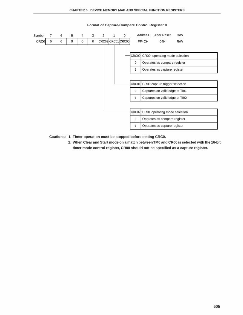
505
CHAPTER 6 DEVICE MEMORY MAP AND SPECIAL FUNCTION REGISTERS
Format of Capture/Compare Control Register 0
Cautions: 1. Timer operation must be stopped before setting CRC0.
2. When Clear and Start mode on a match between TM0 and CR00 is selected with the 16-bit
timer mode control register, CR00 should not be specified as a capture register.
0 0 0 0 0 CRC02 CRC01 CRC00
7 6 5 4 3 2 1 0Symbol
CRC0 FF4CH 04H R/W
Address After Reset R/W
CRC00 CR00 operating mode selection
0 Operates as compare register
1 Operates as capture register
CRC01 CR00 capture trigger selection
Captures on valid edge of TI01
Captures on valid edge of TI00
0
1
CRC02 CR01 operating mode selection
Operates as compare register
Operates as capture register
0
1
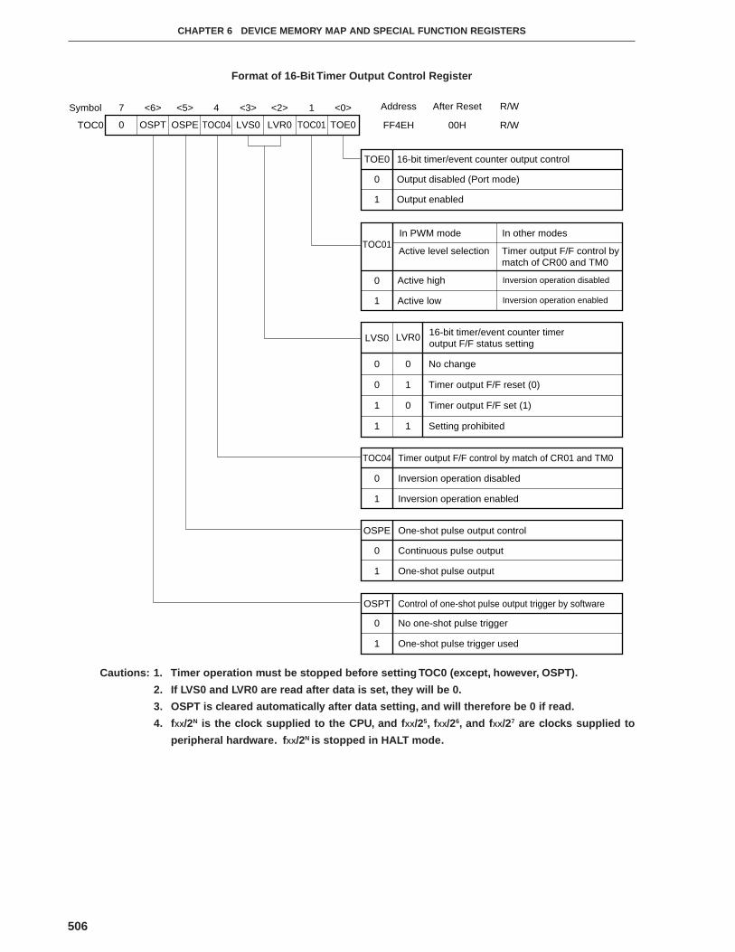
506
CHAPTER 6 DEVICE MEMORY MAP AND SPECIAL FUNCTION REGISTERS
Format of 16-Bit Timer Output Control Register
Cautions: 1. Timer operation must be stopped before setting TOC0 (except, however, OSPT).
2. If LVS0 and LVR0 are read after data is set, they will be 0.
3. OSPT is cleared automatically after data setting, and will therefore be 0 if read.
4. fXX/2N is the clock supplied to the CPU, and f XX/25, fXX/26, and f XX/27 are clocks supplied to
peripheral hardware. f XX/2N is stopped in HALT mode.
0 OSPT OSPE TOC04 LVS0 LVR0 TOC01 TOE0
7 <6> <5> 4 <3> <2> 1 <0>Symbol
TOC0 FF4EH 00H R/W
Address After Reset R/W
TOE0 16-bit timer/event counter output control
0 Output disabled (Port mode)
1 Output enabled
TOC01
0
1
In PWM mode In other modes
Active level selection Timer output F/F control by match of CR00 and TM0
Active high
Active low
Inversion operation disabled
Inversion operation enabled
LVS0 LVR0 16-bit timer/event counter timer output F/F status setting
0 0 No change
0 1 Timer output F/F reset (0)
1 0 Timer output F/F set (1)
1 1 Setting prohibited
TOC04 Timer output F/F control by match of CR01 and TM0
0 Inversion operation disabled
1 Inversion operation enabled
OSPE One-shot pulse output control
0 Continuous pulse output
1 One-shot pulse output
OSPT Control of one-shot pulse output trigger by software
0 No one-shot pulse trigger
1 One-shot pulse trigger used

507
CHAPTER 6 DEVICE MEMORY MAP AND SPECIAL FUNCTION REGISTERS
(4) Registers controlling 8-bit timer/event counters 1 and 2
The following four registers control 8-bit timer/event counters 1 and 2:
• Timer clock select register 1 (TCL1)
• 8-bit timer mode control register 1 (TMC1)
• 8-bit timer output control register (TOC1)
• Port mode register 3 (PM3)
- Refer to section (1) for the register format.

508
CHAPTER 6 DEVICE MEMORY MAP AND SPECIAL FUNCTION REGISTERS
Format of Timer Clock Select Register 1
Caution: To write data other than that already written to TCL1, stop the timer operation once.
Remarks: fXX: Main system clock frequency (fX or fX/2)
fX: Main system clock oscillation frequencyTI1: 8-bit timer register 1 input pinTI2: 8-bit timer register 2 input pin
MCS: Bit 0 of oscillation mode select register (OSMS)Values in parentheses apply to operation with fX = 5.0 MHz.
TCL13 TCL12 TCL11 TCL10
0 0 0 0 TI1 falling edge
0 0 0 1 TI1 rising edge
0 1 1 0
0 1 1 1
fXX/2 fX/2 (2.5 MHz) fX/22 (1.25 MHz)
1 0 0 0
fXX/22 fX/22 (1.25 MHz) fX/23 (625 kHz)
1 0 0 1
fXX/23 fX/23 (625 kHz) fX/24 (313 kHz)
1 0 1 0
fXX/24 fX/24 (313 kHz) fX/25 (156 kHz)
1 0 1 1
fXX/25 fX/25 (156 kHz) fX/26 (78.1 kHz)
1 1 0 0
fXX/26 fX/26 (78.1 kHz) fX/27 (39.1 kHz)
1 1 0 1
fXX/27 fX/27 (39.1 kHz) fX/28 (19.5 kHz)
1 1 1 0
fXX/28 fX/28 (19.5 kHz) fX/29 (9.8 kHz)
1 1 1 1
fXX/29 fX/29 (9.8 kHz) fX/210 (4.9 kHz)
MCS = 1
8-bit timer register 1 count clock selection
MCS = 0
fXX/211 fX/211 (2.4 kHz) fX/212 (1.2 kHz)
TCL17 TCL16 TCL15 TCL14 TCL13 TCL12 TCL11 TCL10
7 6 5 4 3 2 1 0Symbol
TCL1 FF41H 00H R/W
Address After Reset R/W
TCL17 TCL16 TCL15 TCL14
0 0 0 0 TI2 falling edge
0 0 0 1 TI2 rising edge
0 1 1 0
0 1 1 1
fXX/2 fX/2 (2.5 MHz) fX/22 (1.25 MHz)
1 0 0 0
fXX/22 fX/22 (1.25 MHz) fX/23 (625 kHz)
1 0 0 1
fXX/23 fX/23 (625 kHz) fX/24 (313 kHz)
1 0 1 0
fXX/24 fX/24 (313 kHz) fX/25 (156 kHz)
1 0 1 1
fXX/25 fX/25 (156 kHz) fX/26 (78.1 kHz)
1 1 0 0
fXX/26 fX/26 (78.1 kHz) fX/27 (39.1 kHz)
1 1 0 1
fXX/27 fX/27 (39.1 kHz) fX/28 (19.5 kHz)
1 1 1 0
fXX/28 fX/28 (19.5 kHz) fX/29 (9.8 kHz)
1 1 1 1
fXX/29 fX/29 (9.8 kHz) fX/210 (4.9 kHz)
MCS = 1
8-bit timer register 2 count clock selection
MCS = 0
fXX/211 fX/211 (2.4 kHz) fX/212 (1.2 kHz)
Settings other than above are prohibited
Settings other than above are prohibited
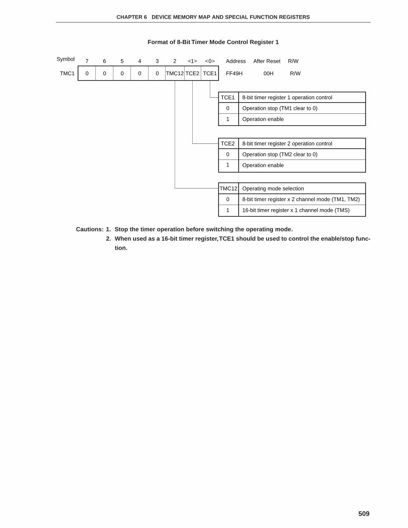
509
CHAPTER 6 DEVICE MEMORY MAP AND SPECIAL FUNCTION REGISTERS
Format of 8-Bit Timer Mode Control Register 1
Cautions: 1. Stop the timer operation before switching the operating mode.
2. When used as a 16-bit timer register, TCE1 should be used to control the enable/stop func-
tion.
TMC12
6 5 4 3 2 1 07Symbol
TMC1 0 0 0 0 0 TCE2 TCE1 FF49H 00H R/W
Address After Reset R/W
TCE1
0
1
8-bit timer register 1 operation control
Operation stop (TM1 clear to 0)
Operation enable
TCE2
0
1
8-bit timer register 2 operation control
Operation stop (TM2 clear to 0)
Operation enable
TMC12
0
1
Operating mode selection
8-bit timer register x 2 channel mode (TM1, TM2)
16-bit timer register x 1 channel mode (TMS)
FC6714
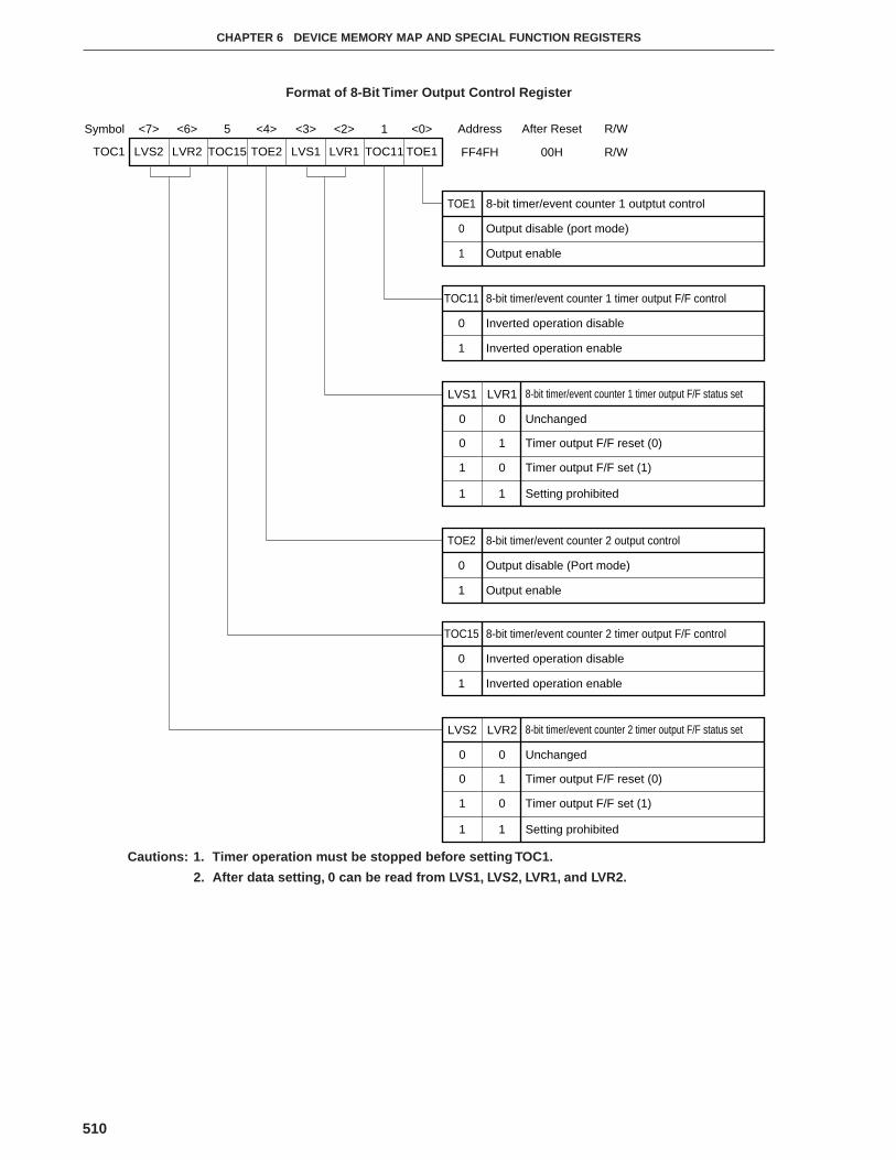
510
CHAPTER 6 DEVICE MEMORY MAP AND SPECIAL FUNCTION REGISTERS
Format of 8-Bit Timer Output Control Register
Cautions: 1. Timer operation must be stopped before setting TOC1.
2. After data setting, 0 can be read from LVS1, LVS2, LVR1, and LVR2.
<0>1<2><3><4>5<6><7>Symbol
TOE1TOC11LVR1LVS1TOE2TOC15LVR2LVS2TOC1 FF4FH 00H R/W
Address After Reset R/W
TOE1 8-bit timer/event counter 1 outptut control
0 Output disable (port mode)
1 Output enable
TOC11 8-bit timer/event counter 1 timer output F/F control
0 Inverted operation disable
1 Inverted operation enable
LVS1 LVR1 8-bit timer/event counter 1 timer output F/F status set
0 0 Unchanged
0 1 Timer output F/F reset (0)
1 0 Timer output F/F set (1)
1 1 Setting prohibited
TOE2 8-bit timer/event counter 2 output control
0 Output disable (Port mode)
1 Output enable
TOC15 8-bit timer/event counter 2 timer output F/F control
0 Inverted operation disable
1 Inverted operation enable
LVS2 LVR2 8-bit timer/event counter 2 timer output F/F status set
0 0 Unchanged
0 1 Timer output F/F reset (0)
1 0 Timer output F/F set (1)
1 1 Setting prohibited
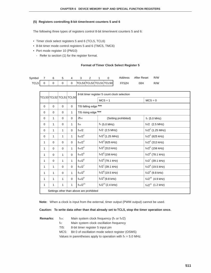
511
CHAPTER 6 DEVICE MEMORY MAP AND SPECIAL FUNCTION REGISTERS
(5) Registers controlling 8-bit timer/event counters 5 and 6
The following three types of registers control 8-bit timer/event counters 5 and 6:
• Timer clock select registers 5 and 6 (TCL5, TCL6)
• 8-bit timer mode control registers 5 and 6 (TMC5, TMC6)
• Port mode register 10 (PM10)
- Refer to section (1) for the register format.
Format of Timer Clock Select Register 5
Note: When a clock is input from the external, timer output (PWM output) cannot be used.
Caution: To write data other than that already set to TCL5, stop the timer operation once.
Remarks: fXX: Main system clock frequency (fX or fX/2)
fX: Main system clock oscillation frequencyTI5: 8-bit timer register 5 input pinMCS: Bit 0 of oscillation mode select register (OSMS)
Values in parentheses apply to operation with fX = 5.0 MHz.
0 0 0 0 TCL53 TCL52 TCL51 TCL50
7 6 5 4 3 2 1 0Symbol
TCL5
TCL53 TCL52 TCL51 TCL50
0 0 0 0 TI5 falling edge Note
0 0 0 1 TI5 rising edge Note
0 1 0 0
fXX fX
(Setting prohibited)
fX/2 (2.5 MHz)0 1 0 1
fXX/2 fX/2 (2.5 MHz) fX/22 (1.25 MHz)0 1 1 0
fXX/22 fX/22 (1.25 MHz) fX/23 (625 kHz)0 1 1 1
fXX/23 fX/23 (625 kHz) fX/24 (313 kHz)1 0 0 0
fXX/24 fX/24 (313 kHz) fX/25 (156 kHz)1 0 0 1
fXX/25 fX/25 (156 kHz) fX/26 (78.1 kHz)1 0 1 0
fXX/26 fX/26 (78.1 kHz) fX/27 (39.1 kHz)1 0 1 1
fXX/27 fX/27 (39.1 kHz) fX/28 (19.5 kHz)1 1 0 0
fXX/28 fX/28 (19.5 kHz) fX/29 (9.8 kHz)1 1 0 1
fXX/29 fX/29 (9.8 kHz) fX/210 (4.9 kHz)1 1 1 0
fX/2111 1 1 1 fXX/211 fX/211 (2.4 kHz) (1.2 kHz)
MCS = 1
8-bit timer register 5 count clock selection
MCS = 0
FF52H 00H R/W
Address After Reset R/W
2fXX
(5.0 MHz)
fX (5.0 MHz)
Settings other than above are prohibited
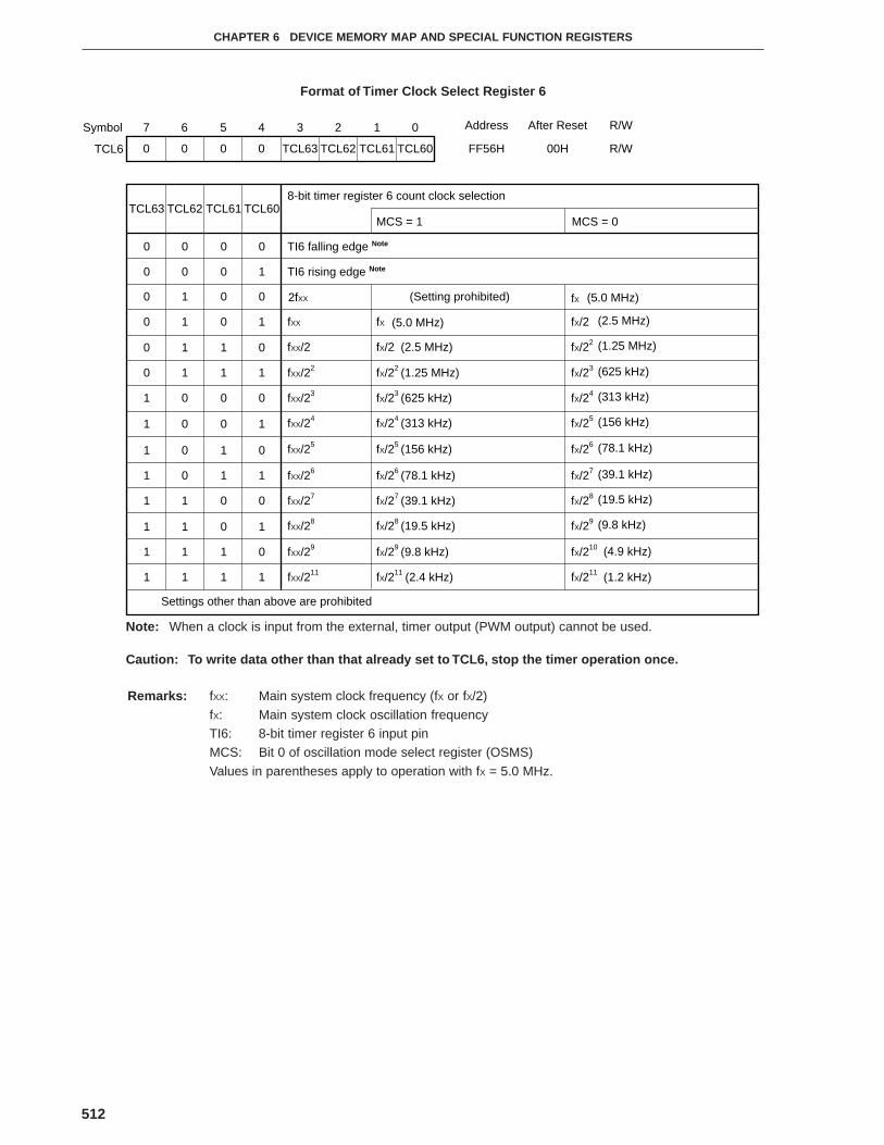
512
CHAPTER 6 DEVICE MEMORY MAP AND SPECIAL FUNCTION REGISTERS
Format of Timer Clock Select Register 6
Note: When a clock is input from the external, timer output (PWM output) cannot be used.
Caution: To write data other than that already set to TCL6, stop the timer operation once.
Remarks: fXX: Main system clock frequency (fX or fX/2)
fX: Main system clock oscillation frequencyTI6: 8-bit timer register 6 input pinMCS: Bit 0 of oscillation mode select register (OSMS)
Values in parentheses apply to operation with fX = 5.0 MHz.
0 0 0 0 TCL63 TCL62 TCL61 TCL60
7 6 5 4 3 2 1 0Symbol
TCL6
TCL63 TCL62 TCL61 TCL60
0 0 0 0 TI6 falling edge Note
0 0 0 1 TI6 rising edge Note
0 1 0 0
fXX fX
(Setting prohibited)
fX/2 (2.5 MHz)0 1 0 1
fXX/2 fX/2 (2.5 MHz) fX/22 (1.25 MHz)0 1 1 0
fXX/22 fX/22 (1.25 MHz) fX/23 (625 kHz)0 1 1 1
fXX/23 fX/23 (625 kHz) fX/24 (313 kHz)1 0 0 0
fXX/24 fX/24 (313 kHz) fX/25 (156 kHz)1 0 0 1
fXX/25 fX/25 (156 kHz) fX/26 (78.1 kHz)1 0 1 0
fXX/26 fX/26 (78.1 kHz) fX/27 (39.1 kHz)1 0 1 1
fXX/27 fX/27 (39.1 kHz) fX/28 (19.5 kHz)1 1 0 0
fXX/28 fX/28 (19.5 kHz) fX/29 (9.8 kHz)1 1 0 1
fXX/29 fX/29 (9.8 kHz) fX/210 (4.9 kHz)1 1 1 0
fX/2111 1 1 1 fXX/211 fX/211 (2.4 kHz) (1.2 kHz)
MCS = 1
8-bit timer register 6 count clock selection
MCS = 0
FF56H 00H R/W
Address After Reset R/W
2fXX
(5.0 MHz)
fX (5.0 MHz)
Settings other than above are prohibited
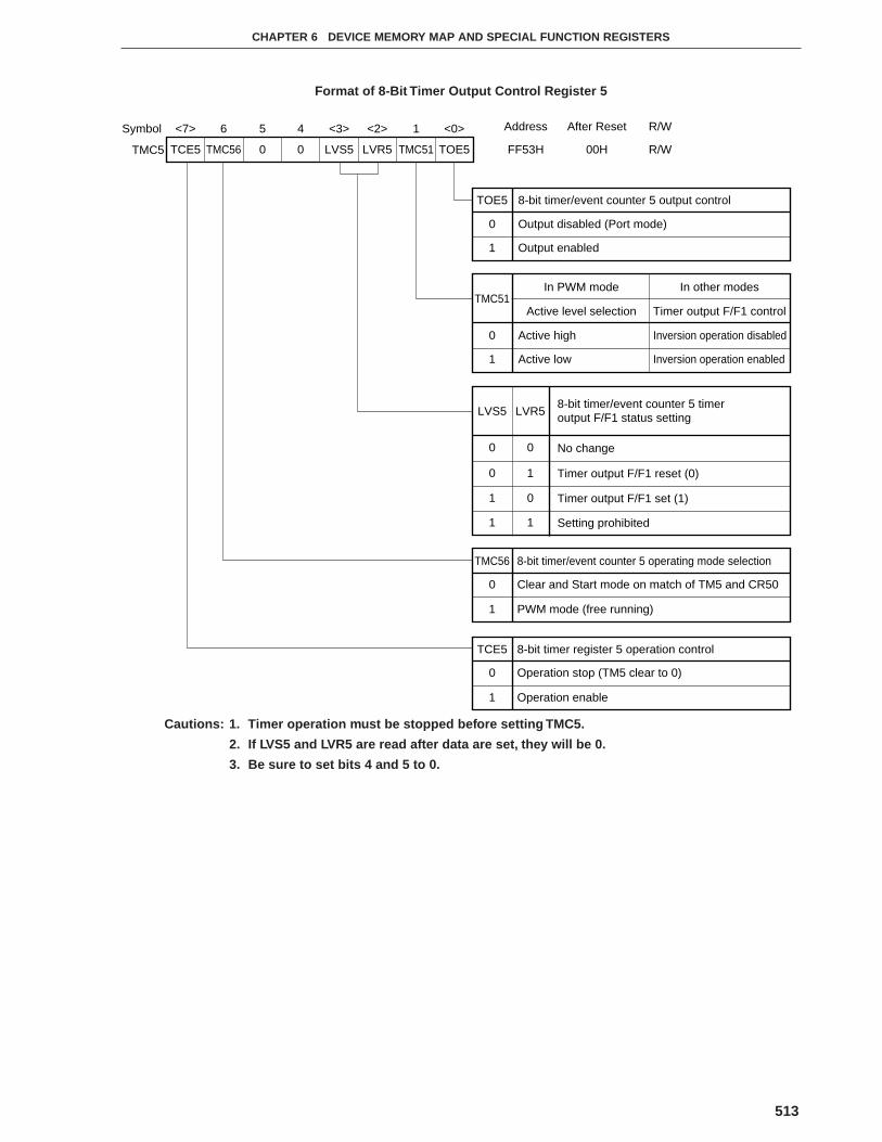
513
CHAPTER 6 DEVICE MEMORY MAP AND SPECIAL FUNCTION REGISTERS
Format of 8-Bit Timer Output Control Register 5
Cautions: 1. Timer operation must be stopped before setting TMC5.
2. If LVS5 and LVR5 are read after data are set, they will be 0.
3. Be sure to set bits 4 and 5 to 0.
TCE5 TMC56 0 0 LVS5 LVR5 TMC51 TOE5
<7> 6 5 4 <3> <2> 1 <0>Symbol
TMC5 FF53H 00H R/W
Address After Reset R/W
TOE5 8-bit timer/event counter 5 output control
0 Output disabled (Port mode)
1 Output enabled
TMC51
0 Active high
1 Active low
In PWM mode In other modes
Active level selection Timer output F/F1 control
Inversion operation disabled
Inversion operation enabled
LVS5 LVR5
0 0
0 1
1 0
1 1
8-bit timer/event counter 5 timer output F/F1 status setting
No change
Timer output F/F1 reset (0)
Timer output F/F1 set (1)
Setting prohibited
TMC56 8-bit timer/event counter 5 operating mode selection
0 Clear and Start mode on match of TM5 and CR50
1 PWM mode (free running)
TCE5 8-bit timer register 5 operation control
0 Operation stop (TM5 clear to 0)
1 Operation enable
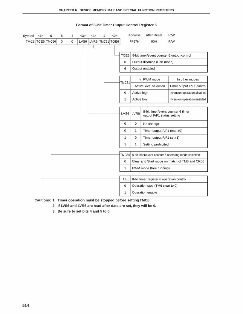
514
CHAPTER 6 DEVICE MEMORY MAP AND SPECIAL FUNCTION REGISTERS
Format of 8-Bit Timer Output Control Register 6
Cautions: 1. Timer operation must be stopped before setting TMC6.
2. If LVS6 and LVR6 are read after data are set, they will be 0.
3. Be sure to set bits 4 and 5 to 0.
TCE6 TMC66 0 0 LVS6 LVR6 TMC61 TOE6
<7> 6 5 4 <3> <2> 1 <0>Symbol
TMC6 FF57H 00H R/W
Address After Reset R/W
TOE6 8-bit timer/event counter 6 output control
0 Output disabled (Port mode)
6 Output enabled
TMC61
0 Active high
1 Active low
In PWM mode In other modes
Active level selection Timer output F/F1 control
Inversion operation disabled
Inversion operation enabled
LVS6 LVR6
0 0
0 1
1 0
1 1
8-bit timer/event counter 6 timer output F/F1 status setting
No change
Timer output F/F1 reset (0)
Timer output F/F1 set (1)
Setting prohibited
TMC66 8-bit timer/event counter 6 operating mode selection
0 Clear and Start mode on match of TM6 and CR60
1 PWM mode (free running)
TCE6 8-bit timer register 6 operation control
0 Operation stop (TM6 clear to 0)
1 Operation enable
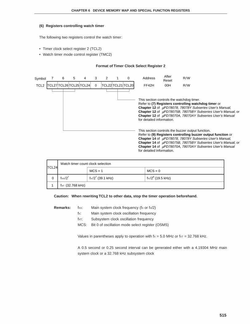
515
CHAPTER 6 DEVICE MEMORY MAP AND SPECIAL FUNCTION REGISTERS
(6) Registers controlling watch timer
The following two registers control the watch timer:
• Timer clock select register 2 (TCL2)
• Watch timer mode control register (TMC2)
Format of Timer Clock Select Register 2
Caution: When rewriting TCL2 to other data, stop the timer operation beforehand.
Remarks: fXX: Main system clock frequency (fX or fX/2)
fX: Main system clock oscillation frequency
fXT: Subsystem clock oscillation frequency
MCS: Bit 0 of oscillation mode select register (OSMS)
Values in parentheses apply to operation with fX = 5.0 MHz or fXT = 32.768 kHz.
A 0.5 second or 0.25 second interval can be generated either with a 4.19304 MHz main
system clock or a 32.768 kHz subsystem clock
TCL27
7
TCL26
6
TCL25 TCL24
4
0
3 2 1 0
FF42H
Address
TCL2
Symbol
TCL22 TCL21 TCL20
5
00H
After Reset
R/W
R/W
0
1
TCL24
fXX/27
fXT (32.768 kHz)
MCS = 1
fX /27 (39.1 kHz)
MCS = 0
fX /28 (19.5 kHz)
Watch timer count clock selection
This section controls the watchdog timer.Refer to (7) Registers controlling watchdog timer orChapter 12 of PD78078, 78078Y Subseries User's Manual,Chapter 12 of PD78075B, 78075BY Subseries User's Manual, orChapter 12 of PD78070A, 78070AY Subseries User's Manualfor detailed information.
µµµ
This section controls the buzzer output function.Refer to (9) Registers controlling buzzer output function orChapter 14 of PD78078, 78078Y Subseries User's Manual,Chapter 14 of PD78075B, 78075BY Subseries User's Manual, orChapter 14 of PD78070A, 78070AY Subseries User's Manualfor detailed information.
µµµ
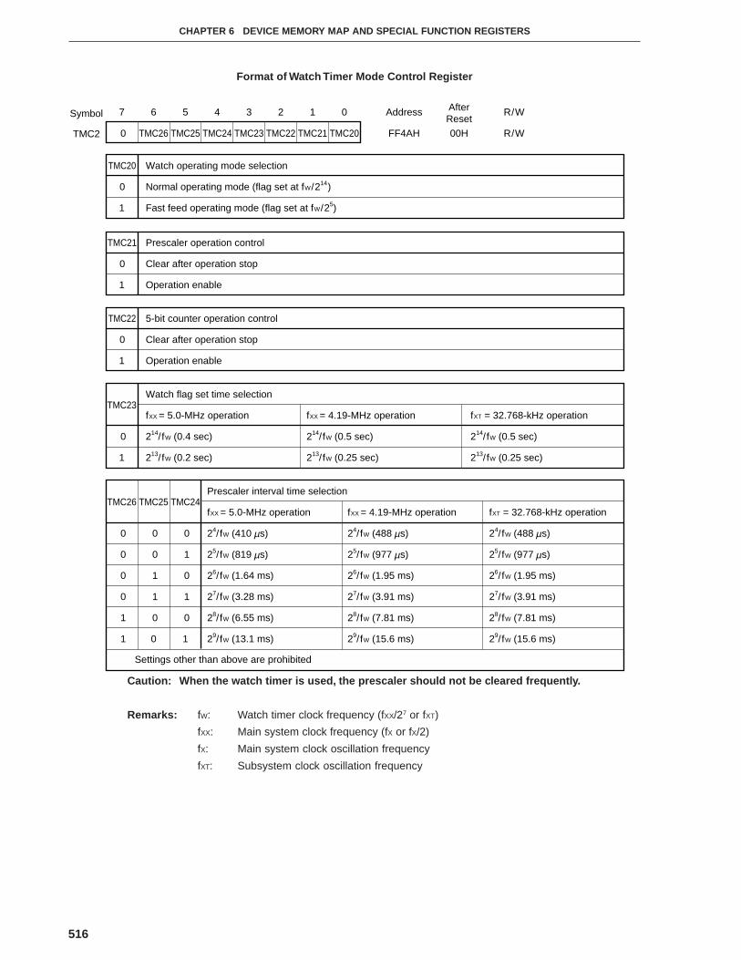
516
CHAPTER 6 DEVICE MEMORY MAP AND SPECIAL FUNCTION REGISTERS
Format of Watch Timer Mode Control Register
Caution: When the watch timer is used, the prescaler should not be cleared frequently.
Remarks: fW: Watch timer clock frequency (fXX/27 or fXT)
fXX: Main system clock frequency (fX or fX/2)
fX: Main system clock oscillation frequency
fXT: Subsystem clock oscillation frequency
0
7
TMC26
6
TMC25 TMC24
4
TMC23
3 2 1 0
FF4AH
Address
TMC2
Symbol
TMC22 TMC21 TMC20
5
00H
After Reset
R/W
R/W
0
1
TMC23fXX = 5.0-MHz operation
214/fW (0.4 sec)
213/fW (0.2 sec)
Watch flag set time selection
0
0
0
0
1
1
0
0
1
1
0
0
0
1
0
1
0
1
TMC26 TMC25 TMC24fXX = 5.0-MHz operation
24/fW (410 s)
25/fW (819 s)
26/fW (1.64 ms)
27/fW (3.28 ms)
28/fW (6.55 ms)
29/fW (13.1 ms)
fXX = 4.19-MHz operation
24/fW (488 s)
25/fW (977 s)
26/fW (1.95 ms)
27/fW (3.91 ms)
28/fW (7.81 ms)
29/fW (15.6 ms)
fXT = 32.768-kHz operation
24/fW (488 s)
25/fW (977 s)
26/fW (1.95 ms)
27/fW (3.91 ms)
28/fW (7.81 ms)
29/fW (15.6 ms)
Prescaler interval time selection
fXX = 4.19-MHz operation
214/fW (0.5 sec)
213/fW (0.25 sec)
fXT = 32.768-kHz operation
214/fW (0.5 sec)
213/fW (0.25 sec)
TMC22
0
1
5-bit counter operation control
Clear after operation stop
Operation enable
TMC21
0
1
Prescaler operation control
Clear after operation stop
Operation enable
TMC20
0
1
Watch operating mode selection
Normal operating mode (flag set at fW/214)
Fast feed operating mode (flag set at fW/25)
µ
µ
µ
µ
µ
µ
Settings other than above are prohibited
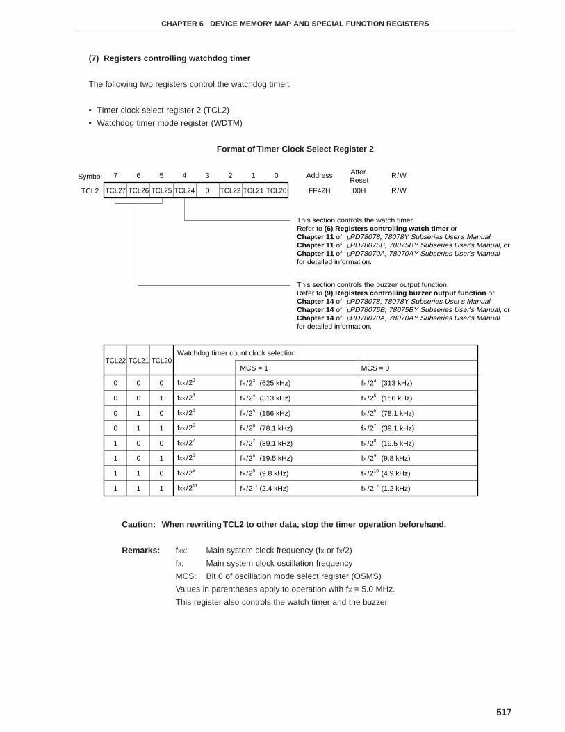
517
CHAPTER 6 DEVICE MEMORY MAP AND SPECIAL FUNCTION REGISTERS
(7) Registers controlling watchdog timer
The following two registers control the watchdog timer:
• Timer clock select register 2 (TCL2)
• Watchdog timer mode register (WDTM)
Format of Timer Clock Select Register 2
Caution: When rewriting TCL2 to other data, stop the timer operation beforehand.
Remarks: fXX: Main system clock frequency (fX or fX/2)
fX: Main system clock oscillation frequency
MCS: Bit 0 of oscillation mode select register (OSMS)
Values in parentheses apply to operation with fX = 5.0 MHz.
This register also controls the watch timer and the buzzer.
TCL27
7
TCL26
6
TCL25 TCL24
4
0
3 2 1 0
FF42H
Address
TCL2
Symbol
TCL22 TCL21 TCL20
5
00H
After Reset
R/W
R/W
0
0
0
0
1
1
1
1
0
0
1
1
0
0
1
1
0
1
0
1
0
1
0
1
TCL22 TCL21 TCL20MCS = 1
fX /23
fX /24
fX /25
fX /26
fX /27
fX /28
fX /29
fX /211
fXX /23
fXX /24
fXX /25
fXX /26
fXX /27
fXX /28
fXX /29
fXX /211
MCS = 0
fX /24
fX /25
fX /26
fX /27
fX /28
fX /29
fX /210
fX /212
Watchdog timer count clock selection
(625 kHz)
(313 kHz)
(156 kHz)
(78.1 kHz)
(39.1 kHz)
(19.5 kHz)
(9.8 kHz)
(2.4 kHz)
(313 kHz)
(156 kHz)
(78.1 kHz)
(39.1 kHz)
(19.5 kHz)
(9.8 kHz)
(4.9 kHz)
(1.2 kHz)
This section controls the watch timer.Refer to (6) Registers controlling watch timer orChapter 11 of PD78078, 78078Y Subseries User's Manual,Chapter 11 of PD78075B, 78075BY Subseries User's Manual, orChapter 11 of PD78070A, 78070AY Subseries User's Manualfor detailed information.
µµµ
This section controls the buzzer output function.Refer to (9) Registers controlling buzzer output function orChapter 14 of PD78078, 78078Y Subseries User's Manual,Chapter 14 of PD78075B, 78075BY Subseries User's Manual, orChapter 14 of PD78070A, 78070AY Subseries User's Manualfor detailed information.
µµµ

518
CHAPTER 6 DEVICE MEMORY MAP AND SPECIAL FUNCTION REGISTERS
Format of Watchdog Timer Mode Register
Notes: 1. Once set to 1, WDTM3 and WDTM4 cannot be cleared to 0 by software.
2. The watchdog timer starts operating as an interval timer as soon as RUN has been set to 1.
3. Once set to 1, RUN cannot be cleared to 0 by software. Thus, once counting starts, counting can
only be stopped by RESET input.
Cautions: 1. When 1 is set in RUN so that the watchdog timer is cleared, the actual overflow time is up to
0.5% shorter than the time set by timer clock select register 2 (TCL2).
2. To use watchdog timer modes 1 and 2, make sure that the interrupt request flag (TMIF4) is
0, and then set WDTM4 to 1.
If WDTM4 is set to 1 when TMIF4 is 1, the non-maskable interrupt request occurs, regard-
less of the contents of WDTM3.
Remark: ×: Don’t care
RUN
<7>
0
6
0 WDTM4
4
WDTM3
3 2 1 0
FFF9H
Address
WDTM
Symbol
0 0 0
5
00H
AfterReset
R/W
R/W
RUN
0
1
Watchdog timer operation mode selection Note 3
Count stop
Counter is cleared and counting starts
WDTM3
×
0
1
Watchdog timer operation modeselection Note 1
Interval timer mode Note 2
(Maskable interrupt request occurs upon generation of an overflow.)
Watchdog timer mode 1(Non-maskable interrupt request occursupon generation of an overflow.)
Watchdog timer mode 2(Reset operation is activated upongeneration of an overflow.)
WDTM4
0
1
1

519
CHAPTER 6 DEVICE MEMORY MAP AND SPECIAL FUNCTION REGISTERS
(8) Registers controlling clock output function
The following two registers control the clock output function:
• Timer clock select register 0 (TCL0)
• Port mode register 3 (PM3)
- Refer to section (1) for the register format.

520
CHAPTER 6 DEVICE MEMORY MAP AND SPECIAL FUNCTION REGISTERS
Format of Timer Clock Select Register 0
Cautions: 1. When enabling PCL output, set TCL00 to TCL03, then set 1 in CLOE with a 1-bit memory
manipulation instruction.
2. To write data other than that already written to TCL0, stop the clock operation once.
Remarks: fXX: Main system clock frequency (fX or fX/2)
fX: Main system clock oscillation frequency
fXT: Subsystem clock oscillation frequency
MCS: Bit 0 of oscillation mode select register (OSMS)
Values in parentheses apply to operation with fX = 5.0 MHz or fXT = 32.768 kHz.
CLOE
<7>
TCL06
6
TCL05 TCL04
4
TCL03
3 2 1 0
FF40H
Address
TCL0
Symbol
TCL02 TCL01 TCL00
5
00H
After Reset
R/W
R/W
CLOE
0
1
PCL output control
Output disable
Output enable
0
0
0
0
1
1
1
1
1
0
1
1
1
0
0
0
0
1
0
0
1
1
0
0
1
1
0
TCL03 TCL02 TCL01
fXT (32.768 kHz)
fXX
fXX/2
fXX/22
fXX/23
fXX/24
fXX/25
fXX/26
fXX/27
MCS = 1
fX (5.0 MHz)
fX /2 (2.5 MHz)
fX /22 (1.25 MHz)
fX /23 (625 kHz)
fX /24 (313 kHz)
fX /25 (156 kHz)
fX /26 (78.1 kHz)
fX /27 (39.1 kHz)
MCS = 0
fX /2 (2.5 MHz)
fX /22 (1.25 MHz)
fX /23 (625 kHz)
fX /24 (313 kHz)
fX /25 (156 kHz)
fX /26 (78.1 kHz)
fX /27 (39.1 kHz)
fX /28 (19.5 kHz)
PCL output clock selectionTCL00
0
1
0
1
0
1
0
1
0
This section controls the 16-bit timer.Refer to (3) Registers controlling 16-bit timer/event counter orChapter 8 of PD78078, 78078Y Subseries User's Manual,Chapter 8 of PD78075B, 78075BY Subseries User's Manual, orChapter 8 of PD78070A, 78070AY Subseries User's Manualfor detailed information.
µµµ
Settings other than above are prohibited
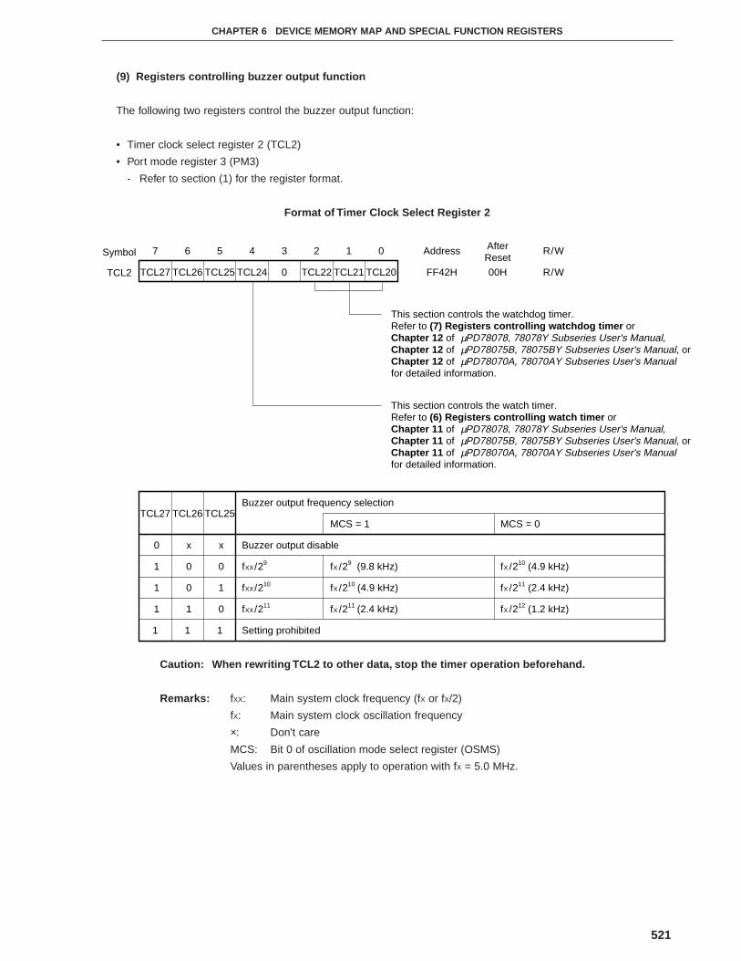
521
CHAPTER 6 DEVICE MEMORY MAP AND SPECIAL FUNCTION REGISTERS
(9) Registers controlling buzzer output function
The following two registers control the buzzer output function:
• Timer clock select register 2 (TCL2)
• Port mode register 3 (PM3)
- Refer to section (1) for the register format.
Format of Timer Clock Select Register 2
Caution: When rewriting TCL2 to other data, stop the timer operation beforehand.
Remarks: fXX: Main system clock frequency (fX or fX/2)
fX: Main system clock oscillation frequency
×: Don't care
MCS: Bit 0 of oscillation mode select register (OSMS)
Values in parentheses apply to operation with fX = 5.0 MHz.
TCL27
7
TCL26
6
TCL25 TCL24
4
0
3 2 1 0
FF42H
Address
TCL2
Symbol
TCL22 TCL21 TCL20
5
00H
After Reset
R/W
R/W
0
1
1
1
1
x
0
0
1
1
x
0
1
0
1
TCL27 TCL26 TCL25
Buzzer output disable
fXX/29
fXX/210
fXX/211
Setting prohibited
MCS = 1
fX /29 (9.8 kHz)
fX /210 (4.9 kHz)
fX /211 (2.4 kHz)
MCS = 0
fX /210 (4.9 kHz)
fX /211 (2.4 kHz)
fX /212 (1.2 kHz)
Buzzer output frequency selection
This section controls the watchdog timer.Refer to (7) Registers controlling watchdog timer orChapter 12 of PD78078, 78078Y Subseries User's Manual,Chapter 12 of PD78075B, 78075BY Subseries User's Manual, orChapter 12 of PD78070A, 78070AY Subseries User's Manualfor detailed information.
µµµ
This section controls the watch timer.Refer to (6) Registers controlling watch timer orChapter 11 of PD78078, 78078Y Subseries User's Manual,Chapter 11 of PD78075B, 78075BY Subseries User's Manual, orChapter 11 of PD78070A, 78070AY Subseries User's Manualfor detailed information.
µµµ
522
CHAPTER 6 DEVICE MEMORY MAP AND SPECIAL FUNCTION REGISTERS
(10) Registers controlling A/D converter
The following three registers control the A/D converter:
• A/D converter mode register (ADM)
• A/D converter input select register (ADIS)
• External interrupt mode register 1 (INTM1)
- Refer to section (17) for the register format.
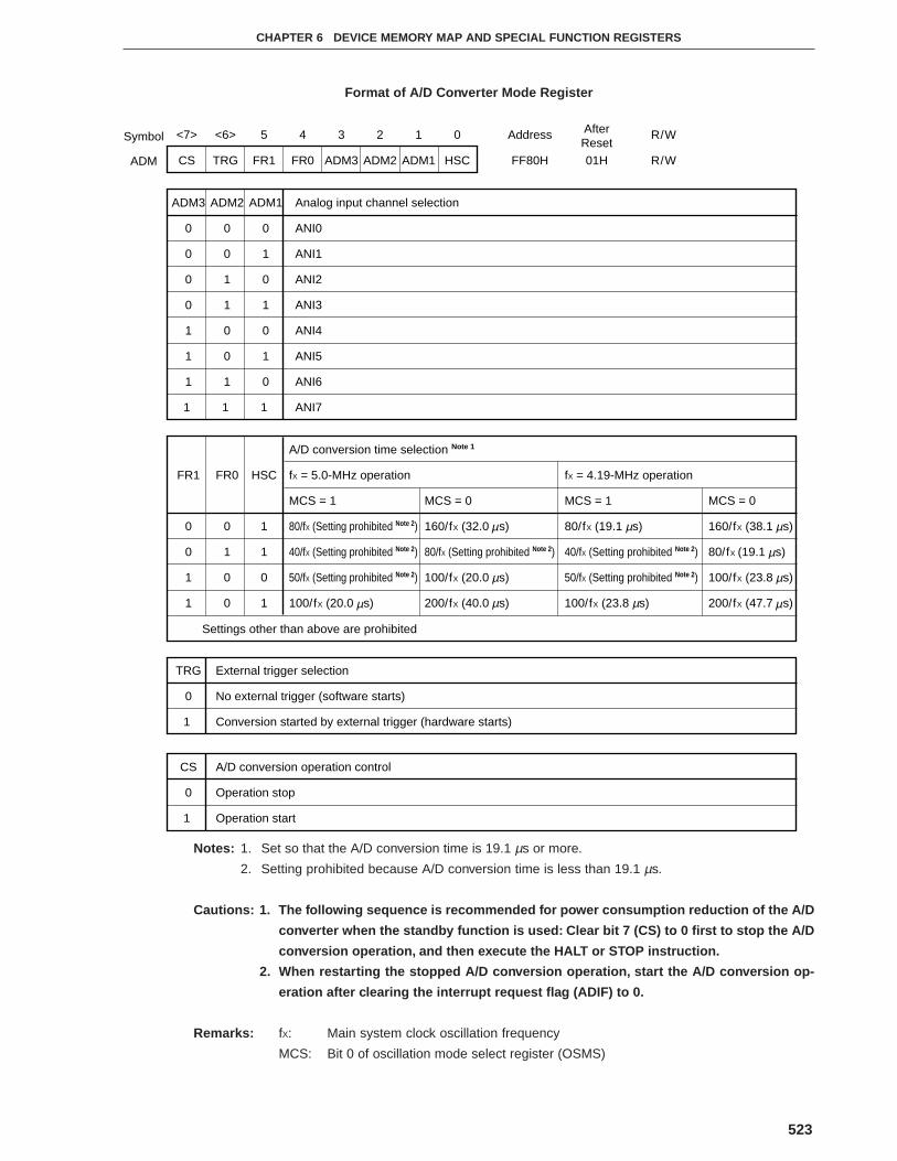
523
CHAPTER 6 DEVICE MEMORY MAP AND SPECIAL FUNCTION REGISTERS
Format of A/D Converter Mode Register
Notes: 1. Set so that the A/D conversion time is 19.1 µs or more.
2. Setting prohibited because A/D conversion time is less than 19.1 µs.
Cautions: 1. The following sequence is recommended for power consumption reduction of the A/D
converter when the standby function is used: Clear bit 7 (CS) to 0 first to stop the A/D
conversion operation, and then execute the HALT or STOP instruction.
2. When restarting the stopped A/D conversion operation, start the A/D conversion op-
eration after clearing the interrupt request flag (ADIF) to 0.
Remarks: fX: Main system clock oscillation frequency
MCS: Bit 0 of oscillation mode select register (OSMS)
CS
<7>
TRG
<6>
FR1 FR0
4
ADM3
3 2 1 0
FF80H
Address
ADM
Symbol
ADM2 ADM1 HSC
5
01H
After Reset
R/W
R/W
ADM3
0
0
0
0
1
1
1
1
ADM2
0
0
1
1
0
0
1
1
ADM1
0
1
0
1
0
1
0
1
Analog input channel selection
ANI0
ANI1
ANI2
ANI3
ANI4
ANI5
ANI6
ANI7
TRG
0
1
External trigger selection
No external trigger (software starts)
Conversion started by external trigger (hardware starts)
FR1
0
0
1
1
FR0
0
1
0
0
A/D conversion time selection Note 1
fX = 5.0-MHz operation
MCS = 1
80/fX (Setting prohibited Note 2)
40/fX (Setting prohibited Note 2)
50/fX (Setting prohibited Note 2)
100/fX (20.0 s)
MCS = 0
160/fX (32.0 s)
80/fX (Setting prohibited Note 2)
100/fX (20.0 s)
200/fX (40.0 s)
fX = 4.19-MHz operation
MCS = 1
80/fX (19.1 s)
40/fX (Setting prohibited Note 2)
50/fX (Setting prohibited Note 2)
100/fX (23.8 s)
MCS = 0
160/fX (38.1 s)
80/fX (19.1 s)
100/fX (23.8 s)
200/fX (47.7 s)
CS
0
1
A/D conversion operation control
Operation stop
Operation start
HSC
1
1
0
1
µ
µ
µ
µ
µ
µ µ
µ
µ
µ
Settings other than above are prohibited
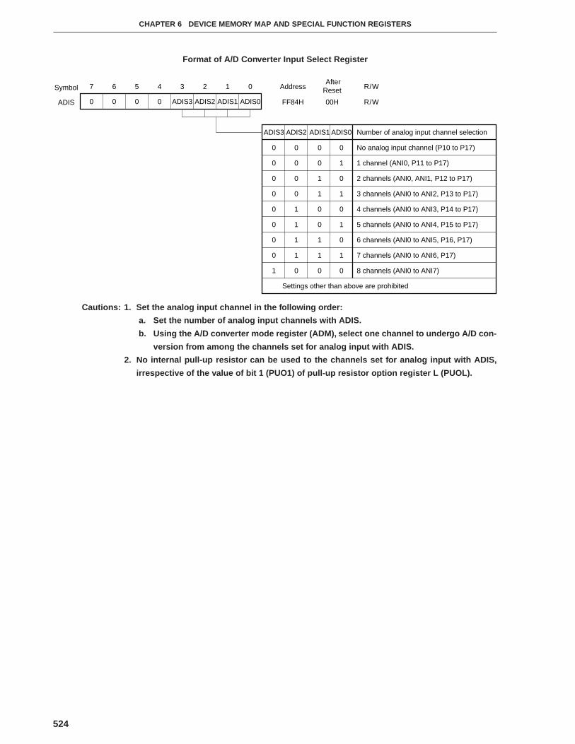
524
CHAPTER 6 DEVICE MEMORY MAP AND SPECIAL FUNCTION REGISTERS
Format of A/D Converter Input Select Register
Cautions: 1. Set the analog input channel in the following order:
a. Set the number of analog input channels with ADIS.
b. Using the A/D converter mode register (ADM), select one channel to undergo A/D con-
version from among the channels set for analog input with ADIS.
2. No internal pull-up resistor can be used to the channels set for analog input with ADIS,
irrespective of the value of bit 1 (PUO1) of pull-up resistor option register L (PUOL).
0
7
0
6
0 0
4
ADIS3
3 2 1 0
FF84H
Address
ADIS
Symbol
ADIS2 ADIS1 ADIS0
5
00H
AfterReset
R/W
R/W
ADIS3
0
0
0
0
0
0
0
0
1
Number of analog input channel selection
No analog input channel (P10 to P17)
1 channel (ANI0, P11 to P17)
2 channels (ANI0, ANI1, P12 to P17)
3 channels (ANI0 to ANI2, P13 to P17)
4 channels (ANI0 to ANI3, P14 to P17)
5 channels (ANI0 to ANI4, P15 to P17)
6 channels (ANI0 to ANI5, P16, P17)
7 channels (ANI0 to ANI6, P17)
8 channels (ANI0 to ANI7)
ADIS2
0
0
0
0
1
1
1
1
0
ADIS1
0
0
1
1
0
0
1
1
0
ADIS0
0
1
0
1
0
1
0
1
0
Settings other than above are prohibited
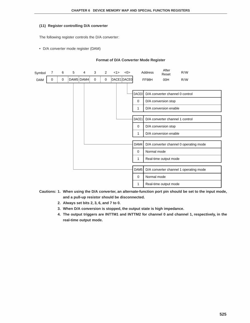
525
CHAPTER 6 DEVICE MEMORY MAP AND SPECIAL FUNCTION REGISTERS
(11) Register controlling D/A converter
The following register controls the D/A converter:
• D/A converter mode register (DAM)
Format of D/A Converter Mode Register
Cautions: 1. When using the D/A converter, an alternate-function port pin should be set to the input mode,
and a pull-up resistor should be disconnected.
2. Always set bits 2, 3, 6, and 7 to 0.
3. When D/A conversion is stopped, the output state is high impedance.
4. The output triggers are INTTM1 and INTTM2 for channel 0 and channel 1, respectively, in the
real-time output mode.
0
7
0
6
DAM5 DAM4
4
0
3 2 <1> <0>
FF98H
Address
DAM
Symbol
0 DACE1 DACE0
5
00H
AfterReset
R/W
R/W
DAM5
0
1
D/A converter channel 1 operating mode
Normal mode
Real-time output mode
DACE0
0
1
D/A converter channel 0 control
D/A conversion stop
D/A conversion enable
DACE1
0
1
D/A converter channel 1 control
D/A conversion stop
D/A conversion enable
DAM4
0
1
D/A converter channel 0 operating mode
Normal mode
Real-time output mode
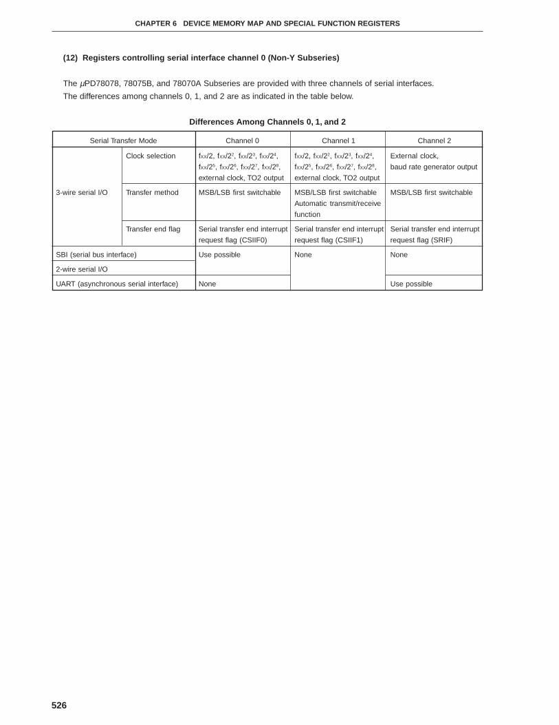
526
CHAPTER 6 DEVICE MEMORY MAP AND SPECIAL FUNCTION REGISTERS
(12) Registers controlling serial interface channel 0 (Non-Y Subseries)
The µPD78078, 78075B, and 78070A Subseries are provided with three channels of serial interfaces.
The differences among channels 0, 1, and 2 are as indicated in the table below.
Differences Among Channels 0, 1, and 2
Serial Transfer Mode Channel 0 Channel 1 Channel 2
Clock selection fXX/2, fXX/22, fXX/23, fXX/24, fXX/2, fXX/22, fXX/23, fXX/24, External clock,
fXX/25, fXX/26, fXX/27, fXX/28, fXX/25, fXX/26, fXX/27, fXX/28, baud rate generator output
external clock, TO2 output external clock, TO2 output
3-wire serial I/O Transfer method MSB/LSB first switchable MSB/LSB first switchable MSB/LSB first switchable
Automatic transmit/receive
function
Transfer end flag Serial transfer end interrupt Serial transfer end interrupt Serial transfer end interrupt
request flag (CSIIF0) request flag (CSIIF1) request flag (SRIF)
SBI (serial bus interface) Use possible None None
2-wire serial I/O
UART (asynchronous serial interface) None Use possible
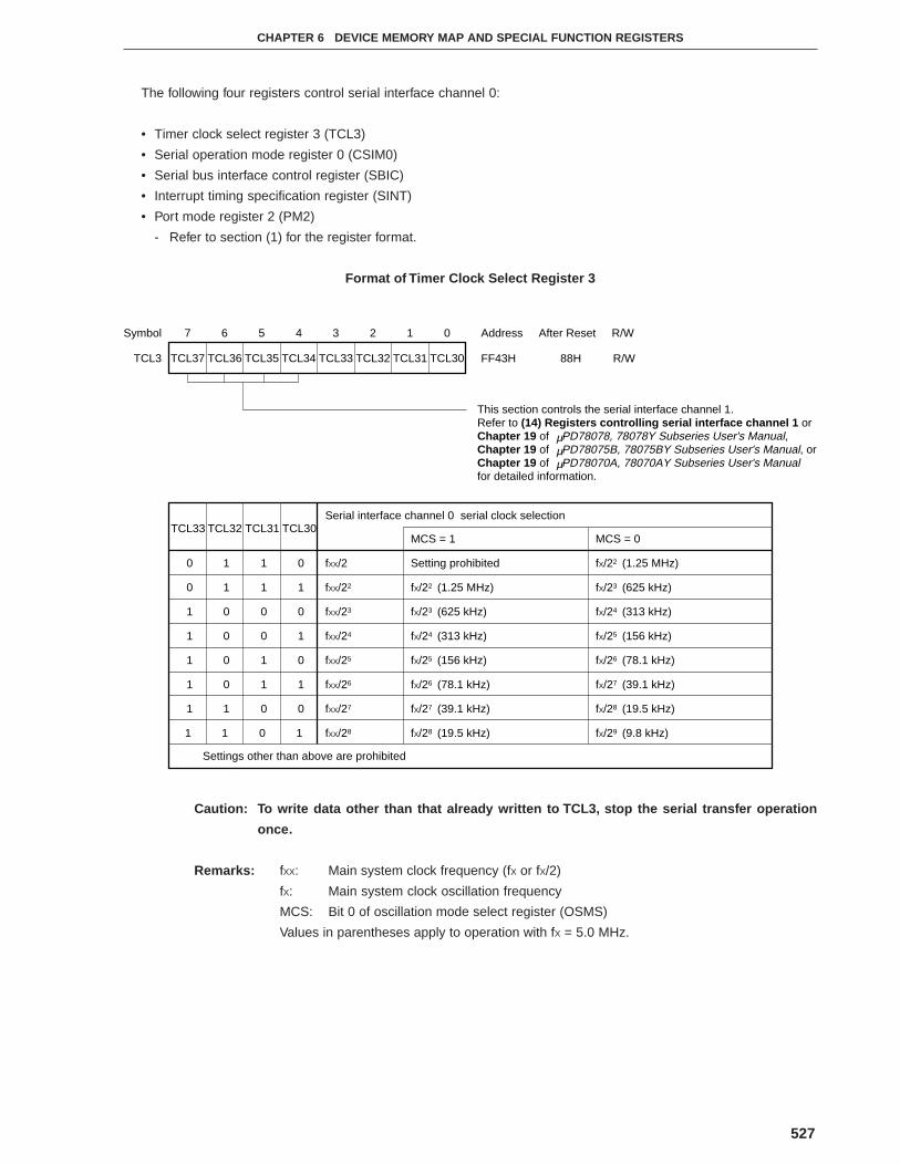
527
CHAPTER 6 DEVICE MEMORY MAP AND SPECIAL FUNCTION REGISTERS
The following four registers control serial interface channel 0:
• Timer clock select register 3 (TCL3)
• Serial operation mode register 0 (CSIM0)
• Serial bus interface control register (SBIC)
• Interrupt timing specification register (SINT)
• Port mode register 2 (PM2)
- Refer to section (1) for the register format.
Format of Timer Clock Select Register 3
Caution: To write data other than that already written to TCL3, stop the serial transfer operation
once.
Remarks: fXX: Main system clock frequency (fX or fX/2)
fX: Main system clock oscillation frequency
MCS: Bit 0 of oscillation mode select register (OSMS)
Values in parentheses apply to operation with fX = 5.0 MHz.
Serial interface channel 0 serial clock selectionTCL33 TCL32 TCL31 TCL30
0
0
1
1
1
1
1
1
1
1
0
0
0
0
1
1
1
1
0
0
1
1
0
0
0
1
0
1
0
1
0
1
fXX/2
fXX/22
fXX/23
fXX/24
fXX/25
fXX/26
fXX/27
fXX/28
MCS = 1
Setting prohibited
fX/22 (1.25 MHz)
fX/23 (625 kHz)
fX/24 (313 kHz)
fX/25 (156 kHz)
fX/26 (78.1 kHz)
fX/27 (39.1 kHz)
fX/28 (19.5 kHz)
MCS = 0
fX/22 (1.25 MHz)
fX/23 (625 kHz)
fX/24 (313 kHz)
fX/25 (156 kHz)
fX/26 (78.1 kHz)
fX/27 (39.1 kHz)
fX/28 (19.5 kHz)
fX/29 (9.8 kHz)
6 5 4 3 2 1 07Symbol
TCL3 TCL37 TCL36 TCL35 TCL34 TCL33 TCL32 TCL31 TCL30 FF43H 88H R/W
Address After Reset R/W
µµµ
This section controls the serial interface channel 1.Refer to (14) Registers controlling serial interface channel 1 orChapter 19 of PD78078, 78078Y Subseries User's Manual,Chapter 19 of PD78075B, 78075BY Subseries User's Manual, orChapter 19 of PD78070A, 78070AY Subseries User's Manualfor detailed information.
Settings other than above are prohibited
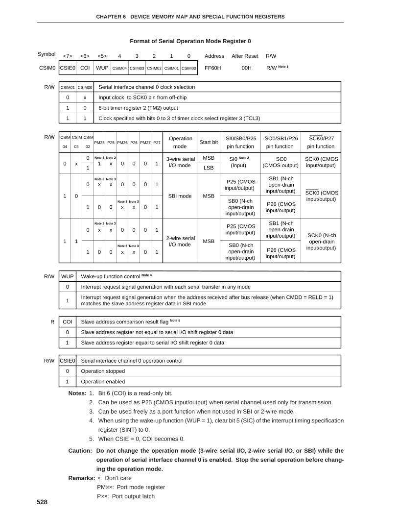
528
CHAPTER 6 DEVICE MEMORY MAP AND SPECIAL FUNCTION REGISTERS
Format of Serial Operation Mode Register 0
Notes: 1. Bit 6 (COI) is a read-only bit.
2. Can be used as P25 (CMOS input/output) when serial channel used only for transmission.
3. Can be used freely as a port function when not used in SBI or 2-wire mode.
4. When using the wake-up function (WUP = 1), clear bit 5 (SIC) of the interrupt timing specification
register (SINT) to 0.
5. When CSIE = 0, COI becomes 0.
Caution: Do not change the operation mode (3-wire serial I/O, 2-wire serial I/O, or SBI) while the
operation of serial interface channel 0 is enabled. Stop the serial operation before chang-
ing the operation mode.
Remarks: ×: Don’t care
PM××: Port mode register
P××: Port output latch
SBI mode
<6> <5> 4 3 2 1 0<7>Symbol
CSIM0 CSIE0 COI WUP CSIM04 CSIM03 CSIM02 CSIM01 CSIM00
CSIM01
0
1
Serial interface channel 0 clock selection
Input clock to SCK0 pin from off-chip
8-bit timer register 2 (TM2) output
0
0
SCK0 (CMOSinput/output)
R/W
1 Clock specified with bits 0 to 3 of timer clock select register 3 (TCL3)
CSIM
04
0
1
CSIM00
x
0
1
FF60H 00H R/W Note 1
Address After Reset R/W
R/W CSIM
03
CSIM
02PM25 P25 PM26 P26 PM27 P27
Operation
modeStart bit
SI0/SB0/P25
pin function
SO0/SB1/P26
pin function
SCK0/P27
pin function
x
1 0
x
0
x
0
0
x
0
x
0
0
1
1
Note 3 Note 3
Note 3 Note 3
MSB
P25 (CMOSinput/output)
SB0 (N-ch open-drain
input/output)
SB1 (N-chopen-drain
input/output)
P26 (CMOSinput/output)
1
MSB
LSB1 x 0 0 0 1
Note 2 3-wire seriall/O mode
SI0 Note 2
(Input)SO0
(CMOS output)SCK0 (CMOSinput/output)
2-wire seriall/O mode
0SCK0 (N-chopen-drain
input/output)1
1 1
x
0
x
0
0
x
0
x
0
0
1
1
Note 3 Note 3
Note 3 Note 3MSB
P25 (CMOSinput/output)
SB0 (N-chopen-drain
input/output)
SB1 (N-chopen-drain
input/output)
P26 (CMOSinput/output)
Note 2
WUP
0
1
Wake-up function control Note 4
Interrupt request signal generation with each serial transfer in any mode
Interrupt request signal generation when the address received after bus release (when CMDD = RELD = 1) matches the slave address register data in SBI mode
R/W
COI
0
1
Slave address comparison result flag Note 5
Slave address register not equal to serial I/O shift register 0 data
Slave address register equal to serial I/O shift register 0 data
R
CSIE0
0
1
Serial interface channel 0 operation control
Operation stopped
Operation enabled
R/W

529
CHAPTER 6 DEVICE MEMORY MAP AND SPECIAL FUNCTION REGISTERS
Format of Serial Bus Interface Control Register (1/2)
Note: Bits 2, 3, and 6 (RELD, CMDD, and ACKD) are read-only bits.
Remarks: Bits 0, 1, and 4 (RELT, CMDT, and ACKT) are 0 when read after data setting.
CSIE0: Bit 7 of serial operation mode register 0 (CSIM0)
<6> <5> <4> <3> <2> <1> <0><7>Symbol
SBIC BSYE ACKD ACKE ACKT CMDD RELD CMDT RELT
RELTUsed for bus release signal output. When RELT = 1, SO0 Iatch is set to 1. After SO0 latch setting, automatically cleared to 0.Also cleared to 0 when CSIE0 = 0.
R/W
FF61H 00H R/W Note
Address After Reset R/W
CMDTUsed for command signal output. When CMDT = 1, SO0 Iatch is cleared to 0. After SO0 latch clearance, automatically cleared to 0.Also cleared to 0 when CSIE0 = 0.
R/W
R RELD Bus release detection
Set Condition (RELD =1)Clear Conditions (RELD = 0)
• When bus release signal (REL) is detected
• When transfer start instruction is executed • If SIO0 and SVA values do not match in address reception • When CSIE0 = 0
• When RESET input is applied
R CMDD Command detection
Clear Conditions (CMDD = 0)
• When transfer start instruction is executed • When bus release signal (REL) is detected • When CSIE0 = 0
• When RESET input is applied
Set Condition (CMDD = 1)
• When command signal (CMD) is detected
ACKTAcknowledge signal is output in synchronization with the falling edge clock of SCK0 just after executionof the instruction to be set to 1, and, after acknowledge signal output, automatically cleared to 0. Used as ACKE = 0. Also cleared to 0 upon start of serial interface transfer or when CSIE0 = 0.
R/W
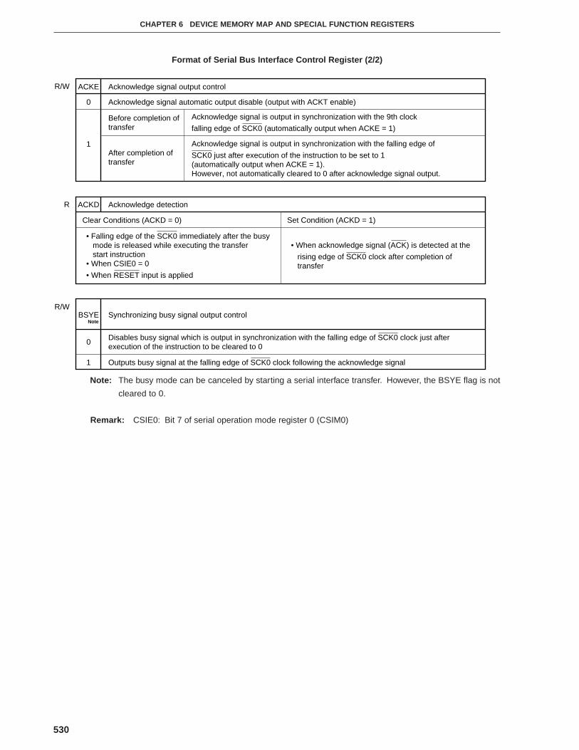
530
CHAPTER 6 DEVICE MEMORY MAP AND SPECIAL FUNCTION REGISTERS
Format of Serial Bus Interface Control Register (2/2)
Note: The busy mode can be canceled by starting a serial interface transfer. However, the BSYE flag is not
cleared to 0.
Remark: CSIE0: Bit 7 of serial operation mode register 0 (CSIM0)
ACKE Acknowledge signal output control
0 Acknowledge signal automatic output disable (output with ACKT enable)
Acknowledge signal is output in synchronization with the 9th clock
falling edge of SCK0 (automatically output when ACKE = 1)Before completion of transfer
Acknowledge signal is output in synchronization with the falling edge of
SCK0 just after execution of the instruction to be set to 1 (automatically output when ACKE = 1). However, not automatically cleared to 0 after acknowledge signal output.
After completion of transfer
1
R/W
R ACKD Acknowledge detection
Clear Conditions (ACKD = 0)
• Falling edge of the SCK0 immediately after the busy mode is released while executing the transfer start instruction • When CSIE0 = 0
• When RESET input is applied
Set Condition (ACKD = 1)
• When acknowledge signal (ACK) is detected at the
rising edge of SCK0 clock after completion of transfer
BSYE Synchronizing busy signal output control
0Disables busy signal which is output in synchronization with the falling edge of SCK0 clock just after execution of the instruction to be cleared to 0
R/W
Note
1 Outputs busy signal at the falling edge of SCK0 clock following the acknowledge signal
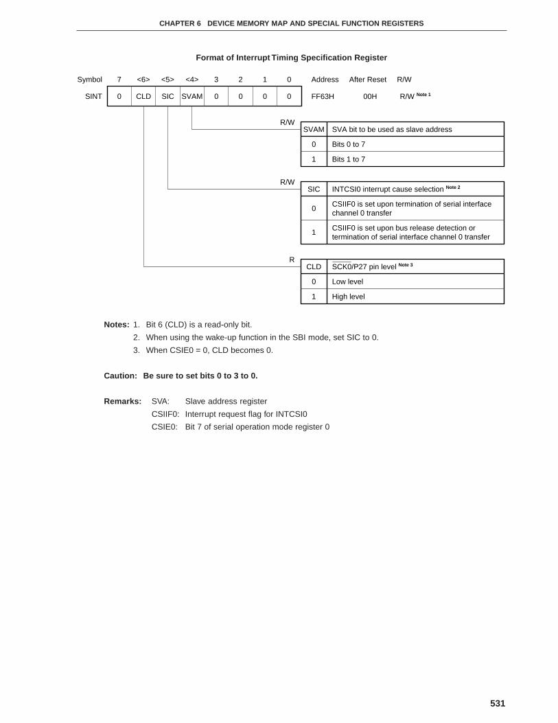
531
CHAPTER 6 DEVICE MEMORY MAP AND SPECIAL FUNCTION REGISTERS
Format of Interrupt Timing Specification Register
Notes: 1. Bit 6 (CLD) is a read-only bit.
2. When using the wake-up function in the SBI mode, set SIC to 0.
3. When CSIE0 = 0, CLD becomes 0.
Caution: Be sure to set bits 0 to 3 to 0.
Remarks: SVA: Slave address register
CSIIF0: Interrupt request flag for INTCSI0
CSIE0: Bit 7 of serial operation mode register 0
<6> <5> <4> 3 2 1 07Symbol
SINT 0 CLD SIC SVAM 0 0 0 0 FF63H 00H R/W Note 1
Address After Reset R/W
SVAM
0
1
SVA bit to be used as slave address
Bits 0 to 7
Bits 1 to 7
SIC
0
INTCSI0 interrupt cause selection Note 2
CSIIF0 is set upon termination of serial interfacechannel 0 transfer
CSIIF0 is set upon bus release detection ortermination of serial interface channel 0 transfer
CLD
0
1
SCK0/P27 pin level Note 3
Low level
High level
R/W
R/W
R
1

532
CHAPTER 6 DEVICE MEMORY MAP AND SPECIAL FUNCTION REGISTERS
(13) Registers controlling serial interface channel 0 (Y Subseries)
The µPD78078Y, 78075BY, and 78070AY Subseries are provided with three channels of serial interfaces.
The differences among channels 0, 1, and 2 are as indicated in the table below.
Differences Among Channels 0, 1, and 2
Serial Transfer Mode Channel 0 Channel 1 Channel 2
3-wire serial I/O Clock selection fXX/2, fXX/22, fXX/23, fXX/24, fXX/2, fXX/22, fXX/23, fXX/24, External clock,
fXX/25, fXX/26, fXX/27, fXX/28, fXX/25, fXX/26, fXX/27, fXX/28, baud rate generator output
external clock, TO2 output external clock, TO2 output
Transfer method MSB/LSB first switchable MSB/LSB first switchable MSB/LSB first switchable
Automatic transmit/receive
function
Transfer end flag Serial transfer end interrupt Serial transfer end interrupt Serial transfer end interrupt
request flag (CSIIF0) request flag (CSIIF1) request flag (SRIF)
I2C bus (inter-IC bus) Use possible None None
2-wire serial I/O
UART (asynchronous serial interface) None Use possible
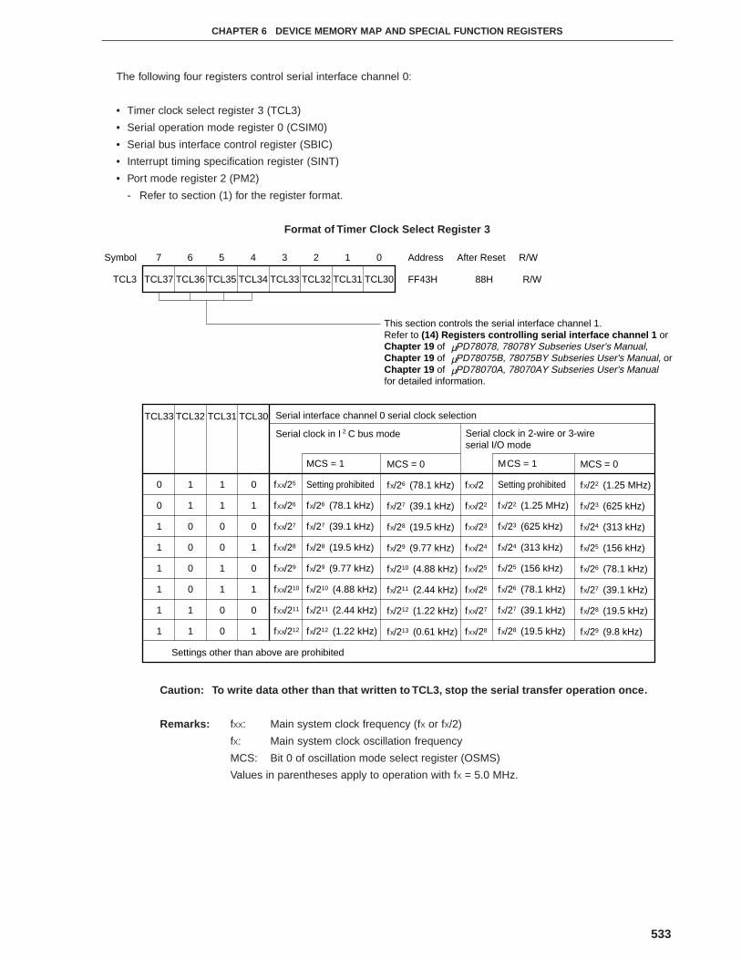
533
CHAPTER 6 DEVICE MEMORY MAP AND SPECIAL FUNCTION REGISTERS
The following four registers control serial interface channel 0:
• Timer clock select register 3 (TCL3)
• Serial operation mode register 0 (CSIM0)
• Serial bus interface control register (SBIC)
• Interrupt timing specification register (SINT)
• Port mode register 2 (PM2)
- Refer to section (1) for the register format.
Format of Timer Clock Select Register 3
Caution: To write data other than that written to TCL3, stop the serial transfer operation once.
Remarks: fXX: Main system clock frequency (fX or fX/2)
fX: Main system clock oscillation frequency
MCS: Bit 0 of oscillation mode select register (OSMS)
Values in parentheses apply to operation with fX = 5.0 MHz.
Serial interface channel 0 serial clock selectionTCL33 TCL32 TCL31 TCL30
0
0
1
1
1
1
1
1
1
1
0
0
0
0
1
1
1
1
0
0
1
1
0
0
0
1
0
1
0
1
0
1
fXX/25
fXX/26
fXX/27
fXX/28
fXX/29
fXX/210
fXX/211
fXX/212
MCS = 1
Setting prohibited
fX/26 (78.1 kHz)
fX/27 (39.1 kHz)
fX/28 (19.5 kHz)
fX/29 (9.77 kHz)
fX/210 (4.88 kHz)
fX/211 (2.44 kHz)
fX/212 (1.22 kHz)
MCS = 1
Setting prohibited
fX/22 (1.25 MHz)
fX/23 (625 kHz)
fX/24 (313 kHz)
fX/25 (156 kHz)
fX/26 (78.1 kHz)
fX/27 (39.1 kHz)
fX/28 (19.5 kHz)
MCS = 0
fX/26 (78.1 kHz)
fX/27 (39.1 kHz)
fX/28 (19.5 kHz)
fX/29 (9.77 kHz)
fX/210 (4.88 kHz)
fX/211 (2.44 kHz)
fX/212 (1.22 kHz)
fX/213 (0.61 kHz)
fXX/2
fXX/22
fXX/23
fXX/24
fXX/25
fXX/26
fXX/27
fXX/28
MCS = 0
fX/22 (1.25 MHz)
fX/23 (625 kHz)
fX/24 (313 kHz)
fX/25 (156 kHz)
fX/26 (78.1 kHz)
fX/27 (39.1 kHz)
fX/28 (19.5 kHz)
fX/29 (9.8 kHz)
Serial clock in I 2 C bus mode Serial clock in 2-wire or 3-wire serial I/O mode
6 5 4 3 2 1 07Symbol
TCL3 TCL37 TCL36 TCL35 TCL34 TCL33 TCL32 TCL31 TCL30 FF43H 88H R/W
Address After Reset R/W
µµµ
This section controls the serial interface channel 1.Refer to (14) Registers controlling serial interface channel 1 orChapter 19 of PD78078, 78078Y Subseries User's Manual,Chapter 19 of PD78075B, 78075BY Subseries User's Manual, orChapter 19 of PD78070A, 78070AY Subseries User's Manualfor detailed information.
Settings other than above are prohibited

534
CHAPTER 6 DEVICE MEMORY MAP AND SPECIAL FUNCTION REGISTERS
Format of Serial Operation Mode Register 0
Notes: 1. Bit 6 (COI) is a read-only bit.2. I2C bus mode, the clock frequency becomes 1/16 of that output from TO2.3. Can be used as P25 (CMOS input/output) when serial channel used only for transmission.4. Can be used freely as a port function when not used in SBI or 2-wire mode.5. When using the wake-up function (WUP = 1), set bit 5 (SIC) of the interrupt timing specification
register (SINT) to 1. Do not execute an instruction that writes the serial I/O shift register 0 (SIO0)while WUP = 1.
6. When CSIE0 = 0, COI becomes 0.
Caution: Do not change the operation mode (3-wire serial I/O, 2-wire serial I/O, or I 2C bus) while the
operation of serial interface channel 0 is enabled. Stop the serial operation before chang-
ing the operation mode.
Remark: ×: Don’t care
<6> <5> 4 3 2 1 0<7>Symbol
CSIM0 CSIE0 COI WUP CSIM04 CSIM03 CSIM02 CSIM01 CSIM00
CSIM01
0
1
Serial interface channel 0 clock selection
Input clock to SCK0/SCL pin from off chip
8-bit timer register 2 (TM2) output
0
R/W
1 Clock specified with bits 0 to 3 of timer clock select register 3 (TCL3)
CSIM
04
0
CSIM00
x
0
1
FF60H 00H R/W Note 1
Address After Reset R/W
R/W CSIM
03
CSIM
02PM25 P25 PM26 P26 PM27 P27
Operation
modeStart bit
SI0/SB0/SDA0/
P25 pin function
SO0/SB1/SDA1/
P26 pin function
SCK0/SCL/P27
pin function
x1
MSB
LSB1 x 0 0 0 1
Note 3 3-wire seriall/O mode
SI0(Input)
SO0(CMOS output)
SCK0 (CMOSinput/output)
Note 3
2-wire seriall/O mode
orI2C bus mode
0
SCK0/SCL(N-ch open-drain
input/output)1
1 1
x
0
x
0
0
x
0
x
0
0
1
1
Note 4 Note 4
Note 4 Note 4MSB
P25 (CMOSinput/output)
SB0/SDA0(N-ch open-drain
input/output)
SB1/SDA1(N-ch open-drain
input/output)
P26 (CMOSinput/output)
Note 3
WUP
0
1
Wake-up function control Note 5
Interrupt request signal generation with each serial transfer in any mode
Interrupt request signal generation when the address received after detecting start condition(when CMDD = 1) matches the slave address register (SVA) data in I2C bus mode
R/W
COI
0
1
Slave address comparison result flag Note 6
Slave address register (SVA) not equal to serial I/O shift register 0 (SIO0) data
Slave address register (SVA) equal to serial I/O shift register 0 (SIO0) data
R
CSIE0
0
1
Serial interface channel 0 operation control
Operation stopped
Operation enabled
R/W
Note 2

535
CHAPTER 6 DEVICE MEMORY MAP AND SPECIAL FUNCTION REGISTERS
Format of Serial Bus Interface Control Register (1/2)
Note: Bits 2, 3, and 6 (RELD, CMDD, and ACKD) are read-only bits.
Remark: CSIE0: Bit 7 of serial operation mode register 0 (CSIM0)
<6> <5> <4> <3> <2> <1> <0><7>Symbol
SBIC BSYE ACKD ACKE ACKT CMDD RELD CMDT RELT
RELTUsed for stop condition signal output. When RELT = 1, SO0 Iatch is set to 1. After SO0 latch setting, automatically cleared to 0.Also cleared to 0 when CSIE0 = 0.
R/W
FF61H 00H R/W Note
Address After Reset R/W
CMDTUsed for start condition signal output. When CMDT = 1, SO0 Iatch is cleared to 0. After SO0 latch clearance, automatically cleared to 0.Also cleared to 0 when CSIE0 = 0.
R/W
R RELD Stop condition detection
Set Condition (RELD = 1)Clear Conditions (RELD = 0)
• When stop condition signal is detected
• When transfer start instruction is executed • If SIO0 and SVA values do not match in address reception • When CSIE0 = 0
• When RESET input is applied
R CMDD Start condition detection
Clear Conditions (CMDD = 0)
• When transfer start instruction is executed • When stop condition signal is detected • When CSIE0 = 0
• When RESET input is applied
Set Condition (CMDD = 1)
• When start condition signal is detected
ACKTUsed to generate the ACK signal by software when the 8-clock wait mode is selected.Keeps SDA0 (SDA1) low from set instruction (ACKT = 1) execution to the next falling edge of SCL.Also cleared to 0 upon start of a serial interface transfer or when CSIE0 = 0.
R/W

536
CHAPTER 6 DEVICE MEMORY MAP AND SPECIAL FUNCTION REGISTERS
Format of Serial Bus Interface Control Register (2/2)
Notes: 1. Setting should be performed before transfer.
2. If an 8-clock wait mode is selected, the acknowledge signal at reception time must be output using
ACKT.
3. The busy mode can be canceled by start of a serial interface transfer or reception of an address
signal. However, the BSYE flag is not cleared to 0.
4. When using the wake-up function, be sure to set the BSYE to 1.
Remark: CSIE0: Bit 7 of serial operation mode register 0 (CSIM0)
ACKE Acknowledge signal output control
0Disables acknowledge signal automatic output (however, output with ACKT is enabled).Used for reception when the 8-clock wait mode is selected or for transmission. Note 2
Enables acknowledge signal automatic output.Outputs acknowledge signal in synchronization with the falling edge of the 9th SCL clock cycle(automatically output when ACKE = 1). However, not automatically cleared to 0 after acknowledge signal output.Used in reception with the 9-clock wait mode selected.
1
R/W
R ACKD Acknowledge detection
Clear Conditions (ACKD = 0)
• While executing the transfer start instruction
• When CSIE0 = 0
• When RESET input is applied
Set Condition (ACKD = 1)
• When acknowledge signal (ACK) is detected at the
rising edge of SCL clock after completion of
transfer
BSYE Control of N-ch open-drain output for transmission in I 2C bus mode
0 Output enabled (transmission)
R/W
Note 3
1
Note 4
Output disabled (reception)
Note 1
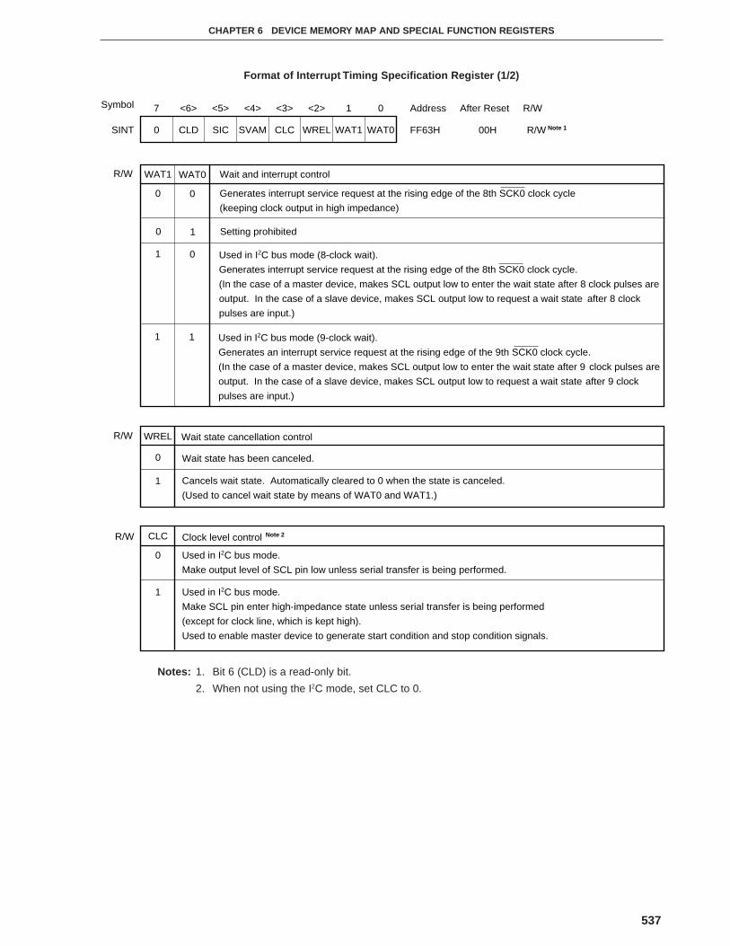
537
CHAPTER 6 DEVICE MEMORY MAP AND SPECIAL FUNCTION REGISTERS
Notes: 1. Bit 6 (CLD) is a read-only bit.
2. When not using the I2C mode, set CLC to 0.
Format of Interrupt Timing Specification Register (1/2)
Used in I2C bus mode.
Make SCL pin enter high-impedance state unless serial transfer is being performed
(except for clock line, which is kept high).
Used to enable master device to generate start condition and stop condition signals.
<6> <5> <4> <3> <2> 1 07Symbol
SINT 0 CLD SIC SVAM CLC WREL WAT1 WAT0 FF63H 00H R/W Note 1
Address After Reset R/W
WREL
0 Wait state has been canceled.
Cancels wait state. Automatically cleared to 0 when the state is canceled.
(Used to cancel wait state by means of WAT0 and WAT1.)
CLC
0
1
Clock level control Note 2
Used in I2C bus mode.
Make output level of SCL pin low unless serial transfer is being performed.
R/W
1
Wait state cancellation control
R/W
WAT1
0
1
Wait and interrupt control
Generates interrupt service request at the rising edge of the 8th SCK0 clock cycle
(keeping clock output in high impedance)
R/W WAT0
0
0 Used in I2C bus mode (8-clock wait).
Generates interrupt service request at the rising edge of the 8th SCK0 clock cycle.
(In the case of a master device, makes SCL output low to enter the wait state after 8 clock pulses are
output. In the case of a slave device, makes SCL output low to request a wait state after 8 clock
pulses are input.)
1 1 Used in I2C bus mode (9-clock wait).
Generates an interrupt service request at the rising edge of the 9th SCK0 clock cycle.
(In the case of a master device, makes SCL output low to enter the wait state after 9 clock pulses are
output. In the case of a slave device, makes SCL output low to request a wait state after 9 clock
pulses are input.)
0 Setting prohibited1
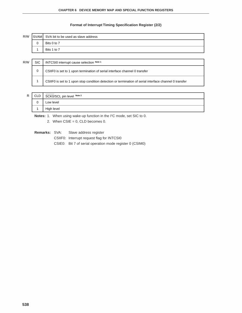
538
CHAPTER 6 DEVICE MEMORY MAP AND SPECIAL FUNCTION REGISTERS
Format of Interrupt Timing Specification Register (2/2)
Notes: 1. When using wake-up function in the I2C mode, set SIC to 0.
2. When CSIE = 0, CLD becomes 0.
Remarks: SVA: Slave address register
CSIIF0: Interrupt request flag for INTCSI0
CSIE0: Bit 7 of serial operation mode register 0 (CSIM0)
SVAM
0
1
SVA bit to be used as slave address
Bits 0 to 7
Bits 1 to 7
SIC
0
INTCSI0 interrupt cause selection Note 1
CSIIF0 is set to 1 upon termination of serial interface channel 0 transfer
CSIIF0 is set to 1 upon stop condition detection or termination of serial interface channel 0 transfer
CLD
0
1
SCK0/SCL pin level Note 2
Low level
High level
R/W
R/W
R
1

539
CHAPTER 6 DEVICE MEMORY MAP AND SPECIAL FUNCTION REGISTERS
(14) Registers controlling serial interface channel 1
The following four registers control serial interface channel 1:
• Timer clock select register 3 (TCL3)
• Serial operation mode register 1 (CSIM1)
• Automatic data transmit/receive control register (ADTC)
• Automatic data transmit/receive time interval specification register (ADTI)
Format of Timer Clock Select Register 3
Caution: When rewriting TCL3 to other data, stop the serial transfer operation beforehand.
Remarks: fXX: Main system clock frequency (fX or fX/2)
fX: Main system clock oscillation frequency
MCS: Bit 0 of oscillation mode select register (OSMS)
Values in parentheses apply to operation with fX = 5.0 MHz.
Serial interface channel 1 serial clock selectionTCL37 TCL36 TCL35 TCL34
0
0
1
1
1
1
1
1
1
1
0
0
0
0
1
1
1
1
0
0
1
1
0
0
0
1
0
1
0
1
0
1
fXX/2
fXX/22
fXX/23
fXX/24
fXX/25
fXX/26
fXX/27
fXX/28
MCS = 1
Setting prohibited
fX/22 (1.25 MHz)
fX/23 (625 kHz)
fX/24 (313 kHz)
fX/25 (156 kHz)
fX/26 (78.1 kHz)
fX/27 (39.1 kHz)
fX/28 (19.5 kHz)
MCS = 0
fX/22 (1.25 MHz)
fX/23 (625 kHz)
fX/24 (313 kHz)
fX/25 (156 kHz)
fX/26 (78.1 kHz)
fX/27 (39.1 kHz)
fX/28 (19.5 kHz)
fX/29 (9.8 kHz)
6 5 4 3 2 1 07Symbol
TCL3 TCL37 TCL36 TCL35 TCL34 TCL33 TCL32 TCL31 TCL30 FF43H 88H R/W
Address After Reset R/W
µµµ
This section controls the serial interface channel 0.Refer to (12) Registers controlling serial interface channel 0 (Non-Y Subseries), (13) Registers controlling serial interface channel 0 (Y Subseries) orChapters 17 and 18 of PD78078, 78078Y Subseries User's Manual,Chapters 17 and 18 of PD78075B, 78075BY Subseries User's Manual, orChapters 17 and 18 of PD78070A, 78070AY Subseries User's Manualfor detailed information.
Settings other than above are prohibited
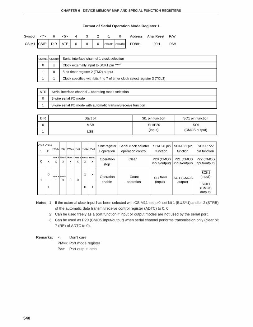
540
CHAPTER 6 DEVICE MEMORY MAP AND SPECIAL FUNCTION REGISTERS
Format of Serial Operation Mode Register 1
Notes: 1. If the external clock input has been selected with CSIM11 set to 0, set bit 1 (BUSY1) and bit 2 (STRB)
of the automatic data transmit/receive control register (ADTC) to 0, 0.
2. Can be used freely as a port function if input or output modes are not used by the serial port.
3. Can be used as P20 (CMOS input/output) when serial channel performs transmission only (clear bit
7 (RE) of ADTC to 0).
Remarks: ×: Don’t care
PM××: Port mode register
P××: Port output latch
Operation
enable
6 <5> 4 3 2 1 0<7>Symbol
CSIM1 CSIE1 DIR ATE 0 0 0 CSIM11 CSIM10
CSIM11
0
1
Serial interface channel 1 clock selection
Clock externally input to SCK1 pin Note 1
8-bit timer register 2 (TM2) output
SCK1(Input)
1 Clock specified with bits 4 to 7 of timer clock select register 3 (TCL3)
CSIE
1
0
CSIM10
x
0
1
FF68H 00H R/W
Address After Reset R/W
CSIM
11P20 PM21 P21 PM22
Shift register
1 operation
Serial clock counter
operation control
SI1/P20 pin
function
SCK1/P22
pin function
x
1
0
1
0
x 0 0
1 x
1
Note 2 Note 2 Note 2 Note 2
Count
operationSI1 Note 3
(Input)
x x x x xOperation
stop
Clear P20 (CMOSinput/output)
P22 (CMOSinput/output)
ATE
0
1
Serial interface channel 1 operating mode selection
3-wire serial I/O mode
3-wire serial I/O mode with automatic transmit/receive function
DIR
0
1
Start bit
MSB
LSB
SI1 pin function
SI1/P20
(Input)
SO1 pin function
SO1
(CMOS output)
x
PM20SO1/P21 pin
function
SO1 (CMOSoutput)
P21 (CMOSinput/output)
SCK1(CMOSoutput)
1
Note 2Note 2
Note 3Note 3
P22
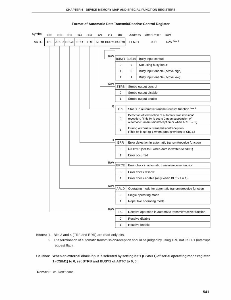
541
CHAPTER 6 DEVICE MEMORY MAP AND SPECIAL FUNCTION REGISTERS
Format of Automatic Data Transmit/Receive Control Register
Notes: 1. Bits 3 and 4 (TRF and ERR) are read-only bits.
2. The termination of automatic transmission/reception should be judged by using TRF, not CSIIF1 (interrupt
request flag).
Caution: When an external clock input is selected by setting bit 1 (CSIM11) of serial operating mode register
1 (CSIM1) to 0, set STRB and BUSY1 of ADTC to 0, 0.
Remark: ×: Don't care
<6> <5> <4> <3> <2> <1> <0><7>Symbol
ADTC RE ARLD ERCE ERR TRF STRB BUSY1 BUSY0 FF69H 00H R/W Note 1
Address After Reset R/W
BUSY1
0
1
1
Busy input control
Not using busy input
Busy input enable (active high)
Busy input enable (active low)
BUSY0
x
0
1
STRB
0
1
Strobe output control
Strobe output disable
Strobe output enable
TRF
1
Status in automatic transmit/receive function Note 2
Detection of termination of automatic transmission/reception. (This bit is set to 0 upon suspension ofautomatic transmission/reception or when ARLD = 0.)
During automatic transmission/reception.(This bit is set to 1 when data is written to SIO1.)
R/W
R/W
R
RERR
0
1
Error detection in automatic transmit/receive function
No error (set to 0 when data is written to SIO1)
Error occurred
R/WARLD
0
1
Operating mode for automatic transmit/receive function
Single operating mode
Repetitive operating mode
R/WRE
0
1
Receive operation in automatic transmit/receive function
Receive disable
Receive enable
R/WERCE
0
Error check in automatic transmit/receive function
Error check disable
Error check enable (only when BUSY1 = 1)
0
1
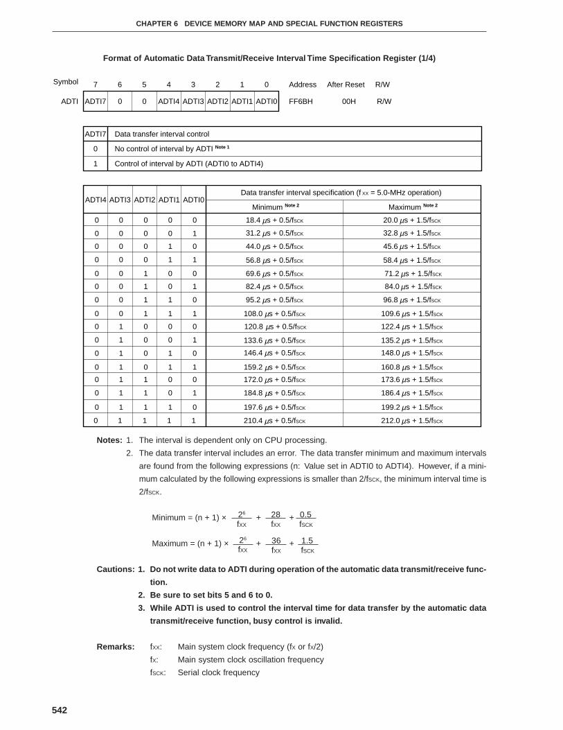
542
CHAPTER 6 DEVICE MEMORY MAP AND SPECIAL FUNCTION REGISTERS
Format of Automatic Data Transmit/Receive Interval Time Specification Register (1/4)
Notes: 1. The interval is dependent only on CPU processing.
2. The data transfer interval includes an error. The data transfer minimum and maximum intervals
are found from the following expressions (n: Value set in ADTI0 to ADTI4). However, if a mini-
mum calculated by the following expressions is smaller than 2/fSCK, the minimum interval time is
2/fSCK.
Minimum = (n + 1) × + +
Maximum = (n + 1) × + +
Cautions: 1. Do not write data to ADTI during operation of the automatic data transmit/receive func-
tion.
2. Be sure to set bits 5 and 6 to 0.
3. While ADTI is used to control the interval time for data transfer by the automatic data
transmit/receive function, busy control is invalid.
Remarks: fXX: Main system clock frequency (fX or fX/2)
fX: Main system clock oscillation frequency
fSCK: Serial clock frequency
26 28 0.5fXX fXX fSCK
26
fXX
36fXX
1.5fSCK
Data transfer interval specification (f XX = 5.0-MHz operation) ADTI4 ADTI3 ADTI2 ADTI1
0
0
0
0
0
0
0
0
0
0
0
0
0
0
0
0
0
0
0
0
0
0
0
0
1
1
1
1
1
1
1
1
0
0
0
0
1
1
1
1
0
0
0
0
1
1
1
1
0
0
1
1
0
0
1
1
0
0
1
1
0
0
1
1
Minimum Note 2
18.4 s + 0.5/fSCK
31.2 s + 0.5/fSCK
44.0 s + 0.5/fSCK
56.8 s + 0.5/fSCK
69.6 s + 0.5/fSCK
82.4 s + 0.5/fSCK
95.2 s + 0.5/fSCK
108.0 s + 0.5/fSCK
120.8 s + 0.5/fSCK
133.6 s + 0.5/fSCK
146.4 s + 0.5/fSCK
159.2 s + 0.5/fSCK
172.0 s + 0.5/fSCK
184.8 s + 0.5/fSCK
197.6 s + 0.5/fSCK
210.4 s + 0.5/fSCK
Maximum Note 2
20.0 s + 1.5/fSCK
32.8 s + 1.5/fSCK
45.6 s + 1.5/fSCK
58.4 s + 1.5/fSCK
71.2 s + 1.5/fSCK
84.0 s + 1.5/fSCK
96.8 s + 1.5/fSCK
109.6 s + 1.5/fSCK
122.4 s + 1.5/fSCK
135.2 s + 1.5/fSCK
148.0 s + 1.5/fSCK
160.8 s + 1.5/fSCK
173.6 s + 1.5/fSCK
186.4 s + 1.5/fSCK
199.2 s + 1.5/fSCK
212.0 s + 1.5/fSCK
6 5 4 3 2 1 07Symbol
ADTI ADTI7 0 0 ADTI4 ADTI3 ADTI2 ADTI1 ADTI0 FF6BH 00H R/W
Address After Reset R/W
ADTI7
0
Data transfer interval control
No control of interval by ADTI Note 1
Control of interval by ADTI (ADTI0 to ADTI4) 1
ADTI0
0
1
0
1
0
1
0
1
0
1
0
1
0
1
0
1
µ
µ
µ
µ
µ
µ
µ
µ
µ
µµ
µ
µ
µ
µ
µ
µ
µ
µ
µ
µ
µ
µ
µ
µ
µ
µ
µ
µ
µ
µ
µ
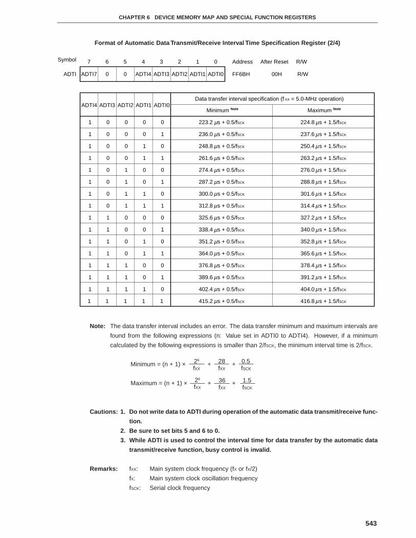
543
CHAPTER 6 DEVICE MEMORY MAP AND SPECIAL FUNCTION REGISTERS
Format of Automatic Data Transmit/Receive Interval Time Specification Register (2/4)
Note: The data transfer interval includes an error. The data transfer minimum and maximum intervals are
found from the following expressions (n: Value set in ADTI0 to ADTI4). However, if a minimum
calculated by the following expressions is smaller than 2/fSCK, the minimum interval time is 2/fSCK.
Minimum = (n + 1) × + +
Maximum = (n + 1) × + +
Cautions: 1. Do not write data to ADTI during operation of the automatic data transmit/receive func-
tion.
2. Be sure to set bits 5 and 6 to 0.
3. While ADTI is used to control the interval time for data transfer by the automatic data
transmit/receive function, busy control is invalid.
Remarks: fXX: Main system clock frequency (fX or fX/2)
fX: Main system clock oscillation frequency
fSCK: Serial clock frequency
26 28 0.5fXX fXX fSCK
26
fXX
36fXX
1.5fSCK
Data transfer interval specification (f XX = 5.0-MHz operation) ADTI4 ADTI3 ADTI2 ADTI1
1
1
1
1
1
1
1
1
1
1
1
1
1
1
1
1
0
0
0
0
0
0
0
0
1
1
1
1
1
1
1
1
0
0
0
0
1
1
1
1
0
0
0
0
1
1
1
1
0
0
1
1
0
0
1
1
0
0
1
1
0
0
1
1
Minimum Note
223.2 s + 0.5/fSCK
236.0 s + 0.5/fSCK
248.8 s + 0.5/fSCK
261.6 s + 0.5/fSCK
274.4 s + 0.5/fSCK
287.2 s + 0.5/fSCK
300.0 s + 0.5/fSCK
312.8 s + 0.5/fSCK
325.6 s + 0.5/fSCK
338.4 s + 0.5/fSCK
351.2 s + 0.5/fSCK
364.0 s + 0.5/fSCK
376.8 s + 0.5/fSCK
389.6 s + 0.5/fSCK
402.4 s + 0.5/fSCK
415.2 s + 0.5/fSCK
Maximum Note
224.8 s + 1.5/fSCK
237.6 s + 1.5/fSCK
250.4 s + 1.5/fSCK
263.2 s + 1.5/fSCK
276.0 s + 1.5/fSCK
288.8 s + 1.5/fSCK
301.6 s + 1.5/fSCK
314.4 s + 1.5/fSCK
327.2 s + 1.5/fSCK
340.0 s + 1.5/fSCK
352.8 s + 1.5/fSCK
365.6 s + 1.5/fSCK
378.4 s + 1.5/fSCK
391.2 s + 1.5/fSCK
404.0 s + 1.5/fSCK
416.8 s + 1.5/fSCK
6 5 4 3 2 1 07Symbol
ADTI ADTI7 0 0 ADTI4 ADTI3 ADTI2 ADTI1 ADTI0 FF6BH 00H R/W
Address After Reset R/W
ADTI0
0
1
0
1
0
1
0
1
0
1
0
1
0
1
0
1
µ
µ
µ
µ
µ
µ
µ
µ
µ
µ
µ
µ
µ
µ
µ
µ
µ
µ
µ
µ
µ
µ
µ
µ
µ
µ
µ
µ
µ
µ
µ
µ
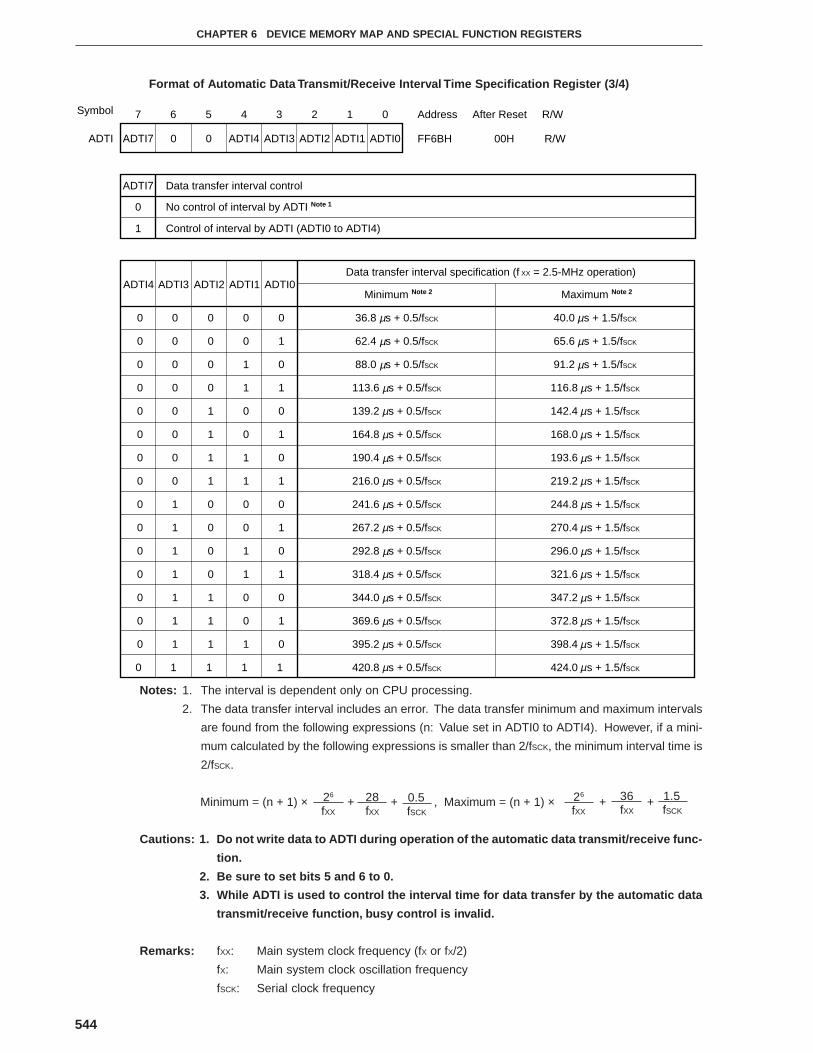
544
CHAPTER 6 DEVICE MEMORY MAP AND SPECIAL FUNCTION REGISTERS
Format of Automatic Data Transmit/Receive Interval Time Specification Register (3/4)
Notes: 1. The interval is dependent only on CPU processing.
2. The data transfer interval includes an error. The data transfer minimum and maximum intervals
are found from the following expressions (n: Value set in ADTI0 to ADTI4). However, if a mini-
mum calculated by the following expressions is smaller than 2/fSCK, the minimum interval time is
2/fSCK.
Minimum = (n + 1) × + + , Maximum = (n + 1) × + +
Cautions: 1. Do not write data to ADTI during operation of the automatic data transmit/receive func-
tion.
2. Be sure to set bits 5 and 6 to 0.
3. While ADTI is used to control the interval time for data transfer by the automatic data
transmit/receive function, busy control is invalid.
Remarks: fXX: Main system clock frequency (fX or fX/2)
fX: Main system clock oscillation frequency
fSCK: Serial clock frequency
26
fXX
36fXX
1.5fSCK
26
fXX
28fXX
0.5fSCK
Data transfer interval specification (f XX = 2.5-MHz operation) ADTI4 ADTI3 ADTI2 ADTI1
0
0
0
0
0
0
0
0
0
0
0
0
0
0
0
0
0
0
0
0
0
0
0
0
1
1
1
1
1
1
1
1
0
0
0
0
1
1
1
1
0
0
0
0
1
1
1
1
0
0
1
1
0
0
1
1
0
0
1
1
0
0
1
1
Minimum Note 2
36.8 s + 0.5/fSCK
62.4 s + 0.5/fSCK
88.0 s + 0.5/fSCK
113.6 s + 0.5/fSCK
139.2 s + 0.5/fSCK
164.8 s + 0.5/fSCK
190.4 s + 0.5/fSCK
216.0 s + 0.5/fSCK
241.6 s + 0.5/fSCK
267.2 s + 0.5/fSCK
292.8 s + 0.5/fSCK
318.4 s + 0.5/fSCK
344.0 s + 0.5/fSCK
369.6 s + 0.5/fSCK
395.2 s + 0.5/fSCK
420.8 s + 0.5/fSCK
Maximum Note 2
40.0 s + 1.5/fSCK
65.6 s + 1.5/fSCK
91.2 s + 1.5/fSCK
116.8 s + 1.5/fSCK
142.4 s + 1.5/fSCK
168.0 s + 1.5/fSCK
193.6 s + 1.5/fSCK
219.2 s + 1.5/fSCK
244.8 s + 1.5/fSCK
270.4 s + 1.5/fSCK
296.0 s + 1.5/fSCK
321.6 s + 1.5/fSCK
347.2 s + 1.5/fSCK
372.8 s + 1.5/fSCK
398.4 s + 1.5/fSCK
424.0 s + 1.5/fSCK
6 5 4 3 2 1 07Symbol
ADTI ADTI7 0 0 ADTI4 ADTI3 ADTI2 ADTI1 ADTI0 FF6BH 00H R/W
Address After Reset R/W
ADTI7
0
Data transfer interval control
No control of interval by ADTI Note 1
Control of interval by ADTI (ADTI0 to ADTI4) 1
ADTI0
0
1
0
1
0
1
0
1
0
1
0
1
0
1
0
1
µ
µ
µ
µ
µ
µ
µ
µ
µ
µ
µ
µ
µ
µ
µ
µ
µ
µ
µ
µ
µ
µ
µ
µ
µ
µ
µ
µ
µ
µ
µ
µ

545
CHAPTER 6 DEVICE MEMORY MAP AND SPECIAL FUNCTION REGISTERS
Format of Automatic Data Transmit/Receive Interval Time Specification Register (4/4)
Note: The data transfer interval includes an error. The data transfer minimum and maximum intervals are
found from the following expressions (n: Value set in ADTI0 to ADTI4). However, if a minimum
calculated by the following expressions is smaller than 2/fSCK, the minimum interval time is 2/fSCK.
Minimum = (n + 1) × + +
Maximum = (n + 1) × + +
Cautions: 1. Do not write data to ADTI during operation of the automatic data transmit/receive func-
tion.
2. Be sure to set bits 5 and 6 to 0.
3. While ADTI is used to control the interval time for data transfer by the automatic data
transmit/receive function, busy control is invalid.
Remarks: fXX: Main system clock frequency (fX or fX/2)
fX: Main system clock oscillation frequency
fSCK: Serial clock frequency
26 28 0.5fXX fXX fSCK
26
fXX
36fXX
1.5fSCK
Data transfer interval specification (f XX = 2.5-MHz operation) ADTI4 ADTI3 ADTI2 ADTI1
1
1
1
1
1
1
1
1
1
1
1
1
1
1
1
1
0
0
0
0
0
0
0
0
1
1
1
1
1
1
1
1
0
0
0
0
1
1
1
1
0
0
0
0
1
1
1
1
0
0
1
1
0
0
1
1
0
0
1
1
0
0
1
1
Minimum Note
446.4 s + 0.5/fSCK
472.0 s + 0.5/fSCK
497.6 s + 0.5/fSCK
523.2 s + 0.5/fSCK
548.8 s + 0.5/fSCK
574.4 s + 0.5/fSCK
600.0 s + 0.5/fSCK
625.6 s + 0.5/fSCK
651.2 s + 0.5/fSCK
676.8 s + 0.5/fSCK
702.4 s + 0.5/fSCK
728.0 s + 0.5/fSCK
753.6 s + 0.5/fSCK
779.2 s + 0.5/fSCK
804.8 s + 0.5/fSCK
830.4 s + 0.5/fSCK
Maximum Note
449.6 s + 1.5/fSCK
475.2 s + 1.5/fSCK
500.8 s + 1.5/fSCK
526.4 s + 1.5/fSCK
552.0 s + 1.5/fSCK
577.6 s + 1.5/fSCK
603.2 s + 1.5/fSCK
628.8 s + 1.5/fSCK
654.4 s + 1.5/fSCK
680.0 s + 1.5/fSCK
705.6 s + 1.5/fSCK
731.2 s + 1.5/fSCK
756.8 s + 1.5/fSCK
782.4 s + 1.5/fSCK
808.0 s + 1.5/fSCK
833.6 s + 1.5/fSCK
6 5 4 3 2 1 07Symbol
ADTI ADTI7 0 0 ADTI4 ADTI3 ADTI2 ADTI1 ADTI0 FF6BH 00H R/W
Address After Reset R/W
ADTI0
0
1
0
1
0
1
0
1
0
1
0
1
0
1
0
1
µ
µ
µ
µ
µ
µ
µ
µ
µ
µ
µ
µ
µ
µ
µ
µ
µ
µ
µ
µ
µ
µ
µ
µ
µ
µ
µ
µ
µ
µ
µ
µ
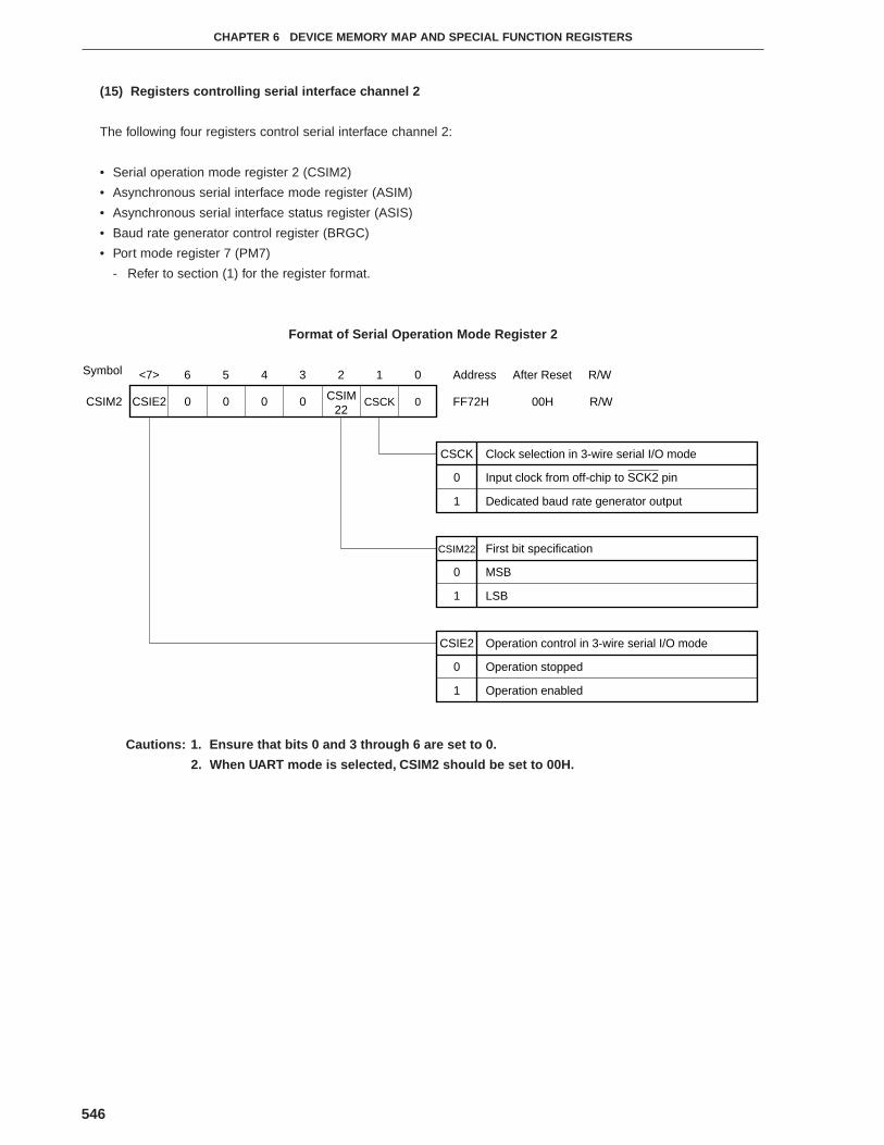
546
CHAPTER 6 DEVICE MEMORY MAP AND SPECIAL FUNCTION REGISTERS
(15) Registers controlling serial interface channel 2
The following four registers control serial interface channel 2:
• Serial operation mode register 2 (CSIM2)
• Asynchronous serial interface mode register (ASIM)
• Asynchronous serial interface status register (ASIS)
• Baud rate generator control register (BRGC)
• Port mode register 7 (PM7)
- Refer to section (1) for the register format.
Format of Serial Operation Mode Register 2
Cautions: 1. Ensure that bits 0 and 3 through 6 are set to 0.
2. When UART mode is selected, CSIM2 should be set to 00H.
6 5 4 3 2 1 0<7>Symbol
CSIM2 CSIE2 0 0 0 0 CSIM22
CSCK 0 FF72H 00H R/W
Address After Reset R/W
CSCK
0
1
Clock selection in 3-wire serial I/O mode
Input clock from off-chip to SCK2 pin
Dedicated baud rate generator output
CSIM22
0
1
First bit specification
MSB
LSB
CSIE2
0
1
Operation control in 3-wire serial I/O mode
Operation stopped
Operation enabled
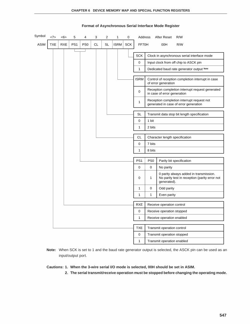
547
CHAPTER 6 DEVICE MEMORY MAP AND SPECIAL FUNCTION REGISTERS
Format of Asynchronous Serial Interface Mode Register
Note: When SCK is set to 1 and the baud rate generator output is selected, the ASCK pin can be used as an
input/output port.
Cautions: 1. When the 3-wire serial I/O mode is selected, 00H should be set in ASIM.
2. The serial transmit/receive operation must be stopped before changing the operating mode.
<6> 5 4 3 2 1 0<7>Symbol
ASIM TXE RXE PS1 PS0 CL SL ISRM SCK FF70H 00H R/W
Address After Reset R/W
SCK
0
1
Clock in asynchronous serial interface mode
Input clock from off chip to ASCK pin
Dedicated baud rate generator output Note
ISRM
0
1
Control of reception completion interrupt in caseof error generation
Reception completion interrupt request generated in case of error generation
Reception completion interrupt request not generated in case of error generation
SL Transmit data stop bit length specification
CL
1
Character length specification
7 bits
8 bits
RXE
0
1
Receive operation control
Receive operation stopped
Receive operation enabled
TXE
0
1
Transmit operation control
Transmit operation stopped
Transmit operation enabled
PS1
0
1
0 1 bit
1 2 bits
0
Parity bit specification
No parity
Even parity
PS0
0
1
0 parity always added in transmission.No parity test in reception (parity error notgenerated).
0 1
1 Odd parity0
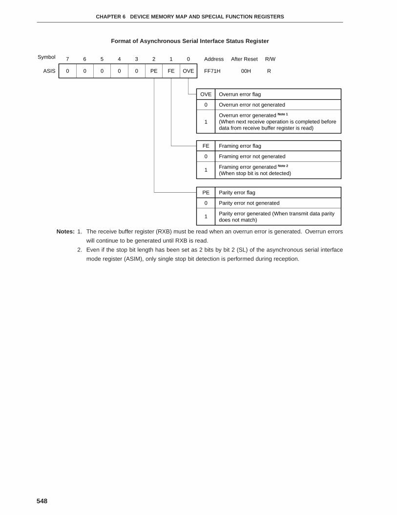
548
CHAPTER 6 DEVICE MEMORY MAP AND SPECIAL FUNCTION REGISTERS
Format of Asynchronous Serial Interface Status Register
Notes: 1. The receive buffer register (RXB) must be read when an overrun error is generated. Overrun errors
will continue to be generated until RXB is read.
2. Even if the stop bit length has been set as 2 bits by bit 2 (SL) of the asynchronous serial interface
mode register (ASIM), only single stop bit detection is performed during reception.
PE
6 5 4 3 2 1 07Symbol
ASIS 0 0 0 0 0 FE OVE FF71H 00H R
Address After Reset R/W
OVE
0
1
Overrun error flag
Overrun error not generated
Overrun error generated Note 1
(When next receive operation is completed beforedata from receive buffer register is read)
FE
0
1
Framing error flag
Framing error not generated
Framing error generated Note 2
(When stop bit is not detected)
PE
0
1
Parity error flag
Parity error not generated
Parity error generated (When transmit data paritydoes not match)

549
CHAPTER 6 DEVICE MEMORY MAP AND SPECIAL FUNCTION REGISTERS
Format of Baud Rate Generator Control Register (1/2)
Note: Can only be used in 3-wire serial I/O mode.
Remarks: fSCK: 5-bit counter source clock
k: Value set in MDL0 to MDL3 (0 ≤ k ≤ 14)
Baud rate generator input clock selectionMDL3 MDL2 MDL1 MDL0
0
0
0
0
0
0
0
0
1
1
1
1
1
1
1
1
0
0
0
0
1
1
1
1
0
0
0
0
1
1
1
1
0
0
1
1
0
0
1
1
0
0
1
1
0
0
1
1
0
1
0
1
0
1
0
1
0
1
0
1
0
1
0
1
fSCK/16
fSCK/17
fSCK/18
fSCK/19
fSCK/20
fSCK/21
fSCK/22
fSCK/23
fSCK/24
fSCK/25
fSCK/26
fSCK/27
fSCK/28
fSCK/29
fSCK/30
fSCK Note
0
1
2
3
4
5
6
7
8
9
10
11
12
13
14
6 5 4 3 2 1 07Symbol
BRGC TPS3 TPS2 TPS1 TPS0 MDL3 MDL2 MDL1 MDL0 FF73H 00H R/W
Address After Reset R/W
k

550
CHAPTER 6 DEVICE MEMORY MAP AND SPECIAL FUNCTION REGISTERS
Format of Baud Rate Generator Control Register (2/2)
TPS3 TPS2 TPS1 TPS0 5-bit counter source clock selection n
MCS = 1 MCS = 0
0 0 0 0 fXX/210 fXX/210 (4.9 kHz) fX/211 (2.4 kHz) 11
0 1 0 1 fXX fX (5.0 MHz) fX/2 (2.5 MHz) 1
0 1 1 0 fXX/2 fX/2 (2.5 MHz) fX/22 (1.25 MHz) 2
0 1 1 1 fXX/22 fX/22 (1.25 MHz) fX/23 (625 kHz) 3
1 0 0 0 fXX/23 fX/23 (625 kHz) fX/24 (313 kHz) 4
1 0 0 1 fXX/24 fX/24 (313 kHz) fX/25 (156 kHz) 5
1 0 1 0 fXX/25 fX/25 (156 kHz) fX/26 (78.1 kHz) 6
1 0 1 1 fXX/26 fX/26 (78.1 kHz) fX/27 (39.1 kHz) 7
1 1 0 0 fXX/27 fX/27 (39.1 kHz) fX/28 (19.5 kHz) 8
1 1 0 1 fXX/28 fX/28 (19.5 kHz) fX/29 (9.8 kHz) 9
1 1 1 0 fXX/29 fX/29 (9.8 kHz) fX/210 (4.9 kHz) 10
Settings other than above are prohibited
Caution: When a write is performed to BRGC during a communication operation, baud rate generator
output is disrupted and communication cannot be performed normally. Therefore, BRGC must
not be written to during a communication operation.
Remarks: fX: Main system clock oscillation frequency
fXX: Main system clock frequency (fX or fX/2)
MCS: Bit 0 of oscillation mode select register (OSMS)
n: Value set in TPS0 to TPS3 (1 ≤ n ≤ 11)
Values in parentheses apply to operation with fX = 5.0 MHz.
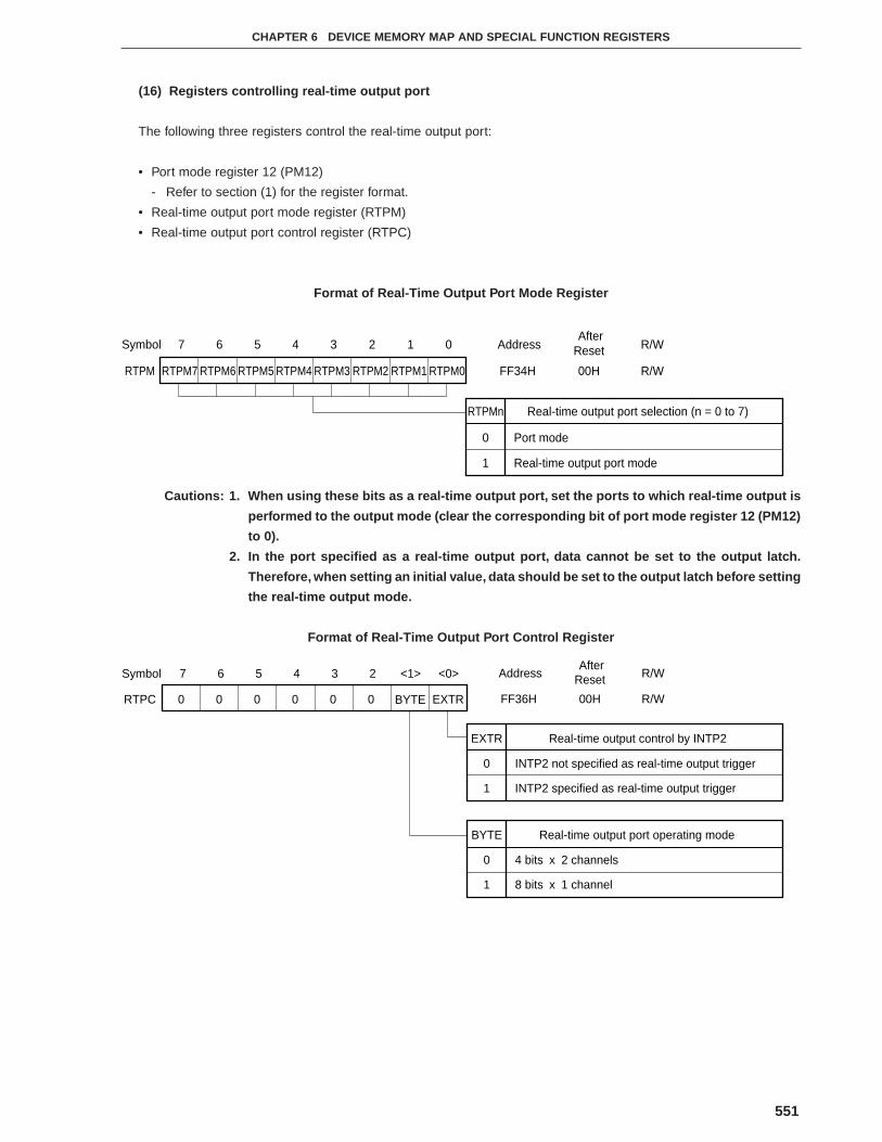
551
CHAPTER 6 DEVICE MEMORY MAP AND SPECIAL FUNCTION REGISTERS
(16) Registers controlling real-time output port
The following three registers control the real-time output port:
• Port mode register 12 (PM12)
- Refer to section (1) for the register format.
• Real-time output port mode register (RTPM)
• Real-time output port control register (RTPC)
Format of Real-Time Output Port Mode Register
Cautions: 1. When using these bits as a real-time output port, set the ports to which real-time output is
performed to the output mode (clear the corresponding bit of port mode register 12 (PM12)
to 0).
2. In the port specified as a real-time output port, data cannot be set to the output latch.
Therefore, when setting an initial value, data should be set to the output latch before setting
the real-time output mode.
Format of Real-Time Output Port Control Register
7
RTPM7
6
RTPM6
5
RTPM5
4
RTPM4
3
RTPM3
2
RTPM2
1
RTPM1
0
RTPM0
Symbol
RTPM
Address
FF34H 00H
AfterReset R/W
R/W
RTPMn
0
1
Port mode
Real-time output port mode
Real-time output port selection (n = 0 to 7)
7
0
Symbol
RTPC
6
0
5
0
4
0
3
0
2
0
<1>
BYTE
<0>
EXTR
Address
FF36H 00H
AfterReset R/W
R/W
EXTR
0
1
Real-time output control by INTP2
INTP2 not specified as real-time output trigger
INTP2 specified as real-time output trigger
BYTE
0
1
Real-time output port operating mode
4 bits x 2 channels
8 bits x 1 channel

552
CHAPTER 6 DEVICE MEMORY MAP AND SPECIAL FUNCTION REGISTERS
(17) Registers controlling interrupt function
A total of 24 interrupt sources are provided for the µPD7807x Subseries, including non-maskable, maskable, and
software interrupts.
Table 6-28. Interrupt Source List
Interrupt Default Interrupt Source Internal/ VectorTable
Type Priority Name Trigger External Address
Non- — RESET Low voltage level External 0000H
maskable INTWDT Watchdog timer overflow (with watchdog timer Internal 0004H
mode 1 selected)
0 INTWDT Watchdog timer overflow (with interval timer mode
selected)
1 INTP0 Pin input edge detection External 0006H
2 INTP1 0008H
3 INTP2 000AH
4 INTP3 000CH
5 INTP4 000EH
6 INTP5 0010H
7 INTP6 0012H
8 INTCSI0 End of serial interface channel 0 transfer Internal 0014H
9 INTCSI1 End of serial interface channel 1 transfer 0016H
Maskable 10 INTSER Serial interface channel 2 UART reception error generation 0018H
11 INTSR End of serial interface channel 2 UART reception 001AH
INTCSI2 End of serial interface channel 2 3-wire transfer
12 INTST End of serial interface channel 2 UART transmission 001CH
13 INTTM3 Reference time interval signal from watch timer 001EH
14 INTTM00 Generation of 16-bit timer register and capture/ 0020H
compare register 00 (CR00) match signal
15 INTTM01 Generation of 16-bit timer register and capture/ 0022H
compare register 01 (CR01) match signal
16 INTTM1 Generation of 8-bit timer/event counter 1 match signal 0024H
17 INTTM2 Generation of 8-bit timer/event counter 2 match signal 0026H
18 INTAD End of A/D converter conversion 0028H
19 INTTM5 Generation of 8-bit timer/event counter 5 match signal 002AH
20 INTTM6 Generation of 8-bit timer/event counter 6 match signal 002CH
Software — BRK BRK instruction execution — 003EH
Note: Default priorities are intended for two or more simultaneously generated maskable interrupt requests. 0 is the
highest priority and 20 is the lowest priority.
Note
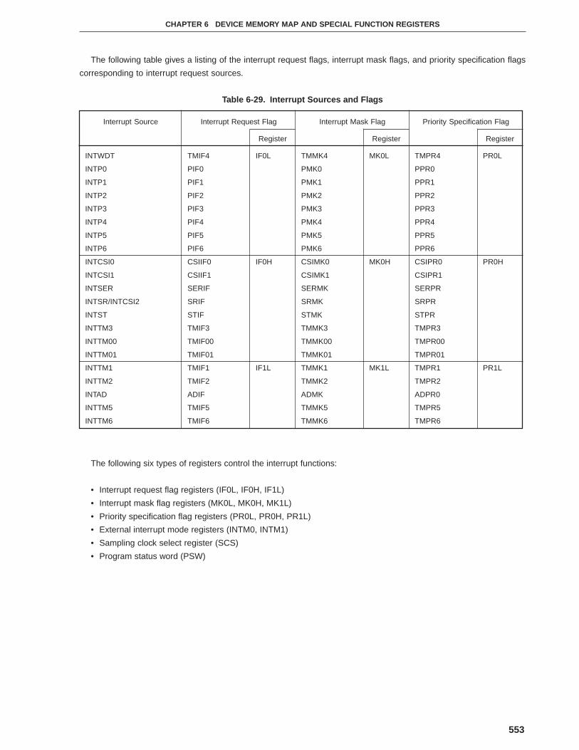
553
CHAPTER 6 DEVICE MEMORY MAP AND SPECIAL FUNCTION REGISTERS
The following table gives a listing of the interrupt request flags, interrupt mask flags, and priority specification flags
corresponding to interrupt request sources.
Table 6-29. Interrupt Sources and Flags
Interrupt Source Interrupt Request Flag Interrupt Mask Flag Priority Specification Flag
Register Register Register
INTWDT TMIF4 IF0L TMMK4 MK0L TMPR4 PR0L
INTP0 PIF0 PMK0 PPR0
INTP1 PIF1 PMK1 PPR1
INTP2 PIF2 PMK2 PPR2
INTP3 PIF3 PMK3 PPR3
INTP4 PIF4 PMK4 PPR4
INTP5 PIF5 PMK5 PPR5
INTP6 PIF6 PMK6 PPR6
INTCSI0 CSIIF0 IF0H CSIMK0 MK0H CSIPR0 PR0H
INTCSI1 CSIIF1 CSIMK1 CSIPR1
INTSER SERIF SERMK SERPR
INTSR/INTCSI2 SRIF SRMK SRPR
INTST STIF STMK STPR
INTTM3 TMIF3 TMMK3 TMPR3
INTTM00 TMIF00 TMMK00 TMPR00
INTTM01 TMIF01 TMMK01 TMPR01
INTTM1 TMIF1 IF1L TMMK1 MK1L TMPR1 PR1L
INTTM2 TMIF2 TMMK2 TMPR2
INTAD ADIF ADMK ADPR0
INTTM5 TMIF5 TMMK5 TMPR5
INTTM6 TMIF6 TMMK6 TMPR6
The following six types of registers control the interrupt functions:
• Interrupt request flag registers (IF0L, IF0H, IF1L)
• Interrupt mask flag registers (MK0L, MK0H, MK1L)
• Priority specification flag registers (PR0L, PR0H, PR1L)
• External interrupt mode registers (INTM0, INTM1)
• Sampling clock select register (SCS)
• Program status word (PSW)

554
CHAPTER 6 DEVICE MEMORY MAP AND SPECIAL FUNCTION REGISTERS
Format of Interrupt Request Flag Registers
Note: WTIF is a test input flag. A vectored interrupt request is not generated.
Cautions: 1. The TMIF4 flag is R/W enabled only when a watchdog timer is used as an interval timer. If a
watchdog timer is used in watchdog timer mode 1, set the TMIF4 flag to 0.
2. Always set IF1L bits 5 and 6 to 0.
Format of Interrupt Mask Flag Registers
Note: WTMK controls standby mode release enable/disable. It does not control the interrupt function.
Cautions: 1. If the TMIF4 flag is read when a watchdog timer is used in watchdog timer mode 1, the MK0
value becomes undefined.
2. Because port 0 has an alternate function as the external interrupt input, when the output
level is changed by specifying the output mode of the port function, an interrupt request
flag is set. Therefore, 1 should be set in the interrupt mask flag before using the output
mode.
3. Always set MK1L bits 5 and 6 to 1.
<7>
PIF6
Symbol
IF0L
<6>
PIF5
<5>
PIF4
<4>
PIF3
<3>
PIF2
<2>
PIF1
<1>
PIF0
<0>
TMIF4
Address
FFE0H 00H
AfterReset R/W
R/W
xxIFx
0
1
Interrupt request flag
No interrupt request signal
Interrupt request signal is generated; interrupt request state
<7>
TMIF01IF0H
<6>
TMIF00
<5>
TMIF3
<4>
STIF
<3>
SRIF
<2>
SERIF
<1>
CSIIF1
<0>
CSIIF0
<7>
WTIFNoteIF1L
6
0
5
0
<4>
TMIF6
<3>
TMIF5
<2>
ADIF
<1>
TMIF2
<0>
TMIF1
FFE1H 00H R/W
FFE2H 00H R/W
<7>
PMK6
Symbol
MK0L
<6>
PMK5
<5>
PMK4
<4>
PMK3
<3>
PMK2
<2>
PMK
<1>
PMK
<0>
TMMK4
Address
FFE4H FFH
AfterReset R/W
R/W
xxMKx
0
1
Interrupt servicing control
Interrupt servicing enabled
Interrupt servicing disabled
<7>
TMMK01MK0H
<6>
TMMK00
<5>
TMMK3
<4>
STMK
<3>
SRMK
<2>
SERMK
<1>
CSIMK1
<0>
CSIMK0
<7>
WTMKNoteMK1L
6
1
5
1
<4>
TMMK6
<3>
TMMK5
<2>
ADMK
<1>
TMMK2
<0>
TMMK1
FFE5H FFH R/W
FFE6H FFH R/W
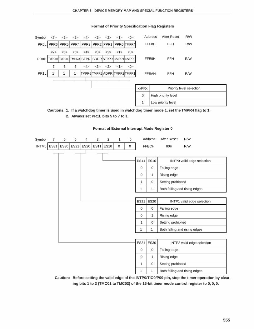
555
CHAPTER 6 DEVICE MEMORY MAP AND SPECIAL FUNCTION REGISTERS
Format of Priority Specification Flag Registers
Cautions: 1. If a watchdog timer is used in watchdog timer mode 1, set the TMPR4 flag to 1.
2. Always set PR1L bits 5 to 7 to 1.
Format of External Interrupt Mode Register 0
Caution: Before setting the valid edge of the INTP0/TIO0/P00 pin, stop the timer operation by clear-
ing bits 1 to 3 (TMC01 to TMC03) of the 16-bit timer mode control register to 0, 0, 0.
<7>
PPR6
Symbol
PR0L
<6>
PPR5
<5>
PPR4
<4>
PPR3
<3>
PPR2
<2>
PPR1
<1>
PPR0
<0>
TMPR4
Address
FFE8H FFH
R/W
R/W
0
1
Priority level selection
High priority level
Low priority level
<7>
TMPR01PR0H
<6>
TMPR00
<5>
TMPR3
<4>
STPR
<3>
SRPR
<2>
SERPR
<1>
CSIPR1
<0>
CSIPR0
7
1PR1L
6
1
5
1
<4>
TMPR6
<3>
TMPR5
<2>
ADPR
<1>
TMPR2
<0>
TMPR1
FFE9H FFH R/W
FFEAH FFH R/W
xxPRx
After Reset
Address
FFECH 00H
R/W
R/W
0
0
1
1
INTP0 valid edge selection
Falling edge
Rising edge
Setting prohibited
Both falling and rising edges
ES11
7
ES31
Symbol
INTM0
6
ES30
5
ES21
4
ES20
3
ES11
2
ES10
1
0
0
0
0
1
0
1
ES10
0
0
1
1
INTP1 valid edge selection
Falling edge
Rising edge
Setting prohibited
Both falling and rising edges
ES21
0
1
0
1
ES20
0
0
1
1
INTP2 valid edge selection
Falling edge
Rising edge
Setting prohibited
Both falling and rising edges
ES31
0
1
0
1
ES30
After Reset

556
CHAPTER 6 DEVICE MEMORY MAP AND SPECIAL FUNCTION REGISTERS
Format of External Interrupt Mode Register 1
Address
FFEDH 00H
R/W
R/W
0
0
1
1
INTP3 valid edge selection
Falling edge
Rising edge
Setting prohibited
Both falling and rising edges
ES41
7
ES71
Symbol
INTM1
6
ES70
5
ES61
4
ES60
3
ES51
2
ES50
1
ES41
0
ES40
0
1
0
1
ES40
0
0
1
1
INTP4 valid edge selection
Falling edge
Rising edge
Setting prohibited
Both falling and rising edges
ES51
0
1
0
1
ES50
0
0
1
1
INTP5 valid edge selection
Falling edge
Rising edge
Setting prohibited
Both falling and rising edges
ES61
0
1
0
1
ES60
0
0
1
1
INTP6 valid edge selection
Falling edge
Rising edge
Setting prohibited
Both falling and rising edges
ES71
0
1
0
1
ES70
After Reset
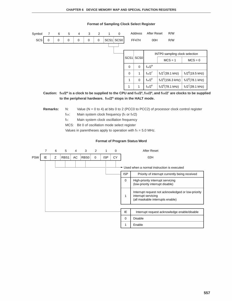
557
CHAPTER 6 DEVICE MEMORY MAP AND SPECIAL FUNCTION REGISTERS
Format of Sampling Clock Select Register
Caution: f XX/2N is a clock to be supplied to the CPU and f XX/25, fXX/26, and f XX/27 are clocks to be supplied
to the peripheral hardware. f XX/2N stops in the HALT mode.
Remarks: N: Value (N = 0 to 4) at bits 0 to 2 (PCC0 to PCC2) of processor clock control register
fXX: Main system clock frequency (fX or fX/2)
fX: Main system clock oscillation frequency
MCS: Bit 0 of oscillation mode select register
Values in parentheses apply to operation with fX = 5.0 MHz.
Format of Program Status Word
Address
FF47H 00H
R/W
R/W
0
0
1
1
INTP0 sampling clock selection
fxx/2N
fxx/27
fxx/25
fxx/26
SCS1
7
0
Symbol
SCS
6
0
5
0
4
0
3
0
2
0
1
SCS1
0
SCS0
0
1
0
1
SCS0MCS = 1 MCS = 0
fx/27(39.1 kHz)
fx/25(156.3 kHz)
fx/26(78.1 kHz)
fx/28(19.5 kHz)
fx/26(78.1 kHz)
fx/27(39.1 kHz)
After Reset
7
IEPSW
6
Z
5
RBS1
4
AC
3
RBS0
2
0
1
ISP
0
CY 02H
ISP
0
Used when a normal instruction is executed
Priority of interrupt currently being received
High-priority interrupt servicing(low-priority interrupt disable)
1Interrupt request not acknowledged or low-priorityinterrupt servicing(all maskable interrupts enable)
IE Interrupt request acknowledge enable/disable
0 Disable
1 Enable
After Reset
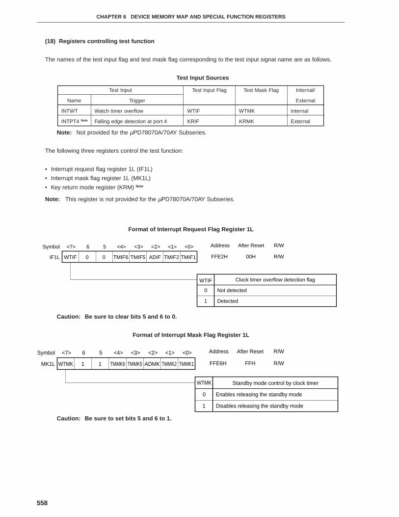
558
CHAPTER 6 DEVICE MEMORY MAP AND SPECIAL FUNCTION REGISTERS
(18) Registers controlling test function
The names of the test input flag and test mask flag corresponding to the test input signal name are as follows.
Test Input Sources
Test Input Test Input Flag Test Mask Flag Internal/
Name Trigger External
INTWT Watch timer overflow WTIF WTMK Internal
INTPT4 Note Falling edge detection at port 4 KRIF KRMK External
Note: Not provided for the µPD78070A/70AY Subseries.
The following three registers control the test function:
• Interrupt request flag register 1L (IF1L)
• Interrupt mask flag register 1L (MK1L)
• Key return mode register (KRM) Note
Note: This register is not provided for the µPD78070A/70AY Subseries.
Format of Interrupt Request Flag Register 1L
Caution: Be sure to clear bits 5 and 6 to 0.
Format of Interrupt Mask Flag Register 1L
<7>
WTIF
Symbol
IF1L
6
0
5
0
<4>
TMIF6
<3>
TMIF5
<2>
ADIF
<1>
TMIF2
<0>
TMIF1
Address
FFE2H 00H
R/W
R/W
0
1
Clock timer overflow detection flag
Not detected
Detected
WTIF
After Reset
Caution: Be sure to set bits 5 and 6 to 1.
<7>
WTMK
Symbol
MK1L
6
1
5
1
<4>
TMMK6
<3>
TMMK5
<2>
ADMK
<1>
TMMK2
<0>
TMMK1
Address
FFE6H FFH
R/W
R/W
0
1
Standby mode control by clock timer
Enables releasing the standby mode
Disables releasing the standby mode
WTMK
After Reset
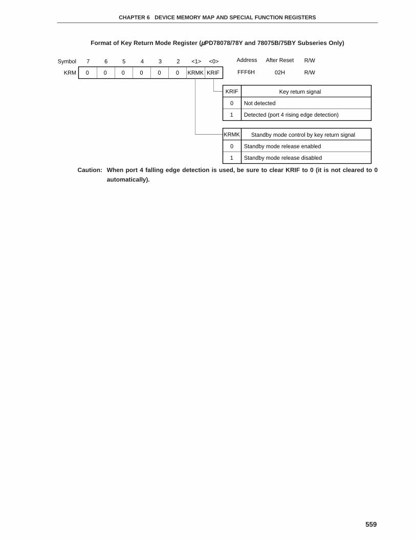
559
CHAPTER 6 DEVICE MEMORY MAP AND SPECIAL FUNCTION REGISTERS
Format of Key Return Mode Register ( µµµµµPD78078/78Y and 78075B/75BY Subseries Only)
Caution: When port 4 falling edge detection is used, be sure to clear KRIF to 0 (it is not cleared to 0
automatically).
7
0
Symbol
KRM
6
0
5
0
4
0
3
0
2
0
<1>
KRMK
<0>
KRIF
Address
FFF6H 02H
R/W
R/W
0
1
Key return signal
Not detected
Detected (port 4 rising edge detection)
KRIF
0
1
Standby mode control by key return signal
Standby mode release enabled
Standby mode release disabled
KRMK
After Reset

560
CHAPTER 6 DEVICE MEMORY MAP AND SPECIAL FUNCTION REGISTERS
(19) Registers controlling external device expansion function
The following three registers control the external device expansion function:
• Memory expansion mode register (MM)
• Internal memory size switching register (IMS)
• External bus type select register (EBTS)
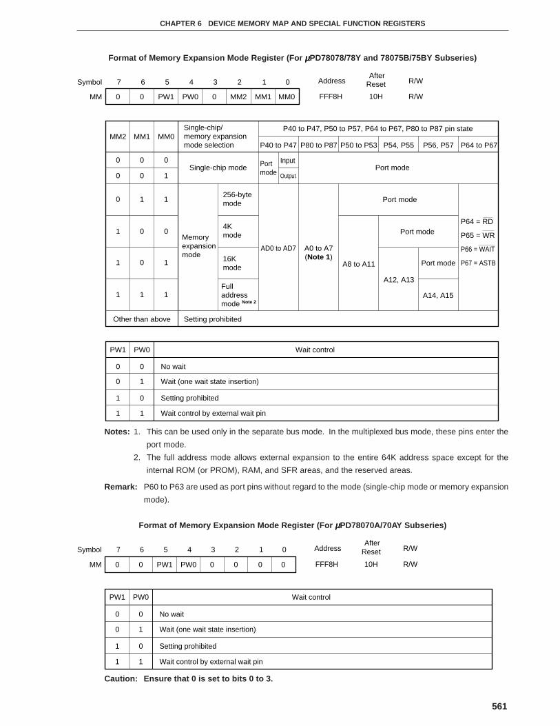
561
CHAPTER 6 DEVICE MEMORY MAP AND SPECIAL FUNCTION REGISTERS
Format of Memory Expansion Mode Register (For µµµµµPD78078/78Y and 78075B/75BY Subseries)
Caution: Ensure that 0 is set to bits 0 to 3.
Notes: 1. This can be used only in the separate bus mode. In the multiplexed bus mode, these pins enter the
port mode.
2. The full address mode allows external expansion to the entire 64K address space except for the
internal ROM (or PROM), RAM, and SFR areas, and the reserved areas.
Remark: P60 to P63 are used as port pins without regard to the mode (single-chip mode or memory expansion
mode).
Format of Memory Expansion Mode Register (For µµµµµPD78070A/70AY Subseries)
7
0
Symbol
MM
6
0
5
PW1
4
PW0
3
0
2
MM2
1
MM1
0
MM0
Address
FFF8H 10H
AfterReset R/W
R/W
MM2 MM1 MM0Single-chip/memory expansionmode selection
P40 to P47, P50 to P57, P64 to P67, P80 to P87 pin state
P40 to P47 P80 to P87 P50 to P53 P54, P55 P56, P57 P64 to P67
0 0 0
0 0 1
0 1 1
1 0 0
1 0 1
1 1 1
Single-chip mode
256-bytemode
4Kmode
16Kmode
Full addressmode Note 2
Memoryexpansionmode
Portmode
Input
OutputPort mode
Port mode
Port mode
Port mode
AD0 to AD7 A0 to A7(Note 1)
A8 to A11
A12, A13
A14, A15
P64 = RD
P65 = WR
P66 = WAIT
P67 = ASTB
Other than above Setting prohibited
PW1 PW0
0 0
0 1
1 0
1 1
Wait control
No wait
Wait (one wait state insertion)
Setting prohibited
Wait control by external wait pin
7
0
Symbol
MM
6
0
5
PW1
4
PW0
3
0
2
0
1
0
0
0
Address
FFF8H 10H
AfterReset R/W
R/W
PW1 PW0
0 0
0 1
1 0
1 1
Wait control
No wait
Wait (one wait state insertion)
Setting prohibited
Wait control by external wait pin

562
CHAPTER 6 DEVICE MEMORY MAP AND SPECIAL FUNCTION REGISTERS
Format of Internal Memory Size Switching Register
(For µµµµµPD78078/78Y and 78075B/75BY Subseries)
Notes: 1. The value of this register after reset differs depending on the product (refer to the table below).
2. When the external device expansion function of the µPD78078/78Y or 78P078/78Y is used, be sure to set
the internal ROM capacity to 56K or less.
Value of Internal Memory Size Switching Register After Reset
(µµµµµPD78078/78Y and 78075B/75BY Subseries)
Part Number Value After Reset
µPD78074B/74BY C8H
µPD78075B/75BY CAH
µPD78076/76Y CCH
µPD78078/78Y, 78P078/78Y CFH
Caution: When using the mask ROM versions, do not set IMS to values other than those shown in the table
above, except for cases in which the external device expansion function is used in the µµµµµPD78078/
78Y.
Remark: IMS should be set according to the internal ROM capacity.
1
1
32 Kbytes
40 Kbytes
0
0
0
1
0
0
7
RAM2
Symbol
IMS
6
RAM1
5
RAM0
4
0
3
ROM3
2
ROM2
1
ROM1
0
ROM0
Address
FFF0H Note 1
R/W
R/W
Internal ROM size selectionROM3
48 Kbytes1
ROM2
1
ROM1
0
ROM0
0
56 Kbytes Note 21 1 1 0
60 Kbytes1 1 1 1
Internal high-speed RAM size selectionRAM2 RAM1 RAM0
1024 bytes1 1 0
After Reset
Settings other than above are prohibited
Settings other than above are prohibited

563
CHAPTER 6 DEVICE MEMORY MAP AND SPECIAL FUNCTION REGISTERS
Format of Internal Memory Size Switching Register (For µµµµµPD78070A/70AY Subseries)
Caution: Although IMS is a register that specifies the internal high-speed RAM capacity, the memory size of
the µµµµµPD78070A/70AY cannot be changed. Do not set IMS with a value other than those used for
resetting.
Format of External Bus Type Select Register (For µµµµµPD78078/78Y and 78075B/75BY Subseries)
Format of External Bus Type Select Register (For µµµµµPD78070A/70AY Subseries)
7
0
Symbol
EBTS
6
0
5
0
4
0
3
0
2
0
1
0
0
EBTS0
Address
FF3FH 00H
R/W
R/W
0
1
Sets operation mode of external device expansion function
Multiplexed bus mode
Separate bus mode
EBTS0
After Reset
Caution: In the µµµµµPD78070A/70AY, this register is fixed to 01H (a separate mode). Do not set EBTS with a
value other than those used for resetting.
7
0
Symbol
EBTS
6
0
5
0
4
0
3
0
2
0
1
0
0
EBTS0
Address
FF3FH 01H
R/W
R/W
0
1
Sets operation mode of external device expansion function
Multiplexed bus mode (setting prohibited)
Separate bus mode
EBTS0
After Reset
7
RAM2
Symbol
IMS
6
RAM1
5
RAM0
4
0
3
0
2
0
1
0
0
0
Address
FFF0H C0H
R/W
R/W
Internal high-speed RAM size selectionRAM2 RAM1 RAM0
1024 bytes1 1 0
Setting prohibitedOther than above
After Reset

564
CHAPTER 6 DEVICE MEMORY MAP AND SPECIAL FUNCTION REGISTERS
(20) Register controlling standby function
The standby function is intended to decrease the power consumption of the system. The following two modes are
available: HALT and STOP.
When MCU is released from the STOP mode, a wait time is required for the crystal to resume oscillations. The wait
time is controlled by the following register:
• Oscillation stabilization time select register (OSTS)
Format of Oscillation Stabilization Time Select Register
Remarks: fXX: Main system clock frequency (fX or fX/2)
fX: Main system clock oscillation frequency
MCS: Bit 0 of oscillation mode select register (OSMS)
Values in parentheses apply to operation with fX = 5.0 MHz.
RESET input sets OSTS to 04H. However, it takes 217/fx, not 218/fx, until the STOP Mode is cleared.
Address
FFFAH 04H
R/W
R/W
0
0
0
0
1
Selection of oscillation stabilizationtime when STOP mode is released
212/fxx
214/fxx
215/fxx
216/fxx
217/fxx
OSTS2
7
0
Symbol
OSTS
6
0
5
0
4
0
3
0
2
OSTS2
1
OSTS1
0
OSTS0
0
0
1
1
0
OSTS1MCS = 1 MCS = 0
212/fx (819 s)
214/fx (3.28 ms)
215/fx (6.55 ms)
216/fx (13.1 ms)
217/fx (26.2 ms)
213/fx (1.64 ms)
215/fx (6.55 ms)
216/fx (13.1 ms)
217/fx (26.2 ms)
218/fx (52.4 ms)
0
1
0
1
0
OSTS0
After Reset
µ
Settings other than above are prohibited
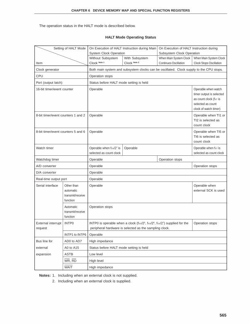
565
CHAPTER 6 DEVICE MEMORY MAP AND SPECIAL FUNCTION REGISTERS
The operation status in the HALT mode is described below.
HALT Mode Operating Status
Setting of HALT Mode On Execution of HALT Instruction during Main On Execution of HALT Instruction during
System Clock Operation Subsystem Clock Operation
Without Subsystem With Subsystem When Main System Clock When Main System Clock
Item Clock Note 1 Clock Note 2 Continues Oscillation Clock Stops Oscillation
Clock generator Both main system and subsystem clocks can be oscillated. Clock supply to the CPU stops.
CPU Operation stops
Port (output latch) Status before HALT mode setting is held
16-bit timer/event counter Operable Operable when watch
timer output is selected
as count clock (fXT is
selected as count
clock of watch timer)
8-bit timer/event counters 1 and 2 Operable Operable when TI1 or
TI2 is selected as
count clock
8-bit timer/event counters 5 and 6 Operable Operable when TI5 or
TI6 is selected as
count clock
Watch timer Operable when fXX/27 is Operable Operable when fXT is
selected as count clock selected as count clock
Watchdog timer Operable Operation stops
A/D converter Operable Operation stops
D/A converter Operable
Real-time output port Operable
Serial interface Other than Operable Operable when
automatic external SCK is used
transmit/receive
function
Automatic Operation stops
transmit/receive
function
External interrupt INTP0 INTP0 is operable when a clock (fXX/25, fXX/26, fXX/27) supplied for the Operation stops
request peripheral hardware is selected as the sampling clock.
INTP1 to INTP6 Operable
Bus line for AD0 to AD7 High impedance
external A0 to A15 Status before HALT mode setting is held
expansion ASTB Low level
WR, RD High level
WAIT High impedance
Notes: 1. Including when an external clock is not supplied.
2. Including when an external clock is supplied.

566
CHAPTER 6 DEVICE MEMORY MAP AND SPECIAL FUNCTION REGISTERS
The operation status in the STOP mode is described below.
STOP Mode Operating Status
Setting of STOP ModeWith Subsystem Clock Without Subsystem Clock
Item
Clock generator Only main system clock stops oscillation
CPU Operation stops
Port (output latch) Status before STOP mode setting is held
16-bit timer/event counter Operable when watch timer output is Operation stopsselected as count clock (fXT is selected ascount clock of watch timer)
8-bit timer/event counters 1 and 2 Operable when TI1 or TI2 is selected for the count clock
8-bit timer/event counters 5 and 6 Operable when TI5 or TI6 is selected for the count clock
Watch timer Operable when fXT is selected for the Operation stopscount clock
Watchdog timer Operation stops
A/D converter
D/A converter Operable
Real-time output port Operable when external trigger is used or TI1 or TI2 is selected for the 8-bittimer/event counter 1 or 2 count clock
Serial interface Other than Operable when externally supplied clock is specified as the serial clockautomatictransmit/receivefunction andUART
Automatic Operation stopstransmit/receivefunction andUART
External interrupt INTP0 Not operablerequest INTP1 to INTP6 Operable
Bus line for AD0 to AD7 High impedanceexternal A0 to A15 Status before STOP mode setting is heldexpansion
ASTB Low level
WR, RD High level
WAIT High impedance
Cautions: 1. When the STOP mode is set, the X2 pin is internally connected to V DD1 via a pull-up resistor to
minimize the leakage current at the crystal oscillator. Thus, do not use the STOP mode in a
system where an external clock is used for the main system clock.
2. Because the interrupt request signal is used to release the Standby mode, if there is an inter-
rupt source with the interrupt request flag set and the interrupt mask flag reset, the Standby
mode is immediately released if set. Thus, the STOP mode is reset to the HALT mode immedi-
ately after execution of the STOP instruction. After the wait set using the oscillation stabiliza-
tion time select register (OSTS), the operating mode is set.

567
CHAPTER 6 DEVICE MEMORY MAP AND SPECIAL FUNCTION REGISTERS
(21) Reset function
The following two operations can generate a reset signal:
• External reset input via the RESET pin
• Internal reset by watchdog timer in the Watchdog Timer mode
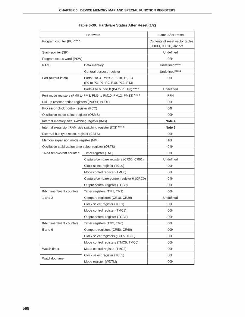
568
CHAPTER 6 DEVICE MEMORY MAP AND SPECIAL FUNCTION REGISTERS
Table 6-30. Hardware Status After Reset (1/2)
Hardware Status After Reset
Program counter (PC) Note 1 Contents of reset vector tables
(0000H, 0001H) are set
Stack pointer (SP) Undefined
Program status word (PSW) 02H
RAM Data memory Undefined Note 2
General-purpose register Undefined Note 2
Port (output latch) Ports 0 to 3, Ports 7, 9, 10, 12, 13 00H
(P0 to P3, P7, P9, P10, P12, P13)
Ports 4 to 6, port 8 (P4 to P6, P8) Note 3 Undefined
Port mode registers (PM0 to PM3, PM5 to PM10, PM12, PM13) Note 3 FFH
Pull-up resistor option registers (PUOH, PUOL) 00H
Processor clock control register (PCC) 04H
Oscillation mode select register (OSMS) 00H
Internal memory size switching register (IMS) Note 4
Internal expansion RAM size switching register (IXS) Note 5 Note 6
External bus type select register (EBTS) 00H
Memory expansion mode register (MM) 10H
Oscillation stabilization time select register (OSTS) 04H
16-bit timer/event counter Timer register (TM0) 00H
Capture/compare registers (CR00, CR01) Undefined
Clock select register (TCL0) 00H
Mode control register (TMC0) 00H
Capture/compare control register 0 (CRC0) 04H
Output control register (TOC0) 00H
8-bit timer/event counters Timer registers (TM1, TM2) 00H
1 and 2 Compare registers (CR10, CR20) Undefined
Clock select register (TCL1) 00H
Mode control register (TMC1) 00H
Output control register (TOC1) 00H
8-bit timer/event counters Timer registers (TM5, TM6) 00H
5 and 6 Compare registers (CR50, CR60) 00H
Clock select registers (TCL5, TCL6) 00H
Mode control registers (TMC5, TMC6) 00H
Watch timer Mode control register (TMC2) 00H
Clock select register (TCL2) 00HWatchdog timer
Mode register (WDTM) 00H
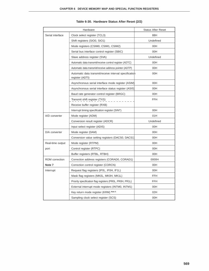
569
CHAPTER 6 DEVICE MEMORY MAP AND SPECIAL FUNCTION REGISTERS
Table 6-30. Hardware Status After Reset (2/2)
Hardware Status After Reset
Serial interface Clock select register (TCL3) 88H
Shift registers (SIO0, SIO1) Undefined
Mode registers (CSIM0, CSIM1, CSIM2) 00H
Serial bus interface control register (SBIC) 00H
Slave address register (SVA) Undefined
Automatic data transmit/receive control register (ADTC) 00H
Automatic data transmit/receive address pointer (ADTP) 00H
Automatic data transmit/receive interval specification 00H
register (ADTI)
Asynchronous serial interface mode register (ASIM) 00H
Asynchronous serial interface status register (ASIS) 00H
Baud rate generator control register (BRGC) 00H
Transmit shift register (TXS) FFH
Receive buffer register (RXB)
Interrupt timing specification register (SINT) 00H
A/D converter Mode register (ADM) 01H
Conversion result register (ADCR) Undefined
Input select register (ADIS) 00H
D/A converter Mode register (DAM) 00H
Conversion value setting registers (DACS0, DACS1) 00H
Real-time output Mode register (RTPM) 00H
port Control register (RTPC) 00H
Buffer registers (RTBL, RTBH) 00H
ROM correction Correction address registers (CORAD0, CORAD1) 0000H
Note 7 Correction control register (CORCN) 00H
Interrupt Request flag registers (IF0L, IF0H, IF1L) 00H
Mask flag registers (MK0L, MK0H, MK1L) FFH
Priority specification flag registers (PR0L, PR0H, PR1L) FFH
External interrupt mode registers (INTM0, INTM1) 00H
Key return mode register (KRM) Note 5 02H
Sampling clock select register (SCS) 00H

570
CHAPTER 6 DEVICE MEMORY MAP AND SPECIAL FUNCTION REGISTERS
Notes: 1. During reset input or oscillation stabilization time wait, only the PC contents among the hardware sta-
tuses become undefined. All other hardware statuses remain unchanged after reset.
2. If the reset signal is input in the Standby mode, the status before reset is retained even after reset.
3. The µPD78070A/70AY Subseries do not have ports 4, 5, 8, and PM5, PM8.
4. The value after reset differs depending on the product, as follows:
µPD78070 µPD78074B µPD78075B µPD78076 µPD78078 µPD78P078
µPD78070Y µPD78074BY µPD78075BY µPD78076Y µPD78078Y µPD78P078Y
IMS C0H C6H C8H CCH CFH
5. This register is not provided for the µPD78070A/70AY Subseries.
6. The value after reset differs depending on the product, as follows:
µPD78076 µPD78078 µPD78P078 µPD78074B µPD78075B
µPD78076Y µPD78078Y µPD78P078Y µPD78074BY µPD78075BY
IXS 0AH 0CH
7. This register is provided only for the µPD78078/78Y Subseries.

571
CHAPTER 6 DEVICE MEMORY MAP AND SPECIAL FUNCTION REGISTERS
(22) Registers controlling ROM correction ( µµµµµPD78078/78Y Subseries only)
The following two types of registers control the ROM correction:
• Correction address registers 0 and 1 (CORAD0 and CORAD1)
• Correction control register (CORCN)
Format of Correction Address Registers 0 and 1
Cautions: 1. Set CORAD0 and CORAD1 when bits 1 (COREN0) and 3 (COREN1) of the correction control
register (CORCN: refer to the figure below) are 0.
2. Only addresses where operation codes are stored can be set in CORAD0 and CORAD1.
3. Do not set the following addresses to CORAD0 and CORAD1:
• Address value in table area of table reference instruction (CALLT instruction): 0040H to 007FH
• Address value in vector table area: 0000H to 003FH
Format of Correction Control Register
Note: Bits 0 and 2 are read-only bits.
7
0
6
0
5
0
4
0 COREN1 CORST1 COREN0 CORST0
Symbol
CORCN
Address
FF8AH
After Reset
COREN0
0
1
CORST0
0
1
COREN1
0
1
CORST1
0
1
R/W
R/W Note00H
Correction address register 0 and fetch address match detection
Not detected
Detected
Correction address register 0 and fetch address matchdetection control
Disabled
Enabled
Correction address register 1 and fetch address match detection
Not detected
Detected
Correction address register 1 and fetch address matchdetection control
Disabled
Enabled
R
R/W
R
R/W
<3> <2> <1> <0>
FF3AH/FF3BH 0000H
Symbol 15
CORAD0
0 Address
FF38H/FF39H
After Reset
0000H
R/W
R/W
CORAD1 R/W
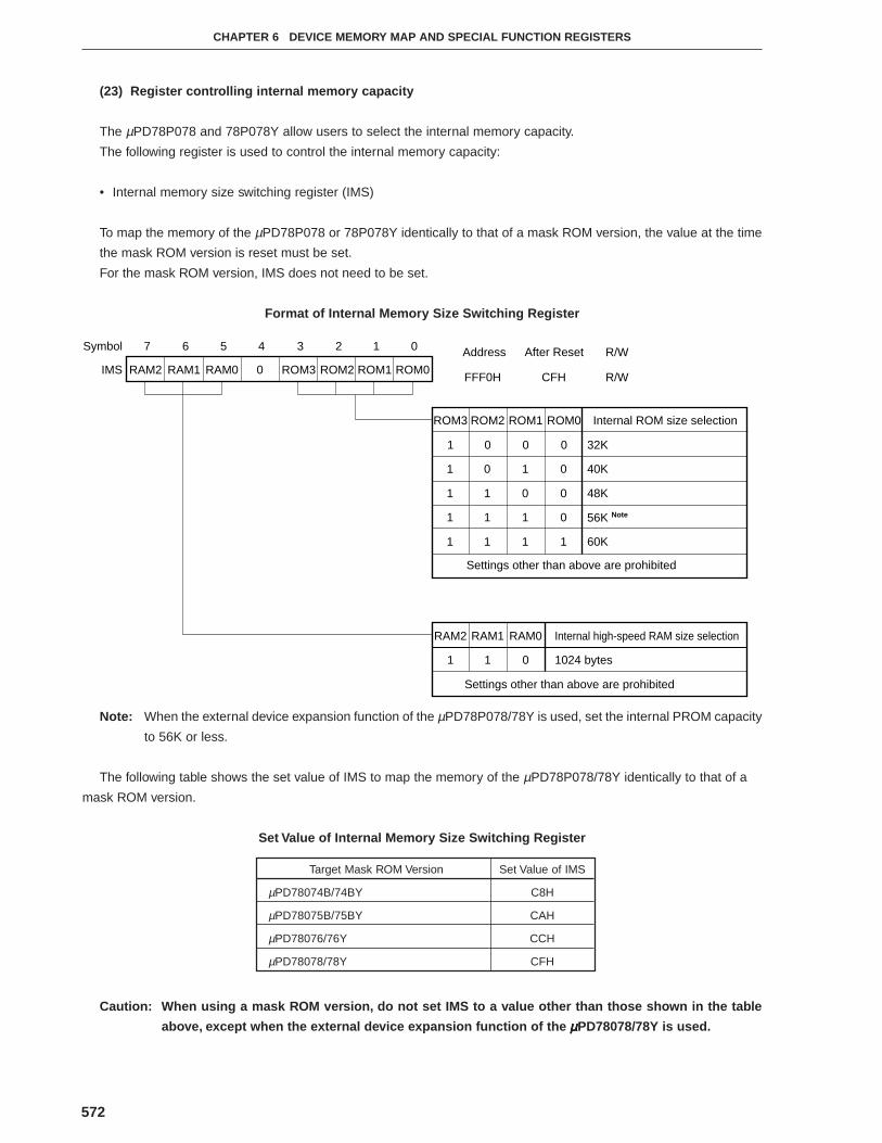
572
CHAPTER 6 DEVICE MEMORY MAP AND SPECIAL FUNCTION REGISTERS
(23) Register controlling internal memory capacity
The µPD78P078 and 78P078Y allow users to select the internal memory capacity.
The following register is used to control the internal memory capacity:
• Internal memory size switching register (IMS)
To map the memory of the µPD78P078 or 78P078Y identically to that of a mask ROM version, the value at the time
the mask ROM version is reset must be set.
For the mask ROM version, IMS does not need to be set.
Format of Internal Memory Size Switching Register
Note: When the external device expansion function of the µPD78P078/78Y is used, set the internal PROM capacity
to 56K or less.
The following table shows the set value of IMS to map the memory of the µPD78P078/78Y identically to that of a
mask ROM version.
Set Value of Internal Memory Size Switching Register
Target Mask ROM Version Set Value of IMS
µPD78074B/74BY C8H
µPD78075B/75BY CAH
µPD78076/76Y CCH
µPD78078/78Y CFH
Caution: When using a mask ROM version, do not set IMS to a value other than those shown in the table
above, except when the external device expansion function of the µµµµµPD78078/78Y is used.
1
1
32K
40K
0
0
0
1
0
0
7
RAM2
Symbol
IMS
6
RAM1
5
RAM0
4
0
3
ROM3
2
ROM2
1
ROM1
0
ROM0
Address
FFF0H CFH
R/W
R/W
Internal ROM size selectionROM3
48K1
ROM2
1
ROM1
0
ROM0
0
56K Note1 1 1 0
60K1 1 1 1
Internal high-speed RAM size selectionRAM2 RAM1 RAM0
1024 bytes1 1 0
Settings other than above are prohibited
After Reset
Settings other than above are prohibited
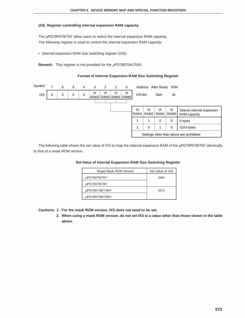
573
CHAPTER 6 DEVICE MEMORY MAP AND SPECIAL FUNCTION REGISTERS
(24) Register controlling internal expansion RAM capacity
The µPD78P078/78Y allow users to select the internal expansion RAM capacity.
The following register is used to control the internal expansion RAM capacity:
• Internal expansion RAM size switching register (IXS)
Remark: This register is not provided for the µPD78070A/70AY.
Format of Internal Expansion RAM Size Switching Register
The following table shows the set value of IXS to map the internal expansion RAM of the µPD78P078/78Y identically
to that of a mask ROM version.
Set Value of Internal Expansion RAM Size Switching Register
Target Mask ROM Version Set Value of IXS
µPD78076/76Y 0AH
µPD78078/78Y
µPD78074B/74BY 0CH
µPD78075B/75BY
Cautions: 1. For the mask ROM version, IXS does not need to be set.
2. When using a mask ROM version, do not set IXS to a value other than those shown in the table
above.
6 5 4 3 2 1 07Symbol
IXS 0 0 0 0 IXRAM3
IXRAM2
IXRAM1
IXRAM0
1
1
Selects internal expansionRAM capacity
0 bytes
Settings other than above are prohibited
FFF4H 0AH W
Address After Reset R/W
IXRAM3
1
IXRAM2
0
IXRAM1
0
1024 bytes0 1 0
IXRAM0

574
CHAPTER 6 DEVICE MEMORY MAP AND SPECIAL FUNCTION REGISTERS
[MEMO]
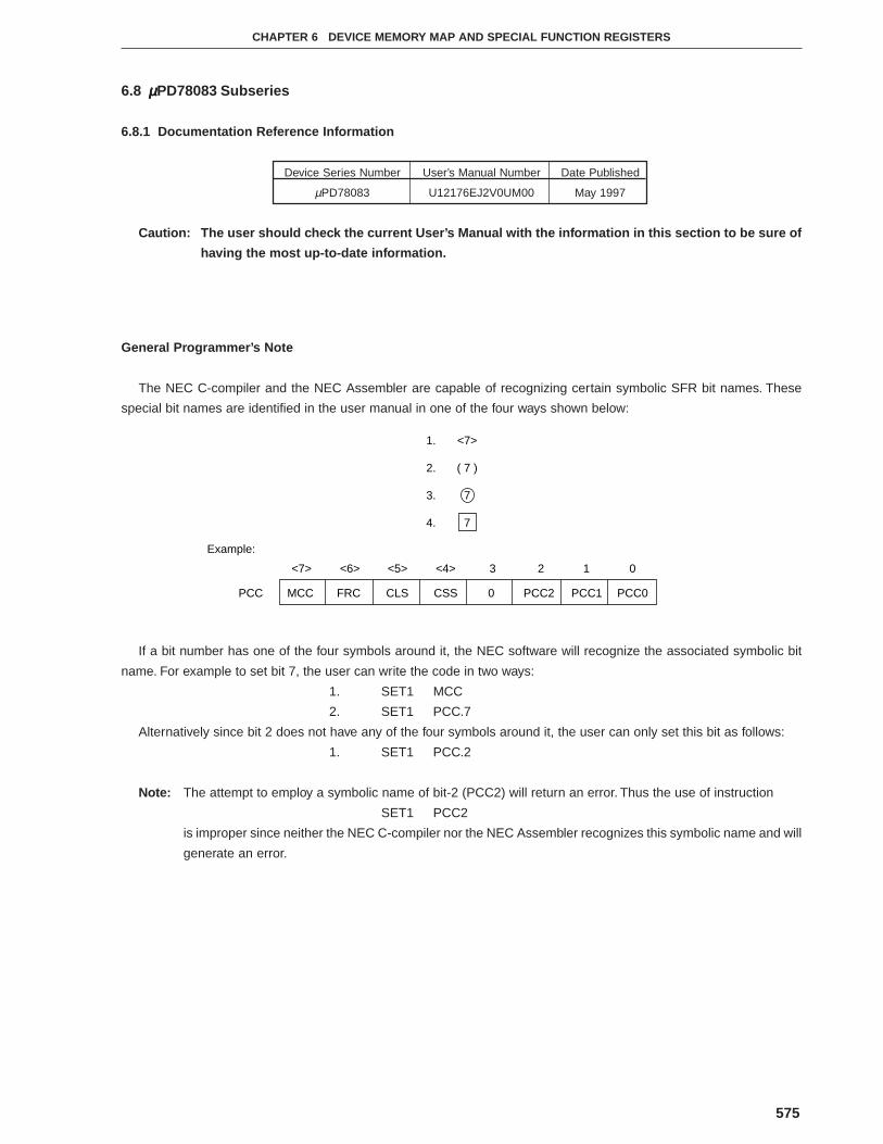
575
CHAPTER 6 DEVICE MEMORY MAP AND SPECIAL FUNCTION REGISTERS
6.8 µµµµµPD78083 Subseries
6.8.1 Documentation Reference Information
Device Series Number User’s Manual Number Date Published
µPD78083 U12176EJ2V0UM00 May 1997
Caution: The user should check the current User’s Manual with the information in this section to be sure of
having the most up-to-date information.
General Programmer’s Note
The NEC C-compiler and the NEC Assembler are capable of recognizing certain symbolic SFR bit names. These
special bit names are identified in the user manual in one of the four ways shown below:
If a bit number has one of the four symbols around it, the NEC software will recognize the associated symbolic bit
name. For example to set bit 7, the user can write the code in two ways:
1. SET1 MCC
2. SET1 PCC.7
Alternatively since bit 2 does not have any of the four symbols around it, the user can only set this bit as follows:
1. SET1 PCC.2
Note: The attempt to employ a symbolic name of bit-2 (PCC2) will return an error. Thus the use of instruction
SET1 PCC2
is improper since neither the NEC C-compiler nor the NEC Assembler recognizes this symbolic name and will
generate an error.
MCCPCC FRC CLS CSS 0 PCC2 PCC1 PCC0
<7> <6> <5> <4> 3 2 1 0
Example:
1.
2.
3.
4.
<7>
( 7 )
7
7

576
CHAPTER 6 DEVICE MEMORY MAP AND SPECIAL FUNCTION REGISTERS
6.8.2 Memory Address Space
Each model in the µPD78083 Subseries can access a memory space of 64K. Figures 6-40 through 6-42 show
memory maps of the respective models.
Figure 6-40. Memory Map ( µPD78081)
Data memory space
General-purpose registers32 × 8 bits
Internal ROM8192 × 8 bits
CALLF entry area
CALLT table area
Vector table area
Program area
Program area
Reserved
Programmemoryspace
Internal high-speed RAM256 × 8 bits
Special function registers (SFRs)
256 × 8 bitsFF00HFEFFH
FEE0HFEDFH
FE00HFDFFH
2000H1FFFH
0000H
1FFFH
0000H
1000H0FFFH
0800H07FFH
0080H 007FH
0040H003FH
FFFFH

577
CHAPTER 6 DEVICE MEMORY MAP AND SPECIAL FUNCTION REGISTERS
Figure 6-41. Memory Map ( µPD78082)
Data memory space
Internal ROM16384 × 8 bits
CALLF entry area
CALLT table area
Vector table area
Program area
Program area
Reserved
Programmemoryspace
Internal high-speed RAM384 × 8 bits
Special function registers (SFRs)
256 × 8 bitsFF00HFEFFH
FEE0HFEDFH
FD80HFD7FH
4000H3FFFH
FFFFH
1000H0FFFH
0800H07FFH
0080H 007FH
0040H003FH
3FFFH
0000H0000H
General-purpose registers32 × 8 bits
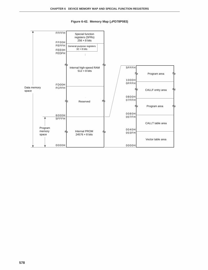
578
CHAPTER 6 DEVICE MEMORY MAP AND SPECIAL FUNCTION REGISTERS
Figure 6-42. Memory Map ( µPD78P083)
Data memory space
Internal PROM24576 × 8 bits
CALLF entry area
CALLT table area
Vector table area
Program area
Program area
Reserved
Programmemoryspace
Internal high-speed RAM512 × 8 bits
Special function registers (SFRs)
256 × 8 bitsFF00HFEFFH
FEE0HFEDFH
FD00HFCFFH
6000H5FFFH
FFFFH
1000H0FFFH
0800H07FFH
0080H 007FH
0040H003FH
5FFFH
0000H0000H
General-purpose registers32 × 8 bits

579
CHAPTER 6 DEVICE MEMORY MAP AND SPECIAL FUNCTION REGISTERS
6.8.3 Special Function Registers (SFRs)
Table 6-31. Special Function Register List ( µPD78083 Subseries) (1/2)
Manipulatable After
Address Special Function Register (SFR) Name Symbol R/W Bit Unit Reset
1 Bit 8 Bits 16 Bits
FF00H Port 0 P0 R/W √ √ – 00H
FF01H Port 1 P1 √ √ –
FF03H Port 3 P3 √ √ –
FF05H Port 5 P5 √ √ –
FF07H Port 7 P7 √ √ –
FF0AH Port 10 P10 √ √ –
FF1FH A/D conversion result register ADCR R – √ – Undefined
FF20H Port mode register 0 PM0 R/W √ √ – FFH
FF21H Port mode register 1 PM1 √ √ –
FF23H Port mode register 3 PM3 √ √ –
FF25H Port mode register 5 PM5 √ √ –
FF27H Port mode register 7 PM7 √ √ –
FF2AH Port mode register 10 PM10 √ √ –
FF40H Timer clock select register 0 TCL0 √ √ – 00H
FF42H Timer clock select register 2 TCL2 – √ –
FF50H Compare register 50 CR50 – √ –
FF51H 8-bit timer register 5 TM5 R – √ –
FF52H Timer clock select register 5 TCL5 R/W – √ –
FF53H 8-bit timer mode control register 5 TMC5 √ √ –
FF54H Compare register 60 CR60 – √ –
FF55H 8-bit timer register 6 TM6 R – √ –
FF56H Timer clock select register 6 TCL6 R/W – √ –
FF57H 8-bit timer mode control register 6 TMC6 √ √ –
FF70H Asynchronous serial interface mode register ASIM √ √ –
FF71H Asynchronous serial interface status register ASIS R √ √ –
FF72H Serial operation mode register 2 CSIM2 R/W √ √ –
FF73H Baud rate generator control register BRGC – √ –
FF74H Transmit shift register TXS SIO2 W – √ – FFH
Receive buffer register RXB R
FF80H A/D converter mode register ADM R/W √ √ – 01H
FF84H A/D converter input select register ADIS – √ – 00H
FFE0H Interrupt request flag register 0L IF0 IF0L √ √ √
FFE1H Interrupt request flag register 0H IF0H √ √
FFE2H Interrupt request flag register 1L IF1L √ √ –
FFE4H Interrupt mask flag register 0L MK0 MK0L √ √ √ FFH
FFE5H Interrupt mask flag register 0H MK0H √ √
FFE6H Interrupt mask flag register 1L MK1L √ √ –

580
CHAPTER 6 DEVICE MEMORY MAP AND SPECIAL FUNCTION REGISTERS
Table 6-31. Special Function Register List ( µPD78083 Subseries) (2/2)
Manipulatable After
Address Special Function Register (SFR) Name Symbol R/W Bit Unit Reset
1 Bit 8 Bits 16 Bits
FFE8H Priority order specification flag register 0L PR0 PR0L R/W √ √ √ FFH
FFE9H Priority order specification flag register 0H PR0H √ √
FFEAH Priority order specification flag register 1L PR1L √ √ –
FFECH External interrupt mode register 0 INTM0 – √ – 00H
FFEDH External interrupt mode register 1 INTM1 – √ –
FFF0H Internal memory size switching register IMS – √ – Note
FFF2H Oscillation mode select register OSMS W – √ – 00H
FFF3H Pull-up resistor option register H PUOH R/W √ √ –
FFF7H Pull-up resistor option register L PUOL √ √ –
FFF9H Watchdog timer mode register WDTM √ √ –
FFFAH Oscillation stabilization time select register OSTS – √ – 04H
FFFBH Processor clock control register PCC √ √ –
Note: The value after reset depends on products:
µPD78081: 82H, µPD78082: 64H, µPD78P083: 46H.
581
CHAPTER 6 DEVICE MEMORY MAP AND SPECIAL FUNCTION REGISTERS
(1) Registers controlling port functions
The following two types of registers control the ports:
• Port mode registers (PM0, PM1, PM3, PM5, PM7, PM10)
• Pull-up resistor option registers (PUOH, PUOL)

582
CHAPTER 6 DEVICE MEMORY MAP AND SPECIAL FUNCTION REGISTERS
Format of Port Mode Registers
Caution: Be sure to set bits 0 and 4 to 7 of PM0, bits 3 to 7 of PM7, and bits 2 to 7 of PM10 to 1.
Format of Pull-up Resistor Option Registers
Cautions: 1. Be sure to set bits 0, 1 and 3 through 7 of PUOH and bits 2, 4, and 6 of PUOL to 0.
2. P00 pin does not incorporate a pull-up resistor.
3. When a pin of port 1 is used as an alternate function pin, an on-chip pull-up resistor cannot
be used even if 1 is set in PUOL bit 1 (PUO1).
PM0
PM1
1 1 PM03 PM02 PM01 1
7 6 5 4 3 2 1 0Symbol
PM3
PM5
FF20H
FF21H
FF23H
FF25H
FFH
FFH
FFH
FFH
R/W
R/W
R/W
R/W
AddressAfterReset R/W
PM17 PM16 PM15 PM14 PM13 PM12 PM11 PM10
PM37 PM36 PM35 PM34 PM33 PM32 PM31 PM30
PM57 PM56 PM55 PM54 PM53 PM52 PM51 PM50
PM7 FF27H FFH R/W1 1 1 1 1 PM72 PM71 PM70
1 1
PM10
PMmn Pmn pin input/output mode selection(m = 0, 1, 3, 5, 7, 10 : n = 0 to 7)
0
1
Output mode (output buffer ON)
Input mode (output buffer OFF)
FF2AH FFH R/W1 1 1 1 1 1 PM101 PM100
PUO7 0 PUO5 0 0 PUO1 PUO0PUOL
PUOm Pm internal pull-up resistor selection(m = 0, 1, 3, 5, 7, 10)
0
1
Internal pull-up resistor not used
Internal pull-up resistor used
FFF7H 00H R/W
6 <5> 4
PUO3
<3> 2 <0><1>
0 0 0 0 PUO10 0 0PUOH FFF3H 00H R/W
7 6 5 4Symbol AddressAfterReset R/W
0
3 <2> 01
<7>
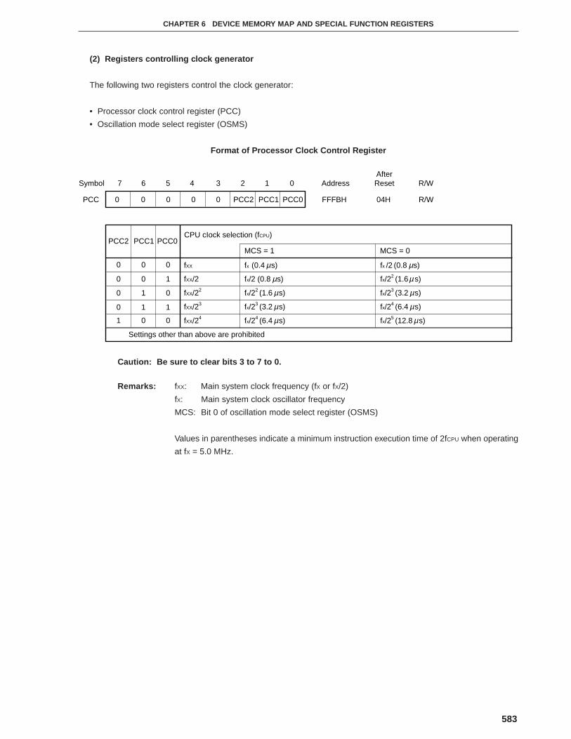
583
CHAPTER 6 DEVICE MEMORY MAP AND SPECIAL FUNCTION REGISTERS
(2) Registers controlling clock generator
The following two registers control the clock generator:
• Processor clock control register (PCC)
• Oscillation mode select register (OSMS)
Format of Processor Clock Control Register
Caution: Be sure to clear bits 3 to 7 to 0.
Remarks: fXX: Main system clock frequency (fX or fX/2)
fX: Main system clock oscillator frequency
MCS: Bit 0 of oscillation mode select register (OSMS)
Values in parentheses indicate a minimum instruction execution time of 2fCPU when operating
at fX = 5.0 MHz.
0 0 0 0 PCC2 PCC1 PCC0PCC FFFBH 04H R/W
7 6 5 4Symbol AddressAfterReset R/W
0
3 2 01
0
0 fXX/2
PCC2CPU cIock selection (fCPU)
PCC1 PCC0
0
0
0
1
0
0
1
1
0
1
1 0 0
fXX/22
fXX/23
fXX/24
fXX
fx/2 (0.8 s)µ
fx/22 (1.6 s)µ
fx/23 (3.2 s)µ
fx/24 (6.4 s)µ
fx (0.4 s)µ
fx/22 (1.6 s)µ
fx/23 (3.2 s)µ
fx/24 (6.4 s)µ
fx/25 (12.8 s)µ
fx /2 (0.8 s)µ
MCS = 1 MCS = 0
Settings other than above are prohibited
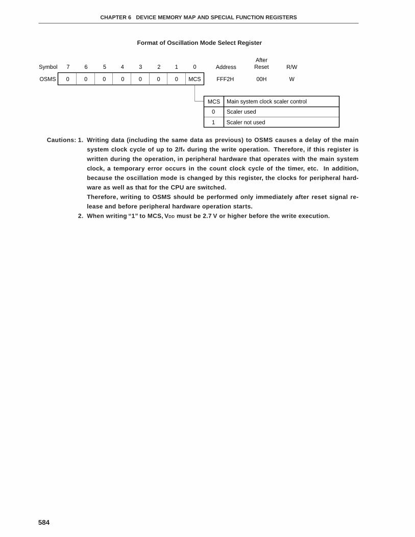
584
CHAPTER 6 DEVICE MEMORY MAP AND SPECIAL FUNCTION REGISTERS
Format of Oscillation Mode Select Register
Cautions: 1. Writing data (including the same data as previous) to OSMS causes a delay of the main
system clock cycle of up to 2/f x during the write operation. Therefore, if this register is
written during the operation, in peripheral hardware that operates with the main system
clock, a temporary error occurs in the count clock cycle of the timer, etc. In addition,
because the oscillation mode is changed by this register, the clocks for peripheral hard-
ware as well as that for the CPU are switched.
Therefore, writing to OSMS should be performed only immediately after reset signal re-
lease and before peripheral hardware operation starts.
2. When writing “1” to MCS, V DD must be 2.7 V or higher before the write execution.
MCS Main system clock scaler control
0
1
Scaler used
Scaler not used
0 0 0 0OSMS FFF2H
7 6 5 4 3 2Symbol 1
0 MCS
0
0
AddressAfterReset R/W
00H W0
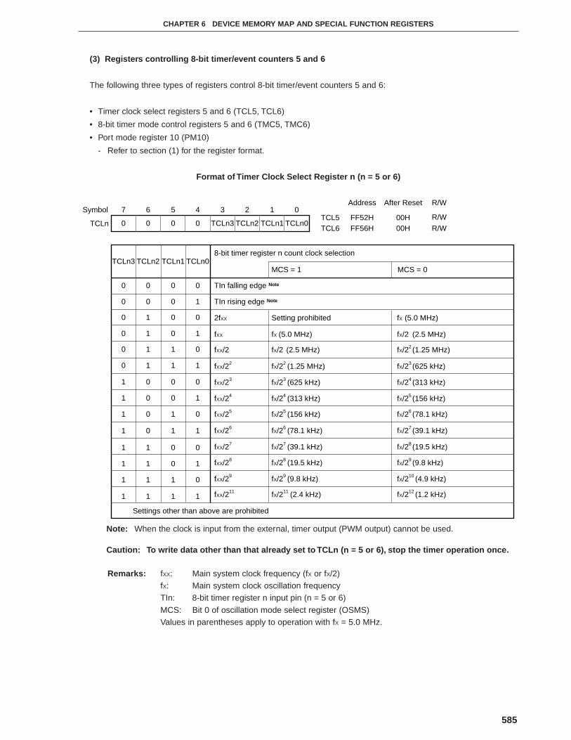
585
CHAPTER 6 DEVICE MEMORY MAP AND SPECIAL FUNCTION REGISTERS
(3) Registers controlling 8-bit timer/event counters 5 and 6
The following three types of registers control 8-bit timer/event counters 5 and 6:
• Timer clock select registers 5 and 6 (TCL5, TCL6)
• 8-bit timer mode control registers 5 and 6 (TMC5, TMC6)
• Port mode register 10 (PM10)
- Refer to section (1) for the register format.
Format of Timer Clock Select Register n (n = 5 or 6)
Note: When the clock is input from the external, timer output (PWM output) cannot be used.
Caution: To write data other than that already set to TCLn (n = 5 or 6), stop the timer operation once.
Remarks: fXX: Main system clock frequency (fX or fX/2)fX: Main system clock oscillation frequencyTIn: 8-bit timer register n input pin (n = 5 or 6)
MCS: Bit 0 of oscillation mode select register (OSMS)Values in parentheses apply to operation with fX = 5.0 MHz.
0 0 0 0 TCLn3 TCLn2 TCLn1 TCLn0
7 6 5 4 3 2 1 0Symbol
TCLnFF56H 00H R/W
R/WFF52HTCL6TCL5 00H
Address After Reset R/W
TCLn3 TCLn2 TCLn1 TCLn0
0 0 0 0 TIn falling edge Note
0 0 0 1 TIn rising edge Note
0 1 1 0
0 1 1 1
fXX/2 fX/2 (2.5 MHz) fX/22 (1.25 MHz)
1 0 0 0
fXX/22 fX/22 (1.25 MHz) fX/23 (625 kHz)
0 1 0 0
0 1 0 1
2fXX Setting prohibited fX (5.0 MHz)
fXX fX (5.0 MHz) fX/2 (2.5 MHz)
1 0 0 1
fXX/23 fX/23 (625 kHz) fX/24 (313 kHz)
1 0 1 0
fXX/24 fX/24 (313 kHz) fX/25 (156 kHz)
1 0 1 1
fXX/25 fX/25 (156 kHz) fX/26 (78.1 kHz)
1 1 0 0
fXX/26 fX/26 (78.1 kHz) fX/27 (39.1 kHz)
1 1 0 1
fXX/27 fX/27 (39.1 kHz) fX/28 (19.5 kHz)
1 1 1 0
fXX/28 fX/28 (19.5 kHz) fX/29 (9.8 kHz)
1 1 1 1
fXX/29 fX/29 (9.8 kHz) fX/210 (4.9 kHz)
MCS = 1
8-bit timer register n count clock selection
MCS = 0
Settings other than above are prohibited
fXX/211 fX/211 (2.4 kHz) fX/212 (1.2 kHz)
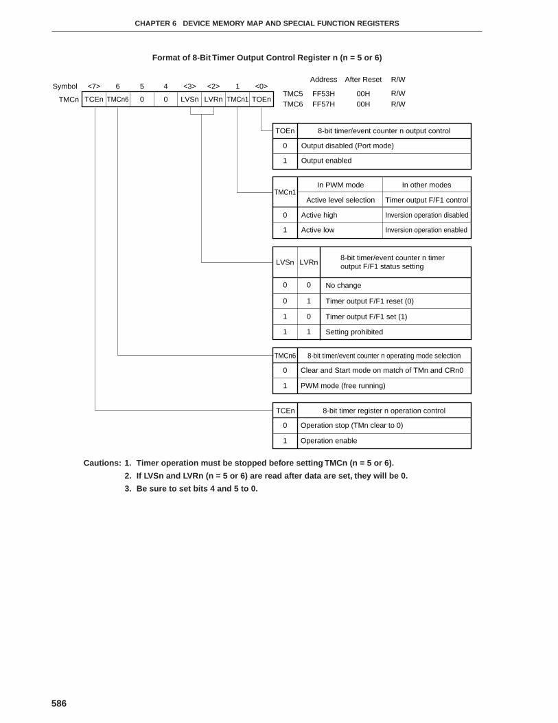
586
CHAPTER 6 DEVICE MEMORY MAP AND SPECIAL FUNCTION REGISTERS
Format of 8-Bit Timer Output Control Register n (n = 5 or 6)
Cautions: 1. Timer operation must be stopped before setting TMCn (n = 5 or 6).
2. If LVSn and LVRn (n = 5 or 6) are read after data are set, they will be 0.
3. Be sure to set bits 4 and 5 to 0.
TCEn TMCn6 0 0 LVSn LVRn TMCn1 TOEn
<7> 6 5 4 <3> <2> 1 <0>Symbol
TMCn
TOEn 8-bit timer/event counter n output control
0 Output disabled (Port mode)
1 Output enabled
TMCn1
0 Active high
1 Active low
In PWM mode In other modes
Active level selection Timer output F/F1 control
Inversion operation disabled
Inversion operation enabled
LVSn LVRn
0 0
0 1
1 0
1 1
8-bit timer/event counter n timer output F/F1 status setting
No change
Timer output F/F1 reset (0)
Timer output F/F1 set (1)
Setting prohibited
TMCn6 8-bit timer/event counter n operating mode selection
0 Clear and Start mode on match of TMn and CRn0
1 PWM mode (free running)
TCEn 8-bit timer register n operation control
0 Operation stop (TMn clear to 0)
1 Operation enable
FF57H 00H R/W
R/WFF53HTMC6TMC5 00H
Address After Reset R/W
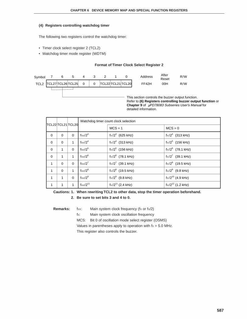
587
CHAPTER 6 DEVICE MEMORY MAP AND SPECIAL FUNCTION REGISTERS
(4) Registers controlling watchdog timer
The following two registers control the watchdog timer:
• Timer clock select register 2 (TCL2)
• Watchdog timer mode register (WDTM)
Format of Timer Clock Select Register 2
Cautions: 1. When rewriting TCL2 to other data, stop the timer operation beforehand.
2. Be sure to set bits 3 and 4 to 0.
Remarks: fXX: Main system clock frequency (fX or fX/2)
fX: Main system clock oscillation frequency
MCS: Bit 0 of oscillation mode select register (OSMS)
Values in parentheses apply to operation with fX = 5.0 MHz.
This register also controls the buzzer.
TCL27
7
TCL26
6
TCL25 0
4
0
3 2 1 0
FF42H
Address
TCL2
Symbol
TCL22 TCL21 TCL20
5
00H
After Reset
R/W
R/W
0
0
0
0
1
1
1
1
0
0
1
1
0
0
1
1
0
1
0
1
0
1
0
1
TCL22 TCL21 TCL20
fXX/23
fXX/24
fXX/25
fXX/26
fXX/27
fXX/28
fXX/29
fXX/211
MCS = 1
fX /23
fX /24
fX /25
fX /26
fX /27
fX /28
fX /29
fX /211
MCS = 0
fX /24
fX /25
fX /26
fX /27
fX /28
fX /29
fX /210
fX /212
Watchdog timer count clock selection
(625 kHz)
(313 kHz)
(156 kHz)
(78.1 kHz)
(39.1 kHz)
(19.5 kHz)
(9.8 kHz)
(2.4 kHz)
(313 kHz)
(156 kHz)
(78.1 kHz)
(39.1 kHz)
(19.5 kHz)
(9.8 kHz)
(4.9 kHz)
(1.2 kHz)
This section controls the buzzer output function.Refer to (6) Registers controlling buzzer output function orChapter 9 of PD78083 Subseries User's Manual fordetailed information.
µ

588
CHAPTER 6 DEVICE MEMORY MAP AND SPECIAL FUNCTION REGISTERS
Format of Watchdog Timer Mode Register
Notes: 1. Once set to 1, WDTM3 and WDTM4 cannot be cleared to 0 by software.
2. The watchdog timer starts operating as an interval timer as soon as RUN has been set to 1.
3. Once set to 1, RUN cannot be cleared to 0 by software.
Thus, once counting starts, counting can only be stopped by RESET input.
Cautions: 1. When 1 is set in RUN so that the watchdog timer is cleared, the actual overflow time is up to
0.5% shorter than the time set by timer clock select register 2 (TCL2).
2. To use watchdog timer modes 1 and 2, make sure that the interrupt request flag (TMIF4) is
0, and then set WDTM4 to 1.
If WDTM4 is set to 1 when TMIF4 is 1, the non-maskable interrupt request occurs, regard-
less of the contents of WDTM3.
Remark: ×: Don’t care
RUN
<7>
0
6
0 WDTM4
4
WDTM3
3 2 1 0
FFF9H
Address
WDTM
Symbol
0 0 0
5
00H
AfterReset
R/W
R/W
RUN
0
1
Watchdog timer operation mode selection Note 3
Count stop
Counter is cleared and counting starts
WDTM3
×
0
1
Watchdog timer operation modeselection Note 1
Interval timer mode Note 2
(Maskable interrupt occurs upon generation of an overflow.)
Watchdog timer mode 1(Non-maskable interrupt occurs upongeneration of an overflow.)
Watchdog timer mode 2(Reset operation is activated upongeneration of an overflow.)
WDTM4
0
1
1
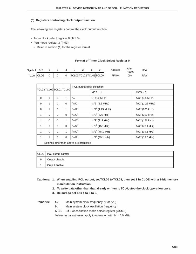
589
CHAPTER 6 DEVICE MEMORY MAP AND SPECIAL FUNCTION REGISTERS
(5) Registers controlling clock output function
The following two registers control the clock output function:
• Timer clock select register 0 (TCL0)
• Port mode register 3 (PM3)
- Refer to section (1) for the register format.
Format of Timer Clock Select Register 0
Cautions: 1. When enabling PCL output, set TCL00 to TCL03, then set 1 in CLOE with a 1-bit memory
manipulation instruction.
2. To write data other than that already written to TCL0, stop the clock operation once.
3. Be sure to set bits 4 to 6 to 0.
Remarks: fXX: Main system clock frequency (fX or fX/2)
fX: Main system clock oscillation frequency
MCS: Bit 0 of oscillation mode select register (OSMS)
Values in parentheses apply to operation with fX = 5.0 MHz.
CLOE
<7>
0
6
0 0
4
TCL03
3 2 1 0
FF40H
Address
TCL0
Symbol
TCL02 TCL01 TCL00
5
00H
After Reset
R/W
R/W
0
0
0
1
1
1
1
1
1
1
1
0
0
0
0
1
0
1
1
0
0
1
1
0
TCL03 TCL02 TCL01
fXX
fXX/2
fXX/22
fXX/23
fXX/24
fXX/25
fXX/26
fXX/27
MCS = 1
fX (5.0 MHz)
fX /2 (2.5 MHz)
fX /22 (1.25 MHz)
fX /23 (625 kHz)
fX /24 (313 kHz)
fX /25 (156 kHz)
fX /26 (78.1 kHz)
fX /27 (39.1 kHz)
MCS = 0
fX /2 (2.5 MHz)
fX /22 (1.25 MHz)
fX /23 (625 kHz)
fX /24 (313 kHz)
fX /25 (156 kHz)
fX /26 (78.1 kHz)
fX /27 (39.1 kHz)
fX /28 (19.5 kHz)
PCL output clock selection
CLOE
0
1
PCL output control
Output disable
Output enable
TCL00
1
0
1
0
1
0
1
0
Settings other than above are prohibited

590
CHAPTER 6 DEVICE MEMORY MAP AND SPECIAL FUNCTION REGISTERS
(6) Registers controlling buzzer output function
The following two registers control the buzzer output function:
• Timer clock select register 2 (TCL2)
• Port mode register 3 (PM3)
- Refer to section (1) for the register format.
Format of Timer Clock Select Register 2
Cautions: 1. When rewriting TCL2 to other data, stop the timer operation beforehand.
2. Be sure to set bits 3 and 4 to 0.
Remarks: fXX: Main system clock frequency (fX or fX/2)
fX: Main system clock oscillation frequency
×: Don't care
MCS: Bit 0 of oscillation mode select register (OSMS)
Values in parentheses apply to operation with fX = 5.0 MHz.
TCL27
7
TCL26
6
TCL25 0
4
0
3 2 1 0
FF42H
Address
TCL2
Symbol
TCL22 TCL21 TCL20
5
00H
After Reset
R/W
R/W
0
1
1
1
1
×
0
0
1
1
×
0
1
0
1
TCL27 TCL26 TCL25
Buzzer output disable
fXX/29
fXX/210
fXX/211
Setting prohibited
MCS = 1
fX /29 (9.8 kHz)
fX /210 (4.9 kHz)
fX /211 (2.4 kHz)
MCS = 0
fX /210 (4.9 kHz)
fX /211 (2.4 kHz)
fX /212 (1.2 kHz)
Buzzer output frequency selection
This section controls the watchdog timer output function.Refer to (4) Registers controlling watchdog timer orChapter 7 of PD78083 Subseries User's Manual fordetailed information.
µ

591
CHAPTER 6 DEVICE MEMORY MAP AND SPECIAL FUNCTION REGISTERS
(7) Registers controlling A/D converter
The following three registers control the A/D converter:
• A/D converter mode register (ADM)
• A/D converter input select register (ADIS)
• External interrupt mode register 1 (INTM1)
- Refer to section (19) for the register format.
592
CHAPTER 6 DEVICE MEMORY MAP AND SPECIAL FUNCTION REGISTERS
Format of A/D Converter Mode Register
Notes: 1. Set so that the A/D conversion time is 19.1 µs or more.
2. Setting prohibited because the A/D conversion time is less than 19.1 µs.
Cautions: 1. The following sequence is recommended for power consumption reduction of the A/D
converter when the standby function is used: Clear bit 7 (CS) to 0 first to stop the A/D
conversion operation, and then execute the HALT or STOP instruction.
2. When restarting the stopped A/D conversion operation, start the A/D conversion op-
eration after clearing the interrupt request flag (ADIF) to 0.
Remarks: fX: Main system clock oscillation frequency
MCS: Bit 0 of oscillation mode select register (OSMS)
CS
<7>
TRG
<6>
FR1 FR0
4
ADM3
3 2 1 0
FF80H
Address
ADM
Symbol
ADM2 ADM1 HSC
5
01H
After Reset
R/W
R/W
ADM3
0
0
0
0
1
1
1
1
ADM2
0
0
1
1
0
0
1
1
ADM1
0
1
0
1
0
1
0
1
Analog input channel selection
ANI0
ANI1
ANI2
ANI3
ANI4
ANI5
ANI6
ANI7
TRG
0
1
External trigger selection
No external trigger (software starts)
Conversion started by external trigger (hardware starts)
FR1
0
0
1
1
FR0
0
1
0
0
A/D conversion time selection Note 1
fX = 5.0-MHz operation
MCS = 1
80/fX (Setting prohibited Note 2)
40/fX (Setting prohibited Note 2)
50/fX (Setting prohibited Note 2)
100/fX (20.0 s)µ
MCS = 0
160/fX (32.0 s)
80/fX (Setting prohibited Note 2)
100/fX (20.0 s)
200/fX (40.0 s)
fX = 4.19-MHz operation
MCS = 1
80/fX (19.1 s)
40/fX (Setting prohibited Note 2)
50/fX (Setting prohibited Note 2)
100/fX (23.8 s)
MCS = 0
160/fX (38.1 s)
80/fX (19.1 s)
100/fX (23.8 s)
200/fX (47.7 s)µ
µ
µ
µ µ
µ
µ
CS
0
1
A/D conversion operation control
Operation stop
Operation start
HSC
1
1
0
1
µ µ
Settings other than above are prohibited

593
CHAPTER 6 DEVICE MEMORY MAP AND SPECIAL FUNCTION REGISTERS
Format of A/D Converter Input Select Register
Cautions: 1. Set the analog input channel in the following order:
a. Set the number of analog input channels with ADIS.
b. Using the A/D converter mode register (ADM), select one channel to undergo A/D con-
version from among the channels set for analog input with ADIS.
2. No internal pull-up resistor can be used to the channels set for analog input with ADIS,
irrespective of the value of bit 1 (PUO1) of pull-up resistor option register L (PUOL).
0
7
0
6
0 0
4
ADIS3
3 2 1 0
FF84H
Address
ADIS
Symbol
ADIS2 ADIS1 ADIS0
5
00H
AfterReset
R/W
R/W
ADIS3
0
0
0
0
0
0
0
0
1
Number of analog input channel selection
No analog input channel (P10 to P17)
1 channel (ANI0, P11 to P17)
2 channels (ANI0, ANI1, P12 to P17)
3 channels (ANI0 to ANI2, P13 to P17)
4 channels (ANI0 to ANI3, P14 to P17)
5 channels (ANI0 to ANI4, P15 to P17)
6 channels (ANI0 to ANI5, P16, P17)
7 channels (ANI0 to ANI6, P17)
8 channels (ANI0 to ANI7)
ADIS2
0
0
0
0
1
1
1
1
0
ADIS1
0
0
1
1
0
0
1
1
0
ADIS0
0
1
0
1
0
1
0
1
0
Settings other than above are prohibited
594
CHAPTER 6 DEVICE MEMORY MAP AND SPECIAL FUNCTION REGISTERS
(8) Registers controlling serial interface channel 2
The following four registers control serial interface channel 2:
• Serial operation mode register 2 (CSIM2)
• Asynchronous serial interface mode register (ASIM)
• Asynchronous serial interface status register (ASIS)
• Baud rate generator control register (BRGC)
Format of Serial Operation Mode Register 2
Cautions: 1. Be sure to set bits 0 and 3 to 6 to 0.
2. When UART mode is selected, CSIM2 should be set to 00H.
6 5 4 3 2 1 0<7>Symbol
CSIM2 CSIE2 0 0 0 0 CSIM22
CSCK 0 FF72H 00H R/W
Address After Reset R/W
CSCK
0
1
Clock selection in 3-wire serial I/O mode
Input clock from off-chip to SCK2 pin
Dedicated baud rate generator output
CSIM22
0
1
First bit specification
MSB
LSB
CSIE2
0
1
Operation control in 3-wire serial I/O mode
Operation stopped
Operation enabled

595
CHAPTER 6 DEVICE MEMORY MAP AND SPECIAL FUNCTION REGISTERS
Format of Asynchronous Serial Interface Mode Register
Note: When SCK is set to 1 and the baud rate generator output is selected, the ASCK pin can be used as an
input/output port.
Cautions: 1. When the 3-wire serial I/O mode is selected, 00H should be set in ASIM.
2. The serial transmit/receive operation must be stopped before changing the operating mode.
<6> 5 4 3 2 1 0<7>Symbol
ASIM TXE RXE PS1 PS0 CL SL ISRM SCK FF70H 00H R/W
Address After Reset R/W
SCK
0
1
Clock selection in asynchronous serial interfacemode
Input clock from off-chip to ASCK pin
Dedicated baud rate generator output Note
ISRM
0
1
Control of reception completion interrupt in caseof error generation
Reception completion interrupt generated in caseof error generation
Reception completion interrupt not generated incase of error generation
SL Transmit data stop bit length specification
CL
1
Character length specification
7 bits
8 bits
RXE
0
1
Receive operation control
Receive operation stopped
Receive operation enabled
TXE
0
1
Transmit operation control
Transmit operation stopped
Transmit operation enabled
PS1
0
1
0 1 bit
1 2 bits
0
Parity bit specification
No parity
Even parity
PS0
0
1
0 parity always added in transmissionNo parity test in reception (parity error notgenerated)
0 1
1 Odd parity0
596
CHAPTER 6 DEVICE MEMORY MAP AND SPECIAL FUNCTION REGISTERS
Format of Asynchronous Serial Interface Status Register
Notes: 1. The receive buffer register (RXB) must be read when an overrun error is generated. Overrun errors
will continue to be generated until RXB is read.
2. Even if the stop bit length has been set as 2 bits by bit 2 (SL) of the asynchronous serial interface
mode register (ASIM), only single stop bit detection is performed during reception.
PE
6 5 4 3 2 1 07Symbol
ASIS 0 0 0 0 0 FE OVE FF71H 00H R
Address After Reset R/W
OVE
0
1
Overrun error flag
Overrun error not generated
Overrun error generated Note 1 (when next receive operation is completed before data from receive buffer register is read)
FE
0
1
Framing error flag
Framing error not generated
Framing error generated Note 2 (when stop bit is not detected)
PE
0
1
Parity error flag
Parity error not generated
Parity error generated (when transmit data paritydoes not match)
597
CHAPTER 6 DEVICE MEMORY MAP AND SPECIAL FUNCTION REGISTERS
Format of Baud Rate Generator Control Register (1/2)
Note: Can only be used in 3-wire serial I/O mode.
Remarks: fSCK: 5-bit counter source clock
k: Value set in MDL0 to MDL3 (0 ≤ k ≤ 14)
Baud rate generator input clock selectionMDL3 MDL2 MDL1 MDL0
0
0
0
0
0
0
0
0
1
1
1
1
1
1
1
1
0
0
0
0
1
1
1
1
0
0
0
0
1
1
1
1
0
0
1
1
0
0
1
1
0
0
1
1
0
0
1
1
0
1
0
1
0
1
0
1
0
1
0
1
0
1
0
1
fSCK/16
fSCK/17
fSCK/18
fSCK/19
fSCK/20
fSCK/21
fSCK/22
fSCK/23
fSCK/24
fSCK/25
fSCK/26
fSCK/27
fSCK/28
fSCK/29
fSCK/30
fSCK Note
0
1
2
3
4
5
6
7
8
9
10
11
12
13
14
6 5 4 3 2 1 07Symbol
BRGC TPS3 TPS2 TPS1 TPS0 MDL3 MDL2 MDL1 MDL0 FF73H 00H R/W
Address After Reset R/W
k

598
CHAPTER 6 DEVICE MEMORY MAP AND SPECIAL FUNCTION REGISTERS
Format of Baud Rate Generator Control Register (2/2)
TPS3 TPS2 TPS1 TPS0 5-bit counter source clock selection n
MCS = 1 MCS = 0
0 0 0 0 fXX/210 fXX/210 (4.9 kHz) fX/211 (2.4 kHz) 11
0 1 0 1 fXX fX (5.0 MHz) fX/2 (2.5 MHz) 1
0 1 1 0 fXX/2 fX/2 (2.5 MHz) fX/22 (1.25 MHz) 2
0 1 1 1 fXX/22 fX/22 (1.25 MHz) fX/23 (625 kHz) 3
1 0 0 0 fXX/23 fX/23 (625 kHz) fX/24 (313 kHz) 4
1 0 0 1 fXX/24 fX/24 (313 kHz) fX/2 (156 kHz) 5
1 0 1 0 fXX/25 fX/25 (156 kHz) fX/26 (78.1 kHz) 6
1 0 1 1 fXX/26 fX/26 (78.1 kHz) fX/27 (39.1 kHz) 7
1 1 0 0 fXX/27 fX/27 (39.1 kHz) fX/28 (19.5 kHz) 8
1 1 0 1 fXX/28 fX/28 (19.5 kHz) fX/29 (9.8 kHz) 9
1 1 1 0 fXX/29 fX/29 (9.8 kHz) fX/210 (4.9 kHz) 10
Settings other than above are prohibited
Caution: When a write is performed to BRGC during a communication operation, baud rate generator
output is disrupted and communication cannot be performed normally. Therefore, BRGC must
not be written to during a communication operation.
Remarks: fX: Main system clock oscillation frequency
fXX: Main system clock frequency (fX or fX/2)
MCS: Bit 0 of oscillation mode select register (OSMS)
n: Value set in TPS0 to TPS3 (1 ≤ n ≤ 11)
Values in parentheses apply to operation with fX = 5.0 MHz.
6 5 4 3 2 1 07Symbol
BRGC TPS3 TPS2 TPS1 TPS0 MDL3 MDL2 MDL1 MDL0 FF73H 00H R/W
Address After Reset R/W
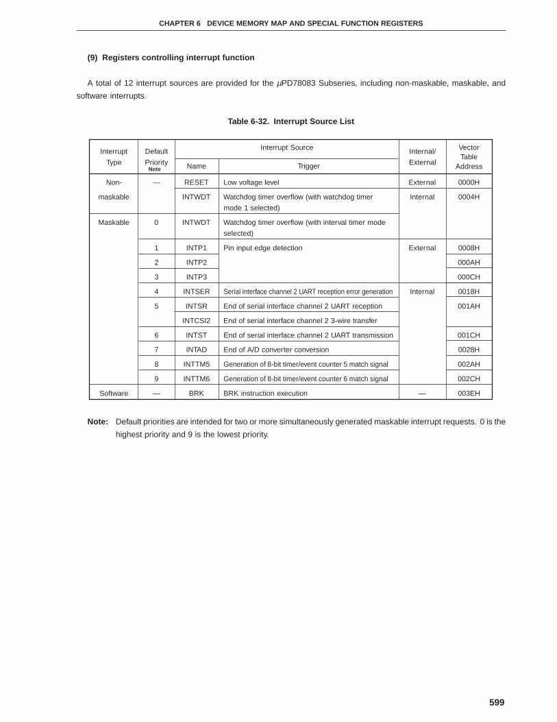
599
CHAPTER 6 DEVICE MEMORY MAP AND SPECIAL FUNCTION REGISTERS
(9) Registers controlling interrupt function
A total of 12 interrupt sources are provided for the µPD78083 Subseries, including non-maskable, maskable, and
software interrupts.
Table 6-32. Interrupt Source List
Interrupt Default Interrupt Source Internal/ VectorTable
Type Priority Name Trigger External Address
Non- — RESET Low voltage level External 0000H
maskable INTWDT Watchdog timer overflow (with watchdog timer Internal 0004H
mode 1 selected)
Maskable 0 INTWDT Watchdog timer overflow (with interval timer mode
selected)
1 INTP1 Pin input edge detection External 0008H
2 INTP2 000AH
3 INTP3 000CH
4 INTSER Serial interface channel 2 UART reception error generation Internal 0018H
5 INTSR End of serial interface channel 2 UART reception 001AH
INTCSI2 End of serial interface channel 2 3-wire transfer
6 INTST End of serial interface channel 2 UART transmission 001CH
7 INTAD End of A/D converter conversion 0028H
8 INTTM5 Generation of 8-bit timer/event counter 5 match signal 002AH
9 INTTM6 Generation of 8-bit timer/event counter 6 match signal 002CH
Software — BRK BRK instruction execution — 003EH
Note: Default priorities are intended for two or more simultaneously generated maskable interrupt requests. 0 is the
highest priority and 9 is the lowest priority.
Note
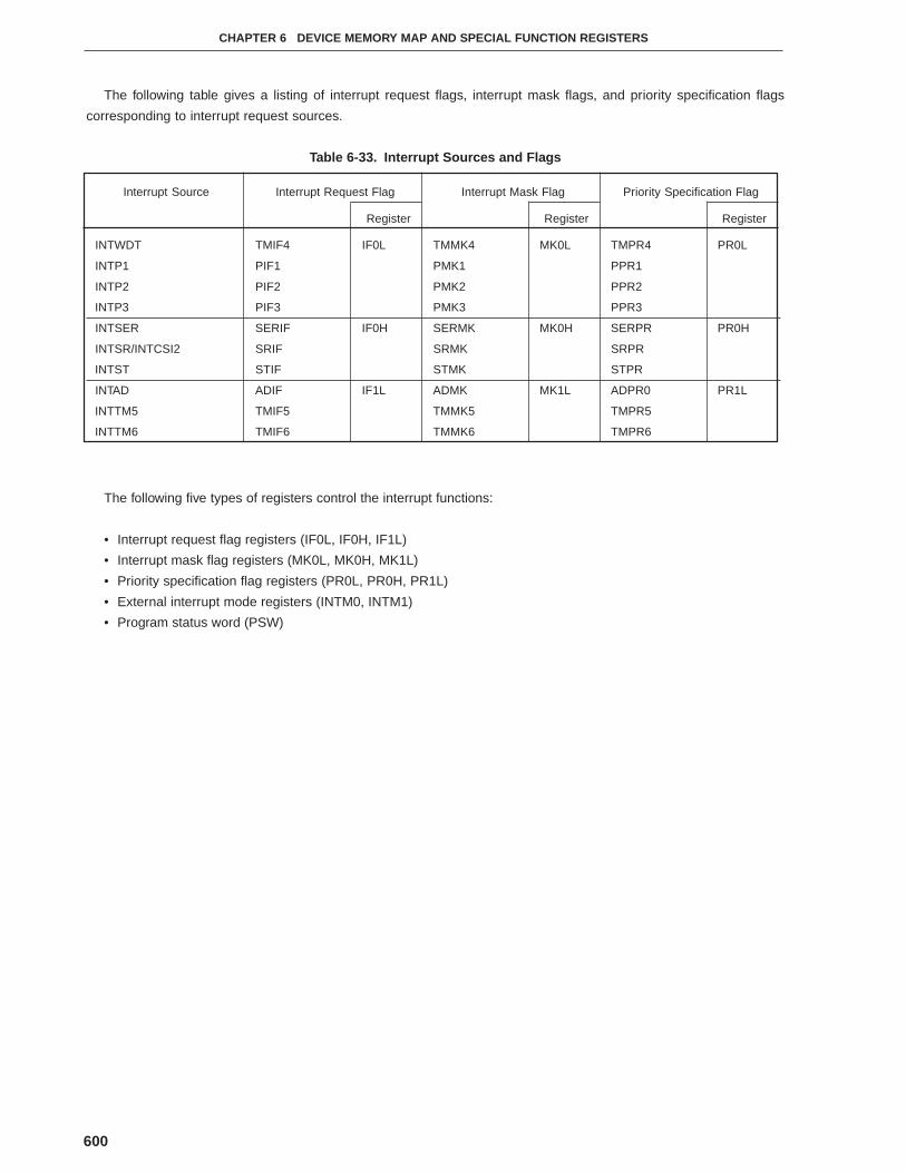
600
CHAPTER 6 DEVICE MEMORY MAP AND SPECIAL FUNCTION REGISTERS
The following table gives a listing of interrupt request flags, interrupt mask flags, and priority specification flags
corresponding to interrupt request sources.
Table 6-33. Interrupt Sources and Flags
Interrupt Source Interrupt Request Flag Interrupt Mask Flag Priority Specification Flag
Register Register Register
INTWDT TMIF4 IF0L TMMK4 MK0L TMPR4 PR0L
INTP1 PIF1 PMK1 PPR1
INTP2 PIF2 PMK2 PPR2
INTP3 PIF3 PMK3 PPR3
INTSER SERIF IF0H SERMK MK0H SERPR PR0H
INTSR/INTCSI2 SRIF SRMK SRPR
INTST STIF STMK STPR
INTAD ADIF IF1L ADMK MK1L ADPR0 PR1L
INTTM5 TMIF5 TMMK5 TMPR5
INTTM6 TMIF6 TMMK6 TMPR6
The following five types of registers control the interrupt functions:
• Interrupt request flag registers (IF0L, IF0H, IF1L)
• Interrupt mask flag registers (MK0L, MK0H, MK1L)
• Priority specification flag registers (PR0L, PR0H, PR1L)
• External interrupt mode registers (INTM0, INTM1)
• Program status word (PSW)
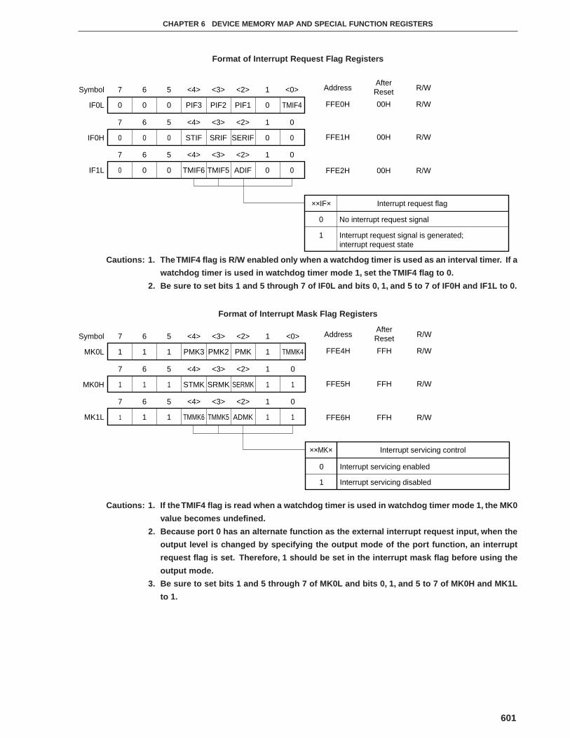
601
CHAPTER 6 DEVICE MEMORY MAP AND SPECIAL FUNCTION REGISTERS
Format of Interrupt Request Flag Registers
Cautions: 1. The TMIF4 flag is R/W enabled only when a watchdog timer is used as an interval timer. If a
watchdog timer is used in watchdog timer mode 1, set the TMIF4 flag to 0.
2. Be sure to set bits 1 and 5 through 7 of IF0L and bits 0, 1, and 5 to 7 of IF0H and IF1L to 0.
Format of Interrupt Mask Flag Registers
Cautions: 1. If the TMIF4 flag is read when a watchdog timer is used in watchdog timer mode 1, the MK0
value becomes undefined.
2. Because port 0 has an alternate function as the external interrupt request input, when the
output level is changed by specifying the output mode of the port function, an interrupt
request flag is set. Therefore, 1 should be set in the interrupt mask flag before using the
output mode.
3. Be sure to set bits 1 and 5 through 7 of MK0L and bits 0, 1, and 5 to 7 of MK0H and MK1L
to 1.
7
0
Symbol
IF0L
6
0
5
0
<4>
PIF3
<3>
PIF2
<2>
PIF1
1
0
<0>
TMIF4
Address
FFE0H 00H
AfterReset R/W
R/W
××IF×
0
1
Interrupt request flag
No interrupt request signal
Interrupt request signal is generated; interrupt request state
7
0IF0H
6
0
5
0
<4>
STIF
<3>
SRIF
<2>
SERIF
1
0
0
0
7
0IF1L
6
0
5
0
<4>
TMIF6
<3>
TMIF5
<2>
ADIF
1
0
0
0
FFE1H 00H R/W
FFE2H 00H R/W
7
1
Symbol
MK0L
6
1
5
1
<4>
PMK3
<3>
PMK2
<2>
PMK
1
1
<0>
TMMK4
Address
FFE4H FFH
AfterReset R/W
R/W
××MK×
0
1
Interrupt servicing control
Interrupt servicing enabled
Interrupt servicing disabled
7
1MK0H
6
1
5
1
<4>
STMK
<3>
SRMK
<2>
SERMK
1
1
0
1
7
1MK1L
6
1
5
1
<4>
TMMK6
<3>
TMMK5
<2>
ADMK
1
1
0
1
FFE5H FFH R/W
FFE6H FFH R/W
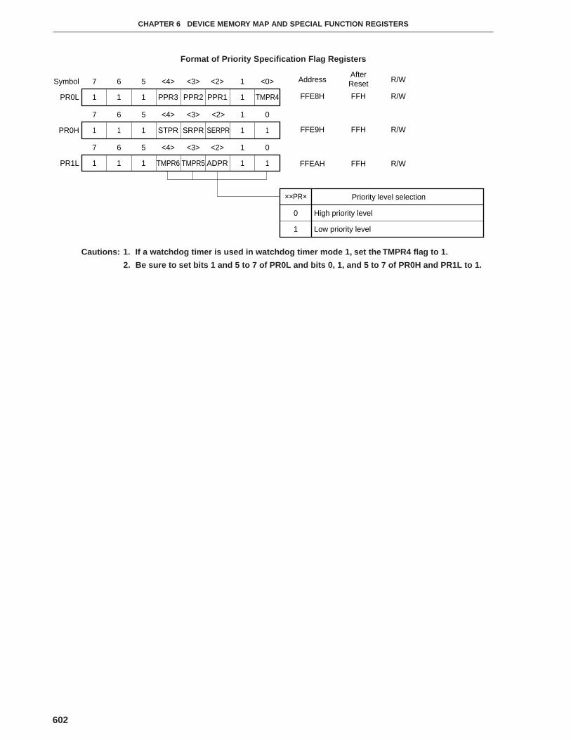
602
CHAPTER 6 DEVICE MEMORY MAP AND SPECIAL FUNCTION REGISTERS
Format of Priority Specification Flag Registers
Cautions: 1. If a watchdog timer is used in watchdog timer mode 1, set the TMPR4 flag to 1.
2. Be sure to set bits 1 and 5 to 7 of PR0L and bits 0, 1, and 5 to 7 of PR0H and PR1L to 1.
7
1
Symbol
PR0L
6
1
5
1
<4>
PPR3
<3>
PPR2
<2>
PPR1
1
1
<0>
TMPR4
Address
FFE8H FFH
AfterReset R/W
R/W
0
1
Priority level selection
High priority level
Low priority level
7
1PR0H
6
1
5
1
<4>
STPR
<3>
SRPR
<2>
SERPR
1
1
0
1
7
1PR1L
6
1
5
1
<4>
TMPR6
<3>
TMPR5
<2>
ADPR
1
1
0
1
FFE9H FFH R/W
FFEAH FFH R/W
××PR×
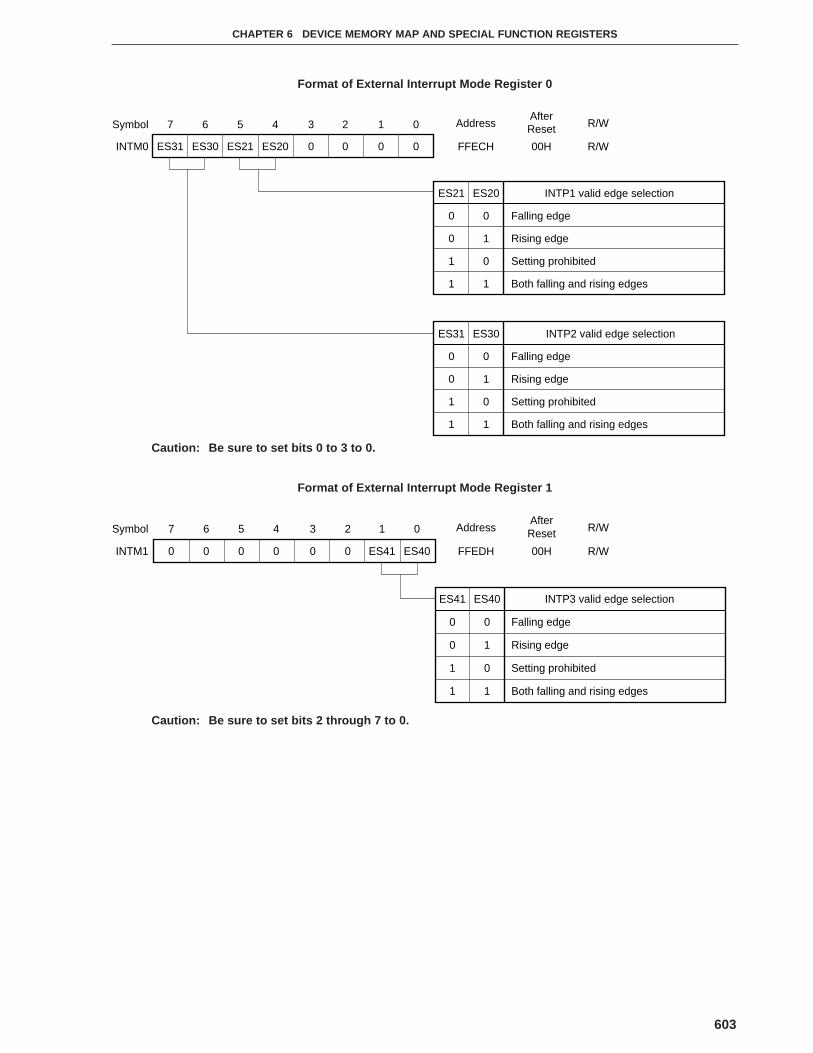
603
CHAPTER 6 DEVICE MEMORY MAP AND SPECIAL FUNCTION REGISTERS
Format of External Interrupt Mode Register 0
Caution: Be sure to set bits 0 to 3 to 0.
Format of External Interrupt Mode Register 1
Caution: Be sure to set bits 2 through 7 to 0.
Address
FFECH 00H
AfterReset R/W
R/W
7
ES31
Symbol
INTM0
6
ES30
5
ES21
4
ES20
3
0
2
0
1
0
0
0
0
0
1
1
INTP1 valid edge selection
Falling edge
Rising edge
Setting prohibited
Both falling and rising edges
ES21
0
1
0
1
ES20
0
0
1
1
INTP2 valid edge selection
Falling edge
Rising edge
Setting prohibited
Both falling and rising edges
ES31
0
1
0
1
ES30
Address
FFEDH 00H
AfterReset R/W
R/W
0
0
1
1
INTP3 valid edge selection
Falling edge
Rising edge
Setting prohibited
Both falling and rising edges
ES41
7
0
Symbol
INTM1
6
0
5
0
4
0
3
0
2
0
1
ES41
0
ES40
0
1
0
1
ES40
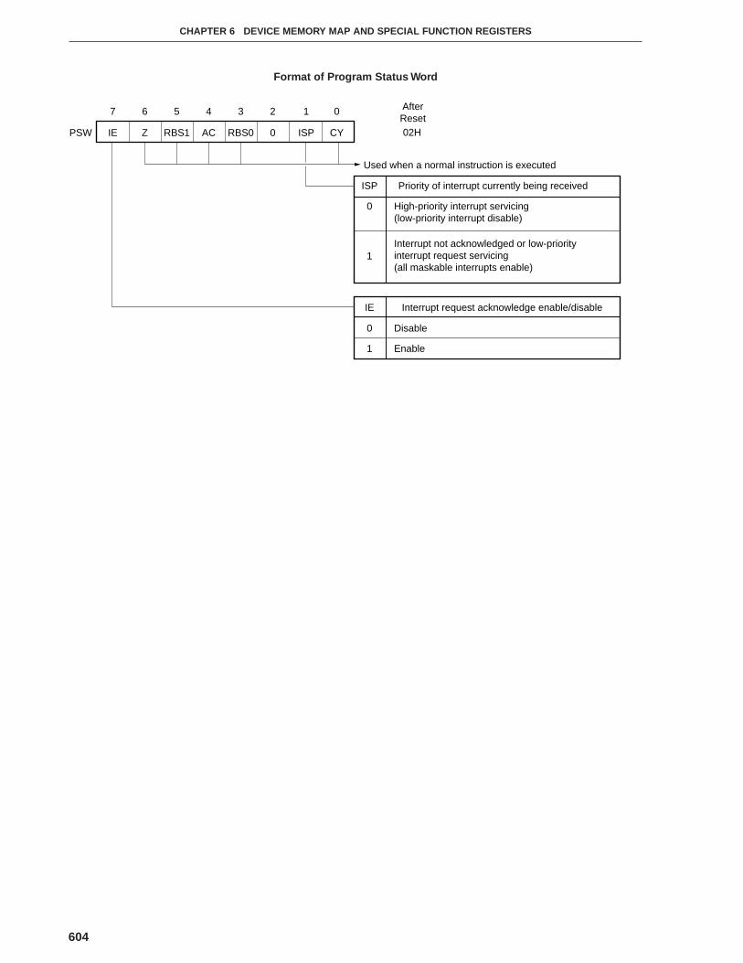
604
CHAPTER 6 DEVICE MEMORY MAP AND SPECIAL FUNCTION REGISTERS
Format of Program Status Word
7
IEPSW
6
Z
5
RBS1
4
AC
3
RBS0
2
0
1
ISP
0
CY 02H
AfterReset
ISP
0
Used when a normal instruction is executed
Priority of interrupt currently being received
High-priority interrupt servicing(low-priority interrupt disable)
1Interrupt not acknowledged or low-priorityinterrupt request servicing(all maskable interrupts enable)
IE Interrupt request acknowledge enable/disable
0 Disable
1 Enable
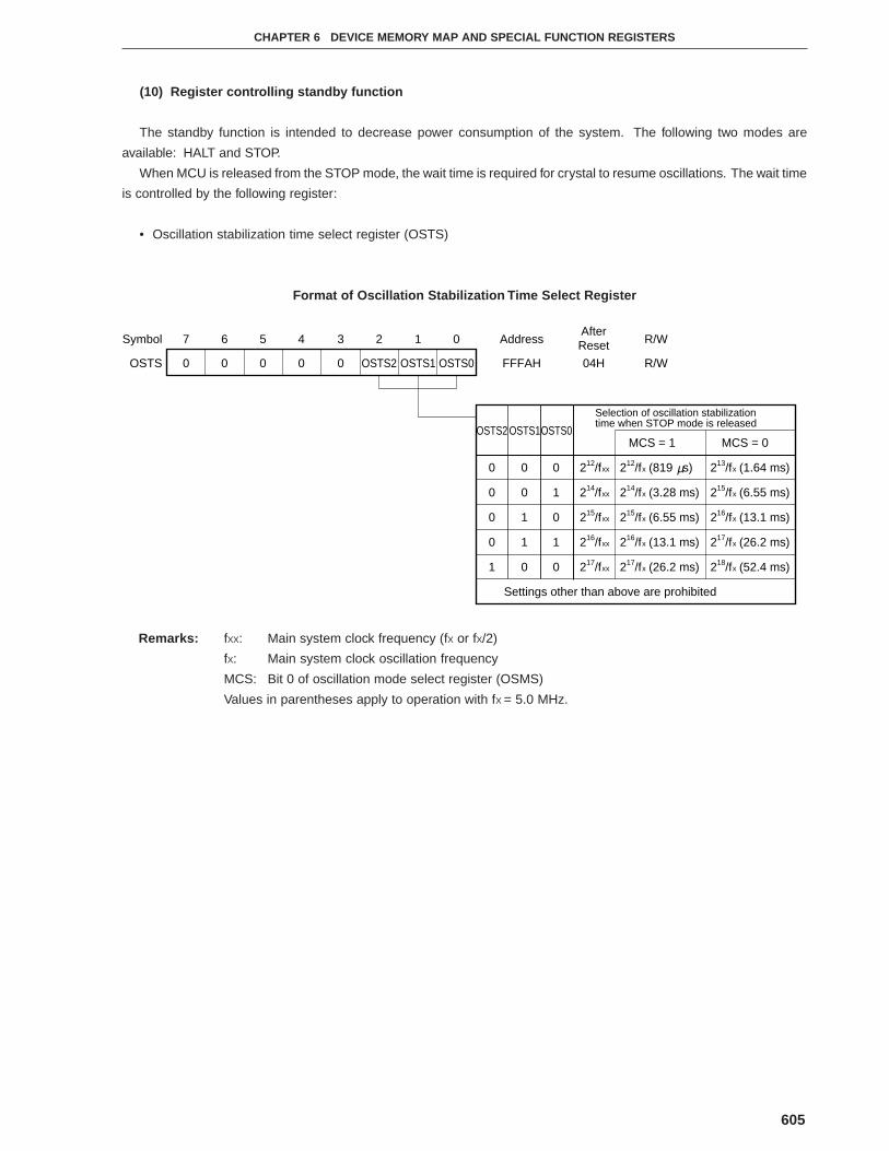
605
CHAPTER 6 DEVICE MEMORY MAP AND SPECIAL FUNCTION REGISTERS
(10) Register controlling standby function
The standby function is intended to decrease power consumption of the system. The following two modes are
available: HALT and STOP.
When MCU is released from the STOP mode, the wait time is required for crystal to resume oscillations. The wait time
is controlled by the following register:
• Oscillation stabilization time select register (OSTS)
Format of Oscillation Stabilization Time Select Register
Remarks: fXX: Main system clock frequency (fX or fX/2)
fX: Main system clock oscillation frequency
MCS: Bit 0 of oscillation mode select register (OSMS)
Values in parentheses apply to operation with fX = 5.0 MHz.
Address
FFFAH 04H
AfterReset R/W
R/W
0
0
0
0
1
Selection of oscillation stabilizationtime when STOP mode is released
212/fxx
214/fxx
215/fxx
216/fxx
217/fxx
OSTS2
7
0
Symbol
OSTS
6
0
5
0
4
0
3
0
2
OSTS2
1
OSTS1
0
OSTS0
0
0
1
1
0
OSTS1MCS = 1 MCS = 0
212/fx (819 s)
214/fx (3.28 ms)
215/fx (6.55 ms)
216/fx (13.1 ms)
217/fx (26.2 ms)
213/fx (1.64 ms)
215/fx (6.55 ms)
216/fx (13.1 ms)
217/fx (26.2 ms)
218/fx (52.4 ms)
µ0
1
0
1
0
OSTS0
Settings other than above are prohibited
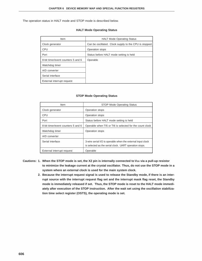
606
CHAPTER 6 DEVICE MEMORY MAP AND SPECIAL FUNCTION REGISTERS
The operation status in HALT mode and STOP mode is described below.
HALT Mode Operating Status
Item HALT Mode Operating Status
Clock generator Can be oscillated. Clock supply to the CPU is stopped.
CPU Operation stops
Port Status before HALT mode setting is held
8-bit timer/event counters 5 and 6 Operable
Watchdog timer
A/D converter
Serial interface
External interrupt request
STOP Mode Operating Status
Item STOP Mode Operating Status
Clock generator Operation stops
CPU Operation stops
Port Status before HALT mode setting is held
8-bit timer/event counters 5 and 6 Operable when TI5 or TI6 is selected for the count clock
Watchdog timer Operation stops
A/D converter
Serial interface 3-wire serial I/O is operable when the external input clock
is selected as the serial clock. UART operation stops.
External interrupt request Operable
Cautions: 1. When the STOP mode is set, the X2 pin is internally connected to V DD via a pull-up resistor
to minimize the leakage current at the crystal oscillator. Thus, do not use the STOP mode in a
system where an external clock is used for the main system clock.
2. Because the interrupt request signal is used to release the Standby mode, if there is an inter-
rupt source with the interrupt request flag set and the interrupt mask flag reset, the Standby
mode is immediately released if set. Thus, the STOP mode is reset to the HALT mode immedi-
ately after execution of the STOP instruction. After the wait set using the oscillation stabiliza-
tion time select register (OSTS), the operating mode is set.
607
CHAPTER 6 DEVICE MEMORY MAP AND SPECIAL FUNCTION REGISTERS
(11) Reset function
The following two operations can be used to generate a reset signal:
• External reset input via the RESET pin
• Internal reset by watchdog timer in the Watchdog Timer mode
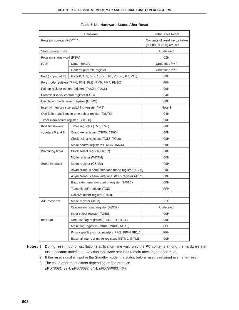
608
CHAPTER 6 DEVICE MEMORY MAP AND SPECIAL FUNCTION REGISTERS
Table 6-34. Hardware Status After Reset
Hardware Status After Reset
Program counter (PC) Note 1 Contents of reset vector tables
(0000H, 0001H) are set
Stack pointer (SP) Undefined
Program status word (PSW) 02H
RAM Data memory Undefined Note 2
General-purpose register Undefined Note 2
Port (output latch) Ports 0, 1, 3, 5, 7, 10 (P0, P1, P3, P5, P7, P10) 00H
Port mode registers (PM0, PM1, PM3, PM5, PM7, PM10) FFH
Pull-up resistor option registers (PUOH, PUOL) 00H
Processor clock control register (PCC) 04H
Oscillation mode select register (OSMS) 00H
Internal memory size switching register (IMS) Note 3
Oscillation stabilization time select register (OSTS) 04H
Timer clock select register 0 (TCL0) 00H
8-bit timer/event Timer registers (TM5, TM6) 00H
counters 5 and 6 Compare registers (CR50, CR60) 00H
Clock select registers (TCL5, TCL6) 00H
Mode control registers (TMC5, TMC6) 00H
Watchdog timer Clock select register (TCL2) 00H
Mode register (WDTM) 00H
Serial interface Mode register (CSIM2) 00H
Asynchronous serial interface mode register (ASIM) 00H
Asynchronous serial interface status register (ASIS) 00H
Baud rate generator control register (BRGC) 00H
Transmit shift register (TXS) FFH
Receive buffer register (RXB)
A/D converter Mode register (ADM) 01H
Conversion result register (ADCR) Undefined
Input select register (ADIS) 00H
Interrupt Request flag registers (IF0L, IF0H, IF1L) 00H
Mask flag registers (MK0L, MK0H, MK1L) FFH
Priority specification flag registers (PR0L, PR0H, PR1L) FFH
External interrupt mode registers (INTM0, INTM1) 00H
Notes: 1. During reset input or oscillation stabilization time wait, only the PC contents among the hardware sta-
tuses become undefined. All other hardware statuses remain unchanged after reset.
2. If the reset signal is input in the Standby mode, the status before reset is retained even after reset.
3. The value after reset differs depending on the product:
µPD78081: 82H, µPD78082: 64H, µPD78P083: 46H.
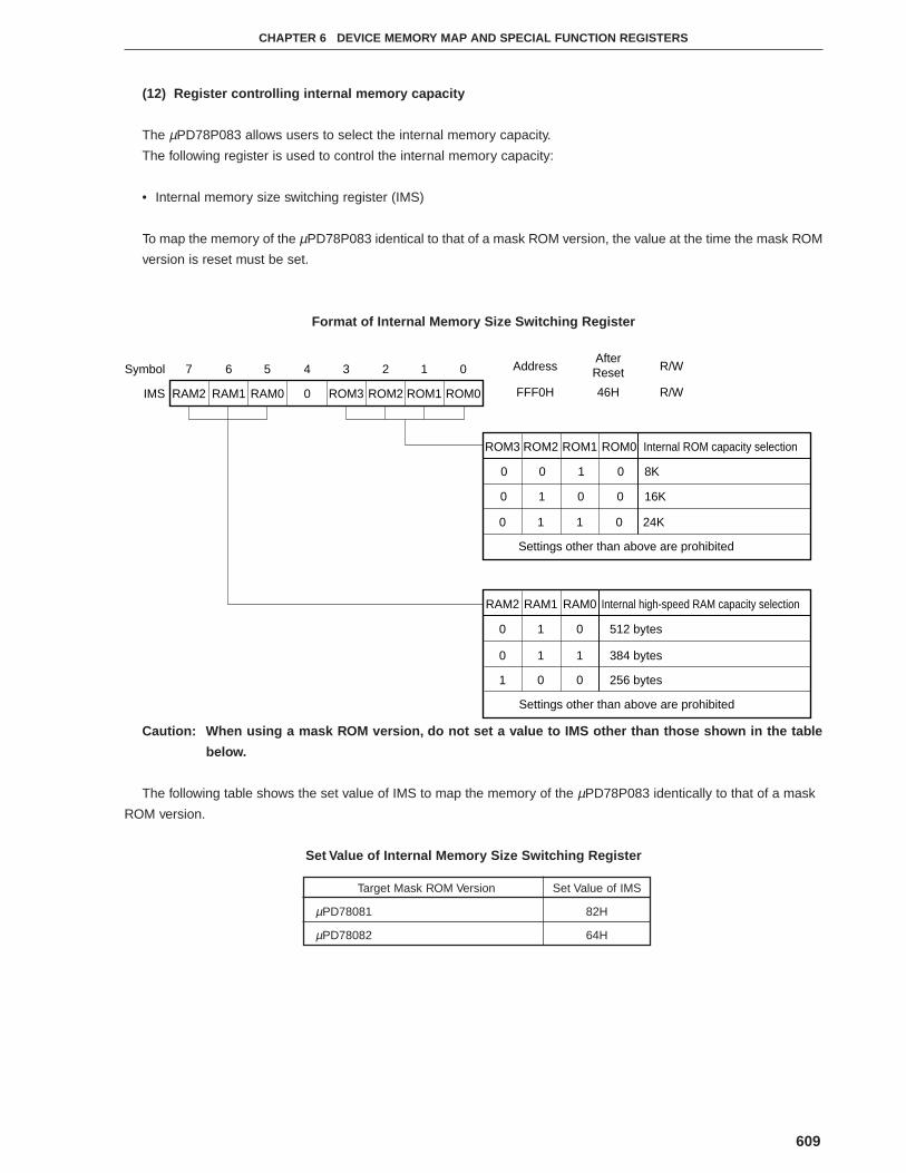
609
CHAPTER 6 DEVICE MEMORY MAP AND SPECIAL FUNCTION REGISTERS
(12) Register controlling internal memory capacity
The µPD78P083 allows users to select the internal memory capacity.
The following register is used to control the internal memory capacity:
• Internal memory size switching register (IMS)
To map the memory of the µPD78P083 identical to that of a mask ROM version, the value at the time the mask ROM
version is reset must be set.
Format of Internal Memory Size Switching Register
Caution: When using a mask ROM version, do not set a value to IMS other than those shown in the table
below.
The following table shows the set value of IMS to map the memory of the µPD78P083 identically to that of a mask
ROM version.
Set Value of Internal Memory Size Switching Register
Target Mask ROM Version Set Value of IMS
µPD78081 82H
µPD78082 64H
7
RAM2
Symbol
IMS
6
RAM1
5
RAM0
4
0
3
ROM3
2
ROM2
1
ROM1
0
ROM0
Address
FFF0H 46H
AfterReset R/W
R/W
0
Internal ROM capacity selection
24K
ROM3
1
ROM2
1
ROM1
0
ROM0
Internal high-speed RAM capacity selectionRAM2 RAM1 RAM0
512 bytes0 1 0
0
0
8K
16K
0
1
1
0
0
0
384 bytes0 1 1
256 bytes1 0 0
Settings other than above are prohibited
Settings other than above are prohibited

610
[MEMO]
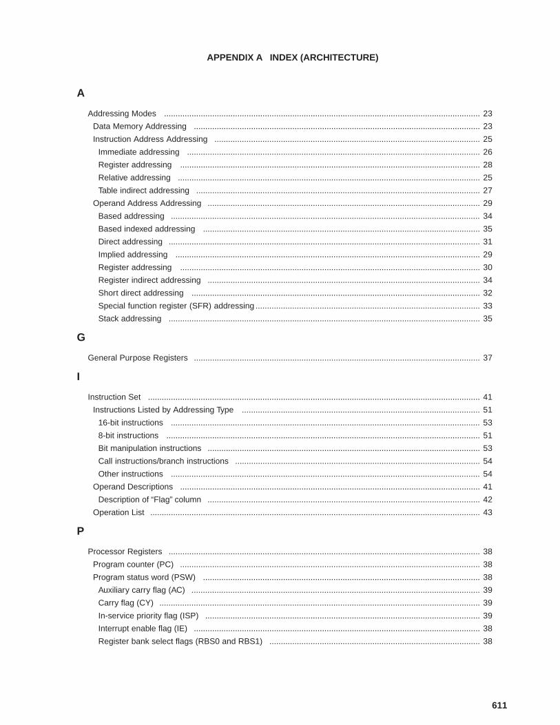
611
APPENDIX A INDEX (ARCHITECTURE)
A
Addressing Modes .......................................................................................................................................... 23
Data Memory Addressing ............................................................................................................................. 23
Instruction Address Addressing .................................................................................................................... 25
Immediate addressing ................................................................................................................................ 26
Register addressing ................................................................................................................................... 28
Relative addressing .................................................................................................................................... 25
Table indirect addressing ............................................................................................................................ 27
Operand Address Addressing ....................................................................................................................... 29
Based addressing ....................................................................................................................................... 34
Based indexed addressing ......................................................................................................................... 35
Direct addressing ........................................................................................................................................ 31
Implied addressing ..................................................................................................................................... 29
Register addressing ................................................................................................................................... 30
Register indirect addressing ....................................................................................................................... 34
Short direct addressing .............................................................................................................................. 32
Special function register (SFR) addressing .................................................................................................. 33
Stack addressing ........................................................................................................................................ 35
G
General Purpose Registers ............................................................................................................................. 37
I
Instruction Set ................................................................................................................................................. 41
Instructions Listed by Addressing Type ........................................................................................................ 51
16-bit instructions ....................................................................................................................................... 53
8-bit instructions ......................................................................................................................................... 51
Bit manipulation instructions ....................................................................................................................... 53
Call instructions/branch instructions ........................................................................................................... 54
Other instructions ....................................................................................................................................... 54
Operand Descriptions ................................................................................................................................... 41
Description of “Flag” column ....................................................................................................................... 42
Operation List ................................................................................................................................................ 43
P
Processor Registers ........................................................................................................................................ 38
Program counter (PC) ................................................................................................................................... 38
Program status word (PSW) ......................................................................................................................... 38
Auxiliary carry flag (AC) .............................................................................................................................. 39
Carry flag (CY) ............................................................................................................................................ 39
In-service priority flag (ISP) ........................................................................................................................ 39
Interrupt enable flag (IE) ............................................................................................................................. 38
Register bank select flags (RBS0 and RBS1) ............................................................................................ 38

612
APPENDIX A INDEX (ARCHITECTURE)
Zero flag (Z) ................................................................................................................................................ 38
Stack pointer (SP) ......................................................................................................................................... 39
S
Sample Program ............................................................................................................................................. 55
Stack Operation ................................................................................................................................................ 39
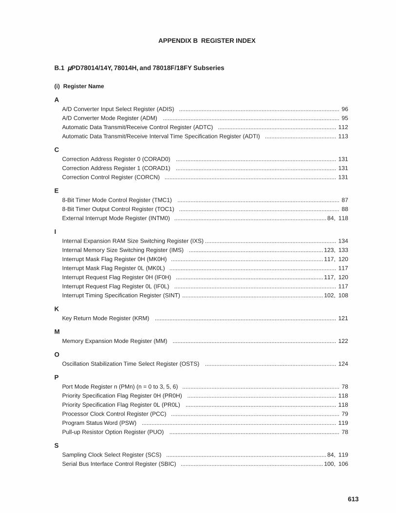
613
APPENDIX B REGISTER INDEX
B.1 µµµµµPD78014/14Y, 78014H, and 78018F/18FY Subseries
(i) Register Name
AA/D Converter Input Select Register (ADIS) ................................................................................................... 96
A/D Converter Mode Register (ADM) ............................................................................................................. 95
Automatic Data Transmit/Receive Control Register (ADTC) ......................................................................... 112
Automatic Data Transmit/Receive Interval Time Specification Register (ADTI) ............................................ 113
CCorrection Address Register 0 (CORAD0) ................................................................................................... 131
Correction Address Register 1 (CORAD1) ................................................................................................... 131
Correction Control Register (CORCN) .......................................................................................................... 131
E8-Bit Timer Mode Control Register (TMC1) .................................................................................................... 87
8-Bit Timer Output Control Register (TOC1) ................................................................................................... 88
External Interrupt Mode Register (INTM0) .............................................................................................. 84, 118
IInternal Expansion RAM Size Switching Register (IXS) ................................................................................. 134
Internal Memory Size Switching Register (IMS) ................................................................................... 123, 133
Interrupt Mask Flag Register 0H (MK0H) .............................................................................................. 117, 120
Interrupt Mask Flag Register 0L (MK0L) ....................................................................................................... 117
Interrupt Request Flag Register 0H (IF0H) ........................................................................................... 117, 120
Interrupt Request Flag Register 0L (IF0L) .................................................................................................... 117
Interrupt Timing Specification Register (SINT) ....................................................................................... 102, 108
KKey Return Mode Register (KRM) ................................................................................................................ 121
MMemory Expansion Mode Register (MM) ..................................................................................................... 122
OOscillation Stabilization Time Select Register (OSTS) ................................................................................. 124
PPort Mode Register n (PMn) (n = 0 to 3, 5, 6) ................................................................................................. 78
Priority Specification Flag Register 0H (PR0H) ............................................................................................ 118
Priority Specification Flag Register 0L (PR0L) ............................................................................................. 118
Processor Clock Control Register (PCC) ........................................................................................................ 79
Program Status Word (PSW) ........................................................................................................................ 119
Pull-up Resistor Option Register (PUO) ......................................................................................................... 78
SSampling Clock Select Register (SCS) ................................................................................................... 84, 119
Serial Bus Interface Control Register (SBIC) ........................................................................................ 100, 106
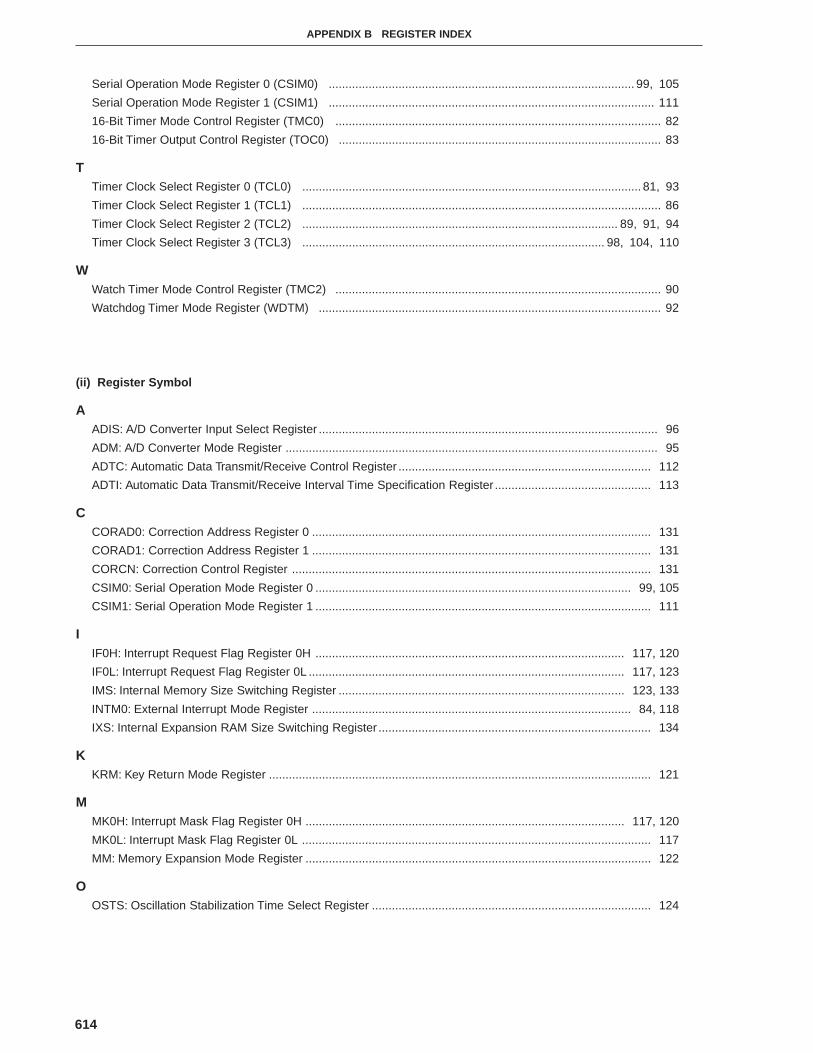
614
APPENDIX B REGISTER INDEX
Serial Operation Mode Register 0 (CSIM0) ............................................................................................ 99, 105
Serial Operation Mode Register 1 (CSIM1) .................................................................................................. 111
16-Bit Timer Mode Control Register (TMC0) .................................................................................................. 82
16-Bit Timer Output Control Register (TOC0) ................................................................................................. 83
TTimer Clock Select Register 0 (TCL0) ...................................................................................................... 81, 93
Timer Clock Select Register 1 (TCL1) ............................................................................................................ 86
Timer Clock Select Register 2 (TCL2) ............................................................................................... 89, 91, 94
Timer Clock Select Register 3 (TCL3) ........................................................................................... 98, 104, 110
WWatch Timer Mode Control Register (TMC2) .................................................................................................. 90
Watchdog Timer Mode Register (WDTM) ....................................................................................................... 92
(ii) Register Symbol
AADIS: A/D Converter Input Select Register ...................................................................................................... 96
ADM: A/D Converter Mode Register ................................................................................................................ 95
ADTC: Automatic Data Transmit/Receive Control Register ............................................................................ 112
ADTI: Automatic Data Transmit/Receive Interval Time Specification Register ............................................... 113
CCORAD0: Correction Address Register 0 ...................................................................................................... 131
CORAD1: Correction Address Register 1 ...................................................................................................... 131
CORCN: Correction Control Register ............................................................................................................ 131
CSIM0: Serial Operation Mode Register 0 ............................................................................................... 99, 105
CSIM1: Serial Operation Mode Register 1 ..................................................................................................... 111
IIF0H: Interrupt Request Flag Register 0H ............................................................................................. 117, 120
IF0L: Interrupt Request Flag Register 0L ............................................................................................... 117, 123
IMS: Internal Memory Size Switching Register ...................................................................................... 123, 133
INTM0: External Interrupt Mode Register ................................................................................................ 84, 118
IXS: Internal Expansion RAM Size Switching Register .................................................................................. 134
KKRM: Key Return Mode Register ................................................................................................................... 121
MMK0H: Interrupt Mask Flag Register 0H ................................................................................................ 117, 120
MK0L: Interrupt Mask Flag Register 0L ......................................................................................................... 117
MM: Memory Expansion Mode Register ........................................................................................................ 122
OOSTS: Oscillation Stabilization Time Select Register .................................................................................... 124
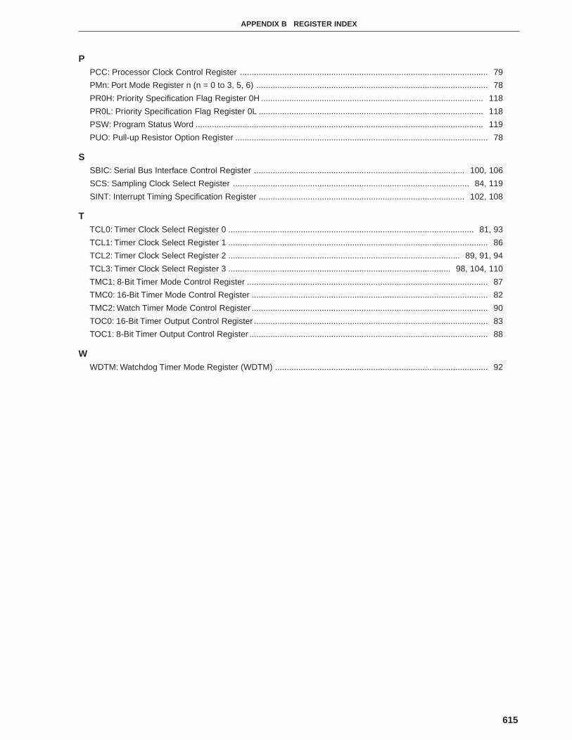
615
APPENDIX B REGISTER INDEX
PPCC: Processor Clock Control Register .......................................................................................................... 79
PMn: Port Mode Register n (n = 0 to 3, 5, 6) ................................................................................................... 78
PR0H: Priority Specification Flag Register 0H ............................................................................................... 118
PR0L: Priority Specification Flag Register 0L ................................................................................................ 118
PSW: Program Status Word ........................................................................................................................... 119
PUO: Pull-up Resistor Option Register ............................................................................................................ 78
SSBIC: Serial Bus Interface Control Register .......................................................................................... 100, 106
SCS: Sampling Clock Select Register ..................................................................................................... 84, 119
SINT: Interrupt Timing Specification Register ........................................................................................ 102, 108
TTCL0: Timer Clock Select Register 0 ......................................................................................................... 81, 93
TCL1: Timer Clock Select Register 1 ............................................................................................................... 86
TCL2: Timer Clock Select Register 2 ................................................................................................... 89, 91, 94
TCL3: Timer Clock Select Register 3 ............................................................................................... 98, 104, 110
TMC1: 8-Bit Timer Mode Control Register ....................................................................................................... 87
TMC0: 16-Bit Timer Mode Control Register ..................................................................................................... 82
TMC2: Watch Timer Mode Control Register ..................................................................................................... 90
TOC0: 16-Bit Timer Output Control Register .................................................................................................... 83
TOC1: 8-Bit Timer Output Control Register ...................................................................................................... 88
WWDTM: Watchdog Timer Mode Register (WDTM) ........................................................................................... 92
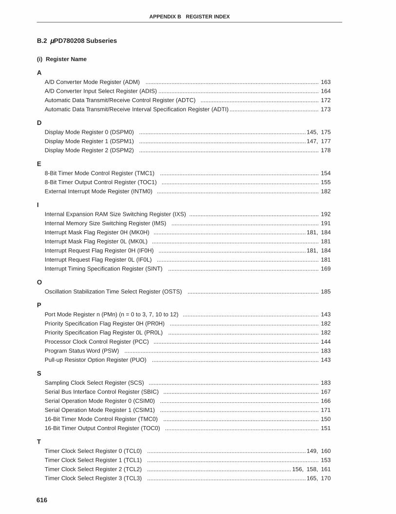
616
APPENDIX B REGISTER INDEX
B.2 µµµµµPD780208 Subseries
(i) Register Name
AA/D Converter Mode Register (ADM) ........................................................................................................... 163
A/D Converter Input Select Register (ADIS) ................................................................................................... 164
Automatic Data Transmit/Receive Control Register (ADTC) ......................................................................... 172
Automatic Data Transmit/Receive Interval Specification Register (ADTI) ....................................................... 173
DDisplay Mode Register 0 (DSPM0) ....................................................................................................... 145, 175
Display Mode Register 1 (DSPM1) ....................................................................................................... 147, 177
Display Mode Register 2 (DSPM2) ............................................................................................................... 178
E8-Bit Timer Mode Control Register (TMC1) .................................................................................................. 154
8-Bit Timer Output Control Register (TOC1) ................................................................................................. 155
External Interrupt Mode Register (INTM0) .................................................................................................... 182
IInternal Expansion RAM Size Switching Register (IXS) ................................................................................ 192
Internal Memory Size Switching Register (IMS) ........................................................................................... 191
Interrupt Mask Flag Register 0H (MK0H) .............................................................................................. 181, 184
Interrupt Mask Flag Register 0L (MK0L) ....................................................................................................... 181
Interrupt Request Flag Register 0H (IF0H) ........................................................................................... 181, 184
Interrupt Request Flag Register 0L (IF0L) .................................................................................................... 181
Interrupt Timing Specification Register (SINT) ............................................................................................. 169
OOscillation Stabilization Time Select Register (OSTS) ................................................................................. 185
PPort Mode Register n (PMn) (n = 0 to 3, 7, 10 to 12) .................................................................................... 143
Priority Specification Flag Register 0H (PR0H) ............................................................................................ 182
Priority Specification Flag Register 0L (PR0L) ............................................................................................. 182
Processor Clock Control Register (PCC) ...................................................................................................... 144
Program Status Word (PSW) ........................................................................................................................ 183
Pull-up Resistor Option Register (PUO) ....................................................................................................... 143
SSampling Clock Select Register (SCS) ......................................................................................................... 183
Serial Bus Interface Control Register (SBIC) ................................................................................................ 167
Serial Operation Mode Register 0 (CSIM0) .................................................................................................. 166
Serial Operation Mode Register 1 (CSIM1) .................................................................................................. 171
16-Bit Timer Mode Control Register (TMC0) ................................................................................................ 150
16-Bit Timer Output Control Register (TOC0) ............................................................................................... 151
TTimer Clock Select Register 0 (TCL0) .................................................................................................. 149, 160
Timer Clock Select Register 1 (TCL1) .......................................................................................................... 153
Timer Clock Select Register 2 (TCL2) ......................................................................................... 156, 158, 161
Timer Clock Select Register 3 (TCL3) .................................................................................................. 165, 170
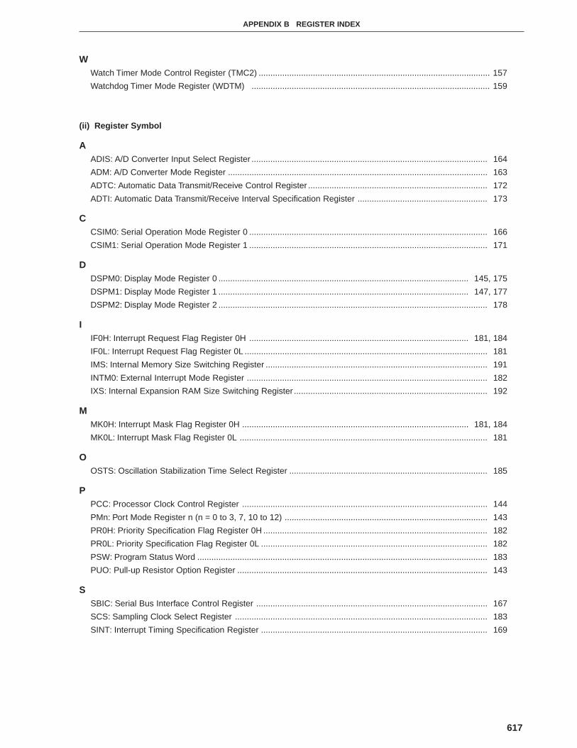
617
APPENDIX B REGISTER INDEX
WWatch Timer Mode Control Register (TMC2) .................................................................................................. 157
Watchdog Timer Mode Register (WDTM) ..................................................................................................... 159
(ii) Register Symbol
AADIS: A/D Converter Input Select Register .................................................................................................... 164
ADM: A/D Converter Mode Register .............................................................................................................. 163
ADTC: Automatic Data Transmit/Receive Control Register ............................................................................ 172
ADTI: Automatic Data Transmit/Receive Interval Specification Register ....................................................... 173
CCSIM0: Serial Operation Mode Register 0 ..................................................................................................... 166
CSIM1: Serial Operation Mode Register 1 ..................................................................................................... 171
DDSPM0: Display Mode Register 0 .......................................................................................................... 145, 175
DSPM1: Display Mode Register 1 .......................................................................................................... 147, 177
DSPM2: Display Mode Register 2 .................................................................................................................. 178
IIF0H: Interrupt Request Flag Register 0H ............................................................................................. 181, 184
IF0L: Interrupt Request Flag Register 0L ....................................................................................................... 181
IMS: Internal Memory Size Switching Register .............................................................................................. 191
INTM0: External Interrupt Mode Register ...................................................................................................... 182
IXS: Internal Expansion RAM Size Switching Register .................................................................................. 192
MMK0H: Interrupt Mask Flag Register 0H ................................................................................................ 181, 184
MK0L: Interrupt Mask Flag Register 0L ......................................................................................................... 181
OOSTS: Oscillation Stabilization Time Select Register .................................................................................... 185
PPCC: Processor Clock Control Register ........................................................................................................ 144
PMn: Port Mode Register n (n = 0 to 3, 7, 10 to 12) ...................................................................................... 143
PR0H: Priority Specification Flag Register 0H ............................................................................................... 182
PR0L: Priority Specification Flag Register 0L ................................................................................................ 182
PSW: Program Status Word ........................................................................................................................... 183
PUO: Pull-up Resistor Option Register .......................................................................................................... 143
SSBIC: Serial Bus Interface Control Register .................................................................................................. 167
SCS: Sampling Clock Select Register ........................................................................................................... 183
SINT: Interrupt Timing Specification Register ................................................................................................ 169

618
APPENDIX B REGISTER INDEX
TTCL0: Timer Clock Select Register 0 ..................................................................................................... 149, 160
TCL1: Timer Clock Select Register 1 ............................................................................................................. 153
TCL2: Timer Clock Select Register 2 ............................................................................................. 156, 158, 161
TCL3: Timer Clock Select Register 3 ..................................................................................................... 165, 170
TMC0: 16-Bit Timer Mode Control Register ................................................................................................... 150
TMC1: 8-Bit Timer Mode Control Register ..................................................................................................... 154
TMC2: Watch Timer Mode Control Register ................................................................................................... 157
TOC0: 16-Bit Timer Output Control Register .................................................................................................. 151
TOC1: 8-Bit Timer Output Control Register .................................................................................................... 155
WWDTM: Watchdog Timer Mode Register ........................................................................................................ 159

619
APPENDIX B REGISTER INDEX
B.3 µµµµµPD780024/24Y and 780034/34Y Subseries
(i) Register Name
AA/D Converter Mode Register (ADM0) ......................................................................................................... 215
Analog Input Channel Specification Register (ADS0) .................................................................................. 216
Asynchronous Serial Interface Mode Register (ASIM0) ............................................................................... 218
Asynchronous Serial Interface Status Register (ASIS0) ................................................................................ 219
BBaud Rate Generator Control Register (BRGC0) ......................................................................................... 220
CCapture/Compare Control Register 0 (CRC0) .............................................................................................. 205
Clock Output Selection Register (CKS) ........................................................................................................ 214
E8-Bit Timer Mode Control Register 5n (TMC5n) (n = 0, 1) ............................................................................. 210
External Interrupt Falling Edge Enable Register (EGN) ............................................................................... 236
External Interrupt Rising Edge Enable Register (EGP) ................................................................................ 236
II2C Shift Register (IIC0) ................................................................................................................................. 230
IIC Clock Select Register (IICCL0) ............................................................................................................... 229
IIC Control Register (IICC0) .......................................................................................................................... 223
IIC Status Register (IICS0) ............................................................................................................................ 226
Internal Memory Size Switching Register (IMS) ........................................................................................... 244
Interrupt Mask Flag Register 0H (MK0H) ...................................................................................................... 234
Interrupt Mask Flag Register 0L (MK0L) ....................................................................................................... 234
Interrupt Mask Flag Register 1L (MK1L) ....................................................................................................... 234
Interrupt Request Flag Register 0H (IF0H) ................................................................................................... 233
Interrupt Request Flag Register 0L (IF0L) .................................................................................................... 233
Interrupt Request Flag Register 1L (IF1L) .................................................................................................... 233
MMemory Expansion Mode Register (MEM) ................................................................................................... 237
Memory Expansion Wait Setting Register (MM) ........................................................................................... 237
OOscillation Stabilization Time Select Register (OSTS) ................................................................................. 238
PPort Mode Register n (PMn) (n = 0, 2 to 7) ................................................................................................... 201
Prescaler Mode Register 0 (PRM0) .............................................................................................................. 207
Priority Specification Flag Register 0H (PR0H) ............................................................................................ 235
Priority Specification Flag Register 0L (PR0L) ............................................................................................. 235
Priority Specification Flag Register 1L (PR1L) ............................................................................................. 235
Processor Clock Control Register (PCC) ...................................................................................................... 203
Program Status Word (PSW) ........................................................................................................................ 236

620
APPENDIX B REGISTER INDEX
Pull-Up Resistor Option Register n (PUn) (n = 0, 2 to 7) .............................................................................. 202
SSerial Operation Mode Register 30 (CSIM30) .............................................................................................. 221
16-Bit Timer Mode Control Register (TMC0) ................................................................................................ 204
16-Bit Timer Output Control Register (TOC0) ............................................................................................... 206
Slave Address Register (SVA0) .................................................................................................................... 230
TTimer Clock Select Register 50 .................................................................................................................... 208
Timer Clock Select Register 51 ...................................................................................................................... 209
WWatch Timer Mode Control Register (WTM) ................................................................................................. 211
Watchdog Timer Clock Select Register (WDCS) .......................................................................................... 212
Watchdog Timer Mode Register (WDTM) ..................................................................................................... 213
(ii) Register Symbol
AADM0: A/D Converter Mode Register ............................................................................................................ 215
ADS0: Analog Input Channel Specification Register ..................................................................................... 216
ASIM0: Asynchronous Serial Interface Mode Register .................................................................................. 218
ASIS0: Asynchronous Serial Interface Status Register ................................................................................. 219
BBRGC0: Baud Rate Generator Control Register ............................................................................................ 220
CCKS: Clock Output Selection Register ........................................................................................................... 214
CRC0: Capture/Compare Control Register 0 ................................................................................................. 205
CSIM30: Serial Operation Mode Register 30 ................................................................................................. 221
EEGN: External Interrupt Falling Edge Enable Register .................................................................................. 236
EGP: External Interrupt Rising Edge Enable Register ................................................................................... 236
IIF0H: Interrupt Request Flag Register 0H ..................................................................................................... 233
IF0L: Interrupt Request Flag Register 0L ....................................................................................................... 233
IF1L: Interrupt Request Flag Register 1L ....................................................................................................... 233
IIC0: I2C Shift Register ................................................................................................................................... 230
IICC0: IIC Control Register ............................................................................................................................ 223
IICCL0: IIC Clock Select Register .................................................................................................................. 229
IICS0: IIC Status Register .............................................................................................................................. 226
IMS: Internal Memory Size Switching Register .............................................................................................. 244
MMEM: Memory Expansion Mode Register ..................................................................................................... 237
MK0H: Interrupt Mask Flag Register 0H ........................................................................................................ 234
MK0L: Interrupt Mask Flag Register 0L ......................................................................................................... 234
MK1L: Interrupt Mask Flag Register 1L ......................................................................................................... 234
MM: Memory Expansion Wait Setting Register .............................................................................................. 237
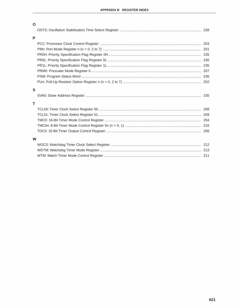
621
APPENDIX B REGISTER INDEX
OOSTS: Oscillation Stabilization Time Select Register .................................................................................... 238
PPCC: Processor Clock Control Register ........................................................................................................ 203
PMn: Port Mode Register n (n = 0, 2 to 7) ..................................................................................................... 201
PR0H: Priority Specification Flag Register 0H ............................................................................................... 235
PR0L: Priority Specification Flag Register 0L ................................................................................................ 235
PR1L: Priority Specification Flag Register 1L ................................................................................................ 235
PRM0: Prescaler Mode Register 0 ................................................................................................................. 207
PSW: Program Status Word ........................................................................................................................... 236
PUn: Pull-Up Resistor Option Register n (n = 0, 2 to 7) ................................................................................ 202
SSVA0: Slave Address Register ....................................................................................................................... 230
TTCL50: Timer Clock Select Register 50 ......................................................................................................... 208
TCL51: Timer Clock Select Register 51 ......................................................................................................... 209
TMC0: 16-Bit Timer Mode Control Register ................................................................................................... 204
TMC5n: 8-Bit Timer Mode Control Register 5n (n = 0, 1) .............................................................................. 210
TOC0: 16-Bit Timer Output Control Register .................................................................................................. 206
WWDCS: Watchdog Timer Clock Select Register ............................................................................................. 212
WDTM: Watchdog Timer Mode Register ........................................................................................................ 213
WTM: Watch Timer Mode Control Register .................................................................................................... 211
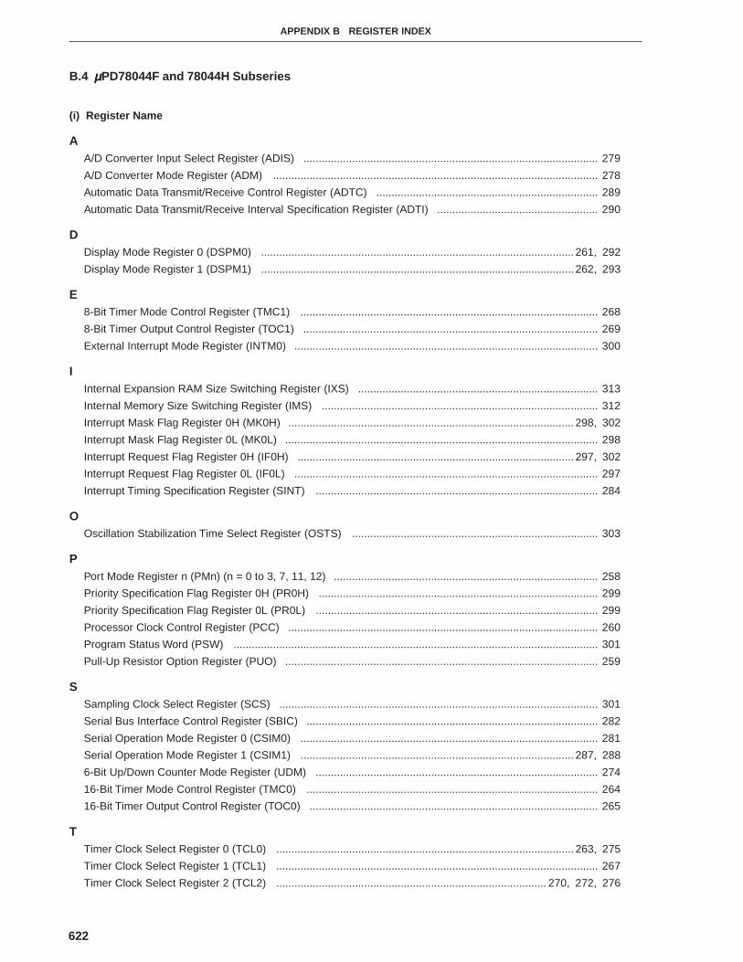
622
APPENDIX B REGISTER INDEX
B.4 µµµµµPD78044F and 78044H Subseries
(i) Register Name
AA/D Converter Input Select Register (ADIS) ................................................................................................. 279
A/D Converter Mode Register (ADM) ........................................................................................................... 278
Automatic Data Transmit/Receive Control Register (ADTC) ......................................................................... 289
Automatic Data Transmit/Receive Interval Specification Register (ADTI) ..................................................... 290
DDisplay Mode Register 0 (DSPM0) ....................................................................................................... 261, 292
Display Mode Register 1 (DSPM1) ....................................................................................................... 262, 293
E8-Bit Timer Mode Control Register (TMC1) .................................................................................................. 268
8-Bit Timer Output Control Register (TOC1) ................................................................................................. 269
External Interrupt Mode Register (INTM0) .................................................................................................... 300
IInternal Expansion RAM Size Switching Register (IXS) ............................................................................... 313
Internal Memory Size Switching Register (IMS) ........................................................................................... 312
Interrupt Mask Flag Register 0H (MK0H) .............................................................................................. 298, 302
Interrupt Mask Flag Register 0L (MK0L) ....................................................................................................... 298
Interrupt Request Flag Register 0H (IF0H) ........................................................................................... 297, 302
Interrupt Request Flag Register 0L (IF0L) .................................................................................................... 297
Interrupt Timing Specification Register (SINT) ............................................................................................. 284
OOscillation Stabilization Time Select Register (OSTS) ................................................................................. 303
PPort Mode Register n (PMn) (n = 0 to 3, 7, 11, 12) ....................................................................................... 258
Priority Specification Flag Register 0H (PR0H) ............................................................................................ 299
Priority Specification Flag Register 0L (PR0L) ............................................................................................. 299
Processor Clock Control Register (PCC) ...................................................................................................... 260
Program Status Word (PSW) ........................................................................................................................ 301
Pull-Up Resistor Option Register (PUO) ....................................................................................................... 259
SSampling Clock Select Register (SCS) ......................................................................................................... 301
Serial Bus Interface Control Register (SBIC) ................................................................................................ 282
Serial Operation Mode Register 0 (CSIM0) .................................................................................................. 281
Serial Operation Mode Register 1 (CSIM1) .......................................................................................... 287, 288
6-Bit Up/Down Counter Mode Register (UDM) ............................................................................................. 274
16-Bit Timer Mode Control Register (TMC0) ................................................................................................ 264
16-Bit Timer Output Control Register (TOC0) ............................................................................................... 265
TTimer Clock Select Register 0 (TCL0) .................................................................................................. 263, 275
Timer Clock Select Register 1 (TCL1) .......................................................................................................... 267
Timer Clock Select Register 2 (TCL2) ......................................................................................... 270, 272, 276
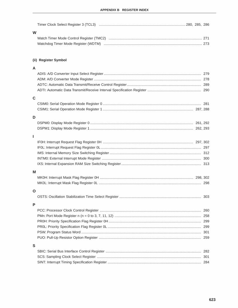
623
APPENDIX B REGISTER INDEX
Timer Clock Select Register 3 (TCL3) ......................................................................................... 280, 285, 286
WWatch Timer Mode Control Register (TMC2) ................................................................................................ 271
Watchdog Timer Mode Register (WDTM) ..................................................................................................... 273
(ii) Register Symbol
AADIS: A/D Converter Input Select Register .................................................................................................... 279
ADM: A/D Converter Mode Register .............................................................................................................. 278
ADTC: Automatic Data Transmit/Receive Control Register ............................................................................ 289
ADTI: Automatic Data Transmit/Receive Interval Specification Register ....................................................... 290
CCSIM0: Serial Operation Mode Register 0 ..................................................................................................... 281
CSIM1: Serial Operation Mode Register 1 ............................................................................................. 287, 288
DDSPM0: Display Mode Register 0 .......................................................................................................... 261, 292
DSPM1: Display Mode Register 1 .......................................................................................................... 262, 293
IIF0H: Interrupt Request Flag Register 0H ............................................................................................. 297, 302
IF0L: Interrupt Request Flag Register 0L ....................................................................................................... 297
IMS: Internal Memory Size Switching Register .............................................................................................. 312
INTM0: External Interrupt Mode Register ...................................................................................................... 300
IXS: Internal Expansion RAM Size Switching Register .................................................................................. 313
MMK0H: Interrupt Mask Flag Register 0H ................................................................................................ 298, 302
MK0L: Interrupt Mask Flag Register 0L ......................................................................................................... 298
OOSTS: Oscillation Stabilization Time Select Register .................................................................................... 303
PPCC: Processor Clock Control Register ........................................................................................................ 260
PMn: Port Mode Register n (n = 0 to 3, 7, 11, 12) ......................................................................................... 258
PR0H: Priority Specification Flag Register 0H ............................................................................................... 299
PR0L: Priority Specification Flag Register 0L ................................................................................................ 299
PSW: Program Status Word ........................................................................................................................... 301
PUO: Pull-Up Resistor Option Register ......................................................................................................... 259
SSBIC: Serial Bus Interface Control Register .................................................................................................. 282
SCS: Sampling Clock Select Register ........................................................................................................... 301
SINT: Interrupt Timing Specification Register ................................................................................................ 284

624
APPENDIX B REGISTER INDEX
TTCL0: Timer Clock Select Register 0 ..................................................................................................... 263, 275
TCL1: Timer Clock Select Register 1 ............................................................................................................. 267
TCL2: Timer Clock Select Register 2 ............................................................................................. 270, 272, 276
TCL3: Timer Clock Select Register 3 ............................................................................................. 280, 285, 286
TMC0: 16-Bit Timer Mode Control Register ................................................................................................... 264
TMC1: 8-Bit Timer Mode Control Register ..................................................................................................... 268
TMC2: Watch Timer Mode Control Register ................................................................................................... 271
TOC0: 16-Bit Timer Output Control Register .................................................................................................. 265
TOC1: 8-Bit Timer Output Control Register .................................................................................................... 269
UUDM: 6-Bit Up/Down Counter Mode Register ................................................................................................ 274
WWDTM: Watchdog Timer Mode Register ........................................................................................................ 273
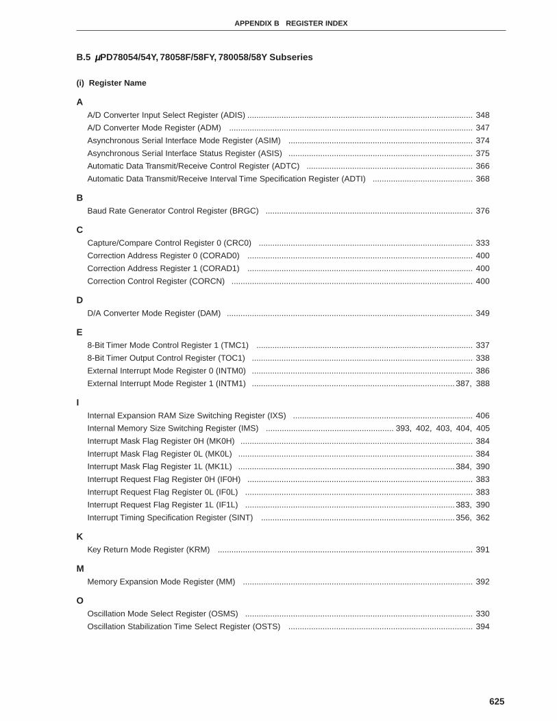
625
APPENDIX B REGISTER INDEX
B.5 µµµµµPD78054/54Y, 78058F/58FY, 780058/58Y Subseries
(i) Register Name
AA/D Converter Input Select Register (ADIS) ................................................................................................... 348
A/D Converter Mode Register (ADM) ........................................................................................................... 347
Asynchronous Serial Interface Mode Register (ASIM) ................................................................................. 374
Asynchronous Serial Interface Status Register (ASIS) ................................................................................. 375
Automatic Data Transmit/Receive Control Register (ADTC) ......................................................................... 366
Automatic Data Transmit/Receive Interval Time Specification Register (ADTI) ............................................ 368
BBaud Rate Generator Control Register (BRGC) ........................................................................................... 376
CCapture/Compare Control Register 0 (CRC0) .............................................................................................. 333
Correction Address Register 0 (CORAD0) ................................................................................................... 400
Correction Address Register 1 (CORAD1) ................................................................................................... 400
Correction Control Register (CORCN) .......................................................................................................... 400
DD/A Converter Mode Register (DAM) ............................................................................................................ 349
E8-Bit Timer Mode Control Register 1 (TMC1) ............................................................................................... 337
8-Bit Timer Output Control Register (TOC1) ................................................................................................. 338
External Interrupt Mode Register 0 (INTM0) ................................................................................................. 386
External Interrupt Mode Register 1 (INTM1) ......................................................................................... 387, 388
IInternal Expansion RAM Size Switching Register (IXS) ............................................................................... 406
Internal Memory Size Switching Register (IMS) ........................................................ 393, 402, 403, 404, 405
Interrupt Mask Flag Register 0H (MK0H) ...................................................................................................... 384
Interrupt Mask Flag Register 0L (MK0L) ....................................................................................................... 384
Interrupt Mask Flag Register 1L (MK1L) ............................................................................................... 384, 390
Interrupt Request Flag Register 0H (IF0H) ................................................................................................... 383
Interrupt Request Flag Register 0L (IF0L) .................................................................................................... 383
Interrupt Request Flag Register 1L (IF1L) ............................................................................................ 383, 390
Interrupt Timing Specification Register (SINT) ..................................................................................... 356, 362
KKey Return Mode Register (KRM) ................................................................................................................ 391
MMemory Expansion Mode Register (MM) ..................................................................................................... 392
OOscillation Mode Select Register (OSMS) .................................................................................................... 330
Oscillation Stabilization Time Select Register (OSTS) ................................................................................. 394

626
APPENDIX B REGISTER INDEX
PPort Mode Register n (PMn) (n = 0 to 7, 12, 13) ................................................................................... 326, 327
Priority Specification Flag Register 0H (PR0H) ............................................................................................ 385
Priority Specification Flag Register 0L (PR0L) ............................................................................................. 385
Priority Specification Flag Register 1L (PR1L) ............................................................................................. 385
Processor Clock Control Register (PCC) ...................................................................................................... 329
Program Status Word (PSW) ........................................................................................................................ 389
Pull-up Resistor Option Register H (PUOH) ................................................................................................. 328
Pull-up Resistor Option Register L (PUOL) .................................................................................................. 328
RReal-Time Output Port Control Register (RTPC) .......................................................................................... 379
Real-Time Output Port Mode Register (RTPM) ............................................................................................ 379
SSampling Clock Select Register (SCS) ......................................................................................................... 389
Serial Bus Interface Control Register (SBIC) ........................................................................................ 354, 360
Serial Interface Pin Select Register (SIPS) ................................................................................................... 378
Serial Operation Mode Register 0 (CSIM0) .......................................................................................... 352, 359
Serial Operation Mode Register 1 (CSIM1) .................................................................................................. 365
Serial Operation Mode Register 2 (CSIM2) .................................................................................................. 373
16-Bit Timer Mode Control Register (TMC0) ................................................................................................ 332
16-Bit Timer Output Control Register (TOC0) ............................................................................................... 334
TTimer Clock Select Register 0 (TCL0) .................................................................................................. 331, 344
Timer Clock Select Register 1 (TCL1) .......................................................................................................... 336
Timer Clock Select Register 2 (TCL2) ......................................................................................... 339, 341, 345
Timer Clock Select Register 3 (TCL3) ......................................................................................... 351, 358, 364
WWatch Timer Mode Control Register (TMC2) ................................................................................................ 340
Watchdog Timer Mode Register (WDTM) ..................................................................................................... 342
(ii) Register Symbol
AADIS: A/D Converter Input Select Register .................................................................................................... 348
ADM: A/D Converter Mode Register .............................................................................................................. 347
ADTC: Automatic Data Transmit/Receive Control Register ............................................................................ 366
ADTI: Automatic Data Transmit/Receive Interval Time Specification Register ............................................... 368
ASIM: Asynchronous Serial Interface Mode Register .................................................................................... 374
ASIS: Asynchronous Serial Interface Status Register ................................................................................... 375
BBRGC: Baud Rate Generator Control Register .............................................................................................. 376
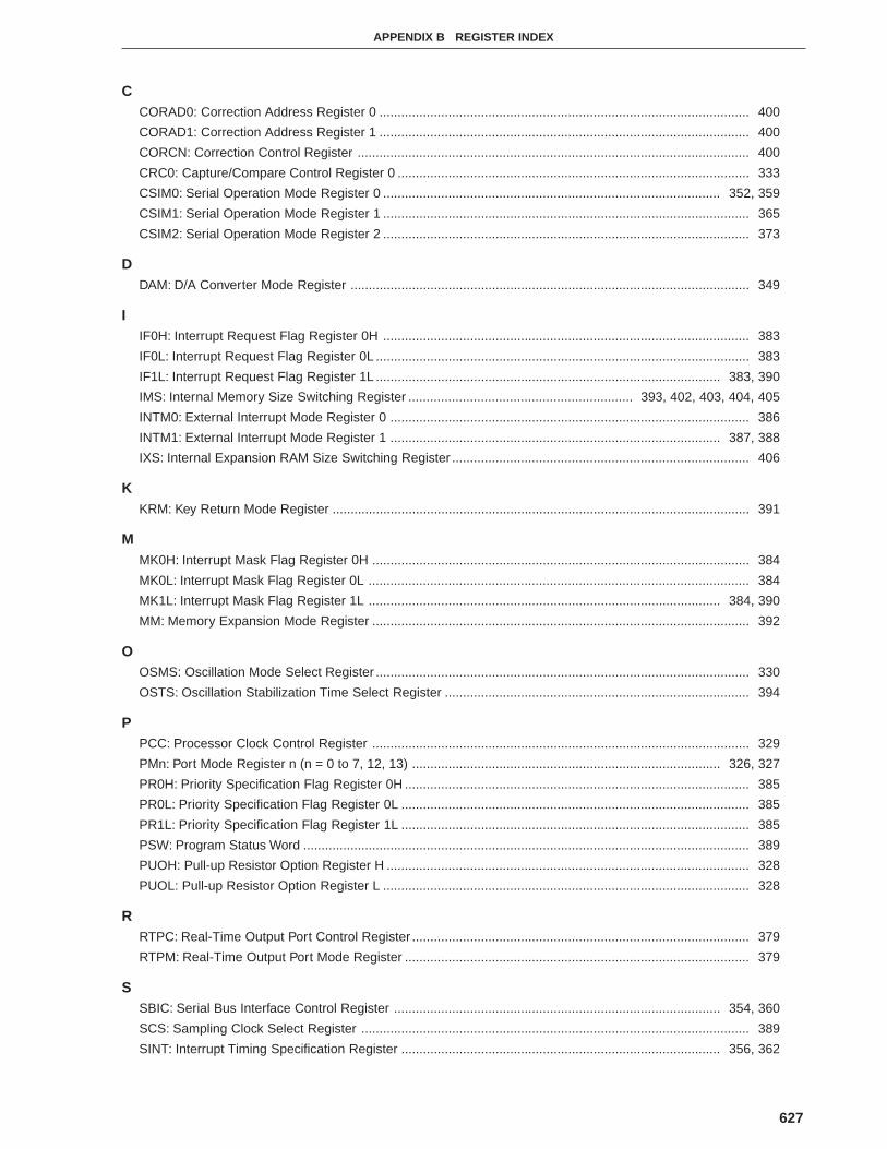
627
APPENDIX B REGISTER INDEX
CCORAD0: Correction Address Register 0 ...................................................................................................... 400
CORAD1: Correction Address Register 1 ...................................................................................................... 400
CORCN: Correction Control Register ............................................................................................................ 400
CRC0: Capture/Compare Control Register 0 ................................................................................................. 333
CSIM0: Serial Operation Mode Register 0 ............................................................................................. 352, 359
CSIM1: Serial Operation Mode Register 1 ..................................................................................................... 365
CSIM2: Serial Operation Mode Register 2 ..................................................................................................... 373
DDAM: D/A Converter Mode Register .............................................................................................................. 349
IIF0H: Interrupt Request Flag Register 0H ..................................................................................................... 383
IF0L: Interrupt Request Flag Register 0L ....................................................................................................... 383
IF1L: Interrupt Request Flag Register 1L ............................................................................................... 383, 390
IMS: Internal Memory Size Switching Register .............................................................. 393, 402, 403, 404, 405
INTM0: External Interrupt Mode Register 0 ................................................................................................... 386
INTM1: External Interrupt Mode Register 1 ........................................................................................... 387, 388
IXS: Internal Expansion RAM Size Switching Register .................................................................................. 406
KKRM: Key Return Mode Register ................................................................................................................... 391
MMK0H: Interrupt Mask Flag Register 0H ........................................................................................................ 384
MK0L: Interrupt Mask Flag Register 0L ......................................................................................................... 384
MK1L: Interrupt Mask Flag Register 1L ................................................................................................. 384, 390
MM: Memory Expansion Mode Register ........................................................................................................ 392
OOSMS: Oscillation Mode Select Register ....................................................................................................... 330
OSTS: Oscillation Stabilization Time Select Register .................................................................................... 394
PPCC: Processor Clock Control Register ........................................................................................................ 329
PMn: Port Mode Register n (n = 0 to 7, 12, 13) ..................................................................................... 326, 327
PR0H: Priority Specification Flag Register 0H ............................................................................................... 385
PR0L: Priority Specification Flag Register 0L ................................................................................................ 385
PR1L: Priority Specification Flag Register 1L ................................................................................................ 385
PSW: Program Status Word ........................................................................................................................... 389
PUOH: Pull-up Resistor Option Register H .................................................................................................... 328
PUOL: Pull-up Resistor Option Register L ..................................................................................................... 328
RRTPC: Real-Time Output Port Control Register ............................................................................................. 379
RTPM: Real-Time Output Port Mode Register ............................................................................................... 379
SSBIC: Serial Bus Interface Control Register .......................................................................................... 354, 360
SCS: Sampling Clock Select Register ........................................................................................................... 389
SINT: Interrupt Timing Specification Register ........................................................................................ 356, 362
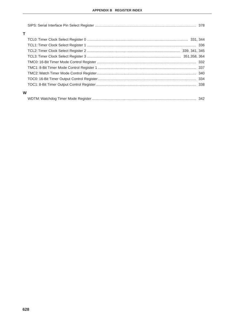
628
APPENDIX B REGISTER INDEX
SIPS: Serial Interface Pin Select Register ..................................................................................................... 378
TTCL0: Timer Clock Select Register 0 ..................................................................................................... 331, 344
TCL1: Timer Clock Select Register 1 ............................................................................................................. 336
TCL2: Timer Clock Select Register 2 ............................................................................................. 339, 341, 345
TCL3: Timer Clock Select Register 3 .............................................................................................. 351,358, 364
TMC0: 16-Bit Timer Mode Control Register ................................................................................................... 332
TMC1: 8-Bit Timer Mode Control Register 1 .................................................................................................. 337
TMC2: Watch Timer Mode Control Register ................................................................................................... 340
TOC0: 16-Bit Timer Output Control Register .................................................................................................. 334
TOC1: 8-Bit Timer Output Control Register .................................................................................................... 338
WWDTM: Watchdog Timer Mode Register ........................................................................................................ 342
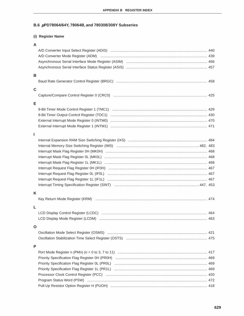
629
APPENDIX B REGISTER INDEX
B.6 µµµµµPD78064/64Y, 78064B, and 780308/308Y Subseries
(i) Register Name
AA/D Converter Input Select Register (ADIS) ................................................................................................. 440
A/D Converter Mode Register (ADM) ........................................................................................................... 439
Asynchronous Serial Interface Mode Register (ASIM) ................................................................................. 456
Asynchronous Serial Interface Status Register (ASIS) ................................................................................. 457
BBaud Rate Generator Control Register (BRGC) ........................................................................................... 458
CCapture/Compare Control Register 0 (CRC0) .............................................................................................. 425
E8-Bit Timer Mode Control Register 1 (TMC1) ............................................................................................... 429
8-Bit Timer Output Control Register (TOC1) ................................................................................................. 430
External Interrupt Mode Register 0 (INTM0) ................................................................................................. 470
External Interrupt Mode Register 1 (INTM1) ................................................................................................. 471
IInternal Expansion RAM Size Switching Register (IXS) ............................................................................... 484
Internal Memory Size Switching Register (IMS) ................................................................................... 482, 483
Interrupt Mask Flag Register 0H (MK0H) ...................................................................................................... 468
Interrupt Mask Flag Register 0L (MK0L) ....................................................................................................... 468
Interrupt Mask Flag Register 1L (MK1L) ....................................................................................................... 468
Interrupt Request Flag Register 0H (IF0H) ................................................................................................... 467
Interrupt Request Flag Register 0L (IF0L) .................................................................................................... 467
Interrupt Request Flag Register 1L (IF1L) .................................................................................................... 467
Interrupt Timing Specification Register (SINT) ..................................................................................... 447, 453
KKey Return Mode Register (KRM) ................................................................................................................ 474
LLCD Display Control Register (LCDC) .......................................................................................................... 464
LCD Display Mode Register (LCDM) ............................................................................................................ 463
OOscillation Mode Select Register (OSMS) .................................................................................................... 421
Oscillation Stabilization Time Select Register (OSTS) ................................................................................. 475
PPort Mode Register n (PMn) (n = 0 to 3, 7 to 11) .......................................................................................... 417
Priority Specification Flag Register 0H (PR0H) ............................................................................................ 469
Priority Specification Flag Register 0L (PR0L) ............................................................................................. 469
Priority Specification Flag Register 1L (PR1L) ............................................................................................. 469
Processor Clock Control Register (PCC) ...................................................................................................... 420
Program Status Word (PSW) ........................................................................................................................ 472
Pull-Up Resistor Option Register H (PUOH) ................................................................................................. 418

630
APPENDIX B REGISTER INDEX
Pull-Up Resistor Option Register L (PUOL) .................................................................................................. 418
SSampling Clock Select Register (SCS) ......................................................................................................... 472
Serial Bus Interface Control Register (SBIC) ........................................................................................ 445, 451
Serial Interface Pin Select Register (SIPS) ................................................................................................... 459
Serial Operation Mode Register 0 (CSIM0) .......................................................................................... 443, 450
Serial Operation Mode Register 2 (CSIM2) .................................................................................................. 455
Serial Operation Mode Register 3 (CSIM3) .................................................................................................. 461
16-Bit Timer Mode Control Register (TMC0) ................................................................................................ 423
16-Bit Timer Output Control Register (TOC0) ............................................................................................... 426
TTimer Clock Select Register 0 (TCL0) .................................................................................................. 422, 435
Timer Clock Select Register 1 (TCL1) .......................................................................................................... 428
Timer Clock Select Register 2 (TCL2) ......................................................................................... 431, 433, 437
Timer Clock Select Register 3 (TCL3) .................................................................................................... 442, 449
Timer Clock Select Register 4 (TCL4) .......................................................................................................... 460
WWatch Timer Mode Control Register (TMC2) ................................................................................................ 432
Watchdog Timer Mode Register (WDTM) ..................................................................................................... 434
(ii) Register Symbol
AADIS: A/D Converter Input Select Register .................................................................................................... 440
ADM: A/D Converter Mode Register .............................................................................................................. 439
ASIM: Asynchronous Serial Interface Mode Register .................................................................................... 456
ASIS: Asynchronous Serial Interface Status Register ................................................................................... 457
BBRGC: Baud Rate Generator Control Register .............................................................................................. 458
CCRC0: Capture/Compare Control Register 0 ................................................................................................. 425
CSIM0: Serial Operation Mode Register 0 ............................................................................................. 443, 450
CSIM2: Serial Operation Mode Register 2 ..................................................................................................... 455
CSIM3: Serial Operation Mode Register 3 ..................................................................................................... 461
IIF0H: Interrupt Request Flag Register 0H ..................................................................................................... 467
IF0L: Interrupt Request Flag Register 0L ....................................................................................................... 467
IF1L: Interrupt Request Flag Register 1L ....................................................................................................... 467
IMS: Internal Memory Size Switching Register ...................................................................................... 482, 483
INTM0: External Interrupt Mode Register 0 .................................................................................................... 470
INTM1: External Interrupt Mode Register 1 ................................................................................................... 471
IXS: Internal Expansion RAM Size Switching Register .................................................................................. 484
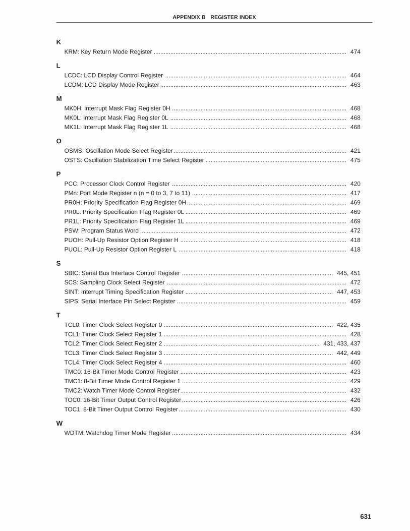
631
APPENDIX B REGISTER INDEX
KKRM: Key Return Mode Register ................................................................................................................... 474
LLCDC: LCD Display Control Register ............................................................................................................ 464
LCDM: LCD Display Mode Register ............................................................................................................... 463
MMK0H: Interrupt Mask Flag Register 0H ........................................................................................................ 468
MK0L: Interrupt Mask Flag Register 0L ......................................................................................................... 468
MK1L: Interrupt Mask Flag Register 1L ......................................................................................................... 468
OOSMS: Oscillation Mode Select Register ....................................................................................................... 421
OSTS: Oscillation Stabilization Time Select Register .................................................................................... 475
PPCC: Processor Clock Control Register ........................................................................................................ 420
PMn: Port Mode Register n (n = 0 to 3, 7 to 11) ............................................................................................ 417
PR0H: Priority Specification Flag Register 0H ............................................................................................... 469
PR0L: Priority Specification Flag Register 0L ................................................................................................ 469
PR1L: Priority Specification Flag Register 1L ................................................................................................ 469
PSW: Program Status Word ........................................................................................................................... 472
PUOH: Pull-Up Resistor Option Register H ................................................................................................... 418
PUOL: Pull-Up Resistor Option Register L .................................................................................................... 418
SSBIC: Serial Bus Interface Control Register .......................................................................................... 445, 451
SCS: Sampling Clock Select Register ........................................................................................................... 472
SINT: Interrupt Timing Specification Register ........................................................................................ 447, 453
SIPS: Serial Interface Pin Select Register ..................................................................................................... 459
TTCL0: Timer Clock Select Register 0 ..................................................................................................... 422, 435
TCL1: Timer Clock Select Register 1 ............................................................................................................. 428
TCL2: Timer Clock Select Register 2 ............................................................................................. 431, 433, 437
TCL3: Timer Clock Select Register 3 ..................................................................................................... 442, 449
TCL4: Timer Clock Select Register 4 ............................................................................................................. 460
TMC0: 16-Bit Timer Mode Control Register ................................................................................................... 423
TMC1: 8-Bit Timer Mode Control Register 1 .................................................................................................. 429
TMC2: Watch Timer Mode Control Register ................................................................................................... 432
TOC0: 16-Bit Timer Output Control Register .................................................................................................. 426
TOC1: 8-Bit Timer Output Control Register .................................................................................................... 430
WWDTM: Watchdog Timer Mode Register ........................................................................................................ 434
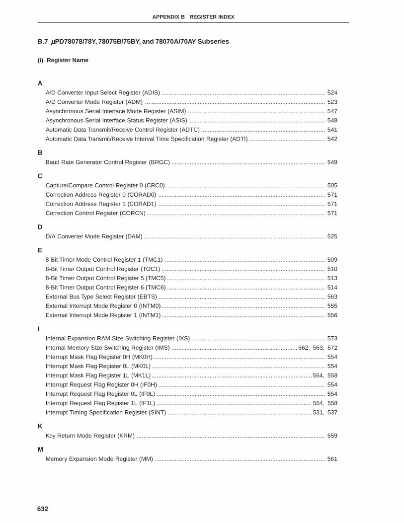
632
APPENDIX B REGISTER INDEX
B.7 µµµµµPD78078/78Y, 78075B/75BY, and 78070A/70AY Subseries
(i) Register Name
AA/D Converter Input Select Register (ADIS) ................................................................................................... 524
A/D Converter Mode Register (ADM) ............................................................................................................. 523
Asynchronous Serial Interface Mode Register (ASIM) ................................................................................... 547
Asynchronous Serial Interface Status Register (ASIS) ................................................................................... 548
Automatic Data Transmit/Receive Control Register (ADTC) ........................................................................... 541
Automatic Data Transmit/Receive Interval Time Specification Register (ADTI) .............................................. 542
BBaud Rate Generator Control Register (BRGC) ............................................................................................. 549
CCapture/Compare Control Register 0 (CRC0) ................................................................................................ 505
Correction Address Register 0 (CORAD0) ..................................................................................................... 571
Correction Address Register 1 (CORAD1) ..................................................................................................... 571
Correction Control Register (CORCN) ............................................................................................................ 571
DD/A Converter Mode Register (DAM) .............................................................................................................. 525
E8-Bit Timer Mode Control Register 1 (TMC1) ................................................................................................. 509
8-Bit Timer Output Control Register (TOC1) ................................................................................................... 510
8-Bit Timer Output Control Register 5 (TMC5) ................................................................................................ 513
8-Bit Timer Output Control Register 6 (TMC6) ................................................................................................ 514
External Bus Type Select Register (EBTS) ..................................................................................................... 563
External Interrupt Mode Register 0 (INTM0) ................................................................................................... 555
External Interrupt Mode Register 1 (INTM1) ................................................................................................... 556
IInternal Expansion RAM Size Switching Register (IXS) ................................................................................. 573
Internal Memory Size Switching Register (IMS) ............................................................................ 562, 563, 572
Interrupt Mask Flag Register 0H (MK0H) ........................................................................................................ 554
Interrupt Mask Flag Register 0L (MK0L) ......................................................................................................... 554
Interrupt Mask Flag Register 1L (MK1L) ................................................................................................. 554, 558
Interrupt Request Flag Register 0H (IF0H) ..................................................................................................... 554
Interrupt Request Flag Register 0L (IF0L) ...................................................................................................... 554
Interrupt Request Flag Register 1L (IF1L) ............................................................................................. 554, 558
Interrupt Timing Specification Register (SINT) ....................................................................................... 531, 537
KKey Return Mode Register (KRM) .................................................................................................................. 559
MMemory Expansion Mode Register (MM) ....................................................................................................... 561

633
APPENDIX B REGISTER INDEX
OOscillation Mode Select Register (OSMS) ...................................................................................................... 501
Oscillation Stabilization Time Select Register (OSTS) ................................................................................... 564
PPort Mode Register n (PMn) (n = 0 to 3, 5 to 10, 12, 13) ................................................................................ 496
Port Mode Register n (PMn) (n = 0 to 3, 6, 7, 9, 10, 12, 13) ........................................................................... 497
Priority Specification Flag Register 0H (PR0H) .............................................................................................. 555
Priority Specification Flag Register 0L (PR0L) ............................................................................................... 555
Priority Specification Flag Register 1L (PR1L) ............................................................................................... 555
Processor Clock Control Register (PCC) ........................................................................................................ 499
Program Status Word (PSW) .......................................................................................................................... 557
Pull-up Resistor Option Register H (PUOH) ................................................................................................... 498
Pull-up Resistor Option Register L (PUOL) .................................................................................................... 498
RReal-Time Output Port Control Register (RTPC) ............................................................................................ 551
Real-Time Output Port Mode Register (RTPM) .............................................................................................. 551
SSampling Clock Select Register (SCS) ........................................................................................................... 557
Serial Bus Interface Control Register (SBIC) .......................................................................................... 529, 535
Serial Operation Mode Register 0 (CSIM0) ............................................................................................ 528, 534
Serial Operation Mode Register 1 (CSIM1) .................................................................................................... 540
Serial Operation Mode Register 2 (CSIM2) .................................................................................................... 546
16-Bit Timer Mode Control Register (TMC0) .................................................................................................. 504
16-Bit Timer Output Control Register (TOC0) ................................................................................................. 506
TTimer Clock Select Register 0 (TCL0) .................................................................................................... 503, 520
Timer Clock Select Register 1 (TCL1) ............................................................................................................ 508
Timer Clock Select Register 2 (TCL2) ........................................................................................... 515, 517, 521
Timer Clock Select Register 3 (TCL3) ........................................................................................... 527, 533, 539
Timer Clock Select Register 5 (TCL5) ............................................................................................................ 511
Timer Clock Select Register 6 (TCL6) ............................................................................................................ 512
WWatch Timer Mode Control Register (TMC2) .................................................................................................. 516
Watchdog Timer Mode Register (WDTM) ....................................................................................................... 518
(ii) Register Symbol
AADIS: A/D Converter Input Select Register .................................................................................................... 524
ADM: A/D Converter Mode Register .............................................................................................................. 523
ADTC: Automatic Data Transmit/Receive Control Register ............................................................................ 541
ADTI: Automatic Data Transmit/Receive Interval Time Specification Register ............................................... 542
ASIM: Asynchronous Serial Interface Mode Register .................................................................................... 547
ASIS: Asynchronous Serial Interface Status Register ................................................................................... 548
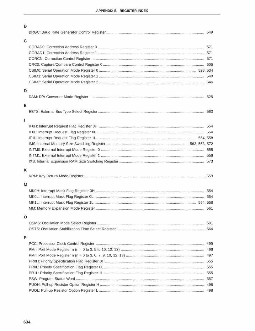
634
APPENDIX B REGISTER INDEX
BBRGC: Baud Rate Generator Control Register .............................................................................................. 549
CCORAD0: Correction Address Register 0 ...................................................................................................... 571
CORAD1: Correction Address Register 1 ...................................................................................................... 571
CORCN: Correction Control Register ............................................................................................................ 571
CRC0: Capture/Compare Control Register 0 ................................................................................................. 505
CSIM0: Serial Operation Mode Register 0 ............................................................................................. 528, 534
CSIM1: Serial Operation Mode Register 1 ..................................................................................................... 540
CSIM2: Serial Operation Mode Register 2 ..................................................................................................... 546
DDAM: D/A Converter Mode Register .............................................................................................................. 525
EEBTS: External Bus Type Select Register ...................................................................................................... 563
IIF0H: Interrupt Request Flag Register 0H ..................................................................................................... 554
IF0L: Interrupt Request Flag Register 0L ....................................................................................................... 554
IF1L: Interrupt Request Flag Register 1L ............................................................................................... 554, 558
IMS: Internal Memory Size Switching Register .............................................................................. 562, 563, 572
INTM0: External Interrupt Mode Register 0 ................................................................................................... 555
INTM1: External Interrupt Mode Register 1 ................................................................................................... 556
IXS: Internal Expansion RAM Size Switching Register .................................................................................. 573
KKRM: Key Return Mode Register ................................................................................................................... 559
MMK0H: Interrupt Mask Flag Register 0H ........................................................................................................ 554
MK0L: Interrupt Mask Flag Register 0L ......................................................................................................... 554
MK1L: Interrupt Mask Flag Register 1L ................................................................................................. 554, 558
MM: Memory Expansion Mode Register ........................................................................................................ 561
OOSMS: Oscillation Mode Select Register ....................................................................................................... 501
OSTS: Oscillation Stabilization Time Select Register .................................................................................... 564
PPCC: Processor Clock Control Register ........................................................................................................ 499
PMn: Port Mode Register n (n = 0 to 3, 5 to 10, 12, 13) ................................................................................ 496
PMn: Port Mode Register n (n = 0 to 3, 6, 7, 9, 10, 12, 13) ........................................................................... 497
PR0H: Priority Specification Flag Register 0H ............................................................................................... 555
PR0L: Priority Specification Flag Register 0L ................................................................................................ 555
PR1L: Priority Specification Flag Register 1L ................................................................................................ 555
PSW: Program Status Word ........................................................................................................................... 557
PUOH: Pull-up Resistor Option Register H .................................................................................................... 498
PUOL: Pull-up Resistor Option Register L ..................................................................................................... 498
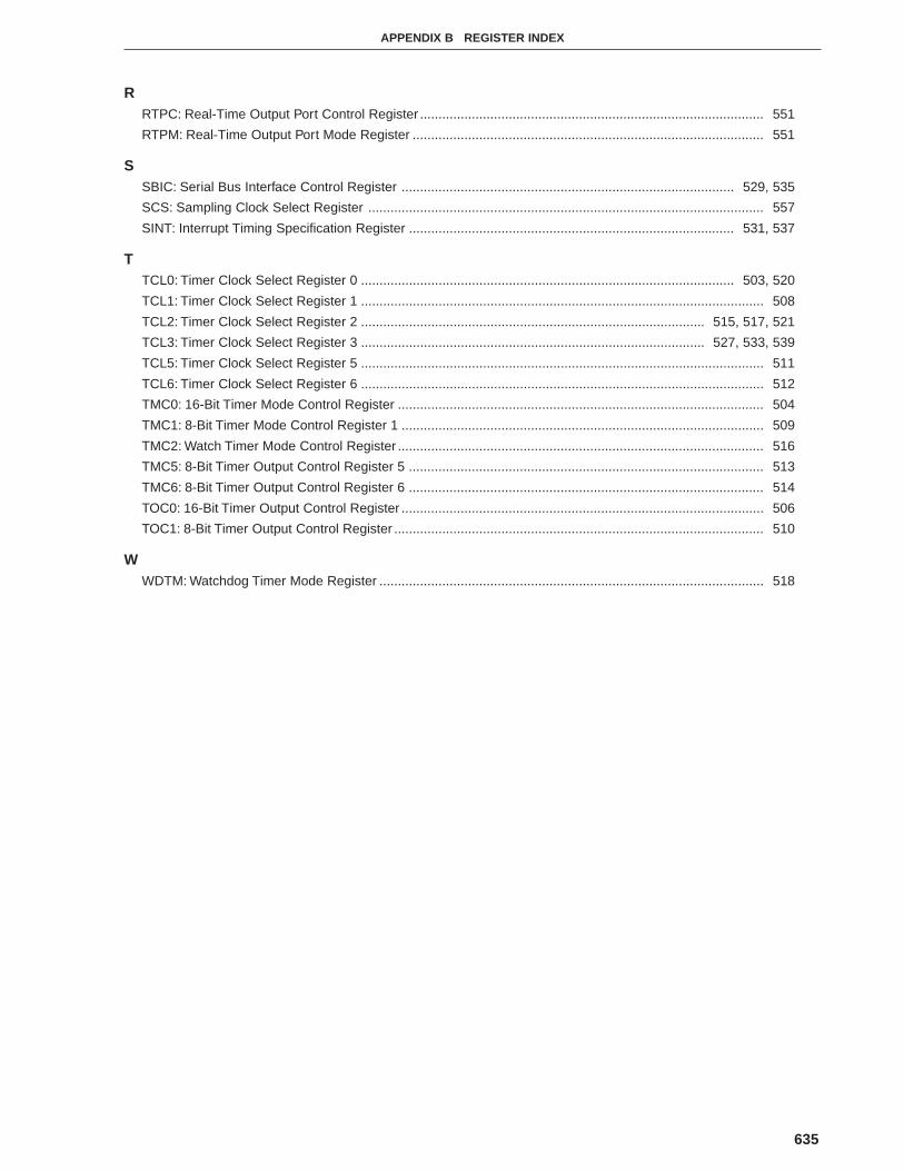
635
APPENDIX B REGISTER INDEX
RRTPC: Real-Time Output Port Control Register ............................................................................................. 551
RTPM: Real-Time Output Port Mode Register ............................................................................................... 551
SSBIC: Serial Bus Interface Control Register .......................................................................................... 529, 535
SCS: Sampling Clock Select Register ........................................................................................................... 557
SINT: Interrupt Timing Specification Register ........................................................................................ 531, 537
TTCL0: Timer Clock Select Register 0 ..................................................................................................... 503, 520
TCL1: Timer Clock Select Register 1 ............................................................................................................. 508
TCL2: Timer Clock Select Register 2 ............................................................................................. 515, 517, 521
TCL3: Timer Clock Select Register 3 ............................................................................................. 527, 533, 539
TCL5: Timer Clock Select Register 5 ............................................................................................................. 511
TCL6: Timer Clock Select Register 6 ............................................................................................................. 512
TMC0: 16-Bit Timer Mode Control Register ................................................................................................... 504
TMC1: 8-Bit Timer Mode Control Register 1 .................................................................................................. 509
TMC2: Watch Timer Mode Control Register ................................................................................................... 516
TMC5: 8-Bit Timer Output Control Register 5 ................................................................................................ 513
TMC6: 8-Bit Timer Output Control Register 6 ................................................................................................ 514
TOC0: 16-Bit Timer Output Control Register .................................................................................................. 506
TOC1: 8-Bit Timer Output Control Register .................................................................................................... 510
WWDTM: Watchdog Timer Mode Register ........................................................................................................ 518
636
APPENDIX B REGISTER INDEX
B.8 µµµµµPD78083 Subseries
(i) Register Name
AA/D Converter Input Select Register (ADIS) ................................................................................................... 593
A/D Converter Mode Register (ADM) ............................................................................................................. 592
Asynchronous Serial Interface Mode Register (ASIM) ................................................................................... 595
Asynchronous Serial Interface Status Register (ASIS) ................................................................................... 596
BBaud Rate Generator Control Register (BRGC) ............................................................................................. 597
E8-Bit Timer Output Control Register n (TMCn) (n = 5, 6) ................................................................................ 586
External Interrupt Mode Register 0 (INTM0) ................................................................................................... 603
External Interrupt Mode Register 1 (INTM1) ................................................................................................... 603
IInternal Memory Size Switching Register (IMS) ............................................................................................. 609
Interrupt Mask Flag Register 0H (MK0H) ........................................................................................................ 601
Interrupt Mask Flag Register 0L (MK0L) ......................................................................................................... 601
Interrupt Mask Flag Register 1L (MK1L) ......................................................................................................... 601
Interrupt Request Flag Register 0H (IF0H) ..................................................................................................... 601
Interrupt Request Flag Register 0L (IF0L) ...................................................................................................... 601
Interrupt Request Flag Register 1L (IF1L) ...................................................................................................... 601
OOscillation Mode Select Register (OSMS) ...................................................................................................... 584
Oscillation Stabilization Time Select Register (OSTS) ................................................................................... 605
PPort Mode Register n (PMn) (n = 0, 1, 3, 5, 7, 10) .......................................................................................... 582
Priority Specification Flag Register 0H (PR0H) .............................................................................................. 602
Priority Specification Flag Register 0L (PR0L) ............................................................................................... 602
Priority Specification Flag Register 1L (PR1L) ............................................................................................... 602
Processor Clock Control Register (PCC) ........................................................................................................ 583
Program Status Word (PSW) .......................................................................................................................... 604
Pull-up Resistor Option Register H (PUOH) ................................................................................................... 582
Pull-up Resistor Option Register L (PUOL) .................................................................................................... 582
SSerial Operation Mode Register 2 (CSIM2) .................................................................................................... 594
TTimer Clock Select Register 0 (TCL0) ............................................................................................................ 589
Timer Clock Select Register 2 (TCL2) .................................................................................................... 587, 590
Timer Clock Select Register n (TCLn) (n = 5, 6) ............................................................................................. 585
WWatchdog Timer Mode Register (WDTM) ....................................................................................................... 588
637
APPENDIX B REGISTER INDEX
(ii) Register Symbol
AADIS: A/D Converter Input Select Register .................................................................................................... 593
ADM: A/D Converter Mode Register .............................................................................................................. 592
ASIM: Asynchronous Serial Interface Mode Register .................................................................................... 595
ASIS: Asynchronous Serial Interface Status Register ................................................................................... 596
BBRGC: Baud Rate Generator Control Register .............................................................................................. 597
CCSIM2: Serial Operation Mode Register 2 ..................................................................................................... 594
IIF0H: Interrupt Request Flag Register 0H ..................................................................................................... 601
IF0L: Interrupt Request Flag Register 0L ....................................................................................................... 601
IF1L: Interrupt Request Flag Register 1L ....................................................................................................... 601
IMS: Internal Memory Size Switching Register .............................................................................................. 609
INTM0: External Interrupt Mode Register 0 ................................................................................................... 603
INTM1: External Interrupt Mode Register 1 ................................................................................................... 603
MMK0H: Interrupt Mask Flag Register 0H ........................................................................................................ 601
MK0L: Interrupt Mask Flag Register 0L ......................................................................................................... 601
MK1L: Interrupt Mask Flag Register 1L ......................................................................................................... 601
OOSMS: Oscillation Mode Select Register ....................................................................................................... 584
OSTS: Oscillation Stabilization Time Select Register .................................................................................... 605
PPCC: Processor Clock Control Register ........................................................................................................ 583
PMn: Port Mode Register n (n = 0, 1, 3, 5, 7, 10) .......................................................................................... 582
PR0H: Priority Specification Flag Register 0H ............................................................................................... 602
PR0L: Priority Specification Flag Register 0L ................................................................................................ 602
PR1L: Priority Specification Flag Register 1L ................................................................................................ 602
PSW: Program Status Word ........................................................................................................................... 604
PUOH: Pull-up Resistor Option Register H .................................................................................................... 582
PUOL: Pull-up Resistor Option Register L ..................................................................................................... 582
TTCL0: Timer Clock Select Register 0 ............................................................................................................. 589
TCL2: Timer Clock Select Register 2 ..................................................................................................... 587, 590
TCLn: Timer Clock Select Register n (n = 5, 6) ............................................................................................. 585
TMCn: 8-Bit Timer Output Control Register n (n = 5, 6) ................................................................................. 586
WWDTM: Watchdog Timer Mode Register ........................................................................................................ 588

638
[MEMO]