rv4640 low cost 64-bit risc cpu w/32-bit bus - renesas
TRANSCRIPT
������������ ����� ��������
����� �������������
� ��� ���������
������������������������◆ High-performance embedded 64-bit microprocessor
- 64-bit integer operations- 64-bit registers- Based on the MIPS RISC Architecture- 100MHz, 133 MHz,150MHz, 180MHz, and 200MHz
operating frequencies- 32-bit bus interface brings 64-bit power to 32-bit system
cost◆ High-performance DSP capability
- 100 Million Integer Mul-Accumulate operations/sec@200MHz
- 67 MFlops floating-point operations @200MHz◆ High-performance microprocessor
- 100 M Mul-Add/second @200MHz- 67 MFlops @200MHz- >500,000 dhrystone (2.1)/sec capability @200MHz (260
dhrystone MIPS)◆ High level of integration
- 64-bit, 200 MHz integer CPU- 67MFlops single-precision floating-point unit- 8KB instruction cache; 8KB data cache- Integer multiply unit with 100M Mul-Add/sec
�
1998 Integrated Device Technology, Inc.
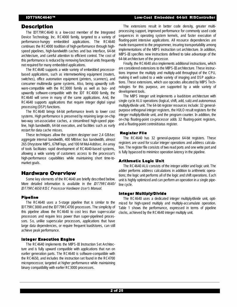
����� ������� ������� ������� ����������200 MHz 64-bit ORION CPU
64-bit Register File
64-bit Adder
Store Aligner
Logic Unit
Load Aligner
High-PerformanceInteger Multiply
Pipe
line
Con
trol
SynSyste
Address TCache Attri
Exception MFunct
System Contro
Instruction Bus
Control Bus
Instruction CacheSet B
Instruction CacheSet A
(Lockable)
The IDT logo is a registered trademark and ORION, RC4650, RC4640, RV4640, RC4600, RC308Integrated Device Technology, Inc.are trademarks of
◆ Upwardly software compatible with IDT RISControllerFamily
◆ Easily upgradable to 64-bit system◆ Low-power operation
- Active power management powers-down inactive units- Standby mode
◆ Large, efficient on-chip caches- Separate 8KB Instruction and 8KB Data caches- Over 2400MB/sec bandwidth from internal caches- 2-set associative- Write-back and write-through support- Cache locking, to facilitate deterministic response- High performance write protocols, for graphics and data
communications◆ Bus compatible with RC4000 family
- System interfaces to 100MHz, provides bandwidth up to400 MB/sec
- Direct interface to 32-bit wide systems- Synchronized to external reference clock for multi- master
operation◆ Improved real-time support
- Fast interrupt decode- Optional cache locking
�� �� ������ ���
FP Register File
FP Add/Sub/Cvt/
Pack/Unpack
FP Multiply
Pip
elin
e C
ontro
l
67MFlops Single-Precision FPA
Div/Sqrt
32-bitchronizedm Interface
ranslation/bute Control
anagementions
l Coprocessor
Data Cache
Data Cache
Data Bus
Set A(Lockable)
Set B
1, RC3052, RC3051, RC3041, RC5000, RC36100, RISController, and RISCore
3486/1
���� ����� ���� ��� �������� ������ ��� ����� ��
��������������������������������������������The IDT79RC4640 is a low-cost member of the Integrated
Device Technology, Inc. RC4000 family, targeted to a variety ofperformance-hungry embedded applications. The RC4640continues the RC4000 tradition of high-performance through high-speed pipelines, high-bandwidth caches and bus interface, 64-bitarchitecture, and careful attention to efficient control. The cost ofthis performance is reduced by removing functional units frequentlynot required for many embedded applications.
The RC4640 supports a wide variety of embedded processor-based applications, such as internetworking equipment (routers,switches), office automation equipment (printers, scanners), andconsumer multimedia game systems. Also, being upwardly soft-ware-compatible with the RC3000 family as well as bus- andupwardly software-compatible with the IDT RC4000 family, theRC4640 will serve in many of the same applications. And, theRC4640 supports applications that require integer digital signalprocessing (DSP) functions.
The RC4640 brings 64-bit performance levels to lower costsystems. High performance is preserved by retaining large on-chiptwo-way set-associative caches, a streamlined high-speed pipe-line, high bandwidth, 64-bit execution, and facilities such as earlyrestart for data cache misses.
These techniques allow the system designer over 2.4 GB/secaggregate internal bandwidth, 400 MB/sec bus bandwidth, almost265 Dhrystone MIPS, 67MFlops, and 100 M Mul-Add/sec. An arrayof tools facilitates rapid development of RC4640-based systems,allowing a wide variety of customers access to the processor’shigh-performance capabilities while maintaining short time-to-market goals.
��������������������� �� �� �� �����������������������������Some key elements of the RC4640 are briefly described below.
More detailed information is available in the IDT79RC4640/IDT79RC4650 RISC Processor Hardware User’s Manual.
��������������������������������
The RC4640 uses a 5-stage pipeline that is similar to theIDT79RC3000 and the IDT79RC4700 processors. The simplicity ofthis pipeline allows the RC4640 to cost less than super-scalarprocessors and require less power than super-pipelined proces-sors. So, unlike superscalar processors, applications that havelarge data dependencies, or require frequent load/stores, can stillachieve peak performance.
�������������������� � � � � ���������������������������� ��������������������
The RC4640 implements the MIPS-III Instruction Set Architec-ture and is fully upward compatible with applications that run onearlier generation parts. The RC4640 is software-compatible withthe RC4650, and includes the instruction set found in the RC4700microprocessor, targeted at higher performance while maintainingbinary compatibility with earlier RC3000 processors.
� �
The extensions result in better code density, greater multi-processing support, improved performance for commonly used codesequences in operating system kernels, and faster execution offloating-point intensive applications. All resource dependencies aremade transparent to the programmer, insuring transportability amongimplementations of the MIPS instruction set architecture. In addition,MIPS-III specifies new instructions defined to take advantage of the64-bit architecture of the processor.
Finally, the RC4640 also implements additional instructions, whichare considered extensions to the MIPS-III architecture. These instruc-tions improve the multiply and multiply-add throughput of the CPU,making it well suited to a wide variety of imaging and DSP applica-tions. These extensions, which use opcodes allocated by MIPS Tech-nologies for this purpose, are supported by a wide variety ofdevelopment tools.
The MIPS integer unit implements a load/store architecture withsingle cycle ALU operations (logical, shift, add, sub) and autonomousmultiply/divide unit. The 64-bit register resources include: 32 general-purpose orthogonal integer registers, the HI/LO result registers for theinteger multiply/divide unit, and the program counter. In addition, theon-chip floating-point co-processor adds 32 floating-point registers,and a floating-point control/status register.
������������������������ ����������������
The RC4640 has 32 general-purpose 64-bit registers. Theseregisters are used for scalar integer operations and address calcula-tion. The register file consists of two read ports and one write port andis fully bypassed to minimize operation latency in the pipeline.
������������������������������������ ���������������� ����������������
The RC4640 ALU consists of the integer adder and logic unit. Theadder performs address calculations in addition to arithmetic opera-tions; the logic unit performs all of the logic and shift operations. Eachunit is highly optimized and can perform an operation in a single pipe-line cycle.
�������������������� ������������������������������������������������������������
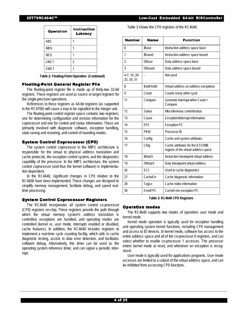
The RC4640 uses a dedicated integer multiply/divide unit, opti-mized for high-speed multiply and multiply-accumulate operation.Table 1 shows the performance, expressed in terms of pipelineclocks, achieved by the RC4640 integer multiply unit.
� ��
���� ����� ���� ��� �������� ������ ��� ����� ��
The MIPS-III architecture defines that the results of a multiply ordivide operation are placed in the HI and LO registers. The valuescan then be transferred to the general purpose register file usingthe MFHI/MFLO instructions.
The RC4640 adds a new multiply instruction, “MUL”, which canspecify that the multiply results bypass the “Lo” register and areplaced immediately in the primary register file. By avoiding theexplicit “Move-from-Lo” instruction required when using “Lo”,throughput of multiply-intensive operations is increased.
An additional enhancement offered by the RC4640 is an atomic“multiply-add” operation, MAD, used to perform multiply-accumu-late operations. This instruction multiplies two numbers and addsthe product to the current contents of the HI and LO registers. Thisoperation is used in numerous DSP algorithms, and allows theRC4640 to cost reduce systems requiring a mix of DSP and controlfunctions.
Finally, aggressive implementation techniques feature lowlatency for these operations along with pipelining to allow newoperations to be issued before a previous one has fully completed.Table 1 also shows the repeat rate (peak issue rate), latency, andnumber of processor stalls required for the various operations. TheRC4640 performs automatic operand size detection to determinethe size of the operand, and implements hardware interlocks toprevent overrun, allowing this high-performance to be achievedwith simple programming.
���������������������������� ����������������� !� !� !� !��������������������������������
The RC4640 incorporates an entire single-precision floating-point coprocessor on chip, including a floating-point register fileand execution units. The floating-point coprocessor forms a “seam-less” interface with the integer unit, decoding and executinginstructions in parallel with the integer unit.
The floating-point unit of the RC4640 directly implementssingle-precision floating-point operations, which enables theRC4640 to perform functions such as graphics rendering withoutrequiring extensive die area or power consumption. The single-precision unit of the RC4640 is directly compatible with the single-precision operation of the RC4700, and features the same laten-cies and repeat rates.
������������
�� ������� ������ �����
MULT/U, MAD/U 16 bit 3 2 0
32 bit 4 3 0
MUL 16 bit 3 2 1
32 bit 4 3 2
DMULT, DMULTU any 6 5 0
DIV, DIVU any 36 36 0
DDIV, DDIVU any 68 68 0
Table 1: RC4640 Integer Multiply Operation
! �
The RC4640 does not directly implement the double-precisionoperations found in the RC4700. However, to maintain softwarecompatibility, the RC4640 will signal a trap when a double-precisionoperation is initiated, allowing the requested function to be emulatedin software. Alternatively, the system architect could use a softwarelibrary emulation of double-precision functions, selected at compiletime, to eliminate the overhead associated with trap and emulation.
���������������������������� �������������������� ��������������������
The RC4640’s floating-point execution units perform single preci-sion arithmetic, as specified in IEEE Standard 754. The executionunit is broken into a separate multiply unit and a combined add/convert/divide/square root unit. Overlap of multiply and add/subtractis supported. The multiplier is partially pipelined, allowing a new multi-plication instruction to begin every 6 cycles.
As in the IDT79RC4700, the RC4640 maintains fully precisefloating-point exceptions while allowing both overlapped and pipe-lined operations. Precise exceptions are extremely important inmission-critical environments, such as ADA, and highly desirable fordebugging in any environment.
The floating-point unit’s operation set includes floating-point add,subtract, multiply, divide, square root, conversion between fixed-pointand floating-point format, conversion among floating-point formats,and floating-point compare. These operations comply with IEEEStandard 754. Double precision operations are not directly supported;attempts to execute double-precision floating point operations, orrefer directly to double-precision registers, result in the RC4640signalling a “trap” to the CPU, enabling emulation of the requestedfunction.
Table 2: gives the latencies of some of the floating-point instruc-tions in internal processor cycles.
"#��$���������%&����
�$���&'
ADD 4
SUB 4
MUL 8
DIV 32
SQRT 31
CMP 3
FIX 4
FLOAT 6
Table 2: Floating-Point Operation
� ��
���� ����� ���� ��� �������� ������ ��� ����� ��
���������������������������� �������������������� """"�������������������� ������������������������ ����������������
The floating-point register file is made up of thirty-two 32-bitregisters. These registers are used as source or target registers forthe single-precision operations.
References to these registers as 64-bit registers (as supportedin the RC4700) will cause a trap to be signalled to the integer unit.
The floating-point control register space contains two registers;one for determining configuration and revision information for thecoprocessor and one for control and status information. These areprimarily involved with diagnostic software, exception handling,state saving and restoring, and control of rounding modes.
#�#�#�#����������������� !!!!�������������������� !��!��!��!�������������������������� $! $! $! $!����%%%%&&&&
The system control coprocessor in the MIPS architecture isresponsible for the virtual to physical address translation andcache protocols, the exception control system, and the diagnosticscapability of the processor. In the MIPS architecture, the systemcontrol coprocessor (and thus the kernel software) is implementa-tion dependent.
In the RC4640, significant changes in CP0 relative to theRC4600 have been implemented. These changes are designed tosimplify memory management, facilitate debug, and speed real-time processing.
#�#�#�#����������������� !!!!�������������������� !��!��!��!�������������������������� ����������������������������
The RC4640 incorporates all system control co-processor(CP0) registers on-chip. These registers provide the path throughwhich the virtual memory system’s address translation iscontrolled, exceptions are handled, and operating modes arecontrolled (kernel vs. user mode, interrupts enabled or disabled,cache features). In addition, the RC4640 includes registers toimplement a real-time cycle counting facility, which aids in cachediagnostic testing, assists in data error detection, and facilitatessoftware debug. Alternatively, this timer can be used as theoperating system reference timer, and can signal a periodic inter-rupt.
ABS 1
MOV 1
NEG 1
LWC1 2
SWC1 1
"#��$���������%&����
�$���&'
Table 2: Floating-Point Operation (Continued)
� �
Table 3 shows the CP0 registers of the RC4640.
'��'��'��'���������������������� ��������������������
The RC4640 supports two modes of operation: user mode andkernel mode.
Kernel mode operation is typically used for exception handlingand operating system kernel functions, including CP0 managementand access to IO devices. In kernel mode, software has access to theentire address space and all of the co-processor 0 registers, and canselect whether to enable co-processor 1 accesses. The processorenters kernel mode at reset, and whenever an exception is recog-nized.
User mode is typically used for applications programs. User modeaccesses are limited to a subset of the virtual address space, and canbe inhibited from accessing CP0 functions.
(%���� ($�� )%�&����
0 IBase Instruction address space base
1 IBound Instruction address space bound
2 DBase Data address space base
3 DBound Data address space bound
4-7, 10, 20-25, 29, 31
- Not used
8 BadVAddr Virtual address on address exceptions
9 Count Counts every other cycle
11 Compare Generate interrupt when Count = Compare
12 Status Miscellaneous control/status
13 Cause Exception/Interrupt information
14 EPC Exception PC
15 PRId Processor ID
16 Config Cache and system attributes
17 CAlg Cache attributes for the 8 512MB regions of the virtual address space
18 IWatch Instruction breakpoint virtual address
19 DWatch Data breakpoint virtual address
26 ECC Used in cache diagnostics
27 CacheErr Cache diagnostic information
28 TagLo Cache index information
30 ErrorEPC CacheError exception PC
Table 3: RC4640 CPO Registers
� ��
���� ����� ���� ��� �������� ������ ��� ����� ��
((((����������������� �� �� �� ����� � � � �������������������������� �� �� �� ������������������ �� �� �� ���������������������
The 4GB virtual address space of the RC4640 is shown infigure 3. The 4 GB address space is divided into addresses acces-sible in either kernel or user mode (kuseg), and addresses onlyaccessible in kernel mode (kseg2:0).
The RC4640 supports the use of multiple user tasks sharingcommon virtual addresses, but mapped to separate physicaladdresses. This facility is implemented via the “base-bounds”registers contained in CP0.
When a user virtual address is asserted (load, store, or instruc-tion fetch), the RC4640 compares the virtual address with thecontents of the appropriate “bounds” register (instruction or data). Ifthe virtual address is “in bounds”, the value of the corresponding“base” register is added to the virtual address to form the physicaladdress for that reference. If the address is not within bounds, anexception is signalled.
This facility enables multiple user processes in a single physicalmemory without the use of a TLB. This type of operation is furthersupported by a number of development tools for the RC4640,including real-time operating systems and “position independentcode”.
Kernel mode addresses do not use the base-bounds registers,but rather undergo a fixed virtual-to-physical address translation.
0xFFFFFFFF
0xC0000000
Kernel virtual address space(kseg2)
Unmapped, 1.0 GB
0xBFFFFFFF
0xA0000000
Uncached kernel physical address space(kseg1)
Unmapped, 0.5GB
0x9FFFFFFF
0x80000000
Cached kernel physical address space(kseg0)
Unmapped, 0.5GB
0x7FFFFFF
0x00000000
User virtual address space(useg)
Mapped, 2.0GB
Figure 1: Mode Virtual Addressing (32-bit mode)
� �
��������)�)�)�)� ####��������������������
To facilitate software debug, the RC4640 adds a pair of “watch”registers to CP0. When enabled, these registers will cause the CPUto take an exception when a “watched” address is appropriatelyaccessed.
���������������������������� ((((����������������
The RC4640 also adds the capability to speed interrupt exceptiondecoding. Unlike the RC4700, which utilizes a single common excep-tion vector for all exception types (including interrupts), the RC4640allows kernel software to enable a separate interrupt exceptionvector. When enabled, this vector location speeds interruptprocessing by allowing software to avoid decoding interrupts fromgeneral purpose exceptions.
!�!�!�!������������� ��������������������
To keep the RC4640’s high-performance pipeline full and oper-ating efficiently, the RC4640 incorporates on-chip instruction and datacaches that can each be accessed in a single processor cycle. Eachcache has its own 64-bit data path and can be accessed in parallel.The cache subsystem provides the integer and floating-point unitswith an aggregate bandwidth of over 2400 MB per second at a pipe-line clock frequency of 200MHz. The cache subsystem is similar inconstruction to that found in the RC4700, although some changeshave been implemented. Table 6 is an overview of the caches foundon the RC4640.
���������������������������������������� !!!!����������������
The RC4640 incorporates a two-way set associative on-chipinstruction cache. This virtually indexed, physically tagged cache is8KB in size and is parity protected.
Because the cache is virtually indexed, the virtual-to-physicaladdress translation occurs in parallel with the cache access, thusfurther increasing performance by allowing these two operations tooccur simultaneously. The tag holds a 20-bit physical address andvalid bit, and is parity protected.
The instruction cache is 64-bits wide, and can be refilled oraccessed in a single processor cycle. Instruction fetches require only32 bits per cycle, for a peak instruction bandwidth of 800MB/sec at200MHz. Sequential accesses take advantage of the 64-bit fetch toreduce power dissipation, and cache miss refill, can write 64 bits-per-cycle to minimize the cache miss penalty. The line size is eightinstructions (32 bytes) to maximize performance.
In addition, the contents of one set of the instruction cache (set“A”) can be “locked” by setting a bit in a CP0 register. Locking the setprevents its contents from being overwritten by a subsequent cachemiss; refill occurs then only into “set B”.
This operation effectively “locks” time critical code into one 4kBset, while allowing the other set to service other instruction streams ina normal fashion. Thus, the benefits of cached performance areachieved, while deterministic real-time response is preserved.
� ��
���� ����� ���� ��� �������� ������ ��� ����� ��
���������������� !!!!����������������
For fast, single cycle data access, the RC4640 includes an 8KBon-chip data cache that is two-way set associative with a fixed 32-byte (eight words) line size. Table 4 lists the RC4640 cacheattributes.
The data cache is protected with byte parity and its tag is protected with a single parity bit. It is virtually indexed and physically tagged to allow simul-taneous address translation and data cache access
The normal write policy is writeback, which means that a storeto a cache line does not immediately cause memory to be updated.This increases system performance by reducing bus traffic andeliminating the bottleneck of waiting for each store operation tofinish before issuing a subsequent memory operation. Softwarecan however select write-through for certain address ranges, usingthe CAlg register in CP0. Cache protocols supported for the datacache are:
◆ Uncached. Addresses in a memory area indicated as uncached will not be read from the cache. Stores to such addresses will be written directly to main memory, without changing cache contents.
◆ Writeback. Loads and instruction fetches will first search the cache, reading main memory only if the desired data is not cache resident. On data store operations, the cache is first searched to see if the target address is cache resident. If it is resident, the cache contents will be updated, and the cache line marked for later writeback. If the cache lookup misses, the target line is first brought into the cache before the cache is updated.
*$�$&�������&� �����%&���� �$�$
Size 8KB 8KB
Organization 2-way set associative 2-way set associative
Line size 32B 32B
Index vAddr11..0 vAddr11..0
Tag pAddr31..12 pAddr31..12
Write policy n.a. writeback /writethru
Line transfer order read sub-block order read sub-block order
write sequential write sequential
Miss restart after trans-fer of
entire line first word
Parity per-word per-byte
Cache locking set A set A
Table 4: RC4640 Cache Attributes
� �
◆ Write-through with write allocate. Loads and instruction fetches will first search the cache, reading main memory only if the desired data is not cache resident. On data store opera-tions, the cache is first searched to see if the target address is cache resident. If it is resident, the cache contents will be updated and main memory will also be written; the state of the “writeback” bit of the cache line will be unchanged. If the cache lookup misses, the target line is first brought into the cache before the cache is updated.
◆ Write-through without write-allocate. Loads and instruc-tion fetches will first search the cache, reading main memory only if the desired data is not cache resident. On data store operations, the cache is first searched to see if the target address is cache resident. If it is resident, the cache contents will be updated, and the cache line marked for later writeback. If the cache lookup misses, then only main memory is written.
Associated with the Data Cache is the store buffer. When theRC4640 executes a Store instruction, this single-entry buffer getswritten with the store data while the tag comparison is performed. Ifthe tag matches, then the data is written into the Data Cache in thenext cycle that the Data Cache is not accessed (the next non-loadcycle). The store buffer allows the RC4640 to execute a store everyprocessor cycle and to perform back-to-back stores without penalty.
****������������ ))))�+�+�+�+++++����
Writes to external memory, whether cache miss writebacks orstores to uncached or write-through addresses, use the on-chip writebuffer. The write buffer holds up to four address and data pairs. Theentire buffer is used for a data cache writeback and allows theprocessor to proceed in parallel with memory update.
####����������������� �� �� �� �������������+�+�+�+���������
The RC4640 supports a 32-bit system interface that is syntacti-cally compatible with the RC4700 system interface.
The interface consists of a 32-bit Address/Data bus with eightcheck bits and a 9-bit command bus protected with parity. In addition,there are eight handshake signals and six interrupt inputs. The inter-face has a simple timing specification and is capable of transferringdata between the processor and memory at a peak rate of 400MB/sec at 200MHz.
Figure 4 shows a typical system using the RC4640. In thisexample two banks of DRAMs are used to supply and accept datawith a DDxxDD data pattern.
The RC4640 clocking interface allows the CPU to be easily matedwith external reference clocks. The CPU input clock is the bus refer-ence clock, and can be between 25 and 67MHz (somewhat depen-dent on maximum pipeline speed for the CPU).
An on-chip phase-locked-loop generates the pipeline clock fromthe system interface clock by multiplying it up an amount selected atsystem reset. Supported multipliers are values 2 through 8 inclusive,allowing systems to implement pipeline clocks at significantly higherfrequency than the system interface clock.
� ��
���� ����� ���� ��� �������� ������ ��� ����� ��
#�#�#�#����������������� �������������������������������������������� ,,,,��������
The 64-bit System Address Data (SysAD) bus is used totransfer addresses and data between the RC4640 and the rest ofthe system. It is protected with an 8-bit parity check bus, SysADC.When initialized for 32-bit operation, SysAD can be viewed as a32-bit multiplexed bus, with 4 parity check bits.
The system interface is configurable to allow easier interfacingto memory and I/O systems of varying frequencies. The busfrequency and reference timing of the RC4640 are taken from theinput clock. The rate at which the CPU transmits data to the systeminterface is programmable via boot time mode control bits. The rateat which the processor receives data is fully controlled by theexternal device. Therefore, either a low cost interface requiring noread or write buffering or a faster, high performance interface canbe designed to communicate with the RC4640. Again, the systemdesigner has the flexibility to make these price/performance trade-offs.
�
Figure 1: Typical RC
RV4640
32
9
BootROM
DRAM(80ns
2
11
####�������������������� !!!!������������������������ ,,,,��������
The RC4640 interface has a 9-bit System Command (SysCmd)bus. The command bus indicates whether the SysAD bus carries anaddress or data. If the SysAD carries an address, then the SysCmdbus also indicates what type of transaction is to take place (forexample, a read or write). If the SysAD carries data, then the SysCmdbus also gives information about the data (for example, this is the lastdata word transmitted, or the cache state of this data line is cleanexclusive). The SysCmd bus is bidirectional to support bothprocessor requests and external requests to the RC4640. Processorrequests are initiated by the RC4640 and responded to by an externaldevice. External requests are issued by an external device andrequire the RC4640 to respond.
The RC4640 supports single datum (one to eight byte) and 8-wordblock transfers on the SysAD bus. In the case of a single-datumtransfer, the low-order 3 address bits gives the byte address of thetransfer, and the SysCmd bus indicates the number of bytes beingtransferred.
� ��
4640 System Architecture
Memory I/OController
Control
Address
SCSI ENET
)
���� ����� ���� ��� �������� ������ ��� ����� ��
----������������������������....���� #�#�#�#�����������������
There are six handshake signals on the system interface. Twoof these, RdRdy* and WrRdy* are used by an external device toindicate to the RC4640 whether it can accept a new read or writetransaction. The RC4640 samples these signals before deas-serting the address on read and write requests.
The following is a list of the supported external requests:◆ Read Response◆ Null
,,,,��������� /��� /��� /��� /������ '�'�'�'���������������������
ExtRqst* and Release* are used to transfer control of theSysAD and SysCmd buses between the processor and an externaldevice. When an external device needs to control the interface, itasserts ExtRqst*. The RC4640 responds by asserting Release* torelease the system interface to slave state.
ValidOut* and ValidIn* are used by the RC4640 and the externaldevice respectively to indicate that there is a valid command ordata on the SysAD and SysCmd buses. The RC4640 assertsValidOut* when it is driving these buses with a valid command ordata, and the external device drives ValidIn* when it has control ofthe buses and is driving a valid command or data.
0000�������� ������������������������������������ #�#�#�#����������������� ����������������++++������������
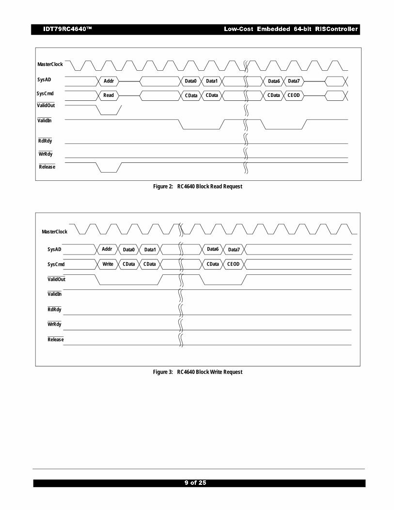
The RC4640 requires a non-overlapping system interface,compatible with the RC4700. This means that only one processorrequest may be outstanding at a time and that the request must beserviced by an external device before the RC4640 issues anotherrequest. The RC4640 can issue read and write requests to anexternal device, and an external device can issue read and writerequests to the RC4640.
The RC4640 asserts ValidOut* and simultaneously drives theaddress and read command on the SysAD and SysCmd buses. Ifthe system interface has RdRdy* or Read transactions asserted,then the processor tristates its drivers and releases the systeminterface to slave state by asserting Release*. The external devicecan then begin sending the data to the RC4640.
Fundamental operational modes for the processor are initializedby the boot-time mode control interface. The boot-time modecontrol interface is a serial interface operating at a very lowfrequency (MasterClock divided by 256). The low-frequency opera-tion allows the initialization information to be kept in a low-costEPROM; alternatively the twenty-or-so bits could be generated bythe system interface ASIC or a simple PAL.
Immediately after the VCCOK Signal is asserted, the processorreads a serial bit stream of 256 bits to initialize all fundamentaloperational modes. After initialization is complete, the processorcontinues to drive the serial clock output, but no further initializationbits are read.
+ �
,�,�,�,��������� /�� /�� /�� /������ ��������������������
The boot-time serial mode stream is defined in Table 5. Bit 0 is thebit presented to the processor when VCCOK is asserted; bit 255 is thelast.
�����1�1�1�1���� ������������������������������������
CP0 is also used to control the power management for theRC4640. This is the standby mode and it can be used to reduce thepower consumption of the internal core of the CPU. The standbymode is entered by executing the WAIT instruction with the SysADbus idle and is exited by any interrupt.
������������ ���� ������ ���� ������ ���� ������ ���� ��������������������������
The RC4640 provides a means to reduce the amount of power con-sumed by the internal core when the CPU would otherwise not be performing any useful operations. This is known as “Standby Mode”.
������������������������ # # # #�������������)�)�)�)���� ����������������
Executing the WAIT instruction enables interrupts and entersStandby mode. When the WAIT instruction finishes the W pipe-stage,if the SysAd bus is currently idle, the internal clocks will shut down,thus freezing the pipeline. The PLL, internal timer, and some of theinput pins (Int[5:0]*, NMI*, ExtReq*, Reset*, and ColdReset*) willcontinue to run. If the conditions are not correct when the WAITinstruction finishes the W pipe-stage (i.e. the SysAd bus is not idle),the WAIT is treated as a NOP.
Once the CPU is in Standby Mode, any interrupt, including theinternally generated timer interrupt, will cause the CPU to exitStandby Mode.
� ��
���� ����� ���� ��� �������� ������ ��� ����� ��
Figure 2: RC4640 Block Read Request
Figure 3: RC4640 Block Write Request
MasterClock
SysAD Addr Data0 Data1 Data6 Data7
SysCmd Read CData CData CData CEOD
ValidOut
ValidIn
RdRdy
WrRdy
Release
MasterClock
SysAD Addr Data0 Data1 Data6 Data7
SysCmd
ValidOut
ValidIn
RdRdy
WrRdy
Release
Write CData CData CData CEOD
� �� ��
���� ����� ���� ��� �������� ������ ��� ����� ��
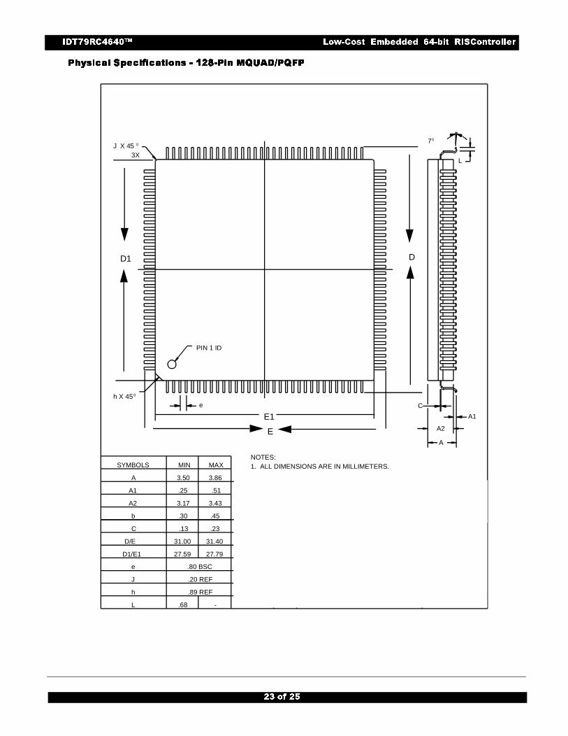
������������������ ����� ����� ����� �������������������������������������������
The RC4640 utilizes special packaging techniques to improvethe thermal properties of high-speed processors. The RV4640 ispackaged using cavity-up packaging in a 128-pin thermallyenhanced PQFP package (“DU”) with a drop-in heat spreader, fordevices with low peak power. The RC4640 also utilizes theMQUAD package for higher power consumption devices (the “MU”package), which is an all-aluminum package with the die attachedto a normal copper lead frame mounted to the aluminum casing.
,��� ��� ���&��#����
0 Reserved (must be zero)
4s:1 Writeback data rate:32-bit0 → W1 → WWx2 → WWxx3 → WxWx4 → WWxxx5 → WWxxxx6 → WxxWxx7 → WWxxxxxx8 → WxxxWxxx9-15 reserved
7:5 Clock multiplier:0 → 21 → 32 → 43 → 54 → 65 → 76 → 87 reserved
8 0 → Little endian1 → Big endian
10:9 00 → R4000 compatible01 → reserved10 → pipelined writes11 → write re-issue
11 Disable the timer interrupt on Int[5]
12 Must be 1
14:13 Output driver strength:10 → 100% strength (fastest)11 → 83% strength00 → 67% strength01 → 50% strength (slowest)
255:15 Must be zero
Table 5: Boot-time mode stream
�� �
Due to the heat-spreading effect of the aluminum, the MQUADpackage allows for an efficient thermal transfer between the die andthe case. The aluminum offers less internal resistance from one endof the package to the other, reducing the temperature gradient acrossthe package and therefore presenting a greater area for convectionand conduction to the PCB for a given temperature. Even nominalamounts of air flow will dramatically reduce the junction temperatureof the die, resulting in cooler operation. The MQUAD package is pinand socket compatible with the 128-pin PQFP package.
The RC4640 is guaranteed in a case temperature range of 0° to+85° C. The type of package, speed (power) of the device, and airflow conditions affect the equivalent ambient temperature conditionsthat will meet this specification.
The equivalent allowable ambient temperature, TA, can be calcu-lated using the thermal resistance from case to ambient (∅CA) of thegiven package. The following equation relates ambient and casetemperatures:
TA = TC - P * ∅CA
where P is the maximum power consumption at hot temperature,calculated by using the maximum ICC specification for the device.
Typical values for ∅CA at various air flows are shown in Table 6.
Note that the RC4640 implements advanced power managementto substantially reduce the average power dissipation of the device.This operation is described in the IDT79RC4640/ IDT79RC4650RISC Processor Hardware User’s Manual.
∅��
-��� �� .��/���0 � ��� ��� ��� +�� ����
128 PQFP (DU) 21 13 10 9 8 7
128 MQUAD (MU) 21 13 10 9 8 7
Table 6: Thermal Resistance (∅CA) at Various Airflows
� ��
���� ����� ���� ��� �������� ������ ��� ����� ��
����� ������ ������ ������ ����� � � � ������� ����������� ����������� ����������� �������������
!!!!�������������������� ����� ��� ��� ��� ������������������ �������������������� ��������������)��)��)��)���� 22223333343434345555
Features:- Added 32-bit bus interface info- Deleted items from low-power operation descriptions.Hardware Overview:- Added detailed descriptions of features.- Changed Boot Time Mode Stream table values for mode bit
12.DC Electrical Characteristics:- The CIN and COUT values have been changed.AC Electrical Characteristics:- In System Interface Parameters tables (RC4640 and
RV4640), Data Setup and Data Hold minimums changed.Valid Combinations:- List of valid combinations has been corrected.
!!!!�������������������� ����� ��� ��� ��� ������������������ �������������������� ���������������� 23362336233623365555
Features:- Added preliminary 150 MHz operation frequencyThermal Considerations:- Added thermally enhanced packaging (“DU”) and drop-in heatspreader information.
- Upgraded 80 to 133MHz speed grade specs to “final.”
!!!!�������������������� ����� ��� ��� ��� ������������������ �������������������� ������������ 22223333363636365555
Features:- Added 180 MHz spreader information- Eliminated 80 MHz
!!!!�������������������� ����� ��� ��� ��� ������������������ �������������������� ���������������� 23372337233723375555
Features:- Added 200MHz operating frequency
!!!!�������������������� ����� ��� ��� ��� ������������������ �������������������� ���������������� 23372337233723375555
Features:- Added 400MB/sec bandwidth referencePower Consumption (RV4640):- Upgraded System Condition Icc active parameters
�� �
� ��
���� ����� ���� ��� �������� ������ ��� ����� ��
!"# �$�� "!�"�!"# �$�� "!�"�!"# �$�� "!�"�!"# �$�� "!�"�####
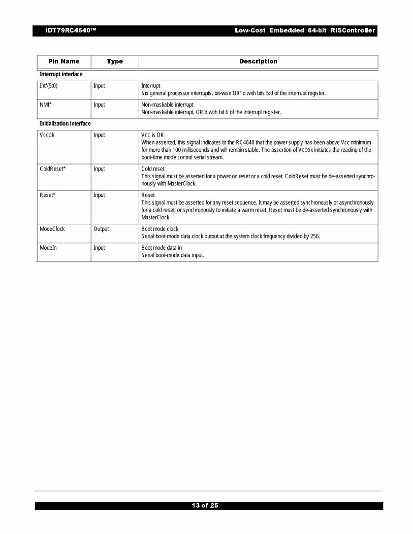
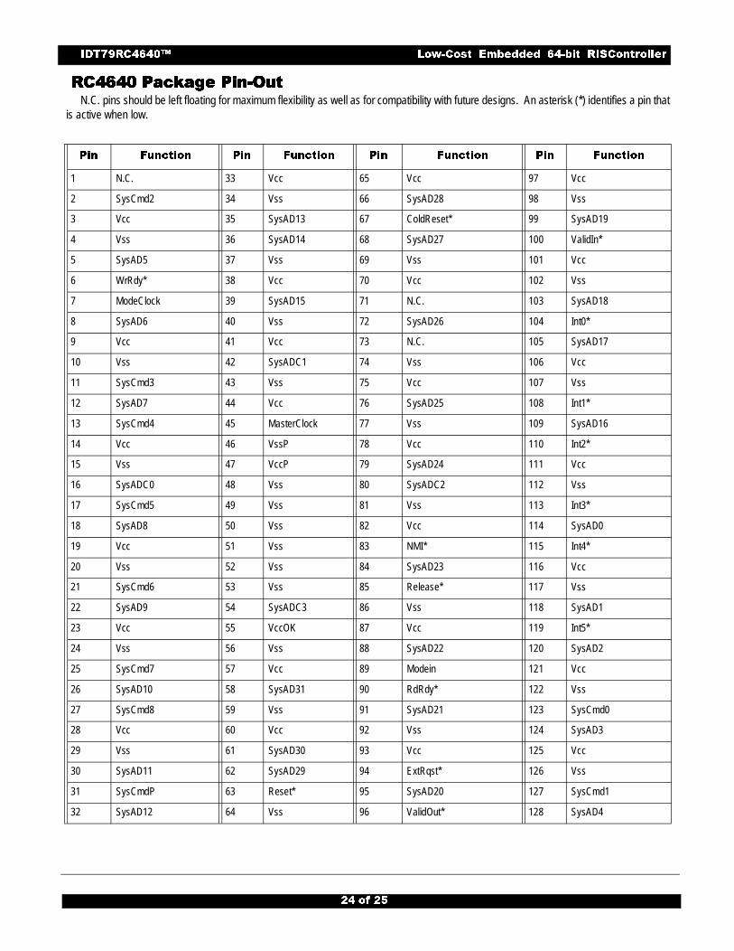
The following is a list of interface, interrupt, and miscellaneous pins available on the RC4640. Pin names ending with an asterisk (*) iden-tify pins that are active when low.
1�� ($�� '#� ���&��#����
System Bus Interface
ExtRqst* Input External requestSignals that the system interface needs to submit an external request.
Release* Output Release interfaceSignals that the processor is releasing the system interface to slave state
RdRdy* Input Read ReadySignals that an external agent can now accept a processor read.
WrRdy* Input Write ReadySignals that an external agent can now accept a processor write request.
ValidIn* Input Valid InputSignals that an external agent is now driving a valid address or data on the SysAD bus and a valid command or data identifier on the SysCmd bus.
ValidOut* Output Valid outputSignals that the processor is now driving a valid address or data on the SysAD bus and a valid com-mand or data identifier on the SysCmd bus.
SysAD(31:0) Input/Output System address/data busA 32-bit address and data bus for communication between the processor and an external agent.
SysADC(3:0) Input/Output System address/data check busA 4-bit bus containing parity check bits for the SysAD bus during data bus cycles.
SysCmd(8:0) Input/Output System command/data identifier busA 9-bit bus for command and data identifier transmission between the processor and an external agent.
SysCmdP Input/Output Reserved system command/data identifier bus parityFor the RC4640 this signal is unused on input and zero on output.
Clock/Control interface
MasterClock Input Master clockMaster clock input used as the system interface reference clock. All output timings are relative to this input clock. Pipeline operation frequency is derived by multiplying this clock up by the factor selected during boot initialization.
VCCP Input Quiet VCC for PLLQuiet VCC for the internal phase locked loop.
VSSP Input Quiet VSS for PLLQuiet VSS for the internal phase locked loop.
�� �� ��
���� ����� ���� ��� �������� ������ ��� ����� ��
1�� ($�� '#� ���&��#����
Interrupt interface
Int*(5:0) Input InterruptSix general processor interrupts, bit-wise OR’ d with bits 5:0 of the interrupt register.
NMI* Input Non-maskable interruptNon-maskable interrupt, OR’d with bit 6 of the interrupt register.
Initialization interface
VCCOk Input VCC is OKWhen asserted, this signal indicates to the RC4640 that the power supply has been above Vcc minimum for more than 100 milliseconds and will remain stable. The assertion of VCCOk initiates the reading of the boot-time mode control serial stream.
ColdReset* Input Cold resetThis signal must be asserted for a power on reset or a cold reset. ColdReset must be de-asserted synchro-nously with MasterClock.
Reset* Input ResetThis signal must be asserted for any reset sequence. It may be asserted synchronously or asynchronously for a cold reset, or synchronously to initiate a warm reset. Reset must be de-asserted synchronously with MasterClock.
ModeClock Output Boot mode clockSerial boot-mode data clock output at the system clock frequency divided by 256.
ModeIn Input Boot mode data inSerial boot-mode data input.
�! �� ��
���� ����� ���� ��� �������� ������ ��� ����� ��
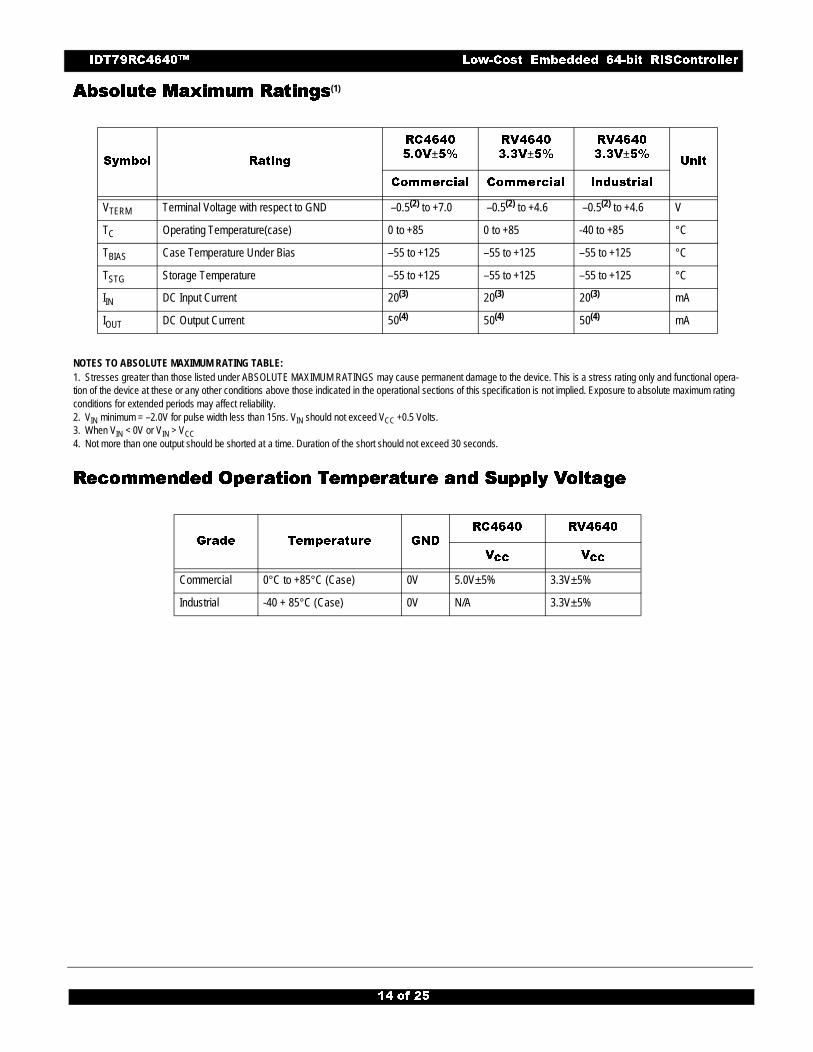
%������� �&�%������� �&�%������� �&�%������� �&������� �� �� �� ����������������(1)
NOTES TO ABSOLUTE MAXIMUM RATING TABLE:1. Stresses greater than those listed under ABSOLUTE MAXIMUM RATINGS may cause permanent damage to the device. This is a stress rating only and functional opera-tion of the device at these or any other conditions above those indicated in the operational sections of this specification is not implied. Exposure to absolute maximum rating conditions for extended periods may affect reliability.2. VIN minimum = –2.0V for pulse width less than 15ns. VIN should not exceed VCC +0.5 Volts.3. When VIN < 0V or VIN > VCC4. Not more than one output should be shorted at a time. Duration of the short should not exceed 30 seconds.
���������� ������������� ������������� ������������� ����������������������� ������������������������������������� �� �� �� ����� ������������������������ '�'�'�'�������������
�'��� �$���2
� ����
�3�4±�5
�4����
!3!4±�5
�4����
!3!4±�56���
�����&�$ �����&�$ ���%����$
VTERM Terminal Voltage with respect to GND –0.5(2) to +7.0 –0.5(2) to +4.6 –0.5(2) to +4.6 V
TC Operating Temperature(case) 0 to +85 0 to +85 -40 to +85 °C
TBIAS Case Temperature Under Bias –55 to +125 –55 to +125 –55 to +125 °C
TSTG Storage Temperature –55 to +125 –55 to +125 –55 to +125 °C
IIN DC Input Current 20(3) 20(3) 20(3) mA
IOUT DC Output Current 50(4) 50(4) 50(4) mA
7�$�� ��#��$�%�� 7(�
� ���� �4����
4�� 4��
Commercial 0°C to +85°C (Case) 0V 5.0V±5% 3.3V±5%
Industrial -40 + 85°C (Case) 0V N/A 3.3V±5%
�� �� ��
���� ����� ���� ��� �������� ������ ��� ����� ��
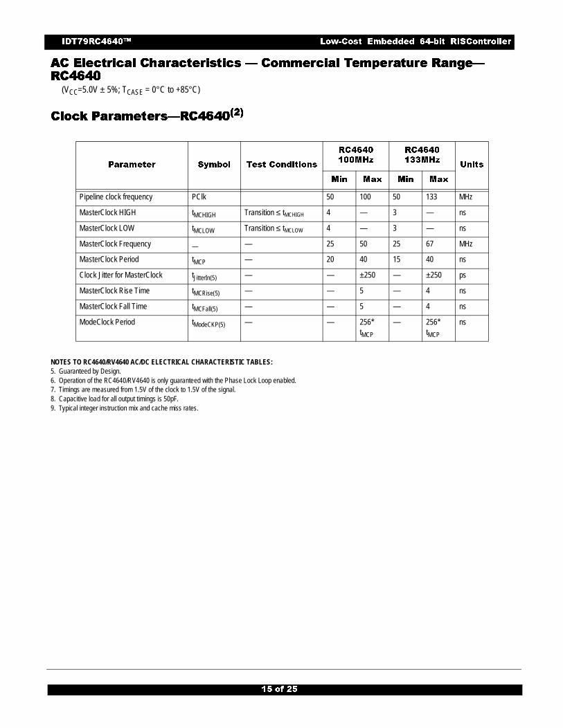
%%%%� $�������� �� $�������� �� $�������� �� $�������� ������������������� ( ������������ ( ������������ ( ������������ ( ������������������������������ ������������������������������������� � � � ��(��(��(��( �)*)+�)*)+�)*)+�)*)+
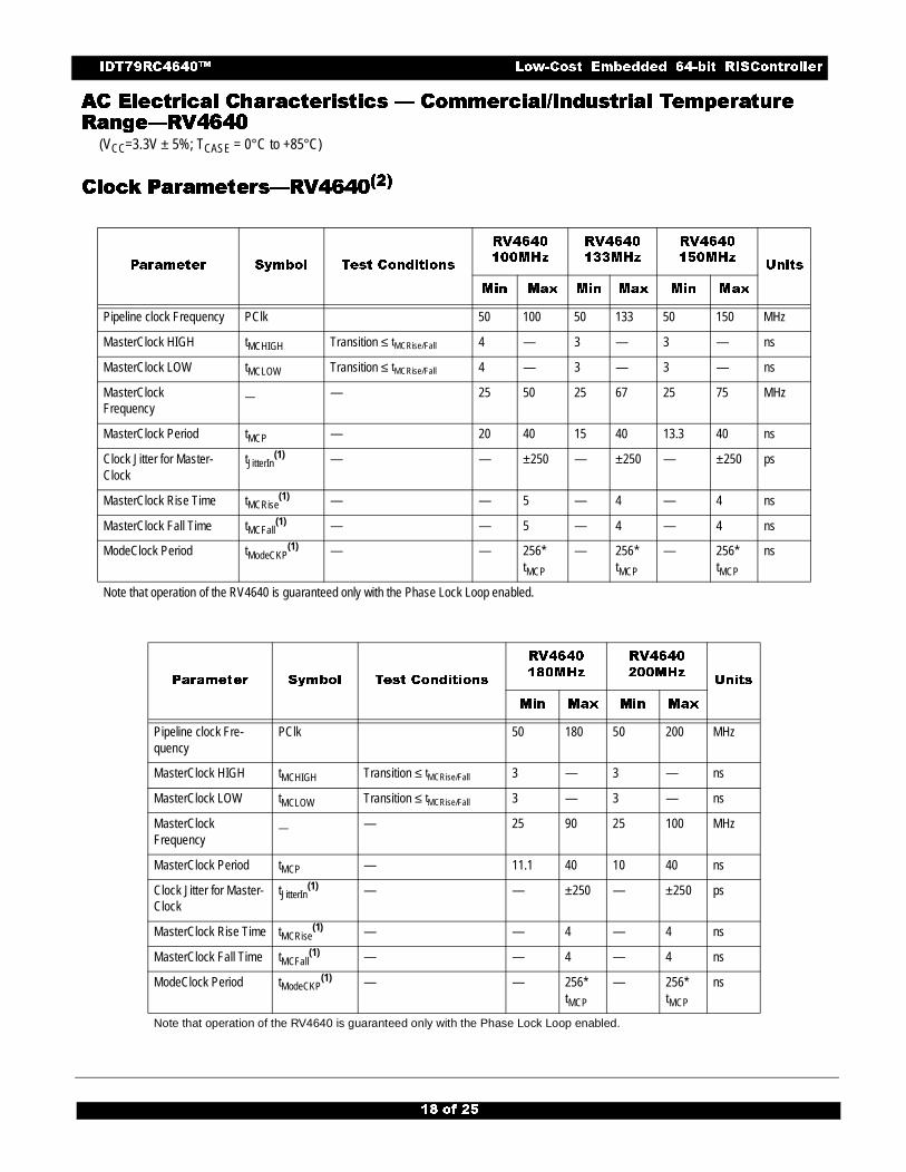
(VCC=5.0V ± 5%; TCASE = 0°C to +85°C)
�������������������� !!!!�������������������������(�(�(�( �)�)�)�)****)+)+)+)+������������
NOTES TO RC4640/RV4640 AC/DC ELECTRICAL CHARACTERISTIC TABLES:5. Guaranteed by Design.6. Operation of the RC4640/RV4640 is only guaranteed with the Phase Lock Loop enabled.7. Timings are measured from 1.5V of the clock to 1.5V of the signal.8. Capacitive load for all output timings is 50pF.9. Typical integer instruction mix and cache miss rates.
1$�$����� �'��� ��� ���������
� ����
���,89
� ����
�!!,896����
,�� ,$: ,�� ,$:
Pipeline clock frequency PClk 50 100 50 133 MHz
MasterClock HIGH tMCHIGH Transition ≤ tMCHIGH 4 — 3 — ns
MasterClock LOW tMCLOW Transition ≤ tMCLOW 4 — 3 — ns
MasterClock Frequency — — 25 50 25 67 MHz
MasterClock Period tMCP — 20 40 15 40 ns
Clock Jitter for MasterClock tJitterIn(5) — — ±250 — ±250 ps
MasterClock Rise Time tMCRise(5) — — 5 — 4 ns
MasterClock Fall Time tMCFall(5) — — 5 — 4 ns
ModeClock Period tModeCKP(5) — — 256*tMCP
— 256*tMCP
ns
�� �� ��
���� ����� ���� ��� �������� ������ ��� ����� ��
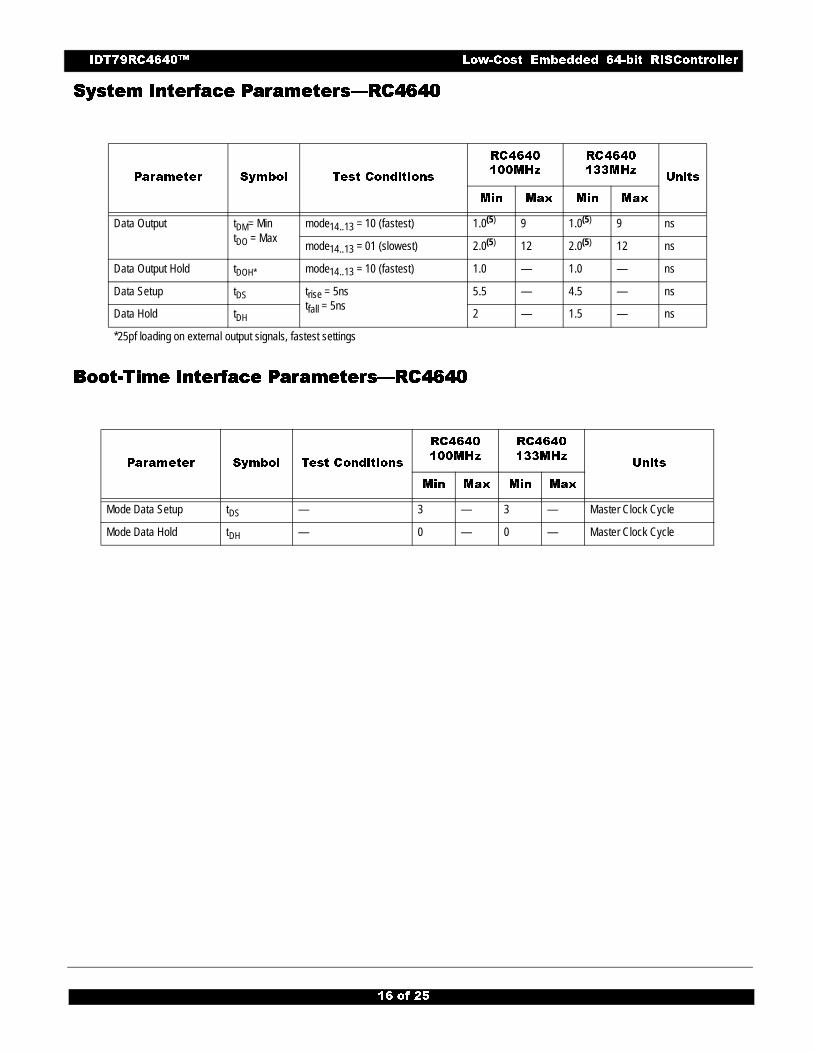
������ "����,�������� "����,�������� "����,�������� "����,�� !!!!�������������������������(�(�(�( �)�)�)�)****)+)+)+)+
����-���� "����,������-���� "����,������-���� "����,������-���� "����,�� !!!!�������������������������(�(�(�( ����)*)+)*)+)*)+)*)+
1$�$����� �'��� ��� ���������
� ����
���,89
� ����
�!!,896����
,�� ,$: ,�� ,$:
Data Output tDM= MintDO = Max
mode14..13 = 10 (fastest) 1.0(5) 9 1.0(5) 9 ns
mode14..13 = 01 (slowest) 2.0(5) 12 2.0(5) 12 ns
Data Output Hold tDOH* mode14..13 = 10 (fastest) 1.0 — 1.0 — ns
Data Setup tDS trise = 5nstfall = 5ns
5.5 — 4.5 — ns
Data Hold tDH 2 — 1.5 — ns
*25pf loading on external output signals, fastest settings
1$�$����� �'��� ��� ���������
� ����
���,89
� ����
�!!,896����
,�� ,$: ,�� ,$:
Mode Data Setup tDS — 3 — 3 — Master Clock Cycle
Mode Data Hold tDH — 0 — 0 — Master Clock Cycle
�� �� ��
���� ����� ���� ��� �������� ������ ��� ����� ��
�� $�������� ���� $�������� ���� $�������� ���� $�������� ���������������� ( ������������ ( ������������ ( ������������ ( ������������������������������ ������������������������������������� � � � ��(��(��(��( �)*)+�)*)+�)*)+�)*)+
(Vcc = 5.0±5%, TCASE = 0°C to +85°C)
!�!�!�!���� ��������� ��������� ��������� ��������������(����(����(����( �)*)+�)*)+�)*)+�)*)+
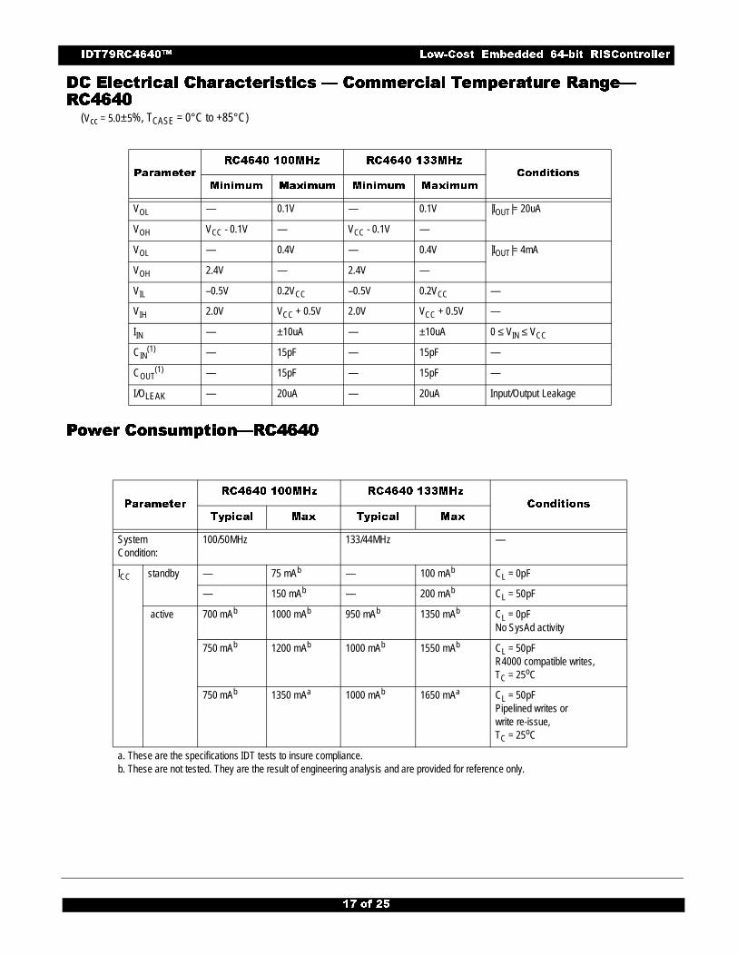
1$�$�����
� ���� ���,89 � ���� �!!,89
���������
,����%� ,$:��%� ,����%� ,$:��%�
VOL — 0.1V — 0.1V |IOUT|= 20uA
VOH VCC - 0.1V — VCC - 0.1V —
VOL — 0.4V — 0.4V |IOUT|= 4mA
VOH 2.4V — 2.4V —
VIL –0.5V 0.2VCC –0.5V 0.2VCC —
VIH 2.0V VCC + 0.5V 2.0V VCC + 0.5V —
IIN — ±10uA — ±10uA 0 ≤ VIN ≤ VCC
CIN(1) — 15pF — 15pF —
COUT(1) — 15pF — 15pF —
I/OLEAK — 20uA — 20uA Input/Output Leakage
1$�$�����
� ���� ���,89 � ���� �!!,89
���������
'#�&$ ,$: '#�&$ ,$:
System Condition:
100/50MHz 133/44MHz —
ICC standby — 75 mAb — 100 mAb CL = 0pF
— 150 mAb — 200 mAb CL = 50pF
active 700 mAb 1000 mAb 950 mAb 1350 mAb CL = 0pF No SysAd activity
750 mAb 1200 mAb 1000 mAb 1550 mAb CL = 50pF R4000 compatible writes,TC = 25oC
750 mAb 1350 mAa 1000 mAb 1650 mAa CL = 50pF Pipelined writes or write re-issue, TC = 25oC
a. These are the specifications IDT tests to insure compliance.b. These are not tested. They are the result of engineering analysis and are provided for reference only.
� �� ��
���� ����� ���� ��� �������� ������ ��� ����� ��
%%%%� $�������� �� $�������� �� $�������� �� $�������� ������������������� ( ������������ ( ������������ ( ������������ ( ���������������������.���.���.���.""""�������������������������������� ���������������������������������������� ��( ��( ��( ��( ')')')')****)+)+)+)+
(VCC=3.3V ± 5%; TCASE = 0°C to +85°C)
�������������������� !!!!�������������������������(�(�(�( ''''))))*)+*)+*)+*)+������������
1$�$����� �'��� ��� ���������
�4����
���,89
�4����
�!!,89
�4����
���,896����
,�� ,$: ,�� ,$: ,�� ,$:
Pipeline clock Frequency PClk 50 100 50 133 50 150 MHz
MasterClock HIGH tMCHIGH Transition ≤ tMCRise/Fall 4 — 3 — 3 — ns
MasterClock LOW tMCLOW Transition ≤ tMCRise/Fall 4 — 3 — 3 — ns
MasterClockFrequency
— — 25 50 25 67 25 75 MHz
MasterClock Period tMCP — 20 40 15 40 13.3 40 ns
Clock Jitter for Master-Clock
tJitterIn(1) — — ±250 — ±250 — ±250 ps
MasterClock Rise Time tMCRise(1) — — 5 — 4 — 4 ns
MasterClock Fall Time tMCFall(1) — — 5 — 4 — 4 ns
ModeClock Period tModeCKP(1) — — 256*
tMCP
— 256*tMCP
— 256*tMCP
ns
Note that operation of the RV4640 is guaranteed only with the Phase Lock Loop enabled.
1$�$����� �'��� ��� ���������
�4����
�+�,89
�4����
���,896����
,�� ,$: ,�� ,$:
Pipeline clock Fre-quency
PClk 50 180 50 200 MHz
MasterClock HIGH tMCHIGH Transition ≤ tMCRise/Fall 3 — 3 — ns
MasterClock LOW tMCLOW Transition ≤ tMCRise/Fall 3 — 3 — ns
MasterClockFrequency
— — 25 90 25 100 MHz
MasterClock Period tMCP — 11.1 40 10 40 ns
Clock Jitter for Master-Clock
tJitterIn(1) — — ±250 — ±250 ps
MasterClock Rise Time tMCRise(1) — — 4 — 4 ns
MasterClock Fall Time tMCFall(1) — — 4 — 4 ns
ModeClock Period tModeCKP(1) — — 256*
tMCP
— 256*tMCP
ns
Note that operation of the RV4640 is guaranteed only with the Phase Lock Loop enabled.
�+ �� ��
���� ����� ���� ��� �������� ������ ��� ����� ��
������ "����,�������� "����,�������� "����,�������� "����,�� !!!!�������������������������(�(�(�( ''''))))*)+*)+*)+*)+
������ "����,�������� "����,�������� "����,�������� "����,�� !!!!�������������������������(�(�(�( ''''))))*)+ /��������*)+ /��������*)+ /��������*)+ /������������0000
����-���� "����,������-���� "����,������-���� "����,������-���� "����,�� !!!!�������������������������( ')*)+�( ')*)+�( ')*)+�( ')*)+
1$�$����� �'��� ���
���������
�4����
���,89
�4����
�!!,89
�4����
���,896����
,�� ,$: ,�� ,$: ,�� ,$:
Data Output tDM= MintDO = Max
mode14..13 = 10(fastest)
1.0(1) 9 1.0(1) 9 1.0(1) 9 ns
mode14..13 = 01(slowest)
2.0(1) 12 2.0(1) 12 2.0(1) 12 ns
Data Output Hold tDOH* mode14..13 = 10 (fastest)
1.0 — 1.0 — 1.0 — ns
Data Setup tDS trise = 3nstfall = 3ns
5.5 — 4.5 — 4.5 — ns
Data Hold tDH 2 — 1.5 — 1.5 — ns
25pf loading on external output signals, fastest settings.
1$�$����� �'��� ���
���������
�4����
�+�,89
�4����
���,896����
,�� ,$: ,�� ,$:
Data Output tDM= MintDO = Max
mode14..13 = 10(fastest)
1.0(1) 9 1.0(1) 9 ns
mode14..13 = 01(slowest)
2.0(1) 10 2.0(1) 10 ns
Data Output Hold tDOH* mode14..13 = 10 (fastest)
1.0 — 1.0 — ns
Data Setup tDS trise = 3nstfall = 3ns
4.5 — 4.5 — ns
Data Hold tDH 1.5 — 1.5 — ns
25pf loading on external output signals, fastest settings.
1$�$����� �'��� ���
���������
�4����
���,89
�4����
�!!,89
�4����
���,896����
,�� ,$: ,�� ,$: ,�� ,$:
Mode Data Setup tDS — 3 — 3 — 3 — Master Clock Cycle
Mode Data Hold tDH — 0 — 0 — 0 — Master Clock Cycle
�� �� ��

���� ����� ���� ��� �������� ������ ��� ����� ��
1$�$����� �'��� ���
���������
�4����
�+�,89
�4����
���,896����
,�� ,$: ,�� ,$:
Mode Data Setup tDS — 3 — 3 — Master Clock Cycle
Mode Data Hold tDH — 0 — 0 — Master Clock Cycle
�� �� ��
���� ����� ���� ��� �������� ������ ��� ����� ��
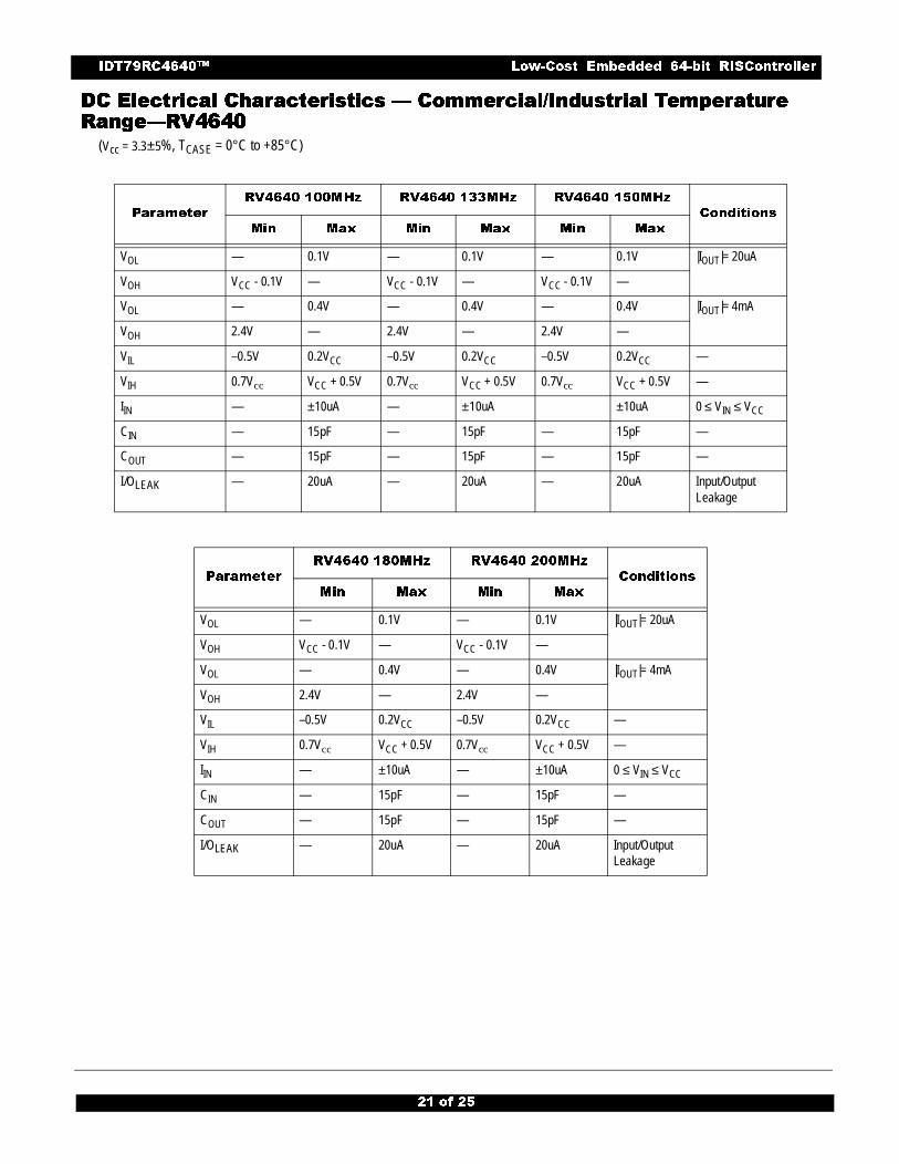
�� $�������� ���� $�������� ���� $�������� ���� $�������� ���������������� ( ������������ ( ������������ ( ������������ ( ���������������������."�����������."�����������."�����������."�������� ���������������������������������������� ��( ��( ��( ��( ')')')')****)+)+)+)+
(Vcc = 3.3±5%, TCASE = 0°C to +85°C)
1$�$�����
�4���� ���,89 �4���� �!!,89 �4���� ���,89
���������
,�� ,$: ,�� ,$: ,�� ,$:
VOL — 0.1V — 0.1V — 0.1V |IOUT|= 20uA
VOH VCC - 0.1V — VCC - 0.1V — VCC - 0.1V —
VOL — 0.4V — 0.4V — 0.4V |IOUT|= 4mA
VOH 2.4V — 2.4V — 2.4V —
VIL –0.5V 0.2VCC –0.5V 0.2VCC –0.5V 0.2VCC —
VIH 0.7Vcc VCC + 0.5V 0.7Vcc VCC + 0.5V 0.7Vcc VCC + 0.5V —
IIN — ±10uA — ±10uA ±10uA 0 ≤ VIN ≤ VCC
CIN — 15pF — 15pF — 15pF —
COUT — 15pF — 15pF — 15pF —
I/OLEAK — 20uA — 20uA — 20uA Input/OutputLeakage
1$�$�����
�4���� �+�,89 �4���� ���,89
���������
,�� ,$: ,�� ,$:
VOL — 0.1V — 0.1V |IOUT|= 20uA
VOH VCC - 0.1V — VCC - 0.1V —
VOL — 0.4V — 0.4V |IOUT|= 4mA
VOH 2.4V — 2.4V —
VIL –0.5V 0.2VCC –0.5V 0.2VCC —
VIH 0.7Vcc VCC + 0.5V 0.7Vcc VCC + 0.5V —
IIN — ±10uA — ±10uA 0 ≤ VIN ≤ VCC
CIN — 15pF — 15pF —
COUT — 15pF — 15pF —
I/OLEAK — 20uA — 20uA Input/OutputLeakage
�� �� ��
���� ����� ���� ��� �������� ������ ��� ����� ��
!�!�!�!���� ��������� ��������� ��������� ��������������(����(����(����( ')*)')*)')*)')*)++++
1$�$�����
�4���� ���,89 �4���� �!!,89 �4���� ���,89
���������
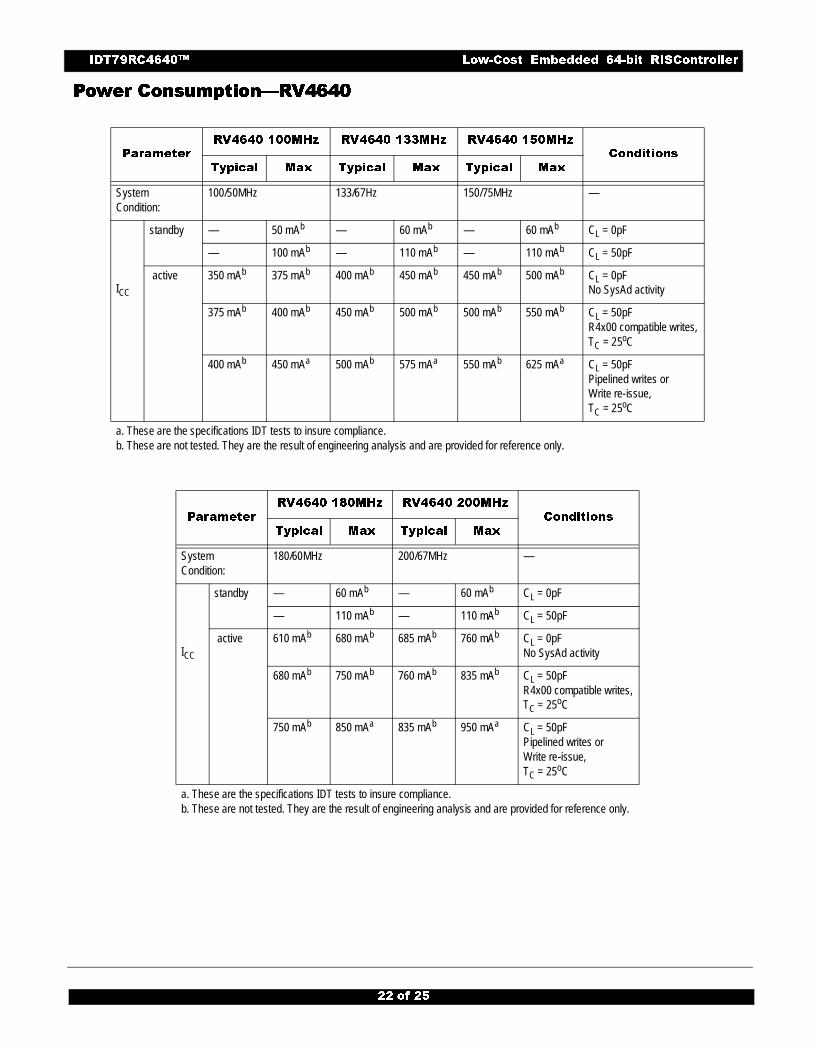
'#�&$ ,$: '#�&$ ,$: '#�&$ ,$:
System Condition:
100/50MHz 133/67Hz 150/75MHz —
ICC
standby — 50 mAb — 60 mAb — 60 mAb CL = 0pF
— 100 mAb — 110 mAb — 110 mAb CL = 50pF
active 350 mAb 375 mAb 400 mAb 450 mAb 450 mAb 500 mAb CL = 0pF No SysAd activity
375 mAb 400 mAb 450 mAb 500 mAb 500 mAb 550 mAb CL = 50pF R4x00 compatible writes,TC = 25oC
400 mAb 450 mAa 500 mAb 575 mAa 550 mAb 625 mAa CL = 50pF Pipelined writes or Write re-issue, TC = 25oC
a. These are the specifications IDT tests to insure compliance.b. These are not tested. They are the result of engineering analysis and are provided for reference only.
1$�$�����
�4���� �+�,89 �4���� ���,89
���������
'#�&$ ,$: '#�&$ ,$:
System Condition:
180/60MHz 200/67MHz —
ICC
standby — 60 mAb — 60 mAb CL = 0pF
— 110 mAb — 110 mAb CL = 50pF
active 610 mAb 680 mAb 685 mAb 760 mAb CL = 0pF No SysAd activity
680 mAb 750 mAb 760 mAb 835 mAb CL = 50pF R4x00 compatible writes,TC = 25oC
750 mAb 850 mAa 835 mAb 950 mAa CL = 50pF Pipelined writes or Write re-issue, TC = 25oC
a. These are the specifications IDT tests to insure compliance.b. These are not tested. They are the result of engineering analysis and are provided for reference only.
�� �� ��
���� ����� ���� ��� �������� ������ ��� ����� ��
�������������������������������� #���#���#���#����+��+��+��+�������������������������� 2� 2� 2� 287878787 �� �� �� ������ ����9���9���9���9�����������9�9�9�9�����
128 LD MQUAD MKT DWG(.80 LD PITCH, GULLWING)
N/A
SYMBOLS
A
MIN MAX
3.17 3.43
.30 .45
A1
A2
D/E
D1/E1
e .80 BSC
TOLERANCES UNLESS
OTHERWISE SPECIFIED
FRAC DEC ANGLES
%%p %%P %%P
SCALE SIZE DRAWING NO. REV
APPROVALS DATE
DRAWN
CHECKED
SHEET OFDO NOT SCALE DRAWING
AA
A
Integrated Device Technology, Inc.
3001 Stender Way, Santa Clara, CA 95054
(408) 492-8333 FAX (408) 727-2328
1 1
- - -
11/95
dt
.25 .51
3.50 3.86
31.00 31.40
27.59 27.79
PSC-4054 00
b
J .20 REF
h .89 REF
L .68 -
C .23.13
R
NOTES:1. ALL DIMENSIONS ARE IN MILLIMETERS.
h X 45 0
PIN 1 ID
J X 45 0
3XL
70
C
A1
A2
A
e
DD1
E
E1
�! �� ��
���� ����� ���� ��� �������� ������ ��� ����� ��
�)*)+�)*)+�)*)+�)*)+ !!!!��������� !��-���� !��-���� !��-���� !��-���N.C. pins should be left floating for maximum flexibility as well as for compatibility with future designs. An asterisk (*) identifies a pin that
is active when low.
1�� )%�&���� 1�� )%�&���� 1�� )%�&���� 1�� )%�&����
1 N.C. 33 Vcc 65 Vcc 97 Vcc
2 SysCmd2 34 Vss 66 SysAD28 98 Vss
3 Vcc 35 SysAD13 67 ColdReset* 99 SysAD19
4 Vss 36 SysAD14 68 SysAD27 100 ValidIn*
5 SysAD5 37 Vss 69 Vss 101 Vcc
6 WrRdy* 38 Vcc 70 Vcc 102 Vss
7 ModeClock 39 SysAD15 71 N.C. 103 SysAD18
8 SysAD6 40 Vss 72 SysAD26 104 Int0*
9 Vcc 41 Vcc 73 N.C. 105 SysAD17
10 Vss 42 SysADC1 74 Vss 106 Vcc
11 SysCmd3 43 Vss 75 Vcc 107 Vss
12 SysAD7 44 Vcc 76 SysAD25 108 Int1*
13 SysCmd4 45 MasterClock 77 Vss 109 SysAD16
14 Vcc 46 VssP 78 Vcc 110 Int2*
15 Vss 47 VccP 79 SysAD24 111 Vcc
16 SysADC0 48 Vss 80 SysADC2 112 Vss
17 SysCmd5 49 Vss 81 Vss 113 Int3*
18 SysAD8 50 Vss 82 Vcc 114 SysAD0
19 Vcc 51 Vss 83 NMI* 115 Int4*
20 Vss 52 Vss 84 SysAD23 116 Vcc
21 SysCmd6 53 Vss 85 Release* 117 Vss
22 SysAD9 54 SysADC3 86 Vss 118 SysAD1
23 Vcc 55 VccOK 87 Vcc 119 Int5*
24 Vss 56 Vss 88 SysAD22 120 SysAD2
25 SysCmd7 57 Vcc 89 Modein 121 Vcc
26 SysAD10 58 SysAD31 90 RdRdy* 122 Vss
27 SysCmd8 59 Vss 91 SysAD21 123 SysCmd0
28 Vcc 60 Vcc 92 Vss 124 SysAD3
29 Vss 61 SysAD30 93 Vcc 125 Vcc
30 SysAD11 62 SysAD29 94 ExtRqst* 126 Vss
31 SysCmdP 63 Reset* 95 SysAD20 127 SysCmd1
32 SysAD12 64 Vss 96 ValidOut* 128 SysAD4
�� �� ��
���� ����� ���� ��� �������� ������ ��� ����� ��
������������� "����� "����� "����� "����,�,�,�,�������������������������
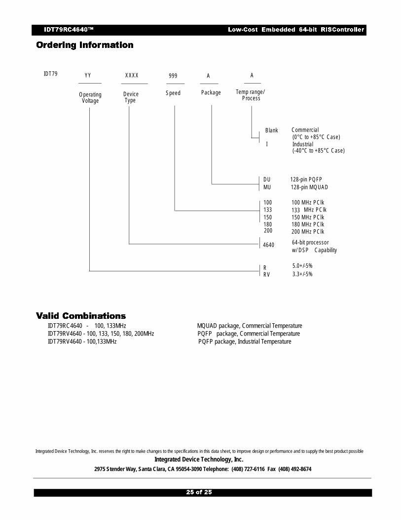
''''������������ ��������������������������������������������IDT79RC4640 - 100, 133MHz MQUAD package, Commercial TemperatureIDT79RV4640 - 100, 133, 150, 180, 200MHz PQFP package, Commercial TemperatureIDT79RV4640 - 100,133MHz PQFP package, Industrial Temperature
IDT79 YY XXXX 999 A A
O perating Voltage
DeviceType
Speed Package Temp range/Process
RRV
4640
100133
MU
Blank Commercial(0°C to +85°C Case)
128-pin MQ UAD
100 MHz PClk133 MHz PC lk
64-bit processor
5.0+/-5%3.3+/-5%
DU 128-pin PQ FP
150 MHz PClk150
I Industrial(-40°C to +85°C C ase)
180 180 MHz PClk200 200 MHz PClk
Capabilityw/ D SP
�� �� ��
Integrated Device Technology, Inc. reserves the right to make changes to the specifications in this data sheet, to improve design or performance and to supply the best product possible
Integrated Device Technology, Inc. 2975 Stender Way, Santa Clara, CA 95054-3090 Telephone: (408) 727-6116 Fax (408) 492-8674