effect of transmission line measurement (tlm ... - core
TRANSCRIPT
Rochester Institute of TechnologyRIT Scholar Works
Theses Thesis/Dissertation Collections
12-2016
Effect of Transmission Line Measurement (TLM)Geometry on Specific Contact ResistivityDeterminationSidhant [email protected]
Follow this and additional works at: http://scholarworks.rit.edu/theses
This Thesis is brought to you for free and open access by the Thesis/Dissertation Collections at RIT Scholar Works. It has been accepted for inclusionin Theses by an authorized administrator of RIT Scholar Works. For more information, please contact [email protected].
Recommended CitationGrover, Sidhant, "Effect of Transmission Line Measurement (TLM) Geometry on Specific Contact Resistivity Determination"(2016). Thesis. Rochester Institute of Technology. Accessed from
Effect of Transmission Line Measurement
(TLM) Geometry on Specific Contact
Resistivity Determination
By
Sidhant Grover
A thesis submitted in partial fulfillment of the
requirements for the degree of
Master of Science in Materials Science and Engineering in the
School of Chemistry and Materials Science,
College of Science
Rochester Institute of Technology
December 2016
Signature of the Author _________________________________
Accepted by _________________________________________
Director, MSE Degree Program Date
SCHOOL OF CHEMISTRY AND MATERIALS SCIENCE
COLLEGE OF SCIENCE
ROCHESTER INSTITUTE OF TECHNOLOGY
ROCHESTER, NEW YORK
CERTIFICATE OF APPROVAL
________________________________________________________________________
M.S. DEGREE DISSERTATION
________________________________________________________________________
The M.S. Degree Dissertation of Sidhant Grover has
been examined and approved by the dissertation
committee as satisfactory for the dissertation required for
the M.S. degree in Materials Science and Engineering.
___________________________________ Date: _____________
Dr. Santosh Kurinec, Thesis Advisor
___________________________________ Date: _____________
Dr. Michael Jackson, Committee Member
___________________________________ Date: _____________
Dr. Robert Pearson, Committee Member
___________________________________ Date: _____________
Dr. Sean Rommel, Committee Member

iii
Dedication
To my family, friends and fraternity brothers. For being a constant source of motivation
and inspiring me to strive to be the best person I could possibly be.
iv
Acknowledgments
Before anyone else, I would like to extend my sincerest gratitude to my advisor Dr. San-
tosh Kurinec for her continuous guidance throughout my senior project and masters thesis.
Her constant support, motivation and encouragement has been invaluable throughout my
research. I would like to thank her, not only for widening my research acumen but also for
inspiring conversation about professional as well as personal development.
My sincere thanks also goes to Dr. Peng Zhang from Michigan State University for
carrying out simulations for this work. His research and guidance on contact resistance
modeling during his time at the University of Michigan has been tremendously helpful for
this work. I would like to acknowledge Dr. Andrew Gabor from BrightSpot Automation
LLC., for giving us access to their data and collaborating with us. I am also very grateful
for Jim Caroll of PhotoMask PORTAL Inc. for their assistance with mask design and
delivering it in a timely manner.
I would like to thank the rest of my committee Dr. Robert Person, Dr. Sean Rommel
and Dr. Michael Jackson for their constant support and flexibility over the course of my
thesis project work. I would also like to thank the SMFL staff, for their tremendous job in
managing the cleanroom tools and assisting with tool training and certifications.
v
AbstractEffect of Transmission Line Measurement (TLM) Geometry on
Specific Contact Resistivity Determination
Sidhant Grover
Supervising Professor: Dr. Santosh Kurinec
Ohmic metal semiconductor contacts are indispensable part of a semiconductor device.
These are characterized by their specific contact resistivity (ρc) in expressed in Ω-cm2 , de-
fined as the inverse slope of current density versus voltage curve at origin. Engineering and
measurement of specific contact resistivity (ρc) is becoming of increasing importance in the
semiconductor industry. Devices ranging from integrated circuits to solar cells use contact
resistivity as a measure of device performance. Novel methods such as contact silicidation,
doped-metal contacts, dipole inserted contacts etc. are continually being developed to re-
duce specific contact resistivity and improve device performance. The Transmission Line
Measurement (TLM) method is most commonly used to extract the specific contact resis-
tivity for such applications. This method is, however, not fully understood and modeled
to understand the flow of current and behavior of charge carriers for contacts of different
dimensions. It has often been observed in literature that applications that involve smaller
TLM geometries most often than not, show low values of ρc and applications that involve
ρc extraction through larger TLM geometries show significantly larger values. A perfect
example of this would be the inconsistencies observed in extracted ρc’s from integrated
vi
circuit applications where TLM geometries range from 0.1 µm to 10 µm and extracted ρc
is of the order of 10−8 to 10−6 Ω-cm2 and photovoltaic applications where geometries are
around 50 µm to 1000 µm and ρc is of the order of 10−5 to 10−2 Ω-cm2. The transfer
length or LT which is the characteristic length that the charge carriers travel beneath the
contact before flowing up into the contact. It has also been seen that in certain cases of
TLM device dimensions, the extracted LT is greater than the actual length of the contact.
This occurence cannot be effectively explained through the conventional TLM analysis.
In this project, the inconsistencies observed in literature were initially attributed to the
error in measurement. Equations for relative uncertainty due to systematic error were op-
timized to obtain values of optimum TLM widths for application specific values of ρc and
RSH . TLM structures with varying widths were fabricated and tested. Underlying doped
regions were created through methods of ion implantation and spin-on-doping targeted for
particular values of RSH . The contacts were fabricated on high and low values of sheet
resistances using Aluminum, NiSi and TiSi2 metals. This was used to experimentally com-
pare the experimental and simulated values of the optimum widths. The devices were also
fabricated with changing contact length in order to try to explain the occurence of the trans-
fer length to be greater than the length of the contact. The experimental mask design had
test structures with constant width and varying TLM lengths. Scaling structures where both
the length and width of the TLM geometry were also increased proportionally to evaluate
the scaling effect of the TLM length and width on the extracted transfer length.
The fabricated TLM structures were then tested and the data was analysed to obtain
values of the transfer length (LT ) and ρc. The relative uncertainty due to systematic error
in ρc was also evaluated. The experimental values of the optimum widths for the least
amount of measurement error were a close match to those obtained through simulations.
It was also observed that for a contact made with a particular metal on a doped layer of
a particular RSH , the LT increased as the width of the TLM structure increased. Many
vii
cases were observed where the extracted LT was greater than the length of the contact,
indicative of current crowding. This was the first time this relation was observed and this
prompted a mask design with changing TLM lengths. A similar linear relation was ob-
served on constant width and changing the length of the contacts. The scaled structures
showed that on simultaneously increasing the length and width of the TLM contacts, the
transfer length proportionally increased. There is, therefore, a geometric dependence of LT
extracted from the measurement of the TLM structures. Through the use of the exact field
solution modeling, LT is underestimated in the integrated circuit application space due to
current crowding effects and overestimated in the case of silicon photovoltaics. There is
no ”one-size-fits-all” geometry that can be used for any particular application space. Due
to the observed underestimations, it was also concluded that the TLM method is not an
appropriate method to determine ρc for nanoscale contact applications.
viii
Contents
Dedication . . . . . . . . . . . . . . . . . . . . . . . . . . . . . . . . . . . . . . iii
Acknowledgments . . . . . . . . . . . . . . . . . . . . . . . . . . . . . . . . . iv
Abstract . . . . . . . . . . . . . . . . . . . . . . . . . . . . . . . . . . . . . . . v
1 Introduction . . . . . . . . . . . . . . . . . . . . . . . . . . . . . . . . . . . 11.1 Motivation . . . . . . . . . . . . . . . . . . . . . . . . . . . . . . . . . . . 31.2 Thesis Outline . . . . . . . . . . . . . . . . . . . . . . . . . . . . . . . . . 6
2 Specific Contact Resistivity ofMetal-Semiconductor Contacts . . . . . . . . . . . . . . . . . . . . . . . . 72.1 Ohmic Contacts . . . . . . . . . . . . . . . . . . . . . . . . . . . . . . . . 7
2.1.1 Schottky Barrier Height . . . . . . . . . . . . . . . . . . . . . . . 82.1.2 Conduction Mechanisms . . . . . . . . . . . . . . . . . . . . . . . 9
2.2 Specific Contact Resistivity . . . . . . . . . . . . . . . . . . . . . . . . . . 122.3 Effect of Interface States . . . . . . . . . . . . . . . . . . . . . . . . . . . 152.4 Measurement Techniques . . . . . . . . . . . . . . . . . . . . . . . . . . . 17
2.4.1 Cross Bridge Kevin Resistance (CBKR) . . . . . . . . . . . . . . . 172.4.2 Shockley Method . . . . . . . . . . . . . . . . . . . . . . . . . . . 18
3 Metal-Semiconductor Contact Technology . . . . . . . . . . . . . . . . . . 203.1 Aluminum Contact Technology . . . . . . . . . . . . . . . . . . . . . . . . 203.2 Metal-Silicide Contact Technology . . . . . . . . . . . . . . . . . . . . . . 22
3.2.1 Formation of Silicides . . . . . . . . . . . . . . . . . . . . . . . . 233.2.2 Self-aligned Silicide (SALICIDE) . . . . . . . . . . . . . . . . . . 24
4 Transmission Line Measurement (TLM) Method . . . . . . . . . . . . . . . 324.1 Transmission Line Measurement (TLM) Structure . . . . . . . . . . . . . . 324.2 ρc Extraction . . . . . . . . . . . . . . . . . . . . . . . . . . . . . . . . . 34
ix
5 Contact Resistance Modeling . . . . . . . . . . . . . . . . . . . . . . . . . 385.1 Three-Dimensional Model . . . . . . . . . . . . . . . . . . . . . . . . . . 395.2 Two-Dimensional Model . . . . . . . . . . . . . . . . . . . . . . . . . . . 405.3 One-Dimensional Model . . . . . . . . . . . . . . . . . . . . . . . . . . . 415.4 Zero-Dimensional Model . . . . . . . . . . . . . . . . . . . . . . . . . . . 425.5 Lumped Circuit Model . . . . . . . . . . . . . . . . . . . . . . . . . . . . 425.6 Exact Field Solution Model . . . . . . . . . . . . . . . . . . . . . . . . . . 46
5.6.1 Changing Contact Resistivity of Interfacial Layer . . . . . . . . . . 495.6.2 Changing Contact Length . . . . . . . . . . . . . . . . . . . . . . 505.6.3 Changing Contact Height . . . . . . . . . . . . . . . . . . . . . . . 52
6 Fabrication of TLM Structures . . . . . . . . . . . . . . . . . . . . . . . . 546.1 Implant Schemes for Target RSH . . . . . . . . . . . . . . . . . . . . . . . 566.2 Aluminum TLM Process Flow . . . . . . . . . . . . . . . . . . . . . . . . 586.3 NiSi TLM Process Flow . . . . . . . . . . . . . . . . . . . . . . . . . . . 586.4 TiSi2 TLM Process Flow . . . . . . . . . . . . . . . . . . . . . . . . . . . 596.5 Testing of Fabricated TLM Structures . . . . . . . . . . . . . . . . . . . . 59
7 TLM Structure Optimization . . . . . . . . . . . . . . . . . . . . . . . . . 627.1 Optimization Through Error Analysis . . . . . . . . . . . . . . . . . . . . 62
8 Results and Discussion . . . . . . . . . . . . . . . . . . . . . . . . . . . . . 688.1 Optimization Results . . . . . . . . . . . . . . . . . . . . . . . . . . . . . 688.2 TLM Width and Transfer Length . . . . . . . . . . . . . . . . . . . . . . . 738.3 TLM Design Length and Transfer Length . . . . . . . . . . . . . . . . . . 748.4 TLM Scaling . . . . . . . . . . . . . . . . . . . . . . . . . . . . . . . . . 758.5 Modeling Results . . . . . . . . . . . . . . . . . . . . . . . . . . . . . . . 76
8.5.1 Fourier Series Analysis Modeling . . . . . . . . . . . . . . . . . . 77
9 Conclusions and Future Work . . . . . . . . . . . . . . . . . . . . . . . . . 819.1 Conclusions . . . . . . . . . . . . . . . . . . . . . . . . . . . . . . . . . . 819.2 Future Work . . . . . . . . . . . . . . . . . . . . . . . . . . . . . . . . . . 82
Bibliography . . . . . . . . . . . . . . . . . . . . . . . . . . . . . . . . . . . . 84
A Detailed Process Flow . . . . . . . . . . . . . . . . . . . . . . . . . . . . . 87

x
B ATHENA code for Implant Simulations . . . . . . . . . . . . . . . . . . . . 93

xi
List of Tables
2.1 Schottky barrier height and work function of a few different metals [13]. . . 9
3.1 Main properties of common silicides [3]. . . . . . . . . . . . . . . . . . . . 22
5.1 Recalculation of ρc from general formula. . . . . . . . . . . . . . . . . . . 46
6.1 Dose and Energy implant parameters for target values of RSH . . . . . . . . 57
xii
List of Figures
1.1 Transmission lines and the TLM circuit model [2] . . . . . . . . . . . . . . 21.2 Example of a TLM structure . . . . . . . . . . . . . . . . . . . . . . . . . 21.3 Difference of ρc values in literature between Integrated Circuits and Silicon
Photovoltaics.[5] [6] [7] [16] . . . . . . . . . . . . . . . . . . . . . . . . . 41.4 Map of optimum widths for different applications 1 and 2. . . . . . . . . . 5
2.1 Energy band diagram of Metal-Semiconductor contact in thermal equilib-rium. . . . . . . . . . . . . . . . . . . . . . . . . . . . . . . . . . . . . . . 8
2.2 Current conduction in Metal-Semiconductor junctions. . . . . . . . . . . . 102.3 E00 and kT as a function of doping density for Si at T = 300K [15]. . . . . 112.4 Electron concentration versus specific contact resistivity for Silicon. . . . . 142.5 Energy levels of interface states . . . . . . . . . . . . . . . . . . . . . . . 152.6 Metal workfunction as a function of barrier height. . . . . . . . . . . . . . 162.7 Structure used for CBKR measurement[18]. . . . . . . . . . . . . . . . . . 172.8 Ladder-structure contacts on doped-semiconductor region, top-down view. . 192.9 Extraction of the transfer length using the Shockley method . . . . . . . . . 19
3.1 Al/Si phase diagram [21]. . . . . . . . . . . . . . . . . . . . . . . . . . . . 213.2 Pit formation and junction spiking [13]. . . . . . . . . . . . . . . . . . . . 223.3 Multiphases in Ti/Si sample [3]. . . . . . . . . . . . . . . . . . . . . . . . 243.4 SALICIDE on MOSFET source/drain [3]. . . . . . . . . . . . . . . . . . . 253.5 Description of SALICIDE process[17]. . . . . . . . . . . . . . . . . . . . 263.6 Ti-Si equilibrium binary phase diagram [12]. . . . . . . . . . . . . . . . . 273.7 Resistance versus temperature curve for in situ annealing of Ti/poly-Si [11]. 283.8 SALICIDE process window for reduced linewidth and film thickness [11]. . 293.9 Ni/Si phase diagram [19]. . . . . . . . . . . . . . . . . . . . . . . . . . . . 303.10 Film resistivity versus annealing temperature for NiSi [4]. . . . . . . . . . . 30
4.1 Top-down view of TLM structure. . . . . . . . . . . . . . . . . . . . . . . 334.2 Horizontal view of TLM device structure. . . . . . . . . . . . . . . . . . . 33
xiii
4.3 Plot to extract transfer length from the TLM method. . . . . . . . . . . . . 344.4 Current path under metal contact to n-type semiconductor. . . . . . . . . . 354.5 Current flow into the contact for low and high ρc. . . . . . . . . . . . . . . 354.6 Transfer length as a function of ρc. . . . . . . . . . . . . . . . . . . . . . . 36
5.1 Non-uniform current distribution in a contact. . . . . . . . . . . . . . . . . 385.2 Resistive network for metal-semiconductor contact resistance [8]. . . . . . 435.3 Voltage distribution under contact [8]. . . . . . . . . . . . . . . . . . . . . 435.4 Coth function . . . . . . . . . . . . . . . . . . . . . . . . . . . . . . . . . 455.5 Electrical contact assumed for Finite Element Model [24]. . . . . . . . . . 475.6 Two contact model for the Exact Field Solution Model. . . . . . . . . . . . 485.7 (a) Current density distribution on changing ρc from the exact field solution
model. (b)Transfer length as a function of interfacial contact resistivity (ρc)[25]. . . . . . . . . . . . . . . . . . . . . . . . . . . . . . . . . . . . . . . 50
5.8 (a) Current density distribution on changing contact length (a) from theexact field solution model. (b) Transfer length as a function of contactlength, a(µm) [25]. . . . . . . . . . . . . . . . . . . . . . . . . . . . . . . 51
5.9 (a) Current density distribution on changing conducting layer (h2) from theexact field solution model. (b) Transfer length as a function of height ofconducting layer (h2) [25]. . . . . . . . . . . . . . . . . . . . . . . . . . . 53
6.1 Mask layout for constant TLM length and different widths. . . . . . . . . . 556.2 Mask layout for constant TLM width and different lengths. . . . . . . . . . 556.3 TLM fabrication process flow. . . . . . . . . . . . . . . . . . . . . . . . . 566.4 Aluminum TLM formation . . . . . . . . . . . . . . . . . . . . . . . . . . 596.5 Testing of TLM structures . . . . . . . . . . . . . . . . . . . . . . . . . . 606.6 I-V plots obtained from measuring resistive contacts from different spac-
ings in the TLM test structure. . . . . . . . . . . . . . . . . . . . . . . . . 60
7.1 Depiction of systematic error through δR or δd on ρc extraction throughthe TLM method [20]. . . . . . . . . . . . . . . . . . . . . . . . . . . . . 65
7.2 Contour map of Wopt for application specific ρc and RSH . . . . . . . . . . . 67
8.1 Contour plot of the systematic error optimization for application specificvalues of ρc and RSH . . . . . . . . . . . . . . . . . . . . . . . . . . . . . 69
8.2 Relative uncertainty due to systematic error as a function of TLM width for(a)low and (b)high RSH using Al and NiSi contact metals. . . . . . . . . . 70
xiv
8.3 Relative uncertainty due to systematic error in specific contact resistivity(ρc) as a function of TLM length (L, µm) for RSH = 1000 Ω and W = 100µm . 71
8.4 Relative uncertainty due to systematic error in specific contact resistivity(ρc) as a function of TLM length (L, µm) for RSH = 50 Ω and constantwidth W = 100µm. . . . . . . . . . . . . . . . . . . . . . . . . . . . . . . 71
8.5 Relative uncertainty due to systematic error in specific contact resistivity(ρc) as a function of TLM length (L, µm) for RSH = 10 Ω. . . . . . . . . . 72
8.6 Transfer Length as a function of TLM width (W, µm). . . . . . . . . . . . . 738.7 Dependence of transfer length on the length of TLM at constant width. . . . 748.8 Scaled TLM contact structures with 1x, 2x and 4x scaling. . . . . . . . . . 758.9 Scaling effect of TLM dimensions on Transfer Length. . . . . . . . . . . . 768.10 Two contact structure for Fourier Series Analysis simulations. . . . . . . . 778.11 Modeled transfer length versus specific contact resistivity for a = 10µm. . . 788.12 Modeled transfer length versus specific contact resistivity for a = 100µm. . 79
9.1 Overestimation and Underestimation by the TLM model. . . . . . . . . . . 83
1
Chapter 1
Introduction
The advent of modern technological society can be largely attributed to tremendous devel-
opments in the semiconductor industry in the past 50 years. Breakthroughs in fabricating
smaller and faster integrated circuits as well as more efficient solar cells has created a well
connected and environment friendly world around us. The need to improve the perfor-
mance of these advanced semiconductor devices is what drives a majority of technological
advancements today.
Device performance in the semiconductor industry can be impacted by various means.
One of the major factors that effect the performance of devices is the resistance between
the contacts and the device itself. This is termed as contact resistance. This contact re-
sistance is dependent on contact area. Therefore, a more critical figure of merit called the
specific contact resistivity can be employed. The Specific Contact Resistivity or ρc is a
more effective characteristic as it is independent of contact area size and is a convenient
factor while comparing contacts of different sizes. The Transmission Line Method (TLM)
can be applied to extract theρc of these contacts. This model gains its name from transmis-
sion lines that are used in power transmission. The initial circuit model was based on how
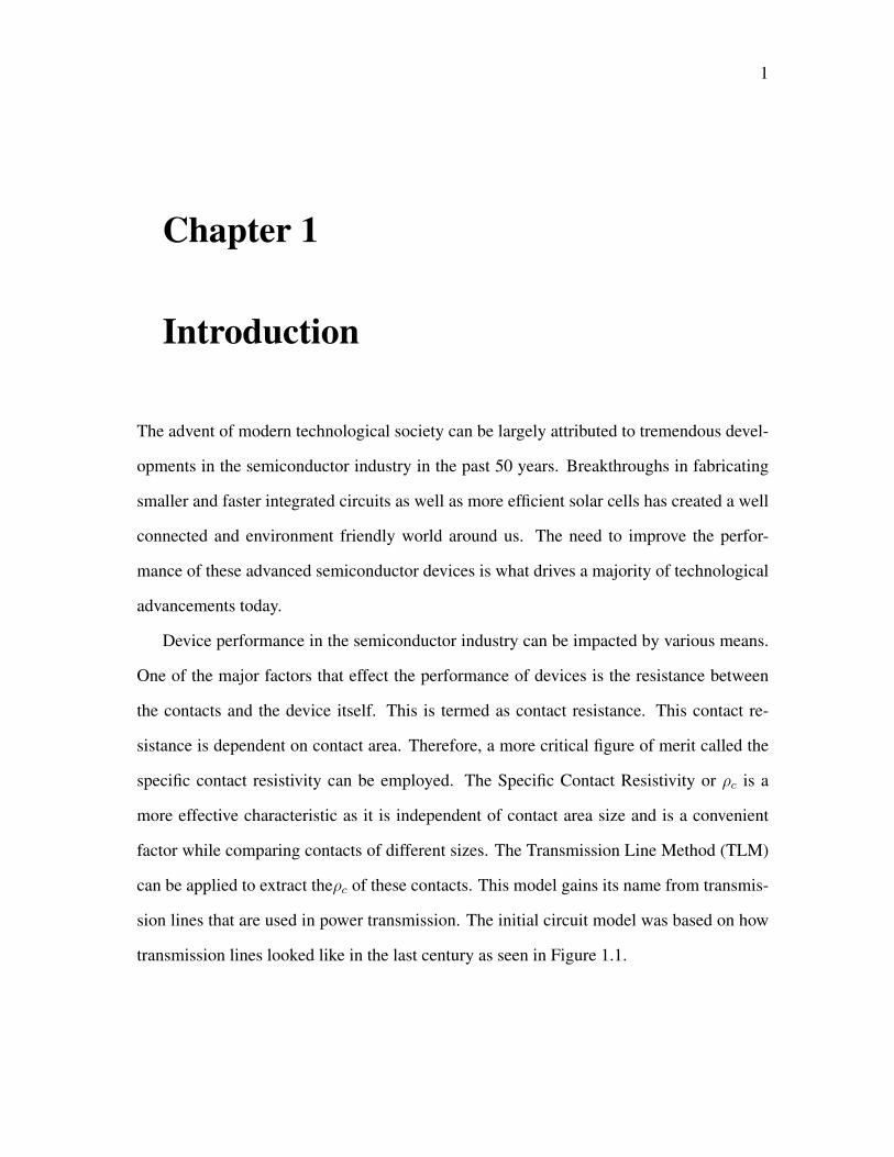
transmission lines looked like in the last century as seen in Figure 1.1.
2
Figure 1.1: Transmission lines and the TLM circuit model [2]
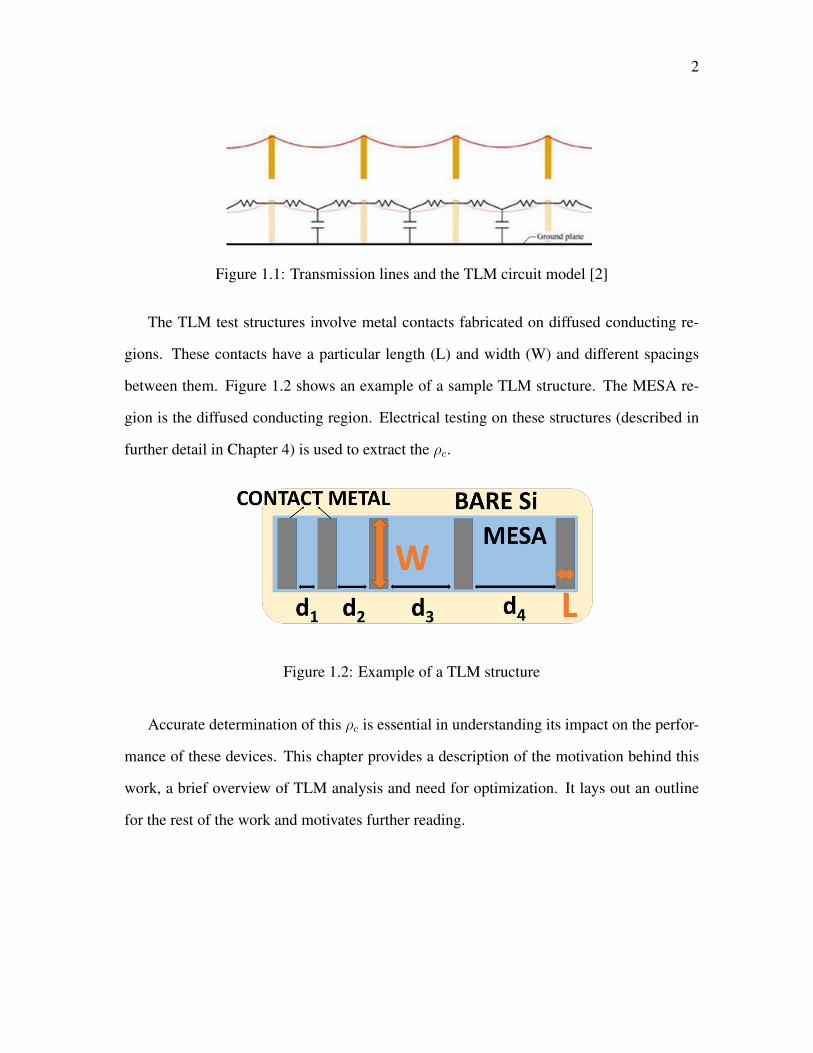
The TLM test structures involve metal contacts fabricated on diffused conducting re-
gions. These contacts have a particular length (L) and width (W) and different spacings
between them. Figure 1.2 shows an example of a sample TLM structure. The MESA re-
gion is the diffused conducting region. Electrical testing on these structures (described in
further detail in Chapter 4) is used to extract the ρc.
Figure 1.2: Example of a TLM structure
Accurate determination of this ρc is essential in understanding its impact on the perfor-
mance of these devices. This chapter provides a description of the motivation behind this
work, a brief overview of TLM analysis and need for optimization. It lays out an outline
for the rest of the work and motivates further reading.
3
1.1 Motivation
The aggressive demand for high performance semiconductor devices has placed a need to
effectively extract the specific contact resistivity for contacts made between these devices
and their external environment. Integrated circuits and photovoltaic applications commonly
use the Transmission Line Method or TLM method to extract the measure of contact resis-
tance i.e. specific contact resistivity or ρc. In the TLM method, the contact current injection
is in a lateral channel that makes the extracted specific contact resistivity values comparable
to FET as well as photovoltaic devices. These device structures have varying ρc and sheet
resistance RSH values and the contacts differ between being alloyed and non-alloyed metal
contacts.
Inconsistencies have been observed in literature regarding the specific contact resis-
tivity values extracted from applications involving large TLM geometries and small TLM
geomtries. For example, values of ρc quoted in literature involving integrated circuit ap-
plications that have very small TLM contact geometries range from about 10−8 to 10−6
Ω− cm2 [7] [16] whereas those in the photovoltaics domain with larger contact geometries
have values of ρc between 10−5 to 10−2 Ω − cm2 [6] [5]. This is very interesting to ob-
serve as ρc is defined to be independent of contact area, but an area dependence is clearly
observed in such literature.
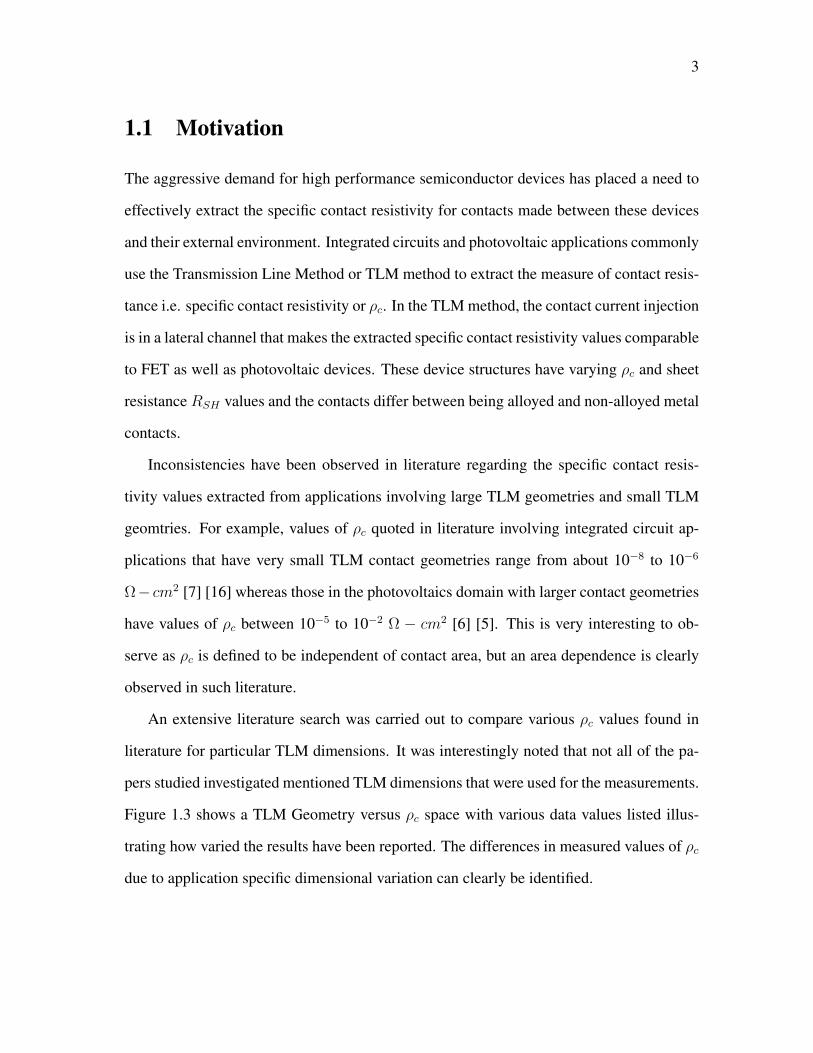
An extensive literature search was carried out to compare various ρc values found in
literature for particular TLM dimensions. It was interestingly noted that not all of the pa-
pers studied investigated mentioned TLM dimensions that were used for the measurements.
Figure 1.3 shows a TLM Geometry versus ρc space with various data values listed illus-
trating how varied the results have been reported. The differences in measured values of ρc
due to application specific dimensional variation can clearly be identified.
4
Specific Contact Resistivity ρc
TL
MG
eom
etry
[6] Gabor 2016ρc = 10−3 Ω-cm2
W = 1cm , L = 65µm
[16] Stavitski 2006ρc =3.9 × 10⁻⁸ Ω-cm2
W = 8µm , L = 3µm
[7] Gallacher 2012ρc =2.3 × 10⁻⁷ Ω-cm2
W = 125 µm , L = 75 µm
[5] Franklin 2014ρc =2 × 10⁻⁵ Ω-cm2
W = 2 cm , L = 2 cm
Figure 1.3: Difference of ρc values in literature between Integrated Circuits and SiliconPhotovoltaics.[5] [6] [7] [16]
Tremendous reduction in device sizes in modern times have required specific contact re-
sistivity (ρc) improvement to maintain small parasitic resistances within acceptable ranges,
particularly for integrated circuit applications. These parasitic resistances need to be signif-
icantly small for all semiconductor applications. Optimum pattern designs for the Trans-
mission Line Model (TLM) that are suggested to achieve minimum measurement uncer-
tainty of the specific contact resistance can be developed for semiconductor applications
of varying ρc and RSH .These values of measurement uncertainty need to be evaluated for
TLM geometries of varying sizes to determine if non-optimized TLM geometries cause the
measurement inconsistencies. Simulations carried out in this paper as well as in Ueng et al
[20] suggest optimum values of the widths of these TLM structures that provide the least
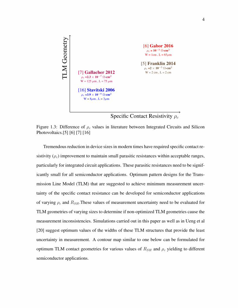
uncertainty in measurement. A contour map similar to one below can be formulated for
optimum TLM contact geometries for various values of RSH and ρc yielding to different
semiconductor applications.
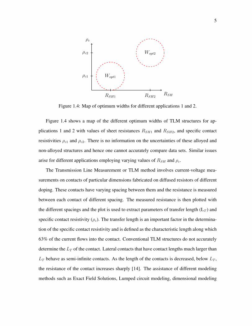
5
RSH
ρc
RSH1 RSH2
ρc1
ρc2
Wopt1
Wopt2
Figure 1.4: Map of optimum widths for different applications 1 and 2.
Figure 1.4 shows a map of the different optimum widths of TLM structures for ap-
plications 1 and 2 with values of sheet resistances RSH1 and RSH2, and specific contact
resistivities ρc1 and ρc2. There is no information on the uncertainties of these alloyed and
non-alloyed structures and hence one cannot accurately compare data sets. Similar issues
arise for different applications employing varying values of RSH and ρc.
The Transmission Line Measurement or TLM method involves current-voltage mea-
surements on contacts of particular dimensions fabricated on diffused resistors of different
doping. These contacts have varying spacing between them and the resistance is measured
between each contact of different spacing. The measured resistance is then plotted with
the different spacings and the plot is used to extract parameters of transfer length (LT ) and
specific contact resistivity (ρc). The transfer length is an important factor in the determina-
tion of the specific contact resistivity and is defined as the characteristic length along which
63% of the current flows into the contact. Conventional TLM structures do not accurately
determine the LT of the contact. Lateral contacts that have contact lengths much larger than
LT behave as semi-infinite contacts. As the length of the contacts is decreased, below LT ,
the resistance of the contact increases sharply [14]. The assistance of different modeling
methods such as Exact Field Solutions, Lumped circuit modeling, dimensional modeling
6
using the Finite Element Method can be used to explore reasons for such dependencies.
1.2 Thesis Outline
This work follows a logical order starting with the definition of specific contact resistiv-
ity of metal-semiconductor contacts. By talking about the Schottky barrier height, the
various conduction mechanisms in Metal-Semiconductor ohmic contacts can be discussed
and their relationship to the specific contact resistivity can be shown. The technology and
operation of metal-semiconductor contact formation techniques like aluminum-to-silicon
contacts and silicided contacts is provided. The Transmission Line Measurement (TLM)
method is then described in detail and different modeling methods such as the three, two,
one and zero dimensional models, the lumped circuit model and the exact field solution
model are described.
The process fabriaction and experiment and then outlined followed by details of the
theoretical and experimental optimization carried out through error analysis. The results of
the modeling and optimization, the impact of changing the TLM dimensions on the transfer
length are then provided. The experimental measurement errors are also analyzed in the
above results. The above results are then summarized to provide conclusions about the
applicability of the TLM method as an accurate method for determining ρc and ideas for
improvement and future research are suggested.
7
Chapter 2
Specific Contact Resistivity of
Metal-Semiconductor Contacts
2.1 Ohmic Contacts
In order to improve the performance of modern semiconductor devices, various methodolo-
gies can be applied. One of them is to reduce the resistance between the electrical contacts
of the device and its environment. Ohmic contacts are most commonly utilized to make
connections between the metal and semiconductors. An ohmic contact is a low resistance
junction that allows similar current conduction in both directions between the metal and the
semiconductor [22]. The current voltage characteristics of ohmic contacts can be linear or
quasi-linear. The voltage drop across the contact junction should be very small when com-
pared to the voltage drop across the device so that the contact can provide the necessary
device current [15].An ohmic contact should not degrade the device and inject minority
carriers.
An essential concept to comprehend for ohmic contacts is the barrier height or more
formally called the Schottky barrier height, denoted by φB and measured in eV.
8
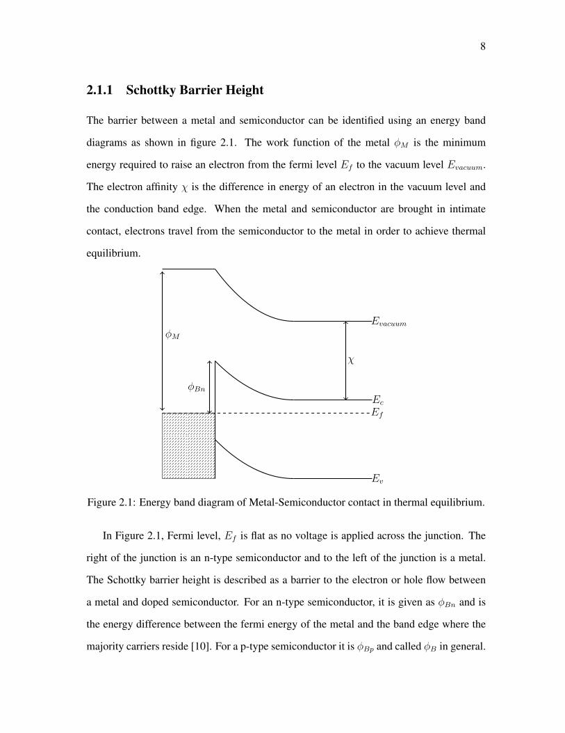
2.1.1 Schottky Barrier Height
The barrier between a metal and semiconductor can be identified using an energy band
diagrams as shown in figure 2.1. The work function of the metal φM is the minimum
energy required to raise an electron from the fermi level Ef to the vacuum level Evacuum.
The electron affinity χ is the difference in energy of an electron in the vacuum level and
the conduction band edge. When the metal and semiconductor are brought in intimate
contact, electrons travel from the semiconductor to the metal in order to achieve thermal
equilibrium.
φM
Evacuum
χ
φBn
Ev
EcEf
Figure 2.1: Energy band diagram of Metal-Semiconductor contact in thermal equilibrium.
In Figure 2.1, Fermi level, Ef is flat as no voltage is applied across the junction. The
right of the junction is an n-type semiconductor and to the left of the junction is a metal.
The Schottky barrier height is described as a barrier to the electron or hole flow between
a metal and doped semiconductor. For an n-type semiconductor, it is given as φBn and is
the energy difference between the fermi energy of the metal and the band edge where the
majority carriers reside [10]. For a p-type semiconductor it is φBp and called φB in general.
9
It is a function of the metal as well as the semiconductor. The barrier height for a metal
contact to an n-type semiconductor is given in Equation 2.1.
φBn = φM − χ (2.1)
Here, φM is the metal work-function and χ is the electron affinity. Similarly, for a
p-type semiconductor, the barrier height φBp is given in Equation 2.2.
ΦBp =Egq
+ χ− φM (2.2)
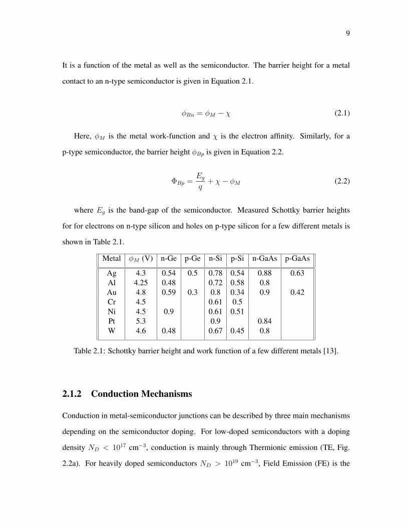
where Eg is the band-gap of the semiconductor. Measured Schottky barrier heights
for for electrons on n-type silicon and holes on p-type silicon for a few different metals is
shown in Table 2.1.
Metal φM (V) n-Ge p-Ge n-Si p-Si n-GaAs p-GaAs
Ag 4.3 0.54 0.5 0.78 0.54 0.88 0.63Al 4.25 0.48 0.72 0.58 0.8Au 4.8 0.59 0.3 0.8 0.34 0.9 0.42Cr 4.5 0.61 0.5Ni 4.5 0.9 0.61 0.51Pt 5.3 0.9 0.84W 4.6 0.48 0.67 0.45 0.8
Table 2.1: Schottky barrier height and work function of a few different metals [13].
2.1.2 Conduction Mechanisms
Conduction in metal-semiconductor junctions can be described by three main mechanisms
depending on the semiconductor doping. For low-doped semiconductors with a doping
density ND < 1017 cm−3, conduction is mainly through Thermionic emission (TE, Fig.
2.2a). For heavily doped semiconductors ND > 1019 cm−3, Field Emission (FE) is the
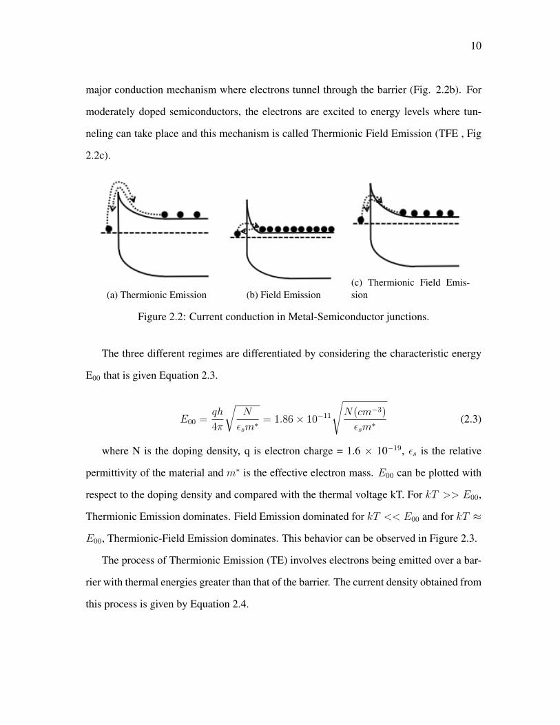
10
major conduction mechanism where electrons tunnel through the barrier (Fig. 2.2b). For
moderately doped semiconductors, the electrons are excited to energy levels where tun-
neling can take place and this mechanism is called Thermionic Field Emission (TFE , Fig
2.2c).
(a) Thermionic Emission (b) Field Emission(c) Thermionic Field Emis-sion
Figure 2.2: Current conduction in Metal-Semiconductor junctions.
The three different regimes are differentiated by considering the characteristic energy
E00 that is given Equation 2.3.
E00 =qh
4π
√N
εsm∗= 1.86× 10⁻¹¹
√N(cm−3)
εsm∗(2.3)
where N is the doping density, q is electron charge = 1.6 × 10⁻¹⁹, εs is the relative
permittivity of the material and m∗ is the effective electron mass. E00 can be plotted with
respect to the doping density and compared with the thermal voltage kT. For kT >> E00,
Thermionic Emission dominates. Field Emission dominated for kT << E00 and for kT ≈
E00, Thermionic-Field Emission dominates. This behavior can be observed in Figure 2.3.
The process of Thermionic Emission (TE) involves electrons being emitted over a bar-
rier with thermal energies greater than that of the barrier. The current density obtained from
this process is given by Equation 2.4.
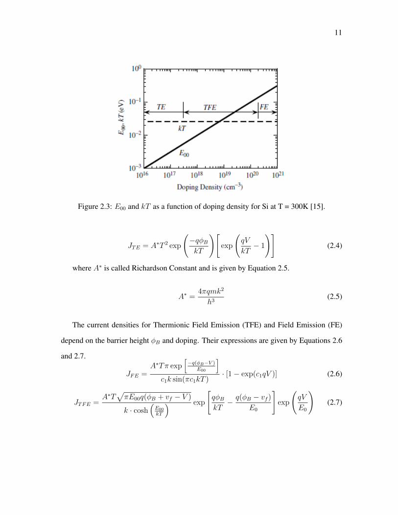
11
Figure 2.3: E00 and kT as a function of doping density for Si at T = 300K [15].
JTE = A∗T 2 exp
(−qφBkT
)[exp
(qV
kT− 1
)](2.4)
where A∗ is called Richardson Constant and is given by Equation 2.5.
A∗ =4πqmk2
h3(2.5)
The current densities for Thermionic Field Emission (TFE) and Field Emission (FE)
depend on the barrier height φB and doping. Their expressions are given by Equations 2.6
and 2.7.
JFE =A∗Tπ exp
[−q(φB−V )
E00
]c1k sin(πc1kT )
· [1− exp(c1qV )] (2.6)
JTFE =A∗T
√πE00q(φB + vf − V )
k · cosh(E00
kT
) exp
[qφBkT− q(φB − vf )
E0
]exp
(qV
E0
)(2.7)
12
The variables c1 and E0 are defined as follows.
c1 =1
2E00
ln
(4φBvf
)(2.8)
E0 = E00 coth
(E00
kT
)(2.9)
vf is the difference between Ec and Ef and can be found using the Joyce-Dixon approxi-
mation.
vf = EC − Ef = kT
[ln
(n
Nc
)+
1√8
n
Nc
](2.10)
where n is the carrier concentration and Nc is the effective density of states given by
Nc = 2
(m∗ekT
2π~2
)3/2
(2.11)
m∗e is the effective mass of electron and the value of Nc for silicon is 2.82 × 1019cm−3.
2.2 Specific Contact Resistivity
The specific contact resistivity, ρc, is a figure of merit for ohmic contacts and is measured in
Ω - cm2. It is used to describe the interfacial quality of the junction. The classic derivation
of ρc is the reciprocal of the derivative of the current density with respect to the voltage at
zero bias [17],
ρc =
(∂J
∂V
)−1
V=0
(2.12)
The specific contact resistivity includes the contact resistivity of not only the interface,
13
but also the regions immediately above and below the interface. The specific contact re-
sistivity is a very useful parameter for ohmic contacts as it is independent of the contact
area and is a very convenient parameter for measuring contacts of different sizes. The ρc
can be measured directly in contrast to contact resistance Rc. ρc can be measured from the
corresponding Rc as
ρc = RcA (2.13)
where A is the effective contact area in cm2.
For metal-semiconductor contacts with low doping concentrations, Thermionic Emis-
sion dominates. The current due to TE is given by Equation 2.4. The specific contact
resistivity due to TE can be obtained by applying Equation 2.12 to the TE current. There-
fore, the specific contact resistivity due to Thermionic Emission
ρc,TE =k
qA∗Texp
(qφBkT
)(2.14)
It can be seen from the above equation that low ρc can be obtained from a low barrier
height. It also shows the temperature dependence of the ρc for a given barrier height. For
higher doping concentrations, ρc starts to depend on the barrier height φB as well as the
doping density ND. The specific contact resistivity due to Field emission, ρc,FE , is given
by
ρc,FE =k2
qA∗·
√E0
E00
√π(qφB + vf )
cosh
(E00
kT
)exp
(qφBE0
− vfkT
)(2.15)
For regions in between, both TE and FE take place the specific contact resistivity, ρc,TFE
is given by
ρc,TFE =k2
qA∗·
[πkT
sin(πc1kT )· exp
(− qφBE00
)− 1
c1
exp
(− qφBE00
− c1vf
)]−1
(2.16)
14
The Richardson constant A∗ for silicon is 110 Acm−2K−2.
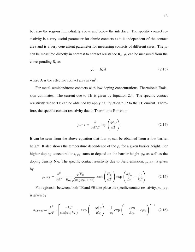
The specific contact resistivity can be plotted with respect to the doping concentration
to show its variation with different barrier heights as seen in Figure 2.4.
Figure 2.4: Electron concentration versus specific contact resistivity for Silicon.
It can be observed from the above graph that for higher doping concentrations, lower
specific contact resistivity values can be obtained. The values of ρc are calculated for each
of the conduction mechanisms using equations 2.14 through 2.16 respectively. It can be ob-
served that Field Emission dominates as a transport mechanism in highly doping whereas
Thermionic Emission dominates at low doping. The specific contact resistivity is inde-
pendent of the doping in the Thermionic emission regime and therefore straight lines are
15
observed. The specific contact resistivity increases with increasing barrier height and there-
fore, lower barrier heights with high electron concentration are preferred. At low barrier
heights, however, very less field emission is observed for high doping concentrations. A
discontinuity is also observed in the regions of transition from one transport mechanism to
the other.
2.3 Effect of Interface States
Interface states on the surface of the semiconductor can also be a significant factor in de-
termining the specific contact resistivity. These interface states can be caused by various
reasons such as broken lattice periodicity on the surface, adsorption of foreign particles and
impurities. These can give rise to trap sites on the semiconductor surface. The trap sites can
be of donor or acceptor type.The sites that are positive when empty and neutral when full
are the donor-like trap sites and the ones that are neutral when empty and negative when
full are the acceptor like trap sites.
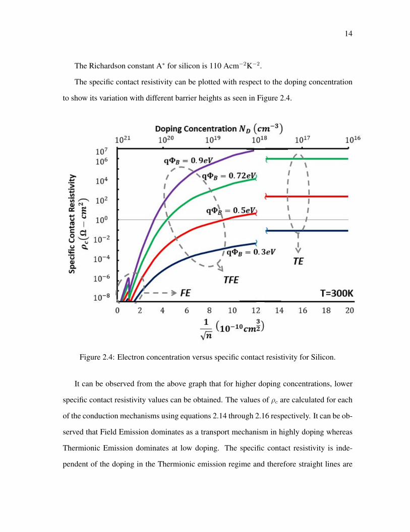
qφ0 Donor like
Acceptor like
Figure 2.5: Energy levels of interface states
qφ0 is the neutral level. Above the neutral level, states are acceptor like and below it,
states are donor like. The interface trap density is given as Dit and is measured in number
of states/cm2-eV. φ0 and Dit can be found using the equations below.
φ0 =Egq− c3 + c2χ
(1− c2)(2.17)
16
Dit = 1.1× 10¹³
(1− c2
c2
)(2.18)
Eg is the band gap, χ is the electron affinity, c2 and c3 are constants. When there are
no surface states present, Dit → 0. Then, c2 → 1 which causes the barrier height to be
a function of the metal-semiconductor workfunction difference forming an ideal schottky
barrier. When the amount of surface states is large, Dit → inf, then c2 → 0. In this
case, φBn = Eg − φ0. The fermi-level is pinned to the surface states at a value qφ0 above
the valence band. The barrier height is then independent of the metal workfunction and
is determined entirely by the semiconductor surface properties. This phenomenon is also
known as Fermi-level pinning. It shows the importance of semiconductor surface pre-
cleaning prior to metal deposition in order to reduce the trap states between the metal-
semiconductor interface. [15] [3]
Figure 2.6: Metal workfunction as a function of barrier height.
17
2.4 Measurement Techniques
There are numerous methods ranging from two-contact two-terminal techniques to six-
terminal methods to measure the specific contact resistivity, ρc. A few of the test structures
commonly employed to measure ρc are discussed in this section with additional emphasis
on ladder structures leading into the Transmission Line Measurement (TLM) method.
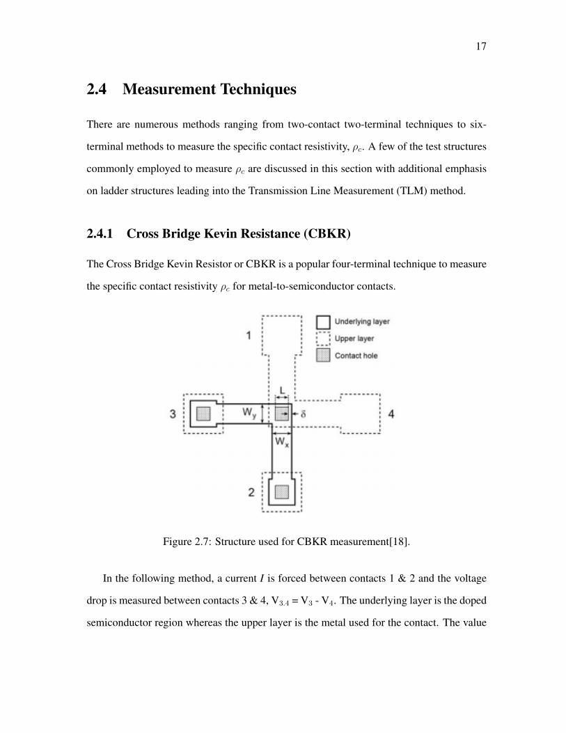
2.4.1 Cross Bridge Kevin Resistance (CBKR)
The Cross Bridge Kevin Resistor or CBKR is a popular four-terminal technique to measure
the specific contact resistivity ρc for metal-to-semiconductor contacts.
Figure 2.7: Structure used for CBKR measurement[18].
In the following method, a current I is forced between contacts 1 & 2 and the voltage
drop is measured between contacts 3 & 4, V3.4 = V3 - V4. The underlying layer is the doped
semiconductor region whereas the upper layer is the metal used for the contact. The value
18
of the contact resistance Rc is then given by Equation 2.19 below.
RCBKR =V3,4
I(2.19)
The specific contact resistivity can then be calculated from the contact area, A, using the
following equation where RCBKR = Rc.
ρc = RcA (2.20)
This generic one-dimensional approach does not take into account the effects of current
crowding that occur when the contact hole window is smaller than the doped underlying
layer, i.e. δ > 0. There is additional voltage drop at the contact periphery and this leads to
additional resistance . This additional resistance becomes extremely important for contacts
with high sheet resistance and low specific contact resistivity and therefore complicate the
CBKR measurements.[18]
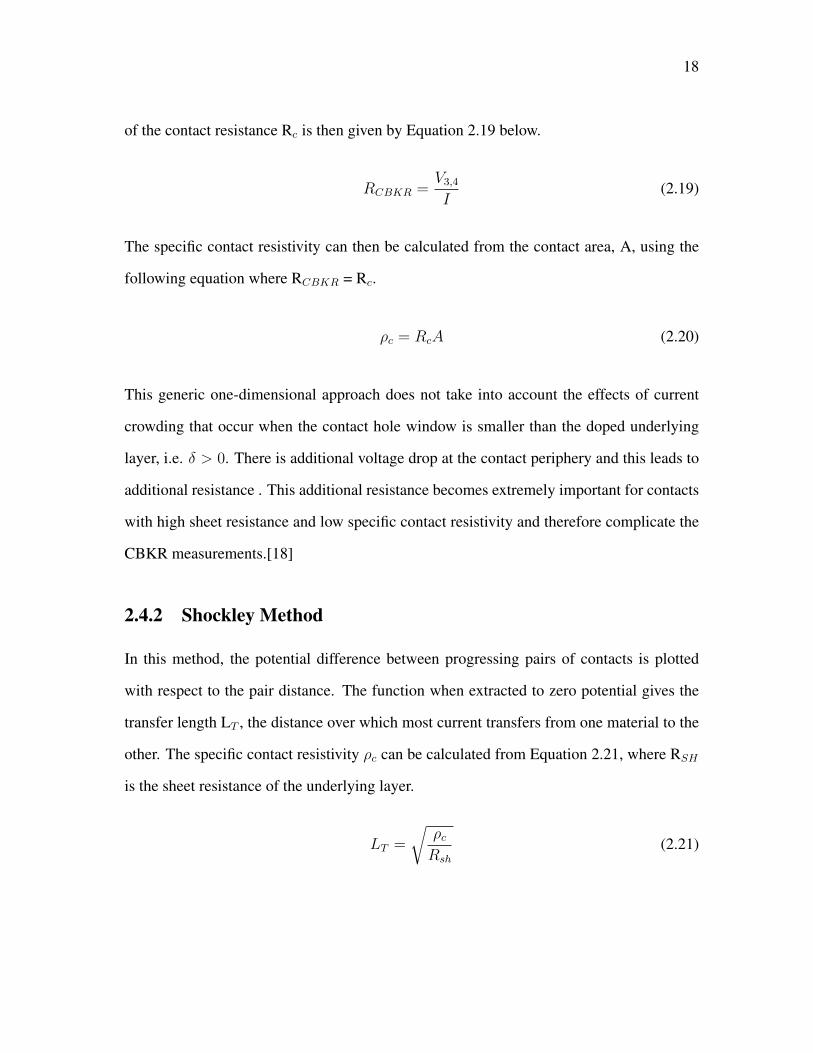
2.4.2 Shockley Method
In this method, the potential difference between progressing pairs of contacts is plotted
with respect to the pair distance. The function when extracted to zero potential gives the
transfer length LT , the distance over which most current transfers from one material to the
other. The specific contact resistivity ρc can be calculated from Equation 2.21, where RSH
is the sheet resistance of the underlying layer.
LT =
√ρcRsh
(2.21)
19
~I
V d
Figure 2.8: Ladder-structure contacts on doped-semiconductor region, top-down view.
Distance
V oltage
LT measured
0 d 2d 3d
V1
V2
V3
Figure 2.9: Extraction of the transfer length using the Shockley method
Detailed description of LT is described in Chapter 4 that discusses the TLM Method in
detail. Before diving into that topic, the technology behind the formation of these metal-
semiconductor contacts needs to be properly understood. The next chapter on the Metal-
Semiconductor contact technology serves this purpose.
20
Chapter 3
Metal-Semiconductor Contact Technology
Metal-semiconductor contacts need to have most, if not all of the following characteristics
in order to be effectively utilized in Si technology. They need to have low contact resistance
to n+ and p+ regions. They should be easy to form and have good compatibility with Si
processing such as deposition, etching, cleaning etc. There must be no reaction or diffusion
of the contact metal into Si, SiO2 or any other materials used in back-end technology. There
must also be no impact of the metal on the electrical characteristics of the shallow junctions.
The contacts must also be thermally stable and reliable.
3.1 Aluminum Contact Technology
Aluminum has traditionally been favored to make metal-semiconductor contacts due to its
good conductivity and the formation of a protective oxide on the top surface.It also fulfills
most of the requirements of a good metal-semiconductor contact listed above. Usually, a
1-2µm thick layer of Aluminum is deposited on patterned Si wafer where it makes direct
contact to the Si in the contact openings. It is the heated to ensure an intimate contact
between the Al and the Si.
The use of aluminum to form contacts was predominantly used in the era of larger
device sizes. As contact geometries began to shrink, an increase in the contact resistance
21
was observed in silicon-aluminum contacts. The processing temperatures for back-end
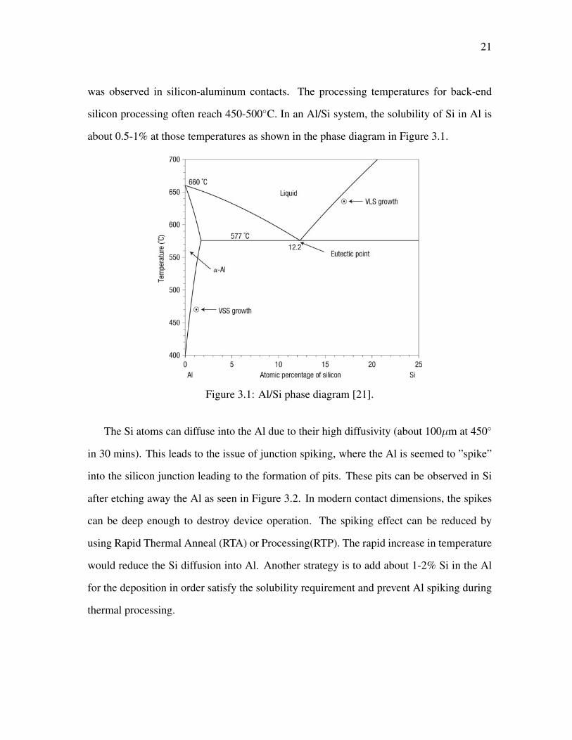
silicon processing often reach 450-500C. In an Al/Si system, the solubility of Si in Al is
about 0.5-1% at those temperatures as shown in the phase diagram in Figure 3.1.
Figure 3.1: Al/Si phase diagram [21].
The Si atoms can diffuse into the Al due to their high diffusivity (about 100µm at 450
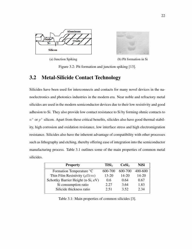
in 30 mins). This leads to the issue of junction spiking, where the Al is seemed to ”spike”
into the silicon junction leading to the formation of pits. These pits can be observed in Si
after etching away the Al as seen in Figure 3.2. In modern contact dimensions, the spikes
can be deep enough to destroy device operation. The spiking effect can be reduced by
using Rapid Thermal Anneal (RTA) or Processing(RTP). The rapid increase in temperature
would reduce the Si diffusion into Al. Another strategy is to add about 1-2% Si in the Al
for the deposition in order satisfy the solubility requirement and prevent Al spiking during
thermal processing.
22
(a) Junction Spiking (b) Pit formation in Si
Figure 3.2: Pit formation and junction spiking [13].
3.2 Metal-Silicide Contact Technology
Silicides have been used for interconnects and contacts for many novel devices in the na-
noelectronics and photonics industries in the modern era. Near noble and refractory metal
silicides are used in the modern semiconductor devices due to their low resistivity and good
adhesion to Si. They also provide low contact resistance to Si by forming ohmic contacts to
n+ or p+ silicon. Apart from these critical benefits, silicides also have good thermal stabil-
ity, high corrosion and oxidation resistance, low interface stress and high electromigration
resistance. Silicides also have the inherent advantage of compatibility with other processes
such as lithography and etching, thereby offering ease of integration into the semiconductor
manufacturing process. Table 3.1 outlines some of the main properties of common metal
silicides.
Property TiSi2 CoSi2 NiSi
Formation Temperature C 600-700 600-700 400-600Thin Film Resistivity (µΩcm) 13-20 14-20 14-20
Schottky Barrier Height (n-Si, eV) 0.6 0.64 0.67Si consumption ratio 2.27 3.64 1.83
Silicide thickness ratio 2.51 3.52 2.34
Table 3.1: Main properties of common silicides [3].
23
3.2.1 Formation of Silicides
The usual formation of metal silicides involves the following steps.
• Cleaning the wafer with a dilute HF and deionized water solution ,followed by blow-
ing dry using nitrogen gun or ”spin-rinse-dry”. This step gets rid of any native in-
terfacial SiO2 layer prior to metal deposition as metal needs to penetrate thin oxide
layer in order to react with silicon to form the silicide.
• Metal is then deposited on the wafer using sputter deposition or epitaxial process.
• Wafer is then heat treated using furnace annealing or Rapid Thermal Processing
(RTP) to form silicide at the metal-silicon interface.
• Removal of the unreacted metal using Piranha etch chemistry.
Formation of metal silicides are governed predominantly by growth kinetics over growth
energetics. Only selective phases of the silicide are detected after thermal annealing of the
metal films on silicon. The formation of multiphases in refractory metal/Si systems can
however be observed through deeper and more refined analysis using better techniques such
as high-resolution transmission electron microscopy (HRTEM) with fast Fourier transform
(FFT) analysis.
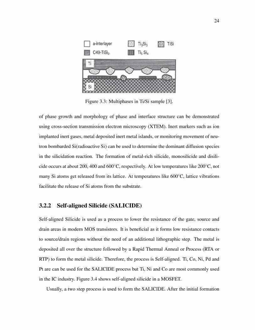
Various different crystalline phases can be formed in a metal/Si system. For example,
the Ti/Si systems forms as many as four different crystalline phases (Ti5Si3, TiSi, C49-TiSi2
and C54-TiSi2).Figure 3.3 shows a sample of the multiphases in Ti/Si The identification of
the initial phases of reaction for these silicides is difficult due to the close proximity and
overlap of diffraction rings from their diffraction patterns.
The growth and formation of metal silicides are diffusion controlled or interface-reaction
controlled and they can be formed far below the eutectic temperature, the temperature at
which a particular mixture freezes or melts. The sequence of phase formation, dependence
24
Figure 3.3: Multiphases in Ti/Si sample [3].
of phase growth and morphology of phase and interface structure can be demonstrated
using cross-section transmission electron microscopy (XTEM). Inert markers such as ion
implanted inert gases, metal deposited inert metal islands, or monitoring movement of neu-
tron bombarded Si(radioactive Si) can be used to determine the dominant diffusion species
in the silicidation reaction. The formation of metal-rich silicide, monosilicide and disili-
cide occurs at about 200, 400 and 600C, respectively. At low temperatures like 200C, not
many Si atoms get released from its lattice. At temperatures like 600C, lattice vibrations
facilitate the release of Si atoms from the substrate.
3.2.2 Self-aligned Silicide (SALICIDE)
Self-aligned Silicide is used as a process to lower the resistance of the gate, source and
drain areas in modern MOS transistors. It is beneficial as it forms low resistance contacts
to source/drain regions without the need of an additional lithographic step. The metal is
deposited all over the structure followed by a Rapid Thermal Anneal or Process (RTA or
RTP) to form the metal silicide. Therefore, the process is Self-aligned. Ti, Co, Ni, Pd and
Pt are can be used for the SALICIDE process but Ti, Ni and Co are most commonly used
in the IC industry. Figure 3.4 shows self-aligned silicide in a MOSFET.
Usually, a two step process is used to form the SALICIDE. After the initial formation
25
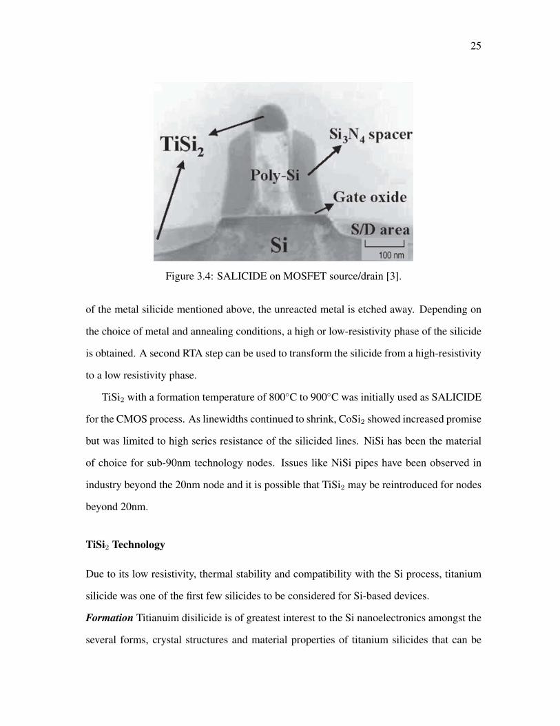
Figure 3.4: SALICIDE on MOSFET source/drain [3].
of the metal silicide mentioned above, the unreacted metal is etched away. Depending on
the choice of metal and annealing conditions, a high or low-resistivity phase of the silicide
is obtained. A second RTA step can be used to transform the silicide from a high-resistivity
to a low resistivity phase.
TiSi2 with a formation temperature of 800C to 900C was initially used as SALICIDE
for the CMOS process. As linewidths continued to shrink, CoSi2 showed increased promise
but was limited to high series resistance of the silicided lines. NiSi has been the material
of choice for sub-90nm technology nodes. Issues like NiSi pipes have been observed in
industry beyond the 20nm node and it is possible that TiSi2 may be reintroduced for nodes
beyond 20nm.
TiSi2 Technology
Due to its low resistivity, thermal stability and compatibility with the Si process, titanium
silicide was one of the first few silicides to be considered for Si-based devices.
Formation Titianuim disilicide is of greatest interest to the Si nanoelectronics amongst the
several forms, crystal structures and material properties of titanium silicides that can be
26
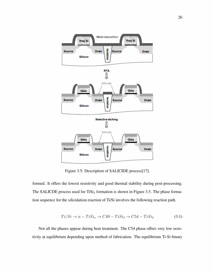
Figure 3.5: Description of SALICIDE process[17].
formed. It offers the lowest resistivity and good thermal stability during post-processing.
The SALICDE process used for TiSi2 formation is shown in Figure 3.5. The phase forma-
tion sequence for the silicidation reaction of Ti/Si involves the following reaction path.
Ti/Si→ α− TiSix → C49− TiSi2 → C54− TiSi2 (3.1)
Not all the phases appear during heat treatment. The C54 phase offers very low resis-
tivity at equilibrium depending upon method of fabrication. The equilibrium Ti-Si binary
27
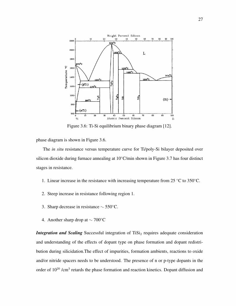
Figure 3.6: Ti-Si equilibrium binary phase diagram [12].
phase diagram is shown in Figure 3.6.
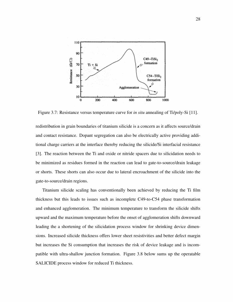
The in situ resistance versus temperature curve for Ti/poly-Si bilayer deposited over
silicon dioxide during furnace annealing at 10C/min shown in Figure 3.7 has four distinct
stages in resistance.
1. Linear increase in the resistance with increasing temperature from 25 C to 350C.
2. Steep increase in resistance following region 1.
3. Sharp decrease in resistance : 550C.
4. Another sharp drop at : 700C
Integration and Scaling Successful integration of TiSi2 requires adequate consideration
and understanding of the effects of dopant type on phase formation and dopant redistri-
bution during silicidation.The effect of impurities, formation ambients, reactions to oxide
and/or nitride spacers needs to be understood. The presence of n or p-type dopants in the
order of 1020 /cm3 retards the phase formation and reaction kinetics. Dopant diffusion and
28
Figure 3.7: Resistance versus temperature curve for in situ annealing of Ti/poly-Si [11].
redistribution in grain boundaries of titanium silicide is a concern as it affects source/drain
and contact resistance. Dopant segregation can also be electrically active providing addi-
tional charge carriers at the interface thereby reducing the silicide/Si interfacial resistance
[3]. The reaction between the Ti and oxide or nitride spacers due to silicidation needs to
be minimized as residues formed in the reaction can lead to gate-to-source/drain leakage
or shorts. These shorts can also occur due to lateral encroachment of the silicide into the
gate-to-source/drain regions.
Titanium silicide scaling has conventionally been achieved by reducing the Ti film
thickness but this leads to issues such as incomplete C49-to-C54 phase transformation
and enhanced agglomeration. The minimum temperature to transform the silicide shifts
upward and the maximum temperature before the onset of agglomeration shifts downward
leading the a shortening of the silicidation process window for shrinking device dimen-
sions. Increased silicide thickness offers lower sheet resistivities and better defect margin
but increases the Si consumption that increases the risk of device leakage and is incom-
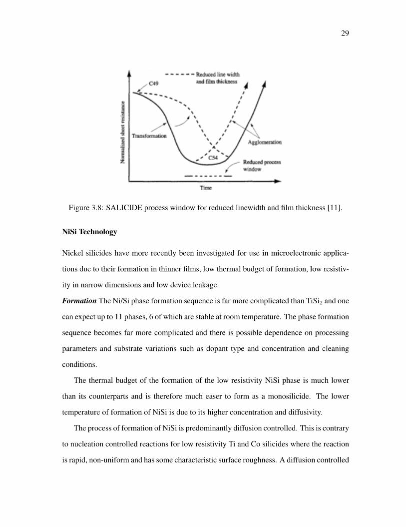
patible with ultra-shallow junction formation. Figure 3.8 below sums up the operatable
SALICIDE process window for reduced Ti thickness.
29
Figure 3.8: SALICIDE process window for reduced linewidth and film thickness [11].
NiSi Technology
Nickel silicides have more recently been investigated for use in microelectronic applica-
tions due to their formation in thinner films, low thermal budget of formation, low resistiv-
ity in narrow dimensions and low device leakage.
Formation The Ni/Si phase formation sequence is far more complicated than TiSi2 and one
can expect up to 11 phases, 6 of which are stable at room temperature. The phase formation
sequence becomes far more complicated and there is possible dependence on processing
parameters and substrate variations such as dopant type and concentration and cleaning
conditions.
The thermal budget of the formation of the low resistivity NiSi phase is much lower
than its counterparts and is therefore much easer to form as a monosilicide. The lower
temperature of formation of NiSi is due to its higher concentration and diffusivity.
The process of formation of NiSi is predominantly diffusion controlled. This is contrary
to nucleation controlled reactions for low resistivity Ti and Co silicides where the reaction
is rapid, non-uniform and has some characteristic surface roughness. A diffusion controlled
30
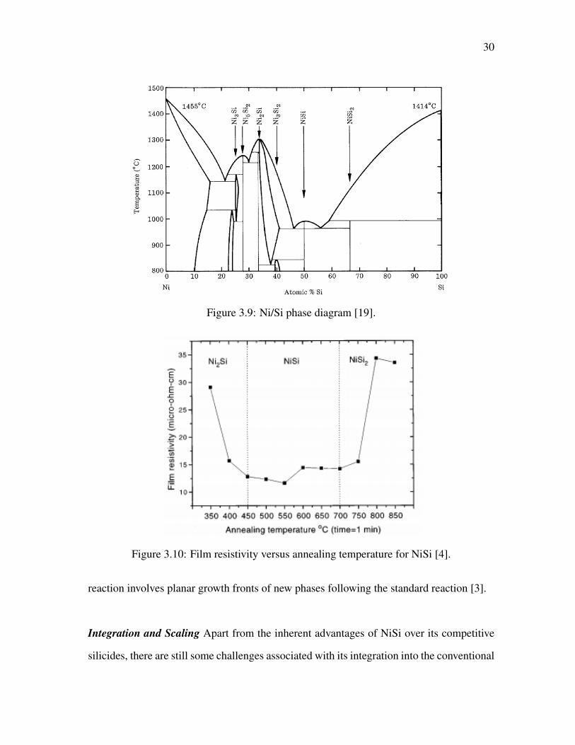
Figure 3.9: Ni/Si phase diagram [19].
Figure 3.10: Film resistivity versus annealing temperature for NiSi [4].
reaction involves planar growth fronts of new phases following the standard reaction [3].
Integration and Scaling Apart from the inherent advantages of NiSi over its competitive
silicides, there are still some challenges associated with its integration into the conventional
31
semiconductor manufacturing. Undesired agglomeration of NiSi and formation of NiSi2 at
low temperatures, excessive Ni diffusion on narrow Si or poly-Si lines can lead to abnor-
mally high junction leakages. The performance and yield of NiSi on narrow poly-Si gate
is far superior than similar silicides. Gate patterning does not limit silicide formation for
NiSi as no degradation in resistance is observed which is usually linked to agglomeration,
stress and voiding effects.
Due to the presence of more grain boundaries on NiSi films on poly-Si substrates, there
is faster diffusion of Ni during phase formation. This process can be optimized to give
thicker silicide on poly-si areas and less silicide on active junctions. This would be advan-
tageous for device applications based on Silicon-On-Insulator (SOI) substrates as source
and drain regions of the devices would require very small amounts of Si consumption. The
formation of high resistivity NiSi2 can also limit the NiSi process. Local stresses can lead
to the formation on NiSi2 even if it does not normally occur in temperatures below 800C.
NiSi provides comparatively higher contact resistance to heavily doped p-type substrates
over heavily doped n-type, but still lower than contacts with CoSi2.
32
Chapter 4
Transmission Line Measurement (TLM)
Method
The Transmission Line Measurement or TLM method is popularly used to determine the
specific contact resistivity of metal-semiconductor interface in the modern semiconductor
industry. Originally proposed by Shockley, it involves current voltage measurements on
adjacent contacts with variable spacing between them. It utilizes a similar ladder structure
as observed in the Shockley method but the current is not perturbed by contacts in between
for this method. The total resistance RT between any two contacts (of length L and width
W) separated by a distance d could be measured and plotted as a function of d. The resulting
equation between RT and R provides an estimate of ρc through the so called transfer length
LT , measured from the intersection of the R curve for RT = 0.
4.1 Transmission Line Measurement (TLM) Structure
The Transmission Line Measurement (TLM) structure involves contacts fabricated on dif-
fused semiconductor regions of a particular sheet resistance RSH depending upon the ap-
plication. These diffused regions are isolated from their surroundings by using trench or
MESA isolation. If MESA isolation is used, the depth of the MESA should be greater than
33
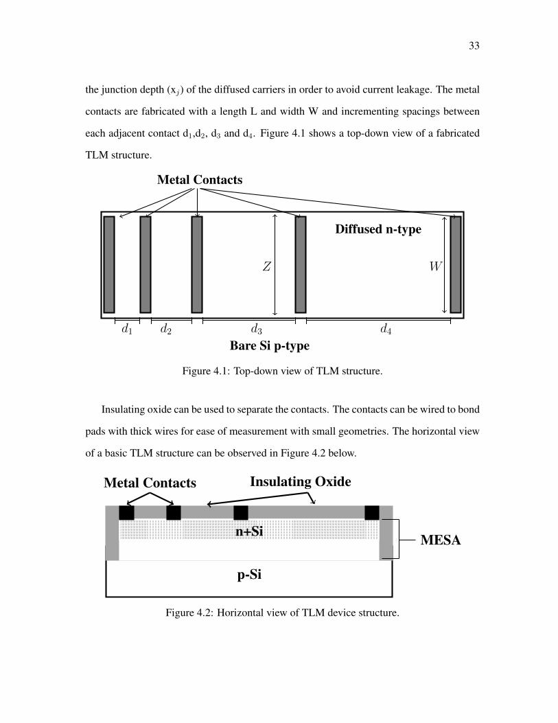
the junction depth (xj) of the diffused carriers in order to avoid current leakage. The metal
contacts are fabricated with a length L and width W and incrementing spacings between
each adjacent contact d1,d2, d3 and d4. Figure 4.1 shows a top-down view of a fabricated
TLM structure.
Bare Si p-type
Diffused n-type
d1 d2 d3 d4
WZ
Metal Contacts
Figure 4.1: Top-down view of TLM structure.
Insulating oxide can be used to separate the contacts. The contacts can be wired to bond
pads with thick wires for ease of measurement with small geometries. The horizontal view
of a basic TLM structure can be observed in Figure 4.2 below.
p-Si
n+Si
Insulating OxideMetal Contacts
MESA
Figure 4.2: Horizontal view of TLM device structure.
34
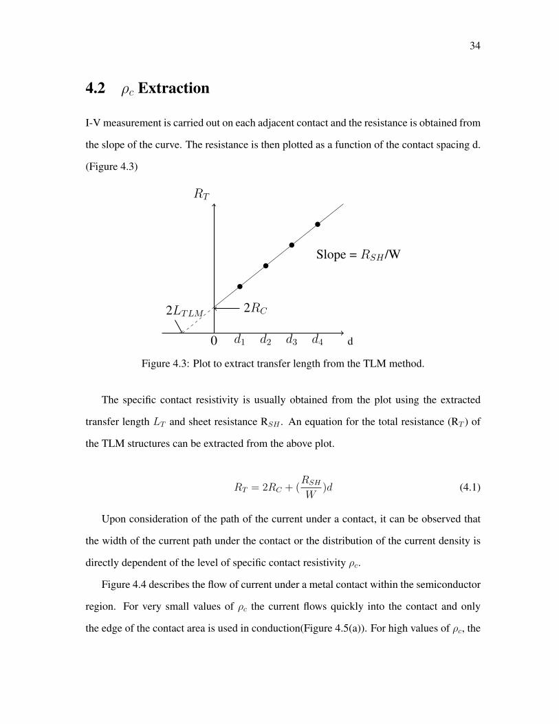
4.2 ρc Extraction
I-V measurement is carried out on each adjacent contact and the resistance is obtained from
the slope of the curve. The resistance is then plotted as a function of the contact spacing d.
(Figure 4.3)
d
RT
Slope = RSH /W
2LTLM 2RC
0 d1 d2 d3 d4
Figure 4.3: Plot to extract transfer length from the TLM method.
The specific contact resistivity is usually obtained from the plot using the extracted
transfer length LT and sheet resistance RSH . An equation for the total resistance (RT ) of
the TLM structures can be extracted from the above plot.
RT = 2RC + (RSH
W)d (4.1)
Upon consideration of the path of the current under a contact, it can be observed that
the width of the current path under the contact or the distribution of the current density is
directly dependent of the level of specific contact resistivity ρc.
Figure 4.4 describes the flow of current under a metal contact within the semiconductor
region. For very small values of ρc the current flows quickly into the contact and only
the edge of the contact area is used in conduction(Figure 4.5(a)). For high values of ρc, the
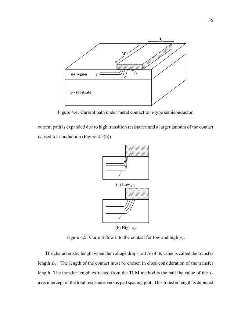
35
W
L
n+ region
p - substrate
ρc~I
Figure 4.4: Current path under metal contact to n-type semiconductor.
current path is expanded due to high transition resistance and a larger amount of the contact
is used for conduction (Figure 4.5(b)).
~I
(a) Low ρc
~I
(b) High ρc
Figure 4.5: Current flow into the contact for low and high ρc.
The characteristic length when the voltage drops to 1/e of its value is called the transfer
length LT . The length of the contact must be chosen in close consideration of the transfer
length. The transfer length extracted from the TLM method is the half the value of the x-
axis intercept of the total resistance versus pad spacing plot. This transfer length is depicted
36
as LTLM .
10−8 10−7 10−6 10−5 10−4 10−3 10−2
10−1
100
101
102
ρc (Ω-cm2)
LTLM
(µm
)
RSH = 50Ω−RSH = 500Ω−RSH = 1500Ω−
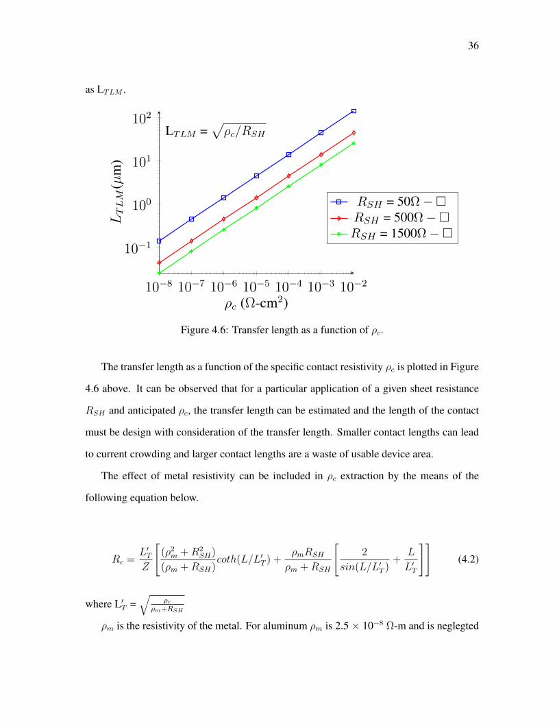
LTLM =√ρc/RSH
Figure 4.6: Transfer length as a function of ρc.
The transfer length as a function of the specific contact resistivity ρc is plotted in Figure
4.6 above. It can be observed that for a particular application of a given sheet resistance
RSH and anticipated ρc, the transfer length can be estimated and the length of the contact
must be design with consideration of the transfer length. Smaller contact lengths can lead
to current crowding and larger contact lengths are a waste of usable device area.
The effect of metal resistivity can be included in ρc extraction by the means of the
following equation below.
Rc =L′TZ
[(ρ2m +R2
SH)
(ρm +RSH)coth(L/L′T ) +
ρmRSH
ρm +RSH
[2
sin(L/L′T )+
L
L′T
]](4.2)
where L′T =√
ρcρm+RSH
ρm is the resistivity of the metal. For aluminum ρm is 2.5 × 10⁻⁸ Ω-m and is neglegted

37
in calculations in this work due to its small difference percentage wise.
38
Chapter 5
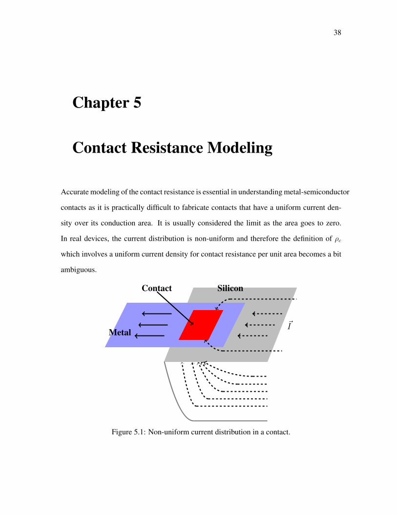
Contact Resistance Modeling
Accurate modeling of the contact resistance is essential in understanding metal-semiconductor
contacts as it is practically difficult to fabricate contacts that have a uniform current den-
sity over its conduction area. It is usually considered the limit as the area goes to zero.
In real devices, the current distribution is non-uniform and therefore the definition of ρc
which involves a uniform current density for contact resistance per unit area becomes a bit
ambiguous.
~I
Silicon
Metal
Contact
Figure 5.1: Non-uniform current distribution in a contact.
39
The contact system is described by transport equations. Poissons and two-carrier con-
tinuity equations in 3-D can be adequately used to describe the model. These equations are
more often then not, simplified into 2-D or 1-D equations.
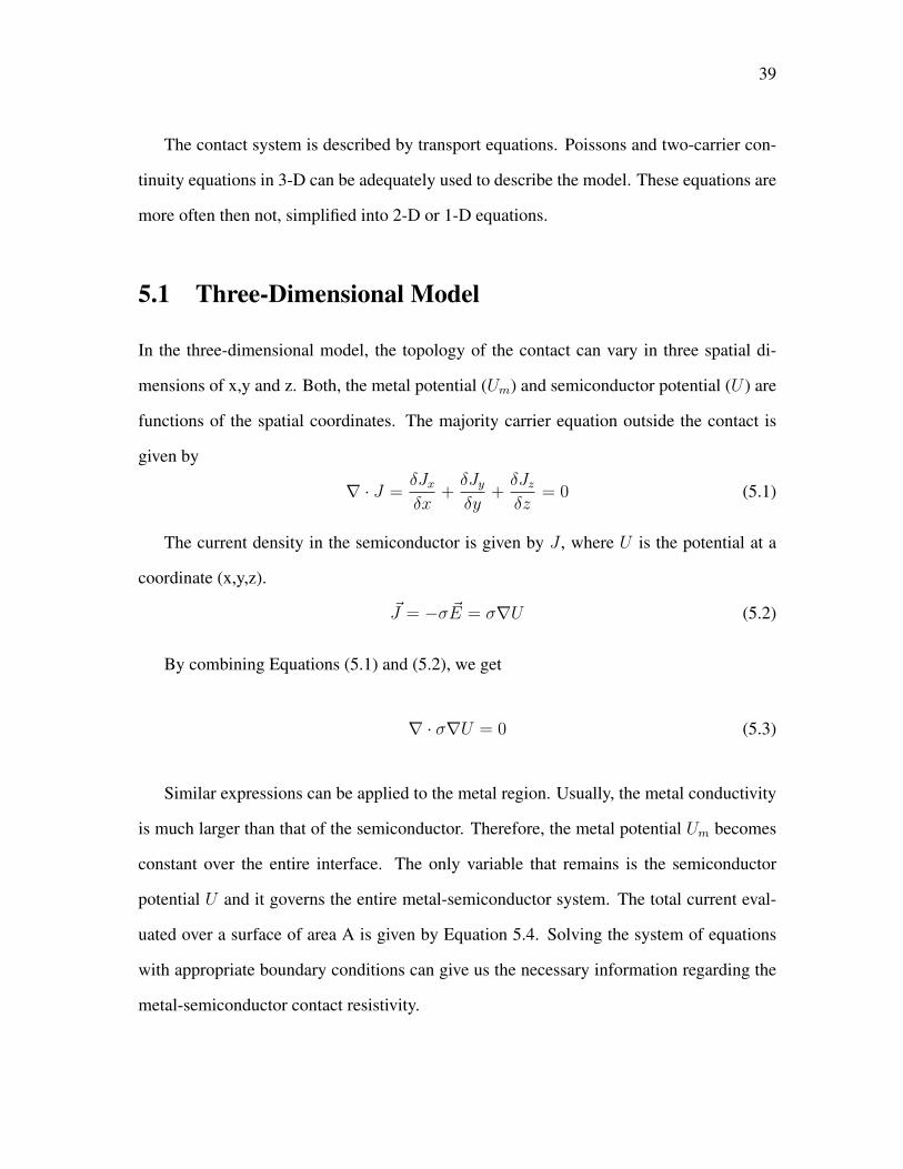
5.1 Three-Dimensional Model
In the three-dimensional model, the topology of the contact can vary in three spatial di-
mensions of x,y and z. Both, the metal potential (Um) and semiconductor potential (U ) are
functions of the spatial coordinates. The majority carrier equation outside the contact is
given by
∇ · J =δJxδx
+δJyδy
+δJzδz
= 0 (5.1)
The current density in the semiconductor is given by J , where U is the potential at a
coordinate (x,y,z).
~J = −σ ~E = σ∇U (5.2)
By combining Equations (5.1) and (5.2), we get
∇ · σ∇U = 0 (5.3)
Similar expressions can be applied to the metal region. Usually, the metal conductivity
is much larger than that of the semiconductor. Therefore, the metal potential Um becomes
constant over the entire interface. The only variable that remains is the semiconductor
potential U and it governs the entire metal-semiconductor system. The total current eval-
uated over a surface of area A is given by Equation 5.4. Solving the system of equations
with appropriate boundary conditions can give us the necessary information regarding the
metal-semiconductor contact resistivity.
40
Itot = −∫
~J · dA (5.4)
Several approximations can be made for heavily doped semiconductor junctions. First,
the effect of minority carriers is neglected. This is equivalent to neglecting the depletion
layer depth or band bending at the contact interface. The total current density is approxi-
mately the same as the majority carrier density because the metal-semiconductor interface
injects far more majority carriers than minority carriers. Second, due to this majority carrier
domination, the majority carrier concentration is approximated to the active dopant density.
Hence, only majority carrier continuity equations are used to solve for the semiconductor
region beneath the contact. The three-dimensional model can get very difficult in compu-
tation and generalization. Therefore, two-dimensional models can be developed while still
providing useful insights.
5.2 Two-Dimensional Model
In the two-dimensional model, the contact interface is considered as a 2-D surface per-
pendicular to the z-axis. The diffused layer is located beneath the metal-semiconductor
interface with an effective thickness that is assumed to be the junction depth. This model
lumps the effects of the z-axis into a single parameter, RSH , the sheet resistance of the
diffused layer.
RSH =
(∫σ(z)dz
)−1
(5.5)
Since the metal layer is usually more conductive than the semiconductor layer, the
metal potential Um is assumed to be constant. If the metal potential is set to zero, the 3-D
equations can be simplified into the following equation called the Helmholtz.
41
∇2V =RSHV
ρc=
V
L2T
(5.6)
In the bulk region with no contact surface, the potential can be described by Laplace’s
equation
∇2V = 0 (5.7)
The above equations can be solved to obtain the I-V characteristics and extract values
of ρc.
5.3 One-Dimensional Model
The one-dimensional or 1-D model is a further simplified model where the variation in the
y-axis is neglected. Since the potential changes only slightly in other axes, the Helmholtz
equation then becomes.
∇2V
δ2x=V (x)
L2T
(5.8)
Upon application of the boundary conditions, the Laplace’s equation can be reduced to
Ohms law and the potential can be shown as
V (x) = Vi
cosh
(L−xLT
)
cosh
(LLT
) (5.9)
The current is given as
42
Itot =W
RSH
δW
δx
∣∣∣∣∣x=0
(5.10)
The above equations can be used to extract the contact resistance. The 1-D model can
be further reduced to provide an even more intuitive feel to the contact resistance extraction.
This is given by the Zero-Dimensional model.
5.4 Zero-Dimensional Model
The 1-D model can be simplified to a 0-D model in the cases of large contact windows,
very high values of ρc or very small contacts. This model assumes that the current density
entering the contact window is uniform and the potential is constant in the semiconductor
layer. ρc is considered as a macroscopic quantity and is given by
Rc =ρcA
(5.11)
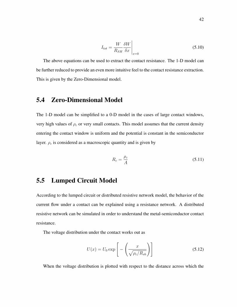
5.5 Lumped Circuit Model
According to the lumped circuit or distributed resistive network model, the behavior of the
current flow under a contact can be explained using a resistance network. A distributed
resistive network can be simulated in order to understand the metal-semiconductor contact
resistance.
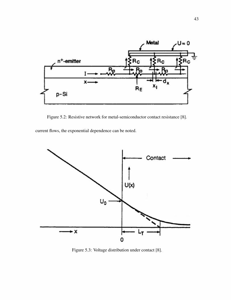
The voltage distribution under the contact works out as
U(x) = U0 exp
[−
(x√
ρc/Rsh
)](5.12)
When the voltage distribution is plotted with respect to the distance across which the
43
Figure 5.2: Resistive network for metal-semiconductor contact resistance [8].
current flows, the exponential dependence can be noted.
Figure 5.3: Voltage distribution under contact [8].
44
It can be observed from Figure 3.3, the voltage drops to 1/e of its value after a charac-
teristic length LT . This is called the transfer length and is a characteristic variable for the
current path. It can be expressed as function of the specific contact resistivity (ρc) and the
sheet resistance RSH through the following equation.
LT =
√ρcRSH
(5.13)
Mathematical analysis of the above expressions leads to the following value for the
specific contact resistance.
ρc =
(RcW
coth( LLT
)
)2
∗ 1
Rsh
(5.14)
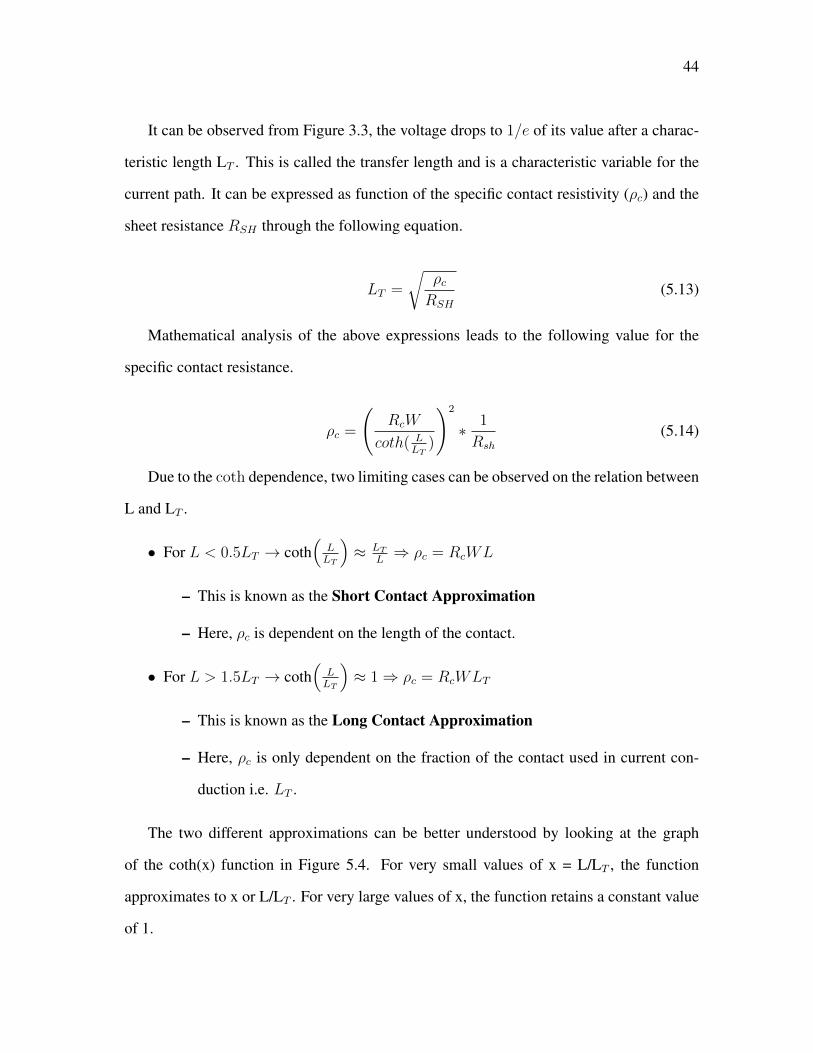
Due to the coth dependence, two limiting cases can be observed on the relation between
L and LT .
• For L < 0.5LT → coth(
LLT
)≈ LT
L⇒ ρc = RcWL
– This is known as the Short Contact Approximation
– Here, ρc is dependent on the length of the contact.
• For L > 1.5LT → coth(
LLT
)≈ 1⇒ ρc = RcWLT
– This is known as the Long Contact Approximation
– Here, ρc is only dependent on the fraction of the contact used in current con-
duction i.e. LT .
The two different approximations can be better understood by looking at the graph
of the coth(x) function in Figure 5.4. For very small values of x = L/LT , the function
approximates to x or L/LT . For very large values of x, the function retains a constant value
of 1.
45
Figure 5.4: Coth function
The long contact approximation of this model has been widely used as legacy for ρc
extraction and can potentially be the cause of incorrect values if appropriate contact ge-
ometries are not used. An example of this was observed in a paper published by BrightSpot
Automation, LLC [6]. Although the length of the contact was 65 µm , the measured trans-
fer length was significantly larger than it in various cases. It was pointed out that the use of
the approximated TLM formula was not applicable for the contact dimensions used in the
study and the use of the generic TLM formula with no approximations gave better results.
A summary of the recalculations are shown in Table 5.1.
Due to the recalculations carried out, the need for better understanding of the generic
formula that has TLM length dependence was highlighted.
The lumped distributed circuit network model for the TLM measurement is limited
in certain ways. In this model, the width of the TLM contact (W) is considered to be
infinitely large when compared to other dimensions and its effect on the ρc extraction is
neglected. The model also does not take into account the current crowding at the edge
46
LT LT < L LT Recalc. ρc(mΩ-cm2) ρc Recalc.(mΩ-cm2)
14.4 µm LT < L 21.67 µm 0.18 0.1833.3 µm LT < L 9.87 µm 0.93 0.8617 µm LT < L 18.69 µm 0.26 0.26
23.3 µm LT < L 13.79 µm 0.45 0.4480.5 µm LT > L 5.88 µm 5.24 2.3425.5 µm LT < L 12.66 µm 0.58 0.5646.9 µm LT < L 7.63 µm 1.86 1.4565.8 µm LT > L 6.34 µm 3.63 2.0817.6 µm LT < L 18.00 µm 0.27 0.2755.8 µm LT < L 6.87 µm 2.61 1.77109.9 µm LT > L 5.42 µm 10.05 2.8326.4 µm LT < L 12.21 µm 0.6 0.58
Table 5.1: Recalculation of ρc from general formula.
of the contact and the constriction (spreading) resistance. It is also assumed that ρc and
RSH are considered uniform throughout the entire structure. The resistivity of the metal
ρm is initially neglected is initially neglected and metal lines are therefore equipotential.
For these reasons, exact field solution model can potentially provide detailed insight into
contact resistance and current crowding. It is discussed in the following section.
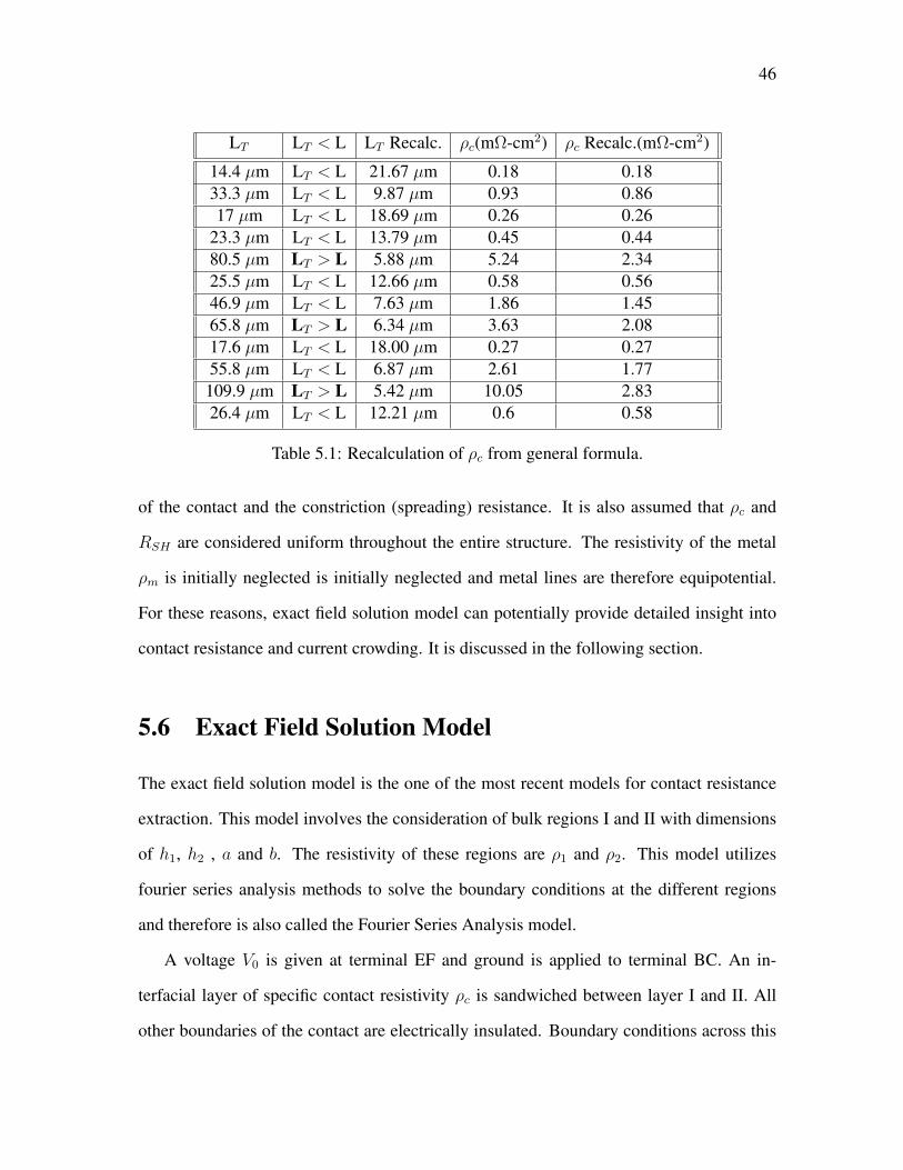
5.6 Exact Field Solution Model
The exact field solution model is the one of the most recent models for contact resistance
extraction. This model involves the consideration of bulk regions I and II with dimensions
of h1, h2 , a and b. The resistivity of these regions are ρ1 and ρ2. This model utilizes
fourier series analysis methods to solve the boundary conditions at the different regions
and therefore is also called the Fourier Series Analysis model.
A voltage V0 is given at terminal EF and ground is applied to terminal BC. An in-
terfacial layer of specific contact resistivity ρc is sandwiched between layer I and II. All
other boundaries of the contact are electrically insulated. Boundary conditions across this
47
Figure 5.5: Electrical contact assumed for Finite Element Model [24].
infinitely thin interfacial layer are given by the normal components of the current density
across the interface, Jz, and the potentials ΦI and ΦII in regions I and II respectively.
Jz = −( 1
ρ1
)δΦI
δz= −
(1
ρII
)δΦII
δz; ρcJz = φII(y, z = 0−)− ΦI(y, z = 0+) (5.15)
Fourier series expansion methods are used to solve for ΦI and ΦII for values of h1, h2 ,
a, b(> a) and including the interface resistance ρc. The total resistance from EF to BC can
be given by the following equation.
RT =ρ2(b− a)
h2W+
ρ2
2πWRc,Total (5.16)
The first term represents the thin film resistance from EF to DG and the second term
represents the total contact resistance in its normalized form as Rc,Total.W is the width of
the contact in the dimension perpendicular to the paper. This model is applicable for the
limit ρc → 0. It takes into account the fringing field near the contact edge and effects
of current crowding and constriction (spreading) resistance. It also includes the effect of
the electrode properties ρ1 and h1. The transfer length LT,FT in this case is defined as
48
the length of the contact interface over which 63.21% of the current transfers from the
conducting layer into the contact. This matches the definition used for the transfer length
in conventional TLM, where LTLM = (ρc/RSH)1/2. The exact field solution model can
be very helpful in understanding the nature of the flow of current into and beneath the
contact. It can assist us in providing a systematic evaluation of the current crowding and
spreading resistance in thin film contacts made with very large contrasts in dimensions and
resistivities [25]. This model can be used to define a transfer length (LT,FT ) which can
then be compared to the conventional TLM transfer length (LT or LTLM ). The comparison
between LT and LT,FT can assist us in evaluating the validity of a certain model over the
other. It can also help in picking an optimum value of the length of the contacts used in the
TLM method for application specific dimensions and contact resistivities. The optimum
values of the transfer length would be the range of values for resistivity and geometry for
with both LT and LT,FT agree.
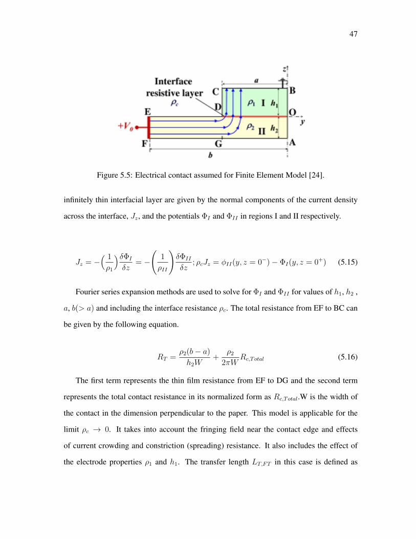
The model considers a pair of contacts that are identical and formed on the top of a
conducting layer on top of an insulating substrate.
InsulatingSubstrate
Conducting Layer ρSH = ρ2/h2
ρ1Contact
h2
h1
V GNDρcInterfacial Resistive Layer
a aL
Figure 5.6: Two contact model for the Exact Field Solution Model.
A Fourier Series based analysis of the current density can be carried out of the above
two-contact model in order to determine the transfer length or LT,FT for different cases
such as changing ρc, a, h1, h2 and ρ1.
Initial simulations were carried out by Dr. Peng Zhang [25] in order to understand the
49
effect of varying the parameters in the model on the transfer length and are summarized in
this section. The effect of varying interfacial contact resistivity (ρc), contact area (largely
dependent upon a), thickness of conducting layer (h2) and height of electrode (h1) were
carried out through the exact field solution model.
The effect of varying the contact resistivity of the interfacial layer or the specific con-
tact resistivity (ρc) was modeled using exact field solution. Its effect on the transfer length
was observed using current density distributions and plots of transfer length versus ρc.
The current transfer length can be plotted as a function of the interfacial contact resistivity
(ρc).This transfer length, called LT,FT can also be compared with the conventional trans-
fer length from the TLM method LTLM . Unless otherwise specified the simulations used
a=0.5µm, L/2 = 10µm, h1 = 100nm, h2 = 50nm, ρ1 = 2.44 × 10⁻⁸ Ω-m and ρSH as 100
Ω/sq. The total current was kept fixed at 50 µA µm−1.
5.6.1 Changing Contact Resistivity of Interfacial Layer
From the above modeling, it can be observed that the current density at the edge of the
contact increases significantly on decreasing the interfacial contact resistivity or the specific
contact resistivity (ρc). There is increased current crowding at the edge of the contact
for lower values of ρc. The transfer length LT,FT from this model can be extracted as
the characteristic length to which 63.31% of the current flows. A comparison of LT,FT
and LT,TLM can be carried out where LT,TLM is the conventional TLM transfer length.
According to Figure 5.7(b), it can be observed that the upper limit of LT,FT is bound to
63.21% of the length of the contact and the lower limit is 63.21% of the height of the
conducting layer. It can be generally observed that LT increases as ρc increases. This is
true irrespective of the measurement technique used. Further, it can be seen that the Exact
Field solution model agrees with the conventional TLM model for a small range of values
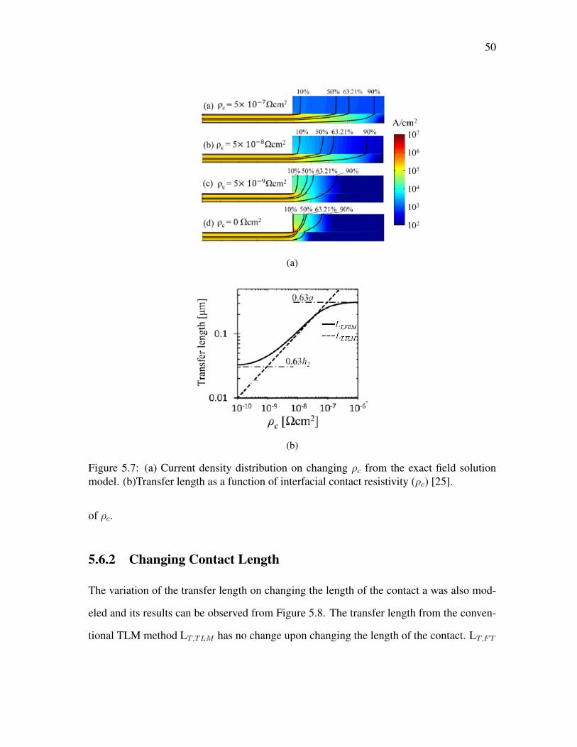
50
(a)
(b)
Figure 5.7: (a) Current density distribution on changing ρc from the exact field solutionmodel. (b)Transfer length as a function of interfacial contact resistivity (ρc) [25].
of ρc.
5.6.2 Changing Contact Length
The variation of the transfer length on changing the length of the contact a was also mod-
eled and its results can be observed from Figure 5.8. The transfer length from the conven-
tional TLM method LT,TLM has no change upon changing the length of the contact. LT,FT
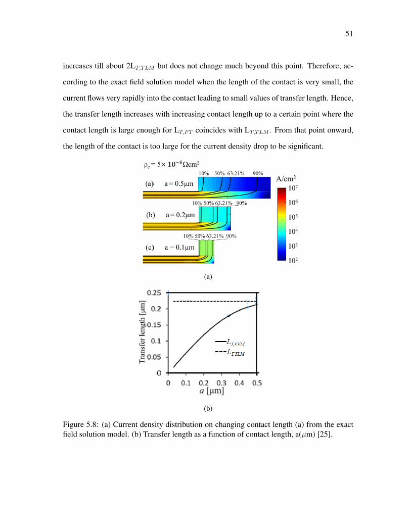
51
increases till about 2LT,TLM but does not change much beyond this point. Therefore, ac-
cording to the exact field solution model when the length of the contact is very small, the
current flows very rapidly into the contact leading to small values of transfer length. Hence,
the transfer length increases with increasing contact length up to a certain point where the
contact length is large enough for LT,FT coincides with LT,TLM . From that point onward,
the length of the contact is too large for the current density drop to be significant.
(a)
(b)
Figure 5.8: (a) Current density distribution on changing contact length (a) from the exactfield solution model. (b) Transfer length as a function of contact length, a(µm) [25].
52
5.6.3 Changing Contact Height
The effect of varying the height of the conducting region, h2 was also modeled and are
shown in Figure 5.9. As h2 decreases, there is significantly more current crowding in the
conducting layer. When h2 is small, LT,FT follows closely with LT,TLM as the TLM model
is reliable when only when the length of the conducting layer h2 → 0.LT,FT increases with
h2 till it reaches a constant value of 0.63 times the length of the contact due to the fringing
field being determined by the smaller of the dimensions in the contact constriction corner
[23].
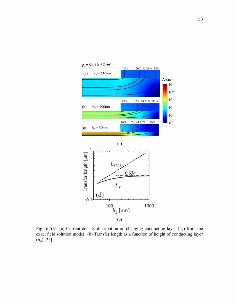
53
(a)
(b)
Figure 5.9: (a) Current density distribution on changing conducting layer (h2) from theexact field solution model. (b) Transfer length as a function of height of conducting layer(h2) [25].
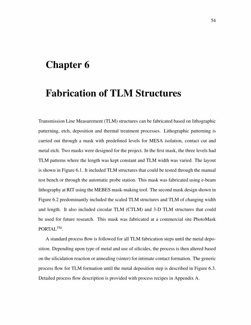
54
Chapter 6
Fabrication of TLM Structures
Transmission Line Measurement (TLM) structures can be fabricated based on lithographic
patterning, etch, deposition and thermal treatment processes. Lithographic patterning is
carried out through a mask with predefined levels for MESA isolation, contact cut and
metal etch. Two masks were designed for the project. In the first mask, the three levels had
TLM patterns where the length was kept constant and TLM width was varied. The layout
is shown in Figure 6.1. It included TLM structures that could be tested through the manual
test bench or through the automatic probe station. This mask was fabricated using e-beam
lithography at RIT using the MEBES mask-making tool. The second mask design shown in
Figure 6.2 predominantly included the scaled TLM structures and TLM of changing width
and length. It also included circular TLM (CTLM) and 3-D TLM structures that could
be used for future research. This mask was fabricated at a commercial site PhotoMask
PORTALTM.
A standard process flow is followed for all TLM fabrication steps until the metal depo-
sition. Depending upon type of metal and use of silicides, the process is then altered based
on the silicidation reaction or annealing (sinter) for intimate contact formation. The generic
process flow for TLM formation until the metal deposition step is described in Figure 6.3.
Detailed process flow description is provided with process recipes in Appendix A.
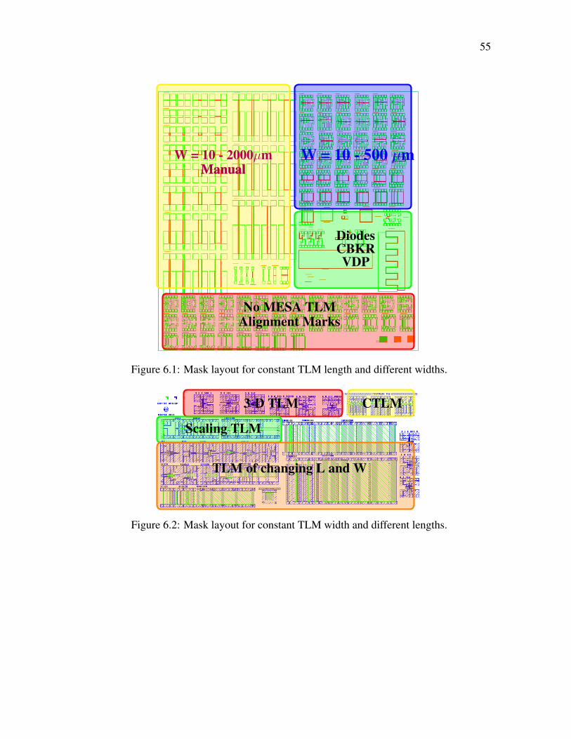
55
W = 10 - 500 µmW = 10 - 2000µmManual
DiodesCBKRVDP
Manual
No MESA TLMAlignment Marks
Figure 6.1: Mask layout for constant TLM length and different widths.
3-D TLM CTLM
Scaling TLM
TLM of changing L and W
Figure 6.2: Mask layout for constant TLM width and different lengths.
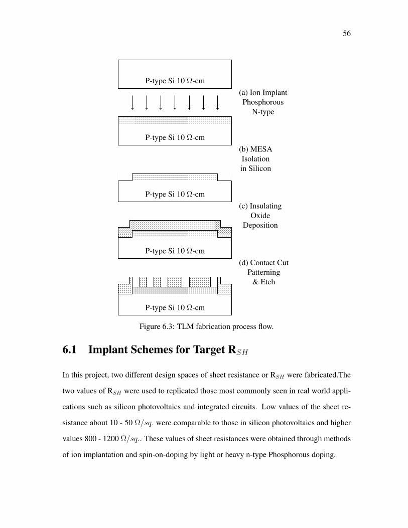
56
P-type Si 10 Ω-cm
P-type Si 10 Ω-cm
P-type Si 10 Ω-cm
P-type Si 10 Ω-cm
P-type Si 10 Ω-cm
(a) Ion ImplantPhosphorous
N-type
(b) MESAIsolationin Silicon
(c) InsulatingOxide
Deposition
(d) Contact CutPatterning
& Etch
Figure 6.3: TLM fabrication process flow.
6.1 Implant Schemes for Target RSH
In this project, two different design spaces of sheet resistance or RSH were fabricated.The
two values of RSH were used to replicated those most commonly seen in real world appli-
cations such as silicon photovoltaics and integrated circuits. Low values of the sheet re-
sistance about 10 - 50 Ω/sq. were comparable to those in silicon photovoltaics and higher
values 800 - 1200 Ω/sq.. These values of sheet resistances were obtained through methods
of ion implantation and spin-on-doping by light or heavy n-type Phosphorous doping.
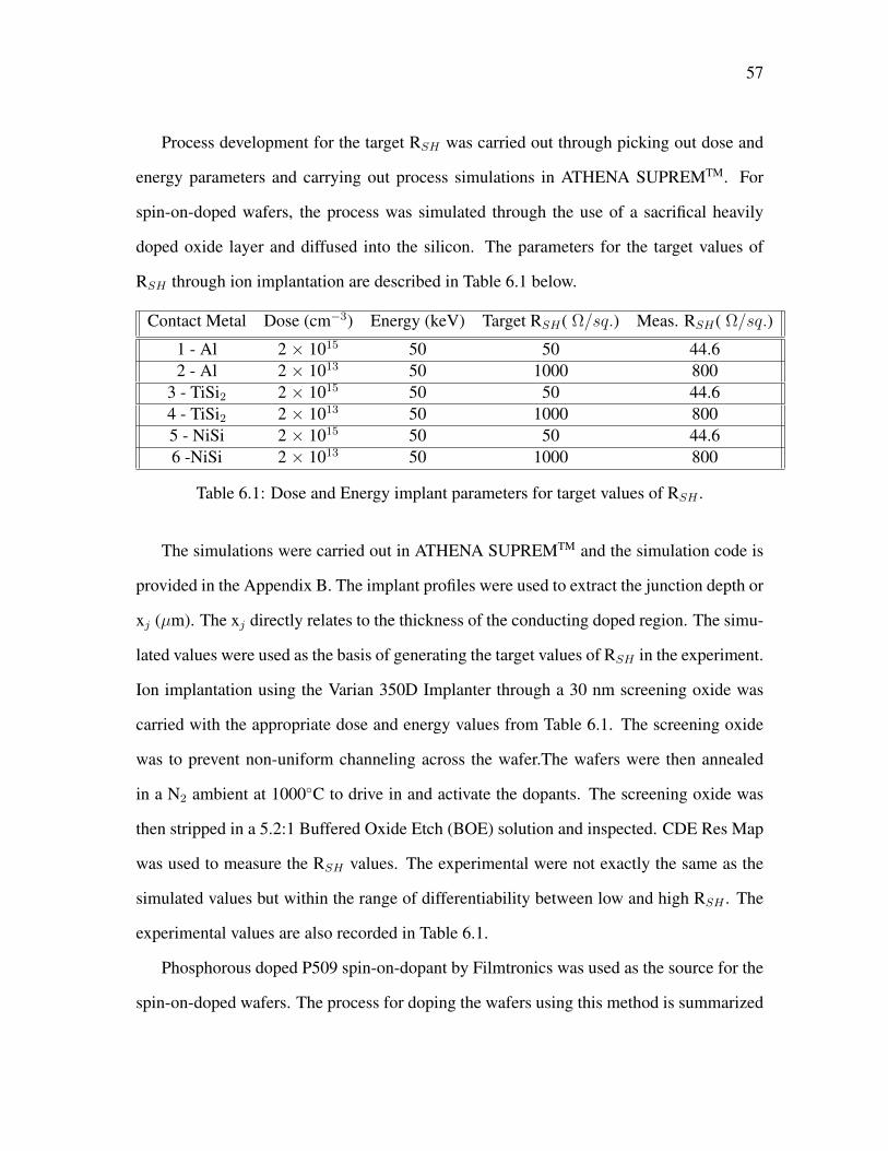
57
Process development for the target RSH was carried out through picking out dose and
energy parameters and carrying out process simulations in ATHENA SUPREMTM. For
spin-on-doped wafers, the process was simulated through the use of a sacrifical heavily
doped oxide layer and diffused into the silicon. The parameters for the target values of
RSH through ion implantation are described in Table 6.1 below.
Contact Metal Dose (cm−3) Energy (keV) Target RSH( Ω/sq.) Meas. RSH( Ω/sq.)
1 - Al 2 × 10¹⁵ 50 50 44.62 - Al 2 × 10¹³ 50 1000 800
3 - TiSi2 2 × 10¹⁵ 50 50 44.64 - TiSi2 2 × 10¹³ 50 1000 8005 - NiSi 2 × 10¹⁵ 50 50 44.66 -NiSi 2 × 10¹³ 50 1000 800
Table 6.1: Dose and Energy implant parameters for target values of RSH .
The simulations were carried out in ATHENA SUPREMTM and the simulation code is
provided in the Appendix B. The implant profiles were used to extract the junction depth or
xj (µm). The xj directly relates to the thickness of the conducting doped region. The simu-
lated values were used as the basis of generating the target values of RSH in the experiment.
Ion implantation using the Varian 350D Implanter through a 30 nm screening oxide was
carried with the appropriate dose and energy values from Table 6.1. The screening oxide
was to prevent non-uniform channeling across the wafer.The wafers were then annealed
in a N2 ambient at 1000C to drive in and activate the dopants. The screening oxide was
then stripped in a 5.2:1 Buffered Oxide Etch (BOE) solution and inspected. CDE Res Map
was used to measure the RSH values. The experimental were not exactly the same as the
simulated values but within the range of differentiability between low and high RSH . The
experimental values are also recorded in Table 6.1.
Phosphorous doped P509 spin-on-dopant by Filmtronics was used as the source for the
spin-on-doped wafers. The process for doping the wafers using this method is summarized
58
below.
• Dispense 2ml of solution on wafer.
• Ramp for 3 seconds at 500 rpm.
• Spin at 3000rpm for 30 seconds
• Bake on hot-plate for 10 minutes at 200C
• Drive-in using recipe 325 (see Appendix)
• Strip baked dopant in 5.2:1 HF BOE for 5 minutes.
• Measure RSH
The measured values of RSH were consistent and about 10 Ω/sq..
6.2 Aluminum TLM Process Flow
The process for fabricating Transmission Line Measurement structures for aluminum is
described as follows. All the steps are the same until part (d) of Figure 6.3. The steps
following involve Aluminum sputter deposition using the CVC601 sputter, patterning using
a pre-defined mask level using the ASML stepper and etch to form contacts with bond pads
using LAM4600 Rainbow etcher. A brief description is shown in Figure 6.4.
A sintering process is carried out at 450C to get rid of a native oxide between metal-
semiconductor interface and reduce the contact resistance.
6.3 NiSi TLM Process Flow
NiSi metal-semiconductor contacts can be formed by a two-step self aligned process dis-
cussed in chapter 4. It involves a sputter deposition of Ni using the P5000 deposition tool
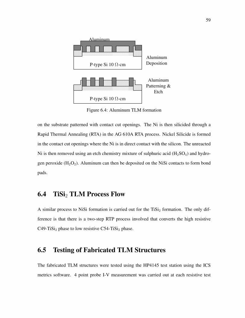
59
P-type Si 10 Ω-cm
P-type Si 10 Ω-cm
AluminumDeposition
Aluminum
AluminumPatterning &
Etch
Figure 6.4: Aluminum TLM formation
on the substrate patterned with contact cut openings. The Ni is then silicided through a
Rapid Thermal Annealing (RTA) in the AG 610A RTA process. Nickel Silicide is formed
in the contact cut openings where the Ni is in direct contact with the silicon. The unreacted
Ni is then removed using an etch chemistry mixture of sulphuric acid (H2SO4) and hydro-
gen peroxide (H2O2). Aluminum can then be deposited on the NiSi contacts to form bond
pads.
6.4 TiSi2 TLM Process Flow
A similar process to NiSi formation is carried out for the TiSi2 formation. The only dif-
ference is that there is a two-step RTP process involved that converts the high resistive
C49-TiSi2 phase to low resistive C54-TiSi2 phase.
6.5 Testing of Fabricated TLM Structures
The fabricated TLM structures were tested using the HP4145 test station using the ICS
metrics software. 4 point probe I-V measurement was carried out at each resistive test
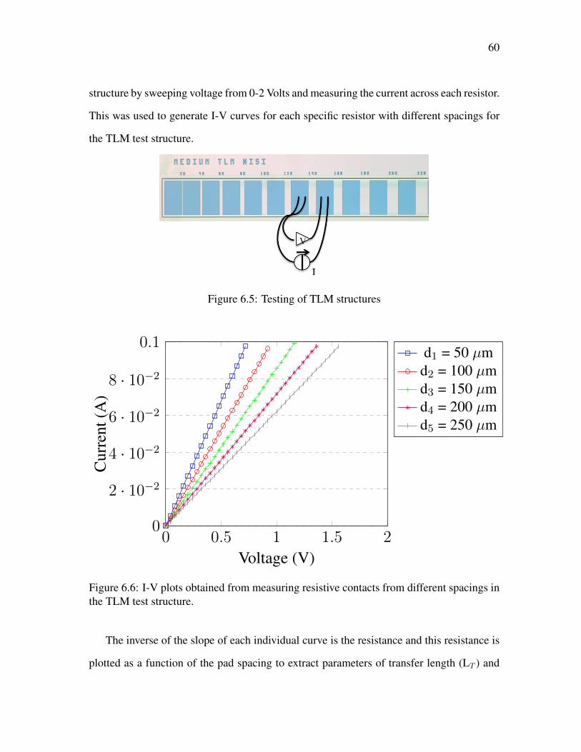
60
structure by sweeping voltage from 0-2 Volts and measuring the current across each resistor.
This was used to generate I-V curves for each specific resistor with different spacings for
the TLM test structure.
Figure 6.5: Testing of TLM structures
0 0.5 1 1.5 20
2 · 10−2
4 · 10−2
6 · 10−2
8 · 10−2
0.1
Voltage (V)
Cur
rent
(A)
d1 = 50 µmd2 = 100 µmd3 = 150 µmd4 = 200 µmd5 = 250 µm
Figure 6.6: I-V plots obtained from measuring resistive contacts from different spacings inthe TLM test structure.
The inverse of the slope of each individual curve is the resistance and this resistance is
plotted as a function of the pad spacing to extract parameters of transfer length (LT ) and

61
specific contact resistivity (ρc) similar to one observed in Figure 4.3. The extracted LT
is used to calculate the ρc from Equation 5.14 using know parameters of W and L. The
example of Figure 6.6 involved contacts of Aluminum metal fabricated on heavily doped
Silicon of underlying sheet resistance RSH of 50 Ω/sq..
62
Chapter 7
TLM Structure Optimization
In order to accurately extract the specific contact resistivity from Transmission Line Mea-
surement (TLM) structures, the TLM geometries must be chosen to provide the least
amount of error in measurement. These geometries need to also be optimized based on
contact material as well as resistive properties of the underlying material to which the con-
tact is made. In other words, the TLM geometries need to be optimized based on sheet
resistance of the underlying doped region for a particular semiconductor application and
the specific contact resistance of the metal used to make the contact. Optimization of
TLM geometries essentially relates to TLM width optimization as we already discussed
the choice of length for accurate ρc extraction in Chapter 3.
7.1 Optimization Through Error Analysis
Error in the Transmission Line Measurement (TLM) method can be classified into two
main types - Random Error and Systematic Error. Random error measures the difference
between the mean determined from a large number of trials and a single measurement of
the parameter in consideration. Systematic Error is a consistent shift of means of a parame-
ter that cannot be reduced by taking a large number of trials. In this paper, only systematic
error was optimized due to ease of calculation and order of importance. The fundamental
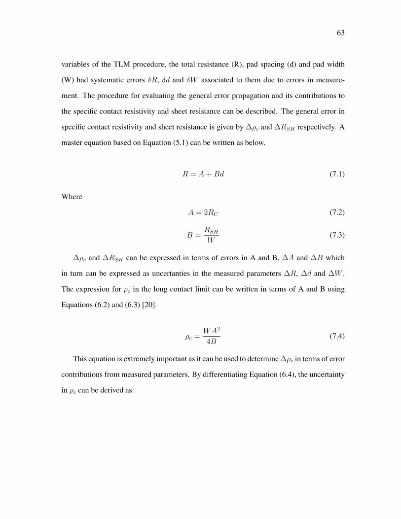
63
variables of the TLM procedure, the total resistance (R), pad spacing (d) and pad width
(W) had systematic errors δR, δd and δW associated to them due to errors in measure-
ment. The procedure for evaluating the general error propagation and its contributions to
the specific contact resistivity and sheet resistance can be described. The general error in
specific contact resistivity and sheet resistance is given by ∆ρc and ∆RSH respectively. A
master equation based on Equation (5.1) can be written as below.
R = A+Bd (7.1)
Where
A = 2RC (7.2)
B =RSH
W(7.3)
∆ρc and ∆RSH can be expressed in terms of errors in A and B, ∆A and ∆B which
in turn can be expressed as uncertanties in the measured parameters ∆R, ∆d and ∆W .
The expression for ρc in the long contact limit can be written in terms of A and B using
Equations (6.2) and (6.3) [20].
ρc =WA2
4B(7.4)
This equation is extremely important as it can be used to determine ∆ρc in terms of error
contributions from measured parameters. By differentiating Equation (6.4), the uncertainty
in ρc can be derived as.
64
∆ρc w
∣∣∣∣∣δρcδA
∣∣∣∣∣∆A+
∣∣∣∣∣δρcδB
∣∣∣∣∣∆B +
∣∣∣∣∣ δρcδW
∣∣∣∣∣∆W=
(WA
2B
)∆A+
(WA2
4B2
)∆B +
(A2
4B
)∆W
(7.5)
The relative uncertainty in ρc can therefore be given by.
∆ρcρcw 2
(∆A
A
)+
∆B
B+
∆W
W(7.6)
The relative uncertainty of the sheet resistance (∆RSH) can be derived in a similar
manner and is given by.
∆RSH
RSH
w∆B
B+
∆W
W(7.7)
The changes in A and B caused due δR and δd can be described in the TLM extraction
plot of differential resistance versus pad spacing plot as shown in the figure below.
For a change in R, i.e. δR , the slope of the plot remains the same and the vertical
intercept shifts δR.
δB|δR = 0 (7.8)
δA|δR = δR (7.9)
Similarly, change in d,i.e. δd does not change the slope but results in the change of the
vertical intercept.
δB|δd = 0 (7.10)
δA|δd = Bδd (7.11)
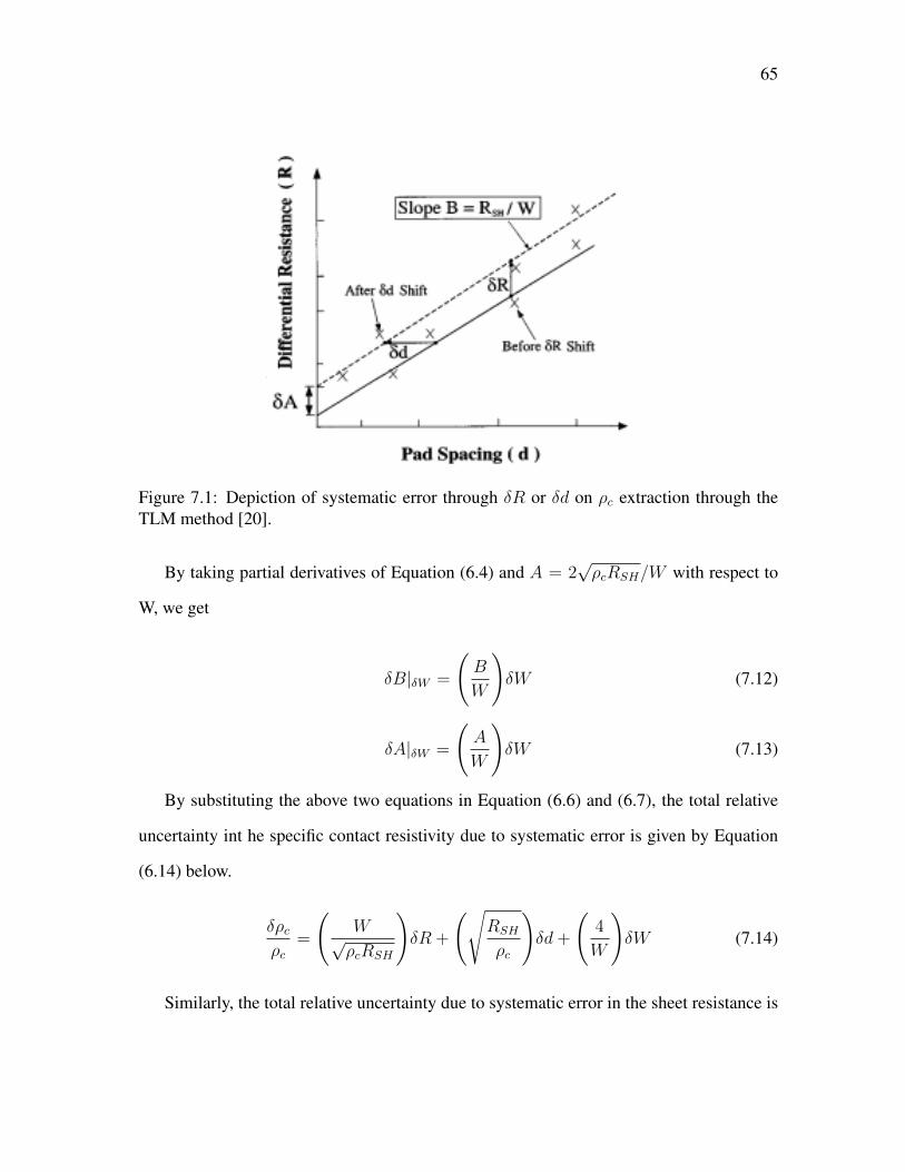
65
Figure 7.1: Depiction of systematic error through δR or δd on ρc extraction through theTLM method [20].
By taking partial derivatives of Equation (6.4) and A = 2√ρcRSH/W with respect to
W, we get
δB|δW =
(B
W
)δW (7.12)
δA|δW =
(A
W
)δW (7.13)
By substituting the above two equations in Equation (6.6) and (6.7), the total relative
uncertainty int he specific contact resistivity due to systematic error is given by Equation
(6.14) below.
δρcρc
=
(W√ρcRSH
)δR +
(√RSH
ρc
)δd+
(4
W
)δW (7.14)
Similarly, the total relative uncertainty due to systematic error in the sheet resistance is
66
given by.
δRSH
RSH
=
(2
W
)δW (7.15)
Since the systematic error is more significant, its optimization is more important when
compared to the random error. The values of RSH and W which yield minimum uncertainty
in ρc can be derived from partial derivatives of of Equation (6.14) with respect to RSH and
W, and setting them equal to zero. This gives us the equation for the optimum width Wopt.
Wopt =
√4√ρcRSH
(δWδR
)(7.16)
Simulations of the optimum widths can be carried out for application specific ranges
of values of RSH and ρc. δR and δW are chosen with respected to anticipated error in
experimental values where δR = 0.2Ω and δW = 1.5 µm. A contour map of the systematic
error optimization can be generated with values of optimum TLM width Wopt for each
particular combination of RSH and ρc.
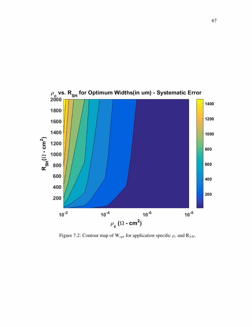
67
Figure 7.2: Contour map of Wopt for application specific ρc and RSH .
68
Chapter 8
Results and Discussion
8.1 Optimization Results
The theory of TLM optimization is described in detail in chapter 6. As mentioned in
the chapter, the systematic error optimization of the TLM width can be carried out. A
contour map of the optimum width calculated for least relative systematic uncertainty can
be generated for application specific values of ρc and RSH .
Figure 8.1 is the same contour plot as in Chapter 7. The particular regions of specific
contact resistivity and sheet resistance have an optimum value of TLM width Wopt that
provides the least amount of systematic error in measurement. It can be observed that for
larger values of RSH and lower values of ρc, the optimum width is in the range of about
800-1200µm. For lower values of RSH and higher values of ρc, the optimum width is
clearly below 200µm.
TLM test structures were fabricated with different contact metals and underlying sheet
resistivities of the conducting regions and tested. The relative uncertainty due to systematic
error in the specific contact resistivity was calculated for each TLM structure of different
contact width. The TLM width that had the least relative uncertainty due to systematic
error was the optimum width. Equation 6.14 was used for the calculation of the error in
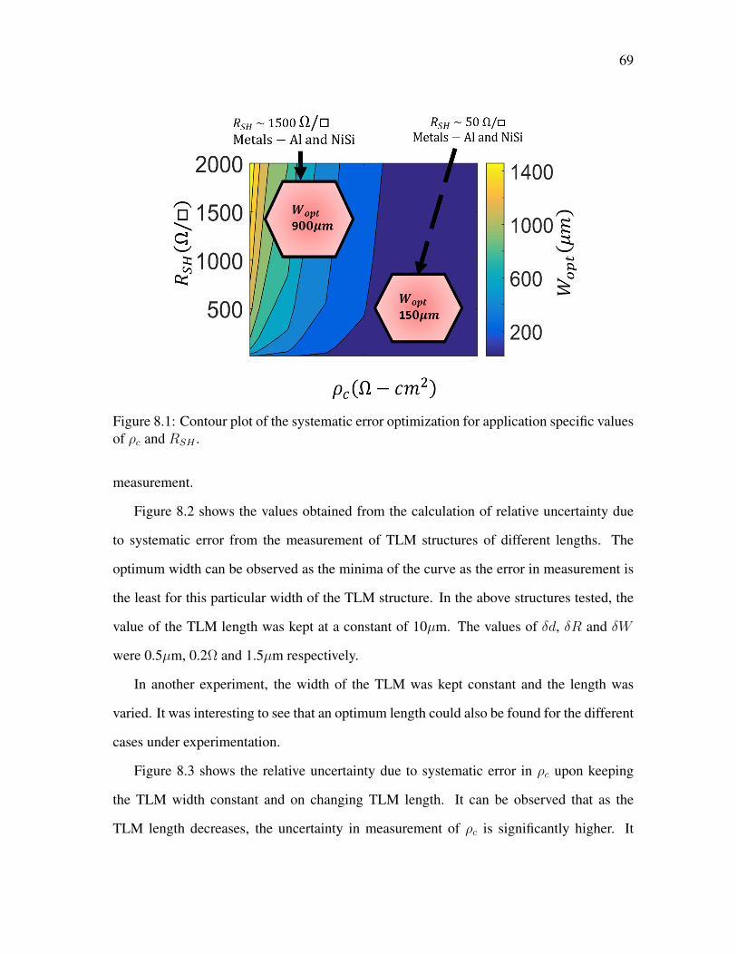
69
Figure 8.1: Contour plot of the systematic error optimization for application specific valuesof ρc and RSH .
measurement.
Figure 8.2 shows the values obtained from the calculation of relative uncertainty due
to systematic error from the measurement of TLM structures of different lengths. The
optimum width can be observed as the minima of the curve as the error in measurement is
the least for this particular width of the TLM structure. In the above structures tested, the
value of the TLM length was kept at a constant of 10µm. The values of δd, δR and δW
were 0.5µm, 0.2Ω and 1.5µm respectively.
In another experiment, the width of the TLM was kept constant and the length was
varied. It was interesting to see that an optimum length could also be found for the different
cases under experimentation.
Figure 8.3 shows the relative uncertainty due to systematic error in ρc upon keeping
the TLM width constant and on changing TLM length. It can be observed that as the
TLM length decreases, the uncertainty in measurement of ρc is significantly higher. It
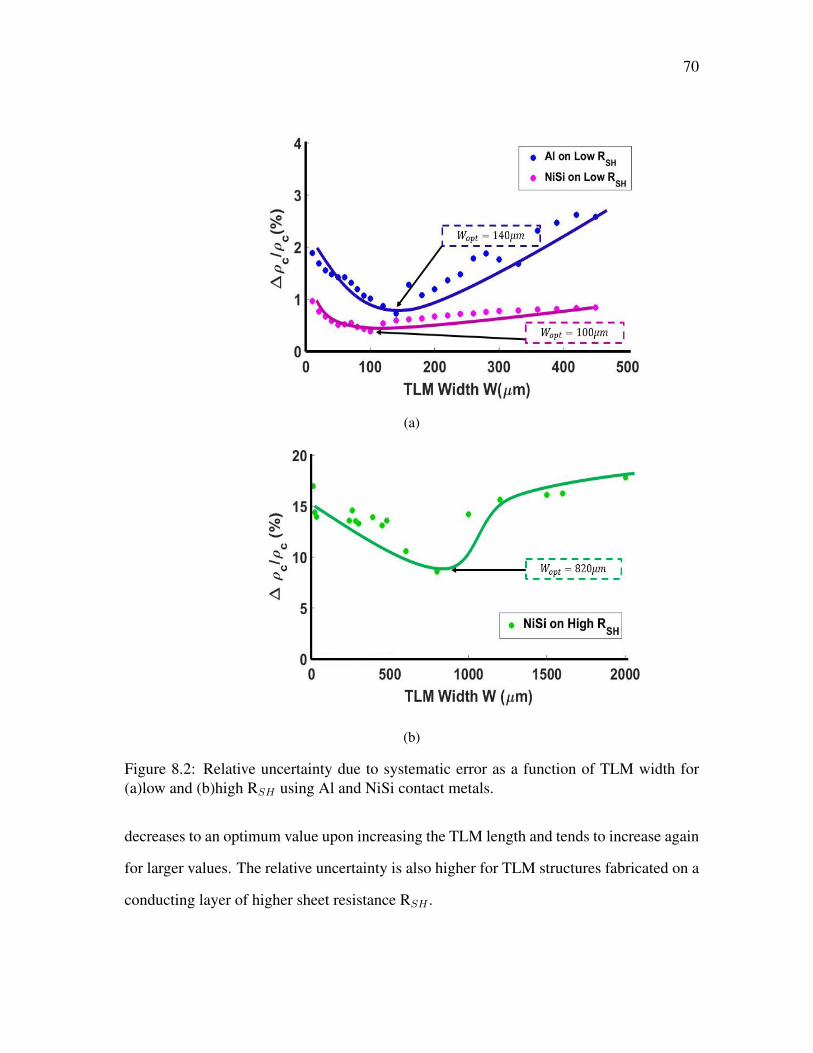
70
(a)
(b)
Figure 8.2: Relative uncertainty due to systematic error as a function of TLM width for(a)low and (b)high RSH using Al and NiSi contact metals.
decreases to an optimum value upon increasing the TLM length and tends to increase again
for larger values. The relative uncertainty is also higher for TLM structures fabricated on a
conducting layer of higher sheet resistance RSH .
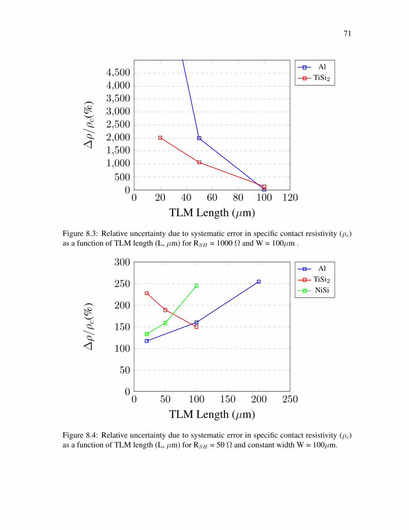
71
0 20 40 60 80 100 1200
500
1,0001,5002,0002,5003,0003,5004,0004,500
TLM Length (µm)
∆ρ/ρ
c(%
)
AlTiSi2
Figure 8.3: Relative uncertainty due to systematic error in specific contact resistivity (ρc)as a function of TLM length (L, µm) for RSH = 1000 Ω and W = 100µm .
0 50 100 150 200 2500
50
100
150
200
250
300
TLM Length (µm)
∆ρ/ρ
c(%
)
AlTiSi2NiSi
Figure 8.4: Relative uncertainty due to systematic error in specific contact resistivity (ρc)as a function of TLM length (L, µm) for RSH = 50 Ω and constant width W = 100µm.
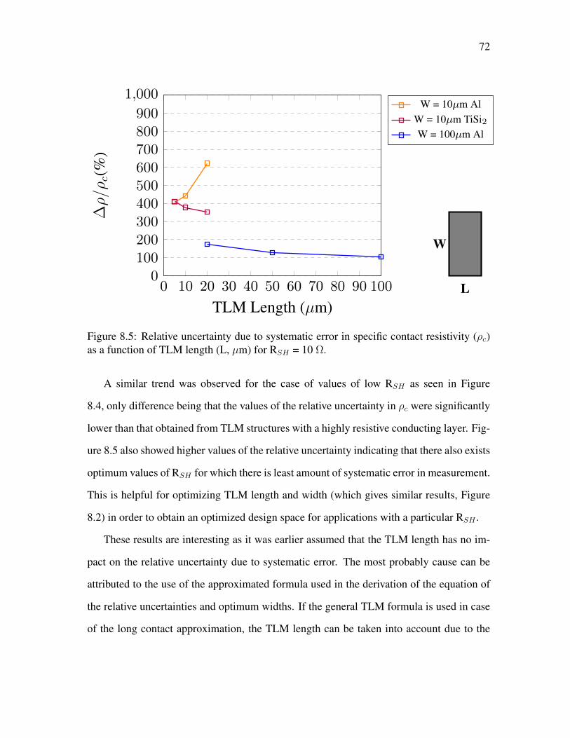
72
0 10 20 30 40 50 60 70 80 90 1000
100200300400500600700800900
1,000
TLM Length (µm)
∆ρ/ρ
c(%
)W = 10µm Al
W = 10µm TiSi2W = 100µm Al
W
L
Figure 8.5: Relative uncertainty due to systematic error in specific contact resistivity (ρc)as a function of TLM length (L, µm) for RSH = 10 Ω.
A similar trend was observed for the case of values of low RSH as seen in Figure
8.4, only difference being that the values of the relative uncertainty in ρc were significantly
lower than that obtained from TLM structures with a highly resistive conducting layer. Fig-
ure 8.5 also showed higher values of the relative uncertainty indicating that there also exists
optimum values of RSH for which there is least amount of systematic error in measurement.
This is helpful for optimizing TLM length and width (which gives similar results, Figure
8.2) in order to obtain an optimized design space for applications with a particular RSH .
These results are interesting as it was earlier assumed that the TLM length has no im-
pact on the relative uncertainty due to systematic error. The most probably cause can be
attributed to the use of the approximated formula used in the derivation of the equation of
the relative uncertainties and optimum widths. If the general TLM formula is used in case
of the long contact approximation, the TLM length can be taken into account due to the
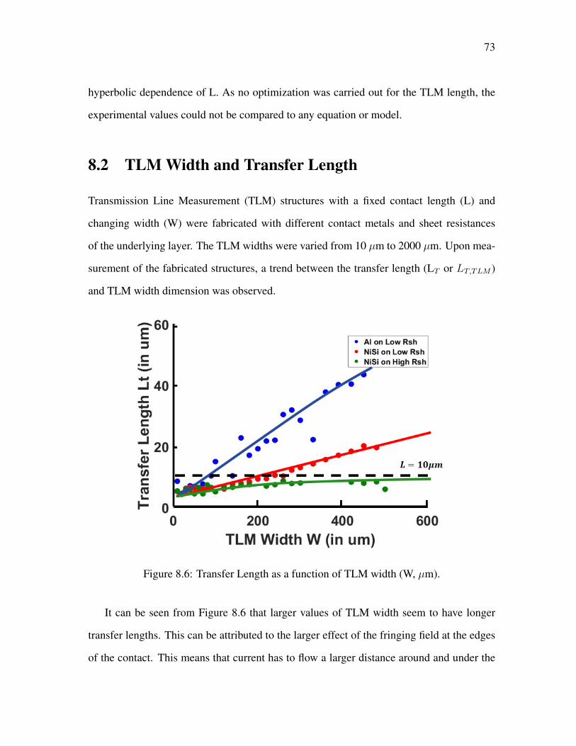
73
hyperbolic dependence of L. As no optimization was carried out for the TLM length, the
experimental values could not be compared to any equation or model.
8.2 TLM Width and Transfer Length
Transmission Line Measurement (TLM) structures with a fixed contact length (L) and
changing width (W) were fabricated with different contact metals and sheet resistances
of the underlying layer. The TLM widths were varied from 10 µm to 2000 µm. Upon mea-
surement of the fabricated structures, a trend between the transfer length (LT or LT,TLM )
and TLM width dimension was observed.
Figure 8.6: Transfer Length as a function of TLM width (W, µm).
It can be seen from Figure 8.6 that larger values of TLM width seem to have longer
transfer lengths. This can be attributed to the larger effect of the fringing field at the edges
of the contact. This means that current has to flow a larger distance around and under the
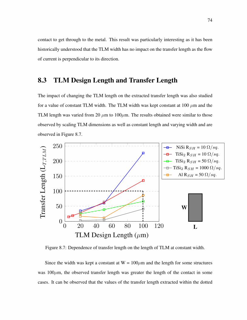
74
contact to get through to the metal. This result was particularly interesting as it has been
historically understood that the TLM width has no impact on the transfer length as the flow
of current is perpendicular to its direction.
8.3 TLM Design Length and Transfer Length
The impact of changing the TLM length on the extracted transfer length was also studied
for a value of constant TLM width. The TLM width was kept constant at 100 µm and the
TLM length was varied from 20 µm to 100µm. The results obtained were similar to those
observed by scaling TLM dimensions as well as constant length and varying width and are
observed in Figure 8.7.
0 20 40 60 80 100 1200
50
100
150
200
250
TLM Design Length (µm)
Tran
sfer
Len
gth
(LT,TLM
) NiSi RSH = 10 Ω/sq.
TiSi2 RSH = 10 Ω/sq.
TiSi2 RSH = 50 Ω/sq.
TiSi2 RSH = 1000 Ω/sq.
Al RSH = 50 Ω/sq.
W
L
Figure 8.7: Dependence of transfer length on the length of TLM at constant width.
Since the width was kept a constant at W = 100µm and the length for some structures
was 100µm, the observed transfer length was greater the length of the contact in some
cases. It can be observed that the values of the transfer length extracted within the dotted
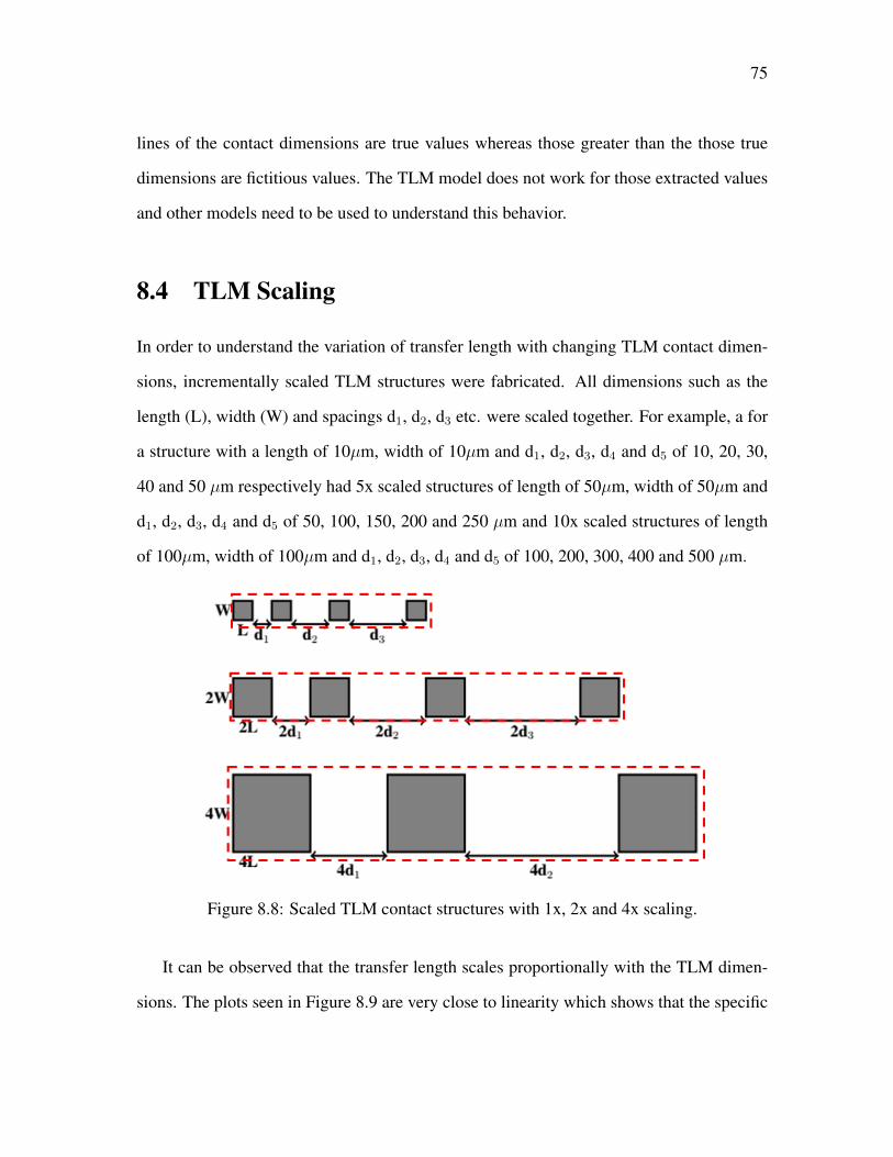
75
lines of the contact dimensions are true values whereas those greater than the those true
dimensions are fictitious values. The TLM model does not work for those extracted values
and other models need to be used to understand this behavior.
8.4 TLM Scaling
In order to understand the variation of transfer length with changing TLM contact dimen-
sions, incrementally scaled TLM structures were fabricated. All dimensions such as the
length (L), width (W) and spacings d1, d2, d3 etc. were scaled together. For example, a for
a structure with a length of 10µm, width of 10µm and d1, d2, d3, d4 and d5 of 10, 20, 30,
40 and 50 µm respectively had 5x scaled structures of length of 50µm, width of 50µm and
d1, d2, d3, d4 and d5 of 50, 100, 150, 200 and 250 µm and 10x scaled structures of length
of 100µm, width of 100µm and d1, d2, d3, d4 and d5 of 100, 200, 300, 400 and 500 µm.
Figure 8.8: Scaled TLM contact structures with 1x, 2x and 4x scaling.
It can be observed that the transfer length scales proportionally with the TLM dimen-
sions. The plots seen in Figure 8.9 are very close to linearity which shows that the specific
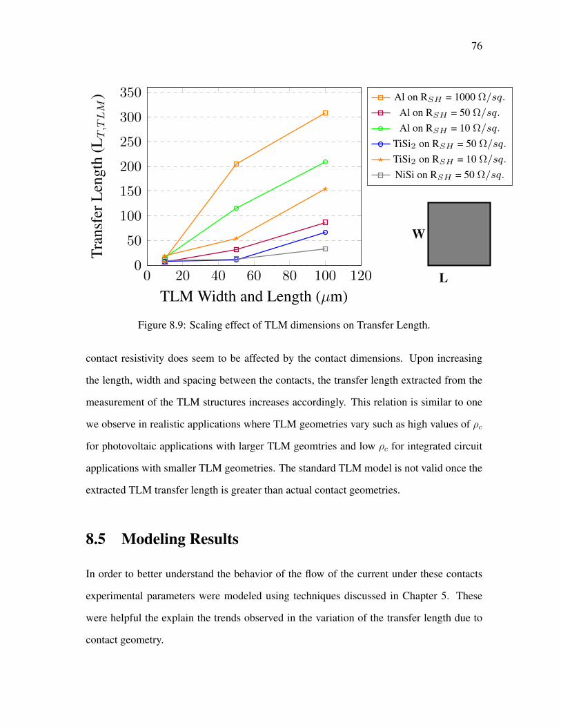
76
0 20 40 60 80 100 1200
50
100
150
200
250
300
350
TLM Width and Length (µm)
Tran
sfer
Len
gth
(LT,TLM
) Al on RSH = 1000 Ω/sq.
Al on RSH = 50 Ω/sq.
Al on RSH = 10 Ω/sq.
TiSi2 on RSH = 50 Ω/sq.
TiSi2 on RSH = 10 Ω/sq.
NiSi on RSH = 50 Ω/sq.
W
L
Figure 8.9: Scaling effect of TLM dimensions on Transfer Length.
contact resistivity does seem to be affected by the contact dimensions. Upon increasing
the length, width and spacing between the contacts, the transfer length extracted from the
measurement of the TLM structures increases accordingly. This relation is similar to one
we observe in realistic applications where TLM geometries vary such as high values of ρc
for photovoltaic applications with larger TLM geomtries and low ρc for integrated circuit
applications with smaller TLM geometries. The standard TLM model is not valid once the
extracted TLM transfer length is greater than actual contact geometries.
8.5 Modeling Results
In order to better understand the behavior of the flow of the current under these contacts
experimental parameters were modeled using techniques discussed in Chapter 5. These
were helpful the explain the trends observed in the variation of the transfer length due to
contact geometry.
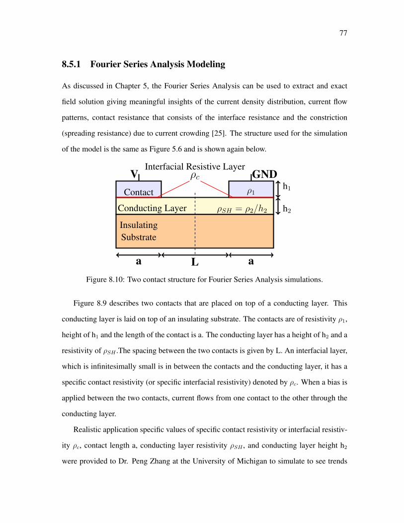
77
8.5.1 Fourier Series Analysis Modeling
As discussed in Chapter 5, the Fourier Series Analysis can be used to extract and exact
field solution giving meaningful insights of the current density distribution, current flow
patterns, contact resistance that consists of the interface resistance and the constriction
(spreading resistance) due to current crowding [25]. The structure used for the simulation
of the model is the same as Figure 5.6 and is shown again below.
InsulatingSubstrate
Conducting Layer ρSH = ρ2/h2
ρ1Contact
h2
h1
V GNDρcInterfacial Resistive Layer
a aLFigure 8.10: Two contact structure for Fourier Series Analysis simulations.
Figure 8.9 describes two contacts that are placed on top of a conducting layer. This
conducting layer is laid on top of an insulating substrate. The contacts are of resistivity ρ1,
height of h1 and the length of the contact is a. The conducting layer has a height of h2 and a
resistivity of ρSH .The spacing between the two contacts is given by L. An interfacial layer,
which is infinitesimally small is in between the contacts and the conducting layer, it has a
specific contact resistivity (or specific interfacial resistivity) denoted by ρc. When a bias is
applied between the two contacts, current flows from one contact to the other through the
conducting layer.
Realistic application specific values of specific contact resistivity or interfacial resistiv-
ity ρc, contact length a, conducting layer resistivity ρSH , and conducting layer height h2
were provided to Dr. Peng Zhang at the University of Michigan to simulate to see trends
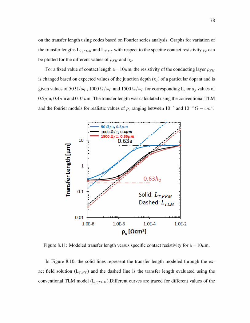
78
on the transfer length using codes based on Fourier series analysis. Graphs for variation of
the transfer lengths LT,TLM and LT,FT with respect to the specific contact resistivity ρc can
be plotted for the different values of ρSH and h2.
For a fixed value of contact length a = 10µm, the resistivity of the conducting layer ρSH
is changed based on expected values of the junction depth (xj) of a particular dopant and is
given values of 50 Ω/sq., 1000 Ω/sq. and 1500 Ω/sq. for corresponding h2 or xj values of
0.5µm, 0.4µm and 0.35µm. The transfer length was calculated using the conventional TLM
and the fourier models for realistic values of ρc ranging between 10−8 and 10−2 Ω− cm2.
Figure 8.11: Modeled transfer length versus specific contact resistivity for a = 10µm.
In Figure 8.10, the solid lines represent the transfer length modeled through the ex-
act field solution (LT,FT ) and the dashed line is the transfer length evaluated using the
conventional TLM model (LT,TLM ).Different curves are traced for different values of the
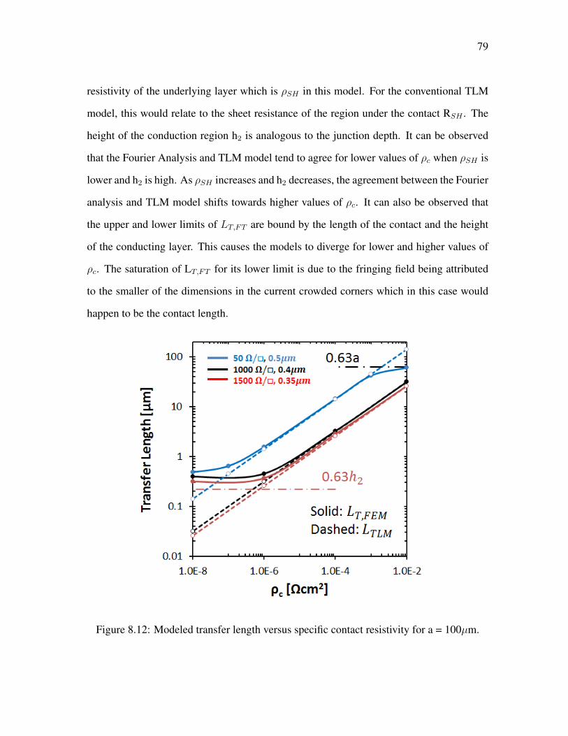
79
resistivity of the underlying layer which is ρSH in this model. For the conventional TLM
model, this would relate to the sheet resistance of the region under the contact RSH . The
height of the conduction region h2 is analogous to the junction depth. It can be observed
that the Fourier Analysis and TLM model tend to agree for lower values of ρc when ρSH is
lower and h2 is high. As ρSH increases and h2 decreases, the agreement between the Fourier
analysis and TLM model shifts towards higher values of ρc. It can also be observed that
the upper and lower limits of LT,FT are bound by the length of the contact and the height
of the conducting layer. This causes the models to diverge for lower and higher values of
ρc. The saturation of LT,FT for its lower limit is due to the fringing field being attributed
to the smaller of the dimensions in the current crowded corners which in this case would
happen to be the contact length.
Figure 8.12: Modeled transfer length versus specific contact resistivity for a = 100µm.
80
Figure 8.11 is modeled with the same parameters from Figure 8.10 except the fact that
the length of the contact is increased to 100µm. It can be observed that the agreement
between LT,TLM and LT,FT exists for a much wider range of values of ρc. For higher
values of ρSH there is very good agreement for larger values of ρc and they coincide as the
transfer length increases.
The results from these simulations can be very helpful in deciding appropriate TLM
contact design geometries for application specific values of RSH and ρc. The applicability
of the general TLM model can be evaluated based on where the transfer lengths in each
of the model coincide. From figures 8.10 and 8.11, the regions of ρc where the solid and
dashed lines are the same. It was also very interesting to notice that for the values at
which the two models agreed, LT = 0.4 × L. The explanation for this was beyond the
scope of this project and is suggested as future work. Therefore, for contact applications
of ρc smaller than 10−6 Ω-cm2, the exact field solution model can better take into account
current constriction effects and gives a more accurate value of ρc. This also means the TLM
model under estimates the value of the transfer length and it is lower for smaller values of
ρc which offers an explanation to values for integrated circuit applications observed in
literature. This also means that values of ρc larger than 10−4 Ω-cm2, transfer length is
largely overestimated explaining larger values of ρc for silicon photovoltaic applications.
81
Chapter 9
Conclusions and Future Work
In this project, various methods were explored to understand the reason for inconsistent
values of ρc observed in literature due to differences in TLM contact dimensions used.
Starting from a brief introduction to ohmic contact theory and specific contact resistivity
(ρc), the different kinds of metal-semiconductor contacts popularly used were explored.
The Transmission Line Measurement (TLM) method was then described in detail and the
process of determining ρc was described. In order to better understand the TLM method,
various models like dimensional models, lumped circuit models and exact field solution or
fourier transform models were described. The TLM structures were then fabricated based
on optimized width values that were designed on a 3-level mask design.
9.1 Conclusions
The error optimization for the TLM widths was confirmed by the experimental results as
TLM structures having widths W with the least amount of systematic error in ρc could
clearly be identified and the experimental values closely matched the ones that were simu-
lated. It was also interestingly observed the for values of constant TLM width and changing
length, there appeared to be optimum values of TLM length as well. These values could
not be significantly extracted due to lack of experimental data and no optimization had
82
been carried out on the general TLM formula. Furthermore, there was a dependence of
the transfer length LT on the TLM width when the TLM length was kept constant. As the
width was increased, the LT also increased. A similar trend was observed when the TLM
width was kept constant and the TLM length was increased. This was attributed to current
crowding and constriction effects of current under the contacts.
The scaled structures were fabricated to confirm the dimensional dependence of LT and
it was observed again that as the length and width of the TLM structures were inreased, the
transfer length increased accordingly. It was concluded that beyond a certain regime of
TLM geometry for a particular application, the general TLM model does not work as the
extracted TLM LT is greater than the length of the contact. To further understand the reason
of this behavior, Fourier transform model or the Exact Field Solution model was used. It
was observed that the Exact field solution and the general TLM models agreed only for
certain values of ρc and LT . This value was only where LT = 0.4 × L. Below those values,
for significantly lower values of ρc, the transfer length is underestimated due to current
crowding and for larger values of ρc, there is an overestimation due to the assumption of
current flow equally into the contact.
It was concluded that there is no universal design to determine ρc using the TLM
method. There is no ”one-size-fits-all” geometry and it changes based on application space.
The scaling structures confirmed the dependence of TLM geometry on LT . Figure 9.1 de-
scribes this result.
It can be seen from Figure 9.1 that for very low values of ρc, LT is drastically underesti-
mated. Since, lower values of ρc are predominantly seen in integrated circuit applications,
it could also be said that the TLM method is not an accurate method to determine ρc for
such applications. The silicon photovoltaics community on the other hand may actually
be quoting ρc values larger than the true values and must design contact dimensions based
projected transfer length values.
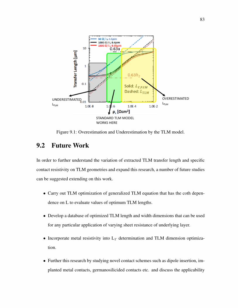
83
Figure 9.1: Overestimation and Underestimation by the TLM model.
9.2 Future Work
In order to further understand the variation of extracted TLM transfer length and specific
contact resistivity on TLM geometries and expand this research, a number of future studies
can be suggested extending on this work.
• Carry out TLM optimization of generalized TLM equation that has the coth depen-
dence on L to evaluate values of optimum TLM lengths.
• Develop a database of optimized TLM length and width dimensions that can be used
for any particular application of varying sheet resistance of underlying layer.
• Incorporate metal resistivity into LT determination and TLM dimension optimiza-
tion.
• Further this research by studying novel contact schemes such as dipole insertion, im-
planted metal contacts, germanosilicided contacts etc. and discuss the applicability
84
of the TLM method in such low specific contact resistivity schemes.
• Extend the TLM method to non-planar structures fabricated and closely emulate three
dimensional contacts observed in FinFET applications.
...
85
Bibliography
[1] Specific contact resistivity versus electron concentration.
[2] Reduction of base access resistance in algan/gan heterojunction bipolar transistorsusing gainn base cap layer and selective epitaxial growth. MRS Online Proceeding,892(2):022113, 2006.
[3] L.J. Chen and Institution of Electrical Engineers. Silicide Technology for IntegratedCircuits. Iee Materials and Devices Series. Institution of Engineering and Technology,2004.
[4] F Deng, RA Johnson, PM Asbeck, SS Lau, WB Dubbelday, T Hsiao, and J Woo.Salicidation process using nisi and its device application. Journal of applied physics,81(12):8047–8051, 1997.
[5] Evan Franklin, Kean Fong, Keith McIntosh, Andreas Fell, Andrew Blakers, TengKho, Daniel Walter, Da Wang, Ngwe Zin, Matthew Stocks, Er-Chien Wang, NicholasGrant, Yimao Wan, Yang Yang, Xueling Zhang, Zhiqiang Feng, and Pierre J. Ver-linden. Design, fabrication and characterisation of a 24.4interdigitated back contactsolar cell. Progress in Photovoltaics: Research and Applications, 24(4):411–427,2016. PIP-14-178.R1.
[6] Andrew M Gabor, Geoffrey Gregory, Adam M Payne, Rob Janoch, Andrew Anselmo,Vijay Yelundur, and Kristopher O Davis. Dependence of solar cell contact resistivitymeasurements on sample preparation methods. In 43rd IEEE Photovoltaics SpecialistConference, 2016.
[7] Kevin Gallacher, P Velha, Douglas J Paul, I MacLaren, Maksym Myronov, andDavid R Leadley. Ohmic contacts to n-type germanium with low specific contactresistivity. Applied Physics Letters, 100(2):022113, 2012.
[8] A. Goetzberger, J. Knobloch, and B. Voss. Crystalline Silicon Solar Cells. Wiley,1998.
86
[9] LASZLO Gutai. Statistical modeling of transmission line model test structures. i. theeffect of inhomogeneities on the extracted contact parameters. IEEE Transactions onElectron Devices, 37(11):2350–2360, 1990.
[10] C. Hu. Modern Semiconductor Devices for Integrated Circuits. Prentice Hall, 2010.
[11] Randy W Mann, Larry A Clevenger, Paul D Agnello, and Francis R White. Silicidesand local interconnections for high-performance vlsi applications. IBM Journal ofResearch and Development, 39(4):403–417, 1995.
[12] Thaddeus B Massalski, Hiroaki Okamoto, PR Subramanian, Linda Kacprzak, andWilliam W Scott. Binary alloy phase diagrams, volume 1. American Society forMetals Metals Park, OH, 1986.
[13] Krishna Saraswat. Metal/semiconductor ohmic contacts. 2009.
[14] Donald Sawdai, Dimitris Pavlidis, and Delong Cui. Enhanced transmission line modelstructures for accurate resistance evaluation of small-size contacts and for more reli-able fabrication. IEEE Transactions on Electron Devices, 46(7):1302–1311, 1999.
[15] Dieter K. Schroder. Semiconductor Material and Device Characterization. Wiley-Interscience, 2006.
[16] N Stavitski, MJH Dal, RAM Wolters, AY Kovalgin, and J Schmitz. Specific contactresistance measurements of metal-semiconductor junctions. 2006.
[17] Natalie Stavitski. Silicide-to-silicon specific contact resistance characterization. 2009.
[18] Natalie Stavitski, Johan H Klootwijk, Henk W van Zeijl, Alexey Y Kovalgin, andRob AM Wolters. Cross-bridge kelvin resistor structures for reliable measurement oflow contact resistances and contact interface characterization. IEEE Transactions onSemiconductor Manufacturing, 22(1):146–152, 2009.
[19] Loic Tous. Nickel/copper plated contacts as an alternative to silver screen printingfor the front side metallization of industrial high efficiency silicon solar cells (elek-trochemisch gedeponeerde nikkel/koper contacten als alternatief voor zilver zeef-druk voor metallisatie van de voorzijde van hoog-efficiente industriele silicium zon-necellen). 2014.
87
[20] Haw-Jye Ueng, David B Janes, and Kevin J Webb. Error analysis leading to designcriteria for transmission line model characterization of ohmic contacts. IEEE trans-actions on electron devices, 48(4):758–766, 2001.
[21] Yewu Wang, Volker Schmidt, Stephan Senz, and Ulrich Gosele. Epitaxial growth ofsilicon nanowires using an aluminium catalyst. Nature nanotechnology, 1(3):186–189, 2006.
[22] S. Wolf and R.N. Tauber. Silicon Processing for the VLSI Era: Process technology.Silicon Processing for the VLSI Era. Lattice Press, 2000.
[23] Peng Zhang. Effects of surface roughness on electrical contact, RF heating and fieldenhancement. PhD thesis, The University of Michigan, 2012.
[24] Peng Zhang and Y. Y. Lau. An exact field solution of contact resistance and compar-ison with the transmission line model. Applied Physics Letters, 104(20), 2014.
[25] Peng Zhang, YY Lau, and RM Gilgenbach. Analysis of current crowding in thinfilm contacts from exact field solution. Journal of Physics D: Applied Physics,48(47):475501, 2015.
88
Appendix A
Detailed Process Flow
Starting Material
Bare Si p-type 1-10 Ohms/sq. Init. Resistivity
Zero Level Lithography
ASML Stepper
Zero Etch
Drytek Quad
CHF3 - 50sccm
CF4 - 25 sccm
O2 - 10 sccm
RF - 200W
Pressure - 100mT
Time - 120 seconds
Resist Strip

89
RCA Clean
Manual RCA Bench
Screening Oxide Growth
Bruce Furnace
LFULL Recipe 250
Target Thickness 250 - 300 Angstroms
Ion Implantation
Varian Ion Implanter
Wafer P1 - Dose 2 × 10¹³ ; Energy 50keV
Wafer P2 - Dose 2 × 10¹⁵ ; Energy 50keV
Wafer P3 - Dose 2 × 10¹⁵ ; Energy 50keV
Wafer P4 - Dose 2 × 10¹⁵ ; Energy 50keV
Wafer P5 - Dose 2 × 10¹⁵ ; Energy 50keV
Wafer P6 - Dose 2 × 10¹⁵ ; Energy 50keV
Anneal
Bruce Furnace
LFULL Sub CMOS Anneal Recipe 106
Screening Oxide Etch
5.2:1 BOE Solution
Measure RSH
CDE ResMap
90
MESA Level Lithography
ASML Stepper
Level 1 - RITTLM2016
MESA Etch
LAM 490
EMCR 613 POLY
Pressure 300mT
RF 150W
O2 40 sccm
SF6 150 sccm
Resist Strip
GASONICS Aura 1000
TEOS Deposition
AMAT LPCVD P5000
Target thickness - 2000 Angstroms
Contact Cut Lithography
ASML Stepper
Level-2 CC
Contact Cut Etch TRION RIE
Recipe - PVKavya

91
Time - 350 seconds
Resist Strip
Metal Deposition
CVC601
Aluminum Wafers P1 and P4
Ar flow 20 sccm
Pressure 5mTorr
Power 2000W
Time 1500s
Ti Wafers P2 and P5
Pressure 5 mTorr
Power 750W
Time 300s
PE4400
Ni Wafers P3 and P6
Pressure 8mT
Power 500W
Time 180s
Silicidation
AG 610A RTP
Ti Silicidation Wafers P2 and P5

92
Recipe FACTISI1.RCP 1 min
Ni Silicidation Wafers P3 and P6
Recipe SISOC550.RCP
Piranha for unreacted metal removal
TiSi2 Wafers P2 and P5
150 ml H2SO4 300 ml H2O2
90 deg 120 seconds
DI Rinse 5 min
Spin-Rinse-Dry
NiSi Wafers P3 and P6
300 ml H2SO4 150 ml H2O2
90 deg 300 seconds
DI Rinse 5 min
Spin-Rinse-Dry
Silicidation
AG 610A RTP
Ti2 Silicidation Wafers P2 and P5
Recipe FACTISI2.RCP 1 min
Piranha for unreacted metal removal
TiSi2 Wafers P2 and P5
150 ml H2SO4 300 ml H2O2

93
90 deg 120 seconds
DI Rinse 5 min
Spin-Rinse-Dry
Metal Deposition
CVC601
Aluminum Wafers P2, P3, P5 and P6
Ar flow 20 sccm
Pressure 5mTorr
Power 2000W
Time 1500s
Metal Lithography
ASML Stepper
Level3- Metal
Metal Etch
LAM4900 Rainbow Etcher
Recipe 122122
Sinter
Bruce Furnace
Wafers P1 and P4
Recipe LFULL 101
94
Appendix B
ATHENA code for Implant Simulations
go athena
line x loc=0 spac=0.1
line x loc=0.35 spac=0.02
line x loc=1 spac=0.1
#
line y loc=0.00 spac=0.005
line y loc=0.3 spac=0.015
line y loc=0.5 spac=0.02
line y loc=2 spac=0.2
line y loc=5 spac=1
method grid.ox=0.001
# initial wafer
init silicon boron resistivity=10 orientation=100
# implant P
#savefile
structure outfile=Process_Sid.str
# Steam Oxide Growth
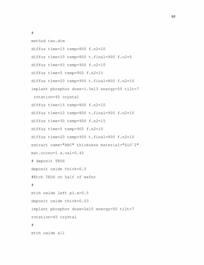
95
#
method two.dim
diffus time=15 temp=800 f.n2=10
diffus time=10 temp=800 t.final=900 f.o2=5
diffus time=93 temp=900 f.o2=10
diffus time=5 temp=900 f.n2=15
diffus time=20 temp=900 t.final=800 f.n2=10
implant phosphor dose=1.5e13 energy=50 tilt=7
rotation=45 crystal
diffus time=15 temp=800 f.n2=10
diffus time=10 temp=800 t.final=900 f.n2=10
diffus time=30 temp=900 f.n2=15
diffus time=5 temp=900 f.n2=10
diffus time=20 temp=900 t.final=800 f.n2=10
extract name="ARC" thickness material="SiO˜2"
mat.occno=1 x.val=0.45
# deposit TEOS
deposit oxide thick=0.5
#Etch TEOS on half of wafer
#
etch oxide left p1.x=0.5
deposit oxide thick=0.03
implant phosphor dose=2e15 energy=50 tilt=7
rotation=45 crystal
#
etch oxide all
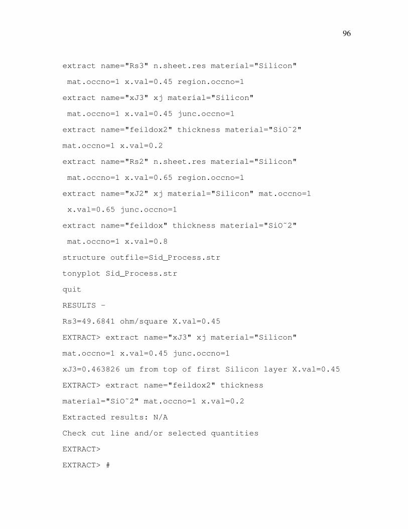
96
extract name="Rs3" n.sheet.res material="Silicon"
mat.occno=1 x.val=0.45 region.occno=1
extract name="xJ3" xj material="Silicon"
mat.occno=1 x.val=0.45 junc.occno=1
extract name="feildox2" thickness material="SiO˜2"
mat.occno=1 x.val=0.2
extract name="Rs2" n.sheet.res material="Silicon"
mat.occno=1 x.val=0.65 region.occno=1
extract name="xJ2" xj material="Silicon" mat.occno=1
x.val=0.65 junc.occno=1
extract name="feildox" thickness material="SiO˜2"
mat.occno=1 x.val=0.8
structure outfile=Sid_Process.str
tonyplot Sid_Process.str
quit
RESULTS -
Rs3=49.6841 ohm/square X.val=0.45
EXTRACT> extract name="xJ3" xj material="Silicon"
mat.occno=1 x.val=0.45 junc.occno=1
xJ3=0.463826 um from top of first Silicon layer X.val=0.45
EXTRACT> extract name="feildox2" thickness
material="SiO˜2" mat.occno=1 x.val=0.2
Extracted results: N/A
Check cut line and/or selected quantities
EXTRACT>
EXTRACT> #
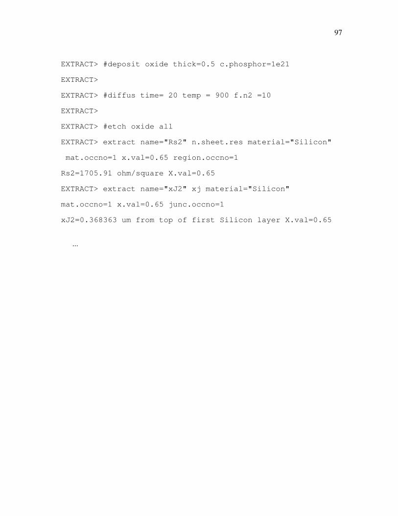
97
EXTRACT> #deposit oxide thick=0.5 c.phosphor=1e21
EXTRACT>
EXTRACT> #diffus time= 20 temp = 900 f.n2 =10
EXTRACT>
EXTRACT> #etch oxide all
EXTRACT> extract name="Rs2" n.sheet.res material="Silicon"
mat.occno=1 x.val=0.65 region.occno=1
Rs2=1705.91 ohm/square X.val=0.65
EXTRACT> extract name="xJ2" xj material="Silicon"
mat.occno=1 x.val=0.65 junc.occno=1
xJ2=0.368363 um from top of first Silicon layer X.val=0.65
...