twepp2018_serial_powering_vf.pdf - cern indico
TRANSCRIPT
System level serial powering studies of RD53A chip
A. Pradas (ITAINNOVA) D. Koukola (CERN), S. Orfanelli (CERN), J. Christiansen
(CERN), M. Karagounis (FH Dortmund), F. Arteche (ITAINNOVA)
within RD53A collaboration
TWEPP 2018 - ANTWERP
1. Introduction2. Serial powering studies
2.1. Simulation and measurement setups2.2. Dynamic response analysis2.3. SLDO configuration issues2.4. Start-up issues2.5. Transients propagation
3. Summary4. Future plans
OUTLINE
TWEPP 2018 - ANTWERP - September 201818/09/2018 2/20
1. Introduction
TWEPP 2018 - ANTWERP - September 2018
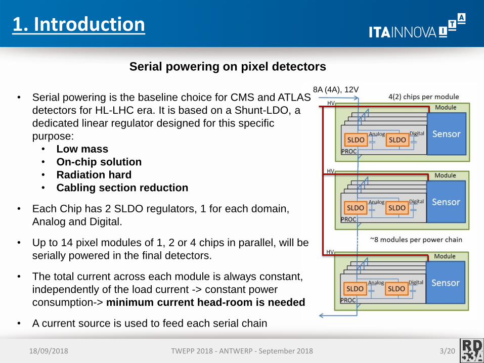
Serial powering on pixel detectors
8A (4A), 12V• Serial powering is the baseline choice for CMS and ATLAS
detectors for HL-LHC era. It is based on a Shunt-LDO, a
dedicated linear regulator designed for this specific
purpose:
• Low mass
• On-chip solution
• Radiation hard
• Cabling section reduction
• Each Chip has 2 SLDO regulators, 1 for each domain,
Analog and Digital.
• Up to 14 pixel modules of 1, 2 or 4 chips in parallel, will be
serially powered in the final detectors.
• The total current across each module is always constant,
independently of the load current -> constant power
consumption-> minimum current head-room is needed
• A current source is used to feed each serial chain
18/09/2018 3/20
1. Introduction
TWEPP 2018 - ANTWERP - September 2018
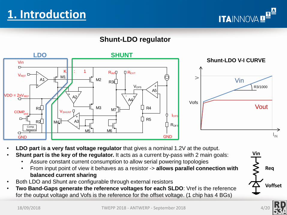
Shunt-LDO regulator
+ -
+
-
+
-
Vin
GND
VREF
VDD = 2xVREF
A1
A2
A3
M1M2
M3
M4
M5
R1
R2
R3I
M6
+-
VOFS
A4
M7
RINT REXT
+
-
A5
R4
R5IOFS
Comp.
Network
VSHUNTCOMPENB
K : 1
ROFS
GND
• LDO part is a very fast voltage regulator that gives a nominal 1.2V at the output.
• Shunt part is the key of the regulator. It acts as a current by-pass with 2 main goals:
• Assure constant current consumption to allow serial powering topologies
• From input point of view it behaves as a resistor -> allows parallel connection with
balanced current sharing
• Both LDO and Shunt are configurable through external resistors
• Two Band-Gaps generate the reference voltages for each SLDO: Vref is the reference
for the output voltage and Vofs is the reference for the offset voltage. (1 chip has 4 BGs)
LDO SHUNT
V
IIN
Vin
Vout
Shunt-LDO V-I CURVE
R3/1000
Vofs
18/09/2018 4/20
Req
Voffset
Vin
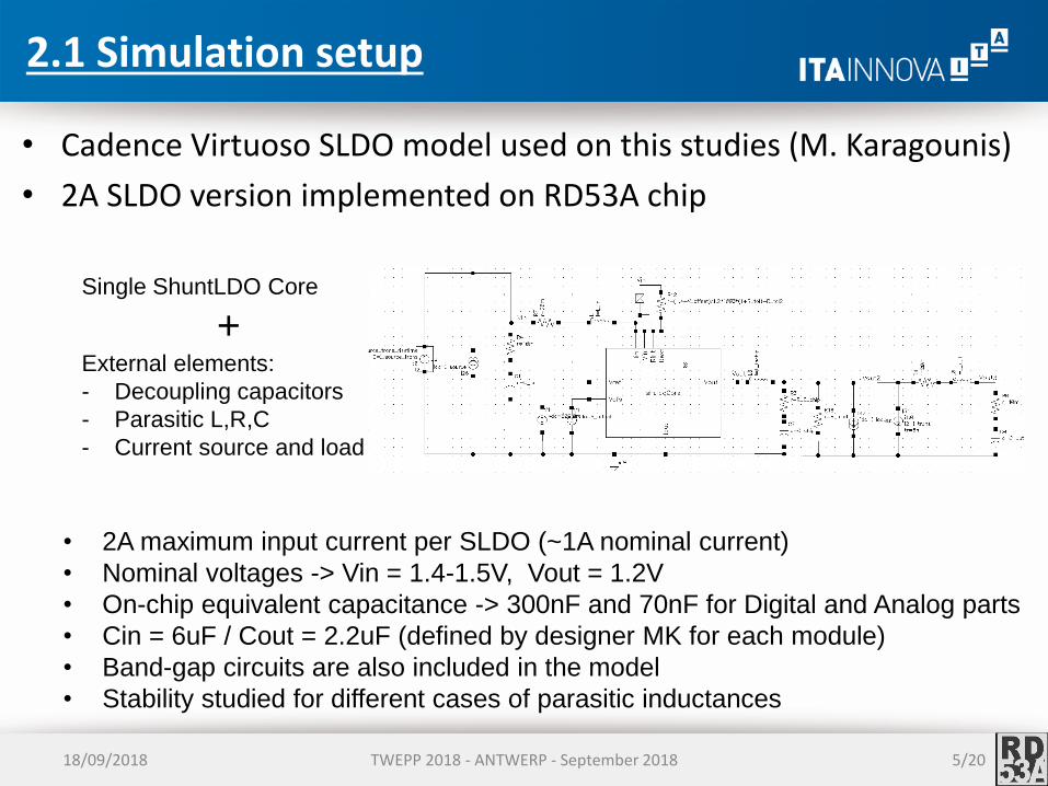
2.1 Simulation setup
TWEPP 2018 - ANTWERP - September 2018
• Cadence Virtuoso SLDO model used on this studies (M. Karagounis)
• 2A SLDO version implemented on RD53A chip
• 2A maximum input current per SLDO (~1A nominal current)
• Nominal voltages -> Vin = 1.4-1.5V, Vout = 1.2V
• On-chip equivalent capacitance -> 300nF and 70nF for Digital and Analog parts
• Cin = 6uF / Cout = 2.2uF (defined by designer MK for each module)
• Band-gap circuits are also included in the model
• Stability studied for different cases of parasitic inductances
Single ShuntLDO Core
+External elements:
- Decoupling capacitors
- Parasitic L,R,C
- Current source and load
18/09/2018 5/20
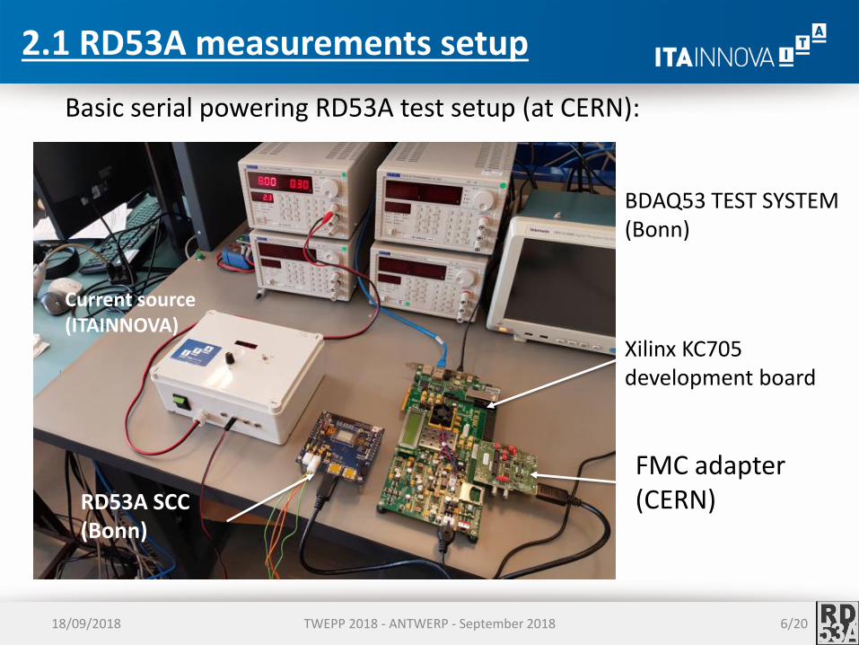
TWEPP 2018 - ANTWERP - September 2018
Basic serial powering RD53A test setup (at CERN):
RD53A SCC (Bonn)
FMC adapter (CERN)
Xilinx KC705 development board
Current source (ITAINNOVA)
BDAQ53 TEST SYSTEM(Bonn)
2.1 RD53A measurements setup
18/09/2018 6/20
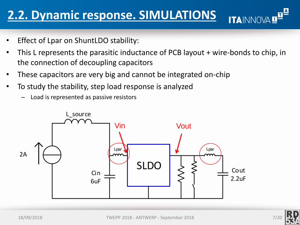
L_source
SLDOCin6uF
2A
Cout2.2uF
LparLpar
TWEPP 2018 - ANTWERP - September 2018
• Effect of Lpar on ShuntLDO stability:
• This L represents the parasitic inductance of PCB layout + wire-bonds to chip, in the connection of decoupling capacitors
• These capacitors are very big and cannot be integrated on-chip
• To study the stability, step load response is analyzed– Load is represented as passive resistors
Vin Vout
2.2. Dynamic response. SIMULATIONS
18/09/2018 7/20
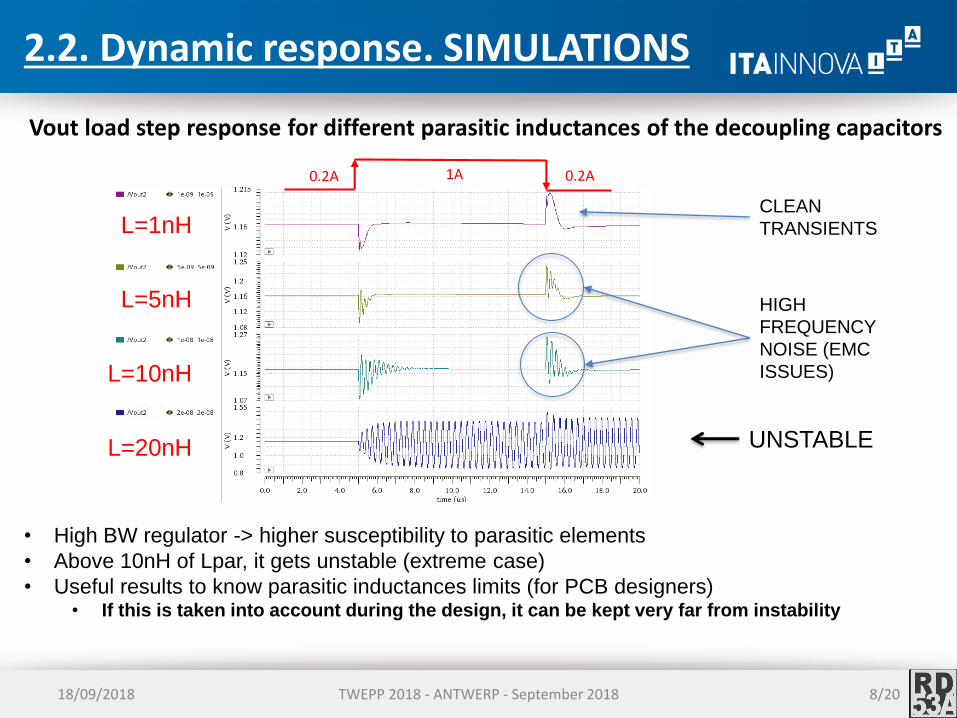
2.2. Dynamic response. SIMULATIONS
TWEPP 2018 - ANTWERP - September 2018
Vout load step response for different parasitic inductances of the decoupling capacitors
0.2A 0.2A1A
L=1nH
L=5nH
L=10nH
• High BW regulator -> higher susceptibility to parasitic elements
• Above 10nH of Lpar, it gets unstable (extreme case)
• Useful results to know parasitic inductances limits (for PCB designers)• If this is taken into account during the design, it can be kept very far from instability
L=20nH UNSTABLE
HIGH
FREQUENCY
NOISE (EMC
ISSUES)
CLEAN
TRANSIENTS
18/09/2018 8/20
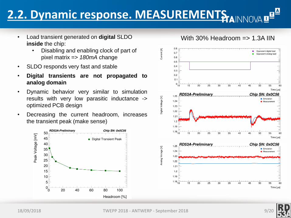
2.2. Dynamic response. MEASUREMENTS
TWEPP 2018 - ANTWERP - September 2018
• Load transient generated on digital SLDO
inside the chip:
• Disabling and enabling clock of part of
pixel matrix => 180mA change
• SLDO responds very fast and stable
• Digital transients are not propagated to
analog domain
• Dynamic behavior very similar to simulation
results with very low parasitic inductance ->
optimized PCB design
• Decreasing the current headroom, increases
the transient peak (make sense)
With 30% Headroom => 1.3A IIN
18/09/2018 9/20
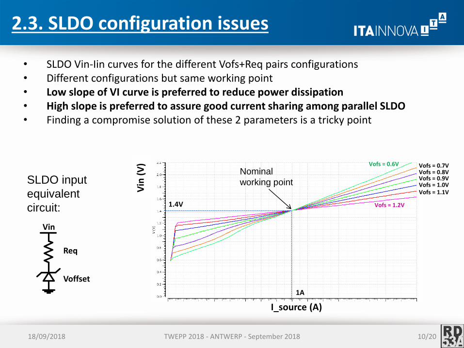
2.3. SLDO configuration issues
TWEPP 2018 - ANTWERP - September 2018
• SLDO Vin-Iin curves for the different Vofs+Req pairs configurations• Different configurations but same working point• Low slope of VI curve is preferred to reduce power dissipation• High slope is preferred to assure good current sharing among parallel SLDO• Finding a compromise solution of these 2 parameters is a tricky point
Vin
(V
)
I_source (A)
Vofs = 0.6V
Vofs = 1.2V
Vofs = 1.1VVofs = 1.0VVofs = 0.9VVofs = 0.8VVofs = 0.7V
Nominal
working point
1.4V
1A
Req
Voffset
Vin
SLDO input
equivalent
circuit:
18/09/2018 10/20
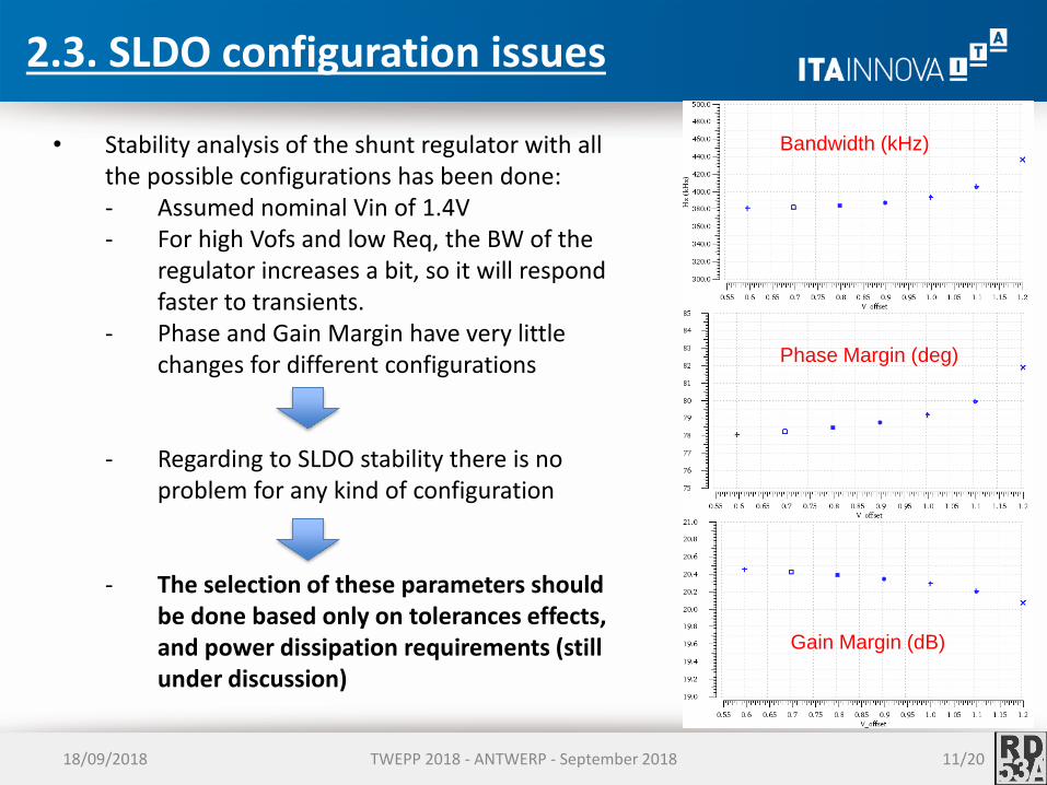
2.3. SLDO configuration issues
TWEPP 2018 - ANTWERP - September 2018
• Stability analysis of the shunt regulator with all the possible configurations has been done:- Assumed nominal Vin of 1.4V- For high Vofs and low Req, the BW of the
regulator increases a bit, so it will respond faster to transients.
- Phase and Gain Margin have very little changes for different configurations
- Regarding to SLDO stability there is no problem for any kind of configuration
- The selection of these parameters should be done based only on tolerances effects, and power dissipation requirements (still under discussion)
Bandwidth (kHz)
Phase Margin (deg)
Gain Margin (dB)
18/09/2018 11/20
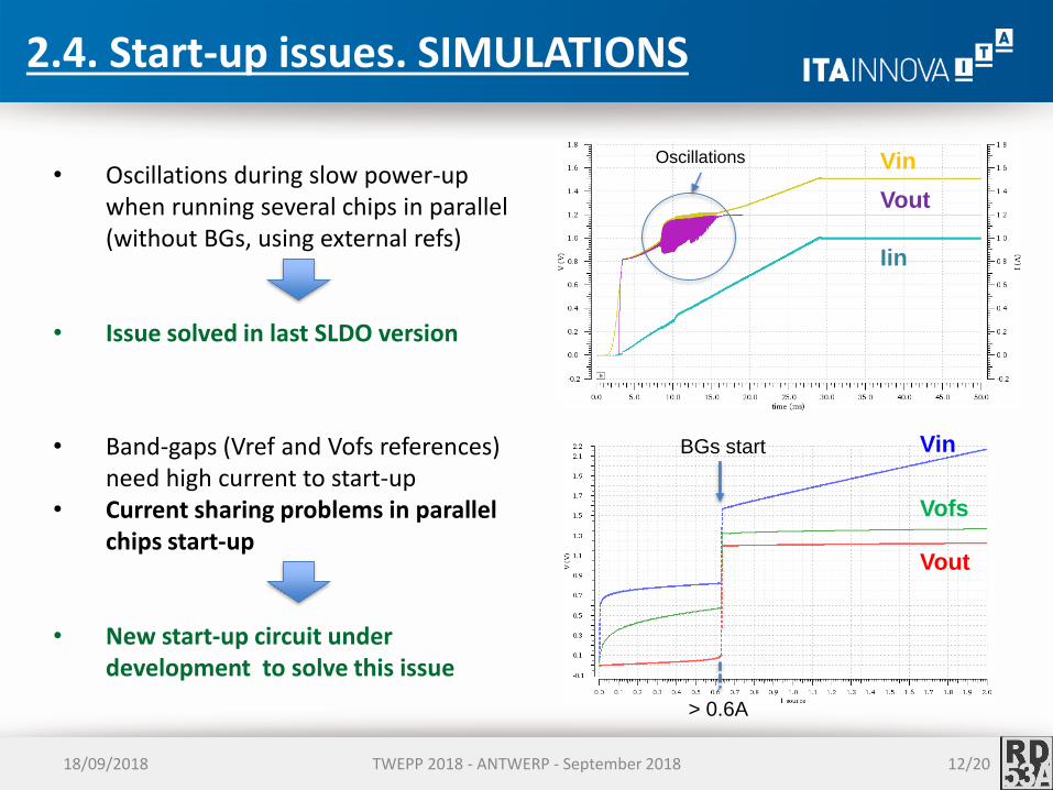
2.4. Start-up issues. SIMULATIONS
TWEPP 2018 - ANTWERP - September 2018
• Oscillations during slow power-up when running several chips in parallel (without BGs, using external refs)
• Issue solved in last SLDO version
• Band-gaps (Vref and Vofs references) need high current to start-up
• Current sharing problems in parallel chips start-up
• New start-up circuit under development to solve this issue
Vin
Iin
Vout
Vin
Vout
Vofs
BGs start
> 0.6A
Oscillations
18/09/2018 12/20
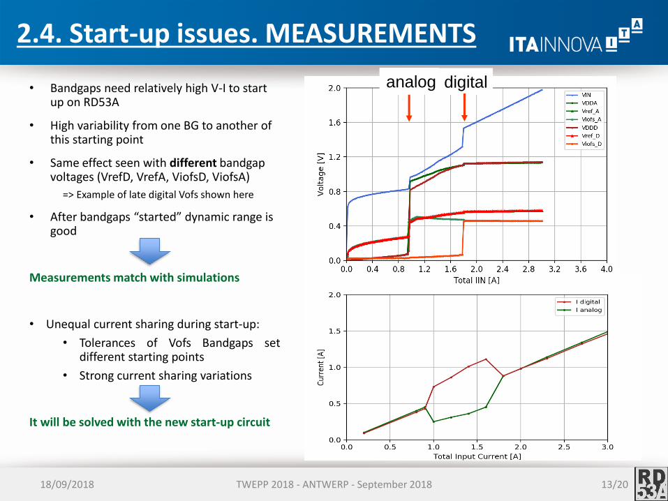
2.4. Start-up issues. MEASUREMENTS
TWEPP 2018 - ANTWERP - September 2018
analog digital• Bandgaps need relatively high V-I to start up on RD53A
• High variability from one BG to another of this starting point
• Same effect seen with different bandgap voltages (VrefD, VrefA, ViofsD, ViofsA)
=> Example of late digital Vofs shown here
• After bandgaps “started” dynamic range is good
Measurements match with simulations
• Unequal current sharing during start-up:
• Tolerances of Vofs Bandgaps setdifferent starting points
• Strong current sharing variations
It will be solved with the new start-up circuit
18/09/2018 13/20
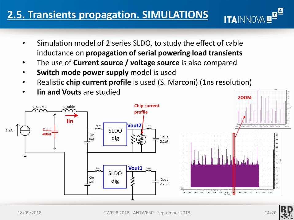
2.5. Transients propagation. SIMULATIONS
TWEPP 2018 - ANTWERP - September 2018
• Simulation model of 2 series SLDO, to study the effect of cable inductance on propagation of serial powering load transients
• The use of Current source / voltage source is also compared• Switch mode power supply model is used• Realistic chip current profile is used (S. Marconi) (1ns resolution)• Iin and Vouts are studied
L_source
SLDOdig
Cin6uF
1.2A
Cout2.2uF
Lpa rLpa r
Csource
400uF
L_cable
SLDOdig
Cin6uF
Cout2.2uF
Lpa rLpa r
Chip current
profile
Vout1
Vout2Iin
ZOOM
18/09/2018 14/20
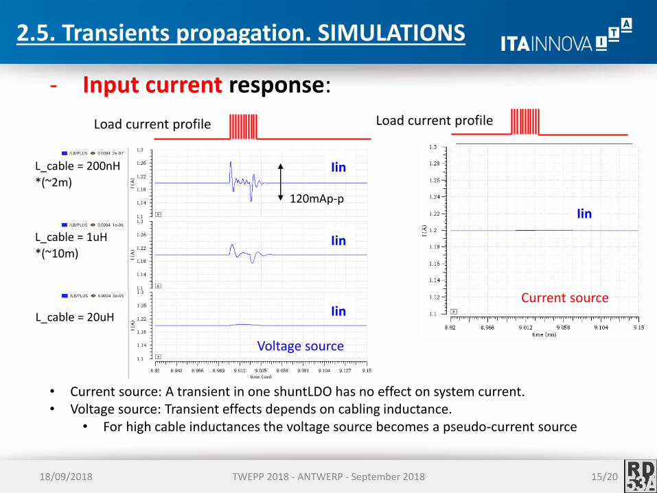
2.5. Transients propagation. SIMULATIONS
TWEPP 2018 - ANTWERP - September 2018
IinL_cable = 200nH
*(~2m)
L_cable = 1uH
*(~10m)
L_cable = 20uH
Voltage source
Current source
Iin
Load current profile
- Input current response:
Load current profile
• Current source: A transient in one shuntLDO has no effect on system current.• Voltage source: Transient effects depends on cabling inductance.
• For high cable inductances the voltage source becomes a pseudo-current source
Iin
Iin
120mAp-p
18/09/2018 15/20
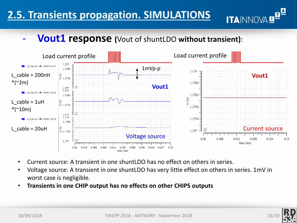
2.5. Transients propagation. SIMULATIONS
TWEPP 2018 - ANTWERP - September 2018
- Vout1 response (Vout of shuntLDO without transient):
Vout1
L_cable = 200nH
*(~2m)
L_cable = 1uH
*(~10m)
L_cable = 20uH
Voltage sourceCurrent source
Vout1
• Current source: A transient in one shuntLDO has no effect on others in series.• Voltage source: A transient in one shuntLDO has very little effect on others in series. 1mV in
worst case is negligible.• Transients in one CHIP output has no effects on other CHIPS outputs
Load current profile Load current profile
1mVp-p
18/09/2018 16/20
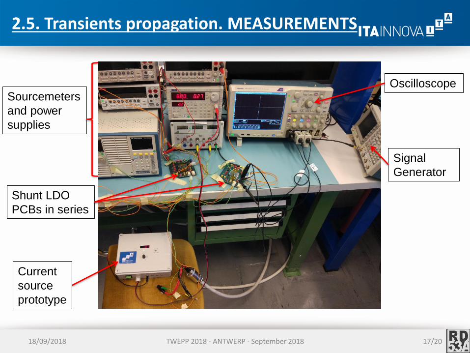
TWEPP 2018 - ANTWERP - September 2018
Current
source
prototype
Shunt LDO
PCBs in series
Oscilloscope
Signal
Generator
Sourcemeters
and power
supplies
2.5. Transients propagation. MEASUREMENTS
18/09/2018 17/20
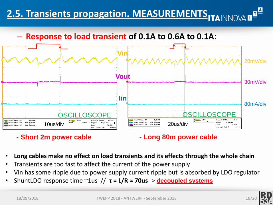
TWEPP 2018 - ANTWERP - September 2018
– Response to load transient of 0.1A to 0.6A to 0.1A:
Vin
Vout
Iin
- Short 2m power cable - Long 80m power cable
OSCILLOSCOPE OSCILLOSCOPE
30mV/div
80mA/div
20mV/div
10us/div 20us/div
• Long cables make no effect on load transients and its effects through the whole chain• Transients are too fast to affect the current of the power supply• Vin has some ripple due to power supply current ripple but is absorbed by LDO regulator• ShuntLDO response time ~1us // τ = L/R ≈ 70us -> decoupled systems
2.5. Transients propagation. MEASUREMENTS
18/09/2018 18/20
3. Summary
TWEPP 2018 - ANTWERP - September 2018
• Simulations models can reproduce ShuntLDO behavior quite accurately -> good to detect and solve any issue
• Serial powering has been proven to be very stable and reliable (confirmed through simulations and measurements):
• Due to local regulation and decoupling, load transients are not propagated to the rest of the system
• Cables impedance does not affect at all in serial powered systems
• Parasitic inductances are not a problem if taken into account during design stage
• Design tolerances have to be taken into account carefully to avoid current sharing issues with parallel CHIPs
• RD53A SLDO has some known issues that are already fixed or being fixed:
• Bandgaps have been improved with a completely new references scheme
• Start-up circuit has been developed and is being verified
• Overload protection circuit has been developed
18/09/2018 19/20
4. Future plans
TWEPP 2018 - ANTWERP - September 2018
• Serial powering tests with large chains of Single Chip Cards and HV lines soon (collaboration between ATLAS and CMS power testing groups)
• First HDI 4x1 prototypes are already available -> serial powering tests on realistic prototypes to start in next months
• SLDO mini-ASIC with improved Bandgap schemes and overcurrent protection, has been submitted during summer -> to be tested on coming months
• Other SLDO features are still under development/discussion and may be included in the next mini-ASIC submission:
• Low Power Mode: mode that allows the SLDO run with very low current for testing with limited cooling
• Start-up circuit: circuit to mitigate BG start-up problems
• EMC (Noise susceptibility) tests have been started on Single Chip Card without sensor:
• Initial tests to understand how to measure the effects of power supplies noise on chip measurements
• More advanced tests will continue during next months with more realistic prototypes, sensors, HV+LV noise, FE immunity comparison, etc.
18/09/2018 20/20
THANK YOU
FOR YOUR
ATTENTION!!
TWEPP 2018 - ANTWERP - September 201818/09/2018 21/20
BACK UP
SLIDES
TWEPP 2018 - ANTWERP - September 201818/09/2018 22/20
1. Introduction
TWEPP 2018 - ANTWERP - September 2018
• Serial chain current is always constant -> power consumption remains always constant
• Current Headroom is a current margin added to the typical chip consumption.
• Necessary to absorb load fluctuations
• If more current drawn than provided SLDO will fall out of regulation
• Set by configuration of SLDO parameters (R + Vofs) and provided input current
• Default headroom is 25% of load current (it may be reduced for final chips)
Shunt-LDO current head-room
18/09/2018 23/20
TWEPP 2018 - ANTWERP - September 2018
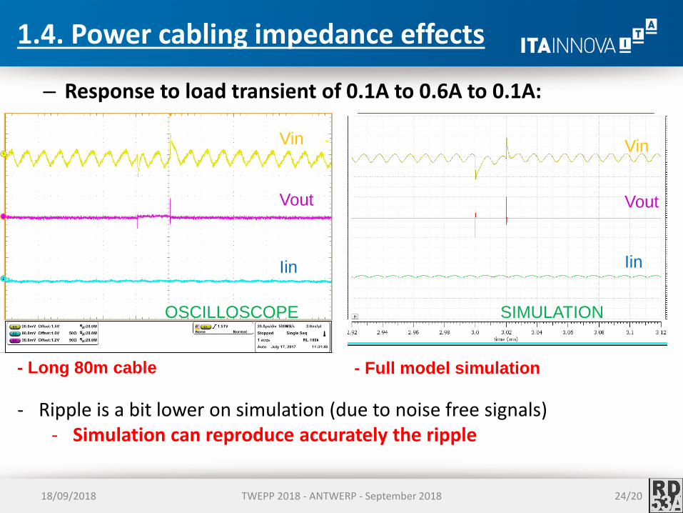
1.4. Power cabling impedance effects
– Response to load transient of 0.1A to 0.6A to 0.1A:
Vin
Vout
Iin
Vin
Vout
Iin
- Long 80m cable - Full model simulation
OSCILLOSCOPE SIMULATION
- Ripple is a bit lower on simulation (due to noise free signals)- Simulation can reproduce accurately the ripple
18/09/2018 24/20
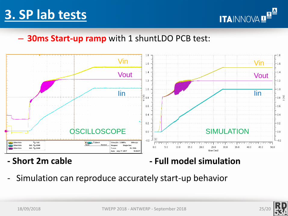
3. SP lab tests
– 30ms Start-up ramp with 1 shuntLDO PCB test:
Vin
Vout
Iin
Vin
Vout
Iin
- Short 2m cable - Full model simulation
- Simulation can reproduce accurately start-up behavior
OSCILLOSCOPE SIMULATION
TWEPP 2018 - ANTWERP - September 201818/09/2018 25/20
18/09/2018 TWEPP 2018 - ANTWERP - September 2018
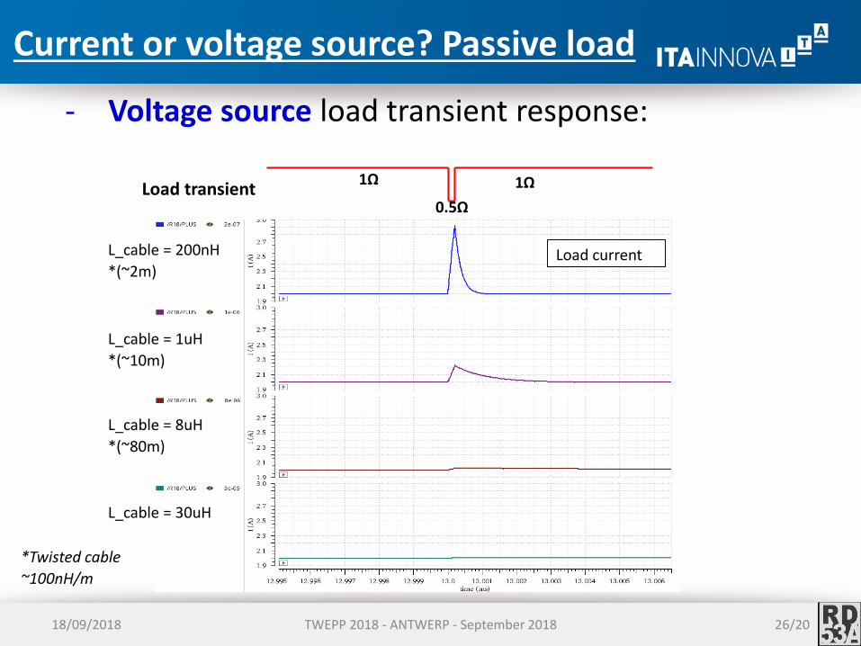
Load current
1Ω
0.5Ω
1ΩLoad transient
- Voltage source load transient response:
L_cable = 200nH
*(~2m)
L_cable = 1uH
*(~10m)
L_cable = 8uH
*(~80m)
L_cable = 30uH
*Twisted cable
~100nH/m
Current or voltage source? Passive load
26/20
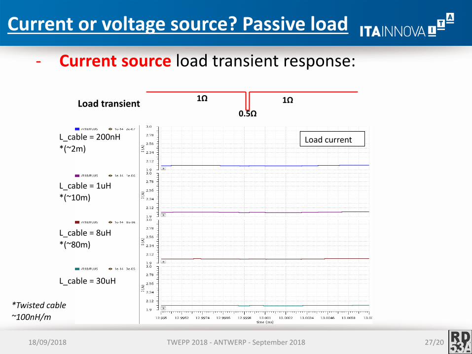
18/09/2018 TWEPP 2018 - ANTWERP - September 2018
Load currentL_cable = 200nH
*(~2m)
L_cable = 1uH
*(~10m)
L_cable = 8uH
*(~80m)
L_cable = 30uH
1Ω
0.5Ω
1ΩLoad transient
- Current source load transient response:
*Twisted cable
~100nH/m
Current or voltage source? Passive load
27/20