katsuro nakamura (kek) - cern indico
TRANSCRIPT
KEK HighEnergyAcceleratorResearchOrganiza6on
KatsuroNakamura(KEK)onbehalfoftheBelleIISVDgroup
VERTEX2016Sep.26,20169/26/16VERTEX2016 1
KEK(HighEnergyAcceleratorResearchOrganiza6on)
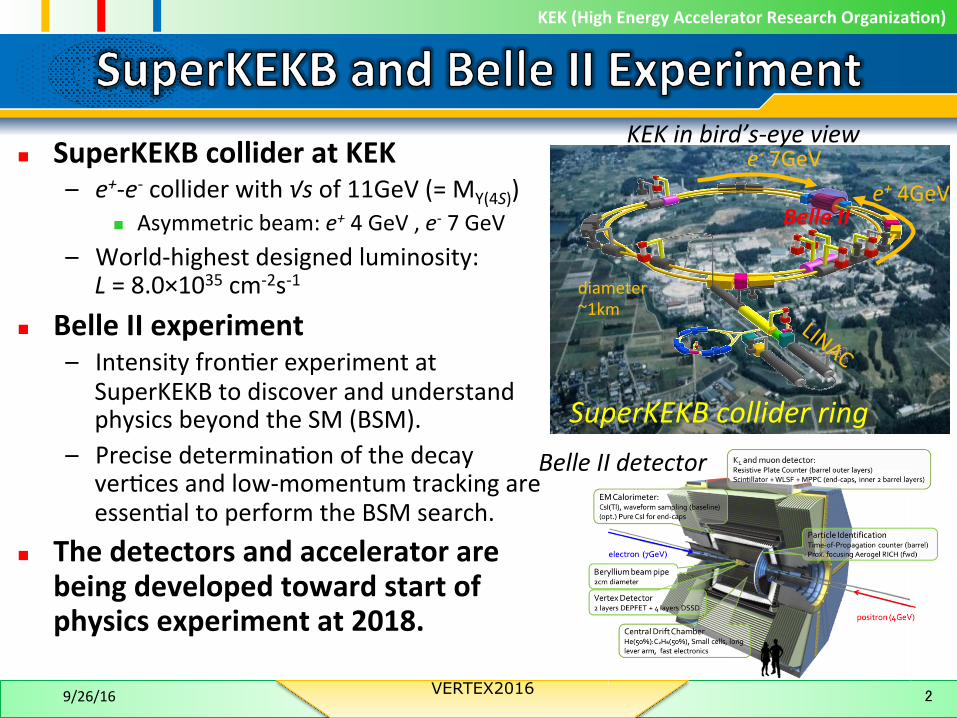
n SuperKEKBcollideratKEK– e+-e-colliderwith√sof11GeV(=MΥ(4S))
n Asymmetricbeam:e+4GeV,e-7GeV– World-highestdesignedluminosity:
L=8.0×1035cm-2s-1n BelleIIexperiment
– IntensityfronTerexperimentatSuperKEKBtodiscoverandunderstandphysicsbeyondtheSM(BSM).
– PrecisedeterminaTonofthedecayverTcesandlow-momentumtrackingareessenTaltoperformtheBSMsearch.
n Thedetectorsandacceleratorarebeingdevelopedtowardstartofphysicsexperimentat2018.
9/26/16 VERTEX2016 2
BelleIIdetector
KEKinbird’s-eyeview
SuperKEKBcolliderring
e-7GeVe+4GeV
BelleII
diameter~1km
KEK(HighEnergyAcceleratorResearchOrganiza6on)
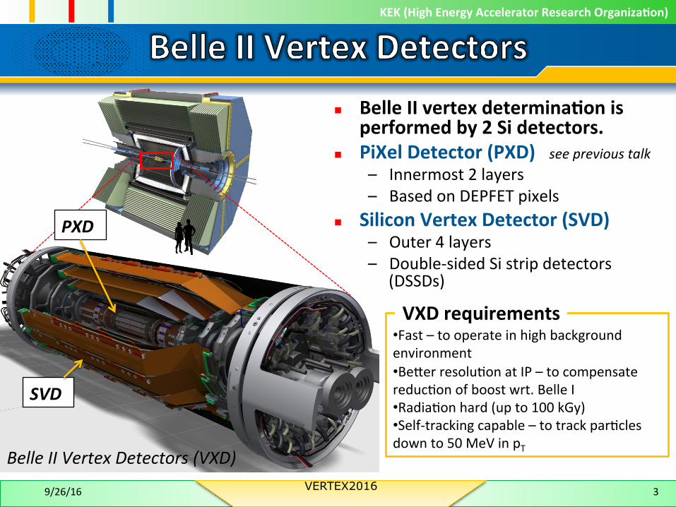
n BelleIIvertexdetermina6onisperformedby2Sidetectors.
n PiXelDetector(PXD)– Innermost2layers– BasedonDEPFETpixels
n SiliconVertexDetector(SVD)– Outer4layers– Double-sidedSistripdetectors
(DSSDs)
• Fast–tooperateinhighbackgroundenvironment• Be_erresoluTonatIP–tocompensatereducTonofboostwrt.BelleI• RadiaTonhard(upto100kGy)• Self-trackingcapable–totrackparTclesdownto50MeVinpT
VXDrequirements
39/26/16 VERTEX2016
seeprevioustalk
PXD
SVD
BelleIIVertexDetectors(VXD)
KEK(HighEnergyAcceleratorResearchOrganiza6on)
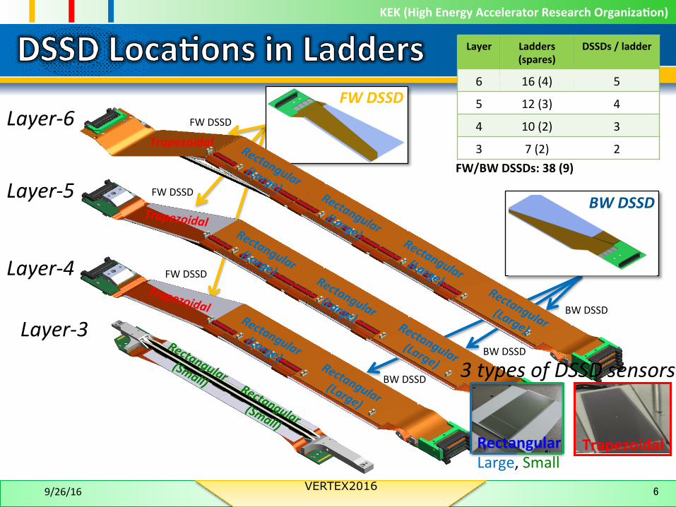
n 4SVDlayers(Layer-3to-6)consistofladders.
n TheladdersarecomposedofseveralDSSDmodules.
n SlantshapesinFWDregionforthematerialbudgetreduc6on.
n Averagematerialbudget:0.7%X0perlayer9/26/16 VERTEX2016 4
Layer-3Layer-4
Layer-5Layer-6 SVD
PXD
Angularacceptance:17°–150°935mm
collisionpoint
PXD+SVDcrosssecJondrawing
RL3=39mmRL4=80mm
RL5=115mmRL6=140mm
SVDmodel
FWD
BWD
SimulatedresoluJonfortrackimpactparameter(IP)
BelleonlySVD(BelleII)
PXD+SVD(BelleII)
Z-direcJon radial-direcJon
Improvedresolu6onsfrompreviousBelleexperimentareexpected.
BelleonlySVD(BelleII)
PXD+SVD(BelleII)
σIP~20umatpT=2GeV/c
KEK(HighEnergyAcceleratorResearchOrganiza6on)
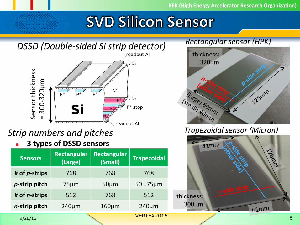
n 3typesofDSSDsensors
9/26/16 VERTEX2016 5
Sensorth
ickness
=300-320μ
m
Sensors Rectangular(Large)
Rectangular(Small) Trapezoidal
#ofp-strips 768 768 768
p-strippitch 75μm 50μm 50…75μm
#ofn-strips 512 768 512
n-strippitch 240μm 160μm 240μm
DSSD(Double-sidedSistripdetector)
P+ stop
readout Al
readout Al
SiP+ P+ P+
N+
N+
SiO2
SiO2N+
Rectangularsensor(HPK)
41mm
Trapezoidalsensor(Micron)
61mm
n-sidestrip
thickness:320μm
thickness:300μm
Stripnumbersandpitches
KEK(HighEnergyAcceleratorResearchOrganiza6on)
BWDSSD
FWDSSD
9/26/16 VERTEX2016 6
Layer Ladders(spares)
DSSDs/ladder
6 16(4) 5
5 12(3) 4
4 10(2) 3
3 7(2) 2FW/BWDSSDs:38(9)
Layer-6
Layer-5
Layer-4
Layer-3
FWDSSD
BWDSSD
BWDSSD
BWDSSD
FWDSSD
FWDSSD
Trapezoidal
Trapezoidal
Trapezoidal
RectangularLarge,Small
Trapezoidal
3typesofDSSDsensors
KEK(HighEnergyAcceleratorResearchOrganiza6on)
9/26/16 VERTEX2016 7
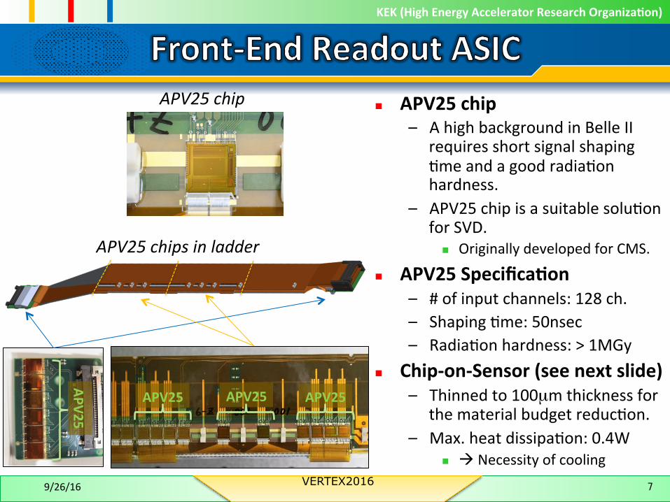
APV25 APV25 APV25
APV25
APV25chipsinladder
APV25chip n APV25chip– AhighbackgroundinBelleII
requiresshortsignalshapingTmeandagoodradiaTonhardness.
– APV25chipisasuitablesoluTonforSVD.
n OriginallydevelopedforCMS.
n APV25Specifica6on– #ofinputchannels:128ch.– ShapingTme:50nsec– RadiaTonhardness:>1MGy
n Chip-on-Sensor(seenextslide)– Thinnedto100µmthicknessfor
thematerialbudgetreducTon.– Max.heatdissipaTon:0.4W
n àNecessityofcooling
KEK(HighEnergyAcceleratorResearchOrganiza6on)
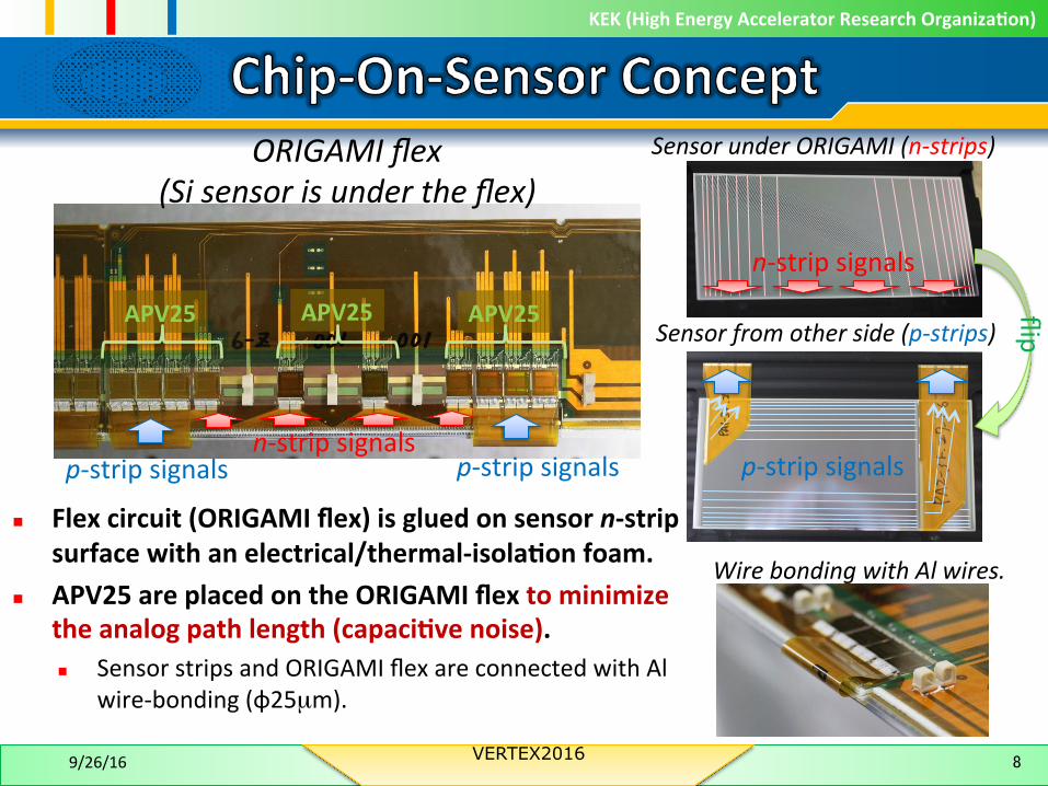
n Flexcircuit(ORIGAMIflex)isgluedonsensorn-stripsurfacewithanelectrical/thermal-isola6onfoam.
n APV25areplacedontheORIGAMIflextominimizetheanalogpathlength(capaci6venoise).n SensorstripsandORIGAMIflexareconnectedwithAl
wire-bonding(φ25µm).
9/26/16 VERTEX2016 8
ORIGAMIflex(Sisensorisundertheflex)
SensorunderORIGAMI(n-strips)
Sensorfromotherside(p-strips)
p-stripsignals p-stripsignalsn-stripsignals
n-stripsignals
p-stripsignals
WirebondingwithAlwires.
APV25 APV25 APV25 flip
KEK(HighEnergyAcceleratorResearchOrganiza6on)
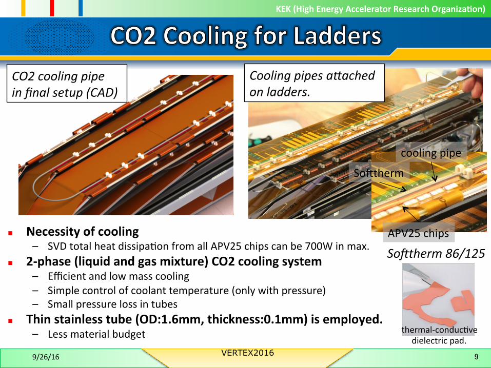
n Necessityofcooling– SVDtotalheatdissipaTonfromallAPV25chipscanbe700Winmax.
n 2-phase(liquidandgasmixture)CO2coolingsystem– Efficientandlowmasscooling– Simplecontrolofcoolanttemperature(onlywithpressure)– Smallpressurelossintubes
n Thinstainlesstube(OD:1.6mm,thickness:0.1mm)isemployed.– Lessmaterialbudget
9/26/16 VERTEX2016 9
coolingpipe
Somtherm
APV25chips
So[therm86/125
Coolingpipesa`achedonladders.
CO2coolingpipeinfinalsetup(CAD)
thermal-conducTvedielectricpad.
KEK(HighEnergyAcceleratorResearchOrganiza6on)
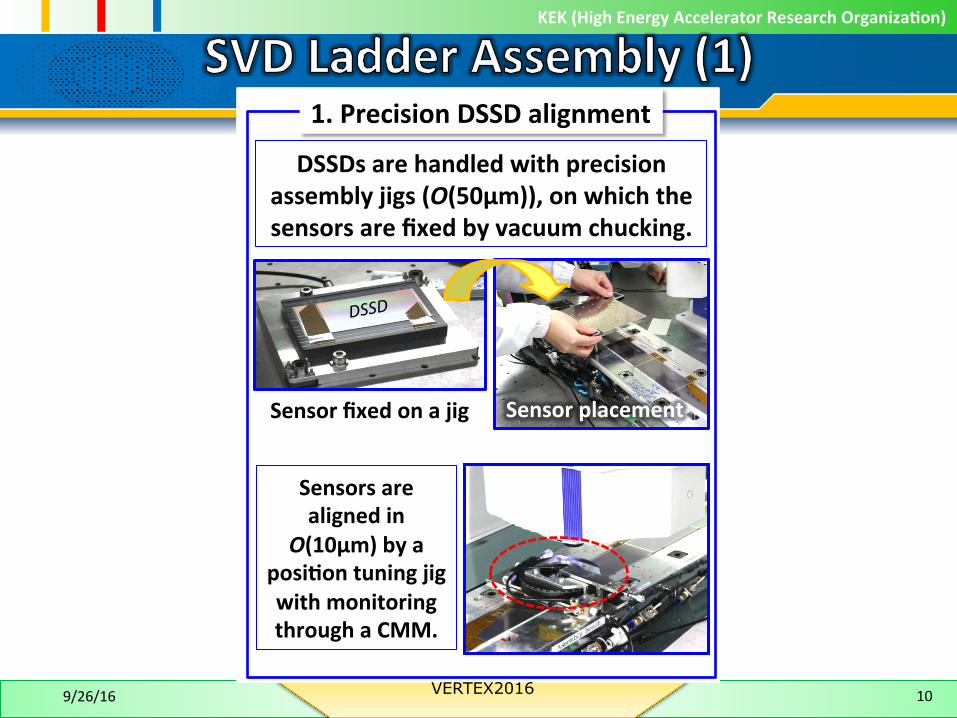
Sensorfixedonajig Sensorplacement
DSSDsarehandledwithprecisionassemblyjigs(O(50μm)),onwhichthesensorsarefixedbyvacuumchucking.
Sensorsarealignedin
O(10μm)byaposi6ontuningjigwithmonitoringthroughaCMM.
1.PrecisionDSSDalignment
9/26/16 VERTEX2016 10
DSSD
KEK(HighEnergyAcceleratorResearchOrganiza6on)
11
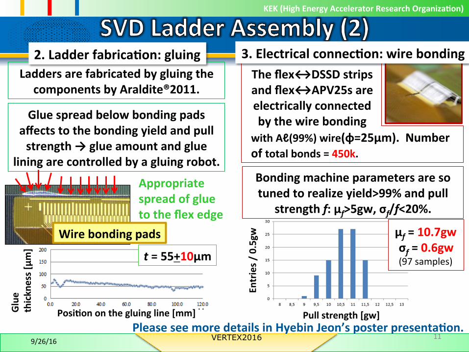
LaddersarefabricatedbygluingthecomponentsbyAraldite®2011.
Gluespreadbelowbondingpadsaffectstothebondingyieldandpullstrength→glueamountandglue
liningarecontrolledbyagluingrobot.
2.Ladderfabrica6on:gluing
Appropriatespreadofgluetotheflexedge
Wirebondingpads
Posi6ononthegluingline[mm]Glue
thickn
ess[μm
]
t=55+10μm
Theflex↔DSSDstripsandflex↔APV25sareelectricallyconnectedbythewirebonding
Bondingmachineparametersaresotunedtorealizeyield>99%andpull
strengthf:μf>5gw,σf/f<20%.
withAℓ(99%)wire(φ=25μm).Numberoftotalbonds=450k.
Pullstrength[gw]
Entries/
0.5gw
μf=10.7gwσf=0.6gw(97samples)
11PleaseseemoredetailsinHyebinJeon’sposterpresenta6on.
3.Electricalconnec6on:wirebonding
9/26/16 VERTEX2016
KEK(HighEnergyAcceleratorResearchOrganiza6on)
9/26/16 VERTEX2016 12
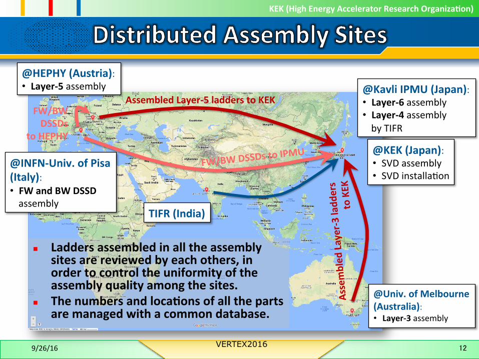
@KEK(Japan):• SVDassembly• SVDinstallaTon
@KavliIPMU(Japan):• Layer-6assembly• Layer-4assemblybyTIFR
TIFR(India)
@Univ.ofMelbourne(Australia):• Layer-3assembly
@INFN-Univ.ofPisa(Italy):• FWandBWDSSDassembly
@HEPHY(Austria):• Layer-5assembly
FW/BWDSSDs
toHEPHY
FW/BWDSSDstoIPMU
AssembledLayer-5ladderstoKEK
Assembled
Layer-3ladd
ers
toKEK
n Laddersassembledinalltheassemblysitesarereviewedbyeachothers,inordertocontroltheuniformityoftheassemblyqualityamongthesites.
n Thenumbersandloca6onsofallthepartsaremanagedwithacommondatabase.
KEK(HighEnergyAcceleratorResearchOrganiza6on)
9/26/16 VERTEX2016 13
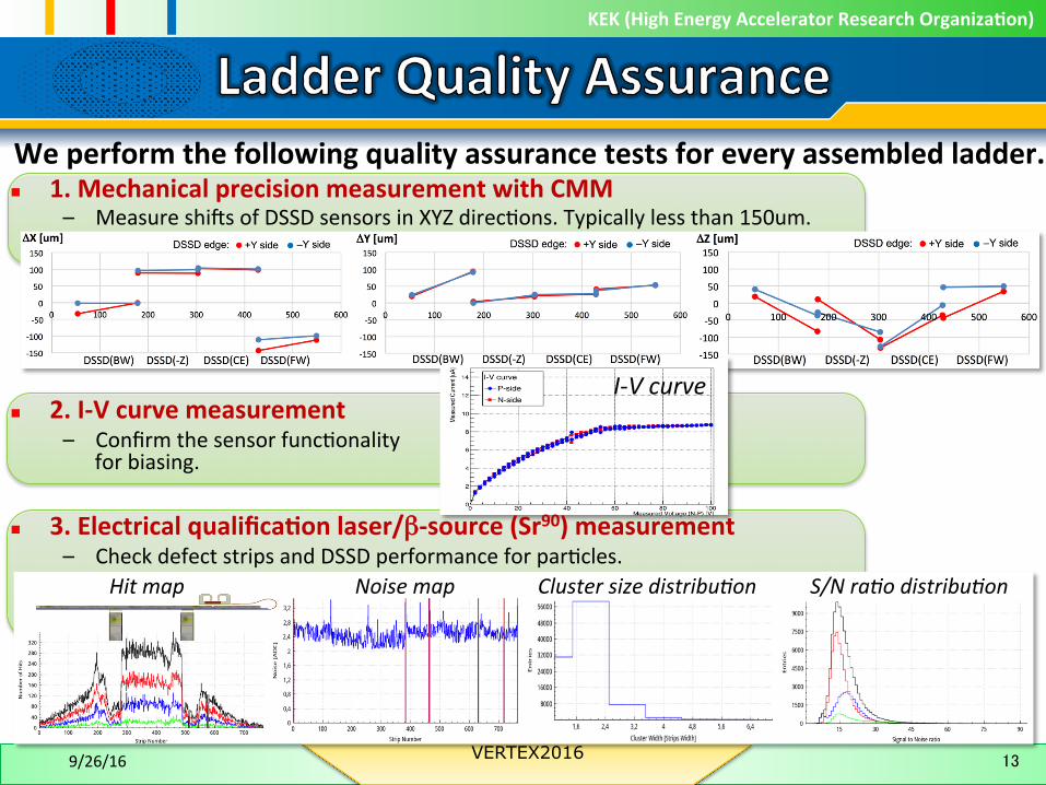
Weperformthefollowingqualityassurancetestsforeveryassembledladder.n 1.MechanicalprecisionmeasurementwithCMM
– MeasureshimsofDSSDsensorsinXYZdirecTons.Typicallylessthan150um.
n 2.I-Vcurvemeasurement– ConfirmthesensorfuncTonality
forbiasing.
n 3.Electricalqualifica6onlaser/β-source(Sr90)measurement– CheckdefectstripsandDSSDperformanceforparTcles.
Hitmap Noisemap ClustersizedistribuJon S/NraJodistribuJon
I-Vcurve
KEK(HighEnergyAcceleratorResearchOrganiza6on)
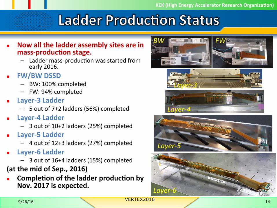
n Nowalltheladderassemblysitesareinmass-produc6onstage.– Laddermass-producTonwasstartedfrom
early2016.n FW/BWDSSD
– BW:100%completed– FW:94%completed
n Layer-3Ladder– 5outof7+2ladders(56%)completed
n Layer-4Ladder– 3outof10+2ladders(25%)completed
n Layer-5Ladder– 4outof12+3ladders(27%)completed
n Layer-6Ladder– 3outof16+4ladders(15%)completed
(atthemidofSep.,2016)n Comple6onoftheladderproduc6onby
Nov.2017isexpected.
9/26/16 VERTEX2016 14
FWBW
Layer-3
Layer-4
Layer-5
Layer-6
KEK(HighEnergyAcceleratorResearchOrganiza6on)
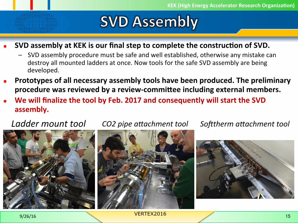
n SVDassemblyatKEKisourfinalsteptocompletetheconstruc6onofSVD.– SVDassemblyproceduremustbesafeandwellestablished,otherwiseanymistakecan
destroyallmountedladdersatonce.NowtoolsforthesafeSVDassemblyarebeingdeveloped.
n Prototypesofallnecessaryassemblytoolshavebeenproduced.Thepreliminaryprocedurewasreviewedbyareview-commizeeincludingexternalmembers.
n WewillfinalizethetoolbyFeb.2017andconsequentlywillstarttheSVDassembly.
9/26/16 VERTEX2016 15
Laddermounttool CO2pipea`achmenttool So[therma`achmenttool
KEK(HighEnergyAcceleratorResearchOrganiza6on)
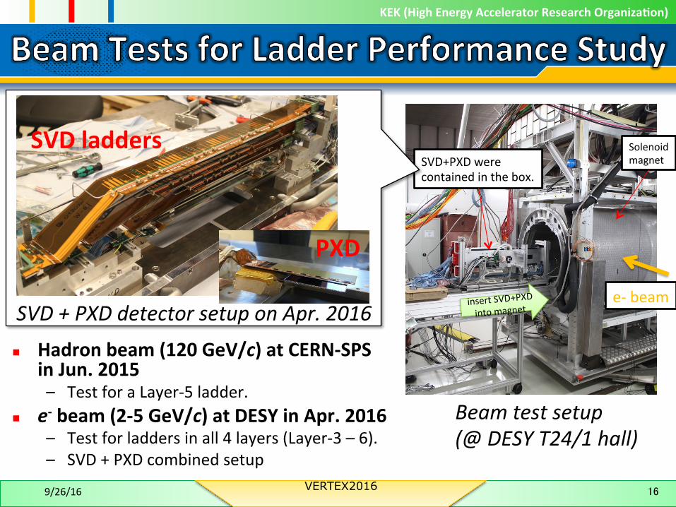
n Hadronbeam(120GeV/c)atCERN-SPSinJun.2015– TestforaLayer-5ladder.
n e-beam(2-5GeV/c)atDESYinApr.2016– Testforladdersinall4layers(Layer-3–6).– SVD+PXDcombinedsetup
9/26/16 VERTEX2016 16
SolenoidmagnetSVD+PXDwere
containedinthebox.
insertSVD+PXD
intomagnete-beam
Beamtestsetup(@DESYT24/1hall)
SVDladders
PXD
SVD+PXDdetectorsetuponApr.2016
KEK(HighEnergyAcceleratorResearchOrganiza6on)
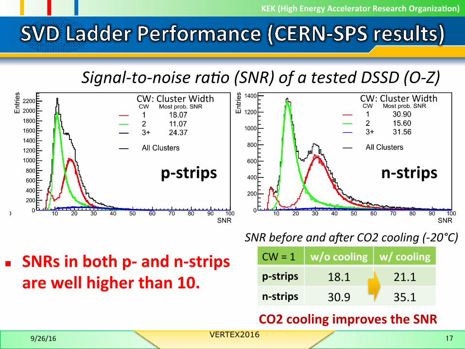
n SNRsinbothp-andn-stripsarewellhigherthan10.
9/26/16 VERTEX2016 17
p-strips n-strips
Signal-to-noiseraJo(SNR)ofatestedDSSD(O-Z)CW:ClusterWidth CW:ClusterWidth
CW=1 w/ocooling w/cooling
p-strips 18.1 21.1n-strips 30.9 35.1
CO2coolingimprovestheSNR
SNRbeforeanda[erCO2cooling(-20°C)
KEK(HighEnergyAcceleratorResearchOrganiza6on)
-directionφstrip number r-250 300 350 400 450 500 550 600 650
[%]
∈ e
ffici
ency
98
98.2
98.4
98.6
98.8
99
99.2
99.4
99.6
99.8
100
5_1_3 u
strip number z-direction 200 250 300 350 400
[%]
∈ e
ffici
ency
98
98.2
98.4
98.6
98.8
99
99.2
99.4
99.6
99.8
100
5_1_3 v
m ]µres iduals v [-200 -150 -100 -50 0 50 100 150 200
nu
mb
er o
f h
its
0
50
100
150
200
250
300
350
E ntries 4458R M S 25.87
/ nd f 2� 66.94 / 41C onstan t 6 .3±347.7 M ean 0 .3765±0.2164 S igm a 0 .25±24.87
9/26/16 VERTEX2016 18
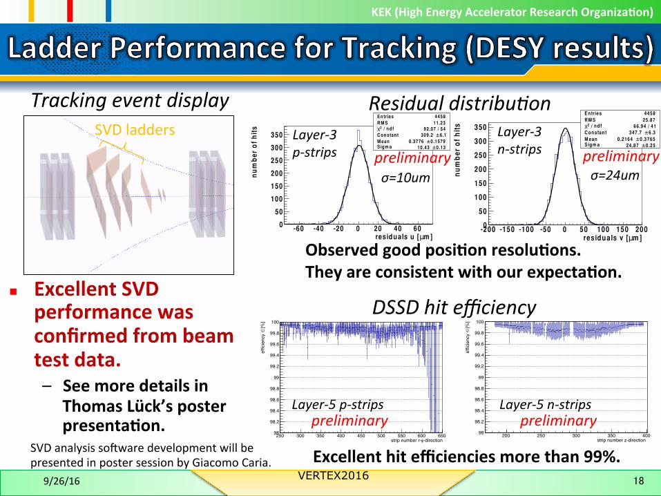
n ExcellentSVDperformancewasconfirmedfrombeamtestdata.– Seemoredetailsin
ThomasLück’sposterpresenta6on.
SVDladders
Trackingeventdisplay ResidualdistribuJon
m ]µres iduals u [-60 -40 -20 0 20 40 60
nu
mb
er o
f h
its
0
50
100
150
200
250
300
350
E ntries 4458R M S 11.23
/ nd f 2� 92.07 / 54C onstan t 6 .1±309.2 M ean 0 .1579±0.3776 S igm a 0 .13±10.43
residual layer 4 in u-direction
Layer-3p-strips
Layer-3n-strips
Observedgoodposi6onresolu6ons.Theyareconsistentwithourexpecta6on.
preliminary preliminary
DSSDhitefficiency
preliminary preliminaryLayer-5p-strips Layer-5n-strips
Excellenthitefficienciesmorethan99%.SVDanalysissomwaredevelopmentwillbepresentedinpostersessionbyGiacomoCaria.
σ=10um σ=24um
KEK(HighEnergyAcceleratorResearchOrganiza6on)
SVD
PXD
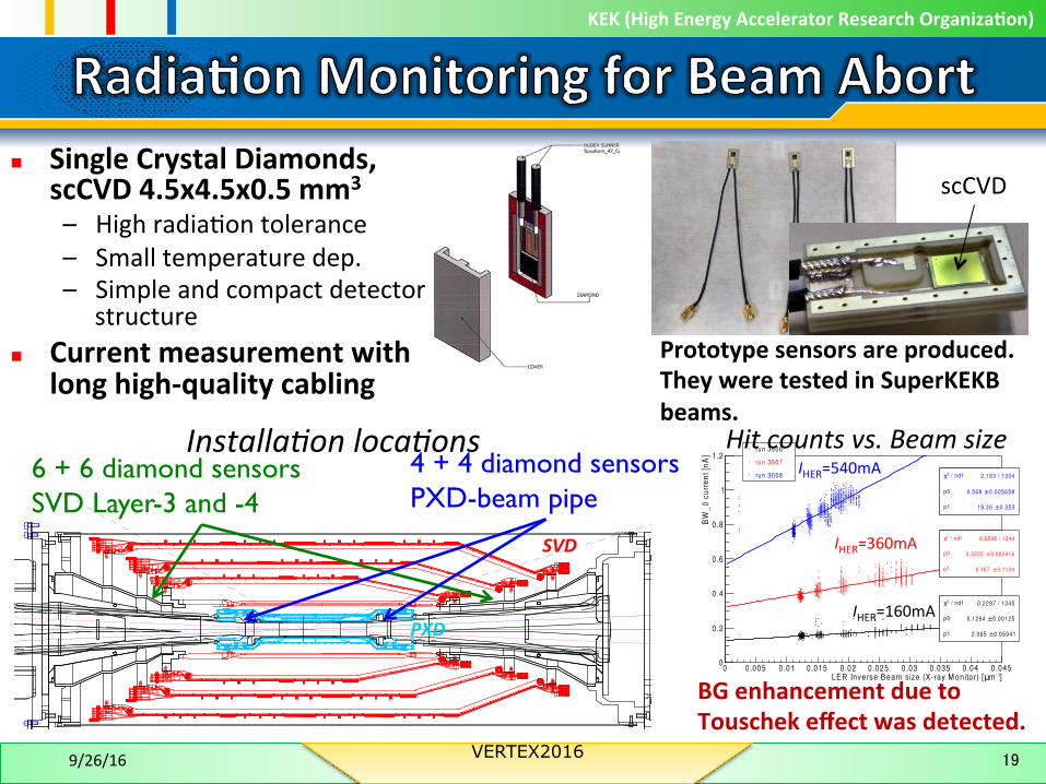
n SingleCrystalDiamonds,scCVD4.5x4.5x0.5mm3– HighradiaTontolerance– Smalltemperaturedep.– Simpleandcompactdetector
structuren Currentmeasurementwith
longhigh-qualitycabling
9/26/16 VERTEX2016 19
6 + 6 diamond sensorsSVD Layer-3 and -4
4 + 4 diamond sensorsPXD-beam pipe
Prototypesensorsareproduced.TheyweretestedinSuperKEKBbeams.
InstallaJonlocaJons
scCVD
]-1mµLE R Inverse B eam s ize (X -ray M on ito r) [0 0 .005 0.01 0.015 0.02 0.025 0.03 0.035 0.04 0.045
BW
_0 c
urre
nt [n
A]
0
0 .2
0 .4
0 .6
0 .8
1
1.2
/ nd f 2� 0.2297 / 1345
p0 0 .00125±0.1294
p1 0 .05941±2.065
/ nd f 2� 0.2297 / 1345
p0 0 .00125±0.1294
p1 0 .05941±2.065
/ nd f 2� 0.8598 / 1344
p0 0 .002416±0.3225
p1 0 .1124±6.167
/ nd f 2� 0.8598 / 1344
p0 0 .002416±0.3225
p1 0 .1124±6.167
/ nd f 2� 2.183 / 1304
p0 0 .005658±0.568
p1 0 .353±19.36
/ nd f 2� 2.183 / 1304
p0 0 .005658±0.568
p1 0 .353±19.36
run 3006
run 3007
run 3008
Hitcountsvs.Beamsize
BGenhancementduetoTouschekeffectwasdetected.
IHER=540mA
IHER=360mA
IHER=160mA
KEK(HighEnergyAcceleratorResearchOrganiza6on)
9/26/16 VERTEX2016 20
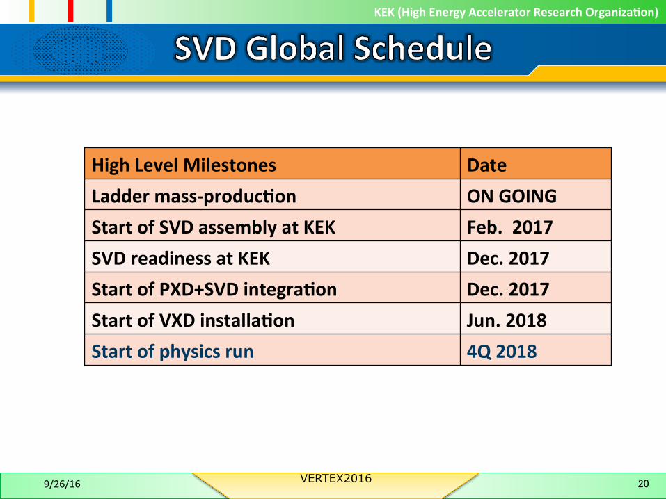
HighLevelMilestones DateLaddermass-produc6on ONGOINGStartofSVDassemblyatKEK Feb.2017SVDreadinessatKEK Dec.2017StartofPXD+SVDintegra6on Dec.2017StartofVXDinstalla6on Jun.2018Startofphysicsrun 4Q2018
KEK(HighEnergyAcceleratorResearchOrganiza6on)
n SVD,whichisessen6alfortheBelleIIexperiment,consistsof4-layerDSSDladders.
n SVDladderproduc6on– Theladdermass-producTonatallassemblysitesisongoing.
n SVDassemblyatKEK– Allprototypetoolswereproducedandreviewed.– ThiswillbefinalizedbyFeb.2017tostarttheSVDassemblyatKEK.– TheSVDassemblywillbecompletedbyDec.2017.
n Performancestudyinbeamtest– Weobtainedsuccessfulperformancesofthetracking,posiTon
resoluTon,andhitefficiencyforfinalSVDladders.
9/26/16 VERTEX2016 21
KEK(HighEnergyAcceleratorResearchOrganiza6on)
9/26/16 VERTEX2016 22
KEK(HighEnergyAcceleratorResearchOrganiza6on)
23
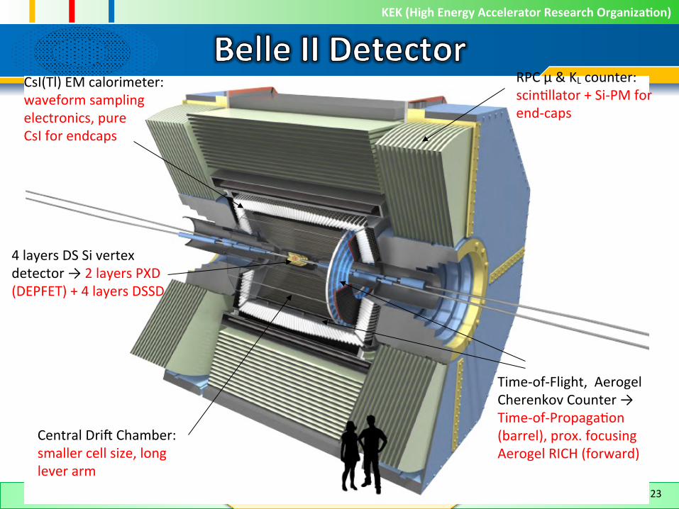
CsI(Tl)EMcalorimeter:waveformsamplingelectronics,pureCsIforendcaps
RPCμ&KLcounter:scinTllator+Si-PMforend-caps
Time-of-Flight,AerogelCherenkovCounter→Time-of-PropagaTon(barrel),prox.focusingAerogelRICH(forward)
4layersDSSivertexdetector→2layersPXD(DEPFET)+4layersDSSD
CentralDrimChamber:smallercellsize,longleverarm
KEK(HighEnergyAcceleratorResearchOrganiza6on)
24
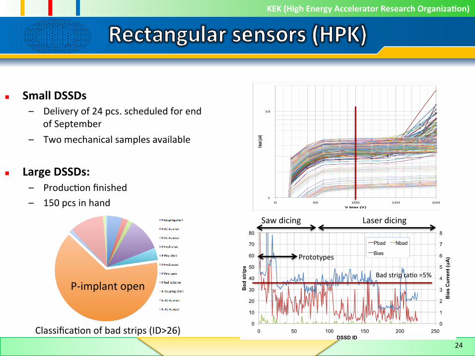
n SmallDSSDs– Deliveryof24pcs.scheduledforend
ofSeptember– Twomechanicalsamplesavailable
n LargeDSSDs:– ProducTonfinished– 150pcsinhand
LaserdicingSawdicing
Prototypes
BadstripraTo=5%
P-implantopen
ClassificaTonofbadstrips(ID>26)
KEK(HighEnergyAcceleratorResearchOrganiza6on)
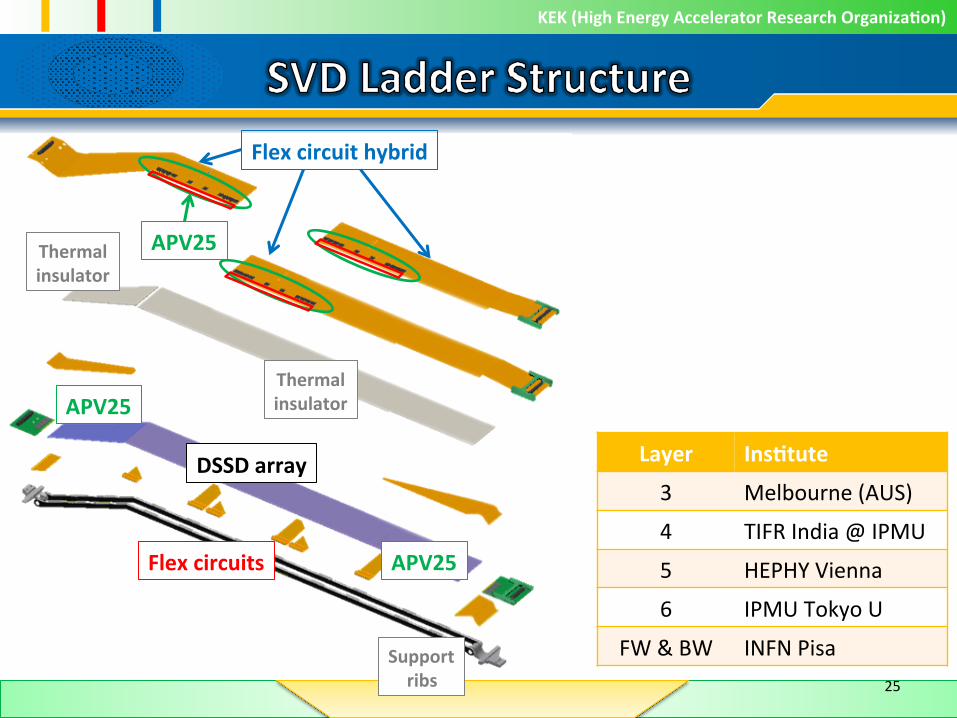
Thermalinsulator
Flexcircuithybrid
APV25Thermalinsulator
DSSDarray
APV25
Flexcircuits
Supportribs
APV25
25
Layer Ins6tute
3 Melbourne(AUS)
4 TIFRIndia@IPMU
5 HEPHYVienna
6 IPMUTokyoU
FW&BW INFNPisa
KEK(HighEnergyAcceleratorResearchOrganiza6on)
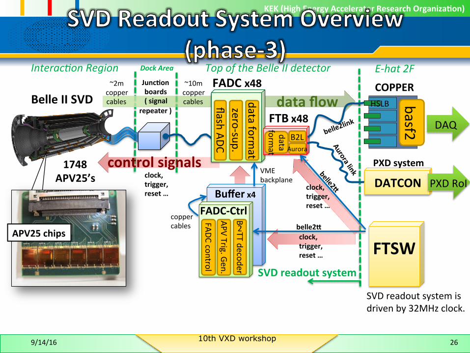
controlsignals
FADCx48
FTBx48
flashADCzero-sup.dataform
at
dataform
at
B2LAurora
COPPERHSLB
DAQ
PXDsystem
PXDRoI
dataflowBelleIISVD
Bufferx4FADC-Ctrl
B2TTdecoder
APVTrig.Gen.
coppercables
FADCcontrol
VMEbackplane
clock,trigger,reset…
clock,trigger,reset…
belle2z
1748APV25’s
~2mcoppercables
Junc6onboards(signal
repeater)
~10mcoppercables
26
clock,trigger,reset…
SVDreadoutsystem
APV25chips
DATCON
FTSW
SVDreadoutsystemisdrivenby32MHzclock.
basf2
InteracJonRegion DockArea TopoftheBelleIIdetector E-hat2F
9/14/16 10th VXD workshop
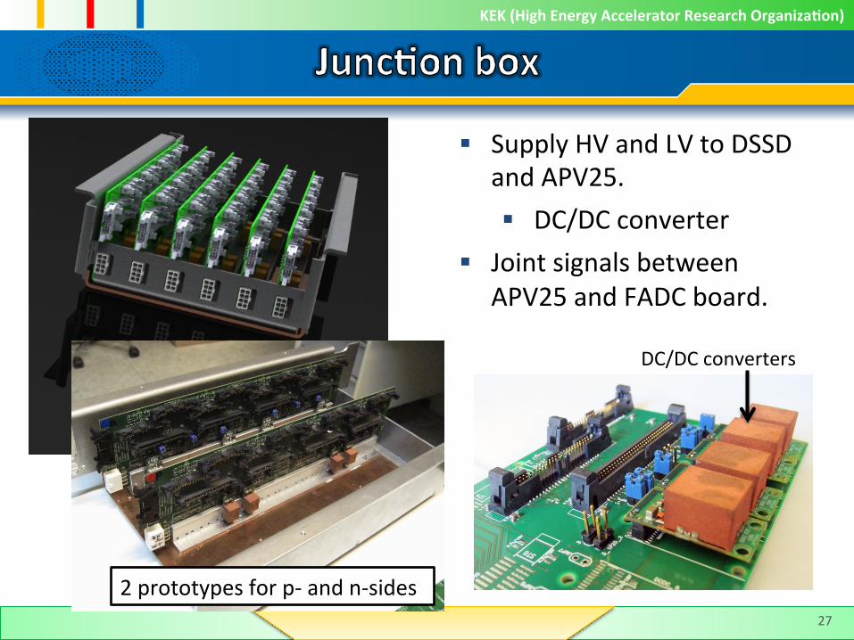
KEK(HighEnergyAcceleratorResearchOrganiza6on)
§ SupplyHVandLVtoDSSDandAPV25.§ DC/DCconverter
§ JointsignalsbetweenAPV25andFADCboard.
27
2prototypesforp-andn-sides
DC/DCconverters
KEK(HighEnergyAcceleratorResearchOrganiza6on)
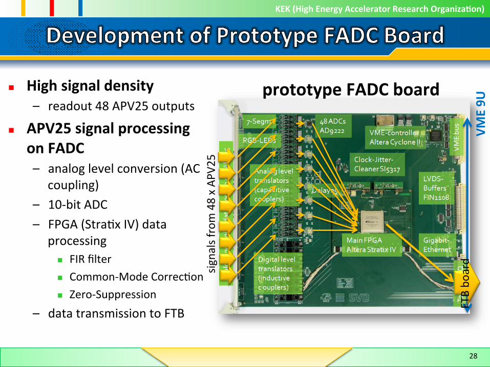
n Highsignaldensity– readout48APV25outputs
n APV25signalprocessingonFADC– analoglevelconversion(AC
coupling)– 10-bitADC– FPGA(StraTxIV)data
processingn FIRfiltern Common-ModeCorrecTonn Zero-Suppression
– datatransmissiontoFTB
28
prototypeFADCboard
signalsfrom
48xAP
V25
FTBbo
ard
VME9U
KEK(HighEnergyAcceleratorResearchOrganiza6on)
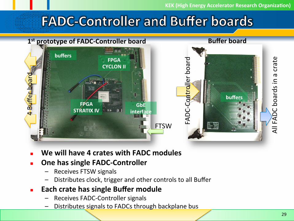
n Wewillhave4crateswithFADCmodulesn OnehassingleFADC-Controller
– ReceivesFTSWsignals– Distributesclock,triggerandothercontrolstoallBuffer
n EachcratehassingleBuffermodule– ReceivesFADC-Controllersignals– DistributessignalstoFADCsthroughbackplanebus
1stprototypeofFADC-Controllerboard Bufferboard
FTSW
4Bu
fferb
oard
FPGASTRATIXIV
FPGACYCLONII
buffers
GbEinterface
FADC
-Con
trollerb
oard
AllFAD
Cbo
ardsinacrate
buffers
29