integrated temporal partitioning and partial reconfiguration techniques for design latency...
TRANSCRIPT

ORIGINAL PAPER
Integrated temporal partitioning and partial reconfigurationtechniques for design latency improvement
Ramzi Ayadi • Bouraoui Ouni • Abdellatif Mtibaa
Received: 5 February 2013 / Accepted: 29 May 2013 / Published online: 16 June 2013
� Springer-Verlag Berlin Heidelberg 2013
Abstract In this paper, we present a novel temporal
partitioning methodology that temporally partitions a data
flow graph on reconfigurable system. Our approach opti-
mizes the whole latency of the design. This aim can be
reached by minimizing the latency of the graph and the
reconfiguration time at the same time. Consequently, our
algorithm starts by an existing temporal partitioning. The
existing temporal partitioning is the result of a whole
latency optimization algorithm. Next, our approach builds
the best architecture, on a partially reconfigurable FPGA,
that gives the lowest value of reconfiguration time. The
proposed methodology was tested on several examples on
the Xilinx Virtex-II pro. The results show significant
reduction in the design latency compared with others
famous approaches used in this field.
Keywords Temporal partitioning � Partially
reconfigurable FPGA � Data flow graph �VLSI applications
1 Introduction
The temporal partitioning has become an essential issue for
several important VLSI applications. Application with
several tasks entails problem complexities that are
unmanageable for existing programmable device. Thus, the
temporal partitioning is used to divide the application into
smaller, more manageable components, with the traditional
goals such as latency optimization or communication cost
optimization, etc. In literature, many methods have been
used to solve the temporal partitioning problem. Many
authors (Ouni and Ayadi 2008; Trimberger 1998; Cardoso
2003; Mtibaa et al. 2007) have used the list scheduling
algorithm. Others have extended existing scheduling of
high-level synthesis (Vasiliko and Ait-Bouraouli 1996;
Spillane and Owen 1998; Ouni et al. 2011a). Also, the
‘‘ILP’’ integer linear programming has been used in Kaul
et al. (1998), Byungil (1999), Wu et al. (2001) to solve the
temporal partitioning problem. The general problem of the
ILP approaches for partitioning a graph is its high execu-
tion time. In fact, the size of the computation model which
grows very fast and, therefore, the algorithm can only be
applied in small examples. To overcome this problem,
some authors reduce the size of the model by reducing the
set of constraints in the problem formulation, but the
numbers of variables and precedence constraints to be
considered still remain high. Further, the network flow
methodology has been used (Liu and Wong 1998a, b) and
improved in Jiang and Wang (2007). The main network
flow algorithm goal is the minimization of the communi-
cation overhead among the partitions, which also means the
minimization of the communication memory. The goal is
formulated as the minimization of the overall cut-size
among the partitions. In Ouni et al. (2009) authors com-
bined the force directed scheduling (FDS) algorithm and
network flow algorithm to reduce the whole latency and the
communication cost at the same time. In Ouni et al.
(2011b) authors combined temporal partitioning and tem-
poral placement to reduce the communication overhead of
the design. In Ouni et al. (2011c) authors a typical math-
ematical algorithm to reduce the whole latency of the
design. As conclusion, in the literature, the most of the
R. Ayadi (&) � B. Ouni � A. Mtibaa
Laboratory of Electronic and Microelectronic, Faculty
of Science of Monastir, University of Monastir,
Monastir 5019, Tunisia
e-mail: [email protected]
123
Evolving Systems (2014) 5:133–141
DOI 10.1007/s12530-013-9082-9
authors have proposed algorithmic approaches to solve the
temporal partitioning problem in the behavior level. The
majority of these studies have not taking into account the
technological evolution of reconfigurable architectures. In
fact, in the literature, temporal partitioning has been
applied only to full dynamic architecture (Ouni et al.
2011c; Ayadi et al. 2012). However, in this work, we
exploit the advantages of dynamic partial FPGA, to build a
full dynamic architecture. In fact, this paper shows how to
combine temporal partitioning algorithms with static and
reconfigurable modules of partially reconfigurable FPGA
to implement the design while optimizing the whole
latency of the design. As conclusion we present a new
algorithmic-architectural methodology to solve the tem-
poral partitioning problem.
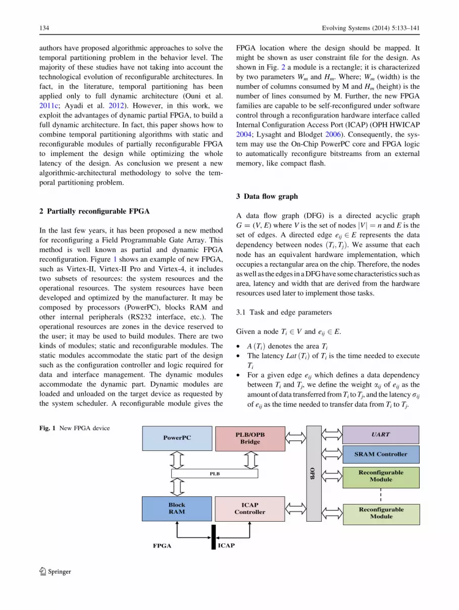
2 Partially reconfigurable FPGA
In the last few years, it has been proposed a new method
for reconfiguring a Field Programmable Gate Array. This
method is well known as partial and dynamic FPGA
reconfiguration. Figure 1 shows an example of new FPGA,
such as Virtex-II, Virtex-II Pro and Virtex-4, it includes
two subsets of resources: the system resources and the
operational resources. The system resources have been
developed and optimized by the manufacturer. It may be
composed by processors (PowerPC), blocks RAM and
other internal peripherals (RS232 interface, etc.). The
operational resources are zones in the device reserved to
the user; it may be used to build modules. There are two
kinds of modules; static and reconfigurable modules. The
static modules accommodate the static part of the design
such as the configuration controller and logic required for
data and interface management. The dynamic modules
accommodate the dynamic part. Dynamic modules are
loaded and unloaded on the target device as requested by
the system scheduler. A reconfigurable module gives the
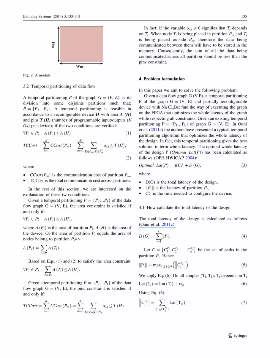
FPGA location where the design should be mapped. It
might be shown as user constraint file for the design. As
shown in Fig. 2 a module is a rectangle; it is characterized
by two parameters Wm and Hm. Where; Wm (width) is the
number of columns consumed by M and Hm (height) is the
number of lines consumed by M. Further, the new FPGA
families are capable to be self-reconfigured under software
control through a reconfiguration hardware interface called
Internal Configuration Access Port (ICAP) (OPH HWICAP
2004; Lysaght and Blodget 2006). Consequently, the sys-
tem may use the On-Chip PowerPC core and FPGA logic
to automatically reconfigure bitstreams from an external
memory, like compact flash.
3 Data flow graph
A data flow graph (DFG) is a directed acyclic graph
G = (V, E) where V is the set of nodes Vj j ¼ n and E is the
set of edges. A directed edge eij 2 E represents the data
dependency between nodes ðTi; TjÞ. We assume that each
node has an equivalent hardware implementation, which
occupies a rectangular area on the chip. Therefore, the nodes
as well as the edges in a DFG have some characteristics such as
area, latency and width that are derived from the hardware
resources used later to implement those tasks.
3.1 Task and edge parameters
Given a node Ti 2 V and eij 2 E.
• A ðTiÞ denotes the area Ti
• The latency Lat ðTiÞ of Ti is the time needed to execute
Ti
• For a given edge eij which defines a data dependency
between Ti and Tj, we define the weight aij of eij as the
amount of data transferred from Ti to Tj, and the latency rij
of eij as the time needed to transfer data from Ti to Tj.
OP
B
UART
SRAM Controller
Reconfigurable Module
Reconfigurable Module
FPGA
PLB
PowerPC PLB/OPB Bridge
Block RAM
ICAP Controller
ICAP
Fig. 1 New FPGA device
134 Evolving Systems (2014) 5:133–141
123
3.2 Temporal partitioning of data flow
A temporal partitioning P of the graph G = (V, E), is its
division into some disjoints partitions such that:
P = {P1…Pk}. A temporal partitioning is feasible in
accordance to a reconfigurable device H with area A (H)
and pins T (H) (number of programmable input/outputs (I/
Os) per device); if the two conditions are verified:
8Pi 2 P; A ðPiÞ�A ðHÞ ð1Þ
TCCost ¼XK
i¼1
CCost ðPmÞ ¼XK
m¼1
X
Ti2Pm; Tj2Pm
ai;j� T ðHÞ;
ð2Þ
where
• CCost ðPmÞ is the communication cost of partition Pm,
• TCCost is the total communication cost across partitions.
In the rest of this section, we are interested on the
explanation of these two conditions.
Given a temporal partitioning P = {P1…Pk} of the data
flow graph G = (V, E), the area constraint is satisfied if
and only if:
8Pi 2 P; A ðPiÞ�A ðHÞ;
where A ðPiÞ is the area of partition Pi; A ðHÞ is the area of
the device. Or the area of partition Pi equals the area of
nodes belong to partition Pi=[
A ðPiÞ ¼X
Ti2Pi
A ðTiÞ:
Based on Eqs. (1) and (2) to satisfy the area constraint
8Pi 2 P;X
Ti2Pi
A ðTiÞ�A ðHÞ:
Given a temporal partitioning P = {P1…Pk} of the data
flow graph G = (V, E), the pins constraint is satisfied if
and only if:
TCCost ¼XK
i¼1
CCost ðPmÞ ¼XK
m¼1
X
Ti2Pm;Tj2Pm
ai;j� T ðHÞ
In fact; if the variable ai;j 6¼ 0 signifies that Tj depends
on Ti. When node Ti is being placed in partition Pm and Tj
is being placed outside Pm, therefore the data being
communicated between them will have to be stored in the
memory. Consequently, the sum of all the data being
communicated across all partition should be less than the
pins constraint.
4 Problem formulation
In this paper we aim to solve the following problem:
Given a data flow graph G (V E), a temporal partitioning
P of the graph G = (V, E) and partially reconfigurable
device with Na CLBs: find the way of executing the graph
on the FPGA that optimizes the whole latency of the graph
while respecting all constraints. Given an existing temporal
partitioning P = {P1…Pk} of graph G = (V, E). In Ouni
et al. (2011c) the authors have presented a typical temporal
partitioning algorithm that optimizes the whole latency of
the design. In fact, this temporal partitioning gives the best
solution in term whole latency. The optimal whole latency
of the design P (Optimal LatðPÞ) has been calculated as
follows (OPH HWICAP 2004):
Optimal LatðPÞ ¼ KCT þ D ðGÞ; ð3Þ
where
• D(G) is the total latency of the design,
• Pik k is the latency of partition Pi,
• CT is the time needed to configure the device.
4.1 How calculate the total latency of the design
The total latency of the design is calculated as follows
(Ouni et al. 2011c):
D ðGÞ ¼Xk
i¼1
Pk ki ð4Þ
Let C ¼ CPi
1 ;CPi
2 ; . . .;CPin
� �be the set of paths in the
partition Pi. Hence
Pik k ¼ max1� j� n CPi
j
������
� �ð5Þ
We apply Eq. (6). On all couples ðTi;TjÞ; Tj depends on Ti
Lat ðTiÞ ¼ Lat ðTiÞ þ rij ð6Þ
Using Eq. (6):
CPi
j
������ ¼
X
ðTm2CPijÞ
Lat ðTmÞ: ð7Þ
Wm
Hm
Fig. 2 A module
Evolving Systems (2014) 5:133–141 135
123
4.2 How calculate CT
Given a device with Na CLBs that operates an execution
frequency Fe. We call sE ¼ 1
Fe the execution rate. We
assume that the device is able to configure Nr CLBs at each
configuration rate Fr. We call sR ¼ 1
Fr the configuration
rate. The relationship between sR and sE is given by:
sR ¼Fe
Fr
� �sE: ð8Þ
Then, the configuration time CT is calculated as follows
(Benoit et al. 2002)
CT ¼ Na
Nr
� �sR ¼
Na
Nr
� �Fe
Fr
� �sE: ð9Þ
Also CT can be written as follows:
CT ¼ Area ðDÞNr
� �sR ¼
W � HNr
� �sR; ð10Þ
where Area (D) = W�H, represent the total area of the
device and W, H are the width and the height of the device.
Hence for all modules Mn ðWn;HnÞ, if
ðAreaðMnÞ\AreaðDÞÞ then:
CT ¼ Area ðDÞNr
� �sR ¼
W � HNr
� �sR [ CT0
¼ Area ðMnÞNr
� �sR ¼
Mn � Hn
Nr
� �sR
Then CT [ CT0 ð11Þ
Therefore, 8 Area ðMnÞ\Area ðDÞð Þ
Optimal LatðPÞ ¼ KCT0 þ D ðGÞ ð12Þ
Hence, based on Eq. 12, we can minimize again the
value of timal LatP, this can be reached by minimizing the
term CT0. Therefore, the true optimal solution in term of
whole latency should be:
Optimal LatðPÞ ¼ K CT0|{z}min
þD ðG), ð13Þ
where CT0|{z}min
is the lowest possible value of CT0
Based on Eqs. (11) and (13) the whole latency mini-
mization problem can be expressed as follow: Given a
graph G (V, E) and an optimal temporal partitioning in
term of whole latency: Find the way of executing the graph
on the FPGA such as the product ðWn � HnÞ has the lowest
possible value while respecting all constraints.
5 Proposed architecture
As shown in Eq. (13) the whole latency minimization
problem can be solved by choosing the lowest possible
value of product ðWn � HnÞ. In this section, we show how
get the lowest value of ðWn � HnÞ.Given a temporal partitioning P of the graph G = (V, E)
into K disjoints temporal partitions P ¼ P1; P2. . .Pkf g.Based on Eq. (1):
88 Pi 2 P; A(PiÞ�Max(PiÞ� ðWn � HnÞ: ð14Þ
Hence, the lowest possible value of product ðWn � HnÞshould be closed to Max ðPiÞ.ðWn � HnÞ Max ðPiÞ ð15Þ
Hence, the graph should be executed on
reconfigurable area such as A ðH) ¼ Max ðPiÞ. As
shown in Sect. 2, we can build reconfigurable and
static modules on the device. Since a module is
characterized by its Wn (width) and it’s Hn (height),
thus we need to build a reconfigurable module on
the partially reconfigurable FPGA, such as
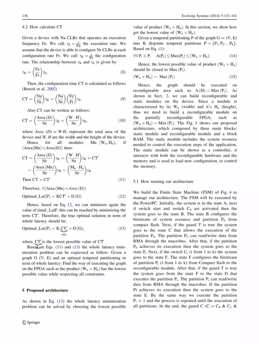
ðWn � HnÞ ¼ Max ðPiÞ. The Fig. 3 shows our proposed
architecture, which composed by three main blocks:
static module and reconfigurable module and a block
RAM. The static module includes the system resource
needed to control the execution steps of the application.
The static module can be shown as a controller, it
interacts with both the reconfigurable hardware and the
memory and is used to load new configuration, to control
the memory.
5.1 How running our architecture
We build the Finite State Machine (FSM) of Fig. 4 to
manage our architecture. The FSM will be executed by
the PowerPC. Initially, the system is in the state A, next
if switch start and switch C0 are activated then the
system goes to the state B. The state B configures the
bitstream of system resource and partition P0 from
compact flash. Next, if the guard T is true the system
goes to the state C that allows the execution of the
partition P0. The partition P0 can read/write data from
RMA through the macrobus. After that, if the partition
P0 achieves its execution then the system goes to the
state E. Next, if the switch Ci (i from 1 to k) the system
goes to the state F. The state F configures the bitstream
of partition Pi (i from 1 to k) from Compact flash to the
reconfigurable module. After that, if the guard T is true
the system goes from the state F to the state D that
executes the partition Pi. The partition Pi can read/write
data from RMA through the macrobus. If the partition
Pi achieves its execution then the system goes to the
state E. By the same way we execute the partition
Pi ? 1 and the process is repeated until the execution of
all partitions. In the end, the guard C (C = C0 & C1 &
136 Evolving Systems (2014) 5:133–141
123
Ci…& Ck) will be true and system comes back to the
state A.
6 Implementation of proposed architecture
Xilinx companies offering FPGA design tools that support
a self reconfiguration design flow. The available synthesis
tools have improved vastly both in speed and in the quality of
results. The following paragraph provides a detailed descrip-
tion of the design flow needed to implement our application.
The proposed design flow includes four mainly steps:
– building static module,
– looking for FPGA free space,
– building reconfigurable module,
– assembly phase.
6.1 Building static module
This step aims to build static module. In our approach the
static module includes the system resources, such as
PowerPC, UART, OPB bus and BLB bus, ICAP interface.
Xilinx Embedded Tool EDK may be used to build the
system resource efficiently. The system resource uses a set
of compiler tools to handle high-level languages such as C,
C??, or assembly language, and produce reliable code for
their embedded target. In this context we developed an
embedded C code to build the FSM of Fig. 4.
6.2 Looking for free space
After building the static module, we look for free space
inside the FPGA to build reconfigurable module. The
Fig. 3 Proposed architecture
Fig. 4 Proposed FSM
Evolving Systems (2014) 5:133–141 137
123

Fig. 5 shows the netlist of the static module and the places
where reconfigurable module may be built.
6.3 Building reconfigurable modules
The goal of the budgeting phase is to determine the size
and location of the reconfigurable module and to lock down
the placement of the bus macros. The budgeting phase can
be done manually. The process, however, is laborious andFig. 5 Free space inside the device
Fig. 6 Implementation of
modules
Fig. 7 XUP Virtex-II Pro
138 Evolving Systems (2014) 5:133–141
123

instead many of the steps have been automated with a tool
called PlanAhead; the PlanAhead tool allows building
modules anywhere inside the device, Fig. 6. After this step
a user constraints file (UCF file) is automatically generated.
After building reconfigurable and static module inside the
device, now we should achieve communication means
between them. BusMacros may be used to maintain correct
connections between the modules by spanning the
boundaries of these rectangular regions. The location of a
macrobuses should be closed to the modules location.
Further, the system needed to communicate with the
environment by using the FPGA pins. So, we used the data
sheet of the target FPGA to find appropriate pins.
6.4 Assembly phase
Last phase of the flow is the assembly of the static and
reconfigurable parts. The final bitstreams are generated as
full bitstreams, after loading the full bitstreams, it is now
possible to reconfigure module of the device with a partial
bitstream of each partition.
7 Experiments
Hardware architecture, XUP Virtex-II, on which the design
flow is to be mapped, is presented in Fig. 7. The XUP
Virtex-II Pro FPGA development system can be used at
any virtually level of the engineering curricula, from
introductory courses through advanced research projects.
In our experiences, we used four approaches, list
scheduling (Trimberger 1998), initial network flow (Liu
and Wong 1998), improved network flow (Jiang and Wang
2007) and our proposed approach. In our experiences, we
evaluated the performance of each approach in term of
whole latency. The Fig. 8 shows the color layout descriptor
‘‘CLD’’ is a low-level visual descriptor that can be
extracted from images or video frames. The process of the
CLD extraction consists of four stages: Image partitioning,
selection of a single representative color for each block,
DCT transformation and non linear quantization and zig-
zag scanning.
Since DCT is the most computationally intensive part of
the CLD algorithm, it has been chosen to be implemented
in hardware, and the rest of subtasks (partitioning, color
selection, quantization, zig-zag scanning and Huffman
encoding) were chosen for software implementation. The
model proposed by Mtibaa et al. (2007) is based on 16
vector products. Thus, the entire DCT is a collection of 16
Table 1 Benchmark characteristics
DFGs Nodes Edges Area (CLB)
DCT 4 9 4 224 256 8,045
DCT 16 9 16 1,929 2,304 13,919
Table 2 Design results
Algorithm Initial network flow Proposed approach Improvement versus
initial network flow
Graph 4 9 4 DCT Task graph 4 9 4 DCT Task graph 4 9 4 DCT Task graph
Number of partitions 9 9 –
Whole latency (ms) 234.005770 102.964770 56 %
Graph 16 9 16 DCT Task graph 16 9 16 DCT Task graph 16 9 16 DCT Task graph
Number of partitions 15 15 –
Whole latency (ms) 390.009710 160.686610 58.90 %
Average improvement in whole latency 57.45 %
Fig. 8 Block diagram of the CLD extraction
Fig. 9 Vector products
Evolving Systems (2014) 5:133–141 139
123

tasks, where each task is a vector product as presented in
Fig. 9.
There are two kinds of tasks in the task graph. ‘‘T1’’ and
‘‘T2’’, whose structure is similar to vector product, but
whose bit widths differ. Table 1 gives the characteristic of
4 9 4 DCT, 16 9 16 DCT task graphs.
The Tables 2, 3 and 4 give the different solutions provided
by the list scheduling, the initial network flow technique, the
enhanced network flow and the proposed approach. Results of
Table 2 shows an average improvement of 57.45 % in term of
whole design latency compared with the list scheduling.
Tables 3 and 4 shows an improvement of 57.25 and 58.85 % in
term of whole design latency compared with initial network
flow and improved network flow, respectively. These results
show the magnitude of benefit possible adopting our approach.
Therefore, our algorithm has a good trade-off between latency
of the graph and reconfiguration overhead. Hence, our
approach can be qualified to be a good temporal partitioning
candidate. In fact, an optimal partitioning approach needs to
balance computation required for each partition and reduce the
reconfiguration overhead so that mapped applications can be
executed faster on dynamically reconfigurable hardware.
8 Conclusion
Today’s large and complex designs are now commonly
implemented in FPGAs, however designer suffers principally
from the time needed to reconfigure, which is still relatively
high, in same case it consumes over than 70 % of the whole
design latency. A high reconfiguration time may lead to not
practical design mainly when designer focuses on the overall
latency minimization of the application. This problem may be
easily faced when using the proposed approach; in fact, there
is always much gain in reconfiguration latency versus others
approaches.
References
Ayadi R, Ouni B, Mtibaa A (2012) A partitioning methodology that
optimizes the communication cost for reconfigurable computing
systems. Int J Autom Comput (Springer Publisher) 9(3): 280–287
Benoit P, Torres L, Robert M, Cambon G, Sassatelli G, Gil T (2002)
Caracterisation d’Architectures Reconfigurables. Un Exemple :
Le Systolic Ring. Francophone Days on Adequacy Algorithm
Architecture JFAAA’2002, 16–18 December 2002, Monastir,
Tunisia, pp 30–34
Cardoso JMP (2003) On combining temporal partitioning and sharing
of functional units in compilation for reconfigurable architec-
tures. IEEE Trans Comput 52(10):1362–1375
Jeong B (1999) Hardware software partitioning for reconfigurable
architectures. M.S. Thesis School of Electrical Engineering,
Seoul National University
Jiang Y-C, Wang J-F (2007) Temporal partitioning data flow graphs
for dynamically reconfigurable computing. IEEE Trans Very
Large Scale Integr Syst 15(12):1351–1361
Kaul K, Vermuri R, Govindarajan S, Ouaiss I (1998) An automated
temporal partitioning tool for a class of DSP application. In:
Table 3 Design results
Algorithm Improved network flow approach Proposed approach Improvement versus
improved network flow
Graph 4 9 4 DCT Task graph 4 9 4 DCT Task graph 4 9 4 DCT Task graph
Number of partitions 9 9 –
Whole latency (ms) 234.004000 102.964770 55.80 %
Graph 16 9 16 DCT Task graph 16 9 16 DCT Task graph 16 9 16 DCT Task graph
Number of partitions 15 15 –
Whole latency (ms) 390.006000 160.686610 58.70 %
Average improvement in whole latency 57.25 %
Table 4 Design results
Algorithm List scheduling approach Proposed approach Improvement versus
list scheduling
Graph 4 9 4 DCT Task graph 4 9 4 DCT Task graph 4 9 4 DCT Task graph
Number of partitions 9 9 –
Whole latency (ms) 234.0043800 102.964770 58.90 %
Graph 16 9 16 DCT Task graph 16 9 16 DCT Task graph 16 9 16 DCT Task graph
Number of partitions 15 15 –
Whole latency (ms) 390.773000 160.686610 58.80 %
Average improvement in whole latency 58.85 %
140 Evolving Systems (2014) 5:133–141
123

Workshop and reconfigurable computing in international con-
ference on parallel architecture and compilation technique
PACT, pp 22–27
Liu H, Wong DF (1998a) Network flow based circuit partitioning for
time-multiplexed FPGAs. In: Proceedings of IEEE/ACM Inter-
national Conference on Computer-Aided Design, pp 497–504
Liu H, Wong DF (1998b) Network flow based multi-way partitioning
with area and pin constraints. IEEE Trans Comput Aided Design
Integr Circuits Syst 17(1):50–59
Lysaght P, Blodget B, Manson J, Young J, Bridgford B (2006) Invited
paper: enhanced architectures, design methodologies and CAD
tools for dynamic reconfiguration of Xilinx FPGAs, PLS, pp 1–6
Mtibaa A, Ouni B, Abid M (2007) An efficient list scheduling
algorithm for time placement problem. Comput Electr Eng
33(4):285–298
OPH HWICAP (2004) Product specification datasheet—DS 280
(v1.3), March
Ouni B, Ayadi R, Abid M (2008) Novel temporal partitioning
algorithm for run time reconfigured systems. J Eng Appl Sci
03(010):335–340
Ouni B, Mtibaa A, Bourennane El-B (2009) Scheduling approach for
run time reconfigured systems. Int J Comput Sci Eng Syst
3(4):335–340
Ouni B, Ayadi R, Mtibaa A (2011a) Partitioning and scheduling
technique for run time reconfigured systems. Int J Comput Aided
Eng Technol 3(1):77–91
Ouni B, Ayadi R, Mtibaa A (2011b) Combining temporal partitioning
and temporal placement techniques for communication cost
improvement. Adv Eng Softw (Elsevier Publisher) 42(7):
444–451
Ouni B, Ayadi R, Mtibaa A (2011c) Temporal partitioning of data
flow graph for dynamically reconfigurable architecture. J Syst
Archit (Elsevier Publisher) 57(8): 790–798
Spillane J, Owen H (1998) Temporal partitioning for partially-
reconfigurable field-programmable gate. Reconfigurable Archi-
tectures Workshop in PS/SPDP’98
Trimberger S (1998) Scheduling designs into a time-multiplexed
FPGA. In: Proceedings of the ACM International Symposium on
Field Program. Gate Arrays, pp 153–160
Vasiliko M, Ait-Boudaoud D (1996) Architectural synthesis for
dynamically reconfigurable logic. In: International workshop on
field-programmable logic and applications, FPL’96, Darmstadt,
Germany
Wu GM, Lin JM, Chang YW (2001) Generic ILP-based approaches
for time-multiplexed FPGA partitioning. IEEE Trans Comput
Aided Des 20(10):1266–1274
Evolving Systems (2014) 5:133–141 141
123