design and fabrication of a 40-mhz annular array transducer
TRANSCRIPT

Design and fabrication of a 40-MHz annular array transducer
Jeffrey A. Ketterling and Frederic L. LizziJ. A. Ketterling and F. L. Lizzi are with Riverside Research Institute, New York, NY(email:[email protected]).
Orlando Aristizábal and Daniel H. TurnbullO. Aristizábal and D. H. Turnbull are with Skirball Institute of Biomolecular Medicine and New YorkUniversity School of Medicine, New York, NY.
AbstractThis paper investigates the feasibility of fabricating a 5-ring, focused annular array transduceroperating at 40 MHz. The active piezoelectric material of the transducer was a 9-μm thickpolyvinylidene fluoride (PVDF) film. One side of the PVDF was metallized with gold and forms theground plane of the transducer. The array pattern of the transducer and electrical traces to eachannulus were formed on a copper-clad polyimide film. The PVDF and polyimide were bonded witha thin layer of epoxy, pressed into a spherically curved shape, and then back filled with epoxy. A 5-ring transducer with equal area elements and 100 μm kerfs between annuli was fabricated and tested.The transducer had a total aperture of 6 mm and a geometric focus of 12 mm. The pulse/echo responsefrom a quartz plate located at the geometric focus, two-way insertion loss (IL), complex impedance,electrical cross-talk, and lateral beamwidth were all measured for each annulus. The compleximpedance data from each element were used to perform electrical matching and the measurementswere repeated. After impedance matching, fc ≈ 36 MHz and BWs ranged from 31 to 39%. The ILsfor the matched annuli ranged from −28 to −38 dB.
I. INTRODUCTION
The field of high-frequency ultrasound (HFU) imaging, using frequencies above 20 MHz, isgrowing rapidly as transducer technologies improve and the cost of high bandwidth electronicinstrumentation decreases. There are two main advantages of HFU transducers. First, they havea large bandwidth which provides fine scale axial resolution. Second, they have a small lateralbeamwidth which permits imaging with resolution on the order of a wavelength (λ = 37 μm at40 MHz). However, single element focused transducers, currently used for most HFUapplications, also have a small depth of field, limiting the best image resolution to a small axialrange close to the geometric focus of the transducer.
The earliest work with HFU transducers utilized single element focused transducers fabricatedwith PVDF membranes as their active acoustic layer [1], [2]. These transducers were relativelyeasy to fabricate but suffered from a fairly high two-way insertion loss (≈ 40 dB) because ofthe material properties of PVDF. This resulted in a focus on methods to improve the insertionloss by optimizing the drive electronics and electrical matching [3]-[7]. At the same time,methods of fabricating single element HFU transducers using ceramic material were also beingrefined, and numerous devices were fabricated successfully to operate in the HFU regime[8]-[10]. These devices have an inherent advantage over PVDF based transducers because oftheir much lower insertion loss. However, single element PVDF transducers continue to be theprimary transducer choice for HFU applications. Both PVDF and ceramic transducers have
This research was supported by grants from the National Institutes of Health (EY014371 and NS38461).
NIH Public AccessAuthor ManuscriptIEEE Trans Ultrason Ferroelectr Freq Control. Author manuscript; available in PMC 2006January 26.
Published in final edited form as:IEEE Trans Ultrason Ferroelectr Freq Control. 2005 April ; 52(4): 672–681.
NIH
-PA Author Manuscript
NIH
-PA Author Manuscript
NIH
-PA Author Manuscript

been used to great success for ophthalmic [11], [12], dermatological [13]-[15], and small animalimaging [16]-[18].
The current emphasis on HFU transducers is targeted more towards array technology. An arraypermits electronic focusing that both improves the depth of field of the device and permits a2D image to be constructed without mechanically scanning the transducer. Technologies suchas CMUT [19], MEMS [20], as well as more traditional ceramic materials are being pursued[21], [22]. These methods all aim to fabricate individual array elements on the order of λ/2;these small dimensions necessitate advances in interconnects and electronics to fullyimplement the technologies.
In the interim, a more practical approach is to develop annular arrays with element sizes similarto current single element transducers. The advantage of an annular array is that it permits anincreased depth of field along a line focus with a relatively limited number of elements. Theprimary drawback is that it must be mechanically scanned to generate a 2D image. Bothpassively focused and unfocused annular arrays are now being pursued. Ceramic materials aretypically used for flat arrays because they are difficult to grow or to press into curved shapes[23]-[25]. PVDF is more advantageous in this respect because it can be easily press fit into acurved shape. PVDF also provides a better acoustic impedance match to water and biologicaltissue. Alves et. al [26] were able to fabricate a PVDF annular array but did not generate imagesor fully implement the array's functionality.
Here, we demonstrate the feasibility of a new method to construct PVDF based annular arrays.The active acoustic element of the transducer is a 9 μm PVDF film with one side coated ingold acting as the ground plane. The positive array pattern of the transducer is formed on acopper clad polyimide film (“flex circuit”). The flex circuit and PVDF are bonded together,press fit into a spherical shape, and then back filled with epoxy. Transducer performance wascharacterized by measuring the pulse/echo response, two-way insertion loss, electrical crosstalk, complex electrical impedance of each array element, and lateral -6-dB pulse/echobeamwidth.
II. MATERIALS AND METHODS
A. Fabrication1) Polyimide Array Patterns: The circuit patterns were designed as positive images with a CADsoftware package (QuickCAD, Autodesk Inc., San Rafael, CA). The transducer we discusshere had a total aperture of 6 mm with five equal area rings separated by 100 μm kerf spacings[Fig. 1]. The electrical traces that permit access to each annulus and the spacing between thetraces were also 100 μm. From the CAD file, a transparent film with the positive array imagewas generated by an offset print shop (Elite Graphics Co. Inc., New York, NY). This methodof creating the positive image permitted us to achieve line widths and spacings of smaller than100 μm.
The array pattern was formed on single sided, copper clad polyimide film (RFlex 1000L810,Rogers Corp., Chandler, AZ), a material commonly used to fabricate flex circuits. Thepolyimide film was 25-μm thick, the copper was 18-μm thick, and an adhesive layer bondingthe copper to the polyimide was 20-μm thick. Before creating the array pattern, the polyimidewas coated with a uniform thickness of positive photoresist (Injectorall, Bohemia, NY).
The fabrication of the copper array pattern utilized standard copper etching techniques. Thepositive array image was placed on top of the photoresist coated polyimide and exposed toultraviolet (UV) light for 2-3 minutes in a UV fluorescent exposure unit (AmerGraph, Sparta,NJ). The polyimide was then transferred to a liquid developer, which removed the photoresist
Ketterling et al. Page 2
IEEE Trans Ultrason Ferroelectr Freq Control. Author manuscript; available in PMC 2006 January 26.
NIH
-PA Author Manuscript
NIH
-PA Author Manuscript
NIH
-PA Author Manuscript

that had been exposed to UV light. The developed film was then gently agitated in a ferricchloride bath until all the copper in the areas lacking photoresist had been etched away. Thefinished array pattern was viewed with a microscope to ensure that the line widths and spacingswere uniform and of the correct size. After gently removing the remaining photoresist withsteel wool, the pattern was tested for electrical continuity between the rings and copper contactpads. Test patterns were first utilized to ensure that we could achieve 100 μm spacing for bothring separations and line widths.
2) Press Fit Assembly: The final assembly of the transducer utilized a press fit technique similarto that used for single element PVDF [1], [26] and ceramic transducers [8], [10]. Figure 2 showsa schematic of the custom jig and material layers of the final assembly. The jig was constructedof aluminum and consisted of a base plate, a pressure plate to apply uniform pressure to thefilms as they were pressed, and a top plate to press in the ball bearing. The base plate had acentral hole in which a Teflon tube was inserted. The Teflon tube ensured that the PVDF andpolyimide films would not tear from the pinching at the transducer's edge during the press fit.
Assembly began by inserting the Teflon tube into the baseplate and then centering the arraypattern over the Teflon tube with the copper side up. The inner diameter of the tube was largerthan the active aperture of the array. A single drop of epoxy (Hysol RE2039, HD3561, LoctiteCorp., Olean, NY) was placed onto the array pattern and a 4 cm by 4 cm section of PVDFmembrane (Ktech Corp., Albuquerque, NM) was placed over the epoxy. The PVDF was 9μm thick and had one side metallized with gold. The metallized side formed the ground planeof the transducer and faced upward. A Teflon ring was placed over the two films and thenlightly clamped with the pressure plate. The pressure plate permitted the film layers to moveslightly while also stretching during the press fit, thus minimizing crinkling of the films at theedge of the transducer.
A stainless steel ball bearing with an OD of 24 mm was then pressed into the films with thetop plate and the plate was tightly secured. Next, the jig was turned over and the Teflon tubewas filled with epoxy. The whole jig assembly was then placed into a vacuum chamber at ≈ 8Torr. The degassing lasted as long as necessary to ensure that no bubbles were present on thebackside of the polyimide (≈ 40 min).
After degassing, the jig was moved into a 40° C oven to reduce the epoxy cure time. When theepoxy had cured, the transducer was removed from the jig and separated from the Teflon tube.This left an epoxy plug with a smaller diameter curved array bonded to it. Excess material wastrimmed away to leave just the electrical traces and their contact pads [Fig. 3]. To form acontinuous ground plane, silver epoxy (EE129-4 Epoxy Technology, Billerica, MA) was usedto join the conductive side of the PVDF to additional ground traces on the polyimide film.
In order to electronically access the array elements, a customized printed circuit board (PCB)was fabricated [Fig. 4]. The PCB had a 20-pin zero insertion force (ZIF) connector on one side(Hirose Electric, Simi Valley, CA) and miniature MMCX-BNC connectors on the other side(Amphenol, Wallingford, CT). BNC cables (RG-174 50 Ω) of 0.87 m length were connectedto the MMCX connectors. An additional advantage of the PCB board was that surface mountinductors could be soldered directly onto the board to perform impedance matching. Amounting bracket made from aluminum rod held the transducer and PCB board. The polyimidefilm could then be wrapped around and inserted into the ZIF connector [Fig. 4].
B. Testing1) Pulse/Echo: The transducers were first characterized by examining their pulse/echo responseusing a quartz-plate target positioned 12 mm from the transducer. The transducer was placedin a small container of degassed water with a 2.5-cm thick quartz plate at its bottom. The
Ketterling et al. Page 3
IEEE Trans Ultrason Ferroelectr Freq Control. Author manuscript; available in PMC 2006 January 26.
NIH
-PA Author Manuscript
NIH
-PA Author Manuscript
NIH
-PA Author Manuscript

transducer was then excited with a pulser/receiver (Panametrics 5900, Waltham, MA) whilethe return signal was digitized with a 1 GS/s, 8-bit digitizer (Acqiris DP110, Monroe, NY).The separation distance and tilt angle between the transducer and the quartz plate were adjustedto maximize the amplitude of the return echo.
2) Two-Way Insertion Loss: Two-way insertion loss measures the efficiency of a transducerby comparing the pulse/echo voltage response of a transducer to the voltage available at a 50Ω load for the same excitation waveform. Insertion loss was measured utilizing a directionalcoupler (Minicircuits ZDC-10-1, Brooklyn, NY) [1] with the transducer on the coupler's inport, the excitation waveform on the coupler's out port, and the coupled port terminated into adigitizer (Acqiris DP110) with 50 Ω impedance.
To measure the pulse/echo voltage response, the transducer was excited with a quasi-continuous wave tone burst. The tone burst was 1 μs in duration and originated from a functiongenerator (Agilent 33250a, Palo Alto, CA) the output of which was gated via an RF switch(Minicircuits ZASWA-2-50DR). The transducer was submerged in degassed water with a thickquartz plate placed in its geometric focal plane and the echo signal from the front surface ofthe quartz reflector was windowed at a delay appropriate to the round trip water path distance.An automated LabVIEW program (National Instruments, Austin, TX) was then used to sweepthrough a frequency range in 1 MHz steps. At each frequency step, the peak-to-peak voltageVpp of the return echo waveform was measured after the output of the coupler's coupled portpassed through a limiter (Anritsu 1N50B,Richardson, TX) and was amplified by 32.5 dB(Miteq AU-1114, Hauppauge, NY). The voltage measurements were converted to dB and thencorrected for the losses due to the quartz plate transmission coefficient (1.7 dB) and acousticattenuation in water (2 × 10⁻⁴ dB/mm-MHz2) [8].
The transmit waveform, representing the voltage available to a 50 Ω load, was measured aftercreating an open circuit at the transducer by detaching the polyimide film from the ZIFconnector on the PCB board. The open circuit at the ZIF connector causes full voltagereflection, with a zero time delay. The Vpp values were again measured in 1 MHz step at thecoupler's coupled port, but without any additional amplification. Because all cabling wasidentical for both the pulse/echo and transmit measurements, the final frequency dependentinsertion loss is calculated by subtracting the transmit results from the pulse/echo results.
3) Complex Impedance: After fabrication and the initial pulse/echo measurement, the compleximpedance of each annulus was measured with a combination Network-Spectrum-ImpedanceAnalyzer (HP4396A & HP43961A, Hewlett Packard, Palo Alto, CA). After compensating forthe 0.87-m cable connecting the transducer to the analyzer, the capacitive reactive componentof the impedance at 40 MHz was used to determine the appropriate series inductance neededto bring the reactance to zero. An appropriate surface mount inductor was selected and soldereddirectly onto the PCB board [Fig. 4]. The complex impedance was again measured to ensurethat the reactance at the center frequency was in fact zero.
4) Electrical Cross Talk: Electrical cross talk between rings was measured by transmitting a1 Vpp continuous wave signal on a single annulus and then measuring the voltages seen by theremaining annuli. The transmit voltage was measured with a high impedance 10X probe whilethe remaining annuli voltages were measured into 50 Ω terminations at the end of the 0.87 mBNC cables. The voltages were measured with a 4-channel digital oscilloscope (WaveRunner6050, LeCroy, Chestnut Ridge, NY). The cross-talk measurements were made at severalfrequencies, including the center frequency of the transducer. The cross talk was expressed indB as the ratio of the voltage on the receive annulus to the voltage on the transmit annulus.The transducer was not submerged in water for this measurement, as this did not change theresults.
Ketterling et al. Page 4
IEEE Trans Ultrason Ferroelectr Freq Control. Author manuscript; available in PMC 2006 January 26.
NIH
-PA Author Manuscript
NIH
-PA Author Manuscript
NIH
-PA Author Manuscript

5) Lateral Beamwidth: The pulse/echo lateral beamwidth of each annulus was measured byscanning the transducer across a 25 μm wire target positioned at the geometric focus of thetransducer. The scanning was performed with an automated XYZ motion system underLabVIEW control. The transducer was excited with a pulser/receiver (Panametrics 5900) andVpp was recorded at 10 μm increments over a span of 0.8 mm. This method of measuring thelateral beam width approximates the case of a point scatterer and is valid as long as the wirediameter is smaller than the wavelength of sound [27].
III. RESULTS
The results shown here are for a 5-ring annular array with equal area elements and 100 μm kerfspacing between rings. The total transducer aperture was 6 mm and the radius of curvature was12 mm. The outer diameter of the epoxy plug was 12.8 mm. The inner and outer radii of theannuli when projected onto a plane were 0, 1.22, 1.32, 1.8, 1.9, 2.26, 2.36, 2.65, 2.75 and 3.0mm [Fig. 1]. The experimental data are compared to the results of a KLM model [28](PiezoCAD, Sonic Concepts, Woodinville, WA) as a means to validate the performance of thetransducer.
A. Unmatched TransducerThe pulse/echo time domain waveform acquired for Ring 1 (central annulus) is shown in Fig.5(a). The other 4 rings, scaled relative to each other, showed similar time domain results withabout a 50% reduction in amplitude compared to the center ring (Fig. 5(c)). The frequencydomain signal for Ring 1 is shown in Fig. 5(b). The center frequency (f c) is 39 MHz and the−6-dB fractional bandwidth (BW) is 61%. Both the time-domain and frequency-domainexperimental results of Fig. 5 compare favorably to the predictions of the KLM model (dotted).
A summary of the power spectra for all five array elements is shown in Fig. 6, showing theshift towards lower sensitivities for the outer rings. The peak amplitude for Ring 1 is normalizedto 0 dB. Table II summarizes the values for the peak amplitude, fc, and BW for all five annuli.The table also shows the results for minimum insertion loss and the frequency at which itoccurred. The insertion losses are consistent with what has been previously reported for PVDFbased transducers [1].
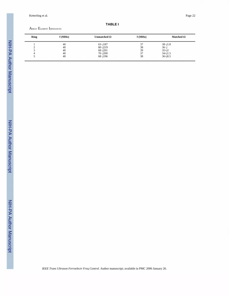
B. Matched TransducerImpedance measurements were made of each annulus in order to determine the most efficientelectrical matching. The unmatched impedance of each element varied only slightly in valueso that a single example is sufficient to demonstrate the approach and results [Fig.7(a)]. Theimpedances at 40 MHz for all of the rings are shown in Table I. The resistance for each elementwas ≈ 70 Ω and for matching purposes the reactive component was taken to be −j200 Ω. Wechose to match the transducer capacitance with an inductor in series on the PCB. For simplicity,all of the array elements utilized the same matching inductance.
A value of 0.82 μH was calculated as the best matching at 40 MHz [Fig.7(b)]. In the ideal casethe reactive component for each ring would be zero at 40 MHz. However, because we utilizedonly a single matching inductance, the frequency at which the matched reactance occurs variessomewhat for each ring [Tab. I]. Impedance plots found from the KLM model showed reactivevalues similar to the experimental results but did not predict the nearly 50% drop in resistance.The discrepancy likely occurs because the PCB and the flex circuit connection to the array adda complicated transmission line that was not fully accounted for in the KLM model.
With the impedance matching accomplished, we repeated the pulse/echo and insertion lossmeasurements. The time-domain pulse/echo signal and the KLM model prediction for Ring 1are shown in Fig. 8(a) scaled relative to the unmatched cases (Fig. 5(a)). The corresponding
Ketterling et al. Page 5
IEEE Trans Ultrason Ferroelectr Freq Control. Author manuscript; available in PMC 2006 January 26.
NIH
-PA Author Manuscript
NIH
-PA Author Manuscript
NIH
-PA Author Manuscript

frequency domain signals are shown in Fig. 8(b), again scaled relative to the unmatched cases.The KLM model predicts a decrease in bandwidth and a downward shift in fc, but less thanwhat was observed experimentally. This may be due partly to the pulse/receiver and partly tonot fully modeling the PCB and flex circuit.
The time domain pulse/echo for all five annuli are shown in Fig. 8(c) scaled relative to eachother. As in the unmatched case, the amplitude drops by ≈ 50% from Ring 1 to Ring 2 and thenremains relatively constant for the remaining rings. The spectra for all five annuli are shownin Fig. 9. The peak amplitudes for Rings 1 to 5 increased by 12, 13, 12, 10 and 11 dB,respectively, relative to the unmatched cases. The values of the peak spectral amplitude, fc,and BW for all five annuli are summarized in Tab. II. Comparing these values to the unmatchedcase, it can be seen that the increase in pulse/echo sensitivity has been achieved at the cost ofreduced bandwidth and a lower center frequency.
The IL data for the matched cases are summarized in Tab. II. As in the unmatched case, thesensitivities of the annuli decrease somewhat for the outer rings. The matched case representsan improvement in insertion loss of 9, 8, 9, 5 and 7 dB over the unmatched case for Rings 1 to5, respectively. The KLM model predicts a similar improvement in IL between the matchedversus unmatched cases (≈ 10 dB) but with the absolute magnitudes of the IL lower than whatwas experimentally observed.
Cross talk was measured for only the matched case and the results are summarized in TableIII. The table shows the cross talk for three excitation frequencies and three different transmitannuli. The cross talk was a minimum at the lowest frequency and increased with increasingfrequency: ≈ −50 dB at 25 MHz, ≈ −42 dB at 40 MHz, ≈ −36 dB at 55 MHz. The electricalcross talk primarily arises from fringing effects at the edges of the copper array pattern and ismost severe when there are sharp corners. The curvature of the rings is likely the main area ofthe copper pattern where fringing occurs rather than the parallel trace lines that lead out to theZIF connector pads.
Lateral beamwidth was measured only for the matched case and Fig. 10 shows the results. Thevalues of the −6-dB beamwidths for Rings 1-5 are 230, 118, 80, 67, and 59 μm, respectively.As in the insertion loss and spectra data, the peak amplitude decreases sharply when movingfrom Ring 1 to Ring 2 and then the remaining rings are similar in value. Qualitatively, thedecreasing beamwidth towards the outer rings may be understood in terms of the aperture. Alarger aperture has a smaller beamwidth for a fixed focal length. Quantitatively, the beamwidthvalues agree favorably with numerical beam calculations based on the spatial impulse responsemethod [29] using a typical pulse/echo response as the drive waveform in the model. Thenumerical beamwidth values for Rings 1-5 are 192, 104, 79, 66, and 58 μm, respectively. Thenumerical results vary somewhat depending on the drive waveform, but the trend of decreasingbeamwidth towards the outer rings will always hold true. Beam profiles of each annulus werealso recorded with a hydrophone and the results and trends were similar to those of the wirephantom.
IV. DISCUSSION
The performance of the PVDF array elements in terms of insertion loss, spectrum, andbandwidth, was similar to what has previously been reported for single element PVDFtransducers [1]. Electrical impedance matching led to an improvement in two-way insertionloss, as predicted by the KLM model. One concern with this transducer design is that there areseveral layers between the PVDF and the epoxy backing plug: epoxy-copper-polyimide. Theselayers may potentially lead to a complicated internal reflection that could deteriorate theperformance of the transducer. By studying the effects of the backing film thicknesses withour KLM model, we were able to determine how the layers affected performance. The copper
Ketterling et al. Page 6
IEEE Trans Ultrason Ferroelectr Freq Control. Author manuscript; available in PMC 2006 January 26.
NIH
-PA Author Manuscript
NIH
-PA Author Manuscript
NIH
-PA Author Manuscript

layer had the effect of making the PVDF a λ/4 resonator because of its high acoustic impedance(41.6 MRayls) relative to PVDF (4.2 MRayls) [1], [30]. The epoxy (3 MRayls) and polyimide(2.3 MRayls) layers primarily lowered the insertion loss and the BW. Internal reflections withinthe layers were not a problem because they were so thin and, at least for the polyimide andepoxy, their acoustic impedances were similar to that of PVDF.
The variation in sensitivities between the inner and outer rings was likely caused by two factors.First, the area of the outer rings was reduced slightly by the presence of the electrical traces(Fig. 1). As noted earlier, the array elements were designed to have equal areas for unbrokenrings. However, the break in the rings only reduced the area by ≈ 3% and does not explain the6 dB drop in sensitivity observed in Table II.
Second, during the press fit, the ball bearing may not apply a uniform force across the wholesurface area of the transducer. This problem may manifest itself in a slight defocusing of thetransducer towards the outer rings and also in an increased thickness of the epoxy adhesionlayer between the PVDF and the polyimide film towards the outer edge of the array. Thethickness increase would both decrease the capacitance (make the reactance more negative)and increase the insertion loss as observed in Table I [30]. The KLM model showed a decreasedsensitivity as the epoxy layer increases but did not capture the increased capacitance becausethe model assumes both sides of the PVDF have a conductive layer whereas our array designhas the epoxy layer between the PVDF and one of its conductive layers.
We attempted to address the potential non-uniform epoxy layer problem by increasing the innerdiameter of the press fit Teflon tube, thus increasing the distance between the active transducerarea and the outer edge of the press fit. This helped to ensure that deviations in the epoxyadhesion layer thickness would not impact the active area of the transducer. The transducertested here utilized this method with the larger Teflon tube and represented a considerableimprovement over earlier prototypes that had a larger transducer aperture.
The electrical cross talk was measured at a fairly low drive voltage (1 Vpp) with the assumptionthat the values scale linearly with voltage. While we did not repeat the measurement at multipledrive voltages, we did look at the electrical cross talk when the annular array was driven witha high voltage, broadband pulse. Again we measured Vpp on the drive element and Vpp as seenby the other elements into a 50 Ω termination. The results were most similar to the 55 MHzcase in Tab. III. Based on these observations, the electrical cross talk does appear to increasewith increasing voltage and is larger on transmit than on receive.
We were not able to observe any acoustic cross talk between elements. For this measurement,the transducer was submerged in water and one element was pulsed while the signals on theremaining elements were viewed with an oscilloscope. We then looked for signals showing asmall delay relative to the excitation pulse. Acoustic cross-talk primarily arises from lateralcoupling during the excitation pulse and is observed as a delayed pulse between array elements.The time delay of the pulse corresponds to the element separation distance and the shearvelocity of the transducer material. For PVDF, the lateral coupling coefficient is very low(k32 = 0.03) compared to the thickness coupling coefficient (kt = 0.18), and thus the lack ofacoustic cross coupling is consistent with the material properties of PVDF.
V. CONCLUSION
We have demonstrated that PVDF based annular arrays can be constructed using a copper cladpolyimide film to form the array electrode pattern. After impedance matching, the performanceof the array elements was similar to what has been reported for single element PVDFtransducers. The additional layers of material behind the PVDF film (epoxy-copper-polyimide)were found to not significantly hinder the transducer performance. This was due to their
Ketterling et al. Page 7
IEEE Trans Ultrason Ferroelectr Freq Control. Author manuscript; available in PMC 2006 January 26.
NIH
-PA Author Manuscript
NIH
-PA Author Manuscript
NIH
-PA Author Manuscript

thinness relative to λ and the close acoustic impedance match between the PVDF, epoxy, andpolyimide. Electrical cross talk was on the order of −42 dB at 40 MHz and increased somewhatfor high drive voltages. No significant acoustic cross coupling was observed between elements.
The advantage to the annular array demonstrated here is that its geometry is ideal for increasingthe depth of field. To achieve a reasonable increase in the depth of field, the F#(focal length/OD) needs be greater than 2 [31]. An F#=2 design with a total aperture of 6 mm permits anincrease in the depth of field to ≈ 6 mm versus ≈ 1 mm for a single element transducer of thesame geometry.
Our current efforts are to improve upon the present design and to develop a quasi-real timedata acquisition system. With the new prototype, we plan to fully utilize the imagingcapabilities of the annular array by acquiring data from individual transmit/receive annuli pairsand then implement digital synthetic aperture algorithms to reconstruct an image. For thetesting, we will initially utilize a wire phantom to validate the array performance and thenproceed to tissue models.
Figure 11 shows an example of data taken from the wire phantom. The phantom consists ofseven 25 μm wires spaced at 1 mm by 1 mm intervals. The transducer was scanned across thewire phantom with the center wire at the geometric focus. The image consists of 150 scan lines,found by averaging at each spatial location, spaced 25 μm apart. Ring 1 was pulsed and thereceived signal on Ring 5 was digitized.
VI. Acknowledgements
The authors wish to thank George Keilman and Chris Vecchio for many useful discussions.
BiographyJeffrey A. Ketterling (Member '02) was born in Seattle, WA, in 1970. He received the B.S.degree in electrical engineering from the University of Washington, Seattle, WA in 1994. Hereceived the Ph.D. in mechanical engineering from Yale University, New Haven, CT, in 1999.His thesis focused on experimental studies of phase space stability in single bubblesonoluminescence. Since 1999 Dr. Ketterling has been a Member of the Research Staff atRiverside Research Institute, New York, NY. His research interests include high frequencyarrays, transducer sound field modeling, and ultra sonic tissue characterization.
Orlando Aristizábal was born in Popayan, Colombia, on April 11, 1964. He received the B.S.degree in Physics in 1986 from City College of New York and the M.Phil. degree in Physicsin 1993 from the Graduate Center of the City University of New York. During this time hestudied the acoustomagnetic properties of Type I and Type II superconducting films. From1993 to 1995 he was a visiting scholar at the University of Illinois in Urbana-Champaign wherehe studied the electrical properties of YBCO and other high temperature superconducting thinfilms. Since 1996 he has been a Research Scientist in the in vivo micro-imaging laboratoryheaded by Dr. Daniel Turnbull at the Skirball Institute of Biomolecular Medicine, New YorkUniversity School of Medicine. His research interests are focused on the development and useof high frequency ultrasound imaging methods and their applications.
Daniel H. Turnbull (Member '92) was born in Niagara Falls, ON, Canada on April 11, 1955.He received the B.Sc. degree in Mathematics in 1978 from Brock University, St. Catharines,ON; the M.S. degree in Applied Mathematics in 1981 from the California Institute ofTechnology, Pasadena, CA; the M.A.Sc. degree in Mechanical Engineering in 1983 from theUniversity of Toronto; and the Ph.D. degree in Medical Biophysics in 1991 from the Universityof Toronto, Toronto, ON, Canada.
Ketterling et al. Page 8
IEEE Trans Ultrason Ferroelectr Freq Control. Author manuscript; available in PMC 2006 January 26.
NIH
-PA Author Manuscript
NIH
-PA Author Manuscript
NIH
-PA Author Manuscript

He was a Systems Engineer at Imatron, Inc., a medical imaging company in San Francisco,CA from 1983 to 1986, and was a Medical Physicist at the Toronto-Sunnybrook RegionalCancer Center in Toronto, ON, Canada from 1991 to 1994. In 1994 he became an AssistantProfessor in the Department of Medical Biophysics, University of Toronto, and soon aftermoved to New York University School of Medicine in New York, NY, where he was anAssistant Professor of Radiology and Pathology, and a member of the Structural BiologyProgram at the Skirball Institute of Biomolecular Medicine from 1994 to 2000. Since 2000, hehas been an Associate Professor of Radiology and Pathology, and a member of the StructuralBiology Program at the Skirball Institute of Biomolecular Medicine, New York UniversitySchool of Medicine in New York, NY. For the past decade, his research interests have beenbroadly focused on the use of ultrasound and magnetic resonance micro-imaging in biology.
Frederic L. Lizzi (S62-M71) was born in Brooklyn, NY, in 1942. He received the B.E.E.degree from Manhattan College, Bronx, NY, in 1963 and the M.S. and Eng.Sc.D. degrees fromColumbia University, New York, NY, in 1965 and 1971, respectively.
He is currently the Research Director of the Biomedical Engineering Laboratories at RiversideResearch Institute, New York, NY, where he has been pursuing biomedical research intherapeutic and diagnostic ultrasound since the 1960s. He serves as principal investigator fora number of research programs supported by the National Institutes of Health that deal withultrasonic imaging, tissue characterization, and therapeutic ultrasound. He is an adjunctprofessor at Cornell University and Columbia at University.
Dr. Lizzi is a Fellow of the American Institute of Ultrasound in Medicine (AIUM) and theAcoustical Society of America. He also is a member of the Advisory Editorial Board ofUltrasound in Medicine and Biology and a member of the board of the International Societyfor Therapeutic Ultrasound. Dr. Lizzi has served as a member of the Board of Governors ofthe AIUM and Chairman of the AIUM Bioeffects Committee. He has received the MayneordLecturer Award from the British Institute of Radiology, the AIUM William J. Fry MemorialAward, the AIUM Joseph Holmes Pioneer Award, and the Pioneer Award from the WorldFederation of Ultrasound in Medicine.
REFERENCES
1. Sherar MD, Foster FS. The design and fabrication of high-frequency poly(vinylidene fluoride)transducers. Ultrason. Imaging 1989;11:75–94. [PubMed: 2734975]
2. Foster FS, Harasiewicz KA, Sherar MD. A history of medical and biological imaging withpolyvinylidene fluoride (PVDF) transducers. IEEE Trans. Ultrason. Ferroelect. Freq. Contr2000;47:1363–1371.
3. Lockwood GR, Hunt JW, Foster FS. The design of protection circuitry for high-frequency ultrasoundimaging systems. IEEE Trans. Ultrason. Ferroelect. Freq. Contr 1991;38:48–55.
4. Lockwood GR, Foster FS. Modeling and optimization of high-frequency ultrasound transducers. IEEETrans. Ultrason. Ferroelecrt. Freq. Contr 1994;41:225–230.
5. Lockwood GR, Hazard CR. Miniature polymer transducers for high frequency medical imaging. Proc.SPIE Med. Imag 1998;3341:228–236.
6. Talman JR, Garverick SL, Morton CE, Lockwood GR. Unit-delay focusing architecture and integrated-circuit implementation for high-frequency ultrasound. IEEE Trans. Ultrason. Ferroelect. Freq. Contr2003;50:1455–1463.
7. Brown JA, Lockwood GR. A low-cost, high-performance pulse generator for ultrasound imaging.IEEE Trans. Ultrason. Ferroelect. Freq. Contr 2002;49:848–851.
8. Lockwood GR, Turnbull DH, Foster FS. Fabrication of high frequency spherically shaped ceramictransducers. IEEE Trans. Ultrason. Ferroelect. Freq. Contr 1994;41:231–235.
9. Aristizábal O, Turnbull DH. 44-MHz LiNbO3 transducers for UBM-guided Doppler ultrasound. IEEETrans. Ultrason. Ferroelect. Freq. Contr 2003;50:623–630.
Ketterling et al. Page 9
IEEE Trans Ultrason Ferroelectr Freq Control. Author manuscript; available in PMC 2006 January 26.
NIH
-PA Author Manuscript
NIH
-PA Author Manuscript
NIH
-PA Author Manuscript

10. Cannata JM, Ritter TA, Chen WH, Silverman RH, Shung KK. Design of efficient, broadband single-element (20-80 MHz) ultrasonic transducers for medical imaging applications. IEEE Trans. Ultrason.Ferroelect. Freq. Contr 2003;50:1548–1557.
11. Lockwood GR, Turnbull DH, Christopher DA, Foster FS. Beyond 30 MHz - Applications of high-frequency ultrasound imaging. IEEE Eng. Med. Biol. Mag 1996;15:60–71.
12. Silverman RH, Rondeau MJ, Lizzi FL, Coleman DJ. Three-dimensional high-frequency ultrasonicparameter imaging of anterior segment pathology. Ophthalmology 1995;102:837–843. [PubMed:7777285]
13. Turnbull DH, Starkoski BG, Harasiewicz KA, Semple JL, From L, Gupta AK, Sauder DN, FosterFS. 40-100 MHz B-scan ultrasound backscatter microscope for skin imaging. Ultrasound Med. Biol1995;21:79–88. [PubMed: 7754581]
14. Harland CC, Kale SG, Jackson P, Mortimer PS, Bamber JC. Differentiation of common benignpigmented skin lesions from melanoma by high-resolution ultrasound. Br. J. Dermatol2000;143:281–289. [PubMed: 10951134]
15. Vogt M, Knuttel A, Hoffman K, Altmeyer P, Ermert H. Comparison of high frequency ultrasoundand optical coherence tomography as modalities for high resolution and non invasive skin imaging.Biomedizinische Technik 2003;48:116–121. [PubMed: 12838793]
16. Foster FS, Pavlin CJ, Harasiewicz KA, Christopher DA, Turnbull DH. Advances in ultrasoundbiomicroscopy. Ultrasound Med. Biol 2000;26:1–27. [PubMed: 10687788]
17. Turnbull DH, Foster FS. Ultrasound biomicroscopy in developmental biology. Trends Biotechnol2002;20:S29–S33.
18. Phoon CKL, Turnbull DH. Ultrasound biomicroscopy-Doppler in mouse cardiovasculardevelopment. Physiol. Genomics 2003;14:3–15. [PubMed: 12824473]
19. Oralkan O, Ergun AS, Johnson JA, Karaman M, Demirci U, Kaviani K, Lee TH, Khuri-Yakub BT.Capacitive micromachined ultrasonic transducers: Next-generation arrays for acoustic imaging?IEEE Trans. Ultrason. Ferroelect. Freq. Contr 2002;49:1596–1610.
20. Fleischman A, Modi R, Nair A, Talman J, Lockwood G, Roy S. Miniature high frequency focusedultrasonic transducers for minimally invasive imaging procedures. Sens. and Actuators, A2003;103:76–82.
21. Ritter TA, Shrout TR, Tutwiler R, Shung KK. A 30-MHz piezo-composite ultrasound array formedical imaging applications. IEEE Trans. Ultrason. Ferroelect. Freq. Contr 2002;49:217–230.
22. Cannata, J.; Shrout, T.; Shung, K. Proc. IEEE 13th Int. Symp. Appl. Ferroelect. Nara; Japan: 2002.A 35 MHz linear ultrasonic array for medical imaging; p. 343-346.
23. Snook, K.; Shrout, T.; Shung, KK. Proc. IEEE 13th Int. Symp. Appl. Ferroelect. Nara; Japan: 2002.Design of a 50 MHz annular array using fine-grain lead titanate; p. 351-354.
24. Morton C, Lockwood G. Design of a 40 MHz annular array. Proc. IEEE Ultrason. Symp 2001;2:1135–1138.
25. Brown JA, Démoré CEM, Lockwood GR. Design and fabrication of annular arrays for high-frequencyultrasound. IEEE Trans. Sonics Ultrason 2004;51:1010–1017.
26. Alves CH, Shook K, Ritter T, Shung KK. High frequency single element and annular array transducersincorporating PVDF. Proc. SPIE Med. Imag 2000;3982:116–121.
27. Raum K, Obrien WD. Pulse-echo field distribution measurement technique for high-frequencyultrasound sources. IEEE Trans. Sonics Ultrason 1997;44:810–815.
28. Leedom D, Krimholtz R, Matthaei GL. Equivalent circuits for transducers having arbitrary even- orodd-symmetry piezoelectric excitation. IEEE Trans. Sonics Ultrason 1971;18:128–141.
29. Arditi M, Foster FS, Hunt JW. Transient fields of concave annular arrays. Ultrason. Imaging1981;3:37–61. [PubMed: 7195094]
30. Brown LF. Design considerations for piezoelectric polymer ultrasound transducers. IEEE Trans.Ultrason. Ferroelect. Freq. Contr 2000;47:1377–1396.
31. Arditi M, Taylor WB, Foster FS, Hunt JW. An annular array system for high-resolution breastechography. Ultrasonic Imaging 1982;4:1–31. [PubMed: 7199769]
Ketterling et al. Page 10
IEEE Trans Ultrason Ferroelectr Freq Control. Author manuscript; available in PMC 2006 January 26.
NIH
-PA Author Manuscript
NIH
-PA Author Manuscript
NIH
-PA Author Manuscript

Fig. 1.Example of positive array image. The kerf spacings between the annuli are 100 μm. The tracesto the right that permit electrical access to each ring and the spacings between them are also100 μm. The central annulus is Ring 1 and the outer annulus is Ring 5. Note that the scale isnot uniform.
Ketterling et al. Page 11
IEEE Trans Ultrason Ferroelectr Freq Control. Author manuscript; available in PMC 2006 January 26.
NIH
-PA Author Manuscript
NIH
-PA Author Manuscript
NIH
-PA Author Manuscript

Fig. 2.Press fit jig. The pressure plate and top plate are clamped down with screws on the threadedrod.
Ketterling et al. Page 12
IEEE Trans Ultrason Ferroelectr Freq Control. Author manuscript; available in PMC 2006 January 26.
NIH
-PA Author Manuscript
NIH
-PA Author Manuscript
NIH
-PA Author Manuscript

Fig. 3.Fully fabricated transducer. The active array is on top of the epoxy plug. The electrical tracesat the top of the image are inserted into the ZIF connector.
Ketterling et al. Page 13
IEEE Trans Ultrason Ferroelectr Freq Control. Author manuscript; available in PMC 2006 January 26.
NIH
-PA Author Manuscript
NIH
-PA Author Manuscript
NIH
-PA Author Manuscript

Fig. 4.PCB that links the traces on the polyimide to MMCX-BNC connectors. The polyimide wrapsaround and is inserted into the ZIF connector. This example also shows surface mount inductorssoldered in series onto the PCB. The PCB is wrapped with copper tape for electrical shielding.
Ketterling et al. Page 14
IEEE Trans Ultrason Ferroelectr Freq Control. Author manuscript; available in PMC 2006 January 26.
NIH
-PA Author Manuscript
NIH
-PA Author Manuscript
NIH
-PA Author Manuscript

Fig. 5.Comparison of KLM model results (dotted) to experimental measurements (solid) for Ring 1with no electrical matching. The results show the pulse/echo response in (a) the time domain,(b) the frequency domain, and (c) the time domain signal for all five array elements.
Ketterling et al. Page 15
IEEE Trans Ultrason Ferroelectr Freq Control. Author manuscript; available in PMC 2006 January 26.
NIH
-PA Author Manuscript
NIH
-PA Author Manuscript
NIH
-PA Author Manuscript

Fig. 6.Quartz plate pulse/echo power spectrum for all five rings of the annular array with no electricalmatching. The values are normalized to the peak value of Ring 1.
Ketterling et al. Page 16
IEEE Trans Ultrason Ferroelectr Freq Control. Author manuscript; available in PMC 2006 January 26.
NIH
-PA Author Manuscript
NIH
-PA Author Manuscript
NIH
-PA Author Manuscript

Fig. 7.Impedance of Ring 4 for the (a) unmatched and (b) matched case. The matched case has a 0.82μH inductor soldered on the PCB with the result of reducing the reactance (dashed) to nearzero at 40 MHz.
Ketterling et al. Page 17
IEEE Trans Ultrason Ferroelectr Freq Control. Author manuscript; available in PMC 2006 January 26.
NIH
-PA Author Manuscript
NIH
-PA Author Manuscript
NIH
-PA Author Manuscript

Fig. 8.Comparison of KLM model results (dotted) to experimental measurements (solid) for Ring 1with electrical matching. The results show the pulse/echo response in (a) the time domain, (b)the frequency domain, and (c) the time domain signal for all five array elements.
Ketterling et al. Page 18
IEEE Trans Ultrason Ferroelectr Freq Control. Author manuscript; available in PMC 2006 January 26.
NIH
-PA Author Manuscript
NIH
-PA Author Manuscript
NIH
-PA Author Manuscript

Fig. 9.Quartz plate pulse/echo power spectrum for all five rings of the annular array with a 0.82 μHinductor in series on the PCB. Amplitudes are relative to Ring 1 of the unmatched case.
Ketterling et al. Page 19
IEEE Trans Ultrason Ferroelectr Freq Control. Author manuscript; available in PMC 2006 January 26.
NIH
-PA Author Manuscript
NIH
-PA Author Manuscript
NIH
-PA Author Manuscript

Fig. 10.Pulse/echo lateral beamwidth for each annulus taken by scanning across a 25 μm wire target.
Ketterling et al. Page 20
IEEE Trans Ultrason Ferroelectr Freq Control. Author manuscript; available in PMC 2006 January 26.
NIH
-PA Author Manuscript
NIH
-PA Author Manuscript
NIH
-PA Author Manuscript

Fig. 11.B-mode image of a wire phantom found by mechanically scanning the annular array across thephantom. The image dimensions are ≈ 7 mm by 7 mm and the array was located to the left ofthe image. The data has been log compressed to provide better contrast. The dynamic range ofthe image is 64 dB.
Ketterling et al. Page 21
IEEE Trans Ultrason Ferroelectr Freq Control. Author manuscript; available in PMC 2006 January 26.
NIH
-PA Author Manuscript
NIH
-PA Author Manuscript
NIH
-PA Author Manuscript
NIH
-PA Author Manuscript
NIH
-PA Author Manuscript
NIH
-PA Author Manuscript
Ketterling et al. Page 22
TABLE IARRAY ELEMENT IMPEDANCES
Ring f (MHz) Unmatched Ω f (MHz) Matched Ω
1 40 63−j187 37 38−j1.82 40 80−j219 38 36−j3 40 68−j201 39 35+j24 40 70−j200 37 34+j1.55 40 68−j196 38 36+j0.5
IEEE Trans Ultrason Ferroelectr Freq Control. Author manuscript; available in PMC 2006 January 26.

NIH
-PA Author Manuscript
NIH
-PA Author Manuscript
NIH
-PA Author Manuscript
Ketterling et al. Page 23
TABLE IISUMMARY OF TRANSDUCER PERFORMANCE
Unmatched Matched
Ring fc(MHz)
BW6dB(%)
dBmaxfIL
(MHz) IL (dB) fc(MHz)
BW6dB(%)
dBmaxfIL
(MHz) IL (dB)
1 39 61 0 50 −35 35 36 12 38 −282 38 54 −6 45 −45 36 31 7 38 −333 39 53 −6 46 −44 36 33 6 40 −354 41 52 −6 50 −43 36 35 4 42 −385 42 57 −7 50 −43 37 39 4 41 −36
IEEE Trans Ultrason Ferroelectr Freq Control. Author manuscript; available in PMC 2006 January 26.

NIH
-PA Author Manuscript
NIH
-PA Author Manuscript
NIH
-PA Author Manuscript
Ketterling et al. Page 24
TABLE IIIELECTRICAL CROSS TALK FOR MATCHED TRANSDUCER
1
Ring 25 MHz 40 MHz 55 MHz
1 −55 - −50 −46 - −41 −39 - −352 −53 −42 −38 −46 −39 −35 −37 −35 −353 −53 −51 - −45 −43 - −36 −35 -4 −42 −51 −52 −40 −44 −40 −35 −36 −345 - −55 −51 - −46 −42 - −36 −35
1All values expressed in dB. A (-) indicates the excitation ring.
IEEE Trans Ultrason Ferroelectr Freq Control. Author manuscript; available in PMC 2006 January 26.