clara: circular linked-list auto and self refresh architecture · we present clara, a circular...
TRANSCRIPT
CLARA: Circular Linked-List Auto and Self RefreshArchitecture
Aditya [email protected]
Mike O’[email protected]
Evgeny [email protected]
Niladrish [email protected]
Joel [email protected]
Stephen [email protected]
ABSTRACTWith increasing DRAM densities, the performance and energy over-heads of refresh operations are increasingly significant. When thesystem is active, refresh commands render DRAM banks unavail-able for increasing periods of time. These refresh operations caninterfere with regular memory operations and hurt performance. Inaddition, when the system is idle, DRAM self-refresh is the domi-nant source of energy consumption, and it directly impacts batterylife and standby time. Prior refresh reduction techniques seek toreduce active-mode auto-refresh energy, reduce self-refresh energy,improve performance, or some combination thereof. In this paper,we present CLARA, a circular linked-list based refresh architecturewhich meets all three goals with very low overheads and withoutsacrificing DRAM capacity. This approach exploits the variation inretention time at a chip granularity as opposed to a DIMM-wide,rank granularity in prior work. CLARA reduces auto- and self-refresh by 86.2%, independent of workload. Auto refresh reduc-tion improves average CPU performance by 3.1% and 6.5% in thenormal and extended temperature range, respectively. GPU perfor-mance improves by 2.1% on average in the extended temperaturerange. DRAM idle power during self-refresh is reduced by 44%.The area overhead of CLARA in the DRAM is about 0.085% andnegligible in the memory controller.
CCS Concepts•Hardware→ Dynamic memory; •Computer systems organi-zation→ Architectures;
KeywordsDRAM, Auto refresh, Self refresh
1. INTRODUCTIONDRAM is a dynamic memory technology which requires peri-
odic refresh operations to maintain data integrity. These refreshoperations incur energy and performance costs, however. Whenthe system is active, auto-refresh commands render one or more
Permission to make digital or hard copies of all or part of this work for personal orclassroom use is granted without fee provided that copies are not made or distributedfor profit or commercial advantage and that copies bear this notice and the full cita-tion on the first page. Copyrights for components of this work owned by others thanACM must be honored. Abstracting with credit is permitted. To copy otherwise, or re-publish, to post on servers or to redistribute to lists, requires prior specific permissionand/or a fee. Request permissions from [email protected].
MEMSYS ’16, October 03-06, 2016, Alexandria, VA, USAc© 2016 ACM. ISBN 978-1-4503-4305-3/16/10. . . $15.00
DOI: http://dx.doi.org/10.1145/2989081.2989084
DRAM banks unavailable for some time, delaying processor re-quests requiring those banks and reducing performance. When thesystem is idle, the DRAM is responsible for refreshing itself. Theseself-refresh operations are a significant fraction of the energy of anidle system, and this energy consumption directly impacts batterylife and standby time in mobile devices. As DRAM densities con-tinue to increase, more refresh operations have to be performed ina given time period. As a result, the impact of refresh on systemperformance and power are also increasing. DRAMs are increas-ingly operating at higher temperatures due to close proximity tohigh-power processors in 2.5D/3D integrated systems as well. Op-erating in the extended temperature range (85−95 ◦C) doubles therequired refresh rate, further increasing the performance and energycosts of refresh operations.
It is well-known that different DRAM cells/rows have differentcharge retention times and, hence, different refresh requirements[24, 31]. This property has been effectively exploited to reduce thecost of refreshes and improve yields in a number of earlier propos-als [47, 34, 40, 6, 16, 10, 48]. These techniques typically profilethe retention time of each DRAM row, store that information inmain memory, memory controller, external EPROM device, or OSpage table, and then refresh each row at its required rate. The in-formation can be stored in a variety of data structures such as abloom filter, array, linked list, fat tree, or binary tree. For example,a bloom filter [34] can be used to test the presence of a DRAM rowin a set before sending a refresh request. A linked-list [48] can beused to create an arbitrary refresh sequence of DRAM rows. Thesetechniques aim to reduce auto-refresh energy, reduce self-refreshenergy, improve performance, or some combination of these.
We propose a linked-list based refresh scheme, CLARA, whichalso takes advantage of retention time variation to reduce the num-ber of refresh operations required and improve performance. Itachieves these goals with very low overheads and without sacrific-ing DRAM capacity. Our approach exploits the fact that a refreshoperation implicitly accesses the data in the row being refreshedin order to both store the refresh characterization in area-efficientDRAM cells, and to access that information on a refresh to indicatethe next row to be refreshed. This approach enables the followingkey benefits:• Reduces the number of active mode auto refresh commands that
must be sent to the DRAM, improving energy efficiency and per-formance.• Reduces the number of self-refresh operations in the low-power
standby mode, saving energy.• Exploits fine-grained retention time variation within a device.• Very low hardware overheads (<0.1% area).
The CLARA architecture reduces both auto- and self- refresh by86.2%, independent of the workload. The auto-refresh reduction
�������� ����������������
������ �� �
������ ���
�� ��� �� ��� �� ���
�� ��� �� ��� �� ���
�� ��� �� ��� �� ���
���������������������������� ���
�� ���������
�� �������� �
�� ���
�� ��
�� ���
�������
����
����� �
������
�� �������
���
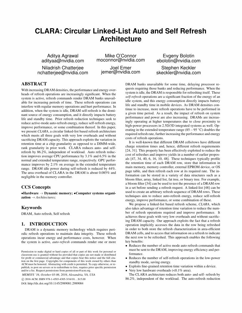
Figure 1: A DRAM channel organization. The circular inset shows the CLARA refresh data as described in Sec. 3.
improves CPU performance by 3.1% and 6.5% in the normal andextended temperature range, respectively. GPU performance im-proves by 2.1% in the extended temperature range. CLARA saves44% of DRAM idle power due to the reduction of self-refresh op-erations.
2. BACKGROUND
2.1 DRAM OrganizationThe DRAM main memory is organized into channels. As shown
in Fig. 1, each channel has independent command, address and datasignals. Each channel contains one or more independent ranks.Each rank typically consists of multiple DRAM chips, often 4, 8or 16. A DRAM chip is also referred to as a DRAM device. EachDRAM device, in turn, has one or more independent banks, hence-forth referred to as device banks. Each device bank typically hasthousands of rows, henceforth referred to as device rows.
The DRAM devices in a rank work in unison and appear as asingle entity to the memory controller. As shown in Fig. 1, multipledevice banks together constitute a Rank-wide bank and multipledevice rows together constitute a Rank-wide row.
2.2 Refresh MechanismAccording to DDR standards [17, 18, 20, 36] each row should
be refreshed once every 64 ms in the normal temperature range(< 85 ◦C) and once every 32 ms in the extended temperature range(85−95 ◦C). For the following discussion, we will assume the nor-mal temperature range of operation. Let N, be the number of rowsin a bank. In the past, the time interval between refresh requeststo a bank, tREFI , was 64 ms/N, and each request refreshed 1 row.With increasing DRAM densities the number of rows per bank (N)has also increased. The value of tREFI has been held constant, how-ever, at 64 ms/8192 ≈ 7800 µs, requiring multiple rows, M, to berefreshed with every request.
Each refresh request lasts for a refresh cycle time, tRFC, whichincludes the time to refresh M rows, precharge the bank and recoverthe charge pump. Refreshing multiple rows allows the DRAM ven-
dor to optimize the process and amortize precharging and recover-ing the charge pump over several row-refresh operations.
Serial and Parallel Refresh. While DRAM vendors do not dis-close their specific implementation of multi-row refresh, timing pa-rameters suggest that the mechanism is serial when M ≤ 4 and par-allel when M > 4. Table 1 shows the refresh cycle time, tRFC whendifferent number of rows, M are refreshed using the DDR4 FineGranularity Refresh (FGR) [20] mode. Let tRC
1, be the time to re-fresh a single row and trec, be the recovery time. When M ≤ 4,tRFC = M× tRC + trec. This suggests that the rows are refreshedsequentially. However, when M > 4, tRFC < M× tRC + trec. Thissuggests that multiple rows in different subarrays, are refreshed inparallel.
Capacity N FGR M M.tRC + trec tRFCMode
4 Gb 32 K 4x 1 110 ns 110 ns4 Gb 32 K 2x 2 160 ns 160 ns4 Gb 32 K 1x 4 260 ns 260 ns8 Gb 64 K 1x 8 460 ns 350 ns16 Gb 128 K 1x 16 860 ns 480 ns
Table 1: Serial and parallel multi-row refresh.2
Auto and Self Refresh Schemes. To maintain data, DRAMrows must be refreshed in both active (auto-refresh) and idle (self-refresh) modes. Different DDR standards use different auto-refreshschemes such as all-bank, per-bank and single-bank refresh. In theall-bank scheme [18], a refresh command refreshes multiple rowsin every bank of the rank. The entire rank is unavailable for tRFC.In the per-bank scheme [36], a refresh command refreshes multiplerows in a single DRAM bank. However, the banks are refreshed in
1tRC is the row cycle time and is equal to the row activate time,tRAS plus the row precharge time, tRP.
2Number of rows, N is for a DDR4 x8 device. tRC = 50 nsfor the slowest DDR4 part i.e. DDR4-1600 (12-12-12). trec wasestimated to be 60 ns. tRFC values are from DDR4 standard [20].
2.0 2.5 3.0 3.5 4.0
−5
−4
−3
−2
−1
01
2
log10 (Tret in msec)
Sta
ndar
d D
evia
tion
(σ)
●
●
●
●
●
●
●
●
Main Distribution
Tail Distribution
● Silicon DataCell Distribution ModelDevice Row Distribution
Figure 2: DRAM cell [24] and device row Tret distribution.
a strict round robin order. In the single-bank scheme [25], the bankscan be refreshed in any order. This allows the memory controllerto schedule refresh operations to otherwise idle-banks, optimizingperformance. DDR4’s Fine Granularity Refresh (FGR) [20] is sim-ilar to all-bank refresh except that it allows refreshing one-half andone-quarter number of rows on each refresh command, reducingthe period for which the rank is unavailable.
In all the above schemes the refresh row address is maintainedinternally by the DRAM devices and is not sent by the memory con-troller. Earlier DRAMs provided a RAS-only refresh scheme whichallow the memory controller to specify a row address for the refreshoperation. This refresh mode in no longer supported in the mostrecent DRAM families. A regular DRAM ‘activate’ operation fol-lowed by a ‘precharge’ can still allow the memory controller to ef-fectively refresh a given row, however. These targeted-row refreshoperations are used by the refresh reduction approaches in [23, 34].
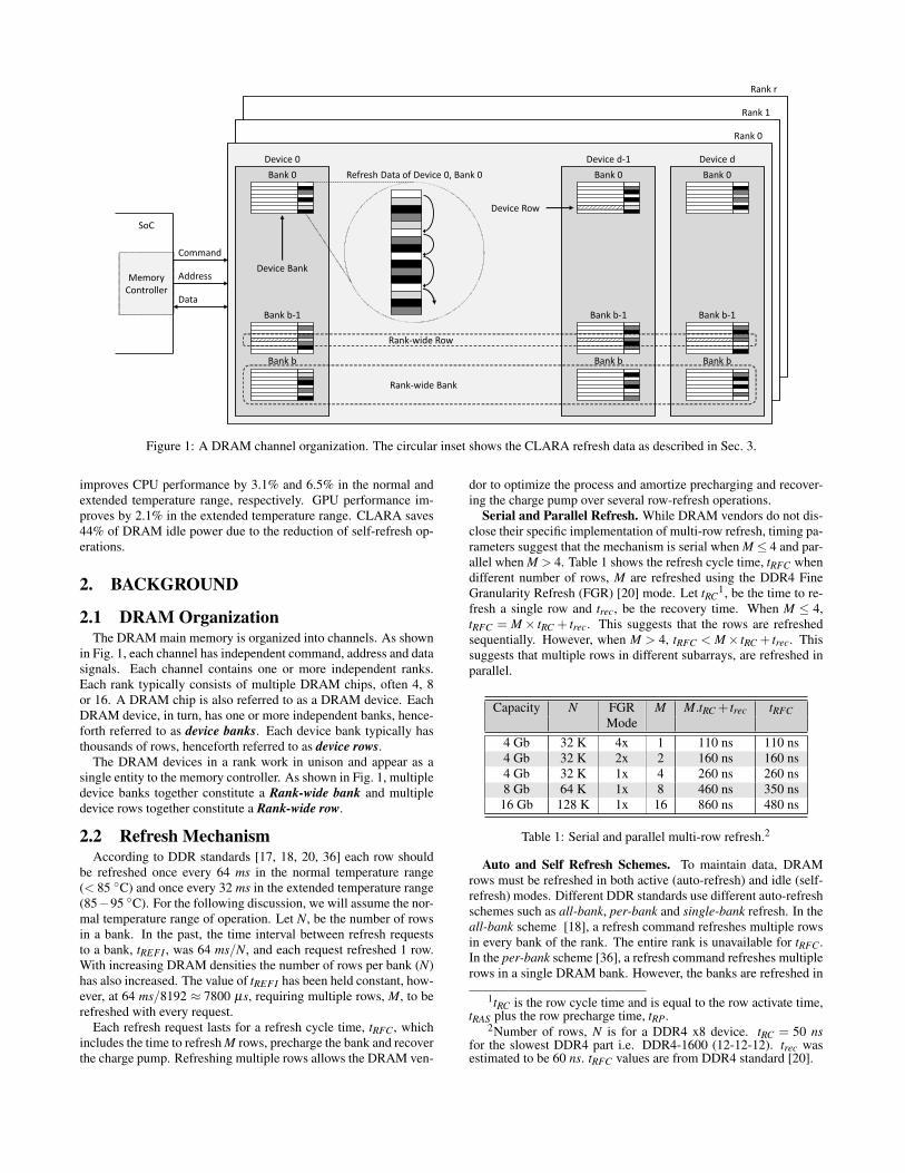
2.3 Retention Time VariationIt is well known that different DRAM cells have different charge
retention times. Kim and Lee [31] obtained the distribution for100, 60 and 50 nm and have projections for 10 nm. A model for thecell retention time distribution was first proposed by Hamamotoet al. [24]. The retention time of a cell, Tret can be expressedas Tret = A× e(Ea/kT ) where, Ea is the trap activation energy, k isthe Boltzmann constant, T is the absolute temperature, and A isthe constant of proportionality. A normal distribution in the trapactivation energy produces a log-normal distribution of cell Tret .
As shown in Fig. 2, the cumulative distribution function (CDF)of the cell retention time consists of a Main Distribution and a TailDistribution. Hamamoto et al. determined that µ(Ea) = 0.68 eVand σ(Ea) = 0.008 eV for the main distribution; and µ(Ea) =0.77 eV and σ(Ea) = 0.039 eV for the tail distribution.
The retention time of a device row can be obtained by determin-ing the minimum Tret of all cells constituting the row. Fig. 2 alsoshows the device row Tret distribution. As shown in the plot andtabulated below, the percentage of device rows with 64 ms<=Tret<128 ms is only about 0.03%. More than 90% of device rows have aTret>= 512 ms. However, current DRAM devices refresh each rowevery 64 ms. This is very pessimistic and results in performanceand power loss. We exploit this variation to reduce both auto andself-refresh, thereby improving performance and power.
3. CLARA ARCHITECTURE
Tret Percentage64 ms ∼ 0.03
128 ms ∼ 0.60256 ms ∼ 7.5512 ms ∼ 91
Table 2: DRAM device row Tret distribution.
CLARA exploits the variation in retention time at a DRAM de-vice level to reduce both auto and self refresh. In order to take ad-vantage of this variation, the retention characteristics of each devicerow must first be profiled. We discuss this profiling and associatedguard-banding in detail in Sec. 4.1. For the purposes of this section,we assume the device rows have been profiled. We describe howthe device rows are categorized according to their retention time,and then we describe the linked-list architecture that enables onlythe necessary rows to be refreshed at the required rates.
3.1 Categorizing the RowsIn order to simplify the hardware, we group rows with similar
retention times into groups that will be refreshed at the same rate.Depending on the Tret , we bin the device row into one of 4 cate-gories viz. 64 ms, 128 ms, 256 ms or 512 ms. We call the numberof rows in a device bank with Tret of 64 ms, 128 ms and 256 ms as α ,β , and γ respectively. If the total number of rows in a device bank isN, the number of device rows with Tret of 512 ms = N−α−β −γ .
We call an interval of 64 ms an epoch. Thus, a device row withTret = 64 ms will require a refresh every epoch, a device row withTret = 128 ms will require a refresh every alternate epoch, and soon, as summarized in Table 3.
From the table, we observe that in epochs 0, 2, 4 and 6, onlyrows with Tret = 64 ms, i.e. α rows, require refresh; in epochs 1and 5, rows with Tret = 64 ms and 128 ms, i.e. α +β rows, requirerefresh; and in epoch 3, rows with Tret = 64 ms, 128 ms and 256 ms,i.e. α+β +γ rows, require refresh. Finally, in epoch 7, all rows, i.e.N rows, require refresh, and is the same as the conventional refreshscheme. The different epochs have different refresh requirements.Overall, by refreshing only the required rows in each epoch, we canreduce refresh overheads. Our proposed linked list based refresharchitecture achieves this goal.
Epoch Tret = Tret = Tret = Tret = # Refresh(64 ms) 64 ms 128 ms 256 ms 512 ms Required
0 Y α
1 Y Y α +β
2 Y α
3 Y Y Y α +β + γ
4 Y α
5 Y Y α +β
6 Y α
7 Y Y Y Y N
Table 3: Variable refresh requirements.
3.2 Linked List ArchitectureThe key insight behind the CLARA architecture is that when a
row in a DRAM device is refreshed, the data in the row is readinto the sense-amplifiers in order to be restored back into the bit-cells. We take advantage of this implicit read operation in order totraverse a linked-list of rows with identical refresh requirements. Inthis section we describe how the linked-list is stored and organizedin the device bank, and then explain how the refresh logic in the

���������
����
����
�����
� ���
������
� �������
����� �� �����
� �������
����� �������
� �������
����� ��� ����
Figure 3: Circular linked-list in a device bank.
device bank uses this linked-list to refresh only the required devicerows in each epoch, during both auto and self refresh.
Linked List Storage and Organization. Fig. 1 shows a devicebank with device rows. We propose to add a few bits to each devicerow. These additional bits are called refresh-data bits. The data andrefresh-data bits share the same access logic such as word lines, rowdecoders etc., and are activated/refreshed at the same time. We ex-ploit the fact that a row refresh operation effectively reads the entirerow (data and refresh-data). In addition to being written back to thearray, the refresh-data is used internally by the device bank refreshlogic to determine the next refresh row address. The refresh-databits are not read or written by the memory controller except duringconfiguration.
As shown in the circular inset in Fig. 1 and in greater detail inFig. 3, the refresh-data within each bank is organized so as to forma circular linked list of rows. The refresh-data bits hold only theaddress offset to the next node (row). The first row of each devicebank, i.e. address = 0, is assumed to have a Tret of 64 ms andserves as the head of the linked list. As shown in Fig. 3, we firstlink all rows with Tret = 64 ms, then link all rows with Tret = 128 msand then link all rows with Tret = 256 ms. The last row with Tret= 256 ms points to the first row. In Fig. 3 the refresh-data hasbeen replicated for clarity. In Sec. 3.5, we describe in detail how togenerate this linked list.
In addition, there are three registers which hold the count of rowswith Tret = 64 ms, 128 ms and 256 ms, i.e. the values α , β , and γ
respectively. It follows that α +β + γ is equal to the length of thelinked list.
From Table 3, in epoch 7, when rows with Tret = 512 ms arerefreshed, all other rows are refreshed as well. This is the same asconventional refresh and no refresh-data is used. Therefore, thereis no need to include rows with Tret = 512 ms in the linked list orprovide a register to hold the count of rows with Tret = 512 ms.
Basic Operation. The linked-list organization allows us to re-fresh only the required device rows in each epoch. In epochs 0, 2,4 and 6, only rows with Tret = 64 ms require refresh, which are thefirst α entries in the linked list; in epochs 1 and 5, rows with Tret =64 ms and 128 ms require refresh, which are the first α +β entriesin the linked list; and in epoch 3, rows with Tret = 64 ms, 128 msand 256 ms require refresh, which are the first α +β + γ entries inthe linked list. In epoch 7, all N rows are refreshed and the linkedlist is not used. At the beginning of each epoch we start at the headof the linked list. Also, since the organization is a linked list andis circular, it can easily handle additional requests in any epoch. Afew additional requests can arrive in the case of multi-row refreshand when the system has multiple banks and devices, as explainedbelow.
For self-refresh, the control logic in the bank uses the three reg-ister values (α, β , γ) to generate the appropriate number of refreshcommands in every epoch. For auto-refresh, the memory controllermaintains a copy of the same three register values, and sends the ap-propriate number of auto-refresh commands in every epoch. Notethat the self-refresh logic and the memory controller do not needto know which device-rows require refresh, only how many requirerefresh in a particular epoch.
Supporting Multi-Row Refresh. In conventional gigabit de-vices, each request typically refreshes 2, 4, 8 or more rows. InCLARA, we refresh the same number of rows in every command.However, we obtain the row addresses from the linked list.
Assuming, each command refreshes M rows, it follows that thedevice bank should receive at least dα/Me requests in epochs 0, 2,4 and 6; at least d(α +β )/Me requests in epochs 1 and 5; and atleast d(α +β + γ)/Me requests in epoch 3. In epoch 7, it shouldreceive dN/Me requests.
A refresh request can arrive from either the memory controlleror the internal self-refresh logic. On receiving a refresh request,the bank refreshes M rows of the linked list following the steps inProcedure 1, where N is the number of rows in a device bank, rowis the array of rows in the bank, refreshdata is the associated arrayof refresh-data in the bank, epoch is the current refresh epoch, andaddress is the refresh row address. address is reset to zero, at thebeginning of every epoch.
Procedure 1 Linked-list based device bank refresh logic.
count = 0while count < M do
Refresh row[address]if epoch = 7 then
address = address+1else
address = address+1+ refreshdata[address]end ifaddress = address mod Ncount = count +1
end while
3.3 Supporting Multiple Banks & DevicesThe description above focused on a single bank within a single
device. In practice, a memory channel consists of multiple rankseach with multiple devices and multiple banks. However, it is im-portant to note that all banks in all devices have the same statisticaldistribution (mean and variance) of retention times. Therefore, thevalues of α , β and γ are similar for all device banks. For example,the number of rows with Tret = 64 ms is similar across all devicebanks.
Therefore in CLARA for auto-refresh, the memory controllerstores and uses only the values of max(α), max(β ) and max(γ).This results in a small number of additional refresh operations insome device-banks. This is easily handled by the circular linked-list design. However, the big advantage is very small storage andcontrol overheads in the memory controller, as explained belowwith the help of an example. For self-refresh, the control logic inevery device bank uses the local values of α , β , and γ , as alreadyexplained.
Let’s assume there are two devices P and Q in a rank, each with 2banks (0 and 1). Let the distribution of Tret i.e. values of α , β and γ ,for the 4 device banks be as shown in Table 4. These values are fora bank with N = 64 K rows and follow the distribution as obtainedin [24]. For these values, max(α) = A = 28, max(β ) = B = 440

and max(γ) = Γ = 5225. Also, assume each auto-refresh commandrefreshes M = 8 rows. Given the values of A, B, Γ, N and M, wecan calculate the number of auto-refresh commands in each epoch.
Count P0 Q0 P1 Q164 ms (α) 17 28 23 18128 ms (β ) 407 386 396 440256 ms (γ) 5080 5179 4997 5225512 ms 60032 59943 60120 59853Total 65536 65536 65536 65536
Table 4: Example Tret distribution of 4 device banks.The memory controller sends dA/8e i.e. 4 requests in epochs
0, 2, 4 and 6; d(A+B)/8e i.e. 59 requests in epochs 1 and 5;and d(A+B+Γ)/8e i.e. 712 requests in epoch 3. In epoch 7,all rows are refreshed and the controller sends the usual 8 K re-quests. Overall, in 8 epochs, the CLARA memory controller sends4×4+2×59+712+8192= 9038 requests. A conventional mem-ory controller will send 8 K requests every epoch and 64 K overall.This is a significant reduction in the number of auto-refresh com-mands over the conventional scheme.
These values can be used for all refresh schemes such as all-bank, per-bank, single-bank, and Fine Granularity Refresh (FGR).In FGR, the memory controller can setup the banks to refresh one-half or one-quarter rows every auto-refresh command. In this mode,the memory controller can repeat the above calculations using M =4 or M = 2, instead of M = 8; or simply double or quadruple thepreviously calculated values. Using per bank α , β , and γ valuesinstead of A, B, and Γ values would further reduce the single-bankrefresh by≈ 0.27% and the all-bank refresh by≈ 0.03%. The stor-age and complexity reduction in the memory controller by usingjust 3 values far outweigh these additional savings.
3.4 Hardware ImplementationFig. 4 shows the hardware implementation of the linked-list
based refresh logic in the device bank. The additional blocks re-quired by our scheme are shown in gray, and consist of a 3-bitepoch counter, an adder and a multiplexer. Every epoch i.e. 64 ms,the timer increments the epoch counter as well as resets the rowaddress to zero. Depending on the epoch, the multiplexer choosesthe address from either the linked list or the conventional addressincrementor.
Timing Overhead. As it is in conventional devices, this addressgeneration logic is used when the row is being written back fromthe sense amplifiers to the array, and it is not in the critical pathof the refresh operation. The delay introduced by an adder and amultiplexer is insignificant compared to the row precharge time,tRP, which is about 15 ns [20, 2, 19] and hence, there is no timingoverhead.
Area Overhead. As mentioned in Sec. 3.2, the refresh-data bitsare stored as additional bits with every row. The refresh-data stor-age overhead is, however, very small. Consider, for example, astate of the art DDR4, 8 Gb, x8 device [20]. Each device bank hasN = 65536 rows, with a device row size of 2 KB. If the numberof refresh-data bits, L = log2N = 16 bits, the storage overhead is(16/16384) = 0.098%. This is an insignificant overhead. In Sec-tion 6.1, we show that we can reduce this overhead even more.
The area overheads in the memory controller are three 16-bitregisters, an adder, a shifter and some control logic to send the ap-propriate number of auto-refresh commands in every epoch. Theseare very small overheads. CLARA uses the same auto-refresh com-mand as in conventional systems and does not introduce any newrefresh commands.
���������
�����
����
��
� ���
���������
����������
������
�����������
����
Figure 4: Linked-list based device bank refresh logic.Power Overhead. Accessing 16 extra bits for every 16K bits has
insignificant power overhead of 0.098% during activate, prechargeand refresh. There is no overhead on read, write or bus power.Overall, power saved during active (2-6%) and idle (44%) far out-weigh the overheads. (See evaluation).
3.5 Device Bank Linked-List GenerationAs mentioned in Sec. 3.2, the refresh-data within each device
bank is organized so as to form a circular linked-list of rows. Therefresh-data bits hold the address offset to the next node. Let offsetbe the address offset between two nodes of the linked list. If thenumber of refresh-data bits is L, then the maximum offset distance,D = 2L, (1 through 2L). If N is the number of rows in a bank and ifL= log2N, then D=N, i.e. the maximum offset distance is equal tothe number of rows in a bank. In this case, constructing the linkedlist as described in Sec. 3.2 is always possible and straightforward.
When L < log2N, three cases arise. We will explain the linkedlist construction for each case using an example. For these exam-ples, let N = 20, L = 3, and D = 8.Case 1: offset ≤ DAs shown in Fig. 5a, the offset between rows with Tret = 64 ms;between the last row with Tret = 64 ms and the first row with Tret= 128 ms; between rows with Tret = 128 ms and so on is less thanD. In this case, a linked list can be easily formed.
Case 2: offset > DAs shown in Fig. 5b, the offset between the third and fourth rowswith Tret = 64 ms is larger than D. In this case we find a victim rowwhose offset ≤ D and Tret is larger than the current Tret value be-ing linked, in this case 64 ms. We then demote its Tret value to thecurrent Tret value being linked, in this case 64 ms. Effectively, weuse victim rows as stepping stones to aid the linked list construc-tion. Obviously, the number of victim rows falls with increasingD.When it is possible to pick a victim row from among multipleeligible rows, we heuristically select the one which maximizesthe offset, as shown in Fig. 5b. In some cases we might need tofind multiple victim rows between a pair of rows. Again, we selectvictim rows which maximize the offset so that the total number ofvictim rows between the pair of rows is minimized.If the offset between, say the last row with Tret = 64 ms and the

�����
�
(a) Case 1
������
�
�����
�
(b) Case 2
� �
�
�
�����
�
(c) Case 3
������
�����
�����
�����
Figure 5: Device bank linked-list generation.
first row with Tret = 128 ms is larger than D, then we find a victimrow whose offset ≤ D and Tret is larger than 128 ms. We thendemote its Tret to the higher of the two endpoints, in this case128 ms.
Case 3: (offset > D) && (!victim row)As shown in Fig. 5c, the offset between the first and second rowswith Tret = 128 ms is larger than D. In addition, we cannot find avictim row as all the intermediate rows have Tret = 64 ms. In thiscase, we demote all rows of the current Tret value being linked tothe next lower Tret value. In our example, we demote all rows withTret = 128 ms to 64 ms. We then have to redo the linked list for Tret= 64 ms, as shown in Fig. 5c. If we now continue to link rows withTret = 256 ms, we will encounter the same issue and those rowswill also need to be demoted to 64 ms. This case happens whenthe maximum offset, D is almost equal to the number of retentiontime bins. In our proposal, this happens when D = 4 i.e. L = 2.
In our evaluation we show the trade-off between the number ofrefresh-data bits and refresh reduction.
4. RELATED ISSUES
4.1 Profiling and ConfigurationInitialization. At power-on, the DRAM module and memory
controller are set by default to the traditional mode of refreshingall DRAM rows at the default maximum rate. The system softwareor BIOS is responsible for reading the refresh profile linked-listinformation from disk or non-volatile memory and populating therefresh linked-list held in each DRAM row via a new DRAM com-mand (an extension of the existing MRS commands). This com-mand writes specified refresh-data to the currently activated row.
At the time the system is first commissioned or after any DRAMmodule is replaced, which can be detected utilizing serial num-ber data in the SPD data, no refresh profile data is available. Thesystem software manages refresh characterization of the module(s)and the construction of the linked-list, as described below. Notethat this characterization and linked-list construction has to be doneonly once.
Profiling and Linked-List Construction. The first step towardsexploiting variation is to profile the Tret of each device row. Avariety of proposals discussing variation in DRAMs [34, 47, 31,24] and eDRAMs [29, 32, 49, 15, 4, 5] have used and/or proposedTret profiling schemes.
Profiling and linked-list construction cannot be done on a testeras the information would be lost soon after. In-situ profiling of therefresh characteristics of the module may not represent the worst-case temperature and voltage, however, the behavior of DRAM
cells under different temperature and voltage conditions is reason-ably well characterized. These effects and others can be accountedfor analytically and with the application of appropriate guard-bands.
Profiling under DPD and VRT. For CLARA, to protect againstDPD effects, we use the test patterns in [33]. The profiling temper-ature is obtained from the on-chip temperature sensor and then theTret value at 85 ◦C is obtained using the equation in [4, 14]. Weapply a guard band to protect against worst-case voltage. Finally,to protect against VRT effects, we apply a guardband of 4x. This isbecause experimental data in [33] shows that the maximum changein Tret due to VRT is ∼ 4x.
Note that the memory vendor guarantees that all lines have Tret>= 64 ms at 85 ◦C even under worst-case voltage and VRT. There-fore, even if we apply a very large guard band (voltage and VRT)on the measured values, all rows will have a Tret of 64 ms but notlower.
Binning. Depending on the precision of the profiling routine, themeasured Tret values can take a large number of distinct values. Tosimplify the hardware implementation, we use only a finite set, S ofTret values. We choose, S ={64 ms, 128 ms, 256 ms, 512 ms}. Us-ing a larger set by adding a bin for 1024 ms offers only marginallymore savings as shown in Sec. 6.1. Note that there are no rows withTret less than 64 ms at 85 ◦C.
4.2 Tester & Testing TimeA tester checks the functionality of DRAM array bits and pe-
ripheral logic at the worst case temperature and voltage. Somerepairs, using spare rows and/or columns, are also performed toimprove yields. CLARA’s overhead in the DRAM array is onlyabout 0.098%. The additional blocks introduced in the peripherallogic are an adder, a multiplexer and a counter. Hence, the testingoverheads are minimal.
Note that profiling or linked-list construction is not done on thetester. Also chips which pass are guaranteed to have a Tret>= 64 msat 85 ◦C even under Data Pattern Dependence (DPD) and VariableRetention Time (VRT) effects.
4.3 Serial and Parallel RefreshLet M be the number of rows refreshed every command. If the
rows are refreshed sequentially (typically when M ≤ 4) the linkedlist organization and the refresh logic are as described in the sec-tions above. If rows from multiple subarrays are refreshed in paral-lel (likely when M≥ 8), multiple linked lists can be maintained andtraversed. For example, assume the upper and lower half of a bankeach refresh 4 lines sequentially. Also assume the upper and lowerhalves work in parallel to refresh M = 8 rows every command. Inthis case we maintain and traverse two smaller linked lists, one each

CPU ParametersChip 4 core CMPCore 3.2 GHz, 4 issue Out-of-OrderInstruction L1 32 KB, 2 way, Private, Write throughData L1 32 KB, 2 way, Private, Write throughL2 256 KB, 8 way, Private, Write backL3 4 MB, 4 banks, Shared, Write backCoherence Snoopy MESI Protocol at L2Line Size 64 BytesMain Memory 32 GB, DDR3L-1600, 25.6 GB/s
CPU Memory ParametersChannels 2Ranks per Channel 2Device Width 8 bitsDevices per Rank 8Device Density 8 GbBanks per Device 8Rows per Bank 64 KColumns per Bank 2 K
Device Timing ParametersDevice Micron MT41K1G8 [19]tREFI (< 85 ◦C) 7800 nstREFI (85−95 ◦C) 3900 nstRFC 350 nstRCD− tRP−CL 11-11-11 DRAM clocks
Table 5: CPU architectural parameters.
for the upper and lower half. The upper and lower halves each willhave the logic as in Fig. 4.
4.4 Soft Error Detection and RecoveryAccording to [44] ∼ 50% of DRAM errors are single bit errors.
We can efficiently detect these common bit errors in the linked-list values using a parity. Alternatively, stronger error detectionand correction could be added to reliability conscious systems withlittle overhead — even the extreme of triple-redundancy for alllinked-list values increases the overhead from 0.098% to 0.294%.
The linked list value is checked for errors in parallel with thenext row address generation in Fig. 4. If the check fails duringauto-refresh, the refresh logic can notify the MC using a dedicatedpin. The memory controller can then set the bank or the entirerank (depending on ‘single-bank’ or ‘all-bank’ scheme) to operatein epoch 7 (conventional) and refresh all rows every epoch, untilit reloads the correct refresh-data to rebuild the linked list. If thecheck fails during self-refresh, the refresh logic can switch to epoch7 and refresh all rows every epoch. It can notify the memory con-troller immediately or on exit from self-refresh mode.
4.5 Temperature AdaptationIn the extended temperature range (85−95 ◦C), the refresh rate
is doubled. In this range, CLARA reduces the epoch length from64 ms to 32 ms. The MC and the self-refresh logic initiate thesame number of refreshes, as obtained in Sec. 3.3 and Sec. 3.2,respectively, but in half the time. The timer in Fig. 4 incrementsthe epoch and resets the row address every 32 ms instead of 64 ms.
5. EVALUATION SETUP
5.1 Architectural ParametersWe evaluate CLARA on a simulated 4 core chip multi-processor
(CMP). Each core has a 4 issue, out-of-order execution engine run-
GPU ParametersNumber of SMs 30Threads per SM 1024Warp Size 32L1/L2/Cacheline Size 32 KB / 786 KB / 128 BMain Memory GDDR5
GPU Memory ParametersChannels 6Ranks per Channel 1Device Width 32 bitsDevices per Rank 2Device Density 16 GbBanks per Device 16 banks in 4 bank-groupsRows per Bank 64 KRow Size 2 KB
Device Timing ParametersDevice Hynix H5GQ1H24AFR [1]tREFI 3900 nstRFC 350 nstRCD− tRP−CL 12-12-12 ns
Table 6: GPU architectural parameters.
ning at 3.2 GHz. Each core also has a private instruction L1 cache,a data L1 cache and a unified L2 cache. The cores share a L3 cache,which is divided into 4 banks. The chip employs a snoopy MESIcoherence protocol between the L2s. The L3 cache is connected tothe off chip main memory.
The CPU main memory is organized as 2 channels of DDR3L-1600, with a peak bandwidth of 25.6 GB/s. Each channel has 2ranks and each rank has 8 banks. The total memory capacity is32 GB. In normal operating conditions (< 85 ◦C), the memory con-troller issues a refresh request every 7800 ns (tREFI). In extendedtemperature range (85−95 ◦C), the memory controller issues a re-fresh request every 3900 ns (tREFI). Higher temperatures are likelyin server environments, 3D stacked organizations, automotive sys-tems etc. The architectural parameters are summarized in Table 5.Detailed DRAM timing parameters were obtained from [19].
We evaluate the impact of CLARA on a throughput processingenvironment using the GPGPUSim [7] simulator. We simulate aGTX-480-like system that has 30 SMs, each with 1024 threads(warp-size of 32) and a 32 KB L1 cache. We simulate 6 mem-ory partitions, each with a 128KB L2, and a 64-bit DRAM channelcomprised of two x32 GDDR5 devices. Each channel has 16 banksorganized into 4 bank groups. We assume a futuristic 16 Gb de-vice with 64 K rows and tRFC = 350 ns. A GDDR5 device issuesa refresh request every 3900 ns (tREFI). The GPU architecturalparameters are summarized in Table 6. DRAM timing parameterswere obtained from [1].
5.2 Applications and ToolsWe evaluate CPU performance using applications from NAS Par-
allel Benchmarks (NPB) [39], SPEC CPU2006 [26], and HPC Chal-lenge (HPCC) Benchmark [27]. The applications and their prob-lem sizes in parenthesis are as follows: BT (small), CG (worksta-tion), IS (workstation), LU (small), MG (workstation), SP (small),astar (test), bzip2 (test), gromacs (test), h264ref (test), lbm (test),libquantum (train), mcf (test), milc (test), povray (test), DGEMM(1024×1024), STREAM2 (default), PTRANS (4096×4096), andJacobi (500× 500). All applications from NAS parallel bench-marks and HPCC benchmarks (except STREAM2), and Jacobi have4 threads; while applications from SPEC suite are single threaded.

We evaluate GPU performance using applications from the Ro-dinia benchmark suite [13]. The applications are as follows: BackPropagation, Breadth First Search, B+ Tree, CFD Solver, GaussianElimination, Heart Wall, HotSpot, Kmeans, LavaMD, LU Decom-position, Needleman-Wunsch, Particle Filter and SRAD.
We use the DRAM cell Tret distribution in [24] to generate theTret values of 128 device banks, each with 1 G (230) cells. The re-fresh reduction reported in Sec. 6 is the average across 128 devicebanks. To estimate CPU system performance we use SESC [42] in-tegrated with DRAMSim2 [43, 21]. To estimate GPU performancewe use GPGPUSim [7]. We use R [41] for statistical analysis.
5.3 Comparison with Prior WorkWe compare CLARA against the following schemes for auto and
self refresh reduction and performance improvement:Baseline. The conventional refresh scheme where the memory
controller issues 8 K auto refresh commands every 64 ms. Eachcommand refreshes 8 rows, thereby refreshing 64 K rows every64 ms.
RAIDR. A recently proposed scheme [34], which bins the Tretof a ‘rank-wide row’ into one of 3 retention categories i.e., 64 ms,128 ms or 256 ms. It reduces the number of refresh commands,however, each command refreshes only 1 rank-wide row by usingthe deprecated ‘RAS-only-refresh’ mode. RAIDR logic overheadincreases with number of retention categories (bins). With 4 bins,most refresh requests (> 90%) require 3 bloom filter checks. There-fore, RAIDR uses 3 bins. We will, however, also compare againsta RAIDR implementation which uses 4 bins i.e. 64 ms, 128 ms,256 ms and 512 ms.
Ideal. A refresh scheme where the Tret of each device row canbe measured, and each device row can be refreshed, with arbitraryprecision.
Among schemes which exploit variation, RAPID [47] and RIO [6]trade off DRAM capacity for refresh reduction. In addition, they re-quire operating system modifications. DTail-R [16] uses the DRAMphysical address space to store refresh-data but that refresh-datahas to be accessed once every 128 refresh decisions. VRA [40] issimilar to CLARA only in the part that it stores additional bits perDRAM row. However, as discussed in Sec. 7, the area and layout is-sues of VRA makes it unrealistic for current systems. RAIDR [34]is a hardware only scheme that does not require software modifica-tion or result in DRAM capacity loss. Hence, we compare againstit. REFLEX [10] is similar to RAIDR w.r.t. auto-refresh reduction.Please see Sec. 7 for a detailed discussion. We will do the evalu-ation in both the normal (< 85 ◦C) and the extended (85− 95 ◦C)temperature range.
6. EVALUATION
6.1 Refresh Data LengthFig. 6 shows the number of refreshes in a bank as a function
of number of refresh-data bits per row. The bank has N = 64 Krows and each row has 16384 bits. The X-axis shows the numberof refresh-data bits per row, L which varies from 0 i.e. no refresh-data bits to log2N = 16 i.e. the maximum number of bits requiredto store an offset. The Y-axis shows the total number of refreshesin 8 epochs i.e. 512 ms.
L = 0 corresponds to the baseline and the total number of re-freshes is equal to 64 K×8 = 524288. As we increase L, the num-ber of refreshes drops very quickly. This is because the numberof victim rows reduce exponentially. With just 5 bits, the numberof refreshes is less than 20% of the baseline. With 10 bits, it is13.79% of the baseline. As discussed in Sec. 3.5, when L = 16
●
●
●
●●
● ● ● ● ● ● ● ● ● ●
0 5 10 15
010
020
030
040
050
0
Refresh data bits per row
Tota
l ref
resh
es in
512
ms
(x10
3 )
●
BaselineCLARAIdeal
Figure 6: Total refreshes vs refresh data bits per row.
the linked list can be constructed without any victim rows. In thiscase each row can be refreshed at its required rate and we performthe minimum number of refreshes i.e. 71956, which is 13.72% ofthe baseline. The ideal scheme requires 40508 refreshes, which is7.72% of the baseline. From the data we observe that there are novictim rows even with 14 or 15 bits. Therefore, the area overheadof CLARA in the DRAM array is only 14/16384×100 = 0.085%.The peripheral logic area overhead is only an epoch counter, anadder and a multiplexer.
Adding a bin of 1024 ms reduces the number of refreshes by anadditional 2.5% i.e. to 11.2% of the baseline. These are diminish-ing returns with additional hardware.
6.2 Auto and Self RefreshFig. 7 shows the auto- and self-refresh reduction using different
refresh schemes. The X-axis shows two sets of bars, one for theauto-refresh mode and one for the self-refresh mode. Each modeis evaluated at the baseline, RAIDR, CLARA and the ideal refreshschemes. The Y-axis shows the reduction w.r.t. the baseline. All
73.58
86.27
92.27
0
50
100
Auto Refresh Self Refresh
Refr
esh R
eduction (
in %
)
RAIDR = 0
RAIDR CLARA Ideal
Figure 7: Auto and self refresh reduction comparison.

0
1
2
3
4
5
6
7
8
BT CG
IS LU MG
SP astar
bzip2
gromacs
h264ref
lbmlibquantum
mcf
milc
povray
DGEM
M
STREAM
2
PTRAN
S
Jacobi
Mean
Perf
orm
ance G
ain
(in
%)
RAIDR CLARA Ideal
Figure 8: CPU performance gains comparison in normal temperature range (< 85 ◦C).
0
2
4
6
8
10
12
14
16
BT CG
IS LU MG
SP astar
bzip2
gromacs
h264ref
lbmlibquantum
mcf
milc
povray
DGEM
M
STREAM
2
PTRAN
S
Jacobi
Mean
Perf
orm
ance G
ain
(in
%)
RAIDR CLARA Ideal
Figure 9: CPU performance gains comparison in extended temperature range (85−95 ◦C).
0
2
4
6
8
10
12
14
16
Back Prop.
BFSB+ Tree
CFD
Gaussian
Heart W
all
HotSpot
Kmeans
LavaMD
LU NW
P. Filter
SRAD
Mean
Perf
orm
ance G
ain
(in
%)
RAIDR CLARA Ideal
Figure 10: GPU performance gains comparison in extended temperature range (85−95 ◦C).
schemes are hardware based and the refresh reduction is applica-tion agnostic. In the extended temperature range, the refresh ratedoubles for all the schemes and hence, the percentage reduction isthe same as in the normal temperature range.
CLARA stores refresh data within the DRAM devices and hence,as explained in Sec. 3.2 and Sec. 3.3, can be used during bothauto- and self-refresh modes. On the other hand, RAIDR storesrefresh data in the memory controller which can be used only inauto-refresh mode. CLARA’s simple hardware allows us to use 4retention bins as opposed to 3 in RAIDR. In addition, CLARA ex-ploits variation at a finer ‘device-row’ granularity as opposed to thecoarser ‘Rank-wide-row’ granularity used in RAIDR.
Overall, CLARA achieves a reduction of 86.2% in both auto- andself-refresh while RAIDR reduces auto-refresh by 73.5%. RAIDRwith 4 bins reduces auto-refresh by 79.0%. RAIDR does not reduceself-refresh at all. Auto-refresh reduction leads to performance im-provements and is quantified in the following section. A reductionof 86.2% in self-refresh reduces DRAM idle power by 44%.
VRT Guard Band. Even with a VRT guard band of 2x and 4x,CLARA achieves a refresh reduction of 77.7% and 56.1% respec-tively, during both auto- and self-refresh. Using the same guardbands, RAIDR only reduces auto-refresh by 59.7% and 24.7% re-
spectively.
6.3 PerformanceFigures 8 and 9 show the CPU performance gain of applications,
using different refresh schemes, in the normal and extended tem-perature range respectively. Figure 10 shows the GPU performancegain in the extended temperature range. In all plots, the X-axis isdivided into multiple sets, one for each application and one for thegeometric mean. Each application is run on the baseline, RAIDR,CLARA, and the ideal refresh schemes. The Y-axis shows the per-formance gain w.r.t. the baseline. In active mode, a reduction inauto-refresh commands increases DRAM bank availability whichin turn improves performance. When the DRAM is in self-refresh,the CPU/GPU is either working from its caches or is also sleepingand hence there is no performance impact.
We observe that CPU applications which are either compute in-tensive or whose working set fits within the last level cache arenot affected by the main memory subsystem and do not show anyperformance gains. On the other hand, memory intensive applica-tions can exhibit a performance improvement of up to 7.5% in thenormal temperature range. As shown in Fig. 8, on average acrossall 19 applications, CLARA performs better than RAIDR and im-

Improves Tret /Validity No Program # Refreshes No DRAMAuto Self Perfor Device Data in and/or OS Program CapacityExploits Scheme
Refresh Refresh mance Granularity Device Modification Independent LossVariation CLARA 3 3 3 3 3 3 3 3
REFLEX [10] 3 3 3 7 7 3 3 3RAIDR [34] 3 7 3 7 7 3 3 3RAPID [47] 3 3 * 7 7 7 7 7VRA [40] 3 3 7 3* 3 3 3 3RIO [6] 3 3 3 7 7 7 3 7DTail-R [16] 3 7 3 7 7 7 3 7Wang patent [48] 7 7 7 7 3* 3 3 7*
Access Pattern Smart Refresh [23] 3 7 3 7 7 3 7 3
Non-critical/ Flikker [35] 3 3 7 7 3 7 7 3Invalid Data SRA [40] 3 3 7 7 3 7 7 3
ESKIMO [28] 3 3* * 7 3 7 7 3PARIS [6] 3 7 3 7 7 7 7 3DTail-V [16] 3 7 3 7 7 7 7 7
Scheduling Ref. Pausing [38] 7 7 3 n/a n/a 3 n/a 3Elastic Ref. [46] 7 7 3 n/a n/a 3 n/a 3DARP&SARP [11] 7 7 3 n/a n/a 3 n/a 3CREAM [50] 7 7 3 n/a n/a 3 n/a 3Adaptive [37] 7 7 3 n/a n/a 3 n/a 3Coordinated [8] 7 7 3 n/a n/a 3 n/a 3
Legend: Yes(3), No(7), Not evaluated(*), Not applicable(n/a)
Table 7: CLARA compared with existing DRAM refresh management techniques.
proves performance by 3.1% in the normal temperature range.In the extended temperature range, the refresh rate and the bank
unavailability doubles and hence the performance penalty in thebaseline is higher. The same reduction (86.2%) in auto-refreshcommands, therefore leads to higher performance gains. As shownin Fig. 9, on average across all 19 applications, CLARA performsbetter than RAIDR and improves performance by 6.5%.
GPU applications benefit from reducing the refresh frequency,however the performance improvements vary depending on the ap-plication (maximum 11% over the baseline with CLARA). Dueto high thread-level-parallelism, GPUs are relatively insensitive tosmall variations in DRAM latency [3], and so the impact of refreshinterruptions are most visible in bandwidth-bound workloads suchas Kmeans. In all cases however, CLARA outperforms RAIDR asexpected.
Energy. In active mode, a performance improvement of 2-6.5%,proportionally reduces system energy by 2-6.5%. In idle-mode,when the CPU/GPU is powered down, we reduce DRAM energyby 44% and hence system energy by 44%.
7. RELATED WORKA variety of techniques have been proposed for refresh manage-
ment in DRAMs. These techniques either reduce auto-refresh, re-duce self-refresh, improve performance or a combination thereof.For example, techniques which reduce auto-refresh often (not al-ways) result in better performance, while refresh scheduling tech-niques only result in better performance. These techniques varyin their granularity, application and/or Operation System (OS) sup-port, information storage location, capacity loss and so on.
These techniques exploit either the variation in retention time(similar to CLARA), data access patterns, data criticality/validityor scheduling flexibility. We have classified all techniques intothese categories as shown in Table 7. For each technique we tab-ulate its ability to reduce auto-refresh, reduce self-refresh and im-prove performance. In addition, we catalog if the technique, worksat a DRAM device granularity, stores row Tret /validity data in the
DRAM device, does not requires application and/or OS modifica-tions, and does not result in DRAM capacity loss. If the techniquereduces auto- and/or self-refresh we note if the reduction is appli-cation agnostic. A good overview of existing refresh schemes canalso be found in [9].
An ideal refresh scheme should have all the above properties.It should reduce auto- and self-refresh and improve performance.The refresh reduction should be application agnostic. It should notrequire application and/or OS modification for maximum portabil-ity or result in DRAM capacity loss. For maximum benefits, thescheme should be able to exploit Tret variation/validity informationat a ‘device-row’ level instead of a ‘Rank-wide row’ level. For ascheme to be useful in self-refresh and to reduce storage overhead,the scheme should store Tret variation/validity information in theDRAM device.
Variation. Amongst the schemes which exploit Tret variation,RAPID [47] and RIO [6] trade off DRAM capacity for refresh re-duction (auto and self). Both schemes operate on an OS-page gran-ularity and remove the leakiest pages from the pool of physicalpages which can be used by the OS. DTail-R [16] stores Tret datain a reserved space in the DRAM physical address space. The Tretdata has to be accessed every 128 refresh decisions but was shownto improve auto-refresh and performance. RAIDR [34] stores Tretdata in bloom filters and can improve auto-refresh and performancebut not self-refresh. The only similarity between CLARA and VRA[40] is that both store Tret information per row in the DRAM de-vice. VRA needs a comparator per row as well. While CLARAstores the bits within the DRAM array, the VRA design stores theadditional bits in registers (flip-flops). The area overhead for VRAis more than 20% for a 8 bit register and comparator per row.
REFLEX [10] reduces auto-refresh by introducing a new ‘dummyrefresh’ command which skips refreshes and increments the in-ternal counter. It can also reduce self-refresh by refreshing weakrows before entering self-refresh(SR) mode. However, the tech-nique works only if the time spent in SR mode is less than 64 ms.After 64 ms it will have to wake up the memory controller, exit SR,

refresh the appropriate rows and go back to SR. For systems withlong idle times (mobile environments) the periodic wake ups is aconcern. Furthermore, REFLEX works on a ‘rank-wide-row’ gran-ularity and not ‘device-row’ granularity. Also, the storage overheadof REFLEX is 2 KB per rank in the memory controller as opposedto 6 bytes for the entire memory in CLARA.
In the patent[48], the inventor proposed a circular linked list de-sign to store the refresh sequence of memory rows. Rows (or blockscontaining rows) with shorter retention appear in the linked listmore often, thus causing them to be refreshed more frequently. Thedescribed scheme targets improving yield in the presence of weak-retention cells, thus the total number of refresh commands issued iskept the same and hence the scheme neither reduces refresh (auto orself) nor improves performance. One could imagine applying thisscheme to reducing refresh rate, however. The described schemeexploits variation at a ‘Rank-wide block’ granularity as opposedto CLARA’s ‘device row’ granularity. The patent describes stor-ing the refresh sequence in an external chip or in separate DRAMrows unlike CLARA, which stores the refresh sequence within theDRAM row which is implicitly available on a row refresh.
Access Pattern. Smart Refresh [23] exploits memory accesspattern to prevent a recently accessed line from begin refreshed.It reduces auto-refresh and improves performance but does not re-duce self-refresh. It does not require any SW support. However,the refresh reduction is contingent on the application footprint andaccess pattern.
Criticality/Validity. Techniques which skip refreshing invalidOS pages or reduce refresh rate to error-tolerant / non-critical data[35] require operating system support for conveying page alloca-tion/deallocation events and language / runtime support for appli-cation annotation. Flikker [35] and SRA [40] reduce auto- and self-refresh, while PARIS [6] and DTail-V [16] reduce auto-refresh andimprove performance. However, the benefits are highly applica-tion dependent. In the worst case when the application is eithernot annotated, has little or no error-tolerant data, or has a largememory footprint, these techniques offer little refresh savings orperformance improvement.
Scheduling. Schemes which schedule refreshes improve perfor-mance but do not reduce auto- and self-refresh. These are part ofthe memory controller scheduler and do not require any softwarechanges. These are orthogonal to our scheme and can be used inconjunction with CLARA. For example, in epoch 7, when all rowshave to be refreshed, CLARA can benefit from refresh scheduling.
Embedded DRAM (eDRAM) is increasingly being adopted intomainstream processors [30, 45]. eDRAM capacity is about 3 or-ders of magnitude smaller than main memory. However, the Tret ofeDRAMs is also 3 orders of magnitude smaller than that of DRAMs[5]. Therefore, refresh operations are a concern for eDRAMs asthey are for DRAMs. Various techniques for refresh reductionin eDRAMs have been proposed as well. These techniques ex-ploit variation [4], dead line prediction [12], access pattern [5] andECC [22, 49].
8. CONCLUSIONIn this paper we presented CLARA, a technique which reduces
auto-refresh and improves performance in active mode, as well asreduces self-refresh in idle mode. It does so without dicarding anyrows in the DRAM. CLARA is also the first technique to exploitvariation in retention time at a device(chip) granularity as opposedto rank granularity in prior work. It is a hardware only solution anddoes not require any software (application or OS) modifications.CLARA is extremely frugal in its hardware requirements. The areaoverhead of CLARA in the DRAM is <0.1%, and negligible in the
memory conttroller.CLARA reduces auto- and self-refresh by 86.2%, and is inde-
pendent of the workload. Auto-refresh reduction improves averageCPU performance by 3.1% and 6.5% in the normal and extendedtemperature range, respectively. It improves average GPU perfor-mance by 2.1% in the extended temperature range. Reduction inself-refresh improves DRAM idle power by 44%.
AcknowledgmentThis research was developed, in part, with funding from the UnitedStates Department of Energy and, in part, with funding from theDefense Advanced Research Projects Agency (DARPA). The views,opinions, and/or findings contained in this article/presentation arethose of the author/presenter and should not be interpreted as repre-senting the official views or policies of the Department of Defenseor the U.S. Government.
9. REFERENCES[1] 1 Gb GDDR5 SGRAM H5GQ1H24AFR. [Online].
Available: http://www.hynix.com/datasheet/pdf/graphics/H5GQ1H24AFR(Rev1.0).pdf
[2] Micron DDR4 SDRAM. [Online]. Available: http://www.micron.com/products/dram/ddr4-sdram
[3] N. Agarwal et al., “Page Placement Strategies for GPUswithin Heterogeneous Memory Systems,” in InternationalConference on Architectural Support for Programming Lan-guages and Operating Systems, 2015.
[4] A. Agrawal, A. Ansari, and J. Torrellas, “Mosaic: Exploitingthe Spatial Locality of Process Variation to Reduce RefreshEnergy in On-Chip eDRAM Modules,” in International Sym-posium on High Performance Computer Architecture, Feb.2014.
[5] A. Agrawal, P. Jain, A. Ansari, and J. Torrellas, “Refrint: In-telligent Refresh to Minimize Power in On-Chip Multiproces-sor Cache Hierarchies,” in International Symposium on HighPerformance Computer Architecture, Feb. 2013.
[6] S. Baek, S. Cho, and R. Melhem, “Refresh Now and Then,”IEEE Transactions on Computers, Dec. 2014.
[7] A. Bakhoda, G. Yuan, W. Fung, H. Wong, and T. Aamodt,“Analyzing CUDA Workloads Using a Detailed GPU Simula-tor,” in IEEE International Symposium on Performance Anal-ysis of Systems and Software, Apr. 2009.
[8] I. Bhati, Z. Chishti, and B. Jacob, “Coordinated Refresh: En-ergy Efficient Techniques for DRAM Refresh Scheduling,”in IEEE International Symposium on Low Power Electronicsand Design, Sep. 2013.
[9] I. Bhati, M.-T. Chang, Z. Chishti, S.-L. Lu, and B. Jacob,“DRAM Refresh Mechanisms, Penalties, and Trade-Offs,” inIEEE Transactions on Computers, 2015.
[10] I. Bhati, Z. Chishti, S.-L. Lu, and B. Jacob, “Flexible Auto-Refresh: Enabling Scalable and Energy-Efficient DRAM Re-fresh Reductions,” in International Symposium on ComputerArchitecture, Jun. 2015.
[11] K.-W. Chang et al., “Improving DRAM Performance by Par-allelizing Refreshes with Accesses,” in IEEE InternationalSymposium on High Performance Computer Architecture,Feb. 2014.
[12] M.-T. Chang, P. Rosenfeld, S.-L. Lu, and B. Jacob, “Technol-ogy Comparison for Large Last-Level Caches (L3Cs): Low-Leakage SRAM, Low Write-Energy STT-RAM, and Refresh-Optimized eDRAM,” in IEEE International Symposium onHigh Performance Computer Architecture, Feb. 2013.

[13] S. Che et al., “Rodinia: A Benchmark Suite for Hetero-geneous computing,” in IEEE International Symposium onWorkload Characterization, Oct. 2009.
[14] J.-H. Choi, K.-S. Noh, and Y.-H. Seo, “Methods of operatingDRAM devices having adjustable internal refresh cycles thatvary in response to on-chip temperature changes,” Patent US8 218 137, Jul., 2012.
[15] K. C. Chun, W. Zhang, P. Jain, and C. Kim, “A 700 MHz2T1C Embedded DRAM Macro in a Generic Logic Processwith No Boosted Supplies,” in International Solid-State Cir-cuits Conference, Feb. 2011.
[16] Z. Cui, S. A. McKee, Z. Zha, Y. Bao, and M. Chen, “DTail: AFlexible Approach to DRAM Refresh Management,” in ACMInternational Conference on Supercomputing, Jun. 2014.
[17] (2009) DDR2 SDRAM Standard. [Online]. Available:http://www.jedec.org/standards-documents/docs/jesd-79-2e
[18] (2012) DDR3 SDRAM Standard. [Online]. Available:http://www.jedec.org/standards-documents/docs/jesd-79-3d
[19] DDR3L SDRAM MT41K1G8. [Online]. Avail-able: http://www.micron.com/~/media/documents/products/data-sheet/dram/ddr3/8gb_ddr3l.pdf
[20] (2013) DDR4 SDRAM Standard. [Online]. Avail-able: http://www.jedec.org/standards-documents/results/jesd79-4%20ddr4
[21] DRAMSim2. [Online]. Available: http://www.eng.umd.edu/~blj/dramsim/
[22] P. Emma, W. Reohr, and M. Meterelliyoz, “Rethinking Re-fresh: Increasing Availability and Reducing Power in DRAMfor Cache Applications,” IEEE Micro, Nov.-Dec. 2008.
[23] M. Ghosh and H.-H. S. Lee, “Smart Refresh: An EnhancedMemory Controller Design for Reducing Energy in Conven-tional and 3D Die-Stacked DRAMs,” in IEEE InternationalSymposium on Microarchitecture, Dec. 2007.
[24] T. Hamamoto, S. Sugiura, and S. Sawada, “On the Reten-tion Time Distribution of Dynamic Random Access Mem-ory (DRAM),” IEEE Transactions on Electron Devices, Jun.1998.
[25] (2013) High Bandwidth Memory (HBM) Standard. [On-line]. Available: http://www.jedec.org/standards-documents/results/jesd235
[26] J. L. Henning, “SPEC CPU2006 Benchmark Descriptions,”SIGARCH Computer Architecture News, Sep. 2006.
[27] HPC Challenge Benchmark. [Online]. Available: http://icl.cs.utk.edu/hpcc/index.html
[28] C. Isen and L. John, “ESKIMO: Energy savings using Se-mantic Knowledge of Inconsequential Memory Occupancyfor DRAM subsystem,” in IEEE/ACM International Sympo-sium on Microarchitecture, Dec. 2009.
[29] S. S. Iyer et al., “Embedded DRAM: Technology platform forthe Blue Gene/L chip,” IBM Journal of Research and Devel-opment, Mar. 2005.
[30] R. Kalla, “POWER7: IBM’s Next Generation POWER Mi-croprocessor,” in Hot Chips: A Symposium on High Perfor-mance Chips, Aug. 2009.
[31] K. Kim and J. Lee, “A New Investigation of Data RetentionTime in Truly Nanoscaled DRAMs,” IEEE Electron DeviceLetters, Aug. 2009.
[32] W. Kong, P. Parries, G. Wang, and S. Iyer, “Analysis of Reten-tion Time Distribution of Embedded DRAM - A New Methodto Characterize Across-Chip Threshold Voltage Variation,” inIEEE International Test Conference, Oct. 2008.
[33] J. Liu, B. Jaiyen, Y. Kim, C. Wilkerson, and O. Mutlu, “AnExperimental Study of Data Retention Behavior in ModernDRAM Devices: Implications for Retention Time ProfilingMechanisms,” in International Symposium on Computer Ar-chitecture, Jun. 2013.
[34] J. Liu, B. Jaiyen, R. Veras, and O. Mutlu, “RAIDR:Retention-Aware Intelligent DRAM Refresh,” in Interna-tional Symposium on Computer Architecture, Jun. 2012.
[35] S. Liu, K. Pattabiraman, T. Moscibroda, and B. G. Zorn,“Flikker: Saving DRAM Refresh-power through CriticalData Partitioning,” in International Conference on Architec-tural Support for Programming Languages and OperatingSystems, Mar. 2011.
[36] (2013) Low Power DDR3 SDRAM Standard. [On-line]. Available: http://www.jedec.org/standards-documents/results/jesd209-3
[37] J. Mukundan et al., “Understanding and Mitigating RefreshOverheads in High-density DDR4 DRAM Systems,” in Inter-national Symposium on Computer Architecture, Jun. 2013.
[38] P. Nair, C.-C. Chou, and M. Qureshi, “A Case for RefreshPausing in DRAM Memory Systems,” in IEEE InternationalSymposium on High Performance Computer Architecture,Feb. 2013.
[39] NAS Parallel Benchmarks. [Online]. Available: http://www.nas.nasa.gov/publications/npb.html
[40] T. Ohsawa, K. Kai, and K. Murakami, “Optimizing theDRAM Refresh Count for Merged DRAM/Logic LSIs,” inInternational Symposium on Low Power Electronics and De-sign, Aug. 1998.
[41] R Core Team, R: A Language and Environment for StatisticalComputing, R Foundation for Statistical Computing, 2014.[Online]. Available: http://www.R-project.org/
[42] J. Renau et al. (2005, Jan.) SESC simulator. [Online].Available: http://sesc.sourceforge.net
[43] P. Rosenfeld, E. Cooper-Balis, and B. Jacob, “DRAMSim2:A Cycle Accurate Memory System Simulator,” Computer Ar-chitecture Letters, 2011.
[44] V. Sridharan and D. Liberty, “A Study of DRAM Failures inthe Field,” in International Conference on High PerformanceComputing, Networking, Storage and Analysis, Nov. 2012.
[45] J. Stuecheli, “Next Generation POWER microprocessor,” inHot Chips: A Symposium on High Performance Chips, Aug.2013.
[46] J. Stuecheli, D. Kaseridis, H. C.Hunter, and L. K. John, “Elas-tic Refresh: Techniques to Mitigate Refresh Penalties in HighDensity Memory,” in IEEE/ACM International Symposium onMicroarchitecture, Dec. 2010.
[47] R. K. Venkatesan, S. Herr, and E. Rotenberg, “Retention-Aware Placement in DRAM (RAPID): Software Methods forQuasi-Non-Volatile DRAM,” in International Symposium onHigh Performance Computer Architecture, Feb. 2006.
[48] D. Wang, “DRAM Refresh Method and System,” Patent US8 711 647, Apr., 2014.
[49] C. Wilkerson et al., “Reducing Cache Power with Low-Cost,Multi-bit Error-Correcting Codes,” in International Sympo-sium on Computer Architecture, Jun. 2010.
[50] T. Zhang, M. Poremba, C. Xu, G. Sun, and Y. Xie, “CREAM:A Concurrent-Refresh-Aware DRAM Memory Architecture,”in IEEE International Symposium on High Performance Com-puter Architecture, Feb. 2014.