altec lansing 1594-b owners manual
DESCRIPTION
1594B owners manualTRANSCRIPT

: / c . . . ; . '.~<..~,;;:;,-;$ 1 ~:-~?:<?S:.+v.,$+~~7:~*..7 . . :g: POWER AMPLIFIER
OPERATING INSTRUCTIONS
I- NOTICE Read this manual before operating the AI-TEC 15948 Power Amplifier.
.. FEATURES
100 Watts of Output Power at Less than 1% THD from Automatic Transfer to Battery Operat~on if AC Power 35 Hz to 20 kHz Fails
Transformer-Isolated Outputs for 4. 8 and 16 Ohms and Low Power Consumption for 25V and 70.7V Distribution Systems
Low Heat Generation Switchable Highpass Filter Protects Driver Loudspeaker
from Excessive Low-Frequency Power Demands Hinged Front Panel for Easy'Maintenance
Exclusive Active Dissipation Sensing Circuit Protects Output Transistors Small Size
AC or Battery Operation Light Weight
ACCESSOR l ES 1 4 1 I Figure 2. Typical Frequency Response 1 I
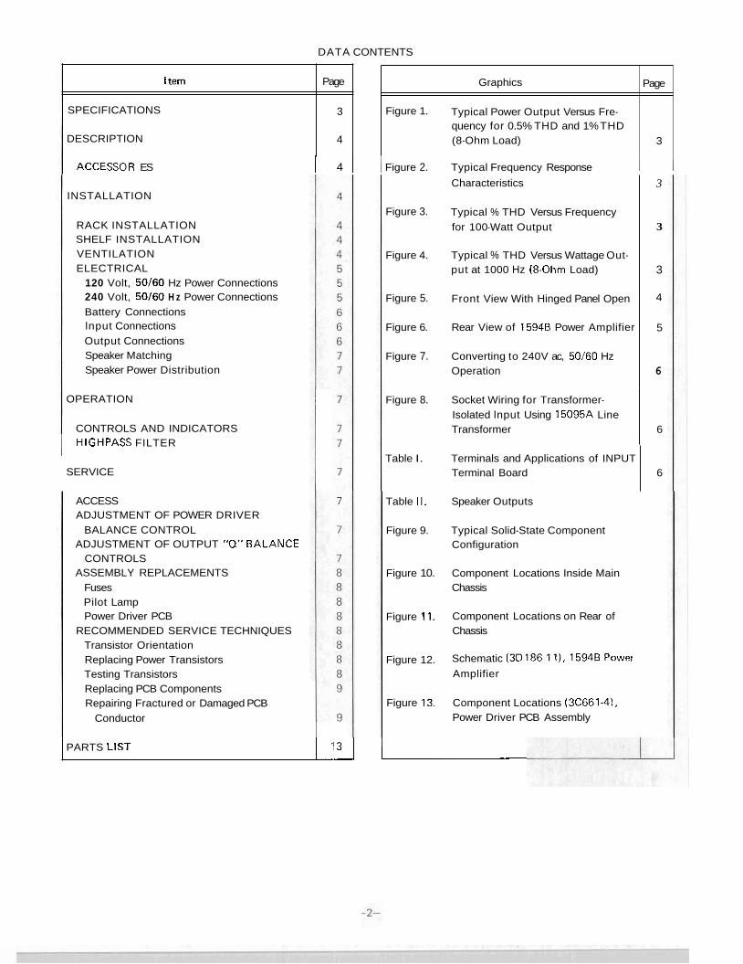
DATA CONTENTS
INSTALLATION
RACK INSTALLATION SHELF INSTALLATION VENTILATION ELECTRICAL
120 Volt, 50160 Hz Power Connections 240 Volt, 50160 H z Power Connections Battery Connections lnput Connections Output Connections Speaker Matching Speaker Power Distribution
l tem
SPECIFICATIONS
DESCRIPTION
OPERATION
Page
3
4
Graphics
Figure 1. Typical Power Output Versus Fre- quency for 0.5% THD and 1% THD (8-Ohm Load)
CONTROLS AND INDICATORS I HIGHPASS FILTER
Page
3
SERVICE
ACCESS ADJUSTMENT OF POWER DRIVER
BALANCE CONTROL ADJUSTMENT OF OUTPUT "Q"BALANCE
CONTROLS ASSEMBLY REPLACEMENTS
Fuses Pilot Lamp Power Driver PCB
RECOMMENDED SERVICE TECHNIQUES Transistor Orientation Replacing Power Transistors Testing Transistors Replacing PCB Components Repairing Fractured or Damaged PCB
Conductor
Characteristics
Figure 3. Typical % THD Versus Frequency for 100-Watt Output
Figure 4. Typical % THD Versus Wattage Out- put at 1000 Hz (8-Ohm Load)
Figure 5. Front View With Hinged Panel Open
Figure 6. Rear View of 15948 Power Amplifier
Figure 7. Converting to 240V ac, 50/60 Hz Operation
3
3
3
4
5
6
Figure 8. Socket Wiring for Transformer- Isolated lnput Using 15095A Line Transformer
Table II. Speaker Outputs
Figure 9. Typical Solid-State Component Configuration
Figure 10. Component Locations Inside Main Chassis
Figure 11. Component Locations on Rear of Chassis
Figure 12. Schematic (3D186 11). 15948 Power
Amplifier
Figure 13. Component Locations 130661-41, Power Driver PCB Assembly
6
Table I. Terminals and Applications of INPUT Terminal Board
PARTS LIST I I L l I
6
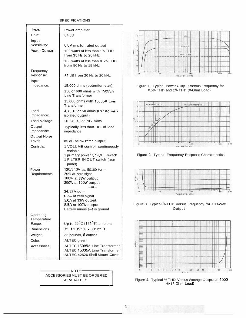
SPECIFICATIONS I I I I Type: I Power amplifier I
Gain:
lnput Sensitivity:
Power Outout:
Frequency Response:
lnput Imoedance:
Load Impedance:
Load Voltage:
Output Impedance:
Output Noise Level:
Controls:
Power Requirements:
Operating Temperature Range:
Dimensions
Weight:
Color:
Accessories:
0.8V rms for rated output
100 watts at less than 1% THD from 35 Hz to 20 kHz
100 watts at less than 0.5% THD from 50 Hz to 15 kHz
+1 dB from 20 Hz to 20 kHz -
15.000 ohms (potentiometer)
150 or 600 ohms with 1509!5A Line Transformer
15.000 ohms with 15335A L.ine Transformer
4, 8. 16 or 50 ohms (transformer- isolated output)
20. 28. 40 or 70.7 volts
Typically less than 10% of load impedance
85 dB below rated output
1 VOLUME control, continuously variable
1 primary power ON.OFF switch 1 FILTER IN-OUT switch (rear
panel)
1201240V ac, 50160 Hz - 20W at zero signal 180W at 33W output 290W at 100W output
-or- 24128V dc - 0.2A at zero signal 5.OA at 33W output 8.5A at 100W output Battery minus (-) is ground
Up to 5 5 ' ~ (131°F) ambient
7 " H x 1 9 " W x 8.112" D
35 pounds, 8 ounces
ALTEC green
ALTEC 15095A Line Transformer ALTEC 15335A Line Transformer ALTEC 42526 Shelf Mount Cover
NOTE I ACCESSORIES MUST BE ORDERED 1
Figure 1.. Typical Power Output Versus Frequency for 0.5% THD and 1% THD (8-Ohm Load)
Figure 2. Typical Frequency Response Characteristics
Figure 3. Typical % THD Versus Frequency for 100-Watt Output
SEPARATELY 1 Figure 4. Typical % THD Versus Wattage Output at 1000 Hz (8-Ohm Load)
DESCRIPTION
The ALTEC 15948 Power Amplifier delivers up t o 100 watts of output power for all Types of sound reinforcement Systems. I t remains stable with operating conditions o f varylng line voltages and wi th all types of loads, including long, unloaded speaker lines having considerable capacitance. Frequency response and output power characteristics are shown in Figures 1 through 4.
A switchable, two-section highpass filter is provided t o pro- tect driver loudspeakers f rom excessive low-frequency power demands.
ALTEC's Active Dissipation Sensing Circuit provides fail- safe protection for the output transistors. Circuit action is immediate and effective at all frequencies wi th in the pass- band o f the amplifier, l imit ing only that port ion of p royam material that would damage or degrade the output transistors.
ACCESSORIES
A plug.in 15095A or 15335A Line Transformer is available t o provide line isolation. Input sensitivity for full-rated amplifier output i r 0.2V rms with the 15095A Transforiner and 0.8V rms w i th the 15335A Transformer.
The 42526 Shelf Mount Cover i s available t o enclose the 15948 for shelf use. I t t i l ts the 15948 for easy accesr t o front panel controls. The sides and top extend beyond the front panel to preventaccidental changes of control settihgs. The cover provides easier handling fo r portability and i t is
sturdy enough t o support lightweight equipment placed on top of it. Four polyethylene feet prevent marring of sur- faces. The ALTEC green finish matches the front panel o f the 15948.
INSTALLATION
The 15948 may be installed in a standard 19-inch equip- ment rack, or in the 42526 Shelf Mount Cover accessory for shelf use. Vertical space requkred 1s 7 inches (four rack units).
RACK INSTALLATION
Step 1. Remove four screws securing front panel. Open and lower panel as shown in Figure 5.
Step 2. Install 15948 in equipment rack with appro- priate four screws supplied.
Step 3. Close f ront panel and secure w i th four screws Rreviously removed.
SHELF INSTALLATION
The 15948 may be shelf mounted as desired after installing the ALTEC 42526 Shelf Mount Cover (refer t o 42526 Installation Instructions).
VENTILATION
The 15948 generates minimal heat during normal use. A l - though the amount of heat i s relatively low, the amplifier
POWER DRIVER PCB POWER DRIVER BALANCE CONTROL PRIMARY POWER TERMINAL BOARD
"QN BALANCE
CONTROLS
PCB S\ ' i l ' / t l~ CONNtLlO11 (J21
Figure 5. Front View With Hinged Panel Open

must be ventilated to prevent an excessive temperalure rise. Because transistors are heat sensitive, the 15948 should not be placed adjacent to heat-generating equipment or in areas where ambient temperature exceeds 5 5 ' ~ (131'~).
I f the 15948 i s installed in an equipment rack or cabinet with other heat-producing equipment installed above andlor below (two or more 15948's or one 15948 with real time analyzer, oscilloscope, etc.), space must be provided be- tween the units or the 15948 may become too warm. The 1-314" perforated panel (ALTEC Part No. 10399) i s recom- mended for this purpose. When several amplifiers or other heat-producing units are installed in a single rack or cabinet, acceptable air temperature may be in d o ~ ~ b t . To determine temperature conditions, operate the system until temperature stabilizes, then measure air temperature with a bulb-type thermometer held at the bottom of the upper- most amplifier. Do not let the thermometer bulb touch metal because the metal probably will be hotter Than the ambient air. I f air temperature exceeds 5 5 ' ~ (or i f i t i s a hot day), the equipment should be spaced farther apart or a blower should be installed to ventilate the cabinet.
CAUTION Do not block the cvver ventilation holes when placing other equipment on the 42526 Shelf Mount Cover accessory. When shelf-mounting the 15948. allow at least 1-314" between the unit and any wall behind i t to assure air circulation past the output transistors.
ELECTRICAL
120 Volt, 50160 Hz Power Connections
Equipment supplied for domestic use is provided with the power transformer primary strapped for 120 volts (terminals
BATTERY POWER TERMINAL BOARD (TB4)
1 to 2 and 3 to 4 on TB3). The power input nameplate, adjacent to the power cord on the chassis, i s mounted to show the appropriate side specifying the connections (see Figure 6). Verify that line voltage i s in accordance with the voltage rating before connecting the 15948 to line power.
240 Volt, 50160 Hz Power Connections
Export equipment i s provided with the power transformer primary strapped for 240 volts (terminals 2 to 3 on TB3). The power input nameplate, adjacent to the power cord on the chassis, i s mounted to show the appropriate side specify- ing the connections.
For a 15948 previously wired for 120V ac primary power, use the following procedure to change wiring for 240V ac, 50160 Hz operation:
Step 1. Remove four screws securing front panel, open and lower panel.
Step 2. Locate terminal board TB3 above power trans. former T I (see Figure 5).
Step 3. Remove strap "A" connecting terminals 1 and 2 and remove strap "8" connecting terminals 3 and 4; solder strap "C" to terminals 2 and 3 (see Figure 7).
Step 4. Remove voltage-rating plate (see Figure 6) from chassis, reverse and reinstall to show 240V ac rating.
Step 5. Close front panel and secure with four screws previously removed.
TRANSFORMER ACCESSORY FILTER RECEPTACLE SWITCH
(J1) (51)
BATTERY POWER VOLTAGE OUTPUT INPUT FUSE (F2) RATING TERMINAL BOARD (TB2) TERMINAL BOARD (TBI)
PLATE
Figure 6. Rear View of 15948 Power Amplifier
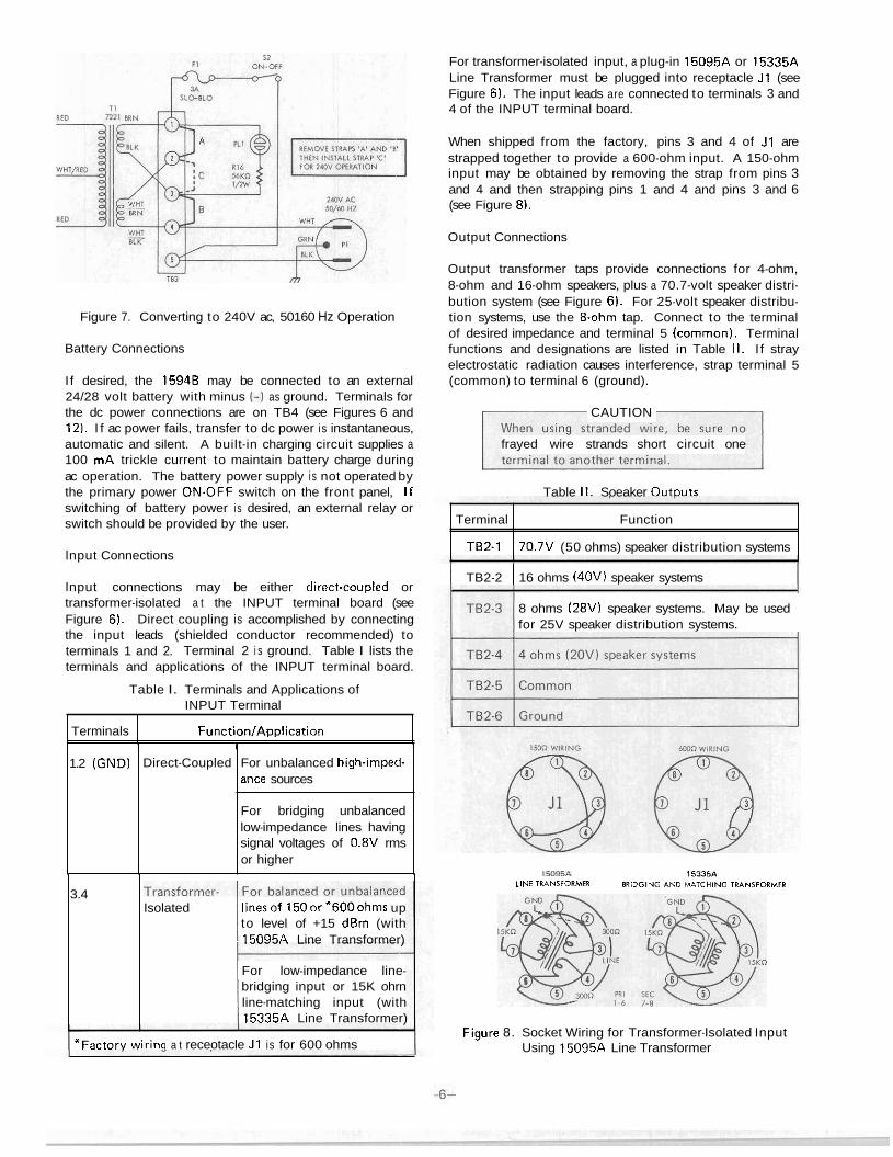
Figure 7. Converting to 240V ac, 50160 Hz Operation
Battery Connections
I f desired, the 15948 may be connected to an external 24/28 volt battery with minus (-1 as ground. Terminals for the dc power connections are on TB4 (see Figures 6 and 12). I f ac power fails, transfer to dc power is instantaneous, automatic and silent. A built-in charging circuit supplies a 100 mA trickle current to maintain battery charge during ac operation. The battery power supply i s not operated by the primary power ON.OFF switch on the front panel, I f switching of battery power i s desired, an external relay or switch should be provided by the user.
lnput Connections
lnput connections may be either direct.coupled or transformer-isolated a t the INPUT terminal board (see Figure 6). Direct coupling is accomplished by connecting the input leads (shielded conductor recommended) to terminals 1 and 2. Terminal 2 i s ground. Table I lists the terminals and applications of the INPUT terminal board.
Table I. Terminals and Applications of INPUT Terminal
Terminals
1.2 (GND)
For transformer-isolated input, a plug-in 15095A or 15335A Line Transformer must be plugged into receptacle J1 (see Figure 6). The input leads are connected to terminals 3 and 4 of the INPUT terminal board.
Function/Application
3.4
When shipped from the factory, pins 3 and 4 of J1 are strapped together to provide a 600-ohm input. A 150-ohm input may be obtained by removing the strap from pins 3 and 4 and then strapping pins 1 and 4 and pins 3 and 6 (see Figure 8).
I
Direct-Coupled
Isolated linesof 150or "600ohms up to level of +15 dBm (with 15095A Line Transformer)
For low-impedance line- bridging input or 15K ohrn line-matching input (with 15335A Line Transformer)
Output Connections
For unbalanced high-imped- ance sources
For bridging unbalanced low-impedance lines having signal voltages of 0.8V rms or higher
Output transformer taps provide connections for 4-ohm, 8-ohm and 16-ohm speakers, plus a 70.7-volt speaker distri- bution system (see Figure 6). For 25-volt speaker distribu- tion systems, use the 8.ohrn tap. Connect to the terminal of desired impedance and terminal 5 (common). Terminal functions and designations are listed in Table II. I f stray electrostatic radiation causes interference, strap terminal 5 (common) to terminal 6 (ground).
CAUTION
frayed wire strands short circuit one
Table II. Soeaker Outouts
I TB2-2 1 16 ohms (40V) speaker systems I
Terminal
8 ohms (28V) speaker systems. May be used for 25V speaker distribution systems.
Function
1M95A 15335A LINE TWNIIORMER BRIDGING AND M T C H I N G TRANSFORMER
I 'Factorv wirina a t receotacle J1 is for 600 ohms I
TB2-1
Figure 8. Socket Wiring for Transformer-Isolated Input Using 15095A Line Transformer
70.7V (50 ohms) speaker distribution systems
Speaker Matching
Use the output tap most nearly equal to total speaker impedance. I f the load impedance falls between two out- put terminal values, use the terminal of lower impedance.
Speaker Power Distribution
Total power distributed to all speakers should be not greater than the power rating of the amplifier system. The 70.7V distribution outlet permits connection to a large number of speakers, each speaker operating at its required powt!r level. Computing impedance i s not necessary for this application. Each speaker i s equipped with a line transformer having various power taps. Select the tap which yields the power desired for that speaker.
OPERATION
ADJUSTMENT OF POWER DRIVER BALANCE CONTROL
The Power Driver Balance Control (R116 on Power Driver PCB), balances the outputs of transistors 0104 and 0105 on the PCB. I f this control is not adjusted properly, high- frequency distortion results. I f adjustment is indicated, use the following procedure:
Step 1. Connect a 16-ohm dummy load across terminals 2 (16 ohms) and 5 (common) of TB2 (see Figure 121.
Step 2. Apply a 20 kHz sine wave to terminals 1 and 2 of the INPUT terminal board (TBl I .
Step 3. Adjust VOLUME control for 100-watt output (40 volts).
CONTROLS AND INDICATORS Step 4. Connect a frequency distortion analyzer (pre
Two operating controls are on the front pane1:a VOLUME ferred) or an oscilloscope to terminals 2 and 5
control and a primary power ON-OFF switch. A pilot indi- of TB2 (16-ohm speaker output) and observe
cator is l i t when the power is ON. output.
HIGHPASS Fl LTER
A two.section highpass filter is provided with the 15948 to protect driver loudspeakers from excessive low-frequency power demands. Filter use is indicated when high power output from the amplifier is applied to driver loudspeakers not equipped with protective crossover networks. The 3 dB frequency of the highpass filter is 400 Hz (see Figure 2).
A screwdriver-operated FILTER IN-OUT switch is located on the rear of the chassis (see Figure 6). The switch is placed in the OUT position when the 15948 is ;hipped from the factory.
SERVICE
I f a malfunction occurs, service should be performed by an ALTEC Qualified Service Representative. For factory ser- vice, ship the 15940 prepaid to Customer Service. ALTEC, 1515South Manchester Avenue. Anaheim, California 92803. For additional information or technical assistance. call (714) 774-2900, or TWX 910-591-1142.
Main chassis component locations are shown in Figures 10 and 11, The 15948 schematic is shown in Figure 12. Com- ponent locations on the power driver PCB are shown in Figure 13.
ACCESS
Remove the four screws securing the front panel, then open and lower the hinged front panel to gain access to the chassis interior.
I f the ALTEC 42526 Shelf Mount Cover accessory is in- stalled, remove by reversing the steps of the cover installa- tion procedure given in the associated instructions.
Step 5. Remove four screws securing front panel, then open and lower panel.
Step 6. Adjust R116 on Power Driver PCB (see Figures 5 and 12) until minimum distortion i s observed on distortion measuring instrument.
Step 7. Close front panel and secure with four screws previously removed.
ADJUSTMENT OF OUTPUT "Q" BALANCE CONTROLS
Output "a" Balance Controls R136 and R137 on Power Driver PCB (see Figure 5) balance the bias current of power transistors 01, 02. Q3 and 04. Inadequate adjustment of these controls may result in distortion and excessive current drain from one or more power transistors. I f adjustment is indicated (such as replacement of one or more power tran- sistors), use the following recommended procedure:
Step 1. Turn VOLUME control fully counterclockwise (01.
Step 2. Remove four screws securing front panel, then lower panel for access to interior.
CAUTION
the chassis i s opened for service. This procedure should be referred to a quali-
Step 3. Turn Output "a" Balance Controls R136 and R137 fully clockwise (see Figure 5).
Step 4. Turn on power and allow a 5-minute warmup period.

Step 5. Adjust R136 and R137 by one of the following methods [method (a) i s preferred] :
(a) Locate wire attached to terminal 1 of output transformer T2. Connect a clamp. on milliammeter to this wire and adjust R136 counterclockwise for a "a" cur- rent of 40 mA. Change connection of milliammeter to wire attached to terminal 3 of output transformer T2 and adjust R137 for a "Q" current of 40 mA.
(bl Remove two screws securing Power Driver PCB to chassis and lower PCB on hinged connector. Connect a millivoltmeter across resistor R7 (see Figure lo) , starling with highest scale to protect meter. Ad- just R136 for meter reading of 13 mV. Change connection of millivoltmeter to read across resistor R8 and adjust R137 for meter reading of 13 mV. Remove millivoltmeter and secure PCB to chassis with two screws previously removed.
Step 6. Close front panel and secure with four screws removed in Step 2.
ASSEMBLY REPLACEMENTS
Fuses
Step 4. Carefully insert new or repaired power driver PCB into connector. Do not warp, bend or twist the board or conductor may fracture.
Step 5. Secure PCB with two screws removed in Step 2.
Step 6. Perform ADJUSTMENT OF POWER DRIVER BALANCE CONTROL procedure.
RECOMMENDED SERVICE TECHNIQUES
I f systematic troubleshooting shows need for parts replace- ment, observe the following precautions.
Transistor Orientation
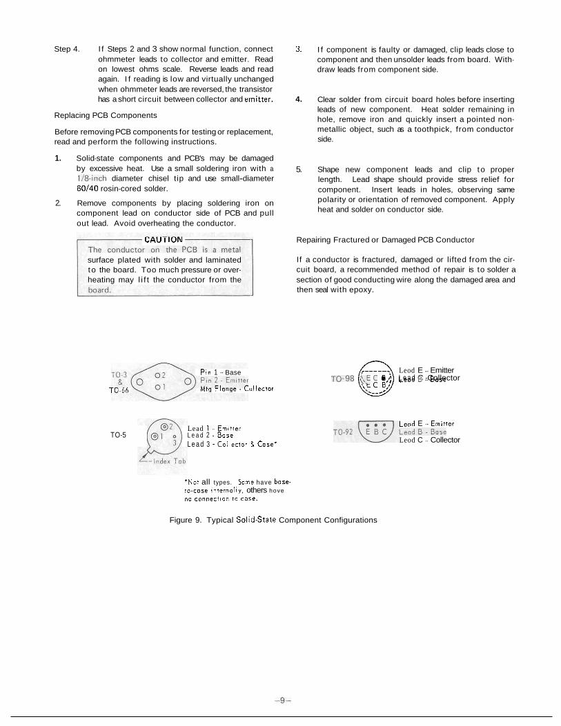
Solid-state components are packaged in various case sizes and types with various lead orientations (see Figure 9). Be- fore removing a solid-state component from tie points or from a PCB, sketch the lead orientation with respect to the t ie points or PCB.
Form the leads of the new component to conform with the leads of the part being replaced to aid in making proper connections. Before removing small transistors, note posi- tion of index tab with respect to the PCB or socket. Cut the leads of the new transistor to the required length and insert them, properly indexed, into the PCB or socket.
Replacing Power Transistors
The ac primary power fuse is mounted on the front panel (see cover photo). The battery power fuse is located on the rear of the chassis (see Figure 6). I f fuse replacement i s re- quired, determine and correct any cause of failure before re- plac~ng fuse. Install an identical fuse (see PARTS LIST) by unscrewing fuse holder, replacing fuse and resecuring fuse holder.
Pilot Lamp
The pilot lamp i s located on the front panel (see cover photo). I f replacement is required, unscrew the red pilot lamp shield to expose the bulb. Press bulb inward and tLlrn ~ ~ ~ n t e r ~ l o ~ k ~ i s e (CCW) to remove. Install an identical bulb (see PARTS LIST), then replace red pilot-lamp shield.
Power Driver PCB
I f the amplifier fails because of a faulty power driver PCB. operation may be restored by replacing the PCB with a new or repaired PCB. Use the following procedure.
Step 1. Remove four screws securing front panel. Open and lower panel for access to PCB (see Figure 5).
Step 2. Remove two screws securing PCB to chassis brackets.
Step 3. Lower hinged connector of PCB and carefully remove PCB from connector.
Verify the following conditions exist when replacing power transistors.
1. Mica insulator i s not damaged. I f damaged, use new insulator.
2. No grit or metal particles are between transistor and heat sink.
3. Both sides of mica insulator are covered with silicone grease or fluid.
4. Mounting screws are tight,
Testing Transistors
Transistors should be checked with a transistor tester. I f a tester i s not available, use the following procedure for test- ing transistors with an ohmmeter.
Step 1. Remove suspected transistor from circuit (see Replacing PCB Components).
Step 2. Connect ohmmeter leads to base and emitter. Read on lowest ohms scale. Reverse leads and read again. Normal readings should be a t least 10 times greater in one direction than in the other.
Step 3. Connect ohmmeter leads to base and collector. Ohmmeter readings should be similar to those obtained in Step 2.
Step 4. I f Steps 2 and 3 show normal function, connect ohmmeter leads to collector and emitter. Read on lowest ohms scale. Reverse leads and read again. I f reading is low and virtually unchanged when ohmmeter leads are reversed, the transistor has a short circuit between collector and emitter.
Replacing PCB Components
Before removing PCB components for testing or replacement, read and perform the following instructions.
1. Solid-state components and PCB's may be damaged by excessive heat. Use a small soldering iron with a 118.inch diameter chisel tip and use small-diameter 60140 rosin-cored solder.
2. Remove components by placing soldering iron on component lead on conductor side of PCB and pull out lead. Avoid overheating the conductor.
CAU I ION
surface plated with solder and laminated to the board. Too much pressure or over- heating may l i f t the conductor from the
P>n 1 - Base
7 0 - 6 6 Mtg Flange. Ccillector
Lead 1 - Emitter TO-5 L e a d 2 - B a s e
L e a d 3 -Collector P Case*
3. I f component is faulty or damaged, clip leads close to component and then unsolder leads from board. With- draw leads from component side.
4. Clear solder from circuit board holes before inserting leads of new component. Heat solder remaining in hole, remove iron and quickly insert a pointed non- metallic object, such as a toothpick, from conductor side.
5. Shape new component leads and clip to proper length. Lead shape should provide stress relief for component. Insert leads in holes, observing same polarity or orientation of removed component. Apply heat and solder on conductor side.
Repairing Fractured or Damaged PCB Conductor
If a conductor is fractured, damaged or lifted from the cir- cuit board, a recommended method of repair is to solder a section of good conducting wire along the damaged area and then seal with epoxy.
,-----., Leod E - Emitter . . . ) L e a d C -Collector 0 \\! C B: Lead 5 - Bose
.__c'
Lead E - Emitter
Leod C - Collector
'Not all types. Some have bose. to-cose internally: others hove no connection t o cose.
Figure 9. Typical Solid.State Component Configurations

POWER DRIVE? PCB ASSEI'.'BLY ( A l ! ? I -.- I ' ! :I; I 3 I \ , t i I i.1 I >?
I N LOWERED POSITION 11 3
Figure 10. Component Locations Inside Main Chassis
T 1 VOLTAGE Q b Q 5 T B I
RATING PLATE
SINK
Figure 11. Component Locations on Rear of Chassis


Reference Ordering Designator Number
27-01-042843-04 + PARTS
Name and
PCB Assembly, Power Driver
Cap., 0.01 p F +20%. 1 oov
Cap.. 7000 pF, 40V
Cap.. 0.05 p~ +lo%, 400V
Cap.. 0.1 p ~ , ~ O O V
Cap.. 1 p ~ , 25v
Cap., 220 pF +lo%, 1 oov Cap.. 0.002 pF +20%, I oov Cap., 5 pF, 25V
Cap., 0.47 pF 21 0'%, 1 oov Cap.. 0.005 p F +20%, 1 oov Cap., 0.0033 p F 220%. 1 oov Diode. 1N4004, selected
Diode, Zener, ZOA, 20v 25%
Diode, Zener. 15A. 1 5 v +5%
Diode, rectifier, 1N3492. 18A. 100V PIV
Diode, 1N456A. 25V. 100 mA
Fuse. 3A. SLO-BLO
Fuse, 10A. 3AG
Socket. octa!
Receptacle, 15-pin (for A l )
Cord, 18GA, 3- conductor. wlplug
Reference Ordering Name and Designator Number Description
115W. 90V, selected
R lO l
Transistor, 2N5305, selected
Transistor, 2N2712, selected
Transistor, 2N3906. selected
Transistor, 2N5308, low noise, selected
47-01-102169-01 Res.. 3 .3Ka 210%. I l14W
48-03-107447-02
47-06-042509.01
47-01-100635.01
47-02-105885-01
47-01-100652-01
47-02-114449-01
47-01-102054-01
47-01.102057-01
47-02-1 12166.01
47.01.102551.01
47-02-100715-01
47-02-100712.01
47-01-102376-01
47-01.100479-01 -
47-01.102190-01
47-01-102171-01
47-01-102168-01
47-01-102167-01
47-01-100477-01 Res.. 470Ka+10%. 1 II~W
Transistor. 2N5320, low, 75v
Pot., 1 5 K a 220%
Res., 2 2 a 210%. l W
Res., 0 . 5 0 210%. 5W
Res.. 1.8Ka+10%, 1W
Res.. 10a, 5W. NI
Res.. 100a+5%. 114W
Res.. 1300+5%, 114W
Res., 5a+10%, 5W. N l
Res.,470L?,210%, 1W
Res., 2000210%. 5W
Res., 470+10%, 5W
Res., 56K0+10%, 112W
Res., 680KQ210%, 1 14W
Res., 1 8 0 K a 210%. 114W
Res., 4.7Ka210%, 114W
Res.. 2.7Ka+10%. 114w
Res.. 2 .2Ka -210%. 114W
Res., 1 0 K 0 25%. 114W
Res., 1OOKa +lo%, 1 /4W
Reference Designator
R113
R l l 4
R115.117
R116
R118.119
R120.123
R121.122
R124.125
R126.127
R128
R129,132
R130.133
- Order~ng
- Number
47 11-102177-01
PARTS LIST (continued) 7 ,
Reference Ordering Description Name and I Designator 1 Number
Res., 15KC?,+10%, I 1.134 1 47-01-102147.01 1 /4W
Res.. 1.8Kn+109b, I 1 ~ 1 3 5 1 47-01-102155.01 114W
Res., 1 Ka+10%, 114W
Res., 3 3 R z . L +,, 114W
Pot., 10a, 22W
Res.. 330Q 210%. 1W
Res., 27Q+10%, l i4W
Res., 47Q+10%, 1 /2W
Res.. 1 8 0 a +lo%, 112W
R136,137
R138.133 .
Res., 56a+10%, 114W
47-05$y697-01 F.ar*?-'>
' i i ,
'47-01-102355-01
Res., 3.3K.Q+5%, 1 /4W
Res.. 22Ka+10%, 21-04-101034-01 1 I I T B 4 I
Name and Description -
Res., 47Q f 10%. 1 /4W
Res., 220.Q ?lo%. 114W
Pot., 5 0 n 2 0 % , 2W"? %~y.t%. . .. ', ?%%
' . ( ;.. Rer.. 1 KCZFIOI, --.
112W
Switch, DPDT, slide
Switch, toggle, 125V ac, 3A - 20V dc, 5A
Transformer. power
Transformer, output
Transformer, output
Terminal board, 4.terminal
Terminai board. 6-terminal
Terminal board, 5.terminal
Terminal board, 2.terrninal