pcb eda tutorial laboratory 3 addendum 1 design … lab-3.1, rev 0.8.0 page 1 university of...
TRANSCRIPT

Cmpe174 Lab-3.1, Rev 0.8.0 page 1
University of California, Santa Cruz
Electrical Engineering Department
PCB EDA Tutorial
Laboratory 3 Addendum 1
Design Flow for the LPKF M60 Process:
CircuitCam 6.1
EE174, Intro to EDA Tools
S.C. Petersen
1. INTRODUCTION AND OBJECTIVES
This addendum lab assumes familiarity with basic post-processing concepts discussed in lab 3, Gerbtool. Therefore,
most of the orienting ideas developed there will be omitted and assumed here. You may want to review lab 3 before
proceeding.
This lab and lab 3 Addendum 2 are devoted to fully explaining the use of a specialized post-processing flow required
to manufacture prototype PCB’s using the LPKF Protomat M60 precision milling / drilling machine. You must
demonstrate knowledge and competence from these two labs before gaining permission to use the M60. This
machine is a three dimensional “plotter” capable of making precision prototype printed circuit boards that requires
specially formatted input files. Using generic Gerber and NC drill files, lab 3.1 discusses how to read these files into
a post-processing program called CircuitCam, much like Gerbtool, that must be used to create a specialized output
file required by the M60. The plotter itself is controlled by a dedicated tool called BoardMaster that subsequently
reads this output from CircuitCam and uses it to operate the M60 and make a PCB. A good way to think of these
two CAM tools is to assume the role of the classic boardhouse, where generic Gerber and drill files are always
submitted. Here, though, they are run through a particular two-step processing sequence to etch and drill a milled
PCB. I call this the “M60 process” to distinguish it from the photolithographic wet-lab process used by conventional
board houses.
The M60 process is so different from the photolithographic process, that you should be aware it is not simply a
convenient way to avoid a conventional wet-lab board house. If you plan to only run several prototypes, then a
conventional boardhouse is probably a better choice. For true prototyping with many potential revisions and
considerable experimental work, for example, breaking out (or fanning out) small SMT parts for experimentation,
the milling machine is a very good choice. You should know the major reason the M60 was originally acquired was
to do RF prototype boards, which tend to be relatively simple but otherwise require precise traces, copper planes and
part placements. Labs 3.1 and 3.2 are primarily meant to follow the Cadence EDA flow taught in EE174, but they
can be used with any layout tool, like Eagle, capable of producing RS-274X Gerber files and an Excellon NC drill
file. Even though CircuitCam is capable of processing RS-274D Gerber and their necessary aperture file, this format
is considered obsolete and will be deprecated here; RS-274X combines them and is the only format discussed in this
lab. Similarly, drill files can also be separated into two files: NC and tool list. Many board houses still require both,
even though the tool list mapping is already contained in the single Excellon NC file. We will assume that you have
used this capability in Allegro (aka “Orcad”) PCB to generate a single Excellon NC; CircuitCam will parse it
correctly.
2. GENERAL DISCUSSION
Before deciding to use the M60 milling process to make a PCB, you should wisely consider the trade-offs compared
to using a convential quick-turn board house, like APC, Sierra Proto Express or 4PCB.com. Take into account the
following regarding use of the M60 process:
The PCB is limited to single or double-layer boards, typically 62.5mil FR4.
Double-sided boards with vias (PTH or plated-through holes) will be unplated drilled holes only. Pads will
appear on both sides of the board, but there will be no connectivity. This fact must be considered back in

Cmpe174 Lab-3.1, Rev 0.8.0 page 2
the layout tool phase. Vias can be implemented using special rivets (expensive) or wire soldered on both
sides and clipped with flush cutters; all of this must be done manually. Note especially that through-hole
sockets and other parts will require soldering on both sides so insure continuity. LPKF even has some
special conductive paste that can be oozed through the hole (available on their website).
The drill rack is limited to a small selection of available sizes. Currently Bels stocks only the following:
o 19.7 mil (0.5 mm) Drill, $5.50 (new Spring 2013)
o 23.6 mil (0.6 mm) Drill, $5.50
o 31.5 mil (0.8 mm) Drill, $5.50
o 39.5 mil (1.0 mm) Drill $5.50
If you require intermediate or larger sizes, they should be implemented by first drilling an undersize hole
using one of the three sizes noted above, and then enlarging them with convential twist drills on the drill
press.
Voids are created by removing copper using precision high speed end-mills. The closest feature spacing is
determined by the smallest available. Currently Bels stocks the following two sizes:
o 10 mil (0.25 mm) RF End Mill, $23.00 (lifetime of 9000 mm)
o 39 mil (1.0 mm) RF End Mill, $14.38 (lifetime of 9000 mm)
Therefore, you will have to change the usual 8 mil spacing constraints to 10 mils to avoid undercutting
adjacent traces or other features closer than 10 mils.
An additional special milling bit is needed to mil around the final PCB contour and thereby remove it from
the larger parent material. This bit is called a contour router and Bels stocks one:
o 79 mil (2.0 mm) Contour Router $14.38
The four drills, two end mills and necessary contour router is clearly an investment.
Two new EDA tools must be learned and mastered, along with concepts and idiosyncratic nomenclature
particular to the M60 machine.
Large regions absent of copper needing to be milled away are costly. This kind of voiding happens
automatically with a conventional photolithographic process, but has to be specifically setup and defined
using the 1.0 mm end mill here. Hence, large voided areas are expensive in terms of router lifetime and,
unless really needed, should be avoided.
There are no solder mask or silk-screen layers. This is a bare copper prototype-only process, similar to what
Alberta Printed Circuits offers with their basic no frills 24 hr quick-turn process.

Cmpe174 Lab-3.1, Rev 0.8.0 page 3
3. TUTORIAL PROJECT
Since our objective is to learn the M60 process and avoid getting bogged down by an overly complex design, this
lab departs from the earlier sequence by starting with a different design deliberately chosen for its inherent
simplicity. Hence, we will use a set of modified artwork and drill files that LPKF originally supplied with their own
poorly organized tutorials.
Before You Begin.
If you followed the CMPE/EE174 sequence, you should already be familiar with the Cadence flow directory tree.
Refer to Lab-1, sec. 3, for a review if you need to. Note the …pcb\artwork folder contains the equivalent of what
Allegro PCB or another layout tool would have already produced. We will use these as our starting point and add the
several files used by the M60 process in this same folder since these files are tied to a unique design in the same way
as Gerber or drill files.
…Tutorial - Top-level directory.
Appnotes - Relevant application notes, papers and references.
…
Design - Tutorial project folder containing any schematics and pcb layout files.
[project name & version]_LPKF
pcb - Board-level PCB files and colorviews.
artwork - Exportable Gerber and drill files.
…
Do not proceed to start working with the M60 process unless the following has already been done:
You are familiar and competent with PCB EDA tool flows and technology. Completing EE174 satisfies
this requirement.
The manufacturing phase is complete; all necessary RS-274X formatted Gerber and Excellon drill files
have been created with the M60 process in mind beforehand. This means DRC spacing contraints have
been adjusted, footprints and vias modified as necessary to accommodate the milling and drill size
requirements. In this lab, these are given to you and can be found in the pcb\artwork noted above.
Create an additional directory under the Design folder titled with LPKF in the folder name. For clarity, this is shown
in red. Note this is the same thing that was done in lab 3 (see lab-3, sec 3) where unique folders for aggregating files
associated with or going to a specific boardhouse were created and saved. This laboratory shows you how to create
the necessary files for the M60 process where all will be placed in the LPKF folder .
TIP: For those using a different toolchain, like Eagle, your folder tree will most likely be different. In this case, be
sure and minimally copy the Appnotes and artwork folder contents.
Loading and Learning Circuit Cam
Since UCSC has a license to use only one instance of CircuitCam, it is meant to be used on the computer in the lab
(BE138) where the M60 and BoardMaster are located. To facilitate learning the tool a version is available that can
be loaded and run without a license for 30 days. Download CircuitCam 6.1.1159 Setup.zip, explode it in a
temporary folder and proceed to install it. During the installation process be sure to not check the option to install
the “Alladi Hardlock Device drivers”. This feature isn’t needed, and if you forget to uncheck it the install will crash.
When the program is run for the first time, you should see CircuitCAM’s Activation Wizard that will appear and
prompt for licensing information. If not, select Help – Activate Program from the main menu bar. To get a 30 day
trial period of full-featured use, cut-and-paste the following credentials:
Serial Number: 09010100
License ID: EQ8GPCZSX0I11NCQE0WAM3JE7
Choose Next and proceed to the next screen and choose the online option to register. I this fails, go back to the
screen and select “Later”; the program will work for 7 days instead of 30.

Cmpe174 Lab-3.1, Rev 0.8.0 page 4
4.0 USING CircuitCam
GETTING STARTED – Begin by launching CircuitCam from the Start Menu or desktop icon (if present). This tool
has many toolbars (but fewer than Gerbtool), and they are all dockable. When all are visible they consume
considerable space, so we will turn some off and re-arrange the rest. I’ve moved all the default groupings onto the
desktop and snapped a screenshot so you can identify them. When docked, the white titles are blank so this is a nice
reference as I will be referring to particular icons by their group affiliation. I have selected and placed all but the
bottom five in the last row. These we won’t be using so they’re omitted and not visible.
Visibility is controlled by grouping in the checkbox shown. Access it by choosing View ->
Toolbars, or by right-clicking the mouse inside any visible toolbar. Since this is lab is
shared by many students, please don’t change these settings unless you need to, and please
don’t change the layout. I show them here in case they need to be restored, and to easily
associate groupings by name.
CIRCUITCAM’S TOOLBARS – A selected summary1 of what these major groups and what their icons are used for
follows. Learning how to use these is not important now, but know where to find them and what they do is:
Standard: These should be self-explanatory, dealing as they do, with conventional file, printing and viewing options
etc.
Unit / Grid:
The zero point is placed at the current anchor point position.
These two icons are mutually exclusive. They affect how the cursor postion is displayed at the bottom of
the screen. The first sets absolute coordinates mode, while the second sets relative coordinates mode.
These two icons are mutually exclusive. The first sets Cartesian mode, the second polar mode. Most of
the work you do will most likely use Cartesian coordinates. Remember, these are display modes, so
toggling between them has no effect on how objects are processed or placed.
1 Appendix-A includes a complete list of all toolbars from the CircuitCam documentation.

Cmpe174 Lab-3.1, Rev 0.8.0 page 5
This pull-down list is very useful. With it you can set the displayed mode to any of those shown. The C60
process has milling and drill sizes specified in metric (mm), so if your board design was created using
English units, like mils, then it can be advantageous to shift back and forth from mils to mm, for example,
to check and guage sizes. This is especially useful when checking drills. Changing units has no effect on
how objects are processed, simply the display is affected; very useful!
This pull-down list also affects only how objects are displayed. Avoid specifying absurd
resolutions since it just makes things more confusing. Realistic precision depends on what units are
selected from the list above. Again, only the display is affected.
CircuitCam has two icons and one pull-down list in this group controlling the grid:
The Show Grid icon toggles the grid on or off.
Snap to Grid enables or disables whether the cursor snaps to the grid or not. Note that when this is active, the
cursor position shown on the status bar only reflects the displayed grid spacing resolution and not the decimal
precision from the list noted above.
This truncated list doesn’t display properly, since it was programmed too narrow, but it allows us to
specify the displayed grid spacing. Note this list is not active unless the grid is visible.
The last icon in the group provides commands to edit points and segments.
Layer:
This important group controls how layers are moved, registered with respect to one another and individually
selected. It also associates particular M60 bits (mills and drills) with particular apertures.
The first two icons, Move Layer to Zero and Match up Layers won’t be discussed or used in this lab,
but they are typically used to work with imported Gerber layers for alignment purposes.
Pressing this icon opens the LayerView dialog window if it isn’t already open. If it is, of course, it does what

Cmpe174 Lab-3.1, Rev 0.8.0 page 6
you would expect: nothing. Why this icon is here is because the layer view window is accessed so often that it
serves as a convenient fast shortcut to get it on the screen. Whether it’s really useful depends on how you
have the desktop organized.
Shown left is the Active Layer list. Only one layer can be active at a time, and it can be
selected here or in the Layer View dialog window discussed later. The layer shown in this
listbar is always the active one, even it’s changed elsewhere. I will have more to say about
this pull-down list later, but only after we’ve discussed the layer view dialog window.
Note layers listed are typically not all of them, so you will have to scroll down to get to the
ones at the bottom of the list.
The Active Aperture / Toolist displays selections related to apertures and CircuitCam tools.
These same selections are also accessible in a different context from the Layer View dialog
window noted above.
The last pull-down list on the toolbar specifies what bit is to be associated with an aperture /
tool. Note these selections are shown in metric, and changing units has now effect on this.
LPKF’s M60 requires metric tooling, so only those available from the company are shown –
and these are all metric sizes. Note there are a few more spiral drills missing at the top.
Notice the absence of end mills in this list. There appear to be only drills and a single contour
router. The reason is this list is meant to assign tools with apertures meant only for through-
hole operations. For drills this is obvious, but the 2.0mm contour router isa special bit
designed to first drill all the way through using a milling action and then move laterally to
traverse the circumference describing the PCB “contour” or board outline. In other words, it
first drills and then cuts out the PCB.

Cmpe174 Lab-3.1, Rev 0.8.0 page 7
When first booting the program, the full-screen layout should be similar to what you see shown below. If not, re-
arrange things until it is. Note the location of the various toolbars and the two tabbed vertical windows on the left
side. The top one has three tabs: Layers, Tools, and Jobs. The lower one has two tabs: Properties and Set Cursor.
The top window in particular will be used frequently.
The cross-hair’s position can be set to indicate relative or absolute position in
whatever units are being used (currently this is inches) at the right side of the Status
Bar along the bottom. If this bar isn’t visible, it can be toggled on by choosing main
menu sequence View -> Status Bar. Selecting the Set Cursor tab shows the options
available. Also, the white “X” in the work area always denotes the origin at (0,0).
Zooming in and out is done with the scroll wheel on the mouse.

Cmpe174 Lab-3.1, Rev 0.8.0 page 8
4.1 IMPORTING DESIGNS
ARCHITECTURAL OVERVIEW – CircuitCam uses a layering scheme that includes a block of layers, some of which
you are already familiar with, and some you are not. The following screen shot shows all 30 of CircuitCam’s default
layers. I’ve expanded them so all the layer and column names display legibly. Become familiar with how the columns
work by their symbols, since the names are typically truncated when actually working with this form. These are
better discussed after some actual data is loaded and processed. Suffice to say at this point that the two colors for
each layer in the Colors column denote color assignment for flashes and draws – just as Gerbtool does, and the True
Width and Outline columns affect how objects (draws and flashes) are displayed. The Selectable column governs
whether layers are locked for editing or not. The conventional layers you are already familiar with are: 4, 5, 10, 19,
22, 26 and 27. The remaining layers are all unique to CircuitCam and BoardMaster.

Cmpe174 Lab-3.1, Rev 0.8.0 page 9
Let’s pause for a moment and reflect on what it is we want CircuitCam to do for us. First, it must read our Excellon
drill file and tool list (aka “drill rack”), allow us to re-assign drill sizes if needed, and then drill precise holes.
Second, it must read conventional RS274X Gerber files and figure out how to tell a vertical milling machine, the
M60, precisely how, at what depth, and where to remove copper so only wanted traces, pads and copper areas
remain. A milling bit having a finite diameter must be used to do this. In CircuitCam, the process of calculating the
actual path from input Gerber data for each milling bit used is called Insulating the layer. Our board has two etch
layers: top and bottom. So the process of insulating them is accomplished by translating the NC data from their
respective conventional source layers and mapping each to a block of one or more special-purpose layers, aptly
named insulation layers. These custom layers contain the translated NC milling instructions to accurately guide
various sized milling bits.
It should be evident, then, that insulation regions are conceptually identical to voids in Allegro PCB. Moreover,
larger voids, usually defined by etch keepouts in Allegro, are called Rubouts here in CircuitCam. Rubouts must be
manually created and will not carry over from Allegro.
Example for the Top Layer - From the convential top etch layer, TopLayer, a block of six uniquely-named custom
layers will contain all the data necessary for the M60 process.
InsulateTop_Bigger
InsulateTop_Big
InsulateTop_Std
InsulateTop_Small
Rubout_Top
FrameTop
The first four are dedicated to insulating traces and pads. Rubbing out a region does not typically include traces, so a
larger milling bit can be used and its edge accuracy can be less. It only has to overlap the precise insulated regions
already cut by one of the four insulate top operations. Just to be clear, the technique used is to first insulate all draws
and flashes using a precise small end mill. Possible rubouts that follow can then proceed with a much larger, but less
precise, end mill. In this lab, traces (draws) and pads (flashes) are insulated with a 10 mil (0.25mm) end mill, and
possible subsequent rubouts wit a 39 mil (1.0 mm) end mill.
The last one is FrameTop. It defines areas requiring special insulation treatment and will not be discussed further in
the this lab, since to effectively use it requires small end mills that are currently not available, for example 4 or 6 mm
end mills.
Why four layers to insulate traces and pads and not just one? Accuracy and tool lifetime are the reason. The idea is
that we electively associate a single routing bit with each layer. In our case, we will be using two bits: 10mil
(0.25mm) and 39mil (1.0mm) and associate them with the InsulateTop_Std and InsulateTop_Big layers
respectively. Separating the layers this way makes them much easier to manage as a manufacturing process and
keeps us organized about what we’re seeing and doing. Ok. So why don’t we just use our 10mil bit for everything?
Milling large insulation areas wider than 10mils means the end mill has to travel sequentially and overlap a
previously cut insulated region by some amount. Clearly, large planar areas will require many passes and
prematurely wear out the tool. Thus, narrow detailed regions, those adjacent to traces and pads, are machined using a
small accurate tool and larger areas, particularly rubouts, with the bigger less accurate tool. By “accuracy”, I am
referring to the quality of the copper edge (trace or pad) left behind by the end mill. Smaller bits result in much more
precise and accurate edges. By choosing different combinations of the True Width and Outline properties, we can
readily see precisely what the insulation operation will entail. After loading some Gerber data and running the
insulation algorithms, you can play with these properties to see how it all works.

Cmpe174 Lab-3.1, Rev 0.8.0 page 10
INPUTTING GERBER AND DRILL DATA – We will begin by loading a modified version of one of LPKF ‘s tutorial
designs2. Choose menu sequence File → Import, or use the more convenient icon on the Front-End
toolbar.
Navigate to the pcb\artwork folder and select all four files found there. These should be the same as shown at left.
CircuitCam will respond by processing all four files. If successful, you should see the Import
window shown below with the Graphic tab sub-window by default. Our task at this point is to check
these imports for correctness and then assign each to one of CircuitCam’s conventional layers. Objects in the
Graphic window generally will display as white until the layer has been assigned to an existing pre-defined
conventional layer also associated with some particular set of colors, one for flashes, the other for draws.
This set of steps is all about sanity checking. For each file, be sure the Size x,y values make sense.
2 LPKF discusses several scenarios presented as awkward and confusing tutorials. Most are poorly organized and difficult to
follow, each committing the usual errors: a bottom-up with too many details and numerous loosely connected factoids. These are
integrated within their single Manual, CircuitCAM 6.1.pdf (I placed it in the Appnotes folder). Though, as a reference manual
without the distracting “tutorials”, it’s pretty good.

Cmpe174 Lab-3.1, Rev 0.8.0 page 11
Beginning with one of the Gerber files, we’ll use the bottom layer, select it and press the Text tab. The result of the
input processing step on this RS274X Gerber file will display. It will show the actual translation results generated by
CircuitCam for its internal use. It is useful for verification and troubleshooting.
CircuitCam also creates a set of D-Codes from this layer and places it in “GerberDefault1”. View them by selecting
the Apertures tab. In the screen shot, I have also selected D11 and picked the Attribute tab to see what it is. You
may notice that these are all in mils with apparently goofy values. The reason is the original file was in metric and

Cmpe174 Lab-3.1, Rev 0.8.0 page 12
these are being displayed after converting to mils. Changing the units would cause this to display differently, but
must be done before this window is opened since it is modal and won’t let you change the focus until it’s closed.
You could, if you wanted, just cancel, change units and start over and the original metric quantities would appear. I
recommend you set the units to whatever the source files use, since this makes it easier to check the import for
correctness.
Now select the Graphic view to once again show the white objects on this layer and then assign the processed
bottom.art data to the convential
BottomLayer. Do this by
scrolling through the default list
in the Layer / Template column.
Be careful to map these
correctly. CircuitCam uses
particular names to integrate with
BoardMaster, so even though
new layers can be added and any
name can be edited, don’t
change these or there will be problems later on. Thus, here for example, “BottomLayer” should be treated as a
reserved layer name. Once a selection is made, the graphic view will display colors assigned to that layer; here,
BottomLayer should appear green. Follow the same procedure for the other two Gerber files. For reference, the
final Gerber assignments are:
bottom.art → BottomLayer
mech.art → BoardOutline
top.art → TopLayer
Importing the Drill File - The nc drill file requires special handling. Select the file as shown
above and you can see what I mean; observe the Godzilla sized drills! This is caused by an
incorrect Excellon m:n format. This can be fixed by experimentally changing the decimal
precision parameter, n until it’s correct. Try scrolling through them while simultaneously
observing the graphic window’s reported Size x,y values, and visually watching the screen;

Cmpe174 Lab-3.1, Rev 0.8.0 page 13
finally select the proper precison of 3 by concluding the Size x,y extents are correct and the window looks right. Use
your judgement here, although the correct setting should be obvious.
The result of using the correct m:n precision is shown below. Note I have also gone ahead and mapped nc.drl to
CircuitCam’s reserved conventional layer: DrillUnplated. Looking over the possible layers, you might have noticed
that we could perhaps have chosen DrillPlated. Since we can’t produce PTH vias, unplated is the proper choice.
This will have consequences later when we use this data in BoardMaster to set up the drilling phase of operation.
At this point, you should have successfully loaded all files necessary for the M60 process. The next step proceeds to
build the insulation layers, check drill sizes and export to BoardMaster.
Before moving on, save your current work. Select menu sequence File → Save As, give it an appropriate name,
“lab3.1”, and be sure to save it as a type *.CAM CircuitCam file. Reload this file at any time to pick up where you
left off. It is functionally the same as Gerbtool’s *.GTD format.

Cmpe174 Lab-3.1, Rev 0.8.0 page 14
4.2 PROCESSING DESIGNS
INSULATION AND CONTOUR ROUTING – The screen shot following shows the four layers immediately after
importation. Note the relative size of the cyan drills. This is a further sanity check on the m:n Excellon drill settings.
At this point you should experiment with the Layers view to get familiar with its features. You may want to refer
back to page 8 where this form is shown with all column labels clearly readable. Do the following:
Toggle the Show All Layers icon. The screen shot above shows it set to show only non-empty layers.
Clicking on a green checkmark will make a layer hidden and toggle the
icon to a red check. Clicking on the red check will reverse this and again
make the layer visible and indicate so with a green checkmark. There is a subtlety here though. Notice the
BottomLayer is hidden and the dotted box in the selectable column has red dash denoting it as unselectable. This
happens automatically whenever a layer is made hidden after toggling the green check. However, a visible layer can
be made deliberately unselectable by clicking on the dashed box directly. Thus, we could make the DrillUnplated
layer unselectable but remain visible. This most useful when moving or deleting objects on particular layers while
keeping all visible. Experiment with all of these fields, including the True Width, Outline and Colors fields.
Working with the Board Outline – While setting different layers visible, you may have noticed the board outline
appears on all three Gerber layers, Top, Bottom and and BoardOutline. This was done purposely to show how to
delete or move objects between layers. We’ll re-create the scenario of a hypothetically empty board layer by deleting
the existing board outline and then moving the same object from either the top or bottom layers. The goal is to find
the board outline on some other layer and move it over to the reserved BoardOutline layer for CircuitCam’s use.
First, make the BoardOutline active. There are three ways to make a layer active:
1. Use the pull-down Active Layer list in the Layer Toolbar. Useful when the layer is hidden, since it will away
appear in the pull-down listbox.

Cmpe174 Lab-3.1, Rev 0.8.0 page 15
2. Click on the layer in the Layers view (it must be visible) and press the Enter key or right-click and select the
Make Active item.
3. Hold the Alt key down and double-click the layer’s name in the Layers view (it must be visible).
Having done this, select it with the mouse (click it anywhere). It should now be highlighted as shown below. Hit the
Delete key and it will disappear. Since this layer is now empty it too will also disapper from the list.
What we want to do now is make the TopLayer active and visible, then select and move only the board outline object
over to the BoardOutline layer. The following screen shot shows this with the outline selected and all layers made
visible with the ShowAll Layers icon so the wanted but otherwise hidden BoardOutline layer can be seen.

Cmpe174 Lab-3.1, Rev 0.8.0 page 16
We’ll now use a very nice feature of CircuitCam: Any selected objects on an active layer will automatically be
moved to any layer that is then subsequently made active. Using any of the three techniques noted above, proceed to
make the BoardOutline active. In this example, I used the Alt double-click method. The actual board outline object
should now appear once again on the BoardOutline layer. Confirm that it has indeed been moved.
Contour Routing the Board Outline – There is no particular order to these tasks, so I’ll begin with setting up the
contour router that must be defined on one of the special layers. We’ll use the board outline to generate a routing
path for the 79mil (2.0mm) Contour Router and place this on layer 17, CuttingOutside layer. Note that we have a
choice of cutting on the outside or inside of the reference path; i.e., we could have selected layer 18, CuttingInside,
but for this job the outside is the correct one. You might use the inside option, for example, to cut away a region
inside your PCB; these are typically called slots or cutouts.
Do this by making the BoardOutline the active layer,
select the board outline object as before and
press the Contour Routing icon on the Front-
End toolbar. This will bring up the Contour
Routing dialog.
This form has a number of options. Once you understand
what’s going on, it’s easy to modify how the generation
algorithm is run. I set things up very conservatively so
it’s hard to make a mistake. Later you can experiment
with this if you like, but for now define things as shown.
For more details on this dialog and its option, refer to
section 6.1 in the CircuitCam documention.
Selecting Run will cause the contour path to be calculated
and placed on the CuttingOutside special layer shown
below with only the BoardOutline and new
CuttingOutside layers visible. Notice the thin yellow
trace inside the thick 79 mil contour trace, confirming we
did this correctly as an outside milling operation.

Cmpe174 Lab-3.1, Rev 0.8.0 page 17
Creating Breakouts – Notice that if we ran the contour router now the PCB would probably dangerously be
“thrown” when it becomes tenuously connected to the parent material. To avoid a catastrophe, several breakout tabs
must be included in the contour router’s path to keep it dimensionally stable. Thus the board is deliberately left intact
at these points after the milling operation, and then carefully cut out with a sharp hack saw. Here’s how to do it:
1. Make only the CuttingOutside layer visible and active; everything else should be hidden3 and therefore
unselectable.
2. Select the new continuous mill contour path (click it).
3. Position the mouse at each point you want a breakout to appear and select it by clicking the mouse. An
asterisk will appear at the point. Typing CTRL + G (case doesn’t matter) will then create the cutout.
CAUTION: Don’t hold down the key combination so it repeats or it will make a mess! Instead of
using CTRL + G, the Breakout Tab icon can be used instead. It is only selectable when an anchor
point using the mouse or + / - keys are used.
The result of this procedure reveals that I choose four points (a good choice). Alternative locations would be the four
corners; location, of course is up to you. Although two breakouts are minimally required, I recommend at least four
on reasonably sized boards. Unless you are already skilled, stick with the four tabs. After running few actual PCB’s
you’ll know how many and where to place them. Don’t use less than two under any circumstances.
After milling your PCB, the descriptive label “breakout” doesn’t mean that you literally bust these narrow points of
connection by twisting and pulling. Rather, I have provided a single-ended 32TPI (teeth-per-inch) hacksaw for the
express purpose of removing boards. Be sure to position the breakout tabs at point that can easily be reached with the
hack saw. The sawblade itself is about 26 mils wide and easily fits in the milled contour.
A few additional points worth considering:
The Tab Width number field within the Breakout sub-panel on the Contour Routing form specifes the width
of the “tabbed” material left between the router passes at each breakout point. Don’t change this value
unless you have a good reason and know what you’re doing.
Breakouts can also be placed using the + / - keys to position the breakpoints.
3 Having everything else hidden isn’t strictly necessary, but it de-clutters the screen when learning how to do this.

Cmpe174 Lab-3.1, Rev 0.8.0 page 18
Insulating the Top Layer – Make the top layer active and the only one visible. Remove any text found there as
well as the board outline (it should have been moved by this time!). If you must have text, it must be moved or
created on the TextTop layer to avoid having it insulated like traces and pads. The default text found on the top layer
can easily be removed by dragging a window around it with the mouse and pressing the delete key (it could also be
easily moved to the TextTop layer had you intended to use it). Any mistakes can be cleared with the usual Windows
CTRL + Z combination; this will usually undo the operation, but I don’t know how deep the history stack is.
With text and board outline removed, proceed to select the trace shown with the mouse. Notice the properties
window tells us what this is: among other things, it is a 59 mil draw using aperture D-code D14. This feature, having
the Properties window always open below the Layers window, is a great convenience at this stage, since we often
want to confirm sizes of objects and clearances between them. Selecting a few other objects, we quickly conclude the
minimum trace width on this layer is 12 mils. Distances can be measured by following menu sequence Edit →
Measure (or the more convenient hot key: Shift + X). The status bar will add an annunciator telling you the distance
between any two points. A screen shot of
where I think the closest feature spacing
can be found on this layer shows the
trace-to-pad distanceon the DIP package
in the lower left region of the layer
reveals it to be about 13 mils. Note that
changing the display units and resolution
is possible, particularly if you wanted
mm instead of mils. Try it!
We conclude after checking clearances
that this layer can be insulated using the
10 mil end mill, so we’ll proceed to do a
first pass at creating the insulation tracks.
Cmpe174 Lab-3.1, Rev 0.8.0 page 19
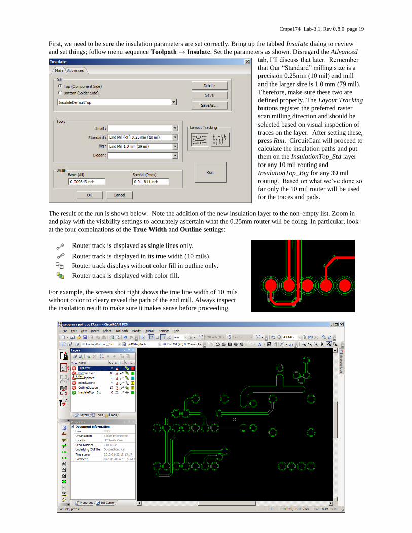
First, we need to be sure the insulation parameters are set correctly. Bring up the tabbed Insulate dialog to review
and set things; follow menu sequence Toolpath → Insulate. Set the parameters as shown. Disregard the Advanced
tab, I’ll discuss that later. Remember
that Our “Standard” milling size is a
precision 0.25mm (10 mil) end mill
and the larger size is 1.0 mm (79 mil).
Therefore, make sure these two are
defined properly. The Layout Tracking
buttons register the preferred raster
scan milling direction and should be
selected based on visual inspection of
traces on the layer. After setting these,
press Run. CircuitCam will proceed to
calculate the insulation paths and put
them on the InsulationTop_Std layer
for any 10 mil routing and
InsulationTop_Big for any 39 mil
routing. Based on what we’ve done so
far only the 10 mil router will be used
for the traces and pads.
The result of the run is shown below. Note the addition of the new insulation layer to the non-empty list. Zoom in
and play with the visibility settings to accurately ascertain what the 0.25mm router will be doing. In particular, look
at the four combinations of the True Width and Outline settings:
Router track is displayed as single lines only.
Router track is displayed in its true width (10 mils).
Router track displays without color fill in outline only.
Router track is displayed with color fill.
For example, the screen shot right shows the true line width of 10 mils
without color to cleary reveal the path of the end mill. Always inspect
the insulation result to make sure it makes sense before proceeding.

Cmpe174 Lab-3.1, Rev 0.8.0 page 20
Adding a Rubout Region on the Top Layer – CircuitCam provides two ways to specify rubout regions, separately
for the top and bottom, or together where a single region applies equally to both. We’ll begin by adding a rubout
region to only the top layer. Shown is a void I want to add around and beneath the DIP package in the lower-left
corner. To do this, as you might suspect, the special milling operation will involve the 39 mil (1.0 mm) end mill and
should therefore end up on the InsulateTop_Big layer. To do this first set rectangle mode by pressing it on the Insert
toolbar (shown just left at the top of the white cross-hair; when active it will have a square hightlight around it).
Then follow menu sequence: Insert → Rubout Area → Top Layer, or use the icon from the Prototype toolbar.
This will change drawing modes allowing you to define one or more rectangular regions. Draw the rectangle
shown by selecting a starting point as an anchor then moving to the opposite corner. Finish by clicking the
mouse and hitting the ESC key.
Since earlier we specified the two router sizes, we can run or re-run the insulation algorithm using the
Insulate Top Layer icon on the Prototype toolbar. Pressing this will run everything. Do this now.
After the new insulation run has completed you should see the region employing the larger router bit whose path is
specified on the InsulateTop_Big layer – as we expected. Moreover, the graphic area we actually drew was specified
on the special layer RuboutTop. You should zoom in on this new region and see how these two routers remove all
copper. I have shown them both in line mode to better delineate the router paths. Particularly notice how much more
efficient the larger bit is in removing large areas of copper and how the router pass around draws a flashes are always
done with the more
precise 10 mil tool.

Cmpe174 Lab-3.1, Rev 0.8.0 page 21
Insulating the Bottom Layer – Follow the same procedure previously used for top layer. First, though, change the
units to mm (millimeters) and bring up the Toolpath → Insulate dialog as shown. I want to explain how the two
Width parameters work. These specify insulation clearances for draws and flashes. Scroll through the Standard sizes
and notice the Base (All) value will
automatically be set to the selected end
mill’s diameter. This can be made
larger, but not smaller, since the first
single pass will always exactly equal the
selected mill size. Making this larger
means additional passes will be made to
widen the initial cut. The Special (Pads)
setting specifies clearances around
flashes, typically pads. Don’t make the
Base larger than the milling size unless
you have a sood reason; it just adds
unnecessary wear and tear to the narrow
tool bit. Experiment with these values
now and see how CircuitCam renders
them. I’ll show you a few examples from
the bottom layer
Case 1: Base = 0.25 mm, Special = 0.25 mm
InsulateBottom_Std is shown in line mode to reveal that a single path was followed once about all objects, whether
draws or flashes.

Cmpe174 Lab-3.1, Rev 0.8.0 page 22
Case 2: Base = 0.25 mm, Special = 0.5 mm
InsulateBottom_Std still in line mode now reveals that a single path was followed for all draws (traces), but 3 passes
were needed to mill the minimum insulation width to 0.5 mm for all flashes (pads). Notice that three passes were
needed, not just two since each one required some overlap with the previous.
Finish insulating the bottom layer with Base and Special both set for 0.25mm. Note that once tools have been
defined and the Base and Special parameters have been set on the Insulate dialog, you can use the Insulate
Bottom Layer icon on the Prototype toolbar.
Insulating Top and Bottom Layers – If you know how you want both layers to be insulated, you can visit the
Insulate dialog once, set all parameters for both layers and run or re-run both of them anytime by using the Insulate
All Layers icon on the Prototype toolbar.
Rubbing out Top and Bottom Layers – Earlier you created a rubout region on the just the top layer. Sometimes we
want a defined void like this to be defined and applied to both the top and bottom simultaneously, where the two are
registered or aligned equally over each other. This can easily be done by putting them on the RuboutAllLayer by
using the follow menu sequence: Insert → Rubout Area → All Layer , or use the icon found on the
Prototype toolbar.

Cmpe174 Lab-3.1, Rev 0.8.0 page 23
4.3 PROCESSING DRILLS
INSULATION AND CONTOUR ROUTING – We actually have little to do in CircuitCam after successfully loading the
Excellon drill files except to check the tool list and decide what drills will actually be used later in Boardmaster.
The best way to do this is to review your design by noting which tool sizes are assigned to holes on your PCB. This
should be both a sanity check and a review to figure what M60 drills are best for each tool in the drill list.
First, open only the DrillUnplated layer for display and be sure it’s selectable. In practice, you may want to turn on
and off other layers, like the board outline and top or bottom, or just leave them on to better guage how the holes are
used. Here, I’ve arbitrarily selected the largest drill size.
Carefully look over the
Properties window. It tells
us only that it is mapped to
tool T3. To find the
associated size, immediately
press the Tools tab, scroll,
select and expand the
Excellon menu item as
shown following.
The submenu
NcDrillDefault displays the
tool-list or “drill rack” with
T3 highlighted
automatically. We see that
T3 specifies an actual drill
of 35 mils. I set the display
to inches and decimal
precision to 3 places so I
could review these in drill
sizes I understand. In metric
they map as follows:
T1: 0.024 mil (0.6 mm)
T2: 0.028 mil (0.8 mm)
T3: 0.035 mil (0.9 mm)

Cmpe174 Lab-3.1, Rev 0.8.0 page 24
CircuitCam’s Excellon drill tool list will later appear in BoardMaster as numbered “pens”; these are noted below in
the lookahead screenshot. All must be mapped to actual drills in BoardMaster. The screenshot is taken from
BoardMaster showing the tool assignments, each as a specific Pen. Note that only metric sizes are displayed.
Remember the LPKF M60 is a metric machine, so all actual tooling is denoted in metric sizes. Among the three
sizes only T2 and T3 need to be re-assigned, since we don’t have 0.7 mm or 0.9 mm drills. The general rule is to use
the next smallest size if it’s available. Thus T2 will use the 0.6 mm drill and T3 the 0.8 mm drill – sizes in our drill
rack. I will show you how to do this in lab 3.2.

Cmpe174 Lab-3.1, Rev 0.8.0 page 25
4.4 EXPORTING THE M60 FILES TO BOARDMASTER
At this point, we are done and ready to move on to lab 3.2. Save your current design as lab3.1.cam and proceed to
export it to BoardMaster.
CircuitCam will generate a special formatted export file in LMD format for later reading into BoardMaster
by simply pressing the ExportLPKFCircuit Board Plotter icon on the Prototype toolbar, or by following
menu sequence: File → Export → LPKF→LpkfCircuitBoardPlotter.
But there’s one catch. Any layers that happen to be visible will be included in the export operation. Therefore, you
must specify the correct layers to avoid later confusion. The screenshot following shows which layers need to be
included for this tutorial. Specify these now, press the export icon and CircuitCam will create the file with the same
name as the current CAM file; it should be lab3.1.LMD.