inkjet-printed flexible gold · pdf file · 2016-04-06for . , , , , , , , , , , ,...
TRANSCRIPT
FULL P
APER
© 2015 WILEY-VCH Verlag GmbH & Co. KGaA, Weinheim 1wileyonlinelibrary.com
1. Introduction
Bioelectronic electrodes are essential in electrophysiology, the scientifi c fi eld that investigates the relationship between electricity and life. Since the advent of electrophysiology in 1783 marked by Luigi Galvani’s experiment of electrical stimulation of a frog leg, electrodes have been used to transduce the body’s ionic current to electronic current and vice versa. [ 1 ] These bioelectronic electrodes can be utilized for both bioimpedance and biopotential measurements. In the case of bioimpedance tomography, a small amount of alternating current is sourced through the tissue, and the resultant voltage signals are recorded using an array of electrodes. Then, various biolog-ical tissues are electrically differentiated depending on the complex impedance of the tissues. The contrast between two dif-ferent types of tissue, for example, lean and fatty tissues, can be picked up using this technique and reconstructed graphi-cally. [ 2 ] In biopotential measurements, dif-ferential voltage measurements are done
on skin and tissue. For example, in electrocardiography (ECG), a set of electrodes are used to pick up the electrical depolariza-tion signal of the heart that provides the cardiac rhythm of the patient. [ 3 ] For bioimpedance and biopotential measurements, the interface between the electrode and the body is crucial, any disturbance at the interface creates unwanted noise artifacts or even invalidates the measurement. [ 4 ] Flexible electronics and optoelectronics are highly promising for creating high-fi delity bioelectronic and biophotonic interfaces. [ 5–8 ] The elasticity of fl exible electronics allows skin-like devices, which are bendable and stretchable. [ 9,10 ] Hence, medical devices fabricated using fl exible materials have the potential to interface better with the human body when compared to rigid electronics.
Fabrication of fl exible medical devices has heavily relied on processing techniques such as metal evaporation, atomic layer deposition, photolithography processes, and transfer printing. [ 11,12 ] In contrast, printing methods, which use rela-tively inexpensive tools and mild processing conditions, [ 11,13 ] can also be used to fabricate fl exible medical devices. [ 7,9 ] Among other printing techniques, inkjet printing (IJP) is promising for
Inkjet-Printed Flexible Gold Electrode Arrays for Bioelectronic Interfaces
Yasser Khan , Felippe J. Pavinatto , Monica C. Lin , Amy Liao , Sarah L. Swisher , Kaylee Mann , Vivek Subramanian , Michel M. Maharbiz , and Ana C. Arias *
Bioelectronic interfaces require electrodes that are mechanically fl exible and chemically inert. Flexibility allows pristine electrode contact to skin and tissue, and chemical inertness prevents electrodes from reacting with biological fl uids and living tissues. Therefore, fl exible gold electrodes are ideal for bioimpedance and biopotential measurements such as bioimpedance tomography, electrocardiography (ECG), electroencephalography (EEG), and electromyography (EMG). However, a manufacturing process to fabricate gold electrode arrays on plastic substrates is still elusive. In this work, a fabrication and low-temperature sintering (≈200 °C) technique is demon-strated to fabricate gold electrodes. At low-temperature sintering conditions, lines of different widths demonstrate different sintering speeds. Therefore, the sintering condition is targeted toward the widest feature in the design layout. Manufactured electrodes show minimum feature size of 62 µm and conductivity values of 5 × 10 6 S m −1 . Utilizing the versatility of printing and plastic electronic processes, electrode arrays consisting of 31 electrodes with electrode-to-electrode spacing ranging from 2 to 7 mm are fabricated and used for impedance mapping of conformal surfaces at 15 kHz. Overall, the fabrication process of an inkjet-printed gold electrode array that is electri-cally reproducible, mechanically robust, and promising for bioimpedance and biopotential measurements is demonstrated.
DOI: 10.1002/adfm.201503316
Y. Khan, Dr. F. J. Pavinatto, Prof. S. L. Swisher,[+] K. Mann, Prof. V. Subramanian, Prof. M. M. Maharbiz, Prof. A. C. Arias Department of Electrical Engineering and Computer Sciences University of California Berkeley , CA 94720 , USA E-mail: [email protected] Dr. F. J. Pavinatto Physics Institute of São Carlos University of São Paulo CEP: 13566-590, São Carlos, SP, Brazil M. C. Lin, A. Liao Joint Graduate Program in Bioengineering University of California Berkeley , CA 94720 , USA [+]Present address: Department of Electrical and Computer Engineering, University of Minnesota , Minneapolis , MN 55455 , USA
Adv. Funct. Mater. 2015, DOI: 10.1002/adfm.201503316
www.afm-journal.dewww.MaterialsViews.com
FULL
PAPER
2 wileyonlinelibrary.com © 2015 WILEY-VCH Verlag GmbH & Co. KGaA, Weinheim
fabricating bioelectronic electrodes because IJP is a noncontact, direct, additive printing method with minimal waste of materials. Additionally, IJP allows easily changeable layouts, which drasti-cally reduce turnaround times for multiple design iterations.
Although the use of IJP to fabricate biosensors is well described, [ 14–16 ] the number of inkjet-printed fl exible medical devices in the literature is still limited. Jensen et al. utilized inkjet-printed gold nanoparticle electrochemical arrays on heat-resistant polyimide Kapton substrate for immunodetection of a cancer biomarker protein. [ 17 ] Jalo et al. demonstrated inkjet-printed antennas on plastic substrates using silver nanoparticle ink, and optimized antenna design for Bluetooth signal trans-mission from the human body surface. [ 18 ] While silver can be used for interfacing sensors to electronics, silver reacts chemi-cally to bodily fl uids, which makes silver undesirable for direct body and skin interfaces. [ 19 ] Alternatively, organic-conducting polymer poly(3,4-ethylenedioxythiophene):polystyrene sulfonate (PEDOT:PSS) can be used for fabricating high-performance bioelectronic electrodes. [ 20 ] That said, gold remains the metal of choice for fabricating electrodes for biomedical applications. Gold is a high work function metal, hence it demonstrates supe-rior stability and inertness when in contact with aqueous media, biological fl uids, or living tissues. To summarize, although bioel-ectronic electrodes can be fabricated in different ways by using conductive materials, [ 21–24 ] there is still a lack in the materials sci-ence literature of the description of robust and effi cient inkjet-printed electrode arrays with applications in the biomedical fi eld.
In this paper, we report on the fabrication of inkjet-printed fl exible gold electrode arrays on plastic substrates that can be used in wearable biomedical applications. These electrode arrays are printed using a gold nanoparticle ink, and the sin-tering conditions are adjusted to plastic-compatible tempera-tures around 200 °C. At low-temperature sintering conditions, lines of different widths demonstrate different sintering speeds. We observed that this is due to a diffusion-controlled mecha-nism of sintering, which depends on surfactant displacement and solvent evaporation. Therefore, the optimum sintering condition is targeted toward the widest feature in the design layout. To enhance mechanical compliance, laser-cut free-standing electrodes are used, which interface better to curved surfaces. Overall, in this paper, practical considerations for IJP reproducible and robust fl exible arrays are described, which can be used for bioimpedance and biopotential measurements such as bioimpedance tomography, electrocardiography (ECG), electroencephalography (EEG), and electromyography (EMG). We recently reported on the use of a similar array to map out pressure ulcers in animal models. [ 9 ] Here, we focus on the array fabrication, low-temperature sintering, and the methodology used for mapping impedance on conformal surfaces.
2. Results and Discussion
2.1. Flexible Inkjet-Printed Gold Electrode Array
IJP is promising for fabricating gold electrode arrays since it is a non-contact, digital, and additive printing method. In con-trast to other printing methods such as screen printing, which uses high-viscosity inks with surfactants, IJP uses low-viscosity
inks—this allows printing of high-purity materials with no binders. [ 25 ] Most common types of conductive ink used in IJP are metal micro and nanoparticle dispersions, metal precursor solutions, conducting polymer solutions, and nanocarbon mate-rial dispersions. [ 26 ] Because gold is highly stable and remains inert when in contact with biological fl uids or living tissues, we employed gold nanoparticle ink for the array fabrication.
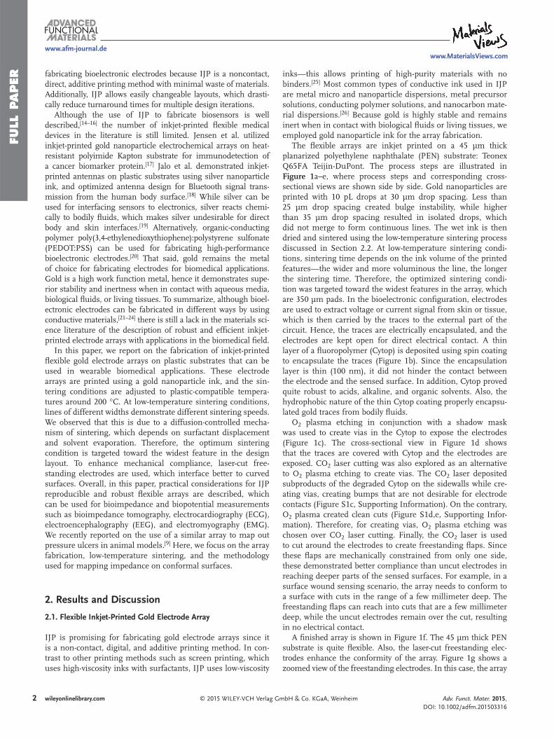
The fl exible arrays are inkjet printed on a 45 µm thick planarized polyethylene naphthalate (PEN) substrate: Teonex Q65FA Teijin-DuPont. The process steps are illustrated in Figure 1 a–e, where process steps and corresponding cross-sectional views are shown side by side. Gold nanoparticles are printed with 10 pL drops at 30 µm drop spacing. Less than 25 µm drop spacing created bulge instability, while higher than 35 µm drop spacing resulted in isolated drops, which did not merge to form continuous lines. The wet ink is then dried and sintered using the low-temperature sintering process discussed in Section 2.2. At low-temperature sintering condi-tions, sintering time depends on the ink volume of the printed features—the wider and more voluminous the line, the longer the sintering time. Therefore, the optimized sintering condi-tion was targeted toward the widest features in the array, which are 350 µm pads. In the bioelectronic confi guration, electrodes are used to extract voltage or current signal from skin or tissue, which is then carried by the traces to the external part of the circuit. Hence, the traces are electrically encapsulated, and the electrodes are kept open for direct electrical contact. A thin layer of a fl uoropolymer (Cytop) is deposited using spin coating to encapsulate the traces (Figure 1 b). Since the encapsulation layer is thin (100 nm), it did not hinder the contact between the electrode and the sensed surface. In addition, Cytop proved quite robust to acids, alkaline, and organic solvents. Also, the hydrophobic nature of the thin Cytop coating properly encapsu-lated gold traces from bodily fl uids.
O 2 plasma etching in conjunction with a shadow mask was used to create vias in the Cytop to expose the electrodes (Figure 1 c). The cross-sectional view in Figure 1 d shows that the traces are covered with Cytop and the electrodes are exposed. CO 2 laser cutting was also explored as an alternative to O 2 plasma etching to create vias. The CO 2 laser deposited subproducts of the degraded Cytop on the sidewalls while cre-ating vias, creating bumps that are not desirable for electrode contacts (Figure S1c, Supporting Information). On the contrary, O 2 plasma created clean cuts (Figure S1d,e, Supporting Infor-mation). Therefore, for creating vias, O 2 plasma etching was chosen over CO 2 laser cutting. Finally, the CO 2 laser is used to cut around the electrodes to create freestanding fl aps. Since these fl aps are mechanically constrained from only one side, these demonstrated better compliance than uncut electrodes in reaching deeper parts of the sensed surfaces. For example, in a surface wound sensing scenario, the array needs to conform to a surface with cuts in the range of a few millimeter deep. The freestanding fl aps can reach into cuts that are a few millimeter deep, while the uncut electrodes remain over the cut, resulting in no electrical contact.
A fi nished array is shown in Figure 1 f. The 45 µm thick PEN substrate is quite fl exible. Also, the laser-cut freestanding elec-trodes enhance the conformity of the array. Figure 1 g shows a zoomed view of the freestanding electrodes. In this case, the array
Adv. Funct. Mater. 2015, DOI: 10.1002/adfm.201503316
www.afm-journal.dewww.MaterialsViews.com
FULL P
APER
3wileyonlinelibrary.com© 2015 WILEY-VCH Verlag GmbH & Co. KGaA, Weinheim
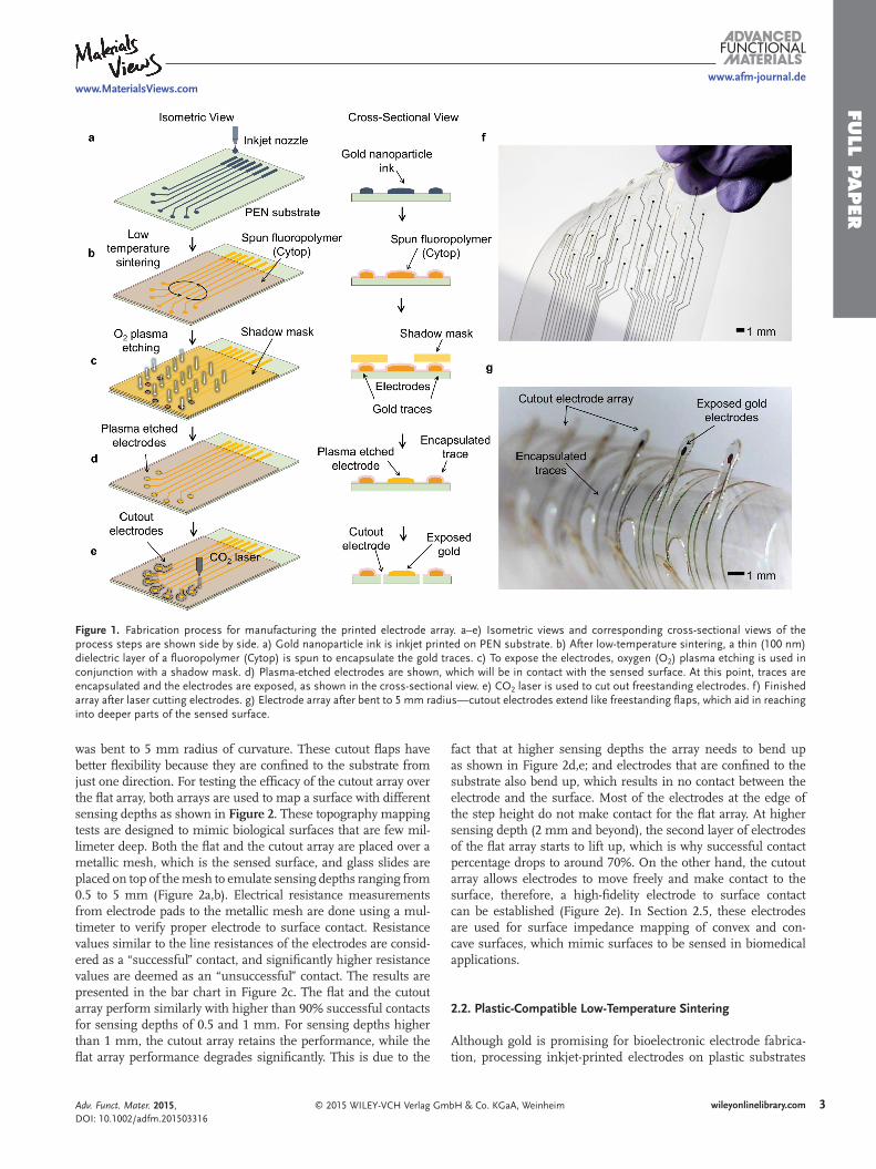
was bent to 5 mm radius of curvature. These cutout fl aps have better fl exibility because they are confi ned to the substrate from just one direction. For testing the effi cacy of the cutout array over the fl at array, both arrays are used to map a surface with different sensing depths as shown in Figure 2 . These topography mapping tests are designed to mimic biological surfaces that are few mil-limeter deep. Both the fl at and the cutout array are placed over a metallic mesh, which is the sensed surface, and glass slides are placed on top of the mesh to emulate sensing depths ranging from 0.5 to 5 mm (Figure 2 a,b). Electrical resistance measurements from electrode pads to the metallic mesh are done using a mul-timeter to verify proper electrode to surface contact. Resistance values similar to the line resistances of the electrodes are consid-ered as a “successful” contact, and signifi cantly higher resistance values are deemed as an “unsuccessful” contact. The results are presented in the bar chart in Figure 2 c. The fl at and the cutout array perform similarly with higher than 90% successful contacts for sensing depths of 0.5 and 1 mm. For sensing depths higher than 1 mm, the cutout array retains the performance, while the fl at array performance degrades signifi cantly. This is due to the
fact that at higher sensing depths the array needs to bend up as shown in Figure 2 d,e; and electrodes that are confi ned to the substrate also bend up, which results in no contact between the electrode and the surface. Most of the electrodes at the edge of the step height do not make contact for the fl at array. At higher sensing depth (2 mm and beyond), the second layer of electrodes of the fl at array starts to lift up, which is why successful contact percentage drops to around 70%. On the other hand, the cutout array allows electrodes to move freely and make contact to the surface, therefore, a high-fi delity electrode to surface contact can be established (Figure 2 e). In Section 2.5, these electrodes are used for surface impedance mapping of convex and con-cave surfaces, which mimic surfaces to be sensed in biomedical applications.
2.2. Plastic-Compatible Low-Temperature Sintering
Although gold is promising for bioelectronic electrode fabrica-tion, processing inkjet-printed electrodes on plastic substrates
Adv. Funct. Mater. 2015, DOI: 10.1002/adfm.201503316
www.afm-journal.dewww.MaterialsViews.com
Figure 1. Fabrication process for manufacturing the printed electrode array. a–e) Isometric views and corresponding cross-sectional views of the process steps are shown side by side. a) Gold nanoparticle ink is inkjet printed on PEN substrate. b) After low-temperature sintering, a thin (100 nm) dielectric layer of a fl uoropolymer (Cytop) is spun to encapsulate the gold traces. c) To expose the electrodes, oxygen (O 2 ) plasma etching is used in conjunction with a shadow mask. d) Plasma-etched electrodes are shown, which will be in contact with the sensed surface. At this point, traces are encapsulated and the electrodes are exposed, as shown in the cross-sectional view. e) CO 2 laser is used to cut out freestanding electrodes. f) Finished array after laser cutting electrodes. g) Electrode array after bent to 5 mm radius—cutout electrodes extend like freestanding fl aps, which aid in reaching into deeper parts of the sensed surface.
FULL
PAPER
4 wileyonlinelibrary.com © 2015 WILEY-VCH Verlag GmbH & Co. KGaA, Weinheim
is challenging. Gold nanoparticle ink requires high sintering temperatures in the range of 250 °C, which is above the melting temperature of the most common plastics used in fl exible elec-tronics, such as polyethylene terephthalate (PET) and polyeth-ylene naphthalate (PEN). This high processing temperature is suitable for inorganic surfaces like silicon. [ 27 ] Moreover, PET and PEN undergo thermal deformation at temperatures higher than the glass transition temperature ( T g ). [ 28 ] A common prac-tice in sintering lab-scale-printed fi lms to mitigate substrate deformation is to tape down fi lms to the hotplate. Therefore, all the samples reported in this paper were sintered while taped down to the hotplate. A time-dependent thermal deformation plot of the heat-stabilized variant of PEN fi lm is shown and discussed in Figure S2 (Supporting Information). For printing gold on plastics, custom-made formulations with tailored par-ticle sizes and surfactant chemical structures have to be synthe-sized. [ 29–31 ] Additionally, sintering studies in the literature focus on deposited fi lms, [ 32 ] while electrode arrays have traces, elec-trodes, and pads of different geometries and widths. Here, we performed low-temperature sintering of a gold nanoparticle ink and studied different printed geometry and the corresponding sintering characteristics.
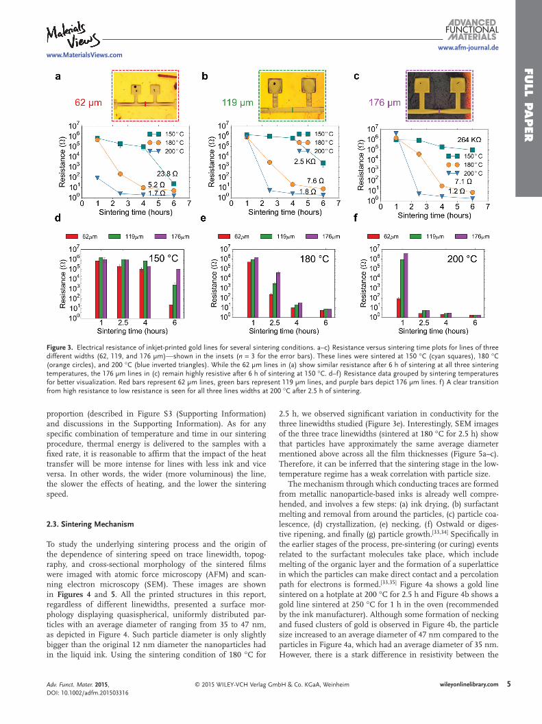
To understand the relationship between printed trace linewidth and sintering conditions, traces with widths of 62, 119, and 176 µm were sintered at several combinations of sin-tering temperature and time, as shown in Figure 3 a–c. The standard sintering condition for the gold nanoparticle ink is 250 °C for 1 h, and resistivity of 5.6 × 10 –8 Ω m is attained
for printed lines sintered at this condition. We show that it is possible to achieve resistivity values of similar magnitude if we use a lower temperature for a longer time. For instance, 2.0 × 10 –7 Ω m was obtained for printed lines (176 µm wide) sintered at 200 °C for 6 h. In general, the lower the temperature, the longer it takes to attain a level of low resistance, as expected.
The dependence of sintering speed on trace linewidth can be seen in Figure 3 a–c. This effect becomes apparent in Figure 3 d–f, where resistance values are plotted separately for each indi-vidual temperature studied, and each linewidth is represented by a color-coded bar. From the bar charts, a conclusion can be drawn that under low-temperature sintering conditions, wider lines take a longer time to sinter compared to the narrower lines. Therefore, if the sintering condition is not properly chosen, very heterogeneous electrical properties are expected in an electrode array with traces of varying width. For example, the narrower traces will be conductive while the wider pads will remain non-conductive. In our experiment, the 62 µm lines have an average resistance of 23.8 Ω after 6 h at 150 °C (Figure 3 a), and 176 µm lines have an average resistance of 264 kΩ under the same condi-tions (Figure 3 c). In other words, for each sintering temperature, there is a specifi c time for which the lines go through a transi-tion regime after which they become conductive, and inside this transition zone resistance can vary orders of magnitude for lines of different widths. For 62 µm lines, the transition time is 6 h at 150 °C, 2.5 h at 180 °C, and 1 h at 200 °C.
Linewidths for our samples scale in a ratio of 1:2:3 and the cross-sectional area of such lines has roughly the same
Adv. Funct. Mater. 2015, DOI: 10.1002/adfm.201503316
www.afm-journal.dewww.MaterialsViews.com
Figure 2. Topography coverage comparison between the fl at array and the cutout array. a) A schematic overview of the topography coverage test setup—the array is placed on a metallic mesh, and glass slides on top of the mesh emulate a step height. Resistance measurements are done from the electrode pad to the metallic mesh to confi rm electrode–surface contact. b) Optical image of the setup—the electrode array, the metallic mesh, and the glass slides are shown. c) A bar chart depicting the percentage of successful electrode–surface contacts by the fl at and the cutout array for various sensing depths. Clearly, the cutout array (green bars) provides a signifi cant edge over the fl at array (red bars) for sensing depths over 1 mm. The error bars represent data collected from fi ve separate runs. d–e) Close-up images collected from the dotted region in (b) (at the step height) for the fl at array and the cutout array, respectively. d) Electrodes at the step height in the fl at array do not touch the surface of the metallic mesh because the 2 mm thick glass slides bend the whole array upward, resulting in an unsuccessful electrode–surface contact. e) The cutout array also bends upward at the interface; however, the cutout electrodes are not confi ned to the array, therefore, the electrodes can make a conformal contact, resulting in a successful electrode–surface contact.
FULL P
APER
5wileyonlinelibrary.com© 2015 WILEY-VCH Verlag GmbH & Co. KGaA, Weinheim
proportion (described in Figure S3 (Supporting Information) and discussions in the Supporting Information). As for any specifi c combination of temperature and time in our sintering procedure, thermal energy is delivered to the samples with a fi xed rate, it is reasonable to affi rm that the impact of the heat transfer will be more intense for lines with less ink and vice versa. In other words, the wider (more voluminous) the line, the slower the effects of heating, and the lower the sintering speed.
2.3. Sintering Mechanism
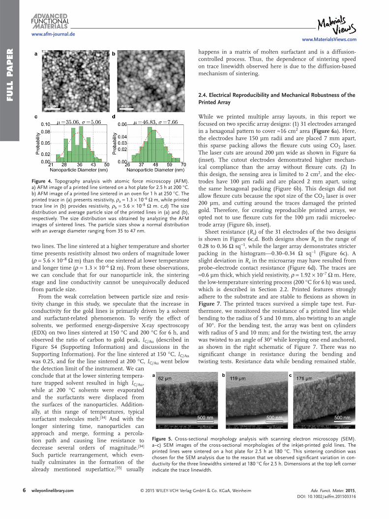
To study the underlying sintering process and the origin of the dependence of sintering speed on trace linewidth, topog-raphy, and cross-sectional morphology of the sintered fi lms were imaged with atomic force microscopy (AFM) and scan-ning electron microscopy (SEM). These images are shown in Figures 4 and 5 . All the printed structures in this report, regardless of different linewidths, presented a surface mor-phology displaying quasispherical, uniformly distributed par-ticles with an average diameter of ranging from 35 to 47 nm, as depicted in Figure 4 . Such particle diameter is only slightly bigger than the original 12 nm diameter the nanoparticles had in the liquid ink. Using the sintering condition of 180 °C for
2.5 h, we observed signifi cant variation in conductivity for the three linewidths studied (Figure 3 e). Interestingly, SEM images of the three trace linewidths (sintered at 180 °C for 2.5 h) show that particles have approximately the same average diameter mentioned above across all the fi lm thicknesses (Figure 5 a–c). Therefore, it can be inferred that the sintering stage in the low-temperature regime has a weak correlation with particle size.
The mechanism through which conducting traces are formed from metallic nanoparticle-based inks is already well compre-hended, and involves a few steps: (a) ink drying, (b) surfactant melting and removal from around the particles, (c) particle coa-lescence, (d) crystallization, (e) necking, (f) Ostwald or diges-tive ripening, and fi nally (g) particle growth. [ 33,34 ] Specifi cally in the earlier stages of the process, pre-sintering (or curing) events related to the surfactant molecules take place, which include melting of the organic layer and the formation of a superlattice in which the particles can make direct contact and a percolation path for electrons is formed. [ 33,35 ] Figure 4 a shows a gold line sintered on a hotplate at 200 °C for 2.5 h and Figure 4 b shows a gold line sintered at 250 °C for 1 h in the oven (recommended by the ink manufacturer). Although some formation of necking and fused clusters of gold is observed in Figure 4 b, the particle size increased to an average diameter of 47 nm compared to the particles in Figure 4 a, which had an average diameter of 35 nm. However, there is a stark difference in resistivity between the
Adv. Funct. Mater. 2015, DOI: 10.1002/adfm.201503316
www.afm-journal.dewww.MaterialsViews.com
Figure 3. Electrical resistance of inkjet-printed gold lines for several sintering conditions. a–c) Resistance versus sintering time plots for lines of three different widths (62, 119, and 176 µm)—shown in the insets ( n = 3 for the error bars). These lines were sintered at 150 °C (cyan squares), 180 °C (orange circles), and 200 °C (blue inverted triangles). While the 62 µm lines in (a) show similar resistance after 6 h of sintering at all three sintering temperatures, the 176 µm lines in (c) remain highly resistive after 6 h of sintering at 150 °C. d–f) Resistance data grouped by sintering temperatures for better visualization. Red bars represent 62 µm lines, green bars represent 119 µm lines, and purple bars depict 176 µm lines. f) A clear transition from high resistance to low resistance is seen for all three lines widths at 200 °C after 2.5 h of sintering.
FULL
PAPER
6 wileyonlinelibrary.com © 2015 WILEY-VCH Verlag GmbH & Co. KGaA, Weinheim
two lines. The line sintered at a higher temperature and shorter time presents resistivity almost two orders of magnitude lower ( ρ = 5.6 × 10 –8 Ω m) than the one sintered at lower temperature and longer time ( ρ = 1.3 × 10 –6 Ω m). From these observations, we can conclude that for our nanoparticle ink, the sintering stage and line conductivity cannot be unequivocally deduced from particle size.
From the weak correlation between particle size and resis-tivity change in this study, we speculate that the increase in conductivity for the gold lines is primarily driven by a solvent and surfactant-related phenomenon. To verify the effect of solvents, we performed energy-dispersive X-ray spectroscopy (EDX) on two lines sintered at 150 °C and 200 °C for 6 h, and observed the ratio of carbon to gold peak, I C/Au (described in Figure S4 (Supporting Information) and discussions in the Supporting Information). For the line sintered at 150 °C, I C/Au was 0.25, and for the line sintered at 200 °C, I C/Au went below the detection limit of the instrument. We can conclude that at the lower sintering tempera-ture trapped solvent resulted in high I C/Au , while at 200 °C solvents were evaporated and the surfactants were displaced from the surfaces of the nanoparticles. Addition-ally, at this range of temperatures, typical surfactant molecules melt. [ 34 ] And with the longer sintering time, nanoparticles can approach and merge, forming a percola-tion path and causing line resistance to decrease several orders of magnitude. [ 34 ] Such particle rearrangement, which even-tually culminates in the formation of the already mentioned superlattice, [ 35 ] usually
happens in a matrix of molten surfactant and is a diffusion-controlled process. Thus, the dependence of sintering speed on trace linewidth observed here is due to the diffusion-based mechanism of sintering.
2.4. Electrical Reproducibility and Mechanical Robustness of the Printed Array
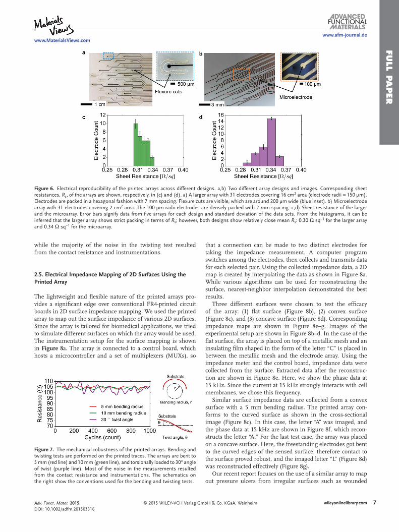
While we printed multiple array layouts, in this report we focused on two specifi c array designs: (1) 31 electrodes arranged in a hexagonal pattern to cover ≈16 cm 2 area ( Figure 6 a). Here, the electrodes have 150 µm radii and are placed 7 mm apart, this sparse packing allows the fl exure cuts using CO 2 laser. The laser cuts are around 200 µm wide as shown in Figure 6 a (inset). The cutout electrodes demonstrated higher mechan-ical compliance than the array without fl exure cuts. (2) In this design, the sensing area is limited to 2 cm 2 , and the elec-trodes have 100 µm radii and are placed 2 mm apart, using the same hexagonal packing (Figure 6 b). This design did not allow fl exure cuts because the spot size of the CO 2 laser is over 200 µm, and cutting around the traces damaged the printed gold. Therefore, for creating reproducible printed arrays, we opted not to use fl exure cuts for the 100 µm radii microelec-trode array (Figure 6 b, inset).
Sheet resistance ( R s ) of the 31 electrodes of the two designs is shown in Figure 6 c,d. Both designs show R s in the range of 0.28 to 0.36 Ω sq −1 , while the larger array demonstrates stricter packing in the histogram—0.30–0.34 Ω sq −1 (Figure 6 c). A slight deviation in R s in the microarray may have resulted from probe–electrode contact resistance (Figure 6 d). The traces are ≈0.6 µm thick, which yield resistivity, ρ = 1.92 × 10 –7 Ω m. Here, the low-temperature sintering process (200 °C for 6 h) was used, which is described in Section 2.2. Printed features strongly adhere to the substrate and are stable to fl exions as shown in Figure 7 . The printed traces survived a simple tape test. Fur-thermore, we monitored the resistance of a printed line while bending to the radius of 5 and 10 mm, also twisting to an angle of 30°. For the bending test, the array was bent on cylinders with radius of 5 and 10 mm; and for the twisting test, the array was twisted to an angle of 30° while keeping one end anchored, as shown in the right schematic of Figure 7 . There was no signifi cant change in resistance during the bending and twisting tests. Resistance data while bending remained stable,
Adv. Funct. Mater. 2015, DOI: 10.1002/adfm.201503316
www.afm-journal.dewww.MaterialsViews.com
Figure 4. Topography analysis with atomic force microscopy (AFM). a) AFM image of a printed line sintered on a hot plate for 2.5 h at 200 °C. b) AFM image of a printed line sintered in an oven for 1 h at 250 °C. The printed trace in (a) presents resistivity, ρ a = 1.3 × 10 –6 Ω m, while printed trace line in (b) provides resistivity, ρ b = 5.6 × 10 –8 Ω m. c,d) The size distribution and average particle size of the printed lines in (a) and (b), respectively. The size distribution was obtained by analyzing the AFM images of sintered lines. The particle sizes show a normal distribution with an average diameter ranging from 35 to 47 nm.
Figure 5. Cross-sectional morphology analysis with scanning electron microscopy (SEM). a–c) SEM images of the cross-sectional morphologies of the inkjet-printed gold lines. The printed lines were sintered on a hot plate for 2.5 h at 180 °C. This sintering condition was chosen for the SEM analysis due to the reason that we observed signifi cant variation in con-ductivity for the three linewidths sintered at 180 °C for 2.5 h. Dimensions at the top left corner indicate the trace linewidth.
FULL P
APER
7wileyonlinelibrary.com© 2015 WILEY-VCH Verlag GmbH & Co. KGaA, Weinheim
while the majority of the noise in the twisting test resulted from the contact resistance and instrumentations.
2.5. Electrical Impedance Mapping of 2D Surfaces Using the Printed Array
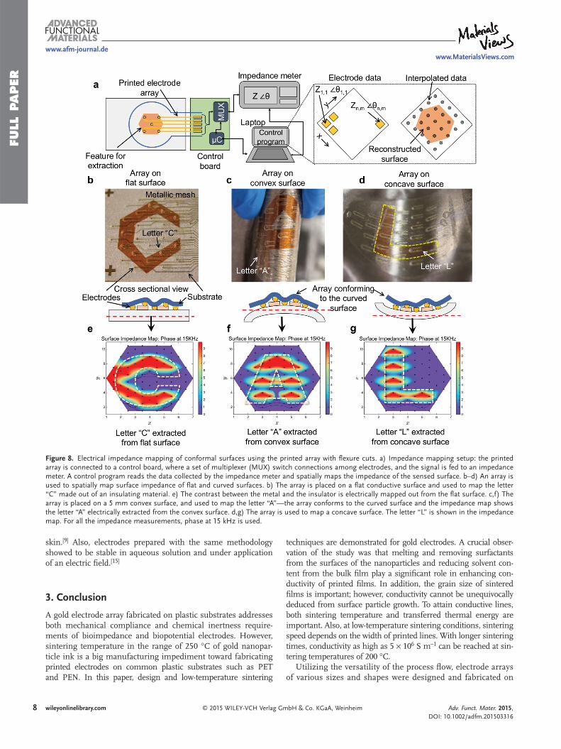
The lightweight and fl exible nature of the printed arrays pro-vides a signifi cant edge over conventional FR4-printed circuit boards in 2D surface impedance mapping. We used the printed array to map out the surface impedance of various 2D surfaces. Since the array is tailored for biomedical applications, we tried to simulate different surfaces on which the array would be used. The instrumentation setup for the surface mapping is shown in Figure 8 a. The array is connected to a control board, which hosts a microcontroller and a set of multiplexers (MUXs), so
that a connection can be made to two distinct electrodes for taking the impedance measurement. A computer program switches among the electrodes, then collects and transmits data for each selected pair. Using the collected impedance data, a 2D map is created by interpolating the data as shown in Figure 8 a. While various algorithms can be used for reconstructing the surface, nearest-neighbor interpolation demonstrated the best results.
Three different surfaces were chosen to test the effi cacy of the array: (1) fl at surface (Figure 8 b), (2) convex surface (Figure 8 c), and (3) concave surface (Figure 8 d). Corresponding impedance maps are shown in Figure 8 e–g. Images of the experimental setup are shown in Figure 8 b–d. In the case of the fl at surface, the array is placed on top of a metallic mesh and an insulating fi lm shaped in the form of the letter “C” is placed in between the metallic mesh and the electrode array. Using the impedance meter and the control board, impedance data were collected from the surface. Extracted data after the reconstruc-tion are shown in Figure 8 e. Here, we show the phase data at 15 kHz. Since the current at 15 kHz strongly interacts with cell membranes, we chose this frequency.
Similar surface impedance data are collected from a convex surface with a 5 mm bending radius. The printed array con-forms to the curved surface as shown in the cross-sectional image (Figure 8 c). In this case, the letter “A” was imaged, and the phase data at 15 kHz are shown in Figure 8 f, which recon-structs the letter “A.” For the last test case, the array was placed on a concave surface. Here, the freestanding electrodes got bent to the curved edges of the sensed surface, therefore contact to the surface proved robust, and the imaged letter “L” (Figure 8 d) was reconstructed effectively (Figure 8 g).
Our recent report focuses on the use of a similar array to map out pressure ulcers from irregular surfaces such as wounded
Adv. Funct. Mater. 2015, DOI: 10.1002/adfm.201503316
www.afm-journal.dewww.MaterialsViews.com
Figure 6. Electrical reproducibility of the printed arrays across different designs. a,b) Two different array designs and images. Corresponding sheet resistances, R s , of the arrays are shown, respectively, in (c) and (d). a) A larger array with 31 electrodes covering 16 cm 2 area (electrode radii = 150 µm). Electrodes are packed in a hexagonal fashion with 7 mm spacing. Flexure cuts are visible, which are around 200 µm wide (blue inset). b) Microelectrode array with 31 electrodes covering 2 cm 2 area. The 100 µm radii electrodes are densely packed with 2 mm spacing. c,d) Sheet resistance of the larger and the microarray. Error bars signify data from fi ve arrays for each design and standard deviation of the data sets. From the histograms, it can be inferred that the larger array shows strict packing in terms of R s ; however, both designs show relatively close mean R s : 0.30 Ω sq −1 for the larger array and 0.34 Ω sq −1 for the microarray.
Figure 7. The mechanical robustness of the printed arrays. Bending and twisting tests are performed on the printed traces. The arrays are bent to 5 mm (red line) and 10 mm (green line), and torsionally loaded to 30° angle of twist (purple line). Most of the noise in the measurements resulted from the contact resistance and instrumentations. The schematics on the right show the conventions used for the bending and twisting tests.
FULL
PAPER
8 wileyonlinelibrary.com © 2015 WILEY-VCH Verlag GmbH & Co. KGaA, Weinheim Adv. Funct. Mater. 2015, DOI: 10.1002/adfm.201503316
www.afm-journal.dewww.MaterialsViews.com
skin. [ 9 ] Also, electrodes prepared with the same methodology showed to be stable in aqueous solution and under application of an electric fi eld. [ 15 ]
3. Conclusion
A gold electrode array fabricated on plastic substrates addresses both mechanical compliance and chemical inertness require-ments of bioimpedance and biopotential electrodes. However, sintering temperature in the range of 250 °C of gold nanopar-ticle ink is a big manufacturing impediment toward fabricating printed electrodes on common plastic substrates such as PET and PEN. In this paper, design and low-temperature sintering
techniques are demonstrated for gold electrodes. A crucial obser-vation of the study was that melting and removing surfactants from the surfaces of the nanoparticles and reducing solvent con-tent from the bulk fi lm play a signifi cant role in enhancing con-ductivity of printed fi lms. In addition, the grain size of sintered fi lms is important; however, conductivity cannot be unequivocally deduced from surface particle growth. To attain conductive lines, both sintering temperature and transferred thermal energy are important. Also, at low-temperature sintering conditions, sintering speed depends on the width of printed lines. With longer sintering times, conductivity as high as 5 × 10 6 S m –1 can be reached at sin-tering temperatures of 200 °C.
Utilizing the versatility of the process fl ow, electrode arrays of various sizes and shapes were designed and fabricated on
Figure 8. Electrical impedance mapping of conformal surfaces using the printed array with fl exure cuts. a) Impedance mapping setup: the printed array is connected to a control board, where a set of multiplexer (MUX) switch connections among electrodes, and the signal is fed to an impedance meter. A control program reads the data collected by the impedance meter and spatially maps the impedance of the sensed surface. b–d) An array is used to spatially map surface impedance of fl at and curved surfaces. b) The array is placed on a fl at conductive surface and used to map the letter “C” made out of an insulating material. e) The contrast between the metal and the insulator is electrically mapped out from the fl at surface. c,f) The array is placed on a 5 mm convex surface, and used to map the letter “A”—the array conforms to the curved surface and the impedance map shows the letter “A” electrically extracted from the convex surface. d,g) The array is used to map a concave surface. The letter “L” is shown in the impedance map. For all the impedance measurements, phase at 15 kHz is used.
FULL P
APER
9wileyonlinelibrary.com© 2015 WILEY-VCH Verlag GmbH & Co. KGaA, WeinheimAdv. Funct. Mater. 2015, DOI: 10.1002/adfm.201503316
www.afm-journal.dewww.MaterialsViews.com
plastic substrates. Electrode arrays consisting of 31 electrodes with electrode-to-electrode spacing ranging from 2 to 7 mm were fabricated and used for impedance mapping of con-formal surfaces at 15 kHz. Since IJP was used for fabricating the arrays, the turnaround time from design to design was quite low compared to the process fl ows that rely on vacuum processing techniques. Minimum feature size of 62 µm was reproducibly printed with sheet resistance of 0.30 Ω sq −1 for 0.6 µm thick lines. Additionally, laser-cut freestanding elec-trodes were created to enhance conformity of the array, which enhanced contact to conformal surfaces. Finally, these arrays were used for surface impedance mapping of different 2D surfaces.
In summary, we demonstrated fl exible gold electrode array fabrication, low-temperature sintering, and the methodology used for mapping impedance on conformal surfaces. These gold electrodes can be utilized for both bioimpedance and bio-potential measurements. Taking advantage of the low-cost and large-area manufacturing techniques, these effi cient and afford-able electrode arrays can be used in novel in-home and in-hospital medical sensing applications.
4. Experimental Section Array Fabrication Process : 45 µm thick polyethylene naphthalate (PEN,
Teonex Q65FA Teijin-DuPont) substrates were used for fabricating the array. Harima gold nanoparticle ink with petroleum hydrocarbon based non-aromatic solvent was printed using a Dimatix inkjet printer (DMP-2800) with 30 µm drop spacing. After that, low-temperature sintering (200 °C for 6 h) was used to create the conductive lines. To encapsulate the lines, the array was spin coated with 100 nm Cytop fl uoropolymer at 1200 rpm spin speed. Then, electrodes were etched using O 2 plasma etching with 240 W power for 12 min. Freestanding electrode fl aps were created using a CO 2 laser with a single run at 70% power. The fl aps were 1 mm wide and 5 mm long.
Low-Temperature Sintering of Printed Features : To evaluate low-temperature sintering of printed features, 62, 119, and 176 µm linewidth structures were printed and sintered. A custom-designed hotplate and an oven were used for sintering the ink. As for the linewidth-dependent sintering speed analysis, four-point-probe (4PP) resistance measurements were taken at 1, 2.5, 4, and 6 h time points. Constant temperature sintering was done at 150, 180, and 200 °C. The longer sintering at 200 °C was utilized for melting and burning the surfactants, as well as for removing solvents from the traces. Resistance measurements were taken using a Keithley 2400 source meter in 4PP settings.
Surface Impedance Mapping Using Electrode Array : A custom software and hardware setup was used to create the surface impedance maps. The printed array was connected to a control board, which hosted a microcontroller and a few multiplexers (MUXs). A host computer controlled the MUXs and selected pairs of electrodes for the impedance measurements. The preprogrammed pairs were then fed to an impedance meter (Agilent E4980AL). Then, the data were transferred from the impedance meter to the computer. Collected data were then interpolated to create the surface map. Impedance measurements were taken at 15 kHz.
Supporting Information Supporting Information is available from the Wiley Online Library or from the author.
Acknowledgements Y.K. and F.J.P. contributed equally to this work. The authors thank Dr. Elisabeth J. Leefl ang, Prof. David Young, Prof. Shuvo Roy, and Prof. Michael R. Harrison from UCSF for their feedback and helpful discussions, and Prof. Ali Javey at UC Berkeley for giving access to equipments in his laboratory. The authors thank Dr. Igal Deckman for the EDX analysis. The authors also thank Dr. Abhinav Gaikwad, Dr. Balthazar Lechêne, Adrien Pierre, and Aminy Ostfeld for numerous helpful discussions. This material is based upon work supported by the National Science Foundation under Grant No. EFRI 1240380. F.J.P. acknowledges FAPESP (Fundação de Amparo do Estado de São Paulo, Project No. 2011/05742-0). A.L. and M.C.L. were supported by a National Science Foundation Graduate Research Fellowship, and S.L.S. was supported by the Noyce Memorial Fellowship in Microelectronics from the Intel Foundation.
Received: August 9, 2015 Revised: September 27, 2015
Published online:
[1] J. Webster , Medical Instrumentation: Application and Design , John Wiley & Sons , Hoboken, NJ , 2010 .
[2] R. Bayford , Annu. Rev. Biomed. Eng. 2006 , 8 , 63 . [3] E. Lepeschkin , B. Surawicz , Circulation 1952 , 6 , 378 . [4] G. G. Wallace , S. E. Moulton , G. M. Clark , Science 2009 , 324 , 185 . [5] J. A. Rogers , Y. Huang , Proc. Natl. Acad. Sci. USA 2009 , 106 ,
10875 . [6] S. Bauer , S. Bauer-Gogonea , I. Graz , M. Kaltenbrunner , C. Keplinger ,
R. Schwödiauer , Adv. Mater. 2014 , 26 , 149 . [7] C. M. Lochner , Y. Khan , A. Pierre , A. C. Arias , Nat. Commun. 2014 ,
5 , 5745 . [8] Y. Khan , C. M. Lochner , A. Pierre , A. C. Arias , presented at 6th IEEE
Int. Workshop on IEEE Advances in Sensors and Interfaces (IWASI) , June 2015 , pp. 83, Gallipoli, Apulia, Italy .
[9] S. L. Swisher , M. C. Lin , A. Liao , E. J. Leefl ang , Y. Khan , F. J. Pavinatto , K. Mann , A. Naujokas , D. Young , S. Roy , A. C. Arias V. Subramanian , M. M. Maharbiz , Nat. Commun. 2015 , 6 , 6575 .
[10] J. A. Rogers , T. Someya , Y. Huang , Science 2010 , 327 , 1603 . [11] A. Carlson , A. M. Bowen , Y. Huang , R. G. Nuzzo , J. A. Rogers , Adv.
Mater. 2012 , 24 , 5284 . [12] C. Pang , C. Lee , K.-Y. Suh , J. Appl. Polym. Sci. 2013 , 130 , 1429 . [13] R. R. Søndergaard , M. Hösel , F. C. Krebs , J. Polym. Sci., Part B:
Polym. Phys. 2013 , 51 , 16 . [14] N. Komuro , S. Takaki , K. Suzuki , D. Citterio , Anal. Bioanal. Chem.
2013 , 405 , 5785 . [15] F. J. Pavinatto , C. W. Paschoal , A. C. Arias , Biosens. Bioelectron.
2015 , 67 , 553 . [16] F. J. Pavinatto , Display and Imaging 2015 , 2 , 69 . [17] G. C. Jensen , C. E. Krause , G. A. Sotzing , J. F. Rusling , Phys. Chem.
Chem. Phys. 2011 , 13 , 4888 . [18] J. Jalo , H. P. Sillanpaa , R. M. Makinen , Prog. Electromagn. Res. 2013 ,
142 , 409 . [19] W. F. Jackson , B. R. Duling , Circ. Res. 1983 , 53 , 105 . [20] P. Leleux , C. Johnson , X. Strakosas , J. Rivnay , T. Hervé , R. M. Owens ,
G. G. Malliaras , Adv. Healthcare Mater. 2014 , 3 , 1377 . [21] Y. Yu , J. Zhang , J. Liu , PLoS ONE 2013 , 8 , e58771 . [22] D.-H. Kim , N. Lu , R. Ma , Y.-S. Kim , R.-H. Kim , S. Wang , J. Wu ,
S. M. Won , H. Tao , A. Islam , K. J. Yu, T.-i. Kim, R. Chowdhury, M. Ying, L. Xu, M. Li, H.-J. Chung, H. Keum, M. McCormick, P. Liu, Y.-W. Zhang, F. G. Omenetto, Y. Huang, T. Coleman, J. A. Rogers, Science 2011 , 333 , 838 .
[23] D.-H. Kim , J. Xiao , J. Song , Y. Huang , J. A. Rogers , Adv. Mater. 2010 , 22 , 2108 .

FULL
PAPER
10 wileyonlinelibrary.com © 2015 WILEY-VCH Verlag GmbH & Co. KGaA, Weinheim Adv. Funct. Mater. 2015, DOI: 10.1002/adfm.201503316
www.afm-journal.dewww.MaterialsViews.com
[24] N. Matsuhisa , M. Kaltenbrunner , T. Yokota , H. Jinno , K. Kuribara , T. Sekitani , T. Someya , Nat. Commun. 2015 , 6 , 7461 .
[25] V. Subramanian , J. Cen , A. de la Fuente Vornbrock , G. Grau , H. Kang , R. Kitsomboonloha , D. Soltman , H.-Y. Tseng , Proc. IEEE 2015 , 103 , 567 .
[26] A. Kamyshny , M. Ben-Moshe , S. Aviezer , S. Magdassi , Macromol. Rapid Commun. 2005 , 26 , 281 .
[27] J. A. Sadie , V. Subramanian , Adv. Funct. Mater. 2014 , 24 , 6834 . [28] V. Zardetto , T. M. Brown , A. Reale , A. Di Carlo , J. Polym. Sci., Part B:
Polym. Phys. 2011 , 49 , 638 . [29] D. Huang , F. Liao , S. Molesa , D. Redinger , V. Subramanian ,
J. Electrochem. Soc. 2003 , 150 , G412 .
[30] T. Bakhishev , V. Subramanian , J. Electron. Mater. 2009 , 38 , 2720 .
[31] A. Gupta , S. Mandal , M. Katiyar , Y. N. Mohapatra , Thin Solid Films 2012 , 520 , 5664 .
[32] J. Chung , S. Ko , N. R. Bieri , C. P. Grigoropoulos , D. Poulikakos , Appl. Phys. Lett. 2004 , 84 , 801 .
[33] J. Perelaer , P. J. Smith , D. Mager , D. Soltman , S. K. Volkman , V. Subramanian , J. G. Korvink , U. S. Schubert , J. Mater. Chem. 2010 , 20 , 8446 .
[34] S. K. Volkman , S. Yin , T. Bakhishev , K. Puntambekar , V. Subramanian , M. F. Toney , Chem. Mater. 2011 , 23 , 4634 .
[35] X. Lin , C. Sorensen , K. Klabunde , J. Nanopart. Res. 2000 , 2 , 157 .

Copyright WILEY‐VCH Verlag GmbH & Co. KGaA, 69469 Weinheim, Germany, 2015.
Supporting Information
for Adv. Funct. Mater., DOI: 10.1002/adfm. 201503316
Inkjet-Printed Flexible Gold Electrode Arrays for Bioelectronic Interfaces Yasser Khan, Felippe J. Pavinatto, Monica C. Lin, Amy Liao, Sarah L. Swisher, Kaylee Mann, Vivek Subramanian, Michel M. Maharbiz, and Ana C. Arias*
1
Supporting Information
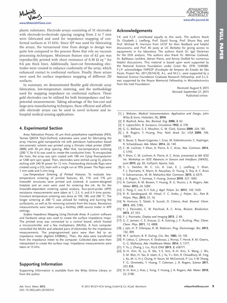
Figure S1: Methods for removing the dielectric layer (Cytop) from the electrodes. a) Laser drilling to open via through
the dielectric layer. b) Oxygen plasma etching using a shadow mask to selectively etch the dielectric layer. The surface
profile of an electrode after c) laser drilling and d) plasma etching. e) Micrograph of an electrode after plasma etching
- etched area encircled by a dark Cytop layer, which is clearly visible; also the exposed electrode is shown.
Bioelectronic electrodes are usually used to extract voltage or current signal from skin or tissue, which isthen carried by the traces to the external part of the circuit. Therefore, the traces are electrically encapsulated,and the electrodes are kept open for direct electrical contact. We encapsulated the traces with a thin (100 nm)layer of a fluoropolymer (Cytop). To open the electrodes for surface contact, we explored CO2 laser drilling(Figure S1a) and oxygen plasma etching (Figure S1b). While laser drilling provided a fast and configurable
drilling solution, surface roughness and non-uniformity impeded reproducibility (Figure S1c), therefore weopted for plasma etching. The CO2 laser deposited sub-products of the degraded Cytop on the sidewalls whilecreating vias, resulting in bumps that are not desirable for skin-electrode contacts. On the contrary, O2 plasmacreated clean cuts as seen from the surface profile and the micrograph (Figure S1d and e).
2
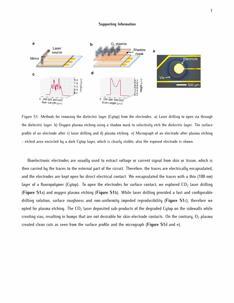
Figure S2: Time-dependent thermal deformation of polyethylene naphthalate (PEN, Teonex Q65FA Teijin-DuPont). a)
Deformation Radius of Curvature (RoC) versus time plot for 2 cm x 2 cm pieces of PEN. Four different conditions were
explored at 180 and 200 C, where samples were left on top of the hotplate (Freestanding) and taped on top of the
hotplate (Taped). b) Optical images of the samples heat-treated for 6 hours, demonstrating thermal deformation (’†’
symbols correspond to the heat-treatment conditions).
Polyester films such as PET and PEN undergo thermal deformation at temperatures higher than the glasstransition temperature (Tg) [1]. In our study, we used a variant of polyethylene naphthalate (PEN): TeonexQ65FA Teijin-DuPont, which shows low shrinkage due to heat stabilization treatments. A time-dependentthermal deformation study of 2 cm x 2 cm pieces of the substrate was carried out to quantify substratedeformation. The samples were heat-treated for 6 hours at 180 and 200 C. Figure S2a shows a deformation
radius of curvature (RoC) versus time plot. At the two temperatures, the samples were left on top of the hotplate,which is referred to as the "Freestanding" state, and samples were taped down to the hotplate using Kaptontape, which is referred to as the "Taped" state. Optical images of the samples after 6 hours of heat-treatmentare shown in Figure S2b. Taping down the films mitigates substrate deformation as observed from the plotand the optical images in Figure S2. At 200 C, taped down samples demonstrate RoC in the range of 8 cm,while freestanding samples demonstrate RoC in the range of 1.5 cm. Taping down films is a common practice
in sintering lab-scale printed films for mitigating substrate deformation. Therefore, all the samples reported inthis paper were sintered while taped down to the hotplate.
3
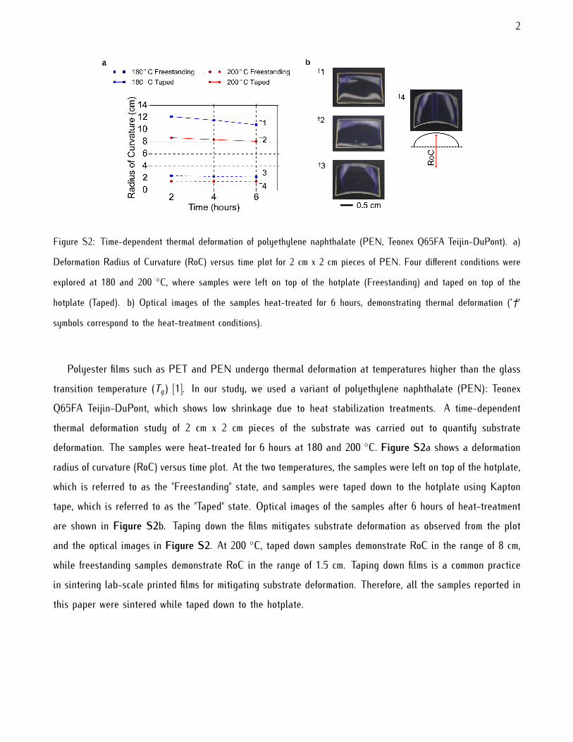
Figure S3: Printed four-point probe structure and height profiles of the printed lines for the sintering study. a) Four-point
probe structure used in the sintering study. b) Surface profiles of the printed gold lines with the three different widths
studied in this work.
The resistivity and sintering analysis was conducted on a four-point probe structure shown in Figure S3a.The width of the lines was increased from 62 to 176 µm. The general profiles for the 62, 119, and 176 µmlines are shown in Figure S3b. The minimum width achieved for the gold nanoparticle ink and the planarizedPEN substrate was 62 µm. The width was then gradually increased keeping the ratio of (1:2:3). However,the coffee ring effect [2] started to appear for the 119 µm lines and became more pronounced for the 176
µm lines. Therefore, the area of the lines scaled in (1.0:1.6:2.6) proportion. This variation is not significantcompared to the resistance variation we observed (three to four orders of magnitude resistance variation) inthe sintering analysis. For example, the 62 µm lines had resistance of 23.8 Ω after 6 hours at 150 C, andthe 176 µm lines had resistance of 264 kΩ under the same conditions. Since resistance is governed by,R = ρ L
A , where, ρ is resistivity, L is the length of the line, and A is the cross-sectional area - with areascaling ratio of (1.0:1.6:2.6), less than an order of magnitude resistance change is expected from just changingthe cross-sectional area. In other words, the height and area variation of the printed lines due to the coffee
ring effect and different dynamics of ink flow inside the structures are not significant compared to the resistivityvariation at low-temperate sintering condition observed in the study.
4
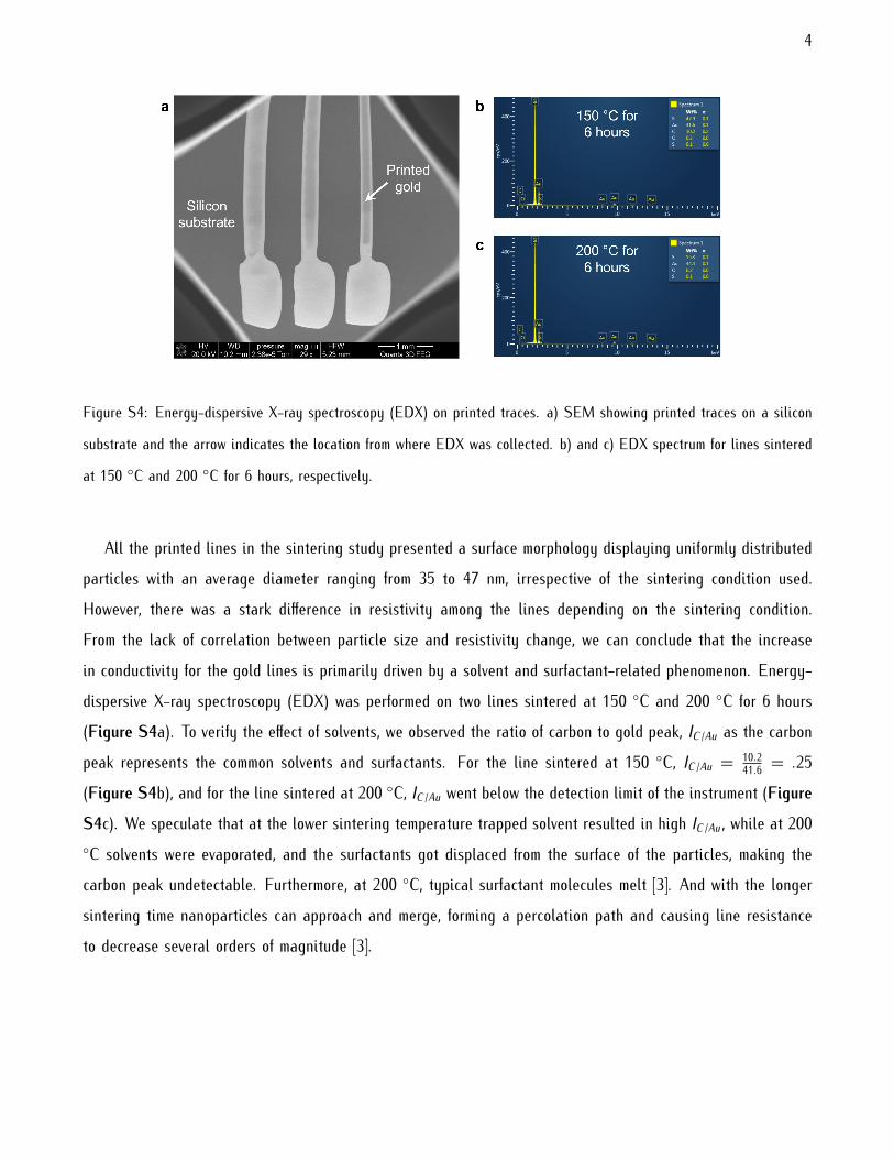
Figure S4: Energy-dispersive X-ray spectroscopy (EDX) on printed traces. a) SEM showing printed traces on a silicon
substrate and the arrow indicates the location from where EDX was collected. b) and c) EDX spectrum for lines sintered
at 150 C and 200 C for 6 hours, respectively.
All the printed lines in the sintering study presented a surface morphology displaying uniformly distributedparticles with an average diameter ranging from 35 to 47 nm, irrespective of the sintering condition used.However, there was a stark difference in resistivity among the lines depending on the sintering condition.From the lack of correlation between particle size and resistivity change, we can conclude that the increasein conductivity for the gold lines is primarily driven by a solvent and surfactant-related phenomenon. Energy-
dispersive X-ray spectroscopy (EDX) was performed on two lines sintered at 150 C and 200 C for 6 hours(Figure S4a). To verify the effect of solvents, we observed the ratio of carbon to gold peak, IC/Au as the carbonpeak represents the common solvents and surfactants. For the line sintered at 150 C, IC/Au = 10.2
41.6 = .25(Figure S4b), and for the line sintered at 200 C, IC/Au went below the detection limit of the instrument (FigureS4c). We speculate that at the lower sintering temperature trapped solvent resulted in high IC/Au, while at 200C solvents were evaporated, and the surfactants got displaced from the surface of the particles, making the
carbon peak undetectable. Furthermore, at 200 C, typical surfactant molecules melt [3]. And with the longersintering time nanoparticles can approach and merge, forming a percolation path and causing line resistanceto decrease several orders of magnitude [3].

5
Supporting References
[1] V. Zardetto, T. M. Brown, A. Reale, A. Di Carlo. J. Polym. Sci., Part B: Polym. Phys. 2011, 49, 9 638.
[2] D. Soltman, V. Subramanian. Langmuir 2008, 24, 5 2224.
[3] S. K. Volkman, S. Yin, T. Bakhishev, K. Puntambekar, V. Subramanian, M. F. Toney. Chem. Mater. 2011, 23, 20 4634.