advanced materials synthesis for inkjet printed...
TRANSCRIPT

Advanced Materials Synthesis for Inkjet
Printed Electronic Applications
Dr. Samuele Porro, Dr. Sergio Bocchini, Dr. Alessandro Chiolerio
Istituto Italiano di Tecnologia (IIT) Center for Space Human Robotics C.so Trento 21, 10129 Torino, Italy
1 - 28th November 2013, PoliMI -

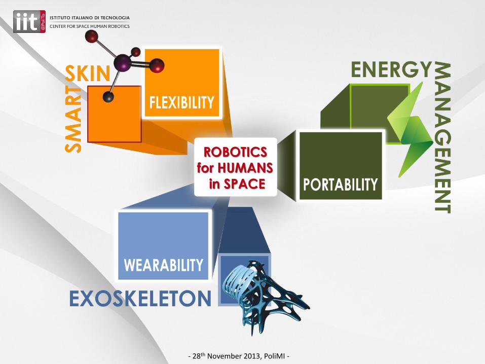
Smart Materials Energy Devices Artificial Physiology
2
Politecnico di Torino campus
Istituto Italiano di Tecnologia - CSHR
Torino
2 - 28th November 2013, PoliMI -
- 28th November 2013, PoliMI -

Outline
o Synthesis
o Morphological analysis
o Electrical properties
1. One pot synthesis of reduced graphene oxide / polyaniline composite ink
2. Hybrid systems based on Ag NPs and acrylic resin
- 28th November 2013, PoliMI -

Outline
o Synthesis
o Morphological analysis
o Electrical properties
1. One pot synthesis of reduced graphene oxide / polyaniline composite ink
2. Hybrid systems based on Ag NPs and acrylic resin
- 28th November 2013, PoliMI -

Endurance
Sustainability
Low-cost
Easy manufacturing
Flexible substrates Devices printed on flexible substrates
Processing: Inkjet Direct Printing
INK REQUIREMENTS - Printability: adjustable viscosity (low), surface tension and solvent evaporation rate - Easy to prepare and process: nanoparticle fillers, fast polymerization of the matrix - Possibly absence of solvents (water-based) - A plus is the absence of post-curing (i.e. thermal). State of the art Metal nanoparticle-based inks: require thermal sintering.
1)
Introduction: aim of research
- 28th November 2013, PoliMI -

Additive Technique (no further steps of material removal are needed) Safe for the substrate (lower substrate damage risk) Material is used without any waste (spin-coating losses 95%) A large variety of materials may be used
Piezoelectric heads: long lifetime with respect to thermal (bubble jet) Cheap compared to silicon technology, no wasted materials, easy to implement Resolution: depends on the head, substrate and ink.
Drop On Demand (DOD) technique
Inkjet Printing
IjP resistive test pattern
Real size of a piezoelectric nozzle (Microfab)
- 28th November 2013, PoliMI -

Endurance
Sustainability
Low-cost
Easy manufacturing
Flexible substrates Printed Electronics
Materials: Polymers and carbon-based 2) GRAPHENE OXIDE
- Large-scale production (oxidation + expansion of graphite)
- Strongly hydrophilic due to oxygenated functional groups Easy to disperse in water and functionalize
- Reduction to graphene by several methods: chemical reaction, thermally, radiation-induced, etc.
Introduction: aim of research
- 28th November 2013, PoliMI -

Synthesis of Polyaniline (PANI)
PANI can be considered as being derived from two different repeating units, which are alternatively reduced and oxidized (base form given in the figure).
The average oxidation state varies continuously: y = 1 is the completely reduced polymer, y = 0.5 is the “half-oxidized” polymer, y = 0 is the completely oxidized polymer.
J. Mater. Chem. C 1 (2013) 5101
Literature: use of ANYLINE monomer precursor Toxic, suspect carcinogenic, easily produces irregular non-linear polymer chains (orto addition), needs hazardous solvents (DMF, etc.), slow reaction, graphene does not disperse in presence of anyline.
This work: use of the anyline dimer (DANI) Non toxic, can be used in water-based emulsion, polymerizes more regularly than anyline. GO, which is a strong oxidant, participates in the complex set of redox reactions which lead to the polymerization of the matrix, and is reduced in-situ.
The polymer/graphene composite can be readily dispersed in a common solvent (DMSO) and inkjet printed.
- 28th November 2013, PoliMI -
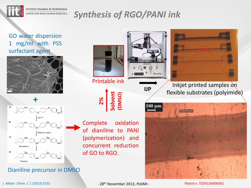
GO water dispersion 1 mg/ml with PSS surfactant agent
+
Dianiline precursor in DMSO
Complete oxidation of dianiline to PANI (polymerization) and concurrent reduction of GO to RGO.
Printable ink
2%
Solv
en
t
(DM
SO)
J. Mater. Chem. C 1 (2013) 5101
Synthesis of RGO/PANI ink
IJP Inkjet printed samples on
flexible substrates (polyimide)
Patent n. TO2013A000561 - 28th November 2013, PoliMI -

UV-Vis absorbance at 481 nm is typical of PANI in the emeraldine salt (conductive) form. The saturation at about 300 nm is expected because of the presence of the graphene filler.
Characterization of RGO/PANI ink
XRD: GO amorphous band (2θ = 13°) disappears in the composite, which shows PANI band (20°) and a peak (38°) which can be ascribed to lamellar graphitic structures.
TGA in N2: two degradation peaks at 300 and 400°C are due to PSS e PANI. The 550°C peak is due to loss of oxygen from GO. The 31.3% weight residulal is graphene. TGA in air: absence of organic contaminations; complete carbonization due to oxidation with peak speed at 530°C.
Patent n. TO2013A000561 - 28th November 2013, PoliMI -
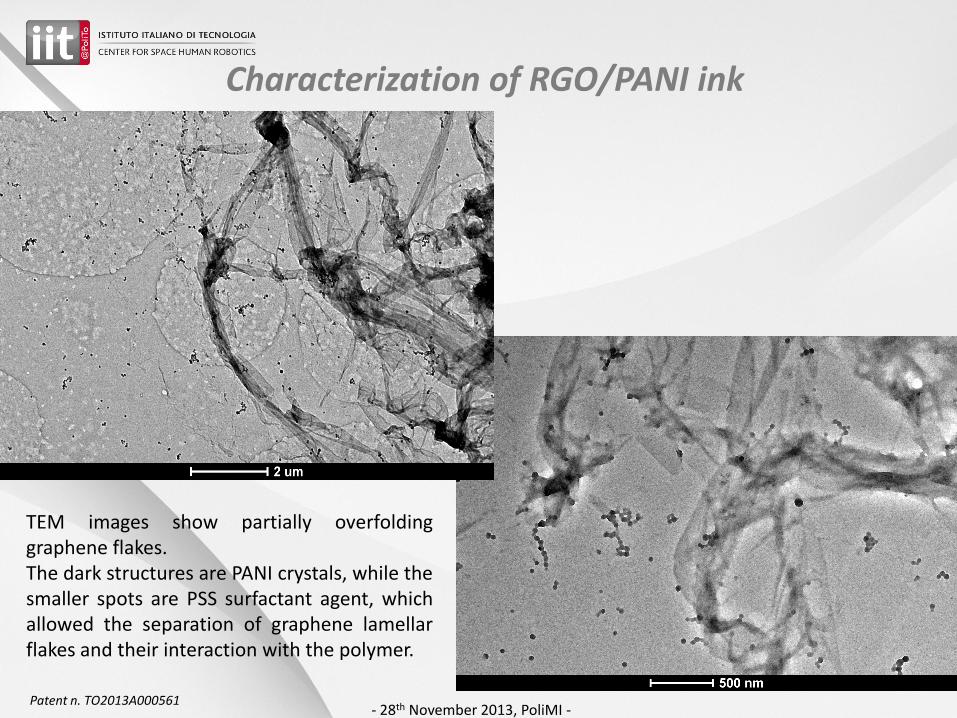
TEM images show partially overfolding graphene flakes. The dark structures are PANI crystals, while the smaller spots are PSS surfactant agent, which allowed the separation of graphene lamellar flakes and their interaction with the polymer.
Characterization of RGO/PANI ink
Patent n. TO2013A000561 - 28th November 2013, PoliMI -

Re
sist
ivit
y [W
cm
]
Width [mm]
RGO/PANI ink
Electrical characterization of RGO/PANI printed tracks
Optical microscope images of RGO/PANI tracks printed on commercial polyimide flexible substrates.
I-V curves in the -50 +50 V range, for different track width .
RGO/PANI 1 pass
- 28th November 2013, PoliMI -

Negative capacitance effects in (RGO) PANI printed tracks
AC measurements in the range 20 Hz – 2 MHz The modulus of complex impedance above 1 kHz is similar to that of an ideal capacitor, and the corresponding phase saturates at -90° (capacitive phase). At frequencies below 100 Hz there is evidence of inductive phase (in average +45°). Increasing AC signal amplitude from 1 to 10 V increases the probability of measuring an inductive phase at frequencies lower than 100 Hz, probably because of an easier charge transfer. This phenomenon is also known as negative capacitance effect.
[Solid-State Electron. 47 (2003) 1089]
- 28th November 2013, PoliMI -

Complex impedance represented as Nyquist plot: x = real part (resistance) y = imaginary part (reactance). Frequency is codified by colour. Spline fits to experimental points show the trajectory of complex impedance across the quadrants. Increasing AC amplitude to 10 V, it is possible to increase the probability of having a positive resistance keeping a negative reactance (equivalent to a negative capacitance effect).
This effect is clear also observing the capacitance versus signal frequency at 10 V AC signal amplitude. Negative capacitances up to some hundreds of µF were observed at very low frequencies, meaning that this material could be exploited in negative supercapacitors for devices running at commercial grid frequencies (50, 60 Hz).
Negative capacitance effects in (RGO) PANI printed tracks
- 28th November 2013, PoliMI -

PANI-EB before/after protonation
Doped Polyaniline (PANI)
Synthesis of PANI, doping with several agents and IJP after solution in DMSO. J. Mater. Chem. C 1 (2013) 5101
Graphene-polymer composites
PEGDA/RGO printable ink. J. Mater. Sci. 48 (2013) 1249
PANI/RGO composite ink. Patent n. TO2013A000561
Technology Transfer: ICP-based inks
- 28th November 2013, PoliMI -

17 - 28th November 2013, PoliMI -

Outline
o Synthesis
o Morphological analysis
o Electrical properties
1. One pot synthesis of reduced graphene oxide / polyaniline composite ink
2. Hybrid systems based on Ag NPs and acrylic resin
- 28th November 2013, PoliMI -

100
101
102
0
10
20
30
40
50
60
70
FE-SEM NP diameter distribution
100
101
102
0
20
40
60
80
100
120
1 10 100
100
101
102
0
5
10
15
20
25
30
35
1 10 500 1 10 100
Log(size)
Co
un
ts
8 x
A. Chiolerio et al., Microelectron. Eng. 88 (2011) 2481-2483
19 - 28th November 2013, PoliMI -

UV-vis spectroscopy and plasmonic properties Transmitted
Reflected A. Chiolerio et al., Microelectron. Eng. 97 (2012) 8-15
Optical plasmonic properties
20 - 28th November 2013, PoliMI -

Re
sist
ance
[Ω
]
3D trajectories describing the path towards electrical percolation during sintering
A. Chiolerio et al., Microelectron. Eng. 97 (2012) 8-15
21 - 28th November 2013, PoliMI -

Islands of residual solvents + Ag NPs
Sintered Ag sponge
Si substrate
Uniform Non-uniform
Residual solvent droplets
Ag / copolymer Uniform zone
Si substrate
Post-annealing nanocomposite section
Post-annealing metal section
A. Chiolerio et al., RSC Advances 3 (2013) 3446
22 - 28th November 2013, PoliMI -

IjP 4 point probe
HAZ
Beam path
A. Chiolerio et al., Microelectron. Eng. 88 (2011) 2481
23 - 28th November 2013, PoliMI -

0 5 10 15 20 25 30 35 40 45 500
50
100
150
200
250
0 5 10 15 20 25 30 35 400
20
40
60
80
100
120
140
160
180
0 5 10 15 20 250
50
100
150
200
250
0 5 10 15 20 250
50
100
150
200
250
0 20 40 60 80 100 1200
50
100
150
200
250
300
AgSbF6
Thick-film resistivity for aged and electroaged samples; NP diameter distributions
24 - 28th November 2013, PoliMI -

Percolation theory: universal model for disordered systems. At criticality, percolation occurs and the system becomes conductive. The critical concentration only depends on the lattice properties.
s
c pp
MN
bap
ni
i ii
1
LATTICE pc
s
d=2 z=3 0.3116±0.0001 1.30±0.02
d=3 z=6 0.6962±0.0001 0.74±0.03
M. Sahimi, Application of Percolation Theory, Taylor & Francis, London 1994
25
- 28th November 2013, PoliMI -

Ag
s
cSbFPEGDAtw
banp
tw
ban
tw
ban
6
1
The new model takes into account the real 3-D
Distribution of NPs within the FESEM image
And the resistivity contribution
Due to SbF6- counter-ion
26
- 28th November 2013, PoliMI -

A specific composition, chosen to express radical-diffusion-engineering, gave
GF > 4
A. Chiolerio et al., Macr. Chem. Phys. 211 (2010) 2008; A. Chiolerio et al., Mater. Sci. Eng. B 177 (2012) 373; A. Chiolerio et al., RSC Advances 3 (2013) 3446
27 - 28th November 2013, PoliMI -

InkA-C100 uncured Unannealed G.F. >> 2.0
0 2 4 6 8 10 12 14
2
4
6
8
10
12
14
R
/R
l/l (%)
G.F.= 61
G.F.= 40
28 - A. Chiolerio, 26th October 2013, Rho Milanofiere, Mecha – Tronika -

29 - 28th November 2013, PoliMI -
A. Chiolerio et al., Microelec. Eng. 97 (2012) 8; V. Camarchia et al., Org. Elec. DOI: 10.1016/j.orgel.2013.10.018

30
Development of a conductive ink
Based on silver microparticles in polar solvent
RFID printed directly on BOPP packaging for food
Low thicknesses (5-10 µm ) high flexibility
Insulator based on functional nanoparticles (Al2O3, TiO2, BaTiO3, SiO2) and polymer-based with UV-curing capabilities
Development of an insulating ink
- 28th November 2013, PoliMI -

Electrodes realized on flexible copper metalized Kapton® (polyimide) film 50 µm thick by photolithography process and etching in iron chloride
Composite tactile sensor ready for characterization
Device under test in a real-time acquisition experiment
31 - 28th November 2013, PoliMI -

Filler: smooth conductive particles Matrix: elastometric, polymer matrix Connectivity: 0-3, 1-3 in function of AR and amount of filler. (Contact between conductive particles) Electrical resistance: is pressure dependent (variation about 6 orders of magnitude) Conduction mechanism: Percolation models
Filler: conductive spiky metal particles Matrix: elastometric, polymer matrix Connectivity: 0-3 (no contact among conductive particles) Electrical resistance: pressure dependent (from 1010 Ωto1Ω)exponential dependence with gap between particles Conduction mechanism: electrical field assisted Fowler- Nordheim tunneling model (enhancement factor up to 1000)
Quantum tunneling hybrid materials
Pressure conductive rubbers
Piezoresistive composite materials
Spiky particles QTC® material from Peratech©
Conventional composite Spherical particles
polymer matrix
connectivity = 0 : particles randomly distributed into the polymer matrix without being connected to each others
connectivity = 3 : continuous network
conductive metal particles
0 - 3 composites
Connectivity of composite
Images from Peratech© website www.peratech.com
32 - 28th November 2013, PoliMI -

33 - 28th November 2013, PoliMI -
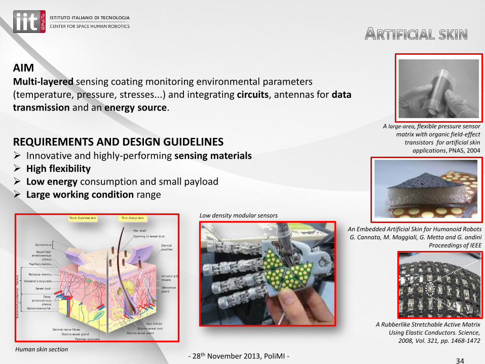
AIM Multi-layered sensing coating monitoring environmental parameters (temperature, pressure, stresses...) and integrating circuits, antennas for data transmission and an energy source.
REQUIREMENTS AND DESIGN GUIDELINES Innovative and highly-performing sensing materials High flexibility Low energy consumption and small payload Large working condition range
A large-area, flexible pressure sensor matrix with organic field-effect
transistors for artificial skin applications, PNAS, 2004
A Rubberlike Stretchable Active Matrix Using Elastic Conductors. Science,
2008, Vol. 321, pp. 1468-1472
An Embedded Artificial Skin for Humanoid Robots G. Cannata, M. Maggiali, G. Metta and G. andini
Proceedings of IEEE
Human skin section
Low density modular sensors
34 - 28th November 2013, PoliMI -

35


Contacts: http://shr.iit.it www.iit.it [email protected] [email protected] [email protected]
Thanks for your kind attention!
Istituto Italiano di Tecnologia (IIT), Center for Space Human Robotics, Turin, Italy