dual-phase inkjet printed electrochromic layers based on ...dual-phase inkjet printed electrochromic...
TRANSCRIPT
Ana Sofia Rações da Cruz
Dual-phase Inkjet Printed Electrochromic Layers based on PTA and WOX/TiO2
Nanoparticles for Electrochromic Applications
Monte de Caparica, 2010

Universidade Nova de Lisboa
Faculdade de Ciências e Tecnologia
Departamento de Ciências dos Materiais
Dual-phase Inkjet Printed Electrochromic Layers based on PTA and WOX/TiO2
Nanoparticles for Electrochromic Applications
By:
Ana Sofia Rações da Cruz
Thesis submitted in Faculdade de Ciências e Tecnologia da Universidade Nova de Lisboa for
the degree of Master in Materials Engineering
Supervisor: Prof. Elvira Fortunato
Co-Supervisor: Eng. Pawel Wojcik
Monte de Caparica, 2010


i
Acknowledgments
This work was only possible thanks to several people, who during the whole
semester helped me with their knowledge, kindness, support and friendship.
To Professor Elvira Fortunato, thank you for the availability to help and guide
during this thesis. For the opportunity of doing my master thesis in such an interesting
subject and for the interest shown in my work during the whole semester.
To Professor Rodrigo Martins and once more, to Professor Elvira Fortunato, thank
you for giving me the possibility to make this work in facilities of excellence.
To Pawel Wojcik, without him this work was certainly not as interesting,
challenging and fun as it was. Thank you for all your help and orientation during the whole
work, for your patience, for being so available to all my questions, some of them really
silly. Thank you for making the work of my master thesis very enjoyable and pleasant.
To Lidia Santos, thanks for all the availability to help, to discuss, to be bored and to
laugh with me, during all those longs hours of measurements. This work would have been
much harder without you.
To the entire MEO group, your kindness and availability allowed this work to be a
very pleasant one, it almost didn’t seem like work at all. A special thanks to Elamurugu
Elangovan and Joana Vaz Pinto for the XRD measurements and to Tito Busani for the SEM
images.
To my college colleagues and friends Adriana Nogueira, Joana Pereira and Ana
Baptista for all the support, patient and friendship. You dealt with all my “pains” during
this semester and it was your support which helped me to finish this important step of my
academic life. I want to also thank to Gonçalo Pereira, for his constant and contagious good
mood.
To all my friends, Ana Valério, André Duarte, Dalila Forte, Frederico Braga, Joana
Viera, Sérgio Lopes, Ana Luz e Bruno Brás. Without you I can assure that I was not going
to be the person that I am today. From this group I want to add a more special thanks to
Dalila, for being so available in helping me with my English even though she was miles
and miles away.
To Nuno Deusdado, thank you for all your love, friendship and support during this
stage of my live. It was really important to me.

ii
To all my family, for always believing in me and for always being present in my
live.
To my parents, if I reached this achievement, it’s owned to you both. Thank you for
everything you did for me, for always being there with me and for making me the very
happy girl that I am.
Thank you!
iii
Abstract
The aim of the work was to develop flexible electrochromic windows via Inkjet
Printing Technique based on amorphous Peroxotungstic Acid (PTA) and metal oxide
nanocrystals. A unique selection of materials allows for a solution processed deposition of
low temperature electrochromic layer which is compatible with flexible substrates such as
PET, PEN and paper.
The use of Inkjet Printing Technique was motivated by the fact that it is a cost
efficient method (mass production) which has a reduced consumption of materials and
energy. It is also a non-contact, digital, no mask and no vacuum patterning method which
greatly simplifies the technological process.
Developed devices were tested using optical, electrochemical, and structural
characterization techniques, in order to find the optimum electrochromic layer composition
which would guarantee desirable electrochromic behavior of the material.
Laboratory studies were supported by statistical techniques such as Design of
Experiment (DOE) and Multiple Regression which leads to a fitting of mathematical model
of the optical and electrical responses.
The dual-phase electrochromic layer consists in the combination of both amorphous
and nanocrystalline phases significantly improve the electrochromic performance of the
devices. The developed method of electrochromic windows manufacturing meets all the
objectives at the beginning of the study.

iv
v
Resumo
O objectivo deste trabalho consistiu no desenvolvimento de janelas electrocrómicas
flexíveis com ácido peroxotungsténico amorfo (PTA) e nanocristais de óxidos metálicos. A
tecnologia utilizada para a deposição destes materiais electrocrómicos foi a impressão a
jacto de tinta, permitindo a deposição de soluções à temperatura ambiente, compatível com
substratos flexíveis tais como PET, PEN e papel.
O baixo custo e o reduzido consumo de materiais e energia foi a motivação para a
selecção da tecnologia de impressão por jacto de tinta como método de deposição. Aliado a
estes factores, trata-se também de um método digital, sem contacto físico e sem
necessidade da utilização de máscaras e vácuo, o que simplifica significativamente o
processo.
Os dispositivos desenvolvidos foram testados recorrendo a técnicas de
caracterização óptica, electroquímica e estructural, por forma a encontrar a composição
óptima da camada electrocrómica que garanta o desempenho electrocrómico adequado do
material.
Os estudos laboratoriais foram suportados por técnicas estatísticas, Desenho de
Experiências (DOE) e Regressão Múltipla, que conduziram à adaptação das respostas
ópticas e eléctricas obtidas a um modelo matemático.
A camada electrocrómica de duas fases consiste numa combinação de uma fase
amorfa e outra nanocristalina, o que melhora significativamente o desempenho
electrocrómico dos dispositivos. O método desenvolvido para a produção de janelas
electrocrómicas foi de encontro a todos os objectivos propostos no início deste estudo.

vi
vii
List of Frequently Used Acronyms and Symbols
[BMIM][BF4] 1-butyl-3-methylimidazolium tetrafluoroborate
[EtNH3][NO3] Ethyl ammonium nitrate
A Absorptance
CA Chronoabsorptometry
CE Coloration Efficiency
CQ Chronocoulometry
CV Cyclic Voltammetry
CVD Chemical Vapor Deposition
d Film Thickness
DOE Design Of Experiments
EC Electrochromic
FIB Focuses Ion Beam
H2O2 Hydrogen Peroxide
In2O3:Sn Indium Tin Oxide
iOX Oxidation peak max.
iRED Reduction peak max.
IrO2 Iridium Dioxide
ITO Indium Tin Oxide
IZO Indium Zinc Oxide
LED Light emitting diode
LiClO4 Lithium perchlorate
LiyWO3 Tungsten Bronze
MnO2 Manganese Dioxide
viii
MoO3 Molybdenum Trioxide
NaClO4 Sodium perchlorate
NbO5 Niobium Pentoxide
OAD Oxalic Acid
PANI Polyaniline
PEDOT Poly(3,4-ethylenedioxythiophene)
PEO-PPO Binary mixture of ethylene poly(oxide) and propylene poly(oxide)
PEN Polyethylene naphthalate
PET Polyethylene terephthalate
PC Propylene carbonate
PMMA Polymethacrylsauremethylester
PTA Peroxotungstic Acid
Qins Charge inserted to the device during coloration process
R Reflection
RF Radio Frequency
Rq Film Roughness
SEM Scanning Electron Microscopy
SrTiO3 Strontium Titanium Trioxide
Tbl Transmittance in bleaching state
Tcol Transmittance in coloration state
TCO Transparent Conductor Oxide
THF Tetrahydrofuran
TiO2 Titanium Dioxide
V2O5 Vanadium Pentoxide

ix
W Tungsten
WO3 Tungsten Trioxide (yellow)
WOX Stoichiometry of tungsten oxide nanoparticles
WO2.9 Tungsten Trioxide (blue)
XRD X-Ray Diffraction
ΔOD Change in Optical density
α Optical absorption coefficient
θ Contact angle
λ Wavelength
τcol Coloration time
τbl Bleaching time
ν Ink viscosity
γ Ink surface tension
ρ Ink density

x
xi
Contents
Acknowledgments………………………………………………………………………...….i
Abstract………………………………………………………………………………..……iii
Resumo……………………………………………………………...…………………...…..v
List of Frequently Used Acronyms and Symbols…………………………………….……vii
Contents………………………………………………………………………………….…xi
List of Figures……………………………………………………………………………..xiii
List of Tables……………………………………………………….……………………..xix
1. Introduction and Objective……………………………………..…….………………..….1
2. Fundamental……………….……………………………….…..…………………………3
2.1 Electrochromism………………………………………………….……………..3
2.2 Inkjet Printing Technique……………………………………..………………..12
2.3 Sol-Gel Processing for Electrochromic Materials………………………...……19
3.Methods and Procedures……………………………....……………….……….………..23
3.1 Experimental Design………………………………………………...…………23
3.2 Electrochromic ink formulation……………………………………….……….31
3.3 Electrolyte Preparation………………………….………………….…………..36
3.4 Processes…………………………………………….……….……….………..36
3.5 Device structure and encapsulation………………………..……….…………..39
3.6 Device characterization………………………………………………...………42
4.Results and Discussion………………………………….…………….………………….49
4.1 Selection of relevant deposition parameters……………………………………49
4.2 Statistical Analysis of Significance…………………………………………….53
4.3 Analysis of electrochromic performance – surface response estimation………71
4.4 Impact of deposition method on electrochromic properties……………………94
5. Conclusion and Future Prospects……………………….……………………………….99
References………………………………………………………..……………………….105

xii
xiii
List of Figures
Figure 2.1 Chromism application examples: a) electrochromism for electrochromic
window application, b) termochromism for ring application, c) photocromism
for glasses application, d) the same organic compound dissolved in solvents
with different polarity ………………………………………………….………........3
Figure 2.2 Electrochromic car rear view mirror……………………………….……….…....6
Figure 2.3 Electrochromic window.........................................................................................7
Figure 2.4 Motorcycle helmet with electrochromic visor…………………………………...7
Figure 2.5 Basic design of an electrochromic window…………………….………………..8
Figure 2.6 Thin Film Deposition Techniques for EC applications………….……………..13
Figure 2.7 Typical construction of an office inkjet printer………………….……………..15
Figure 2.8 Inkjet Printing Technology map………………………………….…………….16
Figure 2.9 Thermal inkjet printing: drop formation………………………….….………....17
Figure 2.10 Typical inkjet ink formulation………………………………….……………..17
Figure 2.11 Sol-gel processes……………………………………………………………...20
Figure 3.1 WO3 yellow nanopowder SEM micrograph……………………………………25
Figure 3.2 WO2.9 blue nanopowder SEM micrograph…………………….….………...….25
Figure 3.3 TiO2 nanopowder SEM image.............................................................................26
Figure 3.4 Design of Experiment phases..............................................................................28
Figure 3.5 The principle of custom made viscometer based on laminar flow..……..……..34
Figure 3.6 Laminar flow representation……………………………………………....……34
Figure 3.7 Inkjet Canon PIXMA iP4500 printer...................................................................38
Figure 3.8 Modified Canon cartridges……………………………………………...….…..39
Figure 3.9 Lab-test device encapsulation method………………………………….…...….41
Figure 3.10 Prototype of inkjet printed lab-test EC window in a) bleached and
b) colored state……………………………………..………………………………42
Figure 3.11 Optical measurements set-up.............................................................................46
xiv
Figure 4.1 The thickness of printed test layers vs. number of passes………………….…..49
Figure 4.2 The change in optical density (bottom and left axis) for layers printed
with different number of passes and spectral transmittance (top and
right axis)……………………………………………………………………...…....50
Figure 4.3 The coloring and bleaching time responses (bottom and left axis) of
printed layers vs. number of passes and coloration-bleaching characteristic (top
and right axis) ……………………………………………………………………...50
Figure 4.4 The charge inserted density for printed layers vs. number of passes (bottom
and left axis); chronocoulometric curves for printed layers (top and
right axis)…………………………………………………………………………...51
Figure 4.5 The a) coloration efficiency and b) optical absorption coefficient of
printed layers vs. number of passes………………………………………………...52
Figure 4.6 The reduction (blue) and oxidation (green) peak maximum for printed
layers vs. number of passes (bottom and left axis); cyclic voltammograms
of printed layers (top and right axis)……………………………………………….53
Figure 4.7 Initial whole multiple regression model with the numeric summaries
for coloration time responses……………………………………………………...57
Figure 4.8 Initial whole multiple regression model with the numeric summaries for bleaching time responses…………………………………………………….……..57
Figure 4.9 Initial whole multiple regression model with the numeric summaries for
optical modulation responses……………………………………………………...58
Figure 1.10 Initial whole multiple regression model with the numeric summaries
for coloration efficiency responses…………………………………………………58
Figure 4.11 Final whole multiple regression model with the numeric summaries
for coloration time responses after excluding the most distant observations………60
Figure 4.12 Final whole multiple regression model with the numeric summaries
for bleaching time responses after excluding the most distant observations………60
xv
Figure 4.13 Final whole multiple regression model with the numeric summaries
for change in optical density after excluding the most distant
observations……………………………………………………………………...…60
Figure 4.14 Final whole multiple regression model with the numeric summaries
for coloration efficiency responses after excluding the most
distant observations………………………………………………………………...60
Figure 4.15 Leverage plots of main effects and factors correlations for τcol response…….62
Figure 4.16 Leverage plots of main effects and factors correlations for τbl responses…….63
Figure 4.17 Leverage plots of main effects and factors correlations for ΔOD responses….64
Figure 4.18 Leverage plots of main effects and factors correlations for CE responses……65
Figure 4.19 Sorted Parameter Estimates plot for a) τcol and b)τbl response……………….69
Figure 4.20 Sorted Parameter Estimates plot for a) ΔOD and b) CE response……………70
Figure 4.21 Profiles of several a-WO3/TiO2/WOX samples for different compositions…...71
Figure 4.22 SEM picture of a printed a-WO3 film (Device no. 25); Inset: Magnified
area showing layer cross-section…………………………………………………..72
Figure 4.23 SEM picture of a printed a-WO3/TiO2/WOX (Device no. 19); Inset:
Magnified area showing chocolate with nuts like structure………………………..73
Figure 4.24 SEM picture of a-WO3/TiO2/WOX printed film (Device no. 19).
Visible islands of different sizes indicate that the layer is not continuous.………...74
Figure 4.25 SEM picture of a-WO3/TiO2/WOX printed film (Device no. 21) with
addition of Oxalic Acid; Inset: Magnified area shows grooves formed on the
surface due to acid crystallization. …………………………………………….…..75
Figure 4.26 XRD patterns of a) WO2.9 blue nanopowder, b) WO3 yellow
nanopowder, c) ink 9 (wPTA=0.01;wTiO2=0.5;wWO2.9=0.49), d) ink 21
(wPTA=0.08; wOAD=0.02;wTiO2=0.45; wWO3=0.45), e) ink 19 (wiso/water=0.87;
wPTA=0.1; wOAD=0.03) …………………………………………………………….76

xvi
Figure 4.27 Transmission modulation of EC windows based on printed films
containing a) a-WO3 with TiO2 and WO2.9 nanoparticles, b) a-WO3 with
WO3 nanoparticles, c) a-WO3 with WO2.9 nanoparticles, d) a-WO3 with
TiO2 nanoparticles and e) pure a-WO3. Annealing: 120 deg C, 1h.……………....78
Figure 4.28 Surface response prediction of ΔOD for a) a-WO3/TiO2/WO3 and b)
a-WO3/TiO2/WO2.9 printed layers………………………………………………….79
Figure 4.29 Surface response prediction of Tbl for a) a-WO3/TiO2/WO3 and
b) a-WO3/TiO2/WO2.9 printed layers……………………………………………….79
Figure 4.30 Surface response prediction of Tcol for a) a-WO3/TiO2/WO3 and b)
a-WO3/TiO2/WO2.9 printed layers………………………………………………….80
Figure 4.31 Color-bleached characteristics for a-WO3/TiO2/WOX printed films
recorded at 900 nm under a square wave potential of ±4V at a frequency
of 0.016 Hz in a first 5 cycles………………………………………………………81
Figure 4.32 Surface response prediction of τcol for a) a-WO3/TiO2/WO3 and b)
a-WO3/TiO2/WO2.9 printed layers……………………………………………...…..82
Figure 4.33 Surface response prediction of τbl for a) a-WO3/TiO2/WO3 and b)
a-WO3/TiO2/WO2.9 printed layers………………………………………………….82
Figure 4.34 Step wave voltage transmittance for 900 nm………………………………….83
Figure 4.35 Surface response prediction of Vopt for a) a-WO3/TiO2/WO3 and
b) a-WO3/TiO2/WO2.9 printed layers………………...…………………………….84
Figure 4.36 Change in transmittance due to site saturation effect (ΔTSS) as a function
of applied voltage (U) for different a-WO3/TiO2/WOX film composition…………85
Figure 4.37 Change in transmittance (ΔT=Tbl-Tcol) as a function of applied voltage
(U) for different a-WO3/TiO2/WOX film composition……………………………..86
Figure 4.38 Surface response prediction of α for a) a-WO3/TiO2/WO3 and b)
a-WO3/TiO2/WO2.9 printed layers……………………………………………….…86
xvii
Figure 4.39 Cyclic voltammograms of EC windows based on printed films containing
a) a-WO3 with TiO2 and WO2.9 nanoparticles, b) a-WO3 with WO3 nanoparticles,
c) a-WO3 with WO2.9 nanoparticles, d) a-WO3 with TiO2 nanoparticles and
e) pure a-WO3. The scan rate is 50 mV/s. Annealing: 120 deg C, 1h……………...87
Figure 4.40 Surface response prediction of iRED for a) a-WO3/TiO2/WO3 and
b) a-WO3/TiO2/WO2.9 printed layers……………...……………………………….88
Figure 4.41 Surface response prediction of iOX for a) a-WO3/TiO2/WO3 and
b) a-WO3/TiO2/WO2.9 printed layers…………………...………………………….89
Figure 4.42 Chronocoulometric curves for films…………………………………………..89
Figure 4.43 Surface response prediction of QISN for a) a-WO3/TiO2/WO3 and
b) a-WO3/TiO2/WO2.9 printed layers………………………...……………………90
Figure 4.44 Surface response prediction of CE for a) a-WO3/TiO2/WO3 and
b) a-WO3/TiO2/WO2.9 printed layers…………………...………………………….91
Figure 4.45 Surface response prediction of viscosity (ν) for precursor solution based
on PTA, OAD, TiO2 nanocrystals and a) WO3 or b) WO2.9 nanoparticles…………92
Figure 4.46 Surface response prediction of surface tension (γ) for precursor solution
based on PTA, OAD, TiO2 nanocrystals and a) WO3 or b) WO2.9 nanoparticles…..93
Figure 4.47 Surface response prediction of density (ρ) for precursor solution based
on PTA, OAD, TiO2 nanocrystals and a) WO3 or b) WO2.9 nanoparticles…………93
Figure 4.48 Surface response of contact angle (θ) for precursor solution based on
PTA, OAD, TiO2 nanocrystals and a) WO3 or b) WO2.9 nanoparticles…………….93
Figure 4.49 Cyclic voltammograms recorded at scan speed of 5 mV/s for spin-coated
and inkjet printed a-WO3/TiO2/WOX films…………………………………...……96
Figure 4.50 Charge density vs. time for spin-coated and inkjet printed
a-WO3/TiO2/WOX films……………………………………………………………97
Figure 4.51 Coloration-bleaching characteristic of spin-coated and inkjet printed
a-WO3/TiO2/WOX films……………………………………………….…………...97

xviii

xix
List of Tables
Table 2.1 Examples of electrochromic metal oxides, their properties and
typical deposition techniques………………………………………………………..9
Table 3.1 Factors to be examined, its role and range............................................................29
Table 3.2 Defined responses and their goals…………………………………………….....30
Table 3.3 Ink Recipes............................................................................................................32
Table 3.4 Profilometry parameters……………………………………………………...….43
Table 3.5 CQ parameters………………………………………………………………...…44
Table 3.6 CV parameters…………………………………………………………………...45
Table 4.1 A tabular summary of factors and responses for all tested devices (part1)……..55
Table 4.2 A tabular summary of the factors and responses for all tested devices (part2)….56
Table 4.3 The Parameter Estimates and Effect Test table for τcol parameter………………66
Table 4.4 The Parameter Estimates and Effect Test table for τbl parameter……………….67
Table 4.5 The Parameter Estimates and Effect Test table for ΔOD parameter……………68
Table 4.6 The Parameter Estimates and Effect Test table for CE parameter………………68
Table 4.7 Comparison of EC films parameters deposited via spin-coating and inkjet
printing (device no. 21) for wiso/water=0; wPTA=0.08 wOAD=0.025;
wTiO2=0.44; wWOX=0.45; WOX: yellow…………………………………………….95

xx
1. Introduction and objective
1
1. Introduction and objective
The overall objective of this work is to develop a complete solution processed and
low temperature dual-phase electrochromic system based on PTA (Peroxotunstic Acid)
precursor deposited via Inkjet Printing Technology. Whereby, the processability of
precursors with nanocrystalline solid content via Inkjet Printing for smart windows
applications is to be demonstrated. Applications related aims to include the optimization of
the properties of the coating materials (composition, rheology, crystallinity, etc.) and the
mechanical, optical and electrochemical characterization of the printed devices. In detail,
developed electrochromic system which includes materials and deposition technique should
satisfy the following conditions:
low-temperature process compatible with flexible substrates, such as PET
(Polyethylene terephthalate), PEN (Polyethylene naphthalate) or paper;
non-contact, digital, additive, no mask and no vacuum patterning method;
eco-friendly;
coexistence of amorphous and nanocrystalline phases for better electrochromic
performance;
cost efficient in mass production;
solution processed deposition;
widely available materials;
application of inorganic material, which provides a higher device stability;
reduced consumption of materials and energy.
Although many research reports about the PTA precursor based depositions
methods (dip-coating, spin-coating) for WO3 (Tungsten Trioxide) thin film coating have
been published, no attempt has yet been reported to prepare WO3 coatings by Inkjet
Printing. This study aims to synthesize amorphous WO3 thin films containing TiO2/WOX
nanocrystals (a-WO3/TiO2/WOX) in a low temperature Inkjet Printing process.
As it is well known, fully crystalline WO3 coating is not the best candidate for EC
(Electrochromic) window application due to its slow diffusion rate and inferior coloration
efficiencies. On the other hand, crystalline states have been shown to be able to withstand a
1. Introduction and objective
2
greater number of cycles. Several studies [1,2] have been made also on the TiO2-doped
WO3 thin films using solution processed deposition techniques. The use of TiO2 (Titanium
Dioxide) as a doping material always resulted in improved electrochromic performance. It
is shown that reversibility can be improved by adding TiO2 to the WO3 precursor and the
lifetime of TiO2/WO3 thin films can be much longer that of pure WO3 material [2]. As TiO2
is hydrophilic it adsorbs water from air and this small amount of water accelerates the H+
ion insertion/removal in to or from the TiO2/WOX thin films. In the present work TiO2
doped a-WO3/WOX thin films were prepared by a simple and inexpensive way. The WO3
sol was mixed with aqueous-alcohol TiO2 nanoparticle dispersion resulting in a stable and
printable ink.
It’s intended to obtain an electrochromic window that has as main specifications
high values of high coloration efficiency and change in optical density and a response time
as small as possible. These specifications will allow the achievement of a device with a
desirable electrochromic performance.
2. Fundamental
3
2. Fundamental
2.1 Electrochromism
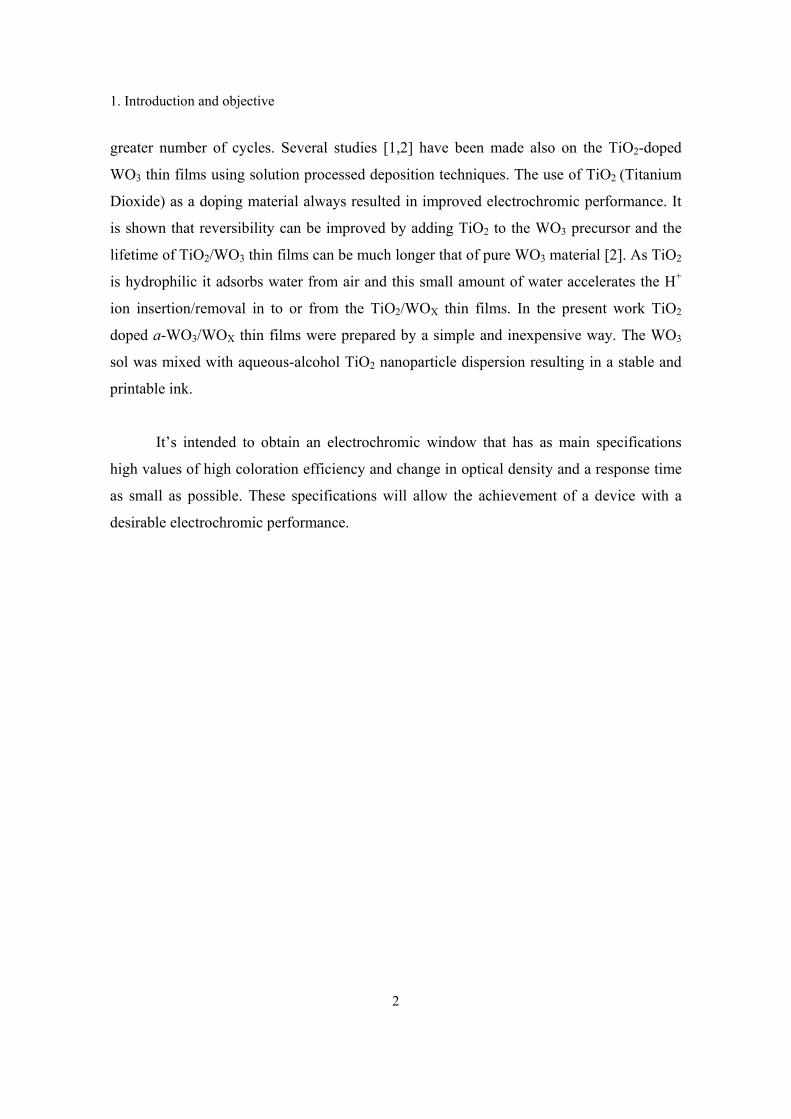
Electrochromism is one of the several types of chromism. The word chromism
stands for the ability of a substance to change its color in a reversible way in result of a
process caused by some form of stimulus. Some types of chromism existing in a practical
applications are listed bellow [3,4]:
electrochromism – voltage application (Figure 2.1a);
termochromism – temperature change (Figure 2.1b)
photocromism – exposure to light radiation (Figure 2.1c);
halochromism – change in pH of a solution;
piezochromism – color change caused by mechanical grinding;
solvatochromism – change of solvent polarity (Figure 2.1d);
ionochromism – addition of ions.
Figure 2.1 Chromism application examples: a) electrochromism for electrochromic
window application [5], b) termochromism for ring application [6], c) photocromism for
glasses application [7], d) the same organic compound dissolved in solvents with different
polarity [8]
2. Fundamental
4
This thesis contains only a detailed exposure of one of the types of chromism which
is electrochromism, since this is the scope of the conducted research. Electrochromism
could be briefly defined as a persistent but reversible optical change produced
electrochemically in selected thin films compounds, designated as electrochromic materials
[9].
The Equation 2.1 represents the electrochromism phenomenon for amorphous WO3
(the most typical and widely studied electrochromic material).
2.1
Amourphous WO3 film in bleach state (transparent) can be switched reversibly to a
colored state (dark blue) by both insertion of ions and electrons to form tungsten bronze
(LiyWO3). The y value in LiyWO3 is the fractional number of sites of which are filled in the
WO3 lattice. For low y values the films have an intense blue [10,11]. The electrochromism
history started in 1704, when Diesbach discovered the Prussian blue, an excellent dye
which had also electrochromic properties. This material changes its state from dark blue to
transparent when a voltage is applied. In 1815 the electrochromism of WO3 was
discovered, by Berzelius [12]. In fact, it was showed that pure WO3 changed color on
reduction when warmed under a flow of dry hydrogen gas. Later in 1824 Wohler effected a
similar chemical reduction with sodium metal. Kobosew and Nekrasso in 1830, recorded
that WO3 powders could acquire the color blue by electrochemical reduction in an acid
solution as it is represented in Equation 2.1. The first step towards an electrochromic device
was taken in 1942 by Talmey, in studies on the coloration associated with electrolytic
reduction of artificially produced particulate molybdenum and tungsten oxide layers. In
1953 Kraus made a very clear description of electrochromism in tungsten oxide films. As
none of these studies attracted much attention, probably most current investigators attribute
the first widely accepted suggestion of an electrochromic device to Deb, in 1969, with the
tungsten oxide films, and after this point, there was a visible increase of the interest in
electrochromism. In spite of the innovation on Deb’s first electrochromic device it wasn’t
able to keep up with the fast development of liquid crystal devices [12,13]. In 1971, Blanc
and Staebler produced an electrochromic effect superior to most of the previously
published. They applied electrodes to the opposing faces of doped, crystalline SrTiO3
2. Fundamental
5
(Strontium Titanium Trioxide) and observed an electrochromic color move into de crystal
from the two electrodes. In 1972, Beegle developed a display having identical counter and
working electrodes as the one from Blanc and Staebler, but made of WO3 [12,13].
Nowadays, Deb’s paper form 1973 is quoted as the work responsible for the true birth of
electrochromic technology.
Nevertheless, electrochromism has remained an active area for basic and applied
research, with large possibilities for applications in emerging technologies. The interest was
boosted in the mid- 1980s with the awareness that electrochromism was of much interest as
a mean to achieve energy efficiency in buildings, using smart windows. [14]
The smart windows and other electrochromic systems consist of two electrodes and
an electrolyte. When applied voltage with appropriate polarity, charge in the cell drives in
and out of the electrochromic material and an electrochemical redox reaction causes a
corresponding color change. Therefore electrochromic materials are currently attracting
much interest in industry for their commercial applications. [15]
Possible applications of electrochromic materials include, among others,
electrochromic displays, cathode ray tubes, thermal-exposure indicator for frozen
foodstuffs, electrochromic mirrors and windows. Electrochromic displays are an
application where significant advances were made in the 1970s and 1980s with the
development of watch and clock displays. However some of their biggest limitations were
speed and lifetime. But for this kind of applications these limitations weren’t critical
because these areas do not require very rapid updating of display information. [16]
Electrochromic materials can also be used in cathode ray tubes with variable
transmittance. An electrochromically darkening cathode ray tube screen employing oxides
it’s an alternative to the common brilliance adjustments of TV tubes, when room
illumination alters. Electrochromic darkening is preferable to direct electrical control as
color values are thereby better preserved. [17]
Another application can be a thermal-exposure indicator for frozen foodstuffs. In
this case a thin electrochromic cell is attached as part of the labeling of frozen foodstuff.
The composition of the cell is chosen so that it remains in the uncolored state when the
foodstuff is frozen. The composition of the polymer electrolyte is chosen to have just the
right temperature coefficient of conductivity so that, on warming, increased conductivity
2. Fundamental
6
allows electrochromism to set in, thus warning of the thermal deterioration of the goods.
The higher the temperature and/or the longer the exposure, the more intense could the color
become and show the deterioration level. It’s also important to refer that after thermal
exposure, re-freezing does not dispel the coloration. [17]
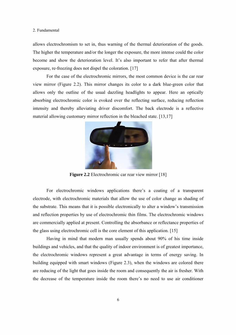
For the case of the electrochromic mirrors, the most common device is the car rear
view mirror (Figure 2.2). This mirror changes its color to a dark blue-green color that
allows only the outline of the usual dazzling headlights to appear. Here an optically
absorbing electrochromic color is evoked over the reflecting surface, reducing reflection
intensity and thereby alleviating driver discomfort. The back electrode is a reflective
material allowing customary mirror reflection in the bleached state. [13,17]
Figure 2.2 Electrochromic car rear view mirror [18]
For electrochromic windows applications there’s a coating of a transparent
electrode, with electrochromic materials that allow the use of color change as shading of
the substrate. This means that it is possible electronically to alter a window’s transmission
and reflection properties by use of electrochromic thin films. The electrochromic windows
are commercially applied at present. Controlling the absorbance or reflectance properties of
the glass using electrochromic cell is the core element of this application. [15]
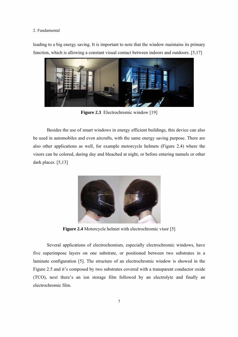
Having in mind that modern man usually spends about 90% of his time inside
buildings and vehicles, and that the quality of indoor environment is of greatest importance,
the electrochromic windows represent a great advantage in terms of energy saving. In
building equipped with smart windows (Figure 2.3), when the windows are colored there
are reducing of the light that goes inside the room and consequently the air is fresher. With
the decrease of the temperature inside the room there’s no need to use air conditioner
2. Fundamental
7
leading to a big energy saving. It is important to note that the window maintains its primary
function, which is allowing a constant visual contact between indoors and outdoors. [5,17]
Figure 2.3 Electrochromic window [19]
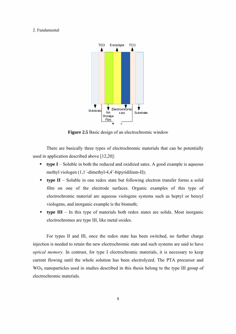
Besides the use of smart windows in energy efficient buildings, this device can also
be used in automobiles and even aircrafts, with the same energy saving purpose. There are
also other applications as well, for example motorcycle helmets (Figure 2.4) where the
visors can be colored, during day and bleached at night, or before entering tunnels or other
dark places. [5,13]
Figure 2.4 Motorcycle helmet with electrochromic visor [5]
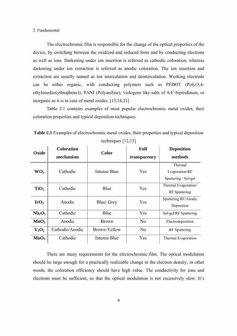
Several applications of electrochomism, especially electrochromic windows, have
five superimpose layers on one substrate, or positioned between two substrates in a
laminate configuration [5]. The structure of an electrochromic window is showed in the
Figure 2.5 and it’s composed by two substrates covered with a transparent conductor oxide
(TCO), next there’s an ion storage film followed by an electrolyte and finally an
electrochromic film.
2. Fundamental
8
Figure 2.5 Basic design of an electrochromic window
There are basically three types of electrochromic materials that can be potentially
used in application described above [12,20]:
type I – Soluble in both the reduced and oxidized sates. A good example is aqueous
methyl viologen (1,1´-dimethyl-4,4’-bipyridilium-II);
type II – Soluble in one redox state but following electron transfer forms a solid
film on one of the electrode surfaces. Organic examples of this type of
electrochromic material are aqueous viologens systems such as heptyl or benzyl
viologens, and inorganic example is the bismuth;
type III – In this type of materials both redox states are solids. Most inorganic
electrochromes are type III, like metal oxides.
For types II and III, once the redox state has been switched, no further charge
injection is needed to retain the new electrochromic state and such systems are said to have
optical memory. In contrast, for type I electrochromic materials, it is necessary to keep
current flowing until the whole solution has been electrolyzed. The PTA precursor and
WOX nanoparticles used in studies described in this thesis belong to the type III group of
electrochromic materials.
2. Fundamental
9
The electrochromic film is responsible for the change of the optical properties of the
device, by switching between the oxidized and reduced form and by conducting electrons
as well as ions. Darkening under ion insertion is referred as cathodic coloration, whereas
darkening under ion extraction is referred as anodic coloration. The ion insertion and
extraction are usually named as ion intercalation and deintercalation. Working electrode
can be either organic, with conducting polymers such as PEDOT (Poly(3,4-
ethylenedioxythiophene)), PANI (Polyaniline), viologens like salts of 4.4’-bipiridinum, or
inorganic as it is in case of metal oxides. [13,14,21]
Table 2.1 contains examples of most popular electrochromic metal oxides, their
coloration properties and typical deposition techniques.
Table 2.1 Examples of electrochromic metal oxides, their properties and typical deposition
techniques [12,13]
Oxide Coloration
mechanism Color
Full
transparency
Deposition
methods
WO3 Cathodic Intense Blue Yes Thermal
Evaporation/RF
Sputtering / Sol-gel
TiO2 Cathodic Blue Yes Thermal Evaporation/
RF Sputtering
IrO2 Anodic Blue/ Grey Yes Sputtering RF/Anodic
Deposition
Nb2O5 Cathodic Blue Yes Sol-gel/RF Sputtering
MnO2 Anodic Brown No Electrodeposition
V2O5 Cathodic/Anodic Brown-Yellow No RF Sputtering
MoO3 Cathodic Intense Blue Yes Thermal Evaporation
There are many requirements for the electrochromic film. The optical modulation
should be large enough for a practically realizable change in the electron density, in other
words, the coloration efficiency should have high value. The conductivity for ions and
electrons must be sufficient, so that the optical modulation is not excessively slow. It’s
2. Fundamental
10
imperative that the electrochromic film has a structure that is permeable enough to permit
easy intercalation and deintercalation of charges.
As it is shown in Figure 2.5, the electrochromic device is composed by two
electrodes, separated with electrolyte, which can be any substance containing free ions that
make the substance electrically conductive. The charge flow takes place from electrolyte to
working electrode as well as from working electrode to electrolyte. The electrolyte, as a
pure ion conductor must be ionically conductive, but electronically insulating. It must allow
ions to be shuttled between an electrochromic film and an ion storage film (counter
electrode) [13,14]. Typically, the electrolytes used in EC windows, as in any other
electrochemical cell, belong to four main classes: aqueous electrolytes, organic liquid
electrolytes, ionic liquids electrolytes and solid polymer electrolytes. [22]
The most common electrolytes are liquid (aqueous and organic), because they are
easy to reproduce and very durable. On the other hand the probability of leakage and low
chemical stability of the liquid electrolytes are inevitable drawbacks for electrochromic
display applications. The aqueous liquids electrolytes encompass both acids and bases,
while the group of organic liquid electrolytes include for example propylene carbonate (PC)
or ethylene carbonate, with addition of lithium salts, such as lithium perchlorate (LiClO4)
or sodium perchlorate (NaClO4)) in order to achieve improved electrochemical properties.
The group of ionic liquid electrolytes is represented for example by ethyl ammonium
nitrate ([EtNH3][NO3]) or 1-butyl-3-methylimidazolium tetrafluoroborate ([BMIM][BF4]).
Those room-temperature fluid salts consist of organic cations and inorganic anions, what
results in improved lifetime and response speed of diverse types of electrochemical devices.
[17,22,23]
Solid polymer electrolytes are usually a polymer or gel matrixes swollen with liquid
electrolyte solutions, a single ion systems in which only one ionic species is mobile within
a polymer matrix. Another common possibility is a solvent-free ion-coupled system
consisting of ion-solvating polymers mixed with salts, so that cations and ions become
mobile within the polymer network.
For EC windows applications gel electrolyte should be transparent, while for EC
displays usually more suitable are opaque substances [17,22]. The measurements presented
2. Fundamental
11
in this thesis were performed using encapsulated EC windows filled with lithium
perchlorate polymeric gel electrolyte.
Another layer of the EC device is the ion storage film, named also as counter
electrode. This layer has the same demands on electronic and ionic conductivity as the
working electrode. It should provide the same stability and durability to the device. If the
ion storage film has electrochromic properties, it should be complementary to this of the
electrochromic film. It means that when the electrochromic films darken upon ion
intercalation the ion storage should darken upon ion deintercalation and vice versa. [13,14]
Finally the electrochomic device needs to have substrates to be built on. For
windows applications, the electrochromic layer is deposited on a transparent substrate,
typically glass or flexible polyester (PET) foil [3]. On the other hand, for display or mirrors
applications, there’s no need for both substrates to be transparent. For example, the
substrates of an electrochromic watch can be glass and Graphite [16].
Both the targets are coated with electrically conducting transparent films, named
Transparent Conductor Oxides (TCO). The TCO should have low electrical resistivity and
high optical transparency. The best material in terms of optical and electrical properties are
In2O3:Sn (Indium Tin Oxide, or ITO), IZO (Indium Zinc Oxide), PEDOT and more
recently also carbon nanotubes. [3,14,21]
When a voltage is applied between the two electrodes, in the electrochromic film
occurs a reaction of reduction that leads to the consumption of the electron, while in the
counter electrode occurs reaction of oxidation that provides the departure of an ion that
goes to the electrochromic layer. Consequently there’s a drift of electrons through the
external circuit from the counter electrode to the electrochromic layer, and to compensate
this charge flow there’s a passage of ions thought the electrolyte, which is located between
the electrodes.
The Equation 2.2 represents the reaction mentioned above, where there’s the need to
provide electrons and ions to the WO3 electrochromic layer.
2.2
The presence of lithium ions in the electrochromic film leads to a variation of electron
density and consequently a color change. The change of electric polarization or a short
circuit brings back the original properties. The coloration can be stopped at any
2. Fundamental
12
intermediate level, and the device exhibits open-circuit memory so that the optical changes
take place only when charge is in movement. [13,14]
2.2 Inkjet Printing Technique
Recently the thin films technology has grown world-wide. The importance of
coatings and synthesis of new materials for the industry have also resulted in a tremendous
increase of innovative thin films processing. Thin films consist of two dimensional
materials created by the process of condensation and growth of atoms, molecules or ions.
Regarding to its thickness there isn’t any well defined value for it, but it should be much
smaller regarding the other two directions.
Modern thin film technology has evolved into a sophisticated set of techniques used
to fabricate many products. Applications include integrated circuits, electronic packaging,
sensors and devices; optical films and devices; as well as protective and decorative
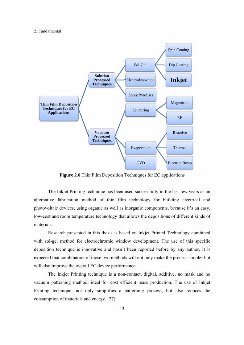
coatings. Figure 2.6 presents short review of the thin film deposition techniques for
electrochromic application. [24-26]
2. Fu
altern
photo
low-c
mate
with
depo
expe
will a
vacu
consu
TT
undamental
Fig
The Inkj
native fabr
ovoltaic dev
cost and roo
erials.
Research
sol-gel me
osition techn
cted that co
also improv
The Inkj
uum pattern
ting techni
umption of
Thin Film DepTechniques f
Applicatio
gure 2.6 Th
et Printing
rication me
vices, using
om tempera
h presented
ethod for e
nique is inn
ombination
ve the overa
jet Printing
ning method
que, not o
f materials a
position for EC ons
hin Film De
technique h
ethod of t
g organic as
ature techno
in this the
electrochrom
novative an
of those tw
all EC devic
g technique
d, ideal for
only simpl
and energy.
SolutionProcesse
Techniqu
VacuumProcesse
Techniqu
13
eposition Te
has been us
thin film
s well as in
ology that a
esis is based
mic window
nd hasn’t b
o methods w
ce performa
is a non-c
r cost effic
lifies a pa
[27]
n ed ues
E
S
m ed ues
echniques fo
sed successf
technology
organic com
allows the d
d on Inkjet
w developm
been reporte
will not onl
ance.
ontact, digi
cient mass
atterning pr
Sol-Gel
Electrodepositi
Spray Pyrolise
Sputtering
Evaporation
CVD
or EC applic
fully in the
y for build
mponents, b
depositions o
Printed Te
ment. The u
ed before b
ly make the
ital, additiv
production.
rocess, but
Sp
D
Iion
es
M
n
El
cations
last few ye
ding electr
because it’s
of different
echnology c
use of this
by any auth
process sim
ve, no mask
. The use o
t also redu
pin Coating
ip Coating
Inkjet
Magnetron
RF
Reactive
Thermal
ectron Beam
ears as an
ical and
an easy,
t kinds of
combined
specific
hor. It is
mpler but
k and no
of Inkjet
uces the
2. Fundamental
14
In the other hand, the Inkjet Printing process is also very complicated, and the ink
used must meet certain chemical and physicochemical requirements including those related
to jetting performance, wetting and adhesion on various substrates. Furthermore, the ink
must be formulated as a stable fluid and upon solidification on the substrate, the printed
element must provide the properties required to the application. [28,29]
In terms of applications, the Inkjet Printing technique has been widely used in
several laboratories as a way to develop alternative deposition methods. It has already been
widely used for printing polymers, metal nanoparticles, carbon nanotubes, molten silver
etc. The possibilities of this technique are vast since the printing can be done in all kinds of
substrates including flexible ones. This allow to use of the Inkjet technology in electronics,
to print on circuit boards, for flat panel displays printing light emitting polymers, producing
organic thin film transistors, organic LEDs (Light emitting diode), sensors, organic solar
cells, electrochromic and thermochromic devices. [28,29]
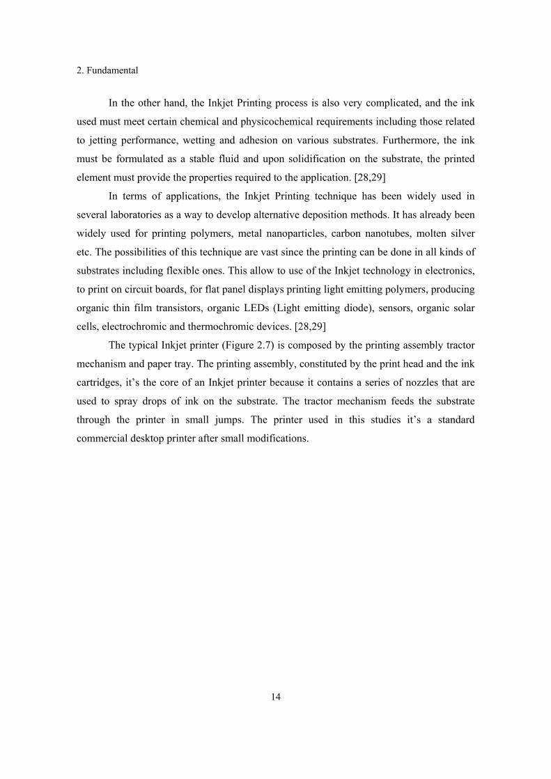
The typical Inkjet printer (Figure 2.7) is composed by the printing assembly tractor
mechanism and paper tray. The printing assembly, constituted by the print head and the ink
cartridges, it’s the core of an Inkjet printer because it contains a series of nozzles that are
used to spray drops of ink on the substrate. The tractor mechanism feeds the substrate
through the printer in small jumps. The printer used in this studies it’s a standard
commercial desktop printer after small modifications.
2. Fundamental
15
Figure 2.7 Typical construction of an office Inkjet printer [30]
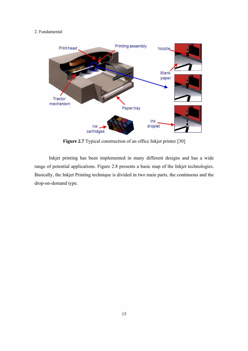
Inkjet printing has been implemented in many different designs and has a wide
range of potential applications. Figure 2.8 presents a basic map of the Inkjet technologies.
Basically, the Inkjet Printing technique is divided in two main parts, the continuous and the
drop-on-demand type.
2. Fundamental
16
Figure 2.8 Inkjet Printing Technology map [30]
The continuous Inkjet printing is achieved using a device that applies an electric
field to the droplets, charging them electrically. Those same droplets are diverted as they
pass through the deflection plates, due to the applied magnetic field and are deposited on
the substrate. Unused droplets are collected out of the printing area.
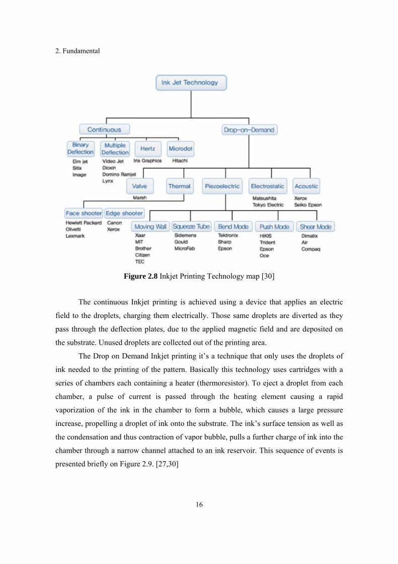
The Drop on Demand Inkjet printing it’s a technique that only uses the droplets of
ink needed to the printing of the pattern. Basically this technology uses cartridges with a
series of chambers each containing a heater (thermoresistor). To eject a droplet from each
chamber, a pulse of current is passed through the heating element causing a rapid
vaporization of the ink in the chamber to form a bubble, which causes a large pressure
increase, propelling a droplet of ink onto the substrate. The ink’s surface tension as well as
the condensation and thus contraction of vapor bubble, pulls a further charge of ink into the
chamber through a narrow channel attached to an ink reservoir. This sequence of events is
presented briefly on Figure 2.9. [27,30]
2. Fundamental
17
Figure 2.9 Thermal Inkjet printing: drop formation [30]
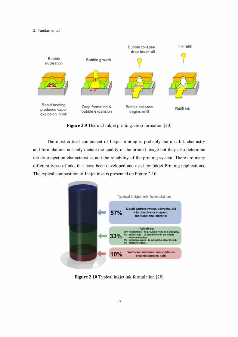
The most critical component of Inkjet printing is probably the ink. Ink chemistry
and formulations not only dictate the quality of the printed image but they also determine
the drop ejection characteristics and the reliability of the printing system. There are many
different types of inks that have been developed and used for Inkjet Printing applications.
The typical composition of Inkjet inks is presented on Figure 2.10.
Figure 2.10 Typical inkjet ink formulation [28]
2. Fundamental
18
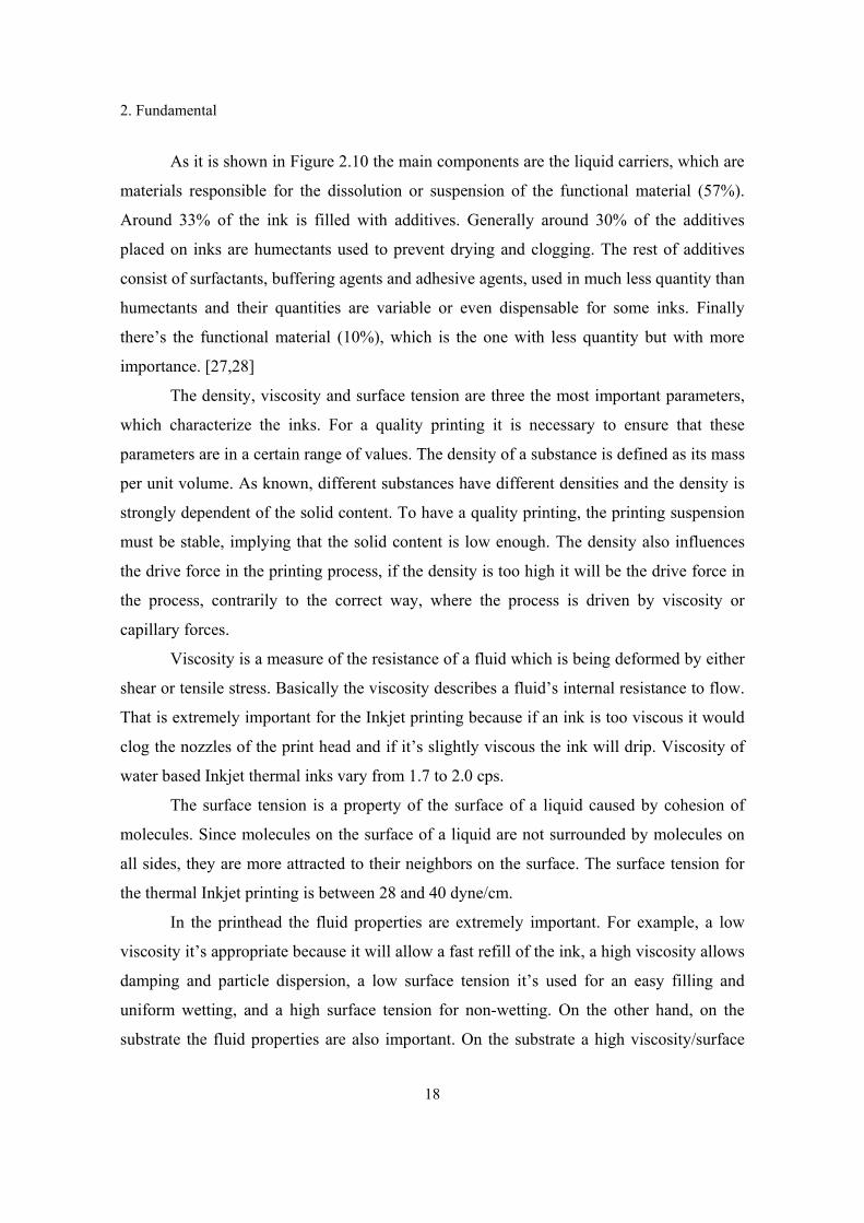
As it is shown in Figure 2.10 the main components are the liquid carriers, which are
materials responsible for the dissolution or suspension of the functional material (57%).
Around 33% of the ink is filled with additives. Generally around 30% of the additives
placed on inks are humectants used to prevent drying and clogging. The rest of additives
consist of surfactants, buffering agents and adhesive agents, used in much less quantity than
humectants and their quantities are variable or even dispensable for some inks. Finally
there’s the functional material (10%), which is the one with less quantity but with more
importance. [27,28]
The density, viscosity and surface tension are three the most important parameters,
which characterize the inks. For a quality printing it is necessary to ensure that these
parameters are in a certain range of values. The density of a substance is defined as its mass
per unit volume. As known, different substances have different densities and the density is
strongly dependent of the solid content. To have a quality printing, the printing suspension
must be stable, implying that the solid content is low enough. The density also influences
the drive force in the printing process, if the density is too high it will be the drive force in
the process, contrarily to the correct way, where the process is driven by viscosity or
capillary forces.
Viscosity is a measure of the resistance of a fluid which is being deformed by either
shear or tensile stress. Basically the viscosity describes a fluid’s internal resistance to flow.
That is extremely important for the Inkjet printing because if an ink is too viscous it would
clog the nozzles of the print head and if it’s slightly viscous the ink will drip. Viscosity of
water based Inkjet thermal inks vary from 1.7 to 2.0 cps.
The surface tension is a property of the surface of a liquid caused by cohesion of
molecules. Since molecules on the surface of a liquid are not surrounded by molecules on
all sides, they are more attracted to their neighbors on the surface. The surface tension for
the thermal Inkjet printing is between 28 and 40 dyne/cm.
In the printhead the fluid properties are extremely important. For example, a low
viscosity it’s appropriate because it will allow a fast refill of the ink, a high viscosity allows
damping and particle dispersion, a low surface tension it’s used for an easy filling and
uniform wetting, and a high surface tension for non-wetting. On the other hand, on the
substrate the fluid properties are also important. On the substrate a high viscosity/surface
2. Fundamental
19
tension is relevant for the spot shape and size control, preventing a non-uniform spreading
and low viscosity/surface tension will provide a rapid spreading.
In a field of electrochromic devices the Inkjet Printing Technology is extremely
promising because it allows the production in series, at low-cost and at room temperature.
The fact of operations and deposition in room temperature allows the production on flexible
substrates.
The performance of printed electrochromic devices is expected to be different, and
probably much better than the conventional ones. This difference it’s due to the fact that
deposited layers can have high porosities, the layer thickness can controlled much easier
and the deposition process is much faster since the drying time is extremely low (the
calcinations process is different than in other techniques). Briefly, when compare to the
vacuum techniques, this is a simpler, cheaper, faster and probably a technique that can
improve the electrochromic behavior of the printed devices. [31]
2.3 Sol-Gel Processing for Electrochromic Materials
Sols and gels are two forms of matter that have been known to exist naturally for a
long time. They include various materials such as ink, clays and a number of other
substances such as the blood and milk. A sol is a stable suspension of colloidal solid
particles within a liquid. For a sol to exist, the solid particles, denser than the surrounding
liquid, must be small enough for the forces responsible of dispersion to be greater than
those of gravity. A gel is a porous 3-dimensionally interconnected solid network that
expands in a stable fashion throughout a liquid medium and is only limited by the size of
the container. If the solid network is made of colloidal sol particles the gel is said to be
colloidal. If the solid network is made of sub-colloidal chemical units then the gel is
polymeric.
A gel is formed when the homogenous dispersion present in the initial sol rigidifies.
This process is called gelation and prevents the development of inhomogeneities within the
material. A sol, or a solution, can be transformed into a colloidal (or polymeric) gel by
2. Fundamental
20
going through what is called a gel point. This is the point where the sol abruptly changes
from a viscous liquid state to a solid phase called the gel. [32,33]
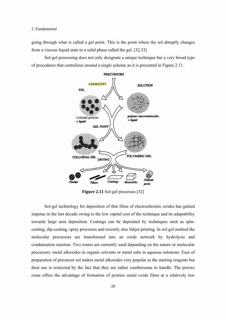
Sol-gel processing does not only designate a unique technique but a very broad type
of procedures that centralizes around a single scheme as it is presented in Figure 2.11.
Figure 2.11 Sol-gel processes [32]
Sol-gel technology for deposition of thin films of electrochromic oxides has gained
impetus in the last decade owing to the low capital cost of the technique and its adaptability
towards large area deposition. Coatings can be deposited by techniques such as spin-
coating, dip-coating, spray processes and recently also Inkjet printing. In sol-gel method the
molecular precursors are transformed into an oxide network by hydrolysis and
condensation reaction. Two routes are currently used depending on the nature or molecular
precursors: metal alkoxides in organic solvents or metal salts in aqueous solutions. Ease of
preparation of precursor sol makes metal alkoxides very popular as the starting reagents but
their use is restricted by the fact that they are rather cumbersome to handle. The peroxo
route offers the advantage of formation of pristine metal oxide films at a relatively low
2. Fundamental
21
temperature owing to the clean burn out properties of organic additives (with low carbon
content) and other volatiles from the as-deposited film. [32,33]
The sol-gel processing has been widely used for deposition of WO3 films. Besides
of being cost-effective, this method has also good control over the microstructure and
homogeneity of the coatings. Therefore this technique has also been used for development
of electrochromic coating starting with the materials, either tungsten alkoxides W(OR)6,
tungsten oxyalkoxide WO(OR)4 or WO2(OR)2. However, these precursors are not stable
towards hydrolysis or condensation and consequently need some stabilizers. [34-36]
The best way to stabilize aqueous solutions of tungsten precursors is to use
complexing reagents such as hydrogen peroxide (H2O2). With a proper concentration of
H2O2, the product that appear at the end of the reaction is soluble in water Peroxotungstic
Acid (PTA). The experimental formula of this crystal is:
· · 2.3
To obtain PTA, according to equation 2.3, the maximum value of x has to be 0.97
and y must be at least 1.1. When 1>x>0.53 PTA is soluble in water and when 0.53>x>0 is
insoluble. Can be concluded that mixing W (tungsten) metallic powder and H2O2 gives
crystalline PTA when x=1 or x=0, while for 1>x>0 the result is amorphous PTA. In either
case the acid suffers polymerization and dehydration during a heat treatment of the film at
temperature between 100 and 200°C [37].
For the proposed objective, which is a large scale and low cost devices, the sol-gel
method combined with Inkjet technology appears to be a versatile technology to deposit
electrochromic tungsten oxide films. Due to the fact that is a non-contact, digital, room
temperature and no vacuum patterning method, with the possibility to control the deposited
layer thickness and porosity makes it ideal for cost efficient mass production.
To allow a correct quality analysis of the developed devices, it’s necessary to
compare the results with another technique. The deposition technique chosen as a reference
is spin-coating, because it is a solution processed method with some similarities to the
Inkjet technology.
Spin-coating has been used for several decades for the application of thin films. It’s
a simple process for rapidly depositing thin coatings onto relatively flat substrates. A
typical process involves depositing a small quantity of a fluid onto the center of a substrate
2. Fundamental
22
that is held by some rotatable fixture and then spinning the substrate at high speed.
Centripetal acceleration cause the fluid to spread to, and eventually off, the edge of the
substrate leaving a uniform coating of the chosen material on the surface. Final film
thickness and other properties will depend on the nature of the fluid (viscosity, drying rate,
percent solids, surface tension, and so on) and the parameters chosen for the spin process.
Factors such as final rotational speed and acceleration contribute to how the properties of
coated films are defined. One of the most important factors in spin coating is repeatability.
Subtle variations in the parameters that define the spin process can result in drastic
variations in the coated film. [38]
The reason to use spin-coating as a reference technique is the fact that the substrates
and materials in both methods are very similar. The solution prepared for Inkjet as an ink,
can be directly deposited by spin-coating allowing an authoritative comparison and
validation of the Inkjet printing as a deposition techniques in EC applications

3. Methods and Procedures
23
3. Methods and Procedures
3.1 Experimental Design for Inkjet Electrochromic Devices
As described in Chapter 2, Inkjet Printing is a solution based technique in which the
formulation of the inks is of great importance to the performance of printer and the final
device performance as well.
The mixture components were selected based on literature review (sol-gel method
for WO3 films), Inkjet technique principles and using an experience of researchers in our
group. Therefore, the chosen constituents are as follow:
1. The base solution (liquid carrier) is a simple mixture of water and isopropyl
alcohol with a weight fraction of 0.7 and 0.3 respectively.
2. The functional materials are:
PTA;
WOX nanoparticle dispersion;
TiO2 nanoparticle dispersion;
3. The additive used as a dispersant is, the oxalic acid (OAD).
The PTA as a WO3 precursor has been obtained by a sol-gel method in which 6g of
tungsten monocrystalline powder, (99.9%, Aldrich, Japan) was carefully added to 50ml
mixture (50:50) of distilled water (Milipore S.A, France) and hydrogen peroxide (30% by
weight, Sigma-Aldrich, Germany). Since the reaction is strongly exothermic, as icy
ambient was employed and the solution was kept slowly stirring for 24 hours. The excess
of tungsten powder was then removed by filtration (0.45 μm syringe filter, Roth, Germany)
leading to a transparent solution. In order to remove the excess of hydrogen peroxide the
solution was dried at 65º C and washed several times with distilled water. After drying the
final result is a water soluble orange crystal powder (PTA). The formation of PTA mainly
depends on the degree of excess decomposed H2O2 in the solution, the atmospheric
humidity during the condensation and the condensation rate [36,39]. Variations of those
parameters lead to emergence of a white powder in a product during condensation which
3. Methods and Procedures
24
should be removed by subsequent washing with distilled water and drying at the same
temperature till the yellow crystals are obtained.
The solution processed PTA is the functional material which as-deposited forms
amorphous phase causing high optical modulation of the layer when electrical potential is
applied. Considering the fluid properties of aqueous-alcohol PTA solution, the use of this
material for printing seems to be reasonable. The quantity of PTA used in experiments is in
the range from 0.01 to 0.2 w/w because that’s the standard PTA concentration used in other
sol-gel deposition techniques, like dip coating. [39]
According to C.M. White et al [40], the crystalline structure of the material
influences the diffusion coefficient inside the electrochromic layer and the length of the
diffusion path. It is therefore obvious that the varied, dual-phase microstructure would
significantly improve the electrochromic performance. The creation of the crystalline phase
in a low temperature, deposition process has so far been possible only using
electrodeposition [41]. Here it’s proposed a new approach which allows for the
incorporation of the crystalline phase into the layer using Inkjet Printing. This innovative
method is based on dispersions of nanocrystals used as components of the printable ink. It’s
expected that this will allow for simultaneous use of the advantages of both phases without
necessity of using high energetic depositions methods or annealing.
The two types of commercially available WOX nanoparticles were used as a source
of crystalline phase, WO3 hereinafter called yellow (Sigma Aldrich Chemistry, USA) and
WO2.9 hereinafter called blue (99.99% pure WO3 ceramic oxide target, Super Conductor
Materials, USA). The suggested designation of those materials is thin film deposition using
PVD techniques. Here, however it serves as a solid content in liquid dispersions. These
liquid dispersions are aqueous alcohol dispersions with a solid content of around 0.01% and
base solution of isopropyl alcohol and water in a constant proportion 0.3/0.7. The different
colors of the WOX nanoparticles are due to their stoichiometry.
Figure 3.1 and 3.2 shows the SEM (Scanning Electron Microscopy) micrographs of
the yellow and blue WOX nanoparticles, respectively. The yellow tungsten oxide exhibits
grains of about 85 nm in diameter, while blue tungsten oxide has grains of 70 nm in
diameter. For convenience, shall refer to those powders as blue and yellow respectively.

3. Methods and Procedures
25
Figure 3.1 WO3 yellow nanopowder SEM
micrograph
Figure 3.2 WO2.9 blue nanopowder SEM
micrograph
The TiO2 nanopowder in aqueous alcohol dispersion has a solid content of
nanoparticles of around 0.01% and the same proportion of isopropyl alcohol and water, as
the WOX dispersions. The presence of titanium dioxide has the objective of increasing the
electrochromic behavior, because this material tends to increase the contact surface area of
the electrochromic material. According to P.S. Patil et al the presence of TiO2
nanoparticles modifies the electrochromic layer structure leading to greater electrochromic
reversibility, stability and coloration efficiency of the devices. The presence of titanium
dioxide also helps the intercalation and deintercalation process due to formation of open
channels resulting in an increase of the surface area of the layer [1]. In this research, was
decided to examine the impact of this factor using TiO2 nanopowder (T20/SC, 3% by
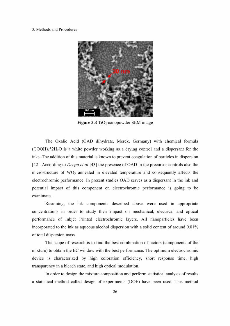
weight, Solaronix). A TiO2 nanopowder SEM micrograph represented in Figure 3.3
indicates that the grain size is much smaller (30 nm) than the WOX nanoparticles.
3. Methods and Procedures
26
Figure 3.3 TiO2 nanopowder SEM image
The Oxalic Acid (OAD dihydrate, Merck, Germany) with chemical formula
(COOH)2*2H2O is a white powder working as a drying control and a dispersant for the
inks. The addition of this material is known to prevent coagulation of particles in dispersion
[42]. According to Deepa et al [43] the presence of OAD in the precursor controls also the
microstructure of WO3 annealed in elevated temperature and consequently affects the
electrochromic performance. In present studies OAD serves as a dispersant in the ink and
potential impact of this component on electrochromic performance is going to be
exanimate.
Resuming, the ink components described above were used in appropriate
concentrations in order to study their impact on mechanical, electrical and optical
performance of Inkjet Printed electrochromic layers. All nanoparticles have been
incorporated to the ink as aqueous alcohol dispersion with a solid content of around 0.01%
of total dispersion mass.
The scope of research is to find the best combination of factors (components of the
mixture) to obtain the EC window with the best performance. The optimum electrochromic
device is characterized by high coloration efficiency, short response time, high
transparency in a bleach state, and high optical modulation.
In order to design the mixture composition and perform statistical analysis of results
a statistical method called design of experiments (DOE) have been used. This method
3. Methods and Procedures
27
allows several factors to be analyzed at the same time in order to know which one has the
greatest impact on the final result.
Design of experiment is the design of any information gathering exercises where
variation is present, whether under the full control of the experiment or not. The purpose of
this method is to characterize, predict, and then cost-effectively improve the behavior of
any system or process [44]. Basically it’s a method to increase productivity and improve
quality of a process.
There are several kinds of Design of Experiments, such as the Factorial Design (full
or fractionated), Taguchi Design, Optimal Design for Regression Models, among others.
For this work was used the Optimal Design for Regression Models. The fact that,
Optimal Designs reduce the costs of experimentations by allowing statistical models to be
estimated with fewer experimental runs and the fact that, it can accommodate multiple
types of factors, such as process, mixture and discrete factors is an advantage of this kind of
design. Specifically, was used the D-Optimal Design, which is most appropriate for
screening experiments because the optimality criterion focuses on precise estimates of the
coefficients.[44]
The software used in this work is JMP® Statistical Discovery Software, which is a
statistical tool that allows the interaction with data, the creation of relations between
important factors and it provides more specific information about the areas that interest the
most in a certain study.
This software allows the choice of several designs. After choosing a specific design
it’s imperative to introduce the responses and factors of the experiment. Afterwards, with
the collected information the program will create a design, which provides the recipes for
the formulation of the sufficient inks to obtain a reliable study. In order to evaluate the
created design, the program will make a table with the ink formulation values and where
the results of measurements and calculations performed to obtain the responses values must
be insert.
When the table is filled the program can finally create a model. In the model
specification, if the effect leverage is chosen then the program will provide the whole
model for each response, the leverage plots for each factor and factors interactions, the
summary of fit table, the parameter estimates and the effects test table, among other
3. Methods and Procedures
28
statistical information. On the other hand if the effect screening is chosen the program will
provide some similar information to the effect leverage, with the addition of the sorted
parameters estimates plot, and some other statistical information. In the effect screening is
also possible to obtain mixture profiles where, with the data inserted in the table, is possible
to create surface response prediction plots of every response. These plots are important for
this study because they allow the observer to see the behavior of the devices when the
quantity of nanoparticles changes.
With all the information obtained from the program it is possible to analyze if the
model created is or isn’t reliable, it is also possible to know the significance of the effects
and it’s possible to obtain a prediction study of the behavior of the devices.
More detailed information about the JMP® Statistical Discovery Software is
available in [44].
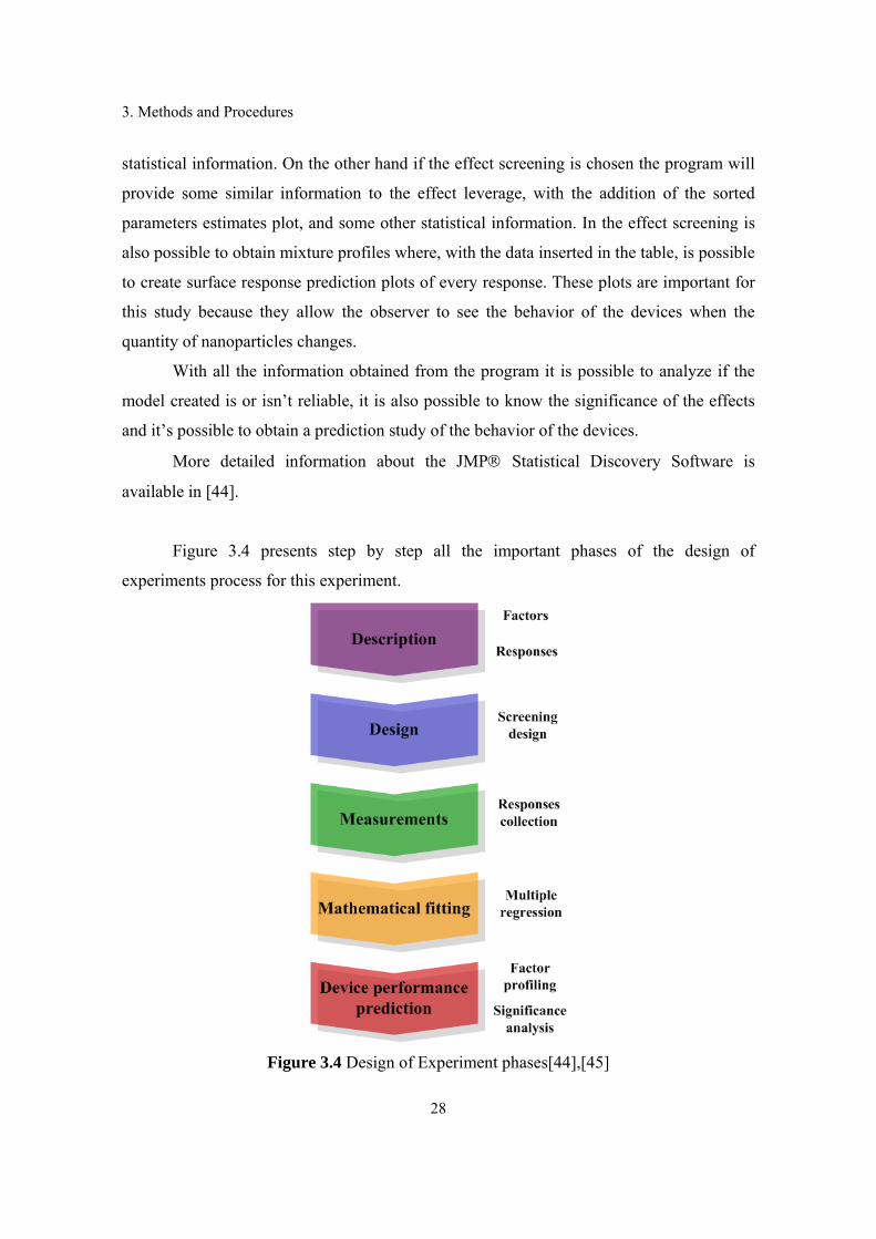
Figure 3.4 presents step by step all the important phases of the design of
experiments process for this experiment.
Figure 3.4 Design of Experiment phases[44],[45]
3. Methods and Procedures
29
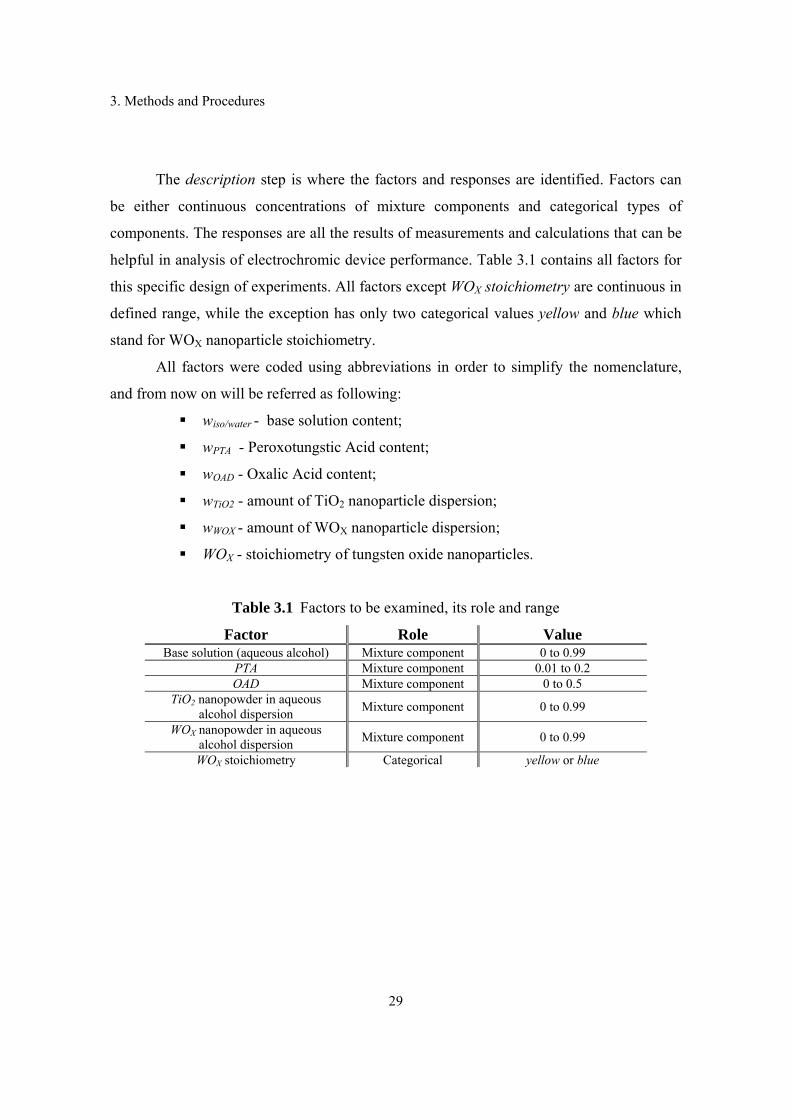
The description step is where the factors and responses are identified. Factors can
be either continuous concentrations of mixture components and categorical types of
components. The responses are all the results of measurements and calculations that can be
helpful in analysis of electrochromic device performance. Table 3.1 contains all factors for
this specific design of experiments. All factors except WOX stoichiometry are continuous in
defined range, while the exception has only two categorical values yellow and blue which
stand for WOX nanoparticle stoichiometry.
All factors were coded using abbreviations in order to simplify the nomenclature,
and from now on will be referred as following:
wiso/water - base solution content;
wPTA - Peroxotungstic Acid content;
wOAD - Oxalic Acid content;
wTiO2 - amount of TiO2 nanoparticle dispersion;
wWOX - amount of WOX nanoparticle dispersion;
WOX - stoichiometry of tungsten oxide nanoparticles.
Table 3.1 Factors to be examined, its role and range
Factor Role Value Base solution (aqueous alcohol) Mixture component 0 to 0.99
PTA Mixture component 0.01 to 0.2 OAD Mixture component 0 to 0.5
TiO2 nanopowder in aqueous alcohol dispersion Mixture component 0 to 0.99
WOX nanopowder in aqueous alcohol dispersion Mixture component 0 to 0.99
WOX stoichiometry Categorical yellow or blue

3. Methods and Procedures
30
Table 3.2 Defined responses and their goals
Response Name Goal Roughness None
Coloration Time Minimize Bleaching Time Minimize
Change in Optical Density Maximize Coloration Efficiency Maximize Oxidation Peak Max None Reduction Peak Max None
Transmittance (bleaching) None Transmittance (coloring) None Inserted Charge Density None
Optical Absorption Coefficient None Density None
Viscosity None Surface Tension None Contact Angle None
The responses shown in Table 3.2 concern the measurements performed on printed
electrochromic devices developed according to the DOE recipes. The results of the
measurements were divided in five groups, and coded as following:
1. Mechanical parameters
d - film thickness;
Rq - film roughness;
2. Optical parameters defined for λ=900nm
τcol - coloration time;
τbl - bleaching time;
ΔOD - change in optical density;
Tcol - transmittance in coloration state;
Tbl - transmittance in bleaching state;
α – optical absorption coefficient;
3. Electrical parameters
iRED - reduction peak max.
iOX - oxidation peak max.
Qins - Charge inserted to the device during coloration process
4. Fluid parameters of the ink
ν - ink viscosity;
3. Methods and Procedures
31
γ - ink surface tension;
θ - ink contact angle on ITO PET substrate;
ρ - ink density;
5. Overall performance defined for λ=900nm
CE - coloration efficiency
In design step the determination of mixture formulations is performed, using the
screening design method. The choice of the screening design occurs because it has the
ability of examine many factors, with fewer experimental runs, to see which have the
greatest effect on examined responses. In addition to the influence of the main components
of the mixture, the screening design allows also to indicate the relevant correlations
between factors. In measurements step all the responses defined in Table 3.2 are physically
collected for all printed devices. The mathematical fitting is a mathematical procedure for
finding the best fitting curve of a given set of points, in order to analyze the data collected
during measurements step. Finally in device performance prediction phase the performance
of any possible device can be predicted based on mathematical model. This phase allow
also to perform analysis of significance in order to classify the factors and extract
information about their interactions.
3.2 Electrochromic ink formulation
The ink used in thermal Inkjet printers should meet certain physical properties
compatible with a wide range of ejecting conditions, i.e., driving voltages and pulse, and
the shape and size of the nozzle. The exact choice of ink components depends upon the
specific application and performance requirements of the printhead from which they are
jetted. Thermal printhead requires ink compositions with a certain set of physical properties
in order to achieve reliable and accurate jetting of the ink, as is well known in the art of
Inkjet printing. Acceptable viscosities are typically no greater than 3 cP, and preferably in
the range of about 1.5 to 2.5 cP.
3. Methods and Procedures
32
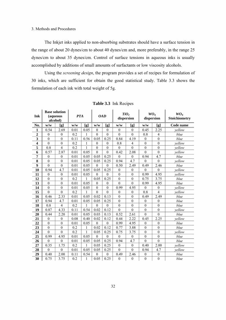
The Inkjet inks applied to non-absorbing substrates should have a surface tension in
the range of about 20 dynes/cm to about 40 dynes/cm and, more preferably, in the range 25
dynes/cm to about 35 dynes/cm. Control of surface tensions in aqueous inks is usually
accomplished by additions of small amounts of surfactants or low viscosity alcohols.
Using the screening design, the program provides a set of recipes for formulation of
30 inks, which are sufficient for obtain the good statistical study. Table 3.3 shows the
formulation of each ink with total weight of 5g.
Table 3.3 Ink Recipes
Ink Base solution
(aqueous alcohol)
PTA OAD TiO2 dispersion
WOX dispersion
WOX Stoichiometry
No. w/w [g] w/w [g] w/w [g] w/w [g] w/w [g] Code name 1 0.54 2.69 0.01 0.05 0 0 0 0 0.45 2.25 yellow 2 0 0 0.2 1 0 0 0 0 0.8 4 blue 3 0 0 0.11 0.56 0.05 0.25 0.84 4.19 0 0 blue 4 0 0 0.2 1 0 0 0.8 4 0 0 yellow 5 0.8 4 0.2 1 0 0 0 0 0 0 yellow 6 0.57 2.87 0.01 0.05 0 0 0.42 2.08 0 0 yellow 7 0 0 0.01 0.05 0.05 0.25 0 0 0.94 4.7 blue 8 0 0 0.01 0.05 0.05 0.25 0.94 4.7 0 0 yellow 9 0 0 0.01 0.05 0 0 0.50 2.49 0.49 2.46 blue
10 0.94 4.7 0.01 0.05 0.05 0.25 0 0 0 0 yellow 11 0 0 0.01 0.05 0 0 0 0 0.99 4.95 yellow 12 0 0 0.2 1 0.05 0.25 0 0 0.75 3.75 blue 13 0 0 0.01 0.05 0 0 0 0 0.99 4.95 blue 14 0 0 0.01 0.05 0 0 0.99 4.95 0 0 yellow 15 0 0 0.2 1 0 0 0 0 0.8 4 yellow 16 0.46 2.33 0.01 0.05 0.02 0.13 0 0 0.49 2.49 blue 17 0.94 4.7 0.01 0.05 0.05 0.25 0 0 0 0 blue 18 0.8 4 0.2 1 0 0 0 0 0 0 blue 19 0.87 4.33 0.11 0.54 0.02 0.12 0 0 0 0 yellow 20 0.44 2.20 0.01 0.05 0.03 0.13 0.52 2.61 0 0 blue 21 0 0 0.08 0.40 0.02 0.12 0.44 2.22 0.45 2.25 yellow 22 0 0 0.01 0.05 0 0 0.99 4.95 0 0 blue 23 0 0 0.2 1 0.02 0.12 0.77 3.88 0 0 blue 24 0 0 0.2 1 0.05 0.25 0.75 3.75 0 0 yellow 25 0.99 4.95 0.01 0.05 0 0 0 0 0 0 blue 26 0 0 0.01 0.05 0.05 0.25 0.94 4.7 0 0 blue 27 0.35 1.75 0.2 1 0.05 0.25 0 0 0.40 2.00 yellow 28 0 0 0.01 0.05 0.05 0.25 0 0 0.94 4.7 yellow 29 0.40 2.00 0.11 0.54 0 0 0.49 2.46 0 0 blue 30 0.75 3.75 0.2 1 0.05 0.25 0 0 0 0 blue
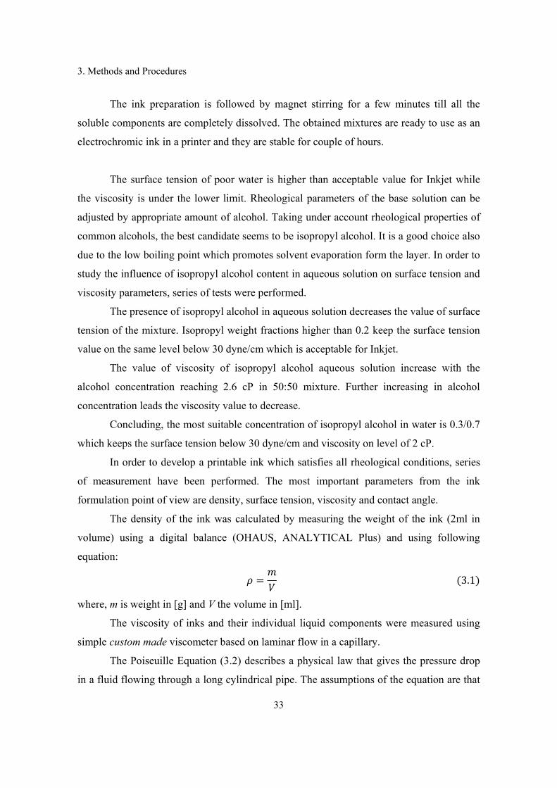
3. Methods and Procedures
33
The ink preparation is followed by magnet stirring for a few minutes till all the
soluble components are completely dissolved. The obtained mixtures are ready to use as an
electrochromic ink in a printer and they are stable for couple of hours.
The surface tension of poor water is higher than acceptable value for Inkjet while
the viscosity is under the lower limit. Rheological parameters of the base solution can be
adjusted by appropriate amount of alcohol. Taking under account rheological properties of
common alcohols, the best candidate seems to be isopropyl alcohol. It is a good choice also
due to the low boiling point which promotes solvent evaporation form the layer. In order to
study the influence of isopropyl alcohol content in aqueous solution on surface tension and
viscosity parameters, series of tests were performed.
The presence of isopropyl alcohol in aqueous solution decreases the value of surface
tension of the mixture. Isopropyl weight fractions higher than 0.2 keep the surface tension
value on the same level below 30 dyne/cm which is acceptable for Inkjet.
The value of viscosity of isopropyl alcohol aqueous solution increase with the
alcohol concentration reaching 2.6 cP in 50:50 mixture. Further increasing in alcohol
concentration leads the viscosity value to decrease.
Concluding, the most suitable concentration of isopropyl alcohol in water is 0.3/0.7
which keeps the surface tension below 30 dyne/cm and viscosity on level of 2 cP.
In order to develop a printable ink which satisfies all rheological conditions, series
of measurement have been performed. The most important parameters from the ink
formulation point of view are density, surface tension, viscosity and contact angle.
The density of the ink was calculated by measuring the weight of the ink (2ml in
volume) using a digital balance (OHAUS, ANALYTICAL Plus) and using following
equation:
3.1
where, m is weight in [g] and V the volume in [ml].
The viscosity of inks and their individual liquid components were measured using
simple custom made viscometer based on laminar flow in a capillary.
The Poiseuille Equation (3.2) describes a physical law that gives the pressure drop
in a fluid flowing through a long cylindrical pipe. The assumptions of the equation are that
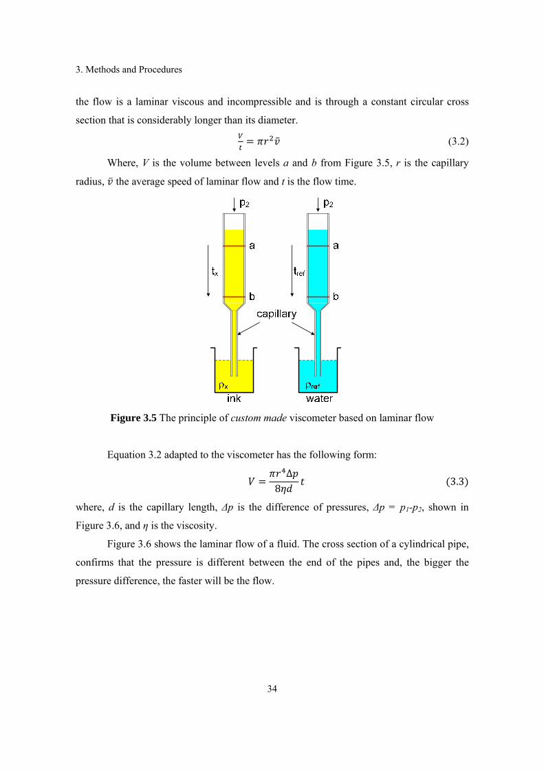
3. Methods and Procedures
34
the flow is a laminar viscous and incompressible and is through a constant circular cross
section that is considerably longer than its diameter.
(3.2)
Where, V is the volume between levels a and b from Figure 3.5, r is the capillary
radius, the average speed of laminar flow and t is the flow time.
Figure 3.5 The principle of custom made viscometer based on laminar flow
Equation 3.2 adapted to the viscometer has the following form:
∆8 3.3
where, d is the capillary length, Δp is the difference of pressures, Δp = p1-p2, shown in
Figure 3.6, and η is the viscosity.
Figure 3.6 shows the laminar flow of a fluid. The cross section of a cylindrical pipe,
confirms that the pressure is different between the end of the pipes and, the bigger the
pressure difference, the faster will be the flow.
3. Methods and Procedures
35
Figure 3.6 Laminar flow representation
The change in pressures through the capillary applied to the Equation 3.3 gives the
final formula for relative viscosity:
3.4
where, ηref is the viscosity of the water, ρx and ρref are the density of ink and water, tx
and tref are the flow time of ink and water respectively.
The final value of ink viscosity taking under account temperature fluctuation is then
calculated using following formula:
3.5
The ink surface tension and the contact angle on ITO PET substrate were obtained
using Contact Angle Measurement System (OCA 15, DataPhysics, Germany). For the static
contact angle measurements, the sessile drop method is the standard method. For that a
sessile drop is illuminated from one side with a diffuse light source and from the other side
the contour of the drop is observed. [46]
The contact angle, θ, is a quantitative measure of the wetting of a solid substrate by
a liquid ink. It is defined geometrically as the angle formed by a liquid at the three phase
boundary where a liquid, gas and solid intersect. Low values of θ indicate that the liquid
spreads, or wets well, while high values indicate poor wetting. If the contact angle is bigger
than 90º the substrate is hydrophobic, and consequently there isn’t a good adhesion
between the surfaces form the materials in contact. On the other hand if the angle is less the
90º, the substrate is hydrophilic and the materials adhesion is favored. A zero contact angle
represents complete wetting. [47,48]
3. Methods and Procedures
36
Surface tension was measured using a pendant drop shape analysis. The shape of a
drop of a liquid hanging from a syringe tip is determined from the balance forces which
include the surface tension of a liquid. The surface or interfacial tension at the liquid
interface can be related to the drop shape through the following equation:
∆ 3.6
where, γ is the surface tension, Δρ the difference in density between fluids at interface, g is
the gravitational constant, R0 the radius of drop curvature at apex and β is the shape factor.
The shape factor can be defined trough the Young-Laplace equation expressed as 3
dimensionless first order equations:
cos 3.7
sin (3.8)
2 3.9
3.3 Electrolyte Preparation
The gel electrolyte which contains a lithium salt, a polymeric matrix and an organic
solvent or a mixture of organic solvents was used as ion conductor layer between counter
and working electrodes. The polymeric matrix in this specific electrolyte is a mixture of
PMMA/PEO/PPO with PC as solvent and plasticizer, which allows the ionic (LiClO4)
conduction. [49]
The materials used in the electrolyte preparation were
polymethacryl-sauremethyleste-PMMA (Fluka, Germany), PEO-PPO (Zeon Chemicals,
Spain), which is a binary mixture of ethylene poly(oxide) and propylene poly(oxide),
lithium perchlorate (Fluka, Germany), propylene carbonate (99%, Fluka, Germany) and
tetrahydrofuran-THF (99.9% THF, Sigma-Aldrich, Germany).
In order to obtain 3g of electrolyte, 0.36g of PMMA, 0.21g of PEO-PPO, 0.33g of
LiClO4 and 1.75 PC were mixed with 4ml of THF and followed by stirring for about 4
hours until a transparent uniform lightly viscous gel were obtained [49].
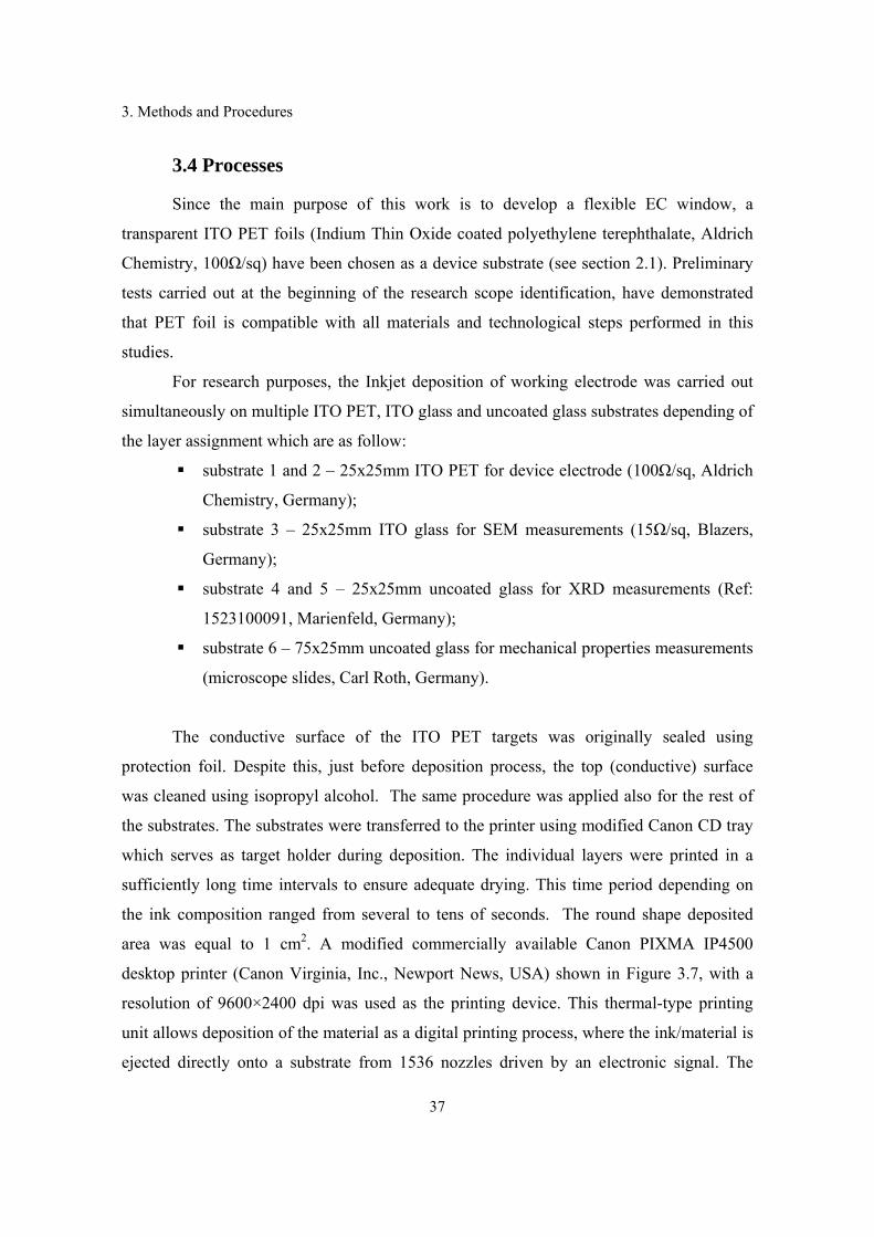
3. Methods and Procedures
37
3.4 Processes
Since the main purpose of this work is to develop a flexible EC window, a
transparent ITO PET foils (Indium Thin Oxide coated polyethylene terephthalate, Aldrich
Chemistry, 100Ω/sq) have been chosen as a device substrate (see section 2.1). Preliminary
tests carried out at the beginning of the research scope identification, have demonstrated
that PET foil is compatible with all materials and technological steps performed in this
studies.
For research purposes, the Inkjet deposition of working electrode was carried out
simultaneously on multiple ITO PET, ITO glass and uncoated glass substrates depending of
the layer assignment which are as follow:
substrate 1 and 2 – 25x25mm ITO PET for device electrode (100Ω/sq, Aldrich
Chemistry, Germany);
substrate 3 – 25x25mm ITO glass for SEM measurements (15Ω/sq, Blazers,
Germany);
substrate 4 and 5 – 25x25mm uncoated glass for XRD measurements (Ref:
1523100091, Marienfeld, Germany);
substrate 6 – 75x25mm uncoated glass for mechanical properties measurements
(microscope slides, Carl Roth, Germany).
The conductive surface of the ITO PET targets was originally sealed using
protection foil. Despite this, just before deposition process, the top (conductive) surface
was cleaned using isopropyl alcohol. The same procedure was applied also for the rest of
the substrates. The substrates were transferred to the printer using modified Canon CD tray
which serves as target holder during deposition. The individual layers were printed in a
sufficiently long time intervals to ensure adequate drying. This time period depending on
the ink composition ranged from several to tens of seconds. The round shape deposited
area was equal to 1 cm2. A modified commercially available Canon PIXMA IP4500
desktop printer (Canon Virginia, Inc., Newport News, USA) shown in Figure 3.7, with a
resolution of 9600×2400 dpi was used as the printing device. This thermal-type printing
unit allows deposition of the material as a digital printing process, where the ink/material is
ejected directly onto a substrate from 1536 nozzles driven by an electronic signal. The
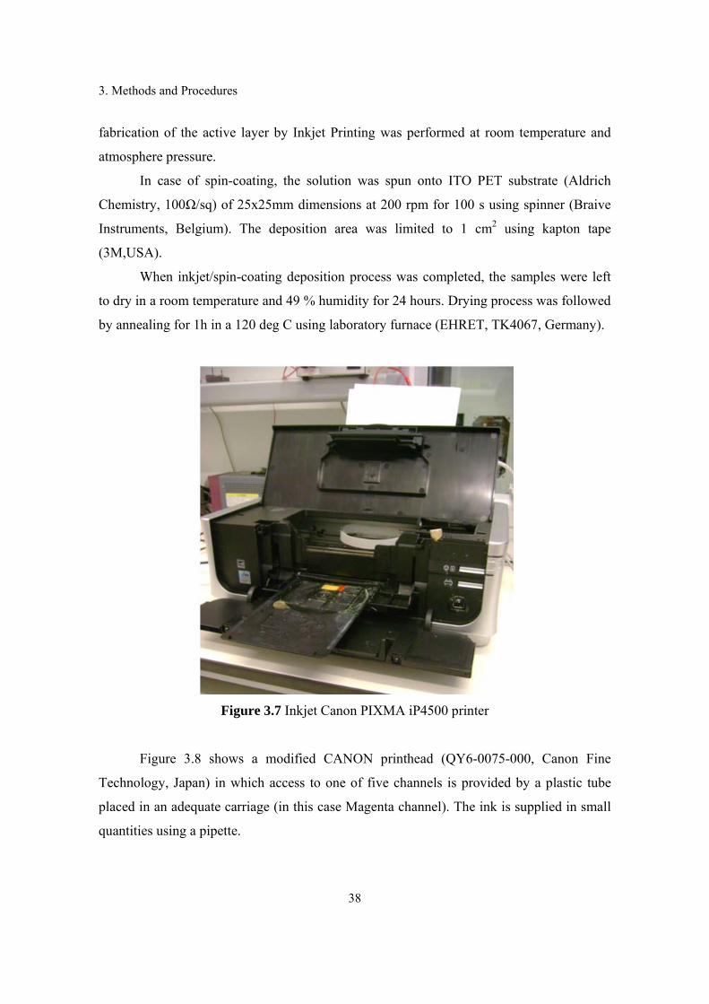
3. Methods and Procedures
38
fabrication of the active layer by Inkjet Printing was performed at room temperature and
atmosphere pressure.
In case of spin-coating, the solution was spun onto ITO PET substrate (Aldrich
Chemistry, 100Ω/sq) of 25x25mm dimensions at 200 rpm for 100 s using spinner (Braive
Instruments, Belgium). The deposition area was limited to 1 cm2 using kapton tape
(3M,USA).
When inkjet/spin-coating deposition process was completed, the samples were left
to dry in a room temperature and 49 % humidity for 24 hours. Drying process was followed
by annealing for 1h in a 120 deg C using laboratory furnace (EHRET, TK4067, Germany).
Figure 3.7 Inkjet Canon PIXMA iP4500 printer
Figure 3.8 shows a modified CANON printhead (QY6-0075-000, Canon Fine
Technology, Japan) in which access to one of five channels is provided by a plastic tube
placed in an adequate carriage (in this case Magenta channel). The ink is supplied in small
quantities using a pipette.
3. Methods and Procedures
39
Figure 3.8 Modified Canon cartridges
The shapes and positions of patterns on the substrates were designed using
Microsoft Visio 2010 vector graphics software and Canon Inkjet iP4500 series driver
working in a high quality mode.
The counter electrode was deposited on the same ITO PET substrates (Aldrich
Chemistry, 100Ω/sq) by brushing. The solution used as a counter electrode material is an
alcohol based paint containing a chemical platinum precursor (Platisol T, Solaronix,
Switzeland). The deposition was followed by annealing for 1h at 120 deg C using
laboratory furnace (EHRET, TK4067, Germany) in order to activate a platinum layer. This
temperature is lower than recommended by the manufacturer, due to the use of flexible,
temperature sensitive substrate. The result is a layer with inferior properties, but still
fulfilling the task.
3.5 Device structure and encapsulation
The performance and operating characteristics of electrochromic devices strongly
depend on encapsulation process. The method used in this work enables to make a small
lab-test EC window that consists of an electrochromic layer, electrolyte and counter
electrode sandwiched between two flexible ITO PET targets. As both targets are made from
transparent plastic foil, the window can be seen clearly through it when active layer is
3. Methods and Procedures
40
bleached. The active area of the device changes from one color to another when stimulated
by an electric current applied to electrodes. All technological steps of proposed
encapsulation method for EC windows are shown in Figure 3.9. On the beginning of the
encapsulation process, the tape spacer (1mm thick, Ceys, Spain) is placed on the bottom
substrate which is partially covered with dried and annealed electrochromic layer. The main
task of using a double site tape as a spacer is to limit the volume of electrolyte and to
establish a constant thickness of the device. In the next step, both substrates are combined
together in a sandwich structure, and the connection is reinforced using thermoplastic glue
(iTools Thermoplastic Gun). The volume inside the device contains one small hole placed
in the corner necessary to introduce gel electrolyte. Prepared structure is ready for filling
with electrolyte which is performed using syringe with a needle. In order to finalize
encapsulation the device is sealed by the same thermoplastic glue. The use of conductive
tape in order to improve the electrical contact is optional. It is important that the volume of
electrolyte inside the device should not contain air bubbles, because their presence may
interfere with measurements.
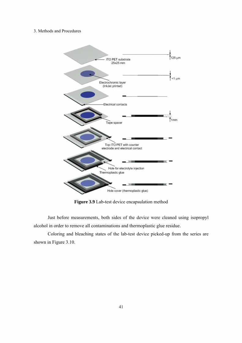
3. Methods and Procedures
41
Figure 3.9 Lab-test device encapsulation method
Just before measurements, both sides of the device were cleaned using isopropyl
alcohol in order to remove all contaminations and thermoplastic glue residue.
Coloring and bleaching states of the lab-test device picked-up from the series are
shown in Figure 3.10.
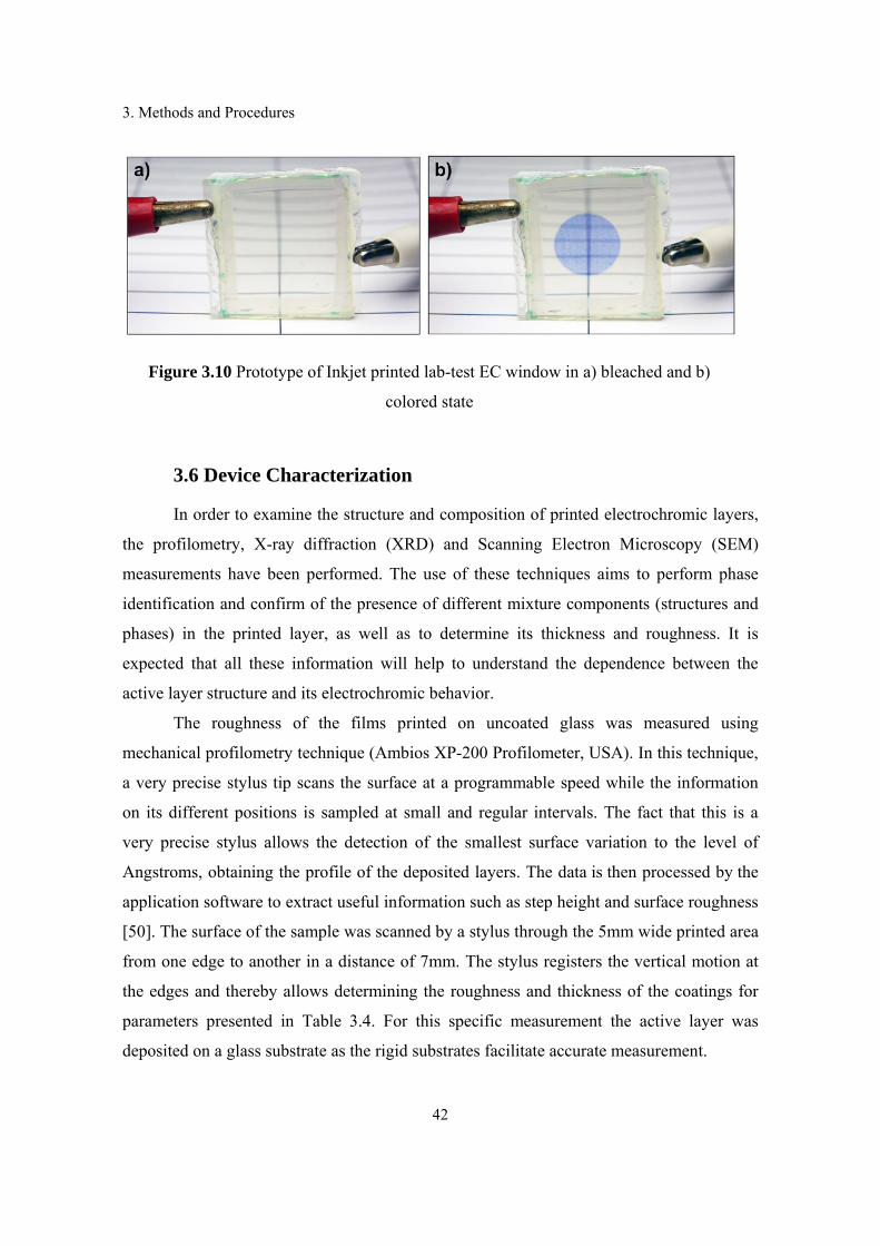
3. Methods and Procedures
42
Figure 3.10 Prototype of Inkjet printed lab-test EC window in a) bleached and b)
colored state
3.6 Device Characterization
In order to examine the structure and composition of printed electrochromic layers,
the profilometry, X-ray diffraction (XRD) and Scanning Electron Microscopy (SEM)
measurements have been performed. The use of these techniques aims to perform phase
identification and confirm of the presence of different mixture components (structures and
phases) in the printed layer, as well as to determine its thickness and roughness. It is
expected that all these information will help to understand the dependence between the
active layer structure and its electrochromic behavior.
The roughness of the films printed on uncoated glass was measured using
mechanical profilometry technique (Ambios XP-200 Profilometer, USA). In this technique,
a very precise stylus tip scans the surface at a programmable speed while the information
on its different positions is sampled at small and regular intervals. The fact that this is a
very precise stylus allows the detection of the smallest surface variation to the level of
Angstroms, obtaining the profile of the deposited layers. The data is then processed by the
application software to extract useful information such as step height and surface roughness
[50]. The surface of the sample was scanned by a stylus through the 5mm wide printed area
from one edge to another in a distance of 7mm. The stylus registers the vertical motion at
the edges and thereby allows determining the roughness and thickness of the coatings for
parameters presented in Table 3.4. For this specific measurement the active layer was
deposited on a glass substrate as the rigid substrates facilitate accurate measurement.
3. Methods and Procedures
43
Table 3.4 Profilometry parameters
Parameters Value Speed 0.20 mm/s Length 7 mm Range 100 μm
Stylus Force 0.5 mg
X-ray diffraction (XPert PRO, PANalytical, Netherlands) is usually used in
electrochemistry to identify a material and give information about the phase, lattice stress,
texture orientation and grain size. It is based on the constructive interference between
x-rays reflected at different atomic planes. By varying the angle between the incident and
diffracted beam and recording the diffracted radiation, a chart with material and phase
specific peaks is achieved. In this work the XRD method has been used to determine the
electrochromic layer crystalline structure.
The X-ray diffraction occurs when a beam focuses on a material, causing a vibration
and which consequence is the emission of a wave with the same length as the focused
beam. If the atoms are periodically organized, forming plans and if the wavelength of the
radiation is in the range of inter atomic spaces, like in X radiation, may occur constructive
or destructive interferences. This effect is described by Bragg’s law represented by the
following equation [51]:
3.10
where, θ is a certain angle of the radiation when it hits the surface of the sample, the
constructive interferences occur to multiple (ni) of the wavelength (λ), related to the space
between atomic plans (dhkl). The θ angle is also known as Bragg angle, being 2θ, the
diffraction angle. The phase and components identification is achieved by comparing the
X-Ray diffraction patterns obtained from the sample with an internationally recognized
database containing reference patterns.
The structural analysis of printed active layers was supported by SEM
measurements (Auriga SEM-FIB, Zeiss, USA). This method enables to study the
3. Methods and Procedures
44
morphology of the surface and cross section (possible on the edges of the fracture) due to
its ability to produce 3D images.
The SEM analysis consists on an electron beam (primary electrons) that makes the
scan of the samples’ surface. When electrons hit the solid state matter they cause the
emission of electrons from the surface (secondary electrons). These electrons are emitted in
every direction and in bigger number according to the proximity of the incident beam. If the
primary electrons beam hits perpendicularly the sample, the activated region and
consequently the secondary emission, is symmetric around that axis. If the primary incident
beam changes, the activated area changes position and the distance traveled by the
secondary electrons changes, changing also the signal generated on the detector. That way
it is possible to obtain a 3D image of the sample surface, with possible amplification up to
500 000 times, where the brightest points represent the highest points of the surface. [51]
The electrochemical measurements which include Chronocoulometry (CQ) and
Cyclic Voltammetry (CV) were performed using galvanostatic method (Gamry Reference
600 Potentiostat, Gamry Instruments, USA). The CQ which involves the measurement of
charge inserted to the device as a function of time is a controlled-potential technique with a
potential step wave form. According to Table 3.5, voltage level of -4V is applied and due to
the reduction reaction the device changes is color to blue. Then, stepping the potential to a
second value (4V), another electrochemical reaction occurs (oxidation) and the device
come back to its bleached state. This test provides the value of Charge Density, which is the
amount of electric charge per unit area.
Table 3.5 CQ parameters
Parameters Value Step 1 Voltage (V) -4
Step 1 Time (s) 30 Step 2 Voltage (V) 4
Step 2 Time (s) 30 Sample Period (s) 0.001
PF Corr. (ohm) 50 Equil. Time (s) 5
Conditioning Time (s) 120 Conditioning E (V) -4
3. Methods and Procedures
45
The CV measurements were preformed in order to examine existence of
electrochemical reactions and the kinetics of electron transfer in the oxidation-reduction
reactions. During CV measurements a voltage is applied to the electrodes and the
corresponding current that flows through the device is monitored. This technique allows the
scanning of the potential in both directions for a finite number of cycles. This fact gives the
possibility of studying the reversibility and the stability of chemical reactions giving also
information about reduction and oxidation current. The reactions detection is possible due
to the approximation of the difference of the voltage to the necessary value to a certain
reaction to occur, taking to an increase of the magnitude in the current. The current is then
limited for the decrease of the reagents forming a peak of current. [52] In a total reversible
reaction, an oxidized component during part of the cycle returns to its reduced state during
the reverse scanning, being possible to oxidize again in a new cycle. This is a very
important measurement for electrochromic applications because it allows the study of the
reversibility and stability of reaction represented in Equation 2.1, Chapter 2, while the
device is in the bleach and in the colored state. The set of parameters used in CV
measurements is shown in Table 3.6.
Table 3.6 CV parameters
Parameters Value Initial voltage (V) 4 Scan Limit 1 (V) -4 Scan Limit 2 (V) 4 Final voltage (V) 4 Scan Rate (mV/s) 50 Step Size (mV) 10
Cycles 2 Initial Delay Time (s) 0.25
Initial Delay Stab. (mV/s) 0 Conditioning Time (s) 120
Conditioning voltage (V) 4
Optical measurements were performed using a spectrometer set-up (Figure 3.11)
consist of following elements:
KEITHLEY 238 High Current Source Measure Unit,
Halogen Light Source HL-2000-FHSA (Mikropack),
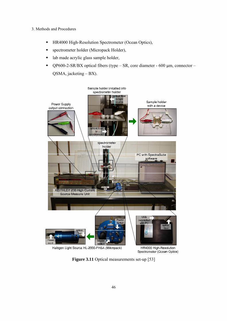
3. Methods and Procedures
46
HR4000 High-Resolution Spectrometer (Ocean Optics),
spectrometer holder (Micropack Holder),
lab made acrylic glass sample holder,
QP600-2-SR/BX optical fibers (type – SR, core diameter - 600 μm, connector –
QSMA, jacketing – BX).
Figure 3.11 Optical measurements set-up [53]
3. Methods and Procedures
47
The spectral response: transmittance (T), reflectance (R) and absorptance (A) were
measured in a wide range of wavelength (400 to 900nm) for the films colored and bleached
after a constant time period (1min) at operating voltage values of 4 and -4V respectively.
The spectral response measurements provide the following information:
Change in optical density (ΔOD) - indicates how much the transmittance of the
electrochromic layer reduces during the coloring process. The change in optical
density is calculated using following equation [1,9]:
∆,,
3.11
where T(t1,λ) and T(t2,λ) are transmission of the films at λ=900 nm before (t1) and
after (t2) the coloration process, respectively.
Coloration efficiency (CE) - the amount of electrochromic color formed by the
charge consumed indicates the overall device performance. The CE value
depends on the wavelength chosen for study and its represented by the following
equation [1,12]:
3.12
where ΔOD is the change in optical density for λ=900nm and QINS is the charge
density inserted to the device.
The optical absorption coefficient (α) - determines the amount of absorbed
optical energy and it’s given by the following equation [54,55] : ∆
3.13
where ΔOD is the change in optical density for λ= 900nm and d is the thickness
of the layer. In this work thickness value is an average thickness of the printed
pattern.
Optical measurements also include Chronoabsorptometry (CA) technique which is a
square-wave potential step method coupled with optical spectroscopy used to probe
switching times and contrast of the film. The electrochromic testing was processed within
an appropriate voltage range (-4V to 4V) so as to avoid electrolyte oxidation and (eventual)
ITO reduction [9].
3. Methods and Procedures
48
Chronoabsorptometry measurements are divided in two procedures, pulse wave and
linear stair pulse. The pulse wave procedure it’s a test where a positive and negative
voltages are applied with constant time periods so that the transmittance change can be
measured. The resulting plot shows the difference between the coloration and bleaching
states of the device. In the linear stair pulse measurement different voltages are applied in a
sequence. In steps of 30 seconds, the lower voltage is always -4V while the upper value
raises of 0.5V every step until it reaches the 4V level.
The CA measurements provide following information:
Coloration time (τcol) – is the time required for an electrochromic device to change
from its bleached to colored state [55]. The coloration time is defined in these
studies as the requisite time for reduction of the device’s transmittance to 80% of
the final reduction.
Bleaching time (τbl) – is the time required for an electrochromic device to change
from its colored to bleached state [55]. The bleaching time is defined in these
studies as the requisite time for change of the device’s transmittance to 80% of the
final bleach level.
Switching stability with long-term cycles - double potential step used to evaluate
the long-term switching stability of films during 5 cycles.
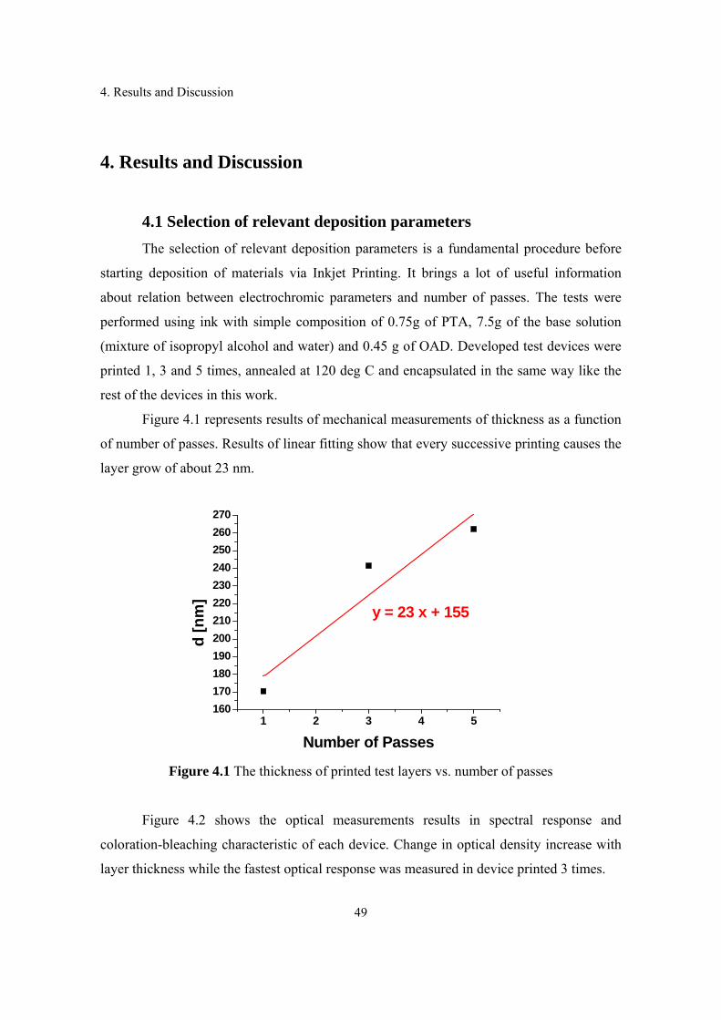
4. Results and Discussion
49
4. Results and Discussion
4.1 Selection of relevant deposition parameters The selection of relevant deposition parameters is a fundamental procedure before
starting deposition of materials via Inkjet Printing. It brings a lot of useful information
about relation between electrochromic parameters and number of passes. The tests were
performed using ink with simple composition of 0.75g of PTA, 7.5g of the base solution
(mixture of isopropyl alcohol and water) and 0.45 g of OAD. Developed test devices were
printed 1, 3 and 5 times, annealed at 120 deg C and encapsulated in the same way like the
rest of the devices in this work.
Figure 4.1 represents results of mechanical measurements of thickness as a function
of number of passes. Results of linear fitting show that every successive printing causes the
layer grow of about 23 nm.
1 2 3 4 5160170180190200210220230240250260270
y = 23 x + 155
d [n
m]
Number of Passes Figure 4.1 The thickness of printed test layers vs. number of passes
Figure 4.2 shows the optical measurements results in spectral response and
coloration-bleaching characteristic of each device. Change in optical density increase with
layer thickness while the fastest optical response was measured in device printed 3 times.
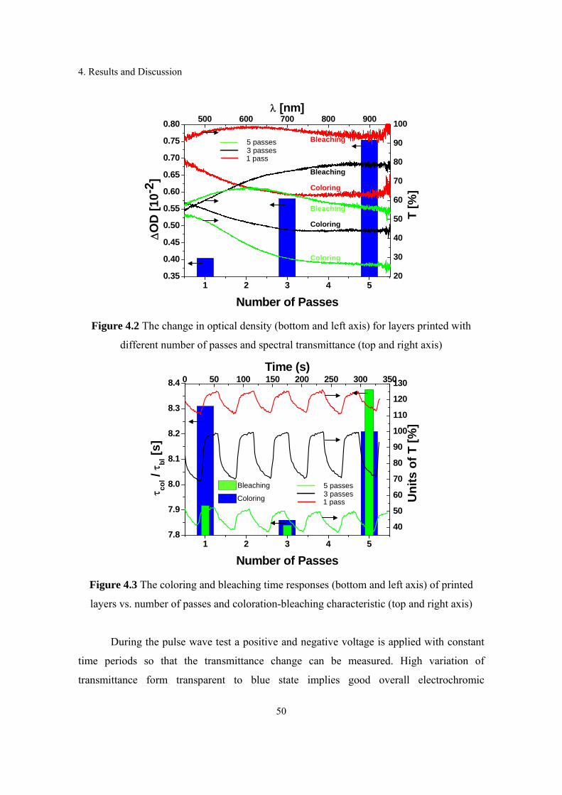
4. Results and Discussion
50
1 2 3 4 50.35
0.40
0.45
0.50
0.55
0.60
0.65
0.70
0.75
0.80
ΔO
D [1
0-2 ]
Number of Passes
500 600 700 800 900
20
30
40
50
60
70
80
90
100
T [%
]
λ [nm]
1 pass3 passes5 passes Bleaching
Coloring
Bleaching
Coloring
Bleaching
Coloring
Figure 4.2 The change in optical density (bottom and left axis) for layers printed with
different number of passes and spectral transmittance (top and right axis)
1 2 3 4 57.8
7.9
8.0
8.1
8.2
8.3
8.4
τ col /
τ bl [s
]
Number of Passes
0 50 100 150 200 250 300 350
40
50
60
70
80
90
100
110
120
130
Uni
ts o
f T [%
]
Time (s)
Coloring
Bleaching
1 pass3 passes5 passes
Figure 4.3 The coloring and bleaching time responses (bottom and left axis) of printed
layers vs. number of passes and coloration-bleaching characteristic (top and right axis)
During the pulse wave test a positive and negative voltage is applied with constant
time periods so that the transmittance change can be measured. High variation of
transmittance form transparent to blue state implies good overall electrochromic
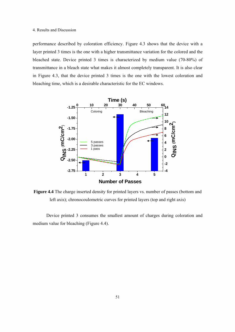
4. Results and Discussion
51
performance described by coloration efficiency. Figure 4.3 shows that the device with a
layer printed 3 times is the one with a higher transmittance variation for the colored and the
bleached state. Device printed 3 times is characterized by medium value (70-80%) of
transmittance in a bleach state what makes it almost completely transparent. It is also clear
in Figure 4.3, that the device printed 3 times is the one with the lowest coloration and
bleaching time, which is a desirable characteristic for the EC windows.
1 2 3 4 5-2.75
-2.50
-2.25
-2.00
-1.75
-1.50
-1.25
QIN
S (m
C/c
m2 )
Number of Passes
0 10 20 30 40 50 60
-4
-2
0
2
4
6
8
10
12
14
QIN
S (m
C/c
m2 )
Time (s)
1 pass3 passes5 passes
BleachingColoring
Figure 4.4 The charge inserted density for printed layers vs. number of passes (bottom and
left axis); chronocoulometric curves for printed layers (top and right axis)
Device printed 3 consumes the smallest amount of charges during coloration and
medium value for bleaching (Figure 4.4).
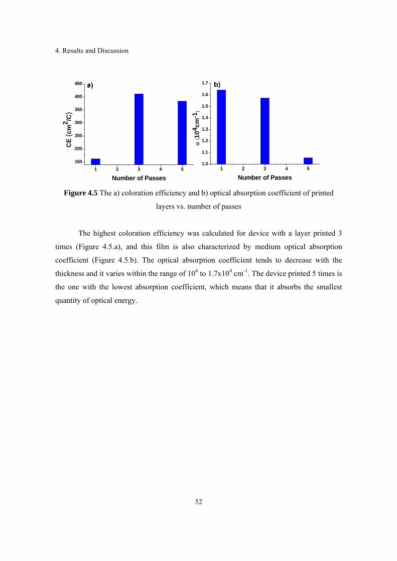
4. Results and Discussion
52
1 2 3 4 51.0
1.1
1.2
1.3
1.4
1.5
1.6
1.7
α (1
04cm
-1)
Number of Passes1 2 3 4 5
150
200
250
300
350
400
450
CE
(cm
2 /C)
Number of Passes Figure 4.5 The a) coloration efficiency and b) optical absorption coefficient of printed
layers vs. number of passes
The highest coloration efficiency was calculated for device with a layer printed 3
times (Figure 4.5.a), and this film is also characterized by medium optical absorption
coefficient (Figure 4.5.b). The optical absorption coefficient tends to decrease with the
thickness and it varies within the range of 104 to 1.7x104 cm-1. The device printed 5 times is
the one with the lowest absorption coefficient, which means that it absorbs the smallest
quantity of optical energy.
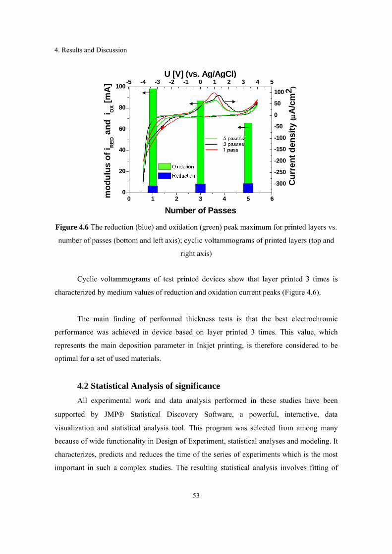
4. Results and Discussion
53
-5 -4 -3 -2 -1 0 1 2 3 4 5
-300
-250
-200
-150
-100
-50
0
50
100
Cur
rent
den
sity
(μA
/cm
2 )
U [V] (vs. Ag/AgCl)
0 1 2 3 4 5 60
20
40
60
80
100
mod
ulus
of i
RED
and
iO
X [mA
]
Number of Passes
Figure 4.6 The reduction (blue) and oxidation (green) peak maximum for printed layers vs.
number of passes (bottom and left axis); cyclic voltammograms of printed layers (top and
right axis)
Cyclic voltammograms of test printed devices show that layer printed 3 times is
characterized by medium values of reduction and oxidation current peaks (Figure 4.6).
The main finding of performed thickness tests is that the best electrochromic
performance was achieved in device based on layer printed 3 times. This value, which
represents the main deposition parameter in Inkjet printing, is therefore considered to be
optimal for a set of used materials.
4.2 Statistical Analysis of significance All experimental work and data analysis performed in these studies have been
supported by JMP® Statistical Discovery Software, a powerful, interactive, data
visualization and statistical analysis tool. This program was selected from among many
because of wide functionality in Design of Experiment, statistical analyses and modeling. It
characterizes, predicts and reduces the time of the series of experiments which is the most
important in such a complex studies. The resulting statistical analysis involves fitting of
4. Results and Discussion
54
mathematical equations to the experimental results to get the entire estimation of response
surface, and testing of all individual effect (factors) in a model for significance.
One of the basic tools in this scientific investigation is the regression analysis since
it enables the identification of functional relationship between independent and dependent
variables. In case of classical regression analysis both the variables are given as real
numbers, but for multiple regressions the purpose is to know more about the relationship
between several independent variables and a dependent variable. [56,57] In this case the
fitting principle is the same as the classical linear regression but the fit is five dimensions.
Table 4.1 and 4.2 list the composition of all mixtures designed using DOE for 30
devices. The marked rows represent devices excluded from the analysis due to low
measurement accuracy. The results of the measurements were divided for a five groups as
presented in section 3.1.
All ink compositions are presented using weight fractions (see also section 3.2):
wiso/water - base solution content;
wPTA - Peroxotungstic Acid content;
wOAD - Oxalic Acid content;
wTiO2 - amount of TiO2 nanoparticle dispersion;
wWOX - amount of WOX nanoparticle dispersion;
WOX - stoichiometry of tungsten oxide nanoparticles.
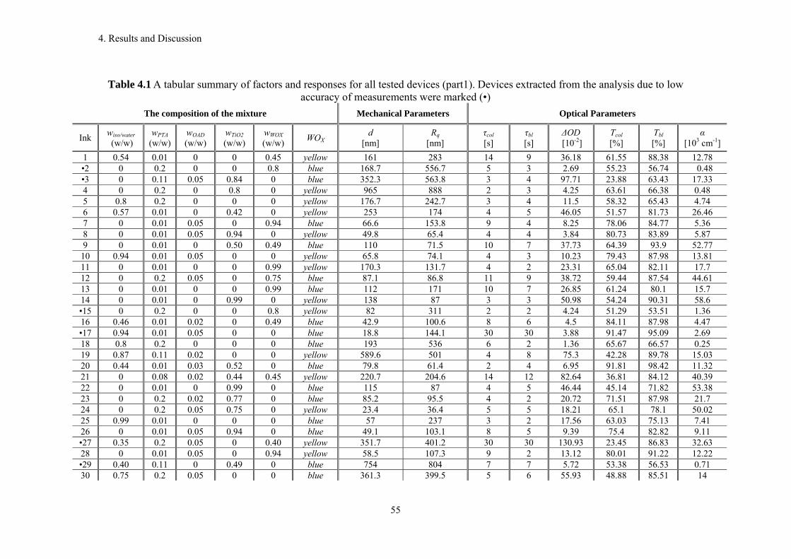
4. Results and Discussion
55
Table 4.1 A tabular summary of factors and responses for all tested devices (part1). Devices extracted from the analysis due to low accuracy of measurements were marked (•)
The composition of the mixture Mechanical Parameters Optical Parameters
Ink wiso/water (w/w)
wPTA (w/w)
wOAD (w/w)
wTiO2 (w/w)
wWOX (w/w) WOX d
[nm] Rq
[nm] τcol [s]
τbl [s]
ΔOD [10-2]
Tcol [%]
Tbl [%]
α [103 cm-1]
1 0.54 0.01 0 0 0.45 yellow 161 283 14 9 36.18 61.55 88.38 12.78 •2 0 0.2 0 0 0.8 blue 168.7 556.7 5 3 2.69 55.23 56.74 0.48 •3 0 0.11 0.05 0.84 0 blue 352.3 563.8 3 4 97.71 23.88 63.43 17.33 4 0 0.2 0 0.8 0 yellow 965 888 2 3 4.25 63.61 66.38 0.48 5 0.8 0.2 0 0 0 yellow 176.7 242.7 3 4 11.5 58.32 65.43 4.74 6 0.57 0.01 0 0.42 0 yellow 253 174 4 5 46.05 51.57 81.73 26.46 7 0 0.01 0.05 0 0.94 blue 66.6 153.8 9 4 8.25 78.06 84.77 5.36 8 0 0.01 0.05 0.94 0 yellow 49.8 65.4 4 4 3.84 80.73 83.89 5.87 9 0 0.01 0 0.50 0.49 blue 110 71.5 10 7 37.73 64.39 93.9 52.77
10 0.94 0.01 0.05 0 0 yellow 65.8 74.1 4 3 10.23 79.43 87.98 13.81 11 0 0.01 0 0 0.99 yellow 170.3 131.7 4 2 23.31 65.04 82.11 17.7 12 0 0.2 0.05 0 0.75 blue 87.1 86.8 11 9 38.72 59.44 87.54 44.61 13 0 0.01 0 0 0.99 blue 112 171 10 7 26.85 61.24 80.1 15.7 14 0 0.01 0 0.99 0 yellow 138 87 3 3 50.98 54.24 90.31 58.6 •15 0 0.2 0 0 0.8 yellow 82 311 2 2 4.24 51.29 53.51 1.36 16 0.46 0.01 0.02 0 0.49 blue 42.9 100.6 8 6 4.5 84.11 87.98 4.47 •17 0.94 0.01 0.05 0 0 blue 18.8 144.1 30 30 3.88 91.47 95.09 2.69 18 0.8 0.2 0 0 0 blue 193 536 6 2 1.36 65.67 66.57 0.25 19 0.87 0.11 0.02 0 0 yellow 589.6 501 4 8 75.3 42.28 89.78 15.03 20 0.44 0.01 0.03 0.52 0 blue 79.8 61.4 2 4 6.95 91.81 98.42 11.32 21 0 0.08 0.02 0.44 0.45 yellow 220.7 204.6 14 12 82.64 36.81 84.12 40.39 22 0 0.01 0 0.99 0 blue 115 87 4 5 46.44 45.14 71.82 53.38 23 0 0.2 0.02 0.77 0 blue 85.2 95.5 4 2 20.72 71.51 87.98 21.7 24 0 0.2 0.05 0.75 0 yellow 23.4 36.4 5 5 18.21 65.1 78.1 50.02 25 0.99 0.01 0 0 0 blue 57 237 3 2 17.56 63.03 75.13 7.41 26 0 0.01 0.05 0.94 0 blue 49.1 103.1 8 5 9.39 75.4 82.82 9.11 •27 0.35 0.2 0.05 0 0.40 yellow 351.7 401.2 30 30 130.93 23.45 86.83 32.63 28 0 0.01 0.05 0 0.94 yellow 58.5 107.3 9 2 13.12 80.01 91.22 12.22 •29 0.40 0.11 0 0.49 0 blue 754 804 7 7 5.72 53.38 56.53 0.71 30 0.75 0.2 0.05 0 0 blue 361.3 399.5 5 6 55.93 48.88 85.51 14
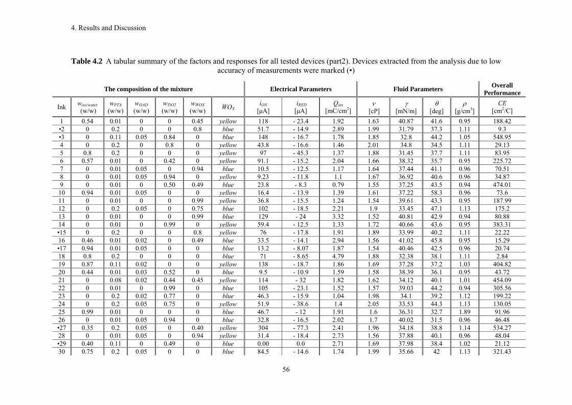
4. Results and Discussion
56
Table 4.2 A tabular summary of the factors and responses for all tested devices (part2). Devices extracted from the analysis due to low accuracy of measurements were marked (•)
The composition of the mixture Electrical Parameters Fluid Parameters Overall Performance
Ink wiso/water (w/w)
wPTA (w/w)
wOAD (w/w)
wTiO2 (w/w)
wWOX (w/w) WOX iOX
[μA] iRED [μA]
Qins [mC/cm2]
ν [cP]
γ [mN/m]
θ [deg]
ρ [g/cm3]
CE [cm2/C]
1 0.54 0.01 0 0 0.45 yellow 118 - 23.4 1.92 1.63 40.87 41.6 0.95 188.42 •2 0 0.2 0 0 0.8 blue 51.7 - 14.9 2.89 1.99 31.79 37.3 1.11 9.3 •3 0 0.11 0.05 0.84 0 blue 148 - 16.7 1.78 1.85 32.8 44.2 1.05 548.95 4 0 0.2 0 0.8 0 yellow 43.8 - 16.6 1.46 2.01 34.8 34.5 1.11 29.13 5 0.8 0.2 0 0 0 yellow 97 - 45.3 1.37 1.88 31.45 37.7 1.11 83.95 6 0.57 0.01 0 0.42 0 yellow 91.1 - 15.2 2.04 1.66 38.32 35.7 0.95 225.72 7 0 0.01 0.05 0 0.94 blue 10.5 - 12.5 1.17 1.64 37.44 41.1 0.96 70.51 8 0 0.01 0.05 0.94 0 yellow 9.23 - 11.8 1.1 1.67 36.92 40.6 0.96 34.87 9 0 0.01 0 0.50 0.49 blue 23.8 - 8.3 0.79 1.55 37.25 43.5 0.94 474.01
10 0.94 0.01 0.05 0 0 yellow 16.4 - 13.9 1.39 1.61 37.22 58.3 0.96 73.6 11 0 0.01 0 0 0.99 yellow 36.8 - 15.5 1.24 1.54 39.61 43.3 0.95 187.99 12 0 0.2 0.05 0 0.75 blue 102 - 18.5 2.21 1.9 33.45 47.1 1.13 175.2 13 0 0.01 0 0 0.99 blue 129 - 24 3.32 1.52 40.81 42.9 0.94 80.88 14 0 0.01 0 0.99 0 yellow 59.4 - 12.5 1.33 1.72 40.66 43.6 0.95 383.31 •15 0 0.2 0 0 0.8 yellow 76 - 17.8 1.91 1.89 33.99 40.2 1.11 22.22 16 0.46 0.01 0.02 0 0.49 blue 33.5 - 14.1 2.94 1.56 41.02 45.8 0.95 15.29 •17 0.94 0.01 0.05 0 0 blue 13.2 - 8.07 1.87 1.54 40.46 42.5 0.96 20.74 18 0.8 0.2 0 0 0 blue 71 - 8.65 4.79 1.88 32.38 38.1 1.11 2.84 19 0.87 0.11 0.02 0 0 yellow 138 - 18.7 1.86 1.69 37.28 37.2 1.03 404.82 20 0.44 0.01 0.03 0.52 0 blue 9.5 - 10.9 1.59 1.58 38.39 36.1 0.95 43.72 21 0 0.08 0.02 0.44 0.45 yellow 114 - 32 1.82 1.62 34.12 40.1 1.01 454.09 22 0 0.01 0 0.99 0 blue 105 - 23.1 1.52 1.57 39.03 44.2 0.94 305.56 23 0 0.2 0.02 0.77 0 blue 46.3 - 15.9 1.04 1.98 34.1 39.2 1.12 199.22 24 0 0.2 0.05 0.75 0 yellow 51.9 - 38.6 1.4 2.05 33.53 44.3 1.13 130.05 25 0.99 0.01 0 0 0 blue 46.7 - 12 1.91 1.6 36.31 32.7 1.89 91.96 26 0 0.01 0.05 0.94 0 blue 32.8 - 16.5 2.02 1.7 40.02 31.5 0.96 46.48 •27 0.35 0.2 0.05 0 0.40 yellow 304 - 77.3 2.41 1.96 34.18 38.8 1.14 534.27 28 0 0.01 0.05 0 0.94 yellow 31.4 - 18.4 2.73 1.56 37.88 40.1 0.96 48.04 •29 0.40 0.11 0 0.49 0 blue 0.00 0.0 2.71 1.69 37.98 38.4 1.02 21.12 30 0.75 0.2 0.05 0 0 blue 84.5 - 14.6 1.74 1.99 35.66 42 1.13 321.43
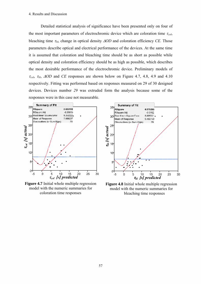
4. Results and Discussion
57
Detailed statistical analysis of significance have been presented only on four of
the most important parameters of electrochromic device which are coloration time τcol,
bleaching time τbl, change in optical density ΔOD and coloration efficiency CE. Those
parameters describe optical and electrical performance of the devices. At the same time
it is assumed that coloration and bleaching time should be as short as possible while
optical density and coloration efficiency should be as high as possible, which describes
the most desirable performance of the electrochromic device. Preliminary models of
τcol, τbl, ΔOD and CE responses are shown below on Figure 4.7, 4.8, 4.9 and 4.10
respectively. Fitting was performed based on responses measured on 29 of 30 designed
devices. Devices number 29 was extruded form the analysis because some of the
responses were in this case not measurable.
Figure 4.7 Initial whole multiple regression
model with the numeric summaries for coloration time responses
Figure 4.8 Initial whole multiple regression
model with the numeric summaries for bleaching time responses
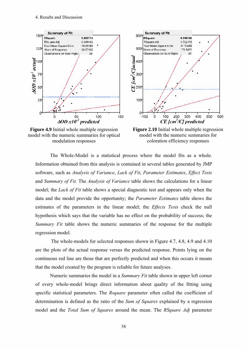
4. Results and Discussion
58
Figure 4.9 Initial whole multiple regression
model with the numeric summaries for optical modulation responses
Figure 2.10 Initial whole multiple regression
model with the numeric summaries for coloration efficiency responses
The Whole-Model is a statistical process where the model fits as a whole.
Information obtained from this analysis is contained in several tables generated by JMP
software, such as Analysis of Variance, Lack of Fit, Parameter Estimates, Effect Tests
and Summary of Fit. The Analysis of Variance table shows the calculations for a linear
model; the Lack of Fit table shows a special diagnostic test and appears only when the
data and the model provide the opportunity; the Parameter Estimates table shows the
estimates of the parameters in the linear model; the Effects Tests check the null
hypothesis which says that the variable has no effect on the probability of success; the
Summary Fit table shows the numeric summaries of the response for the multiple
regression model.
The whole-models for selected responses shown in Figure 4.7, 4.8, 4.9 and 4.10
are the plots of the actual response versus the predicted response. Points lying on the
continuous red line are those that are perfectly predicted and when this occurs it means
that the model created by the program is reliable for future analyses.
Numeric summaries the model in a Summary Fit table shown in upper left corner
of every whole-model brings direct information about quality of the fitting using
specific statistical parameters. The Rsquare parameter often called the coefficient of
determination is defined as the ratio of the Sum of Squares explained by a regression
model and the Total Sum of Squares around the mean. The RSquare Adj parameter

4. Results and Discussion
59
adjusts Rsquare in order to make it more comparable over models with different
numbers of parameters. The Root Mean Square Error estimates the standard deviation
of the random error. The Mean of Response is the overall mean of the response values.
It is especially important as a base model for prediction because all other models are
compared to this value. Finally the Observations (or Sum of Weights) are the number of
observations used in the fit. Since in this case the device number 29 is excluded, there
are 29 observations taken under account.
The RSquare parameter which shows the correlation between the actual and
predicted response of τcol, τbl, ΔOD and CE is 0.55, 0.57, 0.88 and 0.91 respectively
(RSquare =1 when there is a perfect fit, the errors are all zero). That suggests that all
those models would be more accurate if the points lying far from the correlation line
were excluded from analysis. It is also important to note the presence of negative values
for RSquare Adj of Figure 4.7 and 4.8, this can occur when there are few observations
and a lot of regressors, so there will be some useless regressors in the model that will
influence the parameter value.
In order to obtain more reliable and precise results it’s imperative to exclude
more points, than just device number 29. To obtain a better fit, the points extremely
distant from the line and from any other close point should be ignored, because they
don’t truly represent the model for these devices. When a point is excluded it means that
its data row is not taken under account for any analysis, but the point will still appear in
plots.
As can be seen in Figures 4.11 to 4.14, the most distant points (observations)
from the line of fit are 2, 3, 15, 17, and 27 therefore they are (including also device
number 29) excluded from further analysis. This operation provides significant
improvement in correlation between actual and predicted values of τcol, τbl, ΔOD and
CE which have from now on the values of 0.91, 0.95, 0.97 and 0.99 respectively.
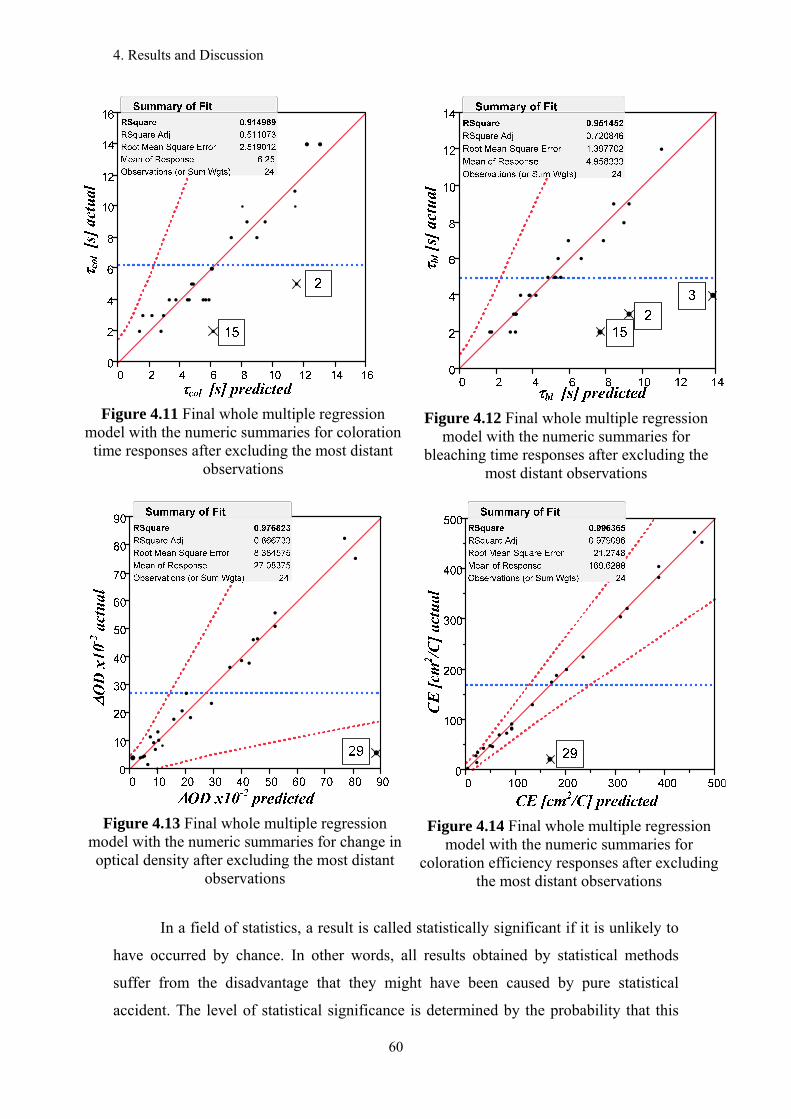
4. Results and Discussion
60
Figure 4.11 Final whole multiple regression
model with the numeric summaries for coloration time responses after excluding the most distant
observations
Figure 4.12 Final whole multiple regression model with the numeric summaries for
bleaching time responses after excluding the most distant observations
Figure 4.13 Final whole multiple regression
model with the numeric summaries for change in optical density after excluding the most distant
observations
Figure 4.14 Final whole multiple regression model with the numeric summaries for
coloration efficiency responses after excluding the most distant observations
In a field of statistics, a result is called statistically significant if it is unlikely to
have occurred by chance. In other words, all results obtained by statistical methods
suffer from the disadvantage that they might have been caused by pure statistical
accident. The level of statistical significance is determined by the probability that this
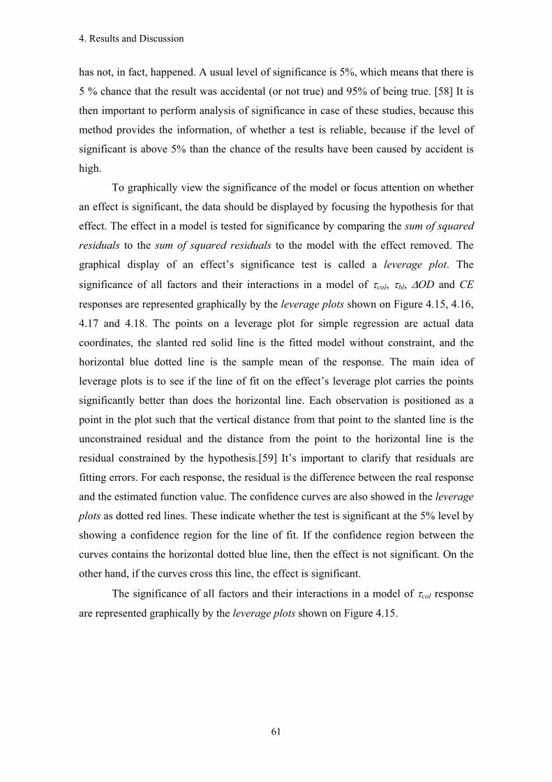
4. Results and Discussion
61
has not, in fact, happened. A usual level of significance is 5%, which means that there is
5 % chance that the result was accidental (or not true) and 95% of being true. [58] It is
then important to perform analysis of significance in case of these studies, because this
method provides the information, of whether a test is reliable, because if the level of
significant is above 5% than the chance of the results have been caused by accident is
high.
To graphically view the significance of the model or focus attention on whether
an effect is significant, the data should be displayed by focusing the hypothesis for that
effect. The effect in a model is tested for significance by comparing the sum of squared
residuals to the sum of squared residuals to the model with the effect removed. The
graphical display of an effect’s significance test is called a leverage plot. The
significance of all factors and their interactions in a model of τcol, τbl, ΔOD and CE
responses are represented graphically by the leverage plots shown on Figure 4.15, 4.16,
4.17 and 4.18. The points on a leverage plot for simple regression are actual data
coordinates, the slanted red solid line is the fitted model without constraint, and the
horizontal blue dotted line is the sample mean of the response. The main idea of
leverage plots is to see if the line of fit on the effect’s leverage plot carries the points
significantly better than does the horizontal line. Each observation is positioned as a
point in the plot such that the vertical distance from that point to the slanted line is the
unconstrained residual and the distance from the point to the horizontal line is the
residual constrained by the hypothesis.[59] It’s important to clarify that residuals are
fitting errors. For each response, the residual is the difference between the real response
and the estimated function value. The confidence curves are also showed in the leverage
plots as dotted red lines. These indicate whether the test is significant at the 5% level by
showing a confidence region for the line of fit. If the confidence region between the
curves contains the horizontal dotted blue line, then the effect is not significant. On the
other hand, if the curves cross this line, the effect is significant.
The significance of all factors and their interactions in a model of τcol response
are represented graphically by the leverage plots shown on Figure 4.15.

4. Results and Discussion
62
0.99wiso/water
0.990.01wPTA −
0.99w OAD
0.99w
2TiO
0.99wWOX
PTAiso/water ww ⋅ OADiso/water ww ⋅2TiOiso/water ww ⋅
XWOiso/water ww ⋅ Xiso/water WOw ⋅
OADPTA ww ⋅2TiOOAD ww ⋅
XOAD WOw ⋅XWOTiO ww
2⋅ XTiO WOw
2⋅ XWO WOw
X⋅
2TiOPTA ww ⋅XWOPTA ww ⋅ XWOwPTA ⋅
XWOOAD ww ⋅
Figure 4.15 Leverage plots of main effects and factors correlations for τcol response
Analysis of all leverage plots for τcol response regression leads to the conclusion
that the significant factor for this response is wWOX (Figure 4.15e) and interaction
between wiso/water and wWOX (Figure 4.15i);
The factor shrinkage on leverage plot measures how collinear the particular
factor is with the other factors. The factor shrinkage is obtained in Figure 4.15b and
4.15c what means that weight fraction of PTA and OAD are not linearly orthogonal to
the other factors. Those two factors shrink almost completely and have no independent
variation to support fitting τcol response variation. It means that the weight fractions of
PTA and OAD are an exact linear function of other factors. The shrinkage along the x
axis in a leverage plots makes an especially compelling picture, since it also portrays the
instability of the line of fit due to the collinearity. This phenomenon may translate into
high standard errors for the parameter estimates, because a small random error in the
narrow direction can have a huge effect on the slope of the correspondent fitting plane
[57].
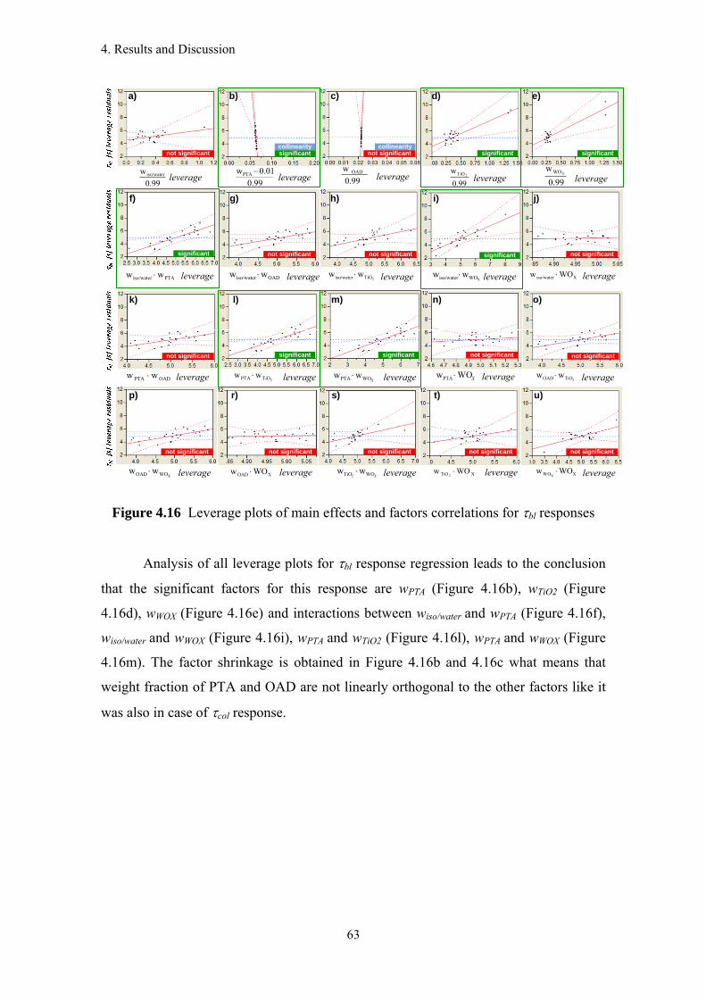
4. Results and Discussion
63
leverage leverage leverage leverage leverage
leverage leverage leverage leverage leverage
leverage leverage
leverage leverage leverage leverage leverage
leverage leverage leverage
a) b) c) d) e)
f) g) h) i) j)
k) l) m) n) o)
p) r) s) t) u)
significantcollinearity collinearity
significant
not significant
not significant not significant not significant
not significantnot significant
not significantnot significantnot significant
not significant
not significant not significant
significant significant
significant
significant significant
not significant
0.99wiso/water
0.990.01wPTA −
0.99w OAD
0.99w
2TiO
0.99wWOX
PTAiso/water ww ⋅ OADiso/water ww ⋅2TiOiso/water ww ⋅
XWOiso/water ww ⋅ Xiso/water WOw ⋅
OADPTA ww ⋅2TiOOAD ww ⋅
XOAD WOw ⋅XWOTiO ww
2⋅ XTiO WOw
2⋅ XWO WOw
X⋅
2TiOPTA ww ⋅XWOPTA ww ⋅ XWOwPTA ⋅
XWOOAD ww ⋅
Figure 4.16 Leverage plots of main effects and factors correlations for τbl responses
Analysis of all leverage plots for τbl response regression leads to the conclusion
that the significant factors for this response are wPTA (Figure 4.16b), wTiO2 (Figure
4.16d), wWOX (Figure 4.16e) and interactions between wiso/water and wPTA (Figure 4.16f),
wiso/water and wWOX (Figure 4.16i), wPTA and wTiO2 (Figure 4.16l), wPTA and wWOX (Figure
4.16m). The factor shrinkage is obtained in Figure 4.16b and 4.16c what means that
weight fraction of PTA and OAD are not linearly orthogonal to the other factors like it
was also in case of τcol response.
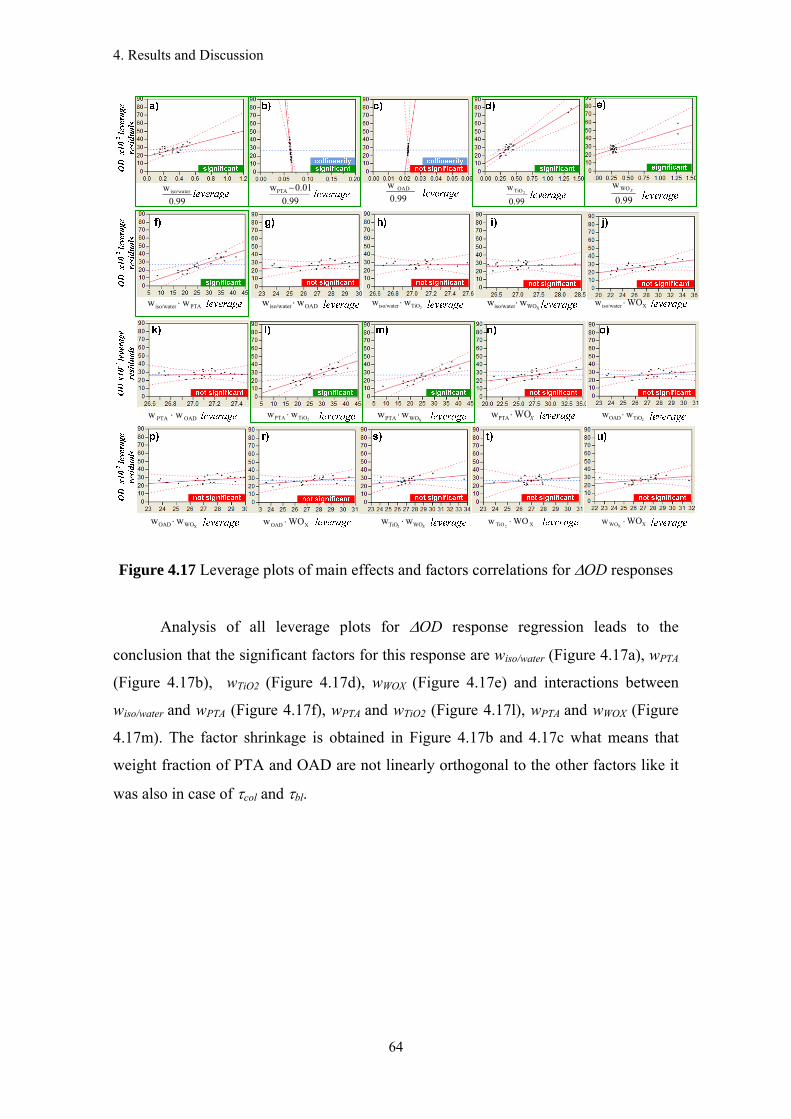
4. Results and Discussion
64
0.99wiso/water
0.990.01wPTA −
0.99w OAD
0.99w
2TiO
0.99wWOX
PTAiso/water ww ⋅ OADiso/water ww ⋅2TiOiso/water ww ⋅
XWOiso/water ww ⋅ Xiso/water WOw ⋅
OADPTA ww ⋅2TiOOAD ww ⋅
XOAD WOw ⋅XWOTiO ww
2⋅ XTiO WOw
2⋅ XWO WOw
X⋅
2TiOPTA ww ⋅XWOPTA ww ⋅ XWOwPTA ⋅
XWOOAD ww ⋅
Figure 4.17 Leverage plots of main effects and factors correlations for ΔOD responses
Analysis of all leverage plots for ΔOD response regression leads to the
conclusion that the significant factors for this response are wiso/water (Figure 4.17a), wPTA
(Figure 4.17b), wTiO2 (Figure 4.17d), wWOX (Figure 4.17e) and interactions between
wiso/water and wPTA (Figure 4.17f), wPTA and wTiO2 (Figure 4.17l), wPTA and wWOX (Figure
4.17m). The factor shrinkage is obtained in Figure 4.17b and 4.17c what means that
weight fraction of PTA and OAD are not linearly orthogonal to the other factors like it
was also in case of τcol and τbl.
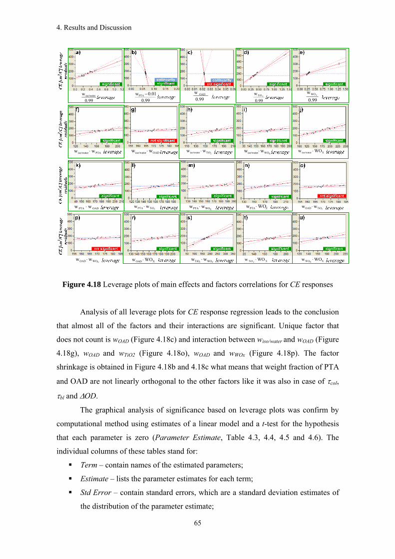
4. Results and Discussion
65
0.99wiso/water
0.990.01wPTA −
0.99w OAD
0.99w
2TiO
0.99wWOX
PTAiso/water ww ⋅ OADiso/water ww ⋅2TiOiso/water ww ⋅
XWOiso/water ww ⋅ Xiso/water WOw ⋅
OADPTA ww ⋅2TiOOAD ww ⋅
XOAD WOw ⋅XWOTiO ww
2⋅ XTiO WOw
2⋅ XWO WOw
X⋅
2TiOPTA ww ⋅XWOPTA ww ⋅ XWOwPTA ⋅
XWOOAD ww ⋅
Figure 4.18 Leverage plots of main effects and factors correlations for CE responses
Analysis of all leverage plots for CE response regression leads to the conclusion
that almost all of the factors and their interactions are significant. Unique factor that
does not count is wOAD (Figure 4.18c) and interaction between wiso/water and wOAD (Figure
4.18g), wOAD and wTiO2 (Figure 4.18o), wOAD and wWOx (Figure 4.18p). The factor
shrinkage is obtained in Figure 4.18b and 4.18c what means that weight fraction of PTA
and OAD are not linearly orthogonal to the other factors like it was also in case of τcol,
τbl and ΔOD.
The graphical analysis of significance based on leverage plots was confirm by
computational method using estimates of a linear model and a t-test for the hypothesis
that each parameter is zero (Parameter Estimate, Table 4.3, 4.4, 4.5 and 4.6). The
individual columns of these tables stand for:
Term – contain names of the estimated parameters;
Estimate – lists the parameter estimates for each term;
Std Error – contain standard errors, which are a standard deviation estimates of
the distribution of the parameter estimate;
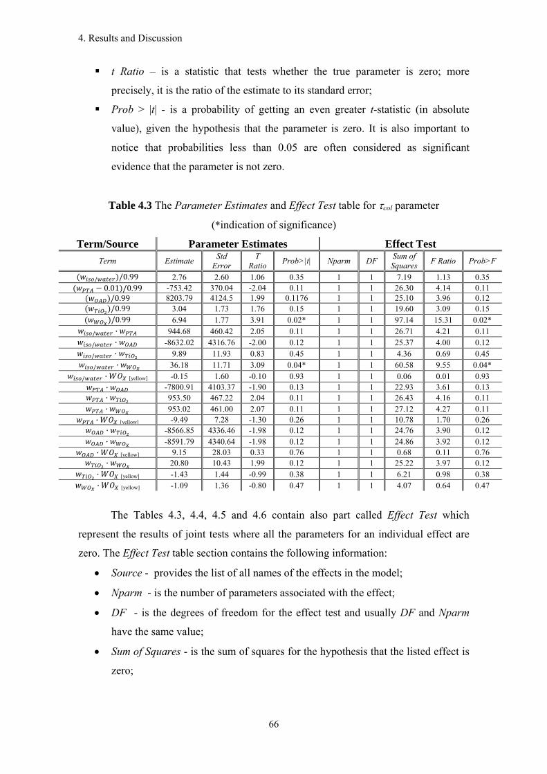
4. Results and Discussion
66
t Ratio – is a statistic that tests whether the true parameter is zero; more
precisely, it is the ratio of the estimate to its standard error;
Prob > |t| - is a probability of getting an even greater t-statistic (in absolute
value), given the hypothesis that the parameter is zero. It is also important to
notice that probabilities less than 0.05 are often considered as significant
evidence that the parameter is not zero.
Table 4.3 The Parameter Estimates and Effect Test table for τcol parameter
(*indication of significance)
Term/Source Parameter Estimates Effect Test Term Estimate Std
Error T
Ratio Prob>|t| Nparm DF Sum of Squares F Ratio Prob>F
/ /0.99 2.76 2.60 1.06 0.35 1 1 7.19 1.13 0.35 0.01 /0.99 -753.42 370.04 -2.04 0.11 1 1 26.30 4.14 0.11 /0.99 8203.79 4124.5 1.99 0.1176 1 1 25.10 3.96 0.12 /0.99 3.04 1.73 1.76 0.15 1 1 19.60 3.09 0.15 /0.99 6.94 1.77 3.91 0.02* 1 1 97.14 15.31 0.02*
/ · 944.68 460.42 2.05 0.11 1 1 26.71 4.21 0.11 / · -8632.02 4316.76 -2.00 0.12 1 1 25.37 4.00 0.12 / · 9.89 11.93 0.83 0.45 1 1 4.36 0.69 0.45
/ · 36.18 11.71 3.09 0.04* 1 1 60.58 9.55 0.04* / · [yellow] -0.15 1.60 -0.10 0.93 1 1 0.06 0.01 0.93
· -7800.91 4103.37 -1.90 0.13 1 1 22.93 3.61 0.13 · 953.50 467.22 2.04 0.11 1 1 26.43 4.16 0.11 · 953.02 461.00 2.07 0.11 1 1 27.12 4.27 0.11
· [yellow] -9.49 7.28 -1.30 0.26 1 1 10.78 1.70 0.26 · -8566.85 4336.46 -1.98 0.12 1 1 24.76 3.90 0.12 · -8591.79 4340.64 -1.98 0.12 1 1 24.86 3.92 0.12
· [yellow] 9.15 28.03 0.33 0.76 1 1 0.68 0.11 0.76 · 20.80 10.43 1.99 0.12 1 1 25.22 3.97 0.12
· [yellow] -1.43 1.44 -0.99 0.38 1 1 6.21 0.98 0.38 · [yellow] -1.09 1.36 -0.80 0.47 1 1 4.07 0.64 0.47
The Tables 4.3, 4.4, 4.5 and 4.6 contain also part called Effect Test which
represent the results of joint tests where all the parameters for an individual effect are
zero. The Effect Test table section contains the following information:
• Source - provides the list of all names of the effects in the model;
• Nparm - is the number of parameters associated with the effect;
• DF - is the degrees of freedom for the effect test and usually DF and Nparm
have the same value;
• Sum of Squares - is the sum of squares for the hypothesis that the listed effect is
zero;
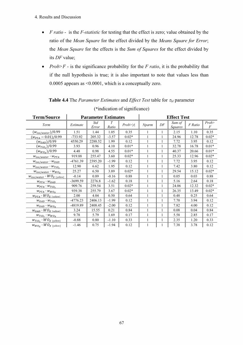
4. Results and Discussion
67
• F ratio - is the F-statistic for testing that the effect is zero; value obtained by the
ratio of the Mean Square for the effect divided by the Means Square for Error;
the Mean Square for the effects is the Sum of Squares for the effect divided by
its DF value;
• Prob>F - is the significance probability for the F ratio, it is the probability that
if the null hypothesis is true; it is also important to note that values less than
0.0005 appears as <0.0001, which is a conceptually zero.
Table 4.4 The Parameter Estimates and Effect Test table for τbl parameter
(*indication of significance)
Term/Source Parameter Estimates Effect Test Term Estimate Std
Error T
Ratio Prob>|t| Nparm DF Sum of Squares F Ratio Prob>
F / /0.99 1.51 1.44 1.05 0.35 1 1 2.15 1.10 0.35 0.01 /0.99 -733.92 205.32 -3.57 0.02* 1 1 24.96 12.78 0.02* /0.99 4550.29 2288.52 1.99 0.12 1 1 7.72 3.95 0.12 /0.99 3.93 0.96 4.10 0.01* 1 1 32.78 16.78 0.01* /0.99 4.48 0.98 4.55 0.01* 1 1 40.37 20.66 0.01*
/ · 919.88 255.47 3.60 0.02* 1 1 25.33 12.96 0.02* / · -4761.39 2395.20 -1.99 0.12 1 1 7.72 3.95 0.12 / · 12.90 6.62 1.95 0.12 1 1 7.42 3.80 0.12
/ · 25.27 6.50 3.89 0.02* 1 1 29.54 15.12 0.02* / · [yellow] -0.14 0.89 -0.16 0.88 1 1 0.05 0.03 0.88
· -3699.59 2276.8 -1.62 0.18 1 1 5.16 2.64 0.18 · 909.76 259.54 3.51 0.02* 1 1 24.06 12.32 0.02* · 939.38 255.79 3.67 0.02* 1 1 26.35 13.49 0.02*
· [yellow] 2.00 4.04 0.50 0.64 1 1 0.48 0.25 0.64 · -4776.23 2406.13 -1.99 0.12 1 1 7.70 3.94 0.12 · -4819.89 2408.45 -2.00 0.12 1 1 7.82 4.00 0.12
· [yellow] 3.24 15.55 0.21 0.84 1 1 0.08 0.04 0.84 · 9.78 5.79 1.69 0.17 1 1 5.58 2.85 0.17
· [yellow] -0.88 0.80 -1.10 0.33 1 1 2.35 1.20 0.33 · [yellow] -1.46 0.75 -1.94 0.12 1 1 7.38 3.78 0.12
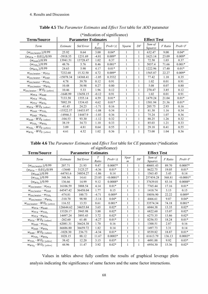
4. Results and Discussion
68
Table 4.5 The Parameter Estimates and Effect Test table for ΔOD parameter
(*indication of significance) Term/Source Parameter Estimates Effect Test
Term Estimate Std Error T Ratio Prob>|t| Nparm DF Sum of
Squares F Ratio Prob>F
/ /0.99 25.92 8.64 3.00 0.04* 1 1 632.47 9.00 0.04* 0.01 /0.99 -5918.35 1231.69 -4.81 0.009* 1 1 1623.14 23.09 0.009* /0.99 13941.51 13728.47 1.02 0.37 1 1 72.50 1.03 0.37 /0.99 48.76 5.76 8.46 0.001* 1 1 5037.4 71.66 0.001* /0.99 24.63 5.90 4.17 0.01* 1 1 1222.96 17.40 0.01*
/ · 7232.68 15.32.50 4.72 0.009* 1 1 1565.87 22.27 0.009* / · -15078.34 14368.41 -1.05 0.3532 1 1 77.42 1.10 0.35 / · 4.78 39.70 0.12 0.91 1 1 1.02 0.01 0.91
/ · 10.48 38.98 0.27 0.80 1 1 5.08 0.07 0.80 / · [yellow] 10.46 5.33 1.96 0.12 1 1 270.47 3.85 0.12
· -1648.99 13658.15 -0.12 0.91 1 1 1.02 0.01 0.91 · 7133.58 1555.14 4.59 0.01* 1 1 1479.24 21.04 0.01* · 7092.39 1534.43 4.62 0.01* 1 1 1501.94 21.36 0.01*
· [yellow] -41.45 24.23 -1.71 0.16 1 1 205.75 2.93 0.16 · -15522.57 14433.97 -1.08 0.34 1 1 81.30 1.16 0.34 · -14946.3 14447.9 -1.03 0.36 1 1 75.24 1.07 0.36
· [yellow] -104.53 93.30 -1.12 0.32 1 1 88.25 1.26 0.32 · 38.19 34.73 1.10 0.33 1 1 85.03 1.21 0.33
· [yellow] 3.09 4.81 0.64 0.55 1 1 29.18 0.41 0.55 · [yellow] 4.61 4.52 1.02 0.36 1 1 73.00 1.04 0.36
Table 4.6 The Parameter Estimates and Effect Test table for CE parameter (*indication of significance)
Term/Source Parameter Estimates Effect Test Term Estimate Std Error T
Ratio Prob>|t| Nparm DF Sum of
Squares F Ratio Prob>F
/ /0.99 207.71 21.93 9.47 0.0007* 1 1 40601.43 89.70 0.0007* 0.01 /0.99 -13640 3125.27 -4.36 0.01* 1 1 8622.75 19.05 0.01* /0.99 -64741.6 34834.27 -1.86 0.14 1 1 1563.45 3.45 0.14 /0.99 348.56 14.61 23.85 <0.0001* 1 1 257454.28 568.81 <0.0001* /0.99 136.66 14.99 9.12 0.0008* 1 1 37639.01 83.16 0.0008*
/ · 16106.59 3888.54 4.14 0.01* 1 1 7765.44 17.16 0.01* / · 64547.42 36458.04 1.77 0.15 1 1 1418.74 3.13 0.15 / · -474.81 100.73 -4.71 0.009* 1 1 10056.90 22.22 0.009*
/ · -310.70 98.90 -3.14 0.04* 1 1 4466.61 9.87 0.04* / · [yellow] 116.52 13.53 8.61 0.001* 1 1 33574.34 74.18 0.001*
· 126644.62 34655.84 3.65 0.02* 1 1 6044.38 13.35 0.02* · 15320.17 3945.98 3.88 0.02* 1 1 6822.60 15.07 0.02* · 14497.24 3893.43 3.72 0.02* 1 1 6275.35 13.86 0.02*
· [yellow] -262.60 61.48 -4.27 0.01* 1 1 8256.53 18.24 0.01* · 62081.31 36624.38 1.70 0.16 1 1 1300.51 2.87 0.16 · 66686.80 36659.72 1.82 0.14 1 1 1497.73 3.31 0.14
· [yellow] -1028.30 236.73 -4.34 0.01* 1 1 8539.82 18.87 0.01* · 1028.15 88.12 11.67 0.0003* 1 1 61613.79 136.13 0.0003*
· [yellow] 38.42 12.20 3.15 0.03* 1 1 4491.88 9.92 0.03* · [yellow] 44.96 11.47 3.92 0.02* 1 1 6954.30 15.36 0.02*
Values in tables above fully confirm the results of graphical leverage plots
analysis indicating the significance of same factors and the same factor interactions.
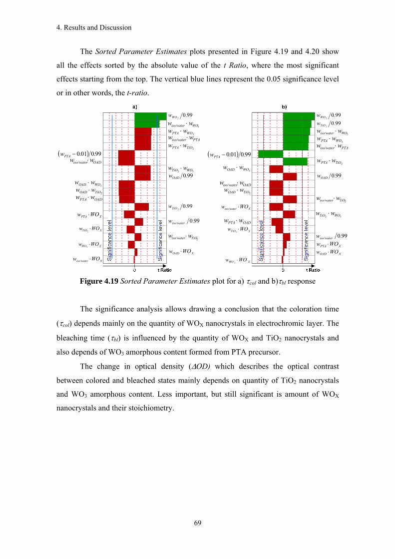
4. Results and Discussion
69
The Sorted Parameter Estimates plots presented in Figure 4.19 and 4.20 show
all the effects sorted by the absolute value of the t Ratio, where the most significant
effects starting from the top. The vertical blue lines represent the 0.05 significance level
or in other words, the t-ratio.
990.wiso/water
( ) 990010 ..wPTA −
9902
.wTiO
9903
.wWO
990.wOAD
2TiOOAD ww ⋅
XOAD WOw ⋅
32 WOTiO ww ⋅
XTiO WOw ⋅2
Xiso/water WOw ⋅
PTAiso/water ww ⋅
OADiso/water ww ⋅
2TiOiso/water ww ⋅
3WOiso/water ww ⋅
XWO WOw ⋅3
OADPTA ww ⋅
2TiOPTA ww ⋅
3WOPTA ww ⋅
XPTA WOw ⋅
3WOOAD ww ⋅
990.wiso/water
( ) 990010 ..wPTA −
9902
.wTiO
9903
.wWO
990.wOAD
2TiOOAD ww ⋅
XOAD WOw ⋅
32 WOTiO ww ⋅
XTiO WOw ⋅2
Xiso/water WOw ⋅
PTAiso/water ww ⋅
OADiso/water ww ⋅
2TiOiso/water ww ⋅
3WOiso/water ww ⋅
XWO WOw ⋅3
OADPTA ww ⋅
2TiOPTA ww ⋅
3WOPTA ww ⋅
XPTA WOw ⋅
3WOOAD ww ⋅
Figure 4.19 Sorted Parameter Estimates plot for a) τcol and b)τbl response
The significance analysis allows drawing a conclusion that the coloration time
(τcol) depends mainly on the quantity of WOX nanocrystals in electrochromic layer. The
bleaching time (τbl) is influenced by the quantity of WOX and TiO2 nanocrystals and
also depends of WO3 amorphous content formed from PTA precursor.
The change in optical density (ΔOD) which describes the optical contrast
between colored and bleached states mainly depends on quantity of TiO2 nanocrystals
and WO3 amorphous content. Less important, but still significant is amount of WOX
nanocrystals and their stoichiometry.
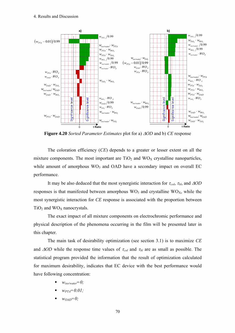
4. Results and Discussion
70
990.wiso/water
( ) 990010 ..wPTA −990
2.wTiO
9903
.wWO
990.wOAD
2TiOOAD ww ⋅
XOAD WOw ⋅
32 WOTiO ww ⋅
XTiO WOw ⋅2
Xiso/water WOw ⋅
PTAiso/water ww ⋅
OADiso/water ww ⋅
2TiOiso/water ww ⋅
3WOiso/water ww ⋅
XWO WOw ⋅3
OADPTA ww ⋅
2TiOPTA ww ⋅3WOPTA ww ⋅
XPTA WOw ⋅
3WOOAD ww ⋅
990.wiso/water
( ) 990010 ..wPTA −
9902
.wTiO
9903
.wWO
990.wOAD
2TiOOAD ww ⋅
XOAD WOw ⋅
32 WOTiO ww ⋅
XTiO WOw ⋅2
Xiso/water WOw ⋅
PTAiso/water ww ⋅
OADiso/water ww ⋅
2TiOiso/water ww ⋅
3WOiso/water ww ⋅
XWO WOw ⋅3
OADPTA ww ⋅
2TiOPTA ww ⋅
3WOPTA ww ⋅
XPTA WOw ⋅
3WOOAD ww ⋅
a) b)
0 t Ratio0 t Ratio
Figure 4.20 Sorted Parameter Estimates plot for a) ΔOD and b) CE response
The coloration efficiency (CE) depends to a greater or lesser extent on all the
mixture components. The most important are TiO2 and WOX crystalline nanoparticles,
while amount of amorphous WO3 and OAD have a secondary impact on overall EC
performance.
It may be also deduced that the most synergistic interaction for τcol, τbl, and ΔOD
responses is that manifested between amorphous WO3 and crystalline WOX, while the
most synergistic interaction for CE response is associated with the proportion between
TiO2 and WOX nanocrystals.
The exact impact of all mixture components on electrochromic performance and
physical description of the phenomena occurring in the film will be presented later in
this chapter.
The main task of desirability optimization (see section 3.1) is to maximize CE
and ΔOD while the response time values of τcol and τbl are as small as possible. The
statistical program provided the information that the result of optimization calculated
for maximum desirability, indicates that EC device with the best performance would
have following concentration:
wiso/water=0;
wPTA=0.01;
wOAD=0;
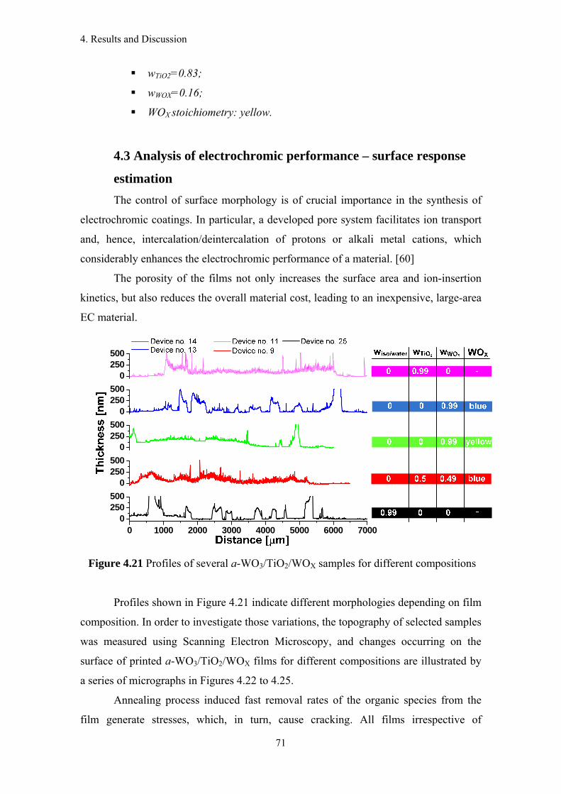
4. Results and Discussion
71
wTiO2=0.83;
wWOX=0.16;
WOX stoichiometry: yellow.
4.3 Analysis of electrochromic performance – surface response
estimation The control of surface morphology is of crucial importance in the synthesis of
electrochromic coatings. In particular, a developed pore system facilitates ion transport
and, hence, intercalation/deintercalation of protons or alkali metal cations, which
considerably enhances the electrochromic performance of a material. [60]
The porosity of the films not only increases the surface area and ion-insertion
kinetics, but also reduces the overall material cost, leading to an inexpensive, large-area
EC material.
0 1000 2000 3000 4000 5000 6000 70000
250500
0250500
0250500
0250500
0250500
Figure 4.21 Profiles of several a-WO3/TiO2/WOX samples for different compositions
Profiles shown in Figure 4.21 indicate different morphologies depending on film
composition. In order to investigate those variations, the topography of selected samples
was measured using Scanning Electron Microscopy, and changes occurring on the
surface of printed a-WO3/TiO2/WOX films for different compositions are illustrated by
a series of micrographs in Figures 4.22 to 4.25.
Annealing process induced fast removal rates of the organic species from the
film generate stresses, which, in turn, cause cracking. All films irrespective of
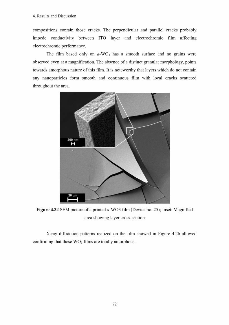
4. Results and Discussion
72
compositions contain those cracks. The perpendicular and parallel cracks probably
impede conductivity between ITO layer and electrochromic film affecting
electrochromic performance.
The film based only on a-WO3 has a smooth surface and no grains were
observed even at a magnification. The absence of a distinct granular morphology, points
towards amorphous nature of this film. It is noteworthy that layers which do not contain
any nanoparticles form smooth and continuous film with local cracks scattered
throughout the area.
Figure 4.22 SEM picture of a printed a-WO3 film (Device no. 25); Inset: Magnified
area showing layer cross-section
X-ray diffraction patterns realized on the film showed in Figure 4.26 allowed
confirming that these WO3 films are totally amorphous.
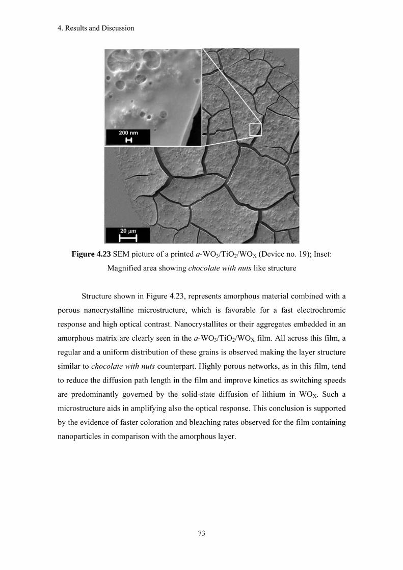
4. Results and Discussion
73
Figure 4.23 SEM picture of a printed a-WO3/TiO2/WOX (Device no. 19); Inset:
Magnified area showing chocolate with nuts like structure
Structure shown in Figure 4.23, represents amorphous material combined with a
porous nanocrystalline microstructure, which is favorable for a fast electrochromic
response and high optical contrast. Nanocrystallites or their aggregates embedded in an
amorphous matrix are clearly seen in the a-WO3/TiO2/WOX film. All across this film, a
regular and a uniform distribution of these grains is observed making the layer structure
similar to chocolate with nuts counterpart. Highly porous networks, as in this film, tend
to reduce the diffusion path length in the film and improve kinetics as switching speeds
are predominantly governed by the solid-state diffusion of lithium in WOX. Such a
microstructure aids in amplifying also the optical response. This conclusion is supported
by the evidence of faster coloration and bleaching rates observed for the film containing
nanoparticles in comparison with the amorphous layer.
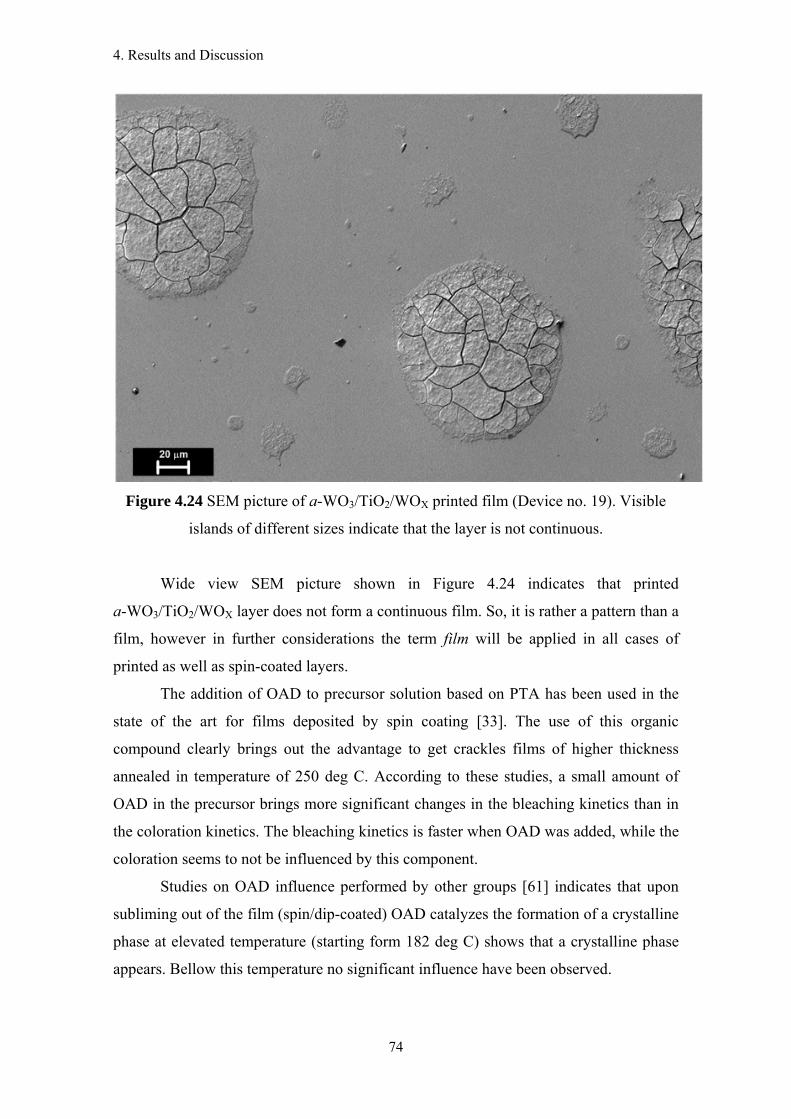
4. Results and Discussion
74
Figure 4.24 SEM picture of a-WO3/TiO2/WOX printed film (Device no. 19). Visible
islands of different sizes indicate that the layer is not continuous.
Wide view SEM picture shown in Figure 4.24 indicates that printed
a-WO3/TiO2/WOX layer does not form a continuous film. So, it is rather a pattern than a
film, however in further considerations the term film will be applied in all cases of
printed as well as spin-coated layers.
The addition of OAD to precursor solution based on PTA has been used in the
state of the art for films deposited by spin coating [33]. The use of this organic
compound clearly brings out the advantage to get crackles films of higher thickness
annealed in temperature of 250 deg C. According to these studies, a small amount of
OAD in the precursor brings more significant changes in the bleaching kinetics than in
the coloration kinetics. The bleaching kinetics is faster when OAD was added, while the
coloration seems to not be influenced by this component.
Studies on OAD influence performed by other groups [61] indicates that upon
subliming out of the film (spin/dip-coated) OAD catalyzes the formation of a crystalline
phase at elevated temperature (starting form 182 deg C) shows that a crystalline phase
appears. Bellow this temperature no significant influence have been observed.
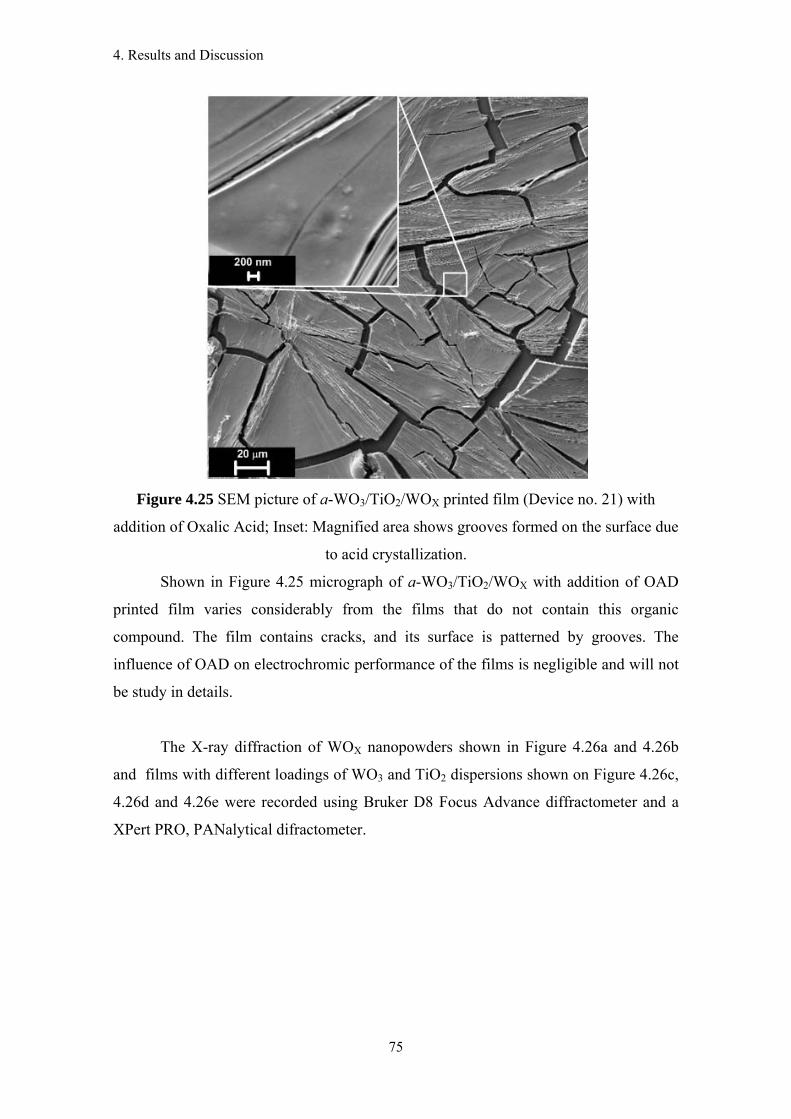
4. Results and Discussion
75
Figure 4.25 SEM picture of a-WO3/TiO2/WOX printed film (Device no. 21) with
addition of Oxalic Acid; Inset: Magnified area shows grooves formed on the surface due
to acid crystallization.
Shown in Figure 4.25 micrograph of a-WO3/TiO2/WOX with addition of OAD
printed film varies considerably from the films that do not contain this organic
compound. The film contains cracks, and its surface is patterned by grooves. The
influence of OAD on electrochromic performance of the films is negligible and will not
be study in details.
The X-ray diffraction of WOX nanopowders shown in Figure 4.26a and 4.26b
and films with different loadings of WO3 and TiO2 dispersions shown on Figure 4.26c,
4.26d and 4.26e were recorded using Bruker D8 Focus Advance diffractometer and a
XPert PRO, PANalytical difractometer.
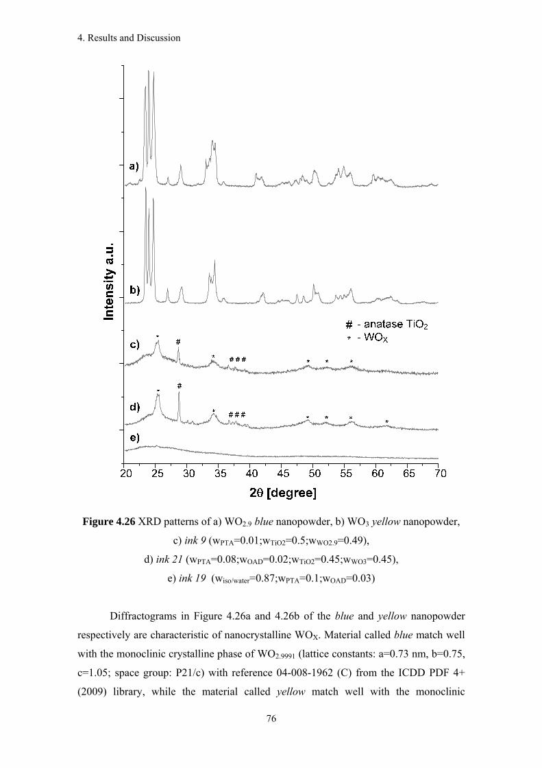
4. Results and Discussion
76
Figure 4.26 XRD patterns of a) WO2.9 blue nanopowder, b) WO3 yellow nanopowder,
c) ink 9 (wPTA=0.01;wTiO2=0.5;wWO2.9=0.49),
d) ink 21 (wPTA=0.08;wOAD=0.02;wTiO2=0.45;wWO3=0.45),
e) ink 19 (wiso/water=0.87;wPTA=0.1;wOAD=0.03)
Diffractograms in Figure 4.26a and 4.26b of the blue and yellow nanopowder
respectively are characteristic of nanocrystalline WOX. Material called blue match well
with the monoclinic crystalline phase of WO2.9991 (lattice constants: a=0.73 nm, b=0.75,
c=1.05; space group: P21/c) with reference 04-008-1962 (C) from the ICDD PDF 4+
(2009) library, while the material called yellow match well with the monoclinic
4. Results and Discussion
77
crystalline phase of WO3 (lattice constants: a=0.72 nm, b=0.75, c=0.76; space group:
P21/n) with reference 04-005-4272 (I) from the same library.
Figure 4.26e shows an amorphous PTA film spectrum which exhibits a broad
halo observed at 2θ∼26 degrees which is characteristic of the amorphous nature of WO3
films.
The XRD findings are augmented by SEM results. XRD patterns of films
presented in Figure 4.26c and 4.26d clearly indicate the presence of TiO2 and WOX
nanocrystals in a film.
Subsequent measurements relate to the optical properties of printed
a-WO3/TiO2/WOX films measured in situ as a working electrode in encapsulated device
filled with a gel electrolyte.
The quantity of the optical density indicates how much the transmittance of the
electrochromic layer reduces during the coloring process. The a-WOX films (upper
corner of ternary plots in Figure 4.28) are known to modulate their transmission
primarily by absorption while crystalline films (bottom part of ternary plots in Figure
4.28) exhibit a pronounced reflection in the NIR region [55]. Figure 4.27 shows that the
transmission modulation for the films a-WO3/TiO2/WOX.
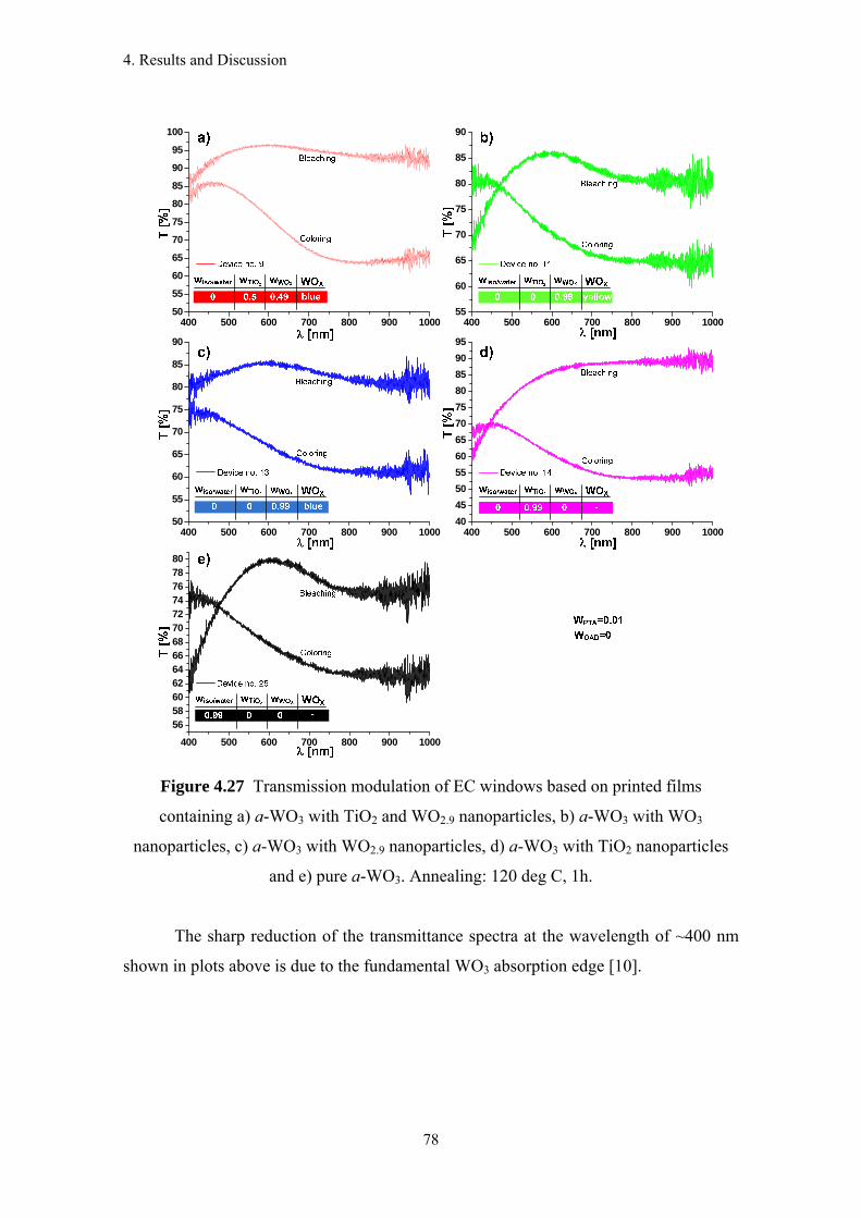
4. Results and Discussion
78
400 500 600 700 800 900 100050
55
60
65
70
75
80
85
90
400 500 600 700 800 900 1000404550556065707580859095
400 500 600 700 800 900 100055
60
65
70
75
80
85
90
400 500 600 700 800 900 100050
55
60
65
70
75
80
85
90
95
100
400 500 600 700 800 900 1000
56586062646668707274767880
Figure 4.27 Transmission modulation of EC windows based on printed films
containing a) a-WO3 with TiO2 and WO2.9 nanoparticles, b) a-WO3 with WO3
nanoparticles, c) a-WO3 with WO2.9 nanoparticles, d) a-WO3 with TiO2 nanoparticles
and e) pure a-WO3. Annealing: 120 deg C, 1h.
The sharp reduction of the transmittance spectra at the wavelength of ~400 nm
shown in plots above is due to the fundamental WO3 absorption edge [10].
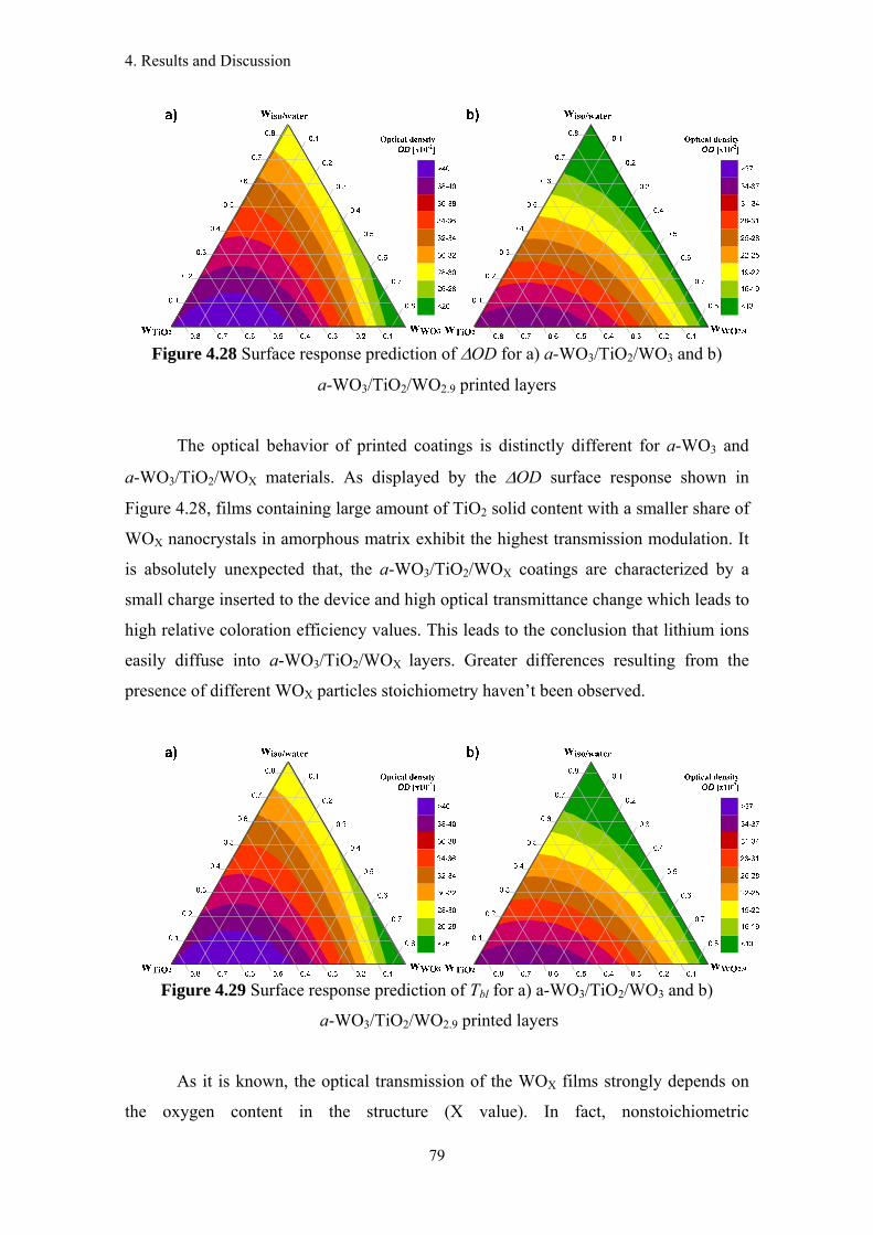
4. Results and Discussion
79
Figure 4.28 Surface response prediction of ΔOD for a) a-WO3/TiO2/WO3 and b)
a-WO3/TiO2/WO2.9 printed layers
The optical behavior of printed coatings is distinctly different for a-WO3 and
a-WO3/TiO2/WOX materials. As displayed by the ΔOD surface response shown in
Figure 4.28, films containing large amount of TiO2 solid content with a smaller share of
WOX nanocrystals in amorphous matrix exhibit the highest transmission modulation. It
is absolutely unexpected that, the a-WO3/TiO2/WOX coatings are characterized by a
small charge inserted to the device and high optical transmittance change which leads to
high relative coloration efficiency values. This leads to the conclusion that lithium ions
easily diffuse into a-WO3/TiO2/WOX layers. Greater differences resulting from the
presence of different WOX particles stoichiometry haven’t been observed.
Figure 4.29 Surface response prediction of Tbl for a) a-WO3/TiO2/WO3 and b)
a-WO3/TiO2/WO2.9 printed layers
As it is known, the optical transmission of the WOX films strongly depends on
the oxygen content in the structure (X value). In fact, nonstoichiometric
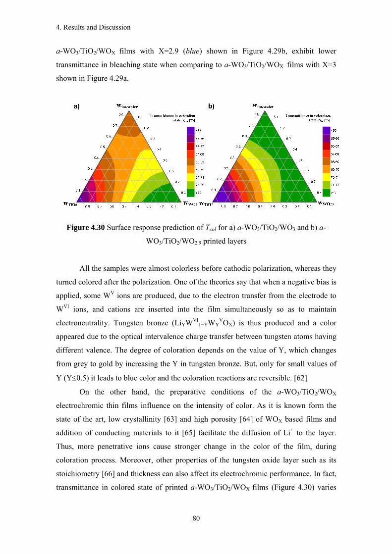
4. Results and Discussion
80
a-WO3/TiO2/WOX films with X=2.9 (blue) shown in Figure 4.29b, exhibit lower
transmittance in bleaching state when comparing to a-WO3/TiO2/WOX films with X=3
shown in Figure 4.29a.
Figure 4.30 Surface response prediction of Tcol for a) a-WO3/TiO2/WO3 and b) a-
WO3/TiO2/WO2.9 printed layers
All the samples were almost colorless before cathodic polarization, whereas they
turned colored after the polarization. One of the theories say that when a negative bias is
applied, some WV ions are produced, due to the electron transfer from the electrode to
WVI ions, and cations are inserted into the film simultaneously so as to maintain
electroneutrality. Tungsten bronze (LiYWVI1−YWY
VOX) is thus produced and a color
appeared due to the optical intervalence charge transfer between tungsten atoms having
different valence. The degree of coloration depends on the value of Y, which changes
from grey to gold by increasing the Y in tungsten bronze. But, only for small values of
Y (Y≤0.5) it leads to blue color and the coloration reactions are reversible. [62]
On the other hand, the preparative conditions of the a-WO3/TiO2/WOX
electrochromic thin films influence on the intensity of color. As it is known form the
state of the art, low crystallinity [63] and high porosity [64] of WOX based films and
addition of conducting materials to it [65] facilitate the diffusion of Li+ to the layer.
Thus, more penetrative ions cause stronger change in the color of the film, during
coloration process. Moreover, other properties of the tungsten oxide layer such as its
stoichiometry [66] and thickness can also affect its electrochromic performance. In fact,
transmittance in colored state of printed a-WO3/TiO2/WOX films (Figure 4.30) varies
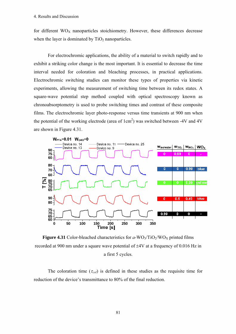
4. Results and Discussion
81
for different WOX nanoparticles stoichiometry. However, these differences decrease
when the layer is dominated by TiO2 nanoparticles.
For electrochromic applications, the ability of a material to switch rapidly and to
exhibit a striking color change is the most important. It is essential to decrease the time
interval needed for coloration and bleaching processes, in practical applications.
Electrochromic switching studies can monitor these types of properties via kinetic
experiments, allowing the measurement of switching time between its redox states. A
square-wave potential step method coupled with optical spectroscopy known as
chronoabsorptometry is used to probe switching times and contrast of these composite
films. The electrochromic layer photo-response versus time transients at 900 nm when
the potential of the working electrode (area of 1cm2) was switched between -4V and 4V
are shown in Figure 4.31.
0 50 100 150 200 250 300 35060657075
8090
65707580607080
607590
Figure 4.31 Color-bleached characteristics for a-WO3/TiO2/WOX printed films
recorded at 900 nm under a square wave potential of ±4V at a frequency of 0.016 Hz in
a first 5 cycles.
The coloration time (τcol) is defined in these studies as the requisite time for
reduction of the device’s transmittance to 80% of the final reduction.
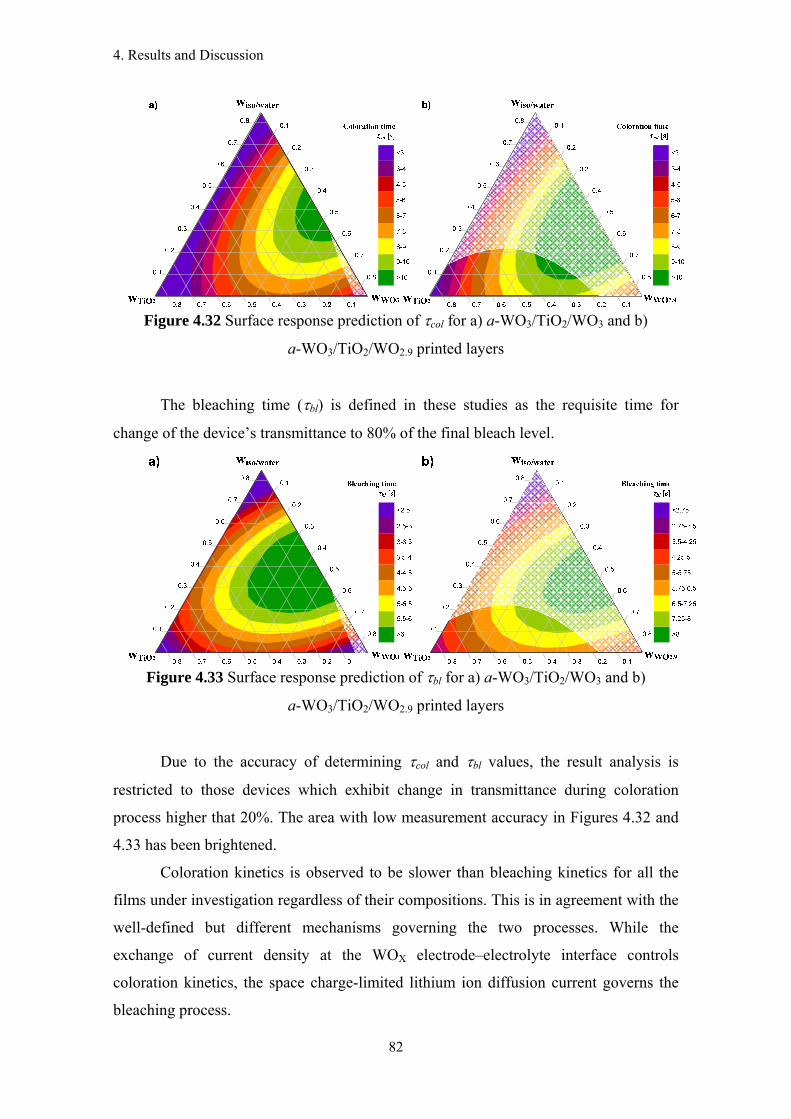
4. Results and Discussion
82
Figure 4.32 Surface response prediction of τcol for a) a-WO3/TiO2/WO3 and b)
a-WO3/TiO2/WO2.9 printed layers
The bleaching time (τbl) is defined in these studies as the requisite time for
change of the device’s transmittance to 80% of the final bleach level.
Figure 4.33 Surface response prediction of τbl for a) a-WO3/TiO2/WO3 and b)
a-WO3/TiO2/WO2.9 printed layers
Due to the accuracy of determining τcol and τbl values, the result analysis is
restricted to those devices which exhibit change in transmittance during coloration
process higher that 20%. The area with low measurement accuracy in Figures 4.32 and
4.33 has been brightened.
Coloration kinetics is observed to be slower than bleaching kinetics for all the
films under investigation regardless of their compositions. This is in agreement with the
well-defined but different mechanisms governing the two processes. While the
exchange of current density at the WOX electrode–electrolyte interface controls
coloration kinetics, the space charge-limited lithium ion diffusion current governs the
bleaching process.
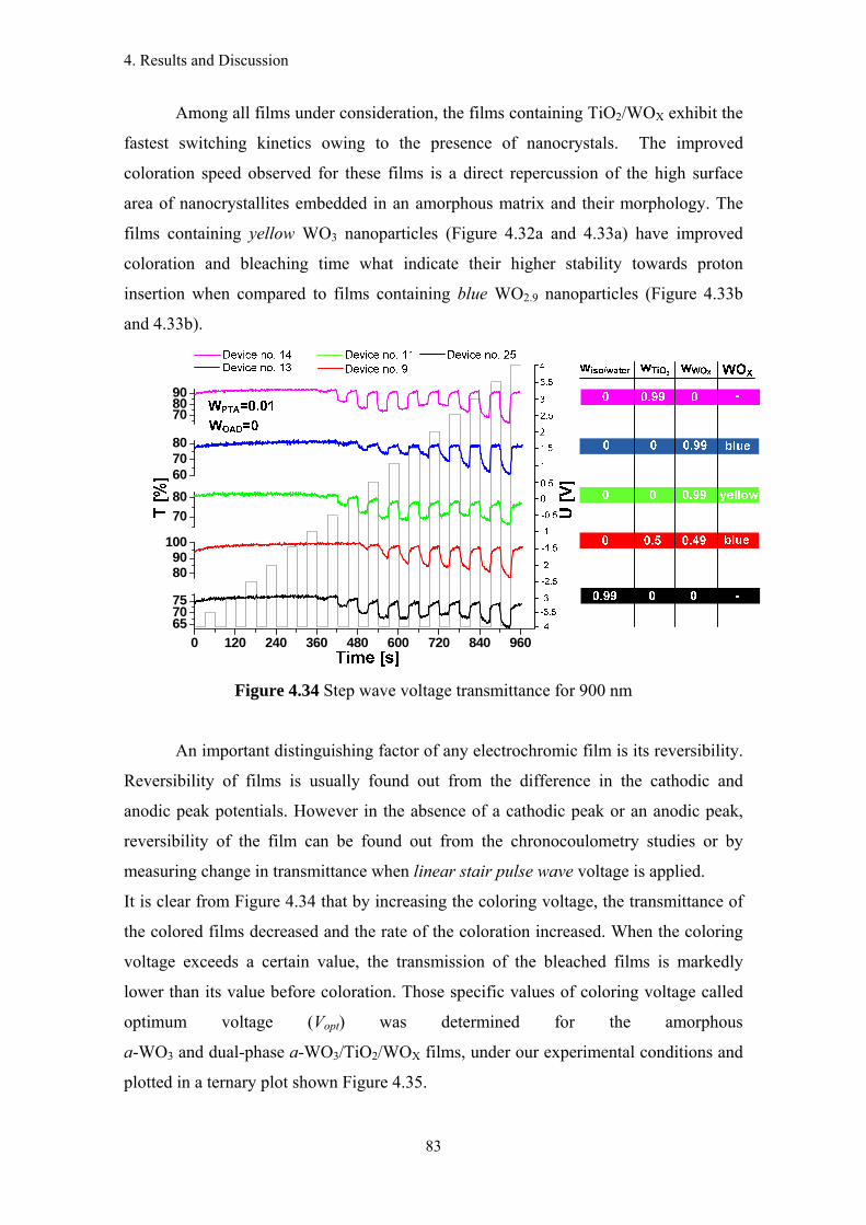
4. Results and Discussion
83
Among all films under consideration, the films containing TiO2/WOX exhibit the
fastest switching kinetics owing to the presence of nanocrystals. The improved
coloration speed observed for these films is a direct repercussion of the high surface
area of nanocrystallites embedded in an amorphous matrix and their morphology. The
films containing yellow WO3 nanoparticles (Figure 4.32a and 4.33a) have improved
coloration and bleaching time what indicate their higher stability towards proton
insertion when compared to films containing blue WO2.9 nanoparticles (Figure 4.33b
and 4.33b).
0 120 240 360 480 600 720 840 960657075
8090
100
7080607080
708090
Figure 4.34 Step wave voltage transmittance for 900 nm
An important distinguishing factor of any electrochromic film is its reversibility.
Reversibility of films is usually found out from the difference in the cathodic and
anodic peak potentials. However in the absence of a cathodic peak or an anodic peak,
reversibility of the film can be found out from the chronocoulometry studies or by
measuring change in transmittance when linear stair pulse wave voltage is applied.
It is clear from Figure 4.34 that by increasing the coloring voltage, the transmittance of
the colored films decreased and the rate of the coloration increased. When the coloring
voltage exceeds a certain value, the transmission of the bleached films is markedly
lower than its value before coloration. Those specific values of coloring voltage called
optimum voltage (Vopt) was determined for the amorphous
a-WO3 and dual-phase a-WO3/TiO2/WOX films, under our experimental conditions and
plotted in a ternary plot shown Figure 4.35.
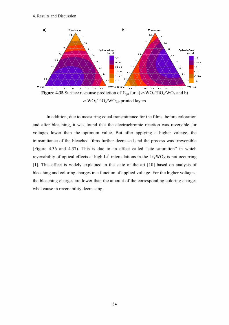
4. Results and Discussion
84
Figure 4.35 Surface response prediction of Vopt for a) a-WO3/TiO2/WO3 and b)
a-WO3/TiO2/WO2.9 printed layers
In addition, due to measuring equal transmittance for the films, before coloration
and after bleaching, it was found that the electrochromic reaction was reversible for
voltages lower than the optimum value. But after applying a higher voltage, the
transmittance of the bleached films further decreased and the process was irreversible
(Figure 4.36 and 4.37). This is due to an effect called “site saturation” in which
reversibility of optical effects at high Li+ intercalations in the LiYWOX is not occurring
[1]. This effect is widely explained in the state of the art [10] based on analysis of
bleaching and coloring charges in a function of applied voltage. For the higher voltages,
the bleaching charges are lower than the amount of the corresponding coloring charges
what cause in reversibility decreasing.
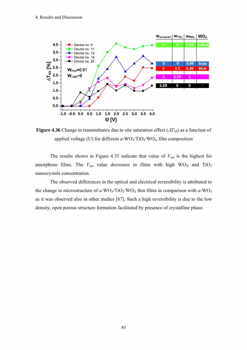
4. Results and Discussion
85
T SS
[%]
-1.0 -0.5 0.0 0.5 1.0 1.5 2.0 2.5 3.0 3.5 4.0
0.0
0.5
1.0
1.5
2.0
2.5
3.0
3.5
4.0
Figure 4.36 Change in transmittance due to site saturation effect (ΔTSS) as a function of
applied voltage (U) for different a-WO3/TiO2/WOX film composition
The results shown in Figure 4.35 indicate that value of Vopt is the highest for
amorphous films. The Vopt value decreases in films with high WOX and TiO2
nanocrystals concentration.
The observed differences in the optical and electrical reversibility is attributed to
the change in microstructure of a-WO3/TiO2/WOX thin films in comparison with a-WO3
as it was observed also in other studies [67]. Such a high reversibility is due to the low
density, open porous structure formation facilitated by presence of crystalline phase.
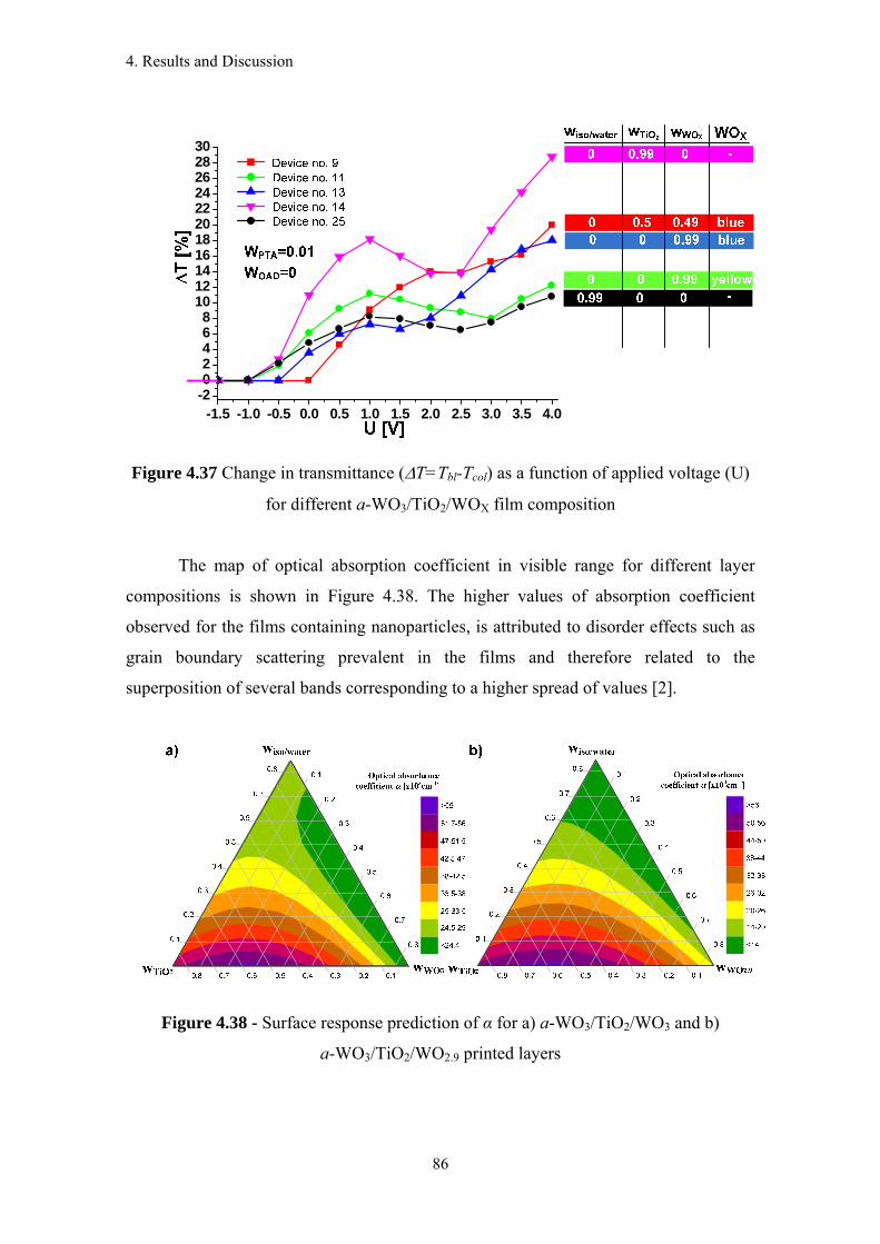
4. Results and Discussion
86
-1.5 -1.0 -0.5 0.0 0.5 1.0 1.5 2.0 2.5 3.0 3.5 4.0-202468
1012141618202224262830
Figure 4.37 Change in transmittance (ΔT=Tbl-Tcol) as a function of applied voltage (U)
for different a-WO3/TiO2/WOX film composition
The map of optical absorption coefficient in visible range for different layer
compositions is shown in Figure 4.38. The higher values of absorption coefficient
observed for the films containing nanoparticles, is attributed to disorder effects such as
grain boundary scattering prevalent in the films and therefore related to the
superposition of several bands corresponding to a higher spread of values [2].
Figure 4.38 - Surface response prediction of α for a) a-WO3/TiO2/WO3 and b)
a-WO3/TiO2/WO2.9 printed layers
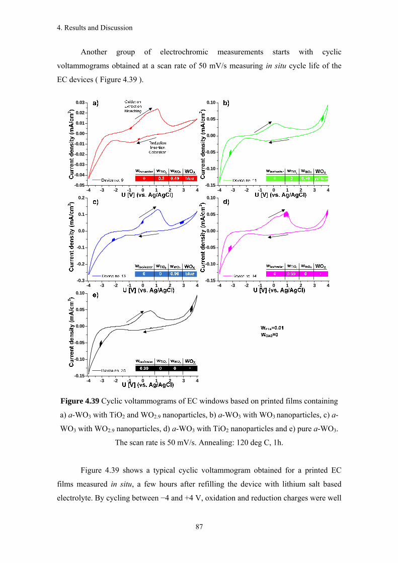
4. Results and Discussion
87
Another group of electrochromic measurements starts with cyclic
voltammograms obtained at a scan rate of 50 mV/s measuring in situ cycle life of the
EC devices ( Figure 4.39 ).
-4 -3 -2 -1 0 1 2 3 4-0.05
-0.04
-0.03
-0.02
-0.01
0.00
0.01
0.02
0.03
-4 -3 -2 -1 0 1 2 3 4-0.15
-0.10
-0.05
0.00
0.05
0.10
-4 -3 -2 -1 0 1 2 3 4-0.3
-0.2
-0.1
0.0
0.1
0.2
-4 -3 -2 -1 0 1 2 3 4-0.15
-0.10
-0.05
0.00
0.05
0.10
-4 -3 -2 -1 0 1 2 3 4-0.15
-0.10
-0.05
0.00
0.05
0.10
Figure 4.39 Cyclic voltammograms of EC windows based on printed films containing
a) a-WO3 with TiO2 and WO2.9 nanoparticles, b) a-WO3 with WO3 nanoparticles, c) a-
WO3 with WO2.9 nanoparticles, d) a-WO3 with TiO2 nanoparticles and e) pure a-WO3.
The scan rate is 50 mV/s. Annealing: 120 deg C, 1h.
Figure 4.39 shows a typical cyclic voltammogram obtained for a printed EC
films measured in situ, a few hours after refilling the device with lithium salt based
electrolyte. By cycling between −4 and +4 V, oxidation and reduction charges were well
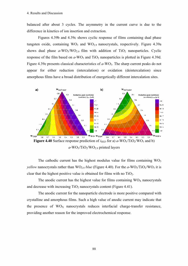
4. Results and Discussion
88
balanced after about 3 cycles. The asymmetry in the current curve is due to the
difference in kinetics of ion insertion and extraction.
Figures 4.39b and 4.39c shows cyclic response of films containing dual phase
tungsten oxide, containing WO3 and WO2.9 nanocrystals, respectively. Figure 4.39a
shows dual phase a-WO3/WO2.9 film with addition of TiO2 nanoparticles. Cyclic
response of the film based on a-WO3 and TiO2 nanoparticles is plotted in Figure 4.39d.
Figure 4.39e presents classical characteristics of a-WO3. The sharp current peaks do not
appear for either reduction (intercalation) or oxidation (deintercalation) since
amorphous films have a broad distribution of energetically different intercalation sites.
Figure 4.40 Surface response prediction of iRED for a) a-WO3/TiO2/WO3 and b)
a-WO3/TiO2/WO2.9 printed layers
The cathodic current has the highest modulus value for films containing WO3
yellow nanocrystals rather than WO2.9 blue (Figure 4.40). For the a-WO3/TiO2/WO3 it is
clear that the highest positive value is obtained for films with no TiO2.
The anodic current has the highest value for films containing WOX nanocrystals
and decrease with increasing TiO2 nanocrystals content (Figure 4.41).
The anodic current for the nanoparticle electrode is more positive compared with
crystalline and amorphous films. Such a high value of anodic current may indicate that
the presence of WOX nanocrystals reduces interfacial charge-transfer resistance,
providing another reason for the improved electrochemical response.
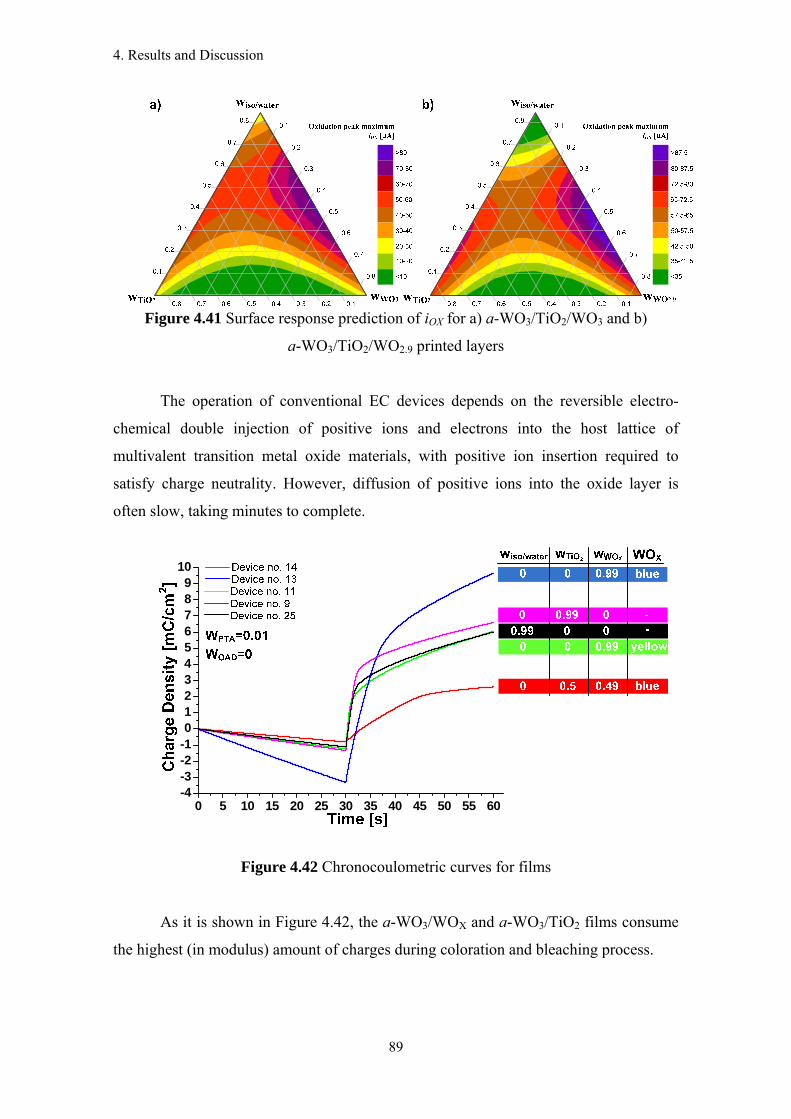
4. Results and Discussion
89
Figure 4.41 Surface response prediction of iOX for a) a-WO3/TiO2/WO3 and b)
a-WO3/TiO2/WO2.9 printed layers
The operation of conventional EC devices depends on the reversible electro-
chemical double injection of positive ions and electrons into the host lattice of
multivalent transition metal oxide materials, with positive ion insertion required to
satisfy charge neutrality. However, diffusion of positive ions into the oxide layer is
often slow, taking minutes to complete.
0 5 10 15 20 25 30 35 40 45 50 55 60-4-3-2-10123456789
10
Figure 4.42 Chronocoulometric curves for films
As it is shown in Figure 4.42, the a-WO3/WOX and a-WO3/TiO2 films consume
the highest (in modulus) amount of charges during coloration and bleaching process.
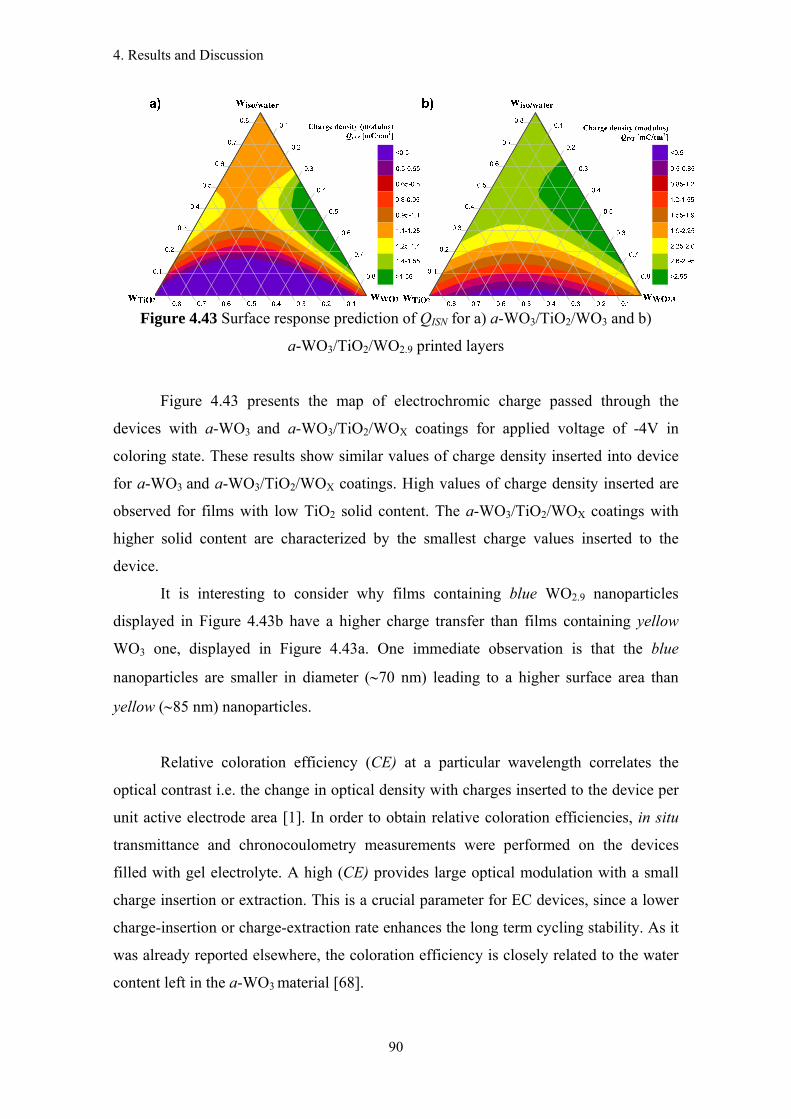
4. Results and Discussion
90
Figure 4.43 Surface response prediction of QISN for a) a-WO3/TiO2/WO3 and b)
a-WO3/TiO2/WO2.9 printed layers
Figure 4.43 presents the map of electrochromic charge passed through the
devices with a-WO3 and a-WO3/TiO2/WOX coatings for applied voltage of -4V in
coloring state. These results show similar values of charge density inserted into device
for a-WO3 and a-WO3/TiO2/WOX coatings. High values of charge density inserted are
observed for films with low TiO2 solid content. The a-WO3/TiO2/WOX coatings with
higher solid content are characterized by the smallest charge values inserted to the
device.
It is interesting to consider why films containing blue WO2.9 nanoparticles
displayed in Figure 4.43b have a higher charge transfer than films containing yellow
WO3 one, displayed in Figure 4.43a. One immediate observation is that the blue
nanoparticles are smaller in diameter (∼70 nm) leading to a higher surface area than
yellow (∼85 nm) nanoparticles.
Relative coloration efficiency (CE) at a particular wavelength correlates the
optical contrast i.e. the change in optical density with charges inserted to the device per
unit active electrode area [1]. In order to obtain relative coloration efficiencies, in situ
transmittance and chronocoulometry measurements were performed on the devices
filled with gel electrolyte. A high (CE) provides large optical modulation with a small
charge insertion or extraction. This is a crucial parameter for EC devices, since a lower
charge-insertion or charge-extraction rate enhances the long term cycling stability. As it
was already reported elsewhere, the coloration efficiency is closely related to the water
content left in the a-WO3 material [68].

4. Results and Discussion
91
Most of the literature data for CE lie in the visible range of the spectrum. At the
same time, stress has been laid on the fact that preparation techniques as well as post-
annealing effects play a vital role in the tuning of the electrochemical properties [69].
According to the state of the art, CE of sol-gel deposited films increases after
application of heat treatment [12,43]. However this rule does not apply for films
deposited by dip-coating wherein CE reduces during heating because of densification of
the film [69].
Figure 4.44 Surface response prediction of CE for a) a-WO3/TiO2/WO3 and b)
a-WO3/TiO2/WO2.9 printed layers
Observed electrochromic devices based on TiO2/WOX nanocrystals
interconnected by amorphous phase leads to higher values of coloration efficiency over
the visible and region as compared to the poor electrochromic performance of
amorphous and non-porous layers.
The TiO2 and WOX solid content impact on CE value illustrated in Figure 4.44
indicates that the highest values of CE above 400 cm2/C can be obtained using those
two nanocrystalline components in conjunction with amorphous PTA phase. The CE
values retrieved from plot presented on Figure 4.44 are the highest for a layer deposited
using a mixture containing equal amount of both TiO2 and WOX while wPTA∼0.01, wOAD
is negligible and no additional base solution is added.
However, such a high values of CE obtained in present studies cannot be directly
compared with results of films deposited by other solution processed techniques. This
differences arise from the fact that Inkjet printed films are not continuous, what was
confirmed by SEM measurements. This means that the value of surface area taken to
calculate the CE value is significantly underestimated.
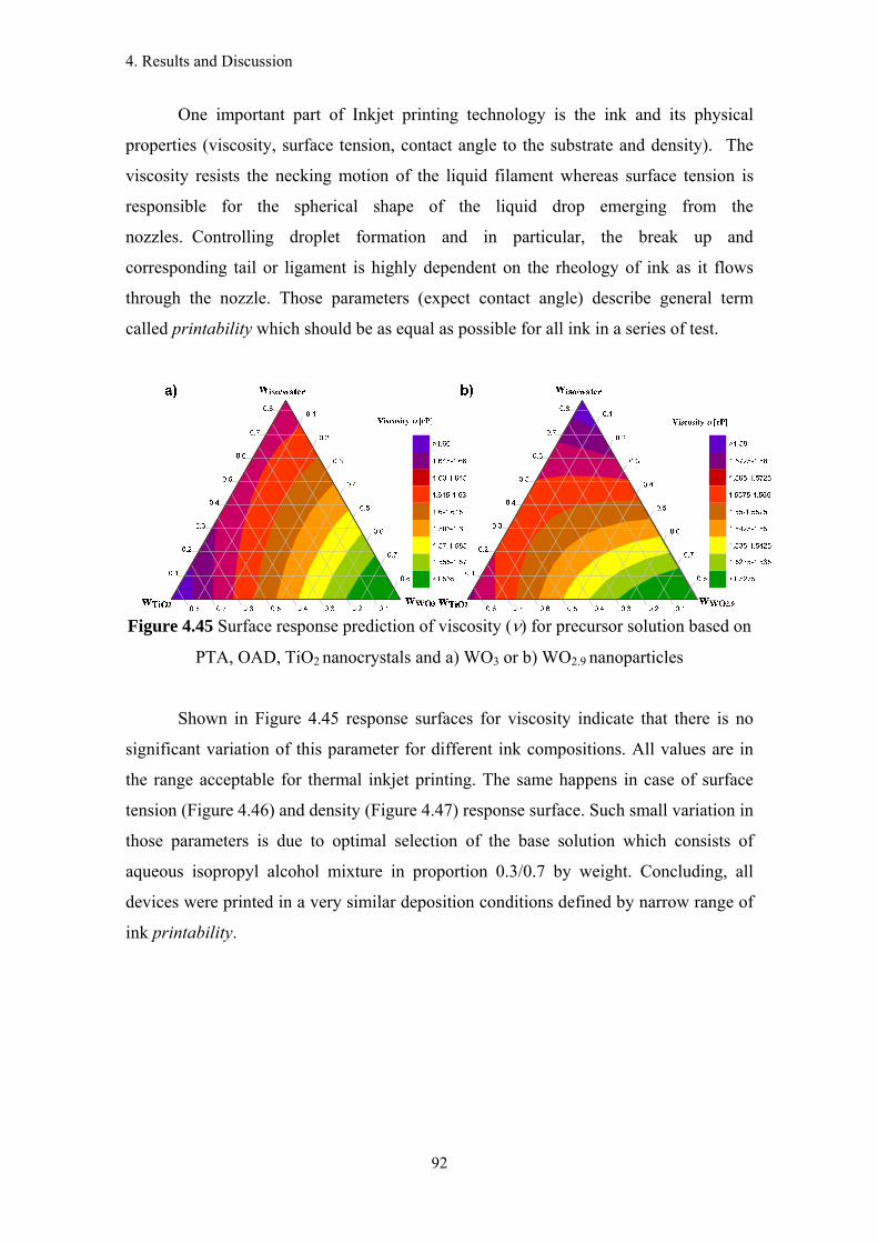
4. Results and Discussion
92
One important part of Inkjet printing technology is the ink and its physical
properties (viscosity, surface tension, contact angle to the substrate and density). The
viscosity resists the necking motion of the liquid filament whereas surface tension is
responsible for the spherical shape of the liquid drop emerging from the
nozzles. Controlling droplet formation and in particular, the break up and
corresponding tail or ligament is highly dependent on the rheology of ink as it flows
through the nozzle. Those parameters (expect contact angle) describe general term
called printability which should be as equal as possible for all ink in a series of test.
Figure 4.45 Surface response prediction of viscosity (ν) for precursor solution based on
PTA, OAD, TiO2 nanocrystals and a) WO3 or b) WO2.9 nanoparticles
Shown in Figure 4.45 response surfaces for viscosity indicate that there is no
significant variation of this parameter for different ink compositions. All values are in
the range acceptable for thermal inkjet printing. The same happens in case of surface
tension (Figure 4.46) and density (Figure 4.47) response surface. Such small variation in
those parameters is due to optimal selection of the base solution which consists of
aqueous isopropyl alcohol mixture in proportion 0.3/0.7 by weight. Concluding, all
devices were printed in a very similar deposition conditions defined by narrow range of
ink printability.
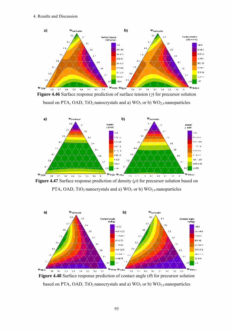
4. Results and Discussion
93
Figure 4.46 Surface response prediction of surface tension (γ) for precursor solution
based on PTA, OAD, TiO2 nanocrystals and a) WO3 or b) WO2.9 nanoparticles
Figure 4.47 Surface response prediction of density (ρ) for precursor solution based on
PTA, OAD, TiO2 nanocrystals and a) WO3 or b) WO2.9 nanoparticles
Figure 4.48 Surface response prediction of contact angle (θ) for precursor solution
based on PTA, OAD, TiO2 nanocrystals and a) WO3 or b) WO2.9 nanoparticles
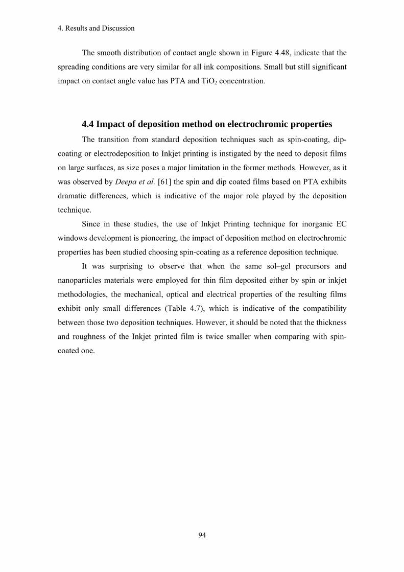
4. Results and Discussion
94
The smooth distribution of contact angle shown in Figure 4.48, indicate that the
spreading conditions are very similar for all ink compositions. Small but still significant
impact on contact angle value has PTA and TiO2 concentration.
4.4 Impact of deposition method on electrochromic properties The transition from standard deposition techniques such as spin-coating, dip-
coating or electrodeposition to Inkjet printing is instigated by the need to deposit films
on large surfaces, as size poses a major limitation in the former methods. However, as it
was observed by Deepa et al. [61] the spin and dip coated films based on PTA exhibits
dramatic differences, which is indicative of the major role played by the deposition
technique.
Since in these studies, the use of Inkjet Printing technique for inorganic EC
windows development is pioneering, the impact of deposition method on electrochromic
properties has been studied choosing spin-coating as a reference deposition technique.
It was surprising to observe that when the same sol–gel precursors and
nanoparticles materials were employed for thin film deposited either by spin or inkjet
methodologies, the mechanical, optical and electrical properties of the resulting films
exhibit only small differences (Table 4.7), which is indicative of the compatibility
between those two deposition techniques. However, it should be noted that the thickness
and roughness of the Inkjet printed film is twice smaller when comparing with spin-
coated one.
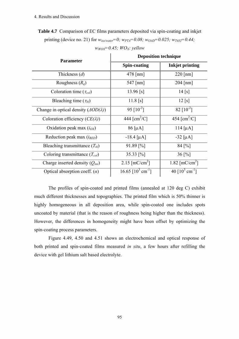
4. Results and Discussion
95
Table 4.7 Comparison of EC films parameters deposited via spin-coating and inkjet
printing (device no. 21) for wiso/water=0; wPTA=0.08; wOAD=0.025; wTiO2=0.44;
wWOX=0.45; WOX: yellow
Parameter Deposition technique
Spin-coating Inkjet printing
Thickness (d) 478 [nm] 220 [nm]
Roughness (Rq) 547 [nm] 204 [nm]
Coloration time (τcol) 13.96 [s] 14 [s]
Bleaching time (τbl) 11.8 [s] 12 [s]
Change in optical density (ΔOD(λ)) 95 [10-2] 82 [10-2]
Coloration efficiency (CE(λ)) 444 [cm2/C] 454 [cm2/C]
Oxidation peak max (iOX) 86 [μA] 114 [μA]
Reduction peak max (iRED) -18.4 [μA] -32 [μA]
Bleaching transmittance (Tbl) 91.89 [%] 84 [%]
Coloring transmittance (Tcol) 35.33 [%] 36 [%]
Charge inserted density (Qins) 2.15 [mC/cm2] 1.82 [mC/cm2]
Optical absorption coeff. (α) 16.65 [103 cm-1] 40 [103 cm-1]
The profiles of spin-coated and printed films (annealed at 120 deg C) exhibit
much different thicknesses and topographies. The printed film which is 50% thinner is
highly homogeneous in all deposition area, while spin-coated one includes spots
uncoated by material (that is the reason of roughness being higher than the thickness).
However, the differences in homogeneity might have been offset by optimizing the
spin-coating process parameters.
Figure 4.49, 4.50 and 4.51 shows an electrochemical and optical response of
both printed and spin-coated films measured in situ, a few hours after refilling the
device with gel lithium salt based electrolyte.
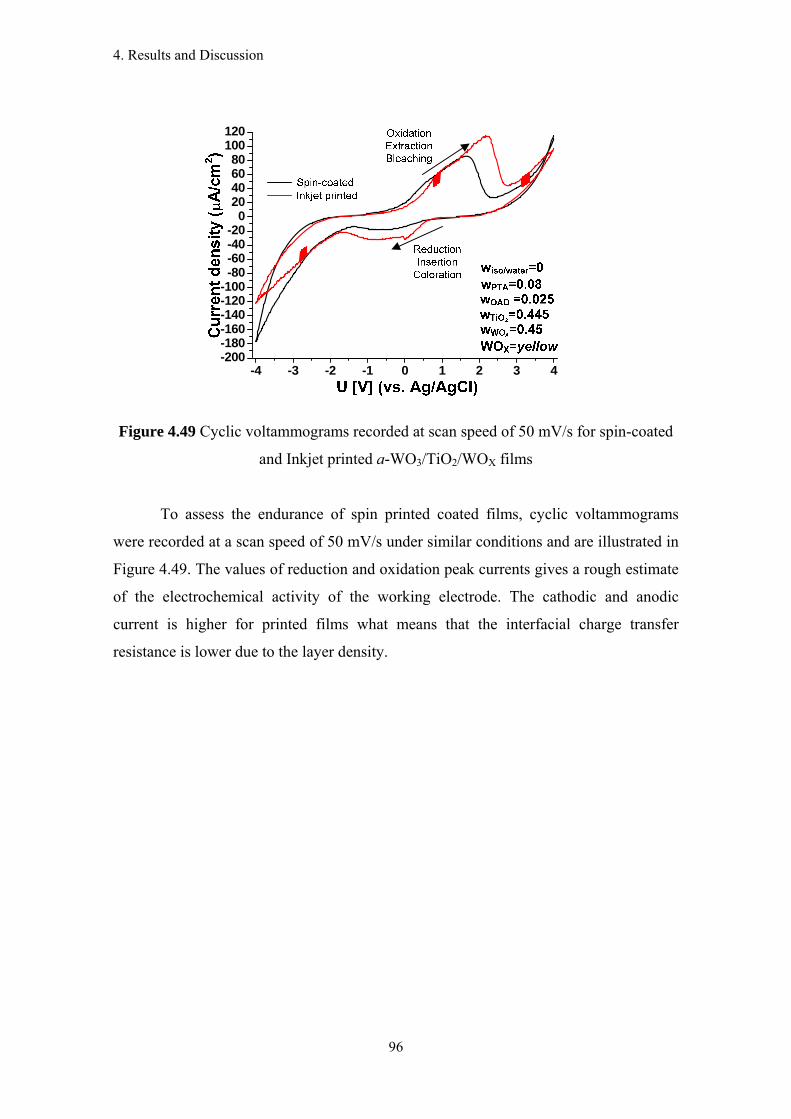
4. Results and Discussion
96
-4 -3 -2 -1 0 1 2 3 4-200-180-160-140-120-100-80-60-40-20
020406080
100120
Figure 4.49 Cyclic voltammograms recorded at scan speed of 50 mV/s for spin-coated
and Inkjet printed a-WO3/TiO2/WOX films
To assess the endurance of spin printed coated films, cyclic voltammograms
were recorded at a scan speed of 50 mV/s under similar conditions and are illustrated in
Figure 4.49. The values of reduction and oxidation peak currents gives a rough estimate
of the electrochemical activity of the working electrode. The cathodic and anodic
current is higher for printed films what means that the interfacial charge transfer
resistance is lower due to the layer density.
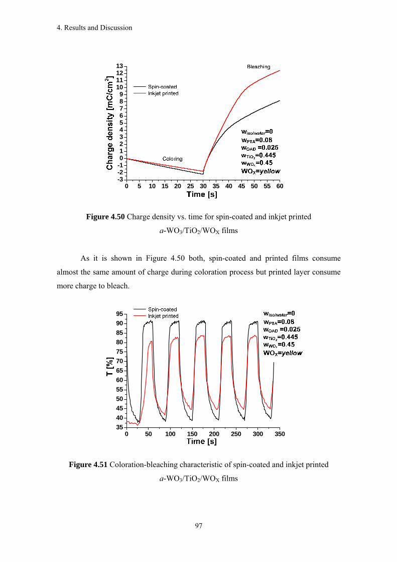
4. Results and Discussion
97
0 5 10 15 20 25 30 35 40 45 50 55 60-3-2-10123456789
10111213
Figure 4.50 Charge density vs. time for spin-coated and inkjet printed
a-WO3/TiO2/WOX films
As it is shown in Figure 4.50 both, spin-coated and printed films consume
almost the same amount of charge during coloration process but printed layer consume
more charge to bleach.
0 50 100 150 200 250 300 35035404550556065707580859095
Figure 4.51 Coloration-bleaching characteristic of spin-coated and inkjet printed
a-WO3/TiO2/WOX films
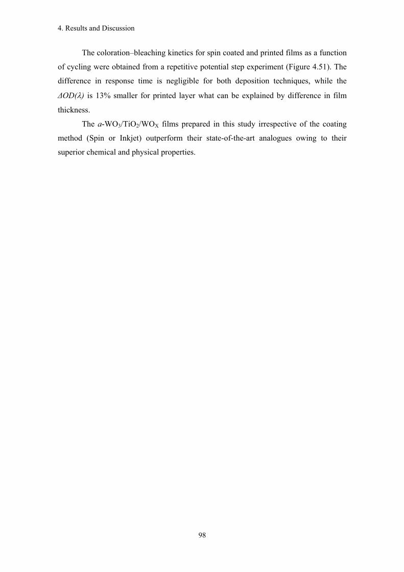
4. Results and Discussion
98
The coloration–bleaching kinetics for spin coated and printed films as a function
of cycling were obtained from a repetitive potential step experiment (Figure 4.51). The
difference in response time is negligible for both deposition techniques, while the
ΔOD(λ) is 13% smaller for printed layer what can be explained by difference in film
thickness.
The a-WO3/TiO2/WOX films prepared in this study irrespective of the coating
method (Spin or Inkjet) outperform their state-of-the-art analogues owing to their
superior chemical and physical properties.
5. Conclusions and future prospects
99
5. Conclusions and future prospects
The main purpose of this work was to develop a complete solution processed
and low temperature dual-phase electrochromic system based on WO3 precursor and
metal oxide nanocrystals deposited via Inkjet Printing Technology. This study aimed to
develop an amorphous a-WO3 matrix with TiO2/WOX nanocrystals embedded for
electrochromic applications. The invented method consist of a combination of a set of
materials (inks) and Inkjet Printing as a deposition technique which makes the system
compatible with temperature sensitive substrates such as PET, PEN and paper.
The scope of this work was find the best combination of factors (components of
the mixture) to obtain the EC window with the best performance. The Inkjet printing of
the electrochromic inks with different composition on top of flexible ITO-PET
substrates was obtained using a Canon PIXMA IP4500 desktop printer. This solution
processed method is a low temperature, non-contact, digital, no mask and no vacuum
patterning, eco friendly, cost efficient in mass production and allows the coexistence of
amorphous and nanocrystalline phases. Briefly, the invented system is an innovative
method for electrochromic device manufacturing based on inorganic nanomaterials.
The use of Inkjet Printing technique for inorganic EC devices development
presented in this thesis is pioneering and the electrochromic performance of the printed
films demonstrates the potential it has for electrochromic applications.
All experimental work and data analysis performed in these studies have been
supported by JMP® Statistical Discovery Software. This statistical design of mixture
experiments and response surface methodologies proved to be a powerful tool for
planning and analyzing experiments to ascertain the influence of electrochromic ink
components like PTA, Oxalic acid, TiO2 and WOX nanoparticles, on the performance of
Inkjet printed electrochromic devices, in particular electrochromic windows.
One of the partial objectives of this research was to find optimum number of
passes which defines layer thickness and roughness and makes it the main Inkjet
deposition parameter. The results obtained lead to the conclusion that the device based
on layer printed 3 times shows the best electrochromic performance. Consequently, this
value was considered as optimum for a set of used materials.
5. Conclusions and future prospects
100
Based on measurements performed on 30 test devices the analysis of
significance have been performed in order to know which factors (mixture components)
are significant and how those factors influence the most important electrochromic
parameters (τcol, τbl, ΔOD, CE). The significance analysis leads to the conclusion that
the coloration time (τcol) depends mainly on the quantity of WOX nanocrystals in
electrochromic layer. The bleaching time (τbl) is influenced by the quantity of WOX and
TiO2 nanocrystals and also depends of WO3 amorphous content formed from PTA
precursor. The change in optical density (ΔOD) which describes the optical contrast
between colored and bleached states mainly depends on quantity of TiO2 nanocrystals
and WO3 amorphous content. Finally, the coloration efficiency (CE) which describes
overall device performance depends to a greater or lesser extent on all the mixture
components, but the most significant are TiO2 and WOX crystalline nanoparticles.
The main task of desirability optimization was to maximize CE and ΔOD while
the response time values of τcol and τbl should be as small as possible. The result of
optimization calculated for maximum desirability indicates that EC device with the best
performance would have the following concentration: wiso/water=0; wPTA=0.01; wOAD=0;
wTiO2=0.83; wWOX=0.16; WOX stoichiometry: yellow.
SEM analysis of a few representative devices indicates that:
the film based on pure a-WO3 is continuous and has a smooth surface; no grains
were observed even at a magnification;
the a-WO3/TiO2/WOX films are favorable for a fast electrochromic response and
high optical contrast;
the a-WO3/TiO2/WOX films have a regular and a uniform distribution of metal
oxide nanocrystalls or their aggregates what makes the structure similar to
chocolate with nuts counterpart;
The wide view SEM picture indicates that printed
a-WO3/TiO2/WOX layer does not form a continuous film; this is rather a pattern
than a film;
the presence of OAD in a-WO3/TiO2/WOX film leads to the appearance of
grooves is the film but do not affect the electrochromic properties significantly.
5. Conclusions and future prospects
101
The XRD diffractograms confirmed that the WOX blue nanopowder match well
with the monoclinic crystalline phase of WO2.9991, while the material called yellow
matched well with the monoclinic crystalline phase of WO3. The film based only on
PTA precursor exhibits a broad halo observed at 2θ∼26 degrees which is characteristic
of the amorphous nature of WO3 films.
Subsequent measurements related to the optical properties of printed
a-WO3/TiO2/WOX films measured in situ as a working electrode in encapsulated device
filled with a gel electrolyte provided the following conclusions:
films containing large amount of TiO2 solid content with a smaller share of
WOX nanocrystals in amorphous matrix exhibit the highest transmission
modulation due to increased surface area;
transmittance in colored state of printed a-WO3/TiO2/WOX films varies for
different WOX nanoparticles stoichiometry, however, these differences
disappear when the layer is dominated by TiO2 nanoparticles;
coloration kinetics is observed to be slower than bleaching kinetics for all the
films under investigation regardless of their compositions;
among all films under consideration, the films containing TiO2/WOX exhibit
the fastest switching kinetics owing to the presence of nanocrystals;
Vopt value is the highest for amorphous films.
The electrochromic measurements lead to the following conclusions:
the cathodic current has the highest modulus value for films containing WO3
yellow nanocrystals rather than WO2.9 blue;
The anodic current has the highest value for films containing WOX
nanocrystals and decrease with increasing TiO2 nanocrystals content;
a-WO3/WOX and a-WO3/TiO2 films consume the highest amount of charges
during coloration and bleaching process;
high values of charge density inserted are observed for films with low TiO2
solid content;
the a-WO3/TiO2/WOX coatings with higher solid content are characterized
by the smallest charge values inserted to the devices what indicates low
power consumption of those devices.
films containing blue WO2.9 nanoparticles have a higher charge transfer than
films containing yellow WO3 nanopowder.
5. Conclusions and future prospects
102
The coloration efficiency which is a parameter that gives the overall
performance of the devices has a value above 400 cm2/C for a-WO3/TiO2/WOX films.
However, such a high values of CE shown in present studies cannot be directly
compared with results of films deposited by other solution processed techniques. These
differences arise from the fact that Inkjet printed films are not continuous, what was
confirmed by SEM measurements. This means that the value of surface area taken to
calculate the CE value is significantly underestimated.
One important part of Inkjet Printing technology is the ink and its physical
properties (viscosity, surface tension, contact angle to the substrate and density). Based
on rheological measurements, it was concluded that there is no significant variation of
viscosity for different ink compositions and all values are in the range acceptable for
thermal Inkjet printing. The same happens in case of surface tension and density. Such
small variation in those parameters is due to optimal selection of the base solution
which consists of aqueous isopropyl alcohol mixture in proportion 0.3/0.7 by weight.
Concluding, all devices were printed in a very similar deposition conditions defined by
narrow range of ink printability. Regarding the contact angle, it was shown that the
spreading conditions were very similar for all ink compositions. Small but still
significant impact on contact angle value has PTA and TiO2 concentration.
The optimization process performed using statistical software indicated that
device with the highest performance have been deposited from the ink with following
composition: wiso/water=0; wPTA=0.08; wOAD=0.025; wTiO2=0.44; wWOX=0.45; WOX:
yellow. Such an ideal electrochromic performance, which is a result of the several
competing mechanisms, demonstrates the potential it has for electrochromic window
applications.
Since in these studies, the use of Inkjet Printing technique for inorganic EC
windows development is pioneering, the impact of deposition method on electrochromic
properties has been studied choosing spin-coating as a reference deposition technique.
Therefore when the same sol–gel precursors and nanoparticles materials were
employed for thin film deposited either by spin or inkjet methodologies, the mechanical,
optical and electrical properties of the resulting films exhibit only small differences,
which is indicative of the compatibility between those two deposition techniques.
However there are some differences that should be noted:
5. Conclusions and future prospects
103
the thickness and roughness of the Inkjet printed film is twice smaller when
comparing with spin-coated one;
the cathodic and anodic current is higher for printed films what means that the
interfacial charge transfer resistance is lower due to the layer density;
both, spin-coated and printed films consume almost the same amount of charge
during coloration process but printed layer consume more charge to bleach;
the difference in response time is negligible for both deposition techniques,
while the ΔOD(λ) is 13% smaller for printed layer what can be explained by
difference in film thickness;
the a-WO3/TiO2/WOX films prepared in this study irrespective of the coating
method (spin or inkjet) outperform their state-of-the-art analogues owing to
their superior chemical and physical properties.
The electrochromic properties of the printed a-WO3/TiO2/WOX films annealed
at 120 deg C are a balance among good electrochemical activity, fast switching kinetics,
high electrochromic efficiency, and ion storage capacity and these are attributable to the
layer density and high surface area of nanocrystals in the printed films which facilitate
fast coloration. The ease processing via Inkjet Printing is evidenced from the fact that
dual-phase films can be fabricated at room-temperature. These properties render them to
be promising candidates for electrochromic windows manufacturing.
The developed method of electrochromic windows manufacturing meets all the
assumptions posed on the beginning of the study. The results obtained during all the
analysis will significantly impact current EC technologies and have promising
implications for the development of electrochromic devices.
Following this study there’s the possibility of producing devices via inkjet
printing, based on WOX nanoparticles synthesized e.g. via hydrothermal process from
the same WO3 sol. As future prospects, this work had open a wide window of
opportunities with this innovative EC deposition technique which allows a great
development in the area, with the cost efficient, mass production of flexible
electrochromic windows. The EC windows developed by inkjet printing on flexible
substrates makes the possibility of the window to adapt to different shapes, like
greenhouses, roofs and walls of buildings, canopies, top of convertible cars, tents,
curtains, and so on.

104
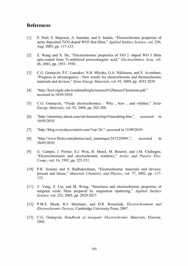
105
References
[1] P. Patil, S. Mujawar, A. Inamdar, and S. Sadale, “Electrochromic properties of spray deposited TiO2-doped WO3 thin films,” Applied Surface Science, vol. 250, Aug. 2005, pp. 117-123.
[2] Z. Wang and X. Hu, “Electrochromic properties of TiO 2 -doped WO 3 films spin-coated from Ti-stabilized peroxotungstic acid,” Electrochimica Acta, vol. 46, 2001, pp. 1951- 1956.
[3] C.G. Granqvist, P.C. Lansaker, N.R. Mlyuka, G.A. Niklasson, and E. Avendano, “Progress in chromogenics : New results for electrochromic and thermochromic materials and devices,” Solar Energy Materials, vol. 93, 2009, pp. 2032-2039.
[4] “http://host.nigde.edu.tr/sahmetlioglu/research%20areas/Chromism.pdf.” accessed in 10/05/2010
[5] C.G. Granqvist, “Oxide electrochromics : Why , how , and whither,” Solar Energy Materials, vol. 92, 2008, pp. 203-208.
[6] “http://chemistry.about.com/od/chemistryfaqs/f/moodring.htm.”, accessed in 10/05/2010
[7] “http://blog.everydayscientist.com/?cat=26.”, accessed in 15/09/2010
[8] “http://www.flickr.com/photos/zack_mensinger/247225099/.”, accessed in 10/05/2010
[9] G. Campet, J. Portier, S.J. Wen, B. Morel, M. Bourrel, and J.M. Chabagno, “Electrochromism and electrochromic windows,” Active and Passive Elec. Comp., vol. 14, 1992, pp. 225-231.
[10] P.R. Somani and S. Radhakrishnan, “Electrochromic materials and devices: present and future,” Materials Chemistry and Physics, vol. 77, 2002, pp. 117-133.
[11] T. Yang, Z. Lin, and M. Wong, “Structures and electrochromic properties of tungsten oxide films prepared by magnetron sputtering,” Applied Surface Science, vol. 252, 2005, pp. 2029-2037.
[12] P.M.S. Monk, R.J. Mortimer, and D.R. Rosseinsk, Electrochromism and Electrochromic Devices, Cambridge University Press, 2007.
[13] C.G. Granqvist, Handbook of inorganic Electrochromic Materials, Elsevier, 2002.
106
[14] E. Avendano, L. Berggren, G.A. Niklasson, C.G. Granqvist, and A. Azens, “Electrochromic materials and devices : Brief survey and new data on optical absorption in tungsten oxide and nickel oxide films,” Thin Solid Films, vol. 496, 2006, pp. 30 - 36.
[15] Y. Takahashi, “Radical-Bearing Redox Polymers and Their Application to Electrochromic Cell,” 2008.
[16] S.K. Deb, “Opportunities and challenges in science and technology of WO 3 for electrochromic and related applications,” Solar Energy Materials and Solar Cells, vol. 92, 2008, pp. 245-258.
[17] D.R. Rosseinsky and R.J. Mortimer, “Electrochromic Systems and the Prospects for Devices **,” Advanced Materials, vol. 13, 2001, pp. 783-793.
[18] “http://casa.hsw.uol.com.br/janelas-inteligentes4.htm.”, accessed in 15/06/2010
[19] “http://eetdnews.lbl.gov/nl05/eetd-nl05-1-window.html.”, 14/06/2010
[20] R.J. Mortimer, A.L. Dyer, and J.R. Reynolds, “Electrochromic organic and polymeric materials for display applications,” Displays, vol. 27, 2006, pp. 2-18.
[21] R. Baetens, B. Petter, and A. Gustavsen, “Properties , requirements and possibilities of smart windows for dynamic daylight and solar energy control in buildings : A state-of-the-art review,” Solar Energy Materials and Solar Cells, vol. 94, 2010, pp. 87-105.
[22] F. Carpi and D.D. Rossi, “Colours from electroactive polymers : Electrochromic , electroluminescent and laser devices based on organic materials,” Optics & Laser Technology, vol. 38, 2006, pp. 292-305.
[23] L. Su, Z. Xiao, and Z. Lu, “All Solid-state electrochromic device with PMMA gel electrolyte,” Materials Chemistry and Physics, vol. 52, 1998, pp. 180-183.
[24] A. Goswami, Thin Film Fundamentals, New Delhi: New Age International Publishers, 1996.
[25] A. Elshabini-Riad and F.D. Barlow III, Thin Film Technology Handbook, New-York: McGraw-Hill, 1997.
[26] J.B. Bates, ed., Proceedings of the Symposium on Thin Film Solid Ionic Devices and Materials, Pennington: The Electrochemical Society, 1996.
[27] P.J. Smith, “Introduction to Inkjet,” . Dutch Polymer Institute, Netherlands
[28] P.J. Wojcik, A. Gonçalves, S. Pereira, G. Gonçalves, I. Ferreira, R. Martins, and E. Fortunato, “Functional Materials For Inkjet Printing Technology - Chemical And Physicochemical Requirements For Novel Applications,” .
[29] “http://www.dimatix.com/markets/index.asp.”, accessed in 01/07/2010
107
[30] P.J. Wojcik, “An Introduction to Ink Jet Technology,” , 2009.
[31] A. Bessiere, J.-C. Badot, M.-C. Certiat, J. Livafe, and V. Lucas, “Sol – gel deposition of electrochromic WO 3 thin film on flexible ITO / PET substrate,” Electrochimica Acta, vol. 46, 2001, pp. 2251- 2256.
[32] A.C. Pierre, Introduction to Sol-Gel Processing, Boston: Kluwer Academic Publishers, 1998.
[33] M. Deepa, T.K. Saxena, D.P. Singh, K.N. Sood, and S.A. Agnihotry, “Spin coated versus dip coated electrochromic tungsten oxide films : Structure , morphology , optical and electrochemical properties,” Electrochimica Acta, vol. 51, 2006, pp. 1974-1989.
[34] P.K. Biswas, N.C. Pramanik, M.K. Mahapatra, D. Ganguli, and J. Livage, “Optical and electrochromic properties of sol – gel WO 3 films on conducting glass,” Materials Letters, vol. 57, 2003, pp. 4429 - 4432.
[35] J. Livage and D. Ganguli, “Sol - gel electrochromic coatings and devices : A review,” Solar Energy Materials, vol. 68, 2001, pp. 365-381.
[36] M. Sharbatdaran, A. Novinrooz, and H. Noorkojouri, “Preparation and Characterization of WO3 Electrochromic Films Obtained by the Sol-Gel Process,” Iran. J. Chem. Chem. Eng., vol. 25, 2006, pp. 25-29.
[37] H. Okamoto, A. Ishikawa, and T. Kudo, “Amorphous and Crystalline Peroxopolytungstic Acids Formed from Tungsten and Hydrogen Peroxide,” The Chemical Society of Japan, vol. 62, 1989, pp. 2723-2724.
[38] M.A. Aegerter and M. Menning, Sol-Gel Technologies for Glass Producers and Users, Saarbrucken: Kluwer Academic Publishers, 2004.
[39] A. Novinrooz, M. Sharbatdaran, and H. Noorkojouri, “Structural and optical properties of WO3 electrochromic layers prepared by the sol-gel method,” Central European Journal of Physics, vol. 3, Sep. 2005, pp. 456-466.
[40] C.M. White, D.T. Gillaspie, E. Whitney, S.-H. Lee, and A.C. Dillon, “Flexible electrochromic devices based on crystalline WO3 nanostructures produced with hot-wire chemical vapor deposition,” Thin Solid Films, vol. 517, Apr. 2009, pp. 3596-3599.
[41] G. Leftheriotis and P. Yianoulis, “Development of electrodeposited WO3 films with modified surface morphology and improved electrochromic properties,” Solid State Ionics, vol. 179, Nov. 2008, pp. 2192-2197.
[42] M. Geiger, “Making Smart Windows Smarter: Improving Optical Efficiency and Intercalation Rates in Sol-Gel Derived Tungsten Trioxide,” Literature Seminar, 2007.
108
[43] M. Deepa, R. Sharma, A. Basu, and S. Agnihotry, “Effect of oxalic acid dihydrate on optical and electrochemical properties of sol–gel derived amorphous electrochromic WO3 films,” Electrochimica Acta, vol. 50, May. 2005, pp. 3545-3555.
[44] “JMP Design of Experiments, Release 6,” 2005.
[45] P.J. Wojcik, A.S. Cruz, L. Santos, A.M. Ramos, L. Pereira, R. Martins, and E. Fortunato, Ink Jet Printed Nanostructured Materials - Applications of Titanium Dioxide and Tungsten Trioxide Nanocrystals for Photovoltaic and Eelectrochromic Window, Poster presented in ANM 2010.
[46] DataPhysics, “Operating manual OCA,” 1998.
[47] “http://www.attension.com/contact-angle.aspx.”, accessed in 24/08/2010
[48] “http://www.gsishop.com/webmagzine/20020925/contact.htm.”, accessed in 24/08/2010
[49] P. Valente, “Desenvolvimento de um Electrólito Polimérico para Mostradores Electrocrómicos,” 2007.
[50] “http://miam2.physics.mcgill.ca/?q=content/ambios-xp200-profiler.”, accessed in 25/08/2010
[51] L. Pereira, “Produção e caracterização de silício policristalino e a sua aplicação a TFTs,”PHD Thesis, FCT-UNL 2008.
[52] B. Brás, “Produção e Caracterização de Baterias de Filme Fino de Papel,”, Master thesis, FCT-UNL 2009.
[53] P.J. Wojcik and L. Santos, “Electrochromic Measurement Protocol,” 2010.
[54] Y. Shen, Z. Lu, S. Spiers, H.A. Mackenzie, H.S. Ashton, J. Hannigan, S.S. Freeborn, and J. Lindberg, “Measurement of the optical absorption coefficient of a liquid by use of a time-resolved photoacoustic technique,” Applied Optics, vol. 39, 2000, pp. 4007-4012.
[55] N. Naseri, R. Azimirad, O. Akhavan, and A.Z. Moshfegh, “Improved electrochromical properties of sol–gel WO3 thin films by doping gold nanocrystals,” Thin Solid Films, vol. 518, Feb. 2010, pp. 2250-2257.
[56] a Vanderkooij, J. Meulman, and W. Heiser, “Local minima in categorical multiple regression,” Computational Statistics & Data Analysis, vol. 50, Jan. 2006, pp. 446-462.
[57] “JMP Introductory Guide, Release 8,” Addiction, vol. 99, Nov. 2009.
[58] “http://www.surveysystem.com/signif.htm.”, accessed in 23/09/2010
109
[59] J. Sall, “Leverage Plots for General Linear Hypotheses,” The American Statistician, vol. 44, Nov. 1990, p. 308.
[60] N. Sharma, M. Deepa, P. Varshney, and S.A. Agnihotry, “Influence of Organic Additive on the Morphological , Electrical and Electrochromic Properties of Sol-Gel Derived WO 3 Coatings,” Journal of Sol-Gel Science and Technology, vol. 18, 2000, pp. 167-173.
[61] M. Deepa, “Electrodeposited tungsten oxide films: annealing effects on structure and electrochromic performance,” Thin Solid Films, vol. 468, Dec. 2004, pp. 32-42.
[62] a Cremonesi, Y. Djaoued, D. Bersani, and P. Lottici, “Micro-Raman spectroscopy on polyethylene-glycol assisted sol–gel meso and macroporous WO3 thin films for electrochromic applications,” Thin Solid Films, vol. 516, Oct. 2007, pp. 4128 - 4132.
[63] Y. Nah, a Ghicov, D. Kim, and P. Schmuki, “Enhanced electrochromic properties of self-organized nanoporous WO3,” Electrochemistry Communications, vol. 10, Nov. 2008, pp. 1777-1780.
[64] O. Lavi, G. Frey, a Siegmann, and Y. Eineli, “Enhanced tungstate electrochromism via formation of transparent conductive networks,” Electrochemistry Communications, vol. 10, Aug. 2008, pp. 1210-1213.
[65] R. Sato, N. Kawamura, and H. Tokumaru, “The coloration of tungsten-oxide film by oxygen deficiency and its mechanism,” Applied Surface Science, vol. 254, Sep. 2008, pp. 7676-7678.
[66] C.G. Granqvist, “Transparent conductors as solar energy materials: A panoramic review,” Solar Energy Materials and Solar Cells, vol. 91, Oct. 2007, pp. 1529-1598.
[67] M. Deepa, P. Singh, S. Sharma, and S. Agnihotry, “Effect of humidity on structure and electrochromic properties of sol–gel-derived tungsten oxide films,” Solar Energy Materials and Solar Cells, vol. 90, Oct. 2006, pp. 2665-2682.
[68] S.S. Kalagi, D.S. Dalavi, R.C. Pawar, N.L. Tarwal, S.S. Mali, and P.S. Patil, “Polymer assisted deposition of electrochromic tungsten oxide thin films,” Journal of Alloys and Compounds, vol. 493, Mar. 2010, pp. 335-339.
[69] V.V. Abramova, A.S. Sinitskii, E. a Goodilin, and Y.D. Tretyakov, “Preparation and properties of electrochromic coatings based on nanoparticle tungsten oxide,” Mendeleev Communications, vol. 15, 2005, pp. 178-180.