3d-/inkjet-printed rf packages and modules for iot...
TRANSCRIPT

3D-/Inkjet-Printed RF Packages and Modules for IoT Applications up to sub-THz frequencies
Manos Tentzeris, Ryan Bahr, Bijan Tehrani
Ken Byers Professor in Flexible Electronics
Georgia Institute of Technology
Atlanta, Georgia

Challenges for Packaging up to sub-THz /mmW
• Millimeter-wave (mm-wave) wireless technology ranging 30–300 GHz emerging in industry for 5G, automotive radar
• System-level packaging an integral component of any wireless system
Challenges for mm-wave system packaging:
• Low-loss materials
– Increase wireless system efficiency
– High-frequency dielectric characterization necessary
• Miniaturization
– Reduce package size and interconnect length
– System-on-package (SoP) integration desired
2

Additive Manufacturing (AM) Solutions
Fabricate wireless systems in a rapid, scalable, and purely-additive fashion
1. Additively fabricate electronic structures– Reduce material waste and processing tools/steps
– Remove high temp and pressure, less package stress
2. High process reconfigurability– Multi-application processing with single tooling technology
– Short-run prototyping and mass-scale production
Where can AM fit in with mm-wave packaging?
3

Mm-Wave Packaging with Printing
4
Materials:
Photoactive resins,
thermoplastics, ceramic
pastes, conductive
adhesives
Materials:
Polymer solutions, metallic
nanoparticle dispersions,
carbon nanomaterial
suspensions
Dielectric lenses
Encapsulations
Die-embedded
leadframes
3D interconnects
RF substrates
Die attach
Inkjet Printing
3D Printing


Stereolithography (SLA) 3D Printing
• DLP or laser-based exposure system
• Resolution determined by pixel or laser spot size
– 1080p DLP projector ~40 um resolution
• SLA advantages compared to FDM/Direct-Write
– Room temperature process, no heated/pressure extrusion
– High resolution with low surface roughness (hundreds of nm)
– Sequential layer polymerization truly solid object
– Simple scalability (highlighting DLP)
6
Photopolymer Resin
Z-Axis Build Plate
UV Source
Build Plate
Movement
SLA Printing Setup

Using SLA for Packaging
• Combine SLA and direct write methods
– Place components into printed cavities
– Resolution too low for interfacing dies
• Layer-by-layer masking and PVD metal deposition
– High resolution, embedded ICs
– Requires mask for each pattern
7
A. J. Lopes et al., “Integrating stereolithography and direct print technologies
for 3d structural electronics fabrication,” Rapid Prototyping Journal, vol. 18,
no. 2, pp. 129–143, 2012.
T. Merkle et al., “Polymer multichip module process using 3-d printing
technologies for d-band applications,” IEEE Transactions on Microwave
Theory and Techniques, vol. 63, no. 2, pp. 481–493, Feb 2015.

SLA 3D Printing and Characterization
• Tools: LittleRP tabletop 3D printer, Viewsonic PJD7820HD DLP projector
• Materials: Vorex (photosensitive resin), Porcelite (ceramic-loaded resin)
8
Goal: characterize dielectric properties of SLA
materials at E-band (55–95 GHz)
1. Material samples printed to match WR-12
waveguide cavity dimensions (3.01 x 1.55 x 1 mm)
2. S-parameters of printed cavity fills measured
across E-band
3. Models satisfying Kramers-Kronig relation used to
extract εr and tanδ from measurements
WR-12 Waveguide
Spacers
Waveguide fill samples

Dielectric Characterization
• Variations less than ± 2% and ± 7% for Vorex and Porcelite sample measurements, respectively
• Linearity observed up to and beyond 90 GHz
• Ceramic-loaded Porcelite material exhibits higher εr
• εr and tanδ comparable to standard epoxy mold compound materials
9

3D-Printed Encapsulation
• Selective patterning of die encapsulation on metallic leadframes
10
3 mm
Standard 1 mm-Thick
Encapsulation
3 mm 3 mm
Text and
DetailingLens Integration
Side View

Post-Process On-Package Printing
• Use inkjet printing to fabricate metallic structures on top of 3D-printed encapsulation
– Decoupling capacitors
– Antenna arrays
– Frequency selective surfaces (FSS)
11
Periodic square FSS inkjet-
printed onto 3D-printed
substrate
Periodic Jerusalem Cross FSS inkjet-
printed onto 3D-printed encapsulation
2 mm
Periodic Slotted-Cross FSS printed
onto 3D-printed encapsulation

mm-Wave SoP: 3D and Inkjet Printing
12
Die: 2 x 2.7 mm
Inkjet print dielectric
ramps for mm-wave
interconnects and
antennas
(IEEE IMS 2016)
Inkjet print on-package
components
(IEEE APS 2015)
Incorporate
through-mold-
vias (TMVs)
within the
package
How can we
integrate
these two
technologies?

Through Mold Vias (TMVs)
• Interface encapsulated IC with peripherals on top of package
• Ultra-thin package-on-package (PoP) stack ups
• Laser drilling used to selectively remove encapsulation
• Limited to BGA with diameter ~250um and pitch ~500um
13
Use 3D printing
to fabricate IC
encapsulation
with through-
mold-vias (TMVs)
A. Yoshida et al., “A study on an ultra thin pop using through mold via technology,” in 2011 IEEE
61st Electronic Compon. and Technol. Conference (ECTC), May 2011, pp. 1547–1551.

TMV Fabrication Process Flow
1. 3D print encapsulation with ramps, inkjet print TMV interconnects
2. 3D print encapsulation cavity fill to seal die and internal interconnects
3. Inkjet print multilayer antennas/passives/etc topology
4. 3D print final encapsulation
14
(1) (2) (3) (4)
IC Die
SLA encapsulation Printed TMVs
2D Side-View Model of Printed 3D SoP Encapsulation

Printed TMVs with SLA and Inkjet Printing
• Ramp TMVs 3D-printed to interconnect die with top of encapsulation
• CPW interconnects inkjet-printed onto 3D-printed ramps and sintered at 150 °C
• Measurements < 67 GHz with continuity up to 65° slope
• 65° ramp: length is < 500 um for 1 mm tall encapsulation
• Insertion loss: 0.5–0.6 dB/mm at 60 GHz 10x improvement from wirebond interconnects
15
SLA 3D-Printed Ramp
Slopes
OO
OO
OOX
15°
75°
35° slope
TMV
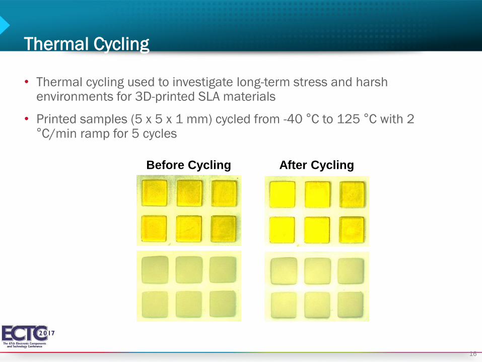
Thermal Cycling
• Thermal cycling used to investigate long-term stress and harsh environments for 3D-printed SLA materials
• Printed samples (5 x 5 x 1 mm) cycled from -40 °C to 125 °C with 2 °C/min ramp for 5 cycles
16
Before Cycling After Cycling

Surface Roughness
• “Flat” surface of a DLP SLA print (Vorex photoresin)
• 100–300 nm roughness appearing periodically, corresponding to approximate size of a DLP pixel
• Compare to 10’s of um roughness with FDM and direct-write 3D printing
17
~40 um

Manos Tentzeris
Reconfigurable “Smart Packaging” Structures
• Verowhite: Stiff polymer
• TangoBlack: Flexible, Strechable polymer (rubber-like)
• Grey60: Hinges, exhibit shape memory effect (SME)
Printed with Objet 260 PolyJet 3D printer, silver
nanoparticle ink for patch antennasJ. Kimionis. “3D-printed Origami Packaging with Inkjet-printed Antennas for RF Harvesting Sensors,
” IEEE Transactions on Microwave Theory and Techniques, vol.63, no.12, Dec. 2015

3D Printed Flexible/Compressible/Stretchable Packages
• Wearable sensing platform
• Ultra flexible
• 3D printed– Low cost– Customized– Flexible
• Sensing capability– Microfluidics liquid sensing
Wenjing Su, Zihan Wu, Yunnan Fang, Ryan Bahr, Markondeya Raj Pulugurtha, Rao Tummala, and Manos M. Tentzeris, "3D Printed
Wearable Flexible SIW and Microfluidics Sensors for Internet of Things and Smart Health Applications", IEEE International Microwave
Symposium (IMS), 2017, accepted
19

Flexible Inkjet-Printed Microfluidics
• Small channel down to 60 um*0.8 um
• Flexible
• On virtually any substrate (e.g.glass)
• Tunable microwave structures
• Ideal for water quality monitoring and biosensing

Manos Tentzeris
3D Printed Electronics
• Microfluidic models can be fabricated
• Multijet printing deposits layer by layer via inkjet nozzles
• Silver epoxy filling to realize resistive, inductive, capacitive passive devices components
• RLC resonator can be created with passives for wireless dielectric sensing, enabling a milk cap food sensor
(Top) 3D printed RLC
components (Bottom) IoT
food sensor

Manos Tentzeris
3D Printing of Complex Antennas
• Laser-based stereolithography used to print structures with different materials
• Flexible/streching structures for origami-based microfluidic antennas.
• Complex patterns for impossible to realize antennas without 3D printing
(Top) Chinese fan antenna
(Bottom) Photonic Crystal
(Left) 3D printed fractal antenna
(Right) Voronoi based antenna

Manos Tentzeris
Reconfigurable Antenna Structures
T. Merkle et al., “Polymer multichip module process using 3-d printing
technologies for d-band applications,” IEEE Transactions on Microwave
Theory and Techniques, vol. 63, no. 2, pp. 481–493, Feb 2015.
Helical/zigzag antenna “Tree” with (a) original and (b)
compressed
Compress

5G for IoT, Wearables and Smart Skins
Advantages:
• Better link detectability (for given aperture
sizes)
• More power available to mm-wave readers
• Large tags can be very directive
• No interference with other readers
Drawbacks that we eliminate
• RF powering is very difficult at mm-
wave: Solar
• Mm-wave components and materials are
expensive: Minimalist design, printed
• Large tags cannot be read from all
directions: Van-Atta

Printed, flexible, backscatter-modulation Van-Atta sensor km-Range “patch” structure
• Active backscatter-modulation Van-Atta
• All the advantages of the passive Van-Atta + non-linear response
• Enables this new structure with– Ultra-long-range reading capabilities (up to several
kilometers)– Outdoor or indoor energy autonomy with solar cell:
– Ultra-low power consumption (200uW)– Almost immediate integration of any of our printed
gas sensors– Several on the same platform, in the future– Great resolution (below 0.5m)

Summary
Combination of inkjet and 3D printing technologies allows for the realization of low-cost, scalable, application-specific mm-wave / sub-THz wireless systems
• Extracted εr and tanδ of SLA materials, yielding suitable characteristics for SoP solutions
• Demonstrated various IC encapsulation schemes with SLA 3D-printing (lens and FSS integration)
• Fabricated and measured printed sloped TMV interconnects for interfacing IC dies with SoP components in 3D encapsulations
26

Manos Tentzeris
3D Printing Techniques – Direct Write
• Micro dispensing
– Physical deposition of wide variety of materials
– Often can be incorporated with multiple materials much easier than optical methods
• Examples:
– Direct write, Aerosol jet, Fused deposition modeling (FDM, multijet printing
3D printing of electronics with
IC’s by depositing silver with a
Voxel8 3D printer

Manos Tentzeris
Fused Deposition Modeling - FDM
• Deposit heated plastic
• Materials: Thermoplastics
• Resolutions:
– XY: 200-400 um
– Z: 20-100 microns
• Advantages:
– Multiple materials– Wide range of polymers
– Easy to add different tools
• Disadvantages:
– Porosity
– Resolution (comparatively)
Traditional FDM machine

Manos Tentzeris
Extremes of Direct Write
• Resolution Extremes
– nScrypt micro-dispensing system
– Layer heights of 1 um
– Deposition width of ~15 um
– Deposits wide assortment of materials from 1 cPs (viscosity of water) to 1,000,000 cPs (4x of thickness of peanut butter)
nScrypt nTip and smartpump
enabling high resolution
dispensing

Manos Tentzeris
PolyJet Printing
• Prints polymers with inkjet tech.
• Resolutions:
– XY: 1600 dpi
– Z: 16 microns
• Advantages:
– Multiple polymers
• Disadvantages:
– Proprietary Polymers Only
Multimaterial polyjet printing of
polymers for a cell phone
mockup.

Manos Tentzeris
3D Printing Techniques - Optical
• Optical-based methods
– Laser-based techniques
– Need to trace the entire pattern
– Digital mask systems
– Scalability, exposes entire layer at once
– No increase in print time to print many devices at once
– i.e. digital micromirror devices (DMD)
• Examples:
– Selective Laser Melting/Sintering, Stereolithography (laser or DLP) (Left) Traditional SLA. (Right)
Two photon absorption

Manos Tentzeris
Selective Laser Sintering SLS
• Fuse polymers/metals
• Resolutions:
– Z: 5-25 microns
– XY: <30 microns
• Advantages:
– Has natural support material
– Metallization
• Disadvantages:
– Single Material
– Roughness/Porosity
Micro Laser Sintering (MLS)

Manos Tentzeris
3D Printing Techniques – Optical Resolutions
• Resolution Extremes
– 2 photo polymerization (i.e. Nanoscribe)
– XYZ resolution limited to near diffraction limit, 100 nm.
Microneedles for bio applications(Top) Demonstration structures.
(Bottom) Photonic Crystal
Manos Tentzeris
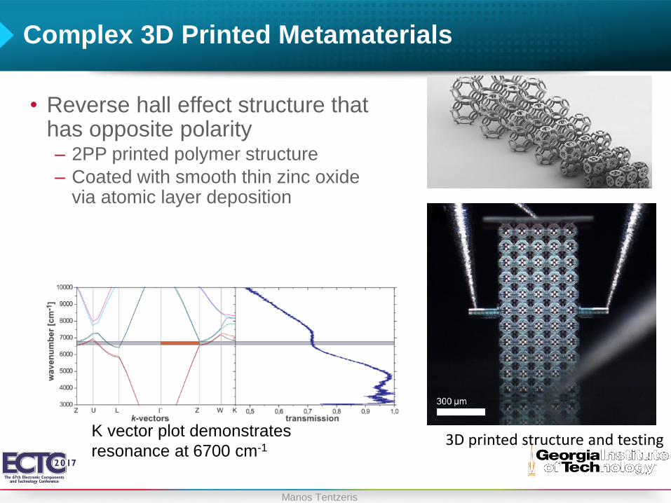
Complex 3D Printed Metamaterials
• Reverse hall effect structure that has opposite polarity– 2PP printed polymer structure
– Coated with smooth thin zinc oxide via atomic layer deposition
K vector plot demonstrates
resonance at 6700 cm-13D printed structure and testing

Manos Tentzeris
Complex 3D printed structures
• Combine SLA and direct write methods– Place components into printed cavities
– Resolution too low for interfacing dies
A. J. Lopes et al., “Integrating stereolithography and direct print technologies
for 3d structural electronics fabrication,” Rapid Prototyping Journal, vol. 18,
no. 2, pp. 129–143, 2012.
3D modeled structure
Physically realized 3D structure.

Manos Tentzeris
Complex 3D printed structures
• Layer-by-layer masking and PVD metal deposition
– High resolution, embedded ICs
– Requires mask for each pattern
T. Merkle et al., “Polymer multichip module process using 3-d printing
technologies for d-band applications,” IEEE Transactions on Microwave
Theory and Techniques, vol. 63, no. 2, pp. 481–493, Feb 2015.

Manos Tentzeris
3D Printed Packaging for MMIC and mm-Wave
• Utilize low cost digital light projection (DLP) Stereolithography
• Selective patterning of die encapsulation on metallic leadframes
37
3 mm
Standard 1 mm-Thick Encapsulation
3 mm 3 mm
Text and Detailing Lens Integration
Side View