high-quality inkjet-printed multilevel interconnects and ...viveks/papers/h8_3mrs03.pdf ·...
TRANSCRIPT

High-quality inkjet-printed multilevel interconnects and inductive components on plasticfor ultra-low-cost RFID applications.
Steven Molesa, David R. Redinger, Daniel C. Huang, and Vivek Subramanian.Department of Electrical Engineering, University of California Berkeley,Berkeley, CA 94720-1770, U.S.A.
ABSTRACT
In recent years, there has been tremendous interest in all-printed electronics as a means ofachieving ultra-low-cost electronic circuits with uses in displays and disposable electronicsapplications such as RFID tags. While there have been a few demonstrations of printed organictransistors to date, there has been little work on the associated passive component andinterconnection technologies required to enable the development of all-printed RFID circuits. Inparticular, low-resistance conductors are crucial to achieve the high-Q inductors necessary forRFID. Here, we demonstrate inkjetted nanoparticle-Au conductors on plastic with sheetresistances as low as 0.03 ohms/square. We describe the optimization of the jetting parameters,and their impact on final film morphology and electrical properties. We also demonstrate abridging technology based on an inkjetted polyimide interlevel dielectric. Using this process, wedemonstrate multilevel interconnect and passive component structures including conductorpatterns, crossover bridges, and tapped planar spiral inductors. Together, these represent animportant step towards the realization of all-printed RFID.
INTRODUCTION
Recently, there has been growing interest in the development of printed organic electronicstechnologies, which are expected to see use in low-cost, flexible displays and disposableelectronics applications. Low-cost RFID tags are considered to be a compelling application,since they may be used to replace UPC barcodes on consumer products, ushering in an era ofenhanced consumer convenience and warehousing efficiency, through a realization of real-timeprice and product controls, automated inventory processes, and automated checkout.
All-printed circuit technologies are attractive for several reasons. They eliminate the needfor expensive lithography, and also eliminate the need for high-vacuum processing, includingPVD, CVD, plasma etching, etc., all of which have major impacts on system cost. Additionally,they use an additive fabrication process, which reduces the waste abatement costs. Thus, theyare expected to result in a substantially reduced integrated cost making them suitable for use indisposable consumer products.
In recent years, there have been some demonstrations of printed transistors in plastic-compatible technologies [1]. However, to date, there have been no significant demonstrations ofthe requisite all-printed passive component technologies. In particular, for RFID, this is a crucialshortcoming, since the requirements imposed on the passive components are tremendous; high-Qinductors and well-behaved capacitors are required for power-coupling and communication [2].Last year, we demonstrated a plastic-compatible gold nanoparticle-based conductor technologythat enabled the printing of low-resistance conductors on plastic for the first time [3]. Here, weoptimize and apply this and other materials to inkjet printing applications, and demonstrate arobust multilevel interconnect technology for RFID circuits, and also demonstrate the associatedinductive components required for the same.
H8.3.1Mat. Res. Soc. Symp. Proc. Vol. 769 © 2003 Materials Research Society
EXPERIMENTAL DETAILS
All experiments were performed using a custom inkjet system, shown in figure 1. Theoverall testbed consists of translation stages, inkjet dispensers, a hot chuck for heating andcooling the substrate, and software to control the various systems. For all experiments, we usedpiezoelectric heads manufactured by Microfab, Inc., with nozzle diameters varying from 30µmto 60µm. Custom software was used to provide overlay, translation, and head control.
Figure 1: The custom inkjet system for printed electronics fabrication.
To develop the processes for forming inductive components and multilevel interconnects,we performed experiments using metallic nanoparticles [3] for conductor formation, and acommercial polyimide for dielectric formation. We varied the droplet jetting waveformparameters, droplet spacing, choice of solvent, and substrate temperature during printing.Resultant film morphology (as measured using optical micrography, profilometry, and AFM)and electrical conductivity were correlated to these parameters and used to drive the optimizationof the processes. These were used to demonstrate inductors and multilevel interconnects.
RESULTS AND DISCUSSION
The piezo-head waveform parameters were optimized to maximize jetting velocity whileensuring good drop-to-drop stability and the absence of satellite droplets. By standardizing allexperimental runs to this baseline, it was possible to specifically examine the impact of variousprocess and materials parameters on film quality, for both the conductor and dielectric films.
Conductor Film Development
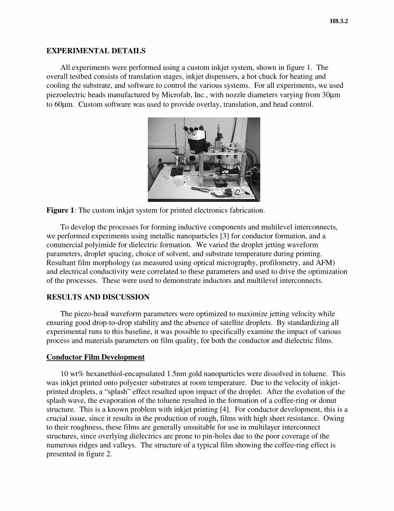
10 wt% hexanethiol-encapsulated 1.5nm gold nanoparticles were dissolved in toluene. Thiswas inkjet printed onto polyester substrates at room temperature. Due to the velocity of inkjet-printed droplets, a “splash” effect resulted upon impact of the droplet. After the evolution of thesplash wave, the evaporation of the toluene resulted in the formation of a coffee-ring or donutstructure. This is a known problem with inkjet printing [4]. For conductor development, this is acrucial issue, since it results in the production of rough, films with high sheet resistance. Owingto their roughness, these films are generally unsuitable for use in multilayer interconnectstructures, since overlying dielectrics are prone to pin-holes due to the poor coverage of thenumerous ridges and valleys. The structure of a typical film showing the coffee-ring effect ispresented in figure 2.
H8.3.2
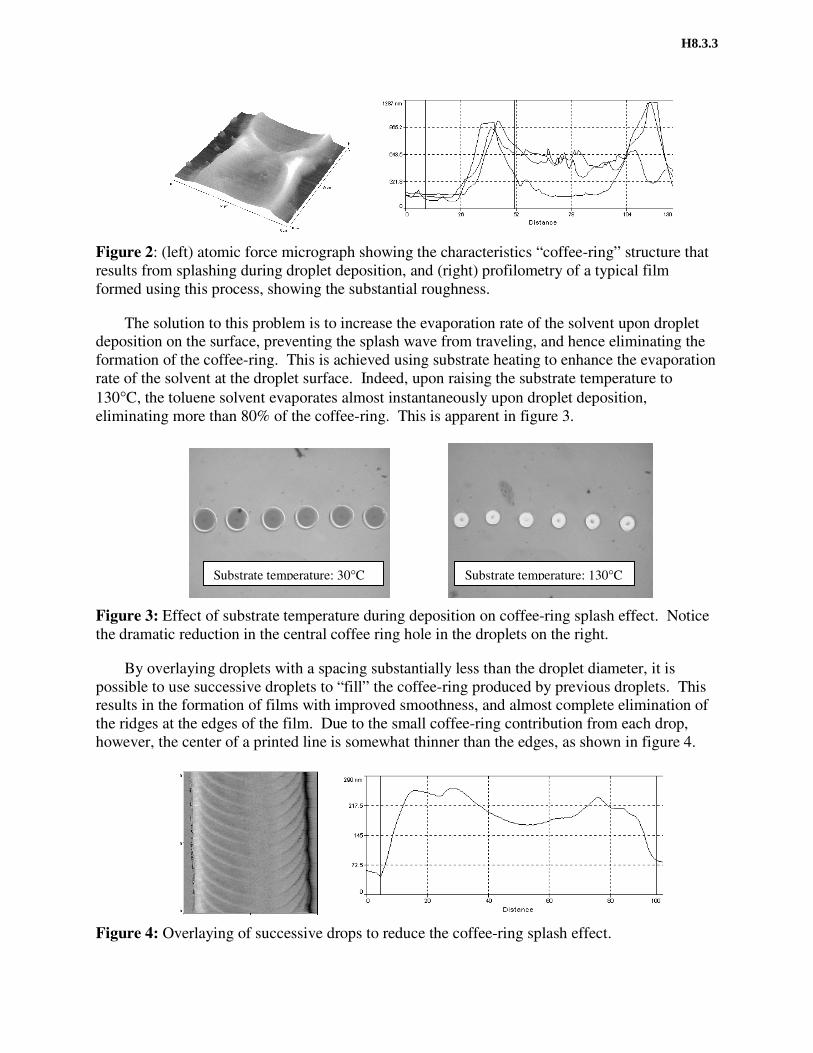
Figure 2: (left) atomic force micrograph showing the characteristics “coffee-ring” structure thatresults from splashing during droplet deposition, and (right) profilometry of a typical filmformed using this process, showing the substantial roughness.
The solution to this problem is to increase the evaporation rate of the solvent upon dropletdeposition on the surface, preventing the splash wave from traveling, and hence eliminating theformation of the coffee-ring. This is achieved using substrate heating to enhance the evaporationrate of the solvent at the droplet surface. Indeed, upon raising the substrate temperature to130°C, the toluene solvent evaporates almost instantaneously upon droplet deposition,eliminating more than 80% of the coffee-ring. This is apparent in figure 3.
Figure 3: Effect of substrate temperature during deposition on coffee-ring splash effect. Noticethe dramatic reduction in the central coffee ring hole in the droplets on the right.
By overlaying droplets with a spacing substantially less than the droplet diameter, it ispossible to use successive droplets to “fill” the coffee-ring produced by previous droplets. Thisresults in the formation of films with improved smoothness, and almost complete elimination ofthe ridges at the edges of the film. Due to the small coffee-ring contribution from each drop,however, the center of a printed line is somewhat thinner than the edges, as shown in figure 4.
Figure 4: Overlaying of successive drops to reduce the coffee-ring splash effect.
Substrate temperature: 30°C Substrate temperature: 130°C
H8.3.3
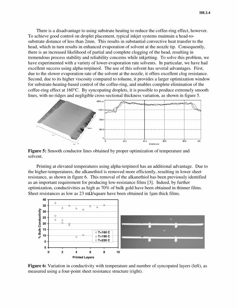
There is a disadvantage to using substrate heating to reduce the coffee-ring effect, however.To achieve good control on droplet placement, typical inkjet systems maintain a head-to-substrate distance of less than 2mm. This results in substantial convective heat transfer to thehead, which in turn results in enhanced evaporation of solvent at the nozzle tip. Consequently,there is an increased likelihood of partial and complete clogging of the head, resulting intremendous process stability and reliability concerns while inkjetting. To solve this problem, wehave experimented with a variety of lower-evaporation rate solvents. In particular, we have hadexcellent success using alpha-terpineol. The use of this solvent has several advantages. First,due to the slower evaporation rate of the solvent at the nozzle, it offers excellent clog resistance.Second, due to its higher viscosity compared to toluene, it provides a larger optimization windowfor substrate-heating-based control of the coffee-ring, and enables complete elimination of thecoffee-ring effect at 160°C. By syncopating droplets, it is possible to produce extremely smoothlines, with no ridges and negligible cross-sectional thickness variation, as shown in figure 5.
Figure 5: Smooth conductor lines obtained by proper optimization of temperature andsolvent.
Printing at elevated temperatures using alpha-terpineol has an additional advantage. Due tothe higher-temperatures, the alkanethiol is removed more efficiently, resulting in lower sheetresistance, as shown in figure 6. This removal of the alkanethiol has been previously identifiedas an important requirement for producing low-resistance films [3]. Indeed, by furtheroptimization, conductivities as high as 70% of bulk gold have been obtained in thinner films.Sheet resistances as low as 23 mΩ/square have been obtained in 1µm thick films.
0
5
10
15
20
25
30
35
40
0 2 4 6 8 10
Printed Layers
%B
ulk
Co
nd
uct
ivit
y
T=160 CT=190 CT=220 C
Figure 6: Variation in conductivity with temperature and number of syncopated layers (left), asmeasured using a four-point sheet resistance structure (right).
H8.3.4
Dielectric Film Development
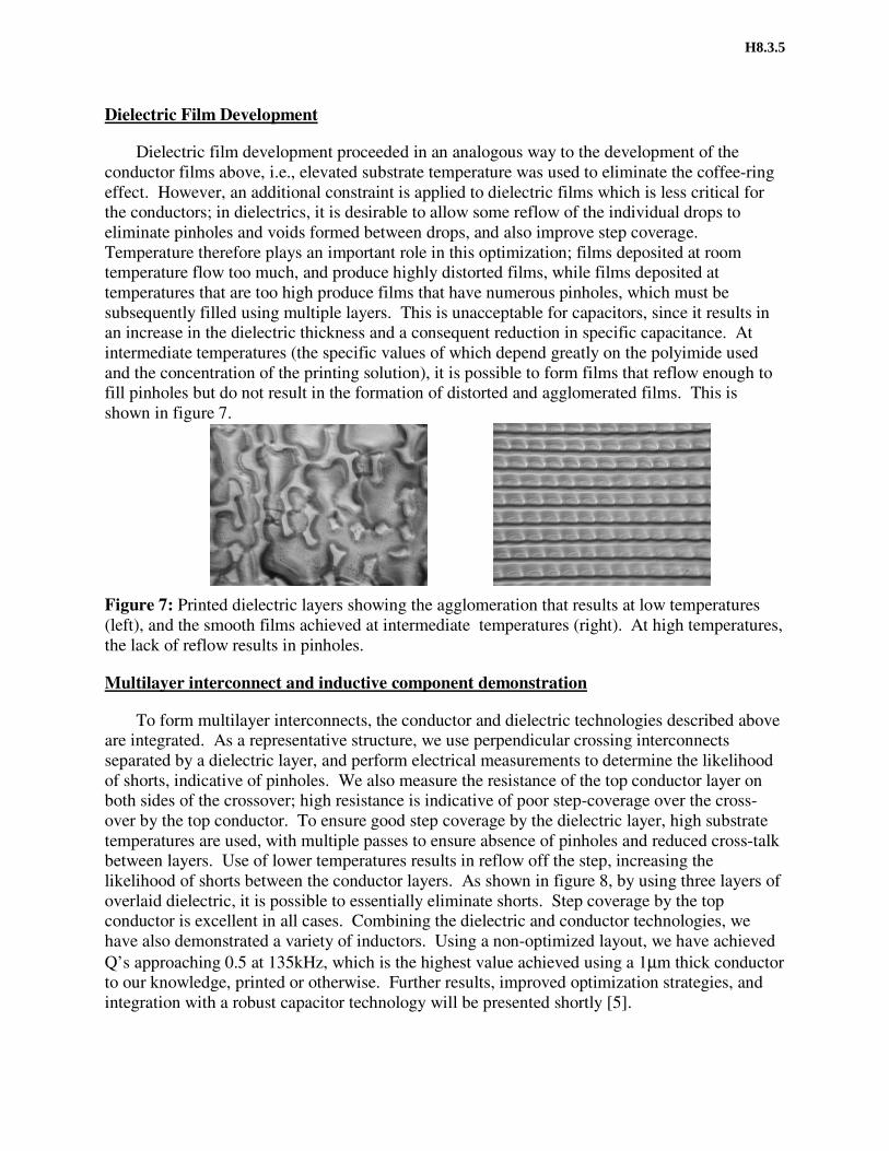
Dielectric film development proceeded in an analogous way to the development of theconductor films above, i.e., elevated substrate temperature was used to eliminate the coffee-ringeffect. However, an additional constraint is applied to dielectric films which is less critical forthe conductors; in dielectrics, it is desirable to allow some reflow of the individual drops toeliminate pinholes and voids formed between drops, and also improve step coverage.Temperature therefore plays an important role in this optimization; films deposited at roomtemperature flow too much, and produce highly distorted films, while films deposited attemperatures that are too high produce films that have numerous pinholes, which must besubsequently filled using multiple layers. This is unacceptable for capacitors, since it results inan increase in the dielectric thickness and a consequent reduction in specific capacitance. Atintermediate temperatures (the specific values of which depend greatly on the polyimide usedand the concentration of the printing solution), it is possible to form films that reflow enough tofill pinholes but do not result in the formation of distorted and agglomerated films. This isshown in figure 7.
Figure 7: Printed dielectric layers showing the agglomeration that results at low temperatures(left), and the smooth films achieved at intermediate temperatures (right). At high temperatures,the lack of reflow results in pinholes.
Multilayer interconnect and inductive component demonstration
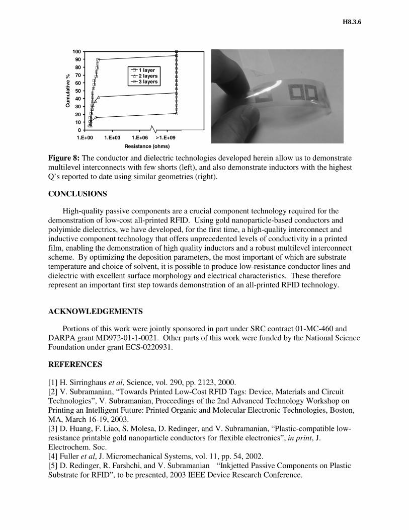
To form multilayer interconnects, the conductor and dielectric technologies described aboveare integrated. As a representative structure, we use perpendicular crossing interconnectsseparated by a dielectric layer, and perform electrical measurements to determine the likelihoodof shorts, indicative of pinholes. We also measure the resistance of the top conductor layer onboth sides of the crossover; high resistance is indicative of poor step-coverage over the cross-over by the top conductor. To ensure good step coverage by the dielectric layer, high substratetemperatures are used, with multiple passes to ensure absence of pinholes and reduced cross-talkbetween layers. Use of lower temperatures results in reflow off the step, increasing thelikelihood of shorts between the conductor layers. As shown in figure 8, by using three layers ofoverlaid dielectric, it is possible to essentially eliminate shorts. Step coverage by the topconductor is excellent in all cases. Combining the dielectric and conductor technologies, wehave also demonstrated a variety of inductors. Using a non-optimized layout, we have achievedQ’s approaching 0.5 at 135kHz, which is the highest value achieved using a 1µm thick conductorto our knowledge, printed or otherwise. Further results, improved optimization strategies, andintegration with a robust capacitor technology will be presented shortly [5].
H8.3.5
0
10
20
30
40
50
60
70
80
90
100
1.E+00 1.E+03 1.E+06 1.E+09 1.E+12
Resistance (ohms)
Cu
mu
lati
ve%
1 layer2 layers3 layers
>
Figure 8: The conductor and dielectric technologies developed herein allow us to demonstratemultilevel interconnects with few shorts (left), and also demonstrate inductors with the highestQ’s reported to date using similar geometries (right).
CONCLUSIONS
High-quality passive components are a crucial component technology required for thedemonstration of low-cost all-printed RFID. Using gold nanoparticle-based conductors andpolyimide dielectrics, we have developed, for the first time, a high-quality interconnect andinductive component technology that offers unprecedented levels of conductivity in a printedfilm, enabling the demonstration of high quality inductors and a robust multilevel interconnectscheme. By optimizing the deposition parameters, the most important of which are substratetemperature and choice of solvent, it is possible to produce low-resistance conductor lines anddielectric with excellent surface morphology and electrical characteristics. These thereforerepresent an important first step towards demonstration of an all-printed RFID technology.
ACKNOWLEDGEMENTS
Portions of this work were jointly sponsored in part under SRC contract 01-MC-460 andDARPA grant MD972-01-1-0021. Other parts of this work were funded by the National ScienceFoundation under grant ECS-0220931.
REFERENCES
[1] H. Sirringhaus et al, Science, vol. 290, pp. 2123, 2000.[2] V. Subramanian, “Towards Printed Low-Cost RFID Tags: Device, Materials and CircuitTechnologies”, V. Subramanian, Proceedings of the 2nd Advanced Technology Workshop onPrinting an Intelligent Future: Printed Organic and Molecular Electronic Technologies, Boston,MA, March 16-19, 2003.[3] D. Huang, F. Liao, S. Molesa, D. Redinger, and V. Subramanian, “Plastic-compatible low-resistance printable gold nanoparticle conductors for flexible electronics”, in print, J.Electrochem. Soc.[4] Fuller et al, J. Micromechanical Systems, vol. 11, pp. 54, 2002.[5] D. Redinger, R. Farshchi, and V. Subramanian “Inkjetted Passive Components on PlasticSubstrate for RFID”, to be presented, 2003 IEEE Device Research Conference.
H8.3.6