samsung sgh-x160 service manual - provinspc2
TRANSCRIPT
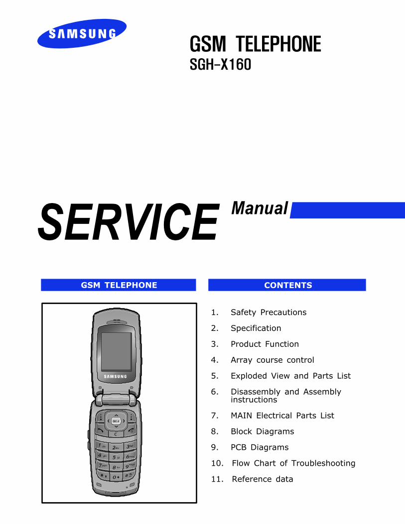
GSM TELEPHONESGH-X160
GSM TELEPHONE CONTENTS
1. Safety Precautions
2. Specification
3. Product Function
4. Array course control
5. Exploded View and Parts List
6. Disassembly and Assemblyinstructions
7. MAIN Electrical Parts List
8. Block Diagrams
9. PCB Diagrams
10. Flow Chart of Troubleshooting
11. Reference data
Contents
1. Safety Precautions1-1. Repair Precaution ...........................................................................1-11-2. ESD(Electrostatically Sensitive Devices) Precaution ...........................1-2
2. Specification2-1. GSM General Specification ..............................................................2-12-2. GSM Tx Power Class ......................................................................2-2
3. Product Function3-1. Main Function ................................................................................3-1
4. Array course controlSoftware Downloading4-1. Downloading Binary Files ................................................................4-24-2. Pre-requsite for Downloading ..........................................................4-24-3. S/W Downloader Program ...............................................................4-3
5. Exploded View and Parts List5-1. Cellular phone Exploded View .........................................................5-15-2. Cellular phone Part list ...................................................................5-2
6. Disassembly and Assembly instructions6-1. Disassembly6-2. Assembly
7. MAIN Electrical Parts List
8. Block Diagrams
9. PCB Diagrams
10. Flow Chart of Troubleshooting10-1. Baseband10-1-1. Power ON ..............................................................................10-1
Contents
10-1-2. Initial ....................................................................................10-310-1-3. Sim Part ...............................................................................10-510-1-4. Microphone Part .....................................................................10-610-1-5. Speaker Part .........................................................................10-810-1-6. LCD backlight ......................................................................10-1010-2. RF10-2-1. GSM Rx ...............................................................................10-1110-2-2. DCS Rx ...............................................................................10-1310-2-3. GSM Tx ...............................................................................10-2110-2-4. DCS Tx ...............................................................................10-17
11. Reference data
SAMSUNG Proprietary-Contents may change without notice
1. Safety Precautions
1-1
This Document can not be used without Samsung's authorization
1-1. Repair Precaution
● Repair in Shield Box, during detailed tuning.
Take specially care of tuning or test,
because specipicty of cellular phone is sensitive for surrounding interference(RF noise).
● Be careful to use a kind of magnetic object or tool,
because performance of parts is damaged by the influence of manetic force.
● Surely use a standard screwdriver when you disassemble this product,
otherwise screw will be worn away.
● Use a thicken twisted wire when you measure level.
A thicken twisted wire has low resistance, therefore error of measurement is few.
● Repair after separate Test Pack and Set because for short danger (for example an
overcurrent and furious flames of parts etc) when you repair board in condition of
connecting Test Pack and tuning on.
● Take specially care of soldering, because Land of PCB is small and weak in heat.
● Surely tune on/off while using AC power plug, because a repair of battery charger is
dangerous when tuning ON/OFF PBA and Connector after disassembing charger.
● Don't use as you pleases after change other material than replacement registered on SEC
System.
Otherwise engineer in charge isn't charged with problem that you don't keep this rules.
SAMSUNG Proprietary-Contents may change without notice
Safety Precautions
1-2
This Document can not be used without Samsung's authorization
1-2. ESD(Electrostatically Sensitive Devices) Precaution
Several semiconductor may be damaged easilly by static electricity. Such parts are called by
ESD(Electrostatically Sensitive Devices), for example IC,BGA chip etc. Read Precaution below.
You can prevent from ESD damage by static electricity.
● Remove static electricity remained your body before you touch semiconductor or parts with
semiconductor. There are ways that you touch an earthed place or wear static electricity
prevention string on wrist.
● Use earthed soldering steel when you connect or disconnect ESD.
● Use soldering removing tool to break static electricity. , otherwise ESD will be damaged by
static electricity.
● Don't unpack until you set up ESD on product. Because most of ESD are packed by box
and aluminum plate to have conductive power,they are prevented from static electricity.
● You must maintain electric contact between ESD and place due to be set up until ESD is
connected completely to the proper place or a circuit board.
2. Specification
2-1
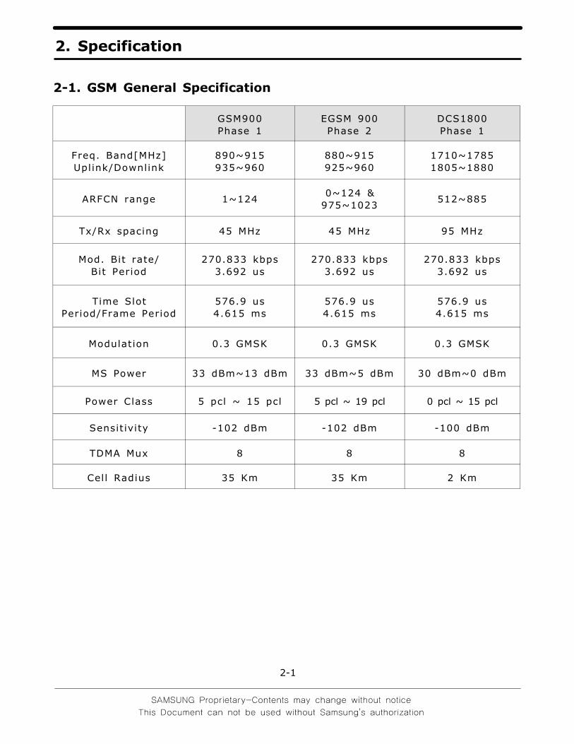
2-1. GSM General Specification
GSM900Phase 1
EGSM 900Phase 2
DCS1800Phase 1
Freq. Band[MHz]Uplink/Downlink
890~915935~960
880~915925~960
1710~17851805~1880
ARFCN range 1~1240~124 &975~1023
512~885
Tx/Rx spacing 45 MHz 45 MHz 95 MHz
Mod. Bit rate/Bit Period
270.833 kbps3.692 us
270.833 kbps3.692 us
270.833 kbps3.692 us
Time SlotPeriod/Frame Period
576.9 us4.615 ms
576.9 us4.615 ms
576.9 us4.615 ms
Modulation 0.3 GMSK 0.3 GMSK 0.3 GMSK
MS Power 33 dBm~13 dBm 33 dBm~5 dBm 30 dBm~0 dBm
Power Class 5 pcl ~ 15 pcl 5 pcl ~ 19 pcl 0 pcl ~ 15 pcl
Sensit ivity -102 dBm -102 dBm -100 dBm
TDMA Mux 8 8 8
Cell Radius 35 Km 35 Km 2 Km
Speclflcation
2-2
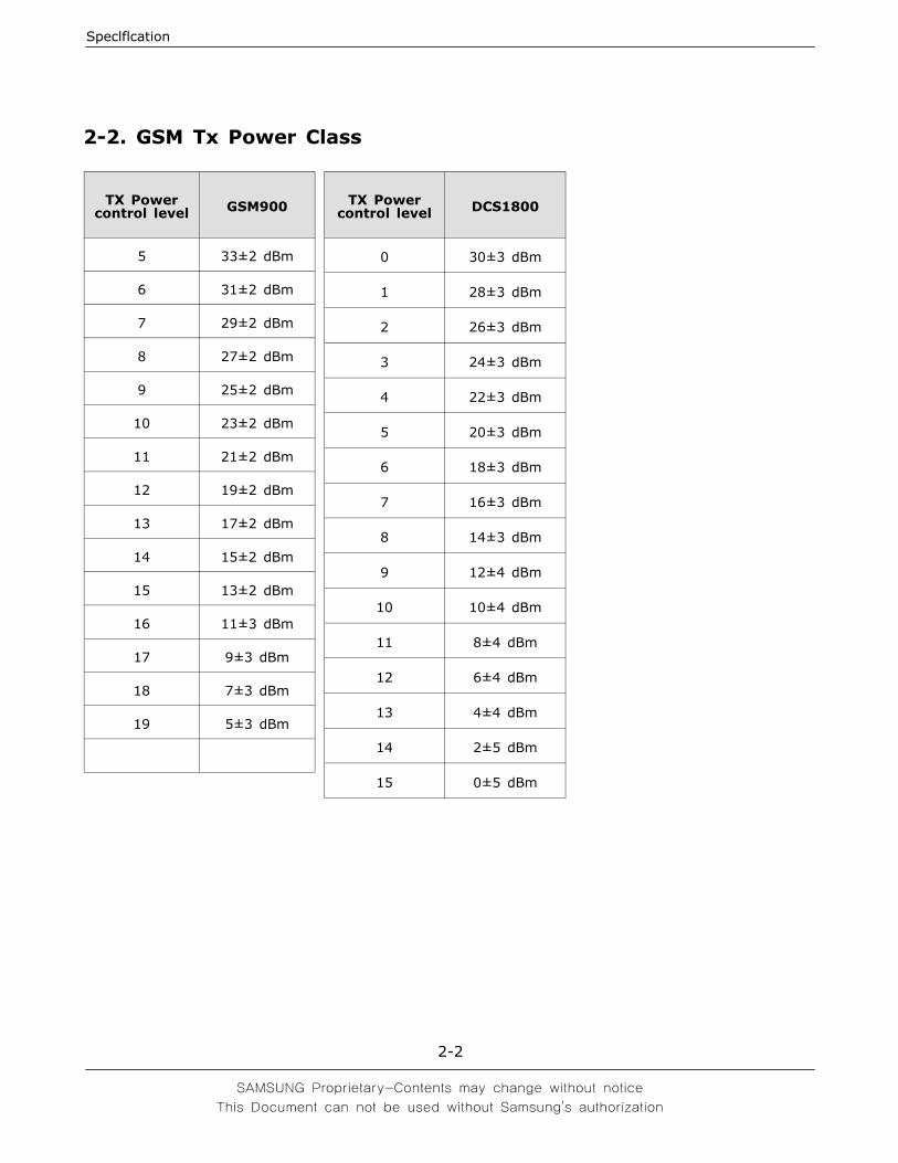
2-2. GSM Tx Power Class
TX Powercontrol level GSM900
5 33±2 dBm
6 31±2 dBm
7 29±2 dBm
8 27±2 dBm
9 25±2 dBm
10 23±2 dBm
11 21±2 dBm
12 19±2 dBm
13 17±2 dBm
14 15±2 dBm
15 13±2 dBm
16 11±3 dBm
17 9±3 dBm
18 7±3 dBm
19 5±3 dBm
TX Powercontrol level DCS1800
0 30±3 dBm
1 28±3 dBm
2 26±3 dBm
3 24±3 dBm
4 22±3 dBm
5 20±3 dBm
6 18±3 dBm
7 16±3 dBm
8 14±3 dBm
9 12±4 dBm
10 10±4 dBm
11 8±4 dBm
12 6±4 dBm
13 4±4 dBm
14 2±5 dBm
15 0±5 dBm
SAMSUNG Proprietary-Contents may change without notice
3. Product Function
3-1
This Document can not be used without Samsung's authorization
Main Function
-Network services
-Sound settings
-Messages
(SMS, MSM, Push messages)
-WAP browser
-Alarm, Calculator, Calendar, Time & Date, Voice mail
SAMSUNG Proprietary-Contents may change without notice
4. Array course control
4-1
This Document can not be used without Samsung's authorization
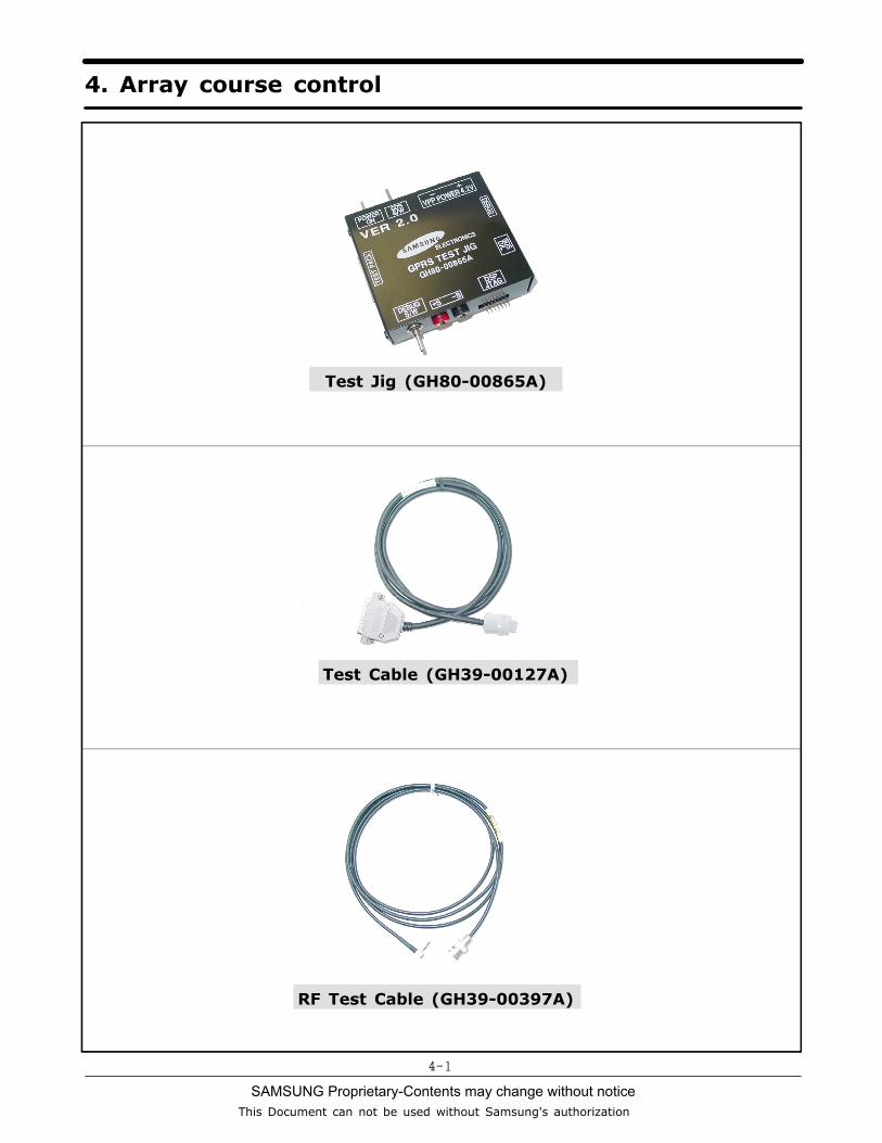
Test Jig (GH80-00865A)
Test Cable (GH39-00127A)
RF Test Cable (GH39-00397A)
SAMSUNG Proprietary-Contents may change without notice
Array course control
4-2
This Document can not be used without Samsung's authorization
Software Downloading
4-1. Downloading Binary Files
• Three binary files for downloading X160.
– X160XXYY.s3 : Main source code binary.
4-2. Pre-requsite for Downloading
• Downloader Program(OptiFlash.exe)
• X160 Mobile Phone
• Data Cable
• Binary files
SAMSUNG Proprietary-Contents may change without notice
Array course control
4-3
This Document can not be used without Samsung's authorization
4-3. S/W Downloader Program
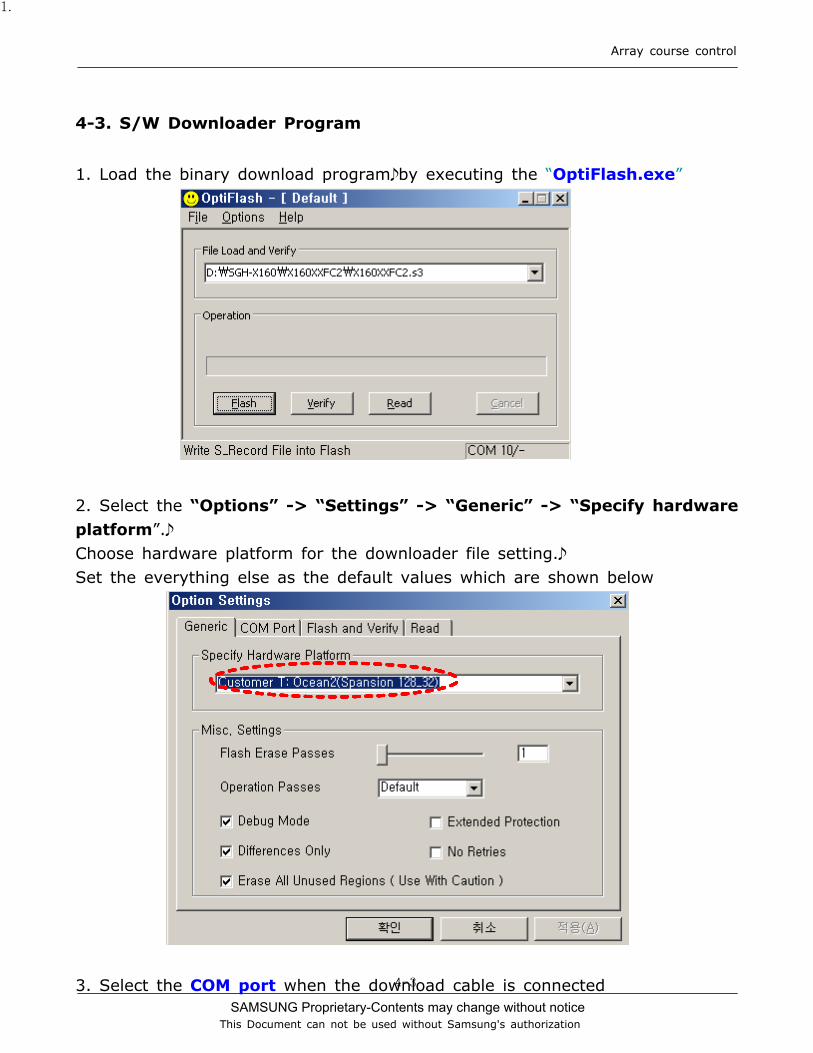
1. Load the binary download program by executing the “OptiFlash.exe”
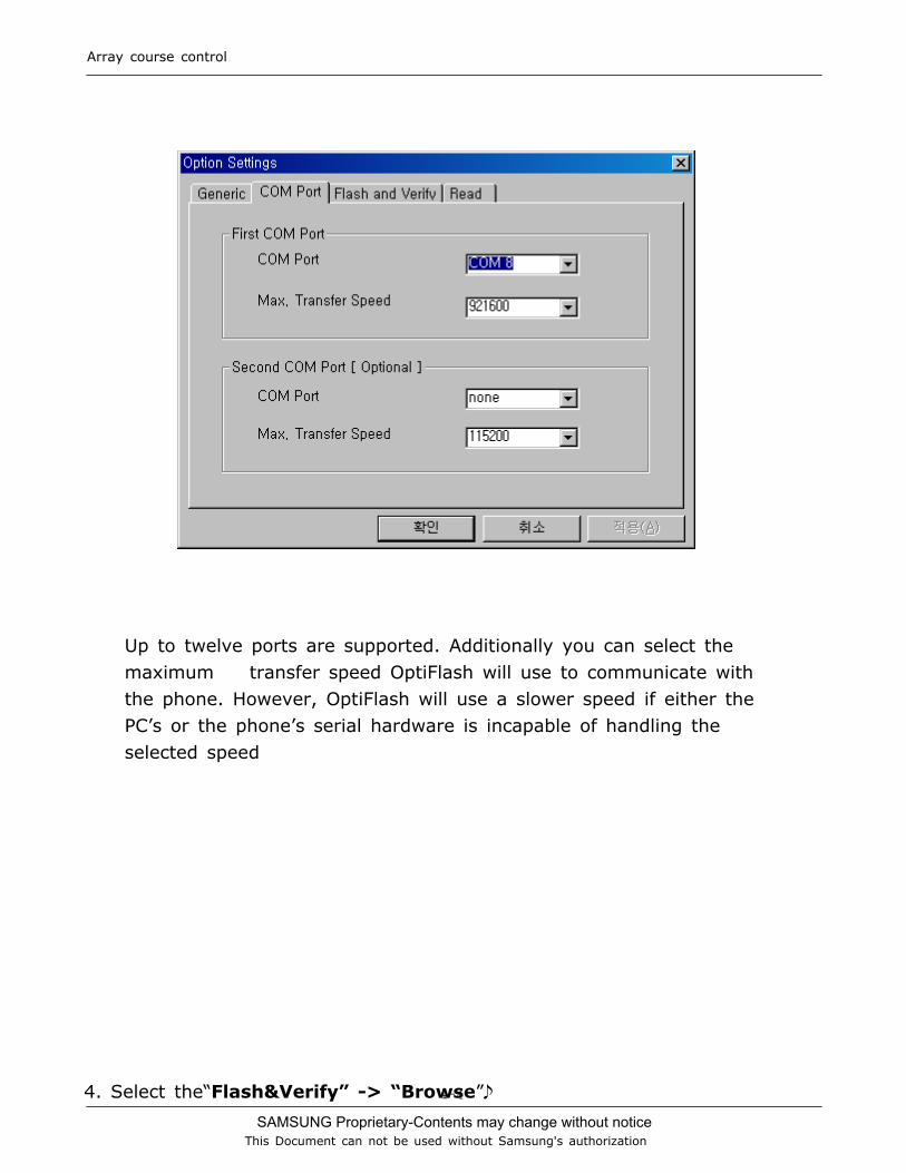
2. Select the “Options” -> “Settings” -> “Generic” -> “Specify hardwareplatform”. Choose hardware platform for the downloader file setting. Set the everything else as the default values which are shown below
3. Select the COM port when the download cable is connected
1.
SAMSUNG Proprietary-Contents may change without notice
Array course control
4-4
This Document can not be used without Samsung's authorization
4. Select the“Flash&Verify” -> “Browse”
Up to twelve ports are supported. Additionally you can select themaximum transfer speed OptiFlash will use to communicate withthe phone. However, OptiFlash will use a slower speed if either thePC’s or the phone’s serial hardware is incapable of handling theselected speed
SAMSUNG Proprietary-Contents may change without notice
Array course control
4-5
This Document can not be used without Samsung's authorization
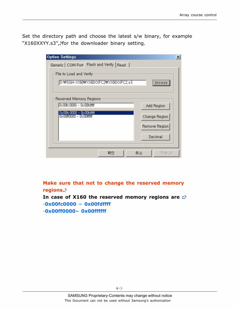
Set the directory path and choose the latest s/w binary, for example“X160XXYY.s3”, for the downloader binary setting.
Make sure that not to change the reserved memoryregions. In case of X160 the reserved memory regions are : -0x00fc0000 – 0x00fdffff-0x00ff0000– 0x00ffffff
SAMSUNG Proprietary-Contents may change without notice
Array course control
4-6
This Document can not be used without Samsung's authorization
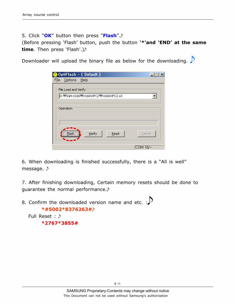
5. Click “OK” button then press “Flash”. (Before pressing ‘Flash’ button, push the button ‘*’and ‘END’ at the sametime. Then press ‘Flash’.)
Downloader will upload the binary file as below for the downloading.
6. When downloading is finished successfully, there is a “All is well”message.
7. After finishing downloading, Certain memory resets should be done toguarantee the normal performance.
8. Confirm the downloaded version name and etc. : *#5002*8376263#
Full Reset : *2767*3855#
SAMSUNG Proprietary-Contents may change without notice
5. Exploded View and Parts List
5-1
This Document can not be used without Samsung's authorization
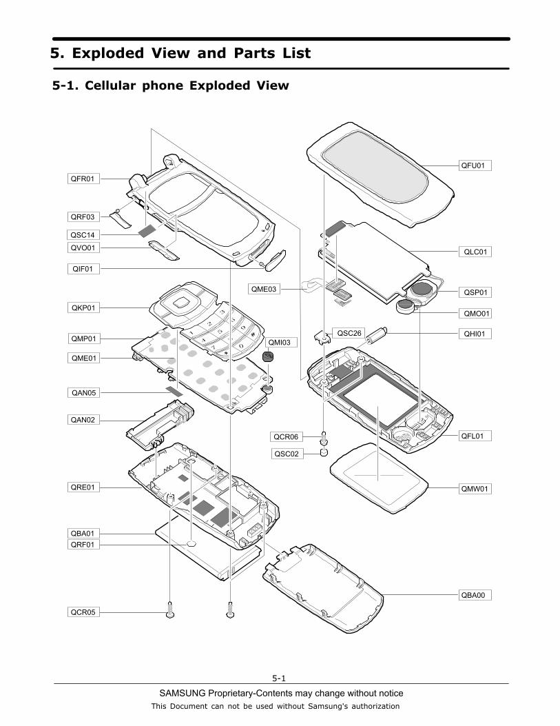
5-1. Cellular phone Exploded View
QFU01
QLC01
QFL01
QMW01
QBA00
QFR01
QKP01
QMP01
QAN02
QRE01
QSP01
QMO01
QHI01
QME01
QBA01
QCR05
QCR06
QSC02
QRF03
QVO01
QIF01
QME03
QRF01
QSC26
QAN05
QSC14
QMI03
SAMSUNG Proprietary-Contents may change without notice
Main Electrical Parts List
5-2
This Document can not be used without Samsung's authorization
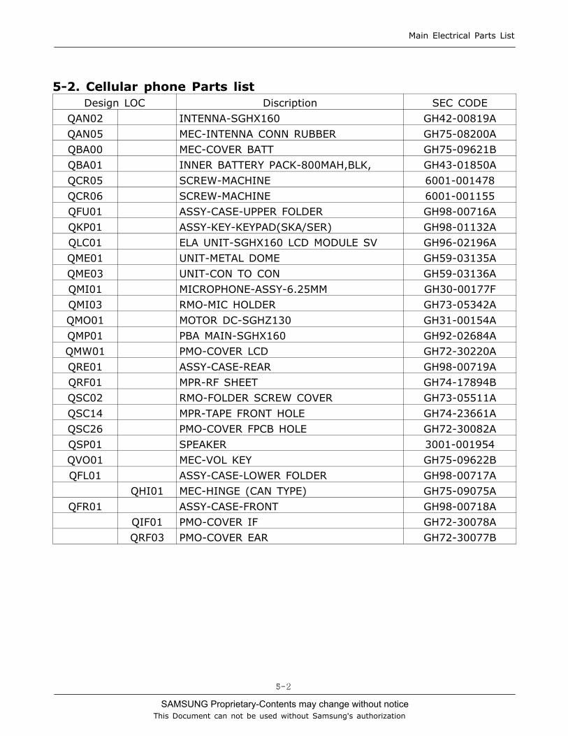
Design LOC Discription SEC CODE
QAN02 INTENNA-SGHX160 GH42-00819A
QAN05 MEC-INTENNA CONN RUBBER GH75-08200A
QBA00 MEC-COVER BATT GH75-09621B
QBA01 INNER BATTERY PACK-800MAH,BLK, GH43-01850A
QCR05 SCREW-MACHINE 6001-001478
QCR06 SCREW-MACHINE 6001-001155
QFU01 ASSY-CASE-UPPER FOLDER GH98-00716A
QKP01 ASSY-KEY-KEYPAD(SKA/SER) GH98-01132A
QLC01 ELA UNIT-SGHX160 LCD MODULE SV GH96-02196A
QME01 UNIT-METAL DOME GH59-03135A
QME03 UNIT-CON TO CON GH59-03136A
QMI01 MICROPHONE-ASSY-6.25MM GH30-00177F
QMI03 RMO-MIC HOLDER GH73-05342A
QMO01 MOTOR DC-SGHZ130 GH31-00154A
QMP01 PBA MAIN-SGHX160 GH92-02684A
QMW01 PMO-COVER LCD GH72-30220A
QRE01 ASSY-CASE-REAR GH98-00719A
QRF01 MPR-RF SHEET GH74-17894B
QSC02 RMO-FOLDER SCREW COVER GH73-05511A
QSC14 MPR-TAPE FRONT HOLE GH74-23661A
QSC26 PMO-COVER FPCB HOLE GH72-30082A
QSP01 SPEAKER 3001-001954
QVO01 MEC-VOL KEY GH75-09622B
QFL01 ASSY-CASE-LOWER FOLDER GH98-00717A QHI01 MEC-HINGE (CAN TYPE) GH75-09075A
QFR01 ASSY-CASE-FRONT GH98-00718A QIF01 PMO-COVER IF GH72-30078A QRF03 PMO-COVER EAR GH72-30077B
5-2. Cellular phone Parts list
SAMSUNG Proprietary-Contents may change without notice
Main Electrical Parts List
5-3
This Document can not be used without Samsung's authorization
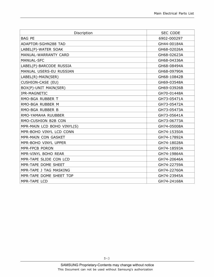
Discription SEC CODE
BAG PE 6902-000297
ADAPTOR-SGHN288 TAD GH44-00184A
LABEL(P)-WATER SOAK GH68-02026A
MANUAL-WARRANTY CARD GH68-02623A
MANUAL-SFC GH68-04336A
LABEL(P)-BARCODE RUSSIA GH68-08494A
MANUAL USERS-EU RUSSIAN GH68-09790A
LABEL(R)-MAIN(SER) GH68-10842B
CUSHION-CASE (EU) GH69-03548A
BOX(P)-UNIT MAIN(SER) GH69-03926B
IPR-MAGNETIC GH70-01448A
RMO-BGA RUBBER T GH73-05471A
RMO-BGA RUBBER M GH73-05472A
RMO-BGA RUBBER B GH73-05473A
RMO-YAMAHA RUUBBER GH73-05641A
RMO-CUSHION B2B CON GH73-06773A
MPR-MAIN LCD BOHO VINYL(S) GH74-05008A
MPR-BOHO VINYL LCD CONN GH74-15350A
MPR-MAIN CON GASKET GH74-17892A
MPR-BOHO VINYL UPPER GH74-18028A
MPR-FPCB PORON GH74-18593A
MPR-VINYL BOHO REAR GH74-19864A
MPR-TAPE SLIDE CON LCD GH74-20646A
MPR-TAPE DOME SHEET GH74-22759A
MPR-TAPE J TAG MASKING GH74-22760A
MPR-TAPE DOME SHEET TOP GH74-23945A
MPR-TAPE LCD GH74-24168A
SAMSUNG Proprietary-Contents may change without notice
6. Disassembly and Assembly instructions
6-1
This Document can not be used without Samsung's authorization
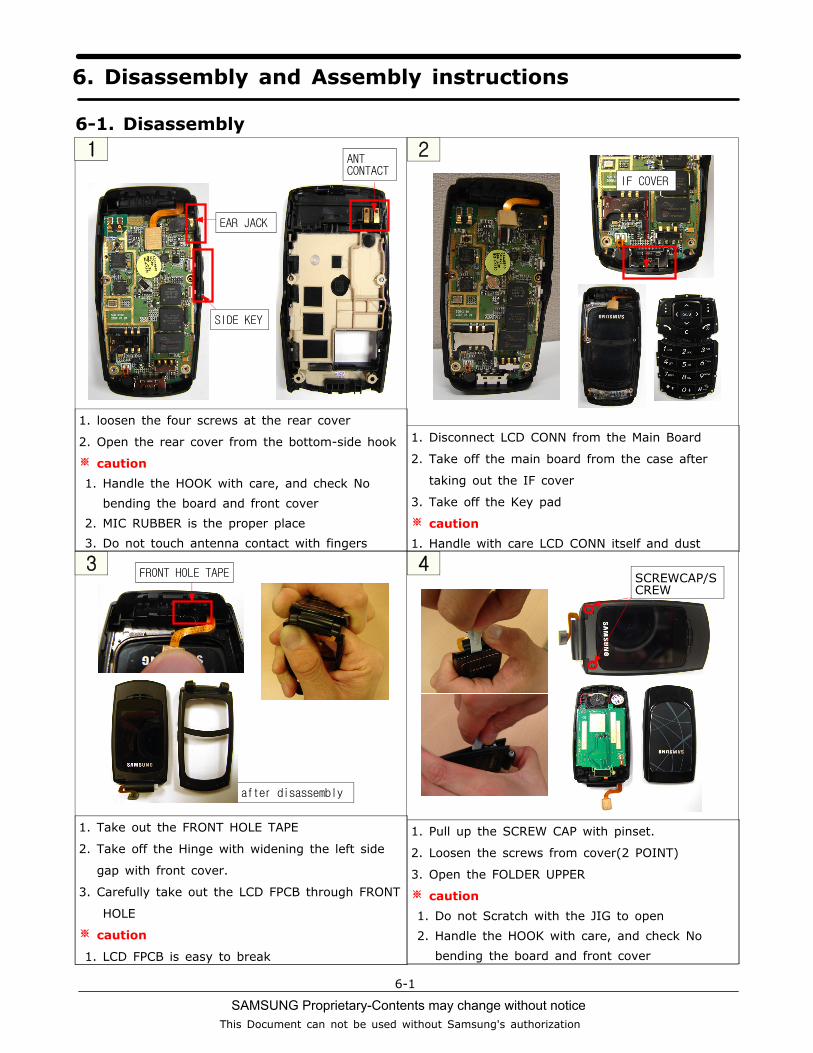
6-1. Disassembly
ANTCONTACT
SIDE KEY
EAR JACK
1. loosen the four screws at the rear cover
2. Open the rear cover from the bottom-side hook
※ caution
1. Handle the HOOK with care, and check No
bending the board and front cover
2. MIC RUBBER is the proper place
3. Do not touch antenna contact with fingers
IF COVER
1. Disconnect LCD CONN from the Main Board
2. Take off the main board from the case after
taking out the IF cover
3. Take off the Key pad
※ caution
1. Handle with care LCD CONN itself and dust
FRONT HOLE TAPE
after disassembly
1. Take out the FRONT HOLE TAPE
2. Take off the Hinge with widening the left side
gap with front cover.
3. Carefully take out the LCD FPCB through FRONT
HOLE
※ caution
1. LCD FPCB is easy to break
SCREWCAP/SCREW
1. Pull up the SCREW CAP with pinset.
2. Loosen the screws from cover(2 POINT)
3. Open the FOLDER UPPER
※ caution
1. Do not Scratch with the JIG to open
2. Handle the HOOK with care, and check No
bending the board and front cover
1
43
2
SAMSUNG Proprietary-Contents may change without notice
Disassembly and Assembly instructions
6-2
This Document can not be used without Samsung's authorization
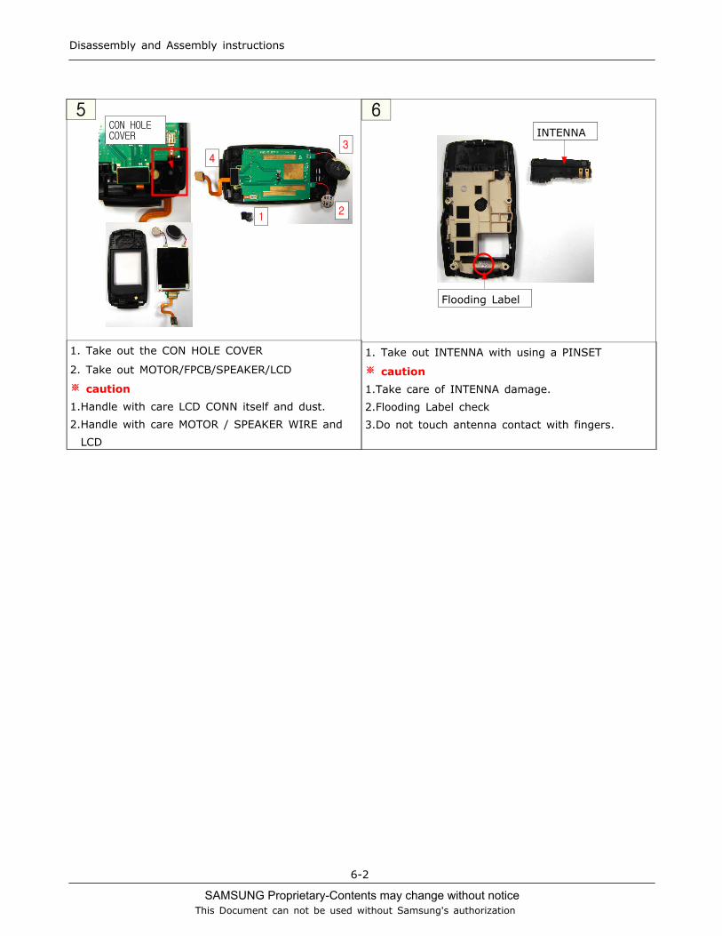
1. Take out the CON HOLE COVER
2. Take out MOTOR/FPCB/SPEAKER/LCD
※ caution
1.Handle with care LCD CONN itself and dust.
2.Handle with care MOTOR / SPEAKER WIRE and
LCD
1. Take out INTENNA with using a PINSET
※ caution
1.Take care of INTENNA damage.
2.Flooding Label check
3.Do not touch antenna contact with fingers.
5 6
1
4
3
2
CON HOLECOVER
Flooding Label
INTENNA
SAMSUNG Proprietary-Contents may change without notice
Disassembly and Assembly instructions
6-3
This Document can not be used without Samsung's authorization
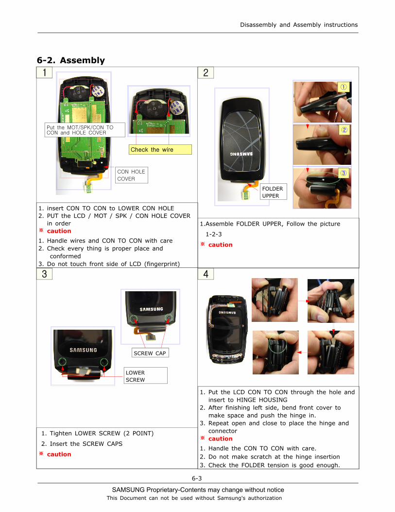
6-2. Assembly
1. insert CON TO CON to LOWER CON HOLE2. PUT the LCD / MOT / SPK / CON HOLE COVERin order
※ caution
1. Handle wires and CON TO CON with care2. Check every thing is proper place andconformed
3. Do not touch front side of LCD (fingerprint)
1.Assemble FOLDER UPPER, Follow the picture
1-2-3
※ caution
1. Tighten LOWER SCREW (2 POINT)
2. Insert the SCREW CAPS
※ caution
1. Put the LCD CON TO CON through the hole andinsert to HINGE HOUSING
2. After finishing left side, bend front cover tomake space and push the hinge in.
3. Repeat open and close to place the hinge andconnector
※ caution
1. Handle the CON TO CON with care.2. Do not make scratch at the hinge insertion3. Check the FOLDER tension is good enough.
1
43
2
Check the wire
CON HOLE
COVER
Put the MOT/SPK/CON TOCON and HOLE COVER
①
②
③
FOLDERUPPER
SCREW CAP
LOWERSCREW
SAMSUNG Proprietary-Contents may change without notice
Disassembly and Assembly instructions
6-4
This Document can not be used without Samsung's authorization
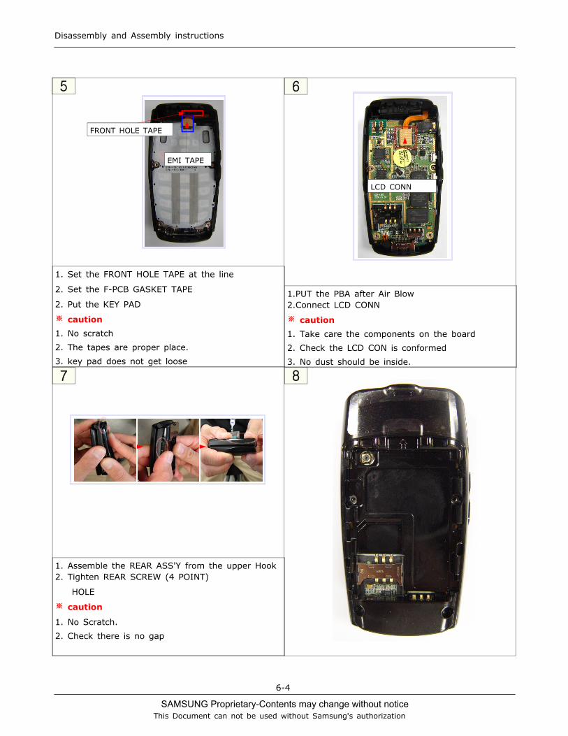
1. Set the FRONT HOLE TAPE at the line
2. Set the F-PCB GASKET TAPE
2. Put the KEY PAD
※ caution
1. No scratch
2. The tapes are proper place.
3. key pad does not get loose
1.PUT the PBA after Air Blow2.Connect LCD CONN
※ caution
1. Take care the components on the board
2. Check the LCD CON is conformed
3. No dust should be inside.
1. Assemble the REAR ASS'Y from the upper Hook2. Tighten REAR SCREW (4 POINT)
HOLE
※ caution
1. No Scratch.
2. Check there is no gap
5
87
6
EMI TAPE
FRONT HOLE TAPE
LCD CONN
SAMSUNG Proprietary-Contents may change without notice
7-1
This Document can not be used without Samsung's authorization
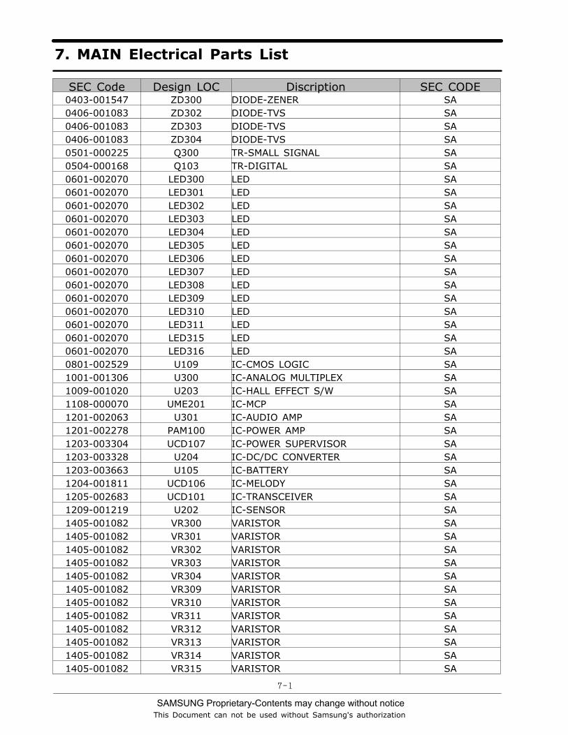
7. MAIN Electrical Parts List
SEC Code Design LOC Discription SEC CODE0403-001547 ZD300 DIODE-ZENER SA0406-001083 ZD302 DIODE-TVS SA0406-001083 ZD303 DIODE-TVS SA0406-001083 ZD304 DIODE-TVS SA0501-000225 Q300 TR-SMALL SIGNAL SA0504-000168 Q103 TR-DIGITAL SA0601-002070 LED300 LED SA0601-002070 LED301 LED SA0601-002070 LED302 LED SA0601-002070 LED303 LED SA0601-002070 LED304 LED SA0601-002070 LED305 LED SA0601-002070 LED306 LED SA0601-002070 LED307 LED SA0601-002070 LED308 LED SA0601-002070 LED309 LED SA0601-002070 LED310 LED SA0601-002070 LED311 LED SA0601-002070 LED315 LED SA0601-002070 LED316 LED SA0801-002529 U109 IC-CMOS LOGIC SA1001-001306 U300 IC-ANALOG MULTIPLEX SA1009-001020 U203 IC-HALL EFFECT S/W SA1108-000070 UME201 IC-MCP SA1201-002063 U301 IC-AUDIO AMP SA1201-002278 PAM100 IC-POWER AMP SA1203-003304 UCD107 IC-POWER SUPERVISOR SA1203-003328 U204 IC-DC/DC CONVERTER SA1203-003663 U105 IC-BATTERY SA1204-001811 UCD106 IC-MELODY SA1205-002683 UCD101 IC-TRANSCEIVER SA1209-001219 U202 IC-SENSOR SA1405-001082 VR300 VARISTOR SA1405-001082 VR301 VARISTOR SA1405-001082 VR302 VARISTOR SA1405-001082 VR303 VARISTOR SA1405-001082 VR304 VARISTOR SA1405-001082 VR309 VARISTOR SA1405-001082 VR310 VARISTOR SA1405-001082 VR311 VARISTOR SA1405-001082 VR312 VARISTOR SA1405-001082 VR313 VARISTOR SA1405-001082 VR314 VARISTOR SA1405-001082 VR315 VARISTOR SA
SAMSUNG Proprietary-Contents may change without notice
Exploded View and Parts List
7-2
This Document can not be used without Samsung's authorization
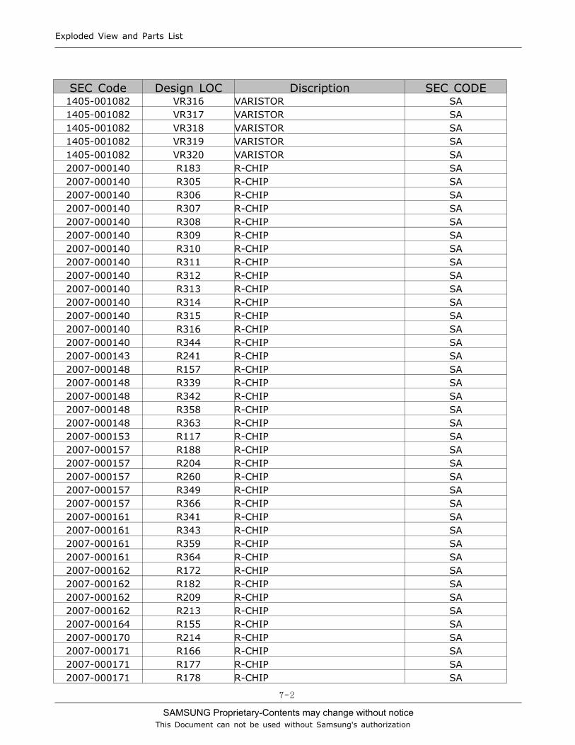
SEC Code Design LOC Discription SEC CODE1405-001082 VR316 VARISTOR SA1405-001082 VR317 VARISTOR SA1405-001082 VR318 VARISTOR SA1405-001082 VR319 VARISTOR SA1405-001082 VR320 VARISTOR SA2007-000140 R183 R-CHIP SA2007-000140 R305 R-CHIP SA2007-000140 R306 R-CHIP SA2007-000140 R307 R-CHIP SA2007-000140 R308 R-CHIP SA2007-000140 R309 R-CHIP SA2007-000140 R310 R-CHIP SA2007-000140 R311 R-CHIP SA2007-000140 R312 R-CHIP SA2007-000140 R313 R-CHIP SA2007-000140 R314 R-CHIP SA2007-000140 R315 R-CHIP SA2007-000140 R316 R-CHIP SA2007-000140 R344 R-CHIP SA2007-000143 R241 R-CHIP SA2007-000148 R157 R-CHIP SA2007-000148 R339 R-CHIP SA2007-000148 R342 R-CHIP SA2007-000148 R358 R-CHIP SA2007-000148 R363 R-CHIP SA2007-000153 R117 R-CHIP SA2007-000157 R188 R-CHIP SA2007-000157 R204 R-CHIP SA2007-000157 R260 R-CHIP SA2007-000157 R349 R-CHIP SA2007-000157 R366 R-CHIP SA2007-000161 R341 R-CHIP SA2007-000161 R343 R-CHIP SA2007-000161 R359 R-CHIP SA2007-000161 R364 R-CHIP SA2007-000162 R172 R-CHIP SA2007-000162 R182 R-CHIP SA2007-000162 R209 R-CHIP SA2007-000162 R213 R-CHIP SA2007-000164 R155 R-CHIP SA2007-000170 R214 R-CHIP SA2007-000171 R166 R-CHIP SA2007-000171 R177 R-CHIP SA2007-000171 R178 R-CHIP SA
SAMSUNG Proprietary-Contents may change without notice
Exploded View and Parts List
7-3
This Document can not be used without Samsung's authorization
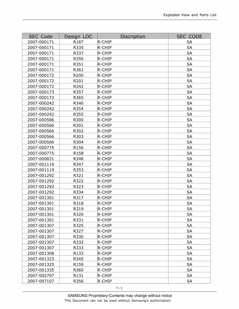
SEC Code Design LOC Discription SEC CODE2007-000171 R187 R-CHIP SA2007-000171 R335 R-CHIP SA2007-000171 R337 R-CHIP SA2007-000171 R350 R-CHIP SA2007-000171 R351 R-CHIP SA2007-000171 R361 R-CHIP SA2007-000172 R200 R-CHIP SA2007-000172 R201 R-CHIP SA2007-000172 R242 R-CHIP SA2007-000173 R357 R-CHIP SA2007-000173 R365 R-CHIP SA2007-000242 R340 R-CHIP SA2007-000242 R354 R-CHIP SA2007-000242 R355 R-CHIP SA2007-000566 R300 R-CHIP SA2007-000566 R301 R-CHIP SA2007-000566 R302 R-CHIP SA2007-000566 R303 R-CHIP SA2007-000566 R304 R-CHIP SA2007-000775 R156 R-CHIP SA2007-000775 R158 R-CHIP SA2007-000831 R348 R-CHIP SA2007-001119 R347 R-CHIP SA2007-001119 R353 R-CHIP SA2007-001292 R321 R-CHIP SA2007-001292 R322 R-CHIP SA2007-001292 R323 R-CHIP SA2007-001292 R334 R-CHIP SA2007-001301 R317 R-CHIP SA2007-001301 R318 R-CHIP SA2007-001301 R319 R-CHIP SA2007-001301 R320 R-CHIP SA2007-001301 R331 R-CHIP SA2007-001307 R325 R-CHIP SA2007-001307 R327 R-CHIP SA2007-001307 R330 R-CHIP SA2007-001307 R332 R-CHIP SA2007-001307 R333 R-CHIP SA2007-001308 R133 R-CHIP SA2007-001323 R345 R-CHIP SA2007-001325 R159 R-CHIP SA2007-001335 R360 R-CHIP SA2007-002797 R131 R-CHIP SA2007-007107 R356 R-CHIP SA
SAMSUNG Proprietary-Contents may change without notice
Exploded View and Parts List
7-4
This Document can not be used without Samsung's authorization
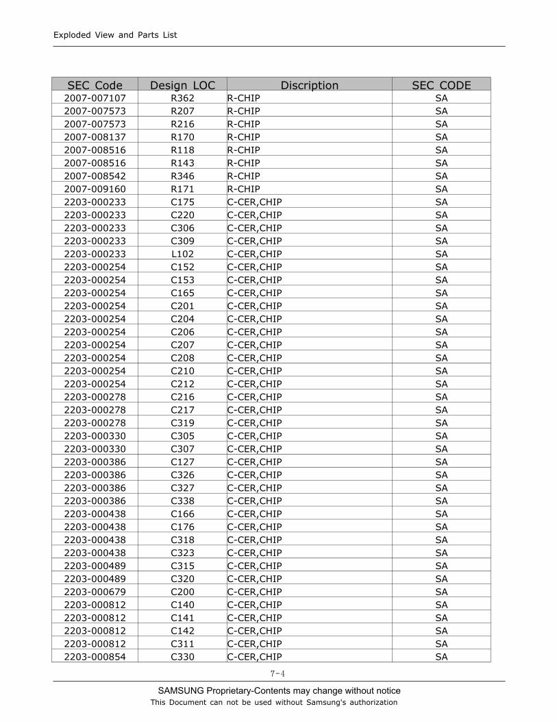
SEC Code Design LOC Discription SEC CODE2007-007107 R362 R-CHIP SA2007-007573 R207 R-CHIP SA2007-007573 R216 R-CHIP SA2007-008137 R170 R-CHIP SA2007-008516 R118 R-CHIP SA2007-008516 R143 R-CHIP SA2007-008542 R346 R-CHIP SA2007-009160 R171 R-CHIP SA2203-000233 C175 C-CER,CHIP SA2203-000233 C220 C-CER,CHIP SA2203-000233 C306 C-CER,CHIP SA2203-000233 C309 C-CER,CHIP SA2203-000233 L102 C-CER,CHIP SA2203-000254 C152 C-CER,CHIP SA2203-000254 C153 C-CER,CHIP SA2203-000254 C165 C-CER,CHIP SA2203-000254 C201 C-CER,CHIP SA2203-000254 C204 C-CER,CHIP SA2203-000254 C206 C-CER,CHIP SA2203-000254 C207 C-CER,CHIP SA2203-000254 C208 C-CER,CHIP SA2203-000254 C210 C-CER,CHIP SA2203-000254 C212 C-CER,CHIP SA2203-000278 C216 C-CER,CHIP SA2203-000278 C217 C-CER,CHIP SA2203-000278 C319 C-CER,CHIP SA2203-000330 C305 C-CER,CHIP SA2203-000330 C307 C-CER,CHIP SA2203-000386 C127 C-CER,CHIP SA2203-000386 C326 C-CER,CHIP SA2203-000386 C327 C-CER,CHIP SA2203-000386 C338 C-CER,CHIP SA2203-000438 C166 C-CER,CHIP SA2203-000438 C176 C-CER,CHIP SA2203-000438 C318 C-CER,CHIP SA2203-000438 C323 C-CER,CHIP SA2203-000489 C315 C-CER,CHIP SA2203-000489 C320 C-CER,CHIP SA2203-000679 C200 C-CER,CHIP SA2203-000812 C140 C-CER,CHIP SA2203-000812 C141 C-CER,CHIP SA2203-000812 C142 C-CER,CHIP SA2203-000812 C311 C-CER,CHIP SA2203-000854 C330 C-CER,CHIP SA
SAMSUNG Proprietary-Contents may change without notice
Exploded View and Parts List
7-5
This Document can not be used without Samsung's authorization
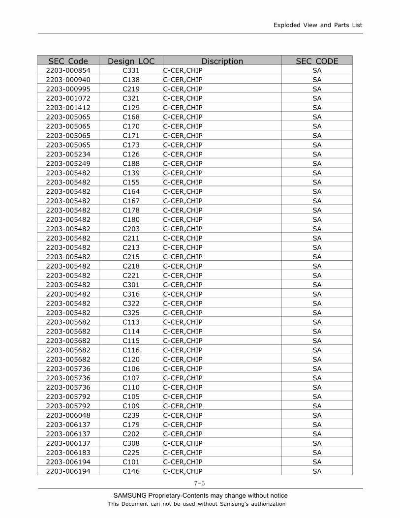
SEC Code Design LOC Discription SEC CODE2203-000854 C331 C-CER,CHIP SA2203-000940 C138 C-CER,CHIP SA2203-000995 C219 C-CER,CHIP SA2203-001072 C321 C-CER,CHIP SA2203-001412 C129 C-CER,CHIP SA2203-005065 C168 C-CER,CHIP SA2203-005065 C170 C-CER,CHIP SA2203-005065 C171 C-CER,CHIP SA2203-005065 C173 C-CER,CHIP SA2203-005234 C126 C-CER,CHIP SA2203-005249 C188 C-CER,CHIP SA2203-005482 C139 C-CER,CHIP SA2203-005482 C155 C-CER,CHIP SA2203-005482 C164 C-CER,CHIP SA2203-005482 C167 C-CER,CHIP SA2203-005482 C178 C-CER,CHIP SA2203-005482 C180 C-CER,CHIP SA2203-005482 C203 C-CER,CHIP SA2203-005482 C211 C-CER,CHIP SA2203-005482 C213 C-CER,CHIP SA2203-005482 C215 C-CER,CHIP SA2203-005482 C218 C-CER,CHIP SA2203-005482 C221 C-CER,CHIP SA2203-005482 C301 C-CER,CHIP SA2203-005482 C316 C-CER,CHIP SA2203-005482 C322 C-CER,CHIP SA2203-005482 C325 C-CER,CHIP SA2203-005682 C113 C-CER,CHIP SA2203-005682 C114 C-CER,CHIP SA2203-005682 C115 C-CER,CHIP SA2203-005682 C116 C-CER,CHIP SA2203-005682 C120 C-CER,CHIP SA2203-005736 C106 C-CER,CHIP SA2203-005736 C107 C-CER,CHIP SA2203-005736 C110 C-CER,CHIP SA2203-005792 C105 C-CER,CHIP SA2203-005792 C109 C-CER,CHIP SA2203-006048 C239 C-CER,CHIP SA2203-006137 C179 C-CER,CHIP SA2203-006137 C202 C-CER,CHIP SA2203-006137 C308 C-CER,CHIP SA2203-006183 C225 C-CER,CHIP SA2203-006194 C101 C-CER,CHIP SA2203-006194 C146 C-CER,CHIP SA
SAMSUNG Proprietary-Contents may change without notice
Exploded View and Parts List
7-6
This Document can not be used without Samsung's authorization
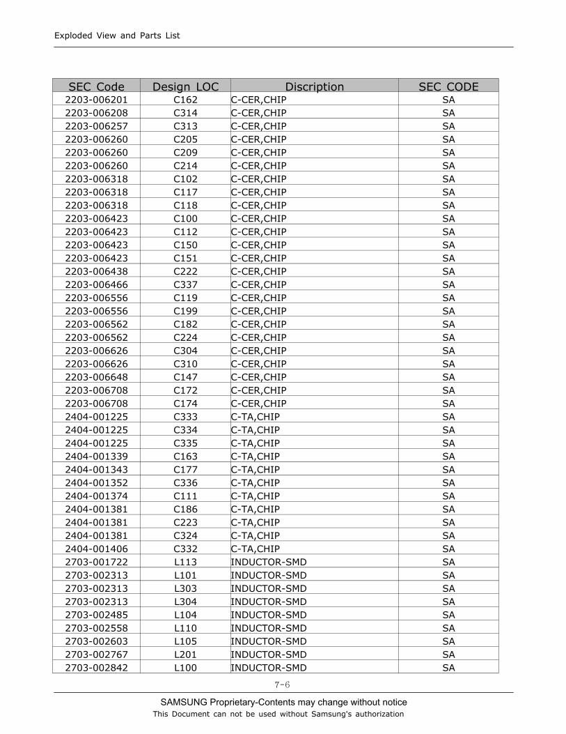
SEC Code Design LOC Discription SEC CODE2203-006201 C162 C-CER,CHIP SA2203-006208 C314 C-CER,CHIP SA2203-006257 C313 C-CER,CHIP SA2203-006260 C205 C-CER,CHIP SA2203-006260 C209 C-CER,CHIP SA2203-006260 C214 C-CER,CHIP SA2203-006318 C102 C-CER,CHIP SA2203-006318 C117 C-CER,CHIP SA2203-006318 C118 C-CER,CHIP SA2203-006423 C100 C-CER,CHIP SA2203-006423 C112 C-CER,CHIP SA2203-006423 C150 C-CER,CHIP SA2203-006423 C151 C-CER,CHIP SA2203-006438 C222 C-CER,CHIP SA2203-006466 C337 C-CER,CHIP SA2203-006556 C119 C-CER,CHIP SA2203-006556 C199 C-CER,CHIP SA2203-006562 C182 C-CER,CHIP SA2203-006562 C224 C-CER,CHIP SA2203-006626 C304 C-CER,CHIP SA2203-006626 C310 C-CER,CHIP SA2203-006648 C147 C-CER,CHIP SA2203-006708 C172 C-CER,CHIP SA2203-006708 C174 C-CER,CHIP SA2404-001225 C333 C-TA,CHIP SA2404-001225 C334 C-TA,CHIP SA2404-001225 C335 C-TA,CHIP SA2404-001339 C163 C-TA,CHIP SA2404-001343 C177 C-TA,CHIP SA2404-001352 C336 C-TA,CHIP SA2404-001374 C111 C-TA,CHIP SA2404-001381 C186 C-TA,CHIP SA2404-001381 C223 C-TA,CHIP SA2404-001381 C324 C-TA,CHIP SA2404-001406 C332 C-TA,CHIP SA2703-001722 L113 INDUCTOR-SMD SA2703-002313 L101 INDUCTOR-SMD SA2703-002313 L303 INDUCTOR-SMD SA2703-002313 L304 INDUCTOR-SMD SA2703-002485 L104 INDUCTOR-SMD SA2703-002558 L110 INDUCTOR-SMD SA2703-002603 L105 INDUCTOR-SMD SA2703-002767 L201 INDUCTOR-SMD SA2703-002842 L100 INDUCTOR-SMD SA
SAMSUNG Proprietary-Contents may change without notice
Exploded View and Parts List
7-7
This Document can not be used without Samsung's authorization
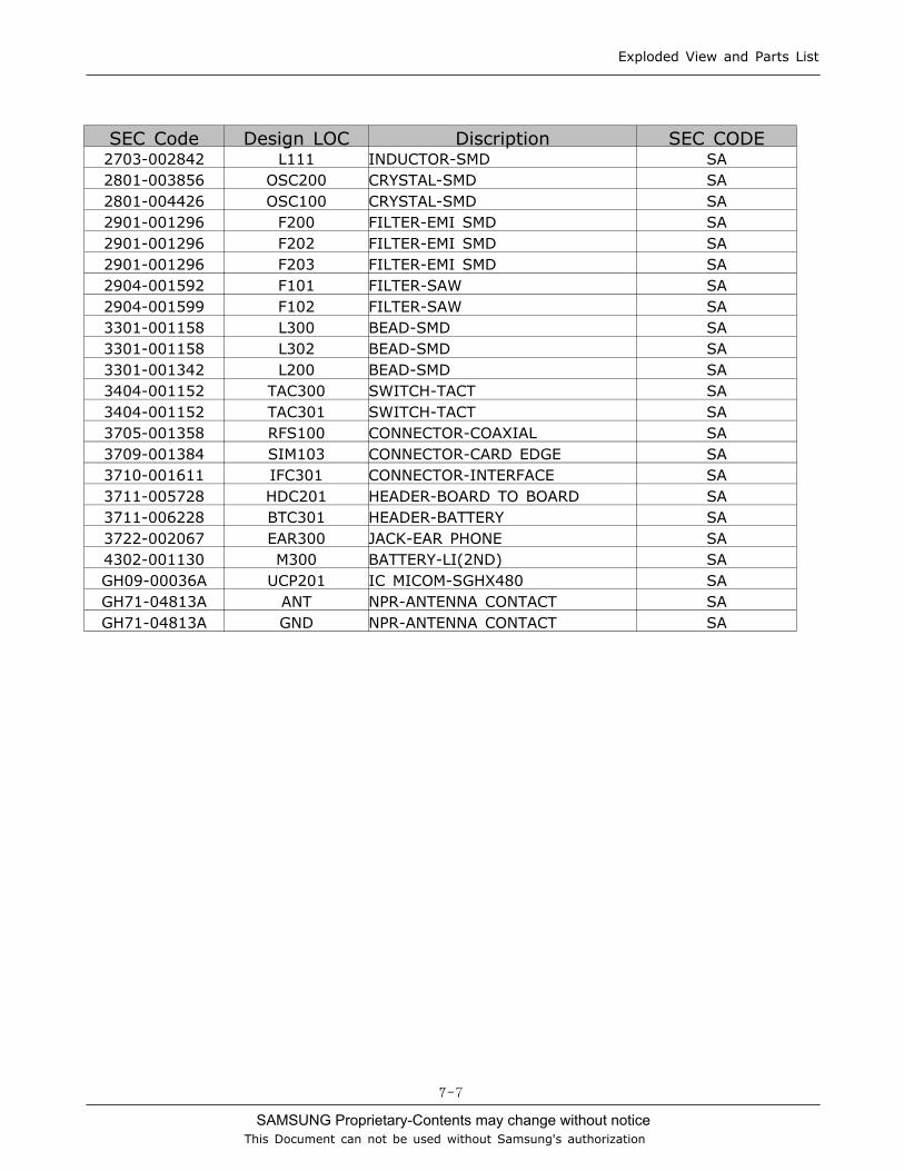
SEC Code Design LOC Discription SEC CODE2703-002842 L111 INDUCTOR-SMD SA2801-003856 OSC200 CRYSTAL-SMD SA2801-004426 OSC100 CRYSTAL-SMD SA2901-001296 F200 FILTER-EMI SMD SA2901-001296 F202 FILTER-EMI SMD SA2901-001296 F203 FILTER-EMI SMD SA2904-001592 F101 FILTER-SAW SA2904-001599 F102 FILTER-SAW SA3301-001158 L300 BEAD-SMD SA3301-001158 L302 BEAD-SMD SA3301-001342 L200 BEAD-SMD SA3404-001152 TAC300 SWITCH-TACT SA3404-001152 TAC301 SWITCH-TACT SA3705-001358 RFS100 CONNECTOR-COAXIAL SA3709-001384 SIM103 CONNECTOR-CARD EDGE SA3710-001611 IFC301 CONNECTOR-INTERFACE SA3711-005728 HDC201 HEADER-BOARD TO BOARD SA3711-006228 BTC301 HEADER-BATTERY SA3722-002067 EAR300 JACK-EAR PHONE SA4302-001130 M300 BATTERY-LI(2ND) SAGH09-00036A UCP201 IC MICOM-SGHX480 SAGH71-04813A ANT NPR-ANTENNA CONTACT SAGH71-04813A GND NPR-ANTENNA CONTACT SA
SAMSUNG Proprietary-Contents may change without notice
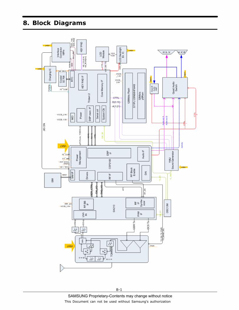
8. Block Diagrams
8-1
This Document can not be used without Samsung's authorization
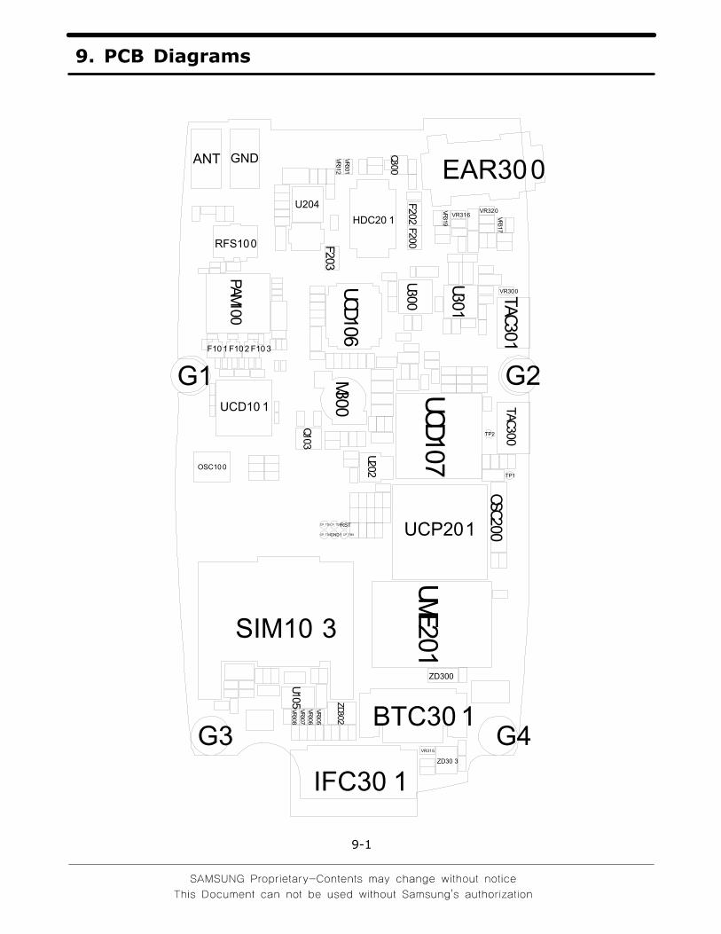
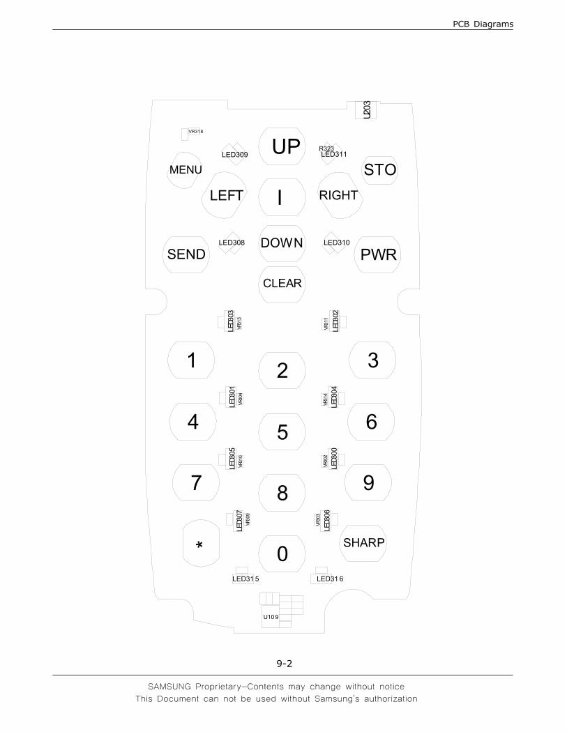
9. PCB Diagrams
9-1
ANT
BTC30 1
CP_TCKCP_TDI
CP_TDO CP_TMS
EAR300
F10 1 F10 2 F10 3
002F
202F
302F
G1 G2
G3 G4
GND
GND1
HDC20 1
IFC30 1
003M
OSC10 0
002C
SO
001M
AP
301Q
003Q
RFS100
RST
SIM10 3
003C
AT10
3CAT
TP1
TP250
1U
202U
U204
003U
103U
UCD10 1
601D
CU
701D
CU
UCP201
102E
MUVR300
103R
V
503R
V60
3RV
703R
V80
3RV
213R
V
VR315
VR31671
3RV
913R
V VR320
ZD300
203D
Z
ZD30 3
PCB Diagrams
9-2
* 0
1 2 3
4 5 6
7 8 9
CLEAR
DOWN
I
003DEL
103DEL
203DEL
303DEL
403DEL
503DEL
603DEL
703DELLED308
LED309
LED310
LED311
LED31 5 LED31 6
LEFT
MENU
PWR
R323
RIGHT
SEND
SHARP
STO
U10 9
302U
UP
203RV303RV
403RV903RV
013RV
113RV
313RV
413RV
VR318
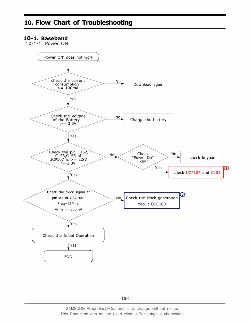
10. Flow Chart of Troubleshooting
10-1
10-1. Baseband10-1-1. Power ON
check the currentconsumption>= 100mA
Download again
'Power ON' does not work
No
Yes
Yes
END
Yes
Check the Initial Operation
Yes
Charge the batteryNoCheck the Voltage
of the Battery>= 3.3V
check keypadNoCheck the pin C152,
C153,C155 ofUCP107 is >= 2.8V
>=2.8V
Check"Power On"
key?
No
check UCP107 and C153Yes 1
Check the clock signal at
pin #4 of OSC100
Freq=26Mhz,
Vrms >=300mV
No Check the clock generation
circuit OSC100
Yes
2
Flow Chart of Troubleshooting
10-2
①
②
2SS
V4
K3
SSV
2R
4SS
V6
P
1SS
V5
G
2OI_
DD
V4J
LTC
O_D
DV4
C 3J
VDD12 J13
2D
DV
3M
3D
DV
6N
VDD34 C11
5D
DV
01C
76D
DV
31B
BD
DV6
A
DD
DV11
N
VD
DV
11L
1OI_
DD
V5
N
SIM_CLK K14
SIM_IO J11SIM_RST K11
UP_CLK N9
UP_IO P10UP_RST R10
1D
DV
6C
N2 1
5C
N
5S
DN
G7
G6
SD
NG
8G
7S
DN
G9
G8
SD
NG
01G
9S
DN
G6
H
VD
NG
31P
RU
CH_
DN
G11F
LTC
O_D
NG
4B
1C
SP_
DN
G51
B2
CSP_
DN
G51
K
01S
DN
G7
H11
SD
NG
8H
9H
21S
DN
G31
SD
NG
7J41
SD
NG
8J51
SD
NG
9J61
SD
NG
01J71
SD
NG
01K
2S
DN
G8F
3S
DN
G9F
4S
DN
G01F
DB8F4DB9F1
BD
NG
6F
DD
NG
01M
QD
NG
8E
1S
DN
G7F
DB10F2DB11F3DB12E2DB13E3DB14D3DB15D2
3C
DA_X
UA
31D
VBAT
VCCD_2.9V
C155
VCCD_2.9V
C162
C153
VCCA_2.9V
C152
SIMDATASIMRST
SIM_RSTSIM_IO
SIM_CLK
SIMCLK
DSP_DB(8)
DSP_DB(0:15)
DSP_DB(15)DSP_DB(14)DSP_DB(13)DSP_DB(12)DSP_DB(11)DSP_DB(10)DSP_DB(9)
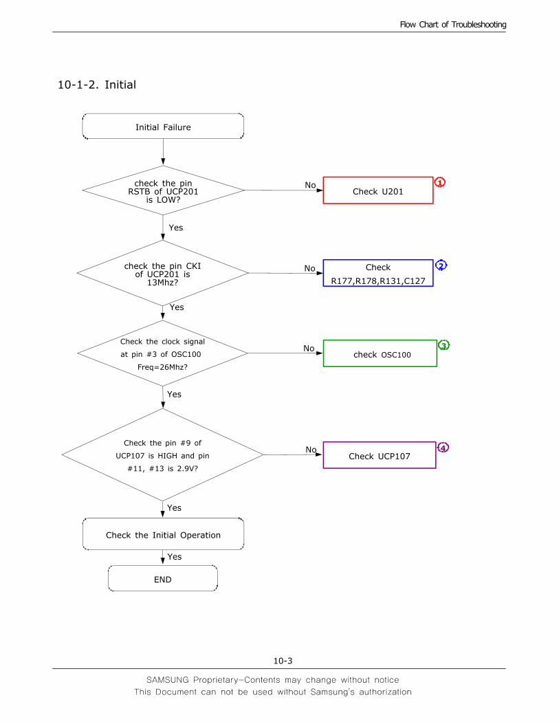
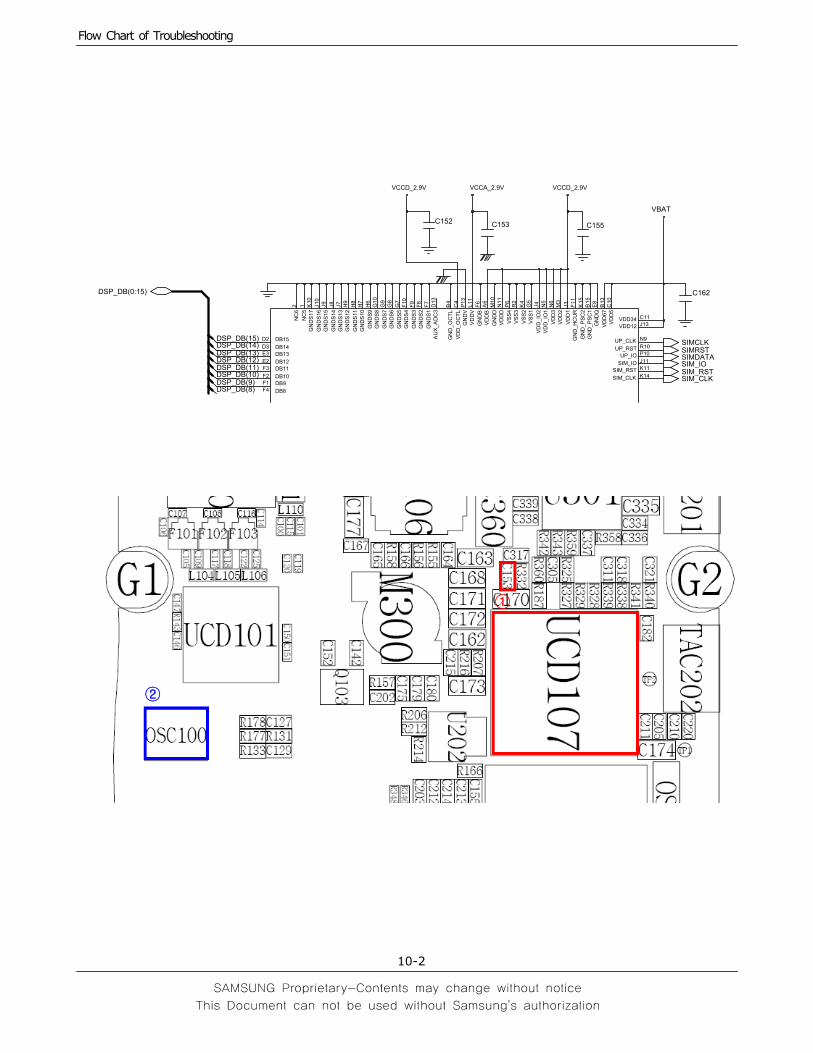
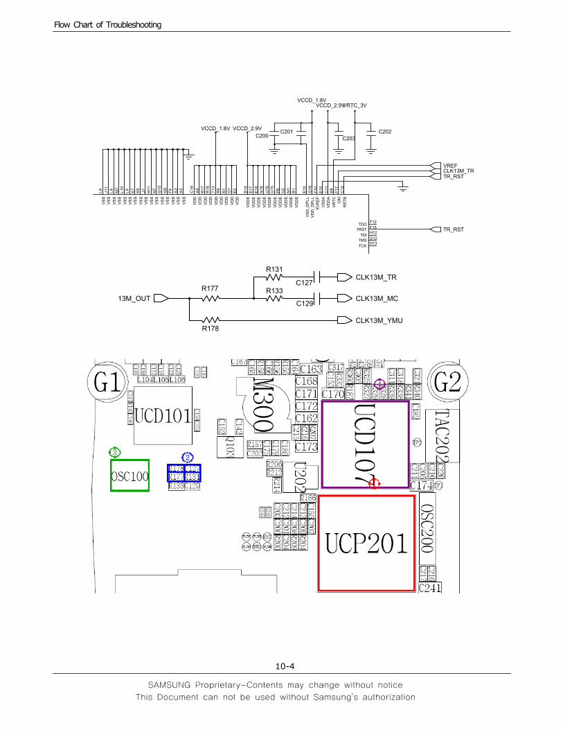
Flow Chart of Troubleshooting
10-3
10-1-2. Initial
Initial Failure
check the pinRSTB of UCP201
is LOW?Check U201
No
Yes
Yes
END
Yes
Check the Initial Operation
Yes
Check
R177,R178,R131,C127
Nocheck the pin CKIof UCP201 is13Mhz?
Check the clock signal
at pin #3 of OSC100
Freq=26Mhz?
Nocheck OSC100
1
Check the pin #9 of
UCP107 is HIGH and pin
#11, #13 is 2.9V?
NoCheck UCP107
Yes
2
3
4
Flow Chart of Troubleshooting
10-4
32
4
1
C200C202
VCCD_2.9V
01FFE
RVX
LLP
D_SSV
SSV
SSV
9G
01G
SSV
SSV
7H
SSV
11H7J
SSV
6K
SSV
01EA
SSV
51E
SSV
6L01L
SSV
SSV
7M8L
SSV
11JS
SVSSV
9L
3A
SSV
6F
ED
DVE
DDV
61U
61N
ED
DVE
DDV
61E71E
ED
DV
LLP
D_D
DV
61G
CTRV
8D
SSV
2A
SSV
7K
DD
VD
DV
61C
AD
DV11
C
1B
ED
DV
ED
DV41
B
ED
DV1
M2
UE
DDV
ED
DV8P
51U
1G
DD
VD
DV
1R
4R
DD
VD
DV
31T61
RD
DV
DD
V71
R5
A
BTSR
21C
H13TCK
TDI H12
F12TDO
G12TMS
TRST F15
DD
V2E
71FI
KC
VCCD_1.8V
VRTC_3V
C201
VCCD_1.8V
C203
VCCD_2.9V
TR_RST
VREF
TR_RSTCLK13M_TR
R178
R177 R133
R131
C127
C129
CLK13M_YMU
CLK13M_MC
CLK13M_TR
13M_OUT
Flow Chart of Troubleshooting
10-5
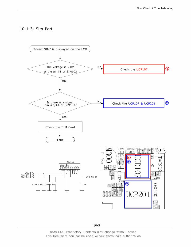
10-1-3. Sim Part
"Insert SIM" is displayed on the LCD
Is there any signalpin #2,3,4 of SIM103?
Check the UCP107
Check the UCP107 & UCP201
END
No
Yes
No
Yes
1
2
Check the SIM Card
The voltage is 2.8V
at the pin#1 of SIM103
1
2
2C138 C139 C141 C142C140
CC
V2
PP
V53
KLC
4D
NG
6O/I
7C
NC
N8
CN
9 01C
N
1C
CV
SIM103
SIM_RSTVSIM
SIM_CLK SIM_IO
Flow Chart of Troubleshooting
10-6
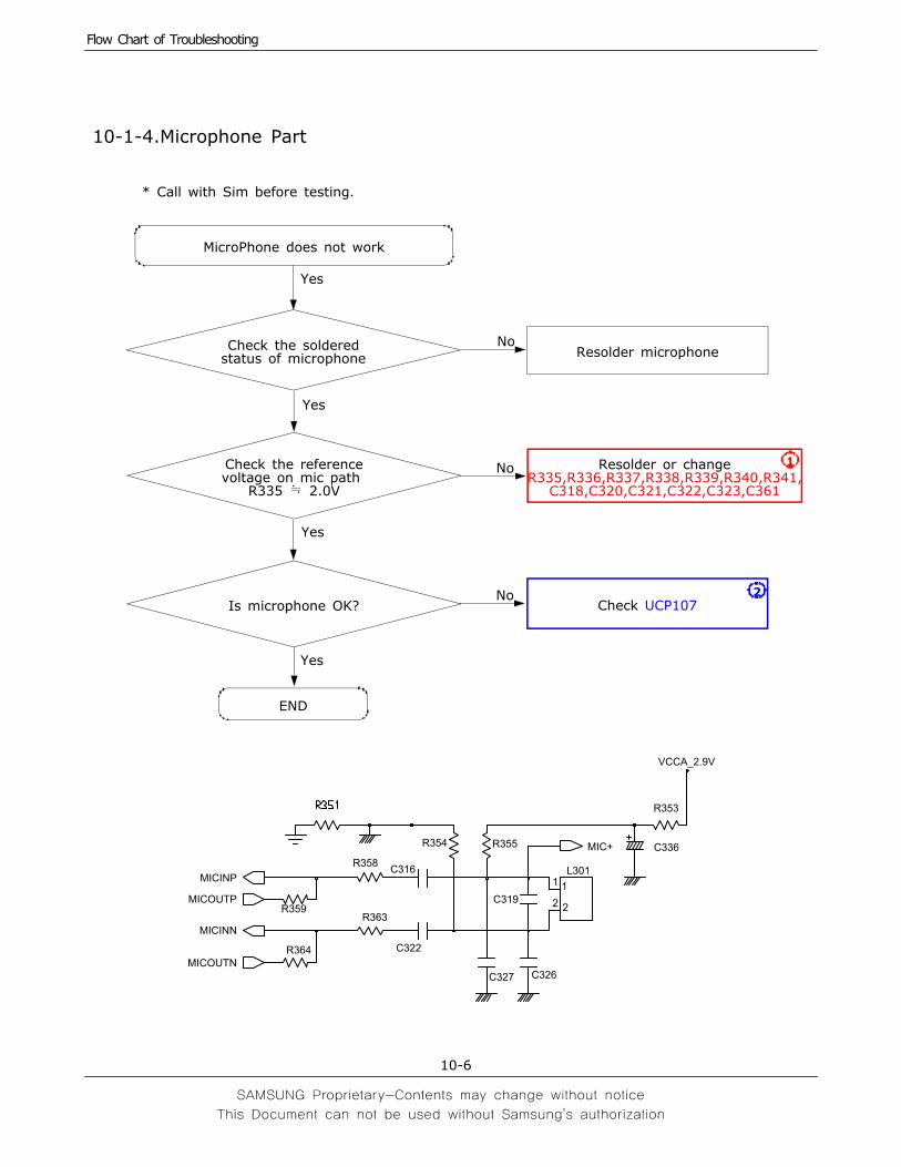
10-1-4.Microphone Part
* Call with Sim before testing.
Check the solderedstatus of microphone
MicroPhone does not work
Resolder microphone
END
No
Yes
Yes
Check the referencevoltage on mic path
R335 ≒ 2.0V
Yes
Resolder or changeR335,R336,R337,R338,R339,R340,R341,C318,C320,C321,C322,C323,C361
No
Is microphone OK?
Yes
Check UCP107No
1
2
R364
R363
C322
C316
R354
C326
C319
L30111
22R359
R358
VCCA_2.9V
C336
R353
C327
R355
MICINN
MICOUTN
MICOUTP
MICINP
MIC+
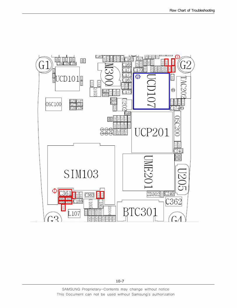
Flow Chart of Troubleshooting
10-7
2
1
1
Flow Chart of Troubleshooting
10-8
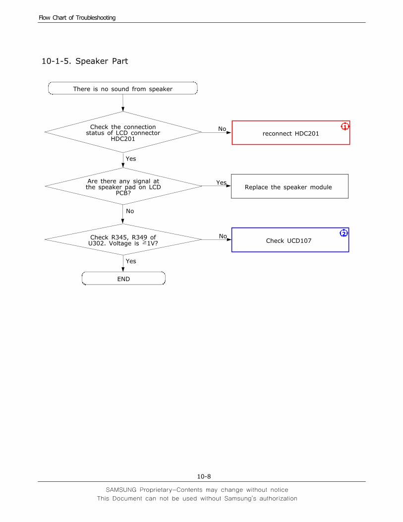
10-1-5. Speaker Part
Check the connectionstatus of LCD connector
HDC201
There is no sound from speaker
Are there any signal atthe speaker pad on LCD
PCB?
reconnect HDC201
Replace the speaker module
END
No
Yes
No
No
Yes
Check R345, R349 ofU302. Voltage is ≥1V?
1
Yes
Check UCD1072
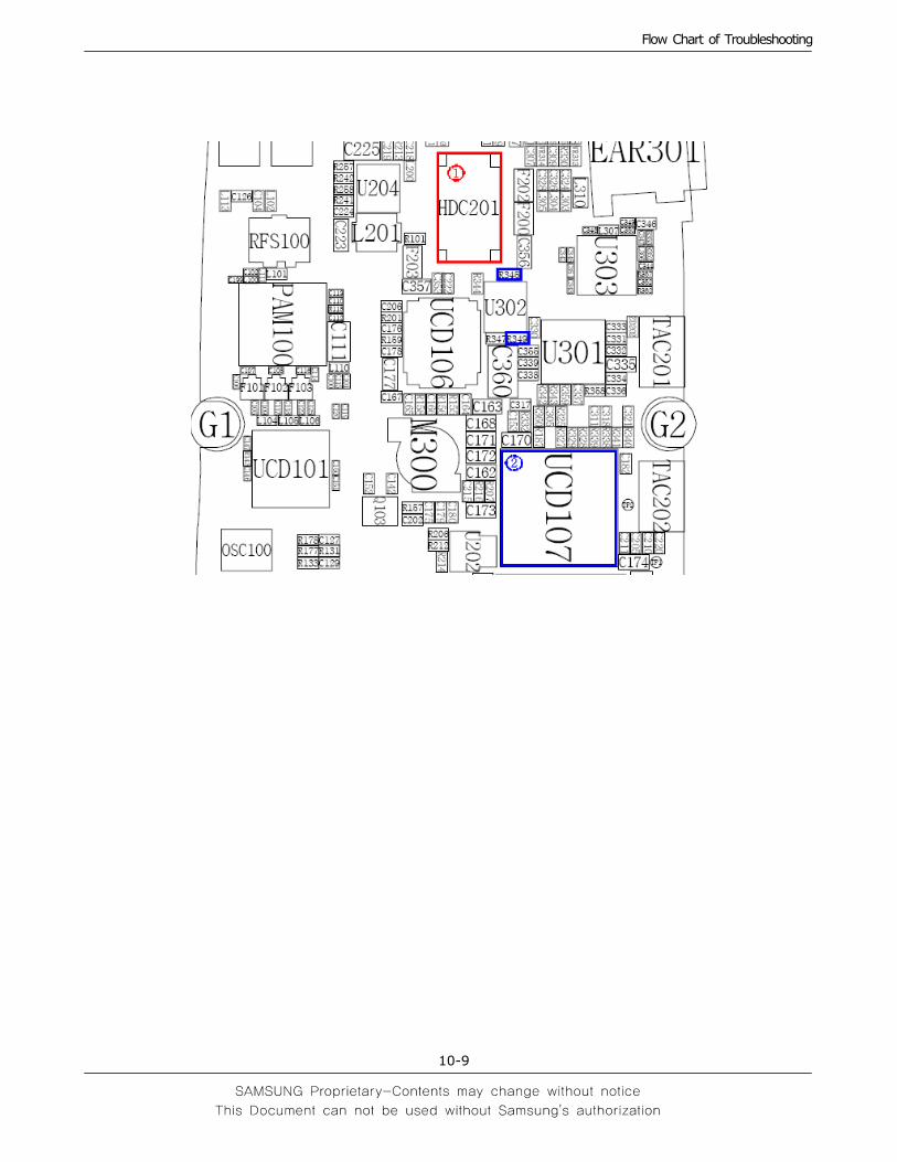
Flow Chart of Troubleshooting
10-9
2
1
Flow Chart of Troubleshooting
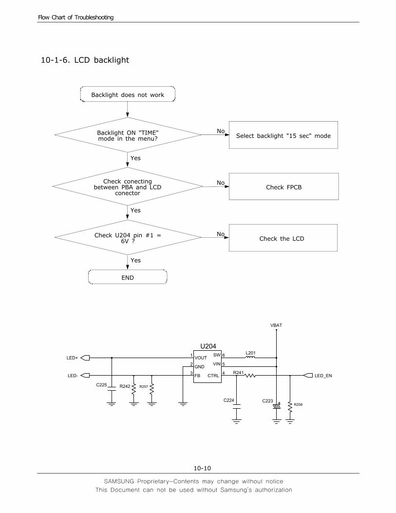
10-10
10-1-6. LCD backlight
Backlight ON "TIME"mode in the menu?
Backlight does not work
Check conectingbetween PBA and LCD
conector
Select backlight "15 sec" mode
Check FPCB
END
No
Yes
No
Check U204 pin #1 =6V ? Check the LCD
Yes
Yes
No
VBAT
L201
R242 R257
R241
C224 C223
C225
CTRL 43 FB
GND2
SW 6
5VIN
1 VOUT
U204
R258
LED-
LED+
LED_EN
Flow Chart of Troubleshooting
10-11
10-2. RF10-2-1. GSM Rx
Normal conditioncatch thechannel ?
Check PAM100pin 12 ≥ -65dbm ?
Check UCD101pin 21,22 ≥-65dBm ?
Yes
No
No
Check PAM100pin 16 ≥ -65dbm ?
Yes
No
Yes
Check ANT, C104,C126,L102,L113
Resolder or changeRFS100,C102,C199,L100,L101,L111
Resolder or changePAM100
Resolder or changeF101,C105,C109,L104
Resolder or change
UCP201
CONTINOUS RX ONRF INPUT : 62CHAMP : -50dbm
Check UCD101pin 13 = 2.9V
Yes
Resolder or changeUCD107
Yes
No
No
1
2
3
4
5
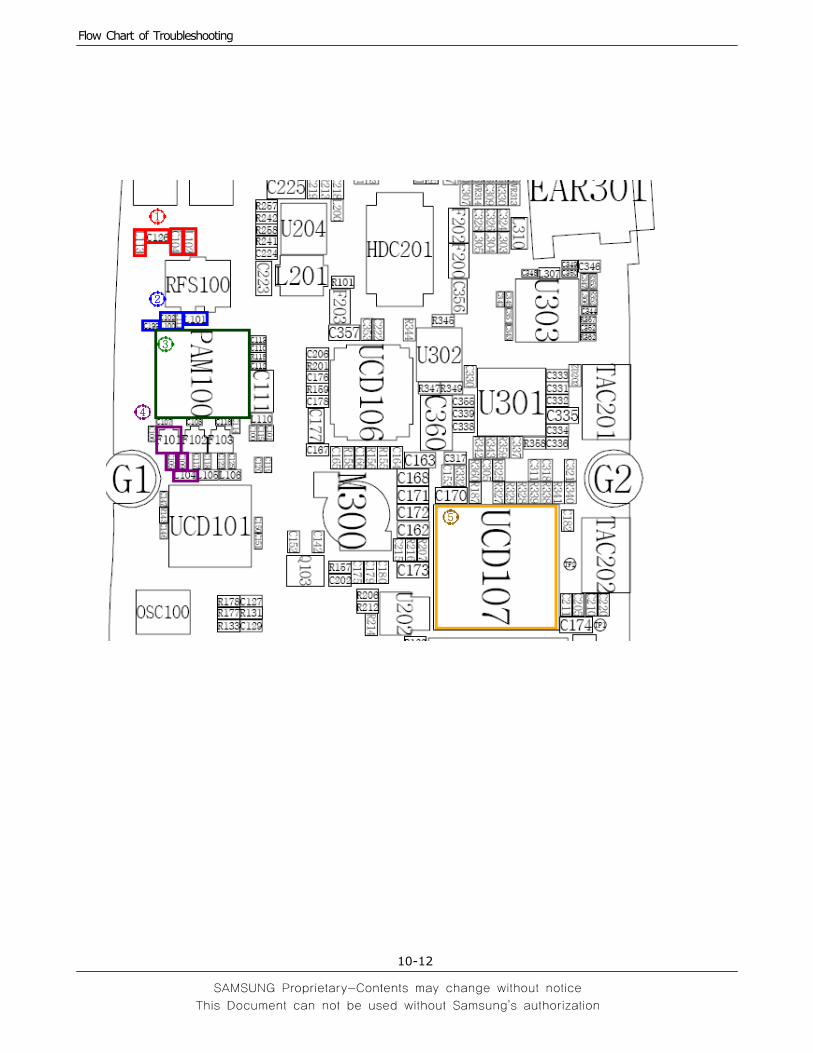
Flow Chart of Troubleshooting
10-12
1
2
3
5
4
Flow Chart of Troubleshooting
10-13
10-2-2. DCS Rx
Normal conditioncatch thechannel ?
Check PAM100pin 12 ≥ -65dbm ?
Check UCD101pin 19,20 ≥-65dBm ?
Yes
No
No
Check PAM100pin 18 ≥ -65dbm ?
Yes
No
Yes
Check ANT, C104,C126,L102,L113
Resolder or changeRFS100,C102,C199,L100,L101,L111
Resolder or changePAM100
Resolder or changeF102,C117,C118,L105
Resolder or change
UCP201
CONTINOUS RX ONRF INPUT : 698CHAMP : -50dbm
Check UCD101pin 13 = 2.9V
Yes
Resolder or changeUCD107
Yes
No
No
1
2
3
4
5
Flow Chart of Troubleshooting
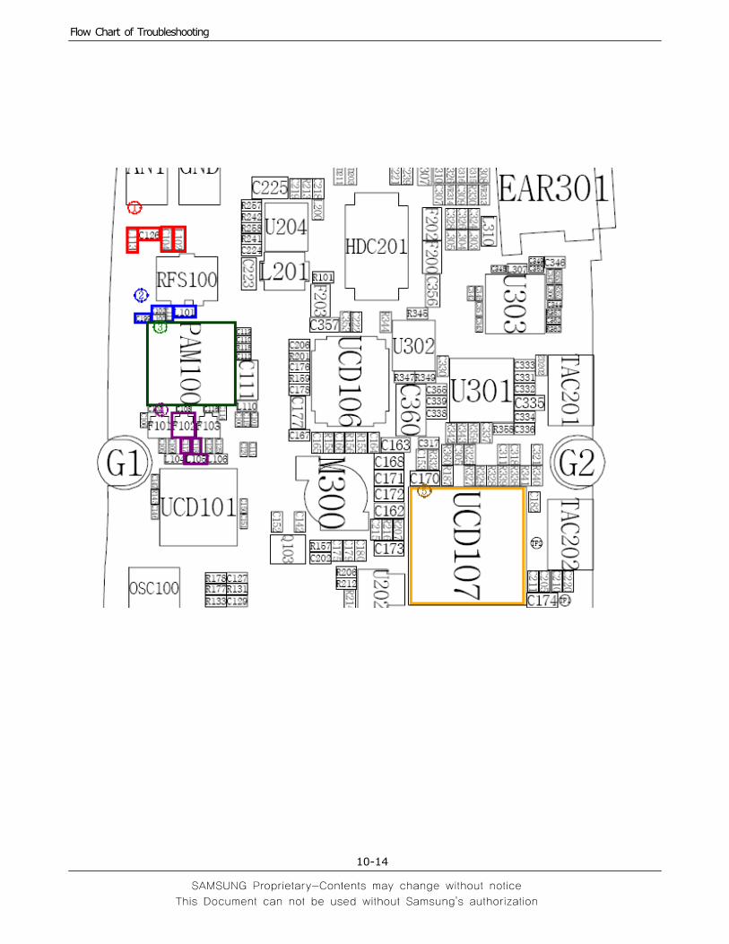
10-14
4
5
3
2
1
Flow Chart of Troubleshooting
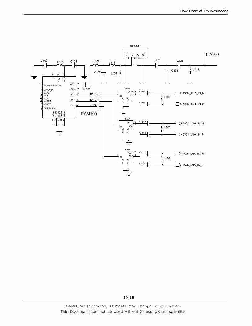
10-15
2AC
3
G1
G4
RFS100
L106
L113
10
2C
CV
3
VMOD_EN9
VRAMP8VTX6
20
RX2 18
RX3 16
RX4 14
1V
2
VBATT7
VBS14VBS25
1C
CV
12
DCS|PCSIN1
1D
NG
312
DN
G51
3D
NG
714
DN
G91
5D
NG
12
GSM850|900TXIN11
RX1
PAM100
ANT
C126
C104L101
G5
1IN
OUT 34OUT
F103
G2
C101L110
C102
L111
C106
C107
C108
C117
L105
C118
L104
C199
L100 L102
5
1IN
OUT 34OUT
5
1IN
OUT 34OUT
F102
G2
G
F101
G
2
G
C100
C105
C109
C125
C122
ANT
DCS_LNA_IN_P
DCS_LNA_IN_N
GSM_LNA_IN_P
GSM_LNA_IN_N
PCS_LNA_IN_P
PCS_LNA_IN_N
Flow Chart of Troubleshooting
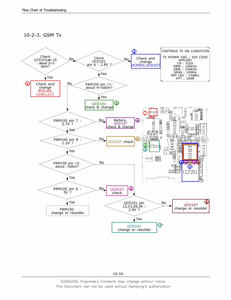
10-16
10-2-3. GSM Tx
CheckUCD101pin 15: about 2~3dbm?
CheckUCD101
pin 6 : 2.8V ?
Check andchangeRFS100,L100,L111
Yes
Check andchange
UCP201,UCD107
No
CONTINUS TX ON CONDITION
TX POWER DAC : 554 CODEAPPLIEDCH : 62ch
RBW : 100KHzVBW : 100KHzSPAN : 10MHzREF LEV : 10dBmATT : 20dB
PAM100 pin 11:about 4~5dbm?
Yes
No
Yes
PAM100 pin 7 :3.7V ?
UCD101check & change
No Battery,UCD107
check & changeYes
PAM100 pin 8 :1.2V ?
NoUCD107 check
Yes
PAM100 pin 6 :3V ?
No UCD107check
UCD101 pin12,13,28,29 :2.9V ?PAM100
change or resolder
UCD107change or resolder
No
Yes
UCD101change or resolder
Yes
PAM100 pin 12:about -5dbm?
No
Yes
No
1
2
3
4
5
6
7
8
37
24 5 6 8
1
2
Flow Chart of Troubleshooting
10-17
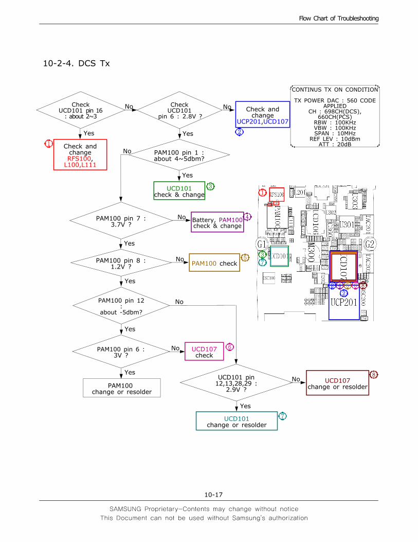
10-2-4. DCS Tx
CONTINUS TX ON CONDITION
TX POWER DAC : 560 CODEAPPLIED
CH : 698CH(DCS),660CH(PCS)RBW : 100KHzVBW : 100KHzSPAN : 10MHzREF LEV : 10dBmATT : 20dB
CheckUCD101
pin 6 : 2.8V ?
PAM100 pin 1 :about 4~5dbm?
No
CheckUCD101 pin 16: about 2~3
No Check andchange
UCP201,UCD107
Yes
No
Yes
Check andchangeRFS100,L100,L111
Yes
UCD101check & change
No Battery, PAM100check & change
Yes
NoPAM100 check
Yes
No
Yes
No UCD107check
Yes
PAM100change or resolder
UCD101 pin12,13,28,29 :2.9V ?
No UCD107change or resolder
Yes
UCD101change or resolder
PAM100 pin 7 :3.7V ?
PAM100 pin 8 :1.2V ?
PAM100 pin 12:
about -5dbm?
PAM100 pin 6 :3V ?
1
2
3
4
5
6
7
8
1
22
3
4
5
6
7
8
1
22
3
4 5
6
7
8
1
3
7
2 4 5 6 8
2
SAMSUNG Proprietary-Contents may change without notice
11. Reference data
11-1
This Document can not be used without Samsung's authorization
11-1. Reference Abbreviate
AAC: Advanced Audio Coding.
AVC : Advanced Video Coding.
BER : Bit Error Rate
BPSK: Binary Phase Shift Keying
CA : Conditional Access
CDM : Code Division Multiplexing
C/I : Carrier to Interference
DMB : Digital Multimedia Broadcasting
EN : European Standard
ES : Elementary Stream
ETSI: European Telecommunications Standards Institute
MPEG: Moving Picture Experts Group
PN : Pseudo-random Noise
PS : Pilot Symbol
QPSK: Quadrature Phase Shift Keying
RS : Reed-Solomon
SI : Service Information
TDM : Time Division Multiplexing
TS : Transport Stream
Samsung Electronics Co.,Ltd.
Code No.: GH68-10717A2006. 05. Rev.1.0
ⓒThis Service Manual is a property of Samsung Electronics Co.,Ltd.Any unauthorized use of Manual can be punished under applicableInternational and/or domestic law.