rapid design space exploration using legacy design data and technology scaling trend
TRANSCRIPT

ARTICLE IN PRESS
INTEGRATION, the VLSI journal 43 (2010) 202–219
Contents lists available at ScienceDirect
INTEGRATION, the VLSI journal
0167-92
doi:10.1
� Corr
E-m
(C. Than
journal homepage: www.elsevier.com/locate/vlsi
Rapid design space exploration using legacy design dataand technology scaling trend
Charles Thangaraj �, Cengiz Alkan, Tom Chen
Electrical and Computer Engineering, Colorado State University, Fort Collins, CO 80521, USA
a r t i c l e i n f o
Article history:
Received 22 January 2009
Received in revised form
9 July 2009
Accepted 6 November 2009
Keywords:
Design trade-off
Design space exploration
Pareto analysis
Evolutionary algorithms
60/$ - see front matter & 2009 Elsevier B.V. A
016/j.vlsi.2009.11.002
esponding author.
ail addresses: [email protected], cha
garaj), [email protected] (T. Chen).
a b s t r a c t
Rapid and effective design space exploration at all stages of a design process enables faster design
convergence and shorter time-to-market. This is particularly important during the early stage of a
design where design decisions can have a significant impact on design convergence. This paper
describes a methodology for design space exploration using design target prediction models. These
models are driven by legacy design data, technology scaling trends and, an in situ model-fitting process.
Experiments on ISCAS benchmark circuits validate the feasibility of the proposed approach and yielded
power centric designs that improved power by 7–32% for a corresponding 0–9% performance impact; or
performance centric designs with improved performance of 10.31–17% for a corresponding 2–3.85%
power penalty. Evolutionary algorithm based Pareto analysis on an industrial 65 nm design uncovered
design tradeoffs which are not obvious to designers and optimize both power and performance. The
high performance design option of the industrial design improved the straight-ported design’s
performance by 29% with a 2.5% power penalty, whereas the low power design option reduced the
straight-ported design’s power consumption by 40% for a 9% performance penalty.
& 2009 Elsevier B.V. All rights reserved.
1. Introduction
Competing design objectives make timely design convergencean increasing challenge, leading to missed schedule and productroad map alterations. Time-to-market amidst growing competi-tion is a fundamental driver of the semiconductor industry.Highly competitive business environment requires companies todeliver products on schedule and maintain product differentiationin the market. Consequently, ‘‘one-size-fits-all’’ design approach isno longer adequate [1]. A successful product portfolio invariablyconsists of designs available and optimized for a particular marketsegment, i.e. cost sensitive consumer electronics, or powersensitive mobile electronics, or performance sensitive micropro-cessor markets. Designing each product variant from scratch istime consuming and incurs significant costs. Leveraging orre-optimizing new design variants from existing designs reducesboth design cost and time. Leveraged designs are typically welldefined with the goal of either boosting performance or reducingpower or both. These goals may be obtained through scaling.However, additional design options, such as incremental func-tional feature enhancements, are often necessary. Design optimi-zation during the early/conceptual design phase precipitates
ll rights reserved.
design convergence by helping avoid costly redesigns later, andtherefore must become an essential part of the design process.
Design convergence in power and performance, especiallywith designs in nanometer CMOS technologies is becomingincreasingly challenging due to stiffer design constraints arisingfrom fabrication limitations and design for manufacturability(DFM) considerations. Performance, power consumption, relia-bility and yield are competing design objectives and are deeplyintertwined, yet the design is expected to converge and achieveoptimal design targets [2–4]. As a result, for nanometer CMOSdesigns, physical implementation of a highly optimized architec-tural design is not guaranteed. To increase the likelihood of designconvergence, optimizations based on abstracted models repre-senting low level implementation in the early design cycle help inchoosing optimal modular design choices and in meeting designschedule. The scope and opportunities for power and performanceoptimization are maximum when the optimization is performedat the higher level. It is essential that the higher level models usedfor design optimization include low level physical design para-meters to ensure more realistic design optimization at the higherlevel. This paper presents a design framework to explore designspace through Pareto analysis, and through subdividing systemtargets and generating corresponding module design targets forall modules in a design. Modular design targets can be power orperformance centric or any desired combination of the two.Leveraged redesign or optimization often involves the application

ARTICLE IN PRESS
C. Thangaraj et al. / INTEGRATION, the VLSI journal 43 (2010) 202–219 203
of additional circuit-level design choices to achieve design targets.The proposed approach offers an effective design flow to providedesigners a better quantitative understanding of the pros andcons of different design choices that can be made to achieve thedesign targets. The proposed method uses a set of analyticalmodels to gauge the impact of different design choices. In situSPICE simulations refine the accuracy of the macro models. Theeffectiveness of the proposed approach is illustrated by applyingit to leveraged redesigns (design porting to a new processtechnology) and leveraged optimizations (what-if analysis onthe ported design) on test circuits including ISCAS benchmarkcircuits and an industrial microprocessor based design.
Experiments on ISCAS benchmark circuits yielded powercentric designs that improved power by 7–32% for a correspond-ing 0–4.3% performance impact; or performance centric designswith improved performance of 10.31–17% for a corresponding2–3.85% power penalty. Evolutionary algorithm based Paretoanalysis on an industrial 65 nm based design yielded designtradeoffs which are not obvious to designers and optimize bothpower and performance. The high performance design option ofthe industrial design improved the straight-ported design’sperformance by 29% with a 2.5% power penalty and the lowpower design option reduced the straight-ported design’s powerconsumption by 40% for a 9% performance penalty.
The rest of the paper is organized as follows. Section 2 reviewsexisting work in the area of early design space exploration.Section 3 presents the details of the proposed method. Experi-mental setup, results and discussions are presented in Sections4–6, respectively, followed by concluding remarks in Section 7.
2. Existing work and motivation
Existing tools for architectural exploration fall into two broadcategories, the first category are tools that are specificallyintended for microprocessors or computation engines to optimizeperformance. They include SimplePower [5], SimpleScalar [6],Wattch toolset [7] and PowerTimer [8]. These tools model anunderlying computation architecture and emulate code executionon the modeled architecture. They collect activity rates, instruc-tion execution rates, miss rates, and prediction efficiency toestimate cycles per instruction (CPI) and other performancemetrics. Power estimation is a post processing step on thecollected metrics and predetermined per-transaction powerestimates. The SimpleScalar toolset is an architectural modelingand simulation infrastructure capable of modeling a simple fivestage to complex out-of-order pipelines. SimpleScalar uses aninstruction interpreter which supports several instruction sets tosimulate program execution on the modeled pipeline. Thisreproduces all internal computation operations, allowingobservation of computational functional unit usage rates andestimation of computing efficiency in terms of CPI.
SimplePower leverages SimpleScalar to simulate programexecution and uses transition sensitive energy models to evaluatetrade-offs among algorithm, architecture, compiler and energy. Ateach execution cycle SimplePower observes all architecturalfunctional unit usage and the corresponding input transitions.Technology dependent switching capacitance tables and powertables along with input transitions are used to estimate powerconsumption. Cache and bus transitions are handled similarly byactivating appropriate routines. Wattch toolset incorporatesimproved switching power models into the SimpleScalar simu-lator. Power (switching power) for each architectural functionunit is calculated as a function of its switching capacitance, powersupply, activity factor, and operating frequency. Switchingcapacitance of each architectural function unit is estimated
individually. Activity factor for each architectural function unitis estimated by SimpleScalar while the program is executed.
PowerTimer is very similar to Wattch in organization but ituses a highly parameterized and advanced processor architecturemodel called Turandot. Improved hierarchical power model basedon detailed bottom-up simulation data were used to estimatepower. Both switching and hold (leakage) power are estimated.The Platune framework [9,10] attempts to enable architecturalparameter tuning of a parameterized SOC platform, for a givenapplication which is to be mapped on to the SOC platform. Platuneuses empirical modules to calculate system power and dynami-cally captures execution-time events for each SOC component tocalculate system performance. Platune uses an exhaustive searchand sorting algorithm along with a parameter interdependencybased configuration space pruning technique to generate Pareto-fronts and to alleviate the problem of configuration spaceexplosion for large systems. In [11] a high level modelingmethodology, power and performance estimation models fordesign space exploration were presented and demonstrated onthree ISCAS85 benchmark circuits. The scalability of the modelingmethodology was demonstrated via an experiment on a largemicroprocessor based design in [12].
The second category of tools are applicable primarily to ASIC tooptimize physical implementation. A typical example of the toolsin this category is BACPAC [13,14]. BACPAC focuses on power andperformance estimation based on low-level physical designparameters and key process parameters. BACPAC attempts to‘‘re-create’’ the design in a bottom-up manner for analysis. Usingdetailed analytical models, BACPAC estimates both switching andleakage power, signal noise, wire-ability and design yield. Acustomizable critical path model is used to estimate designperformance.
Architecture level optimizations without physical implemen-tation constraints do not offer sufficient benefits in achievingdesign convergence. Optimization tools for physical implementa-tion based on low-level physical design parameters are limited intheir ability to explore design space. SimpleScalar has no powerestimation. SimplePower which uses static power tables toestimate power is unsuitable for design space explorationinvolving additional circuit-level design choices. Clock networkpower, which can account for up to 30% of the total dynamicpower [15], is not included in SimplePower making it lessattractive. Wattch toolset does not include leakage power whichis increasing exponentially in nanometer CMOS. PowerTimer hasa constant ‘‘hold’’ power equation to estimate leakage power.PowerTimer can be made to accurately predict system powerand performance but is very slow since macros need to bere-characterized every time an additional circuit-level designchoice is applied. BACPAC is fast but its equipartition approach isnot suitable for modeling highly modular designs such asmicroprocessors and other high performance designs. Platune’sparameter interdependency is application specific and cannot bealways guaranteed, making this framework not suitable forexploration of large systems. In [12] a guided random walkalgorithm was used to generate new designs for DSE, thistechnique lacked the necessary efficiency and coverage neededfor generating high quality Pareto-fronts.
Existing EDA tools typically address specific design aspect suchas timing or power in an accurate and detailed manner [16]. Theydo not address the overall system level design trade-off,implementation feasibility analysis, and fast turn-around what-if analysis often required for assisting designers to meet designquality and time-to-market requirement. Even though a collectionof existing tools may be utilized to perform the above tasks, inter-operability overhead and their nature of lower level detailanalysis make such a concoction too slow for quick feasibility

ARTICLE IN PRESS
C. Thangaraj et al. / INTEGRATION, the VLSI journal 43 (2010) 202–219204
analysis required for effective what-if analysis. The work reportedin this paper is motivated by the lack of fast and effective designspace exploration tools and the shortcomings of the existingapproaches. The goal of the proposed method is twofold: todevelop a high level modeling methodology which includes low-level physical design parameters to provide better constraints fordesign space exploration; and to develop a framework for earlydesign space exploration consisting of the high level modelingmethodology and analytical models that can be used to estimatedesign targets.
This work focuses on performance and power optimizationand what-if analysis during the early design space explorationphase when complete bottoms-up implementation data is not yetavailable. The proposed analytical models include leakage,dynamic power, and performance estimation. Utilizing legacydesign data, technology scaling trend data and allowing in situmacro-model generation and simulation, the proposed frameworkis positioned for more realistic estimates of the impact of circuitlevel design choices for a given design. Furthermore, large designssuch as high-end multi-core microprocessors and complexsystem-on-chips (SOCs) often performed by multiple designteams in parallel, each focusing on a portion (sub-design) of thelarger design. Compartmentalized efforts for optimizations do notguarantee global optimality and a holistic approach to designtradeoffs and optimizations is needed [17,18]. In [19] anevolutionary algorithm based design space exploration (DSE)was demonstrated on a larger VLIW-microprocessor based plat-form. It was shown that an evolutionary algorithm based DSE isimmune to increase in system size and maintained high levels ofefficiency. Unlike our previous work reported in [12], the resultsreported in this paper incorporate an evolutionary algorithm toimprove the DSE’s efficiency and coverage, resulting in highquality Pareto-fronts. The proposed evolutionary algorithm basedDSE methodology and the modeling of a system as a collection ofmodules (or sub-design) where the modules are independentlycharacterized allows for modeling and analyzing large designswith large design spaces without significant disproportionateincrease in system modeling efforts.
3. Proposed approach
EIDA (Early Integrated circuit Design Assist) is a framework forearly design space exploration. It consists of two components; thehigh level models (modeling methodology) and the analyticalmodels for design target prediction. Design space explorationusing EIDA involves iteratively building modular level models,assigning module-granular circuit-level design choices, andestimation of the expected achievable system targets when thedesign solution is implemented. A system is defined as acollection of modules and each module is characterized by a setof module descriptors, called descriptor vector. A collection ofdescriptor vectors form the system model.
Consider a leverage redesign of an existing system design in anewer process, where portions of the system critical path lie in asubset of modules called critical modules. To estimate systemperformance, system critical path delay i.e. sum of modularcritical path delays of critical modules are necessary. Legacy datacan be used to get an initial estimate of the modular critical pathdelay values. When complete bottom-up design data is notavailable, abstracting the underlying design is necessary so as toestimate critical path delay. A module’s critical path delaydepends on number of gates and interconnect length along thepath and typical gate delay. Other factors such as additionalcircuit-level design choices influence critical path delay. There-fore, factors such as legacy performance, total interconnect length
and the ratio of gate to interconnect delay are elements in themodule descriptor vector and in the performance estimationmodel (Section 3.2). To estimate power consumption, dynamicand leakage power for all modules are necessary. Dynamic powerdepends on total switching capacitance, operating frequency,power supply and switching factor. Leakage power depends ongate area for gate leakage, junction area for junction leakage andtotal width of active devices that are off for sub-threshold leakage.These factors among others are elements in the module descriptorvector and in the power estimation models (Section 3.2).
The module critical path can be modeled as a series ofinverters or NAND gates. An equivalent logic gate is defined as astandard sized inverter with a fanout of four (FO4) load, itspropagation delay is defined by equivalent logic gate delay (EGD).The delay of any logic gate can be expressed in terms of EGDs andthe critical path delay is the sum of EGDs of all gates along thepath. That is, a non-standard sized inverter may have a delay of3.75 EGDs and if the critical path consists of 10 of these then, thecritical path delay is 37.5 EGDs. For cells in a given library theircorresponding EGDs are characterized and known. Using EGDs toexpress delay normalizes process technology, and the critical pathdelay can be expressed in a technology independent manner. Theuse of EGD captures logic delay including nominal load on eachlogic gate. Significant RC delays on a path is not captured by theEGD metric. These RC delays need to be added to the logic delay toget total path delay. For leveraged redesigns the ratio of RC delayto logic delay for each module in the legacy design is known.Therefore, the RC delay can be estimated as a function of the logicdelay and the ratio of RC delay to logic delay.
For power estimation, a module’s underlying physical imple-mentation is abstracted as an inverter (the module inverter) with aFO4 load. Note that this representation is different from thestandard sized inverter FO4 configuration used for EGD calcula-tion. The module inverter sizing is proportional to the total P and NFET widths in the module which can be obtained by scaling thelegacy data. Total power consumption consists of dynamic andleakage power. Leakage power consumption for a design isprimarily related to the total gate area, total junction area andtotal device width in the design. These physical design descriptorscan be obtained by scaling legacy design data. Also, leakage is astrong function of the transistor stacking effect, which is capturedby including the stacking factor in the analytical model (Eq. (8)).Dynamic power consumption on the contrary, depends onphysical design descriptors and operating frequency; whereoperating frequency is estimated using the critical path delay.The FO4 connected module inverter representation forms the basisfor macro-model generation used to estimate power and perfor-mance impact of technology scaling and the application ofadditional circuit-level design choices; through in situ simulations.
Elements in a module descriptor vector are primarily obtainedfrom legacy data from previous generation designs or estimatesthrough other sources. Power and performance of leverageddesigns can be estimated by modeling switching capacitancescaling and power supply scaling. For example, the moduleinverter size which reflects the module’s active transistor area andtotal switching capacitance obtained from legacy data is used toestimate scaled active transistor area and total switchingcapacitance. Some descriptor values such as supply voltage,minimum channel length etc. are obtained from the new processtechnology specs.
In situ SPICE simulations are used to ascertain circuit-leveldesign-choice dependent descriptors such as impact of sleeptransistor on performance etc. Fig. 1 illustrates our approach ofusing FO4 module inverters to abstract the physical implemen-tation along with module descriptors to estimate power andperformance from analytical models.

ARTICLE IN PRESS
Fig. 1. A partitioned system shown with module #3 abstracted with F04 inverters
and its corresponding descriptor vector.
Table 1Legacy design descriptors.
CorigFThe total load capacitance in legacy design
TWL—The total wire length in legacy design
ULC—Unit length capacitance in the legacy design (all metal layers)
Wtotal=ðP=NÞFThe total/(P/N) fet width in legacy design
LminFThe minimum fet length in legacy design
foldFoperating frequency of the legacy design
ASF—Average switching factor in the legacy design
CGF—Clock gating correction to activity factor
DECAP_SENS—Supply voltage change due to unit de-coupling capacitance
insertion
Cde_capFDe� coupling capacitance added in legacy design
sf—Stacking factor
HVR—Ratio of # of high Vt to total fets in legacy design
LVR—Ratio of # of low Vt to total fets in legacy design
Cwire_buff FTotal buffer capacitance added in legacy design
TPFR—Typical path fet ratio–ratio of logic delay to total path delay in a typical
speed path
USPE—Useful skew allocation performance enhancement factor
BSUF—Speed up factor due to buffer insertion
Cunit_oldFUnit area gate capacitance in legacy design
Ids_oldFmin W&L, drain current in legacy design
temp—Typical operating temperature in legacy design
Table 2Target process technology descriptors.
sgate_capFScaling factor for gate capacitance in new process
swire_capFScaling factor for wire capacitance in new process
swidthFWidth scaling factor in new process
Ileak_juncFUnit junction leakage current in new process
Ileak_gateFUnit gate leakage current of in new process
IothvFTypical Ioff for high Vt fet in unit linear mm
IowhvFWorst Ioff for high Vt fet in unit linear mm
IotlvFTypical Ioff for low Vt fet in unit linear mm
IowlvFWorst Ioff for low Vt fet in unit linear mm
Igate_per_wFGate tunneling current for unit linear mm
Vdd_specFVoltage at package supply in new chip
ZFPackage IR drop factor
Vdd_bumpFVoltage at supply bumps in new chip (Vdd_spec � Z)
RCSF—RC slowdown factor-slow down due to wire scaling
Cunit_newFUnit area gate capacitance in new process
Ids_newFMin W&L, drain current in new process
C. Thangaraj et al. / INTEGRATION, the VLSI journal 43 (2010) 202–219 205
3.1. Module descriptor vector elements
The descriptor vector is a set of parameters from multiplesources that are used to model and predict system power andperformance. Elements in the descriptor vector enable theinclusion of physical constraints while performing system leveloptimizations.
3.1.1. Legacy design descriptors
Table 1 lists descriptor vector elements obtained from legacydesigns along with their explanations. For example, with the rateof supply voltage scaling diminishing and drain induced barrierlowering (DIBL) effects becoming stronger with technologyscaling, the effectiveness of leakage reduction by stacksbecomes higher. In complex CMOS gates where FETs arestacked, this effect captured by the stacking factor descriptor(sf) defined as the ratio of single device leakage to stack leakage.The sf descriptor is typically obtained from legacy design. Averageswitching activity of a module (ASF) and clock gating (CGF) usedin legacy design are very important for dynamic powerconsumption estimation. Clock gating factor is calculated as theaverage fraction of time the clock signal is gated. Interconnect andgate delay component proportions of the critical path delay aredescribed by the typical path FET ratio (TPFR) descriptor which isthe ratio of critical path gate delay to the total critical path delay.Cwire_buff is the additional switching capacitance introduced due tointerconnect buffer insertion and the buffer speed up factor
(BSUF) captures the speed up in critical path interconnect delaydue to buffer insertion. The useful skew allocation performanceenhancement (USPE) descriptor (unity by default) reflects criticalpath timing improvement as a result of positive skew allocationand combinatorial circuit re-timing and redesign.
3.1.2. Target process technology descriptors
Table 2 lists descriptor vector elements and their explanationswhich are obtained from the new process technologyspecifications, to which the design is to be ported. Scalingfactors, unit capacitance and supply voltage are typically welldefined for any process. Some of the descriptors can be obtainedfrom the SPICE model for the new process. For example, thesupply voltage at the highest metal power grid onchip is lowerthan the voltage at the package power supply terminals due topackage power network’s IR drop. This effect is characterized bythe Z descriptor which characterizes the expected drop due to thepackage power network. The RC slowdown factor (RCSF)descriptor captures the change in unit length (the mostrepresentative interconnect length in the legacy design)interconnect delay in the new process compared to legacyinterconnect delay, when driven by comparable drivers. Thisfactor is typically obtained from process characterization data.
3.1.3. In situ simulation descriptors
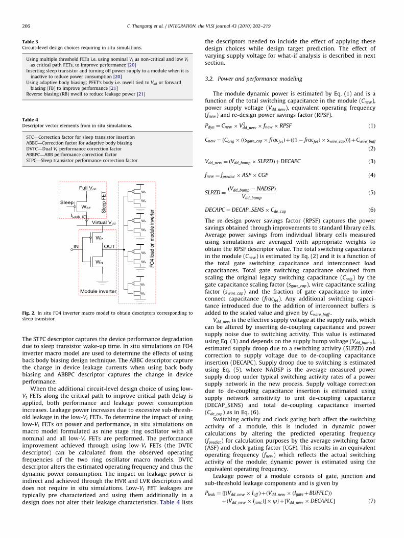
Leveraged redesigns often involve additional features and useadditional circuit-level design choices. Under such circumstancesscaling legacy design data for design space exploration alone isnot sufficient. Therefore, macro models are generated for in situsimulation to determine the relevant descriptor values for variouscircuit-level design that were not available from the legacy designbut may be needed in the new design. In situ simulation improvesprediction accuracy. Leakage device currents can also be esti-mated using in situ simulation method if necessary. Macro-modelgeneration and in situ simulations are performed for thesituations listed in Table 3 and the corresponding descriptorvector elements and their explanations are listed in Table 4.Design options listed in Table 3 affect both power andperformance. The STC descriptor captures the effective leakagepower saving obtained when the module’s power is gated by thesleep transistor. Using a FO4 inverter macro model for in situSPICE simulation as shown in Fig. 2, the STC descriptor can bedetermined by measuring the average sub-threshold gate andjunction leakage currents of the module inverter FETs when theinput is low/high and with the sleep transistor turned off/on.The STC descriptor is calculated as the ratio of the measured totalaverage leakage currents with the sleep transistor off and on.
ARTICLE IN PRESS
Table 3Circuit-level design choices requiring in situ simulations.
Using multiple threshold FETs i.e. using nominal Vt as non-critical and low Vt
as critical path FETs, to improve performance [20]
Inserting sleep transistor and turning off power supply to a module when it is
inactive to reduce power consumption [20]
Using adaptive body biasing; PFET’s body i.e. nwell tied to Vdd or forward
biasing (FB) to improve performance [21]
Reverse biasing (RB) nwell to reduce leakage power [21]
Table 4Descriptor vector elements from in situ simulations.
STC—Correction factor for sleep transistor insertion
ABBC—Correction factor for adaptive body biasing
DVTC—Dual Vt performance correction factor
ABBPC—ABB performance correction factor
STPC—Sleep transistor performance correction factor
Fig. 2. In situ FO4 inverter macro model to obtain descriptors corresponding to
sleep transistor.
C. Thangaraj et al. / INTEGRATION, the VLSI journal 43 (2010) 202–219206
The STPC descriptor captures the device performance degradationdue to sleep transistor wake-up time. In situ simulations on FO4inverter macro model are used to determine the effects of usingback body biasing design technique. The ABBC descriptor capturethe change in device leakage currents when using back bodybiasing and ABBPC descriptor captures the change in deviceperformance.
When the additional circuit-level design choice of using low-Vt FETs along the critical path to improve critical path delay isapplied, both performance and leakage power consumptionincreases. Leakage power increases due to excessive sub-thresh-old leakage in the low-Vt FETs. To determine the impact of usinglow-Vt FETs on power and performance, in situ simulations onmacro model formulated as nine stage ring oscillator with allnominal and all low-Vt FETs are performed. The performanceimprovement achieved through using low-Vt FETs (the DVTCdescriptor) can be calculated from the observed operatingfrequencies of the two ring oscillator macro models. DVTCdescriptor alters the estimated operating frequency and thus thedynamic power consumption. The impact on leakage power isindirect and achieved through the HVR and LVR descriptors anddoes not require in situ simulations. Low-Vt FET leakages aretypically pre characterized and using them additionally in adesign does not alter their leakage characteristics. Table 4 lists
the descriptors needed to include the effect of applying thesedesign choices while design target prediction. The effect ofvarying supply voltage for what-if analysis is described in nextsection.
3.2. Power and performance modeling
The module dynamic power is estimated by Eq. (1) and is afunction of the total switching capacitance in the module (Cnew),power supply voltage (Vdd_new), equivalent operating frequency(fnew) and re-design power savings factor (RPSF).
Pdyn ¼ Cnew � V2dd_new � fnew � RPSF ð1Þ
Cnew ¼ fCorig � ððsgate_cap � fracfetÞþðð1� fracfetÞ � swire_capÞÞgþCwire_buff
ð2Þ
Vdd_new ¼ ðVdd_bump � SLPZDÞþDECAPC ð3Þ
fnew ¼ fpredict � ASF � CGF ð4Þ
SLPZD¼ðVdd_bump � NADSPÞ
Vdd_bumpð5Þ
DECAPC ¼DECAP_SENS� Cde_cap ð6Þ
The re-design power savings factor (RPSF) captures the powersavings obtained through improvements to standard library cells.Average power savings from individual library cells measuredusing simulations are averaged with appropriate weights toobtain the RPSF descriptor value. The total switching capacitancein the module (Cnew) is estimated by Eq. (2) and it is a function ofthe total gate switching capacitance and interconnect loadcapacitances. Total gate switching capacitance obtained fromscaling the original legacy switching capacitance (Corig) by thegate capacitance scaling factor (sgate_cap), wire capacitance scalingfactor (swire_cap) and the fraction of gate capacitance to inter-connect capacitance (fracfet). Any additional switching capaci-tance introduced due to the addition of interconnect buffers isadded to the scaled value and given by Cwire_buff .
Vdd_new is the effective supply voltage at the supply rails, whichcan be altered by inserting de-coupling capacitance and powersupply noise due to switching activity. This value is estimatedusing Eq. (3) and depends on the supply bump voltage (Vdd_bump),estimated supply droop due to a switching activity (SLPZD) andcorrection to supply voltage due to de-coupling capacitanceinsertion (DECAPC). Supply droop due to switching is estimatedusing Eq. (5), where NADSP is the average measured powersupply droop under typical switching activity rates of a powersupply network in the new process. Supply voltage correctiondue to de-coupling capacitance insertion is estimated usingsupply network sensitivity to unit de-coupling capacitance(DECAP_SENS) and total de-coupling capacitance inserted(Cde_cap) as in Eq. (6).
Switching activity and clock gating both affect the switchingactivity of a module, this is included in dynamic powercalculations by altering the predicted operating frequency(fpredict) for calculation purposes by the average switching factor(ASF) and clock gating factor (CGF). This results in an equivalentoperating frequency (fnew) which reflects the actual switchingactivity of the module; dynamic power is estimated using theequivalent operating frequency.
Leakage power of a module consists of gate, junction andsub-threshold leakage components and is given by
Pleak ¼ f½ðVdd_new � Ioff ÞþðVdd_new � ðIgateþBUFFLCÞÞ
þðVdd_new � IjuncÞ� �jgþ½Vdd_new � DECAPLC� ð7Þ

ARTICLE IN PRESS
C. Thangaraj et al. / INTEGRATION, the VLSI journal 43 (2010) 202–219 207
where
Ioff ¼1
2
Wtotal � swidth
sf� HVR� Aþ
Wtotal � swidth
sf� LVR� B
� �ð8Þ
A¼ eðlnðIothvÞþ lnðIowhvÞ=2Þ ð9Þ
B¼ eðlnðIotlvÞþ lnðIowlvÞ=2Þ ð10Þ
Igate ¼ Agate � swidth � Ileak_gate ð11Þ
Ijunc ¼ Asd � Ileak_junc ð12Þ
Asd ¼ t� Agate ð13Þ
j¼ STC � ABBC ð14Þ
The total module sub-threshold leakage current (Ioff ), which isthe average of the P and N tree leakage currents, is estimatedusing Eq. (8). Sub-threshold leakage is a function of the totaldevice width (Wtotal), type of FET i.e. nominal or low-Vt , typicalunit width leakage values (Iothv=owhv=otlv=owtv), process widthscaling factor (swidth), average stacking factor for cell in the newprocess library (sf) and the fraction of low-Vt FETs to nominal FETs(LVR, HVR). The total module gate leakage current (Igate) isestimated using Eq. (11) and is a function of the total gate area inthe module (Agate), width scaling factor (swidth), and unit widthgate leakage current (Ileak_gate). The total module junction leakagecurrent (Ijunc) is estimated using Eq. (12) and is a function ofsource and drain junction area (Asd) and unit junction area leakage(Ileak_junc). Values for the unit width sub-threshold leakage andunit area gate and junction leakages are determined from the newprocess’ foundry characterization data.
An empirical constant determined by process and devicelayout rules (t in Eq. (13)) is used to estimate the average sourceand drain junction areas based on gate area. The impact ofapplying either sleep transistors or back body biasing to themodule is captured by the effective leakage modifier (j) asdefined in Eq. (14). Additional gate leakage due to interconnectbuffers insertion (to improve interconnect delay) and de-couplingcapacitances insertion (to improve power grid integrity) arecaptured by the factors BUFFLC and DECAPLC, respectively.
Operating frequency of a module (fpredict) is obtained bymodifying its legacy operating frequency (fold) according thenew process dependent, design choice dependent and empiricallydetermined factors as
fpredict ¼ A=B� C ð15Þ
A¼ ððfold � HVRÞþðfold � LVR� DVTCÞÞ � DIF ð16Þ
B¼ ðTPFR� FSFÞþ ð1� TPFRÞ �RCSF
BSUF
� �ð17Þ
C ¼ STPC � ABBPC � USPE ð18Þ
FSF ¼Vdd_spec � X
Vdd_bump � SLPZD� ðSLPZD� XÞ
� �Y
ð19Þ
DIF ¼Cunit_old
Cunit_new � swidth �Lmin_new
Lmin_old
�Ids_new
Ids_oldð20Þ
Design choice dependent factors affecting fpredict are, legacyoperating frequency (fold), nominal to low-Vt FET ratios (HVR,LVR), critical path speed up due to low-Vt FETs (DVTC),performance impact correction due to sleep transistor insertion(STPC) and performance impact correction due to back bodybiasing (ABBPC). Empirical factors affection fpredict are, expectedinterconnect slow down due to interconnect RC scaling (RCSF),
expected interconnect buffer insertion speed up attainable (BSUF)and the expected ratio of a typical critical path gate delay to totalcritical path delay (TPFR). Process dependent factors affectingfpredict are, ratio of unit area gate capacitance in the old and newprocess (DIF), ratio of minimum size device drive currents in oldand new process (DIF) and the impact of supply voltage droop onFET delay (FSF). FSF (FET slowdown factor) is a factor thatcaptures FET switching speed dependence on power supplyvoltage and environmental power grid noise. Propagation delaymeasurements from SPICE simulations on standard logic gates inthe new process technology are used to obtain X and Y paramentsin Eq. (19), by curve fitting the SPICE delay measurement data.The operating frequency (reciprocal of the critical path delay) fora module is estimated by Eq. (15). For modules that have newfeatures with no legacy data, critical path delay estimated usingthe number of equivalent gate delays and TPFR are used instead oflegacy data in Eq. (15).
3.3. Effect of power supply (Vdd) scaling
Lowering supply voltage to reduce total power consumption orelevating supply voltage to improve performance is a standarddesign technique [21]. When a module’s supply voltage changes,that affects module dynamic, leakage power, and operatingfrequency. The impact of supply voltage change on dynamicpower can be directly estimated from the expression for dynamicpower (Eq. (1)). However, the impact of supply voltage change ongate leakage, junction leakage, sub-threshold leakage, and deviceslowdown/speedup (operating frequency) are indirect and have tobe determined individually. Supply voltage does not directlyappear in the expressions for total sub-threshold current (Eq. (8)),total gate leakage current (Eq. (11)) and total junction leakagecurrent (Eq. (12)). Moreover, unit width or unit area leakagevalues at nominal supply voltage are used to estimate leakagecurrents and the device slowdown/speedup (i.e. FSF in Eq. (19))was calculated at nominal supply voltage.
Clearly, leakage and gate delay are supply voltage dependent.Detailed models for leakage currents such as models described in[22] exists and can be used to accurately calculate the leakagecurrents under varying supply voltages. However, these modelsrequire detailed physical device analysis and utilize additionalprocess parameters that are hard to extract or not readilyavailable. Therefore, the task of determining the impact of supplyvoltage on leakage current can be simplified by using simpleempirical equations that capture the general relationship of thedetailed models to the first order, as
a¼Vdd_spec
Vdd_appliedð21Þ
Ileak_junc_new¼ Ileak_junc � ea�ða�1Þ ð22Þ
Ileak_gate_new¼ Ileak_gate � eb�ða�1Þ ð23Þ
Ioff _new¼ Ioff � eg�b ð24Þ
b¼adþa2dþa4dþa6d
4� 1 ð25Þ
FSF_new¼ FSF �ð1=aÞ2eþð1=aÞe=2
2ð26Þ
Suitable test circuits are simulated using new process SPICEmodels to measure the leakage currents and device delay bysweeping the supply voltage. The measured values are then usedto determine the analytical approximation coefficients (a;b; g; dand e) by curve fitting. Establishing the analytical approximation

ARTICLE IN PRESS
C. Thangaraj et al. / INTEGRATION, the VLSI journal 43 (2010) 202–219208
prior to design space exploration, obviates the need for repetitivecharacterization runs, thus speeding up the estimation of powersupply scaling on leakage currents and device delays.
Vdd_spec is the nominal power supply voltage and Vdd_applied isthe scaled/altered supply voltage applied. Ileak_junc_new,Ileak_gate_new, Ioff _new and FSF_new are unit area junction, unit
Fig. 3. Design choice changing module descriptors.
Fig. 4. Early design phase explo
area gate, unit width sub-threshold leakages and FET slowdownexpected at the altered supply voltage and Ileak_junc , Ileak_gate, Ioff
and FSF are the corresponding leakages and FET slowdown atnominal supply voltage. When a module’s supply voltage changes,the new unit leakage values and FET slowdown are calculated andthen these values are used instead of the nominal values toestimate module leakage, dynamic powers and operatingfrequency.
3.4. Estimating module power and performance
Eqs. (1)–(21) represent the analytical design target predictionmodels to estimate a module’s power and performance. Moduledescriptors are primary variables in these models. When anexisting design is ported to a new technology or when differentmodule-granular circuit-level design choices are applied, appro-priate module descriptors are modified to reflect the changes; asshown in Fig. 3. When a design choice is applied to the modulewhich requires in situ simulations, such as the choices describedin Section 3.1.3; simulations on the macro models are performedto calculate the corresponding descriptor values. Once allnecessary descriptors are obtained, evaluating the analyticaldesign target prediction models (Eqs. (1)–(21)) results inmodule power and performance estimates.
ratory system design flow.

ARTICLE IN PRESS
C. Thangaraj et al. / INTEGRATION, the VLSI journal 43 (2010) 202–219 209
3.5. System design target prediction
For a system with multiple modules, design choices areindependently assigned to each module in the system. Withnon-homogeneous design choice applied to modules, power andperformance of all modules in the system are sequentiallyestimated. Once this is complete, the predicted system power isas the sum of all the individual module power estimates. Allmodules which contain portions of the system critical path areflagged as ‘‘critical modules’’. The predicted system performancei.e. critical path delay, is the sum of all critical module delayestimates.
3.6. Design space exploration
Design space exploration involves evaluating system designsiteratively by varying circuit-level design choices applied tovarious modules in the system. Fig. 4 shows how the proposedmethodology and tool for design space exploration (EIDA) fits in astandard system design flow. Given a system architectureoptimized for computation efficiency or for functionality in aSoC, generating the optimal power, performance (i.e. operatingfrequency) system implementation scheme involves the followingsteps.
1.
Generating the modular system model and descriptor vectorsfor all modules.2.
Initializing all non-circuit-level design choice dependentdescriptor values. They include all legacy design descriptors,target process technology dependent descriptors and analy-tical approximation coefficients.3.
Making module-granular circuit-level design choice assign-ments to all modules in the system.4.
Generating in situ macro models and initiating SPICE simula-tions to measure the relevant parameters to calculate thecorresponding descriptor values.5.
Table 5Benchmark circuit details.
ISCAS85 c5315 : 178 inputs, 123 outputs, 2406 logic gates
ISCAS85 c6288 : 32 inputs, 32 outputs, 2406 logic gates
ISCAS85 c7552 : 207 inputs, 108 outputs, 3512 logic gates
ISCAS89 s9234 : 36 inputs, 39 outputs, 211 DFF, 5597 logic gates
ISCAS89 s13207 : 62 inputs, 152 outputs, 638 DFF, 7951 logic gates
ISCAS89 s15850 : 77 inputs, 150 outputs, 534 DFF, 9772 logic gates
ISCAS89 s38584 : 38 inputs, 304 outputs, 1426 DFF, 19253 logic gates
ISCAS89 s38417 : 28 inputs, 106 outputs, 1636 DFF, 22179 logic gates
Table 6Assumed descriptor and coefficient values for 180 nm TSMC to 130 nm PTM
Predicting system power and performance using the analyticaldesign target prediction models.
The analytical prediction models for system power and perfor-mance provide a path to link the physical level behavior to thehigh level system specifications, making the proposed approachfor design space exploration more meaningful. Furthermore, usingpath ‘A’ in Fig. 4, the architect may modified the systemarchitecture based on EIDA’s power-performance trade-offand what-if analyses; such physical implementation drivenarchitectural optimization leads to a correct-by-design systemarchitecture. Thus, given a system architecture, early design phasepower-performance optimization as in Fig. 4 improves designconvergence and help meet time-to-market requirement. Therandomizer algorithm in Fig. 4 is described in [23].
technology porting.
swidth was set to 0.7
sf was set to 2.5
RPSF was set at 1
10% Vdd droop i.e. NADSP was set at 0.1
ASF was set to 0.2
HVR was set to 0.9
RCSF was set to 0.15 i.e. 15% interconnect degradation
BSUF was set to 1.3
TPFR was set to 0.75
DECAP_SENS was set to 0.05 V/nF (legacy data)
Fitted a;b; g; d and e in Eqs. (22)–(26) were 10, 8, 1.1, 1 and 2, respectively.
Fitted X and Y in Eq. (19) were 0.2737 and 0.4305, respectively.
Interconnect length (TWL) was set at 1 m and divided among partitions
according to the ratio of partition FET width to total FET width.
4. Proposed design space exploration methodology:experimental setup
The overall goal of the proposed design framework is to enabledesigners to perform sufficiently accurate early design spaceexploration to improve design convergence and meeting time-to-market schedule. Validation of the proposed method for designspace exploration is demonstrated through a technology nodemigration experiment. This experiment generates normalizedpredicted power vs performance charts, while applying standardcircuit-level design techniques to modularized benchmark cir-cuits. Following methodology validation, analytical system design
target prediction model accuracy is verified against SPICEsimulation results. Finally, the scalability of the proposedapproach is shown by applying a Pareto-front analysis to twoISCAS89 benchmark circuits and an industrial microprocessorbased design.
4.1. Experiments in technology node migration
Technology node migrations of ISCAS85 circuits C5315, C6288and C7552 [11] and ISCAS89 circuits S132007, S15850, S38417,S38584 and S9234 from a 180 nm process to a 130 nm processtechnology [24,25] are performed. Table 5 shows thecharacteristics of the ISCAS benchmark circuits used. StructuralVerilog description of these circuits are mapped to gates from a180 nm standard logic gate library from [26] and thecorresponding transistor level SPICE netlists are generated. Thecircuits are each randomly partitioned into four partitions, eachpartition with its input/output signal (nets) is considered as amodule in a system of four interconnected modules. Critical pathswithin each module and within the whole circuit are determinedusing NanoSim [27]. These circuits are relatively small and withrandom partitioning the system critical path fell along andincluded all four partitions, but with varying degrees ofcontribution to the system critical path delay. The transistorlevel netlists for the benchmark circuits are used to determineeach partition’s (module’s) total P and N FET widths. Processdependent descriptors were obtained from the 130 nm processspecifications. Table 6 shows the list of descriptors and theirvalues used for this experiment. Once all the descriptor values(in situ simulation descriptors appropriately initialized to unityor zero) have been determined, analytical evaluations ofEqs. (1)–(21) are performed, resulting in predicted power andperformance numbers for the scaled circuits. The scaled circuitswith no changes to any design choices (i.e. straight port) are usedas the reference circuits to compare with scaled designs with avariety of different choices. The results of the design space

ARTICLE IN PRESS
Table 7Module-granular circuit-level design choices.
No change to the original design
Lowering Vdd by 200 mV
Elevating Vdd by 200 mV
Using Low Vt FETs in critical path
Using sleep transistors
Adaptive body biasing to PFETs (FB)
Adaptive body biasing PFETs (RB)
C. Thangaraj et al. / INTEGRATION, the VLSI journal 43 (2010) 202–219210
exploration are normalized to the ‘‘straight port’’ designs for allcircuits considered in the experiments.
Fig. 5. Test system to determine prediction accuracy.
Table 8Assumed descriptor and coefficient values for 130 nm PTM to 90 nm PTM & 90 nm
PTM to 65 nm PTM.
(a) Common values of descriptors used
swidth was set to 0.7
sf was set to 2.5
RPSF was set at 0.9
10% Vdd droop i.e. NADSP was set at 0.1
ASF was set to 0.2
HVR was set to 0.75
RCSF was set to 0.1 i.e. 10% interconnect degradation
BSUF was set to 1
TPFR was set to 0.5
DECAP_SENS was set to 0.05 V/nF
Interconnect length (TWL) was set at 0.1 m and divided among modules
according to the ratio of module FET width to total FET width.
(b) Technology port dependent descriptor values
Descriptor 130–90 nm 90–65 nm
a Eq. (22) 8.5 6
b Eq. (23) 7.25 6.25
g Eq. (24) 1.02 0.9
d Eq. (25) 0.94 0.65
e Eq. (26) 1.8 1.22
X Eq. (19) 0.3103 0.5262
Y Eq. (19) 0.4625 0.5235
4.2. Applying circuit-level design choice
Design space exploration is performed using a set of designtechniques for either reducing power or improving performance.A design ‘‘assignment’’ is considered valid and complete when allmodules in a system has been assigned a circuit-level designchoice or a valid combination of design choices.
Table 7 lists the design choices applied to the scaled design ona per module basis. The design choices are divided into twosubsets, the first subset contained design choices for improvingperformance and second subset contained design choices forreducing power. Combinations of design techniques (recipes)within a subset are applied to the partitions of all three circuits.Design choices that are available for each module are listed inTable 7. Lowering supply voltage to reduce power and using low-Vt FETs to improve critical path delay may not be a desirablecombination. Incidently, adaptive body biasing and sleeptransistor together may not be a desirable combination sincebody bias has no effect when the supply is turned off. Designchoices and their combinations are then assigned to the modulesbased on the module’s criticality; i.e. critical modules wereassigned design choices from the high performance subset andnon-critical modules were assigned design choices from the lowpower subset. All possible assignments under criticalityconstraints were generated and evaluated. This was done tomimic the intuitive design practice followed by design teams.When using sleep transistors, operating temperatures differdepending on whether a module is turned on and off [28]. Thisis accounted for in the in situ simulations performed by changingtemperature settings accordingly.
4.3. Design target prediction accuracy
Prediction accuracy is the foundation of the applicability of theproposed methodology. A test circuit in a reference technology ischosen for SPICE runs to verify prediction accuracy. Fig. 5 showsthe chosen test circuit, consisting of six modules, two 16-bitadders, one 8-bit adder, one 8-bit subtractor and two 16-bitcomparators. The test circuit’s input vector size is smaller andmore manageable for SPICE simulation to measure power andcritical path delay. The test circuit is implemented in 180 nmTSMC technology and its power consumption and performance(critical path delay) are measured by SPICE simulations. Thisimplementation is considered as the legacy design and themeasured power and delay becomes the legacy design data.Successive scaling (porting) of the circuit to newer technologies,i.e. to 130, 90 & 65 nm PTM [24,25] is performed and SPICEsimulations are used to measure total power consumption andthe critical path delay. Table 8 lists the descriptor values for thevarious technologies used in this experiment.
4.4. EA based design space exploration
The validity of the proposed modeling methodology for designspace exploration and design target prediction accuracy areaddressed through technology node migration (Section 4.1) andsuccessive scaling (Section 4.3) experiments, respectively. In thissection evolutionary algorithm (EA) based design space explorationand the scalability of the modeling methodology are demonstratedon ISCAS89 s38584 and s38417 circuits, and a larger design basedon an existing microprocessor design in a 65 nm CMOS technology[29]. The ISCAS89 circuits were randomly partitioned into fourmodules as described in Section 4.1. The circuits critical paths fellalong all four partitions. The microprocessor based design waspartitioned into 26 modules. Microprocessor partitioning is not atrivial task since in addition to functionality, floor planning, powernetwork integrity, and performance requirements all influencepartitioning. Partitioning of a microprocessor is often a complexand manual process. In the process of partitioning the micro-processor, the optimization techniques discussed in this paperplayed a minor role. Fig. 6 shows the functional partitioning of amodern microprocessor similar to the partitioning scheme used forthis experiment [30,31]. The detailed discussion of the partitioningprocess is beyond the scope of this paper. The system critical pathfell along 10 out of the 26 modules in the system.

ARTICLE IN PRESS
Fig. 6. Block diagram of an modern microprocessor. B/I/M/FP: branch/integer/
memory/floating point units; ALAT: advanced load address table; TLB: translation
look-aside buffer.
Table 9Assumed descriptor and coefficient values for 65 nm PTM to 32 nm PTM.
swidth was set to 0.7
sf was set to 2.5
RPSF was set at 0.9
10% Vdd droop i.e. NADSP was set at 0.1
ASF was set to 0.2
HVR was set to 0.75
RCSF was set to 0.1 i.e. 10% interconnect degradation
BSUF was set to 1
TPFR was set to 0.5
DECAP_SENS was set to 0.05 V/nF
Fitted a;b; g; d and e in Eqs. (22)–(26) were 5, 5.25, 1, 0.65 and 1.4, respectively.
Fitted X and Y in Eq. (19) were 0.5529 and 0.5448, respectively.
Interconnect length (TWL) was set at 10 m and divided among modules
according to the ratio of module FET width to total FET width.
Table 10Valid design choices which can be applied to modules.
S.No. Design choice
1 No change to the original design
2 Reduce Vdd by 100/200a mV
3 Reduce Vdd by 100/200a mV & Sleep Transistors
4 Reduce Vdd by 100/200a mV & ABB-RB non-critical path FETs
5 Increase Vdd by 100/200a mV
6 Increase Vdd by 100/200a mV & low-Vt critical path FETs
7 Increase Vdd by 100/200a mV & ABB-FB critical path FETs
8 Increase Vdd by 100/200a mV, low-Vt & ABB-FB critical path FETs
9 low-Vt critical path FETs
10 low-Vt critical path FETs & ABB-FB critical path FETs
11 ABB-FB critical path FETs
12 ABB-RB non-critical path FETs
C. Thangaraj et al. / INTEGRATION, the VLSI journal 43 (2010) 202–219 211
To demonstrate the EA based design space exploration it isassumed that:
13 Sleep Transistors
1.
a Use higher value for design space exploration of ISCAS89 circuits.A hypothetical microprocessor (based on the existing design ina 65 nm PTM technology) is to be redesigned with no micro-architectural changes in 32 nm PTM process. Following theprocedure outlined in Fig. 4 and using the existing functionalpartitioning, all relevant legacy descriptor values are extracted.The design is then ported (migrated) to the 32 nm PTM processand the system power and performance (operating frequency)are predicted. Then an EA based design optimization usingPareto-analysis is performed on the ported design to completethe design space exploration.
2.
Fig. 7. (a) Chromosome for evolutionary algorithm based Pareto analysis. A
complete list of all design choices is listed in Table 10. (b) A valid chromosome
(12,9,3,0,y,9,7,10,11).
The two ISCAS89 circuits (s38584 and s38417) are to be ported(migrated) from a 180 nm process to a 130 nm processtechnology [24,25] similar to the experiment described inSection 4.1. Then an EA based design optimization usingPareto-analysis is performed on the ported design to completethe design space exploration.
4.4.1. Design migration
The 65 nm microprocessor based design is ported to a 32 nmPTM design [24,25]. Descriptor values for this experiment areshown in Table 9. Similarly, the ISCAS89 circuits are ported from180 to 130 nm PTM. Descriptor values and analyticalapproximation coefficients for this experiment are shown inTable 6.
4.4.2. Design space exploration using Pareto-Front analysis
Table 10 lists the module-granular circuit-level design choicesthat are used for design space exploration.
4.4.3. Chromosome definition
Design space exploration using multi-criteria evolutionaryalgorithms [32] requires a ‘‘chromosome’’ mapping scheme to
represent the system to be optimized. The microprocessor baseddesign consists of 26 modules, where each module can beindependently assigned one of twelve design choices fromTable 10. Therefore, the design’s chromosome mapping is definedas a vector of length 26, where each vector element, or gene, canhave an integer value 0–12. For the ISCAS89 circuits thechromosome mapping is defined as a vector of length 4, whereeach vector element, or gene, can have an integer value 0–12.Fig. 7(a) shows the chromosome (for the microprocessor baseddesign) with 26 elements, one for each module in the system withpossible gene values for module 1 expanded.

ARTICLE IN PRESS
0.6
0.7
0.8
0.9
1.0
1.1
1.2
1.3
0.7
AB
C D
Delay
Pow
er
Straight port
0.8 0.9 1.0 1.1 1.2 1.3 1.4 1.5
S15850trend
Fig. 8. S15850 design choices.
C. Thangaraj et al. / INTEGRATION, the VLSI journal 43 (2010) 202–219212
4.4.4. Chromosome fitness estimation
Every chromosome has fitness values associated with it, whichin this experiment corresponds to a vector of size two (power,-performance) i.e. total power consumption and performance ofthe system with design choices applied as represented by thechromosome itself. Fig. 7(b) shows a valid chromosome withdesign choices applied to all the modules in the design. The fitnessof a given chromosome is evaluated using the analyticalprediction models. Power and performance for all modules inthe system are estimated considering its corresponding genevalue, i.e. design choice. Then from them the system power andperformance are calculated which forms the chromosome fitnessvector. The starting point for design space exploration is theported design to the new process with no additional designchoices applied, represented by the straight-ported chromosome(0,0,0,0,0,0,0,0,0,0,0,0,0,0,0,0,0,0,0,0,0,0,0,0,0,0) for the micropro-cessor based design and (0,0,0,0) for the ISCAS89 circuits. Allpower and performance results presented here are normalized tothe straight-ported chromosome fitness values, respectively.
4.5. Chromosome encoding, generation, and optimization
Binary encoding of the chromosome is used to transform thechromosome into a string of 1s and 0s. Individual gene value canbe an integer between 0 and 12, therefore a 4-bit binary encodingfor each gene is used. Each chromosome will be transformed intoa (26� 4) 104-bit long binary number. For example, thechromosome in Fig. 7(b) will be represented as a binary string:
1100zfflffl}|fflffl{|fflffl{zfflffl}
12
1001zfflffl}|fflffl{|fflffl{zfflffl}
9
0011zfflffl}|fflffl{|fflffl{zfflffl}
3
0000zfflffl}|fflffl{|fflffl{zfflffl}
0
� � �1001zfflffl}|fflffl{|fflffl{zfflffl}
9
0111zfflffl}|fflffl{|fflffl{zfflffl}
7
1010zfflffl}|fflffl{|fflffl{zfflffl}
10
1011zfflffl}|fflffl{|fflffl{zfflffl}
11
:
The parameters used in the evolutionary algorithm baseddesign space exploration are summarized in Table 11.
The initial population is selected in such a way that none of thechromosomes in the initial population dominate any otherchromosome in the population. After the initial population ischosen, the iterative process to optimize the design is carried out.At each iteration two new chromosomes are generated byuniform crossover of two randomly selected chromosomes inthe current population. Invalid chromosomes are discarded. Agenerated valid chromosome’s fitness is evaluated and comparedto all existing chromosome in the current population. If anychromosome in the current population is dominated by thegenerated one, then the dominated chromosome is replaced withthe generated chromosome. Only one replacement is allowed periteration to maintain a constant population size. If any chromo-some in the current population dominates the generatedchromosome then the generated one is discarded.
The results of the experiments to validate the proposedmodeling methodology for design space exploration, to establishthe design target prediction accuracy and, to demonstrate thescalability of EA based design space exploration are presentednext in Section 5.
Table 11Summary of evolutionary algorithm based Pareto analysis.
Characteristic Description
Population size 100
Crossover Uniform crossover
Selection method Two random chromosomes
Mutation probability 1%
Replacement policy Dominant child replaces one dominated
chromosome in the current population
5. Experimental results
5.1. Results of experiments in technology node migration
Fig. 8 shows the normalized power vs performance curvenormalized to the ‘‘straight port’’ scaled S15850 circuit. In Fig. 8,assignments labeled A and B are performance centric assignmentsand assignments labeled C and D are power centric assignments.
Module-granular circuit-level design choices corresponding tothese assignments and circuits are shown in Table 12. In Table 12assignments labeled B and D are the chosen power/performancecentric solutions. Table 13 shows the results of the technologymigration experiment. For each circuit considered, system powerand performance impact for the power and performance centricassignment solutions are tabulated.
5.2. Technology node migration experiment observations
1.
Normalized power vs performance plots (too many to show allin this paper) showed expected trends with the application ofknown power-centric and performance-centric circuit-leveldesign choice assignments. Fig. 8 is an example of the plotsshowing the normalized power vs performance plot for circuitS15850. Additional plots of the experiment can be foundin [11].2.
Normalized power vs performance plots for all but two circuits(S15850,S9234) considered, exhibited trends leading to anassignment optimizing both system power and performance.These two circuits were unique with all modules contributingroughly equally to both system power and system critical pathdelay. As a result these circuits had fewer opportunities forpower performance tradeoff, this can be seen in the powerperformance plot for S15850 (Fig. 8), where the assignmentspread is distinctly subdued and fewer assignments dominat-ing other assignments. This resulted in fewer assignmentswhich improved both power and performance. The charts forthese circuits expose the difficulty in optimizing both powerand performance early in the design phase, thus avoidingcostly redesigns.3.
In circuits S132007 and S38417, one module (#4 in S132007and #3 in S38417) contributed less than 3% to the systemcritical path delay. This underlying circuit condition leads to areduction in system power consumption with little impact onperformance, which could be observed from their correspond-ing power performance plots.4.
An industrial study on a 16-bit multiplier implemented in a90 nm process, reported a 7� reduction in leakage power usingsleep transistors compared to the active state [33]. Similar
ARTICLE IN PRESS
Table 13Technology mode migration results.
Circuit name Assignment name %pwr impact %perf impact
C5315 A 2.35 11.25
D �32
C6288 A 2.43 10.31
E �17
C7552 A 3.85 15.3
E �32
S38584 B 2 9
C �16
S13207 B 2 11
D �23
S38417 B 3 17
C �7
S15850 B 5 8
D �8
S9234 B 4 6
C �4 �2
Fig. 9. Observed technology scaling trends for power and performance.
Fig. 10. Observed prediction error with respect to SPICE.
Table 12Circuit S15850 migration results.
Assign. Module1 Module2 Module3 Module4
A lo-Vt , hi-Vdd , ABB-FB lo-Vt , hi-Vdd , ABB-FB lo-Vt , hi-Vdd , ABB-FB lo-Vt , hi-Vdd , ABB-FB
B hi-Vdd & low-Vt hi-Vdd & low-Vt hi-Vdd & low-Vt hi-Vdd & low-Vt
C none low-Vdd none none
D none ST none none
C. Thangaraj et al. / INTEGRATION, the VLSI journal 43 (2010) 202–219 213
trends are observed here, with a 20% system wide activityfactor the system power saving predicted here is between 16%and 32% ð2:5�26�Þ on average and is comparable to resultsin [33].
5.
An industrial study performed power measurements on anALU in 130 nm process for an typical activity profile andreported a 9% and 15% reduction in power using ABB and ST,respectively [34]. Power savings predictions with a 20%activity factor, using ABB for the circuits are 3–6% on averageand are similar to the reported savings in [34]. This furthervalidates the accuracy of the proposed methodology.5.3. Results of design target prediction accuracy
Fig. 9 shows the technology scaling trends observed for powerand performance when the test circuit is scaled from 180–130 to90–65 nm technology. The technology scaling trend of power and
performance exhibited by the EIDA results are consistent with theresults shown for the reference ALU design in [35] and the resultsfor porting from 180 nm TSMC to a 130 nm technology from [36].
Fig. 10 shows the observed power and performance predictionerrors with respect to SPICE. Power simulations are performedusing a set of input vectors that emulate a typical systemswitching activity of 20%. The prediction errors for power rangefrom 9% to 11% with respect to SPICE. We believe that the errors inpower prediction is well controlled given that some circuitaspects such as load capacitances may not be accuratelymodeled at the system level. The errors in performanceprediction range from 13% to 22% with respect to SPICE. This ismainly due to the unavailability of detailed layout interconnectparasitic values included in the SPICE netlist. However, theinterconnect RC delay contribution is estimated and included inEIDA through the TPFR descriptor in Eq. (17). TPFR was set to 0.5as shown in Table 8. We believe that the errors in performanceprediction are reasonable given the nature of system levelmodeling. The accuracy of static timing analysis usingtraditional signal propagation was shown to be within 14% ofSPICE in [37] in some cases. In terms of average errors, state of theart static timing tools from leading commercial EDA vendorsreport having typical error within 5% of SPICE [38,39]. These toolsoperate on detailed transistor level netlist. Experiments on ISCAScircuits implemented in a 90 nm industrial process using alumped capacitance model and the most commonly usedThevenin based flow for timing analysis yielded errors between10% and 15% (reported mþs error quantile of 7.5%) [40]. With thiscontext, operating at the highest level of abstraction and withpower and performance prediction errors in the range of 9–22%compared to SPICE results makes the usage of EIDA for high leveldesign tradeoffs practical, especially for the early design phasewhen complete bottom up data is not available yet.
5.4. Results of EA based design space exploration
5.4.1. EA based DSE of the microprocessor based design
Porting the microprocessor based design to 32 nm PTM in astraight manner (i.e. no circuit changes etc.) improves operating
ARTICLE IN PRESS
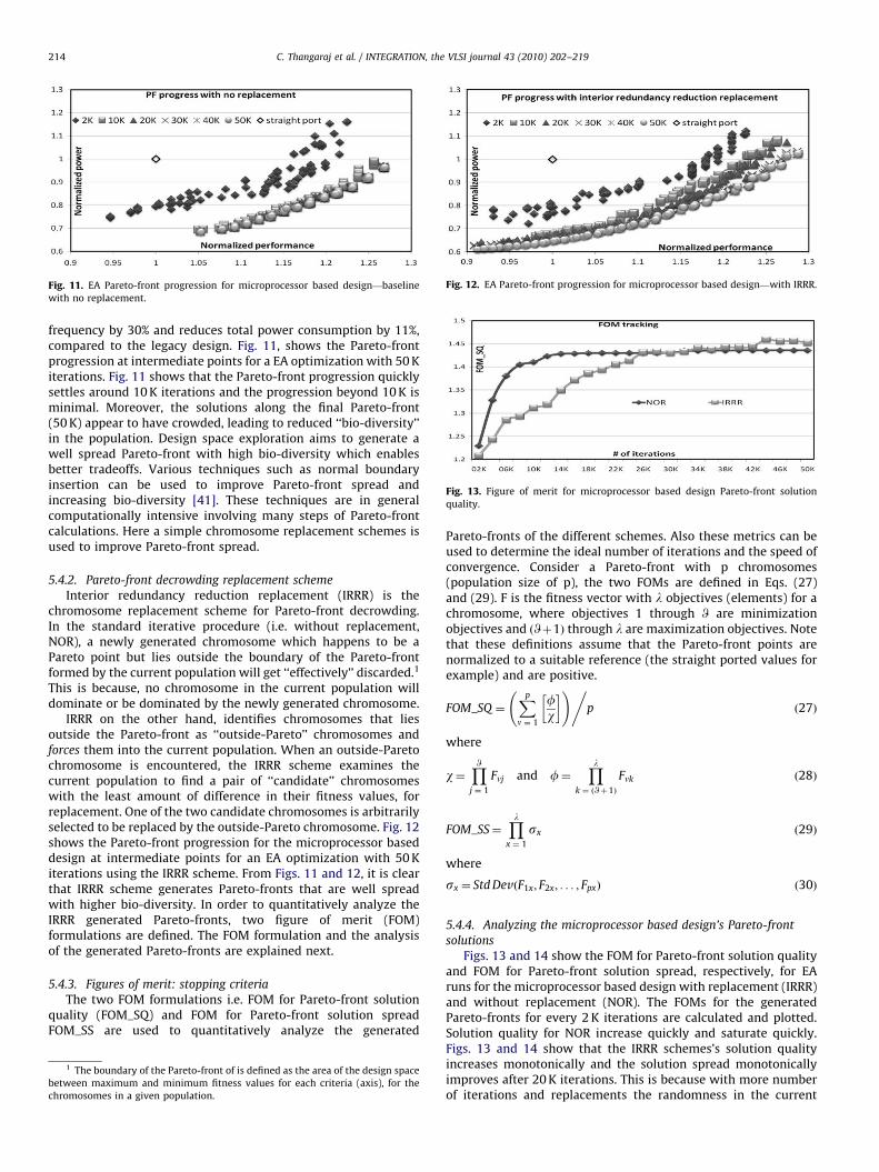
Fig. 11. EA Pareto-front progression for microprocessor based design—baseline
with no replacement.
Fig. 12. EA Pareto-front progression for microprocessor based design—with IRRR.
Fig. 13. Figure of merit for microprocessor based design Pareto-front solution
quality.
C. Thangaraj et al. / INTEGRATION, the VLSI journal 43 (2010) 202–219214
frequency by 30% and reduces total power consumption by 11%,compared to the legacy design. Fig. 11, shows the Pareto-frontprogression at intermediate points for a EA optimization with 50 Kiterations. Fig. 11 shows that the Pareto-front progression quicklysettles around 10 K iterations and the progression beyond 10 K isminimal. Moreover, the solutions along the final Pareto-front(50 K) appear to have crowded, leading to reduced ‘‘bio-diversity’’in the population. Design space exploration aims to generate awell spread Pareto-front with high bio-diversity which enablesbetter tradeoffs. Various techniques such as normal boundaryinsertion can be used to improve Pareto-front spread andincreasing bio-diversity [41]. These techniques are in generalcomputationally intensive involving many steps of Pareto-frontcalculations. Here a simple chromosome replacement schemes isused to improve Pareto-front spread.
5.4.2. Pareto-front decrowding replacement scheme
Interior redundancy reduction replacement (IRRR) is thechromosome replacement scheme for Pareto-front decrowding.In the standard iterative procedure (i.e. without replacement,NOR), a newly generated chromosome which happens to be aPareto point but lies outside the boundary of the Pareto-frontformed by the current population will get ‘‘effectively’’ discarded.1
This is because, no chromosome in the current population willdominate or be dominated by the newly generated chromosome.
IRRR on the other hand, identifies chromosomes that liesoutside the Pareto-front as ‘‘outside-Pareto’’ chromosomes andforces them into the current population. When an outside-Paretochromosome is encountered, the IRRR scheme examines thecurrent population to find a pair of ‘‘candidate’’ chromosomeswith the least amount of difference in their fitness values, forreplacement. One of the two candidate chromosomes is arbitrarilyselected to be replaced by the outside-Pareto chromosome. Fig. 12shows the Pareto-front progression for the microprocessor baseddesign at intermediate points for an EA optimization with 50 Kiterations using the IRRR scheme. From Figs. 11 and 12, it is clearthat IRRR scheme generates Pareto-fronts that are well spreadwith higher bio-diversity. In order to quantitatively analyze theIRRR generated Pareto-fronts, two figure of merit (FOM)formulations are defined. The FOM formulation and the analysisof the generated Pareto-fronts are explained next.
5.4.3. Figures of merit: stopping criteria
The two FOM formulations i.e. FOM for Pareto-front solutionquality (FOM_SQ) and FOM for Pareto-front solution spreadFOM_SS are used to quantitatively analyze the generated
1 The boundary of the Pareto-front of is defined as the area of the design space
between maximum and minimum fitness values for each criteria (axis), for the
chromosomes in a given population.
Pareto-fronts of the different schemes. Also these metrics can beused to determine the ideal number of iterations and the speed ofconvergence. Consider a Pareto-front with p chromosomes(population size of p), the two FOMs are defined in Eqs. (27)and (29). F is the fitness vector with l objectives (elements) for achromosome, where objectives 1 through W are minimizationobjectives and ðWþ1Þ through l are maximization objectives. Notethat these definitions assume that the Pareto-front points arenormalized to a suitable reference (the straight ported values forexample) and are positive.
FOM_SQ ¼Xp
n ¼ 1
fw
� � !,p ð27Þ
where
w¼YWj ¼ 1
Fnj and f¼Yl
k ¼ ðWþ1Þ
Fnk ð28Þ
FOM_SS¼Yl
x ¼ 1
sx ð29Þ
where
sx ¼ Std DevðF1x; F2x; . . . ; FpxÞ ð30Þ
5.4.4. Analyzing the microprocessor based design’s Pareto-front
solutions
Figs. 13 and 14 show the FOM for Pareto-front solution qualityand FOM for Pareto-front solution spread, respectively, for EAruns for the microprocessor based design with replacement (IRRR)and without replacement (NOR). The FOMs for the generatedPareto-fronts for every 2 K iterations are calculated and plotted.Solution quality for NOR increase quickly and saturate quickly.Figs. 13 and 14 show that the IRRR schemes’s solution qualityincreases monotonically and the solution spread monotonicallyimproves after 20 K iterations. This is because with more numberof iterations and replacements the randomness in the current

ARTICLE IN PRESS
C. Thangaraj et al. / INTEGRATION, the VLSI journal 43 (2010) 202–219 215
population reduces. During the standard iterative process whennewly generated chromosomes which dominate and replaceoutlying chromosome in the current population, the Pareto-front spread reduces. This is the case from 10 to 12 K and 18 to20 K for IRRR in Fig. 14. Once the current population’s Pareto-frontis sufficiently close to the edge of the ‘‘true’’ Pareto-front, thespread of the Pareto-front will be improved with more iterations.
Figs. 13 and 14 show that the IRRR scheme is slow to convergearound 42 K iterations, however, it generates Pareto-fronts withhigh spread and quality. Fig. 15 compares the final Pareto-frontfor the microprocessor based design generated at 50 K iterationsby the NOR and IRRR schemes. It clearly shows the spread and
Fig. 14. Figure of Merit for microprocessor based design Pareto-front solution
spread.
Fig. 15. Microprocessor based design Pareto-front analysis results.
Fig. 16. Details of system
quality for IRRR scheme to be better compared to NOR and farsuperior to the results published earlier in [12].
Figs. 16 and 17 show the details of system design A and B fromFig. 15, respectively. Design A improves the straight-port designwith 40% power reduction with only 9% performance impact.Similarly design B improves the straight-port design with 29%improvement in performance with only 2.5% power penalty. EAbased design space exploration with IRRR generates Pareto-frontsthat optimize both system power and performance. Solutionsuncovered henceforth are non-intuitive and are not immediatelyobvious, thus, enabling designers to perform quick, relativelyaccurate design space exploration and trade-off analysis early inthe design phase. This ability is a key contribution of the proposedmethodology.
5.4.5. EA based DSE of ISCAS89 circuits using the IRRR scheme
With the effectiveness of the IRRR scheme demonstrated in theprevious section, two large ISCAS89 circuits are used to furthervalidate IRRR scheme’s effectiveness in this section.
Fig. 18 shows the Pareto-fronts for the two ISCAS89 circuitsafter 50 K iteration with IRRR scheme. The Pareto-front for s38417circuit was expected to be better of the two since (as pointed outin Section 5.1.3) one module in s38417 contributed less than 3% tothe critical path delay. Therefore, power consumption could besignificantly reduced with minimal impact on performance. Sinces38584 circuit did not have such an advantage and the criticalpath was nearly equally divided between all four modules, thefinal Pareto-front for this circuit was inferior as shown in Fig. 18.This proves that the proposed design framework allows for suchopportunities to be uncovered and subsequently generatingsolutions that optimize both system power and performance.
Figs. 19 and 20 show the FOM for Pareto-front solution qualityand FOM for Pareto-front solution spread, respectively, for theISCAS89 circuits with IRRR. As expected the solution quality forthe s38417 circuit is better compared to s38584 circuit since thelatter circuit had fewer opportunities to optimize both power andperformance simultaneously. The FOM for solution quality fors38417 circuit saturates quickly compared to the IRRR solutionquality for the microprocessor based design. This is due to thedifference in the problem size i.e. chromosome length of 4 asopposed to 26, respectively. However, the solution spread FOM
design A from Fig. 15.

ARTICLE IN PRESS
Fig. 17. Details of system design B from Fig. 15.
Fig. 18. Pareto-front with IRRR at 50 K iteration for ISCAS89 s38584 and s38417
circuits.
Fig. 20. Figure of Merit for ISCAS89 s38584 and s38417 circuits Pareto-front with
IRRR solution spread.
Fig. 19. Figure of merit for ISCAS89 s38584 and s38417 circuits Pareto-front with
IRRR solution quality.
C. Thangaraj et al. / INTEGRATION, the VLSI journal 43 (2010) 202–219216
indicates that the spread of the Pareto-front consistentlyimproves only later around 38 K iterations.
6. Discussion of the results
6.1. Impact of ABB design choice
Large area overhead and increased design complexity of usingthe ABB technique may make the ABB choices undesirable,particularly when ABBs used in some modules are mixed withother modules with no ABB on the same chip. To ascertain theimpact of ABB, an EA run with IRRR and 50 K iterations withoutany ABB design choices is performed on the microprocessor baseddesign and its result is compared to the result of the EA run usingIRRR and 50 K iterations with all design choices.
Fig. 21 shows the impact of ABB design choice on the finalPareto-front at 50 K. High performance designs (region A inFig. 21) predominantly use ABB-FB to improve performance,where removal of ABB-FB leads to reduction in both power andperformance. In general, ABB-RB can be used to reduce powerconsumption, however, power consumption reduction using sleeptransistors (ST) is much larger. Low power designs (region B inFig. 21) predominantly use ST (in addition to ABB-RB) to reducepower and use ABB-FB to offset the performance impact of ST.Removal of ABB (both FB and RB) in low power designs lead toreduction in performance as well as power consumption, asillustrated in Fig. 21. As a result the Pareto-front without ABB incomparison with the Pareto-front with ABB, is shifted along thedirection of lower power and performance. Interestingly, thereexists remarkable overlap in the two Pareto-fronts where thesame design goals can be met with much less design complexity.Moreover as shown in Fig. 21 if a 5% power penalty region isconsidered, designs with reduced complexity (without ABB) canbe uncovered with sufficient performance and substantial powersavings.
6.2. Prediction model complexity: impact of model parameters
The analytical design target prediction models (Eqs. (1)–(21))described earlier in the paper have many parameters contained inthem. Majority of these parameters are easy to obtain. For
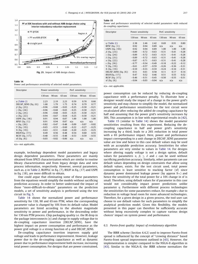
ARTICLE IN PRESS
Fig. 21. Impact of ABB design choice.
Table 14Power and performance sensitivity of selected model parameters.
Descriptor Power sensitivity Perf. sensitivity
130 nm 90 nm 65 nm 130 nm 90 nm 65 nm
Z (Table 2) 2.23 2.19 2.23 0.59 0.70 0.66
DECAP_SENS (Eq. (6)) 1.68 1.79 1.75 0.74 0.79 0.77
b (Eq. (23)) �0.96 �0.68 �0.65 �0.25 �0.30 �0.21
g (Eq. (24)) �0.96 �0.68 �0.65 �0.25 �0.30 �0.21
d (Eq. (25)) �0.96 �0.68 �0.65 �0.25 �0.30 �0.21
a (Eq. (22)) �0.94 �0.67 �0.64 �0.25 �0.30 �0.21
USPE (Eq. (18)) 0.91 0.94 0.87 1.00 1.00 1.00
RPSF (Eq. (1)) 0.91 0.94 0.87 n/a n/a n/a
e (Eq. (26)) �0.82 �0.47 �0.48 �0.09 �0.07 �0.02
Y (Eq. (19)) �0.65 �0.53 �0.60 �0.22 �0.27 �0.25
X (Eq. (19)) �0.63 �0.51 �0.60 �0.20 �0.25 �0.25
BSUF(Eq. (17)) 0.49 0.56 0.48 0.54 0.60 0.55
RCSF (Eq. (17)) �0.48 �0.55 �0.48 �0.53 �0.59 �0.55
sf (Eq. (8)) �0.03 �0.02 �0.06 n/a n/a n/a
n/a—not applicable.
Table 15Power and performance sensitivity of selected model parameters with reduced
de-coupling capacitance.
Descriptor Power sensitivity Perf. sensitivity
130 nm 90 nm 65 nm 130 nm 90 nm 65 nm
Z (Table 2)) 2.38 2.46 2.42 0.69 0.91 0.80
RPSF (Eq. (1)) 0.92 0.94 0.89 n/a n/a n/a
USPE (Eq. (18)) 0.92 0.94 0.89 1.00 1.00 1.00
b (Eq. (23)) �0.89 �0.72 �0.63 �0.31 �0.41 �0.28
g (Eq. (24)) �0.89 �0.72 �0.63 �0.31 �0.41 �0.28
d (Eq. (25)) �0.89 �0.72 �0.63 �0.31 �0.41 �0.28
a (Eq. (22)) �0.87 �0.71 �0.63 �0.31 �0.41 �0.28
e (Eq. (26)) �0.77 �0.54 �0.49 �0.18 �0.22 �0.12
Y (Eq. (19)) �0.61 �0.57 �0.59 �0.26 �0.36 �0.31
X (Eq. (19)) �0.59 �0.55 �0.59 �0.24 �0.34 �0.31
DECAP_SENS (Eq. (6)) 0.51 0.61 0.58 0.11 0.17 0.14
BSUF(Eq. (17)) 0.47 0.52 0.46 0.51 0.55 0.52
RCSF (Eq. (17)) �0.46 �0.51 �0.45 �0.50 �0.55 �0.51
sf (Eq. (8)) �0.04 �0.03 �0.04 n/a n/a n/a
n/a—not applicable.
C. Thangaraj et al. / INTEGRATION, the VLSI journal 43 (2010) 202–219 217
example, technology dependent model parameters and legacydesign dependent parameters. These parameters are mainlyobtained from SPICE characterization which are similar to routinelibrary characterization and from legacy design data and newprocess information, respectively. However, several parameters,such as, Z in Table 2, BUFFLC in Eq. (7), BSUF in Eq. (17) and USPEin Eq. (18), are more difficult to obtain.
One could argue that eliminating some of these parametersfrom the equations would simplify the models without sacrificingprediction accuracy. In order to better understand the impact ofthose ‘‘more-difficult-to-obtain’’ parameters on the predictionmodels, a set of sensitivity analysis is performed using the testcircuit in Fig. 5.
Table 14 shows the normalized power and performancesensitivity for 130, 90 and 65 nm PTM, when the correspondingparameter value is changed by 10% from its default value. Modelparameters are listed according to the absolute magnitudesensitivity to power and performance, in the descending orderfor 130 nm PTM process. Chip packaging quality i.e. the IR drop inthe package interconnects (Z) and change in supply voltage due tode-coupling capacitance insertion (DECAP_SENS), have thehighest impact on power consumption and performance as thepower grid voltage is a strong function of Z and DECAP_SENS.
De-coupling capacitance insertion improves supply gridvoltage and leads to performance improvement. However, leakagepower due to the de-coupling capacitance as well as dynamicpower due to performance improvement both increase, increasingtotal power consumption. For designs that are power constrained,
power consumption can be reduced by reducing de-couplingcapacitance with a performance penalty. To illustrate how adesigner would study the impact of a change in the power grid’ssensitivity and may choose to simplify the model, the normalizedpower and performance sensitivities for the test circuit wererecalculated after reducing the added de-coupling capacitance byhalf and assuming that the power grid’s sensitivity increases by30%. This assumption is in line with experimental results in [42].
Table 15 (similar to Table 14) shows the model parametersensitivities resulting from this experiment. Reducing the de-coupling capacitance in half and power grid’s sensitivityincreasing by a third, leads to a 26% reduction in total powerwith a 6% performance impact. Here, power and performanceimpact corresponding to a unit change in DECAP_SENS parametervalue are low and hence in this case default values may be usedwith an acceptable prediction accuracy. Sensitivities for otherparameters are very similar to values in Table 14. For designswhere altering supply voltage is not a design option, defaultvalues for parameters a, b, g, d and e can be used withoutsacrificing prediction accuracy. Similarly, other paraments can usedefault values depending on design constraints that allow usingdefault values, exists. For the test circuit used, total powerconsumption is least sensitive to stacking factor (sf) sincedynamic power dominated leakage power (by approx 9�) andhence the sensitivity of the total power for a 10% change in sf issmall. Therefore, using default values for sf parameter in this casewould not considerably impact power predictions unlikeparameter Z. Furthermore with different process technologiesthe sensitivities for some parameters reduce, for example e due toreduction in voltage head room for more advanced technologies.Therefore, for a given design in a given process, the tool user canchoose to use default values for such parameters to simplify theanalytical prediction model. Given this flexibility, the modelspresented in this paper can therefore be sufficiently accuratewithout being excessively complex to capture various designchoices’ impact on system power and performance.
6.3. Pareto-front quality: Impact of evolutionary algorithm
The IRRR scheme (Section 4.4.2) used to improve Pareto-frontspread is influenced by the concept of ‘‘crowing distance’’ basedPareto-front spread improvement outlined in [43]. However, theimplementation is simpler compared to the NSGA-II algorithm in[43]. Similar to the NSGA-II, the IRRR scheme normalizes the

ARTICLE IN PRESS
C. Thangaraj et al. / INTEGRATION, the VLSI journal 43 (2010) 202–219218
objective function values, but does not require any user definedsharing parameters and, can be applied to problems with morethan two objectives. The strict one child one parent replacementpolicy used in this work limits the elitism offered by theevolutionary algorithm. The focus of the work presented in thispaper, at this time, is establishing the applicability of theproposed design framework for design space exploration; hencea simpler evolution algorithm with IRRR is used. Integrating morerigorous algorithms such as the NSGA-II or SPEA2 to improve thedesign framework for design space exploration and comparing therelative merits of IRRR scheme and the various algorithms,potentially using the PISA framework [44], are natural extensionsof the work presented here. PISA’s assessment metrics and thetwo proposed FOM can be used to compare the Pareto-frontsgenerated by the various algorithms. Additionally, the uniformity(D�metric) metric proposed in [45] can be included to comparethe Pareto-fronts generated by the various algorithms.
7. Conclusion
System power-performance optimization is most effectiveearly in the design phase when design space exploration isperformed. Design convergence in both power and performance,especially in nanometer CMOS, has become increasingly difficultand choose an optimal implementation target is imperative formeeting time-to-market requirement. The proposed frameworkfor design space exploration using legacy design data, technologyscaling trends, and in situ simulations provides design aid inchoosing optimal implementation targets for better designconvergence. The technology node migration experiment onISCAS benchmark circuits established the feasibility of theproposed methodology. For these circuits, the results from designspace exploration offer 7–32% power reduction with 0–9%performance degradation or 10.31–17% performance improve-ment with 2–3.85% power penalty.
Furthermore, power and performance prediction model accu-racy in successive CMOS technologies from 180 to 65 nm wereexperimentally estimated and compared to similar estimatesfrom existing literature. The accuracy is inline and comparable toresults from other previously published works. Evolutionaryalgorithm based design space exploration using Pareto analysisof a microprocessor based design yielded Pareto optimal solutionsthat optimized both power and performance. The evolutionaryalgorithm was improved by a replacement schemes for decrowd-ing to generate well spread Pareto-fronts to allow better trade-offanalysis. The design space exploration generated designs thatimproved the straight-port design by reducing power by 40% with9% performance impact or by improving performance by 29% with2.5% power penalty. In addition to generating Pareto optimaldesigns, ways to reduce system implementation complexity withbounded impact on power and performance were presented.
The experimental results illustrate the ability of the proposedframework to uncover complex non-intuitive solutions usingevolutionary algorithm based Pareto analysis. By incorporatingthe proposed methodology as part of a standard system design flow,quick what-if analysis can be performed at a high level andunderlying design risks can be exposed very early in the designphase. The key contributions of the proposed framework are: (a) theability to uncover Pareto optimal, complex and non-intuitivesystem designs; (b) the ease of performing high level what-ifanalysis; (c) the potential to expose any underlying design risksvery early in the design phase and (d) design complexity reductionby generating solution without complex design choices such as ABBwith a bounded power and performance impact. Thus, improvingsystem design convergence and meeting time-to-market schedule.
Currently the proposed framework does not include anyestimates for the impact of process variation on design targetswhich are becoming important design considerations. Speciallibraries, RF and analog macro modules that does not followstandard scaling trends are not included in the framework, theseneed to be included to extend the methodology well into ‘‘More-than-Moore’’ design era. Research is on-going to incorporatemacro model based interconnect delay estimation, the estimationof delay impact due to clock uncertainties and, improving andenabling the EA to differentiate between various types of modules(i.e. memory, logic and analog/mixed signal modules) duringchromosome generation. Prediction models for chip area, yieldand system reliability are also being explored to expand currentdesign space exploration capabilities.
References
[1] Justin E. Harlow III, Toward design technology in 2020: trends issues andchallenges [VLSI design], in: Proceedings of IEEE Computer Society AnnualSymposium on VLSI, February 2003, pp. 3–4.
[2] /http://www.itrs.netS, ITRS, 2005.[3] C. Constantinescu, Trends and challenges in VLSI circuit reliability, IEEE
Micro. 23 (4) (2003) 14–19.[4] S. Rusu, M. Sachdev, C. Svensson, B. Nauta, T3: trends and challenges in VLSI
technology scaling towards 100 nm, in: Proceedings of ASP-DAC, IEEEComputer Society, 2002, p. 16.
[5] W. Ye, et al., The design and use of simple power: a cycle-accurate energyestimation tool, in: 37th DAC, 2000, pp. 340–345.
[6] T.M. Austin /http://www.simplescalar.com/S, 2004.[7] D. Brooks, et al., Wattch: a framework for architectural-level power analysis
and optimizations, in: Proceedings of the 27th International Symposium onComputer Architecture, 2000, pp. 83–94.
[8] D. Broooks, et al., New methodology for early-stage, microarchitecture-levelpower-performance analysis of microprocessors, IBM J. Res. Dev. 5/6 (2003)653–670.
[9] T. Givargis, F. Vahid, Platune: a tuning framework for system-on-a-chipplatforms, IEEE Trans. Comput. Aided Des. Integrated Circuits Systems 21 (11)(2002) 1317–1327.
[10] T. Givargis, F. Vahid, J. Henkel, System-level exploration for Pareto-optimalconfigurations in parameterized system-on-a-chip, IEEE Trans. Very LargeScale Integration Systems 10 (2) (Aug. 2002) 416–422.
[11] C. Thangaraj, T. Chen, Power and performance analysis for early design spaceexploration, in: Proceedings of the IEEE Computer Society Annual Symposiumon VLSI, 2007, pp. 473–478.
[12] C. Thangaraj, T. Chen, Early design phase power performance trade-offs usingin-situ macro models, in: IEEE International Symposium on Electronic Design,Test and Applications, 2008, pp. 539–544.
[13] D. Sylvester, et al., System-level performance modeling with BACPAC—Ber-keley Advanced Chip Performance Calculator, in: ACM International Work-shop on System-Level Interconnect Prediction, 1999, pp. 109–114.
[14] D. Sylvester, W. Jiang, K. Keutzer /http://www.eecs.umich.edu/dennis/bacpac/index.htmlS, 1998.
[15] D. Duarte, V. Narayanan, M. Irwin, Impact of technology scaling in the clocksystem power, in: Proceedings of IEEE Computer Society Annual Symposiumon VLSI, 2002, pp. 52–57.
[16] T. Karn, et al., Eda challenges facing future microprocessor design, IEEE Trans.Comput. Aided Des. Integrated Circuits Systems 19 (12) (2000) 1498–1506.
[17] B. Dennington, Low power design from technology challenge to greatproducts, in: Proceedings of International Symposium on Low PowerElectronics and Design, ACM, New York, NY, USA, 2006, p. 213 /http://www.islped.org/X2006/Dennington.pptS.
[18] J. Lin, Design technology challenges for system and chip level designs in verydeep submicron technologies, in: Proceedings of the First IEEE/ACM/IFIPInternational Conference on Hardware/Software Codesign and SystemSynthesis, ACM, New York, NY, USA, 2003, p. 194 /http://www.ece.uci.edu/codes+isss/Invited/JamesLin.pdfS.
[19] G. Ascia, V. Catania, M. Palesi, A multi-objective genetic approach for system-level exploration in parameterized systems-on-a-chip, IEEE Trans. Comput.Aided Des. Integrated Circuits Systems 24 (4) (2005) 635–645.
[20] R. Vilangudipitchai, P. Balsara, Power switch network design for mtcmos, in:18th International Conference on VLSI Design, 2005, pp. 836–839.
[21] T. Chen, S. Naffziger, Comparison of adaptive body bias (abb) and adaptivesupply voltage (asv) for improving delay and leakage under the presence ofprocess variation, IEEE Trans. Very Large Scale Integration Systems 11 (5)(2003) 888–899.
[22] S. Mukhopadhyay, A. Raychowdhury, K. Roy, Accurate estimation of totalleakage in nanometer-scale bulk cmos circuits based on device geometry anddoping profile, IEEE Trans. Comput. Aided Des. Integrated Circuits Systems 24(3) (2005) 363–381.

ARTICLE IN PRESS
C. Thangaraj et al. / INTEGRATION, the VLSI journal 43 (2010) 202–219 219
[23] C. Thangaraj, T. Chen, Design target exploration for meeting time-to-marketusing pareto analysis, in: IEEE International Symposium on Circuits andSystems, May 2008, pp. 364–367.
[24] NIMO, Predictive technology model (ptm) /http://www.eas.asu.edu/ptm/S,2007.
[25] W. Zhao, Y. Cao, New generation of predictive technology model for sub-45 nm design exploration, in: Proceedings of the Seventh InternationalSymposium on Quality Electronic Design, 2006, pp. 585–590.
[26] VCAG-OSU /http://avatar.ecen.okstate.edu/projects/scells/S, 2008.[27] SYNOPSYS /http://www.synopsys.com/S, 2009.[28] K. Shi, D. Howard, Challenges in sleep transistor design and implementation
in low-power designs, in: Proceedings of the 43rd Annual Conference onDesign Automation, 2006, pp. 113–116.
[29] B. Stackhouse, S. Bhimji, C. Bostak, D. Bradley, B. Cherkauer, J. Desai, E.Francom, M. Gowan, P. Gronowski, D. Krueger, C. Morganti, S. Troyer, A 65 nm2-billion transistor quad-core itanium processor, IEEE J. Solid-State Circuits44 (1) (2009) 18–31.
[30] C. McNairy, R. Bhatia, Montecito: a dual-core, dual-thread itanium processor,IEEE Micro. 25 (2) (2005) 10–20.
[31] C. McNairy, D. Soltis, Itanium 2 processor microarchitecture, IEEE Micro. 23(2) (2003) 44–55.
[32] K. Deb, Multi-objective optimization using evolutionary algorithms, in:Wiley-Interscience Series in Systems and Optimization, Wiley, Chichester,2001.
[33] S.K. Hsu, et al., A 110 GOPS/W 16-bit Multiplier and Reconfigurable PLA Loopin 90-nm CMOS, IEEE J. Solid-State Circuits (2006) 256–264.
[34] J.W. Tschanz, et al., Dynamic sleep transistor and body bias for active leakagepower control of microprocessors, IEEE J. Solid-State Circuits (2003) 1838–1845.
[35] B. Chatterjee, M. Sachdev, R. Krishnamurthy, A cpl-based dual supply 32-bitalu for sub 180 nm cmos technologies, in: Proceedings of InternationalSymposium on Low Power Electronics and Design, August 2004, pp. 248–251.
[36] S. Mathew, et al., Sub-500 ps 64 b alus in 0.18 um soi/bulk cmos: design &scaling trends, in: IEEE International Solid State Circuits Conference, vol. 460,2001, pp. 318–319.
[37] D. Blaauw, V. Zolotov, S. Sundareswaran, C. Oh, R. Panda, Slope propagation instatic timing analysis, IEEE/ACM Intl. Conference on Computer-aided Design(2000) 338–343.
[38] SYNOPSYS /http://www.synopsys.com/Tools/Implementation/SignOff/Pages/NanoTime.aspxS, 2009.
[39] CADENCE /http://www.celestry.com/products_nautilusdc.shtmlS, 2009.[40] V. Veetil, D. Sylvester, D. Blaauw, Fast and accurate waveform analysis with
current source models, in: International Symposium on Quality ElectronicDesign, ISQED, March 2008, pp. 53–56.
[41] I. Das, J.E. Dennis, Normal-boundary intersection: a new method forgenerating the pareto surface in nonlinear multicriteria optimizationproblems, SIAM J. Optim. 8 (3) (1998) 631–657.
[42] H. Sanchez, et al., Increasing microprocessor speed by massive application ofon-die high-k mim decoupling capacitors, in: IEEE International Solid-StateCircuits Conference, February 2006, pp. 2190–2199.
[43] K. Deb, A. Pratap, S. Agarwal, T. Meyarivan, A fast and elitist multiobjectivegenetic algorithm: Nsga-ii, IEEE Trans. Evol. Comput. 6 (2002) 182–197.
[44] E. Zitzler, et al. /http://www.tik.ethz.ch/�sop/pisa/S, A platform andprogramming language independent interface for search algorithms, 2008.
[45] C. Erbas, S. Cerav-Erbas, A. Pimentel, Multiobjective optimization andevolutionary algorithms for the application mapping problem in multi-processor system-on-chip design, IEEE Trans. Evol. Comput. 10 (3) (2006)358–374.
Charles Thangaraj received his Bachelor of Engineer-ing from Bharathiyar University, Coimbatore, India in2001, Master of Science degree and the Ph.D. degreefrom Colorado State University, Fort Collins, USA in2005 and 2009, respectively. Currently he is pursuing acareer in engineering education as a Visiting AssistantProfessor at Harvey Mudd College, USA.
Cengiz Alkan is a post doctoral researcher at ColoradoState University. He received his Bachelor of Engineer-ing from Uludag University, Turkey. Master of Sciencedegree from University of Southern California andPh.D. from Colorado State University. Currently he ispursuing research work including circuit optimizationand automated analog design methodologies.
Tom Chen received a B.S. degree from Shanghai Jiao-Tong University, Shanghai, China, and a Ph.D. from theUniversity of Edinburgh, Edinburgh, Scotland. From1987 to 1989, Dr. Chen was with Philips Semiconduc-tors as a member of technical staff. From 1989 to 1990,he was an Assistant Professor at New Jersey Institute ofTechnology. Since 1990, Dr. Chen has been with theDepartment of Electrical and Computer Engineering,Colorado State University, where he is currently theBusiness Challenge Endowment Professor. Dr. Chen’sresearch interests are in the areas of VLSI design andCAD methodology. He has published over 100 papers
in refereed conferences and journals in the areas ofVLSI system architecture and VLSI CAD methodology.