mt90503 2048vc aal1 sar data sheet - microsemi
TRANSCRIPT
1Zarlink Semiconductor Inc.
Zarlink, ZL and the Zarlink Semiconductor logo are trademarks of Zarlink Semiconductor Inc.Copyright 2003-2004, Zarlink Semiconductor Inc. All Rights Reserved.
Features• AAL1 Segmentation and Reassembly device
capable of simultaneously processing up to 2048 bidirectional VCs
• AAL1 cell format for "Structured DS1/E1 N x 64kbps Service" as per ATM Forum AF-VTOA-0078.000 "Circuit Emulation Services Interoperability Specifications" (Nx64 Basic Service, DS1 Nx64 Service with CAS, and E1 Nx64 Service with CAS)
• Two UTOPIA ports (Level 2, 16-bit, 50 MHz) with loopback function for dual fibre ring applications
• Third UTOPIA port for connection to an external AAL5 SAR processor, or for chaining multiple MT90503 or other SAR or IMA devices
• Flexible aggregation capabilities (Nx64) to allow any combination of 64 Kbps
• TDM bus provides 32 bidirectional serial TDM streams at 2.048, 4.096, or 8.192 Mbps for up to 4096 TDM 64 Kbps channels
• Compatible with H.100 and H.110 interfaces
• TDM to ATM transmission latency less than 250 µs
• Support for clock recovery - Adaptive Clock Recovery, Synchronous Residual Time Stamp (SRTS) or external
• Support master and slave TDM bus clock operation
• 8- or 16-bit microprocessor port, configurable to Motorola or Intel timing
• Master clock rate up to 80 MHz
• Single power supply device (3.3V)
• IEEE 1149 (JTAG) interface
December 2004
Ordering Information
MT90503AG 503 Pin PBGA
For temperature range, see page 207.
MT90503 2048VC AAL1 SAR
Data Sheet
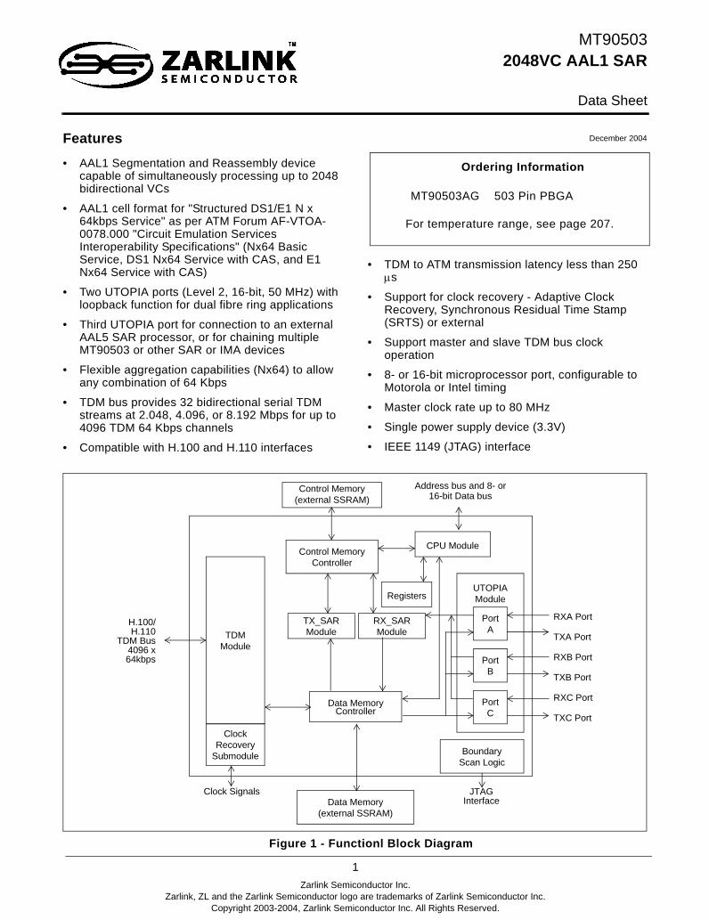
Figure 1 - Functionl Block Diagram
TDMModule
ClockRecovery
Submodule
Data MemoryController
Data Memory(external SSRAM)
CPU Module
Registers
Control MemoryController
Control Memory(external SSRAM)
RX_SARModule
TX_SARModule
UTOPIAModule
PortA
PortB
PortC
BoundaryScan Logic
Address bus and 8- or16-bit Data bus
RXA Port
TXA Port
RXB Port
TXB Port
RXC Port
TXC Port
JTAGInterface
Clock Signals
H.100/H.110
TDM Bus4096 x64kbps
MT90503 Data Sheet
2Zarlink Semiconductor Inc.
DescriptionThe MT90503 is an AAL1 SAR, which offers a highly integrated solution for interfacing telecom bus-based systemswith ATM networks. The device has the capability of simultaneously processing 2048 bidirectional channels of 64kbps. The MT90503 can be connected directly to an H.100 or H.110 compatible bus. The device also offers thecapability of using Channel Associated Signalling (CAS) to support Circuit Emulation Service (CES) for StructuredData Transfer (SDT).
The interface to the TDM port is provided by a TDM bus, which consists of 32 bidirectional serial TDM data streamsat 2.048, 4.096, or 8.192 Mbps, therefore allowing for 2048 bidirectional TDM channels operating at 64 kbps. ThisTDM bus is compatible with the ECTF H.100 and H.110 specifications.
The interface to the ATM domain is provided by three UTOPIA ports (Ports A, B, and C). All three of the UTOPIAports can operate in ATM (master) or PHY (slave) mode. Port A can also be configured as Level 2 M-PHY mode.
Applications
• ATM Access and Multiplexing Equipment
• Switching Platforms that provide internetworking between TDM and ATM
• ATM Edge Switches
• ATM uplink for expansion of COs, PBXs, or open switching platforms using an adjunct ATM switch
• Integrated Digital Loop Carrier (IDLC)
• SONET or SDH Add and Drop Multiplexers (ADM)
• Next Generation Digital Loup Carrier (NGDIC)
• Digital Subscriber Line Access Multiplexer DSLAM with Gateway
Switching Feature• Cells coming in from any of the UTOPIA ports can be switched to any other port. The user has the option to
change the VPI and VCI fields.
PURCHASE OF THIS PRODUCT DOES NOT GRANT THE PURCHASER ANY RIGHTS UNDER PATENT NO.5,260,978. USE OF THIS PRODUCT OR ITS RE-SALE AS A COMPONENT OF ANOTHER PRODUCT MAYREQUIRE A LICENSE UNDER THE PATENT WHICH IS AVAILABLE FROM TELCORDIA TECHNOLOGIES,INC., 445 SOUTH STREET , MORRISTOWN, NEW JERSEY 07960.
ZARLINK ASSUMES NO RESPONSIBILITY OR LIABILITY THAT MAY RESULT FROM ITS CUSTOMERS' USEOF ZARLINK PRODUCTS WITH RESPECT TO THIS PATENT. IN PARTICULAR, ZARLINK'S PATENTINDEMNITY IN ITS TERMS AND CONDITIONS OF SALES WHICH ARE SET OUT IN ITS SALESACKNOWLEDGEMENTS AND INVOICES DOES NOT APPLY TO THIS PATENT.

MT90503 Data Sheet
3Zarlink Semiconductor Inc.
Figure 2 - ATM Switch Application
2048
AALI SARMT90503
28 portAAL1 SAR
MT90528
Octal/IMAMT90220
AT
M U
TO
PIA
Bus
Octal T1/E1FramersMT9072
M13MUX
T3/E3LIU
Clock Digital PLLOscillator MT9045
Clock Digital PLLOscillator MT9045
Stratum 3 Timing Card
Stratum 3 Timing Card
T1/E1LIU
T1/E1FramersT1/E1 IMA Uplink
OC-12Framers& ATM
CellAccess
OpticalInterface& Drivers
TrafficManagement& Switching
ATM Network Uplink
MT9076
T1/E1 CircuitEmulation Services
T3/E3
PSTN SDT
PSTN UDT Traffic
ATM Traffic
Trafficchannels

MT90503 Data Sheet
Table of Contents
4Zarlink Semiconductor Inc.
1.0 Introduction . . . . . . . . . . . . . . . . . . . . . . . . . . . . . . . . . . . . . . . . . . . . . . . . . . . . . . . . . . . . . . . . . . . . . . . . . . 161.1 Functional Overview of the MT90503 . . . . . . . . . . . . . . . . . . . . . . . . . . . . . . . . . . . . . . . . . . . . . . . . . . . . 16
2.0 Features Detailed Description . . . . . . . . . . . . . . . . . . . . . . . . . . . . . . . . . . . . . . . . . . . . . . . . . . . . . . . . . . . 172.1 UTOPIA Interface . . . . . . . . . . . . . . . . . . . . . . . . . . . . . . . . . . . . . . . . . . . . . . . . . . . . . . . . . . . . . . . . . . . 172.2 TDM Interface . . . . . . . . . . . . . . . . . . . . . . . . . . . . . . . . . . . . . . . . . . . . . . . . . . . . . . . . . . . . . . . . . . . . . . 182.3 Clock Recovery . . . . . . . . . . . . . . . . . . . . . . . . . . . . . . . . . . . . . . . . . . . . . . . . . . . . . . . . . . . . . . . . . . . . . 182.4 ATM SAR. . . . . . . . . . . . . . . . . . . . . . . . . . . . . . . . . . . . . . . . . . . . . . . . . . . . . . . . . . . . . . . . . . . . . . . . . . 182.5 Required External Components . . . . . . . . . . . . . . . . . . . . . . . . . . . . . . . . . . . . . . . . . . . . . . . . . . . . . . . . 192.6 Particular Modes of Operation. . . . . . . . . . . . . . . . . . . . . . . . . . . . . . . . . . . . . . . . . . . . . . . . . . . . . . . . . . 192.7 Miscellaneous . . . . . . . . . . . . . . . . . . . . . . . . . . . . . . . . . . . . . . . . . . . . . . . . . . . . . . . . . . . . . . . . . . . . . . 192.8 Power . . . . . . . . . . . . . . . . . . . . . . . . . . . . . . . . . . . . . . . . . . . . . . . . . . . . . . . . . . . . . . . . . . . . . . . . . . . . 20
3.0 Pin Designations and Descriptions . . . . . . . . . . . . . . . . . . . . . . . . . . . . . . . . . . . . . . . . . . . . . . . . . . . . . . . 204.0 Functional Description . . . . . . . . . . . . . . . . . . . . . . . . . . . . . . . . . . . . . . . . . . . . . . . . . . . . . . . . . . . . . . . . . 34
4.1 CPU Interface . . . . . . . . . . . . . . . . . . . . . . . . . . . . . . . . . . . . . . . . . . . . . . . . . . . . . . . . . . . . . . . . . . . . . . 344.1.1 CPU Interrupts . . . . . . . . . . . . . . . . . . . . . . . . . . . . . . . . . . . . . . . . . . . . . . . . . . . . . . . . . . . . . . . . . 35
4.1.1.1 Example Interrupt Flow. . . . . . . . . . . . . . . . . . . . . . . . . . . . . . . . . . . . . . . . . . . . . . . . . . . . . . 354.1.1.2 Interrupt Initialization . . . . . . . . . . . . . . . . . . . . . . . . . . . . . . . . . . . . . . . . . . . . . . . . . . . . . . . 354.1.1.3 Interrupt Servicing . . . . . . . . . . . . . . . . . . . . . . . . . . . . . . . . . . . . . . . . . . . . . . . . . . . . . . . . . 35
4.1.2 Intel/Motorola Interface . . . . . . . . . . . . . . . . . . . . . . . . . . . . . . . . . . . . . . . . . . . . . . . . . . . . . . . . . . 364.1.2.1 Extended Indirect Accessing . . . . . . . . . . . . . . . . . . . . . . . . . . . . . . . . . . . . . . . . . . . . . . . . . 384.1.2.2 Extended Indirect Writes . . . . . . . . . . . . . . . . . . . . . . . . . . . . . . . . . . . . . . . . . . . . . . . . . . . . 384.1.2.3 Extended Indirect Reads . . . . . . . . . . . . . . . . . . . . . . . . . . . . . . . . . . . . . . . . . . . . . . . . . . . . 384.1.2.4 Extended Direct Accessing. . . . . . . . . . . . . . . . . . . . . . . . . . . . . . . . . . . . . . . . . . . . . . . . . . . 384.1.2.5 Extended Direct Writes. . . . . . . . . . . . . . . . . . . . . . . . . . . . . . . . . . . . . . . . . . . . . . . . . . . . . . 394.1.2.6 Extended Direct Reads. . . . . . . . . . . . . . . . . . . . . . . . . . . . . . . . . . . . . . . . . . . . . . . . . . . . . . 39
4.1.3 MT90503 Reset Procedure . . . . . . . . . . . . . . . . . . . . . . . . . . . . . . . . . . . . . . . . . . . . . . . . . . . . . . . 394.2 TDM Module . . . . . . . . . . . . . . . . . . . . . . . . . . . . . . . . . . . . . . . . . . . . . . . . . . . . . . . . . . . . . . . . . . . . . . . 40
4.2.1 TDM Bus Interface . . . . . . . . . . . . . . . . . . . . . . . . . . . . . . . . . . . . . . . . . . . . . . . . . . . . . . . . . . . . . . 404.2.2 TDM Bus Clocking Mechanism . . . . . . . . . . . . . . . . . . . . . . . . . . . . . . . . . . . . . . . . . . . . . . . . . . . . 424.2.3 TDM Datapath . . . . . . . . . . . . . . . . . . . . . . . . . . . . . . . . . . . . . . . . . . . . . . . . . . . . . . . . . . . . . . . . . 424.2.4 TDM Channel Association Structures . . . . . . . . . . . . . . . . . . . . . . . . . . . . . . . . . . . . . . . . . . . . . . . 43
4.2.4.1 Non CAS Operation. . . . . . . . . . . . . . . . . . . . . . . . . . . . . . . . . . . . . . . . . . . . . . . . . . . . . . . . 434.2.4.2 CAS Operation . . . . . . . . . . . . . . . . . . . . . . . . . . . . . . . . . . . . . . . . . . . . . . . . . . . . . . . . . . . 45
4.2.5 TDM Circular Buffers . . . . . . . . . . . . . . . . . . . . . . . . . . . . . . . . . . . . . . . . . . . . . . . . . . . . . . . . . . . . 484.2.6 TDM Circular Buffer Pointers . . . . . . . . . . . . . . . . . . . . . . . . . . . . . . . . . . . . . . . . . . . . . . . . . . . . . . 51
4.2.6.1 Non-multiframing mode . . . . . . . . . . . . . . . . . . . . . . . . . . . . . . . . . . . . . . . . . . . . . . . . . . . . . 514.2.6.2 E1/T1 Multiframing (standard) . . . . . . . . . . . . . . . . . . . . . . . . . . . . . . . . . . . . . . . . . . . . . . . . 52
4.3 TX_SAR Module . . . . . . . . . . . . . . . . . . . . . . . . . . . . . . . . . . . . . . . . . . . . . . . . . . . . . . . . . . . . . . . . . . . . 574.3.1 Overview . . . . . . . . . . . . . . . . . . . . . . . . . . . . . . . . . . . . . . . . . . . . . . . . . . . . . . . . . . . . . . . . . . . . . 57
4.3.1.1 Support and Trunking for Different Types of ATM Cells. . . . . . . . . . . . . . . . . . . . . . . . . . . . . 574.3.2 TX_SAR Event Schedulers . . . . . . . . . . . . . . . . . . . . . . . . . . . . . . . . . . . . . . . . . . . . . . . . . . . . . . . 58
4.3.2.1 Overview . . . . . . . . . . . . . . . . . . . . . . . . . . . . . . . . . . . . . . . . . . . . . . . . . . . . . . . . . . . . . . . . 584.3.2.2 The Transmit Event Scheduler Process . . . . . . . . . . . . . . . . . . . . . . . . . . . . . . . . . . . . . . . . 584.3.2.3 Transmit Event Scheduler Fields Description. . . . . . . . . . . . . . . . . . . . . . . . . . . . . . . . . . . . . 604.3.2.4 Scheduler Events Fields Description . . . . . . . . . . . . . . . . . . . . . . . . . . . . . . . . . . . . . . . . . . . 614.3.2.5 Bandwidth Limitations for Transmit Scheduler Events . . . . . . . . . . . . . . . . . . . . . . . . . . . . . 61
4.3.3 Out of Bandwidth Error. . . . . . . . . . . . . . . . . . . . . . . . . . . . . . . . . . . . . . . . . . . . . . . . . . . . . . . . . . . 624.3.3.1 Percent of Bandwidth Register . . . . . . . . . . . . . . . . . . . . . . . . . . . . . . . . . . . . . . . . . . . . . . . . 634.3.3.2 Distribution of Events by Software . . . . . . . . . . . . . . . . . . . . . . . . . . . . . . . . . . . . . . . . . . . . . 63
4.3.4 Mapping of the Transmit Event Scheduler . . . . . . . . . . . . . . . . . . . . . . . . . . . . . . . . . . . . . . . . . . . . 634.3.5 TX_SAR Control Structures . . . . . . . . . . . . . . . . . . . . . . . . . . . . . . . . . . . . . . . . . . . . . . . . . . . . . . . 64
4.3.5.1 TX_SAR Control Structure Fields . . . . . . . . . . . . . . . . . . . . . . . . . . . . . . . . . . . . . . . . . . . . . 65

MT90503 Data Sheet
Table of Contents
5Zarlink Semiconductor Inc.
4.3.6 Miscellaneous TX_SAR Features . . . . . . . . . . . . . . . . . . . . . . . . . . . . . . . . . . . . . . . . . . . . . . . . . . 694.3.6.1 T1 with CAS and E1 with CAS Cell Format Mapping . . . . . . . . . . . . . . . . . . . . . . . . . . . . . . . 694.3.6.2 Support of Partially-Filled Cells . . . . . . . . . . . . . . . . . . . . . . . . . . . . . . . . . . . . . . . . . . . . . . . 704.3.6.3 TX_SAR FIFO . . . . . . . . . . . . . . . . . . . . . . . . . . . . . . . . . . . . . . . . . . . . . . . . . . . . . . . . . . . . 70
4.4 RX_SAR Module . . . . . . . . . . . . . . . . . . . . . . . . . . . . . . . . . . . . . . . . . . . . . . . . . . . . . . . . . . . . . . . . . . . . 704.4.1 Treatment of Data Cells . . . . . . . . . . . . . . . . . . . . . . . . . . . . . . . . . . . . . . . . . . . . . . . . . . . . . . . . . . 704.4.2 Control Structure . . . . . . . . . . . . . . . . . . . . . . . . . . . . . . . . . . . . . . . . . . . . . . . . . . . . . . . . . . . . . . . 704.4.3 Errors . . . . . . . . . . . . . . . . . . . . . . . . . . . . . . . . . . . . . . . . . . . . . . . . . . . . . . . . . . . . . . . . . . . . . . . . 754.4.4 Error Report Structure . . . . . . . . . . . . . . . . . . . . . . . . . . . . . . . . . . . . . . . . . . . . . . . . . . . . . . . . . . . 76
4.5 UTOPIA Module . . . . . . . . . . . . . . . . . . . . . . . . . . . . . . . . . . . . . . . . . . . . . . . . . . . . . . . . . . . . . . . . . . . . 794.5.1 Overview . . . . . . . . . . . . . . . . . . . . . . . . . . . . . . . . . . . . . . . . . . . . . . . . . . . . . . . . . . . . . . . . . . . . . 794.5.2 UTOPIA Interfaces. . . . . . . . . . . . . . . . . . . . . . . . . . . . . . . . . . . . . . . . . . . . . . . . . . . . . . . . . . . . . . 794.5.3 Errors on received cells . . . . . . . . . . . . . . . . . . . . . . . . . . . . . . . . . . . . . . . . . . . . . . . . . . . . . . . . . . 804.5.4 Transmit and Receive State Machines for ATM and PHY Modes . . . . . . . . . . . . . . . . . . . . . . . . . . 814.5.5 Cell Router . . . . . . . . . . . . . . . . . . . . . . . . . . . . . . . . . . . . . . . . . . . . . . . . . . . . . . . . . . . . . . . . . . . . 824.5.6 Match & Mask for cell routing. . . . . . . . . . . . . . . . . . . . . . . . . . . . . . . . . . . . . . . . . . . . . . . . . . . . . . 83
4.5.6.1 Look-Up Tables Entries . . . . . . . . . . . . . . . . . . . . . . . . . . . . . . . . . . . . . . . . . . . . . . . . . . . . . 844.5.6.2 LUT Addressing . . . . . . . . . . . . . . . . . . . . . . . . . . . . . . . . . . . . . . . . . . . . . . . . . . . . . . . . . . . 844.5.6.3 UTOPIA Clocks . . . . . . . . . . . . . . . . . . . . . . . . . . . . . . . . . . . . . . . . . . . . . . . . . . . . . . . . . . . 85
4.5.7 LED Operation . . . . . . . . . . . . . . . . . . . . . . . . . . . . . . . . . . . . . . . . . . . . . . . . . . . . . . . . . . . . . . . . . 854.5.8 UTOPIA Flow Control. . . . . . . . . . . . . . . . . . . . . . . . . . . . . . . . . . . . . . . . . . . . . . . . . . . . . . . . . . . . 864.5.9 External Interface Signals . . . . . . . . . . . . . . . . . . . . . . . . . . . . . . . . . . . . . . . . . . . . . . . . . . . . . . . . 86
4.6 Clock Recovery Module. . . . . . . . . . . . . . . . . . . . . . . . . . . . . . . . . . . . . . . . . . . . . . . . . . . . . . . . . . . . . . . 874.6.1 Overview . . . . . . . . . . . . . . . . . . . . . . . . . . . . . . . . . . . . . . . . . . . . . . . . . . . . . . . . . . . . . . . . . . . . . 87
4.6.1.1 Two Point Generation Modules . . . . . . . . . . . . . . . . . . . . . . . . . . . . . . . . . . . . . . . . . . . . . . . 874.6.1.2 One SRTS (synchronous residual time stamp) Generating Module. . . . . . . . . . . . . . . . . . . . 874.6.1.3 Three Integer Divisor Clock Modules . . . . . . . . . . . . . . . . . . . . . . . . . . . . . . . . . . . . . . . . . . . 874.6.1.4 Two Precise Clock Modules . . . . . . . . . . . . . . . . . . . . . . . . . . . . . . . . . . . . . . . . . . . . . . . . . . 884.6.1.5 Eleven Multiplexers . . . . . . . . . . . . . . . . . . . . . . . . . . . . . . . . . . . . . . . . . . . . . . . . . . . . . . . . 88
4.6.2 Multiplexers . . . . . . . . . . . . . . . . . . . . . . . . . . . . . . . . . . . . . . . . . . . . . . . . . . . . . . . . . . . . . . . . . . . 884.6.3 Integer Divisor Clocks (idclk) . . . . . . . . . . . . . . . . . . . . . . . . . . . . . . . . . . . . . . . . . . . . . . . . . . . . . . 904.6.4 Precise Clocks (pclk) . . . . . . . . . . . . . . . . . . . . . . . . . . . . . . . . . . . . . . . . . . . . . . . . . . . . . . . . . . . . 924.6.5 Point Generation . . . . . . . . . . . . . . . . . . . . . . . . . . . . . . . . . . . . . . . . . . . . . . . . . . . . . . . . . . . . . . . 934.6.6 Adaptive Clock Recovery . . . . . . . . . . . . . . . . . . . . . . . . . . . . . . . . . . . . . . . . . . . . . . . . . . . . . . . . . 95
4.6.6.1 SRTS Clock Recovery. . . . . . . . . . . . . . . . . . . . . . . . . . . . . . . . . . . . . . . . . . . . . . . . . . . . . . 964.6.7 SRTS Transmission . . . . . . . . . . . . . . . . . . . . . . . . . . . . . . . . . . . . . . . . . . . . . . . . . . . . . . . . . . . . . 974.6.8 External Memory Point Format . . . . . . . . . . . . . . . . . . . . . . . . . . . . . . . . . . . . . . . . . . . . . . . . . . . . 98
5.0 Memory . . . . . . . . . . . . . . . . . . . . . . . . . . . . . . . . . . . . . . . . . . . . . . . . . . . . . . . . . . . . . . . . . . . . . . . . . . . . . 1005.1 Memory Overview . . . . . . . . . . . . . . . . . . . . . . . . . . . . . . . . . . . . . . . . . . . . . . . . . . . . . . . . . . . . . . . . . . 1005.2 Memory Map . . . . . . . . . . . . . . . . . . . . . . . . . . . . . . . . . . . . . . . . . . . . . . . . . . . . . . . . . . . . . . . . . . . . . . 1015.3 Memory Controllers . . . . . . . . . . . . . . . . . . . . . . . . . . . . . . . . . . . . . . . . . . . . . . . . . . . . . . . . . . . . . . . . . 101
5.3.1 Data Memory . . . . . . . . . . . . . . . . . . . . . . . . . . . . . . . . . . . . . . . . . . . . . . . . . . . . . . . . . . . . . . . . . 1015.3.2 Control Memory . . . . . . . . . . . . . . . . . . . . . . . . . . . . . . . . . . . . . . . . . . . . . . . . . . . . . . . . . . . . . . . 1025.3.3 Data Memory Controller . . . . . . . . . . . . . . . . . . . . . . . . . . . . . . . . . . . . . . . . . . . . . . . . . . . . . . . . . 1025.3.4 Control Memory Controller . . . . . . . . . . . . . . . . . . . . . . . . . . . . . . . . . . . . . . . . . . . . . . . . . . . . . . . 103
5.4 Register Overview . . . . . . . . . . . . . . . . . . . . . . . . . . . . . . . . . . . . . . . . . . . . . . . . . . . . . . . . . . . . . . . . . . 1035.5 Detailed Register Description . . . . . . . . . . . . . . . . . . . . . . . . . . . . . . . . . . . . . . . . . . . . . . . . . . . . . . . . . 104
5.5.1 CPU Registers . . . . . . . . . . . . . . . . . . . . . . . . . . . . . . . . . . . . . . . . . . . . . . . . . . . . . . . . . . . . . . . . 1045.5.2 Main Registers . . . . . . . . . . . . . . . . . . . . . . . . . . . . . . . . . . . . . . . . . . . . . . . . . . . . . . . . . . . . . . . . 1105.5.3 UTOPIA Registers . . . . . . . . . . . . . . . . . . . . . . . . . . . . . . . . . . . . . . . . . . . . . . . . . . . . . . . . . . . . . 1215.5.4 TDM Registers . . . . . . . . . . . . . . . . . . . . . . . . . . . . . . . . . . . . . . . . . . . . . . . . . . . . . . . . . . . . . . . 1525.5.5 TX_SAR Registers . . . . . . . . . . . . . . . . . . . . . . . . . . . . . . . . . . . . . . . . . . . . . . . . . . . . . . . . . . . . . 156

MT90503 Data Sheet
Table of Contents
6Zarlink Semiconductor Inc.
5.5.6 Scheduler Registers. . . . . . . . . . . . . . . . . . . . . . . . . . . . . . . . . . . . . . . . . . . . . . . . . . . . . . . . . . . . 1595.5.7 RX_SAR Registers. . . . . . . . . . . . . . . . . . . . . . . . . . . . . . . . . . . . . . . . . . . . . . . . . . . . . . . . . . . . . 1625.5.8 Clock Registers . . . . . . . . . . . . . . . . . . . . . . . . . . . . . . . . . . . . . . . . . . . . . . . . . . . . . . . . . . . . . . . 1675.5.9 Miscellaneous Registers . . . . . . . . . . . . . . . . . . . . . . . . . . . . . . . . . . . . . . . . . . . . . . . . . . . . . . . . 1935.5.10 H.100 Registers . . . . . . . . . . . . . . . . . . . . . . . . . . . . . . . . . . . . . . . . . . . . . . . . . . . . . . . . . . . . . . 200
6.0 Statistics . . . . . . . . . . . . . . . . . . . . . . . . . . . . . . . . . . . . . . . . . . . . . . . . . . . . . . . . . . . . . . . . . . . . . . . . . . . . 2036.1 TDM statistics . . . . . . . . . . . . . . . . . . . . . . . . . . . . . . . . . . . . . . . . . . . . . . . . . . . . . . . . . . . . . . . . . . . . . 2036.2 TX SAR statistics. . . . . . . . . . . . . . . . . . . . . . . . . . . . . . . . . . . . . . . . . . . . . . . . . . . . . . . . . . . . . . . . . . . 2036.3 RX SAR statistics . . . . . . . . . . . . . . . . . . . . . . . . . . . . . . . . . . . . . . . . . . . . . . . . . . . . . . . . . . . . . . . . . . 2036.4 UTOPIA statistics . . . . . . . . . . . . . . . . . . . . . . . . . . . . . . . . . . . . . . . . . . . . . . . . . . . . . . . . . . . . . . . . . . 204
7.0 Programming the fast_clk PLL . . . . . . . . . . . . . . . . . . . . . . . . . . . . . . . . . . . . . . . . . . . . . . . . . . . . . . . . . . 2048.0 Electrical Specifications . . . . . . . . . . . . . . . . . . . . . . . . . . . . . . . . . . . . . . . . . . . . . . . . . . . . . . . . . . . . . . . 207
8.1 DC Characteristics. . . . . . . . . . . . . . . . . . . . . . . . . . . . . . . . . . . . . . . . . . . . . . . . . . . . . . . . . . . . . . . . . . 2078.1.1 Precautions During Power Sequencing . . . . . . . . . . . . . . . . . . . . . . . . . . . . . . . . . . . . . . . . . . . . . 2098.1.2 Precautions During Power Failure . . . . . . . . . . . . . . . . . . . . . . . . . . . . . . . . . . . . . . . . . . . . . . . . . 2098.1.3 Pull-ups . . . . . . . . . . . . . . . . . . . . . . . . . . . . . . . . . . . . . . . . . . . . . . . . . . . . . . . . . . . . . . . . . . . . . 209
8.2 H.110 Diode Clamp Rail . . . . . . . . . . . . . . . . . . . . . . . . . . . . . . . . . . . . . . . . . . . . . . . . . . . . . . . . . . . . . 2098.3 AC Characteristics. . . . . . . . . . . . . . . . . . . . . . . . . . . . . . . . . . . . . . . . . . . . . . . . . . . . . . . . . . . . . . . . . . 210
9.0 Interface Timing . . . . . . . . . . . . . . . . . . . . . . . . . . . . . . . . . . . . . . . . . . . . . . . . . . . . . . . . . . . . . . . . . . . . . . 2119.1 CPU Interface Timing . . . . . . . . . . . . . . . . . . . . . . . . . . . . . . . . . . . . . . . . . . . . . . . . . . . . . . . . . . . . . . . 2119.2 UTOPIA Interface Timing . . . . . . . . . . . . . . . . . . . . . . . . . . . . . . . . . . . . . . . . . . . . . . . . . . . . . . . . . . . . 2199.3 External Memory Timing . . . . . . . . . . . . . . . . . . . . . . . . . . . . . . . . . . . . . . . . . . . . . . . . . . . . . . . . . . . . . 2209.4 H.100/H.110 Interface Timing . . . . . . . . . . . . . . . . . . . . . . . . . . . . . . . . . . . . . . . . . . . . . . . . . . . . . . . . . 2259.5 H.100/H.110 Clocking Signals. . . . . . . . . . . . . . . . . . . . . . . . . . . . . . . . . . . . . . . . . . . . . . . . . . . . . . . . . 227
10.0 Glossary of Terms . . . . . . . . . . . . . . . . . . . . . . . . . . . . . . . . . . . . . . . . . . . . . . . . . . . . . . . . . . . . . . . . . . . 230
MT90503 Data Sheet
List of Figures
7Zarlink Semiconductor Inc.
Figure 1 - Functionl Block Diagram . . . . . . . . . . . . . . . . . . . . . . . . . . . . . . . . . . . . . . . . . . . . . . . . . . . . . . . . . . . . . 1Figure 2 - ATM Switch Application . . . . . . . . . . . . . . . . . . . . . . . . . . . . . . . . . . . . . . . . . . . . . . . . . . . . . . . . . . . . . . 3Figure 3 - Transmit Data Flow - TDM to UTOPIA . . . . . . . . . . . . . . . . . . . . . . . . . . . . . . . . . . . . . . . . . . . . . . . . . 16Figure 4 - Receive Data Flow - UTOPIA to TDM . . . . . . . . . . . . . . . . . . . . . . . . . . . . . . . . . . . . . . . . . . . . . . . . . . 17Figure 5 - PLL Pin Connections . . . . . . . . . . . . . . . . . . . . . . . . . . . . . . . . . . . . . . . . . . . . . . . . . . . . . . . . . . . . . . . 34Figure 6 - TDM Serial to Parallel/Parallel to Serial (SPPS) Converter. . . . . . . . . . . . . . . . . . . . . . . . . . . . . . . . . . 41Figure 7 - CAS and MFS Transport on the TDM Bus . . . . . . . . . . . . . . . . . . . . . . . . . . . . . . . . . . . . . . . . . . . . . . 41Figure 8 - TDM Data Path Controller . . . . . . . . . . . . . . . . . . . . . . . . . . . . . . . . . . . . . . . . . . . . . . . . . . . . . . . . . . . 43Figure 9 - TDM Channel Association Structures: TX Channel non-CAS mode . . . . . . . . . . . . . . . . . . . . . . . . . . . 43Figure 10 - TDM Channel Association: RX Channels (Non CAS mode) . . . . . . . . . . . . . . . . . . . . . . . . . . . . . . . . 44Figure 11 - TDM Channel Association: TX Channels (CAS mode) . . . . . . . . . . . . . . . . . . . . . . . . . . . . . . . . . . . . 45Figure 12 - TDM Channel Association: RX Channels (CAS mode) . . . . . . . . . . . . . . . . . . . . . . . . . . . . . . . . . . . . 46Figure 13 - CAS Change Structure in Control Memory . . . . . . . . . . . . . . . . . . . . . . . . . . . . . . . . . . . . . . . . . . . . . 47Figure 14 - TX/RX Circular Buffer and Size Field . . . . . . . . . . . . . . . . . . . . . . . . . . . . . . . . . . . . . . . . . . . . . . . . . 47Figure 15 - Silent Pattern Buffer A/B in Control Memory . . . . . . . . . . . . . . . . . . . . . . . . . . . . . . . . . . . . . . . . . . . . 48Figure 16 - TDM Circular Buffer (one MultiFrame in T1 mode) . . . . . . . . . . . . . . . . . . . . . . . . . . . . . . . . . . . . . . . 49Figure 17 - TDM Circular Buffer (one Super Frame in E1 mode) . . . . . . . . . . . . . . . . . . . . . . . . . . . . . . . . . . . . . 50Figure 18 - TDM Circular Buffers (Normal mode) . . . . . . . . . . . . . . . . . . . . . . . . . . . . . . . . . . . . . . . . . . . . . . . . . 51Figure 19 - TDM Circular Buffer (Complete Buffer in E1 mode, Strict Multiframing) . . . . . . . . . . . . . . . . . . . . . . . 53Figure 20 - TDM Circular Buffer (Complete Buffer in E1 mode, FASTCAS) . . . . . . . . . . . . . . . . . . . . . . . . . . . . . 54Figure 21 - TDM Circular Buffer (Complete Buffer in T1 mode, Strict Multiframing) . . . . . . . . . . . . . . . . . . . . . . . 55Figure 22 - TDM Circular Buffer (Complete Buffer in T1 mode, FASTCAS) . . . . . . . . . . . . . . . . . . . . . . . . . . . . . 56Figure 23 - ATM Cell Formats . . . . . . . . . . . . . . . . . . . . . . . . . . . . . . . . . . . . . . . . . . . . . . . . . . . . . . . . . . . . . . . . 57Figure 24 - Transmit Event Scheduler Process . . . . . . . . . . . . . . . . . . . . . . . . . . . . . . . . . . . . . . . . . . . . . . . . . . . 59Figure 25 - Unsyncrhonised Schedulers . . . . . . . . . . . . . . . . . . . . . . . . . . . . . . . . . . . . . . . . . . . . . . . . . . . . . . . . 62Figure 26 - Synchronised Schedulers . . . . . . . . . . . . . . . . . . . . . . . . . . . . . . . . . . . . . . . . . . . . . . . . . . . . . . . . . . 62Figure 27 - Partially Synchronised Schedulers . . . . . . . . . . . . . . . . . . . . . . . . . . . . . . . . . . . . . . . . . . . . . . . . . . . 62Figure 28 - TX_SAR Event Scheduler Pointer Flow and Control Structure . . . . . . . . . . . . . . . . . . . . . . . . . . . . . . 64Figure 29 - TX_SAR Control Structure. . . . . . . . . . . . . . . . . . . . . . . . . . . . . . . . . . . . . . . . . . . . . . . . . . . . . . . . . . 65Figure 30 - RX_SAR Control Structure . . . . . . . . . . . . . . . . . . . . . . . . . . . . . . . . . . . . . . . . . . . . . . . . . . . . . . . . . 71Figure 31 - Overrun and Underrun Examples . . . . . . . . . . . . . . . . . . . . . . . . . . . . . . . . . . . . . . . . . . . . . . . . . . . . 76Figure 32 - RX_SAR Error Report Structure . . . . . . . . . . . . . . . . . . . . . . . . . . . . . . . . . . . . . . . . . . . . . . . . . . . . . 77Figure 33 - UTOPIA Module. . . . . . . . . . . . . . . . . . . . . . . . . . . . . . . . . . . . . . . . . . . . . . . . . . . . . . . . . . . . . . . . . . 79Figure 34 - ATM Mode State Machines . . . . . . . . . . . . . . . . . . . . . . . . . . . . . . . . . . . . . . . . . . . . . . . . . . . . . . . . . 81Figure 35 - PHY Mode State Machines . . . . . . . . . . . . . . . . . . . . . . . . . . . . . . . . . . . . . . . . . . . . . . . . . . . . . . . . . 81Figure 36 - Cell Format for cells in internal UTOPIA input and output cell FIFOs . . . . . . . . . . . . . . . . . . . . . . . . . 82Figure 37 - Cell Router Flow . . . . . . . . . . . . . . . . . . . . . . . . . . . . . . . . . . . . . . . . . . . . . . . . . . . . . . . . . . . . . . . . . 83Figure 38 - Match & Mask Example. . . . . . . . . . . . . . . . . . . . . . . . . . . . . . . . . . . . . . . . . . . . . . . . . . . . . . . . . . . . 83Figure 39 - Short and Long Look-Up Table Entries . . . . . . . . . . . . . . . . . . . . . . . . . . . . . . . . . . . . . . . . . . . . . . . . 84Figure 40 - VPI/VCI Concatenation and LUT Entry Address Example . . . . . . . . . . . . . . . . . . . . . . . . . . . . . . . . . 85Figure 41 - UTOPIA Clock Generation. . . . . . . . . . . . . . . . . . . . . . . . . . . . . . . . . . . . . . . . . . . . . . . . . . . . . . . . . . 86Figure 42 - External UTOPIA Interface . . . . . . . . . . . . . . . . . . . . . . . . . . . . . . . . . . . . . . . . . . . . . . . . . . . . . . . . . 87Figure 43 - Multiplexer . . . . . . . . . . . . . . . . . . . . . . . . . . . . . . . . . . . . . . . . . . . . . . . . . . . . . . . . . . . . . . . . . . . . . . 89Figure 44 - Integer Clock Processor . . . . . . . . . . . . . . . . . . . . . . . . . . . . . . . . . . . . . . . . . . . . . . . . . . . . . . . . . . . 92Figure 45 - Adaptive Clock Recovery . . . . . . . . . . . . . . . . . . . . . . . . . . . . . . . . . . . . . . . . . . . . . . . . . . . . . . . . . . 95Figure 46 - Adaptive Cell Reception Flow . . . . . . . . . . . . . . . . . . . . . . . . . . . . . . . . . . . . . . . . . . . . . . . . . . . . . . . 96Figure 47 - Rx SRTS Clock Recovery Module. . . . . . . . . . . . . . . . . . . . . . . . . . . . . . . . . . . . . . . . . . . . . . . . . . . . 97Figure 48 - Tx SRTS Clock Recovery Module . . . . . . . . . . . . . . . . . . . . . . . . . . . . . . . . . . . . . . . . . . . . . . . . . . . . 98

MT90503 Data Sheet
List of Figures
8Zarlink Semiconductor Inc.
Figure 49 - Clock Recovery Information Buffers . . . . . . . . . . . . . . . . . . . . . . . . . . . . . . . . . . . . . . . . . . . . . . . . . . 99Figure 50 - mem_clk Output and fast_clk Generation Circuits. . . . . . . . . . . . . . . . . . . . . . . . . . . . . . . . . . . . . . . 205Figure 51 - mem_clk Input and mclk Generation Circuit . . . . . . . . . . . . . . . . . . . . . . . . . . . . . . . . . . . . . . . . . . . 205Figure 52 - Non-multiplexed CPU Write Access - Intel Mode . . . . . . . . . . . . . . . . . . . . . . . . . . . . . . . . . . . . . . . 211Figure 53 - Non-multiplexed CPU Read Access - Intel Mode . . . . . . . . . . . . . . . . . . . . . . . . . . . . . . . . . . . . . . . 211Figure 54 - Multiplexed CPU Write Access - Intel Mode . . . . . . . . . . . . . . . . . . . . . . . . . . . . . . . . . . . . . . . . . . . 212Figure 55 - Multiplexed CPU Read Access - Intel Mode . . . . . . . . . . . . . . . . . . . . . . . . . . . . . . . . . . . . . . . . . . . 213Figure 56 - Non-Multiplexed CPU Interface Write Access - Motorola Mode . . . . . . . . . . . . . . . . . . . . . . . . . . . . 214Figure 57 - Non-multiplexed CPU Interface Read Access - Motorola Mode . . . . . . . . . . . . . . . . . . . . . . . . . . . . 215Figure 58 - Multiplexed CPU Interface Write Access - Motorola Mode . . . . . . . . . . . . . . . . . . . . . . . . . . . . . . . . 216Figure 59 - Multiplexed CPU Interface Read Access - Motorola Mode . . . . . . . . . . . . . . . . . . . . . . . . . . . . . . . . 217Figure 60 - UTOPIA Timing . . . . . . . . . . . . . . . . . . . . . . . . . . . . . . . . . . . . . . . . . . . . . . . . . . . . . . . . . . . . . . . . . 219Figure 61 - Flowthrough ZBT External Memory Timing - Write Access . . . . . . . . . . . . . . . . . . . . . . . . . . . . . . . . 220Figure 62 - Flowthrough ZBT External Memory Timing - Read Access. . . . . . . . . . . . . . . . . . . . . . . . . . . . . . . . 220Figure 63 - Flowthrough SSRAM External Memory Timing - Write Access . . . . . . . . . . . . . . . . . . . . . . . . . . . . . 221Figure 64 - Flowthrough SSRAM External Memory Timing - Read Access. . . . . . . . . . . . . . . . . . . . . . . . . . . . . 221Figure 65 - Late-write External Memory Timing - Write Access. . . . . . . . . . . . . . . . . . . . . . . . . . . . . . . . . . . . . . 222Figure 66 - Late-write External Memory Timing - Read Access. . . . . . . . . . . . . . . . . . . . . . . . . . . . . . . . . . . . . . 222Figure 67 - Pipelined ZBT External Memory Timing - Write Access . . . . . . . . . . . . . . . . . . . . . . . . . . . . . . . . . . 223Figure 68 - Pipelined ZBT External Memory Timing - Read Access . . . . . . . . . . . . . . . . . . . . . . . . . . . . . . . . . . 223Figure 69 - Pipelined External Memory Timing - Write Access . . . . . . . . . . . . . . . . . . . . . . . . . . . . . . . . . . . . . . 224Figure 70 - Pipelined External Memory Timing - Read Access . . . . . . . . . . . . . . . . . . . . . . . . . . . . . . . . . . . . . . 224Figure 71 - H.100 Input, Output, and Frame Sampling . . . . . . . . . . . . . . . . . . . . . . . . . . . . . . . . . . . . . . . . . . . . 225Figure 72 - H.100 Message Channel Clock, Transmission Delay, and Reception Delay. . . . . . . . . . . . . . . . . . . 226Figure 73 - H.100 Clock Skew (when chip is Master) . . . . . . . . . . . . . . . . . . . . . . . . . . . . . . . . . . . . . . . . . . . . . 226Figure 74 - H.100/H.110 Clocking Signals . . . . . . . . . . . . . . . . . . . . . . . . . . . . . . . . . . . . . . . . . . . . . . . . . . . . . . 227Figure 75 - TDM Bus Timing - Compatibility Clock Generation . . . . . . . . . . . . . . . . . . . . . . . . . . . . . . . . . . . . . . 228Figure 76 - TDM Data Bus Timings . . . . . . . . . . . . . . . . . . . . . . . . . . . . . . . . . . . . . . . . . . . . . . . . . . . . . . . . . . . 229

MT90503 Data Sheet
List of Tables
9Zarlink Semiconductor Inc.
Table 1 - CPU Bus Interface Pins . . . . . . . . . . . . . . . . . . . . . . . . . . . . . . . . . . . . . . . . . . . . . . . . . . . . . . . . . . . . . 21Table 2 - Control Memory Bus Interface Pins . . . . . . . . . . . . . . . . . . . . . . . . . . . . . . . . . . . . . . . . . . . . . . . . . . . . 22Table 3 - Data Memory Bus Interface Pins. . . . . . . . . . . . . . . . . . . . . . . . . . . . . . . . . . . . . . . . . . . . . . . . . . . . . . . 23Table 4 - Data and Control Memory Clock Pins . . . . . . . . . . . . . . . . . . . . . . . . . . . . . . . . . . . . . . . . . . . . . . . . . . . 23Table 5 - H.100/H.110 Bus Interface Pins . . . . . . . . . . . . . . . . . . . . . . . . . . . . . . . . . . . . . . . . . . . . . . . . . . . . . . . 24Table 6 - Clock Recovery Pins . . . . . . . . . . . . . . . . . . . . . . . . . . . . . . . . . . . . . . . . . . . . . . . . . . . . . . . . . . . . . . . . 25Table 7 - Test Pins . . . . . . . . . . . . . . . . . . . . . . . . . . . . . . . . . . . . . . . . . . . . . . . . . . . . . . . . . . . . . . . . . . . . . . . . . 25Table 8 - UTOPIA Interface Pins . . . . . . . . . . . . . . . . . . . . . . . . . . . . . . . . . . . . . . . . . . . . . . . . . . . . . . . . . . . . . . 26Table 9 - Phase Lock Loop (PLL) Pins. . . . . . . . . . . . . . . . . . . . . . . . . . . . . . . . . . . . . . . . . . . . . . . . . . . . . . . . . . 28Table 10 - Process Monitor Pins . . . . . . . . . . . . . . . . . . . . . . . . . . . . . . . . . . . . . . . . . . . . . . . . . . . . . . . . . . . . . . 29Table 11 - Pin Names Listed by Location . . . . . . . . . . . . . . . . . . . . . . . . . . . . . . . . . . . . . . . . . . . . . . . . . . . . . . . . 29Table 12 - Pinout Summary . . . . . . . . . . . . . . . . . . . . . . . . . . . . . . . . . . . . . . . . . . . . . . . . . . . . . . . . . . . . . . . . . . 33Table 13 - CPU Interface Mode Selection . . . . . . . . . . . . . . . . . . . . . . . . . . . . . . . . . . . . . . . . . . . . . . . . . . . . . . . 36Table 14 - Control Register (0000h) . . . . . . . . . . . . . . . . . . . . . . . . . . . . . . . . . . . . . . . . . . . . . . . . . . . . . . . . . . . . 37Table 15 - Read/Write Data Register (0004h) . . . . . . . . . . . . . . . . . . . . . . . . . . . . . . . . . . . . . . . . . . . . . . . . . . . . 37Table 16 - Address High Register (0008h) . . . . . . . . . . . . . . . . . . . . . . . . . . . . . . . . . . . . . . . . . . . . . . . . . . . . . . . 37Table 17 - Address Low Register (000Ah) . . . . . . . . . . . . . . . . . . . . . . . . . . . . . . . . . . . . . . . . . . . . . . . . . . . . . . . 37Table 18 - Field Description for the Transmit Event Scheduler . . . . . . . . . . . . . . . . . . . . . . . . . . . . . . . . . . . . . . . 60Table 19 - Scheduler Event Fields . . . . . . . . . . . . . . . . . . . . . . . . . . . . . . . . . . . . . . . . . . . . . . . . . . . . . . . . . . . . . 61Table 20 - Maximum number of Events per Frame for Common Transmission Speeds . . . . . . . . . . . . . . . . . . . . 61Table 21 - Examples of typical Transmit Event Scheduler Sizes . . . . . . . . . . . . . . . . . . . . . . . . . . . . . . . . . . . . . . 63Table 22 - Description of the Fields for the TX_SAR Control Structure . . . . . . . . . . . . . . . . . . . . . . . . . . . . . . . . . 65Table 23 - Description of the Fields for the RX_SAR Structure . . . . . . . . . . . . . . . . . . . . . . . . . . . . . . . . . . . . . . . 71Table 24 - Payload Sizes for Various Cell Formats . . . . . . . . . . . . . . . . . . . . . . . . . . . . . . . . . . . . . . . . . . . . . . . . 75Table 25 - RX_SAR errors . . . . . . . . . . . . . . . . . . . . . . . . . . . . . . . . . . . . . . . . . . . . . . . . . . . . . . . . . . . . . . . . . . . 75Table 26 - Description of the Fields for the RX_SAR Error Report Structure. . . . . . . . . . . . . . . . . . . . . . . . . . . . . 77Table 27 - Multiplexer Registers. . . . . . . . . . . . . . . . . . . . . . . . . . . . . . . . . . . . . . . . . . . . . . . . . . . . . . . . . . . . . . . 88Table 28 - Source Selection . . . . . . . . . . . . . . . . . . . . . . . . . . . . . . . . . . . . . . . . . . . . . . . . . . . . . . . . . . . . . . . . . . 89Table 29 - idclk_a Register. . . . . . . . . . . . . . . . . . . . . . . . . . . . . . . . . . . . . . . . . . . . . . . . . . . . . . . . . . . . . . . . . . . 91Table 30 - pclk registers . . . . . . . . . . . . . . . . . . . . . . . . . . . . . . . . . . . . . . . . . . . . . . . . . . . . . . . . . . . . . . . . . . . . . 93Table 31 - adapsrts0 Registers . . . . . . . . . . . . . . . . . . . . . . . . . . . . . . . . . . . . . . . . . . . . . . . . . . . . . . . . . . . . . . . 93Table 32 - Tx SRTS Registers . . . . . . . . . . . . . . . . . . . . . . . . . . . . . . . . . . . . . . . . . . . . . . . . . . . . . . . . . . . . . . . . 98Table 33 - SRTS Pointer Buffer, Field Description . . . . . . . . . . . . . . . . . . . . . . . . . . . . . . . . . . . . . . . . . . . . . . . . . 99Table 34 - MT90503 Memory Map . . . . . . . . . . . . . . . . . . . . . . . . . . . . . . . . . . . . . . . . . . . . . . . . . . . . . . . . . . . . 101Table 35 - Types of Data Memory accesses for each agent . . . . . . . . . . . . . . . . . . . . . . . . . . . . . . . . . . . . . . . . 102Table 36 - Types of Control Memory Accesses For Each Agent . . . . . . . . . . . . . . . . . . . . . . . . . . . . . . . . . . . . . 103Table 37 - CPU Control Register . . . . . . . . . . . . . . . . . . . . . . . . . . . . . . . . . . . . . . . . . . . . . . . . . . . . . . . . . . . . . 104Table 38 - CPU Status Register . . . . . . . . . . . . . . . . . . . . . . . . . . . . . . . . . . . . . . . . . . . . . . . . . . . . . . . . . . . . . . 105Table 39 - CPU Interrupt Enable Register . . . . . . . . . . . . . . . . . . . . . . . . . . . . . . . . . . . . . . . . . . . . . . . . . . . . . . 105Table 40 - CPU Counter Register . . . . . . . . . . . . . . . . . . . . . . . . . . . . . . . . . . . . . . . . . . . . . . . . . . . . . . . . . . . . 105Table 41 - LED1 Register . . . . . . . . . . . . . . . . . . . . . . . . . . . . . . . . . . . . . . . . . . . . . . . . . . . . . . . . . . . . . . . . . . . 106Table 42 - LED2 Register . . . . . . . . . . . . . . . . . . . . . . . . . . . . . . . . . . . . . . . . . . . . . . . . . . . . . . . . . . . . . . . . . . . 106Table 43 - PLL Configuration Register . . . . . . . . . . . . . . . . . . . . . . . . . . . . . . . . . . . . . . . . . . . . . . . . . . . . . . . . . 106Table 44 - Intel/Motorola Address Register . . . . . . . . . . . . . . . . . . . . . . . . . . . . . . . . . . . . . . . . . . . . . . . . . . . . . 107Table 45 - Intel/Motorola Address Rise Register . . . . . . . . . . . . . . . . . . . . . . . . . . . . . . . . . . . . . . . . . . . . . . . . . 107Table 46 - Intel/Motorla Address Fall Register . . . . . . . . . . . . . . . . . . . . . . . . . . . . . . . . . . . . . . . . . . . . . . . . . . . 108Table 47 - Intel/Motorola Data Out Register. . . . . . . . . . . . . . . . . . . . . . . . . . . . . . . . . . . . . . . . . . . . . . . . . . . . . 108Table 48 - Intel/Motorola Data In Register . . . . . . . . . . . . . . . . . . . . . . . . . . . . . . . . . . . . . . . . . . . . . . . . . . . . . . 109

MT90503 Data Sheet
List of Tables
10Zarlink Semiconductor Inc.
Table 49 - Intel/Motorola Data Rise/Fall Register. . . . . . . . . . . . . . . . . . . . . . . . . . . . . . . . . . . . . . . . . . . . . . . . . 110Table 50 - Main Control Register . . . . . . . . . . . . . . . . . . . . . . . . . . . . . . . . . . . . . . . . . . . . . . . . . . . . . . . . . . . . . 110Table 51 - Main Status Register . . . . . . . . . . . . . . . . . . . . . . . . . . . . . . . . . . . . . . . . . . . . . . . . . . . . . . . . . . . . . . 111Table 52 - Main Interrupt Enable Register . . . . . . . . . . . . . . . . . . . . . . . . . . . . . . . . . . . . . . . . . . . . . . . . . . . . . . 111Table 53 - Main Counter Register . . . . . . . . . . . . . . . . . . . . . . . . . . . . . . . . . . . . . . . . . . . . . . . . . . . . . . . . . . . . 112Table 54 - Interrupt Flags Register. . . . . . . . . . . . . . . . . . . . . . . . . . . . . . . . . . . . . . . . . . . . . . . . . . . . . . . . . . . . 112Table 55 - Interrupt1 Configuration Register . . . . . . . . . . . . . . . . . . . . . . . . . . . . . . . . . . . . . . . . . . . . . . . . . . . . 113Table 56 - Interrupt2 Configuration Register . . . . . . . . . . . . . . . . . . . . . . . . . . . . . . . . . . . . . . . . . . . . . . . . . . . . 114Table 57 - Interrupt1 Enable Register . . . . . . . . . . . . . . . . . . . . . . . . . . . . . . . . . . . . . . . . . . . . . . . . . . . . . . . . . 114Table 58 - Interrupt2 Enable Register . . . . . . . . . . . . . . . . . . . . . . . . . . . . . . . . . . . . . . . . . . . . . . . . . . . . . . . . . 115Table 59 - Utopia Clock Register . . . . . . . . . . . . . . . . . . . . . . . . . . . . . . . . . . . . . . . . . . . . . . . . . . . . . . . . . . . . . 116Table 60 - Utopia Clock Generation A Register . . . . . . . . . . . . . . . . . . . . . . . . . . . . . . . . . . . . . . . . . . . . . . . . . . 117Table 61 - Utopia Clock Generation B Register . . . . . . . . . . . . . . . . . . . . . . . . . . . . . . . . . . . . . . . . . . . . . . . . . . 118Table 62 - Utopia Clock Generation C Register . . . . . . . . . . . . . . . . . . . . . . . . . . . . . . . . . . . . . . . . . . . . . . . . . . 118Table 63 - Control Memory Parity0 Register . . . . . . . . . . . . . . . . . . . . . . . . . . . . . . . . . . . . . . . . . . . . . . . . . . . . 119Table 64 - Control Memory Parity1 Register . . . . . . . . . . . . . . . . . . . . . . . . . . . . . . . . . . . . . . . . . . . . . . . . . . . . 119Table 65 - Control Memory Configuration Register . . . . . . . . . . . . . . . . . . . . . . . . . . . . . . . . . . . . . . . . . . . . . . . 120Table 66 - Data Memory Parity 0 Register . . . . . . . . . . . . . . . . . . . . . . . . . . . . . . . . . . . . . . . . . . . . . . . . . . . . . . 120Table 67 - Data Memory Parity 1 Register . . . . . . . . . . . . . . . . . . . . . . . . . . . . . . . . . . . . . . . . . . . . . . . . . . . . . . 121Table 68 - Data Memory Configuration Register . . . . . . . . . . . . . . . . . . . . . . . . . . . . . . . . . . . . . . . . . . . . . . . . . 121Table 69 - Utopia Control Register . . . . . . . . . . . . . . . . . . . . . . . . . . . . . . . . . . . . . . . . . . . . . . . . . . . . . . . . . . . . 121Table 70 - Utopia Control1 Register . . . . . . . . . . . . . . . . . . . . . . . . . . . . . . . . . . . . . . . . . . . . . . . . . . . . . . . . . . . 122Table 71 - Utopia Status 0 Register . . . . . . . . . . . . . . . . . . . . . . . . . . . . . . . . . . . . . . . . . . . . . . . . . . . . . . . . . . . 123Table 72 - Utopia Status 2 Register . . . . . . . . . . . . . . . . . . . . . . . . . . . . . . . . . . . . . . . . . . . . . . . . . . . . . . . . . . . 124Table 73 - Utopia Interrupt Enable 2 Register . . . . . . . . . . . . . . . . . . . . . . . . . . . . . . . . . . . . . . . . . . . . . . . . . . . 124Table 74 - Utopia Counters Register . . . . . . . . . . . . . . . . . . . . . . . . . . . . . . . . . . . . . . . . . . . . . . . . . . . . . . . . . . 125Table 75 - Cell Loss Counters Register . . . . . . . . . . . . . . . . . . . . . . . . . . . . . . . . . . . . . . . . . . . . . . . . . . . . . . . . 126Table 76 - Port A Look Up Table Address Register . . . . . . . . . . . . . . . . . . . . . . . . . . . . . . . . . . . . . . . . . . . . . . . 126Table 77 - Port A VPI/VCI Identification Register . . . . . . . . . . . . . . . . . . . . . . . . . . . . . . . . . . . . . . . . . . . . . . . . . 126Table 78 - Port A Concatenation Register . . . . . . . . . . . . . . . . . . . . . . . . . . . . . . . . . . . . . . . . . . . . . . . . . . . . . . 126Table 79 - Port A VPI Match Register . . . . . . . . . . . . . . . . . . . . . . . . . . . . . . . . . . . . . . . . . . . . . . . . . . . . . . . . . 127Table 80 - Port A VCI Mask Register . . . . . . . . . . . . . . . . . . . . . . . . . . . . . . . . . . . . . . . . . . . . . . . . . . . . . . . . . . 127Table 81 - Port A VCI Match Register . . . . . . . . . . . . . . . . . . . . . . . . . . . . . . . . . . . . . . . . . . . . . . . . . . . . . . . . . 127Table 82 - Port A VCI Mask Register . . . . . . . . . . . . . . . . . . . . . . . . . . . . . . . . . . . . . . . . . . . . . . . . . . . . . . . . . . 128Table 83 - Port A Cell Arrival Counter High Register . . . . . . . . . . . . . . . . . . . . . . . . . . . . . . . . . . . . . . . . . . . . . . 128Table 84 - Port A Cell Arrival Counter Low Register . . . . . . . . . . . . . . . . . . . . . . . . . . . . . . . . . . . . . . . . . . . . . . 128Table 85 - Port A Cell Departure Counter High Register . . . . . . . . . . . . . . . . . . . . . . . . . . . . . . . . . . . . . . . . . . . 128Table 86 - Port A Cell Departure Low Register . . . . . . . . . . . . . . . . . . . . . . . . . . . . . . . . . . . . . . . . . . . . . . . . . . 129Table 87 - Port A Overflow0 Register. . . . . . . . . . . . . . . . . . . . . . . . . . . . . . . . . . . . . . . . . . . . . . . . . . . . . . . . . . 129Table 88 - Port A Overflow1 Register. . . . . . . . . . . . . . . . . . . . . . . . . . . . . . . . . . . . . . . . . . . . . . . . . . . . . . . . . . 129Table 89 - Port A Address Register . . . . . . . . . . . . . . . . . . . . . . . . . . . . . . . . . . . . . . . . . . . . . . . . . . . . . . . . . . . 130Table 90 - Port B Look Up Table Register . . . . . . . . . . . . . . . . . . . . . . . . . . . . . . . . . . . . . . . . . . . . . . . . . . . . . . 130Table 91 - Port B VPI/VCI Identification Register . . . . . . . . . . . . . . . . . . . . . . . . . . . . . . . . . . . . . . . . . . . . . . . . . 130Table 92 - Port B Concatenation Register . . . . . . . . . . . . . . . . . . . . . . . . . . . . . . . . . . . . . . . . . . . . . . . . . . . . . . 130Table 93 - Port B VPI Match Register . . . . . . . . . . . . . . . . . . . . . . . . . . . . . . . . . . . . . . . . . . . . . . . . . . . . . . . . . 131Table 94 - Port B VPI Mask Register . . . . . . . . . . . . . . . . . . . . . . . . . . . . . . . . . . . . . . . . . . . . . . . . . . . . . . . . . . 131Table 95 - Port B VCI Match Register . . . . . . . . . . . . . . . . . . . . . . . . . . . . . . . . . . . . . . . . . . . . . . . . . . . . . . . . . 131Table 97 - Port B Cell Arrival Counter High Register . . . . . . . . . . . . . . . . . . . . . . . . . . . . . . . . . . . . . . . . . . . . . . 132

MT90503 Data Sheet
List of Tables
11Zarlink Semiconductor Inc.
Table 98 - Port B Cell Arrival Counter Low Register . . . . . . . . . . . . . . . . . . . . . . . . . . . . . . . . . . . . . . . . . . . . . . 132Table 99 - Port B Cell Departure Counter High Register . . . . . . . . . . . . . . . . . . . . . . . . . . . . . . . . . . . . . . . . . . . 132Table 96 - Port B VCI Mask Register . . . . . . . . . . . . . . . . . . . . . . . . . . . . . . . . . . . . . . . . . . . . . . . . . . . . . . . . . . 132Table 100 - Port B Cell Departure Counter Low Register . . . . . . . . . . . . . . . . . . . . . . . . . . . . . . . . . . . . . . . . . . 133Table 101 - Port B Overflow0 Register. . . . . . . . . . . . . . . . . . . . . . . . . . . . . . . . . . . . . . . . . . . . . . . . . . . . . . . . . 133Table 102 - Port B Overflow1 Register. . . . . . . . . . . . . . . . . . . . . . . . . . . . . . . . . . . . . . . . . . . . . . . . . . . . . . . . . 133Table 103 - Port C Look Up Table Register . . . . . . . . . . . . . . . . . . . . . . . . . . . . . . . . . . . . . . . . . . . . . . . . . . . . . 134Table 104 - Port C VPI/VCI Identification Register. . . . . . . . . . . . . . . . . . . . . . . . . . . . . . . . . . . . . . . . . . . . . . . . 134Table 105 - Port C Concatenation Register . . . . . . . . . . . . . . . . . . . . . . . . . . . . . . . . . . . . . . . . . . . . . . . . . . . . . 134Table 106 - Port C VPI Match Register . . . . . . . . . . . . . . . . . . . . . . . . . . . . . . . . . . . . . . . . . . . . . . . . . . . . . . . . 134Table 107 - Port C VPI Mask Register . . . . . . . . . . . . . . . . . . . . . . . . . . . . . . . . . . . . . . . . . . . . . . . . . . . . . . . . . 135Table 108 - Port C VCI Match Register . . . . . . . . . . . . . . . . . . . . . . . . . . . . . . . . . . . . . . . . . . . . . . . . . . . . . . . . 135Table 109 - Port C VCI Match Register . . . . . . . . . . . . . . . . . . . . . . . . . . . . . . . . . . . . . . . . . . . . . . . . . . . . . . . . 135Table 110 - Port C Cell Arrival Counter High Register . . . . . . . . . . . . . . . . . . . . . . . . . . . . . . . . . . . . . . . . . . . . . 136Table 111 - Port C Cell Arrival Counter Low Register . . . . . . . . . . . . . . . . . . . . . . . . . . . . . . . . . . . . . . . . . . . . . 136Table 112 - Port C Cell Departure Counter High Register . . . . . . . . . . . . . . . . . . . . . . . . . . . . . . . . . . . . . . . . . . 136Table 113 - Port C Cell Departure Counter Low Register . . . . . . . . . . . . . . . . . . . . . . . . . . . . . . . . . . . . . . . . . . 136Table 114 - Port C Overflow0 Register. . . . . . . . . . . . . . . . . . . . . . . . . . . . . . . . . . . . . . . . . . . . . . . . . . . . . . . . . 137Table 115 - Port C Overflow1 Register. . . . . . . . . . . . . . . . . . . . . . . . . . . . . . . . . . . . . . . . . . . . . . . . . . . . . . . . . 137Table 116 - TX_SAR Cell Arrival Counter High Register . . . . . . . . . . . . . . . . . . . . . . . . . . . . . . . . . . . . . . . . . . . 137Table 117 - TX_SAR Cell Arrival Counter Low Register . . . . . . . . . . . . . . . . . . . . . . . . . . . . . . . . . . . . . . . . . . . 138Table 118 - RX_SAR Cell Departure Counter High Register . . . . . . . . . . . . . . . . . . . . . . . . . . . . . . . . . . . . . . . . 138Table 119 - RX_SAR Cell Departure Counter Low Register . . . . . . . . . . . . . . . . . . . . . . . . . . . . . . . . . . . . . . . . 138Table 120 - TX_SAR Overflow0 Register. . . . . . . . . . . . . . . . . . . . . . . . . . . . . . . . . . . . . . . . . . . . . . . . . . . . . . . 138Table 121 - TX_SAR Overflow1 Register. . . . . . . . . . . . . . . . . . . . . . . . . . . . . . . . . . . . . . . . . . . . . . . . . . . . . . . 139Table 122 - HEC Byte Control Register . . . . . . . . . . . . . . . . . . . . . . . . . . . . . . . . . . . . . . . . . . . . . . . . . . . . . . . . 139Table 123 - Unknown Header Routing Register. . . . . . . . . . . . . . . . . . . . . . . . . . . . . . . . . . . . . . . . . . . . . . . . . . 139Table 124 - Unknown OAM Routing Register . . . . . . . . . . . . . . . . . . . . . . . . . . . . . . . . . . . . . . . . . . . . . . . . . . . 140Table 125 - GPIO Input0 Register . . . . . . . . . . . . . . . . . . . . . . . . . . . . . . . . . . . . . . . . . . . . . . . . . . . . . . . . . . . . 140Table 126 - GPIO Input1 Register . . . . . . . . . . . . . . . . . . . . . . . . . . . . . . . . . . . . . . . . . . . . . . . . . . . . . . . . . . . . 140Table 127 - GPIO Input2 Register . . . . . . . . . . . . . . . . . . . . . . . . . . . . . . . . . . . . . . . . . . . . . . . . . . . . . . . . . . . . 141Table 128 - TXA Data Status Register . . . . . . . . . . . . . . . . . . . . . . . . . . . . . . . . . . . . . . . . . . . . . . . . . . . . . . . . . 141Table 129 - TXA Data Interrupt Enable Register . . . . . . . . . . . . . . . . . . . . . . . . . . . . . . . . . . . . . . . . . . . . . . . . . 142Table 130 - RXA Data Status Register . . . . . . . . . . . . . . . . . . . . . . . . . . . . . . . . . . . . . . . . . . . . . . . . . . . . . . . . . 143Table 131 - RXA Data Interrupt Enable Register . . . . . . . . . . . . . . . . . . . . . . . . . . . . . . . . . . . . . . . . . . . . . . . . . 143Table 132 - TXB Data Status Register . . . . . . . . . . . . . . . . . . . . . . . . . . . . . . . . . . . . . . . . . . . . . . . . . . . . . . . . . 144Table 133 - TXB Data Interrupt Enable Register . . . . . . . . . . . . . . . . . . . . . . . . . . . . . . . . . . . . . . . . . . . . . . . . . 145Table 134 - RXB Data Status Register . . . . . . . . . . . . . . . . . . . . . . . . . . . . . . . . . . . . . . . . . . . . . . . . . . . . . . . . . 147Table 135 - RXB Data Interrupt Enable Register . . . . . . . . . . . . . . . . . . . . . . . . . . . . . . . . . . . . . . . . . . . . . . . . . 147Table 136 - GPIO Status Register . . . . . . . . . . . . . . . . . . . . . . . . . . . . . . . . . . . . . . . . . . . . . . . . . . . . . . . . . . . . 148Table 137 - GPIO Status Register . . . . . . . . . . . . . . . . . . . . . . . . . . . . . . . . . . . . . . . . . . . . . . . . . . . . . . . . . . . . 149Table 138 - GPIO Output0 Register . . . . . . . . . . . . . . . . . . . . . . . . . . . . . . . . . . . . . . . . . . . . . . . . . . . . . . . . . . . 150Table 139 - GPIO Output1 Register . . . . . . . . . . . . . . . . . . . . . . . . . . . . . . . . . . . . . . . . . . . . . . . . . . . . . . . . . . . 150Table 140 - GPIO Output2 Register . . . . . . . . . . . . . . . . . . . . . . . . . . . . . . . . . . . . . . . . . . . . . . . . . . . . . . . . . . . 150Table 141 - GPIO Output Enable0 Register . . . . . . . . . . . . . . . . . . . . . . . . . . . . . . . . . . . . . . . . . . . . . . . . . . . . . 151Table 142 - GPIO Output Enable1 Register . . . . . . . . . . . . . . . . . . . . . . . . . . . . . . . . . . . . . . . . . . . . . . . . . . . . . 151Table 143 - GPIO Output Enable2 Register . . . . . . . . . . . . . . . . . . . . . . . . . . . . . . . . . . . . . . . . . . . . . . . . . . . . . 152Table 144 - TDM Control Register . . . . . . . . . . . . . . . . . . . . . . . . . . . . . . . . . . . . . . . . . . . . . . . . . . . . . . . . . . . . 152

MT90503 Data Sheet
List of Tables
12Zarlink Semiconductor Inc.
Table 145 - TDM Status Register . . . . . . . . . . . . . . . . . . . . . . . . . . . . . . . . . . . . . . . . . . . . . . . . . . . . . . . . . . . . . 153Table 146 - Cut VC TSST Register . . . . . . . . . . . . . . . . . . . . . . . . . . . . . . . . . . . . . . . . . . . . . . . . . . . . . . . . . . . 153Table 147 - TSST Underrun Register. . . . . . . . . . . . . . . . . . . . . . . . . . . . . . . . . . . . . . . . . . . . . . . . . . . . . . . . . . 153Table 148 - TSST CAS Underrun Register . . . . . . . . . . . . . . . . . . . . . . . . . . . . . . . . . . . . . . . . . . . . . . . . . . . . . 154Table 149 - TDM Interrupt 0 Register. . . . . . . . . . . . . . . . . . . . . . . . . . . . . . . . . . . . . . . . . . . . . . . . . . . . . . . . . . 154Table 150 - TDM Interrupt 1 Register. . . . . . . . . . . . . . . . . . . . . . . . . . . . . . . . . . . . . . . . . . . . . . . . . . . . . . . . . . 154Table 151 - TDM Interrupt Enable Misc. Register . . . . . . . . . . . . . . . . . . . . . . . . . . . . . . . . . . . . . . . . . . . . . . . . 155Table 152 - TDM Write Pointer 0 Register . . . . . . . . . . . . . . . . . . . . . . . . . . . . . . . . . . . . . . . . . . . . . . . . . . . . . . 155Table 153 - TDM Write Pointer 1 Register . . . . . . . . . . . . . . . . . . . . . . . . . . . . . . . . . . . . . . . . . . . . . . . . . . . . . . 156Table 154 - TDM Read Pointer Register . . . . . . . . . . . . . . . . . . . . . . . . . . . . . . . . . . . . . . . . . . . . . . . . . . . . . . . 156Table 155 - TX_SAR Control Register . . . . . . . . . . . . . . . . . . . . . . . . . . . . . . . . . . . . . . . . . . . . . . . . . . . . . . . . . 156Table 156 - TX_SAR Status Register . . . . . . . . . . . . . . . . . . . . . . . . . . . . . . . . . . . . . . . . . . . . . . . . . . . . . . . . . . 157Table 157 - TX_SAR Interrupt Enable Register . . . . . . . . . . . . . . . . . . . . . . . . . . . . . . . . . . . . . . . . . . . . . . . . . . 157Table 158 - TX_SAR Control 1 Register . . . . . . . . . . . . . . . . . . . . . . . . . . . . . . . . . . . . . . . . . . . . . . . . . . . . . . . 157Table 159 - TX_SAR Data Read Pointer Register . . . . . . . . . . . . . . . . . . . . . . . . . . . . . . . . . . . . . . . . . . . . . . . . 158Table 160 - TX_SAR Data Write Pointer Register . . . . . . . . . . . . . . . . . . . . . . . . . . . . . . . . . . . . . . . . . . . . . . . . 158Table 161 - TX_SAR Data Address Register . . . . . . . . . . . . . . . . . . . . . . . . . . . . . . . . . . . . . . . . . . . . . . . . . . . . 158Table 162 - TX_SAR Data Cell Size Register . . . . . . . . . . . . . . . . . . . . . . . . . . . . . . . . . . . . . . . . . . . . . . . . . . . 158Table 163 - Percent of Bandwidth Register . . . . . . . . . . . . . . . . . . . . . . . . . . . . . . . . . . . . . . . . . . . . . . . . . . . . . 159Table 164 - Scheduler Test Status Register . . . . . . . . . . . . . . . . . . . . . . . . . . . . . . . . . . . . . . . . . . . . . . . . . . . . . 159Table 165 - Scheduler Status Register. . . . . . . . . . . . . . . . . . . . . . . . . . . . . . . . . . . . . . . . . . . . . . . . . . . . . . . . . 159Table 166 - Scheduler Interrupt Enable Register . . . . . . . . . . . . . . . . . . . . . . . . . . . . . . . . . . . . . . . . . . . . . . . . . 159Table 167 - Frame Latency Register . . . . . . . . . . . . . . . . . . . . . . . . . . . . . . . . . . . . . . . . . . . . . . . . . . . . . . . . . . 160Table 168 - Scheduler Configuration & Enable 0 Register. . . . . . . . . . . . . . . . . . . . . . . . . . . . . . . . . . . . . . . . . . 160Table 169 - Scheduler Configuration & Enable 1 Register. . . . . . . . . . . . . . . . . . . . . . . . . . . . . . . . . . . . . . . . . . 160Table 170 - Scheduler Configuration & Enable 2 Register. . . . . . . . . . . . . . . . . . . . . . . . . . . . . . . . . . . . . . . . . . 161Table 171 - Scheduler Configuration & Enable 3 Register. . . . . . . . . . . . . . . . . . . . . . . . . . . . . . . . . . . . . . . . . . 162Table 172 - RX_SAR Control Register . . . . . . . . . . . . . . . . . . . . . . . . . . . . . . . . . . . . . . . . . . . . . . . . . . . . . . . . . 162Table 173 - RX_SAR Status Register. . . . . . . . . . . . . . . . . . . . . . . . . . . . . . . . . . . . . . . . . . . . . . . . . . . . . . . . . . 162Table 174 - RX_SAR Interrupt Enable Register . . . . . . . . . . . . . . . . . . . . . . . . . . . . . . . . . . . . . . . . . . . . . . . . . . 163Table 175 - RX_SAR Data Read Pointer Register . . . . . . . . . . . . . . . . . . . . . . . . . . . . . . . . . . . . . . . . . . . . . . . . 163Table 176 - RX_SAR Data Write Pointer Register . . . . . . . . . . . . . . . . . . . . . . . . . . . . . . . . . . . . . . . . . . . . . . . . 164Table 177 - RX_SAR Data Address Register. . . . . . . . . . . . . . . . . . . . . . . . . . . . . . . . . . . . . . . . . . . . . . . . . . . . 164Table 178 - RX_SAR Data Cell Size Register . . . . . . . . . . . . . . . . . . . . . . . . . . . . . . . . . . . . . . . . . . . . . . . . . . . 164Table 179 - Error Structure Read Register . . . . . . . . . . . . . . . . . . . . . . . . . . . . . . . . . . . . . . . . . . . . . . . . . . . . . . 164Table 180 - Error Structure Write Register . . . . . . . . . . . . . . . . . . . . . . . . . . . . . . . . . . . . . . . . . . . . . . . . . . . . . . 165Table 181 - Error Structure Address High Register . . . . . . . . . . . . . . . . . . . . . . . . . . . . . . . . . . . . . . . . . . . . . . . 165Table 182 - Error Structure Address Low Register. . . . . . . . . . . . . . . . . . . . . . . . . . . . . . . . . . . . . . . . . . . . . . . . 165Table 183 - Error Structure Size Register . . . . . . . . . . . . . . . . . . . . . . . . . . . . . . . . . . . . . . . . . . . . . . . . . . . . . . 165Table 184 - AAL0 Timeout High Register. . . . . . . . . . . . . . . . . . . . . . . . . . . . . . . . . . . . . . . . . . . . . . . . . . . . . . . 166Table 185 - AAL0 Timeout Low Register . . . . . . . . . . . . . . . . . . . . . . . . . . . . . . . . . . . . . . . . . . . . . . . . . . . . . . . 166Table 186 - Error Timeout High Register . . . . . . . . . . . . . . . . . . . . . . . . . . . . . . . . . . . . . . . . . . . . . . . . . . . . . . . 166Table 187 - Error Timeout Low Register . . . . . . . . . . . . . . . . . . . . . . . . . . . . . . . . . . . . . . . . . . . . . . . . . . . . . . . 166Table 188 - Treated Pulses Register . . . . . . . . . . . . . . . . . . . . . . . . . . . . . . . . . . . . . . . . . . . . . . . . . . . . . . . . . . 167Table 189 - Clock Control Register . . . . . . . . . . . . . . . . . . . . . . . . . . . . . . . . . . . . . . . . . . . . . . . . . . . . . . . . . . . 167Table 190 - Clock Status Register . . . . . . . . . . . . . . . . . . . . . . . . . . . . . . . . . . . . . . . . . . . . . . . . . . . . . . . . . . . . 167Table 191 - Status Interrupt Enable Register . . . . . . . . . . . . . . . . . . . . . . . . . . . . . . . . . . . . . . . . . . . . . . . . . . . . 168Table 192 - MCLK Alarm 0 Register . . . . . . . . . . . . . . . . . . . . . . . . . . . . . . . . . . . . . . . . . . . . . . . . . . . . . . . . . . 168

MT90503 Data Sheet
List of Tables
13Zarlink Semiconductor Inc.
Table 193 - MCLK Counter High Register . . . . . . . . . . . . . . . . . . . . . . . . . . . . . . . . . . . . . . . . . . . . . . . . . . . . . . 168Table 194 - MCLK Counter Low Register . . . . . . . . . . . . . . . . . . . . . . . . . . . . . . . . . . . . . . . . . . . . . . . . . . . . . . 168Table 195 - MCLK Alarm 1 Register . . . . . . . . . . . . . . . . . . . . . . . . . . . . . . . . . . . . . . . . . . . . . . . . . . . . . . . . . . 169Table 196 - MCLK Alarm 2 Register . . . . . . . . . . . . . . . . . . . . . . . . . . . . . . . . . . . . . . . . . . . . . . . . . . . . . . . . . . 169Table 197 - TX_SRTS 0 Register. . . . . . . . . . . . . . . . . . . . . . . . . . . . . . . . . . . . . . . . . . . . . . . . . . . . . . . . . . . . . 169Table 198 - TX_SRTS 1 Register. . . . . . . . . . . . . . . . . . . . . . . . . . . . . . . . . . . . . . . . . . . . . . . . . . . . . . . . . . . . . 170Table 199 - TX_SRTS 2 Register. . . . . . . . . . . . . . . . . . . . . . . . . . . . . . . . . . . . . . . . . . . . . . . . . . . . . . . . . . . . . 170Table 200 - TX_SRTS 4 Register. . . . . . . . . . . . . . . . . . . . . . . . . . . . . . . . . . . . . . . . . . . . . . . . . . . . . . . . . . . . . 170Table 201 - TX_SRTS 5 Register. . . . . . . . . . . . . . . . . . . . . . . . . . . . . . . . . . . . . . . . . . . . . . . . . . . . . . . . . . . . . 171Table 202 - Adaptive SRTS0 0 Register . . . . . . . . . . . . . . . . . . . . . . . . . . . . . . . . . . . . . . . . . . . . . . . . . . . . . . . 171Table 203 - Adaptive SRTS0 1 Register . . . . . . . . . . . . . . . . . . . . . . . . . . . . . . . . . . . . . . . . . . . . . . . . . . . . . . . 172Table 204 - Adaptive SRTS0 2 Register . . . . . . . . . . . . . . . . . . . . . . . . . . . . . . . . . . . . . . . . . . . . . . . . . . . . . . . 172Table 205 - Adaptive SRTS0 3 Register . . . . . . . . . . . . . . . . . . . . . . . . . . . . . . . . . . . . . . . . . . . . . . . . . . . . . . . 173Table 206 - Adaptive SRTS0 4 Register . . . . . . . . . . . . . . . . . . . . . . . . . . . . . . . . . . . . . . . . . . . . . . . . . . . . . . . 174Table 207 - Adaptive SRTS0 5 Register . . . . . . . . . . . . . . . . . . . . . . . . . . . . . . . . . . . . . . . . . . . . . . . . . . . . . . . 174Table 208 - Adaptive SRTS0 6 Register . . . . . . . . . . . . . . . . . . . . . . . . . . . . . . . . . . . . . . . . . . . . . . . . . . . . . . . 174Table 209 - Adaptive SRTS0 7 Register . . . . . . . . . . . . . . . . . . . . . . . . . . . . . . . . . . . . . . . . . . . . . . . . . . . . . . . 175Table 210 - Adaptive SRTS0 8 Register . . . . . . . . . . . . . . . . . . . . . . . . . . . . . . . . . . . . . . . . . . . . . . . . . . . . . . . 175Table 211 - Adaptive SRTS0 9 Register. . . . . . . . . . . . . . . . . . . . . . . . . . . . . . . . . . . . . . . . . . . . . . . . . . . . . . . . 175Table 212 - Adaptive SRTS1 0 Register . . . . . . . . . . . . . . . . . . . . . . . . . . . . . . . . . . . . . . . . . . . . . . . . . . . . . . . 175Table 213 - Adaptive SRTS1 1Register . . . . . . . . . . . . . . . . . . . . . . . . . . . . . . . . . . . . . . . . . . . . . . . . . . . . . . . . 176Table 214 - Adaptive SRTS1 2 Register . . . . . . . . . . . . . . . . . . . . . . . . . . . . . . . . . . . . . . . . . . . . . . . . . . . . . . . 177Table 215 - Adaptive SRTS1 3 Register . . . . . . . . . . . . . . . . . . . . . . . . . . . . . . . . . . . . . . . . . . . . . . . . . . . . . . . 177Table 216 - Adaptive SRTS1 4 Register . . . . . . . . . . . . . . . . . . . . . . . . . . . . . . . . . . . . . . . . . . . . . . . . . . . . . . . 177Table 217 - Adaptive SRTS1 5 Register . . . . . . . . . . . . . . . . . . . . . . . . . . . . . . . . . . . . . . . . . . . . . . . . . . . . . . . 178Table 218 - Adaptive SRTS1 6 Register . . . . . . . . . . . . . . . . . . . . . . . . . . . . . . . . . . . . . . . . . . . . . . . . . . . . . . . 178Table 219 - Adaptive SRTS1 7 Register . . . . . . . . . . . . . . . . . . . . . . . . . . . . . . . . . . . . . . . . . . . . . . . . . . . . . . . 178Table 220 - Adaptive SRTS1 8 Register . . . . . . . . . . . . . . . . . . . . . . . . . . . . . . . . . . . . . . . . . . . . . . . . . . . . . . . 178Table 221 - Adaptive SRTS1 9 Register . . . . . . . . . . . . . . . . . . . . . . . . . . . . . . . . . . . . . . . . . . . . . . . . . . . . . . . 179Table 222 - Pin Mux 0 Register . . . . . . . . . . . . . . . . . . . . . . . . . . . . . . . . . . . . . . . . . . . . . . . . . . . . . . . . . . . . . . 179Table 223 - Pin Mux 1 Register . . . . . . . . . . . . . . . . . . . . . . . . . . . . . . . . . . . . . . . . . . . . . . . . . . . . . . . . . . . . . . 179Table 224 - Pin Mux 2 Register . . . . . . . . . . . . . . . . . . . . . . . . . . . . . . . . . . . . . . . . . . . . . . . . . . . . . . . . . . . . . . 180Table 225 - Pin Mux 3 Register . . . . . . . . . . . . . . . . . . . . . . . . . . . . . . . . . . . . . . . . . . . . . . . . . . . . . . . . . . . . . . 180Table 226 - Pin Mux 4 Register . . . . . . . . . . . . . . . . . . . . . . . . . . . . . . . . . . . . . . . . . . . . . . . . . . . . . . . . . . . . . . 180Table 227 - Pin Mux 5 Register . . . . . . . . . . . . . . . . . . . . . . . . . . . . . . . . . . . . . . . . . . . . . . . . . . . . . . . . . . . . . . 181Table 228 - Integer Clock Divisor0 0 Register . . . . . . . . . . . . . . . . . . . . . . . . . . . . . . . . . . . . . . . . . . . . . . . . . . . 181Table 229 - Integer Clock Divisor0 1 Register . . . . . . . . . . . . . . . . . . . . . . . . . . . . . . . . . . . . . . . . . . . . . . . . . . . 182Table 230 - Integer Clock Divisor0 2 Register . . . . . . . . . . . . . . . . . . . . . . . . . . . . . . . . . . . . . . . . . . . . . . . . . . . 182Table 231 - Integer Clock Divisor0 3 Register . . . . . . . . . . . . . . . . . . . . . . . . . . . . . . . . . . . . . . . . . . . . . . . . . . . 183Table 232 - Integer Clock Divisor0 4 Register . . . . . . . . . . . . . . . . . . . . . . . . . . . . . . . . . . . . . . . . . . . . . . . . . . . 183Table 233 - Integer Clock Divisor0 5 Register . . . . . . . . . . . . . . . . . . . . . . . . . . . . . . . . . . . . . . . . . . . . . . . . . . . 184Table 234 - Integer Clock Divisor0 8 Register . . . . . . . . . . . . . . . . . . . . . . . . . . . . . . . . . . . . . . . . . . . . . . . . . . . 184Table 235 - Integer Clock Divisor0 9 Register . . . . . . . . . . . . . . . . . . . . . . . . . . . . . . . . . . . . . . . . . . . . . . . . . . . 184Table 236 - Integer Clock Divisor0 10 Register . . . . . . . . . . . . . . . . . . . . . . . . . . . . . . . . . . . . . . . . . . . . . . . . . . 185Table 237 - Integer Clock Divisor1 0 Register . . . . . . . . . . . . . . . . . . . . . . . . . . . . . . . . . . . . . . . . . . . . . . . . . . . 185Table 238 - Integer Clock Divisor1 1 Register . . . . . . . . . . . . . . . . . . . . . . . . . . . . . . . . . . . . . . . . . . . . . . . . . . . 185Table 239 - Integer Clock Divisor1 2 Register . . . . . . . . . . . . . . . . . . . . . . . . . . . . . . . . . . . . . . . . . . . . . . . . . . . 186Table 240 - Integer Clock Divisor1 3 Register . . . . . . . . . . . . . . . . . . . . . . . . . . . . . . . . . . . . . . . . . . . . . . . . . . . 186

MT90503 Data Sheet
List of Tables
14Zarlink Semiconductor Inc.
Table 241 - Integer Clock Divisor1 4 Register . . . . . . . . . . . . . . . . . . . . . . . . . . . . . . . . . . . . . . . . . . . . . . . . . . . 187Table 242 - Integer Clock Divisor1 5 Register . . . . . . . . . . . . . . . . . . . . . . . . . . . . . . . . . . . . . . . . . . . . . . . . . . . 187Table 243 - Integer Clock Divisor1 8 Register . . . . . . . . . . . . . . . . . . . . . . . . . . . . . . . . . . . . . . . . . . . . . . . . . . . 187Table 244 - Integer Clock Divisor1 9 Register . . . . . . . . . . . . . . . . . . . . . . . . . . . . . . . . . . . . . . . . . . . . . . . . . . . 188Table 245 - Integer Clock Divisor1 10 Register . . . . . . . . . . . . . . . . . . . . . . . . . . . . . . . . . . . . . . . . . . . . . . . . . . 188Table 246 - Integer Clock Divisor2 0 Register . . . . . . . . . . . . . . . . . . . . . . . . . . . . . . . . . . . . . . . . . . . . . . . . . . . 188Table 247 - Integer Clock Divisor2 1 Register . . . . . . . . . . . . . . . . . . . . . . . . . . . . . . . . . . . . . . . . . . . . . . . . . . . 189Table 248 - Integer Clock Divisor2 2 Register . . . . . . . . . . . . . . . . . . . . . . . . . . . . . . . . . . . . . . . . . . . . . . . . . . . 189Table 249 - Integer Clock Divisor2 3 Register . . . . . . . . . . . . . . . . . . . . . . . . . . . . . . . . . . . . . . . . . . . . . . . . . . . 190Table 250 - Integer Clock Divisor2 4 Register . . . . . . . . . . . . . . . . . . . . . . . . . . . . . . . . . . . . . . . . . . . . . . . . . . . 190Table 251 - Integer Clock Divisor2 5 Register . . . . . . . . . . . . . . . . . . . . . . . . . . . . . . . . . . . . . . . . . . . . . . . . . . . 190Table 252 - Integer Clock Divisor2 8 Register . . . . . . . . . . . . . . . . . . . . . . . . . . . . . . . . . . . . . . . . . . . . . . . . . . . 191Table 253 - Integer Clock Divisor2 9 Register . . . . . . . . . . . . . . . . . . . . . . . . . . . . . . . . . . . . . . . . . . . . . . . . . . . 191Table 254 - Integer Clock Divisor2 10 Register . . . . . . . . . . . . . . . . . . . . . . . . . . . . . . . . . . . . . . . . . . . . . . . . . . 191Table 255 - TX SRTS Debug Register . . . . . . . . . . . . . . . . . . . . . . . . . . . . . . . . . . . . . . . . . . . . . . . . . . . . . . . . . 191Table 256 - RX SRTS Debug 0 Register . . . . . . . . . . . . . . . . . . . . . . . . . . . . . . . . . . . . . . . . . . . . . . . . . . . . . . . 192Table 257 - RX SRTS Debug 1 Register . . . . . . . . . . . . . . . . . . . . . . . . . . . . . . . . . . . . . . . . . . . . . . . . . . . . . . . 192Table 258 - AAL1 Error Debug Register . . . . . . . . . . . . . . . . . . . . . . . . . . . . . . . . . . . . . . . . . . . . . . . . . . . . . . . 192Table 259 - Miscellaneous Control Register . . . . . . . . . . . . . . . . . . . . . . . . . . . . . . . . . . . . . . . . . . . . . . . . . . . . 193Table 260 - Miscellaneous Error Register . . . . . . . . . . . . . . . . . . . . . . . . . . . . . . . . . . . . . . . . . . . . . . . . . . . . . . 193Table 261 - Silent Tone 2 Register . . . . . . . . . . . . . . . . . . . . . . . . . . . . . . . . . . . . . . . . . . . . . . . . . . . . . . . . . . . . 193Table 262 - Silent Tone 3 Register . . . . . . . . . . . . . . . . . . . . . . . . . . . . . . . . . . . . . . . . . . . . . . . . . . . . . . . . . . . . 194Table 263 - Silent Tone 4 Register . . . . . . . . . . . . . . . . . . . . . . . . . . . . . . . . . . . . . . . . . . . . . . . . . . . . . . . . . . . . 194Table 264 - Adaptive Point/SRTS Value 0 Register . . . . . . . . . . . . . . . . . . . . . . . . . . . . . . . . . . . . . . . . . . . . . . . 194Table 265 - Adaptive Point/SRTS Base Address Low 0 Register . . . . . . . . . . . . . . . . . . . . . . . . . . . . . . . . . . . . 194Table 266 - Adaptive Point/SRTS Base Address High 0 Register . . . . . . . . . . . . . . . . . . . . . . . . . . . . . . . . . . . . 195Table 267 - Adaptive Point/SRTS Write Pointer 0 Register . . . . . . . . . . . . . . . . . . . . . . . . . . . . . . . . . . . . . . . . . 195Table 268 - Adaptive Point/SRTS Read Pointer 0 Register . . . . . . . . . . . . . . . . . . . . . . . . . . . . . . . . . . . . . . . . . 195Table 269 - Local SRTS Write Pointer 0 Register . . . . . . . . . . . . . . . . . . . . . . . . . . . . . . . . . . . . . . . . . . . . . . . . 195Table 270 - Local SRTS Read Pointer 0 Register . . . . . . . . . . . . . . . . . . . . . . . . . . . . . . . . . . . . . . . . . . . . . . . . 196Table 271 - Adaptive Point/SRTS Value 1 Register . . . . . . . . . . . . . . . . . . . . . . . . . . . . . . . . . . . . . . . . . . . . . . . 196Table 272 - Adaptive Point/SRTS Base Address Low 1 Register . . . . . . . . . . . . . . . . . . . . . . . . . . . . . . . . . . . . 196Table 273 - Adaptive Point/SRTS Base Address High 1 Register . . . . . . . . . . . . . . . . . . . . . . . . . . . . . . . . . . . . 196Table 274 - Adaptive Point/SRTS Write Pointer 1 Register . . . . . . . . . . . . . . . . . . . . . . . . . . . . . . . . . . . . . . . . . 197Table 275 - Adaptive Point/SRTS Read Pointer 1 Register . . . . . . . . . . . . . . . . . . . . . . . . . . . . . . . . . . . . . . . . . 197Table 276 - Local SRTS Write Pointer 1 Register . . . . . . . . . . . . . . . . . . . . . . . . . . . . . . . . . . . . . . . . . . . . . . . . 197Table 277 - Local SRTS Read Pointer 1 Register . . . . . . . . . . . . . . . . . . . . . . . . . . . . . . . . . . . . . . . . . . . . . . . . 197Table 278 - CAS Change Buffer Size Register . . . . . . . . . . . . . . . . . . . . . . . . . . . . . . . . . . . . . . . . . . . . . . . . . . 198Table 279 - CAS Change Buffer Base Address Low Register . . . . . . . . . . . . . . . . . . . . . . . . . . . . . . . . . . . . . . . 198Table 280 - CAS Change Buffer Base Address High Register. . . . . . . . . . . . . . . . . . . . . . . . . . . . . . . . . . . . . . . 198Table 281 - CAS Write Pointer Register. . . . . . . . . . . . . . . . . . . . . . . . . . . . . . . . . . . . . . . . . . . . . . . . . . . . . . . . 198Table 282 - CAS Read Pointer Register . . . . . . . . . . . . . . . . . . . . . . . . . . . . . . . . . . . . . . . . . . . . . . . . . . . . . . . 199Table 283 - CAS Timeout High Register . . . . . . . . . . . . . . . . . . . . . . . . . . . . . . . . . . . . . . . . . . . . . . . . . . . . . . . 199Table 284 - CAS Timeout Low Register . . . . . . . . . . . . . . . . . . . . . . . . . . . . . . . . . . . . . . . . . . . . . . . . . . . . . . . . 199Table 285 - Treated Pulses Register . . . . . . . . . . . . . . . . . . . . . . . . . . . . . . . . . . . . . . . . . . . . . . . . . . . . . . . . . . 199Table 286 - H.100 Control 0 Register. . . . . . . . . . . . . . . . . . . . . . . . . . . . . . . . . . . . . . . . . . . . . . . . . . . . . . . . . . 200Table 287 - H.100 Control 1 Register. . . . . . . . . . . . . . . . . . . . . . . . . . . . . . . . . . . . . . . . . . . . . . . . . . . . . . . . . . 201Table 288 - H.100 Control 2 Register. . . . . . . . . . . . . . . . . . . . . . . . . . . . . . . . . . . . . . . . . . . . . . . . . . . . . . . . . . 201
MT90503 Data Sheet
List of Tables
15Zarlink Semiconductor Inc.
Table 289 - H.100 Flags Register . . . . . . . . . . . . . . . . . . . . . . . . . . . . . . . . . . . . . . . . . . . . . . . . . . . . . . . . . . . . 201Table 290 - H.100 Status Register . . . . . . . . . . . . . . . . . . . . . . . . . . . . . . . . . . . . . . . . . . . . . . . . . . . . . . . . . . . . 202Table 291 - H.100 Interrupt Enable Register . . . . . . . . . . . . . . . . . . . . . . . . . . . . . . . . . . . . . . . . . . . . . . . . . . . . 203Table 292 - Register 0128h Frequency Values . . . . . . . . . . . . . . . . . . . . . . . . . . . . . . . . . . . . . . . . . . . . . . . . . . 206Table 293 - Z Divisor Table . . . . . . . . . . . . . . . . . . . . . . . . . . . . . . . . . . . . . . . . . . . . . . . . . . . . . . . . . . . . . . . . . 206Table 294 - Clock Networks . . . . . . . . . . . . . . . . . . . . . . . . . . . . . . . . . . . . . . . . . . . . . . . . . . . . . . . . . . . . . . . . . 210Table 295 - MCLK - Master Clock Input Parameters . . . . . . . . . . . . . . . . . . . . . . . . . . . . . . . . . . . . . . . . . . . . . . 210Table 296 - Non-multiplexed CPU Interface Intel Mode. . . . . . . . . . . . . . . . . . . . . . . . . . . . . . . . . . . . . . . . . . . . 212Table 297 - Multiplexed CPU Interface Intel Mode. . . . . . . . . . . . . . . . . . . . . . . . . . . . . . . . . . . . . . . . . . . . . . . . 213Table 298 - Non-multiplexed CPU Interface Motorola Mode . . . . . . . . . . . . . . . . . . . . . . . . . . . . . . . . . . . . . . . . 215Table 299 - Multiplexed CPU Interface Motorola Mode . . . . . . . . . . . . . . . . . . . . . . . . . . . . . . . . . . . . . . . . . . . . 217Table 300 - t5 Read Access Time . . . . . . . . . . . . . . . . . . . . . . . . . . . . . . . . . . . . . . . . . . . . . . . . . . . . . . . . . . . . 218Table 301 - UTOPIA Bus Timing . . . . . . . . . . . . . . . . . . . . . . . . . . . . . . . . . . . . . . . . . . . . . . . . . . . . . . . . . . . . . 219Table 302 - Memory Interface Timing. . . . . . . . . . . . . . . . . . . . . . . . . . . . . . . . . . . . . . . . . . . . . . . . . . . . . . . . . . 225Table 303 - H.100/H.110 Interface Timing . . . . . . . . . . . . . . . . . . . . . . . . . . . . . . . . . . . . . . . . . . . . . . . . . . . . . . 227Table 304 - H.100/H.110 Clocking Signals. . . . . . . . . . . . . . . . . . . . . . . . . . . . . . . . . . . . . . . . . . . . . . . . . . . . . . 229
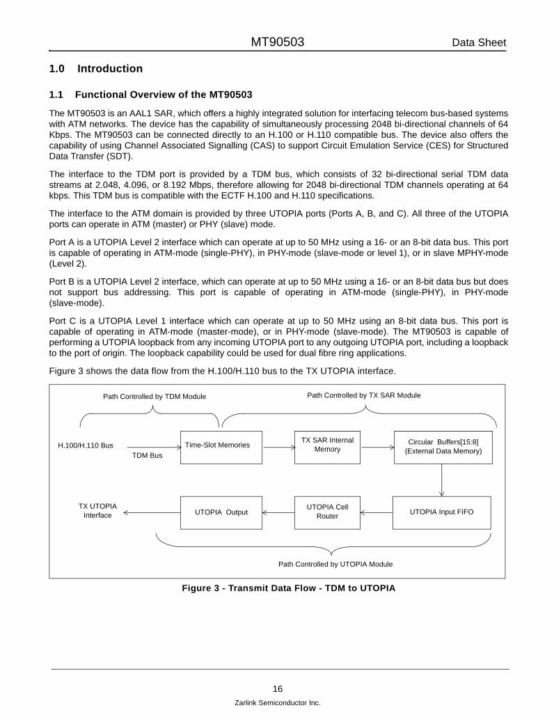
MT90503 Data Sheet
16Zarlink Semiconductor Inc.
1.0 Introduction
1.1 Functional Overview of the MT90503
The MT90503 is an AAL1 SAR, which offers a highly integrated solution for interfacing telecom bus-based systemswith ATM networks. The device has the capability of simultaneously processing 2048 bi-directional channels of 64Kbps. The MT90503 can be connected directly to an H.100 or H.110 compatible bus. The device also offers thecapability of using Channel Associated Signalling (CAS) to support Circuit Emulation Service (CES) for StructuredData Transfer (SDT).
The interface to the TDM port is provided by a TDM bus, which consists of 32 bi-directional serial TDM datastreams at 2.048, 4.096, or 8.192 Mbps, therefore allowing for 2048 bi-directional TDM channels operating at 64kbps. This TDM bus is compatible with the ECTF H.100 and H.110 specifications.
The interface to the ATM domain is provided by three UTOPIA ports (Ports A, B, and C). All three of the UTOPIAports can operate in ATM (master) or PHY (slave) mode.
Port A is a UTOPIA Level 2 interface which can operate at up to 50 MHz using a 16- or an 8-bit data bus. This portis capable of operating in ATM-mode (single-PHY), in PHY-mode (slave-mode or level 1), or in slave MPHY-mode(Level 2).
Port B is a UTOPIA Level 2 interface, which can operate at up to 50 MHz using a 16- or an 8-bit data bus but doesnot support bus addressing. This port is capable of operating in ATM-mode (single-PHY), in PHY-mode(slave-mode).
Port C is a UTOPIA Level 1 interface which can operate at up to 50 MHz using an 8-bit data bus. This port iscapable of operating in ATM-mode (master-mode), or in PHY-mode (slave-mode). The MT90503 is capable ofperforming a UTOPIA loopback from any incoming UTOPIA port to any outgoing UTOPIA port, including a loopbackto the port of origin. The loopback capability could be used for dual fibre ring applications.
Figure 3 shows the data flow from the H.100/H.110 bus to the TX UTOPIA interface.
Figure 3 - Transmit Data Flow - TDM to UTOPIA
H.100/H.110 BusTDM Bus
TX SAR Internal Memory
TX UTOPIA Interface UTOPIA Output
UTOPIA Cell Router UTOPIA Input FIFO
Circular Buffers[15:8] (External Data Memory)
Path Controlled by TDM Module Path Controlled by TX SAR Module
Path Controlled by UTOPIA Module
Time-Slot Memories

MT90503 Data Sheet
17Zarlink Semiconductor Inc.
Figure 4 shows the dataflow from the RX UTOPA interface to the H.100/H.110 bus.
Figure 4 - Receive Data Flow - UTOPIA to TDM
2.0 Features Detailed Description
2.1 UTOPIA Interface
• Contains 3 UTOPIA ports with transmit and receive interfaces:
- Port A: 16-bit or 8-bit UTOPIA Level 2, ATM mode (single-PHY) or PHY mode (single or multi-PHY). Accepts data rates up to 622 Mb/s.
- Port B: 16-bit or 8-bit UTOPIA Level 2 without bus addressing, ATM mode or PHY mode (restricted to 8-bit when Port A is in multi-PHY mode). Accepts data rates up to 622 Mb/s.
- Port C: 8-bit UTOPIA, ATM mode or PHY mode
• Supports cell switching through daisy chained SAR/PHY devices via the UTOPIA interface (AAL5 SARs, AAL1 SARs such as MT90503, and AAL2 SARs such as MT90502).
• Supports both UNI and NNI header formats
• Supports any combination of VCI/VPI concatenation up to 16 bits in ATM Receive direction
• Supports up to 65536 Virtual Circuits Per UTOPIA Port in ATM Receive direction
• Rapid timing reference cell processing in Receive/Segmentation direction
• Can eliminate null cells (VPI = 0, VCI = 0) received at UTOPIA A, B, and C port inputs
• Filters received cells before accessing VCC Look Up Table (LUT)
• UTOPIA VCC loopback for bi-directional ring functionality (from RX A to TX B and from RX B to TX A)
• Per-VCC User cell and OAM cell destination control (for VCs that have a LUT entry)
• Per-UTOPIA-port User cell and OAM cell destination control (for VCs that do not have a LUT entry)
H.100/H.110 BusTDM Bus
UTOPIA Input FIFO UTOPIA Cell RouterRX UTOPIA Interface
Time-Slot Memories RX SAR CBR Portion
UTOPIA Output FIFO
Path Controlled by TDM Module Path Controlled by RX SAR Module
Path Controlled by UTOPIA Module
Circular Buffers[7:0] (External Data Memory)
CPU Module External Control Memory
RX SAR non-CBR PortionCPU

MT90503 Data Sheet
18Zarlink Semiconductor Inc.
2.2 TDM Interface
• H.100/H.110 compatible
• Low latency TDM bus to TDM bus loopback of up to 2048 channels
• Programmable value for the null-octet inserted during an underrun situation
• Receive buffer replay capability or silent pattern insertion for underrun situations
• Support of CAS and MFS for DS1(ESF) and E1
• Automatic Detection of a change in the CAS value, for CAS received in ATM cells, and CAS received from TDM bus
2.3 Clock Recovery
• SRTS clock recovery:
- Dual reference VCs (for redundancy)
- Broadcast SRTS VCs in Transmit /Segmentation direction
• Adaptive clock recovery
- Dual reference VCs (for redundancy)
- Limited jitter, precision enhanced, MCLK (chip clock) to 8 kHz dividers
• Direct 8 kHz clock recovery:
- Can generate an 8 kHz reference using one of 8 multipurpose timing reference pins
- Supports all n * 8 kHz input reference, (1.544 MHz, 2.048 MHz, 19.44 MHz, etc.) up to 12500 * 8 kHz
- Output high time and low time of the 8 kHz reference output can be modified relative to input signal
- The eight multipurpose timing reference pins can be used to support many possible clock recovery configurations, including the following reference signals: SEC8K (MVIP), ATM8K (to/from PHY25 or from PHY155), FNXI (SRTS), CT_NETREF (for CT-Bus)
• Can generate a 20 MHz clock for an external PLL, e.g. MT9042 or MT9044 (output on one of the multipurpose timing reference pins)
2.4 ATM SAR
• Supports AAL1 (with pointer, or without pointer byte), CBR-AAL0, and CBR-AAL5 (AAL5-VTOA) Cell formats
• Supports partially filled cells, with fills from 4 to 47 bytes
• AAL1 cell format for “Structured DS1/E1 Nx64 Kbit/s Service” as per ATM Forum AF-VTOA-0078.000 “Circuit Emulation Services Interoperability Specification” (Nx64 Basic Service, DS1 Nx64 Service with CAS, and E1 Nx64 Service with CAS)
• VCs carrying 1 to 2048 TDM channels
• TDM to ATM Transmission latency less than 250 µs (when minimum voice latency desired, and strict multiframe alignment of voice with CAS not required)
• TDM to ATM Transmission latency less than 3.25 ms (when strict multiframe alignment of voice with CAS required)
• ATM to TDM Reception latency less than CDV + 250 µs (when minimum voice latency desired, and strict multiframe alignment of voice with CAS not required)
• ATM to TDM Reception latency less than CDV + 6.250 ms (when strict multiframe alignment of voice with CAS required)
• Per VCC monitoring (Receive/Reassembly direction):

MT90503 Data Sheet
19Zarlink Semiconductor Inc.
- CDV Monitoring and Delay Correction Fields
- Single cell loss, multiple cell loss, cell misinsertion, AAL1 parity, AAL1-CRC, P-byte Parity, P-Byte Out-of-Range error bits
- Cell Arrival Counter
- Underrun Slip Counter
- Overrun Slip Counter
• Per VCC monitoring (Transmit/Segmentation direction):
- Cell Transmission Counter
• Single received cell loss compensated, replacing the payload with a programmable null-octet
• Support segmentation and reassembly of 2048 full duplex TDM channels (2048 without CAS, subtract one TDM channel for each CAS channel carried)
• Support of up to ±61 ms of CDV in non-multiframing mode, ±45 ms in T1 with strict multiframing, ±29 ms in E1 with strict multiframing
• AAL0 Cell Generation / Reception for software implemented SAR function (cell buffer can contain up to 1024 cells)
• Percentage of bandwidth usage register (Transmit/Segmentation direction)
2.5 Required External Components
• 128K/256K/512K x 18 Control Memory (can be used in up to 2 banks)
• Maximum addressable control memory: 1 MB
• 128K/256K/512K x 18 Data Memory (can be used in up to 4 banks)
• Maximum addressable data memory: 4 MB
• 8 kHz to 16/MHz PLL when H.100/H.110 interface used as master mode
• Clock driver for mclk_src
2.6 Particular Modes of Operation
• Test modes
- TX SAR to RX SAR internal loop-back of some VCs, while MT90503 is running
- TDM Bus loop-back
2.7 Miscellaneous
• Motorola/Intel CPU Interface (paged memory accesses)
• Programmable Maximum number of Interrupts per second
• Multipurpose I/Os
• LED pin generation for UTOPIA Interface
• Parity bits on memory and UTOPIA interfaces to ensure clocking and memory access integrity
• CPU-based OAM cell treatment
• JTAG (IEEE 1149) Test Access Port
• MCLK speed of 80 MHz
• Global reset pin with I/O tri-state

MT90503 Data Sheet
20Zarlink Semiconductor Inc.
• Global power-down and tri-state
2.8 Power
• 3.3V core and I/O supply
• All I/Os are 3.3V with 5 V tolerance
• TDM pins are PCI 5V signalling tolerant (when PCI clamp rail tied to 5 V)
3.0 Pin Designations and DescriptionsThe following tables identify each pin of the MT90503 device's main functional areas. A description of each pin isalso provided.
Notes:
GND pins: A2, A4, A7, A8, A9, A12, A15, A18, A21, A22, A23, A25, A26, A28, B1, B29, D1, D26, D29, E1, E6,E29, G1, G29, H1, H29, J1, J29, L11, L13, L15, L17, L19, M1, M29, N11, N13, N15, N17, N19, R1, R11, R13, R17,R19, R29, T29, U11, U13, U15, U17, U19, V1, W11, W13, W15, W17, W19, AA1, AA29, AB1, AB29, AC1, AD5,AD25, AE1, AE13, AE29, AF1, AF29, AG29, AH1, AH2, AH28, AJ2, AJ4, AJ7, AJ8, AJ9, AJ12, AJ15, AJ18, AJ21,AJ22, AJ23, AJ25, AJ26, AJ28
VDD 3.3V pins: A3, A5, A10, A11, A14, A16, A19, A20, A27, A29, B2, C1, C29, K1, K29, L1, L29, P1, P29, T1,V29, W1, W29, Y1, Y29, AC29, AG1, AH3, AH29, AJ1, AJ3, AJ5, AJ10, AJ11, AJ14, AJ16, AJ19, AJ20, AJ27,AJ29
Pins not connected: A13, B3, B4, B7, B8, B9, B12, B13, B14, B15, B16, C3, C4, C7, C8, C9, C12, C13, C14, C15,D6, D7, D8, D9, D12, D13, D14, D15, D24, E5, E8, E9, E12, E13, E14, E15, E25, M5, M28, T25, W25, AB25, AE4,AE5, AE22, AE23, AE25, AF2, AF23
1 All outputs are +3.3 VDC.
2 All input and output pins that are designated (F) can withstand 5 VDC being applied to them.
3 All input and output pins that are designated (F) are tested with a 50 pF load unless otherwise specified.
4 Designations under the "rst" (reset condition) table column are: X = undefined; Z = high impedance; 1 = high (+3.3 VDC).
5 I/O types include: Output (O), Input (I), Bidirectional (I/O), Power (PWR) and Ground (GND).
6 All buses have pins listed in order from MSB to LSB.
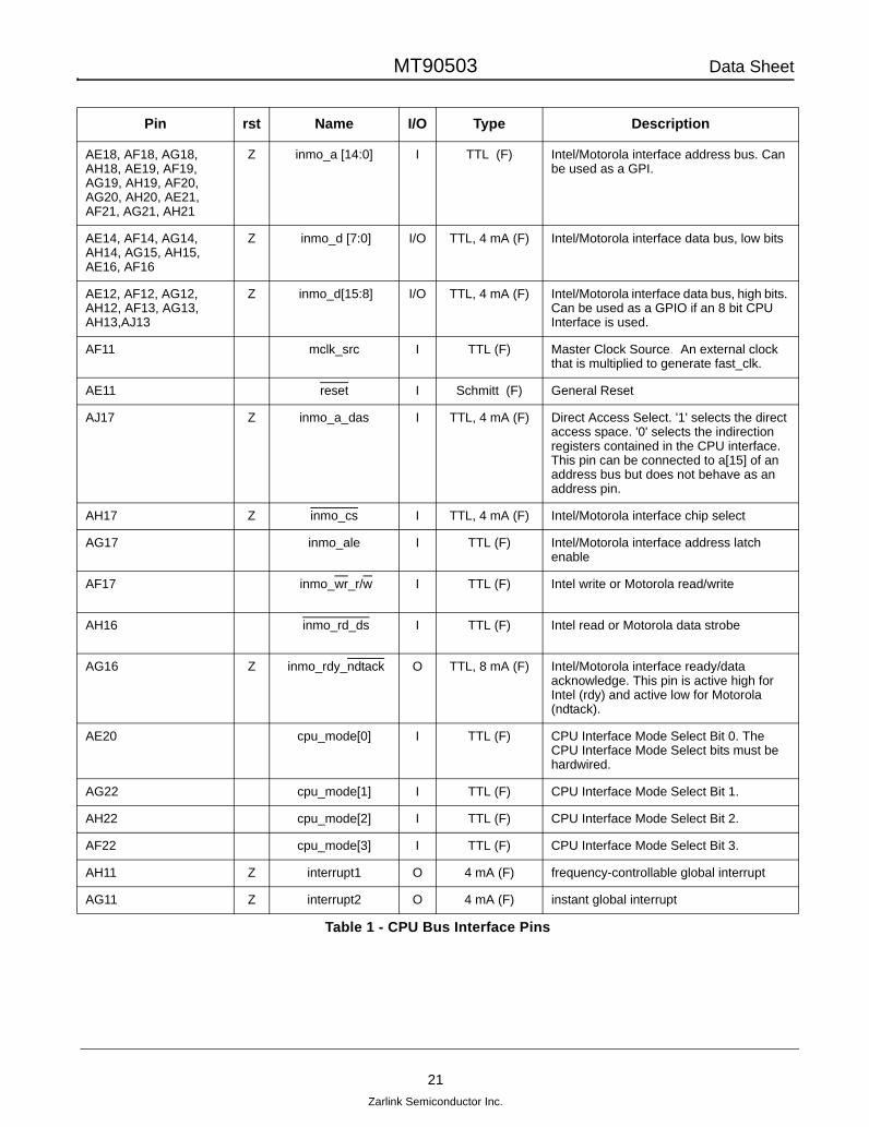
MT90503 Data Sheet
21Zarlink Semiconductor Inc.
Pin rst Name I/O Type Description
AE18, AF18, AG18, AH18, AE19, AF19, AG19, AH19, AF20, AG20, AH20, AE21, AF21, AG21, AH21
Z inmo_a [14:0] I TTL (F) Intel/Motorola interface address bus. Can be used as a GPI.
AE14, AF14, AG14, AH14, AG15, AH15, AE16, AF16
Z inmo_d [7:0] I/O TTL, 4 mA (F) Intel/Motorola interface data bus, low bits
AE12, AF12, AG12, AH12, AF13, AG13, AH13,AJ13
Z inmo_d[15:8] I/O TTL, 4 mA (F) Intel/Motorola interface data bus, high bits. Can be used as a GPIO if an 8 bit CPU Interface is used.
AF11 mclk_src I TTL (F) Master Clock Source. An external clock that is multiplied to generate fast_clk.
AE11 reset I Schmitt (F) General Reset
AJ17 Z inmo_a_das I TTL, 4 mA (F) Direct Access Select. '1' selects the direct access space. '0' selects the indirection registers contained in the CPU interface. This pin can be connected to a[15] of an address bus but does not behave as an address pin.
AH17 Z inmo_cs I TTL, 4 mA (F) Intel/Motorola interface chip select
AG17 inmo_ale I TTL (F) Intel/Motorola interface address latch enable
AF17 inmo_wr_r/w I TTL (F) Intel write or Motorola read/write
AH16 inmo_rd_ds I TTL (F) Intel read or Motorola data strobe
AG16 Z inmo_rdy_ndtack O TTL, 8 mA (F) Intel/Motorola interface ready/data acknowledge. This pin is active high for Intel (rdy) and active low for Motorola (ndtack).
AE20 cpu_mode[0] I TTL (F) CPU Interface Mode Select Bit 0. The CPU Interface Mode Select bits must be hardwired.
AG22 cpu_mode[1] I TTL (F) CPU Interface Mode Select Bit 1.
AH22 cpu_mode[2] I TTL (F) CPU Interface Mode Select Bit 2.
AF22 cpu_mode[3] I TTL (F) CPU Interface Mode Select Bit 3.
AH11 Z interrupt1 O 4 mA (F) frequency-controllable global interrupt
AG11 Z interrupt2 O 4 mA (F) instant global interrupt
Table 1 - CPU Bus Interface Pins

MT90503 Data Sheet
22Zarlink Semiconductor Inc.
Pin rst Name I/O Type Description
AG23, AH23, AE24, AF24,
AG24, AH24, AJ24, AF25, AG25, AH25, AG26, AH26, AH27,
AA26, AA27, AA28, W27, W28
X cmem_a [17:0] O 4 mA Control memory address bus
W26 1 1. cmem_a [18]2. cmem_cs [1]
1. O2. O
4 mA 1. Control memory address bus2. Control memory chip select 1.
AG28, AF27, AE26, AE28, AD27, AC26,
AC28, AB27, AF28, AE27, AD26, AC25, AC27,
AB26, AB28, AA25
Z cmem_d[15:0] I/O TTL, 4 mA Control memory data bus.
Y25 1 cmem_cs[0] O 4 mA Control memory chip select 0
Y27 X cmem_bws[0] O 4 mA Control memory byte write select 0.
Y26 X cmem_bws[1] O 4 mA Control memory byte write select 1.
Y28 X cmem_r/w O 4 mA Control Memory R/W. This signal is only used for late write memories.
AG27, AF26 Z cmem_par[1:0] I/O TTL, 4 mA Control Memory Parity 1:0
Table 2 - Control Memory Bus Interface Pins

MT90503 Data Sheet
23Zarlink Semiconductor Inc.
Pin rst Name I/O Type Description
T28, K26, V28, U29, T27, T26, R28, K25, J27, J26, H28, H27, L25, H25, J28, G27, F25, F27,
F29
X dmem_a[18:0] O 4 mA Data memory address bus
P25, N28, N26, M27, L28, L26, K28, K27, P28, P26, N29, N27, N25, M26, L27,
M25
Z dmem_d[15:0] I/O TTL, 4 mA Data memory data bus
U25 X dmem_r/w O 4 mA Data Memory R/W. This signal is only used for late write memories.
U26 X dmem_bws[0] O 4 mA Data memory byte write select 0.
U27 X dmem_bws[1] O 4 mA Data memory byte write select 1.
U28 1 dmem_cs[0] O 4 mA Data memory chip select 0
V27 1 dmem_cs[1] O 4 mA Data memory chip select 1
V26 1 dmem_cs[2] O 4 mA Data memory chip select 2
V25 1 dmem_cs[3] O 4 mA Data memory chip select 3
R27 Z dmem_par[0] I/O TTL, 4 mA Data memory parity 0
P27 Z dmem_par[1] I/O TTL, 4 mA Data memory parity 1
Table 3 - Data Memory Bus Interface Pins
Pin rst Name I/O Type Description
AD29 mem_clk_i I TTL Data and Control memory clocks
AD28 X mem_clk_o O 4 mA Data and Control memory clocks
R26 mem_clk_positive_i I PECL Data and Control memory clocks, PECL
R25 mem_clk_negative_i I PECL Data and Control memory clocks, PECL
AF15 X mem_clk_positive_o O PECL Data and Control memory clocks, PECL
AE15 X mem_clk_negative_o O PECL Data and Control memory clocks, PECL
Table 4 - Data and Control Memory Clock Pins

MT90503 Data Sheet
24Zarlink Semiconductor Inc.
Pin rst Name I/O Type Description
B17, A17, E22, D17, B19, B18, E16, C18,
C16, C20, E18, E17, D16, E21, B22, B21, B20, B23, E19,
C19, D23, D22, C22, D19, C24,
B24, A24, E20, C21, B26, C23, D21
Z ct_d[31:0] I/O PCI (F) H.100/H.110 serial data bus
G25 Z ct_netref1 I/O Schmitt, 12 mA (F)
H.100/H.110 Network Reference 1.
G26 Z ct_netref2 I/O Schmitt, 12 mA (F)
H.100/H.110 Network Reference 2.
C28 Z ct_c8_a I/O Schmitt, 12 mA (F)
H.100/H.110 8 MHz clock A
B28 Z ct_c8_b I/O Schmitt, 12 mA (F)
H.100/H.110 8 MHz clock B
C27 Z ct_frame_a I/O Schmitt, 12 MA (F)
H.100/H.110 Frame pulse A
C26 Z ct_frame_b I/O Schmitt, 12 MA (F)
H.100/H.110 Frame pulse B
E26 Z ct_fr_comp O 12 mA (F) H.100/H.110 compatibility frame pulse
D27 Z ct_c2 O 12 mA (F) MVIP 90-bit clock
D28 Z ct_c4 O 12 mA (F) MVIP 90-bit clock times two
E23 Z ct_c16- O 12 mA (F) H-MVIP 16 MHz clock
D25 Z ct_c16+ O 12 mA (F) H-MVIP 16 MHz clock
E27 Z ct_sclk O 12 mA (F) SCBUS system clock
E28 Z ct_sclkx2 O 12 mA (F) SCBUS system clock times two
F26 ct_mc I/O TTL,12 mA (F)
H.100/H.110 Message Channel. Open Collector output.
E24 X mc_clock O 4 mA (F) H.100/H.110 Message Channel extracted clock. 2 MHz. Nominal duty cycle: 62% high, 38% low.
B27 mc_tx I TTL (F) H.100/H.110 Message channel transmit data. When this signal is ‘0’, the MT90503 will drive ct_mc low. When ‘1’, the MT90503 will not drive ct_mc.
C25 X mc_rx O 4 mA (F) H.100/H.110 Message channel receive data. The level of this pin directly reflects the value of ct_mc.
Table 5 - H.100/H.110 Bus Interface Pins

MT90503 Data Sheet
25Zarlink Semiconductor Inc.
B25 ct_vdd5_0 I 5V power supply used in PCI Buffers of the ct_d[31:0] signals. Can also be connected to 3V power supply.
D20 ct_vdd5_1 I See ct_vdd5_0.
D18 ct_vdd5_2 I See ct_vdd5_0.
C17 ct_vdd5_3 I See ct_vdd5_0.
Pin rst Name I/O Type Description
E10 Z recov_a I/O TTL, 4 mA (F) Clock recovery general I/O A. This pin can be used as a GPIO.
D10 Z recov_b I/O TTL, 4 mA (F) Clock recovery general I/O B. This pin can be used as a GPIO.
C10 Z recov_c I/O TTL, 4 mA (F) Clock recovery general I/O C. This pin can be used as a GPIO.
B10 Z recov_d I/O TTL, 4 mA (F) Clock recovery general I/O D. This pin can be used as a GPIO.
E11 Z recov_e I/O TTL, 4 mA (F) Clock recovery general I/O E. This pin can be used as a GPIO.
D11 Z recov_f I/O TTL, 4 mA (F) Clock recovery general I/O F. This pin can be used as a GPIO.
C11 Z recov_g I/O TTL, 4 mA (F) Clock recovery general I/O G. This pin can be used as a GPIO.
B11 Z recov_h I/O TTL, 4 mA (F) Clock recovery general I/O H. This pin can be used as a GPIO.
Table 6 - Clock Recovery Pins
PinNom
Switch (MHz)
rst Name I/O Type Description
AE17 0 global_tri_state I TTL (F) (PU) Should be 1 for functional mode, 0 for tristate.
AH5 1 tck I TTL (F) JTAG Test Clock. Should be 1 when not in use
AG5 1 tdi I TTL (F) JTAG Test Data In. Should be 1 when not in use
AH4 1 X tdo O TTL, 4 mA (F) JTAG Test Data Out
AG4 1 tms I TTL (F) JTAG Test Mode Select. Should be 1 when not in use.
AE7 1 trst I TTL (F) JTAG Test Reset. Should be 0 when not in use.
Table 7 - Test Pins
Pin rst Name I/O Type Description
Table 5 - H.100/H.110 Bus Interface Pins (continued)

MT90503 Data Sheet
26Zarlink Semiconductor Inc.
Pin rst Name I/O Type Description
H3 Z txa_clk I/O TTL, 4 mA (F) UTOPIA Port A TX Clock
C6 Z rxa_clk I/O TTL, 4 mA (F) UTOPIA Port A RX Clock
C2 phya_alm I TTL (F) PHY alarm AThis pin can also act as a GPI.
D2 Z phya_rx_led I/O TTL, 12 mA (F) LED signal. When the LED is on, this pin will be '0'. When the LED is off, this pin will be tri-state. This pin can also act as a GPIO.
H5 Z phya_tx_led I/O TTL, 12 mA (F) LED signal. When LED is on, this pin will be '0'. When the LED is off, this pin will be tri-state. This pin can also act as a GIPO.
J5 1. txa_clav2. txa_enb
1.I2.I
TTL (F) 1. UTOPIA Port A TX Cell Available (in ATM)2. UTOPIA Port A TX Enable (in PHY)
H2 1.Z2.Z
1. txa_enb2. txa_clav
1.O2.O
4 mA (F) 1. UTOPIA Port A TX Enable (in ATM). This pin must be pulled-up externally.2. UTOPIA Port A TX Cell Available (in PHY). This pin must be pulled-down externally.
N2 Z txa_soc O 4 mA (F) UTOPIA Port A TX Start of Cell
L5, K2, K3, K4, K5, J2, J3, J4
Z txa_data[7:0] O 4 mA (F) UTOPIA Port A TX Data bus
N4, N5, M2, M3, M4, L2, L3, L4
Z txa_data[15:8] I/O TTL, 4 mA (F) UTOPIA Port A TX Data busEach of these pins can be used as a GPIO.
N3 Z txa_par O 4 mA (F) UTOPIA Port A TX Parity
A6 1. rxa_clav2. rxa_enb
1.I2.I
TTL (F) 1. UTOPIA Port A RX Cell Available (in ATM)2. UTOPIA Port A RX Enable (in PHY)
B6 1. Z2. Z
1. rxa_enb2. rxa_clav
1.O2.O
4 mA (F) 1. UTOPIA Port A RX Enable (in ATM). This pin must be pulled-up externally.2. UTOPIA Port A RX Cell Available (in PHY). This pin must be pulled-down externally.
H4 rxa_soc I TTL (F) UTOPIA Port A RX Start of Cell
E2, E3, E4, D3, D4, D5, C5, B5
rxa_data[7:0] I TTL (F) UTOPIA Port A RX Data bus
G3, G4, G5, F1, F2, F3, F4, F5
rxa_data[15:8] I TTL (F) UTOPIA Port A RX Data busEach of these pins can be used as a GPI.
G2 rxa_par I TTL (F) UTOPIA Port A RX Parity
W4 Z txb_clk I/O TTL, 4 mA UTOPIA Port B TX Clock
N1 Z rxb_clk I/O TTL, 4 mA (F) UTOPIA Port B RX Clock
AB5 phyb_alm I TTL (F) PHY alarm BThis pin can also act as a GPI.
W5 Z phyb_rx_led I/O TTL, 12 mA (F) LED signal. When LED is on, this pin will be '0'. When the LED is off, this pin will be tri-state. This pin can also act as a GPIO.
Table 8 - UTOPIA Interface Pins

MT90503 Data Sheet
27Zarlink Semiconductor Inc.
T5 Z phyb_tx_led I/O TTL, 12 mA (F) LED signal. When LED is on, this pin will be '0'. When the LED is off, this pin will be tri-state. This pin can also act as a GPIO.
W2 1. txb_clav2. txb_enb
1.I2.I
TTL (F) 1. UTOPIA Port B TX Cell Available (in ATM)2. UTOPIA Port B TX Enable (in PHY)
W3 1Z2Z
1. txb_enb2. txb_clav
1.O2.O
4 mA (F) 1. UTOPIA Port B TX Enable (in ATM) This pin must be pulled-up externally.2. UTOPIA Port B TX Cell Available (in PHY). This pin must be pulled-down externally.
AD2 Z txb_soc O 4 mA (F) UTOPIA Port B TX Start of Cell
AA2, AA3, AA4, AA5, Y2, Y3, Y4, Y5
Z txb_data[7:0] O 4 mA (F) UTOPIA Port B TX Data bus
AC3, AC4, AG2, AB2, AB3, AB4
Z txb_data[13:8] I/O TTL, 4 mA (F) UTOPIA Port B TX Data busEach of these pins can be used as a GPIO.
AC2 Z 1. txb_data[14]2. rxa_addr[4]
1.O2.I
TTL, 4 mA (F) 1. UTOPIA Port B TX Data bus2. UTOPIA Port A RX Address 4This pins can be used as a GPIO.
AD4 Z 1. txb_data [15]2. txa_addr[4]
1.O2.I
TTL, 4 mA (F) 1. UTOPIA Port B TX Data bus2. UTOPIA Port A TX Address 4This pin can be used as a GPIO.
AD3 Z txb_par O 4 mA (F) UTOPIA Port B TX Parity
P4 1. rxb_clav2. rxb_enb
1.I2.I
TTL (F) 1. UTOPIA Port B RX Cell Available (in ATM)2. UTOPIA Port B RX Enable (in PHY)
P5 1.Z2.Z
1. rxb_enb2. rxb_clav
1.O2.O
4 mA (F) 1. UTOPIA Port B RX Enable (in ATM). This pin must be pulled-up externally.2. UTOPIA Port B RX Cell Available (in PHY). This pin must be pulled-down externally.
V2 rxb_soc I TTL (F) UTOPIA Port B RX Start of Cell
T3, T4, R2, R3, R4, R5, P2, P3
rxb_data [7:0] I TTL (F) UTOPIA Port B RX Data bus
U3, U4, U5, T2 1. rxb_data [11:8]2. rxa_addr [3:0]
1.I2.I
TTL (F) 1.UTOPIA Port B RX Data bus2. UTOPIA Port A RX Address bus
V4, V5, U1, U2 1. rxb_data [15:12]2. txa_addr [3:0]
1.I2.I
TTL (F) 1. UTOPIA Port B RX Data bus2. UTOPIA Port A TX Address bus
V3 rxb_par I TTL (F) UTOPIA Port B RX Parity
AG10 Z txc_clk I/O TTL, 4 mA (F) UTOPIA Port C TX Clock
AF7 Z rxc_clk I/O TTL, 4 mA (F) UTOPIA Port C RX Clock
AE10 1. txc_clav2. txc_enb
1.I2.I
TTL (F) 1. UTOPIA Port C TX Cell Available (in ATM). 2. UTOPIA Port C TX Enable (in PHY).
Pin rst Name I/O Type Description
Table 8 - UTOPIA Interface Pins (continued)

MT90503 Data Sheet
28Zarlink Semiconductor Inc.
AF10 1. Z2. Z
1. txc_enb2. txc_clav
1.O2.O
4 mA (F) 1. UTOPIA Port C TX Enable (in ATM). This pin must be pulled-up externally.2. UTOPIA Port C TX Cell Available (in PHY). This pin must be pulled-down externally.
AH9 Z txc_soc O 4 mA (F) UTOPIA Port C TX Start of Cell
AG9, AF9, AE9, AH8, AG8, AF8, AE8, AH7
Z txc_data[7:0] O 4 mA (F) UTOPIA Port C TX Data bus
AG7 Z txc_par O 4 mA (F) UTOPIA Port C TX Parity
AH6 1. rxc_clav2. rxc_enb
1.I2.I
TTL (F) 1. UTOPIA Port C RX Cell Available (in ATM)2. UTOPIA Port C RX Enable (in PHY)
AJ6 1. Z2. Z
1. rxc_enb2. rxc_clav
1.O2.O
4 mA (F) 1. UTOPIA Port C RX Enable (in ATM). This pin must be pulled-up externally.
2. UTOPIA Port C RX Cell Available (in PHY). This pin must be pulled-down externally.
AG6 1.Z rxc_soc I TTL (F) UTOPIA Port C RX Start of Cell
AF6, AE6, AF5, AF4, AE2, AE3, AF3, AD1
rxc_data[7:0] I TTL (F) UTOPIA Port C RX Data bus
AH10 rxc_par I TTL (F) UTOPIA Port C RX Parity
Pin rst Name I/O Type Description
J25 pllvss_110 I VSS pin for the CT PLL. See Figure 5, “PLL Pin Connections,” on page 34 for recommended connections.
F28 Pllvdd_110 I VDD pin for the CT PLL. See Figure 5, “PLL Pin Connections,” on page 34 for recommended connections.
H26 Plllp2_110 I Loop-filter pin for the CT PLL. See Figure 5, “PLL Pin Connections,” on page 34 for recommended connections.
G28 pllagn_110 O Analog Ground pin for the CT PLL. See Figure 5, “PLL Pin Connections,” on page 34 for recommended connections.
AC5 pllvss_300 I VSS pin for the FC PLL. See Figure 5, “PLL Pin Connections,” on page 34 for recommended connections.
AG3 pllvdd_300 I VDD pin for the FC PLL. See Figure 5, “PLL Pin Connections,” on page 34 for recommended connections.
Table 9 - Phase Lock Loop (PLL) Pins
Pin rst Name I/O Type Description
Table 8 - UTOPIA Interface Pins (continued)
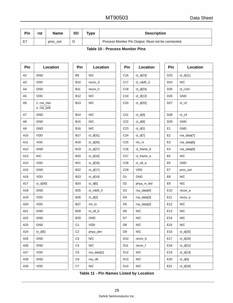
MT90503 Data Sheet
29Zarlink Semiconductor Inc.
Pin rst Name I/O Type Description
E7 proc_out O Process Monitor Pin Output. Must not be connected.
Table 10 - Process Monitor Pins
Pin Location Pin Location Pin Location Pin Location
A2 GND B9 N/C C16 ct_d[23] D23 ct_d[11]
A3 VDD B10 recov_d C17 ct_vdd5_3 D24 N/C
A4 GND B11 recov_h C18 ct_d[24] D25 ct_c16+
A5 VDD B12 N/C C19 ct_d[12] D26 GND
A6 1. rxa_clav2. rxa_enb
B13 N/C C20 ct_d[22] D27 ct_c2
A7 GND B14 N/C C21 ct_d[3] D28 ct_c4
A8 GND B15 N/C C22 ct_d[9] D29 GND
A9 GND B16 N/C C23 ct_d[1] E1 GND
A10 VDD B17 ct_d[31] C24 ct_d[7] E2 rxa_data[7]
A11 VDD B18 ct_d[26] C25 mc_rx E3 rxa_data[6]
A12 GND B19 ct_d[27] C26 ct_frame_b E4 rxa_data[5]
A13 N/C B20 ct_d[15] C27 ct_frame_a E5 N/C
A14 VDD B21 ct_d[16] C28 ct_c8_a E6 GND
A15 GND B22 ct_d[17] C29 VDD E7 proc_out
A16 VDD B23 ct_d[14] D1 GND E8 N/C
A17 ct_d[30] B24 ct_d[6] D2 phya_rx_led E9 N/C
A18 GND B25 ct_vdd5_0 D3 rxa_data[4] E10 recov_a
A19 VDD B26 ct_d[2] D4 rxa_data[3] E11 recov_e
A20 VDD B27 mc_tx D5 rxa_data[2] E12 N/C
A21 GND B28 ct_c8_b D6 N/C E13 N/C
A22 GND B29 GND D7 N/C E14 N/C
A23 GND C1 VDD D8 N/C E15 N/C
A24 ct_d[5] C2 phya_alm D9 N/C E16 ct_d[25]
A25 GND C3 N/C D10 recov_b E17 ct_d[20]
A26 GND C4 N/C D11 recov_f E18 ct_d[21]
A27 VDD C5 rxa_data[1] D12 N/C E19 ct_d[13]
A28 GND C6 rxa_clk D13 N/C E20 ct_d[4]
A29 VDD C7 N/C D14 N/C E21 ct_d[18]
Table 11 - Pin Names Listed by Location

MT90503 Data Sheet
30Zarlink Semiconductor Inc.
B1 GND C8 N/C D15 N/C E22 ct_d[29]
B2 VDD C9 N/C D16 ct_d[19] E23 ct_c16-
B3 N/C C10 recov_c D17 ct_d[28] E24 mc_clock
B4 N/C C11 recov_g D18 ct_vdd5_2 E25 N/C
B5 rxa_data[0] C12 N/C D19 ct_d[8] E26 ct_fr_comp
B6 1. rxa_enb2. rxa_clav
C13 N/C D20 ct_vdd5_1 E27 ct_sclk
B7 N/C C14 N/C D21 ct_d[0] E28 ct_sclkx2
B8 N/C C15 N/C D22 ct_d[10] E29 GND
F1 rxa_data[12] J3 txa_data[1] L29 VDD P26 dmem_d[6]
F2 rxa_data[11] J4 txa_data[0] M1 GND P27 dmem_par[1]
F3 rxa_data[10] J5 1. txa_clav2. txa_enb
M2 txa_data[13] P28 dmem_d[7]
F4 rxa_data[9] J25 pllvss_110 M3 txa_data[12] P29 VDD
F5 rxa_data[8] J26 dmem_a[9] M4 txa_data[11] R1 GND
F25 dmem_a[2] J27 dmem_a[10] M5 N/C R2 rxb_data[5]
F26 ct_mc J28 dmem_a[4] M25 dmem_d[0] R3 rxb_data[4]
F27 dmem_a[1] J29 GND M26 dmem_d[2] R4 rxb_data[3]
F28 Pllvdd_110 K1 VDD M27 dmem_d[12] R5 rxb_data[2]
F29 dmem_a[0] K2 txa_data[6] M28 N/C R11 GND
G1 GND K3 txa_data[5] M29 GND R13 GND
G2 rxa_par K4 txa_data[4] N1 rxb_clk R17 GND
G3 rxa_data[15] K5 txa_data[3] N2 txa_soc R19 GND
G4 rxa_data[14] K25 dmem_a[11] N3 txa_par R25 mem_clk_negative_i
G5 rxa_data[13] K26 dmem_a[17] N4 txa_data[15] R26 mem_clk_positive_i
G25 ct_netref1 K27 dmem_d[8] N5 txa_data[14] R27 dmem_par[0]
G26 ct_netref2 K28 dmem_d[9] N11 GND R28 dmem_a[12]
G27 dmem_a[3] K29 VDD N13 GND R29 GND
G28 pllagn_110 L1 VDD N15 GND T1 VDD
G29 GND L2 txa_data[10] N17 GND T2 1. rxb_data[8]2. rxa_addr[0]
H1 GND L3 txa_data[9] N19 GND T3 rxb_data[7]
H2 1. txa_enb2. txa_clav
L4 txa_data[8] N25 dmem_d[3] T4 rxb_data[6]
H3 txa_clk L5 txa_data[7] N26 dmem_d[13] T5 phyb_tx_led
Pin Location Pin Location Pin Location Pin Location
Table 11 - Pin Names Listed by Location (continued)

MT90503 Data Sheet
31Zarlink Semiconductor Inc.
H4 rxa_soc L11 GND N27 dmem_d[4] T25 N/C
H5 phya_tx_led L13 GND N28 dmem_d[14] T26 dmem_a[13]
H25 dmem_a[5] L15 GND N29 dmem_d[5] T27 dmem_a[14]
H26 Plllp2_110 L17 GND P1 VDD T28 dmem_a[18]
H27 dmem_a[7] L19 GND P2 rxb_data[1] T29 GND
H28 dmem_a[8] L25 dmem_a[6] P3 rxb_data[0] U1 1. rxb_data[13]2. txa_addr[1]
H29 GND L26 dmem_d[10] P4 1. rxb_clav2. rxb_enb
U2 1. rxb_data[12]2. txa_addr[0]
J1 GND L27 dmem_d[1] P5 1. rxb_enb2. rxb_clav
U3 1. rxb_data[11]2. rxa_addr[3]
J2 txa_data[2] L28 dmem_d[11] P25 dmem_d[15] U4 1. rxb_data[10]2. rxa_addr[2]
U5 1. rxb_data[9]2. rxa_addr[1]
W26 1. cmem_a[18]2. cmem_cs[1]
AB28 cmem_d[1] AE11 reset
U11 GND W27 cmem_a[1] AB29 GND AE12 inmo_d[15]
U13 GND W28 cmem_a[0] AC1 GND AE13 GND
U15 GND W29 VDD AC2 1. txb_data[14]2. rxa_addr[4]
AE14 inmo_d[7]
U17 GND Y1 VDD AC3 txb_data[13] AE15 mem_clk_negative_o
U19 GND Y2 txb_data[3] AC4 txb_data[12] AE16 inmo_d[1]
U25 dmem_r/w Y3 txb_data[2] AC5 pllvss_300 AE17 global_tri_state
U26 dmem_bws[0] Y4 txb_data[1] AC25 cmem_d[4] AE18 inmo_a[14]
U27 dmem_bws[1] Y5 txb_data[0] AC26 cmem_d[10] AE19 inmo_a[10]
U28 dmem_cs[0] Y25 cmem_cs[0] AC27 cmem_d[3] AE20 cpu_mode[0]
U29 dmem_a[15] Y26 cmem_bws[1] AC28 cmem_d[9] AE21 inmo_a[3]
V1 GND Y27 cmem_bws[0] AC29 VDD AE22 N/C
V2 rxb_soc Y28 cmem_r/w AD1 rxc_data[0] AE23 N/C
V3 rxb_par Y29 VDD AD2 txb_soc AE24 cmem_a[15]
V4 1. rxb_data[15]2. txa_addr[3]
AA1 GND AD3 txb_par AE25 N/C
V5 1. rxb_data[14]2. txa_addr[2]
AA2 txb_data[7] AD4 1. txb_data[15]2. txa_addr[4]
AE26 cmem_d[13]
V25 dmem_cs[3] AA3 txb_data[6] AD5 GND AE27 cmem_d[6]
V26 dmem_cs[2] AA4 txb_data[5] AD25 GND AE28 cmem_d[12]
V27 dmem_cs[1] AA5 txb_data[4] AD26 cmem_d[5] AE29 GND
Pin Location Pin Location Pin Location Pin Location
Table 11 - Pin Names Listed by Location (continued)

MT90503 Data Sheet
32Zarlink Semiconductor Inc.
V28 dmem_a[16] AA25 cmem_d[0] AD27 cmem_d[11] AF1 GND
V29 VDD AA26 cmem_a[4] AD28 mem_clk_o AF2 N/C
W1 VDD AA27 cmem_a[3] AD29 mem_clk_i AF3 rxc_data[1]
W2 1. txb_clav2. txb_enb
AA28 cmem_a[2] AE1 GND AF4 rxc_data[4]
W3 1. txb_enb2. txb_clav
AA29 GND AE2 rxc_data[3] AF5 rxc_data[5]
W4 txb_clk AB1 GND AE3 rxc_data[2] AF6 rxc_data[7]
W5 phyb_rx_led AB2 txb_data[10] AE4 N/C AF7 rxc_clk
W11 GND AB3 txb_data[9] AE5 N/C AF8 txc_data[2]
W13 GND AB4 txb_data[8] AE6 rxc_data[6] AF9 txc_data[6]
W15 GND AB5 phyb_alm AE7 trst AF10 1. txc_enb2. txc_clav
W17 GND AB25 N/C AE8 txc_data[1] AF11 mclk_src
W19 GND AB26 cmem_d[2] AE9 txc_data[5] AF12 inmo_d[14]
W25 N/C AB27 cmem_d[8] AE10 1. txc_clav2. txc_enb
AF13 inmo_d[11]
AF14 inmo_d[6] AG11 interrupt2 AH8 txc_data[4] AJ5 VDD
AF15 mem_clk_positive_o AG12 inmo_d[13] AH9 txc_soc AJ6 1. rxc_enb2. rxc_clav
AF16 inmo_d[0] AG13 inmo_d[10] AH10 rxc_par AJ7 GND
AF17 inmo_wr_r/w AG14 inmo_d[5] AH11 interrupt1 AJ8 GND
AF18 inmo_a[13] AG15 inmo_d[3] AH12 inmo_d[12] AJ9 GND
AF19 inmo_a[9] AG16 inmo_rdy_ndtack AH13 inmo_d[9] AJ10 VDD
AF20 inmo_a[6] AG17 inmo_ale AH14 inmo_d[4] AJ11 VDD
AF21 inmo_a[2] AG18 inmo_a[12] AH15 inmo_d[2] AJ12 GND
AF22 cpu_mode[3] AG19 inmo_a[8] AH16 inmo_rd_ds AJ13 inmo_d[8]
AF23 N/C AG20 inmo_a[5] AH17 inmo_cs AJ14 VDD
AF24 cmem_a[14] AG21 inmo_a[1] AH18 inmo_a[11] AJ15 GND
AF25 cmem_a[10] AG22 cpu_mode[1] AH19 inmo_a[7] AJ16 VDD
AF26 cmem_par[0] AG23 cmem_a[17] AH20 inmo_a[4] AJ17 inmo_a_das
AF27 cmem_d[14] AG24 cmem_a[13] AH21 inmo_a[0] AJ18 GND
AF28 cmem_d[7] AG25 cmem_a[9] AH22 cpu_mode[2] AJ19 VDD
AF29 GND AG26 cmem_a[7] AH23 cmem_a[16] AJ20 VDD
AG1 VDD AG27 cmem_par[1] AH24 cmem_a[12] AJ21 GND
Pin Location Pin Location Pin Location Pin Location
Table 11 - Pin Names Listed by Location (continued)

MT90503 Data Sheet
33Zarlink Semiconductor Inc.
AG2 txb_data[11] AG28 cmem_d[15] AH25 cmem_a[8] AJ22 GND
AG3 pllvdd_300 AG29 GND AH26 cmem_a[6] AJ23 GND
AG4 tms AH1 GND AH27 cmem_a[5] AJ24 cmem_a[11]
AG5 tdi AH2 GND AH28 GND AJ25 GND
AG6 rxc_soc AH3 VDD AH29 VDD AJ26 GND
AG7 txc_par AH4 tdo AJ1 VDD AJ27 VDD
AG8 txc_data[3] AH5 tck AJ2 GND AJ28 GND
AG9 txc_data[7] AH6 1. rxc_clav2. rxc_enb
AJ3 VDD AJ29 VDD
AG10 txc_clk AH7 txc_data[0] AJ4 GND
Type Input Output I/O Power Ground N/C Total
UTOPIA Port A 21 12 12 45
UTOPIA Port B 21 14 10 45
UTOPIA Port C 12 12 2 26
Clock recovery 0 0 8 8
CPU Bus 26 3 16 45
TDM Bus (H.100/H.110 bus) 1 9 39 4 53
Control memory 0 23 18 41
Data memory 0 26 18 44
Data and Control Memory Clocks 3 3 0 6
Test 6 0 0 6
PLL 1 1 0 2 2 6
Power 40 40
Ground 88 88
Miscellaneous 1 1
No Connects 49 49
Total: 91 104 123 46 90 49 503
Table 12 - Pinout Summary
Pin Location Pin Location Pin Location Pin Location
Table 11 - Pin Names Listed by Location (continued)

MT90503 Data Sheet
34Zarlink Semiconductor Inc.
Figure 5 - PLL Pin Connections
4.0 Functional Description1
4.1 CPU Interface
The MT90503 CPU module provides an interface permitting programmability from an external microprocessor. TheCPU module permits read/write access from MT90503: internal registers, internal and external memories.
The CPU interface comprises of:
• Direct Access Select (DAS) as the MSB bit concatenated with a 15-bit address bus
• 16-bit data bus
• 2 interrupt signals
• associated control signals
• little endian format, unless otherwise specified
The CPU interface can be configured to operate with either Intel or Motorola CPUs. The MT90503 supports both8-bit or 16-bit data bus and multiplexed or non-multiplexed address/data pins. If the CPU is operating in 15-bit bytemode addressing with the LSB of its address bus as a byte field, then the inmo_a [14:0] pins of the MT90503 canbe connected to the a[15:1] pins of the CPU. If both the MT90503 and the CPU are in 15-bit word mode addressing,then the inmo_a[14:0] pins should be connected to the a[14:0] pins of the CPU.
A reduced set of registers ‘CPU Interface Registers’ (0000h to 000Ah) are employed to optimize access time and topermit the CPU to execute indirect read/write accesses via these registers. The CPU also engages these registersto perform direct read/write accesses. The MT90503 and CPU timing relationship is described in section 9.1 onpage 211.
The CPU Control Register (0100h) provides a software reset capability that allows the CPU to reset the MT90503except for the CPU interface. The CPU interface can only be reset by a hardware reset.
1. This product incorporates technology licensed from Melita International Corporation.
pllvdd_0
pllvss_0
pllvdd_1
pllvss_1
pllp2
pllagn
100pF 0.001uF 10uF
VDD
100pF 0.001uF 10uF
VDD
301 ohm (1%)0.01uF (5%)

MT90503 Data Sheet
35Zarlink Semiconductor Inc.
4.1.1 CPU Interrupts
The CPU interface provides a programmable global interrupt capability. The interrupt signal names are ‘interrupt1’and ‘interrupt2’, pins AH11 and AG11 respectively. Both interrupts have programmability to select their polarity(open collector drive) via registers ‘interrupt1_conf’ and ‘interrupt2_conf’ addresses 0224h and 0226h respectively.Interrupt1 accommodates a capability to program a minimum acceptable period between interrupts. The period isprogrammed in µs units via ‘interrupt1_conf’ register. This provides a ‘frequency interrupt controller’ facility andmasks the assertion of further interrupts until the specified period has elapsed. The mask period will commencewhen the interrupt1_treated[15], register interrupt_flags address 0220h is set. When Interrupt2 is enabled it isalways activated when an interrupt condition occurs. Interrupt pins are always tri-stated when inactive.
The operation of the CPU interrupt network is common for all modules. When an interrupt is asserted aninterrupt flag is set to identify the module where the interrupt was generated. Each module has one or moreInterrupt Enable Status Registers where a set interrupt enable bit identifies the source of the interrupt. Oncompletion of the ISR the interrupt must be cleared as the interrupt will remain asserted until it is de-asserted bythe user. All Interrupt Enable Status Registers have a symmetrical Status Register. Hence, the bit positioning ofthe interrupt enables and the associated status bits are identical.
4.1.1.1 Example Interrupt Flow
Upon the initialization of the Global Interrupt pins the following methodology is adopted to identify the source of theinterrupt. For this example Interrupt2 is employed and the CPU module will be the source of the interrupt.
4.1.1.2 Interrupt Initialization
• Set interrupt polarity, register interrupt2_conf[15:14].
• Enable Interrupt2 for the CPU module, register interrupt2_enable[0] 022Ch. The MT90503 will generate an interrupt on interrupt2 according to the modules enabled in interrupt2_enable.
• Set the individual CPU interrupt sources by enabling the respective bits in the `status0_ie' 0104h register. Within the `status0_ie' register there are two possible interrupt sources: internal_read_timeout_ie and inmo_read_done_ie. In the MT90503 Register Description the interrupt bits are labelled IE (Interrupt Enable) in the ‘Type’ column. This register offers the facility to mask/disable unwanted interrupts.
4.1.1.3 Interrupt Servicing
When interrupt2 is asserted (‘interrupt2’ pin):
• Read the interrupt flags to ascertain the module raising the interrupt. The CPU module interrupt flag is located in register interrupt_flags[0] 0220h, this bit is named cpureg_interrupt_active.
• If the cpureg_interrupt_active bit is set, locate the source of the CPU interrupt by reading the ‘status0’ register 0102h, either internal_read_timeout and/or inmo_read_done.
• The associated status register ‘status0’ 0102h contains internal_read_timeout and inmo_read_done bits. Therefore, to de-assert the interrupt the user must write a 1 to register 0102h bits 3 or 4, internal_read_timeout and inmo_read_done respectively. Only then will the interrupt be de-asserted.

MT90503 Data Sheet
36Zarlink Semiconductor Inc.
4.1.2 Intel/Motorola Interface
cpu_mode [3:0]
Interface Type address pins data pins direct_access ale
0000 Intel, 16 bit data bus, non-multiplexed
inmo_a[14:0]**(word address)
inmo_d[15:0] inmo_a_das inmo_ale*
0001 Intel, 16 bit data bus, multiplexed
inmo_d[15:1](word address)
inmo_d[15:0] inmo_a_das inmo_ale*
0010 Intel, 8 bit data bus, non-multiplexed
inmo_a[14:0] (byte address)
inmo_d[7:0] inmo_a_das inmo_ale*
0011 Intel, 8 bit data bus, multiplexed
inmo_a[14:8]& inmo_d[7:0](byte address)
inmo_d[7:0] inmo_a_das inmo_ale*
0100 Motorola, 16 bit data bus, non-multiplexed
inmo_a[14:0](word address)
inmo_d[15:0] inmo_a_das inmo_ale*
0101 Motorola, 16 bit data bus, multiplexed
inmo_d[15:1](word address)
inmo_d[15:0] inmo_a_das inmo_ale*
0110 Motorola, 8 bit data bus, non-multiplexed
inmo_a[14:0] (byte address)
inmo_d[7:0] inmo_a_das inmo_ale*
0111 Motorola, 8 bit data bus, multiplexed
inmo_a[14:8]& inmo_d[7:0](byte address)
inmo_d[7:0] inmo_a_das inmo_ale*
1xxx Reserved
* The inmo_ale pin is interpreted in all modes. However, it is not necessary in the non-multiplexed modes and can be tied to VCC.**The address placed on the inmo_a[14:0] pins is a word address in 16-bit mode and a byte address in 8-bit mode. The address, when placed on the inmo_d pins, is always a byte address.
Table 13 - CPU Interface Mode Selection
0000h
0008h
000Ah
0004h
Control Register
Read/Write Data Register
Address High Register
Address Low Register
The MT90503 CPU interface supports both Intel and Motorolamicroprocessors, in both 8-bit or 16-bit data bus andmultiplexed or non-multiplexed address/data pins. TheMT90503 supports 8 MB of addressable space, thereforeindirection addressing is necessary. The microprocessorinterface directly addresses five control words, used forindirection accessing. The indirection register contents areshown in tables 13 to 17 inclusively. The timing relationshippertaining to the CPU Interface Registers and ExtendedAccess is defined in section 9.1 on page 211.

MT90503 Data Sheet
37Zarlink Semiconductor Inc.
Field Bit Type Reset Description
read_burst_length 6:0 RW 01h Number of words to prefetch.Setting Words
00h 12801h 102h 2. .. .. .
7Fh 127This field is set to 01h for individual (non-sequential) reads. All burst reads greater than 256-bytes must be executed in two or more burst reads.
reserved 7 RO 0h Reset to 0.
access_req 8 PC 0h Set by software when an extended access is initialised. Reset by hardware when the access is completed. Used for extended indirect access only.
extended_a[3:1] 11:9 RW 0h Extended address bits 3:1. Invalid for extended direct access.
write_enable 13:12 RW 0h Active high write enables. 00 = read access.01 = write to lower byte.10 = write to upper byte.11 = write to entire word.
This field is ignored for: extended direct reads and all byte wide extended direct accesses.
extended_parity 15:14 RW 0h Read/Write Parity bits.
Table 14 - Control Register (0000h)
Field Bit Type Reset Description
extended_data[15:0] 15:0 RW 0000h The extended indirect read/write data word register. Invalid for extended direct access.
Table 15 - Read/Write Data Register (0004h)
Field Bit Type Reset Description
extended_a[32:20] 12:0 RW 000h Upper extended address [32:20].
Reserved 15:13 RO 0h Reset to 000.
Table 16 - Address High Register (0008h)
Field Bit Type Reset Description
extended_a[19:4] 15:0 RW 0000h Lower extended address [19:4]. In extended direct addressing, bits 19:16 are employed for 16 bit data bus and bits 19:15 are employed for 8 bit data bus.
Table 17 - Address Low Register (000Ah)
MT90503 Data Sheet
38Zarlink Semiconductor Inc.
4.1.2.1 Extended Indirect Accessing
Extended Indirect Accessing solely employs the registers 0000h to 000Ah to access the 8 MB of addressablememory space.
Synopsis: the user writes the access address to registers 0000h, 0008h and 000Ah. Then the MT90503 willread/write to that address and fetch/place the data value from/to register 0004h. For all extended indirect accessesthe INMO_A_DAS bit will be held low.
4.1.2.2 Extended Indirect Writes
The following steps must be executed to perform an extended indirect write:
The software will set access_req [8] in register 0000h (Step 4 above) and the hardware will reset it when the datawrite has completed. Therefore, the user can poll this bit to determine when the data write has completed.
4.1.2.3 Extended Indirect Reads
The software will set access_req[8] register 0000h and the hardware will reset it when the data is ready to be readfrom register 0004h.
4.1.2.4 Extended Direct Accessing
Extended Direct Accessing employs the high and low address registers to perform page addressing. The addresswithin the page is provided directly by the CPU address bus. Similarly the data is fetched/placed directly on theCPU data bus.
Synopsis: the user writes the access address to registers 0008h and 000Ah but this performs only the pageaddressing. Upon assertion of the address within the page the MT90503 will read/write the data with respect to thataddress. The INMO_A_DAS bit is set when the data read/write occurs. When operating the CPU interface in directmode with a 16-bit data bus, extended_a[19:16], are employed for the lower address word register 000Ah.
1 Write the upper address, extended_a[32:20], to register 0008h. This write may be not be required if previous value holds true.
2 Write the lower address, extended_a[19:4], to register 000Ah. This write may be not be required if previous value holds true.
3 Write the write data, extended_data[15:0], to register 0004h. This write may be not be required if previous value holds true.
4 Write write_enable, extended_parity, access_req=‘1’ and extended_a [3:1] in a single access to register 0000h.
5 Read the access_req bit located in the Control Register[8] to determine when the write has completed.
1 Write the upper address, extended_a[32:20], to register 0008h. This write may be not be required if previous value holds true.
2 Write the lower address, extended_a[19:4], to register 000Ah. This write may be not be required if previous value holds true.
3 Write write_enable = 00, access_req=‘1’ and extended_a [3:1] in a single access to register 0000h.
4 Wait until access_req is cleared, then read the data from the data field extended_data[15:0], register 0004h.
5 Optional parity check may be ascertained by performing a read on the extended_parity[15:14], register 0000h.

MT90503 Data Sheet
39Zarlink Semiconductor Inc.
However, when operating the CPU interface in direct mode with an 8-bit data bus bits, [19:15] are used for the loweraddress word.
4.1.2.5 Extended Direct Writes
4.1.2.6 Extended Direct Reads
4.1.3 MT90503 Reset Procedure
The following reset procedure is required to power-up the MT90503. The reset procedure must be adhered atpower-up employing the reset pin. Post power-up, the reset procedure can be performed from step 3.
1 Write the upper address, extended_a[32:20], to register 0008h. This write may be not be required if previous value holds true.
2 Write the lower address extended_a[19:16] or [19:15] to register 000Ah. The remaining bits [15:4] or [14:4] are ignored. This write may be not be required if previous value holds true.
3 Write write_enable[13:12] (where applicable) and extended_parity[15:14]. The extended parity write is optional.
4 Write the data value to the address within the corresponding memory page with the INMO_A_DAS bit set.
1 Write the upper address, extended_a[32:20], to register 0008h. This write may be not be required if previous value holds true.
2 Write the lower address, extended_a[19:16] or [19:15], to register 000Ah. The remaining bits [15:4] or [14:4] are ignored. This write may be not be required if previous value holds true.
3 Assert the lower address within the memory page and fetch the read data with INMO_A_DAS set.
4 An optional read may be performed to obtain the parity values, extended_parity[15:14] register 0000h.
1 Assert the reset pin for at least 1000 MCLK cycles.
2 De-assert the reset pin. All accesses in the remaining reset procedure will employ indirection.
3 Initialise the mem_clk_* bits and write_cache_enable bit via the Control Register bits [13:10], address 0100h.
4 Write the mclk_src frequency at register led1[6:0] and LED Flash Frequency at registers led1[15:7], register address 0120h. Write the LED Flash Frequency units (i.e. ms or µs) at register led2[0], address 0122h.
5 Initialise the PLL via register pll_conf, address 0128h.
6 Set bits nreset_* in the Control Register bits [7:0], address 0100h.
7 Initialize the data and control memory types via registers 0240h, 0242h, 0244h, 0248h, 024Ah, and 024Ch
8 Select UTOPIA clocking methodology at register addresses 0230h, 0232h, 0234h and 0236h.
9 Configure the interrupts’ active_level for interrupt1 and interrupt2 in register 0224h and 0226h.

MT90503 Data Sheet
40Zarlink Semiconductor Inc.
4.2 TDM Module
The general architecture of the TDM bus consists of three main elements.
• The TDM bus interface which is coupled directly to the bus pins and manages the timing requirements of the H.100/H.110 interface.
• The datapath management for transporting the bytes from the TDM bus to the circular buffers (located in the external data memory).
• The TDM clocking mechanism, this enables the MT90503 to be H.100/H.110 bus master capable and communicates with the clock recovery module.
4.2.1 TDM Bus Interface
The MT90503 TDM Module interfaces with all 32 data streams of the H.100/H.110 bus. The maximum data rate of8.192 Mbps determines the total bus capacity of 4096 TDM TSST. The MT90503 can process up to: 2048transmitting TDM TSST and 2048 receiving TDM TSST within one frame of 125µs.
One less TDM channel is carried for each CAS channel that is desired. If all TDM channels have CAS, then 1024transmit and 1024 receive channels is the limit. The MT90503 can drive out data on any particular TSST (TimeSlot/Stream), or read in data from any particular TSST.
Each individual time slot or DS0 on the H.1x0 bus is assigned by a unique TSST number, based on the followingequation:
The timeslot ranges from 0 to 31 for 2MHz streams, from 0 to 63 for 4MHz streams, or from 0 to 127 for 8MHzstreams.
The 16 lowest data streams are capable of running at a data rate lower than 8.192 MHz. The streams are groupedin fours and each quartet must run at the same data rate. Streams [3:0], [7:4], [11:8] and [15:12] can each run at2.048, 4.096 or 8.192 MHz as a group. This allows backward compatibility with older, slower TDM buses. In thereduced rate, the data is still latched using the CT_C8_A or _B clock-edge, but using every second or every fourthclock-edge. The streams numbered [31:16] must always run at 8.192 MHz.
The TDM bus can also be configured to use only 4, 8, or 16 streams. This configuration requires less processing ofTDM bytes and, also allows a reduced mclk speed. The 4-stream mode is useful for conducting tests, while the16-stream mode allows mclk speed to be cut in half while still allowing half the bandwidth of a full H.100/H.110 bus.
When the H.100/H.110 bus is carrying CAS signalling bits, every even stream carries regular TDM data bytes, andis associated with an odd stream that carries CAS bits and the indication of the beginning of the multiframe. ForTSSTs that are input to the MT90503, the multiframing is provided by the framer. For TSSTs that are generated bythe MT90503, the output multiframing is provided by the MT90503; there is one multiframe which is common to allthe T1 channel signals and one multiframe which is common to all the E1 channel signals. On the input, themultiframing is independent for each TSST and the MT90503 synchronises all of them to its multiframe.
TSST = timeslot * 32 + stream(timeslot * 2+1) * 32 + stream(timeslot * 4+3) * 32 + stream
for 8MHz streamsfor 4MHz streamsfor 2MHz streams

MT90503 Data Sheet
41Zarlink Semiconductor Inc.
Figure 6 - TDM Serial to Parallel/Parallel to Serial (SPPS) Converter
Each TSST can be used independently for CAS or regular TDM bytes. For example, if time slot 0 on stream 0requires signalling bits, then they will be carried on time slot 0, stream 1. However, time slot 1 stream 1 can be usedto carry normal TDM data, even if the time slot preceding it is used for signalling. T1 and E1 channel formats can besupported simultaneously. The multiframe bit’s polarity and position is programmable and global, and will beaccepted at both the input and output. The CAS bits occupy bits [7:4] or [3:0] of the CAS byte, depending on theposition within the byte of the multiframe indicator. The only difference between CAS support in E1 or T1 mode isthe number of frames in the multiframe. T1 contains 24 frames within its multiframes while E1 contains 16. TheCAS bits are latched at the input when the multiframe bit is active, and sent out on the output side during the entiremultiframe. When the multiframe bit is at an active polarity, the associated TDM byte is the first byte of themultiframe.
Figure 7 - CAS and MFS Transport on the TDM Bus
Figure 7, CAS and MFS Transport on the TDM Bus shows the direct interface of the MT90503 with the TDM bus.
TDM Serial to Parallel/Parallel to Serial Module
Quad SPPSConverter
Four CT_Dx pins per SPPS, all running at the same frequency (2,4,8 MHz)
SPPS0
TX TDM Time-Slot Memory 32 x 32 bits
RX TDM Time-Slot Memory 32 x 36 bits
Quad SPPSConverter
Four CT_Dx pins per SPPS, all running at the same frequency (2,4,8 MHz)
Data TransferControler
CT_C8_A
CT_C8_B
CT_FRAME_A
CT_FRAME_B
Time-SlotMemoryPointer
Synchronizer
addresscontrol
SPPS7 TDM Data PathControler
tdm6.cdd
FIG tdm6
ct_c8
ct_d0
ct_d1
ct_frame
AA bit 7 bit 6 A bit 5 A bit 4 A bit 3 A bit 2 A bit 1 A bit 0
AA SFS A’s cas[3] ’s cas[2] A’s cas[1] A’s cas[0]
ct_c8
ct_d0
ct_d1
ct_frame
AA bit 7 bit 6 A bit 5 A bit 4 A bit 3 A bit 2 A bit 1 A bit 0AA bit 7 bit 6 A bit 5 A bit 4 A bit 3 A bit 2 A bit 1 A bit 0A bit 7 bit 6 A bit 5 A bit 4 A bit 3 A bit 2 A bit 1 A bit 0
AA SFS A’s cas[3] ’s cas[2] A’s cas[1] A’s cas[0]AA SFS A’s cas[3] ’s cas[2] A’s cas[1] A’s cas[0]A SFS A’s cas[3] ’s cas[2] A’s cas[1] A’s cas[0]

MT90503 Data Sheet
42Zarlink Semiconductor Inc.
The TDM interface is capable of looping back up to 2048 TSSTs with a latency of two TDM frames, or 250 µs. Thisloopback is indicated by the control structures associated to each TSST. The loopback allows any two time-slotsand streams to be connected together, and work independently of the speed of each of the streams.
The MT90503 can interface with 32 data streams as mentioned in previous paragraphs. Since each TSST can beused to either send or receive data, the MT90503 must tri-state the CT_D pins that are receiving data. To avoidoverlap between a sending and a receiving TSST, this must be done before the next one begins.
4.2.2 TDM Bus Clocking Mechanism
The MT90503 can operate as either a primary or secondary H.100/H.110 master clock source. The H.100/H.110clock (CT_C8) is driven by either CT_C8_A or CT_C8_B. The MT90503 can generate the primary bus clock and allits associated bus clocks (ct_fr_comp, sclk, sclkx2, CT_C16-, CT_C16+, CT_C2 and CT_C4) by using theCT_NETREF signal. The CT_NETREF may be received from another H.100/H.110 bus compatible device or it canbe determined by the clock recovery module. In master mode, the MT90503 will generate all the compatibilityclocks that are necessary for communicating with MVIP and SCSA TDM interfaces. These include the FR_COMP,C2, C4 and C16 signals for communicating with MVIP buses, and the SCLK and SCLKx2 signals forcommunicating with Signal Computing System Architecture SCSA buses.
The TDM module monitors both CT_C8_A and CT_C8_B signals for clock properties and failure. In everyoperating mode, both the CT_C8_A and CT_C8_B signals are monitored for clock failure. There are two methodsof detecting a clock failure on the bus. Firstly, if the rising edge of the clock does not appear within ±35 ns windowof the expected period, the clock is flagged as being invalid. Secondly, if a single frame does not contain exactly1024 clock cycles, then the clock will fail.
The MT90503 can be configured to switch to the backup master clock (CT_C8_A or CT_C8_B), upon the detectionof a master clock failure. The MT90503 can be programmed as a secondary master and therefore switch to thebackup master clock when the external primary master clock source has failed. If the MT90503 switches from asecondary master to master it will re-synchronise the TDM module with the backup clock and generate thecompatibility clocks. The MT90503 continually monitors both CT_C8_A and CT_C8_B clocks for a failure condition.The MT90503 can be programmed to automatically switch to its backup clock in case of a failure.
The MT90503 is an H.100/H.110 master-capable device and, therefore, is able to generate both CT_C8 clocks andCT_FRAME and compatibility signals. As long as the primary signals on the bus are valid, the MT90503 willsynchronise its output to them using a PLL. The MT90503 can also generate the CT_C8 and CT_FRAME signalsindependently of the PLL, using the local 16 MHz clock. In this case, the output signals have no phase relation withthose present on the bus.
When the TDM bus interface module has written the received data to the circular buffers, it increments theTime-Slot Memory Pointer that is sent to the TX_SAR.
4.2.3 TDM Datapath
When writing to the external data memory, no return value is expected. However, when reading data, a return value,upon storing the data into an RX TSST, is expected and is required to be written back to the structure memory. Theunderrun count, which may or may not have been updated, is always written back along with all the other bits of thesecond word.
When the data is received at the time slot memory, it is sent via the TDM datapath to the external data memory.According to which time slot is currently being used, the TDM control structures are read.

MT90503 Data Sheet
43Zarlink Semiconductor Inc.
Figure 8 - TDM Data Path Controller
When accesses are performed from the TDM channel association memory, the write back to the RX half of thecircular buffer is also performed. When this write back is done, the underrun detection bit is written to ‘0’, and anull-octet is inserted in place of the old data byte.
The TDM datapath module can be configured to work with 32 H.100/H.110 streams, 16-streams, 8-streams, or4-streams in order to allow lower clock speeds on the MT90503. The bandwidth requirements for supporting eachof the above configurations are described in the Bandwidth section.
4.2.4 TDM Channel Association Structures
TDM channel association structures are located at 0x8000 to 0xBFFE in internal memory. Each structurecorresponds to a TDM channel by its TSST order.
4.2.4.1 Non CAS Operation
Figure 9 - TDM Channel Association Structures: TX Channel non-CAS mode
TDM Data Path Controler
TDM ChannelAssociation
Memory(2 x 2048 x 32
bits)
Data MemoryRead Access
Cache(64 x 48 bits)
Data MemoryWrite Access
Cache(256 x 48 bits)
TX TDMTime-SlotMemories
Data MemoryDMA Controler
RX TDMTime-SlotMemoriesDetect
Underruns(Write Back UR
Count Field)
Write Back Address (For URCount)
TX PointerRX PointerCPU Address
Offset for MFSCPU Write Data Write Back Data (For UR Count)
Read DataLatch Memory
64 x 48 bits
Data ReadProcess
Data WriteProcess
TS0
TS7
TS5
b8b9b10b11b12b13b14b15+0
b0b1b2b3b4b5b6b7
+2 1
TX/RX Circular Buffer Address and Size
Reserved
Mode
TX/RX Circular Buffer Address and Size: Address and size of the circularbuffer in the data memory to which data bytes will be written.I: Initialized Bit. Written by ‘0’ by software, set by hardware when the channelstarts being treated.Mode: Channel Mode of operation.
“0000”=Normal PCM;others=Reserved.
RBW: RX Byte Write. Selects byte that will be written in the low bytes of thedata memory word where the TX TDM bytes are written.
“00”=Do not write over the low byte;“01”=Write a null byte (usually FFh);“10”=Write silence pattern A;“11”=Write silence pattern B.
RBW 0
I

MT90503 Data Sheet
44Zarlink Semiconductor Inc.
The control structure in Figure 10, TDM Channel Association: RX Channels (Non CAS mode) on page 44 indicatesthe mode and options selected for the TDM channel. In the general TX structure, the RBW (RX Byte Write) bitsprovide the format of the byte that is to be written over the RX byte in the circular buffer. While it is possible to writeover the low-byte, there are three possibilities provided if writing over the byte is chosen: writing a null byte orgenerating one of two silence patterns. The detailed description of the dual-direction buffer is provided in the TDMCircular Buffers section.
Figure 10 - TDM Channel Association: RX Channels (Non CAS mode)
In the receive direction, the control structure retains some of the recurrent features from the transmit structure. TheTX circular buffer/size field is the same, which is normal given that the TX and RX circular buffers are common. Theinformation on the address and size is encoded in the same way as in the TX structure.
For the reception structure, the high mode bit codes whether the RX channel is transmitting a channel receivedfrom ATM or if it is retransmitting information taken from the TDM bus and written into a circular buffer. If the highMode bit is ‘0’, the channel is ATM; if it is ‘1’, the channel is TDM. By supporting a low latency TDM loopback, theMT90503 conforms to the H.100/H.110 specification.
The C and U bits serve as status enable bits. These bits are R/W, and tell the register module whether the registercounters and status bits should report errors on this VC. The U bit is the underrun status enable: when this bit is setand an underrun is detected, the TDM register module will increment the global underrun counter and set theunderrun detect status bit.
The C bit serves at the cut VC detect status enable. When this bit is at ‘0’, the UR count acts as a free running256-underrun counter. In this case, it serves to compile the total number of underruns that have occurred. When theC bit is at ‘1’, then the UR count serves as a detector for cut VCs. The counter resets to 0 each time a valid TDMbyte is received. If an underrun is received, the counter is incremented by one. If the counter ever increments from254 to 255, then 255 consecutive underruns have been received, indicating there is 32 ms of absent data. This isinterpreted as a cut VC and will generate an interrupt.
Cell-loss integration periods of greater than 32 ms can be supported by software. Upon UR Count reaching 255,and subsequent interrupt to the CPU, the software can check that the count has not returned to zero (whichhappens if the cells start to arrive again) at some interval equivalent to the cell-loss integration period.
b8b9b10b11b12b13b14b15+0
b0b1b2b3b4b5b6b7
+2
TX/RX Circular Buffer Address and Size
Reserved
Mode
TX/RX Circular Buffer Address and Size: Address and size of the circular buffer in the data memoryfrom which data bytes will bereadOE: Voice Stream Output Enable. This bit, when set, enables the driving of the Voice Data on thestream.Mode: Channel Mode of operation.
“0000”=Normal PCM;“1000”=Low Latency Loopbackothers=Reserved.
C: Cut VC Status Enable. When ‘0’, the UR Count field is freerunning(256 consecutive underruns willnotbe considered as a Cut VC). When ‘1’, the UR Count field is used as a consecutive underrun indicator
that stops incrementing at 255.U: Underrun Status Enable. When this bit is set and an underrun is detected, the status counters and bitswill report this event.UR Count: 8 bit underrun count. When the C bit is cleared, acts as a freerunning underrun error counter.When the C bit is set, it is used as a cut VC detector. In this mode, the counter is cleared each time avalid byte is received. It increments (to a maximum of FFh) each time a byte underrun is detected. Whena transition from FEh to FFh occurs, the Cut VC status register, counter and id fields are updated. Must beinitialized to FFh by software before enabling VC when C bit is set. Must be initialized to 00h by softwarebefore enabling VC when C bit is cleared.
1 UR CountUC
OE

MT90503 Data Sheet
45Zarlink Semiconductor Inc.
4.2.4.2 CAS Operation
Figure 11 - TDM Channel Association: TX Channels (CAS mode)
The RX Byte Write bits remain the same to allow the insertion of null patterns as for regular channels. The Modebits, indicate the possible configurations and combinations of multiframing and CAS insertion: “0100” is E1, “0110”is T1, and toggling the lowest bit of either of the numbers indicates that the FASTCAS method of transmitting thedata and CAS bytes is being used. FASTCAS is used to lower the latency of Circuit Emulation cells. When usingthe FASTCAS mode, the multiframe pointer is not used and multiframe integrity is therefore not maintained.
In addition, special fields for CAS are added in the two additional words of the structure. The CAS WE (CAS WriteEnable) bits are used to determine if the CAS is written back.
The TX_CAS field is used so the CPU can insert values of CAS, in place of values from the TDM bus; the RX CASvalue is used to compensate for underruns.
The Last TX CAS field is used to detect when the CAS value received on the TDM bus has changed. When a CASvalue is received, it is written back to the Last TX CAS field in the structure. Whenever a new value arrives, it iscompared to the last value. If there is a difference, a CAS change signal is sent to the registers, and the new CASvalue is written to the CAS change buffer in the external memory.
The Frame Offset field is used to store the offset between the internal and external multiframes in the TX direction.When the TDM bus first obtains an external multiframe, it writes the offset field to the correct value between 0 and
b8b9b10b11b12b13b14b15+0
b0b1b2b3b4b5b6b7
+2 1
TX/RX Circular Buffer Address and Size
Reserved
Mode
TX/RX Circular Buffer Address and Size: Address and size of the circular buffer in the data memoryto which data bytes will be written.I: Initialized Bit. Written by ‘0’ by software, set by hardware when the channel starts being treated.Mode: Channel Mode of operation.
“0100”=E1 Strict Multiframing;“0101”=E1 FASTCAS;“0110”=T1 Strict Multiframing;“0111”=T1 FASTCAS;others=Reserved.
RBW: RX Byte Write. Selects byte that will be written in the low bytes of the data memory word wherethe TX TDM bytes are written.
“00”=Do not write over the low byte;“01”=Write a null byte (usually FFh);“10”=Write silence pattern A;“11”=Write silence pattern B.
CASWE: CAS write enable.“x0”=Leave CAS bits in RX Circular Buffer untouched;“x1”=WriteRX CAS UR in RX Circular Buffer in case of underrun;“0x”=Write CAS bits present on the associated odd stream to the TX Circular Buffer;“1x”=WriteTX CAS Force field in order to bypass the CAS bits from the associated odd stream.
TX CAS Force: TX CAS value that must be written to bypass the CAS bits from the associated oddstream.EI: CAS Enable Ignore. If set, the CAS Enable bit (SFS Bit) will be ignored. Instead, the CAS will belatched at one point for each 16/24 consecutive bytes (for E1 and T1 respectively).RX CAS UR: RX CAS value that will be sent in case of an underrun situation on the RX_SAR side.CM: Cas Monitor. When ‘1’, any change in the TX CAS value will be reported to the CPU.Last TX CAS: Last Value of the TX CAS received from the TDM bus.FS Offset: Frame Offset that must be added in order for internal and external multiframes to coincide.Initialize to “00000” by software.
RBW
+4
+6 RX CAS UR TX CAS Force CASWE
FS Offset
0
Last TX CAS
CM0 0 EI
I
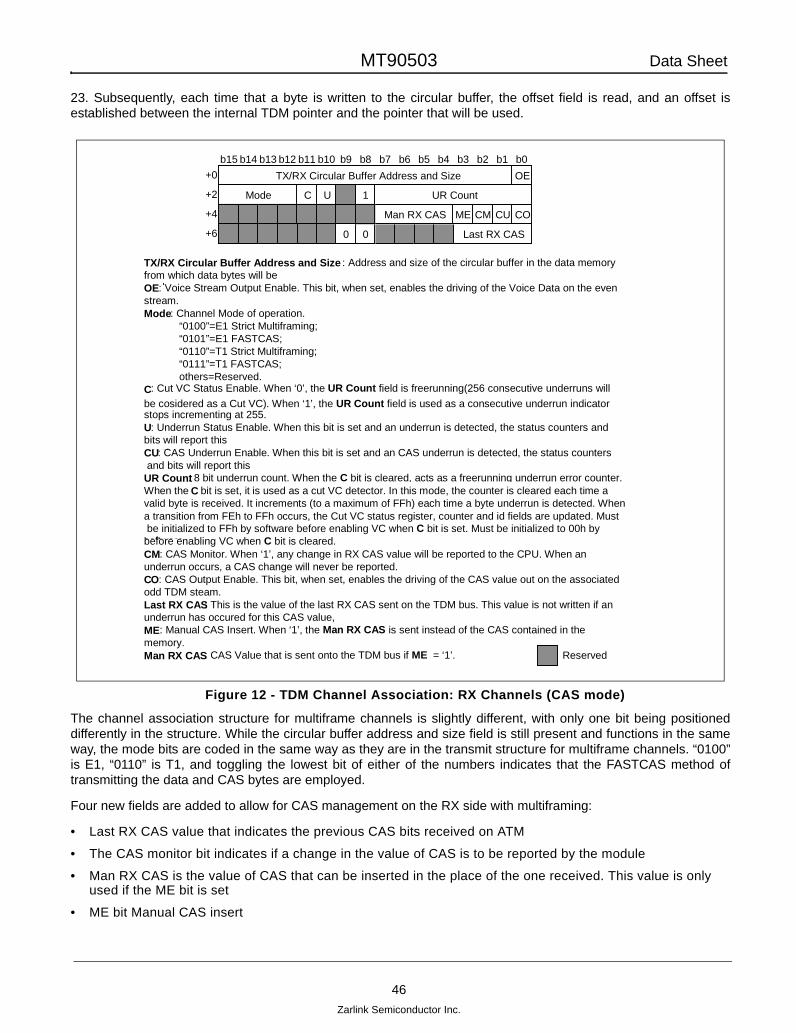
MT90503 Data Sheet
46Zarlink Semiconductor Inc.
23. Subsequently, each time that a byte is written to the circular buffer, the offset field is read, and an offset isestablished between the internal TDM pointer and the pointer that will be used.
Figure 12 - TDM Channel Association: RX Channels (CAS mode)
The channel association structure for multiframe channels is slightly different, with only one bit being positioneddifferently in the structure. While the circular buffer address and size field is still present and functions in the sameway, the mode bits are coded in the same way as they are in the transmit structure for multiframe channels. “0100”is E1, “0110” is T1, and toggling the lowest bit of either of the numbers indicates that the FASTCAS method oftransmitting the data and CAS bytes are employed.
Four new fields are added to allow for CAS management on the RX side with multiframing:
• Last RX CAS value that indicates the previous CAS bits received on ATM
• The CAS monitor bit indicates if a change in the value of CAS is to be reported by the module
• Man RX CAS is the value of CAS that can be inserted in the place of the one received. This value is only used if the ME bit is set
• ME bit Manual CAS insert
b8b9b10b11b12b13b14b15+0
b0b1b2b3b4b5b6b7
+2
TX/RX Circular Buffer Address and Size
Reserved
Mode
TX/RX Circular Buffer Address and Size : Address and size of the circular buffer in the data memoryfrom which data bytes will bereadOE: Voice Stream Output Enable. This bit, when set, enables the driving of the Voice Data on the evenstream.Mode: Channel Mode of operation.
“0100”=E1 Strict Multiframing;“0101”=E1 FASTCAS;“0110”=T1 Strict Multiframing;“0111”=T1 FASTCAS;others=Reserved.
C: Cut VC Status Enable. When ‘0’, the UR Count field is freerunning(256 consecutive underruns willbe cosidered as a Cut VC). When ‘1’, the UR Count field is used as a consecutive underrun indicatorth tstops incrementing at 255.U: Underrun Status Enable. When this bit is set and an underrun is detected, the status counters andbits will report thiseventCU: CAS Underrun Enable. When this bit is set and an CAS underrun is detected, the status countersand bits will report this
UR Count: 8 bit underrun count. When the C bit is cleared, acts as a freerunning underrun error counter.When the C bit is set, it is used as a cut VC detector. In this mode, the counter is cleared each time avalid byte is received. It increments (to a maximum of FFh) each time a byte underrun is detected. Whena transition from FEh to FFh occurs, the Cut VC status register, counter and id fields are updated. Mustbe initialized to FFh by software before enabling VC when C bit is set. Must be initialized to 00h by
softwarebefore enabling VC when C bit is cleared.CM: CAS Monitor. When ‘1’, any change in RX CAS value will be reported to the CPU. When anunderrun occurs, a CAS change will never be reported.CO: CAS Output Enable. This bit, when set, enables the driving of the CAS value out on the associatedodd TDM steam.Last RX CAS: This is the value of the last RX CAS sent on the TDM bus. This value is not written if anunderrun has occured for this CAS value,ME: Manual CAS Insert. When ‘1’, the Man RX CAS is sent instead of the CAS contained in the
t lmemory.Man RX CAS: CAS Value that is sent onto the TDM bus if ME = ‘1’.
1 UR CountUC
+4
+6
CUCM
Last RX CAS
Man RX CAS ME
00
CO
OE

MT90503 Data Sheet
47Zarlink Semiconductor Inc.
For both TX and RX channels, a change in the value of CAS on a channel where the CAS monitor bit is high willcause the new value to be written to the CAS change buffer in the external memory. This buffer contains all thevalues that have been detected as different from the previous value, along with the 12-bit time slot and streamvalue of the TDM channel to which they are associated.
Figure 13 - CAS Change Structure in Control Memory
The Circular Buffer Address/Size field is 15 bits and the addresses are 14 bits each, an indirect method of indicatingthe size is used. This is done by coding the size by the first ‘1’ that is encountered by reading the field starting fromthe left. For example, if the lowest bit of the field is ‘1’, the buffer is 128 bytes (mapped on a 256 byte boundary). Ifthe lowest bit was ‘0’ but the second-lowest bit is ‘1’, then the buffer is 256 bytes (mapped on a 512 byte boundary),etc.
Figure 14 - TX/RX Circular Buffer and Size Field
b8b9b10b11b12b13b14b15+0
b0b1b2b3b4b5b6b7
TSST Number On Which CAS Changed New CAS
FIG tdm26
For 128 word buffers:b8b9b10b11b12b13b14 b0b1b2b3b4b5b6b7
b16b17b18b19b20b21 b8b9b10b11b12b13b14b15 b0b1b2b3b4b5b6b7Address of Circular Buffer in Data Memory
For 256 word buffers:b8b9b10b11b12b13b14 b0b1b2b3b4b5b6b7
b16b17b18b19b20b21 b8b9b10b11b12b13b14b15 b0b1b2b3b4b5b6b7Address of Circular Buffer in Data Memory
For 512 word buffers:b8b9b10b11b12b13b14 b0b1b2b3b4b5b6b7
b16b17b18b19b20b21 b8b9b10b11b12b13b14b15 b0b1b2b3b4b5b6b7Address of Circular Buffer in Data Memory
For 1024 word buffers:b8b9b10b11b12b13b14 b0b1b2b3b4b5b6b7
b16b17b18b19b20b21 b8b9b10b11b12b13b14b15 b0b1b2b3b4b5b6b7Address of Circular Buffer in Data Memory
1
01
001
0001
Address[21:8]
Address[21:9]
Address[21:10]
Address[21:11]
00000000
00000000
00000000
00000000
0
00
000
FIG tdm18
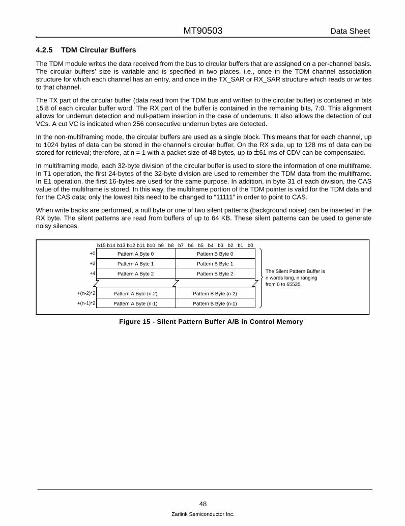
MT90503 Data Sheet
48Zarlink Semiconductor Inc.
4.2.5 TDM Circular Buffers
The TDM module writes the data received from the bus to circular buffers that are assigned on a per-channel basis.The circular buffers’ size is variable and is specified in two places, i.e., once in the TDM channel associationstructure for which each channel has an entry, and once in the TX_SAR or RX_SAR structure which reads or writesto that channel.
The TX part of the circular buffer (data read from the TDM bus and written to the circular buffer) is contained in bits15:8 of each circular buffer word. The RX part of the buffer is contained in the remaining bits, 7:0. This alignmentallows for underrun detection and null-pattern insertion in the case of underruns. It also allows the detection of cutVCs. A cut VC is indicated when 256 consecutive underrun bytes are detected.
In the non-multiframing mode, the circular buffers are used as a single block. This means that for each channel, upto 1024 bytes of data can be stored in the channel’s circular buffer. On the RX side, up to 128 ms of data can bestored for retrieval; therefore, at n = 1 with a packet size of 48 bytes, up to ±61 ms of CDV can be compensated.
In multiframing mode, each 32-byte division of the circular buffer is used to store the information of one multiframe.In T1 operation, the first 24-bytes of the 32-byte division are used to remember the TDM data from the multiframe.In E1 operation, the first 16-bytes are used for the same purpose. In addition, in byte 31 of each division, the CASvalue of the multiframe is stored. In this way, the multiframe portion of the TDM pointer is valid for the TDM data andfor the CAS data; only the lowest bits need to be changed to “11111” in order to point to CAS.
When write backs are performed, a null byte or one of two silent patterns (background noise) can be inserted in theRX byte. The silent patterns are read from buffers of up to 64 KB. These silent patterns can be used to generatenoisy silences.
Figure 15 - Silent Pattern Buffer A/B in Control Memory
b8b9b10b11b12b13b14b15+0
b0b1b2b3b4b5b6b7
Pattern A Byte 0 Pattern B Byte 0
+2 Pattern A Byte 1 Pattern B Byte 1
+4 Pattern A Byte 2 Pattern B Byte 2
+(n-2)*2 Pattern A Byte (n-2) Pattern B Byte (n-2)
+(n-1)*2 Pattern A Byte (n-1) Pattern B Byte (n-1)
The Silent Pattern Buffer is n words long, n ranging from 0 to 65535.

MT90503 Data Sheet
49Zarlink Semiconductor Inc.
Figure 16 - TDM Circular Buffer (one MultiFrame in T1 mode)
The CAS bits are always kept in the highest four bits of the last byte.
In addition to storing the data in the circular buffers, the parity bits of the data memory are used to detect underrunsgenerated on the ATM link. When the RX_SAR writes data to the circular buffers, it writes a ‘1’ in the parity bit of thememory’s low byte. When the TX_SAR writes data bytes in the buffer, it writes a ‘0’ to the parity bit of the memory’slow byte. Therefore, when the TDM reads the data from the circular buffer, it expects to read a ‘1’ from the parity bit.
b8b9b10b11b12b13b14b15+0
b0b1b2b3b4b5b6b7OPLow byte
EP
High byte
+2
+4
+6
+8
+10
+12
+14
+16
+18
+1A
+1C
+1E
+20
+22
+24
+26
+28
+2A
+2C
+2E
+30
+32
+34
+36
+38
+3A
+3C
+3E
Reserved
TX Byte 0
TX Byte 1
TX Byte 2
TX Byte 3
TX Byte 4
TX Byte 5
TX Byte 6
TX Byte 7
TX Byte 8
TX Byte 9
TX Byte 10
TX Byte 11
TX Byte 12
+A
+C
+E
TX Byte 13
TX Byte 14
TX Byte 15
RX Byte 0
RX Byte 1
RX Byte 2
RX Byte 3
RX Byte 4
RX Byte 5
RX Byte 6
RX Byte 7
RX Byte 8
RX Byte 9
RX Byte 10
RX Byte 11
RX Byte 12
RX Byte 13
RX Byte 14
RX Byte 15
Underrun Detection Bits
RX CASTX CAS
TX Byte 16
TX Byte 17
TX Byte 18
TX Byte 19
TX Byte 20
TX Byte 21
TX Byte 22
TX Byte 23
RX Byte 16
RX Byte 17
RX Byte 18
RX Byte 19
RX Byte 20
RX Byte 21
RX Byte 22
RX Byte 23
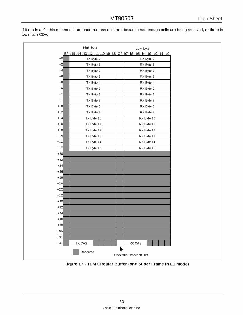
MT90503 Data Sheet
50Zarlink Semiconductor Inc.
If it reads a ‘0’, this means that an underrun has occurred because not enough cells are being received, or there istoo much CDV.
Figure 17 - TDM Circular Buffer (one Super Frame in E1 mode)
b8b9b10b11b12b13b14b15+0
b0b1b2b3b4b5b6b7OPLow byte
EP
High byte
+2
+4
+6
+8
+10
+12
+14
+16
+18
+1A
+1C
+1E
+20
+22
+24
+26
+28
+2A
+2C
+2E
+30
+32
+34
+36
+38
+3A
+3C
+3E
Reserved
TX Byte 0
TX Byte 1
TX Byte 2
TX Byte 3
TX Byte 4
TX Byte 5
TX Byte 6
TX Byte 7
TX Byte 8
TX Byte 9
TX Byte 10
TX Byte 11
TX Byte 12
+A
+C
+E
TX Byte 13
TX Byte 14
TX Byte 15
RX Byte 0
RX Byte 1
RX Byte 2
RX Byte 3
RX Byte 4
RX Byte 5
RX Byte 6
RX Byte 7
RX Byte 8
RX Byte 9
RX Byte 10
RX Byte 11
RX Byte 12
RX Byte 13
RX Byte 14
RX Byte 15
Underrun Detection Bits
RX CASTX CAS

MT90503 Data Sheet
51Zarlink Semiconductor Inc.
4.2.6 TDM Circular Buffer Pointers
The convention that a write pointer points to a byte that is currently being written. In like manner, a read pointerpoints to a byte that is currently being read. Therefore, a read and write pointer to the same buffer must nevercross, or be equal to one another.
4.2.6.1 Non-multiframing mode
The global TDM_write_pointer points to the byte from the TDM bus presently being written to the circular buffers.As in all modes, the TDM_read_pointer is incremented before the TDM_write_pointer, because bytes that comefrom the TDM bus are written after the frame is completed. Meanwhile, bytes read from the data memory and sentonto the bus are already transmitted by the time the frame is complete.
The TDM_write_pnt sent to the TX_SAR is the same as global TDM_write_pointer. The TDM_read_pnt sent to theRX_SAR is one frame ahead of the global TDM_read_pointer. Since the TDM_read_pnt is one more than theglobal TDM_read_pointer, and the TDM_read_pointer is incremented before the TDM_write_pointer, theTDM_read_pnt will always have a lead of either one or two over the TDM_write_pnt.
Figure 18 - TDM Circular Buffers (Normal mode)
b8b9b10b11b12b13b14b15+0
b0b1b2b3b4b5b6b7High byte Low byte
+2
+4
+6
+8
+A
+C
+E
+10
+12
+14
+16
+18
+1A
+1C
+1E
+20
+22
+24
+(n-3)*2
+(n-2)*2
+(n-1)*2
n=Buffer word size {128,256,512,1024}
tdm _write_pnt
tdm _read_pntRX Byte (Being read by TDM)
RX Byte (Being written by TDM)
EP OP
X
1
1
1
1
1
1
1
1
X
0
0
Underrun Detection Bits
rx_sar_write_pnt
Valid rx_sar_write_pntPositions
Valid tx_sar_read_pntPositions
RX Byte (Being written by TDM)
0
0
0
0
0
Valid TDMBytes Waitingto be sent onthe TDM Bus
0
0
0
0
0
0
0
0
0
0
0
0
0
0
0
0
0
0
0
0
0
0
0
0
0
0
0
TX Byte (Being written by TDM)
tx_sar_read_pnt
Valid TDMBytes Wating tobe sent in anATM Celltdm _lll_read_pnt

MT90503 Data Sheet
52Zarlink Semiconductor Inc.
Figure 18 TDM Circular Buffers (Normal mode) shows that very few of the positions within the circular buffer areinvalid for the SAR pointers.
4.2.6.2 E1/T1 Multiframing (standard)
The TDM pointers change to respect the multiframing standards required by E1 and T1 operation. The pointer hastwo halves. One half indicates the number of the multiframe that the TDM is writing or reading; the other half is thenumber of the frame within the multiframe. In the T1 mode, this fraction goes from 0 to 23, while in the E1 mode itranges from 0 to 15. The same global standards of pointer definition still apply as the pointer still points to an invalidbyte.
The TDM_write_pnt has a global value, which is the value of the internal multiframe pointer. However, due to themultiframing offset, the TDM_write_pnt can vary by almost an entire frame. Therefore, if the globalTDM_write_pointer points to 0.0 (Multiframe 0, frame 0) the individual TDM channels may be written anywhere from0.0 to 0.23 in the T1 mode, and from 0.0 to 0.15 in the E1 mode. The TDM channels may be written almost anentire frame ahead of the global pointer. The pointer sent to the TX_SAR is the same as the globalTDM_write_pointer.
The TDM_read_pnt is two multiframes ahead of the TDM_write_pnt. The need for this lead arises from the writebacks and from CAS. Since the TDM_write_pnt can be writing up to 15 frames ahead, a lead of at least onemultiframe must be given. In addition to this, the CAS must be considered. CAS is written during the multiframe ofthe tx, which can be up to one multiframe ahead of the global pointer. When CAS is read from the rx side it is readat the beginning of the multiframe. Therefore, to ensure that there is always a difference of at least one in the CASpointers, the delta between the TDM pointers is established at two multiframes.
Furthermore, the read pointer that is sent to the RX_SAR is almost one multiframe ahead. This is necessarybecause CAS is sent at the end of the multiframe on the ATM side, and is read at the beginning of the multiframe onthe TDM side. Therefore, to ensure that the CAS of the multiframe is written by the RX_SAR before the TDM readsit, the pointer passed to the RX_SAR is incremented by one multiframe minus one frame. Therefore, if theTDM_read_pointer would have been 2.5 (two multiframes, five frames), the TDM_read_pnt passed to the RX_SARis 3.4 (three multiframes, four frames).

MT90503 Data Sheet
53Zarlink Semiconductor Inc.
]
Figure 19 - TDM Circular Buffer (Complete Buffer in E1 mode, Strict Multiframing)
Figure 19 TDM Circular Buffer (Complete Buffer in E1 mode, Strict Multiframing) shows the TDM circular buffer inthe E1 mode. The buffer is only half used for the TDM data. The CAS is located at the end of the buffer, and thewrite and read pointers are offset by a full three multiframes.
b8b9b10b11b12b13 b14 b 15 +0
b0b1b2b3b4b5b6b7
Low byteHigh byte
Reserved
RX MultiFrame 0T X MultiFrame 0
+20
+40 RX MultiFrame 2TX MultiFrame 2
+60 RX MultiFrame 3TX MultiFrame 3
+80 RX MultiFrame 4TX MultiFrame 4
RX MultiFrame (n/32)-2TX MultiFrame (n/32)-2
+(n*2)-20 RX MultiFrame (n/32)-1TX MultiFrame (n/32)-1
n=Buffer word size {128,256,512,1024}
+(n*2)-40
tdm_write_pn t (earliest)
tdm_write_pn t (latest)
tdm_cas_write_p nt (latest)
tdm_cas_write_p nt (earliest)
15 byte offset
tx_sar_read_pnt
Valid rx_sar_write_pnt Positions
Valid tx_sar_read_pnt Positions
TX MultiFrame 1
tdm _read_pnt
tdm _cas_read_pnt
2 MF offset
RX MultiFrame 1
rx_sar_write_pnt
1 MF offset MINIMUM

MT90503 Data Sheet
54Zarlink Semiconductor Inc.
Figure 20 - TDM Circular Buffer (Complete Buffer in E1 mode, FASTCAS)
Figure 20 TDM Circular Buffer (Complete Buffer in E1 mode, FASTCAS) is an E1 circular buffer in the FASTCASmode. Although the TDM read and write pointers are still significantly offset, the delay has been reduced to nearlyzero. This is because the rx_sar_write_pnt and the TDM_read_pnt need only be offset by a single byte, as innon-multiframing mode.
b8b9b10b11b12b13 b14 b 15 +0
b0b1b2b3b4b5b6b7
Low byteHigh byte
Reserved
RX MultiFrame 0T X MultiFrame 0
+20
+40 RX MultiFrame 2TX MultiFrame 2
+60 RX MultiFrame 3TX MultiFrame 3
+80 RX MultiFrame 4TX MultiFrame 4
RX MultiFrame (n/32)-2TX MultiFrame (n/32)-2
+(n*2)-20 RX MultiFrame (n/32)-1TX MultiFrame (n/32)-1
n=Buffer word size {128,256,512,1024}
+(n*2)-40
tdm_write_pn t (earliest)
tdm_write_pn t (latest)
tdm_cas_write_p nt (latest)
tdm_cas_write_p nt (earliest)
15 byte offset
tx_sar_read_pnt
Valid rx_sar_write_pnt Positions
Valid tx_sar_read_pnt Positions
TX MultiFrame 1
tdm _read_pnt
tdm _cas_read_pnt
2 MF offset
RX MultiFrame 1
rx_sar_write_pnt
1 byte offset MINIMUM

MT90503 Data Sheet
55Zarlink Semiconductor Inc.
Figure 21 - TDM Circular Buffer (Complete Buffer in T1 mode, Strict Multiframing)
Figure 21 TDM Circular Buffer (Complete Buffer in T1 mode, Strict Multiframing) shows a T1 circular buffer instandard multiframing mode. The T1 circular buffer is identical to an E1 circular buffer except that the multiframesare 24 bytes instead of 16 bytes.
b8b9b10b11b12b13 b14 b 15 +0
b0b1b2b3b4b5b6b7
Low byteHigh byte
Reserved
RX MultiFrame 0TX MultiFrame 0
+20
+40 RX MultiFrame 2TX MultiFrame 2
+60 TX MultiFrame 3
+80 TX MultiFrame 4
RX MultiFrame (n/32)-2TX MultiFrame (n/32)-2
+(n*2)-20 RX MultiFrame (n/32)-1TX MultiFrame (n/32)-1
n=Buffer word size {128,256,512,1024}
+(n*2)-40
tdm_write_pnt (earliest)
tdm_write_pnt (latest)
tdm_cas_write_pnt (latest)
tdm_cas_write_p nt (earliest)
23 byte offset
tx_sar_read_pnt
Valid rx_sar_write_pnt Positions
Valid tx_sar_read_pnt Positions
TX MultiFrame 1
tdm _read_pnt
tdm _cas_read_pnt
2 MF offset
RX MultiFrame 1
rx_sar_write_pnt
1 MF offset MINIMUM
RX MultiFrame 3
RX MultiFrame 4
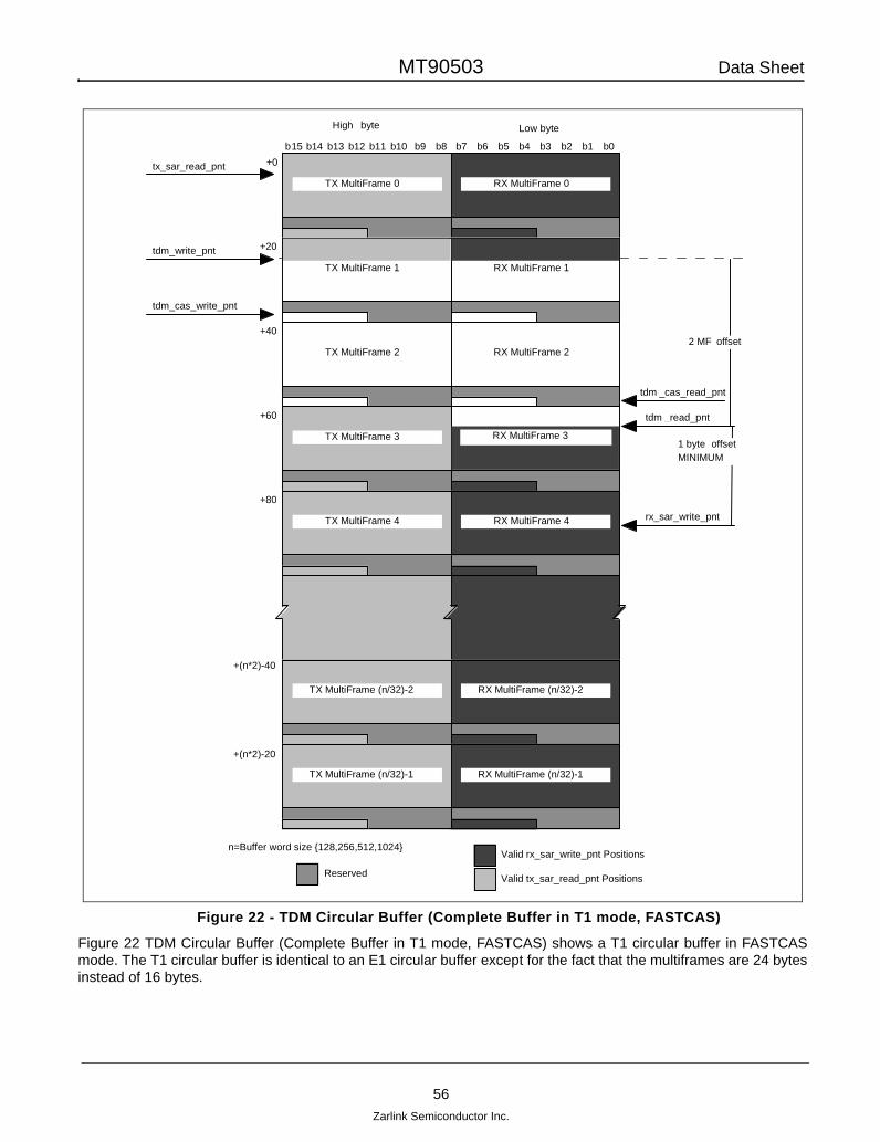
MT90503 Data Sheet
56Zarlink Semiconductor Inc.
Figure 22 - TDM Circular Buffer (Complete Buffer in T1 mode, FASTCAS)
Figure 22 TDM Circular Buffer (Complete Buffer in T1 mode, FASTCAS) shows a T1 circular buffer in FASTCASmode. The T1 circular buffer is identical to an E1 circular buffer except for the fact that the multiframes are 24 bytesinstead of 16 bytes.
b8b9b10b11b12b13 b14 b 15 +0
b0b1b2b3b4b5b6b7
Low byteHigh byte
Reserved
RX MultiFrame 0TX MultiFrame 0
+20
+40 RX MultiFrame 2TX MultiFrame 2
+60 TX MultiFrame 3
+80 RX MultiFrame 4TX MultiFrame 4
RX MultiFrame (n/32)-2TX MultiFrame (n/32)-2
+(n*2)-20 RX MultiFrame (n/32)-1TX MultiFrame (n/32)-1
n=Buffer word size {128,256,512,1024}
+(n*2)-40
tdm_write_pnt
tdm_cas_write_pnt
tx_sar_read_pnt
Valid rx_sar_write_pnt Positions
Valid tx_sar_read_pnt Positions
TX MultiFrame 1
tdm _read_pnt
tdm _cas_read_pnt
2 MF offset
RX MultiFrame 1
rx_sar_write_pnt
1 byte offset MINIMUM
RX MultiFrame 3

MT90503 Data Sheet
57Zarlink Semiconductor Inc.
4.3 TX_SAR Module
4.3.1 Overview
The purpose of the TX_SAR Module is to assemble TDM data bytes into ATM cells to be transmitted to the UTOPIAModule. The TX_SAR Module has no external interfaces, and does not control any of the MT90503’s pins.However, it is the connecting block between the TDM module and the UTOPIA Module in the data transmissiondirection.
When the TX_SAR assembles ATM cells, it reads bytes from the circular buffers in data memory and uses these toassemble the ATM cells.
In order to transmit CBR ATM cells correctly, a timing algorithm is used to ensure that the ATM cells are assembledand transmitted at the defined data rate. This timing algorithm is implemented using the transmit event scheduler.The transmit event scheduler is a construct in control memory that identifies the time ATM cells need to betransmitted, and the circular buffer from which data for the ATM cell is to be retrieved. ATM cells are capable ofcarrying a variable number of virtual channels. Therefore, the rate at which cells are transmitted is variable.
4.3.1.1 Support and Trunking for Different Types of ATM Cells
The type of ATM cells the TX_SAR supports includes AAL1, CBR-AAL0, and AAL5-VTOA. The transmit eventscheduler is capable of supporting the different data rates which are inherent to the different types of ATM cells.Figure 23 - ATM Cell Formats shows the different formats for the ATM cells that the TX_SAR Module supports.
The TX_SAR is also capable of supporting hyperchannels (trunking) of up to 2048 channels per VC. In addition, itcan also support AAL0 and AAL5 trunking, providing the number of channels is divisible by the payload bytes.
Figure 23 - ATM Cell Formats
GFC VPIVPI VCI
VCIVCI PTI CL
HECCSI SEQ CRC PP P-Byte
Payload Byte #0Payload Byte #1
Payload Byte #44Payload Byte #45
GFC VPIVPI VCI
VCIVCI PTI CL
HECCSI SEQ CRC P
Payload Byte #0Payload Byte #1Payload Byte #2
Payload Byte #45Payload Byte #46
GFC VPIVPI VCI
VCIVCI PTI CL
HEC
Payload Byte #2Payload Byte #3
Payload Byte #46Payload Byte #47
Payload Byte #0Payload Byte #1
GFC VPIVPI VCI
VCIVCI PTI CL
HEC
Payload Byte #2Payload Byte #3
Payload Byte #0Payload Byte #1
CRC32 [31:24]
Length [15:8]Length [7:0]
"00000000""00000000"
Payload Byte #39
CRC32 [23:16]CRC32 [15:8]CRC32 [7:0]
AAL1 with Pointer Cell46 Payload Bytes
AAL5 Cell40 Payload Bytes
AAL0 Cell48 Payload Bytes
AAL1 without Pointer Cell47 Payload Bytes

MT90503 Data Sheet
58Zarlink Semiconductor Inc.
4.3.2 TX_SAR Event Schedulers
4.3.2.1 Overview
The purpose of the transmit event scheduler is to ensure that the MT90503 assembles and transmits ATM cells atthe appropriate time. This timing function is implemented to reduce data overruns and underruns.
Before arriving at the TX_SAR, TDM channel data is written into a variable-length (128 to 1024 bytes) transmitcircular buffer, a construct in external data memory, by the TDM Module. Each TDM channel is assigned its owntransmit circular buffer (see section 4.2.6 TDM Circular Buffer Pointers). The transmit event schedulers determineswhen the information will be assembled into ATM cells.
The 15 transmit event schedulers are identical, and all have individual configuration registers. Each transmit eventscheduler is divided into a programmable number of frames. When configured correctly, each transmit eventscheduler frame is constrained to an average of 125 µs (i.e. the time required for one byte to bereceived/transmitted on each TDM channel).
4.3.2.2 The Transmit Event Scheduler Process
Please refer to Figure 24 - Transmit Event Scheduler Process in conjunction with this subsection.
The MT90503’s 15 transmit event schedulers are all maintained in a designated memory block in the externalcontrol memory. Each transmit event scheduler can be programmed to support one of the four types of cells (AAL1with or without pointer, CBR-AAL0, or AAL5-VTOA). Each of the transmit event schedulers can be enabled ordisabled via registers (0610h - 0616h) in order to use less bandwidth if a certain format of ATM cell is not required.Figure 24 - Transmit Event Scheduler Process provides an example of one of the 15 transmit event schedulers inthe MT90503. All transmit event schedulers have exactly the same properties, and all perform the same functions.They can be configured individually to handle different VC configurations.
Each of the 15 transmit event schedulers is made up of a number of “frames”, with each frame containing a numberof events. An event, if executed, consists of the assembling and placing in a UTOPIA output FIFO of one ATM cell.The base address, length, and number of events can be programmed for each scheduler frame. Each transmitevent scheduler has its own Scheduler Base Address which, in conjunction with an internal frame counter, willlocate the events in a specific frame.
In order for an ATM cell to be assembled and transmitted at the appropriate time, the following transmit eventscheduler process steps are required:
An analogy can be made of the above process to a continuous “spinning wheel”, where there is a continualselection and reading of events for each transmit event scheduler frame. Table 19 - Scheduler Event Fieldsprovides a description of the fields for one of the transmit event schedulers. Refer to Figure 24 - Transmit EventScheduler Process to locate the fields.
1 On the reception of a frame pulse, the scheduler scans through the events of the current frame.
2 For each valid event in the current frame, a cell is assembled and transmitted to the UTOPIA module.
3 On the reception of the next frame pulse (125 µs later) or upon the completion of the final valid event in the current frame, whichever is later, the scheduler increments current frame, to point to the next frame in the scheduler.
4 The scheduler reads each frame sequentially, returning to frame 0 upon completion of the final frame in the scheduler.

MT90503 Data Sheet
59Zarlink Semiconductor Inc.
Figure 24 - Transmit Event Scheduler Process
Sche
dule
r 0’s
Info
Sch
edul
er 1
’s In
fo
Sch
edul
er 2
’s In
fo
Sch
edul
er 1
4’s
Info
0000
0h
0000
8h
0001
0h
0007
0h
IC
urre
nt F
ram
e
Num
Env
Rea
d 2m
Eve
nts
Sch
edul
er B
ase
Add
ress
Last
Fra
me
(M)
Fiel
ds fo
r the
Tra
nsm
itTr
ansm
it Ev
ent
Fram
e 0
Fram
e 1
Fram
e 2
Fram
e 3
Fram
e M
-2
Fram
e M
-1
Fram
e M
Eve
nt 0
Even
t 1
Eve
nt m
-1
Eve
nt m
b15
b14
b13
b12
b11
b1
0 b
9 b
8
b7
b6
b5
b4
b3
b2
b1
b0
Tx S
truct
ure
Add
ress
Poi
nter
Sch
ed N
ums
Even
t n-1
Res
erve
d
b15
b14
b13
b12
b11
b10
b9
b8
b7
b6
b5
b4
b3
b2
b1
b0
Eve
nts
neve
r rea
d
Fiel
ds fo
r the
Sch
edul
er E
vent
Tran
smit
Even
t
+2+0 +6
Not
es:
Onl
y 1
of 1
5 sc
hedu
lers
is s
how
nM
= 1
to 2
048
fram
es p
er s
ched
uler
n =
0 to
45
even
ts p
er fr
ame
Fram
es w
ithin
a s
ched
uler
are
exe
cute
dse
quen
tially
with
a n
ew fr
ame
begi
nnin
gev
ery
125
µs (a
vera
ge).
Loop
s w
hen
last
fram
e is
read
Sche
dule
r Lis
tSc
hedu
ler F
orm
at
m =
num
ber o
f eve
nts
in a
fram
e th
at a
re re
ad
Turn
Num
+2+0
Even
t Sch
edul
er
+0 +2n
+4n
+6n
(M-2
)*2n
(M-1
)*2n
M*2
n
+4
Tran
smit
Eve
nt S
ched
uler
Lis
t is
loca
ted
at th
e be
ginn
ing
of C
ontro
l Mem
ory

MT90503 Data Sheet
60Zarlink Semiconductor Inc.
4.3.2.3 Transmit Event Scheduler Fields Description
Table 18 - Field Description for the Transmit Event Scheduler provides a description of the fields for the transmitevent scheduler. Please refer to Figure 24 - Transmit Event Scheduler Process to locate the fields.
Table 18 - Field Description for the Transmit Event Scheduler
Field Name of Field Bits Used Description of Field
I Scheduler Initialised Bit
+0/b15 This bit is reset by software immediately before enabling the transmit event scheduler. Hardware will set this bit the first time it reads the scheduler information structure. When the I bit is read at ’0’ by hardware and the scheduler is used for T1/E1 support, the transmit event scheduler's Current Frame will be written between 0-23 for T1 and 0-15 for E1 in order for frame 0 to correspond to the first byte of a multiframe.
Turn Num Free run counter of scheduler wraps
+0/b13:b11 Turn Num is a counter used for the implementation of multiframing. The scheduler re-synchronises itself with the multiframe count when Turn Num is 0.
Current Frame Current Frame +0/b10:b0 Current Frame is used to record the frame position of the transmit event scheduler. Range 0 to (Last Frame)
Num Env Number of events per frame in the scheduler
+2/b7:b5 The number of events per frame is 2(Num Env)+1. The same number applies to all frames in the scheduler. Range:000 to 101 (2 to 63 events per frame). All others reserved.
Read 2m Events
Read 2m First Events
+2/b4:b0 Indicates to the scheduler how many events in each frame must be read. The same number applies to all frames in the scheduler.
Scheduler Base Address
Pointer to the beginning of the transmit event scheduler
+4/b14:b0 This field is appended with "00000" as the LSBs, to form a 20-bit address.Note: A frame must never cross a boundary of its own size in memory. Therefore, if the transmit event scheduler has more than 8 events per frame (32 bytes per frame), then some LSBs of this field must be 0.
Last Frame (M) Last Frame (M)
+6/b10:b0 Last Frame = (number of frames in the scheduler) - 1. If Last Frame = 0, the scheduler is one frame long, if Last Frame = 1, the scheduler is two frames long, etc.
m012..
31
Events Read6424..
62

MT90503 Data Sheet
61Zarlink Semiconductor Inc.
The number of events per frame in the scheduler, Num Env, determines how much memory is allocated for eachframe in the scheduler: 2 words per event. Within this memory, the scheduler will read only the first 2m events, asstored in the Read 2m Events field. Of the events that are read, only those with the Scheduler Num not equal to‘1111’ (see Table 19) are executed. No action is taken on events that are read whose Scheduler Num is ’1111’.
4.3.2.4 Scheduler Events Fields Description
Table 19 - Scheduler Event Fields provides a description of the fields for the transmit event scheduler entries.Figure 24 - Transmit Event Scheduler Process to locate the fields
4.3.2.5 Bandwidth Limitations for Transmit Scheduler Events
The maximum number of events per frame corresponds to the maximum number of events that can occur in oneframe of all the schedulers simultaneously.
If the frames are not synchronised (as in Figure 25 - Unsyncrhonised Schedulers), the maximum number of eventsper frame is the sum of the maximum events in any frame of each scheduler (in this case, 32 events + 21 events =53 events is the maximum number of events per frame). If the schedulers are synchronised (as in Figure 26 -Synchronised Schedulers), the maximum number of events per frame is the worst in any particular frame (in thiscase, 23 + 17 = 40 events is greater than 6 + 24 = 30 events, so 40 events is the maximum number). If theschedulers are partially synchronised (as in Figure 27 - Partially Synchronised Schedulers), the maximum numberof events per frame is the worst in any frame that can possibly align (in this case, 20 + 5 = 25 events is less than 27+ 12 = 39 events which is greater than 20 + 16 = 36 events and 27 + 7 = 34 events so 39 events is the maximumnumber).
Field Name of Field Bits Used Description of Field
Scheduler Num Transmit Event Scheduler Number
+0/b5:b2 This field contains the scheduler number. 0000 to 1110 = valid scheduler numbers1111 = invalid event. No action will be taken on this eventThe transmit event schedulers are read sequentially.
S Start Bit +0/b0 This field indicates the first event that will be carried out when the VC is initialised.Software must set the S bit of only one event once programming of the scheduler is complete.This bit is only relevant until the I bit is set in the TX Control Structure. After the I bit is set, all events with valid scheduler numbers will be executed as they are encountered.
TX Structure Address Pointer
TX Structure Address Pointer
+2/b14:b0 This field is the pointer to the TX_SAR Structure used to assemble an ATM cell each time this event is read. This field is appended with "00000" as the LSBs to form a 20-bit address.
Table 19 - Scheduler Event Fields
Transmission Speed Maximum Number of Events per Frame
25 Mbps 7155 Mbps 45622 Mbps 183
Table 20 - Maximum number of Events per Frame for Common Transmission Speeds

MT90503 Data Sheet
62Zarlink Semiconductor Inc.
Figure 25 - Unsyncrhonised Schedulers
Figure 26 - Synchronised Schedulers
Figure 27 - Partially Synchronised Schedulers
4.3.3 Out of Bandwidth Error
The TX_SAR out-of-bandwidth error indicates that a particular region of the scheduler, or the scheduler as a whole,is overloaded. This error occurs when the TX_SAR lagging by F frames or more, where F is an integer written toregister 0608h. The TX_SAR has 125 µs to execute all the events in the frame it is servicing at the current time. Ifall the events in the frame are not executed within 125 µs, the TX_SAR continues until the end of the current framebefore moving on to events in the next frame. This method reduces the amount of time it has to service thefollowing frame. If the first frame took 150 µs to service, then there would only be 100 µs left to service the followingframe. Therefore, if the second frame is also very full, the TX_SAR would not have the time to finish servicing it andwill be late again for the following frame.
If frames take an excessively long time to service, the MT90503 may become several frames late. If the MT90503detects that it is F or more frames late, an out-of-bandwidth error will be declared and the MT90503 will skip thenext F frames of events. This action will cause latency in the transmission delay and corrupt data on the VCs untilthe channel reconverges. The channel reconverges once every 375 frames (47 ms) in “AAL1 with pointer”schedulers, and less often if multiframing is used. The cells that were supposed to be assembled in the F missingframes are skipped, and new cells are assembled with the old data. The out-of-bandwidth error arises from an error
21 Events
9 Events
Scheduler 1
Frame 1
Frame 026 Events
15 Events
32 Events
Scheduler 0
Frame 0
Frame 2
Frame 1
23 Events
6 Events
Scheduler 0
Frame 1
Frame 0 17 Events
24 Events
Scheduler 1
Frame 1
Frame 0
Frame 1
Frame 0 20 Events
27 Events
Scheduler 0
Frame 1
Frame 0 5 Events
12 Events
Frame 3
Frame 2 16 Events
7 Events
Scheduler 1

MT90503 Data Sheet
63Zarlink Semiconductor Inc.
with the mapping of the transmit event scheduler. Despite this error, the MT90503 will continue with its operations,however, some cells may be lost.
4.3.3.1 Percent of Bandwidth Register
The TX_SAR incorporates a Percent of Bandwidth register (0510h), which indicates the maximum number of mclkcycles utilised by the TX_SAR process per frame. The Percent of Bandwidth register counts the number of mclkcycles from the time that a frame is received, to the time that all the entries for that frame in the schedulers havebeen completely handled. This value will be compared to the current maximum value obtained by the TX_SARprocess. If the most current value is higher, it is retained and written into the Percent of Bandwidth register. Thevalue in the Percent of Bandwidth register can be cleared by the software. If the TX_SAR takes more than 125 µs toassemble the cells of a particular frame, the Percent of Bandwidth register’s value will be greater than the numberof mclk cycles in the 125 µs time frame.
4.3.3.2 Distribution of Events by Software
The events in the transmit event scheduler need to be distributed as evenly as possible. For example, an “AAL1with pointer” 3-channel VC has three events per 46.875 frames. These events must be spaced out with a distanceof 15 or 16 frames between events to prevent irregular data distribution resulting in transmission latency and/ordata integrity problems. Consequently, a scheduler 8 * 46.875 = 375 frames in length containing 24 events isrequired to map the three events per 46.875 frames evenly. The mapping of this information is accomplished byexternal software.
One of the key features of the transmit event schedulers is their programmable length. Since different cells requiredifferent sizes of schedulers, the schedulers are capable of handling any scheduler length from 1 to 2048 frames.
Refer to Table 21 for examples of transmit event scheduler sizes.
4.3.4 Mapping of the Transmit Event Scheduler
With the “AAL1 with pointer”, the format for the mapping of the transmit event scheduler is asymmetric. The “AAL1with pointer” format expects a cell every 46.875 frames per channel, a transmit event scheduler with 47 frames thatskips the last frame one turn out of eight is required. The MT90503 overcomes this difficulty by creating anextended transmit event scheduler of 375 frames, which is 8 * 46.875. Therefore, the irregularity of the transmitevent scheduler is corrected and events can be mapped appropriately.
Due to this multiplication, the number of events mapped in the transmit event scheduler for any VC is always amultiple of eight. This means the first event in the transmit event scheduler is always a p-byte event and contains azero value pointer indicating the start of a structure.
ATM Cell Type Number of Frames Transmit Event Scheduler size in KB(e.g. 32 events per frame)
CBR-AAL0 48 6*AAL1 with Pointer 375 47AAL1 without Pointer 47 5.875AAL5-VTOA/CBR-AAL0 240 30E1 with CAS 750 94T1 with CAS 1125 141*Note: 6 KB = 32 events per frame * 48 frames per scheduler * 4 bytes per event
Table 21 - Examples of typical Transmit Event Scheduler Sizes

MT90503 Data Sheet
64Zarlink Semiconductor Inc.
4.3.5 TX_SAR Control Structures
TX_SAR control structures are constructs in control memory which contain ATM cell information. When a frameevent is read from one of the 15 transmit event schedulers, an ATM cell is assembled. The scheduler eventcontains the base address that points to the control structure that is used for assembling the ATM cell. The controlstructure contains all of the fields that are required for assembling the ATM cell. The destination field in the controlstructure is responsible for telling the UTOPIA Module the destination VC of the assembled ATM cell. For detailedinformation regarding the destination field, refer to Table 22, 'Description of the Fields for the TX_SAR ControlStructure"‚ on page 65.
Figure 28 - TX_SAR Event Scheduler Pointer Flow and Control Structure shows a functional block diagram of anexample of transmit event scheduler interconnections and pointer flow to the TX_SAR control structure.
Figure 28 - TX_SAR Event Scheduler Pointer Flow and Control Structure
Scheduler 0’s Info
00000h
00008h
00070h
Scheduler List
Scheduler 0
Event 0
Scheduler 0, Frame 1
Scheduler 0, Frame 0
Scheduler 0, Frame 1
Scheduler 0, Frame 374
Pointer to currentFrame in Scheduler
Header of the
TX_SAR Control Structure
Structure
TDM Channel 2 Pnt
TDM Channel 1 Pnt
TDM Channel 0 Pnt
TSST 0
TSST 1
TSST 2
TSST 4093
TSST 4094
TSST 4095
Event 1
Event 63
tx_sar_read_pnt
TDM Channel AssociationMemory (Internal)
tdm_write_pnt
TX Side RX Side
TDM Channel 1’s CircularBuffer (in the Data Memory)
Byte written by TDM Transmit
Byte read by TX_SAR
Note: All structures are in the Control memory unless otherwise specified
TX/RX Circular Buffer Pointer(Same pointer in Channel AssociationMemory and in TX_SAR Control Structure)
Base address of control structure from Event 1

MT90503 Data Sheet
65Zarlink Semiconductor Inc.
4.3.5.1 TX_SAR Control Structure Fields
Figure 29 - TX_SAR Control Structure shows the TX_SAR control structure format and data fields held in controlmemory. Table 22, Description of the Fields for the TX_SAR Control Structure describes the data fields.
The header for the ATM cell to be constructed is derived from words +8 and +A in the TX_SAR control structure.The final 8 bits of the cell header, the Header Error Check (HEC), are calculated and inserted by the UTOPIAmodule. The channel entries, beginning at +16h, are 14-bit pointers to the circular buffers in external data memory,one for each channel in the VC.
Figure 29 - TX_SAR Control Structure
Field Name of Field
Byte Address
Offset /Bits Used
Description of Field
First Entry First Entry +0/b15:b12 First entry gives the position within the structure of the pointer to the first channel. The field is a word pointer and is constant with a value of 0xB. To allow for future structure updates, its value is programmable.
Channel 0’s address is located at base_add + (2 * First Entry).
A Structure Active
+0/b11 This bit indicates whether or not the VC is active. The control structure becomes active when A is set. The A bit is set by software. If the A bit is reset, the control structure will always be ignored. If the A bit is set, hardware may ignore it for other reasons, such as the control structure not being initialised.
Table 22 - Description of the Fields for the TX_SAR Control Structure
First Entry A SRTS AAL CE BS
Last Entry TXD
Payload Size Offset
GFC VPI VCI [15:12]
VCI [11:0]OAMCLP
P-Byte Counter
Current Entry I Seq
tx_sar_read_pnt
Transmitted Cell Counter [31:16]
Transmitted Cell Counter [15:0]
Channel 0’s TX/RX Circular Buffer Pointer
Channel 1’s TX/RX Circular Buffer Pointer
Channel (n-2)’s TX/RX Circular Buffer Pointer
Channel (n-1)’s TX/RX Circular Buffer Pointer Reserved
n=number ofTDM Channelsin the VC
Hardware WriteBack Fields
b15 b14 b13 b12 b11b10 b9 b8 b7 b6 b5 b4 b3 b2 b1 b0+ 0h
+ 2h
+ 4h
+ 6h
+ 8h
+ Ah
+ Ch
+ Eh
+ 10h
+ 12h
+ 14h
+ 16h
+ 18h
+(n*2) + 14h
+ (n*2) + 16h
Header FieldsPTI
V
V
V
V

MT90503 Data Sheet
66Zarlink Semiconductor Inc.
SRTS Synchronous Residual Time Stamp
+0/b8:b7 The SRTS bits indicate the generation of SRTS within the VC. SRTS is either absent, enabled, or enabled and master. Many VCs can be programmed to transmit SRTS, but only one can request a new SRTS value. If many VCs transport SRTS, they must all be of the same size, i.e., the same number of channels, to ensure the validity of the values. If SRTS is generated on the VC, it is packaged within the AAL1 byte of cells 1, 3, 5 and 7 of an 8-cell cycle.The SRTS field should never be enabled on CBR-AAL0 or AAL5-VTOA VCs. If SRTS is enabled on multiple VCs, the events must be mapped in such a way that an event that generated cell # 0 for the master VC occurs before the event that generates cell # 0 for all the other VCs.The SRTS field bits are encoded as follows:00 = No SRTS01 = Reserved10 = Send SRTS11 = Send SRTS, and request a new SRTS value on Seq = 7
AAL Adaptation Layer
+0/b6:b5 The AAL bits indicate the ATM format to be used to assemble the cells in this structure.The AAL field bits are decoded as follows:00 = CBR AAL0. Consists of CBR data01 = AAL5-VTOA. Includes a CRC and a payload size indicator at the end of the cell10 = AAL1 without pointer. Includes a Sequence number packaged with the cell, as well as the possibility of transmitting SRTS on the VC11 = AAL1 with pointer. Includes a Sequence number packaged with the cell, and the possibility of transmitting SRTS on the VC
Field Name of Field
Byte Address
Offset /Bits Used
Description of Field
Table 22 - Description of the Fields for the TX_SAR Control Structure (continued)

MT90503 Data Sheet
67Zarlink Semiconductor Inc.
CE Circuit Emulation
+0/b4:b2 The CE field bits indicate the presence of a multiframing standard used within the VC.The multiframing standard changes the way the information is read from the TDM circular buffers, as well as the standard that is used to generate the p-byte. In addition, setting the CE bits to a CAS setting will indicate to the TX_SAR that CAS signaling bits must be inserted at the end of the AAL1 control structure.The field bits are decoded as follows:000 = No CAS, no multiframe001 = Reserved01x = Reserved100 = T1 without CAS (T1 type circular buffer, but no CAS will be sent in the ATM cells)101 = T1 with CAS (T1 type circular buffer, with CAS sent in the ATM cells110 = E1 without CAS (E1 type circular buffer, but no CAS will be sent in ATM cells)111 = E1 with CAS (E1 type circular buffer, with CAS sent in the ATM cells
BS TX/RX Circular Buffer Size
+0/b1:b0 These bits encode the size of the TDM circular buffer that is to be read from. In T1 and E1 modes, a portion of space in the circular buffer is required to store the CAS values; in the T1 mode 25% is required, and in the E1 mode 50% is required.Half of the TDM circular buffer is used for TX data and half for RX data.The field bits are decoded as follows:00 = 128 words01 = 256 words10 = 512 words11 = 1024 words
Last Entry Last Entry +2/b15:b4 Last Entry is the word offset from the 8 kB boundary containing the structure to the last circular buffer pointer in the structure.
TXD TX_SAR Destination Field
+2/b3:b0 The TXD field is used to tell the UTOPIA Module the destination of the assembled ATM cell.The TX_SAR Destination field is decoded as follows:0000 = Discard ATM cell0XX1 = Send to TXA port0X1X = Send to TXB port01XX = Send to TXC portOthers = ReservedBroadcasting to multiple ports is allowed.
Field Name of Field
Byte Address
Offset /Bits Used
Description of Field
Table 22 - Description of the Fields for the TX_SAR Control Structure (continued)
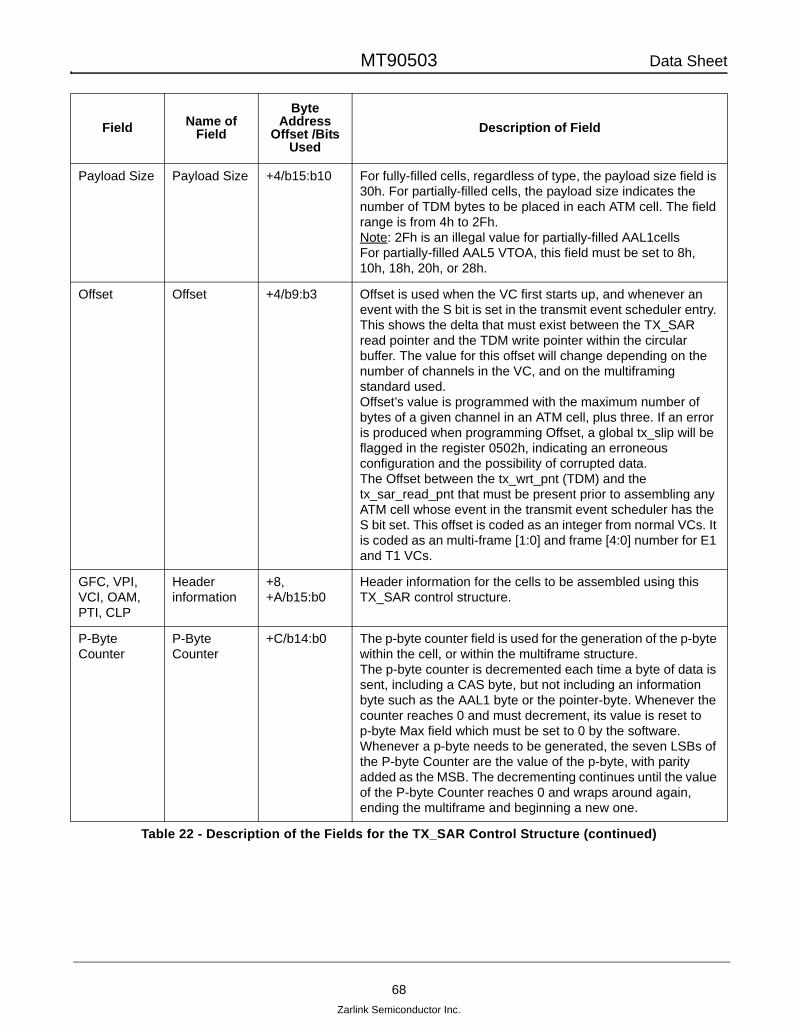
MT90503 Data Sheet
68Zarlink Semiconductor Inc.
Payload Size Payload Size +4/b15:b10 For fully-filled cells, regardless of type, the payload size field is 30h. For partially-filled cells, the payload size indicates the number of TDM bytes to be placed in each ATM cell. The field range is from 4h to 2Fh.Note: 2Fh is an illegal value for partially-filled AAL1cellsFor partially-filled AAL5 VTOA, this field must be set to 8h, 10h, 18h, 20h, or 28h.
Offset Offset +4/b9:b3 Offset is used when the VC first starts up, and whenever an event with the S bit is set in the transmit event scheduler entry. This shows the delta that must exist between the TX_SAR read pointer and the TDM write pointer within the circular buffer. The value for this offset will change depending on the number of channels in the VC, and on the multiframing standard used.Offset’s value is programmed with the maximum number of bytes of a given channel in an ATM cell, plus three. If an error is produced when programming Offset, a global tx_slip will be flagged in the register 0502h, indicating an erroneous configuration and the possibility of corrupted data.The Offset between the tx_wrt_pnt (TDM) and the tx_sar_read_pnt that must be present prior to assembling any ATM cell whose event in the transmit event scheduler has the S bit set. This offset is coded as an integer from normal VCs. It is coded as an multi-frame [1:0] and frame [4:0] number for E1 and T1 VCs.
GFC, VPI, VCI, OAM, PTI, CLP
Header information
+8, +A/b15:b0
Header information for the cells to be assembled using this TX_SAR control structure.
P-Byte Counter
P-Byte Counter
+C/b14:b0 The p-byte counter field is used for the generation of the p-byte within the cell, or within the multiframe structure.The p-byte counter is decremented each time a byte of data is sent, including a CAS byte, but not including an information byte such as the AAL1 byte or the pointer-byte. Whenever the counter reaches 0 and must decrement, its value is reset to p-byte Max field which must be set to 0 by the software.Whenever a p-byte needs to be generated, the seven LSBs of the P-byte Counter are the value of the p-byte, with parity added as the MSB. The decrementing continues until the value of the P-byte Counter reaches 0 and wraps around again, ending the multiframe and beginning a new one.
Field Name of Field
Byte Address
Offset /Bits Used
Description of Field
Table 22 - Description of the Fields for the TX_SAR Control Structure (continued)

MT90503 Data Sheet
69Zarlink Semiconductor Inc.
4.3.6 Miscellaneous TX_SAR Features
4.3.6.1 T1 with CAS and E1 with CAS Cell Format Mapping
For the transmission of T1 with CAS and E1 with CAS, the number of frames required is 9000 and 6000respectively. But, because the number of frames mapped in a full size transmit event scheduler is always amultiple of eight, the MT90503 handles large size schedulers by dividing the size by eight, and mapping eighttimes less events (1125 for T1 with CAS and 750 for E1 with CAS). This results in a latency of one frame.
Current Entry Current Entry +E/b15:b4 The Current Entry field tells the SAR what the first channel is to be assembled in this cell. The valid values for this field are contained between the First Entry and the Last Entry fields inclusively. The Current Entry field also points to words, and is initialised by software to the word pointed to by the First Entry field. the The Current Entry field is similar the Last Entry field, such that it is defined as the offset between the Current Entry field and the 8 kB boundary in which the structure is contained.
I Structure Initialised Bit
+E/b3 The I bit is set by the hardware when a scheduler entry flagged with the Start bit asserted high is encountered, i.e., as soon as the first cell is sent on this VC.This bit is cleared by the software upon initialisation.
Seq AAL1 Sequence Number
+E/b3:b0 These bits are reset by software.
tx_sar_read_pnt
Tx_sar_read_pnt
+10/b15:b6 This value is a pointer to the next byte to be read in the TX/RX Circular Buffers.
Transmitted Cell Counter
Free running transmitted cell counter
+12, +14/b15:b0
The Transmitted Cell Counter increments each time a cell is transmitted on the VC. The time needed for the counter to wrap-around decreases proportionately with the number of channels in the VC. This field should be reset by software and is used for monitoring.
V TDM Channel Valid
+16 to end/b15
When this bit is high the channel is active. When this bit is ’0’, the programmable null byte, found in register 0420h, will be transmitted.
Channel N's TX/RX Circular Buffer Pointer
Channel N's TX/RX Circular Buffer Pointer
+16 to end/b13:b0
This field is a pointer to the TX/RX Circular Buffer associated with this channel. "0000 0000" will be appended to this field as the LSBs to form a 22-bit address in data memory.
Field Name of Field
Byte Address
Offset /Bits Used
Description of Field
Table 22 - Description of the Fields for the TX_SAR Control Structure (continued)

MT90503 Data Sheet
70Zarlink Semiconductor Inc.
4.3.6.2 Support of Partially-Filled Cells
The MT90503 is capable of supporting partially-filled cells, as long as the number of channels in the VC is smalleror equal to the cell fill. A single transmit event scheduler can be created to accommodate several sizes of AAL1,CBR-AAL0 or AAL5-VTOA ATM cells. AAL1 with pointer ATM cells can be used by this format, since the number ofdata bytes per ATM cell is always constant. For example, the 240-entry transmit event scheduler is capable ofaccommodating partially-filled cells of 4-, 5-, 6-, 8-, 10-, 12-, 15-, 16-, 20-, 24-, 30-, or 40-bytes per cell.
4.3.6.3 TX_SAR FIFO
The TX_SAR transmits cells contained in its data cell FIFO when there are no events to be processed. The TXSAR’s data FIFO can be used to store AAL0 cells as well as OAM cells, therefore, CPU-based OAM cell generationis supported.
4.4 RX_SAR Module
The RX_SAR module performs processing on ATM cells received from the UTOPIA module. Cells placed in theRX_SAR input FIFO by the UTOPIA module are read, processed, and then written into the appropriate multi-cellcircular buffer in external control memory. The processing involves identifying the VC corresponding to the cell,examining the cell for errors, determining where to place the data, and monitoring the status of circular buffers. TheRX_SAR module also directs data cells to the data cell FIFO from which the CPU can read them.
The RX_SAR module does not connect to any external pins, interfacing instead with the UTOPIA module, CPUinterface, and external memory controller. Global pointers are shared between the RX_SAR and TDM modules.
ATM cells that are received by the MT90503 are processed by the UTOPIA module and can be directed to any ofthree TX output FIFOs or to the 32-cell RX_SAR input FIFO. Those cells that are forwarded to the RX_SAR aredirected to the SAR portion (cells to be formatted into TDM streams), to the data cell portion (to be examined by theCPU), or to both.
For cells directed to the SAR portion, the RX_SAR uses control information in the RX_SAR Control Structures(Section 4.4.2) to extract the payload data from the received cell and store it into TDM channel RX Circular Bufferslocated in external data memory.
4.4.1 Treatment of Data Cells
Data cells, such as those containing OAM information, are placed in a programmable length FIFO in externalcontrol memory. The length of the FIFO is stored in register 070Eh. The CPU can read a data cell at any time, afterobtaining the address of the FIFO (register 070Ch) and the read pointer (register 0708h).
The CPU can be alerted to the presence of data cells via an interrupt that triggers if either of two events occur: theinterrupt can be generated when the FIFO becomes more than half full or the interrupt can be generated if a datacell has been present in the FIFO for longer than a programmable period of time (registers 0720h, 0722h). Thisinterrupt can be enabled through register 0220h.
When ready to process the information, the CPU obtains a read pointer to the information from register 0708h andreads the information through 26 word accesses.
Cells with the OAM bit set in the PTI portion of the header can be directed to the data cell FIFO on a per VC basis.The same is true for non-OAM cells. In addition, unknown non-OAM cells, and/or unknown OAM cells can also besent to the data cell FIFO (all unknown non-OAM cells are directed to the same location(s)).
4.4.2 Control Structure
For each VC directed to the SAR portion of the RX_SAR, an RX_SAR control structure exists in external controlmemory. The structure, similar to that of the TX_SAR, contains information on how to process a cell including:
• what type of traffic is being carried (AAL1, CBR-AAL0, AAL5-VTOA)

MT90503 Data Sheet
71Zarlink Semiconductor Inc.
• the size of the circular buffers for the data
• how to act in the case of an overrun or underrun
• the multiframing standard in place
• expected presence of CAS
• enabled errors, the size of the payloads
• information necessary to detect and correct for errors
• a pointer to each circular buffer, one for each channel in the VC
Figure 30 - RX_SAR Control Structure
Field Name of Field Byte AddressOffset/Bits Used Description of Field
First Entry First Entry +0/b15:b12 First entry field gives the position within the structure of the pointer to the first channel. The field is a word pointer and is constant with a value of 0xB. To allow for future structure updates, its value is programmable.Channel 0’s address is located at base_add + (2 * First Entry).
Table 23 - Description of the Fields for the RX_SAR Structure
b15 b14 b13 b12 b11 b10 b9 b8 b7 b6 b5 b4 b3 b1 b0
Last Entry SE LE AE PE
FCCEIMBSAALFirst Entry
Max Used Bytes in RX Circular Buffer Payload Size
P -byte counterPBI
Current Entry
rx_sar_write_pnt I Last Seq
2nd Last SeqMonitored Min Lead
Monitored Max Lead
Slip Free rx_sar_write_pnt
Received Cell Counter [31:16]
Reserved n = number of TDM channels in the VC
V
V
V
V
Received Cell Counter [15:0]
Channel 0’s TX/RX Circular Buffer Pointer
Channel 1’s TX/RX Circular Buffer Pointer
Channel (n-2)’s TX/RX Circular Buffer Pointer
Channel (n-1)’s TX/RX Circular Buffer Pointer
b2
+0
+2
+4
+6
+8
+A
+C
+E
+10
+12
+14
+16
+18
+(n*2)+14
+(n*2)+16
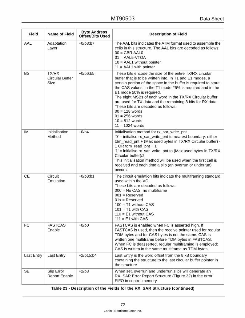
MT90503 Data Sheet
72Zarlink Semiconductor Inc.
AAL Adaptation Layer
+0/b8:b7 The AAL bits indicates the ATM format used to assemble the cells in this structure. The AAL bits are decoded as follows:00 = CBR AAL001 = AAL5-VTOA10 = AAL1 without pointer11 = AAL1 with pointer
BS TX/RX Circular Buffer Size
+0/b6:b5 These bits encode the size of the entire TX/RX circular buffer that is to be written into. In T1 and E1 modes, a certain portion of the space in the buffer is required to store the CAS values; in the T1 mode 25% is required and in the E1 mode 50% is required.The eight MSBs of each word in the TX/RX Circular buffer are used for TX data and the remaining 8 bits for RX data.These bits are decoded as follows:00 = 128 words01 = 256 words10 = 512 words11 = 1024 words
IM Initialisation Method
+0/b4 Initialisation method for rx_sar_write_pnt '0' = initialise rx_sar_write_pnt to nearest boundary: either tdm_read_pnt + (Max used bytes in TX/RX Circular buffer) - 1 OR tdm_read_pnt + 1'1' = initialise rx_sar_write_pnt to (Max used bytes in TX/RX Circular buffer)/2This initialisation method will be used when the first cell is received and each time a slip (an overrun or underrun) occurs.
CE Circuit Emulation
+0/b3:b1 The circuit emulation bits indicate the multiframing standard used within the VC. These bits are decoded as follows:000 = No CAS, no multiframe001 = Reserved01x = Reserved100 = T1 without CAS101 = T1 with CAS110 = E1 without CAS111 = E1 with CAS
FC FASTCAS Enable
+0/b0 FASTCAS is enabled when FC is asserted high. If FASTCAS is used, then the receive pointer used for regular TDM bytes and for CAS bytes is not the same. CAS is written one multiframe before TDM bytes in FASTCAS. When FC is deasserted, regular multiframing is employed: CAS is written in the same multiframe as TDM bytes.
Last Entry Last Entry +2/b15:b4 Last Entry is the word offset from the 8 kB boundary containing the structure to the last circular buffer pointer in the structure.
SE Slip Error Report Enable
+2/b3 When set, overrun and underrun slips will generate an RX_SAR Error Report Structure (Figure 32) in the error FIFO in control memory.
Field Name of Field Byte AddressOffset/Bits Used Description of Field
Table 23 - Description of the Fields for the RX_SAR Structure (continued)

MT90503 Data Sheet
73Zarlink Semiconductor Inc.
LE Cell Loss and Insertion Error Report Enable
+2/b2 When set, single cell losses, multiple cell losses and cell misinsertions will generate an RX_SAR Error Report Structure (Figure 32) in the error FIFO in control memory.
AE AAL1 Byte Report Enable
+2/b1 When set, AAL1 CRC-3 and CRC-3/Seq Num parity errors will generate an RX_SAR Error Report Structure (Figure 32) in the error FIFO in control memory.
PE P-Byte Error Report Enable
+2/b0 When set, p-byte parity errors, p-byte absent and p-byte framing errors will generate an RX_SAR Error Report Structure (Figure 32) in the error FIFO in external control memory.
Max Used Bytes in RX Circular Buffer
Max Used Bytes in RX Circular Buffer
+4/b15:b6 This field indicates the range of valid positions in bytes of the rx_sar_write_pnt relative to the tdm_rx_read_pnt before a cell is received. In no case can this value be 0.
Payload Size
Payload Size +4/b5:b0 For fully-filled cells, regardless of type, the payload size field is 30h. For partially-filled cells, the payload size indicates the number of TDM bytes in each ATM cell. The field range is from 4h to 2Fh.Note: 2Fh is an illegal value for partially-filled AAL1cellsFor partially-filled AAL5 VTOA, this field must be set to 8h, 10h, 18h, 20h, or 28h.
PBI P-Byte Initialization
+6/b15 Initialized to ’0’ by software.
P-Byte Counter
P-Byte Counter
+6/b14:b0 This field is a counter used to detect p-byte framing errors. When a p-byte is detected, this counter is loaded with the p-byte’s value. Each time a TDM byte is received, the counter is decremented. When the counter reaches the Current Entry it should be reset to the First Entry and the rx_sar_write_pnt should point to the beginning of the multiframe if applicable. When it decrements below 0, the counter resets to its maximum. Any time a p-byte is received, its value should match the value in this field, or a p-byte framing error will be detected.
Current Entry
Current Entry +8/b11:b0 Current Entry indicates which TDM channel the RX_SAR is currently writing to the circular buffers. The current entry is defined as being the offset from the 8 KB boundary containing the structure and the “TX/RX Circular Buffer Pointer” being read from the structure. Current Entry is initialised to the value of First Entry, increments up to Last Entry, and then wraps around to First Entry.This field should be initialised by software to 0Bh.Note: This field should not be written to while the VC is active.
Field Name of Field Byte AddressOffset/Bits Used Description of Field
Table 23 - Description of the Fields for the RX_SAR Structure (continued)
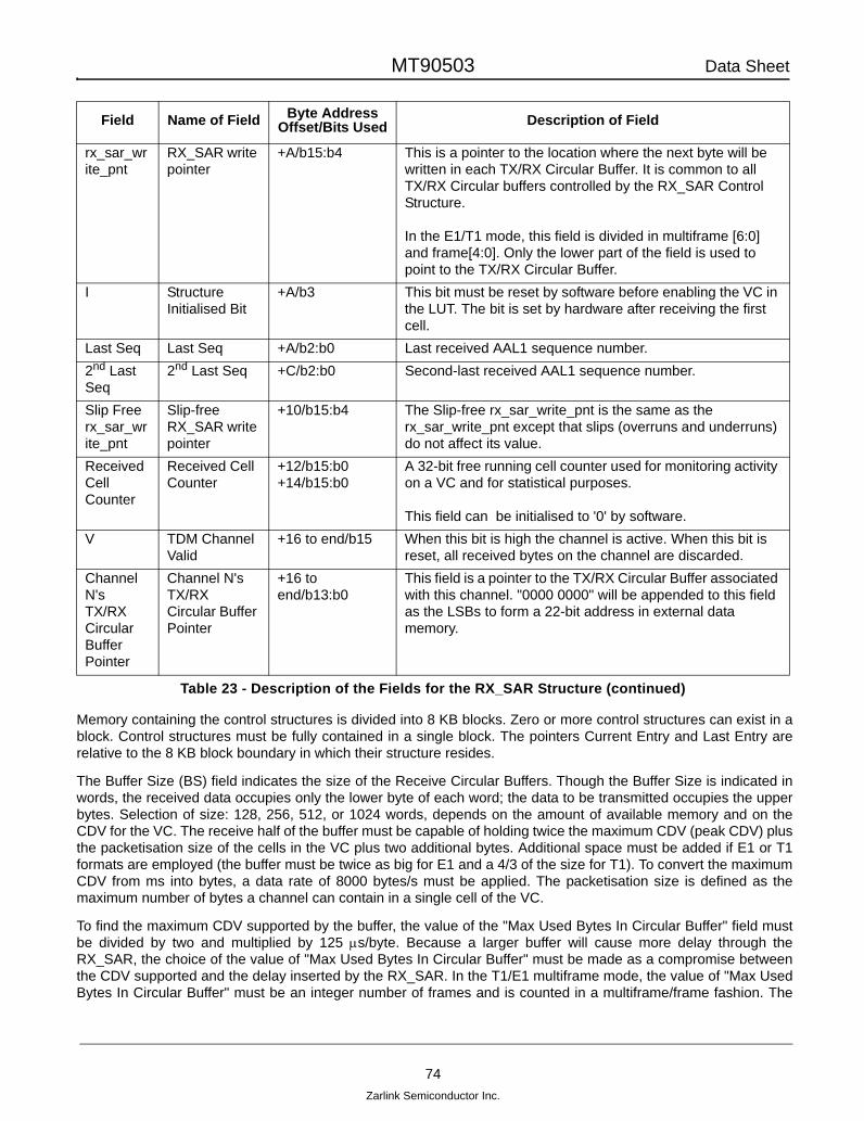
MT90503 Data Sheet
74Zarlink Semiconductor Inc.
Memory containing the control structures is divided into 8 KB blocks. Zero or more control structures can exist in ablock. Control structures must be fully contained in a single block. The pointers Current Entry and Last Entry arerelative to the 8 KB block boundary in which their structure resides.
The Buffer Size (BS) field indicates the size of the Receive Circular Buffers. Though the Buffer Size is indicated inwords, the received data occupies only the lower byte of each word; the data to be transmitted occupies the upperbytes. Selection of size: 128, 256, 512, or 1024 words, depends on the amount of available memory and on theCDV for the VC. The receive half of the buffer must be capable of holding twice the maximum CDV (peak CDV) plusthe packetisation size of the cells in the VC plus two additional bytes. Additional space must be added if E1 or T1formats are employed (the buffer must be twice as big for E1 and a 4/3 of the size for T1). To convert the maximumCDV from ms into bytes, a data rate of 8000 bytes/s must be applied. The packetisation size is defined as themaximum number of bytes a channel can contain in a single cell of the VC.
To find the maximum CDV supported by the buffer, the value of the "Max Used Bytes In Circular Buffer" field mustbe divided by two and multiplied by 125 µs/byte. Because a larger buffer will cause more delay through theRX_SAR, the choice of the value of "Max Used Bytes In Circular Buffer" must be made as a compromise betweenthe CDV supported and the delay inserted by the RX_SAR. In the T1/E1 multiframe mode, the value of "Max UsedBytes In Circular Buffer" must be an integer number of frames and is counted in a multiframe/frame fashion. The
rx_sar_write_pnt
RX_SAR write pointer
+A/b15:b4 This is a pointer to the location where the next byte will be written in each TX/RX Circular Buffer. It is common to all TX/RX Circular buffers controlled by the RX_SAR Control Structure.
In the E1/T1 mode, this field is divided in multiframe [6:0] and frame[4:0]. Only the lower part of the field is used to point to the TX/RX Circular Buffer.
I Structure Initialised Bit
+A/b3 This bit must be reset by software before enabling the VC in the LUT. The bit is set by hardware after receiving the first cell.
Last Seq Last Seq +A/b2:b0 Last received AAL1 sequence number.2nd Last Seq
2nd Last Seq +C/b2:b0 Second-last received AAL1 sequence number.
Slip Free rx_sar_write_pnt
Slip-free RX_SAR write pointer
+10/b15:b4 The Slip-free rx_sar_write_pnt is the same as the rx_sar_write_pnt except that slips (overruns and underruns) do not affect its value.
Received Cell Counter
Received Cell Counter
+12/b15:b0+14/b15:b0
A 32-bit free running cell counter used for monitoring activity on a VC and for statistical purposes.
This field can be initialised to '0' by software.V TDM Channel
Valid+16 to end/b15 When this bit is high the channel is active. When this bit is
reset, all received bytes on the channel are discarded.Channel N's TX/RX Circular Buffer Pointer
Channel N's TX/RX Circular Buffer Pointer
+16 to end/b13:b0
This field is a pointer to the TX/RX Circular Buffer associated with this channel. "0000 0000" will be appended to this field as the LSBs to form a 22-bit address in external data memory.
Field Name of Field Byte AddressOffset/Bits Used Description of Field
Table 23 - Description of the Fields for the RX_SAR Structure (continued)

MT90503 Data Sheet
75Zarlink Semiconductor Inc.
five MSBs select a number of multiframes and the five LSBs a number of frames. In strict muliframing, the five LSBsare always set to '00000'; they can be any value in FASTCAS.
Setting the multiframing standard in the circuit emulation (CE) field will change the way the information is read fromthe TDM circular buffers, as well as the standard that is used to interpret the p-byte. In addition, setting the CE bitsto a CAS setting will indicate to the RX_ SAR that CAS signalling bits should be expected at the end of the AAL1structure.
The payload size represents the number of TDM bytes in the cell and does not include pointer or AAL1-bytes.
4.4.3 Errors
Within the four categories of errors, there are eleven possible errors. All but slip errors (overruns and underruns)pertain only to AAL1 cells.
For the following errors, the only action taken is the generation of an error report structure (Section 4.4.4):
• CRC errors
• CRC/sequence number parity errors
• multiple cell loss
• p-byte parity
Format TDM Bytes Bytes Transmitted Payload Size
AAL1 with pointer, non-p-type cell 16 17 16AAL1 with pointer, p-type cell 16 18 16CBR-AAL0 16 16 16
Table 24 - Payload Sizes for Various Cell Formats
Category Error Coverage Example
AAL1 Byte CRC error AAL1 cellsCRC/Sequence
Number Parity errorAAL1 cells CSI = 1, CRC = 010, Seq. num = 110, parity bit = 1.
Even parity not observed: a parity error has occurred.Cell
loss/misinsertionSingle cell loss AAL1 cells Sequence numbers 1, 2, 4 received. Cell 3 has been
lostcell misinsertion AAL1 cells Sequence numbers 1, 2, 4, 3 received. A cell
misinsertion has occurredMultiple cell loss AAL1 cells Sequence numbers 1, 2, 5 received. Cells 3, 4 have
been lost.P-byte errors P-byte parity error AAL1 cells P-byte = 0100110, parity bit = 0. Even parity not
observed: a p-byte parity error has occurredP-byte out-of-range AAL1 cells P-byte received = 0x52, Structure length for that VC =
0x18. P-byte is too largeP-byte framing error AAL1 cells P-byte is 0x15 when 0x17 was expected.
P-byte absent AAL1 cellsSlip errors Overrun all cells See Figure 31.
Underrun all cells See Figure 31.
Table 25 - RX_SAR errors

MT90503 Data Sheet
76Zarlink Semiconductor Inc.
• out-of-range
• framing
• absent errors
It is the responsibility of the CPU and associated software to act upon notification that an error has occurred. Theexceptions to this policy are
• single cell loss (a dummy cell is inserted and treated before accepting the received cell; the received cell counter is incremented by only one)
• cell misinsertion (the misinserted cell is discarded and the received cell counter is not incremented)
• overruns (data is lost and read/write pointers are adjusted)
• underruns (bytes are inserted according to information set in registers 0420h and read/write pointers are adjusted).
.
Figure 31 - Overrun and Underrun Examples
4.4.4 Error Report Structure
Four categories of errors can be enabled in the RX_SAR structure:
• slip errors
• cell loss & misinsertion errors
• AAL1 byte errors
• p-byte errors
For each cell containing an error for which the error category is enabled, an 8-byte error report structure isgenerated and stored in a FIFO in external control memory. From here, the CPU can read the FIFO and treat theerrors.
INVALID BYTE
Overrun
Max used bytes
in RX
Circ. B
uff.
INVALID BYTE
VALID BYTE
VALID BYTE
VALID BYTE
VALID BYTE
INVALID BYTE
TDM read
pointer
RX_SAR
Write pointer
VALID BYTE
VALID BYTE
VALID BYTE
VALID BYTE
Underrun
Max used bytes
in RX
Circ. B
uff.
INVALID BYTE
TDM read
pointer
RX_SAR
INVALID BYTE
INVALID BYTE
INVALID BYTE
INVALID BYTE
INVALID BYTE
INVALID BYTE
INVALID BYTE
INVALID BYTE
INVALID BYTE
VALID BYTE
VALID BYTE
VALID BYTE
INVALID BYTE
INVALID BYTE
INVALID BYTE
INVALID BYTE
INVALID BYTE
TDM read
pointer
RX_SAR
Write pointer
Normal
Max used bytes
in RX
Circ. B
uff.
INVALID BYTE WritePointer
Note: For a description of Max Used Bytes in Circular Buffer see Table 23 (+4/b15:b6).

MT90503 Data Sheet
77Zarlink Semiconductor Inc.
As per the Data Cell FIFO, the CPU can read the error FIFO at any time after obtaining the address to the FIFO(registers 0714h, 0716h) and the read pointer to the RX_SAR Error Report Structure (register 0710h). Again, aninterrupt can be generated that will trigger if either of two events occurs: when the FIFO becomes more than half fullor if an error report structure has been present in the FIFO for longer than a programmable period of time (register0724h, 0726h). This interrupt can be enabled in register 0220h.
Errors of more than one type on the same cell will result in one error report structure being created indicating alltypes of errors on that cell. The exception to this is cell misinsertion. Since the cell is discarded once themisinsertion has been detected, no further errors can be found on the misinserted cell.
Figure 32 - RX_SAR Error Report Structure
Field Name of FieldByte Address
Offset/bits Used
Description of Field
RX_SAR Structure Base Address [19:5]
RX_SAR Structure Base Address [19:5]
+0/b14:b0 Base address of the RX_SAR Control Structure that caused the Error Report Structure to be generated. Appended with "00000" as the LSBs to form a 20-bit address.
Seq Sequence Number
+2/b2:b0 Sequence number of the cell that caused the Error Report Structure to be generated.
Last Seq Last Sequence Number
+2/b5:b3 Sequence number of the cell which preceded the one that caused the Error Report Structure to be generated.
Received Cell Counter
Received Cell Counter
+4/b15:b0+6/b15:b0
Cell number of the cell that caused the Error Report Structure to be generated.
PA P-Byte Absent Error
+0/b15 A p-byte was expected but was not detected in the cell that caused the error.
PF P-Byte Framing Error
+2/b15 The p-byte that was detected did not match the p-byte that was expected.
PR P-Byte Range Error
+2/b14 The p-byte that was detected was out-of-range; the 7-bit p-byte must not be 94-126 and must be less than the sequence length of the corresponding VC. 127 signifies a dummy offset value.
PP P-Byte Parity Error
+2/b13 The p-byte detected did not match its parity bit.
AC AAL1 Byte CRC-3 Error
+2/b12 There was an error detected in the CRC-3.
AP AAL1 Byte Parity Error
+2/b11 The AAL1 byte detected did not match its parity bit.
Table 26 - Description of the Fields for the RX_SAR Error Report Structure
Received Cell Counter [15:0]Received Cell Counter [31:16]
Last Seq SeqRX_SAR Structure Base Address[19:5]
PF PR PP AC AP OR UR M ML SLPA
b15 b14 b13 b12 b11 b10 b9 b8 b7 b6 b5 b4 b3 b1 b0b2
+0
+2+4
+6

MT90503 Data Sheet
78Zarlink Semiconductor Inc.
OR Overrun Slip +2/b10 The circular buffer associated with a channel receiving data from the cell was overrun.
UR Underrun Slip +2/b9 The circular buffer associated with a channel receiving data from the cell was underrun.
M Cell Misinsertion +2/b8 The sequence number of the cell indicated that a cell was misinserted. This error is always preceded by a single cell loss.
ML Multiple Cell Loss
+2/b7 The sequence number of the cell indicated that multiple cells were lost.
SL Single Cell Loss +2/b6 The sequence number of the cell indicated that a single cell was lost.
Table 26 - Description of the Fields for the RX_SAR Error Report Structure (continued)

MT90503 Data Sheet
79Zarlink Semiconductor Inc.
4.5 UTOPIA Module
4.5.1 Overview
The purpose of the UTOPIA module is to provide an external interface with the ATM domain. The MT90503complies with The ATM Forum’s specifications: af-phy-0017.000 and af-phy-0039.000. The MT90503 usesoctet-level handshaking on its UTOPIA interface.
The UTOPIA module is responsible for accepting cells from four input interfaces, examining the cells and, based onthe source and information in the header, sending the cell to one or more of the four output interfaces. The UTOPIAmodule also calculates and appends the HEC to outgoing ATM cells.
Figure 33 - UTOPIA Module
The UTOPIA interface consists of three ports, labelled A, B, and C. Port A is a Level-2 ATM (single PHY), singlePHY or multi-PHY port and can operate at 50 MHz. Port B is a Level-2 ATM (single PHY) or single PHY port andcan operate at 50 MHz. It is restricted to an 8-bit data bus when port A is in multi-PHY mode. Port C is a Level-1ATM or PHY port.
In addition to ports A, B, and C, the UTOPIA accepts cells from the TX_SAR and routes cells to the RX_SAR and tothe data cell FIFO in external control memory.
4.5.2 UTOPIA Interfaces
Each of the three ports is divided into two portions: a receive portion and a transmit portion. The TX_SAR and thereceive portions are each connected to a 4-cell FIFO. These FIFOs are read on a round-robin basis by the CellRouter (See “Cell Router” on page 82.).
The RX_SAR and the transmit portions are each connected to a 32-cell FIFO.
The ports are configurable with the following options:
• Port A’s transmit portion can be ATM, PHY, with a 16-bit or 8-bit data bus.
Append RXStructure Pointer
AAL1 Byte A B
Control Memory Interface
Cell FIFO(32 cells)
Cell FIFO(32 cells)
Cell FIFO(32 cells)
Cell FIFO(32 cells)
Cell FIFO(4 cells)
Cell FIFO(4 cells)
Cell FIFO(4 cells)
Cell FIFO(4 cells)
TXA UTOPIA Interface(external)
TXB UTOPIA Interface(external)
TXC UTOPIA Interface(external)
RX_SAR Interface(internal)
RXA UTOPIA Interface(external)
RXB UTOPIA Interface(external)
RXC UTOPIA Interface(external)
TX_SAR Interface(internal)
SRTS and Adaptive Clock Recovery Interface
rxa_clk domain
rxb_clk domain
rxc_clk domain
txa_clk domain
txb_clk domain
txc_clk domain mclk domain
Unknown cellsMatch & Mask
LUT
Discard
Known cells
Cell Router

MT90503 Data Sheet
80Zarlink Semiconductor Inc.
• Port A’s receive portion can be ATM or PHY, with a 16-bit or 8-bit data bus.
• Port A can be Level-2 multi-PHY.
• Port B’s transmit portion can be ATM or PHY, with a 16-bit or 8-bit data bus.*
• Port B’s receive portion can be ATM or PHY, with a 16-bit or 8-bit data bus.*
• Port C’s transmit portion can be ATM or PHY, with an 8-bit data bus.
• Port C’s receive portion can be ATM or PHY, with an 8-bit data bus.
*When Port A is in Level-2 multi-PHY mode, Port B must have an 8-bit data bus.
Each receive interface can be independently enabled or disabled. If disabled, the receive interface will stopaccepting cells after the current cell has been received.
When the transmit portions of a port are in PHY mode, the SOC, data bus, and parity output pins can be tristatedwhen the port is not selected. This allows the MT90503 to share a data bus, SOC, and parity lines with otherdevices (i.e. independent ENB signals and CLAV signals for each PHY device, controlled by a single ATM device).
In the case of a receive PHY, the generation of the rx_clav signal is independent of the state machine. The rx_clavsignal is asserted high at any time when a complete cell can be received. Thus as soon as the first byte of a cell isreceived, and there is no room for another cell in the input FIFO, the rx_clav signal will be asserted low. In the caseof a Level-2 PHY, the rx_clav’s will only be driven when the address was placed on the bus during the previouscycle.
4.5.3 Errors on received cells
If the MT90503 receives a short cell on any one of its three ports, the cell will be discarded, and a new cell will bestarted when the second SOC signal is set.
If the SOC is not set after the 53rd byte of a received cell, subsequent bytes are ignored until a a new SOC isreceived.
Data received on all of the three ports is examined for parity errors and an interrupt is raised if an error is found.Cells are not discarded if a parity error is detected. Register 0304h indicates on which port the parity error isdetected.
The ATM HEC is not examined on received cells.

MT90503 Data Sheet
81Zarlink Semiconductor Inc.
4.5.4 Transmit and Receive State Machines for ATM and PHY Modes
Figure 34 - ATM Mode State Machines
Figure 35 - PHY Mode State Machines
Idle(rx_enb=0)
rx_clav=0OR
rx_soc=0
rx_clav=1AND
rx_soc=1
Rx 1stByte
RxNext Byte53 bytes
received
rx_clav=1
<53 BytesAND
rx_clav=1
Idlerx_clav=0
<53 BytesAND
rx_clav=0
rx_clav=1
rx_clav=0Discard
Cell
rx_clav=1AND
rx_soc=1
Idle(rx_enb=1)
No roomfor 1 cell
Room for1 cell
No roomfor 1 cell
Room for atleast 1 cell
IdleCell not available
ORtx_clav=0
Cell availableAND
tx_clav=1
Tx 1stByte
(tx_soc=1,tx_enb=0)
TxNext Byte(tx_soc=0,tx_enb=0)
53 bytessent
tx_clav=1
<53 BytesAND
tx_clav=1
Idletx_clav=0
<53 BytesAND
tx_clav=0
tx_clav=1
tx_clav=0
Transmit State Machine
Receive State Machine
Idle(rx_clav=0)
rx_enb=1**OR
rx_soc=0
rx_enb=0*AND
rx_soc=1
Rx 1stByte
RxNext Byte53 bytes
received
rx_enb=0*
<53 BytesAND
rx_enb=0*
Idlerx_enb=1**
<53 BytesAND
rx_enb=1**
rx_enb=0*
rx_enb=1**Discard
Cell
rx_enb=0*AND
rx_soc=1
Idle(rx_clav=1)
No roomfor 1 cell
Room for1 cell
No roomfor 1 cell
Room for atleast 1 cell
* If MPHY L2, add “AND rx_addr matches”** If MPHY L2, add “OR rx_addr doesn’t match”
NOTE: PHY Mode Transmit and Receive refers to the directionof cells as per the UTOPIA specification.
IdleCell not available
ORtx_enb=1**
Cell availableAND
tx_enb=0*
Tx 1stByte
(tx_soc=1,tx_clav=1)
TxNext Byte(tx_soc=0,tx_clav=1)
53 bytessent
tx_enb=0*
<53 BytesAND
tx_enb=0*
Idletx_enb=1**
<53 BytesAND
tx_enb=1**
tx_enb=0*
tx_enb=1**
Transmit State Machine
Receive State Machine

MT90503 Data Sheet
82Zarlink Semiconductor Inc.
4.5.5 Cell Router
Cells are read on a round-robin basis from the four input FIFOs. Cells from the TX_SAR that contain a ’0’ in theMSB of the TXD field (see Figure 36 on page 82) are written into the output FIFOs designated by the three LSBs ofthe TXD field. Cells from the TX_SAR that contain a ’1’ in the MSB of the TXD field and cells from the RXA, RXB,and RXC ports are handled based on the VPI/VCI of the cell. The TXD field for a cell is the same as the TXD field inthe TX_SAR control structure that created the cell (see Figure 29 on page 65).
Cells written into the RX_SAR output FIFO can be directed to the SAR portion (cells to be formatted into TDMstreams), to the data cell portion (to be examined by the CPU), or to both. This is indicated by the RXD field in cellswritten into the RX_SAR output FIFO.
Figure 36 - Cell Format for cells in internal UTOPIA input and output cell FIFOs
GFCb15 b14 b13 b12 b11 b10 b9 b8 b7 b6 b5 b4 b3 b2 b1 b0
VPI VCI[15:12]OAM
CLP
Payload Byte 44
TXD
RX Structure Pointer
Reserved
GFC: Generic Flow ControlVPI: Virtual Path IdentifierVCI: Virtual Circuit IdentifierOAM: Management Cell. When this bit is set, the cell does not contain TDM bytes and is handled as an OAM cell.PTI: Payload Type Indicator.CLP: Cell Loss Priority (this bit is not examined by the MT90503).Payload Byte X: Payload byte in ATM cell (48 bytes total, numbered 0 to 47).TXD: TX_SAR Destination Field.
"0000" = discard cell"0xx1" = Send to TXA port"0x1x" = Send to TXB port"01xx" = Send to TXC port"1001" = Treat as cell from RXA port"1010" = Treat as cell from RXB port"1100" = Treat as cell from RXC portothers = reserved
RXD: RX_SAR destination field."00" = reserved"x1" = Data Cell (write in RX Data Cell FIFO in external control memory)"1x" = RX_SAR CBR Cell (disassemble this cell with structure pointed to by RX Structure Pointer (Normal) field)
RX Structure Pointer: Pointer to the RX_SAR Structure that will be used to process the current cell. Concatenated with "00000" to form a wp-bit address. (see RX_SAR structure).
Note that RXA, RXB, and RXC input FIFOs do not contain any field beyond Payload Byte 47. Also note that the TX_SAR input FIFO does not contain any field beyond TXD. The TXD field is not written in any of the output FIFOs
Note: The HEC field of the ATM cell is calculated and added for outgoing cells after the cell leaves the FIFO.
+0h
+2h
+4h
+6h
+30h
+32h
+34h
+36h
+38h
+3Ah
+3Ch
+3Eh
Payload Byte 1
Payload Byte 3
Payload Byte 46
GFC
Payload Byte 2
Payload Byte 0
Payload Byte 45
Payload Byte 47
PTI
RXD
VCI[11:0]
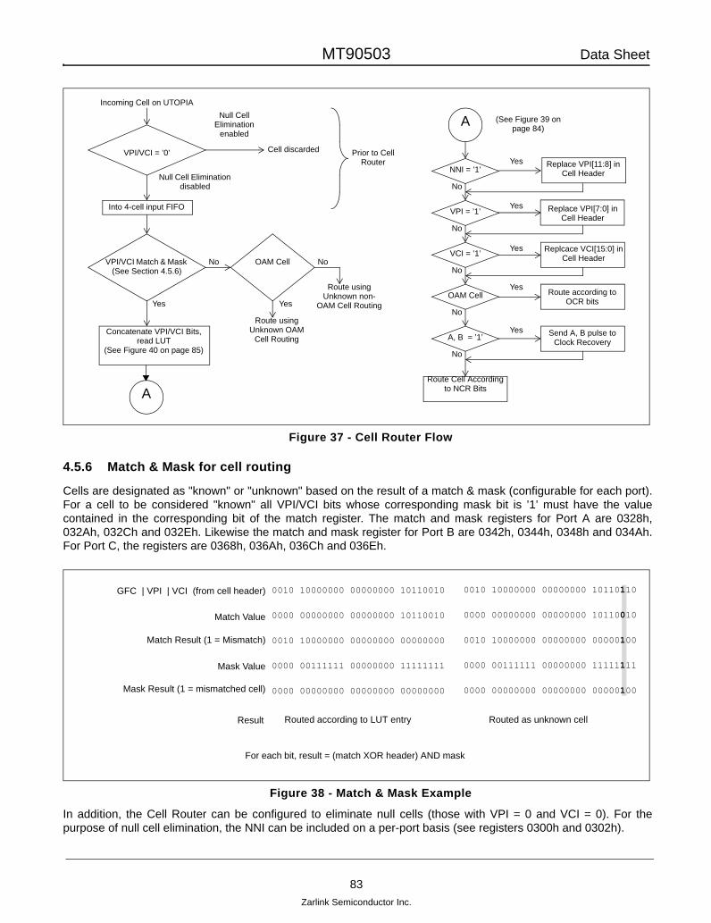
MT90503 Data Sheet
83Zarlink Semiconductor Inc.
Figure 37 - Cell Router Flow
4.5.6 Match & Mask for cell routing
Cells are designated as "known" or "unknown" based on the result of a match & mask (configurable for each port).For a cell to be considered "known" all VPI/VCI bits whose corresponding mask bit is ’1’ must have the valuecontained in the corresponding bit of the match register. The match and mask registers for Port A are 0328h,032Ah, 032Ch and 032Eh. Likewise the match and mask register for Port B are 0342h, 0344h, 0348h and 034Ah.For Port C, the registers are 0368h, 036Ah, 036Ch and 036Eh.
Figure 38 - Match & Mask Example
In addition, the Cell Router can be configured to eliminate null cells (those with VPI = 0 and VCI = 0). For thepurpose of null cell elimination, the NNI can be included on a per-port basis (see registers 0300h and 0302h).
Replace VPI[7:0] in Cell Header
Replace VPI[11:8] in Cell Header
Incoming Cell on UTOPIA
Cell discarded
VPI/VCI Match & Mask (See Section 4.5.6)
OAM CellNo
Route using Unknown non-
OAM Cell Routing
No
Route using Unknown OAM
Cell Routing
YesYes
A
A
NNI = ’1’
VPI = ’1’
VCI = ’1’
OAM Cell
A, B = ’1’
Yes
No
No
No
No
No
Route Cell According to NCR Bits
(See Figure 39 on page 84)
Yes
Yes
Yes
Yes
Replcace VCI[15:0] in Cell Header
Route according to OCR bits
Send A, B pulse to Clock Recovery
VPI/VCI = ’0’
Null Cell Elimination
enabled
Null Cell Elimination disabled
Prior to Cell Router
Concatenate VPI/VCI Bits, read LUT
(See Figure 40 on page 85)
Into 4-cell input FIFO
GFC | VPI | VCI (from cell header) 0010 10000000 00000000 10110010
0000 00000000 00000000 10110010
0010 10000000 00000000 00000000
0000 00111111 00000000 11111111
0000 00000000 00000000 00000000
0010 10000000 00000000 10110110
0000 00000000 00000000 10110010
0010 10000000 00000000 00000100
0000 00111111 00000000 11111111
0000 00000000 00000000 00000100
Match Value
Match Result (1 = Mismatch)
Mask Value
Mask Result (1 = mismatched cell)
Result Routed according to LUT entry Routed as unknown cell
For each bit, result = (match XOR header) AND mask
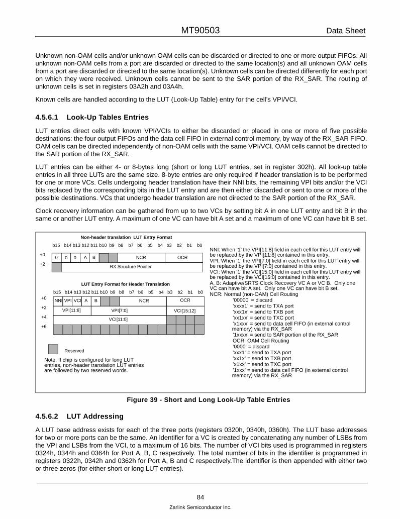
MT90503 Data Sheet
84Zarlink Semiconductor Inc.
Unknown non-OAM cells and/or unknown OAM cells can be discarded or directed to one or more output FIFOs. Allunknown non-OAM cells from a port are discarded or directed to the same location(s) and all unknown OAM cellsfrom a port are discarded or directed to the same location(s). Unknown cells can be directed differently for each porton which they were received. Unknown cells cannot be sent to the SAR portion of the RX_SAR. The routing ofunknown cells is set in registers 03A2h and 03A4h.
Known cells are handled according to the LUT (Look-Up Table) entry for the cell’s VPI/VCI.
4.5.6.1 Look-Up Tables Entries
LUT entries direct cells with known VPI/VCIs to either be discarded or placed in one or more of five possibledestinations: the four output FIFOs and the data cell FIFO in external control memory, by way of the RX_SAR FIFO.OAM cells can be directed independently of non-OAM cells with the same VPI/VCI. OAM cells cannot be directed tothe SAR portion of the RX_SAR.
LUT entries can be either 4- or 8-bytes long (short or long LUT entries, set in register 302h). All look-up tableentries in all three LUTs are the same size. 8-byte entries are only required if header translation is to be performedfor one or more VCs. Cells undergoing header translation have their NNI bits, the remaining VPI bits and/or the VCIbits replaced by the corresponding bits in the LUT entry and are then either discarded or sent to one or more of thepossible destinations. VCs that undergo header translation are not directed to the SAR portion of the RX_SAR.
Clock recovery information can be gathered from up to two VCs by setting bit A in one LUT entry and bit B in thesame or another LUT entry. A maximum of one VC can have bit A set and a maximum of one VC can have bit B set.
Figure 39 - Short and Long Look-Up Table Entries
4.5.6.2 LUT Addressing
A LUT base address exists for each of the three ports (registers 0320h, 0340h, 0360h). The LUT base addressesfor two or more ports can be the same. An identifier for a VC is created by concatenating any number of LSBs fromthe VPI and LSBs from the VCI, to a maximum of 16 bits. The number of VCI bits used is programmed in registers0324h, 0344h and 0364h for Port A, B, C respectively. The total number of bits in the identifier is programmed inregisters 0322h, 0342h and 0362h for Port A, B and C respectively.The identifier is then appended with either twoor three zeros (for either short or long LUT entries).
b15 b14 b13 b12 b11 b10 b9 b8 b7 b6 b5 b4 b3 b2 b1 b0
+0
+2
b15 b14 b13 b12 b11 b10 b9 b8 b7 b6 b5 b4 b3 b2 b1 b0+0
+2
+4
+6
Reserved
LUT Entry Format for Header Translation
Non-header translation LUT Entry Format
NNI: When ’1’ the VPI[11:8] field in each cell for this LUT entry will be replaced by the VPI[11:8] contained in this entry. VPI: When ’1’ the VPI[7:0] field in each cell for this LUT entry will be replaced by the VPI[7:0] contained in this entry.VCI: When ’1’ the VCI[15:0] field in each cell for this LUT entry will be replaced by the VCI[15:0] contained in this entry. A, B: Adaptive/SRTS Clock Recovery VC A or VC B. Only one VC can have bit A set. Only one VC can have bit B set.NCR: Normal (non-OAM) Cell Routing
’00000’ = discard’xxxx1’ = send to TXA port’xxx1x’ = send to TXB port’xx1xx’ = send to TXC port’x1xxx’ = send to data cell FIFO (in external control memory) via the RX_SAR’1xxxx’ = send to SAR portion of the RX_SAROCR: OAM Cell Routing’0000’ = discard’xxx1’ = send to TXA port’xx1x’ = send to TXB port’x1xx’ = send to TXC port’1xxx’ = send to data cell FIFO (in external control memory) via the RX_SAR
Note: If chip is configured for long LUT entries, non-header translation LUT entries are followed by two reserved words.
NCR OCR0 0 0 A B
RX Structure Pointer
NNI VPI VCI A B NCR OCR
VCI[15:12]VPI[11:8] VPI[7:0]
VCI[11:0]
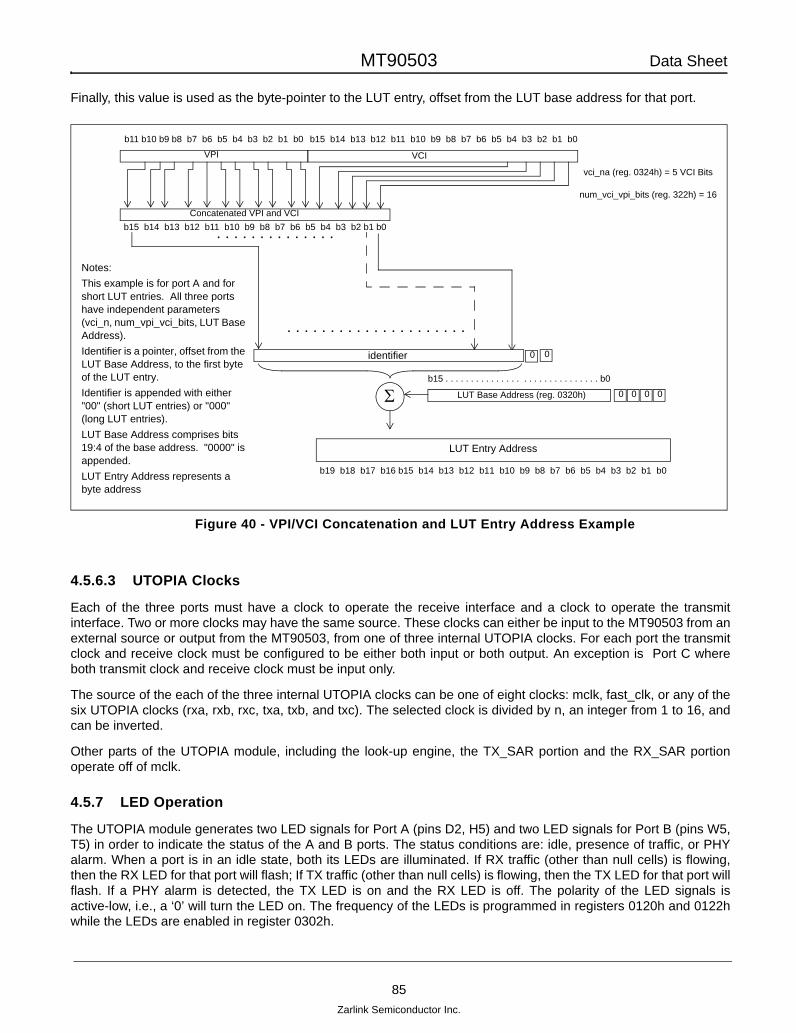
MT90503 Data Sheet
85Zarlink Semiconductor Inc.
Finally, this value is used as the byte-pointer to the LUT entry, offset from the LUT base address for that port.
Figure 40 - VPI/VCI Concatenation and LUT Entry Address Example
4.5.6.3 UTOPIA Clocks
Each of the three ports must have a clock to operate the receive interface and a clock to operate the transmitinterface. Two or more clocks may have the same source. These clocks can either be input to the MT90503 from anexternal source or output from the MT90503, from one of three internal UTOPIA clocks. For each port the transmitclock and receive clock must be configured to be either both input or both output. An exception is Port C whereboth transmit clock and receive clock must be input only.
The source of the each of the three internal UTOPIA clocks can be one of eight clocks: mclk, fast_clk, or any of thesix UTOPIA clocks (rxa, rxb, rxc, txa, txb, and txc). The selected clock is divided by n, an integer from 1 to 16, andcan be inverted.
Other parts of the UTOPIA module, including the look-up engine, the TX_SAR portion and the RX_SAR portionoperate off of mclk.
4.5.7 LED Operation
The UTOPIA module generates two LED signals for Port A (pins D2, H5) and two LED signals for Port B (pins W5,T5) in order to indicate the status of the A and B ports. The status conditions are: idle, presence of traffic, or PHYalarm. When a port is in an idle state, both its LEDs are illuminated. If RX traffic (other than null cells) is flowing,then the RX LED for that port will flash; If TX traffic (other than null cells) is flowing, then the TX LED for that port willflash. If a PHY alarm is detected, the TX LED is on and the RX LED is off. The polarity of the LED signals isactive-low, i.e., a ‘0’ will turn the LED on. The frequency of the LEDs is programmed in registers 0120h and 0122hwhile the LEDs are enabled in register 0302h.
0 0 0 0LUT Base Address (reg. 0320h)
b11 b10 b9 b8 b7 b6 b5 b4 b3 b2 b1 b0 b15 b14 b13 b12 b11 b10 b9 b8 b7 b6 b5 b4 b3 b2 b1 b0
Notes:This example is for port A and for short LUT entries. All three ports have independent parameters (vci_n, num_vpi_vci_bits, LUT Base Address).Identifier is a pointer, offset from the LUT Base Address, to the first byte of the LUT entry.Identifier is appended with either "00" (short LUT entries) or "000" (long LUT entries).LUT Base Address comprises bits 19:4 of the base address. "0000" is appended.LUT Entry Address represents a byte address
LUT Entry Address
VCIVPI
vci_na (reg. 0324h) = 5 VCI Bits
Concatenated VPI and VCIb15 b14 b13 b12 b11 b10 b9 b8 b7 b6 b5 b4 b3 b2 b1 b0. . . . . . . . . . . . . .
. . . . . . . . . . . . . . . . . . . . .
identifier
Σ
b19 b18 b17 b16 b15 b14 b13 b12 b11 b10 b9 b8 b7 b6 b5 b4 b3 b2 b1 b0
b15 . . . . . . . . . . . . . . . . . . . . . . . . . . . . . . b0
00
num_vci_vpi_bits (reg. 322h) = 16

MT90503 Data Sheet
86Zarlink Semiconductor Inc.
Figure 41 - UTOPIA Clock Generation
4.5.8 UTOPIA Flow Control
The UTOPIA module contains the ability to prevent cells in the 4-cell input FIFOs (RXA, RXB, RXC, and TX_SAR)from being handled by the UTOPIA module in the case that the 32-cell output FIFOs (TXA, TXB, TXC, andRX_SAR) exceed programmable levels.
An input FIFO will be blocked when the level of any output FIFO exceeds the level set for that combination of outputFIFO and input FIFO. The levels can be set independently to 1 to 31 cells or to 0, which means no flow control willbe exerted (see registers 0338h-033Ah, 0358h-035Ah, 0378h-037Ah). Cell arrival counters and cell departurecounters for each port, stored in registers (0330h-0336h, 0350h-0356h, 0370-0376h, 0390-0396h), are used tomonitor the fill levels of each output FIFO.
4.5.9 External Interface Signals
Due to the different possible configurations of the UTOPIA ports, the functions of some pins change, depending onthe configuration. Some unused data pins when port A and/or port B are in 8-bit mode become general purposeinputs and/or outputs. When Level-2 addressing is in place for port A, portions of the port B data buses are used foras port A addressing pins. The function of the clav (cell available) and enb (enable data transfer) pins alternatewhen the port is in ATM mode or PHY mode (Figure 42 on page 87).
Please note that the I/O direction of the pins remains the same.
mclk
fast_clk
rxa_clk
rxc_clk
txa_clk
txb_clk
rxb_clk
txc_clk
Divider by n (n=1 to 16)
utopia_clk_1
Inversion
One of three UTOPIA clock generators
utopia_clk_1
utopia_clk_2
utopia_clk_3
rxa_clk
One of six UTOPIA Clocks

MT90503 Data Sheet
87Zarlink Semiconductor Inc.
Figure 42 - External UTOPIA Interface
4.6 Clock Recovery Module
4.6.1 Overview
The purpose of the clock recovery module is to synchronise the TDM clock domain of the MT90503 with otherdevices on the network through information transmitted across the ATM link. Clock recovery is necessary onlywhen the MT90503 is operating as the TDM clock master.
The clock recovery system is composed of several sub-components:
4.6.1.1 Two Point Generation Modules
The point generation modules permit SRTS and/or adaptive clock recovery to be performed by the MT90503. Thetwo modules provide the flexibility to have a back up clock recovery process operating from another VC and/or ofthe complementary type. These modules generate points which are written to control memory and subsequentlyused by the clock recovery algorithm.
4.6.1.2 One SRTS (synchronous residual time stamp) Generating Module
The SRTS generating module, is employed to generate the 4-bit outgoing RTS value.
4.6.1.3 Three Integer Divisor Clock Modules
The integer divisor clock (idclk) modules are designed to manipulate any incoming or internal clocks and producean 8kHz idclk. They provide the flexibility of inverting the clock before or after division, option of setting the duty
PHY Device MT90503 - ATM Mode
txa_clk (H3)
txa_soc (N2)
txa_enb (H2)
txa_clav (J5)
txa_d (N4 . . .)
txa_par (N3)
txclk
txenb
txclav
txsoc
txdata
txpar
rxa_clk (C6)
rxa_soc (H4)
rxa_enb (B6)
rxa_clav (A6)
rxa_d (G3 . . .)
rxa_par (G2)
rxclk
rxenb
rxclav
rxsoc
rxdata
rxpar
MT90503 - PHY Mode
txa_clk (H3)
txa_soc (N2)
txa_enb (J5)
txa_clav (H2)
txa_d (N4 . . .)
txa_par (N3)
rxclk
rxenb
rxclav
rxsoc
rxdata
rxpar
rxa_clk (C6)
rxa_soc (H4)
rxa_enb (A6)
rxa_clav (B6)
rxa_d (G3 . . .)
rxa_par (G2)
txclk
txenb
txclav
txsoc
txdata
txpar
ATM Device
Port A, PHY modePort A, ATM Mode

MT90503 Data Sheet
88Zarlink Semiconductor Inc.
cycle to 50%, 16-bit division and checking of the frequency (within a desired range). Along with the idclk_losssignals, idclk’s are suited to being sent to an external PLL.
4.6.1.4 Two Precise Clock Modules
The precise clock (pclk) modules are used to divide mclk down to pclk_a and pclk_b. Each module has a pclk_lossindicator which can be employed in tandem with the pclk signal to be routed to an external PLL. The division of mclkis performed with a 16-bit integer and a 16-bit fraction, allowing for precise specification of the pclk frequency.These modules are ideally suited to being programmed by the clock recovery algorithm to generate the recoveredclock.
4.6.1.5 Eleven Multiplexers
The 11 multiplexers are: recov_a to recov_h, ct_netref1, ct_netref2 and local_netref_16m. recov_a through recov_hand ct_netrefx are general I/O pins. Local_netref_16m is an internal node, used as the master clock for the TDMsection of the MT90503.
4.6.2 Multiplexers
There are eleven multiplexers (see Table 28, “Source Selection,” on page 89) with 36 possible inputs each (seeTable 29, “idclk_a Register,” on page 91):
Signal Address Bits
recov_a 0860h 13:8
recov_b 0860h 5:0
recov_c 0862h 13:8
recov_d 0862h 5:0
recov_e 0864h 13:8
recov_f 0864h 5:0
recov_g 0866h 13:8
recov_h 0866h 5:0
ct_netref1 0868h 13:8
ct_netref2 0868h 5:0
local_netref_16m 086Ah 5:0
Table 27 - Multiplexer Registers
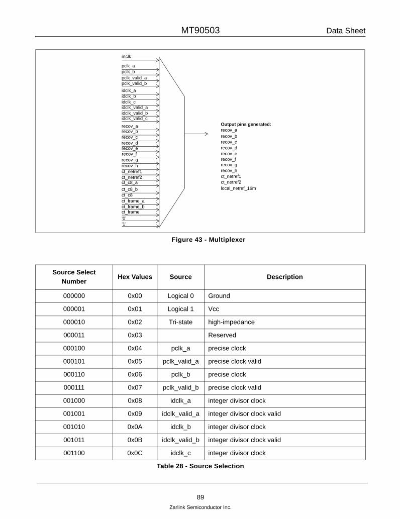
MT90503 Data Sheet
89Zarlink Semiconductor Inc.
Figure 43 - Multiplexer
Source Select Number
Hex Values Source Description
000000 0x00 Logical 0 Ground
000001 0x01 Logical 1 Vcc
000010 0x02 Tri-state high-impedance
000011 0x03 Reserved
000100 0x04 pclk_a precise clock
000101 0x05 pclk_valid_a precise clock valid
000110 0x06 pclk_b precise clock
000111 0x07 pclk_valid_b precise clock valid
001000 0x08 idclk_a integer divisor clock
001001 0x09 idclk_valid_a integer divisor clock valid
001010 0x0A idclk_b integer divisor clock
001011 0x0B idclk_valid_b integer divisor clock valid
001100 0x0C idclk_c integer divisor clock
Table 28 - Source Selection
mclk
pclk_apclk_b
pclk_valid_bidclk_aidclk_b
pclk_valid_a
idclk_cidclk_valid_aidclk_valid_bidclk_valid_c
recov_arecov_brecov_crecov_drecov_erecov_frecov_grecov_hct_netref1ct_netref2ct_c8_act_c8_bct_c8ct_frame_act_frame_bct_frame’0’’1’
Output pins generated:recov_arecov_brecov_crecov_drecov_erecov_frecov_grecov_hct_netref1ct_netref2local_netref_16m

MT90503 Data Sheet
90Zarlink Semiconductor Inc.
4.6.3 Integer Divisor Clocks (idclk)
There are three idclk modules in the MT90503. Each module consists primarily of a 16-bit integer clock divider, butalso has several clock manipulation circuits. These modules have the ability to flag an interrupt (if enabled - 0884h,08A4h, 08C4h) if the input frequency is above or below a desired range, invert the clock’s polarity (before and afterdivision) and set the percentage duty cycle to 50%. idclk_loss_x signals the loss (or incorrect frequency) of an inputsynchronisation clock, allowing the clock to easily be output to an external PLL. idclk_a is configured in the registerrange of 0880h-0894h as described in Table 29.
001101 0x0D idclk_valid_c integer divisor clock valid
001110 0x0E Reserved
001111 0x0F Reserved
010000 0x10 recov_a external I/O pin
010001 0x11 recov_b external I/O pin
010010 0x12 recov_c external I/O pin
010011 0x13 recov_d external I/O pin
010100 0x14 recov_e external I/O pin
010101 0x15 recov_f external I/O pin
010110 0x16 recov_g external I/O pin
010111 0x17 recov_h external I/O pin
011000 0x18 ct_c8 active clock: ct_c8_a or _b
011001 0x19 ct_c8_a TDM clock
011010 0x1A ct_c8_b TDM clock
011011 0x1B ct_frame active clock: ct_frame_a or _b
011100 0x1C ct_frame_a TDM clock
011101 0x1D ct_frame_b TDM clock
011110 0x1E ct_netref1 TDM clock
011111 0x1F ct_netref2 TDM clock
100000 0x20 ref_vca cell arrival on VC A
100001 0x21 ref_vcb cell arrival on VC B
100010 0x22 phy_alm_a PHY Alarm UTOPIA A
100011 0x23 phy_alm_b PHY Alarm UTOPIA B
100100 0x24 mclk master clock
Source Select Number
Hex Values Source Description
Table 28 - Source Selection (continued)

MT90503 Data Sheet
91Zarlink Semiconductor Inc.
These modules are ideally suited to dividing down the highly accurate reference clock (fn) required whenperforming SRTS clock recovery.
Register Bits Name Description
0880h [0] divisor_load_now set to load new value
0880h [1] divisor_reset 0 for reset, 1 for normal operation
0880h [2] even_duty_cycle_select when 1, 50% duty cycle is generated
0880h [3] input_invert_select invert clock before dividing
0880h [4] output_invert_select invert clock after dividing
0880h [13:8] input_source_select see Table 28
0882h [5:0] status registers
0884h [5:0] interrupt enabling
0886h [5:0] manual setting of status registers
0888h [5:0] ext_loss_source_select external output of input clock status. See Table 28.
0888h [6] ext_loss_source_polarity if set to ’1’, source loss is active high
0888h [7] output_loss_polarity if ’1’ output loss is active high
088Ah [15:0] clk_div denominator of clock divider
0890h [15:0] freqchck_div denominator of frequency check divider
0892h [15:0] freqchck_max_mclk_cycles max # of mclk’s between rising edges of the input clock divided by freqchck_div, if failure occurs, freq_too_low (0882h) will be set.
0894h [15:0] freqchck_min_mclk_cycles min # of mclk’s between rising edges of the input clock divided by freqchck_div, if failure occurs, freq_too_high (0882h) will be set.
Note: idclk_b and idclk_c have a corresponding set of registers in the ranges of 08A0h - 08B4h and 08C0h - 08D4h respectively.
Table 29 - idclk_a Register

MT90503 Data Sheet
92Zarlink Semiconductor Inc.
Figure 44 - Integer Clock Processor
4.6.4 Precise Clocks (pclk)
The MT90503 has two digital PLL (pclk) modules. Using mclk as a source, the module will divide it with a 16-bitinteger and optional 16-bit fraction. The 16-bit fraction allows more precise specification on the output frequency.Using the optional 16-bit faction in a typical configuration, mclk = 80MHz, pclk_int_a = 10 000 and pclk_a = 8kHz,will increase the precision from 100 ppm to 1.5 ppm. Also, using the fractional divider will reduce the maximum jitterto one mclk period (12.5ns for 80MHz mclk). Set pclk_frc to 0 if no jitter insertion by the pclk module desired. Thedivider can be programmed dynamically and has a maximum response time of 125µs.
mclkct_c8_act_c8_bct_c8ct_frameact_framebct_framerecov_arecov_brecov_crecov_drecov_erecov_frecov_grecov_hct_netref
50% Duty Cycle Modifier 0880h[2]
Divider 088Ah,
0880h[1:0]
Clock Fre-quency Checker
0890-0894h
idclk_a
idclk_valid_a
0880h [4]0880h [3]
0880h [13:8]
50% Duty Cycle Modifier
08A0h[2]
Divider 08AAh,
08A0h[1:0]
Clock Frequency Checker
08B0-08B4h
idclk_b
idclk_valid_b
08A0h [4]08A0h [3]
08A0h [13:8]
50% Duty Cycle Modifier
08C0h[2]
Divider 08CAh,
08C0h[1:0]
Clock Frequency Checker
08D0-08D4h
idclk_c
idclk_valid_c
08C0h [4]08C0h [3]
08C0h [13:8]
mclkct_c8_act_c8_bct_c8ct_frameact_framebct_framerecov_arecov_brecov_crecov_drecov_erecov_frecov_grecov_hct_netref
mclkct_c8_act_c8_bct_c8ct_frameact_framebct_framerecov_arecov_brecov_crecov_drecov_erecov_frecov_grecov_hct_netref
08A0h [2]
08C0h [2]
0880h [2]

MT90503 Data Sheet
93Zarlink Semiconductor Inc.
The following registers are applicable:
The following equation illustrates the derived frequency of pclk from mclk:
4.6.5 Point Generation
The function of the point generation module is to place points in external memory which have been generated byeither the SRTS or Adaptive clock recovery methods. These points express the rates of the master device’s TDMclock (through a time stamp or the cell rate), the rate of the slave (performing the clock recovery) device’s masterclock and the rate of the slave device’s pclk. This allows the clock recovery algorithm to evaluate the respectiverates and make corrections to the pclk in order to synchronise with the master device.
There are two point generation modules. Each can be configured for SRTS or adaptive clock recovery. The twomodules each have a separate point generation process, separate timing reference and each is associated withone pclk module (i.e. pclk_a with adapsrts0 and pclk_b with adapsrts1). This allows switching between clockrecovery types and/or sources on the fly. The A and B bits of the UTOPIA look-up table determine which VCgenerates ref_vca and ref_vcb (see section 4.5.6.1 on page 84).
Register Name Description
0820h[5] adapsrts0_pclk_loss indicates state of clock
0820h[6] adapsrts0_pclk_divisor_load_now when set, pclk_div and pclk_frc are loaded into digital PLL.
0820h[7] adapsrts0_pclk_divisor_reset when ’0’ digital PLL is in reset state
0830h adapsrts0_pclk_div integer divider of pclk_a
0832h adapsrts0_pclk_frc fractional divider of pclk_a
0820h[5] adapsrts1_pclk_loss indicates state of clock
0840h[6] adapsrts1_pclk_divisor_load_now when set, pclk_div and pclk_frc are loaded into digital PLL.
0840h[7] adapsrts1_pclk_divisor_reset when ’0’ digital PLL is in reset state
0850h adapsrts1_pclk_div integer divider of pclk_b
0852h adapsrts1_pclk_frc fractional divider of pclk_b
Table 30 - pclk registers
Register Bits Name Module1 Description
0820h 0 adaptive_enable A ’1’ activates adaptive clock recovery
0820h 1 rx_srts_enable S ’1’ activates SRTS clock recovery
Table 31 - adapsrts0 Registers2
fpclkfmclk
pclkdivpclkfrc65536-----------------+
------------------------------------------=
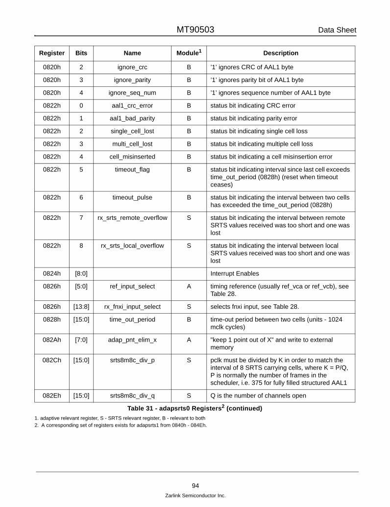
MT90503 Data Sheet
94Zarlink Semiconductor Inc.
0820h 2 ignore_crc B ’1’ ignores CRC of AAL1 byte
0820h 3 ignore_parity B ’1’ ignores parity bit of AAL1 byte
0820h 4 ignore_seq_num B ’1’ ignores sequence number of AAL1 byte
0822h 0 aal1_crc_error B status bit indicating CRC error
0822h 1 aal1_bad_parity B status bit indicating parity error
0822h 2 single_cell_lost B status bit indicating single cell loss
0822h 3 multi_cell_lost B status bit indicating multiple cell loss
0822h 4 cell_misinserted B status bit indicating a cell misinsertion error
0822h 5 timeout_flag B status bit indicating interval since last cell exceeds time_out_period (0828h) (reset when timeout ceases)
0822h 6 timeout_pulse B status bit indicating the interval between two cells has exceeded the time_out_period (0828h)
0822h 7 rx_srts_remote_overflow S status bit indicating the interval between remote SRTS values received was too short and one was lost
0822h 8 rx_srts_local_overflow S status bit indicating the interval between local SRTS values received was too short and one was lost
0824h [8:0] Interrupt Enables
0826h [5:0] ref_input_select A timing reference (usually ref_vca or ref_vcb), see Table 28.
0826h [13:8] rx_fnxi_input_select S selects fnxi input, see Table 28.
0828h [15:0] time_out_period B time-out period between two cells (units - 1024 mclk cycles)
082Ah [7:0] adap_pnt_elim_x A "keep 1 point out of X" and write to external memory
082Ch [15:0] srts8m8c_div_p S pclk must be divided by K in order to match the interval of 8 SRTS carrying cells, where K = P/Q, P is normally the number of frames in the scheduler, i.e. 375 for fully filled structured AAL1
082Eh [15:0] srts8m8c_div_q S Q is the number of channels open
1. adaptive relevant register, S - SRTS relevant register, B - relevant to both 2. A corresponding set of registers exists for adapsrts1 from 0840h - 084Eh.
Register Bits Name Module1 Description
Table 31 - adapsrts0 Registers2 (continued)

MT90503 Data Sheet
95Zarlink Semiconductor Inc.
Figure 45 - Adaptive Clock Recovery
4.6.6 Adaptive Clock Recovery
Adaptive clock recovery is a method which generates a clock based on the rate at which AAL1 cells are arriving.The device acting as the master does not have to structure its cells differently or add any information, it simplytransmits CBR data in AAL1 cells. The slave device performs the adaptive clock recovery, based on a clockrecovery algorithm using points placed in external memory by the point generation module.
To perform adaptive clock recovery, the point generation module of the MT90503 is normally configured with thecell arrival event (ref_vca or ref_vcb) as its timing reference (source 0x20 or 0x21 of Table 28, “Source Selection,”on page 89). The VC’s which are defined as vca and vcb are recorded in the UTOPIA LUT (see Figure 39 onpage 84). The input multiplexer gives the flexibility to use any clock desired. The cell arrival event is receiveddirectly from the UTOPIA look-up module. The look-up engine generates a VC-specific pulse and passes on theAAL1 byte of the received cell.
The AAL1 byte is composed of a sequence number (SN), CRC-3 sequence number protection (SNP) and a paritybit. The adaptive module checks for CRC and parity errors. If errors are found, the cell is ignored and theappropriate bit of register 0822h or 0842h is flagged. The sequence number is also verified to determine if cellshave been lost. Single cell losses can be compensated for and the single_cell_lost register bit (0822h or 0842h [2])will be set. Multiple cell losses cannot be compensated, but will be flagged as either multi_cell_lost (0822h or 0842h[3]) or cell_misinserted (0822h or 0842h [4]).
Elimination of cells with bad CRC or parity,
compensation for lost cells
Cell Counter Point Generation Process
lost_cell_pulse
valid_cell_pulse
Point Elimination (keeps 1 point out
of x cells)
cell_counter[31:0]
ref_input_select
pclk_div pclk_frc load_divisor_now
Precise Clock Generator
pclkCounter
mclkCounter
pclk
pclk_integer[31:0]pclk_fraction[15:0]
mclk_counter[31:0]
Write Points toExternal Control Memory
Time-outDetection
ref_vca
ref_vcb
AAL1 byte
From Registers

MT90503 Data Sheet
96Zarlink Semiconductor Inc.
Figure 46 - Adaptive Cell Reception Flow
The point recording portion of the module records three fields. The ’number of the cell’ is a 32-bit field, the ’numberof mclk cycles’ counted at time of cell arrival is a 32-bit field and the ’number of pclk cycles’ counted when the cellreceived is a 48-bit field composed of a 32-bit integer and 16-bit fraction. This information, from the three counters(cell, mclk and pclk), 112 bits in total, is written to external control memory in a circular buffer reserved for clockrecovery information. (See External Memory Point Format on page 98.) Ratios of this data are compared by theclock recovery algorithm to the desired ratios and correspondingly, corrections are made to the pclk frequencydividers.
It is possible to eliminate some of the timing reference cells sent to memory. This may be done in order to conserveprocessing power. It is especially useful if the clock recovery VC has a high number of channels (i.e. a high rate ofcell arrival). The 8-bit registers, adap_pnt_elim_x (082Ah and 084Ah) can be programmed to "keep one point out ofX".
Each adaptive module has its own associated pclk generator, allowing the wander of each VC to be tracked withrespect to the pclk frequency.
4.6.6.1 SRTS Clock Recovery
The Synchronous Residual Time Stamp (SRTS) method of clock recovery is standardised in ITU-T I.363.1, ANSIT1.630 and Bellcore’s patent1 (U.S. Patent 5 260 978 (11/93)).
The SRTS method uses a stream of residual time stamps (RTS) to express the difference between a commonreference clock (fn) and a local service clock (fs - derived from the local TDM clock, ct_c8_x).
1. Zarlink has entered into an agreement with Bellcore with respect to Bellcore’s U.S. Patent No. 5,260,978 and Zarlink’s manufacture and sale of products containing the SRTS function. However the purchase of this product does not grant the purchaser any rights under U.S. Patent No. 5,260,978. Use of this product or its resale as a component of another product may require a license under the patent which is available from Bell Communications Research, Inc., 445 South Street, Morristown, New Jersey 07960.
Parity OKand CRC OK
AAL1 Byte
Discard Cell
SN = LastSN + 1
SN = LastSN + 2
SN = Last SN -1 & Last SN =
SecLast SN + 2
Generate ’ref_vcx’ pulse
Discard Cell(multiple cell loss detected)
Generate two ’ref_vcx’ pulses(lost cell detected)
Discard Cell(misinserted cell detected)
No
No
No
No
Yes
Yes
Yes
Yes

MT90503 Data Sheet
97Zarlink Semiconductor Inc.
The point generation modules can both be configured for SRTS clock recovery and receive data simultaneouslyfrom 2 VCs. Like adaptive clock recovery, the data is retrieved from the UTOPIA look-up module. The SRTS valueshowever, are spread over 8 cells. As in the adaptive mode, CRC errors, parity errors and missing cells are reportedto their respective registers (0822h & 0842h [4:0]). This component of the SRTS recovery that receives SRTS dataon a VC from an outside source generates "remote" data
The SRTS clock recovery method requires an accurate external reference clock (fn) (e.g., a stratum 3 clock). Thisclock drives the 4-bit counter fnxi_cnt. This count is compared to a count driven by the precise clock digital PLL. Inorder to match the interval of 8 SRTS carrying cells, pclk (8 kHz) must be multiplied by K. K is proportional to thenumber of frames in the scheduler (P) (375 for fully filled structured AAL1) and inversely proportional to the numberof channels open (Q) (respectively of registers 082Ch and 082Eh for point generation module 0 (adapsrts0)). i.e.,K=P/Q. This component of the SRTS clock recovery that compares the pclk generated clock with that of the fnxiclock generates "local" data.
These "local" and "remote" values are written to external memory for the CPU to access.
Figure 47 - Rx SRTS Clock Recovery Module
4.6.7 SRTS Transmission
Similar to the SRTS receive side, the generation of SRTS data must take into account the number of frames in thescheduler (P of register 0818h) and the number of channels in the VC (Q of register 081Ah). A single VC may beused to carry SRTS or the SRTS values may be broadcast on multiple VCs. These VCs must, however, be of thesame format, consistent with the master SRTS VC. These VC’s are configured in the Tx SAR (see Table 22 onpage 65).
Input*1024
pclk 8 Cell PulseInput/((P * 1024) / Q)
To external control memory8.192 MHz RX SRTS
Value Writter(to externalmemory)
recov_arecov_brecov_crecov_drecov_erecov_frecov_grecov_hidclk_aidclk_bidclk_c
fnxifnxi_cnt[3:0]
ref_vcx
AAL1 Byte
Elimination ofCells that have
bad CRC/Parity
SRTS Valueconcatenation
Lost and Misinserted CellCompensation
RX SRTS Value Writter(to external memory)
Time-outDetection
Local
Remote
write_nowsrts_value[3:0]bad_srts_value
To external control memory

MT90503 Data Sheet
98Zarlink Semiconductor Inc.
Figure 48 - Tx SRTS Clock Recovery Module
4.6.8 External Memory Point Format
Figure 49 on page 99 indicates the format of the circular buffers in external memory that contain SRTS andadaptive point information. In adaptive clock recovery, a point is the information pertinent to the reception of a singlecell. In SRTS, a point is the information corresponding to reception of an SRTS value (gathered over eight cells). Ifthe received SRTS value is corrupt (due to errors in the received cells) the valid bit (V) will be 0.
Register Bits Name Description
0810h 0 enable ’1’ enables Tx SRTS
0810h [1:2] bus_clk_sel source of timing: ’10’ - ct_c8_a,’11’ - ct_c8_b,’0x’ - follows active clock, ct_c8_a or _b
0810h [8:13] fnxi_input_select selects source of fnxi see Table 28
0812h 0 overflow set if values sent by Tx SRTS is greater than the number of values read by the Tx SAR
0812h 1 underflow set if the number of Tx SRTS values is less than that read by the Tx SAR
0814h [0:1] Interrupt Enables
0818h [0:15] srts8m8c_div_p P = number of frames in the scheduler
081Ah [0:15] srts8m8c_div_q Q = number of channels open
Table 32 - Tx SRTS Registers
recov_arecov_brecov_crecov_drecov_erecov_frecov_grecov_hidclk_aidclk_bidclk_c
Input/((P * 1024) / Q)
ct_c8_a
ct_c8_bct_c8
5 ValueSRTS Buffer
fnxi_cnt[3:0]
change srts
To TXSAR
fnxi
8 Cell Pulse

MT90503 Data Sheet
99Zarlink Semiconductor Inc.
Figure 49 - Clock Recovery Information Buffers
Field Name of Field Bits Used Description
V Valid Bit b12 Set if the accompanying RX SRTS value is valid
RX SRTS Remote SRTS value b11:b8 The 4-bit SRTS value from the incoming ATM cells on the designated VC.
Local SRTS Local SRTS value b3:b0 The 4-bit SRTS value calculated based on pclk and fnxi
Table 33 - SRTS Pointer Buffer, Field Description
RX SRTS Local SRTSV
RX SRTS Local SRTSV
RX SRTS Local SRTSV
b15 b14 b13 b12 b11 b10 b9 b8 b7 b6 b5 b4 b3 b2 b1 b0
+0
+2
+4
RX SRTS Local SRTSV
b15 b14 b13 b12 b11 b10 b9 b8 b7 b6 b5 b4 b3 b2 b1 b0
pclk Counter Integer [31:16]
pclk Counter Integer [15:0]
pclk Counter fraction [15:0]
mclk Counter [31:16]
mclk Counter [15:0]
Cell Counter [31:16]
Cell Counter [15:0]
+0
+2
+4
+6
+8
+A
+C
+E
Point 0
Point 1
Point 2
Point 3
Point N
Point 4
+0
+10
+20
+30
+40
Reserved
Adaptive Point Buffer
Note: The base address and size of each buffer is configurable in registers 090Eh - 0912h, 091Ch - 0920h.

MT90503 Data Sheet
100Zarlink Semiconductor Inc.
5.0 Memory
5.1 Memory Overview
The MT90503 requires external memory for two purposes: control and data memory. The control memory containsinformation required for: TX_SARs and RX_SARs control structures, transmission schedulers, look up values tomap VCs to RX structures. The control memory also stores data cell FIFO’s. CAS buffers and clock recovery data isalso stored in the control memory. The data memory is employed to store network traffic data for a maximum of2048 bi-directional TDM channels.
The MT90503 interfaces with the external Data SSRAM via the following pins: 19 address pins (dmem_a), 4memory bank/chip selection pins (dmem_cs), 16 data pins, (dmem_d), 2 parity pins (dmem_par), 1 R/W(low) pinused for late write memories (dmem_rw), 2 data memory byte write select pins (dmem_bws) and a memory clock(mem_clk). The external Control SSRAMs interface pins: 19 address pins (cmem_a), cmem_a[18] can beconfigured as a: memory bank/chip selection pin (cmem_cs[1]) or an address pin cmem_a[18], 1 dedicatedmemory bank/chip selection pin (cmem_cs[0]), 16 data pins, (cmem_d), 1 R/W(low) pin used for late writememories (cmem_rw), 2 control memory byte write select pins (cmem_bws).
The data memory supports up to 4 memory banks up to 512 k words per bank determining a data memory limit of4 MB. The data memory clock speed gamut is 40 MHz to 80 MHz. Note: recommended mem_clk speed is 80 MHz.The option of a reduced memory capability is also supported. The following SSRAM sizes can be employed:128 kB, 256 kB, 512 kB and 1 MB. The data bus consists of 18 data bits where two data bits are dedicated as paritybits. The parity bits are used to detect underruns in the circular buffers generated on the ATM link and data errordetection. The parity check can be disabled to permit non-parity memory compatibility. The MT90503 supports 1, 2,3 or 4 banks of external memory, each bank having a total capacity ranging from 64 k x 18 bits to 512 k x 18 bits.Therefore the MT90503 can operate with external memory ranging from 128 kB to 4 MB. The above data memoryconfiguration is initialised via: Data Memory Parity 0 Register, Data Memory Parity 1 Register and Data MemoryConfiguration Register (0248h, 024Ah & 024Ch respectively).
The control memory maximum capacity is 512 k words and supports 2 memory banks. The reduced memorycapability is supported in the same manner as the data memory. However, if all 19 address bits are employed thenthe use of 1 memory bank is permitted. Therefore the MT90503 can operate with external control memory rangingfrom 128 kB to 1 MB. The MT90503 dose not use the parity bits supplied by the control memory. Parity bits can begenerated within the MT90503 and are used for error detection. The above control memory configuration isinitialised via: Control Memory Parity 0 Register, Control Memory Parity 1 Register and Control MemoryConfiguration Register (0240h, 0242h & 0244h respectively).
The MT90503 supports both Pipelined and Flow Through SSRAM employing either: ‘normal’ or ‘Zero BusTurnaround’ (ZBT) operation. When PECL clock is employed ‘Late-Write’ is supported in ‘normal’ operation.
The memory clock (mem_clk) interface must be configured to either PECL or TTL. The interface can be initialisedvia the ‘CPU Control Register’ address 0100h.
The external memory controller can interface with several types of SSRAM, but they must support synchronous busenabling. The SSRAM chip must only enable its data output buffers one cycle after a read (two for pipelinedSSRAM), irrespective of the state of the asynchronous output enable pin. A read is indicated by mem_rw high andthe appropriate mem_cs asserted. The SSRAM can be a registered input type (Synchronous, Synchronous Flowthrough or Synchronous Burst) or a registered input/output type (Synchronous pipelined). Although the MT90503uses synchronous access feature of the memory, it does not use the burst access feature of the memory.
Specific Synchronous SRAM devices may require a turnaround cycle with respect to the bidirectional data bus. TheMT90503 can be configured to insert a turnaround cycle between read access and write access. A turnaroundcycle can be inserted between read access and read access to other memory banks. The turnaround cycleconfiguration is initialised via: Control Memory Configuration Register and Data Memory Configuration Register(0244h & 024Ch respectively). It should be noted that turnaround cycles restrict the memory bandwidth andtherefore the operation MT90503. Maximum throughput is achieved with full clock speed on MCLK and withoutpipelined synchronous RAM and turnaround cycles.
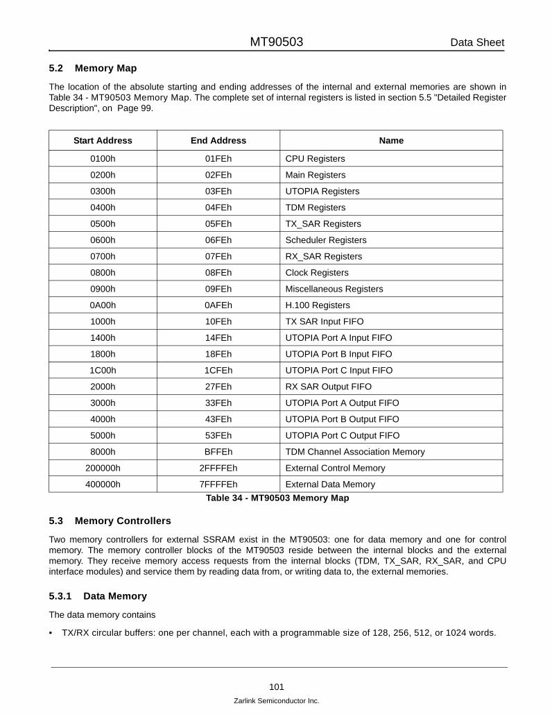
MT90503 Data Sheet
101Zarlink Semiconductor Inc.
5.2 Memory Map
The location of the absolute starting and ending addresses of the internal and external memories are shown inTable 34 - MT90503 Memory Map. The complete set of internal registers is listed in section 5.5 "Detailed RegisterDescription", on Page 99.
Table 34 - MT90503 Memory Map
5.3 Memory Controllers
Two memory controllers for external SSRAM exist in the MT90503: one for data memory and one for controlmemory. The memory controller blocks of the MT90503 reside between the internal blocks and the externalmemory. They receive memory access requests from the internal blocks (TDM, TX_SAR, RX_SAR, and CPUinterface modules) and service them by reading data from, or writing data to, the external memories.
5.3.1 Data Memory
The data memory contains
• TX/RX circular buffers: one per channel, each with a programmable size of 128, 256, 512, or 1024 words.
Start Address End Address Name
0100h 01FEh CPU Registers
0200h 02FEh Main Registers
0300h 03FEh UTOPIA Registers
0400h 04FEh TDM Registers
0500h 05FEh TX_SAR Registers
0600h 06FEh Scheduler Registers
0700h 07FEh RX_SAR Registers
0800h 08FEh Clock Registers
0900h 09FEh Miscellaneous Registers
0A00h 0AFEh H.100 Registers
1000h 10FEh TX SAR Input FIFO
1400h 14FEh UTOPIA Port A Input FIFO
1800h 18FEh UTOPIA Port B Input FIFO
1C00h 1CFEh UTOPIA Port C Input FIFO
2000h 27FEh RX SAR Output FIFO
3000h 33FEh UTOPIA Port A Output FIFO
4000h 43FEh UTOPIA Port B Output FIFO
5000h 53FEh UTOPIA Port C Output FIFO
8000h BFFEh TDM Channel Association Memory
200000h 2FFFFEh External Control Memory
400000h 7FFFFEh External Data Memory

MT90503 Data Sheet
102Zarlink Semiconductor Inc.
The data memory can be up to 4 MB in size. This allows 2048 TDM channels to each have a maximum-size circularbuffer: 2048 TDM channels * 2048 bytes/channel = 4 MB. A parity bit, necessary to detect underruns on incomingTDM data, can be disabled, allowing non-parity memory to be used. The parity bit, when enabled, is also used forerror detection.
The data memory can be distributed between one and four banks. 16 to 19 address bits are required to access the128 KB to 1 MB banks of data memory.
5.3.2 Control Memory
The control memory contains
• TX control structures: one per VC, minimum of 12 words each, maximum of 48 KB total
• RX control structures: one per VC, minimum of 14 words each, maximum of 56 KB total
• Transmit event schedulers: up to fifteen, typical sizes are 6 to 150 KB per enabled scheduler
• Look-up table: three LUTs, each with one entry per known VC, 4 or 8 bytes per entry
• Data cell FIFO: two FIFOs, each programmable in length from 4 to 16384 cells, 32 words per cell
• CAS change buffers: 1 to 32768 words in size
• Silent tone buffers: 1 to 32768 words in size
• Clock recovery point buffers: 9216 words in size
• Error message buffer: programmable length of 0 to 65536 error report structures, 4 words per structure.
The control memory can be up to 1 MB in size. A parity bit is used for error detection. The control memory can bedistributed in either one or two banks. As with the data memory, 16 to 19 address bits are employed; when 19address bits are used, only one memory bank can be supported.
5.3.3 Data Memory Controller
There are five agents which interact with the data memory controller: TX_SAR, RX_SAR, TDM transmit, TDMreceive, and CPU (through the CPU interface). Of these five agents, all but the CPU send their accesses to theirinternal cache, one for each agent, from which the data is written into the data memory when the data memory busis available. The internal caches are capable of buffering up to 128 words each.
The CPU has the highest priority on the write accesses and writes whenever it is flagged to do so. The priorityarbitration used for accesses to the CPU is described in more detail the CPU module section (See 4.1 on page 34).
The memory controller generates the CRC-32 needed for each AAL5-VTOA cell.
Agent Access types
TX_SAR Reads
RX_SAR Writes
TDM transmit Writes
TDM receive Reads
CPU Reads and writes
Table 35 - Types of Data Memory accesses for each agent

MT90503 Data Sheet
103Zarlink Semiconductor Inc.
5.3.4 Control Memory Controller
Unlike the data memory controller, the control memory controller does not contain internal caches. Agents’read/write requests are granted on a cycle-by-cycle basis and each agent waits until its request has beencompleted. Each agent has its own access port allowing it to communicate address, data, r/w, and write enableinformation with the memory controller. The agents are identified in Table 36 - on page 103.
Arbitration between the agents for control memory access is as follows: an agent can request a read or write at anytime. The control memory will continue in its current mode (read or write) until no requests of that type are pending.Then, it will switch and service requests of the other mode. The CPU has the highest priority if the memorycontroller is handling accesses of the mode that the CPU requests. Other agents are granted access on afirst-come first-served basis if the memory controller is handling accesses of the mode the agent requests.
5.4 Register Overview
This section describes the MT90503's internal registers. An 8 KB memory block is reserved for the registermapping.
The register descriptions are grouped in the following sections:
• CPU Module Interface
• Main Registers
• UTOPIA Module
• TDM Module
• TX_SAR Module
• RX_SAR Module
• Clock Registers
• Miscellaneous Registers
• H.100/H.110 Bus Registers
Agent Access types
TX_SAR Reads and writes
RX_SAR Reads and writes
UTOPIA (LUT) Reads and writes
CPU Reads and writes
Table 36 - Types of Control Memory Accesses For Each Agent

MT90503 Data Sheet
104Zarlink Semiconductor Inc.
5.5 Detailed Register Description
5.5.1 CPU Registers
Address: 100hLabel: controlReset Value: 0000h
Label Bit Position Type Description
nreset_registers 0 RW Controls the reset for the MAINREG module and certain CPU functions. '1' out of reset. '0' in reset. Should not be removed unless mclk is present.
nreset_chip_mclk_src 1 RW Resets all other parts of the chip. '1' out of reset. '0' in reset. Should not be removed unless mclk is present.
nreset_txa_clk_mclk_src 2 RW nreset for UTOPIA TXA clock (syncronized on mclk_src). This reset should not be removed unless the corresponding clock is present.
nreset_txb_clk_mclk_src 3 RW nreset for UTOPIA TXB clock (syncronized on mclk_src). This reset should not be removed unless the corresponding clock is present.
nreset_txc_clk_mclk_src 4 RW nreset for UTOPIA TXC clock (syncronized on mclk_src). This reset should not be removed unless the corresponding clock is present.
nreset_rxa_clk_mclk_src 5 RW nreset for UTOPIA RXA clock (syncronized on mclk_src). This reset should not be removed unless the corresponding clock is present.
nreset_rxb_clk_mclk_src 6 RW nreset for UTOPIA RXB clock (syncronized on mclk_src). This reset should not be removed unless the corresponding clock is present.
nreset_rxc_clk_mclk_src 7 RW nreset for UTOPIA RXC clock (syncronized on mclk_src). This reset should not be removed unless the corresponding clock is present.
reserved 8 RW For future use: reserved for mem_clk oe (TTL)
reserved 9 RW For future use: reserved for PECL oe
mem_clk_o_enable 10 RW Enables the mem_clk TTL output to toggle, active high
mem_clk_pecl_enable 11 RW Enables the mem_clk PECL output to toggle, active high
mem_clk_input_sel 12 RW '0' = mem_clk_i pin, '1' = mem_clk PECL pins
write_cache_enable 13 RW When '0', only 1 access can be treated at a time. When '1', write cache contains 128 accesses. If this bit is '1', the average latency to perform a write will be reduced, but the worst-case latency will be increased.
reserved 14 RW Reserved. Must be set t o "0".
test_status 15 TS When '1', all the status bits in the register will be set.
Table 37 - CPU Control Register

MT90503 Data Sheet
105Zarlink Semiconductor Inc.
Address: 102hLabel: status0Reset Value: 0000h
Label Bit Position Type Description
reserved 0 RO Reserved. Always read as "0".
reserved 1 RO Reserved. Always read as "0".
reserved 2 RO Reserved. Always read as "0".
internal_read_timeout 3 ROL Goes high if a read access has been active for 32k mclk_src cycles without completion. Fatal chip error.
inmo_read_done 4 ROL Indicates that an extended indirect access has completed. This is used to indicate to the host that read data is ready.
reserved 15:5 ROL Reserved. Always read as "0000_0000_000"
Table 38 - CPU Status Register
Address: 104hLabel: status0_ieReset Value: 0000h
Label BitPosition Type Description
reserved 0 RO Reserved. Always read as "0".
reserved 1 RO Reserved. Always read as "0".
reserved 2 RO Reserved. Always read as "0".
internal_read_timeout_ie 3 IE When '1' and the corresponding status bit is '1', an interrupt will be generated.
inmo_read_done_ie 4 IE When '1' and the corresponding status bit is '1', an interrupt will be generated.
reserved 15:5 RO Reserved. Always read as "0000_0000_000".
Table 39 - CPU Interrupt Enable Register
Address: 10EHLabel: countersReset Value: 0000h
Label Bit Position Type Description
emul_mode 1:0 EMO Indicates state of counters and status bits. "00" = normal mode, "01" = reset, "1x" = test mode. These bits are only present for tests and should never be used.
reserved 15:2 RW Reserved. Must be "0000_0000_0000_00"
Table 40 - CPU Counter Register

MT90503 Data Sheet
106Zarlink Semiconductor Inc.
Address: 120hLabel: led1Reset Value: 3FD0h
Label Bit Position Type Description
mclk_src_freq[6:0] 6:0 RW mclk_src Frequency in MHz
led_flash_freq[8:0] 15:7 RW Determines the time in ms that the LEDs will be turned off to indicate link activity.
Table 41 - LED1 Register
Address: 122hLabel: led2Reset Value: 0000h
Label Bit Position Type Description
led_test_mode 0 RW If '0', the LED Flashing time will be determined in ms. If '1', the LED Flashing time will be determined in us.
reserved 15:1 RW Reserved. Must be "0000_0000_0000_000"
Table 42 - LED2 Register
Address: 128hLabel: pll_confReset Value: 00A1h
Label Bit Position Type Description
pll_div_x 2:0 RW Divides mclk_src before entering the REF pin of the fast_clk PLL. Together, pll_div_x and pll_div_y determine the speed of fast_clk, which must be between 160 and 200 MHz.
pll_div_y 5:3 RW Divides the feedback path from the output pin of the fast_clk PLL. Together, pll_div_x and pll_div_y determine the speed of fast_clk, which must be between 160 and 200 MHz.
pll_div_z 10:6 RW Divides fast_clk to generate mem_clk
pll_bypass 11 RW If '1', mclk_src divided by pll_div_x becomes fast_clk, bypassing the fast_clk PLL
nreset_pll_async 12 RW Resets the module that divides mclk_src before being used as the REF pin of the fast_clk PLL
reserved 15:13 RO Reserved. Always read as "000"
Table 43 - PLL Configuration Register
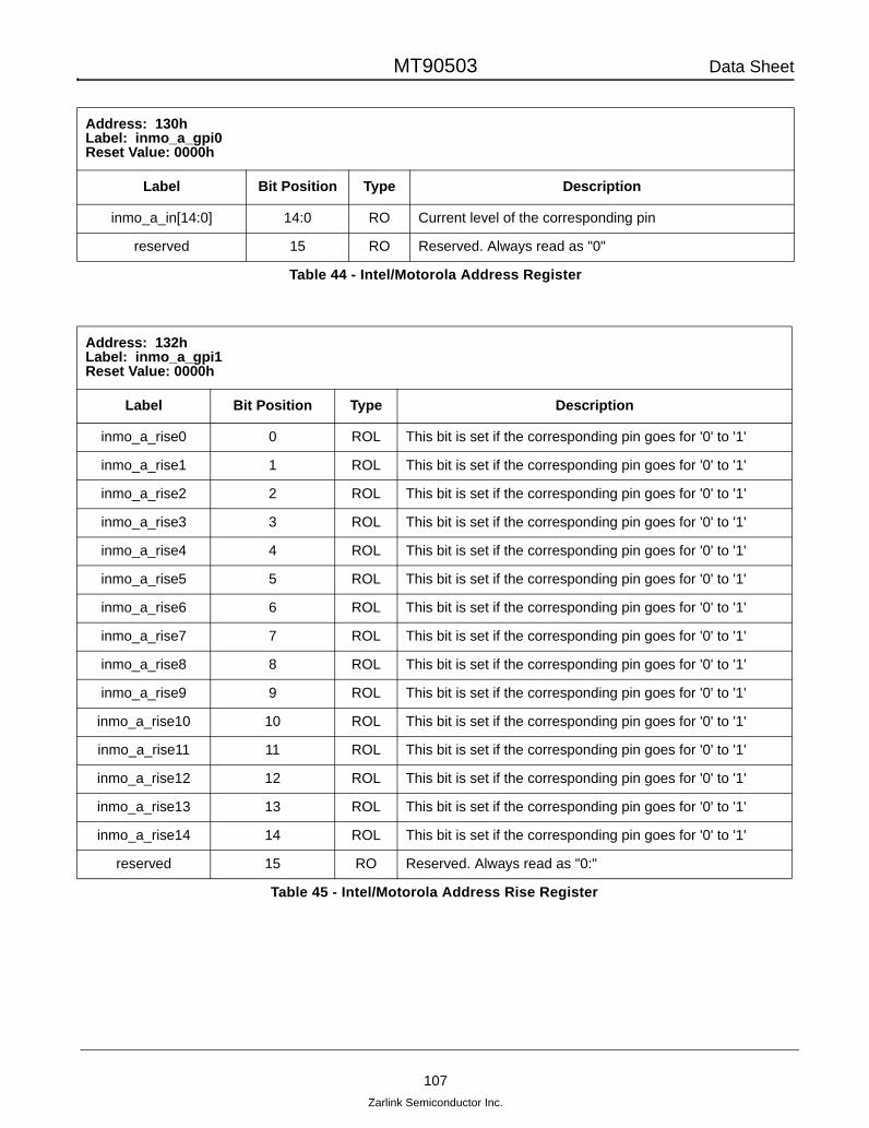
MT90503 Data Sheet
107Zarlink Semiconductor Inc.
Address: 130hLabel: inmo_a_gpi0Reset Value: 0000h
Label Bit Position Type Description
inmo_a_in[14:0] 14:0 RO Current level of the corresponding pin
reserved 15 RO Reserved. Always read as "0"
Table 44 - Intel/Motorola Address Register
Address: 132hLabel: inmo_a_gpi1Reset Value: 0000h
Label Bit Position Type Description
inmo_a_rise0 0 ROL This bit is set if the corresponding pin goes for '0' to '1'
inmo_a_rise1 1 ROL This bit is set if the corresponding pin goes for '0' to '1'
inmo_a_rise2 2 ROL This bit is set if the corresponding pin goes for '0' to '1'
inmo_a_rise3 3 ROL This bit is set if the corresponding pin goes for '0' to '1'
inmo_a_rise4 4 ROL This bit is set if the corresponding pin goes for '0' to '1'
inmo_a_rise5 5 ROL This bit is set if the corresponding pin goes for '0' to '1'
inmo_a_rise6 6 ROL This bit is set if the corresponding pin goes for '0' to '1'
inmo_a_rise7 7 ROL This bit is set if the corresponding pin goes for '0' to '1'
inmo_a_rise8 8 ROL This bit is set if the corresponding pin goes for '0' to '1'
inmo_a_rise9 9 ROL This bit is set if the corresponding pin goes for '0' to '1'
inmo_a_rise10 10 ROL This bit is set if the corresponding pin goes for '0' to '1'
inmo_a_rise11 11 ROL This bit is set if the corresponding pin goes for '0' to '1'
inmo_a_rise12 12 ROL This bit is set if the corresponding pin goes for '0' to '1'
inmo_a_rise13 13 ROL This bit is set if the corresponding pin goes for '0' to '1'
inmo_a_rise14 14 ROL This bit is set if the corresponding pin goes for '0' to '1'
reserved 15 RO Reserved. Always read as "0:"
Table 45 - Intel/Motorola Address Rise Register
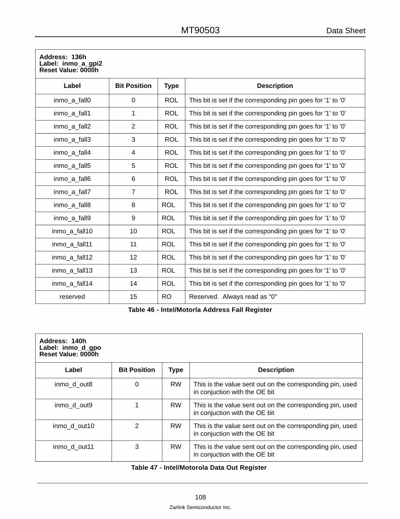
MT90503 Data Sheet
108Zarlink Semiconductor Inc.
Address: 136hLabel: inmo_a_gpi2Reset Value: 0000h
Label Bit Position Type Description
inmo_a_fall0 0 ROL This bit is set if the corresponding pin goes for '1' to '0'
inmo_a_fall1 1 ROL This bit is set if the corresponding pin goes for '1' to '0'
inmo_a_fall2 2 ROL This bit is set if the corresponding pin goes for '1' to '0'
inmo_a_fall3 3 ROL This bit is set if the corresponding pin goes for '1' to '0'
inmo_a_fall4 4 ROL This bit is set if the corresponding pin goes for '1' to '0'
inmo_a_fall5 5 ROL This bit is set if the corresponding pin goes for '1' to '0'
inmo_a_fall6 6 ROL This bit is set if the corresponding pin goes for '1' to '0'
inmo_a_fall7 7 ROL This bit is set if the corresponding pin goes for '1' to '0'
inmo_a_fall8 8 ROL This bit is set if the corresponding pin goes for '1' to '0'
inmo_a_fall9 9 ROL This bit is set if the corresponding pin goes for '1' to '0'
inmo_a_fall10 10 ROL This bit is set if the corresponding pin goes for '1' to '0'
inmo_a_fall11 11 ROL This bit is set if the corresponding pin goes for '1' to '0'
inmo_a_fall12 12 ROL This bit is set if the corresponding pin goes for '1' to '0'
inmo_a_fall13 13 ROL This bit is set if the corresponding pin goes for '1' to '0'
inmo_a_fall14 14 ROL This bit is set if the corresponding pin goes for '1' to '0'
reserved 15 RO Reserved. Always read as "0"
Table 46 - Intel/Motorla Address Fall Register
Address: 140hLabel: inmo_d_gpoReset Value: 0000h
Label Bit Position Type Description
inmo_d_out8 0 RW This is the value sent out on the corresponding pin, used in conjuction with the OE bit
inmo_d_out9 1 RW This is the value sent out on the corresponding pin, used in conjuction with the OE bit
inmo_d_out10 2 RW This is the value sent out on the corresponding pin, used in conjuction with the OE bit
inmo_d_out11 3 RW This is the value sent out on the corresponding pin, used in conjuction with the OE bit
Table 47 - Intel/Motorola Data Out Register

MT90503 Data Sheet
109Zarlink Semiconductor Inc.
inmo_d_out12 4 RW This is the value sent out on the corresponding pin, used in conjuction with the OE bit
inmo_d_out13 5 RW This is the value sent out on the corresponding pin, used in conjuction with the OE bit
inmo_d_out14 6 RW This is the value sent out on the corresponding pin, used in conjuction with the OE bit
inmo_d_out15 7 RW This is the value sent out on the corresponding pin, used in conjuction with the OE bit
inmo_d_oe8 8 RW This is OE bit used to drive the corresponding pin.
inmo_d_oe9 9 RW This is OE bit used to drive the corresponding pin.
inmo_d_oe10 10 RW This is OE bit used to drive the corresponding pin.
inmo_d_oe11 11 RW This is OE bit used to drive the corresponding pin.
inmo_d_oe12 12 RW This is OE bit used to drive the corresponding pin.
inmo_d_oe13 13 RW This is OE bit used to drive the corresponding pin.
inmo_d_oe14 14 RW This is OE bit used to drive the corresponding pin.
inmo_d_oe15 15 RW This is OE bit used to drive the corresponding pin.
Address 142h:Label: inmo_d_gpi0Reset Value: 0000h
Label Bit Position Type Description
inmo_d_in8 0 RO Current level of the corresponding pin
inmo_d_in9 1 RO Current level of the corresponding pin
inmo_d_in10 2 RO Current level of the corresponding pin
inmo_d_in11 3 RO Current level of the corresponding pin
inmo_d_in12 4 RO Current level of the corresponding pin
inmo_d_in13 5 RO Current level of the corresponding pin
inmo_d_in14 6 RO Current level of the corresponding pin
inmo_d_in15 7 RO Current level of the corresponding pin
reserved 15:8 RO Reserved. Always read as "0000_0000"
Table 48 - Intel/Motorola Data In Register
Address: 140hLabel: inmo_d_gpoReset Value: 0000h
Label Bit Position Type Description
Table 47 - Intel/Motorola Data Out Register (continued)

MT90503 Data Sheet
110Zarlink Semiconductor Inc.
5.5.2 Main Registers
Address 144h:Label: inmo_d_gpi1Reset Value: 0000h
Label Bit Position Type Description
inmo_d_rise8 0 ROL This bit is set if the corresponding pin goes for '0' to '1'
inmo_d_rise9 1 ROL This bit is set if the corresponding pin goes for '0' to '1'
inmo_d_rise10 2 ROL This bit is set if the corresponding pin goes for '0' to '1'
inmo_d_rise11 3 ROL This bit is set if the corresponding pin goes for '0' to '1'
inmo_d_rise12 4 ROL This bit is set if the corresponding pin goes for '0' to '1'
inmo_d_rise13 5 ROL This bit is set if the corresponding pin goes for '0' to '1'
inmo_d_rise14 6 ROL This bit is set if the corresponding pin goes for '0' to '1'
inmo_d_rise15 7 ROL This bit is set if the corresponding pin goes for '0' to '1'
inmo_d_fall8 8 ROL This bit is set if the corresponding pin goes for '1' to '0'
inmo_d_fall9 9 ROL This bit is set if the corresponding pin goes for '1' to '0'
inmo_d_fall10 10 ROL This bit is set if the corresponding pin goes for '1' to '0'
inmo_d_fall11 11 ROL This bit is set if the corresponding pin goes for '1' to '0'
inmo_d_fall12 12 ROL This bit is set if the corresponding pin goes for '1' to '0'
inmo_d_fall13 13 ROL This bit is set if the corresponding pin goes for '1' to '0'
inmo_d_fall14 14 ROL This bit is set if the corresponding pin goes for '1' to '0'
inmo_d_fall15 15 ROL This bit is set if the corresponding pin goes for '1' to '0'
Table 49 - Intel/Motorola Data Rise/Fall Register
Address: 200hLabel: controlReset Value: 0000h
Label Bit Position Type Description
reserved 14:0 RO Reserved. Always read as "0000_0000_0000_000"
test_status 15 TS When '1', all the status bits in the register will be set.
Table 50 - Main Control Register

MT90503 Data Sheet
111Zarlink Semiconductor Inc.
Address: 202hLabel: status0Reset Value: 0000h
Label Bit Position Type Description
cmem_parity_error0 0 ROL Indicates a parity error on data received from the control memory on the data bits [7:0]. This will only be detected if cmem_parity_conf[0] is '0'.
cmem_parity_error1 1 ROL Indicates a parity error on data received from the control memory on the data bits [15:8]. This will only be detected if cmem_parity_conf[1] is '0'.
dmem_parity_error0 2 ROL Indicates a parity error on data received from the data memory on the data bits [7:0]. This will only be detected if dmem_parity_conf[0] is '0'.
dmem_parity_error1 3 ROL Indicates a parity error on data received from the data memory on the data bits [15:8]. This will only be detected if dmem_parity_conf[1] is '0'.
reserved 15:4 RW Reserved. Must be "0000_0000_0000"
Table 51 - Main Status Register
Address: 204hLabel: status0_ieReset Value: 0000h
Label BitPosition Type Description
cmem_parity_error0_ie 0 IE When '1' and the corresponding status bit is '1', an interrupt will be generated.
cmem_parity_error1_ie 1 IE When '1' and the corresponding status bit is '1', an interrupt will be generated.
dmem_parity_error0_ie 2 IE When '1' and the corresponding status bit is '1', an interrupt will be generated.
dmem_parity_error1_ie 3 IE When '1' and the corresponding status bit is '1', an interrupt will be generated.
reserved 15:4 RW Reserved. Must be "0000_0000_0000"
Table 52 - Main Interrupt Enable Register

MT90503 Data Sheet
112Zarlink Semiconductor Inc.
Address: countersLabel: 20EhReset Value: 0000h
Label BitPosition Type Description
emul_mode 1:0 EMO Indicates state of counters and status bits. "00" = normal mode, "01" = reset, "1x" = test mode. These bits are only present for tests and should never be used.
reserved 15:2 RW Reserved. Must be "0000_0000_0000_00"
Table 53 - Main Counter Register
Address: 220hLabel: interrupt_flagsReset Value: 0000h
Label BitPosition Type Description
cpureg_interrupt_active 0 RO When '1', indicates that the interrupt request for this module is active.
mainreg_interrupt_active 1 RO When '1', indicates that the interrupt request for this module is active.
utoreg_interrupt_active 2 RO When '1', indicates that the interrupt request for this module is active.
txreg_interrupt_active 3 RO When '1', indicates that the interrupt request for this module is active.
rxreg_interrupt_active 4 RO When '1', indicates that the interrupt request for this module is active.
miscreg_interrupt_active 5 RO When '1', indicates that the interrupt request for this module is active.
wheelreg_interrupt_active 6 RO When '1', indicates that the interrupt request for thismodule is active.
clkreg_interrupt_active 7 RO When '1', indicates that the interrupt request for thismodule is active.
tdmreg_interrupt_active 8 RO When '1', indicates that the interrupt request for thismodule is active.
mastreg_interrupt_active 9 RO When '1', indicates that the interrupt request for thismodule is active.
Table 54 - Interrupt Flags Register

MT90503 Data Sheet
113Zarlink Semiconductor Inc.
casalarm_interrupt_active 10 RO The CAS alarm occurs after the CAS alarm timeoutperiod or if the CAS buffer becomes half full. This is usedto ensure that the host can empty the CAS change bufferin a timely manner without having to poll its fillcontinuously.
tdmalarm_interrupt_active 11 RO When ’0’, the clock divisor module is held in reset.
clkrecovalarm_interrupt_active 12 RO The clock recovery alarm occurs after the clock recoveryalarm timeout period or if either clock recovery bufferbecomes half full. This is used to ensure that the host canempty the clock recovery point buffers in a timely mannerwithout having to poll its fill continuously.
aal0alarm_interrupt_active 13 RO The AAL0 alarm occurs after the AAL0 alarm timeoutperiod or if the AAL0 buffer becomes half full. This is usedto ensure that the host can empty the AAL0 cell buffer in atimely manner without having to poll its fill continuously.
erroralarm_interrupt_active 14 RO The error alarm occurs after the error alarm timeoutperiod or if the error report structure buffer becomes halffull. This is used to ensure that the host can empty theerror structure buffer in a timely manner without having topoll its fill continuously.
interrupt1_treated 15 PUL Software must write this bit to ’1’, when it has finished servicing interrupts.
Address: 224hLabel: interrupt1_confReset Value: 0000h
Label BitPosition Type Description
min_interrupt1_period 13:0 RW Number of us between interrupts (minimum). When 0000h, these is no minimum interval between interrupts. Programming this prevents the host from being flooded with interrupts. Each interrupt will last 1 us.
interrupt1_polarity 15:14 RW Interrupt polarity and output enable. "00"=active low (open-collector); "01"=active high (open-collector); "10" = drive low; "11" = drive high. Drive low or drive high means that the pin's value will not change regardless of internal interrupts.
Table 55 - Interrupt1 Configuration Register
Address: 220hLabel: interrupt_flagsReset Value: 0000h
Label BitPosition Type Description
Table 54 - Interrupt Flags Register (continued)

MT90503 Data Sheet
114Zarlink Semiconductor Inc.
Address: 226hLabel: interrupt2_confReset Value: 0000h
Label BitPosition Type Description
reserved 13:0 RW Reserved. Must be "0000_0000_0000_00"
interrupt2_polarity 15:14 RW Interrupt polarity and output enable. "00"=active low (open-collector); "01"=active high (open-collector); "10" = drive low; "11" = drive high. Drive low or drive high means that the pin's value will not change regardless of internal interrupts.
Table 56 - Interrupt2 Configuration Register
Address: 228hLabel: interrupt1_enableReset Value: 0000h
Label BitPosition Type Description
cpureg_interrupt1_enable 0 RW When '1' and the corresponding interrupt active is '1', an interrupt will be generated on cpu_int[0].
mainreg_interrupt1_enable 1 RW When '1' and the corresponding interrupt active is '1', an interrupt will be generated on cpu_int[0].
utoreg_interrupt1_enable 2 RW When '1' and the corresponding interrupt active is '1', an interrupt will be generated on cpu_int[0].
txreg_interrupt1_enable 3 RW When '1' and the corresponding interrupt active is '1', an interrupt will be generated on cpu_int[0].
rxreg_interrupt1_enable 4 RW When '1' and the corresponding interrupt active is '1', an interrupt will be generated on cpu_int[0].
miscreg_interrupt1_enable 5 RW When '1' and the corresponding interrupt active is '1', an interrupt will be generated on cpu_int[0].
wheelreg_interrupt1_enable 6 RW When '1' and the corresponding interrupt active is '1', an interrupt will be generated on cpu_int[0].
clkreg_interrupt1_enable 7 RW When '1' and the corresponding interrupt active is '1', an interrupt will be generated on cpu_int[0].
tdmreg_interrupt1_enable 8 RW When '1' and the corresponding interrupt active is '1', an interrupt will be generated on cpu_int[0].
mastreg_interrupt1_enable 9 RW When '1' and the corresponding interrupt active is '1', an interrupt will be generated on cpu_int[0].
Table 57 - Interrupt1 Enable Register
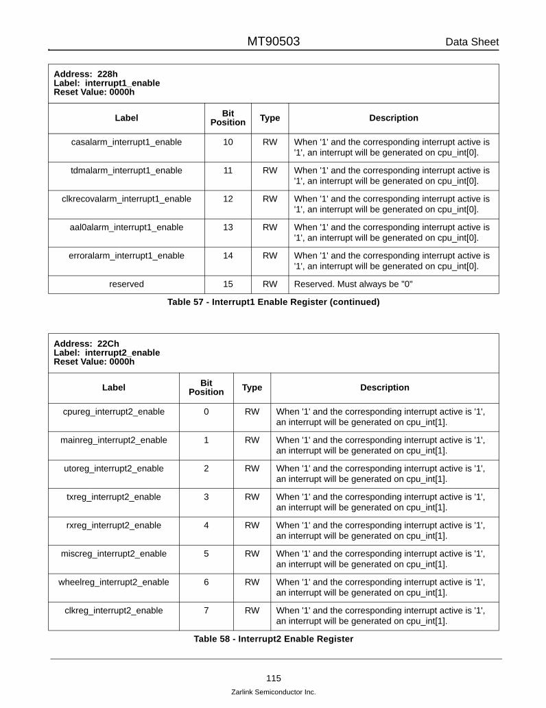
MT90503 Data Sheet
115Zarlink Semiconductor Inc.
casalarm_interrupt1_enable 10 RW When '1' and the corresponding interrupt active is '1', an interrupt will be generated on cpu_int[0].
tdmalarm_interrupt1_enable 11 RW When '1' and the corresponding interrupt active is '1', an interrupt will be generated on cpu_int[0].
clkrecovalarm_interrupt1_enable 12 RW When '1' and the corresponding interrupt active is '1', an interrupt will be generated on cpu_int[0].
aal0alarm_interrupt1_enable 13 RW When '1' and the corresponding interrupt active is '1', an interrupt will be generated on cpu_int[0].
erroralarm_interrupt1_enable 14 RW When '1' and the corresponding interrupt active is '1', an interrupt will be generated on cpu_int[0].
reserved 15 RW Reserved. Must always be "0"
Address: 22ChLabel: interrupt2_enableReset Value: 0000h
Label Bit Position Type Description
cpureg_interrupt2_enable 0 RW When '1' and the corresponding interrupt active is '1', an interrupt will be generated on cpu_int[1].
mainreg_interrupt2_enable 1 RW When '1' and the corresponding interrupt active is '1', an interrupt will be generated on cpu_int[1].
utoreg_interrupt2_enable 2 RW When '1' and the corresponding interrupt active is '1', an interrupt will be generated on cpu_int[1].
txreg_interrupt2_enable 3 RW When '1' and the corresponding interrupt active is '1', an interrupt will be generated on cpu_int[1].
rxreg_interrupt2_enable 4 RW When '1' and the corresponding interrupt active is '1', an interrupt will be generated on cpu_int[1].
miscreg_interrupt2_enable 5 RW When '1' and the corresponding interrupt active is '1', an interrupt will be generated on cpu_int[1].
wheelreg_interrupt2_enable 6 RW When '1' and the corresponding interrupt active is '1', an interrupt will be generated on cpu_int[1].
clkreg_interrupt2_enable 7 RW When '1' and the corresponding interrupt active is '1', an interrupt will be generated on cpu_int[1].
Table 58 - Interrupt2 Enable Register
Address: 228hLabel: interrupt1_enableReset Value: 0000h
Label BitPosition Type Description
Table 57 - Interrupt1 Enable Register (continued)
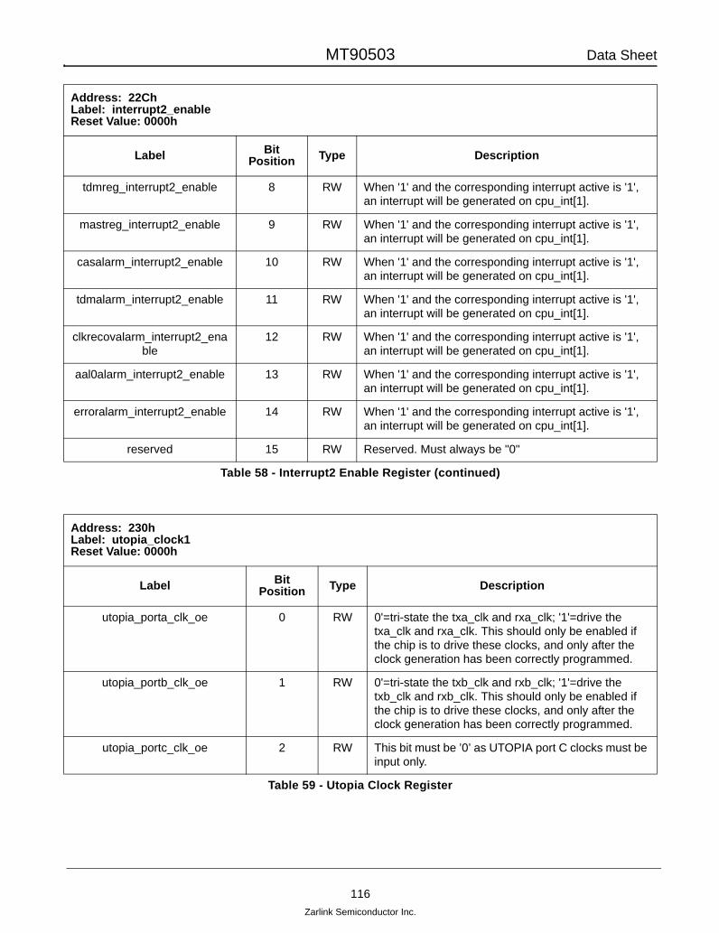
MT90503 Data Sheet
116Zarlink Semiconductor Inc.
tdmreg_interrupt2_enable 8 RW When '1' and the corresponding interrupt active is '1', an interrupt will be generated on cpu_int[1].
mastreg_interrupt2_enable 9 RW When '1' and the corresponding interrupt active is '1', an interrupt will be generated on cpu_int[1].
casalarm_interrupt2_enable 10 RW When '1' and the corresponding interrupt active is '1', an interrupt will be generated on cpu_int[1].
tdmalarm_interrupt2_enable 11 RW When '1' and the corresponding interrupt active is '1', an interrupt will be generated on cpu_int[1].
clkrecovalarm_interrupt2_enable
12 RW When '1' and the corresponding interrupt active is '1', an interrupt will be generated on cpu_int[1].
aal0alarm_interrupt2_enable 13 RW When '1' and the corresponding interrupt active is '1', an interrupt will be generated on cpu_int[1].
erroralarm_interrupt2_enable 14 RW When '1' and the corresponding interrupt active is '1', an interrupt will be generated on cpu_int[1].
reserved 15 RW Reserved. Must always be "0"
Address: 230hLabel: utopia_clock1Reset Value: 0000h
Label Bit Position Type Description
utopia_porta_clk_oe 0 RW 0'=tri-state the txa_clk and rxa_clk; '1'=drive the txa_clk and rxa_clk. This should only be enabled if the chip is to drive these clocks, and only after the clock generation has been correctly programmed.
utopia_portb_clk_oe 1 RW 0'=tri-state the txb_clk and rxb_clk; '1'=drive the txb_clk and rxb_clk. This should only be enabled if the chip is to drive these clocks, and only after the clock generation has been correctly programmed.
utopia_portc_clk_oe 2 RW This bit must be ’0’ as UTOPIA port C clocks must be input only.
Table 59 - Utopia Clock Register
Address: 22ChLabel: interrupt2_enableReset Value: 0000h
Label Bit Position Type Description
Table 58 - Interrupt2 Enable Register (continued)

MT90503 Data Sheet
117Zarlink Semiconductor Inc.
utopia_txa_clk_select[1:0] 4:3 RW "00" = select clock divisor A; "01" = select clock divisor B; "10" = select clock divisor C; "11" = reserved. There are 3 integer clock divisors used to generate the UTOPIA clocks, and each of the 6 UTOPIA clocks can be selected as any one of the 3.
utopia_txb_clk_select[1:0] 6:5 RW "00" = select clock divisor A; "01" = select clock divisor B; "10" = select clock divisor C; "11" = reserved. There are 3 integer clock divisors used to generate the UTOPIA clocks, and each of the 6 UTOPIA clocks can be selected as any one of the 3.
utopia_txc_clk_select[1:0] 8:7 RW Reserved.
utopia_rxa_clk_select[1:0] 10:9 RW "00" = select clock divisor A; "01" = select clock divisor B; "10" = select clock divisor C; "11" = reserved.
utopia_rxb_clk_select[1:0] 12:11 RW "00" = select clock divisor A; "01" = select clock divisor B; "10" = select clock divisor C; "11" = reserved.
utopia_rxc_clk_select[1:0] 14:13 RW Reserved.
reserved 15 RW Reserved. Must always be "0"
Address: 232hLabel: utopia_genaReset Value: 0001h
Label Bit Position Type Description
utopia_clk_diva[5:0] 5:0 RW Integer divisor for input UTOPIA clock. Divides the selected clock source.
utopia_clk_divisor_load_nowa 6 PUL Written to '1' when the source, divisor and inv. have been correctly programmed.
utopia_clk_inva 7 RW Inverts the output of the clock divisor
utopia_clk_srca[2:0] 10:8 RW "000"=txa_clk_in; "001"=txb_clk_in; "010"=txc_clk_in; "011"=rxa_clk_in; "100"=rxb_clk_in;"101"=rxc_clk_in; "110"=mclk; "111"=fast_clk.
utopia_clk_divisor_reseta 11 RW When ’0’, the clock divisor module is held in reset.
Table 60 - Utopia Clock Generation A Register
Address: 230hLabel: utopia_clock1Reset Value: 0000h
Label Bit Position Type Description
Table 59 - Utopia Clock Register (continued)

MT90503 Data Sheet
118Zarlink Semiconductor Inc.
reserved 15:12 RW Reserved. Must always be "0000"
Address: 234hLabel: utopia_genbReset Value: 0001h
Label BitPosition Type Description
utopia_clk_divb[5:0] 5:0 RW Integer divisor for input UTOPIA clock. Divides the selected clock source.
utopia_clk_divisor_load_nowb 6 PUL Written to '1' when the source, divisor and inv. have been correctly programmed.
utopia_clk_invb 7 RW Inverts the output of the clock divisor
utopia_clk_srcb[2:0] 10:8 RW "000"=txa_clk_in; "001"=txb_clk_in; "010"=txc_clk_in; "011"=rxa_clk_in; "100"=rxb_clk_in;"101"=rxc_clk_in; "110"=mclk; "111"=fast_clk.
utopia_clk_divisor_resetb 11 RW When ’0’, the clock divisor module is held in reset.
reserved 15:12 RW Reserved. Must always be "0000"
Table 61 - Utopia Clock Generation B Register
Address: 236hLabel: utopia_gencReset Value: 0001h
Label BitPosition Type Description
utopia_clk_divc[5:0] 5:0 RW Integer divisor for input UTOPIA clock. Divides the selected clock source.
utopia_clk_divisor_load_nowc 6 PUL Written to '1' when the source, divisor and inv. have been correctly programmed.
utopia_clk_invc 7 RW Inverts the output of the clock divisor
utopia_clk_srcc[2:0] 10:8 RW "000"=txa_clk_in; "001"=txb_clk_in; "010"=txc_clk_in; "011"=rxa_clk_in; "100"=rxb_clk_in;"101"=rxc_clk_in; "110"=mclk; "111"=fast_clk.
Table 62 - Utopia Clock Generation C Register
Address: 232hLabel: utopia_genaReset Value: 0001h
Label Bit Position Type Description
Table 60 - Utopia Clock Generation A Register

MT90503 Data Sheet
119Zarlink Semiconductor Inc.
utopia_clk_divisor_resetc 11 RW When ’0’, the clock divisor module is held in reset.
reserved 15:12 RW Reserved. Must always be "0000"
Address: 240hLabel: cmem_parity0Reset Value: 0000h
Label BitPosition Type Description
cmem_parity_conf[1:0] 1:0 RW 0' = parity bits; '1' = user data. In normal chip operation, this field should be set to "00", because the chip does not use the parity bits of the control memory.
cmem_parity_generation_add_mask[18:16]
4:2 RW Mask of address bits [18:16] to be used to generate parity for the control memory. A '1' in one of these bits indicates that the corresponding address bit will be used to generate parity.
reserved 7:5 RO Reserved. Must always be "0000"
cmem_parity_generation_data_mask 15:8 RW Mask of data bits to be used to generate parity for the control memory. A '1' in one of these bits indicates that the data bit will be used to generate parity.
Table 63 - Control Memory Parity0 Register
Address: 242hLabel: cmem_parity1Reset Value: 0000h
Label BitPosition Type Description
cmem_parity_generation_add_mask[15:0]
15:0 RW Mask of address bits [15:0] to be used to generate parity for the control memory. A '1' in one of these bits indicates that the corresponding address bit will be used to generate parity.
Table 64 - Control Memory Parity1 Register
Address: 236hLabel: utopia_gencReset Value: 0001h
Label BitPosition Type Description
Table 62 - Utopia Clock Generation C Register

MT90503 Data Sheet
120Zarlink Semiconductor Inc.
Address: 244hLabel: cmem_confReset Value: 0010h
Label BitPosition Type Description
cmem_add_lines 1:0 RW "11" = 1 MB per chip; "10" = 512 KB per chip; "01" = 256KB per chip; "00" = 128 KB per chip
cmem_mem_type 3:2 RW "00" = flowthrough ZBT; "01" = flowthrough SSRAM; "10" = pipelined ZBT; "11" = pipelined SSRAM.
cmem_rw_ta 4 RW 0 = no read/write turn-around cycles; 1 = 1 read/write turn-around cycle.
reserved 15:5 RO Reserved. Always read as "0000_0000_000"
Table 65 - Control Memory Configuration Register
Address: 248hLabel: dmem_parity0Reset Value: 0000h
Label Bit Position Type Description
dmem_parity_conf[1:0] 1:0 RW 0' = parity bits; '1' = user data.
dmem_parity_generation_add_mask[20:16]
6:2 RW Mask of address bits [20:16] to be used to generate parity for the data memory. A '1' in one of these bits indicates that the corresponding address bit will be used to generate parity.
reserved 7 RO Reserved. Always read as "0"
dmem_parity_generation_data_mask 15:8 RW Mask of data bits to be used to generate parity for the data memory. A '1' in one of these bits indicates that the corresponding data bit will be used to generate parity.
Table 66 - Data Memory Parity 0 Register

MT90503 Data Sheet
121Zarlink Semiconductor Inc.
5.5.3 UTOPIA Registers
Address: 24AhLabel: dmem_parity1Reset Value: 0000h
Label BitPosition Type Description
dmem_parity_generation_add_mask[15:0]
15:0 RW Mask of address bits [15:0] to be used to generate parity for the data memory. A '1' in one of these bits indicates that the corresponding address bit will be used to generate parity.
Table 67 - Data Memory Parity 1 Register
Address: 24ChLabel: dmem_confReset Value: 0010h
Label BitPosition Type Description
dmem_add_lines 1:0 RW "11" = 1 MB per chip; "10" = 512 KB per chip; "01" = 256KB per chip; "00" = 128 KB per chip
dmem_mem_type 3:2 RW "00" = flowthrough ZBT; "01" = flowthrough SSRAM; "10" = pipelined ZBT; "11" = pipelined SSRAM.
dmem_rw_ta 4 RW 0 = no read/write turn-around cycles; 1 = 1 read/write turn-around cycle.
reserved 15:5 RO Reserved. Always read as "0000_0000_000"
Table 68 - Data Memory Configuration Register
Address: 300hLabel: controlReset Value: 0900h
Label BitPosition Type Description
rxa_ena 0 RW Enables UTOPIA port RXA
rxa_sar 1 RW 0' = chip acts as PHY, '1' = chip acts as SAR
rxa_width 2 RW 0' = 8-bit UTOPIA bus, '1' = 16-bit UTOPIA bus
rxb_ena 3 RW Enables UTOPIA port RXB
rxb_sar 4 RW 0' = chip acts as PHY, '1' = chip acts as SAR
rxb_width 5 RW 0' = 8-bit UTOPIA bus, '1' = 16-bit UTOPIA bus
Table 69 - Utopia Control Register

MT90503 Data Sheet
122Zarlink Semiconductor Inc.
txa_sar 6 RW 0' = chip acts as PHY, '1' = chip acts as SAR
txa_width 7 RW 0' = 8-bit UTOPIA bus, '1' = 16-bit UTOPIA bus
txa_multiphy 8 RW 0' = always drive DAT/PAR/SOC pins; '1' = only drive when selected. Only applicable when chip is in PHY mode.
txb_sar 9 RW 0' = chip acts as PHY, '1' = chip acts as SAR
txb_width 10 RW 0' = 8-bit UTOPIA bus, '1' = 16-bit UTOPIA bus
txb_multiphy 11 RW 0' = always drive DAT/PAR/SOC pins; '1' = only drive when selected. Only applicable when chip is in PHY mode.
add_pin_ena 12 RW If '1', UTOPIA port A is level-2 with addressing. When this bit is set, rxb_width and txb_width must be '0'.
reserved 13 RW Reserved. Must always be "0"
null_cell_elim 14 RW When '1', all cells with VPI and VCI equal to '0' will be discarded. Otherwise, they will be kept and treated normally.
test_status 15 TS When '1', all the status bits in the register will be set.
Address: 302hLabel: control1Reset Value: 0008h
Label BitPosition Type Description
rxc_ena 0 RW Enables UTOPIA port RXC
rxc_sar 1 RW 0' = chip acts as PHY, '1' = chip acts as SAR
txc_sar 2 RW 0' = chip acts as PHY, '1' = chip acts as SAR
txc_multiphy 3 RW 0' = always drive DAT/PAR/SOC pins; '1' = only drive when selected. Only applicable when chip is in PHY mode.
uto_output_enable 4 RW 0' Tri-states the ENA or CLAV pin driven by the chip. '1' drives. This bit should be set to '1' after all PHY/SAR register bits have been programmed, but before all rx_ena bits are set.
phy_alarm_pol 6:5 RW "00" = PHY alarm disabled, "01" = PHY alarm active-high, "10" = PHY alarm active-low, "11" = reserved.
Table 70 - Utopia Control1 Register
Address: 300hLabel: controlReset Value: 0900h
Label BitPosition Type Description
Table 69 - Utopia Control Register (continued)

MT90503 Data Sheet
123Zarlink Semiconductor Inc.
long_lut_entries 7 RW When '0', LUT entries are 4 bytes long. When '1', LUT entries are 8 bytes long. Long LUT entries should only be used if header translation is to be performed.
rxa_nni_null_elim 8 RW 1' consider NNI VPI bits for null cell elimination for port RXA. If '0', the high 4 bits of the header (GFC field) will be ignored for null cell elimination.
rxb_nni_null_elim 9 RW 1' consider NNI VPI bits for null cell elimination for port RXB. If '0', the high 4 bits of the header (GFC field) will be ignored for null cell elimination.
rxc_nni_null_elim 10 RW 1' consider NNI VPI bits for null cell elimination for port RXC. If '0', the high 4 bits of the header (GFC field) will be ignored for null cell elimination.
phya_tx_led_conf 11 RW When '0', phya_tx_led pin functions as a LED. When '1', functions as GPIO.
phya_rx_led_conf 12 RW When '0', phya_rx_led pin functions as a LED. When '1', functions as GPIO.
phyb_tx_led_conf 13 RW When '0', phyb_tx_led pin functions as a LED. When '1', functions as GPIO.
phyb_rx_led_conf 14 RW When '0', phyb_rx_led pin functions as a LED. When '1', functions as GPIO.
reserved 15 RW Reserved. Must always be "0"
Address: 304hLabel: status0Reset Value: 0000h
Label BitPosition Type Description
rx_cell_loss 0 ROL Indicates an overflow in the buffer from UTOPIA to the RX SAR
outa_cell_loss 1 ROL Indicates an overflow in the output buffer for port TXA
outb_cell_loss 2 ROL Indicates an overflow in the output buffer for port TXB
outc_cell_loss 3 ROL Indicates an overflow in the output buffer for port TXC
cell_loss_rollover 4 CRL Indicates that the cell_loss_counter register has wrapped
Table 71 - Utopia Status 0 Register
Address: 302hLabel: control1Reset Value: 0008h
Label BitPosition Type Description
Table 70 - Utopia Control1 Register (continued)

MT90503 Data Sheet
124Zarlink Semiconductor Inc.
tx_arr_rollover 5 CRL Indicates that the tx_sar_cell_arrival register has wrapped
rx_dep_rollover 6 CRL Indicates that the rx_sar_cell_departure register has wrapped
ia_arr_rollover 7 CRL Indicates that the porta_cell_arrival register has wrapped
oa_dep_rollover 8 CRL Indicates that the porta_cell_departure register has wrapped
ib_arr_rollover 9 CRL Indicates that the portb_cell_arrival register has wrapped
ob_dep_rollover 10 CRL Indicates that the portb_cell_departure register has wrapped
ic_arr_rollover 11 CRL Indicates that the portc_cell_arrival register has wrapped
oc_dep_rollover 12 CRL Indicates that the portc_cell_departure register has wrapped
rxa_parity_error 13 ROL Indicates a parity error on port RXA
rxb_parity_error 14 ROL Indicates a parity error on port RXB
rxc_parity_error 15 ROL Indicates a parity error on port RXC
Address: 30ChLabel: status2Reset Value: 0000h
Label BitPosition Type Description
phy_alarma 0 ROLO This bit is set when phya_alm pin is active. Active polarity is determined by phy_alarm_pol register
phy_alarmb 1 ROLO This bit is set when phyb_alm pin is active. Active polarity is determined by phy_alarm_pol register
test_a_bit 2 ROL Bit is set when look-up engine gives a pulse on clock recovery VC A. Used for tests.
test_b_bit 3 ROL Bit is set when look-up engine gives a pulse on clock recovery VC B. Used for tests.
reserved 15:4 RW Reserved. Must always be "0000_0000_0000"
Table 72 - Utopia Status 2 Register
Address: 30EhLabel: status2_ieReset Value: 0000h
Table 73 - Utopia Interrupt Enable 2 Register
Address: 304hLabel: status0Reset Value: 0000h
Label BitPosition Type Description
Table 71 - Utopia Status 0 Register (continued)

MT90503 Data Sheet
125Zarlink Semiconductor Inc.
Label BitPosition Type Description
phy_alarma_ie 0 IE When '1' and the corresponding status bit is '1', an interrupt will be generated.
phy_alarmb_ie 1 IE When '1' and the corresponding status bit is '1', an interrupt will be generated.
test_a_bit_ie 2 IE When '1' and the corresponding status bit is '1', an interrupt will be generated.
test_b_bit_ie 3 IE When '1' and the corresponding status bit is '1', an interrupt will be generated.
reserved 15:4 IE When '1' and the corresponding status bit is '1', an interrupt will be generated.
Address: 310hLabel: countersReset Value: 0000h
Label BitPosition Type Description
emul_mode 1:0 EMO Indicates state of counters and status bits. "00" = normal mode, "01" = reset, "1x" = test mode. These bits are only present for tests and should never be used.
cell_loss_emul 2 EMU When emul_mode = "11", writing '1' to this bit will increment the cell_loss counter by 1
tx_arr_emul 3 EMU When emul_mode = "11", writing '1' to this bit will increment the tx_arr counter by 1
rx_dep_emul 4 EMU When emul_mode = "11", writing '1' to this bit will increment the rx_dep counter by 1
ia_arr_emul 5 EMU When emul_mode = "11", writing '1' to this bit will increment the ia_arr counter by 1
oa_dep_emul 6 EMU When emul_mode = "11", writing '1' to this bit will increment the oa_dep counter by 1
ib_arr_emul 7 EMU When emul_mode = "11", writing '1' to this bit will increment the ib_arr counter by 1
ob_dep_emul 8 EMU When emul_mode = "11", writing '1' to this bit will increment the ob_dep counter by 1
ic_arr_emul 9 EMU When emul_mode = "11", writing '1' to this bit will increment the ic_arr counter by 1
oc_dep_emul 10 EMU When emul_mode = "11", writing '1' to this bit will increment the oc_dep counter by 1
reserved 15:11 RW Reserved. Must always be "0000_0"
Table 74 - Utopia Counters Register
Table 73 - Utopia Interrupt Enable 2 Register
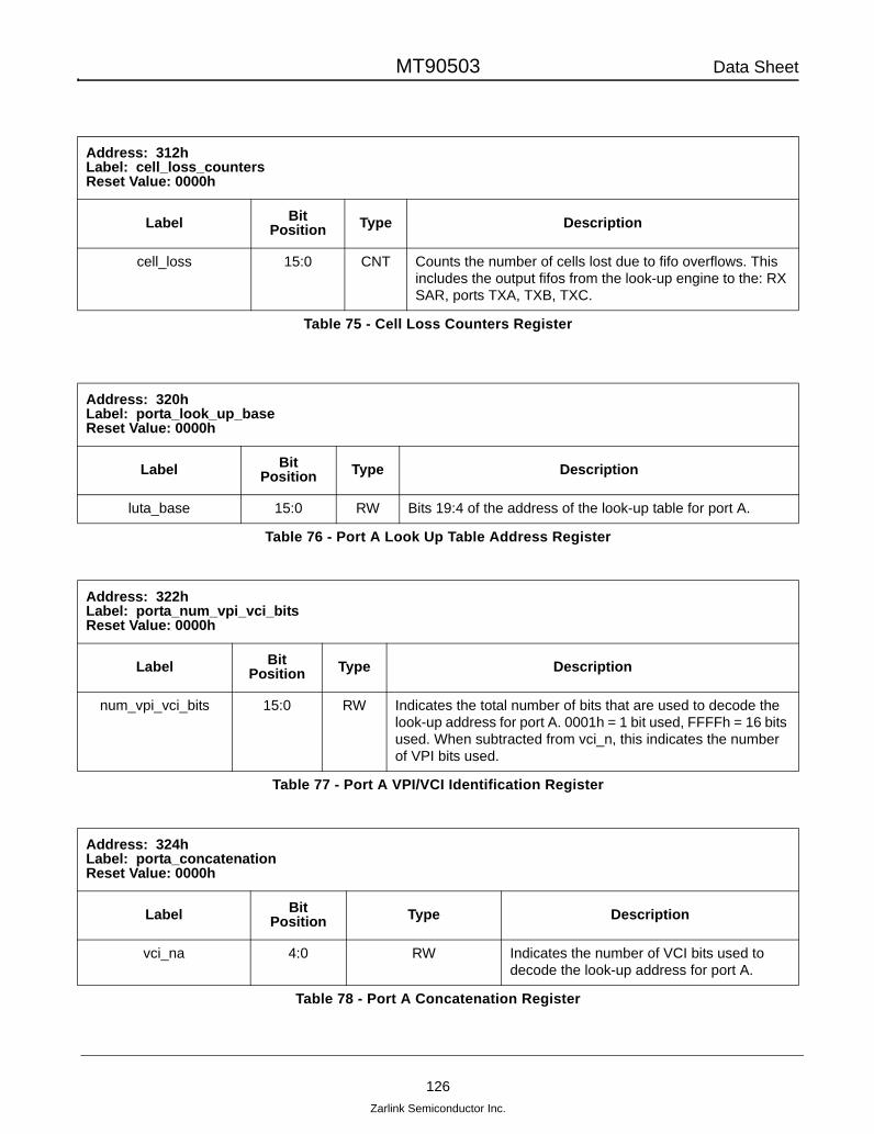
MT90503 Data Sheet
126Zarlink Semiconductor Inc.
Address: 312hLabel: cell_loss_countersReset Value: 0000h
Label Bit Position Type Description
cell_loss 15:0 CNT Counts the number of cells lost due to fifo overflows. This includes the output fifos from the look-up engine to the: RX SAR, ports TXA, TXB, TXC.
Table 75 - Cell Loss Counters Register
Address: 320hLabel: porta_look_up_baseReset Value: 0000h
Label Bit Position Type Description
luta_base 15:0 RW Bits 19:4 of the address of the look-up table for port A.
Table 76 - Port A Look Up Table Address Register
Address: 322hLabel: porta_num_vpi_vci_bitsReset Value: 0000h
Label Bit Position Type Description
num_vpi_vci_bits 15:0 RW Indicates the total number of bits that are used to decode the look-up address for port A. 0001h = 1 bit used, FFFFh = 16 bits used. When subtracted from vci_n, this indicates the number of VPI bits used.
Table 77 - Port A VPI/VCI Identification Register
Address: 324hLabel: porta_concatenationReset Value: 0000h
Label BitPosition Type Description
vci_na 4:0 RW Indicates the number of VCI bits used to decode the look-up address for port A.
Table 78 - Port A Concatenation Register
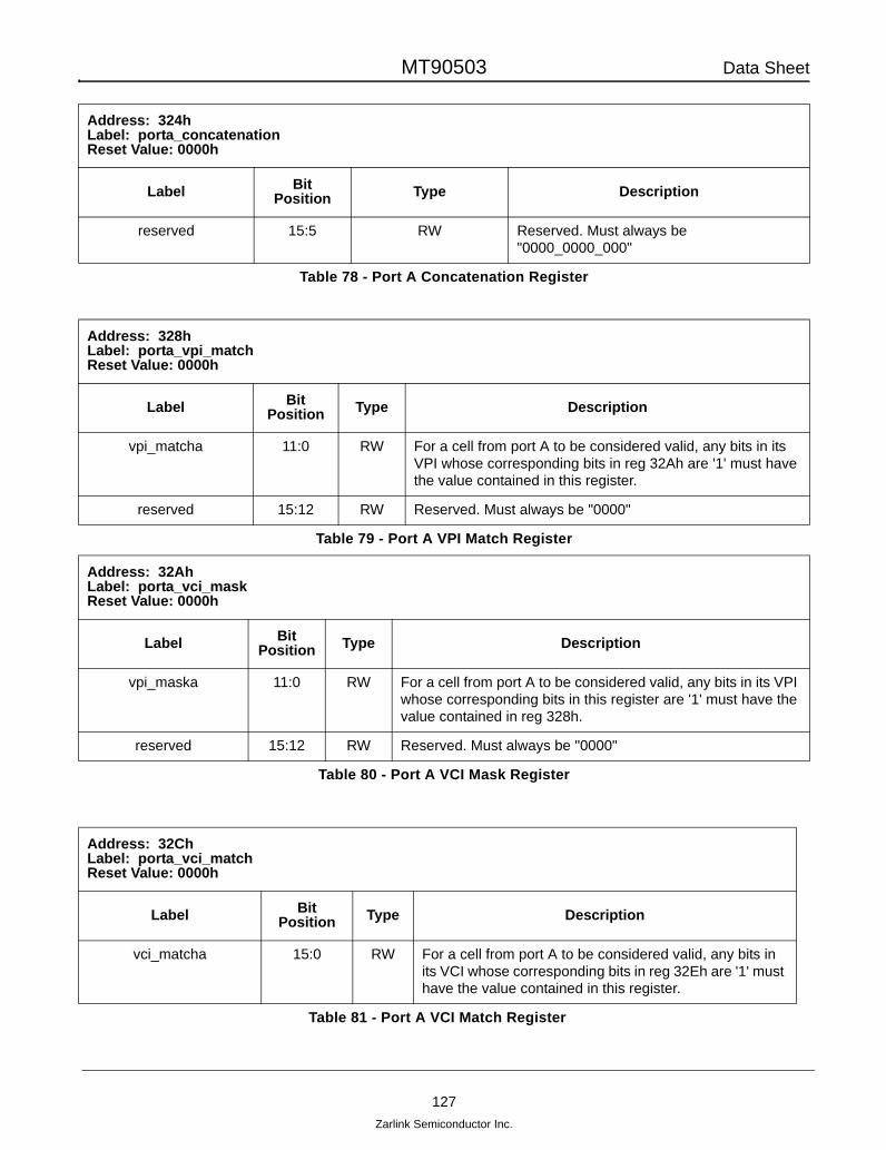
MT90503 Data Sheet
127Zarlink Semiconductor Inc.
reserved 15:5 RW Reserved. Must always be "0000_0000_000"
Address: 328hLabel: porta_vpi_matchReset Value: 0000h
Label Bit Position Type Description
vpi_matcha 11:0 RW For a cell from port A to be considered valid, any bits in its VPI whose corresponding bits in reg 32Ah are '1' must have the value contained in this register.
reserved 15:12 RW Reserved. Must always be "0000"
Table 79 - Port A VPI Match Register
Address: 32AhLabel: porta_vci_maskReset Value: 0000h
Label Bit Position Type Description
vpi_maska 11:0 RW For a cell from port A to be considered valid, any bits in its VPI whose corresponding bits in this register are '1' must have the value contained in reg 328h.
reserved 15:12 RW Reserved. Must always be "0000"
Table 80 - Port A VCI Mask Register
Address: 32ChLabel: porta_vci_matchReset Value: 0000h
Label Bit Position Type Description
vci_matcha 15:0 RW For a cell from port A to be considered valid, any bits in its VCI whose corresponding bits in reg 32Eh are '1' must have the value contained in this register.
Table 81 - Port A VCI Match Register
Address: 324hLabel: porta_concatenationReset Value: 0000h
Label BitPosition Type Description
Table 78 - Port A Concatenation Register

MT90503 Data Sheet
128Zarlink Semiconductor Inc.
Address: 32EhLabel: porta_vci_maskReset Value: 0000h
Label BitPosition Type Description
vci_maska 15:0 RW For a cell from port A to be considered valid, any bits in its VCI whose corresponding bits in this register are '1' must have the value contained in reg 32Ch.
Table 82 - Port A VCI Mask Register
Address: 330hLabel: porta_cell_arrival_highReset Value: 0000h
Label Bit Position Type Description
ia_arr[31:16] 15:0 CNT Freerunning counter of the number of cells received on port A.
Table 83 - Port A Cell Arrival Counter High Register
Address: 332hLabel: porta_cell_arrival_lowReset Value: 0000h
Label Bit Position Type Description
ia_arr[15:0] 15:0 CNT Freerunning counter of the number of cells receivedon port A.
Table 84 - Port A Cell Arrival Counter Low Register
Address: 334hLabel: porta_cell_departure_highReset Value: 0000h
Label Bit Position Type Description
oa_dep[31:16] 15:0 CNT Freerunning counter of the number of cells transmitted on port A.
Table 85 - Port A Cell Departure Counter High Register

MT90503 Data Sheet
129Zarlink Semiconductor Inc.
Address: 336h Label: porta_cell_departure_lowReset Value: 0000h
Label BitPosition Type Description
oa_dep[15:0] 15:0 CNT Freerunning counter of the number of cells transmitted on port A.
Table 86 - Port A Cell Departure Low Register
Address: 338hLabel: porta_overflow0 Reset Value: 0000h
Label BitPosition Type Description
ia_rx_cell_max 4:0 RW If the cell fill of the RX SAR output FIFO becomes greater than this value, cells from the port A input FIFO will be blocked. 0h = no backpressure
ia_oa_cell_max 9:5 RW If the cell fill of the Port A output FIFO becomes greater than this value, cells from the port A input FIFO will be blocked. 0h = no backpressure
ia_ob_cell_max 14:10 RW If the cell fill of the Port B output FIFO becomes greater than this value, cells from the port A input FIFO will be blocked. 0h = no backpressure
reserved 15 RW Reserved. Must always be "0"
Table 87 - Port A Overflow0 Register
Address: 33Ah Label: porta_overflow1Reset Value: 0000h
Label BitPosition Type Description
ia_oc_cell_max 4:0 RW If the cell fill of the Port C output FIFO becomes greater than this value, cells from the port A input FIFO will be blocked. 0h = no backpressure
reserved 15:5 RW Reserved. Must always be "0000_0000_000"
Table 88 - Port A Overflow1 Register

MT90503 Data Sheet
130Zarlink Semiconductor Inc.
Address: 33Ch Label: porta_address Reset Value: 0000h
Label Bit Position Type Description
porta_add 4:0 RW UTOPIA address to which the chip will repond when programmed as a level-2 PHY.
reserved 15:5 RW Reserved. Must always be "0000_0000_000"
Table 89 - Port A Address Register
Address: 340h Label: portb_look_up_b Reset Value: 0000h
Label Bit Position Type Description
lutb_base 15:0 RW Bits 19:4 of the address of the look-up table for port B.
Table 90 - Port B Look Up Table Register
Address: 342h Label: portb_num_vpi_vci_bitsReset Value: 0000h
Label Bit Position Type Description
num_vpi_vci_bits 15:0 RW Indicates the total number of bits that are used to decode the look-up address for port B. 0001h = 1 bit used, FFFFh = 16 bits used. When subtracted from vci_n, this indicates the number of VPI bits used.
Table 91 - Port B VPI/VCI Identification Register
Address: 344h Label: portb_concatenation Reset Value: 0000h
Label BitPosition Type Description
vci_nb 4:0 RW Indicates the number of VCI bits used to decode the look-up address for port B.
reserved 15:5 RW Reserved. Must always be "0000_0000_000"
Table 92 - Port B Concatenation Register

MT90503 Data Sheet
131Zarlink Semiconductor Inc.
Address: 348h Label: portb_vpi_match Reset Value: 0000h
Label BitPosition Type Description
vpi_matchb 11:0 RW For a cell from port B to be considered valid, any bits in its VPI whose corresponding bits in reg 34Ah are '1' must have the value contained in this register.
reserved 15:12 RW Reserved. Must always be "0000"
Table 93 - Port B VPI Match Register
Address: 34Ah Label: portb_vpi_mask Reset Value: 0000h
Label BitPosition Type Description
vpi_maskb 11:0 RW For a cell from port B to be considered valid, any bits in its VPI whose corresponding bits in this register are '1' must have the value contained in reg 348h.
reserved 15:12 RW Reserved. Must always be "0000"
Table 94 - Port B VPI Mask Register
Address: 34ChLabel: portb_vci_match Reset Value: 0000h
Label BitPosition Type Description
vci_matchb 15:0 RW For a cell from port B to be considered valid, any bits in its VCI whose corresponding bits in reg 34Eh are '1' must have the value contained in this register.
Table 95 - Port B VCI Match Register

MT90503 Data Sheet
132Zarlink Semiconductor Inc.
Address: 34Eh Label: portb_vci_mask Reset Value: 0000h
Label BitPosition Type Description
vci_maskb 15:0 RW For a cell from port B to be considered valid, any bits in its VCI whose corresponding bits in this register are '1' must have the value contained in reg 34Ch.
Table 96 - Port B VCI Mask Register
Address: 350h Label: portb_cell_arrival_highReset Value: 0000h
Label BitPosition Type Description
ib_arr[31:16] 15:0 CNT Freerunning counter of the number of cells received on port B.
Table 97 - Port B Cell Arrival Counter High Register
Address: 352h Label: portb_cell_arrival_lowReset Value: 0000h
Label BitPosition Type Description
ib_arr[15:0] 15:0 CNT Freerunning counter of the number of cells received on port B.
Table 98 - Port B Cell Arrival Counter Low Register
Address: 354h Label: portb_cell_departure_highReset Value: 0000h
Label BitPosition Type Description
ob_dep[31:16] 15:0 CNT Freerunning counter of the number of cells transmitted on port B.
Table 99 - Port B Cell Departure Counter High Register

MT90503 Data Sheet
133Zarlink Semiconductor Inc.
Address: 356h Label: portb_cell_departure_lowReset Value: 0000h
Label BitPosition Type Description
ob_dep[15:0] 15:0 CNT Freerunning counter of the number of cells transmitted on port B.
Table 100 - Port B Cell Departure Counter Low Register
Address: 358h Label: portb_overflow0 Reset Value: 0000h
Label Bit Position Type Description
ib_rx_cell_max 4:0 RW If the cell fill of the RX SAR output FIFO becomes greater than this value, cells from the port B input FIFO will be blocked. 0h = no backpressure
ib_oa_cell_max 9:5 RW If the cell fill of the Port A output FIFO becomes greater than this value, cells from the port B input FIFO will be blocked. 0h = no backpressure
ib_ob_cell_max 14:10 RW If the cell fill of the Port B output FIFO becomes greater than this value, cells from the port B input FIFO will be blocked. 0h = no backpressure
reserved 15 RW Reserved. Must always be "0"
Table 101 - Port B Overflow0 Register
Address: 35Ah Label: portb_overflow1 Reset Value: 0000h
Label Bit Position Type Description
ib_oc_cell_max 4:0 RW If the cell fill of the Port C output FIFO becomes greater than this value, cells from the port B input FIFO will be blocked. 0h = no backpressure
reserved 15:5 RW Reserved. Must always be "0000_0000_000"
Table 102 - Port B Overflow1 Register
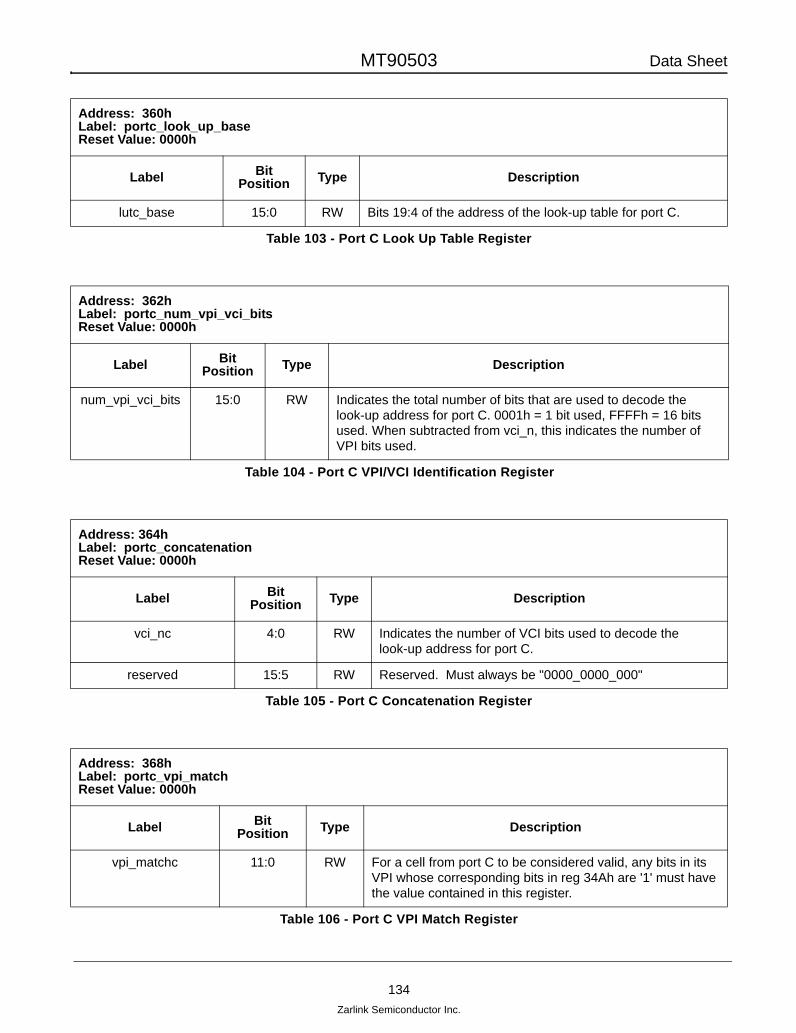
MT90503 Data Sheet
134Zarlink Semiconductor Inc.
Address: 360h Label: portc_look_up_baseReset Value: 0000h
Label Bit Position Type Description
lutc_base 15:0 RW Bits 19:4 of the address of the look-up table for port C.
Table 103 - Port C Look Up Table Register
Address: 362h Label: portc_num_vpi_vci_bits Reset Value: 0000h
Label BitPosition Type Description
num_vpi_vci_bits 15:0 RW Indicates the total number of bits that are used to decode the look-up address for port C. 0001h = 1 bit used, FFFFh = 16 bits used. When subtracted from vci_n, this indicates the number of VPI bits used.
Table 104 - Port C VPI/VCI Identification Register
Address: 364h Label: portc_concatenationReset Value: 0000h
Label BitPosition Type Description
vci_nc 4:0 RW Indicates the number of VCI bits used to decode the look-up address for port C.
reserved 15:5 RW Reserved. Must always be "0000_0000_000"
Table 105 - Port C Concatenation Register
Address: 368h Label: portc_vpi_match Reset Value: 0000h
Label Bit Position Type Description
vpi_matchc 11:0 RW For a cell from port C to be considered valid, any bits in its VPI whose corresponding bits in reg 34Ah are '1' must have the value contained in this register.
Table 106 - Port C VPI Match Register

MT90503 Data Sheet
135Zarlink Semiconductor Inc.
reserved 15:12 RW Reserved. Must always be "0000"
Address: 36Ah Label: portc_vpi_mask Reset Value: 0000h
Label Bit Position Type Description
vpi_maskc 11:0 RW For a cell from port C to be considered valid, any bits in its VPI whose corresponding bits in this register are '1' must have the value contained in reg 348h.
reserved 15:12 RW Reserved. Must always be "0000"
Table 107 - Port C VPI Mask Register
Address: 36Ch Label: portc_vci_match Reset Value: 0000h
Label BitPosition Type Description
vci_matchc 15:0 RW For a cell from port C to be considered valid, any bits in its VCI whose corresponding bits in reg 34Eh are '1' must have the value contained in this register.
Table 108 - Port C VCI Match Register
Address: 36Eh Label: portc_vci_mask Reset Value: 0000h
Label BitPosition Type Description
vci_maskc 15:0 RW For a cell from port C to be considered valid, any bits in its VCI whose corresponding bits in this register are '1' must have the value contained in reg 34Ch.
Table 109 - Port C VCI Match Register
Address: 368h Label: portc_vpi_match Reset Value: 0000h
Label Bit Position Type Description
Table 106 - Port C VPI Match Register

MT90503 Data Sheet
136Zarlink Semiconductor Inc.
Address: 370h Label: portc_cell_arrival_highReset Value: 0000h
Label Bit Position Type Description
ic_arr[31:16] 15:0 CNT Freerunning counter of the number of cells received on port C.
Table 110 - Port C Cell Arrival Counter High Register
Address: 372h Label: portc_cell_arrival_lowReset Value: 0000h
Label Bit Position Type Description
ic_arr[15:0] 15:0 CNT Freerunning counter of the number of cells received on port C.
Table 111 - Port C Cell Arrival Counter Low Register
Address: 374h Label: portc_cell_departure_highReset Value: 0000h
Label Bit Position Type Description
oc_dep[31:16] 15:0 CNT Freerunning counter of the number of cells transmitted on port C.
Table 112 - Port C Cell Departure Counter High Register
Address: 376h Label: portc_cell_departure_lowReset Value: 0000h
Label Bit Position Type Description
oc_dep[15:0] 15:0 CNT Freerunning counter of the number of cells transmitted on port C.
Table 113 - Port C Cell Departure Counter Low Register
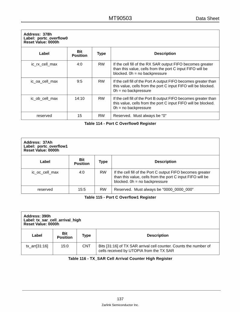
MT90503 Data Sheet
137Zarlink Semiconductor Inc.
Address: 378h Label: portc_overflow0 Reset Value: 0000h
Label Bit Position Type Description
ic_rx_cell_max 4:0 RW If the cell fill of the RX SAR output FIFO becomes greater than this value, cells from the port C input FIFO will be blocked. 0h = no backpressure
ic_oa_cell_max 9:5 RW If the cell fill of the Port A output FIFO becomes greater than this value, cells from the port C input FIFO will be blocked. 0h = no backpressure
ic_ob_cell_max 14:10 RW If the cell fill of the Port B output FIFO becomes greater than this value, cells from the port C input FIFO will be blocked. 0h = no backpressure
reserved 15 RW Reserved. Must always be "0"
Table 114 - Port C Overflow0 Register
Address: 37Ah Label: portc_overflow1 Reset Value: 0000h
Label Bit Position Type Description
ic_oc_cell_max 4:0 RW If the cell fill of the Port C output FIFO becomes greater than this value, cells from the port C input FIFO will be blocked. 0h = no backpressure
reserved 15:5 RW Reserved. Must always be "0000_0000_000"
Table 115 - Port C Overflow1 Register
Address: 390hLabel: tx_sar_cell_arrival_high Reset Value: 0000h
Label BitPosition Type Description
tx_arr[31:16] 15:0 CNT Bits [31:16] of TX SAR arrival cell counter. Counts the number of cells received by UTOPIA from the TX SAR
Table 116 - TX_SAR Cell Arrival Counter High Register

MT90503 Data Sheet
138Zarlink Semiconductor Inc.
Address: 392h Label: tx_sar_cell_arrival_low Reset Value: 0000h
Label Bit Position Type Description
tx_arr[15:0] 15:0 CNT Bits [15:0] of TX SAR arrival cell counter. Counts the number of cells received by UTOPIA from the TX SAR
Table 117 - TX_SAR Cell Arrival Counter Low Register
Address: 394h Label: rx_sar_cell_departure_high Reset Value: 0000h
Label Bit Position Type Description
rx_dep[31:16] 15:0 CNT Bits [31:16] of RX SAR departure cell counter. Counts the number of cells sent to the RX SAR from UTOPIA
Table 118 - RX_SAR Cell Departure Counter High Register
Address: 396h Label: rx_sar_cell_departure_low Reset Value: 0000h
Label Bit Position Type Description
rx_dep[15:0] 15:0 CNT Bits [15:0] of RX SAR departure cell counter. Counts the number of cells sent to the RX SAR from UTOPIA
Table 119 - RX_SAR Cell Departure Counter Low Register
Address: 398h Label: tx_sar_overflow Reset Value: 0000h
Label BitPosition Type Description
tx_rx_cell_max 4:0 RW If the cell fill of the RX SAR output FIFO becomes greater than this value, cells from the TX SAR input FIFO will be blocked. 0h = no backpressure
tx_oa_cell_max 9:5 RW If the cell fill of the Port A output FIFO becomes greater than this value, cells from the TX SAR input FIFO will be blocked. 0h = no backpressure
tx_ob_cell_max 14:10 RW If the cell fill of the Port B output FIFO becomes greater than this value, cells from the TX SAR input FIFO will be blocked. 0h = no backpressure
reserved 15 RW Reserved. Must always be "0"
Table 120 - TX_SAR Overflow0 Register

MT90503 Data Sheet
139Zarlink Semiconductor Inc.
Address: 39Ah Label: tx_sar_overflow Reset Value: 0000h
Label Bit Position Type Description
tx_oc_cell_max 4:0 RW If the cell fill of the Port C output FIFO becomes greater than this value, cells from the TX SAR input FIFO will be blocked. 0h = no backpressure
reserved 15:5 RW Reserved. Must always be "0000_0000_000"
Table 121 - TX_SAR Overflow1 Register
Address: 3A0h Label: hec_byte_controlReset Value: 0055h
Label BitPosition Type Description
hec_mask 7:0 RW Value by which the HEC generated on UTOPIA will be XORed before being transmitted. Should match the value used by the PHY.
reserved 15:8 RW Reserved. Must always be "0000_0000_0"
Table 122 - HEC Byte Control Register
Address: 3A2h Label: unknown_header_routingReset Value: 0000h
Label BitPosition Type Description
rxa_ncr 3:0 RW Normal cell routing for unknow cells received on port A. "xxx1" = Port A, "xx1x" = Port B, "x1xx" = Port C, "1xxx" RX SAR. Cells can be broadcast to multiple destinations by setting multiple bits in this field to '1'.
rxb_ncr 7:4 RW Normal cell routing for unknow cells received on port B. "xxx1" = Port A, "xx1x" = Port B, "x1xx" = Port C, "1xxx" RX SAR. Cells can be broadcast to multiple destinations by setting multiple bits in this field to '1'.
rxc_ncr 11:8 RW Normal cell routing for unknow cells received on port C. "xxx1" = Port A, "xx1x" = Port B, "x1xx" = Port C, "1xxx" RX SAR. Cells can be broadcast to multiple destinations by setting multiple bits in this field to '1'.
reserved 15:12 RW Reserved. Must always be "0000"
Table 123 - Unknown Header Routing Register
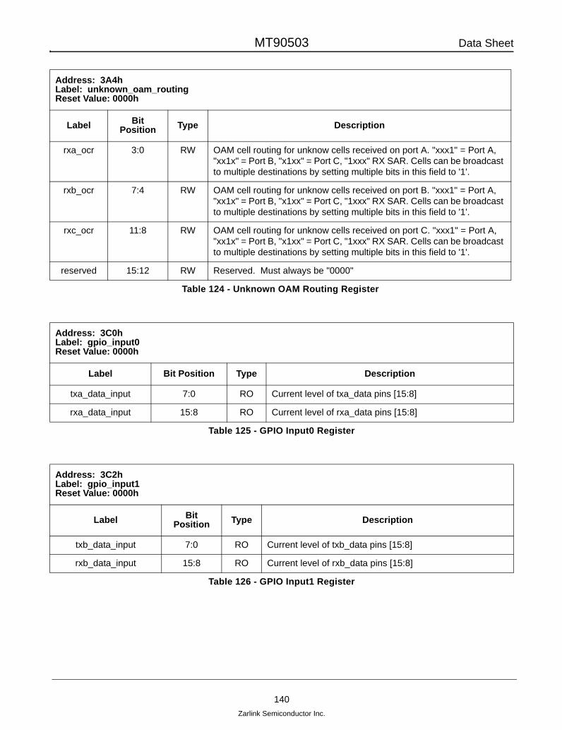
MT90503 Data Sheet
140Zarlink Semiconductor Inc.
Address: 3A4h Label: unknown_oam_routingReset Value: 0000h
Label Bit Position Type Description
rxa_ocr 3:0 RW OAM cell routing for unknow cells received on port A. "xxx1" = Port A, "xx1x" = Port B, "x1xx" = Port C, "1xxx" RX SAR. Cells can be broadcast to multiple destinations by setting multiple bits in this field to '1'.
rxb_ocr 7:4 RW OAM cell routing for unknow cells received on port B. "xxx1" = Port A, "xx1x" = Port B, "x1xx" = Port C, "1xxx" RX SAR. Cells can be broadcast to multiple destinations by setting multiple bits in this field to '1'.
rxc_ocr 11:8 RW OAM cell routing for unknow cells received on port C. "xxx1" = Port A, "xx1x" = Port B, "x1xx" = Port C, "1xxx" RX SAR. Cells can be broadcast to multiple destinations by setting multiple bits in this field to '1'.
reserved 15:12 RW Reserved. Must always be "0000"
Table 124 - Unknown OAM Routing Register
Address: 3C0h Label: gpio_input0 Reset Value: 0000h
Label Bit Position Type Description
txa_data_input 7:0 RO Current level of txa_data pins [15:8]
rxa_data_input 15:8 RO Current level of rxa_data pins [15:8]
Table 125 - GPIO Input0 Register
Address: 3C2h Label: gpio_input1 Reset Value: 0000h
Label Bit Position Type Description
txb_data_input 7:0 RO Current level of txb_data pins [15:8]
rxb_data_input 15:8 RO Current level of rxb_data pins [15:8]
Table 126 - GPIO Input1 Register

MT90503 Data Sheet
141Zarlink Semiconductor Inc.
Address: 3C4h Label: gpio_input2 Reset Value: 0000h
Label Bit Position Type Description
phya_alm_input 0 RO Current level of phya_alm pin
phyb_alm_input 1 RO Current level of phya_alm pin
phya_tx_led_input 2 RO Current level of phya_tx_led pin
phya_rx_led_input 3 RO Current level of phya_rx_led pin
phyb_tx_led_input 4 RO Current level of phyb_tx_led pin
phyb_rx_led_input 5 RO Current level of phyb_rx_led pin
reserved 15:6 RO Reserved. Always read as "0000_0000_00"
Table 127 - GPIO Input2 Register
Address: 3C8h Label: txa_data_status Reset Value: 0000h
Label Bit Position Type Description
txa_data8_rise 0 ROL This bit is set when corresponding pin changes from '0' to '1'
txa_data8_fall 1 ROL This bit is set when corresponding pin changes from '1' to '0'
txa_data9_rise 2 ROL This bit is set when corresponding pin changes from '0' to '1'
txa_data9_fall 3 ROL This bit is set when corresponding pin changes from '1' to '0'
txa_data10_rise 4 ROL This bit is set when corresponding pin changes from '0' to '1'
txa_data10_fall 5 ROL This bit is set when corresponding pin changes from '1' to '0'
txa_data11_rise 6 ROL This bit is set when corresponding pin changes from '0' to '1'
txa_data11_fall 7 ROL This bit is set when corresponding pin changes from '1' to '0'
txa_data12_rise 8 ROL This bit is set when corresponding pin changes from '0' to '1'
txa_data12_fall 9 ROL This bit is set when corresponding pin changes from '1' to '0'
txa_data13_rise 10 ROL This bit is set when corresponding pin changes from '0' to '1'
txa_data13_fall 11 ROL This bit is set when corresponding pin changes from '1' to '0'
txa_data14_rise 12 ROL This bit is set when corresponding pin changes from '0' to '1'
txa_data14_fall 13 ROL This bit is set when corresponding pin changes from '1' to '0'
txa_data15_rise 14 ROL This bit is set when corresponding pin changes from '0' to '1'
txa_data15_fall 15 ROL This bit is set when corresponding pin changes from '1' to '0'
Table 128 - TXA Data Status Register
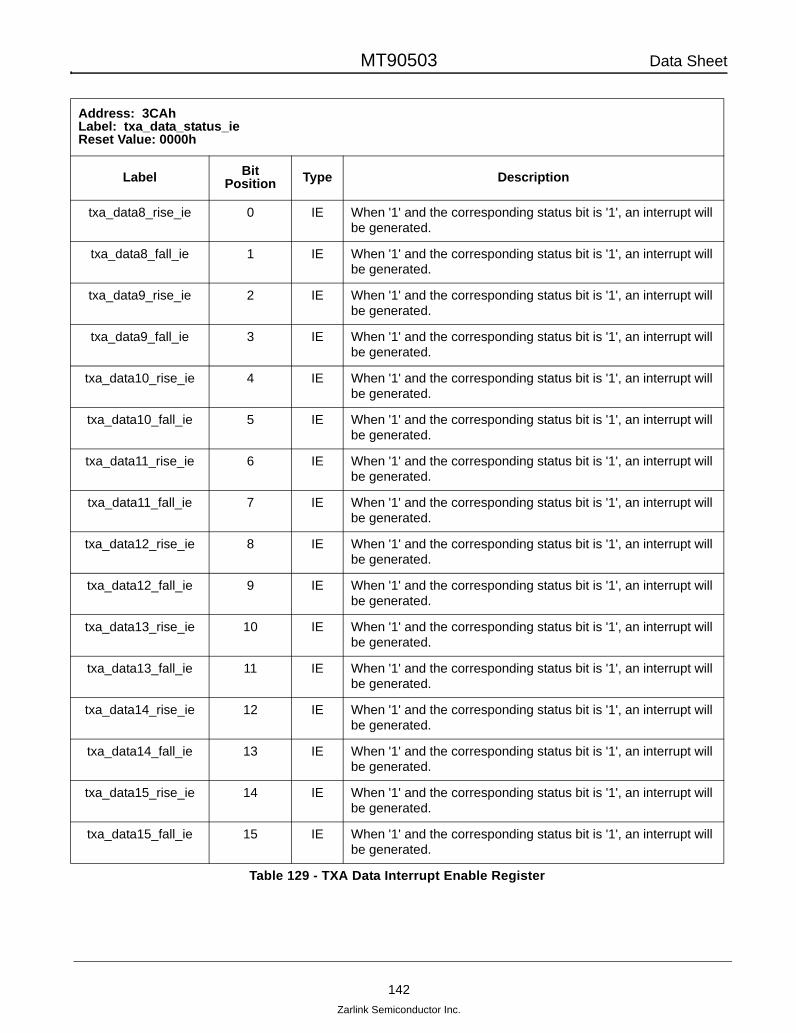
MT90503 Data Sheet
142Zarlink Semiconductor Inc.
Address: 3CAh Label: txa_data_status_ieReset Value: 0000h
Label BitPosition Type Description
txa_data8_rise_ie 0 IE When '1' and the corresponding status bit is '1', an interrupt will be generated.
txa_data8_fall_ie 1 IE When '1' and the corresponding status bit is '1', an interrupt will be generated.
txa_data9_rise_ie 2 IE When '1' and the corresponding status bit is '1', an interrupt will be generated.
txa_data9_fall_ie 3 IE When '1' and the corresponding status bit is '1', an interrupt will be generated.
txa_data10_rise_ie 4 IE When '1' and the corresponding status bit is '1', an interrupt will be generated.
txa_data10_fall_ie 5 IE When '1' and the corresponding status bit is '1', an interrupt will be generated.
txa_data11_rise_ie 6 IE When '1' and the corresponding status bit is '1', an interrupt will be generated.
txa_data11_fall_ie 7 IE When '1' and the corresponding status bit is '1', an interrupt will be generated.
txa_data12_rise_ie 8 IE When '1' and the corresponding status bit is '1', an interrupt will be generated.
txa_data12_fall_ie 9 IE When '1' and the corresponding status bit is '1', an interrupt will be generated.
txa_data13_rise_ie 10 IE When '1' and the corresponding status bit is '1', an interrupt will be generated.
txa_data13_fall_ie 11 IE When '1' and the corresponding status bit is '1', an interrupt will be generated.
txa_data14_rise_ie 12 IE When '1' and the corresponding status bit is '1', an interrupt will be generated.
txa_data14_fall_ie 13 IE When '1' and the corresponding status bit is '1', an interrupt will be generated.
txa_data15_rise_ie 14 IE When '1' and the corresponding status bit is '1', an interrupt will be generated.
txa_data15_fall_ie 15 IE When '1' and the corresponding status bit is '1', an interrupt will be generated.
Table 129 - TXA Data Interrupt Enable Register

MT90503 Data Sheet
143Zarlink Semiconductor Inc.
Address: 3CCh Label: rxa_data_status Reset Value: 0000h
Label Bit Position Type Description
rxa_data8_rise 0 ROL This bit is set when corresponding pin changes from '0' to '1'
rxa_data8_fall 1 ROL This bit is set when corresponding pin changes from '1' to '0'
rxa_data9_rise 2 ROL This bit is set when corresponding pin changes from '0' to '1'
rxa_data9_fall 3 ROL This bit is set when corresponding pin changes from '1' to '0'
rxa_data10_rise 4 ROL This bit is set when corresponding pin changes from '0' to '1'
rxa_data10_fall 5 ROL This bit is set when corresponding pin changes from '1' to '0'
rxa_data11_rise 6 ROL This bit is set when corresponding pin changes from '0' to '1'
rxa_data11_fall 7 ROL This bit is set when corresponding pin changes from '1' to '0'
rxa_data12_rise 8 ROL This bit is set when corresponding pin changes from '0' to '1'
rxa_data12_fall 9 ROL This bit is set when corresponding pin changes from '1' to '0'
rxa_data13_rise 10 ROL This bit is set when corresponding pin changes from '0' to '1'
rxa_data13_fall 11 ROL This bit is set when corresponding pin changes from '1' to '0'
rxa_data14_rise 12 ROL This bit is set when corresponding pin changes from '0' to '1'
rxa_data14_fall 13 ROL This bit is set when corresponding pin changes from '1' to '0'
rxa_data15_rise 14 ROL This bit is set when corresponding pin changes from '0' to '1'
rxa_data15_fall 15 ROL This bit is set when corresponding pin changes from '1' to '0'
Table 130 - RXA Data Status Register
Address: 3CEh Label: rxa_data_status_ie Reset Value: 0000h
Label BitPosition Type Description
rxa_data8_rise_ie 0 IE When '1' and the corresponding status bit is '1', an interrupt will be generated.
rxa_data8_fall_ie 1 IE When '1' and the corresponding status bit is '1', an interrupt will be generated.
rxa_data9_rise_ie 2 IE When '1' and the corresponding status bit is '1', an interrupt will be generated.
Table 131 - RXA Data Interrupt Enable Register

MT90503 Data Sheet
144Zarlink Semiconductor Inc.
rxa_data9_fall_ie 3 IE When '1' and the corresponding status bit is '1', an interrupt will be generated.
rxa_data10_rise_ie 4 IE When '1' and the corresponding status bit is '1', an interrupt will be generated.
rxa_data10_fall_ie 5 IE When '1' and the corresponding status bit is '1', an interrupt will be generated.
rxa_data11_rise_ie 6 IE When '1' and the corresponding status bit is '1', an interrupt will be generated.
rxa_data11_fall_ie 7 IE When '1' and the corresponding status bit is '1', an interrupt will be generated.
rxa_data12_rise_ie 8 IE When '1' and the corresponding status bit is '1', an interrupt will be generated.
rxa_data12_fall_ie 9 IE When '1' and the corresponding status bit is '1', an interrupt will be generated.
rxa_data13_rise_ie 10 IE When '1' and the corresponding status bit is '1', an interrupt will be generated.
rxa_data13_fall_ie 11 IE When '1' and the corresponding status bit is '1', an interrupt will be generated.
rxa_data14_rise_ie 12 IE When '1' and the corresponding status bit is '1', an interrupt will be generated.
rxa_data14_fall_ie 13 IE When '1' and the corresponding status bit is '1', an interrupt will be generated.
rxa_data15_rise_ie 14 IE When '1' and the corresponding status bit is '1', an interrupt will be generated.
rxa_data15_fall_ie 15 IE When '1' and the corresponding status bit is '1', an interrupt will be generated.
Address: 3D0h Label: txb_data_status Reset Value: 0000h
Label BitPosition Type Description
txb_data8_rise 0 ROL This bit is set when corresponding pin changes from '0' to '1'
txb_data8_fall 1 ROL This bit is set when corresponding pin changes from '1' to '0'
txb_data9_rise 2 ROL This bit is set when corresponding pin changes from '0' to '1'
Table 132 - TXB Data Status Register
Address: 3CEh Label: rxa_data_status_ie Reset Value: 0000h
Label BitPosition Type Description
Table 131 - RXA Data Interrupt Enable Register (continued)
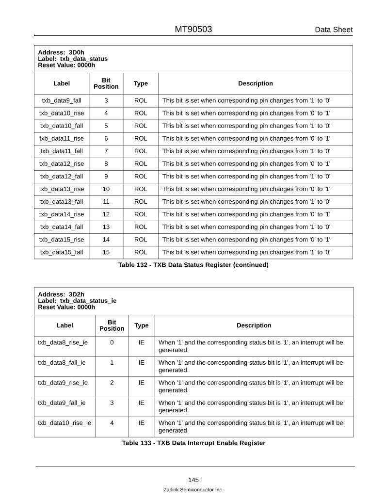
MT90503 Data Sheet
145Zarlink Semiconductor Inc.
txb_data9_fall 3 ROL This bit is set when corresponding pin changes from '1' to '0'
txb_data10_rise 4 ROL This bit is set when corresponding pin changes from '0' to '1'
txb_data10_fall 5 ROL This bit is set when corresponding pin changes from '1' to '0'
txb_data11_rise 6 ROL This bit is set when corresponding pin changes from '0' to '1'
txb_data11_fall 7 ROL This bit is set when corresponding pin changes from '1' to '0'
txb_data12_rise 8 ROL This bit is set when corresponding pin changes from '0' to '1'
txb_data12_fall 9 ROL This bit is set when corresponding pin changes from '1' to '0'
txb_data13_rise 10 ROL This bit is set when corresponding pin changes from '0' to '1'
txb_data13_fall 11 ROL This bit is set when corresponding pin changes from '1' to '0'
txb_data14_rise 12 ROL This bit is set when corresponding pin changes from '0' to '1'
txb_data14_fall 13 ROL This bit is set when corresponding pin changes from '1' to '0'
txb_data15_rise 14 ROL This bit is set when corresponding pin changes from '0' to '1'
txb_data15_fall 15 ROL This bit is set when corresponding pin changes from '1' to '0'
Address: 3D2h Label: txb_data_status_ie Reset Value: 0000h
Label BitPosition Type Description
txb_data8_rise_ie 0 IE When '1' and the corresponding status bit is '1', an interrupt will be generated.
txb_data8_fall_ie 1 IE When '1' and the corresponding status bit is '1', an interrupt will be generated.
txb_data9_rise_ie 2 IE When '1' and the corresponding status bit is '1', an interrupt will be generated.
txb_data9_fall_ie 3 IE When '1' and the corresponding status bit is '1', an interrupt will be generated.
txb_data10_rise_ie 4 IE When '1' and the corresponding status bit is '1', an interrupt will be generated.
Table 133 - TXB Data Interrupt Enable Register
Address: 3D0h Label: txb_data_status Reset Value: 0000h
Label BitPosition Type Description
Table 132 - TXB Data Status Register (continued)
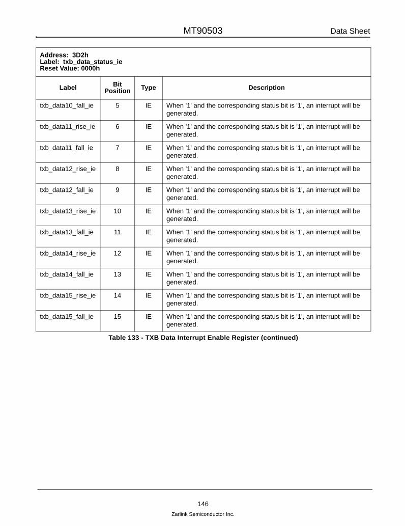
MT90503 Data Sheet
146Zarlink Semiconductor Inc.
txb_data10_fall_ie 5 IE When '1' and the corresponding status bit is '1', an interrupt will be generated.
txb_data11_rise_ie 6 IE When '1' and the corresponding status bit is '1', an interrupt will be generated.
txb_data11_fall_ie 7 IE When '1' and the corresponding status bit is '1', an interrupt will be generated.
txb_data12_rise_ie 8 IE When '1' and the corresponding status bit is '1', an interrupt will be generated.
txb_data12_fall_ie 9 IE When '1' and the corresponding status bit is '1', an interrupt will be generated.
txb_data13_rise_ie 10 IE When '1' and the corresponding status bit is '1', an interrupt will be generated.
txb_data13_fall_ie 11 IE When '1' and the corresponding status bit is '1', an interrupt will be generated.
txb_data14_rise_ie 12 IE When '1' and the corresponding status bit is '1', an interrupt will be generated.
txb_data14_fall_ie 13 IE When '1' and the corresponding status bit is '1', an interrupt will be generated.
txb_data15_rise_ie 14 IE When '1' and the corresponding status bit is '1', an interrupt will be generated.
txb_data15_fall_ie 15 IE When '1' and the corresponding status bit is '1', an interrupt will be generated.
Address: 3D2h Label: txb_data_status_ie Reset Value: 0000h
Label BitPosition Type Description
Table 133 - TXB Data Interrupt Enable Register (continued)

MT90503 Data Sheet
147Zarlink Semiconductor Inc.
Address: 3D4h Label: rxb_data_statusReset Value: 0000h
Label BitPosition Type Description
rxb_data8_rise 0 ROL This bit is set when corresponding pin changes from '0' to '1'
rxb_data8_fall 1 ROL This bit is set when corresponding pin changes from '1' to '0'
rxb_data9_rise 2 ROL This bit is set when corresponding pin changes from '0' to '1'
rxb_data9_fall 3 ROL This bit is set when corresponding pin changes from '1' to '0'
rxb_data10_rise 4 ROL This bit is set when corresponding pin changes from '0' to '1'
rxb_data10_fall 5 ROL This bit is set when corresponding pin changes from '1' to '0'
rxb_data11_rise 6 ROL This bit is set when corresponding pin changes from '0' to '1'
rxb_data11_fall 7 ROL This bit is set when corresponding pin changes from '1' to '0'
rxb_data12_rise 8 ROL This bit is set when corresponding pin changes from '0' to '1'
rxb_data12_fall 9 ROL This bit is set when corresponding pin changes from '1' to '0'
rxb_data13_rise 10 ROL This bit is set when corresponding pin changes from '0' to '1'
rxb_data13_fall 11 ROL This bit is set when corresponding pin changes from '1' to '0'
rxb_data14_rise 12 ROL This bit is set when corresponding pin changes from '0' to '1'
rxb_data14_fall 13 ROL This bit is set when corresponding pin changes from '1' to '0'
rxb_data15_rise 14 ROL This bit is set when corresponding pin changes from '0' to '1'
rxb_data15_fall 15 ROL This bit is set when corresponding pin changes from '1' to '0'
Table 134 - RXB Data Status Register
Address: 3D6h Label: rxb_data_status_ieReset Value: 0000h
Label BitPosition Type Description
rxb_data8_rise_ie 0 IE When '1' and the corresponding status bit is '1', an interrupt will be generated.
rxb_data8_fall_ie 1 IE When '1' and the corresponding status bit is '1', an interrupt will be generated.
rxb_data9_rise_ie 2 IE When '1' and the corresponding status bit is '1', an interrupt will be generated.
rxb_data9_fall_ie 3 IE When '1' and the corresponding status bit is '1', an interrupt will be generated.
Table 135 - RXB Data Interrupt Enable Register
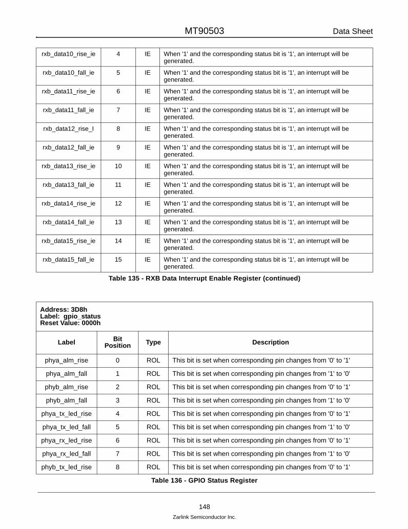
MT90503 Data Sheet
148Zarlink Semiconductor Inc.
rxb_data10_rise_ie 4 IE When '1' and the corresponding status bit is '1', an interrupt will be generated.
rxb_data10_fall_ie 5 IE When '1' and the corresponding status bit is '1', an interrupt will be generated.
rxb_data11_rise_ie 6 IE When '1' and the corresponding status bit is '1', an interrupt will be generated.
rxb_data11_fall_ie 7 IE When '1' and the corresponding status bit is '1', an interrupt will be generated.
rxb_data12_rise_I 8 IE When '1' and the corresponding status bit is '1', an interrupt will be generated.
rxb_data12_fall_ie 9 IE When '1' and the corresponding status bit is '1', an interrupt will be generated.
rxb_data13_rise_ie 10 IE When '1' and the corresponding status bit is '1', an interrupt will be generated.
rxb_data13_fall_ie 11 IE When '1' and the corresponding status bit is '1', an interrupt will be generated.
rxb_data14_rise_ie 12 IE When '1' and the corresponding status bit is '1', an interrupt will be generated.
rxb_data14_fall_ie 13 IE When '1' and the corresponding status bit is '1', an interrupt will be generated.
rxb_data15_rise_ie 14 IE When '1' and the corresponding status bit is '1', an interrupt will be generated.
rxb_data15_fall_ie 15 IE When '1' and the corresponding status bit is '1', an interrupt will be generated.
Address: 3D8h Label: gpio_status Reset Value: 0000h
Label Bit Position Type Description
phya_alm_rise 0 ROL This bit is set when corresponding pin changes from '0' to '1'
phya_alm_fall 1 ROL This bit is set when corresponding pin changes from '1' to '0'
phyb_alm_rise 2 ROL This bit is set when corresponding pin changes from '0' to '1'
phyb_alm_fall 3 ROL This bit is set when corresponding pin changes from '1' to '0'
phya_tx_led_rise 4 ROL This bit is set when corresponding pin changes from '0' to '1'
phya_tx_led_fall 5 ROL This bit is set when corresponding pin changes from '1' to '0'
phya_rx_led_rise 6 ROL This bit is set when corresponding pin changes from '0' to '1'
phya_rx_led_fall 7 ROL This bit is set when corresponding pin changes from '1' to '0'
phyb_tx_led_rise 8 ROL This bit is set when corresponding pin changes from '0' to '1'
Table 136 - GPIO Status Register
Table 135 - RXB Data Interrupt Enable Register (continued)

MT90503 Data Sheet
149Zarlink Semiconductor Inc.
phyb_tx_led_fall 9 ROL This bit is set when corresponding pin changes from '1' to '0'
phyb_rx_led_rise 10 ROL This bit is set when corresponding pin changes from '0' to '1'
phyb_rx_led_fall 11 ROL This bit is set when corresponding pin changes from '1' to '0'
reserved 15:12 ROL Reserved. Always read as "0000"
Address: 3DAh Label: gpio_status_ieReset Value: 0000h
Label BitPosition Type Description
phya_alm_rise_ie 0 IE When '1' and the corresponding status bit is '1', an interrupt will be generated.
phya_alm_fall_ie 1 IE When '1' and the corresponding status bit is '1', an interrupt will be generated.
phyb_alm_rise_ie 2 IE When '1' and the corresponding status bit is '1', an interrupt will be generated.
phyb_alm_fall_ie 3 IE When '1' and the corresponding status bit is '1', an interrupt will be generated.
phya_tx_led_rise_ie 4 IE When '1' and the corresponding status bit is '1', an interrupt will be generated.
phya_tx_led_fall_ie 5 IE When '1' and the corresponding status bit is '1', an interrupt will be generated.
phya_rx_led_rise_ie 6 IE When '1' and the corresponding status bit is '1', an interrupt will be generated.
phya_rx_led_fall_ie 7 IE When '1' and the corresponding status bit is '1', an interrupt will be generated.
phyb_tx_led_rise_ie 8 IE When '1' and the corresponding status bit is '1', an interrupt will be generated.
phyb_tx_led_fall_ie 9 IE When '1' and the corresponding status bit is '1', an interrupt will be generated.
phyb_rx_led_rise_ie 10 IE When '1' and the corresponding status bit is '1', an interrupt will be generated.
phyb_rx_led_fall_ie 11 IE When '1' and the corresponding status bit is '1', an interrupt will be generated.
Table 137 - GPIO Status Register
Address: 3D8h Label: gpio_status Reset Value: 0000h
Label Bit Position Type Description
Table 136 - GPIO Status Register (continued)
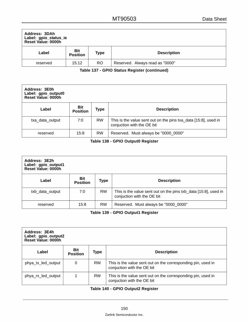
MT90503 Data Sheet
150Zarlink Semiconductor Inc.
reserved 15:12 RO Reserved. Always read as "0000"
Address: 3E0h Label: gpio_output0 Reset Value: 0000h
Label Bit Position Type Description
txa_data_output 7:0 RW This is the value sent out on the pins txa_data [15:8], used in conjuction with the OE bit
reserved 15:8 RW Reserved. Must always be "0000_0000"
Table 138 - GPIO Output0 Register
Address: 3E2h Label: gpio_output1 Reset Value: 0000h
Label Bit Position Type Description
txb_data_output 7:0 RW This is the value sent out on the pins txb_data [15:8], used in conjuction with the OE bit
reserved 15:8 RW Reserved. Must always be "0000_0000"
Table 139 - GPIO Output1 Register
Address: 3E4h Label: gpio_output2 Reset Value: 0000h
Label Bit Position Type Description
phya_tx_led_output 0 RW This is the value sent out on the corresponding pin, used in conjuction with the OE bit
phya_rx_led_output 1 RW This is the value sent out on the corresponding pin, used in conjuction with the OE bit
Table 140 - GPIO Output2 Register
Address: 3DAh Label: gpio_status_ieReset Value: 0000h
Label BitPosition Type Description
Table 137 - GPIO Status Register (continued)

MT90503 Data Sheet
151Zarlink Semiconductor Inc.
phyb_tx_led_output 2 RW This is the value sent out on the corresponding pin, used in conjuction with the OE bit
phyb_rx_led_output 3 RW This is the value sent out on the corresponding pin, used in conjuction with the OE bit
reserved 15:4 RW Reserved. Must always be "0000_0000_0000"
Address: 3E8hLabel: gpio_oe0Reset Value: 0000h
Label Bit Position Type Description
txa_data_oe 7:0 RW This is OE bit used to drive the txa_data [15:8] pins
reserved 15:8 RW Reserved. Must always be "0000_0000"
Table 141 - GPIO Output Enable0 Register
Address: 3EAh Label: gpio_oe1 Reset Value: 0000h
Label Bit Position Type Description
txb_data_oe 7:0 RW This is OE bit used to drive the txb_data [15:8] pins
reserved 15:8 RW Reserved. Must always be "0000_0000"
Table 142 - GPIO Output Enable1 Register
Address: 3E4h Label: gpio_output2 Reset Value: 0000h
Label Bit Position Type Description
Table 140 - GPIO Output2 Register (continued)
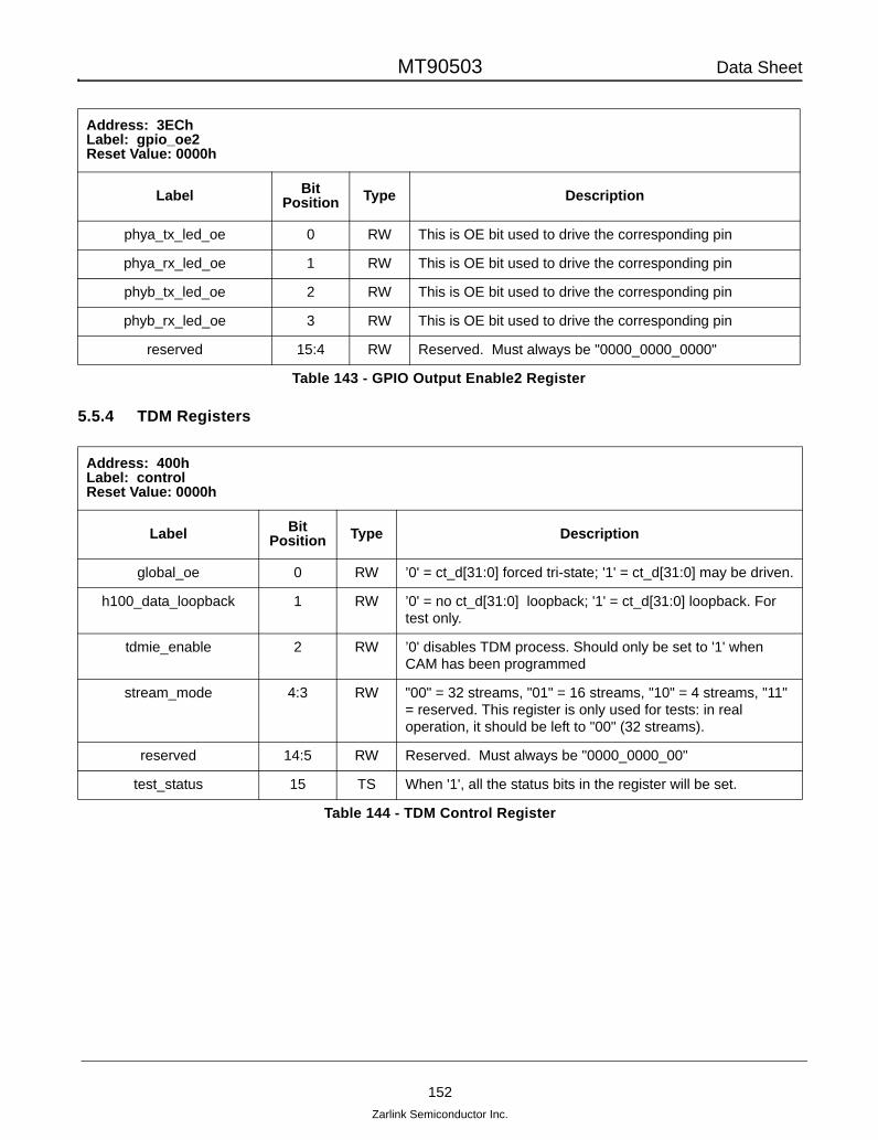
MT90503 Data Sheet
152Zarlink Semiconductor Inc.
5.5.4 TDM Registers
Address: 3ECh Label: gpio_oe2 Reset Value: 0000h
Label Bit Position Type Description
phya_tx_led_oe 0 RW This is OE bit used to drive the corresponding pin
phya_rx_led_oe 1 RW This is OE bit used to drive the corresponding pin
phyb_tx_led_oe 2 RW This is OE bit used to drive the corresponding pin
phyb_rx_led_oe 3 RW This is OE bit used to drive the corresponding pin
reserved 15:4 RW Reserved. Must always be "0000_0000_0000"
Table 143 - GPIO Output Enable2 Register
Address: 400h Label: control Reset Value: 0000h
Label Bit Position Type Description
global_oe 0 RW ’0' = ct_d[31:0] forced tri-state; '1' = ct_d[31:0] may be driven.
h100_data_loopback 1 RW ’0' = no ct_d[31:0] loopback; '1' = ct_d[31:0] loopback. For test only.
tdmie_enable 2 RW ’0' disables TDM process. Should only be set to '1' when CAM has been programmed
stream_mode 4:3 RW "00" = 32 streams, "01" = 16 streams, "10" = 4 streams, "11" = reserved. This register is only used for tests: in real operation, it should be left to "00" (32 streams).
reserved 14:5 RW Reserved. Must always be "0000_0000_00"
test_status 15 TS When '1', all the status bits in the register will be set.
Table 144 - TDM Control Register

MT90503 Data Sheet
153Zarlink Semiconductor Inc.
Address: 402h Label: status0 Reset Value: 0000h
Label BitPosition Type Description
tdm_out_of_bandwidth0 0 ROL Indicates that the TDM state machine is out of bandwidth. Fatal chip error, usually due to mclk frequency being too low.
cut_vc_detected 1 ROL This bit is set when 255 underruns are detected on a VC whose CAM entry has an enabled "Cut VC status enable" bit
underrun_detected 2 ROL Underrun reported on a voice channel on the ATM link.
cas_underrun_detected 3 ROL Underrun reported on CAS bits on the ATM link.
rdatamem_overflow 4 ROL Overflow in the TDM RX internal data memory. Fatal chip error.
tdmtxpip_overflow 5 ROL Overflow in the TDM TX data memory access cache. Fatal chip error.
tdmrxpip_overflow 6 ROL Overflow in the TDM RX data memory access cache. Fatal chip error.
reserved 15:7 ROL Reserved. Always read as "0000_0000_0"
Table 145 - TDM Status Register
Address: 408h Label: cut_vc_tsst Reset Value: 0000h
Label Bit Position Type Description
tsst_number_cut_vc 11:0 RO Indicates the TSST on which the last cut VC error occurred.
reserved 15:12 RO Reserved. Always read as "0000"
Table 146 - Cut VC TSST Register
Address: 40Ah Label: underrun_tsst Reset Value: 0000h
Label Bit Position Type Description
tsst_number_underrun 11:0 RO Indicates the TSST on which the last underrun error occurred.
reserved 15:12 RO Reserved. Always read as "0000"
Table 147 - TSST Underrun Register

MT90503 Data Sheet
154Zarlink Semiconductor Inc.
Address: 40Ch Label: cas_underrun_tsstReset Value: 0000h
Label Bit Position Type Description
tsst_number_cas_underrun 11:0 RO Indicates the TSST on which the last CAS underrun error occurred.
reserved 15:12 RO Reserved. Always read as "0000"
Table 148 - TSST CAS Underrun Register
Address: 410h Label: tdmint_reg0Reset Value: 0000h
Label Bit Position Type Description
h100_samp_clk_delay_flops 3:0 RW Number of flops used = 8 + value of this register. "1111" is reserved for selecting falling edge ct_c8 clock.
h100_samp_clk_delay_buff 7:4 RW "1111" is reserved for selecting rising edge ct_c8 clock
h100_oe_clk_delay_flops 11:8 RW Number of flops used = 8 + value of this register
h100_oe_clk_delay_buff 15:12 RW Number of delay buffers used in the delay chain.
Table 149 - TDM Interrupt 0 Register
Address: 412h Label: tdmint_reg1 Reset Value: 0000h
Label Bit Position Type Description
h100_ts_counter_timeout 6:0 RW Number of mclk cycles in 8 ct_c8 clock cycles - 10%
h100_oe_override_disable 7 RW '1' = do not tri-state the ct_d pin after every timeslot. To respect the H.100 standard, this should be left to '0'.
dstream_0_3_freq 9:8 RW ct_d[3:0] stream clock speed. "00" = 2.048 Mhz; "01" = 4.096 MHz; "10" = 8.192 MHz; "11" = reserved.
dstream_4_7_freq 11:10 RW ct_d[7:4] stream clock speed. "00" = 2.048 Mhz; "01" = 4.096 MHz; "10" = 8.192 MHz; "11" = reserved.
dstream_8_11_freq 13:12 RW ct_d[11:8] stream clock speed. "00" = 2.048 Mhz; "01" = 4.096 MHz; "10" = 8.192 MHz; "11" = reserved.
Table 150 - TDM Interrupt 1 Register

MT90503 Data Sheet
155Zarlink Semiconductor Inc.
dstream_12_15_freq 15:14 RW ct_d[15:12] stream clock speed. "00" = 2.048 Mhz; "01" = 4.096 MHz; "10" = 8.192 MHz; "11" = reserved.
Address: 420h Label: tdmie_misc Reset Value: 00FFh
Label Bit Position Type Description
null_byte 7:0 RW Null byte with which the chip will pad if underruns occur and null byte padding is chosen.
cas_enable_position 10:8 RW Position of the CAS enable bit within the byte on the TDM bus. The CAS nibble will be contained in the nibble in which the enable is not present. For example, if the enable is contained in bit 6, then the nibble will be in bits 3:0.
cas_enable_polarity 11 RW Polarity of the CAS enable bit on the TDM bus.
reserved 15:12 RW Reserved. Must always be "0000"
Table 151 - TDM Interrupt Enable Misc. Register
Address: 460h Label: pnt_ro Reset Value: 0000h
LabelBit
Position
Type Description
txsar_write_pnt_pcm_monitor[9:0]
9:0 RO The current value of the TDM write pointer sent to the TX SAR. Only used for tests.
reserved 15:10 RO Reserved. Always read as "0000_00"
Table 152 - TDM Write Pointer 0 Register
Address: 412h Label: tdmint_reg1 Reset Value: 0000h
Label Bit Position Type Description
Table 150 - TDM Interrupt 1 Register (continued)

MT90503 Data Sheet
156Zarlink Semiconductor Inc.
5.5.5 TX_SAR Registers
Address: 462h Label: txsar_pnt_fire Reset Value: 0000h
LabelBit
Position
Type Description
txsar_write_pnt_insert[9:0] 9:0 RW The test value of the TDM write pointer sent to the TX SAR. Only used for tests.
txsar_write_pnt_insert_ena 10 RW When '1', the above pointer will be sent to the TX SAR instead of the valid pointer. Only used for tests.
reserved 15:11 RO Reserved. Always read as "0000_00"
Table 153 - TDM Write Pointer 1 Register
Address: 464h Label: rxsar_pnt_fire Reset Value: 0000h
Label BitPosition Type Description
rxsar_write_pnt_insert[14:0] 14:0 RW The test value of the TDM read pointer sent to the RXSAR. Only used for tests.
rxsar_write_pnt_insert_ena 15 RW When '1', the above pointer will be sent to the RX SARinstead of the valid pointer. Only used for tests.
Table 154 - TDM Read Pointer Register
Address: 500h Label: control Reset Value: 0000h
Label Bit Position Type Description
reserved 14:0 RO Reserved. Always read as "0000_0000_0000_000"
test_status 15 TS When '1', all the status bits in the register will be set.
Table 155 - TX_SAR Control Register
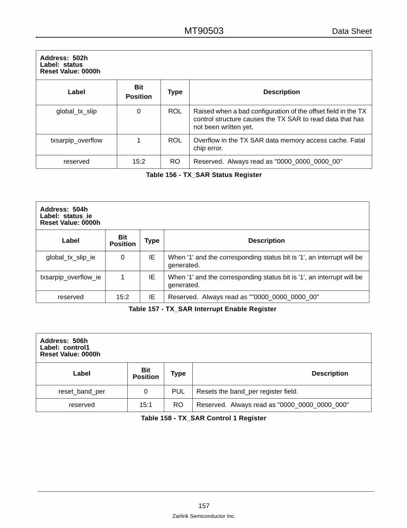
MT90503 Data Sheet
157Zarlink Semiconductor Inc.
Address: 502h Label: status Reset Value: 0000h
LabelBit
PositionType Description
global_tx_slip 0 ROL Raised when a bad configuration of the offset field in the TX control structure causes the TX SAR to read data that has not been written yet.
txsarpip_overflow 1 ROL Overflow in the TX SAR data memory access cache. Fatal chip error.
reserved 15:2 RO Reserved. Always read as "0000_0000_0000_00"
Table 156 - TX_SAR Status Register
Address: 504h Label: status_ie Reset Value: 0000h
Label BitPosition Type Description
global_tx_slip_ie 0 IE When '1' and the corresponding status bit is '1', an interrupt will be generated.
txsarpip_overflow_ie 1 IE When '1' and the corresponding status bit is '1', an interrupt will be generated.
reserved 15:2 IE Reserved. Always read as ""0000_0000_0000_00"
Table 157 - TX_SAR Interrupt Enable Register
Address: 506h Label: control1 Reset Value: 0000h
Label Bit Position Type Description
reset_band_per 0 PUL Resets the band_per register field.
reserved 15:1 RO Reserved. Always read as "0000_0000_0000_000"
Table 158 - TX_SAR Control 1 Register

MT90503 Data Sheet
158Zarlink Semiconductor Inc.
Address: 508hLabel: data_cell_read Reset Value: 0000h
Label Bit Position Type Description
data_read_pnt 13:0 RO Chip's read pointer to the AAL0 FIFO.
reserved 15:14 RO Reserved. Always read as "00"
Table 159 - TX_SAR Data Read Pointer Register
Address: 50Ah Label: data_cell_write Reset Value: 0000h
Label Bit Position Type Description
data_write_pnt 13:0 RW CPU's write pointer to the AAL0 FIFO.
reserved 15:14 RW Reserved. Must always be "00"
Table 160 - TX_SAR Data Write Pointer Register
Address: 50Ch Label: data_cell_add Reset Value: 0000h
Label Bit Position Type Description
data_add 13:0 RW Bits 19:6 of the address of the FIFO in external memory
reserved 15:14 RW Reserved. Always read as "00"
Table 161 - TX_SAR Data Address Register
Address: 50Eh Label: data_cell_size Reset Value: 0000h
Label Bit Position Type Description
data_size 13:0 RW Size of data cell FIFO in 1 cell increments. All zeros = 16k cells. Minimum 4 cells.
reserved 15:14 RW Reserved. Must always be "00"
Table 162 - TX_SAR Data Cell Size Register

MT90503 Data Sheet
159Zarlink Semiconductor Inc.
5.5.6 Scheduler Registers
Address: 510h Label: percentage_of_bandwidthReset Value: 0000h
Label Bit Position Type Description
band_per 15:0 RO Monitor of the maximum number of mclk cycles that it has taken the chip to treat an entire TX SAR frame. If this number is greater than mclk (in Hz) / 8000, some of the frames are overloaded.
Table 163 - Percent of Bandwidth Register
Address: 600h Label: control Reset Value: 0000h
Label BitPosition Type Description
test_status 15 TS When '1', all the status bits in the register will be set.
Table 164 - Scheduler Test Status Register
Address: 602h Label: status Reset Value: 0000h
Label BitPosition Type Description
out_of_band 0 ROL Indicates that the wheel treatment is more than fr_late frames late. This means that at least some of the frames in the wheels are overloaded.
reserved 15:1 ROL Reserved. Always read as "0000_0000_0000_000"
Table 165 - Scheduler Status Register
Address: 604h Label: status_ie Reset Value: 0000h
Label BitPosition Type Description
out_of_band_ie 0 IE When '1' and the corresponding status bit is '1', an interrupt will be generated.
reserved 15:1 IE Reserved. Always read as "0000_0000_0000_000"
Table 166 - Scheduler Interrupt Enable Register

MT90503 Data Sheet
160Zarlink Semiconductor Inc.
Address: 608h Label: frame_latency Reset Value: 0001h
Label Bit Position Type Description
fr_late 3:0 RW Number of frames by which the chip is allowed to be late. 0h = illegal.
reserved 15:4 RW Reserved. Must always be "0000_0000_0000"
Table 167 - Frame Latency Register
Address: 610h Label: wheel_info _0 Reset Value: 0001h
Label BitPosition Type Description
wheel0_ena 0 RW Enable for wheel 0.
wheel0_inf 3:1 RW Configuration of wheel 0. "000" = normal, "100" = T1, "101" = E1, others reserved.l
wheel1_ena 4 RW Enable for wheel 1.
wheel1_inf 7:5 RW Configuration of wheel 1. "000" = normal, "100" = T1, "101" = E1, others reserved.
wheel2_ena 8 RW Enable for wheel 2.
wheel2_inf 11:9 RW Configuration of wheel 2. "000" = normal, "100" = T1, "101" = E1, others reserved.
wheel3_ena 12 RW Enable for wheel 3.
wheel3_inf 15:13 RW Configuration of wheel 3. "000" = normal, "100" = T1, "101" = E1, others reserved.
Table 168 - Scheduler Configuration & Enable 0 Register
Address: 612h Label: wheel_inf_1 Reset Value: 0000h
Label Bit Position Type Description
wheel4_ena 0 RW Enable for wheel 4.
wheel4_inf 3:1 RW Configuration of wheel 4. "000" = normal,"100" = T1, "101" = E1, others reserved.
Table 169 - Scheduler Configuration & Enable 1 Register
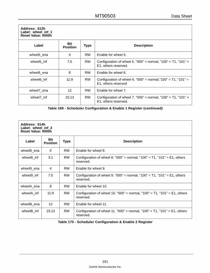
MT90503 Data Sheet
161Zarlink Semiconductor Inc.
wheel5_ena 4 RW Enable for wheel 5.
wheel5_inf 7:5 RW Configuration of wheel 5. "000" = normal, "100" = T1, "101" = E1, others reserved.
wheel6_ena 8 RW Enable for wheel 6.
wheel6_inf 11:9 RW Configuration of wheel 6. "000" = normal,"100" = T1, "101" = E1, others reserved
wheel7_ena 12 RW Enable for wheel 7.
wheel7_inf 15:13 RW Configuration of wheel 7. "000" = normal, "100" = T1, "101" = E1, others reserved.
Address: 614h Label: wheel_inf_2 Reset Value: 0000h
Label BitPosition Type Description
wheel8_ena 0 RW Enable for wheel 8.
wheel8_inf 3:1 RW Configuration of wheel 8. "000" = normal, "100" = T1, "101" = E1, others reserved.
wheel9_ena 4 RW Enable for wheel 9.
wheel9_inf 7:5 RW Configuration of wheel 9. "000" = normal, "100" = T1, "101" = E1, others reserved.
wheelA_ena 8 RW Enable for wheel 10.
wheelA_inf 11:9 RW Configuration of wheel 10. "000" = normal, "100" = T1, "101" = E1, others reserved.
wheelB_ena 12 RW Enable for wheel 11.
wheelB_inf 15:13 RW Configuration of wheel 11. "000" = normal, "100" = T1, "101" = E1, others reserved.
Table 170 - Scheduler Configuration & Enable 2 Register
Address: 612h Label: wheel_inf_1 Reset Value: 0000h
Label Bit Position Type Description
Table 169 - Scheduler Configuration & Enable 1 Register (continued)
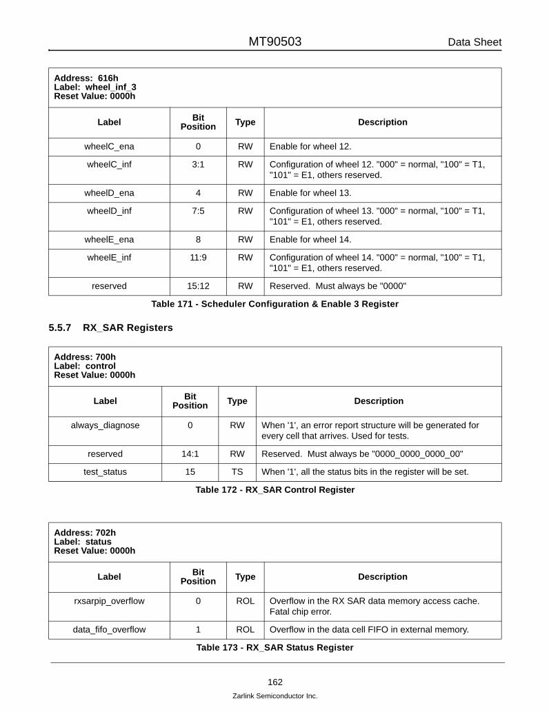
MT90503 Data Sheet
162Zarlink Semiconductor Inc.
5.5.7 RX_SAR Registers
Address: 616h Label: wheel_inf_3 Reset Value: 0000h
Label Bit Position Type Description
wheelC_ena 0 RW Enable for wheel 12.
wheelC_inf 3:1 RW Configuration of wheel 12. "000" = normal, "100" = T1, "101" = E1, others reserved.
wheelD_ena 4 RW Enable for wheel 13.
wheelD_inf 7:5 RW Configuration of wheel 13. "000" = normal, "100" = T1, "101" = E1, others reserved.
wheelE_ena 8 RW Enable for wheel 14.
wheelE_inf 11:9 RW Configuration of wheel 14. "000" = normal, "100" = T1, "101" = E1, others reserved.
reserved 15:12 RW Reserved. Must always be "0000"
Table 171 - Scheduler Configuration & Enable 3 Register
Address: 700h Label: control Reset Value: 0000h
Label Bit Position Type Description
always_diagnose 0 RW When '1', an error report structure will be generated for every cell that arrives. Used for tests.
reserved 14:1 RW Reserved. Must always be "0000_0000_0000_00"
test_status 15 TS When '1', all the status bits in the register will be set.
Table 172 - RX_SAR Control Register
Address: 702hLabel: statusReset Value: 0000h
Label Bit Position Type Description
rxsarpip_overflow 0 ROL Overflow in the RX SAR data memory access cache. Fatal chip error.
data_fifo_overflow 1 ROL Overflow in the data cell FIFO in external memory.
Table 173 - RX_SAR Status Register

MT90503 Data Sheet
163Zarlink Semiconductor Inc.
error_fifo_overflow 2 ROL Overflow in the error report structure FIFO in external memory.
reserved 15:3 ROL Reserved. Always read as "0000_0000_0000_0"
Address: 704h Label: status_ie Reset Value: 0000h
Label BitPosition Type Description
rxsarpip_overflow_ie 0 IE When '1' and the corresponding status bit is '1', an interrupt will be generated.
data_fifo_overflow_ie 1 IE When '1' and the corresponding status bit is '1', an interrupt will be generated.
error_fifo_overflow_ie 2 IE When '1' and the corresponding status bit is '1', an interrupt will be generated.
reserved 15:3 IE Reserved. Always read as "0000_0000_0000_0"
Table 174 - RX_SAR Interrupt Enable Register
Address: 00708h Label: data_cell_read Reset Value: 0000h
Label Bit Position Type Description
data_read_pnt 13:0 RW The CPU's read pointer to the AAL0 cell FIFO.
reserved 15:14 RW Reserved. Must always be "00"
Table 175 - RX_SAR Data Read Pointer Register
Address: 702hLabel: statusReset Value: 0000h
Label Bit Position Type Description
Table 173 - RX_SAR Status Register (continued)

MT90503 Data Sheet
164Zarlink Semiconductor Inc.
Address: 70AhLabel: data_cell_writeReset Value: 0000h
Label Bit Position Type Description
data_write_pnt 13:0 RO The chip's write pointer to the AAL0 cell FIFO.
reserved 15:14 RO Reserved. Always read as "00"
Table 176 - RX_SAR Data Write Pointer Register
Address: 70Ch Label: data_cell_add Reset Value: 0000h
Label Bit Position Type Description
data_add 13:0 RW Bits 19:6 of the address of the FIFO in external memory
reserved 15:14 RW Reserved. Must always be "00"
Table 177 - RX_SAR Data Address Register
Address: 70EhLabel: data_cell_sizeReset Value: 0000h
Label Bit Position Type Description
data_size 13:0 RW Size of data cell FIFO in 1 cell increments. All zeros = 16k cells.
reserved 15:14 RW Reserved. Must always be "00"
Table 178 - RX_SAR Data Cell Size Register
Address: 710h Label: error_struct_read Reset Value: 0000h
Label Bit Position Type Description
error_read_pnt 15:0 RW The CPU's read pointer to the error report structure FIFO.
Table 179 - Error Structure Read Register
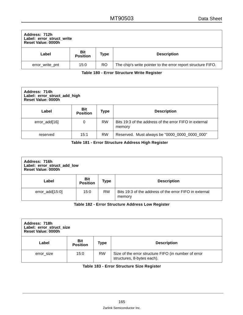
MT90503 Data Sheet
165Zarlink Semiconductor Inc.
Address: 712h Label: error_struct_write Reset Value: 0000h
Label Bit Position Type Description
error_write_pnt 15:0 RO The chip's write pointer to the error report structure FIFO.
Table 180 - Error Structure Write Register
Address: 714h Label: error_struct_add_high Reset Value: 0000h
Label Bit Position Type Description
error_add[16] 0 RW Bits 19:3 of the address of the error FIFO in external memory
reserved 15:1 RW Reserved. Must always be "0000_0000_0000_000"
Table 181 - Error Structure Address High Register
Address: 716h Label: error_struct_add_lowReset Value: 0000h
Label Bit Position Type Description
error_add[15:0] 15:0 RW Bits 19:3 of the address of the error FIFO in external memory
Table 182 - Error Structure Address Low Register
Address: 718h Label: error_struct_size Reset Value: 0000h
Label Bit Position Type Description
error_size 15:0 RW Size of the error structure FIFO (in number of error structures, 8-bytes each).
Table 183 - Error Structure Size Register

MT90503 Data Sheet
166Zarlink Semiconductor Inc.
Address: 720h Label: aal0_timeout_highReset Value: 0000h
Label Bit Position Type Description
aal0_timeout_period[19:16] 3:0 RW Time, in us, that an AAL0 cell can wait in the FIFO before an alarm is generated.
reserved 15:4 RW Reserved. Must always be "0000_0000_0000"
Table 184 - AAL0 Timeout High Register
Address: 722h Label: aal0_timeout_lowReset Value: 0000h
Label BitPosition Type Description
aal0_timeout_period[15:0]
15:0 RW Time, in us, that an AAL0 cell can wait in the FIFO before an alarm is generated.
Table 185 - AAL0 Timeout Low Register
Address: 724h Label: error_timeout_high Reset Value: 0000h
Label Bit Position Type Description
error_timeout_period[19:16] 3:0 RW Time, in us, that an error structure can wait in the FIFO before an alarm is generated.
reserved 15:4 RW Reserved. Must always be "0000_0000_0000"
Table 186 - Error Timeout High Register
Address: 726h Label: error_timeout_low Reset Value: 0000h
Label Bit Position Type Description
error_timeout_period[15:0] 15:0 RW Time, in us, that an error structure can wait in the FIFO before an alarm is generated.
Table 187 - Error Timeout Low Register
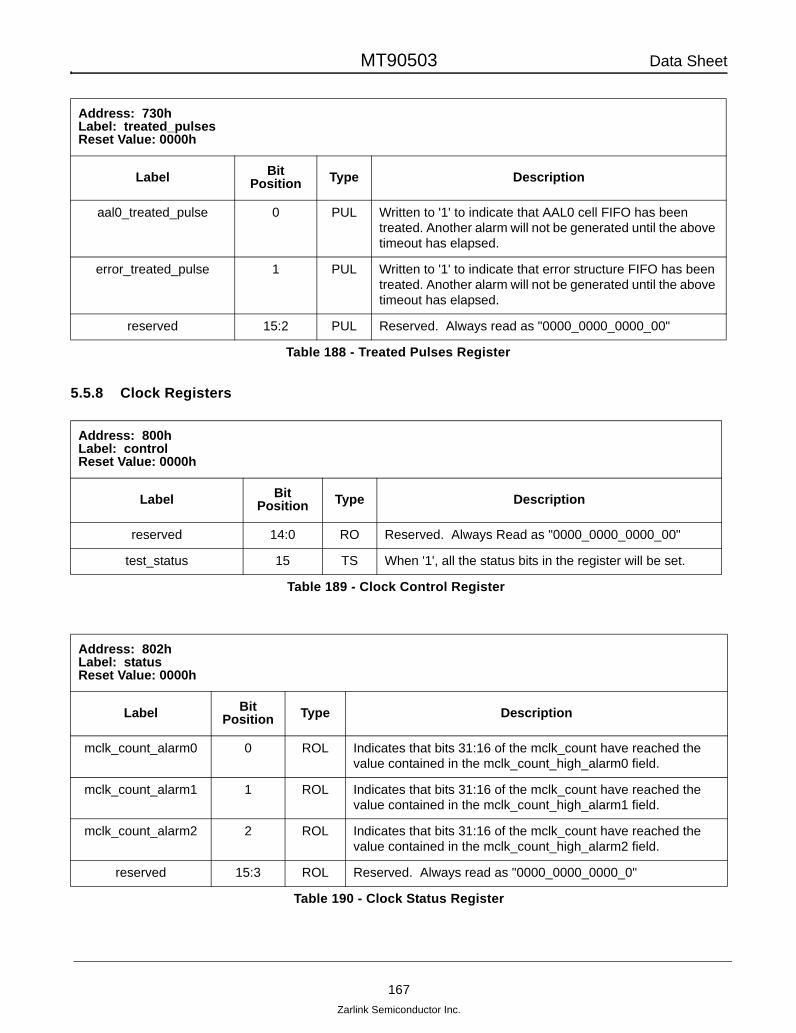
MT90503 Data Sheet
167Zarlink Semiconductor Inc.
5.5.8 Clock Registers
Address: 730h Label: treated_pulses Reset Value: 0000h
Label Bit Position Type Description
aal0_treated_pulse 0 PUL Written to '1' to indicate that AAL0 cell FIFO has been treated. Another alarm will not be generated until the above timeout has elapsed.
error_treated_pulse 1 PUL Written to '1' to indicate that error structure FIFO has been treated. Another alarm will not be generated until the above timeout has elapsed.
reserved 15:2 PUL Reserved. Always read as "0000_0000_0000_00"
Table 188 - Treated Pulses Register
Address: 800h Label: control Reset Value: 0000h
Label BitPosition Type Description
reserved 14:0 RO Reserved. Always Read as "0000_0000_0000_00"
test_status 15 TS When '1', all the status bits in the register will be set.
Table 189 - Clock Control Register
Address: 802h Label: status Reset Value: 0000h
Label BitPosition Type Description
mclk_count_alarm0 0 ROL Indicates that bits 31:16 of the mclk_count have reached the value contained in the mclk_count_high_alarm0 field.
mclk_count_alarm1 1 ROL Indicates that bits 31:16 of the mclk_count have reached the value contained in the mclk_count_high_alarm1 field.
mclk_count_alarm2 2 ROL Indicates that bits 31:16 of the mclk_count have reached the value contained in the mclk_count_high_alarm2 field.
reserved 15:3 ROL Reserved. Always read as "0000_0000_0000_0"
Table 190 - Clock Status Register

MT90503 Data Sheet
168Zarlink Semiconductor Inc.
Address: 804h Label: status_ie Reset Value: 0000h
Label Bit Position Type Description
mclk_count_alarm0_ie 0 IE When '1' and the corresponding status bit is '1', and interrupt will be generated.
mclk_count_alarm1_ie 1 IE When '1' and the corresponding status bit is '1', and interrupt will be generated.
mclk_count_alarm2_ie 2 IE When '1' and the corresponding status bit is '1', and interrupt will be generated.
reserved 15:3 IE Reserved. Always read as "0000_0000_0000_0"
Table 191 - Status Interrupt Enable Register
Address: 806h Label: mclk_count_high_alm0 Reset Value: 0000h
Label Bit Position Type Description
mclk_count_high_alarm0 15:0 RW This register in conjuction with an interrupt enable can be used as a scheduler or as a Periodic Interrupt Controler.
Table 192 - MCLK Alarm 0 Register
Address: 808h Label: mclk_count_high Reset Value: 0000h
Label Bit Position Type Description
mclk_count[31:16] 15:0 RO Freerunning counter of mclk.
Table 193 - MCLK Counter High Register
Address: 80Ah Label: mclk_count_low Reset Value: 0000h
Label Bit Position Type Description
mclk_count[15:0] 15:0 RO Freerunning counter of mclk.
Table 194 - MCLK Counter Low Register
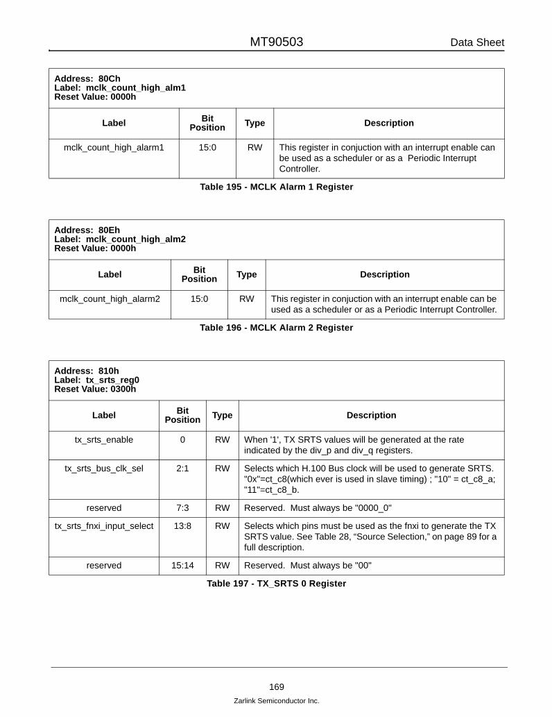
MT90503 Data Sheet
169Zarlink Semiconductor Inc.
Address: 80Ch Label: mclk_count_high_alm1 Reset Value: 0000h
Label Bit Position Type Description
mclk_count_high_alarm1 15:0 RW This register in conjuction with an interrupt enable can be used as a scheduler or as a Periodic Interrupt Controller.
Table 195 - MCLK Alarm 1 Register
Address: 80Eh Label: mclk_count_high_alm2 Reset Value: 0000h
Label Bit Position Type Description
mclk_count_high_alarm2 15:0 RW This register in conjuction with an interrupt enable can be used as a scheduler or as a Periodic Interrupt Controller.
Table 196 - MCLK Alarm 2 Register
Address: 810h Label: tx_srts_reg0 Reset Value: 0300h
Label BitPosition Type Description
tx_srts_enable 0 RW When '1', TX SRTS values will be generated at the rate indicated by the div_p and div_q registers.
tx_srts_bus_clk_sel 2:1 RW Selects which H.100 Bus clock will be used to generate SRTS. "0x"=ct_c8(which ever is used in slave timing) ; "10" = ct_c8_a; "11"=ct_c8_b.
reserved 7:3 RW Reserved. Must always be "0000_0"
tx_srts_fnxi_input_select 13:8 RW Selects which pins must be used as the fnxi to generate the TX SRTS value. See Table 28, “Source Selection,” on page 89 for a full description.
reserved 15:14 RW Reserved. Must always be "00"
Table 197 - TX_SRTS 0 Register
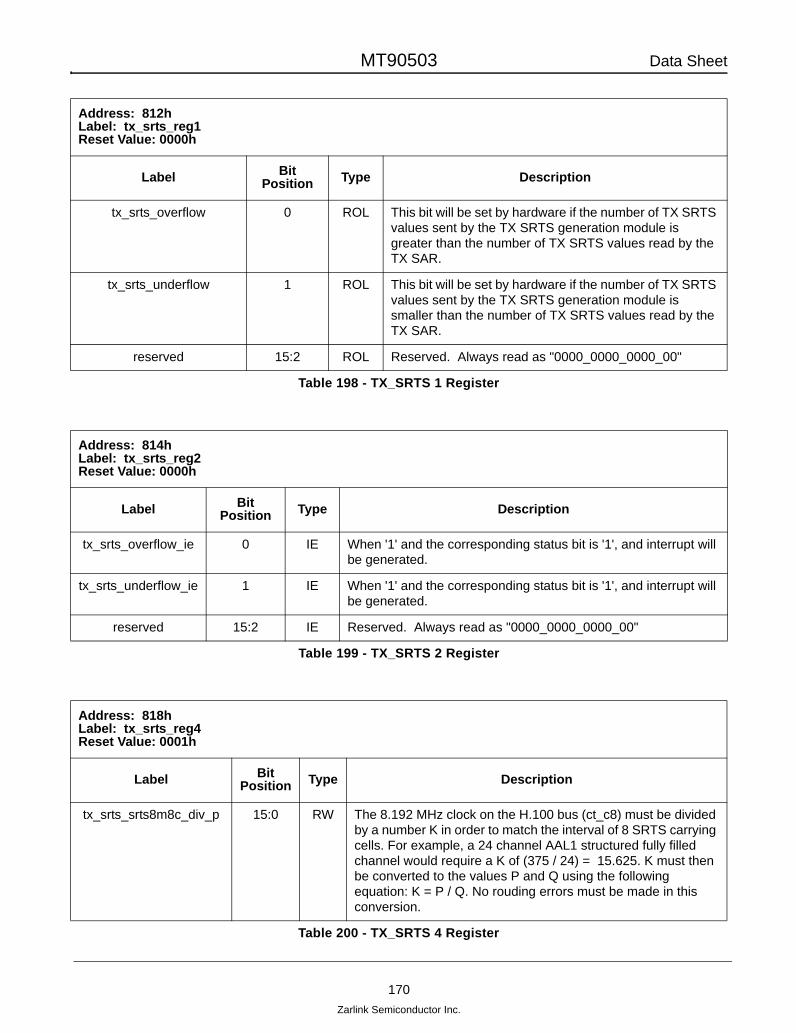
MT90503 Data Sheet
170Zarlink Semiconductor Inc.
Address: 812h Label: tx_srts_reg1 Reset Value: 0000h
Label Bit Position Type Description
tx_srts_overflow 0 ROL This bit will be set by hardware if the number of TX SRTS values sent by the TX SRTS generation module is greater than the number of TX SRTS values read by the TX SAR.
tx_srts_underflow 1 ROL This bit will be set by hardware if the number of TX SRTS values sent by the TX SRTS generation module is smaller than the number of TX SRTS values read by the TX SAR.
reserved 15:2 ROL Reserved. Always read as "0000_0000_0000_00"
Table 198 - TX_SRTS 1 Register
Address: 814h Label: tx_srts_reg2 Reset Value: 0000h
Label Bit Position Type Description
tx_srts_overflow_ie 0 IE When '1' and the corresponding status bit is '1', and interrupt will be generated.
tx_srts_underflow_ie 1 IE When '1' and the corresponding status bit is '1', and interrupt will be generated.
reserved 15:2 IE Reserved. Always read as "0000_0000_0000_00"
Table 199 - TX_SRTS 2 Register
Address: 818h Label: tx_srts_reg4 Reset Value: 0001h
Label BitPosition Type Description
tx_srts_srts8m8c_div_p 15:0 RW The 8.192 MHz clock on the H.100 bus (ct_c8) must be divided by a number K in order to match the interval of 8 SRTS carrying cells. For example, a 24 channel AAL1 structured fully filled channel would require a K of (375 / 24) = 15.625. K must then be converted to the values P and Q using the following equation: K = P / Q. No rouding errors must be made in this conversion.
Table 200 - TX_SRTS 4 Register

MT90503 Data Sheet
171Zarlink Semiconductor Inc.
Address: 81Ah Label: tx_srts_reg5 Reset Value: 0001h
Label Bit Position Type Description
tx_srts_srts8m8c_div_q 15:0 RW See Table 200, “TX_SRTS 4 Register,” on page 170 for a descrption of tx_srts_srts8m8c_div_p.
Table 201 - TX_SRTS 5 Register
Address: 820h Label: adapsrts0_reg0 Reset Value: 0000h
Label Bit Position Type Description
adapsrts0_adaptive_enable 0 RW When '1', the RX Adaptive block 0 is activated. Received cells on VCs tagged as clock recovery VC 'A' will generate an Adaptive point that will be written to external memory.
adapsrts0_rx_srts_enable 1 RW When '1', the RX SRTS block 0 is activated. Received SRTS values on VCs tagged as clock recovery VC 'A' will be written to external memory. Also, local SRTS value will be generated using of the H.100 clocks.
adapsrts0_ignore_crc 2 RW When '1', this bit forces the CRC in the AAL1 Header to be ignored. CRC Errors are reported no matter the state of this bit.
adapsrts0_ignore_parity 3 RW When '1', this bit forces the Parity bit in the AAL1 Header to be ignored. Parity Errors are reported no matter the state of this bit.
adapsrts0_ignore_seq_num 4 RW When '1', this bit forces the Sequence Number t in the AAL1 Header to be ignored. Sequence Number Errors are reported no matter the state of this bit.
adapsrts0_pclk_loss 5 RW This bit can be directly routed out on a recov_X pin in order to convey the state (good / bad) of the clock generated by the adapsrts block 0.
adapsrts0_pclk_divisor_load_now 6 PUL When this bit is written to '1', the pclk_div and pclk_frc are loaded into the digital PLL used to synthesize the pclk.
adapsrts0_pclk_divisor_reset 7 RW When '0', the digital PLL used to synthesize pclk is put in reset state. When '1', it is not longer in reset.
reserved 15:8 RW Reserved. Must always be "0000_0000"
Table 202 - Adaptive SRTS0 0 Register

MT90503 Data Sheet
172Zarlink Semiconductor Inc.
Address: 822h Label: adapsrts0_reg1 Reset Value: 0000h
Label BitPosition Type Description
adapsrts0_aal1_crc_error 0 ROL Set when an AAL1-byte CRC error occurs on cells used in the adapsrts0 block.
adapsrts0_aal1_bad_parity 1 ROL Set when an AAL1-byte parity error occurs on cells used in the adapsrts0 block.
adapsrts0_single_cell_lost 2 ROL Set when a single cell loss error occurs on cells used in the adapsrts0 block.
adapsrts0_multi_cell_lost 3 ROL Set when a multiple cell loss error occurs on cells used in the adapsrts0 block.
adapsrts0_cell_misinserted 4 ROL Set when a cell misinsertion error occurs on cells used in the adapsrts0 block.
adapsrts0_timeout_flag 5 RO Set when a the interval between two cells used in the adapsrts0 block is greater than adapsrts0_time_out_period. This bit is automatically cleared by hardware when the timeout condition ceases.
adapsrts0_timeout_pulse 6 ROL Set when a the interval between two cells used in the adapsrts0 block is greater than adapsrts0_time_out_period.
adapsrts0_rx_srts_remote_overflow
7 ROL Set when two consecutive remote SRTS value were received, and when the second value could not be stored because the interval was too short.
adapsrts0_rx_srts_local_overflow 8 ROL Set when two consecutive local SRTS value were received, and when the second value could not be stored because the interval was too short.
reserved 15:9 ROL Reserved. Always read as "0000_000"
Table 203 - Adaptive SRTS0 1 Register
Address: 824h Label: adapsrts0_reg2 Reset Value: 0000h
Label BitPosition Type Description
adapsrts0_aal1_crc_error_ie 0 IE When '1' and the corresponding status bit is '1', and interrupt will be generated.
Table 204 - Adaptive SRTS0 2 Register

MT90503 Data Sheet
173Zarlink Semiconductor Inc.
adapsrts0_aal1_bad_parity_ie 1 IE When '1' and the corresponding status bit is '1', and interrupt will be generated.
adapsrts0_single_cell_lost_ie 2 IE When '1' and the corresponding status bit is '1', and interrupt will be generated.
adapsrts0_multi_cell_lost_ie 3 IE When '1' and the corresponding status bit is '1', and interrupt will be generated.
adapsrts0_cell_misinserted_ie 4 IE When '1' and the corresponding status bit is '1', and interrupt will be generated.
reserved 5 RO Reserved. Always read as "0"
adapsrts0_timeout_pulse_ie 6 IE When '1' and the corresponding status bit is '1', and interrupt will be generated.
adapsrts0_rx_srts_remote_overflow_ie
7 IE When '1' and the corresponding status bit is '1', and interrupt will be generated.
adapsrts0_rx_srts_local_overflow_ie 8 IE When '1' and the corresponding status bit is '1', and interrupt will be generated.
reserved 15:9 IE Reserved. Always read as "0000_000"
Address: 826h Label: adapsrts0_reg3 Reset Value: 0000h
Label BitPosition Type Description
adapsrts0_ref_input_select 5:0 RW In adaptive mode, this field indicates which events the adapsrts0 block will consider as a timing reference. Rising edges on the recov_X pins can be used. Cell arrival events on Clock Recovery VC A or B can be used. See Table 28, “Source Selection,” on page 89" for more details.
reserved 7:6 RO Reserved. Always read as "00"
adapsrts0_rx_fnxi_input_select 13:8 RW In SRTS mode, this selects the fnxi input used in the RX SRTS block. See Table 28, “Source Selection,” on page 89" for more details.
reserved 15:14 RO Reserved. Always read as "00"
Table 205 - Adaptive SRTS0 3 Register
Address: 824h Label: adapsrts0_reg2 Reset Value: 0000h
Label BitPosition Type Description
Table 204 - Adaptive SRTS0 2 Register (continued)

MT90503 Data Sheet
174Zarlink Semiconductor Inc.
Address: 828h Label: adapsrts0_reg4 Reset Value: 0000h
Label BitPosition Type Description
adapsrts0_time_out_period 15:0 RW This value defines the time-out period between two cells in both adaptive and SRTS mode. Unit is 1024 mclk cycles. 0000h will disabled checking.
Table 206 - Adaptive SRTS0 4 Register
Address: 82Ah Label: adapsrts0_reg5 Reset Value: 0000h
Label BitPosition Type Description
adapsrts0_adap_pnt_elim_x 7:0 RW In adaptive mode, this value defined how many points will be deleted vs how many points will be kept and written to external memory. It is defined as "keep 1 point out of X".
reserved 15:8 RW Reserved. Must always be "0000_0000"
Table 207 - Adaptive SRTS0 5 Register
Address: 82Ch Label: adapsrts0_reg6 Reset Value: 0001h
Label Bit Position Type Description
adapsrts0_srts8m8c_div_p 15:0 RW The clock generated by the digital PLL (pclk at 8KHz) must be divided by a number K in order to match the interval of 8 SRTS carrying cells. For example, a 24 channel AAL1 structured fully filled channel would require a K of (375 / 24) = 15.625 . K must then be converted to the values P and Q using the following equation: K = P / Q. No rouding errors must be made in this conversion.
Table 208 - Adaptive SRTS0 6 Register

MT90503 Data Sheet
175Zarlink Semiconductor Inc.
Address: 82Eh Label: adapsrts0_reg7 Reset Value: 0001h
Label BitPosition Type Description
adapsrts0_srts8m8c_div_q 15:0 RW See adapsrts0_srts8m8c_div_p description.
Table 209 - Adaptive SRTS0 7 Register
Address: 830h Label: adapsrts0_reg8 Reset Value: 2710h
Label BitPosition Type Description
adapsrts0_pclk_div 15:0 RW In order to generate pclk, mclk must be divided by a factor K. This factor is likely to be fractional. The integer part of K is written in the form X / 65536, where X is written in the adapsrts0_pclk_frc register.
Table 210 - Adaptive SRTS0 8 Register
Address: 832h Label: adapsrts0_reg9 Reset Value: 0000h
Label BitPosition Type Description
adapsrts0_pclk_frc 15:0 RW For a description see adapsrts0_pclk_div adapsrts0_pclk_div above.
Table 211 - Adaptive SRTS0 9 Register
Address: 840h Label: adapsrts1_reg0 Reset Value: 0000h
Label BitPosition Type Description
adapsrts1_adaptive_enable 0 RW See adapsrts0 registers 820h to 83Eh.
adapsrts1_rx_srts_enable 1 RW
adapsrts1_ignore_crc 2 RW
adapsrts1_ignore_parity 3 RW
Table 212 - Adaptive SRTS1 0 Register

MT90503 Data Sheet
176Zarlink Semiconductor Inc.
adapsrts1_ignore_seq_num 4 RW
adapsrts1_pclk_loss 5 RW
adapsrts1_pclk_divisor_load_now 6 PUL
adapsrts1_pclk_divisor_reset 7 RW
reserved 15:8 RW Reserved. Must always be "0000_0000"
Address: 842h Label: adapsrts1_reg1 Reset Value: 0000h
Label BitPosition Type Description
adapsrts1_aal1_crc_error 0 ROL See Address: 822h, Table 203, “Adaptive SRTS0 1 Register,” on page 172.
adapsrts1_aal1_bad_parity 1 ROL
adapsrts1_single_cell_lost 2 ROL
adapsrts1_multi_cell_lost 3 ROL
adapsrts1_cell_misinserted 4 ROL
adapsrts1_timeout_flag 5 RO
adapsrts1_timeout_pulse 6 ROL
adapsrts1_rx_srts_remote_overflow 7 ROL
adapsrts1_rx_srts_local_overflow 8 ROL
reserved 15:9 ROL Reserved. Always read as "0000_000"
Table 213 - Adaptive SRTS1 1Register
Address: 840h Label: adapsrts1_reg0 Reset Value: 0000h
Label BitPosition Type Description
Table 212 - Adaptive SRTS1 0 Register (continued)

MT90503 Data Sheet
177Zarlink Semiconductor Inc.
Address: 844h Label: adapsrts1_reg2 Reset Value: 0000h
Label Bit Position Type Description
adapsrts1_aal1_crc_error_ie 0 IE
adapsrts1_aal1_bad_parity_ie 1 IE
adapsrts1_single_cell_lost_ie 2 IE
adapsrts1_multi_cell_lost_ie 3 IE See "Address: 842h" on page 176.
adapsrts1_cell_misinserted_ie 4 IE
reserved 5 RO
adapsrts1_timeout_pulse_ie 6 IE
adapsrts1_rx_srts_remote_overflow_ie 7 IE
adapsrts1_rx_srts_local_overflow_ie 8 IE
reserved 15:9 IE Reserved. Always read as "0000_000"
Table 214 - Adaptive SRTS1 2 Register
Address: 846h Label: adapsrts1_reg3 Reset Value: 0000h
Label BitPosition Type Description
adapsrts1_ref_input_select 5:0 RW See "Address: 826h" on page 173.
reserved 7:6 RO
adapsrts1_rx_fnxi_input_select 13:8 RW
reserved 15:14 RO
Table 215 - Adaptive SRTS1 3 Register
Address: 848h Label: adapsrts1_reg4 Reset Value: 0000h
Label Bit Position Type Description
adapsrts1_time_out_period 15:0 RW See "Address: 828h" on page 174.
Table 216 - Adaptive SRTS1 4 Register

MT90503 Data Sheet
178Zarlink Semiconductor Inc.
Address: 84Ah Label: adapsrts1_reg5 Reset Value: 0001h
Label BitPosition Type Description
adapsrts1_adap_pnt_elim_x 7:0 RW
reserved 15:8 RW Reserved. Must always be "0000_0000"
Table 217 - Adaptive SRTS1 5 Register
Address: 84Ch Label: adapsrts1_reg6 Reset Value: 0000h
Label BitPosition Type Description
adapsrts1_srts8m8c_div_p 15:0 RW See "Address: 82Ch" on page 174.
Table 218 - Adaptive SRTS1 6 Register
Address: 84Eh Label: adapsrts1_reg7 Reset Value: 0000h
Label BitPosition Type Description
adapsrts1_srts8m8c_div_q 15:0 RW See "Address: 82Eh" on page 175.
Table 219 - Adaptive SRTS1 7 Register
Address: 850h Label: adapsrts1_reg8 Reset Value: 0000h
Label BitPosition Type Description
adapsrts1_pclk_div 15:0 RW See "Address: 830h" on page 175.
Table 220 - Adaptive SRTS1 8 Register
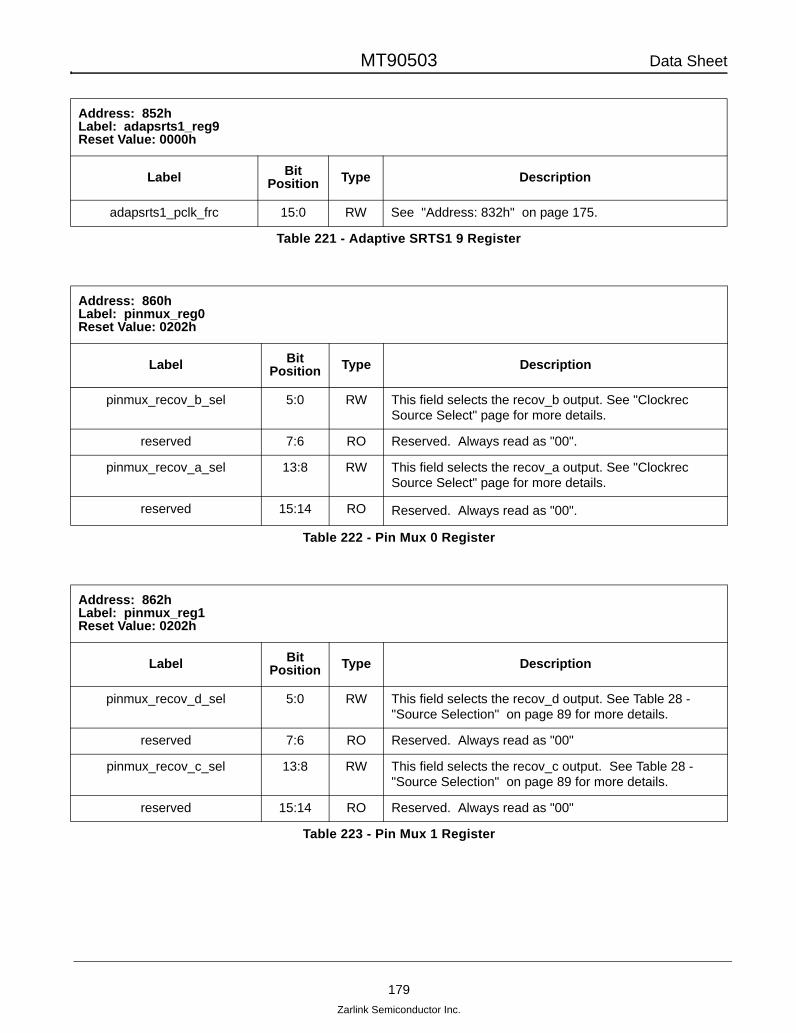
MT90503 Data Sheet
179Zarlink Semiconductor Inc.
Address: 852h Label: adapsrts1_reg9 Reset Value: 0000h
Label BitPosition Type Description
adapsrts1_pclk_frc 15:0 RW See "Address: 832h" on page 175.
Table 221 - Adaptive SRTS1 9 Register
Address: 860h Label: pinmux_reg0 Reset Value: 0202h
Label BitPosition Type Description
pinmux_recov_b_sel 5:0 RW This field selects the recov_b output. See "Clockrec Source Select" page for more details.
reserved 7:6 RO Reserved. Always read as "00".
pinmux_recov_a_sel 13:8 RW This field selects the recov_a output. See "Clockrec Source Select" page for more details.
reserved 15:14 RO Reserved. Always read as "00".
Table 222 - Pin Mux 0 Register
Address: 862h Label: pinmux_reg1 Reset Value: 0202h
Label BitPosition Type Description
pinmux_recov_d_sel 5:0 RW This field selects the recov_d output. See Table 28 - "Source Selection" on page 89 for more details.
reserved 7:6 RO Reserved. Always read as "00"
pinmux_recov_c_sel 13:8 RW This field selects the recov_c output. See Table 28 - "Source Selection" on page 89 for more details.
reserved 15:14 RO Reserved. Always read as "00"
Table 223 - Pin Mux 1 Register

MT90503 Data Sheet
180Zarlink Semiconductor Inc.
Address: 864h Label: pinmux_reg2 Reset Value: 0202h
Label BitPosition Type Description
pinmux_recov_f_sel 5:0 RW This field selects the recov_f output. See Table 28 - "Source Selection" on page 89 for more details.
reserved 7:6 RO Reserved. Always read as "00"
pinmux_recov_e_sel 13:8 RW This field selects the recov_e output. See Table 28 - "Source Selection" on page 89 for more details.
reserved 15:14 RO Reserved. Always read as "00"
Table 224 - Pin Mux 2 Register
Address: 866h Label: pinmux_reg3 Reset Value: 0202h
Label BitPosition Type Description
pinmux_recov_h_sel 5:0 RW This field selects the recov_h output. See Table 28 - "Source Selection" on page 89 for more details.
reserved 7:6 RO Reserved. Always read as "00"
pinmux_recov_g_sel 13:8 RW This field selects the recov_g output. See Table 28 - "Source Selection" on page 89 for more details.
reserved 15:14 RO Reserved. Always read as "00"
Table 225 - Pin Mux 3 Register
Address: 868h Label: pinmux_reg4 Reset Value: 0202h
Label BitPosition Type Description
pinmux_ct_netref2_sel 5:0 RW This field selects the ct_netref2 output. See Table 28 - "Source Selection" on page 89 for more details.
reserved 7:6 RO Reserved. Always read as "00"
pinmux_ct_netref1_sel 13:8 RW This field selects the ct_netref1 output. See Table 28 - "Source Selection" on page 89 for more details.
reserved 15:14 RO Reserved. Always read as "00"
Table 226 - Pin Mux 4 Register

MT90503 Data Sheet
181Zarlink Semiconductor Inc.
Address: 86Ah Label: pinmux_reg5 Reset Value: 0303h
Label BitPosition Type Description
pinmux_local_netref_16m_sel 5:0 RW This field selects the local_16m reference feed into the H.100 master circuit. See Table 28 - "Source Selection" on page 89 for more details.
reserved 7:6 RO Reserved. Always read as "00"
reserved 13:8 RO Reserved. Always read as "0000_00"
reserved 15:14 RO Reserved. Always read as "00"
Table 227 - Pin Mux 5 Register
Address: 880h Label: diviclk0_reg0 Reset Value: 0300h
Label BitPosition Type Description
diviclk0_clk_divisor_load_now 0 PUL When this bit is written to '1', the integer clock divisor 0's division value will be loaded into the divisor.
diviclk0_clk_divisor_reset 1 RW When this bit is '0', the integer clock divisor 0 is put in reset. Must be '1' for normal operation.
diviclk0_even_duty_cycle_select
2 RW When '1', the duty cycle modifier will be enabled and will generate a 50% duty cycle output.
diviclk0_input_invert_select 3 RW When '1', the input of the integer clock divisor will be inverted before being divided.
diviclk0_output_invert_select 4 RW When '1', the output of the integer clock divisor will be inverted before being sent out.
reserved 12:7 RW Reserved. Must always be "0000_00"
diviclk0_input_source_select 13:8 RW This field selects the input of the integer clock divisor. See Table 28 - "Source Selection" on page 89 for more details.
reserved 15:14 RW Reserved. Must always be "00"
Table 228 - Integer Clock Divisor0 0 Register

MT90503 Data Sheet
182Zarlink Semiconductor Inc.
Address: 882h Label: diviclk0_reg1 Reset Value: 0000h
Label BitPosition Type Description
diviclk0_ext_loss_pulse 0 ROLO This bit is set when an external signal indicates that the input of the integer clock divisor is invalid (such as a PHY alarm).
diviclk0_ext_loss_flag 1 RO Same as diviclk0_ext_loss_pulse, but when the error condition ceases, this bit will clear itself.
diviclk0_freq_too_high_pulse 2 ROLO This bit is set when the integer clock divisor input's frequency is off as compared to the expected frequency (received frequency is too high).
diviclk0_freq_too_high_flag 3 RO Same as diviclk0_freq_too_high_pulse, but when the error condition ceases, this bit will clear itself.
diviclk0_freq_too_low_pulse 4 ROLO This bit is set when the integer clock divisor input's frequency is off as compared to the expected frequency (received frequency is too low).
diviclk0_freq_too_low_flag 5 RO Same as diviclk0_freq_too_low_pulse, but when the error condition ceases, this bit will clear itself.
reserved 15:6 RO Reserved. Always read as "0000_0000_00"
Table 229 - Integer Clock Divisor0 1 Register
Address: 884h Label: diviclk0_reg2 Reset Value: 0000h
Label BitPosition Type Description
diviclk0_ext_loss_pulse_ie 0 IE When '1' and the corresponding status bit is '1', and interrupt will be generated.
reserved 1 RO Reserved. Always read as "00"
diviclk0_freq_too_high_pulse_ie 2 IE When '1' and the corresponding status bit is '1', and interrupt will be generated.
reserved 3 RO Reserved. Always read as "00"
diviclk0_freq_too_low_pulse_ie 4 IE When '1' and the corresponding status bit is '1', and interrupt will be generated.
reserved 5 RO Reserved. Always read as "00"
reserved 15:6 RO Reserved. Always read as "0000_0000_00"
Table 230 - Integer Clock Divisor0 2 Register

MT90503 Data Sheet
183Zarlink Semiconductor Inc.
Address: 886h Label: diviclk0_reg3 Reset Value: 0000h
Label BitPosition Type Description
diviclk0_ext_loss_pulse_genloss 0 RW When set, the corresponding status will cause a loss to be signaled for this diviclk.
diviclk0_ext_loss_flag_genloss 1 RW When set, the corresponding status will cause a loss to be signaled for this diviclk.
diviclk0_freq_too_high_pulse_genloss 2 RW When set, the corresponding status will cause a loss to be signaled for this diviclk.
diviclk0_freq_too_high_flag_genloss 3 RW When set, the corresponding status will cause a loss to be signaled for this diviclk.
diviclk0_freq_too_low_pulse_genloss 4 RW When set, the corresponding status will cause a loss to be signaled for this diviclk.
diviclk0_freq_too_low_flag_genloss 5 RW When set, the corresponding status will cause a loss to be signaled for this diviclk.
reserved 15:6 RW Reserved. Must always be "0000_0000_00"
Table 231 - Integer Clock Divisor0 3 Register
Address: 888h Label: diviclk0_reg4 Reset Value: 0063h
Label BitPosition Type Description
diviclk0_ext_loss_source_select 5:0 RW Select's which external pin will signal that the input of the integer clock divisor is good or not. See Table 28 - "Source Selection" on page 89 for more details.
diviclk0_ext_loss_source_polarity 6 RW Input of the integer clock divisor is considered bad when the select ext_loss signal is active (i.e. equal to this bit). 0 = source loss active low; 1 = source loss active high.
diviclk0_output_loss_polarity 7 RW When a loss is detected, the output signal indicating this loss is activated (i.e. the value is this register is sent out). '0' = output loss active low; '1' = output loss active high.
reserved 15:8 RW Reserved. Must always be "0000_0000"
Table 232 - Integer Clock Divisor0 4 Register

MT90503 Data Sheet
184Zarlink Semiconductor Inc.
Address: 88Ah Label: diviclk0_reg5 Reset Value: 0000h
Label BitPosition Type Description
diviclk0_clk_div 15:0 RW This is the denominator used to divide the input clock. It ranges from 1 to 65535.
Table 233 - Integer Clock Divisor0 5 Register
Address: 890h Label: diviclk0_reg8 Reset Value: 0000h
Label BitPosition Type Description
diviclk0_freqchck_div 15:0 RW This value will be used to divide the input clock before check it against the frequency of mclk. The higher the division value, the longer to detect a frequency too high or frequency too low, but the check is more precise. 0000h disables frequency checking.
Table 234 - Integer Clock Divisor0 8 Register
Address: 892h Label: diviclk0_reg9 Reset Value: 0000h
Label BitPosition Type Description
diviclk0_freqchck_max_mclk_cycles 15:0 RW This regsiter defines the maximum number of mclk cycles between two rising edges of the input clock divided by diviclk0_freqchck_div. If a second rising edge has not been detected in diviclk0_freqchck_max_mclk_cycles, the diviclk0_freq_too_low will be detected.
Table 235 - Integer Clock Divisor0 9 Register

MT90503 Data Sheet
185Zarlink Semiconductor Inc.
Address: 894h Label: diviclk0_reg10 Reset Value: 0000h
Label BitPosition Type Description
diviclk0_freqchck_min_mclk_cycles 15:0 RW This regsiter defines the minimum number of mclk cycles between two rising edges of the input clock divided by diviclk0_freqchck_div.If a second rising edge has been detected in less then diviclk0_freqchck_min_mclk_cycles, the diviclk0_freq_too_high will be detected.
Table 236 - Integer Clock Divisor0 10 Register
Address: 8A0h Label: diviclk1_reg0 Reset Value: 0300h
Label BitPosition Type Description
diviclk1_clk_divisor_load_now 0 PUL See regsiters 880h to 89Eh
diviclk1_clk_divisor_reset 1 RW
diviclk1_even_duty_cycle_select 2 RW
diviclk1_input_invert_select 3 RW
diviclk1_output_invert_select 4 RW
diviclk1_input_source_select 13:8 RW
reserved 15:14 RW Reserved. Must always be "00"
Table 237 - Integer Clock Divisor1 0 Register
Address: 8A2h Label: diviclk1_reg1 Reset Value: 0000h
Label BitPosition Type Description
diviclk1_ext_loss_pulse 0 ROLO See register 882h.
diviclk1_ext_loss_flag 1 RO
diviclk1_freq_too_high_pulse 2 ROLO
diviclk1_freq_too_high_flag 3 RO
Table 238 - Integer Clock Divisor1 1 Register

MT90503 Data Sheet
186Zarlink Semiconductor Inc.
diviclk1_freq_too_low_pulse 4 ROLO
diviclk1_freq_too_low_flag 5 RO
reserved 15:6 RO Reserved. Always read as "0000_0000_00"
Address: 8A4h Label: diviclk1_reg2 Reset Value: 0000h
Label BitPosition Type Description
diviclk1_ext_loss_pulse_ie 0 IE See register 884h.
reserved 1 RO
diviclk1_freq_too_high_pulse_ie 2 IE
reserved 3 RO
diviclk1_freq_too_low_pulse_ie 4 IE
reserved 5 RO
reserved 15:6 RO Reserved. Always read as "0000_0000_00"
Table 239 - Integer Clock Divisor1 2 Register
Address: 8A6h Label: diviclk1_reg3 Reset Value: 0000h
Label BitPosition Type Description
diviclk1_ext_loss_pulse_genloss 0 RW See register 886h.
diviclk1_ext_loss_flag_genloss 1 RW
diviclk1_freq_too_high_pulse_genloss 2 RW
diviclk1_freq_too_high_flag_genloss 3 RW
diviclk1_freq_too_low_pulse_genloss 4 RW
Table 240 - Integer Clock Divisor1 3 Register
Address: 8A2h Label: diviclk1_reg1 Reset Value: 0000h
Label BitPosition Type Description
Table 238 - Integer Clock Divisor1 1 Register

MT90503 Data Sheet
187Zarlink Semiconductor Inc.
diviclk1_freq_too_low_flag_genloss 5 RW
reserved 15:6 RW Reserved. Must always be "0000_0000_00"
Address: 8A8h Label: diviclk1_reg4 Reset Value: 0063h
Label BitPosition Type Description
diviclk1_ext_loss_source_select 5:0 RW See register 888h.
diviclk1_ext_loss_source_polarity 6 RW
diviclk1_output_loss_polarity 7 RW
reserved 15:8 RW Reserved. Must always be "0000_0000"
Table 241 - Integer Clock Divisor1 4 Register
Address: 8AAh Label: diviclk1_reg5 Reset Value: 0000h
Label Bit Position Type Description
diviclk1_clk_div 15:0 RW See register 88Ah.
Table 242 - Integer Clock Divisor1 5 Register
Address: 8B0h Label: diviclk1_reg8 Reset Value: 0000h
Label BitPosition Type Description
diviclk1_freqchck_div 15:0 RW See register 890h.
Table 243 - Integer Clock Divisor1 8 Register
Address: 8A6h Label: diviclk1_reg3 Reset Value: 0000h
Label BitPosition Type Description
Table 240 - Integer Clock Divisor1 3 Register (continued)

MT90503 Data Sheet
188Zarlink Semiconductor Inc.
Address: 8B2h Label: diviclk1_reg9 Reset Value: 0000h
Label BitPosition Type Description
diviclk1_freqchck_max_mclk_cycles 15:0 RW See register 892h.
Table 244 - Integer Clock Divisor1 9 Register
Address: 8B4h Label: diviclk1_reg10 Reset Value: 0000h
Label BitPosition Type Description
diviclk1_freqchck_min_mclk_cycles 15:0 RW See register 894h.
Table 245 - Integer Clock Divisor1 10 Register
Address: 8C0h Label: diviclk2_reg0 Reset Value: 0300h
Label BitPosition Type Description
diviclk2_clk_divisor_load_now 0 PUL See registers 880h to 89Eh
diviclk2_clk_divisor_reset 1 RW
diviclk2_even_duty_cycle_select 2 RW
diviclk2_input_invert_select 3 RW
diviclk2_output_invert_select 4 RW
diviclk2_input_source_select 13:8 RW
reserved 15:14 RW Reserved. Must always be "00"
Table 246 - Integer Clock Divisor2 0 Register

MT90503 Data Sheet
189Zarlink Semiconductor Inc.
Address: 8C2h Label: diviclk2_reg1 Reset Value: 0000h
Label BitPosition Type Description
diviclk2_ext_loss_pulse 0 ROLO See register 8A2h.
diviclk2_ext_loss_flag 1 RO
diviclk2_freq_too_high_pulse 2 ROLO
diviclk2_freq_too_high_flag 3 RO
diviclk2_freq_too_low_pulse 4 ROLO
diviclk2_freq_too_low_flag 5 RO
reserved 15:6 RO Reserved. Always read as "0000_0000_00"
Table 247 - Integer Clock Divisor2 1 Register
Address: 8C4h Label: diviclk2_reg2 Reset Value: 0000h
Label BitPosition Type Description
diviclk2_ext_loss_pulse_ie 0 IE See register 8A4h.
reserved 1 RO
diviclk2_freq_too_high_pulse_ie 2 IE
reserved 3 RO
diviclk2_freq_too_low_pulse_ie 4 IE
reserved 5 RO
reserved 15:6 RO Reserved. Always read as "0000_0000_00"
Table 248 - Integer Clock Divisor2 2 Register
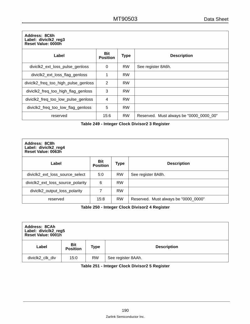
MT90503 Data Sheet
190Zarlink Semiconductor Inc.
Address: 8C6h Label: diviclk2_reg3 Reset Value: 0000h
Label BitPosition Type Description
diviclk2_ext_loss_pulse_genloss 0 RW See register 8A6h.
diviclk2_ext_loss_flag_genloss 1 RW
diviclk2_freq_too_high_pulse_genloss 2 RW
diviclk2_freq_too_high_flag_genloss 3 RW
diviclk2_freq_too_low_pulse_genloss 4 RW
diviclk2_freq_too_low_flag_genloss 5 RW
reserved 15:6 RW Reserved. Must always be "0000_0000_00"
Table 249 - Integer Clock Divisor2 3 Register
Address: 8C8h Label: diviclk2_reg4 Reset Value: 0063h
Label BitPosition Type Description
diviclk2_ext_loss_source_select 5:0 RW See register 8A8h.
diviclk2_ext_loss_source_polarity 6 RW
diviclk2_output_loss_polarity 7 RW
reserved 15:8 RW Reserved. Must always be "0000_0000"
Table 250 - Integer Clock Divisor2 4 Register
Address: 8CAh Label: diviclk2_reg5 Reset Value: 0001h
Label BitPosition Type Description
diviclk2_clk_div 15:0 RW See register 8AAh.
Table 251 - Integer Clock Divisor2 5 Register

MT90503 Data Sheet
191Zarlink Semiconductor Inc.
Address: 8D0h Label: diviclk2_reg8Reset Value: 0000h
Label BitPosition Type Description
diviclk2_freqchck_div 15:0 RW See register 8B0h.
Table 252 - Integer Clock Divisor2 8 Register
Address: 8D2hLabel: diviclk2_reg9 Reset Value: 0000h
Label BitPosition Type Description
diviclk2_freqchck_max_mclk_cycles 15:0 RW See register 8B2h.
Table 253 - Integer Clock Divisor2 9 Register
Address: 8D4h Label: diviclk2_reg10 Reset Value: 0000h
Label BitPosition Type Description
diviclk2_freqchck_min_mclk_cycles 15:0 RW See register 8B4h.
Table 254 - Integer Clock Divisor2 10 Register
Address: 8E0h Label: tx_srts_debug Reset Value: 0000h
Label BitPosition Type Description
tx_srts_eight_cell_pulse_rol 0 ROL Only used for tests.
tx_srts_fnxi_cnt 11:8 RO Only used for tests.
reserved 15:12 RO Reserved. Always read as "0000"
Table 255 - TX SRTS Debug Register

MT90503 Data Sheet
192Zarlink Semiconductor Inc.
Address: 8E4h Label: adapsrts0_rx_srts_debug Reset Value: 0000h
Label BitPosition Type Description
adapsrts0_eight_cell_pulse_rol 0 ROL Only used for tests.
adapsrts0_rx_srts_fnxi_cnt 11:8 RO Only used for tests.
reserved 15:12 RO Reserved. Always read as "0000"
Table 256 - RX SRTS Debug 0 Register
Address: 8E8h Label: adapsrts1_rx_srts_debug Reset Value: 0000h
Label BitPosition Type Description
adapsrts1_eight_cell_pulse_rol 0 ROL Only used for tests.
adapsrts1_rx_srts_fnxi_cnt 11:8 RO Only used for tests.
reserved 15:12 RO Reserved. Always read as "0000"
Table 257 - RX SRTS Debug 1 Register
Address: 8ECh Label: adapsrts_aal1_err_debugReset Value: 0000h
Label BitPosition Type Description
adapsrts0_valid_cell 0 ROL Only used for tests.
adapsrts0_cell_lost 1 ROL Only used for tests.
adapsrts1_valid_cell 2 ROL Only used for tests.
adapsrts1_cell_lost 3 ROL Only used for tests.
reserved 15:4 ROL Reserved. Always read as "0000_0000_0000"
Table 258 - AAL1 Error Debug Register

MT90503 Data Sheet
193Zarlink Semiconductor Inc.
5.5.9 Miscellaneous Registers
Address: 900h Label: control Reset Value: 0000h
Label BitPosition Type Description
test_status 15 TS When '1', all the status bits in the register will be set.
Table 259 - Miscellaneous Control Register
Address: 902h Label: err_reg0 Reset Value: 0000h
Label BitPosition Type Description
adap_srts_remote0_mem_overflow 0 ROL Indicates that the chip did not have time to write an adaptive point structure before the next one was generated.
adap_srts_remote1_mem_overflow 1 ROL Indicates that the chip did not have time to write an adaptive point structure before the next one was generated.
srts_local0_mem_overflow 2 ROL Indicates that the SRTS value buffer overflowed.
srts_local1_mem_overflow 3 ROL Indicates that the SRTS value buffer overflowed.
cas_mem_overflow 4 ROL Indicates that the CAS change memory overflowed.
silent_tone_error 5 ROL New silent tones were requested before the current ones could be fetched.
reserved 15:6 ROL Reserved. Always read as "0000_0000_00"
Table 260 - Miscellaneous Error Register
Address: 908h Label: silent_tone_reg2 Reset Value: 0000h
Label BitPosition Type Description
silent_size 15:0 RW Size of the silent tone buffers, in bytes minus 1. 0 means 1 byte; FFFFh means 10000h bytes.
Table 261 - Silent Tone 2 Register
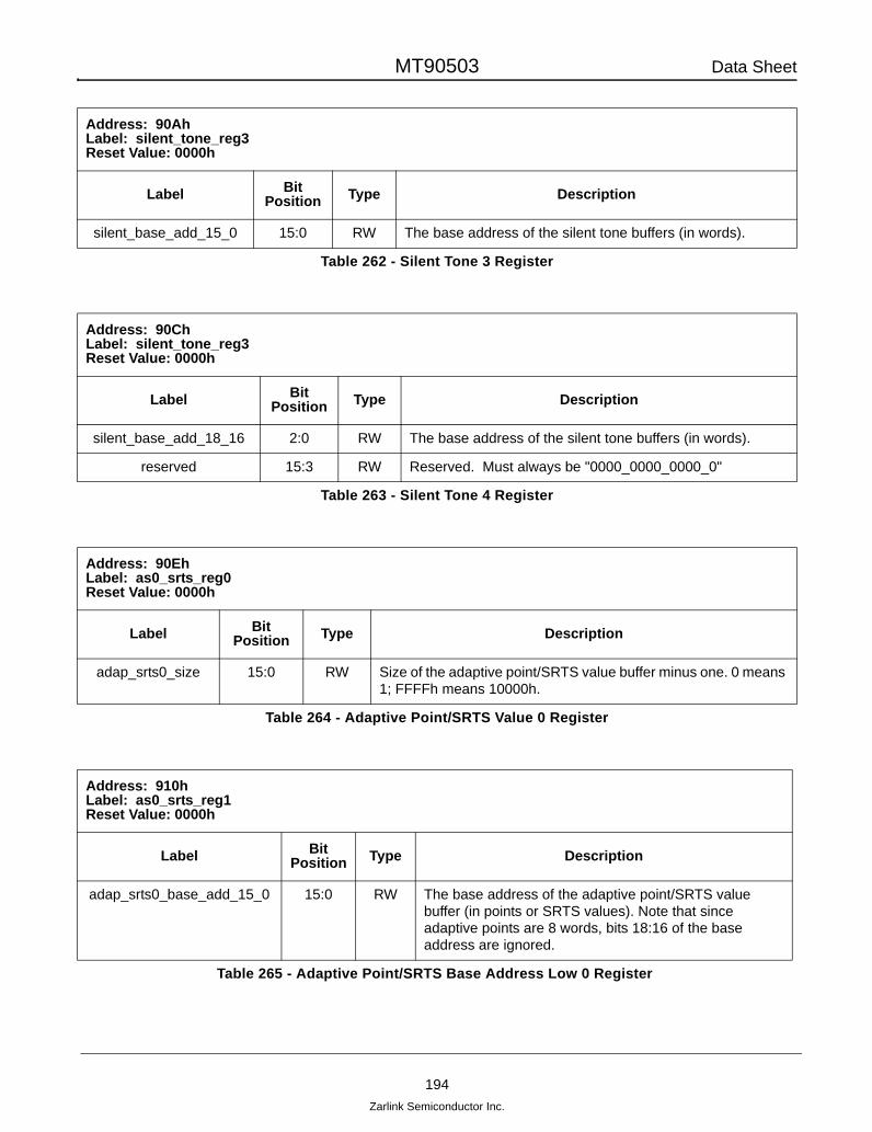
MT90503 Data Sheet
194Zarlink Semiconductor Inc.
Address: 90Ah Label: silent_tone_reg3 Reset Value: 0000h
Label BitPosition Type Description
silent_base_add_15_0 15:0 RW The base address of the silent tone buffers (in words).
Table 262 - Silent Tone 3 Register
Address: 90Ch Label: silent_tone_reg3 Reset Value: 0000h
Label BitPosition Type Description
silent_base_add_18_16 2:0 RW The base address of the silent tone buffers (in words).
reserved 15:3 RW Reserved. Must always be "0000_0000_0000_0"
Table 263 - Silent Tone 4 Register
Address: 90Eh Label: as0_srts_reg0 Reset Value: 0000h
Label BitPosition Type Description
adap_srts0_size 15:0 RW Size of the adaptive point/SRTS value buffer minus one. 0 means 1; FFFFh means 10000h.
Table 264 - Adaptive Point/SRTS Value 0 Register
Address: 910h Label: as0_srts_reg1 Reset Value: 0000h
Label BitPosition Type Description
adap_srts0_base_add_15_0 15:0 RW The base address of the adaptive point/SRTS value buffer (in points or SRTS values). Note that since adaptive points are 8 words, bits 18:16 of the base address are ignored.
Table 265 - Adaptive Point/SRTS Base Address Low 0 Register

MT90503 Data Sheet
195Zarlink Semiconductor Inc.
Address: 912h Label: as0_srts_reg2 Reset Value: 0000h
Label BitPosition Type Description
adap_srts0_base_add_18_16 2:0 RW The base address of the adaptive point/SRTS value buffer (in points or SRTS values). Note that since adaptive points are 8 words, bits 18:16 of the base address are ignored.
reserved 15:3 RW Reserved. Must always be "0000_0000_0000_0"
Table 266 - Adaptive Point/SRTS Base Address High 0 Register
Address: 914h Label: as0_srts_reg3 Reset Value: 0000h
Label BitPosition Type Description
adap_srts_remote0_write_pnt 15:0 RO The chip's write pointer to the adaptive point/SRTS value buffer.
Table 267 - Adaptive Point/SRTS Write Pointer 0 Register
Address: 916h Label: as0_srts_reg4 Reset Value: 0000h
Label BitPosition Type Description
adap_srts_remote0_read_pnt 15:0 RW The CPU's read pointer to the adaptive point/SRTS value buffer.
Table 268 - Adaptive Point/SRTS Read Pointer 0 Register
Address: 918h Label: as0_srts_reg5 Reset Value: 0000h
Label BitPosition Type Description
srts_local0_write_pnt 15:0 RO The chip's write pointer to the local SRTS value buffer.
Table 269 - Local SRTS Write Pointer 0 Register

MT90503 Data Sheet
196Zarlink Semiconductor Inc.
Address: 91Ah Label: as0_srts_reg6 Reset Value: 0000h
Label BitPosition Type Description
srts_local0_read_pnt 15:0 RW The CPU's read pointer to the local SRTS value buffer.
Table 270 - Local SRTS Read Pointer 0 Register
Address: 91Ch Label: as1_srts_reg0 Reset Value: 0000h
Label BitPosition Type Description
adap_srts1_size 15:0 RW Size of the adaptive point/SRTS value buffer minus one. 0 means 1; FFFFh means 10000h.
Table 271 - Adaptive Point/SRTS Value 1 Register
Address: 91Eh Label: as1_srts_reg1 Reset Value: 0000h
Label BitPosition Type Description
adap_srts1_base_add_15_0 15:0 RW The base address of the adaptive point/SRTS value buffer (in points or SRTS values). Note that since adaptive points are 8 words, bits 18:16 of the base address are ignored.
Table 272 - Adaptive Point/SRTS Base Address Low 1 Register
Address: 920h Label: as1_srts_reg2 Reset Value: 0000h
Label BitPosition Type Description
adap_srts1_base_add_18_16 2:0 RW The base address of the adaptive point/SRTS value buffer (in points or SRTS values). Note that since adaptive points are 8 words, bits 18:16 of the base address are ignored.
reserved 15:3 RW Reserved. Must always be "0000_0000_0000_0"
Table 273 - Adaptive Point/SRTS Base Address High 1 Register

MT90503 Data Sheet
197Zarlink Semiconductor Inc.
Address: 922h Label: as1_srts_reg3 Reset Value: 0000h
Label BitPosition Type Description
adap_srts_remote1_write_pnt 15:0 RO The chip's write pointer to the adaptive point/SRTS value buffer.
Table 274 - Adaptive Point/SRTS Write Pointer 1 Register
Address: 924h Label: as1_srts_reg4 Reset Value: 0000h
Label BitPosition Type Description
adap_srts_remote1_read_pnt 15:0 RW The CPU's read pointer to the adaptive point/SRTS value buffer.
Table 275 - Adaptive Point/SRTS Read Pointer 1 Register
Address: 926h Label: as1_srts_reg5 Reset Value: 0000h
Label BitPosition Type Description
srts_local1_write_pnt 15:0 RO The chip's write pointer to the local SRTS value buffer.
Table 276 - Local SRTS Write Pointer 1 Register
Address: 928h Label: as1_srts_reg6 Reset Value: 0000h
Label BitPosition Type Description
srts_local1_read_pnt 15:0 RW The CPU's read pointer to the local SRTS value buffer.
Table 277 - Local SRTS Read Pointer 1 Register

MT90503 Data Sheet
198Zarlink Semiconductor Inc.
Address: 92Ah Label: cas_reg0 Reset Value: 0000h
Label BitPosition Type Description
cas_size 15:0 RW Size of the CAS change buffer minus 1. 0 means 1; FFFFh means 10000h.
Table 278 - CAS Change Buffer Size Register
Address: 92Ch Label: cas_reg1 Reset Value: 0000h
Label BitPosition Type Description
cas_base_add_15_0 15:0 RW Base address of the CAS change buffer.
Table 279 - CAS Change Buffer Base Address Low Register
Address: 92Eh Label: cas_reg2 Reset Value: 0000h
Label BitPosition Type Description
cas_base_add_18_16 2:0 RW Base address of the CAS change buffer.
reserved 15:3 RW Reserved. Must always be "0000_0000_0000_0"
Table 280 - CAS Change Buffer Base Address High Register
Address: 930h Label: cas_reg3 Reset Value: 0000h
Label BitPosition Type Description
cas_write_pnt 15:0 RO The chip's write pointer to the CAS change buffer.
Table 281 - CAS Write Pointer Register

MT90503 Data Sheet
199Zarlink Semiconductor Inc.
Address: 932h Label: cas_reg4 Reset Value: 0000h
Label BitPosition Type Description
cas_read_pnt 15:0 RW The CPU's read pointer to the CAS change buffer.
Table 282 - CAS Read Pointer Register
Address: 944h Label: cas_timeout_hig Reset Value: 0000h
Label BitPosition Type Description
cas_timeout_period[19:16] 3:0 RW Time, in us, that a CAS change report can wait in the FIFO before an alarm is generated.
reserved 15:4 RW Reserved. Must always be "0000_0000_0000"
Table 283 - CAS Timeout High Register
Address: 946h Label: cas_timeout_low Reset Value: 0000h
Label BitPosition Type Description
cas_timeout_period[15:0] 15:0 RW Time, in us, that a CAS change report can wait in the FIFO before an alarm is generated.
Table 284 - CAS Timeout Low Register
Address: 948h Label: treated pulses Reset Value: 0000h
Label BitPosition Type Description
cas_treated_pulse 0 PUL Written to '1' to indicate that CAS change FIFO has been treated. Another alarm will not be generated until the above timeout has elapsed.
reserved 15:1 PUL Reserved. Always read as "0000_0000_0000_000"
Table 285 - Treated Pulses Register

MT90503 Data Sheet
200Zarlink Semiconductor Inc.
5.5.10 H.100 Registers
Address: A00h Label: control0 Reset Value: 0000h
Label BitPosition Type Description
h100_pll_ref_fallback 0 RW '0' = always use selected external clk (selected by h100_pll_ext_source) to source pll's ref input. '1' = if selected clock fails, fallback on local 16.384mHz clock.
h100_pll_ext_source 1 RW '0' = source ct_c8_a_in. '1' = source ct_c8_b_in
h100_pll_local_source 2 RW '0' = source pll's ref input with local 16.384mHz clock, '1' = source with selected external clk (selected via h100_pll_ext_source).
h100_pll_override 3 RW '0' = use embedded PLL to generate outgoing clocks. '1' = bypass PLL and use local 16.384 mHz clock instead.
h100_clk_loopback 4 RW '1' = loops the ct_c8 A and B clocks and frames back into the chip. Used for tests
h100_sclk_speed 6:5 RW "00" = 2.048 mHz. "01" = 4.096 mHz. "10" = 8.192 mHz.
h100_c8_frame_a_oe 7 RW '0' = tri-states ct_c8_a and ct_frame_a
h100_c8_frame_b_oe 8 RW '0' = tri-states ct_c8_b and ct_frame_b
h100_comp_oe 9 RW '0' = tri-states all the compatibility signals
h100_pll_fb_input 11:10 RW Selects pll's fb input: "00" = sample A, "10" = sample B, "01" = sample PLL output (div 4), "11" = reserved.
h100_frame_sync_source
12 RW '0' = sync frame on ct_frame_a_in, '1' = sync frame on ct_frame_b_in
h100_tdmint_clk_sel 13 RW specifies which clk to send to tdmint: '0' = use ct_c8_a. '1' = use ct_c8_b. h100_tdmint_clk_fallback can send other clk instead.
h100_tdmint_clk_fallback
14 RW clk to tdmint if selected clk is bad: '0' = always sync on selected clk (h100_tdming_clk_sel). '1' = if selected clk fails, switch over to backup clk.
test_status 15 TS When '1', all the status bits in the register will be set.
Table 286 - H.100 Control 0 Register
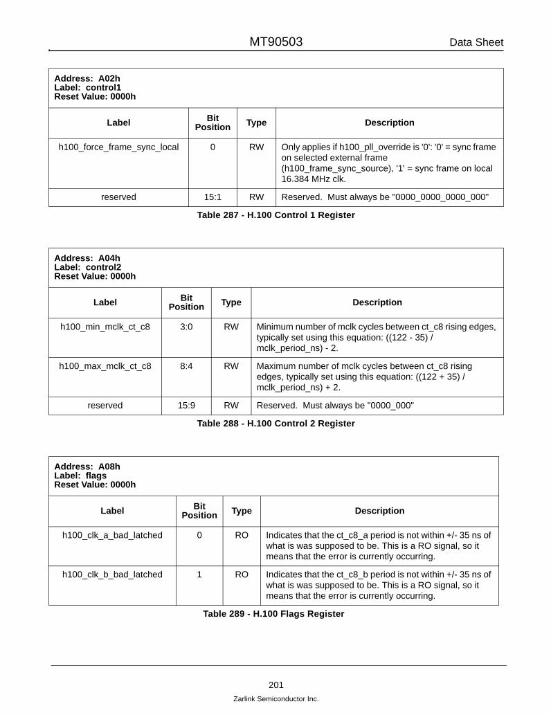
MT90503 Data Sheet
201Zarlink Semiconductor Inc.
Address: A02h Label: control1 Reset Value: 0000h
Label BitPosition Type Description
h100_force_frame_sync_local 0 RW Only applies if h100_pll_override is '0': '0' = sync frame on selected external frame (h100_frame_sync_source), '1' = sync frame on local 16.384 MHz clk.
reserved 15:1 RW Reserved. Must always be "0000_0000_0000_000"
Table 287 - H.100 Control 1 Register
Address: A04h Label: control2 Reset Value: 0000h
Label BitPosition Type Description
h100_min_mclk_ct_c8 3:0 RW Minimum number of mclk cycles between ct_c8 rising edges, typically set using this equation: ((122 - 35) / mclk_period_ns) - 2.
h100_max_mclk_ct_c8 8:4 RW Maximum number of mclk cycles between ct_c8 rising edges, typically set using this equation: ((122 + 35) / mclk_period_ns) + 2.
reserved 15:9 RW Reserved. Must always be "0000_000"
Table 288 - H.100 Control 2 Register
Address: A08h Label: flags Reset Value: 0000h
Label BitPosition Type Description
h100_clk_a_bad_latched 0 RO Indicates that the ct_c8_a period is not within +/- 35 ns of what is was supposed to be. This is a RO signal, so it means that the error is currently occurring.
h100_clk_b_bad_latched 1 RO Indicates that the ct_c8_b period is not within +/- 35 ns of what is was supposed to be. This is a RO signal, so it means that the error is currently occurring.
Table 289 - H.100 Flags Register
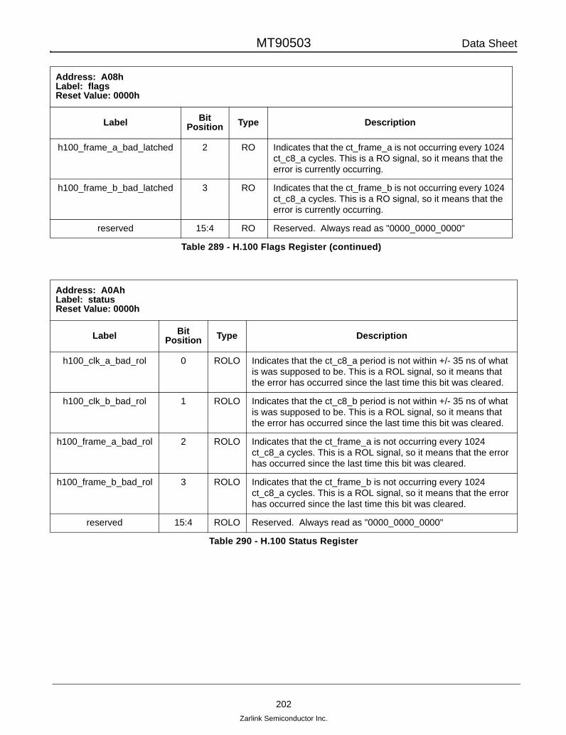
MT90503 Data Sheet
202Zarlink Semiconductor Inc.
h100_frame_a_bad_latched 2 RO Indicates that the ct_frame_a is not occurring every 1024 ct_c8_a cycles. This is a RO signal, so it means that the error is currently occurring.
h100_frame_b_bad_latched 3 RO Indicates that the ct_frame_b is not occurring every 1024 ct_c8_a cycles. This is a RO signal, so it means that the error is currently occurring.
reserved 15:4 RO Reserved. Always read as "0000_0000_0000"
Address: A0Ah Label: status Reset Value: 0000h
Label BitPosition Type Description
h100_clk_a_bad_rol 0 ROLO Indicates that the ct_c8_a period is not within +/- 35 ns of what is was supposed to be. This is a ROL signal, so it means that the error has occurred since the last time this bit was cleared.
h100_clk_b_bad_rol 1 ROLO Indicates that the ct_c8_b period is not within +/- 35 ns of what is was supposed to be. This is a ROL signal, so it means that the error has occurred since the last time this bit was cleared.
h100_frame_a_bad_rol 2 ROLO Indicates that the ct_frame_a is not occurring every 1024 ct_c8_a cycles. This is a ROL signal, so it means that the error has occurred since the last time this bit was cleared.
h100_frame_b_bad_rol 3 ROLO Indicates that the ct_frame_b is not occurring every 1024 ct_c8_a cycles. This is a ROL signal, so it means that the error has occurred since the last time this bit was cleared.
reserved 15:4 ROLO Reserved. Always read as "0000_0000_0000"
Table 290 - H.100 Status Register
Address: A08h Label: flags Reset Value: 0000h
Label BitPosition Type Description
Table 289 - H.100 Flags Register (continued)

MT90503 Data Sheet
203Zarlink Semiconductor Inc.
6.0 Statistics
6.1 TDM statistics
Underrun counter: 16-bit counter that counts the number of underruns detected by TDM interface.
6.2 TX SAR statistics
Percentage of bandwidth utilisation: a register (0510h) which indicates how many mclk cycles were required to treatthe last frame.
Transmitted Cell Counter: 32-bit counter that counts the number of cells transmitted on a particular VC. Each VChas its own counter in its structure.
6.3 RX SAR statistics
Error reporting structures allow software-based counters for the following errors:
• P-byte absent error
• P-byte framing error
• P-byte range error
• P-byte parity error
• Overrun error
• Underrun error
• AAL1 CRC error
• AAL1 parity error
• Single cell loss
• Multiple cell loss
• Cell misinsertion
Address: A0Ch Label: status_ie Reset Value: 0000h
Label BitPosition Type Description
h100_clk_a_bad_rol 0 IE When '1' and the corresponding status bit is '1', an interrupt will be generated.
h100_clk_b_bad_rol 1 IE When '1' and the corresponding status bit is '1', an interrupt will be generated.
h100_frame_a_bad_rol 2 IE When '1' and the corresponding status bit is '1', an interrupt will be generated.
h100_frame_b_bad_rol 3 IE When '1' and the corresponding status bit is '1', an interrupt will be generated.
reserved 15:4 IE Reserved. Always read as "0000_0000_0000"
Table 291 - H.100 Interrupt Enable Register

MT90503 Data Sheet
204Zarlink Semiconductor Inc.
Received Cell Counter: 32-bit counter that counts the number of cells received on a particular VC. Each VC has itsown counter in its structure.
6.4 UTOPIA statistics
Transmitted Cell Counters: 32-bit counters that counts the number of cells transmitted on a particular UTOPIA port.Three counters are available for each ports.
Received Cell Counters: 32-bit counters that counts the number of cells received on a particular UTOPIA port. Eachport has a dedicated counter.
Cell loss counter: 16-bit counters that counts the number of cells lost in the UTOPIA module.
7.0 Programming the fast_clk PLLThe frequency received on mclk_src pin is used by the MT90503’s PLL to generate a much higher frequency(fast_clk). It is then divided down to the output mem_clk frequency.
The X, Y and Z divider can be programmed to be any value as defined in Table 292 and Table 293 on page 206.The MT90503 can support mclk_src with a frequency ranging from 30 MHz to 80 MHz. Only frequencies between50 MHz and 53.3 MHz are not supported by the PLL. The X and Y divisor indicate what values can be programmedin the pll_conf registers 128h. Table 293, “Z Divisor Table,” on page 206 indicates the range of output mem_clk thatcan be achieved. Note that the output mem_clk cannot be programmed to be above 80 MHz, or below 40 MHz.
The fast_clk PLL drives the output mem_clk pins. These pins provide both TTL and PECL interfaces for the outputmem_clk. For both types, the output pins for the mem_clk is always driven. However, when the output pins are notbeing used, the register bits that control the toggling of these two pins should be disabled to reduce powerconsumption.
The user must configure the MT90503 to select the desired input mem_clk type, i.e., either PECL or TTL. The inputmem_clk serves as the main clock (mclk) for the MT90503 and must be present for the MT90503 to function. It isabsolutely necessary for the input mem_clk to be present and one of the inputs to be selected. The outputmem_clk, however, are convenience for the user and do not have to be connected. These outputs eliminate theneed for a second, high-speed oscillator to drive the input mem_clk.
The clock that is connected to the mem_clk inputs on the MT90503, whether it is the TTL or PECL, must be inphase with the clock connected to SSRAM used with the chip. The maximum skew allowed is ±0.5 ns.

MT90503 Data Sheet
205Zarlink Semiconductor Inc.
Figure 50 - mem_clk Output and fast_clk Generation Circuits
Figure 51 - mem_clk Input and mclk Generation Circuit
ClockMultiplication PLL
FB
REF OUT
Divide by Y
Divide by X
Divide by Z
upclk fast_clk
mem_clk_o
50 ohm ControledImpedance Output Buffer(3.3 V LVTTL)
mem_clk_positive_o
PECL Output Buffer
mem_clk_negative_o
_ p _
mclk_src
mem_clk_i
3.3 V LVTTL Input
mem_clk_positive_i
PECL Input Buffer
mem_clk_negative_i+-
mclk Distribution Buffer
mclk

MT90503 Data Sheet
206Zarlink Semiconductor Inc.
Div X Div Y mclk_src (MHz) fast_clk (MHz)
- - 0 to 30 -1 6 30 to 33.33 180 to 2001 5 33.33 to 40 166.66 to 2001 4 40 to 50 160 to 200- - 50 to 53.33 -1 3 53.33 to 66.66 160 to 2002 5 66.66 to 80 166.66 to 2001 2 80 160 to 200
Table 292 - Register 0128h Frequency Values
Div Z output mem_clk
2 803 53.3 to 66.64 40 to 50
Table 293 - Z Divisor Table

MT90503 Data Sheet
207Zarlink Semiconductor Inc.
8.0 Electrical Specifications
8.1 DC Characteristics
* Exceeding these figures may cause permanent damage. Functional operation under these conditions is not guaranteed. Voltage measurements are with respect to ground (VSS) unless otherwise stated. Long-term exposure to absolute maximum ratings may affect device reliability, and permanent damage may occur if operate exceeding the rating. The device should be operated under recommended operating condition.
Note 1: Suitable heat sinks: Part Number 66435, Avvid Thermalloy and Part Number HS2141, Intricast, or other similar heat sinks.Typical figures are at 25°C and are for design aid only; not guaranteed and not subject to production testing.Voltage measurements are with respect to ground (VSS) unless otherwise stated.
Absolute Maximum Ratings
Parameter Symbol Min. Max. Units
1 Supply Voltage – 3.3 Volt Rail VDD -0.3 3.9 V2 Voltage on 3.3V Input pins VI -1.0 3.6 V3 Continuous current at digital inputs II 4.0 mA4 Continuous current at digital outputs IO 5.3 mA5 Storage Temperature TS -40.0 +85.0 °C
Recommended Operating Conditions
Characteristics Symbol Min. Typ. Max. Units Test Conditions
1 Operating Temperature TOP -40.0 25.0 +85.0 °C 2048 Channels with heat sinkNote 1.
2 Operating Temperature TOP -40.0 25.0 +70.0 °C 2048 Channels with no heat sink
3 Operating Temperature TOP -40.0 25.0 +85.0 °C 1024 Channels with no heat sink
4 Supply Voltage, 3.3 Volt Rail VDD 3.0 3.3 3.6 V5 Input Voltage - 3.3 V inputs VI Vss-0.5 3.3 VDD+0.3 V

MT90503 Data Sheet
208Zarlink Semiconductor Inc.
DC Characteristics
Characteristics Symbol Min. Typ. Max. Units Test Conditions
1 Supply Current - 3.3 V supply IDD 720.0 mA 50.0 MHz, Nominal output loads, 1024 Channels, 16 streams active.
2 Supply Current - 3.3 V supply IDDN 970.0 mA 80.0 MHz, Nominal output loads, 2048 Channels
3 Device Power Dissipation PDD1 2.38 W 50.0 MHz, Nominal output loads, 1024 Channels, 16 streams active.
4 Device Power Dissipation PDD2 3.2 W 80.0 MHz, Nominal output loads, 2048 Channels
5 Input High Voltage VIH 2.0 VDD+0.3
V
6 Input Low Voltage VIL Vss-0.5 0.8 V
7 Switching Threshold VTC 1.4 2.0 V
8 Schmitt Trigger Positive Threshold
Vt+ 1.7 2.0 V
9 Schmitt Trigger Neg. Threshold
Vt- 0.8 1.0 V
10 Input Leakage Current II -10.0 10.0 µA VIN = VDDx or Vss
11 Input Pin Capacitance CI 2.5 pF
12 Output Pin Capacitance CO 2.0 pF
13 Output High Impedance Leakage
IOZ -10.0 +/- 1.0 10.0 µA VO = VSS or VDD
14 Output HIGH Voltage VOH 2.4 VDD V IOH = rated current
15 Output LOW Voltage VOL 0.2 0.4 V IOL = rated current
16 3.3V output HIGH current (4 mA buffer)
IOH 4.0 mA VOH = 2.4 V
17 3.3V output LOW current (4 mA buffer)
IOL 4.0 mA VOL = 0.4 V
18 3.3V output HIGH current (8 mA buffer)
IOH 8.0 mA VOH = 2.4 V
19 3.3V output LOW current (8 mA buffer)
IOL 8.0 mA VOL = 0.4 V
20 3.3V output HIGH current (12 mA buffer)
IOH 12.0 mA VOH = 2.4 V

MT90503 Data Sheet
209Zarlink Semiconductor Inc.
8.1.1 Precautions During Power Sequencing
Latch-up is not a concern during power sequencing. The only requirement for sequencing 3.3 V and 5 V suppliesduring power up is that the MT90503 be either held in reset until the rails are stable or have its global_tri_state pinheld low (tristate). However, to minimise over-voltage stress during system start-up, the 3.3 V supply applied to theMT90503 should be brought to a level of at least VDD = 3.0 V before a signal line is driven to a level greater than orequal to 3.3 V. This practice can be implemented either by ensuring that the 3.3 V power turns on simultaneouslywith or before the system 5 V supply turns on, or by ensuring that all 5 V signals are held to a logic LOW stateduring the time that VDD < 3.0 V. This condition is also met also if the MT90503 is held in reset until VDD reaches3.0 V.
Regardless of the method chosen to limit over-voltage stress during power up, exposure must be limited to no morethan + 6.5 V input voltage (VIN). The global_tri_state pin of the MT90503 can be asserted low on power-up toprevent bus contention.
8.1.2 Precautions During Power Failure
Latch-up is not a concern in power failure mode. Although extended exposure of the MT90503 to 5 V signals during3.3 V supply power failure is not recommended, there are no restrictions as long as VIN does not exceed theabsolute maximum rating of 6.5 V. To minimise over-voltage stress during a 3.3 V power supply failure, the designershould either link the power supplies to prevent this condition or ensure that all 5 V signals connected to theMT90503 are held in a logic LOW state until the 5 V supply is deactivated.
8.1.3 Pull-ups
Pull-ups from the 5 V rail to 3.3 V (5 V tolerant) outputs of the MT90503 can cause reverse leakage currents intothose 3.3V outputs when they are active HIGH. (No significant reverse current is present during the highimpedance state.) If the application can put the MT90503 in a state where MCLK is stopped, and a large number of3.3 V output buffers are held in a static HIGH state, current can flow from the 5 V rail to the 3.3 V rail. If thisMCLK-stopped state can not be avoided, the user should determine if the total MT90503 reverse current will have anegative impact on the system 3.3 V power supply. Alternatively, the global_tri_state pin of the MT90503 can beasserted low to put all outputs in the high impedance state.
8.2 H.110 Diode Clamp Rail
As the MT90503 has a diode clamp to the 5 V rail, the diode clamp must be no more than 0.7 V below VDD whenthe pin is not tristated. This can be accomplished by asserting the global_tri_state pin low or by keeping theMT90503 in reset until all rails are stable.
21 3.3V output LOW current (12 mA buffer)
IOL 12.0 mA VOL = 0.4 V
22 Junction-to-Ambient Thermal Resistance
θJ-A 14.225 °C/W 0 cfm air flow (natural convection airflow only)
b. TOP = 0°C to 70°C; VDD = 3.3V ± 5%Voltage measurements are with respect to ground (VSS) unless otherwise stated.
DC Characteristics (continued)

MT90503 Data Sheet
210Zarlink Semiconductor Inc.
8.3 AC Characteristics
All pins are tested with 50 pf worst case loading and 15 pf best case loading unless otherwise specified.
Clock NameMinimum
FrequencyMaximumFrequency
Required ForDevice Operation
MinimumDuty Cycle
MaximumDuty Cycle
mem_clk_i 40 MHz 80 MHz Yes 40% 60%
mclk_src 30 MHz 80 MHz Yes 40% 60%
rxa_clk 1 MHz 50 MHz No 40% 60%
rxb_clk 1 MHz 50 MHz No 40% 60%
rxc_clk 1 MHz 50 MHz No 40% 60%
txa_clk 1 MHz 50 MHz No 40% 60%
txb_clk 1 MHz 50 MHz No 40% 60%
txc_clk 1 MHz 50 MHz No 40% 60%
pll_clk 8.192 MHz 65.536 MHz No 40% 60%
ct_c8_a/b 8.192 MHz 8.192 MHz No 40% 60%
recov_a 0 MHz 80 MHz No 40% 60%
recov_b 0 MHz 80 MHz No 40% 60%
recov_c 0 MHz 80 MHz No 40% 60%
recov_d 0 MHz 80 MHz No 40% 60%
recov_e 0 MHz 80 MHz No 40% 60%
recov_f 0 MHz 80 MHz No 40% 60%
recov_g 0 MHz 80 MHz No 40% 60%
recov_h 0 MHz 80 MHz No 40% 60%
Table 294 - Clock Networks
Characteristic Sym Min Typ MaxUnit
sTest Conditions
mem_clk_i Frequency tMF 40.0 80.0 80.0 MHz 30ppm clock recommended for TDM PLLs
mem_clk_i Pulse Width (HIGH / LOW)
tMH/L 5.0 6.25 7.5 ns For 80MHz operation.
Table 295 - MCLK - Master Clock Input Parameters

MT90503 Data Sheet
211Zarlink Semiconductor Inc.
9.0 Interface Timing
9.1 CPU Interface Timing
Figure 52 - Non-multiplexed CPU Write Access - Intel Mode
Figure 53 - Non-multiplexed CPU Read Access - Intel Mode
write_active
inmo_a[14:0]/inmo_das
inmo_d[15:0]
Address Valid
inmo_rdy
Data Valid
t1
t2
t3
t1 t3
t4 t5 t6
Note:write_active = (inmo_cs = 0) AND (inmo_wr = 0)
inmo_a[14:0]/inmo_das
inmo_d[15:0]
Address Valid
inmo_rdy
Data Valid
t1
t2
t3
t8
t4 t5 t6
t7
Note:read_active = (inmo_cs = 0) AND (inmo_rd = 0)
read_active

MT90503 Data Sheet
212Zarlink Semiconductor Inc.
Figure 54 - Multiplexed CPU Write Access - Intel Mode
Symbol Description Write Access Min. Typ. Max. Unit
t1 write_access_active falling to inmo_d/inmo_a_das/inmo_a valid
2*mclk_src - 4 ns
t2 inmo_rdy_ndtack rising to write_access_active rising 0 nst3 inmo_rdy_ndtack rising to
inmo_d/inmo_a_das/inmo_a invalid0 ns
t4 write_access_active falling to inmo_rdy_ndtack falling
0 12 ns
t5 Write Access Time 740 nst6 write_access_active rising to inmo_rdy_ndtack
tri-state0 10 ns
Symbol Description Read Access Min. Typ. Max. Unit
t1 read_access_active falling to inmo_a_das/inmo_a valid
2*mclk_src - 4 ns
t2 inmo_rdy_ndtack rising to read_access_active rising 0 nst3 inmo_rdy_ndtack rising to inmo_a_das/inmo_a
invalid0 ns
t4 read_access_active falling to inmo_rdy_ndtack falling
0 12 ns
t5 Read Access Time See Table 300 nst6 read_access_active rising to inmo_rdy_ndtack
tri-state0 10 ns
t7 inmo_d valid to inmo_rdy_ndtack rising mclk_src - 4 nst8 read_access_active falling to inmo_d driving 3*mclk_src
- 4ns
Table 296 - Non-multiplexed CPU Interface Intel Mode
inmo_d[15:0]
inmo_ale
Address Valid
inmo_rdy
Data Valid
t3
t2
t4
t5 t6t7
t8
t10t9
Note:write_active = (inmo_cs = 0) AND (inmo_wr = 0)
write_activet1

MT90503 Data Sheet
213Zarlink Semiconductor Inc.
Figure 55 - Multiplexed CPU Read Access - Intel Mode
Symbol Description Write Access Min. Typ. Max. Unit
t1 write_access_active falling to inmo_ale falling 2*mclk_src - 4 nst2 write_access_active falling to inmo_d valid (writes) 2*mclk_src - 4 nst3 inmo_rdy_ndtack rising to write_access_active
rising0 ns
t4 inmo_rdy_ndtack rising to inmo_ale rising & inmo_d invalid
0 ns
t5 Write Access Time 740 nst6 write_access_active rising to inmo_rdy_ndtack
tri-state0 10 ns
t7 write_access_active falling to inmo_rdy_ndtack falling
0 12 ns
t8 inmo_ale high pulse width 5 nst9 inmo_d valid to inmo_ale falling 5 nst10 inmo_ale falling to inmo_d invalid 0 ns
Symbol Description Read Access Min. Typ. Max. Unit
t1 read_access_active falling to inmo_ale falling 2*mclk_src - 4 nst2 inmo_rdy_ndtack rising to read_access_active
rising0 ns
t3 inmo_rdy_ndtack rising to inmo_ale rising 0 nst4 read_access_active falling to inmo_rdy_ndtack
falling0 12 ns
t5 Read Access Time See Table 300 ns
Table 297 - Multiplexed CPU Interface Intel Mode
inmo_d[15:0]
inmo_ale
Address Valid
inmo_rdy
Data Valid
t2
t3
t5 t6t4
t7
t11t10
t9
Note:read_active = (inmo_cs = 0) AND (inmo_rd = 0)
t8read_active
t1

MT90503 Data Sheet
214Zarlink Semiconductor Inc.
Figure 56 - Non-Multiplexed CPU Interface Write Access - Motorola Mode
t6 read_access_active rising to inmo_rdy_ndtack tri-state
0 10 ns
t7 inmo_ale high pulse width 5 nst8 read_access_active falling to inmo_d driving 3*mclk_src -
4ns
t9 inmo_d valid to inmo_rdy_ndtack falling mclk_src - 4 nst10 inmo_d valid to inmo_ale falling 5 nst11 inmo_ale falling to inmo_d invalid 0 ns
Table 297 - Multiplexed CPU Interface Intel Mode (continued)

MT90503 Data Sheet
215Zarlink Semiconductor Inc.
Figure 57 - Non-multiplexed CPU Interface Read Access - Motorola Mode
Symbol Description Write Access Min. Typ. Max. Unit
t1 Address & Data Setup -- inmo_cs and inmo_rd_ds asserted to inmo_a[14:0] and inmo_d[15:0] and inmo_a_das valid
2*mclk_src - 4 ns
t3 Address & Data Hold -- inmo_rdy_ndtack low to inmo_a[14:0[ and inmo_d[15:0] and inmo_a_das invalid
0 ns
t4 Inmo_rdy_ndtack high -- inmo_cs and inmo_rd_ds asserted to inmo_rdy_ndtack driving one
0 12 ns
t5 Inmo_rdy_ndtack delay -- inmo_cs and inmo_rd_ds asserted to inmo_rdy_ndtack driving zero
740 ns
t6 Inmo_rdy_ndtack hold -- inmo_cs and inmo_rd_ds de-asserted to inmo_rdy_ndtack drivingb one
0 10 ns
t7 Inmo_rdy_ndtack high impedance -- inmo_rdy_ndtack driving one to inmo_rdy_ndtack high impedance
2 8 ns
t11 R/W setup -- R/W asserted to inmo_cs asserted 0 ns
t12 R/W hold -- inmo_cs deasserted to R/W deasserted 0 ns
Note: t1, t4, and t5 are dependent upon the last of inmo_cs and inmo_rd_ds to be asserted. t6 is dependent on the first of inmo_cs and inmo_rd_ds to be de-asserted.
Symbol Description Read Access Min. Typ. Max. Unit
t1 Address Setup -- inmo_cs and inmo_rd_ds asserted to inmo_a[14:0[ and inmo_a_das valid
2*mclk_src - 4 ns
Table 298 - Non-multiplexed CPU Interface Motorola Mode
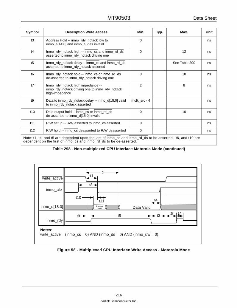
MT90503 Data Sheet
216Zarlink Semiconductor Inc.
Figure 58 - Multiplexed CPU Interface Write Access - Motorola Mode
t3 Address Hold -- inmo_rdy_ndtack low to inmo_a[14:0] and inmo_a_das invalid
0 ns
t4 Inmo_rdy_ndtack high -- inmo_cs and inmo_rd_ds asserted to inmo_rdy_ndtack driving one
0 12 ns
t5 Inmo_rdy_ndtack delay -- inmo_cs and inmo_rd_ds asserted to inmo_rdy_ndtack asserted
See Table 300 ns
t6 Inmo_rdy_ndtack hold -- inmo_cs or inmo_rd_ds de-asserted to inmo_rdy_ndtack driving one
0 10 ns
t7 Inmo_rdy_ndtack high impedance -- inmo_rdy_ndtack driving one to inmo_rdy_ndtack high-impedance
2 8 ns
t9 Data to inmo_rdy_ndtack delay -- inmo_d[15:0] valid to inmo_rdy_ndtack asserted
mclk_src - 4 ns
t10 Data output hold -- inmo_cs or inmo_rd_ds de-asserted to inmo_d[15:0] invalid
0 10 ns
t11 R/W setup -- R/W asserted to inmo_cs asserted 0 ns
t12 R/W hold -- inmo_cs deasserted to R/W deasserted 0 ns
Note: t1, t4, and t5 are dependent upon the last of inmo_cs and inmo_rd_ds to be asserted. t6, and t10 are dependent on the first of inmo_cs and inmo_rd_ds to be de-asserted.
Symbol Description Write Access Min. Typ. Max. Unit
Table 298 - Non-multiplexed CPU Interface Motorola Mode (continued)
write_active
inmo_d[15:0]
inmo_ale
Address Valid
inmo_rdy
Data Valid
t1
t3
t2
t4
t5 t6t9
t8
t11t10
Notes:write_active = (inmo_cs = 0) AND (inmo_ds = 0) AND (inmo_r/w = 0)
t7

MT90503 Data Sheet
217Zarlink Semiconductor Inc.
Figure 59 - Multiplexed CPU Interface Read Access - Motorola Mode
Symbol Description Write Access Min. Typ. Max. Unit
t1 write_access_active falling to inmo_ale falling 2*mclk_src - 4 nst2 write_access_active falling to inmo_d valid (writes) 2*mclk_src - 4 nst3 inmo_rdy_ndtack falling to write_access_active
rising0 ns
t4 inmo_rdy_ndtack falling to inmo_ale rising & inmo_d invalid
0 ns
t5 Write Access Time 740 nst6 write_access_active rising to inmo_rdy_ndtack
rising0 10 ns
t7 inmo_rdy_ndtack rising to inmo_rdy_ndtack tri-state
2 8 ns
t8 inmo_ale high pulse width 5 nst9 write_access_active falling to inmo_rdy_ndtack
driven high0 12 ns
t10 inmo_d valid to inmo_ale falling 5 nst11 inmo_ale falling to inmo_d invalid 0 ns
Symbol Description Read Access Min Typ Max Unit
t1 read_access_active falling to inmo_ale falling 2*mclk_src - 4 nst2 inmo_rdy_ndtack falling to read_access_active
rising0 ns
t3 inmo_rdy_ndtack falling to inmo_ale rising 0 nst4 read_access_active falling to inmo_rdy_ndtack
driving high0 12 ns
Table 299 - Multiplexed CPU Interface Motorola Mode
Notes:read_active = (inmo_cs = 0) AND (inmo_ds = 0) AND (inmo_r/w = 1)
read_active
inmo_d[15:0]
inmo_ale
Address Valid
inmo_rdy
Data Valid
t1
t2t5 t6t4
t11
t13t12
t7
t8
t3t9 t10
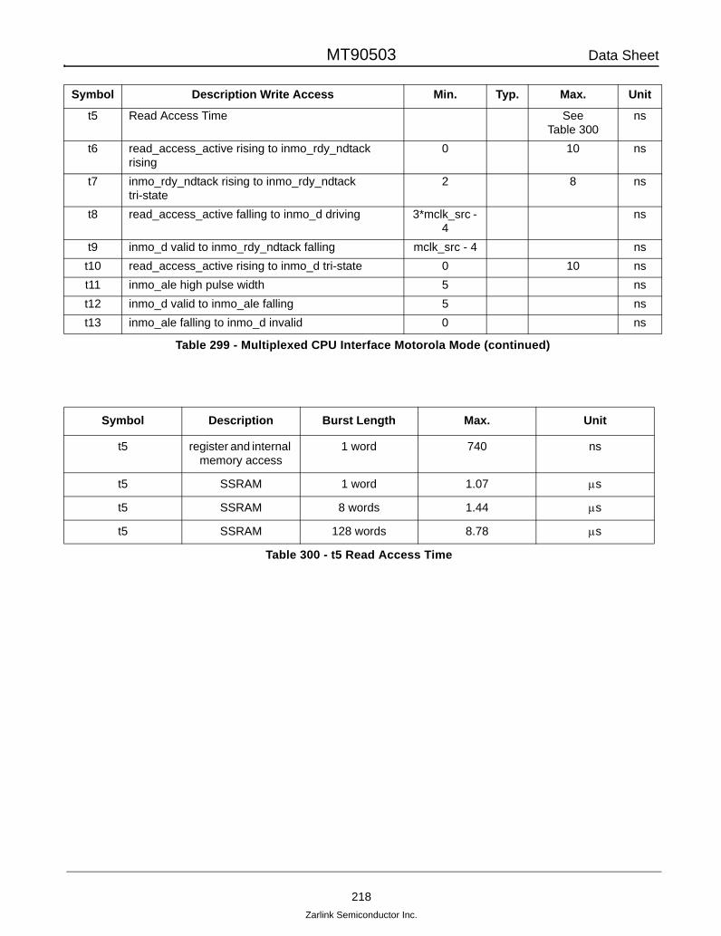
MT90503 Data Sheet
218Zarlink Semiconductor Inc.
t5 Read Access Time SeeTable 300
ns
t6 read_access_active rising to inmo_rdy_ndtack rising
0 10 ns
t7 inmo_rdy_ndtack rising to inmo_rdy_ndtack tri-state
2 8 ns
t8 read_access_active falling to inmo_d driving 3*mclk_src - 4
ns
t9 inmo_d valid to inmo_rdy_ndtack falling mclk_src - 4 nst10 read_access_active rising to inmo_d tri-state 0 10 nst11 inmo_ale high pulse width 5 nst12 inmo_d valid to inmo_ale falling 5 nst13 inmo_ale falling to inmo_d invalid 0 ns
Symbol Description Burst Length Max. Unit
t5 register and internal memory access
1 word 740 ns
t5 SSRAM 1 word 1.07 µs
t5 SSRAM 8 words 1.44 µs
t5 SSRAM 128 words 8.78 µs
Table 300 - t5 Read Access Time
Symbol Description Write Access Min. Typ. Max. Unit
Table 299 - Multiplexed CPU Interface Motorola Mode (continued)

MT90503 Data Sheet
219Zarlink Semiconductor Inc.
9.2 UTOPIA Interface Timing
Figure 60 - UTOPIA Timing
Characteristics Symbol Min. Max. Units
1 Input setup time t1 4 ns2 Input hold time t2 1 ns3 Clock to data valid t3 12 ns4 Clock to data change t4 2 ns5 Clock rising to signal driven t5 1 ns6 Clock rising to signal tri-state t6 1 20 ns
Table 301 - UTOPIA Bus Timing
{tx,rx}{a,b,c}_clk
inputs*
outputs**
t5t3
t4 t6
t1 t2
ATM Mode: * includes signals: {tx,rx}{a,b,c}_clav, rx{a,b,c}_soc, rx{a,b,c}_d[], rx{a,b,c}_par** includes signals: {tx,rx}{a,b,c}_enb, tx{a,b,c}_soc, tx{a,b,c}_d[ ], tx{a,b,c}_par
PHY Mode: * includes signals: {tx,rx}{a,b,c}_enb, rx{a,b,c}_soc, rx{a,b,c}_d[], rx{a,b,c}_par, {tx,rx}a_addr[ ]** includes signals: {tx,rx}{a,b,c}_clav, tx{a,b,c}_soc, tx{a,b,c}_d[ ], tx{a,b,c}_par

MT90503 Data Sheet
220Zarlink Semiconductor Inc.
9.3 External Memory Timing
Figure 61 - Flowthrough ZBT External Memory Timing - Write Access
Figure 62 - Flowthrough ZBT External Memory Timing - Read Access
0ns 10ns 20ns 30ns 40ns 5
mem_clk
mem_cs
mem_rw
mem_a
mem_bws
mem_d
mem_par
address validaddress valid
"11" "00" "11""00"
data valid data valid
parity valid
t4
t5
t3
t4
t6
t3
t3 t4
t3 t4
t3 t4
t5
t3
t6
t4
0ns 10ns 20ns 30ns 40ns 5
mem_clk
mem_cs
mem_rw
mem_a
mem_bws
mem_d
mem_par
address validaddress valid
"11"
data valid
parity valid
t4t3
t3 t4
t1 t2
t6
t1 t2
t6
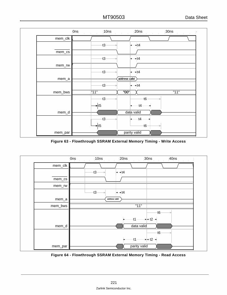
MT90503 Data Sheet
221Zarlink Semiconductor Inc.
Figure 63 - Flowthrough SSRAM External Memory Timing - Write Access
Figure 64 - Flowthrough SSRAM External Memory Timing - Read Access
0ns 10ns 20ns 30ns 4
mem_clk
mem_cs
mem_rw
mem_a
mem_bws
mem_d
mem_par
address validaddress valid
"11" "00" "11""00"
data valid data valid
parity valid
t4
t5
t3
t4
t6
t3
t3 t4
t3 t4
t3 t4
t5
t3
t6
t4
0ns 10ns 20ns 30ns 40ns 5
mem_clk
mem_cs
mem_rw
mem_a
mem_bws
mem_d
mem_par
address validaddress valid
"11"
data valid
parity valid
t4t3
t3 t4
t1 t2
t6
t1 t2
t6

MT90503 Data Sheet
222Zarlink Semiconductor Inc.
Figure 65 - Late-write External Memory Timing - Write Access
Figure 66 - Late-write External Memory Timing - Read Access
0ns 10ns 20ns 30ns 40ns 5
mem_clk
mem_cs
mem_rw
mem_a
mem_bws
mem_d
mem_par
address validaddress valid
"11" "00" "11""00"
data valid data valid
parity valid
t4
t5
t3
t4
t6
t3
t3 t4
t3 t4
t3 t4
t5
t3
t6
t4
0ns 10ns 20ns 30ns 40ns 50ns 6
mem_clk
mem_cs
mem_rw
mem_a
mem_bws
mem_d
mem_par
address validaddress valid
"11"
data valid
parity valid
t4t3
t3 t4
t1 t2
t6
t1 t2
t6

MT90503 Data Sheet
223Zarlink Semiconductor Inc.
Figure 67 - Pipelined ZBT External Memory Timing - Write Access
Figure 68 - Pipelined ZBT External Memory Timing - Read Access
0ns 10ns 20ns 30ns 40ns 50ns 6
mem_clk
mem_cs
mem_rw
mem_a
mem_bws
mem_d
mem_par
address validaddress valid
"11" "00" "11""00"
data valid data valid
parity valid
t4
t5
t3
t4
t6
t3
t3 t4
t3 t4
t3 t4
t5
t3
t6
t4
0ns 10ns 20ns 30ns 40ns 50ns 6
mem_clk
mem_cs
mem_rw
mem_a
mem_bws
mem_d
mem_par
address validaddress valid
"11"
data valid
parity valid
t4t3
t3 t4
t1 t2
t6
t1 t2
t6

MT90503 Data Sheet
224Zarlink Semiconductor Inc.
Figure 69 - Pipelined External Memory Timing - Write Access
Figure 70 - Pipelined External Memory Timing - Read Access
0ns 10ns 20ns 30ns 4
mem_clk
mem_cs
mem_rw
mem_a
mem_bws
mem_d
mem_par
address validaddress valid
"11" "00" "11""00"
data valid data valid
parity valid
t4
t5
t3
t4
t6
t3
t3 t4
t3 t4
t3 t4
t5
t3
t6
t4
0ns 10ns 20ns 30ns 40ns 50ns 6
mem_clk
mem_cs
mem_rw
mem_a
mem_bws
mem_d
mem_par
address validaddress valid
"11"
data valid
parity valid
t4t3
t3 t4
t1 t2
t6
t1 t2
t6
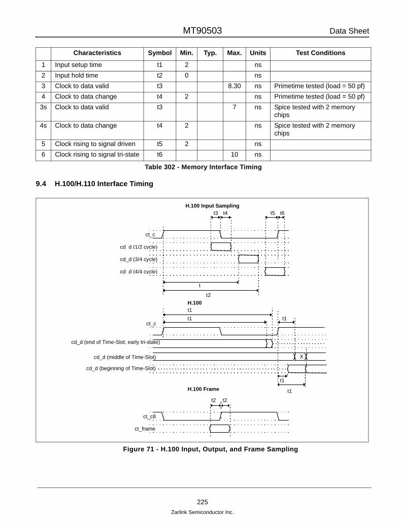
MT90503 Data Sheet
225Zarlink Semiconductor Inc.
9.4 H.100/H.110 Interface Timing
Figure 71 - H.100 Input, Output, and Frame Sampling
Characteristics Symbol Min. Typ. Max. Units Test Conditions
1 Input setup time t1 2 ns2 Input hold time t2 0 ns3 Clock to data valid t3 8.30 ns Primetime tested (load = 50 pf)4 Clock to data change t4 2 ns Primetime tested (load = 50 pf)3s Clock to data valid t3 7 ns Spice tested with 2 memory
chips4s Clock to data change t4 2 ns Spice tested with 2 memory
chips5 Clock rising to signal driven t5 2 ns6 Clock rising to signal tri-state t6 10 ns
Table 302 - Memory Interface Timing
ct_c
cd d (1/2 cycle) cd_d (3/4 cycle) cd d (4/4 cycle)
t2
t3 t4 t5 t6H.100 Input Sampling
ct_c
cd_d (end of Time-Slot; early tri-state) cd_d (middle of Time-Slot)
H.100
cd_d (beginning of Time-Slot) X
t1t1 t1
t1
t1
ct_c8 ct_frame
H.100 Frame
t2 t2
t

MT90503 Data Sheet
226Zarlink Semiconductor Inc.
Figure 72 - H.100 Message Channel Clock, Transmission Delay, and Reception Delay
Figure 73 - H.100 Clock Skew (when chip is Master)
ct_c8 ct_frame
H.100 Message Channel Clock
mc_clock
t30 t31
mc_t
ct_mc
H.100 Message Transmission Delayt40 t41
ct_mc
mc_rx
H.100 Message Reception Delay
t50
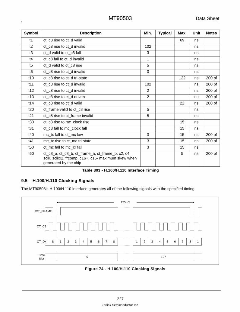
MT90503 Data Sheet
227Zarlink Semiconductor Inc.
9.5 H.100/H.110 Clocking Signals
The MT90503's H.100/H.110 interface generates all of the following signals with the specified timing.
Figure 74 - H.100/H.110 Clocking Signals
Symbol Description Min. Typical Max. Unit Notes
t1 ct_c8 rise to ct_d valid 69 nst2 ct_c8 rise to ct_d invalid 102 nst3 ct_d valid to ct_c8 fall 3 nst4 ct_c8 fall to ct_d invalid 1 nst5 ct_d valid to ct_c8 rise 5 nst6 ct_c8 rise to ct_d invalid 0 nst10 ct_c8 rise to ct_d tri-state 122 ns 200 pft11 ct_c8 rise to ct_d invalid 102 ns 200 pft12 ct_c8 rise to ct_d invalid 2 ns 200 pft13 ct_c8 rise to ct_d driven 2 ns 200 pft14 ct_c8 rise to ct_d valid 22 ns 200 pft20 ct_frame valid to ct_c8 rise 5 nst21 ct_c8 rise to ct_frame invalid 5 nst30 ct_c8 rise to mc_clock rise 15 nst31 ct_c8 fall to mc_clock fall 15 nst40 mc_tx fall to ct_mc low 3 15 ns 200 pft41 mc_tx rise to ct_mc tri-state 3 15 ns 200 pft50 ct_mc fall to mc_rx fall 3 15 nst60 ct_c8_a, ct_c8_b, ct_frame_a, ct_frame_b, c2, c4,
sclk, sclkx2, frcomp, c16+, c16- maximum skew when generated by the chip
5 ns 200 pf
Table 303 - H.100/H.110 Interface Timing
/CT_FRAME
CT_Dx
TimeSlot
125 uS
8 7 8
0
1 2 3 4 5 6
127
17 81 2 3 4 5 6
CT_C8

MT90503 Data Sheet
228Zarlink Semiconductor Inc.
Figure 75 - TDM Bus Timing - Compatibility Clock Generation
C2
/C4
SCLK
SCLKx2*
SCLK(2.048MHz)
(2.048MHz)
(4.096MHz)
SCLK(8.192MHz)
/C16
/CT_FRAME(A/B)
CT_C8(A/B)
/FR_COMP
SCLKx2*(4.096MHz)
SCLKx2*(8.192MHz)

MT90503 Data Sheet
229Zarlink Semiconductor Inc.
Figure 76 - TDM Data Bus Timings
Symbol Parameter Min. Typ. Max. Units
Clock edge rate (All Clocks) 0.25 2 V/nsTc8p Clock CT_C8 Period 122.066-F 122.074+F nsTc8h Clock CT_C8 High Time 49-F 73+F nsTc8l Clock CT_C8 Low Time 49-F 73+F ns
Tsamp Data Sample Point 90 nsTdoz Data Output to HiZ Time -20 0 nsTzdo Data HiZ to Output Time 0 22 nsTdod Data Output Delay Time 0 22 nsTdv Data Valid Time 0 69 nsTdiv Data Invalid Time 102 112 nsTfp /CT_FRAME Width 90 122 180 nsTfs /CT_FRAME Setup Time 45 90 nsTfh /CT_FRAME Hold Time 45 90 nsF Phase Correction 0 10 ns
Table 304 - H.100/H.110 Clocking Signals
/CT_FRAMETfs Tfh
Tfp
0.6V
2.0V
Data Out
Data In
Bit 1Bit 8
1 Bit Cell
Tdv
Tdod
Tdiv
Tdoz
Ts 0Ts 1272.4V
0.4V
1.4V
CT_C8
Tc8h Tc8l
Tc8p
2.0V
0.6V
Tzdo
Tsamp

MT90503 Data Sheet
230Zarlink Semiconductor Inc.
10.0 Glossary of TermsAAL0: ATM Adaptation Layer 0. AAL0 is a straight packaging of 48 bytes of data within an ATM cell. AAL0 can beused to treat either data cells (managed by CPU) or CBR cells (managed by TX/RX SAR).
AAL1: ATM Adaptation Layer 1. AAL1 is used to transport constant bit rate (CBR) data on ATM. The main featuresof AAL1 are a cell sequence number that allows the detection of lost cells and a p-byte that allows reconverging ofmulti-channel VCs.
AAL5: ATM Adaptation Layer 5. The main feature of AAL5 is a 32-bit CRC at the end of the cell that allows thedetection and correction of errors in the data payload. In this design, AAL5 cells are used uniquely to treat CBRinformation.
ATM: Asynchronous Transfer Mode. ATM is a networking standard based on 53-byte cells and is capable ofcarrying voice, data and video information simultaneously.
CAS: Channel Associated Signalling. Signalling bits used to indicate the state of the channel.
CBR: Constant Bit Rate. Cells in CBR format are sent out at a regular rate. CBR is applicable to voice channels.
CDV: Cell Delay Variation. When cells arrive on a UTOPIA port, they arrive with a certain delay with respect towhen they were sent. CDV is a measure of how much that delay varies on a VC.
CLP: Cell Loss Priority. A 1-bit field in the ATM cell header that corresponds to the loss priority of a cell; cells withCLP = 1 can be discarded in a congestion situation.
CNT: Counter. Events in the MT90503 will cause the counter to increment.
CRC: Cyclic Redundancy Check. The CRC is a method of error detection and correction that is applied to a certainfield of data. CRC is an efficient method of error detection because the odds of erroneously detecting a correctpayload are low.
DS1: Digital-Signal Level 1. DS1 is an electrical interface for digital transmissions that contains 24 64-Kbpschannels. The physical interface defined to carry DS1 channels is T1.
E1: E1 is the European equivalent of T1. They are similar with the main difference being E1 runs at 2.048 MHzinstead of 1.544 Mbps, carrying 30 64kbps channels.
ESF: Extended Super-Frame. ESF is a T1 format that defines multiframes as consisting of 24 frames, each one ofwhich contains 1 byte per channel.
FASTCAS: FASTCAS is not an acronym. It is capitalised in this document because it is a reserved word. FASTCASmeans that multiframe integrity is not respected between the TDM and ATM buses. The TDM data is processed assoon as it is received, while CAS is sent when it is available.
FIFO: First In, First Out. A FIFO memory is one in which the first byte to have been written into the memory is thefirst one to be read from the read port.
GFC: Generic Flow Control. The GFC field is kept in the 4 highest bits of an ATM cell’s header and is used for localfunctions (not carried end-to-end). The default value is "0000", meaning that GFC protocol is not enforced.
GPI: General Purpose Input
GPI/O: General Purpose Input or Output
H.100/H.110: A TDM bus standard developed by ECTF to provide backward compatibility to existing TDM buseswith more bandwidth and potential for development.
HEC: Header Error Check. Using the fifth octet in the ATM cell header, ATM equipment may check for an error andcorrect the contents of the header. A CRC algorithm allows for single-error correction and multiple-error detection.

MT90503 Data Sheet
231Zarlink Semiconductor Inc.
IE: Interrupt Enable. This is a register bit that enables a status event to generate an interrupt. This bit is alwaysactive-high.
ISR: Interrupt Service Routine
JTAG: Joint Test Action Group.
LUT: Look-Up Table. In the UTOPIA module of the MT90503, the LUT is used to associate the data from receivedcells with the proper TDM output channels. The LUT is contained in the external memory.
MFS: Multi-Frame Support. The MT90503 is capable of supporting the multi-frame standards of E1 and T1.
MVIP: Multi-Vendor Integration Protocol. MVIP is a standard for transmitting data on a TDM bus.
NNI: Network-Node Interface. NNI ATM cells do not have a GFC nibble, instead having an extra nibble of VPI.
OAM: Operations Administration and Maintenance. MSB within the PTI field of the ATM cell header which indicatesif the ATM cell carries management information such as fault indications.
OC-3: Optical Carrier level-3. A Sonet channel that carries a bandwidth of 155.55 Mbps.
OC-12: Optical Carrier level-12. A Sonet channel that carries a bandwidth of 622.08 Mbps.
PC: Process Control bit. This is a register bit type that is written to ‘1’ to initiate a hardware process. When theprocess completes, the hardware clears the bit.
PCM: Pulse Code Modulation. PCM is the basic method of encoding an analog voice signal into digital form.
PHY: PHYsical layer. The bottom layer of the ATM Reference Model, it provides ATM cell transmission over thephysical interfaces that interconnect the various ATM devices.
PLL: Phase Lock Loop. A phase lock loop is a component that generates an output clock by synchronising itself toan input clock. PLLs are often used to multiply the frequency of clocks.
PTI: Payload Type Identifier. The PTI field is a 3-bit header field that encodes various cell management information.Bit 2 (MSB) indicates OAM information or user data, bit 1 is Explicit Forward Congestion Control Indication (whetherthe cell may have been delayed by network congestion -- never examined by the MT90503) and bit 0 (LSB)indicates that a CBR-AAL5 cell is the final cell in a frame.
PUL: PULse bit. This is a register bit that is written to ‘1’ to indicate an event to the hardware. This bit is always readat ‘0’.
RAM: Random Access Memory. RAM is the main memory in the computer. It is called “random” because anyrandom address can be accessed in an equal amount of time.
RO: Read Only. This serves to define registers that cannot be written to by the CPU.
ROL: Read Only Latch. This defines status bits. Status bits cannot be written to ‘1’ by the CPU; however, once thestatus bit is set, the CPU can clear it by writing a ‘0’ over it.
RW: Read Write. This type of register bit will be readable and writeable by the CPU.
SAR: Segmentation And Reassembly. Method of partitioning, at the source, frames into ATM cells andreassembling, at the destination, these cells back into information frames; lower sublayer of the AAL which insertsdata from the information frames into cells and then adds the required header, trailer, and/or padding bytes tocreate 48-byte payloads to be transmitted to the ATM layer.
SCSA: Signal Computing System Architecture
SRTS: Synchronous Residual Time Stamp. SRTS is a clock recovery technique, which transmits timing informationover the network to allow the source clock to be reconstructed at the other end. SRTS is sent in a 4-bit valuetransmitted over 8 AAL1 cells.

c Zarlink Semiconductor 2002 All rights reserved.
APPRD.
ISSUE
DATE
ACN
Package Code
Previous package codes:
Conforms to JEDEC MS - 034
E
be
E1
A2DD1
AA1
40.2039.8035.56 REF
5031.27
0.60 0.90
35.56 REF
1.1039.80
MIN
0.502.11
40.20
2.560.70
MAX
6. SUBSTRATE THICKNESS IS 0.56 MM REF
4. N IS THE NUMBER OF SOLDER BALLS
2. DIMENSION "b" IS MEASURED AT THE MAXIMUM SOLDER BALL DIAMETER1. CONTROLLING DIMENSIONS ARE IN MM
5. NOT TO SCALE.
NOTE:
e
AA1A2
b
3. SEATING PLANE IS DEFINED BY THE SPHERICAL CROWNS OF THE SOLDER BALLS.
E1
D1
E / 4
D / 4
D
E2
D2
E
DIMENSION
1.25
D2 37.50 39.50
E2 37.50 39.50
N

www.zarlink.com
Information relating to products and services furnished herein by Zarlink Semiconductor Inc. or its subsidiaries (collectively “Zarlink”) is believed to be reliable.However, Zarlink assumes no liability for errors that may appear in this publication, or for liability otherwise arising from the application or use of any suchinformation, product or service or for any infringement of patents or other intellectual property rights owned by third parties which may result from such application oruse. Neither the supply of such information or purchase of product or service conveys any license, either express or implied, under patents or other intellectualproperty rights owned by Zarlink or licensed from third parties by Zarlink, whatsoever. Purchasers of products are also hereby notified that the use of product incertain ways or in combination with Zarlink, or non-Zarlink furnished goods or services may infringe patents or other intellectual property rights owned by Zarlink.
This publication is issued to provide information only and (unless agreed by Zarlink in writing) may not be used, applied or reproduced for any purpose nor form partof any order or contract nor to be regarded as a representation relating to the products or services concerned. The products, their specifications, services and otherinformation appearing in this publication are subject to change by Zarlink without notice. No warranty or guarantee express or implied is made regarding thecapability, performance or suitability of any product or service. Information concerning possible methods of use is provided as a guide only and does not constituteany guarantee that such methods of use will be satisfactory in a specific piece of equipment. It is the user’s responsibility to fully determine the performance andsuitability of any equipment using such information and to ensure that any publication or data used is up to date and has not been superseded. Manufacturing doesnot necessarily include testing of all functions or parameters. These products are not suitable for use in any medical products whose failure to perform may result insignificant injury or death to the user. All products and materials are sold and services provided subject to Zarlink’s conditions of sale which are available on request.
Purchase of Zarlink’s I2C components conveys a licence under the Philips I2C Patent rights to use these components in and I2C System, provided that the systemconforms to the I2C Standard Specification as defined by Philips.
Zarlink, ZL and the Zarlink Semiconductor logo are trademarks of Zarlink Semiconductor Inc.
Copyright Zarlink Semiconductor Inc. All Rights Reserved.
TECHNICAL DOCUMENTATION - NOT FOR RESALE
For more information about all Zarlink productsvisit our Web Site at