investor and analyst presentation december 2019 - at&s
TRANSCRIPT
AT & S Austria Technologie & Systemtechnik Aktiengesellschaft | Fabriksgasse 13 | A-8700 Leoben
Tel +43 (0) 3842 200-0
www.ats.net
AT&S
First choice for advanced applicationsInvestor and Analyst Presentation
December 2019
Investor and Analyst Presentation 1
Table of Contents
Company Overview
Market Update
Financials H1 2019/20 & Outlook
Investment in the future of AT&S
Annex

Investor and Analyst Presentation 2
AT & S Austria Technologie & Systemtechnik Aktiengesellschaft | Fabriksgasse 13 | A-8700 Leoben
Tel +43 (0) 3842 200-0
www.ats.net
Company Overview
Investor and Analyst Presentation 3
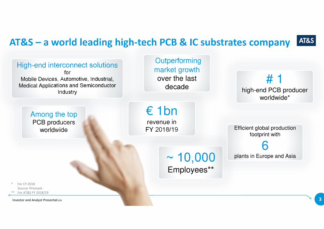
AT&S – a world leading high-tech PCB & IC substrates company
High-end interconnect solutionsfor
Mobile Devices, Automotive, Industrial,
Medical Applications and Semiconductor Industry
Outperforming
market growth over the last
decade
€ 1bnrevenue in
FY 2018/19
Among the top PCB producers
worldwide
# 1 high-end PCB producer
worldwide*
~ 10,000Employees**
Efficient global production footprint with
6 plants in Europe and Asia
* For CY 2018
Source: Prismark
** For AT&S FY 2018/19
Investor and Analyst Presentation 4
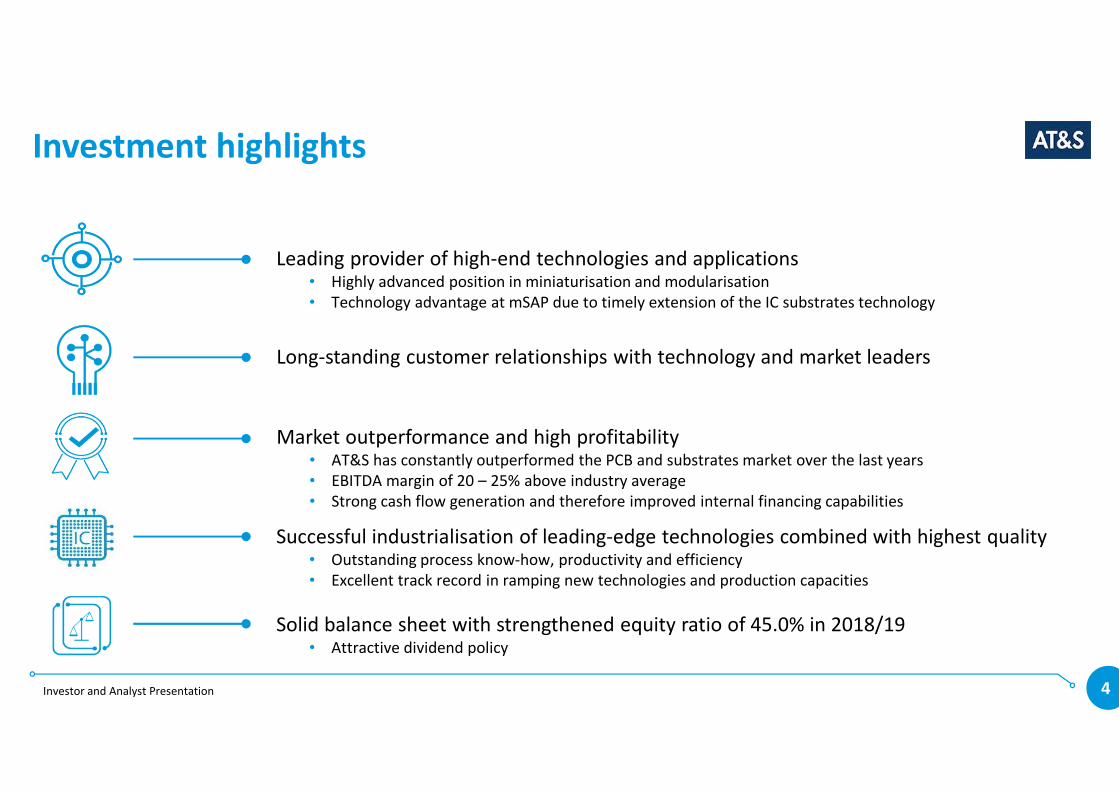
Investment highlights
Leading provider of high-end technologies and applications• Highly advanced position in miniaturisation and modularisation
• Technology advantage at mSAP due to timely extension of the IC substrates technology
Successful industrialisation of leading-edge technologies combined with highest quality • Outstanding process know-how, productivity and efficiency
• Excellent track record in ramping new technologies and production capacities
Long-standing customer relationships with technology and market leaders
Solid balance sheet with strengthened equity ratio of 45.0% in 2018/19 • Attractive dividend policy
Market outperformance and high profitability• AT&S has constantly outperformed the PCB and substrates market over the last years
• EBITDA margin of 20 – 25% above industry average
• Strong cash flow generation and therefore improved internal financing capabilities
Investor and Analyst Presentation 5
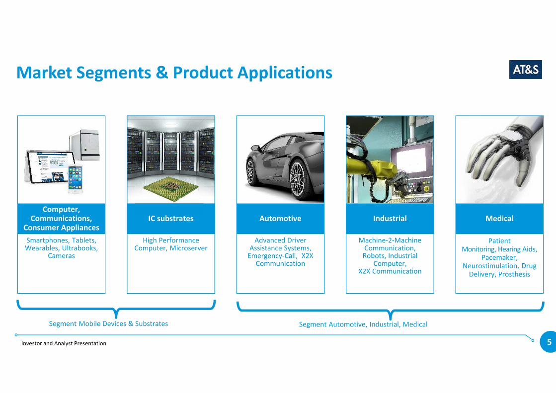
Market Segments & Product Applications
Computer, Communications,
Consumer Appliances
Smartphones, Tablets, Wearables, Ultrabooks,
Cameras
Industrial
Machine-2-Machine Communication,
Robots, Industrial Computer,
X2X Communication
Automotive
Advanced Driver Assistance Systems,
Emergency-Call, X2X Communication
Medical
Patient Monitoring, Hearing Aids,
Pacemaker, Neurostimulation, Drug
Delivery, Prosthesis
IC substrates
High Performance Computer, Microserver
Segment Mobile Devices & Substrates Segment Automotive, Industrial, Medical
Investor and Analyst Presentation 6
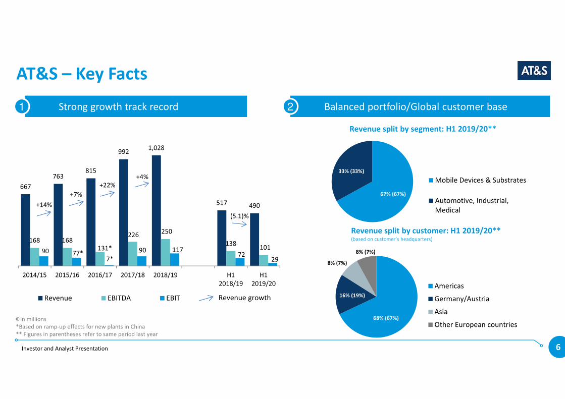
AT&S – Key Facts
667
763815
9921,028
517 490
168 168131*
226250
138101
90 77*7*
90 11772
29
2014/15 2015/16 2016/17 2017/18 2018/19 H1
2018/19
H1
2019/20
Revenue EBITDA EBIT
(5.1)%
Strong growth track record1 Balanced portfolio/Global customer base2
7%
+14%
+7%
+22%
€ in millions
*Based on ramp-up effects for new plants in China
** Figures in parentheses refer to same period last year
Revenue growth
+4%
Revenue split by segment: H1 2019/20**
Revenue split by customer: H1 2019/20**(based on customer’s headquarters)
6
67% (67%)
33% (33%)
Mobile Devices & Substrates
Automotive, Industrial,
Medical
68% (67%)
16% (19%)
8% (7%)
8% (7%)
Americas
Germany/Austria
Asia
Other European countries
Investor and Analyst Presentation 7
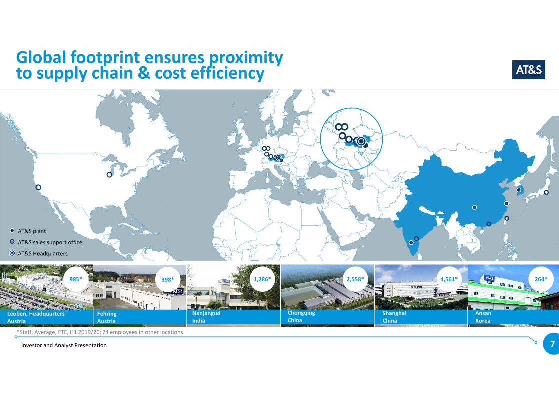
Global footprint ensures proximity to supply chain & cost efficiency
985* 398* 1,286* 2,558* 4,561* 264*
Shanghai
China
Ansan
Korea
Chongqing
ChinaLeoben, Headquarters
Austria
Fehring
Austria
Nanjangud
India
AT&S plant
AT&S sales support office
AT&S Headquarters
*Staff, Average, FTE, H1 2019/20; 74 employees in other locations
Investor and Analyst Presentation 8
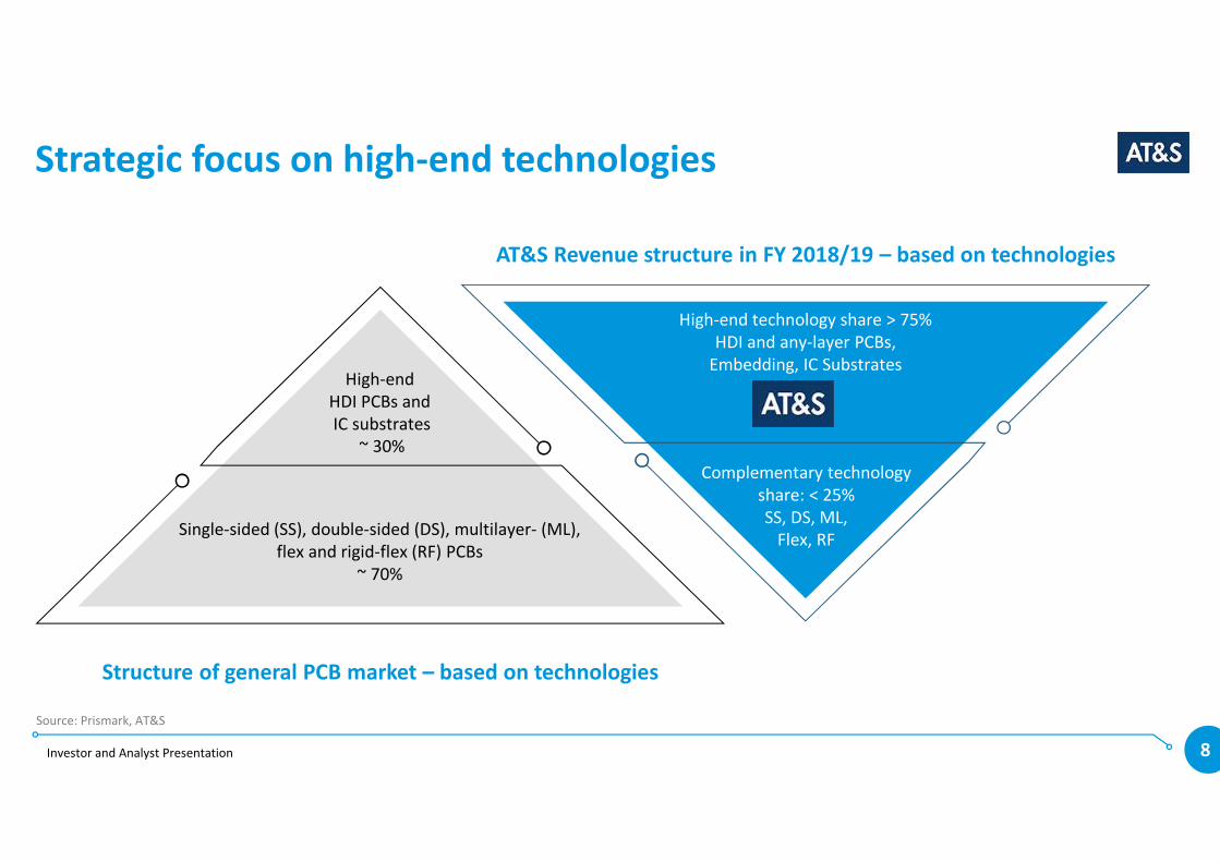
Strategic focus on high-end technologies
AT&S Revenue structure in FY 2018/19 – based on technologies
High-end
HDI PCBs and
IC substrates
~ 30%
Single-sided (SS), double-sided (DS), multilayer- (ML),
flex and rigid-flex (RF) PCBs
~ 70%
High-end technology share > 75%
HDI and any-layer PCBs,
Embedding, IC Substrates
Complementary technology
share: < 25%
SS, DS, ML,
Flex, RF
Structure of general PCB market – based on technologies
Source: Prismark, AT&S
Investor and Analyst Presentation 9
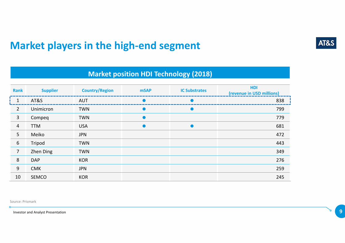
Market players in the high-end segment
Market position HDI Technology (2018)
Rank Supplier Country/Region mSAP IC SubstratesHDI
(revenue in USD millions)
1 AT&S AUT � � 838
2 Unimicron TWN � � 799
3 Compeq TWN � 779
4 TTM USA � � 681
5 Meiko JPN 472
6 Tripod TWN 443
7 Zhen Ding TWN 349
8 DAP KOR 276
9 CMK JPN 259
10 SEMCO KOR 245
Source: Prismark
Investor and Analyst Presentation 10
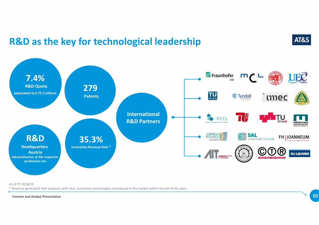
R&D as the key for technological leadership
International
R&D Partners
As of FY 2018/19
* Revenue generated with products with new, innovative technologies introduced to the market within the last three years
R&DHeadquarters
AustriaIndustrialization at the respective
production site
7.4%R&D Quota
(equivalent to € 75.7 million)
35.3%Innovation Revenue Rate *
International
R&D Partners
279 Patents
Investor and Analyst Presentation 11
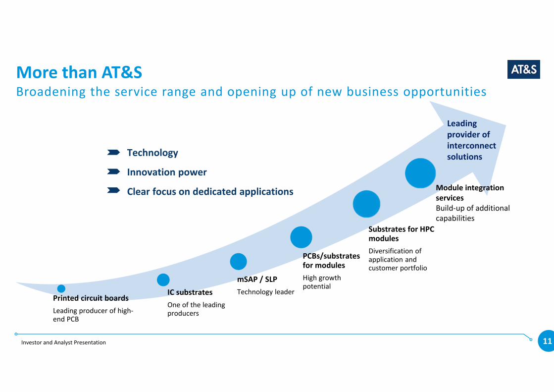
More than AT&S
Printed circuit boards
Leading producer of high-end PCB
IC substrates
One of the leading producers
mSAP / SLP
Technology leader
PCBs/substrates for modules
High growth potential
Substrates for HPC modules
Diversification of application and customer portfolio
Broadening the service range and opening up of new business opportunities
Module integration
services
Build-up of additional
capabilities
Technology
Innovation power
Clear focus on dedicated applications
Leading
provider of
interconnect
solutions
Investor and Analyst Presentation 12
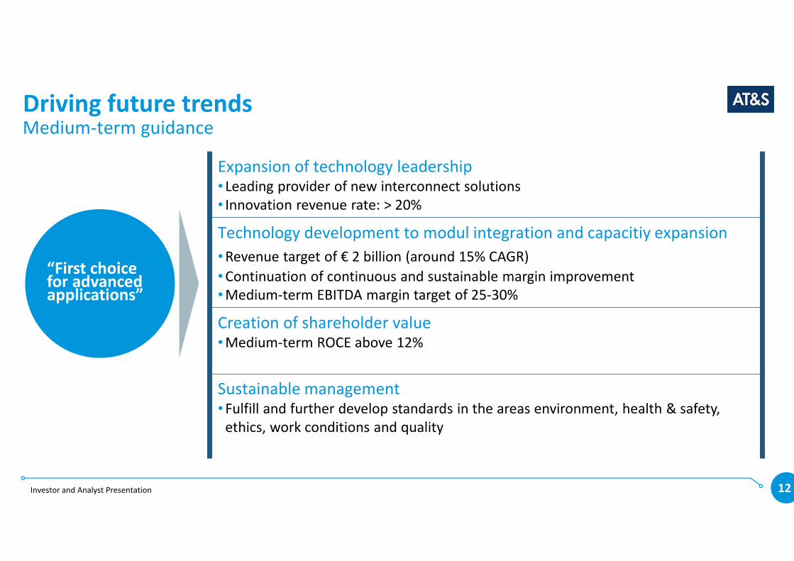
Driving future trends
Expansion of technology leadership• Leading provider of new interconnect solutions
• Innovation revenue rate: > 20%
Technology development to modul integration and capacitiy expansion
• Revenue target of € 2 billion (around 15% CAGR)
• Continuation of continuous and sustainable margin improvement
• Medium-term EBITDA margin target of 25-30%
Creation of shareholder value• Medium-term ROCE above 12%
Sustainable management• Fulfill and further develop standards in the areas environment, health & safety,
ethics, work conditions and quality
“First choice for advanced applications”
Medium-term guidance

Investor and Analyst Presentation 13
AT & S Austria Technologie & Systemtechnik Aktiengesellschaft | Fabriksgasse 13 | A-8700 Leoben
Tel +43 (0) 3842 200-0
www.ats.net
Market Update
Investor and Analyst Presentation 14
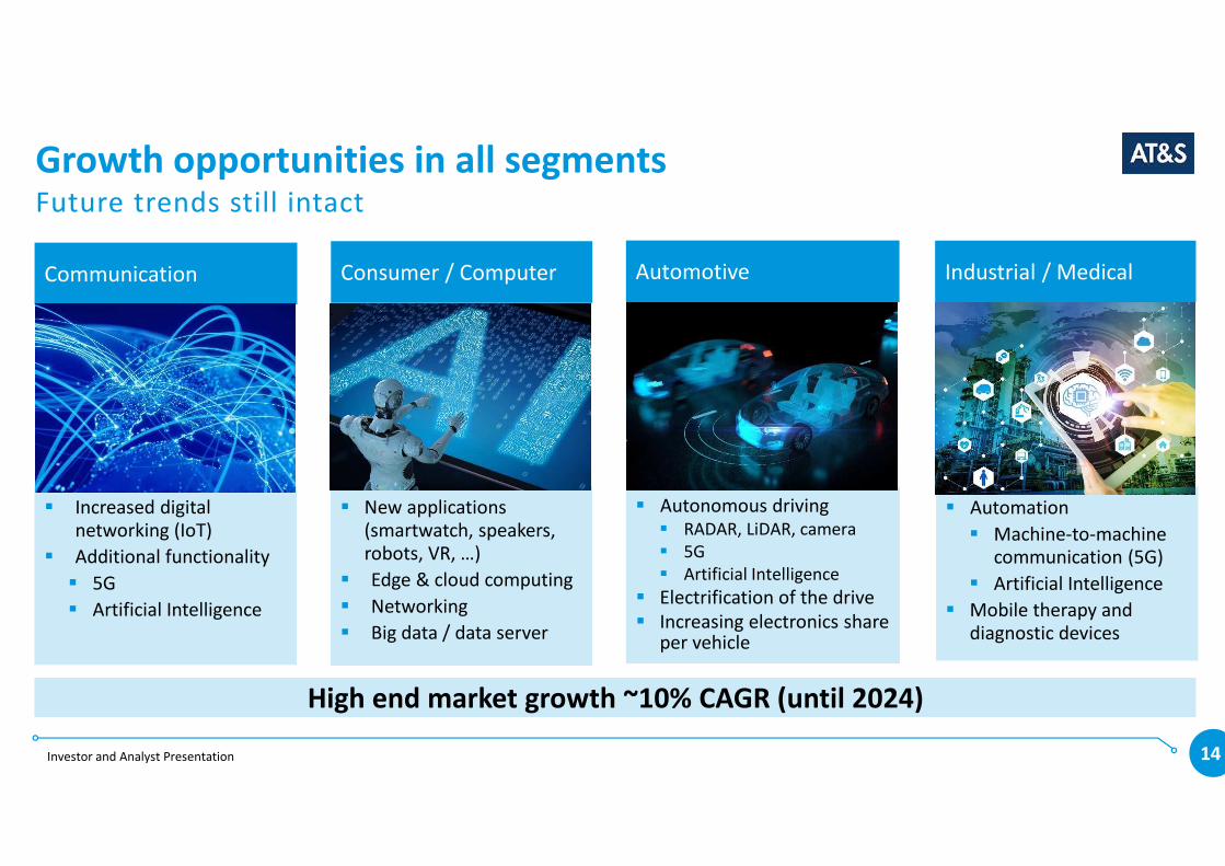
Growth opportunities in all segmentsFuture trends still intact
14
� New applications
(smartwatch, speakers,
robots, VR, …)
� Edge & cloud computing
� Networking
� Big data / data server
Consumer / Computer
� Increased digital
networking (IoT)
� Additional functionality
� 5G
� Artificial Intelligence
Communication
� Automation
� Machine-to-machine
communication (5G)
� Artificial Intelligence
� Mobile therapy and
diagnostic devices
Industrial / Medical
� Autonomous driving
� RADAR, LiDAR, camera
� 5G
� Artificial Intelligence
� Electrification of the drive
� Increasing electronics share per vehicle
Automotive
High end market growth ~10% CAGR (until 2024)

Investor and Analyst Presentation 15
Current market environment
� Trade frictions (US-China) and political environment (Brexit) create uncertainties in the market
� Weakness in automotive market is mainly created by uncertainties about the future of the powertrain
� Growth in electronic content compensates for declining car unit sales
� 5G infrastructure (base station and satellites) currently being built up, mobile devices to follow in significant
volumes from 2020 onwards
� Artificial Intelligence applications drive demand for data processing and memory
� Miniaturization and modularization trend continues
Investor and Analyst Presentation 16
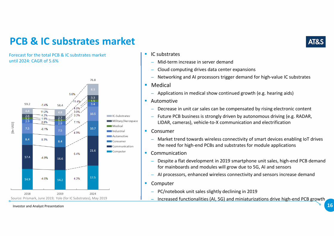
PCB & IC substrates market
16
Source: Prismark, June 2019; Yole (for IC Substrates), May 2019
� IC substrates
− Mid-term increase in server demand
− Cloud computing drives data center expansions
− Networking and AI processors trigger demand for high-value IC substrates
� Medical
− Applications in medical show continued growth (e.g. hearing aids)
� Automotive
− Decrease in unit car sales can be compensated by rising electronic content
− Future PCB business is strongly driven by autonomous driving (e.g. RADAR,
LIDAR, cameras), vehicle-to-X communication and electrification
� Consumer
− Market trend towards wireless connectivity of smart devices enabling IoT drives
the need for high-end PCBs and substrates for module applications
� Communication
− Despite a flat development in 2019 smartphone unit sales, high-end PCB demand
for mainboards and modules will grow due to 5G, AI and sensors
− AI processors, enhanced wireless connectivity and sensors increase demand
� Computer
− PC/notebook unit sales slightly declining in 2019
− Increased functionalities (AI, 5G) and miniaturizations drive high-end PCB growth
Forecast for the total PCB & IC substrates market
until 2024: CAGR of 5.6%
Investor and Analyst Presentation 17
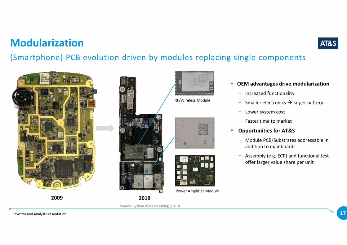
Modularization
(Smartphone) PCB evolution driven by modules replacing single components
2009 2019
� OEM advantages drive modularization
− Increased functionality
− Smaller electronics � larger battery
− Lower system cost
− Faster time to market
� Opportunities for AT&S
− Module PCB/Substrates addressable in
addition to mainboards
− Assembly (e.g. ECP) and functional test
offer larger value share per unit
RF/Wireless Module
Power Amplifier Module
Source: System Plus Consulting (2019)
Investor and Analyst Presentation 18
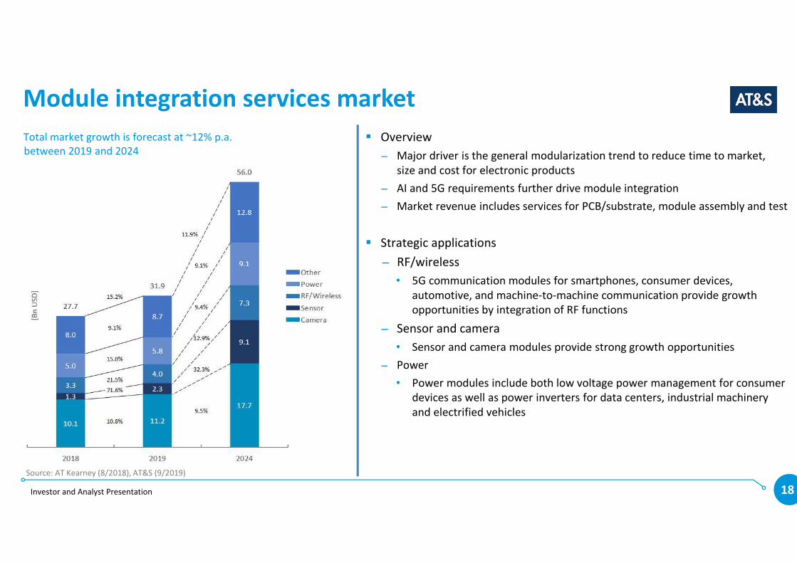
Module integration services market
18
Source: AT Kearney (8/2018), AT&S (9/2019)
� Overview
− Major driver is the general modularization trend to reduce time to market,
size and cost for electronic products
− AI and 5G requirements further drive module integration
− Market revenue includes services for PCB/substrate, module assembly and test
� Strategic applications
− RF/wireless
• 5G communication modules for smartphones, consumer devices,
automotive, and machine-to-machine communication provide growth
opportunities by integration of RF functions
− Sensor and camera
• Sensor and camera modules provide strong growth opportunities
− Power
• Power modules include both low voltage power management for consumer
devices as well as power inverters for data centers, industrial machinery
and electrified vehicles
Total market growth is forecast at ~12% p.a.
between 2019 and 2024
Investor and Analyst Presentation 19
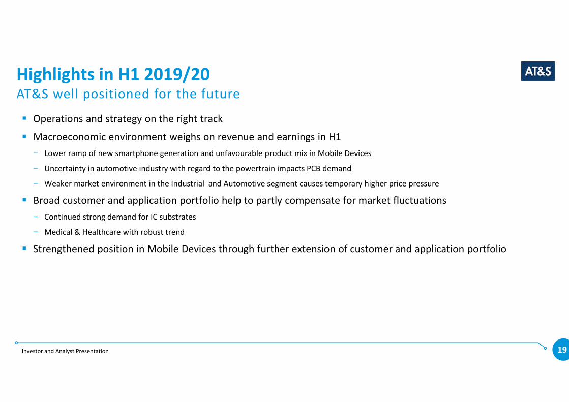
Highlights in H1 2019/20
� Operations and strategy on the right track
� Macroeconomic environment weighs on revenue and earnings in H1
− Lower ramp of new smartphone generation and unfavourable product mix in Mobile Devices
− Uncertainty in automotive industry with regard to the powertrain impacts PCB demand
− Weaker market environment in the Industrial and Automotive segment causes temporary higher price pressure
� Broad customer and application portfolio help to partly compensate for market fluctuations
− Continued strong demand for IC substrates
− Medical & Healthcare with robust trend
� Strengthened position in Mobile Devices through further extension of customer and application portfolio
AT&S well positioned for the future
19

Investor and Analyst Presentation 20
AT & S Austria Technologie & Systemtechnik Aktiengesellschaft | Fabriksgasse 13 | A-8700 Leoben
Tel +43 (0) 3842 200-0
www.ats.net
Financials H1 2019/20 & Outlook
Investor and Analyst Presentation 21
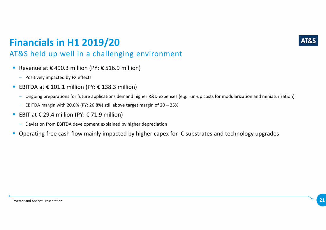
Financials in H1 2019/20
� Revenue at € 490.3 million (PY: € 516.9 million)
− Positively impacted by FX effects
� EBITDA at € 101.1 million (PY: € 138.3 million)
− Ongoing preparations for future applications demand higher R&D expenses (e.g. run-up costs for modularization and miniaturization)
− EBITDA margin with 20.6% (PY: 26.8%) still above target margin of 20 – 25%
� EBIT at € 29.4 million (PY: € 71.9 million)
− Deviation from EBITDA development explained by higher depreciation
� Operating free cash flow mainly impacted by higher capex for IC substrates and technology upgrades
AT&S held up well in a challenging environment
21
Investor and Analyst Presentation 22
Revenue and EBITDA development
€ in millions€ in millions
22
68%
16%
8%
8%
Americas
Germany/Austria
Asia
Other European countries
Revenue split by segment: H1 2019/20
Revenue split by region*: H1 2019/20
22
67%
33%
Mobile Devices & Substrates
Automotive, Industrial,
Medical
*based on customer’s headquarters*based on customer’s headquarters
294.8273.3
237.9222.7
267.6
516.9490.3
86.3 82.2
29.6 34.9
66.2
138.3
101.1
Q2 2018/19 Q3 2018/19 Q4 2018/19 Q1 2019/20 Q2 2019/20 H1 2018/19 H1 2019/20
Revenue EBITDA and margin
12.5%30.1%29.3% 15.7% 24.7% 26.8% 20.6%
Investor and Analyst Presentation 23
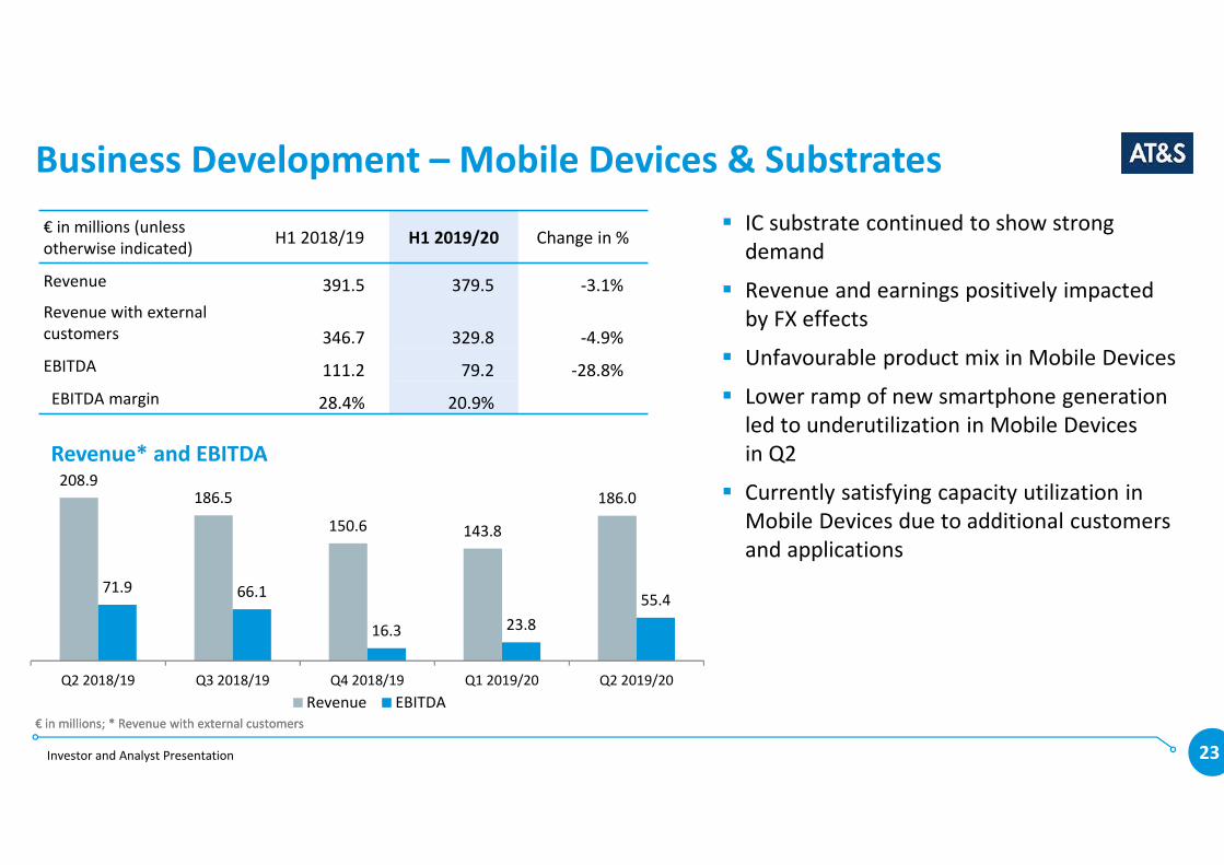
Business Development – Mobile Devices & Substrates
208.9186.5
150.6 143.8
186.0
71.9 66.1
16.3 23.8
55.4
Q2 2018/19 Q3 2018/19 Q4 2018/19 Q1 2019/20 Q2 2019/20
Revenue EBITDA
� IC substrate continued to show strong
demand
� Revenue and earnings positively impacted
by FX effects
� Unfavourable product mix in Mobile Devices
� Lower ramp of new smartphone generation
led to underutilization in Mobile Devices
in Q2
� Currently satisfying capacity utilization in
Mobile Devices due to additional customers
and applications
€ in millions (unless
otherwise indicated)H1 2018/19 H1 2019/20 Change in %
Revenue 391.5 379.5 -3.1%
Revenue with external
customers 346.7 329.8 -4.9%
EBITDA 111.2 79.2 -28.8%
EBITDA margin 28.4% 20.9%
€ in millions; * Revenue with external customers€ in millions; * Revenue with external customers
Revenue* and EBITDA
Investor and Analyst Presentation 24
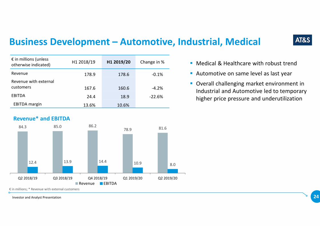
84.3 85.0 86.278.9 81.6
12.4 13.9 14.4 10.9 8.0
Q2 2018/19 Q3 2018/19 Q4 2018/19 Q1 2019/20 Q2 2019/20
Revenue EBITDA
Business Development – Automotive, Industrial, Medical
� Medical & Healthcare with robust trend
� Automotive on same level as last year
� Overall challenging market environment in
Industrial and Automotive led to temporary
higher price pressure and underutilization
€ in millions (unless
otherwise indicated)H1 2018/19 H1 2019/20 Change in %
Revenue 178.9 178.6 -0.1%
Revenue with external
customers 167.6 160.6 -4.2%
EBITDA 24.4 18.9 -22.6%
EBITDA margin 13.6% 10.6%
Revenue* and EBITDA
€ in millions; * Revenue with external customers€ in millions; * Revenue with external customers
Investor and Analyst Presentation 25
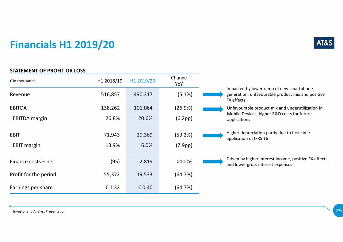
Financials H1 2019/20
Impacted by lower ramp of new smartphone
generation, unfavourable product mix and positive
FX effects
Unfavourable product mix and underutilization in
Mobile Devices, higher R&D costs for future
applications
Higher depreciation partly due to first-time
application of IFRS 16
STATEMENT OF PROFIT OR LOSS
€ in thousands H1 2018/19 H1 2019/20Change
YoY
Revenue 516,857 490,317 (5.1%)
EBITDA 138,262 101,064 (26.9%)
EBITDA margin 26.8% 20.6% (6.2pp)
EBIT 71,943 29,369 (59.2%)
EBIT margin 13.9% 6.0% (7.9pp)
Finance costs – net (95) 2,819 >100%
Profit for the period 55,372 19,533 (64.7%)
Earnings per share € 1.32 € 0.40 (64.7%)
Driven by higher interest income, positive FX effects
and lower gross interest expenses

Investor and Analyst Presentation 26
Financials H1 2019/20
Negative FX effects and dividend payout
Higher capex, impact of IFRS 16
STATEMENT OF FINANCIAL POSITION
€ in thousands 31 Mar 2019 30 Sep 2019 Change
Equity 803,451 768,385 (4.4%)
Total assets 1,784,106 1,809,660 1.4%
Net debt 150,258 233,697 55.5%
Net working capital 160,537 188,939 17.7%
Equity ratio 45.0% 42.5% (2.5%) Effect out of lower equity and higher total assets
Investor and Analyst Presentation 27
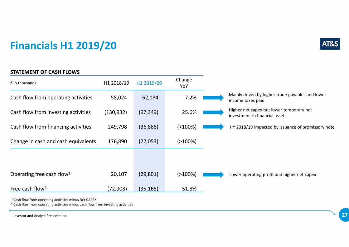
Financials H1 2019/20
Mainly driven by higher trade payables and lower
income taxes paid
Higher net capex but lower temporary net
investment in financial assets
HY 2018/19 impacted by issuance of promissory note
STATEMENT OF CASH FLOWS
€ in thousands H1 2018/19 H1 2019/20Change
YoY
Cash flow from operating activities 58,024 62,184 7.2%
Cash flow from investing activities (130,932) (97,349) 25.6%
Cash flow from financing activities 249,798 (36,888) (>100%)
Change in cash and cash equivalents 176,890 (72,053) (>100%)
Operating free cash flow1) 20,107 (29,801) (>100%)
Free cash flow2) (72,908) (35,165) 51.8%
1) Cash flow from operating activities minus Net CAPEX2) Cash flow from operating activities minus cash flow from investing activities
Lower operating profit and higher net capex
Investor and Analyst Presentation 28
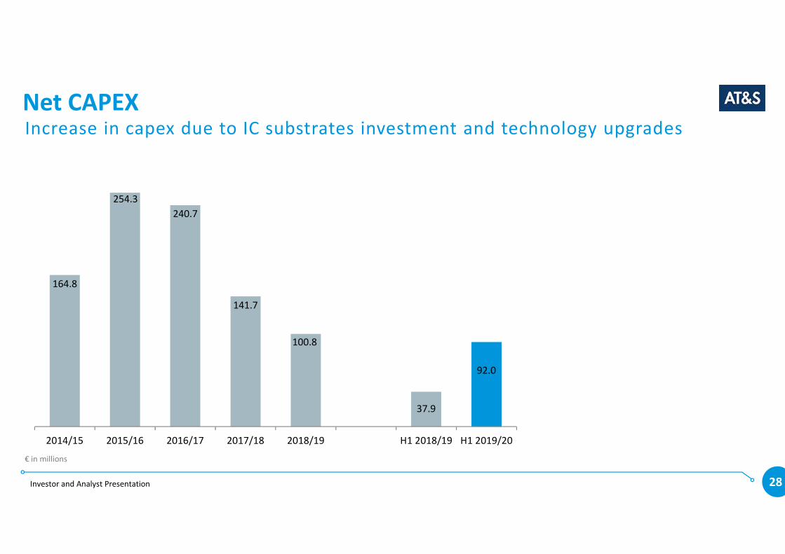
Net CAPEX
€ in millions
164.8
254.3
240.7
141.7
100.8
37.9
92.0
2014/15 2015/16 2016/17 2017/18 2018/19 H1 2018/19 H1 2019/20
Increase in capex due to IC substrates investment and technology upgrades
Investor and Analyst Presentation 29
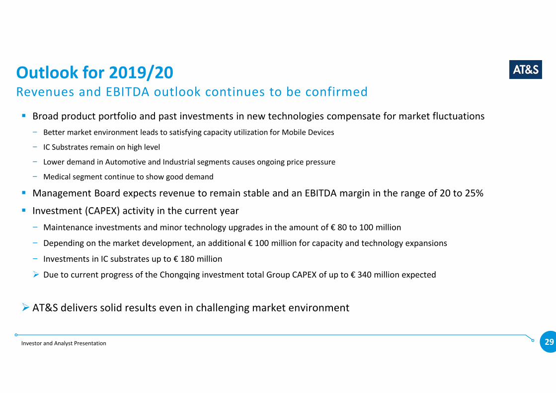
Outlook for 2019/20
� Broad product portfolio and past investments in new technologies compensate for market fluctuations
− Better market environment leads to satisfying capacity utilization for Mobile Devices
− IC Substrates remain on high level
− Lower demand in Automotive and Industrial segments causes ongoing price pressure
− Medical segment continue to show good demand
� Management Board expects revenue to remain stable and an EBITDA margin in the range of 20 to 25%
� Investment (CAPEX) activity in the current year
− Maintenance investments and minor technology upgrades in the amount of € 80 to 100 million
− Depending on the market development, an additional € 100 million for capacity and technology expansions
− Investments in IC substrates up to € 180 million
� Due to current progress of the Chongqing investment total Group CAPEX of up to € 340 million expected
�AT&S delivers solid results even in challenging market environment
Revenues and EBITDA outlook continues to be confirmed

Investor and Analyst Presentation 30
AT & S Austria Technologie & Systemtechnik Aktiengesellschaft | Fabriksgasse 13 | A-8700 Leoben
Tel +43 (0) 3842 200-0
www.ats.net
Investment in the future of AT&S
Investor and Analyst Presentation 31
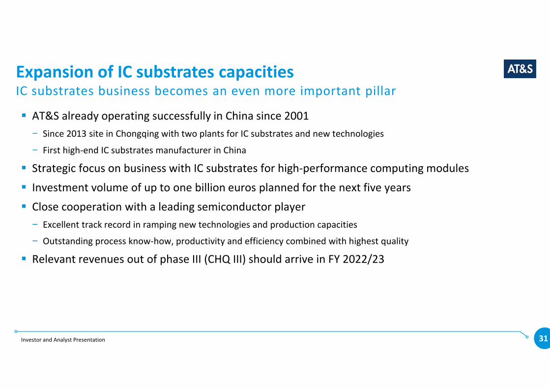
Expansion of IC substrates capacities
� AT&S already operating successfully in China since 2001
− Since 2013 site in Chongqing with two plants for IC substrates and new technologies
− First high-end IC substrates manufacturer in China
� Strategic focus on business with IC substrates for high-performance computing modules
� Investment volume of up to one billion euros planned for the next five years
� Close cooperation with a leading semiconductor player
− Excellent track record in ramping new technologies and production capacities
− Outstanding process know-how, productivity and efficiency combined with highest quality
� Relevant revenues out of phase III (CHQ III) should arrive in FY 2022/23
IC substrates business becomes an even more important pillar
31
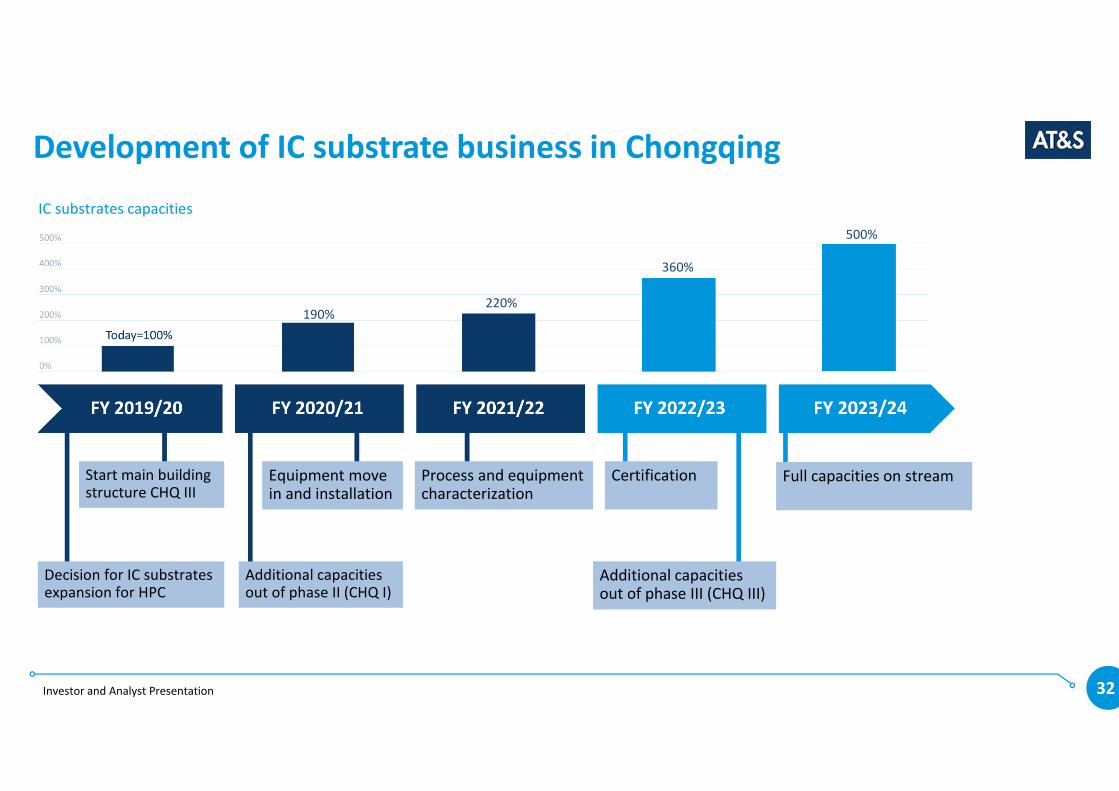
Investor and Analyst Presentation 32
Development of IC substrate business in Chongqing
Process and equipment characterization
Certification Equipment move in and installation
Decision for IC substrates expansion for HPC
Additional capacities out of phase II (CHQ I)
Additional capacities out of phase III (CHQ III)
Start main building structure CHQ III
Full capacities on stream
190%220%
360%
500%
IC substrates capacities
Investor and Analyst Presentation 33
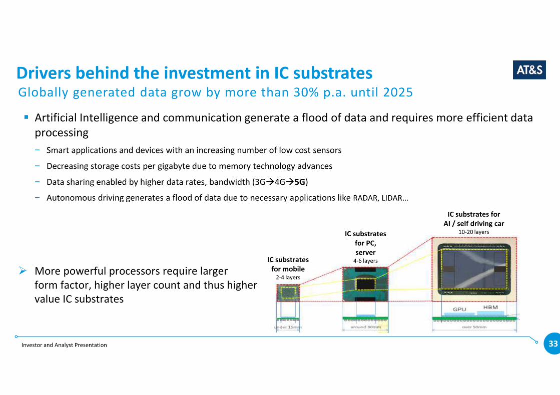
Drivers behind the investment in IC substrates
� Artificial Intelligence and communication generate a flood of data and requires more efficient data
processing
− Smart applications and devices with an increasing number of low cost sensors
− Decreasing storage costs per gigabyte due to memory technology advances
− Data sharing enabled by higher data rates, bandwidth (3G�4G�5G)
− Autonomous driving generates a flood of data due to necessary applications like RADAR, LIDAR…
� More powerful processors require larger
form factor, higher layer count and thus higher
value IC substrates
Globally generated data grow by more than 30% p.a. until 2025
IC substrates
for mobile2-4 layers
IC substrates
for PC,
server4-6 layers
IC substrates for
AI / self driving car10-20 layers
Investor and Analyst Presentation 34
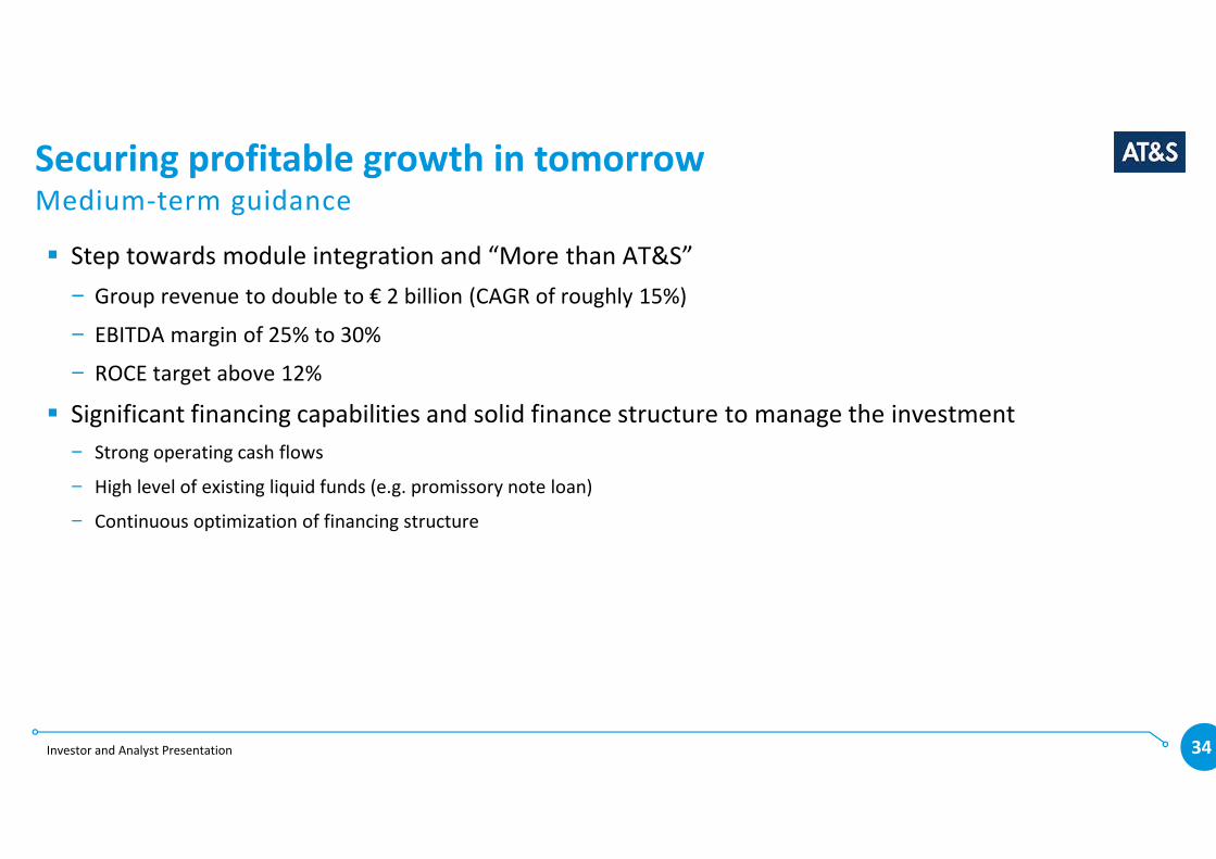
Securing profitable growth in tomorrow
� Step towards module integration and “More than AT&S”
− Group revenue to double to € 2 billion (CAGR of roughly 15%)
− EBITDA margin of 25% to 30%
− ROCE target above 12%
� Significant financing capabilities and solid finance structure to manage the investment
− Strong operating cash flows
− High level of existing liquid funds (e.g. promissory note loan)
− Continuous optimization of financing structure
Medium-term guidance

Investor and Analyst Presentation 35
AT & S Austria Technologie & Systemtechnik Aktiengesellschaft | Fabriksgasse 13 | A-8700 Leoben
Tel +43 (0) 3842 200-0
www.ats.net
Annex
Investor and Analyst Presentation 36
AT&S – Stock ProfileListing: Vienna Stock Exchange,
Prime Standard
Indices: ATX, Vönix, WBI
Thomson Reuters (A): ATSV.VI
Bloomberg (A): ATS:AV
Publication of the first nine months 2019/20 04 February 2020
Preliminary results 2019/20 14 May 2020
Financial Calendar Shareholder structure
# of shares outstanding 38.85m
Average daily volume*: ~ 80,000 shares
Dividend for 2018/19: € 0.60 per share
* 01/12/2018 – 30/11/2019
Investor and Analyst Presentation 37
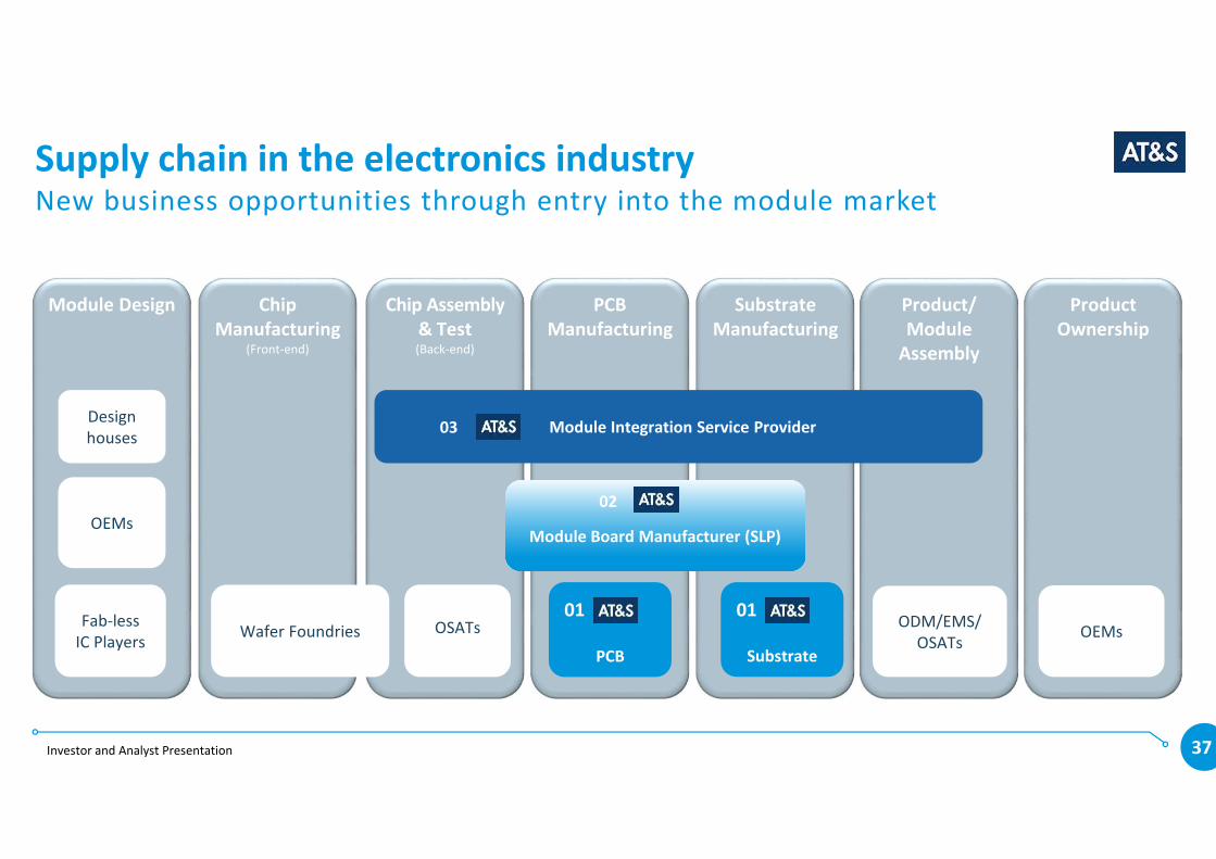
Supply chain in the electronics industryNew business opportunities through entry into the module market
37
Substrate
Manufacturing
Module Design Chip
Manufacturing(Front-end)
PCB
Manufacturing
Chip Assembly
& Test(Back-end)
Product/
Module
Assembly
Product
Ownership
OSATs
PCB
Wafer FoundriesODM/EMS/
OSATsOEMs
OEMs
Fab-less
IC Players
Module Integration Service ProviderDesign
houses03
Module Board Manufacturer (SLP)
02
01
Substrate
01
Investor and Analyst Presentation 38
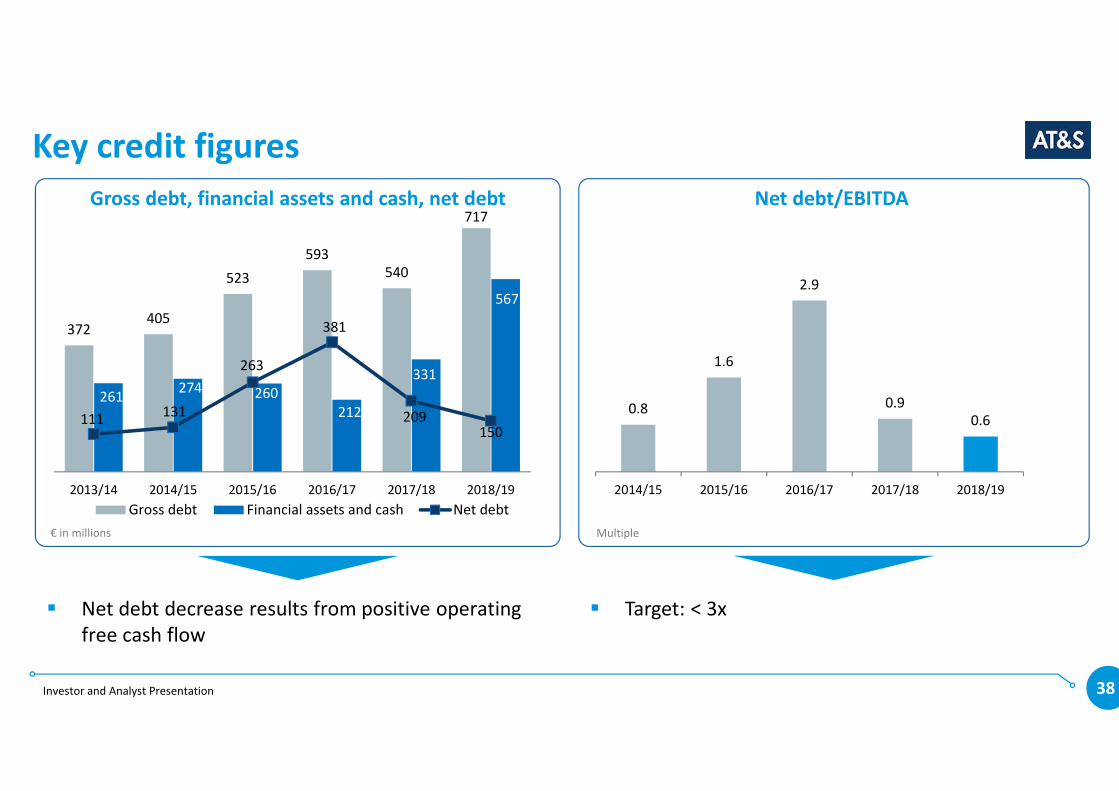
Gross debt, financial assets and cash, net debt
Key credit figures
372405
523
593
540
717
261274 260
212
331
567
111131
263
381
209150
2013/14 2014/15 2015/16 2016/17 2017/18 2018/19
Gross debt Financial assets and cash Net debt
0.8
1.6
2.9
0.9
0.6
2014/15 2015/16 2016/17 2017/18 2018/19
� Target: < 3x
Net debt/EBITDA
� Net debt decrease results from positive operating
free cash flow
€ in millions Multiple
Investor and Analyst Presentation 39
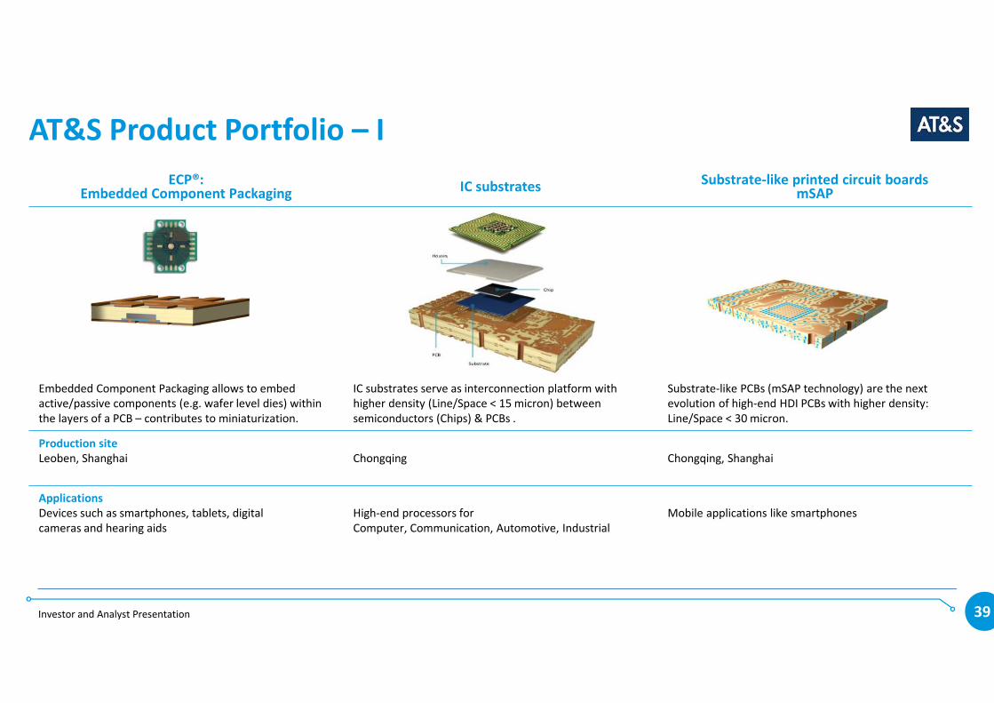
AT&S Product Portfolio – I
ECP®:Embedded Component Packaging
IC substratesSubstrate-like printed circuit boards
mSAP
Embedded Component Packaging allows to embed
active/passive components (e.g. wafer level dies) within
the layers of a PCB – contributes to miniaturization.
IC substrates serve as interconnection platform with
higher density (Line/Space < 15 micron) between
semiconductors (Chips) & PCBs .
Substrate-like PCBs (mSAP technology) are the next
evolution of high-end HDI PCBs with higher density:
Line/Space < 30 micron.
Production site
Leoben, Shanghai Chongqing Chongqing, Shanghai
Applications
Devices such as smartphones, tablets, digital
cameras and hearing aids
High-end processors for
Computer, Communication, Automotive, Industrial
Mobile applications like smartphones
Investor and Analyst Presentation 40
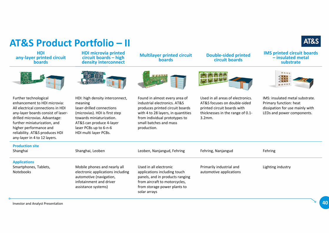
HDI any-layer printed circuit
boards
HDI microvia printed circuit boards – high density interconnect
Multilayer printed circuit boards
Double-sided printed circuit boards
IMS printed circuit boards – insulated metal
substrate
Further technological
enhancement to HDI microvia:
All electrical connections in HDI
any-layer boards consist of laser-
drilled microvias. Advantage:
further miniaturization, and
higher performance and
reliability. AT&S produces HDI
any-layer in 4 to 12 layers.
HDI: high density interconnect,
meaning
laser-drilled connections
(microvias). HDI is first step
towards miniaturization.
AT&S can produce 4-layer
laser PCBs up to 6-n-6
HDI multi layer PCBs.
Found in almost every area of
industrial electronics. AT&S
produces printed circuit boards
with 4 to 28 layers, in quantities
from individual prototypes to
small batches and mass
production.
Used in all areas of electronics.
AT&S focuses on double-sided
printed circuit boards with
thicknesses in the range of 0.1-
3.2mm.
IMS: insulated metal substrate.
Primary function: heat
dissipation for use mainly with
LEDs and power components.
Production site
Shanghai Shanghai, Leoben Leoben, Nanjangud, Fehring Fehring, Nanjangud Fehring
Applications
Smartphones, Tablets,
Notebooks
Mobile phones and nearly all
electronic applications including
automotive (navigation,
infotainment and driver
assistance systems)
Used in all electronic
applications including touch
panels, and in products ranging
from aircraft to motorcycles,
from storage power plants to
solar arrays
Primarily industrial and
automotive applications
Lighting industry
AT&S Product Portfolio – II
Investor and Analyst Presentation 41
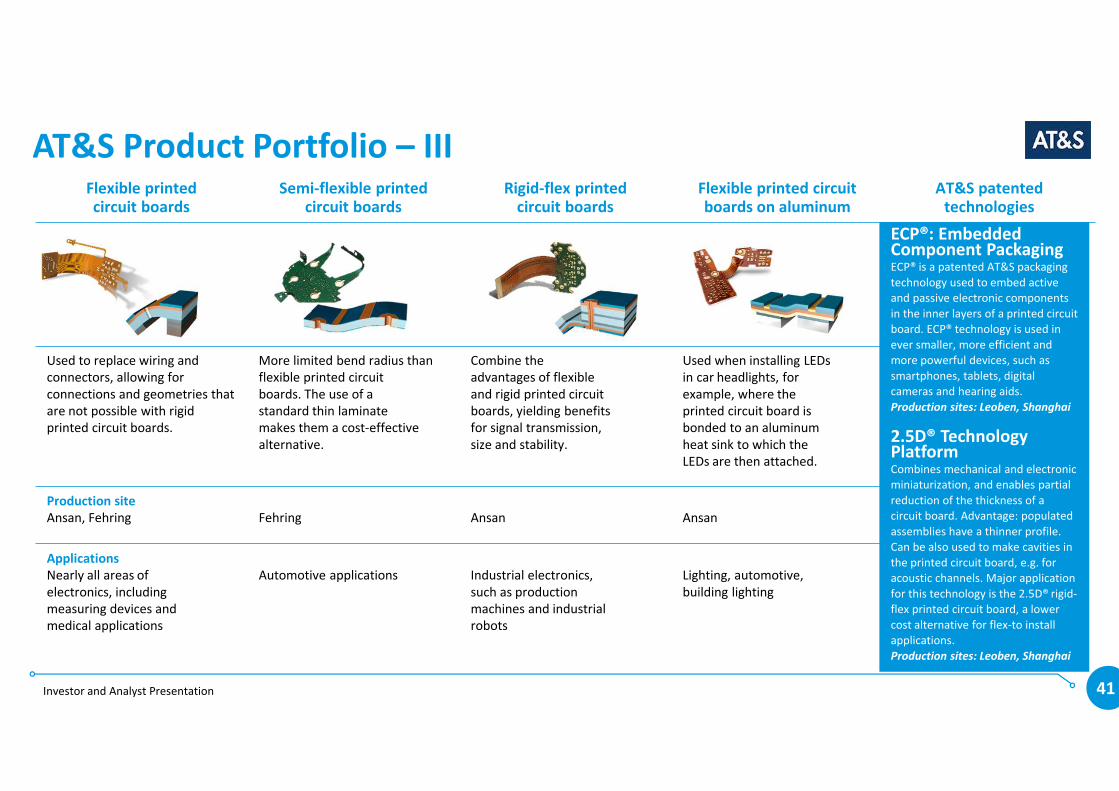
Flexible printed circuit boards
Semi-flexible printed circuit boards
Rigid-flex printed circuit boards
Flexible printed circuitboards on aluminum
AT&S patentedtechnologies
Used to replace wiring and
connectors, allowing for
connections and geometries that
are not possible with rigid
printed circuit boards.
More limited bend radius than
flexible printed circuit
boards. The use of a
standard thin laminate
makes them a cost-effective
alternative.
Combine the
advantages of flexible
and rigid printed circuit
boards, yielding benefits
for signal transmission,
size and stability.
Used when installing LEDs
in car headlights, for
example, where the
printed circuit board is
bonded to an aluminum
heat sink to which the
LEDs are then attached.
Production site
Ansan, Fehring Fehring Ansan Ansan
Applications
Nearly all areas of
electronics, including
measuring devices and
medical applications
Automotive applications Industrial electronics,
such as production
machines and industrial
robots
Lighting, automotive,
building lighting
AT&S Product Portfolio – III
ECP®: Embedded Component PackagingECP® is a patented AT&S packaging
technology used to embed active
and passive electronic components
in the inner layers of a printed circuit
board. ECP® technology is used in
ever smaller, more efficient and
more powerful devices, such as
smartphones, tablets, digital
cameras and hearing aids.
Production sites: Leoben, Shanghai
2.5D® Technology PlatformCombines mechanical and electronic
miniaturization, and enables partial
reduction of the thickness of a
circuit board. Advantage: populated
assemblies have a thinner profile.
Can be also used to make cavities in
the printed circuit board, e.g. for
acoustic channels. Major application
for this technology is the 2.5D® rigid-
flex printed circuit board, a lower
cost alternative for flex-to install
applications.
Production sites: Leoben, Shanghai
Investor and Analyst Presentation 42
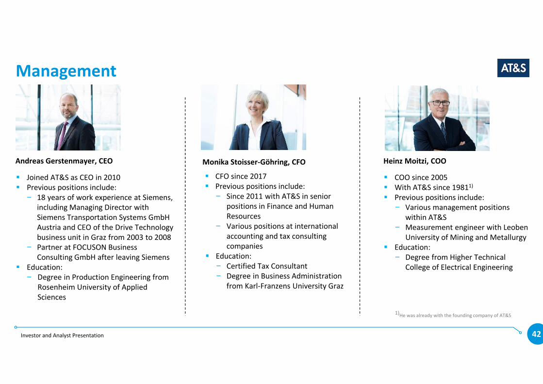
Management
Andreas Gerstenmayer, CEO
� Joined AT&S as CEO in 2010
� Previous positions include:
− 18 years of work experience at Siemens,
including Managing Director with
Siemens Transportation Systems GmbH
Austria and CEO of the Drive Technology
business unit in Graz from 2003 to 2008
− Partner at FOCUSON Business
Consulting GmbH after leaving Siemens
� Education:
− Degree in Production Engineering from
Rosenheim University of Applied
Sciences
Monika Stoisser-Göhring, CFO
� CFO since 2017
� Previous positions include:
− Since 2011 with AT&S in senior
positions in Finance and Human
Resources
− Various positions at international
accounting and tax consulting
companies
� Education:
− Certified Tax Consultant
− Degree in Business Administration
from Karl-Franzens University Graz
Heinz Moitzi, COO
� COO since 2005
� With AT&S since 19811)
� Previous positions include:
− Various management positions
within AT&S
− Measurement engineer with Leoben
University of Mining and Metallurgy
� Education:
− Degree from Higher Technical
College of Electrical Engineering
1)He was already with the founding company of AT&S
Investor and Analyst Presentation 43
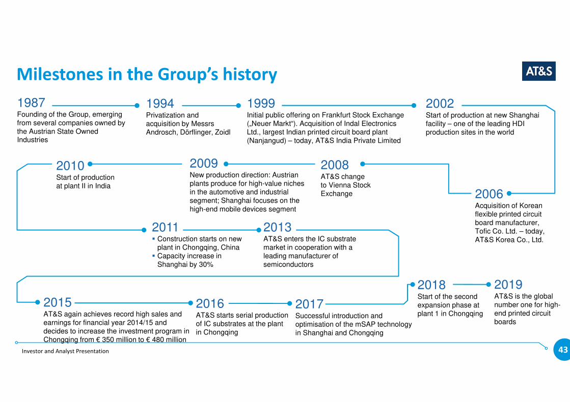
Milestones in the Group’s history
1987Founding of the Group, emerging from several companies owned by the Austrian State Owned Industries
1994Privatization and acquisition by MessrsAndrosch, Dörflinger, Zoidl
1999Initial public offering on Frankfurt Stock Exchange („Neuer Markt“). Acquisition of Indal Electronics Ltd., largest Indian printed circuit board plant (Nanjangud) – today, AT&S India Private Limited
2002Start of production at new Shanghai facility – one of the leading HDI production sites in the world
2010Start of productionat plant II in India
2009New production direction: Austrianplants produce for high-value nichesin the automotive and industrialsegment; Shanghai focuses on the
high-end mobile devices segment
2008AT&S changeto Vienna StockExchange 2006
Acquisition of Koreanflexible printed circuitboard manufacturer,Tofic Co. Ltd. – today,
AT&S Korea Co., Ltd.
2015AT&S again achieves record high sales and earnings for financial year 2014/15 and decides to increase the investment program in Chongqing from € 350 million to € 480 million
2011� Construction starts on new
plant in Chongqing, China� Capacity increase in
Shanghai by 30%
2013AT&S enters the IC substrate market in cooperation with a leading manufacturer of semiconductors
2017Successful introduction and optimisation of the mSAP technology in Shanghai and Chongqing
2016AT&S starts serial production of IC substrates at the plant in Chongqing
2018Start of the second expansion phase at plant 1 in Chongqing
2019AT&S is the global number one for high-end printed circuit boards
Investor and Analyst Presentation 44
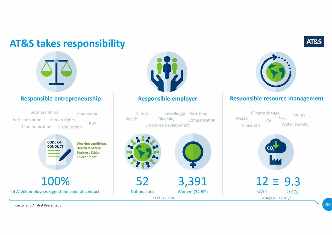
AT&S takes responsibility
Responsible entrepreneurship Responsible employer Responsible resource management
Business ethics
Human rightsAnti-corruption
Innovation
CommunicationRBA
Digitalisation
Diversity
Safety Knowledge
CompensationEmployee development
HealthPart-time Climate change
Water scarcity
Waste
Emissions
CO2
Energy
LCA
52Nationalities
3,391Women (34.5%)
≡
Working conditions
Health & Safety
Business Ethics
Environment
100%of AT&S employees signed the code of conduct
12GWh
9.3kt CO2
savings in FY 2018/19as of 31.03.2019
Investor and Analyst Presentation 45
AT&S – First choice for advanced applications
IR contact
Gerda Königstorfer
Tel: +43 3842 200 5925
Mobile: +43 676 8955 5925
Fax: +43 3842 200 15909
Johannes Mattner
Tel: +43 3842 200 5450
Mobile: +43 676 8955 6093
Fabriksgasse 13,
8700 Leoben/Austria
www.ats.netVisit: www.ats.net; @AT&S IR_PR; AtundS
Investor and Analyst Presentation 46
DisclaimerThis presentation is provided by AT & S Austria Technologie & Systemtechnik Aktiengesellschaft, having its headquarter at Fabriksgasse 13, 8700 Leoben, Austria (“AT&S”), and the
contents are proprietary to AT&S and for information only.
AT&S does not provide any representations or warranties with regard to this presentation or for the correctness and completeness of the statements contained therein, and no
reliance may be placed for any purpose whatsoever on the information contained in this presentation, which has not been independently verified. You are expressly cautioned not
to place undue reliance on this information.
This presentation may contain forward-looking statements which were made on the basis of the information available at the time of preparation and on management‘s expectations
and assumptions. However, such statements are by their very nature subject to known and unknown risks and uncertainties. As a result, actual developments, results, performance
or events may vary significantly from the statements contained explicitly or implicitly herein.
Neither AT&S, nor any affiliated company, or any of their directors, officers, employees, advisors or agents accept any responsibility or liability (for negligence or otherwise) for any
loss whatsoever out of the use of or otherwise in connection with this presentation. AT&S undertakes no obligation to update or revise any forward-looking statements, whether as
a result of changed assumptions or expectations, new information or future events.
This presentation does not constitute a recommendation, an offer or invitation, or solicitation of an offer, to subscribe for or purchase any securities, and neither this presentation
nor anything contained herein shall form the basis of any contract or commitment whatsoever. This presentation does not constitute any financial analysis or financial research and
may not be construed to be or form part of a prospectus. This presentation is not directed at, or intended for distribution to or use by, any person or entity that is a citizen or
resident or located in any locality, state, country or other jurisdiction where such distribution, publication, availability or use would be contrary to law or regulation or which would
require any registration or licensing within such jurisdiction.