interleaved soft-switching boost converter for photovoltaic power-generation system
TRANSCRIPT

IEEE TRANSACTIONS ON POWER ELECTRONICS, VOL. 26, NO. 4, APRIL 2011 1137
Interleaved Soft-Switching Boost Converter forPhotovoltaic Power-Generation System
Doo-Yong Jung, Young-Hyok Ji, Sang-Hoon Park, Yong-Chae Jung, and Chung-Yuen Won, Senior Member, IEEE
Abstract—In this paper, a interleaved soft switching boost con-verter (ISSBC) for a photovoltaic (PV) power-generation systemis proposed. The topology used raises the efficiency for the dc/dcconverter of the PV power conditioning system (PVPCS), and itminimizes switching losses by adopting a resonant soft-switchingmethod. A detailed mode analysis of the proposed topology is pre-sented. The feasibility of the proposed topology is experimentallyverified for a 1.2-kW prototype. The experimental results implythat 97.28% efficiency is achieved under the full-load condition.Consequently, it is confirmed that the overall efficiency is increasedby about 1.5% compared with the conventional hard switching in-terleaved boost converter.
Index Terms—Boost converter, interleaved, maximum power-point tracking (MPPT), photovoltaic (PV) power-generation sys-tems, resonant converter, soft-switching.
I. INTRODUCTION
R ECENTLY, photovoltaic (PV) energy has attracted interestas a next generation energy source capable of solving the
problems of global warming and energy exhaustion caused byincreasing energy consumption. PV energy avoids unnecessaryfuel expenses and there is no air pollution or waste. Also, thereare no mechanical vibrations or noises because the componentsof power generation based on PV energy use semiconductors.The life cycle of the solar cell is more than 20 years, and it canminimize maintenance and management expenses.
The output power of the solar cell is easily changed by thesurrounding conditions such as irradiation and temperature, andalso its efficiency is low. Thus high efficiency is required for thepower conditioning system (PCS), which transmits power fromthe PV array to the load. In general, a single-phase PV PCSconsists of two conversion stages (i.e., dc/dc conversion stageand dc/ac conversion stage). The dc/dc converter is the first stageand it performs maximum power-point tracking (MPPT) andguarantees the dc-link voltage under low irradiance conditions[1], [2].
Manuscript received June 29, 2010; revised October 8, 2010; acceptedOctober 20, 2010. Date of current version June 10, 2011. This work was sup-ported by the Ministry of Knowledge and Economy under a Manpower Devel-opment Program for Energy and Resources. Recommended for publication byAssociate Editor R. Teodorescu.
D.-Y. Jung, Y.-H. Ji, S.-H. Park, and C.-Y. Won are with the Schoolof Information and Communication Engineering, Sungkyunkwan Univer-sity, Suwon 440-746, Korea (e-mail: [email protected]; [email protected];[email protected]; [email protected]).
Y.-C. Jung is with the Department of Electronic Engineering, Namseoul Uni-versity, Cheonan 331-707, Korea (e-mail: [email protected]).
Color versions of one or more of the figures in this paper are available onlineat http://ieeexplore.ieee.org.
Digital Object Identifier 10.1109/TPEL.2010.2090948
This paper proposes a high efficiency dc/dc boost converter toincrease the overall efficiency of PV power conditioning system(PVPCS) [3]–[8]. We studied a 2-phase interleaved boost con-verter integrated with a single-switch type soft-switching boostconverter. The proposed single-switch type soft-switching boostconverter can minimize switching loss by adopting a resonantsoft-switching method. And, no additional switches are neededfor soft switching [9]–[15].
However, the drawback of this converter is that the volt-age across the switch is very high during the resonance mode.The voltage across the switch depends on the parameters ofthe resonant components (i.e., resonant inductance and resonantcapacitance) and the resonant inductor current. In this paper,the optimal design of the resonant components and the inter-leaved method is applied for resonant current reduction. Sincethe interleaved method distributes the input current accordingto each phase, it can decrease the current rating of the switch-ing device. Also, it can reduce the input current ripple, outputvoltage ripple, and size of the passive components [16]–[18].The proposed soft-switching interleaved boost converter can notonly exploit the interleaved converter but also reduce switchinglosses through the soft-switching technique. Therefore, the out-put power of the PV array can be boosted with high efficiency.
This paper presents the operational principle of the converter,a theoretical analysis and design guidelines. A 1.2-kW prototypeof the converter has been built, and simulation and experimentalresults are provided to verify the theoretical analysis.
II. PROPOSED TOPOLOGY
A. Proposed Soft-Switching Boost Converter
The interleaved boost converter consists of two single-phaseboost converters connected in parallel. The two PWM signaldifference is 180◦ when each switch is controlled with the in-terleaving method.
Because each inductor current magnitude is decreased ac-cording to one per phase, we can reduce the inductor size andinductance when the input current flows through two boost in-ductors. The input current ripple is decreased because the inputcurrent is the sum of each current of inductor L1 and L2 .
Fig. 1(a) shows the proposed single-switch type soft-switching boost converter [19]. One resonant inductor, two ca-pacitors, and two diodes are added to a conventional boost con-verter for soft switching using resonance. Fig. 1(b) shows theinterleaved soft-switching boost converter (ISSBC) proposed inthis paper. Two single-phase soft-switching boost converters areconnected in parallel and then to a single output capacitor.
0885-8993/$26.00 © 2011 IEEE
1138 IEEE TRANSACTIONS ON POWER ELECTRONICS, VOL. 26, NO. 4, APRIL 2011
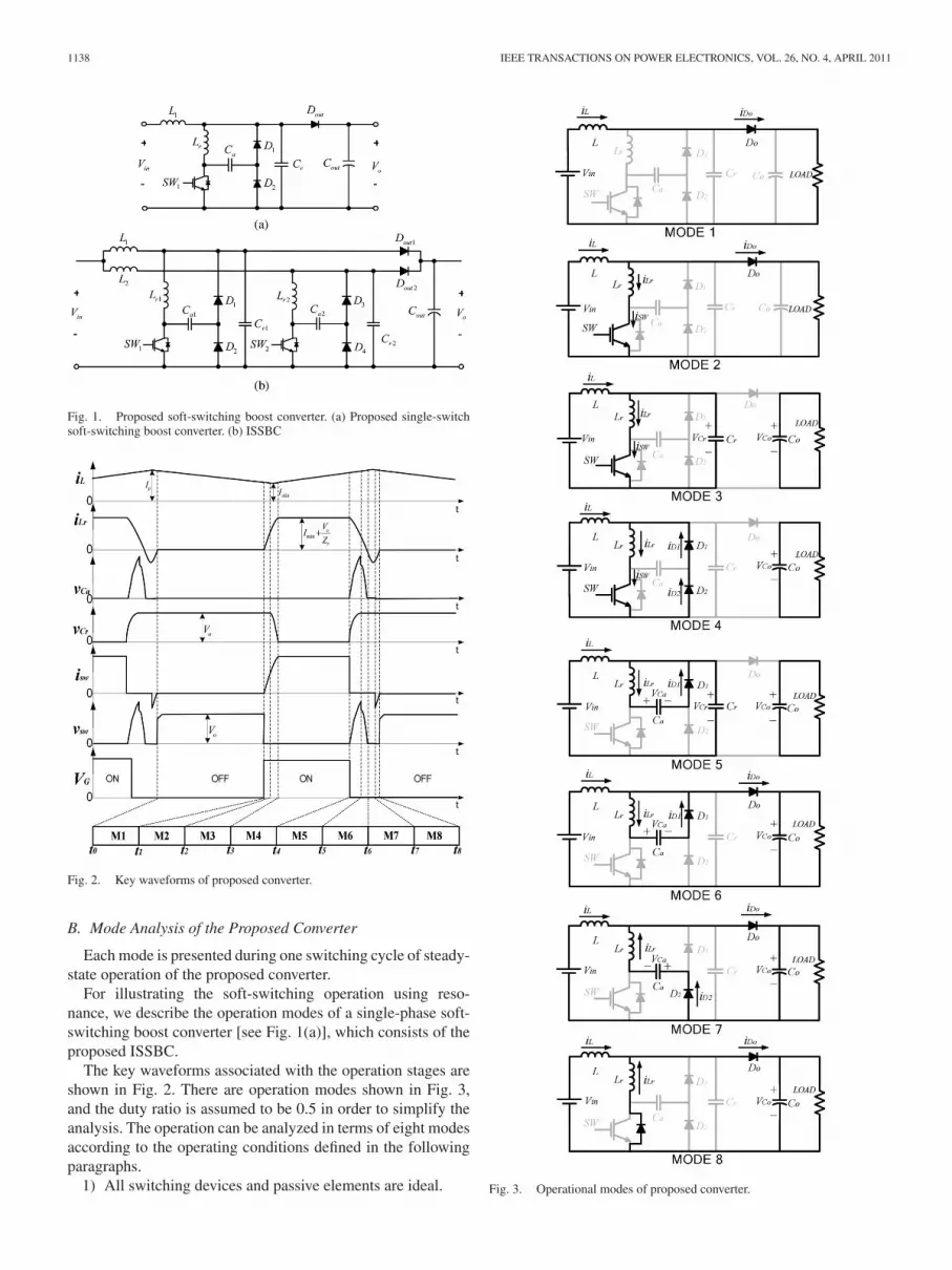
Fig. 1. Proposed soft-switching boost converter. (a) Proposed single-switchsoft-switching boost converter. (b) ISSBC
Fig. 2. Key waveforms of proposed converter.
B. Mode Analysis of the Proposed Converter
Each mode is presented during one switching cycle of steady-state operation of the proposed converter.
For illustrating the soft-switching operation using reso-nance, we describe the operation modes of a single-phase soft-switching boost converter [see Fig. 1(a)], which consists of theproposed ISSBC.
The key waveforms associated with the operation stages areshown in Fig. 2. There are operation modes shown in Fig. 3,and the duty ratio is assumed to be 0.5 in order to simplify theanalysis. The operation can be analyzed in terms of eight modesaccording to the operating conditions defined in the followingparagraphs.
1) All switching devices and passive elements are ideal. Fig. 3. Operational modes of proposed converter.

JUNG et al.: INTERLEAVED SOFT-SWITCHING BOOST CONVERTER FOR PHOTOVOLTAIC POWER-GENERATION SYSTEM 1139
2) The parasitic components of all switching devices andelements are ignored.
3) It is assumed that the initial value of each operation modeis equal to zero.
Mode 1 (t0 ≤ t < t1): The switch is in the off state and the dcoutput of the solar cell array is transmitted directly to the loadthrough L and Dout . In this mode, the main inductor voltagebecomes –(Vo – Vin ). Thus, the main inductor current decreaseslinearly
iL (t) = iL (t0) −Vo − Vin
Lt (1)
iLr(t) = 0, vCr
(t) = Vo, vCa(t) = 0 (2)
iL (t1) = I1 . (3)
Mode 2 (t1 ≤ t < t2): In mode 2, the switch is turned on underzero-current switching (ZCS) because of the resonant inductorLr . In this case, as the output voltage is supplied to the resonantinductor Lr , the current increases linearly. When the resonantcurrent iLr
becomes equal to the main inductor current iL , thecurrent of the output side diode Dout becomes zero
iL (t) = I1 −Vo − Vin
Lt (4)
iLr(t) =
Vo
Lrt, vCr
(t) = Vo, VCa(t) = 0 (5)
iL (t2) ≈ Imin , iLr(t2) ≈ Imin . (6)
Mode 3 (t2 ≤ t <t 3): When the output current iDo u t becomeszero, the mode starts. In this mode, the resonant inductor Lr
and the resonant capacitor Cr resonate and the voltage of Cr
decreases from the output voltage Vo to zero. In this case, themain inductor current iL flows through Lr and the switch
iL (t) ≈ Imin , vCa(t) = 0 (7)
iLr(t) = Imin +
Vo
Zrsin ωr t (8)
vCr(t) = Vo cos ωr t (9)
iLr(t3) = I2 , vCr
(t3) = 0 (10)
ωr = 1/√
LrCr , Zr =√
Lr/Cr (11)
Mode 4 (t3 ≤ t < t4): When the resonant capacitor voltage VCr
becomes zero, the two auxiliary diodes D1 and D2 are turned onand the mode starts. In this mode, the resonant inductor currentis separated into two parts. One is the main inductor current iLand the other is the current turning through the two auxiliarydiodes. The main inductor current iL increases linearly
iL (t) = Imin +Vin
Lt (12)
iLr(t) ≈ I2 (13)
vCr(t) = 0, vCa
(t) = 0 (14)
iL (t4) = I3 , iLr(t4) = I2 . (15)
Mode 5 (t4 ≤ t < t5): In mode 5, the switch turns off underthe zero-voltage condition because of the auxiliary resonant
capacitor Ca . There are two current loops. One is the L-Cr -Vin loop for which the voltage of the resonant capacitor Cr
increases linearly from zero to the output voltage Vo . The other isthe Lr –Ca–D1 loop for which the second resonance occurs. Theenergy stored in Lr is transferred to Ca . The resonant current iLr
decreases linearly and the voltage across Ca becomes maximal
iL (t) ≈ I3 = Imax (16)
iLr(t) = I2 cos ωat (17)
vCa(t) = ZrI2 sinωat, vCr
(t) = I3/Ca (18)
ωa = 1/√
LrCa (19)
Za =√
Lr/Ca. (20)
Mode 6 (t5 ≤ t < t6): When the resonant capacitor voltage vCr
is equal to the output voltage Vo , the mode starts. In this mode,the energy flow from Lr to Ca is completed and the resonantcurrent iLr
becomes zero
iL (t) = I3 −Vo − Vin
Lt (21)
iLr(t) = I2 cos ωat (22)
vCa(t) = ZrI2 sin ωat, vCr
(t) = Vo (23)
vCa(t6) = ZaI3 . (24)
Mode 7 (t6 ≤ t < t7): In mode 7, the voltage of Ca decreases,continuously resonates on the D2–Ca–Lr –Dout–Co loop andthe energy is transferred from Ca to Lr . When the Ca voltagebecomes zero, the resonant current iLr
is the reverse of the cur-rent direction of mode 6. When the voltage of Ca becomes zero,the antiparallel diode of the switch turns on and it transitions tothe next mode
iL (t) = I3 −Vo − Vin
Lt, iLr
(t6) = I4 (25)
iLr(t) =
(Vo
Za− I2
)sinωat, iLr
(t) = I5 (26)
vCr(t) = Vo (27)
vCa(t) = Vo − (Vo − ZaI2) cos ωat = V2 . (28)
Mode 8 (t7 ≤ t < t8): There are two current loops. The maininductor current iL transmits energy to the output through Doutand decreases linearly. The resonant inductor current iLr
alsotransmits energy to the load through Dout and flows throughthe antiparallel diode of the switch. When the resonant inductorcurrent iLr
becomes zero, mode 8 ends
iL (t) = I4 +Vo − Vin
Lt, iLr
(t8) = I6 (29)
iLr(t) = I5 −
Vo
Lrt, iLr
(t8) = 0 (30)
vCr(t) = Vo (31)
vCa(t) = 0. (32)

1140 IEEE TRANSACTIONS ON POWER ELECTRONICS, VOL. 26, NO. 4, APRIL 2011
Fig. 4. Comparison of the peak voltage of switching devices between SSSBCand ISSBC (1 p.u. = output voltage).
III. DESIGN PROCEDURES OF THE PROPOSED CONVERTER
A. Switch Peak Voltage Analysis and Parameter Design
In mode 5, the current that flows through the Lr –Ca–D1 loopshould be large enough for resonance. As described by (18), thevoltage across the auxiliary resonant capacitor Ca is as high asI2 during this resonant period.
vSW (t) = vC a(t) + vC r (t) (33)
The amplitude of the switch voltage is determined by the res-onant devices and the resonant current. To minimize the peakvoltage of the switch, designs for optimal parameters of resonantcomponents are included and the interleaved method is adopted.Because the interleaved method distributes the input current ac-cording to each phase, it can decrease the current rating of theswitching device. Thus, it can reduce the peak voltage acrossthe switch, input current ripple, output voltage ripple and sizeof passive components.
Fig. 4 depicts the peak voltage across the switch of the SingleSoft-switching Boost Converter (SSSBC) and ISSBC accordingto the duty ratio under a full load. The peak voltage of switch isrepresented in p.u. (per unit), and 1 p.u. is signified the 400 Vof output voltage in this paper. The ISSBC reduces the peakvoltage across the switch by about 10–20% compared with theSSSBC.
B. Selection of Resonant Inductor and Capacitor
The ZVS condition of the switch is affected by the auxiliaryresonant capacitor Ca . In mode 5, the current that flows throughthe Lr –Ca–D1 loop should be large enough for resonance. Ingeneral, the snubber capacitance has to be more than ten timesthe parasitic capacitance. The resonant capacitance Ca has tobe more than 20 times the output capacitance of the switch,because the Ca is charged by the resonant inductor current (itis about 2 times the main inductor current) during the switchturn-off period, represented as follows:
Ca > 20Coes . (34)
In mode 3, the resonant inductor current is represented by (8).The period of resonance between resonant inductance Lr andresonant capacitance Cr is about a quarter of the entire resonant
TABLE IEXPERIMENTAL PARAMETERS
period. In general, the rising time of the resonant inductor cur-rent is 10% of the minimum on-time of the switch. However, forsatisfaction of the ZVS condition, the rising time of the resonantinductor current is 50% of the minimum on-time in this paper,as represented by
t3 − t1 =Lr
VoImin +
Tr
4< 0.5DminT (35)
where Tr = 1/fs = 2π√
LrCr , T = 1/fSW , and Dmin =(Vo − Vin min)/Vo .
From (18) and (35), the resonant capacitance Cr can be de-fined as
Cr >D2
min
π2Lrf 2SW
+I2minLr
π2V 2o
− 2IminDmin
π2Vof 2SW
. (36)
Since (2IminDmin)/(π2Vof2SW ) ≈ 0 in (36), this equation can
be rewritten as follows:
Cr >D2
min
π2Lrf 2SW
+I2minLr
π2V 2o
(37)
Lr = {Vo/(I2 − Imin)}2 Cr (38)
where I2 − Imin = Vo/Zr = Vo
√Cr/
√Lr .
From (37) and (38), Cr can be defined as
Cr >Dmin(I2 − Imin)
π2Vof 2SW
/√1 − I2
min/π2(I2 − Imin)2 . (39)
From (38), the resonant inductor parameter is expressed as
Lr <
{(2 × 0.85
Cs
Ca− 1)Vo
/(
Ip
Cr + Caπ√
Cs)}2
(40)
where Cs = CrCa/(Cr + Ca), Vo − V2 ≈ 0.85Vo .
C. Design Example
In this section, the design procedure of the proposed con-verter is based on the derived equations. Table I shows thedesign parameters of the proposed boost converter. And, thedesign guidelines herein provide a proper tool to help chooseresonant components and ensure the appropriate operation ofthe resonance converter.
JUNG et al.: INTERLEAVED SOFT-SWITCHING BOOST CONVERTER FOR PHOTOVOLTAIC POWER-GENERATION SYSTEM 1141
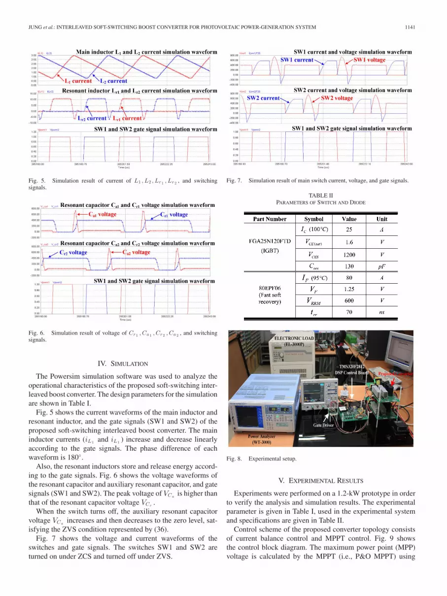
Fig. 5. Simulation result of current of L1 , L2 , Lr 1 , Lr 2 , and switchingsignals.
Fig. 6. Simulation result of voltage of Cr 1 , Ca 1 , Cr 2 , Ca 2 , and switchingsignals.
IV. SIMULATION
The Powersim simulation software was used to analyze theoperational characteristics of the proposed soft-switching inter-leaved boost converter. The design parameters for the simulationare shown in Table I.
Fig. 5 shows the current waveforms of the main inductor andresonant inductor, and the gate signals (SW1 and SW2) of theproposed soft-switching interleaved boost converter. The maininductor currents (iL1 and iL1 ) increase and decrease linearlyaccording to the gate signals. The phase difference of eachwaveform is 180◦.
Also, the resonant inductors store and release energy accord-ing to the gate signals. Fig. 6 shows the voltage waveforms ofthe resonant capacitor and auxiliary resonant capacitor, and gatesignals (SW1 and SW2). The peak voltage of VCa
is higher thanthat of the resonant capacitor voltage VCr
.When the switch turns off, the auxiliary resonant capacitor
voltage VCaincreases and then decreases to the zero level, sat-
isfying the ZVS condition represented by (36).Fig. 7 shows the voltage and current waveforms of the
switches and gate signals. The switches SW1 and SW2 areturned on under ZCS and turned off under ZVS.
Fig. 7. Simulation result of main switch current, voltage, and gate signals.
TABLE IIPARAMETERS OF SWITCH AND DIODE
Fig. 8. Experimental setup.
V. EXPERIMENTAL RESULTS
Experiments were performed on a 1.2-kW prototype in orderto verify the analysis and simulation results. The experimentalparameter is given in Table I, used in the experimental systemand specifications are given in Table II.
Control scheme of the proposed converter topology consistsof current balance control and MPPT control. Fig. 9 showsthe control block diagram. The maximum power point (MPP)voltage is calculated by the MPPT (i.e., P&O MPPT) using

1142 IEEE TRANSACTIONS ON POWER ELECTRONICS, VOL. 26, NO. 4, APRIL 2011
Fig. 9. Control algorism of proposed topology
Fig. 10. Block diagram of experimental setup.
Fig. 11. Experimental results of current waveforms of inductor L1 and induc-tor L2 , and switching signals (L1 and L2 current; Y-axis: 1 A/division, gatesignal; Y-axis: 10 V/division, X-axis: 10 μs/division).
detected PV voltage and current [20]. Calculated MPP voltage iscompared with the detected PV voltage. The difference betweenthe calculated MPP voltage and detected PV voltage is used asan input of voltage controller (i.e., the first PI controller). Theoutput of the voltage controller is used as a current reference.The current reference is divided by the number of phase. Dividedcurrent reference is compared with the current of each phase,and the difference is used as an input of current controller.The gate signal is generated by comparison between the carrier
Fig. 12. Experimental results of the resonant inductor Lr 1 and Lr 2 currentand switching signals (Lr 1 and Lr 2 current; Y-axis: 1 A/division, gate signal;Y-axis: 10 V/division, X-axis: 5 μs/division).
Fig. 13. Experimental results of voltage waveforms of Ca 1 , Cr 1 , and switch-ing signals (Ca 1 and Ca 2 voltage; Y-axis: 200 V/division, gate signal; Y-axis:10 V/division, X-axis: 10 μs/division).
Fig. 14. Experimental results of the current and voltage of switching devicesand switching signals (SW1 voltage; Y-axis: 350 V/division, SW1 current; Y-axis: 20 A/division, gate signal; Y-axis: 10 V/division, X-axis: 2 μs/division).
signal and the output of the current controller. From this, it canbe confirmed that the phase difference between the gate signalsof each phase is equal to 180◦ because there are two phases inthe proposed interleaved soft-switching boost converter.
Fig. 8 shows the experimental setup of proposed converter(see Fig. 9).

JUNG et al.: INTERLEAVED SOFT-SWITCHING BOOST CONVERTER FOR PHOTOVOLTAIC POWER-GENERATION SYSTEM 1143
Fig. 15. Experimental MPPT results of the proposed ISSBC. (a) Non MPPT operation. (b) MPPT operation. (c) Irradiance 50% → 100%. (d) Irradiance100% → 50%.
Fig. 10 depicts the block diagram of the proposed ISSBCfor the MPPT test. The PV simulator condition used in the testwas assumed to consist of the short current 8 A, open volt-age 200 V and maximum power 1.2 kW. The system controlwas implemented in DSP TMS320F2812. The output voltageand current were detected in the ISSBC for MPPT control andcurrent balancing control.
Fig. 11 represents the current of the main inductor L1 and L2 ,and gate signals (SW1 and SW2) under a full load. As the inputcurrent is the sum of the inductor currents, the input currentripple is almost zero. The experimental results obtained fromthe prototype are very similar to those shown in Fig. 5.
Fig. 12 shows the current waveforms of the resonant inductorLr1 , Lr2 , and gate signals. The current through Lr1 and Lr2 aremore than twice the main inductor L1 and L2 current, and itshould drop below zero in area A.
Fig. 13 shows the voltage waveforms of the resonant capacitorand auxiliary resonant capacitor, and gate signals (SW1 andSW2). Compared with the simulation result in Fig. 6, there isa charging voltage of Ca1 shown in area B of Fig. 13. Thedifference was caused by the output capacitance of the switch(FGA25N120FRD).
Fig. 14 shows the experimental results of the switches volt-age and current, and gate signals. As expected from the mode

1144 IEEE TRANSACTIONS ON POWER ELECTRONICS, VOL. 26, NO. 4, APRIL 2011
TABLE IIIEFFICIENCY OF THE PROPOSED ISSBC TOPOLOGY
analysis, the ZCS or ZVS operations of the switches show goodperformance.
Fig. 15 shows the experimental MPPT results of the proposedISSBC. Fig. 15(a) shows the current, voltage, and power wave-forms of the PV simulator without MPPT control. The powerpoint of the PV simulator operates near the open voltage andthe PV simulator provides 400 W, which corresponds to 30% ofmaximum power.
Fig. 15(b)–(d) shows the current, voltage, and power wave-forms of the PV simulator with MPPT control. As seen in theI–V and P–V curves of Fig. 15(b), the proposed system operatesat the maximum power point. Compared with Fig. 15(a), thevoltage decreases and the current increases from 2A to 7A, andthus, the PV simulator provides 1200 W.
Fig. 15(c) shows the MPPT results; the irradiance changesfrom 50% to 100%. Fig. 15(d) shows the MPPT results; theirradiance changes from 100% to 50%. As seen in Fig. 15(c) and(d), MPPT control show good performance under the irradiancechange.
Table III shows results of efficiency comparison betweenproposed soft-switching interleaved boost converter and con-ventional interleaved boost converter. In this comparison, sameswitching devices are applied to each converter prototypes.
VI. CONCLUSION
In this paper, we proposed a soft-switching interleaved boostconverter using resonance. Numerical-mode analysis was per-formed for the design of the proposed ISSBC. From this anal-ysis, an example of an optimal design for resonant componentswas represented. To verify the feasibility of the proposed ISSBC,a 1.2-kW prototype was implemented.
In the experiment, MPPT control was performed by usinga PV simulator, and current balancing control was performed.From the experimental results, it was confirmed that the resonant
components are well designed. The efficiency of the proposedISSBC was measured under the load variation condition andefficiency is measured by the power analyzer WT 3000.
The proposed converter is compared with the conventional in-terleaved hard switching boost converter under the same switch-ing frequency and power conditions.
For the conventional interleaved hard switching boost con-verter and proposed ISSBC, the total efficiencies are measuredfor various load currents, as shown in Table III.
REFERENCES
[1] J.-P. Lee, B.-D. Min, T.-J. Kim, D.-W. Yoo, and J.-Y. Yoo, “Design and con-trol of novel topology for photovoltaic dc/dc converter with high efficiencyunder wide load ranges,” J. Power Electron., vol. 9, no. 2, pp. 300–307,Mar. 2009.
[2] B.-D. Min, J.-P. Lee, and J.-H. Kim, “A novel grid-connected PV PCSwith new high efficiency converter,” J. Power Electron., vol. 8, no. 4,pp. 309–316, Oct. 2008.
[3] G. Hua, C.-S. Leu, Y. Jiang, and F. C. Y. Lee, “Novel zero-voltage-transition PWM converters,” IEEE Trans. Power Electron., vol. 9, no. 2,pp. 213–219, Mar. 1994.
[4] G. Hua, E. X. Yang, Y. Jiang, and F. C. Y. Lee, “Novel zero-current-transition PWM converters,” IEEE Trans. Power Electron., vol. 9, no. 6,pp. 601–606, Nov. 1994.
[5] H. Bodur and A. F. Bakan, “A new ZVT-ZCT-PWM DC-DC converter,”IEEE Trans. Power Electron., vol. 19, no. 3, pp. 676–684, May 2004.
[6] H. Bodur and A. F. Bakan, “A new ZVT-PWM DC-DC converter,” IEEETrans. Power Electron., vol. 17, no. 1, pp. 40–47, Jan. 2002.
[7] N. Jain, P. K. Jain, and G. Joos, “A zero voltage transition boost con-verter employing a soft switching auxiliary circuit with reduced conduc-tion losses,” IEEE Trans. Power Electron., vol. 19, no. 1, pp. 130–139,Jan. 2004.
[8] S. K. Kwon and K. F. A. Sayed, “Boost-half bridge single power stagePWM DC-DC converters for PEM-fuel cell stacks,” J. Power Electron.,vol. 8, no. 3, pp. 239–247, Jul. 2008.
[9] X. Kong and A. M. Khambadkone, “Analysis and implementation of ahigh efficiency, interleaved current—Fed full bridge converter for fuel cellsystem,” IEEE Trans. Power Electron., vol. 22, no. 2, pp. 543–550, Mar.2007.
[10] H. M. Suryawanshi, M. R. Ramteke, K. L. Thakre, and V. B. Borghate,“Unity-power-factor operation of three-phase ac–dc soft switched con-verter based on boost active clamp topology in modular approach,” IEEETrans. Power Electron., vol. 23, no. 1, pp. 229–236, Jan. 2008.
[11] H. Mao, O. Abdel Rahman, and I. Batarseh, “Zero-voltage-switching dc–dc converters with synchronous rectifiers,” IEEE Trans. Power Electron.,vol. 23, no. 1, pp. 369–378, Jan. 2008.
[12] H. Tao, A. Kotsopoulos, J. L. Duarte, and M. A. M. Hendrix, “Transformer-coupled multiport ZVS bidirectional dc–dc converter with wide inputrange,” IEEE Trans. Power Electron., vol. 2, pp. 771–781, Mar. 2008.
[13] H. Xiao and S. Xie, “A ZVS bidirectional dc–dc converter with phase-shiftplus PWM control scheme,” IEEE Trans. Power Electron., vol. 23, no. 2,pp. 813–823, Mar. 2008.
[14] D. V. Ghodke, K. Chatterjee, and B. G. Fernandes, “Three-Phase threelevel, soft switched, phase shifted PWM dc–dc converter for high powerapplications,” IEEE Trans. Power Electron., vol. 23, no. 3, pp. 1214–1227,May 2008.
[15] M. Borage, S. Tiwari, S. Bhardwaj, and S. Kotaiah, “A full-bridge dc–dcconverter with zero-voltage-switching over the entire conversion range,”IEEE Trans. Power Electron., vol. 23, no. 4, pp. 1743–1750, Jul. 2008.
[16] S. Y. Tseng, J. Z. Shiang, H. H. Chang, W. S. Jwo, and C. T. Hsieh, “Anovel turn-on/off snubber for interleaved boost converter,” Proc. IEEE38th Annu. Power Electron. Specialists Conf. (PESC 2007), 2718–2724.
[17] X. Wu, J. Zhang, X. Ye, and Z. Qian, “Analysis and derivations for afamily ZVS converter based on a new active clamp ZVS cell,” IEEETrans. Ind. Electron., vol. 55, no. 2, pp. 773–781, Feb. 2008.
[18] P.-W. Lee, Y.-S. Lee, D. K. W. Cheng, and X.-C. Liu, “Steady-state analysisof an interleaved boost converter with coupled inductors,” IEEE Trans.Ind. Electron., vol. 47, no. 4, Aug. 2000.
[19] D.-Y. Jung, Y.-H. Ji, J.-H. Kim, C.-Y. Won, and Y.-C. Jung, “Soft switchingboost converter for photovoltaic power generation system,” Proc. 13th
JUNG et al.: INTERLEAVED SOFT-SWITCHING BOOST CONVERTER FOR PHOTOVOLTAIC POWER-GENERATION SYSTEM 1145
Power Electron. Motion Control Conf. (EPE-PEMC 2008), pp. 1929–1933, Sep..
[20] T. Esram and P. L. Chapman, “Comparison of photovoltaic array maximumpower point tracking techniques,” IEEE Trans. Energy Convers., vol. 22,no. 2, Jun. 2007.
Doo-Yong Jung was born in Korea in 1981. Hereceived the M.S. degree in 2009 from the Grad-uate School of Photovoltaic System Engineering,Sungkyunkwan University, Suwon, Korea, where heis currently working toward the Ph.D. degree.
His current research interests include converters,inverters and its control for smart-grid applications
Young-Hyok Ji was born in Korea in 1981. Hereceived the M.S. degree in 2009 from the Grad-uate School of Photovoltaic System Engineering,Sungkyunkwan University, Suwon, Korea, where heis currently working toward the Ph.D. degree.
His currnt research interests include converters,inverters and its control for photovoltaic applications
Sang-Hoon Park was born in Korea in 1979. He re-ceived the M.S. degree in 2007 in information andcommunication engineering from SungkyunkwanUniversity, Suwon, Korea, in 2007, where he is cur-rently working toward the Ph.D. degree in informa-tion and communication engineering.
His current research interests include analysis andcontrol of electrical drives, particularly in hybrid andelectrical vehicle application.
Yong-Chae Jung was born in Korea in 1965. He re-ceived the B.S. degree from Hanyang niversity, Seoul,Korea, in 1989, and the M.S. and Ph.D. degrees inelectrical engineering from Korea Advanced Insti-tute of Science and Technology, Daejeon, Korea, in1991 and 1995, respectively.
He is currently an Associate Professor in the De-partment of Electronic Engineering, Namseoul Uni-versity, Cheonan, Korea. His research interests in-clude the design and control of power converters,soft-switching power converters, resonant power cir-
cuits, photovoltaic systems, power-factor correction, switched-mode power sup-ply, induction heating circuits, and electromagnetic-interference suppression.
Dr. Jung is a member of the Korea Institute of Power Electronics and theKorea Institute of Electrical Engineers.
Chung-Yuen Won (SM’05) was born in Korea in1955. He received the B.S. degree in electrical en-gineering from Sungkyunkwan University, Suwon,Korea, in 1978, and the M.S. and Ph.D. degrees inelectrical engineering from Seoul National Univer-sity, Seoul, Korea, in 1980 and 1988, respectively.
From 1990 to 1991, he was with the Departmentof Electrical Engineering, University of Tennessee,Knoxville, as a Visiting Professor. Since 1988, he hasbeen a Faculty Member with Sungkyunkwan Univer-sity, where he is currently a Professor in the School of
Information and Communication Engineering. He is currently the President ofthe Korean Institute of Power Electronics. His research interests include dc–dcconverters for fuel cells, electromagnetics modeling and prediction for motordrives, and control systems for rail power delivery applications.