high purity ultrafine-grained nickel processed by dynamic plastic deformation: microstructure and...
TRANSCRIPT

CO
DOI: 10.1002/adem.201200034MM
UNIC
AT
High Purity Ultrafine-Grained Nickel Processed byDynamic Plastic Deformation: Microstructure andMechanical Properties**
ION
By Lukasz Farbaniec, Akrum Abdul-Latif, Jeno Gubicza and Guy Dirras*Bulk ultrafine-grained samples are processed by dynamic plastic deformation at an average strain rateof 3.3� 102 s�1 from bulk coarse-grained nickel with purity higher than 98.4 wt.%. The obtainedmicrostructure is investigated by electron backscattering diffraction, transmission electron microscopyand X-ray line profile analysis. After dynamic deformation the microstructure evolves into sub-micron-size lamellar and subgrain structures. Evaluation of average grain size shows a heterogeneousmicrostructure along both the diameter and the thickness of the sample. X-ray line profile analysisreveals high dislocation density of about 13� 2� 1014 m�2 in the impacted material. The mechanicalproperties are investigated by means of uniaxial quasi-static compression tests conducted at roomtemperature. The stress–strain behavior of the impacted Ni depends on the location in the impacted diskand on the orientation of the compression axis relative to the impact direction.
Metals and their alloys play an important role in many
engineering fields such as construction and manufacturing of
equipments and tools. Therefore, new materials and/or
microstructure improvement of well-known materials (lead-
ing to a combination of enhanced properties and long life
cycle) are required. As for structural materials, a high strength
combined with good ductility are properties of interest.
Indeed, the grain refinement is an effective way to increase the
strength of materials as expressed by the Hall–Petch relation-
ship.[1,2] For this reason the ultrafine-grained (UFG, the
[*] Prof. G. Dirras, L. FarbaniecUniversite Paris 13, Sorbonne Paris CiteLSPM-CNRS, 99, Avenue J. B. Clement, 93430 Villetaneuse,FranceE-mail: [email protected]
Prof. A. Abdul-LatifLaboratoire d’Ingenierie des Systemes Mecaniques et des Materiaux3, Rue Fernand Hainaut, 93407 St. Ouen Cedex, France
Dr. J. GubiczaDepartment of Materials Physics, Eotvos Lorand UniversityBudapest, P.O. Box 32, H-1518, Hungary
[**] The authors like to thank Mr. Thierry Chauveau for fruitfuldiscussions and texture analysis. This work was supportedby the French National Research Agency, ANR, via the‘‘MIMIC’’ Project (ANR-09-BLAN-0010), the HungarianScientific Research Fund, OTKA, Grant No. K-81360 andpartly by the French-Hungarian bilateral project (PHC Balaton,Hungarian Grant No. TeT_10-1-2011-0737).
ADVANCED ENGINEERING MATERIALS 2012, 14, No. 11 � 2012 WILEY-VCH Ve
average grain size varies between 100 and 1000 nm) and
nanocrystalline (the average grain size is less than 100 nm)
materials have attracted considerable attention in recent years
since the pioneering work of Gleiter.[3–5] The increase in
strength and hardness in metals can be achieved by grain
subdivision during plastic deformation. For this reason a lot
of severe plastic deformation (SPD) methods were developed
in the last decades.[6,7] Among them, high pressure torsion
(HPT) and equal channel angular pressing (ECAP) are the
most frequently used SPD techniques.[8–19] In these proce-
dures, an initial coarse-grained bulk material is subjected to
large strain under high hydrostatic pressure yielding a
uniform microstructure with fine grains without damage of
the specimen. Lately, a new method referred to as dynamic
plastic deformation (DPD) also showed its ability to achieve
grain refinement in different materials.[20,21] Actually, it was
found that under dynamic loading conditions the deformed
microstructure is very similar to that processed by ECAP,
including elongated or equiaxed grains, and subgrain
structure, depending on the applied route of deformation.[23]
DPD technique was recently used to produce UFG micro-
structures in Al, Cu, or Cu–Ag alloy[20–23] in one step or in
combination with powder metallurgy methods.[24–26] These
studies revealed that strain rate, deformation temperature
and stacking fault energy (SFE) play a significant role in
dislocation patterning which subsequently results in the
formation of new grain boundaries during further strain-
ing.[27–31] In this context, the combined effect of the strain
rate and the deformation temperature on the evolution of the
rlag GmbH & Co. KGaA, Weinheim wileyonlinelibrary.com 1027
COM
MUNIC
ATIO
N
L. Farbaniec et al./High Purity Ultrafine-Grained Nickel
microstructure during plastic deformation can be expressed
by the so-called Zener–Hollomon parameter:[32]
Z ¼ _"� expQ
RT
� �
where Q is the activation energy of the mechanism controlling
the rate of deformation, T is the absolute temperature, and
R is the universal gas constant. High strain rate and low
deformation temperature (corresponding to high Z-value)
effectively suppress annihilation of dislocations, resulting
in grain refinement by formation of new boundaries from
dislocations. Contrariwise, deformation conditions corre-
sponding to lower Z values lead to smaller dislocation
density, and therefore to lower amount of grain boundaries
and larger grains.[33] At a given temperature the lower the
SFE, the more difficult the annihilation of dislocations and
the larger the probability of the occurrence of twinning. For
materials with medium or high SFE, the deformation at
ambient temperatures occurs mainly by the motion of full
lattice dislocations. When the deformation temperature is low
(e.g., at cryogenic temperatures) the full lattice dislocation
activity may be suppressed and deformation by twinning
plays a key role.[21] In our previous work,[25] we proposed a
DPD method for processing UFG microstructures in coarse-
grained high SFE materials, such as pure Al. The objective of
the present work is to evaluate the potential of this DPD
technique for grain refinement in commercially pure Ni
with lower SFE than for Al. The influence of as-processed
microstructure on subsequent mechanical behavior is inves-
tigated under quasi-static compression conditions.
1. Experimental Procedure
The initial material was a bulk coarse-grained nickel with
an average grain size of about 25mm. According to the
chemical composition given in Table 1 the purity of Ni was
higher than 98.4%. Test specimens having a diameter of
9.5mm and a length of 16mm were machined from the
rod shaped as-received material supplied by Goodfellow
(www.goodfellow.com). Before DPD tests, the samples were
heat-treated in an electrical air circulating furnace (Carbolite
HRF 7/45 type) at 7508C for 1 h and then air cooled in order to
homogenize the microstructure.
DPD tests were conducted by using a 6-m-height dynamic
drop mass bench test machine.[24] An object with a mass of
45 kg fell almost freely from the drop height of 5.5m and hit
the upper surface of the specimen. At the moment of the
Table 1. Chemical composition of the studied nickel material.
Ni Cu Fe Mg
Composition [mg � g�1] Base <2500 <4000 <200
1028 http://www.aem-journal.com � 2012 WILEY-VCH Verlag GmbH & C
impact the kinetic energy of themasswas approximately 2.5 kJ
that was absorbed by the plastic deformation of the specimen.
The corresponding initial maximum impact velocity was
10m � s�1 that yielded an average strain rate of 3.3� 102 s�1. A
dynamic load cell of 20 tons measured the applied axial force
on specimen. The M5L series Bullier International laser
displacement sensor, 5000g accelerometer and laser beam
displacement transducer measured the displacement of the
impacting object. The force and displacement as a function of
time were recorded under control of a rapid acquisition chain
(2.5MHz). A synchronization signal is triggered by a signal
from two photocells.
A Zeiss Supra 40VP FEG scanning electron microscope
(SEM) was used for electron backscattering diffraction (EBSD)
investigations of the microstructure of the initial and the
impacted samples. EBSD maps were recorded with a step
size of 0.1mm between neighboring measurement positions.
The average grain size and the fraction of low and high
angle grain boundaries (LAGB and HAGB, respectively)
were determined utilizing OIM software v.4 from TexSem
Laboratories (TSL). Mechanical polishing followed by electro-
polishing was used to prepare the specimens for microstruc-
tural examination. The electropolishing step was performed in
an A2 electrolytic solution at room temperature (RT) using a
Tenupol1 electropolishing apparatus from Struers.
Transmission electron microscopy (TEM) investigations
were carried out by a JOEL-2010 electron microscope
operating at 200 kV. Thin foils were prepared using a GatanTM
precision ion polishing system (PIPS) with a current of 0.5mA
and a tension of 15 kV. Complementary microstructural
investigations were carried out on the impacted specimen
by X-ray line profile analysis (XLPA). The X-ray line profiles
were measured on the cross-section perpendicular to the
impacted surface by a high-resolution rotating anode
diffractometer (Nonius, FR 591) using Cu Ka1 radiation
(l¼ 0.15406 nm). Two-dimensional imaging plates detected
the Debye–Scherrer diffraction rings. The line profiles were
determined as the intensity distribution perpendicular to the
rings obtained by integrating the two dimensional distribu-
tion of the intensity along the rings. The line profiles were
evaluated by the convolutional multiple whole profile
(CMWP) analysis.[34,35] In this method, the diffraction pattern
is fitted by the sum of a background spline and the
convolution of the instrumental pattern and the theoretical
line profiles related to the crystallite size, dislocations and
twin faults. The mean crystallite size, the dislocation density
(r) and the twin boundary frequency (b) were obtained from
Elements
Mn Si Ti C S
0 <3500 <1500 <1000 <1500 <100
o. KGaA, Weinheim ADVANCED ENGINEERING MATERIALS 2012, 14, No. 11
COM
MUNIC
ATIO
N
L. Farbaniec et al./High Purity Ultrafine-Grained Nickel
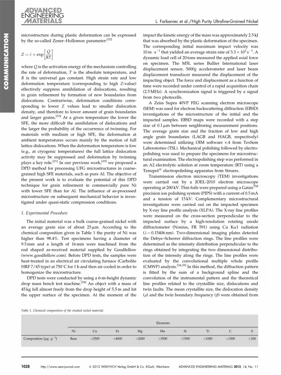
Fig. 1. Reference coordinate system attached to the impacted sample. The squaresnumbered as 1 and 2 indicate the locations of the specimens cut from the center and theedge of the impacted sample for mechanical testing.
the fitting. The latter quantity is defined as the relative fraction
of twin boundaries among {111} lattice planes.
X-ray diffraction (XRD) was used to characterize the
crystallographic texture after impact test. A macroscopic
reference coordinate system (X1, X2, X3) was attached
to the sample, where X3 is the normal direction to the
impacted surface while X1 and X2 directions are lying on
the impacted surface (Figure 1). The XRD measurements
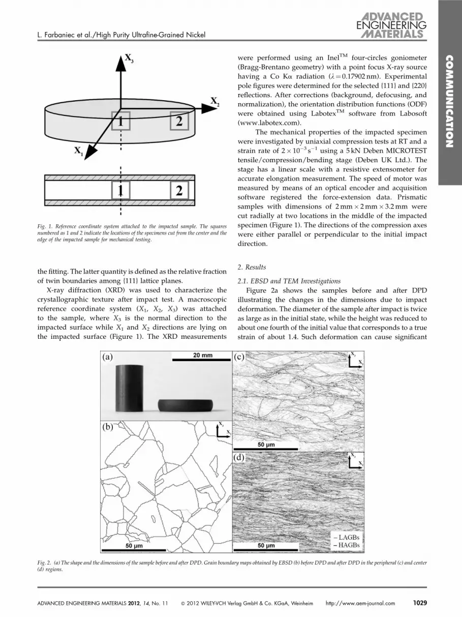
Fig. 2. (a) The shape and the dimensions of the sample before and after DPD. Grain boundar(d) regions.
ADVANCED ENGINEERING MATERIALS 2012, 14, No. 11 � 2012 WILEY-VCH Verl
were performed using an InelTM four-circles goniometer
(Bragg-Brentano geometry) with a point focus X-ray source
having a Co Ka radiation (l¼ 0.17902 nm). Experimental
pole figures were determined for the selected {111} and {220}
reflections. After corrections (background, defocusing, and
normalization), the orientation distribution functions (ODF)
were obtained using LabotexTM software from Labosoft
(www.labotex.com).
The mechanical properties of the impacted specimen
were investigated by uniaxial compression tests at RT and a
strain rate of 2� 10�3 s�1 using a 5 kN Deben MICROTEST
tensile/compression/bending stage (Deben UK Ltd.). The
stage has a linear scale with a resistive extensometer for
accurate elongation measurement. The speed of motor was
measured by means of an optical encoder and acquisition
software registered the force-extension data. Prismatic
samples with dimensions of 2mm� 2mm� 3.2mm were
cut radially at two locations in the middle of the impacted
specimen (Figure 1). The directions of the compression axes
were either parallel or perpendicular to the initial impact
direction.
2. Results
2.1. EBSD and TEM Investigations
Figure 2a shows the samples before and after DPD
illustrating the changes in the dimensions due to impact
deformation. The diameter of the sample after impact is twice
as large as in the initial state, while the height was reduced to
about one fourth of the initial value that corresponds to a true
strain of about 1.4. Such deformation can cause significant
y maps obtained by EBSD (b) before DPD and after DPD in the peripheral (c) and center
ag GmbH & Co. KGaA, Weinheim http://www.aem-journal.com 1029
COM
MUNIC
ATIO
N
L. Farbaniec et al./High Purity Ultrafine-Grained Nickel
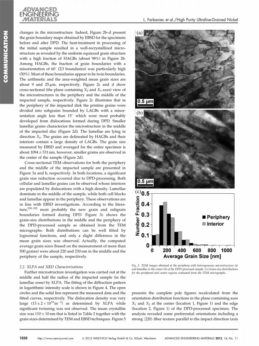
Fig. 3. TEM images obtained at the periphery with heterogeneous microstructure (a)and lamellae in the center (b) of the DPD-processed sample. (c) Grain-size distributionsfor the peripheral and center regions evaluated from the TEM micrographs.
changes in the microstructure. Indeed, Figure 2b–d present
the grain boundary maps obtained by EBSD for the specimens
before and after DPD. The heat-treatment in processing of
the initial sample resulted in a well-recrystallized micro-
structure as revealed by the uniform equiaxed grain structure
with a high fraction of HAGBs (about 98%) in Figure 2b.
Among HAGBs, the fraction of grain boundaries with a
misorientation of 608 (S3 boundaries) was particularly high
(50%). Most of these boundaries appear to be twin boundaries.
The arithmetic and the area-weighted mean grain sizes are
about 9 and 25mm, respectively. Figure 2c and d show
cross-sectional (the plane containing X2 and X3 axes) view of
the microstructures in the periphery and the middle of the
impacted sample, respectively. Figure 2c illustrates that in
the periphery of the impacted disk the pristine grains were
divided into subgrains bounded by LAGBs with a misor-
ientation angle less than 158 which were most probably
developed from dislocations formed during DPD. Smaller
lamellar grains characterize the microstructure in the middle
of the impacted disc (Figure 2d). The lamellae are lying in
direction X2. The grains are delineated by HAGBs and their
interiors contain a large density of LAGBs. The grain size
measured by EBSD and averaged for the entire specimen is
about 1094� 531 nm, however, smaller grains are observed in
the center of the sample (Figure 2d).
Cross-sectional TEM observations for both the periphery
and the middle of the impacted sample are presented in
Figure 3a and b, respectively. In both locations, a significant
grain size reduction occurred due to DPD-processing. Both
cellular and lamellar grains can be observed whose interiors
are populated by dislocations with a high density. Lamellae
dominate in the middle of the sample, while both cell blocks
and lamellae appear in the periphery. These observations are
in line with EBSD investigations. According to the litera-
ture,[28–30] most probably the new grain and subgrain
boundaries formed during DPD. Figure 3c shows the
grain-size distributions in the middle and the periphery of
the DPD-processed sample as obtained from the TEM
micrographs. Both distributions can be well fitted by
lognormal functions, and only a slight difference in the
mean grain sizes was observed. Actually, the computed
average grain sizes (based on the measurement of more than
500 grains) were about 220 and 230 nm in the middle and the
periphery of the sample, respectively.
2.2. XLPA and XRD Characterizations
Further microstructure investigation was carried out at the
middle and half the radius of the impacted sample (in the
lamellae zone) by XLPA. The fitting of the diffraction pattern
in logarithmic intensity scale is shown in Figure 4. The open
circles and the solid line represent the measured data and the
fitted curves, respectively. The dislocation density was very
large (13� 2� 1014m�2) as determined by XLPA while
significant twinning was not observed. The mean crystallite
size was 110� 10 nm that is listed in Table 2 together with the
grain sizes determined by TEMand EBSD techniques. Figure 5
1030 http://www.aem-journal.com � 2012 WILEY-VCH Verlag GmbH & C
presents the complete pole figures recalculated from the
orientation distribution functions in the plane containing axes
X1 and X2 at the center (location 1, Figure 1) and the edge
(location 2, Figure 1) of the DPD-processed specimen. The
analysis revealed some preferential orientations including a
strong h220i fiber texture parallel to the impact direction (axis
o. KGaA, Weinheim ADVANCED ENGINEERING MATERIALS 2012, 14, No. 11

COM
MUNIC
ATIO
N
L. Farbaniec et al./High Purity Ultrafine-Grained Nickel
Fig. 4. The measured (open circle) and the fitted (solid line) X-ray diffraction patterns inlogarithmic intensity scale.
Table 2. The average crystallite size obtained by XLPA, TEM, and EBSD.
XLPA TEM EBSD
Crystallite size [nm] 110� 10 230� 9 1094� 531
X3). The volume fraction of the main fiber texture was
estimated as 46% in the center and 38% at the periphery. The
intensity of this texture component varies along the diameter
Fig. 5. Recalculated {111} and {220} pole figures in the (X1, X2) plane (a) at the center a
ADVANCED ENGINEERING MATERIALS 2012, 14, No. 11 � 2012 WILEY-VCH Verl
and the thickness of the disk, in accordance with the changes
of the microstructure.
2.3. Mechanical Properties
Figure 6 shows the true stress–true plastic strain compres-
sion curves. The compressive yield strength of the initial
material was about 90MPa and the corresponding stress–
strain curve exhibits a strain hardening behavior for the full
range of the investigated strain. After DPD, two types of
mechanical tests were performed: the compression axis was
oriented either perpendicular or parallel to the lamellar
boundaries (LBs) formed during the impact test. If the LBs are
oriented horizontally in the tested samples (Figure 6), the
loading axis was aligned vertically or horizontally in the first
or the second case, therefore these specimens are denoted as V
and H, respectively. In addition, specimens were cut from the
center and the edge with the notations of 1 and 2, respectively
(Figure 1). Therefore, for example the specimen cut from the
center and compressed perpendicularly to the LBs is denoted
as V1. Several observations can be made on the basis of the
mechanical tests: (i) the compressive yield strength increased
by a factor of 5–6 due to the impact. Depending on the location
and the orientation of the specimen the saturation flow stress
varies between 645 and 780MPa; (ii) in general, H specimen
exhibited higher maximum stress than V specimen from the
same location; (iii) for the same orientation of the compression
axis relative to LBs the specimen cut from the location 2
showed higher maximum stress than the sample obtained
from the location 1; (iv) for all DPD-processed samples after a
short hardening stage (up to a plastic strain of about 2%) a
stress plateau or even work softening was observed; (v) for
nd (b) the edge.
ag GmbH & Co. KGaA
sample H1 a resumed work hardening was
observed for strains larger than 5%, which
was not the case for the sample H2.
3. Discussion
Our results showed that intermediate
strain rate impact yielded a microstructure
composed of subgrains delineated by LAGBs
and lamellar grains bounded by HAGBs.
Indeed, EBSD and TEM investigations
revealed significant difference between dis-
location patterns in the middle and the
periphery of the DPD-processed sample,
leading to a heterogeneous microstructure
and texture distribution (Figure 2 and 3).
These results are in line with previous work
on high purity and commercially pure
Al.[25,26] It is observed here that the initial
grain boundary structure, even though dis-
torted, is still visible on the periphery of the
sample (Figure 2c). The amount of LAGBs
observed in that region is also lower than in
the middle of the sample. In general, a
, Weinheim http://www.aem-journal.com 1031

COM
MUNIC
ATIO
N
L. Farbaniec et al./High Purity Ultrafine-Grained Nickel
Fig. 6. True stress–true plastic strain obtained by compression. If the lamellar boundaries are orientedhorizontally in the tested samples, the specimens with vertical or horizontal compression axis are denotedas V or H, respectively. In addition, the specimens cut from the center or the periphery are denoted as 1 or 2,respectively.
non-uniform grain-refinement occurs due to DPD as sug-
gested by EBSD analysis (Figure 2c and d). However, TEM
investigations revealed that the difference in the grain sizes
and grain-size distributions along the diameter of the
impacted disk is small. This suggests that the misorientation
angle between neighboring grains/subgrains is very small at
the periphery of the sample and difficult to access by EBSD
technique. Moreover, the actual step size (0.1mm) used for
EBSD analysis also does not take into account the very
small grains detected by TEM. In addition, the crystallite
size measured by XLPA is the lowest compared to grain
sizes obtained by either EBSD or TEM (Table 2). The
discrepancies between TEM and XRD measurement have
been reported[25,38] in the case of metallic materials deformed
by SPD routes. As an example, the grain size measured
by TEM is about three times larger than the crystallite
size measured by XPLA. As was discussed by Saada and
Dirras,[39] this discrepancy can be related to the fact that X-rays
have better sampling statistics than TEM. In addition,
dislocation walls such as dipolar walls do not give contrast
difference in TEM while they break coherency of X-ray
scattering. Finally, the size of scattering domains is equivalent
to the grain size in materials without a subgrain structure
within individual grains. This is not the case in SPD-processed
materials. TEM investigations (Figure 3) showed high
dislocation density within grains contrary to the case of pure
Al deformed under the same conditions, where the subgrains
were mostly dislocation free.[25] This can be attributed to a
more planar dislocation slip mechanism due to the lower
SFE energy for Ni (�130mJ �m�2[36]) compared to pure Al
(166mJ �m�2[37]) and also to the higher melting point of the
former material. In Al the easy cross-slip and climb of
dislocations yield dynamic recovery and/or recrystallization
during DPD-processing.
The stress–strain curves indicate a significant increase in
the flow stress compared to the non-impacted sample. This
behavior can be attributed to the combined effect of the high
1032 http://www.aem-journal.com � 2012 WILEY-VCH Verlag GmbH & Co. KGaA, Weinheim
dislocation density and the reduced grain
size as have been discussed by Hughes
and Hansen[28,29] and by Krasilnikov.[40]
The present TEM observations revealed
that the average grain size is almost identical
in the whole disk. However, the average
grain size obtained by EBSD was different,
therefore, it is hypothesized that the average
misorientation angle across the grain or
subgrain boundaries changes along the
radius of the impacted disk, which may
contributes to the observed difference in the
mechanical behavior of the samples obtained
from the locations shown in Figure 1 (e.g.,
H1 and H2). In addition, the intensity of the
h220i fiber texture is stronger in region 1
than in region 2. In a face centered cubic
materials such as Ni, the number of activated
dislocation slip systems strongly depends
on the crystallographic orientation relative to the loading
direction.[41] For samples V the loading direction is parallel
to the h220i fiber texture component that yields an activation
of a relatively large number of slip systems resulting in
lower flow stress than for specimens H. This effect depends on
the location in the impacted disk due to the change of the
strength of texture. Similar effect of strain-path change
was recently reported in the case of commercial purity
Al.[26] Additionally, the change in loading direction in H-type
samples may lead to destabilization of the dislocation
structure formed during DPD-processing and also to the
variation of the crystallographic texture. These issues may
contribute to a macroscopic softening/hardening transient
effects.
4. Conclusions
Bulk coarse-grained nickel with purity higher than
98.4wt% was processed by a DPD technique. The impact
deformation caused significant changes in the microstructure
which were studied by EBSD, TEM, and XLPA. The following
observations were made:
(i) T
he microstructure after DPD consists of lamellar grainswith subgrain structure.
(ii) A significant reduction of grain size from about 9mm to230 nm was observed by TEM.
(iii) X LPA investigation revealed a relatively large dislocationdensity (13� 2� 1014m�2) and a crystallite size of
110� 10 nm which is lower than the grain sizes deter-
mined by EBSD or TEM.
(iv) T he compressive yield strength increased by a factor of5–6 due to DPD. The maximum flow stress varied
between 645 and 780MPa and its value depended on
the location in the impacted disk and the loading direc-
tion. This behavior can be attributed to the heterogeneous
ADVANCED ENGINEERING MATERIALS 2012, 14, No. 11

COM
L. Farbaniec et al./High Purity Ultrafine-Grained Nickel
ADVA
microstructure and the varying strength of the h220i fibertexture along the diameter of the impacted disk.
MUNIC
AT
Received: January 30, 2012
Final Version: June 19, 2012
Published online: July 16, 2012
ION
[1] E. O. Hall, Proc. Phys. Soc. Lond. B 1951, 64, 747.[2] N. J. Petch, J. Iron Steel Inst. 1953, 174, 25.
[3] H. Gleiter, Prog. Mater. Sci. 1989, 33, 223.
[4] H. Gleiter, Nanostruct. Mater. 1992, 1, 1.
[5] H. Gleiter, Nanostruct. Mater. 1995, 6, 3.
[6] R. Z. Valiev, R. K. Islamgaliev, I. V. J. Alexandrov, Prog.
Mater. Sci. 2000, 45, 103.
[7] A. Azushima, R. Kopp, A. Korhonen, D. Y. Yang,
F. Micari, G. D. Lahoti, P. Groche, J. Yanagimoto,
N. Tsuji, A. Rosochowski, A. Yanagida, CIRP Ann.
Manuf. Technol. 2008, 57, 716.
[8] Y. Ito, Z. Horita, Mater. Sci. Eng. A 2009, 503, 32.
[9] A. P. Zhilyaev, A. A. Gimazov, E. P. Soshnikova,
A. Revesz, T. G. Langdon, Mater. Sci. Eng. A 2008,
489, 207.
[10] T. Hebesberger, H. P. Stuwe, A. Vorhauer, F. Wetscher,
R. Pippan, Acta Mater. 2005, 53, 393.
[11] Y. Todaka, J. Sasaki, T. Moto, M. Umemoto, Scr. Mater.
2008, 59, 615.
[12] Y. Iwahashi, Z. Horita, M. Nemoto, T. G. Langdon, Acta
Mater. 1997, 45, 4733.
[13] P. L. Sun, P. W. Kao, C. P. Chang, Mater. Sci. Eng. A 2000,
283, 82.
[14] K. Neishi, Z. Horita, T. G. Langdon, Mater. Sci. Eng. A
2002, 325, 54.
[15] A. P. Zhilyaev, B.-K. Kim, J. A. Szpunar, M. D. Baro,
T. G. Langdon, Mater. Sci. Eng. A 2005, 391, 377.
[16] O. V. Mishin, V. Y. Gertsman, R. Z. Valiev, G. Gottstein,
Scr. Mater. 1996, 35, 873.
[17] S. V. Dobatkin, J. A. Szpunar, A. P. Zhilyaev, J. Y. Cho,
A. A. Kuznetsov, Mater. Sci. Eng. A 2007, 462, 132.
[18] D. H. Shin, W. J. Kim, W. Y. Choo, Scr. Mater. 1999, 41,
259.
[19] S. V. Dobatkin, O. V. Rybal’chenko, G. I. Raab, Mater. Sci.
Eng. A 2007, 463, 41.
NCED ENGINEERING MATERIALS 2012, 14, No. 11 � 2012 WILEY-VCH Verl
[20] W. S. Zhao, N. R. Tao, J. Y. Guo, Q. H. Lu, K. Lu, Scr.
Mater. 2005, 53, 745.
[21] Y. S. Li, N. R. Tao, K. Lu, Acta Mater. 2008, 56, 230.
[22] Y. Z. Tian, S. D. Wu, Z. F. Zhang, R. B. Figueiredo,
N. Gao, T. G. Langdon, Mater. Sci. Eng. A 2011, 528,
4331.
[23] F. Huang, N. R. Tao, K. Lu, J. Mater. Sci. Technol. 2011,
27, 1.
[24] A. Abdul-Latif, G. F. Dirras, S. Ramtani, A. Hocini, Int. J.
Mech. Sci. 2009, 51, 797.
[25] G. Dirras, T. Chauveau, A. Abdul-Latif, S. Ramtani,
Q.-H. Bui, Phys. Status Solidi A 2010, 207, 2233.
[26] G. Dirras, T. Chauveau, A. Abdul-Latif, J. Gubicza,
S. Ramtani, Q. Bui, Z. Hegedus, B. Bacroix, Metall. Mater.
Trans. A 2012, 43, 1312.
[27] B. Bay, N. Hansen, D. Kuhlmann-Wilsdorf, Mater. Sci.
Eng. A 1989, 113, 385.
[28] D. A. Hughes, N. Hansen, Acta Mater. 1997, 45, 3871.
[29] D. A. Hughes, N. Hansen, Acta Mater. 2000, 48, 2985.
[30] D. A. Hughes, Scr. Mater. 2002, 47, 697.
[31] G. Dirras, H. Couque, J. Gubicza, A. Ouarem,
T. Chauveau, P. Jenei, Mater. Sci. Eng. A 2010, 527,
4128.
[32] C. Zener, J. H. Hollomon, J. Appl. Phys. 1944, 15, 22.
[33] Y. S. Li, Y. Zhang, N. R. Tao, K. Lu, Acta Mater. 2009, 57,
761.
[34] G. Ribarik, J. Gubicza, T. Ungar, Mater. Sci. Eng. A 2004,
387–389, 343.
[35] L. Balogh, G. Ribarik, T. Ungar, J. Appl. Phys. 2006, 100,
023512.
[36] L. E. Murr, Scr. Metall. 1972, 6, 203.
[37] L. E. Murr, Interfacial Phenomena in Metals and Alloys,
Addison-Wesley, Reading, MA 1975, 378.
[38] A. P. Zhilyaev, J. Gubicza, G. Nurislamova, A. Revesz,
S. Surinach, M. D. Baro, T. Ungar, Phys. Status Solidi A
2003, 198, 263.
[39] G. Saada, G. Dirras, in Dislocations in Solids, Vol. 15 (Eds:
J. P. Hirth, L. Kubin), Elsevier B.V, North-Holland 2009,
Ch. 90.
[40] N. Krasilnikov, W. Lojkowski, Z. Pakiela, R. Valiev,
Mater. Sci. Eng. A 2005, 397, 330.
[41] B. Clausen, T. Lorentzen, T. Leffers, Acta Mater. 1998, 46,
3087.
ag GmbH & Co. KGaA, Weinheim http://www.aem-journal.com 1033