electronics slides
TRANSCRIPT
Electronics 1
Lecture Notes – October 2011
Dr. Tareq Zanoon
1
Chapter 1
Semiconductor diodes
2
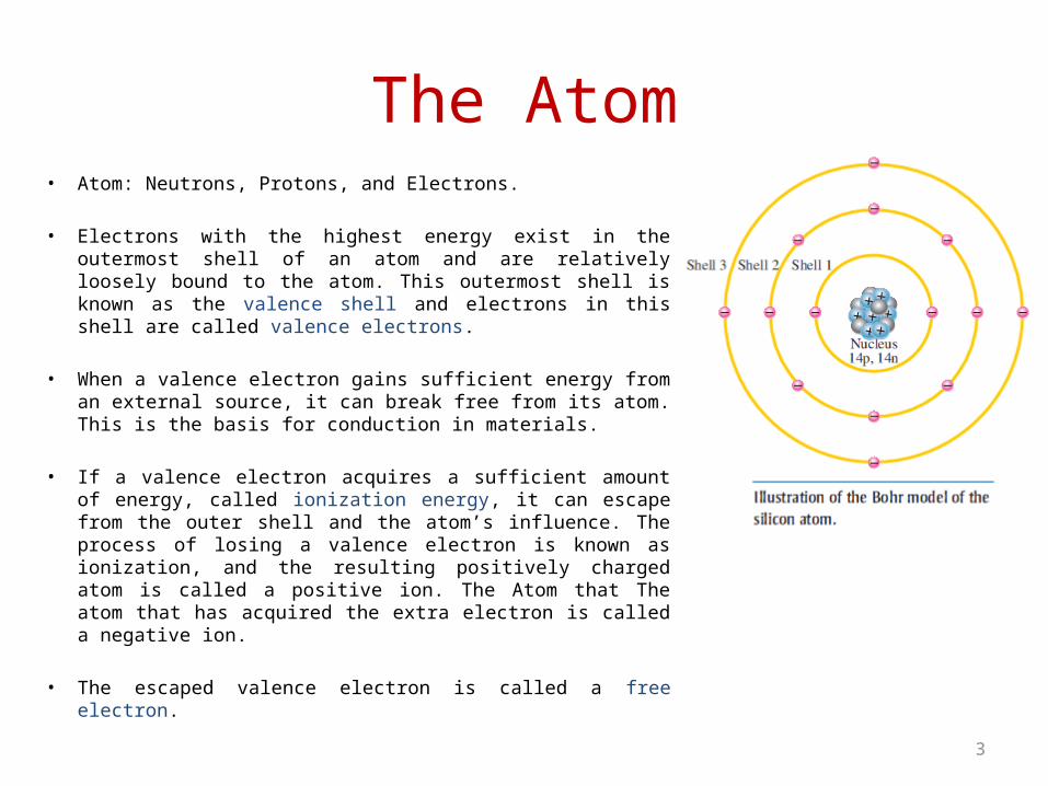
The Atom• Atom: Neutrons, Protons, and Electrons.
• Electrons with the highest energy exist in the outermost shell of an atom and are relatively loosely bound to the atom. This outermost shell is known as the valence shell and electrons in this shell are called valence electrons.
• When a valence electron gains sufficient energy from an external source, it can break free from its atom. This is the basis for conduction in materials.
• If a valence electron acquires a sufficient amount of energy, called ionization energy, it can escape from the outer shell and the atom’s influence. The process of losing a valence electron is known as ionization, and the resulting positively charged atom is called a positive ion. The Atom that The atom that has acquired the extra electron is called a negative ion.
• The escaped valence electron is called a free electron.
3
Materials used in electronics• In terms of their electrical properties, materials can
be classified into three groups: conductors, semiconductors, and insulators.
• Insulators : An insulator is a material that does not conduct electrical current under normal conditions. Most good insulators are compounds rather than single-element material and have very high resistivities. Valence electrons are tightly bound to the atoms; therefore, there are very few free electrons in an insulator. Examples of insulators are rubber, plastics, glass, mica, and quartz.
• Conductors: A conductor is a material that easily conducts electrical current. Most metals are good conductors. The best conductors are single-element materials, such as copper (Cu), silver (Ag), gold (Au), and aluminum (Al), which are characterized by atoms with only one valence electron very loosely bound to the atom. These loosely bound valence electrons become free electrons. Therefore, in a conductive material the free electrons are valence electrons.
4
Materials used in electronics
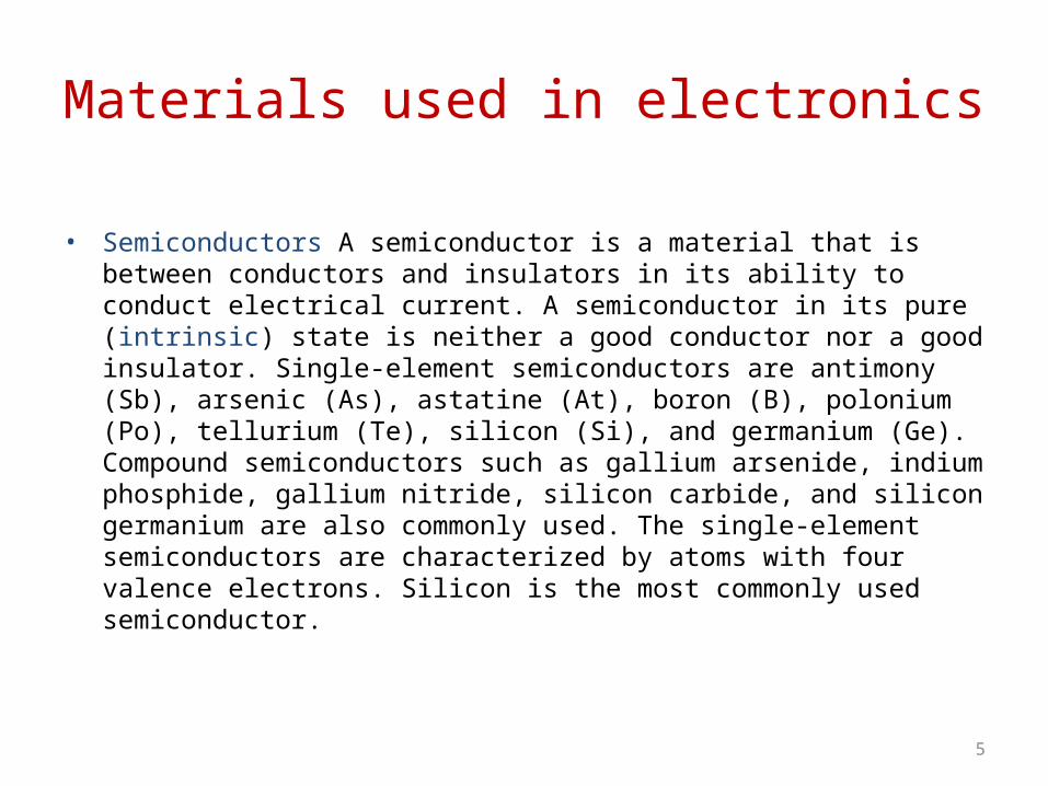
• Semiconductors A semiconductor is a material that is between conductors and insulators in its ability to conduct electrical current. A semiconductor in its pure (intrinsic) state is neither a good conductor nor a good insulator. Single-element semiconductors are antimony (Sb), arsenic (As), astatine (At), boron (B), polonium (Po), tellurium (Te), silicon (Si), and germanium (Ge). Compound semiconductors such as gallium arsenide, indium phosphide, gallium nitride, silicon carbide, and silicon germanium are also commonly used. The single-element semiconductors are characterized by atoms with four valence electrons. Silicon is the most commonly used semiconductor.
5
Conductivity - Resistivity
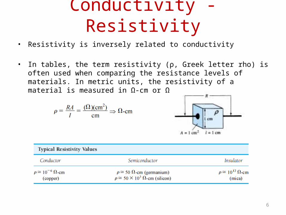
• Resistivity is inversely related to conductivity
• In tables, the term resistivity (ρ, Greek letter rho) is often used when comparing the resistance levels of materials. In metric units, the resistivity of a material is measured in Ω-cm or Ω-m.
6
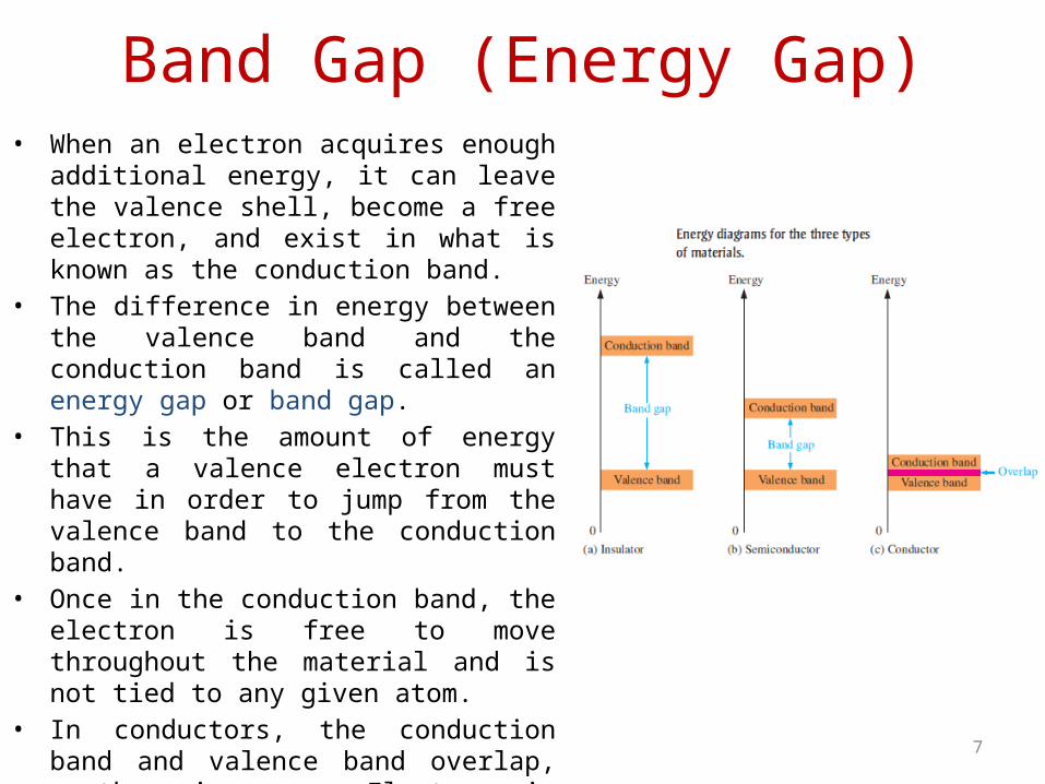
Band Gap (Energy Gap)• When an electron acquires enough
additional energy, it can leave the valence shell, become a free electron, and exist in what is known as the conduction band.
• The difference in energy between the valence band and the conduction band is called an energy gap or band gap.
• This is the amount of energy that a valence electron must have in order to jump from the valence band to the conduction band.
• Once in the conduction band, the electron is free to move throughout the material and is not tied to any given atom.
• In conductors, the conduction band and valence band overlap, so there is no gap. Electrons in the valence band move freely into the conduction band, so there are always free electrons.
7
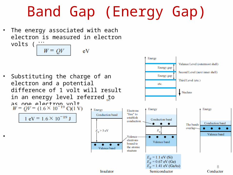
Band Gap (Energy Gap)• The energy associated with each
electron is measured in electron volts (eV).
• Substituting the charge of an electron and a potential difference of 1 volt will result in an energy level referred to as one electron volt.
•
8
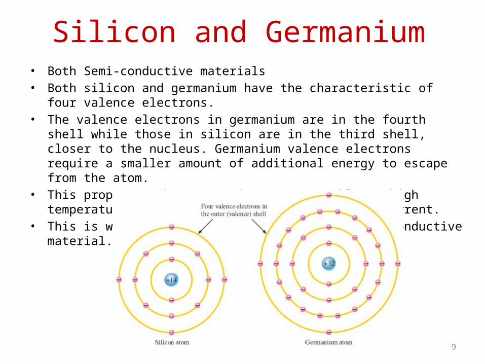
Silicon and Germanium• Both Semi-conductive materials• Both silicon and germanium have the characteristic of
four valence electrons.• The valence electrons in germanium are in the fourth
shell while those in silicon are in the third shell, closer to the nucleus. Germanium valence electrons require a smaller amount of additional energy to escape from the atom.
• This property makes germanium more unstable at high temperatures and results in excessive reverse current.
• This is why silicon is a more widely used semi-conductive material.
9
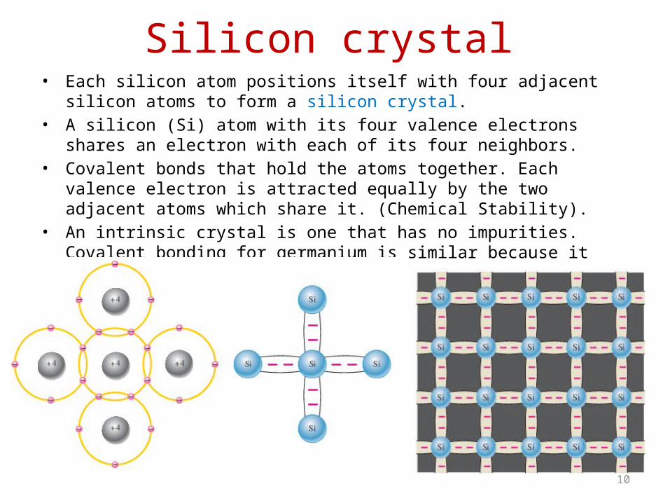
Silicon crystal • Each silicon atom positions itself with four adjacent
silicon atoms to form a silicon crystal. • A silicon (Si) atom with its four valence electrons
shares an electron with each of its four neighbors.• Covalent bonds that hold the atoms together. Each
valence electron is attracted equally by the two adjacent atoms which share it. (Chemical Stability).
• An intrinsic crystal is one that has no impurities. Covalent bonding for germanium is similar because it also has four valence electrons.
10
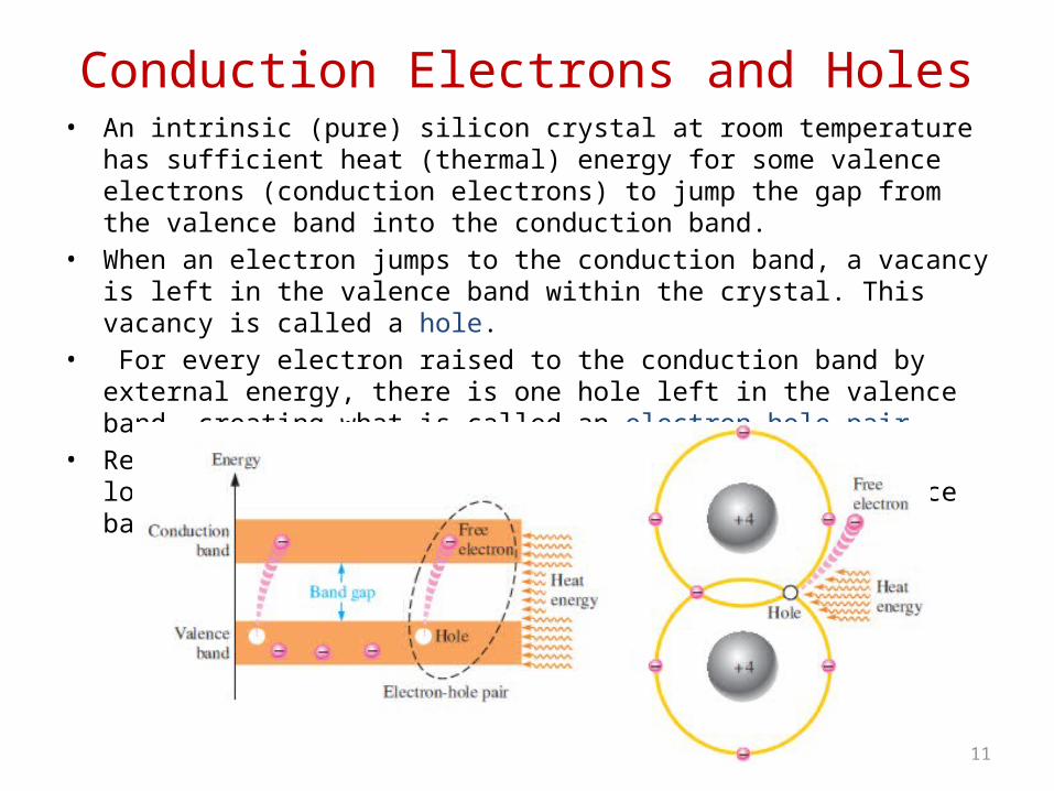
Conduction Electrons and Holes• An intrinsic (pure) silicon crystal at room temperature
has sufficient heat (thermal) energy for some valence electrons (conduction electrons) to jump the gap from the valence band into the conduction band.
• When an electron jumps to the conduction band, a vacancy is left in the valence band within the crystal. This vacancy is called a hole.
• For every electron raised to the conduction band by external energy, there is one hole left in the valence band, creating what is called an electron-hole pair.
• Recombination occurs when a conduction-band electron loses energy and falls back into a hole in the valence band.
11
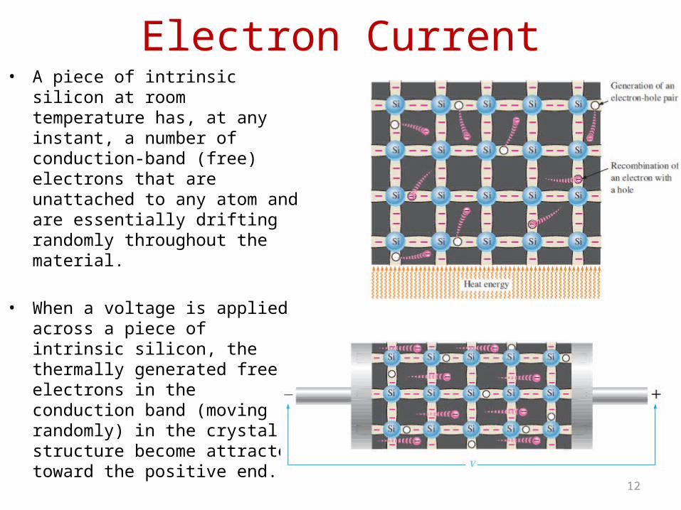
Electron Current• A piece of intrinsic
silicon at room temperature has, at any instant, a number of conduction-band (free) electrons that are unattached to any atom and are essentially drifting randomly throughout the material.
• When a voltage is applied across a piece of intrinsic silicon, the thermally generated free electrons in the conduction band (moving randomly) in the crystal structure become attracted toward the positive end.
• This movement of free electrons is one type of current in a semi-conductive material, and is called electron current.
12
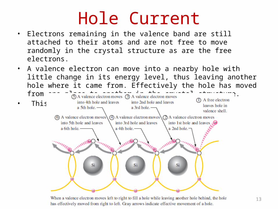
Hole Current• Electrons remaining in the valence band are still
attached to their atoms and are not free to move randomly in the crystal structure as are the free electrons.
• A valence electron can move into a nearby hole with little change in its energy level, thus leaving another hole where it came from. Effectively the hole has moved from one place to another in the crystal structure.
• This Current is called hole current
13
N-type and P-type semiconductors
• The conductivity of semiconductors can be drastically increased by the controlled addition of impurities to the intrinsic (pure) semiconductive material.
• This process, called doping, increases the number of current carriers (electrons or holes).
• A semiconductor material that has been subjected to the doping process is called an extrinsic material.
• The two categories of impurities are n-type and p-type.
14
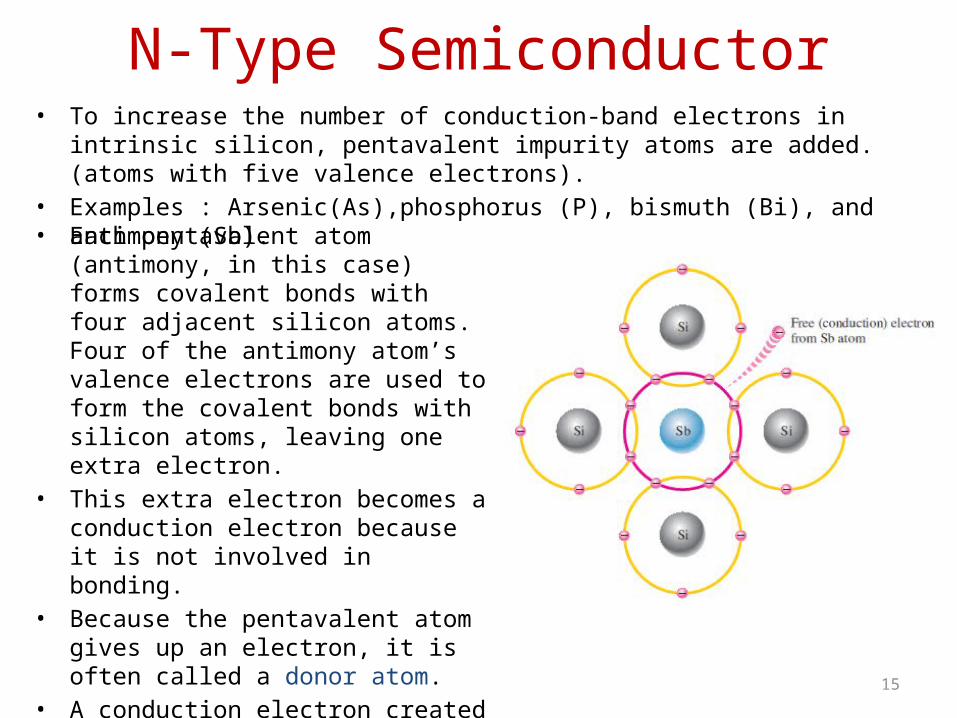
N-Type Semiconductor• To increase the number of conduction-band electrons in
intrinsic silicon, pentavalent impurity atoms are added. (atoms with five valence electrons).
• Examples : Arsenic(As),phosphorus (P), bismuth (Bi), and antimony (Sb).• Each pentavalent atom (antimony, in this case) forms covalent bonds with four adjacent silicon atoms. Four of the antimony atom’s valence electrons are used to form the covalent bonds with silicon atoms, leaving one extra electron.
• This extra electron becomes a conduction electron because it is not involved in bonding.
• Because the pentavalent atom gives up an electron, it is often called a donor atom.
• A conduction electron created by this doping process does not leave a hole in the valence band.
15
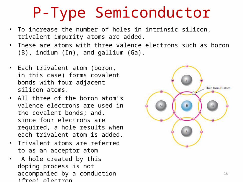
P-Type Semiconductor• To increase the number of holes in intrinsic silicon,
trivalent impurity atoms are added.• These are atoms with three valence electrons such as boron
(B), indium (In), and gallium (Ga).
• Each trivalent atom (boron, in this case) forms covalent bonds with four adjacent silicon atoms.
• All three of the boron atom’s valence electrons are used in the covalent bonds; and, since four electrons are required, a hole results when each trivalent atom is added.
• Trivalent atoms are referred to as an acceptor atom
• A hole created by this doping process is not accompanied by a conduction (free) electron.
16

Majority and Minority Carriers
• For N-type material :• Silicon (or germanium) doped with pentavalent atoms is an n-type
semiconductor. Most of the current carriers are electrons• The electrons are called the majority carriers in n-type
material. • Although the majority of current carriers in n-type material are
electrons, there are also a few holes that are created when electron-hole pairs are thermally generated. These holes are not produced by the addition of the pentavalent impurity atoms. Holes in an n-type material are called minority carriers.
• For P-type material: • silicon (or germanium) doped with trivalent atoms is called a p-
type semiconductor. Most of the current carriers are holes. • The holes are the majority carriers in p-type material. • Although the majority of current carriers in p-type material are
holes, there are also a few conduction-band electrons that are created when electron-hole pairs are thermally generated. These conduction-band electrons are not produced by the addition of the trivalent impurity atoms. Conduction-band electrons in p-type material are the minority carriers. 17
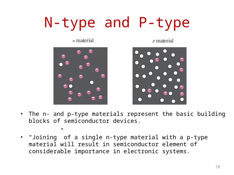
N-type and P-type
• The n- and p-type materials represent the basic building blocks of semiconductor devices.
• “Joining” of a single n-type material with a p-type material will result in semiconductor element of considerable importance in electronic systems.
18
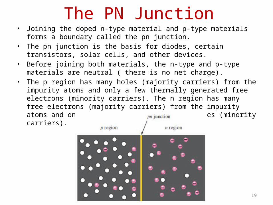
The PN Junction• Joining the doped n-type material and p-type materials
forms a boundary called the pn junction. • The pn junction is the basis for diodes, certain
transistors, solar cells, and other devices.• Before joining both materials, the n-type and p-type
materials are neutral ( there is no net charge).• The p region has many holes (majority carriers) from the
impurity atoms and only a few thermally generated free electrons (minority carriers). The n region has many free electrons (majority carriers) from the impurity atoms and only a few thermally generated holes (minority carriers).
19
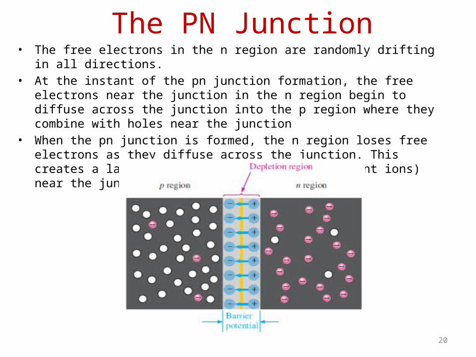
The PN Junction• The free electrons in the n region are randomly drifting
in all directions. • At the instant of the pn junction formation, the free
electrons near the junction in the n region begin to diffuse across the junction into the p region where they combine with holes near the junction
• When the pn junction is formed, the n region loses free electrons as they diffuse across the junction. This creates a layer of positive charges (pentavalent ions) near the junction.
20
The PN Junction• As the electrons move across the junction, the p region loses
holes as the electrons and holes combine. This creates a layer of negative charges (trivalent ions) near the junction.
• These two layers of positive and negative charges form the depletion region. The term depletion refers to the fact that the region near the pn junction is depleted of charge carriers (electrons and holes) due to diffusion across the junction.
• The depletion region is formed very quickly and is very thin compared to the n region and p region.
• After the initial surge of free electrons across the pn junction, the depletion region has expanded to a point where equilibrium is established and there is no further diffusion of electrons across the junction.
• A point is reached where the total negative charge in the depletion region repels any further diffusion of electrons (negatively charged particles) into the p region and the diffusion stops.
• The depletion region acts as a barrier to the further movement of electrons across the junction
21
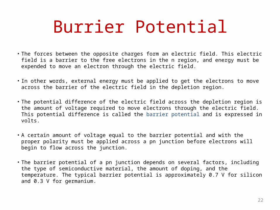
Burrier Potential• The forces between the opposite charges form an electric field. This electric field is a barrier to the free electrons in the n region, and energy must be expended to move an electron through the electric field.
• In other words, external energy must be applied to get the electrons to move across the barrier of the electric field in the depletion region.
• The potential difference of the electric field across the depletion region is the amount of voltage required to move electrons through the electric field. This potential difference is called the barrier potential and is expressed in volts.
• A certain amount of voltage equal to the barrier potential and with the proper polarity must be applied across a pn junction before electrons will begin to flow across the junction.
• The barrier potential of a pn junction depends on several factors, including the type of semiconductive material, the amount of doping, and the temperature. The typical barrier potential is approximately 0.7 V for silicon and 0.3 V for germanium.
22
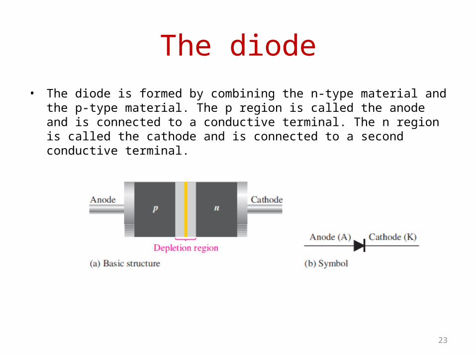
The diode• The diode is formed by combining the n-type material and
the p-type material. The p region is called the anode and is connected to a conductive terminal. The n region is called the cathode and is connected to a second conductive terminal.
23
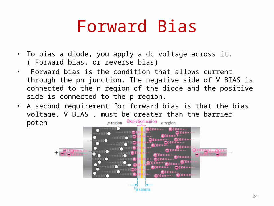
Forward Bias• To bias a diode, you apply a dc voltage across it.
( Forward bias, or reverse bias)• Forward bias is the condition that allows current
through the pn junction. The negative side of V BIAS is connected to the n region of the diode and the positive side is connected to the p region.
• A second requirement for forward bias is that the bias voltage, V BIAS , must be greater than the barrier potential.
24
The Effect of Forward Bias on the Depletion Region
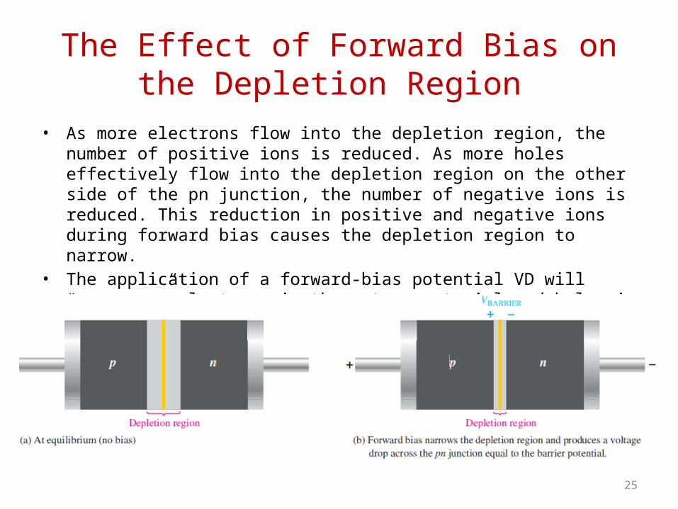
• As more electrons flow into the depletion region, the number of positive ions is reduced. As more holes effectively flow into the depletion region on the other side of the pn junction, the number of negative ions is reduced. This reduction in positive and negative ions during forward bias causes the depletion region to narrow.
• The application of a forward-bias potential VD will “pressure” electrons in the n-type material and holes in the p-type material to recombine with the ions near the boundary and reduce the width of the depletion region.
25
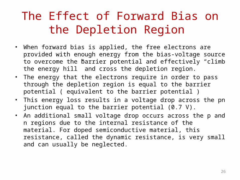
• When forward bias is applied, the free electrons are provided with enough energy from the bias-voltage source to overcome the barrier potential and effectively “climb the energy hill” and cross the depletion region.
• The energy that the electrons require in order to pass through the depletion region is equal to the barrier potential ( equivalent to the barrier potential )
• This energy loss results in a voltage drop across the pn junction equal to the barrier potential (0.7 V).
• An additional small voltage drop occurs across the p and n regions due to the internal resistance of the material. For doped semiconductive material, this resistance, called the dynamic resistance, is very small and can usually be neglected.
The Effect of Forward Bias on the Depletion Region
26
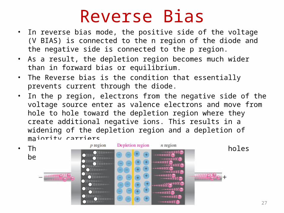
Reverse Bias• In reverse bias mode, the positive side of the voltage
(V BIAS) is connected to the n region of the diode and the negative side is connected to the p region.
• As a result, the depletion region becomes much wider than in forward bias or equilibrium.
• The Reverse bias is the condition that essentially prevents current through the diode.
• In the p region, electrons from the negative side of the voltage source enter as valence electrons and move from hole to hole toward the depletion region where they create additional negative ions. This results in a widening of the depletion region and a depletion of majority carriers.
• The flow of valence electrons can be viewed as holes being “pulled” toward the positive side.
27
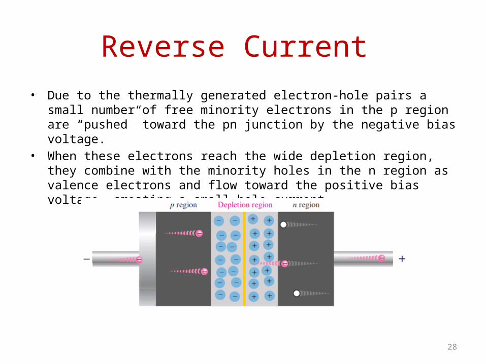
Reverse Current • Due to the thermally generated electron-hole pairs a
small number of free minority electrons in the p region are “pushed” toward the pn junction by the negative bias voltage.
• When these electrons reach the wide depletion region, they combine with the minority holes in the n region as valence electrons and flow toward the positive bias voltage, creating a small hole current.
28
Reverse Breakdown • Normally, the reverse current is so small that it can be
neglected.• However, if the external reverse-bias voltage is
increased to a value called the breakdown voltage, the reverse current will drastically increase.
• The high reverse-bias voltage imparts energy to the free minority electrons so that as they speed through the p region, they collide with atoms with enough energy to knock valence electrons out of orbit and into the conduction band. The newly created conduction electrons are also high in energy and repeat the process. If one electron knocks only two others out of their valence orbit during its travel through the p region, the numbers quickly multiply. As these high-energy electrons go through the depletion region, they have enough energy to go through the n region as conduction electrons, rather than combining with holes.
• The multiplication of conduction electrons just discussed is known as the avalanche effect, and reverse current can increase dramatically if steps are not taken to limit the current.
• When the reverse current is not limited, the resulting heating will permanently damage the diode. Most diodes are not operated in reverse breakdown
29
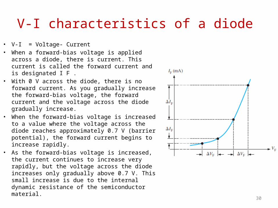
V-I characteristics of a diode • V-I = Voltage- Current• When a forward-bias voltage is applied
across a diode, there is current. This current is called the forward current and is designated I F .
• With 0 V across the diode, there is no forward current. As you gradually increase the forward-bias voltage, the forward current and the voltage across the diode gradually increase.
• When the forward-bias voltage is increased to a value where the voltage across the diode reaches approximately 0.7 V (barrier potential), the forward current begins to increase rapidly.
• As the forward-bias voltage is increased, the current continues to increase very rapidly, but the voltage across the diode increases only gradually above 0.7 V. This small increase is due to the internal dynamic resistance of the semiconductor material.
30
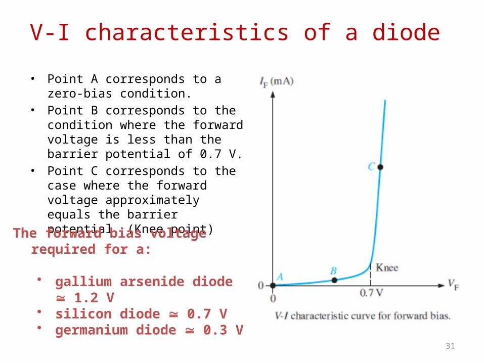
• Point A corresponds to a zero-bias condition.
• Point B corresponds to the condition where the forward voltage is less than the barrier potential of 0.7 V.
• Point C corresponds to the case where the forward voltage approximately equals the barrier potential. (Knee point)
V-I characteristics of a diode
31
The forward bias voltage required for a:
• gallium arsenide diode 1.2 V
• silicon diode 0.7 V• germanium diode 0.3 V
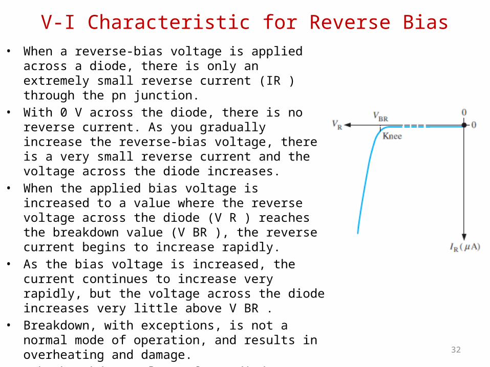
V-I Characteristic for Reverse Bias• When a reverse-bias voltage is applied
across a diode, there is only an extremely small reverse current (IR ) through the pn junction.
• With 0 V across the diode, there is no reverse current. As you gradually increase the reverse-bias voltage, there is a very small reverse current and the voltage across the diode increases.
• When the applied bias voltage is increased to a value where the reverse voltage across the diode (V R ) reaches the breakdown value (V BR ), the reverse current begins to increase rapidly.
• As the bias voltage is increased, the current continues to increase very rapidly, but the voltage across the diode increases very little above V BR .
• Breakdown, with exceptions, is not a normal mode of operation, and results in overheating and damage.
• The breakdown voltage for a diode depends the type of the diode. A typical rectifier diode (the most widely used type) has a breakdown voltage of greater than 50 V. Some specialized diodes have a breakdown voltage that is only 5 V.
32
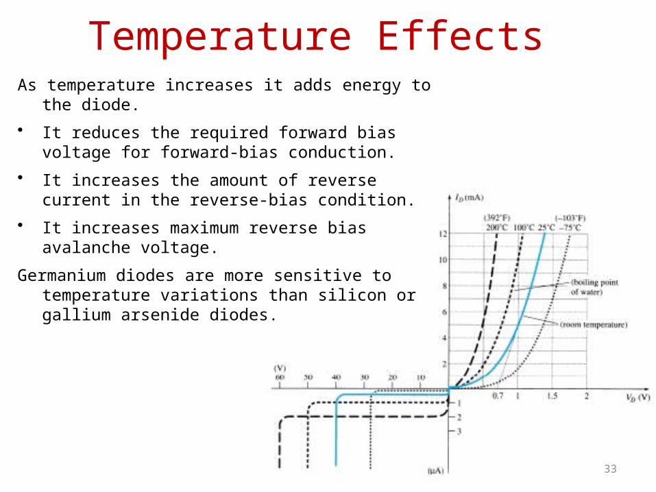
Temperature Effects As temperature increases it adds energy to
the diode. • It reduces the required forward bias
voltage for forward-bias conduction.• It increases the amount of reverse
current in the reverse-bias condition.• It increases maximum reverse bias
avalanche voltage.Germanium diodes are more sensitive to
temperature variations than silicon or gallium arsenide diodes.
33
Chapter 2
Diode Applications
34
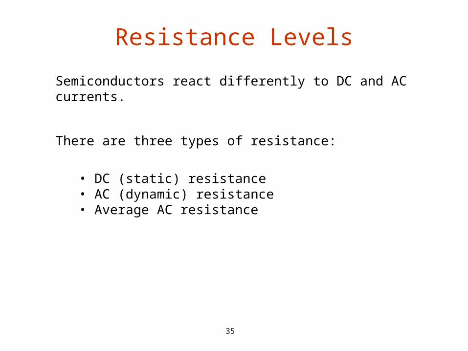
Semiconductors react differently to DC and AC currents.
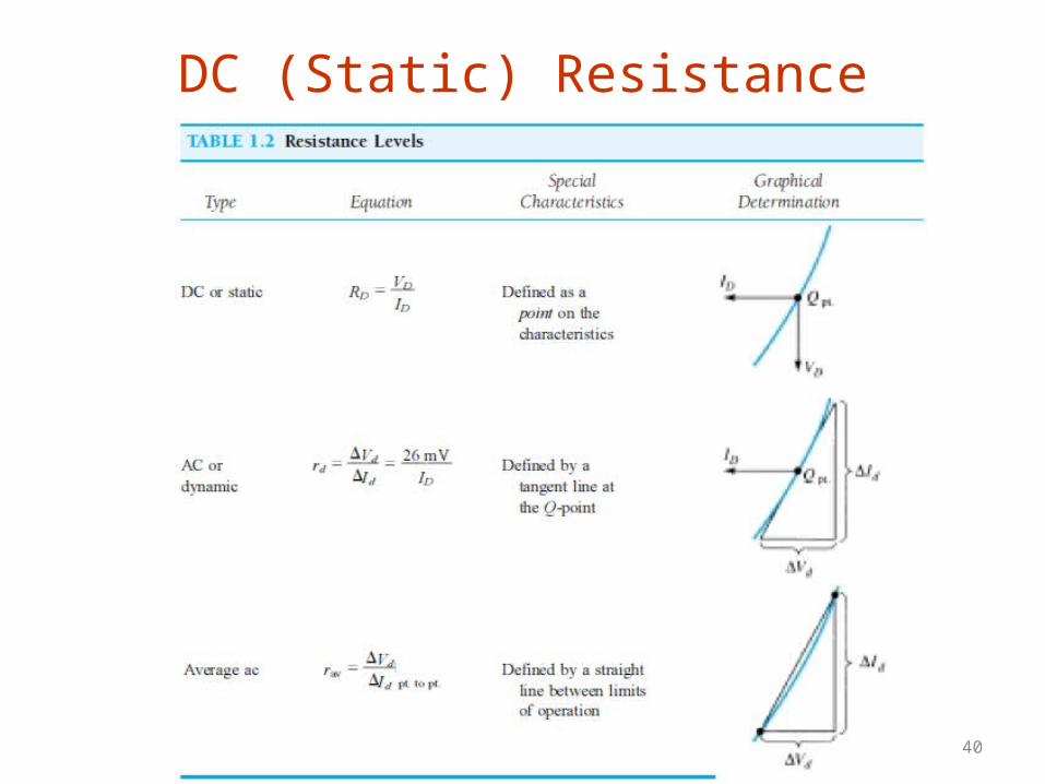
There are three types of resistance:
• DC (static) resistance• AC (dynamic) resistance• Average AC resistance
Resistance Levels
35
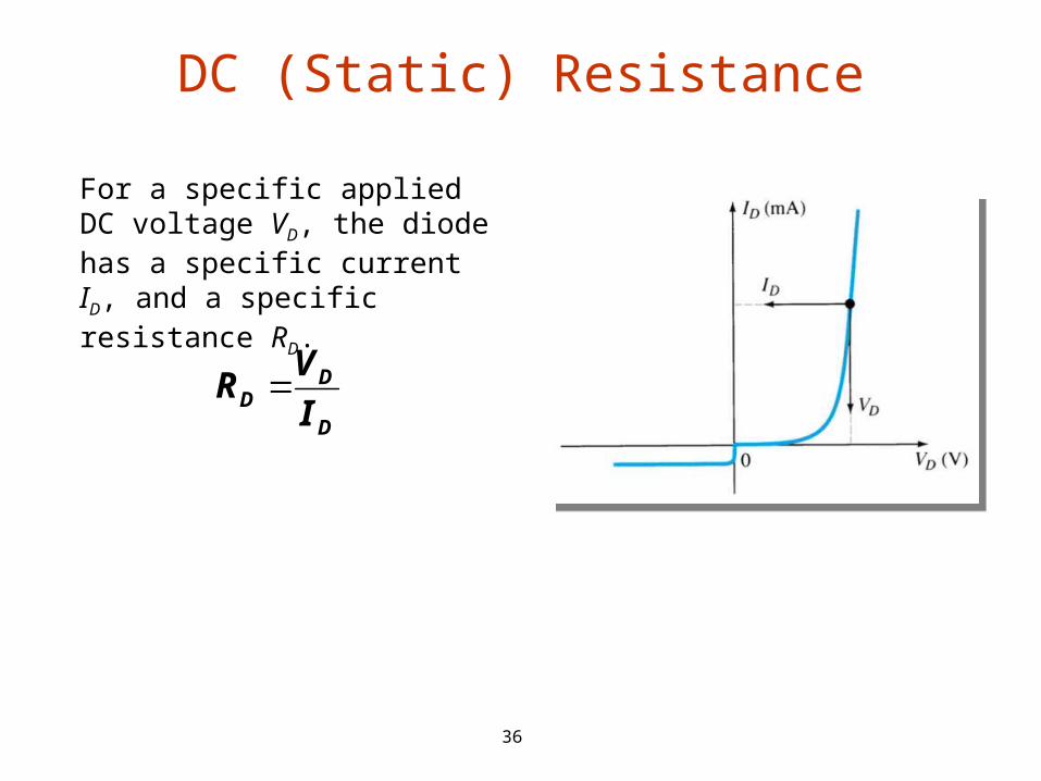
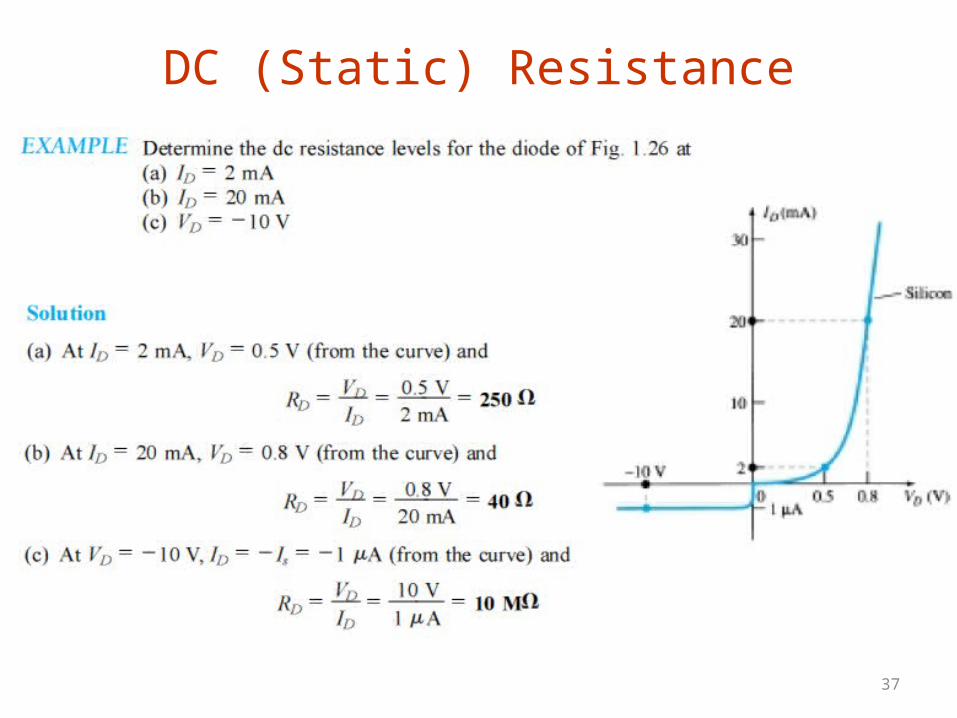
DC (Static) Resistance
For a specific applied DC voltage VD, the diode has a specific current ID, and a specific resistance RD.
D
DD I
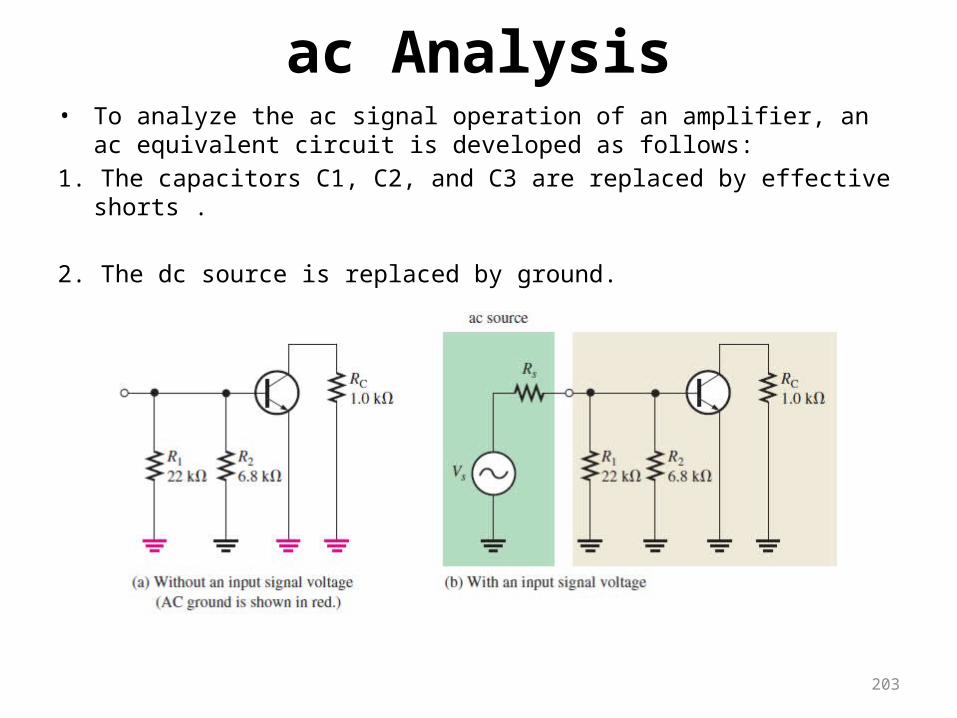
VR
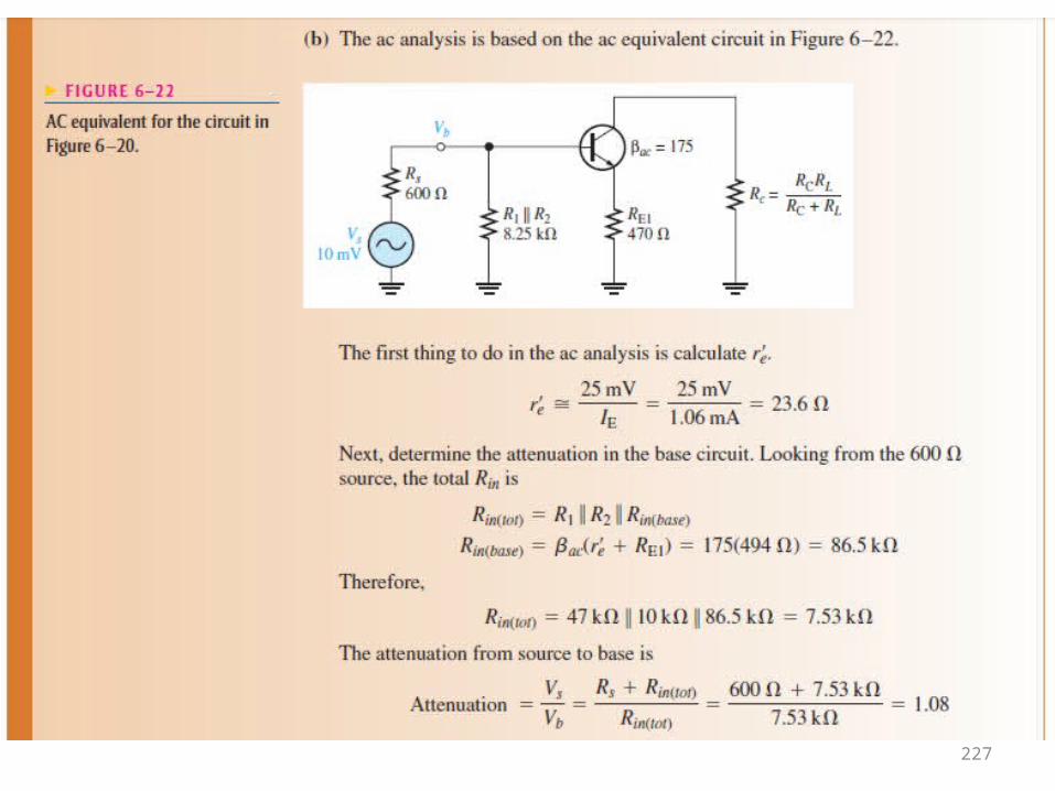
36
37
DC (Static) Resistance
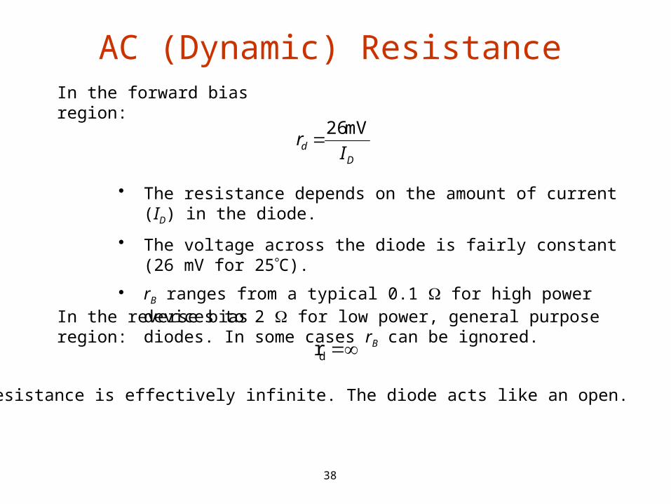
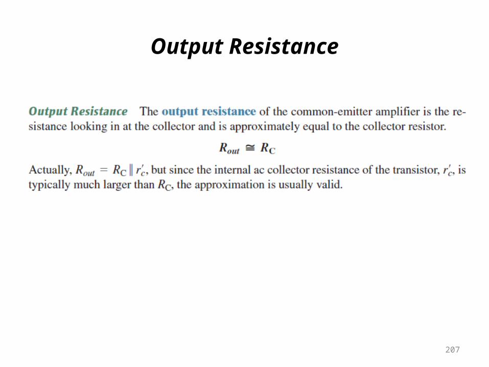
• The resistance depends on the amount of current (ID) in the diode.
• The voltage across the diode is fairly constant (26 mV for 25C).
• rB ranges from a typical 0.1 for high power devices to 2 for low power, general purpose diodes. In some cases rB can be ignored.
AC (Dynamic) Resistance
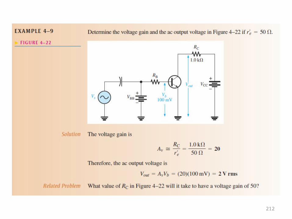
Dd I
r mV 26
rd
In the forward bias region:
In the reverse bias region:
The resistance is effectively infinite. The diode acts like an open.
38
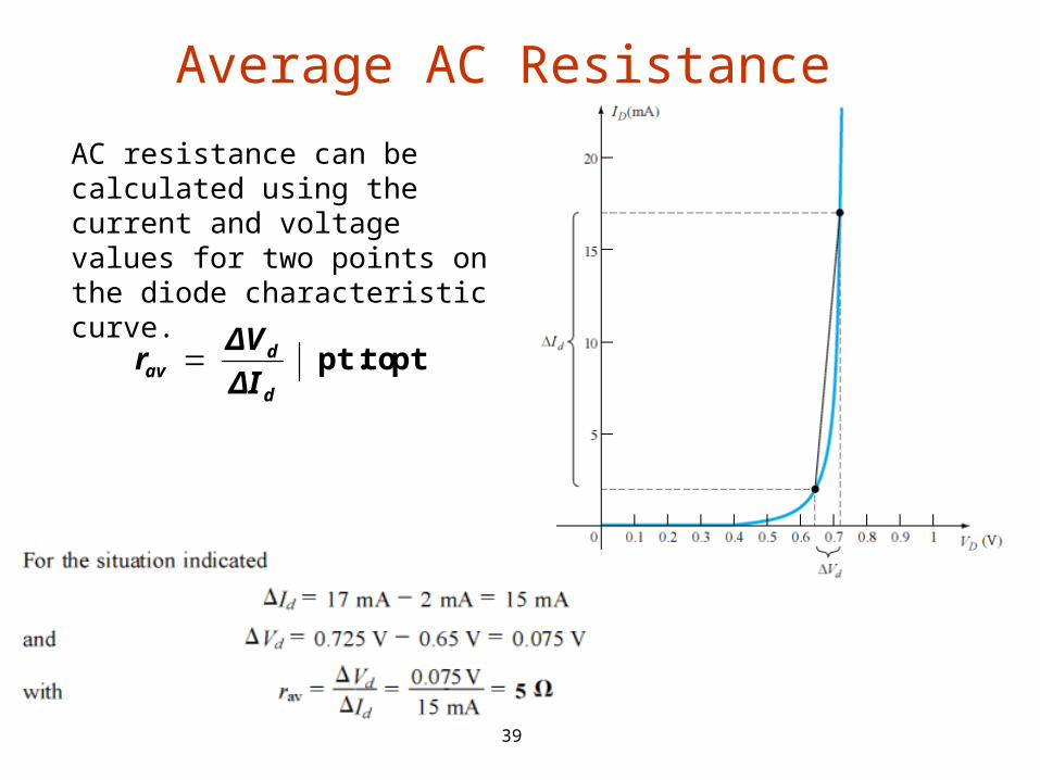
AC resistance can be calculated using the current and voltage values for two points on the diode characteristic curve.
Average AC Resistance
pt. to pt. d
dav ΔI
ΔV r
39
40
DC (Static) Resistance
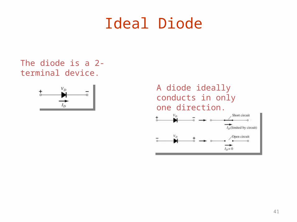
Ideal Diode
The diode is a 2-terminal device.
A diode ideally conducts in only one direction.
41
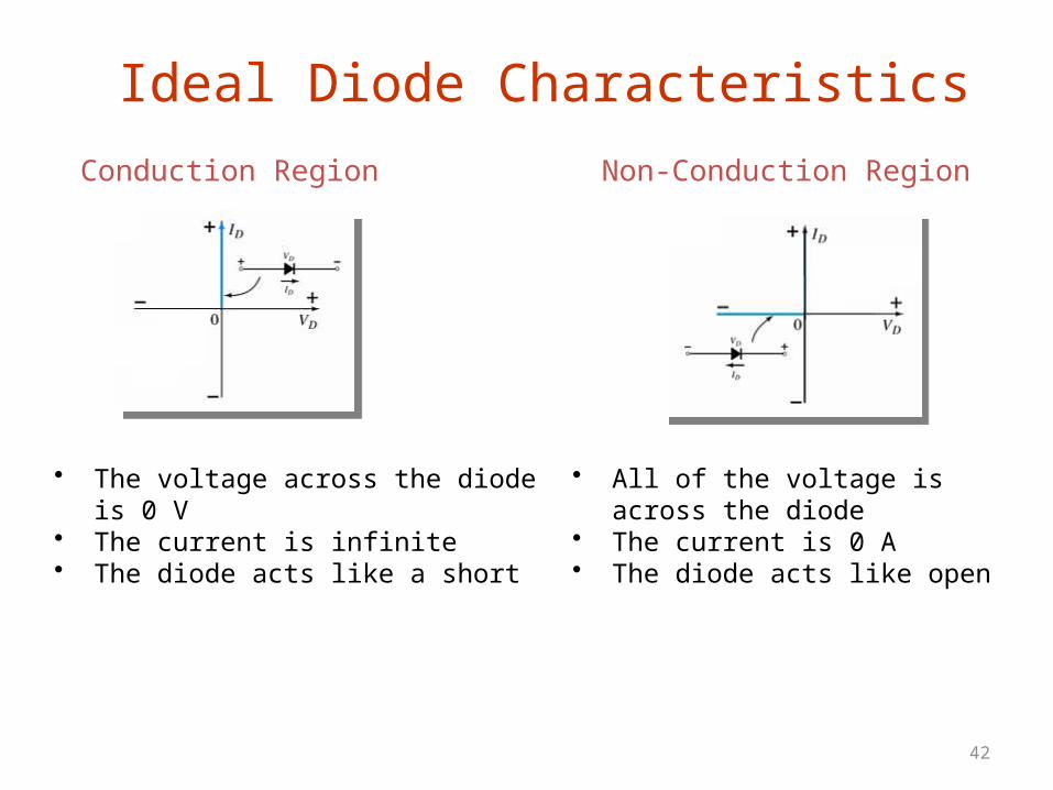
Ideal Diode CharacteristicsConduction Region Non-Conduction Region
• The voltage across the diode is 0 V
• The current is infinite• The diode acts like a short
• All of the voltage is across the diode
• The current is 0 A• The diode acts like open
42
43
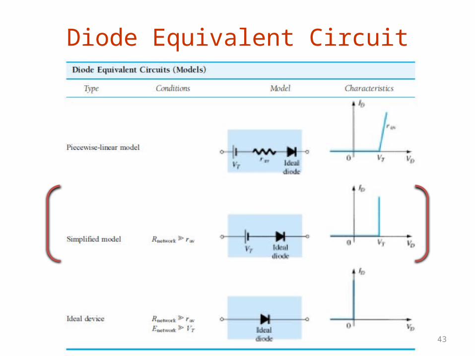
Diode Equivalent Circuit
44
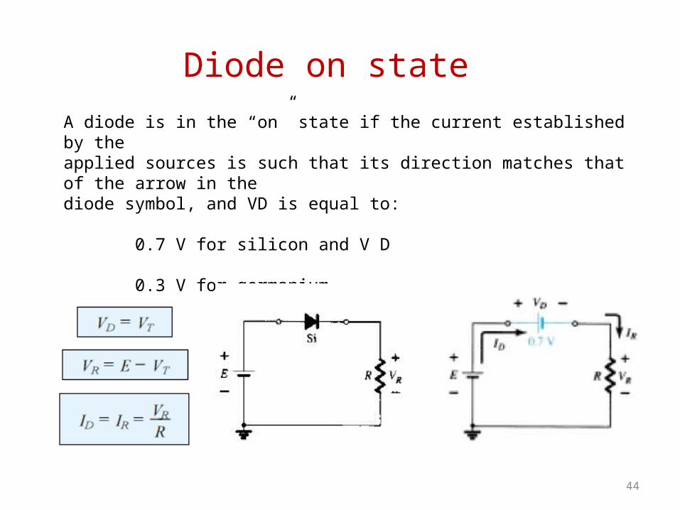
A diode is in the “on” state if the current established by theapplied sources is such that its direction matches that of the arrow in thediode symbol, and VD is equal to: 0.7 V for silicon and V D 0.3 V for germanium
Diode on state
45
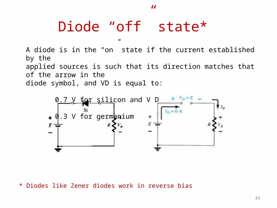
Diode “off” state*
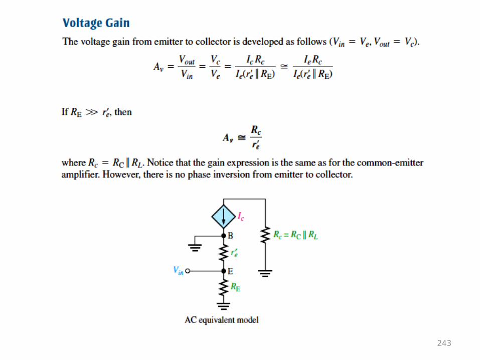
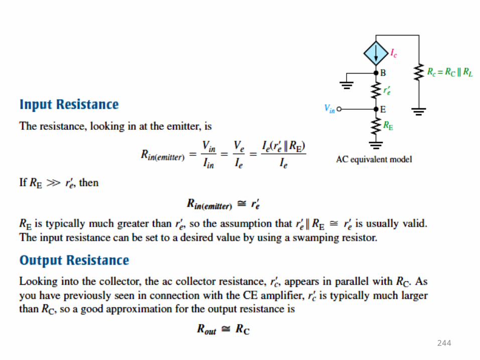
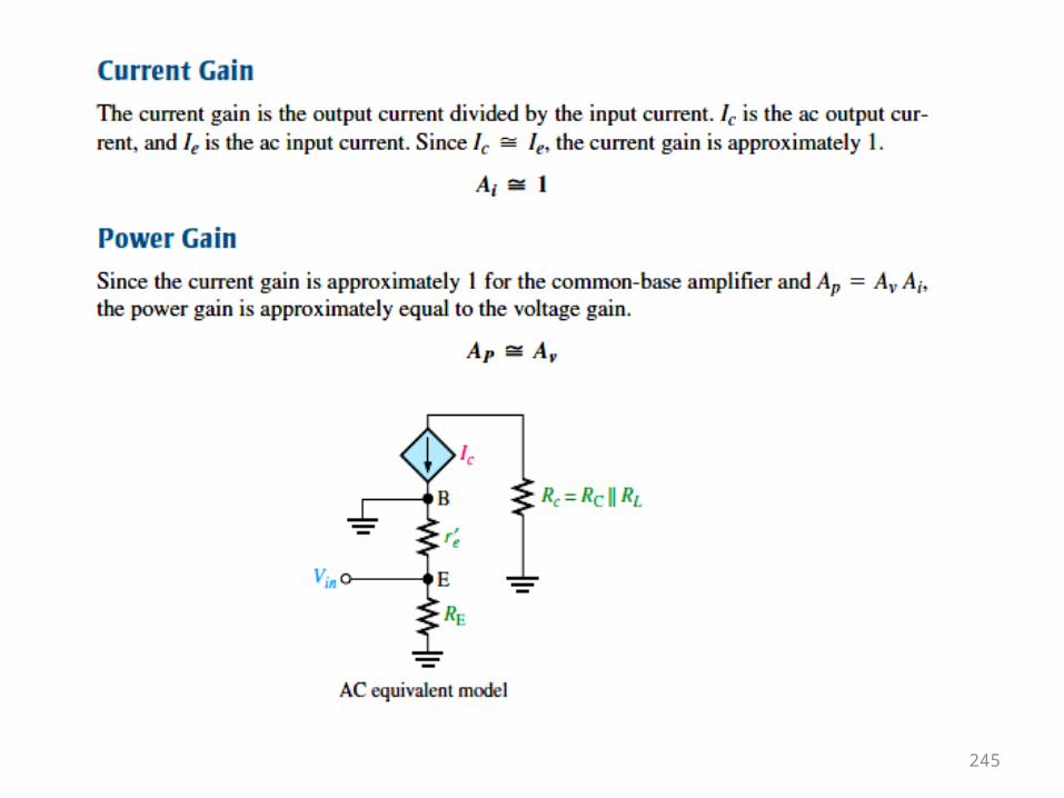
* Diodes like Zener diodes work in reverse bias
A diode is in the “on” state if the current established by theapplied sources is such that its direction matches that of the arrow in thediode symbol, and VD is equal to: 0.7 V for silicon and V D 0.3 V for germanium
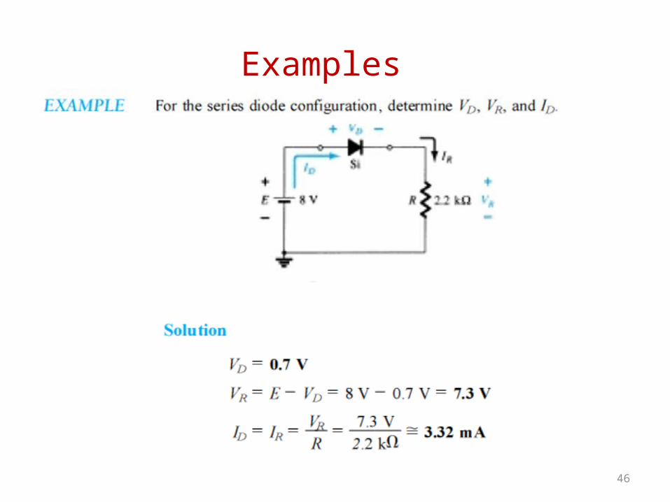
46
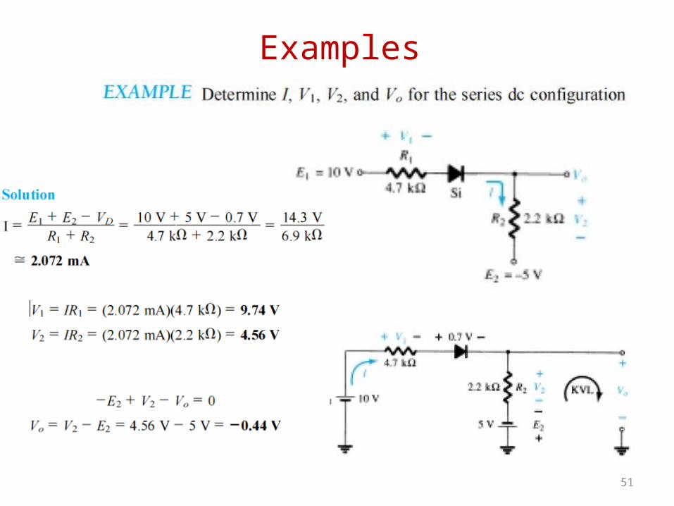
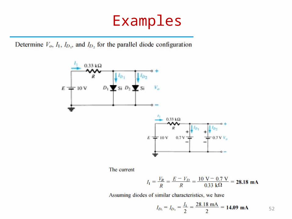
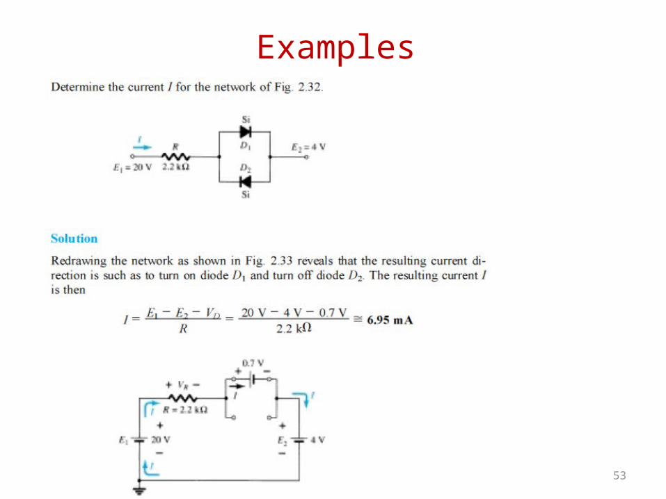
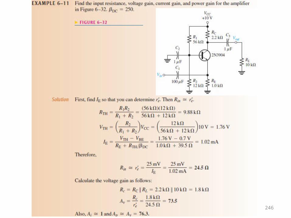
Examples
47
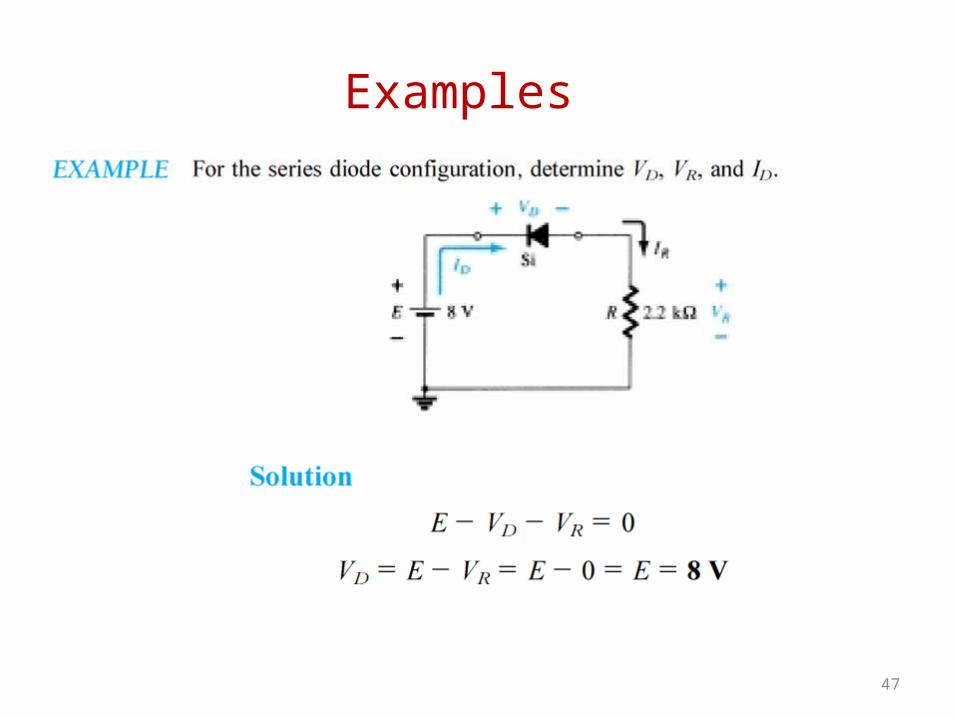
Examples
48
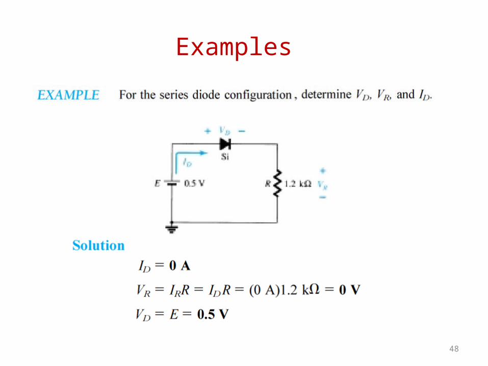
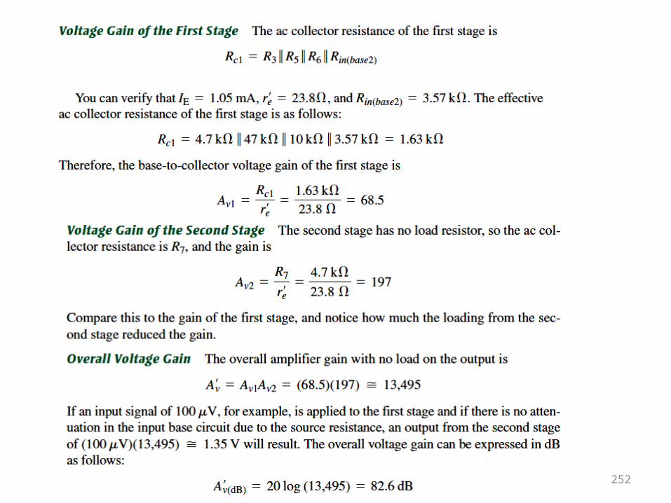
Examples
49
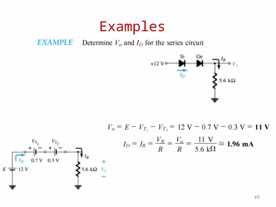
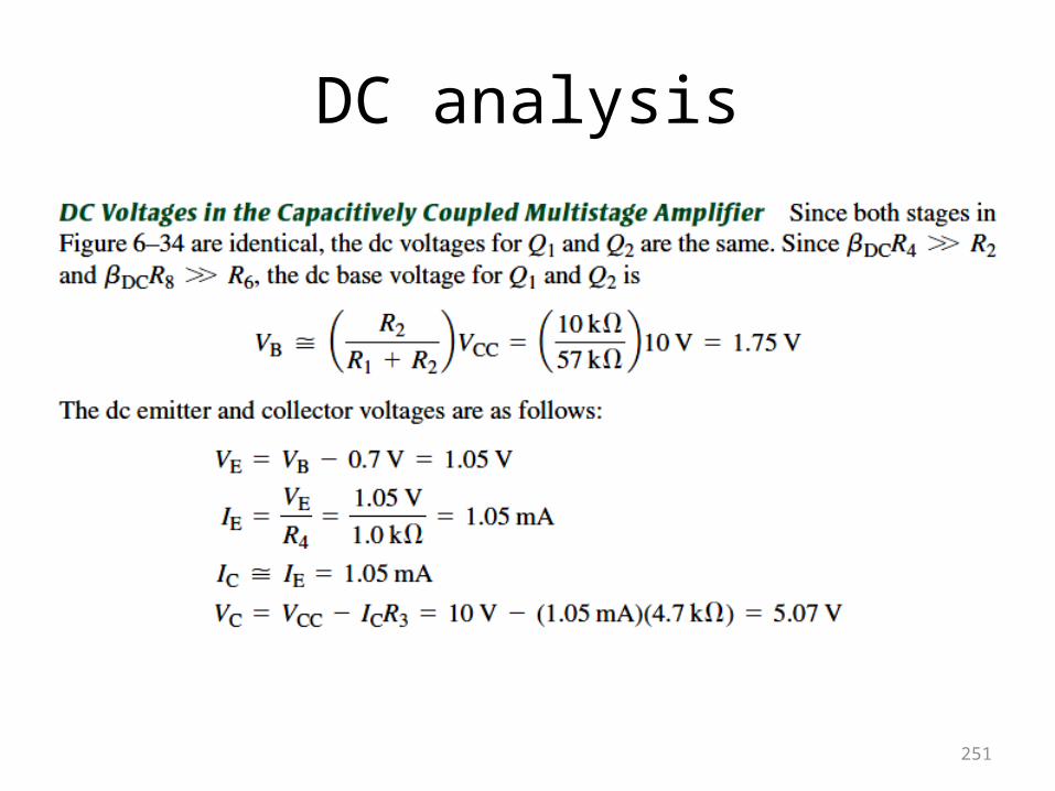
Examples
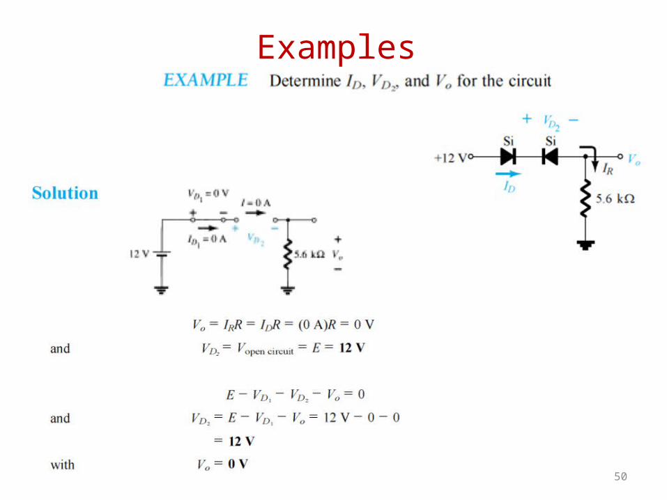
50
Examples
51
Examples
52
Examples
53
Examples
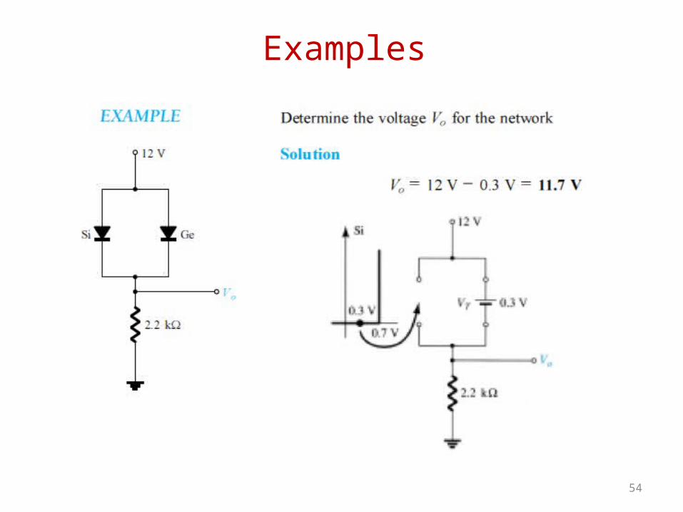
54
Examples
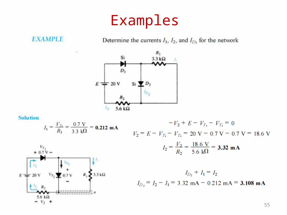
55
Examples
56
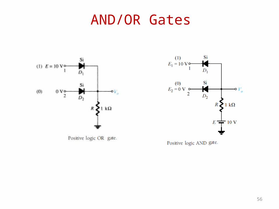
AND/OR Gates
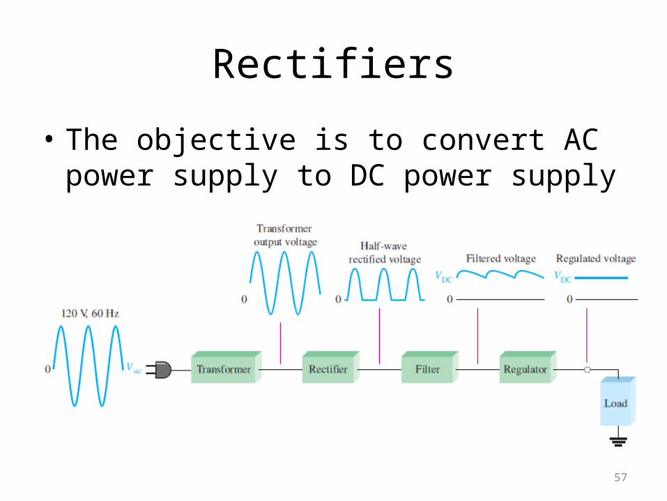
Rectifiers• The objective is to convert AC power supply to DC power supply
57
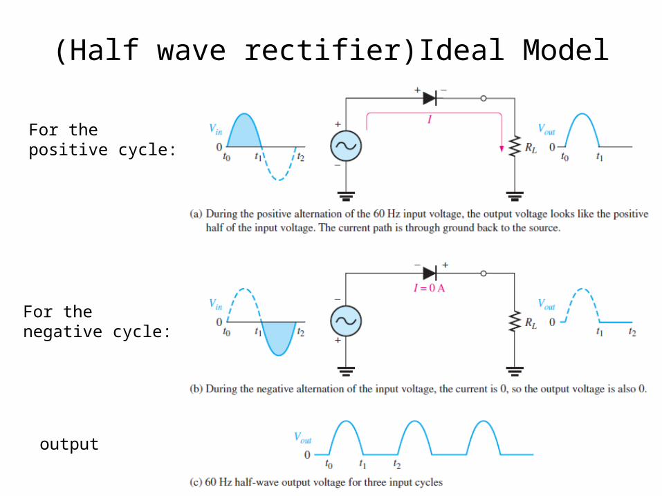
(Half wave rectifier)Ideal Model
58
For the positive cycle:
For the negative cycle:
output
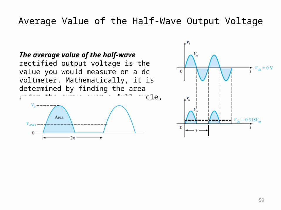
Average Value of the Half-Wave Output Voltage
59
The average value of the half-waverectified output voltage is the value you would measure on a dc voltmeter. Mathematically, it is determined by finding the area under the curve over a full cycle,
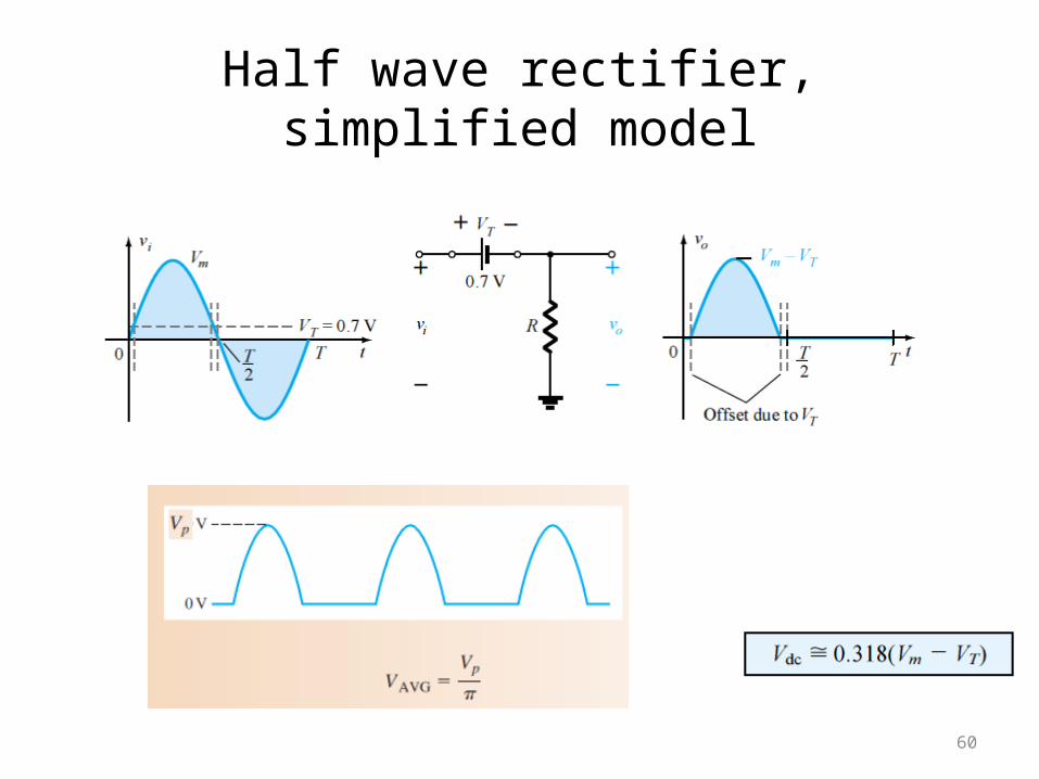
Half wave rectifier, simplified model
60
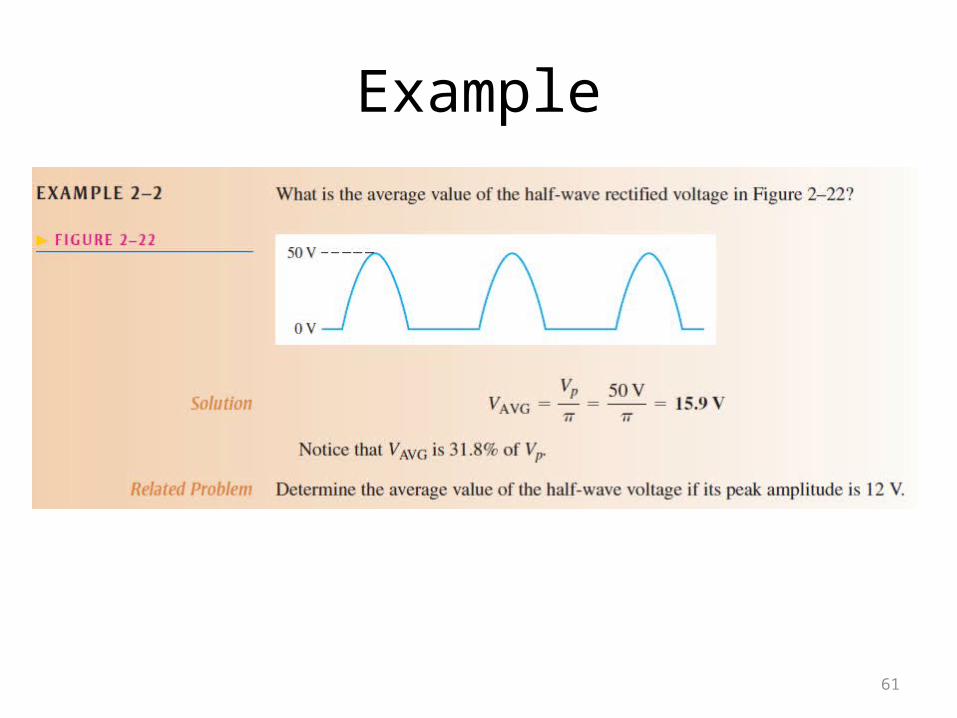
Example
61
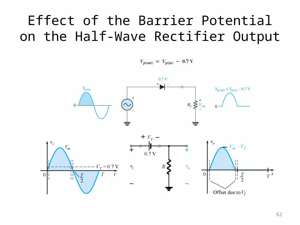
Effect of the Barrier Potential on the Half-Wave Rectifier Output
62
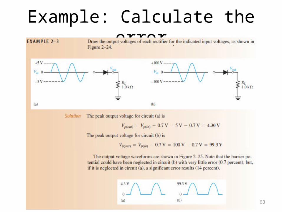
Example: Calculate the error
63
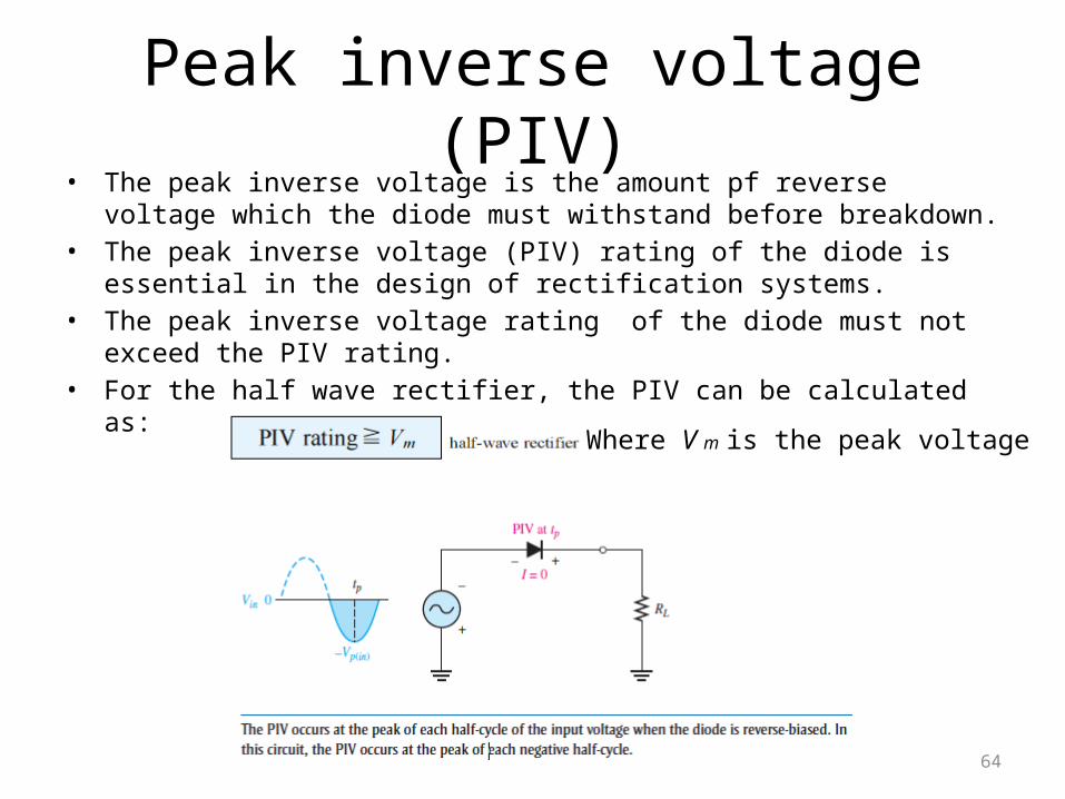
Peak inverse voltage (PIV)
• The peak inverse voltage is the amount pf reverse voltage which the diode must withstand before breakdown.
• The peak inverse voltage (PIV) rating of the diode is essential in the design of rectification systems.
• The peak inverse voltage rating of the diode must not exceed the PIV rating.
• For the half wave rectifier, the PIV can be calculated as:
64
Where V m is the peak voltage
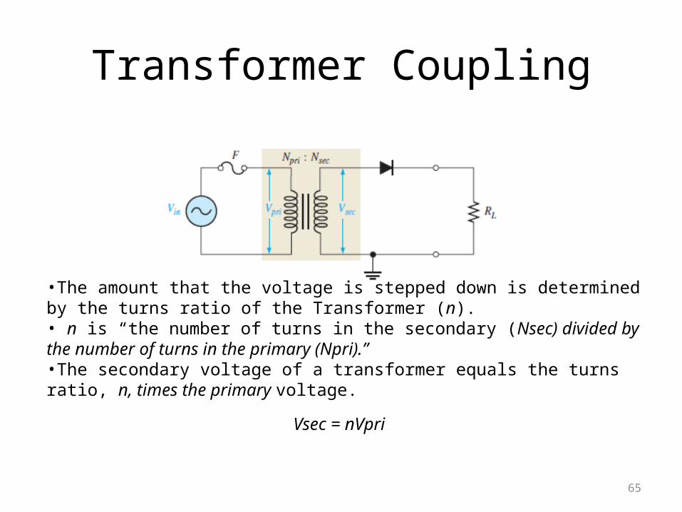
Transformer Coupling
65
•The amount that the voltage is stepped down is determined by the turns ratio of the Transformer (n). • n is “the number of turns in the secondary (Nsec) divided by the number of turns in the primary (Npri).”•The secondary voltage of a transformer equals the turns ratio, n, times the primary voltage.
Vsec = nVpri
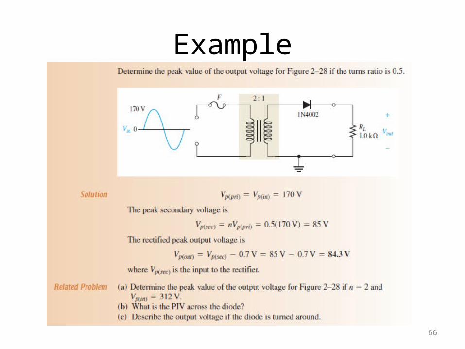
Example
66
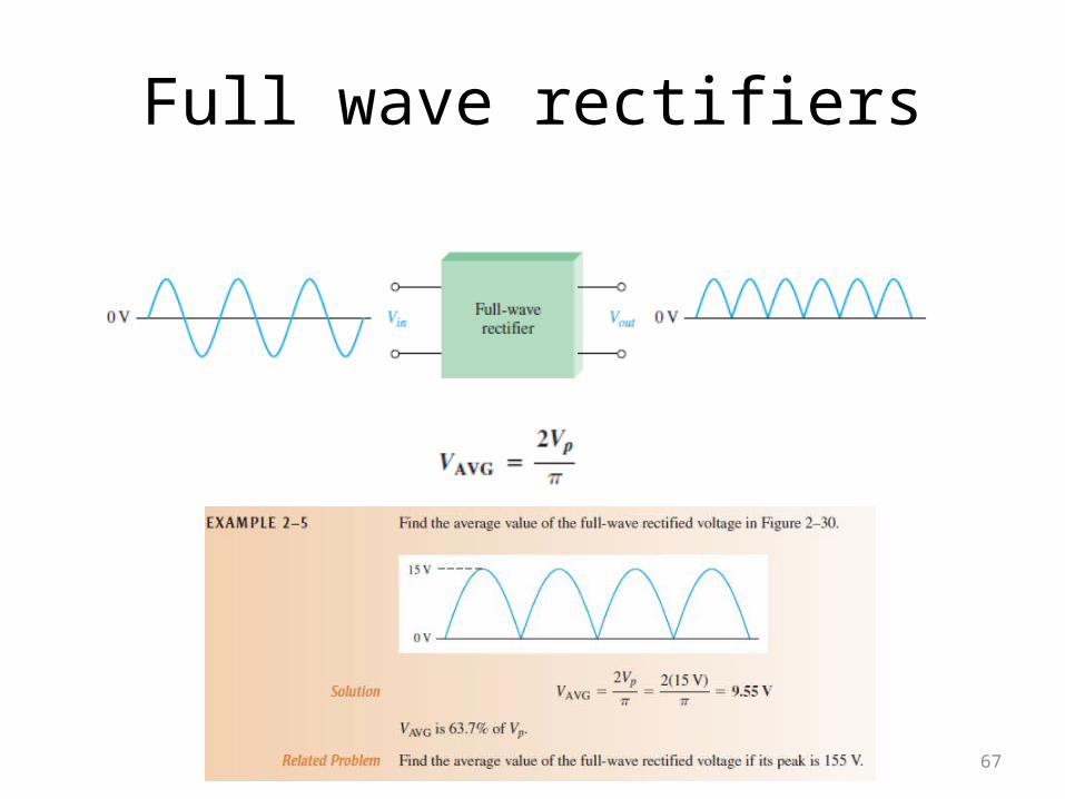
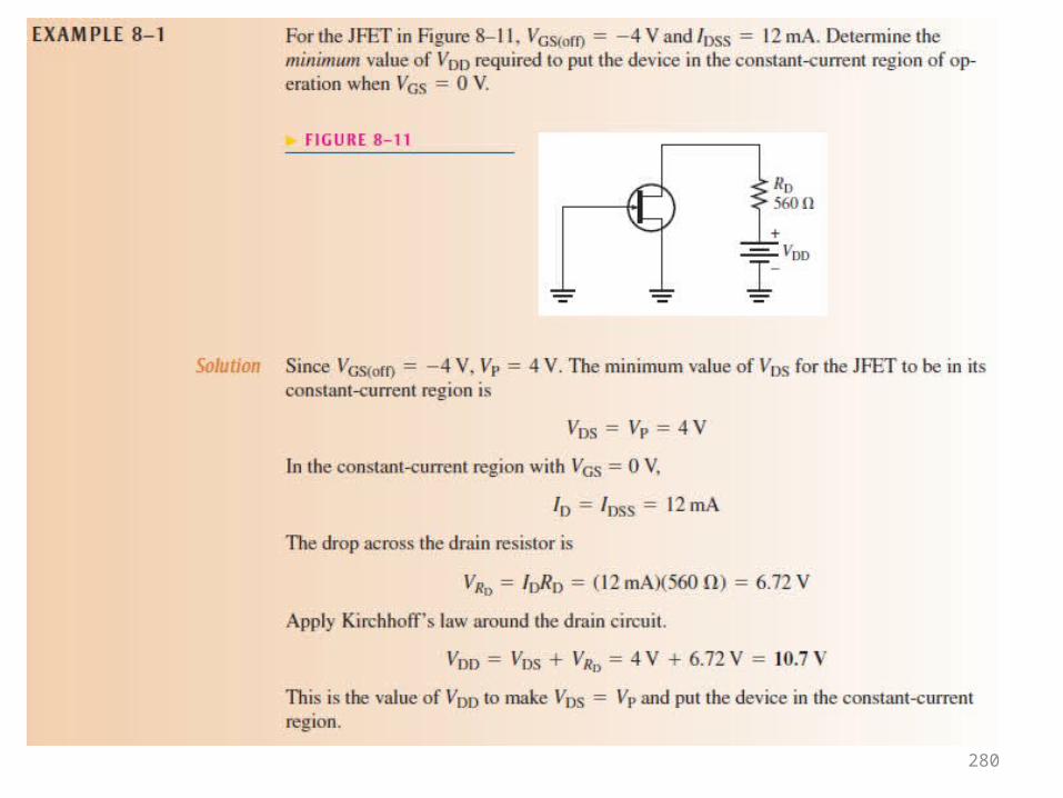
Full wave rectifiers
67
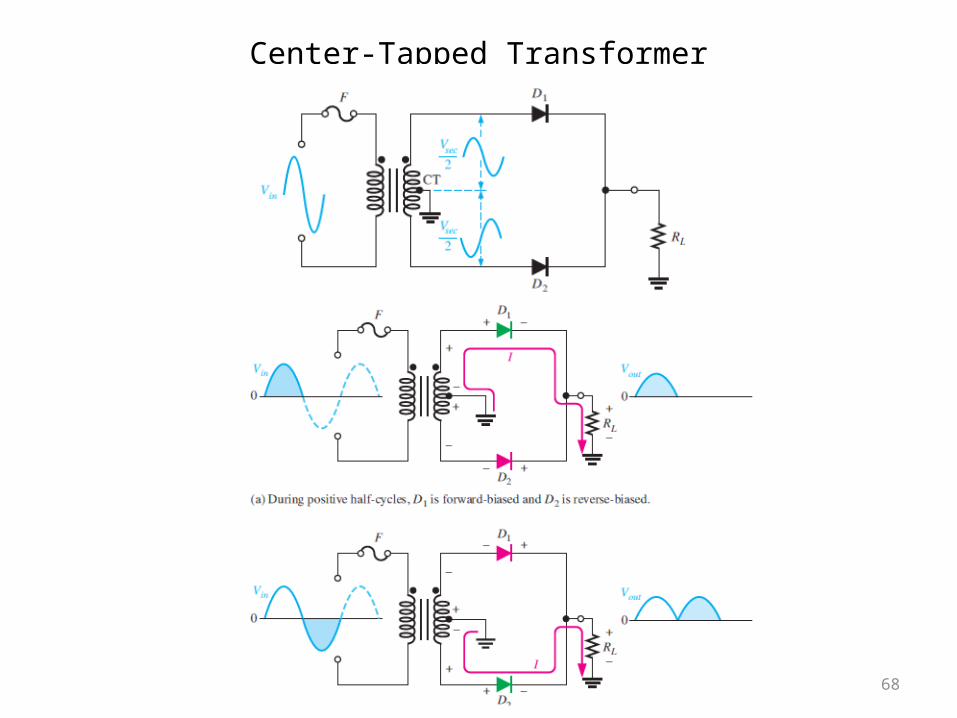
Center-Tapped Transformer
68
69
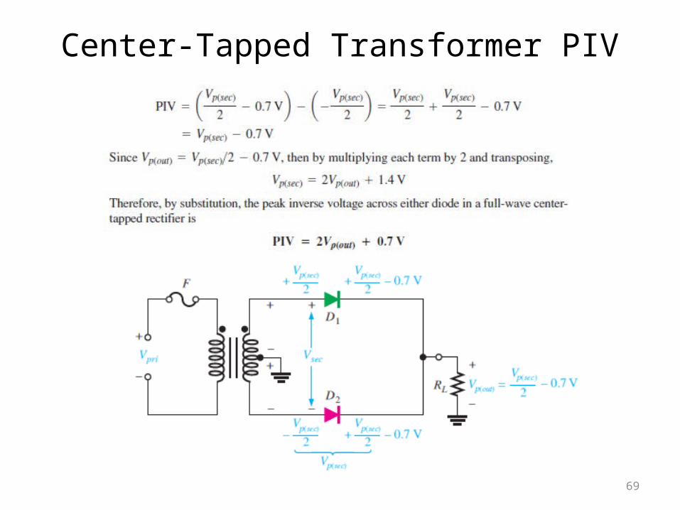
Center-Tapped Transformer PIV
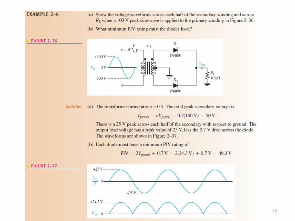
70
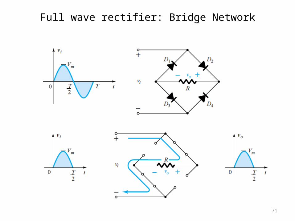
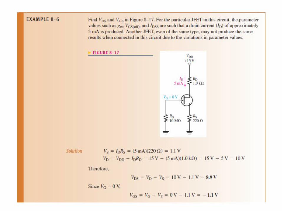
Full wave rectifier: Bridge Network
71
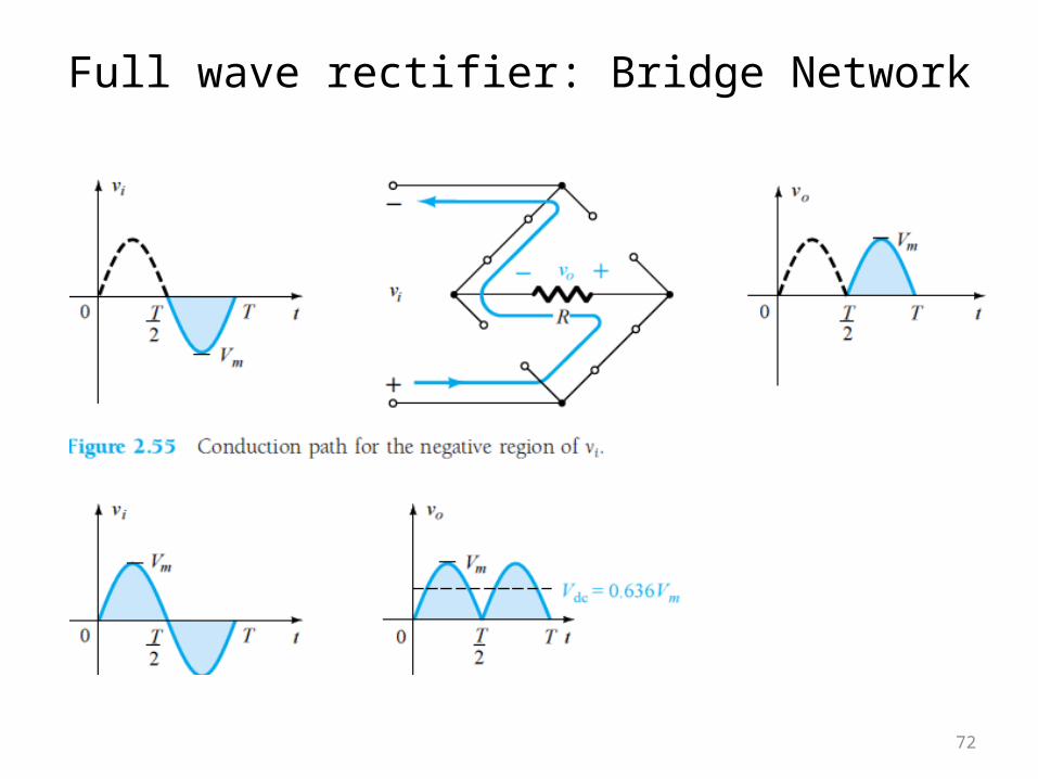
Full wave rectifier: Bridge Network
72
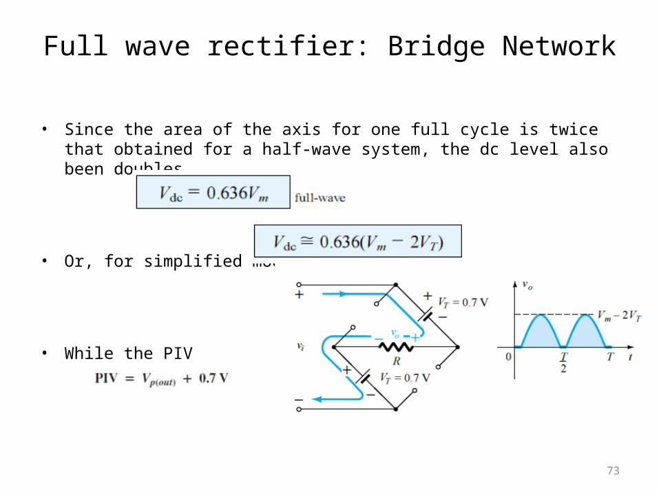
• Since the area of the axis for one full cycle is twice that obtained for a half-wave system, the dc level also been doubles.
• Or, for simplified model
• While the PIV
73
Full wave rectifier: Bridge Network
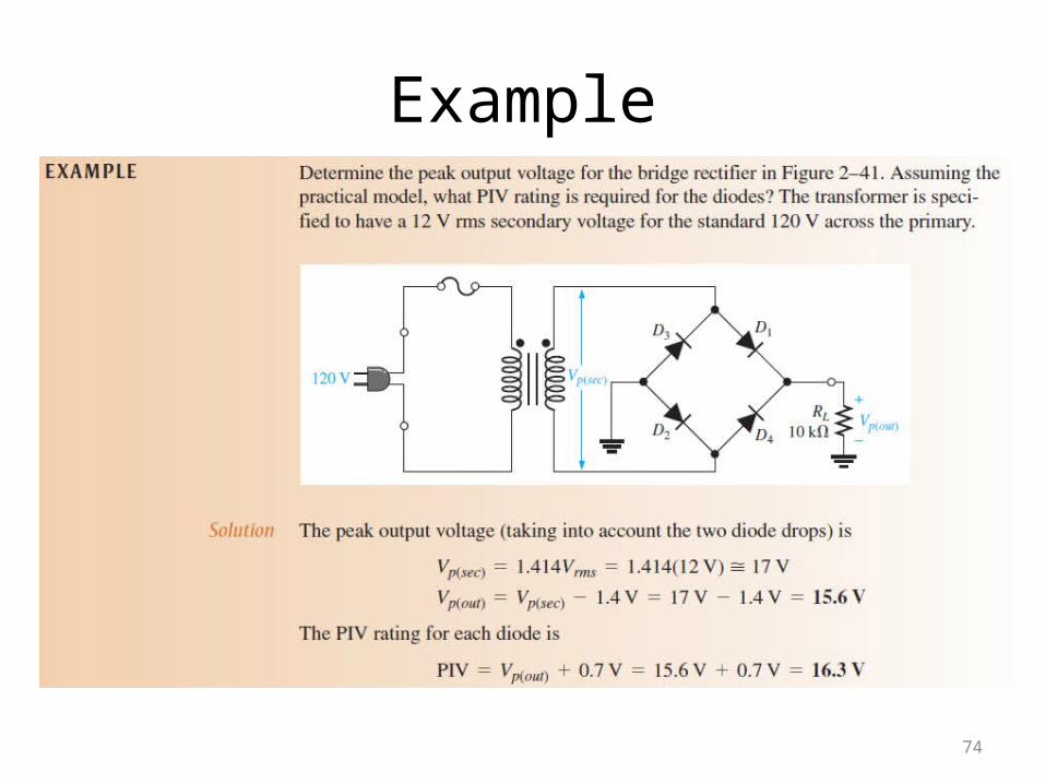
Example
74
Example
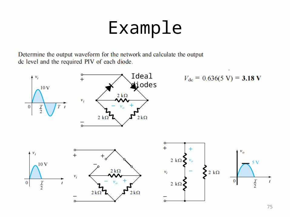
75
Ideal diodes
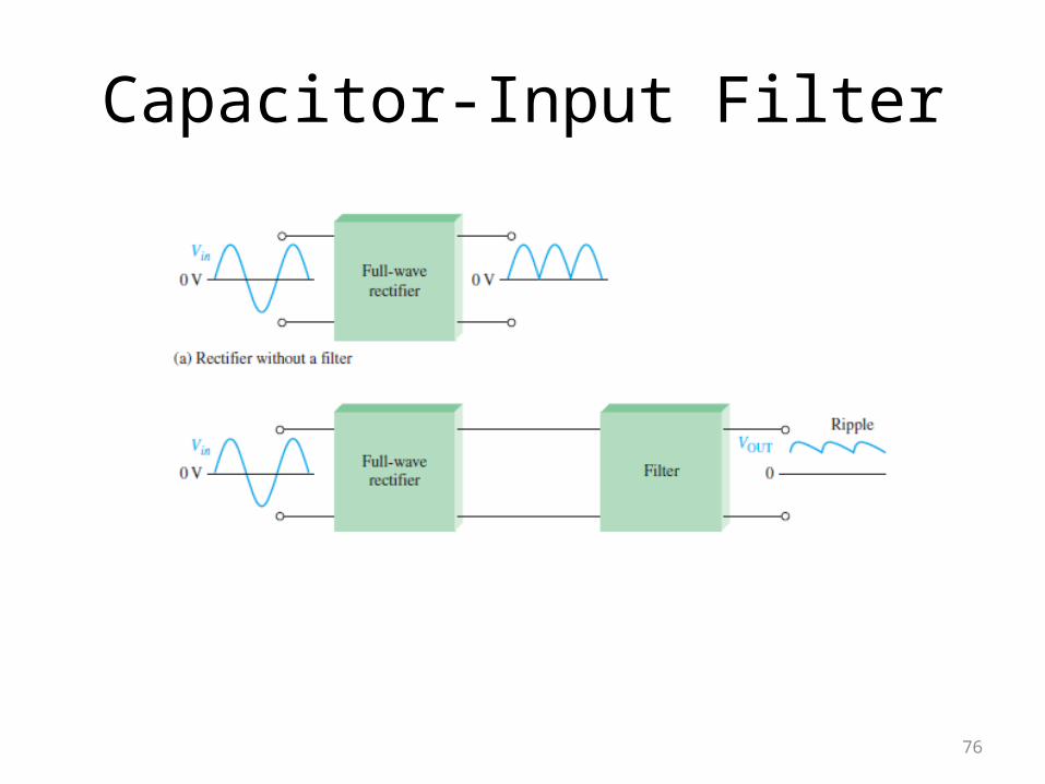
Capacitor-Input Filter
76
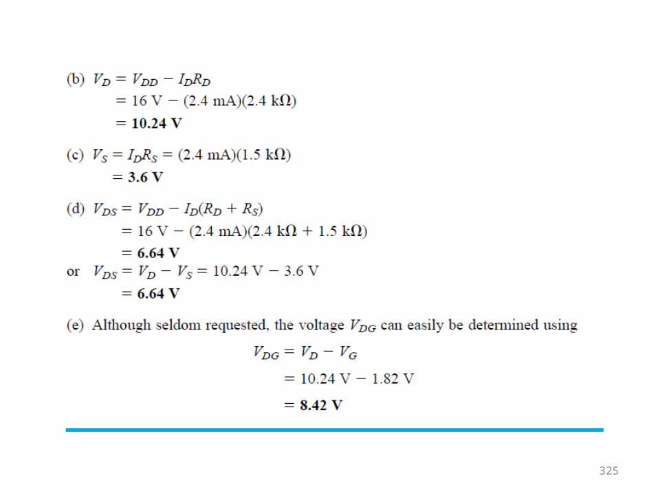
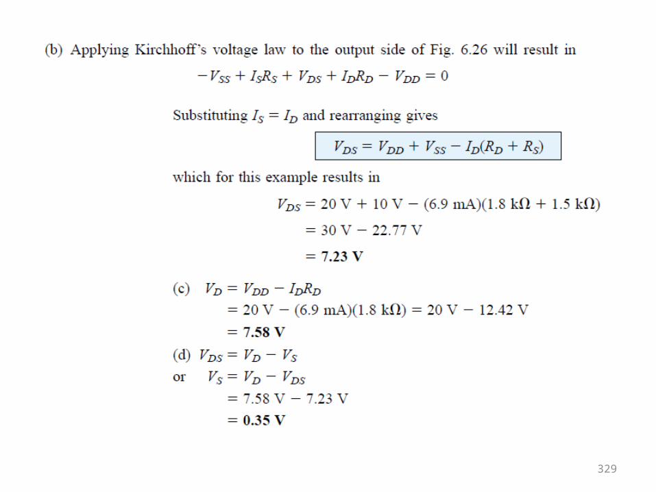
77
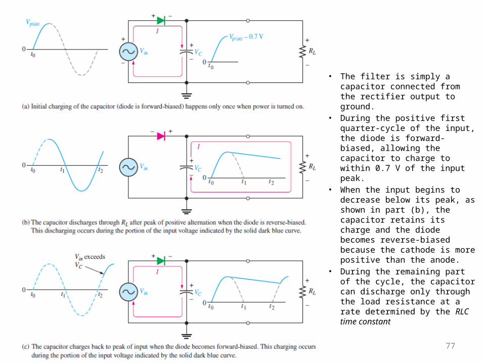
• The filter is simply a capacitor connected from the rectifier output to ground.
• During the positive first quarter-cycle of the input, the diode is forward-biased, allowing the capacitor to charge to within 0.7 V of the input peak.
• When the input begins to decrease below its peak, as shown in part (b), the capacitor retains its charge and the diode becomes reverse-biased because the cathode is more positive than the anode.
• During the remaining part of the cycle, the capacitor can discharge only through the load resistance at a rate determined by the RLC time constant
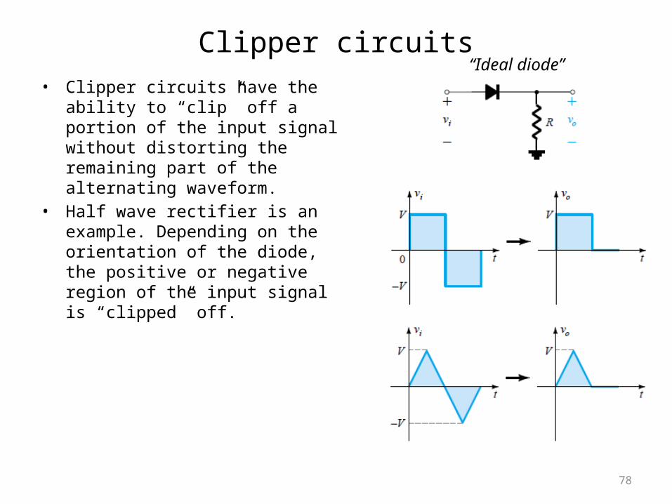
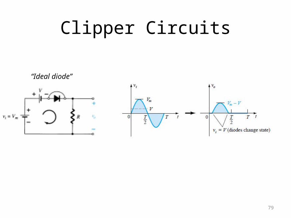
Clipper circuits• Clipper circuits have the
ability to “clip” off a portion of the input signal without distorting the remaining part of the alternating waveform.
• Half wave rectifier is an example. Depending on the orientation of the diode, the positive or negative region of the input signal is “clipped” off.
78
“Ideal diode”
Clipper Circuits
79
“Ideal diode”
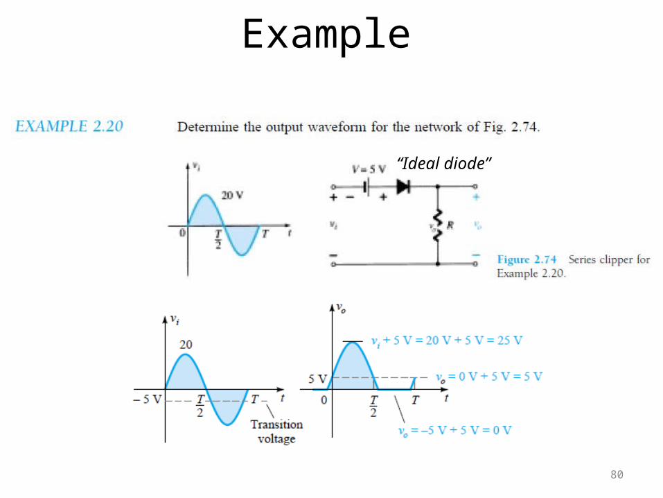
Example
80
“Ideal diode”
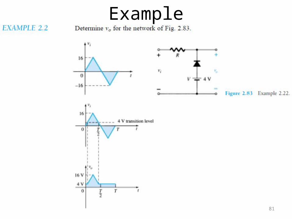
Example
81
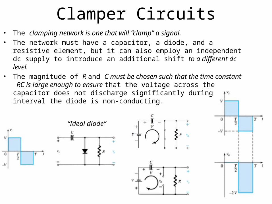
Clamper Circuits• The clamping network is one that will “clamp” a signal.• The network must have a capacitor, a diode, and a
resistive element, but it can also employ an independent dc supply to introduce an additional shift to a different dc level.
• The magnitude of R and C must be chosen such that the time constant RC is large enough to ensure that the voltage across the capacitor does not discharge significantly during the interval the diode is non-conducting.
82
“Ideal diode”
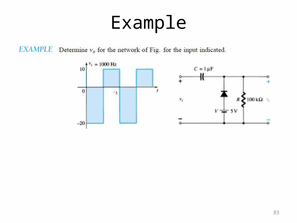
Example
83
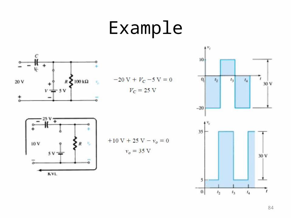
Example
84
Half-Wave Voltage Doubler
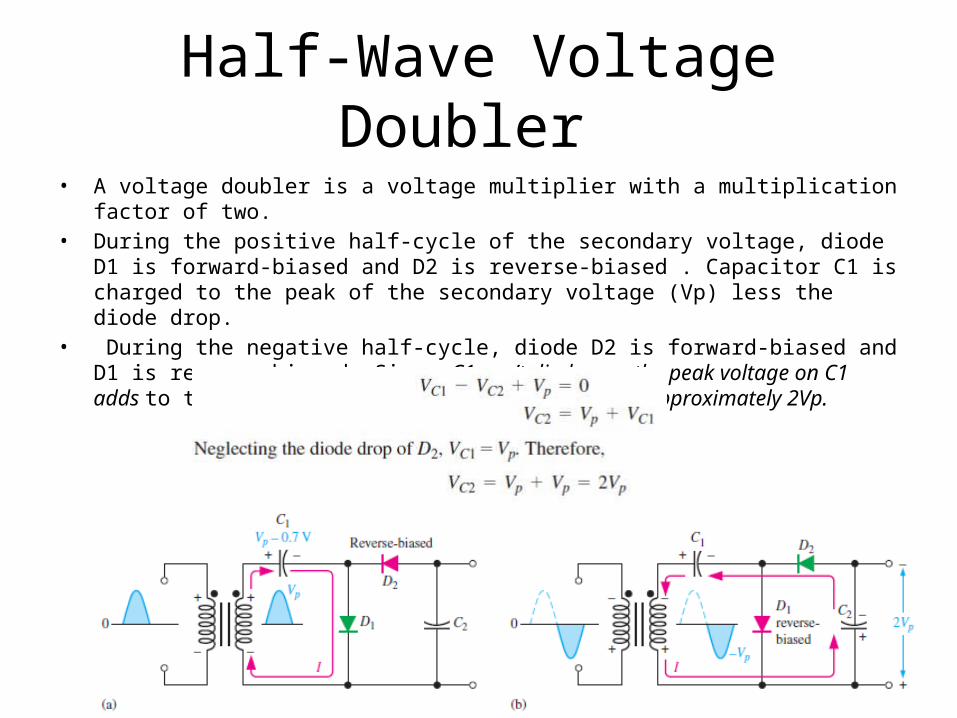
• A voltage doubler is a voltage multiplier with a multiplication factor of two.
• During the positive half-cycle of the secondary voltage, diode D1 is forward-biased and D2 is reverse-biased . Capacitor C1 is charged to the peak of the secondary voltage (Vp) less the diode drop.
• During the negative half-cycle, diode D2 is forward-biased and D1 is reverse-biased. Since C1 can’t discharge, the peak voltage on C1 adds to the secondary voltage to charge C2 to approximately 2Vp.
85
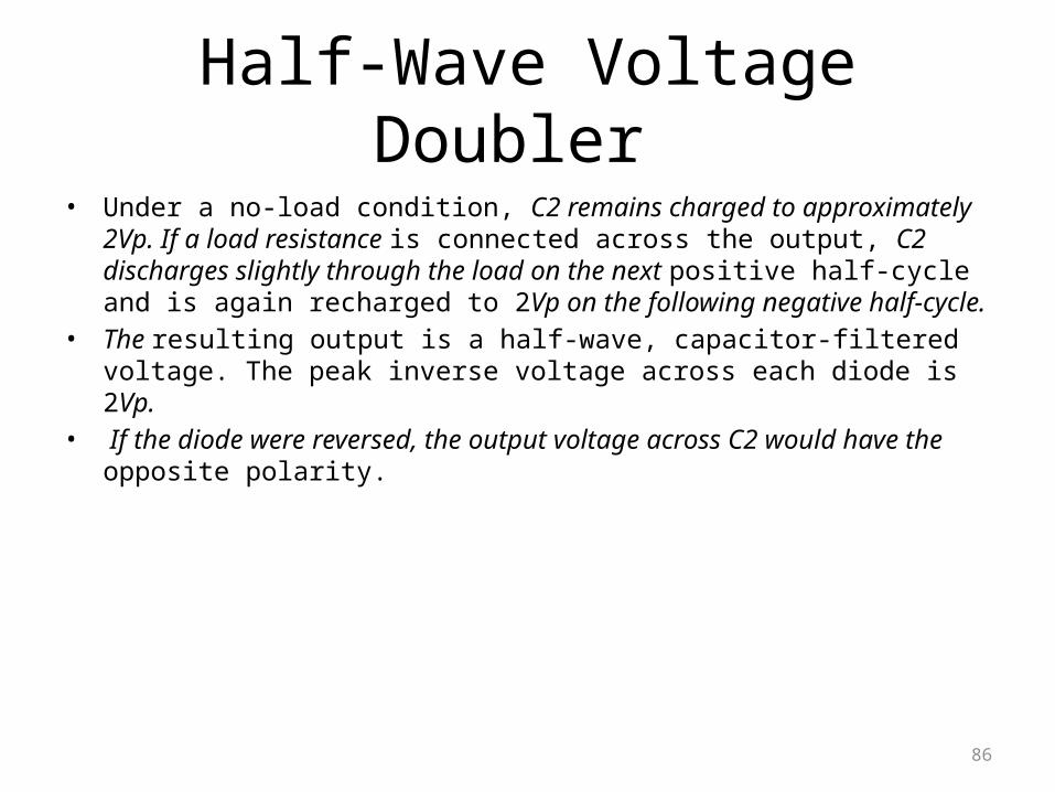
• Under a no-load condition, C2 remains charged to approximately 2Vp. If a load resistance is connected across the output, C2 discharges slightly through the load on the next positive half-cycle and is again recharged to 2Vp on the following negative half-cycle.
• The resulting output is a half-wave, capacitor-filtered voltage. The peak inverse voltage across each diode is 2Vp.
• If the diode were reversed, the output voltage across C2 would have the opposite polarity.
86
Half-Wave Voltage Doubler
Full-Wave Voltage Doubler
87
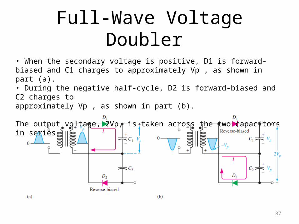
• When the secondary voltage is positive, D1 is forward-biased and C1 charges to approximately Vp , as shown in part (a).• During the negative half-cycle, D2 is forward-biased and C2 charges toapproximately Vp , as shown in part (b).
The output voltage, 2Vp, is taken across the two capacitors in series.
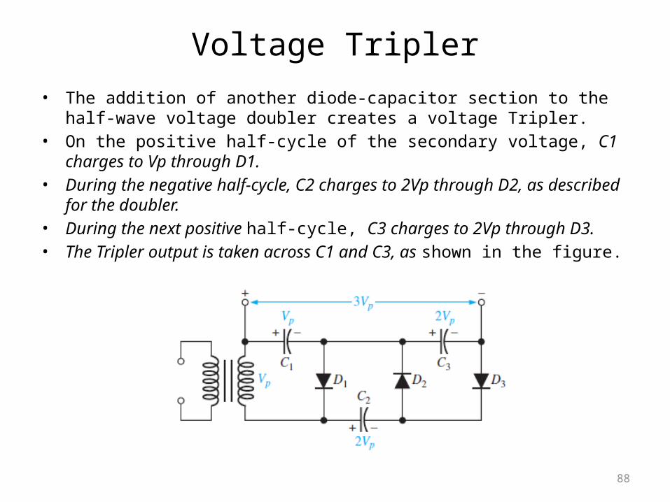
Voltage Tripler• The addition of another diode-capacitor section to the
half-wave voltage doubler creates a voltage Tripler.• On the positive half-cycle of the secondary voltage, C1
charges to Vp through D1.• During the negative half-cycle, C2 charges to 2Vp through D2, as described
for the doubler. • During the next positive half-cycle, C3 charges to 2Vp through D3. • The Tripler output is taken across C1 and C3, as shown in the figure.
88
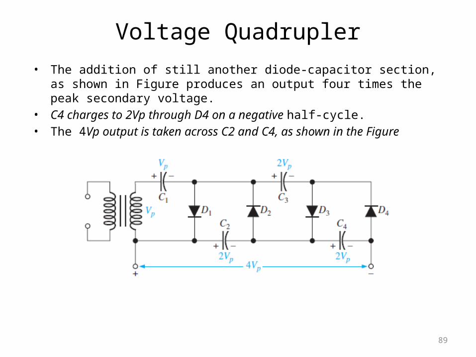
Voltage Quadrupler• The addition of still another diode-capacitor section,
as shown in Figure produces an output four times the peak secondary voltage.
• C4 charges to 2Vp through D4 on a negative half-cycle. • The 4Vp output is taken across C2 and C4, as shown in the Figure
89
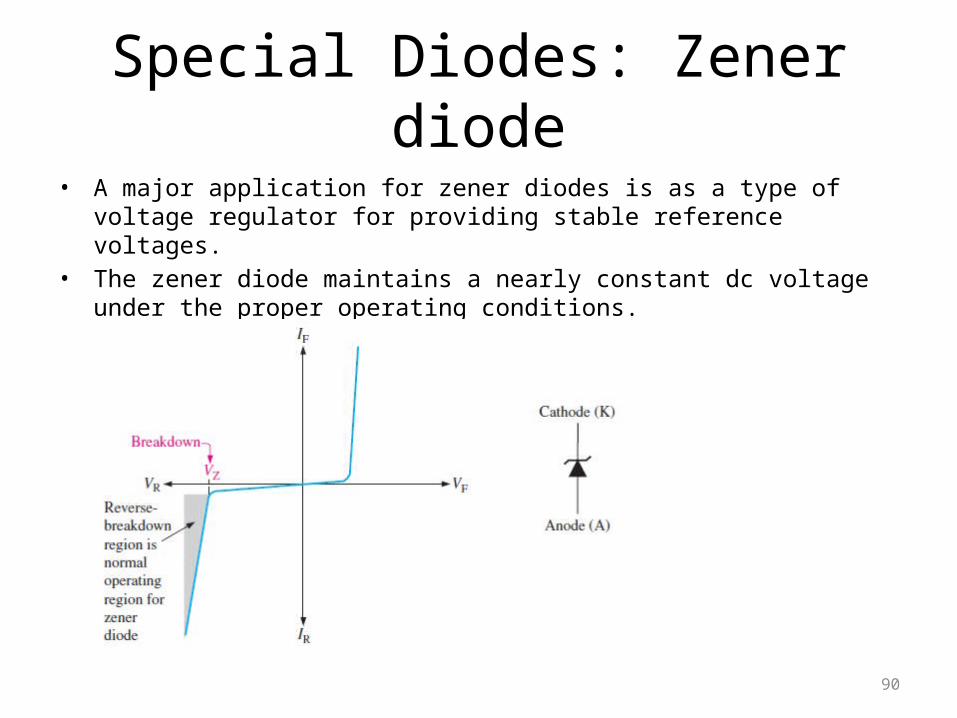
Special Diodes: Zener diode
• A major application for zener diodes is as a type of voltage regulator for providing stable reference voltages.
• The zener diode maintains a nearly constant dc voltage under the proper operating conditions.
90
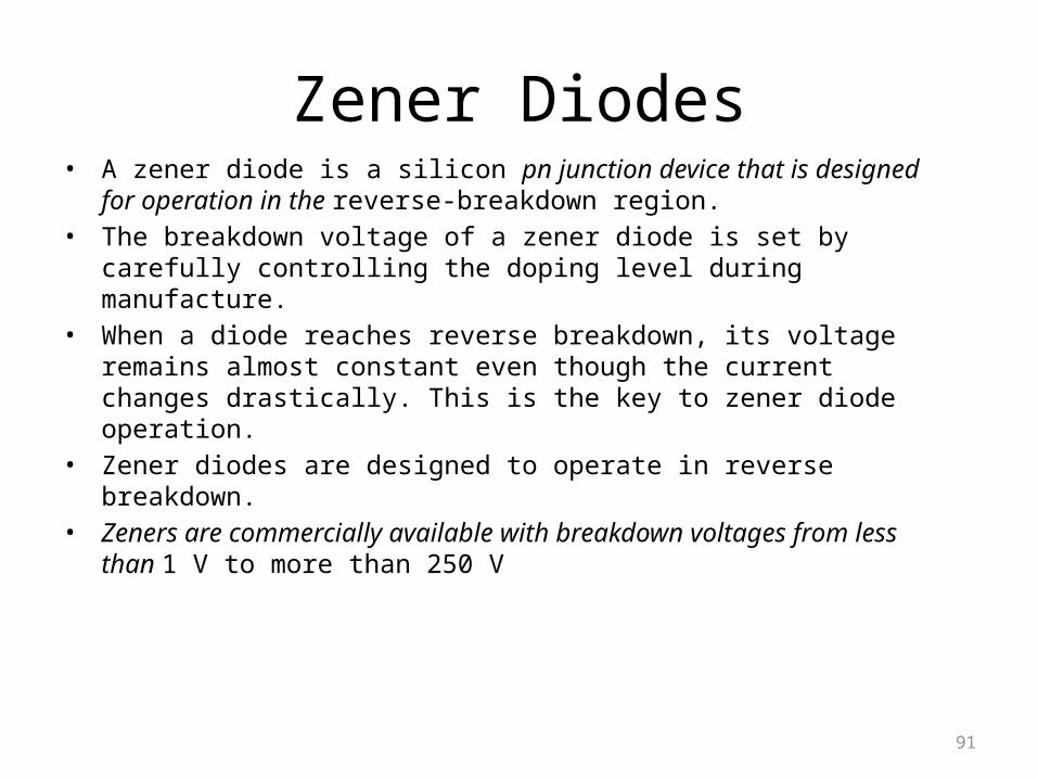
Zener Diodes• A zener diode is a silicon pn junction device that is designed
for operation in the reverse-breakdown region. • The breakdown voltage of a zener diode is set by
carefully controlling the doping level during manufacture.
• When a diode reaches reverse breakdown, its voltage remains almost constant even though the current changes drastically. This is the key to zener diode operation.
• Zener diodes are designed to operate in reverse breakdown.
• Zeners are commercially available with breakdown voltages from less than 1 V to more than 250 V
91
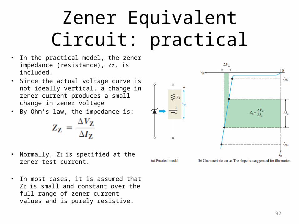
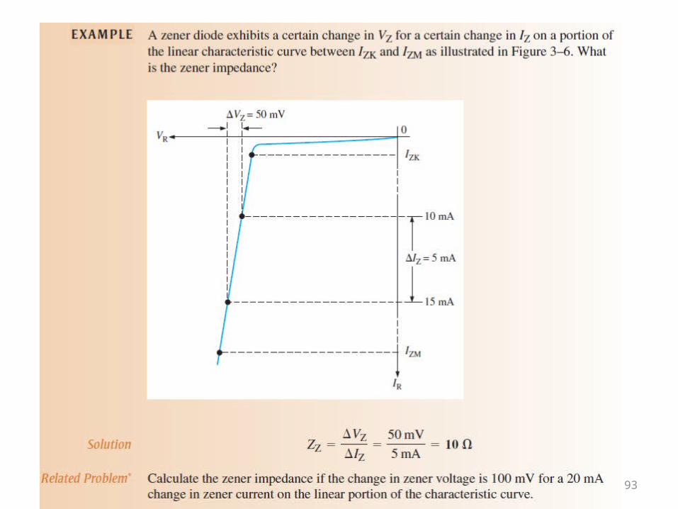
Zener Equivalent Circuit: practical
• In the practical model, the zener impedance (resistance), ZZ, is included.
• Since the actual voltage curve is not ideally vertical, a change in zener current produces a small change in zener voltage
• By Ohm’s law, the impedance is:
• Normally, ZZ is specified at the zener test current.
• In most cases, it is assumed that ZZ is small and constant over the full range of zener current values and is purely resistive.
92
93
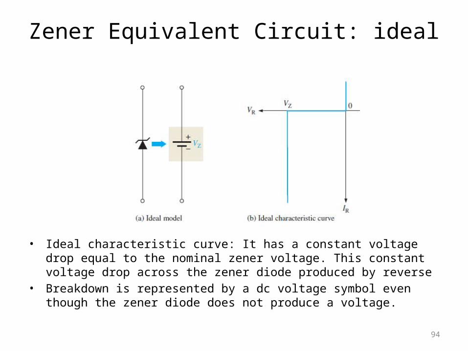
Zener Equivalent Circuit: ideal
• Ideal characteristic curve: It has a constant voltage drop equal to the nominal zener voltage. This constant voltage drop across the zener diode produced by reverse
• Breakdown is represented by a dc voltage symbol even though the zener diode does not produce a voltage.
94
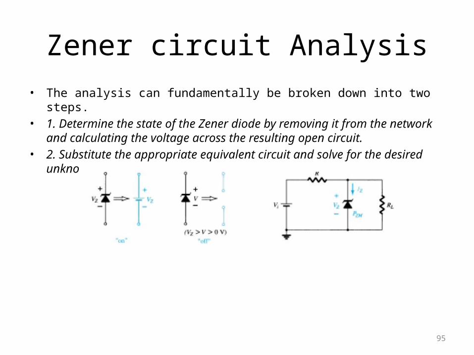
Zener circuit Analysis• The analysis can fundamentally be broken down into two
steps.• 1. Determine the state of the Zener diode by removing it from the network
and calculating the voltage across the resulting open circuit.• 2. Substitute the appropriate equivalent circuit and solve for the desired
unknowns.
95
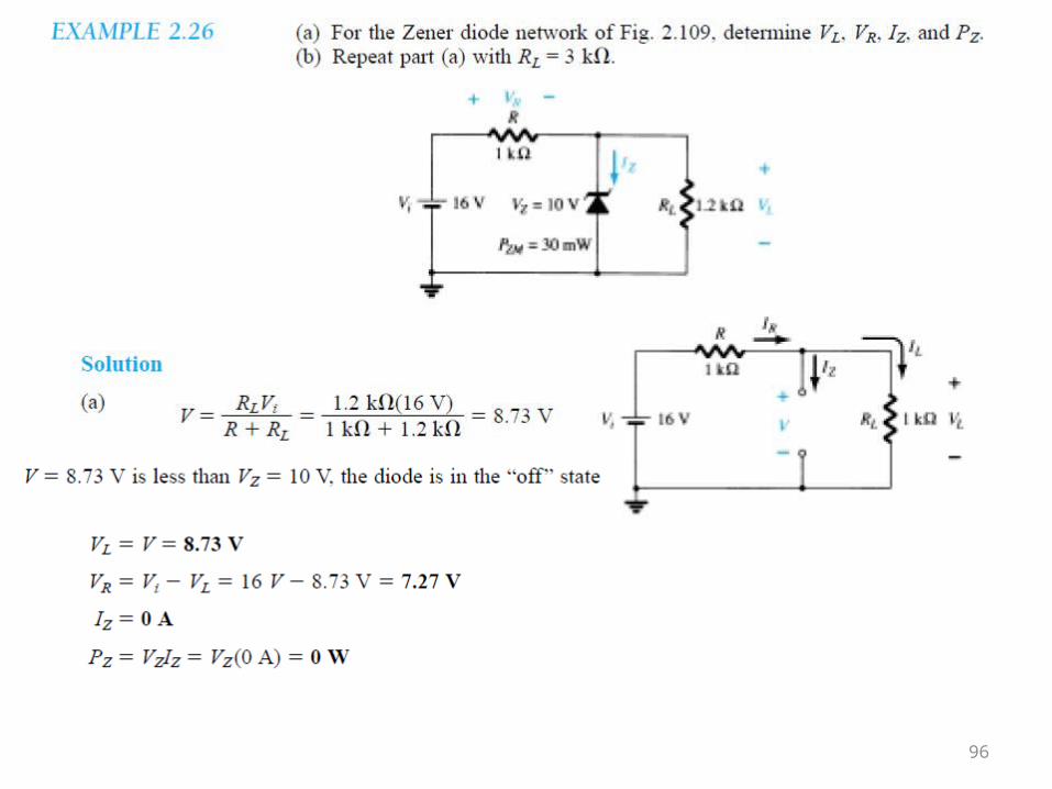
96
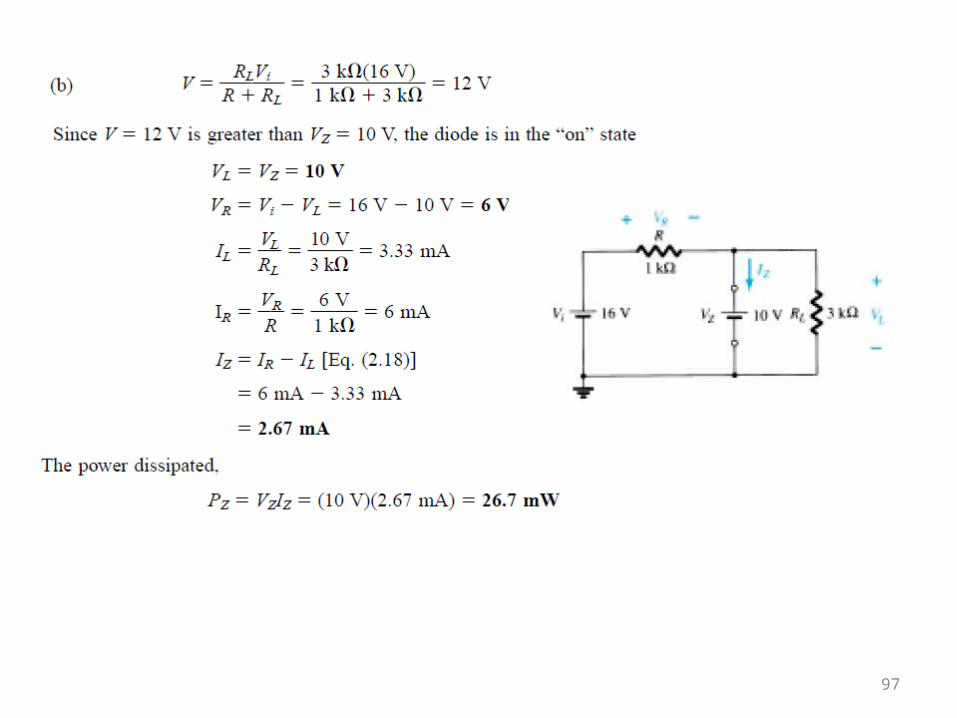
97
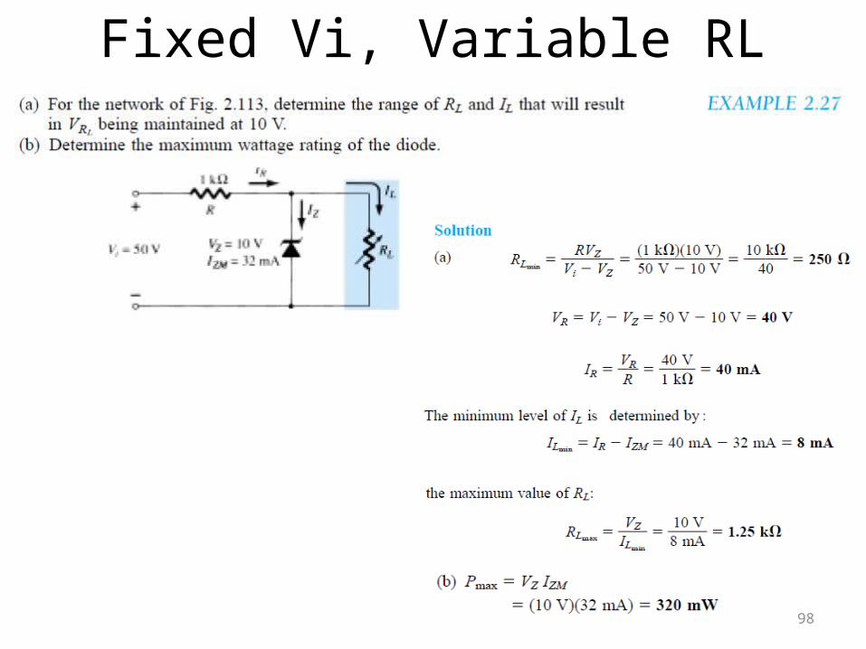
Fixed Vi, Variable RL
98
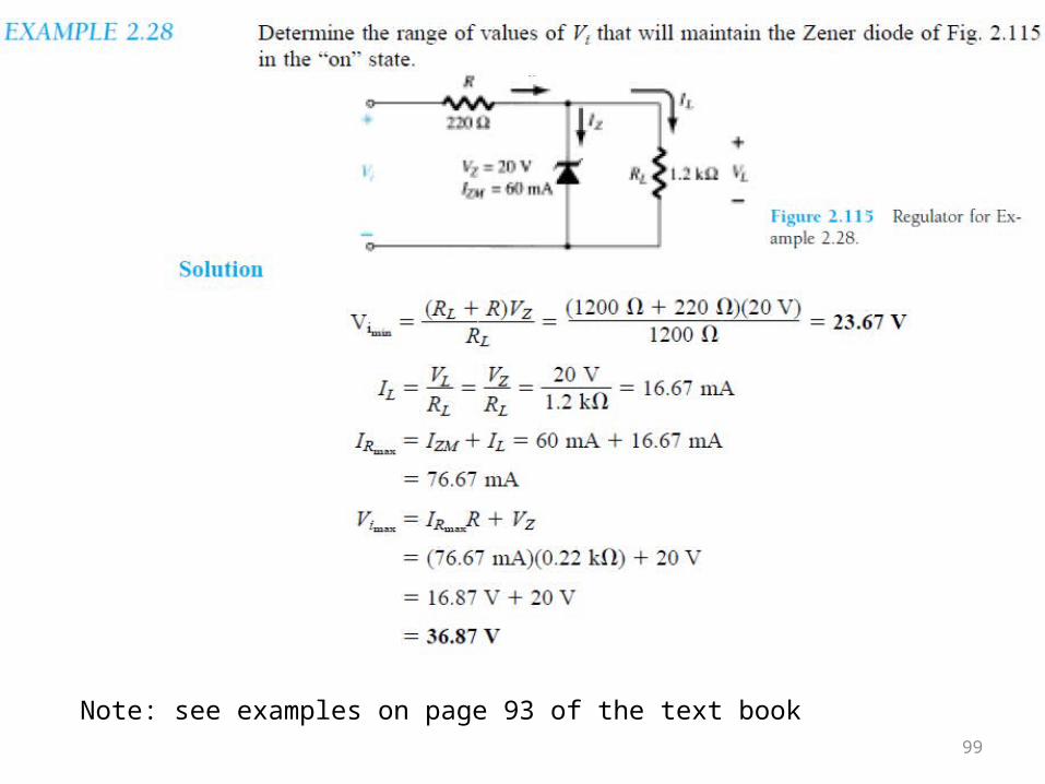
99Note: see examples on page 93 of the text book
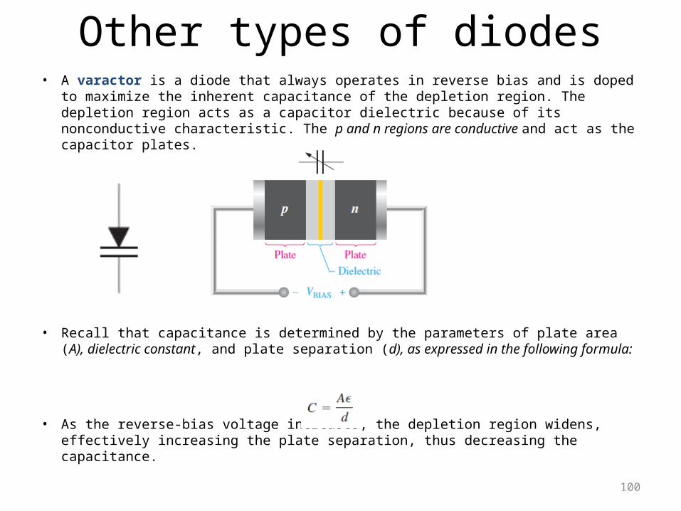
Other types of diodes• A varactor is a diode that always operates in reverse bias and is doped
to maximize the inherent capacitance of the depletion region. The depletion region acts as a capacitor dielectric because of its nonconductive characteristic. The p and n regions are conductive and act as the capacitor plates.
• Recall that capacitance is determined by the parameters of plate area (A), dielectric constant, and plate separation (d), as expressed in the following formula:
• As the reverse-bias voltage increases, the depletion region widens, effectively increasing the plate separation, thus decreasing the capacitance.
100
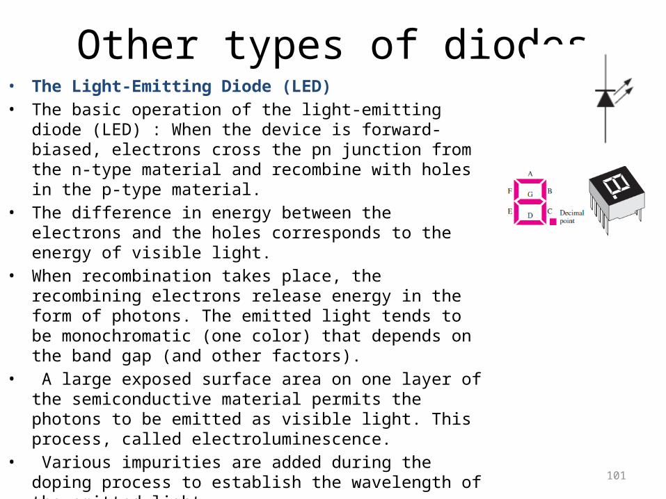
• The Light-Emitting Diode (LED)• The basic operation of the light-emitting
diode (LED) : When the device is forward-biased, electrons cross the pn junction from the n-type material and recombine with holes in the p-type material.
• The difference in energy between the electrons and the holes corresponds to the energy of visible light.
• When recombination takes place, the recombining electrons release energy in the form of photons. The emitted light tends to be monochromatic (one color) that depends on the band gap (and other factors).
• A large exposed surface area on one layer of the semiconductive material permits the photons to be emitted as visible light. This process, called electroluminescence.
• Various impurities are added during the doping process to establish the wavelength of the emitted light.
• Some LEDs emit photons that are not part of the visible spectrum but have longer wavelengths and are in the infrared (IR) portion of the spectrum.
Other types of diodes
101
102
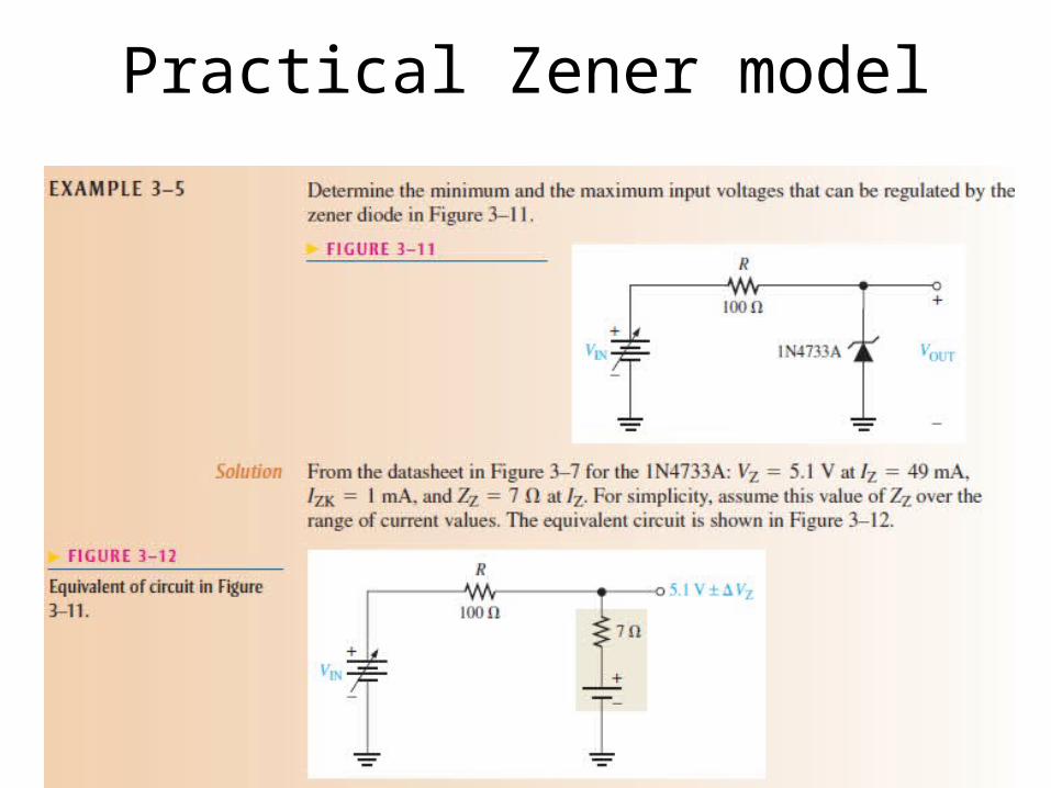
Practical Zener model
103
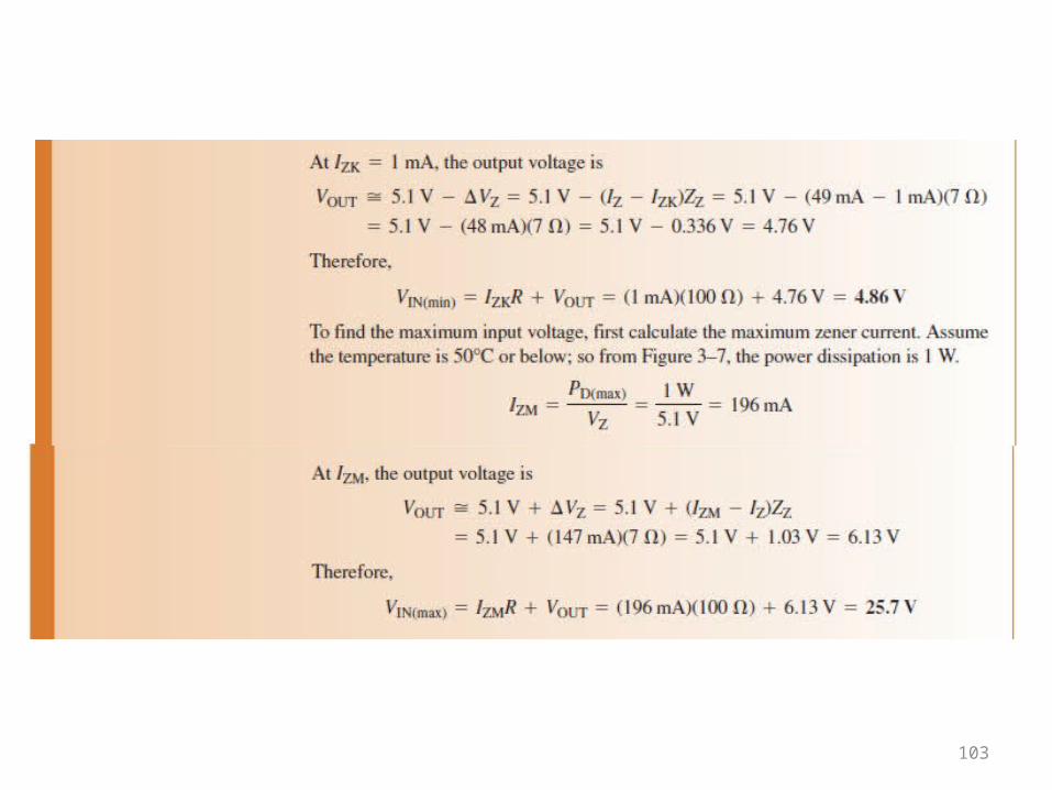
Back to zener diodes
104
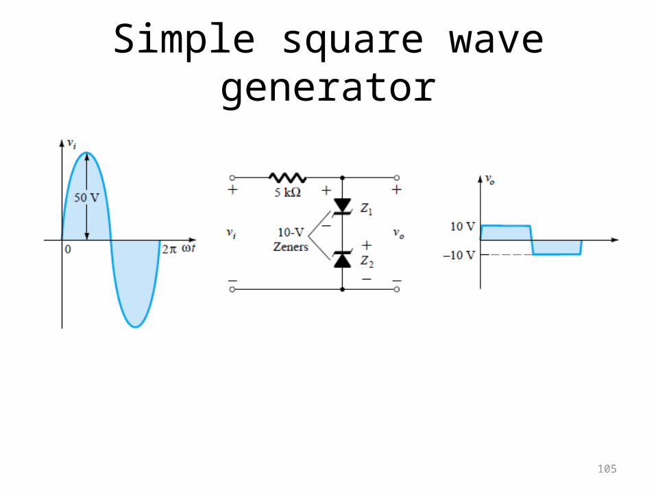
Simple square wave generator
105
Chapter 3
Bipolar Junction Transistors
106
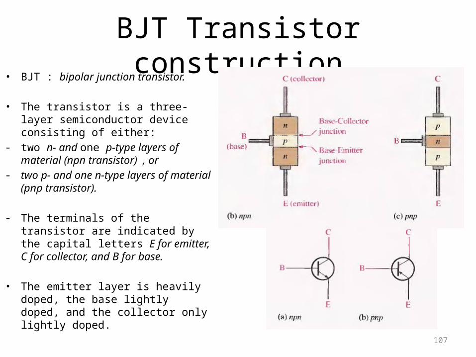
BJT Transistor construction• BJT : bipolar junction transistor.
• The transistor is a three-layer semiconductor device consisting of either:
- two n- and one p-type layers of material (npn transistor) , or
- two p- and one n-type layers of material (pnp transistor).
- The terminals of the transistor are indicated by the capital letters E for emitter, C for collector, and B for base.
• The emitter layer is heavily doped, the base lightly doped, and the collector only lightly doped.
107
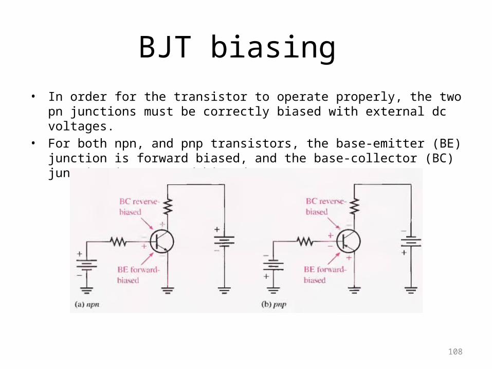
BJT biasing • In order for the transistor to operate properly, the two
pn junctions must be correctly biased with external dc voltages.
• For both npn, and pnp transistors, the base-emitter (BE) junction is forward biased, and the base-collector (BC) junction is reversed biased.
108
109
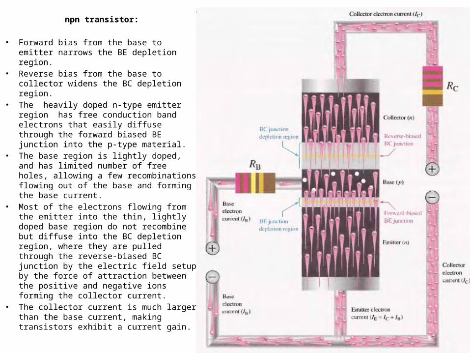
npn transistor:
• Forward bias from the base to emitter narrows the BE depletion region.
• Reverse bias from the base to collector widens the BC depletion region.
• The heavily doped n-type emitter region has free conduction band electrons that easily diffuse through the forward biased BE junction into the p-type material.
• The base region is lightly doped, and has limited number of free holes, allowing a few recombinations flowing out of the base and forming the base current.
• Most of the electrons flowing from the emitter into the thin, lightly doped base region do not recombine but diffuse into the BC depletion region, where they are pulled through the reverse-biased BC junction by the electric field setup by the force of attraction between the positive and negative ions forming the collector current.
• The collector current is much larger than the base current, making transistors exhibit a current gain.
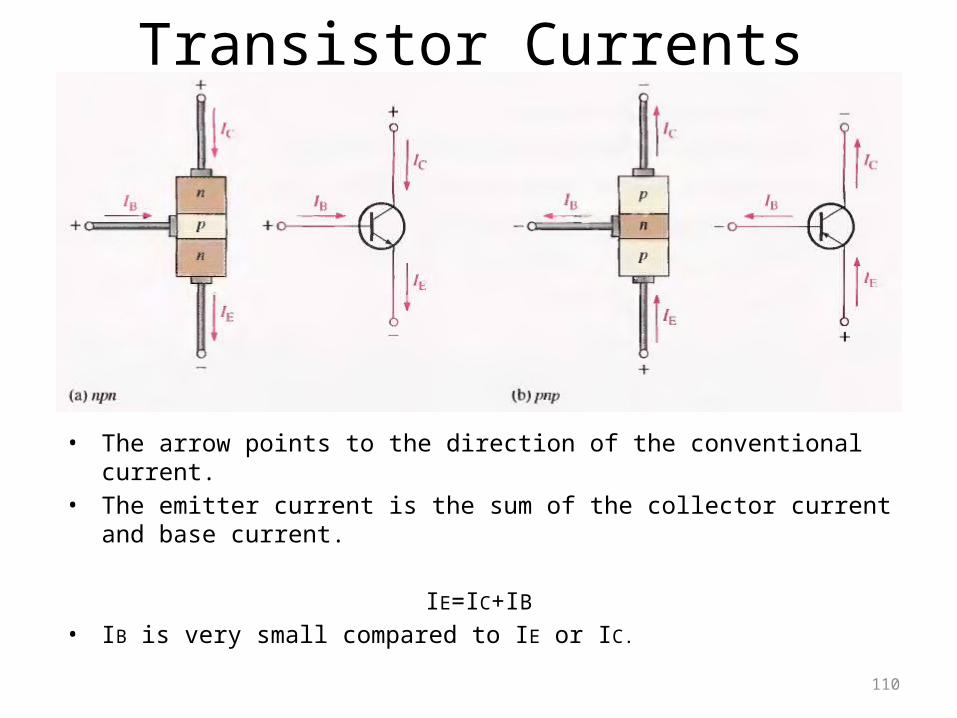
Transistor Currents
• The arrow points to the direction of the conventional current.
• The emitter current is the sum of the collector current and base current.
IE=IC+IB• IB is very small compared to IE or IC.
110
Transistor characteristics and parameters
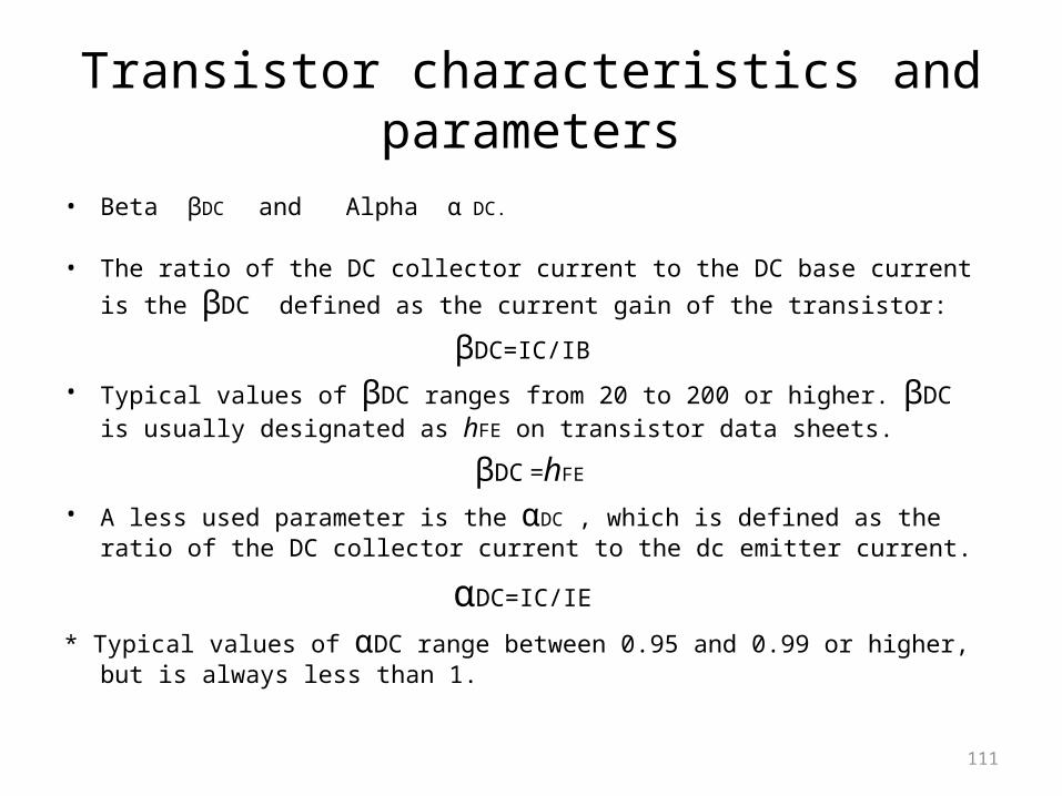
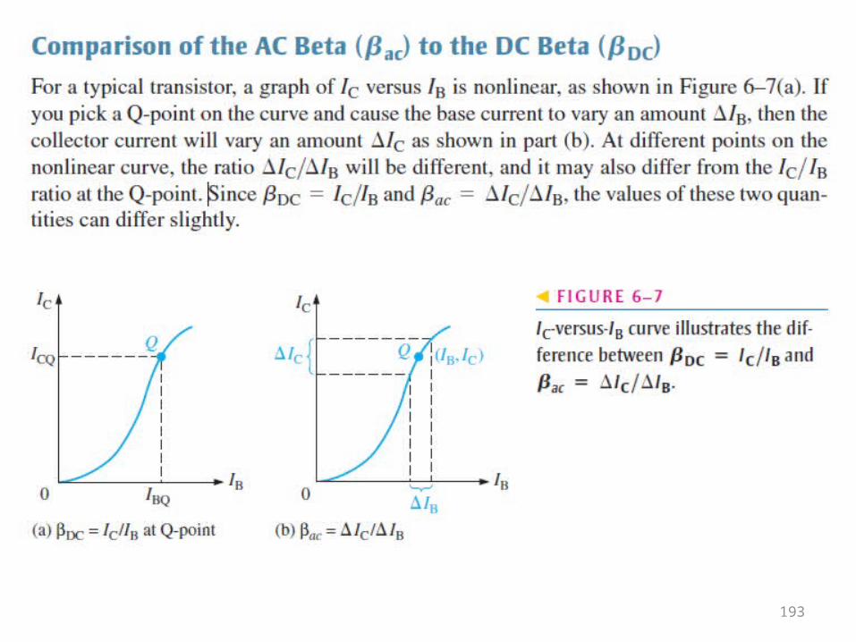
• Beta βDC and Alpha α DC.
• The ratio of the DC collector current to the DC base current is the βDC defined as the current gain of the transistor:
βDC=IC/IB• Typical values of βDC ranges from 20 to 200 or higher. βDC
is usually designated as hFE on transistor data sheets. βDC =hFE
• A less used parameter is the αDC , which is defined as the ratio of the DC collector current to the dc emitter current.
αDC=IC/IE* Typical values of αDC range between 0.95 and 0.99 or higher,
but is always less than 1.
111
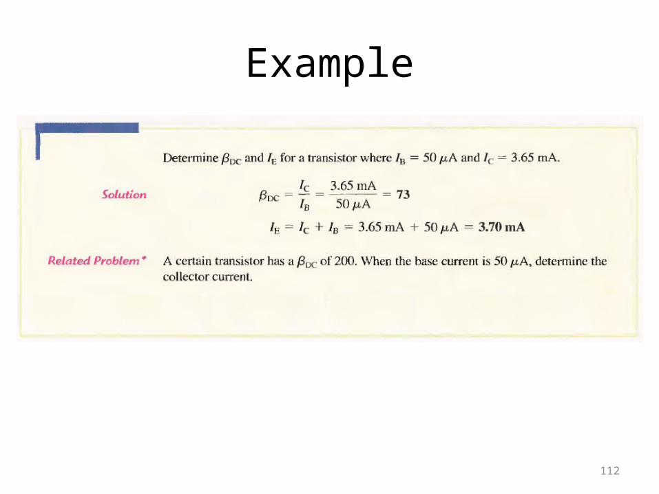
Example
112
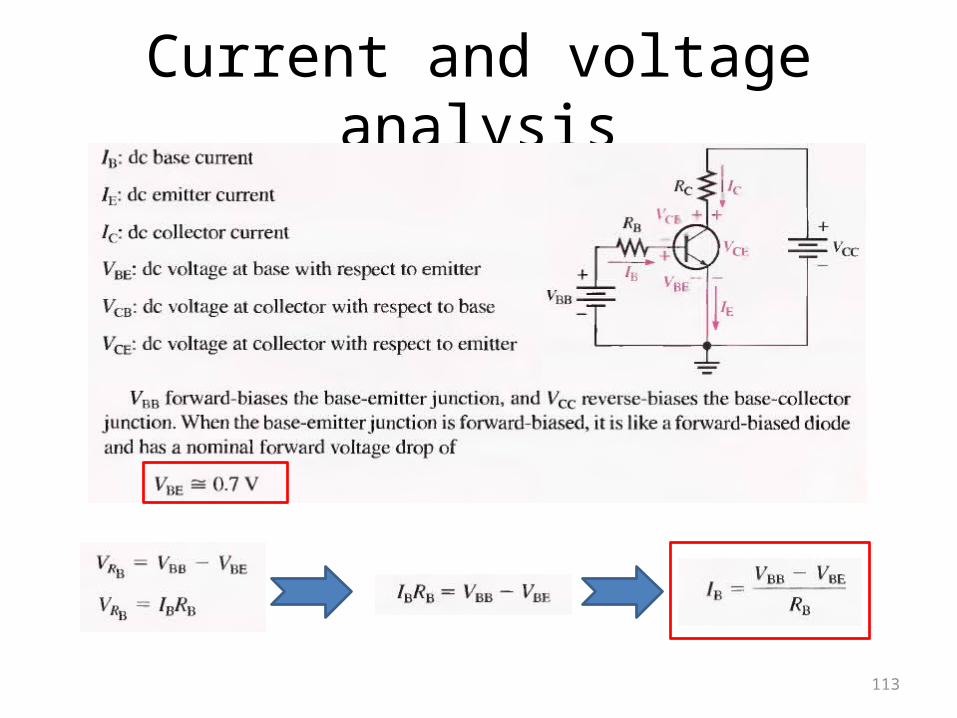
Current and voltage analysis
113
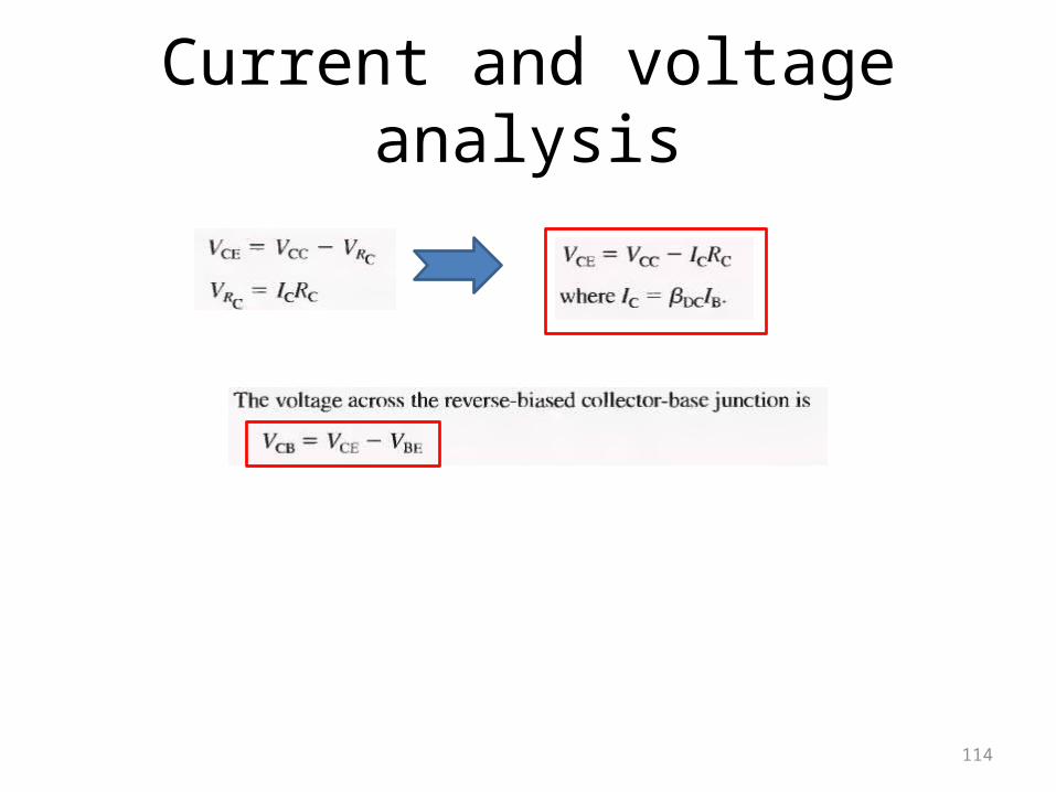
Current and voltage analysis
114
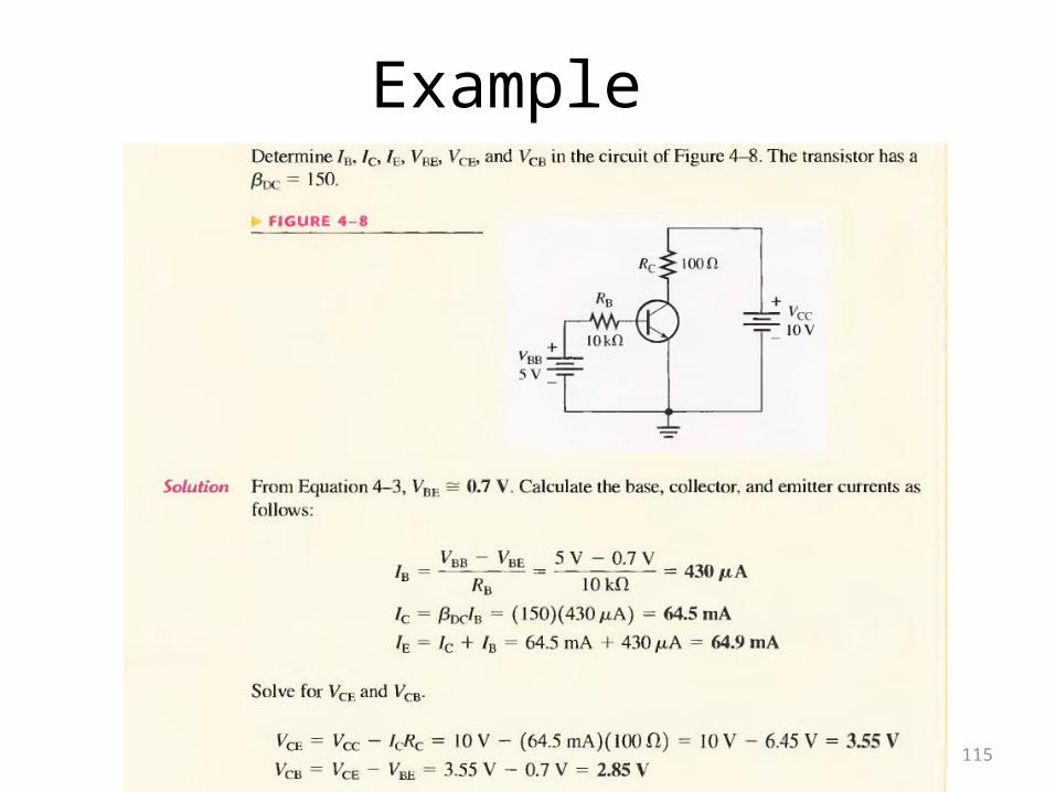
Example
115
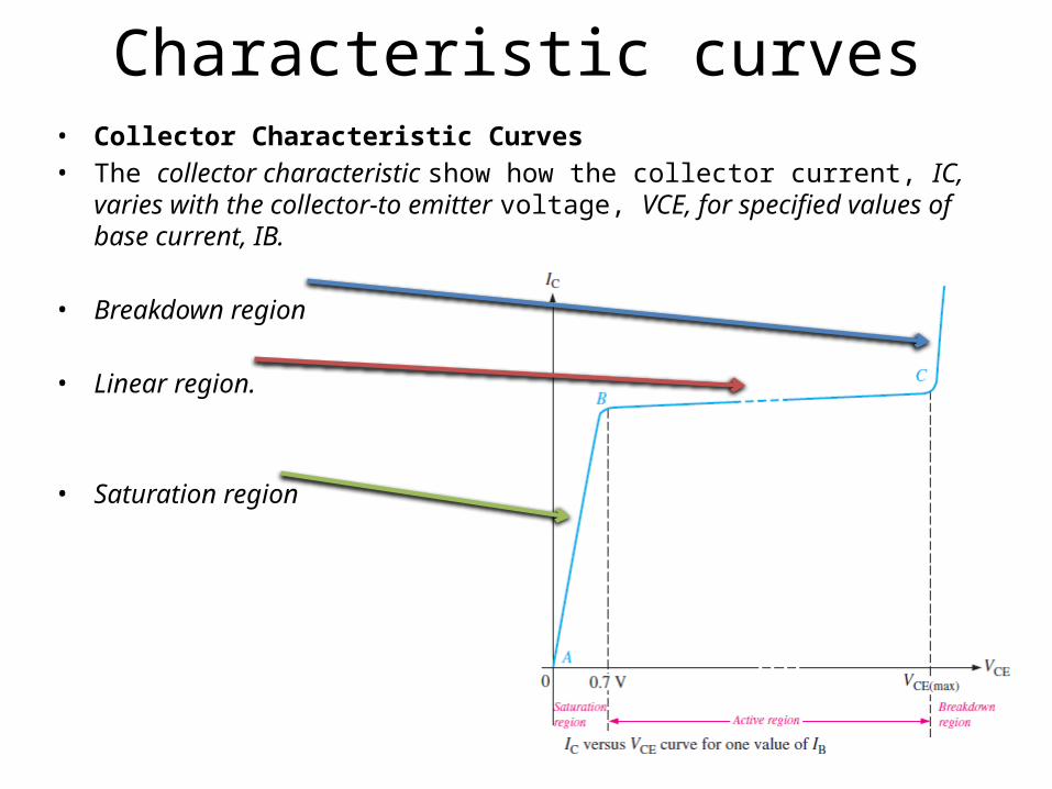
Characteristic curves• Collector Characteristic Curves• The collector characteristic show how the collector current, IC,
varies with the collector-to emitter voltage, VCE, for specified values of base current, IB.
• Breakdown region
• Linear region.
• Saturation region
116
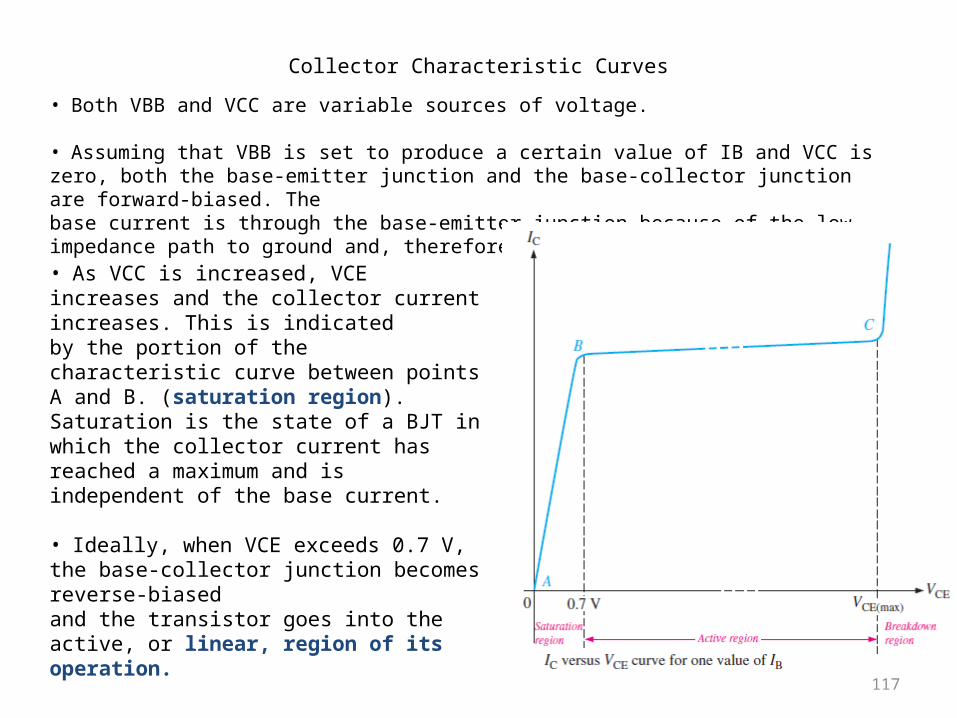
Collector Characteristic Curves
117
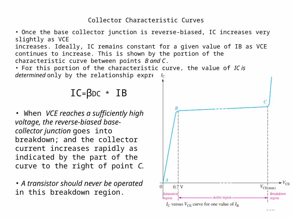
• Both VBB and VCC are variable sources of voltage. • Assuming that VBB is set to produce a certain value of IB and VCC is zero, both the base-emitter junction and the base-collector junction are forward-biased. Thebase current is through the base-emitter junction because of the low impedance path to ground and, therefore, IC is zero.• As VCC is increased, VCE increases and the collector current increases. This is indicatedby the portion of the characteristic curve between points A and B. (saturation region).Saturation is the state of a BJT in which the collector current has reached a maximum and is independent of the base current.
• Ideally, when VCE exceeds 0.7 V, the base-collector junction becomes reverse-biasedand the transistor goes into the active, or linear, region of its operation.
Collector Characteristic Curves
118
• Once the base collector junction is reverse-biased, IC increases very slightly as VCEincreases. Ideally, IC remains constant for a given value of IB as VCE continues to increase. This is shown by the portion of the characteristic curve between points B and C. • For this portion of the characteristic curve, the value of IC is determined only by the relationship expressed as:
• When VCE reaches a sufficiently high voltage, the reverse-biased base-collector junction goes into breakdown; and the collector current increases rapidly as indicated by the part of the curve to the right of point C.
• A transistor should never be operatedin this breakdown region.
IC=βDC * IB
Family of characteristic curves
119
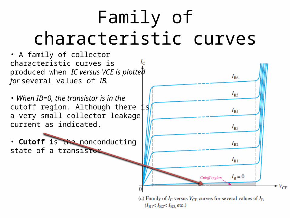
• A family of collector characteristic curves is produced when IC versus VCE is plotted for several values of IB.
• When IB=0, the transistor is in thecutoff region. Although there is a very small collector leakage current as indicated.
• Cutoff is the nonconducting state of a transistor.
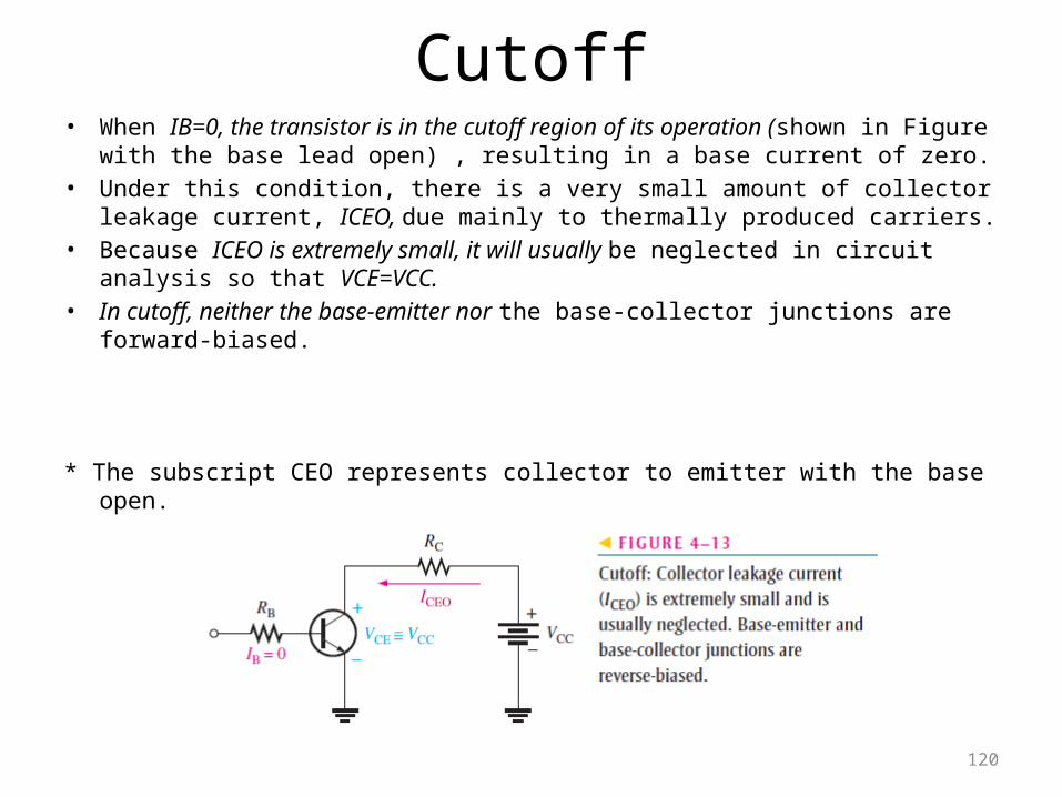
Cutoff• When IB=0, the transistor is in the cutoff region of its operation (shown in Figure
with the base lead open) , resulting in a base current of zero. • Under this condition, there is a very small amount of collector
leakage current, ICEO, due mainly to thermally produced carriers. • Because ICEO is extremely small, it will usually be neglected in circuit
analysis so that VCE=VCC. • In cutoff, neither the base-emitter nor the base-collector junctions are
forward-biased.
* The subscript CEO represents collector to emitter with the base open.
120
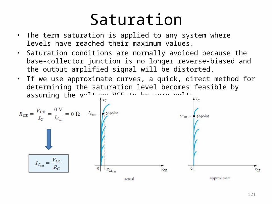
Saturation• The term saturation is applied to any system where
levels have reached their maximum values.• Saturation conditions are normally avoided because the
base–collector junction is no longer reverse-biased and the output amplified signal will be distorted.
• If we use approximate curves, a quick, direct method for determining the saturation level becomes feasible by assuming the voltage VCE to be zero volts.
121
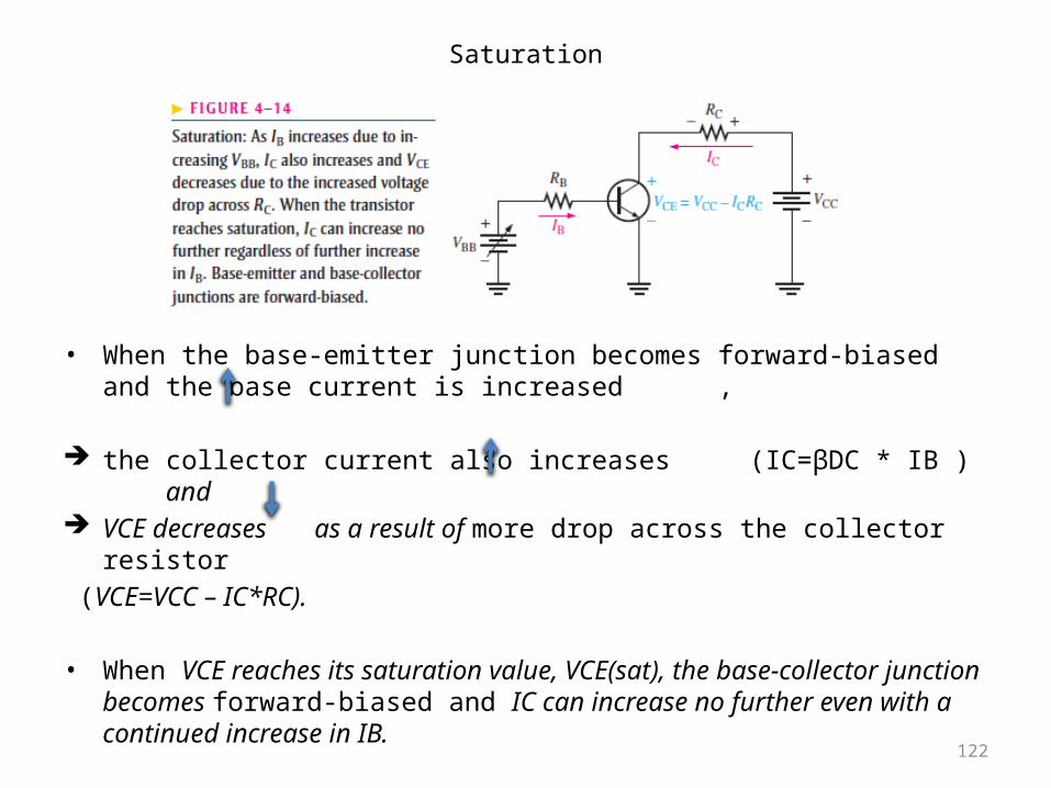
Saturation
• When the base-emitter junction becomes forward-biased and the base current is increased ,
the collector current also increases (IC=βDC * IB ) and
VCE decreases as a result of more drop across the collector resistor
(VCE=VCC – IC*RC).
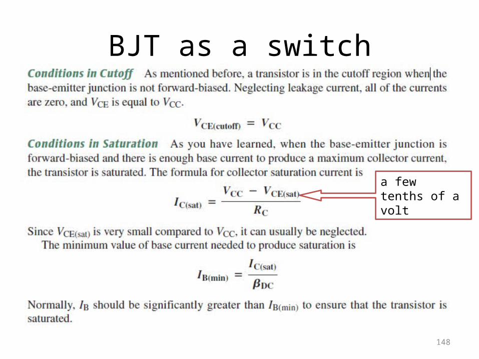
• When VCE reaches its saturation value, VCE(sat), the base-collector junction becomes forward-biased and IC can increase no further even with a continued increase in IB.
• At the point of saturation, the relation (IC=βDC * IB ) is no longer valid.
• VCE(sat) for a transistoroccurs somewhere below the knee of the collector curves, and it is usually only a few tenths of a volt.
122
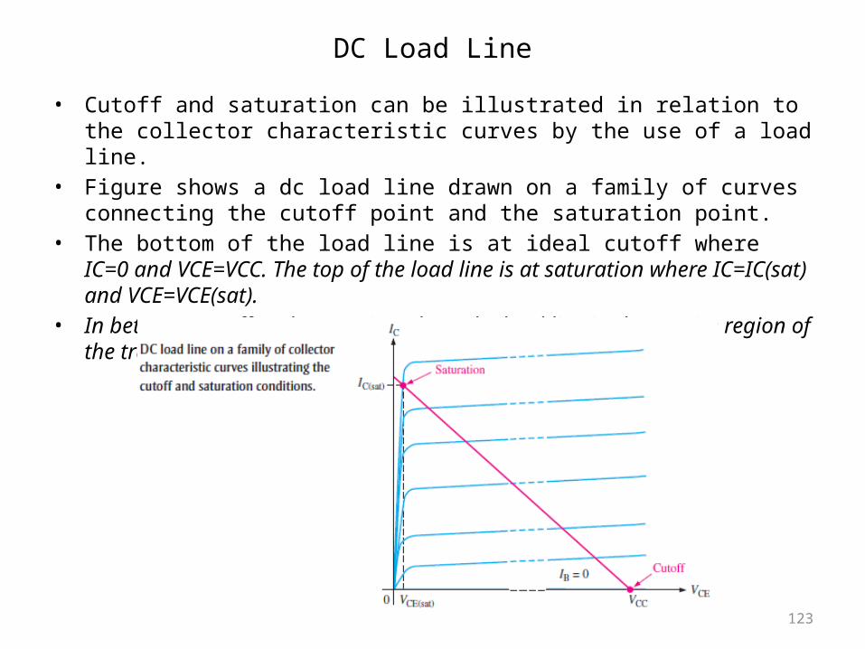
DC Load Line• Cutoff and saturation can be illustrated in relation to
the collector characteristic curves by the use of a load line.
• Figure shows a dc load line drawn on a family of curves connecting the cutoff point and the saturation point.
• The bottom of the load line is at ideal cutoff where IC=0 and VCE=VCC. The top of the load line is at saturation where IC=IC(sat) and VCE=VCE(sat).
• In between cutoff and saturation along the load line is the active region of the transistor’s operation
123
cutoff, saturation, and linear region
• Operation in the cutoff, saturation, and linear regions of the BJT characteristic are provided as follows:
• 1. Linear-region operation:- Base–emitter junction forward biased.- Base–collector junction reverse biased.
• 2. Cutoff-region operation:- Base–emitter junction reverse biased.
• 3. Saturation-region operation:- Base–emitter junction forward biased.- Base–collector junction forward biased.
124
125
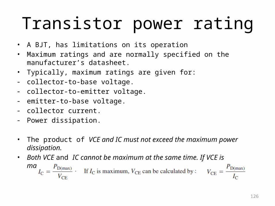
Transistor power rating• A BJT, has limitations on its operation• Maximum ratings and are normally specified on the
manufacturer’s datasheet.• Typically, maximum ratings are given for:- collector-to-base voltage.- collector-to-emitter voltage.- emitter-to-base voltage.- collector current.- Power dissipation.
• The product of VCE and IC must not exceed the maximum power dissipation.
• Both VCE and IC cannot be maximum at the same time. If VCE is maximum, IC can be calculated as
126
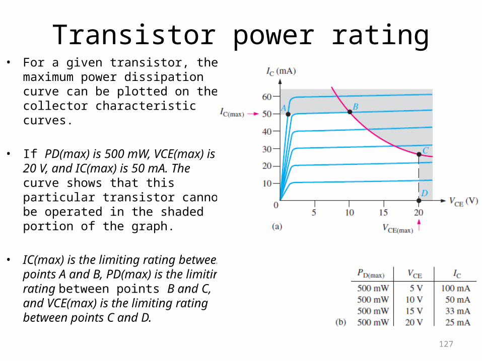
Transistor power rating• For a given transistor, the
maximum power dissipation curve can be plotted on the collector characteristic curves.
• If PD(max) is 500 mW, VCE(max) is 20 V, and IC(max) is 50 mA. The curve shows that this particular transistor cannot be operated in the shaded portion of the graph.
• IC(max) is the limiting rating between points A and B, PD(max) is the limiting rating between points B and C, and VCE(max) is the limiting rating between points C and D.
127
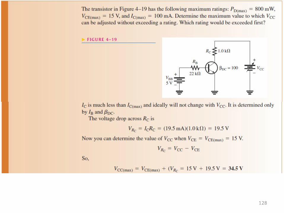
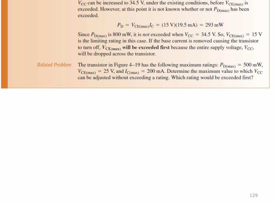
128
129

130
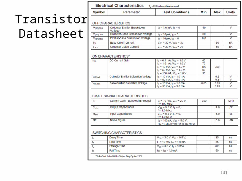
Transistor Datasheet
131
Transistor Datasheet
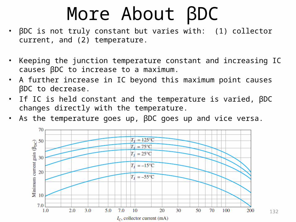
More About βDC • βDC is not truly constant but varies with: (1) collector
current, and (2) temperature.
• Keeping the junction temperature constant and increasing IC causes βDC to increase to a maximum.
• A further increase in IC beyond this maximum point causes βDC to decrease.
• If IC is held constant and the temperature is varied, βDC changes directly with the temperature.
• As the temperature goes up, βDC goes up and vice versa.
132
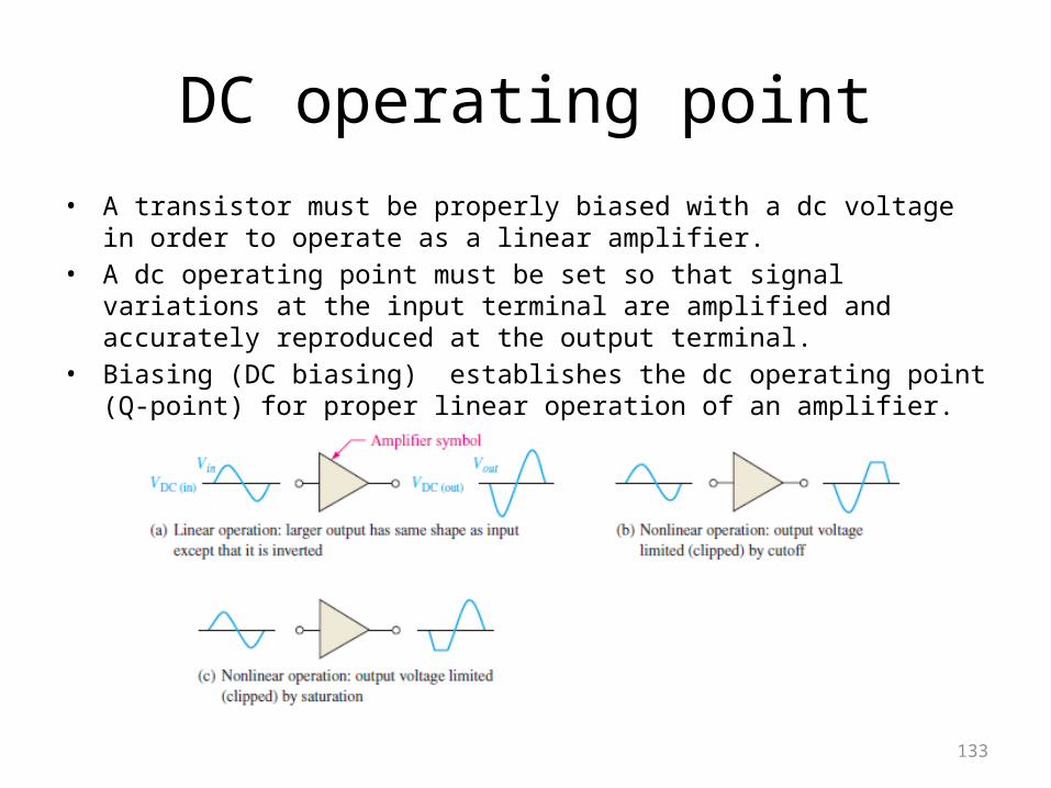
DC operating point• A transistor must be properly biased with a dc voltage
in order to operate as a linear amplifier. • A dc operating point must be set so that signal
variations at the input terminal are amplified and accurately reproduced at the output terminal.
• Biasing (DC biasing) establishes the dc operating point (Q-point) for proper linear operation of an amplifier.
133
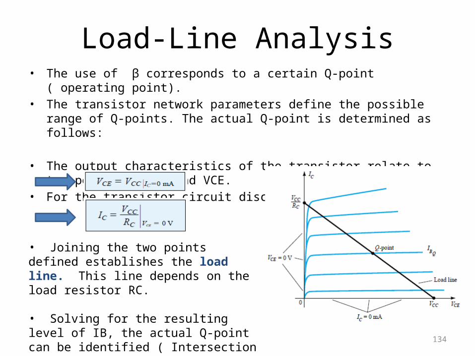
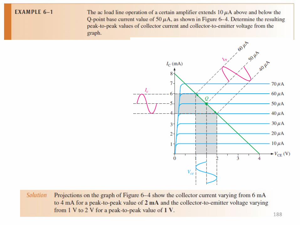
Load-Line Analysis• The use of β corresponds to a certain Q-point
( operating point).• The transistor network parameters define the possible
range of Q-points. The actual Q-point is determined as follows:
• The output characteristics of the transistor relate to two points: IC , and VCE.
• For the transistor circuit discussed earlier
134
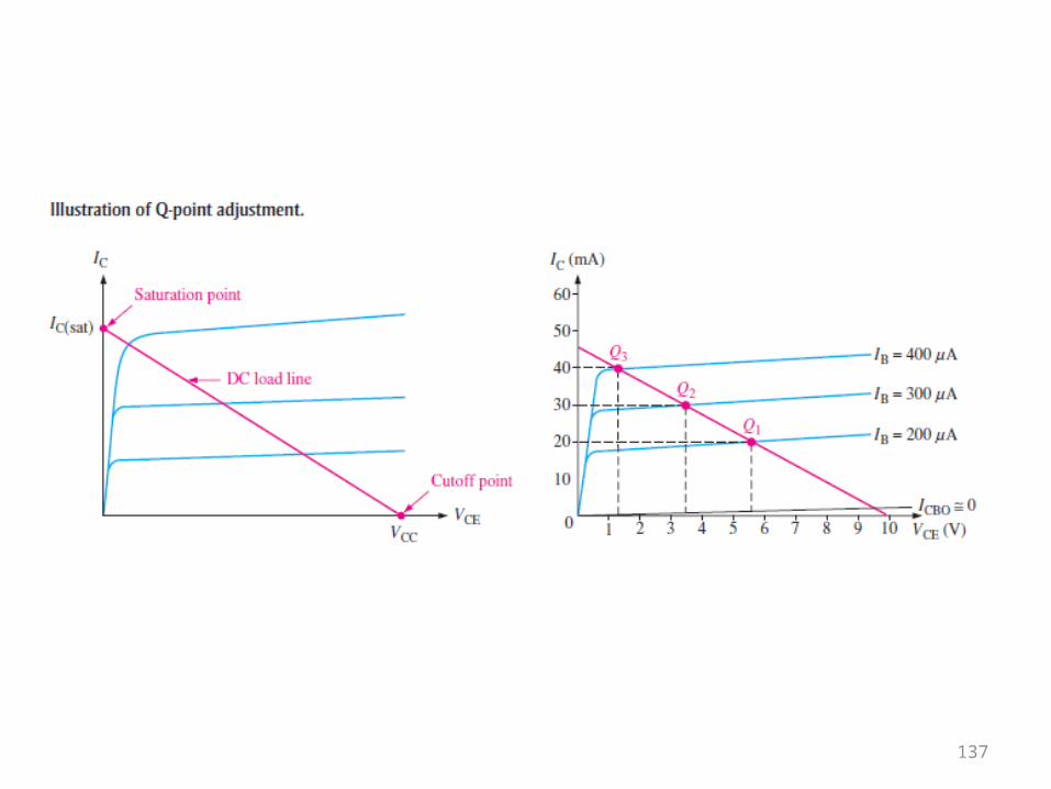
• Joining the two points defined establishes the load line. This line depends on the load resistor RC.
• Solving for the resulting level of IB, the actual Q-point can be identified ( Intersection of IB with the load line).
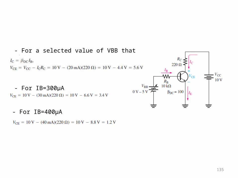
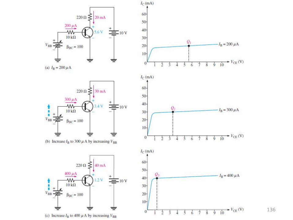
135
- For a selected value of VBB that gives IB=200μA
- For IB=300μA
- For IB=400μA
136
137
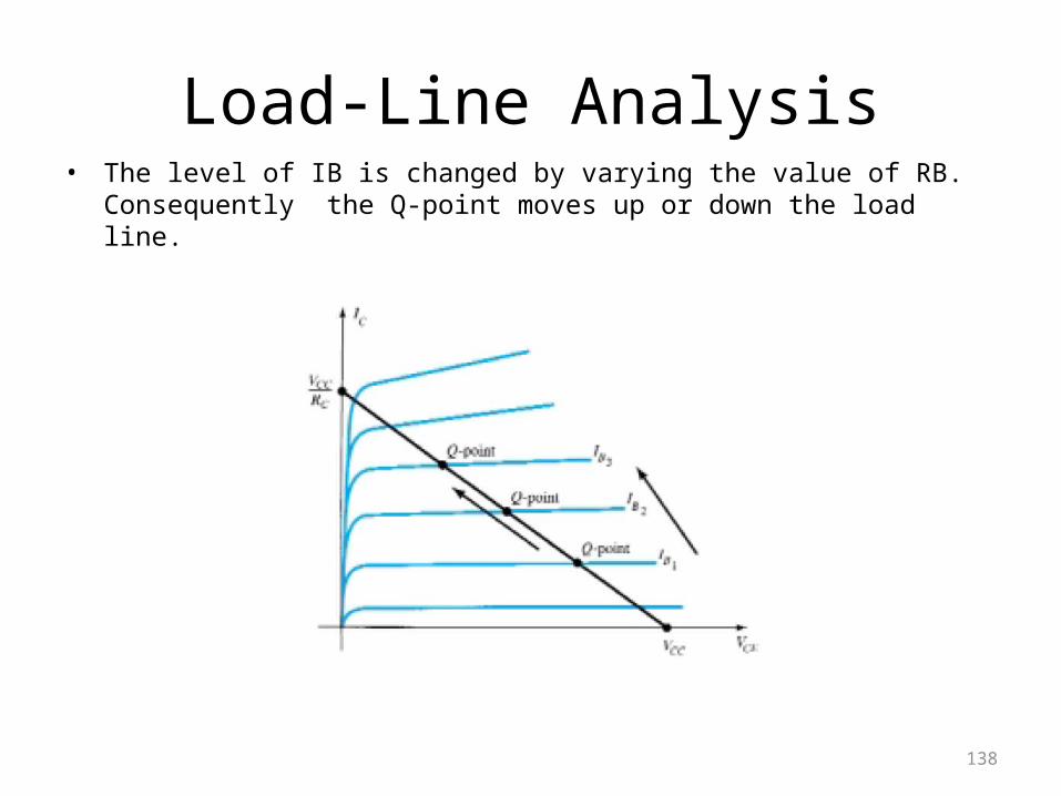
• The level of IB is changed by varying the value of RB. Consequently the Q-point moves up or down the load line.
138
Load-Line Analysis
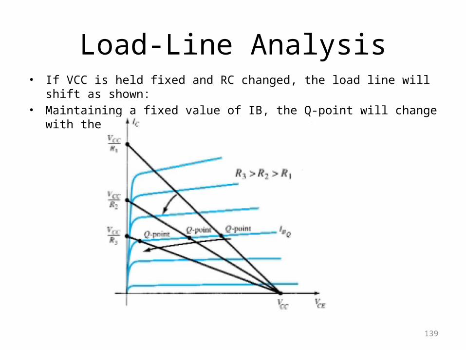
Load-Line Analysis• If VCC is held fixed and RC changed, the load line will
shift as shown:• Maintaining a fixed value of IB, the Q-point will change
with the new load line.
139
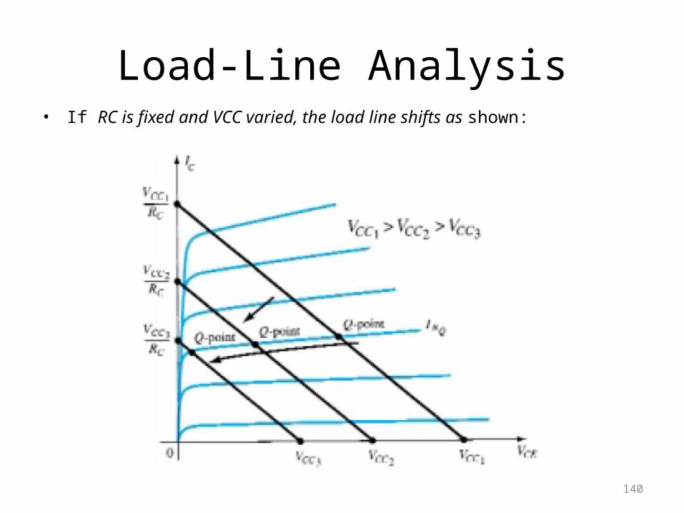
Load-Line Analysis• If RC is fixed and VCC varied, the load line shifts as shown:
140
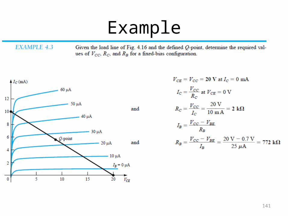
Example
141
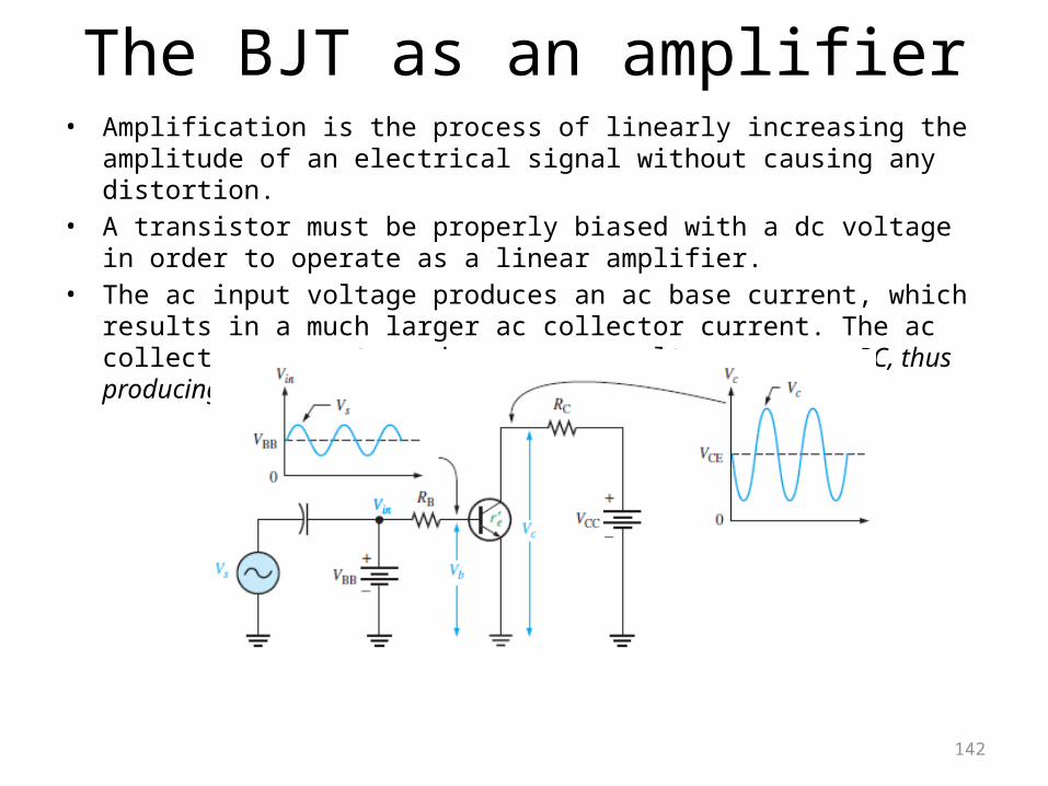
The BJT as an amplifier• Amplification is the process of linearly increasing the
amplitude of an electrical signal without causing any distortion.
• A transistor must be properly biased with a dc voltage in order to operate as a linear amplifier.
• The ac input voltage produces an ac base current, which results in a much larger ac collector current. The ac collector current produces an ac voltage across RC, thus producing an amplified, but inverted waveform.
142
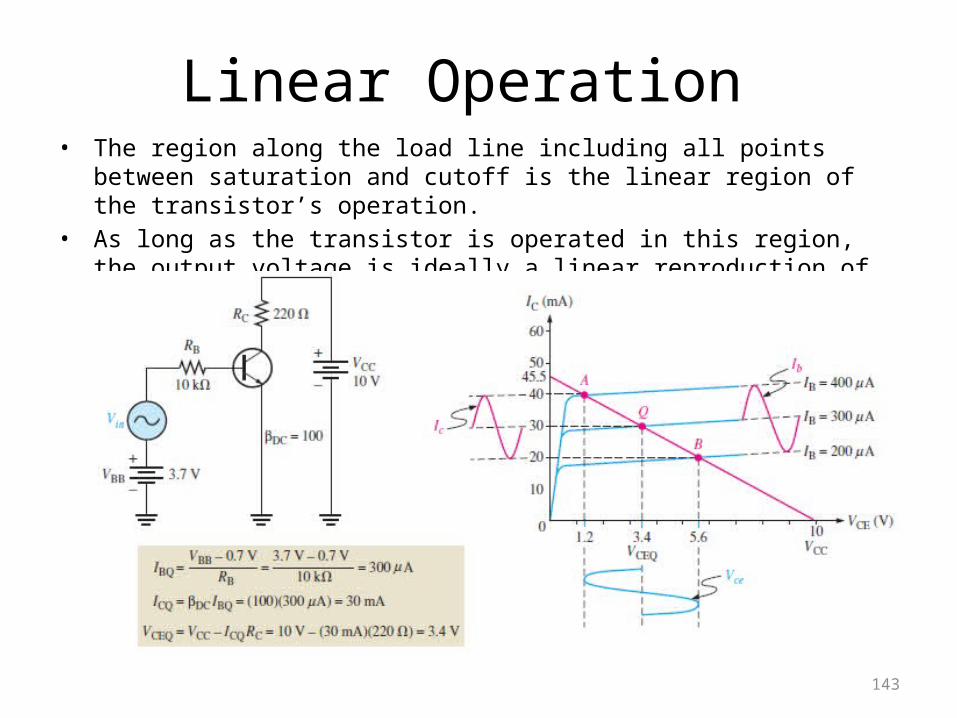
Linear Operation • The region along the load line including all points
between saturation and cutoff is the linear region of the transistor’s operation.
• As long as the transistor is operated in this region, the output voltage is ideally a linear reproduction of the input.
143
144
145
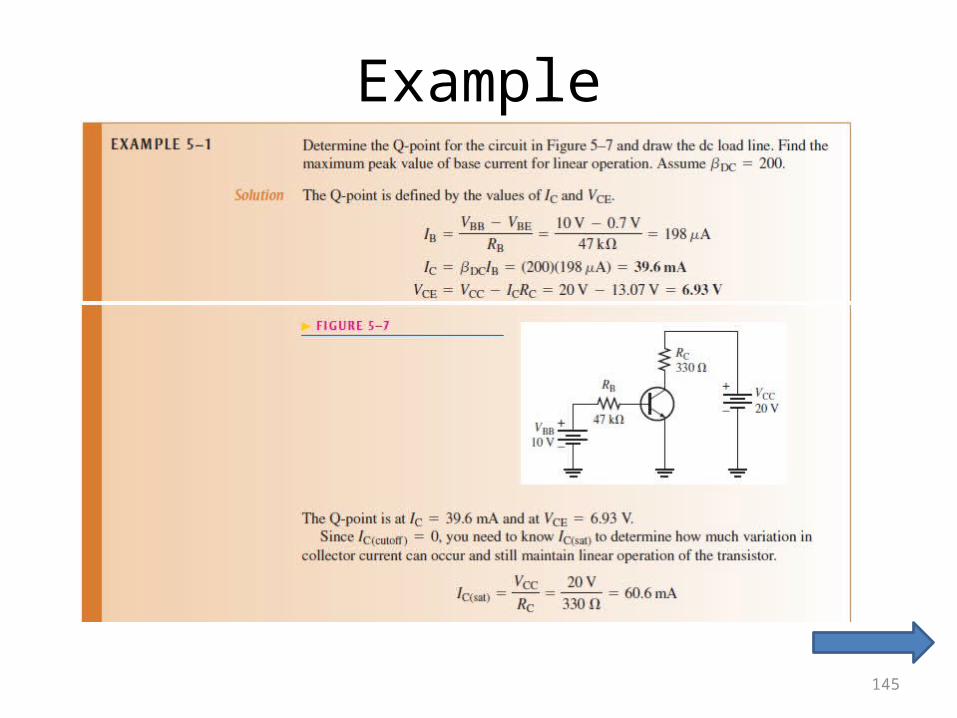
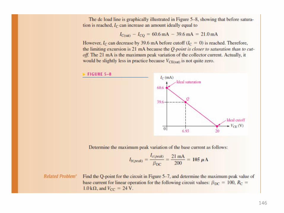
Example
146
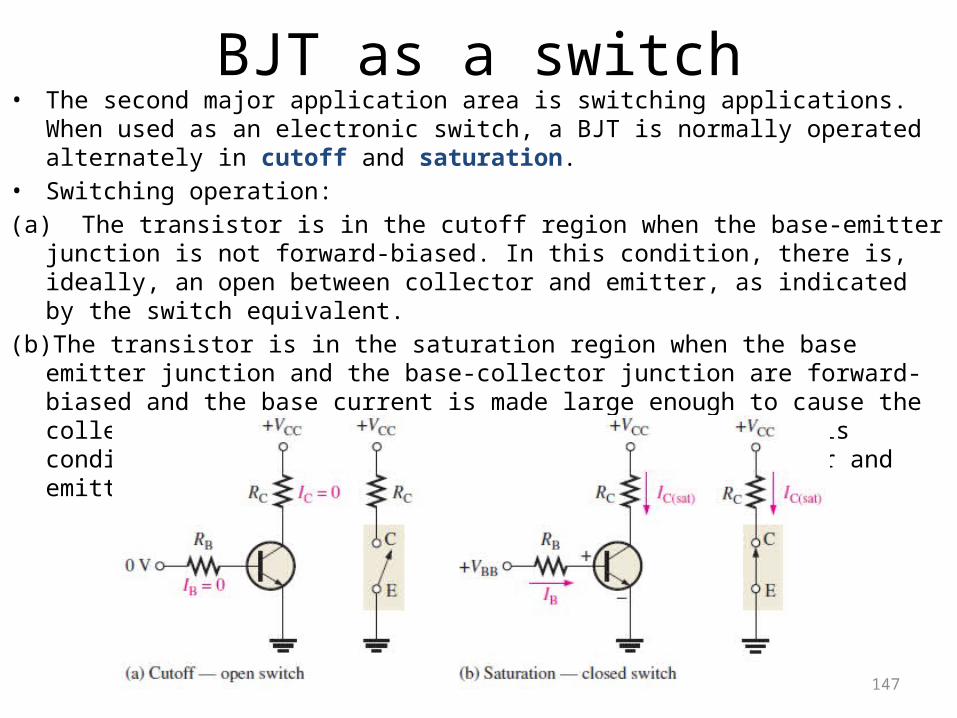
BJT as a switch• The second major application area is switching applications.
When used as an electronic switch, a BJT is normally operated alternately in cutoff and saturation.
• Switching operation:(a) The transistor is in the cutoff region when the base-emitter
junction is not forward-biased. In this condition, there is, ideally, an open between collector and emitter, as indicated by the switch equivalent.
(b)The transistor is in the saturation region when the base emitter junction and the base-collector junction are forward-biased and the base current is made large enough to cause the collector current to reach its saturation value. In this condition, there is, ideally, a short between collector and emitter, as indicated by the switch equivalent.
147
BJT as a switch
148
a few tenths of avolt
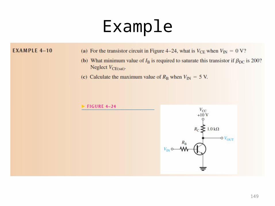
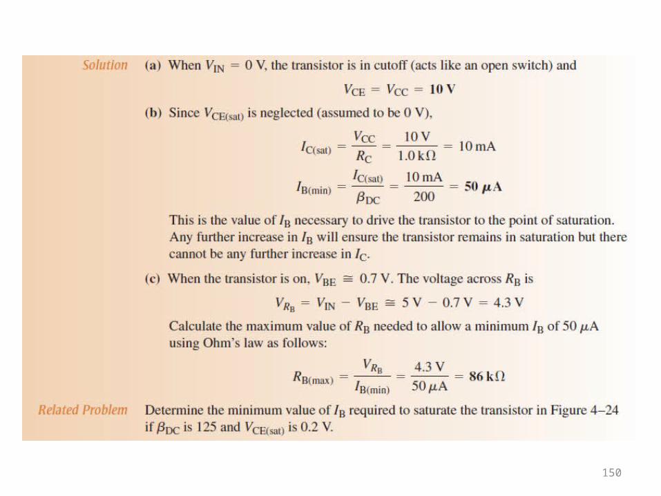
Example
149
150
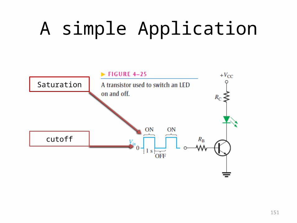
A simple Application
151
Saturation
cutoff
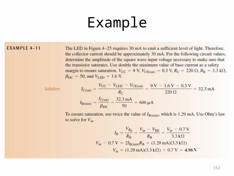
Example
152
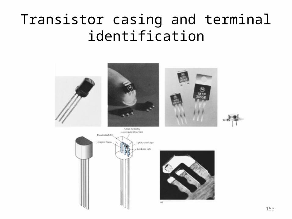
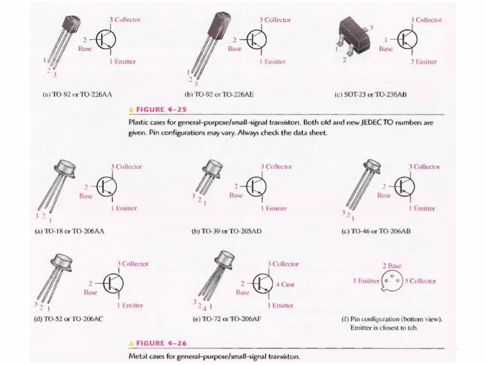
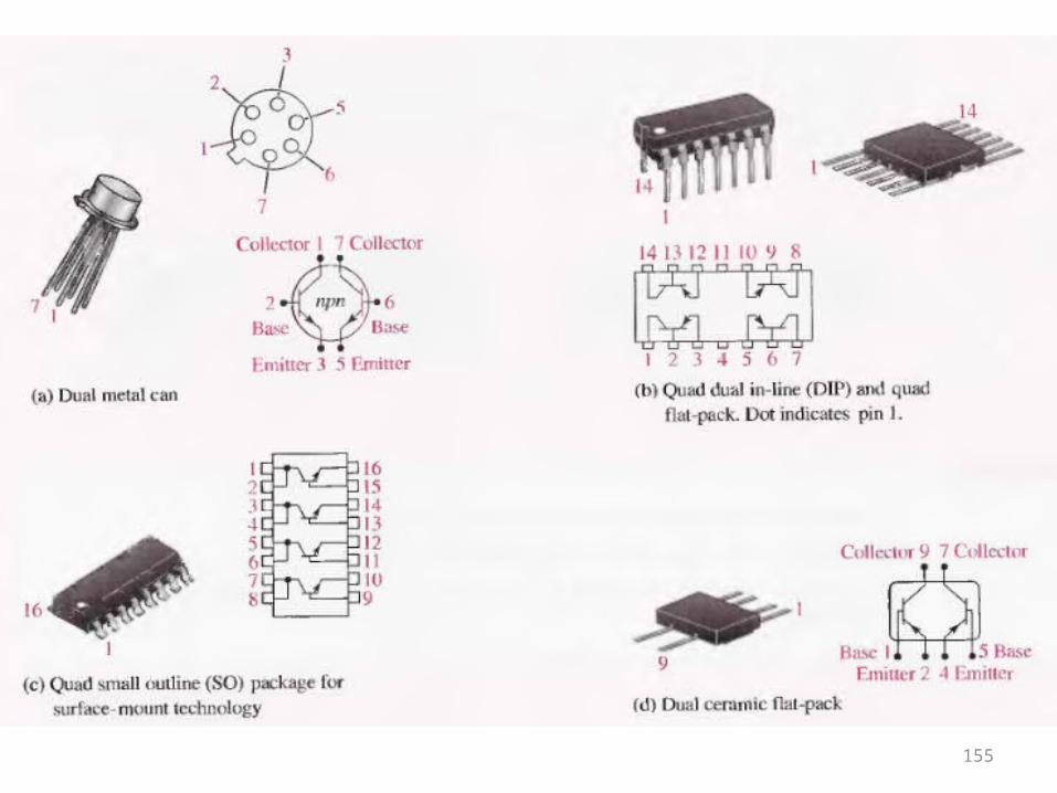
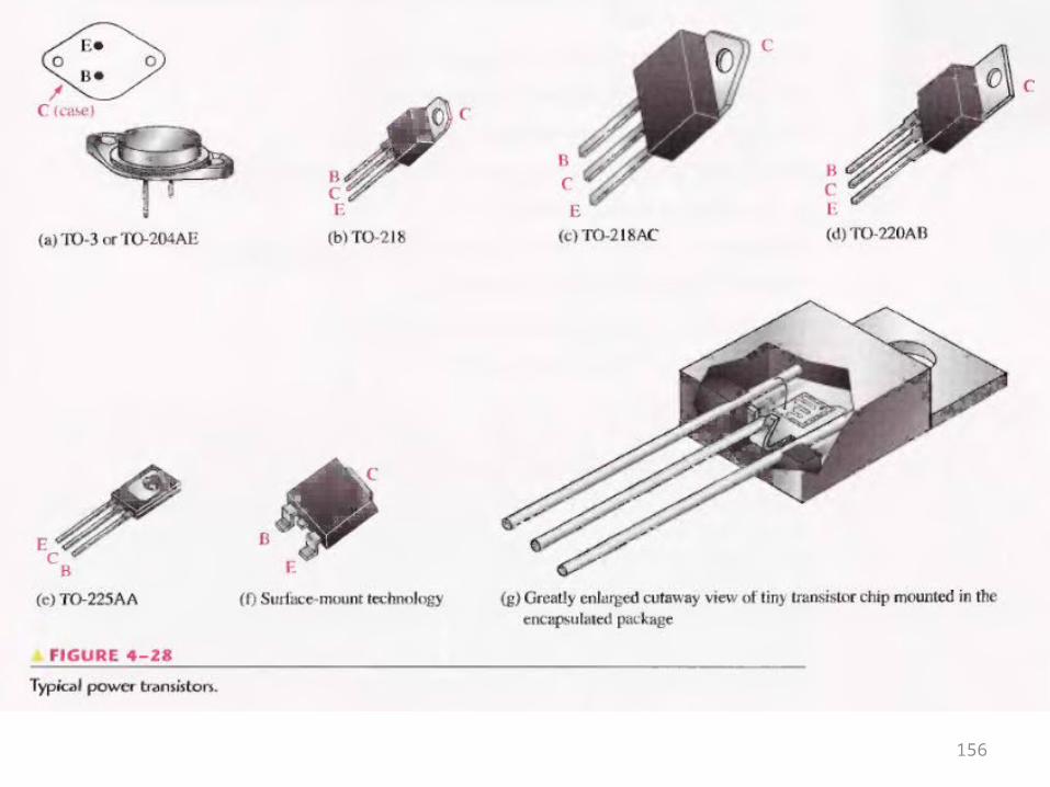
Transistor casing and terminal identification
153
154
155
156
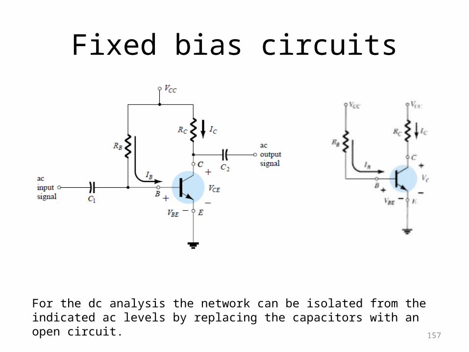
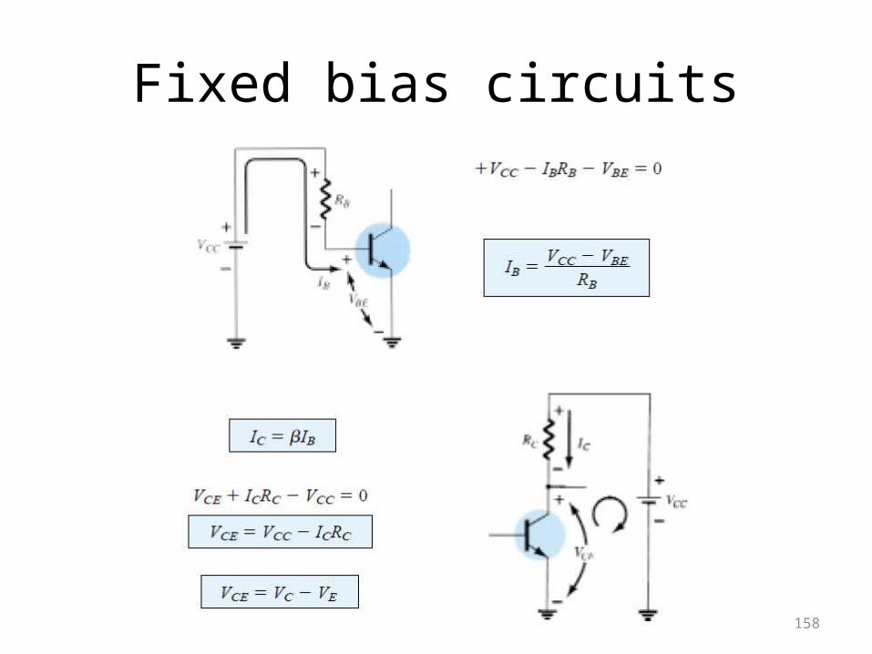
Fixed bias circuits
157
For the dc analysis the network can be isolated from the indicated ac levels by replacing the capacitors with an open circuit.
Fixed bias circuits
158
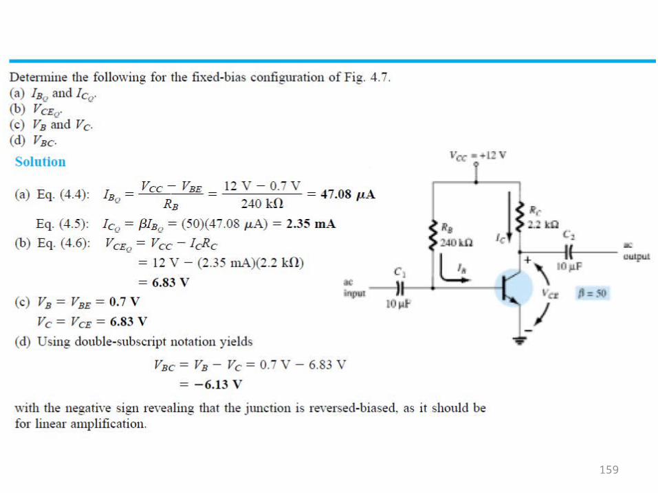
159
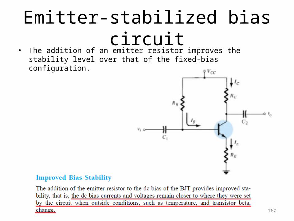
Emitter-stabilized bias circuit
• The addition of an emitter resistor improves the stability level over that of the fixed-bias configuration.
160
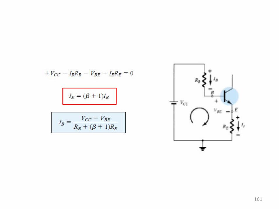
161
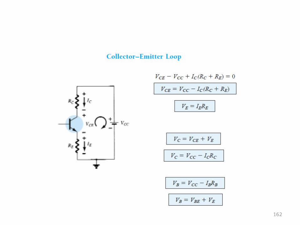
162
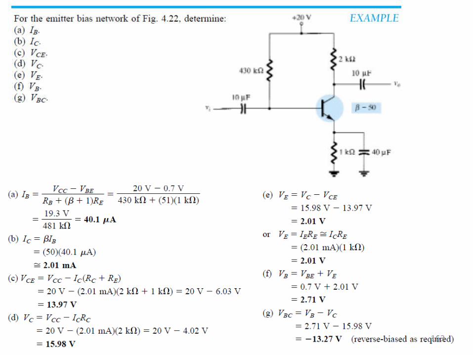
163
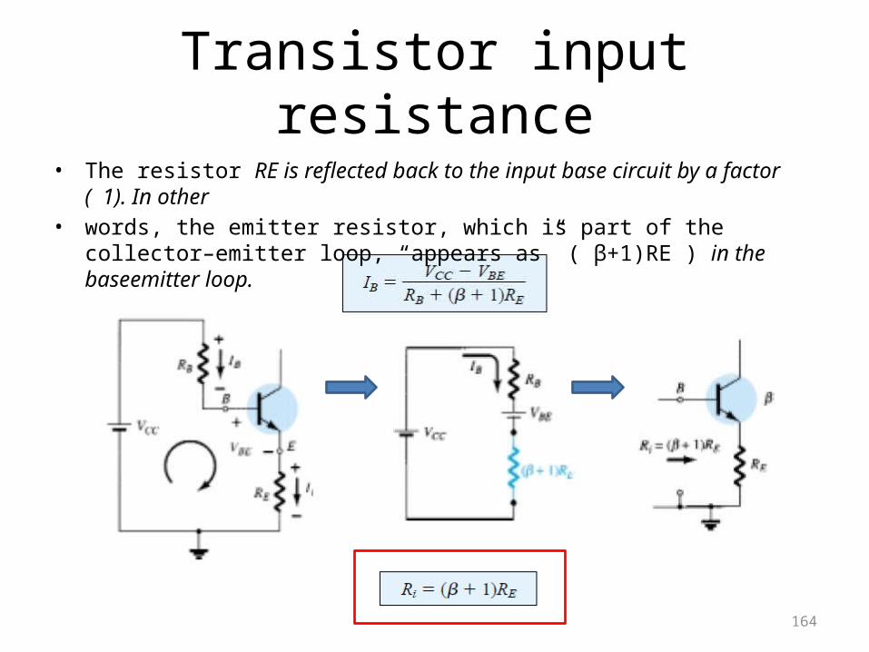
Transistor input resistance
• The resistor RE is reflected back to the input base circuit by a factor ( 1). In other
• words, the emitter resistor, which is part of the collector–emitter loop, “appears as” ( β+1)RE ) in the baseemitter loop.
164
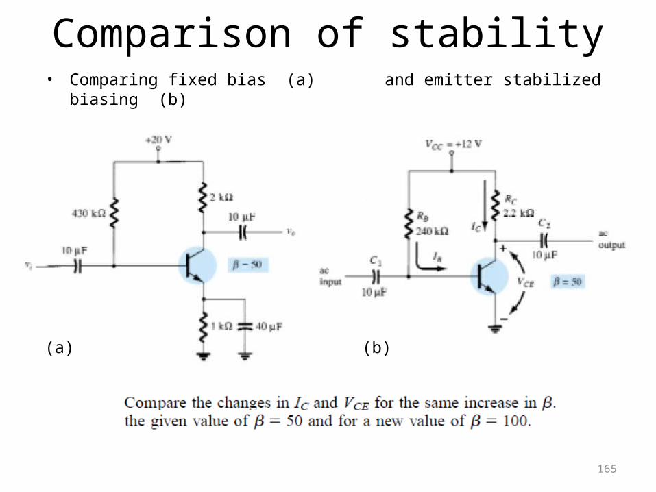
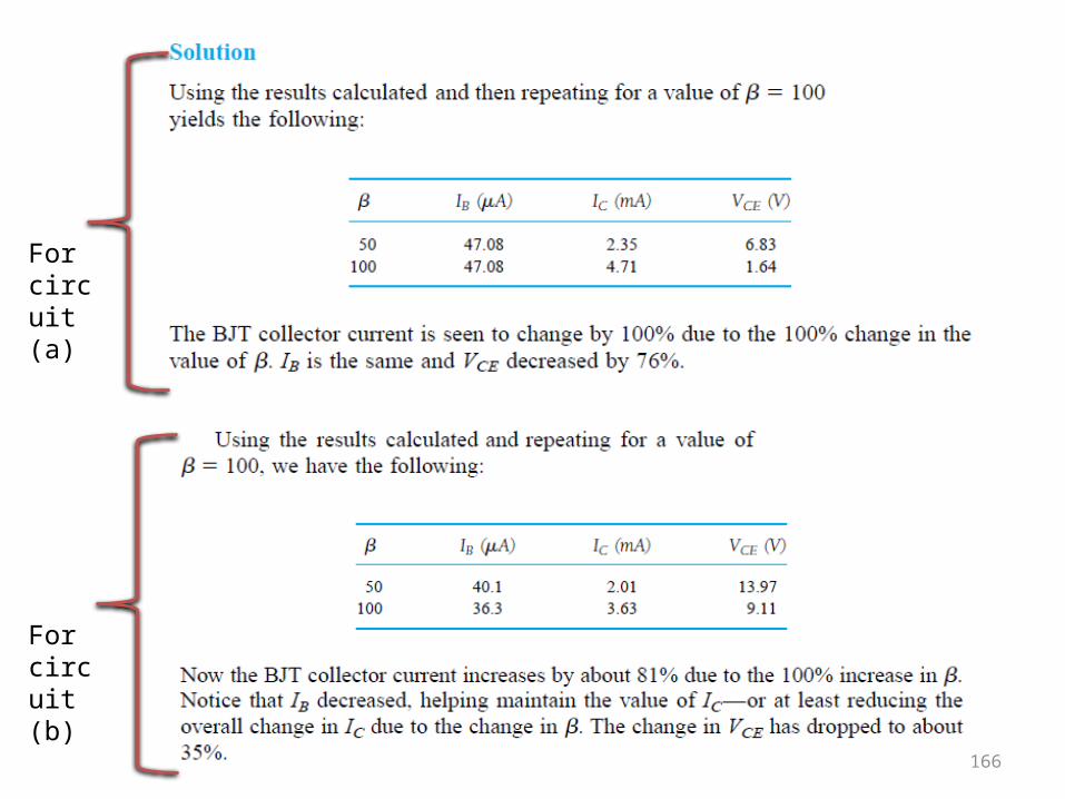
Comparison of stability• Comparing fixed bias (a) and emitter stabilized
biasing (b)
165
(a) (b)
166
For circuit (a)
For circuit (b)
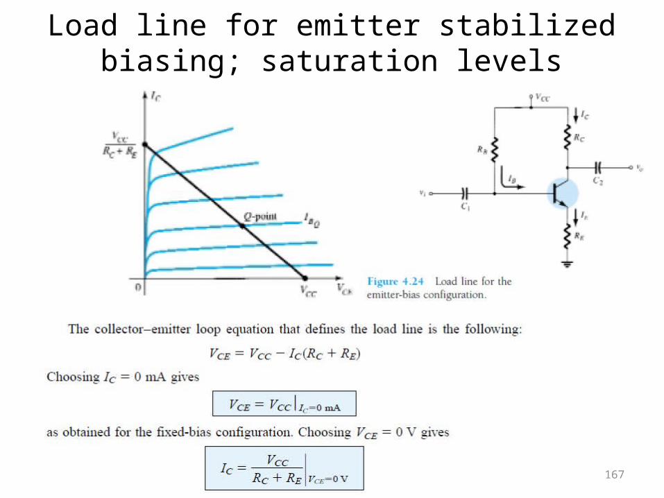
Load line for emitter stabilized biasing; saturation levels
167
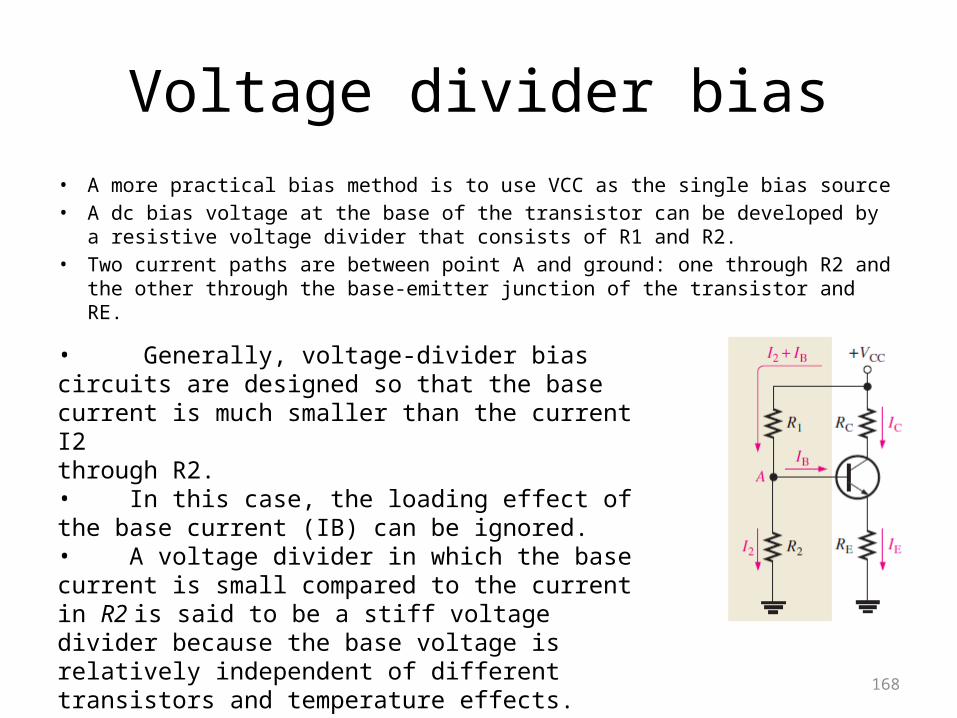
Voltage divider bias• A more practical bias method is to use VCC as the single bias source• A dc bias voltage at the base of the transistor can be developed by
a resistive voltage divider that consists of R1 and R2.• Two current paths are between point A and ground: one through R2 and
the other through the base-emitter junction of the transistor and RE.
168
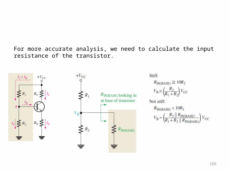
• Generally, voltage-divider bias circuits are designed so that the base current is much smaller than the current I2 through R2.• In this case, the loading effect of the base current (IB) can be ignored. • A voltage divider in which the base current is small compared to the current in R2 is said to be a stiff voltage divider because the base voltage is relatively independent of different transistors and temperature effects.
169
For more accurate analysis, we need to calculate the input resistance of the transistor.
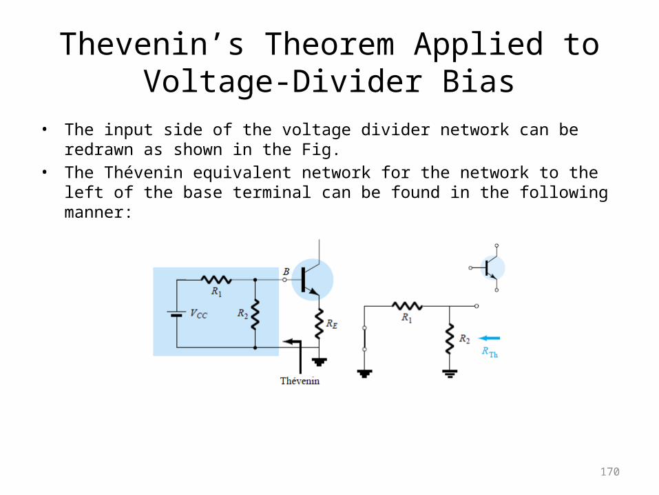
Thevenin’s Theorem Applied to Voltage-Divider Bias
• The input side of the voltage divider network can be redrawn as shown in the Fig.
• The Thévenin equivalent network for the network to the left of the base terminal can be found in the following manner:
170
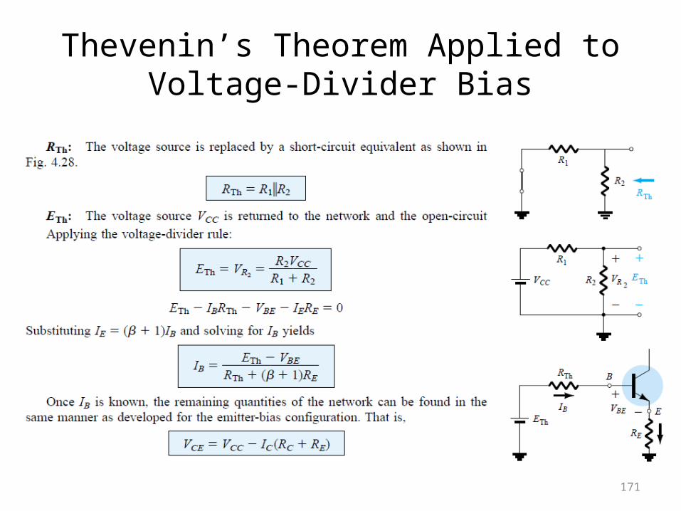
Thevenin’s Theorem Applied to Voltage-Divider Bias
171
172
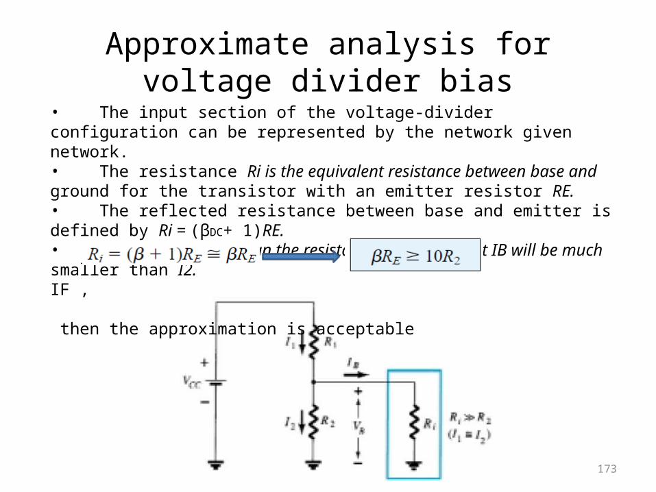
Approximate analysis for voltage divider bias
173
• The input section of the voltage-divider configuration can be represented by the network given network.• The resistance Ri is the equivalent resistance between base and ground for the transistor with an emitter resistor RE.• The reflected resistance between base and emitter is defined by Ri = (βDC+ 1)RE.• If Ri is much larger than the resistance R2, the current IB will be muchsmaller than I2.IF , then the approximation is acceptable
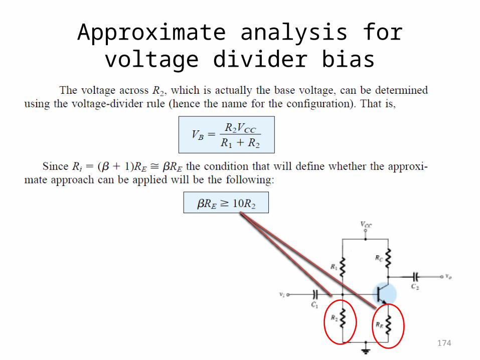
Approximate analysis for voltage divider bias
174
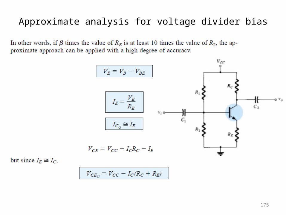
Approximate analysis for voltage divider bias
175
176
177
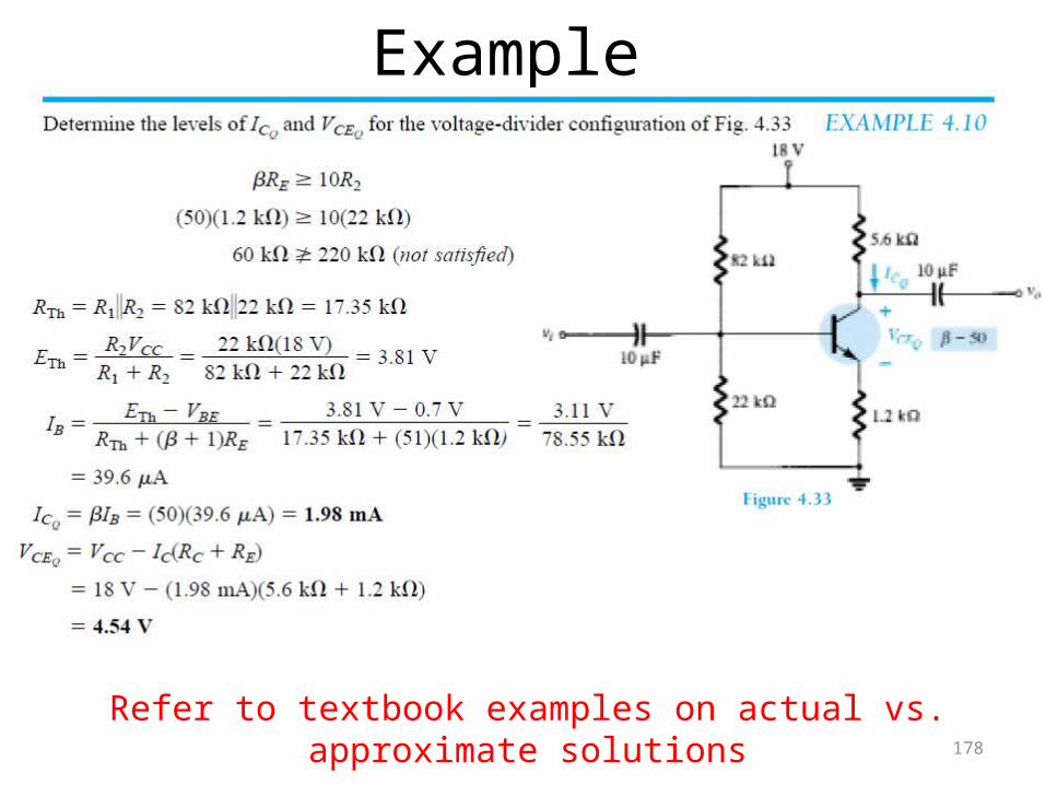
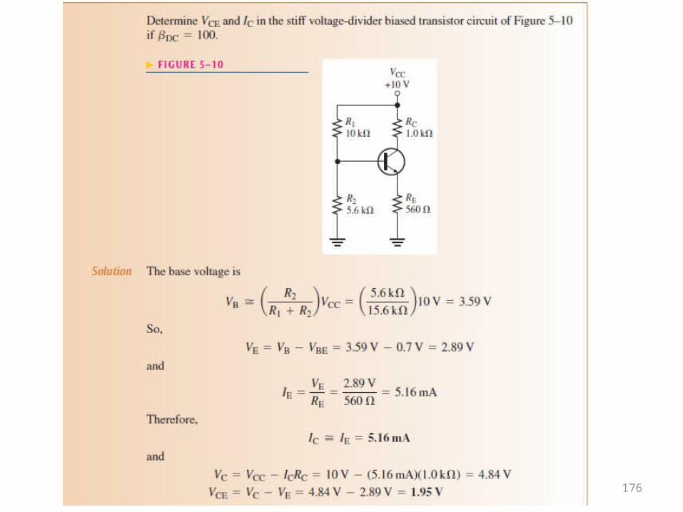
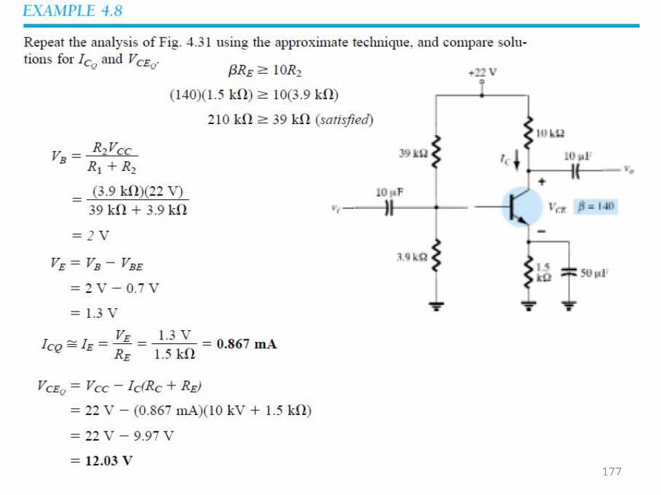
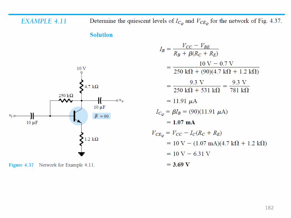
Example
178Refer to textbook examples on actual vs.
approximate solutions
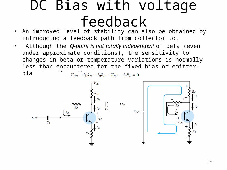
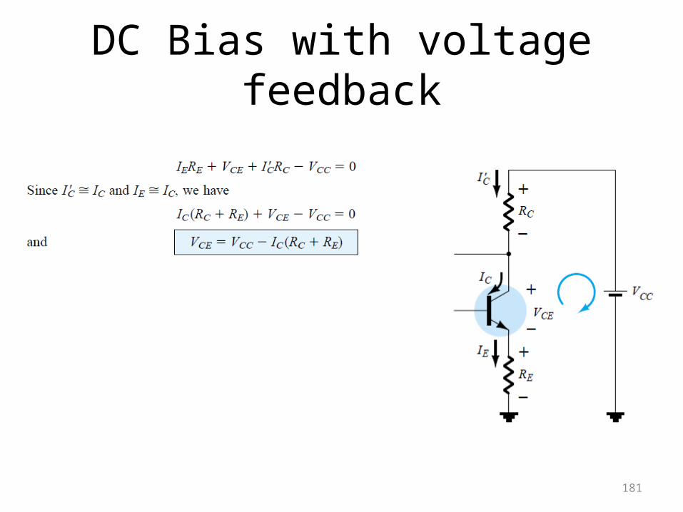
DC Bias with voltage feedback
• An improved level of stability can also be obtained by introducing a feedback path from collector to.
• Although the Q-point is not totally independent of beta (even under approximate conditions), the sensitivity to changes in beta or temperature variations is normally less than encountered for the fixed-bias or emitter-biased configurations.
179
DC Bias with voltage feedback
180
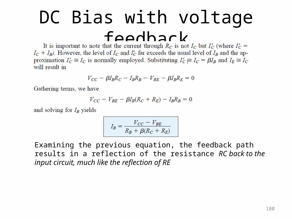
Examining the previous equation, the feedback path results in a reflection of the resistance RC back to the input circuit, much like the reflection of RE
DC Bias with voltage feedback
181
182
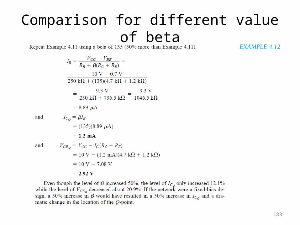
Comparison for different value of beta
183
BJT Amplifiers
184
Transistor amplifier operation
• The biasing of a transistor is purely a dc operation. The purpose of biasing is to establish a Q-point about which variations in current and voltage can occur in response to an ac input signal.
• In applications where small signal voltages must be amplified—such as from an antenna or a microphone—variations about the Q-point are relatively small.
• Amplifiers designed to handle these small ac signals are often referred to as small-signal amplifiers.
185
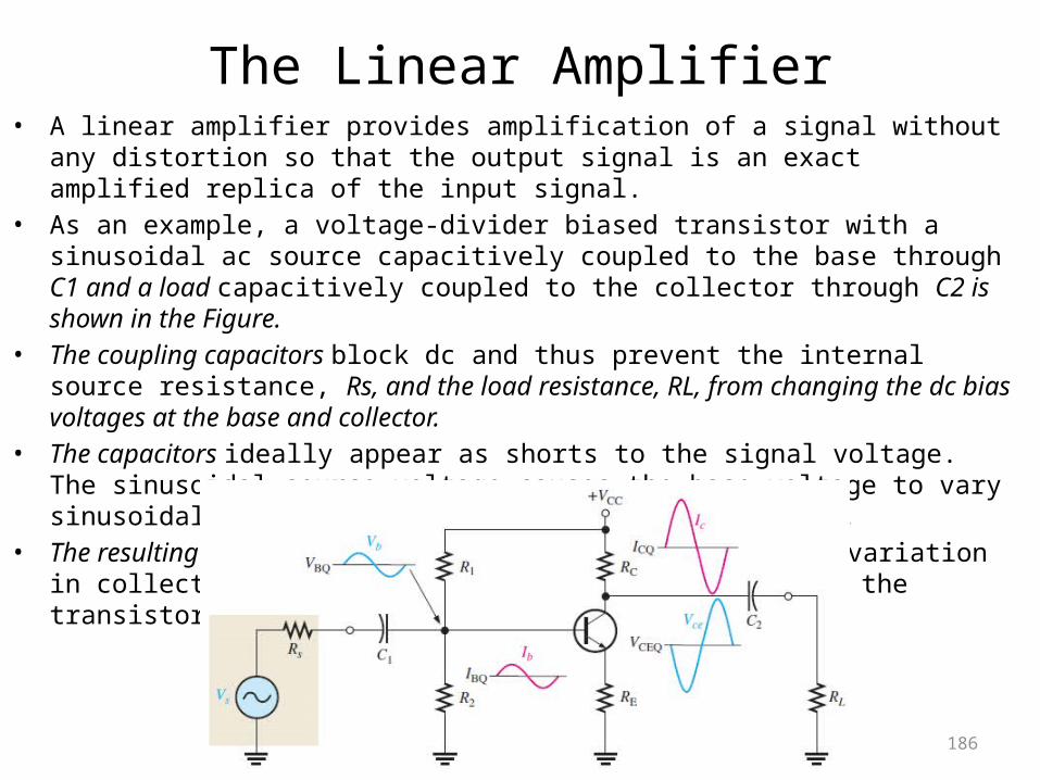
The Linear Amplifier• A linear amplifier provides amplification of a signal without
any distortion so that the output signal is an exact amplified replica of the input signal.
• As an example, a voltage-divider biased transistor with a sinusoidal ac source capacitively coupled to the base through C1 and a load capacitively coupled to the collector through C2 is shown in the Figure.
• The coupling capacitors block dc and thus prevent the internal source resistance, Rs, and the load resistance, RL, from changing the dc bias voltages at the base and collector.
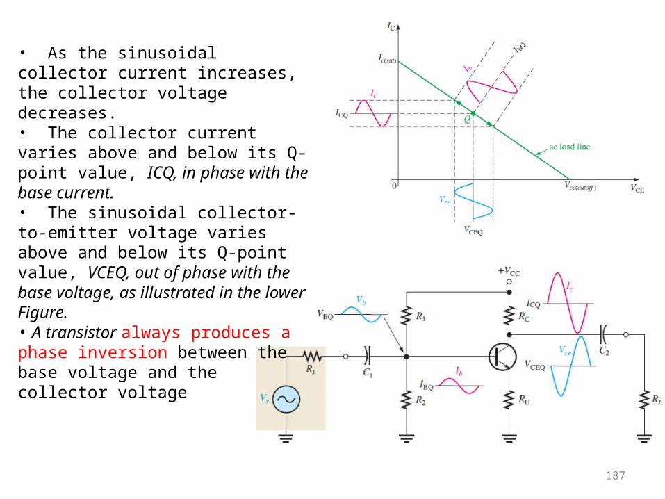
• The capacitors ideally appear as shorts to the signal voltage. The sinusoidal source voltage causes the base voltage to vary sinusoidally above and below its dc bias level, VBQ.
• The resulting variation in base current produces a larger variation in collector current because of the current gain of the transistor.
186
187
• As the sinusoidal collector current increases, the collector voltage decreases. • The collector current varies above and below its Q-point value, ICQ, in phase with the base current.• The sinusoidal collector-to-emitter voltage varies above and below its Q-point value, VCEQ, out of phase with the base voltage, as illustrated in the lower Figure. • A transistor always produces a phase inversion between the base voltage and the collector voltage
188
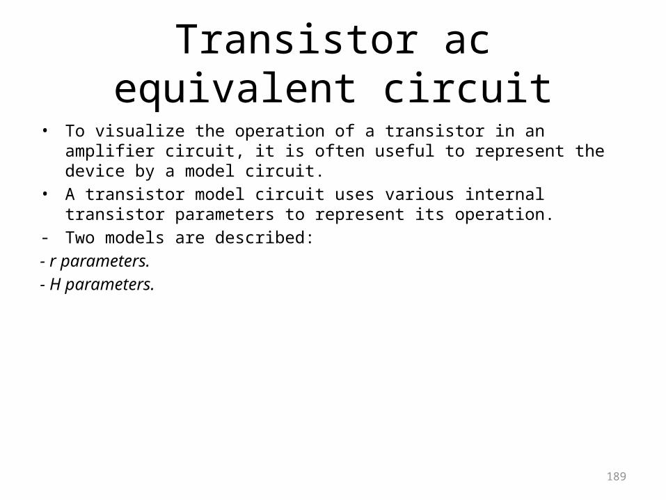
Transistor ac equivalent circuit
• To visualize the operation of a transistor in an amplifier circuit, it is often useful to represent the device by a model circuit.
• A transistor model circuit uses various internal transistor parameters to represent its operation.
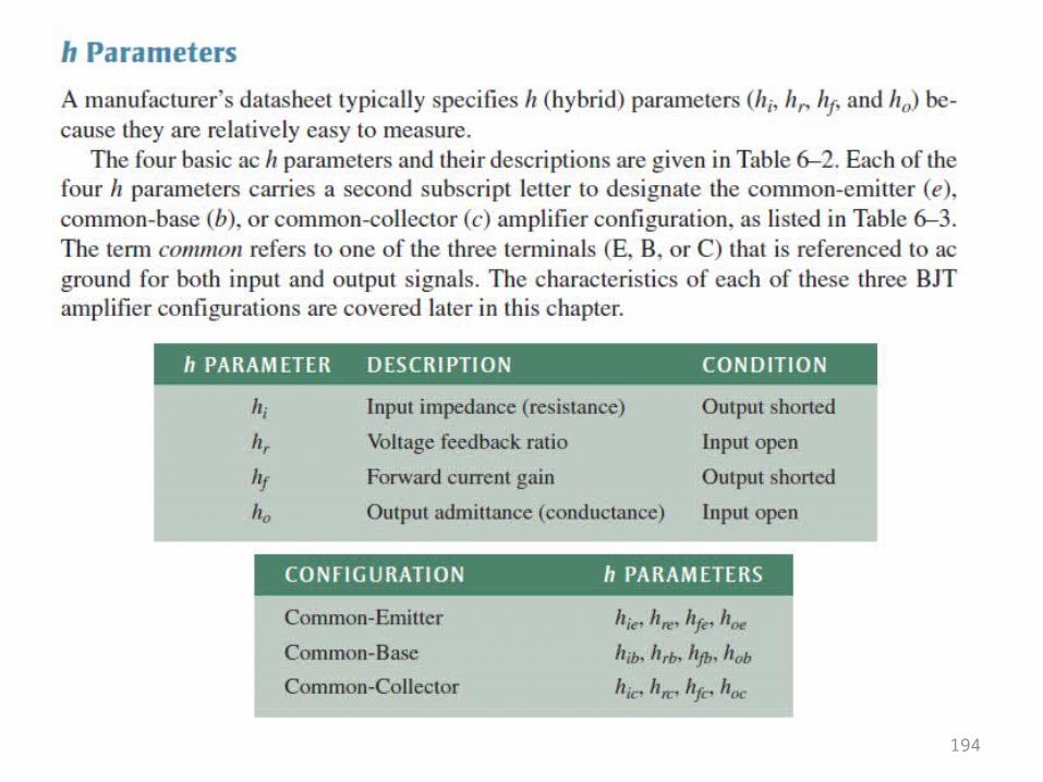
- Two models are described:- r parameters.- H parameters.
189
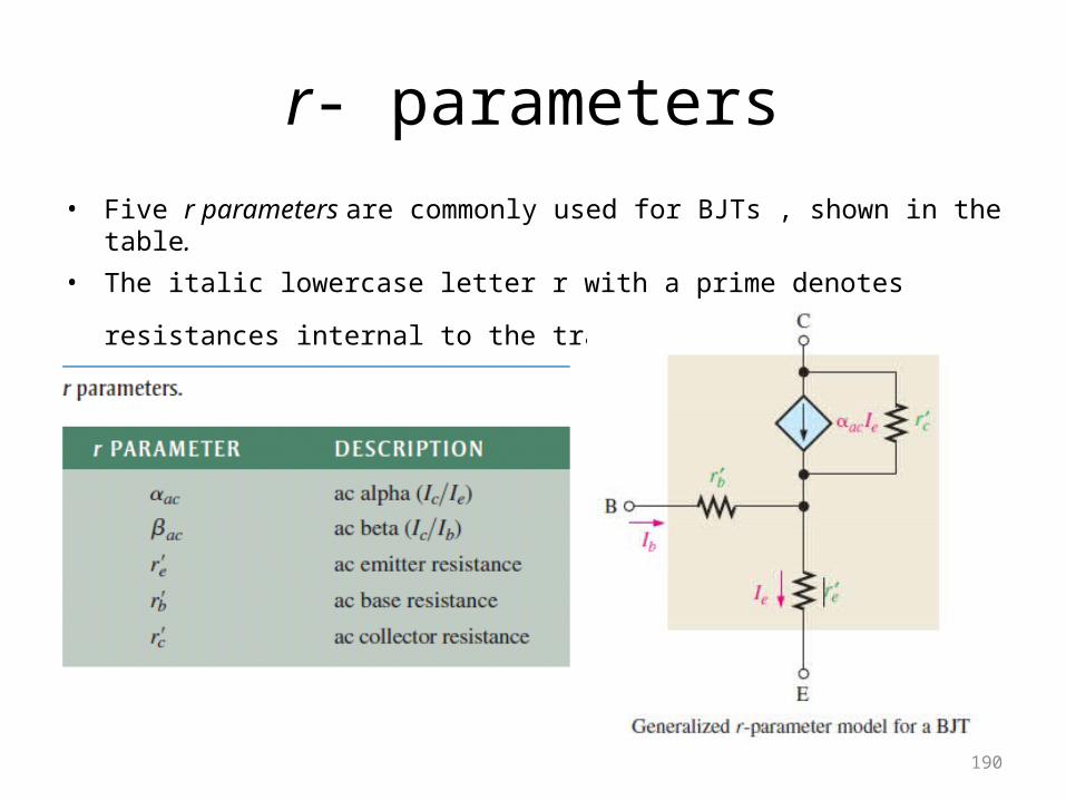
r- parameters• Five r parameters are commonly used for BJTs , shown in the
table. • The italic lowercase letter r with a prime denotes
resistances internal to the transistor.
190
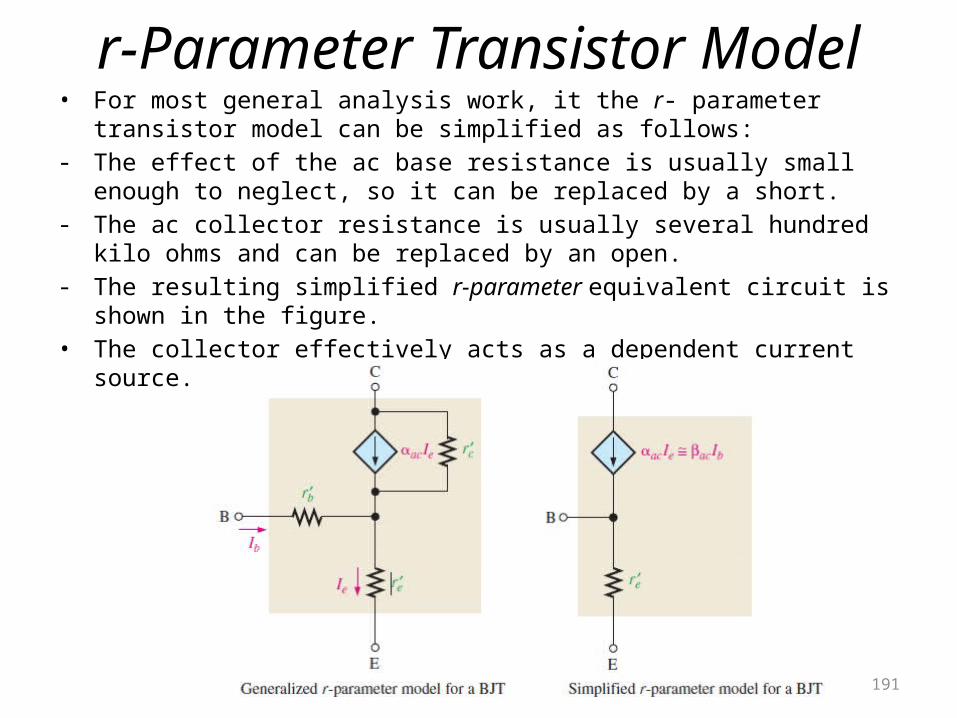
r-Parameter Transistor Model• For most general analysis work, it the r- parameter
transistor model can be simplified as follows: - The effect of the ac base resistance is usually small
enough to neglect, so it can be replaced by a short. - The ac collector resistance is usually several hundred
kilo ohms and can be replaced by an open. - The resulting simplified r-parameter equivalent circuit is
shown in the figure.• The collector effectively acts as a dependent current
source.
191
Calculating r`e
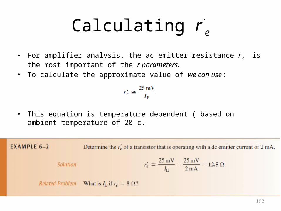
• For amplifier analysis, the ac emitter resistance r`e is
the most important of the r parameters.• To calculate the approximate value of we can use :
• This equation is temperature dependent ( based on ambient temperature of 20 c.
192
193
194
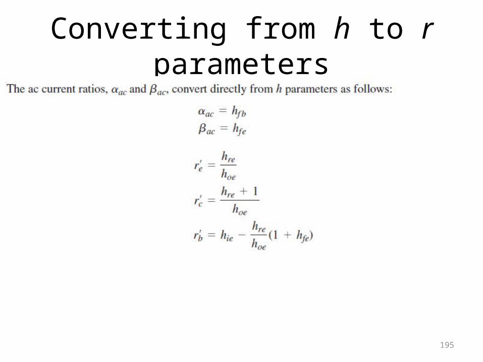
Converting from h to r parameters
195
Amplifier configurations• Three amplifier configurations:
- The common-emitter- The common-base- The common-collector.
196
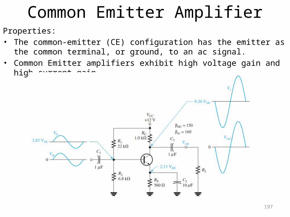
Common Emitter AmplifierProperties:• The common-emitter (CE) configuration has the emitter as
the common terminal, or ground, to an ac signal. • Common Emitter amplifiers exhibit high voltage gain and
high current gain.
197
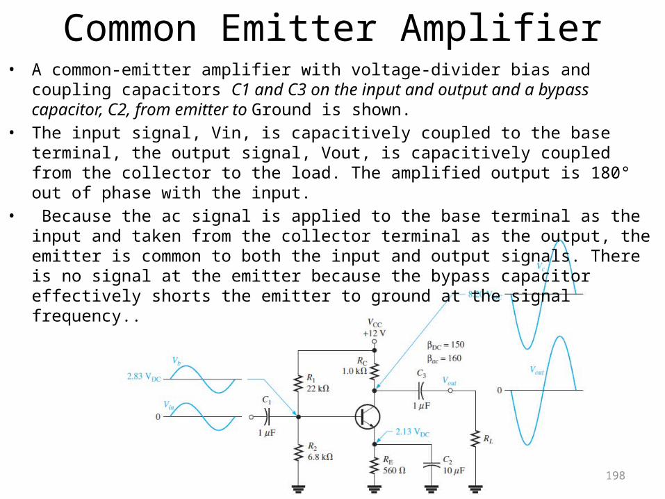
Common Emitter Amplifier• A common-emitter amplifier with voltage-divider bias and
coupling capacitors C1 and C3 on the input and output and a bypass capacitor, C2, from emitter to Ground is shown.
• The input signal, Vin, is capacitively coupled to the base terminal, the output signal, Vout, is capacitively coupled from the collector to the load. The amplified output is 180° out of phase with the input.
• Because the ac signal is applied to the base terminal as the input and taken from the collector terminal as the output, the emitter is common to both the input and output signals. There is no signal at the emitter because the bypass capacitor effectively shorts the emitter to ground at the signal frequency..
198
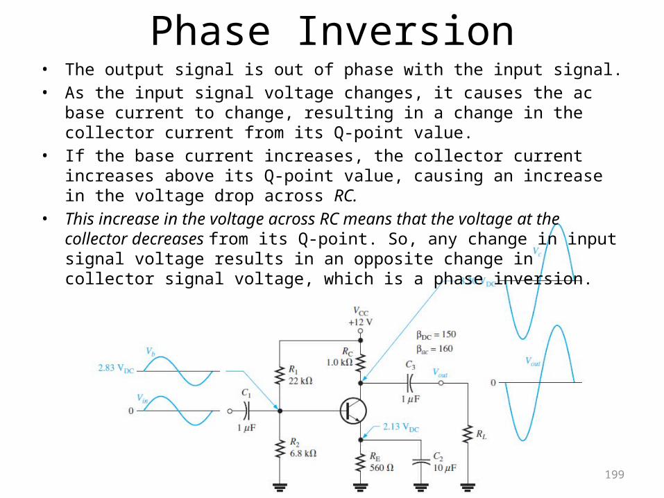
Phase Inversion• The output signal is out of phase with the input signal. • As the input signal voltage changes, it causes the ac
base current to change, resulting in a change in the collector current from its Q-point value.
• If the base current increases, the collector current increases above its Q-point value, causing an increase in the voltage drop across RC.
• This increase in the voltage across RC means that the voltage at the collector decreases from its Q-point. So, any change in input signal voltage results in an opposite change in collector signal voltage, which is a phase inversion.
199
Analysis of Common Emitter Configuration
• DC Analysis: the dc bias values must first be determined.
• ac analysis: analyze the ac signal operation of an amplifier
200
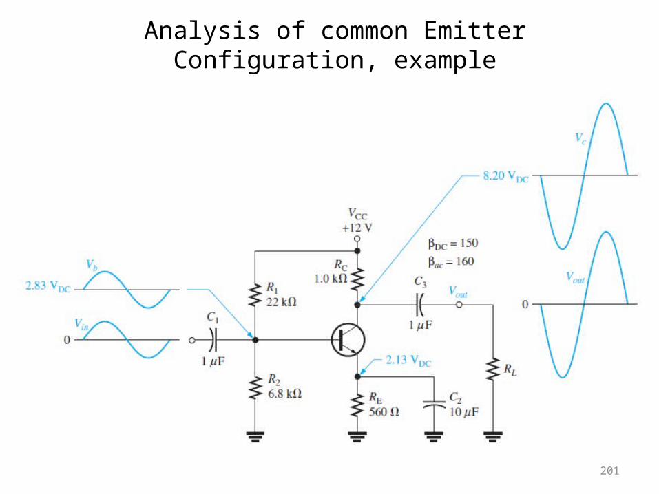
Analysis of common Emitter Configuration, example
201
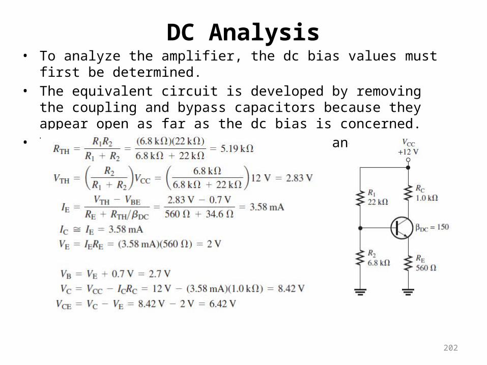
DC Analysis• To analyze the amplifier, the dc bias values must
first be determined. • The equivalent circuit is developed by removing
the coupling and bypass capacitors because they appear open as far as the dc bias is concerned.
• This also removes the load resistor and signal source
202
ac Analysis• To analyze the ac signal operation of an amplifier, an
ac equivalent circuit is developed as follows:1. The capacitors C1, C2, and C3 are replaced by effective
shorts .
2. The dc source is replaced by ground.
203
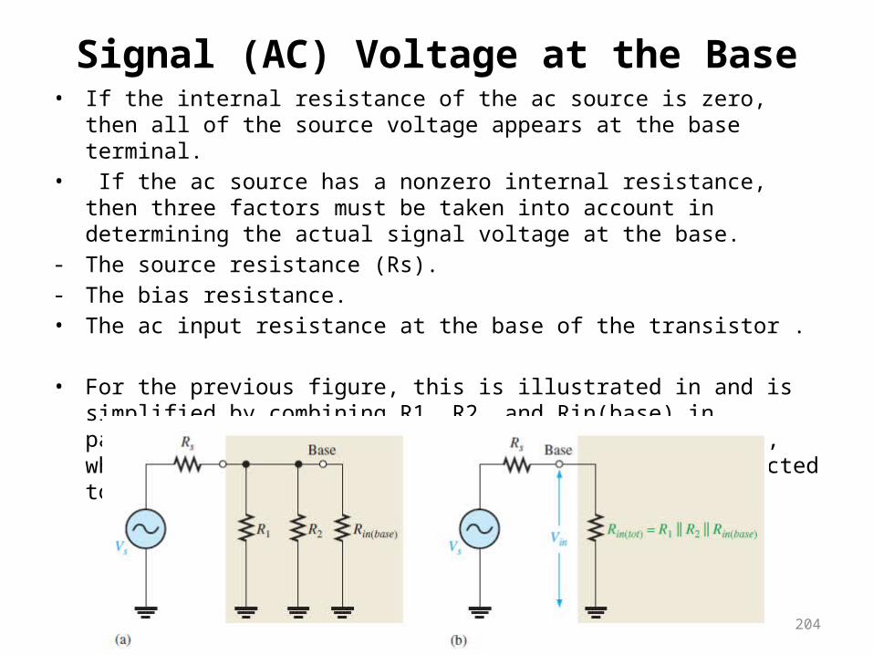
Signal (AC) Voltage at the Base• If the internal resistance of the ac source is zero,
then all of the source voltage appears at the base terminal.
• If the ac source has a nonzero internal resistance, then three factors must be taken into account in determining the actual signal voltage at the base.
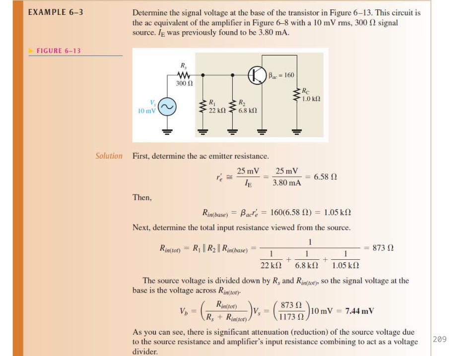
- The source resistance (Rs).- The bias resistance.• The ac input resistance at the base of the transistor .
• For the previous figure, this is illustrated in and is simplified by combining R1, R2, and Rin(base) in parallel to get the total input resistance, Rin(tot), which is the resistance “seen” by an ac source connected to the input.
204
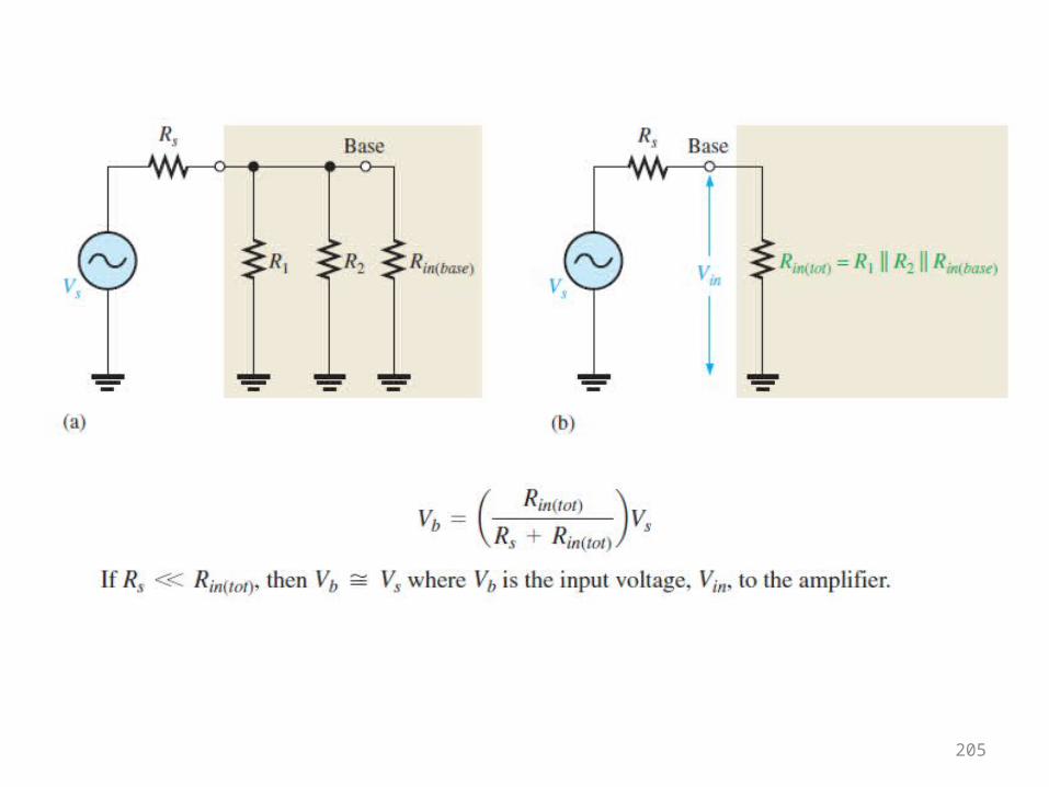
205
206
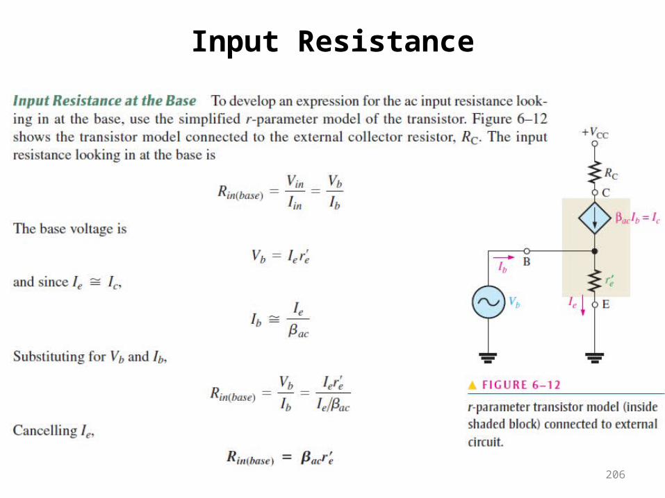
Input Resistance
207
Output Resistance
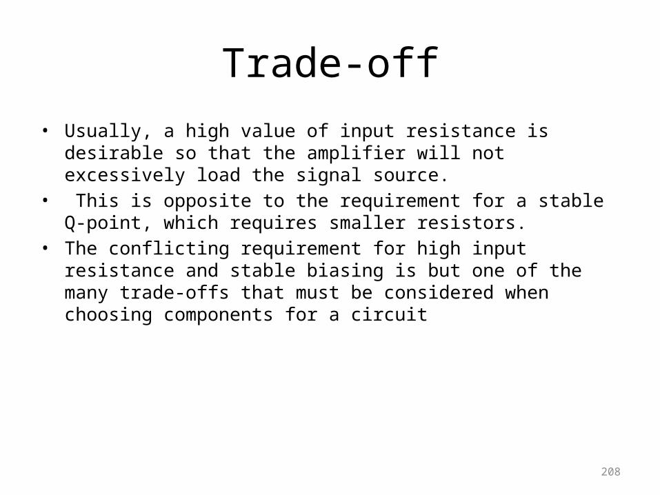
Trade-off• Usually, a high value of input resistance is
desirable so that the amplifier will not excessively load the signal source.
• This is opposite to the requirement for a stable Q-point, which requires smaller resistors.
• The conflicting requirement for high input resistance and stable biasing is but one of the many trade-offs that must be considered when choosing components for a circuit
208
209
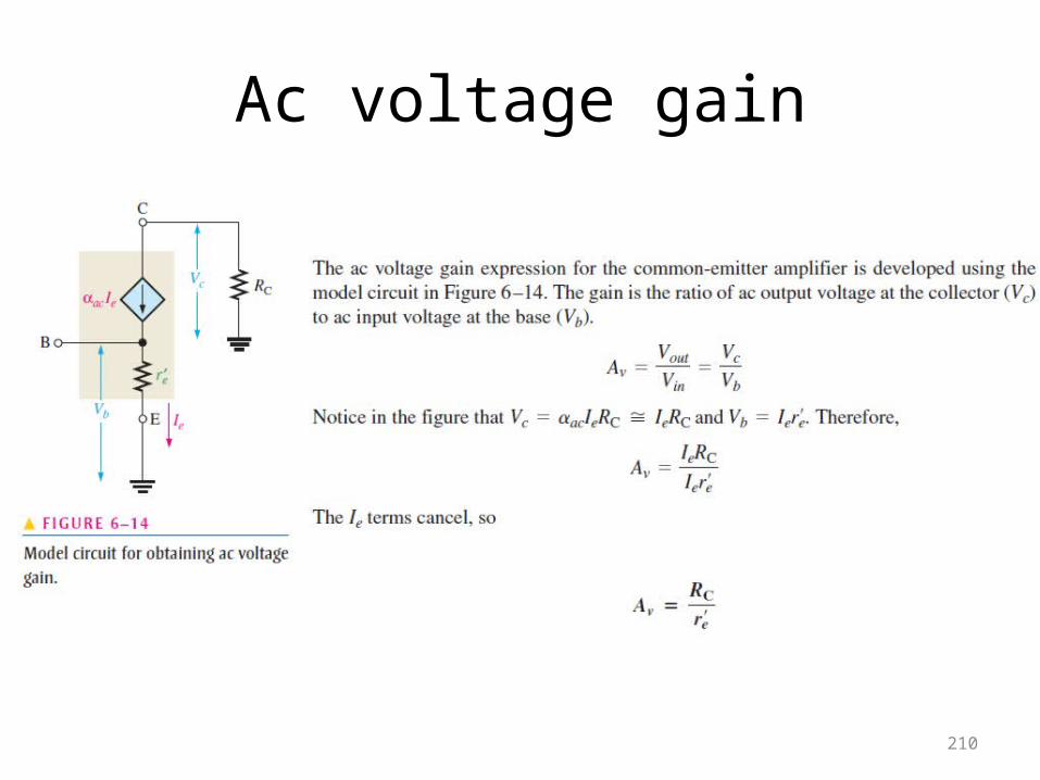
Ac voltage gain
210
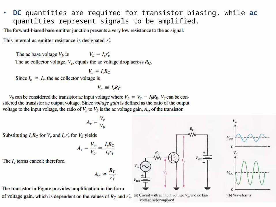
• DC quantities are required for transistor biasing, while ac quantities represent signals to be amplified.
211
212
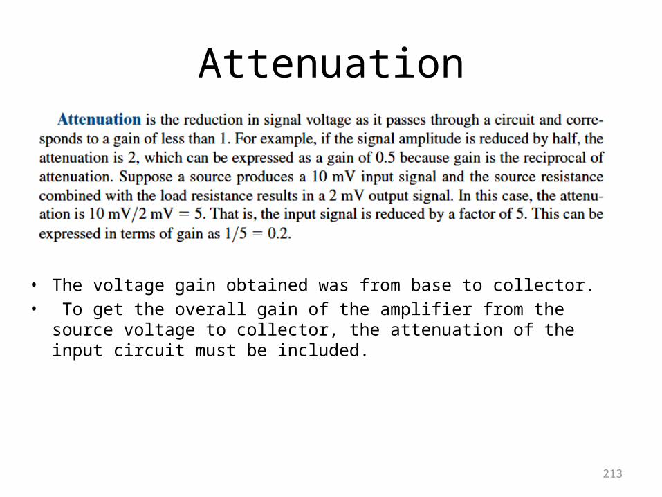
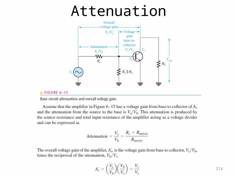
Attenuation
• The voltage gain obtained was from base to collector.• To get the overall gain of the amplifier from the
source voltage to collector, the attenuation of the input circuit must be included.
213
Attenuation
214
Effect of the Emitter Bypass Capacitor on Voltage Gain
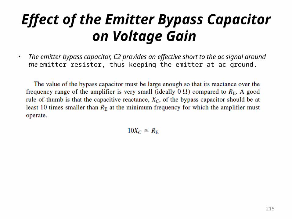
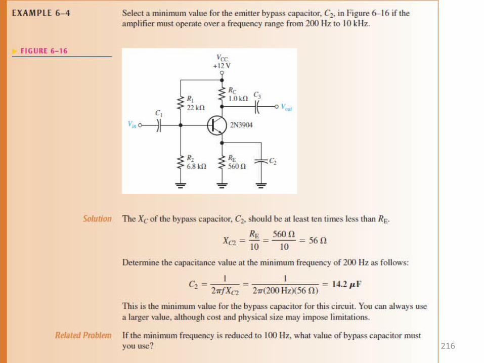
• The emitter bypass capacitor, C2 provides an effective short to the ac signal around the emitter resistor, thus keeping the emitter at ac ground.
215
216
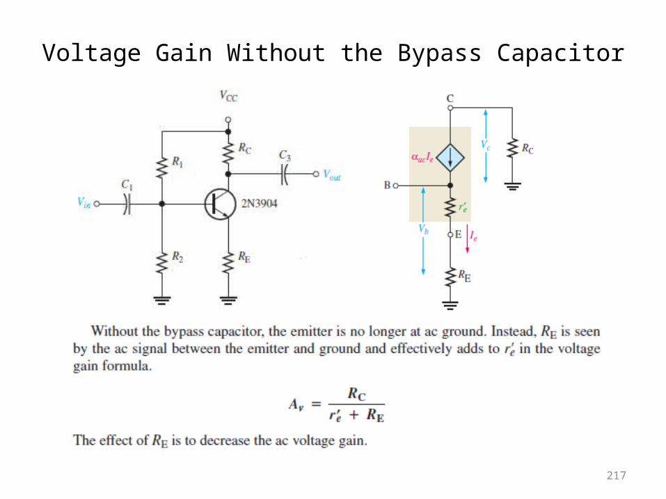
Voltage Gain Without the Bypass Capacitor
217
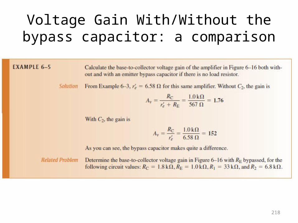
Voltage Gain With/Without the bypass capacitor: a comparison
218
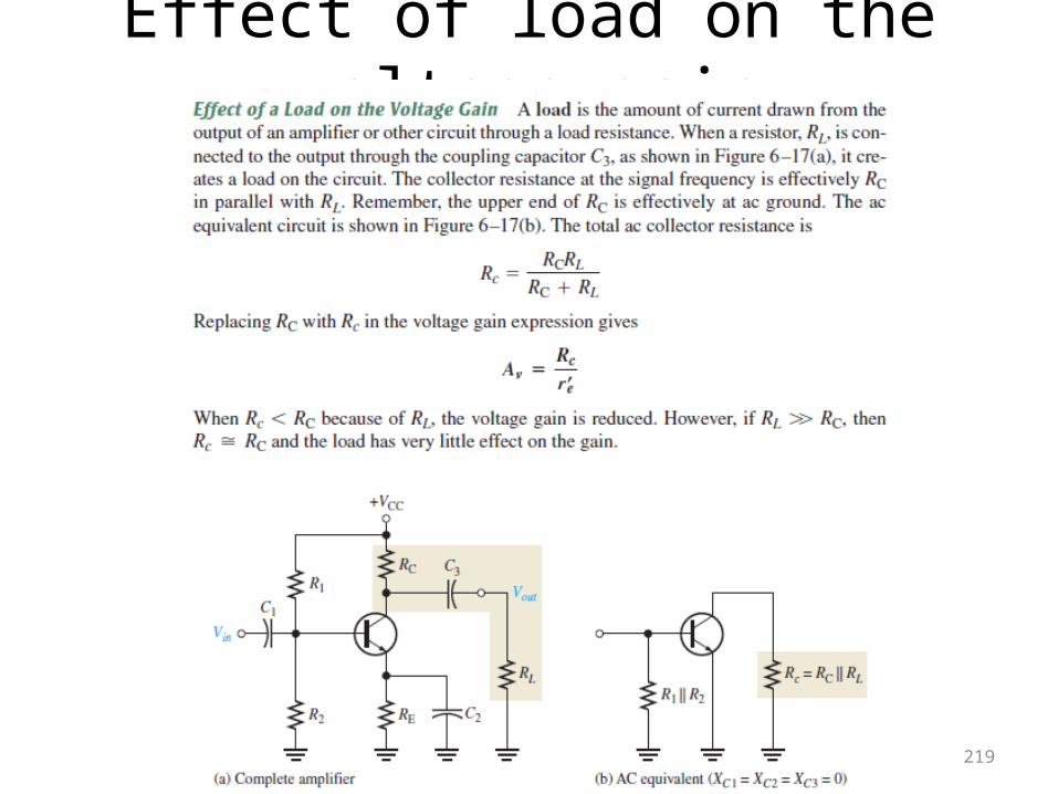
Effect of load on the voltage gain
219
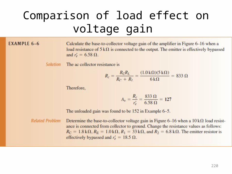
Comparison of load effect on voltage gain
220
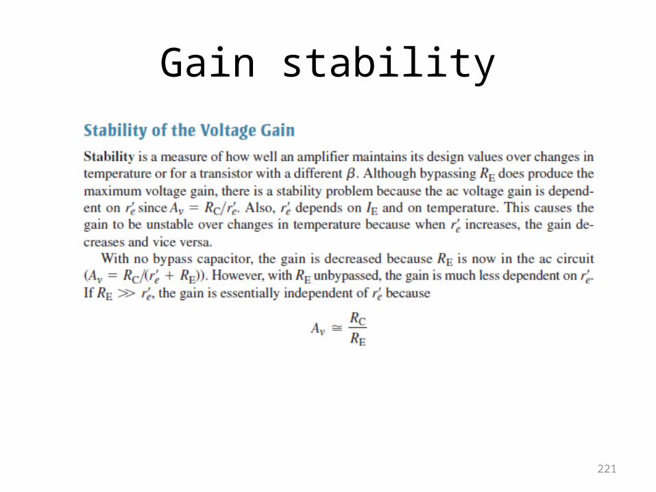
Gain stability
221
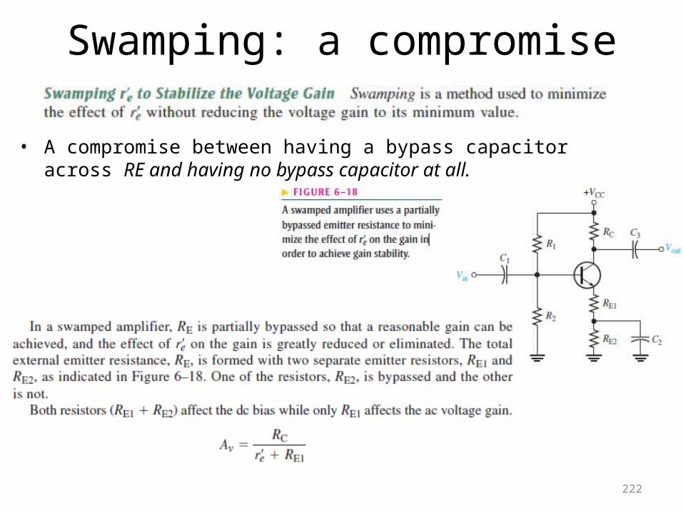
Swamping: a compromise
• A compromise between having a bypass capacitor across RE and having no bypass capacitor at all.
222
223
Effect of swamping on the transistor input resistance
224
Example
225
DC Analysis
226
227
228
229
230
Common collector amplifier
• The common-collector (CC) amplifier is usually referred to as an emitter-follower(EF).
• The input is applied to the base through a coupling capacitor, and the output is at the emitter.
• The voltage gain of a CC amplifier is approximately 1, and its main advantages are its high input resistance and current gain.
231
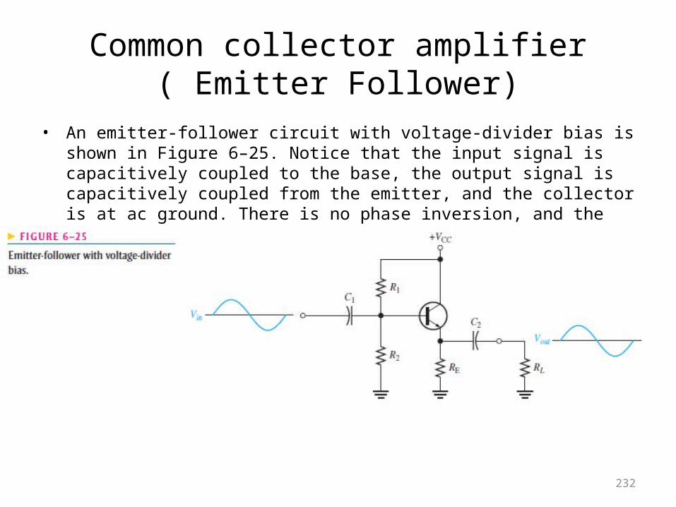
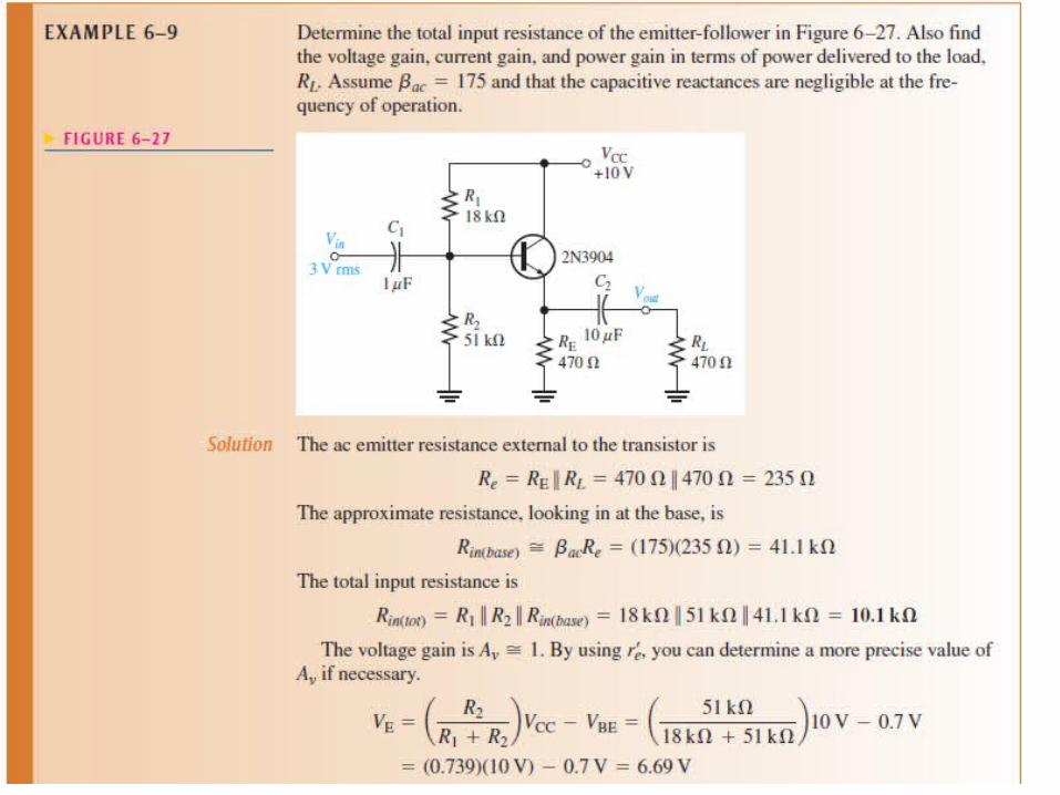
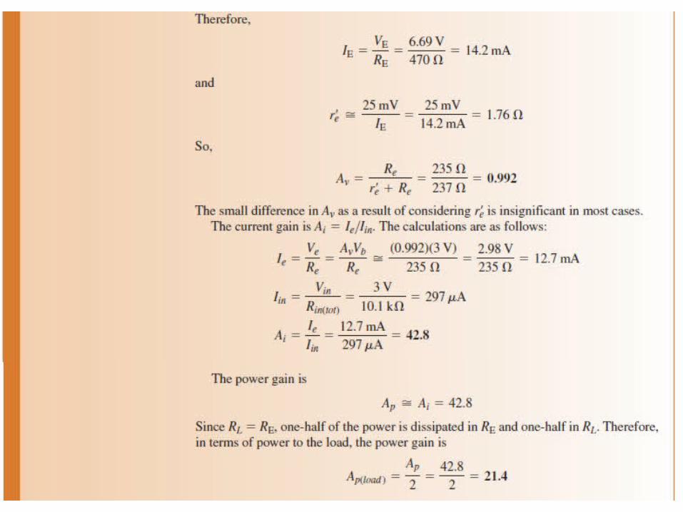
Common collector amplifier ( Emitter Follower)
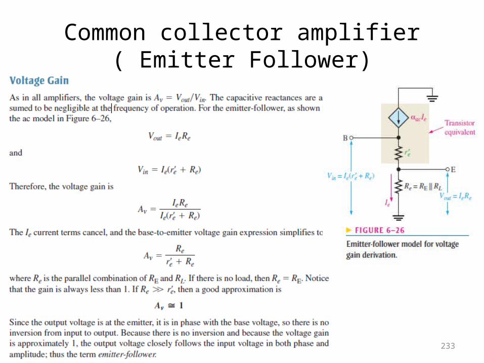
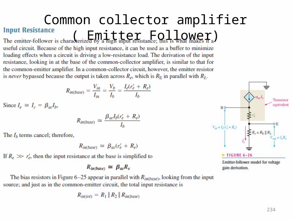
• An emitter-follower circuit with voltage-divider bias is shown in Figure 6–25. Notice that the input signal is capacitively coupled to the base, the output signal is capacitively coupled from the emitter, and the collector is at ac ground. There is no phase inversion, and the output is approximately the same amplitude as the input.
232
Common collector amplifier ( Emitter Follower)
233
234
Common collector amplifier ( Emitter Follower)
235
236
237
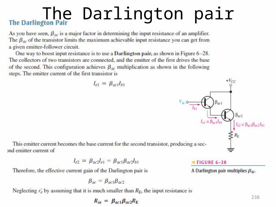
The Darlington pair
238
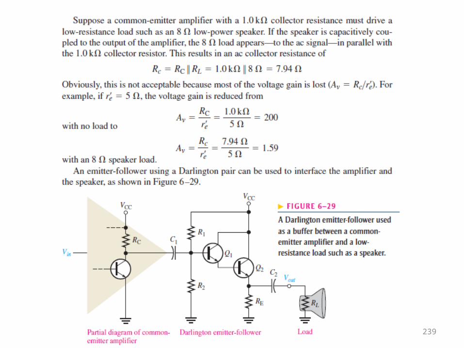
239
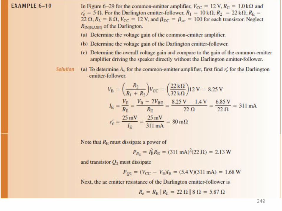
240
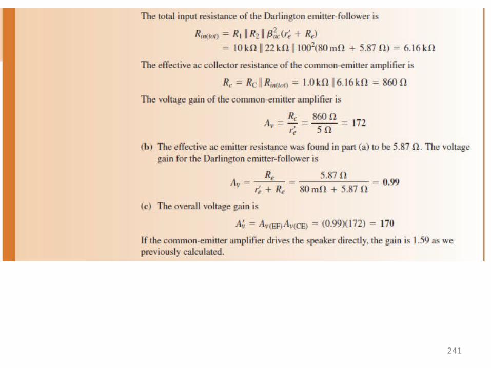
241
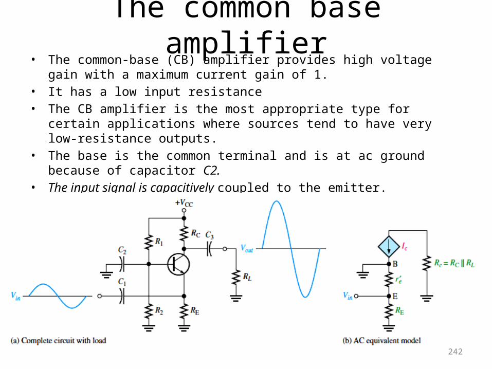
The common base amplifier
• The common-base (CB) amplifier provides high voltage gain with a maximum current gain of 1.
• It has a low input resistance• The CB amplifier is the most appropriate type for
certain applications where sources tend to have very low-resistance outputs.
• The base is the common terminal and is at ac ground because of capacitor C2.
• The input signal is capacitively coupled to the emitter. • The output is capacitively coupled from the collector to
a load resistor.
242
243
244
245
246
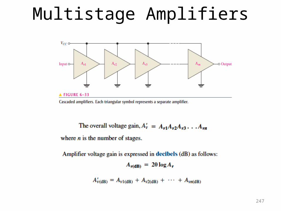
Multistage Amplifiers
247
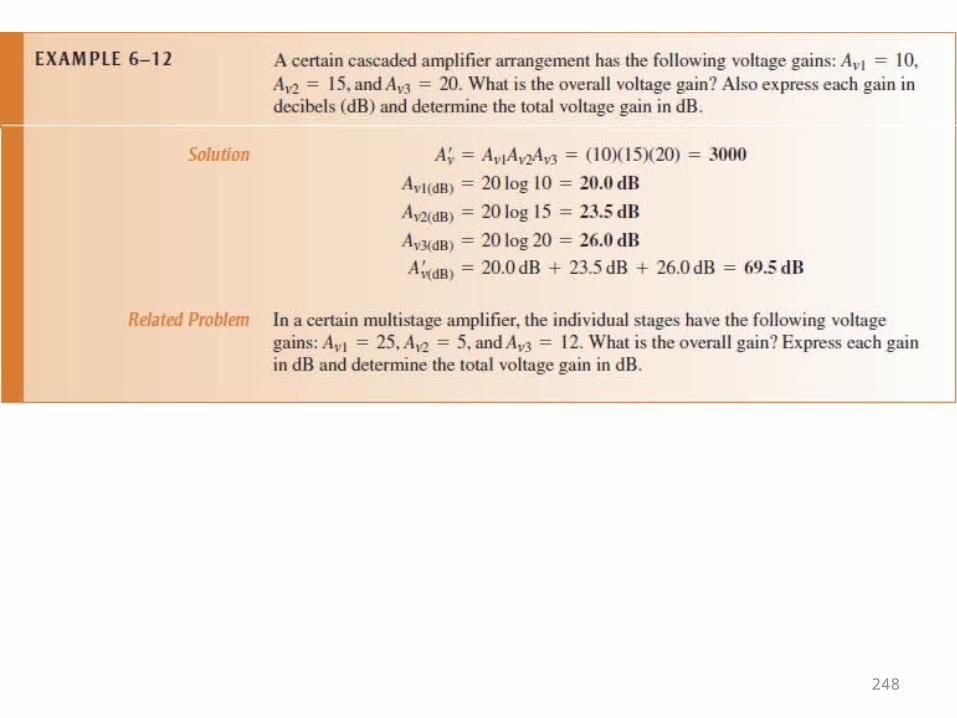
248
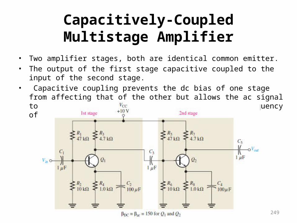
Capacitively-Coupled Multistage Amplifier
• Two amplifier stages, both are identical common emitter.• The output of the first stage capacitive coupled to the
input of the second stage.• Capacitive coupling prevents the dc bias of one stage
from affecting that of the other but allows the ac signal to pass without attenuation because Xc=0 at the frequency of operation.
249
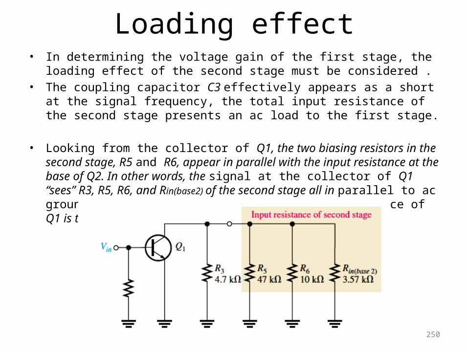
Loading effect• In determining the voltage gain of the first stage, the
loading effect of the second stage must be considered .• The coupling capacitor C3 effectively appears as a short
at the signal frequency, the total input resistance of the second stage presents an ac load to the first stage.
• Looking from the collector of Q1, the two biasing resistors in the second stage, R5 and R6, appear in parallel with the input resistance at the base of Q2. In other words, the signal at the collector of Q1 “sees” R3, R5, R6, and Rin(base2) of the second stage all in parallel to ac ground. Thus, the effective ac collector resistance of Q1 is the total of all these resistances in parallel
250
DC analysis
251
252
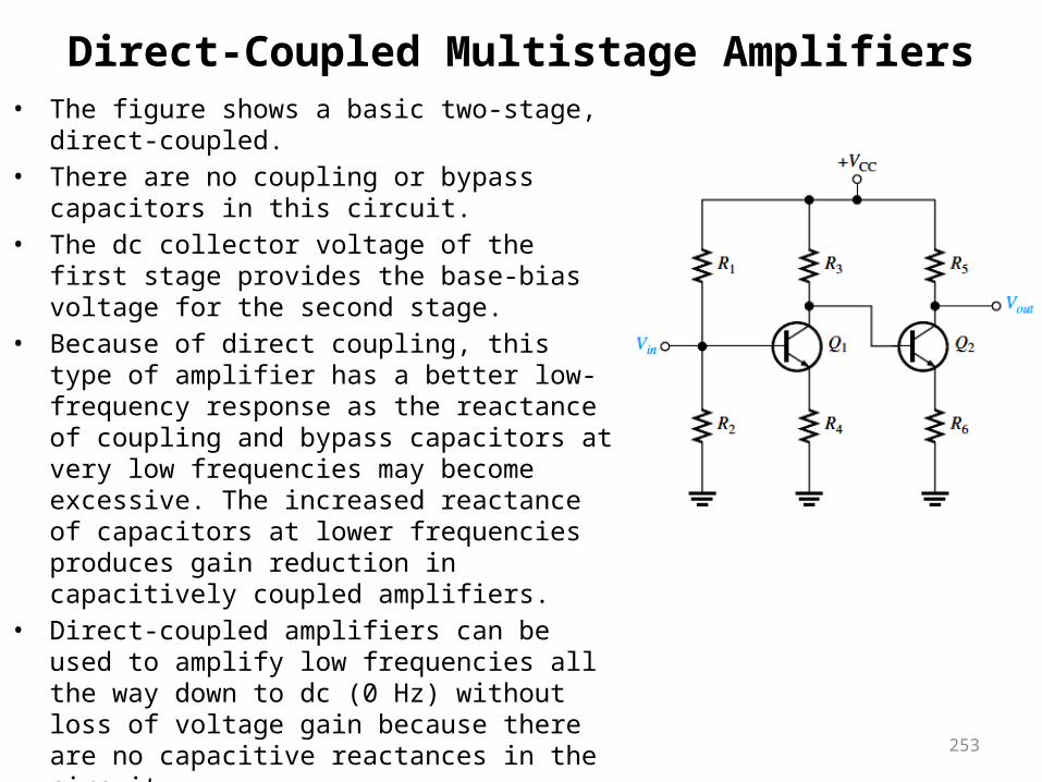
Direct-Coupled Multistage Amplifiers• The figure shows a basic two-stage,
direct-coupled. • There are no coupling or bypass
capacitors in this circuit. • The dc collector voltage of the
first stage provides the base-bias voltage for the second stage.
• Because of direct coupling, this type of amplifier has a better low-frequency response as the reactance of coupling and bypass capacitors at very low frequencies may become excessive. The increased reactance of capacitors at lower frequencies produces gain reduction in capacitively coupled amplifiers.
• Direct-coupled amplifiers can be used to amplify low frequencies all the way down to dc (0 Hz) without loss of voltage gain because there are no capacitive reactances in the circuit.
• The disadvantage, is that small changes in the dc bias voltages from temperature effects or power-supply variation are amplified by the succeeding stages, which can result in a significant drift in the dc levels throughout the circuit
253
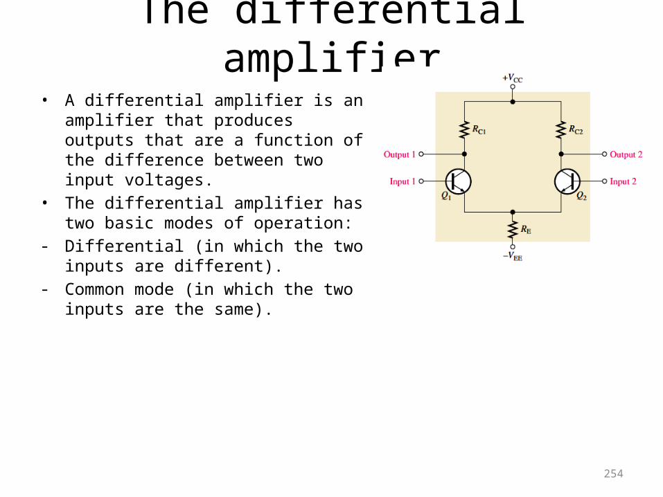
The differential amplifier
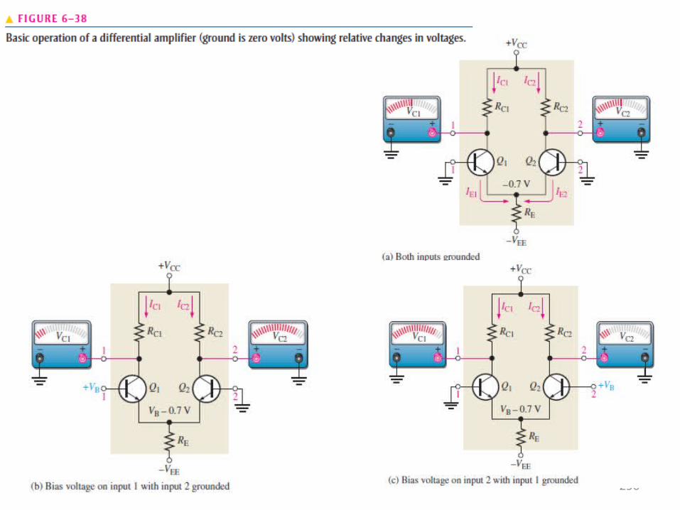
• A differential amplifier is an amplifier that produces outputs that are a function of the difference between two input voltages.
• The differential amplifier has two basic modes of operation:
- Differential (in which the two inputs are different).
- Common mode (in which the two inputs are the same).
254
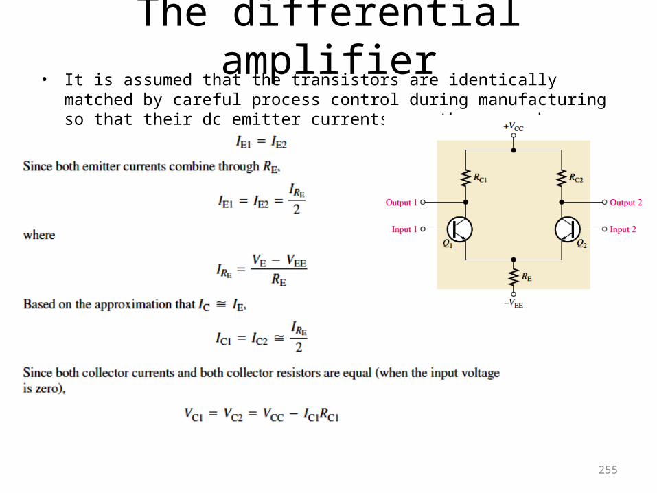
The differential amplifier• It is assumed that the transistors are identically
matched by careful process control during manufacturing so that their dc emitter currents are the same when there is no input signal.
255
256
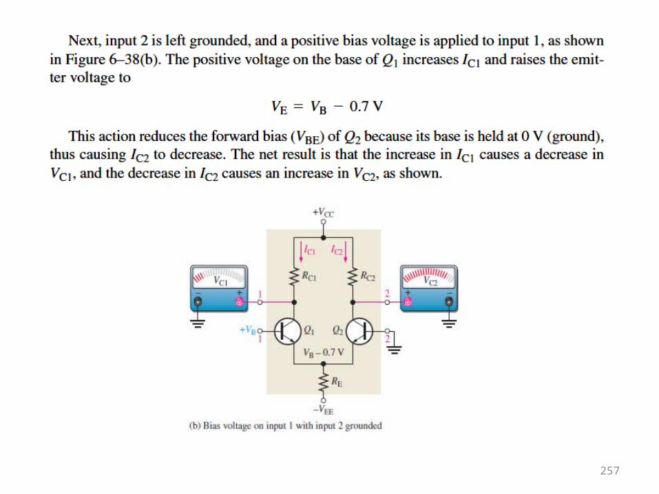
257
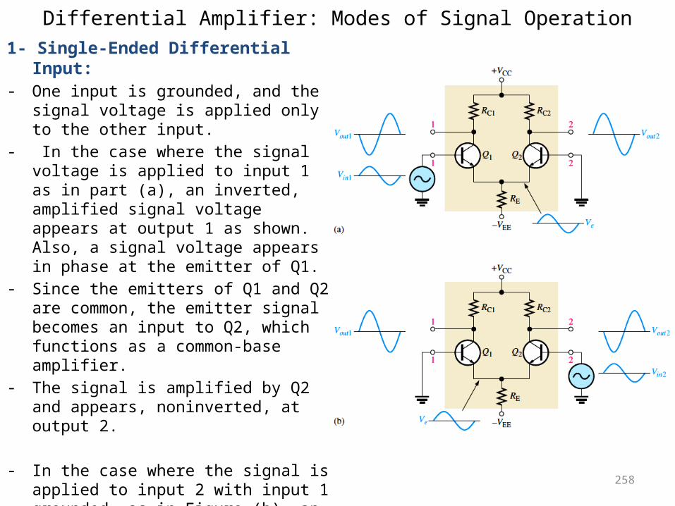
Differential Amplifier: Modes of Signal Operation1- Single-Ended Differential
Input:- One input is grounded, and the
signal voltage is applied only to the other input.
- In the case where the signal voltage is applied to input 1 as in part (a), an inverted, amplified signal voltage appears at output 1 as shown. Also, a signal voltage appears in phase at the emitter of Q1.
- Since the emitters of Q1 and Q2 are common, the emitter signal becomes an input to Q2, which functions as a common-base amplifier.
- The signal is amplified by Q2 and appears, noninverted, at output 2.
- In the case where the signal is applied to input 2 with input 1 grounded, as in Figure (b), an inverted, amplified signal voltage appears at output 2. In this situation, Q1 acts as a common-base amplifier, and a noninverted, amplified signal appears at output 1.
258
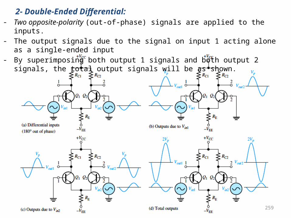
2- Double-Ended Differential: - Two opposite-polarity (out-of-phase) signals are applied to the
inputs. - The output signals due to the signal on input 1 acting alone
as a single-ended input- By superimposing both output 1 signals and both output 2
signals, the total output signals will be as shown.
259
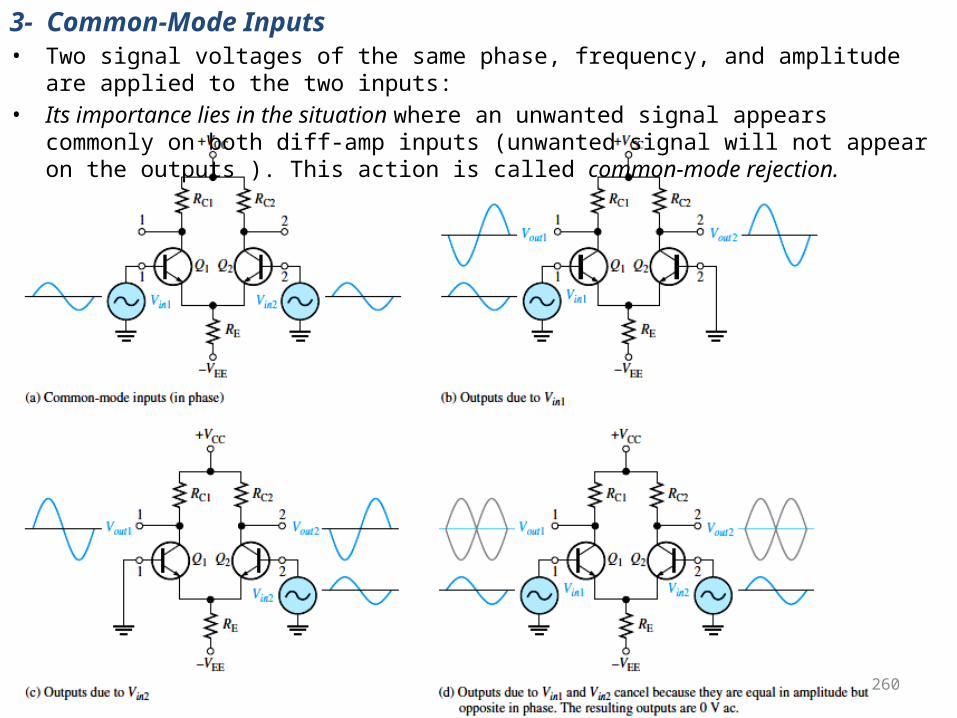
3- Common-Mode Inputs • Two signal voltages of the same phase, frequency, and amplitude
are applied to the two inputs:• Its importance lies in the situation where an unwanted signal appears
commonly on both diff-amp inputs (unwanted signal will not appear on the outputs ). This action is called common-mode rejection.
260
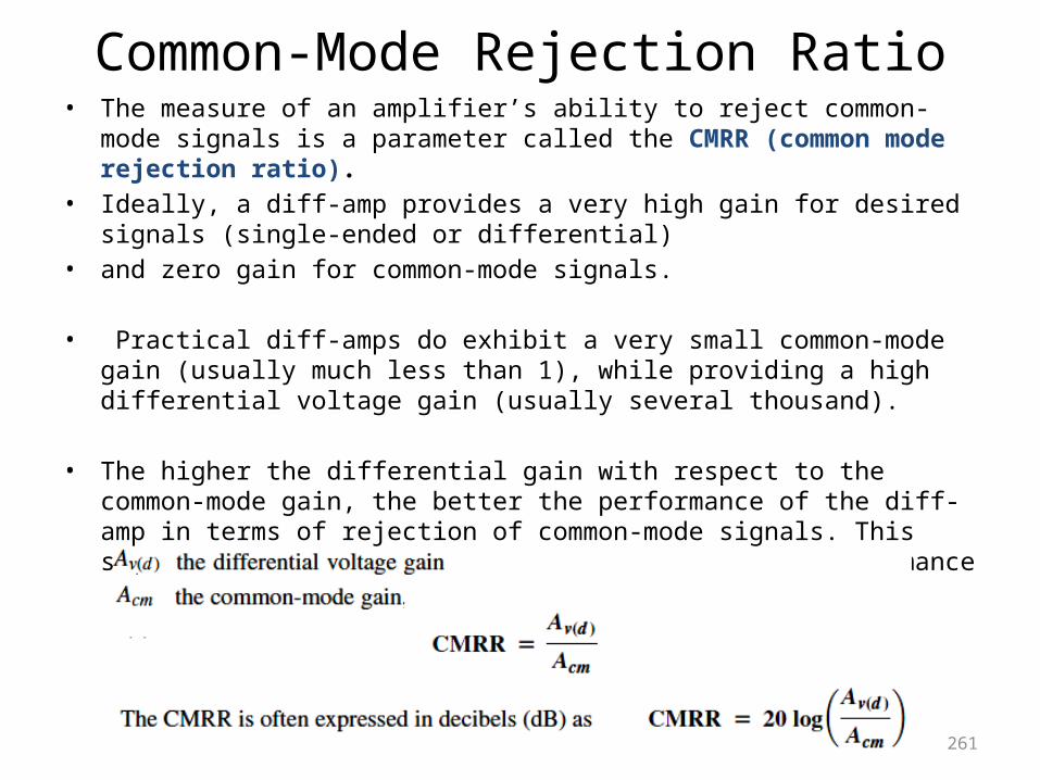
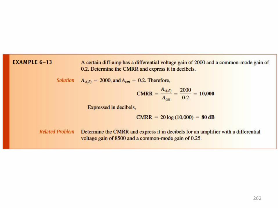
Common-Mode Rejection Ratio• The measure of an amplifier’s ability to reject common-
mode signals is a parameter called the CMRR (common mode rejection ratio).
• Ideally, a diff-amp provides a very high gain for desired signals (single-ended or differential)
• and zero gain for common-mode signals.
• Practical diff-amps do exhibit a very small common-mode gain (usually much less than 1), while providing a high differential voltage gain (usually several thousand).
• The higher the differential gain with respect to the common-mode gain, the better the performance of the diff-amp in terms of rejection of common-mode signals. This suggests that a good measure of the diff-amp’s performance
261
262
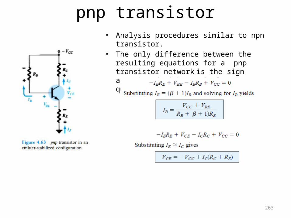
pnp transistor• Analysis procedures similar to npn
transistor.• The only difference between the
resulting equations for a pnp transistor network is the sign associated with particular quantities
263
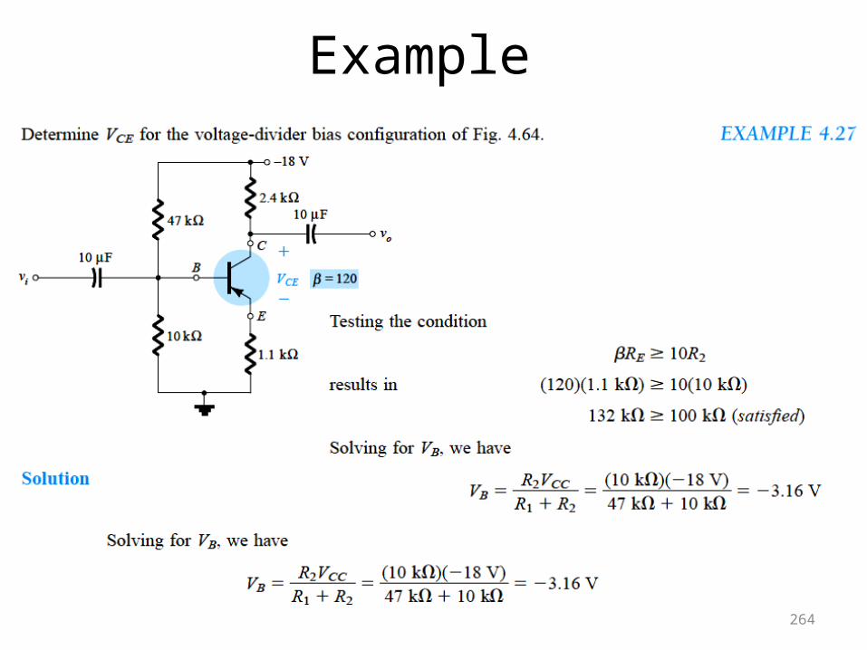
Example
264
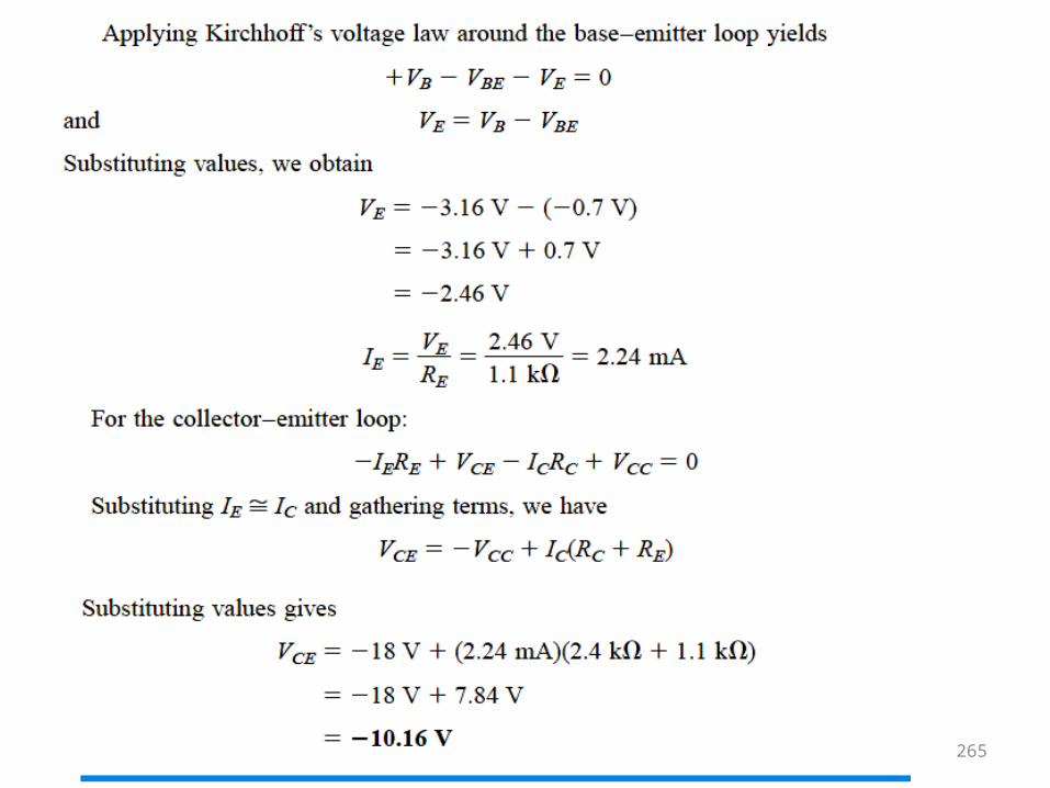
265
FETField Effect Transistors
266
Comparison with the BJT
267
Similarities: • To a large extent match the applications described earlier; Amplifiers, Switching devices
Differences:• FETs are voltage controlled devices. BJTs are current
controlled devices. • Preferred device in low-voltage switching applications
because they are generally faster than BJTs when turned on and off
• FETs have a higher input impedance. BJTs have higher gains.
• FETs are less sensitive to temperature variations and are more easily integrated on ICs.
• FETs are generally more static sensitive than BJTs.
•JFET: Junction FET
•MOSFET: Metal–Oxide–Semiconductor FET
D-MOSFET: Depletion MOSFET E-MOSFET: Enhancement MOSFET
FET Types
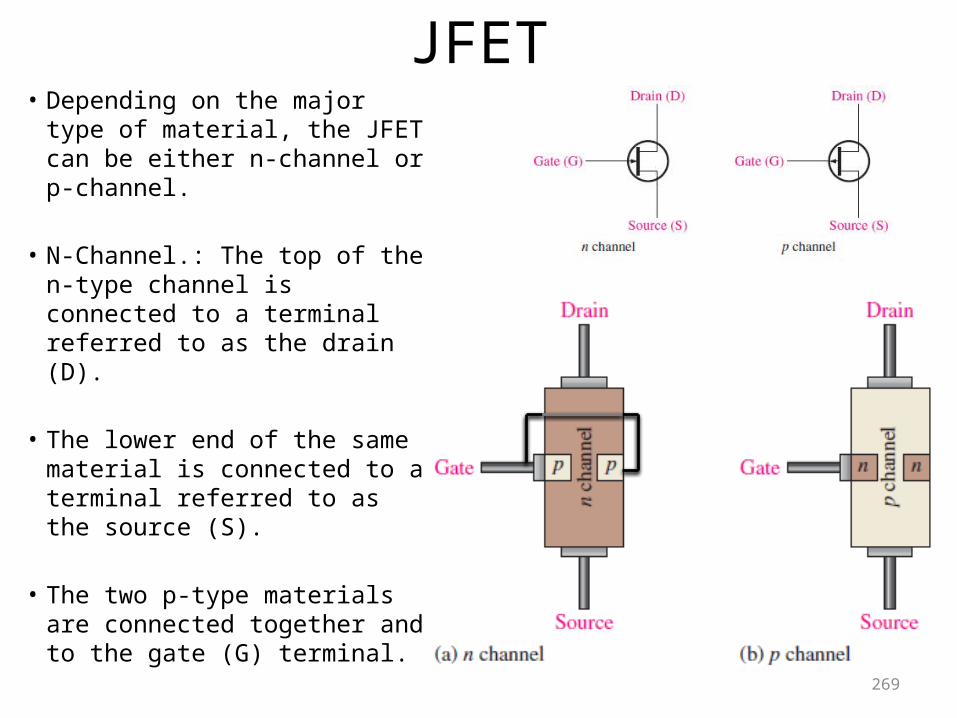
JFET• Depending on the major type of material, the JFET can be either n-channel or p-channel.
• N-Channel.: The top of the n-type channel is connected to a terminal referred to as the drain (D).
• The lower end of the same material is connected to a terminal referred to as the source (S).
• The two p-type materials are connected together and to the gate (G) terminal.
269
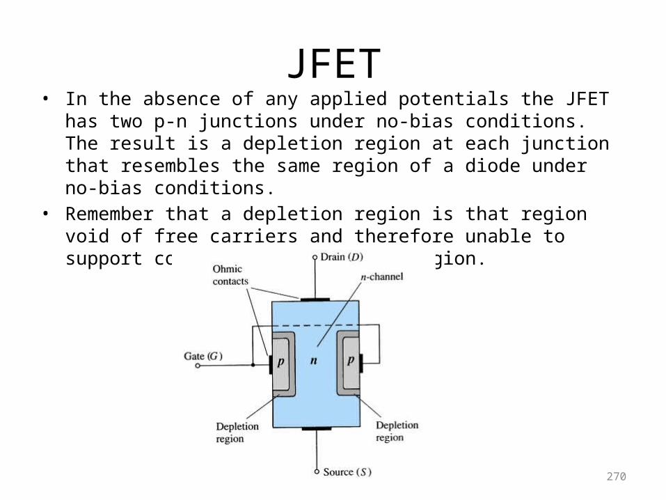
JFET• In the absence of any applied potentials the JFET
has two p-n junctions under no-bias conditions. The result is a depletion region at each junction that resembles the same region of a diode under no-bias conditions.
• Remember that a depletion region is that region void of free carriers and therefore unable to support conduction through the region.
270
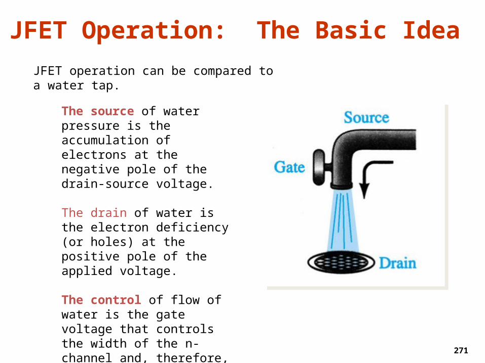
JFET Operation: The Basic IdeaJFET operation can be compared to a water tap.
The source of water pressure is the accumulation of electrons at the negative pole of the drain-source voltage.
The drain of water is the electron deficiency (or holes) at the positive pole of the applied voltage.
The control of flow of water is the gate voltage that controls the width of the n-channel and, therefore, the flow of charges from source to drain.
271
JFET Operating Characteristics
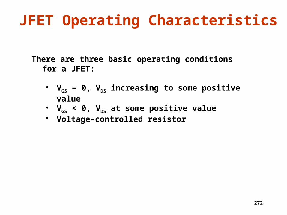
There are three basic operating conditions for a JFET:
• VGS = 0, VDS increasing to some positive value
• VGS < 0, VDS at some positive value• Voltage-controlled resistor
272
JFET Operating Characteristics: VGS = 0 V
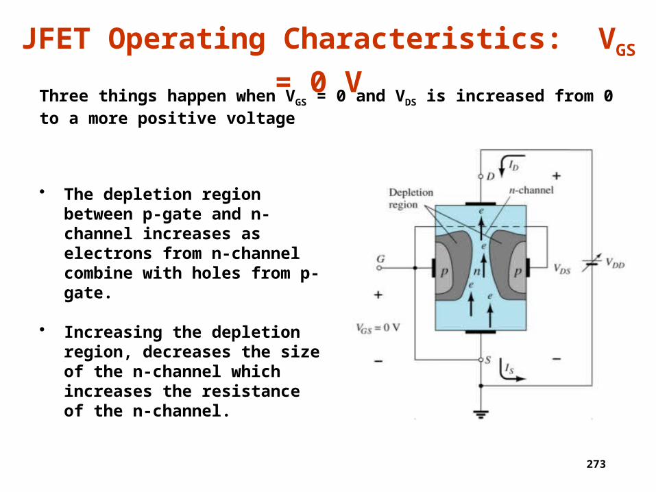
• The depletion region between p-gate and n-channel increases as electrons from n-channel combine with holes from p-gate.
• Increasing the depletion region, decreases the size of the n-channel which increases the resistance of the n-channel.
Three things happen when VGS = 0 and VDS is increased from 0 to a more positive voltage
273
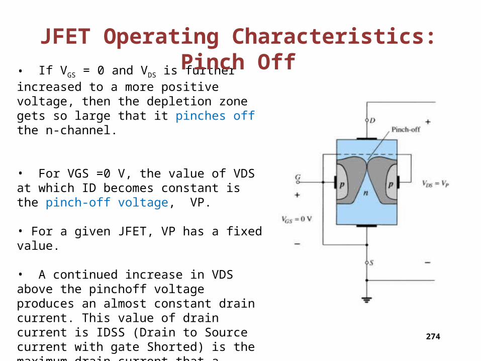
• If VGS = 0 and VDS is further increased to a more positive voltage, then the depletion zone gets so large that it pinches off the n-channel.
• For VGS =0 V, the value of VDS at which ID becomes constant is the pinch-off voltage, VP.
• For a given JFET, VP has a fixed value.
• A continued increase in VDS above the pinchoff voltage produces an almost constant drain current. This value of drain current is IDSS (Drain to Source current with gate Shorted) is the maximum drain current that a specific JFET can produce regardless of the external circuit, and it is always specified for the condition, VGS = 0 V.
JFET Operating Characteristics: Pinch Off
274
275
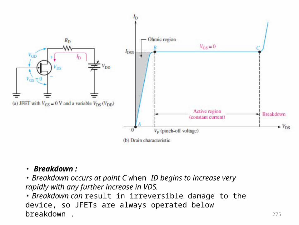
• Breakdown : • Breakdown occurs at point C when ID begins to increase very rapidly with any further increase in VDS. • Breakdown can result in irreversible damage to the device, so JFETs are always operated below breakdown .
At the pinch-off point:
• VGS at pinch-off is denoted as Vp.
• ID is at saturation or maximum. It is referred to as IDSS.
• The ohmic value of the channel is maximum.
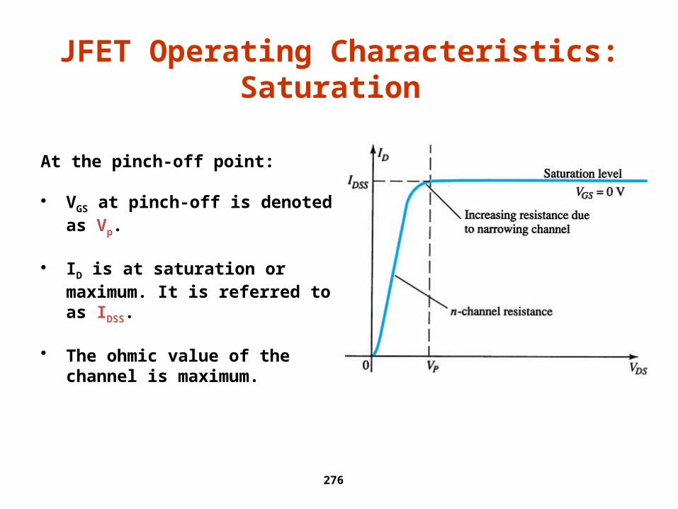
JFET Operating Characteristics: Saturation
276
JFET Operating Characteristics: VGS < 0
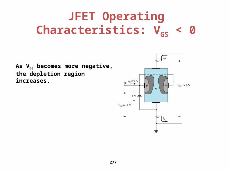
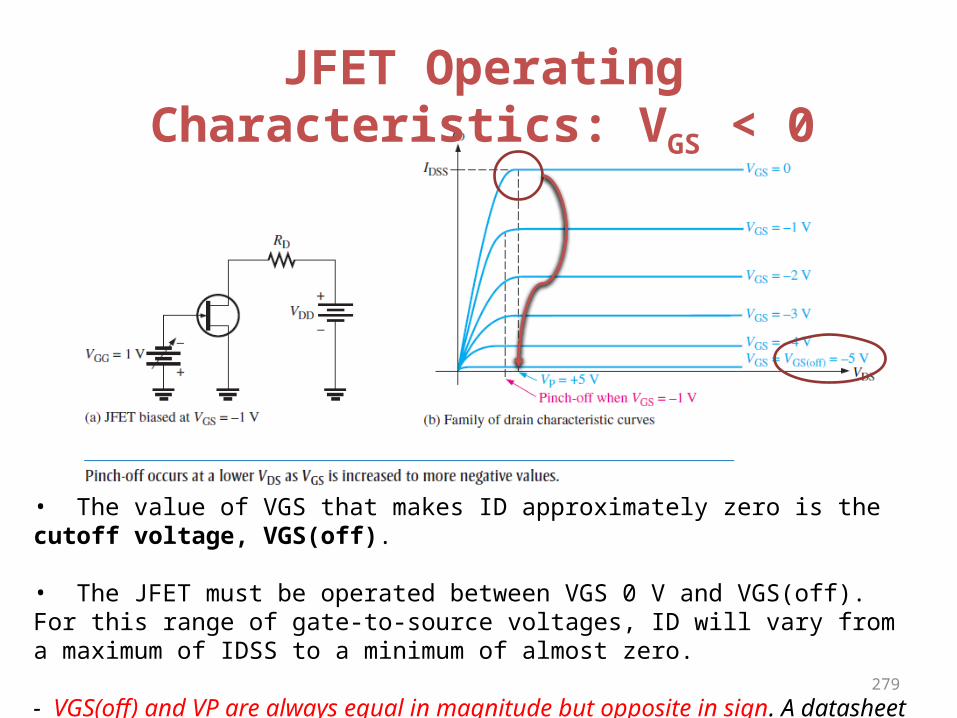
As VGS becomes more negative, the depletion region increases.
277
As VGS becomes more negative:
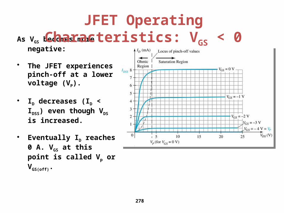
• The JFET experiences pinch-off at a lower voltage (VP).
• ID decreases (ID < IDSS) even though VDS is increased.
• Eventually ID reaches 0 A. VGS at this point is called Vp or VGS(off).
278
JFET Operating Characteristics: VGS < 0
279
JFET Operating Characteristics: VGS < 0
• The value of VGS that makes ID approximately zero is the cutoff voltage, VGS(off).
• The JFET must be operated between VGS 0 V and VGS(off). For this range of gate-to-source voltages, ID will vary from a maximum of IDSS to a minimum of almost zero.
- VGS(off) and VP are always equal in magnitude but opposite in sign. A datasheet usuallywill give either VGS(off) or VP, but not both.
280
2
PGS
od
VV1
rr
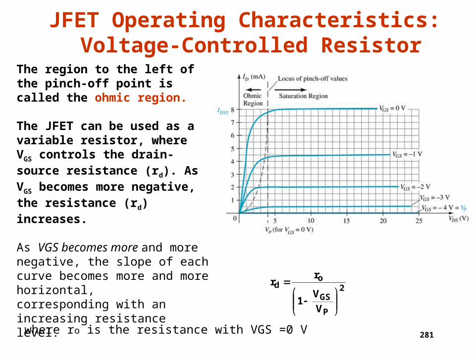
The region to the left of the pinch-off point is called the ohmic region.
The JFET can be used as a variable resistor, where VGS controls the drain-source resistance (rd). As VGS becomes more negative, the resistance (rd) increases.
As VGS becomes more and more negative, the slope of each curve becomes more and more horizontal,corresponding with an increasing resistance level.
JFET Operating Characteristics: Voltage-Controlled Resistor
281where ro is the resistance with VGS =0 V
Voltage-Controlled Resistor
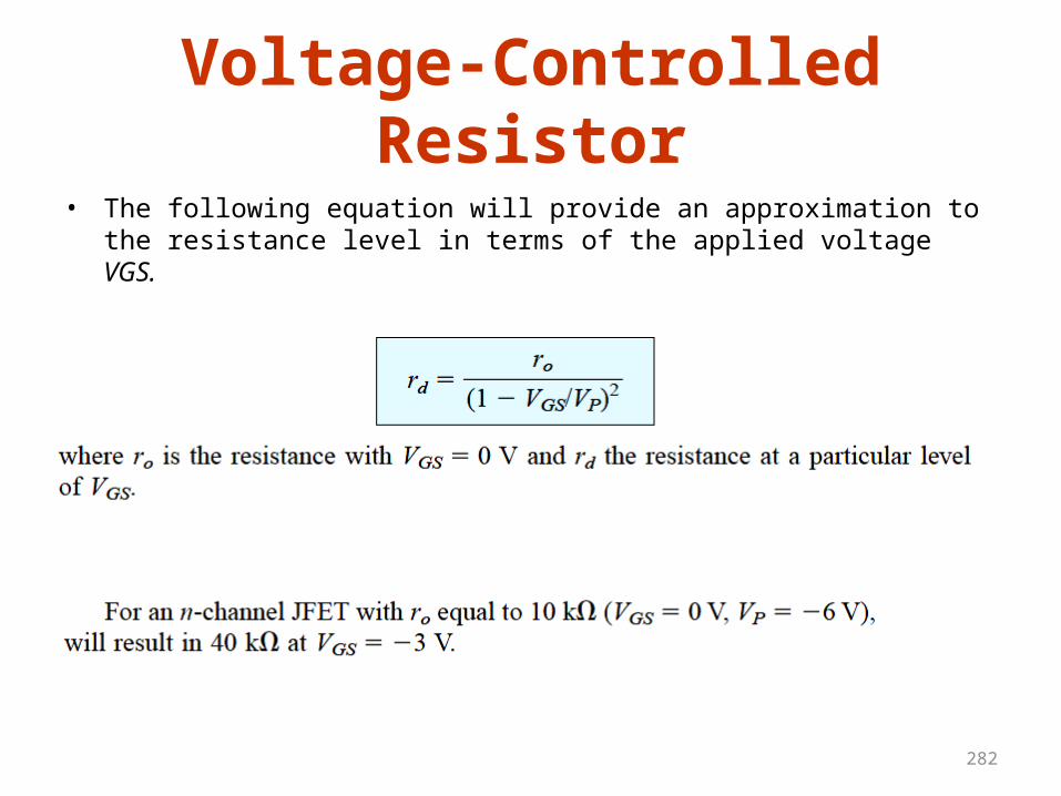
• The following equation will provide an approximation to the resistance level in terms of the applied voltage VGS.
282

p-Channel JFETS
The p-channel JFET behaves the same as the n-channel JFET, except the voltage polarities and current directions are reversed.
283

p-Channel JFET Characteristics
Also note that at high levels of VDS the JFET reaches a breakdown situation: ID increases uncontrollably if VDS > VDSmax.
As VGS increases more positively
• The depletion zone increases
• ID decreases (ID < IDSS)
• Eventually ID = 0 A
284
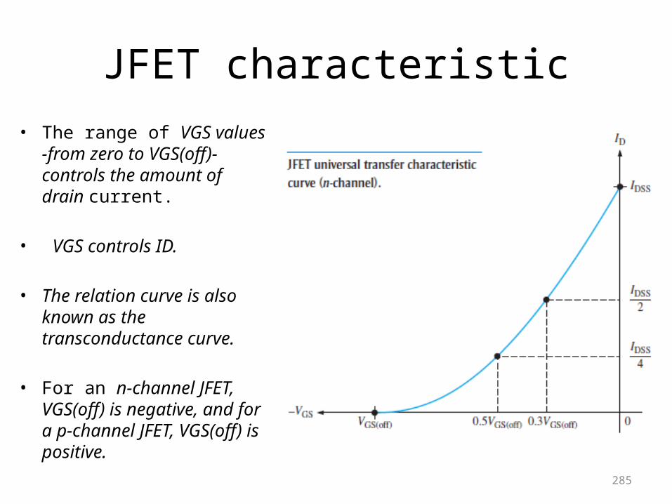
JFET characteristic• The range of VGS values
-from zero to VGS(off)- controls the amount of drain current.
• VGS controls ID.
• The relation curve is also known as the transconductance curve.
• For an n-channel JFET, VGS(off) is negative, and for a p-channel JFET, VGS(off) is positive.
285
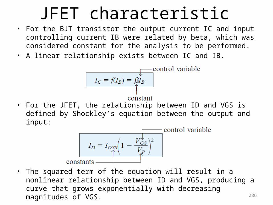
JFET characteristic• For the BJT transistor the output current IC and input
controlling current IB were related by beta, which was considered constant for the analysis to be performed.
• A linear relationship exists between IC and IB.
• For the JFET, the relationship between ID and VGS is defined by Shockley’s equation between the output and input:
• The squared term of the equation will result in a nonlinear relationship between ID and VGS, producing a curve that grows exponentially with decreasing magnitudes of VGS. 286
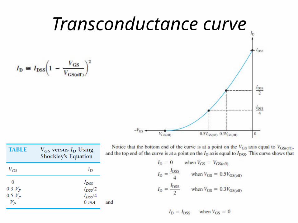
Transconductance curve
287
288
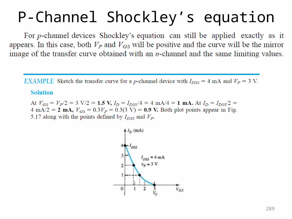
P-Channel Shockley’s equation
289
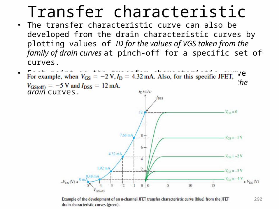
Transfer characteristic• The transfer characteristic curve can also be
developed from the drain characteristic curves by plotting values of ID for the values of VGS taken from the family of drain curves at pinch-off for a specific set of curves.
• Each point on the transfer characteristic curve corresponds to specific values of VGS and ID on the drain curves.
290
291
292
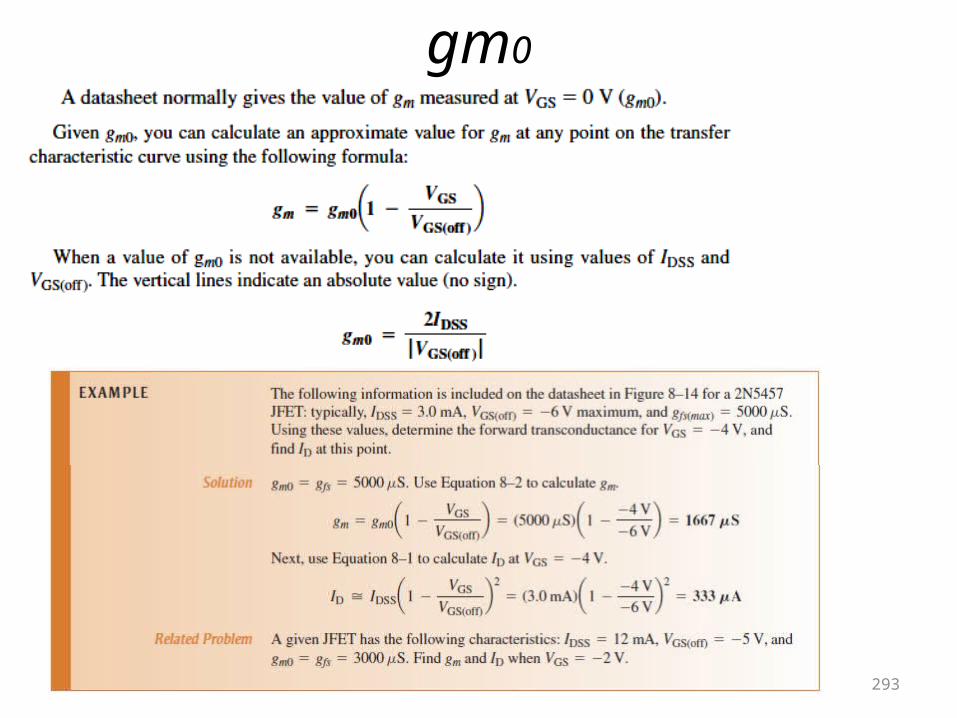
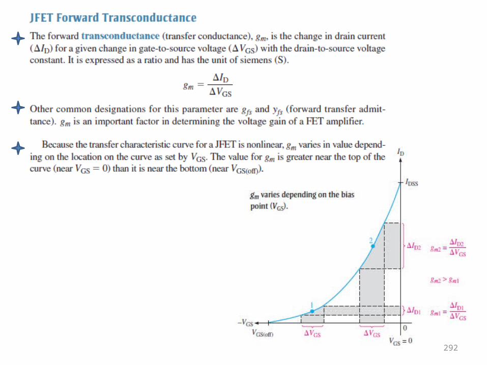
gm0
293
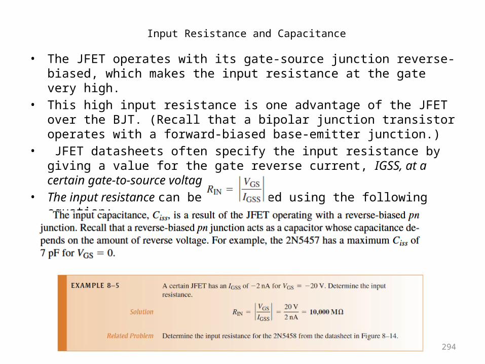
Input Resistance and Capacitance
• The JFET operates with its gate-source junction reverse-biased, which makes the input resistance at the gate very high.
• This high input resistance is one advantage of the JFET over the BJT. (Recall that a bipolar junction transistor operates with a forward-biased base-emitter junction.)
• JFET datasheets often specify the input resistance by giving a value for the gate reverse current, IGSS, at a certain gate-to-source voltage.
• The input resistance can be determined using the following equation:
294
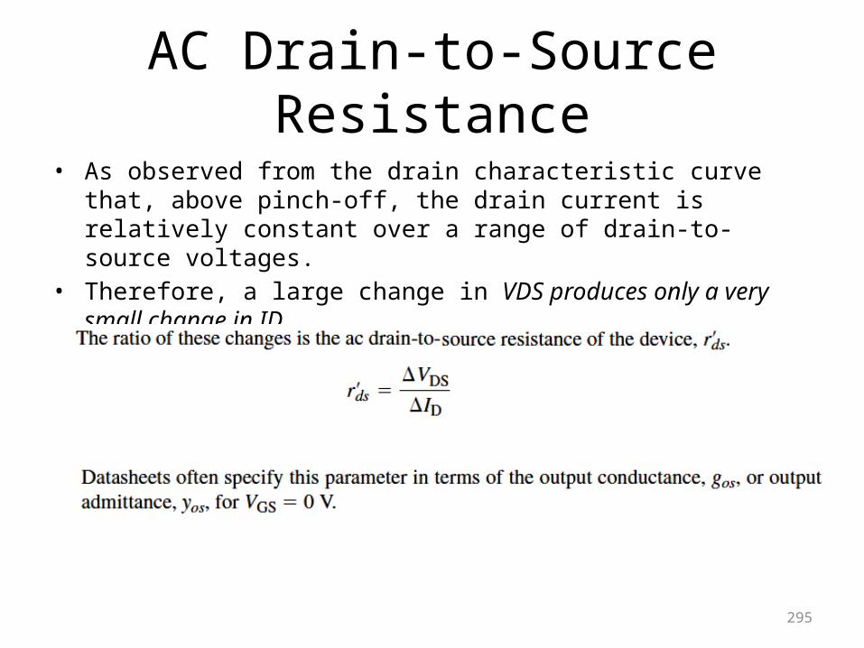
AC Drain-to-Source Resistance
• As observed from the drain characteristic curve that, above pinch-off, the drain current is relatively constant over a range of drain-to-source voltages.
• Therefore, a large change in VDS produces only a very small change in ID
295
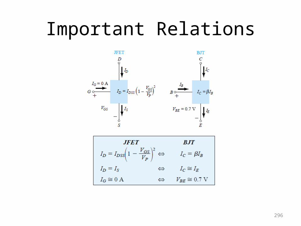
Important Relations
296
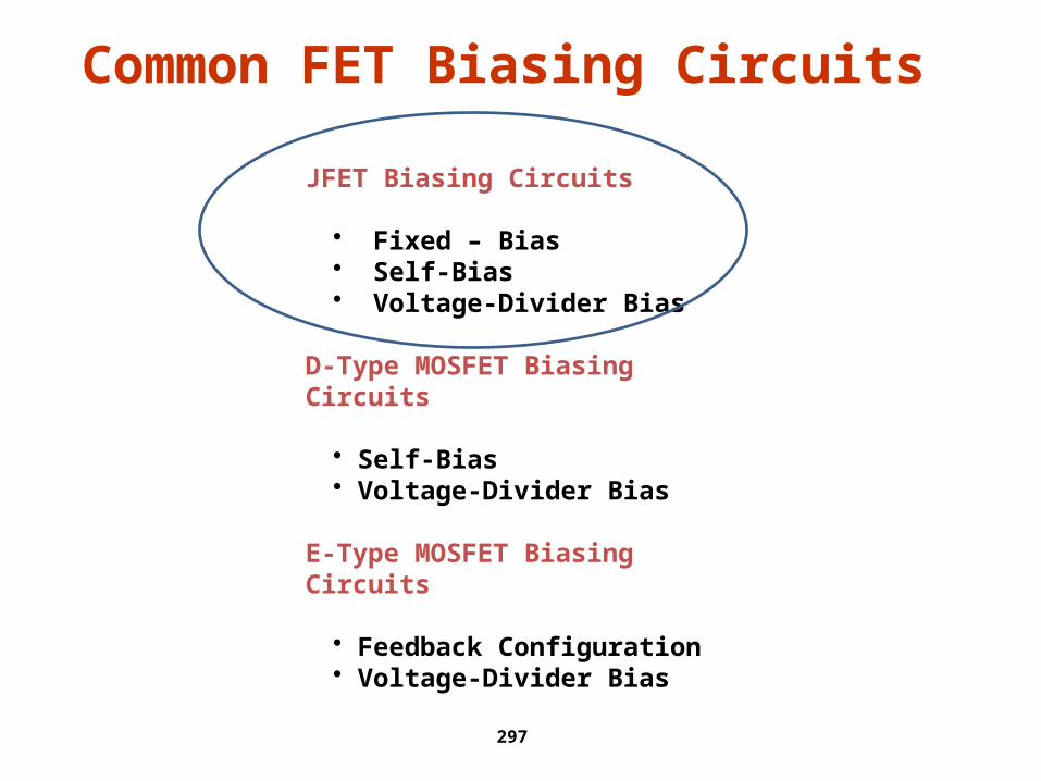
Common FET Biasing CircuitsJFET Biasing Circuits
• Fixed – Bias • Self-Bias • Voltage-Divider Bias
D-Type MOSFET Biasing Circuits
• Self-Bias• Voltage-Divider Bias
E-Type MOSFET Biasing Circuits
• Feedback Configuration• Voltage-Divider Bias
297
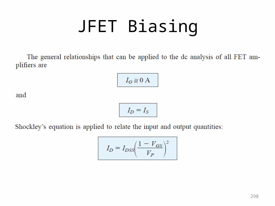
JFET Biasing
298
GGGS
S
DDDDDS
VVVV
RIVV
0
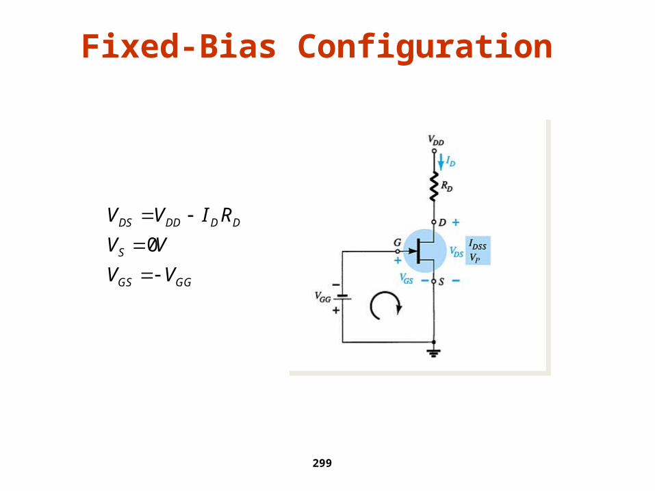
Fixed-Bias Configuration
299
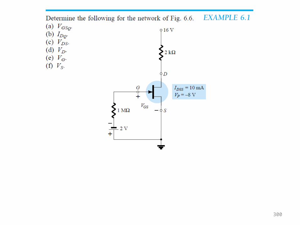
300
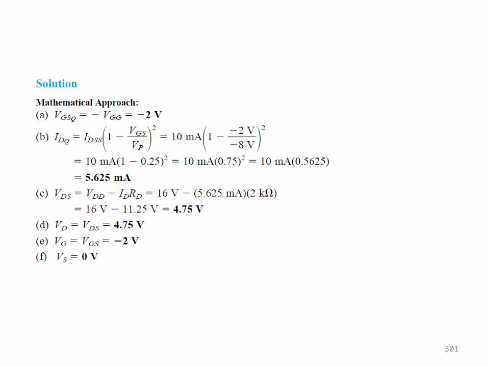
301
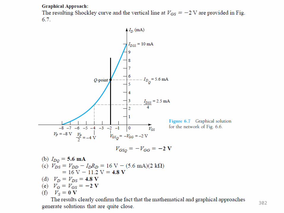
302
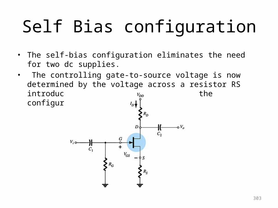
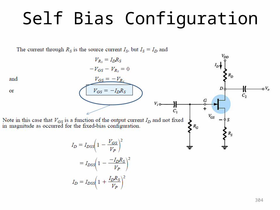
Self Bias configuration• The self-bias configuration eliminates the need
for two dc supplies.• The controlling gate-to-source voltage is now
determined by the voltage across a resistor RS introduced to the source terminal of the configuration.
303
Self Bias Configuration
304
305
306
307
Midpoint Bias
308
309
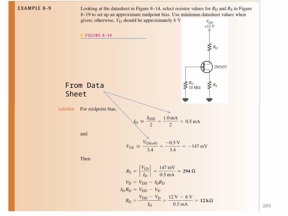
From Data Sheet
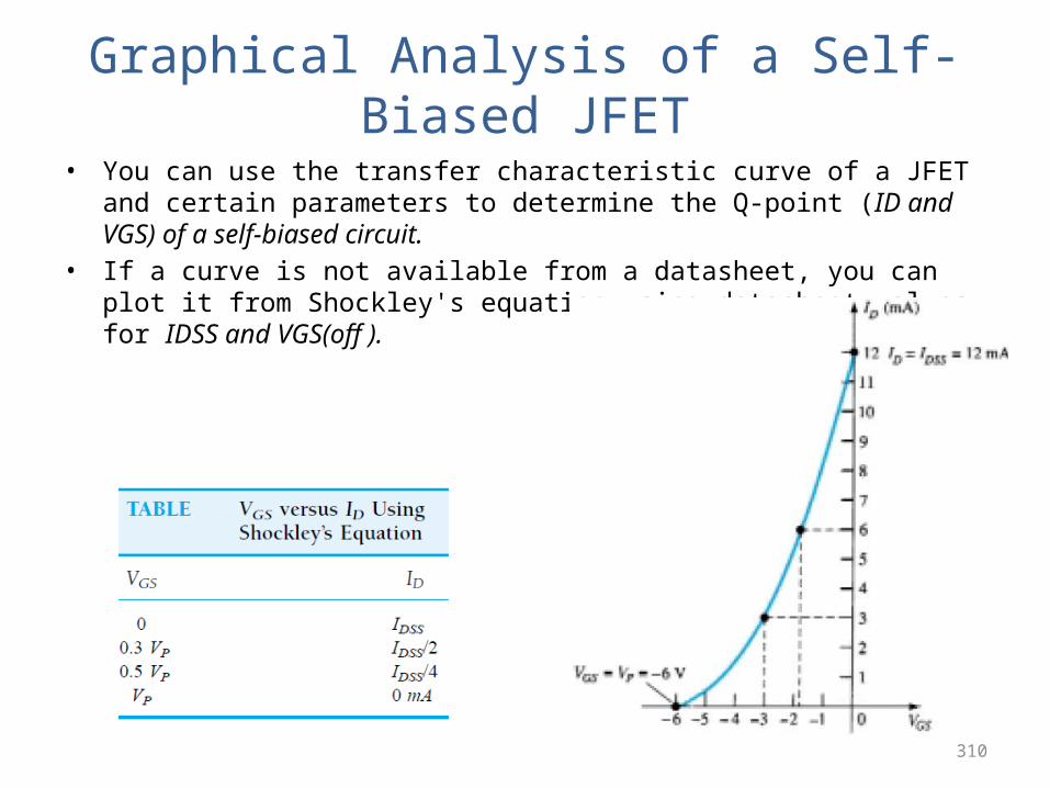
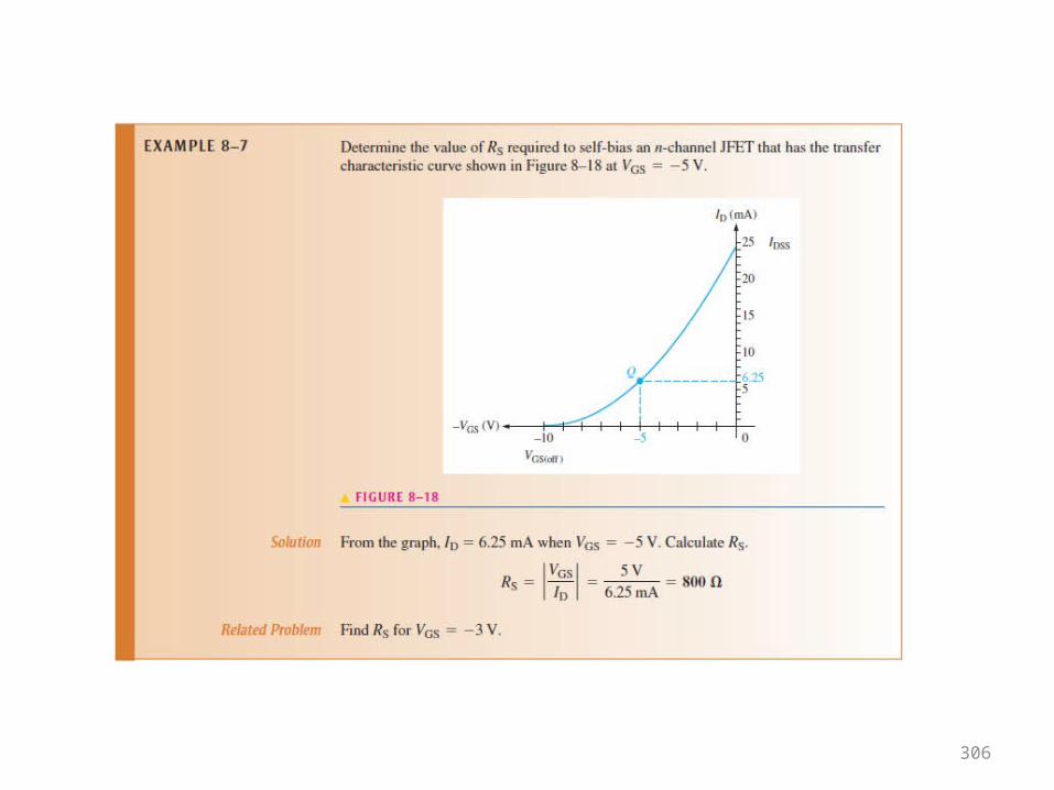
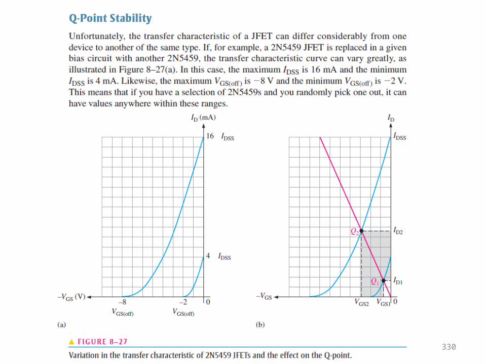
Graphical Analysis of a Self-Biased JFET
• You can use the transfer characteristic curve of a JFET and certain parameters to determine the Q-point (ID and VGS) of a self-biased circuit.
• If a curve is not available from a datasheet, you can plot it from Shockley's equation using datasheet values for IDSS and VGS(off ).
310
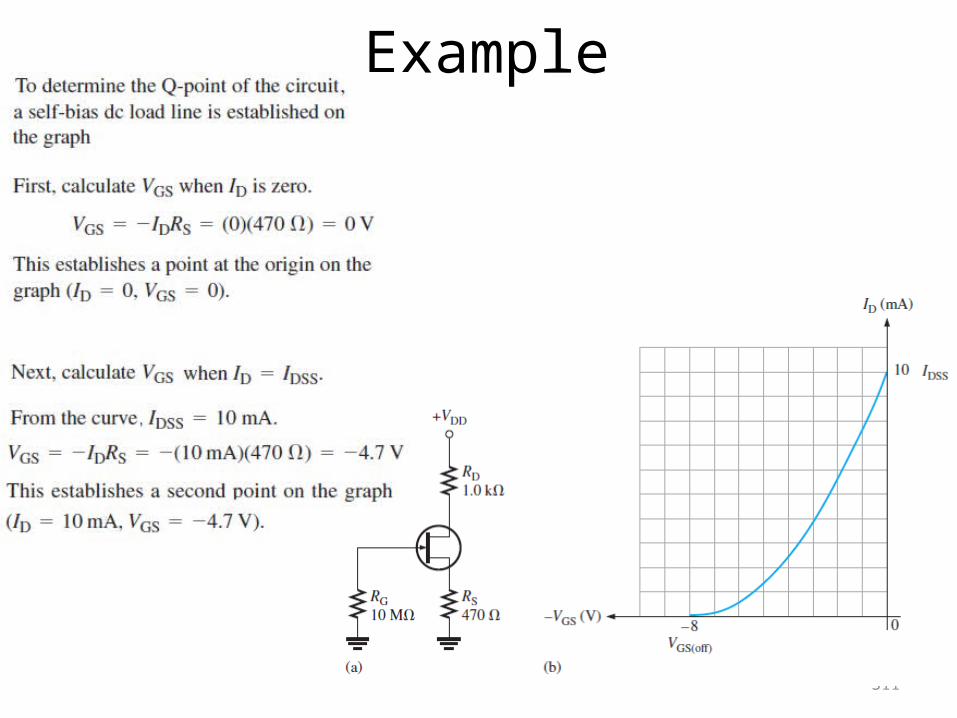
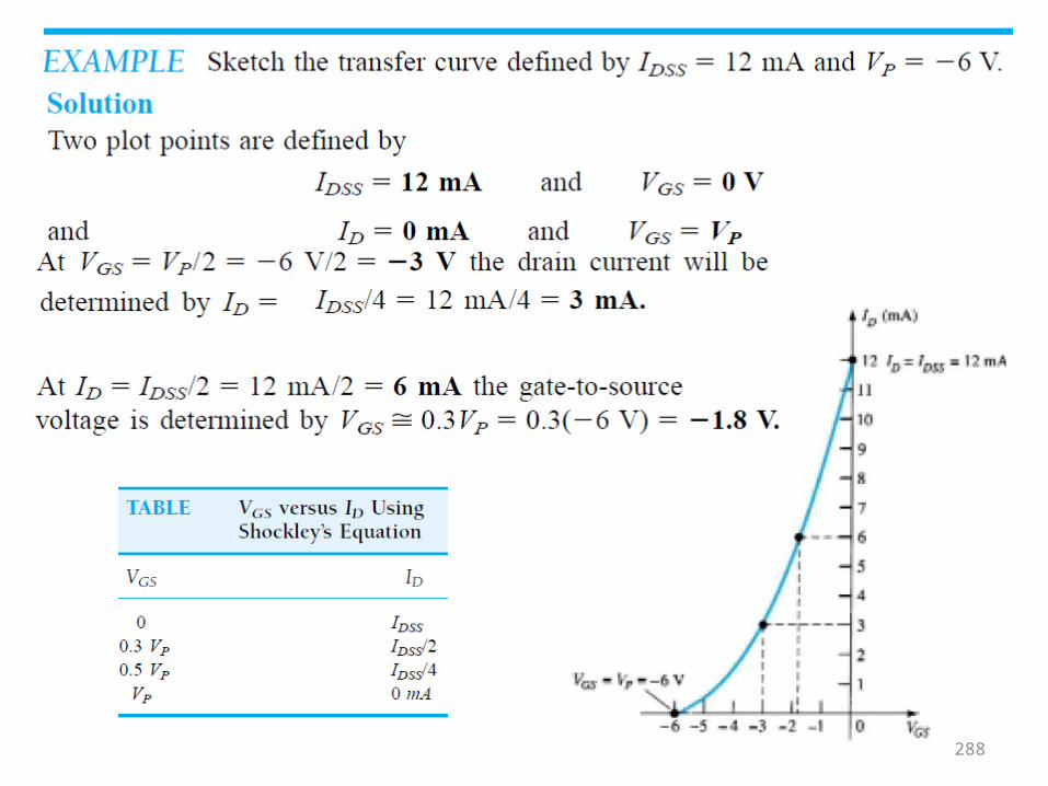
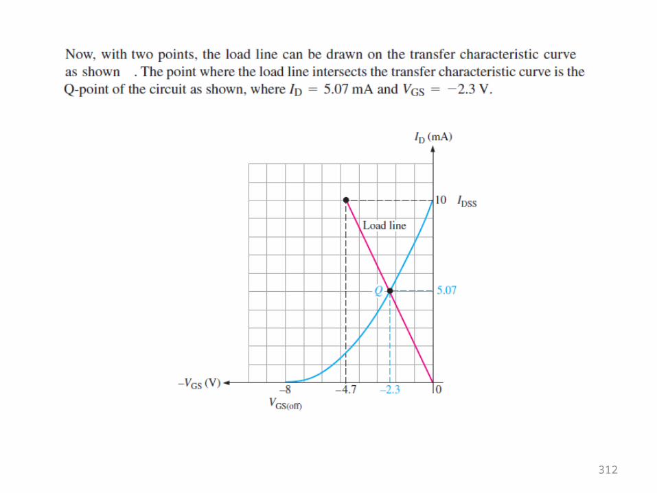
Example
311
312
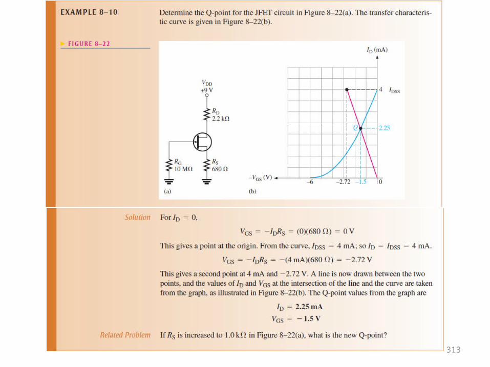
313
314
315
316
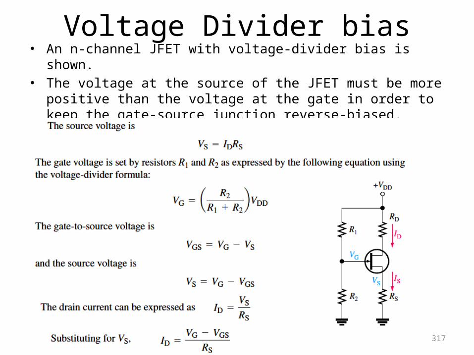
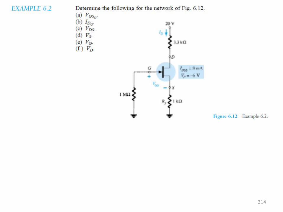
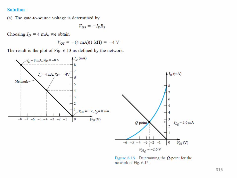
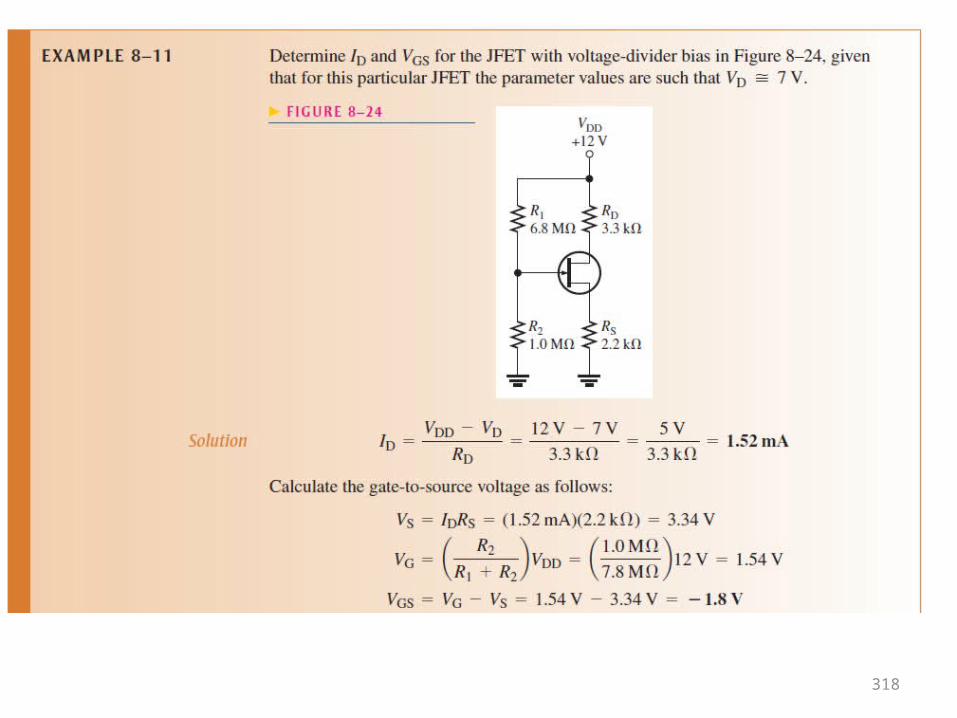
Voltage Divider bias• An n-channel JFET with voltage-divider bias is
shown. • The voltage at the source of the JFET must be more
positive than the voltage at the gate in order to keep the gate-source junction reverse-biased.
317
318
Graphical Analysis of a JFET with Voltage-Divider Bias
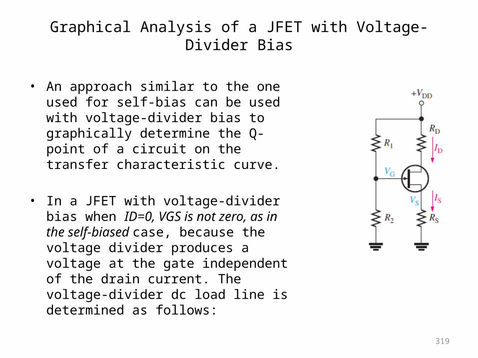
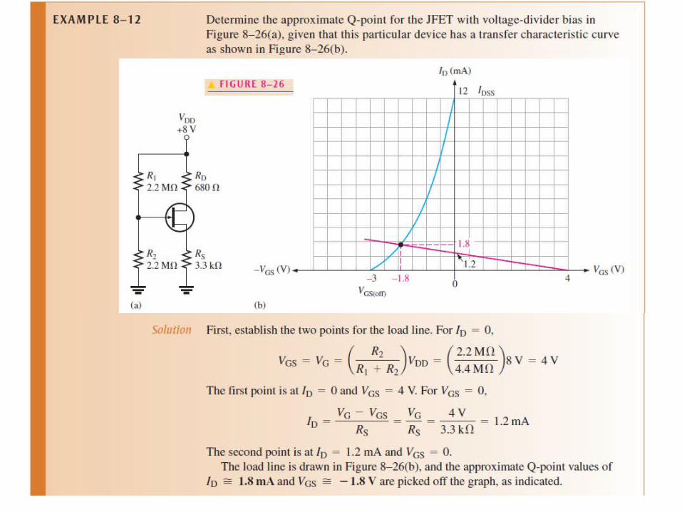
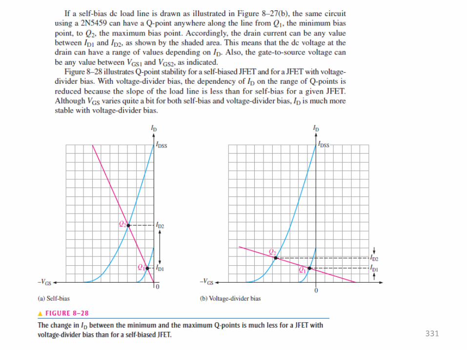
• An approach similar to the one used for self-bias can be used with voltage-divider bias to graphically determine the Q-point of a circuit on the transfer characteristic curve.
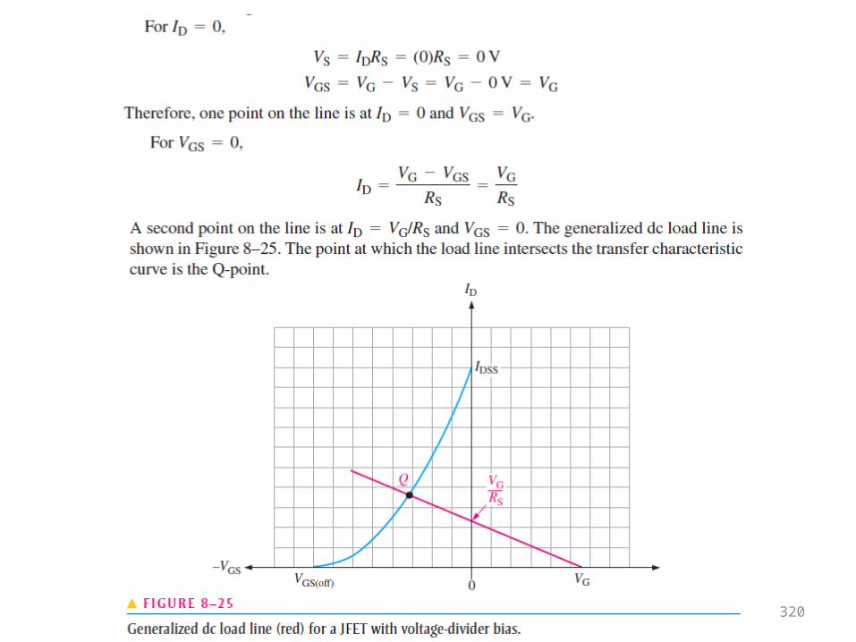
• In a JFET with voltage-divider bias when ID=0, VGS is not zero, as in the self-biased case, because the voltage divider produces a voltage at the gate independent of the drain current. The voltage-divider dc load line is determined as follows:
319
320
321
322
323
324
325
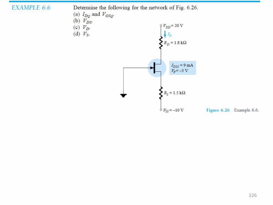
326
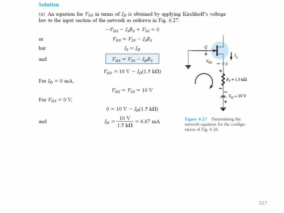
327
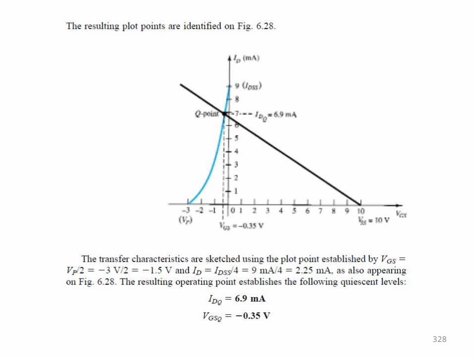
328
329
330
331
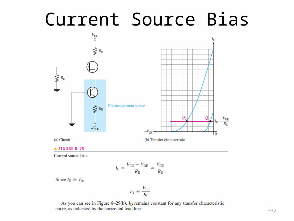
Current Source Bias
332
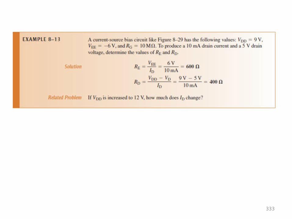
333
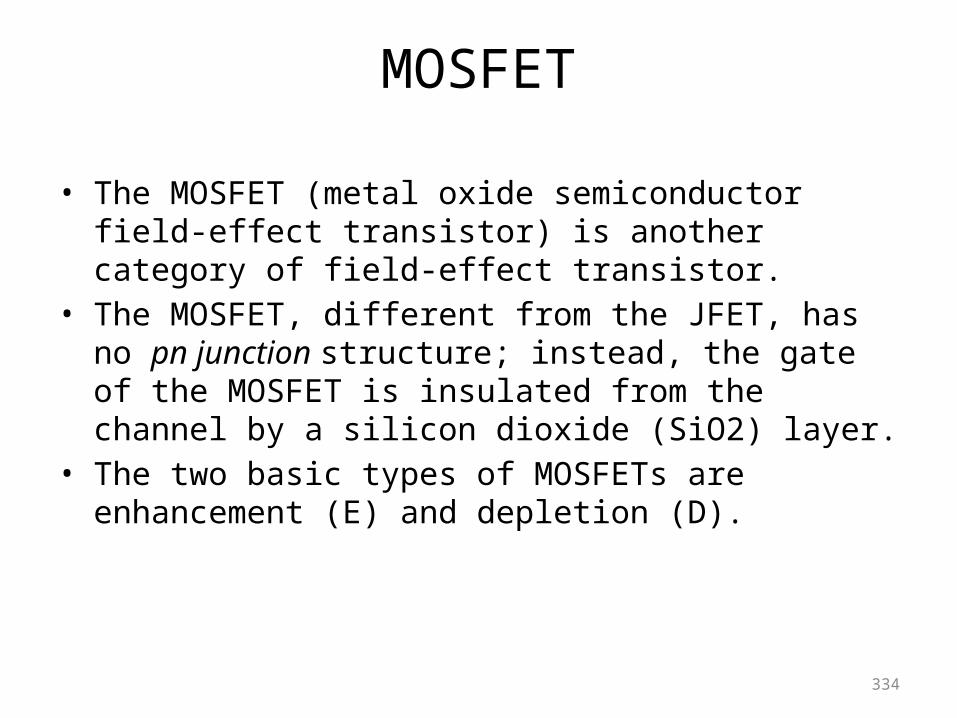
MOSFET
• The MOSFET (metal oxide semiconductor field-effect transistor) is another category of field-effect transistor.
• The MOSFET, different from the JFET, has no pn junction structure; instead, the gate of the MOSFET is insulated from the channel by a silicon dioxide (SiO2) layer.
• The two basic types of MOSFETs are enhancement (E) and depletion (D).
334
335
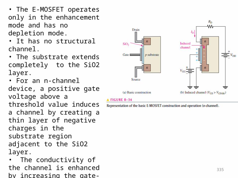
• The E-MOSFET operates only in the enhancement mode and has no depletion mode.• It has no structural channel. • The substrate extends completely to the SiO2 layer. • For an n-channel device, a positive gate voltage above a threshold value induces a channel by creating a thin layer of negative charges in the substrate region adjacent to the SiO2 layer.• The conductivity of the channel is enhanced by increasing the gate-to-source voltage and thus pulling more electrons into the channel area. • For any gate voltage below the threshold value, there is no channel
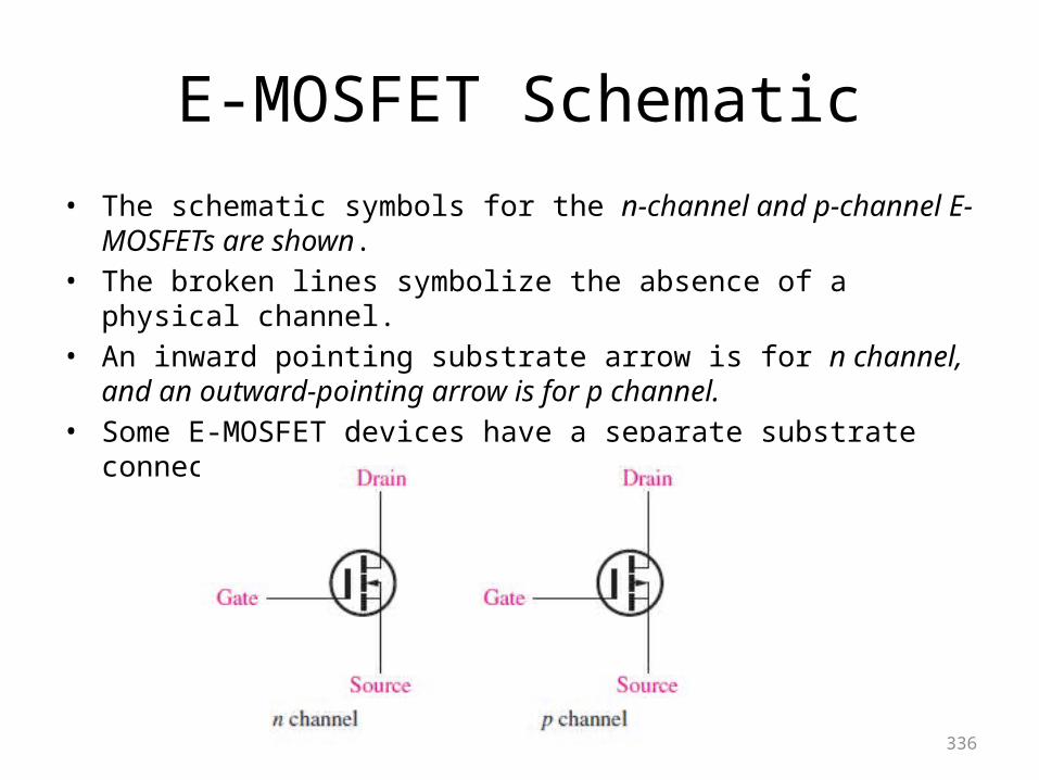
E-MOSFET Schematic• The schematic symbols for the n-channel and p-channel E-
MOSFETs are shown. • The broken lines symbolize the absence of a
physical channel. • An inward pointing substrate arrow is for n channel,
and an outward-pointing arrow is for p channel.• Some E-MOSFET devices have a separate substrate
connection.
336
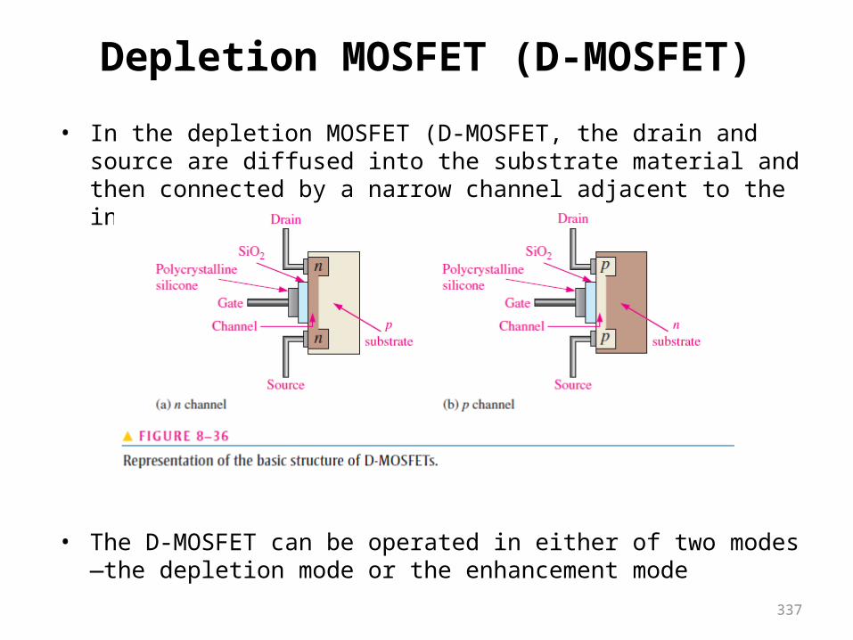
Depletion MOSFET (D-MOSFET)• In the depletion MOSFET (D-MOSFET, the drain and
source are diffused into the substrate material and then connected by a narrow channel adjacent to the insulated gate.
• The D-MOSFET can be operated in either of two modes—the depletion mode or the enhancement mode
337
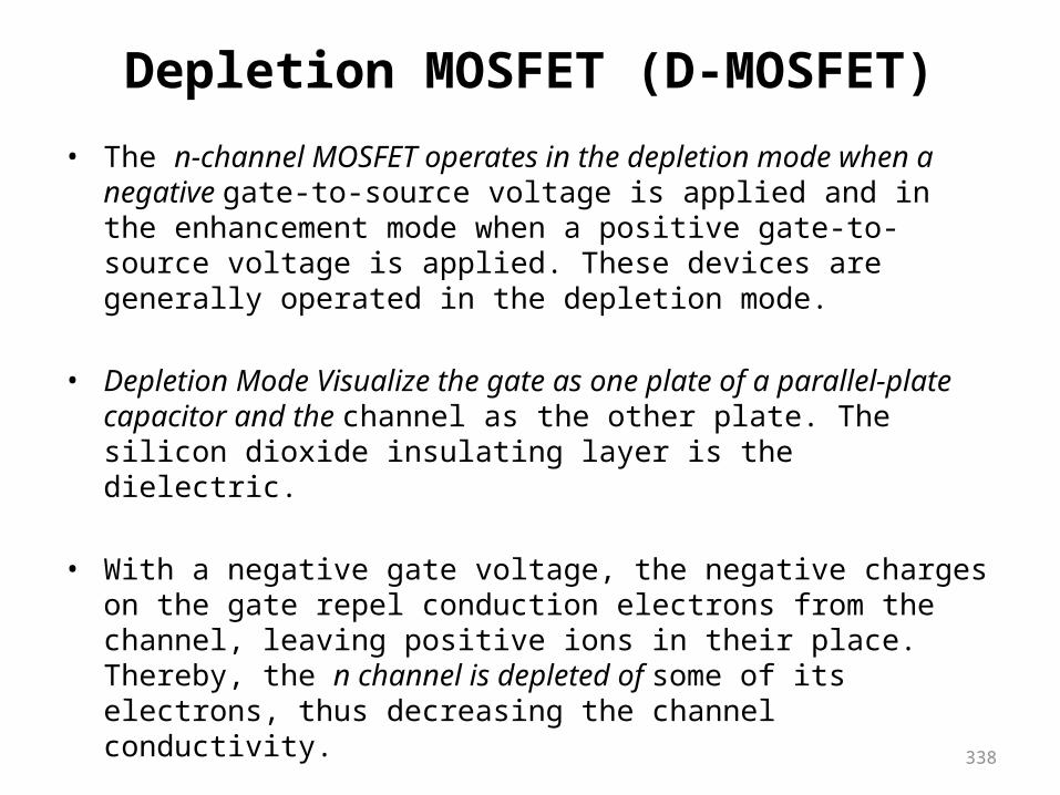
• The n-channel MOSFET operates in the depletion mode when a negative gate-to-source voltage is applied and in the enhancement mode when a positive gate-to-source voltage is applied. These devices are generally operated in the depletion mode.
• Depletion Mode Visualize the gate as one plate of a parallel-plate capacitor and the channel as the other plate. The silicon dioxide insulating layer is the dielectric.
• With a negative gate voltage, the negative charges on the gate repel conduction electrons from the channel, leaving positive ions in their place. Thereby, the n channel is depleted of some of its electrons, thus decreasing the channel conductivity. 338
Depletion MOSFET (D-MOSFET)
Depletion MOSFET (D-MOSFET)
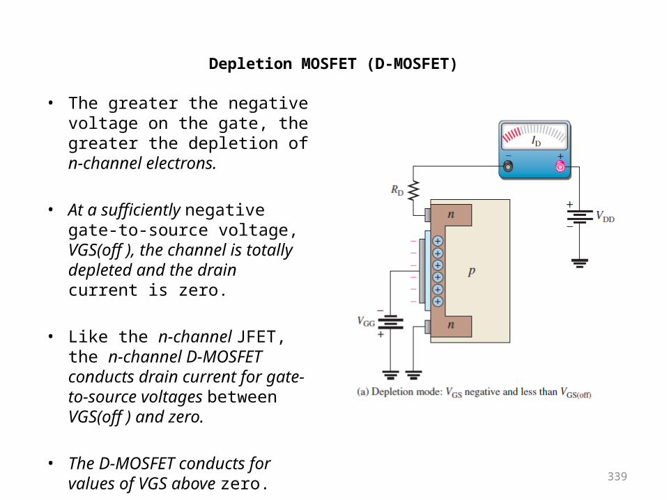
• The greater the negative voltage on the gate, the greater the depletion of n-channel electrons.
• At a sufficiently negative gate-to-source voltage, VGS(off ), the channel is totally depleted and the drain current is zero.
• Like the n-channel JFET,
the n-channel D-MOSFET conducts drain current for gate-to-source voltages between VGS(off ) and zero.
• The D-MOSFET conducts for values of VGS above zero. 339
Depletion MOSFET (D-MOSFET)
340
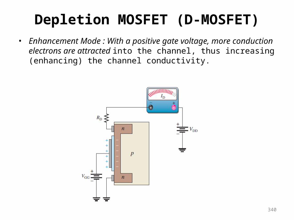
• Enhancement Mode : With a positive gate voltage, more conduction electrons are attracted into the channel, thus increasing (enhancing) the channel conductivity.
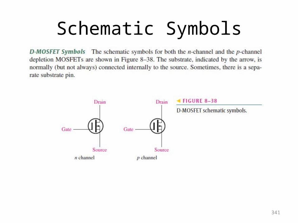
Schematic Symbols
341

Power MOSFET : Structures• The conventional enhancement MOSFETs have a long thin
channel.
• This results in a relatively high drain-to-source resistance
• It limits the E-MOSFET to low power applications.
342
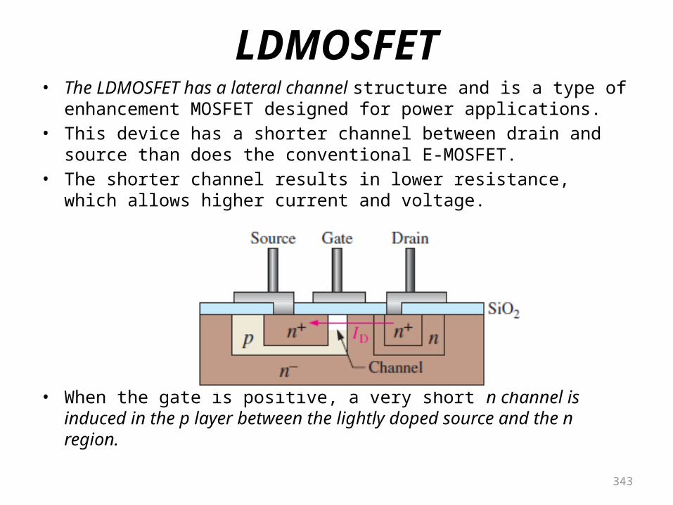
LDMOSFET• The LDMOSFET has a lateral channel structure and is a type of
enhancement MOSFET designed for power applications.• This device has a shorter channel between drain and
source than does the conventional E-MOSFET. • The shorter channel results in lower resistance,
which allows higher current and voltage.
• When the gate is positive, a very short n channel is induced in the p layer between the lightly doped source and the n region.
343

VMOSFET • The V-groove MOSFET is another example of the conventional E-MOSFET• designed to achieve higher power capability by creating a
shorter and wider channel with• less resistance between the drain and source using a vertical
channel structure.• The shorter, wider channels allow for higher currents and,
thus, greater power dissipation.• Frequency response is also improved.• The VMOSFET has two source connections, a gate connection on
top, and a drain connection on the bottom, as shown in Figure 8–41. The channel is induced vertically along both sides of the V-shaped groove between the drain (n+ substrate where n+ means a higher doping level than n-) and the source connections. The channel length is set by the thickness of the layers, which is controlled by doping densities and diffusion time rather than by mask dimensions.
344

TMOSFET • The vertical channel structure of the TMOSFET is illustrated in Figure
8–42.• The gate structure is embedded in a silicon
dioxide layer, and the source contact is continuous over the entire surface area. The drain is on the bottom.
• TMOSFET achieves greater packing density than VMOSFET, while retaining the short vertical channel advantage.
345
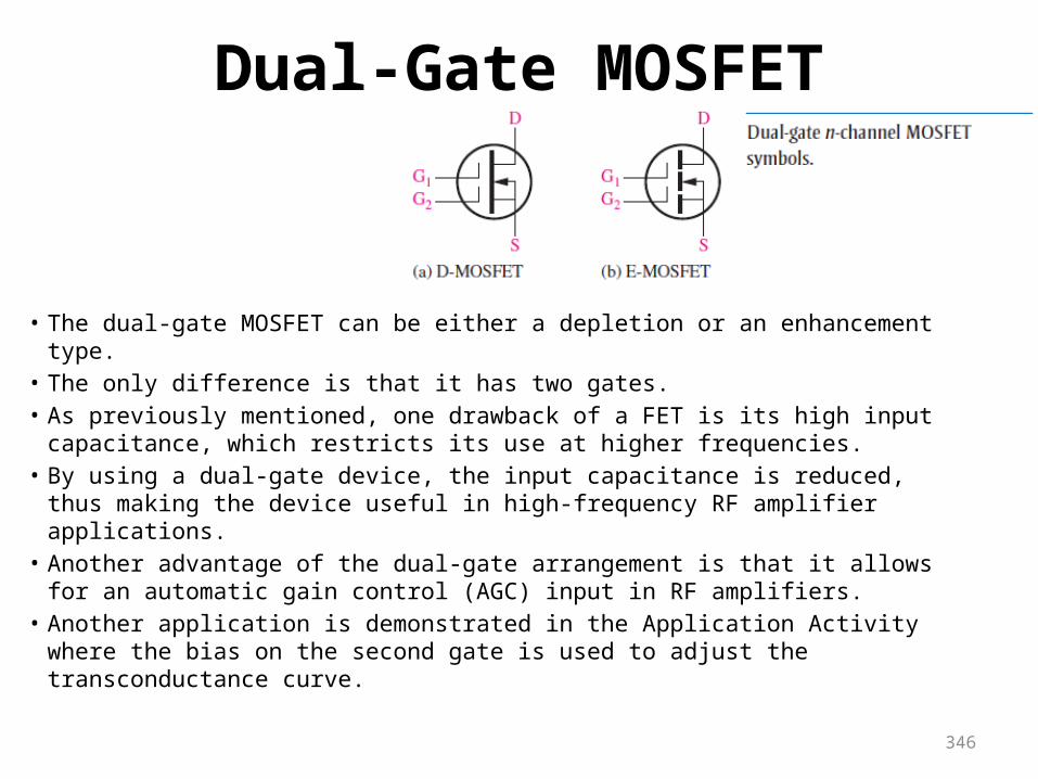
Dual-Gate MOSFET
• The dual-gate MOSFET can be either a depletion or an enhancement type.
• The only difference is that it has two gates. • As previously mentioned, one drawback of a FET is its high input capacitance, which restricts its use at higher frequencies.
• By using a dual-gate device, the input capacitance is reduced, thus making the device useful in high-frequency RF amplifier applications.
• Another advantage of the dual-gate arrangement is that it allows for an automatic gain control (AGC) input in RF amplifiers.
• Another application is demonstrated in the Application Activity where the bias on the second gate is used to adjust the transconductance curve.
346
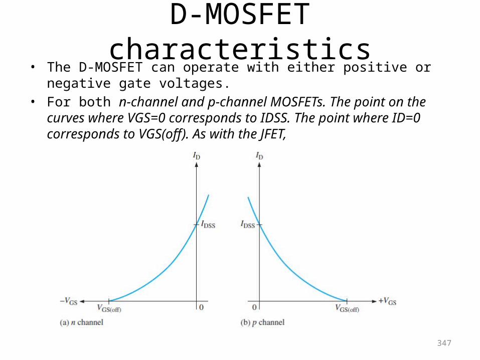
D-MOSFET characteristics
• The D-MOSFET can operate with either positive or negative gate voltages.
• For both n-channel and p-channel MOSFETs. The point on the curves where VGS=0 corresponds to IDSS. The point where ID=0 corresponds to VGS(off). As with the JFET,
347
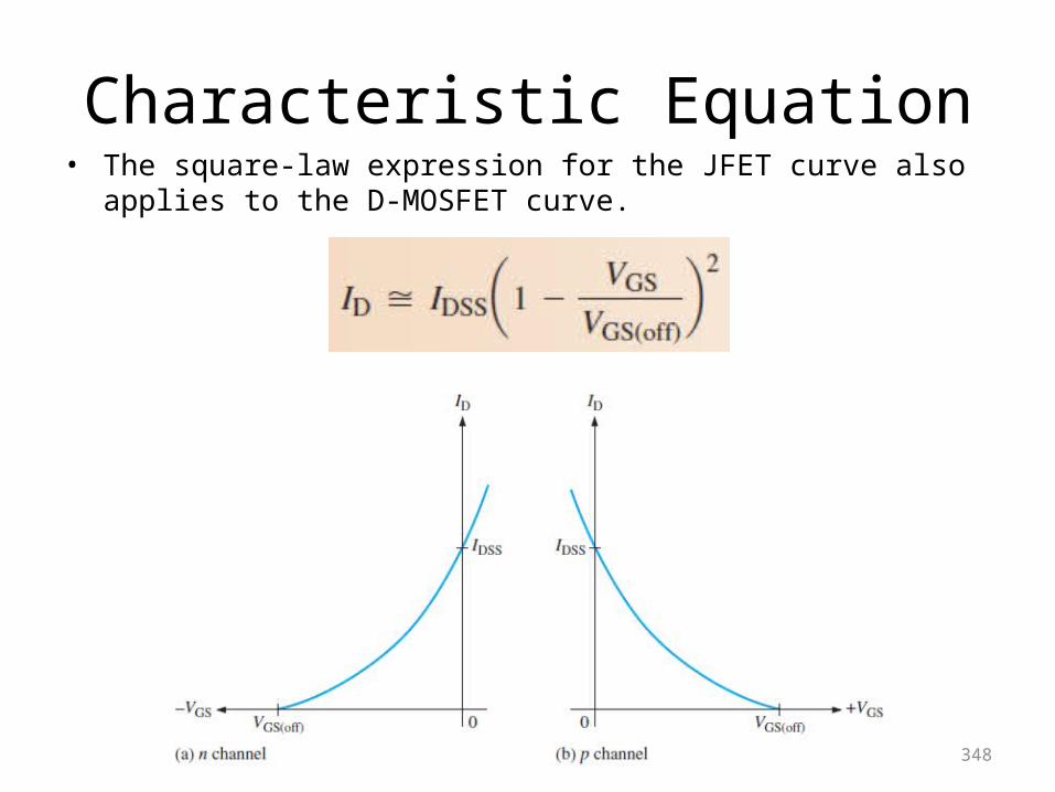
Characteristic Equation
348
• The square-law expression for the JFET curve also applies to the D-MOSFET curve.
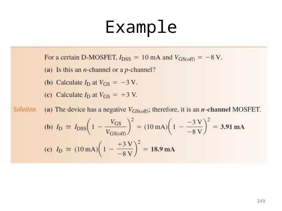
Example
349
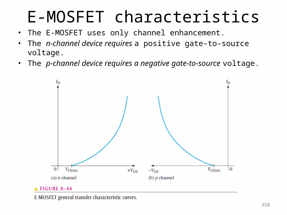
E-MOSFET characteristics• The E-MOSFET uses only channel enhancement. • The n-channel device requires a positive gate-to-source
voltage.• The p-channel device requires a negative gate-to-source voltage.
350
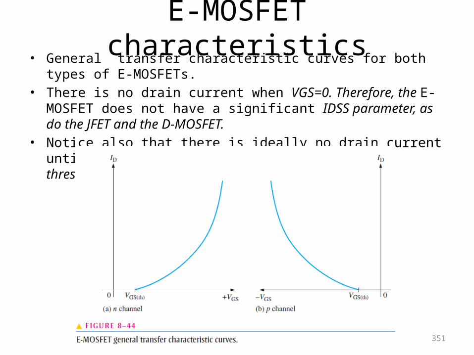
E-MOSFET characteristics• General transfer characteristic curves for both
types of E-MOSFETs. • There is no drain current when VGS=0. Therefore, the E-
MOSFET does not have a significant IDSS parameter, as do the JFET and the D-MOSFET.
• Notice also that there is ideally no drain current until VGS reaches a certain nonzero value called the threshold voltage, VGS(th).
351
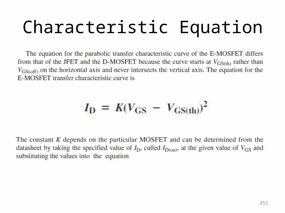
Characteristic Equation
352
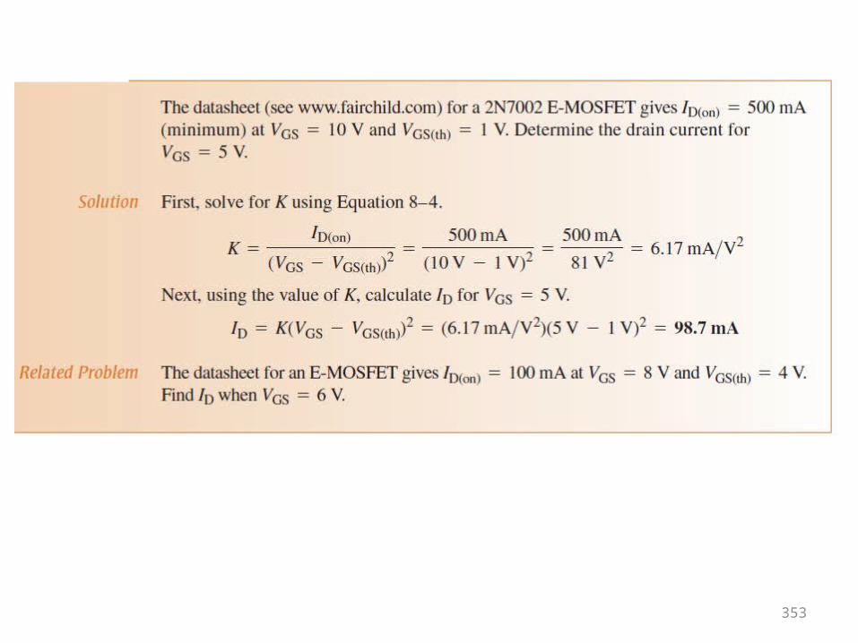
353
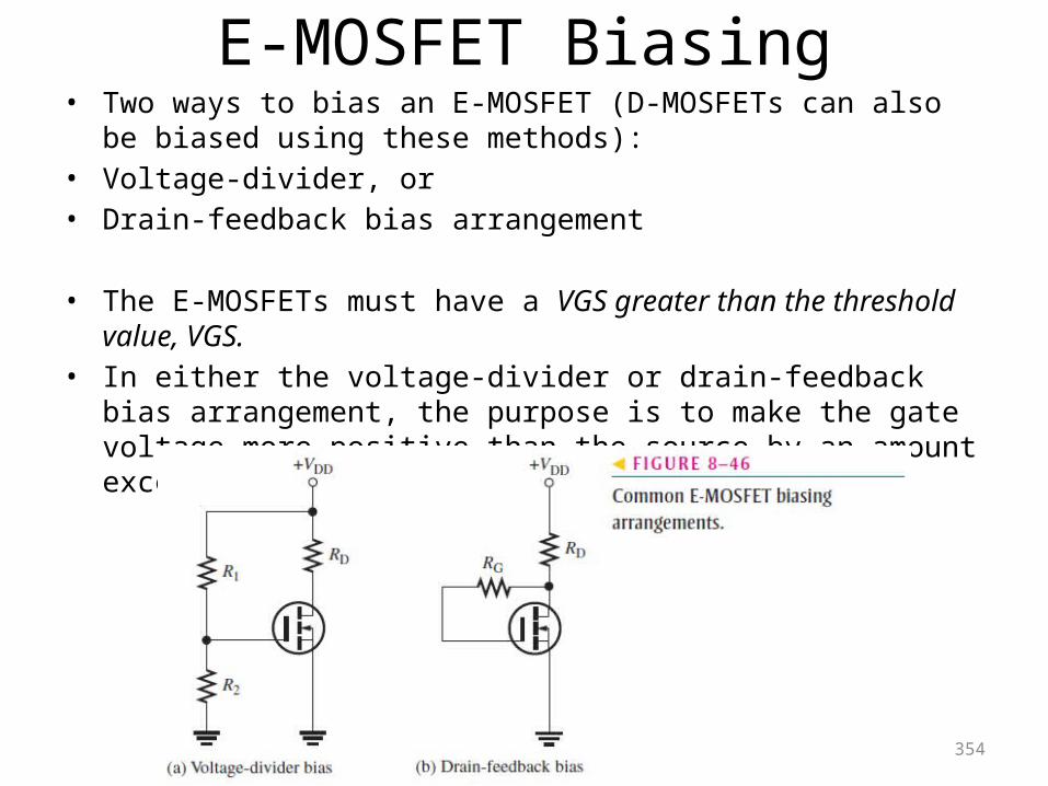
E-MOSFET Biasing• Two ways to bias an E-MOSFET (D-MOSFETs can also
be biased using these methods):• Voltage-divider, or • Drain-feedback bias arrangement
• The E-MOSFETs must have a VGS greater than the threshold value, VGS.
• In either the voltage-divider or drain-feedback bias arrangement, the purpose is to make the gate voltage more positive than the source by an amount exceeding VGS(th).
354
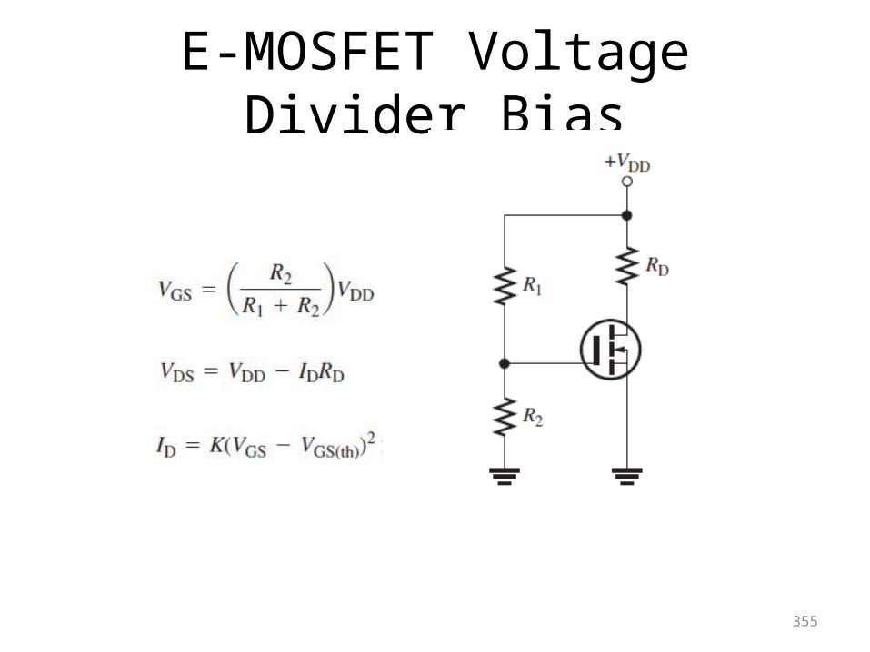
E-MOSFET Voltage Divider Bias
355
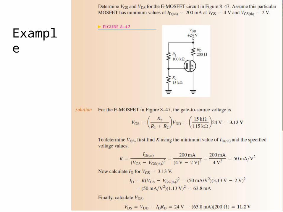
356
Example
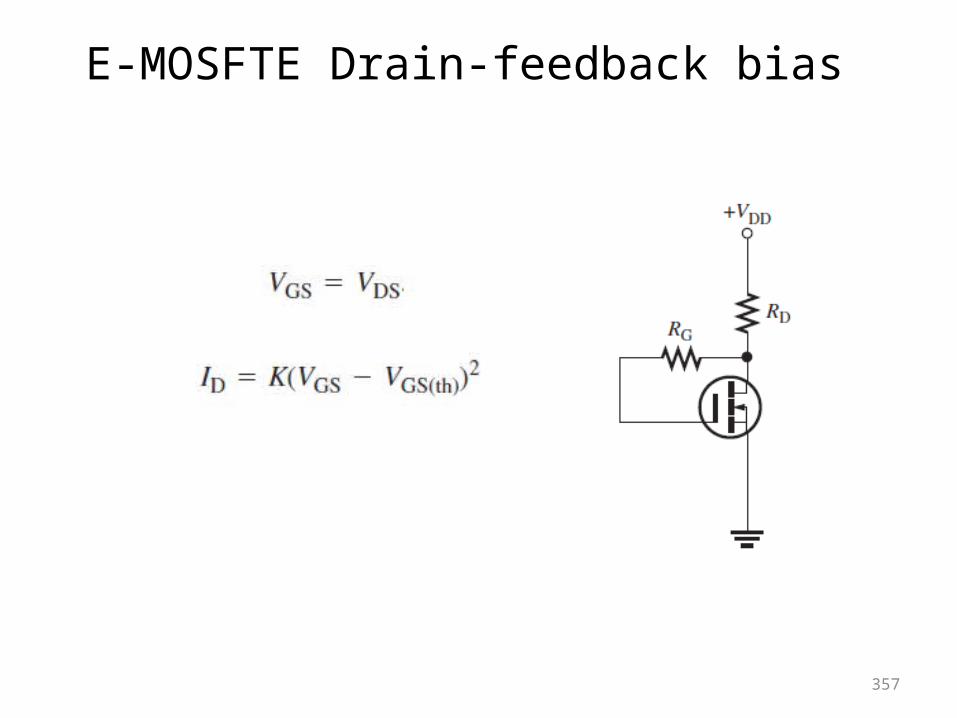
E-MOSFTE Drain-feedback bias
357
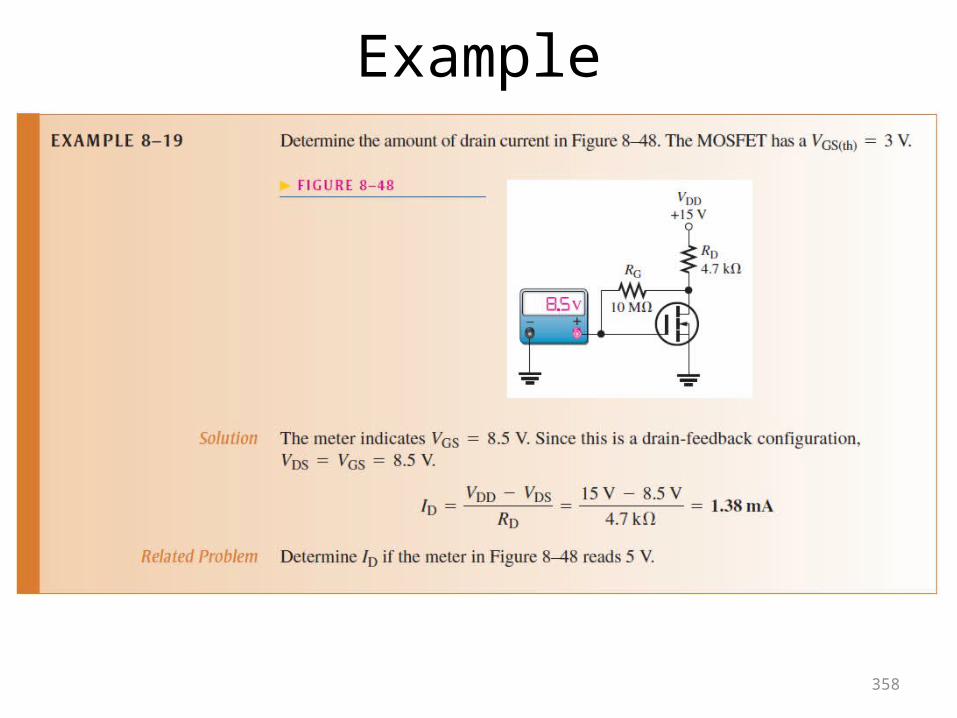
Example
358
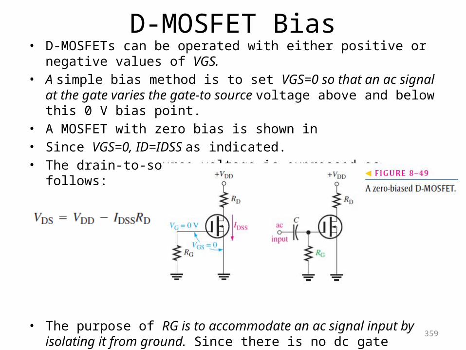
D-MOSFET Bias• D-MOSFETs can be operated with either positive or
negative values of VGS. • A simple bias method is to set VGS=0 so that an ac signal
at the gate varies the gate-to source voltage above and below this 0 V bias point.
• A MOSFET with zero bias is shown in• Since VGS=0, ID=IDSS as indicated. • The drain-to-source voltage is expressed as
follows:
• The purpose of RG is to accommodate an ac signal input by isolating it from ground. Since there is no dc gate current, RG does not affect the zero
• gate-to-source bias
359
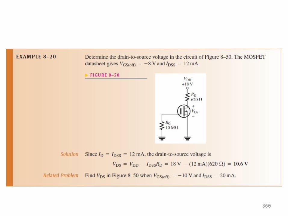
360
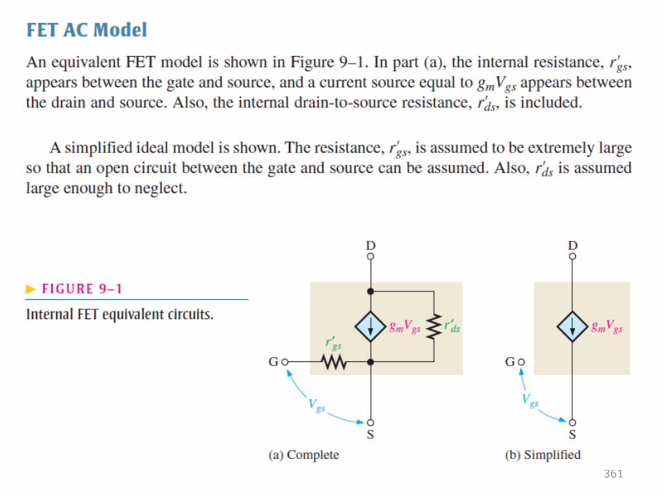
361
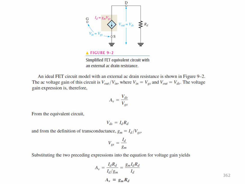
362
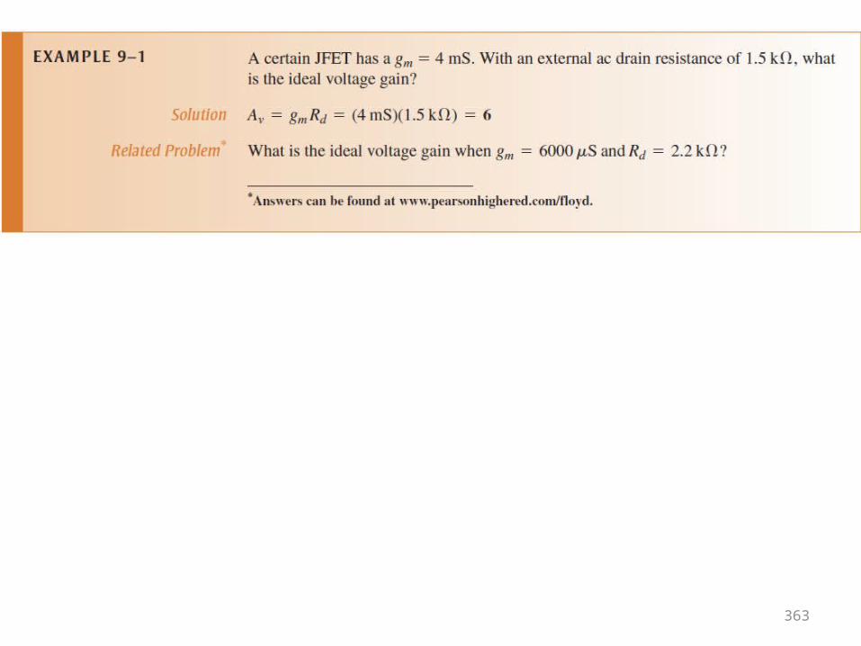
363
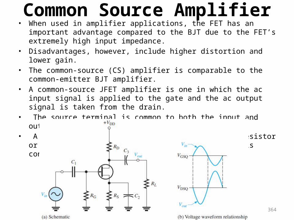
Common Source Amplifier• When used in amplifier applications, the FET has an
important advantage compared to the BJT due to the FET’s extremely high input impedance.
• Disadvantages, however, include higher distortion and lower gain.
• The common-source (CS) amplifier is comparable to the common-emitter BJT amplifier.
• A common-source JFET amplifier is one in which the ac input signal is applied to the gate and the ac output signal is taken from the drain.
• The source terminal is common to both the input and output signal.
• A common-source amplifier either has no source resistor or has a bypassed source resistor, so the source is connected to ac ground.
364
JFET Amplifier Operation• A self-biased common-source n-channel JFET amplifier with an ac source
capacitively coupled to the gate is shown in Figure 9–3(a). The resistor, RG, serves two purposes: It keeps the gate at approximately 0 V dc (because IGSS is extremely small), and its large value (usually several mega ohms) prevents loading of the ac signal source.
• A bias voltage is produced by the drop across RS. The bypass capacitor, C2, keeps the source of the JFET at ac ground.
• The input signal voltage causes the gate-to-source voltage to swing above and below its Q-point value (VGSQ), causing a corresponding swing in drain current. As the drain current increases, the voltage drop across RD also increases, causing the drain voltage to decrease.
• The drain current swings above and below its Q-point value in phase with the gate-to-source voltage. The drain-to-source voltage swings above and below its Q-point value (VDSQ) and is 180° out of phase with the gate-to-source voltage.
365
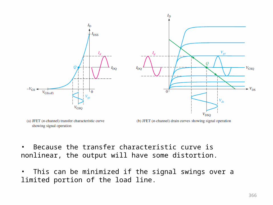
366
• Because the transfer characteristic curve is nonlinear, the output will have some distortion.
• This can be minimized if the signal swings over a limited portion of the load line.
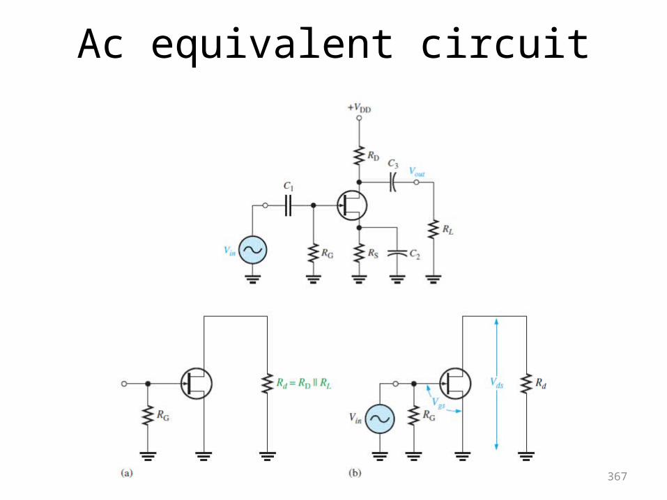
Ac equivalent circuit
367
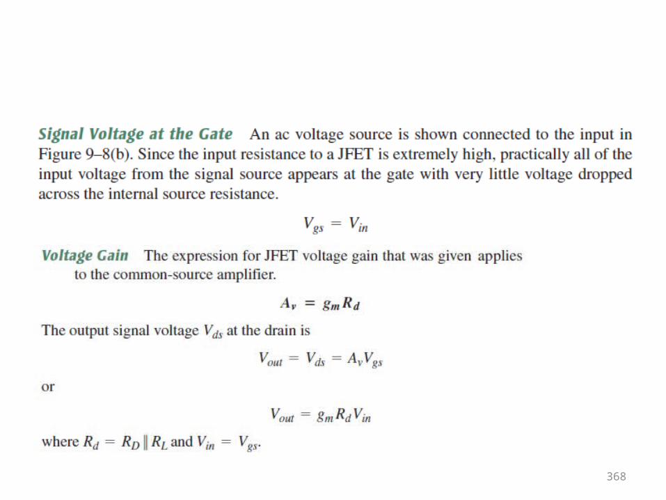
368
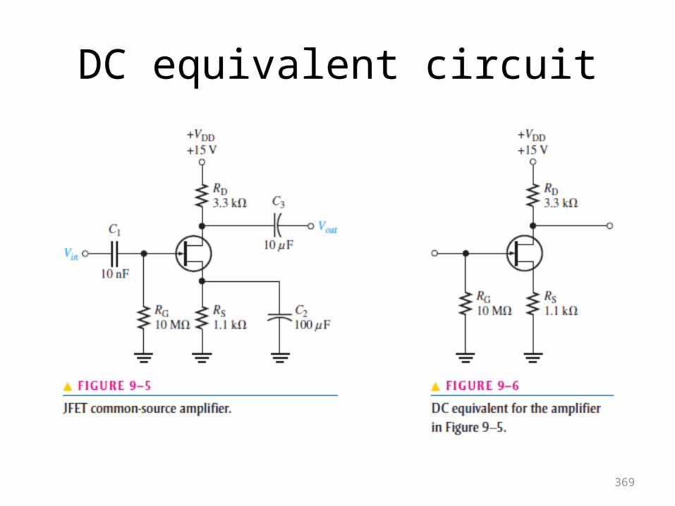
DC equivalent circuit
369
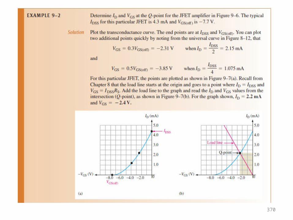
370
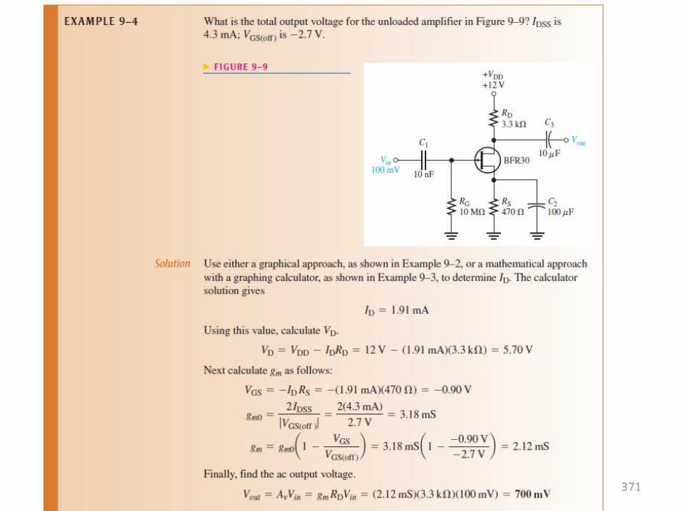
371
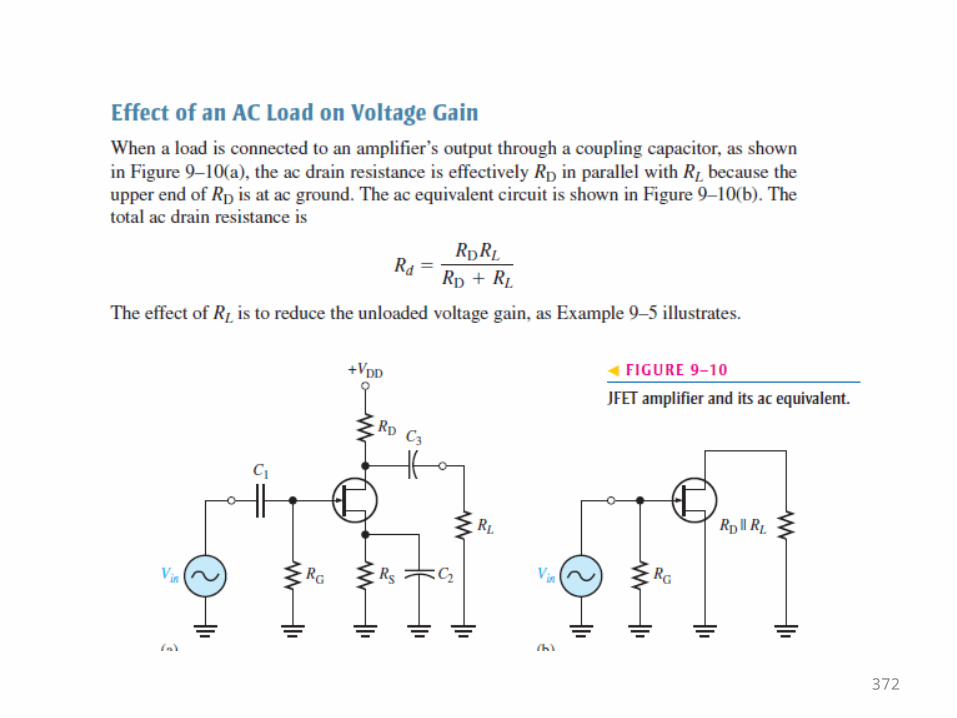
372
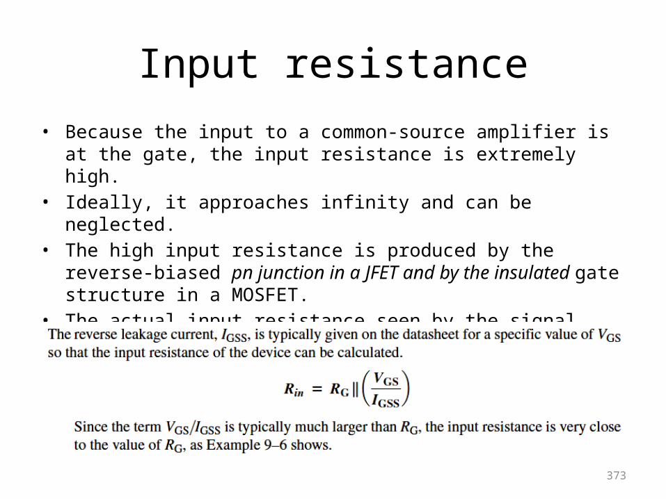
Input resistance• Because the input to a common-source amplifier is
at the gate, the input resistance is extremely high.
• Ideally, it approaches infinity and can be neglected.
• The high input resistance is produced by the reverse-biased pn junction in a JFET and by the insulated gate structure in a MOSFET.
• The actual input resistance seen by the signal source is the gate-to-ground resistor, RG, in parallel with the FET’s input resistance, VGS/IGSS.
373
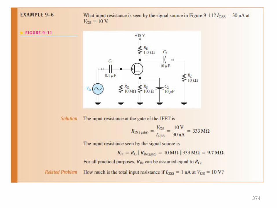
374
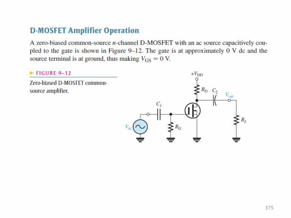
375
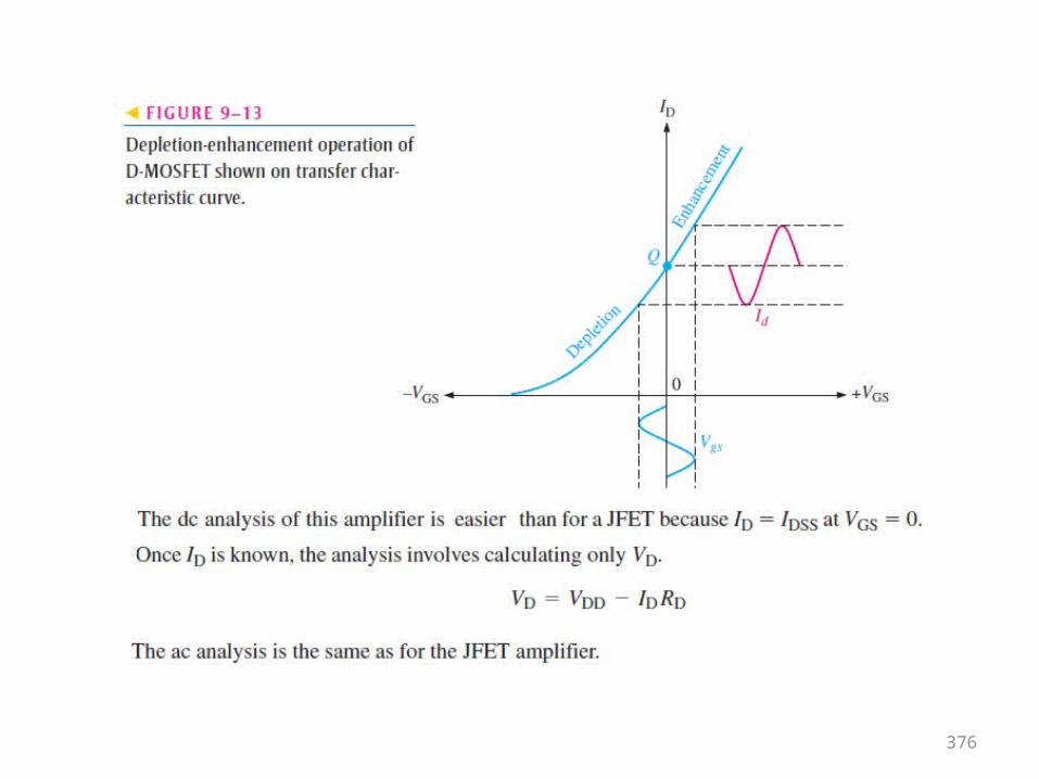
376
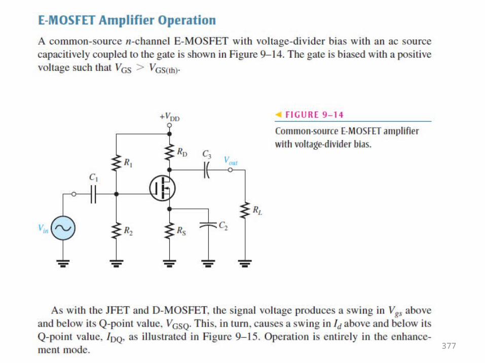
377
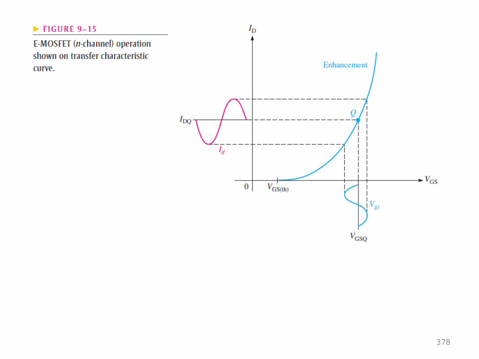
378
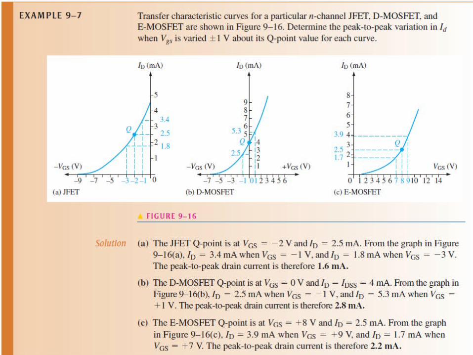
379
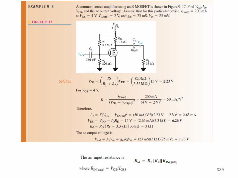
380
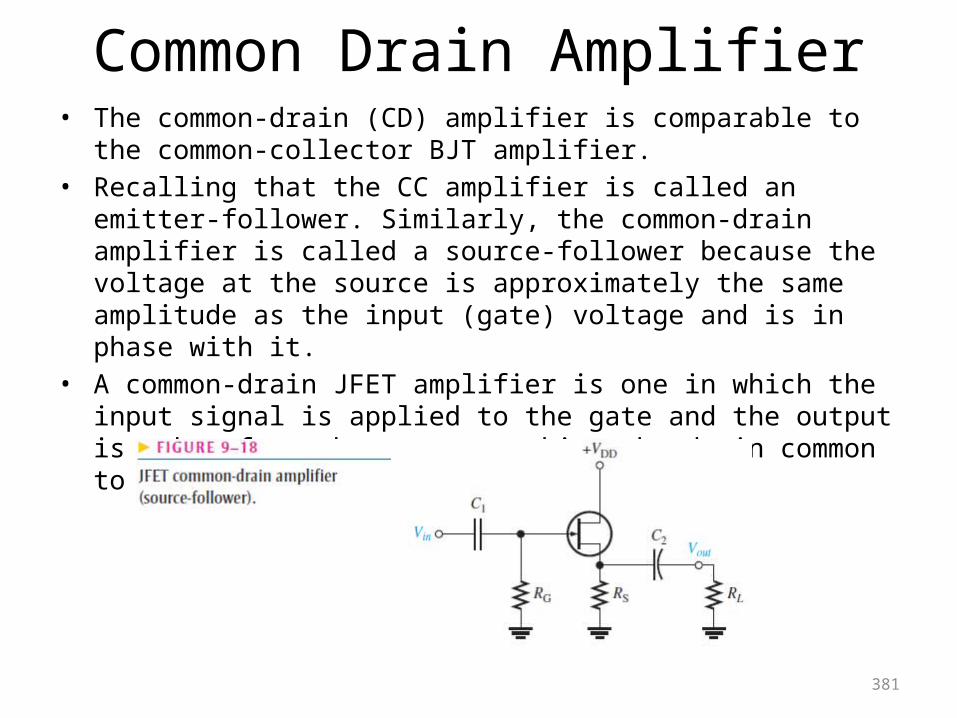
Common Drain Amplifier• The common-drain (CD) amplifier is comparable to
the common-collector BJT amplifier.• Recalling that the CC amplifier is called an
emitter-follower. Similarly, the common-drain amplifier is called a source-follower because the voltage at the source is approximately the same amplitude as the input (gate) voltage and is in phase with it.
• A common-drain JFET amplifier is one in which the input signal is applied to the gate and the output is taken from the source, making the drain common to both.
381
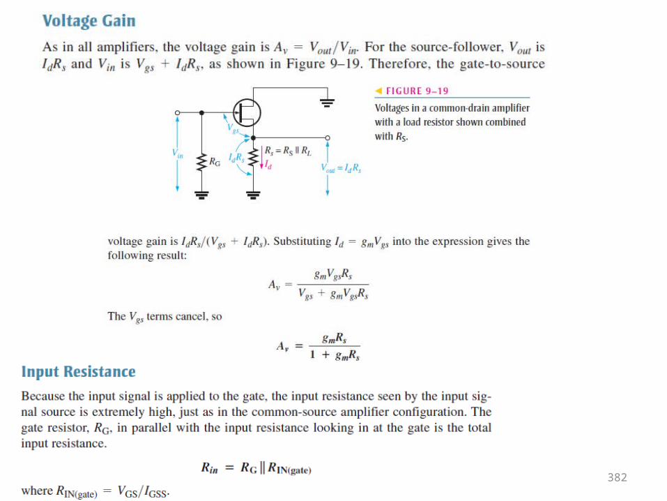
382
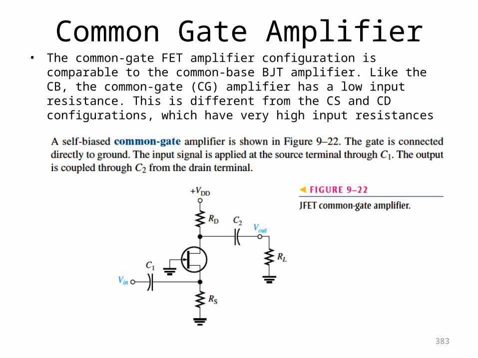
Common Gate Amplifier• The common-gate FET amplifier configuration is
comparable to the common-base BJT amplifier. Like the CB, the common-gate (CG) amplifier has a low input resistance. This is different from the CS and CD configurations, which have very high input resistances
383
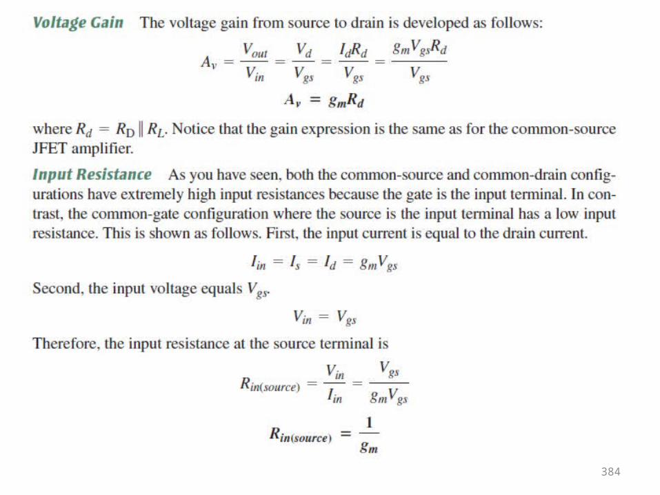
384
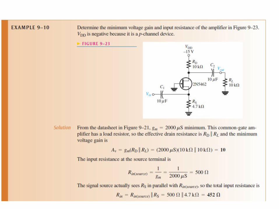
385