design and development of a multi-die embedded micro wafer level package
TRANSCRIPT

Copyright © 2008 Year IEEE. Reprinted from IEEE ECTC 2008. 27 - 30 May 2008, Florida USA.. This material is posted here with permission of the IEEE. Such permission of the IEEE does not in any way imply IEEE endorsement of any of Institute of Microelectronics’ products or services. Internal or personal use of this material is permitted. However, permission to reprint/republish this material for advertising or promotional purposes or for creating new collective works for resale or redistribution must be obtained from the IEEE by writing to [email protected].
Design and Development of a Multi-Die Embedded Micro Wafer Level Package
Vaidyanathan Kripesh, Vempati Srinivas Rao, Aditya Kumar, Gaurav Sharma, Khong Chee Houe, Zhang Xiaowu, Khoo Yee Mong, Navas Khan and John Lau
Institute of Microelectronics, A*STAR (Agency for Science, Technology and Research), 11 Science Park Road, Singapore 117685
Email: [email protected], Phone: +65 67705592
Abstract
The primary trend in electronics industry is product miniaturization. Both design and manufacturing engineers are looking for ways to make products lighter, smaller, less expensive, and at the same time faster, more powerful, reliable, user-friendly, and functional. A partial list of today's "shrinking" products would include cellular phones, personal and sub-notebook computers, pagers, PCMCIA cards, camcorders, palmtop organizers, telecommunications equipment, and automotive components. With silicon chips continue integrating more functionality as per Moore’s Law, the packaging is challenged to integrate and shrink. Chips First or Embedded Chip packaging is a revolutionary way to overcome these recent packaging integration challenges. Packaging researchers have worked on embedded packaging and developed newer way of embedding the chip. The PBGA replaced the lead frame based peripheral array packages, in which the die is electrically connected to circuit board (PCB) substrate by wire bonding or flip chip technology, before covering with molding compound. Embedded Wafer level packaging takes the next step, eliminating the PCB, as well as the need to use wire bonding or flip-chip bumps to establish electrical connection. This paper deals with the development embedding multiple dies at wafer level. A detailed mechanical and structural analysis of the package in terms of the die thickness, wafer size and warpage is presented. The package format is suitable for stacking multiple die in 3D format and 2D format. The paper also deals with characterization of the materials and the process integration of the multidie wafer level packaging. Initial reliability results of the package are also presented.
Introduction
Packaging is an essential technology for semiconductor products. In addition to traditional functions, such as providing electric connections and protecting the chip against mechanical and environmental stresses, packaging is being utilized as a system integration platform. Just like chips benefit from the size reduction of the transistors, so do systems: reductions in size result in increased functionality at lower costs. While silicon chips continue integrating more functionality as per Moore's Law, the packaging is challenged to also integrate and shrink. However data of the ITRS (International Technology Roadmap for Semiconductors) [1] highlight for micro-/nanoelectronic developments, that the shrinkage of the pitches and pads at the chip to package interface is much faster than the shrinkage at the package to board interface. Thus, innovative technology approaches are required to overcome this so-called “interconnect gap”. As
per ITRS roadmap 2007 consumer electronics is the primary driving force for electronic package technology development. Today consumer electronics comprise 50 % of the total integrated circuit revenue. Consumer electronics mandate small form factor and foot print area electronic packages [1].
Standard wafer level packaging (WLP) technology is defined such that all technology steps are performed on wafer level. Drivers for the implementation of WLP technology are cost reduction, smaller form factor, and better electrical performance with respect to high frequency applications. However limitations of WLPs are that they are always fan-in solutions and the area available for I/O is limited to chip footprint size. Thus, for the placement of a large number of I/Os two solutions are possible: i) the chip has to be designed bigger, which will be a large cost adder in the front-end, or ii) an additional material has to be placed as a placeholder around the die to bear the wiring of a fan-out redistribution. The second solution allows a large number of contacts, which is based on an embedded device technology with fan-out redistribution [2-4]. Current smallest microelectronics packages are chip scale packages (CSPs) and flip chips that are agreed to yield maximum miniaturization. Flip chip technology has reached maturity during the last years and is used for processor packaging, mobile communication devices, and sensor packaging, all taking advantage of the various benefits as short interconnects, HF compatibility, good thermal performance, and more. However, these usual approaches toward component packaging focus on single-chip packages, which do not generically support the generation of maximum miniaturization for more complex systems integrating not only ICs, but also sensors, microelectromechanical systems (MEMS)/ nanoelectromechanical systems (NEMS) devices, bus interfaces, etc. One of the most promising ways to generate such modular systems is the use of three-dimensional (3-D) interconnect technology, allowing the cost and size effective combination of various components into a complex system [5-7]. Beside the technological flexibility to combine various modules to a functional system, miniaturization is achieved by footprint reduction and there is a potential to increase reliability as the modules can be tested prior to system assembly, allowing reduced failure rates. These packages however achieve 3-D integration using separate interposers and are generally application specific with limited potential for high-volume and low-cost manufacturing. In this paper we propose new stacked embedded micro wafer level package (EMWLP) architecture. The proposed package combines the benefits of wafer level packaging, fan out interconnects and 3-D integration without the use of any interposers. The novel EMWLP 3D technology allows stacking heterogeneous chips
978-1-4244-2231-9/08/$25.00 ©2008 IEEE 1544 2008 Electronic Components and Technology Conference
such as RF, logic, memory etc, and fan-out. Heterogeneous chips of different sizes are stacked and configured to a re-constructed wafer by embedding the stacked chips in mold compound material. All interconnects from each chip of the stacked module are brought to the same plane using different heights of copper pillar interconnects on different chips and grinding the re-constructed wafer. Then these interconnects are fanned-out on to the mould compound area using metal redistributed lines and dielectric material layers and then formed flip-chip bumps for second level packaging.
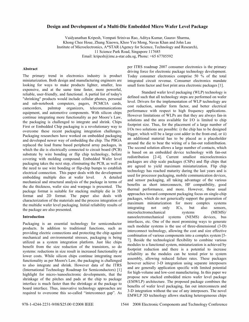
Process Flow and Integration Figure 1 provides a summary of the EMWLP fabrication
process. (a) A support wafer is laminated with molding tape material. (b) Three different wafers are electroplated and singulated to provide different sizes of known good chips. These different chips are then laminated with dicing die attach film and singulated and stacked to fabricate the reconfigured wafer. (c) The reconfigured wafer is then molded using the transfer molding process. (d) The molded silicon chip stack is then grinded to expose the copper pillars. (e) This is followed by release of the support wafer and (f) peeling off of the molding tape. (g) Redistribution layer is fabricated on the molded compound wafer followed by final ball placement. The detailed process parameters are described in the respective sections.
Figure 1: Overview of the process flow for fabricating stacked embedded wafer level package
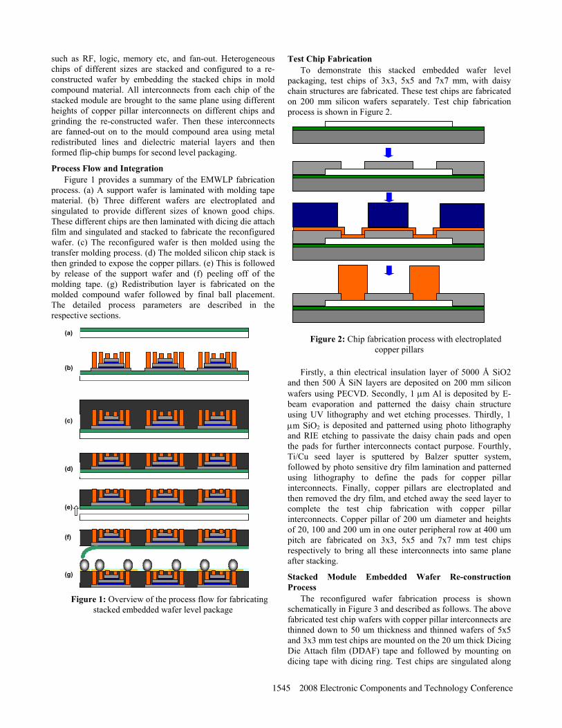
Test Chip Fabrication To demonstrate this stacked embedded wafer level
packaging, test chips of 3x3, 5x5 and 7x7 mm, with daisy chain structures are fabricated. These test chips are fabricated on 200 mm silicon wafers separately. Test chip fabrication process is shown in Figure 2.
Figure 2: Chip fabrication process with electroplated copper pillars
Firstly, a thin electrical insulation layer of 5000 Å SiO2
and then 500 Å SiN layers are deposited on 200 mm silicon wafers using PECVD. Secondly, 1 µm Al is deposited by E-beam evaporation and patterned the daisy chain structure using UV lithography and wet etching processes. Thirdly, 1 µm SiO2 is deposited and patterned using photo lithography and RIE etching to passivate the daisy chain pads and open the pads for further interconnects contact purpose. Fourthly, Ti/Cu seed layer is sputtered by Balzer sputter system, followed by photo sensitive dry film lamination and patterned using lithography to define the pads for copper pillar interconnects. Finally, copper pillars are electroplated and then removed the dry film, and etched away the seed layer to complete the test chip fabrication with copper pillar interconnects. Copper pillar of 200 um diameter and heights of 20, 100 and 200 um in one outer peripheral row at 400 um pitch are fabricated on 3x3, 5x5 and 7x7 mm test chips respectively to bring all these interconnects into same plane after stacking.
Stacked Module Embedded Wafer Re-construction Process
The reconfigured wafer fabrication process is shown schematically in Figure 3 and described as follows. The above fabricated test chip wafers with copper pillar interconnects are thinned down to 50 um thickness and thinned wafers of 5x5 and 3x3 mm test chips are mounted on the 20 um thick Dicing Die Attach film (DDAF) tape and followed by mounting on dicing tape with dicing ring. Test chips are singulated along
(e)
(a)
(b)
(c)
(d)
(f)
(g)
(e)
(a)
(b)
(c)
(d)
(f)
(g)
(e)
(a)
(b)
(c)
(d)
(f)
(g)
1545 2008 Electronic Components and Technology Conference

with DAF tape by dicing and DAF tape is in between thin test chip wafer and dicing tape now. The DAF tapes should with stand the molding process conditions and should not move the chip location during molding process. First, 7x7 mm test chip is pick and placed with a large spacing on to the double sided adhesive tape which is mounted on the support carrier as shown in figure 3. This adhesive tape fixes the chip position during the molding process and must release after molding process and this step is crucial; at the end of the process the placement accuracy of the dies must be compatible with the pad redistribution. Then 5x5 mm test chip with DAF tape is pick and placed at the center of the 7x7 mm test chip, followed by 3x3 mm test chip with DAF tape at the center of the 5x5 mm test chip as shown in figure 3(b). Pick and placement process is carried out with uniform force on the chip to obtain the proper attachment and followed by the DAF tape curing to improve the adhesion between DAF tape and chip surface. Figure 3 shows the stacking process using DAF tape
Figure 3: Schematic showing the multiple die attaching process using the dicing die attach film
Wafer Level Embedding Technology In semiconductor packaging technology, a number of
embedding methods, such as transfer, injection, compression, lamination, printing, and potting are used to embed the semiconductor chip or wafer in a polymer [8-15]. Broadly these embedding methods are characterized into two categories, the first is molding and the other is liquid encapsulation. Both of these embedding categories have their advantages and disadvantages. Normally, the molding processes, such as transfer, injection, and compression, offer a precise control on dimensions and high throughput, but they are expensive. On the other hand, liquid encapsulation methods, such as printing, potting, and casting, are of low cost, but they does not offer precise control on dimensions.
Other than the embedding method, the physical properties of embedding materials also play an important role in achieving reliable embedding of chip or wafer. Since the embedding materials are the polymeric materials which have very high coefficient of thermal expansion (CTE) as compared to single crystal Si, a large amount of thermo-mechanical stresses is developed in the composite polymer-Si structure after the embedding process. To minimize the thermo-mechanical stresses, normally two approaches are used for the selection of polymeric material. The first
approach is low CTE approach and the other is high CTE approach. In the low CTE approach, the CTE of polymeric compound is decreased to match with CTE of Si and this is done by adding high amount of filler particles in the polymeric compound. The high filler content of polymeric compound reduces its CTE mismatch with Si and thus reduces the thermo-mechanical stresses. In the high CTE approach, the polymeric compounds do not have high filler content and thus the Young’s moduli of these compounds are also very low. Due to low Young’s modulus, the high CTE polymeric materials do not induce high thermo-mechanical stresses in the composite polymer-Si structure. Though both the approaches reduce thermo-mechanical stresses, the low CTE material approach with conventional molding methods such as transfer or compression is generally used to achieve the high mechanical strength and the precise control on dimensions of embedded structure.
Recently, a few conventional embedding methods have been used to make reconstructed wafer [13-15]. A reconstructed wafer is a wafer that includes known good dies (KGD) embedded in a polymeric compound and has a number of advantages over the normal polymeric embedded wafer. These advantages are lower cost, higher performance, exceptional versatility, and higher I/Os [14-15]. Owing to these advantages, the embedded wafer level packaging (EWLP) technology is becoming a promising packaging technology to meet future requirements of the integration of multi-function devices. However, so far only a 2D integration has been realized using EWLP technology. In the present work, a new embedded package has been developed that can realize a 3D integration of multi-function devices using the EMWLP technology.
In the present work, for embedding, transfer molding method was used to achieve precise control on the dimensions of embedded structure and a low CTE (7 ppm/°C) material approach is followed to reduce the thermo-mechanical stresses. The molding temperature and time was 175°C and 80 sec, respectively. After embedding the stacked Si dies, the grinding of molding compound was carried out to expose the Cu pillar as shown in Figure 4. The grinding was carried out with the help of lapping machine using grinding papers of grid ranging from 320 to 1200. Figure 5 shows the SEM and optical images of embedded and grinded samples. From the figures the embedding of stacked Si dies is clearly evident and the Cu pillars can be seen to be evenly exposed after the grinding.
Figure 4: Process flow showing (a) stacked Si chips with Cu pillars, then (b) embedding of stacked Si chips in
polymeric compound, and finally (c) grinding of polymeric compound to expose Cu pillars.
Interconnect Redistribution on Re-Constructed Wafer The planarized copper pillar interconnects of embedded
stacked module as shown in Figure 6(a), are redistributed
Pick Up
Heat Cure
50um Silicon Spacer
Die Mount
Silicon Carrier
Base Material
AdhesiveSilicon Wafer
DicingPick Up
Heat Cure
50um Silicon Spacer
Die Mount
Silicon Carrier
Base Material
AdhesiveSilicon Wafer
Dicing
(b) Embedding (c) Grinding to expose Cu pillars
0.5 mm
(a) Stacked chip with copper pillars (b) Embedding (c) Grinding to expose Cu pillars
0.5 mm
(a) Stacked chip with copper pillars
1546 2008 Electronic Components and Technology Conference
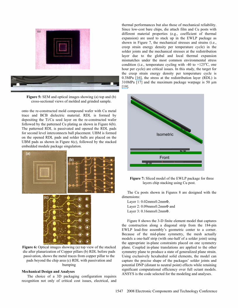
Figure 5: SEM and optical images showing (a) top and (b)
cross-sectional views of molded and grinded sample.
onto the re-constructed mold compound wafer with Cu metal trace and BCB dielectric material. RDL is formed by depositing the Ti/Cu seed layer on the re-constructed wafer followed by the patterned Cu plating as shown in Figure 6(b). The patterned RDL is passivated and opened the RDL pads for second level interconnects ball placement. UBM is formed on the opened RDL pads and solder balls are placed on the UBM pads as shown in Figure 6(c), followed by the stacked embedded module package singulation.
Figure 6: Optical images showing (a) top view of the stacked die after planarization of Copper pillars (b) RDL before pads passivation, shows the metal traces from copper pillar to the
pads beyond the chip area (c) RDL with passivation and bumping
Mechanical Design and Analyses The choice of a 3D packaging configuration requires
recognition not only of critical cost issues, electrical, and
thermal performances but also those of mechanical reliability. Since low-cost bare chips, die attach film and Cu posts with different material properties (e.g., coefficient of thermal expansion) are used to stack up in the EWLP package as shown in Figure 7, the mechanical stresses and strains (i.e., creep strain energy density per temperature cycle) in the solder joints and the mechanical stresses at the redistribution layer due to the global and local thermal expansion mismatches under the most common environmental stress condition (i.e., temperature cycling with -40 to +125oC, one hour per cycle) are critical issues. In this study, the target for the creep strain energy density per temperature cycle is 0.3MPa [16], the stress at the redistribution layer (RDL) is 310MPa [17] and the maximum package warpage is 50 µm [19].
Figure 7: Sliced model of the EWLP package for three layers chip stacking using Cu post.
The Cu posts shown in Figures 8 are designed with the
dimensions: Layer 1: 0.02mmx0.2mmΦ, Layer 2: 0.09mmx0.2mmΦ and Layer 3: 0.16mmx0.2mmΦ. Figure 8 shows the 3-D finite element model that captures
the construction along a diagonal strip from the 184-pin EWLP lead-free assembly’s geometric center to a corner. Because of the mid-plane symmetry, the mesh actually models a one-half strip (with one-half of a solder joint) using the appropriate in-plane constraints placed on one symmetry plane. Coupled in-plane translations are applied to the other symmetry plane to produce a state of generalized plane strain. Using exclusively hexahedral solid elements, the model can capture the precise shape of the packages’ solder joints and potential DNP (distant to neutral point) effects while retaining significant computational efficiency over full octant models. ANSYS is the code selected for the modeling and analyses.
Isometric
Front (a)
(b)
(c)
(a)(b)
(c)
(a)
(b)
1547 2008 Electronic Components and Technology Conference
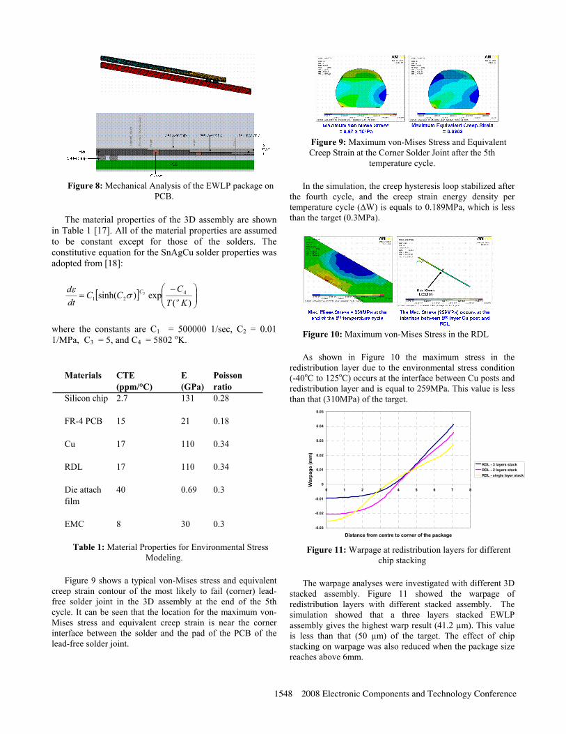
Figure 8: Mechanical Analysis of the EWLP package on
PCB. The material properties of the 3D assembly are shown
in Table 1 [17]. All of the material properties are assumed to be constant except for those of the solders. The constitutive equation for the SnAgCu solder properties was adopted from [18]:
[ ] ⎟⎟⎠
⎞⎜⎜⎝
⎛ −=
)(exp)sinh( 4
213
KTC
CCdtd
oCσε
where the constants are C1 = 500000 1/sec, C2 = 0.01 1/MPa, C3 = 5, and C4 = 5802 oK.
Materials CTE E Poisson
(ppm/°C) (GPa) ratio Silicon chip 2.7 131 0.28 FR-4 PCB 15 21 0.18 Cu 17 110 0.34 RDL 17 110 0.34 Die attach 40 0.69 0.3 film EMC 8 30 0.3
Table 1: Material Properties for Environmental Stress Modeling.
Figure 9 shows a typical von-Mises stress and equivalent
creep strain contour of the most likely to fail (corner) lead-free solder joint in the 3D assembly at the end of the 5th cycle. It can be seen that the location for the maximum von-Mises stress and equivalent creep strain is near the corner interface between the solder and the pad of the PCB of the lead-free solder joint.
Figure 9: Maximum von-Mises Stress and Equivalent Creep Strain at the Corner Solder Joint after the 5th
temperature cycle. In the simulation, the creep hysteresis loop stabilized after
the fourth cycle, and the creep strain energy density per temperature cycle (∆W) is equals to 0.189MPa, which is less than the target (0.3MPa).
Figure 10: Maximum von-Mises Stress in the RDL As shown in Figure 10 the maximum stress in the
redistribution layer due to the environmental stress condition (-40oC to 125oC) occurs at the interface between Cu posts and redistribution layer and is equal to 259MPa. This value is less than that (310MPa) of the target.
-0.03
-0.02
-0.01
0
0.01
0.02
0.03
0.04
0.05
0 1 2 3 4 5 6 7 8
Distance from centre to corner of the package
War
page
(mm
)
RDL - 3 layers stackRDL - 2 layers stackRDL - single layer stack
Figure 11: Warpage at redistribution layers for different
chip stacking The warpage analyses were investigated with different 3D
stacked assembly. Figure 11 showed the warpage of redistribution layers with different stacked assembly. The simulation showed that a three layers stacked EWLP assembly gives the highest warp result (41.2 µm). This value is less than that (50 µm) of the target. The effect of chip stacking on warpage was also reduced when the package size reaches above 6mm.
1548 2008 Electronic Components and Technology Conference
Conclusions A multi-die embedded wafer level packaging scheme has
been presented in this paper. The process flow for the fabrication of the multi-die embedded wafer level package envisages a low cost and high throughput manufacturable method. A three-die embedded module has been demonstrated and the some of the important results are summarized as below.
• The package can have 3 to 5x time reduction in space and volume as compared to conventional embedded wafer level packages
• A very simple and low cost integration method for 3D- multidie embedded package has been proposed.
• The warpage of the molded wafer is critical and the molding optimization has been proposed to over come the same. The choice of low CTE (7ppm/°C) mold compound material leads to less warpage values.
• Low temperature, 200°C dielectric, resdistribution is required to achieved a good quality integration
Acknowledgments The authors would like to thank the Microsystems
Modules and Components laboratory staff at IME for their support for fabrication and analysis of the package.
References 1. see http://public.itrs.net 2. J.-C. Souriau et al., “Wafer Level Processing of 3D
System in Package for RF and Data Applications”, 55th Electronic Components and Technology Conf, Lake Buena Vista, FL, June 2005, p. 356
3. S.N. Towle et al. “Bumpless Built-Up Layer Packaging“, ASME International Mechanical Engineering Congress and Exposition, New York, NY, Nov. 2001
4. D. Komatsu and T. Wakabayashi, “Trend of WLP Technology and Next Generation Packaging “WLP and EWLP”, 5th International Workshop on Microelectronics Assembly and Packaging & Reverse Trade Show, Fukuoka, Japan, 15.-16. Sept. 2005
5. P. Matuscheck, J. Evers, W. Schaefer, M. Nienhaus, and S. Kleen, “A field mill based on the modular MEMS framework MATCH-X,” in Proc. Actuator 2002, Bremen, Germany, June 10–12, 2002, pp. 316–320.
6. M. Klein, H. Oppermann, R. Aschenbrenner, and H. Reichl, “Modular systems for sensor integration,” in Proc. IMAPS 2002, Denver, CO, pp. 194–198.
7. V. Solberg, “Innovative 3D solutions for multiple die packaging,” in Proc. SMTA 2003, IL, pp. 626–630.
8. T. Hamano et al., “Super CSPTM : WLCSP Solution for Memory and System LSI”, in proceedings of International Symposium on Advanced Packaging Materials 1999.
9. A. Okuno, “Wafer Level CSP Process by VPES(Vacuum Printing Encapsulation Systems)”, in proceedings of International Symposium on Electronics Materials & Packaging 2000.
10. T. Braun et al., “Wafer Level Encapsulation – A transfer Molding Approach to System in Package Generation”, in proceedings of EPTC 2002, Singapore.
11. R. Aschenbrenner et al., “Process Flow and Manufacturing Concept for Embedded Active Devices”, in proceedings of EPTC 2004, Singapore.
12. C. T. Ko et al., “Embedded Active Device Packaging Technoloogy for Next-Generation Chip-in-Substrate Packages, CiSP”, in proceedings of ECTC 2006, US.
13. J. C. Souriau et al., “Wafer Level Processing on Re-built Wafer for Chip Staking”, in proceedings EPTC 2005, Singapore.
14. M. Brunnbauer et al., “An Embedded Device Technology Based on a Molded Reconfigured Wafer”, in proceedings of ECTC 2006, US.
15. B. Keser et al., “The Redistributed Chip Package: A Breakthrough for Advanced Packaging”, in proceedings of ECTC 2007
16. Ahmer Syed, “Accumulated Creep Strain and Energy Density Based Thermal Fatigue Life Prediction Models for SnAgCu Solder Joints”, in proceedings of ECTC 2004.
17. M. G. Pecht, et al, “Electronic Packaging Materials and Their Properties”, CRC Press LLC, Boca Raton, 1998.
18. Lau, J. H., and W. Dauksher, “Creep of Sn-(3.5-3.9)wt%Ag-(0.5-0.8)wt%Cu Lead-Free Solder”, in Micromaterials and Nanomaterials, Edited by B. Michel, Fraunhofer Institute, IZM, Berlin, 2004, pp. 54-62.
19. Yuan Li, “Accurate Predictions of Flip Chip BGA Warpage”, in proceedings of ECTC 2003.
1549 2008 Electronic Components and Technology Conference