decoder encoder mux
TRANSCRIPT
Chapter-2
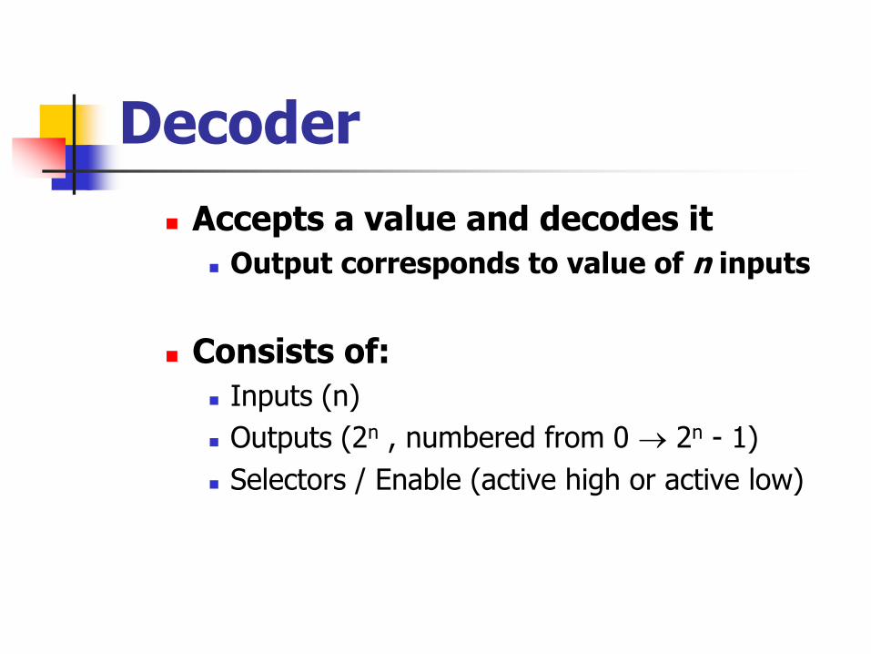
Decoder
Encoder
MUX
Decoder
Accepts a value and decodes it
Output corresponds to value of n inputs
Consists of:
Inputs (n)
Outputs (2n , numbered from 0 2n - 1)
Selectors / Enable (active high or active low)
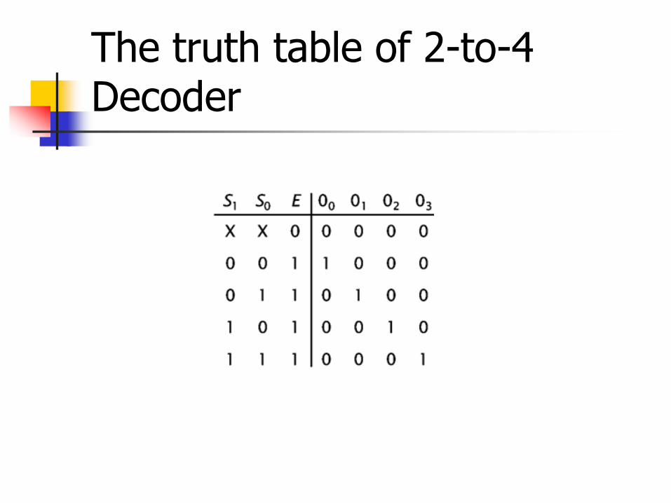
The truth table of 2-to-4 Decoder
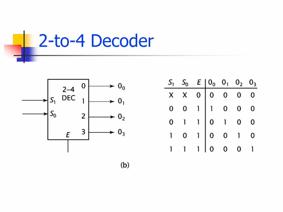
2-to-4 Decoder
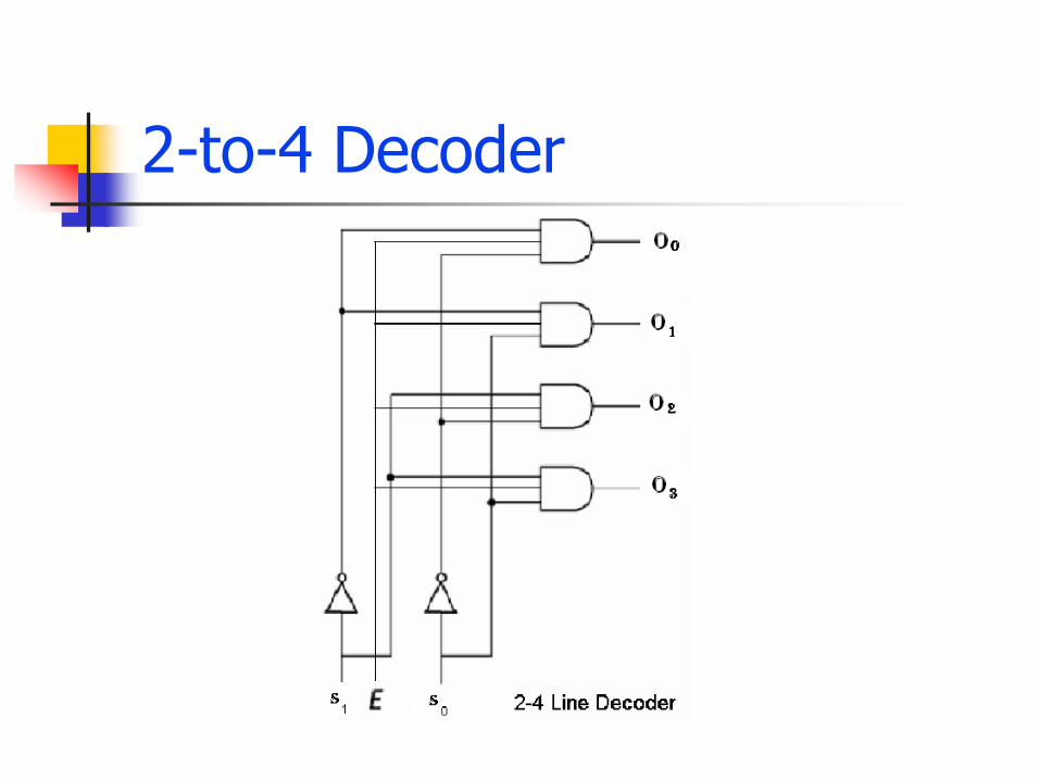
2-to-4 Decoder
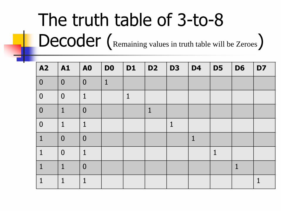
The truth table of 3-to-8 Decoder (Remaining values in truth table will be Zeroes)
A2 A1 A0 D0 D1 D2 D3 D4 D5 D6 D7
0 0 0 1
0 0 1 1
0 1 0 1
0 1 1 1
1 0 0 1
1 0 1 1
1 1 0 1
1 1 1 1
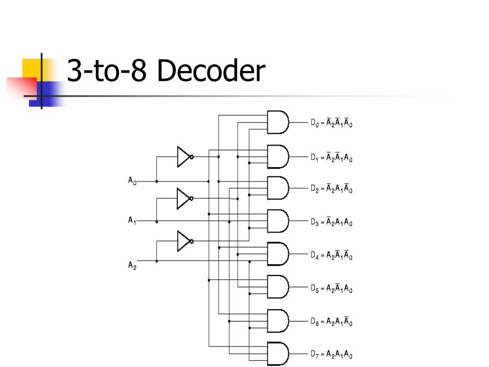
3-to-8 Decoder
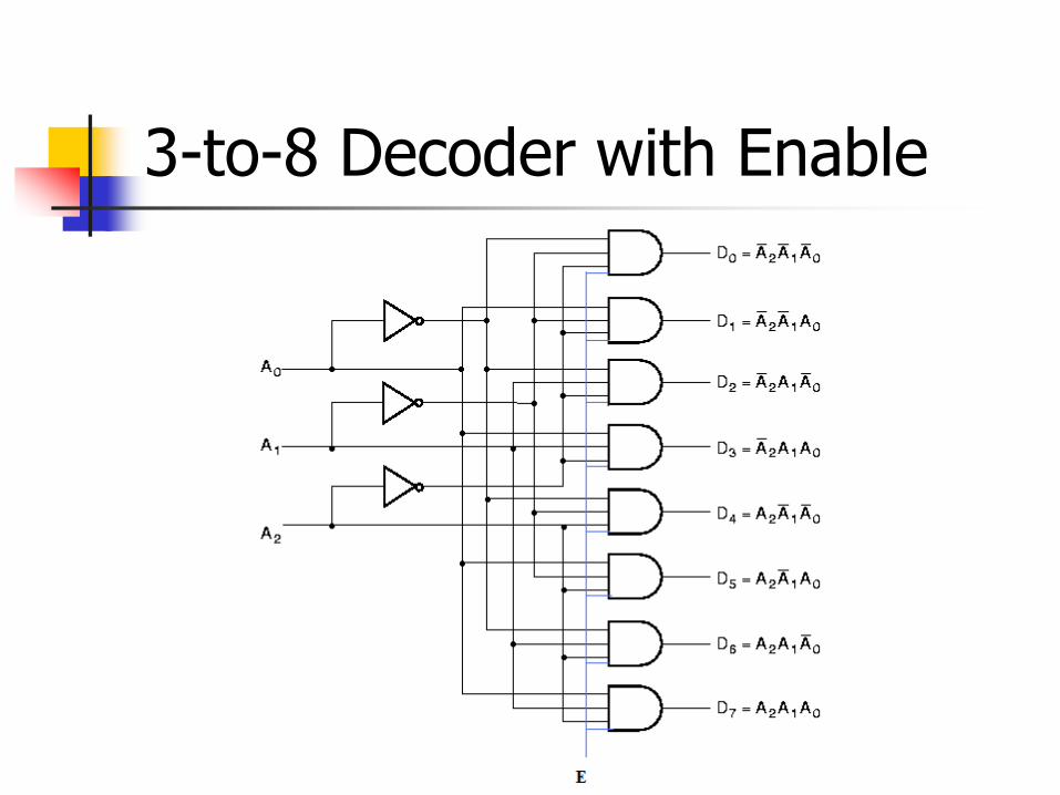
3-to-8 Decoder with Enable
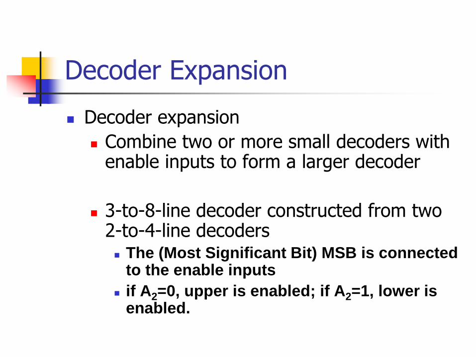
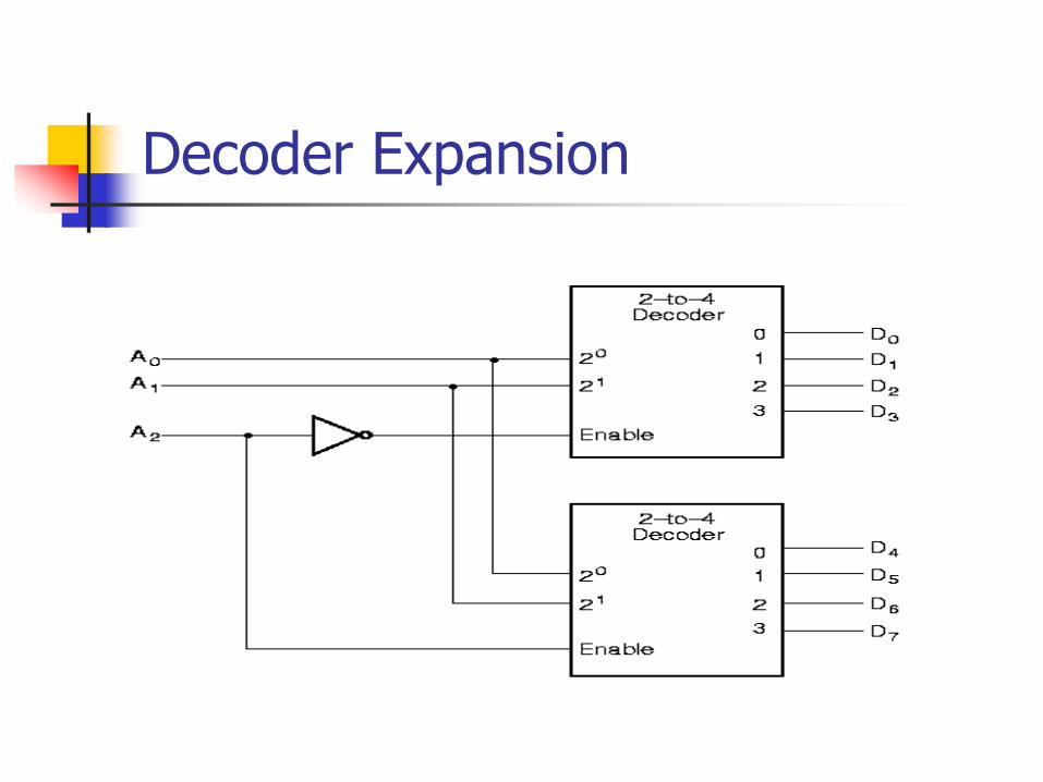
Decoder Expansion
Decoder expansion
Combine two or more small decoders with enable inputs to form a larger decoder
3-to-8-line decoder constructed from two 2-to-4-line decoders The (Most Significant Bit) MSB is connected
to the enable inputs
if A2=0, upper is enabled; if A2=1, lower is enabled.
Decoder Expansion
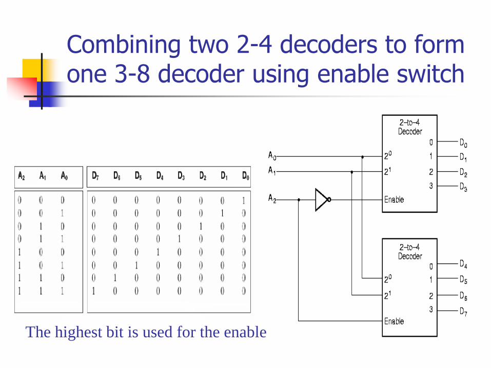
Combining two 2-4 decoders to form one 3-8 decoder using enable switch
The highest bit is used for the enables
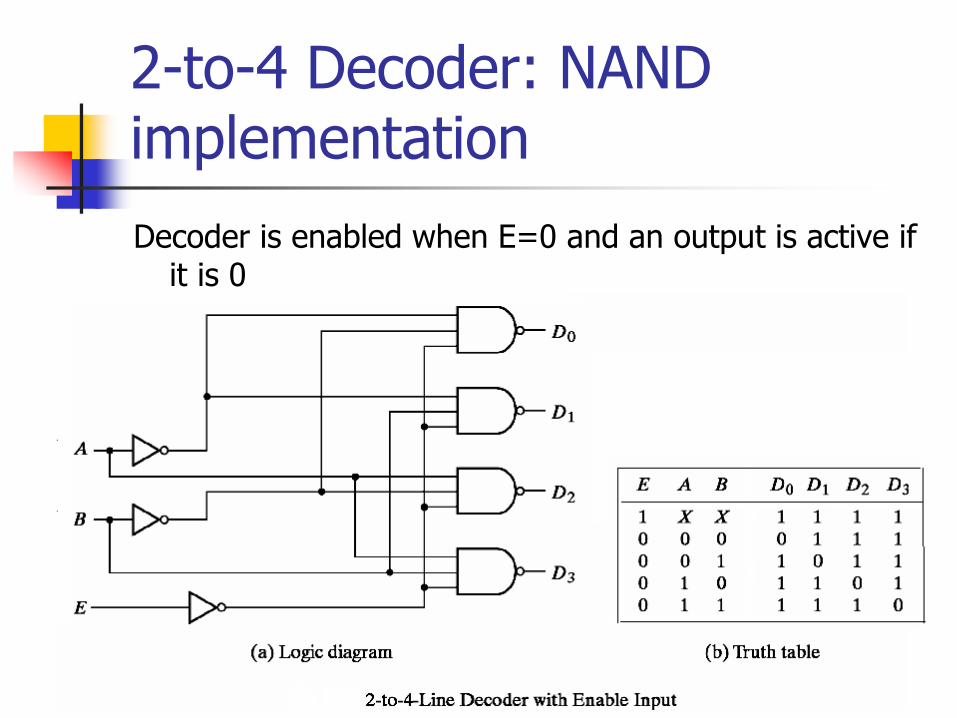
2-to-4 Decoder: NAND implementation
Decoder is enabled when E=0 and an output is active if it is 0
Outline
Decoder
Encoder
Mux
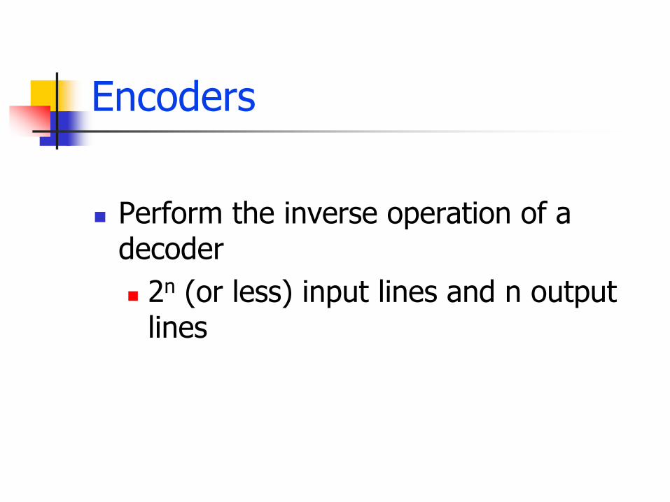
Encoders
Perform the inverse operation of a decoder
2n (or less) input lines and n output lines
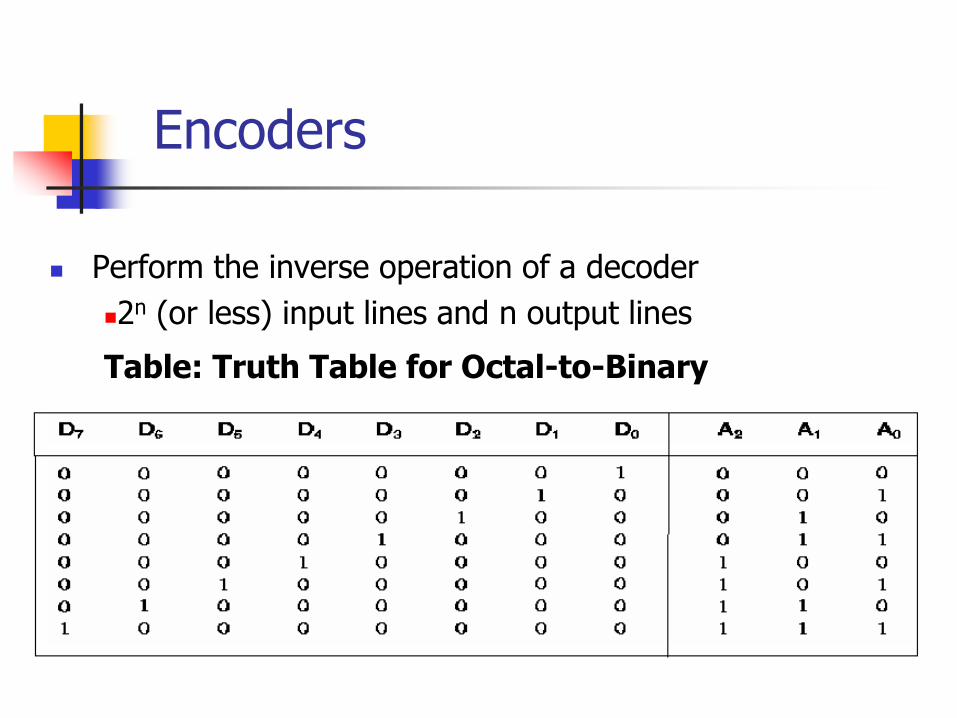
Encoders
Perform the inverse operation of a decoder
2n (or less) input lines and n output lines
Table: Truth Table for Octal-to-Binary
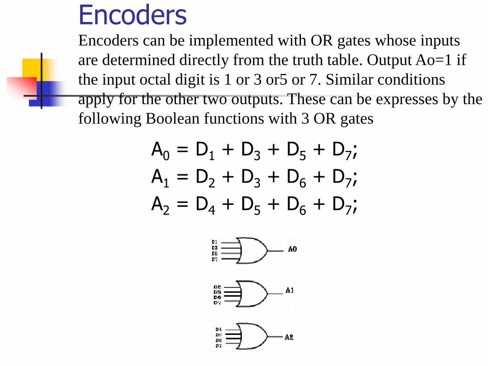
A0 = D1 + D3 + D5 + D7;
A1 = D2 + D3 + D6 + D7;
A2 = D4 + D5 + D6 + D7;
Encoders Encoders can be implemented with OR gates whose inputs
are determined directly from the truth table. Output Ao=1 if
the input octal digit is 1 or 3 or5 or 7. Similar conditions
apply for the other two outputs. These can be expresses by the
following Boolean functions with 3 OR gates
Outline
Decoder
Encoder
Mux
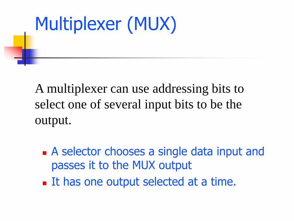
Multiplexer (MUX)
A selector chooses a single data input and passes it to the MUX output
It has one output selected at a time.
A multiplexer can use addressing bits to
select one of several input bits to be the
output.
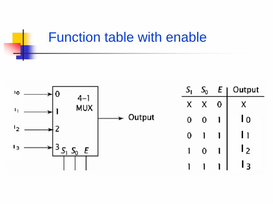
Function table with enable
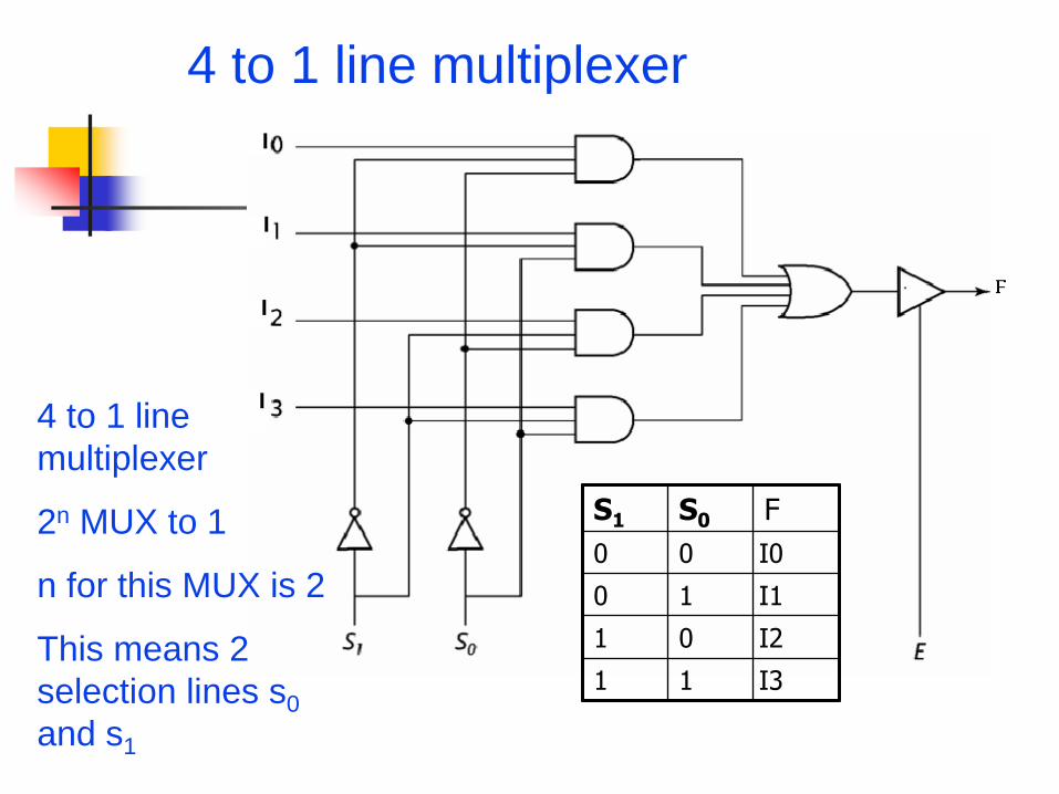
4 to 1 line multiplexer
S1 S0 F
0 0 I0
0 1 I1
1 0 I2
1 1 I3
4 to 1 line
multiplexer
2n MUX to 1
n for this MUX is 2
This means 2
selection lines s0
and s1
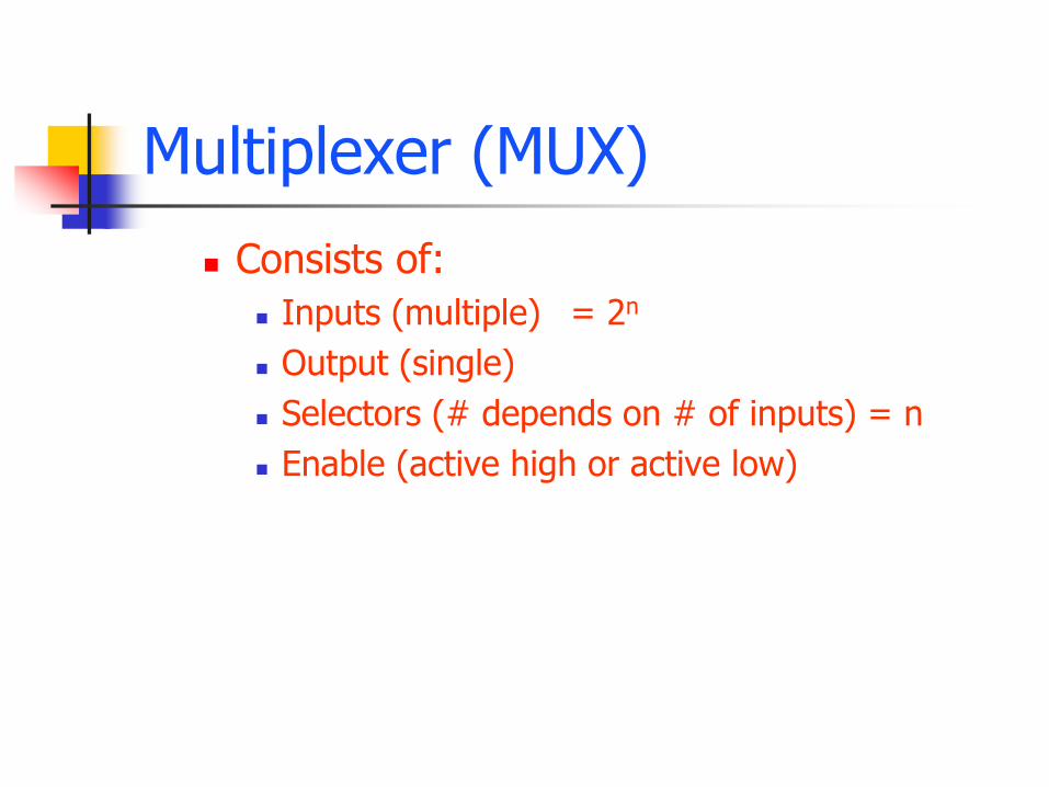
Multiplexer (MUX)
Consists of:
Inputs (multiple) = 2n
Output (single)
Selectors (# depends on # of inputs) = n
Enable (active high or active low)
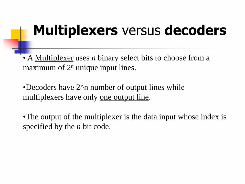
Multiplexers versus decoders
• A Multiplexer uses n binary select bits to choose from a
maximum of 2n unique input lines.
•Decoders have 2^n number of output lines while
multiplexers have only one output line.
•The output of the multiplexer is the data input whose index is
specified by the n bit code.
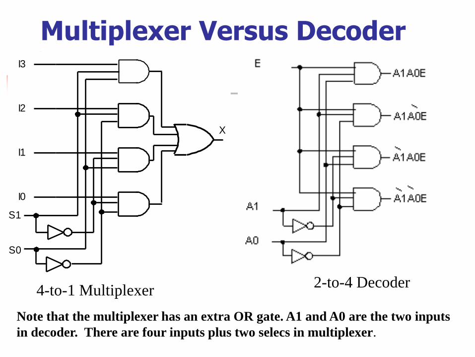
Multiplexer Versus Decoder
S0
S1
I3
I2
I1
I0
X
Note that the multiplexer has an extra OR gate. A1 and A0 are the two inputs
in decoder. There are four inputs plus two selecs in multiplexer.
4-to-1 Multiplexer 2-to-4 Decoder
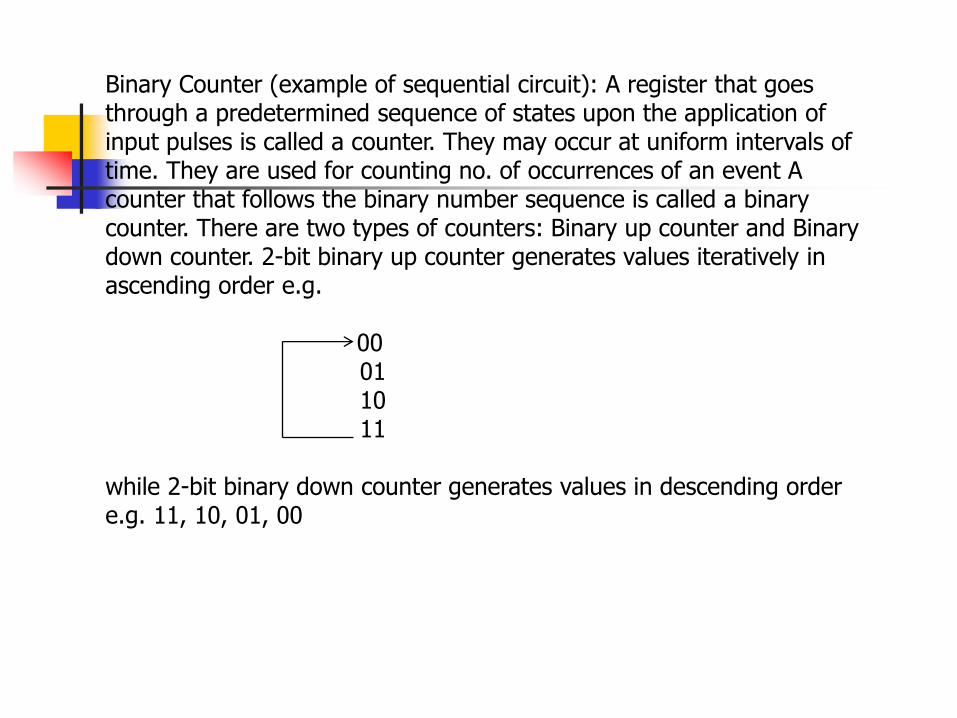
Binary Counter (example of sequential circuit): A register that goes through a predetermined sequence of states upon the application of input pulses is called a counter. They may occur at uniform intervals of time. They are used for counting no. of occurrences of an event A counter that follows the binary number sequence is called a binary counter. There are two types of counters: Binary up counter and Binary down counter. 2-bit binary up counter generates values iteratively in ascending order e.g. 00 01 10 11 while 2-bit binary down counter generates values in descending order e.g. 11, 10, 01, 00
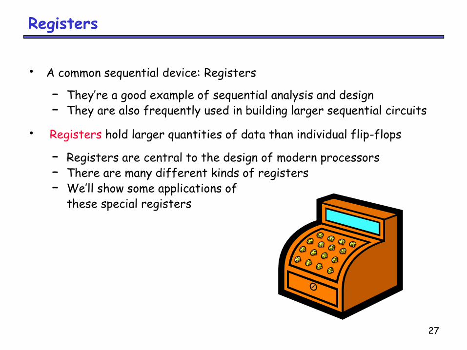
27
Registers
• A common sequential device: Registers
– They’re a good example of sequential analysis and design – They are also frequently used in building larger sequential circuits
• Registers hold larger quantities of data than individual flip-flops
– Registers are central to the design of modern processors – There are many different kinds of registers – We’ll show some applications of these special registers
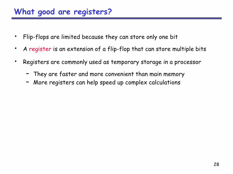
28
What good are registers?
• Flip-flops are limited because they can store only one bit
• A register is an extension of a flip-flop that can store multiple bits
• Registers are commonly used as temporary storage in a processor
– They are faster and more convenient than main memory
– More registers can help speed up complex calculations
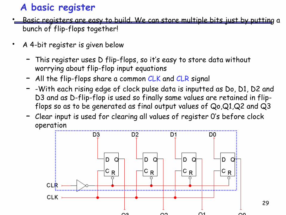
29
A basic register • Basic registers are easy to build. We can store multiple bits just by putting a
bunch of flip-flops together!
• A 4-bit register is given below
– This register uses D flip-flops, so it’s easy to store data without worrying about flip-flop input equations
– All the flip-flops share a common CLK and CLR signal
– -With each rising edge of clock pulse data is inputted as Do, D1, D2 and D3 and as D-flip-flop is used so finally same values are retained in flip-flops so as to be generated as final output values of Qo,Q1,Q2 and Q3
– Clear input is used for clearing all values of register 0’s before clock operation
30
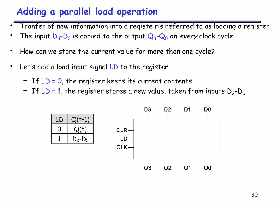
Adding a parallel load operation
• Tranfer of new information into a registe ris referred to as loading a register
• The input D3-D0 is copied to the output Q3-Q0 on every clock cycle
• How can we store the current value for more than one cycle?
• Let’s add a load input signal LD to the register
– If LD = 0, the register keeps its current contents
– If LD = 1, the register stores a new value, taken from inputs D3-D0
LD Q(t+1)
0 Q(t)
1 D3-D0
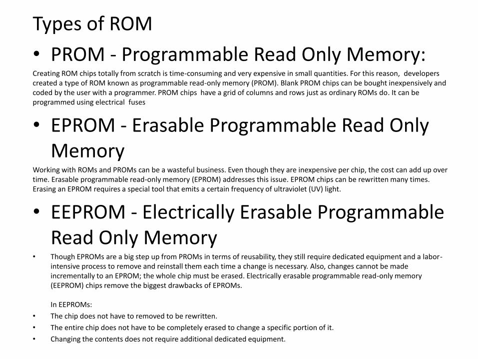
Types of ROM
• PROM - Programmable Read Only Memory: Creating ROM chips totally from scratch is time-consuming and very expensive in small quantities. For this reason, developers created a type of ROM known as programmable read-only memory (PROM). Blank PROM chips can be bought inexpensively and coded by the user with a programmer. PROM chips have a grid of columns and rows just as ordinary ROMs do. It can be programmed using electrical fuses
• EPROM - Erasable Programmable Read Only Memory
Working with ROMs and PROMs can be a wasteful business. Even though they are inexpensive per chip, the cost can add up over time. Erasable programmable read-only memory (EPROM) addresses this issue. EPROM chips can be rewritten many times. Erasing an EPROM requires a special tool that emits a certain frequency of ultraviolet (UV) light.
• EEPROM - Electrically Erasable Programmable Read Only Memory
• Though EPROMs are a big step up from PROMs in terms of reusability, they still require dedicated equipment and a labor-intensive process to remove and reinstall them each time a change is necessary. Also, changes cannot be made incrementally to an EPROM; the whole chip must be erased. Electrically erasable programmable read-only memory (EEPROM) chips remove the biggest drawbacks of EPROMs. In EEPROMs:
• The chip does not have to removed to be rewritten.
• The entire chip does not have to be completely erased to change a specific portion of it.
• Changing the contents does not require additional dedicated equipment.