ic-pv battery-buffered hall-multiturn encoder
TRANSCRIPT

iC-PVBATTERY-BUFFERED HALL-MULTITURN ENCODER
Rev D1, Page 1/27
FEATURES
Integrated Hall sensors with automatic gain and offset control Current consumption of only 2µA to 30µA in typ. applications Tracking speed of up to 120 000 rpm Configurable multiturn counting up to 40 bits Octal encoder mode (singleturn) with 3-bit parallel output Shift-register input for singleturn position Shift-register output of synchronized MT/ST position SSI multiturn data output with error, parity and sync. bits Adjustable multiturn preset value Pin-triggered preset and boot-up from external EEPROM I2C multimaster interface to read EEPROM Supply voltage range of 3.0 V to 5.5 V Integrated supply switching to backup battery Error output on overspeed, low battery and CRC failure Space-saving 16-pin QFN package
APPLICATIONS
Gearless revolution counting Multiturn encoders Absolute end-of-shaft encoders Period counters Metering applications
PACKAGES
QFN163 mm x 3 mm x 0.9 mm
RoHS compliant
BLOCK DIAGRAM
PARALLEL
ERROR
HALL SENSORS
iC-PV
+
-
LOGIC AND SERIAL INTERFACE SERIAL/
SSI Interface
01
OSCILLATOR
0
MULTIMASTER
RAM
MONITOR
-
I2C
HALL CONTROL COUNTERMULTITURN
1 1
SUPPLY SWITCH
SIN/DIG CONVERTER
+
VDDS
DO_P0
VDDVBAT
PRE
CLK_N1
Monitor
POSITION ENCODE
OUTPUTSDA
GND
N0
N2
SCL
P2
DI_P1
SEL
NERR
+
-
+
-NCOS
PCOS
NSIN
PSIN
B
B
B
B
Copyright © 2013, 2015 iC-Haus http://www.ichaus.com

iC-PVBATTERY-BUFFERED HALL-MULTITURN ENCODER
Rev D1, Page 2/27
DESCRIPTION
iC-PV is an ultra low power magnetic multiturn en-coder with up to 40 bit multiturn and 3 bit singleturnresolution, used for magnetic on-axis position sens-ing. On main power failure, the iC-PV switches tobattery supply automatically and continues countingthe correct multiturn position.
Together with an additional singleturn encoder iC (e.g.iC-MHM, iC-LG, iC-LNB, etc.) and a diametricallymagnetized cylindrical permanent magnet it forms acomplete multiturn encoder system. Depending onthe used singleturn iC, a second magnetic or opticalcode disc might be mandatory. Furthermore the iCcan function as a 3 bit parallel encoder. A multiturnencoder system can be built in combination with amicrocontroller and an optional singleturn device.
The Hall signal processing stage is designed for ul-tra low power applications and can be configured tosupport angular accelerations up to 760 000 rad/s2
at a maximum speed of 120 000 rpm. With higherdemands on acceleration, the power consumptionincreases. The maximum supported acceleration isconfigurable, therefore an optimal trade-off betweenpower consumption and supported acceleration canbe individually chosen to meet the demands of thetarget application.
iC-PV reads its configuration from an external EEP-ROM via an I2C interface with multimaster support.Among others, the bit length for multiturn and syn-chronization data, the interface mode, the maximumsupported acceleration and the usage of error or par-ity bits can be configured. The configuration read-inis triggered by the preset pin PRE. A pulse on thispin resets the device and reads a new configurationfrom EEPROM. The multiturn counter is preset to aconfigurable value (default 0).
The configuration RAM and multiturn counter valueare protected against bit errors by an 8 bit polyno-mial cyclic redundancy check. Additionally, an erroris produced on excessive speed or acceleration. Anintegrated battery monitor can be used to signalizean empty battery as an error. A detected error is dis-played via output NERR and is observable as an errorbit in the SSI communication protocol.
While providing this wide range of functionality, theiC-PV multiturn encoder comes in a space-savingQFN16 package. This facilitates its integration in ex-isting encoder systems or the design of new smallencoders.
iC-PVBATTERY-BUFFERED HALL-MULTITURN ENCODER
Rev D1, Page 3/27
CONTENTS
PACKAGING INFORMATION 4PIN CONFIGURATION
QFN16 3 mm x 3 mm (top view) . . . . . 4PACKAGE DIMENSIONS . . . . . . . . . . . 5
ABSOLUTE MAXIMUM RATINGS 6
THERMAL DATA 6
ELECTRICAL CHARACTERISTICS 7
OPERATING REQUIREMENTS 8Serial and Parallel Interface . . . . . . . . . . 9
CONFIGURATION PARAMETERS 10
REGISTER MAP (iC-PV and EEPROM) 10
SENSOR PRINCIPLE 11
POSITION OF THE HALL SENSORS 11
HALL SENSOR CONDITIONING: ANGLEOFFSET AND CODE DIRECTION 12
MODE SELECT INPUT SEL 12
STARTUP BEHAVIOR AND PRESET FUNCTION 13
SERIAL INTERFACE (SEL = LOW) 14
PARALLEL MODE (SEL = HIGH) 16
MULTITURN COUNTER 16
I2C MULTIMASTER INTERFACE TO EEPROMINTERFACE AND CRC PROTECTION 17
SUPPLY SWITCH AND BATTERY MONITORING 18
BIAS AND OSCILLATOR CALIBRATION 18
CALCULATING CURRENT CONSUMPTION 19Interface Mode (SEL = LOW) . . . . . . . . . 19Parallel Encoder Mode (SEL = HIGH) . . . . 19
APPLICATION NOTES: Operating distancesensor to magnet 20
APPLICATION NOTES: Singleturn iCs withmultiturn interface (SSI-Mode) 21
APPLICATION NOTES: Chain operating mode 22
APPLICATION NOTES: iC-PV as batterypowered revolution counter or meteringdevice 24
APPLICATION NOTES: iC-PV as 3 bit parallelmode (µC application) 25
DESIGN REVIEW : Notes On Chip Functions 25
REVISION HISTORY 26
iC-PVBATTERY-BUFFERED HALL-MULTITURN ENCODER
Rev D1, Page 4/27
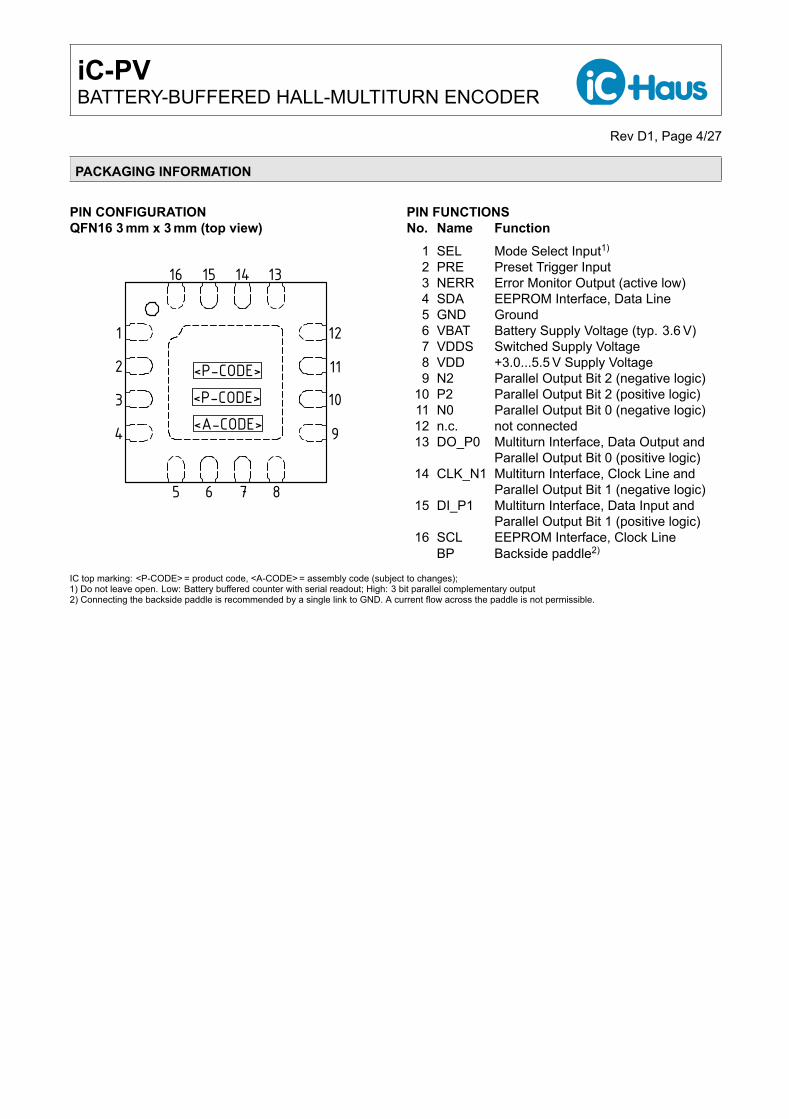
PACKAGING INFORMATION
PIN CONFIGURATIONQFN16 3 mm x 3 mm (top view)
1
2
16 15 14 13
12
11
10
9
8765
4
3<A-CODE><P-CODE><P-CODE>
PIN FUNCTIONSNo. Name Function
1 SEL Mode Select Input1)
2 PRE Preset Trigger Input3 NERR Error Monitor Output (active low)4 SDA EEPROM Interface, Data Line5 GND Ground6 VBAT Battery Supply Voltage (typ. 3.6 V)7 VDDS Switched Supply Voltage8 VDD +3.0...5.5 V Supply Voltage9 N2 Parallel Output Bit 2 (negative logic)
10 P2 Parallel Output Bit 2 (positive logic)11 N0 Parallel Output Bit 0 (negative logic)12 n.c. not connected13 DO_P0 Multiturn Interface, Data Output and
Parallel Output Bit 0 (positive logic)14 CLK_N1 Multiturn Interface, Clock Line and
Parallel Output Bit 1 (negative logic)15 DI_P1 Multiturn Interface, Data Input and
Parallel Output Bit 1 (positive logic)16 SCL EEPROM Interface, Clock Line
BP Backside paddle2)
IC top marking: <P-CODE> = product code, <A-CODE> = assembly code (subject to changes);1) Do not leave open. Low: Battery buffered counter with serial readout; High: 3 bit parallel complementary output2) Connecting the backside paddle is recommended by a single link to GND. A current flow across the paddle is not permissible.

iC-PVBATTERY-BUFFERED HALL-MULTITURN ENCODER
Rev D1, Page 5/27
PACKAGE DIMENSIONS
3
3
1.75
TOP
0.50 0.25
1.700.40
1.70
BOTTOM
0.90
±0.10
0.48
SIDE
1.70
2.95
R0.15
0.50 0.30
1.70
2.95
0.65
RECOMMENDED PCB-FOOTPRINT
dra_qfn16-3x3-1_pv_y1_pack_1, 15:1
All dimensions given in mm.Tolerance of sensor pattern: ±0.10mm / ±1° (with respect to center of backside pad).Tolerances of form and position according to JEDEC MO-220.

iC-PVBATTERY-BUFFERED HALL-MULTITURN ENCODER
Rev D1, Page 6/27
ABSOLUTE MAXIMUM RATINGS
These ratings do not imply operating conditions; functional operation is not guaranteed. Beyond these ratings device damage may occur.Item Symbol Parameter Conditions UnitNo. Min. Max.G001 V(VDD) Supply Voltage at VDD referenced to GND -0.3 6 VG002 V(VBAT) Supply Voltage at VBAT referenced to GND, -0.3 6 V
if VDD > Von: VBAT < VDD + 1 VG003 V(VDDS) Voltage at VDDS referenced to GND -0.3 6 VG004 V() Voltage at SCL, SDA, DI_P1, CLK_N1,
DO_P0, N0, NERR, P2, N2, PRE, SELreferenced to GND -0.3 6 V
G005 I(VDD) Current in VDD -10 50 mAG006 I(VBAT) Current in VBAT -10 50 mAG007 I(VDDS) Current in VDDS -10 50 mAG008 I(GND) Current in GND -50 10 mAG009 I() Current in SCL, SDA, DI_P1, CLK_N1,
DO_P0, N0, NERR, P2, N2, PRE, SEL-30 30 mA
G010 Vd() ESD Susceptibility at all pins HBM, 100 pF discharged through 1.5 kΩ 2 kVG011 Tj Junction Temperature -40 150 °CG012 Ts Storage Temperature Range see package specifications -40 150 °C
THERMAL DATA
Operating conditions: VDD = 3.0...5.5 V; VBAT = 3.0...5.0 VItem Symbol Parameter Conditions UnitNo. Min. Typ. Max.
T01 Ta Operating Ambient Temperature Range Package QFN16 -40 125 °CT02 Rthja Thermal Resistance Chip/Ambience QFN16-3x3 surface mounted to PCB
according to JEDEC 51 thermal measurementstandards
45 K/W
All voltages are referenced to ground unless otherwise stated.All currents flowing into the device pins are positive; all currents flowing out of the device pins are negative.
iC-PVBATTERY-BUFFERED HALL-MULTITURN ENCODER
Rev D1, Page 7/27
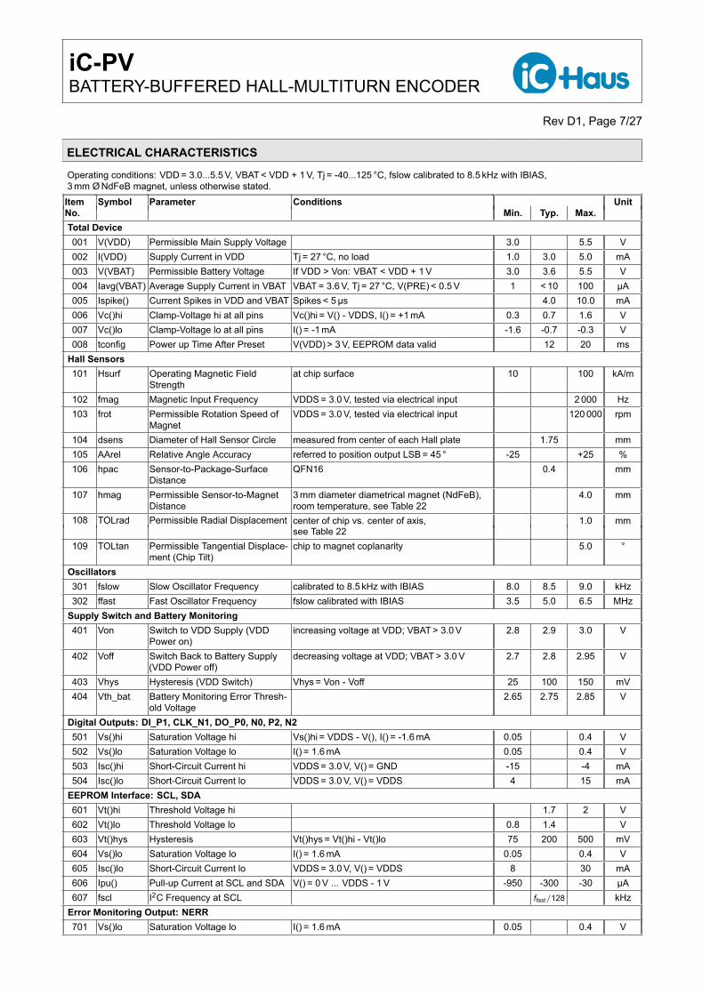
ELECTRICAL CHARACTERISTICS
Operating conditions: VDD = 3.0...5.5 V, VBAT < VDD + 1 V, Tj = -40...125 °C, fslow calibrated to 8.5 kHz with IBIAS,3 mm Ø NdFeB magnet, unless otherwise stated.Item Symbol Parameter Conditions UnitNo. Min. Typ. Max.Total Device001 V(VDD) Permissible Main Supply Voltage 3.0 5.5 V002 I(VDD) Supply Current in VDD Tj = 27 °C, no load 1.0 3.0 5.0 mA003 V(VBAT) Permissible Battery Voltage If VDD > Von: VBAT < VDD + 1 V 3.0 3.6 5.5 V004 Iavg(VBAT) Average Supply Current in VBAT VBAT = 3.6 V, Tj = 27 °C, V(PRE) < 0.5 V 1 < 10 100 µA005 Ispike() Current Spikes in VDD and VBAT Spikes < 5µs 4.0 10.0 mA006 Vc()hi Clamp-Voltage hi at all pins Vc()hi = V() - VDDS, I() = +1 mA 0.3 0.7 1.6 V007 Vc()lo Clamp-Voltage lo at all pins I() = -1 mA -1.6 -0.7 -0.3 V008 tconfig Power up Time After Preset V(VDD) > 3 V, EEPROM data valid 12 20 ms
Hall Sensors101 Hsurf Operating Magnetic Field
Strengthat chip surface 10 100 kA/m
102 fmag Magnetic Input Frequency VDDS = 3.0 V, tested via electrical input 2 000 Hz103 frot Permissible Rotation Speed of
MagnetVDDS = 3.0 V, tested via electrical input 120 000 rpm
104 dsens Diameter of Hall Sensor Circle measured from center of each Hall plate 1.75 mm105 AArel Relative Angle Accuracy referred to position output LSB = 45 ° -25 +25 %106 hpac Sensor-to-Package-Surface
DistanceQFN16 0.4 mm
107 hmag Permissible Sensor-to-MagnetDistance
3 mm diameter diametrical magnet (NdFeB),room temperature, see Table 22
4.0 mm
108 TOLrad Permissible Radial Displacement center of chip vs. center of axis, 1.0 mmsee Table 22
109 TOLtan Permissible Tangential Displace-ment (Chip Tilt)
chip to magnet coplanarity 5.0 °
Oscillators301 fslow Slow Oscillator Frequency calibrated to 8.5 kHz with IBIAS 8.0 8.5 9.0 kHz302 ffast Fast Oscillator Frequency fslow calibrated with IBIAS 3.5 5.0 6.5 MHz
Supply Switch and Battery Monitoring401 Von Switch to VDD Supply (VDD
Power on)increasing voltage at VDD; VBAT > 3.0 V 2.8 2.9 3.0 V
402 Voff Switch Back to Battery Supply(VDD Power off)
decreasing voltage at VDD; VBAT > 3.0 V 2.7 2.8 2.95 V
403 Vhys Hysteresis (VDD Switch) Vhys = Von - Voff 25 100 150 mV404 Vth_bat Battery Monitoring Error Thresh-
old Voltage2.65 2.75 2.85 V
Digital Outputs: DI_P1, CLK_N1, DO_P0, N0, P2, N2501 Vs()hi Saturation Voltage hi Vs()hi = VDDS - V(), I() = -1.6 mA 0.05 0.4 V502 Vs()lo Saturation Voltage lo I() = 1.6 mA 0.05 0.4 V503 Isc()hi Short-Circuit Current hi VDDS = 3.0 V, V() = GND -15 -4 mA504 Isc()lo Short-Circuit Current lo VDDS = 3.0 V, V() = VDDS 4 15 mA
EEPROM Interface: SCL, SDA601 Vt()hi Threshold Voltage hi 1.7 2 V602 Vt()lo Threshold Voltage lo 0.8 1.4 V603 Vt()hys Hysteresis Vt()hys = Vt()hi - Vt()lo 75 200 500 mV604 Vs()lo Saturation Voltage lo I() = 1.6 mA 0.05 0.4 V605 Isc()lo Short-Circuit Current lo VDDS = 3.0 V, V() = VDDS 8 30 mA606 Ipu() Pull-up Current at SCL and SDA V() = 0 V ... VDDS - 1 V -950 -300 -30 µA607 fscl I2C Frequency at SCL ffast/128 kHz
Error Monitoring Output: NERR701 Vs()lo Saturation Voltage lo I() = 1.6 mA 0.05 0.4 V
iC-PVBATTERY-BUFFERED HALL-MULTITURN ENCODER
Rev D1, Page 8/27
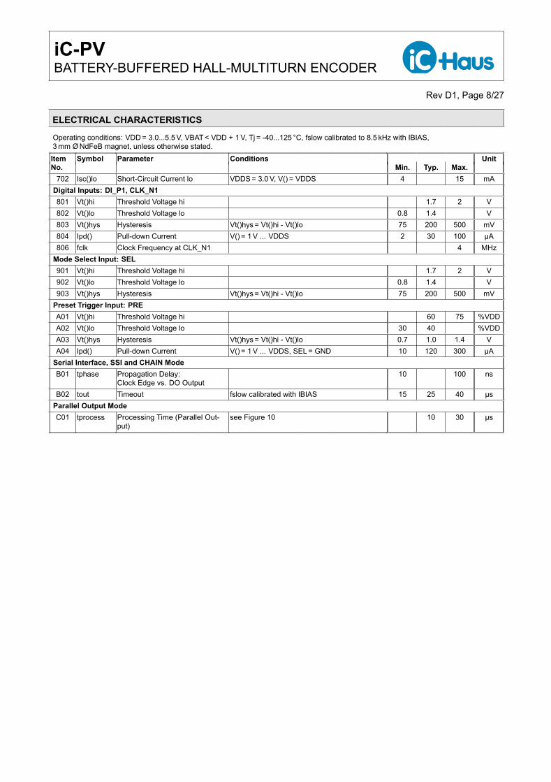
ELECTRICAL CHARACTERISTICS
Operating conditions: VDD = 3.0...5.5 V, VBAT < VDD + 1 V, Tj = -40...125 °C, fslow calibrated to 8.5 kHz with IBIAS,3 mm Ø NdFeB magnet, unless otherwise stated.Item Symbol Parameter Conditions UnitNo. Min. Typ. Max.
702 Isc()lo Short-Circuit Current lo VDDS = 3.0 V, V() = VDDS 4 15 mADigital Inputs: DI_P1, CLK_N1801 Vt()hi Threshold Voltage hi 1.7 2 V802 Vt()lo Threshold Voltage lo 0.8 1.4 V803 Vt()hys Hysteresis Vt()hys = Vt()hi - Vt()lo 75 200 500 mV804 Ipd() Pull-down Current V() = 1 V ... VDDS 2 30 100 µA806 fclk Clock Frequency at CLK_N1 4 MHz
Mode Select Input: SEL901 Vt()hi Threshold Voltage hi 1.7 2 V902 Vt()lo Threshold Voltage lo 0.8 1.4 V903 Vt()hys Hysteresis Vt()hys = Vt()hi - Vt()lo 75 200 500 mV
Preset Trigger Input: PREA01 Vt()hi Threshold Voltage hi 60 75 %VDDA02 Vt()lo Threshold Voltage lo 30 40 %VDDA03 Vt()hys Hysteresis Vt()hys = Vt()hi - Vt()lo 0.7 1.0 1.4 VA04 Ipd() Pull-down Current V() = 1 V ... VDDS, SEL = GND 10 120 300 µA
Serial Interface, SSI and CHAIN ModeB01 tphase Propagation Delay:
Clock Edge vs. DO Output10 100 ns
B02 tout Timeout fslow calibrated with IBIAS 15 25 40 µsParallel Output ModeC01 tprocess Processing Time (Parallel Out-
put)see Figure 10 10 30 µs
iC-PVBATTERY-BUFFERED HALL-MULTITURN ENCODER
Rev D1, Page 9/27
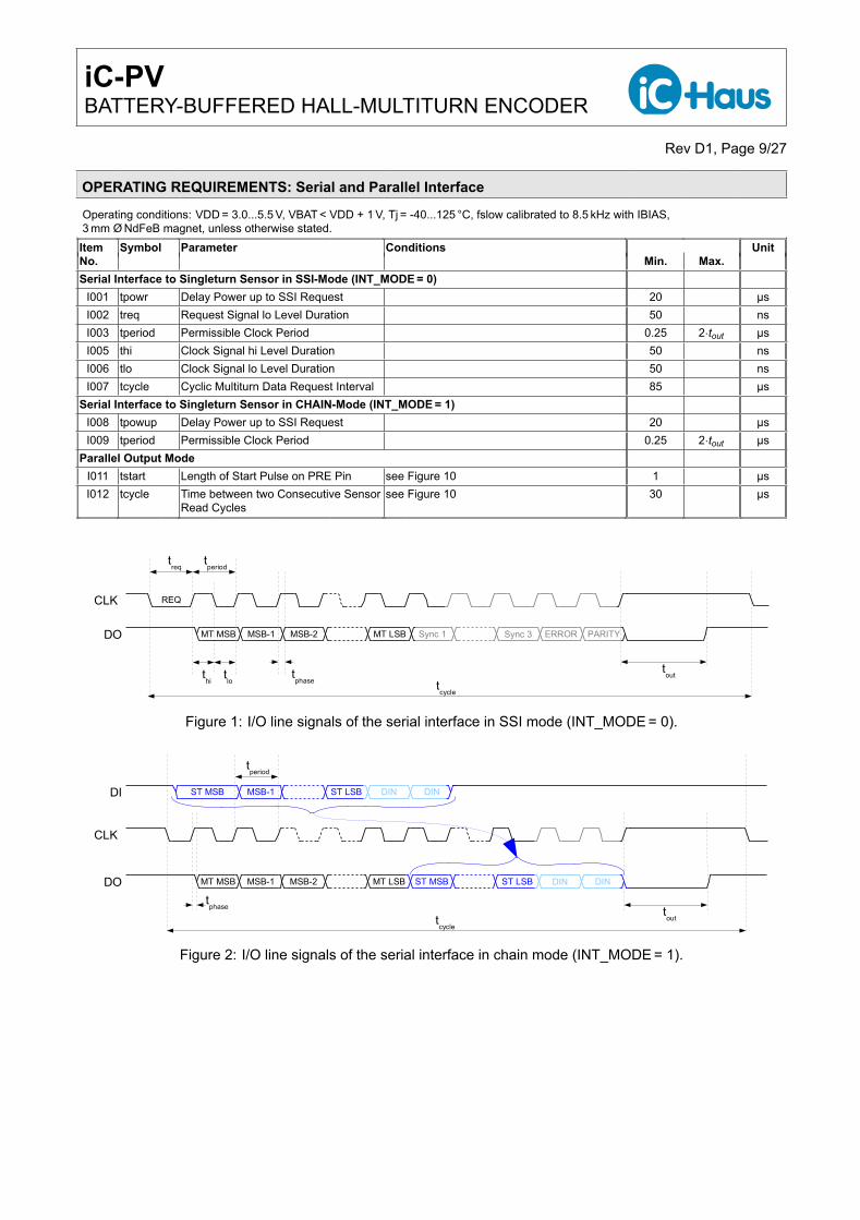
OPERATING REQUIREMENTS: Serial and Parallel Interface
Operating conditions: VDD = 3.0...5.5 V, VBAT < VDD + 1 V, Tj = -40...125 °C, fslow calibrated to 8.5 kHz with IBIAS,3 mm Ø NdFeB magnet, unless otherwise stated.Item Symbol Parameter Conditions UnitNo. Min. Max.Serial Interface to Singleturn Sensor in SSI-Mode (INT_MODE = 0)
I001 tpowr Delay Power up to SSI Request 20 µsI002 treq Request Signal lo Level Duration 50 nsI003 tperiod Permissible Clock Period 0.25 2·tout µsI005 thi Clock Signal hi Level Duration 50 nsI006 tlo Clock Signal lo Level Duration 50 nsI007 tcycle Cyclic Multiturn Data Request Interval 85 µs
Serial Interface to Singleturn Sensor in CHAIN-Mode (INT_MODE = 1)I008 tpowup Delay Power up to SSI Request 20 µsI009 tperiod Permissible Clock Period 0.25 2·tout µs
Parallel Output ModeI011 tstart Length of Start Pulse on PRE Pin see Figure 10 1 µsI012 tcycle Time between two Consecutive Sensor
Read Cyclessee Figure 10 30 µs
CLK
DO
REQ
treq
MT MSB MSB-1
thi
tlo
MSB-2
tphase
MT LSB
tout
tperiod
Sync 1 Sync 3 ERROR PARITY
tcycle
Figure 1: I/O line signals of the serial interface in SSI mode (INT_MODE = 0).
CLK
DO MT MSB MSB-1 MSB-2 MT LSB
tperiod
ST MSB DIN
tcycle
DIN
DI ST MSB MSB-1 ST LSB
ST LSB
tphase
DINDIN
tout
Figure 2: I/O line signals of the serial interface in chain mode (INT_MODE = 1).
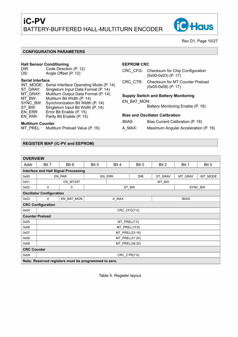
iC-PVBATTERY-BUFFERED HALL-MULTITURN ENCODER
Rev D1, Page 10/27
CONFIGURATION PARAMETERS
Hall Sensor ConditioningDIR: Code Direction (P. 12)OS: Angle Offset (P. 12)
Serial InterfaceINT_MODE: Serial Interface Operating Mode (P. 14)ST_GRAY: Singleturn Input Data Format (P. 14)MT_GRAY: Multiturn Output Data Format (P. 14)MT_BW: Multiturn Bit Width (P. 14)SYNC_BW: Synchronization Bit Width (P. 14)ST_BW: Singleturn Input Bit Width (P. 14)EN_ERR: Error Bit Enable (P. 15)EN_PAR: Parity Bit Enable (P. 15)
Multiturn CounterMT_PREL: Multiturn Preload Value (P. 16)
EEPROM CRCCRC_CFG: Checksum for Chip Configuration
(0x00-0x03) (P. 17)CRC_CTR: Checksum for MT Counter Preload
(0x05-0x09) (P. 17)
Supply Switch and Battery MonitoringEN_BAT_MON:
Battery Monitoring Enable (P. 18)
Bias and Oscillator CalibrationIBIAS: Bias Current Calibration (P. 18)A_MAX: Maximum Angular Acceleration (P. 19)
REGISTER MAP (iC-PV and EEPROM)
OVERVIEWAddr Bit 7 Bit 6 Bit 5 Bit 4 Bit 3 Bit 2 Bit 1 Bit 0
Interface and Hall Signal Processing0x00 EN_PAR EN_ERR DIR ST_GRAY MT_GRAY INT_MODE0x01 OS_MT2ST MT_BW0x02 0 0 ST_BW SYNC_BW
Oscillator Configuration0x03 0 EN_BAT_MON A_MAX IBIAS
CRC Configuration0x04 CRC_CFG(7:0)
Counter Preload0x05 MT_PREL(7:0)0x06 MT_PREL(15:8)0x07 MT_PREL(23:16)0x08 MT_PREL(31:24)0x09 MT_PREL(39:32)
CRC Counter0x0A CRC_CTR(7:0)
Note: Reserved registers must be programmed to zero.
Table 5: Register layout

iC-PVBATTERY-BUFFERED HALL-MULTITURN ENCODER
Rev D1, Page 11/27
SENSOR PRINCIPLE
yx
z
N
S
ω
−Bz
+BzB
Figure 3: Sensor principle
In conjunction with a rotating permanent magnet, theiC-PV can be used to create a complete (multiturn) en-coder system. A diametrically magnetized, cylindricalpermanent magnet made of neodymium iron boron (Nd-
FeB) or samarium cobalt (SmCo) generates optimumsensor signals. The diameter of the magnet should bebetween 2 to 8 mm.
The iC-PV has four Hall sensors adapted for angledetermination and to convert the magnetic field intoa measurable Hall voltage. Only the z-component ofthe magnetic field is evaluated, whereby the field linespass through two opposing Hall sensors in the oppositedirection. Figure 3 shows an example of field vectors.The arrangement of the Hall sensors is selected sothat the mounting of the magnets relative to iC-PV isextremely tolerant. Two Hall sensors combined providea differential Hall signal. When the magnet is rotatedaround the longitudinal axis, sine and cosine outputvoltages are produced, which can be used to determinethe current angle.
In combination with a digital counter, this angle infor-mation is used to determine the absolute (multiturn)position, i.e., the iC-PV counts the revolutions of thepermanent magnet.
POSITION OF THE HALL SENSORS
The Hall sensors are placed in the center of the QFN16package at 90 ° to one another and arranged in a circlewith a diameter of 1.75 mm as shown in Figure 4.
In order to calculate the angle position of a diametricallypolarized magnet placed above the device, a differencein signal is formed between opposite pairs of Hall sen-sors, resulting in the sine being VSIN = VPSIN - VNSINand the cosine VCOS = VPCOS - VNCOS. The zero angleposition of the magnet is marked by the resulting cosinevoltage value being at a maximum and the sine voltagevalue at zero.
In this case, the south pole of the magnet is exactlyabove the PCOS sensor and the north pole is abovesensor NCOS, as shown in Figure 5. Sensors PSINand NSIN are placed along the pole boundary so thatneither generate a Hall signal.
When the magnet is rotated counterclockwise, the polesalso cover the PSIN and NSIN sensors, resulting in thesine and cosine signals shown in Figure 6.
NSIN NCOS
PSINPCOS
Pin 1 Mark
top view
Figure 4: Position of the Hall sensors

iC-PVBATTERY-BUFFERED HALL-MULTITURN ENCODER
Rev D1, Page 12/27
SN
Figure 5: Magnet zero position (top view)
Figure 6: Pattern of analog sensor signals with cor-responding angle of rotation
HALL SENSOR CONDITIONING: ANGLE OFFSET AND CODE DIRECTION
Assembled together with a diametrically polarizedmagnet, the integrated Hall sensor signal processinggenerates a 3 bit position word. Therefore, the iC-PVcan deliver up to 3 synchronization bits to the singleturnsensor in SSI readout mode.
OS Addr. 0x01; bit 7:5Code Phase shift000 0 °, no shift001 +45 ° leading010 +90 ° leading011 +135 ° leading100 -180 ° leading or trailing101 -135 ° trailing110 -90 ° trailing111 -45 ° trailing
Table 6: Angle offset
When the phase relationship between an additionalsingleturn iC and the iC-PV as multiturn encoder isunknown, or the singleturn sensor takes care of thesynchronization (SSI mode) and expects a defined re-lationship, the position can be electrically manipulatedto achieve the desired (leading or trailing) phase shift,regardless of the actual mounting position. An offset
value is added to the digitized Hall sensor position ac-cording to parameter OS.
In applications where the chain operation mode is used(see Page 14), the iC-PV takes care of synchronization.Therefore, it has to be mounted leading in relation tothe singleturn iC. The OS parameter can be used toachieve this phase shift on random mounting displace-ments. To ensure correct synchronization of multiturnand singleturn data, the resulting phase shift betweenmultiturn and singleturn position must be in range 0 ° to180 ° (MT leading)∗.
DIR Addr. 0x00; bit 3Code Direction0 Normal1 Inverted
Table 7: Code direction
For assembly situations were the mounting direction ofthe magnet is not known, the counting direction can beeasily swapped with the configuration bit DIR. The bitwould be typically used to invert the counting directionsin applications where the iC-PV is assembled on theback side of a PCB.
∗ 0 ° to 180 ° is the ideal range for tolerated values of phase shift between ST and MT. This range is further reduced due to communication,propagation or processing delays for the specific application. Typically, it is reduced by few degrees, increasing with rotational velocity.
iC-PVBATTERY-BUFFERED HALL-MULTITURN ENCODER
Rev D1, Page 13/27
MODE SELECT INPUT SEL
The input SEL defines the operating mode of iC-PV.For the default application as battery buffered multiturncounter with serial position readout, it is mandatory toconnect the SEL input to GND potential. In case a 3bit parallel and differential position output is desired, ahigh state at SEL input selects the parallel mode. Itis mandatory to connect SEL to a defined high or lowpotential.
MODE SELECT INPUT SELState iC-PV Operating ModeLow Battery buffered counter with serial readoutHigh 3 bit parallel complementary outputOpen Not allowed
Table 8: Mode selection via SEL pin
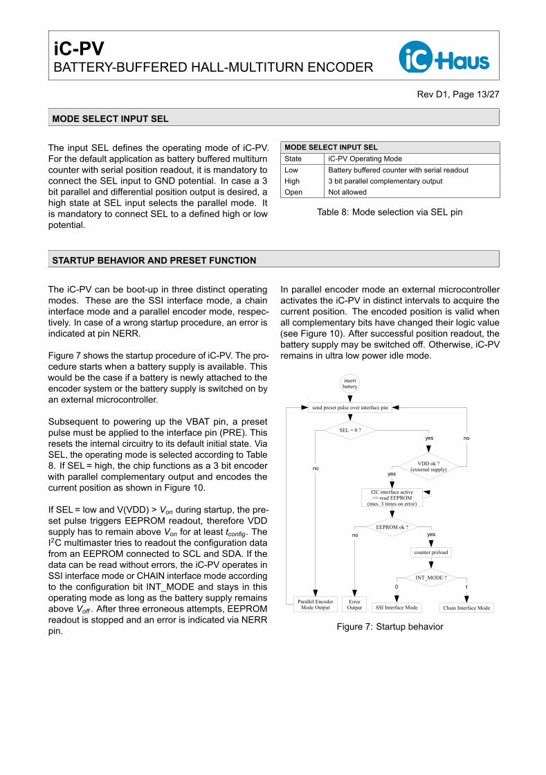
STARTUP BEHAVIOR AND PRESET FUNCTION
The iC-PV can be boot-up in three distinct operatingmodes. These are the SSI interface mode, a chaininterface mode and a parallel encoder mode, respec-tively. In case of a wrong startup procedure, an error isindicated at pin NERR.
Figure 7 shows the startup procedure of iC-PV. The pro-cedure starts when a battery supply is available. Thiswould be the case if a battery is newly attached to theencoder system or the battery supply is switched on byan external microcontroller.
Subsequent to powering up the VBAT pin, a presetpulse must be applied to the interface pin (PRE). Thisresets the internal circuitry to its default initial state. ViaSEL, the operating mode is selected according to Table8. If SEL = high, the chip functions as a 3 bit encoderwith parallel complementary output and encodes thecurrent position as shown in Figure 10.
If SEL = low and V(VDD) > Von during startup, the pre-set pulse triggers EEPROM readout, therefore VDDsupply has to remain above Von for at least tconfig. TheI2C multimaster tries to readout the configuration datafrom an EEPROM connected to SCL and SDA. If thedata can be read without errors, the iC-PV operates inSSI interface mode or CHAIN interface mode accordingto the configuration bit INT_MODE and stays in thisoperating mode as long as the battery supply remainsabove Voff . After three erroneous attempts, EEPROMreadout is stopped and an error is indicated via NERRpin.
In parallel encoder mode an external microcontrolleractivates the iC-PV in distinct intervals to acquire thecurrent position. The encoded position is valid whenall complementary bits have changed their logic value(see Figure 10). After successful position readout, thebattery supply may be switched off. Otherwise, iC-PVremains in ultra low power idle mode.
send preset pulse over interface pin
EEPROM ok ?
Parallel Encoder Mode Output
no yes
VDD ok ?(external supply)no
yes
I2C interface active=> read EEPROM
(max. 3 times on error)
INT_MODE ?
SSI Interface Mode
0
Chain Interface Mode
1
Error Output
insertbattery
counter preload
SEL = 0 ?
yes no
Figure 7: Startup behavior
iC-PVBATTERY-BUFFERED HALL-MULTITURN ENCODER
Rev D1, Page 14/27
SERIAL INTERFACE (SEL = LOW)
iC-PV can connect to an external singleturn sensor viaa serial interface. To ensure compatibility with differenttypes of singleturn sensors, the iC-PV’s serial interfacecan operate in two distinct modes. These are a stan-dard SSI conform operating mode and a chain mode,respectively.
In the SSI mode, the iC-PV expects an external sin-gleturn sensor to request the multiturn data via a SSIprotocol. The singleturn sensor takes care of synchro-nization and calculates a consistent absolute position.The data in pin (DI) is not used in this operating mode.iC-PV is compatible with all iC-Haus optical or mag-netic singleturn encoders featuring a multiturn interface(MTI). For details please refer to application examplesin Figure 12 up to Figure 15.In this mode of operation, iC-PV can also be used asstand-alone magnetic revolution counter. The positioncan be read via a serial, SSI compatible protocol (seeFigure 17).
In the chain mode, the singleturn sensor transmits thesingleturn position first to the iC-PV via the data in pin(DI). In this configuration, the iC-PV takes care of syn-chronization, calculates a consistent absolute positionand outputs it concurrently (MSB first) via the data outpin (DO), comparable to a shiftregister. An applicationexample with iC-LNG as singleturn iC is shown in Fig-ure 16.The respective mode to operate in is set using parame-ter INT_MODE.
INT_MODE Addr. 0x00; bit 0Code Mode0 Standard SSI readout mode (SSI)1 Chain mode (CHAIN)
Table 9: Serial interface operating mode
By default, the iC-PV expects the serial input at the datain pin (DI) to be binary. Similarly it outputs its countedmultiturn position via DO in binary format. In case oneof them or both are required to be in gray format, thiscan be configured by setting the ST_GRAY bit or theMT_GRAY bit, respectively.
ST_GRAY Addr. 0x00; bit 2Code Format0 Binary code1 Gray code
Table 10: Singleturn input data format via pin DI
MT_GRAY Addr. 0x00; bit 1Code Format0 Binary code1 Gray code
Table 11: Multiturn output data format via pin DO
The width of the internal multiturn counter is 40 bit. Inapplications where smaller counter depths are sufficientor are restricted by the bit width of the serial interface,the output length of the counter value can be configuredwith MT_BW as shown in Table 12.
MT_BW Addr. 0x01; bit 4:0Code Bit width0x00 9 bit0x01 10 bit. ...0x1E 39 bit0x1F 40 bit
Table 12: Multiturn bit width
Additionally iC-PV can transmit up to 3 synchronizationbits, according to configuration parameter SYNC_BWshown in Table 13.
SYNC_BW Addr. 0x02; bit 1:0Code Bit width Phase shift range00 0 bit no synchronization bit01 1 bit 0 °... 180 °10 2 bit 0 °... 270 °11 3 bit 0 °... 315 °
Table 13: Synchronization bit width and resulting toler-able ideal phase shift
The singleturn bit width, iC-PV expects in chain modeat pin DI, can be configured in similar way with configu-ration parameter ST_BW (Table 14).
ST_BW Addr. 0x02; bit 5:2Code Bit width0x00 3 bit0x01 4 bit... ...0x0F 18 bit
Table 14: Singleturn input bit width
After the transmission of the absolute position and thesynchronization information, iC-PV’s serial protocol al-lows the optional transmission of an error bit and a
iC-PVBATTERY-BUFFERED HALL-MULTITURN ENCODER
Rev D1, Page 15/27
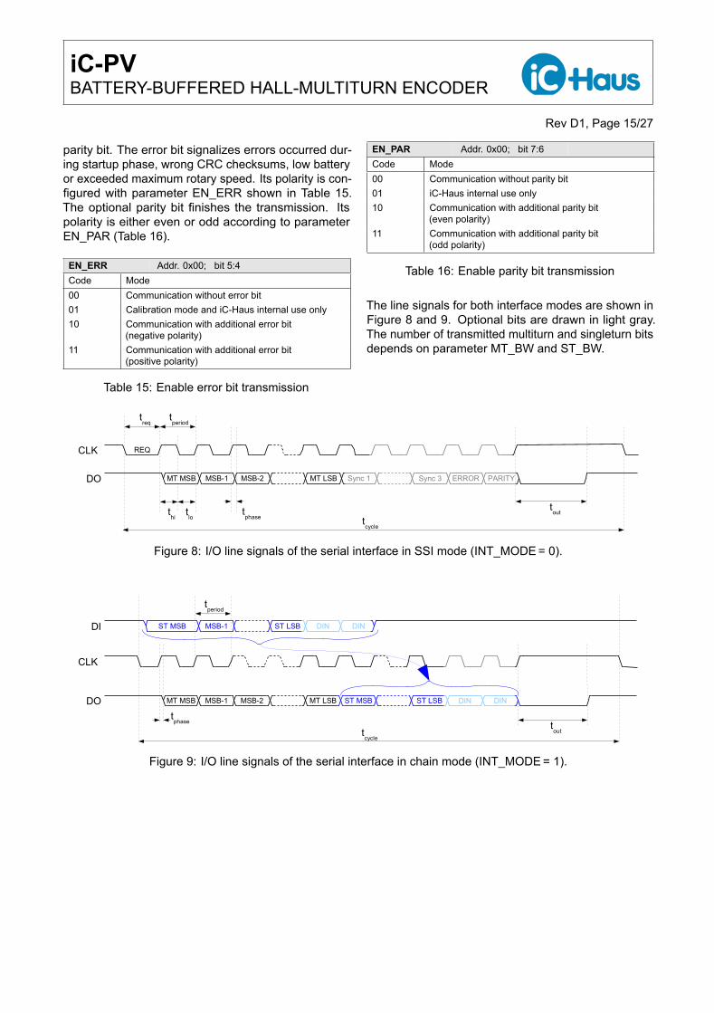
parity bit. The error bit signalizes errors occurred dur-ing startup phase, wrong CRC checksums, low batteryor exceeded maximum rotary speed. Its polarity is con-figured with parameter EN_ERR shown in Table 15.The optional parity bit finishes the transmission. Itspolarity is either even or odd according to parameterEN_PAR (Table 16).
EN_ERR Addr. 0x00; bit 5:4Code Mode00 Communication without error bit01 Calibration mode and iC-Haus internal use only10 Communication with additional error bit
(negative polarity)11 Communication with additional error bit
(positive polarity)
Table 15: Enable error bit transmission
EN_PAR Addr. 0x00; bit 7:6Code Mode00 Communication without parity bit01 iC-Haus internal use only10 Communication with additional parity bit
(even polarity)11 Communication with additional parity bit
(odd polarity)
Table 16: Enable parity bit transmission
The line signals for both interface modes are shown inFigure 8 and 9. Optional bits are drawn in light gray.The number of transmitted multiturn and singleturn bitsdepends on parameter MT_BW and ST_BW.
CLK
DO
REQ
treq
MT MSB MSB-1
thi
tlo
MSB-2
tphase
MT LSB
tout
tperiod
Sync 1 Sync 3 ERROR PARITY
tcycle
Figure 8: I/O line signals of the serial interface in SSI mode (INT_MODE = 0).
CLK
DO MT MSB MSB-1 MSB-2 MT LSB
tperiod
ST MSB DIN
tcycle
DIN
DI ST MSB MSB-1 ST LSB
ST LSB
tphase
DINDIN
tout
Figure 9: I/O line signals of the serial interface in chain mode (INT_MODE = 1).
iC-PVBATTERY-BUFFERED HALL-MULTITURN ENCODER
Rev D1, Page 16/27
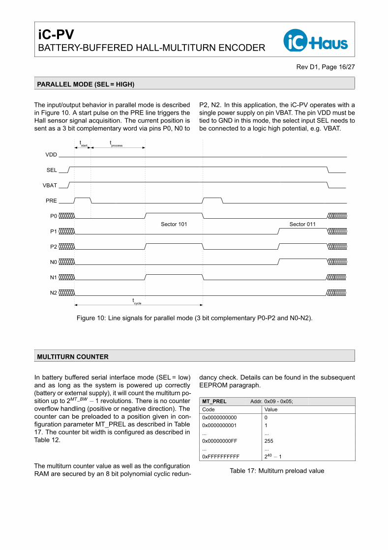
PARALLEL MODE (SEL = HIGH)
The input/output behavior in parallel mode is describedin Figure 10. A start pulse on the PRE line triggers theHall sensor signal acquisition. The current position issent as a 3 bit complementary word via pins P0, N0 to
P2, N2. In this application, the iC-PV operates with asingle power supply on pin VBAT. The pin VDD must betied to GND in this mode, the select input SEL needs tobe connected to a logic high potential, e.g. VBAT.
P0
P1
tstart
tcycle
VBAT
PRE
SEL
P2
N0
N1
N2
tprocess
Sector 101 Sector 011
VDD
Figure 10: Line signals for parallel mode (3 bit complementary P0-P2 and N0-N2).
MULTITURN COUNTER
In battery buffered serial interface mode (SEL = low)and as long as the system is powered up correctly(battery or external supply), it will count the multiturn po-sition up to 2MT_BW − 1 revolutions. There is no counteroverflow handling (positive or negative direction). Thecounter can be preloaded to a position given in con-figuration parameter MT_PREL as described in Table17. The counter bit width is configured as described inTable 12.
The multiturn counter value as well as the configurationRAM are secured by an 8 bit polynomial cyclic redun-
dancy check. Details can be found in the subsequentEEPROM paragraph.
MT_PREL Addr. 0x09 - 0x05;Code Value0x0000000000 00x0000000001 1... ...0x00000000FF 255... ...0xFFFFFFFFFF 240 − 1
Table 17: Multiturn preload value

iC-PVBATTERY-BUFFERED HALL-MULTITURN ENCODER
Rev D1, Page 17/27
I2C MULTIMASTER INTERFACE TO EEPROM INTERFACE AND CRC PROTECTION
Pins SCL and SDA form an interface which can be usedto communicate (read-only) with an external EEPROMaccording to I2C protocol (with at least 128 bytes, e.g.24C01, 24C02, 24C08 and maximum 24C16, extendedaddress range is not supported).
This EEPROM is used to store the iC-PV configuration(addresses 0x00 to 0x0A) according to the register mapon Page 10. The configuration is protected against biterrors by an 8 bit polynomial cyclic redundancy check.CRC checksum failure is displayed via output NERRand as an error bit at the end of the SSI communica-tion protocol. The multiturn counter preload value isstored in its own configuration area (0x05 - 0x09) andis also saved with its own CRC on 0x0A. The CRC forthe remaining four configuration bytes (0x00 - 0x03)is stored at address 0x04. Both CRC checksums aregenerated with the polynomial X8 + X5 + X3 + X2 + X1 + 1(0x2F sometimes also named as 0x12F). The CRC startvalue is zero.
Since iC-PV does only read configuration data, the writeaccess to EEPROM is done via external inline program-ming via pins SCL and SDA (I2C protocol). The directEEPROM access to I2C lines is shown in the applica-tion schematic on Page 24. In applications with sharedEEPROM, e.g. with iC-MHM, the EEPROM program-ming for iC-PV configuration can be done via the BiSSinterface of the iC-MHM (see Figure 12).
If no EEPROM is available or desired in the applica-tion, programming the iC-PV with a microcontroller unit(MCU) is possible. Therefore, the MCU has to emulatean I2C slave, since iC-PV is acting as a bus masteronly. At startup, after a short high pulse at pin PRE, theiC-PV request the address 0x00 to 0x0A from the con-nected I2C slave. This is done in a combined write/readcommand as shown in Figure 11. The shown sequenceis repeated 11 times.
The expected slave address is 0x50 or "101 0000", thestandard I2C slave EEPROM address.
SCL
SDA 1 0 A2S A1 A0 W1 0 ACK D7 ... D0 ACK Sr 1 0 A2S A1 A01 0 R ACK D7 … D0 ACK P
Slave Address (7 bit “1010000“) Write ACK(Slave)
Data (8 bit)EEPROMaddressto read
ACK(Slave)
Startrepeatedcondition
Startcond.
Read ACK(Slave)
Data (8 bit)read from requested address
NACK(Master)
Slave Address (7 bit “1010000“) Stopcond.
Master requesting the address to read (write command master to slave)
Master reading the data at requested address (read command master to slave)
Claimingthe bus
Keepingthe bus
Releasingthe bus
fscl
Figure 11: iC-PV combined write/read command reading one slave address.
iC-PVBATTERY-BUFFERED HALL-MULTITURN ENCODER
Rev D1, Page 18/27
SUPPLY SWITCH AND BATTERY MONITORING
To retain and acquire the absolute position even onmain power failure, the iC-PV switches from VDD toa battery supply on pin VBAT. The switching point liesjust below 3 V. So if the main supply voltage on VDDdrops below 3 V, the internal circuitry will be poweredby VBAT instead of VDD.
The supply switch has a build in hysteresis. The thresh-old voltages are defined in the electrical characteristicssection named Voff (Item No. 402), i.e. the voltage atwhich the circuit switches from VDD supply to VBATsupply and Von (Item No. 401), the voltage at which thecircuit switches back to VDD.
Depending on the used energy storage, e.g. a 3.6 Vbattery with 1 Ah capacity, the device can operate for
several years. The iC-PV monitors the voltage at pinVBAT to detect a low battery voltage. If it drops belowa defined error threshold voltage (Item No. 404), anerror is generated and signalized via pin NERR and aserror bit in the SSI communication protocol. The batterymonitoring function can be enabled/disabled with con-figuration parameter EN_BAT_MON as show in Table18.
EN_BAT_MON Addr. 0x03; bit 6Code Function0 Battery monitoring off1 Battery monitoring on
Table 18: Enable or disable the internal battery monitor.
BIAS AND OSCILLATOR CALIBRATION
The bias current for the internal oscillator can be con-figured with the configuration parameter IBIAS. An in-crease or decrease in bias current will directly influencethe oscillator frequency. The bias current should becalibrated at the typical battery supply voltage so thatthe frequency of the oscillator is around 8.5 kHz (seeItem No. 301). The clock frequency is observable inthe dedicated calibration mode. The calibration mode isentered by configuring the EN_ERR parameter to "01"(see Table 15). The oscillator clock is then output onpin DI_P1.
IBIAS Addr. 0x03; bit 2:0Code Frequency change100 +20 %101 +10 %110 0 %111 -10 %000 -20 %001 -30 %010 -40 %011 -50 %
Table 19: Bias current; oscillator frequency calibration.
iC-PVBATTERY-BUFFERED HALL-MULTITURN ENCODER
Rev D1, Page 19/27
CALCULATING CURRENT CONSUMPTION
Interface Mode (SEL = LOW)The current consumption of the iC-PV can be config-ured by parameter A_MAX. Besides the current con-sumption, this parameter sets the maximum angle ac-celeration (from shaft halt) supported by the iC-PVin the respective configuration. The relationship be-tween maximum acceleration and current consump-tion is shown in Table 20. For accelerations below48 · 103rad/s2, the typical current consumption lies be-low 10µA.
For applications were only sporadic motor movement isexpected during battery supply, Table 20 mainly definesthe current consumed by iC-PV. Additionally, Table 21gives typical values in case of enduring movement at acertain angular velocity.
A_MAX Addr. 0x03; bit 5:3Code αmax [
s2 ] αmax [ rads2 ] typ.
Iavg[µA]max.
Iavg[µA]000 40 · 106 760 · 103 26 36001 10 · 106 190 · 103 14 18010 2.5 · 106 48 · 103 7 10011 625 · 103 12 · 103 4 6100 160 · 103 3 · 103 2.5 4101 40 · 103 0.75 · 103 2 3110 10 · 103 0.2 · 103 1.5 2.5111 reserved
Table 20: Maximum supported angular acceleration(from shaft halt) and average current con-sumption on shaft halt or slow angular veloc-ity. V(VBAT) = 3.6 V, V(PRE) < 0.5 V.
I(VBAT) for angular velocity [RPM]f [RPM] f [Hz] Iavg[µA] Iavg[µA] Iavg[µA] Iavg[µA] Iavg[µA] Iavg[µA] Iavg[µA]
AMAX =110
AMAX =101
AMAX =100
AMAX =011
AMAX =010
AMAX =001
AMAX =000
0 0 1.5 2 2.5 4 7 14 26< 125 < 2 1.5 2 2.5 4 7 14 26< 250 < 4 2 2 2.5 4 7 14 26< 500 < 8 2.5 2.5 2.5 4 7 14 26
< 1000 < 16 4 4 4 4 7 14 26< 2000 < 33 7 7 7 7 7 14 26< 4000 < 66 14 14 14 14 14 14 26< 8000 < 133 26 26 26 26 26 26 26
< 16000 < 266 51 51 51 51 51 51 51
Table 21: Average current consumption vs. angular velocity. Typical values for V(VBAT) = 3.6 V, Ta = 25 °C andV(PRE) < 0.5 V.
Parallel Encoder Mode (SEL = HIGH)The current consumption in parallel encoder mode is di-rectly proportional to the sampling frequency, fs. Lowersampling frequencies use less current and higher fre-quencies use more current. The typical mean valueof current consumed by iC-PV, is calculated as shownbelow (V(VBAT) = 3.6 V, Tj = 25 °C) :
Iavg[µA] = 25 · fs[kHz]
For instance, at a sampling frequency of 1 000 samplesper second, fs = 1 kHz and I = 25µA. At 100 samplesper second, I = 2.5µA.

iC-PVBATTERY-BUFFERED HALL-MULTITURN ENCODER
Rev D1, Page 20/27
APPLICATION NOTES: Operating distance sensor to magnet
The iC-PV is highly tolerant for assembly displace-ments between the magnet and the iC itself. The finalsetup has to meet the specified operating magnetic fieldstrength (Item No. 101). Depending on the used mag-net, this leads to different permissible sensor to magnetdistances. For typical magnets made of NdFeB theoperating distances are shown in Table 22. The thirdcolumn defines the permissible radial displacement.The permissible tangential displacement (tilt error) isdefined in Item No. 109.
Assembly tolerances sensor to magnetØ Magnet Distance Radial Displacement3 mm up to 4.0 mm up to 1.0 mm4 mm up to 6.0 mm up to 1.5 mm8 mm up to 7.0 mm up to 3.0 mm
Table 22: Assembly tolerances: Operating distancesensor to magnet and permissible radial dis-placement.

iC-PVBATTERY-BUFFERED HALL-MULTITURN ENCODER
Rev D1, Page 21/27
APPLICATION NOTES: Singleturn iCs with multiturn interface (SSI-Mode)
B
B
B
B
B B
B B
RAM
D
SINiC-MHM
LINEDRIVER
BiSSINTERFACE
EEPROMiC-PV
HALL FRONTEND
SUPPLY SWITCH
OSCILLATOR
D
over JP1 on PV1M1
SIN
I2C MULTI MASTER
ERRORMONITORMULTITURN COUNTER
SERIAL INTERFACE MT-INTERFACE
ERROR
optional preset line
MULTI MASTER
MONITOR
I2C
DIGITAL-IOPSIN
NCOS
HALL SENSOR
PCOS
NSIN
CONTROLAMPLITUDE
MAO
SLO
NCOSDI_P1
CLK_N1
SDA
SCL
MA
SLI
VDDSVDD
DO_P0
GNDA
NERR
VDDS
PRE
P1SCL
NERR
VDD
MCL
MDI
GNDSDA
SCL
SDA
P3
P2
GNDS
GND
VBAT
PSIN
PCOS
NSIN
SEL
VDD
MAOMA
SLISLO
VDD
GND
Figure 12: Application example iC-PV as battery-buffered multiturn device connected to the MT interface ofthe iC-MHM singleturn encoder. Interface operating in SSI-Mode (INT_MODE = 0). The two iC’sshare one common EEPROM for configuration. EEPROM is written via iC-MHM, BiSS registeraccess. The position (MT + ST) is transmitted via the serial BiSS interface (please see iC-MHMspecification for further details).
B
B
SSiSPI
B
Z
NERR
(optional)
EEPROM
SerialA
I2CMULTI
MASTERRAM
INTERFACE HANDLER
+
-
OSCILLATOR
SER INTERFACE
12 BIT
ERROR MANAGEMENT
MASTER TRACK
CONFIGURATION
+
-
HALL SENSORS SIN/DIG CONVERTER
SUPPLY SWITCH
SYNCHRONISATION
PGA
CLOCK
BIAS
PORT APORT B
INTERFACEINLINE
POSITION ENCODE
COUNTERMULTITURN
Incremental
ENCODER PROCESSOR
SINUS/DIGITAL
I2C EEPROM
EEPROM
PROG
EEPROMINTERFACE
LOGIC AND SERIAL INTERFACE
HALL CONTROL
ERRORMONITOR
SERIAL/PARALLELOUTPUTSSI Interface
Interface
1 0 0 1 1
AMPLITUDEINTERFACE
NONIUS TRACKBiSS
128 Byte RAM
HALL SENSORSANA/DIG OUTPUT
MULTITURN
REFERENCE
12 BIT
iC-PV iC-MUCONTROL
Monitor
P2
PRE
N0
DI_P1
VDDS
DO_P0
N2
VDDVBAT
GND
NERR
CLK_N1
SDA
SEL
VDD
GND
VDD
SDA SCL
SCL
SDA SCL GND
100nF
100nF1μF 100nF
+
-
+
-
+
100nF 100nF 100nF
VPD
VNA
PSIN
NSIN
PCOS
NCOS
SCL
SDA
PRESET
SDA
PB3
PB2
PB1
PB0
PA3
PA2
PA1
PA0
SCL
VPA
MTD
MTC
VND
100nF100nF
B
+
1μF 100nF100nF
100nF
100nF
B B
B
Figure 13: Application example iC-PV as battery-buffered multiturn device connected to the MT interfaceof the iC-MU absolute singleturn encoder. Interface operating in SSI-Mode (INT_MODE = 0).One EEPROM per iC mandatory for configuration. iC-PV EEPROM, direct access via SCL, SDA.BiSS, SPI and SSI are available for serial data transmission (please see iC-MU specification forfurther details).
iC-PVBATTERY-BUFFERED HALL-MULTITURN ENCODER
Rev D1, Page 22/27
COUNTERMULTITURN
MULTIMASTER
RAM
1 0 0 1
SIN/DIG CONVERTER
Ext. Sync
Code Reverse
Interface
Serial MT
Position Data
Monitor
Synchronisation
Parallel
Register
Reset
Interface
SINP
N
D1
LED ControlAdj
TestSUPPLY SWITCH
LOGIC AND SERIAL INTERFACE
HALL CONTROL
ERROR
INLINEPROG
EEPROMINTERFACESERIAL/
PARALLELOUTPUTSSI Interface
POSITION ENCODE
BiSS
N
Track7NP
NN
VP
VN
Track8..10
&Error
2
VP
1
2
SensorsAlignment
EEPROM
Optional
Microcontroller
Track2..6,11..13
P
N
LED Control
sin+cos,sum &Bias
POR
Reference
OSCILLATOR
+
-
+
-
HALL SENSORS
VN
COSP
N
P
Preset
InterfaceBiSS
EEPROM iC-LGCInterpolator
8-Bit
Calibration
Temperature
Configuration
Interface
Interface
MONITOR
MonitoriC-PV
NN
NP
Track1
D0
I2C
GND
N2
P2
TVP
TVN
P4
SEL
P3
GND
VDD
MDI
SCL
NWR
NRES
SYNC
NL
SCL
SDA
MA
SDA
NERR
DO_P0
GND
VDDVBAT
NDIR
P1
NERR
GND AGND
NPRES
SLO
SLI
P7
TNP
VNCOS
VDD
ICOS
SCL
VCCA
RSET
LED
N0
DI_P1
CLK_N1
SDA
SCL
P2
P5
P6
LVCC
NRD
MCL
VREF
ISIN
VDDS
PRE
TNN
SDA
VDD VDDM
VNSIN
P0
100nF
100nF100nF
100nF
+
-
+
-
100nF
1μFiC-SG85
LED
NCOS
SCL
SDA
SLO
MA
PSIN
NSIN
PCOS
PRESET
100nF
100nF 100nF
B B
LEDiC-SG85
100nF
1μF
100nF
B B
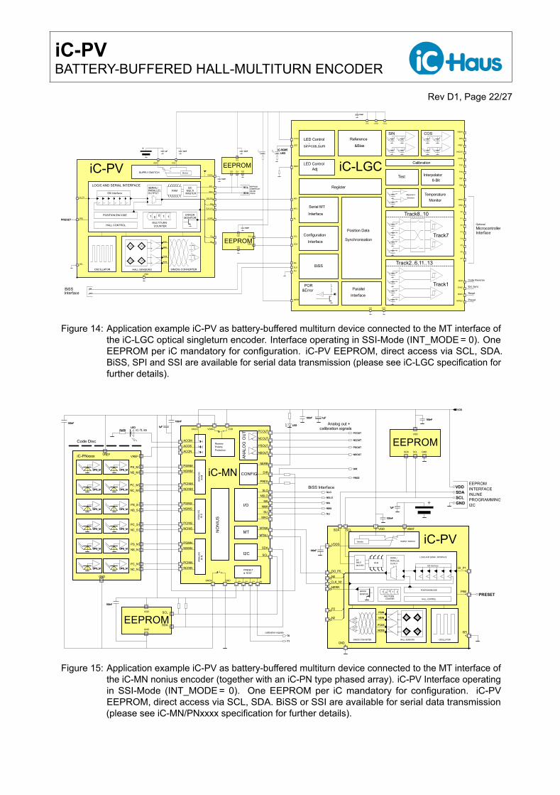
Figure 14: Application example iC-PV as battery-buffered multiturn device connected to the MT interface ofthe iC-LGC optical singleturn encoder. Interface operating in SSI-Mode (INT_MODE = 0). OneEEPROM per iC mandatory for configuration. iC-PV EEPROM, direct access via SCL, SDA.BiSS, SPI and SSI are available for serial data transmission (please see iC-LGC specification forfurther details).
B B
B B
iC-TL 85
-
EEPROMINTERFACEINLINEPROGRAMMINGI2C
-+
RAM
11
PARALLELSERIAL/
MONITOR
IN N
Code Disc
OU
T
CONFIG
BiSS Interface
EEPROM
IN M
LOGIC AND SERIAL INTERFACE
SUPPLY SWITCH
AN
ALO
G
NO
NIU
S
ReversePolarityProtection
calibration signals
MT
ANAL
OG
Monitor iC-PV
POSITION ENCODE
SSI InterfaceOUTPUT
AN
ALO
GIN
S
SIN/DIG CONVERTER HALL SENSORS
-
+
iC-MN
MULTITURN
EEPROM+
PRESET& TEST
AN
ALO
G
OSCILLATOR
COUNTER
MASTERMULTII2C
Analog out +
iC-PNxxxx
ERROR
HALL CONTROL
-+
calibration signals
I2C
I/O
001
N2
VDD
SDA SCL
NC_N DO_P0
NSLO
NC_S
T3 T2
PSOUTACOM
GND
SCL
PRE
VDDS
GND
NMA
SLI
MAO
N0GNDGNDA
VDDA VDD
PS_N
VREF VREF
CLK_N1
DI_P1
ACON
ACOS
NCINN
MA
SDA
PC_S
MTSLI
PRES
NCOUT
PCOUT
PS_M
SLO
SEL
DIR
P2
NERR
GND
VBATVDDSCL
PCINM
NCINM
NSINM
PSINS
NSINS
T1 T0
NSINN
NSOUT
PCINN
SCL
SDA
SDA
VACO
PSINM
VDD
GND
PC_M
NC_M
NS_M
PCINS
NCINS
PSINN
MTMA
NS_N
NERR
NS_S
PS_S
PC_N
100nF
DPS_M
DPS_M
DPS_M DPS_M
100nF
100nF
DPS_M
1μFRLED
LEDLED
DPS_M
DPS_M
DPS_M
1μF
DPS_M
1μF100nF
100nF
DPS_MDPS_M
100nF100nF
VDD
VDD
GND
SDASCL
DPS_M
NCOS
PCOS
NSIN
PSIN
PRESET
NSOUT
PSOUT
NCOUT
PCOUT
T1
T0
SLO
SLI
NMA
MA
NSLO
DIR
PRES
DPS_M
100nF
100nF
100nF
DPS_M
DPS_M DPS_M
LEDRLED
LED
DPS_M
1μF
1μF
DPS_M
DPS_M
DPS_M
DPS_M DPS_M
100nF
DPS_MDPS_M
100nF
100nF
1μF100nF
Figure 15: Application example iC-PV as battery-buffered multiturn device connected to the MT interface ofthe iC-MN nonius encoder (together with an iC-PN type phased array). iC-PV Interface operatingin SSI-Mode (INT_MODE = 0). One EEPROM per iC mandatory for configuration. iC-PVEEPROM, direct access via SCL, SDA. BiSS or SSI are available for serial data transmission(please see iC-MN/PNxxxx specification for further details).
iC-PVBATTERY-BUFFERED HALL-MULTITURN ENCODER
Rev D1, Page 23/27
APPLICATION NOTES: Chain operating mode
PARALLEL
HALL SENSORS SIN/DIG CONVERTER
SUPPLY SWITCH
LOGIC AND SERIAL INTERFACE
HALL CONTROL
ERRORMONITOR
SERIAL/
SSI Interface
6-BitSIGNAL-LEVEL
CONTROLLER
INTERFACE
SPI
OUTPUT
OSCILLATOR
DA3
DA2
DA1
DA11
DA10
DA9
DA8 EEPROMINTERFACEINLINEPROGRAMMINGI2C
DNCOS
POSITION ENCODE
COUNTERMULTITURN
MONITORING
INCOUT MUX
LOGIK
CORRECTION
ANALOG MUX
DPCOS
DNSIN
110
I2CMULTI
CONDITIONING
MicroController
iC-PV Monitor
+
-
+
-
MASTERRAM
1 0
EEPROM
DPSIN
INTERPOLATOR
DA4
INTERFACE
SERIALSIGNAL
DA5
iC-LNG
DA7
DA6
REFERENCE
VOLTAGE
SERIAL_DATA_IN
NSL
PRE
VDDS
DO_P0
VDD
SDA
SCLSDA
VDD
GND
VDD
GND
CLK_N1
SCL
NERR
DI_P1
GND
N0
VBAT
CLK
N2
P2
SEL
100nF 100nF
100nF
iC-SN85LED
100nF 100nF
+
-
+
-
1μF
PSIN
NSIN
PCOS
NCOS
PSIN
NSIN
PCOS
NCOS
SCKMOSIMISOCS
PSIN
NSIN
PCOS
NCOS
SDASCL
GND
VDD
POKINCA
INCB
INCZ
P06ERR
P05
VDDA
GNDA GND
VDD
NSL
DOUT
DIN
TPS
TNS
TPC
TNC
PRESET
LED
PSIN
TA1
NSIN
TA2
PCOS
TA3
NCOS
TA4
INCA
INCB
INCZ
CLK
SCK
MOSI
MISO
CS
ATD1
B
TD2
PO5
PO6
TPS
TNS
TPC
TNC
POK
Z
100nF
100nF 100nF
LEDiC-SN85
100nF 100nF
1μF
B B
B B
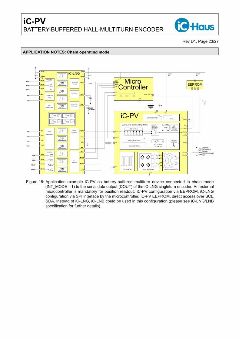
Figure 16: Application example iC-PV as battery-buffered multiturn device connected in chain mode(INT_MODE = 1) to the serial data output (DOUT) of the iC-LNG singleturn encoder. An externalmicrocontroller is mandatory for position readout. iC-PV configuration via EEPROM, iC-LNGconfiguration via SPI interface by the microcontroller. iC-PV EEPROM, direct access over SCL,SDA. Instead of iC-LNG, iC-LNB could be used in this configuration (please see iC-LNG/LNBspecification for further details).
iC-PVBATTERY-BUFFERED HALL-MULTITURN ENCODER
Rev D1, Page 24/27
APPLICATION NOTES: iC-PV as battery powered revolution counter or metering device
INTERFACEPOSITIONREADOUT
0
EEPROMINTERFACEINLINE
SERIAL
EEPROM
ERRORMONITOR
SERIAL/PARALLELOUTPUTSSI Interface
POSITION ENCODE
COUNTERMULTITURN
OSCILLATOR
HALL CONTROL
I2CMULTI
MASTERRAM
1
DO_P0
PROGRAMMING
SSI
I2C
0 1 1
iC-PV Monitor
+
-
+
HALL SENSORS SIN/DIG CONVERTER
-
SUPPLY SWITCH
LOGIC AND SERIAL INTERFACE
SEL
DI_P1
N0
PRE
VDDS
N2
P2
NERR
VDDVBAT
GND
SCLSDA
SCL
SDA
CLK_N1
100nF
GND
VDD
+
-
+
-
100nF1μF
100nF
PRESET
DATACLOCK
PSIN
NSIN
PCOS
NCOS
VDD
VDD
GND
GND
SCLSDA
100nF
BB
BB
100nF
100nF1μF
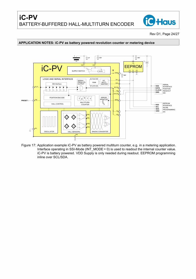
Figure 17: Application example iC-PV as battery powered multiturn counter, e.g. in a metering application.Interface operating in SSI-Mode (INT_MODE = 0) is used to readout the internal counter value.iC-PV is battery powered. VDD Supply is only needed during readout. EEPROM programminginline over SCL/SDA.
iC-PVBATTERY-BUFFERED HALL-MULTITURN ENCODER
Rev D1, Page 25/27
APPLICATION NOTES: iC-PV as 3 bit parallel mode (µC application)
Configuration
OSCILLATOR
COUNTERMULTITURN
iC-PVRAM
I2CMULTI
MASTER
Monitor
+
-
+
-
HALL SENSORS SIN/DIG CONVERTER
SUPPLY SWITCH
LOGIC AND SERIAL INTERFACE
HALL CONTROL
ERRORMONITOR
Microcontroller
SPIKE CONTROL
1
SERIAL/PARALLELOUTPUTSSI Interface
POSITION ENCODE
Wait on DATA
Rise Power
Start Pulse IntervallMultiturn Position
Counter
Interface to
Singleturn Encoder
SEL
Determine
3
Send START
2
1 0 0 1 1
and Readout
N0
VDDS
P2
PRESDA
NERR
SCL
SUPPLY
CLK_N1
DO_P0
DI_P1
N2
VBAT VDD
GND
VDD
P0
N0
P1
N1
P2
N2
GND
START
100nF
+
-
+
-
PSIN
NSIN
PCOS
NCOS
100nF
BB
BB
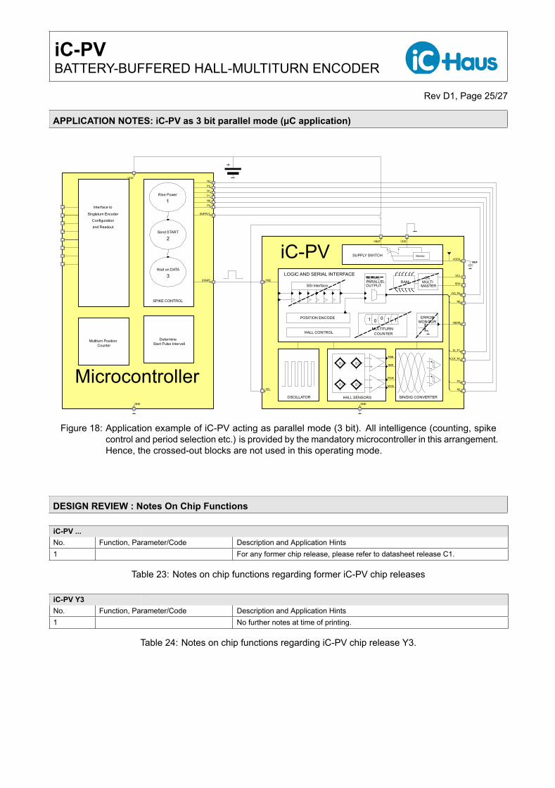
Figure 18: Application example of iC-PV acting as parallel mode (3 bit). All intelligence (counting, spikecontrol and period selection etc.) is provided by the mandatory microcontroller in this arrangement.Hence, the crossed-out blocks are not used in this operating mode.
DESIGN REVIEW : Notes On Chip Functions
iC-PV ...No. Function, Parameter/Code Description and Application Hints1 For any former chip release, please refer to datasheet release C1.
Table 23: Notes on chip functions regarding former iC-PV chip releases
iC-PV Y3No. Function, Parameter/Code Description and Application Hints1 No further notes at time of printing.
Table 24: Notes on chip functions regarding iC-PV chip release Y3.
iC-PVBATTERY-BUFFERED HALL-MULTITURN ENCODER
Rev D1, Page 26/27
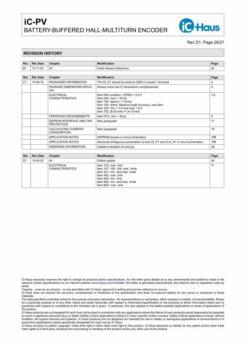
REVISION HISTORY
Rel. Rel. Date Chapter Modification PageB1 13-11-25 All Initial release (reference) all
Rel. Rel. Date Chapter Modification PageC1 14-09-19 PACKAGING INFORMATION "Pin DI_P1 should be wired to GND if unused." removed 4
PACKAGE DIMENSIONS QFN163x3
Sensor circle and iC dimensions complemented 5
ELECTRICALCHARACTERISTICS
Item 004 condition: V(PRE) < 0.5 VItem 008: max. = 20 msItem 104: dsens = 1.75 mmItem 105: AArel, Relative Angle Accuracy, new ItemItem 302: min. = 3.5 and max. = 6.5Item 702: [8-30 mA] => [4-15 mA]
7,8
OPERATING REQUIREMENTS Item I012: min. = 30µs 9EEPROM INTERFACE AND CRCPROTECTION
New paragraph 17
CALCULATING CURRENTCONSUMPTION
New paragraph 18
APPLICATION NOTES EEPROM access in circuit schematics 19ffAPPLICATION NOTES Removed ambiguous presentation of pins DI_P1 and CLK_N1 in circuit schematics 19ffORDERING INFORMATION Update evaluation kit and gui 26
Rel. Rel. Date Chapter Modification PageD1 15-05-22 All Global update All
ELECTRICALCHARACTERISTICS
Item 103: max. limitItem 107, 108, 109: max. limitsItem 301: min. and max. limitsItem 402: max. limitItem 403: min. limitItem 606: min. and max. limitsItem B02: max. limit
7f
iC-Haus expressly reserves the right to change its products and/or specifications. An info letter gives details as to any amendments and additions made to therelevant current specifications on our internet website www.ichaus.com/infoletter; this letter is generated automatically and shall be sent to registered users byemail.Copying – even as an excerpt – is only permitted with iC-Haus’ approval in writing and precise reference to source.iC-Haus does not warrant the accuracy, completeness or timeliness of the specification and does not assume liability for any errors or omissions in thesematerials.The data specified is intended solely for the purpose of product description. No representations or warranties, either express or implied, of merchantability, fitnessfor a particular purpose or of any other nature are made hereunder with respect to information/specification or the products to which information refers and noguarantee with respect to compliance to the intended use is given. In particular, this also applies to the stated possible applications or areas of applications ofthe product.iC-Haus products are not designed for and must not be used in connection with any applications where the failure of such products would reasonably be expectedto result in significant personal injury or death (Safety-Critical Applications) without iC-Haus’ specific written consent. Safety-Critical Applications include, withoutlimitation, life support devices and systems. iC-Haus products are not designed nor intended for use in military or aerospace applications or environments or inautomotive applications unless specifically designated for such use by iC-Haus.iC-Haus conveys no patent, copyright, mask work right or other trade mark right to this product. iC-Haus assumes no liability for any patent and/or other trademark rights of a third party resulting from processing or handling of the product and/or any other use of the product.

iC-PVBATTERY-BUFFERED HALL-MULTITURN ENCODER
Rev D1, Page 27/27
ORDERING INFORMATION
Type Package Options Order Designation
iC-PV QFN16-3x3 iC-PV QFN16-3x3
Evaluation kit PCB 38 mm diameter iC-PV EVAL PV1M1
iC-PV GUI Evaluation software for Windows PC For download link refer towww.ichaus.com/pv_gui
Please send your purchase orders to our order handling team:
Fax: +49 (0) 61 35 - 92 92 - 692E-Mail: [email protected]
For technical support, information about prices and terms of delivery please contact:
iC-Haus GmbH Tel.: +49 (0) 61 35 - 92 92 - 0Am Kuemmerling 18 Fax: +49 (0) 61 35 - 92 92 - 192D-55294 Bodenheim Web: http://www.ichaus.comGERMANY E-Mail: [email protected]
Appointed local distributors: http://www.ichaus.com/sales_partners