high-performance and energy-efficient decoder design for
TRANSCRIPT
University of California
Los Angeles
High-Performance and Energy-Efficient
Decoder Design for Non-Binary LDPC Codes
A dissertation submitted in partial satisfaction
of the requirements for the degree
Doctor of Philosophy in Electrical Engineering
by
Yuta Toriyama
2016

© Copyright by
Yuta Toriyama
2016
Abstract of the Dissertation
High-Performance and Energy-Efficient
Decoder Design for Non-Binary LDPC Codes
by
Yuta Toriyama
Doctor of Philosophy in Electrical Engineering
University of California, Los Angeles, 2016
Professor Dejan Markovic, Chair
Binary Low-Density Parity-Check (LDPC) codes are a type of error correction code
known to exhibit excellent error-correcting capabilities, and have increasingly been applied
as the forward error correction solution in a multitude of systems and standards, such as
wireless communications, wireline communications, and data storage systems. In the pursuit
of codes with even higher coding gain, non-binary LDPC (NB-LDPC) codes defined over a
Galois field of order q have risen as a strong replacement candidate. For codes defined
with similar rate and length, NB-LDPC codes exhibit a significant coding gain improvement
relative to that of their binary counterparts.
Unfortunately, NB-LDPC codes are currently limited from practical application by the
immense complexity of their decoding algorithms, because the improved error-rate perfor-
mance of higher field orders comes at the cost of increasing decoding algorithm complexity.
Currently available ASIC implementation solutions for NB-LDPC code decoders are simul-
taneously low in throughput and power-hungry, leading to a low energy efficiency.
We propose several techniques at the algorithm level as well as hardware architecture level
in an attempt to bring NB-LDPC codes closer to practical deployment. On the algorithm
side, we propose several algorithmic modifications and analyze the corresponding hardware
cost alleviation as well as impact on coding gain. We also study the quantization scheme
ii
for NB-LDPC decoders, again in the context of both the hardware and coding gain impacts,
and we propose a technique that enables a good tradeoff in this space. On the hardware
side, we develop a FPGA-based NB-LDPC decoder platform for architecture prototyping as
well as hardware acceleration of code evaluation via error rate simulations. We also discuss
the architectural techniques and innovations corresponding to our proposed algorithm for
optimization of the implementation. Finally, a proof-of-concept ASIC chip is realized that
integrates many of the proposed techniques. We are able to achieve a 3.7x improvement
in the information throughput and 23.8x improvement in the energy efficiency over prior
state-of-the-art, without sacrificing the strong error correcting capabilities of the NB-LDPC
code.
iii
The dissertation of Yuta Toriyama is approved.
Richard D. Wesel
Gregory J. Pottie
Lara Dolecek
Dejan Markovic, Committee Chair
University of California, Los Angeles
2016
iv

For my parents.
v
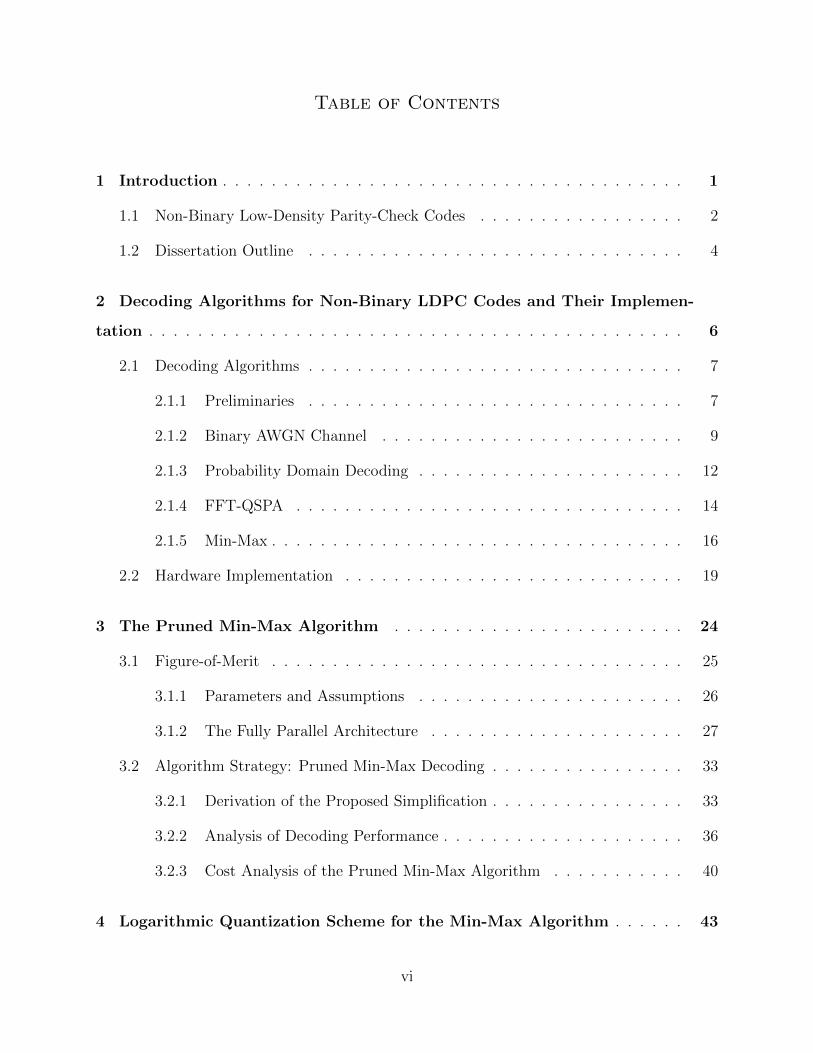
Table of Contents
1 Introduction . . . . . . . . . . . . . . . . . . . . . . . . . . . . . . . . . . . . . . 1
1.1 Non-Binary Low-Density Parity-Check Codes . . . . . . . . . . . . . . . . . 2
1.2 Dissertation Outline . . . . . . . . . . . . . . . . . . . . . . . . . . . . . . . 4
2 Decoding Algorithms for Non-Binary LDPC Codes and Their Implemen-
tation . . . . . . . . . . . . . . . . . . . . . . . . . . . . . . . . . . . . . . . . . . . . 6
2.1 Decoding Algorithms . . . . . . . . . . . . . . . . . . . . . . . . . . . . . . . 7
2.1.1 Preliminaries . . . . . . . . . . . . . . . . . . . . . . . . . . . . . . . 7
2.1.2 Binary AWGN Channel . . . . . . . . . . . . . . . . . . . . . . . . . 9
2.1.3 Probability Domain Decoding . . . . . . . . . . . . . . . . . . . . . . 12
2.1.4 FFT-QSPA . . . . . . . . . . . . . . . . . . . . . . . . . . . . . . . . 14
2.1.5 Min-Max . . . . . . . . . . . . . . . . . . . . . . . . . . . . . . . . . . 16
2.2 Hardware Implementation . . . . . . . . . . . . . . . . . . . . . . . . . . . . 19
3 The Pruned Min-Max Algorithm . . . . . . . . . . . . . . . . . . . . . . . . 24
3.1 Figure-of-Merit . . . . . . . . . . . . . . . . . . . . . . . . . . . . . . . . . . 25
3.1.1 Parameters and Assumptions . . . . . . . . . . . . . . . . . . . . . . 26
3.1.2 The Fully Parallel Architecture . . . . . . . . . . . . . . . . . . . . . 27
3.2 Algorithm Strategy: Pruned Min-Max Decoding . . . . . . . . . . . . . . . . 33
3.2.1 Derivation of the Proposed Simplification . . . . . . . . . . . . . . . . 33
3.2.2 Analysis of Decoding Performance . . . . . . . . . . . . . . . . . . . . 36
3.2.3 Cost Analysis of the Pruned Min-Max Algorithm . . . . . . . . . . . 40
4 Logarithmic Quantization Scheme for the Min-Max Algorithm . . . . . . 43
vi
4.1 Prior Art . . . . . . . . . . . . . . . . . . . . . . . . . . . . . . . . . . . . . 44
4.2 Computational Complexity . . . . . . . . . . . . . . . . . . . . . . . . . . . . 46
4.2.1 Derivation of Computational Complexity of the Min-Max Algorithm . 46
4.2.2 Routing Overhead . . . . . . . . . . . . . . . . . . . . . . . . . . . . 48
4.3 Quantization Effects . . . . . . . . . . . . . . . . . . . . . . . . . . . . . . . 48
4.4 The Logarithmic Quantization Scheme . . . . . . . . . . . . . . . . . . . . . 52
4.4.1 The Proposed Scheme . . . . . . . . . . . . . . . . . . . . . . . . . . 52
4.4.2 Error Rate Comparison . . . . . . . . . . . . . . . . . . . . . . . . . . 53
4.4.3 Estimated Computational Complexity . . . . . . . . . . . . . . . . . 54
5 Implementation of FPGA Platform for Code Performance Evaluation . 60
5.1 Architecture . . . . . . . . . . . . . . . . . . . . . . . . . . . . . . . . . . . . 61
5.2 Design Methodology . . . . . . . . . . . . . . . . . . . . . . . . . . . . . . . 67
5.3 Results . . . . . . . . . . . . . . . . . . . . . . . . . . . . . . . . . . . . . . . 68
5.3.1 Hardware Resource Utilization on FPGA . . . . . . . . . . . . . . . . 68
5.3.2 Frame Error Rate Simulations . . . . . . . . . . . . . . . . . . . . . . 72
6 Augmented Hard-Decision Based Decoding Algorithm and Combination
with Soft Decoding . . . . . . . . . . . . . . . . . . . . . . . . . . . . . . . . . . . 74
6.1 Iterative Hard-Decision Based Majority Logic Decoding . . . . . . . . . . . . 76
6.1.1 Augmented IHRB-MLGD . . . . . . . . . . . . . . . . . . . . . . . . 77
6.1.2 Detection of Erasure Condition . . . . . . . . . . . . . . . . . . . . . 79
6.2 Software Simulation Results . . . . . . . . . . . . . . . . . . . . . . . . . . . 80
6.3 Combination with the Min-Max Algorithm . . . . . . . . . . . . . . . . . . . 83
7 ASIC Implementation . . . . . . . . . . . . . . . . . . . . . . . . . . . . . . . . 86
7.1 Parity-Check Matrix . . . . . . . . . . . . . . . . . . . . . . . . . . . . . . . 87
vii
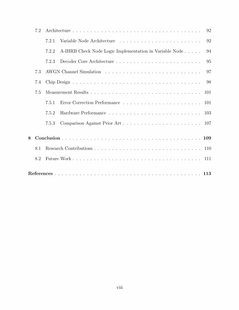
7.2 Architecture . . . . . . . . . . . . . . . . . . . . . . . . . . . . . . . . . . . . 92
7.2.1 Variable Node Architecture . . . . . . . . . . . . . . . . . . . . . . . 92
7.2.2 A-IHRB Check Node Logic Implementation in Variable Node . . . . . 94
7.2.3 Decoder Core Architecture . . . . . . . . . . . . . . . . . . . . . . . . 95
7.3 AWGN Channel Simulation . . . . . . . . . . . . . . . . . . . . . . . . . . . 97
7.4 Chip Design . . . . . . . . . . . . . . . . . . . . . . . . . . . . . . . . . . . . 98
7.5 Measurement Results . . . . . . . . . . . . . . . . . . . . . . . . . . . . . . . 101
7.5.1 Error Correction Performance . . . . . . . . . . . . . . . . . . . . . . 101
7.5.2 Hardware Performance . . . . . . . . . . . . . . . . . . . . . . . . . . 103
7.5.3 Comparison Against Prior Art . . . . . . . . . . . . . . . . . . . . . . 107
8 Conclusion . . . . . . . . . . . . . . . . . . . . . . . . . . . . . . . . . . . . . . . 109
8.1 Research Contributions . . . . . . . . . . . . . . . . . . . . . . . . . . . . . . 110
8.2 Future Work . . . . . . . . . . . . . . . . . . . . . . . . . . . . . . . . . . . . 111
References . . . . . . . . . . . . . . . . . . . . . . . . . . . . . . . . . . . . . . . . . 113
viii
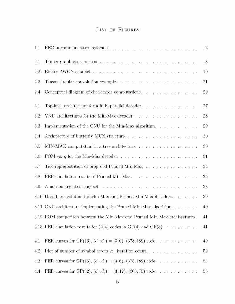
List of Figures
1.1 FEC in communication systems. . . . . . . . . . . . . . . . . . . . . . . . . . 2
2.1 Tanner graph construction. . . . . . . . . . . . . . . . . . . . . . . . . . . . . 8
2.2 Binary AWGN channel. . . . . . . . . . . . . . . . . . . . . . . . . . . . . . . 10
2.3 Tensor circular convolution example. . . . . . . . . . . . . . . . . . . . . . . 21
2.4 Conceptual diagram of check node computations. . . . . . . . . . . . . . . . 22
3.1 Top-level architecture for a fully parallel decoder. . . . . . . . . . . . . . . . 27
3.2 VNU architectures for the Min-Max decoder. . . . . . . . . . . . . . . . . . . 28
3.3 Implementation of the CNU for the Min-Max algorithm. . . . . . . . . . . . 29
3.4 Architecture of butterfly MUX structure. . . . . . . . . . . . . . . . . . . . . 30
3.5 MIN-MAX computation in a tree architecture. . . . . . . . . . . . . . . . . . 30
3.6 FOM vs. q for the Min-Max decoder. . . . . . . . . . . . . . . . . . . . . . . 31
3.7 Tree representation of proposed Pruned Min-Max. . . . . . . . . . . . . . . . 34
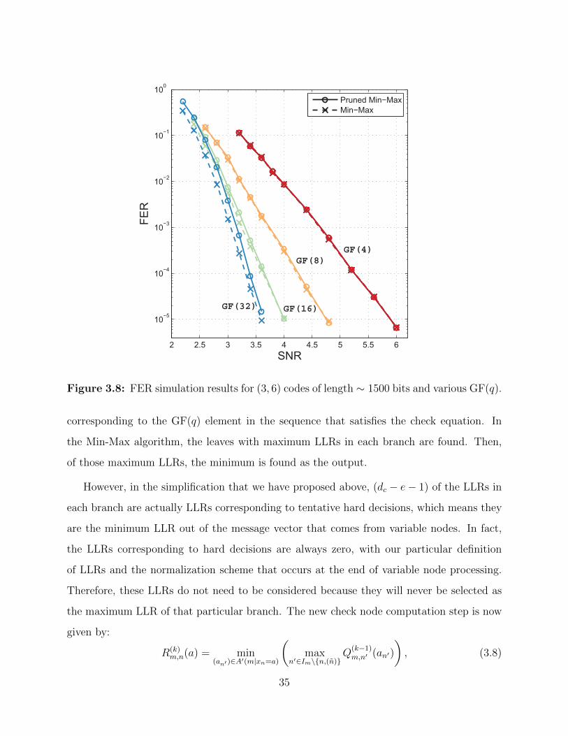
3.8 FER simulation results of Pruned Min-Max. . . . . . . . . . . . . . . . . . . 35
3.9 A non-binary absorbing set. . . . . . . . . . . . . . . . . . . . . . . . . . . . 38
3.10 Decoding evolution for Min-Max and Pruned Min-Max decoders. . . . . . . . 39
3.11 CNU architecture implementing the Pruned Min-Max algorithm. . . . . . . . 40
3.12 FOM comparison between the Min-Max and Pruned Min-Max architectures. 41
3.13 FER simulation results for (2, 4) codes in GF(4) and GF(8). . . . . . . . . . 41
4.1 FER curves for GF(16), (dv, dc) = (3, 6), (378, 189) code. . . . . . . . . . . . 49
4.2 Plot of number of symbol errors vs. iteration count. . . . . . . . . . . . . . . 52
4.3 FER curves for GF(16), (dv, dc) = (3, 6), (378, 189) code. . . . . . . . . . . . 54
4.4 FER curves for GF(32), (dv, dc) = (3, 12), (300, 75) code. . . . . . . . . . . . 55
ix
4.5 Normalized computational complexity for Min-Max algorithm implementation. 56
5.1 Quasi-cyclic structure of parity-check matrix. . . . . . . . . . . . . . . . . . . 62
5.2 Partially parallel architecture. . . . . . . . . . . . . . . . . . . . . . . . . . . 64
5.3 Partially parallel architecture with log quantization. . . . . . . . . . . . . . . 65
5.4 Variable node implementation for FPGA platform. . . . . . . . . . . . . . . 66
5.5 Check node implementation for FPGA platform. . . . . . . . . . . . . . . . . 66
5.6 Automated RTL generation scheme. . . . . . . . . . . . . . . . . . . . . . . . 67
5.7 FPGA accelerated FER simulation. . . . . . . . . . . . . . . . . . . . . . . . 71
5.8 FPGA accelerated FER simulation with log quantization. . . . . . . . . . . . 72
6.1 IHRB-MLGD modification strategy comparison. . . . . . . . . . . . . . . . . 81
6.2 IHRB-MLGD modification strategy comparison. . . . . . . . . . . . . . . . . 82
6.3 Comparison of FER in simulation with and without A-IHRB. . . . . . . . . 84
6.4 Comparison of BER in simulation with and without A-IHRB. . . . . . . . . 84
6.5 Comparison of simulation times with and without A-IHRB. . . . . . . . . . . 85
7.1 Protograph for code of ASIC design. . . . . . . . . . . . . . . . . . . . . . . 88
7.2 Comparison of codes across GF(q). . . . . . . . . . . . . . . . . . . . . . . . 89
7.3 Comparison of 8k codes across GF(q) with max iterations = 6. . . . . . . . . 90
7.4 Comparison of 8k codes across GF(q) with max iterations = 20. . . . . . . . 91
7.5 Varibale node architecture. . . . . . . . . . . . . . . . . . . . . . . . . . . . . 93
7.6 Decoder core architecture. . . . . . . . . . . . . . . . . . . . . . . . . . . . . 96
7.7 AWGN generator block details. . . . . . . . . . . . . . . . . . . . . . . . . . 97
7.8 Tausworthe PRNG block details. . . . . . . . . . . . . . . . . . . . . . . . . 99
7.9 General task flow for chip tapeout. . . . . . . . . . . . . . . . . . . . . . . . 100
7.10 Lab test setup for chip measurement. . . . . . . . . . . . . . . . . . . . . . . 102
x
7.11 Chip micrograph. . . . . . . . . . . . . . . . . . . . . . . . . . . . . . . . . . 103
7.12 Frame error rate chip measurements. . . . . . . . . . . . . . . . . . . . . . . 104
7.13 Average number of iterations per frame chip measurements. . . . . . . . . . 105
7.14 Throughput and power versus operating frequency. . . . . . . . . . . . . . . 106
7.15 Shmoo plot measurements for three received chips. . . . . . . . . . . . . . . 106
7.16 Table of chip measurement results and comparison with prior art. . . . . . . 108
xi
List of Tables
2.1 Summary of Selected Published Works 1 . . . . . . . . . . . . . . . . . . . . 23
3.1 Error Profile Comparison (FER ≈ 10−5) . . . . . . . . . . . . . . . . . . . . 38
4.1 Error Profile of Various Quantization Schemes . . . . . . . . . . . . . . . . . 59
4.2 Quantization Scheme Examples . . . . . . . . . . . . . . . . . . . . . . . . . 59
4.3 Percent Savings in Computational Complexity . . . . . . . . . . . . . . . . . 59
5.1 FPGA Synthesis Results (3,24) L130 P65 . . . . . . . . . . . . . . . . . . . . 69
5.2 FPGA Synthesis Results (3,27) L114 P57 . . . . . . . . . . . . . . . . . . . . 70
5.3 FPGA Synthesis Results (3,30) L104 P104 . . . . . . . . . . . . . . . . . . . 70
7.1 Possible Constant Values for the Tausworthe PRNG . . . . . . . . . . . . . . 98
xii
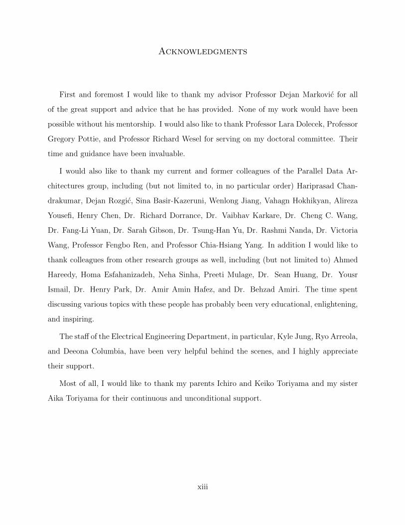
Acknowledgments
First and foremost I would like to thank my advisor Professor Dejan Markovic for all
of the great support and advice that he has provided. None of my work would have been
possible without his mentorship. I would also like to thank Professor Lara Dolecek, Professor
Gregory Pottie, and Professor Richard Wesel for serving on my doctoral committee. Their
time and guidance have been invaluable.
I would also like to thank my current and former colleagues of the Parallel Data Ar-
chitectures group, including (but not limited to, in no particular order) Hariprasad Chan-
drakumar, Dejan Rozgic, Sina Basir-Kazeruni, Wenlong Jiang, Vahagn Hokhikyan, Alireza
Yousefi, Henry Chen, Dr. Richard Dorrance, Dr. Vaibhav Karkare, Dr. Cheng C. Wang,
Dr. Fang-Li Yuan, Dr. Sarah Gibson, Dr. Tsung-Han Yu, Dr. Rashmi Nanda, Dr. Victoria
Wang, Professor Fengbo Ren, and Professor Chia-Hsiang Yang. In addition I would like to
thank colleagues from other research groups as well, including (but not limited to) Ahmed
Hareedy, Homa Esfahanizadeh, Neha Sinha, Preeti Mulage, Dr. Sean Huang, Dr. Yousr
Ismail, Dr. Henry Park, Dr. Amir Amin Hafez, and Dr. Behzad Amiri. The time spent
discussing various topics with these people has probably been very educational, enlightening,
and inspiring.
The staff of the Electrical Engineering Department, in particular, Kyle Jung, Ryo Arreola,
and Deeona Columbia, have been very helpful behind the scenes, and I highly appreciate
their support.
Most of all, I would like to thank my parents Ichiro and Keiko Toriyama and my sister
Aika Toriyama for their continuous and unconditional support.
xiii
Vita
2001 – 2005 Rancho Bernardo High School, San Diego, California.
2007 Software Engineer Intern, NextWave Broadband, San Diego, CA.
2009 B.S. with High Honors, Electrical Engineering and Computer Sciences,University of California, Berkeley.
2009 – 2016 Graduate Student Researcher, Department of Electrical Engineering,University of California, Los Angeles.
2009 EE Departmental Fellowship,University of California, Los Angeles.
2011 M.S., Electrical Engineering,University of California, Los Angeles.
2011 Hardware Engineer Intern, Broadcom, Irvine, CA.
2013 – 2014 Broadcom Fellowship,University of California, Los Angeles.
2014 Intern, Toshiba Semiconductor and Storage Systems, Yokohama, Kana-gawa Prefecture, Japan.
2015 Teaching Assistant, EE216A: Design of VLSI Circuits and Systems,University of California, Los Angeles.
2016 Teaching Assistant, EE115C: Digital Electronic Circuits,University of California, Los Angeles.
xiv
Publications
Y. Toriyama, B. Amiri, L. Dolecek, and D. Markovic, “Logarithmic Quantization Scheme forReduced Hardware Cost and Improved Error Floor in Non-Binary LDPC Decoders,”in Proc. IEEE Global Comm. Conf., (GLOBECOM14), pp. 3162-3167, Dec. 2014.
Y. Toriyama, B. Amiri, L. Dolecek, and D. Markovic, “Field-Order Based Hardware CostAnalysis of Non-Binary LDPC Decoders,” in Proc. 48th Asilomar Conference on Sig-nals, Systems and Computers, pp. 2045-2049, Nov. 2014.
R. Dorrance, F. Ren, Y. Toriyama, A.A. Hafez, C.-K.K. Yang, D. Markovic, “Scalabilityand Design-Space Analysis of a 1T-1MTJ Memory Cell for STT-RAM,” IEEE Trans.Electron Devices (TED), vol. 59, no. 4, pp. 878-887, Apr. 2012.
F. Ren, H. Park, R. Dorrance, Y. Toriyama, A. Amin, C.-K.K. Yang, D. Markovic, “ABody-Voltage-Sensing-Based Short Pulse Reading Circuit for Advanced Spin-TorqueTransfer RAMs (STT-RAMs),” in Proc. 13th Int. Symp. on Quality Electronic De-sign (ISQED’12), pp. 275-282, Mar. 2012.
R. Dorrance, F. Ren, Y. Toriyama, A. Amin, C.-K.K. Yang, D. Markovic, “Scalability andDesign-Space Analysis of a 1T-1MTJ Memory Cell,” in Proc. ACM/IEEE Int. Symp.on Nanoscale Arch. (NANOARCH’11), pp. 53-58, Jun. 2011.
xv
CHAPTER 1
Introduction
1.1 Non-Binary Low-Density Parity-Check Codes . . . . . . . . . . . . . . . 2
1.2 Dissertation Outline . . . . . . . . . . . . . . . . . . . . . . . . . . . . . 4
1
Communication Channel
Channel Coding
Channel Decoding
Information Source
Information Destination
Transmitter
Receiver
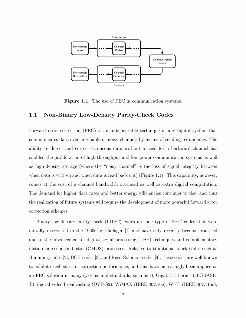
Figure 1.1: The use of FEC in communication systems.
1.1 Non-Binary Low-Density Parity-Check Codes
Forward error correction (FEC) is an indispensable technique in any digital system that
communicates data over unreliable or noisy channels by means of sending redundancy. The
ability to detect and correct erroneous data without a need for a backward channel has
enabled the proliferation of high-throughput and low-power communication systems as well
as high-density storage (where the “noisy channel” is the loss of signal integrity between
when data is written and when data is read back out) (Figure 1.1). This capability, however,
comes at the cost of a channel bandwidth overhead as well as extra digital computation.
The demand for higher data rates and better energy efficiencies continues to rise, and thus
the realization of future systems will require the development of more powerful forward error
correction schemes.
Binary low-density parity-check (LDPC) codes are one type of FEC codes that were
initially discovered in the 1960s by Gallager [1] and have only recently become practical
due to the advancement of digital signal processing (DSP) techniques and complementary
metal-oxide-semiconductor (CMOS) processes. Relative to traditional block codes such as
Hamming codes [2], BCH codes [3], and Reed-Solomon codes [4], these codes are well-known
to exhibit excellent error correction performance, and thus have increasingly been applied as
an FEC solution in many systems and standards, such as 10 Gigabit Ethernet (10GBASE-
T), digital video broadcasting (DVB-S2), WiMAX (IEEE 802.16e), Wi-Fi (IEEE 802.11ac),
2
high-capacity data storage systems, and deep-space communications [5,6,7,8,9,10]. Various
systems impose various requirements on the FEC in terms of the code rate, length, and
target frame error rates (FER) and bit error rates (BER). Wireless communication systems
tend to employ shorter codes with lower rates and target FERs of ∼ 10−6, whereas wired
communication systems and storage systems require FERs of ∼ 10−12 and below, and thus
use longer codes and higher code rates.
The trouble with LDPC codes is that they are notorious for their decoding algorithm
complexity, and field-programmable gate array (FPGA) or application-specific integrated
circuit (ASIC) implementations of the decoding algorithms are costly in terms of hardware
resource utilization and energy efficiency. For these codes, however, research advancements
have made ASIC implementations of decoders relatively practical in terms of achievable
throughput and power consumption [9, 10, 11, 12, 13]. A number of techniques at both the
algorithm and architecture levels are employed that enable LDPC codes to be utilized in
the real applications mentioned above. The end user is never satiated, however, and the
requirement for higher communication throughput and higher storage density calls for the
development of codes with even better performance.
In the pursuit of codes with higher coding gain, non-binary LDPC (NB-LDPC) codes
defined over a Galois field of order q (GF(q)), where q is a power of 2, have risen as a strong
candidate [14], [15]. For codes defined with similar rate and length, NB-LDPC codes exhibit
a significant coding gain improvement relative to that of their binary counterparts, including
lower error floors [16]. Furthermore, NB-LDPC codes overcome some weaknesses of binary
LDPC codes in other qualities, such as the error rate performance when shorter code lengths
or higher-order modulation are used [15], or their performance in non-AWGN channels, such
as those for storage devices [17]. Unfortunately, NB-LDPC codes are currently limited from
practical application by the immense complexity of their decoding algorithms, because the
improved error-rate performance of higher field orders comes at the cost of increasing de-
coding algorithm complexity [18]. This trade-off has spurred interest in research, both from
the algorithm perspective and the digital hardware perspective, on the implementation of
decoding algorithms at reduced costs [19,20,21,22,23,24,25,26]. However, ASIC implemen-
3
tation results have yet to attain numbers that rationalize the use of NB-LDPC schemes in
the communication and storage systems of today. At the algorithm level, too many sim-
plifications cannot be made or the coding gain will deteriorate to a point where NB-LDPC
codes no longer make sense. At the architecture level, the immense amount of computation
required is difficult to avoid, and there also exists large latencies inherent in the signal flow
due to data dependencies.
This dissertation presents our work on bringing NB-LDPC code decoders closer to prac-
tical deployment. From the algorithm side, we attempt to simplify the decoding algorithm
without sacrificing the coding gain performance, which is of course easier said than done.
We propose several decoding algorithm choices, each of which are suitable under varying
conditions. Thus, for a particular application an appropriate decoding method must be cho-
sen to optimize the decoder as much as possible. From the hardware implementation side,
we propose techniques for the evaluation of hardware implementation costs based on the
decoding algorithm enabling the evaluation of the Galois Field order GF(q) as a parameter
to our design space. Additionally, we present techniques such as our quantization scheme
and computation unit sharing architecture that finally enables our realization of the highly
optimized ASIC NB-LDPC decoder implementation. We develop a flexible FPGA platform
which enables both a FER simulation for code evaluation as well as hardware cost estima-
tion. Finally, we fabricate a proof-of-concept ASIC NB-LDPC decoder which incorporates
the techniques we propose and report the measured benefits relative to prior art.
1.2 Dissertation Outline
Chapter 2 introduces the decoding of NB-LDPC codes, and defines terms and variables
that will be used in the rest of the dissertation. A survey on prior art is also conducted
to explore the state-of-the-art designs of NB-LDPC code decoder implementations.
Chapter 3 details our proposed Pruned Min-Max algorithm that enables the simplifica-
tion of the check-node computations, which are often the bottleneck in the computational
4
complexity of NB-LDPC decoding. The hardware implementation cost is evaluated in
order to show the benefits achieved by adopting this scheme.
Chapter 4 details our proposed Logarithmic Quantization Scheme, an implementation
technique that allows us to greatly reduce the computational complexity cost of NB-
LDPC decoding with only a small performance penalty in terms of coding gain. An error
profile analysis as well as hardware implementation cost analysis is also presented.
Chapter 5 details the implementation of our FPGA platform for code performance eval-
uation, spurred by the requirement for hardware-accelerated NB-LDPC decoding simu-
lators for the observation of ultra-low FER regimes. Some of the techniques introduced
are employed here, and hypotheses from the previous chapter are verified by means of
the increased simulation capability brought on by this FPGA platform.
Chapter 6 introduces our proposed scheme of combining hard- and soft-decision based
decoders for a further optimized decoder design. The new algorithm allows for a much
higher throughput on average without penalty in coding gain. The applicability of this
technique as well as implementation considerations are discussed.
Chapter 7 discusses the design of our ASIC realization of an NB-LDPC decoder based
on the techniques proposed so far. Details concerning the architecture as well as indi-
vidual building blocks are discussed. We also present the fabrication and measurement
results of the ASIC implementation, along with a comparison with the state-of-the-art.
Chapter 8 concludes the dissertation and provides some possible directions for future
research.
5
CHAPTER 2
Decoding Algorithms for Non-Binary LDPC Codes
and Their Implementation
2.1 Decoding Algorithms . . . . . . . . . . . . . . . . . . . . . . . . . . . . . 7
2.1.1 Preliminaries . . . . . . . . . . . . . . . . . . . . . . . . . . . . . . . . . 7
2.1.2 Binary AWGN Channel . . . . . . . . . . . . . . . . . . . . . . . . . . . 9
2.1.3 Probability Domain Decoding . . . . . . . . . . . . . . . . . . . . . . . . 12
2.1.4 FFT-QSPA . . . . . . . . . . . . . . . . . . . . . . . . . . . . . . . . . . 14
2.1.5 Min-Max . . . . . . . . . . . . . . . . . . . . . . . . . . . . . . . . . . . 16
2.2 Hardware Implementation . . . . . . . . . . . . . . . . . . . . . . . . . . 19
6
2.1 Decoding Algorithms
2.1.1 Preliminaries
The ultimate goal in decoding NB-LDPC codes is the following: given some information
about each received symbol from the channel, try to find a codeword that satisfies the parity
check of the code. We begin by defining some variables.
A Galois field of order q, where q = 2p, is closed under the operations of addition and
multiplication modulo an irreducible polynomial of degree p, called the primitive polynomial,
whose coefficients are in GF(2). The elements of GF(q) are polynomials of degree less than
p, or equivalently, powers of the root of the primitive polynomial. An NB-LDPC code is a
linear block code defined by its M × N parity check matrix H whose entries hm,n, where
0 ≤ m ≤ (M − 1) and 0 ≤ n ≤ (N − 1), are field elements a ∈ GF(q). For a sufficiently
well constructed parity check matrix, the code rate is given as r = 1 − dvdc
= 1 − MN. A
valid codeword x = (x0, x1, ..., xN−1), xn ∈ GF(q) is a vector in the nullspace of H, i.e. the
syndrome z = x×HT = 0. Practical decoding algorithms are based on the Tanner graph of
this code, constructed as follows:
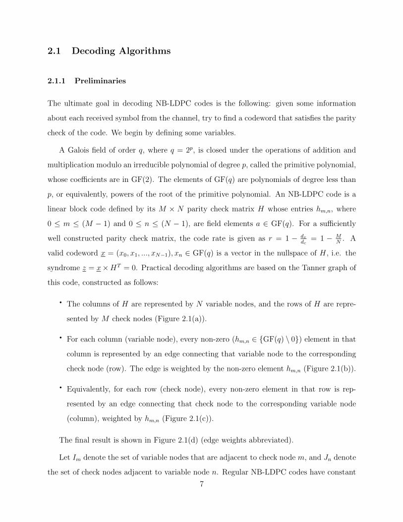
· The columns of H are represented by N variable nodes, and the rows of H are repre-
sented by M check nodes (Figure 2.1(a)).
· For each column (variable node), every non-zero (hm,n ∈ {GF(q) \ 0}) element in that
column is represented by an edge connecting that variable node to the corresponding
check node (row). The edge is weighted by the non-zero element hm,n (Figure 2.1(b)).
· Equivalently, for each row (check node), every non-zero element in that row is rep-
resented by an edge connecting that check node to the corresponding variable node
(column), weighted by hm,n (Figure 2.1(c)).
The final result is shown in Figure 2.1(d) (edge weights abbreviated).
Let Im denote the set of variable nodes that are adjacent to check node m, and Jn denote
the set of check nodes adjacent to variable node n. Regular NB-LDPC codes have constant
7
1
0
0
0
0
0
0
0
0
0
0
0
0
0
0
0
0
1
1
α5 α3
α2
α4
α3
α
α5
α6
α6
α3
α2
α4
α6
H =Variable Nodes
Check Nodes
(a)
1
0
0
0
0
0
0
0
0
0
0
0
0
0
0
0
0
1
1
α5 α3
α2
α4
α3
α
α5
α6
α6
α3
α2
α4
α6
H =1
0
0
0
0
0
0
0
0
0
0
0
0
0
0
0
0
1
1
α5 α3
α2
α4
α3
α
α5
α6
α6
α3
α2
α4
α6
H =
(b)
1
0
0
0
0
0
0
0
0
0
0
0
0
0
0
0
0
1
1
α5 α3
α2
α4
α3
α
α5
α6
α6
α3
α2
α4
α6
H =1
0
0
0
0
0
0
0
0
0
0
0
0
0
0
0
0
1
1
α5 α3
α2
α4
α3
α
α5
α6
α6
α3
α2
α4
α6
H =
(c)
1
0
0
0
0
0
0
0
0
0
0
0
0
0
0
0
0
1
1
α5 α3
α2
α4
α3
α
α5
α6
α6
α3
α2
α4
α6
H =
(d)
Figure 2.1: Construction example of the Tanner graph representation of a parity check
matrix.
8
check and variable node degrees, denoted by dc = |Im| and dv = |Jn|, and are also referred to
as (dv, dc) codes. Let A(m) denote the collection of ordered sets of dc GF(q) elements that
satisfy check equation m. Furthermore, let A(m|xn = a) denote the collection of ordered
sets of (dc − 1) GF(q) elements that satisfy check equation m, given that the nth element in
the codeword x is equal to a.
2.1.2 Binary AWGN Channel
The Additive White Gaussian Noise (AWGN) channel often serves as a common baseline
for comparing the performance of a variety of codes. This is because this channel model is
relatively realistic (more so than simplistic channels such as the binary erasure channel (BEC)
or the binary symmetric channel (BSC)) while remaining mathematically manageable. For
example, thermal noise has a flat power spectral density (PSD) because the source of the
noise is the sum of the movement of charge of electrons excited by the external temperature,
which tends to have a Gaussian distribution due to the central limit theorem (CLT).
When non-binary GF(q) symbols are sent through a binary channel, each symbol is
divided into log2(q) bits which are the coefficients in the polynomial representation of the
symbol. The polynomial representation is chosen over the power representation (using log2(q)
bits to represent the exponent of the root of the primitive polynomial) because the GF(q)
operations of addition and multiplication are simpler.
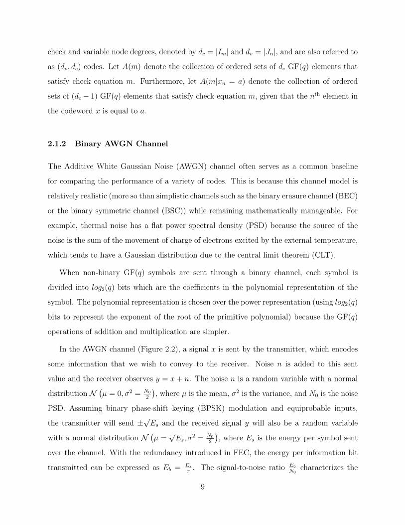
In the AWGN channel (Figure 2.2), a signal x is sent by the transmitter, which encodes
some information that we wish to convey to the receiver. Noise n is added to this sent
value and the receiver observes y = x + n. The noise n is a random variable with a normal
distribution N(µ = 0, σ2 = N0
2
), where µ is the mean, σ2 is the variance, and N0 is the noise
PSD. Assuming binary phase-shift keying (BPSK) modulation and equiprobable inputs,
the transmitter will send ±√Es and the received signal y will also be a random variable
with a normal distribution N(µ =
√Es, σ
2 = N0
2
), where Es is the energy per symbol sent
over the channel. With the redundancy introduced in FEC, the energy per information bit
transmitted can be expressed as Eb = Es
r. The signal-to-noise ratio Eb
N0characterizes the
9
x y
n
Figure 2.2: A visualization of the binary AWGN channel.
AWGN channel completely; in realistic scenarios and many simulations Es is kept constant
(the transmitter does not change its output power) and the noise level N0 is varied (the
channel conditions are changed), but equivalently, σ2 can be kept constant while µ is changed.
This signal-to-noise ratio can be expressed as:
Eb
N0
=µ2
2rσ2. (2.1)
The probability density function (pdf) of a normal distributionN (µ, σ2) can be expressed
as:
f(x, µ, σ) =1√2πσ2
exp
(−(x− µ)2
2σ2
). (2.2)
Given some received value y, the probability that the transmitter sent +√Es is:
p(x = +
√Es
⏐⏐⏐ y) = p0 =f(y, µ, σ)
f(y, µ, σ) + f(y,−µ, σ), (2.3)
and the probability that the transmitter sent −√Es is:
p(x = −
√Es
⏐⏐⏐ y) = p1 = 1− p0 =f(y,−µ, σ)
f(y, µ, σ) + f(y,−µ, σ). (2.4)
10
Since a GF(q) symbol is broken up into log2 q bits in transmission over the binary channel,
the probability that the symbol a ∈ GF(q) was sent given multiple received values can be
calculated as the product of log2 q probabilities given by Equations 2.3 and 2.4.
The log likelihood ratio (LLR) of a received bit can be computed as:
ln
(p0p1
)= ln
(p0
1− p0
)= 4yµ
1
2σ2. (2.5)
We can normalize either µ or σ2 to be equal to 1. If µ = 1, y must have a distribution
N(µ = ±1, σ2 = 1
2rEbN0
), and the LLR can be expressed as:
ln
(p0p1
)= 4yr
Eb
N0
. (2.6)
If σ2 = 1, y must have a distribution N(µ = ±
√2r Eb
N0, σ2 = 1
), and the LLR can be
expressed as:
ln
(p0p1
)= 2y
√2r
Eb
N0
. (2.7)
The LLR corresponding to a symbol a ∈ GF(q) is defined as:
Ln(a) = ln
(Pr(xn = a)|channelPr(xn = a)|channel
), (2.8)
where a is defined to be the most likely field element for variable node n, i.e., Pr(xn = a)
is maximum when xn = a. Note that this definition of LLRs yields smaller LLRs for more
likely field elements, allowing the LLRs to be interpreted as a “distance” metric from the
most likely field element [26]. This symbol LLR can equivalently be calculated as the sum of
individual bit LLRs, normalized to the LLR of the most likely symbol so that the minimum
LLR is equal to zero. Either the probability or LLR a priori channel information is utilized
as input to the decoding algorithms.
11
2.1.3 Probability Domain Decoding
In iterative decoding algorithms of NB-LDPC codes often referred to as “Message-Passing”
or “Belief-Propagation” algorithms, messages consisting of a vector of probabilities or LLRs
are passed back and forth between adjacent variable nodes and check nodes. Let Qm,n(a)
be the message from variable node n to check node m, and Rm,n(a) be the message from
check node m to variable node n, for the GF(q) element a. Let Qn(a) be the a posteriori
information of variable node n for the field element a, and yn be the hard decision of variable
node n, determined as the GF(q) element a associated with the minimum LLR in Qn(a).
Traditional NB-LDPC decoding is conducted as follows [16]. The superscript k indicates
the current iteration, and K is the maximum number of iterations allowed.
1) Initialization: The iteration index k is initialized to 0, and the a posteriori information
as well as the messages from the variable nodes are initialized to be equal to the a priori
probability information from the channel:
Qn(a) = Q(0)m,n(a) = pn(a). (2.9)
2) Termination Check : A hard decision y = (y0, y1, . . . , yN−1), y ∈ GF(q)N is made based
on the most likely symbol and the syndrome s = (s0, s1, . . . , sM−1), s ∈ GF(q)M is computed:
yn = argmaxa∈GF(q)
Qn(a), (2.10)
s = y ×HT . (2.11)
If either s = 0 or k = K, then y is output as the result of the algorithm. Otherwise, k is
incremented by 1.
3) Check Node Processing : The messages from check nodes to variable nodes are updated:
12
R(k)m,n(a) =
∑(an′ )∈A(m|xn=a)
⎛⎝ ∏n′∈Im\{n}
Q(k−1)m,n′ (an′)
⎞⎠ . (2.12)
The variable n′ is the index to the adjacent variable nodes for this check node m, except
for the destination of this message, n. The (dc−1)-tuple (an′) is a set of GF(q) elements that
satisfy check equation m, given xn = a. For each such solution set, the associated probability
is computed with the product (the probability that the first symbol is some symbol a0, AND
the second symbol is some symbol a1, AND etc.). The probabilities of all solutions sets are
summed (the probability that the correct solution is some set (a0), OR the correct solution
is some set (a1), OR etc.) and is used as the output message of this check node.
4) Variable Node Processing : The messages from variable nodes to check nodes are
updated:
Q′(k)m,n(a) = α× pn(a)×
∏m′∈In\{m}
R(k)m′,n(a), (2.13)
where α is some normalization scaling factor. This outgoing message from a variable node
is the product of probabilities from the channel and the adjacent check nodes except for
the destination check node of the message. The product is normalized so that the sum of
probabilities becomes 1.
In addition, the a posteriori information is updated (used to make a hard decision in the
next iteration):
Qn(a) = pn(a)×∏m∈In
R(k)m,n(a). (2.14)
5) Iteration: Go to step 2) Termination Check. ♦
Because Equation 2.12 is computed as the sum of products, this algorithm is also referred
to as the sum-product algorithm.
13
2.1.4 FFT-QSPA
Within the algorithm described in the previous section, the most computationally cumber-
some portion is Equation 2.12. Namely, the set A(m|xn = a) is large and impractical to find
directly. The Fast Fourier Transform-based Q-ary Sum-Product Algorithm (FFT-QSPA)
has been proposed by [18] as a simplification to the traditional decoding method, and has
yielded a speed-up in software simulations.
The key insight to deriving this simplification (as well as to get a good intuitive under-
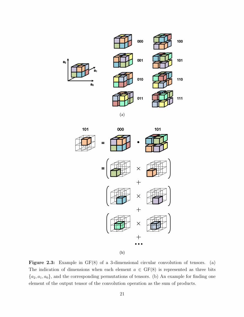
standing of the decoding of NB-LDPC codes in general) is to observe that, in GF(q), the sum
of products described in Equation 2.12 can be thought of as a (log2 q)-dimensional circular
convolution of (dc−1) tensors with two discrete points in each dimension. Figure 2.3 depicts
an example in GF(8).
An element a ∈ GF(8) can be represented as a set of three bits {a2, a1, a0}, which
indicates the set of coefficients of the polynomial representing that element. To compile a
message of probabilities for some variable node, the probability of that variable node being
some element a ∈ GF(8) is placed in the tensor in the corresponding location, and the
tensor is sent back and forth as the message (instead of a one-dimensional vector) in the
message-passing algorithm. Once the tensor is populated, a permutation of the tensor, one
corresponding to each element a ∈ GF(8), can be defined (Figure 2.3(a)). The permutation
is conducted in such a way that any dimension with a “1” becomes swapped (indicated by
a gap in the figure).
In passing a tensor from a variable node to a check node, the tensor contents are shuffled so
that each location contains the probability corresponding to a×hi,j ∈ GF(8) where hi,j is the
edge label on the tanner graph. To compute the element of the output tensor corresponding
to, for example {1, 0, 1}, we must find all of the sequences that would satisfy the check
equation (the finite field sum equals zero), if the last element were {1, 0, 1}. Equivalently, the
finite field sum of all elements except for the last element must equal {1, 0, 1}. This condition
is achieved through the permutation of the tensor; when one of two tensors undergoes a
permutation of {1, 0, 1}, then each element-by-element finite field sum becomes equal to
14
{1, 0, 1} (Figure 2.3(a)). Thus to populate the {1, 0, 1} space in the output tensor, the
sum of element-by-element products is computed. To compute the entire convolution, the
sum of products is computed for each permutation. Because the convolution operation is
associative, the entire check node computation can be taken care of two tensors at a time.
We can take this one step further by applying a common technique employed to reduce
the (computational and conceptual) complexity, which is to convert signals into the Fourier
domain. That is, this convolution in the “time” domain can be computed as a multiplica-
tion in the “frequency” domain. To perform this conversion, a (log2 q)-dimensional 2-point
discrete Fourier transform (DFT) is applied to each message tensor. A multi-dimensional 2-
point DFT is equivalent to a Walsh-Hadamard transform, which, unlike the one-dimensional
q-point DFT, does not require any multiplications by the so-called “twiddle factors” (ex-
cept for negation). After the tensors in the “frequency” domain are multiplied together
element-wise, the inverse DFT (conveniently, the Walsh-Hadamard transform is involutive)
is performed to complete the check node computation.
Armed with this insight, we can now define the FFT-QSPA [18] as follows.
1) Initialization: Same as Section 2.1.3.
2) Termination Check : Same as Section 2.1.3.
3) FFT-Based Check Node Processing : The messages from variable nodes to check nodes
are first permuted according to the corresponding element in the parity-check matrix H:
Q(k−1)m,n (a) = Q
(k−1)m,n′ (h
−1m,n × a). (2.15)
Then, the element-wise product is computed in the “frequency” domain:
U (k)m,n = F
(Q
(k−1)m,n′
). (2.16)
V (k)m,n(a) =
∏n′∈Im\{n}
U(k)m,n′(a). (2.17)
15
R(k)m,n = F−1
(V
(k)m,n′
). (2.18)
Finally, the outgoing messages to variable nodes are permuted back:
R(k)m,n(a) = R
(k)m,n′(hm,n × a). (2.19)
4) Variable Node Processing : Same as Section 2.1.3.
5) Iteration: Same as Section 2.1.3. ♦
The FFT-QSPA performs very well in software simulations and is often used as a basis
for comparison between various constructions of finite-length codes, and so on.
2.1.5 Min-Max
Thus far, the decoding algorithms have been manipulating probabilities, which are numbers
residing between 0 ≤ p ≤ 1. However, it is highly desirable to deal with LLRs in a hardware
implementation of the decoding, from a numerical stability perspective (for example, when
two small probabilities are multiplied together, the result is an extremely small number).
Furthermore, the multiplications (in the probability domain) required in the variable node
computations simplify to additions (in the LLR domain).
However, the transformation of probabilities to LLRs makes the addition of probabilities
rather difficult. Not only does this mean that the DFT becomes difficult to apply, but also
even without the DFT the check node computation becomes difficult. Thus, several approx-
imations (akin to those in simplified binary LDPC decoding schemes) becomes necessary.
Since the sum of two probabilities is dominated by the larger probability, we can approxi-
mate pa + pb ≈ max (pa, pb). In the LLR domain, this becomes the minimum function, since
symbols with higher probability have a smaller LLR (as mentioned in Section 2.1.2).
Another approximation can be made in the same vein, in order to simplify the decoding
further. While the multiplication of probabilities can be computed as the sum of LLRs, the
outcome of this function is dominated mostly by the smaller of probabilities, or the larger
16
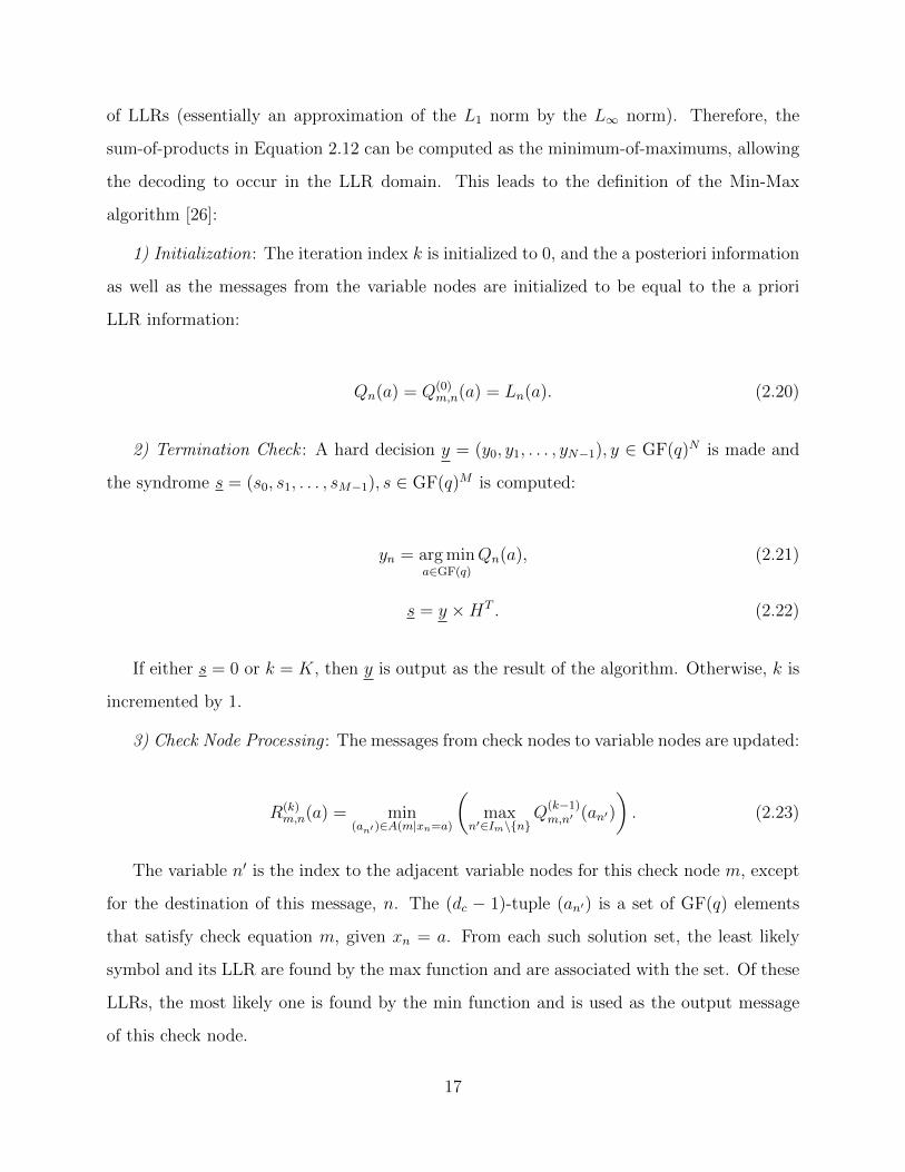
of LLRs (essentially an approximation of the L1 norm by the L∞ norm). Therefore, the
sum-of-products in Equation 2.12 can be computed as the minimum-of-maximums, allowing
the decoding to occur in the LLR domain. This leads to the definition of the Min-Max
algorithm [26]:
1) Initialization: The iteration index k is initialized to 0, and the a posteriori information
as well as the messages from the variable nodes are initialized to be equal to the a priori
LLR information:
Qn(a) = Q(0)m,n(a) = Ln(a). (2.20)
2) Termination Check : A hard decision y = (y0, y1, . . . , yN−1), y ∈ GF(q)N is made and
the syndrome s = (s0, s1, . . . , sM−1), s ∈ GF(q)M is computed:
yn = argmina∈GF(q)
Qn(a), (2.21)
s = y ×HT . (2.22)
If either s = 0 or k = K, then y is output as the result of the algorithm. Otherwise, k is
incremented by 1.
3) Check Node Processing : The messages from check nodes to variable nodes are updated:
R(k)m,n(a) = min
(an′ )∈A(m|xn=a)
(max
n′∈Im\{n}Q
(k−1)m,n′ (an′)
). (2.23)
The variable n′ is the index to the adjacent variable nodes for this check node m, except
for the destination of this message, n. The (dc − 1)-tuple (an′) is a set of GF(q) elements
that satisfy check equation m, given xn = a. From each such solution set, the least likely
symbol and its LLR are found by the max function and are associated with the set. Of these
LLRs, the most likely one is found by the min function and is used as the output message
of this check node.
17
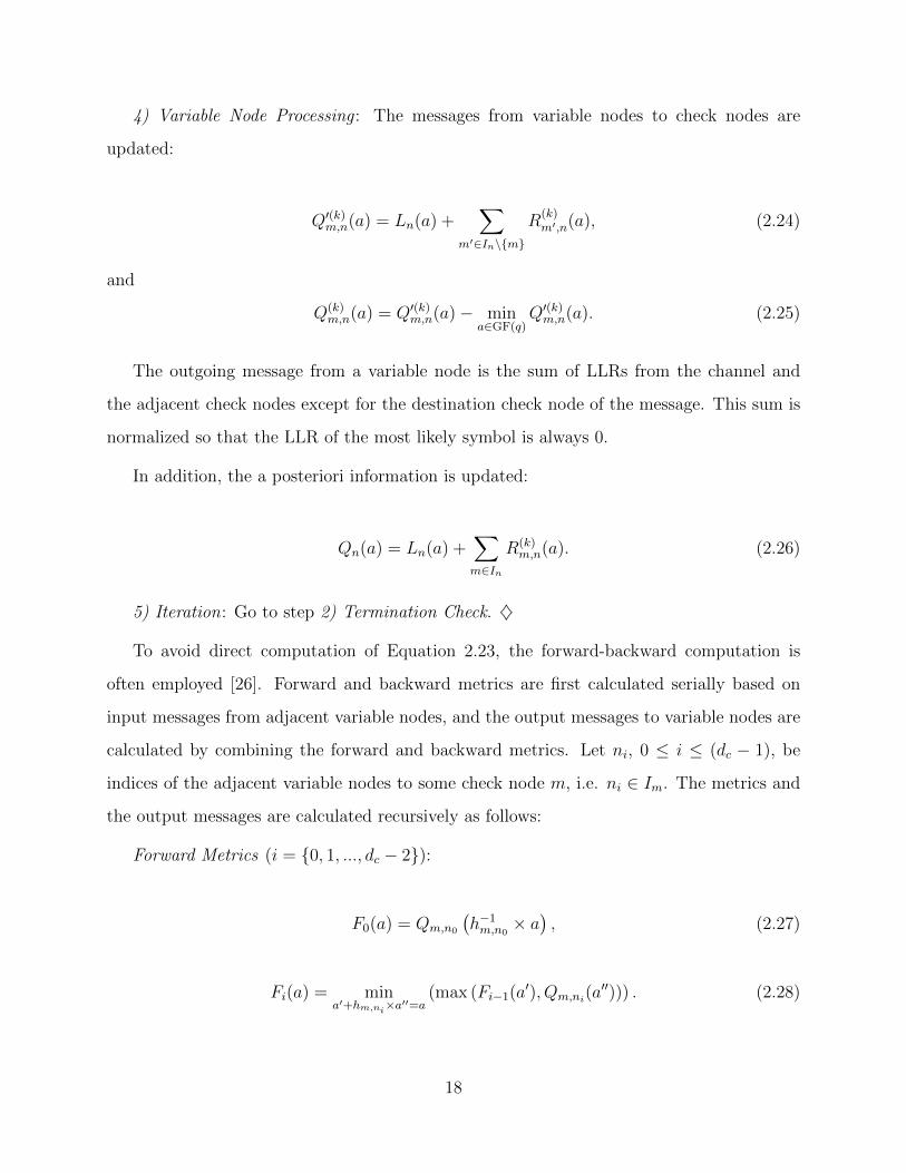
4) Variable Node Processing : The messages from variable nodes to check nodes are
updated:
Q′(k)m,n(a) = Ln(a) +
∑m′∈In\{m}
R(k)m′,n(a), (2.24)
and
Q(k)m,n(a) = Q′(k)
m,n(a)− mina∈GF(q)
Q′(k)m,n(a). (2.25)
The outgoing message from a variable node is the sum of LLRs from the channel and
the adjacent check nodes except for the destination check node of the message. This sum is
normalized so that the LLR of the most likely symbol is always 0.
In addition, the a posteriori information is updated:
Qn(a) = Ln(a) +∑m∈In
R(k)m,n(a). (2.26)
5) Iteration: Go to step 2) Termination Check. ♦
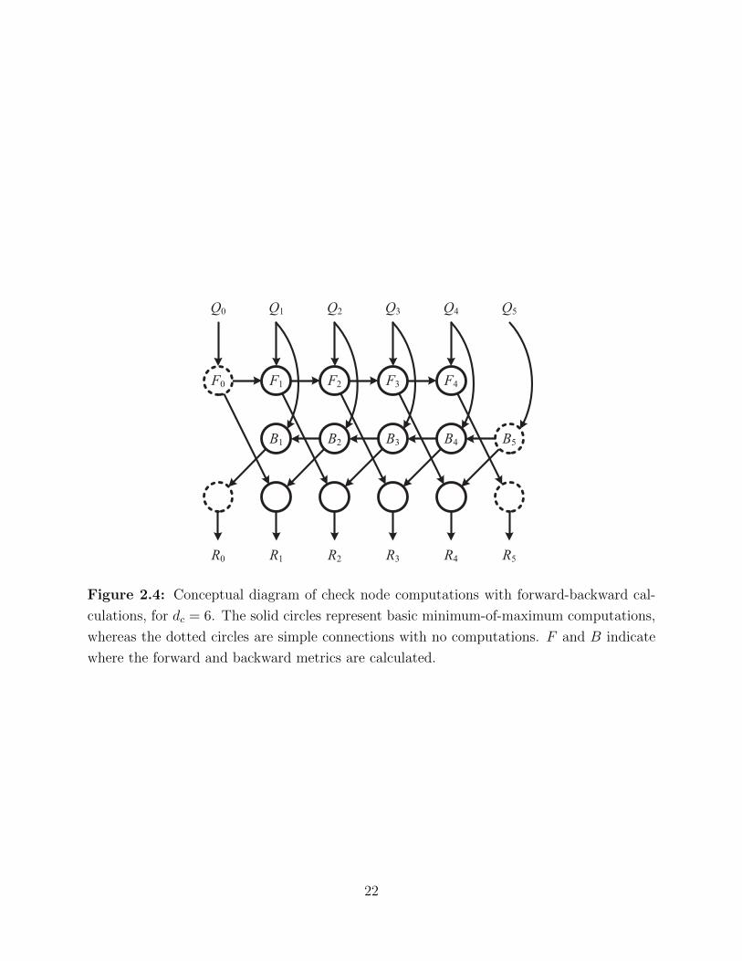
To avoid direct computation of Equation 2.23, the forward-backward computation is
often employed [26]. Forward and backward metrics are first calculated serially based on
input messages from adjacent variable nodes, and the output messages to variable nodes are
calculated by combining the forward and backward metrics. Let ni, 0 ≤ i ≤ (dc − 1), be
indices of the adjacent variable nodes to some check node m, i.e. ni ∈ Im. The metrics and
the output messages are calculated recursively as follows:
Forward Metrics (i = {0, 1, ..., dc − 2}):
F0(a) = Qm,n0
(h−1m,n0
× a), (2.27)
Fi(a) = mina′+hm,ni×a′′=a
(max (Fi−1(a′), Qm,ni
(a′′))) . (2.28)
18
Backward Metrics (i = {dc − 1, dc − 2, ..., 1}):
Bdc−1(a) = Qm,ndc−1
(h−1m,ndc−1
× a), (2.29)
Bi(a) = mina′+hm,ni×a′′=a
(max (Bi+1(a′), Qm,ni
(a′′))) . (2.30)
Output Messages (i = {0, 1, ..., dc − 1}):
Rm,n0(a) = B1(a), (2.31)
Rm,ni(a) = min
a′+a′′=−hm,ni×a(max (Fi−1(a
′), Bi+1(a′′))) , (2.32)
Rm,ndc−1(a) = Fdc−2(a). (2.33)
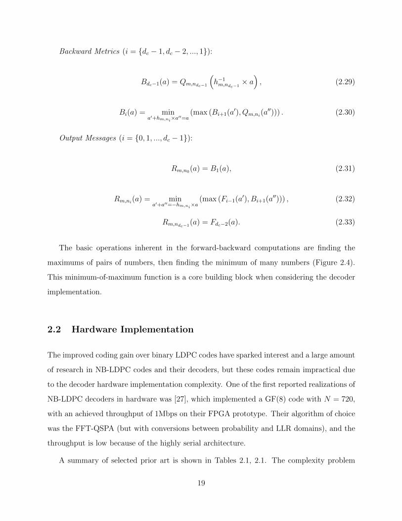
The basic operations inherent in the forward-backward computations are finding the
maximums of pairs of numbers, then finding the minimum of many numbers (Figure 2.4).
This minimum-of-maximum function is a core building block when considering the decoder
implementation.
2.2 Hardware Implementation
The improved coding gain over binary LDPC codes have sparked interest and a large amount
of research in NB-LDPC codes and their decoders, but these codes remain impractical due
to the decoder hardware implementation complexity. One of the first reported realizations of
NB-LDPC decoders in hardware was [27], which implemented a GF(8) code with N = 720,
with an achieved throughput of 1Mbps on their FPGA prototype. Their algorithm of choice
was the FFT-QSPA (but with conversions between probability and LLR domains), and the
throughput is low because of the highly serial architecture.
A summary of selected prior art is shown in Tables 2.1, 2.1. The complexity problem
19
of NB-LDPC codes is quite clear. On one hand, implementations of standard decoding
algorithms with respectable codes parameters [19,20,21,22] are all quite costly for moderate
throughputs. On the other hand, to achieve high data throughputs, either a trivial code
must be chosen [23] or a simplistic decoding algorithm must be implemented [24], both of
which result in a severe degradation of coding gain and a high error floor.
20
a0
a1
a2
000
001
010
011
100
101
110
111
(a)
101
=
000 101
=
(b)
Figure 2.3: Example in GF(8) of a 3-dimensional circular convolution of tensors. (a)
The indication of dimensions when each element a ∈ GF(8) is represented as three bits
{a2, a1, a0}, and the corresponding permutations of tensors. (b) An example for finding one
element of the output tensor of the convolution operation as the sum of products.
21
Q0 Q1 Q2 Q3
R0 R1 R2 R3
Q4
R4
Q5
R5
F0 F1 F2 F3 F4
B1 B2 B3 B4 B5
Figure 2.4: Conceptual diagram of check node computations with forward-backward cal-
culations, for dc = 6. The solid circles represent basic minimum-of-maximum computations,
whereas the dotted circles are simple connections with no computations. F and B indicate
where the forward and backward metrics are calculated.
22
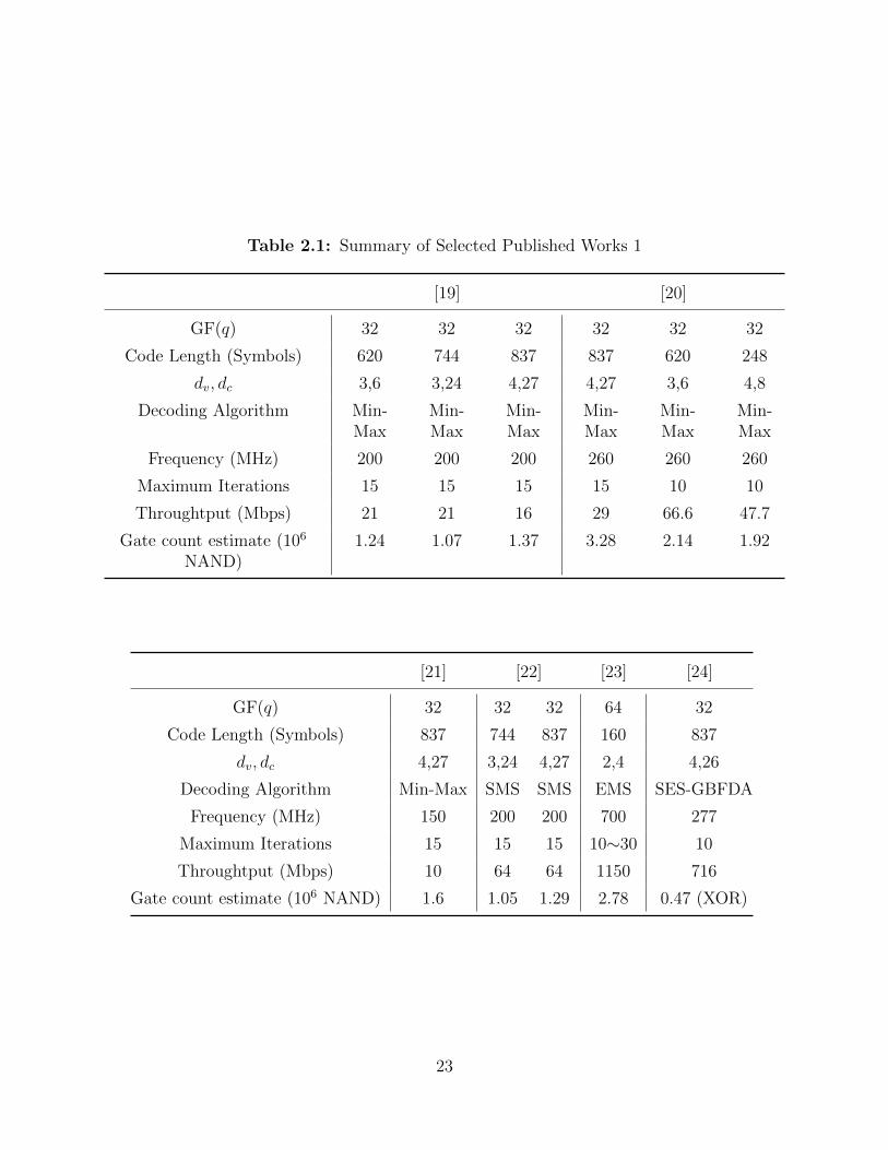
Table 2.1: Summary of Selected Published Works 1
[19] [20]
GF(q) 32 32 32 32 32 32
Code Length (Symbols) 620 744 837 837 620 248
dv, dc 3,6 3,24 4,27 4,27 3,6 4,8
Decoding Algorithm Min-Max
Min-Max
Min-Max
Min-Max
Min-Max
Min-Max
Frequency (MHz) 200 200 200 260 260 260
Maximum Iterations 15 15 15 15 10 10
Throughtput (Mbps) 21 21 16 29 66.6 47.7
Gate count estimate (106
NAND)1.24 1.07 1.37 3.28 2.14 1.92
[21] [22] [23] [24]
GF(q) 32 32 32 64 32
Code Length (Symbols) 837 744 837 160 837
dv, dc 4,27 3,24 4,27 2,4 4,26
Decoding Algorithm Min-Max SMS SMS EMS SES-GBFDA
Frequency (MHz) 150 200 200 700 277
Maximum Iterations 15 15 15 10∼30 10
Throughtput (Mbps) 10 64 64 1150 716
Gate count estimate (106 NAND) 1.6 1.05 1.29 2.78 0.47 (XOR)
23
CHAPTER 3
The Pruned Min-Max Algorithm
3.1 Figure-of-Merit . . . . . . . . . . . . . . . . . . . . . . . . . . . . . . . . 25
3.1.1 Parameters and Assumptions . . . . . . . . . . . . . . . . . . . . . . . . 26
3.1.2 The Fully Parallel Architecture . . . . . . . . . . . . . . . . . . . . . . . 27
3.2 Algorithm Strategy: Pruned Min-Max Decoding . . . . . . . . . . . . . . 33
3.2.1 Derivation of the Proposed Simplification . . . . . . . . . . . . . . . . . 33
3.2.2 Analysis of Decoding Performance . . . . . . . . . . . . . . . . . . . . . 36
3.2.3 Cost Analysis of the Pruned Min-Max Algorithm . . . . . . . . . . . . . 40
24
In the ASIC implementation of any DSP algorithm, changes in the algorithm itself causes
the largest impact in terms of obtainable hardware performance (throughput, power, etc.).
Therefore it is natural to first investigate potential ways to simplify the decoding of NB-
LDPC codes in order to make them more practical. In this chapter we introduce our proposed
simplifications to the Min-Max algorithm, which we call the Pruned Min-Max algorithm,
and explore the effects of our proposed changes on the coding gain as well as computational
complexity.
The contents of this chapter are mostly published in [28].
3.1 Figure-of-Merit
Before we discuss the algorithm itself, first we will introduce a figure-of-merit (FOM) which
we will utilize to quantify the computational complexity and how that translates into hard-
ware resources.
An analytical expression for the throughput of an NB-LDPC decoder is relatively straight-
forward to derive. First, let z be the number of clock cycles required to calculate a single
iteration of the decoding algorithm. Next, we assume that the decoder is operating in a
low FER/BER regime so that the output of the decoder converges to a codeword relatively
quickly most of the time, and the average number of iterations required per codeword is
denoted as Kavg. The average number of iterations per codeword, Kavg, is assumed to be
independent of the maximum number of iterations K, because the input noise realizations
that cause the decoder to take many iterations to converge are rare (although other factors
such as the maximum latency of the decoder or the required input buffer length are deter-
mined by the worst case K). Then, the product z ×Kavg is the number of clock cycles the
decoder requires per codeword on average. If the digital circuitry operates at some clock
frequency fclk, and the decoder is designed for a particular code whose length is B bits, then
25
the average throughput T of the iterative decoder in bits per second can be expressed as:
T
[bits
s
]=
fclk
[cycles
s
]×B
[bits
codeword
]z[
cyclesiteration
]×Kavg
[iterationscodeword
] . (3.1)
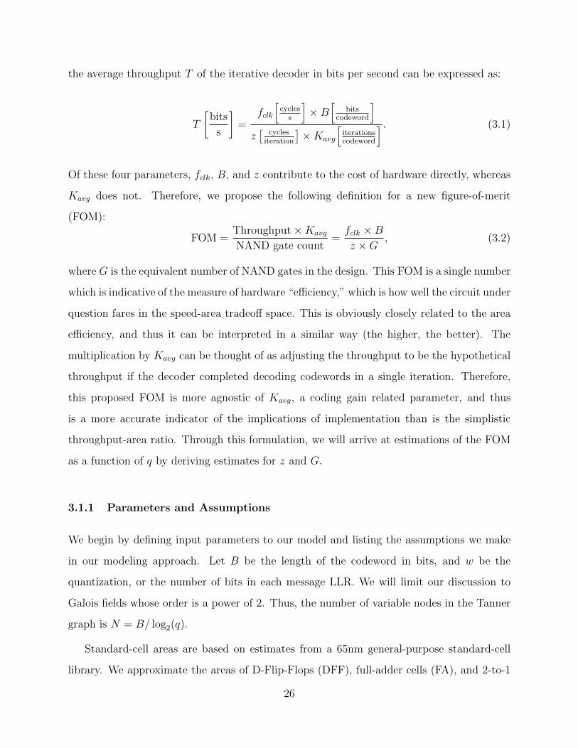
Of these four parameters, fclk, B, and z contribute to the cost of hardware directly, whereas
Kavg does not. Therefore, we propose the following definition for a new figure-of-merit
(FOM):
FOM =Throughput×Kavg
NAND gate count=
fclk ×B
z ×G, (3.2)
where G is the equivalent number of NAND gates in the design. This FOM is a single number
which is indicative of the measure of hardware “efficiency,” which is how well the circuit under
question fares in the speed-area tradeoff space. This is obviously closely related to the area
efficiency, and thus it can be interpreted in a similar way (the higher, the better). The
multiplication by Kavg can be thought of as adjusting the throughput to be the hypothetical
throughput if the decoder completed decoding codewords in a single iteration. Therefore,
this proposed FOM is more agnostic of Kavg, a coding gain related parameter, and thus
is a more accurate indicator of the implications of implementation than is the simplistic
throughput-area ratio. Through this formulation, we will arrive at estimations of the FOM
as a function of q by deriving estimates for z and G.
3.1.1 Parameters and Assumptions
We begin by defining input parameters to our model and listing the assumptions we make
in our modeling approach. Let B be the length of the codeword in bits, and w be the
quantization, or the number of bits in each message LLR. We will limit our discussion to
Galois fields whose order is a power of 2. Thus, the number of variable nodes in the Tanner
graph is N = B/ log2(q).
Standard-cell areas are based on estimates from a 65nm general-purpose standard-cell
library. We approximate the areas of D-Flip-Flops (DFF), full-adder cells (FA), and 2-to-1
26
VNU
Interconnect
CNU
VNU VNUVNU
CNUCNU
Figure 3.1: Top-level architecture for a fully parallel decoder.
multiplexors (MUX) to be equivalent to 5, 5 and 2.5 NAND gate areas, respectively. We
assume that a 2-input, w-bit adder is implemented as a ripple-carry adder and consists
of w FAs and w DFFs, therefore consuming 10w NAND gates in area and 1 clock cycle
to execute. Furthermore, we assume that a 2-input w-bit minimum (MIN) or maximum
(MAX) function to be equivalent in area and latency to a 2-input w-bit adder. Conceptually,
this assumption makes sense because a similar “carry” signal must be generated for both
operations. Moreover, a simple gate-level synthesis of these blocks for various w and fclk
validates this approximation. An N -input adder is implemented with a tree of (N − 1)
2-input adders which takes log2(N) clock cycles to finish computation. A similar approach
is taken for MIN, MAX, and MUX. To arrive at a total equivalent NAND gate count, we
assume that storage of one SRAM bit requires roughly 1.5 NAND gates [20]. The latency of
any memory block is assumed to be 1 clock cycle.
Because we are aiming to arrive at a FOM that captures the ratio of throughput and area,
decisions to implement low-level functions in serial or parallel are taken to have negligible
effect in our result. Also, the details of implementation or scheduling are not optimized and
the control logic overhead is ignored for simplicity.
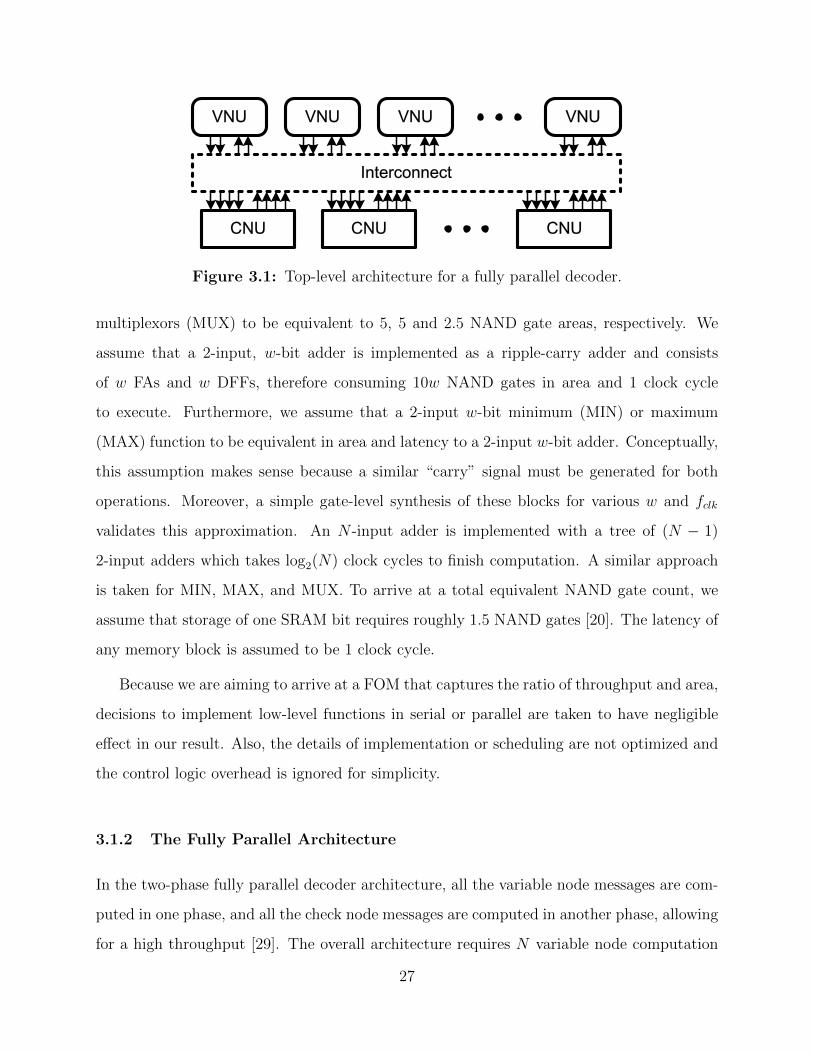
3.1.2 The Fully Parallel Architecture
In the two-phase fully parallel decoder architecture, all the variable node messages are com-
puted in one phase, and all the check node messages are computed in another phase, allowing
for a high throughput [29]. The overall architecture requires N variable node computation
27
R0
R1
Q1
Q0
Y
Ln
Ln
R0
R1
R2
Q2
Q1
Q0
Y
R1
R2
Ln
(a)
(b)
Figure 3.2: VNU architectures for the Min-Max decoder, for (a) dv = 2 and (b) dv = 3.
28
R
Q
Q
Figure 3.3: Implementation of the CNU for the Min-Max algorithm.
units (VNU) and M check node computation units (CNU), with memories for the messages
embedded in these computation units (Figure 3.1). Therefore, the total NAND gate count
for this architecture is:
G = N ×GVNU +M ×GCNU, (3.3)
and the total number of clock cycles required per iteration is:
z = zVNU + zCNU, (3.4)
assuming there is no overlap.
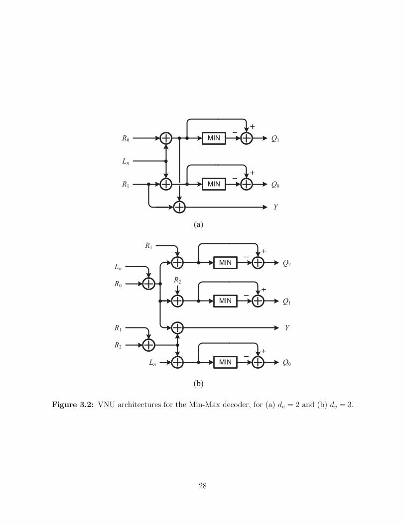
The VNU receives dv incoming messages from adjacent CNUs, as well as the channel a
priori message, and generates dv outgoing messages to adjacent CNUs. The input messages
and channel a priori information are summed together, and the resulting message is nor-
malized (Figure 3.2). We will limit our discussion to codes with dv = {2, 3} for simplicity,
although the analysis holds more generally. The q-input minimum function used for normal-
ization can be implemented as a tree of (q − 1) 2-input minimum functions, which would
take log2(q) clock cycles to compute its output. Now that the VNU is implemented with
29
blocks for which the gate count and delay are known, GVNU as well as zVNU can be estimated
based on the assumptions outlined above. For example, for dv = 2, GVNU = 10w(7q − 2),
and zVNU = log2(q) + 2.
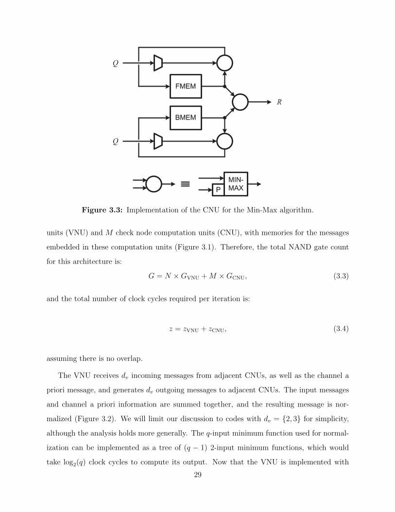
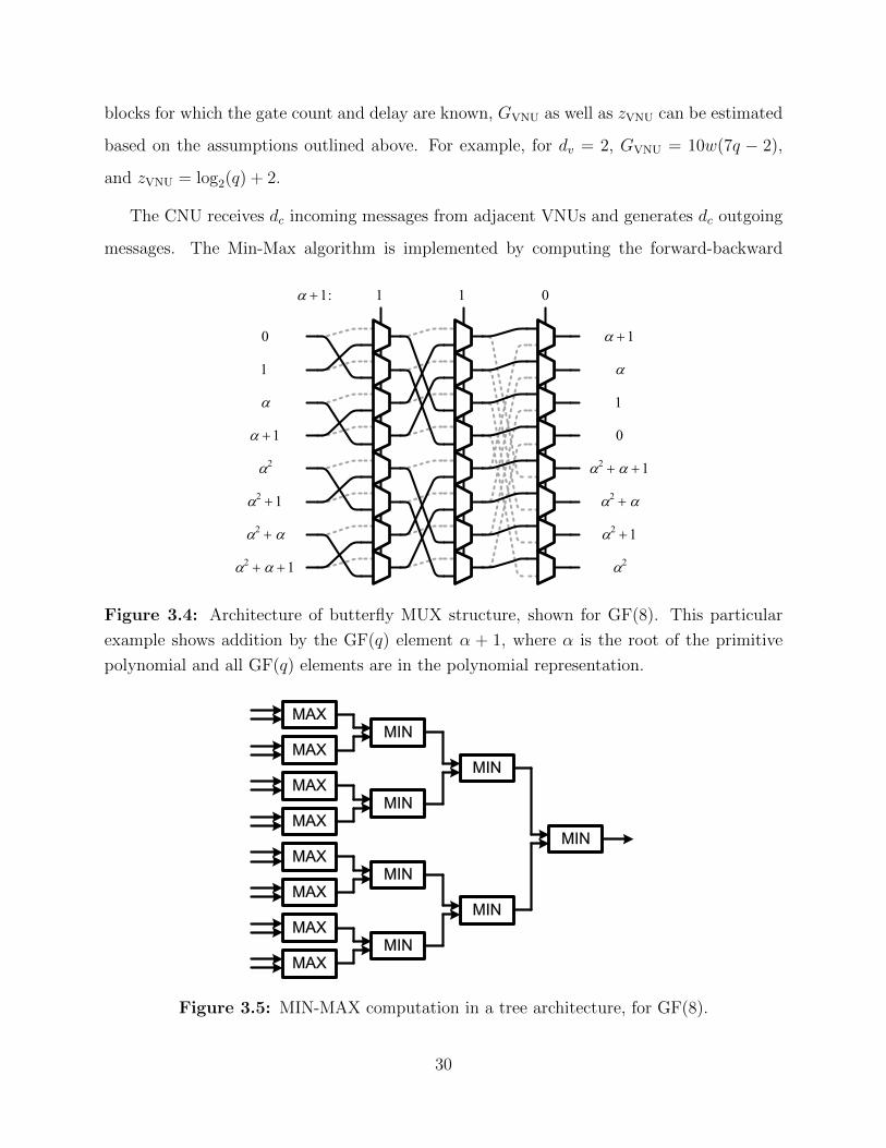
The CNU receives dc incoming messages from adjacent VNUs and generates dc outgoing
messages. The Min-Max algorithm is implemented by computing the forward-backward
a
a + 1
a2
a2 + 1
1
0
a2 + a
a2 + a + 1
a + 1: 011
0
1
a
a + 1
a2
a2 + 1
a2 + a
a2 + a + 1
Figure 3.4: Architecture of butterfly MUX structure, shown for GF(8). This particular
example shows addition by the GF(q) element α + 1, where α is the root of the primitive
polynomial and all GF(q) elements are in the polynomial representation.
MAX
MAX
MAX
MAX
MIN
MIN
MIN
MAX
MAX
MAX
MAX
MIN
MIN
MIN
MIN
Figure 3.5: MIN-MAX computation in a tree architecture, for GF(8).
30
metrics (Figure 3.3). This divides the task of the CNU down to performing the minimum-of-
maximum operation between two vectors at a time. The variable permutation of messages,
represented as the block labeled ”P” in Figure 3.3, can be implemented in a butterfly MUX
structure (Figure 3.4) (a similar structure has been proposed in [30]). This structure allows a
vector of LLRs to be permuted correctly, given that the select signal binary representation as
well as the message vector LLR ordering are both in the polynomial representation of GF(q)
elements. The MIN-MAX block computes the minimum of the pair-wise maximums, which
is the basic computation necessary in the forward-backward calculations (Figure 3.5) [19].
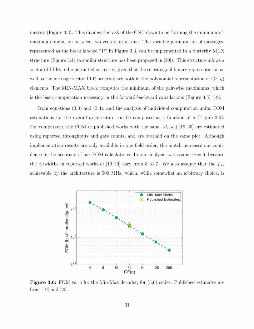
From equations (3.3) and (3.4), and the analysis of individual computation units, FOM
estimations for the overall architecture can be computed as a function of q (Figure 3.6).
For comparison, the FOM of published works with the same (dv, dc) [19, 20] are estimated
using reported throughputs and gate counts, and are overlaid on the same plot. Although
implementation results are only available in one field order, the match increases our confi-
dence in the accuracy of our FOM calculations. In our analysis, we assume w = 6, because
the bitwidths in reported works of [19, 20] vary from 5 to 7. We also assume that the fclk
achievable by the architecture is 500 MHz, which, while somewhat an arbitrary choice, is
4 8 16 32 64 128 256101
102
103
GF(q)
FOM
[bps
*iter
atio
ns/g
ates
]
Min−Max ModelPublished Estimates
Figure 3.6: FOM vs. q for the Min-Max decoder, for (3,6) codes. Published estimates are
from [19] and [20].
31
also a reasonable one given the technology node as well as the conservative insertion of flip-
flops in the estimation of required NAND gates. This choice will also be validated in a later
section through the use of physical synthesis tools. It is also noted that [19] and [20] esti-
mate achievable throughputs under the assumption that each codeword takes K maximum
iterations to decode. Therefore, their FOMs are calculated using K rather than Kavg to be
consistent.
Because the FOM is an indicator of the inherent tradeoff between speed and area, this
result quantifies the amount of penalty that must be paid when choosing to implement a
code in a higher field order. It is also interesting to note that for a given (dv, dc), G grows
linearly with respect to B, because in equation (3.3), N = B/ log2(q), and M = N(dv/dc).
Since T also increases linearly with B as indicated by equation (3.1), it follows that the
FOM of the overall architecture is constant with respect to B. Therefore, the code length
implemented will be constrained by other considerations, such as the overall required system
latency.
Our definition of the FOM and its analytical expression in equation (3.2) has remained
generic and thus can be applied to analyze binary LDPC decoders. However, we provide
limited discussion on binary LDPC decoders for the following two reasons. First, the accuracy
of our modeling approach is degraded, because binary decoders are more likely to have a
costly routing network and a low silicon area utilization [9, 13, 29], relative to NB-LDPC
decoders. Therefore, a block-level resource estimation based only on the required operations
will most likely overestimate the FOM. Second, the fairness of a direct comparison of FOMs
of existing works between binary and non-binary decoders is somewhat questionable. Not
only are the implemented algorithms different, but also the maturity of the field of binary
LDPC decoder implementations has yielded various features in designs which differ from
those of the existing NB-LDPC decoders. Namely, the architectures of the state-of-the-art
binary LDPC decoders are for irregular codes and have rate programmability [9, 12], for
higher performance in practical systems.
Crude estimations can give us some information, however. For example, the architecture
in [12], based on the rate-12LDPC code in the WiMAX standard, has an estimated FOM of
32
∼ 13600 according to equation (3.2), which is ∼ 7 times higher than that of the Min-Max
algorithm implemented for (3, 6) codes in GF(4), even without taking rate programmability
into account. This is the gap which must be closed (or the penalty that must be paid)
in order to realize NB-LDPC decoders as a practical solution to communication systems.
In general, while FOMs can be estimated from published works for binary decoders, it is
difficult to draw informed conclusions beyond the fact that binary LDPC decoders have
achieved higher FOMs than NB-LDPC decoders.
3.2 Algorithm Strategy: Pruned Min-Max Decoding
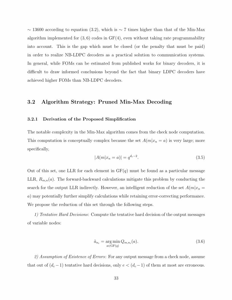
3.2.1 Derivation of the Proposed Simplification
The notable complexity in the Min-Max algorithm comes from the check node computation.
This computation is conceptually complex because the set A(m|xn = a) is very large; more
specifically,
|A(m|xn = a)| = qdc−2. (3.5)
Out of this set, one LLR for each element in GF(q) must be found as a particular message
LLR, Rm,n(a). The forward-backward calculations mitigate this problem by conducting the
search for the output LLR indirectly. However, an intelligent reduction of the set A(m|xn =
a) may potentially further simplify calculations while retaining error-correcting performance.
We propose the reduction of this set through the following steps.
1) Tentative Hard Decisions : Compute the tentative hard decision of the output messages
of variable nodes:
ani= argmin
a∈GF(q)
Qm,ni(a). (3.6)
2) Assumption of Existence of Errors : For any output message from a check node, assume
that out of (dc−1) tentative hard decisions, only e < (dc−1) of them at most are erroneous.
33
MAX
e errorsmore than
e errors
output message
hard
decision
MIN
MAX MAX MAX
Figure 3.7: Tree representation of the proposed simplification in the check node computa-
tion, for dc = 4 and e = 2. The dotted lines indicate the ”pruned” branches.
Thus, a new set A′(m|xn = a) can be defined as the set of GF(q) elements that satisfy check
equation m given xn = a, with the additional constraint that at least (dc − e − 1) of the
elements in this set must be a tentative hard decision. With this simplification, the size of
the set of LLRs to be considered in the check node computation is reduced:
|A′(m|xn = a)| =(dc − 1
e
)× qe−1. (3.7)
Thus, a new check node computation step in a simplified Min-Max algorithm can be
defined by replacing the set A with A′. A similar reduction has been proposed in [22] for the
EMS algorithm. We will take advantage of the fact that the output message of check nodes
in the Min-Max algorithm are one of the LLRs from the output message of variable nodes
and propose an additional simplification step.
3) Pruning of Hard-Decision LLRs : To further reduce the search space of LLRs in
the check node computation, we generate a tree of LLRs that is considered in the check
node computation (Figure 3.7). The root of this tree represents the output message of
the check node. Each branch stemming from the root represents one element in the set
A′(m|xn = a). There are (dc− 1) leaves connected to each of these sets, signifying each LLR
34
2 2.5 3 3.5 4 4.5 5 5.5 6
10−5
10−4
10−3
10−2
10−1
100
SNR
FER
Pruned Min−MaxMin−Max
GF(4)GF(8)
GF(16)GF(32)
Figure 3.8: FER simulation results for (3, 6) codes of length ∼ 1500 bits and various GF(q).
corresponding to the GF(q) element in the sequence that satisfies the check equation. In
the Min-Max algorithm, the leaves with maximum LLRs in each branch are found. Then,
of those maximum LLRs, the minimum is found as the output.
However, in the simplification that we have proposed above, (dc − e− 1) of the LLRs in
each branch are actually LLRs corresponding to tentative hard decisions, which means they
are the minimum LLR out of the message vector that comes from variable nodes. In fact,
the LLRs corresponding to hard decisions are always zero, with our particular definition
of LLRs and the normalization scheme that occurs at the end of variable node processing.
Therefore, these LLRs do not need to be considered because they will never be selected as
the maximum LLR of that particular branch. The new check node computation step is now
given by:
R(k)m,n(a) = min
(an′ )∈A′(m|xn=a)
(max
n′∈Im\{n,(n)}Q
(k−1)m,n′ (an′)
), (3.8)
35
where (n) indicates the set of adjacent variable nodes whose LLRs are tentative hard deci-
sions.
In the first simplification step, we proposed to reduce the number of branches that stem
from the root of the tree by changing the search space from A(m|xn = a) to A′(m|xn = a). In
the second step, we proposed to eliminate leaves at the bottom of the tree by not considering
tentative hard-decision LLRs. Due to this action of pruning the LLR tree, we call our
proposed algorithm the Pruned Min-Max algorithm.
3.2.2 Analysis of Decoding Performance
The Pruned Min-Max algorithm with e = 2 is simulated for a variety of codes, and the FER
and BER performance is compared against that of the original Min-Max algorithm (Figure
3.8). It can be seen that the modifications of the Pruned Min-Max algorithm incur very
little decoding performance degradation relative to the Min-Max algorithm. Simulations are
conducted for a variety of code lengths (∼ 1500, 2500 bits), parity-check matrix structures
(random, quasi-cyclic), field orders (GF(4, 8, 16, 32)), and variable-node degrees (dv = 2, 3),
which are not shown but give similar results. The choice of e is a critical factor which
affects both the performance and the hardware cost. For the most savings in computational
complexity, we would like to minimize e (in the limit, e = 0 is a decoder which passes around
only hard information). We have found through simulations that e < 2 incurs significant
performance degradation (not shown), whereas e = 2 maintains the decoding performance
close to that of the Min-Max algorithm, leading us to the choice of e = 2.
However, a simple direct comparison of error performances of the two algorithms seems
rather superficial and insufficient to conclude that one is a valid replacement candidate for the
other. Therefore, in order to understand the similar performances of the Min-Max and the
Pruned Min-Max decoding algorithms, we analyze the error profiles of these two algorithms
through simulations [31]. Given the same channel realizations, which are the inputs to
the decoding algorithms, the output vectors in error have been compared and investigated,
again for a variety of code parameters. To minimize the uncertainty of the simulation, a
36
sufficiently large sample size of frame errors (∼ 100) is simulated. Once the errors are
identified by simulating an appropriate sample size in both decoders, the following scenarios
are considered: (i) identical errors that are caused by a particular channel realization in
both decoders, (ii) different errors caused by the same channel realization in both decoders,
and (iii) errors in only one of the two decoders caused by any realization. The set of errors
described by (i), (ii), and (iii) are denoted as X, Y , and Z, respectively.
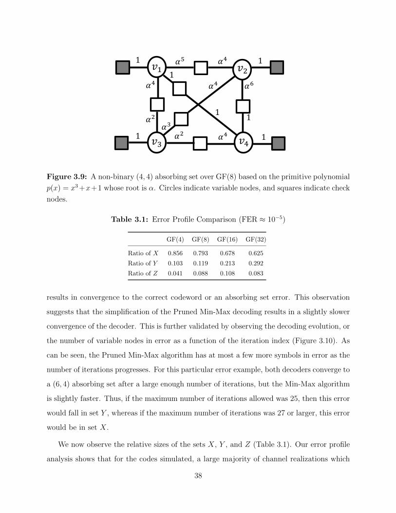
We first characterize the three scenarios of X, Y , and Z by considering the non-binary
absorbing sets of the code. Absorbing sets are of interest because decoding algorithms
have been shown to converge to these non-codeword objects in the Tanner graph, causing
erroneous outputs [32]. A subset V of the variable nodes, with |V| = a, is an (a, b) non-binary
absorbing set over GF(q) if there exists a vector of GF(q) elements (v1, v2, . . . , va) for V such
that 1) there are exactly b unsatisfied check nodes connected to V , and 2) for each variable
node in V , the number of adjacent satisfied check nodes is larger than the number of adjacent
unsatisfied checks. An example of a (4, 4) non-binary absorbing set over GF(8) is shown in
Figure 3.9. In this example, if (v1, v2, v3, v4) = (1, α, α2, 1), each variable node is adjacent to
exactly 3 satisfied (light square) and 1 unsatisfied (dark square) check nodes. Therefore, the
two conditions for the absorbing set are satisfied. As the number of iterations progresses,
the decoder can converge to these absorbing sets and remain stuck, causing errors in the
output (Figure 3.10).
In our simulations, a large majority of the errors in the set X are non-binary absorbing
set errors. In this case, both the Min-Max and Pruned Min-Max decoders converge to
some non-binary absorbing set before they reach their maximum number of iterations. In
the set Y , the Min-Max decoder converges to an absorbing set error before reaching the
maximum number of iterations, whereas the Pruned Min-Max algorithm does not. Finally,
in the majority of the cases in set Z, the Min-Max decoder outputs the correct codeword,
whereas the Pruned Min-Max algorithm does not converge. For the sets Y and Z, we
observe that the outputs of the Pruned Min-Max algorithm are close to the outputs of the
Min-Max algorithm, and validate through simulation that increasing the maximum number
of iterations for the Pruned Min-Max algorithm, for the set of inputs causing Y and Z,
37
𝛼4
1 1
𝛼3
𝛼2
𝛼6
1
1
1 1
𝑣4
𝑣2 𝑣1
𝑣3 1
𝛼4
𝛼5
𝛼4
𝛼2
𝛼4
Figure 3.9: A non-binary (4, 4) absorbing set over GF(8) based on the primitive polynomial
p(x) = x3+x+1 whose root is α. Circles indicate variable nodes, and squares indicate check
nodes.
Table 3.1: Error Profile Comparison (FER ≈ 10−5)
GF(4) GF(8) GF(16) GF(32)
Ratio of X 0.856 0.793 0.678 0.625
Ratio of Y 0.103 0.119 0.213 0.292
Ratio of Z 0.041 0.088 0.108 0.083
results in convergence to the correct codeword or an absorbing set error. This observation
suggests that the simplification of the Pruned Min-Max decoding results in a slightly slower
convergence of the decoder. This is further validated by observing the decoding evolution, or
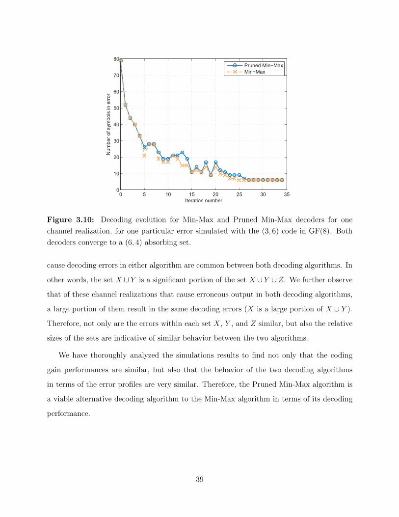
the number of variable nodes in error as a function of the iteration index (Figure 3.10). As
can be seen, the Pruned Min-Max algorithm has at most a few more symbols in error as the
number of iterations progresses. For this particular error example, both decoders converge to
a (6, 4) absorbing set after a large enough number of iterations, but the Min-Max algorithm
is slightly faster. Thus, if the maximum number of iterations allowed was 25, then this error
would fall in set Y , whereas if the maximum number of iterations was 27 or larger, this error
would be in set X.
We now observe the relative sizes of the sets X, Y , and Z (Table 3.1). Our error profile
analysis shows that for the codes simulated, a large majority of channel realizations which
38
0 5 10 15 20 25 30 350
10
20
30
40
50
60
70
80
Iteration number
Num
ber o
f sym
bols
in e
rror
Pruned Min−MaxMin−Max
Figure 3.10: Decoding evolution for Min-Max and Pruned Min-Max decoders for one
channel realization, for one particular error simulated with the (3, 6) code in GF(8). Both
decoders converge to a (6, 4) absorbing set.
cause decoding errors in either algorithm are common between both decoding algorithms. In
other words, the set X ∪ Y is a significant portion of the set X ∪ Y ∪Z. We further observe
that of these channel realizations that cause erroneous output in both decoding algorithms,
a large portion of them result in the same decoding errors (X is a large portion of X ∪ Y ).
Therefore, not only are the errors within each set X, Y , and Z similar, but also the relative
sizes of the sets are indicative of similar behavior between the two algorithms.
We have thoroughly analyzed the simulations results to find not only that the coding
gain performances are similar, but also that the behavior of the two decoding algorithms
in terms of the error profiles are very similar. Therefore, the Pruned Min-Max algorithm is
a viable alternative decoding algorithm to the Min-Max algorithm in terms of its decoding
performance.
39
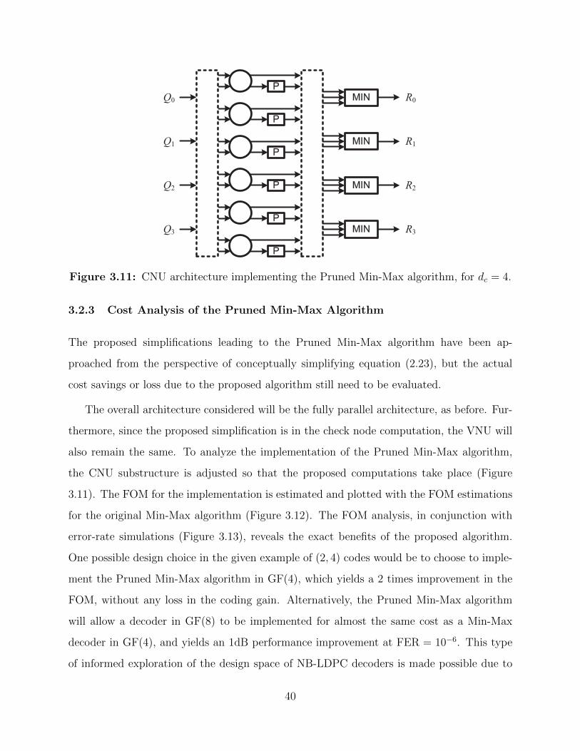
Q0
Q1
Q2
Q3
R0
R1
R2
R3
Figure 3.11: CNU architecture implementing the Pruned Min-Max algorithm, for dc = 4.
3.2.3 Cost Analysis of the Pruned Min-Max Algorithm
The proposed simplifications leading to the Pruned Min-Max algorithm have been ap-
proached from the perspective of conceptually simplifying equation (2.23), but the actual
cost savings or loss due to the proposed algorithm still need to be evaluated.
The overall architecture considered will be the fully parallel architecture, as before. Fur-
thermore, since the proposed simplification is in the check node computation, the VNU will
also remain the same. To analyze the implementation of the Pruned Min-Max algorithm,
the CNU substructure is adjusted so that the proposed computations take place (Figure
3.11). The FOM for the implementation is estimated and plotted with the FOM estimations
for the original Min-Max algorithm (Figure 3.12). The FOM analysis, in conjunction with
error-rate simulations (Figure 3.13), reveals the exact benefits of the proposed algorithm.
One possible design choice in the given example of (2, 4) codes would be to choose to imple-
ment the Pruned Min-Max algorithm in GF(4), which yields a 2 times improvement in the
FOM, without any loss in the coding gain. Alternatively, the Pruned Min-Max algorithm
will allow a decoder in GF(8) to be implemented for almost the same cost as a Min-Max
decoder in GF(4), and yields an 1dB performance improvement at FER = 10−6. This type
of informed exploration of the design space of NB-LDPC decoders is made possible due to
40
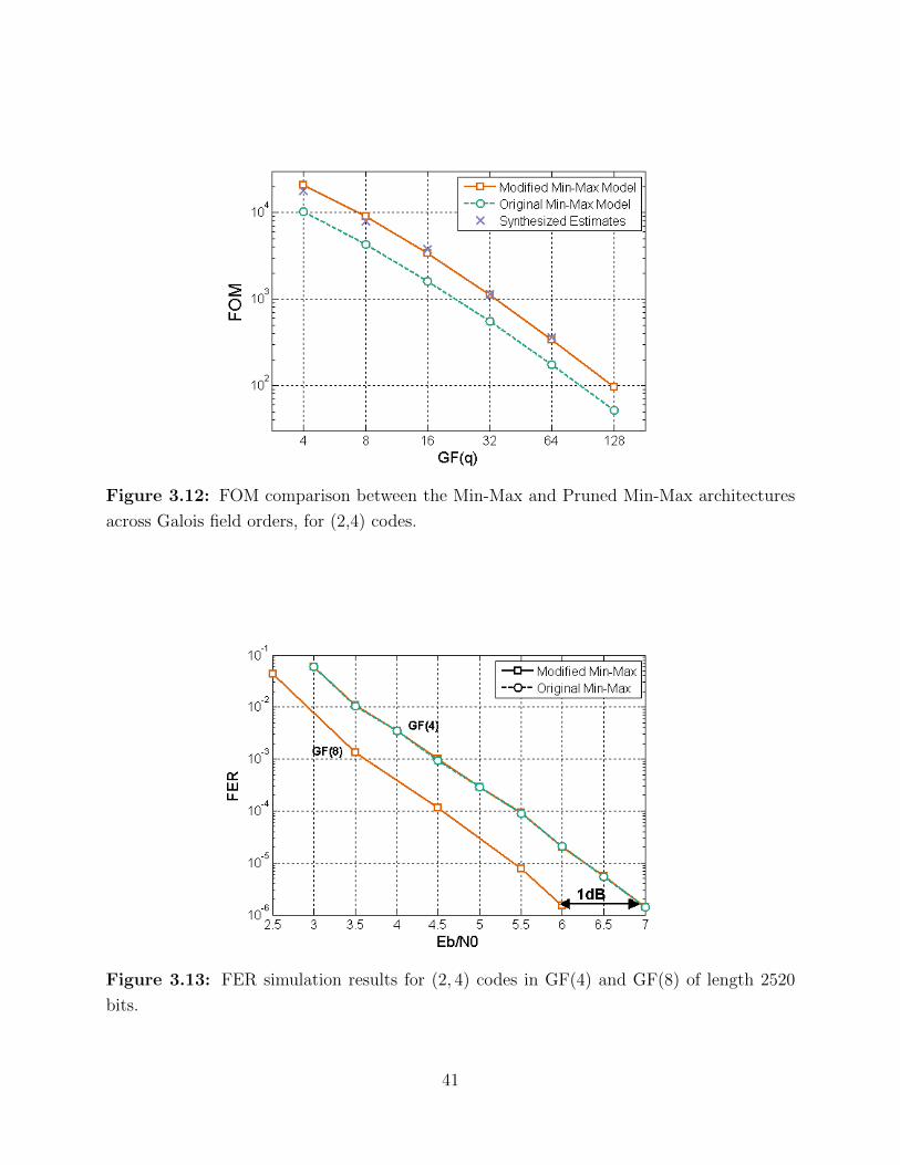
Figure 3.12: FOM comparison between the Min-Max and Pruned Min-Max architectures
across Galois field orders, for (2,4) codes.
Figure 3.13: FER simulation results for (2, 4) codes in GF(4) and GF(8) of length 2520
bits.
41
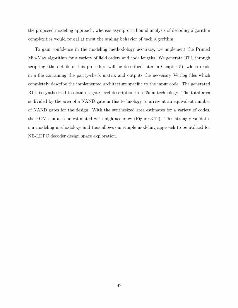
the proposed modeling approach, whereas asymptotic bound analysis of decoding algorithm
complexities would reveal at most the scaling behavior of each algorithm.
To gain confidence in the modeling methodology accuracy, we implement the Pruned
Min-Max algorithm for a variety of field orders and code lengths. We generate RTL through
scripting (the details of this procedure will be described later in Chapter 5), which reads
in a file containing the parity-check matrix and outputs the necessary Verilog files which
completely describe the implemented architecture specific to the input code. The generated
RTL is synthesized to obtain a gate-level description in a 65nm technology. The total area
is divided by the area of a NAND gate in this technology to arrive at an equivalent number
of NAND gates for the design. With the synthesized area estimates for a variety of codes,
the FOM can also be estimated with high accuracy (Figure 3.12). This strongly validates
our modeling methodology and thus allows our simple modeling approach to be utilized for
NB-LDPC decoder design space exploration.
42
CHAPTER 4
Logarithmic Quantization Scheme for the Min-Max
Algorithm
4.1 Prior Art . . . . . . . . . . . . . . . . . . . . . . . . . . . . . . . . . . . 44
4.2 Computational Complexity . . . . . . . . . . . . . . . . . . . . . . . . . . 46
4.2.1 Derivation of Computational Complexity of the Min-Max Algorithm . . 46
4.2.2 Routing Overhead . . . . . . . . . . . . . . . . . . . . . . . . . . . . . . 48
4.3 Quantization Effects . . . . . . . . . . . . . . . . . . . . . . . . . . . . . 48
4.4 The Logarithmic Quantization Scheme . . . . . . . . . . . . . . . . . . . 52
4.4.1 The Proposed Scheme . . . . . . . . . . . . . . . . . . . . . . . . . . . . 52
4.4.2 Error Rate Comparison . . . . . . . . . . . . . . . . . . . . . . . . . . . 53
4.4.3 Estimated Computational Complexity . . . . . . . . . . . . . . . . . . . 54
43
A very important consideration in the hardware implementation of any DSP algorithm
is the finite wordlength and its effects on the algorithm performance. In the case of LDPC
decoders, fixed point quantization is used and the number of bits are often highly limited.
This is due to the nature of LDPC decoding. Many of the commonly used decoding algo-
rithms can be broken down into fairly simple operations, such as summation, maximum,
minimum, and so on. The inherent complexity in decoding stems from the sheer number of
these operations that must be performed. Therefore, while there is not much room for sim-
plification of the operations themselves, quantization can make quite a significant impact in
terms of overall cost of implementation. However, designers may fall into certain traps when
deciding on the bit width used, negatively impacting the decoder performance. This chapter
will discuss and investigate the impact of quantization on the error profile. In addition, we
will propose what we call the logarithmic quantization scheme which does not significantly
degrade the coding gain but greatly alleviates the hardware implementation cost.
The contents of this chapter are mostly published in [33].
4.1 Prior Art
Two important considerations in practical ASIC implementations of NB-LDPC decoders are
the wordlength, or the number of bits used to represent a number, and correspondingly the
quantization scheme, or how these bits are used to represent what numbers. The wordlength
has an obvious direct impact on the hardware implementation cost; not only are the com-
putation costs a function of the wordlength, but also the signal routing overhead, notorious
for LDPC decoders, can change with the wordlength. On the other hand, the quantization
scheme affects the error rates achieved by the implemented decoder. Therefore, the choices
of these design parameters are of utmost importance in the design of hardware implemen-
tations of these decoders, because they affect both the coding gain and the implementation
costs. In the case of binary LDPC code decoders, the random-like interconnect connecting
the nodes are known to be a bottleneck in hardware implementations, whereas the compu-
tational complexity is relatively low [11]. Therefore, wordlength reduction solutions such as
44
the “Split-Row Threshold” algorithm [13] successfully reduce the hardware cost by improv-
ing the logic utilization. However in the case of NB-LDPC decoders which naturally have a
higher logic utilization [29], the check node computations are of primary concern in terms of
attempting to reduce the hardware complexity, although the interconnect of course should
not be disregarded.
A popular and straightforward method for selecting the wordlength and quantization
parameters in published NB-LDPC decoder implementations [19,22,34] is to choose a quan-
tization scheme with minimum wordlength that does not degrade the frame error rate (FER)
in simulations. This has often lead to a solution of five (or more) quantization bits, with three
integer and two fractional bits being particularly popular [19, 22, 34]. However, the imple-
mentation solutions remain costly in area, and thus a more aggressive wordlength reduction
is desirable. Meanwhile, the minimum FER in simulation in these works for determining the
wordlength is limited to ∼ 10−5, which seems rather simplistic. In fact, it is known in the
case of binary LDPC code decoders that the quantization scheme can be a source of error
floors [35,36]. Thus, previously published NB-LDPC code decoder implementations are not
only too costly in silicon area to be practical, but also potentially vulnerable to error floor
regions, due to the limited number of bits reserved for integer representation. While sophis-
ticated non-uniform quantization schemes have been proposed to mitigate the rise of error
floors in binary LDPC codes [35, 36], the effect of complicating the quantization scheme on
the decoder implementation complexity has been ignored. This is potentially an even more
significant problem for NB-LDPC code decoders of higher field orders, and traditionally,
uniform quantization schemes have been favored for their simplicity [15]. Interestingly, a
unique aspect of the Min-Max decoding algorithm for NB-LDPC codes is that the noto-
riously costly check node computations require only comparison operations. This insight
instigates the search for a monotonic (but not necessarily uniform) quantization scheme that
not only performs well in the decoding sense, but also reduces the overall hardware cost
by maintaining enough simplicity so as to not incur a large cost overhead for implementing
other arithmetic where necessary (such as variable nodes).
45
4.2 Computational Complexity
To gain a sense of the hardware implementation cost, we analyze the computational com-
plexity per iteration of the Min-Max algorithm. Our unit of measurement will be “operations
per bit,” or OP/b, where an operation is a 2-input addition (subtraction) or comparison.
For example, the computational complexity to add two b-bit numbers together would be b
OP/b (we assume that adders saturate), and the complexity to find the minimum of n b-bit
numbers would be (n − 1)b OP/b. Roughly speaking, 1 OP/b corresponds to a full-adder
cell and a D flip flop, because those cells would correspond to the cost to implement a single
bit addition. The costs of b-bit additions and b-bit comparisons are confirmed to be simi-
lar through synthesis estimates. Because we would like to use this complexity measure to
compare the implementation costs of codes with various q, we will normalize the total cost,
Ctot, by the length of the codeword in bits, B. Our final result, Ctot/B, can be interpreted
as the computational complexity required per iteration to process and decode one bit of the
output codeword.
4.2.1 Derivation of Computational Complexity of the Min-Max Algorithm
For a decoder of an NB-LDPC code defined by an N ×M parity check matrix, N , M , dv,
and dc are related by the total number of edges E in the Tanner graph:
E = Ndv = Mdc. (4.1)
Because each GF(q) symbol contains log2 q bits:
B = N log2 q. (4.2)
Let bv and bc be the wordlengths of numbers in the variable node computations and check
node computations, respectively. If Cv is the number of operations in a single variable
46
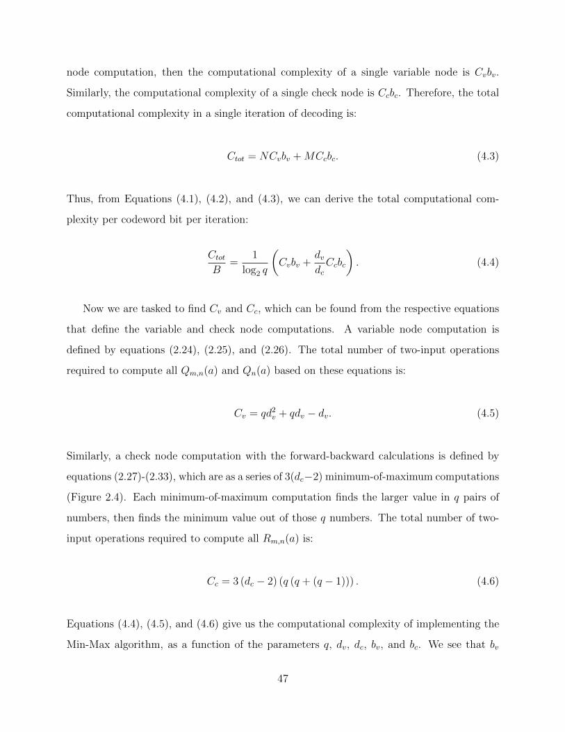
node computation, then the computational complexity of a single variable node is Cvbv.
Similarly, the computational complexity of a single check node is Ccbc. Therefore, the total
computational complexity in a single iteration of decoding is:
Ctot = NCvbv +MCcbc. (4.3)
Thus, from Equations (4.1), (4.2), and (4.3), we can derive the total computational com-
plexity per codeword bit per iteration:
Ctot
B=
1
log2 q
(Cvbv +
dvdcCcbc
). (4.4)
Now we are tasked to find Cv and Cc, which can be found from the respective equations
that define the variable and check node computations. A variable node computation is
defined by equations (2.24), (2.25), and (2.26). The total number of two-input operations
required to compute all Qm,n(a) and Qn(a) based on these equations is:
Cv = qd2v + qdv − dv. (4.5)
Similarly, a check node computation with the forward-backward calculations is defined by
equations (2.27)-(2.33), which are as a series of 3(dc−2) minimum-of-maximum computations
(Figure 2.4). Each minimum-of-maximum computation finds the larger value in q pairs of
numbers, then finds the minimum value out of those q numbers. The total number of two-
input operations required to compute all Rm,n(a) is:
Cc = 3 (dc − 2) (q (q + (q − 1))) . (4.6)
Equations (4.4), (4.5), and (4.6) give us the computational complexity of implementing the
Min-Max algorithm, as a function of the parameters q, dv, dc, bv, and bc. We see that bv
47
and bc appear only in equation (4.4) and thus directly impact the computational complexity.
It is important to note that if Cv or Cc change due to some algorithmic modifications, the
overall complexity Ctot will change but the impact of the wordlengths still remains as is in
equation (4.4). For example, if bv and bc are both reduced by a factor of two, then Ctot will
also be reduced by the same factor, regardless of the specific algorithm.
4.2.2 Routing Overhead
Although not part of the computational complexity of the defining equations, the routing
of signals is a significant overhead in the implementation of these decoders and thus must
be considered. Although the logic utilization impact of the routing is difficult to estimate,
quantified comparisons can be made by counting the required number of wires for the in-
terconnect. As described in Equation (4.1), there are E output messages from all variable
nodes, and E output messages from all check nodes. Each message consists of q LLRs, each
of which are represented with either bv or bc bits. Therefore, in a fully parallel architecture,
the total number of wires W required for these connections is:
W = qE (bv + bc) . (4.7)
Therefore, the routing interconnect is also directly impacted by bv and bc. Architectural
modifications, for example to serialize the node computations, or algorithmic modifications,
for example to maintain only the nm < q most important LLRs in each message, will change
the total number W but a large portion of W will still be linearly related to (bv + bc).
4.3 Quantization Effects
We will now study the impact of the wordlength and quantization scheme on the performance
of NB-LDPC decoder, particularly in the error-floor region. Through discussion of the error
profile, we will justify that the maximum representable number of messages is the main
48
Figure 4.1: FER curves for GF(16), (dv, dc) = (3, 6), (378, 189) code, for selected quanti-
zation schemes, and K = 20.
quantization design parameter which determines the performance of quantized NB-LDPC
decoders in error floor region. In particular, we observe that most of the so-called “non-
absorbing set errors” and “oscillation errors” are corrected as we increase the maximum
representable number of the messages in our quantization scheme. This reduced number
of errors results in a better error floor performance for quantizations with large maximum
representable numbers.
In this manuscript, a fixed-point quantization scheme with b total bits and f fractional
bits is denoted as “ubdf” (u for uniform). It is noted that f need not be positive, and a
“negative” number of fractional bits can be used to increase the maximum representable
number at the cost of precision.
The FER curves for various wordlengths and quantization schemes are simulated for a
GF(16), (dv, dc) = (3, 6), (378, 189) code over the binary additive white Gaussian noise (BI-
AWGN) channel (Figure 4.1). The u8d2 scheme employs a large number of bits and has good
precision, and is plotted as a point of reference. We first observe that some quantizations
49

schemes introduce an early error-floor region. In fact, the u3d0 and the u5d2 schemes,
which have a similar maximum representable number (≈ 7), have similar error-floor regions.
Furthermore, these curves cross over with the curve for the u3d(-1) scheme, which has a
larger maximum representable number (= 14) at SNR≈ 3.6dB. Thus, even though the u3d(-
1) scheme suffers from a performance degradation in the waterfall region, this scheme is
a better choice for implementation than are u3d0 or u5d2, assuming NB-LDPC codes are
employed in low-FER applications. A similar point of observation is that the u4d0 and u4d(-
1) schemes, which have the same number of bits, also have a cross over point at SNR≈4.4
dB. Again, the limited maximum representable number of the u4d0 scheme introduces an
error floor region which is not observed for quantization schemes with larger maximum
representable numbers.
Additionally, we observe that quantization schemes with similar precisions (u3d0 and
u4d0, for example) initially have overlapping waterfall curves, until their limited maximum
representable number yields their respective error floor regions. This phenomenon of the pre-
cision controlling the performance in the waterfall region and the maximum representable
number determining the location of the error floor is observed in simulations for codes with
varying field orders and rates. Therefore, we empirically conclude that the precision deter-
mines the performance in the waterfall region, whereas the maximum representable number
determines the location of the error floor regime.
To gain insight into the causes of different error curve shapes, the error profile of selected
schemes at SNR= 4.4dB are observed for the GF(16), (dv, dc) = (3, 6), (378, 189) code (Table
4.1). We categorize the errors at the output of the Min-Max decoder into the following
classes:
Fixed-point errors (not to be confused with fixed-point number representation):
· Absorbing-set (AS) errors : the decoder converges to an absorbing set [32].
· Non-absorbing-set (NAS) errors : the decoder converges to a subset of variable nodes
which does not satisfy absorbing set conditions.
50
Non-fixed-point errors :
· Oscillating (OS) errors : the output of the decoder oscillates between two errors.
· Non-converging (NC) errors : the decoder does not converge to any specific object.
The distributions of error types for each quantization scheme can be attributed to the
maximum representable numbers, which affect the occurrence of message saturation. For
example, a low maximum leads to messages consisting of many LLRs that equals the max-
imum after a small number of iterations. This causes the more frequent occurrence of OS
and NAS errors in quantization schemes such as u3d0 and u5d2. Because NB-LDPC codes
will target applications requiring very low error rates, it is imperative for the quantization
scheme in ASIC implementations to have the ability to represent large numbers in order to
avoid message saturation that causes the aforementioned errors. Therefore, for a given num-
ber of uniformly quantized bits, it is better to increase the maximum representable number
by trading off precision so that the waterfall curve may shift but no error floor arises, rather
than to increase the precision so as to match the waterfall curve to ideal values in high FER
regions but generate an avoidable error floor region.
The message saturation phenomenon can also be observed in the error evolution, or the
number of symbol errors as a function of the iteration count. This error evolution is plotted
for the u3d0 and u8d2 quantization schemes (Figure 4.2). We observe that for u3d0, the
errors of the decoder are generally stable after a few iterations. Therefore, increasing the
maximum number of iterations does not improve the performance. On the other hand, many
errors for u8d2 are not stabilized (i.e., not converged to a fixed point) before the decoder
reaches its maximum number of iterations. As a result, increasing the maximum number
of iterations would improve the performance of the decoder since it enables the decoder to
converge to a fixed point (most probably the correct codeword).
51
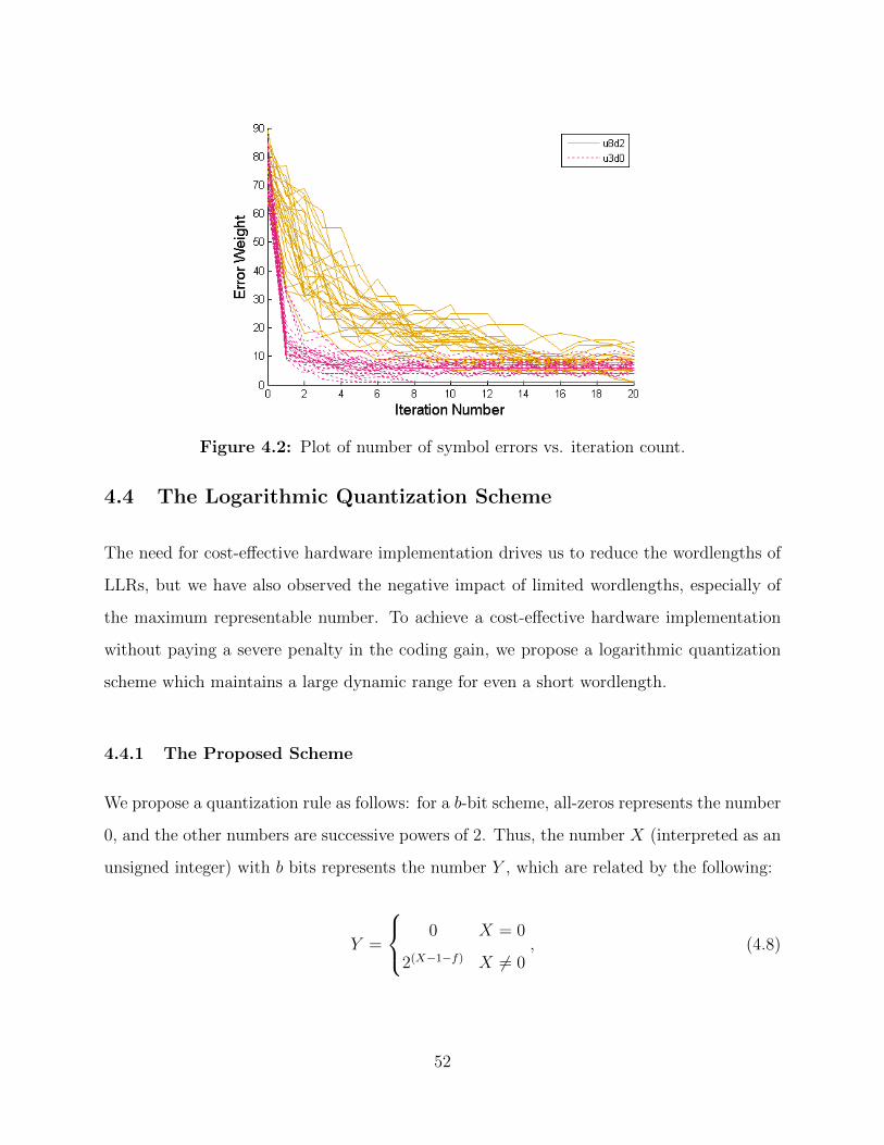
Figure 4.2: Plot of number of symbol errors vs. iteration count.
4.4 The Logarithmic Quantization Scheme
The need for cost-effective hardware implementation drives us to reduce the wordlengths of
LLRs, but we have also observed the negative impact of limited wordlengths, especially of
the maximum representable number. To achieve a cost-effective hardware implementation
without paying a severe penalty in the coding gain, we propose a logarithmic quantization
scheme which maintains a large dynamic range for even a short wordlength.
4.4.1 The Proposed Scheme
We propose a quantization rule as follows: for a b-bit scheme, all-zeros represents the number
0, and the other numbers are successive powers of 2. Thus, the number X (interpreted as an
unsigned integer) with b bits represents the number Y , which are related by the following:
Y =
⎧⎨⎩ 0 X = 0
2(X−1−f) X = 0, (4.8)
52
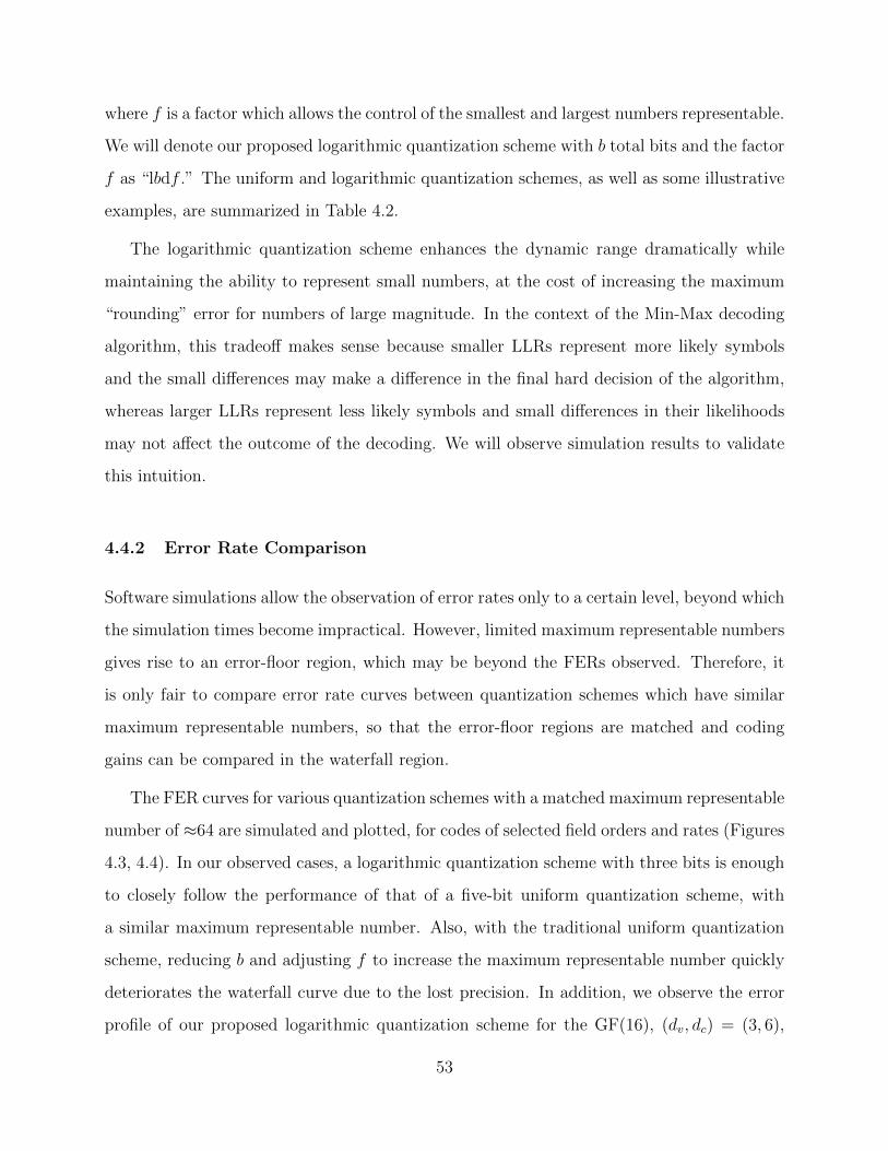
where f is a factor which allows the control of the smallest and largest numbers representable.
We will denote our proposed logarithmic quantization scheme with b total bits and the factor
f as “lbdf .” The uniform and logarithmic quantization schemes, as well as some illustrative
examples, are summarized in Table 4.2.
The logarithmic quantization scheme enhances the dynamic range dramatically while
maintaining the ability to represent small numbers, at the cost of increasing the maximum
“rounding” error for numbers of large magnitude. In the context of the Min-Max decoding
algorithm, this tradeoff makes sense because smaller LLRs represent more likely symbols
and the small differences may make a difference in the final hard decision of the algorithm,
whereas larger LLRs represent less likely symbols and small differences in their likelihoods
may not affect the outcome of the decoding. We will observe simulation results to validate
this intuition.
4.4.2 Error Rate Comparison
Software simulations allow the observation of error rates only to a certain level, beyond which
the simulation times become impractical. However, limited maximum representable numbers
gives rise to an error-floor region, which may be beyond the FERs observed. Therefore, it
is only fair to compare error rate curves between quantization schemes which have similar
maximum representable numbers, so that the error-floor regions are matched and coding
gains can be compared in the waterfall region.
The FER curves for various quantization schemes with a matched maximum representable
number of ≈64 are simulated and plotted, for codes of selected field orders and rates (Figures
4.3, 4.4). In our observed cases, a logarithmic quantization scheme with three bits is enough
to closely follow the performance of that of a five-bit uniform quantization scheme, with
a similar maximum representable number. Also, with the traditional uniform quantization
scheme, reducing b and adjusting f to increase the maximum representable number quickly
deteriorates the waterfall curve due to the lost precision. In addition, we observe the error
profile of our proposed logarithmic quantization scheme for the GF(16), (dv, dc) = (3, 6),
53
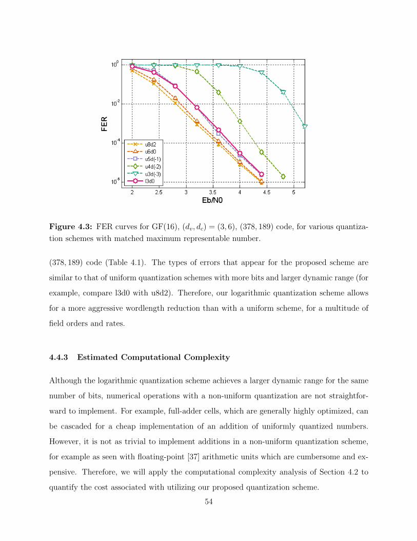
Figure 4.3: FER curves for GF(16), (dv, dc) = (3, 6), (378, 189) code, for various quantiza-
tion schemes with matched maximum representable number.
(378, 189) code (Table 4.1). The types of errors that appear for the proposed scheme are
similar to that of uniform quantization schemes with more bits and larger dynamic range (for
example, compare l3d0 with u8d2). Therefore, our logarithmic quantization scheme allows
for a more aggressive wordlength reduction than with a uniform scheme, for a multitude of
field orders and rates.
4.4.3 Estimated Computational Complexity
Although the logarithmic quantization scheme achieves a larger dynamic range for the same
number of bits, numerical operations with a non-uniform quantization are not straightfor-
ward to implement. For example, full-adder cells, which are generally highly optimized, can
be cascaded for a cheap implementation of an addition of uniformly quantized numbers.
However, it is not as trivial to implement additions in a non-uniform quantization scheme,
for example as seen with floating-point [37] arithmetic units which are cumbersome and ex-
pensive. Therefore, we will apply the computational complexity analysis of Section 4.2 to
quantify the cost associated with utilizing our proposed quantization scheme.
54
Figure 4.4: FER curves for GF(32), (dv, dc) = (3, 12), (300, 75) code, for various quantiza-
tion schemes with matched maximum representable number.
Our primary concern in the computational complexity are the check-node computations,
which usually dominate the complexity. However, an important aspect of the Min-Max de-
coding algorithm is that the only operations required in the check nodes are comparisons.
Therefore, as long as the quantization scheme of choice is monotonic, the check-node com-
putations can be implemented with the same logic as the uniform-quantization operations.
Because our logarithmic quantization scheme follows this, any wordlength reduction achieved
will directly reduce the computational complexity of the check-node computations.
On the other hand, variable-node computations contain sum operations. Therefore, at
the variable nodes, we convert the incoming messages into a uniformly quantized number,
and convert the outgoing messages into a logarithmically quantized number. Because the
numbers represented by the logarithmic quantization are powers of 2 (or zero), their repre-
sentation in the uniform domain is a one-hot number (or all zeros). Therefore, conversion
into the uniform domain is implemented with a simple binary-to-one-hot converter. Conver-
sion to the logarithmic domain is conducted by outputting the index of the most significant
bit that equals 1, and adding 1 to the output if the next bit also equals 1 (this implements
55
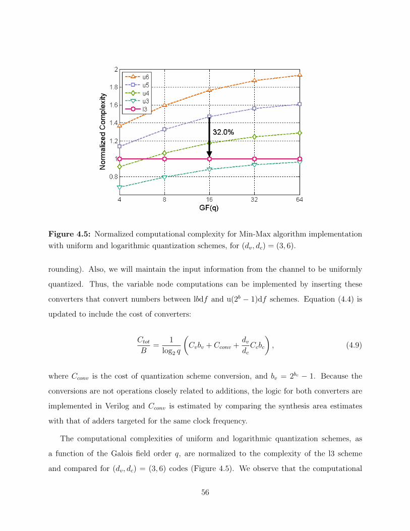
Figure 4.5: Normalized computational complexity for Min-Max algorithm implementation
with uniform and logarithmic quantization schemes, for (dv, dc) = (3, 6).
rounding). Also, we will maintain the input information from the channel to be uniformly
quantized. Thus, the variable node computations can be implemented by inserting these
converters that convert numbers between lbdf and u(2b − 1)df schemes. Equation (4.4) is
updated to include the cost of converters:
Ctot
B=
1
log2 q
(Cvbv + Cconv +
dvdcCcbc
), (4.9)
where Cconv is the cost of quantization scheme conversion, and bv = 2bc − 1. Because the
conversions are not operations closely related to additions, the logic for both converters are
implemented in Verilog and Cconv is estimated by comparing the synthesis area estimates
with that of adders targeted for the same clock frequency.
The computational complexities of uniform and logarithmic quantization schemes, as
a function of the Galois field order q, are normalized to the complexity of the l3 scheme
and compared for (dv, dc) = (3, 6) codes (Figure 4.5). We observe that the computational
56
complexity of the l3 scheme is less than that of the u4 scheme beyond GF(8), and the l3
scheme complexity approaches that of the u3 scheme as GF(q) increases. This is because
the complexity of the check node computation begins to dominate, but the logarithmic
scheme allows us to save on the complexity in the check nodes for trading off complexity
in the variable nodes. The savings by moving from a u5 scheme to the l3 scheme can
be calculated for a variety of GF(q) and (dv, dc), and is summarized in Table 4.3. For
our running example of a GF(16), (3, 6) code, employing the l3d0 quantization scheme
allows us to maintain a similar error correction curve as the u5d(-1) scheme, but reduce the
computational complexity by 32.0%. Similarly for the GF(32), (3, 12) code investigated in
Figure 4.4, the computational complexity reduction by moving from u5d(-1) to l3d0 is 36.7%.
As GF(q) increases, the overheads associated with implementing the proposed logarithmic
scheme diminish relative to the check node computational complexity, and the savings by
moving from u5 to l3 approach 40%. For any specific code, simulations comparing the coding
gains of uniform and logarithmic schemes can be used in conjunction with the computational
complexity analysis to calculate the savings achieved by utilizing the logarithmic scheme.
As for the interconnect, the expression for the number of wires (Equation (4.7)) remains
the same. Thus, a change in the wordlength will still directly impact the routing overhead.
However, in the logarithmic quantization scheme, the conversion logic can be placed at the
input and output of variable nodes, thus allowing all of the routing to be conducted with
the reduced wordlength. For example, for an l3 scheme, both bv = bc = 3 in Equation
(4.7). Therefore, the change in the number of wires is directly proportional to the change
in wordlength of the utilized scheme. For example, relative to a u5 scheme, the l3 scheme
reduces the number of wires by 40%. Thus, the logarithmic quantizations scheme is effective
in reducing both the total computational complexity, especially for higher field orders, as
well as the routing congestion.
We have identified that a quantization scheme which limits the maximum representable
number causes particular types of errors to appear more often and thus cause the error
floor region to rise. We have proposed a logarithmic quantization scheme that, when ap-
plied to ASIC implementations of Min-Max decoders, allows for a reduced wordlength while
57
maintaining a large dynamic range. These qualities result in the decoder maintaining good
coding gain and a suppressed error floor, as well as reduced total computational complex-
ity especially for higher field orders. While it is easy to overlook the significance of the
quantization scheme, the combined benefits of our proposed solution substantially eases the
complexity-performance trade-off, notorious for NB-LDPC decoders.
58
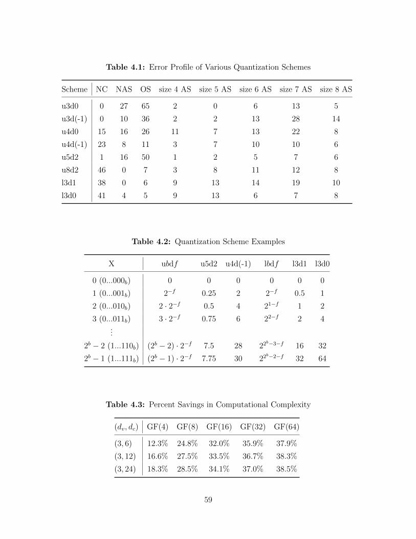
Table 4.1: Error Profile of Various Quantization Schemes
Scheme NC NAS OS size 4 AS size 5 AS size 6 AS size 7 AS size 8 AS
u3d0 0 27 65 2 0 6 13 5
u3d(-1) 0 10 36 2 2 13 28 14
u4d0 15 16 26 11 7 13 22 8
u4d(-1) 23 8 11 3 7 10 10 6
u5d2 1 16 50 1 2 5 7 6
u8d2 46 0 7 3 8 11 12 8
l3d1 38 0 6 9 13 14 19 10
l3d0 41 4 5 9 13 6 7 8
Table 4.2: Quantization Scheme Examples
X ubdf u5d2 u4d(-1) lbdf l3d1 l3d0
0 (0...000b) 0 0 0 0 0 0
1 (0...001b) 2−f 0.25 2 2−f 0.5 1
2 (0...010b) 2 · 2−f 0.5 4 21−f 1 2
3 (0...011b) 3 · 2−f 0.75 6 22−f 2 4...
2b − 2 (1...110b) (2b − 2) · 2−f 7.5 28 22b−3−f 16 32
2b − 1 (1...111b) (2b − 1) · 2−f 7.75 30 22b−2−f 32 64
Table 4.3: Percent Savings in Computational Complexity
(dv, dc) GF(4) GF(8) GF(16) GF(32) GF(64)
(3, 6) 12.3% 24.8% 32.0% 35.9% 37.9%
(3, 12) 16.6% 27.5% 33.5% 36.7% 38.3%
(3, 24) 18.3% 28.5% 34.1% 37.0% 38.5%
59
CHAPTER 5
Implementation of FPGA Platform for Code
Performance Evaluation
5.1 Architecture . . . . . . . . . . . . . . . . . . . . . . . . . . . . . . . . . . 61
5.2 Design Methodology . . . . . . . . . . . . . . . . . . . . . . . . . . . . . 67
5.3 Results . . . . . . . . . . . . . . . . . . . . . . . . . . . . . . . . . . . . . 68
5.3.1 Hardware Resource Utilization on FPGA . . . . . . . . . . . . . . . . . 68
5.3.2 Frame Error Rate Simulations . . . . . . . . . . . . . . . . . . . . . . . 72
60
Simulation of NB-LDPC decoding is an essential research tool commonly utilized to eval-
uate the performance of NB-LDPC codes in terms of the error rate. Software implementation
of decoding algorithms are employed to observe and validate the performance of many design
parameter choices, such as the parity-check matrix construction methodology, decoding al-
gorithm modifications, and so on. However, there is a limit to the error rate level which can
be observed in such simulations with software implementations, because beyond a certain
point, simulations simply take much too long even when a large amount of computing power
is utilized for the problem. For example, to observe a frame error rate of 10−5, approximately
107 frames should be simulated. This is because to claim any frame error rate with statis-
tical significance, at least 100 frame errors (as a rule of thumb) at that signal-to-noise ratio
should be observed. Although exact simulation times vary with computing power as well as
simulation parameters, simulation times often become too long beyond frame error rates of
around 10−5 or 10−6, as is often observed as the limit of software simulations in published
works. Therefore, there is a strong demand for hardware acceleration of NB-LDPC decoding
simulations. However, not only is a hardware implementation of NB-LDPC decoding costly
(in hardware and engineer resources), but also maintaining enough flexibility to allow for
multiple tuning knobs in the simulation framework is quite tricky. In this chapter we discuss
the details of our implementation of a flexible FPGA platform for NB-LDPC decoding sim-
ulation acceleration, enabling the evaluation of code performance at lower frame error rates
relative to software solutions.
5.1 Architecture
The hardware architecture for the decoder comes hand in hand with the code construction
and parity-check matrix structure. In our platform, we would like to achieve as much flexi-
bility as possible to be able to simulate a variety of codes, without the architecture becoming
too inefficient or the design effort becoming too difficult.
The choice to restrict the possible codes to quasi-cyclic codes [38, 39] comes naturally.
While there do exist other code construction methods that yield coding gain benefits (such as
61
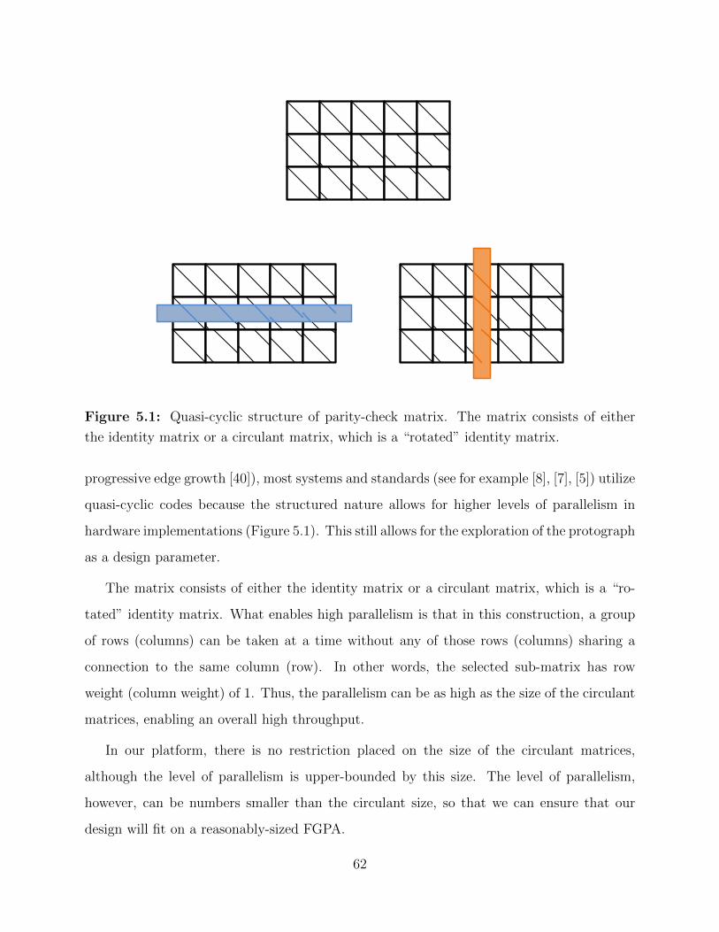
Figure 5.1: Quasi-cyclic structure of parity-check matrix. The matrix consists of either
the identity matrix or a circulant matrix, which is a “rotated” identity matrix.
progressive edge growth [40]), most systems and standards (see for example [8], [7], [5]) utilize
quasi-cyclic codes because the structured nature allows for higher levels of parallelism in
hardware implementations (Figure 5.1). This still allows for the exploration of the protograph
as a design parameter.
The matrix consists of either the identity matrix or a circulant matrix, which is a “ro-
tated” identity matrix. What enables high parallelism is that in this construction, a group
of rows (columns) can be taken at a time without any of those rows (columns) sharing a
connection to the same column (row). In other words, the selected sub-matrix has row
weight (column weight) of 1. Thus, the parallelism can be as high as the size of the circulant
matrices, enabling an overall high throughput.
In our platform, there is no restriction placed on the size of the circulant matrices,
although the level of parallelism is upper-bounded by this size. The level of parallelism,
however, can be numbers smaller than the circulant size, so that we can ensure that our
design will fit on a reasonably-sized FGPA.
62
Another design choice is the field order (GF(q)) over which the code is defined. For this
exercise we restrict our field order to be at GF(8). This is for the following reasons:
(1) Restriction to a single field order greatly increases simplicity and ease of implementa-
tion.
(2) Realistically speaking, the decoding algorithm of choice itself is not a fixed parameter
of the field order. For example, the EMS algorithm [23] only works for high field
orders. This is because only a subset of each message is passed between nodes, which
requires computational overhead to find this subset (for example, sorters in hardware).
However, the field order must be large enough so that a subset suffices as the message.
For example, only keeping 32 out of 256 message LLRs may result in a significant
hardware reduction without a noticeable degradation in coding gain, because 32 out
of 256 is a small fraction but 32 is still a large number. However, keeping 4 out of 8
message LLRs will probably actually increase the hardware cost due to the overhead
required to find the 4 to keep, but also at the same time the coding gain might be
significantly degraded because 4 is a small number of LLRs to keep.
(3) GF(8) is a significant improvement over binary LDPC codes yet the hardware cost
increase is only slightly outrageous.
Although the fixed GF(8) may seem restrictive, we will see in Chapter 7 that this is actually
not a bad design choice, even in terms of the coding gain.
Our final design parameters are the node degrees. We will confine ourselves to regular
codes for simplicity. In general, variable node degrees (dv) are small, whereas check node
degrees (dc) are large. Furthermore, check node calculations employ forward-backward com-
putations (see Chapter 2), which induces a large latency due to data dependencies (thus,
the lack of ability to parallelize). As a result, variations in the check node degree are fairly
simple to account for by simply changing the control logic. However, changes in the variable
node degree require slightly more work, simply because dv is small to begin with and even a
slight change requires a significant change in the implementation. Therefore, we choose to
63
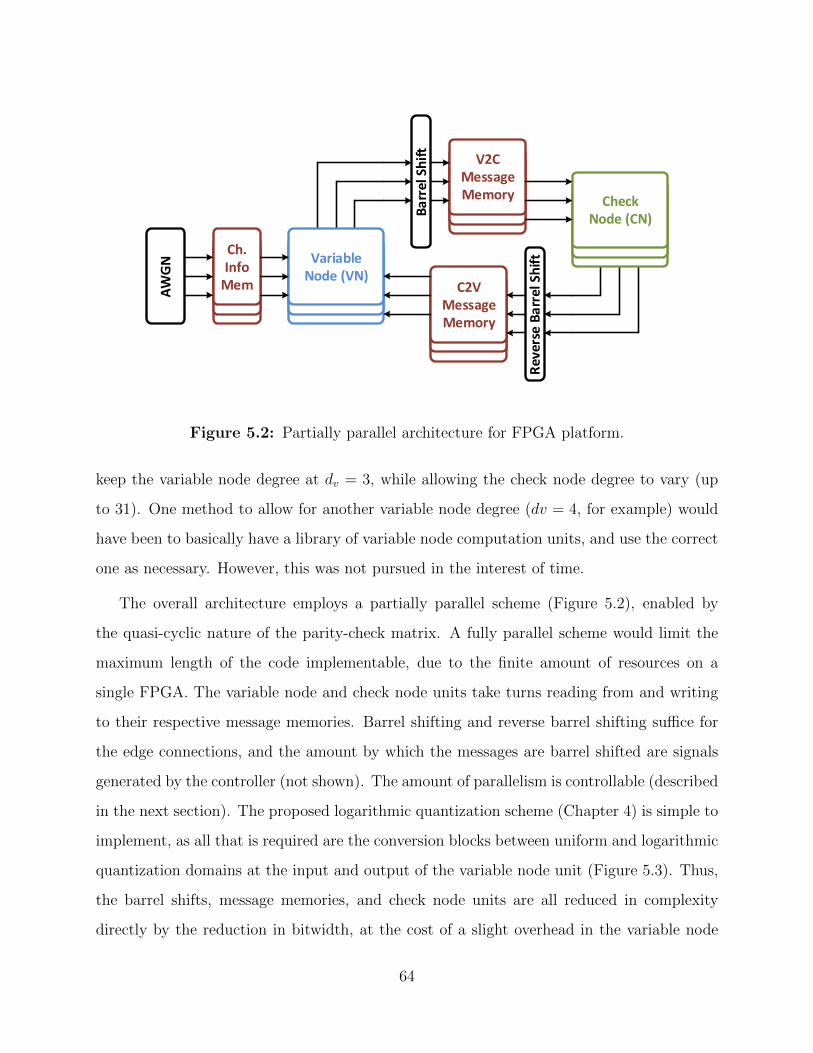
Ch. Info
Mem
Variable Node (VN)
C2V Message Memory
Check Node (CN)B
arr
el S
hif
t
V2C Message Memory
Rev
erse
Ba
rrel
Sh
ift
AW
GN
Figure 5.2: Partially parallel architecture for FPGA platform.
keep the variable node degree at dv = 3, while allowing the check node degree to vary (up
to 31). One method to allow for another variable node degree (dv = 4, for example) would
have been to basically have a library of variable node computation units, and use the correct
one as necessary. However, this was not pursued in the interest of time.
The overall architecture employs a partially parallel scheme (Figure 5.2), enabled by
the quasi-cyclic nature of the parity-check matrix. A fully parallel scheme would limit the
maximum length of the code implementable, due to the finite amount of resources on a
single FPGA. The variable node and check node units take turns reading from and writing
to their respective message memories. Barrel shifting and reverse barrel shifting suffice for
the edge connections, and the amount by which the messages are barrel shifted are signals
generated by the controller (not shown). The amount of parallelism is controllable (described
in the next section). The proposed logarithmic quantization scheme (Chapter 4) is simple to
implement, as all that is required are the conversion blocks between uniform and logarithmic
quantization domains at the input and output of the variable node unit (Figure 5.3). Thus,
the barrel shifts, message memories, and check node units are all reduced in complexity
directly by the reduction in bitwidth, at the cost of a slight overhead in the variable node
64
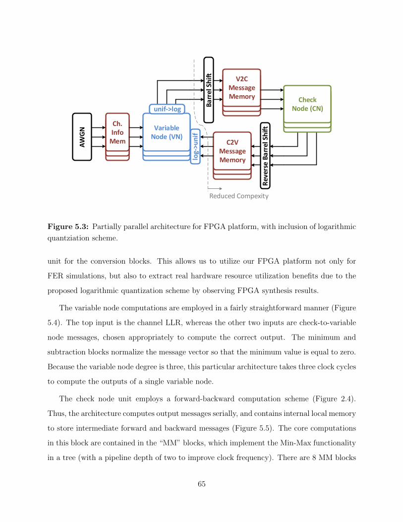
Ch. Info
Mem
Variable Node (VN)
C2V Message Memory
Check Node (CN)B
arr
el S
hif
t
V2C Message Memory
Rev
erse
Ba
rrel
Sh
ift
AW
GN
unif->log
log-
>un
ifReduced Compexity
Figure 5.3: Partially parallel architecture for FPGA platform, with inclusion of logarithmic
quantziation scheme.
unit for the conversion blocks. This allows us to utilize our FPGA platform not only for
FER simulations, but also to extract real hardware resource utilization benefits due to the
proposed logarithmic quantization scheme by observing FPGA synthesis results.
The variable node computations are employed in a fairly straightforward manner (Figure
5.4). The top input is the channel LLR, whereas the other two inputs are check-to-variable
node messages, chosen appropriately to compute the correct output. The minimum and
subtraction blocks normalize the message vector so that the minimum value is equal to zero.
Because the variable node degree is three, this particular architecture takes three clock cycles
to compute the outputs of a single variable node.
The check node unit employs a forward-backward computation scheme (Figure 2.4).
Thus, the architecture computes output messages serially, and contains internal local memory
to store intermediate forward and backward messages (Figure 5.5). The core computations
in this block are contained in the “MM” blocks, which implement the Min-Max functionality
in a tree (with a pipeline depth of two to improve clock frequency). There are 8 MM blocks
65
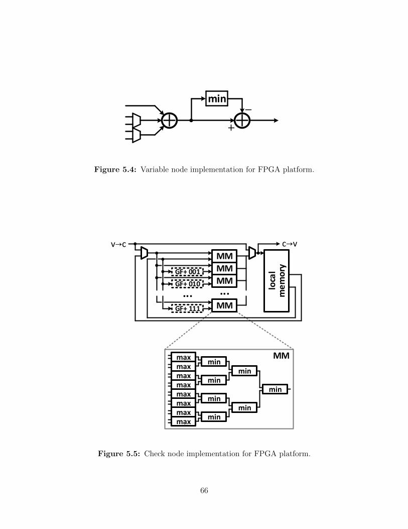
min
Figure 5.4: Variable node implementation for FPGA platform.
MM
GF+ 001 MM
GF+ 010 MM
GF+ 111 MM
loca
l m
em
ory
... ...
v→c c→v
maxmin
maxmax
minmax
min
minmax
minmaxmax
minmax
min
MM
Figure 5.5: Check node implementation for FPGA platform.
66
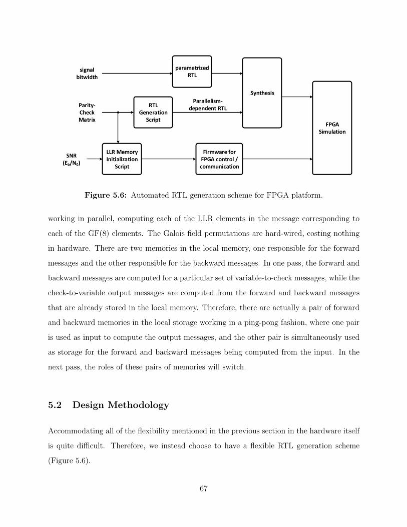
RTL Generation
Script
Parity-Check Matrix
Synthesis
parametrized RTL
Parallelism-dependent RTL
LLR Memory Initialization
Script
SNR (Eb/N0)
Firmware for FPGA control / communication
FPGASimulation
signal bitwidth
Figure 5.6: Automated RTL generation scheme for FPGA platform.
working in parallel, computing each of the LLR elements in the message corresponding to
each of the GF(8) elements. The Galois field permutations are hard-wired, costing nothing
in hardware. There are two memories in the local memory, one responsible for the forward
messages and the other responsible for the backward messages. In one pass, the forward and
backward messages are computed for a particular set of variable-to-check messages, while the
check-to-variable output messages are computed from the forward and backward messages
that are already stored in the local memory. Therefore, there are actually a pair of forward
and backward memories in the local storage working in a ping-pong fashion, where one pair
is used as input to compute the output messages, and the other pair is simultaneously used
as storage for the forward and backward messages being computed from the input. In the
next pass, the roles of these pairs of memories will switch.
5.2 Design Methodology
Accommodating all of the flexibility mentioned in the previous section in the hardware itself
is quite difficult. Therefore, we instead choose to have a flexible RTL generation scheme
(Figure 5.6).
67

The inputs to an FER simulation that directly impact the hardware are the signal
bitwidths (quantization scheme), and the parity-check matrix itself. The signal bitwidth
is taken care of by simply parameterizing the Verilog and changing the appropriate parame-
ter at the top level. Most of the RTL can be taken care of in this way, especially lower level
computational blocks such as the variable-node and check-node units. There are portions of
the RTL, however, that depend on the parity-check matrix and/or the amount of parallelism,
and these portions cannot be accommodated by a simple parametrization of the RTL. For
example, the module that instantiates all of the variable-node units must know how many
modules to instantiate. Also, the control logic that addresses the message memories must
know the locations of the non-zero elements within the parity-check matrix as well as the
amount of parallelism. Therefore, these modules (the top level modules, barrel shifters, and
control logic) are generated by a script that takes in the parallelism and the parity-check
matrix as input. These generated Verilog files, along with the parametrized Verilog files, are
taken together into synthesis to generate the bitstream to program the FPGA.
The SNR of the simulation changes the way the channel LLRs are initialized. These
initialization values (which also depend on the code rate) are also generated upfront, and
used by the firmware that controls the programmed FPGA to initialize the memories. The
firmware can be edited to also control parameters such as the clock frequency, maximum
number of iterations, maximum number of frames to simulate, and so on.
5.3 Results
In this section we discuss some of the results obtained from the implemented FPGA platform.
5.3.1 Hardware Resource Utilization on FPGA
Due to the flexibility provided by the automated RTL generation process, we can compare
the FPGA resource utilizations across varying design parameters. Of note, we are specifically
interested in the effect of the quantization scheme. Thus, we synthesize several designs across
68

Table 5.1: FPGA Synthesis Results (3,24) L130 P65
Bitwidth Logic Util. CombinationalALUTs
Total BlockMemory Bits Max Clock Freq
Synthesis CPUTime (minutes)
3 41 %127,021(30 %)
4,838,928(23 %) 87.2 MHz 147
4 48 %150,775(35 %)
5,931,536(28 %) 74.8 MHz 349
5 58 %180,788(43 %)
6,857,744(32 %) 71.0 MHz 508
6 67 %206,960(49 %)
7,783,952(37 %) 64.9 MHz 521
3 log 45 %155,893(37 %)
8,399,120(40 %) 87.9 MHz 171
varying codes and bitwidths and compare the synthesis results (Tables 5.1, 5.2, 5.3). In the
tables, L indicates the circulant size of the parity-check matrix and P indicates the amount
of parallelism.
It is noted that the “Total Block Memory Bits’ column is not an accurate reflection of the
actual required amount of memory, due to a design procedure limitation. In FPGA synthesis,
block RAM modules are utilized for memory, which have modular address spaces and word
bitwidths. If the amount of parallelism increases, while the total number of required bits of
storage does not change, the number of RAM ports will increase, and thus the number of
bits per RAM block decreases. However, to facilitate the design of the FPGA platform, the
address space of the block RAM used in the design was not optimized for larger amounts
of parallelism, leading to an excessive reported memory usage. One exception is the last
row of Table 5.3, where the address space of the block RAM used for storing channel LLR
information was halved (to make the design fit).
The effects of the bitwidth within the realm of the conventional uniform quantization
scheme are fairly obvious; the logic utilization increases, the combinational ALUT utiliza-
tion increases, the required memory increases, the maximum clock frequency of operation
69
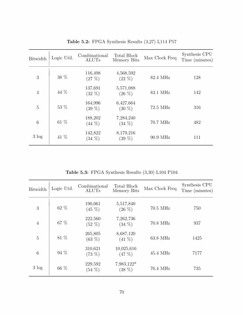
Table 5.2: FPGA Synthesis Results (3,27) L114 P57
Bitwidth Logic Util. CombinationalALUTs
Total BlockMemory Bits Max Clock Freq
Synthesis CPUTime (minutes)
3 38 %116,498(27 %)
4,568,592(22 %) 82.4 MHz 128
4 44 %137,691(32 %)
5,571,088(26 %) 83.1 MHz 142
5 53 %164,996(39 %)
6,427,664(30 %) 72.5 MHz 316
6 61 %188,202(44 %)
7,284,240(34 %) 70.7 MHz 482
3 log 41 %142,822(34 %)
8,179,216(39 %) 90.9 MHz 111
Table 5.3: FPGA Synthesis Results (3,30) L104 P104
Bitwidth Logic Util. CombinationalALUTs
Total BlockMemory Bits Max Clock Freq
Synthesis CPUTime (minutes)
3 62 %190,061(45 %)
5,517,840(26 %) 70.5 MHz 750
4 67 %222,560(52 %)
7,262,736(34 %) 70.8 MHz 937
5 81 %265,805(63 %)
8,687,120(41 %) 63.8 MHz 1425
6 94 %310,621(73 %)
10,025,616(47 %) 45.4 MHz 7177
3 log 66 %229,592(54 %)
7,983,122*(38 %) 76.4 MHz 735
70
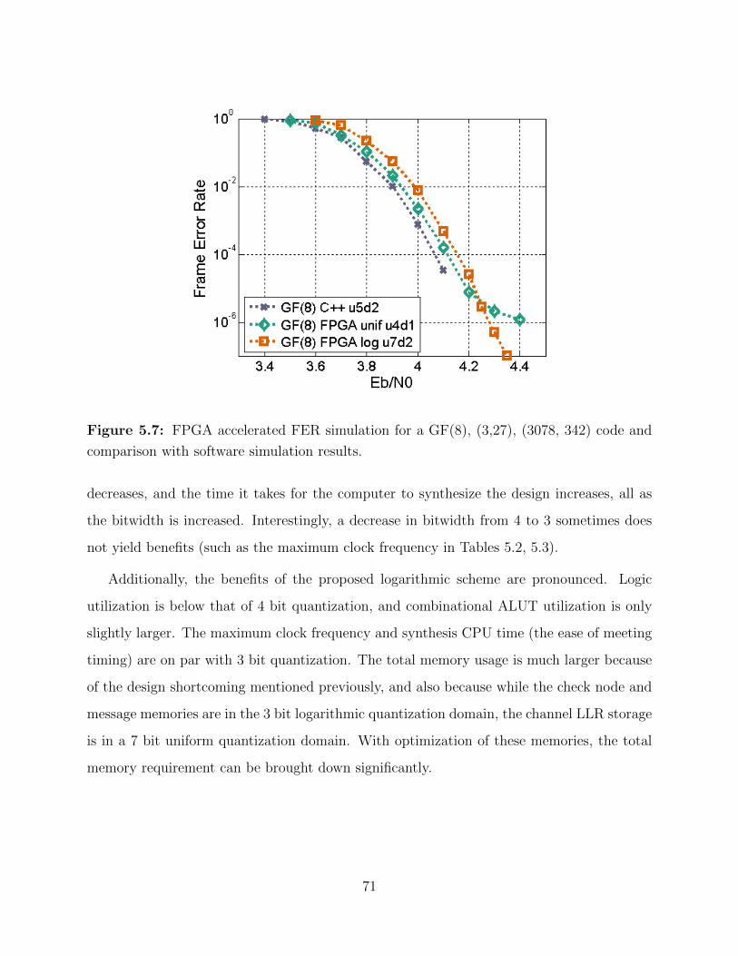
Figure 5.7: FPGA accelerated FER simulation for a GF(8), (3,27), (3078, 342) code and
comparison with software simulation results.
decreases, and the time it takes for the computer to synthesize the design increases, all as
the bitwidth is increased. Interestingly, a decrease in bitwidth from 4 to 3 sometimes does
not yield benefits (such as the maximum clock frequency in Tables 5.2, 5.3).
Additionally, the benefits of the proposed logarithmic scheme are pronounced. Logic
utilization is below that of 4 bit quantization, and combinational ALUT utilization is only
slightly larger. The maximum clock frequency and synthesis CPU time (the ease of meeting
timing) are on par with 3 bit quantization. The total memory usage is much larger because
of the design shortcoming mentioned previously, and also because while the check node and
message memories are in the 3 bit logarithmic quantization domain, the channel LLR storage
is in a 7 bit uniform quantization domain. With optimization of these memories, the total
memory requirement can be brought down significantly.
71
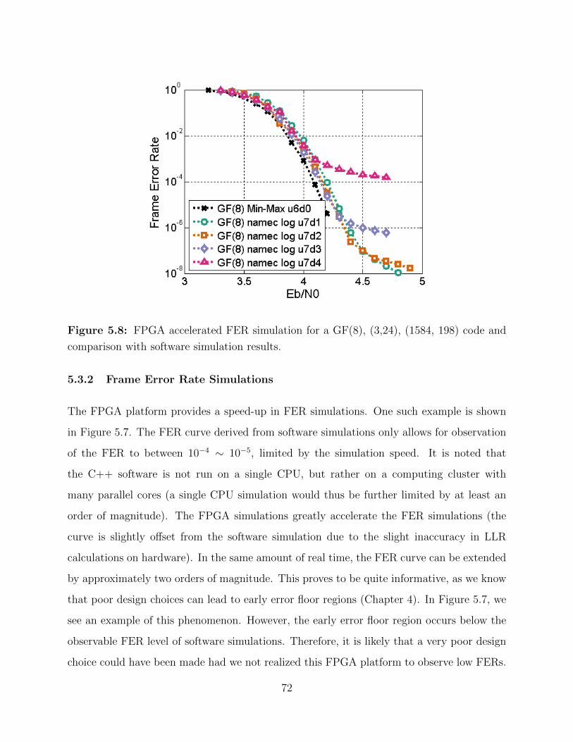
Figure 5.8: FPGA accelerated FER simulation for a GF(8), (3,24), (1584, 198) code and
comparison with software simulation results.
5.3.2 Frame Error Rate Simulations
The FPGA platform provides a speed-up in FER simulations. One such example is shown
in Figure 5.7. The FER curve derived from software simulations only allows for observation
of the FER to between 10−4 ∼ 10−5, limited by the simulation speed. It is noted that
the C++ software is not run on a single CPU, but rather on a computing cluster with
many parallel cores (a single CPU simulation would thus be further limited by at least an
order of magnitude). The FPGA simulations greatly accelerate the FER simulations (the
curve is slightly offset from the software simulation due to the slight inaccuracy in LLR
calculations on hardware). In the same amount of real time, the FER curve can be extended
by approximately two orders of magnitude. This proves to be quite informative, as we know
that poor design choices can lead to early error floor regions (Chapter 4). In Figure 5.7, we
see an example of this phenomenon. However, the early error floor region occurs below the
observable FER level of software simulations. Therefore, it is likely that a very poor design
choice could have been made had we not realized this FPGA platform to observe low FERs.
72
Figure 5.8 shows another example of the gravity of the quantization scheme choice. As
the decimal point is shifted to the left, the error floor region rises, even with the logarithmic
quantization scheme. However, due to the error floor levels, it is highly likely that we would
only have been able to observe the poorest one in Figure 5.8 with software, again due to the
speed limitation. However, with the FPGA platform, we are able to distinctively claim that
the effect of the quantization scheme on the error floor is gradual, as we had suspected.
Thus, the FPGA prototyping effort has proven to be effective in not only evaluating
the effect on the hardware implementation cost of decoder parameter choices, but also in
accelerating FER simulations in order to be able to observe phenomena at lower FER levels.
We can conclude with higher confidence that the logarithmic quantization scheme is able
to suppress the hardware implementation cost effectively while maintaining superior coding
gain characteristics.
73
CHAPTER 6
Augmented Hard-Decision Based Decoding Algorithm
and Combination with Soft Decoding
6.1 Iterative Hard-Decision Based Majority Logic Decoding . . . . . . . . . . 76
6.1.1 Augmented IHRB-MLGD . . . . . . . . . . . . . . . . . . . . . . . . . . 77
6.1.2 Detection of Erasure Condition . . . . . . . . . . . . . . . . . . . . . . . 79
6.2 Software Simulation Results . . . . . . . . . . . . . . . . . . . . . . . . . 80
6.3 Combination with the Min-Max Algorithm . . . . . . . . . . . . . . . . . 83
74
It is difficult to yield an efficient hardware implementation solely based on soft decoding
algorithms such as the Min-Max algorithm, because the severe complexity cannot be dimin-
ished too much before a non-negligible coding gain penalty arises. At the extreme, crude
decoding methods such as hard-decision based algorithms aimed at simplification generally
yields extremely poor coding gain and potentially very high error floors. What we would
like to achieve is the best of both worlds: good coding gain and low error floor of the soft
decoding algorithm, and the computational efficiency of the hard decoding algorithm.
The key observation we make is that in a high-SNR, low-FER regime, most of the time
a soft-decision decoding is unnecessary to arrive at the correct codeword. For example, if at
a particular SNR a soft decoder can achieve an FER of 10−9 and a hard decoder an FER
of 10−2, then although the hard decoder has terrible coding gain, the effort put into all the
computations of the soft decoder was probably only really necessary about 1% of the time.
In fact, as long as the errors made by the hard decoder are detectable errors, then we can
initially let the crude decoder attempt to decode the received word, and only have the soft
decoder activated when the hard decoder fails. This strategy has the potential to yield great
benefits in the hardware implementation, because most of the time the decoder will exhibit
properties (power consumption, throughput, etc.) of the hard decoder, while the coding gain
performance can approach that of the soft decoder.
It remains for us to find a “crude” decoding algorithm appropriate for this strategy. The
suitable algorithm must satisfy several properties:
· The algorithm must have very low computational complexity.
· The algorithm must have a “good enough” waterfall regime (the coding gain loss
relative to the Min-Max algorithm cannot be excessive). This is because for some target
FER the crude algorithm should take care of most of the codewords for the hardware
implementation to reap the benefits due to reduced computational complexity.
· The algorithm can have a high error floor. The existence of a floor for the hard
algorithm does not matter because the residual errors will be cleaned up by the Min-
Max algorithm.
75
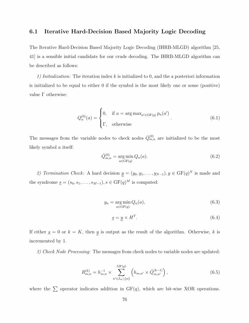
6.1 Iterative Hard-Decision Based Majority Logic Decoding
The Iterative Hard-Decision Based Majority Logic Decoding (IHRB-MLGD) algorithm [25,
41] is a sensible initial candidate for our crude decoding. The IHRB-MLGD algorithm can
be described as follows:
1) Initialization: The iteration index k is initialized to 0, and the a posteriori information
is initialized to be equal to either 0 if the symbol is the most likely one or some (positive)
value Γ otherwise:
Q(0)n (a) =
⎧⎪⎨⎪⎩0, if a = argmaxa′∈GF(q) pn(a
′)
Γ, otherwise
. (6.1)
The messages from the variable nodes to check nodes Q(0)m,n are initialized to be the most
likely symbol a itself:
Q(0)m,n = argmin
a∈GF(q)
Qn(a). (6.2)
2) Termination Check : A hard decision y = (y0, y1, . . . , yN−1), y ∈ GF(q)N is made and
the syndrome s = (s0, s1, . . . , sM−1), s ∈ GF(q)M is computed:
yn = argmina∈GF(q)
Qn(a), (6.3)
s = y ×HT . (6.4)
If either s = 0 or k = K, then y is output as the result of the algorithm. Otherwise, k is
incremented by 1.
3) Check Node Processing : The messages from check nodes to variable nodes are updated:
R(k)m,n = h−1
m,n ×GF(q)∑
n′∈Im\{n}
(hm,n′ × Q
(k−1)m,n′
), (6.5)
where the∑
operator indicates addition in GF(q), which are bit-wise XOR operations.
76
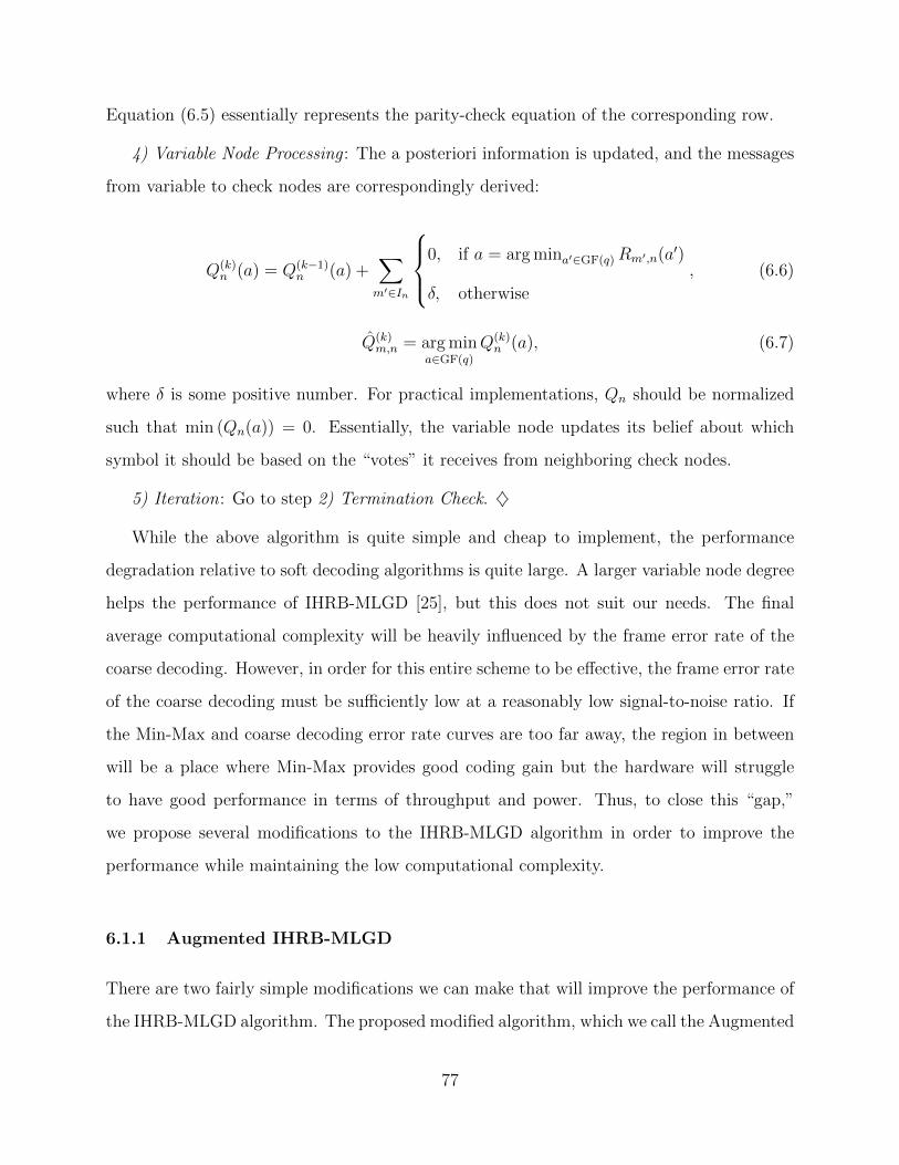
Equation (6.5) essentially represents the parity-check equation of the corresponding row.
4) Variable Node Processing : The a posteriori information is updated, and the messages
from variable to check nodes are correspondingly derived:
Q(k)n (a) = Q(k−1)
n (a) +∑m′∈In
⎧⎪⎨⎪⎩0, if a = argmina′∈GF(q) Rm′,n(a
′)
δ, otherwise
, (6.6)
Q(k)m,n = argmin
a∈GF(q)
Q(k)n (a), (6.7)
where δ is some positive number. For practical implementations, Qn should be normalized
such that min (Qn(a)) = 0. Essentially, the variable node updates its belief about which
symbol it should be based on the “votes” it receives from neighboring check nodes.
5) Iteration: Go to step 2) Termination Check. ♦
While the above algorithm is quite simple and cheap to implement, the performance
degradation relative to soft decoding algorithms is quite large. A larger variable node degree
helps the performance of IHRB-MLGD [25], but this does not suit our needs. The final
average computational complexity will be heavily influenced by the frame error rate of the
coarse decoding. However, in order for this entire scheme to be effective, the frame error rate
of the coarse decoding must be sufficiently low at a reasonably low signal-to-noise ratio. If
the Min-Max and coarse decoding error rate curves are too far away, the region in between
will be a place where Min-Max provides good coding gain but the hardware will struggle
to have good performance in terms of throughput and power. Thus, to close this “gap,”
we propose several modifications to the IHRB-MLGD algorithm in order to improve the
performance while maintaining the low computational complexity.
6.1.1 Augmented IHRB-MLGD
There are two fairly simple modifications we can make that will improve the performance of
the IHRB-MLGD algorithm. The proposed modified algorithm, which we call the Augmented
77
IHRB-MLGD (A-IHRB), will also better suit our needs as an initial crude decoding method.
The first change to make is to utilize soft input information from the channel, instead of
initializing the channel information to be a simple vector consisting of 0 or Γ as in Equation
(6.1). This is avoided in implementations of IHRB-MLGD [25] from the perspective of the
increased storage requirements. However, in our case, this is not an issue as the soft channel
information is required by the Min-Max algorithm anyways.
The other change we propose is to differentiate each outgoing message of a variable node.
Equations 6.6 and 6.7 are replaced with the following:
4) Variable Node Processing for A-IHRB : The a posteriori information is updated, and
the messages from variable to check nodes are correspondingly derived:
Q(k)m,n(a) = Q(k−1)
m,n (a) +∑
m′∈In\{m}
⎧⎪⎨⎪⎩0, if a = argmina′∈GF(q) Rm′,n(a
′)
δ, otherwise
, (6.8)
Q(k)m,n = argmin
a∈GF(q)
Q(k)m,n(a), (6.9)
where δ is some positive number. Again, Q is normalized every iteration for numerical
stability in an actual implementation. Additionally, the a posteriori LLR is also calculated
and kept for hard decisions.
Traditionally, variable nodes in IHRB-MLGD only maintain one “state” each that is
the cumulative information of the channel input and “votes” that come in from neighboring
check nodes every iteration. However, this is not in the spirit of traditional belief-propagation
decoding where for each outgoing message from a node, the incoming message to that node
from the target node is excluded. The original IHRB-MLGD does not do this because
maintaining a “state” for each adjacent check node increases the storage requirement at the
variable node linearly with the variable node degree dv, and IHRB-MLGD is most commonly
applied to codes with very high dv for improved performance. In our case, this change will
still increase the storage requirement at the variable node. However, we can curb this increase
by maintaining a moderate dv since we are not seeking that much performance out of the
78
coarse decoder itself.
6.1.2 Detection of Erasure Condition
The employment of a completely hard-decision-based decoding strategy relaxes the computa-
tional complexity at the expense of a usually unacceptable degradation in coding gain. This
extreme tradeoff stems from the fact that each messages only conveys information about one
symbol out of q possible symbols, and even though more might be known (at some particu-
lar variable node, for example), this other information is not transmitted as a message. To
make use of this additional information without a large increase in computational complex-
ity, we propose an additional modification to IHRB-MLGD, which we call the detection of
an erasure condition, inspired by LDPC decoding on the Binary Erasure Channel (BEC).
The modification is as follows. Each message passed between nodes will have one more bit
of information, indicating whether the symbol being passed is “erased” or not. The outgoing
symbols are still computed in the same way in both the variable and check nodes. In the
variable-to-check messages, the symbol being sent is indicated as “erased” if the variable
node is not very sure if this symbol is the correct one. Mathematically, the erasure condition
is asserted if there exists another symbol in GF(q) besides the most likely one whose LLR
falls within some threshold (the LLR of the most likely symbol is 0). This means that, for
example, the second most likely symbol is also actually somewhat likely to be the correct
solution (although it may not be the most likely at this point in time). In the check-to-
variable messages, the symbol being sent is indicated as “erased” if again, the check node
is not very sure if this symbol is the correct one. Mathematically, the erasure condition
is asserted if any of the input symbols used to produce this output is indicated as erased
(similar to the check node operations in decoding over the BEC). This is because if even a
single input to the check node equation changes, the output symbol can change drastically
(because the check node operations are a bit-wise XOR). Finally, the variable node updates
79
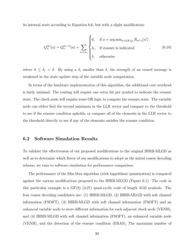
its internal state according to Equation 6.6, but with a slight modification:
Q(k)n (a) = Q(k−1)
n (a) +∑m′∈In
⎧⎪⎪⎪⎪⎪⎨⎪⎪⎪⎪⎪⎩0, if a = argmina′∈GF(q) Rm′,n(a
′)
δe, if erasure is indicated
δ, otherwise
, (6.10)
where 0 ≤ δe < δ. By using a δe smaller than δ, the strength of an erased message is
weakened in the state update step of the variable node computation.
In terms of the hardware implementation of this algorithm, the additional cost overhead
is fairly minimal. The routing will require one extra bit per symbol to indicate the erasure
state. The check node will require some OR logic to compute the erasure state. The variable
node can either find the second minimum in the LLR vector and compare to the threshold
to see if the erasure condition upholds, or compare all of the elements in the LLR vector to
the threshold directly to see if any of the elements satisfies the erasure condition.
6.2 Software Simulation Results
To validate the effectiveness of our proposed modifications to the original IHRB-MLGD as
well as to determine which flavor of our modifications to adopt as the initial coarse decoding
scheme, we turn to software simulation for performance comparison.
The performance of the Min-Max algorithm (with logarithmic quantization) is compared
against the various modifications proposed to the IHRB-MLGD (Figure 6.1). The code in
this particular example is a GF(8) (3,27) quasi-cyclic code of length 3132 symbols. The
four coarse decoding candidates are: (1) IHRB-MLGD, (2) IHRB-MLGD with soft channel
information (FSOFT), (3) IHRB-MLGD with soft channel information (FSOFT) and an
enhanced variable node to store different information for each adjacent check node (VENH),
and (4) IHRB-MLGD with soft channel information (FSOFT), an enhanced variable node
(VENH), and the detection of the erasure condition (ERAS). The maximum number of
80
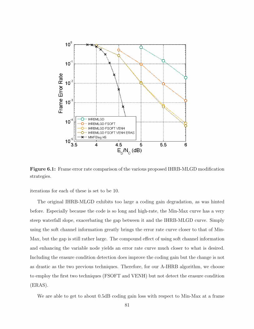
Figure 6.1: Frame error rate comparison of the various proposed IHRB-MLGDmodification
strategies.
iterations for each of these is set to be 10.
The original IHRB-MLGD exhibits too large a coding gain degradation, as was hinted
before. Especially because the code is so long and high-rate, the Min-Max curve has a very
steep waterfall slope, exacerbating the gap between it and the IHRB-MLGD curve. Simply
using the soft channel information greatly brings the error rate curve closer to that of Min-
Max, but the gap is still rather large. The compound effect of using soft channel information
and enhancing the variable node yields an error rate curve much closer to what is desired.
Including the erasure condition detection does improve the coding gain but the change is not
as drastic as the two previous techniques. Therefore, for our A-IHRB algorithm, we choose
to employ the first two techniques (FSOFT and VENH) but not detect the erasure condition
(ERAS).
We are able to get to about 0.5dB coding gain loss with respect to Min-Max at a frame
81
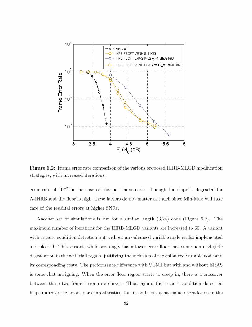
Figure 6.2: Frame error rate comparison of the various proposed IHRB-MLGDmodification
strategies, with increased iterations.
error rate of 10−2 in the case of this particular code. Though the slope is degraded for
A-IHRB and the floor is high, these factors do not matter as much since Min-Max will take
care of the residual errors at higher SNRs.
Another set of simulations is run for a similar length (3,24) code (Figure 6.2). The
maximum number of iterations for the IHRB-MLGD variants are increased to 60. A variant
with erasure condition detection but without an enhanced variable node is also implemented
and plotted. This variant, while seemingly has a lower error floor, has some non-negligible
degradation in the waterfall region, justifying the inclusion of the enhanced variable node and
its corresponding costs. The performance difference with VENH but with and without ERAS
is somewhat intriguing. When the error floor region starts to creep in, there is a crossover
between these two frame error rate curves. Thus, again, the erasure condition detection
helps improve the error floor characteristics, but in addition, it has some degradation in the
82
waterfall region. For the purposes of our use of A-IHRB as an initial coarse decoder, we
actually care more about the performance in the waterfall region, because we want to close
the “gap” between A-IHRB and Min-Max for high frame error rates. This example further
validates our choice to exclude the erasure condition detection from A-IHRB in our final
decoding strategy. While the erasure condition detection as an addition to IHRB-MLGD
may potentially be useful as a stand-alone algorithm, we will not investigate this further.
6.3 Combination with the Min-Max Algorithm
We will quickly discuss some of the aspects concerning the combination of A-IHRB with
Min-Max before diving deeply into the implementation details.
The FER and BER performance simulation results of the proposed dual-algorithm scheme
over the AWGN channel are shown (Figures 6.3, 6.4). Regardless of the maximum number
of iterations for the Min-Max algorithm (6 and 20 are shown), the error rate curves overlap,
which is fairly obvious. In fact, the simulation results are almost exactly the same in the
sense that the same channel inputs cause errors to occur. Very rarely does A-IHRB help
the performance by decoding a channel input correctly where Min-Max was not able to. On
the other hand, A-IHRB did unfortunately yield some undetectable (zero syndrome) errors,
causing the dual-algorithm scheme to not be able to move on to Min-Max. This phenomenon
was observed more for shorter codes, codes with smaller node degrees, and higher maximum
number of A-IHRB iterations (beyond 10). This limits the applicability of our proposed
scheme to codes that satisfy some of these characteristics. Additionally, bringing down the
maximum number of A-IHRB iterations will help, although this will degrade the hardware
performance. For example, if the maximum number of iterations of A-IHRB is set to be 8,
there are zero such undetectable errors over the simulated range of input channel Eb/N0.
Although not a good measure of the exact performance improvements, we can still observe
some of the benefits yielded by our proposed scheme in the software run-time of simulations.
We measure the time it takes for the software to decode 1000 frames as a function of Eb/N0,
83

Figure 6.3: Comparison of FER in simulation with and without A-IHRB.
Figure 6.4: Comparison of BER in simulation with and without A-IHRB.
84
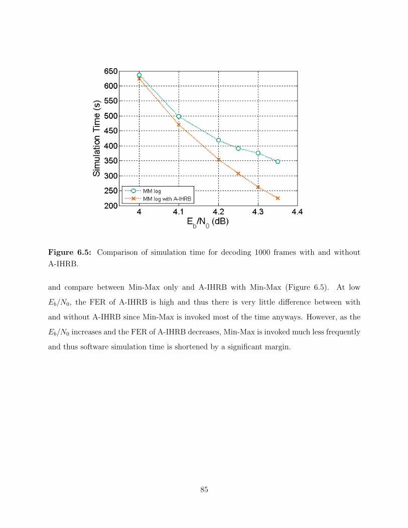
Figure 6.5: Comparison of simulation time for decoding 1000 frames with and without
A-IHRB.
and compare between Min-Max only and A-IHRB with Min-Max (Figure 6.5). At low
Eb/N0, the FER of A-IHRB is high and thus there is very little difference between with
and without A-IHRB since Min-Max is invoked most of the time anyways. However, as the
Eb/N0 increases and the FER of A-IHRB decreases, Min-Max is invoked much less frequently
and thus software simulation time is shortened by a significant margin.
85
CHAPTER 7
ASIC Implementation
7.1 Parity-Check Matrix . . . . . . . . . . . . . . . . . . . . . . . . . . . . . 87
7.2 Architecture . . . . . . . . . . . . . . . . . . . . . . . . . . . . . . . . . . 92
7.2.1 Variable Node Architecture . . . . . . . . . . . . . . . . . . . . . . . . . 92
7.2.2 A-IHRB Check Node Logic Implementation in Variable Node . . . . . . 94
7.2.3 Decoder Core Architecture . . . . . . . . . . . . . . . . . . . . . . . . . 95
7.3 AWGN Channel Simulation . . . . . . . . . . . . . . . . . . . . . . . . . 97
7.4 Chip Design . . . . . . . . . . . . . . . . . . . . . . . . . . . . . . . . . . 98
7.5 Measurement Results . . . . . . . . . . . . . . . . . . . . . . . . . . . . . 101
7.5.1 Error Correction Performance . . . . . . . . . . . . . . . . . . . . . . . . 101
7.5.2 Hardware Performance . . . . . . . . . . . . . . . . . . . . . . . . . . . . 103
7.5.3 Comparison Against Prior Art . . . . . . . . . . . . . . . . . . . . . . . 107
86
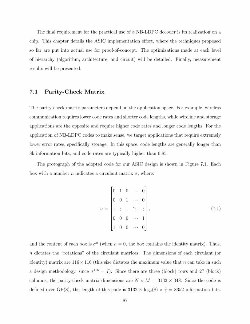
The final requirement for the practical use of a NB-LDPC decoder is its realization on a
chip. This chapter details the ASIC implementation effort, where the techniques proposed
so far are put into actual use for proof-of-concept. The optimizations made at each level
of hierarchy (algorithm, architecture, and circuit) will be detailed. Finally, measurement
results will be presented.
7.1 Parity-Check Matrix
The parity-check matrix parameters depend on the application space. For example, wireless
communication requires lower code rates and shorter code lengths, while wireline and storage
applications are the opposite and require higher code rates and longer code lengths. For the
application of NB-LDPC codes to make sense, we target applications that require extremely
lower error rates, specifically storage. In this space, code lengths are generally longer than
8k information bits, and code rates are typically higher than 0.85.
The protograph of the adopted code for our ASIC design is shown in Figure 7.1. Each
box with a number n indicates a circulant matrix σ, where:
σ =
⎡⎢⎢⎢⎢⎢⎢⎢⎢⎢⎣
0 1 0 · · · 0
0 0 1 · · · 0...
......
. . ....
0 0 0 · · · 1
1 0 0 · · · 0
⎤⎥⎥⎥⎥⎥⎥⎥⎥⎥⎦, (7.1)
and the content of each box is σn (when n = 0, the box contains the identity matrix). Thus,
n dictates the “rotations” of the circulant matrices. The dimensions of each circulant (or
identity) matrix are 116×116 (this size dictates the maximum value that n can take in such
a design methodology, since σ116 = I). Since there are three (block) rows and 27 (block)
columns, the parity-check matrix dimensions are N × M = 3132 × 348. Since the code is
defined over GF(8), the length of this code is 3132 × log2(8) × 89= 8352 information bits.
87
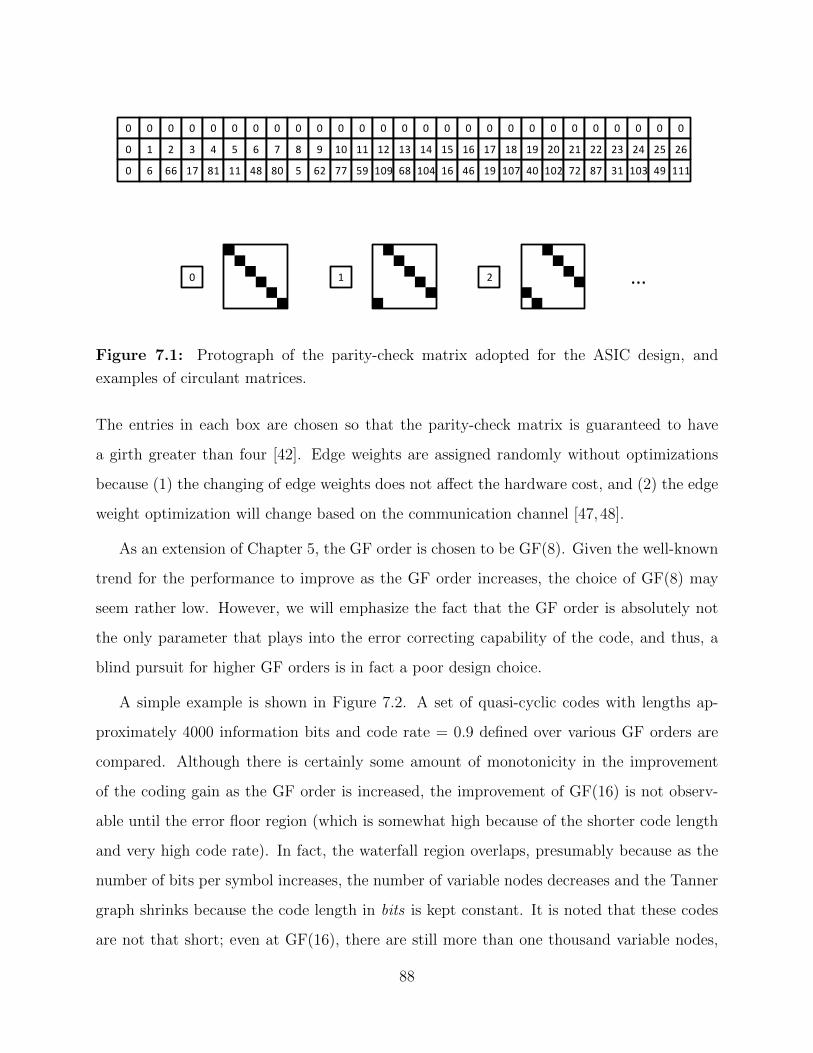
0 0 0 0 0 0 0 0 0 0 0 0 0 0 0 0 0 0 0 0 0 0 0 0 0 0 0
0 1 2 3 4 5 6 7 8 9
0 6 66 17 81 11 48 80 5 62 77 59 109 68 104 16 46 19 107 40 102 72 87 31 103 49 111
10 11 12 13 14 15 16 17 18 19 20 21 22 23 24 25 26
0 1 2 ...
Figure 7.1: Protograph of the parity-check matrix adopted for the ASIC design, and
examples of circulant matrices.
The entries in each box are chosen so that the parity-check matrix is guaranteed to have
a girth greater than four [42]. Edge weights are assigned randomly without optimizations
because (1) the changing of edge weights does not affect the hardware cost, and (2) the edge
weight optimization will change based on the communication channel [47,48].
As an extension of Chapter 5, the GF order is chosen to be GF(8). Given the well-known
trend for the performance to improve as the GF order increases, the choice of GF(8) may
seem rather low. However, we will emphasize the fact that the GF order is absolutely not
the only parameter that plays into the error correcting capability of the code, and thus, a
blind pursuit for higher GF orders is in fact a poor design choice.
A simple example is shown in Figure 7.2. A set of quasi-cyclic codes with lengths ap-
proximately 4000 information bits and code rate = 0.9 defined over various GF orders are
compared. Although there is certainly some amount of monotonicity in the improvement
of the coding gain as the GF order is increased, the improvement of GF(16) is not observ-
able until the error floor region (which is somewhat high because of the shorter code length
and very high code rate). In fact, the waterfall region overlaps, presumably because as the
number of bits per symbol increases, the number of variable nodes decreases and the Tanner
graph shrinks because the code length in bits is kept constant. It is noted that these codes
are not that short; even at GF(16), there are still more than one thousand variable nodes,
88
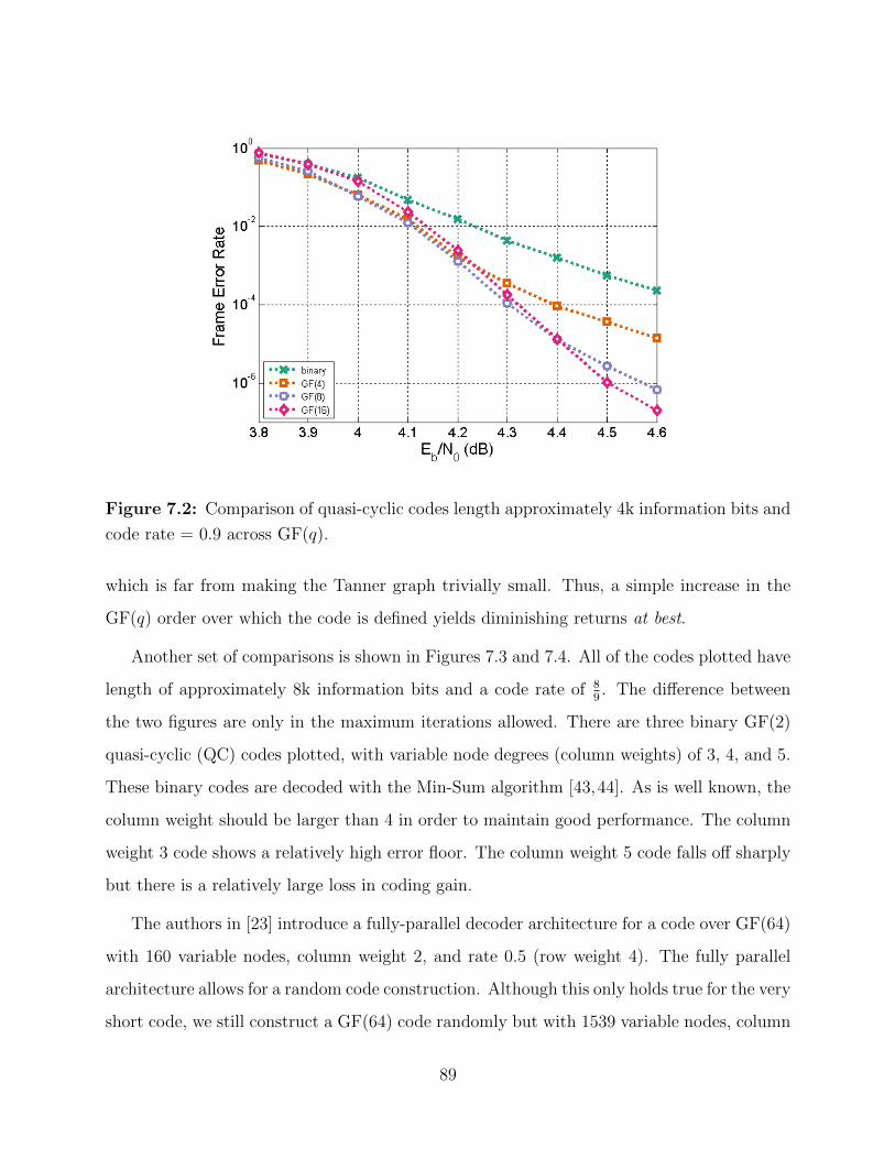
Figure 7.2: Comparison of quasi-cyclic codes length approximately 4k information bits and
code rate = 0.9 across GF(q).
which is far from making the Tanner graph trivially small. Thus, a simple increase in the
GF(q) order over which the code is defined yields diminishing returns at best.
Another set of comparisons is shown in Figures 7.3 and 7.4. All of the codes plotted have
length of approximately 8k information bits and a code rate of 89. The difference between
the two figures are only in the maximum iterations allowed. There are three binary GF(2)
quasi-cyclic (QC) codes plotted, with variable node degrees (column weights) of 3, 4, and 5.
These binary codes are decoded with the Min-Sum algorithm [43,44]. As is well known, the
column weight should be larger than 4 in order to maintain good performance. The column
weight 3 code shows a relatively high error floor. The column weight 5 code falls off sharply
but there is a relatively large loss in coding gain.
The authors in [23] introduce a fully-parallel decoder architecture for a code over GF(64)
with 160 variable nodes, column weight 2, and rate 0.5 (row weight 4). The fully parallel
architecture allows for a random code construction. Although this only holds true for the very
short code, we still construct a GF(64) code randomly but with 1539 variable nodes, column
89
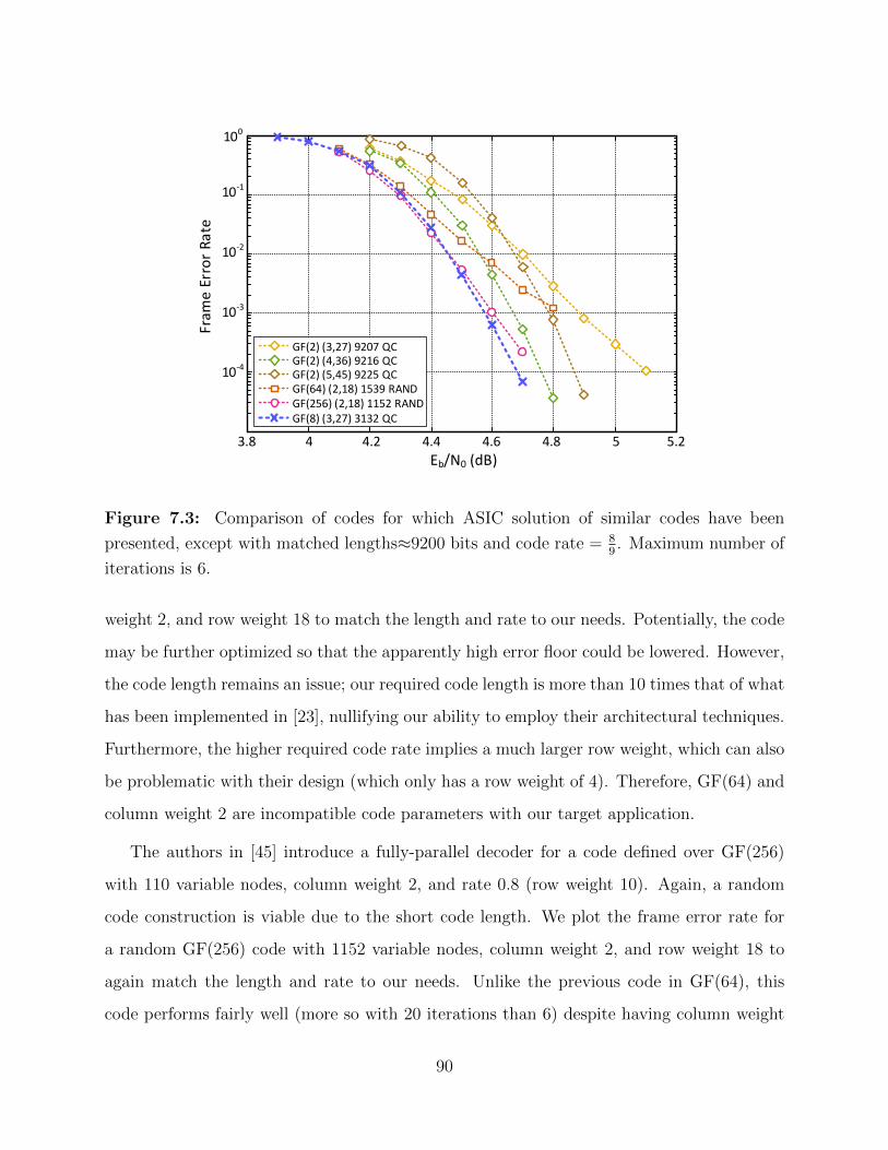
Eb/N0 (dB)
Fram
e E
rro
r R
ate
GF(8) (3,27) 3132 QCGF(256) (2,18) 1152 RANDGF(64) (2,18) 1539 RANDGF(2) (5,45) 9225 QCGF(2) (4,36) 9216 QCGF(2) (3,27) 9207 QC
10-4
4.6 4.8 5 5.23.8 4 4.2 4.4
10-3
10-2
10-1
100
Figure 7.3: Comparison of codes for which ASIC solution of similar codes have been
presented, except with matched lengths≈9200 bits and code rate = 89. Maximum number of
iterations is 6.
weight 2, and row weight 18 to match the length and rate to our needs. Potentially, the code
may be further optimized so that the apparently high error floor could be lowered. However,
the code length remains an issue; our required code length is more than 10 times that of what
has been implemented in [23], nullifying our ability to employ their architectural techniques.
Furthermore, the higher required code rate implies a much larger row weight, which can also
be problematic with their design (which only has a row weight of 4). Therefore, GF(64) and
column weight 2 are incompatible code parameters with our target application.
The authors in [45] introduce a fully-parallel decoder for a code defined over GF(256)
with 110 variable nodes, column weight 2, and rate 0.8 (row weight 10). Again, a random
code construction is viable due to the short code length. We plot the frame error rate for
a random GF(256) code with 1152 variable nodes, column weight 2, and row weight 18 to
again match the length and rate to our needs. Unlike the previous code in GF(64), this
code performs fairly well (more so with 20 iterations than 6) despite having column weight
90
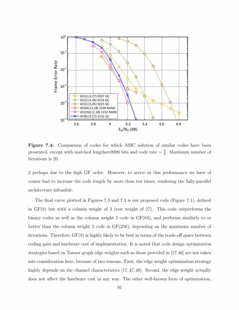
Eb/N0 (dB)
Fram
e E
rro
r R
ate
GF(8) (3,27) 3132 QCGF(256) (2,18) 1152 RANDGF(64) (2,18) 1539 RANDGF(2) (5,45) 9225 QCGF(2) (4,36) 9216 QCGF(2) (3,27) 9207 QC
10-4
4.6 4.83.6 3.8 4 4.2 4.4
10-3
10-2
10-1
100
10-5
Figure 7.4: Comparison of codes for which ASIC solution of similar codes have been
presented, except with matched lengths≈9200 bits and code rate = 89. Maximum number of
iterations is 20.
2 perhaps due to the high GF order. However, to arrive at this performance we have of
course had to increase the code length by more than ten times, rendering the fully-parallel
architecture infeasible.
The final curve plotted in Figures 7.3 and 7.4 is our proposed code (Figure 7.1), defined
in GF(8) but with a column weight of 3 (row weight of 27). This code outperforms the
binary codes as well as the column weight 2 code in GF(64), and performs similarly to or
better than the column weight 2 code in GF(256), depending on the maximum number of
iterations. Therefore, GF(8) is highly likely to be best in terms of the trade-off space between
coding gain and hardware cost of implementation. It is noted that code design optimization
strategies based on Tanner graph edge weights such as those provided in [17,46] are not taken
into consideration here, because of two reasons. First, the edge weight optimization strategy
highly depends on the channel characteristics [17, 47, 48]. Second, the edge weight actually
does not affect the hardware cost in any way. The other well-known form of optimization,
91
namely the structural optimization of the binary LDPC matrix, is limited anyways since we
must employ a quasi-cyclic code.
Unfortunately, the choice to implement a code in GF(8) does not automatically translate
to cheap or even feasible hardware costs (for example, see [27]). This is because while GF(8)
codes are much more expensive than binary codes, many of the techniques utilized in prior
art such as [23], [45] do not apply at GF(8). Most importantly, the EMS algorithm [14], [15]
does not yield benefits until the GF order is at least approximately 32, because there is no
good choice for the truncated message length nm where nm < q when q is smaller. Either
nm is too small and the coding gain is excessively sacrificed, or nm is too close to q and
the overhead cost in hardware (for sorters, etc.) becomes too large (or both). Thus, it is
imperative for us to design the architecture carefully to reap the benefits of our GF(8) code.
7.2 Architecture
The algorithm of choice will be the dual-algorithm scheme with A-IHRB and Min-Max
decoding algorithms, detailed in Chapter 6. While the algorithm has been discussed in
detail, we have still yet to consider the actual hardware implementation strategy. An upfront
concern is the area overhead of the dual-algorithm scheme; if multiple algorithms must be
implemented, then that much extra cost must be paid in hardware. We will seek to mitigate
this overhead by close observation of the variable node computation.
7.2.1 Variable Node Architecture
The variable node computation in the Min-Max algorithm is described in Equations 2.24,
2.25, and 2.26. In essence, the core of these equations are comprised of summations and
normalizations (minimum and subtraction). On the other hand, the variable node compu-
tations in the A-IHRB algorithm is described in Equations 6.8 and 6.9. The crux of these
equations are summations and the argmin function. It is fairly straightforward to share the
summation operations, since there will be the same number of addition operations required
92
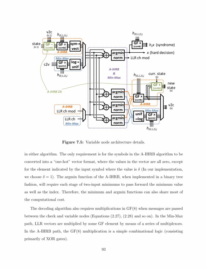
A-IHRB
Min-MaxA-IHRB
Min-Max
A-IHRB
Min-Max
sym→ vect
GF ÷ (comb)
log→unif
GF ÷(perm)
GF ×(comb)
h{0,1,2},j
hijx
LLR ch mod
GF ×(comb)
h{0,1,2},j
h{0,1,2},j
h{0,1,2},j
c2v
state(k-1)
v2c(k-1)
curr. state (k)
GF ×(perm)
h{0,1,2},j
unif→log
v2c(k)
LLR ch mod
LLR ch
A-IHRB &
Min-Max
(hard decision)
(syndrome)
new state
(k)
xargmin norm
argmin norm
argmin norm
argmin norm
A-IHRB CN
GF − (comb)
GF + (comb)
Figure 7.5: Variable node architecture details.
in either algorithm. The only requirement is for the symbols in the A-IHRB algorithm to be
converted into a “one-hot” vector format, where the values in the vector are all zero, except
for the element indicated by the input symbol where the value is δ (In our implementation,
we choose δ = 1). The argmin function of the A-IHRB, when implemented in a binary tree
fashion, will require each stage of two-input minimums to pass forward the minimum value
as well as the index. Therefore, the minimum and argmin functions can also share most of
the computational cost.
The decoding algorithm also requires multiplications in GF(8) when messages are passed
between the check and variable nodes (Equations (2.27), (2.28) and so on). In the Min-Max
path, LLR vectors are multiplied by some GF element by means of a series of multiplexors.
In the A-IHRB path, the GF(8) multiplication is a simple combinational logic (consisting
primarily of XOR gates).
93
The final variable node architecture is shown in Figure 7.5. The two data paths for A-
IHRB and Min-Max are separated by muxes, and as mentioned, the core computations of
summation and argmin/normalization are shared. In the A-IHRB path, GF multiplications
(and divisions) are implemented using combinational logic, and the symbols are converted
into a vector format to feed into the summation blocks. In the Min-Max path, the GF
multiplications are permutations, and the signals in the logarithmic quantization domain
(Chapter 4) are converted into the uniform quantization domain so that numbers may be
added (and the adders may be shared). These converters are placed as close to the adders as
possible so that everything outside (muxes for GF multiplication by permutation in the Min-
Max path, the wiring overhead, storage requirements, etc.) can be directly reduced by the
number of bits required for the representation of LLRs. The variable node also must compute
the a posteriori LLRs to make hard decisions as output of the decoder, as well as to check
the syndrome for early termination. This is shown in the top path of Figure 7.5. The “LLR
ch” signal in the Min-Max path is the channel information given as input to the algorithm
itself. The “LLR ch mod” signal in the A-IHRB path is the set of signals corresponding
to Q(k−1)m,n (a) in Equation (6.8) as well as the a posteriori LLR for hard decisions (refer to
Section 6.1.1 for details).
7.2.2 A-IHRB Check Node Logic Implementation in Variable Node
The combinational GF(8) subtraction and addition blocks in the A-IHRB data path in Figure
7.5 are for check node computations in A-IHRB. The check node computations in A-IHRB,
described by Equation (6.5), are actually simple bit-wise XOR operations on GF symbols.
Thus, instead of computing Equation (6.5) for each output edge on a check node, we can
instead compute a check node “state” as follows:
S(k)m =
GF(q)∑n′∈Im
(hm,n′ × Q
(k−1)m,n′
), (7.2)
94
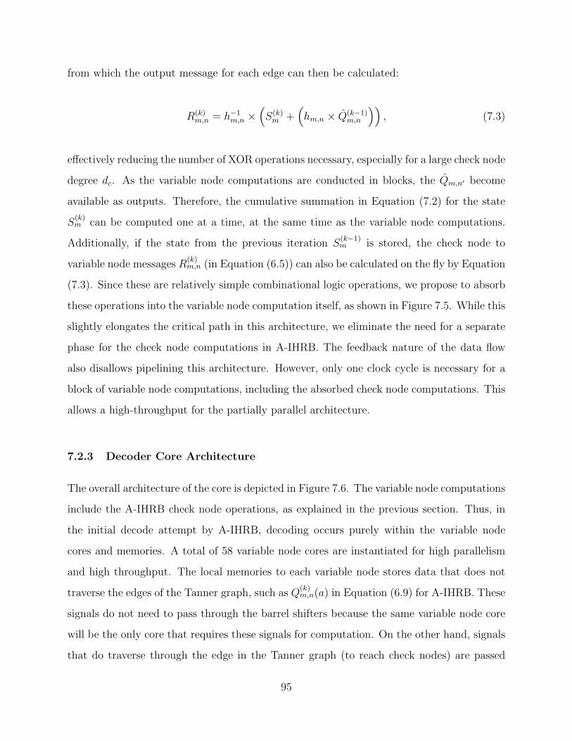
from which the output message for each edge can then be calculated:
R(k)m,n = h−1
m,n ×(S(k)m +
(hm,n × Q(k−1)
m,n
)), (7.3)
effectively reducing the number of XOR operations necessary, especially for a large check node
degree dc. As the variable node computations are conducted in blocks, the Qm,n′ become
available as outputs. Therefore, the cumulative summation in Equation (7.2) for the state
S(k)m can be computed one at a time, at the same time as the variable node computations.
Additionally, if the state from the previous iteration S(k−1)m is stored, the check node to
variable node messages R(k)m,n (in Equation (6.5)) can also be calculated on the fly by Equation
(7.3). Since these are relatively simple combinational logic operations, we propose to absorb
these operations into the variable node computation itself, as shown in Figure 7.5. While this
slightly elongates the critical path in this architecture, we eliminate the need for a separate
phase for the check node computations in A-IHRB. The feedback nature of the data flow
also disallows pipelining this architecture. However, only one clock cycle is necessary for a
block of variable node computations, including the absorbed check node computations. This
allows a high-throughput for the partially parallel architecture.
7.2.3 Decoder Core Architecture
The overall architecture of the core is depicted in Figure 7.6. The variable node computations
include the A-IHRB check node operations, as explained in the previous section. Thus, in
the initial decode attempt by A-IHRB, decoding occurs purely within the variable node
cores and memories. A total of 58 variable node cores are instantiated for high parallelism
and high throughput. The local memories to each variable node stores data that does not
traverse the edges of the Tanner graph, such as Q(k)m,n(a) in Equation (6.9) for A-IHRB. These
signals do not need to pass through the barrel shifters because the same variable node core
will be the only core that requires these signals for computation. On the other hand, signals
that do traverse through the edge in the Tanner graph (to reach check nodes) are passed
95
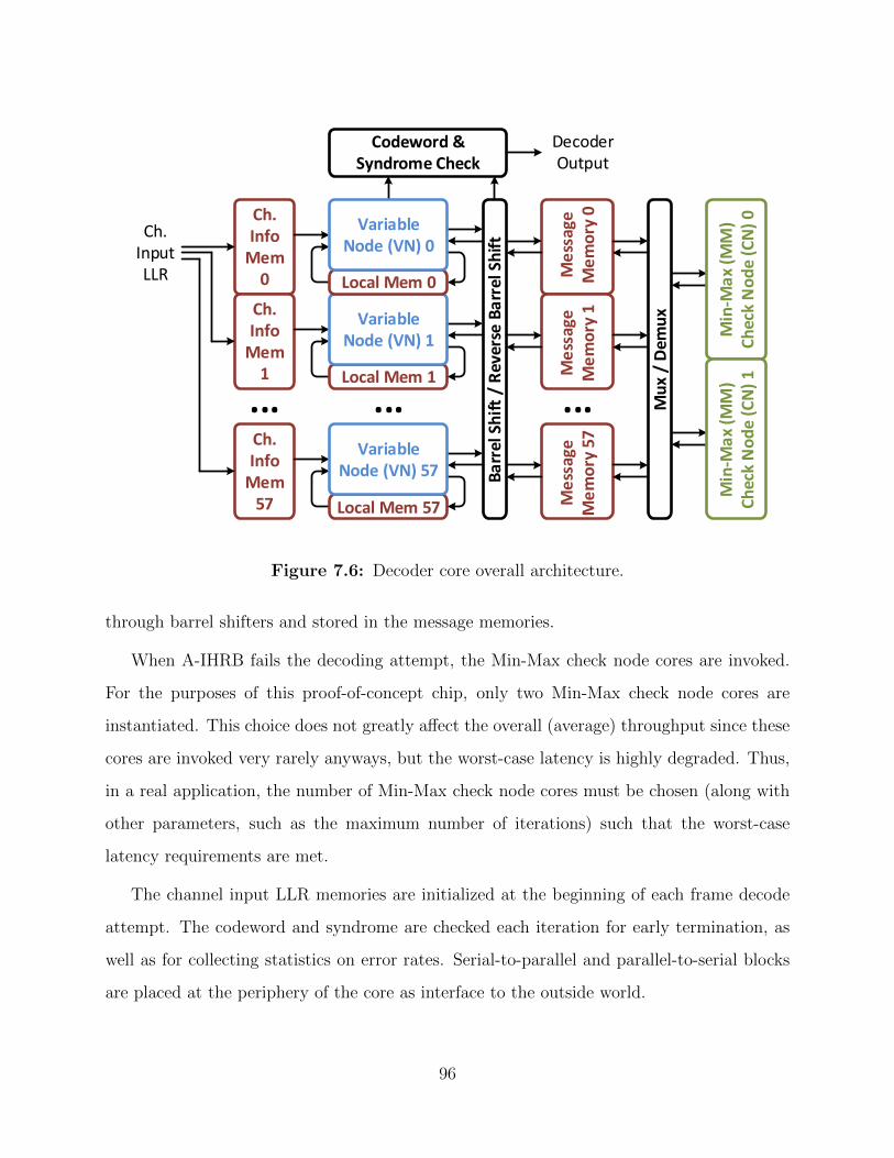
...
Ch. Info
Mem 0
Ch. Info
Mem 1 Local Mem 1
Ch. Info
Mem 57
Ba
rrel
Sh
ift
/ R
ever
se B
arr
el S
hif
tLocal Mem 57
Me
ssag
e M
em
ory
0M
ess
age
Me
mo
ry 1
Me
ssag
e M
em
ory
57
Mu
x /
Dem
ux
Min
-Ma
x (M
M)
Ch
eck
No
de
(CN
) 0
Min
-Ma
x (M
M)
Ch
eck
No
de
(CN
) 1
Codeword & Syndrome Check
Ch. Input LLR
Decoder Output
... ...
Local Mem 0
Variable Node (VN) 1
Variable Node (VN) 57
Variable Node (VN) 0
Figure 7.6: Decoder core overall architecture.
through barrel shifters and stored in the message memories.
When A-IHRB fails the decoding attempt, the Min-Max check node cores are invoked.
For the purposes of this proof-of-concept chip, only two Min-Max check node cores are
instantiated. This choice does not greatly affect the overall (average) throughput since these
cores are invoked very rarely anyways, but the worst-case latency is highly degraded. Thus,
in a real application, the number of Min-Max check node cores must be chosen (along with
other parameters, such as the maximum number of iterations) such that the worst-case
latency requirements are met.
The channel input LLR memories are initialized at the beginning of each frame decode
attempt. The codeword and syndrome are checked each iteration for early termination, as
well as for collecting statistics on error rates. Serial-to-parallel and parallel-to-serial blocks
are placed at the periphery of the core as interface to the outside world.
96
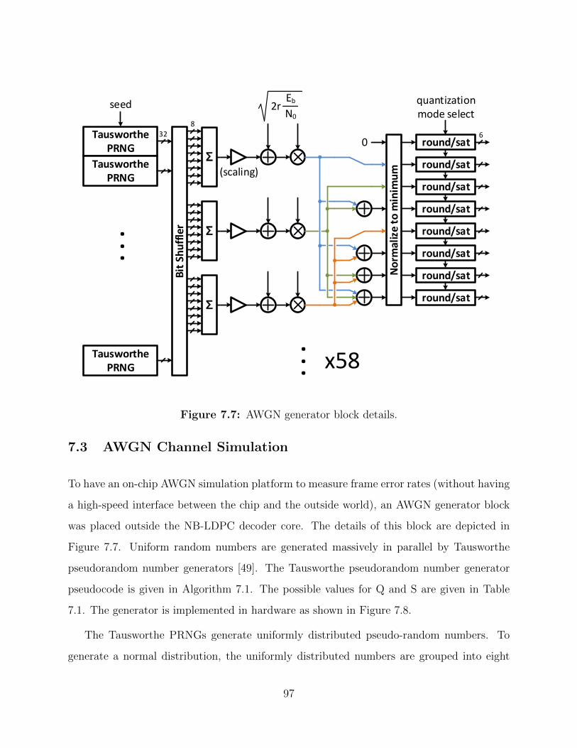
Tausworthe PRNG
Bit
Sh
uff
ler
Tausworthe PRNG
round/sat
2rEb
N0
No
rmal
ize
to m
inim
um
Tausworthe PRNG
seed
. . .
32
Σ
8
round/sat
round/sat
round/sat
round/sat
round/sat
round/sat
round/sat
Σ
Σ
. . .
0
x58
quantization mode select
6
(scaling)
Figure 7.7: AWGN generator block details.
7.3 AWGN Channel Simulation
To have an on-chip AWGN simulation platform to measure frame error rates (without having
a high-speed interface between the chip and the outside world), an AWGN generator block
was placed outside the NB-LDPC decoder core. The details of this block are depicted in
Figure 7.7. Uniform random numbers are generated massively in parallel by Tausworthe
pseudorandom number generators [49]. The Tausworthe pseudorandom number generator
pseudocode is given in Algorithm 7.1. The possible values for Q and S are given in Table
7.1. The generator is implemented in hardware as shown in Figure 7.8.
The Tausworthe PRNGs generate uniformly distributed pseudo-random numbers. To
generate a normal distribution, the uniformly distributed numbers are grouped into eight
97

1 taus () {2 b1 = (((state1 << Q1) ˆ state1) >> (31 - S1));
3 state1 = (((state1 & 32’hFFFFFFFE ) << S1) ˆ b1);
4 b2 = (((state2 << Q2) ˆ state2) >> (29 - S2));
5 state2 = (((state2 & 32’hFFFFFFFC ) << S2) ˆ b2);
6 b3 = (((state3 << Q3) ˆ state3) >> (28 - S3));
7 state3 = (((state3 & 32’hFFFFFFF8 ) << S3) ˆ b3);
8 }
Algorithm 7.1: pseudocode for Tausworthe PRNG.
Table 7.1: Possible Constant Values for the Tausworthe PRNG
Q1 Q2 Q3 S1 S2 S3
13 2 3 12 4 17
7 2 9 24 7 11
3 2 13 20 16 7
and added together, which by the central limit theorem generates a distribution that resem-
bles a Gaussian. The output of this is scaled properly to produce a normal distribution with
zero mean and variance one. Then, the signal-to-noise ratio is used to transform the Gaus-
sian distributed random variable into a log-likelihood ratio that represents the information
received from the observation from the channel. Three of these LLRs are taken at a time
and combined properly to generate a vector of 8 LLRs, since the NB-LDPC code is defined
over GF(8). This LLR vector is normalized so that the minimum LLR in the vector is 0.
Finally, the LLRs are quantized to the correct number of bits, with the correct decimal point
location and fed into the channel input LLR memory of the decoder core.
7.4 Chip Design
The general task flow is depicted in Figure 7.9. The parity-check matrix is generated by
a script in MATLAB and is used in a software implementation of the decoding algorithm
in C++ to observe the error rate performance in simulation. The C++ implementation is
98
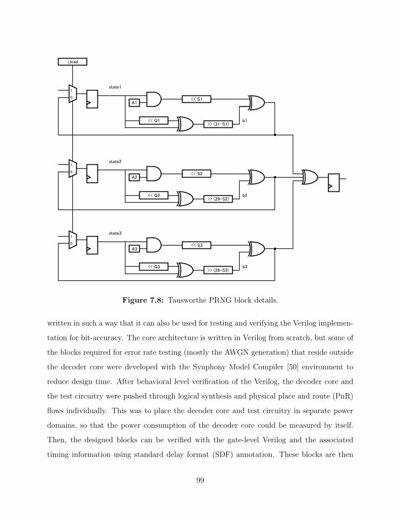
i_load
state1
<< Q1>> (31-S1)
<< S1A1
b1
1
0
state2
<< Q2>> (29-S2)
<< S2A2
b2
1
0
state3
<< Q3>> (28-S3)
<< S3A3
b3
1
0
Figure 7.8: Tausworthe PRNG block details.
written in such a way that it can also be used for testing and verifying the Verilog implemen-
tation for bit-accuracy. The core architecture is written in Verilog from scratch, but some of
the blocks required for error rate testing (mostly the AWGN generation) that reside outside
the decoder core were developed with the Synphony Model Compiler [50] environment to
reduce design time. After behavioral level verification of the Verilog, the decoder core and
the test circuitry were pushed through logical synthesis and physical place and route (PnR)
flows individually. This was to place the decoder core and test circuitry in separate power
domains, so that the power consumption of the decoder core could be measured by itself.
Then, the designed blocks can be verified with the gate-level Verilog and the associated
timing information using standard delay format (SDF) annotation. These blocks are then
99
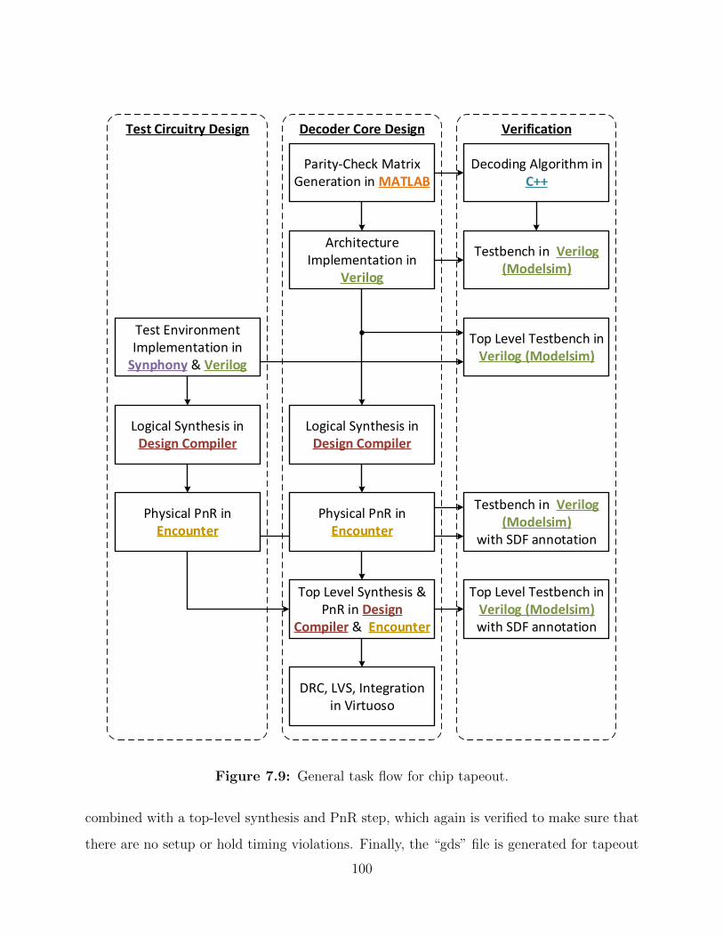
Decoding Algorithm in C++
Parity-Check Matrix Generation in MATLAB
Architecture Implementation in
Verilog
Test Environment Implementation in
Synphony & Verilog
Top Level Testbench in Verilog (Modelsim)
Logical Synthesis in Design Compiler
Logical Synthesis in Design Compiler
Physical PnR in Encounter
Physical PnR in Encounter
Top Level Synthesis & PnR in Design
Compiler & Encounter
Testbench in Verilog (Modelsim)
DRC, LVS, Integration in Virtuoso
Testbench in Verilog (Modelsim)
with SDF annotation
Top Level Testbench in Verilog (Modelsim) with SDF annotation
VerificationDecoder Core DesignTest Circuitry Design
Figure 7.9: General task flow for chip tapeout.
combined with a top-level synthesis and PnR step, which again is verified to make sure that
there are no setup or hold timing violations. Finally, the “gds” file is generated for tapeout
100
in the Cadence Virtuoso environment.
7.5 Measurement Results
The proof-of-concept chip is taped out in a 40nm LP process. Since our bottleneck is in
the speed/throughput rather than energy consumption, the low threshold voltage (LVT)
flavor of transistors and standard cell library are used. The lab test setup is depicted in
Figure 7.10. A custom printed circuit board (PCB) is fabricated and assembled with off-
the-shelf components such as low voltage differential signaling (LVDS) drivers, low-dropout
regulators (LDO), etc. to power the chip-under-test and to interface to the packaged chip. A
zero insertion force (ZIF) socket is used so that multiple chips can be tested using the same
PCB. The chips are wire bonded in a pin grid array (PGA) package. Although the electrical
characteristics of these packages are not optimal for high-speed communications, the chip
contains a serial-parallel interface in the test circuitry, and therefore any communication
between the chip and the outside world could be conducted slowly and the high decoder
throughput could be recorded within the chip itself. The ROACH board [51] based on a
Virtex-5 FPGA [52] that was developed by the CASPER [53] research group is used to
communicate to the chip serially to program the chip and to read out decoding results and
statistics. Communication to the ROACH board is conducted through the KATCP [54]
protocol.
The decoder core measures 1782µm×2655µm with an area of 4.73mm2, while the AWGN
generation block and serial interface outside of the core is 279µm × 2655µm with an area
of 0.74mm2 (Figure 7.11, the pad ring is open because the core area is shared with other
research projects).
7.5.1 Error Correction Performance
The on-chip AWGN and corresponding LLR generation is utilized for frame error rate sim-
ulations (after functional verification). The measured frame error rate is plotted in Figure
101
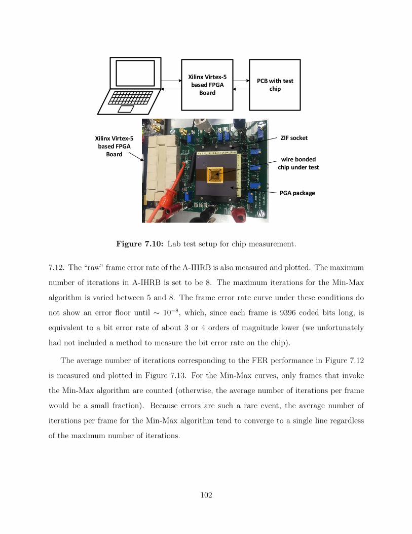
Xilinx Virtex-5 based FPGA
Board
PCB with test chip
Xilinx Virtex-5 based FPGA
Boardwire bonded
chip under test
PGA package
ZIF socket
Figure 7.10: Lab test setup for chip measurement.
7.12. The “raw” frame error rate of the A-IHRB is also measured and plotted. The maximum
number of iterations in A-IHRB is set to be 8. The maximum iterations for the Min-Max
algorithm is varied between 5 and 8. The frame error rate curve under these conditions do
not show an error floor until ∼ 10−8, which, since each frame is 9396 coded bits long, is
equivalent to a bit error rate of about 3 or 4 orders of magnitude lower (we unfortunately
had not included a method to measure the bit error rate on the chip).
The average number of iterations corresponding to the FER performance in Figure 7.12
is measured and plotted in Figure 7.13. For the Min-Max curves, only frames that invoke
the Min-Max algorithm are counted (otherwise, the average number of iterations per frame
would be a small fraction). Because errors are such a rare event, the average number of
iterations per frame for the Min-Max algorithm tend to converge to a single line regardless
of the maximum number of iterations.
102
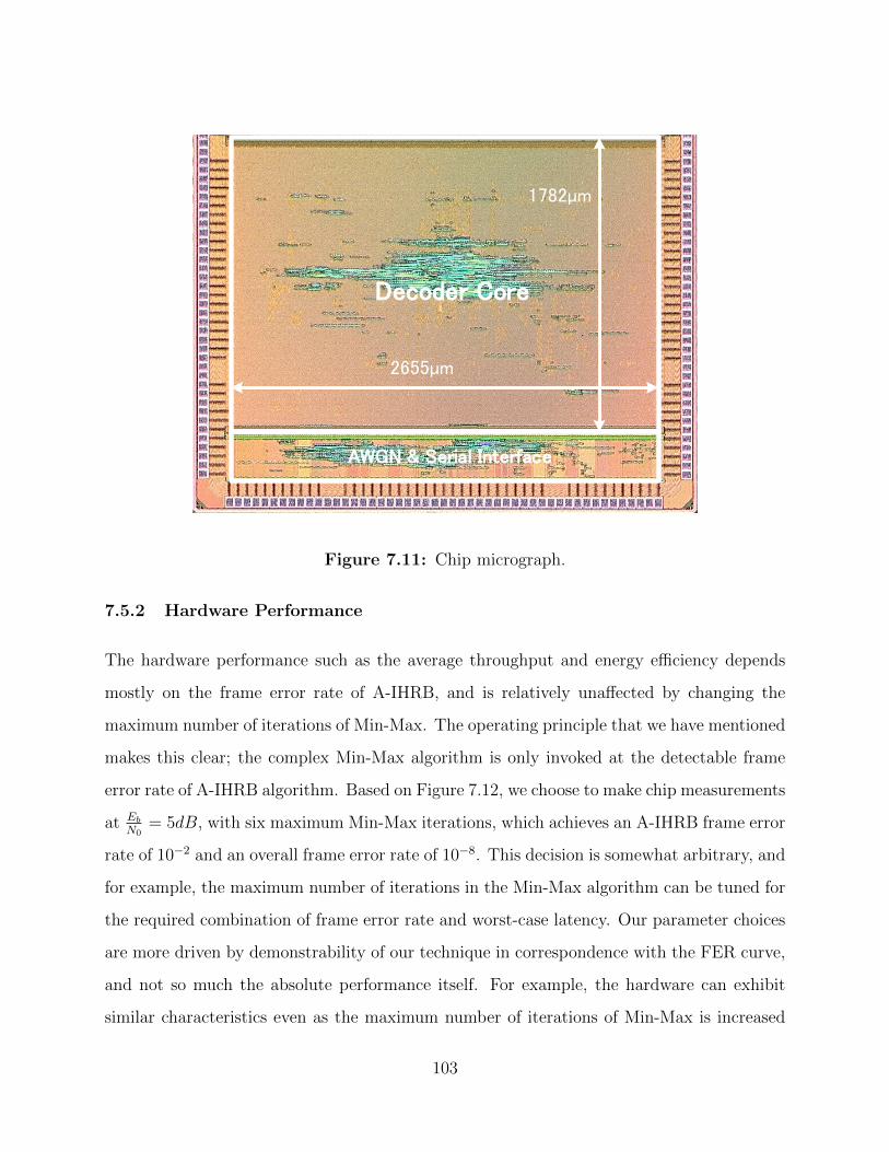
Decoder Core
AWGN & Serial Interface
1782µm
2655µm
Figure 7.11: Chip micrograph.
7.5.2 Hardware Performance
The hardware performance such as the average throughput and energy efficiency depends
mostly on the frame error rate of A-IHRB, and is relatively unaffected by changing the
maximum number of iterations of Min-Max. The operating principle that we have mentioned
makes this clear; the complex Min-Max algorithm is only invoked at the detectable frame
error rate of A-IHRB algorithm. Based on Figure 7.12, we choose to make chip measurements
at Eb
N0= 5dB, with six maximum Min-Max iterations, which achieves an A-IHRB frame error
rate of 10−2 and an overall frame error rate of 10−8. This decision is somewhat arbitrary, and
for example, the maximum number of iterations in the Min-Max algorithm can be tuned for
the required combination of frame error rate and worst-case latency. Our parameter choices
are more driven by demonstrability of our technique in correspondence with the FER curve,
and not so much the absolute performance itself. For example, the hardware can exhibit
similar characteristics even as the maximum number of iterations of Min-Max is increased
103
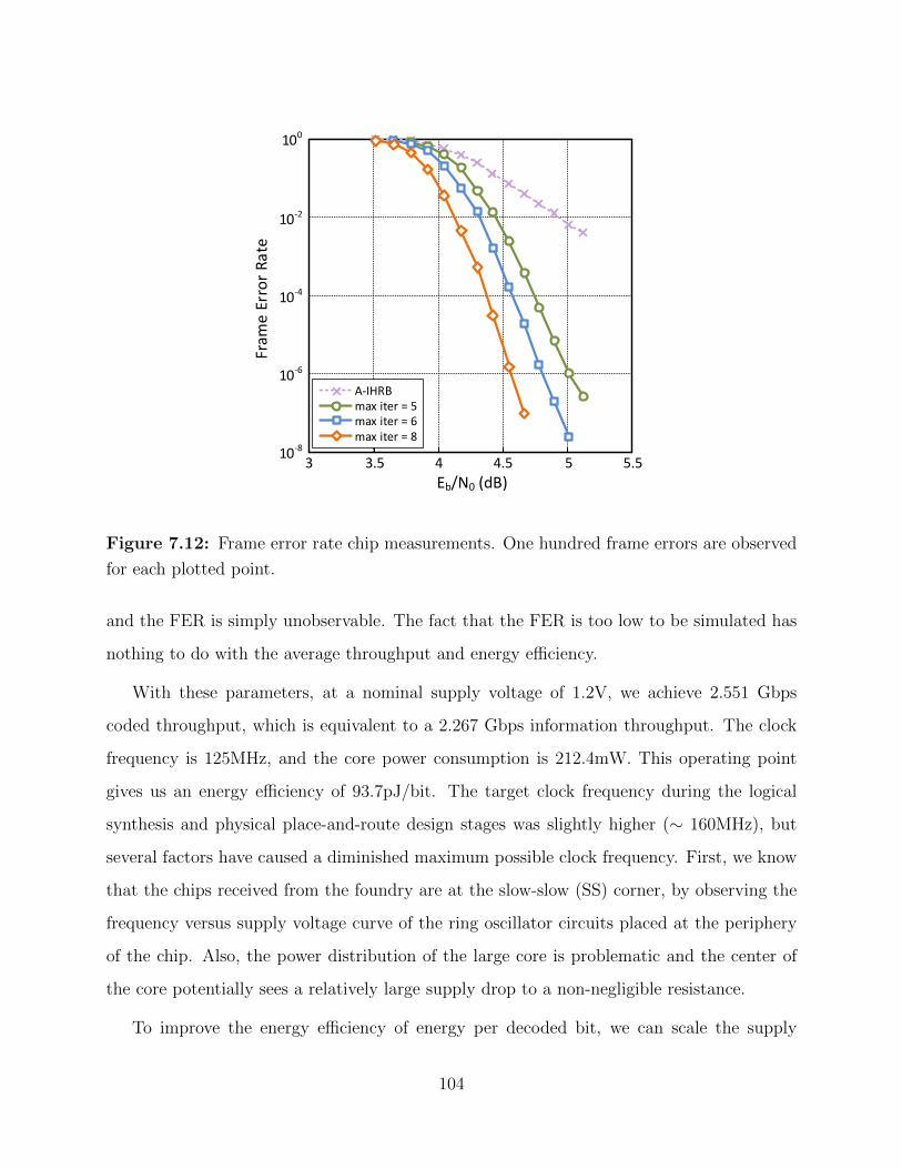
100
10-2
10-4
10-6
10-8
Fram
e E
rro
r R
ate
Eb/N0 (dB)4.5 5 5.53 3.5 4
max iter = 8max iter = 6max iter = 5A-IHRB
Figure 7.12: Frame error rate chip measurements. One hundred frame errors are observed
for each plotted point.
and the FER is simply unobservable. The fact that the FER is too low to be simulated has
nothing to do with the average throughput and energy efficiency.
With these parameters, at a nominal supply voltage of 1.2V, we achieve 2.551 Gbps
coded throughput, which is equivalent to a 2.267 Gbps information throughput. The clock
frequency is 125MHz, and the core power consumption is 212.4mW. This operating point
gives us an energy efficiency of 93.7pJ/bit. The target clock frequency during the logical
synthesis and physical place-and-route design stages was slightly higher (∼ 160MHz), but
several factors have caused a diminished maximum possible clock frequency. First, we know
that the chips received from the foundry are at the slow-slow (SS) corner, by observing the
frequency versus supply voltage curve of the ring oscillator circuits placed at the periphery
of the chip. Also, the power distribution of the large core is problematic and the center of
the core potentially sees a relatively large supply drop to a non-negligible resistance.
To improve the energy efficiency of energy per decoded bit, we can scale the supply
104
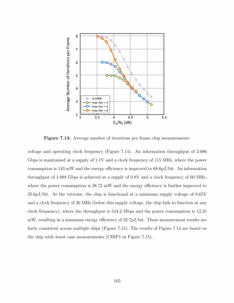
Eb/N0 (dB)4.5 5 5.53 3.5 4
max iter = 8max iter = 6max iter = 5A-IHRB
7
5
3
2
Ave
rage
Nu
mb
er
of
Ite
rati
on
s p
er
Fram
e
4
6
8
Figure 7.13: Average number of iterations per frame chip measurements.
voltage and operating clock frequency (Figure 7.14). An information throughput of 2.086
Gbps is maintained at a supply of 1.1V and a clock frequency of 115 MHz, where the power
consumption is 143 mW and the energy efficiency is improved to 68.6pJ/bit. An information
throughput of 1.088 Gbps is achieved at a supply of 0.8V and a clock frequency of 60 MHz,
where the power consumption is 38.72 mW and the energy efficiency is further improved to
35.6pJ/bit. At the extreme, the chip is functional at a minimum supply voltage of 0.65V
and a clock frequency of 30 MHz (below this supply voltage, the chip fails to function at any
clock frequency), where the throughput is 544.2 Mbps and the power consumption is 12.35
mW, resulting in a minimum energy efficiency of 22.7pJ/bit. These measurement results are
fairly consistent across multiple chips (Figure 7.15). The results of Figure 7.14 are based on
the chip with worst case measurements (CHIP1 in Figure 7.15).
105
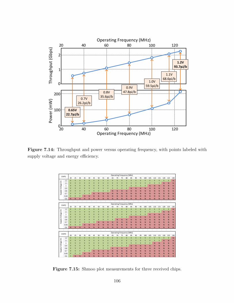
40 60 80 100 120
Thro
ug
hp
ut
(Gb
ps)
Po
wer
(m
W)
Operating Frequency (MHz)
0
100
200
0
1
2
20
40 60 80 100 12020Operating Frequency (MHz)
1.2V93.7pJ/b
1.1V68.6pJ/b
1.0V59.5pJ/b0.9V
47.8pJ/b0.8V35.6pJ/b
0.7V26.2pJ/b
0.65V22.7pJ/b
Figure 7.14: Throughput and power versus operating frequency, with points labeled with
supply voltage and energy efficiency.
20 25 30 35 40 45 50 55 60 65 70 75 80 85 90 95 100 105 110 115 120 125 130
1.2 Y Y Y Y Y Y Y Y Y Y Y Y Y Y Y Y Y Y Y Y Y Y N
1.1 Y Y Y Y Y Y Y Y Y Y Y Y Y Y Y Y Y Y Y Y N N N
1 Y Y Y Y Y Y Y Y Y Y Y Y Y Y Y Y Y N N N N N N
0.9 Y Y Y Y Y Y Y Y Y Y Y Y Y N N N N N N N N N N
0.8 Y Y Y Y Y Y Y Y Y N N N N N N N N N N N N N N
0.7 Y Y Y Y Y N N N N N N N N N N N N N N N N N N
0.65 Y Y Y N N N N N N N N N N N N N N N N N N N N
0.6 N N N N N N N N N N N N N N N N N N N N N N N
20 25 30 35 40 45 50 55 60 65 70 75 80 85 90 95 100 105 110 115 120 125 130
1.2 Y Y Y Y Y Y Y Y Y Y Y Y Y Y Y Y Y Y Y Y Y Y N
1.1 Y Y Y Y Y Y Y Y Y Y Y Y Y Y Y Y Y Y Y Y N N N
1 Y Y Y Y Y Y Y Y Y Y Y Y Y Y Y Y Y N N N N N N
0.9 Y Y Y Y Y Y Y Y Y Y Y Y Y N N N N N N N N N N
0.8 Y Y Y Y Y Y Y Y Y Y N N N N N N N N N N N N N
0.7 Y Y Y Y Y Y N N N N N N N N N N N N N N N N N
0.65 Y Y Y N N N N N N N N N N N N N N N N N N N N
0.6 N N N N N N N N N N N N N N N N N N N N N N N
20 25 30 35 40 45 50 55 60 65 70 75 80 85 90 95 100 105 110 115 120 125 130
1.2 Y Y Y Y Y Y Y Y Y Y Y Y Y Y Y Y Y Y Y Y Y Y N
1.1 Y Y Y Y Y Y Y Y Y Y Y Y Y Y Y Y Y Y Y Y N N N
1 Y Y Y Y Y Y Y Y Y Y Y Y Y Y Y Y Y Y N N N N N
0.9 Y Y Y Y Y Y Y Y Y Y Y Y Y N N N N N N N N N N
0.8 Y Y Y Y Y Y Y Y Y N N N N N N N N N N N N N N
0.7 Y Y Y Y Y N N N N N N N N N N N N N N N N N N
0.65 Y Y Y N N N N N N N N N N N N N N N N N N N N
0.6 Y N N N N N N N N N N N N N N N N N N N N N N
Sup
ply
Vo
ltag
e (V
)
CHIP3
Operating Frequency (MHz)
Operating Frequency (MHz)
Operating Frequency (MHz)
Sup
ply
Vo
ltag
e (V
)Su
pp
ly V
olt
age
(V)
CHIP1
CHIP2
Figure 7.15: Shmoo plot measurements for three received chips.
106
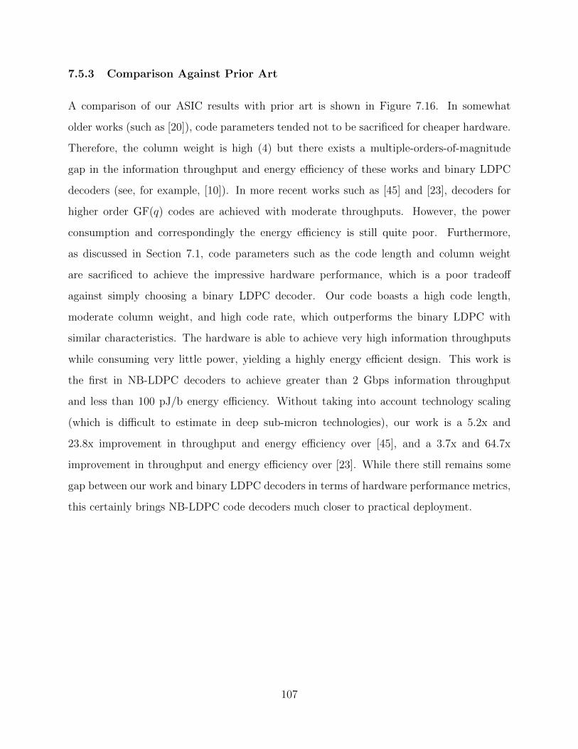
7.5.3 Comparison Against Prior Art
A comparison of our ASIC results with prior art is shown in Figure 7.16. In somewhat
older works (such as [20]), code parameters tended not to be sacrificed for cheaper hardware.
Therefore, the column weight is high (4) but there exists a multiple-orders-of-magnitude
gap in the information throughput and energy efficiency of these works and binary LDPC
decoders (see, for example, [10]). In more recent works such as [45] and [23], decoders for
higher order GF(q) codes are achieved with moderate throughputs. However, the power
consumption and correspondingly the energy efficiency is still quite poor. Furthermore,
as discussed in Section 7.1, code parameters such as the code length and column weight
are sacrificed to achieve the impressive hardware performance, which is a poor tradeoff
against simply choosing a binary LDPC decoder. Our code boasts a high code length,
moderate column weight, and high code rate, which outperforms the binary LDPC with
similar characteristics. The hardware is able to achieve very high information throughputs
while consuming very little power, yielding a highly energy efficient design. This work is
the first in NB-LDPC decoders to achieve greater than 2 Gbps information throughput
and less than 100 pJ/b energy efficiency. Without taking into account technology scaling
(which is difficult to estimate in deep sub-micron technologies), our work is a 5.2x and
23.8x improvement in throughput and energy efficiency over [45], and a 3.7x and 64.7x
improvement in throughput and energy efficiency over [23]. While there still remains some
gap between our work and binary LDPC decoders in terms of hardware performance metrics,
this certainly brings NB-LDPC code decoders much closer to practical deployment.
107
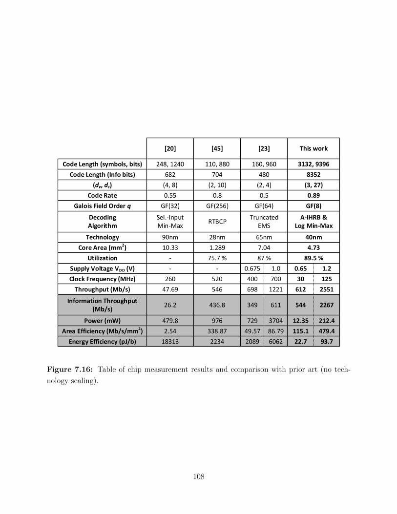
This work
Code Length (symbols, bits)
(dv, dc)
Code Rate
Galois Field Order q
DecodingAlgorithm
Technology
Core Area (mm2)
Throughput (Mb/s)
Power (mW)
Area Efficiency (Mb/s/mm2)
[23][20]
Information Throughput (Mb/s)
Energy Efficiency (pJ/b)
Clock Frequency (MHz)
Utilization
Sel.-Input Min-Max
160, 960
(2, 4)
0.5
GF(64)
Truncated EMS
65nm
7.04
87 %
400
698
349
729
49.57
2089
248, 1240
(4, 8)
0.55
GF(32)
90nm
10.33
-
260
47.69
26.2
479.8
2.54
18313
3132, 9396
(3, 27)
0.89
GF(8)
A-IHRB & Log Min-Max
40nm
4.73
89.5 %
30
612
544
12.35
115.1
22.7
[45]
RTBCP
110, 880
(2, 10)
0.8
GF(256)
28nm
1.289
75.7 %
520
546
436.8
976
338.87
2234
Code Length (Info bits) 480682 8352704
Supply Voltage VDD (V) 0.675- 0.65 1.2
125
2551
2267
212.4
479.4
93.7
700
1221
611
3704
86.79
6062
1.0-
Figure 7.16: Table of chip measurement results and comparison with prior art (no tech-
nology scaling).
108
CHAPTER 8
Conclusion
8.1 Research Contributions . . . . . . . . . . . . . . . . . . . . . . . . . . . . 110
8.2 Future Work . . . . . . . . . . . . . . . . . . . . . . . . . . . . . . . . . . 111
109
8.1 Research Contributions
Specific accomplishments of this research are:
· Proposed several algorithmic simplifications and analyzed their effects:
– The Pruned Min-Max algorithm, which was shown to have negligible impact on
the performance and directly alleviate hardware implementation costs for lower
rate codes.
– The A-IHRB algorithm, which in combination with a soft decoding algorithm is
highly amenable to hardware implementation which results in a high throughput
and high energy efficiency.
· Analyzed the effect of the quantization scheme on the decoding performance of NB-
LDPC codes, and identified the effects of limiting the number of bits used to represent
LLRs.
· Proposed the Logarithmic quantization scheme, which is easily applicable to any exist-
ing soft decoder and yields large (up to 40% in our comparison) hardware cost reduction
without paying a price in the coding gain.
· Created a multi-purpose FPGA platform:
– The Min-Max algorithm, implemented in hardware, accelerates frame error rate
simulations enabling the observation of much lower frame error rates relative to
software simulations.
– The logarithmic quantization scheme is applied, demonstrating both the hardware
resource savings as well as the negligible performance degradation (especially
important to observe at lower frame error rates).
– The FPGA platform features a flexible script-based RTL generation scheme, en-
abling the demonstration of FER simulation results as well as hardware resource
utilization reports across a variety of parity-check matrix designs.
110
· Fabricated a proof-of-concept ASIC chip. The maximum information throughput
achieved was 2.267 Gbps at 1.2V supply and 125MHz clock, where the power con-
sumption was 212.4mW. The energy efficiency at this operating point was 93.7pJ/bit.
The throughput and energy efficiency are 3.7x and 23.8x improvements respectively
from state-of-the-art. The energy efficiency can further be improved by scaling the
supply voltage down to 0.65V, where the information throughput is 544.2 Mbps and
the power consumption is 12.35mW, yielding an energy efficiency of 22.7pJ/bit.
8.2 Future Work
Areas of potential future work include:
· Application of algorithmic techniques to spatially coupled NB-LDPC codes. While the
proposed techniques such as the logarithmic quantization scheme should seamlessly
integrate with spatially coupled codes and decoders such as windowed decoders, this
has not been explicitly verified or investigated. It will also be worthwhile to investigate
the hardware implications of our techniques in this context.
· Alternatives to the A-IHRB algorithm. The A-IHRB as it is is fairly simple and it
is not likely that a great performance improvement can be made without introducing
too much complexity. However, it is possible that the “coarse” decoder can play an
increased role in the dual-algorithm decoding scheme. For example, could the channel
input LLR vector be “preprocessed” so that the soft decoding algorithm improves
its performance? Although not discussed in this manuscript, we did investigate this
possibility and found that it is not trivial to find such a “preprocessing” scheme without
introducing high complexity or a coding gain degradation (sometimes in the form of
an early error floor, which can be missed). However, there is still the possibility of an
opportunity for improvement in this regard.
· Further improvement of ASIC specifications. While we have made large advancements
in terms of the information throughput, energy efficiency per decoded bit, etc., there
111
is still a gap in the performance relative to binary LDPC code decoders.
– One major bottleneck is the relatively long critical path in the proposed variable
node unit, slowing down the overall clock frequency of the decoder. Somehow
reducing the logic depth or allowing pipelining (although these would not be
trivial) would be of high interest for our architecture.
– Another high-cost element is the storage of messages. The memory elements
take a large amount of real estate on silicon, and this cost only increases as the
code length increases (to 2K and 4K byte codewords). Techniques to reduce this
storage requirement will further help reduce the decoder cost.
· Consideration of rate-programmability. The decoder architecture design for rate-
programmable NB-LDPC decoders for storage is an open question.
112
References
[1] R. G. Gallager, “Low-Density Parity-Check Codes,” Ph.D. dissertation, Cambridge,MA: MIT Press, 1963. 2
[2] R. Hamming, “Error detecting and error correcting codes,” The Bell Systems TechnicalJournal, vol. 29, no. 2, pp. 147–150, Apr. 1950. 2
[3] R. Bose and D. Ray-Chaudhuri, “On a class of error correcting binary group codes,”Information and Control, vol. 3, pp. 68–79, Mar. 1960. 2
[4] I. Reed and G. Solomon, “Polynomial codes over certain finite fields,” Journal of theSociety for Industrial and Applied Mathematics, vol. 8, pp. 300–304, June 1960. 2
[5] IEEE Standard for Information Technology - Telecommunications and Information Ex-change Between Systems-Local and Metropolitan Area Networks-Specific RequirementsPart 3: Carrier Sense Multiple Access With Collision Detection (CSMA/CD) AccessMethod and Physical Layer Specifications, IEEE Std. 802.3an Std., 2006. 3, 62
[6] ETSI Standard TR 102 376 V1.1.1: Digital Video Broadcasting (DVB) User Guidelinesfor the Second Generation System for Broadcasting, Interactive Services, News Gather-ing and Other Broadband Satellite Applications (DVB-S2), ETSI Std. TR 102 376 Std.,2005. 3
[7] IEEE Standard for Local and Metropolitan Area Networks Part 16: Air Interface forFixed and Mobile Broadband Wireless Access Systems Amendment 2: Physical andMedium Access Control Layers for Combined Fixed and Mobile Operation in LicensedBands and Corrigendum 1, IEEE Std. 802.16e Std., 2006. 3, 62
[8] IEEE Standard for Information Technology: Telecommunications and Information Ex-change between Systems: Local and Metropolitan Area Networks: Specific RequirementsPart 11: Wireless LAN Medium Access Control (MAC) and Physical Layer (PHY)Specifications Amendment 4: Enhancements for Very High Throughput for Operationin Bands below 6 GHz., IEEE Std. 802.11ac-2013 Std., 2013. 3, 62
[9] C.-H. Liu et al., “An LDPC decoder chip based on self-routing network for IEEE 802.16eapplications,” IEEE J. Solid-State Circuits, vol. 43, no. 3, pp. 684–694, Mar. 2008. 3,32
[10] Z. Zhang, V. Anantharam, M. J. Wainwright, and B. Nikolic, “An Efficient 10GBASE-TEthernet LDPC Decoder Design With Low Error Floors,” IEEE J. Solid-State Circuits,vol. 45, no. 4, April 2010. 3, 107
[11] M. Mansour and N. Shanbhag, “High-throughput LDPC decoders,” IEEE Trans. VeryLarge Scale Integr. (VLSI) Syst., vol. 11, no. 6, pp. 976–996, Dec 2003. 3, 44
[12] K. Zhang, X. Huang, and Z. Wang, “A high-throughput LDPC decoder architecturewith rate compatibility,” IEEE Trans. Circuits Syst. I, Reg Papers, vol. 58, no. 4, pp.839–847, Apr. 2011. 3, 32
113
[13] T. Mohsenin, D. Truong, and B. Baas, “A low-complexity message-passing algorithmfor reduced routing congestion in LDPC decoders,” IEEE Trans. Circuits Syst. I, RegPapers, vol. 57, no. 5, pp. 1048–1061, May 2010. 3, 32, 45
[14] D. Declercq and M. Fossorier, “Decoding Algorithms for Nonbinary LDPC Codes OverGF(q),” IEEE Trans. Commun., vol. 55, no. 4, pp. 633–643, April 2007. 3, 92
[15] A. Voicila et al., “Low-complexity decoding for non-binary LDPC codes in high orderfields,” IEEE Trans. Commun., vol. 58, no. 5, pp. 1365–1375, May 2010. 3, 45, 92
[16] M. Davey and D. MacKay, “Low-density parity check codes over GF(q),” IEEE Com-mun. Lett., vol. 2, no. 6, pp. 165–167, June 1998. 3, 12
[17] A. Hareedy, B. Amiri, R. Galbraith, and L. Dolecek, “Non-Binary LDPC Codes forMagnetic Recording Channels: Error Floor Analysis and Optimized Code Design,”IEEE Transactions on Communications, vol. 64, no. 8, pp. 3194–3207, Aug 2016. 3, 91
[18] L. Barnault and D. Declercq, “Fast decoding algorithm for LDPC over GF(2q),” inProc. Inform. Theory Workshop, Mar. 2003, pp. 70–73. 3, 14, 15
[19] X. Chen, S. Lin, and V. Akella, “Efficient configurable decoder architecture for non-binary quasi-cyclic LDPC codes,” IEEE Trans. Circuits Syst. I, Reg Papers, vol. 59,no. 1, pp. 188–197, Jan. 2012. 3, 20, 23, 31, 32, 45
[20] Y.-L. Ueng et al., “An efficient layered decoding architecture for nonbinary QC-LDPCcodes,” IEEE Trans. Circuits Syst. I, Reg Papers, vol. 59, no. 2, pp. 385–398, Feb. 2012.3, 20, 23, 27, 31, 32, 107
[21] X. Zhang and F. Cai, “Reduced-complexity decoder architecture for non-binary LDPCcodes,” IEEE Trans. Very Large Scale Integr. (VLSI) Syst., vol. 19, no. 7, pp. 1229–1238, July 2011. 3, 20, 23
[22] X. Chen and C.-L. Wang, “High-throughput efficient non-binary LDPC decoder basedon the simplified min-sum algorithm,” IEEE Trans. Circuits Syst. I, Reg Papers, vol. 59,no. 11, pp. 2784–2794, Nov. 2012. 3, 20, 23, 34, 45
[23] Y. S. Park, Y. Tao, and Z. Zhang, “A Fully Parallel Nonbinary LDPC Decoder WithFine-Grained Dynamic Clock Gating,” IEEE J. Solid-State Circuits, vol. 50, no. 2, pp.464–475, Feb. 2015. 3, 20, 23, 63, 89, 90, 92, 107
[24] F. Garcıa-Herrero, M. J. Canet, and J. Valls, “Nonbinary LDPC Decoder Based onSimplified Enhanced Generalized Bit-Flipping Algorithm,” IEEE Trans. Very LargeScale Integr. (VLSI) Syst., vol. 22, no. 6, pp. 1455–1459, June 2014. 3, 20, 23
[25] X. Zhang, F. Cai, and S. Lin, “Low-complexity reliability-based message-passing de-coder architectures for non-binary LDPC codes,” IEEE Trans. Very Large Scale Integr.(VLSI) Syst., vol. 20, no. 11, pp. 1938–1950, Nov. 2012. 3, 76, 77, 78
[26] V. Savin, “Min-Max decoding for non binary LDPC codes,” in Proc. IEEE Int. Symp.Inf. Theory, July 2008, pp. 960–964. 3, 11, 17, 18
114
[27] C. Spagnol, E. M. Popovici, and W. P. Marnane, “Hardware Implementation of GF(2m)LDPC Decoders,” IEEE Trans. Circuits Syst. I, Reg Papers, vol. 56, no. 12, pp. 2609–2620, Dec 2009. 19, 92
[28] Y. Toriyama, B. Amiri, L. Dolecek, and D. Markovic, “Field-order based hardware costanalysis of non-binary LDPC decoders,” in Proc. IEEE Asilomar Conf. Signals, Syst.,and Comput., Nov 2014, pp. 2045–2049. 25
[29] Y. S. Park, Y. Tao, and Z. Zhang, “A 1.15Gb/s fully parallel nonbinary LDPC decoderwith fine-grained dynamic clock gating,” in Proc. IEEE Int. Solid-State Circuits Conf.Dig. Tech. Papers (ISSCC), Feb. 2013, pp. 422–423. 27, 32, 45
[30] J. Lin, J. Sha, Z. Wang, and L. Li, “Efficient decoder design for nonbinary quasicyclicLDPC codes,” IEEE Trans. Circuits Syst. I, Reg Papers, vol. 57, no. 5, pp. 1071–1082,May 2010. 31
[31] B. Amiri, S. Srinivasa, and L. Dolecek, “Quantization, absorbing regions and practicalmessage passing decoders,” in Proc. IEEE Asilomar Conf. Signals, Syst., and Comput.,Nov. 2012, pp. 1255–1259. 36
[32] B. Amiri, J. Kliewer, and L. Dolecek, “Analysis and enumeration of absorbing sets fornon-binary graph-based codes,” in Proc. IEEE Int. Symp. Inform. Theory (ISIT), July2013, pp. 398–409. 37, 50
[33] Y. Toriyama, B. Amiri, L. Dolecek, and D. Markovic, “Logarithmic quantization schemefor reduced hardware cost and improved error floor in non-binary LDPC decoders,” inIEEE Glob. Commun. Conf. (GLOBECOM), Dec 2014, pp. 3162–3167. 44
[34] J. Lin and Z. Yan, “Efficient Shuffled Decoder Architecture for Nonbinary Quasi-CyclicLDPC Codes,” IEEE Trans. Very Large Scale Integr. (VLSI) Syst., vol. 21, no. 9, pp.1756–1761, Sept 2013. 45
[35] X. Zhang and P. H. Siegel, “Quantized min-sum decoders with low error floor for LDPCcodes,” in Proc. IEEE Int. Symp. Inform. Theory (ISIT), July 2012, pp. 2871–2875. 45
[36] X. Zhang and P. H. Siegel, “Will the Real Error Floor Please Stand Up?” in Int. Conf.Sig. Proc. Comm. (SPCOM), July 2012, pp. 1–5. 45
[37] “IEEE Standard for Floating-Point Arithmetic,” IEEE Std 754-2008, pp. 1–70, August2008. 54
[38] L. Lan et al., “Construction of Quasi-Cyclic LDPC Codes for AWGN and Binary ErasureChannels: A Finite Field Approach,” IEEE Trans. Information Theory, vol. 53, no. 7,pp. 2429–2458, July 2007. 61
[39] L. Zhang et al., “Quasi-Cyclic LDPC Codes: An Algebraic Construction, Rank Analysis,and Codes on Latin Squares,” IEEE Trans. Commun., vol. 58, no. 11, pp. 3126–3139,November 2010. 61
115
[40] X.-Y. Hu, E. Eleftheriou, and D. M. Arnold, “Progressive Edge-Growth TannerGraphs,” in IEEE Glob. Telecommun. Conf. (GLOBECOM), Nov 2001, pp. 995–1001.62
[41] C. Y. Chen, Q. Huang, C. C. Chao, and S. Lin, “Two low-complexity reliability-basedmessage-passing algorithms for decoding non-binary ldpc codes,” IEEE Trans. Com-mun., vol. 58, no. 11, pp. 3140–3147, November 2010. 76
[42] M. P. C. Fossorier, “Quasicyclic low-density parity-check codes from circulant permu-tation matrices,” IEEE Trans. Information Theory, vol. 50, no. 8, pp. 1788–1793, Aug2004. 88
[43] J. Chen and M. P. C. Fossorier, “Density evolution for two improved BP-Based decodingalgorithms of LDPC codes,” IEEE Commun. Lett., vol. 6, no. 5, pp. 208–210, May 2002.89
[44] J. Zhao, F. Zarkeshvari, and A. H. Banihashemi, “On implementation of min-sum al-gorithm and its modifications for decoding low-density Parity-check (LDPC) codes,”IEEE Trans. Commun., vol. 53, no. 4, pp. 549–554, April 2005. 89
[45] J. Lin and Z. Yan, “An Efficient Fully Parallel Decoder Architecture for NonbinaryLDPC Codes,” IEEE Trans. Very Large Scale Integr. (VLSI) Syst., vol. 22, no. 12, pp.2649–2660, Dec 2014. 90, 92, 107
[46] B. Amiri, J. A. F. Castro, and L. Dolecek, “Design of non-binary quasi-cyclic ldpc codesby absorbing set removal,” in IEEE Information Theory Workshop (ITW), Nov 2014,pp. 461–465. 91
[47] A. Hareedy et al., “Non-Binary LDPC Code Optimization for Partial-Response Chan-nels,” in IEEE Glob. Commun. Conf. (GLOBECOM), Dec 2015, pp. 1–6. 88, 91
[48] A. Hareedy, C. Lanka, and L. Dolecek, “A General Non-Binary LDPC Code Opti-mization Framework Suitable for Dense Flash Memory and Magnetic Storage,” IEEEJournal on Selected Areas in Communications, vol. 34, no. 9, pp. 2402–2415, Sept 2016.88, 91
[49] P. L’Ecuyer, “Maximally Equidistributed Combined Tausworthe Generators,” AMSMathematics of Computation, vol. 65, pp. 203–213, 1996. 97
[50] “Synphony Model Compiler,” [Online]. Available: http://www.synopsys.com/Tools/Implementation/FPGAImplementation/Pages/synphony-model-compiler.aspx. 99
[51] “ROACH.” [Online]. Available: https://casper.berkeley.edu/wiki/ROACH. 101
[52] “Virtex-5 Family Overview.” [Online]. Available: http://www.xilinx.com/support/documentation/data sheets/ds100.pdf. 101
[53] “Collaboration for Astronomy Signal Processing and Engineering Research (CASPER).”[Online]. Available: https://casper.berkeley.edu. 101
116

[54] “KATCP.” [Online]. Available: https://casper.berkeley.edu/wiki/KATCP. 101
117