designing fast golay encoder/decoder in xilinx xact with
TRANSCRIPT

NPS ARCHIVE1997.03SARI, M.
NAVAL POSTGRADUATE SCHOOLMonterey, California
THESIS
iThesisS16674
DESIGNING FAST GOLAY ENCODER/DECODER IN XILINX
XACT WITH MENTOR GRAPHICS CAD INTERFACE
by
Mehmet San
March 1997
Thesis Advisor:
Second Reader:
Chin Hwa Lee
Todd Weatherford
Approved for public release; distribution is unlimited.


REPORT DOCUMENTATION PAGE Form Approved OMB No. 0704-0188
Public reporting burden for this collection ot information is estimated to average 1 hour per response, including the time for reviewing instruction, searching
existing data sources, gathering and maintaining the data needed, and completing and reviewing the collection of information. Send comments regarding this
burden estimate or any other aspect of this collection of information, including suggestions for reducing this burden, to Washington Headquarters Services,
Directorate for Information Operations and Reports, 1215 Jefferson Davis Highway, Suite 1204, Arlington, VA 22202-4302, and to the Office of Management andBudget, Paperwork Reduction Project (0704-0188) Washington DC 20503.
1 . AGENCY USE ONLY (Leave
blank)
REPORT DATEMarch 1997
3. REPORT TYPE AND DATES COVEREDMaster's Thesis
TITLE AND SUBTITLE DESIGNING FAST GOLAY ENCODER/DECODERIN XILINX XACT WITH MENTOR GRAPHICS CAD INTERFACE
6. AUTHOR(S) Sary, Mehmet
5. FUNDING NUMBERS
7. PERFORMING ORGANIZATION NAME(S) AND ADDRESS(ES)Naval Postgraduate School
Monterey, CA 93943-5000
8. PERFORMINGORGANIZATIONREPORT NUMBER
SPONSORING/MONITORING AGENCY NAME(S) AND ADDRESS(ES) 10. SPONSORING/MONITORINGAGENCY REPORT NUMBER
1 1 . SUPPLEMENTARY NOTES The views expressed in this thesis are those of the author and do not reflect
the official policy or position of the Department of Defense or the U.S. Government.
12a. DISTRIBUTION/AVAILABILITY STATEMENTApproved for public release; distribution is unlimited.
12b. DISTRIBUTION CODE
1 3. ABSTRACT (maximum 200 words)
The programmable logic array is one of the most fascinating and fast developing areas of
technology. Field programmable gate arrays are becoming prevalent in design as the density of the gate
arrays goes up. In this thesis study, a fast encoding/decoding algorithm, Extended Golay Coding, is
implemented in Xilinx XC4000 family programmable gate array (FPGA) architecture. The encoder/decoder
is designed using the Xilinx XACT tool with the Mentor Graphics schematic capture Design Architect (DA)
and Quicksimll simulation interfaces. With the static RAM bits onboard the new Xilinx FPGAs, the
architecture is more powerful, and it is relatively easy to upgrade the old design based on the needs of the
users. In this thesis, fast encoder/decoder is implemented with transmission word redundancy and
interleaving. This is based on the data link layer description of the Milstd 181-144A. The FPGA static RAMbits are used for the encode and decode ROM of the algorithm that makes the coder faster. Modular
approach and design hierarchy made design tasks easier and upgradable in this study. The timing
simulations of some design modules will be presented. Due to the complexity of the circuits, it is found that
the design has to be migrated to a higher density chip than XC4003 used in the simulations.
14. SUBJECT TERMS Spinning Sphere, Rotationally Symmetric Flow, Spectral
Methods
15. NUMBER OFPAGES 103
16. PRICE CODE
17. SECURITY CLASSIFI-
CATION OF REPORTUnclassified
18. SECURITY CLASSIFI-
CATION OF THIS PAGEUnclassified
19. SECURITY CLASSIFI-
CATION OF ABSTRACTUnclassified
20. LIMITATION OFABSTRACT
UL
NSN 7540-01-280-5500 Standard Form 298 (Rev. 2-89)
Prescribed by ANSI Std. 239-18 298-102

Approved for public release; distribution is unlimited.
DESIGNING FAST GOLAY ENCODER/DECODER IN XILINX XACTWITH MENTOR GRAPHICS CAD INTERFACE
Mehmet Sari
Lieutenant Junior Grade, Turkish NavyB.S., Turkish Naval Academy, 1991
Submitted in partial fulfillment of the
requirements for the degree of
MASTER OF SCIENCE IN ELECTRICAL ENGINEERING
from the
NAVAL POSTGRADUATE SCHOOLMarch 1997

DUDLB«»*M«yOSTGABSTRACT »ont£R£$g^g** SCHOo
The programmable logic array is one of the most fascinating and fast
developing areas of technology. Field programmable gate arrays are becoming
prevalent in design as the density of the gate arrays goes up. In this thesis
study, a fast encoding/decoding algorithm, Extended Golay Coding, is
implemented in Xilinx XC4000 family programmable gate array (FPGA)
architecture. The encoder/decoder is designed using the Xilinx XACT tool with
the Mentor Graphics schematic capture Design Architect (DA) and Quicksimll
simulation interfaces. With the static RAM bits onboard the new Xilinx FPGAs,
the architecture is more powerful, and it is relatively easy to upgrade the old
design based on the needs of the users. In this thesis, fast encoder/decoder is
implemented with transmission word redundancy and interleaving. This is based
on the data link layer description of the Milstd 181-144A. The FPGA static RAM
bits are used for the encode and decode ROM of the algorithm that makes the
coder faster. Modular approach and design hierarchy made design tasks easier
and upgradable in this study. The timing simulations of some design modules
will be presented. Due to the complexity of the circuits, it is found that the design
has to be migrated to a higher density chip than XC4003 used in the simulations.

V!
TABLE OF CONTENTS
I. INTRODUCTION 1
II. ENCODING/DECODING AND EXTENDED GOLAY CODE 3
A. FECINMILSTD188-141A 4
B. THE GOLAY CODE 5
C. INTERLEAVING AND DEINTERLEAVING 10
D. REDUNDANT WORDS 12
III. DESIGNING A FAST GOLAY ENCODER / DECODER 13
A. MODULAR DESIGN APPROACH 13
B. GENERAL OVERVIEW OF THE DESIGN 14
1. Top Level Layer 14
a. Introduction 14
b. Getting Into MGC Designs 17
2. Descriptions of the Design Modules 17
a. NEWTEST_YEN 17
(1) ENCODE_IN_WMAT 17
(2) 12BIT_SHIFTREG1 19
(3) REGFIRST_WEN1 19
(4) REG_NEWSECOND1 20
b. DECODE_STAGE_LAST2 21
(1) VOTER6 22
(2) GOLAY_MAJ_WORD_A and
GOLAY_MAJ_WORD_B 23
(3) MAJ_WORD_A_TO_ENC and
MAJ_WORD_B_TO_ENC 23
(4) REG_FORMAJ_WORD 24
(5). XOR2S_NEW3 24
vii

c. RAM_BITS_NEW1 25
IV. SIMULATION RESULTS 27
A. MGC DESIGN ARCHITECT 27
B. SIMULATIONS OF THE DESIGN MODULES 28
1. NEWTEST_YEN Simulation 28
2. DECODE_STAGE_LAST2 Simulation. 33
3. RAM_BITS_NEW1 Simulation 36
V. XILINX FIELD PROGRAMMABLE GATE ARRAYS 41
A. XILINX LOGICAL CELL ARRAYS 44
B. XILINX FAMILY ARCHITECTURE 45
1. Configurable Logic Blocks 45
2. Abundant Routing Resources 51
3. On-Chip Memory 51
4. Input/Output Blocks 52
5. Programmable Interconnect 54
6. Taking Advantage of Reconfiguration 55
7. The Xilinx Development System 56
C. CONCLUSION 56
VI. CONCLUSION AND RECOMMENDATIONS 59
APPENDIX A. CIRCUIT SCHEMATICS 61
APPENDIX B. SIMULATION SCHEMATICS 81
LIST OF REFERENCES 91
INITIAL DISTRIBUTION LIST 93
VIII

I. INTRODUCTION
The effective performance of a station, while communicating over adverse
RF channels, relies on the combined use of error correction, interleaving and
redundancy. These functions shall be performed within the transmit encoder and
receive decoder. By encoding and decoding redundant bits, it is possible to
correct bit errors without asking the source to retransmit. This provides reliable
transmission in a noisy or heavily interferenced channel. The bit errors at the
receiving end are recovered by forward error correcting (FEC) codes without
requiring a second channel to ask for retransmit (like in most error correcting
schemes using automatic repeat request - ARQ [Snelgrove,1994]). Block codes
or convolutional codes are used where retransmission of data is impractical or
impossible, such as in space probes or in broadcast satellites that transmit to
multiple receivers simultaneously [Stallings, 1994].
In this thesis study, the implementation of the Fast Golay
encoder/decoder is done on schematic entries. The design can be exported into
a Programmable Logic Device. Functional, and timing simulations of the design
will be explained in this thesis.
The main objective of this thesis is to design a reliable encoder/decoder
that can be used in a noisy or heavily interfered environment. The functionality
of the algorithm is explained in Chapter II. The designs in schematics are
explained in Chapter III. In Chapter IV, the stimulus inputs and simulation results
1

of the schematic sheets are discussed. The controller part is to be designed
according to these simulations results in a later study. The Xilinx Logical Cell
Array (LCA) technology is mentioned in Chapter V. The conclusion and
recommendations are given in the Chapter VI of this thesis.

II. ENCODING/DECODING AND EXTENDED GOLAY CODE
This chapter explains the basics of encoding/decoding algorithms, the
value of using the extended Golay Code, and how the algorithm works.
The demand for efficient and reliable digital data communication has
been increased by the emergence of large scale and high speed data networks
in the military, governmental, and private sectors. A merging of communications
and computer technology in this type of systems require the error correcting
algorithms. They are essential to provide reliable transmission of data.
[Snelgrove, 1994].
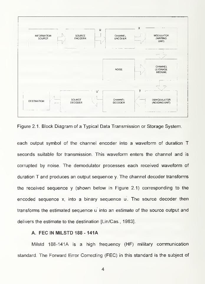
A typical transmission system may be represented by the block diagram in
Figure 2.1 [Lin and Castello, 1983]. The information source can be either a
person or a machine, e.g. digital computer. The source output can be either a
continuous waveform or a sequence of discrete symbols. The source encoder
transforms source output into a sequence of binary digits (bits), called the
information sequence u in Figure 2.1. In the case of a continuous source, this
involves analog-to-digital (AMD) conversion. The source encoder helps to
represent a source output with minimized number of bits per unit time. Another
requirement for source encoder is the ability to reconstruct signal from
information sequence u without ambiguity.
The channel encoder transforms the message sequence u into a discrete
encoded sequence x in Figure 2.1 , called a code word. The modulator changes
INFORMATIONSOURCE
DESTINATION
SOURCEENCODER
SOURCEDECODER
\r
CHANNELENCODER
NOISE
CHANNELDECODER
MODULATOR(WRITING
UNIT)
3TCHANNEL(STORAGEMEDIUM)
y\7
\^DEMODULATOR(READING UNIT)
Figure 2.1. Block Diagram of a Typical Data Transmission or Storage System.
each output symbol of the channel encoder into a waveform of duration T
seconds suitable for transmission. This waveform enters the channel and is
corrupted by noise. The demodulator processes each received waveform of
duration T and produces an output sequence y. The channel decoder transforms
the received sequence y (shown below in Figure 2.1) corresponding to the
encoded sequence x, into a binary sequence u. The source decoder then
transforms the estimated sequence u into an estimate of the source output and
delivers the estimate to the destination [Lin/Cas., 1983].
A. FEC IN MILSTD 188 - 141A
Milstd 188-141A is a high frequency (HF) military communication
standard. The Forward Error Correcting (FEC) in this standard is the subject of

study in this thesis given in this chapter. This standard consists of Automatic
Link Establishment (ALE) and FEC sublayers in the Data Link Layer of the seven
layer OSI model shown in Figure 2.2. This thesis involves only the Golay Code,
interleave, and redundancy of the standard.
TRANSMIT RECEIVE
ALESUBLAYER
PROTECTIONSUBLAYER
ALEPROTOCOL
(ALE WORD)
ALEPROTOCOL
WORD SYNCH
SEVEN LAYEROSI MODEL
FECSUBLAYEI
(BIT PATTERN)
GOLAY ENCOOER
INTERLEAVE
REDUNDANCY
PATTERN SYNCH
GOLAY DECODER
5
MODULATOR
TRANSMITTER
DEINTERLEAVE
DEMODULATOR
APPLICATIONLAYER
r
PRESENTATIONLAYER
r
' SESSIONLAYER
TRANSPORTLAYER
NETWORKLAYER
DATA LINKLAYER
PHYSICALLAYER
Figure 2.2. Milstd 188-141A FEC in OSI Model.
B. THE GOLAY CODE
The Golay code is a binary linear block (23, 12) code with minimum
Hamming distance = 7 [Lin and Castello, 63 and Proakis, 1989, 446]. The (23,
12) Golay code is the only known multiple-error-correcting binary code which is
capable of correcting any combination of three or less random errors in a block
of 23 digits [Lin, Castello, 1983]. The extended Golay code is obtained by adding
an overall parity bit to the (23, 12) code which results in a binary linear block
(24, 12) code with minimum Hamming distance = 8.
The (23 ,12 ) Golay code is generated either by
gi(x)= 1 +x2 +x4 +x5 + x6 +x10 +x 11
(2.1)
or by
g2 (x) = 1 +x+x5 +x6 + x7 +x9 +x 11
(2.2)
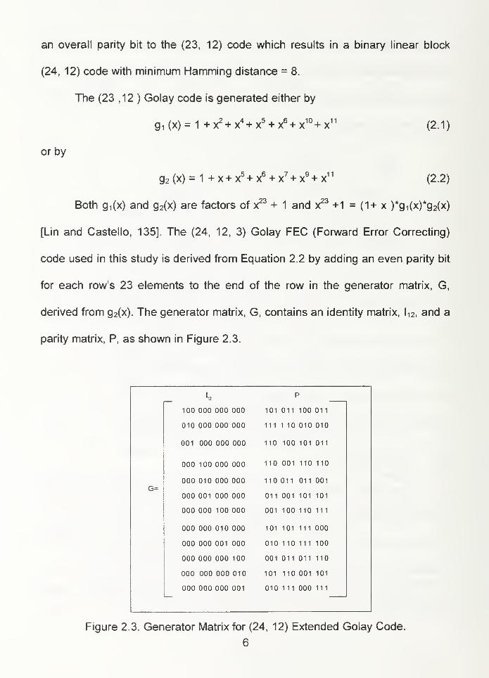
Both g^x) and g 2(x) are factors of x23 + 1 and x
23+1 = (1+ x )*gi(x)*g 2(x)
[Lin and Castello, 135]. The (24, 12, 3) Golay FEC (Forward Error Correcting)
code used in this study is derived from Equation 2.2 by adding an even parity bit
for each row's 23 elements to the end of the row in the generator matrix, G,
derived from g 2(x). The generator matrix, G, contains an identity matrix, l 12 , and a
parity matrix, P, as shown in Figure 2.3.
'* p
100 000 000 000 101 011 100 011
010 000 000 000 111 110 010 010
001 000 000 000 110 100 101 011
000 100 000 000 110 001 110 110
G=000 010 000 000
000 001 000 000
110 011 011 001
011 001 101 101
000 000 100 000 001 100 110 111
000 000 010 000 101 101 111 000
000 000 001 000 010 110 111 100
000 000 000 100 001 011 011 110
000 000 000 010 101 110 001 101
000 000 000 001 010 111 000 111
Figure 2.3. Generator Matrix for (24, 12) Extended Golay Code.
6
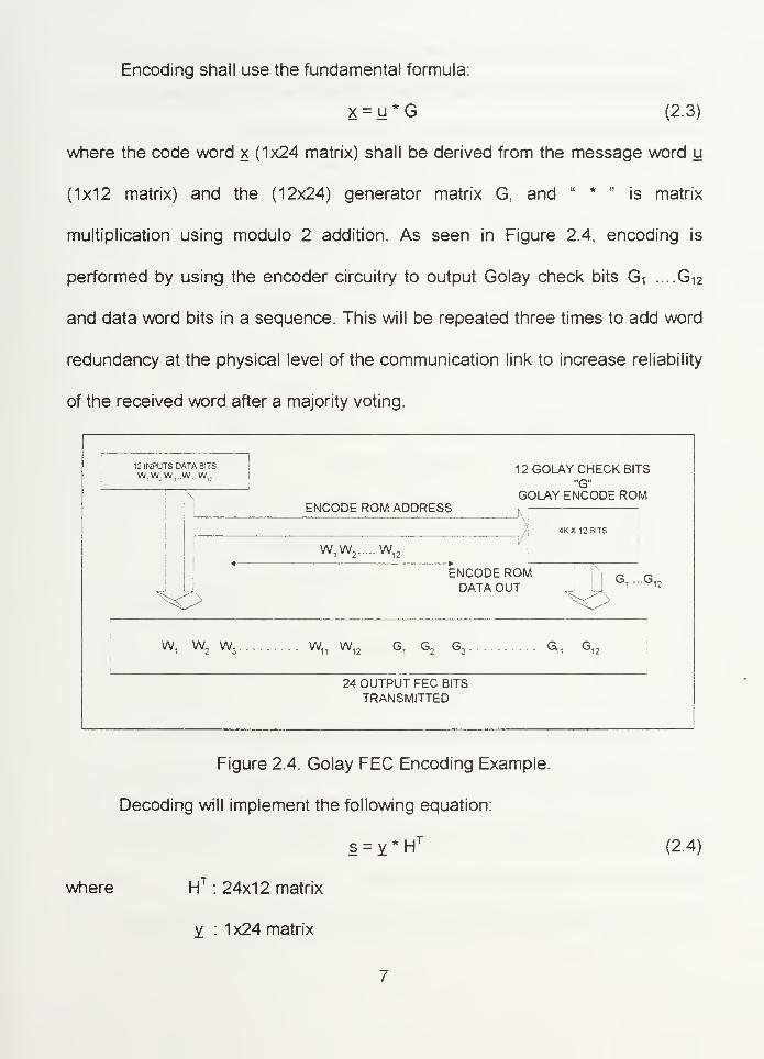
Encoding shall use the fundamental formula:
x = u*G (2.3)
where the code word x (1x24 matrix) shall be derived from the message word u
(1x12 matrix) and the (12x24) generator matrix G, and " * " is matrix
multiplication using modulo 2 addition. As seen in Figure 2.4, encoding is
performed by using the encoder circuitry to output Golay check bits Gi ....G12
and data word bits in a sequence. This will be repeated three times to add word
redundancy at the physical level of the communication link to increase reliability
of the received word after a majority voting.
12 INPUTS DATA BITS
w. w.w3.,.w.. W,.
! i
12 GOLAY CHECK BITS
"G"i
I
i ]
GOLAY ENCODE ROMFMcnnr r?OM Annnrw
^
4KX12 8ITS
\>
w,w2
w12
ENCODE ROM \\ QDATA OUT J J^ 1 '
.G12
w1w
2w
3
IWW G G G G G.... vv,, vv12
o1
o2
o3
va,. >j12
i
24 OUTPUT FEC BITS
TRANSMITTED
Figure 2.4. Golay FEC Encoding Example.
Decoding will implement the following equation:
s = y * HT
where HT: 24x12 matrix
(2.4)
y : 1 x24 matrix
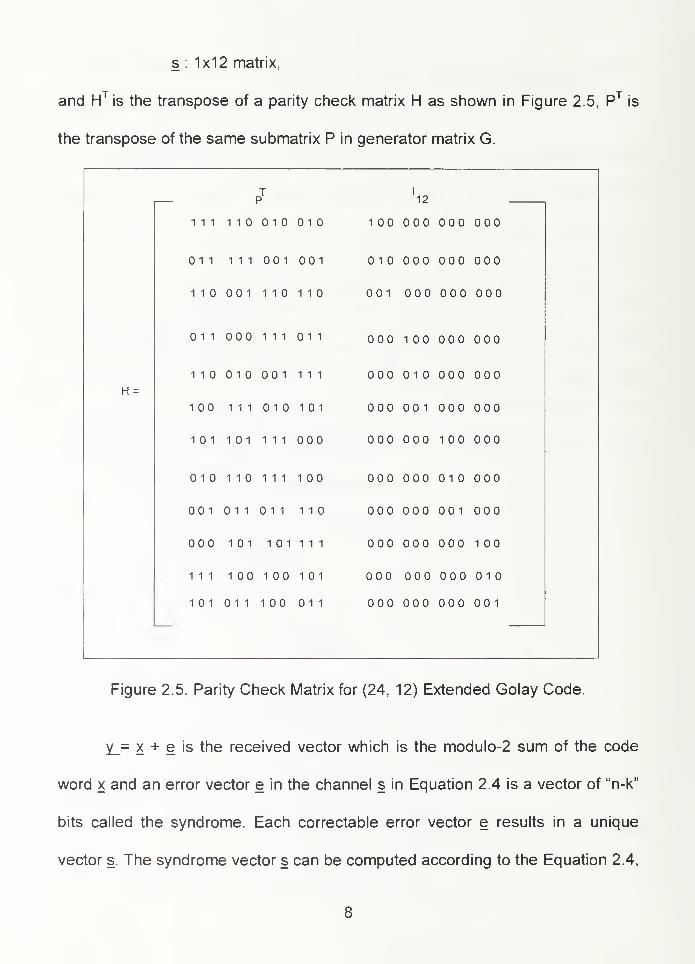
s : 1x12 matrix,
and H Tis the transpose of a parity check matrix H as shown in Figure 2.5, PT
is
the transpose of the same submatrix P in generator matrix G.
H =
PT
111 110 010 010
011 111 001 001
110 001 110 110
011 000 111 011
110 010 001 111
100 111 010 101
101 101 111 000
010 110 111 100
001 011 011 110
000 101 101111
111 100 100 101
101 011 100 011
12
100 000 000 000
010 000 000 000
001 000 000 000
000 100 000 000
000 010 000 000
000 001 000 000
000 000 100 000
000 000 010 000
000 000 001 000
000 000 000 100
000 000 000 010
000 000 000 00 1
Figure 2.5. Parity Check Matrix for (24, 12) Extended Golay Code.
y_= x + e is the received vector which is the modulo-2 sum of the code
word x and an error vector e in the channel s in Equation 2.4 is a vector of "n-k"
bits called the syndrome. Each correctable error vector e results in a unique
vector s. The syndrome vector s can be computed according to the Equation 2.4,
8
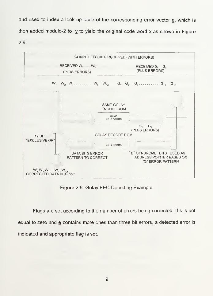
and used to index a look-up table of the corresponding error vector e, which is
then added modulo-2 to y to yield the original code word x as shown in Figure
2.6.
24 INPUT FEC BITS RECEIVED (WITH ERRORS)
RECEIVED W, W12
(PLUS ERRORS)
RECEIVED Q...Q 2
(PLUS ERRORS)
W, W2W
3 W„ W1:
G1
G2 G
3G
11G12
SAME GOLAYENCODE ROM
SAME4K X 12 BITS
G, G,2
(PLUS ERRORS)
12 BIT
"EXCLUSIVE OR'
GOLAY DECODE ROM
4K X 12 BITS
DATA BITS ERRORPATTERN TO CORRECT
§ SYNDROME BITS USED ASADDRESS POINTER BASED ON
"G" ERROR PATTERN
W1W2W3 ....W
11W
12
CORRECTED DATA BITS "W"
Figure 2.6. Golay FEC Decoding Example.
Flags are set according to the number of errors being corrected. If s is not
equal to zero and e contains more ones than three bit errors, a detected error is
indicated and appropriate flag is set.

c. INTERLEAVING AND DEINTERLEAVING
The Milstd 188-141A basic word has 24 bits, and it requires two Golay
encoder section A and section B to do the work. The basic word bits Wi^ (MSB)
through Win24 (LSB) and resultant Golay FEC bits Gi through G24 (with G 13
through G24 inverted) shall be interleaved following the pattern in Figure 2.7
before transmission.
CODER A I AffT BITff
G* -
G, "
G2 "
G*
G„ B24G» B23
49" "H RT1 IFF RIT=0 ^^S49 S49
GOLAY CHECK G n B22 B24 G24 CHECK BITS
BITS INVERTEDG„ B21 A24 G12 G»
REINVERTED
FROM NORMAL Ga B20 B23 G23 G« TO NORMALAFTER G.» B19 A23 G11 G„ "
Gl7
BEFORE
ENCODING G.s B18 B22 G22 DECODINGG„ B17 A22 G10 G„ '
G,; -
G,4 "
G«W WR24
G„ B16 B21 G21 DECODER BG„ B15 A21 G9G,« B14 B20 G20G„ B13 A20 G8 V
WM B12Wa B11WE B10
B19 G19A19 G7B18 G18A18 G6
W» WR23Wn WR22W„ WR21WB WR20
sV^WR24WR23W, B9
Ws B8B17 G17A17 G5
W» WR19W„ WR18^ WR22
WR211IIIt
W„ B7 BT6 G16 W„ WR17^\VWR20
l/l/iW« B6 A16 G4 W,6
WR16^N\>WR19IllllUt
W" B5 B15 G15 W„ WR15S^NS WR18W18
B4 A15 G3 w" WR14\nN>WR17II 1 hWin* III W,5 B3 B14 G14 W„ WR13^VN^WR16Win*, In W„ B2 A14 G2 \V WR15Wina '////////)
W„ B1 B13 G13 \\WR14Win, II A13 G1 WR13Win, II r.ODFR R B12 W24 yV/^W^MlspBCQDER A
G.j A24Win,, If
A12 W12 G„ WR12Win,, 'll G„ A23 B1 1 W23 G„ WR11Win„ G, A22 A11 W11 G„ - WR10Win,6
G, A21 B10 W22 G WR9Win,, G, A20 A10 W10 G, WR8Win,, Gi A19 B9 W21 G> WR7Win,, G 6 A18
G, A17A9 W9B8 W20 aMaxv^
G.G,
WR6WR5
Win,;
G, A16 A8 W8 ujWS\a G. WR4Win,,
G, A15 B7 W19 Wf\\\V G 3WR3
Win,„ G, A14 A7 W7//)V/aCv\\\ G ;
WR2Win, G, A13 B6 W18 ijj rfj \\\\ >
G, - WR1Win,
Win,
A6 W6 W,2 WR12W„ WR11Wu A12 B5 W17
Win, W„ A11 A5 W5 W, WR10 //////////output
Win, W10
A10 B4 W16 W, WR9 ///////// BASIC
Win. W, A9 A4 W4 W, WR8 II II W0RDWin 3
W, A8 B3 W15 W, WR7 III <24 BITS)
Win, W, A7 A3 W3 W, WR6Win, W c A6
\N, A5B2 W14 W, WR5
\\\\ A2 W2 W 4 WR4INPUT BAS)C\\
W> A4W 3 A3Wj A2
B1 W13 W3 WR3
WORD(24 BITSA A1 W1 W ; WR2\ ^-^'"TRA W, WR1\ W, A1 -1T3TERLEAVING WORDS DEINTERLEA\ ING
GOLAY ENCODING (49 BITS) GOLAY UECODING
Figure 2.7. Word Bit Coding/Decoding, Interleaving/Deinterleaving.
10
There are forty eight interleaved bits, and the 49th
bit is a stuff bit
(value=0) during transmission. They shall constitute a transmitted word and be
transmitted A1, B1, A2, B2, ..., A24, B24, S49 using a 16-1/3 symbols (tones)
per word time (Tw). In order to lessen the effects of the channel noise causing
information data bits loss all from one word, interleaving in this manner is
employed. At the receiver, after 2/3 majority voting in Figure 2.8, the 48 received
bits of the majority word (including the remaining errors) shall be deinterleaved
as shown in Figure 2.6. The Golay FEC decoder will then produce a correct (ed)
24 bit basic word (or an uncorrectable error flag). The 49,h
stuff bit (S49 ) is
ignored.
i RFniiNnANT-wnRny J,redundant "word M + r J
WORD(BIT) FLO
WORD M + 1
BIT ORIENTED 2/3MAJORITY VOTE
DECODER
$.
TNOTE : THE USE OF 2/3 VOTING REQUIRES EACH
MAJORITY WORD M TO BE TRANSMITTEDAT LEAST THREE ADJACENT TIMES
WORD ORIENTEDDEINTERLEAVING AND DECODING
Figure 2.8. Bit and Word Majority Voting Before Decoding.
11

D. REDUNDANT WORDS
Each of the transmitted 49-bit (or 16-1/3 symbol) word in the Tw time shall
be redundant (times 3) to reduce the effects of fading, interference and noise. At
bit time interval (approximately Tw/49), the receiver shall examine the present bit
and the past bit stream and perform a 2/3 majority vote, on a bit-by-bit basis,
over a span of three words. The resultant 48 most recent majority bits (excluding
the 49th
bit which is the stuff bit) constitute the latest majority word and shall be
delivered to the deinterleaver and FEC decoder (Figure 2.8). In addition, the
number of unanimous votes of the 48 possible votes associated with the majority
word can be temporarily retained for use.
In this thesis the main focus is on the design and simulation of various
modules that will accomplished the operation discussed in this chapter.
12
III. DESIGNING A FAST GOLAY ENCODER / DECODER
In this chapter, the implementation of the fast Golay decoder/encoder is
explained. The implementation overview, and details are given to help the
design of a controller in a future study.
A. MODULAR DESIGN APPROACH
The modular approach allows a designer to create small pieces of the
whole design and debug them relatively easier than the bigger complex
designs. Making designs in short time period is important in today's fast
developing area of technology. It is advantageous to put the pieces together
creating the whole design as layers of encapsulation and modules. This
approach develops a hierarchy of layers from the topmost one showing the
simple inputs and outputs of the whole system to the lowest one showing the
gate level construction of each component. As we go down to lower layers, we
get into those encapsulated design modules and involve more the hardware
details of each module. In this way, the design is partitioned into layers of
hierarchy and modules independent from each other. This allows them to be
individually simulated and debugged.
13
B. GENERAL OVERVIEW OF THE DESIGN
1. Top Level Layer
a. Introduction
The top layer consists of the input signal: serial data input,
encoder/decoder select, system clock, and clear signals and encode/decode
ROM matrices. The output signals are encoded word transmission or decoded-
and-recovered data word serial output. There are status signals representing the
valid times of the signal transmission beginning and ending.
The functional overview of the design is shown in Figure 3.1. The
encode, and decode ROM matrices in the algorithm are entered into the static
RAM cells of the FPGA initially. The encode control signals and decode control
signals are generated alongside serial input according to the encoder/decoder
select input of the controller unit in Figure 3.1.
SERIAL DATAINPUT
ENCODE/DECODEROM INPUT
CONTROLSIGNALS
O
ENCODER/DECODERSELECT
MAIN_
CIRCUIT ENCODER/DECODERSERIAL OUTPUT
CONTROLLERENCODER/DECODER'BEGIN & END SIGNALS
Figure 3.1. Functional Diagram of the Golay Encoder/Decoder.
14

The controller in Figure 3.1 will generate the status signals showing the
beginning, and end of encode and decode word transmissions. The design
schematic (MAIN_CIRCUIT) will generate the serial encoder/decoder output
according to control signals, and serial bits coming in. The work presented in
this thesis is focused on the MAIN_CIRCUIT. The design of CONTROLLER is
not included.
The block diagram of the MAINCIRCUIT of the encoder/decoder
is shown in Figure 3.2. This represents the interfaces among modules which
perform the two functions shown in Figure 2.4 and Figure 2.6.
TOJ«JW0RDBX0R(1 12)
DECODE RAM. I N(11 0) /.
SYND_8US(13:24)
ENCODE RAJJl 1NIQ11!
HSERIAL IN ^
SYSTEM CLKNEWEST YEN DECODE STAGE LAST2
-J-MAJORITY BUSES! 3x49)
(BUS_A, BOS.8 8USCI
-) Transmit encode out
uRAM BITS NEW1 XOR2SNEW2
VOTED WORD0324)
DECODED_WORD.OUT(13:24)
DECODED_WORD_OUT(1 12)
TO MAJWORDA(1 12)
r i"
RAM BITS NEW1
248TT PAR TO SER
SYND_BUS(1 12
u
r^
TRANSMT-DECODE OUT
VOTED_WORD(T12)
XOR2SMEW2
Figure 3.2 Block Diagram of the Golay Encoder/Decoder.
15
NEWTEST_YEN, the first module on the left of the Figure 3.2, has
two functions. The first one is that the entire encoding cycle is finished in this
module. The second one is that it has the three 49-bit registers that are used
both for encoding, and decoding cycles as explained in details later in this
chapter. The encode ROM matrix in this module is looked up by serial input
message bits. The Golay check bits are generated according to the algorithm
shown in Figure 2.4.
DECODE_STAGE_LAST2 is the second module on the left in
Figure 3.2. One of its two basic functions is to take the three buses with received
redundant message words from the first module NEWTEST_YEN to make a 2/3
majority voting explained in Chapter II. Its other function is to generate syndrome
bits shown in Figure 2.6, and pass it to the RAM_BITS_NEW1 modules shown in
Figure A.1. Meanwhile this module is to keep the two voted message words until
they are XORed with error correcting data bits to give the corrected data word as
shown in Figure 2.6.
There are two RAM_BITS_NEW1 modules. One is at the top, and
the other is at the bottom. RAM_BITS_NEW1 module has the parity check matrix
or decode ROM. This module takes the syndrome bits, and generates the "data
bits error pattern to correct" as shown in Figure 2.6.
As shown in Figure 3.2, two identical stages are dealing with the
two halves of the 12 bit portions in the same manner. XOR2S_NEW2 module
takes both the received message word and "data bits error pattern bits"
16

TO_MAJWORDA_XOR or TO_MAJWORDB_XOR. It also corrects the received
message word VOTED_WORD by XORing both inputs.
The 24BIT_PAR_TO_SER module multiplexes both corrected
message words, and puts them on a serial output line.
b. Getting Into MGC Designs
The top level module Figure A.1 shows the detailed inputs, and
outputs in the system. The controller generates the control signals needed for
the modules. These signals will be asserted according to the programmed
stimulus in Quicksimll during simulations.
The lower layer of MAINCIRCUIT in the hierarchy shows the
modules and the interfaces among them as shown in Figure A.2. Detailed
descriptions of each module will be given in this chapter.
2. Descriptions of the Design Modules
a. NEWTEST_YEN
This module has two basic functions. If the cycle is an encoding
cycle, it uses serial input bits to look up the Generator matrix (G) to generate
Golay check bits. The upper golay check bits are inverted before interleaving.
The two Golay words and two message words are interleaved as shown in
Figure A.3. This provides reliable transmission and receive of messages without
being much affected by environmental noise and electromagnetic interference.
(1) ENCODE_IN_WMAT. This is the third module from
the top at the left. This module's basic function is using serial input bits to look
17
up generator matrix for check bits. The encode and decode ROMs' values are
entered into static RAM bits (ram 16x8 and ram 16x4 library parts) as shown in
Figure A.4. A 4-bit counter is used to begin counting when reset. The count will
be ANDed with the serial input. This will be used to look up Generator Matrix as
the row select. Shift enable signal from controller will be asserted for twelve
clocks. This lasts until all the message word bits to be ANDed with the count are
shifted. The serial input bits will be multiplexed into the two encoders while they
are also shifted into two 12 bit shift registers(12BIT_SHIFTREG1s on the left of
Figure A.3) to keep the message words to be interleaved later. The contents of
the shift registers and two Golay check words will be interleaved into the module
REGFIRSTWEN1, the third module from right as shown in Figure A.3. The
encode ROM look-up will be performed by the "count value" corresponding to
ones in the message word bit sequence. The corresponding row in encode ROM
will be XORed with the next one that is looked up. For example, if the eighth
element of the message word is one, it will pass the count value eight, and it will
look up the eighth row in the generator matrix. This row will be XORed with the
present XOR module inputs. If the serial message input bit is "1", it passes the
counter's count, or if it is "0", it passes "0" to look up the generator matrix. The
passed count zero value will look up the first row of the matrix which consists of
all zero values in its 12 bit positions and send twelve zero values into the
XORing module (RAM_XOR_TO_LAST1) shown in Figure A.4. The zero bit
values in the message word will not affect the result.
18
The 12FDC_WES and the 5FDC_WES are the same
schematics except that in 12FDC_WES, there are 12 D flip-flops instead of 5 in
5FDC_WES. They are used as parallel shifter of the incoming bits with an
enable signal as shown in Figure A.4 and Figure A.7. These two help pipeline
the stages, and eliminate the possible invalid output transition into the XORing
module (RAM_XOR_TO_LAST1).
The RAM_XOR_TO_LAST1 module gets the rows looked up
in the encode ROM, and uses the serial message bits as enable to take the
looked up row into the XORing module as shown in Figure A.6. The ANDing of
serial input and inverted WE (write enable signal to write the encode or decode
ROM into the static memory cells) provides this enable signal.
(2). 12BIT_SHIFTREG1. The 12BIT_SHIFTREG1 module
shown in Figure A.5 is used to buffer the input message word bits and keep
them as they go into the ENCODE!NWMAT module simultaneously. When the
message bits are all taken into ENCODEJNWMAT module, this module will
have all the twelve bits of the message word to be interleaved later.
(3). REGFIRST_WEN1. The two module outputs
mentioned above are interleaved and shifted into the 49 bit register by asserting
the enable signal FROMENCS from the controller in the encoding cycle as
shown in Figure A.3, and Figure A.8. After these bits are interleaved and shifted
into this module, the TR_ENC_OUT (transmit encoded word serial out signal
19
from the controller) is asserted high for 3x49 clock cycles to transmit the
interleaved 49 bits.
In the decoding cycle, SERCONT_SIG_0 and
SERCONT_SIG_1 (control signals for multiplexing serial input both in the
decode and the encode cycles) are both asserted high by the controller, and the
serial input is passed into REGFIRST_WEN1's 49th
bit. The serial input bits to
be decoded are shifted into this module, and later into the next two modules (49
bit REG_NEWSECOND1 register modules) in a sequential order. The 3x49 bits
are taken into three modules to be loaded on three buses for the majority vote.
In the encoding cycle, the interleaved 49 bits are transmitted
to physical medium by asserting TR_EN1 signal high as they are shifted down
the first 49-bit register module (REGF!RST_WEN1, the third module from the
right in Figure A.3). TR_EN2 control signal is asserted high to transmit the bits
coming from the REGFIRST_WEN1 module into module REG_NEWSECOND1
(the second one from the right in Figure A.3). Finally TR_EN3 is asserted high to
transmit the bits coming from the first REG_NEWSECOND1 module (the second
module from the right in Figure A.3) into the second module
REG_NEWSECOND1 (the first one from the right in Figure A.3).
(4). REG_NEWSECOND1. This module is used in two
adjacent places at right as shown in Figure A.3. This module is also used in both
the decoding and the encoding cycles as mentioned early in this chapter.
20

In the encoding cycle, after the interleaving, the module
REGFIRSTWENM's content is shifted into the first, and then into the second
REG_NEWSECOND1 modules as shown in Figure A.3. While the bits are
shifted into the next bit position, they are transmitted by the output signal
"TR_SER_ENCOUT" as shown in Figure A.3.
In the decoding cycle, the control signals
SERCONT_SIG_0, and SERCONT_SIG_1 from controller will be asserted to
multiplex the serial input into the REGFIRSTWEN1 module. And they are
shifted into the second and the third modules (two REGNEW_SECOND1
modules as shown in Figure A3) until all the 3x49 bits are taken into three of the
register sets.
A majority vote done MAJ_VOTE_DONE control signal will
be asserted to clear the registers after the majority vote of three buses as shown
in Figure A.3. The encoded word is transmitted to the output signal
TR_SER_ENCOUT in Figure A.3.
b. DECODE_STAGE_LAST2
The DECODE_STAGE_LAST2 module shown in Figure A. 10
performs the majority vote of the three incoming 49-bit buses from the registers
explained in NEWTESTYEN module. When all the buses are ready, the
majority vote enable signal, MAJ_VOTE_EN from controller, is asserted high to
make 2/3 majority vote of the bus values. After the vote, the voted 49bits are
deinterleaved as shown in Figure A. 10. The 2x12 bit message words and 2x12
21
bit Golay check words are obtained after the deinterleaving. The upper Golay
check bits shown in Figure A. 10 are reinverted before being taken into the
upper XOR2S_NEW1 module at the right shown in the same figure. The control
signal SHIFTAFMAJ_EN is asserted high after the vote. It shifts deinterleaved
values into the golay (GOI_AY_MAJ_WORD_A, and GOLAY_MAJ_WORD_B)
and voted message word (GOLAY_MAJWORD_A, and GOLAY_MAJWORD_B)
modules shown in the Figure A. 10. SHIFTJNTOENCS (shift voted message
words into the encoders control signal) shifts "the received message word with
errors" into ENCODE_IN_WMAT module to look up the encode ROM. This
yields the check bits to compare with the received Golay check bits to find out if
any received message bit is in error. The ENCODINGDONE signal will be
asserted high when all the received message word is shifted, and XORed with
the received Golay bits. The REGCLR_ASYND_XOR (register clear) signal will
be asserted high after the voted message word's XORing with syndrome bits as
shown in Figure A.2.
(1). VOTER6. This module performs a majority vote after
having all three incoming 49-bit buses (three redundant received 49 bits to be
decoded) are ready. A majority vote enable signal from controller is asserted
high when all buses are ready (the MAJVOTEEN signal in Figure A.11). The
majority vote algorithm is 2/3 voting. If the two or three bits are low (or zeros),
then the vote is zero, if two or three bits are high (or ones), then the vote is one.
22
Suppose the incoming three bit signal names are A, B, and C, then the vote is
implemented by MAJ_ VOTE = (AxB)x(AxC)x(BxC) as shown in Figure A.1 1
.
(2). GOLAY_MAJ_WORD_A and GOLAY_MAJ_WORD_B.
These components have the values of the received check bits after majority vote
and deinterleaving as shown in Figure A. 10. The difference between these two
modules is that the one above (GOLAY_MAJ_WORD_B) has all the incoming
bits inverted as explained in Chapter II (Figure 2.7). The input/output bits are
named according to Figure 2.7.
The deinterleaved bits coming into these modules are
shifted by SHIFTAFMAJ_EN signal by asserting MAJ_VOTE_EN input pad of
the each module shown in Figures A. 10 and A. 12. The bit values of each
received message word will be kept by asserting MAJ_VOTE_EN low to allow
the Q outputs of the D flip-flops circulate to keep the value they have until they
are cleared as shown in Figure A. 12.
(3). MAJ_WORD_A_TO_ENC and MAJ_WORD_B_TO_ENC.
The function of these modules is to shift the voted message word to look up the
encode ROM to find the check bits. These check bits are XORed with the
received Golay check bits to give the syndrome bits shown in the Figure A. 10.
The interleaved bits coming into modules MAJ_WORD_B_TO_ENC, and
MAJ_WORD_A_TO_ENC are shifted serially into higher and lower encoder
modules (ENCODE_IN_WMAT modules shown as two modules one on top of
the other at the second column from the right in Figure A. 10). SHIFTIN_ENCA
23
and SHIFTIN_ENCB input signals are asserted high for 12 clock period for each
module to shift all twelve-bit voted message word into encoders. After all the
message bits are shifted, the SHIFTEN control signal shown in Figure A. 10 will
be asserted low to end the shift. As long as the SHIFTEN signal is high, it won't
let the message bits (taken once into these modules) get into shifted sequence
as shown in Figure A. 13. This is taken care of by "and2b1" (two input AND gate
with one input inverted) gates by having the SHIFTEN signal coming into their
inverted inputs. The modules are cleared by the ENCS_DONE (encode
operation is done) signal.
(4). REG_FORMAJ_WORD. The REG_FORMAJ_WORD
module keeps the received message word until the syndrome bits look up the
decode ROM to give the "data bits error pattern to correct" shown in Figure2.6.
After this error correcting pattern is obtained, it is used to correct the received
message word as explained later in this chapter. This module is the same as the
GOLAYMAJWORDA module except the naming of the input and output
signals.
(5). XOR2S_NEW3. This module performs modulo two
addition of each row of the encode ROM looked up by the received message
word bits. This is done by XORing the columns of each looked up row in encode
ROM as they come into XOR gates shown in Figure A. 15. The
GEN_SYNDROME control signal will shift the final value of the XORs' outputs
24
into the D flip-flops to give the "syndrome bits" that are explained later in this
chapter.
c. RAM_BITS_NEW1
This module looks similar to ENCODE!NWMAT module. The
difference is that, in this module there is an additional sub module at the left
(SYND_LAST_CIR). The RAM bits in this module are programmed to keep
"decode ROM" values shown in Table 4.6 instead of "encode ROM" shown in
Table 4.1. This module takes the syndrome bits generated by the module
DECODE_STAGE_LAST2 shown in Figure A. 16. By using the syndrome bits to
look up the decode ROM "Data Bits Error Pattern to Correct" in Figure 2.6 is
obtained. The SYND_LAST_CIR in Figure A. 17 is the same module as the
MAJWORDBTOENC in Figure A. 13, except the naming of the input and
output signals. Rest of the modules are explained early in this chapter.
In this chapter all modules implementing the MAIN_CIRCUIT were
constructed. Because the functionality of this modules are well defined,
simulation of these modules will be explained in the following chapter.
25

26

IV. SIMULATION RESULTS
In this chapter, first mentor graphics schematic capture tool Design
Architect and logic simulation tool Quicksimll are discussed. Simulation inputs
and outputs after running the Quicksimll simulations for several modules are
given as examples in discussion.
A. MGC DESIGN ARCHITECT
Mentor Graphics tools are used to assist the electronic design Process
used in this thesis. Mentor Graphics tools can provide schematic entry, design
analysis in IC/PCB layout, test and manufacturing, electronic packaging, and
document preparation [Mentor Graphics Idea Station, 1989].
A schematic entry tool consists of three main parts. The first part,
component libraries, provides files of component and their simulation models
used in schematic designs and simulations. NETED (Net Editor-Schematic
Capture) creates schematic sheets of components. And SYMED (Symbol Editor)
creates component symbols using pins, borders and design properties.
Schematic sheets are created by placing components, drawing nets, and adding
textual information. It has a variety of different library packages with many library
parts to facilitate the design. The routing capability, the gate count, and the
delay time in digital simulations provide great insight and analysis capability to
the designers.
27
In this thesis, Xilinx XC4000 library parts associated with Mentor Graphics
Design Architect are used to create the design sheets in schematic entries.
Besides the basic components, some medium scale integrated circuit
components such as counters and RAM bits (16x8 and 16x4 RAM cell-
components) provided by Xilinx 4000 family library are also used to build
modules. Specifications are explained in Xilinx, Prog. Logic Data Book, 1996.
B. SIMULATIONS OF THE DESIGN MODULES
Using the Quicksimll simulations to test and debug the design sheets is
straight forward. Quicksimll gives the user the opportunity to go down the design
layers to trace and list the individual signal in details. This helps to find out how
the signal transitions occur in details in most of the debugging cases. The other
benefit of this tool is that it gives the user the capability to save the force values
simulation stimulus and the ability to be upgraded later along with the setup and
waveform save options.
1. NEWTEST_YEN Simulation
The module NEWTESTYEN shown in Figure A.2 is the first module in the
design to be simulated. The functionality and interfaces of this module are
explained in Chapter III. Both the encoding circuit and the registers to keep the
serial input for majority vote in the decode cycle are implemented in this module.
This module performs the Golay FEC encoding shown in Figure 2.4 using the
Equation 2.3. The Generator matrix G shown in Figure 2.3 is stored into the static
RAM bits by input signals ENCODE_RAM_IN (11:0), WE, A3, A2, A1, A0. The
28
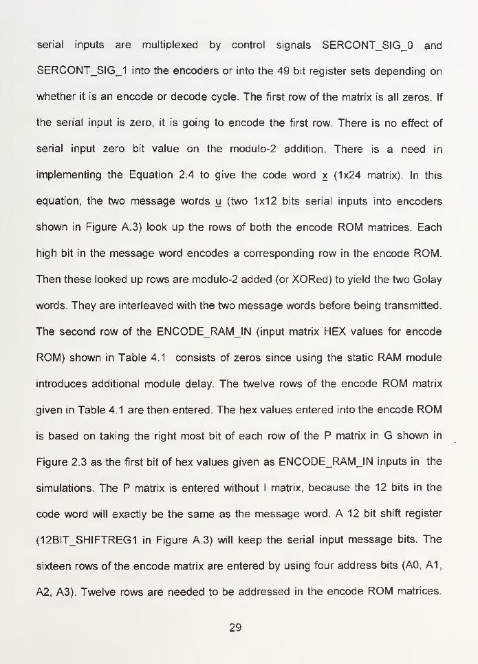
serial inputs are multiplexed by control signals SERCONT_SIG_0 and
SERCONT_SIG_1 into the encoders or into the 49 bit register sets depending on
whether it is an encode or decode cycle. The first row of the matrix is all zeros. If
the serial input is zero, it is going to encode the first row. There is no effect of
serial input zero bit value on the modulo-2 addition. There is a need in
implementing the Equation 2.4 to give the code word x (1x24 matrix). In this
equation, the two message words u (two 1x12 bits serial inputs into encoders
shown in Figure A. 3) look up the rows of both the encode ROM matrices. Each
high bit in the message word encodes a corresponding row in the encode ROM.
Then these looked up rows are modulo-2 added (or XORed) to yield the two Golay
words. They are interleaved with the two message words before being transmitted.
The second row of the ENCODERAMIN (input matrix HEX values for encode
ROM) shown in Table 4.1 consists of zeros since using the static RAM module
introduces additional module delay. The twelve rows of the encode ROM matrix
given in Table 4.1 are then entered. The hex values entered into the encode ROM
is based on taking the right most bit of each row of the P matrix in G shown in
Figure 2.3 as the first bit of hex values given as ENCODE_RAM_IN inputs in the
simulations. The P matrix is entered without I matrix, because the 12 bits in the
code word will exactly be the same as the message word. A 12 bit shift register
(12BIT_SHIFTREG1 in Figure A.3) will keep the serial input message bits. The
sixteen rows of the encode matrix are entered by using four address bits (AO, A1
,
A2, A3). Twelve rows are needed to be addressed in the encode ROM matrices.
29
Zero bit values are entered into the first and the last two rows of the encode ROM
matrix. It is strongly advised to assert a 7/globalsetreset" signal for a fraction of a
clock period before doing the simulations on the XC4000 family FPGAs. This
helps clear the chip modules to eliminate unknown (resistive or high Z) states. The
input values of the simulation are summarized in the Table 4.1 as specified above.
CLOCK_PERIOD
(nsec.)
ENCODE_ROM_IN(1 1 :0)
(HEX.)
A3
(MSB)
A2 A1 A0
(LSB)
200 000
400 000 1
600 C75 1
800 49F 1 1
1000 D4B 1
1200 6E3 1 1
1400 9B3 1 1
1600 B66 1 1 1
1800 ECC
2000 1ED
2200 3DA 1
2400 7B4 1 1
2600 B1D 1
2800 E3A 1 1
3000 000 1 1
3200 000 1 1 1
Table 4.1 . Input values of he encode ROM.
30
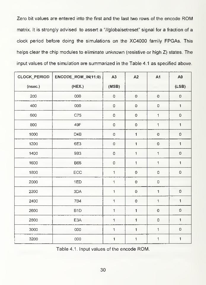
For the write period of the encode ROM (200-3400 ns), WE signal is held
high. The control signals SERCONT_SIG_0, and SERCONT_SIG_1 , clear
signals, transmit enable signals, and shift enable signals shown in Figure A.3.
They are given in Table 4.2 when they are at their high states.
CONTROL SIGNAL HIGH CLOCK PERIOD (nsec.)
SERCONT_SIG_0 4000-6400
SERCONT_SIG_1 6400-8800
CLR_FINXOR_A 100-3800
CLR_FINXOR_B 100-6200
CLR_SERIN 100-150
TR_ENC_OUT 9400-39200
FROM_ENCS 9400-39200
MAJ_VOTE_DONE 100-200
TR_EN1 9800-19600
TR_EN2 19600-29400
TR_EN3 29400-39200
Table 4.2. Values of the control signals at their high clock periods.
The simulation of NEWTEST_YEN module is focused on checking the
encoding functionality. The simulation results presented in Figures B.1, B.2 and
B.3 are for checking the NEWTEST_YEN module's encoding function.
The encode ROM input signal values are traced between times 200ns
and 3400ns as shown in Figure B.1. The WE (write enable) signal is held high
as the address bits (A0, A1, A2, A3) are changed to let the encode ROM bits be
written.
31
The values entered into the encode ROM and the first 49bit register bus
(REGFIRSTWEN1) transitions' traces are shown in Figure B.2. After the
message and the Golay check bits from the two code word bits are interleaved,
they are taken into the BUS_A at time 9400ns. This 49 bit sequence is shifted
one bit position at each clock cycle into the next REG_NEWSECOND1 module.
The interleaved bit sequence is transmitted by TR_SER_ENCOUT output signal
shown in Figure B.2. When the FROM_ENCS signal is high, the encoder A and
B (ENCODE_IN_WMATs), shift register A and B (12BIT_SHIFTREG1s) values
are taken into the BUS_A as shown in Figure B.2.
There are three transmission sequence control signals TREN1,
TR_EN2, and TR_EN3 as shown in Figure B.3. TR_EN3 signal's being high
means that the values in the right REG_NEWSECOND1 module shown in Figure
A.3 are transmitted by the TR_SER_ENCOUT signal. TR_EN1 and TR_EN2
signals being low means that the transmission of the bit sequence in
REGFIRST_WEN1 and first REG_NEWSECOND1 modules are completed. The
BUS_C shows how the bits are shifted at each clock cycle.
SERIALJN bit values given in Table 4.3 are being asserted from time
4000ns on to the serial input of the lower ENCODE_IN_WMAT. SERIALJN bits
are then multiplexed into the serial input of the upper ENCODElNWMAT
modules shown in Figure A.3 at time 6400ns and on.
32
CLOCK @ A (nsec.) SERIALJN (Bit Value) CLOCK @ B (nsec.)
4000 1 6400
4200 1 6800
4400 7000
4600 7200
4800 1 7400
5000 7600
5200 7800
5400 1 8000
5600 1 8200
5800 8400
6000 1 8600
6200 1 8800
Table 4.3. Serial Input Values Asserted to Encoder A and B.
The TR_SER_ENCOUT sends the last bit of the code word at time
38800ns since it gets into the 49 bit registers (first into REGFIRST_WEN1) at
time 9400ns. As a result the total transmission lasts until 9400+3x49x200 =
38800ns (three times 49 bit shift each at one clock cycle). The NEWTEST_YEN
modules behave as expected
2. DECODE_STAGE_LAST2 Simulation
In this simulation, the functionality of the majority voter (shown in Figure
A.11), deinterleaving and generation of the syndrome bits in the
DECODE_STAGE_LAST2 module shown in Figures A.2 and A.11 are checked.
33
This module represents the upper portion of the Figure 2.6. The received
sequence consists of two twenty four bits code word. Each consists of a
message and a check word. The purpose of this simulation is to make sure the
majority voting and interleaving are performed correctly. The check bits
generated from the received message word can help to find out if received
message word has bit errors. If any of the syndrome bits is one, then the
message word is in error. Message word is corrected in a way shown in Figure
2.6. The syndrome bits are used to look up the decode ROM to yield the data
bits error corrected pattern values. This pattern bits are XORed with the received
message word. This will correct the received message word. The encode ROM
and decode ROM values are entered in the same way as it is shown in Table
4.1. The row values of the matrices are the only differences in the encode and
the decode ROMs. The stimulus values of DECODE_STAGE_LAST2 module
are given in Table 4.4, where the encode ROM is the same as the one in
NEWTEST_YEN simulation.
Three 49 bit input values are asserted on each bus. They are 2/3 majority
voted in a way shown in Figure 2.8. After majority vote, the voted code word bits
are interleaved as shown in Figure 2.7. The decode procedure's first part
consists of generating syndrome bits as explained above. The three bus values
here are picked up in a random manner. Majority clear (MAJCLR in Figure
A.11) is asserted high before the vote to clear the voter circuit. Majority vote
enable signal is asserted when all buses are ready for the vote. When the vote
34
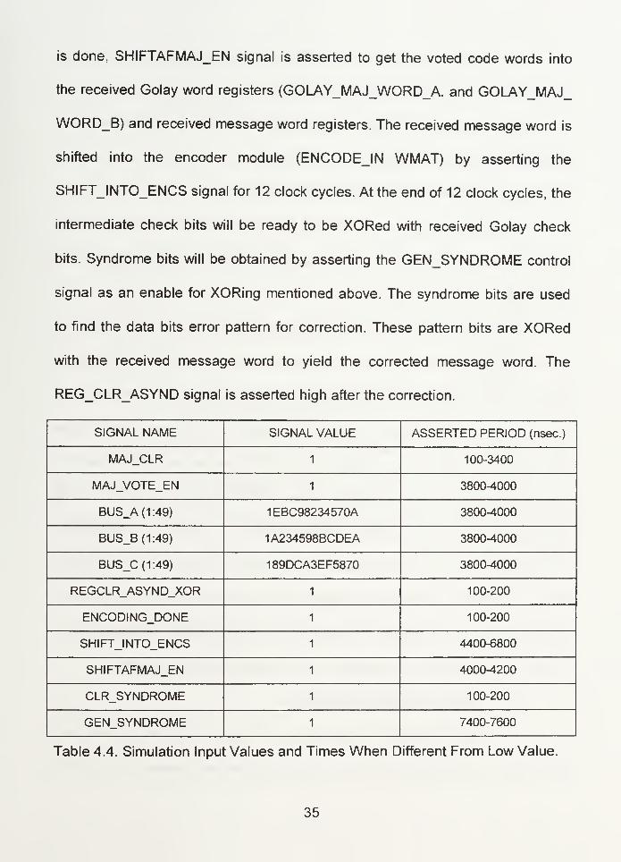
is done, SHIFTAFMAJEN signal is asserted to get the voted code words into
the received Golay word registers (GOLAY_MAJ_WORD_A. and GOLAY_MAJ_
WORDB) and received message word registers. The received message word is
shifted into the encoder module (ENCODEJN WMAT) by asserting the
SHIFT_INTO_ENCS signal for 12 clock cycles. At the end of 12 clock cycles, the
intermediate check bits will be ready to be XORed with received Golay check
bits. Syndrome bits will be obtained by asserting the GEN_SYNDROME control
signal as an enable for XORing mentioned above. The syndrome bits are used
to find the data bits error pattern for correction. These pattern bits are XORed
with the received message word to yield the corrected message word. The
REGCLRASYND signal is asserted high after the correction.
SIGNAL NAME SIGNAL VALUE ASSERTED PERIOD (nsec.)
MAJ_CLR 1 100-3400
MAJ_VOTE_EN 1 3800-4000
BUS_A(1:49) 1EBC98234570A 3800-4000
BUS_B(1:49) 1A234598BCDEA 3800-4000
BUS_C(1:49) 189DCA3EF5870 3800-4000
REGCLR_ASYND_XOR 100-200
ENCODING_DONE 100-200
SHIFT_INTO_ENCS 4400-6800
SHIFTAFMAJ_EN 4000-4200
CLR_SYNDROME 100-200
GEN_SYNDROME 7400-7600
Table 4.4. Simulation Input Values and Times When Different From Low Value.
35
The input values given to these three buses, and to the majority enable
signal (MAJVOTEEN) are shown in Figure B.4.
As shown in Figure B.5, when the encode ROM is being written, all other
signals stay low. The ROM values in this figure are the same as those encode
ROM values used in the NEWTEST_YEN simulation.
The output values are valid at time 7600ns as shown in Figure B.6. The
24 syndrome bits generated are valid after asserting the GEN_SYNDROME
signal high between 7400 and 7600ns.
All bus values at time 7600ns are valid after the assertion of
SHIFTAFMAJ_EN (shift enable after majority vote). The received message word
stays on the VOTEDWORD bus until it is corrected by the data bit error
correcting pattern bits. Bus values shown in Table 4.4 begin with ones. These
ones are the first bits in these buses. The rest of the values are handled as HEX
values. For example, for the BUS_A value 1 EBC98234570A, the first 1 is not
handled as HEX 1 (which is 0001 in 2's complement), but instead it is handled as
a single bit(the first bit in 49 bit bus value). Another important point to be taken
into consideration is the synchronization of the signals. When they have to go
through the same components at the same time, some kind of buffering should
be used to synchronize the signals to avoid invalid or unknown results.
3. RAM_BITS_NEW1 Simulation
The RAM_BITS_NEW1 module shown in Figure A. 16 takes the syndrome
bits to look up decode ROM matrix to yield data bits error pattern for correction
36

as shown in Figure 2.6. The difference between this module and the
ENCODE_IN_WMAT module is that the RAM_BITS_NEW1 has a parallel input
and serial output syndrome block. Besides, the RAM bits have the input values
of the decode ROM matrix instead of the encode ROM matrix that is used
previously in section I. The RAM_BITS_NEW1 stimulus force input values other
than decode ROM matrix are given in Table 4.5.
SIGNAL NAME SIGNAL VALUE ASSERTED PERIOD (nsec.)
SYND_XIN 1 3600-3800
SHIFT_EN 1 4000-6600
CLR_FINXOR 1 100-4200
COUNT_RESET 1 100-4000
Table 4.5. RAM_BITS_NEW1 Force Values.
The syndrome input values are in a sequence of "1 1 1 1 1 1 1 1 1"
as S1, S2, S3,..., S12 respectively. They are asserted in parallel between 3600
and 3800 ns. The decode ROM values used to input into the RAM bits are given
in Table 4.6.
37
CLOCK_PERIOD
(nsec.)
ENCODE_ROM_IN(1 1 :0)
(HEX.)
A3
(MSB)
A2 A1 A0
(LSB)
200 000
400 000 1
600 F92 1
800 7C9 1 1
1000 C76 1
1200 63B 1 1
1400 C8F 1 1
1600 8D5 1 1 1
1800 B78
2000 5BC
2200 2DE 1
2400 16F 1 1
2600 F25 1
2800 AE3 1 1
3000 000 1 1
3200 000 1 1 1
Table 4.6. Input Values of the D*?code ROI\A.
In Figure B.7, decode ROM input values, and the other signal values
shown in Table 4.5 are traced. The input values of the decode matrix is taken
from the PTmatrix of the parity check matrix H shown in Figure 2.5. The rest of
38
the signals are handled in the same way as they are handled in NEWTEST_YEN
simulation section.
The RAM_BITS_NEW1 module generates the valid results at time 6800ns
as shown in Figure B.8. The syndrome bits asserted to look up the decode ROM
proves to be the same value (579 in HEX as shown in Figure B.8) as the hand
calculated value.
In simulations, some vital experience was gained. At very early
simulations the force values for stimulus were entered bit by bit, and again and
again at each new simulation session. These took a long setup time in
simulations. Later in the simulations the hex values for "force files" are used.
These force files were saved everytime when the new force values were
entered. These were kept for upgrading after debugging of the current schematic
designs.
For the functional part of the simulation, the first thing to be considered is
to get the implemented function work properly, and produce what is expected.
Timing is not a major concern, except that you still can improve the speed by
pipelining each stage to see how fast it can get. One of the biggest problems
causing the invalid results was that the signals were being asserted
asynchronously. This problem is eliminated by using the buffers at the signal
paths. The signals coming earlier than the others will then be asserted at the
same time.
39

The other difficulty faced in the simulations was in asserting the bus
inputs. This problem is recovered by inputting the ROM matrices in a way shown
in this chapter. They (the hex values in simulations of both encoder and
decoder) are obtained by entering the ROM values given in Chapter II. Because
of some of the ripper and bus naming conventions, the inputs had to be entered
just the opposite way. That is the most significant bit value became the least
significant bit value, and vice versa. In debugging the big modules that has a
couple of modules inside, the simulation input times had to be reprogrammed for
the synchronization purposes.
The main purpose of these three simulations is to debug each module,
and find out when to assert the control signals to the modules. This will help the
design of the controller
40
V. XILINX FIELD PROGRAMMABLE GATE ARRAYS
Beginning in 1980s, industry was introduced with a new technology to
make ASIC designers more competitive. This shortens long acquired testing
time, and fabrication-dependent wait period. Using FPGAs one can implement
large digital circuits on a single chip. For Xilinx XC4000EX chips, they have up
to 125 000 gates, and for XC4062XL it has up to 72K static RAM bits on a single
chip [Xilinx, The Programmable Logic Data Book, 1996]. Along with laser
programmable chip technology, FPGA technology is among those which grows
at the fastest speed to offer industrial solutions to compete with VLSI
technologies. The biggest disadvantage with FPGAs is the overall speed
concern since the wiring and switching introduce resistive propagation delays as
compared to transistor level design. But it is managed to get up to 66 Mhz
overall speed in designs with Xilinx FPGAs. Now the FPGAs have more flip
flops, and faster switching capabilities, and special clock distribution lines that
can run through the whole chip. Faster speed designs are accomplished by
pipelining, and by up to date solution database offered to the customers on the
Internet. Field Programmable Gate Arrays provides the benefit of custom CMOS
VLSI, while avoiding the initial cost, time delay, and inherent risk of a competitor
technology, conventional masked gate array. Programmable logic devices
provide the benefits of high integration levels without the risks or expenses of
41
semi-custom and custom IC development. Here are some of the benefits of
programmable logic devices versus mask programmed gate arrays:
A. Faster design and verification: FPGAs can be designed and verified
quickly while the same process requires several weeks with gate
arrays. There are no non-recurring engineering (NRE) costs, no test
vectors to generate, and no delay while waiting for prototypes to be
manufactured. [Xilinx, Programmable Data book, 1996]
B. Design changes without penalty: Because the devices are software
configured and user-programmed, modifications are much less risky
and can be made anytime, in a matter of minutes or hours, as opposed
to weeks it would take with gate arrays. This results in significant cost
savings in design and production.
C. Shortest time-to-market: When designing with programmable logic,
time to market is measured in days or a few weeks, not months often
required when using gate arrays. A study by a marketing research firm
concluded that a six month delay in getting to market can cost a
product one-third of its lifetime potential profit. With masked
programmed gate arrays, design iterations can easily add that much
additional time, and more to a product schedule [Xilinx, Programmable
Logic Data Book, 1996]. FPGAs replaces most discrete and SSI
devices, resulting in an 80% reduction in the number of components
42
and a 75% reduction in test time since it does not require test vectors.
[Xilinx, programmable Logic Breakthrough '95,1995].
The result of experience gained with two successful FPGA family
(XC2000 ,and XC3000) helped the XC4000, XC5000, and XC6000 families to
provide a regular, flexible, programmable architecture of Configurable Logic
Blocks (CLBs) [Xilinx, Technical Data, XC4000 LCA family, 1990]. They are
interconnected by a powerful hierarchy of versatile and abundant routing
recourses, and surrounded by a perimeter of programmable I/O blocks on the
chip.
The devices are customized by loading configuration data into the internal
memory cells. The FPGAs can either actively read its configuration data out of
external serial or byte-parallel PROM (master modes), or the configuration data
can be written into the FPGA from a host (slave and peripheral modes).
The Xilinx family is supported by powerful and sophisticated software,
covering every aspect of the design: from schematic entry to simulation, to
automatic block placement and routing of the interconnects, and finally the
creation of the configuration bit stream. Since the FPGAs can be re-programmed
for unlimited number of times, they can be used in innovative designs where
hardware configuration is changed dynamically, or where hardware must be
adopted to different user applications. FPGAs are ideal for shortening the design
and development cycle, but they also offer a cost effective solution for
43
productive rates well beyond 1000 systems per month. [Xilinx, Tech. Data,
XC4000 LCA family
A. XILINX LOGICAL CELL ARRAYS
Xilinx high density user programmable gate arrays comprise three major
configurable elements: configurable logic blocks (CLBs), input/output blocks
(lOBs), and interconnections. The CLBs provide the functional elements for
constructing the user's logic. The lOBs provide the interface between the
package pins, and internal signal lines. The programmable interconnect
resources provide routing paths to connect inputs and the outputs of the CLBs
and lOBs onto the appropriate networks [Xilinx, Technical Data, XC4000 LCA
Family, 1990].
Customized configuration is established by programming internal static
memory cells that determine the logic functions and interconnections
implemented in the LCA device. XC4000 family achieves high speed through
advanced semiconductor technology (0.35 micron CMOS fabrication
technology), chip density reaches up to 125 K logic gates with system
performance of up to 66 MHz speed. It is also 100% Peripheral Component
Interconnect (PCI) compliant supporting standard ASIC design flow. Three
layers of metal is used in latest XC4000EXs, and extra feature of Select-RAM
memory in XILINX chips dramatically improves the system performance, ease-of-
use, and overall gate count. This feature allows easy distribution of high
44

performance customized single or dual port RAM functions. [Xilinx, Pro. Log.
Data Book, 4-8, 1996]
B. XILINX FAMILY ARCHITECTURE
1. Configurable Logic Blocks
A number of architectural improvements contribute to the Xilinx Family's
increased logic density and performance levels. The most important one is a
more powerful and flexible configurable logic block (CLB) surrounded by a
versatile set of routing resources, resulting in more effective gates per CLB.
Each CLB packs a pair of flip-flops, and two independent 4-input function
generators. The two function generators offer designers plenty of flexibility,
because most of the combinatorial logic functions need less than four inputs.
Consequently, the design software tools can deal with each function generator
independently, improving the cell usage [ Xilinx, XC4000 LCA family, 1990].
Thirteen CLB inputs, and four CLB outputs provide access to function
generators and flip-flops. Four inputs are available to each of the two function
generators (F1-F4 and G1-G4). These function generators, whose outputs are
labeled F' and G\ are each capable of implementing any arbitrarily defined
Boolean function of their four inputs. The function generators are implemented
as memory look up tables, therefore the propagation delay is independent of the
function being implemented. A third function generator, labeled H', can
implement any Boolean function of its three inputs; F' ,G' and a third input from
outside the block (H1). Signals from the function generators can exit CLB on two
45
outputs; F' or H' can be connected to the F output, and G' or H' can be
connected to the G output, Thus, a CLB can be used to implement any two
independent functions up to four variables or one single function of five variables
or any function of four variables together with some functions of five variables, or
it can implement even some functions of up to nine variables (Figure 5.1).
Implementing wide functions in a single block reduces both the number of
required blocks and the delay in the signal path, achieving both increased
density and speed [Xilinx XC 4000 LCA family technical data book, 1990].
G4
G3
G2
G1
F4F3
F2
F1
WE" DATAIN
G' FUNCTIONGENERATOR
WE DATAIN
P- FUNCTIONGENERATOR
JLJLiiWE D1 DO EC
CONFIGURATIONMEMORY BIT
Figure 5.1. CLB Function Generators Has the Ability To Be Used AsRead/Write Memory Cells.
46
The two storage elements in the CLB are edge triggered D-type flip-flops
with common clock (K) and clock enable (EC) inputs. A third common input (S/R)
can be programmed as either asynchronous set or reset signal independently for
each of the two registers; this input can be disabled for either flip-flop.
A separate global SET/RESET line (not shown in Figure 5.2) sets or clears each
register during power up, reconfiguration, or when a dedicated RESET net is
driven active. This RESET input does not compete with other routing recourses;
it can be connected to any package pin, providing a global reset input. Each flip-
flop can be triggered on either rising or falling edge of the clock. The source of a
flip-flop data input is programmable: it is driven either by functions F\ G' and H',
or Direct In (DIN) block input. The flip-flops drive the Q1 and Q2 of the CLB
outputs. In addition, each CLB F' and G' function generator contains dedicated
arithmetic logic for the fast generation of the carry and borrow signals, greatly
increasing the efficiency and performance of adders, subtracters, accumulators,
comparators, and even counters. Multiplexers in the CLB map the four control
inputs, labeled C1 through C4 in Figure 5.2, into the four internal control signals
(H1, DIN, S/R, AND EC) in any arbitrary manner [Xilinx, XC4000 LCA
Family, 1994].
Delays in LCA-based designs are layout dependent. While this makes it
hard to predict a worst case guaranteed performance, there is a rule designers
should consider; the system clock rate should not exceed one third to one half of
the specified toggle rate. Critical portions of a design, shift registers and simple
47
counters, can run faster approximately two-thirds of the specified toggle rate
[Xilinx, Tech. Data XC4000 LCA family].
£ $ $ $H1 DIN S/R EC
G4
G3
G2
G1
LOGICFUNCTION
OF G''
G1-G4
LOGICFUNCTION
OF H'P, G'
ANDH1
F4F3
F2
F1
LOGICFUNCTION .
OF '
F1-F4
MULTIPLEXERCONTROLLED
BY CONFIGURATIONPROGRAM
K(CLOCK)
F^DING
-H' 7^T&
'— DIN^
CONTt
SDD Q-Q2
Lr S/R h
CONT
^TjD SD"CpQ1
i
EC RD
->
Figure 5.2. Simplified Diagram of XC4000 Configurable Logic Block.
The CLB can pass the combinatorial outputs to the interconnect networks,
but can also store the combinatorial result(s) or other incoming data in one or
two flip-flops, and connect their outputs to the interconnect network as well. The
older programmable gate arrays had to make a choice, either output the
combinatorial function or the stored value. From the XC4000 FPGAs on, the flip-
48
flops can be used as registers or shift registers without blocking the function
generators from performing a different, perhaps unrelated job. This increases the
functional density of the chip [Xilinx, Tech. Data, XC4000 LCA Family, 1990].
When a function generator drives a flip-flop in a CLB, the combinatorial
propagation delay overlaps completely with the set-up time of the flip-flop. The
set-up time is specified between the function generator inputs and the clock
input. This represents a performance advantage over competing technologies
where combinatorial delays must be added to the flip-flop set-up time. Each CLB
includes high speed carry logic that can be activated by configuration. Each 4-
input function generator can be configured as a two bit adder with built in hidden
carry that can be expanded to any length. This dedicated adder circuitry is so
fast and efficient that conventional speed up methods like carry
generate/propagate are meaningless, even at the 16-bit level, and of marginal
benefit at the 32-bit level. The fast carry logic opens the door to many new
applications involving arithmetic operation, where the previous generations of
FPGAs were not fast and/or not efficient enough. High speed address offset
calculations in microprocessor or graphic systems, and high speed addition in
digital signal processing are two typical applications. As the technology
develops, the carry logic helps faster and more efficient counters, in addition,
the abundance of flip-flops in the CLBs invites pipelined designs. This is a
powerful way of increasing performance by breaking the function into smaller
subfunctions, and executing them in parallel, passing on the results through the
49
pipeline. This method should be seriously considered wherever total
performance is more important than simple throughput-delay [Xilinx, Tech. Data
XC4000, LCA family, 1990].
For years, FPGAs have suffered from the lack of fast and wide decoding
circuitry. When the address or the data field is wider than the function generator
inputs, FPGAs need level decoding and thus are slower than PALs. In XC3000
there are five bits, in XC4000 family CLBs, there are nine inputs; and any
decoder up to 9 inputs is, therefore compact and fast. But there is also a need
for larger decoders, especially for address decoding in large microprocessor
systems. The XC4000 family has 16 very fast programmable decoders, each
with up to 40 inputs. These dedicated decoders are located at chip periphery,
four decoders on each chip edge. They accept I/O signals and internal signals
as input and generate a decoded output in 10 ns. Each decoder AND gate can
also be split into two when a larger number of narrower decoders is required.
Very large PALs can be emulated by ORing the decoder outputs in a CLB. This
fast decoding feature covers what has been long considered a weakness of
FPGAs. Users often resorted to external PALs for simple, but fast decoding
functions. The maximum output current specification of today's FPGAs often
forces the user to add external buffers, cumbersome especially on bi-directional
I/O lines. [Xilinx, Tech. Data XC4000 LCA Family].
50
2. Abundant Routing Resources
Connections between blocks are made by metal lines with programmable
switching points and switching matrices. The globally distributed signal lines
have access to any clock or logic input. The designer of synchronous systems
can distribute several clocks, and control signals, all over the chip, without
having to worry about any clock skew. The horizontal long lines can be used as
unidirectional or bi-directional data buses, or they can implement wide
multiplexers or wired AND functions. Single-length lines connect the switching
matrices that are located at every intersection of a row and a column of CLB.
These lines provide the greatest interconnect flexibility, but cause a delay
whenever they go through a switching matrix. Double-length lines provide faster
signal routing over intermediate distances [Xilinx, Tech Data XC4000 LCA
Family, 1996].
3. On-Chip Memory
Beginning from XC4000 family LCAs, They have on-chip static memory
resources (RAM bits up to 73728 bits for XC4062XL)[Xilinx, The Prog. Logic
Data Book, 1996], further increasing the system integration level. And optional
mode for each CLB makes the memory look up tables in the F' and G' function
generators usable as either 16*2 or 32*1 bit array of read/write memory cells.
The F1-F4 and G1-G4 inputs to the function generators act as address lines,
selecting a particular memory cell in each look up table. The functionality of the
CLB control signals changes in this configuration; H1, DIN, and S/R lines
51
become the two data inputs and the Write Enable (WE) input for 16*2 memory.
When the 32*1 configuration is selected, D1 acts as the fifth address bit, and DO
as the data input. The content of the memory cell(s) being addressed are
available at the F' and G' function generator outputs, and can exit the CLB
through its F and G outputs. Configuring the CLB function generators as
read/write memory does not affect the functionality of the other portions of the
CLB, with the exception of the redefinition of the control signals. The H' function
generator can be used to implement Boolean functions of F' ,G' and D1, and D2
flip-flops can latch the F\ G', H', or DO signals. The RAM bits are very fast: read
access time is the same as logic delay (for XC4000 about 5 ns) and write time is
10 ns (again for the same FPGA), both are several times faster than any off-chip
solution. Such distributed RAM is a novel concept, creating new possibilities in
system design; registered arrays of multiple accumulators, status registers,
index registers, DMA counters, distributed shift registers, LIFO stacks, and FIFO
buffers. The other important benefit of on board RAM bits is to save gates (such
as flip-flops, address line decoders, and etc.) which designer can use to
implement more other functions [Xilinx, Tech. Data XC4000 LCA family, 1990].
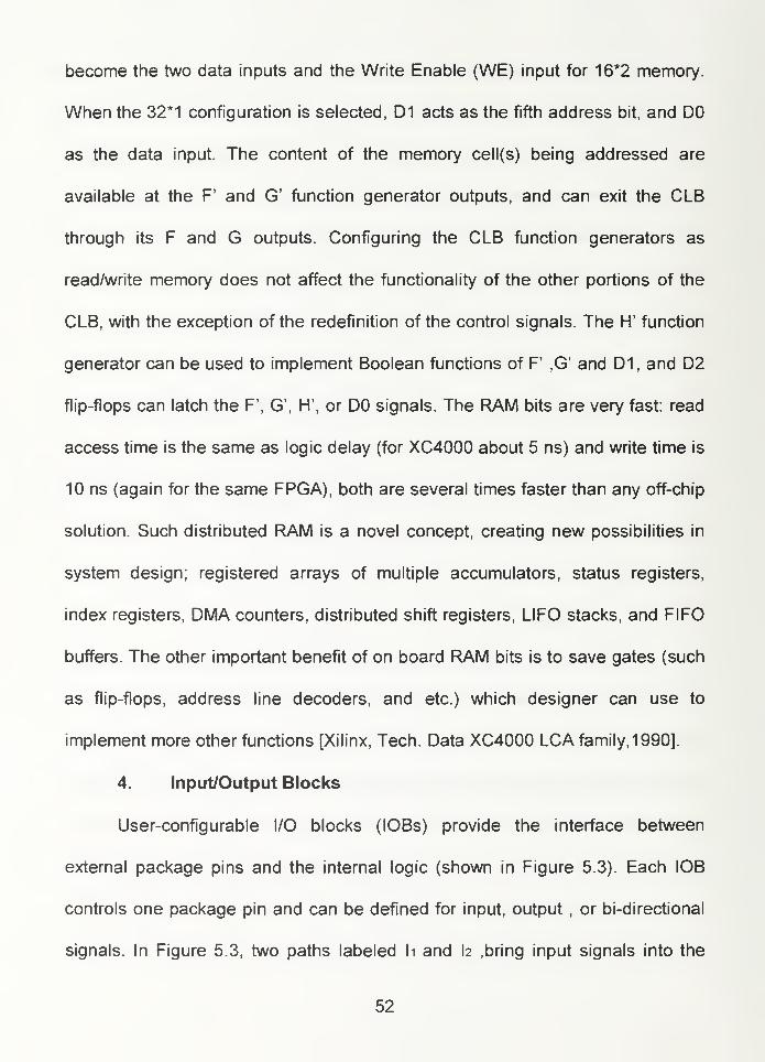
4. Input/Output Blocks
User-configurable I/O blocks (lOBs) provide the interface between
external package pins and the internal logic (shown in Figure 5.3). Each IOB
controls one package pin and can be defined for input, output , or bi-directional
signals. In Figure 5.3, two paths labeled h and I2 .bring input signals into the
52
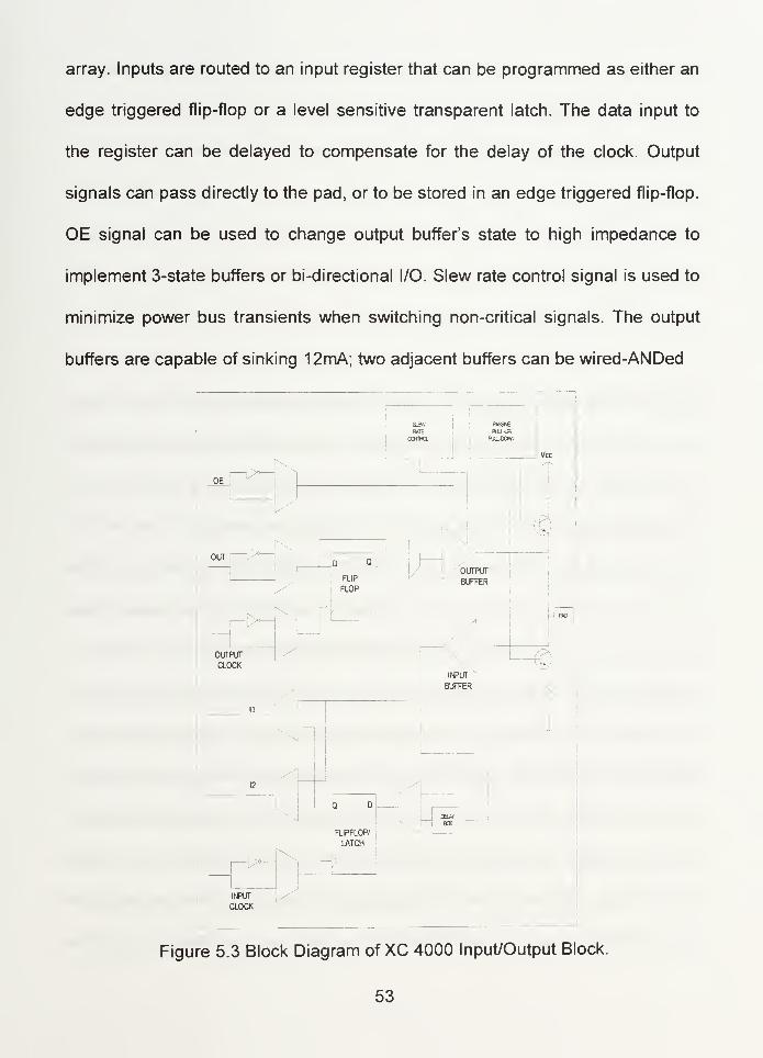
array. Inputs are routed to an input register that can be programmed as either an
edge triggered flip-flop or a level sensitive transparent latch. The data input to
the register can be delayed to compensate for the delay of the clock. Output
signals can pass directly to the pad, or to be stored in an edge triggered flip-flop.
OE signal can be used to change output buffer's state to high impedance to
implement 3-state buffers or bi-directional I/O. Slew rate control signal is used to
minimize power bus transients when switching non-critical signals. The output
buffers are capable of sinking 12mA; two adjacent buffers can be wired-ANDed
OEW
COJTRO.
PASMPUU.-UP/
PUU.-0OW
VccXT-.
OE
KOUT
j\D Q^
FLIP
FLOP
'^Q
OUTPUT
BUFFER
OUTPUT
CLOCK
rt
INPUT
BUFFER
n
FLIPFLOP/
LATCH
w caw
r^INPUT
CLOCK
Figure 5.3 Block Diagram of XC 4000 Input/Output Block.
53

externally to sink up to 24mA in order not to use buffers outside the package, in
this case ;
t can support short buses on any card (like PC board). Programmable
pull-up and pull-down resistors are useful to connect unused pins to Vcc or
ground to minimize the power consumption. And it is compatible with IEEE
standard 1149.1 for boundary scan testing, permitting easy chip and board level
testing of LCA-based applications[Xilinx, Tech. Data XC4000 LCA Family, 1990].
5. Programmable Interconnect
All internal connections are composed of metal segments with
programmable switching points to implement the desired routing. An abundance
of different routing resources is provided to achieve efficient automated routing.
The number of routing channels is scaled to the size of the array, i.e, it
increases with array size. CLB inputs and outputs are distributed on four sides of
the block (beginning from XC4000 FPGAs), providing routing flexibility. There
are three main types of interconnect, distinguished by the relative length of their
segments: single-length lines, double-length lines, and long lines. The number of
routing channels varies with the array size. The routing scheme was designed
for minimum resistance and capacitance of the average routing path, resulting in
significant performance improvements. The single-length lines are a grid of
horizontal and vertical lines that intersect at a switch matrix between each block.
Each switch matrix consists of programmable n-channel pass transistors used to
establish connections between the single length lines. And it can be routed one
way or multiple ways depending on the branches required. Single length lines
54
are used to conduct signals within a localized area and to provide branching for
nets fanout greater than one [Xilinx, Tech. Data XC4000 LCA Family].
Double-length lines provide the most efficient implementation of
intermediate length, point to point interconnections. Long lines form a grid of
metal interconnect segments that run the entire length or width of the array.
Additional long lines in the vertical plane can be driven by special global buffers,
designed to distribute clocks and other high fanout control signals throughout
the array with minimal skew. Long lines are intended for high fanout time, critical
signal nets. Communication between long lines and single-length lines is
controlled by programmable interconnect points at the line intersection by six
pass transistors to route signal to where it is needed [Xilinx, Tech Data XC4000
LCA family, 1990]. Double length lines do not connect with other lines, and
beginning with the XC4000EX quad lines, introduce higher communication or
faster propagation capabilities.
6. Taking Advantage of Reconfiguration
All Xilinx families of LCAs can be reconfigured to change logic functions
while resident in the system. This gives the system designer a new degree of
freedom that is not available with any other type of logic. Hardware configuration
can be changed as easily as software. Design updates and modifications are
easy. An LCA device can be reconfigured dynamically to perform different
functions at different times. Reconfigurable logic can be used to implement
system self diagnostics, create system capable of being reconfigured for
55

different environments or operations, implement dual-purpose hardware for a
given application. As an added benefit, use of reconfigurable LCAs simplifies
hardware design and debugging and shortens a product's time-to-market [Xilinx,
Tech. Data XC4000 LCA Family, 1996] .
7. The Xilinx Development System
The powerful hardware features of FPGA family require a powerful, easy
to use development tool, and Xilinx provides an enhanced tool: Xilinx Automated
CAE Tool (XACT). And XACT Design Manager (XDM) simplifies the selection of
command line options with pull-down menus and online documents. Design
sheet can be entered using schematic capture software or industry standard
interfaces such as EDIF. The XACT development system has interfaces with a
number of powerful design environments, and it supports more than 100
packages (like Mentor Graphics, ORCAD, FutureNet, VIEWLogic, Cadence,
Synopsys, etc.).
C. CONCLUSION
In this thesis study, the XC4003 FPGA environment is used for the
simulations of the individual modules. It is concluded that, the XC4003 gate
count is not sufficient for the MAINCIRCUIT design even before adding the
controller. The XC4007 or a higher XC4000 family member should be chosen to
satisfy the needs.
As a result FPGAs are used with high performance along with price
leadership for high volume applications like Plug-and-play cards, ATM
56

(Asynchronous Transfer Mode) cards, for wireless communication, CDROMs,
SATCOMs, Teleconferencing and DSP applications successfully.
57

58
VI. CONCLUSION AND RECOMMENDATIONS
In this thesis study, the golay encoder/decoder is implemented in the
Mentor Graphics schematic entry tool Design Architect. The simulations for
some individual modules are done in Quicksimll for Xilinx XC4003 FPGA
environment. The controller part of the design is to be implemented in a later
study according to the simulation results obtained in this study (as explained in
Chapter IV). After the design is completed, the migration of the coder into an
FPGA chip is to be done. It is necessary to do timing simulations of the coder
for the FPGA demo board. The FPGA that will be used to simulate the coder
should be a XC4007 or higher gate capacity chip depending on the
implementation of the controller.
During the real environment execution on the demo board, the encode
and decode ROM inputs need to be done only once at the beginning. The static
RAM bits can keep the ROM values entered. Therefore, the input/output pads
can be assigned to other I/O signals. The static RAM bits of the XILINX
architecture provided faster encoding, and decoding capability, but it took time
to understand how to include it in the design process.
For a faster schematic design of the coder, flip flops can be used at
several stages by dividing the modules into equal design partitions for
pipelining. In the XC4000 family there are a number of options that can offer
59
enough gate counts for designs requiring large number of gates for high speed
pipeline operation.
Modular design approach helped a lot in the implementation and the
debugging of the modules and layers of the design hierarchy. Moreover it
helped the understanding of the function partitions and interfaces.
For future implementation of the controller, the first approach is to define
the partitions of states independent of each other. After debugging each state
transition diagram of the partitions, they all can be put together to perform the
overall state transition diagram. By using this state table and an algorithm (such
as one-hot) the controller can be implemented. The second approach is to use
a synthesis tool (like VHDL or Verilog in one of the EDA tools) by writing the
states of the controller required in the design in high level languages. After
converting it into schematic sheet, it can be imported into the FPGA chips.
Before designing the controller and exporting the design into an FPGA
chip, it is important to study the State Machine Design Chapter in the Digital
Design Book [John F. Wakerly.1994], Xilinx XC4000 FPGA training course
manuals, and the XILINX "User Guide and Tutorials" book to save time before
facing the potential problems.
The lack of experience with the schematic capture and simulation tools is
part of the difficulty in this work. Customer services of the design programming
environment and direct support people were often not available. This problem
resulted in slow down during the thesis study.
60

APPENDIX A.
CIRCUIT SCHEMATICS
61

CQCCD
>
Qmzm>r-
I
mzoDmoOCD13CD—
^
mooQ.CD
oCDOOQ.CD
uI i I i
_ i o o o o o .
.
»- s» ^ »- t — — r--> ci m m r-i owM-0'*i"Znnnnn»'"C TJ -T3 -O TJ "O -O T) "D ~D "O "O "O
62
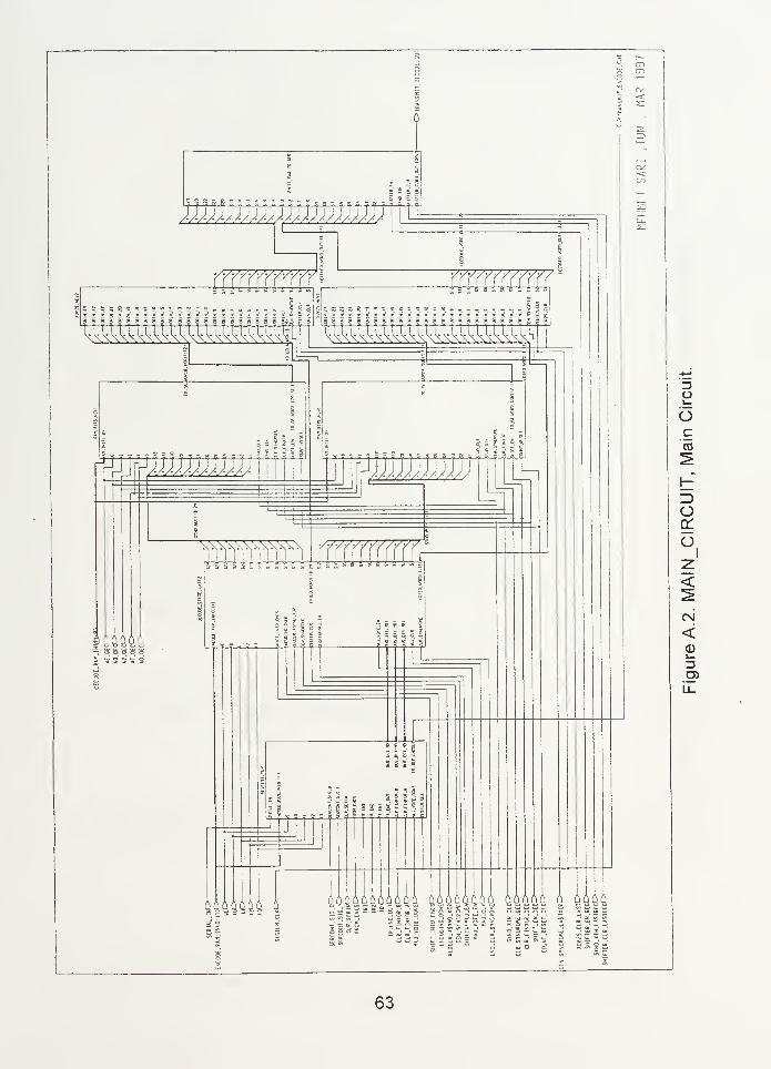
^rsisy^jsi wmmmaaaBaaaBBaasaBBSBaaaaaa g?g | a
| [j » i j j » i » i » ; 8 j i j^SffifflMM
166664
; ! » 3 b
Mfflxm
466,4666 6666,66666 666^64466 o o 06 4 6 6666
13o'6
cCO
H
Oa:
oiz
<
csi
<>_
SSI'
63
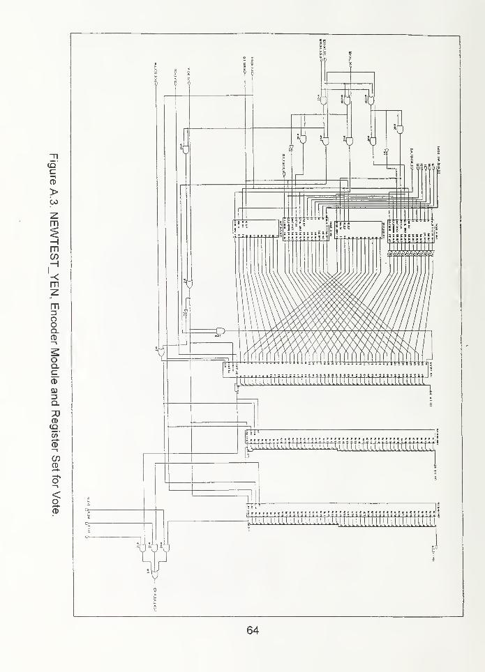
CQCCD
>CO
zm
mH
I
-<m
mOOQ.CD
OQ.C_CD
0)=JQ.
70CDCQ(/>'
CD
CD
<OCD
"i
X
V
5M JH I
90
'j
. _i.: T,f i:i> f
V V V
. . . E B . S i i ' 5
»iiiiiiil i"
TTTTTTr
fors^uuiUK^^uuuuuuuiUUUUU
• '•'• 1
iiiuiiiiuuiiiiijiuu iuiuiiiiiniiiiuiiii'
64
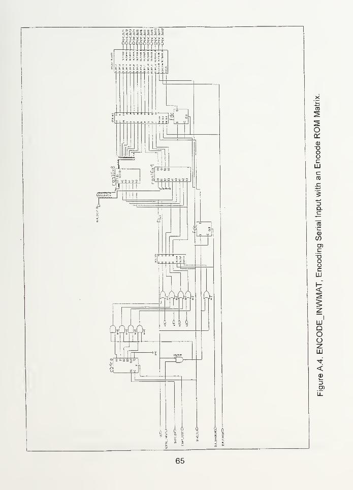
3 33333333333v v y y y v y y y y y y
:
a a a a a a
• n j. a n i i
il
HS%
IWlWlWl
1 M Ml
A
nn L L
L^
i'TriTr'TTSA
i 6 i i
"¥ 5
X
03
Oa:
<DT3OOCLU
C03
3Q.C
"i_
(D
CO
D)CTJOOcHI
h-"
<
HIQOOZLU
<
65

f deeII20-
IIlO
I1QO
ISO
180
nofoc.clrO-
FOCS-EnO"foc.clkO-
ISO
-0
-CE
->c
fdci-0
-CE
->cCLR
fdci
-0
-CE
->CCLR
fdee-D- CE
->CCLR
f deeD Q
CE'
>CCLR
fdee
ISO
IlO
CLR
fdee
CLR
fdci
CE'
>CCLR
130-
120
ao
fdeeD C\-
CE °
* CLR
T"
fdci
o a
CE'
* CLR
fd(
fd(
D DI-
CE j
>CCLR 1
Z3
-Ooi?
-Oon
-OOlQ
-Oos
-Or
H=>07
-oos
-oos
Oc<
-Oc;
-o G2
-Ooi
Figure A.5. 12BIT_SHIFTREG1, 12 Bit Shift Register.
66
TO.orr.30-
TO.Off.'O-
TO_orr_sO-
o-^>
ac.riNxosO-
ar.«_riNxoeO-
srw.osOrt0.0rr.7O-
to.orr.sO—
10.0rr.9O-
ro.orr.12O-
bo—[0^ 4-i^>
o—^>^ ' xor?
o—5>
C^^P
D £>
o—=£>^ ' .or?
0-^£>
r^5>
o—=0H / «or2
0"^P
TcTcT
T3cl
T3E
Tac~
rmr
Hl
O—
S
O ^L>
TUcf
13E
TcfcT
T3SI
TZc
ro.riNxce.2
I0_riNXCR_3
ro.riNxoR.s
ro.riNxcR.8
ro.riNxoR.s
ro.riNXOR.io
ro.riNxoR.i?
Figure A.6.RAM_XOR_TO_LAST1, Looked up Encode ROM Rows XOR Module
67
foc.cirD-
focs.enc^
FOC.CUO-
f dee
SERIAL. INPUlC-
-CE
->c
race
-CE
->c
face-0
-CE
->c
face-D-CE->C
I- ace-0
-CE
->C
face-0
-CE
->c
fde e
-0
-CE
->C
race-D-CE
->C
face- l
-CE
Tac!
foes
race
Oo:;
-Don
-OOIQ
H=>09
-O0B
-Ooi
-Ok
-O05
-o c <
Ooi
-Oo?
-Ooi
Figure A.7. 12FDC_WES, 12 D-Flip-Flop with Enable.
68
Figure A.8. REGFIRST_WEN1 , First Column 49 Bit Register Module.
69
Figure A.9. REG_VEWSEC0ND1, Second and Third Column Register Module.
70
:S£»5iiEHi£S ;CO-KC-SC(= £
i
t8 s 8 8 a a a a a a lit
i ^*HHH hh I
'
53'
a iitis c aS
j a a a
i
, , i i i i i i 5 5 i i
a^ - 1 1
1
1 5 i
:
rFf
,. * w r. B g K n i i-) H 1 1' ' 1 H T i
0,
itiiiiliitttiiiiitiiiiii i\\iit\i\%ii\iii*ti*il\\\3
* 2SS2
_0
T3O
Ocoi_
CDc(D
OCD
£oDC>»CO
DcCO
CD»—
>
o>
o
CMI-
<
LU
o<I-co
I
LUQOOLUQ
<CDi—
71

CJ.O [>>-
C23D [»-
c??o [>o-
oD [>o-
«£C.B.s.«rwH»o-STSTEN.CltO-
c?oD [>o-
-C>°-
-c>^
OlD Oo-
-£*>-
"£*>-
-r>s-
-£*?-
£dc_
Fdc
-O-C023
Fdc-1 C>C022
Fdc
Idc
Fdc
-OC0I9
ld^
1i^
Fdc
t oc
-Ocois
dc
iI
~f1&L_
Figure A.12.GOLAY_MAJ_WORD_B, Received Golay Word Register.
73
,Frice
c""!
& .FcIcb
frice
PO
£d££ ^O
Fdce
,Fdce
ro-
L-J=33-
Fdce,
Fdce
i3>
k^>
fdce
40I>
to.~^>
, fdce ^O
£d£i
to-
£dc£
3tdce.ClCft9
E3M
Fdee
fdce
fcd£e-
F-eee
;
v
-Ol£LO«S.Hll1«
Figure A.13. MAJ_WORD_B_TO_ENC, Received Message Word Register.
74
-3D-andZbl ~l Fdc
H-^P^
a?mrtS
v> fdc
3^ "*""'
—o-•ndZ
- COR
and?bl V^ fflfi
jS^h: at
w.d
—o-and!
~!^ Frlr
j^—O- OJ?
-J3D-v> Fric
JPOR
t"~
-3D-~tn
Fdc
>cas
j?P
^3"~V^
Fdca o
J? -.—D-
!
~V>Fdc
J? - <CL8
"""
-3D-~V^
fdc
JP
_wc dc
c c
or2
nlZ
-3D-"V Fdr: cJ? -
rvfftol> FricL
""ri=0- " a»
Figure A. 14. REG_FORMAJ_WORD, Register for Majority Word.
75

ccN_srnoaoHEC>-
X0B1N.2*
I0B1N.12:;£=dx>
X0R1N,
IOC IN,-.?£=3X>
10S]H.22
X06IN.1Q
X0B1N.?I
xorin.9
>E>
£=T>
XOfilN
X0BIN.8g^D-
RIN.19D—^\~x.0BIN.7D Jl—
•
X0BIN.I8C
X0B1N.CC
xoeiN.w
X081N.S' )L>
X0B1N.
XOBIN.«or2
or?
IIBW.nD >TC NX08IN.2D M. '
XOBIN.IS
X0BIN.3
XOeiN.I]
xoaiK.r
x>
o-
o-
o-
T>
D-
Id£_Osi2
Idc_
ids.
Fdc
Fdc
idc
ids.
i Fdc
D"Fdc
r>Fdc
D ^PIdc_
-OSI9
-OS5
-OS8
4o ol Oss
Osi
-Osi
Figure A. 15. XOR2S_NEW3, Syndrome Bit Generator XOR Module.
76

O
Oo
Oa:
<DoOoCD
Q
LUZ
I
COh;
CO
<a:
CD
<CDi_
77
Figure A. 17. SYND_LAST_CIR, Syndrome Bits Shift Module.
78
Figure A. 18. 24BIT_PAR_TO_SER, 24 Bit Massage Words Shift Module
79

80

APPENDIX B.
SIMULATION SCHEMATICS
81

C-
^
CD
DO
m
menH'<m
c/>
3'
c_
£D
O=3
5"
"DC#—i-
CDOCD
!
o§oooo<?>
ooos
+
+
+
+
+
ooooQooooooo9
+
+
+
+•
+
+
+
+
+
+
+
+
+
+
+
+
+
4-
+
+
+
+
+
+
+
4-
+
+
+
+
+
+
1
+
+
+
+
+
+
+
+
+
+
+
1—
'
+
+
+
+
+
+
+
+
+
f
1
+
+
+
+
+
+
+
+
+
+
+
1
+
+
+
+
+
+
+
+
+1
—
'
+
+
+
+
+
+
+
+
+
+
+
t 1
1 1
1 L
+
+
+
+
+
+
+
+
+
+
+
+
:=],_j j H r x
x
><
><
X
X
T1
82
+ + + + + + + + + +
+ + + + + + + + + +
+ + + + + + + + + +
+ + + + + + + + + +
+ + + + + + + + + +
+ + + + + + + + + +
+ + + + + + + + + +
+ + + + + + + + + +
+ + + + + + + + + +
*- + + + + + + + + +
+ + + + + + + + + 4:
+ + + + + + + + »- +
+ + + + + + + + + +
+ + + + + + + + + +
OOo+ + + + + + + + + +
J .
r
i
4- +
X X +
Oo
Q or-a oCQ
§ +oo otl« oa\ or^ oCD o
oO oX X +
o r^a\ o\o oo\ o$ § +o\ oU. oo oC~t oO oO o
oX X +
CO mT oCQ oU orvj o03 <t> +CJ or- oW o£ <3
oCO oi—
i
oX X +
t H< oin oVO ocr, otTi <£>
W or*l otx, oO on oO o
oX X +
CMQCQ
OrK +U.<T(
r*CO
W
X *
0\VD
LPVO<t\ +&.OmOou.o><; + +
o o oo o oo o oo o ooo § §o o oo o oo o oo o oo o oo o oo o
+ 1
o
CO
to•_
0)
to
O)<D
DH
ZLUv
,
h-COLUh-
£LU
CM
DQ
0)
83
VO O <D ~»— — — o
COc-^
(D
pa
^
i
-
m:>
HmenH'-<
m
u
73a>
w—
^
c/>:r
^j
m3Q.
X
X
0)o
2 X
2 X
84
*1 *0r *Xr * XXXXXXXXXXXXXr1 1 Or Xr XXXXXXXXXXXXXr2 1 Or Xr XXXXXXXXXXXXXr
100 *0 *1 *0 0000000000000200 *1 *0 0000000000000300 *0 0000000000000400 *1 0000000000000500 *0 0000000000000600 *1 0000000000000700 *0 0000000000000800 *1 0000000000000900 *0 0000000000000
1000 *1 00000000000001100 *0 00000000000001200 *1 00000000000001300 *0 00000000000001400 *1 00000000000001500 *0 00000000000001600 *1 00000000000001700 *0 00000000000001800 *1 00000000000001900 *0 00000000000002000 *1 00000000000002100 *0 00000000000002200 *1 00000000000002300 *0 00000000000002400 *1 00000000000002500 *0 00000000000002600 *1 00000000000002700 *0 00000000000002800 *1 00000000000002900 *0 00000000000003000 *1 00000000000003100 "0 00000000000003200 *1 ooooooooooooc3300 *0 00000000000003400 *1 00000000000003500 .0 *0 00000000000003600 .0 *1 ooooooooooooc3700 .0 0 00000000000003800 .
* 1 *1 1EBC98234570A3800 .3 1 1 1EBC98234570A3900 .0 *0 1 1EBC98234570A4000 .0 *] *0 '00000000000004100 .0 *0 ooooooooooooc4200 .0 *1 ooooooooooooc4200 . 1 1 ooooooooooooc4300 .0 *0 ooooooooooooc4400 .0 *1 ooooooooooooc
Time ( IS ) ~/SYSTEM_CLK~/MAJ_CLR
/VMAJ_VOTE_EN~/BUS_A(l:49)
* XXXXXXXXXXXXXrXXXXXXXXXXXXXrXXXXXXXXXXXXXr*0000000000000000000000000000000000000000000000000000000000000000000000000000000000000000000000000000000000000000000000000000000000000000000000000000000000000000000000000000000000000000000000000000000000000000000000000000000000000000000000000000000000000000000000000000000000000000000000000000000000000000000000000000000000000000000000000000000000000000000000000000000000000000000000000000000000000000000000000000000000000000000000000000000000000000000000000000000000000000000000000
-1A2 3 4 59 83CDEA1A2 3 4 598BCDEA1A2345983CDEAooooooooooooo00000000000000000000000000000000000000000000000000000000000000000~/BUS_B(l:49)
* XXXXXXXXXXXXXrXXXXXXXXXXXXXrXXXXXXXXXXXXXr*0000000000000000000000000000000000000000000000000000000000000000000000000000000000000000000000000000000000000000000000000000000000000000000000000000000000000000000000000000000000000000000000000000000000000000000000000000000000000000000000000000000ooooooooooooo00000000000000000000000000000000000000000000000000000000000000000000000000000000000000000000000000000000000000000000000000000000000000000000000000000000000000000000000000000000000000000000000000000000000000000000000000000189DCA3EF5870189DCA3EF5870189DCA3EF5870ooooooooooooo00000000000000000000000000000000000000000000000000000000000000000~ / BUS_C ( 1 : 4 9
)
Figure B.4. DECODE_STAGE_LAST2 Simulation Inputs List.
85
/SYSTF.M_CL,K
/HAJ..CLR
/K/uJ_V«*TE_EN
/DUS_A<1 19)
"L_J"
ogooooooooooo
EJUS ( 1 •OOCUOCOOOOOOO
/BUS_C(1 :<9J
KOCLR_ASVND_XOB
/GNCCOING.DCNC
SHIFT_INTO_ENCS
/SHIFTAFKAJ_E^
„'GTE3_W0RD ( 1 : 12)
^OTED_WORD(24: 1)
»V)CaPE_RAM_XN(0: 12)
/WE
•cioot.c^coocoo
J^ZD^L ~X^ ^~
fc°* X7"' X^"
J~l
/CD) SYNDROME
/S23
/S22
/sri
/S20
/S19
/SIS
/sn
/S10
/SIS
/su
/S13
/S12
/SIX
rsio
'S9
_PUS(13.
A_nus t
:
_PUSI13:
A_DUS(1
:
Figure B.5. DECODE_STAGE_LAST2 Encode ROM Trace.
86
,5"tem-clk injui_ruTruuuu/KAJ_CLR
#
TJU"LTUTTL/KAJ_VOTE_EN . . . . ,
/ bui_* i i:* * I oooooooeooooo • * •
/BUb_bii:fl*j oooooooeooooo «
/bub_Lii.^» oooooooeooooo •
ECCLH_ASYND_XOR
/ ENCODINC_DONE . . . . .
/SHIFTAFKAJ_EN . . . . ,
OTED_WORim .12) . . * . ,
OTED_WRD(2«:l) 9SF0F1 .
DE_RAK.1N(0:U)Q00 . •
/WE * • « .
/AO ,
/Al _
/A2 . . . . ,
/A3 ....../CEN_SYNDROK£
_J—L_—L_
/S24 .... n/S23 .... n/S22 , » . n/S21 ..../S20 ..../S19 ..../sie ....
f—
1
/S17 .... n/S16 .... •
/SIS .... —1
•—
1
/Slfl .... ~1•
/S13 ..../S12 ..../sii
4 t
/SIO ..../S9 ..../se
/S7 ....1—1 f—
1
/S6 ..../S5 ....
f—1
1—
1
/Si1—
1f—
I
/S3 ..../S2
/SI ....UL_U_BUMU:.M)
QD8 .
UJL_A_bUMl:W)9FC .
AJ.H_b.Ml J .24.Fftg .
KAJ_A_BUMi :Ui BF0
4BO0.O S600.0 6100 72 SOO
Timeir.sl
Figure B.6. DEC0DE_STAGE_LAST2 Syndrome Bits Trace.
87
x r- i
o pi p".
r f
X JIL
ci co z COH -<
z 1
r. o 50 oV 1 ro 1
o X o 1
w r i
re z. H t;
1 1
+|
*
M w w w w toLP Oi -O
CO C/l COCO CO CO
r f f f r r r
« o
r r t r
31
C-i(D
00
>I
CD
HC7)
i
m
X
X
oCDOOQ_CD
73O
x
X
0)OCD
Xf f
f » f y t t
1 1 1 1 1 1
88

89

90
LIST OF REFERENCES
John F. Wakerley, Digital Design Principles & Practices, Prentice-Hall, Inc.
Englewood Cliffs, New Jersey, 1994.
Mentor Graphics Inc., Idea Station, Personal Learning Program, 1989.
Proakis John G., Digital Communication, Mc Graw Hill, Inc, New York, NY, 1989.
Shu Lin, Daniel J. Costello, Error Control Coding: Fundamentals andApplications, Prentice Hall, Inc, Englewood Cliffs, New Jersey, 1983.
Snelgrove, Andrew H., "The Design of Programmable Convolutional Encoder
Using VHDL and an FPGA," December 1994.
William Stalling, Data and Computer Communications, McMillan Publishing
Company, New York, NY, 1994.
XI LI NX, Inc, XC3000and XC4000 Family Programmable Gate Array Training
Course Day1, Day2, Day3, Day4, San Jose, CA, 1995.
XILINX, Inc, Programmable Logic Breakthrough'95, San Jose, CA, 1995.
XILINIX, Inc, The Programmable Logic Data Book, San Jose, CA, 1994.
XILINX, Inc, User Guide and Tutorials, San Jose, CA, 1991
.
XILINX, Inc., XACT Libraries Guide, San Jose, CA, 1994.
XILINXJnc, XACT MENTOR Version & Interface User Guide, San Jose, CA,
1994.
91

92

INITIAL DISTRIBUTION LIST
No. Copies
1. Defense Technical Information Center 2
8725 John J. Kingman RcL, STE 0944Ft. Belvoir, VA 22060-6218
2. Dudley Knox Library 2
Naval Postgraduate School
411 Dyer Rd.
Monterey, CA 93943-51 01
3. Chairman, Code EC 1
Department of Electrical and Computer Engineering
Naval Postgraduate School
Monterey, CA 93943-5121
4. Professor Chin-Hwa Lee, Code EC/Le 1
Department of Electrical and Computer Engineering
Naval Postgraduate School
Monterey, CA 93943-51 21
5. Professor Todd Weatherford, Code EC/We 1
Department of Electrical and Computer Engineering
Naval Postgraduate School
Monterey, CA 93943-5121
6. Deniz Kuvvetleri Komutanligi 2
Personel Daire Baskanligi
Bakanliklar, Ankara, Turkey
7. Deniz Harp Okulu Komutligi 1
Tuzla, Istanbul, Turkey 81704
8. Mehmet Sari 1
Dz.Utgm.
Deniz Kuvvetleri Komutanligi
Muhabere Eln. Bsk.'ligi
Sahil Sistemleri Gelistirme Proje Sb.
Bakanliklar, Ankara, Turkey
93
9. Istanbul Teknik Universitesi
Universite KutuphanesiMaslak, Istanbul, Turkey
10 Orta Dogu Teknik Universitesi
Universite Kutuphanesi
Balgat, Ankara, Turkey
1 1
.
Golcuk Tersanesi Komutanligi
APGE Baskanligi
Golcuk, Kocaeli, Turkey
12. Bogazici Universitesi
Universite Kutuphanesi
Bebek, Istanbul, Turkey
94


DUDLEY KNOX LIBRARY
3 2768 00337690 6