catalyst size limitation in vapor–liquid–solid zno nanowire growth using pulsed laser deposition
TRANSCRIPT

Thin Solid Films 520 (2012) 4626–4631
Contents lists available at SciVerse ScienceDirect
Thin Solid Films
j ourna l homepage: www.e lsev ie r .com/ locate / ts f
Catalyst size limitation in vapor–liquid–solid ZnO nanowire growth using pulsedlaser deposition
A. Marcu a,⁎, L. Trupina b, R. Zamani c,d, J. Arbiol c,e, C. Grigoriu a, J.R. Morante d,f
a National Institute for Laser Plasma and Radiation Physics, Laser Department, Atomistilor 409, P.O. Box MG 36, Bucharest-Magurele, Romaniab National Institute of Materials Physics, Atomistilor 105 bis, P.O. Box MG MG7, Bucharest-Magurele, Romaniac Institut de Ciència de Materials de Barcelona ICMAB-CSIC, 08193 Bellaterra, CAT, Spaind Catalonia Institute for Energy Research (IREC), E-08019 Barcelona, CAT, Spaine Institució Catalana de Recerca i Estudis Avançats (ICREA) E-08010 Barcelona, CAT, Spainf Departament d'Electrònica, Universitat de Barcelona, E-08028 Barcelona, CAT, Spain
⁎ Corresponding author. Fax: +40 21 457 4027.E-mail address: [email protected] (A. Marcu).
0040-6090/$ – see front matter © 2011 Elsevier B.V. Alldoi:10.1016/j.tsf.2011.10.126
a b s t r a c t
a r t i c l e i n f oAvailable online 29 October 2011
Keywords:Vapor–liquid–solidCatalyst sizeZnO nanowireVLS/PLDPLD/PR systemPLD with plasma reflection
Using a pulsed laser deposition system in a plane reflector configuration, we have grown single crystal ZnOnanowires using different gold catalyst quantities and different local particle fluxes. The number of ZnOnanowire over the square micrometer substrate surface proved to depend on both gold quantity and particleflux, in specific conditions. If for a “low particle flux” the nanowire density seems to strongly depend on thegold quantity, for a “high particle flux”, the dependence is no longer observable. The results were interpretedin terms of the catalyst absorbed particle concentration dependence on the catalyst droplet size and incidentparticle flux.
© 2011 Elsevier B.V. All rights reserved.
1. Introduction
Zinc Oxide (ZnO) is a direct band-gap (Eg=3.37 eV) semiconductorwith a large excitation binding energy (60 meV), exhibiting near UVemission, transparent conductivity and piezoelectricity. Variousapplications of ZnO nano materials such as ultraviolet detectorsand field emission display devices are under way. Moreover, ZnO isbiocompatible and can be used for biomedical applications withoutcoating so biosensors are also a promising opportunity for the ZnOnanostructure. With the Bottom–Up burst in nanotechnology devel-opment, ZnO-based nanowire devices become technically possible[1–7] but morphology control remains a challenge for the presenttechnologies. One approach in morphology control is to use thevapor–liquid–solid technique (VLS) where the dimensions aregenerally controlled by the catalyst size. This technique became acommon technique for nanostructure fabrication, particularly foroxide materials [8–13], but not exclusively [14,15]. Since thefabricated nanostructures are requested to be smaller and smallerwith controlled material properties, pushing the technique to itslimits requires a better understanding and control of techniqueelementary processes. However, most of the experimental investiga-tions of the VLS elementary processes and optimizations covered thetemperature related process dependences [16–18] while the catalystsize related problems were drawn less attention and the present
rights reserved.
knowledge on the related interactions is still rather scarce. Catalystsize related processes were theoretically investigated by somepapers [19–21] and there are just a few reports [22] on experimentalwork involved in distinguishing and controlling the catalyst sizerelated processes.
In this paper, we are using a Pulsed Laser Deposition (PLD) systemin a special geometry setup for growing ZnO nanowires based on theVLS technique. The investigations focus on the catalyst and particleflux limitations and their possible applications in nanowire diameterand nanowire density control respectively.
2. Experimental details
Pulsed Laser Deposition (PLD) system used for these experimentsconsisted of a picosecond Nd:YAG pulsed laser and a vacuum chamber.Laser wavelength was 355 nm, frequency 500 kHz and laser power1.5 W. The target was a sintered ZnO material and the substrate a11–20 single crystal Al2O3. We used gold droplets as liquid catalyst.The catalyst was deposited on the substrate surface by sputtering. Thesubstrate conditions were specific to PLD/VLS ZnO nanowire growingprocess, respectively substrate temperature ~800 °C and ambientoxygen pressure ~1 Pa. Substrate pre-annealing time at the workingtemperature was in the range of several minutes.
The particularity of the experimental setup (Fig. 1) is the presenceof a plane reflector between target and substrate in a so called pulsedlaser depositionwith plasma reflector [23].While it has been previouslyproved that the clusters and big particles inhibit the VLS growingprocess [24], the main role of the reflector is to filter the big particles

Fig. 1. PLD/PR experimental setup.
4627A. Marcu et al. / Thin Solid Films 520 (2012) 4626–4631
and cluster from the ablation plume and stop them from reaching thesubstrate area. Since the previous studies have shown that using suchan experimental setup the deposition rate would significantly dependon the particles reflection angle [25,26], a second role of this reflectorwas to provide different particle fluxes on different substrate zones,and allow us to investigate the influence of the particle flux variationon the VLS growing process on the same sample surface and experi-mental conditions. Thus, the systemwill have a ‘low-flux’ (Zone L) sub-strate zone corresponding to high reflection angles of the reflectedparticles, a ‘high-flux’ (Zone H) corresponding to low reflection anglesof the reflected particles, and a zone accessible to the particles comingstraight from the target marked as ‘droplet-zone’ (Zone D) wheresmall droplets or clusters might arrive. The substrate size was about5×5 mm, the target–reflector distance was about 2 cm, while themask–substrate distance only several millimeters.
The samples were investigated using X ray diffraction (XRD)(Panalytical X'Pert MRD with CuKα (λ=0.15918 nm)). The X-ray in-tensity was recorded as a function of 2θ angle but with 1° substrateoffset for diminishing the substrate diffraction line (in our case sap-phire — 110). There were also made scanning electron microscopy(SEM) investigations using a FEI Quanta, E=50 keV apparatus, trans-mission electron microscopy investigations using a JEOL 2010F oper-ated at 200 kV with a point to point resolution of 0.19 nm, atomicforce microscopy (AFM) investigations using a MFP 3D SA, AsylumResearch with cantilevers with a spring constant of 2 N/m (OlympusAC240-TS) for imaging in ACmode and photoluminescence investiga-tions using an Edinburgh Instruments FS-920D with a 350 nm laserexcitation wavelength.
3. Results and discussions
Using our experimental setup and a thin gold layer (~1 nm) weobtained a nanowire layer on the relatively small (~25 mm2) 11–20alumina substrate area (Fig. 2a). Our XRD investigations presentedin Fig. 2b suggest a [0001] preferential growing. We should howevermention the presence of the ZnO [101] peak (the biggest one for theZnO nanopowders) which we assume to partially belong to the
unfiltered plume droplets (Fig. 1 Zone D) that still reach the substratearea on a sample side and partially to the nanowire tip tilting tenden-cy. Transmission electron microscopy investigations confirm the sin-gle crystal structure of the nanowires and [0001] preferentialgrowing (Fig. 2c). From the SEM measurements in the tip areas wecould roughly estimate wire diameter between 30 and 100 nm(Fig. 2a). Since the nanowire growing mechanism is VLS, the wire di-ameter should be given by the catalyst droplet diameter so the goldcatalyst droplet diameter effective for growing these wires shouldalso be in the same range.
For investigating the catalyst size distribution, we have sputteredvery thin gold layers on several 11–20 alumina substrates. After heat-ing the substrates at the deposition temperature (about 800 °C) forseveral minutes (the usual time for starting the nanowire growingin our PLD/VLS experimental system), the gold deposited layerforms gold droplets on the substrate surface and a typical atomicforce microscopy image for an initial gold thickness estimated at0.2 nm is presented in Fig. 3. Droplet diameter distribution seems todepend on the initial quantity of deposited gold. The diameter distri-bution variation on the initial gold film thicknesses, measured withinthe limits of our AFM apparatus and image processing capabilities, ispresented in Fig. 4 for three initial thickness estimations of the goldlayer, respectively 0.1 nm, 0.2 nm and 0.35 nm. We should noticethat a significant percent of droplets have diameters between 15and 45 nm. There is also a second group of droplets with diametersbetween 60 and 150 nm less significant as population, but significantin terms of volume. It is interesting to mention that with increasingthe gold quantity, the big diameter population percent tends to de-crease (Fig. 4a). Considering the fact that the total amount of gold isactually increasing, the result is a clear increasing tendency of thesmall diameter droplets population and also a tendency of the big di-ameter population to decrease (Fig. 4b), particularly for the particlesover 100 nm. We should mention that the measurement errorbelow several nanometers might become significant but is beyondour interest for the present discussion. These tendencies are in agree-ment with previous observations of the catalyst size variation withdeposited quantity, previously made on the grown nanowires [27].
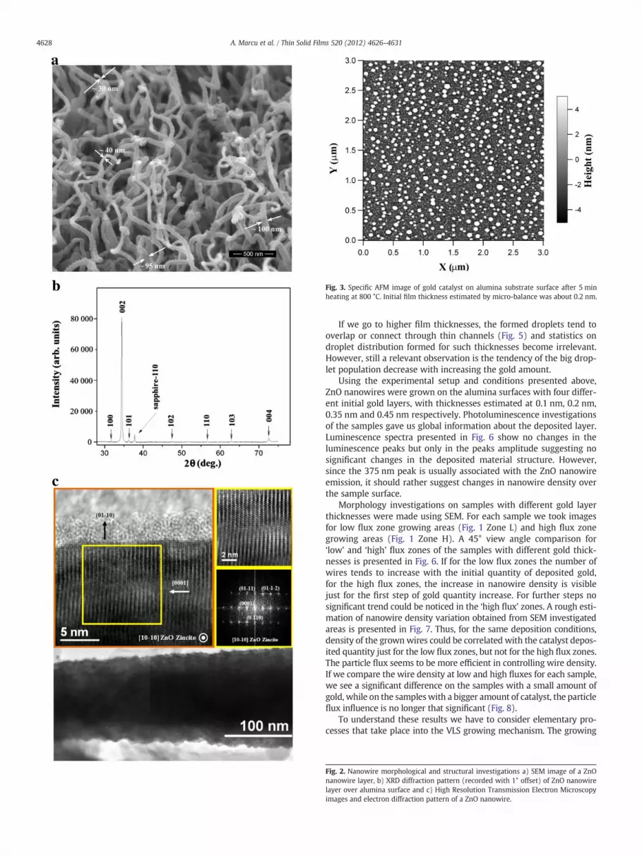
Fig. 3. Specific AFM image of gold catalyst on alumina substrate surface after 5 minheating at 800 °C. Initial film thickness estimated by micro-balance was about 0.2 nm.
4628 A. Marcu et al. / Thin Solid Films 520 (2012) 4626–4631
If we go to higher film thicknesses, the formed droplets tend tooverlap or connect through thin channels (Fig. 5) and statistics ondroplet distribution formed for such thicknesses become irrelevant.However, still a relevant observation is the tendency of the big drop-let population decrease with increasing the gold amount.
Using the experimental setup and conditions presented above,ZnO nanowires were grown on the alumina surfaces with four differ-ent initial gold layers, with thicknesses estimated at 0.1 nm, 0.2 nm,0.35 nm and 0.45 nm respectively. Photoluminescence investigationsof the samples gave us global information about the deposited layer.Luminescence spectra presented in Fig. 6 show no changes in theluminescence peaks but only in the peaks amplitude suggesting nosignificant changes in the deposited material structure. However,since the 375 nm peak is usually associated with the ZnO nanowireemission, it should rather suggest changes in nanowire density overthe sample surface.
Morphology investigations on samples with different gold layerthicknesses were made using SEM. For each sample we took imagesfor low flux zone growing areas (Fig. 1 Zone L) and high flux zonegrowing areas (Fig. 1 Zone H). A 45° view angle comparison for‘low’ and ‘high’ flux zones of the samples with different gold thick-nesses is presented in Fig. 6. If for the low flux zones the number ofwires tends to increase with the initial quantity of deposited gold,for the high flux zones, the increase in nanowire density is visiblejust for the first step of gold quantity increase. For further steps nosignificant trend could be noticed in the ‘high flux’ zones. A rough esti-mation of nanowire density variation obtained from SEM investigatedareas is presented in Fig. 7. Thus, for the same deposition conditions,density of the grownwires could be correlated with the catalyst depos-ited quantity just for the low flux zones, but not for the high flux zones.The particle flux seems to be more efficient in controlling wire density.If we compare the wire density at low and high fluxes for each sample,we see a significant difference on the samples with a small amount ofgold, while on the sampleswith a bigger amount of catalyst, the particleflux influence is no longer that significant (Fig. 8).
To understand these results we have to consider elementary pro-cesses that take place into the VLS growing mechanism. The growing
Fig. 2. Nanowire morphological and structural investigations a) SEM image of a ZnOnanowire layer, b) XRD diffraction pattern (recorded with 1° offset) of ZnO nanowirelayer over alumina surface and c) High Resolution Transmission Electron Microscopyimages and electron diffraction pattern of a ZnO nanowire.

Fig. 4. Gold droplet distribution results estimated from AFM substrate measurements a) diameter percentage distribution and b) number/square micrometer diameter distribution.
4629A. Marcu et al. / Thin Solid Films 520 (2012) 4626–4631
process consists in preferential absorption of particles' vapors into theliquid catalyst droplets and their deposition in solid phase at the bottomof the droplet catalyst. However, absorbed particles start to be deposit-ed below the liquid droplet just after a critic concentration is reachedinto the catalyst. Comparing the number of grownwires for the thinnergold layer (~0.1 nm) in the ‘low flux’ zone with the AFM image of thegold formed droplets, we can easily notice that, for such a low particleflux, there is a rather limited number of the droplets that will be effec-tive in formingwires. Since increasing the gold quantity would increasethe grown population but still not all the droplets form nanowires, wecould correlate previously the observed droplet population 20–60 nmincrease with the nanowire density increase of the ‘low flux’ areas andconclude that this population is actually responsible for the grownmor-phology in our experiment. Actually, the grownwire diameter is indeedwithin this range andmight sustain this assumption. A possible theoret-ical support for this correlation should be that a bigger droplet mightnot get enough absorbed particles to reach the critical concentrationthat enables it to grow through VLS mechanism, and the resulting
morphology is finally the result of the VLS and thin film growing com-petition, respectively an island growth or even film morphology forthe corresponding substrate area.
When looking at the ‘high flux’ zones (Fig. 1 Zone H) density var-iation, we notice that for the same catalyst distribution variation,nanowire density variation is no longer the same. Even if the20–60 nm gold population increases, the nanowire density does notchange significantly and the correlation between the population in-crease and the nanowire density increase is no longer possible. Hav-ing a closer look at the nanowires morphology, we can also noticethat the wire's diameter distribution is actually considerably widerfor these ‘high flux’ zones than for the ‘low flux’ zones, similar toour previous estimated results on diameter distribution for the“thick” gold layers, namely, we can easily identify wires with diame-ters between 30 and 90 nm. Still, not all the gold droplets would formnanowires into the ‘high flux’ zones, but certainly a wider range ofdroplet diameters leads to nanowire growth. Thus, the particle fluxseems to be correlated with catalyst droplet diameter.

Fig. 8. ZnO nanowire density variation on catalyst initial film thickness estimated fromSEM images.
Fig. 5. AFM image of gold catalyst on alumina substrate surface after 5 min heating at800 °C for an initial gold thickness estimated by micro-balance of about 0.8 nm.
Fig. 6. Photoluminescence spectra of ZnO nanowires grown using different initial goldcatalyst film thicknesses.
4630 A. Marcu et al. / Thin Solid Films 520 (2012) 4626–4631
The droplet diameter selection through the particles' flux can befurther understood if we consider the fact that we are using pulsedlaser ablation and particles' incident flux would be pulsed as well.Plume particle interaction with the substrate and gold catalyst, and
Fig. 7. 45° view angle SEM images of ZnO nanowire layer grown on alumina substrate usingwere taken in the ‘high’ (H) and ‘low’ (L) flux zones of the substrate.
particle absorption into the catalyst droplet respectively are alsopulsed processes. Since nanowire growing process below a dropletcould be triggered only by reaching the critical particle concentrationinside it, there is a limited time for reaching this concentration, andthis roughly corresponds to the peak interaction between plumeand substrate [25,28,29,30,31]. Unlike the catalyst assisted depositionprocess, catalyst desorption takes place below the critical particle con-centration as well [32]. Thus, only if during plume interaction with thesubstrate, impinging particles together with diffused particles areabsorbed together into the droplet, the desorption process can beovercome. Outside of this interval, the concentration will decreaseanyway by desorption, without growing of the nanowire until thenext ablation plume impact. It is obvious that a bigger droplet diam-eter would mean a bigger volume of the catalyst and consequentlyrequires a bigger number of particles to be absorbed to reach the crit-ical concentration. It is also interesting to notice that the grownwires have about same length suggesting that nanowire growing isnot affected by the density. They do not actually influence one anoth-er during the growth process. Thus, the collected particles for such alimited time could come from a limited vicinity and the main way toincrease this number of particles remains the increase of the particleflux. This could roughly explain the differences in nanowire density be-tween the ‘low’ and ‘high’ flux zones observed for relatively small cata-lyst quantity samples and the wider nanowire density observed onthe substrate ‘high flux’ zones.
a) 0.1 nm b) 0.2 nm c) 0.34 nm and d) 0.45 nm gold catalyst initial thicknesses. Images

4631A. Marcu et al. / Thin Solid Films 520 (2012) 4626–4631
4. Conclusions
Considering these results, we can conclude that in this work wehave experimentally proved the catalyst size limitations of the VLSprocess in PLD/VLS ZnO nanowire growth. Particularly at low particlesflux there seems to be a catalyst size based selective nanowire growthwhich we understand in terms of catalyst volume dependent absorbedparticle concentration during the plume interaction with the substrate.Using these results, we can actually try to control the nanowire densityon a surface with a specific droplet diameter population distribution bylocally controlling the particle flux.
Acknowledgment
This work was partially supported by PosDru/89/1.5/S/60746Program. The authors would like to thank the TEM facilities in ServeisCientificotècnics from Universitat de Barcelona.
References
[1] Y.Q. Bie, Z.M. Liao, P.W.W., Y.B. Zhou, X.B. Han, Y. Ye, Q. Zhao, X.S. Wu, L. Dai, J. Xu,L.W. Sang, J.J. Deng, K. Laurent, Y. Leprince-Wang, D.P. Yu, Adv. Mater. 22 (2010)4284.
[2] L.X. Mu, W.S. Shi, T.P. Zhang, H.Y. Zhang, Y. Wang, G.W. She, Y.H. Gao, P.F. Wang,J.C. Chang, S.T. Lee, Appl. Phys. Lett. 98 (2011) 163101.
[3] K. Kim, H.G. Kang, H. Kim, J.S. Lee, S. Kim, W. Kang, G.T. Kim, Appl. Phys. A 94(2009) 253.
[4] F. Hernández-Ramírez, A. Tarancón, O. Casals, J. Arbiol, A. Romano-Rodríguez, J.R.Morante, Sens. Actuators, B 121 (2007) 3.
[5] O. Lupan, G.A. Emelchenko, V.V. Ursaki, G. Chai, A.N. Redkin, A.N. Gruzintsev, I.M.Tiginyanu, L. Chow, L.K. Ono, B. Roldan Cuenya, H. Heinrich, E.E. Yakimov, Mater.Res. Bull. 45 (2010) 1026.
[6] O. Lupan, V.M. Guérin, I.M. Tiginyanu, V.V. Ursaki, L. Chow, H. Heinrich, T. Pauporté,J. Photochem. Photobiol., A 211 (2010) 65.
[7] G. Chai, O. Lupan, L. Chow, H. Heinrich, Sens. Actuators, A 150 (2009) 184.[8] L. Yuguo, Y. Aichun, Z. Boshi, P. Ruiqin, Z. Xuelei, J. Semicond. 32 (2011) 023002
doi:10.1088/1674-4926/32/2/023002.[9] J.-C. Lee, K.-S. Park, T.-G. Kim, H.-J. Choi, Y.-M. Sung, Nanotechnology 17 (2006)
4317.[10] H. Srivastava, P. Tiwari, A.K. Srivastava, R.V. Nandedkar, J. Appl. Phys. 102 (2007)
054303.[11] H.W. Kim, J.W. Lee, Physica E 40 (2008) 2499.[12] H.W. Kim, S.H. Shim, Chem. Phys. Lett. 422 (2006) 165.[13] Q. Wan, E.N. Dattoli, W.Y. Fung, W. Guo, Y. Chen, X. Pan, W. Lu, Nano Lett. 12
(2006) 2909.[14] K. Tateno, G. Zhang, H. Nakano, Nano Lett. 8 (2008) 3645.[15] T.T. Xu, J.-G. Zheng, A.W. Nicholls, S. Stankovich, R.D. Piner, R.S. Ruoff, Nano Lett. 4
(2004) 2051.[16] R.T.R. Kumar, E. McGlynn, M. Biswas, R. Saunders, G. Trolliard, B. Soulestin, J.-R.
Duclere, J.P. Mosnier, M.O. Henry, J. Appl. Phys. Lett. 104 (2008) 084309.[17] K. Nagashima, T. Yanagida, H. Tanaka, T. Kawai, Appl. Phys. Lett. 90 (2007)
233103.[18] Y. Yao, F. Li, S.-T. Lee, Chem. Phys. Lett. 406 (2005) 381.[19] T.Y. Tan, N. Li, U. Gosele, Appl. Phys. Lett. 83 (2003) 1199.[20] S.M. Roper, S.H. Davis, S.A. Noeeis, A.A. Golovin, J. Appl. Phys. 102 (2007) 034304.[21] E.I. Givargizov, J. Cryst. Growth 31 (1975) 20.[22] T. Yanagida, K. Nagashima, H. Tanaka, T. Kawai, J. Appl. Phys. 104 (2008) 016101.[23] A. Marcu, C. Grigoriu, K. Yatsui, SPIE 5581 (2003) 371.[24] A. Marcu, C. Grigoriu, C.P.Lungu, T.Yanagida and T.Kawai, Physica E (2010), online
http://dx.doi.org/10.1016/j.physe.2010.11.002.[25] A. Marcu, C. Grigoriu, K. Yatsui, Appl. Surf. Sci. 252 (2006) 4733.[26] A. Marcu, C. Grigoriu, K. Yatsui, Appl. Surf. Sci. 248 (2005) 466.[27] D.L. Guo, X. Huang, G.Z. Xing, Z. Zhang, G.P. Li, M. He, H. Zhang, H. Chen, T. Wu,
Phys. Rev. B: Condens. Matter 83 (2011) 045403.[28] S. Gacek, X. Wang, Appl. Phys. A 94 (2009) 675.[29] S. Gacek, Z. Wang, Appl. Phys. A 272 (2009) 3342.[30] D.B. Geohegan, A.A. Puretzky, Appl. Phys. Lett. 67 (1995) 197.[31] Y. Nakata, W.K.A. Kumuduni, T. Okada, M. Maeda, Appl. Phys. Lett. 64 (1994).[32] A. Marcu, T. Yanagida, K. Nagashima, H. Tanaka, T. Kawai, J. Appl. Phys. 102 (2007)
016102.