an1759 - nxp
TRANSCRIPT
F
ree
sca
le S
em
ico
nd
uc
tor,
In
c..
.
Order this documentby AN1759/D
AN1759
Add a Non-Volatile Clock to the MC68HC705J1ABy Mark Glenewinkel
Field Applications EngineeringConsumer Systems GroupAustin, Texas
Introduction
Many embedded systems require the measurement of time. This can beaccomplished internally by some MCUs that have on-chip real-timeclocks. Even so, for date, month, and leap year measurement, this taskcan take substantial amounts of bandwidth and code space.
The DS1307 64x8 serial real-time clock provides calendar and timekeeping functions along with system-enhancing non-volatile RAM. Witha 2-wire interface, timekeeping can be managed easily.
Some applications of using the DS1307 are:
• Logging of chronological events
• Tracking power down time of a system
• Providing alarm functions
Motorola, Inc., 1998 AN1759
For More Information On This Product, Go to: www.freescale.com
Application Note
F
ree
sca
le S
em
ico
nd
uc
tor,
I
Freescale Semiconductor, Inc.n
c..
.
The non-volatile RAM (random-access memory) also gives the useradditional applications such as:
• Power down information storage for consumer electronics likeTVs, VCRs, and hand-held portables
• Identification number storage for remote addressing or security
• Storage of telecommunication information like phone numberrecall and speed dialing
This application note describes the interface between theMC68HC705J1A (J1A) and the DS1307. Circuitry and example code aregiven to demonstrate the interface between the two parts.
Features The DS1307 provides these features:
• Real-time clock counts seconds, minutes, hours, day of the week,date, month, and year.
• Leap year compensation valid up to 2100
• 56 bytes of non-volatile RAM for data storage
• 2-wire serial interface
• Programmable square wave output with frequencies of 1 Hz,4.096 kHz, 8.192 kHz, and 32.768 kHz
• Automatic power switching to battery when main power fails
• In battery backup mode, less than 500 nA consumed at 25 °C
• 8-pin DIP or SOIC package
• Optional industrial temperature range of –40 °C to +85 °C
Description The DS1307 is a low-power binary coded decimal (BCD) clock calendarthat provides seconds, minutes, hours, day, date, month, and year. Inaddition, it has 56 bytes of non-volatile RAM. End-of-the-monthadjustments are automatic for months with less than 31 days. Thedevice also corrects for leap years. The clock can operate in either12-hour or 24-hour mode. In 12-hour mode, an a.m./p.m indicator isused.
AN1759
2 For More Information On This Product,
Go to: www.freescale.com
Application NoteDS1307 Hardware Interface
F
ree
sca
le S
em
ico
nd
uc
tor,
I
Freescale Semiconductor, Inc.n
c..
.
The DS1307 has built-in power management circuitry to detect powerfailures on the VDD pin and when detected will switch power over to thebattery back-up pin, VBAT. Access to the device is terminated when VDDfalls below 1.25 x VBAT. Further accesses to the device are not allowed.On power up, the device switches power from VBAT to VDD when the VDDpin is 0.2 volts above VBAT. Once VDD is higher than 1.25 x VBAT, normaloperations can continue.
Address and data are communicated via the 2-wire bus. The DS1307operates as a slave at all times and is accessed by first transmitting theDS1307’s identification code on the bus.
DS1307 Hardware Interface
Pinout and PinDescriptions
Figure 1. DS1307 Pinout
VDD and GND These pins serve as the main power source for the device. When+5 volts is applied to this pin, the device is fully accessible and data canbe read or written. If the power on the VDD pin falls below 1.25 x VDD, thedevice switches its power supply to VBAT. At this point, reading andwriting to the device is prohibited. The timekeeping function and non-volatile RAM are unaffected.
VBAT This pin is the power input for any standard 3-volt lithium battery or other3-volt source. For proper operation, this voltage must be held between2.5 and 3.5 volts. A lithium battery with at least a 35-mA hours rating willback up the DS1307 for more than 10 years in the absence of power.
1
2
3
4
8
7
6
5
X2
VBAT
GND
X1
SQW/OUT
SCL
SDA
VDD
AN1759
3 For More Information On This Product,
Go to: www.freescale.com
Application Note
F
ree
sca
le S
em
ico
nd
uc
tor,
I
Freescale Semiconductor, Inc.n
c..
.
X1 and X2 These pins are used to connect a 32.768-kHz crystal to the device. Noother capacitors or resistors are needed for this crystal circuit. Theinternal oscillator circuitry is designed for a crystal with load capacitanceof 12.5 pF. For the test circuit described in this application note, anEpson C-001R crystal was used. The Digi-key part number for thisdevice is SE3201-ND.
SQW/OUT When enabled, this pin outputs one of four selectable frequencies:
• 1 Hz
• 4.096 kHz
• 8.192 kHz
• 32.768 kHz
The 1-Hz signal can be used to feed an external interrupt pin on an MCU.This allows the MCU to use minimal bandwidth when servicing thetimekeeping function of a system.
When disabled, the pin acts as a normal output pin. It is controlled viathe DS1307 control register.
SCL The SCL pin is the clock input for the DS1307 2-wire serial interface.
SDA The SDA pin is an I/O pin used to transmit and receive data off the 2-wireserial interface. SDA is an open-drain pin that requires an external pullupresistor.
AN1759
4 For More Information On This Product,
Go to: www.freescale.com
Application NoteDS1307 Hardware Interface
F
ree
sca
le S
em
ico
nd
uc
tor,
I
Freescale Semiconductor, Inc.n
c..
.
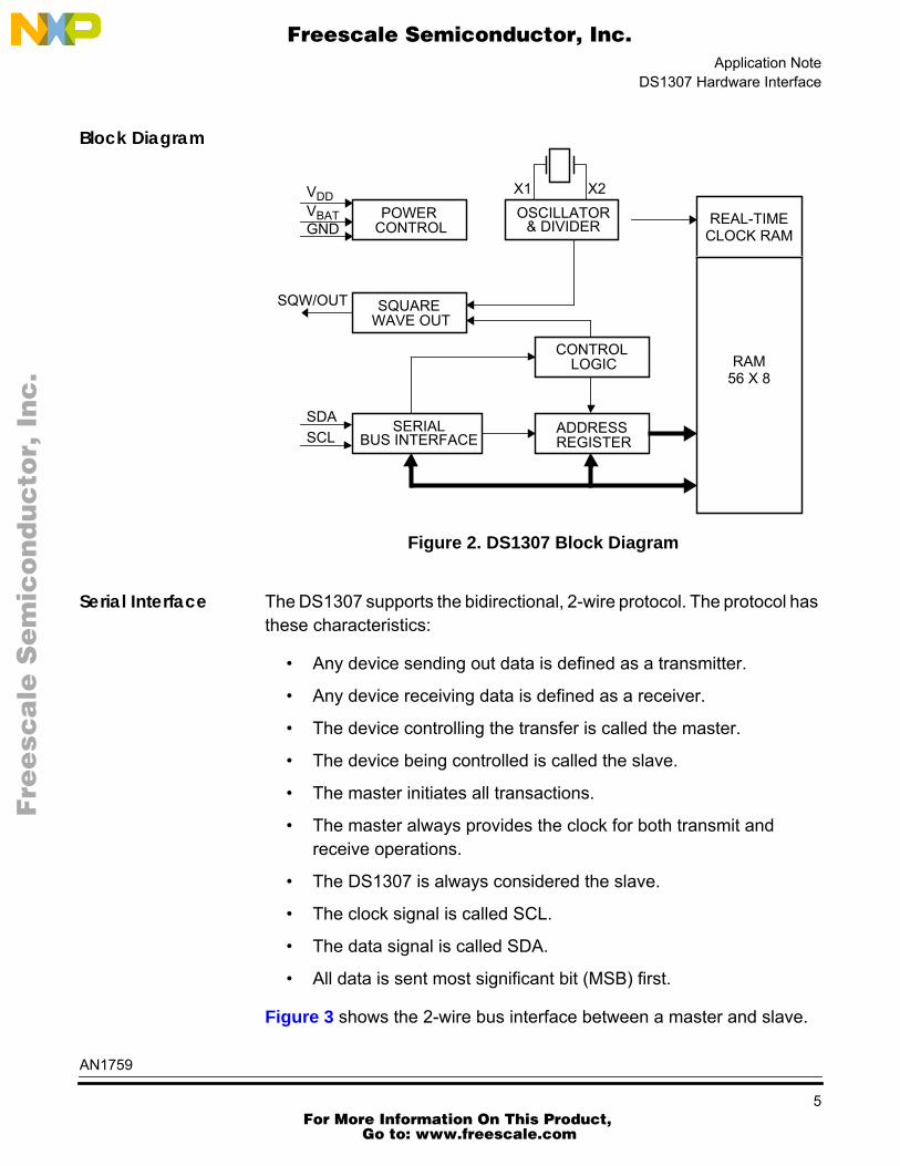
Block Diagram
Figure 2. DS1307 Block Diagram
Serial Interface The DS1307 supports the bidirectional, 2-wire protocol. The protocol hasthese characteristics:
• Any device sending out data is defined as a transmitter.
• Any device receiving data is defined as a receiver.
• The device controlling the transfer is called the master.
• The device being controlled is called the slave.
• The master initiates all transactions.
• The master always provides the clock for both transmit andreceive operations.
• The DS1307 is always considered the slave.
• The clock signal is called SCL.
• The data signal is called SDA.
• All data is sent most significant bit (MSB) first.
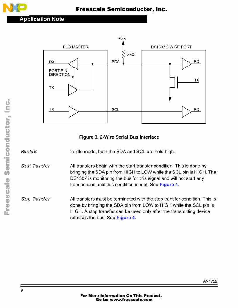
Figure 3 shows the 2-wire bus interface between a master and slave.
SQUARE
OSCILLATOR& DIVIDER
SERIALBUS INTERFACE
POWER
CONTROL
ADDRESS
REAL-TIMECLOCK RAM
RAM56 X 8
X1 X2VDDVBATGND
SQW/OUT
SDASCL
CONTROL
WAVE OUT
REGISTER
LOGIC
AN1759
5 For More Information On This Product,
Go to: www.freescale.com
Application Note
F
ree
sca
le S
em
ico
nd
uc
tor,
I
Freescale Semiconductor, Inc.n
c..
.
Figure 3. 2-Wire Serial Bus Interface
Bus Idle In idle mode, both the SDA and SCL are held high.
Start Transfer All transfers begin with the start transfer condition. This is done bybringing the SDA pin from HIGH to LOW while the SCL pin is HIGH. TheDS1307 is monitoring the bus for this signal and will not start anytransactions until this condition is met. See Figure 4 .
Stop Transfer All transfers must be terminated with the stop transfer condition. This isdone by bringing the SDA pin from LOW to HIGH while the SCL pin isHIGH. A stop transfer can be used only after the transmitting devicereleases the bus. See Figure 4 .
+5 V
DS1307 2-WIRE PORT
RX
TX
5 kΩ
RX
TX
PORT PIN
BUS MASTER
TX RXSCL
SDA
DIRECTION
AN1759
6 For More Information On This Product,
Go to: www.freescale.com
Application NoteDS1307 Hardware Interface
F
ree
sca
le S
em
ico
nd
uc
tor,
I
Freescale Semiconductor, Inc.n
c..
.
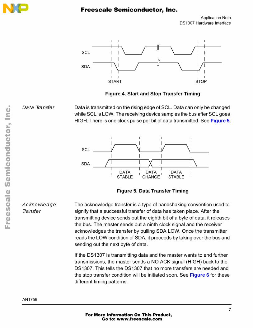
Figure 4. Start and Stop Transfer Timing
Data Transfer Data is transmitted on the rising edge of SCL. Data can only be changedwhile SCL is LOW. The receiving device samples the bus after SCL goesHIGH. There is one clock pulse per bit of data transmitted. See Figure 5 .
Figure 5. Data Transfer Timing
AcknowledgeTransfer
The acknowledge transfer is a type of handshaking convention used tosignify that a successful transfer of data has taken place. After thetransmitting device sends out the eighth bit of a byte of data, it releasesthe bus. The master sends out a ninth clock signal and the receiveracknowledges the transfer by pulling SDA LOW. Once the transmitterreads the LOW condition of SDA, it proceeds by taking over the bus andsending out the next byte of data.
If the DS1307 is transmitting data and the master wants to end furthertransmissions, the master sends a NO ACK signal (HIGH) back to theDS1307. This tells the DS1307 that no more transfers are needed andthe stop transfer condition will be initiated soon. See Figure 6 for thesedifferent timing patterns.
SCL
SDA
START STOP
SCL
SDA
DATACHANGE
DATASTABLE
DATASTABLE
AN1759
7 For More Information On This Product,
Go to: www.freescale.com
Application Note
F
ree
sca
le S
em
ico
nd
uc
tor,
I
Freescale Semiconductor, Inc.n
c..
.
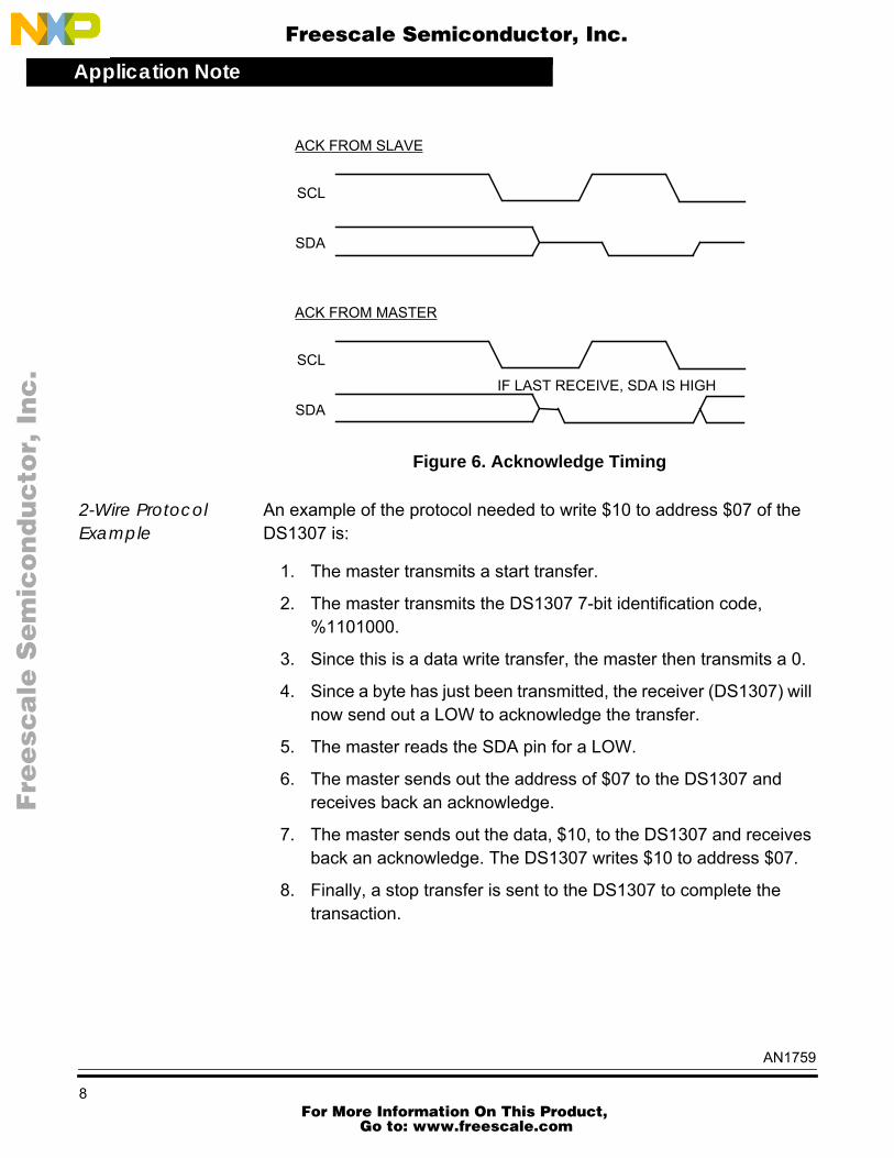
Figure 6. Acknowledge Timing
2-Wire ProtocolExample
An example of the protocol needed to write $10 to address $07 of theDS1307 is:
1. The master transmits a start transfer.
2. The master transmits the DS1307 7-bit identification code,%1101000.
3. Since this is a data write transfer, the master then transmits a 0.
4. Since a byte has just been transmitted, the receiver (DS1307) willnow send out a LOW to acknowledge the transfer.
5. The master reads the SDA pin for a LOW.
6. The master sends out the address of $07 to the DS1307 andreceives back an acknowledge.
7. The master sends out the data, $10, to the DS1307 and receivesback an acknowledge. The DS1307 writes $10 to address $07.
8. Finally, a stop transfer is sent to the DS1307 to complete thetransaction.
SCL
SDA
ACK FROM SLAVE
SCL
SDA
ACK FROM MASTER
IF LAST RECEIVE, SDA IS HIGH
AN1759
8 For More Information On This Product,
Go to: www.freescale.com
Application NoteDS1307 Software Interface
F
ree
sca
le S
em
ico
nd
uc
tor,
I
Freescale Semiconductor, Inc.n
c..
.
DS1307 Software Interface
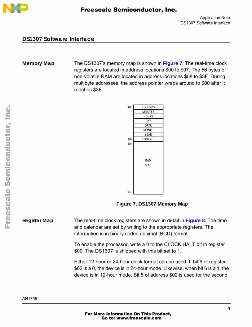
Memory Map The DS1307’s memory map is shown in Figure 7 . The real-time clockregisters are located in address locations $00 to $07. The 56 bytes ofnon-volatile RAM are located in address locations $08 to $3F. Duringmultibyte addresses, the address pointer wraps around to $00 after itreaches $3F.
Figure 7. DS1307 Memory Map
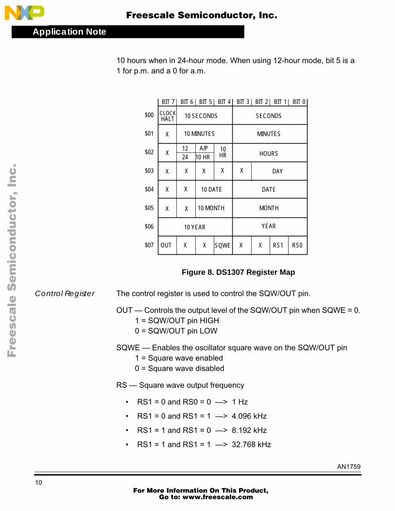
Register Map The real-time clock registers are shown in detail in Figure 8 . The timeand calendar are set by writing to the appropriate registers. Theinformation is in binary coded decimal (BCD) format.
To enable the processor, write a 0 to the CLOCK HALT bit in register$00. The DS1307 is shipped with this bit set to 1.
Either 12-hour or 24-hour clock format can be used. If bit 6 of register$02 is a 0, the device is in 24-hour mode. Likewise, when bit 6 is a 1, thedevice is in 12-hour mode. Bit 5 of address $02 is used for the second
SECONDSMINUTES
RAM56X8
HOURSDAY
DATEMONTHYEAR
CONTROL
$00
$07
$08
$3F
AN1759
9 For More Information On This Product,
Go to: www.freescale.com
Application Note
F
ree
sca
le S
em
ico
nd
uc
tor,
I
Freescale Semiconductor, Inc.n
c..
.
10 hours when in 24-hour mode. When using 12-hour mode, bit 5 is a1 for p.m. and a 0 for a.m.
Figure 8. DS1307 Register Map
Control Register The control register is used to control the SQW/OUT pin.
OUT — Controls the output level of the SQW/OUT pin when SQWE = 0.1 = SQW/OUT pin HIGH0 = SQW/OUT pin LOW
SQWE — Enables the oscillator square wave on the SQW/OUT pin1 = Square wave enabled0 = Square wave disabled
RS — Square wave output frequency
• RS1 = 0 and RS0 = 0 —> 1 Hz
• RS1 = 0 and RS1 = 1 —> 4.096 kHz
• RS1 = 1 and RS1 = 0 —> 8.192 kHz
• RS1 = 1 and RS1 = 1 —> 32.768 kHz
$00
BIT 7 BIT 6 BIT 5 BIT 4 BIT 3 BIT 2 BIT 1 BIT 0
SECONDS
MINUTES
HOURS
CLOCK 10 SECONDS
10 MINUTES
HALT
DAY
DATE
MONTH
YEAR
X
X
X
X
X X
X
X
1224 10 HR
A/P 10HR
X X X
10 DATE
10 MONTH
10 YEAR
X X XXOUT SQWE RS1 RS0
$01
$02
$03
$04
$05
$06
$07
AN1759
10 For More Information On This Product,
Go to: www.freescale.com
Application NoteDS1307 Software Interface
F
ree
sca
le S
em
ico
nd
uc
tor,
I
Freescale Semiconductor, Inc.n
c..
.
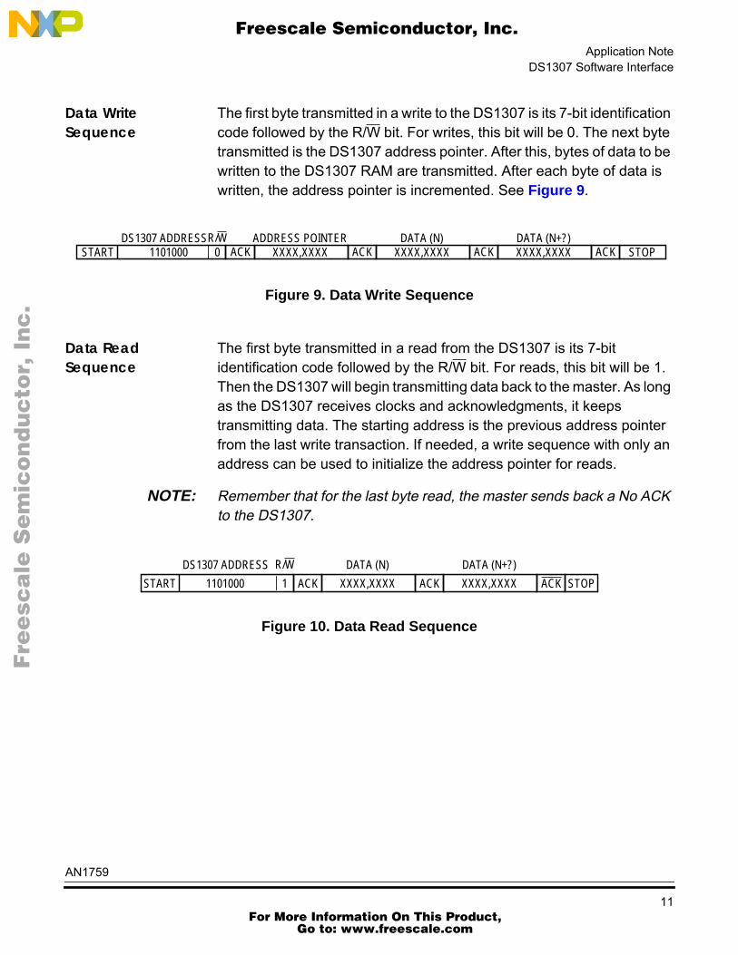
Data WriteSequence
The first byte transmitted in a write to the DS1307 is its 7-bit identificationcode followed by the R/W bit. For writes, this bit will be 0. The next bytetransmitted is the DS1307 address pointer. After this, bytes of data to bewritten to the DS1307 RAM are transmitted. After each byte of data iswritten, the address pointer is incremented. See Figure 9 .
Figure 9. Data Write Sequence
Data ReadSequence
The first byte transmitted in a read from the DS1307 is its 7-bitidentification code followed by the R/W bit. For reads, this bit will be 1.Then the DS1307 will begin transmitting data back to the master. As longas the DS1307 receives clocks and acknowledgments, it keepstransmitting data. The starting address is the previous address pointerfrom the last write transaction. If needed, a write sequence with only anaddress can be used to initialize the address pointer for reads.
NOTE: Remember that for the last byte read, the master sends back a No ACKto the DS1307.
Figure 10. Data Read Sequence
START 1101000DS1307 ADDRESSR/W
0 ACK XXXX,XXXXADDRESS POINTER
ACK XXXX,XXXXDATA (N)
ACK XXXX,XXXXDATA (N+?)
ACK STOP
START 1101000
DS1307 ADDRESS R/W
1 ACK XXXX,XXXX
DATA (N)
ACK XXXX,XXXX
DATA (N+?)
ACK STOP
AN1759
11 For More Information On This Product,
Go to: www.freescale.com
Application Note
F
ree
sca
le S
em
ico
nd
uc
tor,
I
Freescale Semiconductor, Inc.n
c..
.
MC68HC705J1A Hardware Interface
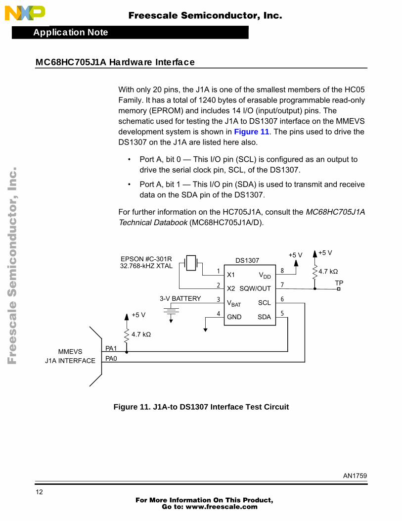
With only 20 pins, the J1A is one of the smallest members of the HC05Family. It has a total of 1240 bytes of erasable programmable read-onlymemory (EPROM) and includes 14 I/O (input/output) pins. Theschematic used for testing the J1A to DS1307 interface on the MMEVSdevelopment system is shown in Figure 11 . The pins used to drive theDS1307 on the J1A are listed here also.
• Port A, bit 0 — This I/O pin (SCL) is configured as an output todrive the serial clock pin, SCL, of the DS1307.
• Port A, bit 1 — This I/O pin (SDA) is used to transmit and receivedata on the SDA pin of the DS1307.
For further information on the HC705J1A, consult the MC68HC705J1ATechnical Databook (MC68HC705J1A/D).
Figure 11. J1A-to DS1307 Interface Test Circuit
1
2
3
4
8
7
6
5
X2
VBAT
GND
X1
SQW/OUT
SCL
SDA
VDD
+5 VDS1307
PA0PA1MMEVS
3-V BATTERY
+5 V
4.7 kΩ
TP
+5 V
4.7 kΩ
J1A INTERFACE
EPSON #C-301R32.768-kHZ XTAL
AN1759
12 For More Information On This Product,
Go to: www.freescale.com
Application NoteMC68HC705J1A Software Interface
F
ree
sca
le S
em
ico
nd
uc
tor,
I
Freescale Semiconductor, Inc.n
c..
.
MC68HC705J1A Software Interface
I/O driving or manipulation is the process of toggling I/O pins withsoftware instructions to create a certain hardware peripheral. The HC05CPU provides special instructions specifically to manipulate singleI/O pins.
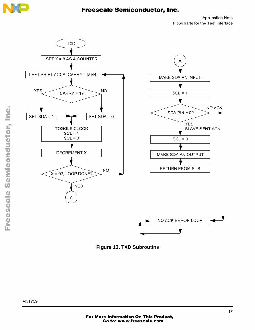
Five subroutines were created to provide an easy applicationprogramming interface (API). These routines are:
• START_SER — Sends out a start condition on the bus
• STOP_SER — Sends out a stop condition on the bus
• TXD — The master takes the contents of AccA and transmits itMSB first to the DS1307. The master also checks foracknowledgement from the DS1307.
• RXD — After the master addresses the DS1307 with itsidentification code and the read bit, the DS1307 transmits a byteof data back to the master. This routine reads that byte and puts itinto AccA. The master also generates an acknowledgment back tothe DS1307.
• RXD_LAST — This routine is just like RXD but it is used for thelast byte read from the DS1307. It does not generate anacknowledgment back to the DS1307.
The flowcharts for the DS1620 serial I/O drivers are shown inFlowcharts for the Test Interface . These routines were writtenespecially for the DS1307 and may not be able to properly drive otherMCU peripherals with 2-wire serial buses.
A typical application would use the SQW/OUT pin on the DS1307. Whenconfiguring this pin for a 1-Hz signal, feed the signal to the IRQ pin of anMCU. An interrupt routine can be created to read the contents of theDS1307 every time a 1-Hz signal hits the IRQ pin. This should takeminimal CPU bandwidth and provide the user an easy way to retrievetime and date information.
The main test routine was written to verify the bus interface between theDS1307 and the J1A. It writes a known date and time into the DS1307
AN1759
13 For More Information On This Product,
Go to: www.freescale.com
Application Note
F
ree
sca
le S
em
ico
nd
uc
tor,
I
Freescale Semiconductor, Inc.n
c..
.
and then reads it back out. The data read is put into a RAM buffer on theHC05. When the emulator is stopped, read the contents of the HC05RAM buffer to verify the transmission process.
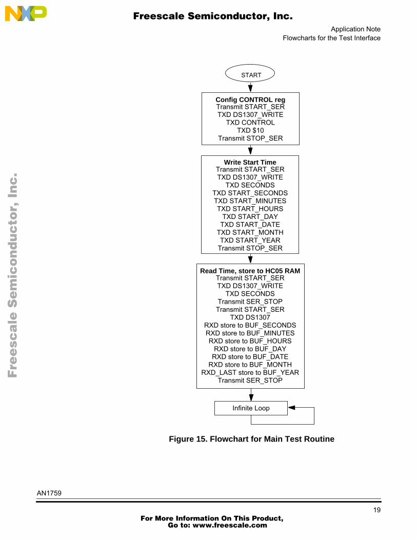
The test routine sequence is shown in Figure 15 . The assembly code forthe test routine is provided in the section titled Code Listing .
The sequence of tests is:
1. Configure the device to turn on a 1-Hz signal on the SQW/OUTpin.
a. Transmit a start condition.
b. Transmit the DS1307 code to write to the device of%11010000.
c. Transmit the control register address and then $10.
d. Transmit a stop condition.
2. Write start time.
a. Transmit a start condition.
b. Transmit the DS1307 code to write to the device of%11010000.
c. Transmit the starting address of $00, the seconds register.
d. Transmit Saturday, June 20, 1998, 4:30:00 p.m. (By writing a0 to bit 7 of the seconds register, the crystal circuit has beenturned on.)
e. Transmit a stop condition.
3. Read time and date, store away to HC05 RAM buffer.
a. Transmit a start condition.
b. Transmit the DS1307 code to write to the device of%11010000.
c. Transmit the starting address of $00.
d. Transmit a stop condition.
e. Transmit a start condition.
AN1759
14 For More Information On This Product,
Go to: www.freescale.com
Application NoteDevelopment Tools
F
ree
sca
le S
em
ico
nd
uc
tor,
I
Freescale Semiconductor, Inc.n
c..
.
f. Transmit the DS1307 code to read from the device of%11010001.
g. Read the date and time and store away to HC05 RAM.
h. Transmit a stop condition.
Since the real-time clock is running, you can restart the code at step 3and verify that it is keeping time.
This routine demonstrates the interface software needed tocommunicate with the DS1307. Although the J1A was used, any HC05device could utilize this interface code. Minor adjustments of port pinsand memory maps might be necessary.
Development Tools
The interface was created and tested using these development tools:
• M68MMPFB0508 — Freescale MMEVS platform board
• X68EM05J1A — Freescale J1A emulation module
• Win IDE Version 1.02 — Editor, assembler, and debugger byP&E Microcomputer Systems
AN1759
15 For More Information On This Product,
Go to: www.freescale.com

Application Note
F
ree
sca
le S
em
ico
nd
uc
tor,
I
Freescale Semiconductor, Inc.n
c..
.
Flowcharts for the Test Interface
Figure 12. START_SER and STOP_SER Subroutines
START_SER
TAKE SDA LOW
TAKE SCL LOW
RETURN FROM SUB
STOP_SER
TAKE SCL HIGH
TAKE SDA HIGH
RETURN FROM SUB
AN1759
16 For More Information On This Product,
Go to: www.freescale.com
Application NoteFlowcharts for the Test Interface
F
ree
sca
le S
em
ico
nd
uc
tor,
I
Freescale Semiconductor, Inc.n
c..
.
Figure 13. TXD Subroutine
TXD
SET X = 8 AS A COUNTER
LEFT SHIFT ACCA, CARRY = MSB
DECREMENT X
CARRY = 1?YES NO
SET SDA = 1 SET SDA = 0
X = 0?, LOOP DONE?NO
YES
TOGGLE CLOCKSCL = 1SCL = 0
MAKE SDA AN INPUT
SCL = 1
SDA PIN = 0?NO ACK
YESSLAVE SENT ACK
SCL = 0
MAKE SDA AN OUTPUT
A
A
RETURN FROM SUB
NO ACK ERROR LOOP
AN1759
17 For More Information On This Product,
Go to: www.freescale.com

Application Note
F
ree
sca
le S
em
ico
nd
uc
tor,
I
Freescale Semiconductor, Inc.n
c..
.
Figure 14. RXD/RXD_LAST Subroutines
RXD/RXD_LAST
MAKE SDA AN INPUT
SCL=1
X = 0?
YES, RECEIVED 8-BIT DATA
NO
SDA PIN = 0?CARRY BIT = SDA
YES
NO
ROTATE LEFT ACCAPUTS CARRY BIT INTO ACCA MSB
SCL = 0
MAKE SDA AN OUTPUTSDA = 0
SET X = 8 AS A COUNTER
DECREMENT X
TOGGLE CLOCKSCL=1SCL=0
RETURN FROM SUB
RXD — ACK WITH SDA = 0RXD_LAST — NO ACK WITH SDA = 1
AN1759
18 For More Information On This Product,
Go to: www.freescale.com
Application NoteFlowcharts for the Test Interface
F
ree
sca
le S
em
ico
nd
uc
tor,
I
Freescale Semiconductor, Inc.n
c..
.
Figure 15. Flowchart for Main Test Routine
START
Config CONTROL regTransmit START_SERTXD DS1307_WRITE
TXD CONTROLTXD $10
Transmit STOP_SER
Write Start TimeTransmit START_SERTXD DS1307_WRITE
TXD SECONDSTXD START_SECONDSTXD START_MINUTESTXD START_HOURS
TXD START_DAYTXD START_DATE
TXD START_MONTHTXD START_YEAR
Transmit STOP_SER
Read Time, store to HC05 RAMTransmit START_SERTXD DS1307_WRITE
TXD SECONDSTransmit SER_STOPTransmit START_SER
TXD DS1307RXD store to BUF_SECONDSRXD store to BUF_MINUTESRXD store to BUF_HOURS
RXD store to BUF_DAYRXD store to BUF_DATE
RXD store to BUF_MONTHRXD_LAST store to BUF_YEAR
Transmit SER_STOP
Infinite Loop
AN1759
19 For More Information On This Product,
Go to: www.freescale.com
Application Note
F
ree
sca
le S
em
ico
nd
uc
tor,
I
Freescale Semiconductor, Inc.n
c..
.
Code Listing
************************************************************************************** File name: DS1307.ASM* Example Code for the MC68HC705J1A Interface to the* Dallas DS1307 Serial Real Time Clock* Ver: 1.0* Date: June 1, 1998* Author: Mark Glenewinkel* Freescale Field Applications* Consumer Systems Group* Assembler: P&E IDE ver 1.02** For code explanation and flow charts, please consult Freescale Application Note* "Add a Non-volatile Clock to the MC68HC705J1A" Literature # AN1759/D*************************************************************************************
*** SYSTEM DEFINITIONS AND EQUATES ***************************************************** Internal Register DefinitionsPORTA EQU $00 ;PortADDRA EQU $04 ;data direction for PortA
*** Application Specific DefinitionsSER_PORT EQU $00 ;PORTA is SER_PORTSCL EQU 0T ;PORTA, bit 0, clock signalSDA EQU 1T ;PORTA, bit 1, data signal
DS1307_WRITE EQU $D0 ;addresses the DS1307 for writeDS1307_READ EQU $D1 ;addresses the DS1307 for readSECONDS EQU $00 ;DS1307 address for secondsMINUTES EQU $01 ;DS1307 address for minutesHOURS EQU $02 ;DS1307 address for hoursDAY EQU $03 ;DS1307 address for the dayDATE EQU $04 ;DS1307 address for the dateMONTH EQU $05 ;DS1307 address for the monthYEAR EQU $06 ;DS1307 address for the yearCONTROL EQU $07 ;DS1307 address for control
*** Memory DefinitionsEPROM EQU $300 ;start of EPROM memRAM EQU $C0 ;start of RAM memRESET EQU $7FE ;vector for reset
*** Time Start Definitions for test*** Start on Saturday, June 20th, 1998, 4:30:00 PMSTART_SECONDS EQU $00 ;0 secondsSTART_MINUTES EQU $30 ;30 minutesSTART_HOURS EQU $64 ;4 hours, PM, 12 Hour modeSTART_DAY EQU $06 ;SaturdaySTART_DATE EQU $20 ;20thSTART_MONTH EQU $06 ;JuneSTART_YEAR EQU $98 ;1998
AN1759
20 For More Information On This Product,
Go to: www.freescale.com
Application NoteCode Listing
F
ree
sca
le S
em
ico
nd
uc
tor,
I
Freescale Semiconductor, Inc.n
c..
.
*** RAM VARIABLES ******************************************************************* Buffer for test reading data from the DS1307
ORG RAMBUF_SECONDS DB 1 ;buffer on HC05 for secondsBUF_MINUTES DB 1 ;buffer on HC05 for hoursBUF_DAY DB 1 ;buffer on HC05 for the dayBUF_DATE DB 1 ;buffer on HC05 for the dateBUF_MONTH DB 1 ;buffer on HC05 for the monthBUF_YEAR DB 1 ;buffer on HC05 for the year
*** MAIN ROUTINE *******************************************************************ORG EPROM ;start at begining of EPROM
*** Intialize PortsSTART lda #$03 ;init SER_PORT
sta SER_PORTlda #$03 ;make SER_PORT pins outputssta DDRA
*** DS1307 configuration*** Turn on osc, turn on SQW/OUT pin with 1 Hz signal
jsr START_SER ;start serial transmission
lda #DS1307_WRITE ;address the DS1307 device, writejsr TXDlda #CONTROL ;send address of control regjsr TXDlda #$10 ;send config datajsr TXD
jsr STOP_SER ;stop serial transmission
*** Write Starting Time to DS1307jsr START_SER ;start serial transmission
lda #DS1307_WRITE ;address the DS1307 device, writejsr TXDlda #SECONDS ;start address of DS1307jsr TXDlda #START_SECONDS ;write secondsjsr TXDlda #START_MINUTES ;write minutesjsr TXDlda #START_HOURS ;write hoursjsr TXDlda #START_DAY ;write dayjsr TXDlda #START_DATE ;write datejsr TXDlda #START_MONTH ;write monthjsr TXDlda #START_YEAR ;write yearjsr TXD
jsr STOP_SER ;stop serial transmission
AN1759
21 For More Information On This Product,
Go to: www.freescale.com
Application Note
F
ree
sca
le S
em
ico
nd
uc
tor,
I
Freescale Semiconductor, Inc.n
c..
.
*** Read Time, store away in HC05 time buffer for verification* Write starting address
jsr START_SER ;start serial transmission
lda #DS1307_WRITE ;address the DS1307 device, writejsr TXDlda #SECONDS ;start address of DS1307 readjsr TXD
jsr STOP_SER ;stop serial transmission
* Read Time data put in HC05 bufferjsr START_SER ;start serial transmission
lda #DS1307_READ ;address the DS1307 device, readjsr TXDjsr RXDsta BUF_SECOND ;read seconds, store to bufferjsr RXDsta BUF_MINUTES ;read minutes, store to bufferjsr RXDsta BUF_HOURS ;read hours, store to bufferjsr RXDsta BUF_DAY ;read the day, store to bufferjsr RXDsta BUF_DATE ;read the date, store to bufferjsr RXDsta BUF_MONTH ;read the month, store to bufferjsr RXD_LASTsta BUF_YEAR ;read the year, store to buffer
jsr STOP_SER ;stop serial transmission
DUMMY bra DUMMY ;test sequence is over
*** SUBROUTINES *********************************************************************** Sends out Start command on busSTART_SER bclr SDA,SER_PORT ;SDA=0
bclr SCL,SER_PORT ;SCL=0rts
*** Sends out Stop command on busSTOP_SER bset SCL,SER_PORT ;SCL=1
bset SDA,SER_PORT ;SDA=1rts
*** Routine takes contents of AccA and transmits it serially to*** the DS1307, MSB first*** Looks for ACK, goes to ERROR routine if no ACKTXD ldx #8T ;set counter
WRITE asla ;Carry bit = MSBbcc J1bset SDA,SER_PORT ;SDA=1bra CLOCK_IT ;branch to clock_it
J1 bclr SDA,SER_PORT ;SDA=0brn J1 ;evens it out
AN1759
22 For More Information On This Product,
Go to: www.freescale.com
Application NoteCode Listing
F
ree
sca
le S
em
ico
nd
uc
tor,
I
Freescale Semiconductor, Inc.n
c..
.
CLOCK_IT bset SCL,SER_PORT ;SCL=1bclr SCL,SER_PORT ;SCL=0decx ;decrement counterbne WRITE
* Check for ACKbclr SDA,DDRA ;SDA is inputbset SCL,SER_PORT ;SCL=1brclr SDA,SER_PORT,J2 ;if SDA=0, slave ACK
ACK_ERROR bra ACK_ERROR ;no slave ACK, error loop
J2 bclr SCL,SER_PORT ;SCL=0bset SDA,DDRA ;SDA is outputrts ;return from sub
*** Routine clocks the DS1307 to read data from SDA, MSB first*** 8 bit contents are put in AccA*** Generates ACK back to slaveRXD bclr SDA,DDRA ;make the SDA pin on J1A input
ldx #8T ;set counter
READ bset SCL,SER_PORT ;SCL=1brclr SDA,SER_PORT,J3 ;carry bit = SDA
J3 rola ;put carry bit into AccA MSBbclr SCL,SER_PORT ;SCL=0
decx ;decrement counterbne READ
* ACK back to slavebset SDA,DDRA ;make the SDA pin on J1A outputbclr SDA,SER_PORT ;SDA=0bset SCL,SER_PORT ;SCL=1bclr SCL,SER_PORT ;SCL=0rts ;return from sub
*** Routine clocks the DS1307 to read data from SDA, MSB first*** 8 bit contents are put in AccA*** Generates NO ACK back to slave, signals last read to DS1307RXD_LAST bclr SDA,DDRA ;make the SDA pin on J1A input
ldx #8T ;set counter
READ_LAST bset SCL,SER_PORT ;SCL=1brclr SDA,SER_PORT,J4 ;carry bit = SDA
J4 rola ;put carry bit into AccA MSBbclr SCL,SER_PORT ;SCL=0
decx ;decrement counterbne READ_LAST
* NO ACK back to slavebset SDA,DDRA ;make the SDA pin on J1A outputbset SDA,SER_PORT ;SDA=1bset SCL,SER_PORT ;SCL=1bclr SCL,SER_PORT ;SCL=0rts ;return from sub
*** VECTOR TABLE *******************************************************************ORG RESETDW START
AN1759
23 For More Information On This Product,
Go to: www.freescale.com
N
ON
-D
IS
CL
OS
UR
E
AG
RE
EM
EN
T
RE
QU
IR
ED
Application Note
F
ree
sca
le S
em
ico
nd
uc
tor,
I
Freescale Semiconductor, Inc.n
c..
.
References
MC68HC705J1A Technical Data, Freescale document order numberMC68HC705J1A/D, 1996.
M68HC05 Applications Guide, Freescale document order numberM68HC05AG/AD, 1996.
DS1307 Datasheet, Dallas Semiconductor, 1997.
For More Information On This Product,
Go to: www.freescale.com