migrating from the mc9s08ll16 to mc9s08ll64 ... - nxp
TRANSCRIPT
Freescale SemiconductorApplication Note
Document Number: AN3990Rev. 0, 11/2009
Contents
Introduction . . . . . . . . . . . . . . . . . . . . . . . . . . . . . . . . . . . 1New features and differences on the MC9S08LL64 . . . . 2
2.1 Pinout and package changes . . . . . . . . . . . . . . . . . 22.2 Memory and peripherals . . . . . . . . . . . . . . . . . . . . . 52.3 Memory systems: flash, RAM with MMU. . . . . . . . . 52.4 Upgraded ICS . . . . . . . . . . . . . . . . . . . . . . . . . . . . . 52.5 New 12-bit ADC. . . . . . . . . . . . . . . . . . . . . . . . . . . . 52.6 VREF: new voltage reference module. . . . . . . . . . . 82.7 LCD module. . . . . . . . . . . . . . . . . . . . . . . . . . . . . . . 82.8 Stop and run current differences . . . . . . . . . . . . . . . 9Migrating the thermostat reference design . . . . . . . . . . . 9
3.1 Change MCU selection . . . . . . . . . . . . . . . . . . . . . . 93.2 Hardware differences . . . . . . . . . . . . . . . . . . . . . . 103.3 Software differences . . . . . . . . . . . . . . . . . . . . . . . 103.4 Conclusion. . . . . . . . . . . . . . . . . . . . . . . . . . . . . . . 173.5 Improvements and updates . . . . . . . . . . . . . . . . . . 17References . . . . . . . . . . . . . . . . . . . . . . . . . . . . . . . . . . 19
ppendix AThermostat Reference Design Schematic. . . . . . 20ppendix BThermostat Low End LCD Glass Specification . . 22
Migrating from the MC9S08LL16 to MC9S08LL64 Microcontrollerby: Philip Drake
8-Bit Systems and Applications EngineeringAustin, Texas
1 IntroductionFreescale Semiconductor’s MC9S08LL64 represents a simple, low-cost, low-power upgrade path from the MC9S08LL16.
This document introduces the MC9S08LL36/64 and describes the upgrade options when moving from the smaller memory devices in the LL family to this new device. This document also introduces new features in the MC9S08LL36/64 and highlights differences between the MC9S08LL16 and MC9S08LL36/64. For in-depth implementation of MC9S08LL36/64, please consult Freescale document MC9S08LL64RM, MC9S08LL64/ MC9S08LL36 Reference Manual. (For simplicity, we will sometimes refer only to the MC9S08LL64, but it is understood that it is the same device as the MC9S08LL36/64.)
The MC9S08LL64 is available in a 64-pin LQFP package which is pin-to-pin compatible with the MC9S08LL16, but it can also be ordered in an 80-pin
12
3
4AA
© Freescale Semiconductor, Inc., 2009. All rights reserved.
New features and differences on the MC9S08LL64
package if more LCD pins are required for your application.
NOTEWith the exception of mask set errata documents, if any other Freescale document contains information conflicting with the device data sheet, the data sheet should be considered to have the most current and correct data.
The major differences between the MC9S08LL16 and MC68HC908LL64 are:• Larger flash space for larger application code• Larger RAM space• MMU for full access to entire 64 KB memory map• More LCD control pins on the 80-pin version of the MC9S08LL64• New ADC• Added trimmable voltage reference (eliminates one port pin)• Additional SCI module• Higher speed DCO for higher bus speed
2 New features and differences on the MC9S08LL64Let us explore in more depth the new features and differences on the MC9S08LL36/64.
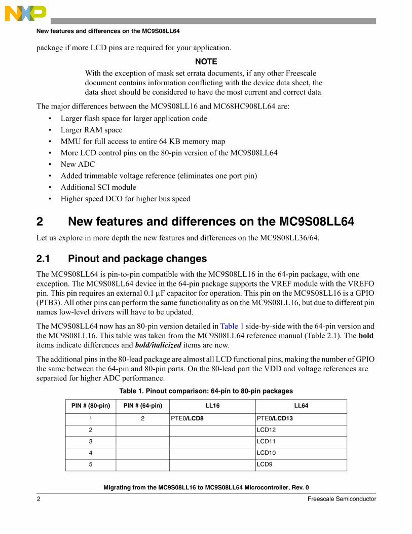
2.1 Pinout and package changesThe MC9S08LL64 is pin-to-pin compatible with the MC9S08LL16 in the 64-pin package, with one exception. The MC9S08LL64 device in the 64-pin package supports the VREF module with the VREFO pin. This pin requires an external 0.1 μF capacitor for operation. This pin on the MC9S08LL16 is a GPIO (PTB3). All other pins can perform the same functionality as on the MC9S08LL16, but due to different pin names low-level drivers will have to be updated.
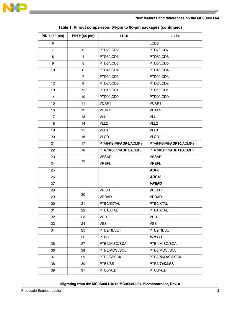
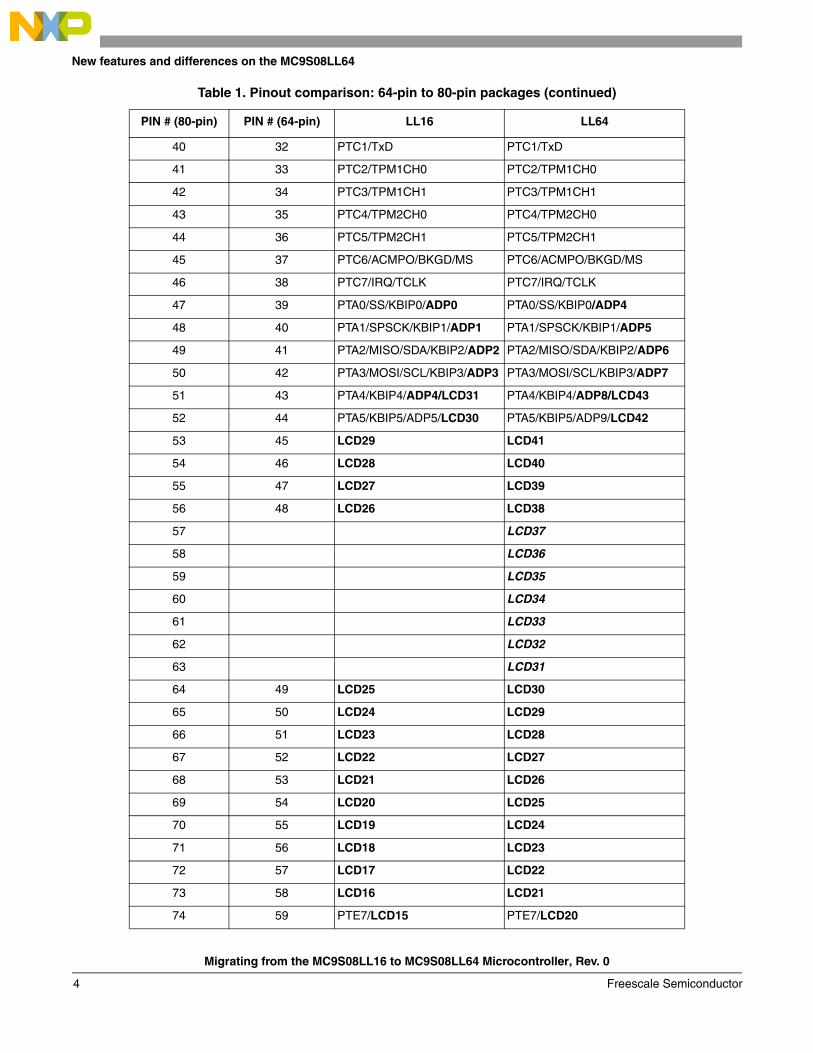
The MC9S08LL64 now has an 80-pin version detailed in Table 1 side-by-side with the 64-pin version and the MC9S08LL16. This table was taken from the MC9S08LL64 reference manual (Table 2.1). The bold items indicate differences and bold/italicized items are new.
The additional pins in the 80-lead package are almost all LCD functional pins, making the number of GPIO the same between the 64-pin and 80-pin parts. On the 80-lead part the VDD and voltage references are separated for higher ADC performance.
Table 1. Pinout comparison: 64-pin to 80-pin packages
PIN # (80-pin) PIN # (64-pin) LL16 LL64
1 2 PTE0/LCD8 PTE0/LCD13
2 LCD12
3 LCD11
4 LCD10
5 LCD9
Migrating from the MC9S08LL16 to MC9S08LL64 Microcontroller, Rev. 0
Freescale Semiconductor2
New features and differences on the MC9S08LL64
6 LCD8
7 3 PTD7/LCD7 PTD7/LCD7
8 4 PTD6/LCD6 PTD6/LCD6
9 5 PTD5/LCD5 PTD5/LCD5
10 6 PTD4/LCD4 PTD4/LCD4
11 7 PTD3/LCD3 PTD3/LCD3
12 8 PTD2/LCD2 PTD2/LCD2
13 9 PTD1/LCD1 PTD1/LCD1
14 10 PTD0/LCD0 PTD0/LCD0
15 11 VCAP1 VCAP1
16 12 VCAP2 VCAP2
17 13 VLL1 VLL1
18 14 VLL2 VLL2
19 15 VLL3 VLL3
20 16 VLCD VLCD
21 17 PTA6/KBIP6/ADP6/ACMP+ PTA6/KBIP6/ADP10/ACMP+
22 18 PTA7/KBIP7/ADP7/ACMP- PTA7/KBIP7/ADP11/ACMP-
2319
VSSAD VSSAD
24 VREFL VREFL
25 ADP0
26 ADP12
27 VREFO
2820
VREFH VREFH
29 VDDAD VDDAD
30 21 PTB0/EXTAL PTB0/XTAL
31 22 PTB1/XTAL PTB1/XTAL
32 23 VDD VDD
33 24 VSS VSS
34 25 PTB2/RESET PTB2/RESET
26 PTB3 VREFO
35 27 PTB4/MISO/SDA PTB4/MISO/SDA
36 28 PTB5/MOSI/SCL PTB5/MOSI/SCL
37 29 PTB6/SPSCK PTB6/RxD2/SPSCK
38 30 PTB7/SS PTB7/TxD2/SS
39 31 PTC0/RxD PTC0/RxD
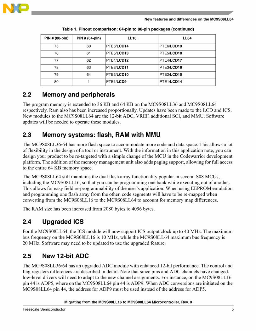
Table 1. Pinout comparison: 64-pin to 80-pin packages (continued)
PIN # (80-pin) PIN # (64-pin) LL16 LL64
Migrating from the MC9S08LL16 to MC9S08LL64 Microcontroller, Rev. 0
Freescale Semiconductor 3
New features and differences on the MC9S08LL64
40 32 PTC1/TxD PTC1/TxD
41 33 PTC2/TPM1CH0 PTC2/TPM1CH0
42 34 PTC3/TPM1CH1 PTC3/TPM1CH1
43 35 PTC4/TPM2CH0 PTC4/TPM2CH0
44 36 PTC5/TPM2CH1 PTC5/TPM2CH1
45 37 PTC6/ACMPO/BKGD/MS PTC6/ACMPO/BKGD/MS
46 38 PTC7/IRQ/TCLK PTC7/IRQ/TCLK
47 39 PTA0/SS/KBIP0/ADP0 PTA0/SS/KBIP0/ADP4
48 40 PTA1/SPSCK/KBIP1/ADP1 PTA1/SPSCK/KBIP1/ADP5
49 41 PTA2/MISO/SDA/KBIP2/ADP2 PTA2/MISO/SDA/KBIP2/ADP6
50 42 PTA3/MOSI/SCL/KBIP3/ADP3 PTA3/MOSI/SCL/KBIP3/ADP7
51 43 PTA4/KBIP4/ADP4/LCD31 PTA4/KBIP4/ADP8/LCD43
52 44 PTA5/KBIP5/ADP5/LCD30 PTA5/KBIP5/ADP9/LCD42
53 45 LCD29 LCD41
54 46 LCD28 LCD40
55 47 LCD27 LCD39
56 48 LCD26 LCD38
57 LCD37
58 LCD36
59 LCD35
60 LCD34
61 LCD33
62 LCD32
63 LCD31
64 49 LCD25 LCD30
65 50 LCD24 LCD29
66 51 LCD23 LCD28
67 52 LCD22 LCD27
68 53 LCD21 LCD26
69 54 LCD20 LCD25
70 55 LCD19 LCD24
71 56 LCD18 LCD23
72 57 LCD17 LCD22
73 58 LCD16 LCD21
74 59 PTE7/LCD15 PTE7/LCD20
Table 1. Pinout comparison: 64-pin to 80-pin packages (continued)
PIN # (80-pin) PIN # (64-pin) LL16 LL64
Migrating from the MC9S08LL16 to MC9S08LL64 Microcontroller, Rev. 0
Freescale Semiconductor4
New features and differences on the MC9S08LL64
2.2 Memory and peripheralsThe program memory is extended to 36 KB and 64 KB on the MC9S08LL36 and MC9S08LL64 respectively. Ram also has been increased proportionally. Updates have been made to the LCD and ICS. New modules to the MC9S08LL64 are the 12-bit ADC, VREF, additional SCI, and MMU. Software updates will be needed to operate these modules.
2.3 Memory systems: flash, RAM with MMUThe MC9S08LL36/64 has more flash space to accommodate more code and data space. This allows a lot of flexibility in the design of a tool or instrument. With the information in this application note, you can design your product to be re-targeted with a simple change of the MCU in the Codewarrior development platform. The addition of the memory management unit also adds paging support, allowing for full access to the entire 64 KB memory space.
The MC9S08LL64 still maintains the dual flash array functionality popular in several S08 MCUs, including the MC9S08LL16, so that you can be programming one bank while executing out of another. This allows for easy field re-programmability of the user’s application. When using EEPROM emulation and programming one flash array from the other, code segments will have to be re-mapped when converting from the MC9S08LL16 to the MC9S08LL64 to account for memory map differences.
The RAM size has been increased from 2080 bytes to 4096 bytes.
2.4 Upgraded ICSFor the MC9S08LL64, the ICS module will now support ICS output clock up to 40 MHz. The maximum bus frequency on the MC9S08LL16 is 10 MHz, while the MC9S08LL64 maximum bus frequency is 20 MHz. Software may need to be updated to use the upgraded feature.
2.5 New 12-bit ADCThe MC9S08LL36/64 has an upgraded ADC module with enhanced 12-bit performance. The control and flag registers differences are described in detail. Note that since pins and ADC channels have changed. low-level drivers will need to adapt to the new channel assignments. For instance, on the MC9S08LL16 pin 44 is ADP5, where on the MC9S08LL64 pin 44 is ADP9. When ADC conversions are initiated on the MC9S08LL64 pin 44, the address for ADP9 must be used instead of the address for ADP5.
75 60 PTE6/LCD14 PTE6/LCD19
76 61 PTE5/LCD13 PTE5/LCD18
77 62 PTE4/LCD12 PTE4/LCD17
78 63 PTE3/LCD11 PTE3/LCD16
79 64 PTE2/LCD10 PTE2/LCD15
80 1 PTE1/LCD9 PTE1/LCD14
Table 1. Pinout comparison: 64-pin to 80-pin packages (continued)
PIN # (80-pin) PIN # (64-pin) LL16 LL64
Migrating from the MC9S08LL16 to MC9S08LL64 Microcontroller, Rev. 0
Freescale Semiconductor 5
New features and differences on the MC9S08LL64
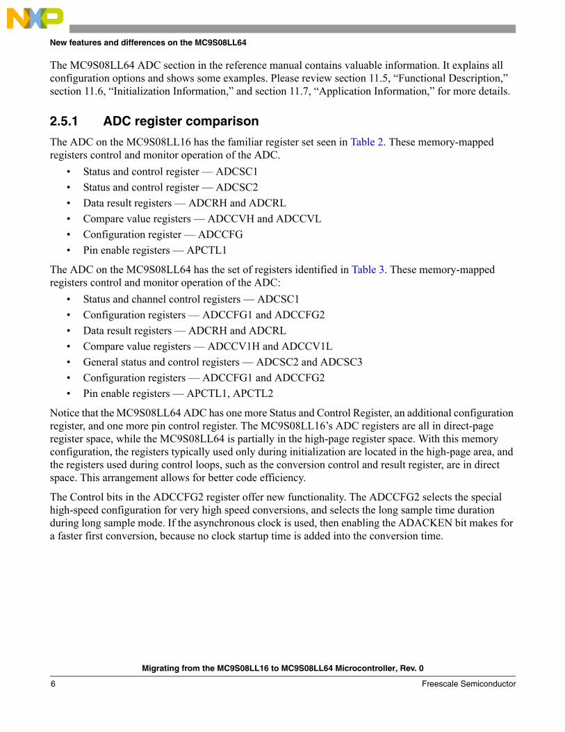
The MC9S08LL64 ADC section in the reference manual contains valuable information. It explains all configuration options and shows some examples. Please review section 11.5, “Functional Description,” section 11.6, “Initialization Information,” and section 11.7, “Application Information,” for more details.
2.5.1 ADC register comparison
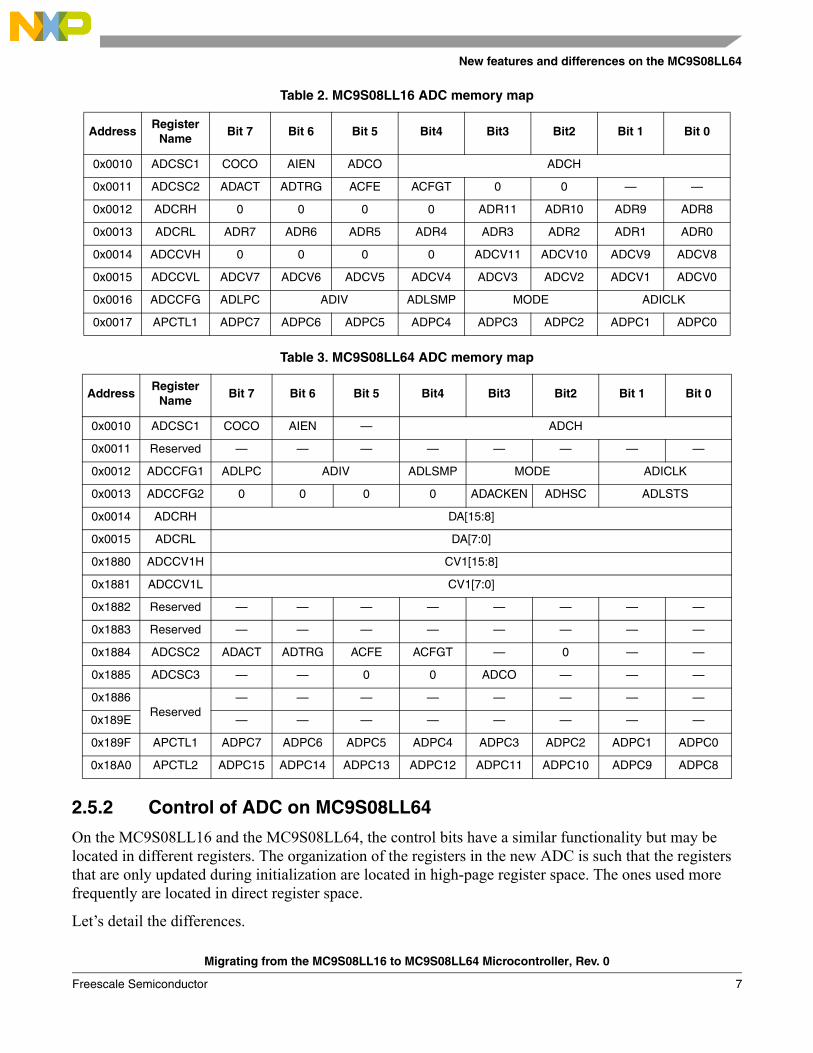
The ADC on the MC9S08LL16 has the familiar register set seen in Table 2. These memory-mapped registers control and monitor operation of the ADC.
• Status and control register — ADCSC1• Status and control register — ADCSC2• Data result registers — ADCRH and ADCRL • Compare value registers — ADCCVH and ADCCVL• Configuration register — ADCCFG• Pin enable registers — APCTL1
The ADC on the MC9S08LL64 has the set of registers identified in Table 3. These memory-mapped registers control and monitor operation of the ADC:
• Status and channel control registers — ADCSC1• Configuration registers — ADCCFG1 and ADCCFG2• Data result registers — ADCRH and ADCRL• Compare value registers — ADCCV1H and ADCCV1L• General status and control registers — ADCSC2 and ADCSC3• Configuration registers — ADCCFG1 and ADCCFG2• Pin enable registers — APCTL1, APCTL2
Notice that the MC9S08LL64 ADC has one more Status and Control Register, an additional configuration register, and one more pin control register. The MC9S08LL16’s ADC registers are all in direct-page register space, while the MC9S08LL64 is partially in the high-page register space. With this memory configuration, the registers typically used only during initialization are located in the high-page area, and the registers used during control loops, such as the conversion control and result register, are in direct space. This arrangement allows for better code efficiency.
The Control bits in the ADCCFG2 register offer new functionality. The ADCCFG2 selects the special high-speed configuration for very high speed conversions, and selects the long sample time duration during long sample mode. If the asynchronous clock is used, then enabling the ADACKEN bit makes for a faster first conversion, because no clock startup time is added into the conversion time.
Migrating from the MC9S08LL16 to MC9S08LL64 Microcontroller, Rev. 0
Freescale Semiconductor6
New features and differences on the MC9S08LL64
2.5.2 Control of ADC on MC9S08LL64
On the MC9S08LL16 and the MC9S08LL64, the control bits have a similar functionality but may be located in different registers. The organization of the registers in the new ADC is such that the registers that are only updated during initialization are located in high-page register space. The ones used more frequently are located in direct register space.
Let’s detail the differences.
Table 2. MC9S08LL16 ADC memory map
AddressRegister
NameBit 7 Bit 6 Bit 5 Bit4 Bit3 Bit2 Bit 1 Bit 0
0x0010 ADCSC1 COCO AIEN ADCO ADCH
0x0011 ADCSC2 ADACT ADTRG ACFE ACFGT 0 0 — —
0x0012 ADCRH 0 0 0 0 ADR11 ADR10 ADR9 ADR8
0x0013 ADCRL ADR7 ADR6 ADR5 ADR4 ADR3 ADR2 ADR1 ADR0
0x0014 ADCCVH 0 0 0 0 ADCV11 ADCV10 ADCV9 ADCV8
0x0015 ADCCVL ADCV7 ADCV6 ADCV5 ADCV4 ADCV3 ADCV2 ADCV1 ADCV0
0x0016 ADCCFG ADLPC ADIV ADLSMP MODE ADICLK
0x0017 APCTL1 ADPC7 ADPC6 ADPC5 ADPC4 ADPC3 ADPC2 ADPC1 ADPC0
Table 3. MC9S08LL64 ADC memory map
AddressRegister
NameBit 7 Bit 6 Bit 5 Bit4 Bit3 Bit2 Bit 1 Bit 0
0x0010 ADCSC1 COCO AIEN — ADCH
0x0011 Reserved — — — — — — — —
0x0012 ADCCFG1 ADLPC ADIV ADLSMP MODE ADICLK
0x0013 ADCCFG2 0 0 0 0 ADACKEN ADHSC ADLSTS
0x0014 ADCRH DA[15:8]
0x0015 ADCRL DA[7:0]
0x1880 ADCCV1H CV1[15:8]
0x1881 ADCCV1L CV1[7:0]
0x1882 Reserved — — — — — — — —
0x1883 Reserved — — — — — — — —
0x1884 ADCSC2 ADACT ADTRG ACFE ACFGT — 0 — —
0x1885 ADCSC3 — — 0 0 ADCO — — —
0x1886Reserved
— — — — — — — —
0x189E — — — — — — — —
0x189F APCTL1 ADPC7 ADPC6 ADPC5 ADPC4 ADPC3 ADPC2 ADPC1 ADPC0
0x18A0 APCTL2 ADPC15 ADPC14 ADPC13 ADPC12 ADPC11 ADPC10 ADPC9 ADPC8
Migrating from the MC9S08LL16 to MC9S08LL64 Microcontroller, Rev. 0
Freescale Semiconductor 7
New features and differences on the MC9S08LL64
• The ADCO bit has been moved. It is now located in control register ADCSC3. It has the same functionality as on the MC9S08LL16.
• The ADSC2 register has been moved and a reserved bit added. It is located in high-page register space. Bit three of the register is added to the list of reserved bits that must be set to zero.
• The result registers have been moved, renamed, and extended. The new register names are ADCRH and ADCRL. The bits are named DA[15:8] and DA[7:0], respectively.
• The compare value registers are moved and renamed. The new register names are ADCCV1H and ADCCV1L.
• The config register ADCCFG on the MC9S08LL16 has been moved on the MC9S08LL64 ADC and a second config register added. The new register names are ADCCFG1 and ADCCFG2. They are both located in the direct-page register space.
2.6 VREF: new voltage reference moduleThe voltage reference module supplies an accurate voltage output that is trimmable by an 8-bit register in 0.5 mV steps. There are two VREF modules on the MCU, but only one is pinned out in a particular package. VREFO1 is only available on the 80-pin part (output on pin 27), and VREFO2 is only available on the 64-pin part (output on pin 26).
The VREF module is capable of driving a maximum load of 1 mA across temperature. For more information please refer to the MC9S08LL64 data sheet, section 3.13, table 19, “VREF Specifications.”
2.6.1 Initializing the VREF
The reference manual states that in the 80-pin package the VREF1 module is enabled and the VREF2 module is disabled. The opposite is true for the 64-pin package. Even though one of the modules is disabled, it is recommended that you initialize both VREF modules at the same time with the same values. Writing to the disabled module will not cause an illegal address access.
2.7 LCD moduleThe MC9S08LL36/64 has 44 segment LCD pins available in the 80-pin package version of the part, versus 32 in the 64-pin package. This allows you to drive up to 288 segments, utilizing up to eight pins as back planes (BP) and thirty-six as front planes (FP). As is the standard on the LL family, any pin can be configured as an FP or a BP. With this increased number of LCDs there is a corresponding increase in the number of LCD registers.
2.7.1 Pin name differences
As mentioned before, low-level drivers will have to be updated due to different pin names. Only a few of the LCD pin names are the same between the MC9S08LL16 and the MC9S08LL64.
LCD example: MC9S08LL16 pin 49 is LCD25, but on the MC9S08LL64 pin 49 is LCD30. LCD drivers will have to be modified so that the LCD25 functionality is mapped to LCD30. For example, if LCD25 was used as a backplane pin, LCD30 must now be configured as a backplane pin on the MC9S08LL64.
Migrating from the MC9S08LL16 to MC9S08LL64 Microcontroller, Rev. 0
Freescale Semiconductor8

Migrating the thermostat reference design
2.8 Stop and run current differencesAs a result of the larger memory and added modules, the MC9S08LL64 stop IDDs will be slightly higher than on the MC9S08LL16. This additional leakage current will lead to a 25–75 nA increase during stop2 operating mode.
MC9S08LL64-run IDDs will be slightly higher than on the MC9S08LL16. At 1 MHz the typical IDD is between 0.9 mA to 2 mA. You can get the specifics of your application with the MC9S08LL64 using the updated web-based Low-Power Battery Calculator available on the Freescale site.
3 Migrating the thermostat reference designTo demonstrate the steps required in the migration of an MC9S08LL16-based application to the MC9S08LL64 MCU, we will explain the process step by step using a real application. A complete thermostat reference platform was designed by Freescale using the MC9S08LL16 MCU. The following sections explain the steps needed to migrate the code and hardware from the MC9S08LL16 to the MC9S08LL64.
In general we will proceed to make the pin name changes in the LCD driver and ADC, make the ADC module updates, check the ICS for any changes, and then compile and test the new code in a version of the thermostat reference design after replacing the MC9S08LL16 with an MC9S08LL36 or MC9S08LL64.
3.1 Change MCU selectionIn Codewarrior you will need to change the MCU selected from the MC9S08LL16 to the MC9S08LL36 or MC9S08LL64. Since we updated this board with an MC9S08LL36, we select the “Change MCU” connections, then select the MC9S08LL36 using the P&E multilink as the debugger interface. After requesting this change, several error messages were received while compiling. Each of these errors needs to be addressed. There were errors in removing files mc9s08ll16.h and mc9s08ll16.c, which were removed manually. Since the Project.prm file was modified for the project, the substitution with the MC9S08LL36 version did not happen. The base linker file (*.prm file) was added and updated to reflect the custom MC9S08LL16 version. The original MC9S08LL16 base linker file was modified to add the relocate feature for flash as EEPROM functionality. So changes were made to add these segments to the MC9S08LL36 linker file; DATA_ROM and FLASH_TO_RAM segments. These changes are required since the application uses part of the flash for variable storage and does the programming of flash from RAM.DATA_ROM = READ_ONLY 0xC000 TO 0xC1FF;FLASH_TO_RAM = READ_ONLY 0xC200 TO 0xC25F RELOCATE_TO 0x7A0;ROM2 = READ_ONLY 0xC260 TO 0xFFAD;
The basic process used for the software migration can be used for any migration effort. Make a copy of the original thermostat project, then open the new Thermostat.mcp file with CodeWarrior. For a copy of the original thermostat project, please refer to the associated software for Freescale document DRM106, Thermostat Reference Design Using the MC9S08LL16, available at freescale.com.
Migrating from the MC9S08LL16 to MC9S08LL64 Microcontroller, Rev. 0
Freescale Semiconductor 9
Migrating the thermostat reference design
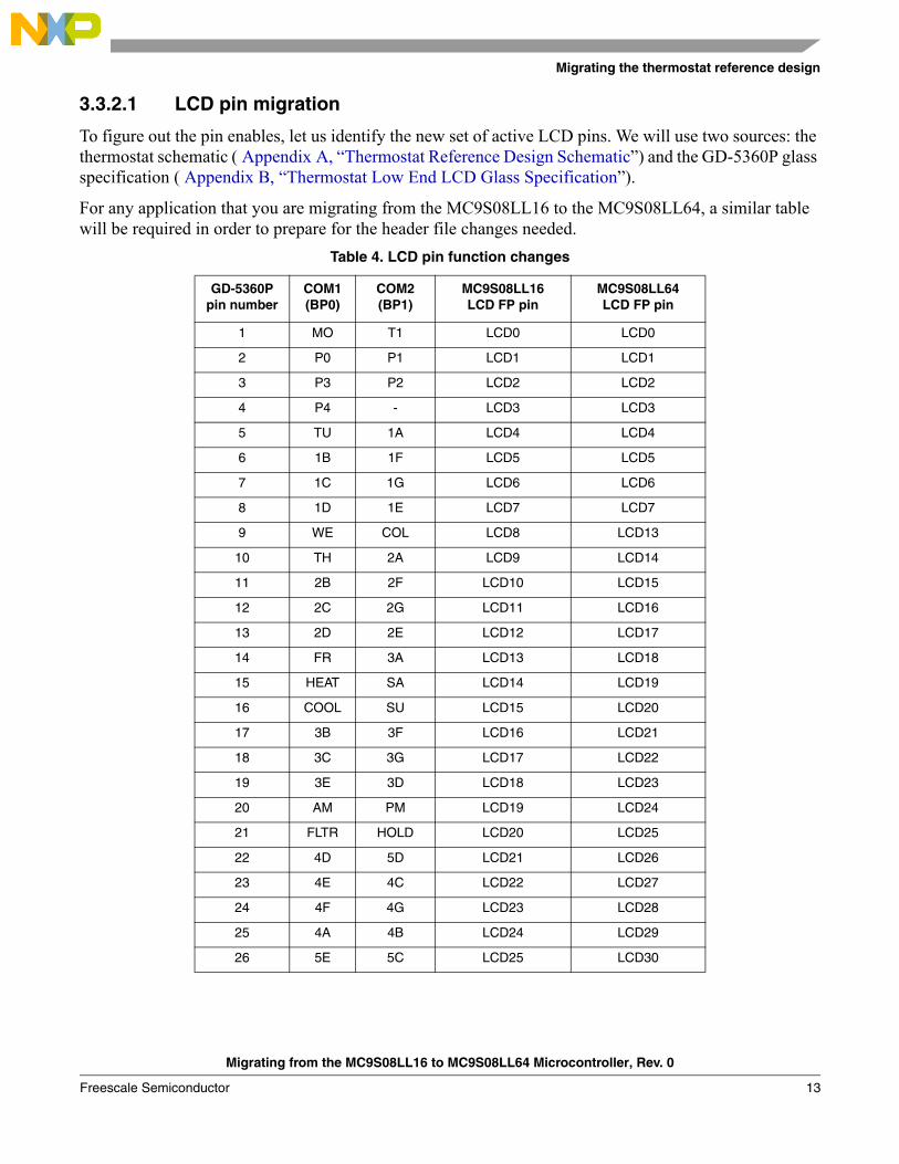
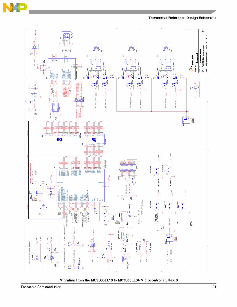
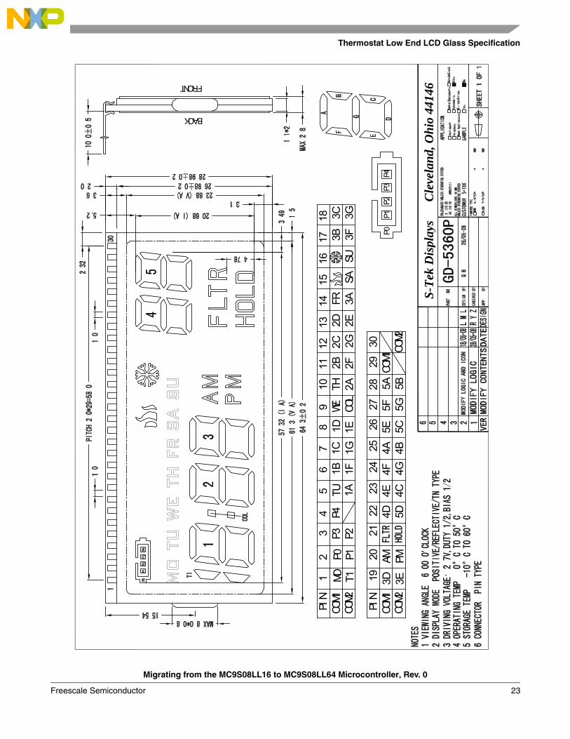
3.2 Hardware differencesWe used the schematic of the thermostat SCH v0.5 (see Appendix A, “Thermostat Reference Design Schematic”) and the LCD glass specification (see Appendix B, “Thermostat Low End LCD Glass Specification”) when creating the pin-out comparison in Table 4. The paragraphs below identify the differences, but note that there are a lot more similarities than differences, making this migration painless.
3.2.1 Port pins
The MC9S08LL16 has a PTB3 pin which has been converted to a VREF output pin with no GPIO functionality. The thermostat system used PTB3 to enable the Cymbit battery backup system. In order to keep this functionality, the enable function must be attained in some other way, either using another output pin or by making the enable a manual jumper.
Since the battery backup hardware was not present on this version of the thermostat, these two lines were commented out in the software:// #define CONFIG_CBC_EVAL_EN_PULL_UP PTBPE_PTBPE3 = 1// #define CONFIG_CBC_EVAL_EN_DDR PTBDD_PTBDD3 = 0
3.2.2 ADC channel pins
The ADC channel changes will have an impact on the code, so we need to be aware of the changes needed to accommodate the channel changes. One change we could make later is the addition of humidity measurement. The original design did not have enough I/O and LCD pins. By taking advantage of the increased number of I/O pins, this humidity function could be added. A channel assignment and low-level driver change will have to be made to add this function.
Other channel assignments changes include:• Channel 7 is now channel 11• Channel 6 is now channel 10
These pins are being used as an input for temperature measurement. Low-level headers must be changed to accommodate this change. In file S08_ADC12.h, change the #defines for channel 1 to a 10, and also the pin control. This will allow input channel 10 to be enabled as demonstrated below.#define ADC1_CHAN 10#define ADC1_PCTL1 0#define ADC1_PCTL2 APCTL2_ADPC10_MASK
Let’s step through the code and change the settings that are different between the ADC modules. First, Channel 6 is now Channel 10. This pin is being used as temperature sensor input.
3.3 Software differences
3.3.1 ADC module changes
A thorough review of the changes in the ADC section above and the MC9S08LL64 reference manual is necessary to identify all of the subtle changes when using the new ADC on the MC9S08LL64.
Migrating from the MC9S08LL16 to MC9S08LL64 Microcontroller, Rev. 0
Freescale Semiconductor10

Migrating the thermostat reference design
However, one of the simplest ways to identify what needs to be changed is to try compiling the project after selecting the new MCU target. The two MCUs are similar enough that this method will quickly identify most of the code items that need to be updated.
The code relating to ADC is the first place to examine. The header file changes were identified in the previous section. To recap the changes we need, channel 6 is now changed to channel 10. So we have to change the input channel for temperature measurements to channel 10 and change the pin enable for channel 10. Change the S08_ADC12.h file like this:#define ADC1_CHAN 10#define ADC1_PCTL1 0#define ADC1_PCTL2 APCTL2_ADPC10_MASK
Initializing and configuring the new ADC is our next goal. Here is the code initializing the ADC.void ADC_Init(UINT16* pADC_BufferPointer){ SCGC1_ADC = 1; ADCSC1 = 0; ADCSC2 = 0; ADCCFG = ADCCFG_ADLSMP_MASK | ADCCFG_ADIV1_MASK | ADCCFG_ADIV0_MASK | ADCCFG_MODE0_MASK | ADCCFG_ADICLK0_MASK; APCTL1 = APCTL1_REG; #ifdef APCTL2 APCTL2 = APCTL2_REG; #endif #ifdef APCTL3 APCTL3 = APCTL3_REG; #endif pADC_Pointer = pADC_BufferPointer;}
The ADCSC1 register in the MC9S08LL64 is different from the MC9S08LL16 ADC in one bit, the ADCO, which controlled the continuous conversion switch. If the code required continuous conversion then a write to ADCSC3_ADCO would be required. The routine ADC_Start_conversions() is changed to this:void ADC_Start_conversions(void){
ADCSC3 = ADCSC3_ADCO_MASK;}
The ADCSC2 register has the same definition as in the MC9S08LL16 but has been moved to the High-Page register. Any assembly code that used direct page addressing will need to be changed. The compiler handles this for us.
The next register is the ADCCFG1 register. This has the same definition as the ADCCFG register in the MC9S08LL16. The only change we need to make to the code is to add the “1” after the register name, like this:ADCCFG1 = ADCCFG1_ADLSMP_MASK | ADCCFG1_ADIV1_MASK | ADCCFG1_ADIV0_MASK | ADCCFG1_MODE0_MASK | ADCCFG1_ADICLK0_MASK;
Migrating from the MC9S08LL16 to MC9S08LL64 Microcontroller, Rev. 0
Freescale Semiconductor 11
Migrating the thermostat reference design
The new configuration register, ADCCFG2, will be left at the reset defaults. This disables the asynchronous clock, selects the normal conversion sequence, and selects the longest sample time.
Next are the ADC pin control registers. On the MC9S08LL64 there are two registers to accommodate the increased number of channels. The MC9S08LL16 version enables all of the pins as inputs with these defines.#define APCTL1_REG ADC1_PCTL1 | ADC2_PCTL1 | ADC3_PCTL1 | ADC4_PCTL1 | ADC5_PCTL1 | ADC6_PCTL1 | ADC7_PCTL1 | ADC8_PCTL1 | ADC9_PCTL1 | ADC10_PCTL1;#define APCTL2_REG ADC1_PCTL2 | ADC2_PCTL2 | ADC3_PCTL2 | ADC4_PCTL2 | ADC5_PCTL2 | ADC6_PCTL2 | ADC7_PCTL2 | ADC8_PCTL2 | ADC9_PCTL2 | ADC10_PCTL2;
#define APCTL3_REG ADC1_PCTL3 | ADC2_PCTL3 | ADC3_PCTL3 | ADC4_PCTL3 | ADC5_PCTL3 | ADC6_PCTL3 | ADC7_PCTL3 | ADC8_PCTL3 | ADC9_PCTL3 | ADC10_PCTL3;
3.3.2 LCD Code Migration
There are several ways to approach the migration of the code to a new LCD pinout. The changes we are making here are typical of the kind of changes you would make if you were to put new glass on your application. You take your original design, create a table of pin and functional differences, and then use this difference table to guide you through the changes in the application code.
First notice that some of the LCD pin names changed:• LCD9 is now LCD14• LCD31 is now LCD43• LCD30 is now LCD42• LCD29 is now LCD41• LCD28 is now LCD40• LCD27 is now LCD39• LCD26 is now LCD38• LCD25 is now LCD30
and so on. The LCD pins that did not change names are pins LCD0 through LCD7.
Each of these differences will be accounted for in the changes needed for the LCD low-level driver code. We can use the spreadsheet supplied with AN3796, “LCD Driver Specification,” to accommodate the differences.
This spreadsheet was developed by the authors of AN3796 and sets up the defines for the glass used in the thermostat controller. We could use this spreadsheet to do the LCD pin redefinition. After the spreadsheet has been modified, we can copy and paste the defines into the header file.
Since we did not have access to the original spreadsheet used for this application code we chose another, more direct way: going to the header file for the glass we have on this reference design board, the low-end LCD (GD5360.h), and changing the low-level defines as needed.
Migrating from the MC9S08LL16 to MC9S08LL64 Microcontroller, Rev. 0
Freescale Semiconductor12
Migrating the thermostat reference design
3.3.2.1 LCD pin migration
To figure out the pin enables, let us identify the new set of active LCD pins. We will use two sources: the thermostat schematic ( Appendix A, “Thermostat Reference Design Schematic”) and the GD-5360P glass specification ( Appendix B, “Thermostat Low End LCD Glass Specification”).
For any application that you are migrating from the MC9S08LL16 to the MC9S08LL64, a similar table will be required in order to prepare for the header file changes needed.
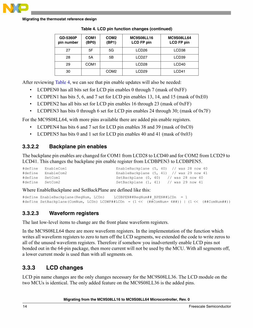
Table 4. LCD pin function changes
GD-5360Ppin number
COM1(BP0)
COM2(BP1)
MC9S08LL16LCD FP pin
MC9S08LL64LCD FP pin
1 MO T1 LCD0 LCD0
2 P0 P1 LCD1 LCD1
3 P3 P2 LCD2 LCD2
4 P4 - LCD3 LCD3
5 TU 1A LCD4 LCD4
6 1B 1F LCD5 LCD5
7 1C 1G LCD6 LCD6
8 1D 1E LCD7 LCD7
9 WE COL LCD8 LCD13
10 TH 2A LCD9 LCD14
11 2B 2F LCD10 LCD15
12 2C 2G LCD11 LCD16
13 2D 2E LCD12 LCD17
14 FR 3A LCD13 LCD18
15 HEAT SA LCD14 LCD19
16 COOL SU LCD15 LCD20
17 3B 3F LCD16 LCD21
18 3C 3G LCD17 LCD22
19 3E 3D LCD18 LCD23
20 AM PM LCD19 LCD24
21 FLTR HOLD LCD20 LCD25
22 4D 5D LCD21 LCD26
23 4E 4C LCD22 LCD27
24 4F 4G LCD23 LCD28
25 4A 4B LCD24 LCD29
26 5E 5C LCD25 LCD30
Migrating from the MC9S08LL16 to MC9S08LL64 Microcontroller, Rev. 0
Freescale Semiconductor 13
Migrating the thermostat reference design
After reviewing Table 4, we can see that pin enable updates will also be needed:• LCDPEN0 has all bits set for LCD pin enables 0 through 7 (mask of 0xFF)• LCDPEN1 has bits 5, 6, and 7 set for LCD pin enables 13, 14, and 15 (mask of 0xE0)• LCDPEN2 has all bits set for LCD pin enables 16 through 23 (mask of 0xFF)• LCDPEN3 has bits 0 through 6 set for LCD pin enables 24 through 30; (mask of 0x7F)
For the MC9S08LL64, with more pins available there are added pin enable registers.• LCDPEN4 has bits 6 and 7 set for LCD pin enables 38 and 39 (mask of 0xC0)• LCDPEN5 has bits 0 and 1 set for LCD pin enables 40 and 41 (mask of 0x03)
3.3.2.2 Backplane pin enables
The backplane pin enables are changed for COM1 from LCD28 to LCD40 and for COM2 from LCD29 to LCD41. This changes the backplane pin enable register from LCDBPEN3 to LCDBPEN5.#define EnableCom1 EnableBackplane (5, 40) // was 28 now 40#define EnableCom2 EnableBackplane (5, 41) // was 29 now 41#define SetCom1 SetBackplane (0, 40) // was 28 now 40#define SetCom2 SetBackplane (1, 41) // was 29 now 41
Where EnableBackplane and SetBackPlane are defined like this:#define EnableBackplane(RegNum, LCDn) LCDBPEN##RegNum##_BPEN##LCDn = 1 #define SetBackplane(ComNum, LCDn) LCDWF##LCDn = (1 << (##ComNum+ 4##)) | (1 << (##ComNum##))
3.3.2.3 Waveform registers
The last low-level items to change are the front plane waveform registers.
In the MC9S08LL64 there are more waveform registers. In the implementation of the function which writes all waveform registers to zero to turn off the LCD segments, we extended the code to write zeros to all of the unused waveform registers. Therefore if somehow you inadvertently enable LCD pins not bonded out in the 64-pin package, then more current will not be used by the MCU. With all segments off, a lower current mode is used than with all segments on.
3.3.3 LCD changes
LCD pin name changes are the only changes necessary for the MC9S08LL36. The LCD module on the two MCUs is identical. The only added feature on the MC9S08LL36 is the added pins.
27 5F 5G LCD26 LCD38
28 5A 5B LCD27 LCD39
29 COM1 LCD28 LCD40
30 COM2 LCD29 LCD41
Table 4. LCD pin function changes (continued)
GD-5360Ppin number
COM1(BP0)
COM2(BP1)
MC9S08LL16LCD FP pin
MC9S08LL64LCD FP pin
Migrating from the MC9S08LL16 to MC9S08LL64 Microcontroller, Rev. 0
Freescale Semiconductor14
Migrating the thermostat reference design
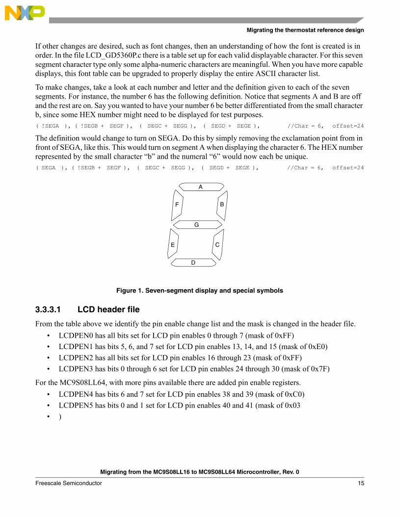
If other changes are desired, such as font changes, then an understanding of how the font is created is in order. In the file LCD_GD5360P.c there is a table set up for each valid displayable character. For this seven segment character type only some alpha-numeric characters are meaningful. When you have more capable displays, this font table can be upgraded to properly display the entire ASCII character list.
To make changes, take a look at each number and letter and the definition given to each of the seven segments. For instance, the number 6 has the following definition. Notice that segments A and B are off and the rest are on. Say you wanted to have your number 6 be better differentiated from the small character b, since some HEX number might need to be displayed for test purposes.( !SEGA ), ( !SEGB + SEGF ), ( SEGC + SEGG ), ( SEGD + SEGE ), //Char = 6, offset=24
The definition would change to turn on SEGA. Do this by simply removing the exclamation point from in front of SEGA, like this. This would turn on segment A when displaying the character 6. The HEX number represented by the small character “b” and the numeral “6” would now each be unique.( SEGA ), ( !SEGB + SEGF ), ( SEGC + SEGG ), ( SEGD + SEGE ), //Char = 6, offset=24
Figure 1. Seven-segment display and special symbols
3.3.3.1 LCD header file
From the table above we identify the pin enable change list and the mask is changed in the header file.• LCDPEN0 has all bits set for LCD pin enables 0 through 7 (mask of 0xFF)• LCDPEN1 has bits 5, 6, and 7 set for LCD pin enables 13, 14, and 15 (mask of 0xE0)• LCDPEN2 has all bits set for LCD pin enables 16 through 23 (mask of 0xFF)• LCDPEN3 has bits 0 through 6 set for LCD pin enables 24 through 30 (mask of 0x7F)
For the MC9S08LL64, with more pins available there are added pin enable registers.• LCDPEN4 has bits 6 and 7 set for LCD pin enables 38 and 39 (mask of 0xC0)• LCDPEN5 has bits 0 and 1 set for LCD pin enables 40 and 41 (mask of 0x03• )
A
B
C
D
E
F
G
Migrating from the MC9S08LL16 to MC9S08LL64 Microcontroller, Rev. 0
Freescale Semiconductor 15
Migrating the thermostat reference design
3.3.3.2 Backplane pin enables
The backplane pin enables are changed for COM1 from LCD28 to LCD40 and for COM2 from LCD29 to LCD41. This changes the backplane pin enable register from LCDBPEN3 to LCDBPEN5. In the function below we need to clear the LCDBPEN registers 4 and 5 since the MC9S08LL64 has more pins.void vfnEnableBackplanes (void){ LCDBPEN0 = 0x00; LCDBPEN1 = 0x00; LCDBPEN2 = 0x00; LCDBPEN3 = 0x00; LCDBPEN4 = 0x00; LCDBPEN5 = 0x00; EnableCom1; EnableCom2; SetCom1; SetCom2;}
3.3.3.3 Waveform registers
The last low-level items to change are the front plane waveform registers.
There are 26 front planes for this piece of LCD glass. There are 5 digits and then symbols. Going through the LCD table changes each of the front plane assignments are changed. Below are examples of the kind of changes made to the GD5360.h header file.
The character assignments change to this:#define CharacterPlace(LCDn) LCDWF##LCDn
#define Char1a CharacterPlace (4) // (4) Glass Pin 5#define Char1b CharacterPlace (5) // (5) Glass Pin 6#define Char1c CharacterPlace (6) // (6) Glass Pin 7#define Char1d CharacterPlace (7) // (7) Glass Pin 8 #define Char2a CharacterPlace (14) // (9 to 15) Glass Pin 10 #define Char2b CharacterPlace (15) //(10 to 16) Glass Pin 11 #define Char2c CharacterPlace (16) //(11 to 17) Glass Pin 12 #define Char2d CharacterPlace (17) //(12 to 18) Glass Pin 13 #define Char3a CharacterPlace (18) //(13 to 19) Glass Pin 14 #define Char3b CharacterPlace (21) //(16 to 22) Glass Pin 17 #define Char3c CharacterPlace (22) //(17 to 23) Glass Pin 18 #define Char3d CharacterPlace (23) //(18 to 24) Glass Pin 19 #define Char4d CharacterPlace (26) //(21 to 27) Glass Pin 22 #define Char4c CharacterPlace (27) //(22 to 28) Glass Pin 23 #define Char4b CharacterPlace (28) //(23 to 29) Glass Pin 24 #define Char4a CharacterPlace (29) //(24 to 30) Glass Pin 25 #define Char5c CharacterPlace (30) //(25 to 30) Glass Pin 26 #define Char5b CharacterPlace (38) //(26 to 38) Glass Pin 27 #define Char5a CharacterPlace (39) //(27 to 40) Glass Pin 28 #define Char5d CharacterPlace (26) //(21 to 27) Glass Pin 22
And the symbol front plane assignments are changed to this:#define _LCD_MONDAY_WF LCDWF0
Migrating from the MC9S08LL16 to MC9S08LL64 Microcontroller, Rev. 0
Freescale Semiconductor16
Migrating the thermostat reference design
#define _LCD_ONE_WF LCDWF0#define _LCD_BATTERY_WF LCDWF1#define _LCD_BAT1_WF LCDWF1#define _LCD_BAT3_WF LCDWF2#define _LCD_BAT2_WF LCDWF2#define _LCD_BAT4_WF LCDWF3#define _LCD_TUESDAY_WF LCDWF4#define _LCD_WEDNESDAY_WF LCDWF13 // was LCDWF8 #define _LCD_COLON_WF LCDWF13 // was LCDWF8 #define _LCD_THURSDAY_WF LCDWF14 // was LCDWF9 #define _LCD_FRIDAY_WF LCDWF18 // was LCDWF13#define _LCD_HEAT_WF LCDWF19 // was LCDWF14#define _LCD_SATURDAY_WF LCDWF19 // was LCDWF14#define _LCD_COOL_WF LCDWF20 // was LCDWF15#define _LCD_SUNDAY_WF LCDWF20 // was LCDWF15#define _LCD_AM_WF LCDWF24 // was LCDWF19#define _LCD_PM_WF LCDWF24 // was LCDWF19#define _LCD_FLTR_WF LCDWF25 // was LCDWF20#define _LCD_HOLD_WF LCDWF25 // was LCDWF20
3.4 ConclusionThe migration from the MC9S08LL16 to the MC9S08LL36 or MC9S08LL64 is very direct. Once the changes and updates in the new MCUs were identified, then we were able to systematically address these differences in the reference design thermostat project. This process typifies the procedure you will need to use in the migration of the code developed for the MC9S08LL16 to the MC9S08LL64. Taking the steps in-between, such as creating pin number and name change tables, will help in not skipping past some of the more subtle changes needed.
So the steps for migration can be summarized as in this list.1. Identify the new features and differences in the MCUs.2. Make tables of all pin and functional changes in your application.3. Systematically implement the updates to the project, documenting the updates as you go.4. Debug the resulting software port, identifying any weakness in the hardware and software design.5. Design and implement improvements and updates as needed.
When doing this project, some problems were encountered with the initial software porting due to a mistake in the ADC pin enable register defines. The defines were not self-checking and allowed an improper assignment for the pin control bit for ADC channel 10, to pin control register 1 instead of to pin control register 2. This kind of error could be avoided by carefully considering the way defines and functions are designed, allowing the compiler to identify malformed bit names. Since the result of the error was misleading, several hours were spent trying to identify why the LCD display was incorrect.
3.5 Improvements and updatesWhen migrating an application from one MCU to another, or from a smaller memory device to a larger, we often take the opportunity to add features and improve the design. This is done after the task of migration is usually complete.
Migrating from the MC9S08LL16 to MC9S08LL64 Microcontroller, Rev. 0
Freescale Semiconductor 17

Migrating the thermostat reference design
3.5.1 Additional features for a thermostat
Some of the possible extra features for a thermostat might be.• Adding temperature profiles for each day of the week• Remote monitoring of room temperatures• Adding compressor hold to keep from damaging expensive pumps with rapid on/off cycles• Communication with the Smart grid to allow utilities the ability to cycle off A/C or heating units• Control over the fresh air introduced into the system, considering outside temperature and humidity• Control over the system considering indoor humidity• Vent control over individual rooms• Building communications for zone controls
3.5.2 Design improvements
As design engineers we try our best to work out any problems with the device operation before we lay out money for printed circuit boards, components, and software development budgets. The unanticipated consequences of our decisions often come in the form of lower-than-specified accuracy, or non-operational circuits. One such issue on the thermostat is the humidity measurement. Due to a lack of I/O the design engineer tried to share the functionality of the temperature and humidity measurement with two pins. As it turns out, the range of impedance change of the humidity sensor is not large enough compared to the combined impedance of the thermistor and the resistors in the circuit. To make it work properly we need one more I/O pin. With the option of going to an 80-lead part, more I/O is available and would solve our problem. If we had not tried to make the thermostat able to handle both the high-end and low-end displays that would also have left more I/O available for this function as well.
The thermostat code does not take advantage of the dual-flash-array topology of the MCU on the MC9S08LL16 or the MC9S08LL64. This could be another improvement made to this code. This way interrupts can remain enabled and the programming of data in the lower flash array can done from the upper array, not requiring code to be transferred to RAM.
Another improvement discovered when porting the code was how the software reports problems. There was a non-functional temperature sensor and the temperature display was attempting to output a non-standard ASCII character. This was due to the bad data (0xFFF) being measured by the ADC temperature sensor input. To aid the user in determining the problem an error code system should be developed and displayed whenever out-of-range data is detected, as in this case.
3.5.3 Field re-flashing
With higher-end systems the ability to update the program is imperative. Special considerations in the design of the re-programming interface are necessary. In a building control system there is usually a communications feature built into the control interface. The physical interfaces used for this interconnect are the SCI for node-to-node and the IIC for multi-nodal networks. If these are used, a bootloader must be designed to allow for erasure and re-programming, but it must not impact the safe state of the control system. Examples of how to implement these bootloader functions can be found in several other application notes. Freescale document AN2295, “Developer’s Serial Bootloader for M68HC08 and
Migrating from the MC9S08LL16 to MC9S08LL64 Microcontroller, Rev. 0
Freescale Semiconductor18
References
HCS08 MCUs,” covers the development of serial bootloaders for HC08 and S08 MCU’s. Take a look at this application note for more details. Device specific bootloaders may be offered on the Freescale web site as well.
3.5.4 Software re-targeting
When managing multiple software targets we have a very powerful tool built into the Codewarrior for Microcontrollers Tools. The thermostat software project already uses this feature for the choice between the high-end thermostat and the low-end thermostat. The software re-targeting for different MCU types, as we are doing in this application note, is a logical extension of this feature. If we had designed the software to be able to handle both platforms, the MC9S08LL16 and MC9S08LL36, then there would have been some additional software hooks we could have put in to make the choice of targets as simple as choosing a new target and re-compiling.
4 ReferencesAll documents listed are Freescale documents and are available at www.freescale.com.
• MC9S08LL16RM, MC9S08LL16/MC9S08LL8 Reference Manual, Rev. 6, July 2009• MC9S08LL64RM, MC9S08LL64/MC9S08LL36 Reference Manual, Rev. 5, October 2009• MC9S08LL64, MC9S08LL64/MC9S08LL36 Data Sheet, Rev. 4, August 2009• AN3796, “LCD Driver Specification,” Rev. 2, October 2009• AN3796.xls, LCD driver assignment spreadsheet (this is in a zip file associated with the AN3796
application note on the freescale.com website)• DRM106, “Thermostat Reference Design Using the MC9S08LL16,” Rev. 1, July 2009• AN3821, “How to Handle Dual Flash Architecture in MC9S08LG32,” Rev. 1, February 2009• AN3822, “Emulating EEPROM Implementation in Dual Flash Architecture on MC9S08LG32,”
Rev. 0, February 2009• AN2295, “Developer’s Serial Bootloader for M68HC08 and HCS08 MCUs,” Rev. 8, August 2006
Migrating from the MC9S08LL16 to MC9S08LL64 Microcontroller, Rev. 0
Freescale Semiconductor 19

Thermostat Reference Design Schematic
Appendix A Thermostat Reference Design Schematic
Migrating from the MC9S08LL16 to MC9S08LL64 Microcontroller, Rev. 0
Freescale Semiconductor20
Thermostat Reference Design Schematic
5 5
4 4
3 3
2 2
1 1
DD
CC
BB
AA
LCD
0LC
D1
LCD
2LC
D3
LCD
5LC
D4
LCD
6LC
D7
LCD
8LC
D9
LCD
10LC
D11
LCD
12LC
D13
LCD
14LC
D15
LCD
16LC
D17
LCD
18LC
D19
LCD
20LC
D21
LCD
22LC
D23
LCD
24LC
D25
LCD
26LC
D27
LCD
28LC
D29
LCD
31LC
D30
LCD
[0:3
1]LC
D[0
:31]
LCD
0LC
D1
LCD
2LC
D3
LCD
4LC
D5
LCD
6LC
D7
LCD
8LC
D9
LCD
10LC
D11
LCD
12LC
D13
LCD
16
LCD
18LC
D19
LCD
20LC
D21
LCD
22LC
D23
LCD
24LC
D25
LCD
26LC
D27
LCD
28LC
D29
LCD
30LC
D14
LCD
15LC
D31
LCD
27LC
D26
LCD
25LC
D24
LCD
23LC
D22
LCD
21LC
D20
LCD
19LC
D18
LCD
17LC
D16
LCD
15LC
D14
LCD
13LC
D12
LCD
11LC
D10
LCD
9LC
D8
LCD
7LC
D6
LCD
5LC
D4
LCD
3LC
D2
LCD
1LC
D0
LCD
28LC
D29
LCD
[0:3
1]
LCD
17
HE
AT
_RE
LAY
_SE
T
FA
N_R
ELA
Y_S
ET
CO
OL_
RE
LAY
_SE
TKE
Y5
FA
N_O
N/O
FF
VD
DA
VS
SA
VD
DA
VS
SA
XTA
L
EXT
AL
EXT
AL
XTA
L
XTA
L
EXT
AL
KE
Y1
KE
Y2
KE
Y3
KE
Y4
KE
Y1
KE
Y2
KE
Y3
KE
Y4
CB
C_E
VA
L_05
_RE
SE
T
FA
N_O
N/O
FF
/RE
SE
T
TH
ER
MIS
TO
R/H
UM
IDIT
Y_E
N RXD TXD
HU
MID
ITY
/TH
ER
MIS
TO
R_E
N
BK
GD
TH
ER
MIS
TO
R/H
UM
IDIT
Y_E
NH
UM
IDIT
Y/T
HE
RM
IST
OR
_EN
BK
GD
/RE
SE
T
/RE
SE
T
RXD
TXD
HE
AT
_RE
LAY
_RE
SE
T
CO
OL_
RE
LAY
_RE
SE
T
FA
N_R
ELA
Y_R
ES
ET
CO
OL_
RE
LAY
_RE
SE
T
CO
OL_
RE
LAY
_SE
T
FA
N_R
ELA
Y_R
ES
ET
FA
N_R
ELA
Y_S
ET
HE
AT
_RE
LAY
_RE
SE
T
HE
AT
_RE
LAY
_SE
T
CB
C_E
VA
L_05
_RE
SE
T
CB
C_E
VA
L_05
_EN
CB
C_E
VA
L_05
_EN
TH
ER
MIS
TO
R/H
UM
IDIT
Y_E
NH
UM
IDIT
Y/T
HE
RM
IST
OR
_EN
KE
Y5
BK
GD
_US
B/R
ES
ET
_US
B
/RE
SE
T_U
SB
BK
GD
_US
B
+3V
+3V
+3V
+3V
+24V
+24V
+24V
+24V
+3V
+3V
+3V
+3V
+3V
+3V
+3V
+3V
+3V
VC
C
+3V
VC
C
VC
CV
CC
+3V
+3.0
V_U
SB
+5V
_US
B
+3.0
V_U
SB
+3.0
V_U
SB
+5V
_US
B+3
.0V
_US
B
PT
B0/
IRQ
/TP
MC
LKP
TB
3/_B
LMS
PT
B4/
XTA
LP
TA
0/K
BIP
0/T
PM
CH
0
PT
A1/
KB
IP1/
MIS
O
PT
A5/
KB
IP5/
TP
MC
H1
PT
A4/
KB
IP4/
_SS
PT
A3/
KB
IP3/
SP
SC
K
PT
B0/
IRQ
/TP
MC
LK
PT
B3/
_BLM
S
PT
B4/
XTA
L
PT
A0/
KB
IP0/
TP
MC
H0
PT
A1/
KB
IP1/
MIS
OP
TA
2/K
BIP
2/M
OS
IP
TA
3/K
BIP
3/S
PS
CK
PT
A4/
KB
IP4/
_SS
PT
A5/
KB
IP5/
TP
MC
H1
PT
A2/
KB
IP2/
MO
SI
Dra
win
g T
itle:
Siz
eD
ocum
ent N
umbe
rR
ev
Dat
e:S
heet
of
Pag
e T
itle:
PD
F: S
PF
-XXX
XXX
SO
UR
CE
: SC
H-X
XXXX
A
Th
erm
ost
at
C
Mon
day,
Sep
tem
ber
22, 2
008
SC
HE
MA
TIC
PA
GE
1
33
Dra
win
g T
itle:
Siz
eD
ocum
ent N
umbe
rR
ev
Dat
e:S
heet
of
Pag
e T
itle:
PD
F: S
PF
-XXX
XXX
SO
UR
CE
: SC
H-X
XXXX
A
Th
erm
ost
at
C
Mon
day,
Sep
tem
ber
22, 2
008
SC
HE
MA
TIC
PA
GE
1
33
Dra
win
g T
itle:
Siz
eD
ocum
ent N
umbe
rR
ev
Dat
e:S
heet
of
Pag
e T
itle:
PD
F: S
PF
-XXX
XXX
SO
UR
CE
: SC
H-X
XXXX
A
Th
erm
ost
at
C
Mon
day,
Sep
tem
ber
22, 2
008
SC
HE
MA
TIC
PA
GE
1
33
External Crystal Option
UP
DO
WNTIM
E/D
AT
EC
OO
L/H
EA
TP
RO
GR
AM
Heat
Out
Fan
Out
Cool
Out
+24V
1 - 2
2 - 3
FAN ON
FAN OFF
1 - 2
2 - 3
NORMAL OPERATION
LOW POWER OPERATION
CURRENT SENSING TERMINALS
Function
Position
Function
Position
Function
Position
1 - 2
1 - 3
NORMAL
SENSE
DNP
RU
N/H
OL
D
SW
17K
S11
R23
CQ
DS
W17
KS
11R
23C
QD
1
3
42
SW
15K
S11
R23
CQ
DS
W15
KS
11R
23C
QD
1
3
42
C5
0.1u
FC
50.
1uF
SW
18
DS
1E-S
L2-D
C3V
SW
18
DS
1E-S
L2-D
C3V
+_S
ET
1
+_R
ST
6
-3
SE
T12
RS
T10
CO
M7
C39
3.3
UF
C39
3.3
UF
U1
MC
9S08
LL16
LH
U1
MC
9S08
LL16
LH
PTE
1/LC
D9
1P
TE0/
LCD
82
PTD
7/LC
D7
3P
TD6/
LCD
64
PTD
5/LC
D5
5P
TD4/
LCD
46
PTD
3/LC
D3
7P
TD2/
LCD
28
PTD
1/LC
D1
9P
TD0/
LCD
010
VC
AP
111
VC
AP
212
VLL
113
VLL
214
VLL
315
VLC
D16
PTA
6/K
BIP
6/A
DP
6/A
CM
P+
17
PTA
7/K
BIP
7/A
DP
7/A
CM
P-
18
VSSA/VREFL 19VDDA/VREFH20
PTB
0/E
XTA
L21
PTB
1/X
TAL
22
VDD23 VSS 24
PTB
2/R
ES
ET
25
PTB
326
PTB
4/M
ISO
/SD
A27
PTB
5/M
OS
I/SC
L28
PTB
6/S
PS
CK
29
PTB
7/S
S30
PTC
0/R
xD31
PTC
1/Tx
D32
LCD
2648
LCD
2747
LCD
2846
LCD
2945
PTA
5/K
BIP
5/A
DP
5/LC
D30
44P
TA4/
KB
IP4/
AD
P4/
LCD
3143
PTA
3/M
OS
I/SC
L/K
BIP
3/A
DP
342
PTA
2/M
ISO
/SD
A/K
BIP
2/A
DP
241
PTA
1/S
PS
CK
/KB
IP1/
AD
P1
40P
TA0/
SS
/KB
IP0/
AD
P0
39
PTC
7/IR
Q/T
CLK
38P
TC6/
AC
MP
O/B
KG
D/M
S37
PTC
5/TP
M2C
H1
36P
TC4/
TPM
2CH
035
PTC
3/TP
M1C
H1
34P
TC2/
TPM
1CH
033
PTE
2/LC
D10
64
PTE
3/LC
D11
63
PTE
4/LC
D12
62
PTE
5/LC
D13
61
PTE
6/LC
D14
60
PTE
7/LC
D15
59
LCD
1658
LCD
1757
LCD
1856
LCD
1955
LCD
2054
LCD
2153
LCD
2252
LCD
2351
LCD
2450
LCD
2549
C12
22P
FC
1222
PF
Q4
BS
S13
8Q
4B
SS
138
1
23
D7
CM
DS
H2-
3D
7C
MD
SH
2-3
21
HU
29H
CH
-100
0-00
1H
U29
HC
H-1
000-
001
1 2
J37
7700
J37
7700
12
34
C7
0.1u
FC
70.
1uF
D4
CM
DS
H2-
3D
4C
MD
SH
2-3
21
D2
CM
DS
H2-
3D
2C
MD
SH
2-3
21
C35
0.1
UF
C35
0.1
UF
SW
14K
S11
R23
CQ
DS
W14
KS
11R
23C
QD
1
3
42
VIN
VO
UT
GN
D/A
DJ
U7
MC
3326
9DT
-3.3
G
VIN
VO
UT
GN
D/A
DJ
U7
MC
3326
9DT
-3.3
G
3
1
2
Q1
BS
S13
8Q
1B
SS
138
1
23
C2
10.0
uFC2
10.0
uF
R12
100.
0KR12
100.
0K
SW
25M
SS
12A
RS
W25
MS
S12
AR 1
2
3
MTG
1M
TG2
MTG
3M
TG4
J30
CO
N_1
_PW
RJ3
0C
ON
_1_P
WR
1 23
R14
10M
R14
10M
R2
0R
20
R15
300
R15
300
J40
CO
N_2
X5
J40
CO
N_2
X5
12
34 6
5 78
910
C3
0.1u
FC
30.
1uF
SW
28M
SS
12A
RS
W28
MS
S12
AR
1
2
3
MTG
1M
TG2
MTG
3M
TG4
L139
0 O
HM
@10
0MH
ZL1
390
OH
M@
100M
HZ
12
SW
20
DS
1E-S
L2-D
C3V
SW
20
DS
1E-S
L2-D
C3V
+_S
ET
1
+_R
ST
6
-3
SE
T12
RS
T10
CO
M7
DS
4
GD
-536
0P
DS
4
GD
-536
0P
11
22
33
44
55
66
77
88
99
1010
1111
1212
1313
1414
1515
1616
1717
1818
1919
2020
2121
2222
2323
2424
2525
2626
2727
2828
CO
M1
29
CO
M2
30
R19
33.0
KR
1933
.0K
C4
0.1u
FC
40.
1uF
C36
10.0
uFC
3610
.0uF
D6
CM
DS
H2-
3D
6C
MD
SH
2-3
21
C37
0.1
UFC37
0.1
UF
D10
HS
MG
-C17
0D
10H
SM
G-C
170
21
SW
13K
S11
R23
CQ
DS
W13
KS
11R
23C
QD
1
3
42
C15
0.1u
FC
150.
1uF
Y2
32.7
68K
HZ
Y2
32.7
68K
HZ
12
Q2
BS
S13
8Q
2B
SS
138
1
23
D9
LXT
0805
SB
W-T
RD
9LX
T08
05S
BW
-TR
21
J35
7700
J35
7700
12
34
Q5
BS
S13
8Q
5B
SS
138
1
23
DS
3 GD
-493
5P
DS
3 GD
-493
5P
11
22
33
44
55
66
77
88
99
1010
1111
1212
1313
1414
1515
1616
1717
1818
1919
2020
2121
2222
2323
2424
2525
2626
2727
2828
2929
3030
3131
3232
D1
MB
R05
20LT
1GD
1M
BR
0520
LT1G
D8
HS
MS
-C17
0D
8H
SM
S-C
170
21
J34
7700
J34
7700
12
34
J36
7700
J36
7700
12
34
R3
1.0M
R3
1.0M
L239
0 O
HM
@10
0MH
ZL2
390
OH
M@
100M
HZ
12
J33
7700
J33
7700
12
34
R1
4.7K
R1
4.7K
R17
300
R17
300
J32
7700
J32
7700
12
34
+C
910
UF
+C
910
UF
D3
CM
DS
H2-
3D
3C
MD
SH
2-3
21
C38
1.0U
FC
381.
0UF
U30 MC
9S08
JS16
xxx
U30 MC
9S08
JS16
xxx
PTB
0/IR
Q/T
PM
CLK
1
PTB
1/R
ES
ET
2
PTB
2/B
KG
D/M
S3
PTB
3/B
LMS
4
PTA
0/K
BIP
0/TP
MC
H0
5
NC
16
PTA
1/K
BIP
1/M
ISO
7
PTA
2/K
BIP
2/M
OS
I8
PTA
3/K
BIP
3/S
PS
CK
9
PTA
4/K
BIP
4/S
S10
NC
212
VDD11 VSS 13
US
BD
N14
US
BD
P15
VU
SB
3316
PTA
5/K
BIP
5/TP
MC
H1
17
PTB
5/E
XTA
L22
PTA
7/K
BIP
7/TX
D20
PTB
4/X
TAL
21
NC
424
PTA
6/K
BIP
6/R
XD
19
NC
318
VSSOSC 23
EP 25
SW
29M
SS
12A
RS
W29
MS
S12
AR
12 3
MTG1MTG2MTG3MTG4
R13
100.
0KR13
100.
0K
SW
19
DS
1E-S
L2-D
C3V
SW
19
DS
1E-S
L2-D
C3V
+_S
ET
1
+_R
ST
6
-3
SE
T12
RS
T10
CO
M7
C6
0.1u
FC
60.
1uF
Q3
BS
S13
8Q
3B
SS
138
1
23
C11
22P
FC
1122
PF
SW
27M
SS
12A
RS
W27
MS
S12
AR
12 3
MTG1MTG2MTG3MTG4
D5
CM
DS
H2-
3D
5C
MD
SH
2-3
21
SW
7
Pus
h-to
-Mak
e
SW
7
Pus
h-to
-Mak
e
13 4
2C
80.
1uF
C8
0.1u
F
Y3
4MH
z
Y3
4MH
z
12
J2 HD
R 2
X3
J2 HD
R 2
X3
12
346
5
J1 HD
R 2
X3
J1 HD
R 2
X3
12
346
5
SW
16K
S11
R23
CQ
DS
W16
KS
11R
23C
QD
1
3
42
R4
82K
R4
82K
J38 S
KT
_24
J38 S
KT
_24
1 2 3 4 5 6 7 8 9 10 11 12131415161718192021222324
BT
1B
AT
TE
RY
HO
LDE
RB
T1
BA
TT
ER
Y H
OLD
ER
1 2
U32
LP29
81IM
5X3.
0/N
OP
BU
32LP
2981
IM5X
3.0/
NO
PB
Vin
1
ON
/OFF
3
GND 2
NC
4
Vou
t5
Y4
12M
Hz
Y4
12M
Hz
OU
T3
GN
D2
VC
C4
OE
1
R11
10.0
KR
1110
.0K
R16
300
R16
300
R18
33.0
KR
1833
.0K
+C
101.
0UF
+C
101.
0UF
t
RT
210
0Kt
RT
210
0K
C1
0.1u
FC
10.
1uF
Q6
BS
S13
8Q
6B
SS
138
1
23
12
3 4
+D-D G VJ39
US
B_T
YP
E_B
12
3 4
+D-D G VJ39
US
B_T
YP
E_B
12 3 4
S1
S2
Migrating from the MC9S08LL16 to MC9S08LL64 Microcontroller, Rev. 0
Freescale Semiconductor 21

Thermostat Low End LCD Glass Specification
Appendix B Thermostat Low End LCD Glass Specification
Migrating from the MC9S08LL16 to MC9S08LL64 Microcontroller, Rev. 0
Freescale Semiconductor22
Thermostat Low End LCD Glass Specification
BACK
FRONT
PIN
COM2
COM1
13
25
47
69
811
1013
1214
1518
1716
PIN
COM2
COM1
1921
2023
2225
2427
2628
MO T1P3 P2
P41ATU
1B 1F1G1C
1D 1EWE CO
LTH 2A
2B 2F2G
2D 2EFR 3A
SA2C
SU3F
3C 3G3B
3D 3EAM PM
4A 4B5E 5C
5F 5G5A 5B
P1P2
P3P4
P029
30CO
M1CO
M2
P0 P1
4D 5D4E 4C
4F 4G
S-T
ek D
ispl
ays
C
leve
land
, Ohi
o 44
146
Migrating from the MC9S08LL16 to MC9S08LL64 Microcontroller, Rev. 0
Freescale Semiconductor 23

Document Number: AN3990Rev. 011/2009
How to Reach Us:
Home Page:www.freescale.com
Web Support:http://www.freescale.com/support
USA/Europe or Locations Not Listed:Freescale Semiconductor, Inc.Technical Information Center, EL5162100 East Elliot RoadTempe, Arizona 85284+1-800-521-6274 or +1-480-768-2130www.freescale.com/support
Europe, Middle East, and Africa:Freescale Halbleiter Deutschland GmbHTechnical Information CenterSchatzbogen 781829 Muenchen, Germany+44 1296 380 456 (English)+46 8 52200080 (English)+49 89 92103 559 (German)+33 1 69 35 48 48 (French)www.freescale.com/support
Japan:Freescale Semiconductor Japan Ltd.HeadquartersARCO Tower 15F1-8-1, Shimo-Meguro, Meguro-ku,Tokyo 153-0064Japan0120 191014 or +81 3 5437 [email protected]
Asia/Pacific:Freescale Semiconductor China Ltd.Exchange Building 23FNo. 118 Jianguo RoadChaoyang DistrictBeijing 100022 China +86 10 5879 [email protected]
For Literature Requests Only:Freescale Semiconductor Literature Distribution Center1-800-441-2447 or 303-675-2140Fax: [email protected]
Information in this document is provided solely to enable system and software implementers to use Freescale Semiconductor products. There are no express or implied copyright licenses granted hereunder to design or fabricate any integrated circuits or integrated circuits based on the information in this document.
Freescale Semiconductor reserves the right to make changes without further notice to any products herein. Freescale Semiconductor makes no warranty, representation or guarantee regarding the suitability of its products for any particular purpose, nor does Freescale Semiconductor assume any liability arising out of the application or use of any product or circuit, and specifically disclaims any and all liability, including without limitation consequential or incidental damages. “Typical” parameters that may be provided in Freescale Semiconductor data sheets and/or specifications can and do vary in different applications and actual performance may vary over time. All operating parameters, including “Typicals”, must be validated for each customer application by customer’s technical experts. Freescale Semiconductor does not convey any license under its patent rights nor the rights of others. Freescale Semiconductor products are not designed, intended, or authorized for use as components in systems intended for surgical implant into the body, or other applications intended to support or sustain life, or for any other application in which the failure of the Freescale Semiconductor product could create a situation where personal injury or death may occur. Should Buyer purchase or use Freescale Semiconductor products for any such unintended or unauthorized application, Buyer shall indemnify and hold Freescale Semiconductor and its officers, employees, subsidiaries, affiliates, and distributors harmless against all claims, costs, damages, and expenses, and reasonable attorney fees arising out of, directly or indirectly, any claim of personal injury or death associated with such unintended or unauthorized use, even if such claim alleges that Freescale Semiconductor was negligent regarding the design or manufacture of the part.
RoHS-compliant and/or Pb-free versions of Freescale products have the functionality and electrical characteristics as their non-RoHS-compliant and/or non-Pb-free counterparts. For further information, see http://www.freescale.com or contact your Freescale sales representative.
For information on Freescale’s Environmental Products program, go to http://www.freescale.com/epp.
Freescale™ and the Freescale logo are trademarks of Freescale Semiconductor, Inc. All other product or service names are the property of their respective owners.© Freescale Semiconductor, Inc. 2009. All rights reserved.