msc711x packet telephony farm card (spt711xpfce) - nxp
TRANSCRIPT
© Freescale Semiconductor, Inc., 2004, 2006. All rights reserved.
Freescale SemiconductorUser’s Guide
The MSC711x packet telephony farm card (SPT711xPFCE) accelerates time to market of MSC711x DSP voice over internet protocol (VoIP) designs. This card contains a farm of four StarCore™-based MSC711x DSP devices aggregated through a ten-port Ethernet switch and interfacing with a computer telephony (CT) bus carrying up to four TDM streams. The board meets the common mezzanine card (CMC) specification for a single-width form factor. Two separate CMC connector sites, one on each side, provide the pin connections for two different development platforms.
The board is designed to connect to the Freescale Packet Telephony Development Kit (PDK) and the Freescale Modular Development System (MDS). Both development platforms are designed with Freescale PowerQUICC™ processors. One side has three CMC connectors placed as described in the CMC specification, plus a fourth non-standard CMC connector for additional signalling. The other side has all four standard CMC connectors. All power/ground and most signal connections match the PCI telecom mezzanine card (PTMC) specification (type 3).
The devices can boot standalone through an on-board I2C EEPROM or under external host control through the host processor bus interface. Typical data flow converts VoIP traffic from the Ethernet switch to the TDM bus and generates VoIP traffic using data from the TDM bus.
Contents1 Packet Telephony Development Kit . . . . . . . . . . . . . . .32 System Interfaces . . . . . . . . . . . . . . . . . . . . . . . . . . . . .4
2.1 External Bus Through Programmable Logic . . . . .52.2 Ethernet (MII/RMII) . . . . . . . . . . . . . . . . . . . . . . . .62.3 Time-Division Multiplex (TDM) Bus . . . . . . . . . . 72.4 JTAG Connector . . . . . . . . . . . . . . . . . . . . . . . . . . .8
3 Hardware . . . . . . . . . . . . . . . . . . . . . . . . . . . . . . . . . . . .83.1 MSC711x DSPs . . . . . . . . . . . . . . . . . . . . . . . . . . .83.2 DDR SDRAM . . . . . . . . . . . . . . . . . . . . . . . . . . . .113.3 Complex Programmable Logic Device (CPLD) . .123.4 VIA VT6510B Ethernet Switch . . . . . . . . . . . . . .133.5 I2C Bus Devices . . . . . . . . . . . . . . . . . . . . . . . . . .153.6 Voltage Regulators . . . . . . . . . . . . . . . . . . . . . . . .21
4 Board Configuration . . . . . . . . . . . . . . . . . . . . . . . . . .224.1 Reset and Boot Mode Selection . . . . . . . . . . . . . .224.2 Optional Resistors . . . . . . . . . . . . . . . . . . . . . . . . .22
5 Board Specifications . . . . . . . . . . . . . . . . . . . . . . . . . 236 CPLD Memory Map . . . . . . . . . . . . . . . . . . . . . . . . . .247 CPLD Registers . . . . . . . . . . . . . . . . . . . . . . . . . . . . .25
Appendix A CPLD Firmware . . . . . . . . . . . . . . . . . . . . . . .30Appendix B SPT711xPFCE Schematics . . . . . . . . . . . . . . .36Appendix C SPT711xPFCE Assembly Drawing . . . . . . . . .37
MSC711x Packet Telephony Farm Card (SPT711xPFCE)
Document Number: PTKIT711xUGRev. 1, 04/2006
MSC711x Packet Telephony Farm Card (SPT711xPFCE), Rev. 1
2 Freescale Semiconductor
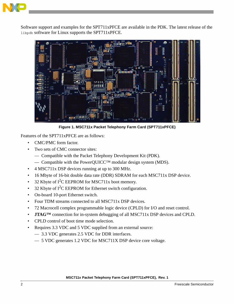
Software support and examples for the SPT711xPFCE are available in the PDK. The latest release of the libpdk software for Linux supports the SPT711xPFCE.
Figure 1. MSC711x Packet Telephony Farm Card (SPT711xPFCE)
Features of the SPT711xPFCE are as follows:
• CMC/PMC form factor.
• Two sets of CMC connector sites:
— Compatible with the Packet Telephony Development Kit (PDK).
— Compatible with the PowerQUICC™ modular design system (MDS).
• 4 MSC711x DSP devices running at up to 300 MHz.
• 16 Mbyte of 16-bit double data rate (DDR) SDRAM for each MSC711x DSP device.
• 32 Kbyte of I2C EEPROM for MSC711x boot memory.
• 32 Kbyte of I2C EEPROM for Ethernet switch configuration.
• On-board 10-port Ethernet switch.
• Four TDM streams connected to all MSC711x DSP devices.
• 72 Macrocell complex programmable logic device (CPLD) for I/O and reset control.
• JTAG™ connection for in-system debugging of all MSC711x DSP devices and CPLD.
• CPLD control of boot time mode selection.
• Requires 3.3 VDC and 5 VDC supplied from an external source:
— 3.3 VDC generates 2.5 VDC for DDR interfaces.
— 5 VDC generates 1.2 VDC for MSC711X DSP device core voltage.

MSC711x Packet Telephony Farm Card (SPT711xPFCE), Rev. 1
Freescale Semiconductor 3
Packet Telephony Development Kit
1 Packet Telephony Development KitThe Packet Telephony Development Kit (PDK) is a Freescale platform for evaluating and developing voice-over packet applications. The PDK has an MPC8260 host network processor that runs Linux, StarCore DSP resource cards that run DSP code, and a public switched telephone network (PSTN) card with interfaces such as E1/T1 and analog telephone lines (see Figure 2).
Figure 2. Components of the PDK
The documentation for the kit components is listed in Table 1.
Table 1. PTK Components and Their Associated Documents
Component Document Document ID
Baseboard Packet Development Kit Baseboard Hardware User’s Guide PTKITBASEUG
MPC8260 control processor
MPC8260 PowerQUICC II™ Family Reference Manual(Available at the website listed on the back page of this user’s guide.)
MPC8260UM
PSTN card Packet Development Kit PSTN Mezzanine User’s Guide PTKITPSTNUG
StarCore DSP resource daughter card
• MSC8102 Packet Telephony Farm Card (MSC8102PFC) User’s Guide• MSC8101 Packet Telephony Farm Card (MSC8101PFC) User’s Guide• MSC8122 Packet Telephony Farm Card (MSC8122PFC-HV) User’s Guide• MSC711x Packet Telephony Farm Card (SPT711xPFCE) User’s Guide
PTKIT8102UG
PTKIT8101UG
PTKIT8122UG
PTKIT711xUG
MSC8122 processor MSC8122 Reference Manual and other MSC8122 documentation are located at the web site listed on the back cover of this user’s guide.
MSC8122RM
MSC8103 processor MSC8103 Reference Manual and other MSC8103 documentation are located at the web site listed on the back cover of this user’s guide.
MSC8103RM
Software Packet Telephony Development Kit Software User’s Guide PTKITSOFTUG
PSTN StarCore DSPResource
Daughter card
MPC8260Control
ProcessorEthernet
ManagedPacket
Network
TelephoneNetwork
Baseboard

MSC711x Packet Telephony Farm Card (SPT711xPFCE), Rev. 1
4 Freescale Semiconductor
System Interfaces
CAUTIONThe packet telephony development kit includes open-construction printed circuit boards that contain static-sensitive components. These boards are subject to damage from electrostatic discharge (ESD). To prevent such damage, you must use static-safe work surfaces and grounding straps, as defined in ANSI/EOS/ESD S6.1 and ANSI/EOS/ESD S4.1. All handling of these boards must be in accordance with ANSI/EAI 625.
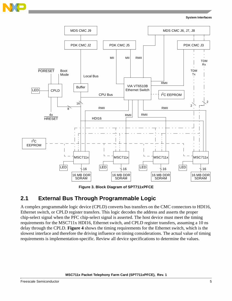
2 System InterfacesTo support VoIP applications development, the SPT711xPFCE provides four time-division multiplex (TDM) and four Ethernet interfaces at the CMC connectors (see Figure 3). It includes interfaces for program storage, download, and debug. These interfaces can also be used to transfer control messages with a system controller.
Table 2. Reference Documents
Document Revision Date Document ID
Standard Physical and Environmental layers for PCI Mezzanine Cards: PMC
Draft 2.4 January 12, 2001
IEEE: P1386.1
Standard for a Common Mezzanine Card Family: CMC Draft 2.4a March 21, 2001 IEEE: P1386
CompactPCI PCI Telecom Mezzanine Card Specification R1.0 April 11, 2001 PICMG 2.15
H.100 Hardware Compatibility Specification: CT Bus 1.0 H.100
MSC711x Packet Telephony Farm Card (SPT711xPFCE), Rev. 1
Freescale Semiconductor 5
System Interfaces
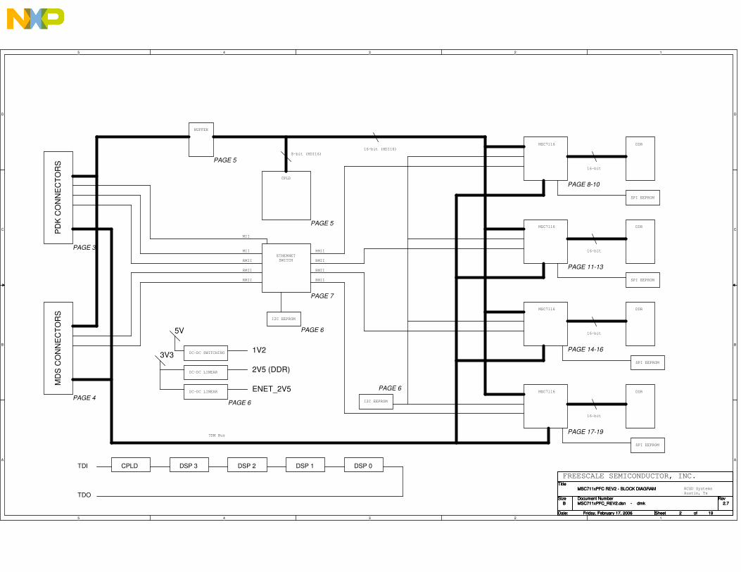
Figure 3. Block Diagram of SPT711xPFCE
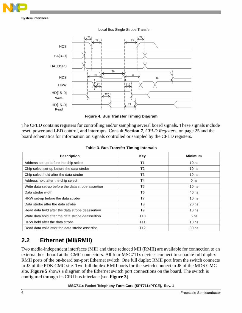
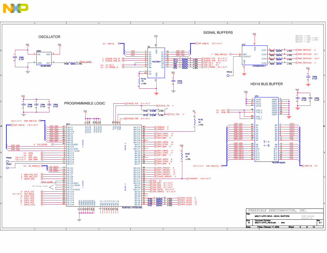
2.1 External Bus Through Programmable LogicA complex programmable logic device (CPLD) converts bus transfers on the CMC connectors to HDI16, Ethernet switch, or CPLD register transfers. This logic decodes the address and asserts the proper chip-select signal when the PFC chip-select signal is asserted. The host device must meet the timing requirements for the MSC711x HDI16, Ethernet switch, and CPLD register transfers, assuming a 10 ns delay through the CPLD. Figure 4 shows the timing requirements for the Ethernet switch, which is the slowest interface and therefore the driving influence on timing considerations. The actual value of timing requirements is implementation-specific. Review all device specifications to determine the values.
MSC711x
16 MB DDRSDRAM
LED 16
MSC711x
16 MB DDRSDRAM
LED 16
MSC711x
16 MB DDRSDRAM
LED 16
MSC711x
16 MB DDRSDRAM
LED 16
VIA VT6510BEthernet Switch
MDS CMC J9
PDK CMC J5PDK CMC J2
MDS CMC J6, J7, J8
PDK CMC J3
I2CEEPROM
BufferCPLDLED
4xHRESET
Local Bus
CPU Bus
MII MII RMII
RMII
RMIIRMII
RMII RMII
16 22
TDMTx
TDMRx
HDI16
I2C EEPROM
8
PORESET BootMode
MSC711x Packet Telephony Farm Card (SPT711xPFCE), Rev. 1
6 Freescale Semiconductor
System Interfaces
Figure 4. Bus Transfer Timing Diagram
The CPLD contains registers for controlling and/or sampling several board signals. These signals include reset, power and LED control, and interrupts. Consult Section 7, CPLD Registers, on page 25 and the board schematics for information on signals controlled or sampled by the CPLD registers.
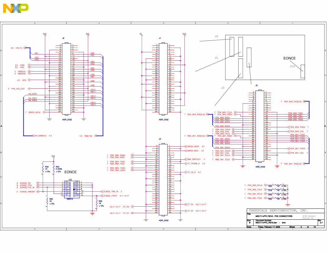
2.2 Ethernet (MII/RMII)Two media-independent interfaces (MII) and three reduced MII (RMII) are available for connection to an external host board at the CMC connectors. All four MSC711x devices connect to separate full duplex RMII ports of the on-board ten-port Ethernet switch. One full duplex RMII port from the switch connects to J3 of the PDK CMC site. Two full duplex RMII ports for the switch connect to J8 of the MDS CMC site. Figure 5 shows a diagram of the Ethernet switch port connections on the board. The switch is configured through its CPU bus interface (see Figure 3).
Table 3. Bus Transfer Timing Intervals
Description Key Minimum
Address set-up before the chip select T1 10 ns
Chip-select set-up before the data strobe T2 10 ns
Chip-select hold after the data strobe T3 10 ns
Address hold after the chip select T4 0 ns
Write data set-up before the data strobe assertion T5 10 ns
Data strobe width T6 40 ns
HRW set-up before the data strobe T7 10 ns
Data strobe after the data strobe T8 20 ns
Read data hold after the data strobe deassertion T9 10 ns
Write data hold after the data strobe deassertion T10 5 ns
HRW hold after the data strobe T11 10 ns
Read data valid after the data strobe assertion T12 30 ns
HCS
HA[3:0]
HA_DSP0
HDS
HRW
HD[15:0]
LOCAL BUS SINGLE-STROBE TRANSFERT1
T5
T7
T2 T3T4
T9
T10
T6
T8
HD[15:0]
WRITE
READ
T11
T12
HCS
HA[3:0]
HA_DSP0
HDS
HRW
HD[15:0]
LOCAL BUS SINGLE-STROBE TRANSFERT1
T5
T7
T2 T3T4
T9
T10
T6
T8
HD[15:0]
WRITE
READ
T11
T12
Local Bus Single-Strobe Transfer
HCS
HA[3–0]
HA_DSP0
HDS
HRW
HD[15–0]
HD[15–0]
Write
Read

MSC711x Packet Telephony Farm Card (SPT711xPFCE), Rev. 1
Freescale Semiconductor 7
System Interfaces
Figure 5. Ethernet Connections
2.3 Time-Division Multiplex (TDM) BusFour streams of TDM data are available for connection to an external host board and are connected to all MSC711x DSP devices. The streams connect to J3 of the PDK CMC site and J6, J7, and J8 of the MDS CMC site. One pair of frame and clock signalling is provided for all TDM streams. Streams CT_D1 and CT_D5 must be used for TDM streams from the external host to the DSP farm. Streams CT_D0 and CT_D4 must be used for TDM streams from the DSP farm to the external host. The frame and clock signals are buffered and then connected to each DSP device. The CT_D0, CT_D1, CT_D5, and CT_D4 signals are connected directly from the DSP devices to the CMC connectors. Figure 6 shows the TDM stream connections on the board.
Table 4. VIA Ethernet Switch Port Connections
Port Type Connection
0 RMII MSC711x Device 0
1 RMII MSC711x Device 1
2 RMII MSC711x Device 2
3 RMII MSC711x Device 3
4 RMII MDS CMC
5 RMII MDS CMC P3
6 RMII PDK CMC
7 RMII No Connection
8 MII PDK CMC P5
9 MII PDK CMC P5
VIA VT6510BEthernet Switch
PDK CMC J3
MDS CMC J8
PDK CMC J5
MSC711x MSC711x MSC711x MSC711x
RMII
RMII RMII
RMII
RMII
RMII
MIIMII
MDC/MDIO
RMII

MSC711x Packet Telephony Farm Card (SPT711xPFCE), Rev. 1
8 Freescale Semiconductor
Hardware
Figure 6. TDM Connections
2.4 JTAG ConnectorConnector J10 is a 14-pin 0.100 inch pitch header that provides JTAG debugger access to the board. For details on the connector signals, refer to the schematics in Appendix A. One JTAG chain on the board connects all four MSC711x devices and the CPLD. The chain is connected as follows:
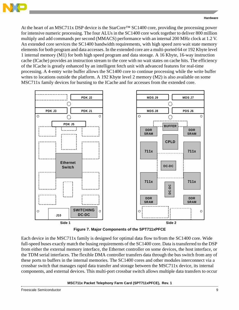
3 HardwareFigure 7 depicts the main components of the SPT711xPFCE board, which are the MSC711x DSP devices, CPLD, Ethernet switch, I2C bus devices, and voltage regulators.
3.1 MSC711x DSPsThe MSC711x family of highly integrated DSPs targets high-bandwidth computationally intensive DSP applications and is optimized for Enterprise class packet telephony applications. These processors deliver enhanced performance while maintaining low power dissipation and greatly reducing system cost.
MSC711xMSC711x
CT_F
CT_C8
CT_D0CT_D4
CT_D1
CT_D5
BU
FF
ER
BU
FF
ER
PD
K C
MC
J3
MD
S C
MC
J6,
7,8
MSC711xMSC711x
MSC711xMSC711x
MSC711xMSC711x
TDM TX
TDM RX
CLOCK
FRAME
TDM TX
TDM RX
CLOCK
CLOCK
FRAME
TDI CPLD MSC711x 3 MSC711x 2
MSC711x 1MSC711x 0TDO
MSC711x Packet Telephony Farm Card (SPT711xPFCE), Rev. 1
Freescale Semiconductor 9
Hardware
At the heart of an MSC711x DSP device is the StarCore™ SC1400 core, providing the processing power for intensive numeric processing. The four ALUs in the SC1400 core work together to deliver 800 million multiply and add commands per second (MMACS) performance with an internal 200 MHz clock at 1.2 V. An extended core services the SC1400 bandwidth requirements, with high speed zero wait state memory elements for both program and data accesses. In the extended core are a multi-ported 64 or 192 Kbyte level 1 internal memory (M1) for both high speed program and data storage. A 16 Kbyte, 16-way instruction cache (ICache) provides an instruction stream to the core with no wait states on cache hits. The efficiency of the ICache is greatly enhanced by an intelligent fetch unit with advanced features for real-time processing. A 4-entry write buffer allows the SC1400 core to continue processing while the write buffer writes to locations outside the platform. A 192 Kbyte level 2 memory (M2) is also available on some MSC711x family devices for bursting to the ICache and for accesses from the extended core.
Figure 7. Major Components of the SPT711xPFCE
Each device in the MSC711x family is designed for optimal data flow to/from the SC1400 core. Wide full-speed buses exactly match the busing requirements of the SC1400 core. Data is transferred to the DSP from either the external memory interface, the Ethernet controller on some devices, the host interface, or the TDM serial interfaces. The flexible DMA controller transfers data through the bus switch from any of these ports to buffers in the internal memories. The SC1400 cores and other modules interconnect via a crossbar switch that manages rapid data transfer and storage between the MSC711x device, its internal components, and external devices. This multi-port crossbar switch allows multiple data transfers to occur
SIDE 1
PDK J1
PDK J2
PDK J3
SIDE 2
PDS J6
MDS J7
MDS J8
MDS J9
CPLD
BUFFER
711x 711x
711x 711x
PDK J5
Ethernet Switch
SWITCHING DC-DCJ10
DDR SRAM
DDR SRAM
DDR SRAM
DDR SRAM
DC
-DC
DC
-DC
DC-DCDC-DC
Side 1 Side 2
MSC711x Packet Telephony Farm Card (SPT711xPFCE), Rev. 1
10 Freescale Semiconductor
Hardware
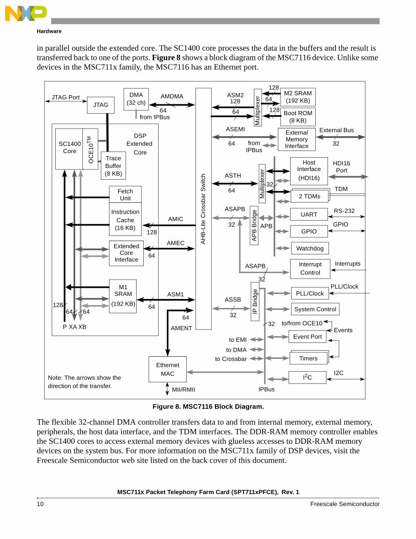
in parallel outside the extended core. The SC1400 core processes the data in the buffers and the result is transferred back to one of the ports. Figure 8 shows a block diagram of the MSC7116 device. Unlike some devices in the MSC711x family, the MSC7116 has an Ethernet port.
Figure 8. MSC7116 Block Diagram.
The flexible 32-channel DMA controller transfers data to and from internal memory, external memory, peripherals, the host data interface, and the TDM interfaces. The DDR-RAM memory controller enables the SC1400 cores to access external memory devices with glueless accesses to DDR-RAM memory devices on the system bus. For more information on the MSC711x family of DSP devices, visit the Freescale Semiconductor web site listed on the back cover of this document.
Boot ROM(8 KB)
RS-232
APB
AP
B B
ridge
64
UART
ExternalMemory
InterruptsInterrupt
HDI16
32
HostInterface
(HDI16)
External Bus
Timers
DSPExtended
DMA
Note: The arrows show the
Interface
Port
(32 ch)64
32
12832
SC1400Core
Cache(16 KB)
ExtendedCore
Interface
UnitFetch
M1SRAM
(192 KB)
64
64
128
64
AH
B-L
ite C
ross
bar
Sw
itch
P XA XB
12864 64
PLL/ClockPLL/Clock
Mul
tiple
xer
OC
E10
TM
TraceBuffer(8 KB)
to/from OCE10
IP B
ridge
32
Events32
IPBus
to DMA
to EMI
JTAGJTAG Port
Core
AMDMA
AMIC
AMEC
ASM1
ASM2
ASEMI
ASTH
ASAPB
fromIPBus
I2CI2C
ASSB
GPIOGPIO
Instruction
from IPBus
Watchdog
Event Port
to Crossbar
System Control
Control32
ASAPB
2 TDMsTDM
EthernetMAC
AMENT
64
MII/RMIIdirection of the transfer.
M2 SRAM(192 KB)
Mul
tiple
xer
128
128
64
64
MSC711x Packet Telephony Farm Card (SPT711xPFCE), Rev. 1
Freescale Semiconductor 11
Hardware
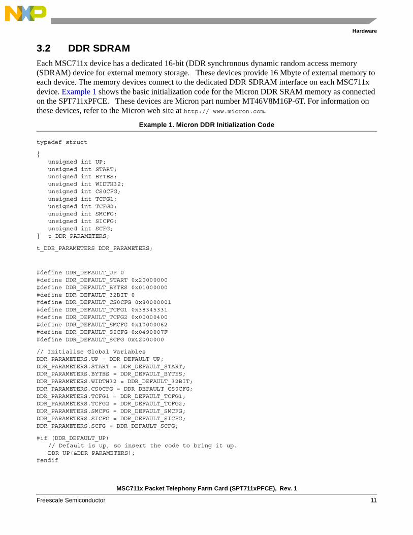
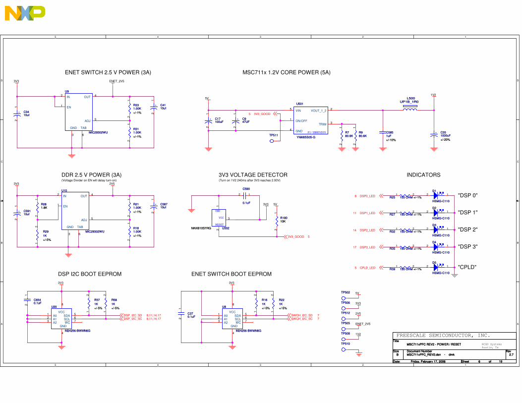
3.2 DDR SDRAMEach MSC711x device has a dedicated 16-bit (DDR synchronous dynamic random access memory (SDRAM) device for external memory storage. These devices provide 16 Mbyte of external memory to each device. The memory devices connect to the dedicated DDR SDRAM interface on each MSC711x device. Example 1 shows the basic initialization code for the Micron DDR SRAM memory as connected on the SPT711xPFCE. These devices are Micron part number MT46V8M16P-6T. For information on these devices, refer to the Micron web site at http:// www.micron.com.
Example 1. Micron DDR Initialization Code
typedef struct
{unsigned int UP;unsigned int START;unsigned int BYTES;unsigned int WIDTH32;unsigned int CS0CFG;unsigned int TCFG1;unsigned int TCFG2;unsigned int SMCFG;unsigned int SICFG;unsigned int SCFG;
} t_DDR_PARAMETERS;
t_DDR_PARAMETERS DDR_PARAMETERS;
#define DDR_DEFAULT_UP 0#define DDR_DEFAULT_START 0x20000000#define DDR_DEFAULT_BYTES 0x01000000#define DDR_DEFAULT_32BIT 0#define DDR_DEFAULT_CS0CFG 0x80000001#define DDR_DEFAULT_TCFG1 0x38345331#define DDR_DEFAULT_TCFG2 0x00000400#define DDR_DEFAULT_SMCFG 0x10000062#define DDR_DEFAULT_SICFG 0x0490007F#define DDR_DEFAULT_SCFG 0x42000000
// Initialize Global VariablesDDR_PARAMETERS.UP = DDR_DEFAULT_UP;DDR_PARAMETERS.START = DDR_DEFAULT_START;DDR_PARAMETERS.BYTES = DDR_DEFAULT_BYTES;DDR_PARAMETERS.WIDTH32 = DDR_DEFAULT_32BIT;DDR_PARAMETERS.CS0CFG = DDR_DEFAULT_CS0CFG;DDR_PARAMETERS.TCFG1 = DDR_DEFAULT_TCFG1;DDR_PARAMETERS.TCFG2 = DDR_DEFAULT_TCFG2;DDR_PARAMETERS.SMCFG = DDR_DEFAULT_SMCFG;DDR_PARAMETERS.SICFG = DDR_DEFAULT_SICFG;DDR_PARAMETERS.SCFG = DDR_DEFAULT_SCFG;
#if (DDR_DEFAULT_UP)// Default is up, so insert the code to bring it up.DDR_UP(&DDR_PARAMETERS);
#endif
MSC711x Packet Telephony Farm Card (SPT711xPFCE), Rev. 1
12 Freescale Semiconductor
Hardware
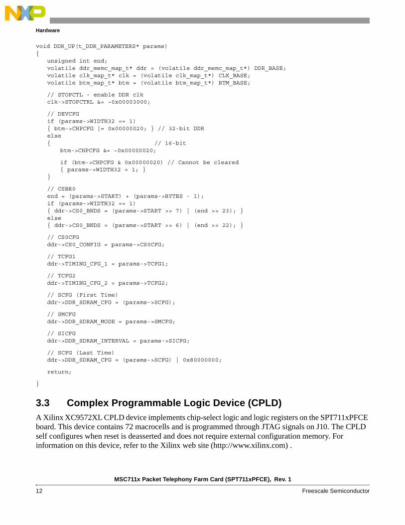
void DDR_UP(t_DDR_PARAMETERS* params){
unsigned int end;volatile ddr_memc_map_t* ddr = (volatile ddr_memc_map_t*) DDR_BASE;volatile clk_map_t* clk = (volatile clk_map_t*) CLK_BASE;volatile btm_map_t* btm = (volatile btm_map_t*) BTM_BASE;
// STOPCTL - enable DDR clkclk->STOPCTRL &= ~0x00003000;
// DEVCFGif (params->WIDTH32 == 1){ btm->CHPCFG |= 0x00000020; } // 32-bit DDRelse{ // 16-bit
btm->CHPCFG &= ~0x00000020;
if (btm->CHPCFG & 0x00000020) // Cannot be cleared{ params->WIDTH32 = 1; }
}
// CSBR0end = (params->START) + (params->BYTES - 1);if (params->WIDTH32 == 1){ ddr->CS0_BNDS = (params->START >> 7) | (end >> 23); }else{ ddr->CS0_BNDS = (params->START >> 6) | (end >> 22); }
// CS0CFGddr->CS0_CONFIG = params->CS0CFG;
// TCFG1ddr->TIMING_CFG_1 = params->TCFG1;
// TCFG2ddr->TIMING_CFG_2 = params->TCFG2;
// SCFG (First Time)ddr->DDR_SDRAM_CFG = (params->SCFG);
// SMCFGddr->DDR_SDRAM_MODE = params->SMCFG;
// SICFGddr->DDR_SDRAM_INTERVAL = params->SICFG;
// SCFG (Last Time)ddr->DDR_SDRAM_CFG = (params->SCFG) | 0x80000000;
return;
}
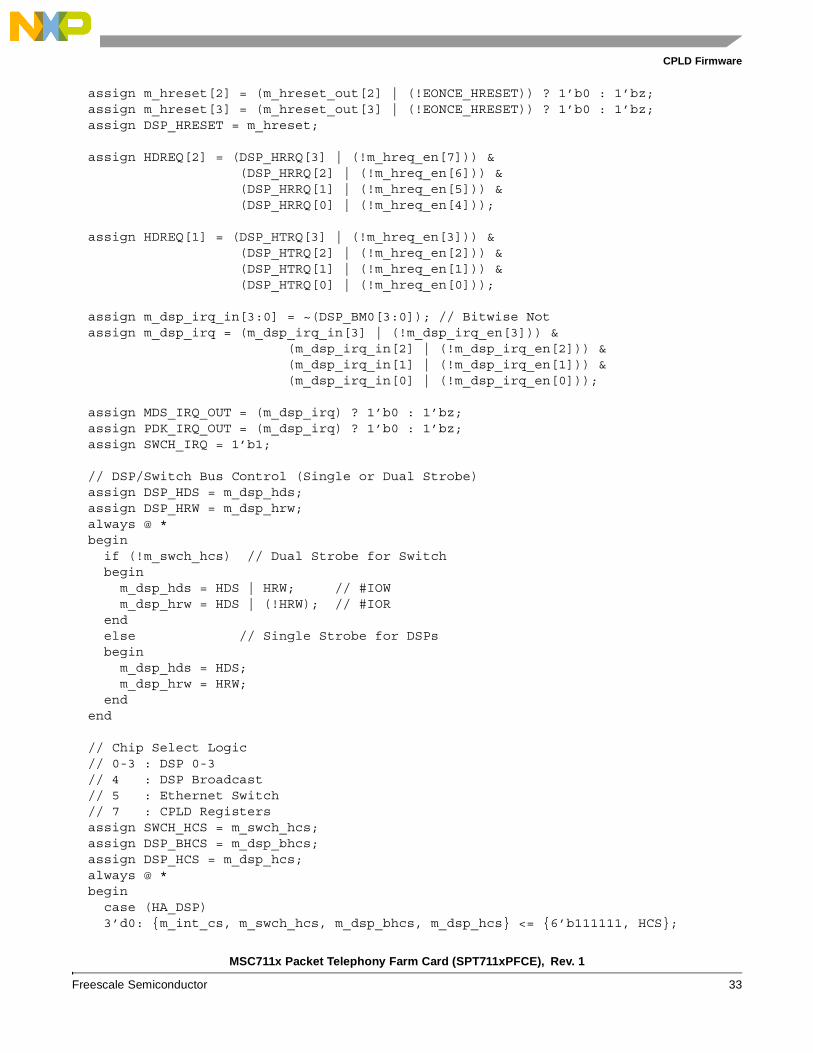
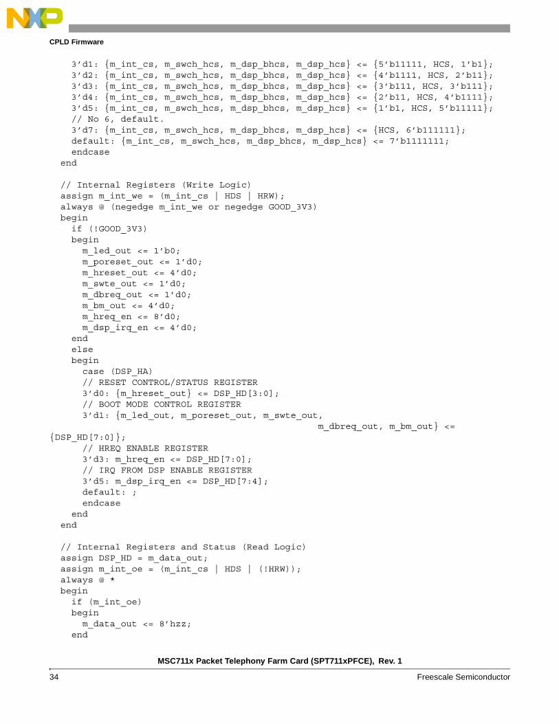
3.3 Complex Programmable Logic Device (CPLD)A Xilinx XC9572XL CPLD device implements chip-select logic and logic registers on the SPT711xPFCE board. This device contains 72 macrocells and is programmed through JTAG signals on J10. The CPLD self configures when reset is deasserted and does not require external configuration memory. For information on this device, refer to the Xilinx web site (http://www.xilinx.com) .
MSC711x Packet Telephony Farm Card (SPT711xPFCE), Rev. 1
Freescale Semiconductor 13
Hardware
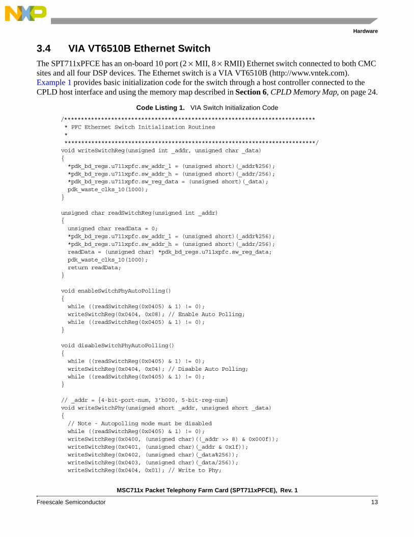
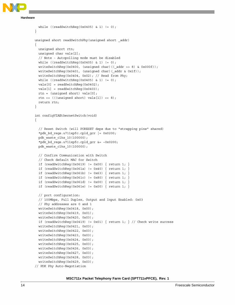
3.4 VIA VT6510B Ethernet SwitchThe SPT711xPFCE has an on-board 10 port (2 × MII, 8 × RMII) Ethernet switch connected to both CMC sites and all four DSP devices. The Ethernet switch is a VIA VT6510B (http://www.vntek.com). Example 1 provides basic initialization code for the switch through a host controller connected to the CPLD host interface and using the memory map described in Section 6, CPLD Memory Map, on page 24.
Code Listing 1. VIA Switch Initialization Code
/*************************************************************************** * PFC Ethernet Switch Initialization Routines * ***************************************************************************/void writeSwitchReg(unsigned int _addr, unsigned char _data) { *pdk_bd_regs.u711xpfc.sw_addr_l = (unsigned short)(_addr%256); *pdk_bd_regs.u711xpfc.sw_addr_h = (unsigned short)(_addr/256); *pdk_bd_regs.u711xpfc.sw_reg_data = (unsigned short)(_data); pdk_waste_clks_10(1000);}
unsigned char readSwitchReg(unsigned int _addr) { unsigned char readData = 0; *pdk_bd_regs.u711xpfc.sw_addr_l = (unsigned short)(_addr%256); *pdk_bd_regs.u711xpfc.sw_addr_h = (unsigned short)(_addr/256); readData = (unsigned char) *pdk_bd_regs.u711xpfc.sw_reg_data; pdk_waste_clks_10(1000); return readData; }
void enableSwitchPhyAutoPolling(){ while ((readSwitchReg(0x0405) & 1) != 0); writeSwitchReg(0x0404, 0x08); // Enable Auto Polling; while ((readSwitchReg(0x0405) & 1) != 0);}
void disableSwitchPhyAutoPolling(){ while ((readSwitchReg(0x0405) & 1) != 0); writeSwitchReg(0x0404, 0x04); // Disable Auto Polling; while ((readSwitchReg(0x0405) & 1) != 0);}
// _addr = {4-bit-port-num, 3’b000, 5-bit-reg-num}void writeSwitchPhy(unsigned short _addr, unsigned short _data){ // Note - Autopolling mode must be disabled while ((readSwitchReg(0x0405) & 1) != 0); writeSwitchReg(0x0400, (unsigned char)((_addr >> 8) & 0x000f)); writeSwitchReg(0x0401, (unsigned char)(_addr & 0x1f)); writeSwitchReg(0x0402, (unsigned char)(_data%256)); writeSwitchReg(0x0403, (unsigned char)(_data/256)); writeSwitchReg(0x0404, 0x01); // Write to Phy;
MSC711x Packet Telephony Farm Card (SPT711xPFCE), Rev. 1
14 Freescale Semiconductor
Hardware
while ((readSwitchReg(0x0405) & 1) != 0);}
unsigned short readSwitchPhy(unsigned short _addr){ unsigned short rtn; unsigned char vals[2]; // Note - Autopolling mode must be disabled while ((readSwitchReg(0x0405) & 1) != 0); writeSwitchReg(0x0400, (unsigned char)((_addr >> 8) & 0x000f)); writeSwitchReg(0x0401, (unsigned char)(_addr & 0x1f)); writeSwitchReg(0x0404, 0x02); // Read from Phy; while ((readSwitchReg(0x0405) & 1) != 0); vals[0] = readSwitchReg(0x0402); vals[1] = readSwitchReg(0x0403); rtn = (unsigned short) vals[0]; rtn += (((unsigned short) vals[1]) << 8); return rtn;}
int configVIAEthernetSwitch(void){
// Reset Switch (will PORESET dsps due to "strapping pins" shared) *pdk_bd_regs.u711xpfc.cpld_gcr |= 0x0200; pdk_waste_clks_10(100000); *pdk_bd_regs.u711xpfc.cpld_gcr &= ~0x0200; pdk_waste_clks_10(100000);
// Confirm Communication with Switch // Check default MAC for Switch if (readSwitchReg(0x0619) != 0x00) { return 1; } if (readSwitchReg(0x061a) != 0x40) { return 1; } if (readSwitchReg(0x061b) != 0x63) { return 1; } if (readSwitchReg(0x061c) != 0x80) { return 1; } if (readSwitchReg(0x061d) != 0x00) { return 1; } if (readSwitchReg(0x061e) != 0x00) { return 1; }
// port configuration: // 100Mbps, Full Duplex, Output and Input Enabled: 0x03 // Phy addresses are 0 and 1 writeSwitchReg(0x0418, 0x00); writeSwitchReg(0x0419, 0x01); writeSwitchReg(0x0420, 0x03); if (readSwitchReg(0x0419) != 0x01) { return 1; } // Check write success writeSwitchReg(0x0421, 0x03); writeSwitchReg(0x0422, 0x03); writeSwitchReg(0x0423, 0x03); writeSwitchReg(0x0424, 0x03); writeSwitchReg(0x0425, 0x03); writeSwitchReg(0x0426, 0x03); writeSwitchReg(0x0427, 0x03); writeSwitchReg(0x0428, 0x03); writeSwitchReg(0x0429, 0x03);// PDK Phy Auto-Negotiation
MSC711x Packet Telephony Farm Card (SPT711xPFCE), Rev. 1
Freescale Semiconductor 15
Hardware
disableSwitchPhyAutoPolling(); if (readSwitchPhy(0x0802) == 0x0013) { writeSwitchPhy(0x0800, 0x8000); while ((readSwitchPhy(0x0800) & 0x8000) != 0); writeSwitchPhy(0x0804, 0x0DE1); // Capabilities writeSwitchPhy(0x0800, 0x1000); // Enable Auto-Negotiation if (readSwitchPhy(0x0804) != 0x0DE1) { return 1; } } if (readSwitchPhy(0x0902) == 0x0013) { writeSwitchPhy(0x0900, 0x8000); while ((readSwitchPhy(0x0900) & 0x8000) != 0); writeSwitchPhy(0x0904, 0x0DE1); // Capabilities writeSwitchPhy(0x0900, 0x1000); // Enable Auto-Negotiation if (readSwitchPhy(0x0904) != 0x0DE1) { return 1; } }
return 0;}
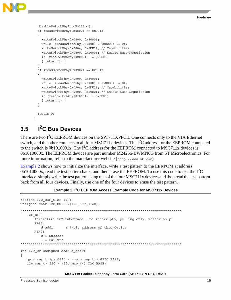
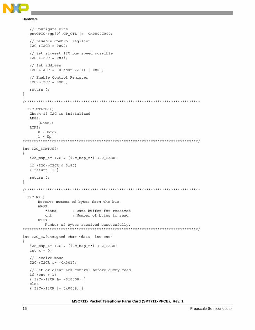
3.5 I2C Bus DevicesThere are two I2C EEPROM devices on the SPT711XPFCE. One connects only to the VIA Ethernet switch, and the other connects to all four MSC711x devices. The I2C address for the EEPROM connected to the switch is 0b1010001x. The I2C address for the EEPROM connected to MSC711x devices is 0b1010000x. The EEPROM devices are part number M24256-BWMN6G from ST Microelectronics. For more information, refer to the manufacturer website (http://www.st.com).
Example 2 shows how to initialize the interface, write a test pattern to the EERPOM at address 0b1010000x, read the test pattern back, and then erase the EEPROM. To use this code to test the I2C interface, simply write the test pattern using one of the four MSC711x devices and then read the test pattern back from all four devices. Finally, use one of the four devices to erase the test pattern.
Example 2. I2C EEPROM Access Example Code for MSC711x Devices
#define I2C_BUF_SIZE 1024unsigned char I2C_BUFFER[I2C_BUF_SIZE];
/******************************************************************************I2C_UP()
Initialize I2C Interface - no interrupts, polling only, master onlyARGS:
d_addr : 7-bit address of this deviceRTNS:
0 = Success1 = Failure
******************************************************************************/
int I2C_UP(unsigned char d_addr){
gpio_map_t *pstGPIO = (gpio_map_t *)GPIO_BASE;i2c_map_t* I2C = (i2c_map_t*) I2C_BASE;
MSC711x Packet Telephony Farm Card (SPT711xPFCE), Rev. 1
16 Freescale Semiconductor
Hardware
// Configure PinspstGPIO->gp[0].GP_CTL |= 0x0000C000;
// Disable Control RegisterI2C->I2CR = 0x00;
// Set slowest I2C bus speed possibleI2C->IFDR = 0x3f;
// Set addressI2C->IADR = (d_addr << 1) | 0x08;
// Enable Control RegisterI2C->I2CR = 0x80;
return 0;}
/******************************************************************************
I2C_STATUS()Check if I2C is initializedARGS:
(None.)RTNS:
0 = Down1 = Up
******************************************************************************/
int I2C_STATUS(){
i2c_map_t* I2C = (i2c_map_t*) I2C_BASE;
if (I2C->I2CR & 0x80){ return 1; }
return 0;}
/******************************************************************************
I2C_RX()Receive number of bytes from the bus.ARGS:
*data : Data buffer for receivedcnt : Number of bytes to read
RTNS:Number of bytes received successfully.
******************************************************************************/
int I2C_RX(unsigned char *data, int cnt){
i2c_map_t* I2C = (i2c_map_t*) I2C_BASE;int x = 0;
// Receive modeI2C->I2CR &= ~0x0010;
// Set or clear Ack control before dummy readif (cnt > 1){ I2C->I2CR &= ~0x0008; }else{ I2C->I2CR |= 0x0008; }
MSC711x Packet Telephony Farm Card (SPT711xPFCE), Rev. 1
Freescale Semiconductor 17
Hardware
// Read data (dummy read to start transfer)data[x] = (unsigned char) I2C->I2DR;cnt--;
while (cnt > 0){
// Wait for transfer to startwhile (I2C->I2SR & 0x0080);
// Wait for transfer to endwhile ((I2C->I2SR & 0x0080) == 0);
// Set or clear Ack control before last readif (cnt > 1){ I2C->I2CR &= ~0x0008; }else{ I2C->I2CR |= 0x0008; }
// Read datadata[x++] = (unsigned char) I2C->I2DR; cnt--;
}
// Wait for transfer to startwhile (I2C->I2SR & 0x0080);
// Wait for transfer to endwhile ((I2C->I2SR & 0x0080) == 0);
// Signal stop before last readI2C->I2CR &= ~0x0030;
// Read Read for last data (post stop condition)data[x++] = (unsigned char) I2C->I2DR;
return x;}
/******************************************************************************
I2C_TX()Transmit byte on busARGS:
data : Data to sendRTNS:
0 = Success1 = Failure
******************************************************************************/
int I2C_TX(unsigned char data){
i2c_map_t* I2C = (i2c_map_t*) I2C_BASE;
// Send byteI2C->I2CR |= 0x0010; // Tx
I2C->I2DR = (unsigned short) (data);
// Wait for transfer to startwhile (I2C->I2SR & 0x0080){
if (I2C->I2SR & 0x0050)
MSC711x Packet Telephony Farm Card (SPT711xPFCE), Rev. 1
18 Freescale Semiconductor
Hardware
{ return 1; }}
// Wait for transfer to endwhile ((I2C->I2SR & 0x0080) == 0){
if (I2C->I2SR & 0x0050){ return 1; }
}
// Check for Ackif (I2C->I2SR & 0x0001){ return 1; }
return 0;}
/******************************************************************************
I2C_WR()Write a byte to an I2C EEPROM Device. This performs one byte write at a time to avoid page burst boundary requirements. ARGS:
t_addr : LSB 3-bit address of target device from base address 0xA0.b_addr : Byte address in device*data : Data to write
RTNS:0 = Success1 = Failure
******************************************************************************/
int I2C_WR(unsigned char t_addr, unsigned short b_addr, unsigned char *data){
i2c_map_t* I2C = (i2c_map_t*) I2C_BASE;
// Arbitrate for Buswhile (I2C->I2SR & 0x0020); // Bus BusyI2C->I2CR |= 0x0020; // Master
// Send device addressif (I2C_TX(0xA0 | ((t_addr & 7) << 1))){ I2C->I2CR &= ~0x0030; return 1; }
// Send byte address (MSB first)if (I2C_TX((unsigned char) (b_addr >> 8))){ I2C->I2CR &= ~0x0030; return 1; }if (I2C_TX((unsigned char) (b_addr & 0x00ff))){ I2C->I2CR &= ~0x0030; return 1; }
// Send byte dataif (I2C_TX(*data)){ I2C->I2CR &= ~0x0030; return 1; }
// Release BusI2C->I2CR &= ~0x0030; // Slave Rx
return 0;}
/******************************************************************************I2C_RD()
MSC711x Packet Telephony Farm Card (SPT711xPFCE), Rev. 1
Freescale Semiconductor 19
Hardware
Read data from an I2C EEPROM DeviceARGS:
t_addr : LSB 3-bit address of target device from base address 0xA0.b_addr : Byte address in device*data : Data to writecnt : number of bytes to read
RTNS:Number of bytes read.
******************************************************************************/
int I2C_RD(unsigned char t_addr, unsigned short b_addr, unsigned char *data,int cnt)
{i2c_map_t* I2C = (i2c_map_t*) I2C_BASE;int x;
if (cnt < 0){ return 0; }
// Arbitrate for Buswhile (I2C->I2SR & 0x0020); // Bus BusyI2C->I2CR |= 0x0020; // Master
// Send device address (Keep action a "Write" to set Random Access address)if (I2C_TX(0xA0 | ((t_addr & 7) << 1))){ I2C->I2CR &= ~0x0030; return 1; }
// Send byte address (MSB first)if (I2C_TX((unsigned char) (b_addr >> 8))){ I2C->I2CR &= ~0x0030; return 1; }if (I2C_TX((unsigned char) (b_addr & 0x00ff))){ I2C->I2CR &= ~0x0030; return 1; }
I2C->I2CR |= 0x0004; // Restart
// Send device address (Now send "Read")if (I2C_TX(0xA1 | (t_addr << 1))){ I2C->I2CR &= ~0x0030; return 1; }
// Receive a byte data (bus is released by subroutine)x = I2C_RX(data, cnt);
return x;}
/******************************************************************************I2C_EEPROM_INIT()
Write Test Vector Into I2C EEPROMARGS:
(None.)RTNS:
0 = Success1 = Failure
******************************************************************************/
int I2C_EEPROM_INIT(){
unsigned short x;unsigned char y;unsigned int retry;

MSC711x Packet Telephony Farm Card (SPT711xPFCE), Rev. 1
20 Freescale Semiconductor
Hardware
// Init first 1k of EEPROM with sequntial numbers (+5, will roll-over)y = 0;for (x = 0; x < 1024; x++){
retry = 0;while (I2C_WR(0, x, &y)){
retry++;if (retry > 150){ return 1; }
}y += 5;
}return 0;
}
/******************************************************************************
I2C_EEPROM_CHECK()Check Test Vector In I2C EEPROMARGS:
(None.)RTNS:
0 = Success1 = Failure
******************************************************************************/
int I2C_EEPROM_CHECK(){
unsigned short x;unsigned char y;
// Read data into bufferif (I2C_RD(0, 0, I2C_BUFFER, I2C_BUF_SIZE) != I2C_BUF_SIZE){ return 1; }
// Check first part of EEPROM for sequntial numbers (+5, will roll-over)y = 0;
for (x = 0; x < I2C_BUF_SIZE; x++){
if (I2C_BUFFER[x] != y){ return 1; }y += 5;
}return 0;
}
/******************************************************************************
I2C_EEPROM_ERASE()ERASE I2C EEPROMARGS:
(None.)RTNS:
0 = Success1 = Failure
******************************************************************************/
int I2C_EEPROM_ERASE(){

MSC711x Packet Telephony Farm Card (SPT711xPFCE), Rev. 1
Freescale Semiconductor 21
Hardware
unsigned short x;unsigned char y;unsigned int retry;
// Init first 1k of EEPROM with 0xFFy = 0xff;for (x = 0; x < 1024; x++){
retry = 0;while (I2C_WR(0, x, &y)){
retry++;if (retry > 150){ return 1; }
}}return 0;
}
3.6 Voltage RegulatorsTwo linear regulator modules on the SPT711xPFCE generate the DDR SDRAM (2.5 VDC) and Ethernet switch core (2.5 V) voltages from the externally supplied 3.3 VDC. A switching regulator generates the MSC711x core (1.2 VDC) voltage from the externally-supplied 5 VDC. Figure 9 shows how to probe the board voltages.
Figure 9. Voltage Probing Points
MD
S J
6
N
E
SIDE 2
SRAM711x
CPLD
MD
S J
8
MD
S J
9M
DS
J7
SRAM711x711x
711x
SRAM
SRAM
TAB – GND
PIN 4 – 2V5 (Switch)PIN 4 – 2V5
(DDR)
U9U10
C9
C175V
C35
1V2
PIN 1– 3V3
Side 2
MSC711x Packet Telephony Farm Card (SPT711xPFCE), Rev. 1
22 Freescale Semiconductor
Board Configuration
4 Board ConfigurationSome SPT711xPFCE features are not enabled when the board is shipped from the factory. Carefully evaluate the features and their conflicts before enabling them.
4.1 Reset and Boot Mode SelectionThe complex programmable logic device (CPLD) controls reset and boot mode selection. It contains the logic necessary to assert PORESET to all four MSC711x devices and individual HRESET to each MSC711x device. The host can also change the boot mode selection signals to all four MSC711x devices. By default, all devices reset to boot mode 0b0000 with SWTE and DBREQ deasserted. For details, see Section 7, CPLD Registers, on page 25.
The on-board reset circuitry has been minimized and handles only initial powerup and final powerdown. The circuitry requires a rise/fall time of at least 1 V per 25 ms for both external voltage sources. Also, the external 5 VDC supply must begin rising within 100 ms of the time when the external 3.3 VDC source reaches 2.90 VDC. The reset circuitry issues a PORESET when the external 3.3 VDC source drops below 2.95 VDC or when the 5 VDC source drops below 0.8 VDC. These requirements are reasonable for the board’s intended use.
If the external 5 VDC supply is between 0.8 VDC and 3.0 VDC after 200 ms of the external 3.3 VDC reaches 2.95 VDC, the core voltage may “brown out” without triggering a PORESET. The host processor must issue a PORESET through the CPLD registers to reset the cores.
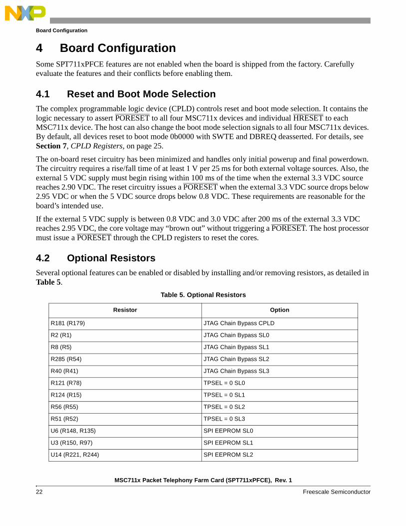
4.2 Optional ResistorsSeveral optional features can be enabled or disabled by installing and/or removing resistors, as detailed in Table 5.
Table 5. Optional Resistors
Resistor Option
R181 (R179) JTAG Chain Bypass CPLD
R2 (R1) JTAG Chain Bypass SL0
R8 (R5) JTAG Chain Bypass SL1
R285 (R54) JTAG Chain Bypass SL2
R40 (R41) JTAG Chain Bypass SL3
R121 (R78) TPSEL = 0 SL0
R124 (R15) TPSEL = 0 SL1
R56 (R55) TPSEL = 0 SL2
R51 (R52) TPSEL = 0 SL3
U6 (R148, R135) SPI EEPROM SL0
U3 (R150, R97) SPI EEPROM SL1
U14 (R221, R244) SPI EEPROM SL2
MSC711x Packet Telephony Farm Card (SPT711xPFCE), Rev. 1
Freescale Semiconductor 23
Board Specifications
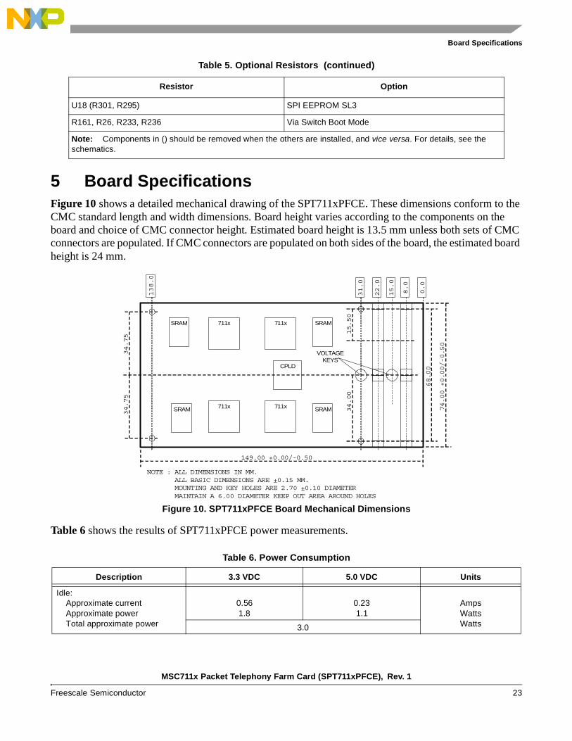
5 Board SpecificationsFigure 10 shows a detailed mechanical drawing of the SPT711xPFCE. These dimensions conform to the CMC standard length and width dimensions. Board height varies according to the components on the board and choice of CMC connector height. Estimated board height is 13.5 mm unless both sets of CMC connectors are populated. If CMC connectors are populated on both sides of the board, the estimated board height is 24 mm.
Figure 10. SPT711xPFCE Board Mechanical Dimensions
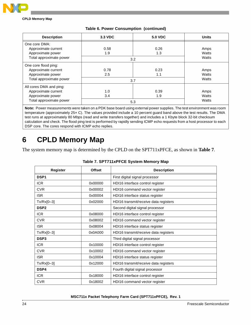
Table 6 shows the results of SPT711xPFCE power measurements.
U18 (R301, R295) SPI EEPROM SL3
R161, R26, R233, R236 Via Switch Boot Mode
Note: Components in () should be removed when the others are installed, and vice versa. For details, see the schematics.
Table 6. Power Consumption
Description 3.3 VDC 5.0 VDC Units
Idle: Approximate current Approximate power Total approximate power
0.561.8
0.231.1
AmpsWattsWatts3.0
Table 5. Optional Resistors (continued)
Resistor Option
SRAM711x 711x
711x 711x
CPLD
VOLTAGEKEYS
74.00 +0.00/-0.50
149.00 +0.00/-0.50
34.75
8.0
0.0
22.0
15.0
31.0
138.0
68.00
NOTE : ALL DIMENSIONS IN MM. ALL BASIC DIMENSIONS ARE ±0.15 MM.MOUNTING AND KEY HOLES ARE 2.70 ±0.10 DIAMETERMAINTAIN A 6.00 DIAMETER KEEP OUT AREA AROUND HOLES
34.00
15.50
34.75
SRAM
SRAM
SRAM
MSC711x Packet Telephony Farm Card (SPT711xPFCE), Rev. 1
24 Freescale Semiconductor
CPLD Memory Map
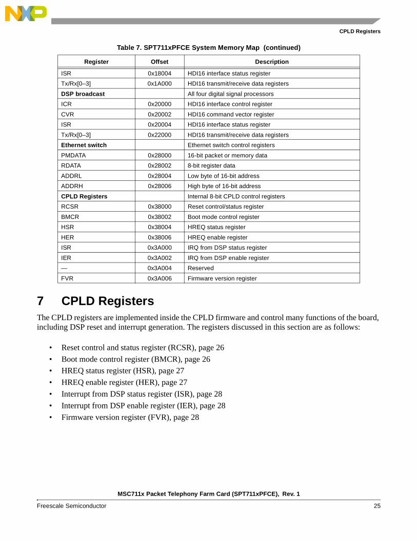
6 CPLD Memory MapThe system memory map is determined by the CPLD on the SPT711xPFCE, as shown in Table 7.
One core DMA: Approximate current Approximate power Total approximate power
0.581.9
0.261.3
AmpsWattsWatts3.2
One core flood ping: Approximate current Approximate power Total approximate power
0.782.5
0.231.1
AmpsWattsWatts3.7
All cores DMA and ping: Approximate current Approximate power Total approximate power
1.03.4
0.391.9
AmpsWattsWatts5.3
Note: Power measurements were taken on a PDK base board using external power supplies. The test environment was room temperature (approximately 25× C). The values provided include a 10 percent guard band above the test results. The DMA test runs at approximately 80 Mbps (read and write transfers together) and includes a 1 Kbyte block 32-bit checksum calculation and check. The flood ping test is performed by rapidly sending ICMP echo requests from a host processor to each DSP core. The cores respond with ICMP echo replies.
Table 7. SPT711xPFCE System Memory Map
Register Offset Description
DSP1 First digital signal processor
ICR 0x00000 HDI16 interface control register
CVR 0x00002 HDI16 command vector register
ISR 0x00004 HDI16 interface status register
Tx/Rx[0–3] 0x02000 HDI16 transmit/receive data registers
DSP2 Second digital signal processor
ICR 0x08000 HDI16 interface control register
CVR 0x08002 HDI16 command vector register
ISR 0x08004 HDI16 interface status register
Tx/Rx[0–3] 0x0A000 HDI16 transmit/receive data registers
DSP3 Third digital signal processor
ICR 0x10000 HDI16 interface control register
CVR 0x10002 HDI16 command vector register
ISR 0x10004 HDI16 interface status register
Tx/Rx[0–3] 0x12000 HDI16 transmit/receive data registers
DSP4 Fourth digital signal processor
ICR 0x18000 HDI16 interface control register
CVR 0x18002 HDI16 command vector register
Table 6. Power Consumption (continued)
Description 3.3 VDC 5.0 VDC Units
MSC711x Packet Telephony Farm Card (SPT711xPFCE), Rev. 1
Freescale Semiconductor 25
CPLD Registers
7 CPLD RegistersThe CPLD registers are implemented inside the CPLD firmware and control many functions of the board, including DSP reset and interrupt generation. The registers discussed in this section are as follows:
• Reset control and status register (RCSR), page 26
• Boot mode control register (BMCR), page 26
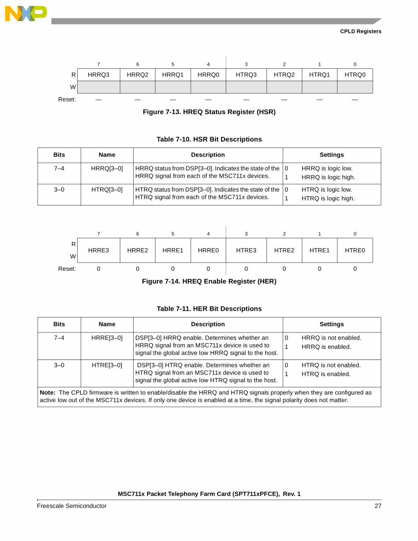
• HREQ status register (HSR), page 27
• HREQ enable register (HER), page 27
• Interrupt from DSP status register (ISR), page 28
• Interrupt from DSP enable register (IER), page 28
• Firmware version register (FVR), page 28
ISR 0x18004 HDI16 interface status register
Tx/Rx[0–3] 0x1A000 HDI16 transmit/receive data registers
DSP broadcast All four digital signal processors
ICR 0x20000 HDI16 interface control register
CVR 0x20002 HDI16 command vector register
ISR 0x20004 HDI16 interface status register
Tx/Rx[0–3] 0x22000 HDI16 transmit/receive data registers
Ethernet switch Ethernet switch control registers
PMDATA 0x28000 16-bit packet or memory data
RDATA 0x28002 8-bit register data
ADDRL 0x28004 Low byte of 16-bit address
ADDRH 0x28006 High byte of 16-bit address
CPLD Registers Internal 8-bit CPLD control registers
RCSR 0x38000 Reset control/status register
BMCR 0x38002 Boot mode control register
HSR 0x38004 HREQ status register
HER 0x38006 HREQ enable register
ISR 0x3A000 IRQ from DSP status register
IER 0x3A002 IRQ from DSP enable register
— 0x3A004 Reserved
FVR 0x3A006 Firmware version register
Table 7. SPT711xPFCE System Memory Map (continued)
Register Offset Description
MSC711x Packet Telephony Farm Card (SPT711xPFCE), Rev. 1
26 Freescale Semiconductor
CPLD Registers
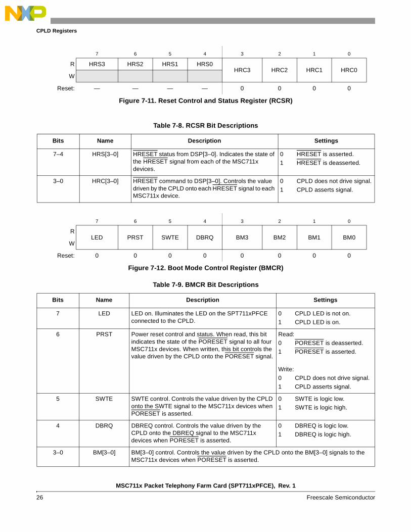
7 6 5 4 3 2 1 0
R HRS3 HRS2 HRS1 HRS0HRC3 HRC2 HRC1 HRC0
W
Reset: — — — — 0 0 0 0
Figure 7-11. Reset Control and Status Register (RCSR)
Table 7-8. RCSR Bit Descriptions
Bits Name Description Settings
7–4 HRS[3–0] HRESET status from DSP[3–0]. Indicates the state of the HRESET signal from each of the MSC711x devices.
0 HRESET is asserted.
1 HRESET is deasserted.
3–0 HRC[3–0] HRESET command to DSP[3–0]. Controls the value driven by the CPLD onto each HRESET signal to each MSC711x device.
0 CPLD does not drive signal.
1 CPLD asserts signal.
7 6 5 4 3 2 1 0
RLED PRST SWTE DBRQ BM3 BM2 BM1 BM0
W
Reset: 0 0 0 0 0 0 0 0
Figure 7-12. Boot Mode Control Register (BMCR)
Table 7-9. BMCR Bit Descriptions
Bits Name Description Settings
7 LED LED on. Illuminates the LED on the SPT711xPFCE connected to the CPLD.
0 CPLD LED is not on.
1 CPLD LED is on.
6 PRST Power reset control and status. When read, this bit indicates the state of the PORESET signal to all four MSC711x devices. When written, this bit controls the value driven by the CPLD onto the PORESET signal.
Read:
0 PORESET is deasserted.
1 PORESET is asserted.
Write:
0 CPLD does not drive signal.
1 CPLD asserts signal.
5 SWTE SWTE control. Controls the value driven by the CPLD onto the SWTE signal to the MSC711x devices when PORESET is asserted.
0 SWTE is logic low.
1 SWTE is logic high.
4 DBRQ DBREQ control. Controls the value driven by the CPLD onto the DBREQ signal to the MSC711x devices when PORESET is asserted.
0 DBREQ is logic low.
1 DBREQ is logic high.
3–0 BM[3–0] BM[3–0] control. Controls the value driven by the CPLD onto the BM[3–0] signals to the MSC711x devices when PORESET is asserted.
MSC711x Packet Telephony Farm Card (SPT711xPFCE), Rev. 1
Freescale Semiconductor 27
CPLD Registers
7 6 5 4 3 2 1 0
R HRRQ3 HRRQ2 HRRQ1 HRRQ0 HTRQ3 HTRQ2 HTRQ1 HTRQ0
W
Reset: — — — — — — — —
Figure 7-13. HREQ Status Register (HSR)
Table 7-10. HSR Bit Descriptions
Bits Name Description Settings
7–4 HRRQ[3–0] HRRQ status from DSP[3–0]. Indicates the state of the HRRQ signal from each of the MSC711x devices.
0 HRRQ is logic low.
1 HRRQ is logic high.
3–0 HTRQ[3–0] HTRQ status from DSP[3–0]. Indicates the state of the HTRQ signal from each of the MSC711x devices.
0 HTRQ is logic low.
1 HTRQ is logic high.
7 6 5 4 3 2 1 0
RHRRE3 HRRE2 HRRE1 HRRE0 HTRE3 HTRE2 HTRE1 HTRE0
W
Reset: 0 0 0 0 0 0 0 0
Figure 7-14. HREQ Enable Register (HER)
Table 7-11. HER Bit Descriptions
Bits Name Description Settings
7–4 HRRE[3–0] DSP[3–0] HRRQ enable. Determines whether an HRRQ signal from an MSC711x device is used to signal the global active low HRRQ signal to the host.
0 HRRQ is not enabled.
1 HRRQ is enabled.
3–0 HTRE[3–0] DSP[3–0] HTRQ enable. Determines whether an HTRQ signal from an MSC711x device is used to signal the global active low HTRQ signal to the host.
0 HTRQ is not enabled.
1 HTRQ is enabled.
Note: The CPLD firmware is written to enable/disable the HRRQ and HTRQ signals properly when they are configured as active low out of the MSC711x devices. If only one device is enabled at a time, the signal polarity does not matter.
MSC711x Packet Telephony Farm Card (SPT711xPFCE), Rev. 1
28 Freescale Semiconductor
CPLD Registers
7 6 5 4 3 2 1 0
R IRQ3 IRQ2 IRQ1 IRQ0 — — — —
W
Reset: — — — — 0 0 0 0
Figure 7-15. Interrupt from DSP Status Register (ISR)
Table 7-12. ISR Bit Descriptions
Bits Name Description Settings
7–4 IRQ[3–0] Interrupt request from DSP[3–0]. Shows the interrupt status from each MSC711x device. The Event2 pin from each MSC711x device signals interrupts to the host.
0 Requesting interrupt.
1 Not requesting interrupt.
3–0 — Reserved. Cleared to zero for future compatibility.
7 6 5 4 3 2 1 0
RIE3 IE2 IE1 IE0
— — — —
W
Reset: 0 0 0 0 0 0 0 0
Figure 7-16. Interrupt from DSP Enable Register (IER)
Table 7-13. IER Bit Descriptions
Bits Name Description Settings
7–4 IE[3–0] Interrupt request from DSP[3–0] enable. Determines whether an IRQ signal from an MSC711x device is used to signal the global active low IRQ signal to the host.
0 Request is disabled.
1 Request is enabled.
3–0 — Reserved. Cleared to zero for future compatibility.
Note: The CPLD firmware is written to enable/disable the IRQ signals properly when they are configured as active low out of the MSC711x devices. If only one device is enabled at a time, the signal polarity does not matter.
7 6 5 4 3 2 1 0
R BV1 BV0 MV2 MV1 MV0 mV2 mV1 mV0
W
Reset: — — — — — — — —
Figure 7-17. Firmware Version Register (FVR)

MSC711x Packet Telephony Farm Card (SPT711xPFCE), Rev. 1
Freescale Semiconductor 29
CPLD Registers
Table 7-14. FVR Bit Descriptions
Bits Name Description Settings
7–6 BV[1–0] Board version. Indicates the board revision level as programmed into the CPLD firmware.
5–3 MV[2–0] Major version. Indicates the firmware major revision level.
2–0 mV[2–0] Minor version. Indicates the firmware minor revision level.

MSC711x Packet Telephony Farm Card (SPT711xPFCE), Rev. 1
30 Freescale Semiconductor
CPLD Firmware
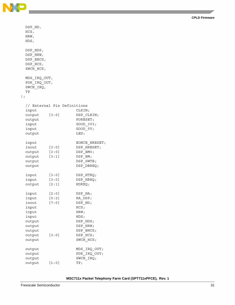
Appendix A CPLD Firmware
/* Copyright 2005, All Rights Reserved, Freescale Semiconductor, Inc. *//**************************************************************************** PROJECT : MSC711xPFC Revision 2 CPLD (Xilinx XC9572XL-10TQG100C) MODULE : TOPLEVEL NOTES : All bus control signals are active-low (CS, DS, RW, etc.). AUTHOR : David M. Koltak 10/17/2005 VER DATE AUTHOR -DESCRIPTION-----------------------------------------------------------------------------0.1 10/17/2005 David M. Koltak -Initial Design1.0 10/18/2005 David M. Koltak -Compiles without warnings or errors1.1 10/19/2005 David M. Koltak -IDMA Mode, BM Reset I2C, Clock Loop1.2 10/19/2005 David M. Koltak -Changed BM0 so default=0, output=11.3 11/07/2005 David M. Koltak -Changed default BM back to 0x0 -Changed clock assignments2.0 01/30/2006 David M. Koltak -Changed HDREQ equations -Added Firmware Version Register -Removed IDMA Mode3.0 04/19/2006 David M. Koltak -Updated for production boards (V2.7)****************************************************************************/
‘define BOARD_VERSION 2’d1‘define MAJOR_VERSION 3’d3‘define MINOR_VERSION 3’d0
module TOPLEVEL( CLKIN, DSP_CLKIN, PORESET, GOOD_3V3, GOOD_5V, LED, EONCE_HRESET, DSP_HRESET, DSP_BM0, DSP_BM, DSP_SWTE, DSP_DBREQ, DSP_HTRQ, DSP_HRRQ, HDREQ, DSP_HA, HA_DSP,
MSC711x Packet Telephony Farm Card (SPT711xPFCE), Rev. 1
Freescale Semiconductor 31
CPLD Firmware
DSP_HD, HCS, HRW, HDS, DSP_HDS, DSP_HRW, DSP_BHCS, DSP_HCS, SWCH_HCS, MDS_IRQ_OUT, PDK_IRQ_OUT, SWCH_IRQ, TP);
// External Pin Definitions input CLKIN; output [3:0] DSP_CLKIN; output PORESET; input GOOD_3V3; input GOOD_5V; output LED; input EONCE_HRESET; inout [3:0] DSP_HRESET; output [3:0] DSP_BM0; output [3:1] DSP_BM; output DSP_SWTE; output DSP_DBREQ; input [3:0] DSP_HTRQ; input [3:0] DSP_HRRQ; output [2:1] HDREQ; input [2:0] DSP_HA; input [0:2] HA_DSP; inout [7:0] DSP_HD; input HCS; input HRW; input HDS; output DSP_HDS; output DSP_HRW; output DSP_BHCS; output [3:0] DSP_HCS; output SWCH_HCS; output MDS_IRQ_OUT; output PDK_IRQ_OUT; output SWCH_IRQ; output [1:0] TP;
MSC711x Packet Telephony Farm Card (SPT711xPFCE), Rev. 1
32 Freescale Semiconductor
CPLD Firmware
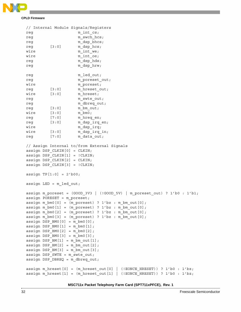
// Internal Module Signals/Registers reg m_int_cs; reg m_swch_hcs; reg m_dsp_bhcs; reg [3:0] m_dsp_hcs; wire m_int_we; wire m_int_oe; reg m_dsp_hds; reg m_dsp_hrw; reg m_led_out; reg m_poreset_out; wire m_poreset; reg [3:0] m_hreset_out; wire [3:0] m_hreset; reg m_swte_out; reg m_dbreq_out; reg [3:0] m_bm_out; wire [3:0] m_bm0; reg [7:0] m_hreq_en; reg [3:0] m_dsp_irq_en; wire m_dsp_irq; wire [3:0] m_dsp_irq_in; reg [7:0] m_data_out; // Assign Internal to/from External Signals assign DSP_CLKIN[0] = CLKIN; assign DSP_CLKIN[1] = !CLKIN; assign DSP_CLKIN[2] = CLKIN; assign DSP_CLKIN[3] = !CLKIN; assign TP[1:0] = 2’b00; assign LED = m_led_out; assign m_poreset = (GOOD_3V3 | (!GOOD_5V) | m_poreset_out) ? 1’b0 : 1’b1; assign PORESET = m_poreset; assign m_bm0[0] = (m_poreset) ? 1’bz : m_bm_out[0]; assign m_bm0[1] = (m_poreset) ? 1’bz : m_bm_out[0]; assign m_bm0[2] = (m_poreset) ? 1’bz : m_bm_out[0]; assign m_bm0[3] = (m_poreset) ? 1’bz : m_bm_out[0]; assign DSP_BM0[0] = m_bm0[0]; assign DSP_BM0[1] = m_bm0[1]; assign DSP_BM0[2] = m_bm0[2]; assign DSP_BM0[3] = m_bm0[3]; assign DSP_BM[1] = m_bm_out[1]; assign DSP_BM[2] = m_bm_out[2]; assign DSP_BM[3] = m_bm_out[3]; assign DSP_SWTE = m_swte_out; assign DSP_DBREQ = m_dbreq_out; assign m_hreset[0] = (m_hreset_out[0] | (!EONCE_HRESET)) ? 1’b0 : 1’bz; assign m_hreset[1] = (m_hreset_out[1] | (!EONCE_HRESET)) ? 1’b0 : 1’bz;
MSC711x Packet Telephony Farm Card (SPT711xPFCE), Rev. 1
Freescale Semiconductor 33
CPLD Firmware
assign m_hreset[2] = (m_hreset_out[2] | (!EONCE_HRESET)) ? 1’b0 : 1’bz; assign m_hreset[3] = (m_hreset_out[3] | (!EONCE_HRESET)) ? 1’b0 : 1’bz; assign DSP_HRESET = m_hreset; assign HDREQ[2] = (DSP_HRRQ[3] | (!m_hreq_en[7])) & (DSP_HRRQ[2] | (!m_hreq_en[6])) & (DSP_HRRQ[1] | (!m_hreq_en[5])) & (DSP_HRRQ[0] | (!m_hreq_en[4]));
assign HDREQ[1] = (DSP_HTRQ[3] | (!m_hreq_en[3])) & (DSP_HTRQ[2] | (!m_hreq_en[2])) & (DSP_HTRQ[1] | (!m_hreq_en[1])) & (DSP_HTRQ[0] | (!m_hreq_en[0])); assign m_dsp_irq_in[3:0] = ~(DSP_BM0[3:0]); // Bitwise Not assign m_dsp_irq = (m_dsp_irq_in[3] | (!m_dsp_irq_en[3])) & (m_dsp_irq_in[2] | (!m_dsp_irq_en[2])) & (m_dsp_irq_in[1] | (!m_dsp_irq_en[1])) & (m_dsp_irq_in[0] | (!m_dsp_irq_en[0])); assign MDS_IRQ_OUT = (m_dsp_irq) ? 1’b0 : 1’bz; assign PDK_IRQ_OUT = (m_dsp_irq) ? 1’b0 : 1’bz; assign SWCH_IRQ = 1’b1; // DSP/Switch Bus Control (Single or Dual Strobe) assign DSP_HDS = m_dsp_hds; assign DSP_HRW = m_dsp_hrw; always @ * begin if (!m_swch_hcs) // Dual Strobe for Switch begin m_dsp_hds = HDS | HRW; // #IOW m_dsp_hrw = HDS | (!HRW); // #IOR end else // Single Strobe for DSPs begin m_dsp_hds = HDS; m_dsp_hrw = HRW; end end // Chip Select Logic // 0-3 : DSP 0-3 // 4 : DSP Broadcast // 5 : Ethernet Switch // 7 : CPLD Registers assign SWCH_HCS = m_swch_hcs; assign DSP_BHCS = m_dsp_bhcs; assign DSP_HCS = m_dsp_hcs; always @ * begin case (HA_DSP) 3’d0: {m_int_cs, m_swch_hcs, m_dsp_bhcs, m_dsp_hcs} <= {6’b111111, HCS};
MSC711x Packet Telephony Farm Card (SPT711xPFCE), Rev. 1
34 Freescale Semiconductor
CPLD Firmware
3’d1: {m_int_cs, m_swch_hcs, m_dsp_bhcs, m_dsp_hcs} <= {5’b11111, HCS, 1’b1}; 3’d2: {m_int_cs, m_swch_hcs, m_dsp_bhcs, m_dsp_hcs} <= {4’b1111, HCS, 2’b11}; 3’d3: {m_int_cs, m_swch_hcs, m_dsp_bhcs, m_dsp_hcs} <= {3’b111, HCS, 3’b111}; 3’d4: {m_int_cs, m_swch_hcs, m_dsp_bhcs, m_dsp_hcs} <= {2’b11, HCS, 4’b1111}; 3’d5: {m_int_cs, m_swch_hcs, m_dsp_bhcs, m_dsp_hcs} <= {1’b1, HCS, 5’b11111}; // No 6, default. 3’d7: {m_int_cs, m_swch_hcs, m_dsp_bhcs, m_dsp_hcs} <= {HCS, 6’b111111}; default: {m_int_cs, m_swch_hcs, m_dsp_bhcs, m_dsp_hcs} <= 7’b1111111; endcase end // Internal Registers (Write Logic) assign m_int_we = (m_int_cs | HDS | HRW); always @ (negedge m_int_we or negedge GOOD_3V3) begin if (!GOOD_3V3) begin m_led_out <= 1’b0; m_poreset_out <= 1’d0; m_hreset_out <= 4’d0; m_swte_out <= 1’d0; m_dbreq_out <= 1’d0; m_bm_out <= 4’d0; m_hreq_en <= 8’d0; m_dsp_irq_en <= 4’d0; end else begin case (DSP_HA) // RESET CONTROL/STATUS REGISTER 3’d0: {m_hreset_out} <= DSP_HD[3:0]; // BOOT MODE CONTROL REGISTER 3’d1: {m_led_out, m_poreset_out, m_swte_out,
m_dbreq_out, m_bm_out} <= {DSP_HD[7:0]}; // HREQ ENABLE REGISTER 3’d3: m_hreq_en <= DSP_HD[7:0]; // IRQ FROM DSP ENABLE REGISTER 3’d5: m_dsp_irq_en <= DSP_HD[7:4]; default: ; endcase end end // Internal Registers and Status (Read Logic) assign DSP_HD = m_data_out; assign m_int_oe = (m_int_cs | HDS | (!HRW)); always @ * begin if (m_int_oe) begin m_data_out <= 8’hzz; end

MSC711x Packet Telephony Farm Card (SPT711xPFCE), Rev. 1
Freescale Semiconductor 35
CPLD Firmware
else begin case (DSP_HA) // RESET CONTROL/STATUS REGISTER 3’d0: m_data_out <= {DSP_HRESET, m_hreset_out}; // BOOT MODE CONTROL REGISTER 3’d1: m_data_out <= {m_led_out, (!PORESET), m_swte_out,
m_dbreq_out, m_bm_out[3:0]}; // HREQ STATUS REGISTER 3’d2: m_data_out <= {DSP_HRRQ, DSP_HTRQ}; // HREQ ENABLE REGISTER 3’d3: m_data_out <= m_hreq_en; // IRQ FROM DSP STATUS REGISTER 3’d4: m_data_out <= {m_dsp_irq_in, 4’d0}; // IRQ FROM DSP ENABLE REGISTER 3’d5: m_data_out <= {m_dsp_irq_en, 4’d0}; // FIRMWARE VERSION REGISTER 3’d7: m_data_out <= {‘BOARD_VERSION, ‘MAJOR_VERSION, ‘MINOR_VERSION}; default: m_data_out <= 8’d0; endcase end end endmodule
MSC711x Packet Telephony Farm Card (SPT711xPFCE), Rev. 1
36 Freescale Semiconductor
SPT711xPFCE Schematics
Appendix B SPT711xPFCE Schematics
5
5
4
4
3
3
2
2
1
1
D D
C C
B B
A A
Title
Size Document Number Rev
Date: Sheet of
MSC711xPFC_REV2.dsn - dmk 2.7
MSC711xPFC REV2 - TITLE
B
1 19Friday, February 17, 2006
Title
Size Document Number Rev
Date: Sheet of
MSC711xPFC_REV2.dsn - dmk 2.7
MSC711xPFC REV2 - TITLE
B
1 19Friday, February 17, 2006
Title
Size Document Number Rev
Date: Sheet of
MSC711xPFC_REV2.dsn - dmk 2.7
MSC711xPFC REV2 - TITLE
B
1 19Friday, February 17, 2006
FREESCALE SEMICONDUCTOR, INC.
NCSD SystemsAustin, Tx
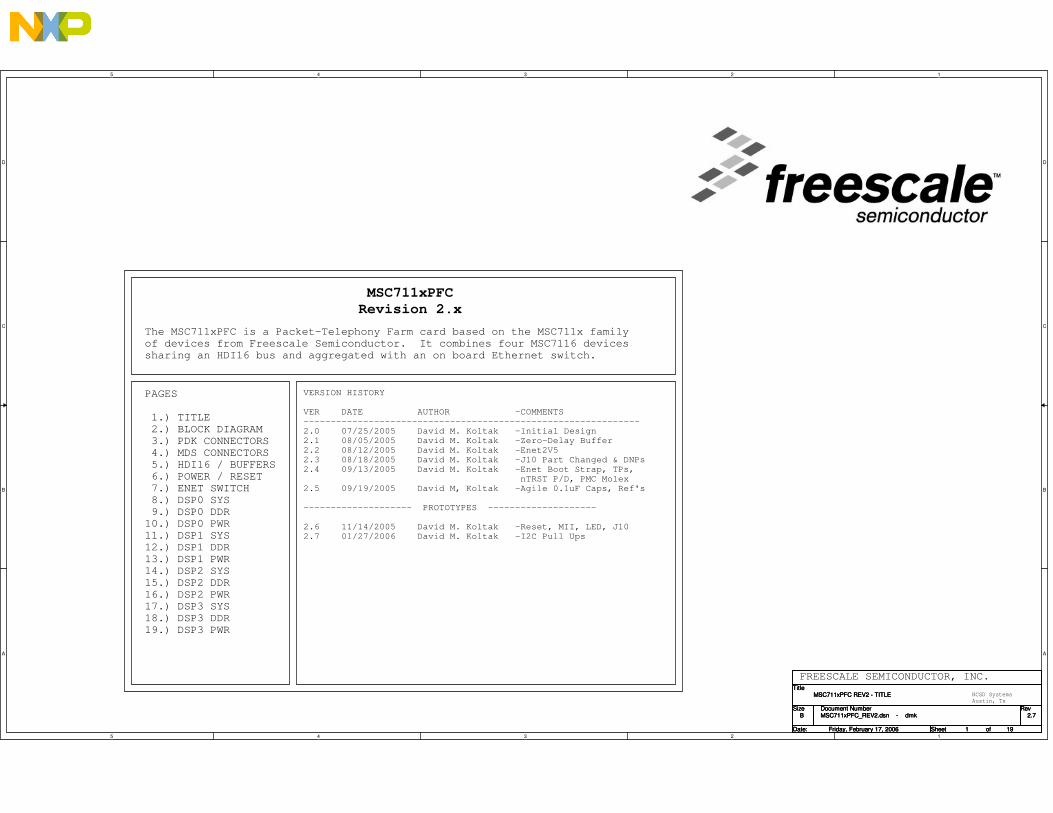
MSC711xPFCRevision 2.x
The MSC711xPFC is a Packet-Telephony Farm card based on the MSC711x family of devices from Freescale Semiconductor. It combines four MSC7116 devicessharing an HDI16 bus and aggregated with an on board Ethernet switch.
PAGES
1.) TITLE 2.) BLOCK DIAGRAM 3.) PDK CONNECTORS 4.) MDS CONNECTORS 5.) HDI16 / BUFFERS 6.) POWER / RESET 7.) ENET SWITCH 8.) DSP0 SYS 9.) DSP0 DDR10.) DSP0 PWR11.) DSP1 SYS12.) DSP1 DDR13.) DSP1 PWR14.) DSP2 SYS15.) DSP2 DDR16.) DSP2 PWR17.) DSP3 SYS18.) DSP3 DDR19.) DSP3 PWR
VERSION HISTORY
VER DATE AUTHOR -COMMENTS--------------------------------------------------------------2.0 07/25/2005 David M. Koltak -Initial Design2.1 08/05/2005 David M. Koltak -Zero-Delay Buffer2.2 08/12/2005 David M. Koltak -Enet2V52.3 08/18/2005 David M. Koltak -J10 Part Changed & DNPs2.4 09/13/2005 David M. Koltak -Enet Boot Strap, TPs, nTRST P/D, PMC Molex2.5 09/19/2005 David M, Koltak -Agile 0.1uF Caps, Ref's
-------------------- PROTOTYPES --------------------
2.6 11/14/2005 David M. Koltak -Reset, MII, LED, J102.7 01/27/2006 David M. Koltak -I2C Pull Ups
5
5
4
4
3
3
2
2
1
1
D D
C C
B B
A A
Title
Size Document Number Rev
Date: Sheet of
MSC711xPFC_REV2.dsn - dmk 2.7
MSC711xPFC REV2 - BLOCK DIAGRAM
B
2 19Friday, February 17, 2006
Title
Size Document Number Rev
Date: Sheet of
MSC711xPFC_REV2.dsn - dmk 2.7
MSC711xPFC REV2 - BLOCK DIAGRAM
B
2 19Friday, February 17, 2006
Title
Size Document Number Rev
Date: Sheet of
MSC711xPFC_REV2.dsn - dmk 2.7
MSC711xPFC REV2 - BLOCK DIAGRAM
B
2 19Friday, February 17, 2006
NCSD SystemsAustin, Tx
FREESCALE SEMICONDUCTOR, INC.
MSC7116 DDR
16-bit
MSC7116 DDR
16-bit
MSC7116 DDR
16-bit
MSC7116 DDR
16-bit
CPLD
16-bit (HDI16)8-bit (HDI16)
BUFFER
TDM Bus
SPI EEPROM
SPI EEPROM
SPI EEPROM
SPI EEPROM
ETHERNET SWITCH
RMII
RMII
RMII
RMII
PD
K C
ON
NE
CTO
RS
MD
S C
ON
NE
CTO
RS
RMII
RMII
RMII
MII
MII
PAGE 7
PAGE 5
PAGE 8-10
PAGE 11-13
PAGE 14-16
PAGE 17-19
PAGE 4
PAGE 3
PAGE 5
DC-DC SWITCHING
DC-DC LINEAR
DC-DC LINEAR
5V
3V31V2
2V5 (DDR)
ENET_2V5
I2C EEPROM
PAGE 6
PAGE 6
I2C EEPROM
PAGE 6
CPLD DSP 3 DSP 2 DSP 1 DSP 0TDI
TDO
5
5
4
4
3
3
2
2
1
1
D D
C C
B B
A A
HD0HD1
HD2HD3
HD4HD5
HD6HD7
HD8
HD9
HD10HD11
HD12HD13
HD14HD15
HA1
HA2HA3
HA_DSP0
HA_DSP1HA_DSP2
PDK_MII2_RXD0PDK_MII2_RXD1PDK_MII2_RXD2
PDK_MII2_RXD3
PDK_MII2_TXD0PDK_MII2_TXD1PDK_MII2_TXD2PDK_MII2_TXD3
PDK_MII1_TXD0PDK_MII1_TXD1PDK_MII1_TXD2PDK_MII1_TXD3
PDK_MII1_RXD0PDK_MII1_RXD1PDK_MII1_RXD2
PDK_MII1_RXD3
5V 3V33V33V3
3V3
HD[0:15]4,5
HA[1:3]4,5
HRW4,5HDS4,5
HCS4,5
HA_DSP[0:2] 4,5
PDK_IRQ_OUT5
HDREQ15HDREQ25
PDK_MII2_RXD[3:0]7 PDK_MII2_RXDV7PDK_MII2_TCLK7
PDK_MII2_RXER7PDK_MII2_CRS7PDK_MII2_RCLK7
PDK_MII2_TXD[3:0]7
PDK_MII1_RXDV7PDK_MII1_RXD[3:0]7
PDK_MII1_TXEN 7
PDK_MII1_COL 7
PDK_MII2_TXEN 7
PDK_MII2_COL 7
PDK_MII1_RXER7PDK_MII1_CRS7PDK_MII1_RCLK7
PDK_MII1_TCLK7
PDK_MII1_TXD[3:0]7
SWCH_MDIO 4,7
SWCH_MDC 4,7
CT_FRAME_A 4,5
CT_C8_A 4,5
CT_D4 4,8,11,14,17
CT_D0 4,8,11,14,17
RMII_REFCLK1 5
PDK_RMII_TXEN7PDK_RMII_CSDV7
CT_D14,8,11,14,17
CT_D54,8,11,14,17
EONCE_TMS_IN 5
EONCE_nTRST 8,11,14,17
EONCE_TDI5EONCE_TDO8EONCE_TCK_IN5
EONCE_HRESET5PDK_MII1_RCLK7
SWCH_HCLK7
PDK_MII2_TCLK7
PDK_MII2_RCLK7
PDK_RMII_TXD17PDK_RMII_TXD07
PDK_RMII_RXD17PDK_RMII_RXD07
PDK_MII1_TCLK7
Title
Size Document Number Rev
Date: Sheet of
MSC711xPFC_REV2.dsn - dmk 2.7
MSC711xPFC REV2 - PDK CONNECTORS
B
3 19Friday, February 17, 2006
Title
Size Document Number Rev
Date: Sheet of
MSC711xPFC_REV2.dsn - dmk 2.7
MSC711xPFC REV2 - PDK CONNECTORS
B
3 19Friday, February 17, 2006
Title
Size Document Number Rev
Date: Sheet of
MSC711xPFC_REV2.dsn - dmk 2.7
MSC711xPFC REV2 - PDK CONNECTORS
B
3 19Friday, February 17, 2006
NCSD SystemsAustin, Tx
FREESCALE SEMICONDUCTOR, INC.
EONCE
EONCE
J2
J1
J3
J10
1 2R30 1K +/-5%R30 1K +/-5%
13579111315171921232527293133353739414345474951535557596163
2468
10121416182022242628303234363840424446485052545658606264
J3
HDR_2X32
J3
HDR_2X32
13579111315171921232527293133353739414345474951535557596163
2468
10121416182022242628303234363840424446485052545658606264
J2
HDR_2X32
J2
HDR_2X32
1 2R43 1K +/-5%R43 1K +/-5%1
2
R901K+/-5%
R901K+/-5%
12
R501K+/-5%
R501K+/-5%
1 2R34 1K +/-5%R34 1K +/-5%
13579111315171921232527293133353739414345474951535557596163
2468
10121416182022242628303234363840424446485052545658606264
J1
HDR_2X32
J1
HDR_2X32
13579
246810
1311
1412
GND
KEYTMSNCTRST
TDITDOTCKNCRSTVDDNC
GNDGND
J10
HDR14
GND
KEYTMSNCTRST
TDITDOTCKNCRSTVDDNC
GNDGND
J10
HDR14
12
R440 OHM+/-5%
R440 OHM+/-5%
12
R421K+/-5%
R421K+/-5%
13579111315171921232527293133353739414345474951535557596163
2468
10121416182022242628303234363840424446485052545658606264
J5
HDR_2X32
J5
HDR_2X32
1 2R19 1K +/-5%R19 1K +/-5%

5
5
4
4
3
3
2
2
1
1
D D
C C
B B
A A
HD0HD2
HD4HD6HD8HD10
HD12HD14
HA_DSP0HA_DSP2
HA1
HA3
HD1HD3HD5HD7
HD9HD11HD13HD15
HA_DSP1
HA2
HD0HD1HD2HD3HD4HD5HD6HD7HD8HD9HD10HD11HD12HD13HD14HD15
HA_DSP0HA_DSP1HA_DSP2
HA1HA2HA3
5V3V33V3
MDS_RMII2_CSDV 7
MDS_RMII2_TXEN7
SWCH_MDC3,7
SWCH_MDIO3,7
MDS_IRQ_OUT 5
RMII_REFCLK4 5
HRW 3,5HDS 3,5
HCS3,5
HD[0:15]3,5
HA_DSP[0:2]3,5
HA[1:3]3,5
MDS_RMII2_TXD0 7
MDS_RMII2_RXD07
MDS_RMII1_TXD07
MDS_RMII1_CSDV7
MDS_RMII1_TXD17MDS_RMII1_RXD17
MDS_RMII1_RXD07MDS_RMII1_TXEN7
CT_D5 3,8,11,14,17
CT_FRAME_A 3,5
CT_D13,8,11,14,17CT_D4 3,8,11,14,17CT_D03,8,11,14,17
CT_C8_A3,5CT_FRAME_A3,5
CT_C8_A 3,5
CT_C8_A 3,5
CT_FRAME_A 3,5
MDS_RMII2_TXD1 7
MDS_RMII2_RXD1 7
Title
Size Document Number Rev
Date: Sheet of
MSC711xPFC_REV2.dsn - dmk 2.7
MSC711xPFC REV2 - MDS CONNECTORS
B
4 19Friday, February 17, 2006
Title
Size Document Number Rev
Date: Sheet of
MSC711xPFC_REV2.dsn - dmk 2.7
MSC711xPFC REV2 - MDS CONNECTORS
B
4 19Friday, February 17, 2006
Title
Size Document Number Rev
Date: Sheet of
MSC711xPFC_REV2.dsn - dmk 2.7
MSC711xPFC REV2 - MDS CONNECTORS
B
4 19Friday, February 17, 2006
FREESCALE SEMICONDUCTOR, INC.
NCSD SystemsAustin, Tx
J6
J7
J9
J8
13579111315171921232527293133353739414345474951535557596163
2468
10121416182022242628303234363840424446485052545658606264
J9
HDR_2X32
J9
HDR_2X32
13579111315171921232527293133353739414345474951535557596163
2468
10121416182022242628303234363840424446485052545658606264
J6
HDR_2X32
J6
HDR_2X32
13579111315171921232527293133353739414345474951535557596163
2468
10121416182022242628303234363840424446485052545658606264
J7
HDR_2X32
J7
HDR_2X32
13579111315171921232527293133353739414345474951535557596163
2468
10121416182022242628303234363840424446485052545658606264
J8
HDR_2X32
J8
HDR_2X32
5
5
4
4
3
3
2
2
1
1
D D
C C
B B
A A
HD15HD14HD13HD12HD11HD10HD9HD8
HD7HD6HD5HD4HD3HD2HD1HD0DSP_HD15
DSP_HD12DSP_HD11DSP_HD10DSP_HD9DSP_HD8
DSP_HD7DSP_HD6DSP_HD5DSP_HD4DSP_HD3DSP_HD2DSP_HD1DSP_HD0
DSP_HD14DSP_HD13
CPLD_CLKIN
DSP_HD0DSP_HD1DSP_HD2DSP_HD3DSP_HD4DSP_HD5DSP_HD6DSP_HD7
DSP_HA0DSP_HA1DSP_HA2
CPLD_CLKIN
HA3HA2HA1
DSP_HA0DSP_HA1DSP_HA2
HA_DSP0HA_DSP1HA_DSP2
3V3
3V3
3V33V3
3V3
3V3
3V3
3V3
3V3
3V3
3V3
5V
DSP_HD[15:0]7,8,11,14,17
HRW3,4HDS3,4
EONCE_TCK 8,11,14,17EONCE_TDI 3
CPLD_TDO 17
EONCE_TMS 8,11,14,17
DSP0_HRESET 8DSP1_HRESET 11DSP2_HRESET 14DSP3_HRESET 17EONCE_HRESET 3
DSP_HD[15:0]7,8,11,14,17 HD[0:15] 3,4
HCS3,4HRW3,4
PORESET 7,8,11,14,17
DSP0_BM0 8
DSP_SWTE 8,11,14,17DSP_DBREQ 8,11,14,17
DSP3_CLKIN 17DSP2_CLKIN 14DSP1_CLKIN 11DSP0_CLKIN 8
DSP_C8_1 8,11DSP_FRAME 8,11,14,17
CT_C8_A3,4CT_FRAME_A3,4
DSP_BM2 8,11,14,17DSP_BM3 8,11,14,17
DSP_HA[2:0] 7,8,11,14,17
DSP_HDS7,8,11,14,17DSP_HRW7,8,11,14,17
HA[1:3]3,4 DSP_HA[2:0] 7,8,11,14,17
RMII_REFCLK7
RMII_REFCLK1 3
RMII_REFCLK2 8,11
DSP_BM1 8,11,14,17
DSP1_BM0 11
DSP2_BM0 14
DSP3_BM0 17
DSP1_HTRQ 11
DSP2_HTRQ 14
DSP3_HTRQ 17
DSP0_HTRQ 8
DSP1_HRRQ 11
DSP2_HRRQ 14
DSP3_HRRQ 17
DSP0_HRRQ 8
HDREQ2 3HDREQ1 3
HA_DSP[0:2]3,4
SWCH_HCS7DSP3_HCS17DSP2_HCS14DSP1_HCS11DSP0_HCS8
MDS_IRQ_OUT4PDK_IRQ_OUT3SWCH_IRQ7
DSP_BHCS8,11,14,17CPLD_LED6
RMII_REFCLK3 14,17
RMII_REFCLK4 4
EONCE_TCK_IN3EONCE_TMS_IN3
EONCE_TCK 8,11,14,17EONCE_TMS 8,11,14,17DSP_C8_2 14,17
HCS 3,4
3V3_GOOD6
Title
Size Document Number Rev
Date: Sheet of
MSC711xPFC_REV2.dsn - dmk 2.7
MSC711xPFC REV2 - HDI16 / BUFFERS
B
5 19Friday, February 17, 2006
Title
Size Document Number Rev
Date: Sheet of
MSC711xPFC_REV2.dsn - dmk 2.7
MSC711xPFC REV2 - HDI16 / BUFFERS
B
5 19Friday, February 17, 2006
Title
Size Document Number Rev
Date: Sheet of
MSC711xPFC_REV2.dsn - dmk 2.7
MSC711xPFC REV2 - HDI16 / BUFFERS
B
5 19Friday, February 17, 2006
FREESCALE SEMICONDUCTOR, INC.
NCSD SystemsAustin, Tx
SIGNAL BUFFERS
HDI16 BUS BUFFER
OSCILLATOR
PROGRAMMABLE LOGIC
CLK Delay Loops
REFCLK1 -> PDKREFCLK2 -> DSP0 & DSP1REFCLK3 -> DSP2 & DSP3REFCLK4 -> MDS
DNP
12
R1181K+/-5%
R1181K+/-5%
1 2R181 0 OHM +/-5%R181 0 OHM +/-5%
1 2R250 22ohm +/-5%R250 22ohm +/-5%
A047
A146
A244
A343
A441
A540
A638
A737
A836
A935
A1033
A1132
A1230
A1329
A1427
A1526
B0 2
B1 3
B2 5
B3 6
B4 8
B5 9
B6 11
B7 12
B8 13
B9 14
B10 16
B11 17
B12 19
B13 20
B14 22
B15 23
GND0 4
GND1 10
GND2 15
GND3 21
GND4 28
GND5 34
GND6 39
GND7 45
VCC07
VCC118
VCC231
VCC342
nOE_048
nOE_125
T/nR_01
T/nR_124
T-><-R
U12
74LCXR162245
T-><-R
U12
74LCXR162245
TP504TP504
TP507TP507
1 2R111 22ohm +/-5%R111 22ohm +/-5%
12
R1871K+/-5%
R1871K+/-5%
12
C5880.1uF C5880.1uF
1 2R86 22ohm +/-5%R86 22ohm +/-5%
1 2R185 22ohm +/-5%R185 22ohm +/-5%
1 2R191 22ohm +/-5%R191 22ohm +/-5%
12
C5450.1uF C5450.1uF
1 2R101 22ohm +/-5%R101 22ohm +/-5% 1 2
R256 22ohm +/-5%R256 22ohm +/-5%
1 2R241 22ohm +/-5%R241 22ohm +/-5%
1 2R255 22ohm +/-5%R255 22ohm +/-5%
12
R1761K+/-5%
R1761K+/-5%
REF1
CLKOUT8
VD
D6
GN
D4
CLK1 3
CLK2 2
CLK3 5
CLK4 7
U17
CY2305CSXC-1
U17
CY2305CSXC-1
1 2R188 22ohm +/-5%R188 22ohm +/-5%
1 2R94 22ohm +/-5%R94 22ohm +/-5%
12
C5920.1uF C5920.1uF
O1 18
O2 17
O3 16
O4 15
O5 14
O6 13
O7 12
O8 11
G11
D12
D23
D34
D45
D56
D67
D78
D89
G219
VD
D1
20G
ND
10
U1
74LCX541
U1
74LCX541
12
C5890.1uF C5890.1uF
B1-C116
B1-C213
B1-C318
B1-C420
B1-C514
B1-C615
B1-C725
B1-C817
B1-C9,GCK122
B1-C1028
B1-C11,GCK223
B1-C1233
B1-C1336
B1-C14,GCK327
B1-C1529
B1-C1639
B1-C1730
B1-C1840
B2-C187
B2-C294
B2-C391
B2-C493
B2-C595
B2-C696
B2-C7,GTS13
B2-C897
B2-C9,GSR99
B2-C101
B2-C11,GTS24
B2-C126
B2-C138
B2-C149
B2-C1511 B2-C1610
B2-C1712
B2-C1892
B3-C1 41
B3-C2 32
B3-C3 49B3-C4 50
B3-C5 35
B3-C6 53B3-C7 54
B3-C8 37
B3-C9 42
B3-C10 60
B3-C11 52
B3-C12 61B3-C13 63
B3-C14 55B3-C15 56
B3-C16 64
B3-C17 58B3-C18 59
B4-C1 65
B4-C2 67
B4-C3 71B4-C4 72
B4-C5 68
B4-C6 76B4-C7 77
B4-C8 70
B4-C9 66
B4-C10 81
B4-C11 74
B4-C12 82B4-C13 85
B4-C14 78
B4-C15 89
B4-C16 86
B4-C17 90
B4-C18 79
GN
D0
21
GN
D1
31
GN
D2
44
GN
D3
62
GN
D4
69
GN
D5
75
GN
D6
84
GN
D7
100
NC
_02
NC
_17
NC
_219
NC
_324
NC
_434
NC
_543
NC
_646
NC
_773
NC
_880
VC
Cin
t05
VC
Cin
t157
VC
Cin
t298
VC
Cio
026
VC
Cio
138
VC
Cio
251
VC
Cio
388
TCK
48
TDI
45
TDO
83
TMS
47
BLOCK 2
BLOCK 1
BLOCK 3
BLOCK 4
U11
XC9572XL-10TQG100C
BLOCK 2
BLOCK 1
BLOCK 3
BLOCK 4
U11
XC9572XL-10TQG100C
12
C5940.1uF C5940.1uF
TP513TP513
1 2R186 22ohm +/-5%R186 22ohm +/-5%
12
C5930.1uF C5930.1uF
12
C5860.1uF C5860.1uF
1 2R183 22ohm +/-5%R183 22ohm +/-5%
12
C6360.1uF C6360.1uF
EN1
GND2 OUT 3
VDD 4U503
33.333 MHz
U503
33.333 MHz 1 2R74 22ohm +/-5%R74 22ohm +/-5%
1 2R179 0 OHM +/-5%R179 0 OHM +/-5%
5
5
4
4
3
3
2
2
1
1
D D
C C
B B
A A
ENET_2V5
2V5
3V3
3V3
1V25V
3V3
3V33V3
5V
3V3
2V5
ENET_2V5
1V2
5V
3V3_GOOD 5
3V3_GOOD5
SWCH_I2C_SD 7SWCH_I2C_SC 7
DSP_I2C_SD 8,11,14,17DSP_I2C_SC 8,11,14,17
DSP0_LED8
DSP1_LED11
DSP2_LED14
DSP3_LED17
CPLD_LED5
Title
Size Document Number Rev
Date: Sheet of
MSC711xPFC_REV2.dsn - dmk 2.7
MSC711xPFC REV2 - POWER / RESET
B
6 19Friday, February 17, 2006
Title
Size Document Number Rev
Date: Sheet of
MSC711xPFC_REV2.dsn - dmk 2.7
MSC711xPFC REV2 - POWER / RESET
B
6 19Friday, February 17, 2006
Title
Size Document Number Rev
Date: Sheet of
MSC711xPFC_REV2.dsn - dmk 2.7
MSC711xPFC REV2 - POWER / RESET
B
6 19Friday, February 17, 2006
NCSD SystemsAustin, Tx
FREESCALE SEMICONDUCTOR, INC.
DDR 2.5 V POWER (3A)
ENET SWITCH 2.5 V POWER (3A) MSC711x 1.2V CORE POWER (5A)
3V3 VOLTAGE DETECTOR
ENET SWITCH BOOT EEPROMDSP I2C BOOT EEPROM
"DSP 0"
"DSP 1"
"DSP 2"
"DSP 3"
"CPLD"
INDICATORS(Turn on 1V2 240ms after 3V3 reaches 2.93V)(Voltage Divider on EN will delay turn-on)
12
R221K+/-5%
R221K+/-5%
12
R331.00K+/-1%
R331.00K+/-1%
1 2R25 150 OHM +/-1%R25 150 OHM +/-1%
1 2R39 150 OHM +/-1%R39 150 OHM +/-1%
12
R980.6KR980.6K
12
R211.00K+/-1%
R211.00K+/-1%
12
+ C59110uf
+ C59110uf
12
R161K+/-5%
R161K+/-5%
TP510TP510
12
+ C3410uf
+ C3410uf
12
C370.1uF C370.1uF
TP505TP505
12
R780.6KR780.6K
12
R581K+/-5%
R581K+/-5%
TP506TP506
2 1D4
HSMG-C110
D4
HSMG-C110
12
R18010KR18010K
1 2R27 150 OHM +/-1%R27 150 OHM +/-1%
12
R291K+/-5%
R291K+/-5%
12
R181.00K+/-1%
R181.00K+/-1%
12
R571K+/-5%
R571K+/-5%
TP511TP511
IN2 OUT 4
ADJ 5
EN1
GND
3
TAB
6
U9
MIC29302WU
U9
MIC29302WU
2 1D3
HSMG-C110
D3
HSMG-C110
1 2R32 150 OHM +/-1%R32 150 OHM +/-1%
L500UP1B_1R0
L500UP1B_1R0
12
+ C17100uF
+ C17100uF
12
C590
0.1uF
C590
0.1uF
12
+ C58710uf
+ C58710uf
12
+ C4110uf
+ C4110uf
2 1D2
HSMG-C110
D2
HSMG-C110
IN2 OUT 4
ADJ 5
EN1
GND
3
TAB
6
U10
MIC29302WU
U10
MIC29302WU
TP508TP508
12
+ C947UF
+ C947UF
12
R311.00K+/-1%
R311.00K+/-1%
12
3
GND
VCC
RESETU502MAX810STRG
GND
VCC
RESETU502MAX810STRG
A01
A12
A23
GND
4
WC 7
SDA 5
SCL 6
VCC
8U20
M24256-BWMN6G
U20
M24256-BWMN6G
TP512TP512
C5851uF+/-10%
C5851uF+/-10%
12
R281.8KR281.8K
TP502TP502
2 1D5
HSMG-C110
D5
HSMG-C110
2 1D1
HSMG-C110
D1
HSMG-C110
1 2R35 150 OHM +/-1%R35 150 OHM +/-1%
12
C6540.1uF C6540.1uF
A01
A12
A23
GND
4
WC 7
SDA 5
SCL 6
VCC
8U8
M24256-BWMN6G
U8
M24256-BWMN6G
+ C351000uF+/-20%
+ C351000uF+/-20%
VIN5
ON/OFF1
GND4
VOUT_1_2 2
TRIM 3
P1-YNM05S05
U501
YNM05S05-G
P1-YNM05S05
U501
YNM05S05-G
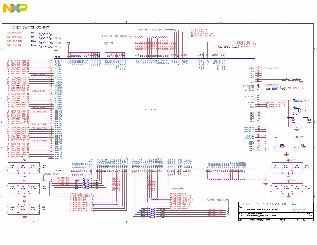
5
5
4
4
3
3
2
2
1
1
D D
C C
B B
A A
DS
P_H
D0
DS
P_H
D1
DS
P_H
D2
DS
P_H
D3
DS
P_H
D4
DS
P_H
D5
DS
P_H
D6
DS
P_H
D7
DS
P_H
D8
DS
P_H
D9
DS
P_H
D10
DS
P_H
D11
DS
P_H
D12
DS
P_H
D13
DS
P_H
D14
DS
P_H
D15
DS
P_H
A0
DS
P_H
A1
DS
P_H
A2
DSP1_RMII_RXD0
DSP1_RMII_CSDV
UNUSED_INPUT
UNUSED_INPUT
UNUSED_INPUT
PD
K_M
II2_R
XD
0P
DK
_MII2
_RX
D1
PD
K_M
II2_R
XD
2P
DK
_MII2
_RX
D3
PD
K_M
II1_R
XD
0P
DK
_MII1
_RX
D1
PD
K_M
II1_R
XD
2P
DK
_MII1
_RX
D3
UNUSED_INPUT
UNUSED_INPUT
DSP1_RMII_CSDV
DSP1_RMII_RXD0
ENET_CHIP_INIT0
ENET_CHIP_INIT1
ENET_CHIP_INIT0
ENET_CHIP_INIT1
UNUSED_INPUT
PDK_MII2_TXD0PDK_MII2_TXD1PDK_MII2_TXD2PDK_MII2_TXD3
PDK_MII1_TXD3PDK_MII1_TXD2PDK_MII1_TXD1PDK_MII1_TXD0
3V3 ENET_2V5
3V3
3V3
3V3
ENET_2V5
ENET_2V5
3V3 ENET_2V5
DSP_HD[15:0]5,8,11,14,17
DSP_HA[2:0]5,8,11,14,17
DSP_HDS 5,8,11,14,17DSP_HRW 5,8,11,14,17SWCH_HCS 5SWCH_IRQ 5
SWCH_MDC 3,4SWCH_MDIO 3,4SWCH_HCLK 3
PORESET 5,8,11,14,17
RMII_REFCLK 5
DSP0_RMII_TXEN8DSP1_RMII_TXEN11DSP2_RMII_TXEN14DSP3_RMII_TXEN17MDS_RMII1_TXEN4MDS_RMII2_TXEN4PDK_RMII_TXEN3
DSP0_RMII_RXD08DSP1_RMII_RXD011DSP2_RMII_RXD014DSP3_RMII_RXD017MDS_RMII1_RXD04MDS_RMII2_RXD04PDK_RMII_RXD03
DSP0_RMII_TXD08DSP1_RMII_TXD011DSP2_RMII_TXD014DSP3_RMII_TXD017MDS_RMII1_TXD04MDS_RMII2_TXD04PDK_RMII_TXD03
DSP0_RMII_TXD18DSP1_RMII_TXD111DSP2_RMII_TXD114DSP3_RMII_TXD117MDS_RMII1_TXD14MDS_RMII2_TXD14PDK_RMII_TXD13
DSP0_RMII_RXD18DSP1_RMII_RXD111DSP2_RMII_RXD114DSP3_RMII_RXD117MDS_RMII1_RXD14MDS_RMII2_RXD14PDK_RMII_RXD13
DSP0_RMII_CSDV8DSP1_RMII_CSDV11DSP2_RMII_CSDV14DSP3_RMII_CSDV17MDS_RMII1_CSDV4MDS_RMII2_CSDV4PDK_RMII_CSDV3
PDK_MII2_TXD[3:0] 3
PDK_MII2_RXD[3:0]3
PDK_MII2_TXEN 3
PDK_MII2_COL3PDK_MII2_CRS3PDK_MII2_RXER3
PDK_MII2_RCLK3PDK_MII2_RXDV3PDK_MII2_TCLK3
PDK_MII1_TCLK 3PDK_MII1_RXDV 3PDK_MII1_RCLK 3PDK_MII1_RXD[3:0] 3PDK_MII1_RXER 3PDK_MII1_CRS 3PDK_MII1_COL 3PDK_MII1_TXEN 3
PDK_MII1_TXD[3:0]3
SWCH_I2C_SC 6SWCH_I2C_SD 6
Title
Size Document Number Rev
Date: Sheet of
MSC711xPFC_REV2.dsn - dmk 2.7
MSC711xPFC REV2 - ENET SWITCH
B
7 19Friday, February 17, 2006
Title
Size Document Number Rev
Date: Sheet of
MSC711xPFC_REV2.dsn - dmk 2.7
MSC711xPFC REV2 - ENET SWITCH
B
7 19Friday, February 17, 2006
Title
Size Document Number Rev
Date: Sheet of
MSC711xPFC_REV2.dsn - dmk 2.7
MSC711xPFC REV2 - ENET SWITCH
B
7 19Friday, February 17, 2006
NCSD SystemsAustin, Tx
FREESCALE SEMICONDUCTOR, INC.
INTERNAL PULL-UP
ENET SWITCH CONFIG
DNP
DNP
DNP
12
C430.1uF C430.1uF
1 2R261K +/-5%
R261K +/-5%
12
C380.1uF C380.1uF
12
C300.1uF C300.1uF
12
C420.1uF C420.1uF
1 2R17 22ohm +/-5%R17 22ohm +/-5%
1 2R182 22ohm +/-5%R182 22ohm +/-5%
12
C480.1uF C480.1uF
1 2R37 22ohm +/-5%R37 22ohm +/-5%
12
C390.1uF C390.1uF
1 2R264 22ohm +/-5%R264 22ohm +/-5%
12
C310.1uF C310.1uF
1 2R24 22ohm +/-5%R24 22ohm +/-5% 1
2
C440.1uF C440.1uF
1 2R45 22ohm +/-5%R45 22ohm +/-5%
12
C510.1uF C510.1uF
12
C500.1uF C500.1uF
12
C5960.1uF C5960.1uF
12
C320.1uF C320.1uF
1 2R2361K +/-5%
R2361K +/-5%
VC
C0
4
VC
C1
8
VC
C2
26
VC
C3
32
VC
C4
39
VC
C5
43
VC
C6
47
VC
C7
77
VC
C8
87
VC
C9
97
VC
C10
123
VC
C11
147
VC
C12
167
VC
C13
189
VC
C14
199
VC
C15
205
VD
D0
1
VD
D1
33
VD
D2
53
VD
D3
105
VD
D4
157
VD
D_O
SC
68
VD
D_P
LL69
VD
D_R
AM
011
6
VD
D_R
AM
113
0
VD
D_R
AM
214
4
CSDV0134
CSDV1141
CSDV2151
CSDV3161
CSDV4169
CSDV5176
CSDV6184
CSDV7192
RXD0P0135
RXD0P1142
RXD0P2152
RXD0P3162
RXD0P4170
RXD0P5177
RXD0P6185
RXD0P7193
RXD1P0136
RXD1P1143
RXD1P2153
RXD1P3163
RXD1P4171
RXD1P5178
RXD1P6186
RXD1P7194
TXENP0133
TXENP1140
TXENP2150
TXENP3160
TXENP4168
TXENP5175
TXENP6183
TXENP7191
TXD0P0129
TXD0P1139
TXD0P2149
TXD0P3159
TXD0P4166
TXD0P5174
TXD0P6182
TXD0P7190
TXD1P0128
TXD1P1138
TXD1P2148
TXD1P3155
TXD1P4165
TXD1P5173
TXD1P6181
TXD1P7188
CLS
012
7
CLS
113
7
CLS
214
6
CLS
315
4
CLS
416
4
CLS
517
2
CLS
617
9
CLS
718
7
GTX
CLK
15
GTX
CLK
242
M1_
TXD
038
M1_
TXD
137
M1_
TXD
235
M1_
TXD
334
M1_
TXE
N40
M1_
CO
L50
M1_
CR
S49
M1_
RX
ER
51
M1_
RX
D0
56
M1_
RX
D1
57
M1_
RX
D2
58
M1_
RX
D3
59
M1_
RX
CLK
54
M1_
RX
DV
55
M1_
MTX
CLK
48
M0_
TXD
020
7
M0_
TXD
120
6
M0_
TXD
220
4
M0_
TXD
320
3
M0_
TXE
N3
M0_
CO
L13
M0_
CR
S12
M0_
RX
ER
14
M0_
RX
D0
17
M0_
RX
D1
19
M0_
RX
D2
20
M0_
RX
D3
21
M0_
RX
CLK
15
M0_
RX
DV
16
M0_
TXC
LK11
G1_
RX
D4
60
G1_
RX
D5
61
G1_
RX
D6
62
G1_
RX
D7
63
M1_
TXE
R44
M0_
TXE
R7
G1_
TXD
431
G1_
TXD
530
G1_
TXD
628
G1_
TXD
727
VS
S0
22
VS
S1
23
VS
S2
24
VS
S3
2
VS
S4
6
VS
S5
10
VS
S6
29
VS
S7
36
VS
S8
41
VS
S9
45
VS
S10
73
VS
S11
81
VS
S12
92
VS
S13
107
VS
S14
132
VS
S15
158
VS
S16
180
VS
S17
196
VS
S18
202
GND0 18GND1 52GND2 104GND3 156GND4 208
GND_OSC 65GND_PLL 70
GND_RAM0 117GND_RAM1 131GND_RAM2 145
HD
010
1
HD
110
0
HD
299
HD
398
HD
496
HD
595
HD
694
HD
793
HD
891
HD
990
HD
1089
HD
1188
HD
1286
HD
1385
HD
1484
HD
1583
HA
010
8
HA
110
3
HA
210
2
DM
A_R
EQ
#11
1
DM
A_A
CK
#11
0
WA
IT#/
ALE
109
HC
LK11
3
INTR
Q82
HC
S#
115
IOR
#11
4
IOW
#11
2
TEST0 71
TEST1 72
TEST2 74
TEST3 75
TEST4 76
TEST5 78
TEST6 79
TEST7 80
EXT_CLK125 64
CLK50 195
M0_CLK25 9
M1_CLK25 46
XI 66
XO 67
RESET 106
EEC 118
EEIO 119
NC0 197
NC1 198
NC2 200
NC3 201
NC4 25
MD
C12
5M
DIO
126
LED
C/S
PC
LK12
0
LED
IO12
1
LIN
K_A
CT8
122
LIN
K_A
CT9
124
VIA VT6510B
U504
VT6510B
VIA VT6510B
U504
VT6510B
1 2R38 22ohm +/-5%R38 22ohm +/-5%
1 2R23 22ohm +/-5%R23 22ohm +/-5%
12
C470.1uF C470.1uF
12
C330.1uF C330.1uF 1 2
R46 22ohm +/-5%R46 22ohm +/-5%
1 2R10 0 OHM +/-5%R10 0 OHM +/-5%
1 2R20 22ohm +/-5%R20 22ohm +/-5%
1 2R41.0M+/-5%R41.0M+/-5%
12
C450.1uF C450.1uF
12
+ C40100uF
+ C40100uF
12
C520.1uF C520.1uF
1 2R2331K +/-5%
R2331K +/-5%
12
C220.1uF C220.1uF
C1110pF+/-5%
C1110pF+/-5%
12
C460.1uF C460.1uF
1 2R184 22ohm +/-5%R184 22ohm +/-5%
1 2R1611K +/-5%
R1611K +/-5%
12
C360.1uF C360.1uF
1 2R36 22ohm +/-5%R36 22ohm +/-5%
12
C490.1uF C490.1uF
C1510pF+/-5%
C1510pF+/-5%
1 2
U500
25MHz
U500
25MHz
12
+ C595100uF
+ C595100uF
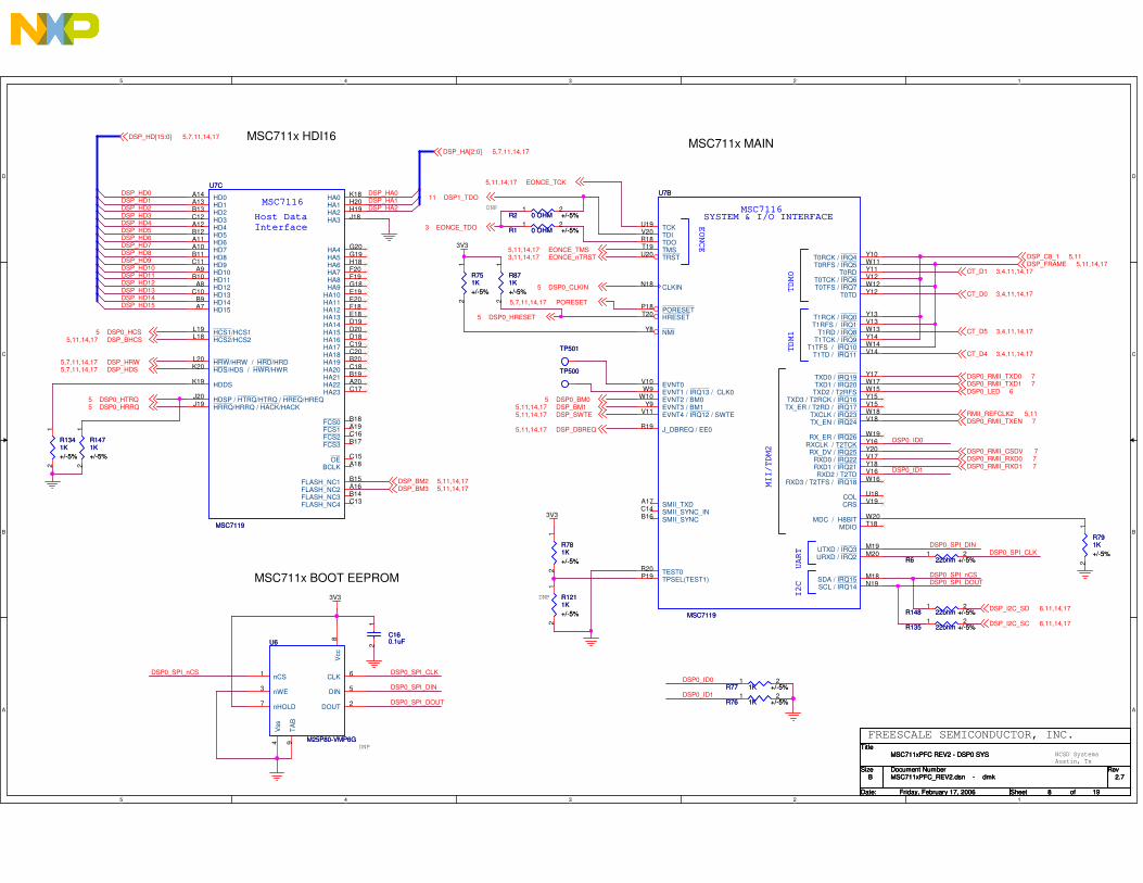
5
5
4
4
3
3
2
2
1
1
D D
C C
B B
A A
DSP_HD0DSP_HD1DSP_HD2DSP_HD3DSP_HD4DSP_HD5DSP_HD6DSP_HD7DSP_HD8DSP_HD9DSP_HD10DSP_HD11DSP_HD12DSP_HD13DSP_HD14DSP_HD15
DSP_HA0DSP_HA1DSP_HA2
DSP0_ID0
DSP0_ID1
DSP0_SPI_nCSDSP0_SPI_DOUT
DSP0_SPI_DIN
DSP0_ID0
DSP0_ID1
DSP0_SPI_CLK
DSP0_SPI_DIN
DSP0_SPI_DOUT
DSP0_SPI_nCS
DSP0_SPI_CLK
3V3
3V3
3V3
DSP_HD[15:0] 5,7,11,14,17
DSP0_HCS5
DSP_HRW5,7,11,14,17DSP_HDS5,7,11,14,17
DSP_HA[2:0] 5,7,11,14,17
EONCE_TCK5,11,14,17
DSP1_TDO11
EONCE_TDO3
EONCE_TMS5,11,14,17EONCE_nTRST3,11,14,17
DSP0_CLKIN5
PORESET5,7,11,14,17
DSP0_HRESET5
DSP0_BM05DSP_BM15,11,14,17DSP_SWTE5,11,14,17
DSP_DBREQ5,11,14,17
DSP0_HTRQ5DSP0_HRRQ5
DSP_BHCS5,11,14,17
DSP_C8_1 5,11DSP_FRAME 5,11,14,17
CT_D1 3,4,11,14,17
CT_D0 3,4,11,14,17
CT_D5 3,4,11,14,17
CT_D4 3,4,11,14,17
DSP0_RMII_CSDV 7
RMII_REFCLK2 5,11DSP0_RMII_TXEN 7
DSP0_LED 6
DSP0_RMII_TXD0 7DSP0_RMII_TXD1 7
DSP0_RMII_RXD1 7DSP0_RMII_RXD0 7
DSP_I2C_SD 6,11,14,17
DSP_I2C_SC 6,11,14,17
DSP_BM2 5,11,14,17DSP_BM3 5,11,14,17
Title
Size Document Number Rev
Date: Sheet of
MSC711xPFC_REV2.dsn - dmk 2.7
MSC711xPFC REV2 - DSP0 SYS
B
8 19Friday, February 17, 2006
Title
Size Document Number Rev
Date: Sheet of
MSC711xPFC_REV2.dsn - dmk 2.7
MSC711xPFC REV2 - DSP0 SYS
B
8 19Friday, February 17, 2006
Title
Size Document Number Rev
Date: Sheet of
MSC711xPFC_REV2.dsn - dmk 2.7
MSC711xPFC REV2 - DSP0 SYS
B
8 19Friday, February 17, 2006
NCSD SystemsAustin, Tx
FREESCALE SEMICONDUCTOR, INC.
MSC711x HDI16
MSC711x BOOT EEPROM
MSC711x MAIN
DNP
DNP
DNP
12
R871K+/-5%
R871K+/-5%
HD0A14
HD1A13
HD2B13
HD3C12
HD4A12
HD5B12
HD6A11
HD7A10
HD8B11
HD9C11
HD10A9
HD11B10
HD12A8
HD13C10
HD14B9
HD15A7
HA0 K18
HA1 H20
HA2 H19
HA3 J18
HA4 G20
HA5 G19
HA6 H18
HA7 F20
HA8 F19
HA9 G18
HA10 E19
HA11 E20
HA12 F18
HA13 E18
HA14 D19
HA15 D20
HA16 D18
HA17 C19
HA18 C20
HA19 B20
HA20 C18
HA21 B19
HA22 A20
HA23 C17
HCS1/HCS1L19
HCS2/HCS2L18
HRW/HRW / HRD/HRDL20
HDDSK19
HDSP / HTRQ/HTRQ / HREQ/HREQJ20
HRRQ/HRRQ / HACK/HACKJ19
HDS/HDS / HWR/HWRK20
FCS0 B18
FCS1 A19
FCS2 C16
FCS3 B17
BCLK A18OE C15
FLASH_NC1 B15
FLASH_NC2 A16
FLASH_NC3 B14
FLASH_NC4 C13
MSC7116
Host Data Interface
U7C
MSC7119
MSC7116
Host Data Interface
U7C
MSC7119
12
R781K+/-5%
R781K+/-5%
12
R791K+/-5%
R791K+/-5%
1 2R76 1K +/-5%R76 1K +/-5%
12
R1211K+/-5%
R1211K+/-5%
12
R1471K+/-5%
R1471K+/-5%
12
R1341K+/-5%
R1341K+/-5%
1 2R6 22ohm +/-5%R6 22ohm +/-5%
1 2R77 1K +/-5%R77 1K +/-5%
TP501TP501
1 2R148 22ohm +/-5%R148 22ohm +/-5%
12
R751K+/-5%
R751K+/-5%
1 2R2 0 OHM +/-5%R2 0 OHM +/-5%
TP500TP500
T0RCK / IRQ4 Y10
T0RFS / IRQ5 W11
T0RD Y11
T0TCK / IRQ6 V12
T0TFS / IRQ7 W12
T0TD Y12
T1RCK / IRQ0 Y13
T1RFS / IRQ1 V13
T1RD / IRQ8 W13
T1TCK / IRQ9 Y14
T1TFS / IRQ10 W14
T1TD / IRQ11 V14
TXD0 / IRQ19 Y17
TXD1 / IRQ20 W17
RXD0 / IRQ22 V17
RXD1 / IRQ21 Y18
TXCLK / IRQ23 W18
TX_EN / IRQ24 V18
RX_DV / IRQ25 Y20
RX_ER / IRQ26 W19
COL U18
CRS V19
MDC / H8BIT W20
MDIO T18
TXD3 / T2RCK / IRQ16 Y15TXD2 / T2RFS W15
TX_ER / T2RD / IRQ17 V15
RXCLK / T2TCK Y16
RXD3 / T2TFS / IRQ18 W16RXD2 / T2TD V16
TCKU19
TDIV20
TDOR18
TMST19
TRSTU20
J_DBREQ / EE0R19
SDA / IRQ15 M18
SCL / IRQ14 N19
URXD / IRQ2 M20UTXD / IRQ3 M19
PORESETP18
HRESETT20
TEST0R20
TPSEL(TEST1)P19
EVNT0V10
EVNT1 / IRQ13 / CLK0W9
EVNT2 / BM0W10
EVNT3 / BM1Y9
EVNT4 / IRQ12 / SWTEV11
NMIY8
SMII_SYNCB16SMII_SYNC_INC14 SMII_TXDA17
CLKINN18
MSC7116SYSTEM & I/O INTERFACE
TDM0
TDM1
MII/TDM2
UART
I2C
EONCE
U7B
MSC7119
MSC7116SYSTEM & I/O INTERFACE
TDM0
TDM1
MII/TDM2
UART
I2C
EONCE
U7B
MSC71191 2
R135 22ohm +/-5%R135 22ohm +/-5%12
C160.1uF C160.1uF
1 2R1 0 OHM +/-5%R1 0 OHM +/-5%
Vss
4
Vcc
8
DIN 5
DOUT 2
CLK 6nCS1
nWE3
nHOLD7
TAB
9
U6
M25P80-VMP6G
U6
M25P80-VMP6G
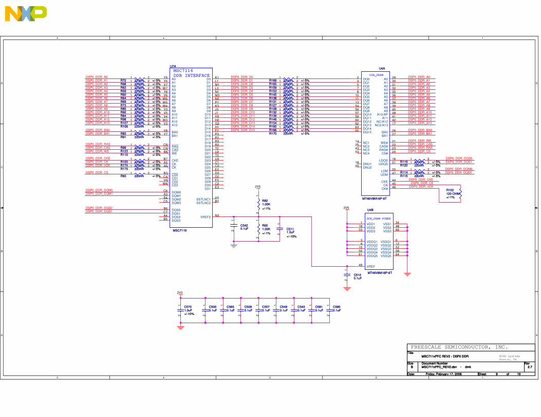
5
5
4
4
3
3
2
2
1
1
D D
C C
B B
A A
DSP0_DDR_A0DSP0_DDR_A1DSP0_DDR_A2DSP0_DDR_A3DSP0_DDR_A4DSP0_DDR_A5DSP0_DDR_A6DSP0_DDR_A7DSP0_DDR_A8DSP0_DDR_A9DSP0_DDR_A10DSP0_DDR_A11DSP0_DDR_A12DSP0_DDR_A13
DSP0_DDR_D15DSP0_DDR_D14DSP0_DDR_D13DSP0_DDR_D12DSP0_DDR_D11DSP0_DDR_D10DSP0_DDR_D9DSP0_DDR_D8DSP0_DDR_D7DSP0_DDR_D6
DSP0_DDR_D4DSP0_DDR_D3DSP0_DDR_D2DSP0_DDR_D1DSP0_DDR_D0
DSP0_DDR_D5
DSP0_DDR_BA0DSP0_DDR_BA1
DSP0_DDR_RASDSP0_DDR_CASDSP0_DDR_WE
DSP0_DDR_CKEDSP0_DDR_CKDSP0_DDR_nCK
DSP0_DDR_CS
DSP0_DDR_A0DSP0_DDR_A1DSP0_DDR_A2DSP0_DDR_A3DSP0_DDR_A4DSP0_DDR_A5DSP0_DDR_A6DSP0_DDR_A7DSP0_DDR_A8DSP0_DDR_A9DSP0_DDR_A10DSP0_DDR_A11DSP0_DDR_A12DSP0_DDR_A13
DSP0_DDR_BA0DSP0_DDR_BA1
DSP0_DDR_WEDSP0_DDR_CASDSP0_DDR_RASDSP0_DDR_CS
DSP0_DDR_CKEDSP0_DDR_CK
DSP0_DDR_nCK
DSP0_DDR_DQM0DSP0_DDR_DQM1
DSP0_DDR_DQS0DSP0_DDR_DQS1
DSP0_DDR_DQM0DSP0_DDR_DQM1
DSP0_DDR_DQS0DSP0_DDR_DQS1
2V5
2V5
2V5
Title
Size Document Number Rev
Date: Sheet of
MSC711xPFC_REV2.dsn - dmk 2.7
MSC711xPFC REV2 - DSP0 DDR
B
9 19Friday, February 17, 2006
Title
Size Document Number Rev
Date: Sheet of
MSC711xPFC_REV2.dsn - dmk 2.7
MSC711xPFC REV2 - DSP0 DDR
B
9 19Friday, February 17, 2006
Title
Size Document Number Rev
Date: Sheet of
MSC711xPFC_REV2.dsn - dmk 2.7
MSC711xPFC REV2 - DSP0 DDR
B
9 19Friday, February 17, 2006
NCSD SystemsAustin, Tx
FREESCALE SEMICONDUCTOR, INC.
VDD11
VDD218
VDD333
VDDQ13
VDDQ29
VDDQ315
VDDQ455
VDDQ561
VREF49
VSS1 34
VSS2 48
VSS3 66
VSSQ1 6
VSSQ2 12
VSSQ4 58VSSQ3 52
VSSQ5 64
DDR_DRAM POWER
U4B
MT46V8M16P-6T
DDR_DRAM POWER
U4B
MT46V8M16P-6T
1 2R175 22ohm +/-5%R175 22ohm +/-5%
12
R651.00K+/-1%
R651.00K+/-1%
R102120 OHM+/-1%
R102120 OHM+/-1%
1 2R99 22ohm +/-5%R99 22ohm +/-5%
1 2R98 22ohm +/-5%R98 22ohm +/-5%
1 2R69 22ohm +/-5%R69 22ohm +/-5%
1 2R154 22ohm +/-5%R154 22ohm +/-5%
12
R821.00K+/-1%
R821.00K+/-1%
1 2R115 22ohm +/-5%R115 22ohm +/-5%
DQ02
DQ14
DQ25
DQ37
DQ48
DQ510
DQ611
DQ713
DQ854
DQ956
DQ1057
DQ1159
DQ1260
DQ1362
DQ1463
DQ1565
A0 29
A1 30
A2 31
A3 32
A4 35
A5 36
A6 37
A7 38
A8 39
A9 40
A10/AP 28
A11 41
BA0 26
BA1 27
CAS# 22WE# 21
RAS# 23
CS# 24
LDQS 16
UDQS 51
LDM 20
UDM 47
NC114
NC2/A13 17
NC225
NC/A12 42
NC343
NC453
DNU119
DNU250
CKE 44
CK 45
CK# 46
DDR_DRAM
U4A
MT46V8M16P-6T
DDR_DRAM
U4A
MT46V8M16P-6T
1 2R127 22ohm +/-5%R127 22ohm +/-5%
1 2R159 22ohm +/-5%R159 22ohm +/-5%
1 2R174 22ohm +/-5%R174 22ohm +/-5%
1 2R91 22ohm +/-5%R91 22ohm +/-5%
1 2R84 22ohm +/-5%R84 22ohm +/-5%
1 2R170 22ohm +/-5%R170 22ohm +/-5%
1 2R64 22ohm +/-5%R64 22ohm +/-5%
1 2R139 22ohm +/-5%R139 22ohm +/-5%
1 2R138 22ohm +/-5%R138 22ohm +/-5%
12
C5701.0uF +/-10%
C5701.0uF +/-10%
A0Y5
A1Y4
A2V7
A3W7
A4Y6
A5V6
A6W6
A7W5
A8W4
A9Y3
A10V5
A11V4
A12W3
A13V3
BA0V8
BA1Y7
RASC8
CASC9
WEB8
CKEB7
CKA5
CKA6
CS0B3
CS1C4
CS2V9
CS3W8
D0 K1
D1 L1
D2 M1
D3 L3
D4 N1
D5 M3
D6 N2
D7 P1
D8 K3
D9 J3
D10 J1
D11 H3
D12 H2
D13 G2
D14 H1
D15 F2
D16 P3
D17 P2
D18 R3
D19 R2
D20 T2
D21 U2
D22 T3
D23 U3
D24 C1
D25 C3
D26 E2
D27 D3
D28 D2
D29 F3
D30 C2
DQM0C6
DQM1A3
DQM2B4
DQM3C5
DQS0B6
DQS1C7
DQS2A4
DQS3B5
D31 E3
SSTLNC1 V2
SSTLNC2 B2
VREF2 N3
MSC7116DDR INTERFACE
U7A
MSC7119
MSC7116DDR INTERFACE
U7A
MSC7119
12
C5800.1uF C5800.1uF
1 2R100 22ohm +/-5%R100 22ohm +/-5%
12
C5810.1uF C5810.1uF
12
C5430.1uF C5430.1uF
12
C5490.1uF C5490.1uF
12
C5570.1uF C5570.1uF
1 2R83 22ohm +/-5%R83 22ohm +/-5%
12
C5090.1uF C5090.1uF
12
C5650.1uF C5650.1uF
1 2R92 22ohm +/-5%R92 22ohm +/-5%
1 2R160 22ohm +/-5%R160 22ohm +/-5%
1 2R68 22ohm +/-5%R68 22ohm +/-5%
1 2R60 22ohm +/-5%R60 22ohm +/-5%
1 2R128 22ohm +/-5%R128 22ohm +/-5%
1 2R153 22ohm +/-5%R153 22ohm +/-5%
1 2R72 22ohm +/-5%R72 22ohm +/-5%
1 2R119 22ohm +/-5%R119 22ohm +/-5%
1 2R110 22ohm +/-5%R110 22ohm +/-5%
12
C5111.0uF +/-10%
C5111.0uF +/-10%
1 2R106 22ohm +/-5%R106 22ohm +/-5%
12
C5120.1uF C5120.1uF
1 2R85 22ohm +/-5%R85 22ohm +/-5%
1 2R169 22ohm +/-5%R169 22ohm +/-5%
12
C5000.1uF C5000.1uF
1 2R146 22ohm +/-5%R146 22ohm +/-5%
1 2R59 22ohm +/-5%R59 22ohm +/-5%
1 2R131 22ohm +/-5%R131 22ohm +/-5%
1 2R165 22ohm +/-5%R165 22ohm +/-5%
1 2R120 22ohm +/-5%R120 22ohm +/-5%
1 2R93 22ohm +/-5%R93 22ohm +/-5%
1 2R123 22ohm +/-5%R123 22ohm +/-5%
12
C5420.1uF C5420.1uF
1 2R107 22ohm +/-5%R107 22ohm +/-5%
1 2R73 22ohm +/-5%R73 22ohm +/-5%
1 2R166 22ohm +/-5%R166 22ohm +/-5%
1 2R132 22ohm +/-5%R132 22ohm +/-5%
1 2R63 22ohm +/-5%R63 22ohm +/-5%
1 2R114 22ohm +/-5%R114 22ohm +/-5%
1 2R145 22ohm +/-5%R145 22ohm +/-5%
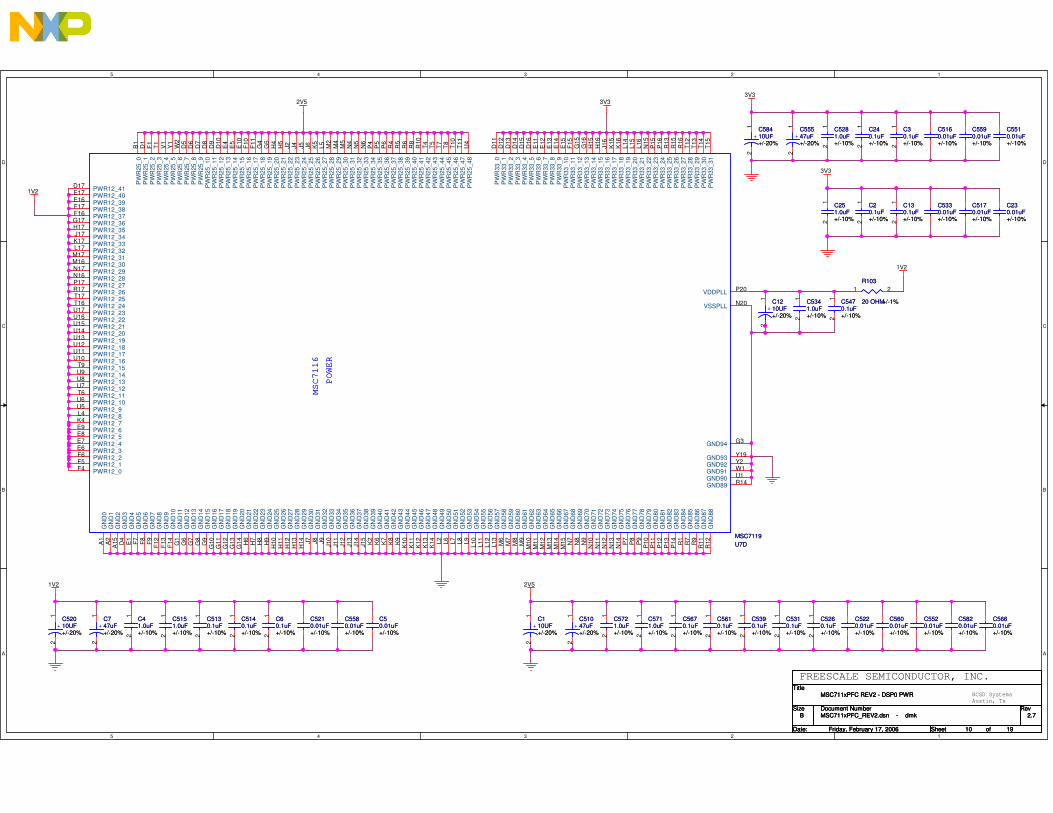
5
5
4
4
3
3
2
2
1
1
D D
C C
B B
A A
1V2
2V5 3V3
1V2
2V51V2
3V3
3V3
Title
Size Document Number Rev
Date: Sheet of
MSC711xPFC_REV2.dsn - dmk 2.7
MSC711xPFC REV2 - DSP0 PWR
B
10 19Friday, February 17, 2006
Title
Size Document Number Rev
Date: Sheet of
MSC711xPFC_REV2.dsn - dmk 2.7
MSC711xPFC REV2 - DSP0 PWR
B
10 19Friday, February 17, 2006
Title
Size Document Number Rev
Date: Sheet of
MSC711xPFC_REV2.dsn - dmk 2.7
MSC711xPFC REV2 - DSP0 PWR
B
10 19Friday, February 17, 2006
NCSD SystemsAustin, Tx
FREESCALE SEMICONDUCTOR, INC.
C5510.01uF+/-10%
C5510.01uF+/-10%
12
C5260.1uF +/-10%
C5260.1uF +/-10%
C5330.01uF+/-10%
C5330.01uF+/-10%
12
+C110UF+/-20%
+C110UF+/-20%
C5210.01uF+/-10%
C5210.01uF+/-10%
12
+C51047uF+/-20%
+C51047uF+/-20%
12
+C58410UF+/-20%
+C58410UF+/-20%
C5660.01uF+/-10%
C5660.01uF+/-10%
12
C5151.0uF +/-10%
C5151.0uF +/-10%
PWR12_0F4 PWR12_1F5 PWR12_2F6 PWR12_3E6 PWR12_4E7PWR12_5E8 PWR12_6E9 PWR12_7K4 PWR12_8L4 PWR12_9U5PWR12_10U6 PWR12_11T6 PWR12_12U7 PWR12_13U8 PWR12_14U9
PW
R25
_0B
1
PW
R25
_1D
1
PW
R25
_2F1
PW
R25
_3T1
PW
R25
_4V
1
PW
R25
_5Y
1
PW
R25
_6W
2
PW
R25
_13
E4
PW
R25
_14
E5
PW
R25
_15
E10
PW
R25
_16
F10
PW
R25
_17
F11
PW
R25
_18
G4
PW
R25
_19
G5
PW
R25
_20
H4
PW
R25
_21
H5
PW
R25
_22
J2
GN
D0
A1
GN
D1
A2
GN
D2
A15
GN
D3
D4
GN
D4
E1
VDDPLL P20
VSSPLL N20
PWR12_15T9 PWR12_16U10 PWR12_17U11
PWR12_26R17 PWR12_27P17 PWR12_28N16 PWR12_29N17PWR12_30M16 PWR12_31M17
PWR12_18U12 PWR12_19U13PWR12_20U14 PWR12_21U15 PWR12_22U16 PWR12_23U17 PWR12_24T16PWR12_25T17
PWR12_32L17 PWR12_33K17 PWR12_34J17PWR12_35H17 PWR12_36G17 PWR12_37F16 PWR12_38F17 PWR12_39E16PWR12_40E17 PWR12_41D17 P
WR
25_7
D5
PW
R25
_8D
6
PW
R25
_9D
7
PW
R25
_10
D8
PW
R25
_11
D9
PW
R25
_12
D10
PW
R25
_23
J4
PW
R25
_24
J5
PW
R25
_25
J6
PW
R25
_26
K5
PW
R25
_27
L5
PW
R25
_28
M2
PW
R25
_29
M4
PW
R25
_30
M5
PW
R25
_31
N4
PW
R25
_32
N5
PW
R25
_33
N6
PW
R25
_34
P4
PW
R25
_35
P5
PW
R25
_36
P6
PW
R25
_37
R4
PW
R25
_38
R5
PW
R25
_39
R6
PW
R25
_40
R8
PW
R25
_41
R10
PW
R25
_42
T4
PW
R25
_43
T5
PW
R25
_44
T7
PW
R25
_45
T8
PW
R25
_46
T10
PW
R25
_47
T11
PW
R25
_48
U4
GN
D5
F7
GN
D6
F8
GN
D7
F9
GN
D8
F12
GN
D9
F13
GN
D10
F14
GN
D11
G1
GN
D12
G6
GN
D13
G7
GN
D14
G8
GN
D15
G9
GN
D16
G10
GN
D17
G11
GN
D18
G12
GN
D19
G13
GN
D20
G14
GN
D21
H6
GN
D22
H7
GN
D23
H8
GN
D24
H9
GN
D25
H10
GN
D26
H11
GN
D27
H12
GN
D28
H13
GN
D29
H14
GN
D30
J7
GN
D31
J8
GN
D32
J9
GN
D33
J10
GN
D34
J11
GN
D35
J12
GN
D36
J13
GN
D37
J14
GN
D38
J15
GN
D39
K2
GN
D40
K6
GN
D41
K7
GN
D42
K8
GN
D43
K9
GN
D44
K10
GN
D45
K11
GN
D46
K12
GN
D47
K13
GN
D48
K14
GN
D49
L2
GN
D50
L6
GN
D51
L7
GN
D52
L8
GN
D53
L9
GN
D54
L10
GN
D55
L11
GN
D56
L12
GN
D57
L13
GN
D58
M6
GN
D59
M7
GN
D60
M8
GN
D61
M9
GN
D62
M10
GN
D63
M11
GN
D64
M12
GN
D65
M13
GN
D66
M14
GN
D67
M15
GN
D68
N7
GN
D69
N8
GN
D70
N9
GN
D71
N10
GN
D72
N11
GN
D73
N12
GN
D74
N13
GN
D75
N14
GN
D76
P7
GN
D77
P8
GN
D78
P9
GN
D79
P10
GN
D80
P11
GN
D81
P12
GN
D82
P13
GN
D83
P14
GN
D84
R1
GN
D85
R7
GN
D86
R9
GN
D87
R11
GN
D88
R12
GND89 R14GND90 U1GND91 W1GND92 Y2GND93 Y19
PW
R33
_0D
11
PW
R33
_1D
12
PW
R33
_2D
13
PW
R33
_3D
14
PW
R33
_4D
15
PW
R33
_5D
16
PW
R33
_6E
11
PW
R33
_7E
12
PW
R33
_8E
13
PW
R33
_9E
14
PW
R33
_10
E15
PW
R33
_11
F15
PW
R33
_12
G15
PW
R33
_13
G16
PW
R33
_14
H15
PW
R33
_15
H16
PW
R33
_16
J16
PW
R33
_17
K15
PW
R33
_18
K16
PW
R33
_19
L14
PW
R33
_20
L15
PW
R33
_21
L16
PW
R33
_22
N15
PW
R33
_23
P15
PW
R33
_24
P16
PW
R33
_25
R13
PW
R33
_26
R15
PW
R33
_27
R16
PW
R33
_28
T12
PW
R33
_29
T13
PW
R33
_30
T14
PW
R33
_31
T15
GND94 G3
MSC7116
POWER
U7DMSC7119
MSC7116
POWER
U7DMSC7119
12
+C55547uF+/-20%
+C55547uF+/-20%
C5520.01uF+/-10%
C5520.01uF+/-10%
12
C5721.0uF +/-10%
C5721.0uF +/-10%
12
C60.1uF +/-10%
C60.1uF +/-10%
1 2R103
20 OHM+/-1%
R103
20 OHM+/-1%
12
C5711.0uF +/-10%
C5711.0uF +/-10%
12
C5281.0uF +/-10%
C5281.0uF +/-10%
C5160.01uF+/-10%
C5160.01uF+/-10%
12
C5670.1uF +/-10%
C5670.1uF +/-10%
12
C251.0uF +/-10%
C251.0uF +/-10%
12
+C52010UF+/-20%
+C52010UF+/-20%
12
C20.1uF +/-10%
C20.1uF +/-10%
C5590.01uF+/-10%
C5590.01uF+/-10%
C50.01uF+/-10%
C50.01uF+/-10%
12
C5610.1uF +/-10%
C5610.1uF +/-10%
C5170.01uF+/-10%
C5170.01uF+/-10%
12
C5310.1uF +/-10%
C5310.1uF +/-10%
C230.01uF+/-10%
C230.01uF+/-10%
C5580.01uF+/-10%
C5580.01uF+/-10%
12
C5130.1uF +/-10%
C5130.1uF +/-10%
12
C5390.1uF +/-10%
C5390.1uF +/-10%
12
+C747uF+/-20%
+C747uF+/-20%
C5820.01uF+/-10%
C5820.01uF+/-10%
C5220.01uF+/-10%
C5220.01uF+/-10%
12
C130.1uF +/-10%
C130.1uF +/-10%
12
C5140.1uF +/-10%
C5140.1uF +/-10%
C5600.01uF+/-10%
C5600.01uF+/-10%
12
C5341.0uF +/-10%
C5341.0uF +/-10%
12
C240.1uF +/-10%
C240.1uF +/-10%
12
C5470.1uF +/-10%
C5470.1uF +/-10%
12
+C1210UF+/-20%
+C1210UF+/-20%
12
C30.1uF +/-10%
C30.1uF +/-10%
12
C41.0uF +/-10%
C41.0uF +/-10%

5
5
4
4
3
3
2
2
1
1
D D
C C
B B
A A
DSP_HA0DSP_HD0DSP_HA1DSP_HD1DSP_HA2DSP_HD2
DSP_HD3DSP_HD4DSP_HD5DSP_HD6DSP_HD7
DSP1_SPI_nCS
DSP_HD8DSP_HD9
DSP1_SPI_DOUT
DSP_HD10
DSP1_ID0
DSP_HD11
DSP1_ID1
DSP_HD12DSP_HD13
DSP1_SPI_DIN
DSP_HD14DSP_HD15
DSP1_SPI_CLK
DSP1_SPI_DIN
DSP1_SPI_DOUT
DSP1_ID0
DSP1_SPI_CLK
DSP1_SPI_nCS
DSP1_ID1
3V3
3V3
3V3
3V3
DSP_DBREQ5,8,14,17
DSP_BHCS5,8,14,17
CT_D1 3,4,8,14,17
DSP_HA[2:0] 5,7,8,14,17
DSP_I2C_SD 6,8,14,17
DSP1_RMII_TXD0 7
CT_D0 3,4,8,14,17
DSP1_RMII_TXD1 7
DSP_I2C_SC 6,8,14,17
CT_D5 3,4,8,14,17
DSP1_RMII_RXD1 7
EONCE_TCK5,8,14,17
CT_D4 3,4,8,14,17
DSP2_TDO14
DSP1_RMII_RXD0 7
DSP1_TDO8
EONCE_TMS5,8,14,17EONCE_nTRST3,8,14,17
DSP1_RMII_CSDV 7
RMII_REFCLK2 5,8DSP1_RMII_TXEN 7
DSP1_LED 6
DSP_C8_1 5,8
DSP1_CLKIN5
DSP_FRAME 5,8,14,17
PORESET5,7,8,14,17
DSP1_HTRQ5
DSP1_HRESET5
DSP1_HRRQ5
DSP_HD[15:0] 5,7,8,14,17
DSP1_HCS5
DSP_HRW5,7,8,14,17DSP_HDS5,7,8,14,17
DSP1_BM05DSP_BM15,8,14,17DSP_SWTE5,8,14,17
DSP_BM2 5,8,14,17DSP_BM3 5,8,14,17
Title
Size Document Number Rev
Date: Sheet of
MSC711xPFC_REV2.dsn - dmk 2.7
MSC711xPFC REV2 - DSP1 SYS
B
11 19Friday, February 17, 2006
Title
Size Document Number Rev
Date: Sheet of
MSC711xPFC_REV2.dsn - dmk 2.7
MSC711xPFC REV2 - DSP1 SYS
B
11 19Friday, February 17, 2006
Title
Size Document Number Rev
Date: Sheet of
MSC711xPFC_REV2.dsn - dmk 2.7
MSC711xPFC REV2 - DSP1 SYS
B
11 19Friday, February 17, 2006
NCSD SystemsAustin, Tx
FREESCALE SEMICONDUCTOR, INC.
DNP
DNP
DNP
MSC711x HDI16
MSC711x BOOT EEPROM
MSC711x MAIN
1 2R13 1K +/-5%R13 1K +/-5%
Vss
4
Vcc
8
DIN 5
DOUT 2
CLK 6nCS1
nWE3
nHOLD7
TAB
9
U3
M25P80-VMP6G
U3
M25P80-VMP6G
12
R111K+/-5%
R111K+/-5%
12
R121K+/-5%
R121K+/-5%
1 2R5 0 OHM +/-5%R5 0 OHM +/-5%
1 2R97 22ohm +/-5%R97 22ohm +/-5%
12
R151K+/-5%
R151K+/-5%
HD0A14
HD1A13
HD2B13
HD3C12
HD4A12
HD5B12
HD6A11
HD7A10
HD8B11
HD9C11
HD10A9
HD11B10
HD12A8
HD13C10
HD14B9
HD15A7
HA0 K18
HA1 H20
HA2 H19
HA3 J18
HA4 G20
HA5 G19
HA6 H18
HA7 F20
HA8 F19
HA9 G18
HA10 E19
HA11 E20
HA12 F18
HA13 E18
HA14 D19
HA15 D20
HA16 D18
HA17 C19
HA18 C20
HA19 B20
HA20 C18
HA21 B19
HA22 A20
HA23 C17
HCS1/HCS1L19
HCS2/HCS2L18
HRW/HRW / HRD/HRDL20
HDDSK19
HDSP / HTRQ/HTRQ / HREQ/HREQJ20
HRRQ/HRRQ / HACK/HACKJ19
HDS/HDS / HWR/HWRK20
FCS0 B18
FCS1 A19
FCS2 C16
FCS3 B17
BCLK A18OE C15
FLASH_NC1 B15
FLASH_NC2 A16
FLASH_NC3 B14
FLASH_NC4 C13
MSC7116
Host Data Interface
U2C
MSC7119
MSC7116
Host Data Interface
U2C
MSC7119
12
R1091K+/-5%
R1091K+/-5%
1 2R14 1K +/-5%R14 1K +/-5%
12
R1241K+/-5%
R1241K+/-5%
1 2R3 22ohm +/-5%R3 22ohm +/-5%
12
C140.1uF C140.1uF
12
R1621K+/-5%
R1621K+/-5%
T0RCK / IRQ4 Y10
T0RFS / IRQ5 W11
T0RD Y11
T0TCK / IRQ6 V12
T0TFS / IRQ7 W12
T0TD Y12
T1RCK / IRQ0 Y13
T1RFS / IRQ1 V13
T1RD / IRQ8 W13
T1TCK / IRQ9 Y14
T1TFS / IRQ10 W14
T1TD / IRQ11 V14
TXD0 / IRQ19 Y17
TXD1 / IRQ20 W17
RXD0 / IRQ22 V17
RXD1 / IRQ21 Y18
TXCLK / IRQ23 W18
TX_EN / IRQ24 V18
RX_DV / IRQ25 Y20
RX_ER / IRQ26 W19
COL U18
CRS V19
MDC / H8BIT W20
MDIO T18
TXD3 / T2RCK / IRQ16 Y15TXD2 / T2RFS W15
TX_ER / T2RD / IRQ17 V15
RXCLK / T2TCK Y16
RXD3 / T2TFS / IRQ18 W16RXD2 / T2TD V16
TCKU19
TDIV20
TDOR18
TMST19
TRSTU20
J_DBREQ / EE0R19
SDA / IRQ15 M18
SCL / IRQ14 N19
URXD / IRQ2 M20UTXD / IRQ3 M19
PORESETP18
HRESETT20
TEST0R20
TPSEL(TEST1)P19
EVNT0V10
EVNT1 / IRQ13 / CLK0W9
EVNT2 / BM0W10
EVNT3 / BM1Y9
EVNT4 / IRQ12 / SWTEV11
NMIY8
SMII_SYNCB16SMII_SYNC_INC14 SMII_TXDA17
CLKINN18
MSC7116SYSTEM & I/O INTERFACE
TDM0
TDM1
MII/TDM2
UART
I2C
EONCE
U2B
MSC7119
MSC7116SYSTEM & I/O INTERFACE
TDM0
TDM1
MII/TDM2
UART
I2C
EONCE
U2B
MSC7119
12
R1081K+/-5%
R1081K+/-5%
1 2R150 22ohm +/-5%R150 22ohm +/-5%
1 2R8 0 OHM +/-5%R8 0 OHM +/-5%
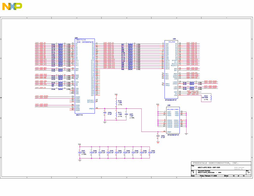
5
5
4
4
3
3
2
2
1
1
D D
C C
B B
A A
DSP1_DDR_A3
DSP1_DDR_A7
DSP1_DDR_D9
DSP1_DDR_A4
DSP1_DDR_A8DSP1_DDR_D8
DSP1_DDR_A5
DSP1_DDR_A9
DSP1_DDR_D7DSP1_DDR_A6
DSP1_DDR_A10
DSP1_DDR_D6DSP1_DDR_A7
DSP1_DDR_A11
DSP1_DDR_A8
DSP1_DDR_A12
DSP1_DDR_D4
DSP1_DDR_A9
DSP1_DDR_A13
DSP1_DDR_D3
DSP1_DDR_A10
DSP1_DDR_BA0
DSP1_DDR_D2
DSP1_DDR_A11
DSP1_DDR_BA1
DSP1_DDR_D1
DSP1_DDR_A12
DSP1_DDR_WE
DSP1_DDR_D0
DSP1_DDR_A13
DSP1_DDR_CASDSP1_DDR_RASDSP1_DDR_CS
DSP1_DDR_CKE
DSP1_DDR_BA0
DSP1_DDR_CK
DSP1_DDR_BA1
DSP1_DDR_nCK
DSP1_DDR_RAS
DSP1_DDR_D5
DSP1_DDR_DQM0
DSP1_DDR_CAS
DSP1_DDR_A0
DSP1_DDR_DQM1
DSP1_DDR_WE
DSP1_DDR_A1
DSP1_DDR_D15
DSP1_DDR_DQS0DSP1_DDR_CKE
DSP1_DDR_A2
DSP1_DDR_D14
DSP1_DDR_DQM0
DSP1_DDR_CK DSP1_DDR_DQS1
DSP1_DDR_A3
DSP1_DDR_D13
DSP1_DDR_nCK
DSP1_DDR_A0
DSP1_DDR_DQM1
DSP1_DDR_A4
DSP1_DDR_D12
DSP1_DDR_CS
DSP1_DDR_A1
DSP1_DDR_A5
DSP1_DDR_DQS0
DSP1_DDR_D11
DSP1_DDR_A2
DSP1_DDR_A6
DSP1_DDR_D10
DSP1_DDR_DQS12V5
2V5
2V5
Title
Size Document Number Rev
Date: Sheet of
MSC711xPFC_REV2.dsn - dmk 2.7
MSC711xPFC REV2 - DSP1 DDR
B
12 19Friday, February 17, 2006
Title
Size Document Number Rev
Date: Sheet of
MSC711xPFC_REV2.dsn - dmk 2.7
MSC711xPFC REV2 - DSP1 DDR
B
12 19Friday, February 17, 2006
Title
Size Document Number Rev
Date: Sheet of
MSC711xPFC_REV2.dsn - dmk 2.7
MSC711xPFC REV2 - DSP1 DDR
B
12 19Friday, February 17, 2006
NCSD SystemsAustin, Tx
FREESCALE SEMICONDUCTOR, INC.
1 2R96 22ohm +/-5%R96 22ohm +/-5%
12
C5360.1uF C5360.1uF
1 2R113 22ohm +/-5%R113 22ohm +/-5%
1 2R125 22ohm +/-5%R125 22ohm +/-5%
1 2R164 22ohm +/-5%R164 22ohm +/-5%
R141120 OHM
+/-1%
R141120 OHM
+/-1%
1 2R67 22ohm +/-5%R67 22ohm +/-5%A0Y5
A1Y4
A2V7
A3W7
A4Y6
A5V6
A6W6
A7W5
A8W4
A9Y3
A10V5
A11V4
A12W3
A13V3
BA0V8
BA1Y7
RASC8
CASC9
WEB8
CKEB7
CKA5
CKA6
CS0B3
CS1C4
CS2V9
CS3W8
D0 K1
D1 L1
D2 M1
D3 L3
D4 N1
D5 M3
D6 N2
D7 P1
D8 K3
D9 J3
D10 J1
D11 H3
D12 H2
D13 G2
D14 H1
D15 F2
D16 P3
D17 P2
D18 R3
D19 R2
D20 T2
D21 U2
D22 T3
D23 U3
D24 C1
D25 C3
D26 E2
D27 D3
D28 D2
D29 F3
D30 C2
DQM0C6
DQM1A3
DQM2B4
DQM3C5
DQS0B6
DQS1C7
DQS2A4
DQS3B5
D31 E3
SSTLNC1 V2
SSTLNC2 B2
VREF2 N3
MSC7116DDR INTERFACE
U2A
MSC7119
MSC7116DDR INTERFACE
U2A
MSC7119
1 2R105 22ohm +/-5%R105 22ohm +/-5%
1 2R88 22ohm +/-5%R88 22ohm +/-5%
1 2R156 22ohm +/-5%R156 22ohm +/-5%
1 2R116 22ohm +/-5%R116 22ohm +/-5%
12
C5320.1uF C5320.1uF
1 2R130 22ohm +/-5%R130 22ohm +/-5%
12
C5771.0uF +/-10%
C5771.0uF +/-10%
12
C5480.1uF C5480.1uF
1 2R137 22ohm +/-5%R137 22ohm +/-5%
1 2R167 22ohm +/-5%R167 22ohm +/-5%
1 2R144 22ohm +/-5%R144 22ohm +/-5%
12
C5760.1uF C5760.1uF
12
R1551.00K+/-1%
R1551.00K+/-1%
1 2R61 22ohm +/-5%R61 22ohm +/-5%
1 2R143 22ohm +/-5%R143 22ohm +/-5%
VDD11
VDD218
VDD333
VDDQ13
VDDQ29
VDDQ315
VDDQ455
VDDQ561
VREF49
VSS1 34
VSS2 48
VSS3 66
VSSQ1 6
VSSQ2 12
VSSQ4 58VSSQ3 52
VSSQ5 64
DDR_DRAM POWER
U5B
MT46V8M16P-6T
DDR_DRAM POWER
U5B
MT46V8M16P-6T
1 2R136 22ohm +/-5%R136 22ohm +/-5%
1 2R152 22ohm +/-5%R152 22ohm +/-5%
1 2R151 22ohm +/-5%R151 22ohm +/-5%
1 2R177 22ohm +/-5%R177 22ohm +/-5%
1 2R133 22ohm +/-5%R133 22ohm +/-5%
1 2R66 22ohm +/-5%R66 22ohm +/-5%
12
C5830.1uF C5830.1uF
1 2R173 22ohm +/-5%R173 22ohm +/-5%
1 2R62 22ohm +/-5%R62 22ohm +/-5%
1 2R95 22ohm +/-5%R95 22ohm +/-5%
1 2R129 22ohm +/-5%R129 22ohm +/-5%
1 2R163 22ohm +/-5%R163 22ohm +/-5%
12
C5540.1uF C5540.1uF
12
C5440.1uF C5440.1uF
DQ02
DQ14
DQ25
DQ37
DQ48
DQ510
DQ611
DQ713
DQ854
DQ956
DQ1057
DQ1159
DQ1260
DQ1362
DQ1463
DQ1565
A0 29
A1 30
A2 31
A3 32
A4 35
A5 36
A6 37
A7 38
A8 39
A9 40
A10/AP 28
A11 41
BA0 26
BA1 27
CAS# 22WE# 21
RAS# 23
CS# 24
LDQS 16
UDQS 51
LDM 20
UDM 47
NC114
NC2/A13 17
NC225
NC/A12 42
NC343
NC453
DNU119
DNU250
CKE 44
CK 45
CK# 46
DDR_DRAM
U5A
MT46V8M16P-6T
DDR_DRAM
U5A
MT46V8M16P-6T
1 2R117 22ohm +/-5%R117 22ohm +/-5%
1 2R81 22ohm +/-5%R81 22ohm +/-5%
1 2R71 22ohm +/-5%R71 22ohm +/-5%
12
C5530.1uF C5530.1uF
1 2R70 22ohm +/-5%R70 22ohm +/-5%
12
C5271.0uF +/-10%
C5271.0uF +/-10%
1 2R149 22ohm +/-5%R149 22ohm +/-5%
12
C5380.1uF C5380.1uF
1 2R104 22ohm +/-5%R104 22ohm +/-5%
1 2R157 22ohm +/-5%R157 22ohm +/-5%
1 2R89 22ohm +/-5%R89 22ohm +/-5%
12
C5790.1uF C5790.1uF
12
R1711.00K+/-1%
R1711.00K+/-1%
1 2R168 22ohm +/-5%R168 22ohm +/-5%
1 2R126 22ohm +/-5%R126 22ohm +/-5%
1 2R80 22ohm +/-5%R80 22ohm +/-5%
1 2R112 22ohm +/-5%R112 22ohm +/-5%
1 2R142 22ohm +/-5%R142 22ohm +/-5%
1 2R172 22ohm +/-5%R172 22ohm +/-5%
1 2R158 22ohm +/-5%R158 22ohm +/-5%
1 2R122 22ohm +/-5%R122 22ohm +/-5%
1 2R178 22ohm +/-5%R178 22ohm +/-5%
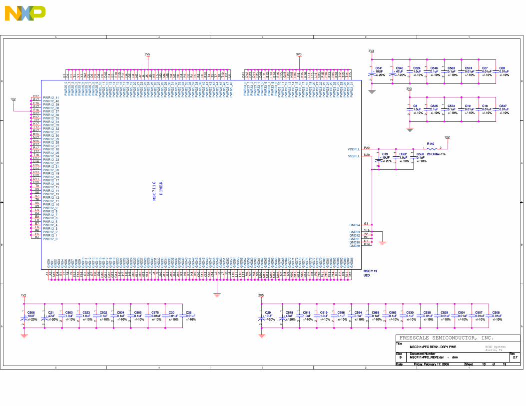
5
5
4
4
3
3
2
2
1
1
D D
C C
B B
A A
1V2
1V2
2V5
2V5
3V3
1V2
3V3
3V3
Title
Size Document Number Rev
Date: Sheet of
MSC711xPFC_REV2.dsn - dmk 2.7
MSC711xPFC REV2 - DSP1 PWR
B
13 19Friday, February 17, 2006
Title
Size Document Number Rev
Date: Sheet of
MSC711xPFC_REV2.dsn - dmk 2.7
MSC711xPFC REV2 - DSP1 PWR
B
13 19Friday, February 17, 2006
Title
Size Document Number Rev
Date: Sheet of
MSC711xPFC_REV2.dsn - dmk 2.7
MSC711xPFC REV2 - DSP1 PWR
B
13 19Friday, February 17, 2006
NCSD SystemsAustin, Tx
FREESCALE SEMICONDUCTOR, INC.
C270.01uF+/-10%
C270.01uF+/-10%
C5010.01uF+/-10%
C5010.01uF+/-10%
C5750.01uF+/-10%
C5750.01uF+/-10%
12
+C57847uF+/-20%
+C57847uF+/-20%
12
C5560.1uF +/-10%
C5560.1uF +/-10%
C180.01uF+/-10%
C180.01uF+/-10%
C5350.01uF+/-10%
C5350.01uF+/-10%
12
C5460.1uF +/-10%
C5460.1uF +/-10%
12
+C54110UF+/-20%
+C54110UF+/-20%
C280.01uF+/-10%
C280.01uF+/-10%
12
C5250.1uF +/-10%
C5250.1uF +/-10%
12
C5231.0uF +/-10%
C5231.0uF +/-10%
C260.01uF+/-10%
C260.01uF+/-10%
12
C5640.1uF +/-10%
C5640.1uF +/-10%
1 2R140
20 OHM+/-1%
R140
20 OHM+/-1%
C5370.01uF+/-10%
C5370.01uF+/-10%
12
C5621.0uF +/-10%
C5621.0uF +/-10%
12
C5630.1uF +/-10%
C5630.1uF +/-10%
12
C5730.1uF +/-10%
C5730.1uF +/-10%
12
+C54047uF+/-20%
+C54047uF+/-20%
12
C5500.1uF +/-10%
C5500.1uF +/-10%
C5290.01uF+/-10%
C5290.01uF+/-10%
C5080.01uF+/-10%
C5080.01uF+/-10%
12
C5020.1uF +/-10%
C5020.1uF +/-10%
12
C5680.1uF +/-10%
C5680.1uF +/-10%
12
C5181.0uF +/-10%
C5181.0uF +/-10%
12
C5040.1uF +/-10%
C5040.1uF +/-10%
12
+C2147uF+/-20%
+C2147uF+/-20%
12
C5690.1uF +/-10%
C5690.1uF +/-10%
C5070.01uF+/-10%
C5070.01uF+/-10%
12
C5241.0uF +/-10%
C5241.0uF +/-10%
C5740.01uF+/-10%
C5740.01uF+/-10%
12
C5031.0uF +/-10%
C5031.0uF +/-10%
12
+C2910UF+/-20%
+C2910UF+/-20%
C100.01uF+/-10%
C100.01uF+/-10%
12
C5050.1uF +/-10%
C5050.1uF +/-10%
12
+C50610UF+/-20%
+C50610UF+/-20%
12
+C1910UF+/-20%
+C1910UF+/-20%
12
C81.0uF +/-10%
C81.0uF +/-10%
C200.01uF+/-10%
C200.01uF+/-10%
12
C5300.1uF +/-10%
C5300.1uF +/-10%
12
C5191.0uF +/-10%
C5191.0uF +/-10%
PWR12_0F4PWR12_1F5 PWR12_2F6 PWR12_3E6 PWR12_4E7 PWR12_5E8PWR12_6E9 PWR12_7K4 PWR12_8L4 PWR12_9U5 PWR12_10U6PWR12_11T6 PWR12_12U7 PWR12_13U8 PWR12_14U9
PW
R25
_0B
1
PW
R25
_1D
1
PW
R25
_2F1
PW
R25
_3T1
PW
R25
_4V
1
PW
R25
_5Y
1
PW
R25
_6W
2
PW
R25
_13
E4
PW
R25
_14
E5
PW
R25
_15
E10
PW
R25
_16
F10
PW
R25
_17
F11
PW
R25
_18
G4
PW
R25
_19
G5
PW
R25
_20
H4
PW
R25
_21
H5
PW
R25
_22
J2
GN
D0
A1
GN
D1
A2
GN
D2
A15
GN
D3
D4
GN
D4
E1
VDDPLL P20
VSSPLL N20
PWR12_15T9PWR12_16U10 PWR12_17U11
PWR12_26R17 PWR12_27P17 PWR12_28N16 PWR12_29N17 PWR12_30M16PWR12_31M17
PWR12_18U12 PWR12_19U13 PWR12_20U14PWR12_21U15 PWR12_22U16 PWR12_23U17 PWR12_24T16 PWR12_25T17
PWR12_32L17 PWR12_33K17 PWR12_34J17 PWR12_35H17PWR12_36G17 PWR12_37F16 PWR12_38F17 PWR12_39E16 PWR12_40E17PWR12_41D17 P
WR
25_7
D5
PW
R25
_8D
6
PW
R25
_9D
7
PW
R25
_10
D8
PW
R25
_11
D9
PW
R25
_12
D10
PW
R25
_23
J4
PW
R25
_24
J5
PW
R25
_25
J6
PW
R25
_26
K5
PW
R25
_27
L5
PW
R25
_28
M2
PW
R25
_29
M4
PW
R25
_30
M5
PW
R25
_31
N4
PW
R25
_32
N5
PW
R25
_33
N6
PW
R25
_34
P4
PW
R25
_35
P5
PW
R25
_36
P6
PW
R25
_37
R4
PW
R25
_38
R5
PW
R25
_39
R6
PW
R25
_40
R8
PW
R25
_41
R10
PW
R25
_42
T4
PW
R25
_43
T5
PW
R25
_44
T7
PW
R25
_45
T8
PW
R25
_46
T10
PW
R25
_47
T11
PW
R25
_48
U4
GN
D5
F7
GN
D6
F8
GN
D7
F9
GN
D8
F12
GN
D9
F13
GN
D10
F14
GN
D11
G1
GN
D12
G6
GN
D13
G7
GN
D14
G8
GN
D15
G9
GN
D16
G10
GN
D17
G11
GN
D18
G12
GN
D19
G13
GN
D20
G14
GN
D21
H6
GN
D22
H7
GN
D23
H8
GN
D24
H9
GN
D25
H10
GN
D26
H11
GN
D27
H12
GN
D28
H13
GN
D29
H14
GN
D30
J7
GN
D31
J8
GN
D32
J9
GN
D33
J10
GN
D34
J11
GN
D35
J12
GN
D36
J13
GN
D37
J14
GN
D38
J15
GN
D39
K2
GN
D40
K6
GN
D41
K7
GN
D42
K8
GN
D43
K9
GN
D44
K10
GN
D45
K11
GN
D46
K12
GN
D47
K13
GN
D48
K14
GN
D49
L2
GN
D50
L6
GN
D51
L7
GN
D52
L8
GN
D53
L9
GN
D54
L10
GN
D55
L11
GN
D56
L12
GN
D57
L13
GN
D58
M6
GN
D59
M7
GN
D60
M8
GN
D61
M9
GN
D62
M10
GN
D63
M11
GN
D64
M12
GN
D65
M13
GN
D66
M14
GN
D67
M15
GN
D68
N7
GN
D69
N8
GN
D70
N9
GN
D71
N10
GN
D72
N11
GN
D73
N12
GN
D74
N13
GN
D75
N14
GN
D76
P7
GN
D77
P8
GN
D78
P9
GN
D79
P10
GN
D80
P11
GN
D81
P12
GN
D82
P13
GN
D83
P14
GN
D84
R1
GN
D85
R7
GN
D86
R9
GN
D87
R11
GN
D88
R12
GND89 R14GND90 U1GND91 W1GND92 Y2GND93 Y19
PW
R33
_0D
11
PW
R33
_1D
12
PW
R33
_2D
13
PW
R33
_3D
14
PW
R33
_4D
15
PW
R33
_5D
16
PW
R33
_6E
11
PW
R33
_7E
12
PW
R33
_8E
13
PW
R33
_9E
14
PW
R33
_10
E15
PW
R33
_11
F15
PW
R33
_12
G15
PW
R33
_13
G16
PW
R33
_14
H15
PW
R33
_15
H16
PW
R33
_16
J16
PW
R33
_17
K15
PW
R33
_18
K16
PW
R33
_19
L14
PW
R33
_20
L15
PW
R33
_21
L16
PW
R33
_22
N15
PW
R33
_23
P15
PW
R33
_24
P16
PW
R33
_25
R13
PW
R33
_26
R15
PW
R33
_27
R16
PW
R33
_28
T12
PW
R33
_29
T13
PW
R33
_30
T14
PW
R33
_31
T15
GND94 G3
MSC7116
POWER
U2DMSC7119
MSC7116
POWER
U2DMSC7119

5
5
4
4
3
3
2
2
1
1
D D
C C
B B
A A
DSP_HA0DSP_HD0DSP_HA1DSP_HD1DSP_HA2DSP_HD2
DSP_HD3DSP_HD4DSP_HD5DSP_HD6DSP_HD7
DSP2_SPI_nCS
DSP_HD8DSP_HD9
DSP2_SPI_DOUT
DSP_HD10
DSP2_ID0
DSP_HD11
DSP2_ID1
DSP_HD12DSP_HD13
DSP2_SPI_DIN
DSP_HD14DSP_HD15
DSP2_SPI_CLK
DSP2_SPI_DIN
DSP2_SPI_DOUT
DSP2_ID0
DSP2_SPI_CLK
DSP2_SPI_nCS
DSP2_ID1
3V3
3V3
3V3
3V3
DSP_DBREQ5,8,11,17
DSP_BHCS5,8,11,17
CT_D1 3,4,8,11,17
DSP_HA[2:0] 5,7,8,11,17
DSP_I2C_SD 6,8,11,17
DSP2_RMII_TXD0 7
CT_D0 3,4,8,11,17
DSP2_RMII_TXD1 7
DSP_I2C_SC 6,8,11,17
CT_D5 3,4,8,11,17
DSP2_RMII_RXD1 7
EONCE_TCK5,8,11,17
CT_D4 3,4,8,11,17
DSP3_TDO17
DSP2_RMII_RXD0 7
DSP2_TDO11
EONCE_TMS5,8,11,17EONCE_nTRST3,8,11,17
DSP2_RMII_CSDV 7
RMII_REFCLK3 5,17DSP2_RMII_TXEN 7
DSP2_LED 6
DSP_C8_2 5,17
DSP2_CLKIN5
DSP_FRAME 5,8,11,17
PORESET5,7,8,11,17
DSP2_HTRQ5
DSP2_HRESET5
DSP2_HRRQ5
DSP_HD[15:0] 5,7,8,11,17
DSP2_HCS5
DSP_HRW5,7,8,11,17DSP_HDS5,7,8,11,17
DSP2_BM05DSP_BM15,8,11,17DSP_SWTE5,8,11,17
DSP_BM2 5,8,11,17DSP_BM3 5,8,11,17
Title
Size Document Number Rev
Date: Sheet of
MSC711xPFC_REV2.dsn - dmk 2.7
MSC711xPFC REV2 - DSP2 SYS
B
14 19Friday, February 17, 2006
Title
Size Document Number Rev
Date: Sheet of
MSC711xPFC_REV2.dsn - dmk 2.7
MSC711xPFC REV2 - DSP2 SYS
B
14 19Friday, February 17, 2006
Title
Size Document Number Rev
Date: Sheet of
MSC711xPFC_REV2.dsn - dmk 2.7
MSC711xPFC REV2 - DSP2 SYS
B
14 19Friday, February 17, 2006
NCSD SystemsAustin, Tx
FREESCALE SEMICONDUCTOR, INC.
DNP
DNP
DNP
MSC711x HDI16
MSC711x BOOT EEPROM
MSC711x MAIN
12
C640.1uF C640.1uF
Vss
4
Vcc
8
DIN 5
DOUT 2
CLK 6nCS1
nWE3
nHOLD7
TAB
9
U14
M25P80-VMP6G
U14
M25P80-VMP6G
12
R561K+/-5%
R561K+/-5%
1 2R53 22ohm +/-5%R53 22ohm +/-5%
1 2R244 22ohm +/-5%R244 22ohm +/-5%
12
R2871K+/-5%
R2871K+/-5%
1 2R221 22ohm +/-5%R221 22ohm +/-5%
HD0A14
HD1A13
HD2B13
HD3C12
HD4A12
HD5B12
HD6A11
HD7A10
HD8B11
HD9C11
HD10A9
HD11B10
HD12A8
HD13C10
HD14B9
HD15A7
HA0 K18
HA1 H20
HA2 H19
HA3 J18
HA4 G20
HA5 G19
HA6 H18
HA7 F20
HA8 F19
HA9 G18
HA10 E19
HA11 E20
HA12 F18
HA13 E18
HA14 D19
HA15 D20
HA16 D18
HA17 C19
HA18 C20
HA19 B20
HA20 C18
HA21 B19
HA22 A20
HA23 C17
HCS1/HCS1L19
HCS2/HCS2L18
HRW/HRW / HRD/HRDL20
HDDSK19
HDSP / HTRQ/HTRQ / HREQ/HREQJ20
HRRQ/HRRQ / HACK/HACKJ19
HDS/HDS / HWR/HWRK20
FCS0 B18
FCS1 A19
FCS2 C16
FCS3 B17
BCLK A18OE C15
FLASH_NC1 B15
FLASH_NC2 A16
FLASH_NC3 B14
FLASH_NC4 C13
MSC7116
Host Data Interface
U13C
MSC7119
MSC7116
Host Data Interface
U13C
MSC7119
1 2R288 1K +/-5%R288 1K +/-5%
1 2R285 0 OHM +/-5%R285 0 OHM +/-5%
12
R471K+/-5%
R471K+/-5%
12
R551K+/-5%
R551K+/-5%
1 2R54 0 OHM +/-5%R54 0 OHM +/-5%
1 2R289 1K +/-5%R289 1K +/-5%
12
R2311K+/-5%
R2311K+/-5%
12
R2901K+/-5%
R2901K+/-5%
T0RCK / IRQ4 Y10
T0RFS / IRQ5 W11
T0RD Y11
T0TCK / IRQ6 V12
T0TFS / IRQ7 W12
T0TD Y12
T1RCK / IRQ0 Y13
T1RFS / IRQ1 V13
T1RD / IRQ8 W13
T1TCK / IRQ9 Y14
T1TFS / IRQ10 W14
T1TD / IRQ11 V14
TXD0 / IRQ19 Y17
TXD1 / IRQ20 W17
RXD0 / IRQ22 V17
RXD1 / IRQ21 Y18
TXCLK / IRQ23 W18
TX_EN / IRQ24 V18
RX_DV / IRQ25 Y20
RX_ER / IRQ26 W19
COL U18
CRS V19
MDC / H8BIT W20
MDIO T18
TXD3 / T2RCK / IRQ16 Y15TXD2 / T2RFS W15
TX_ER / T2RD / IRQ17 V15
RXCLK / T2TCK Y16
RXD3 / T2TFS / IRQ18 W16RXD2 / T2TD V16
TCKU19
TDIV20
TDOR18
TMST19
TRSTU20
J_DBREQ / EE0R19
SDA / IRQ15 M18
SCL / IRQ14 N19
URXD / IRQ2 M20UTXD / IRQ3 M19
PORESETP18
HRESETT20
TEST0R20
TPSEL(TEST1)P19
EVNT0V10
EVNT1 / IRQ13 / CLK0W9
EVNT2 / BM0W10
EVNT3 / BM1Y9
EVNT4 / IRQ12 / SWTEV11
NMIY8
SMII_SYNCB16SMII_SYNC_INC14 SMII_TXDA17
CLKINN18
MSC7116SYSTEM & I/O INTERFACE
TDM0
TDM1
MII/TDM2
UART
I2C
EONCE
U13B
MSC7119
MSC7116SYSTEM & I/O INTERFACE
TDM0
TDM1
MII/TDM2
UART
I2C
EONCE
U13B
MSC7119
12
R2861K+/-5%
R2861K+/-5%
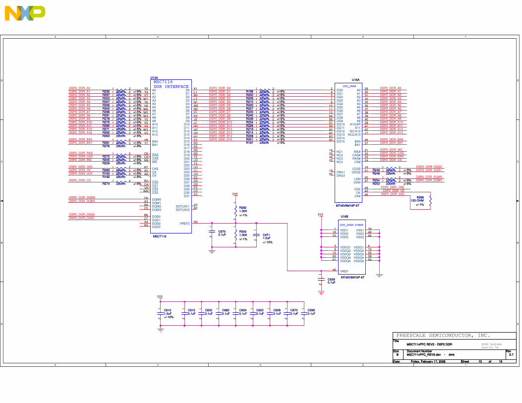
5
5
4
4
3
3
2
2
1
1
D D
C C
B B
A A
DSP2_DDR_A3
DSP2_DDR_A7
DSP2_DDR_D9
DSP2_DDR_A4
DSP2_DDR_A8DSP2_DDR_D8
DSP2_DDR_A5
DSP2_DDR_A9
DSP2_DDR_D7DSP2_DDR_A6
DSP2_DDR_A10
DSP2_DDR_D6DSP2_DDR_A7
DSP2_DDR_A11
DSP2_DDR_A8
DSP2_DDR_A12
DSP2_DDR_D4
DSP2_DDR_A9
DSP2_DDR_A13
DSP2_DDR_D3
DSP2_DDR_A10
DSP2_DDR_BA0
DSP2_DDR_D2
DSP2_DDR_A11
DSP2_DDR_BA1
DSP2_DDR_D1
DSP2_DDR_A12
DSP2_DDR_WE
DSP2_DDR_D0
DSP2_DDR_A13
DSP2_DDR_CASDSP2_DDR_RASDSP2_DDR_CS
DSP2_DDR_CKE
DSP2_DDR_BA0
DSP2_DDR_CK
DSP2_DDR_BA1
DSP2_DDR_nCK
DSP2_DDR_RAS
DSP2_DDR_D5
DSP2_DDR_DQM0
DSP2_DDR_CAS
DSP2_DDR_A0
DSP2_DDR_DQM1
DSP2_DDR_WE
DSP2_DDR_A1
DSP2_DDR_D15
DSP2_DDR_DQS0DSP2_DDR_CKE
DSP2_DDR_A2
DSP2_DDR_D14
DSP2_DDR_DQM0
DSP2_DDR_CK DSP2_DDR_DQS1
DSP2_DDR_A3
DSP2_DDR_D13
DSP2_DDR_nCK
DSP2_DDR_A0
DSP2_DDR_DQM1
DSP2_DDR_A4
DSP2_DDR_D12
DSP2_DDR_CS
DSP2_DDR_A1
DSP2_DDR_A5
DSP2_DDR_DQS0
DSP2_DDR_D11
DSP2_DDR_A2
DSP2_DDR_A6
DSP2_DDR_D10
DSP2_DDR_DQS12V5
2V5
2V5
Title
Size Document Number Rev
Date: Sheet of
MSC711xPFC_REV2.dsn - dmk 2.7
MSC711xPFC REV2 - DSP2 DDR
B
15 19Friday, February 17, 2006
Title
Size Document Number Rev
Date: Sheet of
MSC711xPFC_REV2.dsn - dmk 2.7
MSC711xPFC REV2 - DSP2 DDR
B
15 19Friday, February 17, 2006
Title
Size Document Number Rev
Date: Sheet of
MSC711xPFC_REV2.dsn - dmk 2.7
MSC711xPFC REV2 - DSP2 DDR
B
15 19Friday, February 17, 2006
NCSD SystemsAustin, Tx
FREESCALE SEMICONDUCTOR, INC.
1 2R192 22ohm +/-5%R192 22ohm +/-5%
1 2R270 22ohm +/-5%R270 22ohm +/-5%
1 2R262 22ohm +/-5%R262 22ohm +/-5%
1 2R276 22ohm +/-5%R276 22ohm +/-5%
1 2R275 22ohm +/-5%R275 22ohm +/-5%
1 2R306 22ohm +/-5%R306 22ohm +/-5%
1 2R259 22ohm +/-5%R259 22ohm +/-5%
1 2R197 22ohm +/-5%R197 22ohm +/-5%
12
C6000.1uF C6000.1uF
1 2R303 22ohm +/-5%R303 22ohm +/-5%
1 2R193 22ohm +/-5%R193 22ohm +/-5%
1 2R219 22ohm +/-5%R219 22ohm +/-5%
1 2R253 22ohm +/-5%R253 22ohm +/-5%
1 2R291 22ohm +/-5%R291 22ohm +/-5%
12
C6390.1uF C6390.1uF
12
C6320.1uF C6320.1uF
1 2R240 22ohm +/-5%R240 22ohm +/-5%
1 2R209 22ohm +/-5%R209 22ohm +/-5%
1 2R202 22ohm +/-5%R202 22ohm +/-5%
12
C6230.1uF C6230.1uF
1 2R201 22ohm +/-5%R201 22ohm +/-5%
12
C6101.0uF +/-10%
C6101.0uF +/-10%
12
C6730.1uF C6730.1uF
1 2R274 22ohm +/-5%R274 22ohm +/-5%
1 2R226 22ohm +/-5%R226 22ohm +/-5%
1 2R280 22ohm +/-5%R280 22ohm +/-5%
1 2R215 22ohm +/-5%R215 22ohm +/-5%
12
C6820.1uF C6820.1uF
12
R3001.00K+/-1%
R3001.00K+/-1%
1 2R297 22ohm +/-5%R297 22ohm +/-5%
1 2R249 22ohm +/-5%R249 22ohm +/-5%
1 2R208 22ohm +/-5%R208 22ohm +/-5%
1 2R234 22ohm +/-5%R234 22ohm +/-5%
1 2R269 22ohm +/-5%R269 22ohm +/-5%
1 2R302 22ohm +/-5%R302 22ohm +/-5%
1 2R281 22ohm +/-5%R281 22ohm +/-5%
1 2R245 22ohm +/-5%R245 22ohm +/-5%
1 2R307 22ohm +/-5%R307 22ohm +/-5%
VDD11
VDD218
VDD333
VDDQ13
VDDQ29
VDDQ315
VDDQ455
VDDQ561
VREF49
VSS1 34
VSS2 48
VSS3 66
VSSQ1 6
VSSQ2 12
VSSQ4 58VSSQ3 52
VSSQ5 64
DDR_DRAM POWER
U16B
MT46V8M16P-6T
DDR_DRAM POWER
U16B
MT46V8M16P-6T
1 2R220 22ohm +/-5%R220 22ohm +/-5%
12
C6150.1uF C6150.1uF
1 2R235 22ohm +/-5%R235 22ohm +/-5%
1 2R248 22ohm +/-5%R248 22ohm +/-5%
1 2R292 22ohm +/-5%R292 22ohm +/-5%
R268120 OHM
+/-1%
R268120 OHM
+/-1%
1 2R198 22ohm +/-5%R198 22ohm +/-5%A0Y5
A1Y4
A2V7
A3W7
A4Y6
A5V6
A6W6
A7W5
A8W4
A9Y3
A10V5
A11V4
A12W3
A13V3
BA0V8
BA1Y7
RASC8
CASC9
WEB8
CKEB7
CKA5
CKA6
CS0B3
CS1C4
CS2V9
CS3W8
D0 K1
D1 L1
D2 M1
D3 L3
D4 N1
D5 M3
D6 N2
D7 P1
D8 K3
D9 J3
D10 J1
D11 H3
D12 H2
D13 G2
D14 H1
D15 F2
D16 P3
D17 P2
D18 R3
D19 R2
D20 T2
D21 U2
D22 T3
D23 U3
D24 C1
D25 C3
D26 E2
D27 D3
D28 D2
D29 F3
D30 C2
DQM0C6
DQM1A3
DQM2B4
DQM3C5
DQS0B6
DQS1C7
DQS2A4
DQS3B5
D31 E3
SSTLNC1 V2
SSTLNC2 B2
VREF2 N3
MSC7116DDR INTERFACE
U13A
MSC7119
MSC7116DDR INTERFACE
U13A
MSC7119
1 2R227 22ohm +/-5%R227 22ohm +/-5%
DQ02
DQ14
DQ25
DQ37
DQ48
DQ510
DQ611
DQ713
DQ854
DQ956
DQ1057
DQ1159
DQ1260
DQ1362
DQ1463
DQ1565
A0 29
A1 30
A2 31
A3 32
A4 35
A5 36
A6 37
A7 38
A8 39
A9 40
A10/AP 28
A11 41
BA0 26
BA1 27
CAS# 22WE# 21
RAS# 23
CS# 24
LDQS 16
UDQS 51
LDM 20
UDM 47
NC114
NC2/A13 17
NC225
NC/A12 42
NC343
NC453
DNU119
DNU250
CKE 44
CK 45
CK# 46
DDR_DRAM
U16A
MT46V8M16P-6T
DDR_DRAM
U16A
MT46V8M16P-6T
1 2R214 22ohm +/-5%R214 22ohm +/-5%
1 2R279 22ohm +/-5%R279 22ohm +/-5%
1 2R239 22ohm +/-5%R239 22ohm +/-5%
12
C5990.1uF C5990.1uF
1 2R254 22ohm +/-5%R254 22ohm +/-5%
12
C6711.0uF +/-10%
C6711.0uF +/-10%
12
C6380.1uF C6380.1uF
1 2R263 22ohm +/-5%R263 22ohm +/-5%
1 2R296 22ohm +/-5%R296 22ohm +/-5%
1 2R271 22ohm +/-5%R271 22ohm +/-5%
12
R2821.00K+/-1%
R2821.00K+/-1%
12
C6700.1uF C6700.1uF
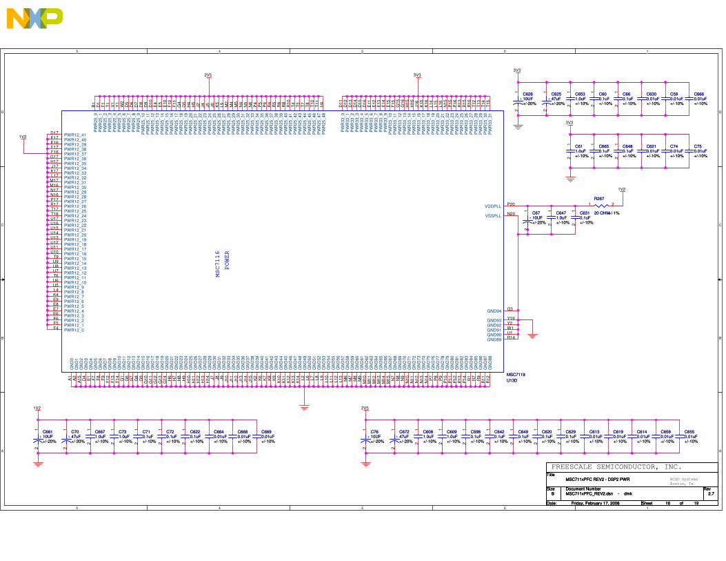
5
5
4
4
3
3
2
2
1
1
D D
C C
B B
A A
1V2
1V2
2V5
2V5
3V3
1V2
3V3
3V3
Title
Size Document Number Rev
Date: Sheet of
MSC711xPFC_REV2.dsn - dmk 2.7
MSC711xPFC REV2 - DSP2 PWR
B
16 19Friday, February 17, 2006
Title
Size Document Number Rev
Date: Sheet of
MSC711xPFC_REV2.dsn - dmk 2.7
MSC711xPFC REV2 - DSP2 PWR
B
16 19Friday, February 17, 2006
Title
Size Document Number Rev
Date: Sheet of
MSC711xPFC_REV2.dsn - dmk 2.7
MSC711xPFC REV2 - DSP2 PWR
B
16 19Friday, February 17, 2006
NCSD SystemsAustin, Tx
FREESCALE SEMICONDUCTOR, INC.
12
+C66110UF+/-20%
+C66110UF+/-20%
12
C6220.1uF +/-10%
C6220.1uF +/-10%
12
+C6710UF+/-20%
+C6710UF+/-20%
12
C611.0uF +/-10%
C611.0uF +/-10%
C6680.01uF+/-10%
C6680.01uF+/-10%
12
C6290.1uF +/-10%
C6290.1uF +/-10%
PWR12_0F4PWR12_1F5 PWR12_2F6 PWR12_3E6 PWR12_4E7 PWR12_5E8PWR12_6E9 PWR12_7K4 PWR12_8L4 PWR12_9U5 PWR12_10U6PWR12_11T6 PWR12_12U7 PWR12_13U8 PWR12_14U9
PW
R25
_0B
1
PW
R25
_1D
1
PW
R25
_2F1
PW
R25
_3T1
PW
R25
_4V
1
PW
R25
_5Y
1
PW
R25
_6W
2
PW
R25
_13
E4
PW
R25
_14
E5
PW
R25
_15
E10
PW
R25
_16
F10
PW
R25
_17
F11
PW
R25
_18
G4
PW
R25
_19
G5
PW
R25
_20
H4
PW
R25
_21
H5
PW
R25
_22
J2
GN
D0
A1
GN
D1
A2
GN
D2
A15
GN
D3
D4
GN
D4
E1
VDDPLL P20
VSSPLL N20
PWR12_15T9PWR12_16U10 PWR12_17U11
PWR12_26R17 PWR12_27P17 PWR12_28N16 PWR12_29N17 PWR12_30M16PWR12_31M17
PWR12_18U12 PWR12_19U13 PWR12_20U14PWR12_21U15 PWR12_22U16 PWR12_23U17 PWR12_24T16 PWR12_25T17
PWR12_32L17 PWR12_33K17 PWR12_34J17 PWR12_35H17PWR12_36G17 PWR12_37F16 PWR12_38F17 PWR12_39E16 PWR12_40E17PWR12_41D17 P
WR
25_7
D5
PW
R25
_8D
6
PW
R25
_9D
7
PW
R25
_10
D8
PW
R25
_11
D9
PW
R25
_12
D10
PW
R25
_23
J4
PW
R25
_24
J5
PW
R25
_25
J6
PW
R25
_26
K5
PW
R25
_27
L5
PW
R25
_28
M2
PW
R25
_29
M4
PW
R25
_30
M5
PW
R25
_31
N4
PW
R25
_32
N5
PW
R25
_33
N6
PW
R25
_34
P4
PW
R25
_35
P5
PW
R25
_36
P6
PW
R25
_37
R4
PW
R25
_38
R5
PW
R25
_39
R6
PW
R25
_40
R8
PW
R25
_41
R10
PW
R25
_42
T4
PW
R25
_43
T5
PW
R25
_44
T7
PW
R25
_45
T8
PW
R25
_46
T10
PW
R25
_47
T11
PW
R25
_48
U4
GN
D5
F7
GN
D6
F8
GN
D7
F9
GN
D8
F12
GN
D9
F13
GN
D10
F14
GN
D11
G1
GN
D12
G6
GN
D13
G7
GN
D14
G8
GN
D15
G9
GN
D16
G10
GN
D17
G11
GN
D18
G12
GN
D19
G13
GN
D20
G14
GN
D21
H6
GN
D22
H7
GN
D23
H8
GN
D24
H9
GN
D25
H10
GN
D26
H11
GN
D27
H12
GN
D28
H13
GN
D29
H14
GN
D30
J7
GN
D31
J8
GN
D32
J9
GN
D33
J10
GN
D34
J11
GN
D35
J12
GN
D36
J13
GN
D37
J14
GN
D38
J15
GN
D39
K2
GN
D40
K6
GN
D41
K7
GN
D42
K8
GN
D43
K9
GN
D44
K10
GN
D45
K11
GN
D46
K12
GN
D47
K13
GN
D48
K14
GN
D49
L2
GN
D50
L6
GN
D51
L7
GN
D52
L8
GN
D53
L9
GN
D54
L10
GN
D55
L11
GN
D56
L12
GN
D57
L13
GN
D58
M6
GN
D59
M7
GN
D60
M8
GN
D61
M9
GN
D62
M10
GN
D63
M11
GN
D64
M12
GN
D65
M13
GN
D66
M14
GN
D67
M15
GN
D68
N7
GN
D69
N8
GN
D70
N9
GN
D71
N10
GN
D72
N11
GN
D73
N12
GN
D74
N13
GN
D75
N14
GN
D76
P7
GN
D77
P8
GN
D78
P9
GN
D79
P10
GN
D80
P11
GN
D81
P12
GN
D82
P13
GN
D83
P14
GN
D84
R1
GN
D85
R7
GN
D86
R9
GN
D87
R11
GN
D88
R12
GND89 R14GND90 U1GND91 W1GND92 Y2GND93 Y19
PW
R33
_0D
11
PW
R33
_1D
12
PW
R33
_2D
13
PW
R33
_3D
14
PW
R33
_4D
15
PW
R33
_5D
16
PW
R33
_6E
11
PW
R33
_7E
12
PW
R33
_8E
13
PW
R33
_9E
14
PW
R33
_10
E15
PW
R33
_11
F15
PW
R33
_12
G15
PW
R33
_13
G16
PW
R33
_14
H15
PW
R33
_15
H16
PW
R33
_16
J16
PW
R33
_17
K15
PW
R33
_18
K16
PW
R33
_19
L14
PW
R33
_20
L15
PW
R33
_21
L16
PW
R33
_22
N15
PW
R33
_23
P15
PW
R33
_24
P16
PW
R33
_25
R13
PW
R33
_26
R15
PW
R33
_27
R16
PW
R33
_28
T12
PW
R33
_29
T13
PW
R33
_30
T14
PW
R33
_31
T15
GND94 G3
MSC7116
POWER
U13DMSC7119
MSC7116
POWER
U13DMSC7119
12
C6091.0uF +/-10%
C6091.0uF +/-10%
C590.01uF+/-10%
C590.01uF+/-10%
C6140.01uF+/-10%
C6140.01uF+/-10%
12
+C67247uF+/-20%
+C67247uF+/-20%
C6640.01uF+/-10%
C6640.01uF+/-10%
12
C5980.1uF +/-10%
C5980.1uF +/-10%
C740.01uF+/-10%
C740.01uF+/-10%
C6130.01uF+/-10%
C6130.01uF+/-10%
12
C600.1uF +/-10%
C600.1uF +/-10%
12
+C62610UF+/-20%
+C62610UF+/-20%
C6660.01uF+/-10%
C6660.01uF+/-10%
12
C6650.1uF +/-10%
C6650.1uF +/-10%
12
C731.0uF +/-10%
C731.0uF +/-10%
C6690.01uF+/-10%
C6690.01uF+/-10%
12
C6420.1uF +/-10%
C6420.1uF +/-10%
C750.01uF+/-10%
C750.01uF+/-10%
1 2R267
20 OHM+/-1%
R267
20 OHM+/-1%12
C6471.0uF +/-10%
C6471.0uF +/-10%
12
C660.1uF +/-10%
C660.1uF +/-10%
12
C6480.1uF +/-10%
C6480.1uF +/-10%
12
C6310.1uF +/-10%
C6310.1uF +/-10%
12
+C62547uF+/-20%
+C62547uF+/-20%
C6190.01uF+/-10%
C6190.01uF+/-10%
C6550.01uF+/-10%
C6550.01uF+/-10%
12
C710.1uF +/-10%
C710.1uF +/-10%
12
C6490.1uF +/-10%
C6490.1uF +/-10%
12
C6081.0uF +/-10%
C6081.0uF +/-10%
12
C720.1uF +/-10%
C720.1uF +/-10%
12
+C7047uF+/-20%
+C7047uF+/-20%
12
C6200.1uF +/-10%
C6200.1uF +/-10%
C6590.01uF+/-10%
C6590.01uF+/-10%
12
C6531.0uF +/-10%
C6531.0uF +/-10%
C6300.01uF+/-10%
C6300.01uF+/-10%
12
C6671.0uF +/-10%
C6671.0uF +/-10%
12
+C7610UF+/-20%
+C7610UF+/-20%
C6210.01uF+/-10%
C6210.01uF+/-10%

5
5
4
4
3
3
2
2
1
1
D D
C C
B B
A A
DSP_HA0DSP_HD0DSP_HA1DSP_HD1DSP_HA2DSP_HD2
DSP_HD3DSP_HD4DSP_HD5DSP_HD6DSP_HD7
DSP3_SPI_nCS
DSP_HD8DSP_HD9
DSP3_SPI_DOUT
DSP_HD10
DSP3_ID0
DSP_HD11
DSP3_ID1
DSP_HD12DSP_HD13
DSP3_SPI_DIN
DSP_HD14DSP_HD15
DSP3_SPI_CLK
DSP3_SPI_DIN
DSP3_SPI_DOUT
DSP3_ID0
DSP3_SPI_CLK
DSP3_SPI_nCS
DSP3_ID1
3V3
3V3
3V3
3V3
DSP_DBREQ5,8,11,14
DSP_BHCS5,8,11,14
CT_D1 3,4,8,11,14
DSP_HA[2:0] 5,7,8,11,14
DSP_I2C_SD 6,8,11,14
DSP3_RMII_TXD0 7
CT_D0 3,4,8,11,14
DSP3_RMII_TXD1 7
DSP_I2C_SC 6,8,11,14
CT_D5 3,4,8,11,14
DSP3_RMII_RXD1 7
EONCE_TCK5,8,11,14
CT_D4 3,4,8,11,14
CPLD_TDO5
DSP3_RMII_RXD0 7
DSP3_TDO14
EONCE_TMS5,8,11,14EONCE_nTRST3,8,11,14
DSP3_RMII_CSDV 7
RMII_REFCLK3 5,14DSP3_RMII_TXEN 7
DSP3_LED 6
DSP_C8_2 5,14
DSP3_CLKIN5
DSP_FRAME 5,8,11,14
PORESET5,7,8,11,14
DSP3_HTRQ5
DSP3_HRESET5
DSP3_HRRQ5
DSP_HD[15:0] 5,7,8,11,14
DSP3_HCS5
DSP_HRW5,7,8,11,14DSP_HDS5,7,8,11,14
DSP3_BM05DSP_BM15,8,11,14DSP_SWTE5,8,11,14
DSP_BM2 5,8,11,14DSP_BM3 5,8,11,14
Title
Size Document Number Rev
Date: Sheet of
MSC711xPFC_REV2.dsn - dmk 2.7
MSC711xPFC REV2 - DSP3 SYS
B
17 19Friday, February 17, 2006
Title
Size Document Number Rev
Date: Sheet of
MSC711xPFC_REV2.dsn - dmk 2.7
MSC711xPFC REV2 - DSP3 SYS
B
17 19Friday, February 17, 2006
Title
Size Document Number Rev
Date: Sheet of
MSC711xPFC_REV2.dsn - dmk 2.7
MSC711xPFC REV2 - DSP3 SYS
B
17 19Friday, February 17, 2006
NCSD SystemsAustin, Tx
FREESCALE SEMICONDUCTOR, INC.
DNP
DNP
DNP
MSC711x HDI16
MSC711x BOOT EEPROM
MSC711x MAIN
HD0A14
HD1A13
HD2B13
HD3C12
HD4A12
HD5B12
HD6A11
HD7A10
HD8B11
HD9C11
HD10A9
HD11B10
HD12A8
HD13C10
HD14B9
HD15A7
HA0 K18
HA1 H20
HA2 H19
HA3 J18
HA4 G20
HA5 G19
HA6 H18
HA7 F20
HA8 F19
HA9 G18
HA10 E19
HA11 E20
HA12 F18
HA13 E18
HA14 D19
HA15 D20
HA16 D18
HA17 C19
HA18 C20
HA19 B20
HA20 C18
HA21 B19
HA22 A20
HA23 C17
HCS1/HCS1L19
HCS2/HCS2L18
HRW/HRW / HRD/HRDL20
HDDSK19
HDSP / HTRQ/HTRQ / HREQ/HREQJ20
HRRQ/HRRQ / HACK/HACKJ19
HDS/HDS / HWR/HWRK20
FCS0 B18
FCS1 A19
FCS2 C16
FCS3 B17
BCLK A18OE C15
FLASH_NC1 B15
FLASH_NC2 A16
FLASH_NC3 B14
FLASH_NC4 C13
MSC7116
Host Data Interface
U19C
MSC7119
MSC7116
Host Data Interface
U19C
MSC7119
12
R2601K+/-5%
R2601K+/-5%
1 2R207 1K +/-5%R207 1K +/-5%
12
R511K+/-5%
R511K+/-5%
1 2R247 22ohm +/-5%R247 22ohm +/-5%
12
C650.1uF C650.1uF
12
R2051K+/-5%
R2051K+/-5%
T0RCK / IRQ4 Y10
T0RFS / IRQ5 W11
T0RD Y11
T0TCK / IRQ6 V12
T0TFS / IRQ7 W12
T0TD Y12
T1RCK / IRQ0 Y13
T1RFS / IRQ1 V13
T1RD / IRQ8 W13
T1TCK / IRQ9 Y14
T1TFS / IRQ10 W14
T1TD / IRQ11 V14
TXD0 / IRQ19 Y17
TXD1 / IRQ20 W17
RXD0 / IRQ22 V17
RXD1 / IRQ21 Y18
TXCLK / IRQ23 W18
TX_EN / IRQ24 V18
RX_DV / IRQ25 Y20
RX_ER / IRQ26 W19
COL U18
CRS V19
MDC / H8BIT W20
MDIO T18
TXD3 / T2RCK / IRQ16 Y15TXD2 / T2RFS W15
TX_ER / T2RD / IRQ17 V15
RXCLK / T2TCK Y16
RXD3 / T2TFS / IRQ18 W16RXD2 / T2TD V16
TCKU19
TDIV20
TDOR18
TMST19
TRSTU20
J_DBREQ / EE0R19
SDA / IRQ15 M18
SCL / IRQ14 N19
URXD / IRQ2 M20UTXD / IRQ3 M19
PORESETP18
HRESETT20
TEST0R20
TPSEL(TEST1)P19
EVNT0V10
EVNT1 / IRQ13 / CLK0W9
EVNT2 / BM0W10
EVNT3 / BM1Y9
EVNT4 / IRQ12 / SWTEV11
NMIY8
SMII_SYNCB16SMII_SYNC_INC14 SMII_TXDA17
CLKINN18
MSC7116SYSTEM & I/O INTERFACE
TDM0
TDM1
MII/TDM2
UART
I2C
EONCE
U19B
MSC7119
MSC7116SYSTEM & I/O INTERFACE
TDM0
TDM1
MII/TDM2
UART
I2C
EONCE
U19B
MSC7119
12
R2611K+/-5%
R2611K+/-5%
1 2R301 22ohm +/-5%R301 22ohm +/-5%
1 2R40 0 OHM +/-5%R40 0 OHM +/-5%
1 2R206 1K +/-5%R206 1K +/-5%
Vss
4
Vcc
8
DIN 5
DOUT 2
CLK 6nCS1
nWE3
nHOLD7
TAB
9
U18
M25P80-VMP6G
U18
M25P80-VMP6G
12
R491K+/-5%
R491K+/-5%
12
R481K+/-5%
R481K+/-5%
1 2R41 0 OHM +/-5%R41 0 OHM +/-5%
1 2R295 22ohm +/-5%R295 22ohm +/-5%
12
R521K+/-5%
R521K+/-5%
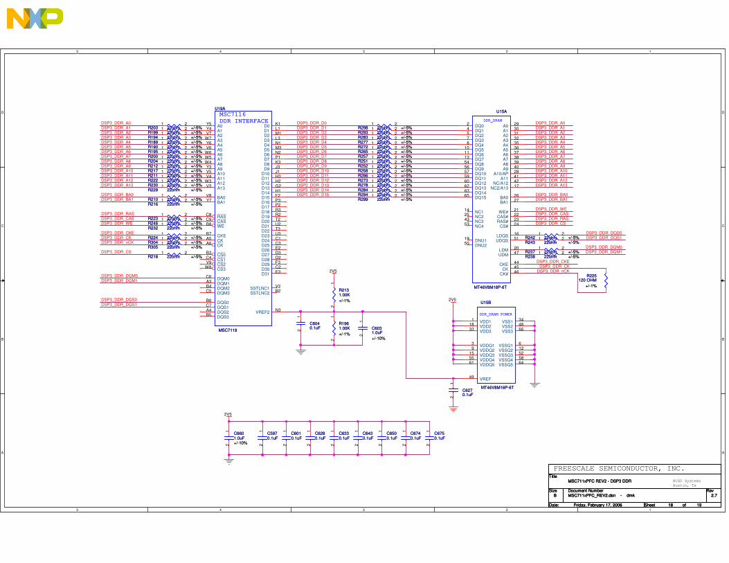
5
5
4
4
3
3
2
2
1
1
D D
C C
B B
A A
DSP3_DDR_A3
DSP3_DDR_A7
DSP3_DDR_D9
DSP3_DDR_A4
DSP3_DDR_A8DSP3_DDR_D8
DSP3_DDR_A5
DSP3_DDR_A9
DSP3_DDR_D7DSP3_DDR_A6
DSP3_DDR_A10
DSP3_DDR_D6DSP3_DDR_A7
DSP3_DDR_A11
DSP3_DDR_A8
DSP3_DDR_A12
DSP3_DDR_D4
DSP3_DDR_A9
DSP3_DDR_A13
DSP3_DDR_D3
DSP3_DDR_A10
DSP3_DDR_BA0
DSP3_DDR_D2
DSP3_DDR_A11
DSP3_DDR_BA1
DSP3_DDR_D1
DSP3_DDR_A12
DSP3_DDR_WE
DSP3_DDR_D0
DSP3_DDR_A13
DSP3_DDR_CASDSP3_DDR_RASDSP3_DDR_CS
DSP3_DDR_CKE
DSP3_DDR_BA0
DSP3_DDR_CK
DSP3_DDR_BA1
DSP3_DDR_nCK
DSP3_DDR_RAS
DSP3_DDR_D5
DSP3_DDR_DQM0
DSP3_DDR_CAS
DSP3_DDR_A0
DSP3_DDR_DQM1
DSP3_DDR_WE
DSP3_DDR_A1
DSP3_DDR_D15
DSP3_DDR_DQS0DSP3_DDR_CKE
DSP3_DDR_A2
DSP3_DDR_D14
DSP3_DDR_DQM0
DSP3_DDR_CK DSP3_DDR_DQS1
DSP3_DDR_A3
DSP3_DDR_D13
DSP3_DDR_nCK
DSP3_DDR_A0
DSP3_DDR_DQM1
DSP3_DDR_A4
DSP3_DDR_D12
DSP3_DDR_CS
DSP3_DDR_A1
DSP3_DDR_A5
DSP3_DDR_DQS0
DSP3_DDR_D11
DSP3_DDR_A2
DSP3_DDR_A6
DSP3_DDR_D10
DSP3_DDR_DQS12V5
2V5
2V5
Title
Size Document Number Rev
Date: Sheet of
MSC711xPFC_REV2.dsn - dmk 2.7
MSC711xPFC REV2 - DSP3 DDR
B
18 19Friday, February 17, 2006
Title
Size Document Number Rev
Date: Sheet of
MSC711xPFC_REV2.dsn - dmk 2.7
MSC711xPFC REV2 - DSP3 DDR
B
18 19Friday, February 17, 2006
Title
Size Document Number Rev
Date: Sheet of
MSC711xPFC_REV2.dsn - dmk 2.7
MSC711xPFC REV2 - DSP3 DDR
B
18 19Friday, February 17, 2006
NCSD SystemsAustin, Tx
FREESCALE SEMICONDUCTOR, INC.
1 2R246 22ohm +/-5%R246 22ohm +/-5%
1 2R189 22ohm +/-5%R189 22ohm +/-5% 1 2
R272 22ohm +/-5%R272 22ohm +/-5%
12
C5970.1uF C5970.1uF
1 2R257 22ohm +/-5%R257 22ohm +/-5%
1 2R243 22ohm +/-5%R243 22ohm +/-5%
1 2R203 22ohm +/-5%R203 22ohm +/-5%
R225120 OHM
+/-1%
R225120 OHM
+/-1%
1 2R298 22ohm +/-5%R298 22ohm +/-5%A0Y5
A1Y4
A2V7
A3W7
A4Y6
A5V6
A6W6
A7W5
A8W4
A9Y3
A10V5
A11V4
A12W3
A13V3
BA0V8
BA1Y7
RASC8
CASC9
WEB8
CKEB7
CKA5
CKA6
CS0B3
CS1C4
CS2V9
CS3W8
D0 K1
D1 L1
D2 M1
D3 L3
D4 N1
D5 M3
D6 N2
D7 P1
D8 K3
D9 J3
D10 J1
D11 H3
D12 H2
D13 G2
D14 H1
D15 F2
D16 P3
D17 P2
D18 R3
D19 R2
D20 T2
D21 U2
D22 T3
D23 U3
D24 C1
D25 C3
D26 E2
D27 D3
D28 D2
D29 F3
D30 C2
DQM0C6
DQM1A3
DQM2B4
DQM3C5
DQS0B6
DQS1C7
DQS2A4
DQS3B5
D31 E3
SSTLNC1 V2
SSTLNC2 B2
VREF2 N3
MSC7116DDR INTERFACE
U19A
MSC7119
MSC7116DDR INTERFACE
U19A
MSC7119
1 2R265 22ohm +/-5%R265 22ohm +/-5%
1 2R278 22ohm +/-5%R278 22ohm +/-5%
VDD11
VDD218
VDD333
VDDQ13
VDDQ29
VDDQ315
VDDQ455
VDDQ561
VREF49
VSS1 34
VSS2 48
VSS3 66
VSSQ1 6
VSSQ2 12
VSSQ4 58VSSQ3 52
VSSQ5 64
DDR_DRAM POWER
U15B
MT46V8M16P-6T
DDR_DRAM POWER
U15B
MT46V8M16P-6T
1 2R212 22ohm +/-5%R212 22ohm +/-5%
1 2R252 22ohm +/-5%R252 22ohm +/-5%
12
C6750.1uF C6750.1uF
1 2R237 22ohm +/-5%R237 22ohm +/-5%
12
C6031.0uF +/-10%
C6031.0uF +/-10%
12
C6500.1uF C6500.1uF
1 2R229 22ohm +/-5%R229 22ohm +/-5%
1 2R200 22ohm +/-5%R200 22ohm +/-5%
1 2R222 22ohm +/-5%R222 22ohm +/-5%
12
R2131.00K+/-1%
R2131.00K+/-1%
12
C6040.1uF C6040.1uF
1 2R305 22ohm +/-5%R305 22ohm +/-5%
1 2R223 22ohm +/-5%R223 22ohm +/-5%
1 2R230 22ohm +/-5%R230 22ohm +/-5%
DQ02
DQ14
DQ25
DQ37
DQ48
DQ510
DQ611
DQ713
DQ854
DQ956
DQ1057
DQ1159
DQ1260
DQ1362
DQ1463
DQ1565
A0 29
A1 30
A2 31
A3 32
A4 35
A5 36
A6 37
A7 38
A8 39
A9 40
A10/AP 28
A11 41
BA0 26
BA1 27
CAS# 22WE# 21
RAS# 23
CS# 24
LDQS 16
UDQS 51
LDM 20
UDM 47
NC114
NC2/A13 17
NC225
NC/A12 42
NC343
NC453
DNU119
DNU250
CKE 44
CK 45
CK# 46
DDR_DRAM
U15A
MT46V8M16P-6T
DDR_DRAM
U15A
MT46V8M16P-6T
1 2R216 22ohm +/-5%R216 22ohm +/-5%
1 2R217 22ohm +/-5%R217 22ohm +/-5%
1 2R190 22ohm +/-5%R190 22ohm +/-5%
1 2R232 22ohm +/-5%R232 22ohm +/-5%
1 2R299 22ohm +/-5%R299 22ohm +/-5%
12
C6330.1uF C6330.1uF
1 2R194 22ohm +/-5%R194 22ohm +/-5%
1 2R304 22ohm +/-5%R304 22ohm +/-5%
1 2R273 22ohm +/-5%R273 22ohm +/-5%
1 2R238 22ohm +/-5%R238 22ohm +/-5%
1 2R204 22ohm +/-5%R204 22ohm +/-5%
12
C6270.1uF C6270.1uF
12
C6010.1uF C6010.1uF
1 2R251 22ohm +/-5%R251 22ohm +/-5%
1 2R283 22ohm +/-5%R283 22ohm +/-5%
1 2R293 22ohm +/-5%R293 22ohm +/-5%
12
C6430.1uF C6430.1uF
1 2R294 22ohm +/-5%R294 22ohm +/-5%
12
C6601.0uF +/-10%
C6601.0uF +/-10%
12
C6740.1uF C6740.1uF
1 2R218 22ohm +/-5%R218 22ohm +/-5%
1 2R266 22ohm +/-5%R266 22ohm +/-5%
1 2R211 22ohm +/-5%R211 22ohm +/-5%
12
C6280.1uF C6280.1uF
1 2R277 22ohm +/-5%R277 22ohm +/-5%
12
R1961.00K+/-1%
R1961.00K+/-1%
1 2R199 22ohm +/-5%R199 22ohm +/-5%
1 2R242 22ohm +/-5%R242 22ohm +/-5%
1 2R284 22ohm +/-5%R284 22ohm +/-5%
1 2R258 22ohm +/-5%R258 22ohm +/-5%
1 2R224 22ohm +/-5%R224 22ohm +/-5%
1 2R195 22ohm +/-5%R195 22ohm +/-5%
1 2R210 22ohm +/-5%R210 22ohm +/-5%

5
5
4
4
3
3
2
2
1
1
D D
C C
B B
A A
1V2
1V2
2V5
2V5
3V3
1V2
3V3
3V3
Title
Size Document Number Rev
Date: Sheet of
MSC711xPFC_REV2.dsn - dmk 2.7
MSC711xPFC REV2 - DSP3 PWR
B
19 19Friday, February 17, 2006
Title
Size Document Number Rev
Date: Sheet of
MSC711xPFC_REV2.dsn - dmk 2.7
MSC711xPFC REV2 - DSP3 PWR
B
19 19Friday, February 17, 2006
Title
Size Document Number Rev
Date: Sheet of
MSC711xPFC_REV2.dsn - dmk 2.7
MSC711xPFC REV2 - DSP3 PWR
B
19 19Friday, February 17, 2006
NCSD SystemsAustin, Tx
FREESCALE SEMICONDUCTOR, INC.
12
C6160.1uF +/-10%
C6160.1uF +/-10%
12
C6170.1uF +/-10%
C6170.1uF +/-10%
12
+C6210UF+/-20%
+C6210UF+/-20%
PWR12_0F4PWR12_1F5 PWR12_2F6 PWR12_3E6 PWR12_4E7 PWR12_5E8PWR12_6E9 PWR12_7K4 PWR12_8L4 PWR12_9U5 PWR12_10U6PWR12_11T6 PWR12_12U7 PWR12_13U8 PWR12_14U9
PW
R25
_0B
1
PW
R25
_1D
1
PW
R25
_2F1
PW
R25
_3T1
PW
R25
_4V
1
PW
R25
_5Y
1
PW
R25
_6W
2
PW
R25
_13
E4
PW
R25
_14
E5
PW
R25
_15
E10
PW
R25
_16
F10
PW
R25
_17
F11
PW
R25
_18
G4
PW
R25
_19
G5
PW
R25
_20
H4
PW
R25
_21
H5
PW
R25
_22
J2
GN
D0
A1
GN
D1
A2
GN
D2
A15
GN
D3
D4
GN
D4
E1
VDDPLL P20
VSSPLL N20
PWR12_15T9PWR12_16U10 PWR12_17U11
PWR12_26R17 PWR12_27P17 PWR12_28N16 PWR12_29N17 PWR12_30M16PWR12_31M17
PWR12_18U12 PWR12_19U13 PWR12_20U14PWR12_21U15 PWR12_22U16 PWR12_23U17 PWR12_24T16 PWR12_25T17
PWR12_32L17 PWR12_33K17 PWR12_34J17 PWR12_35H17PWR12_36G17 PWR12_37F16 PWR12_38F17 PWR12_39E16 PWR12_40E17PWR12_41D17 P
WR
25_7
D5
PW
R25
_8D
6
PW
R25
_9D
7
PW
R25
_10
D8
PW
R25
_11
D9
PW
R25
_12
D10
PW
R25
_23
J4
PW
R25
_24
J5
PW
R25
_25
J6
PW
R25
_26
K5
PW
R25
_27
L5
PW
R25
_28
M2
PW
R25
_29
M4
PW
R25
_30
M5
PW
R25
_31
N4
PW
R25
_32
N5
PW
R25
_33
N6
PW
R25
_34
P4
PW
R25
_35
P5
PW
R25
_36
P6
PW
R25
_37
R4
PW
R25
_38
R5
PW
R25
_39
R6
PW
R25
_40
R8
PW
R25
_41
R10
PW
R25
_42
T4
PW
R25
_43
T5
PW
R25
_44
T7
PW
R25
_45
T8
PW
R25
_46
T10
PW
R25
_47
T11
PW
R25
_48
U4
GN
D5
F7
GN
D6
F8
GN
D7
F9
GN
D8
F12
GN
D9
F13
GN
D10
F14
GN
D11
G1
GN
D12
G6
GN
D13
G7
GN
D14
G8
GN
D15
G9
GN
D16
G10
GN
D17
G11
GN
D18
G12
GN
D19
G13
GN
D20
G14
GN
D21
H6
GN
D22
H7
GN
D23
H8
GN
D24
H9
GN
D25
H10
GN
D26
H11
GN
D27
H12
GN
D28
H13
GN
D29
H14
GN
D30
J7
GN
D31
J8
GN
D32
J9
GN
D33
J10
GN
D34
J11
GN
D35
J12
GN
D36
J13
GN
D37
J14
GN
D38
J15
GN
D39
K2
GN
D40
K6
GN
D41
K7
GN
D42
K8
GN
D43
K9
GN
D44
K10
GN
D45
K11
GN
D46
K12
GN
D47
K13
GN
D48
K14
GN
D49
L2
GN
D50
L6
GN
D51
L7
GN
D52
L8
GN
D53
L9
GN
D54
L10
GN
D55
L11
GN
D56
L12
GN
D57
L13
GN
D58
M6
GN
D59
M7
GN
D60
M8
GN
D61
M9
GN
D62
M10
GN
D63
M11
GN
D64
M12
GN
D65
M13
GN
D66
M14
GN
D67
M15
GN
D68
N7
GN
D69
N8
GN
D70
N9
GN
D71
N10
GN
D72
N11
GN
D73
N12
GN
D74
N13
GN
D75
N14
GN
D76
P7
GN
D77
P8
GN
D78
P9
GN
D79
P10
GN
D80
P11
GN
D81
P12
GN
D82
P13
GN
D83
P14
GN
D84
R1
GN
D85
R7
GN
D86
R9
GN
D87
R11
GN
D88
R12
GND89 R14GND90 U1GND91 W1GND92 Y2GND93 Y19
PW
R33
_0D
11
PW
R33
_1D
12
PW
R33
_2D
13
PW
R33
_3D
14
PW
R33
_4D
15
PW
R33
_5D
16
PW
R33
_6E
11
PW
R33
_7E
12
PW
R33
_8E
13
PW
R33
_9E
14
PW
R33
_10
E15
PW
R33
_11
F15
PW
R33
_12
G15
PW
R33
_13
G16
PW
R33
_14
H15
PW
R33
_15
H16
PW
R33
_16
J16
PW
R33
_17
K15
PW
R33
_18
K16
PW
R33
_19
L14
PW
R33
_20
L15
PW
R33
_21
L16
PW
R33
_22
N15
PW
R33
_23
P15
PW
R33
_24
P16
PW
R33
_25
R13
PW
R33
_26
R15
PW
R33
_27
R16
PW
R33
_28
T12
PW
R33
_29
T13
PW
R33
_30
T14
PW
R33
_31
T15
GND94 G3
MSC7116
POWER
U19DMSC7119
MSC7116
POWER
U19DMSC7119
C540.01uF+/-10%
C540.01uF+/-10%
12
C6560.1uF +/-10%
C6560.1uF +/-10%
C6800.01uF+/-10%
C6800.01uF+/-10%
12
C6520.1uF +/-10%
C6520.1uF +/-10%
12
C6340.1uF +/-10%
C6340.1uF +/-10%
12
C6120.1uF +/-10%
C6120.1uF +/-10%
C6810.01uF+/-10%
C6810.01uF+/-10%
12
C691.0uF +/-10%
C691.0uF +/-10%
12
C6631.0uF +/-10%
C6631.0uF +/-10%
C6450.01uF+/-10%
C6450.01uF+/-10%
C680.01uF+/-10%
C680.01uF+/-10%
12
C6060.1uF +/-10%
C6060.1uF +/-10%
C6370.01uF+/-10%
C6370.01uF+/-10%
C560.01uF+/-10%
C560.01uF+/-10%
C6350.01uF+/-10%
C6350.01uF+/-10%
12
C6240.1uF +/-10%
C6240.1uF +/-10%
12
+C67610UF+/-20%
+C67610UF+/-20%
12
+C60247uF+/-20%
+C60247uF+/-20%
C6440.01uF+/-10%
C6440.01uF+/-10%
12
C6791.0uF +/-10%
C6791.0uF +/-10%
12
C6780.1uF +/-10%
C6780.1uF +/-10%
12
+C64010UF+/-20%
+C64010UF+/-20%
12
C6070.1uF +/-10%
C6070.1uF +/-10%
12
C6460.1uF +/-10%
C6460.1uF +/-10%
12
C6571.0uF +/-10%
C6571.0uF +/-10%
C630.01uF+/-10%
C630.01uF+/-10%
12
C6181.0uF +/-10%
C6181.0uF +/-10%
12
C570.1uF +/-10%
C570.1uF +/-10%
12
+C5847uF+/-20%
+C5847uF+/-20%
12
C6581.0uF +/-10%
C6581.0uF +/-10%
C550.01uF+/-10%
C550.01uF+/-10%
12
C6621.0uF +/-10%
C6621.0uF +/-10%
C6050.01uF+/-10%
C6050.01uF+/-10%
1 2R228
20 OHM+/-1%
R228
20 OHM+/-1%
12
+C64147uF+/-20%
+C64147uF+/-20%
12
+C5310UF+/-20%
+C5310UF+/-20%
12
C6770.1uF +/-10%
C6770.1uF +/-10%
C6110.01uF+/-10%
C6110.01uF+/-10%
C6510.01uF+/-10%
C6510.01uF+/-10%
MSC711x Packet Telephony Farm Card (SPT711xPFCE), Rev. 1
Freescale Semiconductor 37
SPT711xPFCE Assembly Drawing
Appendix C SPT711xPFCE Assembly Drawing
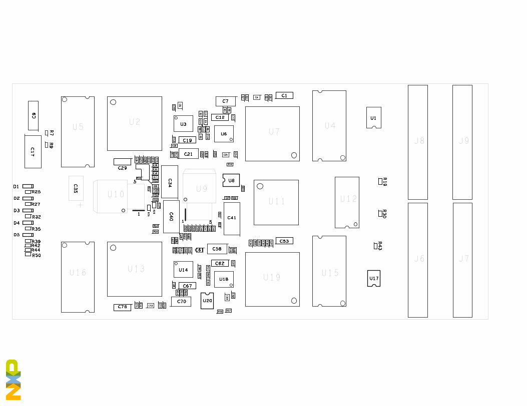
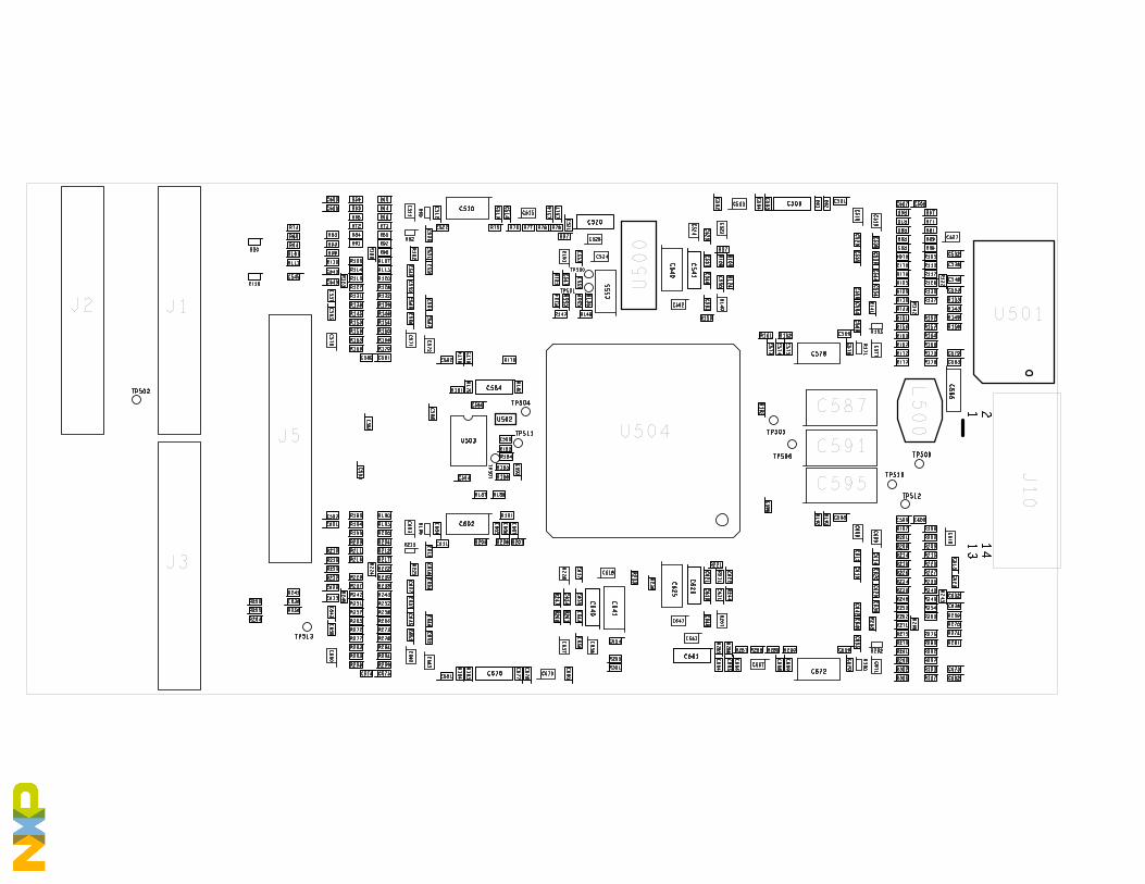
MSC711x Packet Telephony Farm Card (SPT711xPFCE), Rev. 1
38 Freescale Semiconductor
SPT711xPFCE Assembly Drawing
THIS PAGE INTENTIONALLY LEFT BLANK
Document Number: PTKIT711xUGRev. 104/2006
Freescale™ and the Freescale logo are trademarks of Freescale Semiconductor, Inc. StarCore is a licensed trademark of StarCore LLC. The StarCore DSP SC1400 core is based on the StarCore technology under license from StarCore LLC. All other product or service names are the property of their respective owners.
© Freescale Semiconductor, Inc., 2004, 2006.
Information in this document is provided solely to enable system and software
implementers to use Freescale Semiconductor products. There are no express or
implied copyright licenses granted hereunder to design or fabricate any integrated
circuits or integrated circuits based on the information in this document.
Freescale Semiconductor reserves the right to make changes without further notice to
any products herein. Freescale Semiconductor makes no warranty, representation or
guarantee regarding the suitability of its products for any particular purpose, nor does
Freescale Semiconductor assume any liability arising out of the application or use of
any product or circuit, and specifically disclaims any and all liability, including without
limitation consequential or incidental damages. “Typical” parameters which may be
provided in Freescale Semiconductor data sheets and/or specifications can and do
vary in different applications and actual performance may vary over time. All operating
parameters, including “Typicals” must be validated for each customer application by
customer’s technical experts. Freescale Semiconductor does not convey any license
under its patent rights nor the rights of others. Freescale Semiconductor products are
not designed, intended, or authorized for use as components in systems intended for
surgical implant into the body, or other applications intended to support or sustain life,
or for any other application in which the failure of the Freescale Semiconductor product
could create a situation where personal injury or death may occur. Should Buyer
purchase or use Freescale Semiconductor products for any such unintended or
unauthorized application, Buyer shall indemnify and hold Freescale Semiconductor
and its officers, employees, subsidiaries, affiliates, and distributors harmless against all
claims, costs, damages, and expenses, and reasonable attorney fees arising out of,
directly or indirectly, any claim of personal injury or death associated with such
unintended or unauthorized use, even if such claim alleges that Freescale
Semiconductor was negligent regarding the design or manufacture of the part.
How to Reach Us:
Home Page: www.freescale.com
email: [email protected]
USA/Europe or Locations Not Listed: Freescale Semiconductor Technical Information Center, CH3701300 N. Alma School Road Chandler, Arizona 85224 [email protected]
Europe, Middle East, and Africa:Freescale Halbleiter Deutschland GmbHTechnical Information CenterSchatzbogen 781829 Muenchen, Germany+44 1296 380 456 (English) +46 8 52200080 (English)+49 89 92103 559 (German)+33 1 69 35 48 48 (French) [email protected]
Japan: Freescale Semiconductor Japan Ltd. HeadquartersARCO Tower 15F1-8-1, Shimo-Meguro, Meguro-ku Tokyo 153-0064, Japan 0120 191014+81 3 5437 [email protected]
Asia/Pacific: Freescale Semiconductor Hong Kong Ltd. Technical Information Center2 Dai King Street Tai Po Industrial Estate, Tai Po, N.T., Hong Kong +800 2666 [email protected]
For Literature Requests Only:Freescale Semiconductor
Literature Distribution Center P.O. Box 5405Denver, Colorado 80217 1-800-441-2447303-675-2140Fax: 303-675-2150LDCForFreescaleSemiconductor
@hibbertgroup.com