mfr4200 - data sheet - nxp
TRANSCRIPT

FlexRayCommunication
freescale.com
Controllers
MFR4200Data Sheet
MFR4200Rev. 112/2006


MFR4200 Data Sheet
MFR4200Rev. 1
12/2006

MFR4200 Data Sheet, Rev. 1
4 Freescale Semiconductor
To provide the most up-to-date information, the revision of our documents on the World Wide Web will be the most current. Your printed copy may be an earlier revision. To verify that you have the latest information available, refer to http://www.freescale.com
The following revision history table summarizes changes contained in this document. For your convenience, the page number designators have been linked to the appropriate location.
Revision History
DateRevision
LevelDescription
PageNumber(s)
08/2005 0 Initial release. N/A
12/2006 1 Updated the following sections to remove information relating to clock quality check block:A.3.1.1, “POR”A.3.1.2, “LVR”A.3.1.3, “External Reset”Table A-11Table A-12Updated Figure B-1, Figure B-2, and Figure B-3 with latest drawings to comply with Jedec specifications.Applied latest version of back page.
231231231231232
239, 240, 241

Introduction
Device Overview
MFR4200 FlexRay Communication Controller
Dual Output Voltage Regulator (VREG3V3V2)
Clocks and Reset Generator
Oscillator (OSCV2)
Electrical Characteristics
Package Information
Printed Circuit Board Layout Recommendations
MFR4200 Protocol Implementation Document
Index of Registers
MFR4200 Data Sheet, Rev. 1
Freescale Semiconductor 5

MFR4200 Data Sheet, Rev. 1
6 Freescale Semiconductor

Contents
Section Number Title Page
Chapter 1Introduction
1.1 Audience . . . . . . . . . . . . . . . . . . . . . . . . . . . . . . . . . . . . . . . . . . . . . . . . . . . . . . . . . . . . . . . . . . . . . 211.2 Additional Reading . . . . . . . . . . . . . . . . . . . . . . . . . . . . . . . . . . . . . . . . . . . . . . . . . . . . . . . . . . . . 211.3 Terminology . . . . . . . . . . . . . . . . . . . . . . . . . . . . . . . . . . . . . . . . . . . . . . . . . . . . . . . . . . . . . . . . . . 221.4 Part Number Coding . . . . . . . . . . . . . . . . . . . . . . . . . . . . . . . . . . . . . . . . . . . . . . . . . . . . . . . . . . . . 23
Chapter 2Device Overview
2.1 Introduction . . . . . . . . . . . . . . . . . . . . . . . . . . . . . . . . . . . . . . . . . . . . . . . . . . . . . . . . . . . . . . . . . . 252.1.1 Features . . . . . . . . . . . . . . . . . . . . . . . . . . . . . . . . . . . . . . . . . . . . . . . . . . . . . . . . . . . . . . 252.1.2 Implementation Details and Constraints . . . . . . . . . . . . . . . . . . . . . . . . . . . . . . . . . . . . . 262.1.3 Modes of Operation . . . . . . . . . . . . . . . . . . . . . . . . . . . . . . . . . . . . . . . . . . . . . . . . . . . . . 262.1.4 Block Diagram . . . . . . . . . . . . . . . . . . . . . . . . . . . . . . . . . . . . . . . . . . . . . . . . . . . . . . . . . 282.1.5 Memory Map . . . . . . . . . . . . . . . . . . . . . . . . . . . . . . . . . . . . . . . . . . . . . . . . . . . . . . . . . . 302.1.6 Part ID Assignments . . . . . . . . . . . . . . . . . . . . . . . . . . . . . . . . . . . . . . . . . . . . . . . . . . . . 31
2.2 Signal Descriptions . . . . . . . . . . . . . . . . . . . . . . . . . . . . . . . . . . . . . . . . . . . . . . . . . . . . . . . . . . . . 312.2.1 System Pinout . . . . . . . . . . . . . . . . . . . . . . . . . . . . . . . . . . . . . . . . . . . . . . . . . . . . . . . . . 312.2.2 Pin Functions and Signal Properties . . . . . . . . . . . . . . . . . . . . . . . . . . . . . . . . . . . . . . . . 322.2.3 Detailed Signal Descriptions . . . . . . . . . . . . . . . . . . . . . . . . . . . . . . . . . . . . . . . . . . . . . . 362.2.4 Power Supply Pins . . . . . . . . . . . . . . . . . . . . . . . . . . . . . . . . . . . . . . . . . . . . . . . . . . . . . . 43
2.3 System Clock Description . . . . . . . . . . . . . . . . . . . . . . . . . . . . . . . . . . . . . . . . . . . . . . . . . . . . . . . 442.4 Modes of Operation . . . . . . . . . . . . . . . . . . . . . . . . . . . . . . . . . . . . . . . . . . . . . . . . . . . . . . . . . . . . 46
2.4.1 Overview . . . . . . . . . . . . . . . . . . . . . . . . . . . . . . . . . . . . . . . . . . . . . . . . . . . . . . . . . . . . . 462.4.2 Recommended Pullup/down Resistor Values . . . . . . . . . . . . . . . . . . . . . . . . . . . . . . . . . 462.4.3 Host Controller Interfaces . . . . . . . . . . . . . . . . . . . . . . . . . . . . . . . . . . . . . . . . . . . . . . . . 462.4.4 External Output Clock . . . . . . . . . . . . . . . . . . . . . . . . . . . . . . . . . . . . . . . . . . . . . . . . . . . 472.4.5 MFR4200 Connection to FlexRay Network . . . . . . . . . . . . . . . . . . . . . . . . . . . . . . . . . . 492.4.6 Power Mode . . . . . . . . . . . . . . . . . . . . . . . . . . . . . . . . . . . . . . . . . . . . . . . . . . . . . . . . . . . 51
2.5 Resets and Interrupts . . . . . . . . . . . . . . . . . . . . . . . . . . . . . . . . . . . . . . . . . . . . . . . . . . . . . . . . . . . 512.5.1 Overview . . . . . . . . . . . . . . . . . . . . . . . . . . . . . . . . . . . . . . . . . . . . . . . . . . . . . . . . . . . . . 512.5.2 Resets . . . . . . . . . . . . . . . . . . . . . . . . . . . . . . . . . . . . . . . . . . . . . . . . . . . . . . . . . . . . . . . . 512.5.3 Interrupt Sources . . . . . . . . . . . . . . . . . . . . . . . . . . . . . . . . . . . . . . . . . . . . . . . . . . . . . . . 51
MFR4200 Data Sheet, Rev. 1
Freescale Semiconductor 7

Section Number Title Page
Chapter 3MFR4200 FlexRay Communication Controller
3.1 Introduction . . . . . . . . . . . . . . . . . . . . . . . . . . . . . . . . . . . . . . . . . . . . . . . . . . . . . . . . . . . . . . . . . . 533.1.1 MFR4200 Features . . . . . . . . . . . . . . . . . . . . . . . . . . . . . . . . . . . . . . . . . . . . . . . . . . . . . 533.1.2 MFR4200 Implementation Parameters and Constraints . . . . . . . . . . . . . . . . . . . . . . . . . 54
3.2 Memory Map and Registers . . . . . . . . . . . . . . . . . . . . . . . . . . . . . . . . . . . . . . . . . . . . . . . . . . . . . . 543.2.1 Introduction . . . . . . . . . . . . . . . . . . . . . . . . . . . . . . . . . . . . . . . . . . . . . . . . . . . . . . . . . . . 543.2.2 Register Map Summary . . . . . . . . . . . . . . . . . . . . . . . . . . . . . . . . . . . . . . . . . . . . . . . . . . 553.2.3 Register Descriptions . . . . . . . . . . . . . . . . . . . . . . . . . . . . . . . . . . . . . . . . . . . . . . . . . . . . 60
3.3 Message Buffer . . . . . . . . . . . . . . . . . . . . . . . . . . . . . . . . . . . . . . . . . . . . . . . . . . . . . . . . . . . . . . . 1413.3.1 Message Buffer Layout . . . . . . . . . . . . . . . . . . . . . . . . . . . . . . . . . . . . . . . . . . . . . . . . . 1413.3.2 Message Buffer Field Descriptions . . . . . . . . . . . . . . . . . . . . . . . . . . . . . . . . . . . . . . . . 1433.3.3 Message Buffer Slot Status Vector . . . . . . . . . . . . . . . . . . . . . . . . . . . . . . . . . . . . . . . . 1463.3.4 Message ID . . . . . . . . . . . . . . . . . . . . . . . . . . . . . . . . . . . . . . . . . . . . . . . . . . . . . . . . . . 1493.3.5 NMVector Fields . . . . . . . . . . . . . . . . . . . . . . . . . . . . . . . . . . . . . . . . . . . . . . . . . . . . . . 1493.3.6 Data[0:31] — Data Fields . . . . . . . . . . . . . . . . . . . . . . . . . . . . . . . . . . . . . . . . . . . . . . . 149
3.4 Message Buffer Control, Configuration, Status and Filtering Register Set . . . . . . . . . . . . . . . . . 1503.4.1 Message Buffer Control, Configuration and Status Register . . . . . . . . . . . . . . . . . . . . . 1503.4.2 Message Buffer Filter Registers . . . . . . . . . . . . . . . . . . . . . . . . . . . . . . . . . . . . . . . . . . . 1583.4.3 Receive FIFO Filters . . . . . . . . . . . . . . . . . . . . . . . . . . . . . . . . . . . . . . . . . . . . . . . . . . . 159
3.5 Message Buffer Handling and Operations . . . . . . . . . . . . . . . . . . . . . . . . . . . . . . . . . . . . . . . . . . 1603.5.1 Introduction . . . . . . . . . . . . . . . . . . . . . . . . . . . . . . . . . . . . . . . . . . . . . . . . . . . . . . . . . . 1603.5.2 Buffer Map . . . . . . . . . . . . . . . . . . . . . . . . . . . . . . . . . . . . . . . . . . . . . . . . . . . . . . . . . . . 1603.5.3 Active Message Buffers . . . . . . . . . . . . . . . . . . . . . . . . . . . . . . . . . . . . . . . . . . . . . . . . . 1613.5.4 Buffer Configuration . . . . . . . . . . . . . . . . . . . . . . . . . . . . . . . . . . . . . . . . . . . . . . . . . . . 1663.5.5 Buffer Reconfiguration in the Normal State of Operation . . . . . . . . . . . . . . . . . . . . . . . 1723.5.6 Message Buffer Operations . . . . . . . . . . . . . . . . . . . . . . . . . . . . . . . . . . . . . . . . . . . . . . 173
3.6 Receive FIFO Function . . . . . . . . . . . . . . . . . . . . . . . . . . . . . . . . . . . . . . . . . . . . . . . . . . . . . . . . 1863.7 Host Controller Interfaces . . . . . . . . . . . . . . . . . . . . . . . . . . . . . . . . . . . . . . . . . . . . . . . . . . . . . . 189
3.7.1 MFR4200 Asynchronous Memory Interface . . . . . . . . . . . . . . . . . . . . . . . . . . . . . . . . . 1893.7.2 MFR4200 HCS12 Interface . . . . . . . . . . . . . . . . . . . . . . . . . . . . . . . . . . . . . . . . . . . . . . 192
3.8 External 4/10 MHz Output Clock . . . . . . . . . . . . . . . . . . . . . . . . . . . . . . . . . . . . . . . . . . . . . . . . 1973.9 Communication Controller States . . . . . . . . . . . . . . . . . . . . . . . . . . . . . . . . . . . . . . . . . . . . . . . . 197
3.9.1 Hard Reset State . . . . . . . . . . . . . . . . . . . . . . . . . . . . . . . . . . . . . . . . . . . . . . . . . . . . . . . 1973.9.2 Configuration State . . . . . . . . . . . . . . . . . . . . . . . . . . . . . . . . . . . . . . . . . . . . . . . . . . . . 1993.9.3 Diagnosis Stop State . . . . . . . . . . . . . . . . . . . . . . . . . . . . . . . . . . . . . . . . . . . . . . . . . . . 2003.9.4 Normal Active State . . . . . . . . . . . . . . . . . . . . . . . . . . . . . . . . . . . . . . . . . . . . . . . . . . . . 2013.9.5 Normal Passive State . . . . . . . . . . . . . . . . . . . . . . . . . . . . . . . . . . . . . . . . . . . . . . . . . . . 201
3.10 Debug Port . . . . . . . . . . . . . . . . . . . . . . . . . . . . . . . . . . . . . . . . . . . . . . . . . . . . . . . . . . . . . . . . . . 2023.10.1 Debug Port Overview . . . . . . . . . . . . . . . . . . . . . . . . . . . . . . . . . . . . . . . . . . . . . . . . . . . 2023.10.2 Debug Port Functions . . . . . . . . . . . . . . . . . . . . . . . . . . . . . . . . . . . . . . . . . . . . . . . . . . 2033.10.3 Debug Port Function Timing . . . . . . . . . . . . . . . . . . . . . . . . . . . . . . . . . . . . . . . . . . . . . 204
MFR4200 Data Sheet, Rev. 1
8 Freescale Semiconductor

Section Number Title Page
Chapter 4Dual Output Voltage Regulator (VREG3V3V2)
4.1 Introduction . . . . . . . . . . . . . . . . . . . . . . . . . . . . . . . . . . . . . . . . . . . . . . . . . . . . . . . . . . . . . . . . . 2074.1.1 Features . . . . . . . . . . . . . . . . . . . . . . . . . . . . . . . . . . . . . . . . . . . . . . . . . . . . . . . . . . . . . 2074.1.2 Modes of Operation . . . . . . . . . . . . . . . . . . . . . . . . . . . . . . . . . . . . . . . . . . . . . . . . . . . . 2074.1.3 Block Diagram . . . . . . . . . . . . . . . . . . . . . . . . . . . . . . . . . . . . . . . . . . . . . . . . . . . . . . . . 207
4.2 External Signal Description . . . . . . . . . . . . . . . . . . . . . . . . . . . . . . . . . . . . . . . . . . . . . . . . . . . . . 2094.2.1 VDDR, VSSR — Regulator Power Input . . . . . . . . . . . . . . . . . . . . . . . . . . . . . . . . . . . . . 2094.2.2 VDDA, VSSA — Regulator Reference Supply . . . . . . . . . . . . . . . . . . . . . . . . . . . . . . . . 2094.2.3 VDD, VSS — Regulator Output1 (Core Logic) . . . . . . . . . . . . . . . . . . . . . . . . . . . . . . . 2104.2.4 VDDOSC, VSSOSC — Regulator Output2 (OSC) . . . . . . . . . . . . . . . . . . . . . . . . . . . . . . 2104.2.5 VREGEN — Optional Regulator Enable . . . . . . . . . . . . . . . . . . . . . . . . . . . . . . . . . . . . . 210
4.3 Functional Description . . . . . . . . . . . . . . . . . . . . . . . . . . . . . . . . . . . . . . . . . . . . . . . . . . . . . . . . . 2104.3.1 REG — Regulator Core . . . . . . . . . . . . . . . . . . . . . . . . . . . . . . . . . . . . . . . . . . . . . . . . . 2104.3.2 Full-performance Mode . . . . . . . . . . . . . . . . . . . . . . . . . . . . . . . . . . . . . . . . . . . . . . . . . 2104.3.3 POR — Power On Reset . . . . . . . . . . . . . . . . . . . . . . . . . . . . . . . . . . . . . . . . . . . . . . . . 2114.3.4 LVR — Low Voltage Reset . . . . . . . . . . . . . . . . . . . . . . . . . . . . . . . . . . . . . . . . . . . . . . 2114.3.5 CTRL — Regulator Control . . . . . . . . . . . . . . . . . . . . . . . . . . . . . . . . . . . . . . . . . . . . . 211
4.4 Resets . . . . . . . . . . . . . . . . . . . . . . . . . . . . . . . . . . . . . . . . . . . . . . . . . . . . . . . . . . . . . . . . . . . . . . 2114.4.1 Power On Reset . . . . . . . . . . . . . . . . . . . . . . . . . . . . . . . . . . . . . . . . . . . . . . . . . . . . . . . 2114.4.2 Low Voltage Reset . . . . . . . . . . . . . . . . . . . . . . . . . . . . . . . . . . . . . . . . . . . . . . . . . . . . . 211
Chapter 5Clocks and Reset Generator
5.1 Introduction . . . . . . . . . . . . . . . . . . . . . . . . . . . . . . . . . . . . . . . . . . . . . . . . . . . . . . . . . . . . . . . . . 2135.1.1 Features . . . . . . . . . . . . . . . . . . . . . . . . . . . . . . . . . . . . . . . . . . . . . . . . . . . . . . . . . . . . . 213
5.2 Functional Description . . . . . . . . . . . . . . . . . . . . . . . . . . . . . . . . . . . . . . . . . . . . . . . . . . . . . . . . . 2145.2.1 MFR4200 Pins Relevant to the CRG . . . . . . . . . . . . . . . . . . . . . . . . . . . . . . . . . . . . . . . 2145.2.2 Reset Generation and CLKOUT Control . . . . . . . . . . . . . . . . . . . . . . . . . . . . . . . . . . . . 214
Chapter 6Oscillator (OSCV2)
6.1 Introduction . . . . . . . . . . . . . . . . . . . . . . . . . . . . . . . . . . . . . . . . . . . . . . . . . . . . . . . . . . . . . . . . . 2176.1.1 Features . . . . . . . . . . . . . . . . . . . . . . . . . . . . . . . . . . . . . . . . . . . . . . . . . . . . . . . . . . . . . 2176.1.2 Modes of Operation . . . . . . . . . . . . . . . . . . . . . . . . . . . . . . . . . . . . . . . . . . . . . . . . . . . . 217
6.2 External Signal Description . . . . . . . . . . . . . . . . . . . . . . . . . . . . . . . . . . . . . . . . . . . . . . . . . . . . . 2176.2.1 VDDOSC and VSSOSC — OSC Operating Voltage, OSC Ground . . . . . . . . . . . . . . . . . . 2176.2.2 EXTAL and XTAL — Clock/Crystal Source Pins . . . . . . . . . . . . . . . . . . . . . . . . . . . . . 217
6.3 Functional Description . . . . . . . . . . . . . . . . . . . . . . . . . . . . . . . . . . . . . . . . . . . . . . . . . . . . . . . . . 218
MFR4200 Data Sheet, Rev. 1
Freescale Semiconductor 9

Section Number Title Page
Appendix AElectrical Characteristics
A.1 General . . . . . . . . . . . . . . . . . . . . . . . . . . . . . . . . . . . . . . . . . . . . . . . . . . . . . . . . . . . . . . . . . . . . . 219A.1.1 Parameter Classification . . . . . . . . . . . . . . . . . . . . . . . . . . . . . . . . . . . . . . . . . . . . . . . . . 219A.1.2 Power Supply . . . . . . . . . . . . . . . . . . . . . . . . . . . . . . . . . . . . . . . . . . . . . . . . . . . . . . . . . 220A.1.3 Pins . . . . . . . . . . . . . . . . . . . . . . . . . . . . . . . . . . . . . . . . . . . . . . . . . . . . . . . . . . . . . . . . . 220A.1.4 Current Injection . . . . . . . . . . . . . . . . . . . . . . . . . . . . . . . . . . . . . . . . . . . . . . . . . . . . . . . 221A.1.5 Absolute Maximum Ratings . . . . . . . . . . . . . . . . . . . . . . . . . . . . . . . . . . . . . . . . . . . . . . 221A.1.6 ESD Protection and Latch-up Immunity . . . . . . . . . . . . . . . . . . . . . . . . . . . . . . . . . . . . 222A.1.7 Operating Conditions . . . . . . . . . . . . . . . . . . . . . . . . . . . . . . . . . . . . . . . . . . . . . . . . . . . 223A.1.8 Power Dissipation and Thermal Characteristics . . . . . . . . . . . . . . . . . . . . . . . . . . . . . . . 223A.1.9 I/O Characteristics . . . . . . . . . . . . . . . . . . . . . . . . . . . . . . . . . . . . . . . . . . . . . . . . . . . . . 226A.1.10 Supply Currents . . . . . . . . . . . . . . . . . . . . . . . . . . . . . . . . . . . . . . . . . . . . . . . . . . . . . . . 228
A.2 Voltage Regulator (VREG). . . . . . . . . . . . . . . . . . . . . . . . . . . . . . . . . . . . . . . . . . . . . . . . . . . . . . 229A.2.1 Operating Conditions . . . . . . . . . . . . . . . . . . . . . . . . . . . . . . . . . . . . . . . . . . . . . . . . . . . 229A.2.2 Chip Power-up and Voltage Drops . . . . . . . . . . . . . . . . . . . . . . . . . . . . . . . . . . . . . . . . . 230A.2.3 Output Loads. . . . . . . . . . . . . . . . . . . . . . . . . . . . . . . . . . . . . . . . . . . . . . . . . . . . . . . . . . 230
A.3 Reset and Oscillator . . . . . . . . . . . . . . . . . . . . . . . . . . . . . . . . . . . . . . . . . . . . . . . . . . . . . . . . . . . 231A.3.1 Startup. . . . . . . . . . . . . . . . . . . . . . . . . . . . . . . . . . . . . . . . . . . . . . . . . . . . . . . . . . . . . . . 231A.3.2 Oscillator. . . . . . . . . . . . . . . . . . . . . . . . . . . . . . . . . . . . . . . . . . . . . . . . . . . . . . . . . . . . . 232
A.4 AMI Interface Timing Diagram . . . . . . . . . . . . . . . . . . . . . . . . . . . . . . . . . . . . . . . . . . . . . . . . . . 232A.5 HCS12 Interface Timing Diagram . . . . . . . . . . . . . . . . . . . . . . . . . . . . . . . . . . . . . . . . . . . . . . . . 236
Appendix BPackage Information
B.1 64-pin LQFP package . . . . . . . . . . . . . . . . . . . . . . . . . . . . . . . . . . . . . . . . . . . . . . . . . . . . . . . . . . 239
Appendix CPrinted Circuit Board Layout Recommendations
Appendix CMFR4200 Protocol Implementation Document
C.1 Introduction . . . . . . . . . . . . . . . . . . . . . . . . . . . . . . . . . . . . . . . . . . . . . . . . . . . . . . . . . . . . . . . . . . 245C.1.1 Purpose . . . . . . . . . . . . . . . . . . . . . . . . . . . . . . . . . . . . . . . . . . . . . . . . . . . . . . . . . . . . . . 245C.1.2 Structure . . . . . . . . . . . . . . . . . . . . . . . . . . . . . . . . . . . . . . . . . . . . . . . . . . . . . . . . . . . . . 245C.1.3 References. . . . . . . . . . . . . . . . . . . . . . . . . . . . . . . . . . . . . . . . . . . . . . . . . . . . . . . . . . . . 245
C.2 Overall Protocol State Machine . . . . . . . . . . . . . . . . . . . . . . . . . . . . . . . . . . . . . . . . . . . . . . . . . . 246C.3 Coding and Decoding . . . . . . . . . . . . . . . . . . . . . . . . . . . . . . . . . . . . . . . . . . . . . . . . . . . . . . . . . . 249
C.3.1 Overview. . . . . . . . . . . . . . . . . . . . . . . . . . . . . . . . . . . . . . . . . . . . . . . . . . . . . . . . . . . . . 249C.3.2 NRZ Coding . . . . . . . . . . . . . . . . . . . . . . . . . . . . . . . . . . . . . . . . . . . . . . . . . . . . . . . . . . 249C.3.3 NRZ Decoding . . . . . . . . . . . . . . . . . . . . . . . . . . . . . . . . . . . . . . . . . . . . . . . . . . . . . . . . 250
MFR4200 Data Sheet, Rev. 1
10 Freescale Semiconductor

Section Number Title Page
C.3.4 Signal Integrity . . . . . . . . . . . . . . . . . . . . . . . . . . . . . . . . . . . . . . . . . . . . . . . . . . . . . . . . 250C.4 Frame Format . . . . . . . . . . . . . . . . . . . . . . . . . . . . . . . . . . . . . . . . . . . . . . . . . . . . . . . . . . . . . . . . 250C.5 Media Access Control . . . . . . . . . . . . . . . . . . . . . . . . . . . . . . . . . . . . . . . . . . . . . . . . . . . . . . . . . . 250C.6 Frame and Symbol Processing . . . . . . . . . . . . . . . . . . . . . . . . . . . . . . . . . . . . . . . . . . . . . . . . . . . 251C.7 Wakeup, Startup, and Reintegration . . . . . . . . . . . . . . . . . . . . . . . . . . . . . . . . . . . . . . . . . . . . . . . 251
C.7.1 Introduction. . . . . . . . . . . . . . . . . . . . . . . . . . . . . . . . . . . . . . . . . . . . . . . . . . . . . . . . . . . 251C.7.2 Cluster Wakeup. . . . . . . . . . . . . . . . . . . . . . . . . . . . . . . . . . . . . . . . . . . . . . . . . . . . . . . . 251C.7.3 Communication Startup and Reintegration. . . . . . . . . . . . . . . . . . . . . . . . . . . . . . . . . . . 251
C.8 Clock Synchronization . . . . . . . . . . . . . . . . . . . . . . . . . . . . . . . . . . . . . . . . . . . . . . . . . . . . . . . . . 252C.8.1 Introduction. . . . . . . . . . . . . . . . . . . . . . . . . . . . . . . . . . . . . . . . . . . . . . . . . . . . . . . . . . . 252C.8.2 Time Representation . . . . . . . . . . . . . . . . . . . . . . . . . . . . . . . . . . . . . . . . . . . . . . . . . . . . 252C.8.3 Synchronization Process . . . . . . . . . . . . . . . . . . . . . . . . . . . . . . . . . . . . . . . . . . . . . . . . . 252C.8.4 Clock Startup . . . . . . . . . . . . . . . . . . . . . . . . . . . . . . . . . . . . . . . . . . . . . . . . . . . . . . . . . 252C.8.5 Time Measurement . . . . . . . . . . . . . . . . . . . . . . . . . . . . . . . . . . . . . . . . . . . . . . . . . . . . . 252C.8.6 Correction Term Calculation . . . . . . . . . . . . . . . . . . . . . . . . . . . . . . . . . . . . . . . . . . . . . 252C.8.7 Clock Correction. . . . . . . . . . . . . . . . . . . . . . . . . . . . . . . . . . . . . . . . . . . . . . . . . . . . . . . 253C.8.8 Sync Frame Configuration Rules . . . . . . . . . . . . . . . . . . . . . . . . . . . . . . . . . . . . . . . . . . 253
C.9 Controller Host Interface. . . . . . . . . . . . . . . . . . . . . . . . . . . . . . . . . . . . . . . . . . . . . . . . . . . . . . . . 253C.10 Device Specific Power Modes . . . . . . . . . . . . . . . . . . . . . . . . . . . . . . . . . . . . . . . . . . . . . . . . . . . 253C.11 Bus Guardian Schedule Monitoring . . . . . . . . . . . . . . . . . . . . . . . . . . . . . . . . . . . . . . . . . . . . . . . 253C.12 System Parameters and Configuration Constraints . . . . . . . . . . . . . . . . . . . . . . . . . . . . . . . . . . . . 254
C.12.1 System Parameters . . . . . . . . . . . . . . . . . . . . . . . . . . . . . . . . . . . . . . . . . . . . . . . . . . . . . 254C.12.2 Configuration Constraints. . . . . . . . . . . . . . . . . . . . . . . . . . . . . . . . . . . . . . . . . . . . . . . . 254
Appendix DIndex of Registers
MFR4200 Data Sheet, Rev. 1
Freescale Semiconductor 11

Section Number Title Page
MFR4200 Data Sheet, Rev. 1
12 Freescale Semiconductor

List of Figures
Figure Number Title Page
Figure 1-1. Order Part Number Coding. . . . . . . . . . . . . . . . . . . . . . . . . . . . . . . . . . . . . . . . . . . . . . . . 23Figure 2-1. MFR4200 Block Diagram . . . . . . . . . . . . . . . . . . . . . . . . . . . . . . . . . . . . . . . . . . . . . . . . 29Figure 2-2. Pin Assignments for MFR4200 in 64-pin LQFP . . . . . . . . . . . . . . . . . . . . . . . . . . . . . . . 32Figure 2-3. Pierce Oscillator Connections. . . . . . . . . . . . . . . . . . . . . . . . . . . . . . . . . . . . . . . . . . . . . . 42Figure 2-4. External Clock Connections . . . . . . . . . . . . . . . . . . . . . . . . . . . . . . . . . . . . . . . . . . . . . . . 43Figure 2-5. Clock Connections . . . . . . . . . . . . . . . . . . . . . . . . . . . . . . . . . . . . . . . . . . . . . . . . . . . . . . 45Figure 2-6. CLKOUT Generation During Power-on Reset. . . . . . . . . . . . . . . . . . . . . . . . . . . . . . . . . 47Figure 2-7. CLKOUT Generation during Low Voltage Reset . . . . . . . . . . . . . . . . . . . . . . . . . . . . . . 48Figure 2-8. CLKOUT Generation During External Hard Reset . . . . . . . . . . . . . . . . . . . . . . . . . . . . . 49Figure 2-9. Example: Connecting a FlexRay Optical/Electrical PHY to the MFR4200. . . . . . . . . . . 50Figure 2-10. Example: Connecting an RS485 PHY to the MFR4200. . . . . . . . . . . . . . . . . . . . . . . . . . 50Figure 3-1. Key to Register Diagrams. . . . . . . . . . . . . . . . . . . . . . . . . . . . . . . . . . . . . . . . . . . . . . . . . 61Figure 3-2. Module Version Register 0 . . . . . . . . . . . . . . . . . . . . . . . . . . . . . . . . . . . . . . . . . . . . . . . . 62Figure 3-3. Module Version Register 1 . . . . . . . . . . . . . . . . . . . . . . . . . . . . . . . . . . . . . . . . . . . . . . . . 62Figure 3-4. Magic Number Register . . . . . . . . . . . . . . . . . . . . . . . . . . . . . . . . . . . . . . . . . . . . . . . . . . 63Figure 3-5. Module Configuration Register 0 . . . . . . . . . . . . . . . . . . . . . . . . . . . . . . . . . . . . . . . . . . . 64Figure 3-6. Module Configuration Register 1 . . . . . . . . . . . . . . . . . . . . . . . . . . . . . . . . . . . . . . . . . . . 66Figure 3-7. Host Interface Pins Drive Strength Register. . . . . . . . . . . . . . . . . . . . . . . . . . . . . . . . . . . 67Figure 3-8. Physical Layer Pins Drive Strength Register . . . . . . . . . . . . . . . . . . . . . . . . . . . . . . . . . . 68Figure 3-9. Host Interface Pins Pullup/down Enable Register . . . . . . . . . . . . . . . . . . . . . . . . . . . . . . 68Figure 3-10. Host Interface Pins Pullup/down Control Register. . . . . . . . . . . . . . . . . . . . . . . . . . . . . . 69Figure 3-11. Physical Layer Pins Pullup/down Enable Register. . . . . . . . . . . . . . . . . . . . . . . . . . . . . . 69Figure 3-12. Physical Layer Pins Pullup/down Control Register . . . . . . . . . . . . . . . . . . . . . . . . . . . . . 70Figure 3-13. Voltage Regulator Status Register . . . . . . . . . . . . . . . . . . . . . . . . . . . . . . . . . . . . . . . . . . 70Figure 3-14. Bit Duration Register . . . . . . . . . . . . . . . . . . . . . . . . . . . . . . . . . . . . . . . . . . . . . . . . . . . . 71Figure 3-15. Delay Compensation Channel A Register . . . . . . . . . . . . . . . . . . . . . . . . . . . . . . . . . . . . 72Figure 3-16. Delay Compensation Channel B Register . . . . . . . . . . . . . . . . . . . . . . . . . . . . . . . . . . . . 72Figure 3-17. Cluster Drift Damping Register . . . . . . . . . . . . . . . . . . . . . . . . . . . . . . . . . . . . . . . . . . . . 73Figure 3-18. Maximum Sync Frames Register . . . . . . . . . . . . . . . . . . . . . . . . . . . . . . . . . . . . . . . . . . . 73Figure 3-19. Nominal Macrotick Length Register . . . . . . . . . . . . . . . . . . . . . . . . . . . . . . . . . . . . . . . . 74Figure 3-20. Microticks Per Cycle Low Register . . . . . . . . . . . . . . . . . . . . . . . . . . . . . . . . . . . . . . . . . 74Figure 3-21. Microticks Per Cycle High Register . . . . . . . . . . . . . . . . . . . . . . . . . . . . . . . . . . . . . . . . . 75
MFR4200 Data Sheet, Rev. 1
Freescale Semiconductor 13

Figure Number Title Page
Figure 3-22. Static Slot Length Register . . . . . . . . . . . . . . . . . . . . . . . . . . . . . . . . . . . . . . . . . . . . . . . . 75Figure 3-23. Number of Static Slots Register . . . . . . . . . . . . . . . . . . . . . . . . . . . . . . . . . . . . . . . . . . . . 76Figure 3-24. Static Payload Length Register. . . . . . . . . . . . . . . . . . . . . . . . . . . . . . . . . . . . . . . . . . . . . 76Figure 3-25. Minislot Length Register . . . . . . . . . . . . . . . . . . . . . . . . . . . . . . . . . . . . . . . . . . . . . . . . . 77Figure 3-26. Minislot Action Point Offset Register . . . . . . . . . . . . . . . . . . . . . . . . . . . . . . . . . . . . . . . 77Figure 3-27. Static Slot Action Point Offset Register . . . . . . . . . . . . . . . . . . . . . . . . . . . . . . . . . . . . . . 78Figure 3-28. Latest Dynamic Transmission Start Register . . . . . . . . . . . . . . . . . . . . . . . . . . . . . . . . . . 78Figure 3-29. Maximum Payload Length Dynamic Register . . . . . . . . . . . . . . . . . . . . . . . . . . . . . . . . . 79Figure 3-30. Symbol Window Configuration Register . . . . . . . . . . . . . . . . . . . . . . . . . . . . . . . . . . . . . 79Figure 3-31. Network Idle Time Configuration Register . . . . . . . . . . . . . . . . . . . . . . . . . . . . . . . . . . . 80Figure 3-32. Cycle Length Register . . . . . . . . . . . . . . . . . . . . . . . . . . . . . . . . . . . . . . . . . . . . . . . . . . . 80Figure 3-33. Maximum Cycle Length Deviation Register . . . . . . . . . . . . . . . . . . . . . . . . . . . . . . . . . . 81Figure 3-34. External Offset Correction Register . . . . . . . . . . . . . . . . . . . . . . . . . . . . . . . . . . . . . . . . . 81Figure 3-35. External Rate Correction Register . . . . . . . . . . . . . . . . . . . . . . . . . . . . . . . . . . . . . . . . . . 82Figure 3-36. External Correction Control Register . . . . . . . . . . . . . . . . . . . . . . . . . . . . . . . . . . . . . . . . 82Figure 3-37. Maximum Offset Correction Register . . . . . . . . . . . . . . . . . . . . . . . . . . . . . . . . . . . . . . . 83Figure 3-38. Maximum Rate Correction Register . . . . . . . . . . . . . . . . . . . . . . . . . . . . . . . . . . . . . . . . . 84Figure 3-39. Coldstart Maximum Register . . . . . . . . . . . . . . . . . . . . . . . . . . . . . . . . . . . . . . . . . . . . . . 84Figure 3-40. Transmit Start Sequence Length Register . . . . . . . . . . . . . . . . . . . . . . . . . . . . . . . . . . . . 85Figure 3-41. Network Management Vector Length Register . . . . . . . . . . . . . . . . . . . . . . . . . . . . . . . . 85Figure 3-42. Sync Frame Register . . . . . . . . . . . . . . . . . . . . . . . . . . . . . . . . . . . . . . . . . . . . . . . . . . . . . 86Figure 3-43. Sync Frame Header Register . . . . . . . . . . . . . . . . . . . . . . . . . . . . . . . . . . . . . . . . . . . . . . 86Figure 3-44. Bus Guardian Tick Register . . . . . . . . . . . . . . . . . . . . . . . . . . . . . . . . . . . . . . . . . . . . . . . 87Figure 3-45. Delay Counter Register. . . . . . . . . . . . . . . . . . . . . . . . . . . . . . . . . . . . . . . . . . . . . . . . . . . 87Figure 3-46. Debug Port Control Register. . . . . . . . . . . . . . . . . . . . . . . . . . . . . . . . . . . . . . . . . . . . . . . 88Figure 3-47. Start of Offset Correction Cycle Time Register . . . . . . . . . . . . . . . . . . . . . . . . . . . . . . . . 89Figure 3-48. Idle Detection Length Register . . . . . . . . . . . . . . . . . . . . . . . . . . . . . . . . . . . . . . . . . . . . . 90Figure 3-49. Symbol Window Control Register . . . . . . . . . . . . . . . . . . . . . . . . . . . . . . . . . . . . . . . . . . 90Figure 3-50. Wakeup Mechanism Control Register . . . . . . . . . . . . . . . . . . . . . . . . . . . . . . . . . . . . . . . 91Figure 3-51. Wakeup Symbol TX Idle Register . . . . . . . . . . . . . . . . . . . . . . . . . . . . . . . . . . . . . . . . . . 91Figure 3-52. Wakeup Symbol TX Low Register. . . . . . . . . . . . . . . . . . . . . . . . . . . . . . . . . . . . . . . . . . 92Figure 3-53. Listen Timeout With Noise Length Register . . . . . . . . . . . . . . . . . . . . . . . . . . . . . . . . . . 92Figure 3-54. Protocol State Register . . . . . . . . . . . . . . . . . . . . . . . . . . . . . . . . . . . . . . . . . . . . . . . . . . . 93Figure 3-55. Current Cycle Counter Value Register . . . . . . . . . . . . . . . . . . . . . . . . . . . . . . . . . . . . . . . 94Figure 3-56. Current Macrotick Counter Value Register . . . . . . . . . . . . . . . . . . . . . . . . . . . . . . . . . . . 94
MFR4200 Data Sheet, Rev. 1
14 Freescale Semiconductor

Figure Number Title Page
Figure 3-57. Offset Correction Value Register . . . . . . . . . . . . . . . . . . . . . . . . . . . . . . . . . . . . . . . . . . . 95Figure 3-58. Rate Correction Value Register . . . . . . . . . . . . . . . . . . . . . . . . . . . . . . . . . . . . . . . . . . . . 95Figure 3-59. Global Network Management Vector n Register, n = [0:5] . . . . . . . . . . . . . . . . . . . . . . . 96Figure 3-60. Symbol Window Status Channel A Register . . . . . . . . . . . . . . . . . . . . . . . . . . . . . . . . . . 97Figure 3-61. Symbol Window Status Channel B Register . . . . . . . . . . . . . . . . . . . . . . . . . . . . . . . . . . 98Figure 3-62. Bus Guardian Status Register . . . . . . . . . . . . . . . . . . . . . . . . . . . . . . . . . . . . . . . . . . . . . . 99Figure 3-63. Startup Interrupt Enable Register . . . . . . . . . . . . . . . . . . . . . . . . . . . . . . . . . . . . . . . . . . 100Figure 3-64. Maximum Odd Cycles Without Clock Correction Fatal Register . . . . . . . . . . . . . . . . . 101Figure 3-65. Maximum Odd Cycles Without Clock Correction Passive Register . . . . . . . . . . . . . . . 101Figure 3-66. Channel Status Error Counter n Register, n = [0:1] . . . . . . . . . . . . . . . . . . . . . . . . . . . . 102Figure 3-67. Interrupt Enable Register 0 . . . . . . . . . . . . . . . . . . . . . . . . . . . . . . . . . . . . . . . . . . . . . . . 103Figure 3-68. Slot Status Selection n Register, n = [0:3] . . . . . . . . . . . . . . . . . . . . . . . . . . . . . . . . . . . 103Figure 3-69. Slot Status Counter n Register, n = [0:7] . . . . . . . . . . . . . . . . . . . . . . . . . . . . . . . . . . . . 104Figure 3-70. Slot Status Counter Condition n Register, n = [0:7] . . . . . . . . . . . . . . . . . . . . . . . . . . . . 105Figure 3-71. Slot Status Counter Incrementation Register . . . . . . . . . . . . . . . . . . . . . . . . . . . . . . . . . 107Figure 3-72. Slot Status Counter Interrupt Mask Register . . . . . . . . . . . . . . . . . . . . . . . . . . . . . . . . . 107Figure 3-73. Receive Buffer Interrupt Vector Register . . . . . . . . . . . . . . . . . . . . . . . . . . . . . . . . . . . . 108Figure 3-74. Transmit Buffer Interrupt Vector Register . . . . . . . . . . . . . . . . . . . . . . . . . . . . . . . . . . . 109Figure 3-75. CHI Error Register . . . . . . . . . . . . . . . . . . . . . . . . . . . . . . . . . . . . . . . . . . . . . . . . . . . . . 109Figure 3-76. Clock Correction Failed Counter Register . . . . . . . . . . . . . . . . . . . . . . . . . . . . . . . . . . . 113Figure 3-77. Error Handling Level Register . . . . . . . . . . . . . . . . . . . . . . . . . . . . . . . . . . . . . . . . . . . . 113Figure 3-78. Interrupt Status Register 0 . . . . . . . . . . . . . . . . . . . . . . . . . . . . . . . . . . . . . . . . . . . . . . . 114Figure 3-79. Startup Interrupt Status Register. . . . . . . . . . . . . . . . . . . . . . . . . . . . . . . . . . . . . . . . . . . 118Figure 3-80. Slot Status n Register, n = [0:7] . . . . . . . . . . . . . . . . . . . . . . . . . . . . . . . . . . . . . . . . . . . 119Figure 3-81. Odd Sync Frame ID n Register, n = [0:15]. . . . . . . . . . . . . . . . . . . . . . . . . . . . . . . . . . . 120Figure 3-82. Even Sync Frame ID n Register, n = [0:15] . . . . . . . . . . . . . . . . . . . . . . . . . . . . . . . . . . 121Figure 3-83. Odd Measurement Channel A n Register, n = [0:15] . . . . . . . . . . . . . . . . . . . . . . . . . . . 121Figure 3-84. Odd Measurement Channel B n Register, n = [0:15] . . . . . . . . . . . . . . . . . . . . . . . . . . . 122Figure 3-85. Even Measurement Channel A n Register, n = [0:15] . . . . . . . . . . . . . . . . . . . . . . . . . . 122Figure 3-86. Even Measurement Channel B n Register, n = [0:15] . . . . . . . . . . . . . . . . . . . . . . . . . . 123Figure 3-87. Even Measurement Counter Register . . . . . . . . . . . . . . . . . . . . . . . . . . . . . . . . . . . . . . . 124Figure 3-88. Odd Measurement Counter Register. . . . . . . . . . . . . . . . . . . . . . . . . . . . . . . . . . . . . . . . 124Figure 3-89. FIFO Size Register . . . . . . . . . . . . . . . . . . . . . . . . . . . . . . . . . . . . . . . . . . . . . . . . . . . . . 125Figure 3-90. Message Buffer Control, Configuration and Status n Register, n = [0:58] . . . . . . . . . . 126Figure 3-91. Active Transmit Buffer Frame ID Register . . . . . . . . . . . . . . . . . . . . . . . . . . . . . . . . . . 126
MFR4200 Data Sheet, Rev. 1
Freescale Semiconductor 15

Figure Number Title Page
Figure 3-92. Active Transmit Buffer Cycle Counter and Payload Length Register . . . . . . . . . . . . . . 127Figure 3-93. Active Transmit Buffer Header CRC Register . . . . . . . . . . . . . . . . . . . . . . . . . . . . . . . . 127Figure 3-94. Active Transmit Buffer Data n Register, n = [0:15] . . . . . . . . . . . . . . . . . . . . . . . . . . . . 128Figure 3-95. Active Transmit Buffer Message Buffer Slot Status Vector Register . . . . . . . . . . . . . . 128Figure 3-96. Active Receive Buffer Frame ID Register . . . . . . . . . . . . . . . . . . . . . . . . . . . . . . . . . . . 129Figure 3-97. Active Receive Buffer Cycle Counter and Payload Length Register . . . . . . . . . . . . . . . 129Figure 3-98. Active Receive Buffer Header CRC Register. . . . . . . . . . . . . . . . . . . . . . . . . . . . . . . . . 130Figure 3-99. Active Receive Buffer Data n Register, n = [0:15]. . . . . . . . . . . . . . . . . . . . . . . . . . . . . 130Figure 3-100. Active Receive Buffer Message Buffer Slot Status Vector Register . . . . . . . . . . . . . . . 131Figure 3-101. Active FIFO Buffer Frame ID Register . . . . . . . . . . . . . . . . . . . . . . . . . . . . . . . . . . . . . 131Figure 3-102. Active FIFO Buffer Cycle Counter and Payload Length Register . . . . . . . . . . . . . . . . . 132Figure 3-103. Active FIFO Buffer Header CRC Register. . . . . . . . . . . . . . . . . . . . . . . . . . . . . . . . . . . 132Figure 3-104. Active FIFO Buffer Data n Register, n = [0:15]. . . . . . . . . . . . . . . . . . . . . . . . . . . . . . . 133Figure 3-105. Active FIFO Buffer Message Buffer Slot Status Vector Register . . . . . . . . . . . . . . . . . 133Figure 3-106. Sync Frame Acceptance Filter Value Register . . . . . . . . . . . . . . . . . . . . . . . . . . . . . . . . 134Figure 3-107. Sync Frame Acceptance Filter Mask Register . . . . . . . . . . . . . . . . . . . . . . . . . . . . . . . . 134Figure 3-108. Sync Frame Rejection Filter Register . . . . . . . . . . . . . . . . . . . . . . . . . . . . . . . . . . . . . . . 135Figure 3-109. Cycle Counter Filter n Register, n = [0:58] . . . . . . . . . . . . . . . . . . . . . . . . . . . . . . . . . . 135Figure 3-110. FIFO Acceptance Filter Message ID Value Register . . . . . . . . . . . . . . . . . . . . . . . . . . . 136Figure 3-111. FIFO Acceptance Filter Message ID Mask Register . . . . . . . . . . . . . . . . . . . . . . . . . . . 136Figure 3-112. FIFO Acceptance/Rejection Filter Channel Register . . . . . . . . . . . . . . . . . . . . . . . . . . . 137Figure 3-113. FIFO Rejection Filter Frame ID Value Register . . . . . . . . . . . . . . . . . . . . . . . . . . . . . . 138Figure 3-114. FIFO Rejection Filter Frame ID Mask Register . . . . . . . . . . . . . . . . . . . . . . . . . . . . . . . 138Figure 3-115. Timer Interrupt Configuration Register 0 Cycle Set . . . . . . . . . . . . . . . . . . . . . . . . . . . 139Figure 3-116. Timer Interrupt Configuration Register 0 Macrotick Offset . . . . . . . . . . . . . . . . . . . . . 140Figure 3-117. Timer Interrupt Configuration Register 1 Cycle Set . . . . . . . . . . . . . . . . . . . . . . . . . . . 140Figure 3-118. Timer Interrupt Configuration Register 1 High . . . . . . . . . . . . . . . . . . . . . . . . . . . . . . . 141Figure 3-119. Transmit Message Buffer Slot Status Vector . . . . . . . . . . . . . . . . . . . . . . . . . . . . . . . . . 146Figure 3-120. Receive and Receive FIFO Message Buffer Slot Status Vector. . . . . . . . . . . . . . . . . . . 147Figure 3-121. BUFCSnR of a Receive Message Buffer . . . . . . . . . . . . . . . . . . . . . . . . . . . . . . . . . . . . 150Figure 3-122. BUFCSnR of a Transmit Message Single Buffer for the Dynamic Segment. . . . . . . . . 150Figure 3-123. BUFCSnR of a Host Part Transmit Message Buffer of a Double Tx Buffer
for the Dynamic Segment . . . . . . . . . . . . . . . . . . . . . . . . . . . . . . . . . . . . . . . . . . . . . . . . 151Figure 3-124. BUFCSnR of a Host Part Transmit Message Buffer of a Double Tx Buffer
for the Static Segment. . . . . . . . . . . . . . . . . . . . . . . . . . . . . . . . . . . . . . . . . . . . . . . . . . . 151
MFR4200 Data Sheet, Rev. 1
16 Freescale Semiconductor

Figure Number Title Page
Figure 3-125. BUFCSnR of a Single Transmit Message Buffer for the Static Segment . . . . . . . . . . . 151Figure 3-126. BUFCSnR of a CC Part Transmit Message Buffer of a Double Tx Buffer
for Dynamic and Static Segment . . . . . . . . . . . . . . . . . . . . . . . . . . . . . . . . . . . . . . . . . . 152Figure 3-127. BUFCSnR of FIFO Buffer . . . . . . . . . . . . . . . . . . . . . . . . . . . . . . . . . . . . . . . . . . . . . . . 152Figure 3-128. CCFnR, Transmit and Receive Message Buffer Filter Registers . . . . . . . . . . . . . . . . . . 158Figure 3-129. CCFnR, CC Part Buffer of a Double Transmit Message Buffer Filter Registers. . . . . . 158Figure 3-130. CCFnR, FIFO Buffer Filter Registers. . . . . . . . . . . . . . . . . . . . . . . . . . . . . . . . . . . . . . . 158Figure 3-131. Buffer Control, Configuration, Status/Filtering Register Set for Transmit/Receive
Buffers . . . . . . . . . . . . . . . . . . . . . . . . . . . . . . . . . . . . . . . . . . . . . . . . . . . . . . . . . . . . . . 161Figure 3-132. Buffer Control, Configuration, Status/Filtering Register Set for Receive FIFO Buffers 163Figure 3-133. Buffer Busy Bit Timing for a Transmit Message Buffer . . . . . . . . . . . . . . . . . . . . . . . . 165Figure 3-134. Example of a Buffer Configuration . . . . . . . . . . . . . . . . . . . . . . . . . . . . . . . . . . . . . . . . 170Figure 3-135. Transition Scheme Between Different Buffer Types Depending on Operational
Mode of CC . . . . . . . . . . . . . . . . . . . . . . . . . . . . . . . . . . . . . . . . . . . . . . . . . . . . . . . . . . 173Figure 3-136. Operations During a Frame Reception . . . . . . . . . . . . . . . . . . . . . . . . . . . . . . . . . . . . . . 175Figure 3-137. Operations with a Single Transmit Message Buffer during an Event Type of
Transmission for a Static Segment . . . . . . . . . . . . . . . . . . . . . . . . . . . . . . . . . . . . . . . . . 180Figure 3-138. Double Transmit Message Buffer Structure . . . . . . . . . . . . . . . . . . . . . . . . . . . . . . . . . . 181Figure 3-139. Doubled Buffer Data Collection with State Driven Transmit Operation . . . . . . . . . . . . 184Figure 3-140. Doubled Buffer Data collection with Event Driven Transmit Operation . . . . . . . . . . . . 185Figure 3-141. FIFO Status (Empty, Not Empty, Overrun) — Example of FIFO with Three
Message Buffers . . . . . . . . . . . . . . . . . . . . . . . . . . . . . . . . . . . . . . . . . . . . . . . . . . . . . . . 187Figure 3-142. Connecting MFR4200 to MPC5xx Using the AMI (Example) . . . . . . . . . . . . . . . . . . . 190Figure 3-143. Connecting MFR4200 to MAC71xx Using the AMI (Example) . . . . . . . . . . . . . . . . . . 191Figure 3-144. Connecting MFR4200 to DSP56F83x (Hawk) Using the AMI (Example) . . . . . . . . . . 191Figure 3-145. FlexRay CC to HCS12 Device Connection with HCS12 EBI Paged Mode Support. . . 193Figure 3-146. FlexRay CC to HCS12 Device Connection with HCS12 EBI Unpaged Mode Support 194Figure 3-147. HCS12 interface Address Decoding and Internal CS Signal Generation . . . . . . . . . . . . 195Figure 3-148. Timing Diagram of CC State Transition from Configuration State to Normal State . . . 200Figure 3-149. Start of Communication Cycle and Start of Offset Correction Functions Timing . . . . . 204Figure 3-150. Timing for Debug Functions with Three EXTAL or CC_CLK Clock Cycles
of High State (Logic “1“) . . . . . . . . . . . . . . . . . . . . . . . . . . . . . . . . . . . . . . . . . . . . . . . . 204Figure 3-151. Slot Start in Static Segment Function Timing . . . . . . . . . . . . . . . . . . . . . . . . . . . . . . . . 205Figure 4-1. VREG3V3 Block Diagram . . . . . . . . . . . . . . . . . . . . . . . . . . . . . . . . . . . . . . . . . . . . . . . 208Figure 5-1. Power-on Reset . . . . . . . . . . . . . . . . . . . . . . . . . . . . . . . . . . . . . . . . . . . . . . . . . . . . . . . . 215Figure 5-2. Low Voltage Reset . . . . . . . . . . . . . . . . . . . . . . . . . . . . . . . . . . . . . . . . . . . . . . . . . . . . . 215Figure 5-3. External Reset . . . . . . . . . . . . . . . . . . . . . . . . . . . . . . . . . . . . . . . . . . . . . . . . . . . . . . . . . 216
MFR4200 Data Sheet, Rev. 1
Freescale Semiconductor 17

Figure Number Title Page
Figure A-1. Voltage Regulator — Chip Power-up and Voltage Drops (not scaled) . . . . . . . . . . . . . 230Figure A-2. AMI Interface Read and Write Timing Diagrams . . . . . . . . . . . . . . . . . . . . . . . . . . . . . 233Figure A-3. AMI Interface Write-after-Read Transactions Timing Diagram . . . . . . . . . . . . . . . . . . 234Figure A-4. AMI Interface Read-after-Write Transactions Timing Diagram . . . . . . . . . . . . . . . . . . 234Figure A-5. HCS12 Interface Read/write Timing Diagram . . . . . . . . . . . . . . . . . . . . . . . . . . . . . . . . 236Figure B-1. 64-pin LQFP Mechanical Dimensions (Case No. 840K) (Page 1). . . . . . . . . . . . . . . . . 239Figure B-2. 64-pin LQFP Mechanical Dimensions (Case No. 840K) (Page 2). . . . . . . . . . . . . . . . . 240Figure B-3. 64-pin LQFP Mechanical Dimensions (Case No. 840K) (Page 3). . . . . . . . . . . . . . . . . 241Figure C-1. Recommended PCB Layout (64-pin LQFP) for Standard Pierce Oscillator Mode . . . . 244Figure C-1. Protocol Operation Control (POC) - 1 . . . . . . . . . . . . . . . . . . . . . . . . . . . . . . . . . . . . . . 246Figure C-2. Protocol Operation Control (POC) - 2 . . . . . . . . . . . . . . . . . . . . . . . . . . . . . . . . . . . . . . 247Figure C-3. POC — Normal Operation . . . . . . . . . . . . . . . . . . . . . . . . . . . . . . . . . . . . . . . . . . . . . . . 248Figure C-4. POC — Passive Operation . . . . . . . . . . . . . . . . . . . . . . . . . . . . . . . . . . . . . . . . . . . . . . . 249
MFR4200 Data Sheet, Rev. 1
18 Freescale Semiconductor

List of Tables
Table Number Title Page
Table 1-1. Acronyms and Abbreviations . . . . . . . . . . . . . . . . . . . . . . . . . . . . . . . . . . . . . . . . . . . . . . . 22
Table 1-2. Notational Conventions. . . . . . . . . . . . . . . . . . . . . . . . . . . . . . . . . . . . . . . . . . . . . . . . . . . . 22
Table 2-1. Interface Selection. . . . . . . . . . . . . . . . . . . . . . . . . . . . . . . . . . . . . . . . . . . . . . . . . . . . . . . . 26
Table 2-2. Clockout Selection . . . . . . . . . . . . . . . . . . . . . . . . . . . . . . . . . . . . . . . . . . . . . . . . . . . . . . . 27
Table 2-3. Bus Driver Type Selection . . . . . . . . . . . . . . . . . . . . . . . . . . . . . . . . . . . . . . . . . . . . . . . . . 27
Table 2-4. Voltage Regulator VDDR Connection . . . . . . . . . . . . . . . . . . . . . . . . . . . . . . . . . . . . . . . . 28
Table 2-5. Device Memory Map . . . . . . . . . . . . . . . . . . . . . . . . . . . . . . . . . . . . . . . . . . . . . . . . . . . . . 30
Table 2-6. Assigned Part ID Numbers . . . . . . . . . . . . . . . . . . . . . . . . . . . . . . . . . . . . . . . . . . . . . . . . . 31
Table 2-7. Pin Functions and Signal Properties . . . . . . . . . . . . . . . . . . . . . . . . . . . . . . . . . . . . . . . . . . 33
Table 2-8. MFR4200 Power and Ground Connection Summary . . . . . . . . . . . . . . . . . . . . . . . . . . . . . 43
Table 2-9. Recommended Pullup/down Resistor Values for IF_SEL[0:1] and CLK_S[0:1] Inputs . . 46
Table 3-1. Register Map Summary. . . . . . . . . . . . . . . . . . . . . . . . . . . . . . . . . . . . . . . . . . . . . . . . . . . . 55
Table 3-2. Bus Driver Type Selection . . . . . . . . . . . . . . . . . . . . . . . . . . . . . . . . . . . . . . . . . . . . . . . . . 64
Table 3-3. Encoding of Debug Port Control Fields CNTRL[7:4] and CNTRL[3:0] . . . . . . . . . . . . . . 88
Table 3-4. CC State Coding . . . . . . . . . . . . . . . . . . . . . . . . . . . . . . . . . . . . . . . . . . . . . . . . . . . . . . . . . 93
Table 3-5. Mapping between Receive Message Buffer Payload Bytes and GNMVnR Registers . . . . 96
Table 3-6. Channel Configuration for SSCCnR. . . . . . . . . . . . . . . . . . . . . . . . . . . . . . . . . . . . . . . . . 106
Table 3-7. Error Handling Level Coding . . . . . . . . . . . . . . . . . . . . . . . . . . . . . . . . . . . . . . . . . . . . . . 114
Table 3-8. Mapping between SSSnR and SSnR. . . . . . . . . . . . . . . . . . . . . . . . . . . . . . . . . . . . . . . . . 120
Table 3-9. FIFO Size . . . . . . . . . . . . . . . . . . . . . . . . . . . . . . . . . . . . . . . . . . . . . . . . . . . . . . . . . . . . . 125
Table 3-10. FIFO Channel Filtering Configuration . . . . . . . . . . . . . . . . . . . . . . . . . . . . . . . . . . . . . . . 137
Table 3-11. Receive Message Buffer Layout . . . . . . . . . . . . . . . . . . . . . . . . . . . . . . . . . . . . . . . . . . . . 141
Table 3-12. Receive FIFO Message Buffer Layout . . . . . . . . . . . . . . . . . . . . . . . . . . . . . . . . . . . . . . . 142
Table 3-13. Transmit Message Buffer Layout . . . . . . . . . . . . . . . . . . . . . . . . . . . . . . . . . . . . . . . . . . . 142
Table 3-14. Mapping between Buffer Layout and Active Receive/Transmit/FIFO Message Buffers. 143
Table 3-15. Channel Filtering Configuration . . . . . . . . . . . . . . . . . . . . . . . . . . . . . . . . . . . . . . . . . . . . 156
Table 3-16. CC Buffer Fields Accessibility . . . . . . . . . . . . . . . . . . . . . . . . . . . . . . . . . . . . . . . . . . . . . 167
Table 3-17. Double Transmit Message Buffer Data Collection with State Driven TransmitOperation. . . . . . . . . . . . . . . . . . . . . . . . . . . . . . . . . . . . . . . . . . . . . . . . . . . . . . . . . . . . . . 183
Table 3-18. Double Transmit Message Buffer Data Collection with Event Driven TransmitOperation. . . . . . . . . . . . . . . . . . . . . . . . . . . . . . . . . . . . . . . . . . . . . . . . . . . . . . . . . . . . . . 186
Table 3-19. FlexRay CC MCU Interface Configuration . . . . . . . . . . . . . . . . . . . . . . . . . . . . . . . . . . . 189
Table 3-20. AMI Interface Signals and Pins Description. . . . . . . . . . . . . . . . . . . . . . . . . . . . . . . . . . . 192
MFR4200 Data Sheet, Rev. 1
Freescale Semiconductor 19

Table Number Title Page
Table 3-21. HCS12 Interface Signal and Pin Descriptions . . . . . . . . . . . . . . . . . . . . . . . . . . . . . . . . . 196
Table 3-22. CLKOUT Frequency Selection. . . . . . . . . . . . . . . . . . . . . . . . . . . . . . . . . . . . . . . . . . . . . 197
Table 3-23. Debug Port Functions Description . . . . . . . . . . . . . . . . . . . . . . . . . . . . . . . . . . . . . . . . . . 203
Table 4-1. VREG3V3V2 — Signal Properties. . . . . . . . . . . . . . . . . . . . . . . . . . . . . . . . . . . . . . . . . . 209
Table 4-2. VREG3V3V2 — Reset Sources . . . . . . . . . . . . . . . . . . . . . . . . . . . . . . . . . . . . . . . . . . . . 211
Table 5-1. MFR4200 Pins Relevant to the CRG . . . . . . . . . . . . . . . . . . . . . . . . . . . . . . . . . . . . . . . . 214
Table A-1. Absolute Maximum Ratings . . . . . . . . . . . . . . . . . . . . . . . . . . . . . . . . . . . . . . . . . . . . . . . 221
Table A-2. ESD and Latch-up Test Conditions. . . . . . . . . . . . . . . . . . . . . . . . . . . . . . . . . . . . . . . . . . 222
Table A-3. ESD and Latch-up Protection Characteristics . . . . . . . . . . . . . . . . . . . . . . . . . . . . . . . . . . 222
Table A-4. Operating Conditions . . . . . . . . . . . . . . . . . . . . . . . . . . . . . . . . . . . . . . . . . . . . . . . . . . . . 223
Table A-5. Thermal Package Simulation Details . . . . . . . . . . . . . . . . . . . . . . . . . . . . . . . . . . . . . . . . 225
Table A-6. 5V I/O Characteristics (VDD5 = 5V) . . . . . . . . . . . . . . . . . . . . . . . . . . . . . . . . . . . . . . . . 226
Table A-7. 3.3V I/O Characteristics (VDD5 = 3.3V) . . . . . . . . . . . . . . . . . . . . . . . . . . . . . . . . . . . . . 227
Table A-8. Supply Current Characteristics . . . . . . . . . . . . . . . . . . . . . . . . . . . . . . . . . . . . . . . . . . . . . 228
Table A-9. Voltage Regulator - Operating Conditions . . . . . . . . . . . . . . . . . . . . . . . . . . . . . . . . . . . . 229
Table A-10. Voltage Regulator Recommended Capacitive Loads . . . . . . . . . . . . . . . . . . . . . . . . . . . . 230
Table A-11. Startup Characteristics. . . . . . . . . . . . . . . . . . . . . . . . . . . . . . . . . . . . . . . . . . . . . . . . . . . . 231
Table A-12. Oscillator Characteristics . . . . . . . . . . . . . . . . . . . . . . . . . . . . . . . . . . . . . . . . . . . . . . . . . 232
Table A-13. AMI Interface AC Switching Characteristics over the Operating Range . . . . . . . . . . . . 235
Table A-14. HCS12 Interface Timing Parameters . . . . . . . . . . . . . . . . . . . . . . . . . . . . . . . . . . . . . . . . 237
Table C-1. Suggested External Component Values . . . . . . . . . . . . . . . . . . . . . . . . . . . . . . . . . . . . . . 243
MFR4200 Data Sheet, Rev. 1
20 Freescale Semiconductor

Chapter 1 IntroductionThis data sheet provides information on a system that includes the MFR4200 FlexRay Communication Controller Module.
1.1 AudienceThis data sheet is intended for application and system hardware developers who wish to develop products for the FlexRay MFR4200. It is assumed that the reader understands FlexRay protocol functionality and microcontroller system design.
1.2 Additional ReadingFor additional reading that provides background to, or supplements, the information in this manual:
• Appendix C, “MFR4200 Protocol Implementation Document”
• For more information about the FlexRay protocol, refer to the following document:
— FlexRay Communications System Protocol Specification V1.1, FlexRay Consortium, 2004.
• For more information about Philips Bus Guardian and Bus Driver devices, refer to the following documents:
— FlexRay Electrical Physical Layer Specification, v1.5, FlexRay Consortium, 2004,
— FlexRay Bus Guardian Preliminary Functional Specification, v1.9, FlexRay Consortium, June 2004.
• For more information about RS485 transceivers:
— About the MAX3078 transceiver (IDLE state coded as “1”)http://pdfserv.maxim-ic.com/en/ds/MAX3070E-MAX3079E.pdf
— About the MAX3485 transceiver (IDLE state coded as “0”)http://pdfserv.maxim-ic.com/en/ds/MAX3483-MAX3491.pdf
• For more information about the Power PC interface, refer to the Freescale products section at www.freescale.com.
• For more information about M9HCS12 Family devices and M9HCS12 programming, refer to the Freescale Products section at www.freescale.com.
MFR4200 Data Sheet, Rev. 1
Freescale Semiconductor 21

Introduction
1.3 Terminology
Table 1-1. Acronyms and Abbreviations
Term Meaning
AMI Asynchronous memory interface
BG Bus guardian
CC Communication controller (an alternative term for the MFR4200)
ceil Function ceil(x) returns the nearest integer greater than or equal to x
Cycle length in µT The actual length of a cycle in µT for the ideal controller (± 0 ppm)
EBI External bus interface
FSS Frame start sequence
Host The FlexRay CC host MCU
LSB Less/least significant bit
MCU Microcontroller
MSB More/most significant bit
MT Macrotick
µT Microtick
NIT Network idle time
PHY Physical interface
PS FlexRay Communications System Protocol Specification
PWD Protocol working document
RX Reception
TCU Time control unit
TX Transmission
TDMA Time division multiplex access
Table 1-2. Notational Conventions
active-high Names of signals that are active-high are shown in upper case text, without a ‘#’ symbol at the end.Active-high signals are asserted (active) when they are high and negated when they are low.
active-low A ‘#’ symbol at the end of a signal name indicates that the signal is active-low.An active-low signal is asserted (active) when it is at the logic low level and is negated when it is at the logic high level.
asserted A signal that is asserted is in its active logic state. An active-low signal changes from high to low when asserted; an active-high signal changes from low to high when asserted.
negated A signal that is negated is in its inactive logic state. An active-low signal changes from low tohigh when negated; an active-high signal changes fromhigh to low when negated.
set To set a bit means to establish logic level one on the bit.
clear To clear a bit means to establish logic level zero on the bit.
MFR4200 Data Sheet, Rev. 1
22 Freescale Semiconductor

Part Number Coding
1.4 Part Number Coding
Figure 1-1. Order Part Number Coding
0x0F The prefix “0x” denotes a hexadecimal number.
0b0011 The prefix “0x” denotes a binary number.
x In certain contexts, such as a signal encoding, this indicates “don’t care”. For example, if a field is binary encoded 0bx001, the state of the first bit is “don’t care”.
== Used in equations, this symbol signifies comparison.
Table 1-2. Notational Conventions (continued)
P FR 4200 M PB 40Speed Option
Temperature Option
Device Title
Controller Family
Qualification
Package Option
M = Qualified part
AE = 64-pin Lead Free / Halide Free LQFP
40 = 40 MHz
PB = 64-pin LQFP
M = -40oC to +125oC
P = Engineering Sample
MFR4200 Data Sheet, Rev. 1
Freescale Semiconductor 23

Introduction
MFR4200 Data Sheet, Rev. 1
24 Freescale Semiconductor

Introduction
Chapter 2 Device Overview
2.1 IntroductionThe FlexRay Communication Controller MFR4200 implements the FlexRay protocol in accordance with Appendix C, “MFR4200 Protocol Implementation Document”. This appendix refers to FlexRay Communications System Protocol Specification V1.1 for most protocol mechanisms, and complements the protocol specification where necessary.
The controller host interface (CHI) of the FlexRay Communication Controller MFR4200 is implemented in accordance with Chapter 3, “MFR4200 FlexRay Communication Controller”.
2.1.1 Features
The following list of features is not comprehensive, but is a selection of the most important features. Detailed descriptions of the protocol and the CHI features are provided in the following.
• Chapter 3, “MFR4200 FlexRay Communication Controller”
• Appendix C, “MFR4200 Protocol Implementation Document”
The most important features are:
• Bit rate up to a maximum of 10 Mbit/sec on each of two channels.
• 59 message buffers, each with a payload of up to 32 bytes of data.
• FlexRay frames with up to 254 payload data bytes. Padding is used for FlexRay payload data that exceeds the 32-byte data size boundary.
• One configurable receive FIFO.
• Each message buffer configurable as a receive message buffer, or as a transmit message buffer (single or double), or as part of the receive FIFO.
• Two receive shadow message buffers available to each channel.
• Message buffer configurable with state or event semantics.
• Flexible error signaling mechanism providing eight configurable counters, slot status indicators and interrupts.
• Internal measured time difference values used for clock synchronization can be read via the CHI.
• The status of up to four slots can be observed independently of the communication controller receive buffers.
• The host accesses all message buffers by means of three active message buffers (active transmit message buffer, active message receive buffer, and active receive FIFO buffer) in the CHI.
• Configurable message filtering based on frame ID, cycle counter, and channel, for transmit and receive message buffers.
• Configurable message filtering based on frame ID, channel, and message ID, for the receive FIFO.
• Duration of the communication cycle configurable in microticks.
MFR4200 Data Sheet, Rev. 1
Freescale Semiconductor 25

Device Overview
2.1.2 Implementation Details and Constraints• The MFR4200 provides two hardware selectable host interfaces:
— HCS12 interface, for direct connection to Freescale’s HCS12 family of microcontrollers.The HCS12 interface clock signal used to synchronize data transfer can run at a maximum rate of 8 MHz.
— Asynchronous memory interface (AMI), for asynchronous connection to microcontrollers.
• Internal 40 MHz quartz oscillator.
• Internal voltage regulator for the digital logic and the oscillator.
• Hardware selectable clock output to drive external host devices: Disabled/4/10/40 MHz.
• Maskable interrupt sources available over one interrupt output line.
• Glueless electrical physical layer interface compatible with dedicated FlexRay physical layer. Industry standard RS485 physical layer device can be used with additional glue logic.
• Two pins have multiplexed strobe functions.
NOTERefer to Chapter 3, “MFR4200 FlexRay Communication Controller” for more implementation details and constraints.
2.1.3 Modes of Operation
NOTEThis section depicts only the MFR4200 device modes, not the FlexRay protocol operating modes of the MFR4200 FlexRay module. Refer to Chapter 3, “MFR4200 FlexRay Communication Controller for more information on the FlexRay module operating modes.
Only one user mode is available on the MFR4200 — normal operating mode.
In normal operating mode, the selections described below are possible.
2.1.3.1 Interface Selection
The external interface is selected by means of the IF_SEL[0:1] pins, as shown in Table 2-1.
Table 2-1. Interface Selection
PinInterface
IF_SEL0 IF_SEL1
0 0 Reserved
0 1 HCS12 synchronous interface
1 0 Asynchronous Memory Interface
1 1 Reserved
MFR4200 Data Sheet, Rev. 1
26 Freescale Semiconductor

Introduction
NOTEAs the IF_SEL[0:1] signals share pins with physical layer interface signals, the interface type must be selected using either pullup or pulldown resistors.
IF_SEL[0:1] signals are inputs during the internal reset sequence and are latched by the internal reset signal level. Refer to Chapter 5, “Clocks and Reset Generator” for more information.
2.1.3.2 Clockout Selection
The CLK_S[0:1] pins select the CLKOUT pin output clock frequency or disable the output clock.
NOTEAs CLK_S[0:1] signals share pins with physical layer interface signals, the CLKOUT function must be selected using either pullup or pulldown resistors.
CLK_S[0:1] signals are inputs during the internal reset sequence and are latched by the internal reset signal level. Refer to Chapter 5, “Clocks and Reset Generator for more information.
2.1.3.3 Bus Driver Type Selection
The SCM[0:1] bits of the MCR0 register (see Chapter 3, “MFR4200 FlexRay Communication Controller) select the bus driver type.
Table 2-2. Clockout Selection
PinCLKOUT Function
CLK_S0 CLK_S1
0 0 4 MHz output
1 0 10 MHz output
0 1 40 MHz output
1 1 Disabled (CLKOUT output is “0”)
Table 2-3. Bus Driver Type Selection
Driver Type SCM1 SCM0
RS485 (IDLE state coded as ’0’)1
1 Refer to Section 1.2, “Additional Reading” for more information on RS485.
0 0
Optical/Electrical PHY 0 1
Reserved 1 0
RS485 (IDLE state coded as ’1’)1 1 1
MFR4200 Data Sheet, Rev. 1
Freescale Semiconductor 27

Device Overview
NOTE It is not possible to mix in a cluster or per channel:
• Different RS485;
• RS485 and Optical/Electrical PHY.
2.1.3.4 Internal VREG Enable/Disable Selection
2.1.4 Block Diagram
Figure 2-1 shows a block diagram of the MFR4200 device.
Table 2-4. Voltage Regulator VDDR Connection
VDDR Description
Supplied with VDD51
1 Refer to Section A.1.7, “Operating Conditions” for the VDD5
Internal Voltage Regulator enabled
Tied to ground Internal Voltage Regulator disabled
MFR4200 Data Sheet, Rev. 1
28 Freescale Semiconductor

Introduction
Figure 2-1. MFR4200 Block Diagram
Voltage Regulator
Receiver Channel A
Receiver Channel B
Transmitter Channel A
Transmitter Channel B
TCU
External Clock Generator
Debug Strobe
Oscillator Clock and ResetGeneration Module
Host Interface
AsynchronousMemory Interface
HCS12Interface
ARM/DBG1/CLK_S0BGT/DBG2/IF_SEL0
MT/CLK_S1
TXEN2#/ TXE2_485#
TXD_BG1/TXD1_485/IF_SEL1
BGE2RXD_BG2/RXD2_485
TEST
Supply Pins
BGE1
TXD_BG2/TXD2_485
TXEN1#/ TXE1_485#
RXD_BG1/RXD1_485
D1/PAD14D0/PAD15
D8/PAD7D7/PAD8D6/PAD9D5/PAD10D4/PAD11D3/PAD12D2/PAD13
D14/PAD1D13/PAD2D12/PAD3D11/PAD4D10/PAD5D9/PAD6
D15/PAD0
VDDX[1..4]VSSX[1..4]
ACS5
A9/ACS2
A7/ACS0A6/XADDR14
ACS4OE#/ACS3
A8/ACS1
A5/XADDR15A4/XADDR16
A2/XADDR18A1/XADDR19
A3/XADDR17
VSSRVDD2_5VDDRVSS2_5
VSSRVDD2_5
VDDR
VSS2_5
VDDOSCVSSOSC
EXTAL/CC_CLKVDDOSC
XTAL
VSSOSC
RESET#
ECLK_CC
INT_CC#
CE#/LSTRB
WE#/RW_CC#
CLKOUT/TM0
Internal Logic I/O DriverOscillatorVREG input
VDDAVSSA
VSSAVDDA
VREG input analog
CLKOUT
MFR4200 Data Sheet, Rev. 1
Freescale Semiconductor 29

Device Overview
2.1.5 Memory Map
Table 2-5 shows the device memory map of the MFR4200 after a hard reset.
The FlexRay block defines the MFR4200 address memory map. Refer to Chapter 3, “MFR4200 FlexRay Communication Controller for the detailed register map.
Table 2-5. Device Memory Map
Address (Hex) Module Size (bytes)
0x000–0x018 General Control Registers 26
0x01A–0x01E Acceptance Filter Registers 6
0x024–0x04A General Control Registers 40
0x04C–0x082 Slot Status Registers 56
0x084–0x0FE General Control Registers 124
0x100–0x126 Active Receive FIFO Buffer 40
0x128–0x13E Reserved, read-only location 24
0x140–0x166 Active Receive Message Buffer 40
0x168–0x17E Reserved, read-only location 24
0x180–0x1A6 Active Transmit Message Buffer 40
0x1A8–0x1FE Reserved, read-only location 88
0x200–0x2FE Buffer Control, Configuration and Status Registers,Cycle Counter Filters Registers
256
0x300–0x31E Reserved, read-only location 32
0x320–0x3FE General Status Registers 224
MFR4200 Data Sheet, Rev. 1
30 Freescale Semiconductor

Signal Descriptions
2.1.6 Part ID Assignments
The part ID is located in two 16-bit registers, MVR0 and MVR1, at addresses 0x002 and 0x098 (see Chapter 3, “MFR4200 FlexRay Communication Controller). This read-only value is a unique part ID for each revision of the chip. Table 2-6 shows the assigned part ID number.
2.2 Signal DescriptionsThis section describes the signals that connect off-chip. It includes a pinout diagram, a table of signal properties, and a detailed discussion of each signal.
2.2.1 System Pinout
The MFR4200 is available in a 64-pin low profile quad flat package (LQFP). Most pins perform two or more functions, as described in Section 2.2.2, “Pin Functions and Signal Properties”. Figure 2-2 shows the pin assignments.
Table 2-6. Assigned Part ID Numbers
Device Mask Set NumberPart ID1
1 The coding is as follows (see also the MVR0 and MVR1 register descriptions in Chapter 3, “MFR4200 FlexRay Communication Controller):
MVR0:
Bit 15-12: Major release of the FlexRay block in the MFR4200 deviceBit 11-08: Minor release of the FlexRay block in the MFR4200 deviceBit 07-00: Device Part ID1
MVR1:
Bit 15-08: Device Part ID2.
Bit 07-04: Major release of the MFR4200 device.Bit 03-00: Minor release of the MFR4200 device.
MVR0 MVR1
MFR4200 0L60X 0x9042 0x0000
MFR4200 1L60X 0x9042 0x0001
MFR4200 Data Sheet, Rev. 1
Freescale Semiconductor 31

Device Overview
Figure 2-2. Pin Assignments for MFR4200 in 64-pin LQFP
2.2.2 Pin Functions and Signal Properties
Table 2-7 provides a summary of all pin functions and signal properties shown in Figure 2-2.
48
47
46
45
44
43
42
41
40
39
38
37
36
35
34
33
1
2
3
4
5
6
7
8
9
10
11
12
13
14
15
16
49505152535455565758596061626364
32313029282726252423222120191817
MT/CLK_S12
ARM/DBG11/CLK_S02
BGE2
TXD_BG2/TXD2_485
TXEN2#TXE2_485#
RXD_BG2/RXD2_485
BGE1
TXD_BG1/TXD1_485/IF_SEL12
D1/PAD14
D0/PAD15
VSSX2
VDDX2
TXEN1#/TXE1_485#
VDDX4
ACS5
RXD_BG1/RXD1_485
TEST
D9/PAD6
D10/PAD5
D11/PAD4
D12/PAD3
D13/PAD2
D14/PAD1
VDDX1
VSSX1
D15/PAD0
A1/XADDR19
A2/XADDR18
A3/XADDR17
A4/XADDR16
A5/XADDR15
RESET#
VS
SA
VD
DA
D2/PA
D13
EC
LK_C
C
VS
SX
3
VD
DX
3
D3/PA
D12
D4/PA
D11
D5/PA
D10
D6/PA
D9
VD
D2_5
VS
S2_5
D7/PA
D8
D8/PA
D7
CLK
OU
T
INT
_CC
#
BG
T/D
BG
21/IF
_SE
L02
VS
SX
4
WE
#/RW
_CC
CE
#/LST
RB
AC
S4
OE
#/AC
S3
VD
DO
SC
XTA
L
EX
TAL/C
C_C
LK
VS
SO
SC
A9/A
CS
2
A8/A
CS
1
VD
DR
VS
SR
A7/A
CS
0
A6/X
AD
DR
14
Notes:1 One of the following internal signals can be output through the DBG1 or DBG2 pin:
PCS, SSS, RAGFB, MSS, DSSB, SFB, RCFB, SCC, RAGFA, MTS, SOC, DSSA, SFA, RCFA. (See Table 3-3 and Table 3-23.)
2 CLK_S[1:0] and IF_SEL[1:0] are inputs during the internal reset sequence, and are latched by the internal reset signal level.
MFR4200 Data Sheet, Rev. 1
32 Freescale Semiconductor

Signal Descriptions
Table 2-7. Pin Functions and Signal Properties
PinN
Pin1
Function1Pin1
Function2Pin1
Function3Powered
byIn/Out
Pin type2,3
Reset
Functional Description
Host Interface Pins
11 A1 XADDR19 - VDDX I PC - AMI address bus / HCS12 expanded address lines. A1= LSB of the AMI address bus.
12 A2 XADDR18 - VDDX I PC - AMI address bus / HCS12 expanded address lines.
13 A3 XADDR17 - VDDX I PC - AMI address bus / HCS12 expanded address lines.
14 A4 XADDR16 - VDDX I PC - AMI address bus / HCS12 expanded address lines.
15 A5 XADDR15 - VDDX I PC - AMI address bus / HCS12 expanded address lines.
17 A6 XADDR14 - VDDX I PC - AMI address bus / HCS12 expanded address lines. XADDR14 = LSB of the HCS12 expanded address lines
18 A7 ACS0 - VDDX I PC - AMI address bus / HCS12 address select inputs.
21 A8 ACS1 - VDDX I PC - AMI address bus / HCS12 address select inputs.
22 A9 ACS2 - VDDX I PC - AMI address bus / HCS12 address select inputs.
27 OE#4 ACS3 - VDDX I PC - AMI read output enable signal / HCS12 address select input.
28 ACS4 - - VDDX I PC - HCS12 address select inputs.
34 ACS5 - - VDDX I PC - HCS12 address select inputs. MSB of the address select inputs.
10 D15 PAD0 - VDDX I/O Z/DC/PC Z AMI data bus / HCS12 multiplexed address/data bus. PAD0 is the LSB of the HCS12 address/data bus.
7 D14 PAD1 - VDDX I/O Z/DC/PC Z AMI data bus / HCS12 multiplexed address/data bus.
6 D13 PAD2 - VDDX I/O Z/DC/PC Z AMI data bus / HCS12 multiplexed address/data bus.
5 D12 PAD3 - VDDX I/O Z/DC/PC Z AMI data bus / HCS12 multiplexed address/data bus.
4 D11 PAD4 - VDDX I/O Z/DC/PC Z AMI data bus / HCS12 multiplexed address/data bus.
3 D10 PAD5 - VDDX I/O Z/DC/PC Z AMI data bus / HCS12 multiplexed address/data bus.
2 D9 PAD6 - VDDX I/O Z/DC/PC Z AMI data bus / HCS12 multiplexed address/data bus.
MFR4200 Data Sheet, Rev. 1
Freescale Semiconductor 33

Device Overview
62 D8 PAD7 - VDDX I/O Z/DC/PC Z AMI data bus / HCS12 multiplexed address/data bus.
61 D7 PAD8 - VDDX I/O Z/DC/PC Z AMI data bus / HCS12 multiplexed address/data bus.
58 D6 PAD9 - VDDX I/O Z/DC/PC Z AMI data bus / HCS12 multiplexed address/data bus.
57 D5 PAD10 - VDDX I/O Z/DC/PC Z AMI data bus / HCS12 multiplexed address/data bus.
56 D4 PAD11 - VDDX I/O Z/DC/PC Z AMI data bus / HCS12 multiplexed address/data bus.
55 D3 PAD12 - VDDX I/O Z/DC/PC Z AMI data bus / HCS12 multiplexed address/data bus.
51 D2 PAD13 - VDDX I/O Z/DC/PC Z AMI data bus / HCS12 multiplexed address/data bus.
40 D1 PAD14 - VDDX I/O Z/DC/PC Z AMI data bus / HCS12 multiplexed address/data bus.
39 D0 PAD15 - VDDX I/O Z/DC/PC Z AMI data bus / HCS12 multiplexed address/data bus. D0 is the LSB of the AMI data bus
29 CE# LSTRB - VDDX I PC - AMI chip select signal / HCS12 low-byte strobe signal
30 WE# RW_CC# - VDDX I PC - AMI write enable signal/ HCS12 read/write select signal
52 ECLK_CC - - VDDX I PC - HCS12 clock input
Physical Layer Interface
32 BGT DBG2 IF_SEL0 VDDX I/O DC/PD - Bus Guardian Tick / Debug strobe point signal 2/Host interface selection 0
48 MT CLK_S1 - VDDX I/O DC/PD - Bus Guardian Macrotick/Controller clock output select signal 1
47 ARM DBG1 CLK_S0 VDDX I/O DC/PD - Bus Guardian ARM signal / Debug strobe point signal1/Controller clock output select signal 0
33 RXD_BG1 RXD2_485 - VDDX I PC - PHY Data receiver input / RS485 Data receiver input
43 RXD_BG2 RXD2_485 - VDDX I PC - PHY Data receiver input / RS485 Data receiver input
36 TXEN1# TXE1_485# - VDDX O DC 1 Transmit enable for PHY / Transmit enable for RS485
44 TXEN2# TXE2_485# - VDDX O DC 1 Transmit enable for PHY / Transmit enable for RS485
Table 2-7. Pin Functions and Signal Properties (continued)
PinN
Pin1
Function1Pin1
Function2Pin1
Function3Powered
byIn/Out
Pin type2,3
Reset
Functional Description
MFR4200 Data Sheet, Rev. 1
34 Freescale Semiconductor

Signal Descriptions
41 TXD_BG1 TXD1_485 IF_SEL1 VDDX I/O DC/PD - PHY Data transmitter output / RS485 Data transmitter output / Host interface selection 1
45 TXD_BG2 TXD2_485 - VDDX O DC 0 PHY Data transmitter output / RS485 Data transmitter output
42 BGEN1 - - VDDX I PC - Bus Guardian Enable monitor input
46 BGEN2 - - VDDX I PC - Bus Guardian Enable monitor input
Clock Signals
63 CLKOUT - - VDDX I/O DC - Controller clock output selectable as disabled or 4/10/40 MHz
Others
16 RESET# - - VDDX I - - Hardware reset input
64 INT_CC# - - VDDX O OD/DC 1 Controller interrupt output
1 TEST - - VDDX I - - Must be tied to logic low in application.
Oscillator
24 EXTAL CC_CLK - VDDOSC I - - Crystal driver / External clock pin
25 XTAL - - I - - Crystal driver pin
Supply/Bypass Filter pins
8 VDDX1 - - - - - - Supply voltage, I/O
37 VDDX2 - - - - - - Supply voltage, I/O
54 VDDX3 - - - - - - Supply voltage, I/O
35 VDDX4 - - - - - - Supply voltage, I/O
9 VSSX1 - - - - - - Supply voltage ground, I/O
38 VSSX2 - - - - - - Supply voltage ground, I/O
53 VSSX3 - - - - - - Supply voltage ground, I/O
31 VSSX4 - - - - - - Supply voltage ground, I/O
20 VDDR - - - - - - Supply voltage, supply to pin drivers and internal voltage regulator
19 VSSR - - - - - - Supply voltage ground, ground to pin drivers and internal voltage regulator
50 VDDA - - - - - - Supply analog voltage
49 VSSA - - - - - - Supply analog voltage ground
59 VDD2_5,4 - - - - - - Core voltage power supply output (nominally 2.5V)
60 VSS2_54 - - - - - - Core voltage ground output
Table 2-7. Pin Functions and Signal Properties (continued)
PinN
Pin1
Function1Pin1
Function2Pin1
Function3Powered
byIn/Out
Pin type2,3
Reset
Functional Description
MFR4200 Data Sheet, Rev. 1
Freescale Semiconductor 35

Device Overview
2.2.3 Detailed Signal Descriptions
2.2.3.1 A[1:6]/XADDR[19:14] — AMI Address Bus, HCS12 Expanded Address Inputs
A[1:6]/XADDR[19:14] are general purpose input pins. Their function is selected by the IF_SEL[0:1] pins. Refer to Section 3.7, “Host Controller Interfaces” for more information. The pins can be configured to enable or disable either pullup or pulldown resistors on the pins. (See Section 3.2.3.2.5, “Host Interface Pins Pullup/down Enable Register (HIPPER)” and Section 3.2.3.2.6, “Host Interface Pins Pullup/down Control Register (HIPPCR)”.)
A[1:6] are AMI interface address signals. A1 is the LSB of the AMI address bus.
XADDR[19:14] are HCS12 interface expanded address lines. XADDR14 is the LSB of the HCS12 interface expanded address lines.
2.2.3.2 A[7:9]/ACS[0:2] — AMI Address Bus, HCS12 Expanded Address Inputs
A[7:9]/ACS[0:2] are general purpose input pins. Their function is selected by the IF_SEL[0:1] pins. Refer to Section 3.7, “Host Controller Interfaces” for more information. The pins can be configured to enable or disable either pullup or pulldown resistors on the pins.
26 VDDOSC4 - - - - - - Oscillator voltage power supply output (nominally 2.5 V)
23 VSSOSC4 - - - - - - Oscillator voltage ground output
1 # – signal is active-low.2 PC (Pullup/down Controlled) – Register controlled internal weak pullup/down for a pin in input mode. Refer to the following
sections for more information:
– Section 3.2.3.2.5, “Host Interface Pins Pullup/down Enable Register (HIPPER)”– Section 3.2.3.2.6, “Host Interface Pins Pullup/down Control Register (HIPPCR)”
– Section 3.2.3.2.7, “Physical Layer Pins Pullup/down Enable Register (PLPPER)”
– Section 3.2.3.2.8, “Physical Layer Pins Pullup/down Control Register (PLPPCR)”PD (Pull Down) – Internal weak pulldown for a pin in input mode.
DC (Drive strength Controlled) – Register controlled drive strength for a pin in the output mode. Refer to the following for more information:
– Section 3.2.3.2.3, “Host Interface and Physical Layer Pins Drive Strength Register (HIPDSR)”
– Section 3.2.3.2.4, “Physical Layer Pins Drive Strength Register (PLPDSR)”Z – Three-stated pin.
OD (Open Drain) – Output pin with open drain.3 Reset state:
– All pins with the PC option have pullup/down resistors disabled.
– All pins with the DC option have full drive strength.4 No load allowed except for bypass capacitors.
Table 2-7. Pin Functions and Signal Properties (continued)
PinN
Pin1
Function1Pin1
Function2Pin1
Function3Powered
byIn/Out
Pin type2,3
Reset
Functional Description
MFR4200 Data Sheet, Rev. 1
36 Freescale Semiconductor

Signal Descriptions
A[7:9] are AMI interface address signals.
ACS[0:2] are HCS12 interface address select signals.
2.2.3.3 OE#/ACS3 — AMI Read Output Enable, HCS12 Address Select Input.
OE#/ACS3 is a general purpose input pin. Its function is selected by the IF_SEL[0:1] pins. Refer to Section 3.7, “Host Controller Interfaces” for more information. The pin can be configured to enable or disable either a pullup or pulldown resistor on the pin.
OE# is the AMI interface output enable signal. This signal controls MFR4200 data output and the state of three-stated data pins D[15:0] during host read operations.
ACS3 is an HCS12 interface address select signal.
2.2.3.4 ACS[4:5] — HCS12 Address Select Inputs
ACS[4:5] are general purpose input pins.Their function is selected by the IF_SEL[0:1] pins. Refer to Section 3.7, “Host Controller Interfaces” for more information. The pins can be configured to enable or disable either pullup or pulldown resistors on the pins.
ACS[4:5] are HCS12 interface address select signals. ACS5 is the MSB of the address select inputs.
2.2.3.5 D[15:0]/PAD[0:15] — AMI Data Bus, HCS12 Multiplexed Address/Data Bus
D[15:0]/PAD[0:15] are general purpose input or output pins. Their functions are selected by the IF_SEL[0:1] pins. Refer to Section 3.7, “Host Controller Interfaces” for more information. These pins can be configured to provide either high or reduced output drive, and also to enable or disable either pullup or pulldown resistors on the pins.
D[15:0] are data signals of the AMI interface. D0 is the LSB of the AMI data bus.
PAD[0:15] are HCS12 interface multiplexed address/data signals in the HCS12 Host interface mode of operation. PAD0 is the LSB of the HCS12 address/data bus.
2.2.3.6 CE#/LSTRB — AMI Chip Select, HCS12 Low-byte Strobe
The function of this pin is selected by IF_SEL[0:1] pins. Section 3.7, “Host Controller Interfaces” for more information. The pin can be configured to enable or disable either a pullup or pulldown resistor on the pin.
CE# is an AMI interface transfer size input signal. It indicates the size of the requested data transfer in the current bus cycle.
LSTRB is an HCS12 interface low-byte strobe input signal. It indicates the type of bus access.
MFR4200 Data Sheet, Rev. 1
Freescale Semiconductor 37

Device Overview
2.2.3.7 WE#/RW_CC# — AMI Write Enable, HCS12 Read/Write Select
The function of this pin is selected by IF_SEL[0:1] pins. Refer to Section 3.7, “Host Controller Interfaces” for more information. The pin can be configured to enable or disable either a pullup or pulldown resistor on the pin.
WE# is an AMI interface write select signal. It strobes the valid data provided by the host on the D[15:0] pins during write operations to the MFR4200 memory.
RW_CC# is an HCS12 interface read/write input signal. It indicates the direction of data transfer for a transaction.
2.2.3.8 ECLK_CC — HCS12 Clock Input
ECLK_CC is the HCS12 interface clock input signal. The input clock frequency can be up to 8 MHz in the HCS12 mode of the external interface block. The pin can be configured to enable or disable either a pullup or pulldown resistor on the pin.
2.2.3.9 BGT/DBG2/IF_SEL0 — Bus Guardian Tick, Debug Strobe Point 2, Host Interface Selection 0
BGT is a bus guardian tick clock output signal provided from the CC. If a Bus Guardian device is not used in an application, this pin may be left open.
BGT is active, irrespective of which physical layer is selected. If the RS485 Driver type is selected, this pin is not used.
This signal should be connected to the bus guardian on each channel. The pin can be configured to provide either high or reduced output drive.
DBG2 is debug strobe point output 2. The function output on this pin is selected by the debug port control register. Refer to Section 3.10, “Debug Port” for more information.
IF_SEL0 is the CC external interface selection input signal. Refer to Table 2-1 for the selection coding.
NOTEThe IF_SEL[0:1] signals are inputs during the internal reset sequence and are latched by the internal reset signal level.
While the IF_SEL0 value is being latched, the output drive control is disabled and the internal pulldown resistor is connected to the pin.
As the IF_SEL[0:1] signals share pins with Physical Layer Interface signals, pullup/down devices must be used for selection. Recommended pullup/down resistor values for the IF_SEL[0:1] inputs are given in Section 2.4.2, “Recommended Pullup/down Resistor Values”.
2.2.3.10 MT/CLK_S1 — Bus Guardian Macrotick, Clock Output Select 1
MT is a Bus Guardian macrotick output signal from the CC. If a bus guardian device is not used in an application, this pin may be left open.
MFR4200 Data Sheet, Rev. 1
38 Freescale Semiconductor

Signal Descriptions
MT is active, irrespective of which physical layer is selected. If the RS485 driver type is selected, this pin is not used.
This signal should be connected to the Bus Guardians on each channel. The pin can be configured to provide either high or reduced output drive.
CLK_S1 is the CLKOUT clock frequency selection input signal. See Table 2-2.
NOTECLK_S[0:1] signals are inputs during the internal reset sequence and are latched by the internal reset signal level.
While the CLK_S1 value is being latched, the output drive control is disabled and the internal pulldown resistor is connected to the pin.
As CLK_S[0:1] signals share pins with Physical Layer Interface signals, pullup/down devices must be used for the selection. Recommended pullup/down resistor values for the CLK_S[0:1] inputs are given in Section 2.4.2, “Recommended Pullup/down Resistor Values”.
2.2.3.11 ARM/DBG1/CLK_S0 — Bus Guardian ARM, Debug Strobe Point 1, Clock Output Select 0
ARM is an output signal from the CC to a bus guardian. If a bus guardian device is not used in an application, this pin may be left open.
ARM is active, irrespective of which physical layer is selected. If the RS485 driver type is selected, this pin is not used.
This signal should be connected to the bus guardian on each channel. The pin can be configured to provide either high or reduced output drive.
DBG1 is the debug strobe point output 1. The function output on this pin is selected by the debug port control register. Refer to Section 3.10, “Debug Port” for more information.
CLK_S0 is the CLKOUT clock frequency selection input signal. See Table 2-2.
NOTECLK_S[0:1] signals are inputs during the internal reset sequence and are latched by the internal reset signal level.
While the CLK_S0 value is being latched, the output drive control is disabled and the internal pulldown resistor is connected to the pin.
As CLK_S[0:1] signals share pins with Physical Layer Interface signals, pullup/down devices must be used for selection. Recommended pullup/down resistor values for the CLK_S[0:1] inputs are given in the Section 2.4.2, “Recommended Pullup/down Resistor Values”.
MFR4200 Data Sheet, Rev. 1
Freescale Semiconductor 39

Device Overview
2.2.3.12 RXD_BG[1:2]/RXD[1:2]_485 — PHY Received Data, RS485 Received Data
The function of this pin is selected by the SCM[0:1] bits in the MCR0 register. Refer to Section 3.2.3.2.1, “Module Configuration Register 0 (MCR0)” for more information. The pins can be configured to enable or disable either pullup or pulldown resistors on the pins.
RXD_BG[1:2] are bus driver receive data input signals if the FlexRay Optical/Electrical PHY is configured:
• RXD_BG1 is the input to the CC from Physical Layer Channel 1.
• RXD_BG2 is the input to the CC from Physical Layer Channel 2.
RXD[1:2]_485 are bus driver receive data input signals if the RS485 Driver type is configured:
• RXD1_485 is the input to the CC from Physical Layer Channel 1
• RXD2_485 is the input to the CC from Physical Layer Channel 2.
2.2.3.13 TXEN[1:2]#/TXE[1:2]_485# — PHY Transmit Enable, RS485 Transmit Enable
TXEN[1:2]# are bus driver transmit enable output signals if the FlexRay Optical/Electrical PHY is configured:
• TXEN1# is the output of the CC to Physical Layer Channel 1
• TXEN2# is the output of the CC to Physical Layer Channel 2.
TXE[1:2]_485# are Bus Driver Transmit Enable output signals if the RS485 Driver type is configured:
• TXE1_485# is the output of the CC to the Physical Layer Channel 1.
• TXE2_485# is the output of the CC to the Physical Layer Channel 2.
Refer to Figure 2-10 for an example RS485 bus driver connection using external glue logic.
The pins can be configured to provide either high or reduced output drive.
2.2.3.14 TXD_BG1/TXD1_485/ IF_SEL1 — PHY Transmit Data 1, RS485 Transmit Data 1, Host Interface Selection 1
The function of this pin is selected by the SCM[0:1] bits in the MCR0 register. Refer to Section 3.2.3.2.1, “Module Configuration Register 0 (MCR0)” for more information. The pins can be configured to provide either high or reduced output drive.
TXD_BG[1:2] are bus driver transmit data output signals if the FlexRay Optical/Electrical PHY is configured:
• TXD_BG1 is the output of the CC to Physical Layer Channel 1
• TXD_BG2 is the output of the CC to Physical Layer Channel 2.
TXD[1:2]_485 are bus driver transmit data output signals if the RS485 Driver type is configured:
• TXD1_485 is the output of the CC to Physical Layer Channel 1.
• TXD2_485 is the output of the CC to Physical Layer Channel 2.
MFR4200 Data Sheet, Rev. 1
40 Freescale Semiconductor

Signal Descriptions
IF_SEL1 is the CC external interface selection input signal. Refer to Table 2-1 for the selection coding.
NOTEIF_SEL[0:1] signals are inputs during the internal reset sequence and are latched by the internal reset signal level.
While the IF_SEL1 level is being latched, the output drive control is disabled and the internal pulldown resistor is connected to the pin.
As IF_SEL[0:1] signals share pins with Physical Layer Interface signals, pullup/down devices must be used for the selection. Recommended pullup/down resistor values for the IF_SEL[0:1] inputs are given in Section 2.4.2, “Recommended Pullup/down Resistor Values”.
2.2.3.15 TXD_BG2/TXD2_485 — PHY Transmit Data 2, RS485 Transmit Data 2
The function of this pin is selected by the SCM[0:1] bits in the MCR0 register. Refer to Section 3.2.3.2.1, “Module Configuration Register 0 (MCR0)” for more information.
TXD_BG[1:2] are bus driver transmit data output signals if the FlexRay Optical/Electrical PHY is configured:
• TXD_BG1 is the output of the CC to Physical Layer Channel 1.
• TXD_BG2 is the output of the CC to Physical Layer Channel 2.
TXD[1:2]_485 are bus driver transmit data output signals if the RS485 Driver type is configured:
• TXD1_485 is the output of the CC to the Physical Layer Channel 1.
• TXD2_485 is the output of the CC to the Physical Layer Channel 2.
2.2.3.16 BGEN[1:2] — Bus Guardian Enable
The CC monitors the schedule of Bus Guardians operations by checking the BGEN[1:2] input signals provided by Bus Guardians:
BGEN1 is the input from the Physical Layer Channel 1 to the CC.
BGEN2 is the input from the Physical Layer Channel 2 to the CC.
If the RS485 Driver type is configured, the BGEN[1:2] inputs are not used and may be left open, but it is recommended to connect these pins to the logic "0" or logic "1" level either by enabling either pullup or pulldown resistors or by using external components. The pins can be configured to enable or disable either pullup or pulldown resistors on the pins.
2.2.3.17 CLKOUT — Clock Output
CLKOUT is an external continuous clock output signal. The frequency of CLKOUT is selected by the CLK_S[0:1] pins. The CLKOUT signal is always active after power-up of the CC, in all CC states including the hard reset state. The pin can be configured to provide either high or reduced output drive.
MFR4200 Data Sheet, Rev. 1
Freescale Semiconductor 41

Device Overview
As the CLKOUT signal can be disabled during internal resets, refer to Section 2.4.4, “External Output Clock” for more information on CLKOUT generation during external hard and internal resets.
2.2.3.18 RESET# — External Reset
RESET# is an active-low control signal that acts as an input to initialize the CC to a known startup state.
2.2.3.19 INT_CC# — Interrupt Output
INT_CC# is an AMI and HCS12 interfaces interrupt request output signal. The CC may request a service routine from the host to run. The interrupt is indicated by the logic level: it is asserted if the INT_CC# outputs a logic "0" and negated if it outputs a logic "1".
The pin can be configured to provide either high or reduced output drive.
2.2.3.20 TEST
The TEST pin must be tied to VSS in all applications.
2.2.3.21 EXTAL/CC_CLK — Crystal Driver, External Clock Pin
This pin can act as a crystal driver pin (EXTAL) or as an external clock input pin (CC_CLK). On reset, the device clock is derived from the input frequency on this pin. Refer to Figure 2-3 for Pierce oscillator connections and and Figure 2-4 for external clock connections. See also Chapter 6, “Oscillator (OSCV2)”.
2.2.3.22 XTAL — Crystal Driver Pin
XTAL is a crystal driver pin. Refer to Figure 2-3 for Pierce oscillator connections and and Figure 2-4 for external clock connections. See also Chapter 6, “Oscillator (OSCV2)”.
Figure 2-3. Pierce Oscillator Connections
Where:
• Q = 40 MHz crystal• Rb is in the range 1M - 10 Mohms
• Rs is a lower value, which can be 0 Ohms
• C1 = C2• Oscillator supply output capacitor C3 = 220 nF
Refer to crystal manufacturer’s product specification for recommended values
EXTAL
XTAL
VDDOSC
VSSOSC
Rs
RbQ
C2
C1
C3
VSSOSC
VSSOSC
MFR4200
MFR4200 Data Sheet, Rev. 1
42 Freescale Semiconductor

Signal Descriptions
Figure 2-4. External Clock Connections
2.2.4 Power Supply Pins
MFR4200 power and ground pins are summarized in Table 2-8 and described below.
NOTEAll VSS pins must be connected together in the application.
Because fast signal transitions place high, short-duration current demands on the power supply, use bypass capacitors with high-frequency characteristics and place them as close to the MFR4200 as possible. Bypass requirements depend on how heavily the MFR4200 pins are loaded.
Table 2-8. MFR4200 Power and Ground Connection Summary
MnemonicPin Number
Nominal Voltage
Description64-pin LQFP
VDD2_5 59 2.5V Internal power and ground generated by internal regulator
VSS2_5 60 0V
VDDR 20 3.3V External power and ground, supply to supply to pin drivers and internal voltage regulator.
VSSR 19 0V
VDDX[1:4] 8, 37, 54, 35 3.3V External power and ground, supply to pin drivers.
VSSX[1:4] 9, 38, 53, 31 0V
VDDA 50 3.3V Operating voltage and ground for the internal voltage regulator.
VSSA 49 0V
VDDOSC 26 2.5V Provides operating voltage and ground for the internal oscillator. This allows the supply voltage to the oscillator to be bypassed independently. Internal power and ground generated by internal regulator.VSSOSC 23 0V
Where:
G = 40MHz CMOS-compatible External Oscillator (VDDOSC-level)
EXTAL/CC_CLK
XTAL
VDDOSC
VSSOSC
C3
VSSOSC
Not connected
MFR4200
Clkout
(left open)
MFR4200 Data Sheet, Rev. 1
Freescale Semiconductor 43

Device Overview
2.2.4.1 VDDX, VSSX — Power and Ground Pins for I/O Drivers
External power and ground for I/O drivers.
2.2.4.2 VDDR, VSSR — Power and Ground Pins for I/O Drivers and Internal Voltage Regulator
External power and ground for I/O drivers and input to the internal voltage regulator.
NOTEThe VDDR pin enables the internal 3.3 V to 2.5 V voltage regulator. If this pin is tied to ground, the internal voltage regulator is turned off.
2.2.4.3 VDD2_5, VSS2_5 — Core Power Pins
Power is supplied to the MFR4200 core through VDD2_5 and VSS2_5. This 2.5 V supply is derived from the internal voltage regulator. No static load is allowed on these pins. If VDDR is tied to ground, the internal voltage regulator is turned off.
NOTENo load is allowed except for bypass capacitors.
2.2.4.4 VDDA, VSSA — Power Supply Pins for VREG
VDDA, VSSA are the power supply and ground input pins for the voltage regulator. They also provide the reference voltages for the internal voltage regulator.
2.2.4.5 VDDOSC, VSSOSC — Power Supply Pins for OSC
VDDOSC, VSSOSC provide operating voltage and ground for the oscillator. This allows the supply voltage to the oscillator to be bypassed independently. This 2.5V voltage is generated by the internal voltage regulator.
NOTENo load is allowed except for bypass capacitors.
2.3 System Clock DescriptionThe internal Clock and Reset Generator block provides the internal clock signals for the FlexRay block and all other modules. Figure 2-5 shows the clock connections from the CRG to all modules.
Refer to Chapter 5, “Clocks and Reset Generator” for detailed information on clock generation.
MFR4200 Data Sheet, Rev. 1
44 Freescale Semiconductor

System Clock Description
Figure 2-5. Clock Connections
CRG
EXTAL
XTAL
oscillator clock
Host Interface
External Clock Generator
Debug Strobe
TCU
Transmitter Channel A
Receiver Channel A
Receiver Channel B
Transmitter Channel A
MFR4200 Data Sheet, Rev. 1
Freescale Semiconductor 45

Device Overview
2.4 Modes of Operation
2.4.1 Overview
The MFR4200 device operates only in one user mode — the normal mode. In normal mode, different host interfaces can be selected, each with its own associated external pin and interface configurations. The device has no low power modes.
2.4.2 Recommended Pullup/down Resistor Values
As IF_SEL[0:1] and CLK_S[0:1] signals share pins with physical layer interface signals, pullup/down devices must be used for selection. Recommended pullup/down resistor values for the IF_SEL[0:1] and CLK_S[0:1] inputs are given in Table 2-9.
2.4.3 Host Controller Interfaces
The FlexRay communication controller can be connected to and controlled by microcontrollers with two types of interface. The MCU type is selected by the IF_SEL0 and IF_SEL1 inputs as shown in Section 2.1.3.1, “Interface Selection”.
The CC latches the values of the IF_SEL0 and IF_SEL1 signals when it leaves the hard reset state. The CC configures the interface for the type of MCU based on the latched values. The CC latches the values again after it has left the hard reset state (see Section 3.9.1, “Hard Reset State”).
NOTEIf the CC senses an unsupported mode on its IF_SEL pins, it stops all internal operations, does not perform or respond to any host transactions, stays in configuration mode, and does not integrate into the communication process. The following steps must be taken to select a correct MCU interface mode:
1. IF_SEL0, IF_SEL1 must be set to AMI or to HCS12 mode;
2. The hard reset signal of the CC must be asserted again.
Table 2-9. Recommended Pullup/down Resistor Values for IF_SEL[0:1] and CLK_S[0:1] Inputs
IO, Regulator, and Analog Supply Level (VDD5) Pullup Resistor1
1 The listed values are calculated for the MFR4200 physical layer connection where no internal pullup/down resistors are assumed in the Electrical PHY at the TXD_BG1, BGT, ARM and MT interface lines. If an Electrical PHY device has internal pullup/down resistors connected to those signals, then the external pullup/down resistor values must be recalculated to ensure that VIL requirements for pulldown resistors or VIH requirements for pullup resistors for the chosen VDD5 are met. Refer to Section A.1.9, “I/O Characteristics” for more information on VIL, VIH and VDD5.
Pulldown Resistor1 Units
3.3V 16 47 kOhm
5V 10 47 kOhm
MFR4200 Data Sheet, Rev. 1
46 Freescale Semiconductor
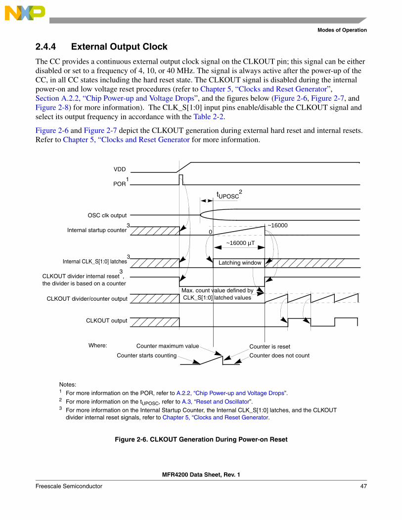
Modes of Operation
2.4.4 External Output Clock
The CC provides a continuous external output clock signal on the CLKOUT pin; this signal can be either disabled or set to a frequency of 4, 10, or 40 MHz. The signal is always active after the power-up of the CC, in all CC states including the hard reset state. The CLKOUT signal is disabled during the internal power-on and low voltage reset procedures (refer to Chapter 5, “Clocks and Reset Generator”, Section A.2.2, “Chip Power-up and Voltage Drops”, and the figures below (Figure 2-6, Figure 2-7, and Figure 2-8) for more information). The CLK_S[1:0] input pins enable/disable the CLKOUT signal and select its output frequency in accordance with the Table 2-2.
Figure 2-6 and Figure 2-7 depict the CLKOUT generation during external hard reset and internal resets. Refer to Chapter 5, “Clocks and Reset Generator for more information.
Figure 2-6. CLKOUT Generation During Power-on Reset
POR1
VDD
OSC clk output
Internal startup counter3
Internal CLK_S[1:0] latches3
CLKOUT divider internal reset3,
the divider is based on a counter
CLKOUT divider/counter output
~16000 µT
Latching window
Counter starts counting
Counter maximum value Counter is reset
Max. count value defined by CLK_S[1:0] latched values
Counter does not count
Where:
~16000 0
CLKOUT output
tUPOSC2
Notes:1 For more information on the POR, refer to A.2.2, “Chip Power-up and Voltage Drops”.2 For more information on the tUPOSC, refer to A.3, “Reset and Oscillator”.3 For more information on the Internal Startup Counter, the Internal CLK_S[1:0] latches, and the CLKOUT
divider internal reset signals, refer to Chapter 5, “Clocks and Reset Generator.
MFR4200 Data Sheet, Rev. 1
Freescale Semiconductor 47

Device Overview
Figure 2-7. CLKOUT Generation during Low Voltage Reset
LVR1
Internal startup counter2
Internal CLK_S[1:0] latches2
CLKOUT divider internal reset2,
the divider is based on a counter
CLKOUT divider/counter output
~16000 µT
Latching window
Counter starts counting
Counter maximum value Counter is reset
Max. count value defined by CLK_S[1:0] latched values
Counter does not count
Where:
~16000 0
CLKOUT output
Notes:1 For more information about the POR, refer to A.2.2, “Chip Power-up and Voltage Drops.2 For more information about the Internal Startup Counter, the Internal CLK_S[1:0] latches, and the CLKOUT
divider internal reset signals, refer to Chapter 5, “Clocks and Reset Generator.
MFR4200 Data Sheet, Rev. 1
48 Freescale Semiconductor

Modes of Operation
Figure 2-8. CLKOUT Generation During External Hard Reset
2.4.5 MFR4200 Connection to FlexRay Network
Figure 2-9 shows an example of connecting a FlexRay Optical/Electrical PHY to the MFR4200. Figure 2-10 shows how to connect the RS485 transceiver to the CC.
External Reset
Internal CLK_S[1:0] latches2
CLKOUT divider internal reset,the divider is based on a counter
CLKOUT divider/counter output
Latching window
Counter starts counting
Counter maximum value Counter is reset
Counter does not count
Where:
CLKOUT output
RESET# pin
External reset after internal glitch filter
1
CLKOUT stabilization time3
10 MHz 4 MHz
max 8 µT
Notes:1 Refer to Chapter 5, “Clocks and Reset Generator for more information on the reset glitch filter.2 For example, running at 10 MHz, then switching to 4 MHz.3 When the external hard reset signal applied to the RESET# pin is negated, the CLKOUT signal frequency
is stabilized after maximum 8 µT.
MFR4200 Data Sheet, Rev. 1
Freescale Semiconductor 49

Device Overview
Figure 2-9. Example: Connecting a FlexRay Optical/Electrical PHY to the MFR4200
Figure 2-10. Example: Connecting an RS485 PHY to the MFR4200
RXD1
TXD1
TXEN1
BGE1
MT
BGT
ARM
BGE2
RXD2
TXD2
TXEN2
MFR4200
Bus
Bus
Bus
Bus
Guardian 1
Guardian 2
Driver 1
Driver 2
RXD_BG1
TXD_BG1
TXEN1
BGE1
MT
BGT
ARM
BGE2
RXD_BG2
TXD_BG2
TXEN1
RXD1
TXD1
TXEN1
BGE1
MT
BGT
ARM
BGE2
RXD2
TXD2
TXEN2
MFR4200
RS485
RS485
Transceiver 1
Transceiver 2
RXD1_485
TXD1_485
TXEN1_485
BGE1
MT
BGT
ARM
BGE2
RXD2_485
TXD2_485
TXEN2_485
Not Connected
Not Connected
Not Connected
Not Connected
Not ConnectedInverter
MFR4200 Data Sheet, Rev. 1
50 Freescale Semiconductor

Resets and Interrupts
NOTETXENn signals for the FlexRay Optical/Electrical PHY are multiplexed with TXENn_485 signals for the RS485 interfaces. Therefore, additional external inverters are required for these signals in the RS485 mode.
2.4.6 Power Mode
No power saving features are implemented in the MFR4200; the device operates only in power mode.
2.5 Resets and Interrupts
2.5.1 Overview
All possible MFR4200 internal interrupt sources are combined and provided to the host by means of one available interrupt line: INT_CC#. Refer to Chapter 3, “MFR4200 FlexRay Communication Controller” for more information on available interrupt sources. The type of interrupt is level sensitive.
MFR4200 has the following resets:
• external hard reset input signal RESET#.
• internal power-on and low-voltage resets provided by the internal voltage regulator (refer to Chapter 5, “Clocks and Reset Generator” and Chapter 4, “Dual Output Voltage Regulator (VREG3V3V2)” for more information).
2.5.2 Resets
When a reset occurs, MFR4200 registers and control bits are changed to known startup states. Refer to the respective module chapters for register reset states for information of the different kind of resets and for register reset states.
2.5.2.1 I/O Pins
Refer to Chapter 3, “MFR4200 FlexRay Communication Controller” for configuration of MFR4200 pins out of reset.
2.5.3 Interrupt Sources
All interrupt sources available in the MFR4200 are controlled and indicated by the following registers:
• Interrupt status register 0 (ISR0)
• Interrupt enable register 0 (IER0)
• Startup interrupt status register (SISR)
• Startup interrupt enable register (SIER)
For more information on interrupt sources, refer to Chapter 3, “MFR4200 FlexRay Communication Controller.
MFR4200 Data Sheet, Rev. 1
Freescale Semiconductor 51

Device Overview
MFR4200 Data Sheet, Rev. 1
52 Freescale Semiconductor

Chapter 3 MFR4200 FlexRay Communication Controller
3.1 IntroductionThis version of the MFR4200 communication controller block guide supports MFR4200 devices with the mask numbers 0L60X and 1L60X.
3.1.1 MFR4200 Features
The MFR4200 provides the following features.
• The FlexRay protocol according to FlexRay Protocol Working document (PWD) V1.1, with differences described in the MFR4200 Protocol Implementation Document (PID)
• Data rate of up to 10 Mbit/s on each of two channels
• FlexRay frames with up to 254 payload bytes (padding is used for FlexRay payload data that exceeds 32-byte data size boundary)
• One configurable receive FIFO
• Configurable counters, status indicators, and interrupts dedicated to error signalling
• Measured value indicators for clock synchronization
• The status of up to four slots can be observed independently of CC receive message buffers
• Configurable error signaling
• Fractional macroticks (MT) supported for clock correction
• 59 message buffers, each with up to 32 payload bytes
• Message buffers configurable with state or event semantics
• Each message buffer can be configured as a receive message buffer, as a transmit message buffer (single or double), or as a part of the receive FIFO
• Receive background buffers for each channel
• The host accesses all buffers by means of three active message buffers (active transmit message buffer, active receive message buffer and active receive FIFO buffer)
• Filtering for frame ID, cycle counter, and channel for receive and transmit message buffers
• Filtering for frame ID, channel, and message ID for the receive FIFO
• Maskable interrupt sources provided over one interrupt line
• Two types of host interface: HCS12 interface and asynchronous memory interfaces
• Minislot action point offset is configurable
• Static slot action point offset is configurable
• Hardware selectable clock output to drive external host devices: disabled/4/10/40 MHz
• Electrical physical layer interface compatible with dedicated FlexRay physical layer. Industry standard RS485 physical layer interface also available.
MFR4200 Data Sheet, Rev. 1
Freescale Semiconductor 53

MFR4200 FlexRay Communication Controller
3.1.2 MFR4200 Implementation Parameters and Constraints
3.1.2.1 Implementation Parameters
• The duration of a microtick (µT) is one CC_CLK period (25 ns at 40 MHz); a microtick starts with a rising edge of CC_CLK.
• The CC internal initialization procedure lasts for 1025 cycles of the CC_CLK clock; it starts after leaving the hard reset state (see Section 3.9.1, “Hard Reset State”).
• After the external hard reset signal on the RESET# pin is negated, the CLKOUT signal frequency is stabilized after 8 µT.
NOTERefer to Section 3.8, “External 4/10 MHz Output Clock” for more information on the CLKOUT output.
3.1.2.2 Implementation Constraints
• The maximum external clock frequency is 40 MHz (CC_CLK).
• Minislot length down to 2 µs (at CC_CLK frequency of 40 MHz) for the dynamic segment.
• Minislot length is configurable (minimum 2 MT).
• The maximum communication cycle length is 16 ms.
• Collision avoidance symbol length is set to 30 bits.
• The maximum configurable static slot length is 255 MT.
3.2 Memory Map and Registers
3.2.1 Introduction
This section describes the memory map, and the content and use of the registers in the host interface module. A memory map of the CC is shown in Table 3-1.
The host accesses four types of CC registers:
• General control registers
• Buffer control, configuration, status and filtering register sets
• FIFO acceptance/rejection filter register sets
• Fifty-nine (59) configurable message buffers. The host can configure every buffer as a receive message buffer, as a transmit message buffer (single or double), or as a FIFO receive message buffer. All buffers are accessible through three active windows mirrored to the memory map:
— One active transmit message buffer
— One active receive message buffer
— One active FIFO buffer
MFR4200 Data Sheet, Rev. 1
54 Freescale Semiconductor

Memory Map and Registers
NOTEThe CC has two shadow receive message buffers per channel (four shadow buffers, in total); these allow reception while the host accesses the receive message buffers. One additional shadow message buffer is used for internal operations. Therefore, only 59 buffers out of 64 are available to the user as message buffers.
3.2.2 Register Map Summary
Table 3-1. Register Map Summary
Register DescriptionAddress
(Hex)Address
(Dec)Hard Reset
(Hex)
MNR Magic Number Register 0 0 815
MVR0 Module Version Register 0 2 2 9042
MCR0 Module Configuration Register 0 4 4 8000
MCR1 Module Configuration Register 1 6 6 0
CMCVR Current Macrotick Counter Value Register 8 8 0
CCCVR Current Cycle Counter Value Register 0A 10 0
PSR Protocol State Register 0C 12 0
ISR0 Interrupt Status Register 0 0E 14 0
SISR Startup Interrupt Status Register 10 16 0
CHIER CHI Error Register 12 18 0
IER0 Interrupt Enable Register 0 14 20 0
SIER Startup Interrupt Enable Register 16 22 0
FSIZR FIFO Size Register 18 24 0
FAFCHR FIFO Acceptance/Rejection Filter Channel Register
1A 26 0
FAFMIDVR FIFO Acceptance Filter Message ID Value Register
1C 28 0
FAFMIDMR FIFO Acceptance Filter Message ID Mask Register
1E 30 0
FRFFIDVR FIFO Rejection Filter Frame ID Value Register
20 32 0
FRFFIDMR FIFO Rejection Filter Frame ID Mask Register
22 34 0
RBIVECR Receive Buffer Interrupt Vector Register 24 36 0
TBIVECR Transmit Buffer Interrupt Vector Register 26 38 0
SSCIR Slot Status Counter Incrementation Register 28 40 0
SSCIMR Slot Status Counter Interrupt Mask Register 2A 42 0
MFR4200 Data Sheet, Rev. 1
Freescale Semiconductor 55

MFR4200 FlexRay Communication Controller
CSECnR Channel Status Error Counter n Register, n=[0:1]
2C, 2E 44, 46 0
TICR0CS Timer Interrupt Configuration Register 0 Cycle Set
30 48 0
TICR0MO Timer Interrupt Configuration Register 0 Macrotick Offset
32 50 0
TICR1CS Timer Interrupt Configuration Register 1 Cycle Set
34 52 0
TICR1MO Timer Interrupt Configuration Register 1 Macrotick Offset
36 54 0
DBPCR Debug Port Control Register 38 56 0
BGSR Bus Guardian Status Register 3A 58 0
DCR Delay Counter Register 3C 60 0
NMVLR Network Management Vector Length Register
3E 62 0
GNMVnR Global Network Management Vector n Register, n=[0:5]
GNMV0R=40GNMV1R=42GNMV2R=44GNMV3R=46GNMV4R=48GNMV5R=4A
GNMV0R=64GNMV1R=66GNMV2R=68GNMV3R=70GNMV4R=72GNMV5R=74
0
SSCnR Slot Status Counter n Register, n=[0:7] SSC0R=4CSSC1R=4ESSC2R=50SSC3R=52SSC4R=54SSC5R=56SSC6R=58SSC7R=5A
SSC0R=76SSC1R=78SSC2R=80SSC3R=82SSC4R=84SSC5R=86SSC6R=88SSC7R=90
0
SSCCnR Slot Status Counter Condition n Register, n=[0:7]
SSCC0R=5CSSCC1R=5ESSCC2R=60SSCC3R=62SSCC4R=64SSCC5R=66SSCC6R=68SSCC7R=6A
SSCC0R=92SSCC1R=94SSCC2R=96SSCC3R=98SSCC4R=100SSCC5R=102SSCC6R=104SSCC7R=106
0
SSSnR Slot Status Selection n Register, n=[0:3] SSS0R=6CSSS1R=6ESSS2R=70SSS3R=72
SSS0R=108SSS1R=110SSS2R=112SSS3R=114
0
Table 3-1. Register Map Summary
Register DescriptionAddress
(Hex)Address
(Dec)Hard Reset
(Hex)
MFR4200 Data Sheet, Rev. 1
56 Freescale Semiconductor

Memory Map and Registers
SSnR Slot Status n Register, n=[0:7] SS0R=74SS1R=76SS2R=78SS3R=7ASS4R=7CSS5R=7ESS6R=80SS7R=82
SS0R=116SS1R=118SS2R=120SS3R=122SS4R=124SS5R=126SS6R=128SS7R=130
0
SWCTRLR Symbol Window Control Register 84 132 0
SWSAR Symbol Window Status channel A Register 86 134 0
SWSBR Symbol Window Status channel B Register 88 136 0
WMCTRLR Wakeup Mechanism Control Register 8A 138 0
NSSR Number of Static Slots Register 8E 142 1
SPLR Static Payload Length Register 90 144 0
MPLDR Maximum Payload Length Dynamic Register
92 146 0
SYNCFR Sync Frame Register 94 148 0
SYNCHR Sync Frame Header Register 96 150 undefined
MVR1 Module Version Register 1 98 152 For mask set number:
0L60X – 0;1L60X – 0001
HIPDSR Host Interface Pins Drive Strength Register 9A 154 0
PLPDSR Physical Layer Pins Drive Strength Register 9C 156 0
HIPPER Host Interface Pins Pullup/down Enable Register
9E 158 0
HIPPCR Host Interface Pins Pullup/down Control Register
A0 160 0
PLPPER Physical Layer Pins Pullup/down Enable Register
A2 162 0
PLPPCR Physical Layer Pins Pullup/down Control Register
A4 164 0
VREGSR Voltage Regulator Status Register A6 166 0
BDR Bit Duration Register A8 168 undefined
IDLR Idle Detection Length Register AA 170 undefined
NMLR Nominal Macrotick Length Register AC 172 undefined
BGTR Bus Guardian Tick Register AE 174 undefined
SSLR Static Slot Length Register B0 176 undefined
Table 3-1. Register Map Summary
Register DescriptionAddress
(Hex)Address
(Dec)Hard Reset
(Hex)
MFR4200 Data Sheet, Rev. 1
Freescale Semiconductor 57

MFR4200 FlexRay Communication Controller
CLR Cycle Length Register B2 178 undefined
MPCLR Microticks per Cycle Low Register B4 180 undefined
MPCHR Microticks per Cycle High Register B6 182 undefined
MCLDAR Maximum Cycle Length Deviation Register B8 184 undefined
TSSLR Transmit Start Sequence Length Register BA 186 undefined
SWCR Symbol Window Configuration Register BC 188 undefined
NITCR Network Idle Time Configuration Register BE 190 undefined
CSMR Coldstart Maximum Register C0 192 undefined
MSFR Maximum Sync Frames Register C2 194 undefined
LDTSR Latest Dynamic Transmission Start Register C4 196 undefined
MSLR Minislot Length Register C6 198 undefined
MSAPOR Minislot Action Point Offset Register C8 200 undefined
SSAPOR Static Slot Action Point Offset Register CA 202 undefined
MOCWCFR Maximum Odd Cycles Without Clock Correction Fatal Register
CC 204 undefined
DCAR Delay Compensation Channel A Register D0 208 undefined
DCBR Delay Compensation Channel B Register D2 210 undefined
LNLR Listen timeout with Noise Length Register D6 214 undefined
MOCWCPR Maximum Odd Cycles Without clock Correction Passive Register
D8 216 undefined
MOCR Maximum Offset Correction Register DA 218 undefined
MRCR Maximum Rate Correction Register DC 220 undefined
CDDR Cluster Drift Damping Register DE 222 undefined
SOCCTR Start of Offset Correction Cycle Time Register
E0 224 undefined
WUSTXIR Wakeup Symbol TX Idle Register EA 234 0
WUSTXLR Wakeup Symbol TX Low Register EC 236 0
SYNFAFMR Sync Frame Acceptance Filter Mask Register
EE 238 undefined
SYNFAFVR Sync Frame Acceptance Filter Value Register
F0 240 undefined
SYNFRFR Sync Frame Rejection Filter Register F2 242 undefined
EOCR External Offset Correction Register F4 244 undefined
ERCR External Rate Correction Register F6 246 undefined
Table 3-1. Register Map Summary
Register DescriptionAddress
(Hex)Address
(Dec)Hard Reset
(Hex)
MFR4200 Data Sheet, Rev. 1
58 Freescale Semiconductor

Memory Map and Registers
ECCR External Correction Control Register F8 248 undefined
AFBFRID Active FIFO Buffer Frame ID Register 100 256 undefined
AFBCCPLR Active FIFO Buffer Cycle Counter and Payload Length Register
102 258 undefined
AFBCRCR Active FIFO Buffer Header CRC Register 104 260 undefined
AFBDATAnR Active FIFO Buffer Data n Register, n=[0:15] ARFBDATA0R=106 …
ARFBDATA15R=124
ARFBDATA0R=262 …
ARFBDATA15R=292
undefined
AFBMBSSVR Active FIFO Buffer Message Buffer Slot Status Vector Register
126 294 undefined
ARBFRID Active Receive Buffer Frame ID Register 140 320 undefined
ARBCCPLR Active Receive Buffer Cycle Counter and Payload Length Register
142 322 undefined
ARBCRCR Active Receive Buffer Header CRC Register 144 324 undefined
ARBDATAnR Active Receive Buffer Data n Register, n=[0:15]
ARBDATA0R=146…
ARBDATA15R=164
ARBDATA0R=326…
ARBDATA15R=356
undefined
ARBMBSSVR Active Receive Buffer Message Buffer Slot Status Vector Register
166 358 undefined
ATBFRID Active Transmit Buffer Frame ID Register 180 384 undefined
ATBCCPLR Active Transmit Buffer Cycle Counter and Payload Length Register
182 386 undefined
ATBCRCR Active Transmit Buffer Header CRC Register 184 388 undefined
ATBDATAnR Active Transmit Buffer Data n Register, n=[0:15]
ATBDATA0R=186…
ATBDATA15R=1A4
ATBDATA0R=390…
ATBDATA15R=420
undefined
ATBMBSSVR Active Transmit Buffer Message Buffer Slot Status Vector Register
1A6 422 undefined
BUFCSnR Message Buffer Control, Configuration and Status n Register, n=[0:58]
BUFCS0R=200BUFCS1R=204
…BUFCS57R=2E4BUFCS58R=2E8
BUFCS0R=512BUFCS1R=516
…BUFCS57R=740BUFCS58R=744
IFLG, IENA, CFG and VALID bits are reset to
0; others are undefined
CCFnR Cycle Counter Filter n Register, n=[0:58] CCF0R=202CCF1R=206
…CCF57R=2E6CCF58R=2EA.
CCF0R=514CCF1R=518
…CCF57R=742CCF58R=746
undefined
CCFCR Clock Correction Failed Counter Register 326 806 undefined
EHLR Error Handling Level Register 328 808 undefined
Table 3-1. Register Map Summary
Register DescriptionAddress
(Hex)Address
(Dec)Hard Reset
(Hex)
MFR4200 Data Sheet, Rev. 1
Freescale Semiconductor 59

MFR4200 FlexRay Communication Controller
3.2.3 Register Descriptions
A condensed overview of all registers is provided in Section 3.2.2, “Register Map Summary”
NOTE• All registers not shown in the CC memory map registers are not
implemented in hardware.
• Any read operation on bits marked as ‘Reserved’ will return an undefined value (either ‘1’ or ‘0’).
• The host must take care that bits marked as ‘Reserved’ are set to 0 when writing.
• The reset value indicated for each register is the value that the register has after a hard reset operation.
• Meaning of the bit field character in the registers layout:
– ‘r’ indicates that the bit-field may be read by host
– ‘w’ denotes that the bit-field may be updated by host
– ‘h’ means that the bit-field is updated by the communication controller
RCVR Rate Correction Value Register 32A 810 undefined
OCVR Offset Correction Value Register 32C 812 undefined
EMCR Even Measurement Counter Register 33C 828 undefined
OMCR Odd Measurement Counter Register 33E 830 undefined
EMAnR Even Measurement channel A n Register, n=[0:15]
EMA0R=340…
EMA15R=35E
EMA0R=832…
EMA15R=862
undefined
EMBnR Even Measurement channel B n Register, n=[0:15]
EMB0R=360…
EMB15R=37E
EMB0R=864…
EMB15R=894
undefined
ESFIDnR Even Sync ID n Register, n=[0:15] EID0R=380…
EID15R=39E
EID0R=896…
EID15R=926
undefined
OMAnR Odd Measurement channel A n Register, n=[0:15]
OMA0R=3A0…
OMA15R=3BE
OMA0R=928…
OMA15R=958
undefined
OMBnR Odd Measurement channel B n Register, n=[0:15]
OMB0R=3C0…
OMB15R=3DE
OMB0R=960…
OMB15R=990
undefined
OSFIDnR Odd Sync Frame ID n Register, n=[0:15] OSFID0R=3E0…
OSFID15R=3FE
OSFID0R=1008…
OSFID15R=1022
undefined
Table 3-1. Register Map Summary
Register DescriptionAddress
(Hex)Address
(Dec)Hard Reset
(Hex)
MFR4200 Data Sheet, Rev. 1
60 Freescale Semiconductor

Memory Map and Registers
• Combinations such as ‘rh’, ‘rw’ or ‘rwh’ appear in the text indicating the different access possibilities.
• An additional asterisk ‘*’ indicates an exceptional behavior, i.e. under which conditions the host is allowed to write a ‘rw’ or ‘rwh’ bit-field, etc. In such cases, refer to the detailed bit-field description.
• Descriptions of configuration registers specify the possible range of values in square brackets – [,].
NOTEThe configuration registers’ possible ranges of values, specified in square brackets [ : ], denote only the MFR4200 implementation constraints. Not every configuration supported by the MFR4200 implementation is necessarily a valid configuration of an application network. For more information about configuration constraints, refer to the PWD: Configuration Constraints Notations chapter.
A key to the register diagrams is shown in Figure 3-1.
Figure 3-1. Key to Register Diagrams
3.2.3.3.1 Bit Duration Register (BDR)FlexRay Protocol Related Parameter – gdBitAddress0xA8Reset undefined state
15 14 13 12 11 10 9 8
Reserved Reserved Reserved Reserved Reserved Reserved Reserved Reserved
r r r r r r r r
7 6 5 4 3 2 1 0
Reserved BD6 BD5 BD4 BD3 BD2 BD1 BD0
r rw* rw* rw* rw* rw* rw* rw*
Section Number
Register
Register Full Name Register Short Name
Register Reset Bit Number Bit Access Bit NameValue/State
FlexRay ProtocolRelated Parameter
Address Scheme
MFR4200 Data Sheet, Rev. 1
Freescale Semiconductor 61

MFR4200 FlexRay Communication Controller
3.2.3.1 Controller’s Constants Registers
3.2.3.1.1 Module Version Register 0 (MVR0)
Address 0x2Reset 0x9042
The read-only MVR0, together with MVR1 (see following section), holds the version number of the implementation. The MVR0 contains the following fields:
PDA[0:7] denotes the device PartID1.
MINFR[0:3] denotes the minor release of the FlexRay core in the MFR4200 device.
MJFR[0:3] denotes the major release of the FlexRay core in the MFR4200 device.
3.2.3.1.2 Module Version Register 1 (MVR1)
Address 0x98Reset
The read-only MVR1, together with MVR0 (see previous section), holds the version number of the implementation. The MVR1 contains:
15 14 13 12 11 10 9 8
MJFR3 MJFR2 MJFR1 MJFR0 MINFR3 MINFR2 MINFR1 MINFR0
r r r r r r r r
7 6 5 4 3 2 1 0
PDA7 PDA6 PDA5 PDA4 PDA3 PDA2 PDA1 PDA0
r r r r r r r r
Figure 3-2. Module Version Register 0
Device Mask Set Number Reset Value
MFR4200 0L60X 0x0000
MFR4200 1L60X 0x0001
15 14 13 12 11 10 9 8
PDB7 PDB6 PDB5 PDB4 PDB3 PDB2 PDB1 PDB0
r r r r r r r r
7 6 5 4 3 2 1 0
MJMR3 MJMR2 MJMR1 MJMR0 MINMR3 MINMR2 MINMR1 MINMR0
r r r r r r r r
Figure 3-3. Module Version Register 1
MFR4200 Data Sheet, Rev. 1
62 Freescale Semiconductor

Memory Map and Registers
PDB[0:7] denotes the device PartID2.
MINMR[0:3] denotes the minor release of the MFR4200 device.
MJMR[0:3] denotes the major release of the MFR4200 device.
3.2.3.1.3 Magic Number Register (MNR)
Address 0x0Reset 0x0815
This read-only register contains the arbitrary value 0x0815; it is used for endianess and memory map address offset checks.
NOTEThe MNR contains 0x0000 while the controller is initializing after leaving the hard reset state. Only after this initialization is completed, does it contain the value 0x0815. After the controller leaves the hard reset state, the host must wait until the initialization is completed before reading or writing to the controller. The initialization takes 1025 cycles (CC_CLK) after de-assertion of the hard reset.
During the internal initialization procedure time, the host must not access any CC register except MNR (see Section 3.2.3.1.3, “Magic Number Register (MNR)”), which acknowledges the completion of the internal initialization procedure.
15 14 13 12 11 10 9 8
MN15 MN14 MN13 MN12 MN11 MN10 MN9 MN8
r r r r r r r r
7 6 5 4 3 2 1 0
MN7 MN6 MN5 MN4 MN3 MN2 MN1 MN0
r r r r r r r r
Figure 3-4. Magic Number Register
MFR4200 Data Sheet, Rev. 1
Freescale Semiconductor 63

MFR4200 FlexRay Communication Controller
3.2.3.2 Configuration Registers
3.2.3.2.1 Module Configuration Register 0 (MCR0)
Address 0x4Reset 0x8000
NOTESetting the CONFIG bit and writing to other bits in this register can be done in separate instructions only. Trying to set CONFIG and change other bits at the same time will change CONFIG only — the other bits will not be changed. Clearing CONFIG and writing to other bits in the MCR0 can be done simultaneously in one instruction.
DIAGSTOP — Diagnosis Stop State Bit
When this bit is set by the host, the CC immediately enters the Diagnosis Stop state. Any ongoing transmission or reception is aborted, and synchronization with the FlexRay communication bus is lost.
When this bit is cleared by the host, the controller enters the configuration state.
1 – The CC is in the Diagnosis Stop state.
0 – The CC is not in the Diagnosis Stop state.
SCM0, SCM1 — Serial Communication Mode Bits 0 and 1
These bits define the type of bus driver connected to the controller. It can be written during the configuration state only.
15 14 13 12 11 10 9 8
CONFIG Reserved Reserved Reserved Reserved Reserved CBE CAE
rwh r r r r r rw* rw*
7 6 5 4 3 2 1 0
Reserved ENSYNFF NSYNC SCM1 SCM0 Reserved DIAGSTOP Reserved
r rw* rh rw* rw* r rw r
Figure 3-5. Module Configuration Register 0
Table 3-2. Bus Driver Type Selection
Driver type SCM1 SCM0
RS485 (IDLE state coded as “0”) 0 0
Optical/Electrical PHY 0 1
— 1 0
RS485 (IDLE state coded as “1”) 1 1
MFR4200 Data Sheet, Rev. 1
64 Freescale Semiconductor

Memory Map and Registers
NOTEIt is not possible to mix different RS485’s in a cluster or per channel, or to mix RS485 and Optical/Electrical PHY.
NSYNC — Node Synchronized
This read-only bit is set when the controller enters the normal state in the course of startup or reintegration. The NSYNC is set by the CC in the NIT preceding a transition to normal operation. The NSYNC is cleared by the CC in the NIT, prior to switching to the normal passive state (the ‘yellow’ error state; see Section 3.2.3.6.5, “Error Handling Level Register (EHLR)”) or the Diagnosis Stop state (the ‘red’ error state; see Section 3.2.3.6.5, “Error Handling Level Register (EHLR)”), due to…
• …the correction value exceeding MRCR (see Section 3.2.3.3.25, “Maximum Rate Correction Register (MRCR)”)
• …the offset correction value exceeding MOCR (see Section 3.2.3.3.24, “Maximum Offset Correction Register (MOCR)”)
• …the CCFCR value (see Section 3.2.3.6.4, “Clock Correction Failed Counter Register (CCFCR)”) exceeding MOCWCPR (see Section 3.2.3.5.3, “Maximum Odd Cycles Without clock Correction Passive Register (MOCWCPR)”) or MOCWCFR (see Section 3.2.3.5.2, “Maximum Odd Cycles Without Clock Correction Fatal Register (MOCWCFR)).
1 – Node is synchronized to cluster.
0 – Node is not synchronized to cluster.
ENSYNFF — Enable Sync Frame Filters
This bit enables/disables acceptance and rejection filtering for sync frames (see Section 3.2.3.8.1, “Sync Frame Acceptance Filter Value Register (SYNFAFVR)”, Section 3.2.3.8.2, “Sync Frame Acceptance Filter Mask Register (SYNFAFMR)” and Section 3.2.3.8.3, “Sync Frame Rejection Filter Register (SYNFRFR)”).
1 – Sync frames are used for the clock synchronization only when they pass the acceptance filter and are not rejected by the rejection filter.
0 – Sync frames are used for the clock synchronization independently of the acceptance and rejection filter.
CAE — Channel A Enable
This bit enables channel A. It can be written during the configuration state only.
1 – Channel A is enabled.
0 – Channel A is disabled.
CBE — Channel B Enable
This bit enables channel B. It can be written during the configuration state only.
1 – Channel B is enabled.
0 – Channel B disabled.
MFR4200 Data Sheet, Rev. 1
Freescale Semiconductor 65

MFR4200 FlexRay Communication Controller
CONFIG — Configuration State Bit
When the host sets this bit, the CC immediately enters the configuration state. The controller aborts any ongoing transmission or reception and abandons synchronization to the FlexRay cluster. When the host clears this bit, the controller resumes normal operation (see Section 3.9.2, “Configuration State”). After a hard reset, the controller automatically enters the configuration state (CONFIG bit set).
1 – Configuration state.
0 – Normal operation.
3.2.3.2.2 Module Configuration Register 1 (MCR1)
Address 0x6Reset 0x0
MATE — Media Access Test Enable
This flag enables the media access test in the MFR4200 bus guardian (BG) monitor. This flag may be written in the configuration state only.
1 – Media access test is enabled.
0 – Media access test is disabled.
BGSMSWE — BG Schedule Monitoring Symbol Window Enable
This flag determines the behavior of the MFR4200 bus guardian schedule monitor during the symbol window. It may be written in the configuration state only.
1 – BG is expected to be open during symbol window of the communication cycle.
0 – BG is expected to be closed during symbol window of the communication cycle.
BGSMDSE — BG Schedule Monitoring Dynamic Segment Enable
This flag determines the behavior of the MFR4200 bus guardian monitor during the dynamic segment of the communication cycle. It may be written in the configuration state only.
1 – BG expected to be open during dynamic segment of the communication cycle.
0 – BG expected to be closed during dynamic segment of the communication cycle.
15 14 13 12 11 10 9 8
Reserved Reserved Reserved Reserved Reserved AYTG ARL CSI
r r r r r rw* rw* rw*
7 6 5 4 3 2 1 0
Reserved ECSE BGSMDSE BGSMSWE Reserved MATE Reserved Reserved
r rw* rw* rw* r rw* r r
Figure 3-6. Module Configuration Register 1
MFR4200 Data Sheet, Rev. 1
66 Freescale Semiconductor

Memory Map and Registers
ECSE — External Clock Synchronization Enable
This configuration flag enables/disables the External Clock Synchronization. It can be written during the configuration state only.
1 – External Clock Synchronization is enabled.
0 – External Clock Synchronization is disabled.
CSI — Coldstart Inhibit Mode
The node can be prevented from initializing the TDMA communication schedule by setting the CSI bit to ‘1’ in the configuration state. It can be written during the configuration state only.
1 – Node is in Coldstart Inhibit mode.
0 – Node is not in Coldstart Inhibit mode.
ARL — Allow Red Level
If this bit is set, the transition to the red error handling level (Diagnosis Stop state) due to clock sync errors is allowed. It may be written in the configuration state only.
1 – Error handling level red is allowed (the CC enters the Diagnosis Stop state).
0 – Error handling level red is prohibited (the CC enters the configuration state).
AYTG — Allow Yellow to Green
If this bit is set, the transition from the yellow error handling level to the green error handling level is allowed. It may be written in the configuration state only.
1 – Transition from yellow to green is allowed.
0 – Transition from yellow to green is prohibited.
3.2.3.2.3 Host Interface and Physical Layer Pins Drive Strength Register (HIPDSR)
Address 0x9AReset 0x0
This register controls the drive strength of the MFR4200 pins identified in Figure 3-7.
15 14 13 12 11 10 9 8
Reserved Reserved Reserved Reserved Reserved Reserved Reserved Reserved
r r r r r r r r
7 6 5 4 3 2 1 0
Reserved Reserved INT_CC# CLKOUT ARM/DBG1/ CLK_S0
MT/CLK_S1 BGT/DBG2/IF_SEL0
PAD[0:15]/D[15:0]
r r rw rw rw rw rw rw
Figure 3-7. Host Interface Pins Drive Strength Register
MFR4200 Data Sheet, Rev. 1
Freescale Semiconductor 67

MFR4200 FlexRay Communication Controller
1 – Pin drive strength is partial (see Appendix A.1.9, “I/O Characteristics”).
0 – Pin drive strength is full (see Appendix A.1.9, “I/O Characteristics”).
3.2.3.2.4 Physical Layer Pins Drive Strength Register (PLPDSR)
Address 0x9CReset 0x0
This register controls the drive strength of the MFR4200 pins identified in Figure 3-8.
1 – Pin drive strength is partial (see Section A.1.9, “I/O Characteristics”).
0 – Pin drive strength is full (see Section A.1.9, “I/O Characteristics”).
3.2.3.2.5 Host Interface Pins Pullup/down Enable Register (HIPPER)
Address 0x9EReset 0x0
This register enables the pullups and pulldowns on MFR4200 pins identified in Figure 3-9. The pullup/down state is controlled by the HIPPCR (see Section 3.2.3.2.6, “Host Interface Pins Pullup/down Control Register (HIPPCR)”).
1 – Pullup/down resistor enabled.
15 14 13 12 11 10 9 8
Reserved Reserved Reserved Reserved Reserved Reserved Reserved Reserved
r r r r r r r r
7 6 5 4 3 2 1 0
Reserved Reserved Reserved Reserved TXD_BG2/TXD2_485
TXD_BG1/TXD1_485/
IF_SEL1
TXEN2#/TXE2_485#
TXEN1#/TXE1_485#
r r r r rw rw rw rw
Figure 3-8. Physical Layer Pins Drive Strength Register
15 14 13 12 11 10 9 8
ECLK_CC WE#/RW_CC#
CE#/LSTRB D[15:0]/PAD[0:15]
ACS5 ACS4 OE#/ACS3 A9/ACS2
rw rw rw rw rw rw rw rw
7 6 5 4 3 2 1 0
A8/ACS1 A7/ACS0 A6/XADDR14
A5/XADDR15
A4/XADDR16
A3/XADDR17
A2/XADDR18
A1/XADDR19
rw rw rw rw rw rw rw rw
Figure 3-9. Host Interface Pins Pullup/down Enable Register
MFR4200 Data Sheet, Rev. 1
68 Freescale Semiconductor

Memory Map and Registers
0 – Pullup/down resistor disabled.
3.2.3.2.6 Host Interface Pins Pullup/down Control Register (HIPPCR)
Address 0xA0Reset 0x0
This register controls the pullups and pulldowns on MFR4200 pins identified in Figure 3-10. These functions can be enabled/disabled by the HIPPER (see Section 3.2.3.2.5, “Host Interface Pins Pullup/down Enable Register (HIPPER)”).
1 – Pullup selected.
0 – Pulldown selected.
3.2.3.2.7 Physical Layer Pins Pullup/down Enable Register (PLPPER)
Address 0xA2Reset 0x0
This register enables the pullups and pulldowns on MFR4200 pins identified in Figure 3-11. The pullup/down state is controlled by the PLPPCR (see Section 3.2.3.2.8, “Physical Layer Pins Pullup/down Control Register (PLPPCR)”).
1 – Pullup/down enabled.
0 – Pullup/down disabled.
15 14 13 12 11 10 9 8
ECLK_CC WE#/RW_CC#
CE#/LSTRB D[15:0]/PAD[0:15]
ACS5 ACS4 OE#/ACS3 A9/ACS2
rw rw rw rw rw rw rw rw
7 6 5 4 3 2 1 0
A8/ACS1 A7/ACS0 A6/XADDR14
A5/XADDR15
A4/XADDR16
A3/XADDR17
A2/XADDR18
A1/XADDR19
rw rw rw rw rw rw rw rw
Figure 3-10. Host Interface Pins Pullup/down Control Register
15 14 13 12 11 10 9 8
Reserved Reserved Reserved Reserved Reserved Reserved Reserved Reserved
r r r r r r r r
7 6 5 4 3 2 1 0
Reserved Reserved Reserved Reserved BGEN2 BGEN1 RXD_BG2/RXD2_485
RXD_BG1/RXD1_485
r r r r rw rw rw rw
Figure 3-11. Physical Layer Pins Pullup/down Enable Register
MFR4200 Data Sheet, Rev. 1
Freescale Semiconductor 69

MFR4200 FlexRay Communication Controller
3.2.3.2.8 Physical Layer Pins Pullup/down Control Register (PLPPCR)
Address 0xA4Reset 0x0
This register controls the pullups and pulldowns on MFR4200 pins identified in Figure 3-12. These function can be enabled/disabled by the PLPPER (see Section 3.2.3.2.7, “Physical Layer Pins Pullup/down Enable Register (PLPPER)”).
1 – Pullup selected.
0 – Pulldown selected.
3.2.3.2.9 Voltage Regulator Status Register (VREGSR)
Address 0xA6Reset
This register indicates the occurrence of internal low-voltage and/or power-on reset events caused by power-on of MFR4200 device or supply voltage disturbances. The Low-voltage Status and Power-on Status bits do not cause an interrupt over the INT_CC# pin; therefore, the host may read this register to check the status.
The host clears any status bit in VREGSR by reading VREGSR. The CC sets a status bit in the VREGSR again when it detects the condition for that bit.
15 14 13 12 11 10 9 8
Reserved Reserved Reserved Reserved Reserved Reserved Reserved Reserved
r r r r r r r r
7 6 5 4 3 2 1 0
Reserved Reserved Reserved Reserved BGEN2 BGEN1 RXD_BG2/RXD2_485
RXD_BG1/RXD1_485
r r r r rw rw rw rw
Figure 3-12. Physical Layer Pins Pullup/down Control Register
15 14 13 12 11 10 9 8
Reserved Reserved Reserved Reserved Reserved Reserved Reserved Reserved
r r r r r r r r
7 6 5 4 3 2 1 0
Reserved Reserved Reserved Reserved Reserved Reserved Low-voltage Status
Power-on Status
r r r r r r rwh rwh
Figure 3-13. Voltage Regulator Status Register
MFR4200 Data Sheet, Rev. 1
70 Freescale Semiconductor

Memory Map and Registers
Low-voltage Status, Power-on Status
1 – MFR4200 has been reset internally due to reset conditions sensed by the voltage regulator.
0 – MFR4200 has not been reset internally.
NOTELow-voltage and power-on events generated by the MFR4200 voltage regulator cause the internal MFR4200 reset with the same consequences as in the case of an external hard reset. Therefore, changes to the VREGSR bits can be read by the host only after the MFR4200 leaves the internal reset state.
3.2.3.3 Control Registers
3.2.3.3.1 Bit Duration Register (BDR)
FlexRay Protocol Related Parameter – gdBitAddress 0xA8Reset undefined state
This register controls the number of microticks per bit. Writing this register is possible only during the configuration state.
15 14 13 12 11 10 9 8
Reserved Reserved Reserved Reserved Reserved Reserved Reserved Reserved
r r r r r r r r
7 6 5 4 3 2 1 0
Reserved BD6 BD5 BD4 BD3 BD2 BD1 BD0
r rw* rw* rw* rw* rw* rw* rw*
Figure 3-14. Bit Duration Register
MFR4200 Data Sheet, Rev. 1
Freescale Semiconductor 71

MFR4200 FlexRay Communication Controller
3.2.3.3.2 Delay Compensation Channel A Register (DCAR)
FlexRay Protocol Related Parameter – pDelayCompensation[A]Address 0xD0Reset undefined state
This register holds the value used to compensate for reception delays on channel A in microticks. The register can be written during the configuration state only. The value of this register must be within the range [0:127].
3.2.3.3.3 Delay Compensation Channel B Register (DCBR)
FlexRay Protocol Related Parameter – pDelayCompensation[B]Address 0xD2Reset undefined state
This register holds the value used to compensate for reception delays on channel B in microticks. The register can be written during the configuration state only. The value of this register must be within the range [0:127].
15 14 13 12 11 10 9 8
DCA15 DCA14 DCA13 DCA12 DCA11 DCA10 DCA9 DCA8
rw* rw* rw* rw* rw* rw* rw* rw*
7 6 5 4 3 2 1 0
DCA7 DCA6 DCA5 DCA4 DCA3 DCA2 DCA1 DCA0
rw* rw* rw* rw* rw* rw* rw* rw*
Figure 3-15. Delay Compensation Channel A Register
15 14 13 12 11 10 9 8
DCB15 DCB14 DCB13 DCB12 DCB11 DCB10 DCB9 DCB8
rw* rw* rw* rw* rw* rw* rw* rw*
7 6 5 4 3 2 1 0
DCB7 DCB6 DCB5 DCB4 DCB3 DCB2 DCB1 DCB0
rw* rw* rw* rw* rw* rw* rw* rw*
Figure 3-16. Delay Compensation Channel B Register
MFR4200 Data Sheet, Rev. 1
72 Freescale Semiconductor

Memory Map and Registers
3.2.3.3.4 Cluster Drift Damping Register (CDDR)
FlexRay Protocol Related Parameter – pClusterDriftDampingAddress 0xDEReset undefined state
This register defines the value used, in clock synchronization, to minimize the accumulation of rounding errors. This register can be written in the configuration state only. The register value is given in microticks and must be within the range [1:15].
3.2.3.3.5 Maximum Sync Frames Register (MSFR)
FlexRay Protocol Related Parameter – gSyncNodeMaxAddress 0xC2Reset undefined state
This register holds the maximum number of sync frames that can be transmitted on either channel in a network, including a node’s own sync frame. The host may modify this register in the configuration state only. The value of this register must be within the range [2:15].
15 14 13 12 11 10 9 8
CDD15 CDD14 CDD13 CDD12 CDD11 CDD10 CDD9 CDD8
rw* rw* rw* rw* rw* rw* rw* rw*
7 6 5 4 3 2 1 0
CDD7 CDD6 CDD5 CDD4 CDD3 CDD2 CDD1 CDD0
rw* rw* rw* rw* rw* rw* rw* rw*
Figure 3-17. Cluster Drift Damping Register
15 14 13 12 11 10 9 8
MSF15 MSF14 MSF13 MSF12 MSF11 MSF10 MSF9 MSF8
rw* rw* rw* rw* rw* rw* rw* rw*
7 6 5 4 3 2 1 0
MSF7 MSF6 MSF5 MSF4 MSF3 MSF2 MSF1 MSF0
rw* rw* rw* rw* rw* rw* rw* rw*
Figure 3-18. Maximum Sync Frames Register
MFR4200 Data Sheet, Rev. 1
Freescale Semiconductor 73

MFR4200 FlexRay Communication Controller
3.2.3.3.6 Nominal Macrotick Length Register (NMLR)
FlexRay Protocol Related Parameter – pMicroPerMacroNomAddress 0xACReset undefined state
This register defines the integer number of microticks per nominal macrotick, according to Equation 3-1.
NMLR = int (cycle length in µT / CLR) Eqn. 3-1
Writing this register is possible only in the configuration state.
3.2.3.3.7 Microticks Per Cycle Low Register (MPCLR)
Address 0xB4Reset undefined state
The MPCHR and MPCLR are described in the following section.
The MPCLR can be written during the configuration state only.
15 14 13 12 11 10 9 8
Reserved Reserved Reserved Reserved Reserved Reserved Reserved Reserved
r r r r r r r r
7 6 5 4 3 2 1 0
NML7 NML6 NML5 NML4 NML3 NML2 NML1 NML0
rw* rw* rw* rw* rw* rw* rw* rw*
Figure 3-19. Nominal Macrotick Length Register
15 14 13 12 11 10 9 8
MPCL15 MPCL14 MPCL13 MPCL12 MPCL11 MPCL10 MPCL9 MPCL8
rw* rw* rw* rw* rw* rw* rw* rw*
7 6 5 4 3 2 1 0
MPCL7 MPCL6 MPCL5 MPCL4 MPCL3 MPCL2 MPCL1 MPCL0
rw* rw* rw* rw* rw* rw* rw* rw*
Figure 3-20. Microticks Per Cycle Low Register
MFR4200 Data Sheet, Rev. 1
74 Freescale Semiconductor

Memory Map and Registers
3.2.3.3.8 Microticks Per Cycle High Register (MPCHR)
Address 0xB6Reset undefined state
The MPCHR and MPCLR define the number of microticks per cycle. Writing these registers is possible only in the configuration state. The relationship between registers MPCHR, MPCLR, and CLR is given by Equation 3-2.
MPCHR * 2^16 + MPCLR = (Cycle Length) – k * CLR Eqn. 3-2
Where:
• Cycle Length = the length of a communication cycle in microticks
• k = 1 [microtick/macrotick]
3.2.3.3.9 Static Slot Length Register (SSLR)
FlexRay Protocol Related Parameter – gdStaticSlotAddress 0xB0Reset undefined state
This register defines the number of macroticks per slot. Writing this register is possible only in the configuration state.
15 14 13 12 11 10 9 8
Reserved Reserved Reserved Reserved Reserved Reserved Reserved Reserved
r r r r r r r r
7 6 5 4 3 2 1 0
MPCH7 MPCH6 MPCH5 MPCH4 MPCH3 MPCH2 MPCH1 MPCH0
rw* rw* rw* rw* rw* rw* rw* rw*
Figure 3-21. Microticks Per Cycle High Register
15 14 13 12 11 10 9 8
Reserved Reserved Reserved Reserved Reserved Reserved Reserved Reserved
r r r r r r r r
7 6 5 4 3 2 1 0
SSL7 SSL6 SSL5 SSL4 SSL3 SSL2 SSL1 SSL0
rw* rw* rw* rw* rw* rw* rw* rw*
Figure 3-22. Static Slot Length Register
MFR4200 Data Sheet, Rev. 1
Freescale Semiconductor 75

MFR4200 FlexRay Communication Controller
3.2.3.3.10 Number of Static Slots Register (NSSR)
FlexRay Protocol Related Parameter – gNumberOfStaticSlotsAddress 0x8EReset 0x1
This register defines the number of static slots in a cycle. Writing this register is possible only during the configuration state.
NOTEThe range of possible values for the NSSR is from 0x2 to 0x3FF. This means that at least two static slots must be programmed.
3.2.3.3.11 Static Payload Length Register (SPLR)
FlexRay Protocol Related Parameter – gPayloadLengthStaticAddress 0x90Reset 0x0
This register defines the maximum data length for static frames in words (1 word = 2 bytes). Writing this register is possible only during the configuration state.
15 14 13 12 11 10 9 8
Reserved Reserved Reserved Reserved Reserved NSS10 NSS9 NSS8
r r r r r rw* rw* rw*
7 6 5 4 3 2 1 0
NSS7 NSS6 NSS5 NSS4 NSS3 NSS2 NSS1 NSS0
rw* rw* rw* rw* rw* rw* rw* rw*
Figure 3-23. Number of Static Slots Register
15 14 13 12 11 10 9 8
Reserved Reserved Reserved Reserved Reserved Reserved Reserved Reserved
r r r r r r r r
7 6 5 4 3 2 1 0
Reserved SPL6 SPL5 SPL4 SPL3 SPL2 SPL1 SPL0
r rw* rw* rw* rw* rw* rw* rw*
Figure 3-24. Static Payload Length Register
MFR4200 Data Sheet, Rev. 1
76 Freescale Semiconductor

Memory Map and Registers
3.2.3.3.12 Minislot Length Register (MSLR)
FlexRay Protocol Related Parameter – gdMinislotAddress 0xC6Reset undefined state
This register defines the minislot length in macroticks. The register can be written during the configuration state only. The value of this register must be within the range [2:63].
3.2.3.3.13 Minislot Action Point Offset Register (MSAPOR)
FlexRay Protocol Related Parameter – gdMinislotActionPointOffsetAddress 0xC8Reset undefined state
This register defines the offset of the action point within the minislot in macroticks. The register can be written during the configuration state only. The value of this register must be within the range [1:15].
15 14 13 12 11 10 9 8
Reserved Reserved Reserved Reserved Reserved Reserved Reserved Reserved
r r r r r r r r
7 6 5 4 3 2 1 0
Reserved MSL6 MSL5 MSL4 MSL3 MSL2 MSL1 MSL0
r rw* rw* rw* rw* rw* rw* rw*
Figure 3-25. Minislot Length Register
15 14 13 12 11 10 9 8
Reserved Reserved Reserved Reserved Reserved Reserved Reserved Reserved
r r r r r r r r
7 6 5 4 3 2 1 0
Reserved Reserved Reserved Reserved MSAPO3 MSAPO2 MSAPO1 MSAPO0
r r r r rw* rw* rw* rw*
Figure 3-26. Minislot Action Point Offset Register
MFR4200 Data Sheet, Rev. 1
Freescale Semiconductor 77

MFR4200 FlexRay Communication Controller
3.2.3.3.14 Static Slot Action Point Offset Register (SSAPOR)
FlexRay Protocol Related Parameter – gdActionPointOffsetAddress 0xCAReset undefined state
This register defines the offset of the action point in macroticks. The register can be written only during the configuration state. The value of this register must be within the range [1:15].
3.2.3.3.15 Latest Dynamic Transmission Start Register (LDTSR)
FlexRay Protocol Related Parameter – pLatestTxAddress 0xC4Reset undefined state
This register defines the cycle time after which dynamic frame transmission can start. If the cycle time is greater than this register’s value, the controller continues an ongoing dynamic frame transmission (started before this point in time) and does not start any new dynamic frame transmissions. The latest dynamic transmission start is expressed in macroticks. The register can be written only in the configuration state.
15 14 13 12 11 10 9 8
Reserved Reserved Reserved Reserved Reserved Reserved Reserved Reserved
r r r r r r r r
7 6 5 4 3 2 1 0
Reserved Reserved Reserved Reserved SSAPO3 SSAPO2 SSAPO1 SSAPO0
r r r r rw* rw* rw* rw*
Figure 3-27. Static Slot Action Point Offset Register
15 14 13 12 11 10 9 8
Reserved Reserved LDT13 LDT12 LDT11 LDT10 LDT9 LDT8
r r rw* rw* rw* rw* rw* rw*
7 6 5 4 3 2 1 0
LDT7 LDT6 LDT5 LDT4 LDT3 LDT2 LDT1 LDT0
rw* rw* rw* rw* rw* rw* rw* rw*
Figure 3-28. Latest Dynamic Transmission Start Register
MFR4200 Data Sheet, Rev. 1
78 Freescale Semiconductor

Memory Map and Registers
3.2.3.3.16 Maximum Payload Length Dynamic Register (MPLDR)
FlexRay Protocol Related Parameter – gMaxPayloadLengthDynamicAddress 0x92Reset 0x0
This register defines the maximum payload length in the dynamic segment, in terms of words (1 word = 2 bytes). This register can be written only during the configuration state.
NOTEThe value of the maximum payload length dynamic register is used for checking transmit message buffers (see the MDPLE bit description in Section 3.2.3.6.3, “CHI Error Register (CHIER)” and Section 3.3.2.7, “LEN[6: 0] — Payload Length”).
3.2.3.3.17 Symbol Window Configuration Register (SWCR)
FlexRay Protocol Related Parameter – gdSymbolWindowAddress 0xBCReset undefined state
This register defines the cycle time in which the symbol window starts. The cycle time is measured in macroticks. This register may be modified only in the configuration state.
15 14 13 12 11 10 9 8
Reserved Reserved Reserved Reserved Reserved Reserved Reserved Reserved
r r r r r r r r
7 6 5 4 3 2 1 0
Reserved MPLD6* MPLD5* MPLD4* MPLD3* MPLD2* MPLD1* MPLD0*
r rw* rw* rw* rw* rw* rw* rw*
Figure 3-29. Maximum Payload Length Dynamic Register
15 14 13 12 11 10 9 8
Reserved Reserved SWC13 SWC12 SWC11 SWC10 SWC9 SWC8
r r rw* rw* rw* rw* rw* rw*
7 6 5 4 3 2 1 0
SWC7 SWC6 SWC5 SWC4 SWC3 SWC2 SWC1 SWC0
rw* rw* rw* rw* rw* rw* rw* rw*
Figure 3-30. Symbol Window Configuration Register
MFR4200 Data Sheet, Rev. 1
Freescale Semiconductor 79

MFR4200 FlexRay Communication Controller
3.2.3.3.18 Network Idle Time Configuration Register (NITCR)
FlexRay Protocol Related Parameter – gdNITAddress 0xBEReset undefined state
This register defines the cycle time in which the network idle time starts. The cycle time is measured in macroticks. The register may be modified in the configuration state only. This register is related to the SOCCTR register (refer to the note in Section 3.2.3.3.34, “Start of Offset Correction Cycle Time Register (SOCCTR)”).
NOTESince the duration of the NIT must be longer than or equal to
ceil ((1300µT + 170µT * MSFR)/NMLR) + 1 [nominal MT], Eqn. 3-3
this register must be configured to, at most
CLR - NIT duration [nominal MT] Eqn. 3-4
3.2.3.3.19 Cycle Length Register (CLR)
FlexRay Protocol Related Parameter – gMacroPerCycleAddress 0xB2Reset undefined state
This register defines the number of macroticks per cycle. Writing this register is possible during the configuration state only. The CC uses this register value during startup only.
15 14 13 12 11 10 9 8
Reserved Reserved NITC13 NITC12 NITC11 NITC10 NITC9 NITC8
r r rw* rw* rw* rw* rw* rw*
7 6 5 4 3 2 1 0
NITC7 NITC6 NITC5 NITC4 NITC3 NITC2 NITC1 NITC0
rw* rw* rw* rw* rw* rw* rw* rw*
Figure 3-31. Network Idle Time Configuration Register
15 14 13 12 11 10 9 8
Reserved Reserved CL13 CL12 CL11 CL10 CL9 CL8
r r rw* rw* rw* rw* rw* rw*
7 6 5 4 3 2 1 0
CL7 CL6 CL5 CL4 CL3 CL2 CL1 CL0
rw* rw* rw* rw* rw* rw* rw* rw*
Figure 3-32. Cycle Length Register
MFR4200 Data Sheet, Rev. 1
80 Freescale Semiconductor

Memory Map and Registers
3.2.3.3.20 Maximum Cycle Length Deviation Register (MCLDAR)
FlexRay protocol related parameter – gdMaxDriftAddress 0xB8Reset undefined state
This register defines the number of microticks for a communication cycle of another CC with the maximum deviation of 1500 ppm with respect to the local oscillator.
Writing this register is possible only during the configuration state. The value for the MCLDAR is calculated from Equation 3-5:
MCLDAR = ceil ( cycle_length[µT] * 1.5*10-3 ) Eqn. 3-5
3.2.3.3.21 External Offset Correction Register (EOCR)
FlexRay Protocol Related Parameter – pExternOffsetCorrectionAddress 0xF4Reset undefined state
This register holds the absolute value of the initial external offset correction to be applied, together with the internal clock synchronization value (see Section 3.2.3.3.23, “External Correction Control Register (ECCR)”). The host may write this register during the configuration state only. The register value is expressed in microticks.
15 14 13 12 11 10 9 8
Reserved Reserved Reserved Reserved Reserved Reserved MCLDA9 MCLDA8
r r r r r r rw* rw*
7 6 5 4 3 2 1 0
MCLDA7 MCLDA6 MCLDA5 MCLDA4 MCLDA3 MCLDA2 MCLDA1 MCLDA0
rw* rw* rw* rw* rw* rw* rw* rw*
Figure 3-33. Maximum Cycle Length Deviation Register
15 14 13 12 11 10 9 8
EOC15 EOC14 EOC13 EOC12 EOC11 EOC10 EOC9 EOC8
rw* rw* rw* rw* rw* rw* rw* rw*
7 6 5 4 3 2 1 0
EOC7 EOC6 EOC5 EOC4 EOC3 EOC2 EOC1 EOC0
rw* rw* rw* rw* rw* rw* rw* rw*
Figure 3-34. External Offset Correction Register
MFR4200 Data Sheet, Rev. 1
Freescale Semiconductor 81

MFR4200 FlexRay Communication Controller
3.2.3.3.22 External Rate Correction Register (ERCR)
FlexRay Protocol Related Parameter – pExternRateCorrectionAddress 0xF6Reset undefined state
This register holds the absolute value of the initial external rate correction to be applied, together with the internal clock synchronization value (see Section 3.2.3.3.23, “External Correction Control Register (ECCR)”). The host may write this register in the configuration state only. The register value is expressed in microticks.
3.2.3.3.23 External Correction Control Register (ECCR)
Address 0xF8Reset undefined state
NOTEThis register must be set before the NIT start of communication cycle x, in order to affect the clock correction in the communication cycle x+1.
EOCE — External Offset Correction Enable
0 – External offset correction disabled.
1 – External offset correction enabled.
15 14 13 12 11 10 9 8
ECR15 ECR14 ECR13 ECR12 ECR11 ECR10 ECR9 ECR8
rw* rw* rw* rw* rw* rw* rw* rw*
7 6 5 4 3 2 1 0
ERC7 ERC6 ERC5 ERC4 ERC3 ERC2 ERC1 ERC0
rw* rw* rw* rw* rw* rw* rw* rw*
Figure 3-35. External Rate Correction Register
15 14 13 12 11 10 9 8
Reserved Reserved Reserved Reserved Reserved Reserved Reserved Reserved
r r r r r r r r
7 6 5 4 3 2 1 0
Reserved Reserved Reserved Reserved ERCA ERCE EOCA EOCE
r r r r rw rwh rw rwh
Figure 3-36. External Correction Control Register
MFR4200 Data Sheet, Rev. 1
82 Freescale Semiconductor

Memory Map and Registers
NOTEIf this bit is set by the host, external offset correction will be performed once during the subsequent double cycle; afterwards, this bit will be cleared automatically by the communication controller.
EOCA — External Offset Correction Application
0 – Add external offset correction value.
1 – Subtract external offset correction value.
ERCE — External Rate Correction Enable
0 – External rate correction disabled.
1 – External rate correction enabled.
NOTEIf this bit is set by the host, the external rate correction will be performed once during the subsequent double cycle, and afterwards this bit will be automatically cleared by the communication controller.
ERCA — External Rate Correction Application
0 – Add external rate correction.
1 – Subtract external rate correction.
3.2.3.3.24 Maximum Offset Correction Register (MOCR)
FlexRay Protocol Related Parameter – pOffsetCorrectionOutAddress 0xDAReset undefined state
This register defines the maximum permitted absolute offset correction value, in microticks, to be applied by the internal clock synchronization algorithms. This register can be written during the configuration state only. The value of this register does not effect the external clock correction value.
15 14 13 12 11 10 9 8
MOC15 MOC14 MOC13 MOC12 MOC11 MOC10 MOC9 MOC8
rw* rw* rw* rw* rw* rw* rw* rw*
7 6 5 4 3 2 1 0
MOC7 MOC6 MOC5 MOC4 MOC3 MOC2 MOC1 MOC0
rw* rw* rw* rw* rw* rw* rw* rw*
Figure 3-37. Maximum Offset Correction Register
MFR4200 Data Sheet, Rev. 1
Freescale Semiconductor 83

MFR4200 FlexRay Communication Controller
3.2.3.3.25 Maximum Rate Correction Register (MRCR)
FlexRay Protocol Related Parameter – pRateCorrectionOutAddress 0xDCReset undefined state
This register defines the maximum permitted absolute rate correction value, in microticks, to be applied by the internal clock synchronization algorithms. This register can be written during the configuration state only. The value of this register does not effect the external clock correction value.
3.2.3.3.26 Coldstart Maximum Register (CSMR)
FlexRay Protocol Related Parameter – gColdStartAttemptsAddress 0xC0Reset undefined state
The value in this register determines the maximum number of coldstart attempts that a coldstarting startup node is allowed to make, when trying to start up the network without receiving a valid response from another node. After this number of coldstart attempts, the CC falls back to the integration listen state and does not perform another coldstart attempt, until the controller enters and leaves the configuration state again. If the register is programmed with the value ‘0’, then the CC is not allowed to start communication. Writing the coldstart maximum register is possible during the configuration state only. The value of this register must be within the range [0:32767].
15 14 13 12 11 10 9 8
MRC15 MRC14 MRC13 MRC12 MRC11 MRC10 MRC9 MRC8
rw* rw* rw* rw* rw* rw* rw* rw*
7 6 5 4 3 2 1 0
MRC7 MRC6 MRC5 MRC4 MRC3 MRC2 MRC1 MRC0
rw* rw* rw* rw* rw* rw* rw* rw*
Figure 3-38. Maximum Rate Correction Register
15 14 13 12 11 10 9 8
CMS15 CMS14 CMS13 CMS12 CMS11 CMS10 CMS9 CMS8
rw* rw* rw* rw* rw* rw* rw* rw*
7 6 5 4 3 2 1 0
CSM7 CSM6 CSM5 CSM4 CSM3 CSM2 CSM1 CSM0
rw* rw* rw* rw* rw* rw* rw* rw*
Figure 3-39. Coldstart Maximum Register
MFR4200 Data Sheet, Rev. 1
84 Freescale Semiconductor

Memory Map and Registers
3.2.3.3.27 Transmit Start Sequence Length Register (TSSLR)
FlexRay Protocol Related Parameter – gdTSSTransmitter/pdTSSReceiverAddress 0xBAReset undefined state
The TSSLR defines the length, in bits, of the transmit start sequence on the physical layer.
Bits TSSLT[0:7] (LSB) define the nominal length of the transmit start sequence for transmission.
Bits TSSLR[8:15] (MSB) define maximum length of the transmit start sequence for reception.
Writing is possible only during the configuration state.
3.2.3.3.28 Network Management Vector Length Register (NMVLR)
FlexRay Protocol Related Parameter – gNetworkManagementVectorLengthAddress 0x3EReset 0x0
This register defines the length, in bytes, of the network management vector (see Section 3.2.3.4.6, “Global Network Management Vector n Register, n = [0:5] (GNMVnR)”). Writing is possible during the configuration state only. The value of this register must be within the range [0:12].
15 14 13 12 11 10 9 8
TSSLR7 TSSLR6 TSSLR5 TSSLR4 TSSLR3 TSSLR2 TSSLR1 TSSLR0
rw* rw* rw* rw* rw* rw* rw* rw*
7 6 5 4 3 2 1 0
TSSLT7 TSSLT6 TSSLT5 TSSLT4 TSSLT3 TSSLT2 TSSLT1 TSSLT0
rw* rw* rw* rw* rw* rw* rw* rw*
Figure 3-40. Transmit Start Sequence Length Register
15 14 13 12 11 10 9 8
Reserved Reserved Reserved Reserved Reserved Reserved Reserved Reserved
r r r r r r r r
7 6 5 4 3 2 1 0
Reserved Reserved Reserved Reserved NMVL3 NMVL2 NMVL1 NMVL0
r r r r rw* rw* rw* rw*
Figure 3-41. Network Management Vector Length Register
MFR4200 Data Sheet, Rev. 1
Freescale Semiconductor 85

MFR4200 FlexRay Communication Controller
3.2.3.3.29 Sync Frame Register (SYNCFR)
Address 0x94Reset 0x0
This register contains the identifier of the sync frame to be transmitted. This register can be written during the configuration state only. There is no sync frame to transmit, if this register holds the value 0x0. A hard reset clears the register.
SUP — Startup
This bit sets the startup frame indicator. It can be written in the configuration state only.
1 – CC is a startup node and has its startup frame indicator set.
0 – CC is not a startup node.
3.2.3.3.30 Sync Frame Header Register (SYNCHR)
Address 0x96Reset undefined state
This register contains the header CRC of the sync frame to be transmitted. This register can be written during the configuration state only.
15 14 13 12 11 10 9 8
SUP Reserved Reserved Reserved Reserved SYNCF10 SYNCF9 SYNCF8
rw* r r r r rw* rw* rw*
7 6 5 4 3 2 1 0
SYNCF7 SYNCF6 SYNCF5 SYNCF4 SYNCF3 SYNCF2 SYNCF1 SYNCF0
rw* rw* rw* rw* rw* rw* rw* rw*
Figure 3-42. Sync Frame Register
15 14 13 12 11 10 9 8
Reserved Reserved Reserved Reserved Reserved SYNCRC10 SYNCRC9 SYNCRC8
r r r r r rw* rw* rw*
7 6 5 4 3 2 1 0
SYNCRC7 SYNCRC6 SYNCRC5 SYNCRC4 SYNCRC3 SYNCRC2 SYNCRC1 SYNCRC0
rw* rw* rw* rw* rw* rw* rw* rw*
Figure 3-43. Sync Frame Header Register
MFR4200 Data Sheet, Rev. 1
86 Freescale Semiconductor

Memory Map and Registers
NOTEThe SYNCHR value overwrites the header CRC field of a transmit message buffer that: a) has the same frame ID as the SYNCF[0:10] field of the SYNCFR (see Section 3.2.3.3.29, “Sync Frame Register (SYNCFR)”), and b) was selected by the CC for transmission as a sync message.
3.2.3.3.31 Bus Guardian Tick Register (BGTR)
Address 0xAEReset undefined state
This register defines the period length of the bus guardian tick to be provided by the CC to the bus guardian.
The value BGT[0:4], is expressed in multiples of the CC microtick. Writing this register is possible only during the configuration state. The value of this register must be within the range [2:16].
3.2.3.3.32 Delay Counter Register (DCR)
Address 0x3CReset 0x0
This register specifies the configurable part of the delay between the reset of the CONFIG bit (host writing MCR0.CONFIG) and the point in time when the controller actually leaves the configuration state (see Section 3.9.2, “Configuration State”). The delay is configurable in steps of eight microticks, i.e.
the configured value * 8 = delay in microticks Eqn. 3-6
The host may write this register only during the configuration state.
15 14 13 12 11 10 9 8
Reserved Reserved Reserved Reserved Reserved Reserved Reserved Reserved
r r r r r r r r
7 6 5 4 3 2 1 0
Reserved Reserved Reserved BGT4 BGT3 BGT2 BGT1 BGT0
r r r rw* rw* rw* rw* rw*
Figure 3-44. Bus Guardian Tick Register
15 14 13 12 11 10 9 8
DC15 DC14 DC13 DC12 DC11 DC10 DC9 DC8
rw* rw* rw* rw* rw* rw* rw* rw*
7 6 5 4 3 2 1 0
DC7 DC6 DC5 DC4 DC3 DC2 DC1 DC0
rw* rw* rw* rw* rw* rw* rw* rw*
Figure 3-45. Delay Counter Register
MFR4200 Data Sheet, Rev. 1
Freescale Semiconductor 87

MFR4200 FlexRay Communication Controller
3.2.3.3.33 Debug Port Control Register (DBPCR)
Address 0x38Reset 0x0
This register controls the output functions of the BGT and ARM_BG pins of the controller as described in Table 3-3.
Bits CNTRL[7:4] determine the functionality of the port BGT pin.
Bits CNTRL[3:0] determine the functionality of the port ARM_BG pin.
Refer to 3.10, “Debug Port” for a detailed description of the debug functions.
NOTEThe output function controls of BGT and ARM_BG pins are independent of each other. Therefore, they may be set with equal or different values.
15 14 13 12 11 10 9 8
Reserved Reserved Reserved Reserved Reserved Reserved Reserved Reserved
r r r r r r r r
7 6 5 4 3 2 1 0
CNTRL7 CNTRL6 CNTRL5 CNTRL4 CNTRL3 CNTRL2 CNTRL1 CNTRL0
rw rw rw rw rw rw rw rw
Figure 3-46. Debug Port Control Register
Table 3-3. Encoding of Debug Port Control Fields CNTRL[7:4] and CNTRL[3:0]
CNTRL[7:4],CNTRL[3:0]
Mode of the BGT, Mode of the ARM_BG Signal
0 Normal operation of BGT and ARM_BG –
1 Protocol state change PCS
2 Slot start in static segment SSS
3 Minislot start MSS
4 RxD after glitch filter on channel A RAGFA
5 Dynamic slot start on channel A DSSA
6 Start of frame on channel A SFA
7 Received syntactically correct an semantically valid frame indication on channel A RCFA
8 Start of a communication cycle SCC
9 Macrotick MTS
10 Start of offset correction SOC
11 – –
12 RxD after glitch filter on channel B RAGFB
MFR4200 Data Sheet, Rev. 1
88 Freescale Semiconductor

Memory Map and Registers
3.2.3.3.34 Start of Offset Correction Cycle Time Register (SOCCTR)
FlexRay Protocol Related Parameter – gOffsetCorrectionStartAddress 0xE0Reset undefined state
This register defines the delay time (in multiples of macroticks) after which the offset correction will start. Writing this register is possible only during the configuration state.
NOTEThe time interval between the start time of the NIT (see NITCR) and the Start of Offset Correction time is used by the CC for clock correction calculations. The minimum interval that must be ensured during NITCR and SOCCTR programming can be calculated from Equation 3-7:
Delaymin = ceil(500µT + 110µT*MSFR)/NMLR) + 1 [nominal MT] Eqn. 3-7
Therefore, the SOCCTR value must be:
SOCCTR >= NITCR + Delaymin [nominal MT] Eqn. 3-8
13 Dynamic slot start on channel B DSSB
14 Start of frame on channel B SFB
15 Received syntactically correct an semantically valid frame indication on channel B RCFB
15 14 13 12 11 10 9 8
Reserved Reserved SOCCT13 SOCCT12 SOCCT11 SOCCT10 SOCCT9 SOCCT8
r r rw* rw* rw* rw* rw* rw*
7 6 5 4 3 2 1 0
SOCCT7 SOCCT6 SOCCT5 SOCCT4 SOCCT3 SOCCT2 SOCCT1 SOCCT0
rw* rw* rw* rw* rw* rw* rw* rw*
Figure 3-47. Start of Offset Correction Cycle Time Register
Table 3-3. Encoding of Debug Port Control Fields CNTRL[7:4] and CNTRL[3:0] (continued)
CNTRL[7:4],CNTRL[3:0]
Mode of the BGT, Mode of the ARM_BG Signal
MFR4200 Data Sheet, Rev. 1
Freescale Semiconductor 89

MFR4200 FlexRay Communication Controller
3.2.3.3.35 Idle Detection Length Register (IDLR)
FlexRay protocol related parameter – gdDynamicSlotIdlePhaseAddress 0xAAReset undefined state
This register defines the number of minislots used by the CC for checking the duration of the network idle time between two consecutive frames in the dynamic segment. This includes the dynamic slot idle phase. Writing this register is possible only during the configuration state.
The value of IDLR depends on the values of the bit duration register (Section 3.2.3.3.1, “Bit Duration Register (BDR)) and the minislot length register (Section 3.2.3.3.12, “Minislot Length Register (MSLR)). It can be calculated using Equation 3-9.
IDLR = ceil( (11 * BDR) / (NMLR * MSLR) ). Eqn. 3-9
The value in the register must be in the range [1:15].
3.2.3.3.36 Symbol Window Control Register (SWCTRLR)
Address 0x84Reset 0x0
This register controls the transmission of symbols in a symbol window of a communication cycle. The register may be modified during the configuration state and during normal operation.
CHB and CHA determine whether a symbol will be transmitted on channel B or channel A, respectively.
1 – Symbol transmission enabled.
15 14 13 12 11 10 9 8
Reserved Reserved Reserved Reserved Reserved Reserved Reserved Reserved
r r r r r r r r
7 6 5 4 3 2 1 0
Reserved Reserved Reserved Reserved IDL3 IDL2 IDL1 IDL0
r r r r rw* rw* rw* rw*
Figure 3-48. Idle Detection Length Register
15 14 13 12 11 10 9 8
Reserved Reserved Reserved Reserved Reserved Reserved Reserved Reserved
r r r r r r r r
7 6 5 4 3 2 1 0
Reserved CHB CHA Reserved Reserved Reserved Reserved Reserved
r rw rw r r r r r
Figure 3-49. Symbol Window Control Register
MFR4200 Data Sheet, Rev. 1
90 Freescale Semiconductor

Memory Map and Registers
0 – Symbol transmission disabled.
3.2.3.3.37 Wakeup Mechanism Control Register (WMCTRLR)
Address 0x8AReset 0x0
This register controls the transmission of wakeup symbols. The register may be modified in the configuration state only.
CHB and CHA determine whether a wakeup symbol will be transmitted on channel B or channel A, respectively.
1 – Wakeup symbol transmission enabled.
0 – Wakeup symbol transmission disabled.
CNT[4:0] determine the number of wakeup symbols to be transmitted. The controller will transmit at least two wakeup symbols if wakeup symbol transmission is enabled.
3.2.3.3.38 Wakeup Symbol TX Idle Register (WUSTXIR)
FlexRay protocol related parameter – gdWakeupSymbolTxIdleAddress 0xEAReset 0x0
This register controls the duration of the idle period of wakeup symbols. Bits CNT[7:0] determine the duration of the idle period in bit durations on the network. The register may be modified in the configuration state only.
15 14 13 12 11 10 9 8
Reserved Reserved Reserved Reserved Reserved Reserved Reserved Reserved
r r r r r r r r
7 6 5 4 3 2 1 0
Reserved CHB CHA CNT4 CNT3 CNT2 CNT1 CNT0
r rw* rw* rw* rw* rw* rw* rw*
Figure 3-50. Wakeup Mechanism Control Register
15 14 13 12 11 10 9 8
Reserved Reserved Reserved Reserved Reserved Reserved Reserved Reserved
r r r r r r r r
7 6 5 4 3 2 1 0
CNT7 CNT6 CNT5 CNT4 CNT3 CNT2 CNT1 CNT0
rw* rw* rw* rw* rw* rw* rw* rw*
Figure 3-51. Wakeup Symbol TX Idle Register
MFR4200 Data Sheet, Rev. 1
Freescale Semiconductor 91

MFR4200 FlexRay Communication Controller
3.2.3.3.39 Wakeup Symbol TX Low Register (WUSTXLR)
FlexRay protocol related parameter – gdWakeupSymbolTxLowAddress 0xECReset 0x0
This register controls the duration of the low period of wakeup symbols. Bits CNT[5:0] determine the duration of the low period in bit durations on the network. The register may be modified only during the configuration state.
3.2.3.3.40 Listen Timeout With Noise Length Register (LNLR)
FlexRay protocol related parameter – gListenNoiseAddress 0xD6Reset undefined state
This register controls the duration of the listen timeout with noise. Bits CNT[4:0] determine the duration of the listen timeout as a number of communication cycles. The register may be modified in the configuration state only.
15 14 13 12 11 10 9 8
Reserved Reserved Reserved Reserved Reserved Reserved Reserved Reserved
r r r r r r r r
7 6 5 4 3 2 1 0
Reserved Reserved CNT5 CNT4 CNT3 CNT2 CNT1 CNT0
r r rw* rw* rw* rw* rw* rw*
Figure 3-52. Wakeup Symbol TX Low Register
15 14 13 12 11 10 9 8
Reserved Reserved Reserved Reserved Reserved Reserved Reserved Reserved
r r r r r r r r
7 6 5 4 3 2 1 0
Reserved Reserved Reserved CNT4 CNT3 CNT2 CNT1 CNT0
r r r rw* rw* rw* rw* rw*
Figure 3-53. Listen Timeout With Noise Length Register
MFR4200 Data Sheet, Rev. 1
92 Freescale Semiconductor

Memory Map and Registers
3.2.3.4 Status Registers
3.2.3.4.1 Protocol State Register (PSR)
Address 0x0CReset 0x0
This register is used to indicate the internal state of the CC. This register is read-only for the host. A hard reset clears the register.
NOTERefer to note 2 in Section 3.2.3.5.7, “Slot Status Counter n Register, n = [0:7] (SSCnR)” for information on the MFR4200 slot status monitoring mechanisms.
15 14 13 12 11 10 9 8
Reserved Reserved Reserved Reserved Reserved Reserved Reserved Reserved
r r r r r r r r
7 6 5 4 3 2 1 0
Reserved Reserved Reserved PS4 PS3 PS2 PS1 PS0
r r r rh rh rh rh rh
Figure 3-54. Protocol State Register
Table 3-4. CC State Coding
CC State Code (Decimal)Slot Status Monitoring
available
Configuration 0 No
Initialize Schedule 1 No
Normal Active Operation 2 Yes
Normal Passive Operation 3 Yes
Integration Consistency Check 4 Yes
Integration Listen 5 No
Coldstart Listen 21 No
Integration Coldstart Check 22 Yes
Join Coldstart 23 Yes
Coldstart Collision Resolution 24 No
Coldstart Consistency Check 25 Yes
Coldstart Gap 26 No
Wakeup 11 No
MFR4200 Data Sheet, Rev. 1
Freescale Semiconductor 93

MFR4200 FlexRay Communication Controller
3.2.3.4.2 Current Cycle Counter Value Register (CCCVR)
FlexRay protocol related parameter – vCycleAddress 0x0AReset 0x0
This register provides the current cycle counter value (bits CCCV[4:0]). The register is cleared by a hard reset or when leaving the configuration state. If the maximum value is reached, the counter wraps around to zero and continues counting.
The current cycle counter value is measured in communication cycles.
3.2.3.4.3 Current Macrotick Counter Value Register (CMCVR)
FlexRay protocol related parameter – vMacrotickAddress 0x08Reset 0x0
This register indicates the current cycle time in macroticks (bits CMCV[13:0]. The register is cleared by a hard reset or when leaving the configuration state. The CC increments the register during the cycle, and clears it at the start of a new cycle.
15 14 13 12 11 10 9 8
Reserved Reserved Reserved Reserved Reserved Reserved Reserved Reserved
r r r r r r r r
7 6 5 4 3 2 1 0
Reserved Reserved CCCV5 CCCV4 CCCV3 CCCV2 CCCV1 CCCV0
r r rh rh rh rh rh rh
Figure 3-55. Current Cycle Counter Value Register
15 14 13 12 11 10 9 8
Reserved Reserved CMCV13 CMCV12 CMCV11 CMCV10 CMCV9 CMCV8
r r rh rh rh rh rh rh
7 6 5 4 3 2 1 0
CMCV7 CMCV6 CMCV5 CMCV4 CMCV3 CMCV2 CMCV1 CMCV0
rh rh rh rh rh rh rh rh
Figure 3-56. Current Macrotick Counter Value Register
MFR4200 Data Sheet, Rev. 1
94 Freescale Semiconductor

Memory Map and Registers
3.2.3.4.4 Offset Correction Value Register (OCVR)
FlexRay protocol related parameter – vOffsetCorrectionAddress 0x32CReset undefined state
This read-only register indicates the offset correction value, in microticks, calculated by the clock synchronization algorithm (before external offset correction and before value limitation), at the end of each communication cycle. Data in this register is presented in 2’s complement form. The value in this register is valid after a communication cycle start and until its NIT start. The CC modifies OCVR during the NIT.
3.2.3.4.5 Rate Correction Value Register (RCVR)
FlexRay protocol related parameter – vRateCorrectionAddress 0x32AReset undefined state
This read-only register indicates the rate correction value, in microticks, calculated by the clock synchronization algorithm (before external rate correction and value limitation), at the end of each odd communication cycle. Data in this register is presented in 2’s complement form.
15 14 13 12 11 10 9 8
OCV15 OCV14 OCV13 OCV12 OCV11 OCV10 OCV9 OCV8
rh rh rh rh rh rh rh rh
7 6 5 4 3 2 1 0
OCV7 OCV6 OCV5 OCV4 OCV3 OCV2 OCV1 OCV0
rh rh rh rh rh rh rh rh
Figure 3-57. Offset Correction Value Register
15 14 13 12 11 10 9 8
RCV15 RCV14 RCV13 RCV12 RCV11 RCV10 RCV9 RCV8
rh rh rh rh rh rh rh rh
7 6 5 4 3 2 1 0
RCV7 RCV6 RCV5 RCV4 RCV3 RCV2 RCV1 RCV0
rh rh rh rh rh rh rh rh
Figure 3-58. Rate Correction Value Register
MFR4200 Data Sheet, Rev. 1
Freescale Semiconductor 95

MFR4200 FlexRay Communication Controller
3.2.3.4.6 Global Network Management Vector n Register, n = [0:5] (GNMVnR)
Address GNMV0R=0x40, GNMV1R=0x42, GNMV2R=0x44, GNMV3R=0x46, GNMV4R=0x48, GNMV5R=0x4A,Reset 0x0
These read-only registers hold the global network management vector. The length of the network management vector is configured by means of the NMVLR register (see Section 3.2.3.3.28, “Network Management Vector Length Register (NMVLR)”). The GNMVnR registers are cleared during a hard reset.
NOTEIf the NMVLR register is programmed with a value less than 12, then the remaining bytes of the GNMVnR registers (which are not used for network management vector accumulating) will remain 0’s.
The global network management vector, as presented in the communication cycle x, is the OR-combination of all network management vectors received in the communication cycle x-1. The controller ensures that the value read from GNMV0R is consistent.
The mapping between the receive message buffer payload bytes and the GNMVnR registers is shown in Table 3-5. (See also Section , “Receive, receive FIFO, and transmit message buffers are accessible to the host MCU only through the active receive, active transmit, and active receive FIFO buffers.”.)
15 14 13 12 11 10 9 8
GNMV15 GNMV14 GNMV13 GNMV12 GNMV11 GNMV10 GNMV9 GNMV8
rh rh rh rh rh rh rh rh
7 6 5 4 3 2 1 0
GNMV7 GNMV6 GNMV5 GNMV4 GNMV3 GNMV2 GNMV1 GNMV0
rh rh rh rh rh rh rh rh
Figure 3-59. Global Network Management Vector n Register, n = [0:5]
Table 3-5. Mapping between Receive Message Buffer Payload Bytes and GNMVnR Registers
GNMVnR Byte NMVectorn
GNMV0R MSB NMVector1
LSB NMVector0
GNMV1R MSB NMVector3
LSB NMVector2
…
GNMV5R MSB NMVector11
LSB NMVector10
MFR4200 Data Sheet, Rev. 1
96 Freescale Semiconductor

Memory Map and Registers
3.2.3.4.7 Symbol Window Status channel A Register (SWSAR)
Address 0x86Reset 0x0
This register holds the symbol window status for channel A. The symbol window status is the same as a regular slot status as described in Section 3.3.3, “Message Buffer Slot Status Vector”, with the addition of the SYMB flag.
SYMB — Symbol
This flag indicates the reception of a symbol in the symbol window.
0 – No symbol received.
1 – Symbol received.
TXCON — TX Conflict
This flag indicates transmission conflicts, i.e. indicates that a reception is ongoing when the controller starts transmission. This bit indicates conflicts during transmission in a symbol window.
0 – No transmission conflict detected
1 – Transmission conflict detected
Refer to Section 3.3.3, “Message Buffer Slot Status Vector” for a description of the other bits in this register.
15 14 13 12 11 10 9 8
Reserved Reserved Reserved Reserved Reserved Reserved SYMB CH
r r r r r r rh rh
7 6 5 4 3 2 1 0
VCE SYNCF NULLF SUPF SERR CERR BVIOL TXCON
rh rh rh rh rh rh rh rh
Figure 3-60. Symbol Window Status Channel A Register
MFR4200 Data Sheet, Rev. 1
Freescale Semiconductor 97

MFR4200 FlexRay Communication Controller
3.2.3.4.8 Symbol Window Status Channel B Register (SWSBR)
Address 0x88Reset 0x0
This register holds the symbol window status for channel B. The symbol window status is the same as a regular slot status as described in Section 3.3.3, “Message Buffer Slot Status Vector”, with the addition of the SYMB flag.
SYMB — Symbol
This flag indicates the reception of a symbol in the symbol window.
0 – No symbol received.
1 – Symbol received.
TXCON — TX Conflict
This flag indicates transmission conflicts, i.e. indicates that a reception is ongoing when the controller starts transmission. This bit indicates conflicts during transmission in a symbol window.
0 – No transmission conflict detected
1 – Transmission conflict detected
Refer to Section 3.3.3, “Message Buffer Slot Status Vector” for a description of the other bits in this register.
15 14 13 12 11 10 9 8
Reserved Reserved Reserved Reserved Reserved Reserved SYMB CH
r r r r r r rh rh
7 6 5 4 3 2 1 0
VCE SYNCF NULLF SUPF SERR CERR BVIOL TXCON
rh rh rh rh rh rh rh rh
Figure 3-61. Symbol Window Status Channel B Register
MFR4200 Data Sheet, Rev. 1
98 Freescale Semiconductor

Memory Map and Registers
3.2.3.4.9 Bus Guardian Status Register (BGSR)
Address 0x3AReset 0x0
This register holds the bus guardian status.
BGRR — Bus Guardian Reset Request
Request to the host to reset the bus guardian.
1 – BG reset request.
0 – No BG reset request.
BGSME0 – Bus Guardian Schedule Monitoring Error Indication for channel A
Indication of a bus guardian schedule monitoring error on channel A.
1 – BGSM error on channel A.
0 – No BGSM error on channel A.
BGSME1 — Bus Guardian Schedule Monitoring Error Indication for channel B
Indication of a bus guardian schedule monitoring error on channel B.
1 – BGSM error on channel B.
0 – No BGSM error on channel B.
NOTEIf at least one of the BGSME bits is set, the BGS bit is set in the ISR0 (see Section 3.2.3.6.6, “Interrupt Status Register 0 (ISR0)”), and an interrupt is generated if enabled (see Section 3.2.3.5.5, “Interrupt Enable Register 0 (IER0)”).
15 14 13 12 11 10 9 8
Reserved Reserved Reserved Reserved Reserved Reserved Reserved Reserved
r r r r r r r r
7 6 5 4 3 2 1 0
Reserved Reserved Reserved Reserved Reserved BGSME1 BGSME0 BGRR
r r r r r rh rh rh
Figure 3-62. Bus Guardian Status Register
MFR4200 Data Sheet, Rev. 1
Freescale Semiconductor 99

MFR4200 FlexRay Communication Controller
3.2.3.5 Interrupt and Error Signaling Related Control Registers
3.2.3.5.1 Startup Interrupt Enable Register (SIER)
Address 0x16Reset 0x0
This register holds the interrupt enable flags related to the startup interrupt status register (see Section 3.2.3.6.7, “Startup Interrupt Status Register (SISR)”). The SIER register is cleared during a hard reset.
CDSTMIE — Coldstart Max Interrupt Enable
1 – Coldstart max interrupt enabled.
0 – Coldstart max interrupt disabled.
PLFIE — Plausibility Failed Interrupt Enable
1 – Plausibility failed interrupt enabled.
0 – Plausibility failed interrupt disabled.
CDSTPNIE — Coldstart Path Normal Interrupt Enable
1 – Coldstart path normal interrupt enabled.
0 – Coldstart path normal interrupt disabled.
CDSTPNSIE — Coldstart Path Noise Interrupt Enable
1 – Coldstart path noise interrupt enabled.
0 – Coldstart path noise interrupt disabled.
CDSTPNSIE — Coldstart Path Noise Interrupt Enable
1 – Coldstart path noise interrupt enabled.
0 – Coldstart path noise interrupt disabled
15 14 13 12 11 10 9 8
Reserved Reserved Reserved Reserved Reserved Reserved Reserved Reserved
r r r r r r r r
7 6 5 4 3 2 1 0
Reserved Reserved Reserved Reserved CDSTPNSIE CDSTPNIE PLFIE CDSTMIE
r r r r rw rw rw rw
Figure 3-63. Startup Interrupt Enable Register
MFR4200 Data Sheet, Rev. 1
100 Freescale Semiconductor

Memory Map and Registers
3.2.3.5.2 Maximum Odd Cycles Without Clock Correction Fatal Register (MOCWCFR)
FlexRay protocol related parameter – gMaxWithoutClockCorrectionFatalAddress 0xCCReset undefined state
This register holds the maximum number of odd communication cycles (double cycles) before a node enters the diagnosis stop state due to missing sync frame pairs (missing rate correction).
The register can be written only in the configuration state. If the CCFCV register value equals the MOCWCFR register value, the CC will enter the ‘red’ error state (see Section 3.2.3.6.5, “Error Handling Level Register (EHLR)”), and will signal this to the host by raising an interrupt.
According to the protocol specification, the value of this register lies in the range [1:15]; however, the current implementation supports values in the range [1:32767].
3.2.3.5.3 Maximum Odd Cycles Without clock Correction Passive Register (MOCWCPR)
FlexRay protocol related parameter – gMaxWithoutClockCorrectonPassiveAddress 0xD8Reset undefined state
This register holds the maximum number of odd communication cycles (double cycles) before a node enters the passive state due to missing sync frame pairs (missing rate correction).
The register can be written only in the configuration state. If the CCFCR register value (see Section 3.2.3.6.4, “Clock Correction Failed Counter Register (CCFCR)”) equals the MOCWCPR register value, the CC will enter the ‘yellow’ error state (see Section 3.2.3.6.5, “Error Handling Level Register (EHLR)”), and will signal this to the host by raising an interrupt. According to the protocol specification,
15 14 13 12 11 10 9 8
MCWCF15 MCWCF14 MCWCF14 MCWCF14 MCWCF14 MCWCF14 MCWCF14 MCWCF14
rw* rw* rw* rw* rw* rw* rw* rw*
7 6 5 4 3 2 1 0
MCWCF14 MCWCF14 MCWCF14 MCWCF4 MCWCF3 MCWCF2 MCWCF1 MCWCF0
rw* rw* rw* rw* rw* rw* rw* rw*
Figure 3-64. Maximum Odd Cycles Without Clock Correction Fatal Register
15 14 13 12 11 10 9 8
MCWCP15 MCWCP14 MCWCP13 MCWCP12 MCWCP11 MCWCP10 MCWCP9 MCWCP8
rw* rw* rw* rw* rw* rw* rw* rw*
7 6 5 4 3 2 1 0
MCWCP7 MCWCP6 MCWCP5 MCWCP4 MCWCP3 MCWCP2 MCWCP1 MCWCP0
rw* rw* rw* rw* rw* rw* rw* rw*
Figure 3-65. Maximum Odd Cycles Without Clock Correction Passive Register
MFR4200 Data Sheet, Rev. 1
Freescale Semiconductor 101

MFR4200 FlexRay Communication Controller
the value of this register lies in the range [1:15]; however, the current implementation supports values in the range [1:32767].
3.2.3.5.4 Channel Status Error Counter n Register, n = [0:1] (CSECnR)
Address 0x2C, 0x2EReset 0x0
Channel status error counters CSEC0R and CSEC1R wrap around after they reach the maximum value. These registers are reset when leaving the configuration state.
CSEC0R is assigned to channel A of the CC.
CSEC1R is assigned to channel B of the CC.
The controller generates a slot status vector for:
• every static slot
• dynamic slots during which the controller receives or transmits a frame
• symbol window
• network idle time on either channel
The controller increments the corresponding channel status error counter once if any slot status error bit (bits 0–3 of the slot status vector) is set.
Channel status error counters are independent of other slot status monitoring mechanisms, i.e. message buffers (Section 3.2.3.7, “Message Buffers and FIFO Configuration Related Registers”), slot status registers (Section 3.2.3.6.8, “Slot Status n Register with n = [0:7] (SSnR)”), and slot status counters (Section 3.2.3.5.7, “Slot Status Counter n Register, n = [0:7] (SSCnR)”).
NOTE• To determine the number of errors that occurred during a certain period
of time, the host must store intermediate values of the channel status error counters.
• If a frame exceeds a slot boundary, the controller increments the channel status error counter twice, because a slot boundary violation always affects two slots.
15 14 13 12 11 10 9 8
CNT15 CNT14 CNT13 CNT12 CNT11 CNT10 CNT9 CNT8
rh rh rh rh rh rh rh rh
7 6 5 4 3 2 1 0
CNT7 CNT6 CNT5 CNT4 CNT3 CNT2 CNT1 CNT0
rh rh rh rh rh rh rh rh
Figure 3-66. Channel Status Error Counter n Register, n = [0:1]
MFR4200 Data Sheet, Rev. 1
102 Freescale Semiconductor

Memory Map and Registers
• Refer to Table 3-4 for slot status monitoring availability in different protocol states.
3.2.3.5.5 Interrupt Enable Register 0 (IER0)
Address 0x14Reset 0x0
Each bit in the IER0 register enables its corresponding interrupt in the ISR0 register (see Section 3.2.3.6.6, “Interrupt Status Register 0 (ISR0)”). Their meaning is as follows:
0 – The corresponding interrupt is disabled.
1 – The corresponding interrupt enabled.
3.2.3.5.6 Slot Status Selection n Register, n = [0:3] (SSSnR)
Address SSS0R=0x6C, SSS1R=0x6E, SSS2R=0x70, SSS3R=0x72Reset 0x0
This set of n registers selects the static slot IDs for which the status will be provided in the SSnR registers (see Section 3.2.3.6.8, “Slot Status n Register with n = [0:7] (SSnR)”).
NOTESSSnR cannot be used for dynamic slots or minislots.
ID[0:10] — Slot Status Slot ID Selection
ID[0:10] select the ID of the slot to observe.
15 14 13 12 11 10 9 8
FATALIE CCLRIE MAXSYNCIE EHLCIE MRCEIE SSINTIE BGSIE MOCEIE
rw rw rw rw rw rw rw rw
7 6 5 4 3 2 1 0
TIF1IE TIF0IE CYCIE RFOIE RFNEIE CHIERRIE TXIE RXIE
rw rw rw rw rw rw rw rw
Figure 3-67. Interrupt Enable Register 0
15 14 13 12 11 10 9 8
Reserved Reserved Reserved Reserved Reserved ID10 ID9 ID8
r r r r r rw rw rw
7 6 5 4 3 2 1 0
ID7 ID6 ID5 ID4 ID3 ID2 ID1 ID0
rw rw rw rw rw rw rw rw
Figure 3-68. Slot Status Selection n Register, n = [0:3]
MFR4200 Data Sheet, Rev. 1
Freescale Semiconductor 103

MFR4200 FlexRay Communication Controller
3.2.3.5.7 Slot Status Counter n Register, n = [0:7] (SSCnR)
Address SSC0R=0x4C, SSC1R=0x4E, SSC2R=0x50, SSC3R=0x52, SSC4R=0x54, SSC5R=0x56, SSC6R=0x58, SSC7R=0x5AReset 0x0
Slot status counters may trigger interrupts via the SSCIR register (see Section 3.2.3.5.9, “Slot Status Counter Incrementation Register (SSCIR)”). These interrupts may be enabled via the SSCIMR register (see Section 3.2.3.5.10, “Slot Status Counter Interrupt Mask Register (SSCIMR)”). Refer to Table 3-4 for slot status monitoring availability in different protocol states.
The controller increments the internal slot status counter whenever the slot status provided by the protocol engine fulfills the status condition specified in the corresponding slot status counter condition register SSCCnR. The internal slot status counter is not directly visible to the host. Depending on the value of bit MULTCYC of the corresponding register SSCCnR (see Section 3.2.3.5.8, “Slot Status Counter Condition n Register, n = [0:7] (SSCCnR)”), the controller either clears the internal slot status counter with every cycle start (MULTCYC = 0) or keeps on incrementing continuously (MULTCYC = 1).
The host always gets the value of the internal slot status counter for the previous comunication cycle (MULTCYC = 0) or cycles (MULTCYC = 1), when accessing slot status counters SSCnR.
Slot status counters do not wraparound.
NOTE 1• To clear slot status counter SSCnR, the host must reset bit MULTCYC
in the corresponding slot status counter condition register SSCCnR. The controller will then reset the internal slot status counter at the beginning of the following cycle, and the host will get the accumulated value of the internal slot status counter at the end of the following cycle.
• The controller clears all internal slot status counters when leaving the configuration state.
• The controller clears an internal slot status counter at the beginning of every cycle, if bit MULTCYC is 0 in the corresponding slot status counter condition register.
NOTE 2The controller provides four independent slot status monitoring mechanisms:
15 14 13 12 11 10 9 8
CNT15 CNT14 CNT13 CNT12 CNT11 CNT10 CNT9 CNT8
rh rh rh rh rh rh rh rh
7 6 5 4 3 2 1 0
CNT7 CNT6 CNT5 CNT4 CNT3 CNT2 CNT1 CNT0
rh rh rh rh rh rh rh rh
Figure 3-69. Slot Status Counter n Register, n = [0:7]
MFR4200 Data Sheet, Rev. 1
104 Freescale Semiconductor

Memory Map and Registers
• Slot status registers SSnR configured via slot status selection registers SSSnR, as described in Section 3.2.3.6.8, “Slot Status n Register with n = [0:7] (SSnR)” and Section 3.2.3.5.6, “Slot Status Selection n Register, n = [0:3] (SSSnR)”.
• Channel status error counters CSEC0R and CSEC1R, as described in Section 3.2.3.5.4, “Channel Status Error Counter n Register, n = [0:1] (CSECnR)”.
• Slot status information within message buffers, as described in Section 3.3.3, “Message Buffer Slot Status Vector”.
• Slot status counter registers SSCnR configured via slot status counter condition registers SSCCnR as described in Section 3.2.3.5.7, “Slot Status Counter n Register, n = [0:7] (SSCnR)” and Section 3.2.3.5.8, “Slot Status Counter Condition n Register, n = [0:7] (SSCCnR)”.
• Refer to Table 3-4 for slot status monitoring availability in different protocol states.
3.2.3.5.8 Slot Status Counter Condition n Register, n = [0:7] (SSCCnR)
Address SSCC0R=0x5C, SSCC1R=0x5E, SSCC2R=0x60, SSCC3R=0x62, SSCC4R=0x64, SSCC5R=0x66, SSCC6R=0x68, SSCC7R=0x6AReset 0x0
Each of these registers serves as condition to detect if the corresponding slot status counter (see Section 3.2.3.5.7, “Slot Status Counter n Register, n = [0:7] (SSCnR)”) is to be incremented.
SSCMx, x = [0:3] — Slot Status Mask
A binary AND operation is performed on this 4-bit vector and the status of each slot-channel tuple that is not booked for transmission in the static part of the communication cycle.
If the result is 0, and conditions for null frame selection (NULLS), sync frame selection (SYNCS), startup frame selection (SUPFS), and valid communication element selection (VCES) are not met, the counter will not be incremented for that slot-channel tuple.
NULLFS — NULL Frame Selection
This register is used to restrict counting to received null frames only.
15 14 13 12 11 10 9 8
Reserved Reserved Reserved Reserved Reserved CHCFG1 CHCFG0 MULTCYC
r r r r r rw rw rw
7 6 5 4 3 2 1 0
VCES SYNCFS NULLFS SUPFS SSCM3 SSCM2 SSCM1 SSCM0
rw rw rw rw rw rw rw rw
Figure 3-70. Slot Status Counter Condition n Register, n = [0:7]
MFR4200 Data Sheet, Rev. 1
Freescale Semiconductor 105

MFR4200 FlexRay Communication Controller
0 – The slot status counter is incremented independently of the null frame indication bit.
1 – The slot status counter is incremented only when a syntactically correct null frame is received.
SYNCFS — SYNC Frame Selection
This register can be used to restrict counting to received sync frames only.
0 – The slot status counter can be incremented independently of the sync frame bit.
1 – The slot status counter can be incremented only when a syntactically correct sync frame is received.
SUPFS — StartUP Frame Selection
This register can be used to restrict counting to received startup frames only.
0 – The slot status counter can be incremented independently of the startup bit.
1 – The slot status counter can be incremented only when a syntactically correct startup frame is received.
VCES — Valid Communication Element Selection
This register can be used to restrict counting to semantically valid frames only.
0 – The slot status counter can be incremented for semantically valid and invalid frames.
1 – The slot status counter can be incremented only when a semantically valid frame is received.
MULTCYC — Multiple Cycle
This bit determines if the slot status counter reflects the values of multiple communication cycles or of the previous communication cycle only. Note that MULTCYC may be written during normal operation, but its value must not be modified by the host during the NIT.
0 – The internal slot status counter starts at 0 at the beginning of every communication cycle, and SSCnR reflects the values of the previous communication cycle.
1 – The internal slot status counter is not reset to 0 at the beginning of every communication cycle; this allows counting of specific slot status conditions over several communication cycles. SSCnR reflects the accumulated values counted in previous communication cycles.
CHCFG1, CHCFG0 — Channel Configuration
These bits determine the channel assignment for slot status counters SSCnR, as defined in Table 3-6.
Table 3-6. Channel Configuration for SSCCnR
CHCFG1 CHCFG0 Meaning
0 0 Count for channel A
0 1 Count for channel B
MFR4200 Data Sheet, Rev. 1
106 Freescale Semiconductor

Memory Map and Registers
NOTESlot status counting is supported for the static segment only.
3.2.3.5.9 Slot Status Counter Incrementation Register (SSCIR)
Address 0x28Reset 0x0
This register contains one bit, SSCIRn, for each slot status counter SSCnR (see Section 3.2.3.5.7, “Slot Status Counter n Register, n = [0:7] (SSCnR)”). Bit SSCIRn is set when the slot status counter SSCnR is incremented. The register is reset on leaving the configuration state. The host may clear individually each bit in register SSCIR by writing a ‘1’ to it.
3.2.3.5.10 Slot Status Counter Interrupt Mask Register (SSCIMR)
Address 0x2AReset 0x0
1 0 Count for both channels only once even if the counting condition is fulfilled for both channels
1 1 Count for both channels independently. If the counting condition is fulfilled for both channels, count twice.
15 14 13 12 11 10 9 8
0 0 0 0 0 0 0 0
r r r r r r r r
7 6 5 4 3 2 1 0
SSCIR7 SSCIR6 SSCIR5 SSCIR4 SSCIR3 SSCIR2 SSCIR1 SSCIR0
rwh rwh rwh rwh rwh rwh rwh rwh
Figure 3-71. Slot Status Counter Incrementation Register
15 14 13 12 11 10 9 8
Reserved Reserved Reserved Reserved Reserved Reserved Reserved Reserved
r r r r r r r r
7 6 5 4 3 2 1 0
SSCIMR7 SSCIMR6 SSCIMR5 SSCIMR4 SSCIMR3 SSCIMR2 SSCIMR1 SSCIMR0
rw rw rw rw rw rw rw rw
Figure 3-72. Slot Status Counter Interrupt Mask Register
Table 3-6. Channel Configuration for SSCCnR
CHCFG1 CHCFG0 Meaning
MFR4200 Data Sheet, Rev. 1
Freescale Semiconductor 107

MFR4200 FlexRay Communication Controller
Via this register, the host may enable individually each bit in the SSCIR (see Section 3.2.3.5.9, “Slot Status Counter Incrementation Register (SSCIR)”) to trigger the interrupt SSINT in the ISR0 (see Section 3.2.3.6.6, “Interrupt Status Register 0 (ISR0)”.
1 – If the corresponding bit in register SSCIR is set, trigger the interrupt SSINT.
0 – Ignore the corresponding bit in register SSCIR; do not trigger an interrupt.
3.2.3.6 Interrupt and Error Signaling Related Status Registers
3.2.3.6.1 Receive Buffer Interrupt Vector Register (RBIVECR)
Address 0x24Reset 0x0
This register indicates the lowest numbered receive message buffer that has its interrupt status flag (IFLG) and its interrupt enable (IENA) bits set. The register is cleared by a hard reset or by leaving the configuration state.
NOTE• After an IFLG has been set or cleared, the CC updates the RBIVECR
register after 1 µT.
• The RBIVECR register contains valid data only if the RXIF bit is set (see Section 3.2.3.6.6, “Interrupt Status Register 0 (ISR0)”).
• If there are no IFLG bits set for any receive message buffers that have their IENA bit set, then the CC sets the RBIVECR register to 0x0000 (IFLG, IENA — see Section 3.2.3.7.2, “Message Buffer Control, Configuration and Status n Register, n = [0:58] (BUFCSnR)”).
15 14 13 12 11 10 9 8
Reserved Reserved Reserved Reserved Reserved Reserved Reserved Reserved
r r r r r r r r
7 6 5 4 3 2 1 0
Reserved Reserved RBIVEC5 RBIVEC4 RBIVEC3 RBIVEC2 RBIVEC1 RBIVEC0
r r rh rh rh rh rh rh
Figure 3-73. Receive Buffer Interrupt Vector Register
MFR4200 Data Sheet, Rev. 1
108 Freescale Semiconductor

Memory Map and Registers
3.2.3.6.2 Transmit Buffer Interrupt Vector Register (TBIVECR)
Address 0x26Reset 0x0
This register indicates the lowest numbered transmit message buffer that has its interrupt status flag (IFLG) and its interrupt enable (IENA) bits set. A hard reset or leaving the configuration state clear the register.
NOTE• After an IFLG has been set or cleared, the CC updates the TBIVECR
register after 1 µT.
• The TBIVECR register contains valid data only if the TXIF bit is set (see Section 3.2.3.6.6, “Interrupt Status Register 0 (ISR0)”).
• If there are no IFLG bits set for any transmit message buffers that have their IENA bit set, then the CC sets the TBIVECR register to 0x0000 (IFLG, IENA — see Section 3.2.3.7.2, “Message Buffer Control, Configuration and Status n Register, n = [0:58] (BUFCSnR)”).
3.2.3.6.3 CHI Error Register (CHIER)
Address 0x12Reset 0x0
This register holds CHI status flags. The host clears any status bit in the CHIER by writing a '1' to it; writing a ‘0’ does not change the bit state. The CC sets a status bit in the CHIER again, when it detects the condition for that bit. If the host and the CC try to write the CHIER register at the same time, the CC write
15 14 13 12 11 10 9 8
Reserved Reserved Reserved Reserved Reserved Reserved Reserved Reserved
r r r r r r r r
7 6 5 4 3 2 1 0
Reserved Reserved TBIVEC5 TBIVEC4 TBIVEC3 TBIVEC2 TBIVEC1 TBIVEC0
r r rh rh rh rh rh rh
Figure 3-74. Transmit Buffer Interrupt Vector Register
15 14 13 12 11 10 9 8
ILLADR NMENF NMEFTS SPLME MDPLE BULE EFLE FBLE
rwh rwh rwh rwh rwh rwh rwh rwh
7 6 5 4 3 2 1 0
TBLE RBLE Reserved CCPBLE BB Reserved IRE FLE
rwh rwh r rwh rwh r rwh rwh
Figure 3-75. CHI Error Register
MFR4200 Data Sheet, Rev. 1
Freescale Semiconductor 109

MFR4200 FlexRay Communication Controller
operation has the higher priority. If the host tries to clear a set error flag in the CHIER register, while the CC at the same time sets this bit, the error flag will remain set. A hard reset clears the register.
NOTEWhen any error is processed by the CC, and indicated in the CHIER register, the CC raises an interrupt, if configured to do so by means of the ISR0 and IER0 bits, and continues operation without changing state.
FLE — Frame Lost Error
This error occurs if the host has locked a receive message buffer, and two semantically valid frames for that buffer are received during this locked time. The first frame will be lost.
1 – Frame lost error detected.
0 – No frame lost error detected.
IRE — Illegal Reconfiguration Error
This error appears if the host tries to reconfigure a dynamic transmit message buffer to a static one. The reconfiguration, in that case, is ignored by the CC.
1 – Illegal reconfiguration error detected.
0 – No illegal reconfiguration error detected.
BB — Buffer Busy
This bit is set if the host tries to lock a message buffer that is locked by the CC for internal operations. The CC, in that case, does not grant access to the message buffer through the locking mechanism.
1 – Buffer busy detected.
0 – No buffer busy detected.
Buffer Locking Errors:
CCPBLE — CC Part Buffer of a Double Transmit Message Buffer Lock Error
This error is raised if the host tries to lock a CC part buffer of a double transmit message buffer. The CC, in that case, does not grant access to the CC part buffer of a double transmit message buffer through the locking mechanism.
1 – CCPBLE detected.
0 – No CCPBLE detected.
RBLE — Receive Message Buffers Locking Error
This error appears if the host tries to lock more than 1 receive message buffer. The CC in that case does not grant access to the buffer through the locking mechanism.
1 – RBLE detected.
MFR4200 Data Sheet, Rev. 1
110 Freescale Semiconductor

Memory Map and Registers
0 – No RBLE detected.
TBLE — Transmit Message Buffers Locking Error
This error appears if the host tries to lock more than one transmit message buffer. The CC, in that case, does not grant access to the buffer through the locking mechanism.
1 – TBLE detected.
0 – No TBLE detected.
FBLE — FIFO Message Buffer Lock Error
This error appears if the host tries to lock a FIFO message buffer not through message buffer 0. The CC, in that case, does not grant access to the message buffer through the locking mechanism.
1 – FBLE detected.
0 – No FBLE detected.
EFLE — Empty FIFO Lock Error
This error appears if the host tries to lock an empty FIFO. The CC, in that case, does not grant access to the FIFO through the locking mechanism.
1 – EFLE detected.
0 – No EFLE detected.
BULE — Unlocked Message Buffer Lock Error
This error appears if the host tries to access an unlocked message buffer through any active message buffer. In that case, the host write operations to an active message buffer are ignored, and read operations return 0’s.
1 – BULE detected.
0 – No BULE detected.
Other Error Indicators:
MDPLE — Maximum Dynamic Payload Length Exceeded Error
This error appears if the payload length written into a dynamic segment transmit message buffer PayloadLength field is greater than the maximum payload length dynamic configured in the maximum payload length dynamic register MPLDR (see Section 3.2.3.3.16, “Maximum Payload Length Dynamic Register (MPLDR)”). In that case, the wrong payload length is ignored.
1 – MDPLE detected.
0 – No MDPLE detected.
MFR4200 Data Sheet, Rev. 1
Freescale Semiconductor 111

MFR4200 FlexRay Communication Controller
SPLME — Static Payload Length Mismatch Error
This error appears if the payload length written into a static segment transmit message buffer is not equal to the static payload length configured within the static payload length register SPLR (see Section 3.2.3.3.11, “Static Payload Length Register (SPLR)”). In that case, the wrong payload length is ignored.
1 – SPLME detected.
0 – No SPLME detected.
NMEFTS — Network Management Error Frame Too Short
This error appears if the payload length value of a received message is not big enough to hold the complete configured NM vector. However, the received part of the NM vector is used for the NM vector update (see Section 3.2.3.4.6, “Global Network Management Vector n Register, n = [0:5] (GNMVnR)”).
1 – NMEFTS detected.
0 – No NMEFTS detected.
NMENF — Network Management Error Null Frame
This error appears if a received message with an NM bit set has a null frame bit set. In that case, the GNMVnR registers are not updated.
1 – NMENF detected.
0 – No NMENF detected.
ILLADR — Illegal Address
This error appears if the host tries to perform a byte access (a write access, if the HCS12 interface is selected) or an unaligned word access.
If the HCS12 interface is selected (see chapter Section 3.7, “Host Controller Interfaces”), and this error appears, the CC presents the data value 0x0000 to the host and indicates an IILADR error.
NOTEThe address space from 0x0400 to 0x1FFF in the MFR4200 memory map is reserved. Reading this address space results in data 0x0000, while writing does not change the memory. Reading or writing this address space will set the ILLADR bit.
1 – ILLADR detected.
0 – No ILLADR detected.
MFR4200 Data Sheet, Rev. 1
112 Freescale Semiconductor

Memory Map and Registers
3.2.3.6.4 Clock Correction Failed Counter Register (CCFCR)
FlexRay Protocol Related Parameter – vClockCorrectionFailedAddress 0x326Reset undefined state
This register holds the clock correction failed counter. This counter is reset when a node enters normal active operation. It is incremented by one at the end of any odd communication cycle, when either the missing offset correction error or the missing rate correction error, or both, are active. The counter is reset to zero at the end of an odd communication cycle if neither the offset correction failed error nor the rate correction failed error is active. The counter is not incremented after it reaches the maximum odd communication cycles without clock correction programmed value (see Section 3.2.3.5.2, “Maximum Odd Cycles Without Clock Correction Fatal Register (MOCWCFR)”). The host has read-only access to this register.
3.2.3.6.5 Error Handling Level Register (EHLR)
Address 0x328Reset undefined state
This register holds the current value of the error handling level. Error handling levels are defined in Table 3-7:
15 14 13 12 11 10 9 8
Reserved Reserved Reserved Reserved Reserved Reserved Reserved Reserved
r r r r r r r r
7 6 5 4 3 2 1 0
Reserved Reserved Reserved Reserved OWCC3 OWCC2 OWCC1 OWCC0
r r r r rh rh rh rh
Figure 3-76. Clock Correction Failed Counter Register
15 14 13 12 11 10 9 8
Reserved Reserved Reserved Reserved Reserved Reserved Reserved Reserved
r r r r r r r r
7 6 5 4 3 2 1 0
Reserved Reserved Reserved Reserved Reserved Reserved EHL1 EHL0
r r r r r r rh rh
Figure 3-77. Error Handling Level Register
MFR4200 Data Sheet, Rev. 1
Freescale Semiconductor 113

MFR4200 FlexRay Communication Controller
3.2.3.6.6 Interrupt Status Register 0 (ISR0)
Address 0x0EReset 0x0
This register indicates the occurrence of interrupt events. Together with IER0 (see Section 3.2.3.5.5, “Interrupt Enable Register 0 (IER0)”), it allows the module to operate in a polled or interrupt driven system.
NOTE• The host clears any status bit in the ISR0 by writing a '1' to the bit.
Writing a ‘0’ does not change the bit state.
• The CC sets a status bit of the ISR0 again when it detects the condition for that bit.
• The host must resolve the conditions causing the RFNEIF, CHIERRIF, TXIF, and RXIF bits to be asserted, as these flags are updated automatically by the CC, depending on conditions related to these flags. If the host does not resolve the conditions that lead to these flags being asserted, the CC ignores the host’s clear operation for these bits and the bits remain asserted.
• If the host and the CC try to write the ISR0 register at the same time, the CC operation has the higher priority.
Every flag has an associated interrupt enable flag in interrupt enable register 0. The ISR0 register is cleared by a hard reset or by leaving the configuration state.
Table 3-7. Error Handling Level Coding
EHL1 EHL0 Error Handling Level CC state
0 0 Green level Normal Active
0 1 Yellow level Normal Passive
1 0 Red level Diagnosis Stop
1 1 Not used –
15 14 13 12 11 10 9 8
FATAL CCLR MAXSYNC EHLC MRCE SSINT BGS MOCE
rwh rwh rwh rwh rwh rwh rwh rwh
7 6 5 4 3 2 1 0
TIF1 TIF0 CYCIF RFOIF RFNEIF CHIERRIF TXIF RXIF
rwh rwh rwh rwh rwh rwh rwh rwh
Figure 3-78. Interrupt Status Register 0
MFR4200 Data Sheet, Rev. 1
114 Freescale Semiconductor

Memory Map and Registers
RXIF — Receive Interrupt Flag
This bit is set when any of the enabled (IENAn = 1) receive message buffers or the receive FIFO has successfully received a frame. Sources of this interrupt are set IFLG bits (see Section 3.4.1, “Message Buffer Control, Configuration and Status Register”) of the corresponding message buffers. If RXIE is set (see Section 3.2.3.5.5, “Interrupt Enable Register 0 (IER0)”), a receive interrupt remains pending while the RXIF flag is set.
1 – At least one receive message buffer is full.
0 – All receive message buffers are empty.
TXIF — Transmit Interrupt Flag
This read-only bit is set when any of the enabled (IENAn = 1) transmit message buffers is empty (IFLG = 1). Sources of this interrupt are set IFLG bits (see Section 3.4.1, “Message Buffer Control, Configuration and Status Register”) of the corresponding message buffers. If TXIE is set (see Section 3.2.3.5.5, “Interrupt Enable Register 0 (IER0)”), an interrupt remains pending while this flag is set.
1 – At least one transmit message buffer is empty.
0 – All transmit message buffers are full.
CHIERRIF — CHI Error Interrupt Flag
This bit is set when a CHI error is detected. Sources of this interrupt are CHI errors in the CHIER register (see Section 3.2.3.6.3, “CHI Error Register (CHIER)”). If CHIERRIF is set, an interrupt remains pending while this flag is set.
1 – A CHI error was detected.
0 – No CHI error was detected.
RFNEIF — Receive FIFO Not Empty Interrupt Flag
This bit is set when the receive FIFO is not empty. If enabled, a FIFO not empty interrupt remains pending while this flag is set. The flag will be cleared if the FIFO is empty and message buffer 0 is unlocked. The CC sets this flag when the FIFO is not empty.
1 – Receive FIFO is not empty.
0 – Receive FIFO is empty.
RFOIF — Receive FIFO Overrun Interrupt Flag
This bit is set when a receive FIFO overrun occurs. If enabled, an interrupt remains pending while this flag is set.
1 – A receive FIFO overrun has been detected.
0 – No receive FIFO overrun has occurred.
MFR4200 Data Sheet, Rev. 1
Freescale Semiconductor 115

MFR4200 FlexRay Communication Controller
CYCIF — Cycle Start Interrupt Flag
This bit is set when a communication cycle starts. If enabled, an interrupt remains pending while this flag is set.
1 – A communication cycle started.
0 – No communication cycle started.
TIF0/TIF1 — Timer Interrupt Flag 0/1
This bit is set when:
• the result of the timer 0/1 interrupt calculation, based on the cycle base and repetition fields of the timer interrupt configuration register 0 (see Section 3.2.3.9.1, “Timer Interrupt Configuration Register 0 Cycle Set (TICR0CS)”), matches the current cycle counter value in the CCCV register (see Section 3.2.3.4.2, “Current Cycle Counter Value Register (CCCVR)”);
• and the macrotick offset programmed in the timer interrupt configuration register 0 (see Section 3.2.3.9.1, “Timer Interrupt Configuration Register 0 Cycle Set (TICR0CS)”) matches the current macrotick value from CMCVR (see Section 3.2.3.4.3, “Current Macrotick Counter Value Register (CMCVR)”).
If enabled, an interrupt remains pending while this flag is set.
1 – Timer 0/1 has reached the limit.
0 – Timer 0/1 has not reached the limit.
NOTEAfter a hard reset, timer interrupt configuration registers are cleared. The CC indicates timers interrupts (ISR0 = 0x00C0) immediately after the hard reset, as the protocol engine provides cycle time and cycle counter values equal to zero during the whole configuration state. No interrupt is indicated to the host, as the interrupt enable register IER0 is also 0 after a hard reset.
MOCE — Missing Offset Correction error
This bit is set if an insufficient number of measurements is available for offset correction at the end of the communication cycle (even and odd).
1 – Insufficient number of measurements available for offset correction.
0 – Sufficient number of measurements available for offset correction
BGS — Bus Guardian Status
This bit indicates bus guardian schedule monitoring errors on channel A and/or channel B. The host may read the bus guardian status register BGSR (see Section 3.2.3.4.9, “Bus Guardian Status Register (BGSR)”) to determine on which channel the error occurred. The host may reset BGS by writing a ‘1’.
1 – Bus guardian schedule monitoring error.
0 – No bus guardian schedule monitoring error
MFR4200 Data Sheet, Rev. 1
116 Freescale Semiconductor

Memory Map and Registers
SSINT — Slot Status Interrupt
This bit indicates that at least one slot status counter register SSCnR (see Section 3.2.3.5.7, “Slot Status Counter n Register, n = [0:7] (SSCnR)”) that is enabled as an interrupt source via slot status counter interrupt mask register SSCIMR (see Section 3.2.3.5.10, “Slot Status Counter Interrupt Mask Register (SSCIMR)”) has been incremented.
1 – At least one slot status counter that is enabled as an interrupt source has been incremented.
0 – No slot status counter that is enabled as an interrupt source has been incremented.
MRCE — Missing Rate Correction error
This bit is set if an insufficient number of measurement pairs is available for rate correction at the end of the odd communication cycle.
1 – Insufficient number of measurement pairs available for rate correction
0 – Sufficient number of measurement pairs available for rate correction
EHLC — Error Handling Level Changed/ Startup Interrupt detected
This signal indicates, to the host, changes to the error handling level.
1 – Error handling level has changed.
0 – Error handling level has not changed.
MAXSYNC — Max Sync Frames Detected
The controller sets this bit when more than the configured maximum number of sync frames (see Section 3.2.3.3.5, “Maximum Sync Frames Register (MSFR)”) are detected within a single cycle. In this case, the controller is not able to capture all time difference measurements.
1 – More than the configured maximum number of sync frames have been received.
0 – Not more than the configured maximum number of sync frames have been received.
CCLR — Clock Correction Limit Reached
This bit is set if offset or rate calculation reaches the threshold as configured in registers MOCR and MRCR (see Section 3.2.3.3.24, “Maximum Offset Correction Register (MOCR)” and Section 3.2.3.3.25, “Maximum Rate Correction Register (MRCR)”).
1 – Offset or rate calculation has reached the limit.
0 – Offset and rate correction are within the limit.
FATAL — Fatal Error
This bit is set if an illegal condition is detected in the protocol state machine; this can be caused by illegal configuration. In this as, the controller goes into the diagnosis stop state immediately.
1 – Fatal error detected.
MFR4200 Data Sheet, Rev. 1
Freescale Semiconductor 117

MFR4200 FlexRay Communication Controller
0 – No fatal error detected.
3.2.3.6.7 Startup Interrupt Status Register (SISR)
Address 0x10Reset 0x0
This register holds the interrupt flags related to the startup procedure. All flags are read/write for the host. Each flag has an associated interrupt enable flag in the startup interrupt enable register (see Section 3.2.3.5.1, “Startup Interrupt Enable Register (SIER)”). The SISR register is cleared during a hard reset or when leaving the configuration state.
The host clears a status bit in the SISR by writing a '1' to it. Writing a ‘0’ does not change the bit state. The CC sets a status bit in the SISR again when it detects the condition for that bit. If the host and the CC try to access the SISR register at the same time, the CC operation has the higher priority.
CDSTMIF — Coldstart Max Interrupt Flag
This error signal is set if the maximum number of allowed retries of a coldstarting CC (CSMR programmed value – see Section 3.2.3.3.26, “Coldstart Maximum Register (CSMR)”) is reached. That is, if the CSMR register is programmed with the value N, the CC sets the CDSTMIF bit after the Nth retry has failed. If enabled, an interrupt remains pending while this flag is set.
1 – Coldstart Maximum value has been reached.
0 – Coldstart Maximum value has not been reached.
PLFIF — Plausibility Failed Interrupt Flag
This error signal is set if the consistency check of the local CC within the startup sequence failed, i.e. the number of received valid startup frames is less than required. If enabled, an interrupt remains pending while this flag is set.
1 – A Plausibility Check of the local CC within the startup sequence failed.
0 – A Plausibility Check of the local CC within the startup sequence did not fail.
15 14 13 12 11 10 9 8
Reserved Reserved Reserved Reserved Reserved Reserved Reserved Reserved
r r r r r r r r
7 6 5 4 3 2 1 0
Reserved Reserved Reserved Reserved CDSTPNSIF CDSTPNIF PLFIF CDSTMIF
r r r r rwh rwh rwh rwh
Figure 3-79. Startup Interrupt Status Register
MFR4200 Data Sheet, Rev. 1
118 Freescale Semiconductor

Memory Map and Registers
CDSTPNSIF — Coldstart Path Noise Interrupt Flag
This signal is set if the CC has entered startup via the coldstart noise path. This indicates that the CC tried to start the network. If enabled, an interrupt remains pending while this flag is set.
1 – The startup has been entered via the coldstart noise path.
0 – The startup has not been entered via the coldstart noise path.
CDSTPNIF — Coldstart Path Normal Interrupt Flag
This signal is set if the CC has entered the startup via the normal coldstart path. This indicates that the CC tried to start the network. If enabled, an interrupt is pending while this flag is set.
1 – Startup has been entered via the normal coldstart path.
0 – Startup has not been entered via the normal coldstart path.
3.2.3.6.8 Slot Status n Register with n = [0:7] (SSnR)
Address SS0R=0x74, SS1R=0x76, SS2R=0x78, SS3R=0x7A, SS4R=0x7C, SS5R=0x7E, SS6R=0x80, SS7R=0x82Reset 0x0
Each of these registers holds the status of the slot specified in the corresponding slot status selection register SSSnR for both channel A and channel B. The suffices “_A” and “_B” indicate whether the slot status is valid for channel A or channel B, respectively. For a detailed description of the slot status flags, refer to Section 3.3.3, “Message Buffer Slot Status Vector”.
The controller provides a pair of slot status registers for each monitored slot with the first register being assigned to even communication cycles, and the second to odd communication cycles, as shown in Table 3-8.
The controller clears the slot status registers SSnR (see Section 3.2.3.6.8, “Slot Status n Register with n = [0:7] (SSnR)”) when leaving the configuration state.
NOTE• Refer to Table 3-4 for slot status monitoring availability in different
protocol states.
• The slot status of slot n is updated within the first macrotick of slot n+1.
15 14 13 12 11 10 9 8
VCE_B SYNCF_B NULLF_B SUPF_B SERR_B CERR_B BVIOL_B TXCON_B
rh rh rh rh rh rh rh rh
7 6 5 4 3 2 1 0
VCE_A SYNCF_A NULLF_A SUPF_A SERR_A CERR_A BVIOL_A TXCON_A
rh rh rh rh rh rh rh rh
Figure 3-80. Slot Status n Register, n = [0:7]
MFR4200 Data Sheet, Rev. 1
Freescale Semiconductor 119

MFR4200 FlexRay Communication Controller
• Empty slots exhibit the slot status 0x00 for both channels, because the slot status registers SSnR do not include the slot status channel bit.
3.2.3.6.9 Odd Sync Frame ID n Register, n = [0:15] (OSFIDnR)
Address OSFID0R=0x3E0 … OSFID15R=0x3FEReset undefined state
These registers hold the frame IDs of all sync frames received in odd communication cycles and used for clock synchronization. The CC does not change the odd ID values from the end of the static part in the odd cycle to the beginning of the NIT in the even communication cycle.
NOTEIf a CC is configured to send sync frames (see Section 3.2.3.3.29, “Sync Frame Register (SYNCFR)”), the CC will store its sync frame ID in register OSFID0R.
Table 3-8. Mapping between SSSnR and SSnR
Slot Status Selection Register
Even communication cycle Odd communication cycle
Channel A(low byte)
Channel B(high byte)
Channel A(low byte)
Channel B(high byte)
SSS0R SS0R SS0R SS1R SS1R
SSS1R SS2R SS2R SS3R SS3R
SSS2R SS4R SS4R SS5R SS5R
SSS3R SS6R SS6R SS7R SS7R
15 14 13 12 11 10 9 8
Reserved Reserved Reserved Reserved Reserved ID10 ID9 ID8
r r r r r rh rh rh
7 6 5 4 3 2 1 0
ID7 ID6 ID5 ID4 ID3 ID2 ID1 ID0
rh rh rh rh rh rh rh rh
Figure 3-81. Odd Sync Frame ID n Register, n = [0:15]
MFR4200 Data Sheet, Rev. 1
120 Freescale Semiconductor

Memory Map and Registers
3.2.3.6.10 Even Sync Frame ID n Register, n = [0:15] (ESFIDnR)
Address EID0R=0x380 … EID15R=0x39EReset undefined state
These registers hold the slot IDs of all sync frames received in even communication cycles and used for clock synchronization. The CC does not change the even ID values from the end of the static part in the even cycle to the beginning of the NIT in the odd communication cycle.
NOTEIf a CC is configured to send sync frames (see Section 3.2.3.3.29, “Sync Frame Register (SYNCFR)), each time the CC clears the EMCR or OMCR, it:
• initializes the ESFID0R (or OSFID0R) with its sync frame ID,
• increments EMCR or OMCR,
• initializes EMA0R and EMB0R or OMA0R and EMB0R with the following value:
NMLR * SSAPOR – TSSLR * BDR – max(DCAR,DCBR) – 4 Eqn. 3-10
3.2.3.6.11 Odd Measurement Channel A n Register, n = [0:15] (OMAnR)
Address OMA0R=0x3A0 … OMA15R=0x3BEReset undefined state
15 14 13 12 11 10 9 8
Reserved Reserved Reserved Reserved Reserved ID10 ID9 ID8
r r r r r rh rh rh
7 6 5 4 3 2 1 0
ID7 ID6 ID5 ID4 ID3 ID2 ID1 ID0
rh rh rh rh rh rh rh rh
Figure 3-82. Even Sync Frame ID n Register, n = [0:15]
15 14 13 12 11 10 9 8
OMA15 OMA14 OMA13 OMA12 OMA11 OMA10 OMA9 OMA8
rh rh rh rh rh rh rh rh
7 6 5 4 3 2 1 0
OMA7 OMA6 OMA5 OMA4 OMA3 OMA2 OMA1 OMA0
rh rh rh rh rh rh rh rh
Figure 3-83. Odd Measurement Channel A n Register, n = [0:15]
MFR4200 Data Sheet, Rev. 1
Freescale Semiconductor 121

MFR4200 FlexRay Communication Controller
These registers hold the sync frame arrival time measured in microticks relative to the slot start boundary. Registers OMA0R to OMA15R contain all measurement values from channel A for the odd communication cycle.
3.2.3.6.12 Odd Measurement Channel B n Register, n = 0:15] (OMBnR)
Address OMB0R=0x3C0 … OMB15R=0x3DEReset undefined state
These registers hold the sync frame arrival time measured in microticks relative to the slot start boundary. Registers OMB0R to OMB15R contain all measurement values from channel B for the odd communication cycle.
3.2.3.6.13 Even Measurement Channel A n Register, n = [0:15] (EMAnR)
Address EMA0R=0x340 … EMA15R=0x35EReset undefined state
These registers hold the sync frame arrival time measured in microticks relative to the slot start boundary. Registers EMA[0:15]R contain all measurement values from channel A for the even communication cycle.
15 14 13 12 11 10 9 8
OMB15 OMB14 OMB13 OMB12 OMB11 OMB10 OMB9 OMB8
rh rh rh rh rh rh rh rh
7 6 5 4 3 2 1 0
OMB7 OMB6 OMB5 OMB4 OMB3 OMB2 OMB1 OMB0
rh rh rh rh rh rh rh rh
Figure 3-84. Odd Measurement Channel B n Register, n = [0:15]
15 14 13 12 11 10 9 8
EMA15 EMA14 EMA13 EMA12 EMA11 EMA10 EMA9 EMA8
rh rh rh rh rh rh rh rh
7 6 5 4 3 2 1 0
EMA7 EMA6 EMA5 EMA4 EMA3 EMA2 EMA1 EMA0
rh rh rh rh rh rh rh rh
Figure 3-85. Even Measurement Channel A n Register, n = [0:15]
MFR4200 Data Sheet, Rev. 1
122 Freescale Semiconductor

Memory Map and Registers
3.2.3.6.14 Even Measurement Channel B n Register, n = [0:15] (EMBnR)
Address EMB0R=0x360 … EMB15R=0x37EReset undefined state
These registers hold the sync frame arrival time measured in microticks relative to the slot start boundary. Registers EMB[0:15]R contain all measurement values from channel B for the even communication cycle.
NOTETo get the time difference based on the expected time reference point, one must subtract the nominal action point offset in microticks, the frame start sequence length and the delay compensation according to the formula below:
Time difference = (EMAnR, EMBnR, OMAnR, or OMBnR) – NMLR * SSAPOR– TSSLR * BDR – max(DCAR,DCBR) – 4 Eqn. 3-11
As the transmission start sequence length is given in bits, it must be converted to µT by multiplying it by the bit duration. As the channel information is not available for the list of sync frame arrival times, the CC standardizes the values based on the channel with the larger delay compensation value; thereby, the frame arrival time is always positive.
A sync frame arrival time of 0 in one of the measurement registers denotes an invalid time difference. For example, if, in a given slot, only a sync frame on channel A has been received, the corresponding EMBnR will hold the value 0.
15 14 13 12 11 10 9 8
EMB15 EMB14 EMB13 EMB12 EMB11 EMB10 EMB9 EMB8
rh rh rh rh rh rh rh rh
7 6 5 4 3 2 1 0
EMB7 EMB6 EMB5 EMB4 EMB3 EMB2 EMB1 EMB0
rh rh rh rh rh rh rh rh
Figure 3-86. Even Measurement Channel B n Register, n = [0:15]
MFR4200 Data Sheet, Rev. 1
Freescale Semiconductor 123

MFR4200 FlexRay Communication Controller
3.2.3.6.15 Even Measurement Counter Register (EMCR)
Address 0x33CReset undefined state
The EMCR and OMCR are described in the following section.
3.2.3.6.16 Odd Measurement Counter Register (OMCR)
Address 0x33EReset undefined state
The EMCR and OMCR hold the number of valid sync frames received during the static segment of an even or odd cycle, respectively. If sync frame filtering is enabled, only sync frames that have passed the sync frame rejection and/or acceptance filters (see Section 3.2.3.8.3, “Sync Frame Rejection Filter Register (SYNFRFR)” and Section 3.2.3.8.1, “Sync Frame Acceptance Filter Value Register (SYNFAFVR)”) are considered. The EMCR and OMCR registers hold the number of valid measurements in the measurement tables (see Section 3.2.3.6.9, “Odd Sync Frame ID n Register, n = [0:15] (OSFIDnR)” and Section 3.2.3.6.11, “Odd Measurement Channel A n Register, n = [0:15] (OMAnR)”). For example, if the value of EMCR is two, then two valid sync frames are available for clock sync calculations; the remaining fourteen values in the measurement table for the even cycle are invalid and may have undefined content.
The EMCR and OMCR counters are incremented each time, when a valid sync frame has been received on at least one of the channels.
EMCR and OMCR are reset when the CC enters the initialize schedule and coldstart collision resolution states. In the normal active state and the normal passive state, EMCR is reset in the NIT of the odd cycle, and OMCR is reset at the end of the even cycle. If the node is a non sync node, EMCR and OMCR are
15 14 13 12 11 10 9 8
Reserved Reserved Reserved Reserved Reserved Reserved Reserved Reserved
r r r r r r r r
7 6 5 4 3 2 1 0
Reserved Reserved Reserved Reserved EMC3 EMC2 EMC1 EMC0
r r r r rh rh rh rh
Figure 3-87. Even Measurement Counter Register
15 14 13 12 11 10 9 8
Reserved Reserved Reserved Reserved Reserved Reserved Reserved Reserved
r r r r r r r r
7 6 5 4 3 2 1 0
Reserved Reserved Reserved Reserved OMC3 OMC2 OMC1 OMC0
r r r r rh rh rh rh
Figure 3-88. Odd Measurement Counter Register
MFR4200 Data Sheet, Rev. 1
124 Freescale Semiconductor

Memory Map and Registers
reset to zero. If the node is a sync node, EMCR and OMCR are reset to 1, as a sync node considers its own sync frames as zero values in the measurement tables.
3.2.3.7 Message Buffers and FIFO Configuration Related Registers
3.2.3.7.1 FIFO Size Register (FSIZR)
Address 0x18Reset 0x0
This register is used to configure the FIFO. The number of message buffers assigned to the receive FIFO, starting from message buffer 0, can be selected. Writing the FSIZR register is possible only during the configuration state.
15 14 13 12 11 10 9 8
Reserved Reserved Reserved Reserved Reserved Reserved Reserved Reserved
r r r r r r r r
7 6 5 4 3 2 1 0
Reserved Reserved FSIZ5 FSIZ4 FSIZ3 FSIZ2 FSIZ1 FSIZ0
r r rw* rw* rw* rw* rw* rw*
Figure 3-89. FIFO Size Register
Table 3-9. FIFO Size
FSIZ[5:0] FIFO Size
000000 No FIFO is defined
000001 only message buffer 0
000010 message buffer 0…message buffer 1
000011 message buffer 0…message buffer 2
… …
111001 message buffer 0…message buffer 56
111010 message buffer 0…message buffer 57
others message buffer 0…message buffer 58
MFR4200 Data Sheet, Rev. 1
Freescale Semiconductor 125

MFR4200 FlexRay Communication Controller
3.2.3.7.2 Message Buffer Control, Configuration and Status n Register, n = [0:58] (BUFCSnR)
Address BUFCS0R=0x200, BUFCS1R=0x204, …, BUFCS57R=0x2E4, BUFCS58R=0x2E8.BUFCSnR=0x200 + 0x4*dec2hex(n)Reset IFLG, IENA, CFG and VALID bits are reset to 0, others – in undefined state
For a description of these registers and the bit access scheme, see Section 3.4.1, “Message Buffer Control, Configuration and Status Register”.
3.2.3.7.3 Active Transmit Buffer Frame ID Register (ATBFRID)
Address 0x180Reset undefined state
For a description of this register and the bit access scheme, refer to Section 3.5, “Message Buffer Handling and Operations”.
15 14 13 12 11 10 9 8
VALID TT CCFE BT DATUPD CHB CHA BUFCMT
* * * * * * * *
7 6 5 4 3 2 1 0
Reserved LOCK Reserved Reserved IENA IFLG Reserved CFG
r * r r * * r *
Figure 3-90. Message Buffer Control, Configuration and Status n Register, n = [0:58]
15 14 13 12 11 10 9 8
R* PP NFI SYNC STARTUP ID10 ID9 ID8
rw rw* r r r rw* rw* rw*
7 6 5 4 3 2 1 0
ID7 ID6 ID5 ID4 ID3 ID2 ID1 ID0
rw* rw* rw* rw* rw* rw* rw* rw*
Figure 3-91. Active Transmit Buffer Frame ID Register
MFR4200 Data Sheet, Rev. 1
126 Freescale Semiconductor

Memory Map and Registers
3.2.3.7.4 Active Transmit Buffer Cycle Counter and Payload Length Register (ATBCCPLR)
Address 0x182Reset undefined state
NOTEThe host may read the CYCL_CNT[5:0] bits but, as those bits are not updated by the CC, they will be in an undefined state.
For a description of this register and the bit access scheme, refer to Section 3.5, “Message Buffer Handling and Operations”.
3.2.3.7.5 Active Transmit Buffer Header CRC Register (ATBCRCR)
Address 0x184Reset undefined state
For a description of this register and the bit access scheme, refer to Section 3.5, “Message Buffer Handling and Operations”.
15 14 13 12 11 10 9 8
Reserved Reserved CYCL_CNT5 CYCL_CNT4 CYCL_CNT3 CYCL_CNT2 CYCL_CNT1 CYCL_CNT0
r r r* r* r* r* r* r*
7 6 5 4 3 2 1 0
Reserved LEN6 LEN5 LEN4 LEN3 LEN2 LEN1 LEN0
r rw* rw* rw* rw* rw* rw* rw*
Figure 3-92. Active Transmit Buffer Cycle Counter and Payload Length Register
15 14 13 12 11 10 9 8
Reserved Reserved Reserved Reserved Reserved HCRC10 HCRC9 HCRC8
r r r r r rw* rw* rw*
7 6 5 4 3 2 1 0
HCRC7 HCRC6 HCRC5 HCRC4 HCRC3 HCRC2 HCRC1 HCRC0
rw* rw* rw* rw* rw* rw* rw* rw*
Figure 3-93. Active Transmit Buffer Header CRC Register
MFR4200 Data Sheet, Rev. 1
Freescale Semiconductor 127

MFR4200 FlexRay Communication Controller
3.2.3.7.6 Active Transmit Buffer Data n Register, n = [0:15] (ATBDATAnR)
Address ATBDATA0R=0x186 … ATBDATA15R=0x1A4Reset undefined state
For a description of these registers, refer to Section 3.5, “Message Buffer Handling and Operations”.
3.2.3.7.7 Active Transmit Buffer Message Buffer Slot Status Vector Register (ATBMBSSVR)
Address 0x1A6Reset undefined state
For a description of this register, refer to Section 3.5, “Message Buffer Handling and Operations”.
15 14 13 12 11 10 9 8
DATA(2n+1)15 DATA(2n+1)14 DATA(2n+1)13 DATA(2n+1)12 DATA(2n+1)11 DATA(2n+1)10 DATA(2n+1)9 DATA(2n+1)8
rw rw rw rw rw rw rw rw
7 6 5 4 3 2 1 0
DATA(2n)7 DATA(2n)6 DATA(2n)5 DATA(2n)4 DATA(2n)3 DATA(2n)2 DATA(2n)1 DATA(2n)0
rw rw rw rw rw rw rw rw
Figure 3-94. Active Transmit Buffer Data n Register, n = [0:15]
15 14 13 12 11 10 9 8
Reserved Reserved Reserved Reserved Reserved Reserved Reserved CH
r r r r r r r r
7 6 5 4 3 2 1 0
VCE SYNCF NULLF SUPF SERR CERR BVIOL TXCON
r r r r r r r rh
Figure 3-95. Active Transmit Buffer Message Buffer Slot Status Vector Register
MFR4200 Data Sheet, Rev. 1
128 Freescale Semiconductor

Memory Map and Registers
3.2.3.7.8 Active Receive Buffer Frame ID Register (ARBFRID)
Address 0x140Reset undefined state
For a description of this register, refer to Section 3.5, “Message Buffer Handling and Operations”.
3.2.3.7.9 Active Receive Buffer Cycle Counter and Payload Length Register (ARBCCPLR)
Address 0x142Reset undefined state
For a description of this register, refer to Section 3.5, “Message Buffer Handling and Operations”.
15 14 13 12 11 10 9 8
R* PP NFI SYNC STARTUP ID10 ID9 ID8
rh rh rh rh rh rw* rw* rw*
7 6 5 4 3 2 1 0
ID7 ID6 ID5 ID4 ID3 ID2 ID1 ID0
rw* rw* rw* rw* rw* rw* rw* rw*
Figure 3-96. Active Receive Buffer Frame ID Register
15 14 13 12 11 10 9 8
Reserved Reserved CYCL_CNT5 CYCL_CNT4 CYCL_CNT3 CYCL_CNT2 CYCL_CNT1 CYCL_CNT0
r r rh rh rh rh rh rh
7 6 5 4 3 2 1 0
Reserved LEN6 LEN5 LEN4 LEN3 LEN2 LEN1 LEN0
r rh rh rh rh rh rh rh
Figure 3-97. Active Receive Buffer Cycle Counter and Payload Length Register
MFR4200 Data Sheet, Rev. 1
Freescale Semiconductor 129

MFR4200 FlexRay Communication Controller
3.2.3.7.10 Active Receive Buffer Header CRC Register (ARBCRCR)
Address 0x144Reset undefined state
For a description of this register, refer to Section 3.5, “Message Buffer Handling and Operations”.
3.2.3.7.11 Active Receive Buffer Data n Register, n = [0:15] (ARBDATAnR)
Address ARBDATA0R=0x146 … ARBDATA15R=0x164Reset undefined state
For a description of these registers, refer to Section 3.5, “Message Buffer Handling and Operations”.
15 14 13 12 11 10 9 8
Reserved Reserved Reserved Reserved Reserved HCRC10 HCRC9 HCRC8
r r r r r rh rh rh
7 6 5 4 3 2 1 0
HCRC7 HCRC6 HCRC5 HCRC4 HCRC3 HCRC2 HCRC1 HCRC0
rh rh rh rh rh rh rh rh
Figure 3-98. Active Receive Buffer Header CRC Register
15 14 13 12 11 10 9 8
DATA(2n+1)15 DATA(2n+1)14 DATA(2n+1)13 DATA(2n+1)12 DATA(2n+1)11 DATA(2n+1)10 DATA(2n+1)9 DATA(2n+1)8
rh rh rh rh rh rh rh rh
7 6 5 4 3 2 1 0
DATA(2n)7 DATA(2n)6 DATA(2n)5 DATA(2n)4 DATA(2n)3 DATA(2n)2 DATA(2n)1 DATA(2n)0
rh rh rh rh rh rh rh rh
Figure 3-99. Active Receive Buffer Data n Register, n = [0:15]
MFR4200 Data Sheet, Rev. 1
130 Freescale Semiconductor

Memory Map and Registers
3.2.3.7.12 Active Receive Buffer Message Buffer Slot Status Vector Register (ARBMBSSVR)
Address 0x166Reset undefined state
For a description of this register, refer to Section 3.5, “Message Buffer Handling and Operations”.
3.2.3.7.13 Active FIFO Buffer Frame ID Register (AFBFRID)
Address 0x100Reset undefined state
For a description of this register, refer to Section 3.5, “Message Buffer Handling and Operations”.
15 14 13 12 11 10 9 8
Reserved Reserved Reserved Reserved Reserved Reserved Reserved CH
r r r r r r r r
7 6 5 4 3 2 1 0
VCE SYNCF NULLF SUPF SERR CERR BVIOL TXCON
rh rh rh rh rh rh rh r
Figure 3-100. Active Receive Buffer Message Buffer Slot Status Vector Register
15 14 13 12 11 10 9 8
R* PP NFI SYNC STARTUP ID10 ID9 ID8
rh rh rh rh rh rh rh rh
7 6 5 4 3 2 1 0
ID7 ID6 ID5 ID4 ID3 ID2 ID1 ID0
rh rh rh rh rh rh rh rh
Figure 3-101. Active FIFO Buffer Frame ID Register
MFR4200 Data Sheet, Rev. 1
Freescale Semiconductor 131

MFR4200 FlexRay Communication Controller
3.2.3.7.14 Active FIFO Buffer Cycle Counter and Payload Length Register (AFBCCPLR)
Address 0x102Reset undefined state
For a description of this register, refer to Section 3.5, “Message Buffer Handling and Operations”.
3.2.3.7.15 Active FIFO Buffer Header CRC Register (AFBCRCR)
Address 0x104Reset undefined state
For a description of this register, refer to Section 3.5, “Message Buffer Handling and Operations”.
15 14 13 12 11 10 9 8
Reserved Reserved CYCL_CNT5 CYCL_CNT4 CYCL_CNT3 CYCL_CNT2 CYCL_CNT1 CYCL_CNT0
r r rh rh rh rh rh rh
7 6 5 4 3 2 1 0
Reserved LEN6 LEN5 LEN4 LEN3 LEN2 LEN1 LEN0
r rh rh rh rh rh rh rh
Figure 3-102. Active FIFO Buffer Cycle Counter and Payload Length Register
15 14 13 12 11 10 9 8
Reserved Reserved Reserved Reserved Reserved HCRC10 HCRC9 HCRC8
r r r r r rh rh rh
7 6 5 4 3 2 1 0
HCRC7 HCRC6 HCRC5 HCRC4 HCRC3 HCRC2 HCRC1 HCRC0
rh rh rh rh rh rh rh rh
Figure 3-103. Active FIFO Buffer Header CRC Register
MFR4200 Data Sheet, Rev. 1
132 Freescale Semiconductor

Memory Map and Registers
3.2.3.7.16 Active FIFO Buffer Data n Register, n = [0:15] (AFBDATAnR)
Address ARFBDATA0R=0x106 … ARFBDATA15R=0x124Reset undefined state
For a description of these registers, refer to Section 3.5, “Message Buffer Handling and Operations”.
3.2.3.7.17 Active FIFO Buffer Message Buffer Slot Status Vector Register (AFBMBSSVR)
Address 0x126Reset undefined state
For a description of this register, refer to Section 3.5, “Message Buffer Handling and Operations”.
15 14 13 12 11 10 9 8
DATA(2n+1)15 DATA(2n+1)14 DATA(2n+1)13 DATA(2n+1)12 DATA(2n+1)11 DATA(2n+1)10 DATA(2n+1)9 DATA(2n+1)8
rh rh rh rh rh rh rh rh
7 6 5 4 3 2 1 0
DATA(2n)7 DATA(2n)6 DATA(2n)5 DATA(2n)4 DATA(2n)3 DATA(2n)2 DATA(2n)1 DATA(2n)0
rh rh rh rh rh rh rh rh
Figure 3-104. Active FIFO Buffer Data n Register, n = [0:15]
15 14 13 12 11 10 9 8
Reserved Reserved Reserved Reserved Reserved Reserved Reserved CH
r r r r r r r r
7 6 5 4 3 2 1 0
VCE SYNCF NULLF SUPF SERR CERR BVIOL TXCON
rh rh rh rh rh rh rh r
Figure 3-105. Active FIFO Buffer Message Buffer Slot Status Vector Register
MFR4200 Data Sheet, Rev. 1
Freescale Semiconductor 133

MFR4200 FlexRay Communication Controller
3.2.3.8 Filtering Related Registers
3.2.3.8.1 Sync Frame Acceptance Filter Value Register (SYNFAFVR)
Address 0xF0Reset undefined state
If ENSYNFF bit is set (see Section 3.2.3.2.1, “Module Configuration Register 0 (MCR0)”), every valid sync frame with the identifier ID must fulfill the following condition before its arrival time measurement values can be used for the clock synchronization.
An identifier is accepted when:
( NOT((ID XOR SynFAFV) AND SynFAFM) AND NOT(ID == SynFRF) ) == TRUE Eqn. 3-12
This register may be written only in the configuration state.
3.2.3.8.2 Sync Frame Acceptance Filter Mask Register (SYNFAFMR)
Address 0xEEReset undefined state
SYNFAFM[10:0]
0 – This bit position is “don't care” for acceptance.
1 – This bit of the identifier must be identical to the corresponding bit in the acceptance value, for it to be accepted by the sync frame acceptance filter.
This register may be written only in the configuration state.
15 14 13 12 11 10 9 8
Reserved Reserved Reserved Reserved Reserved SYNFAFV10 SYNFAFV9 SYNFAFV8
r r r r r rw* rw* rw*
7 6 5 4 3 2 1 0
SYNFAFV7 SYNFAFV6 SYNFAFV5 SYNFAFV4 SYNFAFV3 SYNFAFV2 SYNFAFV1 SYNFAFV0
rw* rw* rw* rw* rw* rw* rw* rw*
Figure 3-106. Sync Frame Acceptance Filter Value Register
15 14 13 12 11 10 9 8
Reserved Reserved Reserved Reserved Reserved SYNFAFM10 SYNFAFM9 SYNFAFM8
r r r r r rw* rw* rw*
7 6 5 4 3 2 1 0
SYNFAFM7 SYNFAFM6 SYNFAFM5 SYNFAFM4 SYNFAFM3 SYNFAFM2 SYNFAFM1 SYNFAFM0
rw* rw* rw* rw* rw* rw* rw* rw*
Figure 3-107. Sync Frame Acceptance Filter Mask Register
MFR4200 Data Sheet, Rev. 1
134 Freescale Semiconductor

Memory Map and Registers
3.2.3.8.3 Sync Frame Rejection Filter Register (SYNFRFR)
Address 0xF2Reset undefined state
If the ENSYNFF bit is set (see Section 3.2.3.2.1, “Module Configuration Register 0 (MCR0)”), this register is used to identify a sync frame ID whose arrival time measurement values are to be rejected for clock synchronization. Note that this register can be written at any time by the host, unlike SYNFAFMR and SYNFAFVR (see Section 3.2.3.8.2, “Sync Frame Acceptance Filter Mask Register (SYNFAFMR)” and Section 3.2.3.8.1, “Sync Frame Acceptance Filter Value Register (SYNFAFVR)”).
NOTETo ensure correct operation of the CC, the host should update this register only during the NIT.
3.2.3.8.4 Cycle Counter Filter n Register, n = [0:58] (CCFnR)
Address CCF0R=0x202, CCF1R=0x206, …, CCF57R=0x2E6, CCF58R=0x2EA.CCFnR=0x202 + 0x4*dec2hex(n)Reset undefined state
Each cycle counter filter register is related to an appropriate message buffer: CCF0R to message buffer 0, CCF1R to message buffer 1, … , CCF58R to message buffer 58. (For more information, refer to Section , “Receive, receive FIFO, and transmit message buffers are accessible to the host MCU only through the active receive, active transmit, and active receive FIFO buffers.”).
15 14 13 12 11 10 9 8
Reserved Reserved Reserved Reserved Reserved SYNFRF10 SYNFRF9 SYNFRF8
r r r r r rw rw rw
7 6 5 4 3 2 1 0
SYNFRF7 SYNFRF6 SYNFRF5 SYNFRF4 SYNFRF3 SYNFRF2 SYNFRF1 SYNFRF0
rw rw rw rw rw rw rw rw
Figure 3-108. Sync Frame Rejection Filter Register
15 14 13 12 11 10 9 8
Reserved Reserved CCM5 CCM4 CCM3 CCM2 CCM1 CCM0
r r rw* rw* rw* rw* rw* rw*
7 6 5 4 3 2 1 0
Reserved Reserved CCV5 CCV4 CCV3 CCV2 CCV1 CCV0
r r rw* rw* rw* rw* rw* rw*
Figure 3-109. Cycle Counter Filter n Register, n = [0:58]
MFR4200 Data Sheet, Rev. 1
Freescale Semiconductor 135

MFR4200 FlexRay Communication Controller
CCV[0:5] — Cycle Count Value n Bit[0:5]
These bits determine the cycle count value to be used for the cycle filtering.
CCM[0:5] — Cycle Count Mask n Bit[0:5]
These bits define the mask used in the filtering process.
0 – This bit of the cycle counter is not used for filtering.
1 – This bit of the cycle counter is used for filtering.
For a description of the read and write character of each bit-field, refer to Section 3.4.1, “Message Buffer Control, Configuration and Status Register” and Section 3.4.2, “Message Buffer Filter Registers”.
3.2.3.8.5 FIFO Acceptance Filter Message ID Value Register (FAFMIDVR)
Address 0x1CReset 0x0
FMDAFV[0:15]
These bit-fields define the FIFO message ID filter value, for comparison with the message ID field of received frames. It defines the acceptable pattern value of the message ID to be received. These bits may be written only in the configuration state.
3.2.3.8.6 FIFO Acceptance Filter Message ID Mask Register (FAFMIDMR)
Address 0x1EReset 0x0
15 14 13 12 11 10 9 8
FMDAFV15 FMDAFV14 FMDAFV13 FMDAFV12 FMDAFV11 FMDAFV10 FMDAFV9 FMDAFV8
rw* rw* rw* rw* rw* rw* rw* rw*
7 6 5 4 3 2 1 0
FMDAFV7 FMDAFV6 FMDAFV5 FMDAFV4 FMDAFV3 FMDAFV2 FMDAFV1 FMDAFV0
rw* rw* rw* rw* rw* rw* rw* rw*
Figure 3-110. FIFO Acceptance Filter Message ID Value Register
15 14 13 12 11 10 9 8
FMDAFM15 FMDAFM14 FMDAFM13 FMDAFM12 FMDAFM11 FMDAFM10 FMDAFM9 FMDAFM8
rw* rw* rw* rw* rw* rw* rw* rw*
7 6 5 4 3 2 1 0
FMDAFM7 FMDAFM6 FMDAFM5 FMDAFM4 FMDAFM3 FMDAFM2 FMDAFM1 FMDAFM0
rw* rw* rw* rw* rw* rw* rw* rw*
Figure 3-111. FIFO Acceptance Filter Message ID Mask Register
MFR4200 Data Sheet, Rev. 1
136 Freescale Semiconductor

Memory Map and Registers
FMDAFM[0:15]
These bit-fields define the mask for the FIFO message ID filter.
0 – This bit in the message ID field of a received frame is not considered for acceptance filtering.
1 – This bit in the message ID field of a received frame is used for the acceptance filtering.
These bits may be written only in the configuration state.
3.2.3.8.7 FIFO Acceptance/Rejection Filter Channel Register (FAFCHR)
Address 0x1AReset 0x0
FCHAAFV, FCHBAFV
These are FIFO channel filtering value bits. They define the channel from which the received frame will be accepted or rejected. These bits may be written only in the configuration state.
15 14 13 12 11 10 9 8
Reserved Reserved Reserved Reserved Reserved Reserved Reserved Reserved
r r r r r r r r
7 6 5 4 3 2 1 0
Reserved Reserved Reserved Reserved Reserved Reserved FCHBAFV FCHAAFV
r r r r r r rw* rw*
Figure 3-112. FIFO Acceptance/Rejection Filter Channel Register
Table 3-10. FIFO Channel Filtering Configuration
FCHAAFV FCHBAFVReceive message buffer
Store valid Rx frame
1 1 Frame received on both channels are accepted or rejected
1 0 Frame received on channel A is accepted or rejected
0 1 Frame received on channel B is accepted or rejected
0 0 Ignore frame
MFR4200 Data Sheet, Rev. 1
Freescale Semiconductor 137

MFR4200 FlexRay Communication Controller
3.2.3.8.8 FIFO Rejection Filter Frame ID Value Register (FRFFIDVR)
Address 0x20Reset 0x0
FFIDRFV[0:10]
This field contains the FIFO frame ID rejection filter value, for comparison with frame ID fields of received frames. It defines the acceptable pattern value of the frame ID to be rejected. These bits may be written only in the configuration state.
3.2.3.8.9 FIFO Rejection Filter Frame ID Mask Register (FRFFIDMR)
Address 0x22Reset 0x0
FFIDRFM[0:10]
These bit-fields indicate the mask for the FIFO Rejection frame ID filter.
0 – This bit of the internal slot ID (when a frame was received) is not considered for the rejection filtering.
1 – This bit of the internal slot ID (when a frame was received) is used for the rejection filtering.
These bits may be written only in the configuration state.
15 14 13 12 11 10 9 8
Reserved Reserved Reserved Reserved Reserved FFIDRFV10 FFIDRFV9 FFIDRFV8
r r r r r rw* rw* rw*
7 6 5 4 3 2 1 0
FFIDRFV7 FFIDRFV6 FFIDRFV5 FFIDRFV4 FFIDRFV3 FFIDRFV2 FFIDRFV1 FFIDRFV0
rw* rw* rw* rw* rw* rw* rw* rw*
Figure 3-113. FIFO Rejection Filter Frame ID Value Register
15 14 13 12 11 10 9 8
Reserved Reserved Reserved Reserved Reserved FFIDRFM10 FFIDRFM9 FFIDRFM8
r r r r r rw* rw* rw*
7 6 5 4 3 2 1 0
FFIDRFM7 FFIDRFM6 FFIDRFM5 FFIDRFM4 FFIDRFM3 FFIDRFM2 FFIDRFM1 FFIDRFM0
rw* rw* rw* rw* rw* rw* rw* rw*
Figure 3-114. FIFO Rejection Filter Frame ID Mask Register
MFR4200 Data Sheet, Rev. 1
138 Freescale Semiconductor

Memory Map and Registers
3.2.3.9 Timer Related Registers
The CC provides two timers with timer interrupt configuration registers for setting interrupts for specific points of global time. Each timer contains two parameters:
1. Cycle Set: A 9-bit register is used to specify in which set of communication cycles the interrupt will occur. It consists of two fields, the base cycle [b] and the cycle repetition [c]. The set of cycle numbers where the interrupt is to generated is determined from these two fields using the formula:
b + n*2^c (n = 0, 1, 2, …) Eqn. 3-13
where:
— b is a 6-bit cycle number used to identify the initial value for generating the cycle set.
— c is a 3-bit value used to determine a constant repetition factor to be added to the base cycle (c = 0 … 6)
— b must be smaller than 2^c:
b<2^c. Eqn. 3-14
2. Macrotick Offset: This 16-bit value is the macrotick offset from the beginning of the cycle in which the interrupt is to occur. The interrupt occurs at this offset for each cycle in the interrupt cycle set.
3.2.3.9.1 Timer Interrupt Configuration Register 0 Cycle Set (TICR0CS)
Address 0x30Reset 0x0
This register holds base cycle and cycle repetition values for timer 0.
A hard reset clears the register.
BCT[0:5]
Base cycle value for timer 0.
CR[0:2]
Cycle repetition value for timer 0.
15 14 13 12 11 10 9 8
Reserved Reserved Reserved Reserved Reserved CR2 CR1 CR0
r r r r r rw rw rw
7 6 5 4 3 2 1 0
Reserved Reserved BCT5 BCT4 BCT3 BCT2 BCT1 BCT0
r r rw rw rw rw rw rw
Figure 3-115. Timer Interrupt Configuration Register 0 Cycle Set
MFR4200 Data Sheet, Rev. 1
Freescale Semiconductor 139

MFR4200 FlexRay Communication Controller
3.2.3.9.2 Timer Interrupt Configuration Register 0 Macrotick Offset (TICR0MO)
Address 0x32Reset 0x0
This register holds the macrotick offset value for timer 0. A hard reset clears the register.
3.2.3.9.3 Timer Interrupt Configuration Register 1 Cycle Set (TICR1CS)
Address 0x34Reset 0x0
This register holds base cycle and cycle repetition values for timer 1.
A hard reset clears the register.
BCT[0:5]
Base cycle value for timer 1.
CR[0:2]
Cycle repetition value for timer 1.
15 14 13 12 11 10 9 8
MO15 MO14 MO13 MO12 MO11 MO10 MO9 MO8
rw rw rw rw rw rw rw rw
7 6 5 4 3 2 1 0
MO7 MO6 MO5 MO4 MO3 MO2 MO1 MO0
rw rw rw rw rw rw rw rw
Figure 3-116. Timer Interrupt Configuration Register 0 Macrotick Offset
15 14 13 12 11 10 9 8
Reserved Reserved Reserved Reserved Reserved CR2 CR1 CR0
r r r r r rw rw rw
7 6 5 4 3 2 1 0
Reserved Reserved BCT5 BCT4 BCT3 BCT2 BCT1 BCT0
r r rw rw rw rw rw rw
Figure 3-117. Timer Interrupt Configuration Register 1 Cycle Set
MFR4200 Data Sheet, Rev. 1
140 Freescale Semiconductor

Message Buffer
3.2.3.9.4 Timer Interrupt Configuration Register 1 Macrotick Offset (TICR1MO)
Address 0x36Reset 0x0
The timer interrupt configuration register 1 macrotick offset holds the macrotick offset value for timer 1. A hard reset clears the register.
3.3 Message BufferReceive, receive FIFO, and transmit message buffers are accessible to the host MCU only through the active receive, active transmit, and active receive FIFO buffers.
3.3.1 Message Buffer Layout
The layout shown in below, apply to transmit, receive buffer, and FIFO buffers.
15 14 13 12 11 10 9 8
MO15 MO14 MO13 MO12 MO11 MO10 MO9 MO8
rw rw rw rw rw rw rw rw
7 6 5 4 3 2 1 0
MO7 MO6 MO5 MO4 MO3 MO2 MO1 MO0
rw rw rw rw rw rw rw rw
Figure 3-118. Timer Interrupt Configuration Register 1 High
Table 3-11. Receive Message Buffer Layout
15 14 13 12 11 10 9 8 7 6 5 4 3 2 1 0
0 R*RO
PPRO
NFIRO
SYNCRO
START UPRO
Frame ID (11 bits)RO_NO/WR_CS
1 R NU Cycle Count (6 bits) RO R NU PayloadLength (7 bits) RO
2 R NU Header CRC (11 bits) RO
3 Message ID1/Data1/NMVector1 RO Message ID0/Data0/NMVector0 RO
4 Data3/NMVector3 RO Data2/NMVector2 RO
5 Data5/NMVector5 RO Data4/NMVector4 RO
6 Data7/NMVector7 RO Data6/NMVector6 RO
7 Data9/NMVector9 RO Data8/NMVector8 RO
8 Data11/NMVector11 RO Data10/NMVector10 RO
9 Data13 RO Data12 RO
… … RO … RO
18 Data31 RO Data30 RO
19 Message Buffer Slot Status Vector RO
MFR4200 Data Sheet, Rev. 1
Freescale Semiconductor 141

MFR4200 FlexRay Communication Controller
NOTEThe host cannot access the CC part of a double transmit message buffer. CC raises a locking error if the host tries to lock the CC part of a double transmit message buffer.
Table 3-12. Receive FIFO Message Buffer Layout
15 14 13 12 11 10 9 8 7 6 5 4 3 2 1 0
0 R*RO
PPRO
NFIRO
SYNCRO
START UPRO
Frame ID (11 bits)RO
1 R NU Cycle Count (6 bits) RO R NU PayloadLength (7 bits) RO
2 R NU Header CRC (11 bits) RO
3 Message ID1/Data1/NMVector1RO Message ID0/Data0/NMVector0 RO
4 Data3/NMVector3RO Data2/NMVector2 RO
5 Data5/NMVector5 RO Data4/NMVector4 RO
6 Data7/NMVector7 RO Data6/NMVector6 RO
7 Data9/NMVector9 RO Data8/NMVector8 RO
8 Data11/NMVector11 RO Data10/NMVector10 RO
9 Data13 RO Data12 RO
… … RO … RO
18 Data31 RO Data30 RO
19 Message Buffer Slot Status Vector RO
Table 3-13. Transmit Message Buffer Layout
15 14 13 12 11 10 9 8 7 6 5 4 3 2 1 0
0 R*WR
PPTX_CS_NO
NFINU
SYNCNU
START UP NU
Frame ID (11 bits)TX_CS_NO
1 R NU Cycle Count (6 bits) NU R NU PayloadLength (7 bits) TX_CS_NO
2 R NU Header CRC (11 bits) TX_CS_NO
3 Message ID1/Data1/NMVector1 WR Message ID0/Data0/NMVector0 WR
4 Data3/NMVector3 WR Data2/NMVector2 WR
5 Data5/NMVector5 WR Data4/NMVector4
6 Data7/NMVector7 WR Data6/NMVector6 WR
7 Data9/NMVector9 WR Data8/NMVector8 WR
8 Data11/NMVector11 WR Data10/NMVector10 WR
9 Data13 WR Data12 WR
… … WR … WR
18 Data31 WR Data30 WR
19 Message Buffer Slot Status Vector RO
MFR4200 Data Sheet, Rev. 1
142 Freescale Semiconductor

Message Buffer
Where:
The size of the data field in the MFR4200 is limited to 32 bytes.
3.3.2 Message Buffer Field Descriptions
3.3.2.1 ID[10:0] — Frame ID Field
Each transmit and receive message buffer and the FIFO buffer contains a frame ID field. This field is interpreted differently for receive message buffers, transmit message buffers, and the receive FIFO.
RO_NO/WR_CS Host read access; host write access during the configuration state only
TX_CS_NO Host read access; host write access:– during the configuration state for all transmit message buffers– during normal mode of operation for buffers configured for the dynamic segment of the
communication cycle (read-only access for static segment buffers)
RO Host read-only access
WR Host read/write access
NU Reserved or read-only bits not used by the CC during operation
Table 3-14. Mapping between Buffer Layout and Active Receive/Transmit/FIFO Message Buffers
Message Buffer LayoutActive FIFO/Receive/Transmit
Message Buffers Register
R*
PP
NFI
SYNC
START UP
Frame ID (11 bits)Active FIFO/Receive/Transmit Buffer Frame ID Register
R Cycle Count (6 bits) RPayloadLength (7
bits)Active FIFO/Receive/Transmit Buffer Cycle Counter and Payload Length Register
R Header CRC (11 bits) Active FIFO/Receive/Transmit Buffer Header CRC Register
Message ID1/Data1/NMVector1
Message ID0/Data0/NMVector0
Active FIFO/Receive/Transmit Buffer Data 0 Register
Data3/NMVector3 Data2/NMVector2 Active FIFO/Receive/Transmit Buffer Data 1 Register
Data5/NMVector5 Data4/NMVector4 Active FIFO/Receive/Transmit Buffer Data 2 Register
Data7/NMVector7 Data6/NMVector6 Active FIFO/Receive/Transmit Buffer Data 3 Register
Data9/NMVector9 Data8/NMVector8 Active FIFO/Receive/Transmit Buffer Data 4 Register
Data11/NMVector11 Data10/NMVector10 Active FIFO/Receive/Transmit Buffer Data 5 Register
Data13 Data12 Active FIFO/Receive/Transmit Buffer Data 6 Register
… … …
Data31 Data30 Active FIFO/Receive/Transmit Buffer Data 15 Register
Message Buffer Slot Status Vector Active FIFO/Receive/Transmit Buffer Message Buffer Slot Status Vector Register
MFR4200 Data Sheet, Rev. 1
Freescale Semiconductor 143

MFR4200 FlexRay Communication Controller
Receive message buffers:
The Frame ID field contains a frame ID filtering value. A received frame is stored in the first receive message buffer with a filter matching the received frame ID. The channel and cycle counter receive filtering criteria must also be met.
Transmit message buffers:
The frame ID field in the message buffer is used to determine the appropriate slot for frame transmission. The frame is transmitted in the time slot corresponding to the frame ID, provided the channel and cycle counter criteria are also met.
Receive FIFO message buffer:
The frame ID field in each element of the receive FIFO buffer stores a received frame ID value, if the frame is accepted by the FIFO acceptance filter and not rejected by the FIFO rejection filter and if there is no matching dedicated receive message buffer. For more information on FIFO filters, refer to Section 3.2.3.8, “Filtering Related Registers”)
3.3.2.2 R* — Reserved Bit
The reserved bit R* corresponds to the reserved bit in the header of the FlexRay frame. The controller transmits that bit within the frame header. This bit must be cleared by the host for PS V1.9/V2.0 compliant operation.
3.3.2.3 R — Reserved Bits
These bits are reserved for future use and have no correlation with the R* bit.
3.3.2.4 PP — Payload Preamble Bit
The payload preamble bit indicates that a static frame’s payload data hold a network management vector, and that a dynamic frame’s payload data hold a message ID, respectively.
3.3.2.5 NFI — Null Frame Indication Bit
The null frame indication bit shows the value of the null frame indication flag for received frames stored in message receive/FIFO buffers. This bit has no function for transmit message buffers. The NULLF bit, described in Section 3.3.3, “Message Buffer Slot Status Vector”, indicates the reception of a null frame on the physical layer.
NOTEDuring the transition from the hard reset to the configuration state, the CC initializes the NFI bits of all buffers to ‘0’. In the normal passive and active states, the CC receives but does not store null frames. Therefore, after the first reception and storage of a valid receive frame’s header and payload data to a receive message/FIFO buffer, the CC sets the NFI bit of that buffer. From that moment on, this bit remains set.
MFR4200 Data Sheet, Rev. 1
144 Freescale Semiconductor

Message Buffer
3.3.2.6 CYCLCNT[5:0] — Cycle Counter
The cycle counter field holds the CC cycle counter value at frame reception time. This field is not used in message buffers configured for transmission.
3.3.2.7 LEN[6: 0] — Payload Length
The payload length field holds the number of words (1 word = 2 bytes) contained in the payload segment of the frame.
Receive message buffers and receive FIFO:
The payload field indicates the value of the payload length field in the received frame (see Section 3.3.3, “Message Buffer Slot Status Vector).
Transmit message buffers:
The payload field indicates the number of words to be transmitted.
If the host writes a payload length not equal to SPLR into a static frame, the CC generates the CHI error interrupt SPLME (see Section 3.2.3.6.3, “CHI Error Register (CHIER)”).
If the host writes a payload length greater than MPLDR into a dynamic frame, the CC generates the CHI error interrupt MDPLE (see Section 3.2.3.6.3, “CHI Error Register (CHIER)”).
Note that the size of the data field in the MFR4200 is limited to 32 bytes (see Section 3.1.1, “MFR4200 Features”).
3.3.2.8 HCRC[10:0] — Header CRC
The header CRC field contains a cyclic redundancy check code (CRC) computed over the sync bit, startup bit, the frame ID, and the payload length fields of the frame.
Receive message buffers and Receive FIFO:
The header CRC field contains the header CRC of the semantically valid and syntactically correct received frame.
Transmit message buffers:
The Header CRC field contains the Header CRC value calculated and provided by the host. Note that the controller does not check if the Header CRC provided by the host is correct.
3.3.2.9 SYNC — Sync Bit
The SYNC bit determines whether the frame is to be used for clock synchronization.
Receive message buffers and Receive FIFO:
The bit contains the SYNC bit of the stored frame. This bit is updated only when a new semantically valid frame matching the buffer filters has been stored in the message buffer.
MFR4200 Data Sheet, Rev. 1
Freescale Semiconductor 145

MFR4200 FlexRay Communication Controller
Transmit message buffers:
This bit is not used.
NOTEThe host sets up the slot ID determining the slot during which the CC transmits a sync frame via the sync frame register SYNCFR (see Section 3.2.3.3.29, “Sync Frame Register (SYNCFR)”).
3.3.2.10 STARTUP — Startup Bit
The STARTUP bit determines whether the frame is to be used for clock synchronization during startup.
Receive message buffers and Receive FIFO
The bit contains the STARTUP bit of the stored frame. This bit is updated only when a new semantically valid frame matching the buffer filters has been stored in the message buffer.
Transmit message buffers
This bit is not used.
NOTEThe host sets up the STARTUP bit for transmit frames via the startup bit SUP in register SYNCFR (see Section 3.2.3.3.29, “Sync Frame Register (SYNCFR)”).
3.3.3 Message Buffer Slot Status Vector
All message buffers, including transmit buffers, comprise a message buffer slot status vector holding a 9-bit wide slot status information field.
15 14 13 12 11 10 9 8
Reserved Reserved Reserved Reserved Reserved Reserved Reserved CH
r r r r r r r r
7 6 5 4 3 2 1 0
VCE SYNCF NULLF SUPF SERR CERR BVIOL TXCON
r r r r r r r rh*
Figure 3-119. Transmit Message Buffer Slot Status Vector
MFR4200 Data Sheet, Rev. 1
146 Freescale Semiconductor

Message Buffer
NOTE• The CC indicates status information for transmit message buffers only,
in the TXCON bit; the remaining bits are used to indicated receive status information. Therefore, if a message buffer is configured as a receive or receive FIFO message buffer, its TXCON bit is not used by the CC. If a message buffer is configured as a transmit message buffer, only its TXCON bit is updated by the CC, while the remaining bits are not used by the controller.
• Refer to Table 3-4 for slot status monitoring availability in different protocol states.
• After reception of a null frame or an invalid frame, the controller updates only the slot status vector of a selected receive message buffer or FIFO buffer. Other fields (see Table 3-11 and Table 3-12) of those buffers stay unaltered.
• After reception of a valid frame, the controller updates the slot status vector and the remainder of the receive message buffer or FIFO buffer.
• After transmission of a frame, the controller updates the slot status vector in the current transmit message buffer.
• The controller updates a message buffer assigned to slot n within the first macrotick of the slot n+1.
• Empty static slots exhibit slot status 0x0000 on channel A and 0x0100 on channel B.
3.3.3.1 TXCON — TX Conflict
This flag indicates transmission conflicts, i.e. indicates that a reception is in progress when the controller starts transmission. This bit indicates conflicts during transmission in static and dynamic segments.
0 – No transmission conflict detected.
1 – Transmission conflict detected.
15 14 13 12 11 10 9 8
Reserved Reserved Reserved Reserved Reserved Reserved Reserved CH
r r r r r r r rh*
7 6 5 4 3 2 1 0
VCE SYNCF NULLF SUPF SERR CERR BVIOL TXCON
rh* rh* rh* rh* rh* rh* rh* r
Figure 3-120. Receive and Receive FIFO Message Buffer Slot Status Vector
MFR4200 Data Sheet, Rev. 1
Freescale Semiconductor 147

MFR4200 FlexRay Communication Controller
3.3.3.2 BVIOL — Boundary Violation
This flag provides information about media activity at slot boundaries (either the end or the beginning of the current slot). Note that this is not necessarily an error condition, as a semantically valid frame can be received between the slot boundaries, provided that the idle conditions before and after the frame are fulfilled.
0 – No media activity detected at slot boundaries.
1 – Media activity detected at slot boundaries.
3.3.3.3 CERR — Content Error
This flag indicates the reception of a semantically incorrect frame.
0 – No content error occurred in current slot.
1 – Content error occurred in current slot.
3.3.3.4 SERR — Syntax Error
This flag indicates the reception of a syntactically incorrect frame.
0 – No syntax error occurred in current slot.
1 – Syntax error occurred in current slot.
3.3.3.5 SUPF — Startup Frame Indication
This flag indicates the reception of a frame header having its startup bit set.
0 – No syntactically correct startup frame received in current slot.
1 – Syntactically correct startup frame received in current slot.
3.3.3.6 NULLF — NULL Frame Indication
This flag indicates the reception of a frame header having its null frame indication bit set.
0 – No syntactically correct null frame received in current slot.
1 – Syntactically correct null frame received in current slot.
3.3.3.7 SYNCF — SYNC Frame Indication
This flag indicates the reception of a frame header having its sync frame indication set.
0 – No syntactically correct sync frame received in current slot.
1 – Syntactically correct sync frame received in current slot.
MFR4200 Data Sheet, Rev. 1
148 Freescale Semiconductor

Message Buffer
3.3.3.8 VCE — Valid Communication Element
This flag indicates the reception of a valid communication element. A valid communication element is either a syntactically and semantically correct frame or symbol.
0 – No valid communication element received in current slot.
1 – Valid frame received in current slot.
3.3.3.9 CH — Channel
This flag indicates the channel the slot status refers to.
0 – Slot status of channel A.
1 – Slot status of channel B.
3.3.4 Message ID
If the payload preamble bit PP is set, the message ID field holds the message ID of a dynamic frame located in the message buffer. The FIFO filter may use the received message ID for message ID filtering.
3.3.5 NMVector Fields
If the payload preamble bit PP is set, the network management vector fields hold the network management vector of a static frame located in the message buffer.
3.3.6 Data[0:31] — Data Fields
Receive message buffers:
The data fields store received frame payload data, if all the receive filtering criteria are met.
Transmit message buffers:
The host writes these data fields with payload data to be transmitted.
Receive FIFO:
The data fields in the FIFO buffer stores a received frame’s payload data values if the channel, message ID, and cycle counter are accepted by the configured receive FIFO acceptance filter value and mask, and not rejected by the configured receive FIFO rejection filter value and mask, and if there is no matching dedicated receive message buffer in the mailbox.
MFR4200 Data Sheet, Rev. 1
Freescale Semiconductor 149

MFR4200 FlexRay Communication Controller
3.4 Message Buffer Control, Configuration, Status and Filtering Register Set
3.4.1 Message Buffer Control, Configuration and Status Register
Message buffer control, configuration and status register (BUFCSnR[0:58]). The BUFCS[0:58] layout is the same for receive message buffers, transmit message buffers and FIFO. However, the access rules for register bits depend on various modes of operation and on the buffer configuration.
Bit 15 14 13 12 11 10 9 8
Name VALIDRO_NO/WR_CS
TTNU
CCFERO_NO/WR_CS
BTNU
DATUPDRO_NO/WR_CS
ChBRO_NO/WR_CS
ChARO_NO/WR_CS
BUFCMTNU
Hard Reset 0
Access rwh* r rw* r rwh* rw* rw* r
Bit 7 6 5 4 3 2 1 0
Name ReservedNU
LOCKWR
ReservedNU
ReservedNU
IENAWR
IFLGRO
ReservedNU
CFGRO_NO/WR_CS
Hard Reset 0 0 0
Access r rw r r rw rh r rw*
Figure 3-121. BUFCSnR of a Receive Message Buffer
Bit 15 14 13 12 11 10 9 8
Name VALIDRO
TTWR
CCFERO_NO/WR_CS
BTRO_NO/WR_CS
DATUPDNU
ChBRO_NO/WR_CS
ChARO_NO/WR_CS
BUFCMTWR
Hard Reset 0
Access rh rw rw* rw* r rw* rw* rw
Bit 7 6 5 4 3 2 1 0
Name ReservedNU
LOCKWR
ReservedNU
ReservedNU
IENAWR
IFLGRO
ReservedNU
CFGRO_NO/WR_CS
Hard Reset 0 0 0
Access r rw r r rw rh r rw*
Figure 3-122. BUFCSnR of a Transmit Message Single Buffer for the Dynamic Segment
MFR4200 Data Sheet, Rev. 1
150 Freescale Semiconductor

Message Buffer Control, Configuration, Status and Filtering Register Set
Bit 15 14 13 12 11 10 9 8
Name VALIDRO
TTRO_NO/WR_CS
CCFERO_NO/WR_CS
BTRO_NO/WR_CS
DATUPDNU
ChBRO_NO/WR_CS
ChARO_NO/WR_CS
BUFCMTWR
Hard Reset 0
Access rh rw* rw* rw* r rw* rw* rw
Bit 7 6 5 4 3 2 1 0
Name ReservedNU
LOCKWR
ReservedNU
ReservedNU
IENAWR
IFLGRO
ReservedNU
CFGRO_NO/WR_CS
Hard Reset 0 0 0
Access r rw r r rw rh r rw*
Figure 3-123. BUFCSnR of a Host Part Transmit Message Buffer of a Double Tx Buffer for the Dynamic Segment
Bit 15 14 13 12 11 10 9 8
Name VALIDRO
TTRO_NO/WR_CS
CCFERO_NO/WR_CS
BTRO_NO/WR_CS
DATUPDNU
ChBRO_NO/WR_CS
ChARO_NO/WR_CS
BUFCMTWR
Hard Reset 0
Access rh rw* rw* rw* r rw* rw* rw
Bit 7 6 5 4 3 2 1 0
Name ReservedNU
LOCKWR
ReservedNU
ReservedNU
IENAWR
IFLGRO
ReservedNU
CFGRO_NO/WR_CS
Hard Reset 0 0 0
Access r rw r r rw rh r rw*
Figure 3-124. BUFCSnR of a Host Part Transmit Message Buffer of a Double Tx Buffer for the Static Segment
Bit 15 14 13 12 11 10 9 8
Name VALIDRO
TTRO_NO/WR_CS
CCFERO_NO/WR_CS
BTRO_NO/WR_CS
DATUPDNU
ChBRO_NO/WR_CS
ChARO_NO/WR_CS
BUFCMTWR
Hard Reset 0
Access rh rw* rw* rw* r rw* rw* rw
Bit 7 6 5 4 3 2 1 0
Name ReservedNU
LOCKWR
ReservedNU
ReservedNU
IENAWR
IFLGRO
ReservedNU
CFGRO_NO/WR_CS
Hard Reset 0 0 0
Access r rw r r rw rh r rw*
Figure 3-125. BUFCSnR of a Single Transmit Message Buffer for the Static Segment
MFR4200 Data Sheet, Rev. 1
Freescale Semiconductor 151

MFR4200 FlexRay Communication Controller
Where:
3.4.1.1 CFG — Message Buffer Configuration Bit
This bit is used to configure the corresponding buffer as a transmit or receive message buffer. CFG bit is cleared by a hard reset. The access to this bit is defined in Table 3-16.
1 – The corresponding buffer is configured as a transmit message buffer.
0 – The corresponding buffer is configured as a receive message buffer.
Bit 15 14 13 12 11 10 9 8
Name VALIDRO
TTRO
CCFERO
BTRO
DATUPDNU
ChBRO
ChARO
BUFCMTRO
Hard Reset 0
Access rh r r r r r r r
Bit 7 6 5 4 3 2 1 0
Name ReservedNU
LOCKNU
ReservedNU
ReservedNU
IENARO
IFLGRO
ReservedNU
CFGRO
Hard Reset 0 0 0
Access r r r r r rh r r
Figure 3-126. BUFCSnR of a CC Part Transmit Message Buffer of a Double Tx Buffer for Dynamic and Static Segment
Bit 15 14 13 12 11 10 9 8
Name VALIDNU
TTNU
CCFENU
BTNU
DATUPDNU
ChBNU
ChANU
BUFCMTNU
Hard Reset 0
Access r r r r r r r r
Bit 7 6 5 4 3 2 1 0
Name ReservedNU
LOCKWR
ReservedNU
ReservedNU
IENANU
IFLGNU
ReservedNU
CFGNU
Hard Reset 0 0 0
Access r rwh r r r r r r
Figure 3-127. BUFCSnR of FIFO Buffer
RO_NO/WR_CS Host read/write access during the configuration state, in other states – Host read access;
RO Host read-only access
WR Host read/write access
NU Reserved or not used
MFR4200 Data Sheet, Rev. 1
152 Freescale Semiconductor

Message Buffer Control, Configuration, Status and Filtering Register Set
3.4.1.2 IFLG — Interrupt Status Flag
The IFLG flag is provided by the CC. It performs different functions depending on the configuration of the corresponding message buffer.
Receive message buffer:
The flag indicates that the controller has updated the receive message buffer due to frame reception (update of data fields and the slot status vector after reception of a valid frame, or update of the slot status vector after reception of an invalid frame). The host can clear the flag by a buffer lock operation.
1 – The controller sets the flag when the receive message buffer was updated after a frame reception. The host must process received data and clear the IFLG bit.
0 – The message buffer is not updated, or the host has cleared the IFLG bit implicitly by locking the message buffer.
Transmit message buffer:
The flag indicates that the message buffer is empty, or that the controller has transmitted a frame from that message buffer. The host can clear the flag by a buffer lock operation.
1 – The flag is set by the controller when the transmit message buffer is empty/not updated (i.e. has been transmitted). The host may write new data to the buffer.
0 – The flag is cleared implicitly by the host when the transmit message buffer is updated (i.e. locked).
Receive FIFO buffer:
The flag has no meaning; it will never be set.
NOTE1. The IFLG bit is set to the value of the CFG bit with each write to a BUFCSnR register, during the
configuration state. During normal operation, the controller updates the IFLG bit after frame transmission (transmit message buffer) and after frame reception (receive message buffer).
— If CFG is clear (receive message buffer) the CC clears the IFLG bit, also, indicating that the receive message buffer does not hold new receive data.
— If CFG is set (transmit message buffer) the CC sets the IFLG bit, also, indicating that the transmit message buffer is empty and will be filled by the host application.
2. If the host does not write to a BUFCSnR register during the configuration state, the IFLG holds the value it had before it entered the configuration state.
3.4.1.3 IENA — IFLG Interrupt Enable
This bit enables the corresponding message buffer as an IFLG bit interrupt source. If the message buffer is configured as a receive message buffer, the generated by the CC interrupt is a read interrupt. If the message buffer is configured as a transmit message buffer, the interrupt generated by the CC is a write interrupt.
1 – The corresponding message buffer interrupt is enabled.
MFR4200 Data Sheet, Rev. 1
Freescale Semiconductor 153

MFR4200 FlexRay Communication Controller
0 – The corresponding message buffer interrupt is disabled.
This bit is not used for the FIFO.
3.4.1.4 LOCK — Message Buffer Lock Request
The bit has various functions depending on the configuration of the corresponding message buffer.
The host can implicitly lock/unlock the buffer by writing ‘1’ to the LOCK bit. Writing a ‘1’ to the LOCK bit toggles the value of the LOCK bit:
• A buffer is locked when the LOCK bit read operation returns ‘1’.
• A buffer is unlocked when the LOCK bit read operation returns ‘0’.
Receive FIFO:
The host must lock a FIFO buffer to make it accessible in the active receive FIFO buffer window. The host can request a FIFO buffer lock by writing a ‘1’ to the LOCK bit of buffer 0, provided the FIFO is configured. Writing a ‘0’ to the LOCK bit has no effect on the bit. An attempt to lock the FIFO through, not buffer 0, but another FIFO buffer’s LOCK bit, causes a FIFO buffer lock error (see Section 3.2.3.6.3, “CHI Error Register (CHIER)”).
Receive message buffer:
The host must lock a receive message buffer in order to make it accessible in the active receive message buffer window. The host can request a message buffer lock by writing a’1’ to the LOCK bit. Writing a ‘0’ to the LOCK bit has no effect on the bit. When the buffer is locked, the LOCK bit read operation returns ‘1’.
Transmit message buffer:
The host must lock the buffer in order to make it accessible through the active transmit message buffer window. The host can request a buffer lock by writing a ‘1’ to the LOCK bit. Writing a ‘0’ to the LOCK bit has no effect on this bit. When the buffer is locked, the LOCK bit read operation returns ‘1’. A buffer committed for transmission (appropriate BUFCMT bit is ‘1’) cannot be locked. If the host sends a lock request for the committed transmit message buffer, a lock error will be raised (see Section 3.2.3.6.3, “CHI Error Register (CHIER)”).
NOTE• For more information about the locking/unlocking procedure, see
Section 3.5.3.4, “Active Buffers Locking/Unlocking and Locking Timing”.
• Writing to the LOCK bit causes all other bits of a message buffer control and status register to be ignored for this write access to the buffer control register, i.e. it is not possible to update the buffer control register with the same write operation as toggles the locked/unlocked status of the buffer. The lock/unlock request is not stored — there is no pending lock request.
MFR4200 Data Sheet, Rev. 1
154 Freescale Semiconductor

Message Buffer Control, Configuration, Status and Filtering Register Set
• Unlocking the buffer in the FIFO moves the FIFO buffer access pointer to the next buffer in the FIFO (see Section 3.6, “Receive FIFO Function”). So, the FIFO does not support multiple consecutive locking/unlocking of the same FIFO entry.
• The host locks the FIFO buffers by setting the LOCK bit in FIFO buffer number 0.
3.4.1.5 BUFCMT — Message Buffer Commit Flag
The host commits a transmit message buffer for transmission by setting the BUFCMT flag of the corresponding buffer to ‘1’.
The CC checks the BUFCMT bit of all transmit message buffers when it schedules a transmission.
The CC can transmit, or put a frame from a transmit message buffer into a transmission schedule, only when the buffer is committed for transmission (BUFCMT = 1), unlocked (LOCK = 0), and all internal procedures on that transmit message buffer are finished (copying process, unlock process, a transmission).
At the end of buffer transmission, The CC clears the BUFCMT bits of single transmit message buffers and CC part buffers of double transmit message buffers committed for transmission.
The CC clears the BUFCMT bit of a double buffer’s host part at the end of the buffer copy process. During the buffer copy process, the CC copies buffer data from the buffer’s CC part to the buffer’s host part.
The host may set the BUFCMT bit only for a locked transmit message buffer. To complete the commit operation, the host must unlock the buffer. Thereafter, the CC indicates a successful commitment with the BUFCMT set. The read operation of a BUFCMT bit always returns a ‘0’ for a locked buffer.
1 – The transmit message buffer is committed for transmission.
0 – The transmit message buffer is not committed for transmission.
NOTEThis flag is related only to transmit message buffers. Reading or writing to BUFCMT bit in a receive message buffer has no meaning (i.e., this bit is not used). When the host writes ‘1’ to the BUFCMT bit, that value will be stored until the CC clears it; so, only one write is necessary. Writing a ‘0’ to the BUFCMT location does not change its state.
3.4.1.6 ChA, ChB — Channel A and Channel B Flags
ChA and ChB are channel filtering bits associated with each buffer. They serve as a filter for a receive message buffer, and as a control field for a transmit message buffer.
Receive message buffer:
Received frames are stored if they are received on all the specified channels in the channel filtering field. Other filtering criteria must also be met.
MFR4200 Data Sheet, Rev. 1
Freescale Semiconductor 155

MFR4200 FlexRay Communication Controller
Transmit message buffer:
The content of the buffer is transmitted only on the channels specified in the channel filtering field when the cycle counter filtering and frame ID filtering criteria are also met.
Receive FIFO:
Those bits have no meaning for the receive FIFO (refer to Section 3.6, “Receive FIFO Function” for more information about FIFO filters)
3.4.1.7 CCFE — Cycle Counter Filtering Enable Bit
The host controls the cycle counter filtering (refer to Section 3.2.3.8.4, “Cycle Counter Filter n Register, n = [0:58] (CCFnR)”) of a buffer by the cycle counter filtering enable bit.
1 – Cycle counter filtering is enabled.
0 – Cycle counter filtering is not performed.
3.4.1.8 DATUPD — Data Updated
DATUPD indicates if the frame data was or was not updated during the last matching slot/cycle/channel triple in the static segment according to the filter. The CC updates the DATUPD bit after every static slot assigned to this buffer. The host may reset this bit during the configuration state by writing a “0” to the bit.
Note that DATUPD is not reset by empty minislots in the dynamic segment. It is set, however, when a semantically valid frame is received in the dynamic segment.
1 – A semantically valid (non null) frame was received during the last slot with a matching slot/cycle/channel triple.
0 – Either a frame that was not semantically valid or a null frame was received during the last slot with a matching slot/cycle/channel triple.
3.4.1.9 BT — Buffer Type
The host can configure every buffer of the CC as a single transmit message buffer or as a double message buffer. The handling and the operations for buffers with different types are specified in Section 3.5, “Message Buffer Handling and Operations”.
0 – Single transmit message buffer.
Table 3-15. Channel Filtering Configuration
ChA ChBTransmit message buffer
Transmit frameReceive message buffer
Store semantically valid received frame
1 1 on both channels ignore frame
1 0 on channel A received on channel A
0 1 on channel B received on channel B
0 0 no transmission ignore frame
MFR4200 Data Sheet, Rev. 1
156 Freescale Semiconductor

Message Buffer Control, Configuration, Status and Filtering Register Set
1 – Double transmit message buffer.
3.4.1.10 TT — Type of Transmission
The host can configure the type of transmission used for a buffer. Therefore, the CC can combine two types of systems — event and state driven systems.
0 – Event type of transmission
1 – State type of transmission
NOTEThe TT bit controls how the CC operates with the VALID bit.
3.4.1.11 VALID — Message Buffer Valid Flag
The semantic of this status bit depends on the configuration of the message buffer.
Transmit message buffer:
The valid bit indicates whether a transmit buffer holds valid for transmission data or not.
The CC clears the VALID bit of a transmit message buffer when the host locks it.
When the host has committed the buffer for transmission (see the BUFCMT bit description in Section 3.4.1, “Message Buffer Control, Configuration and Status Register”) and unlocked it, the controller performs the following operations:
• Sets the appropriate VALID bit — valid data frame.
• Clears the VALID bit when the frame has been transmitted, if the appropriate TT bit of the buffer is clear (event type of transmission).
• Does not change the VALID bit when the frame has been transmitted, if the appropriate TT bit of the buffer is set (state type of transmission).
1 – The corresponding buffer contains a semantically valid frame to be transmitted.
0 – The corresponding buffer does not contain a semantically valid frame to be transmitted.
Receive message buffer
The VALID bit indicates whether a receive message buffer holds semantically valid frame data or not.
It is up to the host to reset this bit during the configuration state. It changes to ‘1’ when the first valid non null frame is received.
1 – The corresponding buffer contains semantically valid frame data.
0 – The corresponding buffer does not contain semantically valid frame data.
MFR4200 Data Sheet, Rev. 1
Freescale Semiconductor 157

MFR4200 FlexRay Communication Controller
NOTEThe host can write the VALID bit only during the configuration state, for receive message buffers. During all other modes of the CC this bit is read-only.
3.4.1.12 Reserved — Reserved
Those bits are reserved for future use. Reserved bit are accessible by host read operations only. They have an undefined state.
3.4.2 Message Buffer Filter Registers
The cycle counter filter register CCFnR[0:58] is shown in the following figures.
Where:
Message buffer filter registers sets are used only for transmit and receive message buffers, not for the FIFO. The FIFO has its own filter register set (see Section 3.2.3.8, “Filtering Related Registers”).
3.4.2.1 Cycle Counter Filter Register (CCFnR)
The operation of the filtering mechanism depends on the configuration of the buffer.
Receive message buffer:
The received frame is stored only if all the following conditions are met.
15 14 13 12 11 10 9 8 7 6 5 4 3 2 1 0
ReservedNU
Cycle Count MaskRO_NO/WR_CS
ReservedNU
Cycle Count ValueRO_NO/WR_CS
Figure 3-128. CCFnR, Transmit and Receive Message Buffer Filter Registers
15 14 13 12 11 10 9 8 7 6 5 4 3 2 1 0
ReservedNU
Cycle Count MaskRO
ReservedNU
Cycle Count ValueRO
Figure 3-129. CCFnR, CC Part Buffer of a Double Transmit Message Buffer Filter Registers
15 14 13 12 11 10 9 8 7 6 5 4 3 2 1 0
ReservedNU
Cycle Count MaskNU
ReservedNU
Cycle Count ValueNU
Figure 3-130. CCFnR, FIFO Buffer Filter Registers
RO_NO/WR_CS Field with host read-only access during normal operation (host write access in configuration state only)
RO Field with host read-only access
NU Reserved or not used
MFR4200 Data Sheet, Rev. 1
158 Freescale Semiconductor

Message Buffer Control, Configuration, Status and Filtering Register Set
• The received cycle counter matches an element of the buffer’s cycle filter register, if cycle filtering is enabled;
• Channel and frame ID criteria are met;
• The received message has passed all error checks (see the PWD: Message Error Check chapter)
Transmit message buffer:
The content of the buffer is transmitted, when an element of the cycle filter register matches the current cycle counter, and the frame ID matches the slot counter value.
For a detailed description of the CCFR registers, see Section 3.2.3.8.4, “Cycle Counter Filter n Register, n = [0:58] (CCFnR)”.
3.4.3 Receive FIFO Filters
There are two filter sets available for FIFO filtering:
• One FIFO acceptance filter set, comprising the following registers:
— FIFO acceptance filter message ID value register(see Section 3.2.3.8.5, “FIFO Acceptance Filter Message ID Value Register (FAFMIDVR)”)
— FIFO acceptance filter message ID mask register(see Section 3.2.3.8.6, “FIFO Acceptance Filter Message ID Mask Register (FAFMIDMR)”)
• One FIFO rejection filter set, comprising the following registers:
— FIFO rejection filter frame ID value register(see Section 3.2.3.8.8, “FIFO Rejection Filter Frame ID Value Register (FRFFIDVR)”)
— FIFO rejection filter frame ID mask register(see Section 3.2.3.8.9, “FIFO Rejection Filter Frame ID Mask Register (FRFFIDMR)”)
The channels, from which the received frame will be accepted or rejected by the FIFO acceptance/rejection filters, are specified by the FAFCHR register (see Section 3.2.3.8.7, “FIFO Acceptance/Rejection Filter Channel Register (FAFCHR)”).
NOTEThe information from a received frame will be stored in the FIFO provided the following conditions are met:
• The receive message buffer filtering did not succeed, i.e. none of the configured receive message buffers has a matching filter.
• The message ID is accepted by the configured acceptance filter set.
• The frame ID is not rejected by the configured rejection filter set.
NOTEFrame ID filtering and message ID filtering can be enabled/disabled independently of each other by setting the masks and values appropriately:
MFR4200 Data Sheet, Rev. 1
Freescale Semiconductor 159

MFR4200 FlexRay Communication Controller
• To disable frame ID filtering, set the frame ID value to 0x0000 and the frame ID mask to 0xFFFF. (No semantically valid frame ID will be rejected.)
• To disable message ID filtering, set the message ID mask to 0x0000 (all message IDs are accepted).
3.5 Message Buffer Handling and Operations
3.5.1 Introduction
The FlexRay MFR4200 uses a partial double buffering technique to provide a scheme for buffer handling. Using this technology, buffers can be configured as single/double transmit message buffers, or partially, as single and as double transmit message buffers, as required by the application. At the same time, the FlexRay MFR4200 offers enhanced:
• Active window mechanism
• Interrupt service
• Buffer access scheme
The new buffer handling and operations scheme has the following features.
• The host and the CC have independent access to all the buffers. Therefore, the host can access receive/transmit message buffers almost instantly while the CC transmits/receives frames.
• The host can configure receive/transmit buffers in the configuration state and partially, during normal operation (see Section 3.5.5, “Buffer Reconfiguration in the Normal State of Operation”).
• The buffer configuration map is flexible.
• The buffer mechanism supports multiple locking/unlocking of the same transmit buffer, without committing for transmission.
• The host can commit a transmit message buffer for transmission without update or with only partial update of its data fields.
• The host explicitly controls every transmit buffer commitment for transmission.
• The host can access a receive message buffer while the CC receives a new frame for that buffer.
All features are described in more detail in the following sections.
3.5.2 Buffer Map
The FlexRay CC memory map including buffers locations is shown in Table 3-1.
The host accesses CC internal buffer data, configuration, and status fields only through appropriate active receive/ transmit/FIFO message buffers by using the locking mechanism. Shadow receive message buffers serve the host accesses to message buffers while the CC continues to receive/transmit frames.
MFR4200 Data Sheet, Rev. 1
160 Freescale Semiconductor

Message Buffer Handling and Operations
3.5.3 Active Message Buffers
The concept of active message buffers simplifies buffer access for the host. If a buffer is locked by the host, then, depending on the message buffer configuration, the buffer data and configuration information is mirrored to one of the active buffers — the active receive message buffer, the active transmit message buffer, or the active receive FIFO buffer.
3.5.3.1 Active Receive Message Buffer
The active receive message buffer (see Table 3-1) contains receive message buffer data and configuration fields. Any receive message buffer is accessible through the active receive message buffer after the locking procedure for this buffer has been finished. The active receive message buffer layout is shown in Table 3-11.
Buffer control, configuration, filtering and status data is stored in the buffer control, configuration, status and filtering registers set. The layout of the set is presented in Figure 3-131.
Figure 3-131. Buffer Control, Configuration, Status/Filtering Register Set for Transmit/Receive Buffers
Buffer Control, Configuration, Status and
Filtering Registers Set
472 Bytes(4 Words X 59 Buffers)
Message Buffer 0
Cycle Counter Filter 0 Register (CCF0R)
Message Buffer Control, Configuration and StatusRegister (BUFCS0R)
Message Buffer 58
Cycle Counter Filter 0 Register (CCF58R)
Message Buffer Control, Configuration and StatusRegister (BUFCS58R)
...
...
...
MFR4200 Data Sheet, Rev. 1
Freescale Semiconductor 161

MFR4200 FlexRay Communication Controller
NOTEFigure 3-131 does not apply to message buffers configured as receive FIFO buffers.
3.5.3.2 Active Transmit Message Buffer
The active transmit message buffer (see Table 3-1) contains transmit message buffer data and configuration fields. Any transmit message buffer is accessible through the active transmit message buffer after the buffer has been locked successfully. The active transmit message buffer layout is shown in Table 3-13.
Buffer control, configuration, filtering and status data is stored in the buffer control, configuration, status and filtering registers set. The layout of the set is presented in Figure 3-131.
3.5.3.3 Active Receive FIFO Buffer
The active receive FIFO message buffer (see Table 3-1) contains receive FIFO buffer data and configuration fields. Any receive FIFO buffer is accessible through the active receive FIFO buffer after the locking procedure for this buffer has been finished.
For a detailed description of FIFO access, refer to Section 3.6, “Receive FIFO Function”. The active receive FIFO buffer layout is shown in Table 3-12. The locking procedure for receive FIFO buffers is different from the receive/transmit message buffer locking operation (see Section 3.5.3.4, “Active Buffers Locking/Unlocking and Locking Timing” and the LOCK bit description in Section 3.2.3.7.2, “Message Buffer Control, Configuration and Status n Register, n = [0:58] (BUFCSnR)”).
NOTEFigure 3-131 is applicable for transmit and receive message buffers only, not for receive FIFO buffers.
If a buffer is configured as a receive FIFO buffer, only its buffer control, configuration and status register (BUFCSnR) is used; the CCFnR registers are not. Instead of the CCFnR registers, the FIFO acceptance filter registers and FIFO rejection filter registers must be used.
The buffer control, configuration, status and filtering register set for the receive FIFO buffers is shown on the Figure 3-132. Buffer 0 is configured as a receive FIFO buffer.
MFR4200 Data Sheet, Rev. 1
162 Freescale Semiconductor

Message Buffer Handling and Operations
Figure 3-132. Buffer Control, Configuration, Status/Filtering Register Set for Receive FIFO Buffers
Buffer 0 is configured as a receive FIFO buffer; the remaining buffers are configured as receive or transmit message buffers.
3.5.3.4 Active Buffers Locking/Unlocking and Locking Timing
The host accesses any buffer through the active buffers by using the locking/unlocking mechanism.
The LOCK bit serves as locking request (control data) and acknowledgement (status data) at the same time (hence, the host write and read operations to that bit return different values). For a detailed description of the LOCK bit, refer to Section 3.4, “Message Buffer Control, Configuration, Status and Filtering Register Set”.
Locking/unlocking procedure:
1. The host sends a message buffer lock request by writing ‘1’ to the appropriate LOCK bit of the message buffer in the BUFCSnR register (see Section 3.4.1, “Message Buffer Control, Configuration and Status Register”).
Buffer Control, Configuration, Status and
Filtering Registers Set
472 Bytes(4 Words X 59 Buffers)
Message Buffer 0 — Configured as a Receive FIFO Buffer
Not used
Message Buffer Control, Configuration and StatusRegister (BUFCS0R)
Message Buffer 58
Cycle Counter Filter 0 Register (CCF58R)
Message Buffer Control, Configuration and StatusRegister (BUFCS58R)
...
...
...
MFR4200 Data Sheet, Rev. 1
Freescale Semiconductor 163

MFR4200 FlexRay Communication Controller
2. The host checks that the message buffer is locked (accessible through an active buffer) by reading the LOCK bit. If the resulting value is ‘1’, the message buffer was locked successfully. Otherwise, the message buffer could not be locked and the lock request must be repeated.
3. At the same time, the host checks for a locking error by reading the lock interrupt flag CHIERRIF in the interrupt status register ISR0 (see Section 3.2.3.6.6, “Interrupt Status Register 0 (ISR0)”).
4. In the event of a locking error, the host may determine the cause of the error (see Section 3.2.3.6.3, “CHI Error Register (CHIER)”), and may retry, if necessary.
5. Depending on the message buffer type, the host performs buffer read or read/write operations when the message buffer becomes available through an active buffer (LOCK = ‘1’). All transmit message buffers are accessible through the active transmit message buffer, receive message buffers through the active receive message buffer, and FIFO buffers through the active receive FIFO buffer. Once the message buffer is locked, the host accesses it without checking the LOCK bit.
6. When the host has finished the message buffer update, it can unlock the message buffer by writing again ‘1’ to the LOCK bit. This request to unlock the message buffer is always and immediately granted, so the host does not have to check the state of the LOCK bit.
7. The host can start a locking procedure for another message buffer.
Locking principles:
• The host accesses the FIFO, receive message buffers, and transmit message buffers only through the active receive FIFO buffer, the active receive message buffer, and the active transmit message buffer.
• The host must lock a buffer, to make it accessible through an active message buffer.
• The host must unlock a message buffer when it has finished accessing it.
• The host cannot access shadow message buffers.
• The host cannot lock more than one receive message buffer and not more than one transmit message buffer.
• The host can lock up to three buffers mirrored to the appropriate active buffers at the same time — one transmit message buffer, one receive message buffer, and one receive FIFO buffer.
• The host may lock and unlock transmit and receive message buffers several times before committing them.
• The host may commit a transmit message buffer for transmission (by setting BUFCMT to ‘1’) after performing several locking/unlocking procedures on that buffer before committing.
• Unlocking the buffer in the FIFO will move the FIFO buffer access pointer to the next buffer in the FIFO. Therefore, the FIFO does not support multiple consecutive locking/unlocking procedures for one FIFO buffer.
• The host cannot lock CC part buffers of double transmit message buffers.
• The host can lock only the host part buffers of double transmit message buffers.
• Once the buffer is locked, the host accesses it without checking the LOCK bit.
MFR4200 Data Sheet, Rev. 1
164 Freescale Semiconductor

Message Buffer Handling and Operations
Locking errors:
Refer to Section 3.2.3.6.3, “CHI Error Register (CHIER)” for a detailed description. The most important points are as follows.
• If the controller receives two frames for a receive message buffer that is locked by the host, the controller discards the older frame and sets the frame lost error FLE in the CHIER register.
• A message buffer committed for transmission (its BUFCMT bit is ‘1’) cannot be locked. If the host sends a lock request for the committed transmit message buffer, a lock error is raised.
• The host cannot access the odd buffers (CC part buffers) of the double transmit message buffers. If it sends a locking request for any odd buffer of a double transmit message buffer, a lock error is raised.
• If the host tries to lock a second transmit or receive buffer or a second FIFO buffer, the controller issues a lock error. See the description of the RBLE, TBLE, FBLE bits in Section 3.2.3.6.3, “CHI Error Register (CHIER)”.
NOTEThe host can write the BUFCMT bit of a message buffer only after the buffer is locked and available through an active buffer. The BUFCMT bit is part of the message buffer control, configuration, and status registers BUFCSnR[0:58] (see Section 3.4.1, “Message Buffer Control, Configuration and Status Register”).
Locking timing:
If a transmit message buffer (single or double) was committed for transmission in slot n and unlocked by the host, and if the CC has scheduled this buffer for transmission in slot n, then this buffer is locked by the CC for transmission (see the BB bit description in Section 3.2.3.6.3, “CHI Error Register (CHIER)”) for the time shown in Figure 3-133.
Figure 3-133. Buffer Busy Bit Timing for a Transmit Message Buffer
slot n slot n-1 NIT
communication cycle
TX Buffer Locking (Slot ID = n)
locking impossible1locking possible locking possible
4 µT4 µT
1 If the host issues a lock request here, the CC does not grant the lock request, but sets the BB flag in the CHIER register indicating a transmit message buffer busy lock error.
MFR4200 Data Sheet, Rev. 1
Freescale Semiconductor 165

MFR4200 FlexRay Communication Controller
3.5.4 Buffer Configuration
For the CC to start up correctly, the host must configure all the used buffers during the configuration state. The host can reconfigure buffers partially during normal operation (see Section 3.5.5, “Buffer Reconfiguration in the Normal State of Operation”). An example of buffer configuration is presented in Figure 3-134.
Each buffer is one of following:
• Receive FIFO buffer
• Receive message buffer
• Single transmit message buffer
• Double transmit message buffer
Each double transmit message buffer consists of two parts — the host part buffer and the CC part buffer.
The host part buffer of a double transmit message buffer is a buffer with an even number configured as a double transmit message buffer.
The CC part buffer of a double transmit message buffer is a buffer with the next (after the host part buffer) number.
The accessibility of buffer fields depends on the buffer configuration. All information about buffer field accessibility is summarized in Table 3-16.
MFR4200 Data Sheet, Rev. 1
166 Freescale Semiconductor

Message Buffer Handling and Operations
Where
Table 3-16. CC Buffer Fields Accessibility
Field Receive Message Buffer
Receive FIFO Buffer
Single Transmit Message Buffer
for Static Segment
Single Transmit Message Buffer
for Dynamic Segment
Host Part Buffer of a Double
Transmit Message BufferBuffer
R* RO RO RO_NO/WR_CS WR RO_NO/WR_CS
PP RO RO RO_NO/WR_CS WR RO_NO/WR_CS
NFI RO RO NU NU NU
SYNC RO RO NU NU NU
STARTUP RO RO NU NU NU
FRAME ID RO_NO/WR_CS RO RO_NO/WR_CS WR RO_NO/WR_CS
Cycle Counter RO RO NU NU NU
Payload Length RO RO RO_NO/WR_CS WR RO_NO/WR_CS
Header CRC RO RO RO_NO/WR_CS WR RO_NO/WR_CS
DATA RO RO WR WR WR
Message Buffer Slot Status Vector
RO RO RO RO RO
CFG RO_NO/WR_CS NU RO_NO/WR_CS RO_NO/WR_CS RO_NO/WR_CS
IFLG RO NU RO RO RO
IENA WR NU WR WR WR
LOCK WR WR WR WR WR
BUFCMT NU NU WR WR WR
ChA RO_NO/WR_CS NU RO_NO/WR_CS RO_NO/WR_CS RO_NO/WR_CS
ChB RO_NO/WR_CS NU RO_NO/WR_CS RO_NO/WR_CS RO_NO/WR_CS
DATUPD RO_NO/WR_CS NU NU NU NU
BT NU NU RO_NO/WR_CS RO_NO/WR_CS RO_NO/WR_CS
CCFE RO_NO/WR_CS NU RO_NO/WR_CS RO_NO/WR_CS RO_NO/WR_CS
TT NU NU RO_NO/WR_CS WR RO_NO/WR_CS
VALID RO_NO/WR_CS NU RO RO RO
Cycle Counter mask RO_NO/WR_CS NU RO_NO/WR_CS RO_NO/WR_CS RO_NO/WR_CS
Cycle Counter Value RO_NO/WR_CS NU RO_NO/WR_CS RO_NO/WR_CS RO_NO/WR_CS
RO_NO/WR_CS Field with host read-only access during normal operation. Host write access only in configuration state
RO Field with host read-only access
WR Field with host read/write access
NU Not used (always hold fixed value – ‘0’). Fields with host read access only
MFR4200 Data Sheet, Rev. 1
Freescale Semiconductor 167

MFR4200 FlexRay Communication Controller
Configuration Procedure during Configuration State
1. The CC enters the configuration mode after a hard reset or by the CONFIG bit in the MCR0 register being set (see Section 3.2.3.2.1, “Module Configuration Register 0 (MCR0)”). After a hard reset, all message buffers are initialized to as receive message buffers disabled for receive operations (frame ID=0x0). All the bits in the BUFCSnR registers are initialized to 0; the frame ID fields and CCFnR are cleared (to 0).
2. After the CC has entered the configuration state, the host configures a message buffer:
— The host configures the BUFCSnR register (CFG, IENA, CHA, CHB, BT, CCFE, and TT bits) (see Section 3.4.1, “Message Buffer Control, Configuration and Status Register”).
— The host configures the CCFnR register of the message buffer.
— The host locks a message buffer in accordance with Section 3.5.3.4, “Active Buffers Locking/Unlocking and Locking Timing”.
— After the message buffer is locked, the host configures the remaining configuration fields of the message buffer in accordance with the configuration principles (see below).
— The host unlocks the message buffer.
3. After the host has configured the message buffers, it requests the CC to leave the configuration state by setting the CONFIG bit in the MCR0 register to ‘0’. Configuration becomes active after the CC leaves the configuration state.
4. After the CC leaves the configuration state, it goes to the normal mode of operation (see Section 3.9, “Communication Controller States”).
NOTEAfter leaving the hard reset state (the hard reset signal is negated), on the next rising edge of the CC_CLK signal, the CC starts performing an internal initialization procedure (see Section 3.9.1, “Hard Reset State” and Section 3.2.3.1.3, “Magic Number Register (MNR)”).
During this internal initialization procedure, the CC initializes its internal memory, including the following message buffer configuration/control parameters.
• Frame ID = 0x0
• CCFnR: Cycle Count Mask and Cycle Counter Value fields = ‘0’s
• BUFCSnR:
— BUFCMT = 0
— ChA,ChB = 0
— BT= 0
— CCFE = 0
— TT = 0
— LOCK = 0
— IFLG = 0
— VALID = 0
— IENA = 0
MFR4200 Data Sheet, Rev. 1
168 Freescale Semiconductor

Message Buffer Handling and Operations
— CFG = 0
— DATUPD = 0
During the internal initialization procedure, the host must not access any CC registers except MNR (see Section 3.2.3.1.3, “Magic Number Register (MNR)”), which acknowledges the finish of the internal initialization procedure.
Message Buffer Configuration Principles
• After a hard reset, all message buffers are initialized as receive message buffers disabled for receive operations (frame ID=0x0). In normal operation, any buffers not configured by the host, during the configuration state, remain receive message buffers disabled for receive operations.
• If a configuration includes FIFO buffers (see Section 3.2.3.7.1, “FIFO Size Register (FSIZR)”), the FIFO starts from message buffer 0 (see Figure 3-134).
• Buffers of different types can be mixed in the buffer map (receive, single transmit, double transmit, and transmit/receive message buffers that are not used for transmit/receive operations (frame ID=0x0)) (see Figure 3-134).
• FIFO buffers:
— must be placed in a continuous subset of message buffers that is uninterrupted by buffers of other types
— the number of message buffers reserved for the FIFO is determined by the FIFO size register value (see Section 3.2.3.7.1, “FIFO Size Register (FSIZR)”)
• The host part buffer of a double transmit message buffer must have an odd number.
• The number of the CC part buffer of a double transmit message buffer must be its host part buffer + 1.
• During the configuration state, only the host part buffer of a double transmit message buffer is available for host read/write configuration operations. Hence, the host part buffer configuration is used for both parts of a double transmit message buffer. The configuration of the host part buffer overwrites the configuration of the CC part buffer.
• Only transmit message buffers can be configured as double transmit message buffers.
• FIFO and receive message buffers are always single buffers.
• CC part buffers of double transmit message buffers have read-only host access. CC part buffers cannot be locked; consequently, the host can read only the BUFCSnR and CCFnR registers of the buffer.
An example of buffer configuration is presented in Figure 3-134.
MFR4200 Data Sheet, Rev. 1
Freescale Semiconductor 169

MFR4200 FlexRay Communication Controller
Figure 3-134. Example of a Buffer Configuration
3.5.4.1 Receive Message Buffer Configuration
Receive message buffers can be configured in the configuration state. The configuration must be done in accordance with the configuration procedure and principles. The CFG bits in the BUFCSnR of receive message buffers are 0.
The number of receive message buffers is configurable; however, receive message buffers cannot be placed between FIFO buffers or between the host and CC parts of double transmit message buffers. Receive message buffers cannot be double message buffers.
Buffer 0Buffer 1Buffer 2Buffer 3Buffer 4Buffer 5Buffer 6Buffer 7Buffer 8
Buffer 10Buffer 9
Buffer 11
Buffer 13Buffer 15
Buffer 17Buffer 19
Buffer 53Buffer 55Buffer 57
Buffer 12
Buffer 14Buffer 16
Buffer 18
Buffer 52Buffer 54Buffer 56
BufferBufferBufferBuffer
- Receive FIFO Buffer
- Receive Message Buffer
- Transmit Message Buffer (Dynamic segment)
- Transmit Message Buffer (Static segment)
BufferBuffer
Buffer- Single Buffer
- Double Buffer
Host can reconfigurethose buffers during
Normal mode ofoperation
Host cannot reconfigurethe FIFO size during
Normal mode ofoperation
Buffer 58
… ...
MFR4200 Data Sheet, Rev. 1
170 Freescale Semiconductor

Message Buffer Handling and Operations
It is possible to configure from 0 to 59 buffers as receive message buffers.
3.5.4.2 Transmit Message Buffer Configuration
Transmit message buffers can be configured in the configuration state. Single transmit message buffers for the dynamic segment can be configured in the configuration state and during normal operation. The configuration must be done in accordance with the configuration procedure and principles. The CFG bits in the BUFCSnR of transmit message buffers are 1’s.
The number of transmit message buffers is configurable; however, transmit message buffers cannot be placed between FIFO buffers or between the host and CC parts of double transmit message buffers.
Transmit message buffers can be configured as single or double transmit message buffers for static and dynamic segments.
If a message buffer is part of a double transmit message buffer:
• The host part buffer must be an even number buffer only.
• The CC part buffer must be an odd number buffer only. The number of the CC part buffer must be its host part buffer number + 1.
• The host must set only a host part buffers configuration in the configuration state. CC part buffers of double transmit message buffers will be initialized by the same configuration automatically.
• In normal mode of operation host operates only with the host part buffers control and status fields. It has read-only accesses to the CC part buffers control and status fields (see Section 3.4.1, “Message Buffer Control, Configuration and Status Register”).
It is possible to configure from 0 to 59 message buffers as single transmit message buffers, or 29 double transmit message buffers, or different mixtures of single and double transmit message buffers (for example, 15 single transmit message buffers + 22 double transmit message buffers).
3.5.4.3 Receive FIFO Configuration
FIFO Receive buffers can be configured only in the configuration state. First, the host must set the FIFO size register (see Section 3.2.3.7.1, “FIFO Size Register (FSIZR)”).
NOTEThe FIFO is configured only via the FSIZR register.
The host can write the FIFO size register only during the configuration state. The configuration must be done in accordance with the configuration procedure and principles.
If a configuration includes FIFO buffers, message buffer 0 must be the first FIFO buffer (see Figure 3-134). The subset of FIFO buffers must be contiguous.
It is possible to configure up to 59 message buffers as FIFO receive message buffers.
MFR4200 Data Sheet, Rev. 1
Freescale Semiconductor 171

MFR4200 FlexRay Communication Controller
3.5.5 Buffer Reconfiguration in the Normal State of Operation
Reconfiguration procedure during the normal state of operation:
The host must follow the configuration principles and procedure as well as reconfiguration principles, while reconfigures the message buffers during normal operation.
Reconfiguration principles:
1. Only single transmit message buffers for dynamic segment (STBDS) are reconfigurable in normal operation.
2. States and parameters that are reconfigurable:
— Parameters of STBDS accessible for host write operations (see Section , “Receive, receive FIFO, and transmit message buffers are accessible to the host MCU only through the active receive, active transmit, and active receive FIFO buffers.” and Section 3.4.1, “Message Buffer Control, Configuration and Status Register”).
3. Buffers, states and parameters that are not reconfigurable:
— FIFO size
— Double transmit message buffers
— Receive message buffers
— Buffers from transmit message buffers to receive message buffers, and vice versa
— All the filtering parameters (channel filters configuration, frame ID filters configuration (except single transmit message buffers for dynamic segment), message ID filters configuration and masks, message buffer filtering configuration)
— Buffers cannot be reassigned from static to dynamic segment, or vice versa.
— FIFO
— Buffers cannot be reconfigured from single to double transmit message buffers, or vice versa.
— Buffers assigned to the static segment are not reconfigurable
Figure 3-135 shows how CC buffers can be configured and reconfigured during the configuration state, and reconfigured during the normal state of the CC:
MFR4200 Data Sheet, Rev. 1
172 Freescale Semiconductor

Message Buffer Handling and Operations
Figure 3-135. Transition Scheme Between Different Buffer Types Depending on Operational Mode of CC
3.5.6 Message Buffer Operations
The main principles of the host and the CC data exchange are as follows.
• The host has full control over the CC.
• After the configuration step is performed by the host, the CC can run the FlexRay protocol. The CC does not require any additional support from the host for operation in a cluster without faults and disturbances.
• Data exchange is based on access requests and acknowledge flags.
The host and the CC provide a set of transmit/receive operations for managing data flow between a FlexRay network and the host.
3.5.6.1 Data collection during Receive Operation
Frames are stored in the CHI if there is at least one receive message buffer or FIFO receive buffer configured. Therefore, it actively participates in the internal buffer filters matching process, which takes
Single/doubletransmit
message buffer,static segment
Single transmitmessage buffer,
dynamicsegment
Receivemessage buffer
Transition in the Normal and in the Configuration states
Transition in the Configuration state
Double transmitmessage buffer,
dynamicsegment
MFR4200 Data Sheet, Rev. 1
Freescale Semiconductor 173

MFR4200 FlexRay Communication Controller
place every time the communication controller receives a semantically valid and syntactically correct frame.
An example of operations during a frame reception is shown on the Figure 3-136.
3.5.6.1.1 The Host Operations during Reception
After every successful frame reception, the CC sets the flag IFLG of a matching buffer. This flag indicates that a frame has been received and stored in a buffer, and the host can read it to empty the buffer for the next reception. All IFLG bits are logically OR’ed and connected to the host interrupt line. The host receives an interrupt if at least one IFLG is set and not masked by the appropriate IENA bit in the BUFCSnR register.
To read a receive message buffer the host must perform the following steps:
1. Process an interrupt by reading the ISR registers, if necessary. or check the IFLG bits of receive message buffers.
2. Locate one IFLG interrupt source register by reading the receive message buffer interrupt vector register (see Section 3.2.3.6, “Interrupt and Error Signaling Related Status Registers”).
3. Send a lock request (write LOCK bit with the value ‘1’) for the corresponding message buffer, to make it accessible through the active receive message buffer.
4. Wait for lock acknowledge (LOCK bit reads as value ‘1’).
5. Read the active receive message buffer.
6. Send an unlock request for the message buffer.
MFR4200 Data Sheet, Rev. 1
174 Freescale Semiconductor

Message Buffer Handling and Operations
Figure 3-136. Operations During a Frame Reception
DATA
00
1
IFLG
LOCK1
Host O
perationsR
eceive Message B
uffer AS
hadow B
uffer
CC
received a new m
essage for buffer A
updated the buffer
. ....
Buffer is locked
New Frame Reception
CC
Operations
DATA
01
1
IFLG
LOCK1
DATA
1 Reception
DATA
01
1
IFLG
LOCK1
DATA
1 Reception
DATA
01
1
IFLG
LOCK1
DATA
1 Reception
DATA
00
0
IFLG
LOCK1
DATA
1
DATA
00
1
IFLG
LOCK1
CC
starts reception of a new
message that m
atches the filtering conditions of buffer A
after at least one
comm
unication cycle
CC
continues reception of the new
message
CC
received the new
semantically valid fram
e
CC
in the shadow buffer w
ith buffer A
CC
continues reception of the new
message
...
Host receives an IF
LG interrupt
and locks the buffer by sending a lock request (w
rites ‘1’ to the LO
CK
bit) and checking the acknow
ledge LOC
K1 bit
Buffer is locked by H
ost and perform
s read/write
operation with the buffer
Buffer is still locked by H
ost and perform
s read/write
operation with the buffer
Buffer is still locked by H
ost. It has finished read/w
rite operation w
ith the buffer and unlocks it by sending an U
nlock request (writes ‘1’
again to the LOC
K bit.
Buffer is unlocked and IF
LG is reset to ‘0’
. .
Host receives an IF
LG
interrupt
Tim
e
. .
Note:
1R
ead back value of the bit.
MFR4200 Data Sheet, Rev. 1
Freescale Semiconductor 175

MFR4200 FlexRay Communication Controller
3.5.6.1.2 CC Operations during Reception
The CC receives every frame to a shadow message buffer first, as shown in Figure 3-136.
NOTEA frame received in slot n and stored in a configured message buffer or FIFO is accessible to the host, through the CHI, 16 µT after the start of slot n+1.
The CC performs a filtering process based on filter configuration. This process takes place every time the CC receives a semantically valid and syntactically correct frame. In this process, the CC sequentially compares all the receive message buffers filters to the received ones. The first message buffer matching all the filtering requirements will be updated with the new frame. The matching message buffer will be overwritten, if the message buffer was already full (IFLG = 1). If a received frame does not match the filtering fields of any receive message buffer, it will be compared with the FIFO filters. If a frame matches the FIFO filtering parameters, it will be stored in the FIFO; otherwise, it will be ignored. The CC ignores invalid frames and does not store them in buffers.
The received frame will be stored in the first matching receive message buffer. The search engine starts after the end of the FIFO, or at message buffer 0 (if no FIFO is configured), and searches upwards. Thus, if there are two receive message buffers matching the received frame, the frame will always be stored in the buffer with the lower buffer index. The CC does not check which buffer fits the frame best. Thus, if a message buffer holds a filtering subset of another message buffer, that message buffer (with the filtering subset) must be located at the lower message buffer index. The application must manage this.
The matching message buffer will not be updated if it is still locked. If the message buffer is locked after reception, it will be updated as soon as it is unlocked. If the buffer is locked for more than one communication cycle and, if the frame, which matches that message buffer filtering, is received twice during this period, the buffer will be updated with the newer frame, as soon as it is unlocked, and a frame lost error will be raised to the host (see Section 3.2.3.6.3, “CHI Error Register (CHIER)”). The corresponding IFLG bit (message buffer is full) is set every time the message buffer is updated, and, if enabled, a receive interrupt is generated.
In the case of locking, when the host may lock one receive message buffer, the CC has two shadow message buffers per channel to continue frame reception targeted for any receive message buffers including the locked one.
NOTEDuring the filtering process, the CC must check the payload length field of a received frame before the CC applies message ID filtering. If the payload length of a received frame is too small to hold the full message ID value, the CC performs the message ID filtering with the default message ID value (0x0).
3.5.6.2 Data Collection during Transmit Operation
Some or all of the message buffers can be configured as transmit message buffers via the BUFCSnR register sets (see Section 3.4.1, “Message Buffer Control, Configuration and Status Register”). The configuration of transmit message buffers must comply with the buffer configuration procedure and
MFR4200 Data Sheet, Rev. 1
176 Freescale Semiconductor

Message Buffer Handling and Operations
principles. The CC handles transmit operations differently during the static and dynamic segments of transmission; it also handles single and double transmit message buffers differently. For transmission, the CC uses data from configured and committed transmit message buffers only.
The host submits a frame for transmission by committing a message buffer for transmission (BUFCMT bit) and by subsequent unlocking of the transmit message buffer. The transmit message buffer remains valid for transmission until its VALID bit = 1.
To prepare a transmit message buffer for transmission, the following steps must be performed.
1. Configure the message buffer as a transmit message buffer in accordance with the buffer configuration procedure and principles.
2. Lock the corresponding message buffer, to make it accessible in the active transmit message buffer. Buffer locking must be done in accordance with the locking/unlocking procedure and principles
3. Write/read the active transmit message buffer to change or update the message buffer content.
4. Commit the message buffer for transmission, by setting the BUFCMT bit to ‘1’.
5. Unlock the message buffer.
Commitment-to-transmission time for single and double transmit message buffers:
To transmit a frame in slot n, the host must commit and unlock the buffer:
• Static segment transmit message buffer: 4 µT before the beginning of slot n-1 or the network idle time (NIT).
• Dynamic segment transmit message buffer: 4 µT before the beginning of slot n-1 or the network idle time (NIT).
Static segment:
For the static segment, if there are several frames pending for transmission, the frame with the ID corresponding to the next sending slot is selected for transmission. The CC checks other filtering fields of those messages. If several frames are suitable for current static slot transmission, the CC performs an internal arbitration.
The CC transmission procedure is described in detail in the frame processing section of the PWD. The most important points are as follows.
• Only valid frames (VALID bit = 1) can be transmitted by the CC.
• If there are valid frames with the same frame ID, the CC checks their filter fields. If two or more of them match the conditions of the transmit slot, the message buffer with the lowest message buffer number wins the internal arbitration.
• If two buffers are assigned to the same static slot but to different transmission channels, the CC transmits them simultaneously on assigned channels during transmission of that static slot.
• If a message buffer was committed for transmission (BUFCMT = 1) it becomes valid (VALID = 1) after buffer unlock operation, and the host cannot lock it until it is transmitted at least once.
The CC changes the following bits, if a message from a message buffer has been sent.
MFR4200 Data Sheet, Rev. 1
Freescale Semiconductor 177

MFR4200 FlexRay Communication Controller
• IFLG
• BUFCMT
• VALID (depending on the TT bit of the BUFCSnR register — see Section 3.4.1, “Message Buffer Control, Configuration and Status Register)
Dynamic segment
In the dynamic segment, if several valid frames are pending within the interface, the frame with the highest priority (lowest frame ID) is selected next.
The CC transmission procedure is described in detail in the frame processing section of the PWD document. The most important points are as follows.
• In the dynamic segment, different minislot sequences are possible on both channels (concurrent sending of different IDx on both channels).
• Pending frames are selected in accordance with their identifier and their filter configuration.
• Frames overlapping with the network idle time (NIT), defined by the NITCR (see Section 3.2.3.3.18, “Network Idle Time Configuration Register (NITCR)”), will be not transmitted.
• If there are two or more transmit message buffers with the same identifier, the message buffer with the lowest number wins the internal arbitration and will be transmitted; the remaining message buffer(s) with matching filters will be removed from the arbitration process until the next communication cycle.
• If a message buffer was committed for transmission (BUFCMT= 1) it becomes valid (VALID = 1) after the buffer unlock operation. The host cannot lock it until it is transmitted; this prevents changing of a message buffer’s fields, while it is waiting to be transmitted.
• Only valid frames (VALID bit = 1) can be transmitted by the CC.
• Only identifiers that are higher than the highest static identifier are allowed for the dynamic segment.
• If there are valid frames with the same frame ID, the CC must check their filter fields. If two or more of them match the conditions of the transmit slot, the message buffer with the lowest address wins the internal arbitration.
• The CC does not transmit null frames in the dynamic segment.
• If two message buffers are assigned to the same dynamic slot but to different transmission channels, the CC transmits them on the same minislot number and assigned channels during transmission of that dynamic slot.
The CC changes the following bits if the message buffer has been sent.
1. IFLG
2. BUFCMT
3. VALID (depending on the TT bit of the BUFCSnR register — see Section 3.4.1, “Message Buffer Control, Configuration and Status Register)
MFR4200 Data Sheet, Rev. 1
178 Freescale Semiconductor

Message Buffer Handling and Operations
3.5.6.2.1 Single Transmit Message Buffer Data collection during Transmit Operation
The host can configure some message buffers of the CC as single transmit message buffers. If there is at least one transmit message buffer configured, or the sync frame register value (see Section 3.2.3.3.29, “Sync Frame Register (SYNCFR)”) is not 0x0, the CC can actively transmit frames out of the connected FlexRay network.
To configure a single transmit message buffer, the following next steps must be performed.
1. Configure the message buffer as a transmit message buffer, in accordance with the configuration procedure and principles.
2. Set the message buffer type bit (BT) to 0 — single transmit message buffer.
After a buffer is configured as a single transmit message buffer and a CC enters the normal mode of operation, The host can start preparation and commitment of frames for transmission. Figure 3-137 shows an example of host and CC operation on a single transmit message buffer during frame transmission in normal operation.
As shown in Figure 3-137, The host sends a lock request for a message buffer and always checks for the lock request acknowledge bit LOCK to be a ‘1’ before it starts to update the message buffer content (see Section 3.5.3.4, “Active Buffers Locking/Unlocking and Locking Timing” and Section 3.2.3.6.3, “CHI Error Register (CHIER)” for more information).
After a transmit message buffer is locked, the host can update it, via the active transmit message buffer, and can commit it to transmission by setting the BUFCMT bit to ‘1’ and unlocking the message buffer.
After transmission, the CC sets the IFLG bit of a message buffer, and clears BUFCMT. The CC changes the VALID bit after transmission depending on the TT bit.
MFR4200 Data Sheet, Rev. 1
Freescale Semiconductor 179

MFR4200 FlexRay Communication Controller
Figure 3-137. Operations with a Single Transmit Message Buffer during an Event Type of Transmission for a Static Segment
DATA10 1 1 0
VALI
D
IFLG
LOCK
1
BUFC
MT
DATA10 1 1 1
VALI
D
IFLG
LOCK
1
BUFC
MT
DATA11 0 1 1
VALI
D
IFLG
LOCK
1
BUFC
MT
DATA11 0 0 1
VALI
D
IFLG
LOCK
1
BUFC
MT
DATA11 0 0 1
VALI
D
IFLG
LOCK
1
BUFC
MT
DATA11 0 0 1
VALI
D
IFLG
LOCK
1
BUFC
MT
DATA10 1 1 0
VALI
D
IFLG
LOCK
1
BUFC
MT
DATA21 0 1 1
VALI
D
IFLG
LOCK
1
BUFC
MT
DATA20 1 1 1
VALI
D
IFLG
LOCK
1
BUFC
MT
Host OperationsTransmit Message Buffer with
Frame ID = A CC Operations
Lock Request(Host writes LOCK=1)
Unlock Request(Host writes LOCK=1)
Lock Request(Host writes LOCK=1)
Lock Request(Host writes LOCK=1)
Unlock Request(Host writes LOCK = 1)
but access not grantedbecause CC locked
the buffer.
Lock Request(Host writes LOCK=1)but access not granted
because CC lockedthe buffer.
CC transmissionrequest.
Access granted
CC transmission on request. Access not
granted because Host locked the
buffer
CC transmits a Null Frame
because the buffer is locked
by Host and there is no other matching buffer
CC transmits DATA1
TransmissionDone
TransmissionDone
......
......
......
......
......
......
......
......
Hos
t upd
ates
dat
a an
d co
mm
its b
uffe
r fo
r tr
ansm
issi
on
Hos
t upd
ates
dat
a an
d co
mm
its b
uffe
r fo
r tr
ansm
issi
on
Tran
smis
sion
of D
ATA
1Tr
ansm
issi
on o
f Nul
l Fra
me
Time Note:1 Read back value of the bit.
MFR4200 Data Sheet, Rev. 1
180 Freescale Semiconductor

Message Buffer Handling and Operations
3.5.6.2.2 Doubled Buffer Data collection during Transmit Operation
The host can configure some message buffers of the CC as double transmit message buffers. If there is at least one double transmit message buffer configured, then the CC can actively transmit frames out of the connected FlexRay network.
To configure a double transmit message buffer (Figure 3-138), the follow steps must be performed.
1. Configure the even number message buffer as a transmit message buffer, in accordance with the configuration procedure and principles.
2. Set the message buffer type bit BT (see Section 3.4.1, “Message Buffer Control, Configuration and Status Register”) to 1 — host part buffer of double transmit message buffers (configuration is copied to the CC part buffers automatically).
The Figure 3-139 shows an example of a double transmit message buffer data collection during the state driven transmit operation in normal operation.
The Figure 3-140 shows an example of a doubled transmit message buffer data collection during the event driven transmit operation.
NOTEWhen the CC transmits a null frame, it does not change the BUFCSnR registers of the buffers.
Host Operations with a Double Transmit Message Buffer during Transmission
The host can perform the following operations on a double transmit message buffer.
• Lock buffer for reading and/or modifying.
• Read message buffer slot status vector, data and configuration.
• Write data.
• Commit and unlock for transmission.
Main principles of the host operations with double transmit message buffers:
• The host always operates with host part buffers.
• The host can perform operations with host part buffers independent of CC transmit operations from the CC part buffers.
• Data exchange is based on access requests and acknowledge flags.
• The host and the CC operate only with configured buffers that have frame ID field not equal to ‘0’.
• The addresses of the host part buffers do not change during normal operation.
• The host has read-only access to the CC part buffer BUFCSnR registers.
Buffernumber(even)
Host Part Buffer nBuffer
Number+1(odd)
CC part Buffer n+1
BUFCS(n) BUFCS(n+1)
Figure 3-138. Double Transmit Message Buffer Structure
MFR4200 Data Sheet, Rev. 1
Freescale Semiconductor 181

MFR4200 FlexRay Communication Controller
• The host operates with a double transmit message buffer in the same way as it does with a single transmit message buffer.
• The host can receive an IFLG interrupt after transmission of a committed CC part buffer.
• The host cannot lock a host part buffer (read value of the LOCK= 0) during swap and copy procedures.
• The host part buffer of a double transmit message buffer cannot be locked (read back value of the LOCK= 0), if the host has committed the host part buffer for transmission but the BUFCMT bit of the CC part buffer is still ‘1’ (a frame has not yet been transmitted).
• if the host has committed a host part buffer of a double message buffer for transmission, the CC performs an atomic swap of the host part and CC part buffers including the BUFCSnR registers of the host and the CC part buffers, and starts a copy process.
CC Operations with a Double Transmit Message Buffer During Transmission
The CC performs the following operations on a double transmit message buffer.
1. Lock buffer for transmission.
2. Update the message buffer slot status vector of the host and the CC part buffers.
3. Swap host and CC part buffers after commitment for transmission.
4. Copy the CC part buffer to the host part buffer during commitment for transmission. The CC copies the following fields from a CC part buffer of a double transmit buffer to a host part buffer (see Section 3.5, “Message Buffer Handling and Operations”):
— R*
— PP
— Frame ID
— Payload length
— Header CRC
— Data[0:31]
— Message buffer slot status vector
Main principles of CC operations with double transmit buffers:
• The CC may perform transmit operations from the CC part buffers while the host updates the host part buffers.
• Data exchange is based on access requests and acknowledge flags.
• The host and the CC operate only with configured buffers that have frame ID fields not equal to ‘0’.
• The numbers of the CC part buffers do not change during normal operation.
As it is presented in Section 3.5.6, “Message Buffer Operations”, host operations on a host part of a double transmit message buffer are the same as they are on a single transmit message buffer. However, CC operations with host part and CC part buffers are different.
MFR4200 Data Sheet, Rev. 1
182 Freescale Semiconductor

Message Buffer Handling and Operations
Table 3-17. Double Transmit Message Buffer Data Collection with State Driven Transmit Operation
TimePoint
Host Operations CC Operations
1 The host sends a lock request to a host part buffer of a double transmit message buffer (it writes LOCK=’1’) and receives a request acknowledge (read back value of the LOCK=’1’).
–
2 The host part buffer is locked. The host updates the buffer contents.
The CC starts frames transmission and sends a buffer lock request for CC part buffer to transmit the frame this buffer holds.
3 The host part buffer is locked. The host updates the buffer contents.
The CC locked the CC part buffer and transmits the frame from it
4 The host part buffer is locked. The host finished data update (buffer holds the DATA1), committed the buffer for transmission (BUFCMT=’1’) and sent an unlock request (it writes again LOCK=’1’)
The CC finished transmission and updates the BUFCMT, VALID and IFLG bits of the CC part buffer
5 Unlock granted. The CC clears the IFLG bit of the host part buffer to ‘0’ and sets the VALID bit. The CC performs an atomic swap of the host part and CC part buffers including the BUFCSnR registers and starts a copy process.
6 – The atomic swap of the host part and CC part buffers is done. The CC starts the copy process from the new CC part buffer to the host part buffer. BUFCMT bit of the host part buffer is ‘1’ until those processes are finished (The host cannot lock the host part buffer).
7 – The CC continues the copy process and starts frames transmission. The CC sends a buffer lock request for CC part buffer to transmit the frame this buffer holds.
8 The host sends a lock request to a host part buffer of a double transmit message buffer (it writes LOCK=’1’) but does not receive a lock request acknowledge (read back value of the LOCK=’0’) due to the copy process running.
The CC continues the copy process.The CC locked the CC part buffer and transmits the frame from it.
9 – The CC transmits the frame from the CC part buffer. The CC finished the copy process (The host can lock the buffer).
10 The host sends a lock request to a host part buffer of a double transmit message buffer (it writes LOCK=’1’) and receives a request acknowledge (read back value of the LOCK=’1’) and has starts to update data in the host part buffer.
The CC transmits the frame from the CC part buffer.
MFR4200 Data Sheet, Rev. 1
Freescale Semiconductor 183

MFR4200 FlexRay Communication Controller
Figure 3-139. Doubled Buffer Data Collection with State Driven Transmit Operation
DATA
00
11
0
VALID
IFLG
LOCK1
BUFCMT
Host O
perationsC
C O
perations
Lock Request
(Host w
rites LOC
K=
1)
CC
transmission
request
Host updates data and commits buffer
for transmissionD
ATA0
11
0
VALID
IFLG
BUFCMT
DATA
00
11
0
VALID
IFLG
LOCK1
BUFCMT
11
0
VALID
IFLG
BUFCMT
01
10
VALID
IFLG
LOCK1
BUFCMT
Unlock R
equest(H
ost writes LO
CK
=1)
11
0
VALID
IFLG
BUFCMT
DATA
10
11
0
VALID
IFLG
LOCK1
BUFCMT
DATA
01
10
VALID
IFLG
BUFCMT
Invalid data during0
11
0
VALID
IFLG
LOCK1
BUFCMT
Lock Request
(Host w
rites LOC
K=
1)1
01
VALID
IFLG
BUFCMTD
ATA1
01
10
VALID
IFLG
LOCK1
BUFCMT
Lock Request
(Host w
rites LOC
K=
1)1
01
VALID
IFLG
BUFCMT
Lock not granted
Host part buffer —
even part of a double buffer (even buffer num
ber)C
C part buffer —
odd part of a double buffer (odd buffer num
ber)
Buffer locked
DATA
1B
uffer locked
copy process for DATA
1
DATA
0B
uffer locked by CC
DATA
0B
uffer locked by CC
DATA
1B
uffer locked by CC
DATA
1B
uffer locked by CC
Copy P
rocess Sw
ap
CC
transmits
DATA
0
Transmission done
CC
transmission
request
CC
performs atom
ic swap
operation of two buffers
CC
transmits
DATA
0
Transmission done
Host updates data and commits buffer for
transmission
Transmission of DATA1
CC
performs a copy process Transmission of DATA0
...
...
...
...
...
...
...
...
...
...
...
...
...
...
...
...
Note:
1R
ead back value of the bit.
Tim
e
110 23489 567
MFR4200 Data Sheet, Rev. 1
184 Freescale Semiconductor

Message Buffer Handling and Operations
Figure 3-140. Doubled Buffer Data collection with Event Driven Transmit Operation
DATA
00
11
0
VALID
IFLG
LOCK1
BUFCMT
Host O
perationsC
C O
perations
Lock Request
(Host w
rites LOC
K=
1)Host updates data and commits buffer
for transmission
DATA
00
10
VALID
IFLG
BUFCMT
DATA
00
11
0
VALID
IFLG
LOCK1
BUFCMT
01
0
VALID
IFLG
BUFCMT
11
11
VALID
IFLG
LOCK1
BUFCMT
Unlock R
equest(H
ost writes LO
CK
=1)
01
0
VALID
IFLG
BUFCMT
DATA
11
00
1
VALID
IFLG
LOCK1
BUFCMT
DATA
00
10
VALID
IFLG
BUFCMT
Invalid data during0
10
0
VALID
IFLG
LOCK1
BUFCMT
Lock Request
(Host w
rites LOC
K=
1)1
01
VALID
IFLG
BUFCMT
DATA
11
11
0
VALID
IFLG
LOCK1
BUFCMT
Lock Request
(Host w
rites LOC
K=
1)1
01
VALID
IFLG
BUFCMT
Lock not granted
Host part buffer —
even part of a double buffer (even buffer num
ber)C
C part buffer —
odd part of a double buffer (odd buffer num
ber)
Buffer locked
DATA
1B
uffer locked
copy process for DATA
1
DATA
0B
uffer locked by CC
DATA
0B
uffer locked by CC
DATA
1B
uffer locked by CC
DATA
1B
uffer locked by CC
Copy P
rocess Sw
ap
CC
transmission
request
CC
performs atom
ic swap
operation of two buffers
CC
transmits
DATA
0
Transmission done
Host updates data and commits buffer for
transmission
Transmission of DATA1
CC
performs a copy process
...
...
...
...
...
...
...
...
Note:
1R
ead back value of the bit.
Tim
e
110 23489 567
MFR4200 Data Sheet, Rev. 1
Freescale Semiconductor 185

MFR4200 FlexRay Communication Controller
3.6 Receive FIFO FunctionSome or all of the message buffers can be configured as a receive first-in-first-out (FIFO) system.
The FIFO always starts at message buffer 0 and can be configured to a maximum of 59 message message buffers by means of the FIFO size register (see Section 3.2.3.7.1, “FIFO Size Register (FSIZR)”).
Table 3-18. Double Transmit Message Buffer Data Collection with Event Driven Transmit Operation
Time Point
Host Operations CC Operations
1 The host sends a lock request to a host part buffer of a double transmit message buffer (it writes LOCK=’1’) and receives a request acknowledge (read back value of the LOCK=’1’).
The Valid bit of the CC part buffer is ‘0’ – data is not valid and the CC does not transmit frame containing data from this buffer
2 The host part buffer is locked. The host updates the buffer contents.
The Valid bit of the CC part buffer is ‘0’ – data is not valid and the CC does not transmit frame containing data from this buffer
3 The host part buffer is locked. The host updates the buffer contents.
The Valid bit of the CC part buffer is ‘0’ – data is not valid and the CC does not transmit frame containing data from this buffer
4 The host part buffer is locked. The host finished data update (buffer holds the DATA1), committed the buffer for transmission (BUFCMT=’1’) and sent an unlock request (it writes again LOCK=’1’)
The Valid bit of the CC part buffer is ‘0’ – data is not valid and the CC does not transmit frame containing data from this buffer
5 Unlock granted. The CC clears the IFLG bit of the host part buffer to ‘0’ and sets the VALID bit. The CC performs an atomic swap of the host part and CC part buffers including the BUFCSnR registers and starts a copy process.
6 – The atomic swap of the host part and CC part buffers is done. The CC starts the copy process from the new CC part buffer to the host part buffer. BUFCMT bit of the host part buffer is ‘1’ until those processes are finished (The host cannot lock the host part buffer).
7 – The CC continues the copy process and starts frames transmission. The CC sends a buffer lock request for CC part buffer to transmit the frame this buffer holds.
8 The host sends a lock request to a host part buffer of a double transmit message buffer (it writes LOCK=’1’) but does not receive a lock request acknowledge (read back value of the LOCK=’0’) due to the copy process running.
The CC continues the copy process.The CC locked the CC part buffer and transmits the frame from it.
9 – The CC transmits the frame from the CC part buffer. The CC finished the copy process (The host can lock the buffer).
10 The host sends a lock request to a host part buffer of a double transmit message buffer (it writes LOCK=’1’) and receives a request acknowledge (read back value of the LOCK=’1’) and has starts to update data in the host part buffer.
The CC transmits the frame from the CC part buffer.
MFR4200 Data Sheet, Rev. 1
186 Freescale Semiconductor

Receive FIFO Function
Every incoming frame not matching any receive filter, but matching the programmable FIFO filters, is stored in the FIFO buffer system. In this case, the received frame and its message buffer slot status vector are stored in the next FIFO message buffer, including. There are two status bits in ISR0 (see the RFNEIF and RFOIF bits in Section 3.2.3.6.6, “Interrupt Status Register 0 (ISR0)”): one shows that the receive FIFO is not empty; the other shows that a receive FIFO overrun has been detected. Interrupts are generated, if interrupts are enabled.
NOTE• The CC does not store null frames and invalid frames in FIFO.
• If the CC has two channels configured, then, during the static part of transmission, the CC stores in the FIFO first the frame received on channel A, and then the frame received on channel B. All FIFO filtering conditions must match for both received frames.
There are two internal (not host accessible) index registers associated with each FIFO. The PUT index register (PUTIDX) is used as an index to the next available location in the FIFO buffer system. When a new frame is received, it is written into the message buffer addressed by the PUTIDX register; the PUTIDX register is then incremented, to address the next message buffer. If the PUTIDX register is incremented past the highest FIFO message buffer, the PUTIDX register is reset to 0. The GET index register (GETIDX) is used to address the next FIFO buffer to be read. The GETIDX register is incremented when unlocking one of the receive FIFO buffers. The FIFO buffer system is completely filled when the PUT pointer (PUTIDX) reaches the value of the GET pointer (GETIDX). New incoming frames cannot be stored in the FIFO. The FIFO overrun flag is set at the end of this frame if no error has occurred. A receive FIFO non empty status is detected when the PUTIDX register differs from the GETIDX register. This indicates that there is at least one received frame in the FIFO buffer system.
The PUTIDX register and the GETIDX register cannot be accessed by the host.
The FIFO empty, FIFO not empty, and FIFO overrun situations are explained in Figure 3-141.
Figure 3-141. FIFO Status (Empty, Not Empty, Overrun) — Example of FIFO with Three Message Buffers
– – – A – – A B C
0 1 2 0 1 2 0 1 2
GETIDX GETIDX
PUTIDX was incremented last + new incoming message (which is lost)
(READ) (READ)GETIDX(READ)
FIFO Empty FIFO Not Empty FIFO Overrun
PUTIDX(WRITE)
PUTIDX(WRITE)
PUTIDX(WRITE)
MFR4200 Data Sheet, Rev. 1
Freescale Semiconductor 187

MFR4200 FlexRay Communication Controller
To read a receive FIFO buffer, the host must lock the FIFO buffer by sending a lock request (LOCK=’1’) to message buffer 0. When a FIFO buffer is locked (read back value of the LOCK=’1’), the message buffer addressed by GETIDX appears in the active receive FIFO buffer. After reading, the FIFO buffer must be unlocked, and the GETIDX pointer is incremented.
The complete set of FIFO acceptance/rejection filters consists of the following registers (see Section 3.2.3.8, “Filtering Related Registers”).
Two filter sets are available for FIFO filtering:
• One FIFO acceptance filter set, comprising:
— FIFO acceptance filter message ID value register
— FIFO acceptance filter message ID mask register
• One FIFO rejection filter set, comprising:
— FIFO rejection filter frame ID value register
— FIFO rejection filter frame ID mask register
• The channels from which the received frame will be accepted or rejected by the FIFO acceptance/rejection filters are specified in Section 3.2.3.8.7, “FIFO Acceptance/Rejection Filter Channel Register (FAFCHR)”.
The FIFO acceptance filter value registers define the acceptable pattern of the frame to be received. The FIFO acceptance filter mask registers specify which of the corresponding bits are marked ‘don’t care’ for acceptance filtering.
The FIFO rejection filter value registers define the acceptable pattern of the frame to be rejected. The FIFO rejection filter mask registers specify which of the corresponding bits are marked ‘don’t care’ for rejection filtering.
If acceptance and rejection filter are configured to match the same identifier, the frame will be rejected.
NOTE• The content of the FIFO is not reset by entering, being in, or leaving the
configuration state. Therefore, if the CC has stored any messages in the FIFO, and has entered the configuration state without reading those messages, and has returned to normal operation, then those messages will remain in the FIFO.
• The CC automatically updates the BUFCSnR registers of the FIFO buffers to 0x0 values when the CC enters the configuration state for the first time.
• The host must clear buffer control flags CFG, IFLG, and IENA (write 0x0000 to the buffer control register) of a message buffer that has already been in use or that has already been configured, before the host may extend the FIFO (alter the FIFO size) to include that message buffer in the FIFO. Failing to do so will result in invalid indications in the RBIVEC/TBIVEC registers (see Section 3.2.3.6.1, “Receive Buffer Interrupt Vector Register (RBIVECR)” and Section 3.2.3.6.2, “Transmit Buffer Interrupt Vector Register (TBIVECR)”), i.e. RBIVEC/TBIVEC
MFR4200 Data Sheet, Rev. 1
188 Freescale Semiconductor

Host Controller Interfaces
will still indicate asserted IFLG bits for the message buffer that has been included in the FIFO.
3.7 Host Controller InterfacesThe FlexRay communication controller can be connected and controlled by two types of microcontrollers through the CC MCU interface. Two pins, IF_SEL0 and IF_SEL1, configure the interface for the type of MCU. The MCU type is selected by IF_SEL0 and IF_SEL1 inputs as shown in Table 3-19.
When it leaves the hard reset state, the CC latches the values of the IF_SEL0 and IF_SEL1 signals and configures the interface for the type of MCU accordingly. The CC does not analyze IF_SEL0 and IF_SEL1 after it has left the hard reset state (see Section 3.9.1, “Hard Reset State”).
NOTEIf the CC senses the unsupported mode on its IF_SEL pins, it stops all internal operations, does not perform/respond on any host transactions, stays in the configuration mode, and does not integrate into the communication process. The following steps must be taken to select a correct MCU interface mode.
1. IF_SEL0, IF_SEL1 must be set to the AMI or HCS12 mode.
2. The hard reset signal of the CC must be asserted again.
3.7.1 MFR4200 Asynchronous Memory Interface
The MFR4200 asynchronous memory interface is shown in Figure 3-142. This interface has the following characteristics and features:
• Data exchange in AMI mode is controlled by the CE#, WE# and OE# signals.
• The MFR4200 AMI is implemented as an asynchronous memory slave module, thus enabling fast interfacing between the CC and a variety of microcontrollers.
• The MFR4200 AMI decodes its internal registers addresses with the help of the chip select signal CE# and the address lines A[9:1].
NOTEThe address space from 0x0400 to 0x1FFF is reserved. Reading this address space results in data 0x0000, while writing will not change the memory. Reading or writing this address space will set the ILLADR bit in CHIER.
Table 3-19. FlexRay CC MCU Interface Configuration
Mode IF_SEL0 IF_SEL1
Unsupported 0 0
HCS12 0 1
AMI 1 0
Unsupported 1 1
MFR4200 Data Sheet, Rev. 1
Freescale Semiconductor 189

MFR4200 FlexRay Communication Controller
• The AMI module accepts only 16-bit wide (word) transactions. It does not have byte select lines and, thus, does not recognize 8-bit wide accesses. Therefore, it does not indicate errors in the event of 8-bit transactions.
• The WE# signal indicates the direction of data transfer for a transaction.
• The OE# signal enables the AMI data output to a microcontroller during read transactions.
• INT_CC# is an interrupt line that can be used for requesting, by means of the internal interrupt controller, a service routine from a host controller.
• The MFR4200 AMI module does not support burst transactions.
Figure 3-142. Connecting MFR4200 to MPC5xx Using the AMI (Example)
D15
D0
WE#
CE#
To the PHY
MFR4200...
A9
A1
...
OE#
INT_CC#
IF_SEL0/BGT/DBGT
IF_SEL1/TXD_BG1/TXD_485
... ...
... ...D0
D15
WE#
CSn#
...
A22
A30
...
OE#
IRQn#
To the PHY
VDDIO
VDDIO
MicrocontrollerMPC5xx
MFR4200 Data Sheet, Rev. 1
190 Freescale Semiconductor

Host Controller Interfaces
Figure 3-143. Connecting MFR4200 to MAC71xx Using the AMI (Example)
Figure 3-144. Connecting MFR4200 to DSP56F83x (Hawk) Using the AMI (Example)
D15
D0
WE#
CE#
To the PHY
MFR4200...
A9
A1
...
OE#
INT_CC#
IF_SEL0/BGT/DBGT
IF_SEL1/TXD_BG1/TXD_485
... ...
... ...D15
D0
RD/WR#
CSn#
...
A9
A1
...
OE#
IRQn#
To the PHY
VDDIO
VDDIO
MicrocontrollerMAC71xx
D15
D0
WE#
CE#
To the PHY
MFR4200...
A9
A0
...
OE#
INT_CC#
IF_SEL0/BGT/DBGT
IF_SEL1/TXD_BG1/TXD_485
... ...
... ...D15
D0
WR#
CSn#
...
A9
A1
...
RD#
IRQn#
To the PHY
VDDIO
VDDIO
MicrocontrollerDSP56F83x
MFR4200 Data Sheet, Rev. 1
Freescale Semiconductor 191

MFR4200 FlexRay Communication Controller
3.7.1.1 AMI Interface Signals and Pins Description
Where:
I – input pin; O – output pin; I/O – input/output pin
3.7.2 MFR4200 HCS12 Interface
The MFR4200 HCS12 interface with HCS12 EBI paged mode support is shown in Figure 3-145.
The FlexRay CC to HCS12 connection with HCS12 EBI unpaged mode support is shown in Figure 3-146.
• The MFR4200 HCS12 interface supports the paged and unpaged modes of the HCS12 external bus interface connected to it.
• The MFR4200 HCS12 interface is implemented as a synchronous HCS12 external bus slave module, thus enabling fast data exchange between them.
• The MFR4200 HCS12 interface decodes addresses of read/write transactions to its internal registers and generates its internal CS signal with the use of the address/data lines PAD[0:15], ACS[0:5] and XADDR[14:19] (see Figure 3-147).
— The address and data lines PAD[0:15] are multiplexed. They are denoted ADR[0:15] when referring to the address and DATA[0:15] when referring to the data. The MFR4200 is selected only when the address ADR[10:15] matches ACS[0:5] (ADR[10] matches ACS[0], ADR[11] matches ACS[1], etc.), and the address XADDR[14:19] matches 0.
Table 3-20. AMI Interface Signals and Pins Description
Signal name
MCU External Bus and Memory Controller Pin
FlexRay CC MCU Interface Pin
Function Description
Name I/O Name I/O
D[15:0] D[15:0] I/O* D[15:0] I/O Data Bus, D0 is the LSB of data
A[9:1] A[9:1] O A[9:1] I Address Bus, A1 is the LSB of address
RD/WR# RD/WR# O WE# I Read/Write – Indicates the direction of the data transfer for a transaction. A logic one indicates a read from a slave device; a logic zero indicates a write to a slave device.
OE# OE# O OE# I Output Enable Signal, controls AMI data output during read transactions
IRQn# IRQn# I INT_CC# O Interrupt Request (level sensitive) – One of the eight external lines that can request, by means of the internal interrupt controller, a service routine from the MPC555.
IF_SEL[0:1] – – IF_SEL[0:1] I Interface Select – FlexRay CC MCU interface configuration pins
CSn# CSn# O CE# I Chip Select/Chip Enable – These signal enable peripheral or memory devices at programmed addresses if defined appropriately in the memory controller.
MFR4200 Data Sheet, Rev. 1
192 Freescale Semiconductor

Host Controller Interfaces
• The HCS12 interface module accepts only aligned 16-bit wide read/write and 8-bit wide read transactions. The FlexRay CC module does not support 8-bit wide write accesses. The error indication bit ILLADR (illegal address) is raised in the CHIER (see Section 3.2.3.6.3, “CHI Error Register (CHIER)”) in the event of an 8 bit write transaction, or if an unaligned half word transaction is performed (detected if ADR[0] is equal to 1 or if LSTRB is equal to 1). Data 0x0000 is presented to the host in this case.
• the RW_CC# signal indicates the direction of data transfer for a transaction.
• INT_CC# is an interrupt line that can be used for requesting, by means of the internal interrupt controller, a service routine from the HCS12 device.
Figure 3-145. FlexRay CC to HCS12 Device Connection with HCS12 EBI Paged Mode Support
PAD0
PAD15
ECLK_CC
RW_CC#
To the PHY
MFR4200...
XADDR14
XADDR19
...
LSTRB
INT_CC#
IF_SEL0/BGT/DBGT
IF_SEL1/TXD_BG1/TXD_485
... ...
... ...ADDR/DATA0
ADDR/DATA15
ECLK
R/W#
...
XADDR14
XADDR19
...
LSTRB
IRQn#
To the PHY
VDDIO
VDDIO
HCS12
...... ...
ACS5
ACS4
ACS3
ACS0
VDDIO
VDDIO
VDDIO
EBI
MFR4200 Data Sheet, Rev. 1
Freescale Semiconductor 193

MFR4200 FlexRay Communication Controller
Figure 3-146. FlexRay CC to HCS12 Device Connection with HCS12 EBI Unpaged Mode Support
PAD0
PAD15
ECLK_CC
RW_CC#
To the PHY
MFR4200...
LSTRB
INT_CC#
IF_SEL0/BGT/DBGT
IF_SEL1/TXD_BG1/TXD_485
... ...ADDR/DATA0
ADDR/DATA15
ECLK
R/W#
...
LSTRB
IRQn#
To the PHY
VDDIO
VDDIO
HCS12
...... ...
XADDR[14:19]
ACS5
ACS0
VDDIO
VDDIO
EBI
6
MFR4200 Data Sheet, Rev. 1
194 Freescale Semiconductor

Host Controller Interfaces
Figure 3-147. HCS12 interface Address Decoding and Internal CS Signal Generation
HCS12 Interface of the CC
16 bit
Address/Data
Demultiplexer
PAD[0..15]16 bit
16 bit
DATA[0..15]DATA SIGNALS
ADR[0..15]ADDRESS SIGNALS
10 bit
6 bit
6 bi
t AddressComparator1
ACS[0..5]CS
16 bitADR[0..9]ADDRESS SIGNALS
ADR[10..15]
ACS[0..5]
XADDR[14..19]
AddressComparator2XADDR[14..19]
6 bit“000000”
2 bitADR[14..15]
2 bit“01”
2 bi
t
6 bit
6 bit
AddressComparator3
“1”
1
0C
&
MFR4200 Data Sheet, Rev. 1
Freescale Semiconductor 195

MFR4200 FlexRay Communication Controller
3.7.2.1 HCS12 Interface Signal and Pin Descriptions
Table 3-21. HCS12 Interface Signal and Pin Descriptions
Signal nameHCS12 External Bus
FlexRay CC MCU Interface Pin
Function Description
Name I/O Name I/O1
1 I – input pin; O – output pin; I/O – input/output pin
AD[0:15] ADDR/DATA[0:15] I/O* PAD[0:15] I/O Multiplexed external address data bus (AD0 is the LSB; AD15 is the MSB)
ECLK# ECLK# O ECLK_CC# I Internal bus clock output – This output line is the clock system frequency of the HCS12
XADDR[14:19] XADDR[14:19] O XADDR[14:19] I HCS12 interface expanded address lines – (XADDR14 is the LSB of the HCS12 interface expanded address lines)
ACS[0:5] – – ACS[0:5] I HCS12 interface, address select inputs. ACS5: MSB of the address select inputs
RD/WR# RD/WR# O RW_CC# I Read/Write – Indicates the direction of the data transfer for a transaction. A logic one indicates a read from a slave device; a logic zero indicates a write to a slave device.
LSTRB# LSTRB# O LSTRB# I Low-byte Strobe – indicates the type of bus access
IRQ# IRQ# I INT_CC# O Interrupt Request (level sensitive) – One of the external lines that can request, by means of the internal interrupt controller, a service routine from the HCS12.
IF_SEL[0:1] – – IF_SEL[0:1] I Interface Select – FlexRay CC MCU interface configuration pins
MFR4200 Data Sheet, Rev. 1
196 Freescale Semiconductor

External 4/10 MHz Output Clock
3.8 External 4/10 MHz Output ClockA continuous external 4/10 MHz output clock signal is provided by the CC on the CLKOUT pin. This signal is always active after power-up of the CC in all CC states including the hard reset state. The CLKOUT signal is disabled during the internal power-on and low voltage reset procedures (refer to Chapter 5, “Clocks and Reset Generator” for more information).
The output frequency of the CLKOUT signal is selected by the CLK_S0, CLK_S1 input pins, in accordance with Table 3-22.
NOTEFor information on CLKOUT stabilization timing parameters, refer to Appendix A, “Electrical Characteristics”.
3.9 Communication Controller States
3.9.1 Hard Reset State
Protocol Operation Control: Initiate hardware state.
During this state, the CC initializes all internal registers to their specified hard reset default state (see Section 3.2.2, “Register Map Summary”).
In the hard reset state:
• All the operation with protocol state machine are stopped.
• There is no transmission or reception on the FlexRay bus.
• There is no clock synchronization running.
• The CC host interface is stopped.
• The CC analyzes the input signals on the two pins IF_SEL0 and IF_SEL1 while leaving the hard reset state to configure the interface for the type of MCU (see Section 3.7, “Host Controller Interfaces”).
The CC enters the hard reset state:
• According to the state of the hard reset pin (see Section 5.2.2, “Reset Generation and CLKOUT Control”).
Table 3-22. CLKOUT Frequency Selection
PinCLKOUT Function
CLK_S0 CLK_S1
0 0 4 MHz output
1 0 10 MHz output
0 1 40 MHz output
1 1 Disabled (CLKOUT output is “0“)
MFR4200 Data Sheet, Rev. 1
Freescale Semiconductor 197

MFR4200 FlexRay Communication Controller
NOTEIn the hard reset state, the host MCU type is not defined. If the host accesses the CC during this state, the CC can enter into an unpredictable state. Therefore, the host is prohibited from performing any accesses to the CC when the CC is in the hard reset state.
Initialization of the CC is done on leaving the hard reset state, i.e. on a rising edge of the hard reset signal (see Section 3.2.3.1.3, “Magic Number Register (MNR)”). After leaving the hard reset state, the host must wait until initialization is complete, before reading or writing to the controller.
During this internal initialization procedure, the CC initializes its internal memory including following configuration/control parameters of its message buffers.
• Frame ID = 0x0
• CCFnR: Cycle Count Mask and Cycle Counter Value fields = 0
• BUFCSnR:
— BUFCMT = 0
— ChA, ChB = 0
— BT= 0
— CCFE = 0
— TT = 0
— LOCK = 0
— IFLG = 0
— VALID = 0
— IENA = 0
— CFG = 0
— DATAUPD = 0
During the internal initialization procedure the host must not access any of the CC registers except MNR (see Section 3.2.3.1.3, “Magic Number Register (MNR)), which acknowledges the end of the internal initialization procedure.
The CC exits the hard reset state and enters the configuration state, after the hard reset signal is negated (see Section 3.2.3.2.1, “Module Configuration Register 0 (MCR0)”).
MFR4200 Data Sheet, Rev. 1
198 Freescale Semiconductor

Communication Controller States
3.9.2 Configuration State
Protocol Operation Control: Config state.
During this state, the host configures the CC in accordance with the access scheme for CC internal resources (see Section , “Receive, receive FIFO, and transmit message buffers are accessible to the host MCU only through the active receive, active transmit, and active receive FIFO buffers.”) and the configuration principles (see Section 3.5, “Message Buffer Handling and Operations”).
In the configuration state:
• All operations with the protocol state machine are stopped.
• There is no transmission or reception on the FlexRay bus.
• There is no clock synchronization running.
• The host interface of the CC is operational.
• The host type is fixed after the hard reset state.
• All message buffers, after entering the configuration state from the hard reset state, are “not used” buffers. The CC stores its configuration if it enters the configuration state from a state other than the hard reset state.
• If the host puts the CC into the configuration state by setting the CONFIG bit in MCR0 register to ‘1’ (see Section 3.2.3.2.1, “Module Configuration Register 0 (MCR0)”), the CC configuration data will be held, except data that is initialized when leaving the configuration state.
On leaving the configuration state, some registers are cleared by the CC (this operation is highlighted in descriptions of those registers).
The CC enters the configuration state:
• By leaving the hard reset state.
• According to the state of the CONFIG bit in the MCR0 register (see Section 3.2.3.2.1, “Module Configuration Register 0 (MCR0)”).
• By leaving the sleep state or the diagnosis stop states.
NOTEThe CC enters the configuration state immediately the MCR0 CONFIG bit is set. This may cause a protocol violation; the user must take care to ensure that entry to the configuration state does not cause a protocol violation.
The CC exits from the configuration state and enters the normal state of operation (see Section 3.9.4, “Normal Active State”).
Figure 3-148 represents a timing diagram of the transition from the configuration state to the normal state.
MFR4200 Data Sheet, Rev. 1
Freescale Semiconductor 199

MFR4200 FlexRay Communication Controller
Figure 3-148. Timing Diagram of CC State Transition from Configuration State to Normal State
3.9.3 Diagnosis Stop State
Protocol Operation Control: Freeze state.
The diagnosis stop state is intended to support the user during host software off-line system diagnosis. It allows:
• the user to stop all protocol engine operations (frame transmission, reception, clock synchronization, etc.) except host interface operations,
• the host to read all host interface registers.
In the diagnosis stop state:
• All operations of the protocol state machine are stopped.
• There is no transmission and no reception on the FlexRay bus.
• There is no clock synchronization running.
• The host interface is operational.
• All registers have the same access scheme as they have in normal operation (see Table 3-16);
The CC enters the diagnosis stop state from the normal state of operation:
• If the host sets the DIAGSTOP bit in the MCR0 register (see Section 3.2.3.2.1, “Module Configuration Register 0 (MCR0)”).
The host has written ‘0’ to the MCR0 bit in CONFIG, requesting the CC to leave the Configuration State
Delay configured by the DCR in microticks
CC starts entering the
Normal State
CC is in the Configuration
State
Configuration State 1001 microseconds Programmed Delay Startup
4000microticks
delay
Note:1 For a 40.000 MHz crystal connected to
EXTAL/XTAL pins, or for 40.000 MHz CC_CLK input clock.
Time
MFR4200 Data Sheet, Rev. 1
200 Freescale Semiconductor

Communication Controller States
NOTEThe CC enters the diagnosis stop state immediately the DIAGSTOP bit is set. This may cause a protocol violation; the user must ensure that entry to the diagnosis stop state does not cause a protocol violation.
The CC exits from the diagnosis stop state and enters the configuration state (see Section 3.9.2, “Configuration State”).
3.9.4 Normal Active State
Protocol Operation Control: Normal active state.
In the normal state, the CC supports regular communication functions — frame transmission, reception, clock synchronization, host interface operations, etc.
In the normal state:
• The CC performs transmission and reception on the FlexRay bus, if configured.
• Clock synchronization runs.
• The host interface is operational.
• All registers comply with the access scheme shown in Table 3-16.
The CC enters the normal state from the configuration state:
• If the host clears the CONFIG bit in the MCR0 register to ‘0’ (see Section 3.2.3.2.1, “Module Configuration Register 0 (MCR0)”).
The CC exits the normal state and enters:
• The configuration state, according to the state of the CONFIG bit in the MCR0 register
• The diagnosis stop state, according to the state of the DIAGSTOP bit in the MCR0 register.
• The debug state, according to the state of the DBG bit in the MCR0 register.
• The listen only state, according to the state of the LO bit in the MCR0 register.
• The listen only state, to deal with errors caused by clock synchronization failure (for more detailed information, refer to the PWD: Clock Synchronization chapter).
• The sleep state, according to the state of the SLPRQ and SLPACK bits in the MCR0 register.
For the description of the SLPRQ, SLPACK, CONFIG, DIAGSTOP, DBG and LO bits, see Section 3.2.3.2.1, “Module Configuration Register 0 (MCR0)”.
NOTEFor a detailed description of the normal state, refer to the PWD: HW States and Operation Modes chapter.
3.9.5 Normal Passive State
Protocol Operation Control: Normal passive state.
MFR4200 Data Sheet, Rev. 1
Freescale Semiconductor 201

MFR4200 FlexRay Communication Controller
In the normal passive state, the CC supports regular communication functions (reception, clock synchronization, host interface operations, etc.), except frame transmission.
In the normal passive state:
• The CC receives frames on the FlexRay bus, if configured.
• The CC does not transmit any frames on the FlexRay bus.
• Clock synchronization runs.
• The host interface is operational.
• All registers comply with the access scheme shown in Table 3-16.
The CC enters the normal passive state from the normal mode of operation:
• From the normal active state, if the clock synchronization failed (for more detailed information, refer to the PWD: Clock Synchronization chapter)
NOTEThe CC enters the normal passive state at the end of the current communication cycle.
The CC exits the normal passive state and enters:
• The configuration state, according to the state of the CONFIG bit in the MCR0 register;
• The diagnosis stop state, according to the state of the DIAGSTOP bit in the MCR0 register;
• The debug state, according to the state of the DBG bit in the MCR0 register;
• The sleep state, according to the state of the SLPRQ and SLPACK bits in the MCR0 register; (see Section 3.2.3.2.1, “Module Configuration Register 0 (MCR0)”).
NOTEFor a detailed description of the listen state, refer to the PWD: HW States and Operation Modes chapter.
3.10 Debug Port
3.10.1 Debug Port Overview
The debug port is provided by means of two MFR4200 pins — BGT/DBG2/IF_SEL0 and ARM/DBG1/CLK_S0. The debug port control register (see Section 3.2.3.3.33, “Debug Port Control Register (DBPCR)”) selects the output functions for these two pins. The functions are controlled independently of each other and, therefore, the same or different output functions may be configured for the BGT/DBG2/IF_SEL0 and ARM/DBG1/CLK_S0 pins.
NOTEAs the DBG1 and DBG2 signals are shared with the bus guardian output signals on the BGT/DBG2/IF_SEL0 and ARM/DBG1/CLK pins, the debug port pins are not accessible in applications where bus guardian devices are connected to the MFR4200.
MFR4200 Data Sheet, Rev. 1
202 Freescale Semiconductor

Debug Port
3.10.2 Debug Port Functions
Table 3-23 describes all debug port functions.
Table 3-23. Debug Port Functions Description
FunctionShort Name
Indicated by Description
Protocol state change PCS Rising edge of the signal The CC strobes every protocol state change (see Section 3.2.3.4.1, “Protocol State Register (PSR)”).
Slot start in static segment SSS Rising edge of the signal The CC strobes every static slot start.
Minislot start MSS Rising edge of the signal The CC strobes every minislot start.
RxD after glitch filter on channel A
RAGFA — This function outputs data received on channel A RxD (RXD_BG1/RXD1_485 pin) after glitch filter processing.
Dynamic slot start on channel A DSSA Rising edge of the signal The CC strobes every dynamic slot start on channel A.
Start of frame on channel A SFA Rising edge of the signal The CC strobes every receive frame start on channel A.
Received syntactically correct an semantically valid frame indication on channel A
RCFA Rising edge of the signal The CC indicates every reception of a syntactically correct and semantically valid frame on channel A after 11 FlexRay bus bits, measured from the received frame end sequence.
Start of a communication cycle SCC Rising edge of the signal and its level
The CC strobes every communication cycle start with a rising edge. This signal stays high during the communication cycle and the CC negates it (low) with the NIT start.
Macrotick MTS Rising edge of the signal This function outputs the CC internal corrected macrotick.
Start of offset correction SOC Rising edge of the signal The CC strobes the time point during the NIT when it performs the offset correction.
RxD after glitch filter on channel B
RAGFB — This function outputs data received on channel B RxD (RXD_BG2/RXD2_485 pin) after glitch filter processing.
Dynamic slot start on channel B DSSB Rising edge of the signal The CC strobes every dynamic slot start on channel B.
Start of frame on channel B SFB Rising edge of the signal The CC strobes every receive frame start on channel B.
Received syntactically correct an semantically valid frame indication on channel B
RCFB Rising edge of the signal The CC indicates every reception of a syntactically correct and semantically valid frame on channel B after 11 FlexRay bus bits measured from the received frame end sequence.
MFR4200 Data Sheet, Rev. 1
Freescale Semiconductor 203

MFR4200 FlexRay Communication Controller
3.10.3 Debug Port Function Timing
Figure 3-149 depicts a timing diagram for the start of communication cycle function and the start of offset correction function, in relation to the communication cycle timing.
Figure 3-149. Start of Communication Cycle and Start of Offset Correction Functions Timing
The following debug functions indicate certain events with the rising edge and stay high for three clock cycles of the EXTAL or CC_CLK clock (see Figure 3-150).
• Protocol state change
• Minislot start
• RxD after glitch filter on channel A
• Dynamic slot start on channel A
• Start of frame on channel A
• Indication of syntactically correct and semantically valid frame received on channel A
• Macrotick
• RxD after glitch filter on channel B
• Dynamic slot start on channel B
• Start of frame on channel B
• Indication of syntactically correct and semantically valid frame received on channel B
Figure 3-150. Timing for Debug Functions with Three EXTAL or CC_CLK Clock Cycles of High State (Logic “1“)
Communicationcycle
Start ofcommunication
cycle
Start ofoffset correction
NIT NITDynamicSegement
StaticSegment
SymbolWindow
StaticSegment
EXTAL orCC_CLK
Debug portsignal
MFR4200 Data Sheet, Rev. 1
204 Freescale Semiconductor

Debug Port
The slot start in static segment debug function indicates every slot start event in the static segment with a rising edge that stays high for one clock cycle of the EXTAL or CC_CLK clock (see Figure 3-151):
Figure 3-151. Slot Start in Static Segment Function Timing
EXTAL orCC_CLK
Debug portsignal
MFR4200 Data Sheet, Rev. 1
Freescale Semiconductor 205

MFR4200 FlexRay Communication Controller
MFR4200 Data Sheet, Rev. 1
206 Freescale Semiconductor

Chapter 4 Dual Output Voltage Regulator (VREG3V3V2)
4.1 IntroductionThe VREG3V3V2 is a dual output voltage regulator providing two separate 2.5 V (typical) supplies differing in the amount of current that can be sourced. The regulator input voltage range is from 3.3 V up to 5 V (typical).
4.1.1 Features
The block VREG3V3V2 includes these distinctive features:• Two parallel, linear voltage regulators
— Bandgap reference• Power-on reset (POR)• Low-voltage reset (LVR)
4.1.2 Modes of Operation
VREG3V3V2 can operate in two modes on MFR4200:• Full-performance mode (FPM)
The regulator is active, providing the nominal supply voltage of 2.5 V with full current sourcing capability at both outputs. Features LVR (low-voltage reset) and POR (power-on reset) are available.
• Shutdown modeControlled by VREGEN (see device overview chapter for connectivity of VREGEN).This mode is characterized by minimum power consumption. The regulator outputs are in a high impedance state; only the POR feature is available, and LVR is disabled.This mode must be used to disable the chip internal regulator VREG3V3V2, i.e., to bypass the VREG3V3V2 to use external supplies.
4.1.3 Block Diagram
Figure 4-1 shows the function principle of VREG3V3V2 by means of a block diagram. The regulator core REG consists of two parallel sub-blocks, REG1 and REG2, providing two independent output voltages.
MFR4200 Data Sheet, Rev. 1
Freescale Semiconductor 207

Dual Output Voltage Regulator (VREG3V3V2)
Figure 4-1. VREG3V3 Block Diagram
LVR POR
VDDR
VDD
PORLVR
CTRL
VSS
VDDOSC
VSSOSC
VREGEN
RE
G
REG2
REG1
PIN
VDDA
VSSA
REG: Regulator Core
CTRL: Regulator Control
LVR: Low Voltage Reset
POR: Power-on Reset
VSSR
MFR4200 Data Sheet, Rev. 1
208 Freescale Semiconductor

Dual Output Voltage Regulator (VREG3V3V2)
4.2 External Signal DescriptionDue to the nature of VREG3V3V2 being a voltage regulator providing the chip internal power supply voltages most signals are power supply signals connected to pads.
Table 4-1 shows all signals of VREG3V3V2 associated with pins.
NOTECheck device overview chapter for connectivity of the signals.
4.2.1 VDDR, VSSR — Regulator Power Input
Signal VDDR is the power input of VREG3V3V2. All currents sourced into the regulator loads flow through this pin. A chip external decoupling capacitor (100 nF...220 nF, X7R ceramic) between VDDR and VSSR can smoothen ripple on VDDR.
For entering Shutdown Mode, pin VDDR must also be tied to ground on devices without a VREGEN pin.
4.2.2 VDDA, VSSA — Regulator Reference Supply
Signals VDDA/VSSA which are supposed to be relatively quiet are used to supply the analog parts of the regulator. Internal precision reference circuits are supplied from these signals. A chip external decoupling capacitor (100 nF...220 nF, X7R ceramic) between VDDA and VSSA can further improve the quality of this supply.
Table 4-1. VREG3V3V2 — Signal Properties
Name Port Function Reset State Pull Up
VDDR — VREG3V3V2 power input (positive supply) — —
VSSR — VREG3V3V2 power input (ground) — —
VDDA — VREG3V3V2 quiet input (positive supply) — —
VSSA — VREG3V3V2 quiet input (ground) — —
VDD — VREG3V3V2 primary output (positive supply) — —
VSS — VREG3V3V2 primary output (ground) — —
VDDOSC — VREG3V3V2 secondary output (positive supply) — —
VSSOSC — VREG3V3V2 secondary output (ground) — —
VREGEN (optional) — VREG3V3V2 (Optional) Regulator Enable — —
MFR4200 Data Sheet, Rev. 1
Freescale Semiconductor 209

Dual Output Voltage Regulator (VREG3V3V2)
4.2.3 VDD, VSS — Regulator Output1 (Core Logic)
Signals VDD/VSS are the primary outputs of VREG3V3V2 that provide the power supply for the core logic. These signals are connected to device pins to allow external decoupling capacitors (100 nF...220 nF, X7R ceramic).
In Shutdown Mode an external supply at VDD/VSS can replace the voltage regulator.
4.2.4 VDDOSC, VSSOSC — Regulator Output2 (OSC)
Signals VDDOSC/VSSOSC are the secondary outputs of VREG3V3V2 that provide the power supply for the oscillator. These signals are connected to device pins to allow external decoupling capacitors (100 nF...220 nF, X7R ceramic).
In Shutdown Mode an external supply at VDDOSC/VSSOSC can replace the voltage regulator.
4.2.5 VREGEN — Optional Regulator Enable
This optional signal is used to shutdown VREG3V3V2. In that case VDD/VSS and VDDOSC/VSSOSC must be provided externally. Shutdown Mode is entered with VREGEN being low. If VREGEN is high, the VREG3V3V2 is in reduced-power mode.
For the connectivity of VREGEN see device overview chapter.
NOTESwitching from FPM or RPM to shutdown of VREG3V3V2 and vice versa is not supported while the CC is powered.
4.3 Functional DescriptionBlock VREG3V3V2 is a voltage regulator as depicted in Figure 4-1. The regulator functional elements are the regulator core (REG), a power-on reset module (POR) and a low-voltage reset module (LVR). There is also the regulator control block (CTRL) which manages the operating modes of VREG3V3V2.
4.3.1 REG — Regulator Core
VREG3V3V2, respectively its regulator core has two parallel, independent regulation loops (REG1 and REG2) that differ only in the amount of current that can be sourced to the connected loads. Therefore, only REG1 providing the supply at VDD/VSS is explained. The principle is also valid for REG2.
The regulator is a linear series regulator with a bandgap reference in its full-performance mode and a voltage clamp in reduced-power mode. All load currents flow from input VDDR to VSS or VSSOSC, the reference circuits are connected to VDDA and VSSA.
4.3.2 Full-performance Mode
In full-performance mode, a fraction of the output voltage (VDD) and the bandgap reference voltage are fed to an operational amplifier. The amplified input voltage difference controls the gate of an output driver.
MFR4200 Data Sheet, Rev. 1
210 Freescale Semiconductor

Dual Output Voltage Regulator (VREG3V3V2)
4.3.3 POR — Power On Reset
This functional block monitors output VDD. If VDD is below VPORD, signal POR is high; if it exceeds VPORD, the signal goes low. The transition to low forces the CPU into the power-on sequence.
Due to its role during chip power-up, this module must be active in all operating modes of VREG3V3V2.
4.3.4 LVR — Low Voltage Reset
Block LVR monitors the primary output voltage VDD. If it drops below the assertion level (VLVRA) signal LVR asserts and when rising above the deassertion level (VLVRD) signal LVR negates again. The LVR function is available only in full-performance mode.
4.3.5 CTRL — Regulator Control
This part contains digital functionality needed to control the operating modes.
4.4 ResetsThis subsection describes how VREG3V3V2 controls the reset of the CC. The reset values of registers and signals are provided in Section 3.2, “Memory Map and Registers”. Possible reset sources are listed in Table 4-2.
4.4.1 Power On Reset
During chip power-up the digital core may not work if its supply voltage VDD is below the POR deassertion level (VPORD). Therefore, signal POR, which forces the other blocks of the device into reset, is kept high until VDD exceeds VPORD. Then POR becomes low and the reset generator of the device continues the start-up sequence.
4.4.2 Low Voltage Reset
For information on low-voltage reset see Section 4.3.4, “LVR — Low Voltage Reset”.
Table 4-2. VREG3V3V2 — Reset Sources
Reset Source Local Enable
Power-on reset Always active
Low-voltage reset Always active
MFR4200 Data Sheet, Rev. 1
Freescale Semiconductor 211

Dual Output Voltage Regulator (VREG3V3V2)
MFR4200 Data Sheet, Rev. 1
212 Freescale Semiconductor

Chapter 5 Clocks and Reset Generator
5.1 IntroductionThis document describes the CRG operation in functional mode and only those aspects of it useful to the end user.
5.1.1 Features
The main features of this block are:
• System clock generator depending on the mode: functional, scan or memory BIST mode.
• System reset generation from the following possible events:
— Power-on
— Low voltage
— External pin reset
• Reset control signal generation for the FlexRay module’s CLKOUT generator.
MFR4200 Data Sheet, Rev. 1
Freescale Semiconductor 213

Clocks and Reset Generator
5.2 Functional Description
5.2.1 MFR4200 Pins Relevant to the CRG
5.2.2 Reset Generation and CLKOUT Control
The CRG will provide a system reset on any of the following events: power-on, low voltage, or low level detected at the RESET# pin. Entry into reset is asynchronous and does not require a clock; however, the MFR4200 cannot sequence out of reset in functional mode without a system clock.
The CRG scans, during different periods depending on the origin of the reset source, the interface and CLKOUT selector pins: IF_SEL[0:1] and CLK_S[0:1].
Table 5-1. MFR4200 Pins Relevant to the CRG
Pin N Pin Name In/Out Pin type1
1 PC (Pullup/down Controlled) – Register controlled internal weak pull up/down for a pin in the input mode.
PD (Pull Down) – Internal weak pull down for a pin in the input mode.
DC (Drive strength Controlled) – Register controlled drive strength for a pin in the output mode.Z – Three-stated pin.
OD (Open Drain) – Output pin with open drain.
Reset state: – All pins with the PC option have pullup/down resistors disabled.
– All pins with the DC option have full drive strength.
Functional Description
1 TEST I - This pin must be tied to logic ‘0’.
16 RESET# I - Hardware reset input
24 EXTAL/CC_CLK I - Crystal driver / External clock pin
25 XTAL I - Crystal driver pin
32 BGT/DBG2/IF_SEL0 I/O DC/PD Bus guardian tick / Debug strobe point signal 2 / Host interface selection 0
41 TXD_BG1/TXD1_485/IF_SEL1
I/O DC/PD PHY data transmitter output / RS485 data transmitter output / Host interface selection 1
47 ARM/DBG1/CLK_S0 I/O DC/PD Bus guardian ARM signal / Debug strobe point signal 1 / Controller clock output select signal 0
48 MT/CLK_S1 I/O DC/PD Bus guardian macrotick / Controller clock output select signal 1
52 ECLK_CC I PC HCS12 clock input
63 CLKOUT I/O DC CLKOUT output, selectable as disabled or 4/10/40 MHz.
MFR4200 Data Sheet, Rev. 1
214 Freescale Semiconductor

Functional Description
NOTESee Section 3.7, “Host Controller Interfaces” and Section 3.8, “External 4/10 MHz Output Clock” for a description of the encoding of these pins.
5.2.2.1 Power-on or Low Voltage Reset
When the power-on or low voltage reset signals are asserted, the CRG sets the internal reset signal. The CRG will negate synchronously the internal reset signal, approximately 16000 EXTAL/CC_CLK clock ticks after the negation of the power-on or low-voltage reset signals.
While the internal reset signal is asserted due to a power-on or low-voltage situation, the pins CLK_S[0:1] and IF_SEL[0:1] are latched and the CLKOUT is disabled. After the CRG negates the internal reset signal the FlexRay core will:
1. generate CLKOUT signal with frequency indicated by the values latched in CLK_S[0:1],
2. select the required host interface with the last value latched in IF_SEL[0:1] signals.
Figure 5-1. Power-on Reset
Figure 5-2. Low Voltage Reset
VDD
power_on reset
internal_reset ~16000
latching window
CLK_Sx - IF_SELx
CLKOUT
VDD
power_on reset
internal_reset
CLK_Sx – IF_SELx
CLKOUT
~16000
latching window
low_level_voltage
low_voltage
internal_reset ~ 16000
CLK_Sx - IF_SELx
CLKOUT
latching
low_voltage
internal_reset
CLK_Sx – IF_SELx
CLKOUT
latching window
~16000
MFR4200 Data Sheet, Rev. 1
Freescale Semiconductor 215

Clocks and Reset Generator
5.2.2.2 External Reset
When the RESET# pin is asserted the CRG sets the internal reset signal. The CRG will negate the internal reset signal approximately 16 EXTAL/CC_CLK clock ticks after the de-assertion of RESET#.
While the internal reset signal is asserted due to an external reset, the pins CLK_S[0:1] and IF_SEL[0:1] are latched but the CLKOUT signal is still be generated. Figure 5-3 shows an external reset sequence.
Figure 5-3. External Reset
~ 16internal_reset
RESET
latching
CLKOUT
CLK_Sx - IF_SELx
RESET#RESET#
internal_reset
CLK_Sx – IF_SELx
CLKOUT
latching window
~16
MFR4200 Data Sheet, Rev. 1
216 Freescale Semiconductor

Chapter 6 Oscillator (OSCV2)
6.1 IntroductionThe OSCV2 module provides one oscillator concept:
• A robust full swing Pierce oscillator with the possibility to feed in an external square wave
6.1.1 Features
The Pierce OSC option provides the following features:
• Wider high frequency operation range
• No DC voltage applied across the crystal
• Full rail-to-rail (2.5 V nominal) swing oscillation with low EM susceptibility
• Fast startup
Common features:
• Operation from the VDDOSC 2.5 V (nominal) supply rail
6.1.2 Modes of Operation
One mode of operation exists:
• Full swing Pierce oscillator mode, which can also be used to feed in an externally generated square wave suitable for high frequency operation and harsh environments
6.2 External Signal DescriptionThis section lists and describes the signals that connect off chip.
6.2.1 VDDOSC and VSSOSC — OSC Operating Voltage, OSC Ground
These pins provide the operating voltage (VDDOSC) and ground (VSSOSC) for the OSCV2 circuitry. This allows the supply voltage to the OSCV2 to be independently bypassed.
6.2.2 EXTAL and XTAL — Clock/Crystal Source Pins
These pins provide the interface for either a crystal or a CMOS compatible clock to control the internal clock generator circuitry. EXTAL is the external clock input or the input to the crystal oscillator amplifier. XTAL is the output of the crystal oscillator amplifier. All the CC internal system clocks are derived from
MFR4200 Data Sheet, Rev. 1
Freescale Semiconductor 217

Oscillator (OSCV2)
the EXTAL input frequency. In full stop mode (PSTP = 0) the EXTAL pin is pulled down by an internal resistor of typical 200 kΩ.
NOTEFreescale Semiconductor recommends an evaluation of the application board and chosen resonator or crystal by the resonator or crystal supplier.
The Crystal circuit is changed from standard.
The Pierce circuit is not suited for overtone resonators and crystals without a careful component selection.
For more information on EXTAL and XTAL, see Section 2.2.3.22, “XTAL — Crystal Driver Pin”.
6.3 Functional DescriptionThe OSCV2 block has two external pins, EXTAL and XTAL. The oscillator input pin, EXTAL, is intended to be connected to either a crystal or an external clock source.
A buffered EXTAL signal, OSCCLK, becomes the internal reference clock. To improve noise immunity, the oscillator is powered by the VDDOSC and VSSOSC power supply pins.
MFR4200 Data Sheet, Rev. 1
218 Freescale Semiconductor

Appendix AElectrical Characteristics
A.1 GeneralNOTE
The electrical characteristics given in this appendix are preliminary and must be used as a guide only. Values cannot be guaranteed by Freescale and are subject to change without notice.
NOTEThe part is specified and tested over the 5 V and 3.3 V ranges. For the intermediate range, generally the electrical specifications for the 3.3 V range apply, but the part is not tested in production test in the intermediate range.
This appendix provides the most accurate electrical information for the MFR4200 device available at the time of publication.
This introduction is intended to give an overview on several common topics like power supply, current injection etc.
A.1.1 Parameter Classification
The electrical parameters shown in this supplement are guaranteed by various methods. The following classifications are used and the parameters are tagged accordingly in the column labeled “C” in the parameter tables, where appropriate.
P: Parameters that are guaranteed during production testing on each individual device.
C: Parameters that are achieved by the design characterization by measuring a statistically relevant sample size across process variations.
T: Parameters that are achieved by design characterization on a small sample size from typical devices under typical conditions unless otherwise noted. All values shown in the typical column are within this category.
D: Parameters that are derived mainly from simulations.
MFR4200 Data Sheet, Rev. 1
Freescale Semiconductor 219

Electrical Characteristics
A.1.2 Power Supply
The MFR4200 uses several pins to supply power to the I/O pins, oscillator and the digital core.
The VDDA, VSSA pair supplies the internal voltage regulator.
The VDDX, VSSX, VDDR and VSSR pairs supply the I/O pins, VDDR supplies also the internal voltage regulator.
VDD2_5 and VSS2_5 are the supply pins for the digital logic, VDDOSC, VSSOSC supply the oscillator.
VDDA, VDDX, VDDR as well as VSSA, VSSX, VSSR are connected by anti-parallel diodes for ESD protection.
NOTEIn the following context, VDD5 is used for either VDDA, VDDR and VDDX; VSS5 is used for either VSSA, VSSR and VSSX unless otherwise noted.
IDD5 denotes the sum of the currents flowing into the VDDA, VDDX and VDDR pins.
VDD is used for VDD2_5 and VDDOSC, VSS is used for VSS2_5 and VSSOSC.
IDD is used for the current flowing into VDD2_5.
A.1.3 Pins
There are four groups of functional pins.
A.1.3.1 3.3V I/O pins
Those I/O pins have a nominal level of 3.3V. This class of pins is comprised of all I/O pins (all MFR4200 pins excluding EXTAL, XTAL and all power supply pins).The internal structure of all those pins is identical, however some of the functionality may be disabled. E.g. for the input-only pins the output drivers are disabled permanently.
A.1.3.2 Oscillator
The pins EXTAL, XTAL dedicated to the oscillator have a nominal 2.5V level. They are supplied by VDDOSC.
A.1.3.3 VDDR
This pin is used to enable the on chip voltage regulator.
MFR4200 Data Sheet, Rev. 1
220 Freescale Semiconductor

General
A.1.4 Current Injection
Power supply must maintain regulation within operating VDD5 or VDD range during instantaneous and operating maximum current conditions. If positive injection current (Vin > VDD5) is greater than IDD5, the injection current may flow out of VDD5 and could result in external power supply going out of regulation. Ensure external VDD5 load will shunt current greater than maximum injection current. This will be the greatest risk when the CC is not consuming power; e.g. if no system clock is present, or if clock rate is very low which would reduce overall power consumption.
A.1.5 Absolute Maximum Ratings
Absolute maximum ratings are stress ratings only. A functional operation under or outside those maxima is not guaranteed. Stress beyond those limits may affect the reliability or cause permanent damage of the device.
This device contains circuitry protecting against damage due to high static voltage or electrical fields; however, it is advised that normal precautions be taken to avoid application of any voltages higher than maximum-rated voltages to this high-impedance circuit. Reliability of operation is enhanced if unused inputs are tied to an appropriate logic voltage level (e.g., either VSS5 or VDD5).
Table A-1. Absolute Maximum Ratings1
1 Beyond absolute maximum ratings device might be damaged.
Num Rating Symbol Min Max Unit
1 I/O, Regulator and Analog Supply Voltage VDD5 -0.3 6.5 V
2 Digital Logic Supply Voltage 2
2 The device contains an internal voltage regulator to generate the logic and OSC supply out of the I/O supply. The absolute maximum ratings apply when the device is powered from an external source.
VDD -0.3 3.0 V
3 Oscillator Supply Voltage 2 VDDOSC -0.3 3.0 V
4 Voltage difference VDDX to VDDR and VDDA ΔVDDX -0.3 0.3 V
5 Voltage difference VSSX to VSSR and VSSA ΔVSSX -0.3 0.3 V
6 Digital I/O Input Voltage VIN -0.3 6.5 V
7 EXTAL, XTAL inputs VILV -0.3 3.0 V
8 Instantaneous Maximum CurrentSingle pin limit for all digital I/O pins 3
3 All digital I/O pins are internally clamped to VSSX and VDDX, VSSR and VDDR or VSSA and VDDA.
ID
-25 +25 mA
9 Instantaneous Maximum CurrentSingle pin limit for EXTAL, XTAL4
4 Those pins are internally clamped to VSSOSC and VDDOSC.
IDL
-25 +25 mA
10 Operating Temperature Range (packaged) TA -40 +125 oC
11 Operating Temperature Range (junction) TJ -40 +150 oC
12 Storage Temperature Range Tstg
– 65 155 °C
MFR4200 Data Sheet, Rev. 1
Freescale Semiconductor 221

Electrical Characteristics
A.1.6 ESD Protection and Latch-up Immunity
All ESD testing is in conformity with CDF-AEC-Q100 Stress test qualification for Automotive Grade Integrated Circuits. During the device qualification ESD stresses were performed for the Human Body Model (HBM), the Machine Model (MM) and the Charge Device Model.
A device will be defined as a failure if after exposure to ESD pulses the device no longer meets the device specification. Complete DC parametric and functional testing is performed per the applicable device specification at room temperature followed by hot temperature, unless specified otherwise in the device specification.
Table A-2. ESD and Latch-up Test Conditions
Model Description Symbol Value Unit
Human Body Series Resistance R1 1500 Ohm
Storage Capacitance C 100 pF
Number of Pulse per pinpositivenegative
- -33
Machine Series Resistance R1 0 Ohm
Storage Capacitance C 200 pF
Number of Pulse per pinpositivenegative
- -33
Latch-up Minimum input voltage limit - -2.5 V
Maximum input voltage limit - 7.5 V
Table A-3. ESD and Latch-up Protection Characteristics
Num C Rating Symbol Min Max Unit
1 T Human Body Model (HBM) VHBM 2000 - V
2 T Machine Model (MM) VMM 200 - V
3 T Charge Device Model (CDM) VCDM 500 - V
4 T Latch-up Current at TA = 125°Cpositivenegative
ILAT+100-100
-mA
5 T Latch-up Current at TA = 27°Cpositivenegative
ILAT+200-200
- mA
MFR4200 Data Sheet, Rev. 1
222 Freescale Semiconductor

General
A.1.7 Operating Conditions
This chapter describes the operating conditions of the device. Unless otherwise noted those conditions apply to all the following data.
NOTERefer to the temperature rating of the device (C, V, M) with regards to the ambient temperature TA and the junction temperature TJ. For power dissipation calculations refer to Section A.1.8, “Power Dissipation and Thermal Characteristics”.
A.1.8 Power Dissipation and Thermal Characteristics
Power dissipation and thermal characteristics are closely related. The user must assure that the maximum operating junction temperature is not exceeded. The average chip-junction temperature (TJ) in °C can be obtained from:
Eqn. A-1
TJ = Junction Temperature [°C]
TA = Ambient Temperature [°C]
PD = Total Chip Power Dissipation [W]
ΘJA = Package Thermal Resistance [°C/W]
The total power dissipation can be calculated from:
Table A-4. Operating Conditions
Rating Symbol Min Typ Max Unit
Oscillator and Quartz frequency fOSC - 40.000 40.000 MHz
Quartz overtone Fundamental Frequency
Quartz frequency stability at TJ fSTB -1500 300 1500 ppm
Voltage difference VDDX to VDDR and VDDA DVDDX -0.1 0 0.1 V
Voltage difference VSSX to VSSR and VSSA DVSSX -0.1 0 0.1 V
I/O, Regulator and Analog Supply VDD5 2.97 3.3 5.5 V
Digital Logic Supply Voltage1
1 The device contains an internal voltage regulator to generate the logic and OSC supply out of the I/O supply.
VDD 2.25 2.5 2.75 V
Oscillator Supply Voltage1 VDDOSC 2.25 2.5 2.75 V
Operating Junction Temperature Range TJ -40 - 140 oC
Operating Ambient Temperature Range2
2 Refer to Section A.1.8, “Power Dissipation and Thermal Characteristics” for more information about the relation between ambient temperature TA and device junction temperature TJ.
TJ -40 27 125 oC
TJ TA PD ΘJA•( )+=
MFR4200 Data Sheet, Rev. 1
Freescale Semiconductor 223

Electrical Characteristics
Eqn. A-2
PINT = Chip Internal Power Dissipation [W]
Two cases with internal voltage regulator enabled and disabled must be considered:
1. Internal Voltage Regulator disabled
Eqn. A-3
Eqn. A-4
PIO is the sum of all output currents on I/O ports associated with VDDX and VDDR.
For RDSON is valid:
Eqn. A-5
respectively
Eqn. A-6
2. Internal voltage regulator enabled
Eqn. A-7
IDDR is the current shown in Table A-8 and not the overall current flowing into VDDR, which additionally contains the current flowing into the external loads with output high.
Eqn. A-8
PIO is the sum of all output currents on I/O ports associated with VDDX and VDDR.
PD PINT PIO+=
PINT IDD VDD⋅ IDDOSC VDDOSC⋅ IDDA+ VDDA⋅+=
PIO RDSONi∑ IIOi
2⋅=
RDSONVOLIOL------------ for outputs driven low;=
RDSONVDD5 VOH–
IOH------------------------------------ for outputs driven high;=
PINT IDDR VDDR⋅ IDDA VDDA⋅+=
PIO RDSONi∑ IIOi
2⋅=
MFR4200 Data Sheet, Rev. 1
224 Freescale Semiconductor

General
Table A-5. Thermal Package Simulation Details
Num Rating Symbol Value Unit
1 Junction to Ambient LQFP64, single sided PCB1,2, Natural Convection
1 Junction temperature is a function of die size, on-chip power dissipation, package thermal resistance, mounting site (board) temperature, ambient temperature, air flow, power dissipation of other components on the board, and board thermal resistance.
2 Per SEMI G38-87 and EIA/JEDEC Standard 51-2 with the single layer horizontal PC Board according to EIA/JEDEC Standard 51-3
RθJA 67 oC/W
2 Junction to Ambient LQFP64, double sided PCB with 2 internal planes1,3, Natural Convection
3 Per EIA/JEDEC Standard 51-6 with the four layer horizontal PC Board (double-sided PCB with two internal planes) according to EIA/JEDEC Standard 51-7
RθJMA 52 oC/W
3 Junction to Ambient LQFP64 (@200 ft/min), single sided PCB1,3 RθJMA 60 oC/W
4 Junction to Ambient LQFP64 (@200 ft/min), double sided PCB with 2 internal planes1,3
RθJMA 48 oC/W
5 Junction to Board LQFP644
4 Thermal resistance between the die and the printed circuit board per EIA/JEDEC Standard 51-8. Board temperature is measured on the top surface of the board near the package.
RθJB 34 oC/W
6 Junction to Case LQFP645
5 Thermal resistance between the die and the case top surface as measured by the cold plate method (MIL SPEC-883 Method 1012.1).
RθJC 17 oC/W
7 Junction to Package Top LQFP646, Natural Convection
6 Thermal characterization parameter indicating the temperature difference between package top and the junction temperature per EIA/JEDEC Standard 51-2.
ΨJT 3 oC/W
MFR4200 Data Sheet, Rev. 1
Freescale Semiconductor 225

Electrical Characteristics
A.1.9 I/O Characteristics
This section describes the characteristics of all 3.3V I/O pins. All parameters are not always applicable, e.g. not all pins feature pullup/pulldown resistances.
Table A-6. 5V I/O Characteristics (VDD5 = 5V)
Conditions are shown in Figure A-4, unless otherwise noted.
Num C Rating Symbol Min Typ Max Unit
1 P Input High Voltage VIH 0.65*VDD5 - - V
T Input High Voltage VIH - - VDD5+0.3 V
2 P Input Low Voltage VIL - - 0.35*VDD5 V
T Input Low Voltage VIL VSS5-0.3 - - V
3 C Input Hysteresis VHYS - 250 - mV
4 P High Impedance (Off-state) Leakage Current VIN=VDD or VSS, all input/output and output pins
IIN -2.5 - +2.5 uA
5 P Output High Voltage (pins in output mode)@50% Partial Drive IOH = -2mA
VOH VDD5-0.8 - - V
6 P Output High Voltage (pins in output mode)@100% Full Drive IOH = -10mA
VOH VDD5-0.8 - - V
7 P Output Low Voltage (pins in output mode)@50% Partial Drive IOL = +2mA
VOL - - 0.8 V
8 P Output Low Voltage (pins in output mode)@100% Full Drive IOL = +10mA
VOL - - 0.8 V
9 P Internal Pullup Device Current, tested at VIL Max
IPUL - - -130 uA
10 P Internal Pullup Device Current, tested at VIH Min.
IPUH -10 - - uA
11 P Internal Pulldown Device Current, tested at VIH Min.
IPDH - - 130 uA
12 P Internal Pulldown Device Current, tested at VIL Max
IPDL 10 - - uA
13 d Input Capacitance (input, input/outputpins)
CIN - 7 - pF
14 T Injection Current1
1 Refer to Section A.1.4, “Current Injection”, for more information.
mA
Single Pin Limit IICS -2.5 - 2.5
Total Device Limit. Sum of all injected currents IICP -25 - 25
15 P Load Capacitance50% Partial Drive100% Full Drive
CL - -2550
pF
MFR4200 Data Sheet, Rev. 1
226 Freescale Semiconductor

General
Table A-7. 3.3V I/O Characteristics (VDD5 = 3.3V)
Conditions are VDDX=3.3V +/-10% Temperature from -40oC to +140oC, unless otherwise noted
Num C Rating Symbol Min Typ Max Unit
1 P Input High Voltage VIH 0.65*VDD5 - - V
T Input High Voltage VIH - - VDD5+0.3 V
2 P Input Low Voltage VIL - - 0.35*VDD5 V
T Input Low Voltage VIL VSS5-0.3 - - V
3 C Input Hysteresis VHYS - 250 - mV
4 P High Impedance (Off-state) Leakage Current VIN=VDD or VSS, all input/output and output pins
IIN -2.5 - +2.5 uA
5 P Output High Voltage (pins in output mode)@50% Partial Drive IOH = -0.75mA
VOH VDD5-0.4 - - V
6 P Output High Voltage (pins in output mode)@100% Full Drive IOH = -4.5mA
VOH VDD5-0.4 - - V
7 P Output Low Voltage (pins in output mode)@50% Partial Drive IOL = +0.9mA
VOL - - 0.4 V
8 P Output Low Voltage (pins in output mode)@100% Full Drive IOL = +5.5mA
VOL - - 0.4 V
9 P Internal Pullup Device Current, tested at VIL Max
IPUL - - -60 uA
10 P Internal Pullup Device Current, tested at VIH Min.
IPUH -6 - - uA
11 P Internal Pulldown Device Current, tested at VIH Min.
IPDH - - 60 uA
12 P Internal Pulldown Device Current, tested at VIL Max
IPDL 6 - - uA
13 D Input Capacitance (input, input/outputpins)
CIN - 7 - pF
14 T Injection Current1
1 Refer to Section A.1.4, “Current Injection” for more information.
mA
Single Pin Limit IICS -2.5 - 2.5
Total Device Limit. Sum of all injected currents IICP -25 - 25
15 P Load Capacitance50% Partial Drive100% Full Drive
CL - -2550
pF
MFR4200 Data Sheet, Rev. 1
Freescale Semiconductor 227

Electrical Characteristics
A.1.10 Supply Currents
This section describes the current consumption characteristics of the device as well as the conditions for the measurements.
A.1.10.1 Measurement Conditions
All measurements are without output loads. Unless otherwise noted the currents are measured with internal voltage regulator enabled and a 40 MHz oscillator in standard Pierce mode. Production testing is performed using a square wave signal at the EXTAL input.
Table A-8. Supply Current Characteristics
Conditions are shown in Table A-4 unless otherwise noted
Num C Rating Symbol Min Typ Max Unit
1 P Run supply currents Internal regulator enabled
-40°C IDD5 - - 49.901 mA
25°C - - 50.563
70°C - - TBD
85°C - - TBD
100°C - - TBD
105°C - - TBD
120°C - - TBD
125°C - - TBD
140°C - - 51.047
MFR4200 Data Sheet, Rev. 1
228 Freescale Semiconductor

Voltage Regulator (VREG)
A.2 Voltage Regulator (VREG)
A.2.1 Operating Conditions
Table A-9. Voltage Regulator - Operating Conditions
Conditions are shown in Table A-4 unless otherwise noted
Num C Characteristic Symbol Min Typical Max Unit
1 P Input Voltages VVDDR,A 2.97 — 5.5 V
2 P Regulator CurrentShutdown Mode
IREG — TBD 40 μA
3 P Output Voltage CoreFull Performance ModeShutdown Mode
VDD 2.45—
2.5—1
1 High Impedance Output
2.75—
VV
4 P Output Voltage OSCFull Performance ModeShutdown Mode
VDDOSC 2.35—
2.5—2
2 High Impedance Output
2.75—
VV
5 P Low Voltage Reset3
Assert Level
3 Monitors VDD, always active
VLVRA 2.25 — — V
6 C Power-on Reset4
Assert LevelDeassert Level
4 Monitors VDD, always active
VPORAVPORD
0.97—
——
—2.05
VV
MFR4200 Data Sheet, Rev. 1
Freescale Semiconductor 229

Electrical Characteristics
A.2.2 Chip Power-up and Voltage Drops
Voltage regulator sub modules POR (power-on reset) and LVR (low voltage reset) handle chip power-up or drops of the supply voltage. Their function is described in Figure A-1.
Figure A-1. Voltage Regulator — Chip Power-up and Voltage Drops (not scaled)
A.2.3 Output Loads
A.2.3.1 Resistive Loads
On-chip voltage regulator intended to supply the internal logic and oscillator circuits allows no external DC loads.
A.2.3.2 Capacitive Loads
The capacitive loads are specified in Table A-10. Ceramic capacitors with X7R dielectricum are required
Table A-10. Voltage Regulator Recommended Capacitive Loads
Num Characteristic Symbol Min Typical Max Unit
1 VDD external capacitive load CDDext 200 440 12000 nF
3 VDDOSC external capacitive load CDDOSCext 90 220 5000 nF
VLVRD
VLVRA
VPORD
POR
LVR
t
VVDD
MFR4200 Data Sheet, Rev. 1
230 Freescale Semiconductor

Reset and Oscillator
A.3 Reset and OscillatorThis section summarizes the electrical characteristics of the various startup scenarios for the Oscillator.
A.3.1 Startup
Table A-11 summarizes several startup characteristics explained in this section. Detailed description of the startup behavior can be found in the MFR4200 Clock and Reset Generator (CRG) Block User Guide.
A.3.1.1 POR
The release level VPORR (see Table A-9) and the assert level VPORA (see Table A-9) are derived from the VDD Supply. They are also valid if the device is powered externally. After releasing the POR reset the oscillator is started.
A.3.1.2 LVR
The assert level VLVRA (see Table A-9) is derived from the VDD Supply. After releasing the LVR reset, the oscillator is started.
A.3.1.3 External Reset
When external reset is asserted for a time greater than PWRSTL the CRG module generates an internal reset, and the CC starts operations, if there was an oscillation before reset.
Table A-11. Startup Characteristics
Conditions are shown in Table A-4 unless otherwise noted
Num C Rating Symbol Min Typ Max Unit
1 T POR release level VPORR - - 2.07 V
2 T POR assert level VPORA 0.97 - - V
3 D Reset input pulse width, minimum input time PWRSTL 2 - - tosc
MFR4200 Data Sheet, Rev. 1
Freescale Semiconductor 231

Electrical Characteristics
A.3.2 Oscillator
The device features an internal Pierce oscillator. The device does not have a clock monitor.
A.4 AMI Interface Timing DiagramThe CC AMI Interface read/write timing diagram is shown on the Figure A-2.
• Writing to the device is accomplished when Chip Enable(CE#) and Write Enable (WE#) inputs are low (asserted).
• Reading from the device is accomplished when Chip Enable (CE#) and Output Enable (OE#) are low (asserted) while the Write Enable (WE#) is high (negated).
• The input/output pins (D[15:0]) are in a high-impedance state when the device is not selected (CE# is high), the outputs are disabled (OE# is high) or during a write operation (CE# is low, WE# is low).
Table A-12. Oscillator Characteristics
Conditions are shown in Table A-4 unless otherwise noted
Num C Rating Symbol Min Typ Max Unit
1 C Crystal oscillator range (Pierce) 1
1 Depending on the crystal a damping series resistor might be necessary
fOSC 0.5 - 40 MHz
2 P Startup Current iOSC 100 - - μA
6 P External square wave input frequency fEXT 0.5 - 50 MHz
7 D External square wave pulse width low tEXTL 9.5 - - ns
8 D External square wave pulse width high tEXTH 9.5 - - ns
9 D External square wave rise time tEXTR - - 1 ns
10 D External square wave fall time tEXTF - - 1 ns
11 D Input Capacitance (EXTAL, XTAL pins) CIN - 7 - pF
12 C DC Operating Bias in Pierce mode on EXTAL Pin VDCBIAS - TBD - V
MFR4200 Data Sheet, Rev. 1
232 Freescale Semiconductor

AMI Interface Timing Diagram
Figure A-2. AMI Interface Read and Write Timing Diagrams
CE#
A[9..1]
WE#
D[15..0]
“1”
DATA valid
ADDRESS valid
High-Z High-Z
READ CYCLE
tRC
tACE
CE#
A[9..1]
WE#
D[15..0] DATA valid
ADDRESS valid
High-Z High-Z
WRITE CYCLE
tWC
tSCE
tSD tHD
tCEWE
tPWE
OE#
tDOE
tLZOEtHZOE
tSAR tHAR
tOEH
tHOE
OE# “1”
tWEH
tLOE
tSAW tHAW
MFR4200 Data Sheet, Rev. 1
Freescale Semiconductor 233

Electrical Characteristics
Figure A-3. AMI Interface Write-after-Read Transactions Timing Diagram
Figure A-4. AMI Interface Read-after-Write Transactions Timing Diagram
CE#
A[9..1]
WE#
D[15..0]
“1”
DATA valid
ADDRESS valid
High-Z
READ CYCLE
DATA valid
ADDRESS valid
High-Z
WRITE CYCLE
tOEWE
OE# “1”
High-Z
“1”
DATA valid
ADDRESS valid
High-Z High-Z
READ CYCLE
CE#
A[9..1]
WE#
D[15..0] DATA valid
ADDRESS valid
High-Z
WRITE CYCLE
tWEOE
OE# “1”
MFR4200 Data Sheet, Rev. 1
234 Freescale Semiconductor

AMI Interface Timing Diagram
Table A-13. AMI Interface AC Switching Characteristics over the Operating Range
Characteristic Symbol Min Max Unit
Read Cycle
Read Time Cycle tRC 155 - ns
Address Setup Read tSAR 5 - ns
Address Hold Read tHAR 50 - ns
OE# LOW to Data valid tDOE - 145 ns
OE# high time tHOE 30 - ns
OE# low time tLOE 150 - ns
OE# LOW to Low-Z tLZOE 20 - ns
OE# HIGH to High-Z tHZOE - 15 ns
OE# HIGH to CE# HIGH tOEH 0 - ns
WE# HIGH to OE# LOW tWEOE 80 - ns
Write Cycle
Write Time Cycle tWC 50 - ns
Address Setup Write tSAW 30 - ns
Address Hold Write tHAW 5 - ns
CE# LOW to Write End tSCE 50 - ns
Data Set-up to Write End tSD 30 - ns
Data Hold from Write End tHD 5 - ns
WE# Pulse Width tPWE 30 - ns
WE# high time tWEH 55 - ns
Write End to CE# high tCEWE 30 - ns
OE# HIGH to WE# LOW tOEWE 15 - ns
MFR4200 Data Sheet, Rev. 1
Freescale Semiconductor 235

Electrical Characteristics
A.5 HCS12 Interface Timing DiagramThe HCS12 device external bus is synchronous with clock frequency up to 8 MHz. Signals are sampled on the both ECLK# edges (see Figure A-5).
The HCS12 host addresses the CC as a slow memory device. Due to that the HCS12 ECLK external clock signal must be stretched. In the MFR4200 the output ECLK clock must be stretched by 3 periods of the HCS12 internal bus-rate clock.
The CC HCS12 Interface read/write timing diagram is shown in Figure A-5.
For more information regarding the HCS12 and HCS12 programming, refer to the HCS12 V1.5 core user guide, available at http://www.freescale.com/files/microcontrollers/doc/ref_manual/S12CPU15UG.pdf.
Figure A-5. HCS12 Interface Read/write Timing Diagram
ACS
ECLK
(x)Addr/Data(write)
R/W
(x)Addr/Data(read)
LSTRB
data
data
data
data
(x)addr
(x)addr
1 2
34
5 6
7 8 9
10 11 1312
14 15
20 21 22
ACS
MFR4200 Data Sheet, Rev. 1
236 Freescale Semiconductor

HCS12 Interface Timing Diagram
Table A-14. HCS12 Interface Timing Parameters
Num Rating Min Max UnitsRestric-
tion1
1 Column Restriction:
- CC limitation by the Communication Controller but complies to HCS12.
- HCS12 limitation because of HCS12 specification.
1 Pulse width, ECLK Low 1/CC_CLK {25}2 3
2 { .. } - values in ns if the CC_CLK = 40 MHz.3 If the parameter is not met then ECLK signal deassertion cannot be sampled and the write/read window cannot be calculated.
- - ns CC
2 Pulse width, ECLK High 4/CC_CLK {100}+[14] - - ns CC
3,11 Address valid time to E rise4
4 (X)Addr and LSTRB are taken over by the controller with the rising edge of the ECLK.
- 11 - - ns HCS12
4 Write data delay time - - - 7 ns HCS12
5 ECLK rise to write data invalid 3/CC_CLK {75}-[4] - - ns CC
6(4) Write data hold time - 2 - - ns HCS12
7 RW delay time - - - 7 ns HCS12
8 RW valid time to ECLK rise - 14 - - ns HCS12
9 RW hold time - 2 - - ns HCS12
10 Data hold to address - 2 - - ns HCS12
12 Multiplexed address hold time - 2 - - ns HCS12
13 ECLK high access time (ECLK high to Read Data valid)
2/CC_CLK {50} 3/CC_CLK {75} ns CC
14 Read data setup time - 13 - - ns HCS12
15 Read data hold time - 0 - - ns HCS12
20 Low strobe delay time - - - 7 ns HCS12
21 Low strobe valid to ECLK rise - 14 - - ns HCS12
22 Low strobe hold time - 2 - - ns HCS12
MFR4200 Data Sheet, Rev. 1
Freescale Semiconductor 237

Electrical Characteristics
MFR4200 Data Sheet, Rev. 1
238 Freescale Semiconductor

64-pin LQFP package
Appendix BPackage Information
B.1 64-pin LQFP package
Figure B-1. 64-pin LQFP Mechanical Dimensions (Case No. 840F-02) (Page 1)
MFR4200 Data Sheet, Rev. 1
Freescale Semiconductor 239

Package Information
Figure B-2. 64-pin LQFP Mechanical Dimensions (Case No. 840F-02) (Page 2)
MFR4200 Data Sheet, Rev. 1
240 Freescale Semiconductor

64-pin LQFP package
Figure B-3. 64-pin LQFP Mechanical Dimensions (Case No. 840F-02) (Page 3)
MFR4200 Data Sheet, Rev. 1
Freescale Semiconductor 241

Package Information
MFR4200 Data Sheet, Rev. 1
242 Freescale Semiconductor

64-pin LQFP package
Appendix CPrinted Circuit Board Layout RecommendationsThe PCB must be laid out carefully to ensure proper operation of the voltage regulator and the CC. The following rules must be observed:
• Every supply pair must be decoupled by a ceramic capacitor connected as near as possible to the corresponding pins (Cd).
• The central point of the ground star should be the VSSR pin.
• Low-ohmic low-inductance connections should be used between VSSX and VSSR.
• VSSOSC must be directly connected to VSSR.
• Traces of VSSOSC, EXTAL and XTAL must be kept as short as possible. Occupied board area for C1, C2, C3 and Q should be as small as possible.
• Other signals or supply lines should not be routed under the area occupied by C1, C2, C3, and Q and the connection area of the CC.
• The central power input should be fed in at the VDDA/VSSA pins.
Figure C-1 shows a recommended PCB layout (64-pin LQFP) for standard Pierce oscillator mode, while Table C-1 provides suggested values for the external components.
Table C-1. Suggested External Component Values
Component Purpose Type Value
C1 OSC load cap ceramic X7R 2pF
C2 OSC load cap ceramic X7R 2pF
C3 VDDOSC filter cap ceramic X7R 100– 220nF
C4 VDDA filter cap ceramic X7R 100– 220nF
Cd VDDR, VDDX filter cap ceramic X7R/tantalum 100– 220nF
Cload VDD2_5 filter cap ceramic X7R 100– 220nF
RB OSC res 1 MOhm
RS OSC res 0 Ohm (i.e. short-circuit_
Q Quartz NDK NX8045GA 40 MHz
MFR4200 Data Sheet, Rev. 1
Freescale Semiconductor 243

Printed Circuit Board Layout Recommendations
Figure C-1. Recommended PCB Layout (64-pin LQFP) for Standard Pierce Oscillator Mode
MFR4200 Data Sheet, Rev. 1
244 Freescale Semiconductor

Appendix CMFR4200 Protocol Implementation Document
C.1 Introduction
C.1.1 Purpose
This document is an appendix to the MFR4200 FlexRay Microcontroller data sheet (MFR4200V2). It describes the FlexRay protocol implementation in the MFR4200.
C.1.2 Structure
This appendix follows the structure of the FlexRay Communications System Protocol Specification V1.1 (PS V1.1). Each section explains whether the implementation in the MFR4200 is identical to the PS V1.1 or is realized with an intermediate solution. Where only the section headline is provided, the implementation is compliant with the PS V1.1.
C.1.3 References1. FlexRay Communications System Protocol Specification V1.1 (intermediate consortium baseline)
(PS V1.1/PWD)
2. MFR4200 FlexRay Microcontroller Data Sheet (MFR4200V2)
MFR4200 Data Sheet, Rev. 1
Freescale Semiconductor 245

MFR4200 Protocol Implementation Document
C.2 Overall Protocol State MachineThe MFR4200 implements the overall protocol state machine according to PS V1.1/PWD, with differences presented below.
Figure C-1. Protocol Operation Control (POC) - 1
host: wakeup
STARTUP
ProtocolOperation Control
(POC)
WAKEUP
reset status information
initiate hardware
CONFIG
host: config complete
take over config data
vClockCorrection-FailedCounter:=0
NORMAL_ACTIVE
pSyncSlot ?
else
= 0
CODEC on A (NORMAL),CODEC on B (NORMAL),FSP control on A (GO),FSP control on B (GO),MAS control on A (ALL),MAS control on B (ALL),CSP control (NOSYNC)
CODEC on A (NORMAL),CODEC on B (NORMAL),FSP control on A (GO),FSP control on B (GO),MAS control on A (ALL),MAS control on B (ALL),CSP control (SYNC)
CODEC on A (INIT),CODEC on B (INIT),FSP control on A (INIT),FSP control on B (INIT),MAS control on A (INIT),MAS control on B (INIT),CSP control (INIT)
MFR4200 Data Sheet, Rev. 1
246 Freescale Semiconductor

Overall Protocol State Machine
Figure C-2. Protocol Operation Control (POC) - 2
*
low voltage hardware reset activated
FREEZE
internal error
host: config
CONFIG
transmitter off
*(freeze)
host: freeze
red state
transmitter off
cycle start(zCycleCounter)
NORMAL_ACTIVE,NORMAL_PASSIVE
-
host: config
*
CONFIG
transmitter off
not implementedfor FPGA V8.x
MFR4200 Data Sheet, Rev. 1
Freescale Semiconductor 247

MFR4200 Protocol Implementation Document
Figure C-3. POC — Normal Operation
vClockCorrectionFailed:=0
NORMAL_ACTIVE
vClockCorrectionFailed :=vClockCorrectionFailed + 1
vClockCorrection-Failed ?
MISSING_RATE
SUCCESSFULLIMIT_REACHED
pAllowFreeze-DueToClock ?false
>= gMaxWithoutClockCorrection-Fatal
true
>= gMaxWithoutClockCorrection-Passive
vClockCorrection-Failed ?
else
zClockState ?
zCycleCounter ?
odd
even
ClockSyncState(zClockState,zStartupPairs, zRefPair)
else
READYNORMAL_PASSIVE
CODEC on A (INIT),CODEC on B (INIT),FSP control on A (INIT),FSP control on B (INIT),MAS control on A (INIT),MAS control on B (INIT),CSP control (INIT)
CODEC on A (NORMAL),CODEC on B (NORMAL),FSP control on A (GO),FSP control on B (GO),MAS control on A (NOCE),MAS control on B (NOCE),CSP control (NOSYNC)
MFR4200 Data Sheet, Rev. 1
248 Freescale Semiconductor

Coding and Decoding
Figure C-4. POC — Passive Operation
C.3 Coding and DecodingThe implementation is compliant with PS V1.1, with the exception that the wakeup symbol is not detected.
C.3.1 Overview
The implementation is compliant with PS V1.1.
C.3.2 NRZ Coding
The implementation is compliant with PS V1.1.
NORMAL_PASSIVE
true
ClockSyncState(zClockState,StartupPairs, zRefPair)
vClockCorrection-Failed ?
< gMaxWithoutClock-CorrectionFatal
vClockCorrectionFailed :=vClockCorrectionFailed + 1;
< gMaxWithoutClock-CorrectionFatal
pAllowFreeze-DueToClock ?
true
else
false
zStartupNodes?
false
false
pAllowPassive-ToFreeze ?
true
vClockCorrection-Failed ? else
vClockCorrectionFailed:= 0
LIMIT_REACHED
MISSING_RATE SUCCESSFULzClockState ?
zCycleCounter ?
odd
even
FREEZE
NORMAL_ACTIVE
pSyncSlot ?
else
= 0CODEC on A (INIT),CODEC on B (INIT),FSP control on A (INIT),FSP control on B (INIT),MAS control on A (INIT),MAS control on B (INIT),CSP control (INIT)
CODEC on A (NORMAL),CODEC on B (NORMAL),FSP control on A (GO),FSP control on B (GO),MAS control on A (ALL),MAS control on B (ALL),CSP control (SYNC)
CODEC on A (NORMAL),CODEC on B (NORMAL),FSP control on A (GO),FSP control on B (GO),MAS control on A (ALL),MAS control on B (ALL),CSP control (NOSYNC)
=1
>1
pStartupNode?
MFR4200 Data Sheet, Rev. 1
Freescale Semiconductor 249

MFR4200 Protocol Implementation Document
C.3.3 NRZ Decoding
The implementation is compliant with PS V1.1.
C.3.3.1 NFZ Decoding Principles
The implementation is compliant with PS V1.1.
C.3.3.2 Frame Decoding
The implementation is compliant with PS V1.1.
C.3.3.3 Symbol Decoding
The implementation is compliant with PS V1.1.
C.3.3.3.1 Collision Resolution Symbol
The implementation is compliant with PS V1.1.
C.3.3.3.2 Wakeup Symbol
MFR4200 can generate a wakeup symbol in accordance with Section C.3.2, “NRZ Coding”. However, the implementation does not recognize a wakeup symbol. See also Section C.7.2, “Cluster Wakeup”.
C.3.3.4 Decoding Error
The implementation is compliant with PS V1.1.
C.3.4 Signal Integrity
The implementation is compliant with PS V1.1.
C.4 Frame FormatThe implementation is compliant with PS V1.1.
NOTEThe semantic of the null frame bit has been inverted compared with previous implementations, to be compliant with PS V1.1.
C.5 Media Access ControlThe implementation is compliant with PS V1.1.
NOTEDue to the implementation, there is a lower boundary gdNIT (see Section 3.2.3.3.18, “Network Idle Time Configuration Register (NITCR).
MFR4200 Data Sheet, Rev. 1
250 Freescale Semiconductor

Frame and Symbol Processing
C.6 Frame and Symbol ProcessingThe implementation is compliant with PS V1.1, with the following exceptions.
• STUP is not indicated to the host.
• Data received during startup is not provided to the host.
C.7 Wakeup, Startup, and Reintegration
C.7.1 Introduction
The implementation is compliant with PS V1.1.
C.7.2 Cluster Wakeup
The functionality of the wakeup is implemented in part only. The controller can generate wakeup symbols on configurable channels and repeat them for a configurable number of times in accordance with WAKEUP SEND.
WAKEUP LISTEN is not implemented. After completing WAKEUP SEND, the controller returns to the CONFIG state.
C.7.3 Communication Startup and Reintegration
Clearing the coldstart inhibit bit after leaving 'PC_RESET' is not supported in MFR4200. This applies for the following subsections.
C.7.3.1 Definitions and Properties
The implementation is compliant with PS V1.1.
C.7.3.2 Principle of Operation
The implementation is compliant with PS V1.1.
C.7.3.3 Coldstart Inhibit Mode
The implementation is compliant with PS V1.1.
C.7.3.4 Startup State Diagram
The implementation is compliant with PS V1.1. However, the protocol state indicated in the host interface is incorrect for a short time, in the following case:
When the node has unsuccessfully performed a coldstart, and the number of remaining coldstart attempts is 0, the host interface indicates that the controller has entered the coldstart listen state, and will change to the integration listen state only after approximately one macrotick.
MFR4200 Data Sheet, Rev. 1
Freescale Semiconductor 251

MFR4200 Protocol Implementation Document
Moreover, in Figure 7-6 (PS V1.1), and in similar drawings for nodes B and C, the state Initialize schedule lasts until the end of the communication cycle, rather than changing in the middle of the cycle.
C.8 Clock Synchronization
C.8.1 Introduction
The implementation is compliant with PS V1.1.
C.8.2 Time Representation
The implementation is compliant with PS V1.1.
C.8.3 Synchronization Process
Figure 8-3 (PS V1.1): In MFR4200 the measurement tables are initialized during the NIT (before cycle start, rather than after the cycle start). The entries for the even cycle are initialized in the NIT of the odd cycle. Likewise, the measurements of the odd cycle are initialized in the NIT of the even cycle.
C.8.4 Clock Startup
The implementation is compliant with PS V1.1.
C.8.5 Time Measurement
The implementation is compliant with PS V1.1. However, note that the clock sync measurement values indicated in the host interface are different from the example shown in Figure 8-8 (PS V1.1).
C.8.5.1 Data Structure
The implementation is compliant with PS V1.1.
C.8.5.2 Initialization
In MFR4200, the table for the odd cycle measurements is initialized in the NIT of the even cycle, and vice versa, rather than after the beginning of the even cycle.
C.8.6 Correction Term Calculation
Figure 8-13 (PS V1.1): MFR4200 differs slightly from this description. Startup frames are counted on a per channel basis, with one counter for each channel, rather than one counter for both channels. For evaluation, the maximum is taken, rather than counting a startup frame on either channel with a single counter. Moreover, in MFR4200, the check of vOffsetCorrection is performed before the external offset correction, rather than after external offset correction.
MFR4200 Data Sheet, Rev. 1
252 Freescale Semiconductor

Controller Host Interface
Figure 8-14 (PS V1.1): In MFR4200 the check of vRateCorrection is performed before the external offset correction rather than after external rate correction.
C.8.7 Clock Correction
Figure 8-15 (PS V1.1): The implementation in MFR4200 is compliant with the red text in the middle of the diagram. Moreover, when macrotick counting is reset, the host interface indication of vMacrotick is immediately reset to 0, as soon as the macrotick counting is reset; however, internally, the macrotick generation continues for a short time in accordance with the specification.
C.8.8 Sync Frame Configuration Rules
Table 8-3 (PS V1.1): MFR4200 supports up to 16 sync frames, rather than 15.
C.9 Controller Host InterfaceThe implementation of the host interface is compliant with the specification in PS V1.1. The implementation supports the following features:
• Message filtering
— Frame ID filtering
— Cycle counter filtering
— Channel filtering
— Message ID filtering (FIFO only)
• Message FIFO (receive FIFO)
• Timer
• Error signalling
• Host interrupts
— Timer interrupt
— Error signaling interrupt
• Network management vector
C.10 Device Specific Power ModesMFR4200 supports supervision of voltage levels, and performs a reset when the supply voltage drops below a boundary specified in Chapter 5, “Clocks and Reset Generator.
A low power mode or sleep mode is not supported.
C.11 Bus Guardian Schedule MonitoringThe implementation is compliant with PS V1.1.
MFR4200 Data Sheet, Rev. 1
Freescale Semiconductor 253

MFR4200 Protocol Implementation Document
C.12 System Parameters and Configuration Constraints
C.12.1 System Parameters
System parameters are used primarily for the protocol description and are not protocol mechanisms. Therefore, they are almost transparent to the user in the MFR4200 implementation. The only difference from PS V1.1 that is relevant to the user is as follows.
• cSyncNodeMax is fixed at 16.
NOTEParameters relating to unsupported features are not mentioned here.
C.12.2 Configuration Constraints
The implementation requires most of the constraints specified in PS V1.1 to be fulfilled. Exceptions are bit rate configuration and bit sample clock frequency, which are configurable in a wider range than described in PS V1.1.
NOTEHowever, while fulfilling these configuration constraints is necessary, it is not sufficient for a valid configuration.
MFR4200 Data Sheet, Rev. 1
254 Freescale Semiconductor

Appendix DIndex of Registers
AActive FIFO Buffer Cycle Counter and Payload Length Register (AFBCCPLR) 132Active FIFO Buffer Data n Register (AFBDATAnR) 133Active FIFO Buffer Frame ID Register (AFBFRID) 131Active FIFO Buffer Header CRC Register (AFBCRCR) 132Active FIFO Buffer Message Buffer Slot Status Vector Register (AFBMBSSVR) 133Active Receive Buffer Cycle Counter and Payload Lenth Register (ARBCCPLR) 129Active Receive Buffer Data n Register (ARBDATAnR) 130Active Receive Buffer Frame ID Register (ARBFRID) 129Active Receive Buffer Header CRC Register (ARBCRCR) 130Active Receive Buffer Message Buffer Slot Status Vector Register (ARBMBSSVR) 131Active Transmit Buffer Cycle Counter and Payload Length Register (ATBCCPLR) 127Active Transmit Buffer Data n Register (ATBDATAnR) 128Active Transmit Buffer Frame ID Register (ATBFRID) 126Active Transmit Buffer Header CRC Register (ATBCRCR) 127Active Transmit Buffer Message Buffer Slot Status Vector Register (ATBMBSSVR) 128
BBit Duration Register (BDR) 71Buffer Control, Configuration and Status n Register (BUFCSnR) 126Bus Guardian Status Register (BGSR) 99Bus Guardian Tick Register (BGTR) 87
CChannel Status Error Counter n Register (CSECnR) 102CHI Error Register (CHIER) 109Clock Correction Failed Counter Register (CCFCR) 113Cluster Drift Damping Register (CDDR) 73Cold Start Maximum Register (CSMR) 84Current Cycle Counter Value Register (CCCVR) 94Current Macrotick Counter Value Register (CMCVR) 94Cycle Counter Filter n Register (CCFnR) 135Cycle Length Register (CLR) 80
DDebug Port Control Register (DBPCR) 88Delay Compensation Channel A Register (DCAR) 72
MFR4200 Data Sheet, Rev. 1
Freescale Semiconductor 255

Index of Registers
Delay Compensation Channel B Register (DCBR) 72Delay Counter Register (DCR) 87
EError Handling Level Register (EHLR) 113Even Measurement channel A n Register (EMAnR) 122Even Measurement channel B n Register (EMBnR) 123Even Measurement Counter Register (EMCR) 124Even Sync Frame ID n Register (ESFIDnR) 121External Correction Control Register (ECCR) 82External Offset Correction Register (EOCR) 81External Rate Correction Register (ERCR) 82
FFIFO Acceptance Filter Message ID Mask Register (FAFMIDMR) 136FIFO Acceptance Filter Message ID Value Register (FAFMIDVR) 136FIFO Acceptance/Rejection Filter Channel Register (FAFCHR) 137FIFO Rejection Filter Frame ID Mask Register (FRFFIDMR) 138FIFO Rejection Filter Frame ID Value Register (FRFFIDVR) 138FIFO Size Register (FSIZR) 125
GGlobal Network Management Vector n Register (GNMVnR) 96
HHost Interface and Physical Layer Pins Drive Strength Register (HIPDSR) 67Host Interface Pins PullUp/Down Control Register (HIPPCR) 69Host Interface Pins PullUp/Down Enable Register (HIPPER) 68
IIdle Detection Length Register (IDLR) 90Interrupt Enable Register 0 (IER0) 103Interrupt Status Register 0 (ISR0) 114
LLatest Dynamic Transmission Start Register (LDTSR) 78Listen timeout with Noise Length Register (LNLR) 92
MFR4200 Data Sheet, Rev. 1
256 Freescale Semiconductor

MMagic Number Register (MNR) 63Maximum Cycle Length Deviation Register (MCLDAR) 81Maximum Odd Cycles Without Clock Correction Fatal Register (MOCWCFR) 101Maximum Odd Cycles Without clock Correction Passive Register (MOCWCPR) 101Maximum Offset Correction Register (MOCR) 83Maximum Payload Length Dynamic Register (MPLDR) 79Maximum Rate Correction Register (MRCR) 84Maximum Sync Frames Register (MSFR) 73Microticks per Cycle High Register (MPCHR) 75Microticks per Cycle Low Register (MPCLR) 74Minislot Action Point Offset Register (MSAPOR) 77Minislot Length Register (MSLR) 77Module Configuration Register 0 (MCR0) 64Module Configuration Register 1 (MCR1) 66Module Version Register 0 (MVR0) 62Module Version Register 1 (MVR1) 62
NNetwork Idle Time Configuration Register (NITCR) 80Network Management Vector Length Register (NMVLR) 85Nominal Macrotick Length Register (NMLR) 74Number of Static Slots Register (NSSR) 76
OOdd Measurement channel A n Register (OMAnR) 121Odd Measurement channel B n Register (OMBnR) 122Odd Measurement Counter Register (OMCR) 124Odd Sync Frame ID n Register (OSFIDnR) 120Offset Correction Value Register (OCVR) 95
PPhysical Layer Pins Drive Strength Register (PLPDSR) 68Physical Layer Pins PullUp/Down Control Register (PLPPCR) 70Physical Layer Pins PullUp/Down Enable Register (PLPPER) 69Protocol State Register (PSR) 93
RRate Correction Value Register (RCVR) 95Receive Buffer Interrupt Vector Register (RBIVECR) 108
MFR4200 Data Sheet, Rev. 1
Freescale Semiconductor 257

Index of Registers
SSlot Status Counter Condition n Register (SSCCnR) 105Slot Status Counter Incrementation Register (SSCIR) 107Slot Status Counter Interrupt Mask Register (SSCIMR) 107Slot Status Counter n Register (SSCnR) 104Slot Status n Register (SSnR) 119Slot Status Selection n Register (SSSnR) 103Start of Offset Correction Cycle Time Register (SOCCTR) 89Startup Interrupt Enable Register (SIER) 100Startup Interrupt Status Register (SISR) 118Static Payload Length Register (SPLR) 76Static Slot Action Point Offset Register (SSAPOR) 78Static Slot Length Register (SSLR) 75Symbol Window Configuration Register (SWCR) 79Symbol Window Control Register (SWCTRLR) 90Symbol Window Status channel A Register (SWSAR) 97Symbol Window Status channel B Register (SWSBR) 98Sync Frame Acceptance Filter Mask Register (SYNFAFMR) 134Sync Frame Acceptance Filter Value Register (SYNFAFVR) 134Sync Frame Header Register (SYNCHR) 86Sync Frame Register (SYNCFR) 86Sync Frame Rejection Filter Register (SYNFRFR) 135
TTimer Interrupt Configuration Register 0 Cycle Set (TICR0CS) 139Timer Interrupt Configuration Register 0 Macrotick Offset (TICR0MO) 140Timer Interrupt Configuration Register 1 Cycle Set (TICR1CS) 140Timer Interrupt Configuration Register 1 Macrotick Offset (TICR1MO) 141Transmit Buffer Interrupt Vector Register (TBIVECR) 109Transmit Start Sequence Length Register (TSSLR) 85
VVoltage Regulator Status Register (VREGSR) 70
WWakeup Mechanism Control Register (WMCTRLR) 91Wakeup Symbol TX Idle Register (WUSTXIR) 91Wakeup Symbol TX Low Register (WUSTXLR) 92
MFR4200 Data Sheet, Rev. 1
258 Freescale Semiconductor


Document Number: MFR4200Rev. 112/2006
How to Reach Us:
Home Page:www.freescale.com
Web Support:http://www.freescale.com/support
USA/Europe or Locations Not Listed:Freescale SemiconductorTechnical Information Center, EL5162100 East Elliot RoadTempe, Arizona 85284+1-800-521-6274 or +1-480-768-2130www.freescale.com/support
Europe, Middle East, and Africa:Freescale Halbleiter Deutschland GmbHTechnical Information CenterSchatzbogen 781829 Muenchen, Germany+44 1296 380 456 (English)+46 8 52200080 (English)+49 89 92103 559 (German)+33 1 69 35 48 48 (French)www.freescale.com/support
Japan:Freescale Semiconductor Japan Ltd.HeadquartersARCO Tower 15F1-8-1, Shimo-Meguro, Meguro-ku,Tokyo 153-0064Japan0120 191014 or +81 3 5437 [email protected]
Asia/Pacific:Freescale Semiconductor Hong Kong Ltd.Technical Information Center2 Dai King StreetTai Po Industrial EstateTai Po, N.T., Hong Kong+800 2666 [email protected]
For Literature Requests Only:Freescale Semiconductor Literature Distribution CenterP.O. Box 5405Denver, Colorado 802171-800-441-2447 or 303-675-2140Fax: [email protected]
Information in this document is provided solely to enable system and software implementers to use Freescale Semiconductor products. There are no express or implied copyright licenses granted hereunder to design or fabricate any integrated circuits or integrated circuits based on the information in this document.
Freescale Semiconductor reserves the right to make changes without further notice to any products herein. Freescale Semiconductor makes no warranty, representation or guarantee regarding the suitability of its products for any particular purpose, nor does Freescale Semiconductor assume any liability arising out of the application or use of any product or circuit, and specifically disclaims any and all liability, including without limitation consequential or incidental damages. “Typical” parameters that may be provided in Freescale Semiconductor data sheets and/or specifications can and do vary in different applications and actual performance may vary over time. All operating parameters, including “Typicals”, must be validated for each customer application by customer’s technical experts. Freescale Semiconductor does not convey any license under its patent rights nor the rights of others. Freescale Semiconductor products are not designed, intended, or authorized for use as components in systems intended for surgical implant into the body, or other applications intended to support or sustain life, or for any other application in which the failure of the Freescale Semiconductor product could create a situation where personal injury or death may occur. Should Buyer purchase or use Freescale Semiconductor products for any such unintended or unauthorized application, Buyer shall indemnify and hold Freescale Semiconductor and its officers, employees, subsidiaries, affiliates, and distributors harmless against all claims, costs, damages, and expenses, and reasonable attorney fees arising out of, directly or indirectly, any claim of personal injury or death associated with such unintended or unauthorized use, even if such claim alleges that Freescale Semiconductor was negligent regarding the design or manufacture of the part.
Freescale™ and the Freescale logo are trademarks of Freescale Semiconductor, Inc. All other product or service names are the property of their respective owners.
© Freescale Semiconductor, Inc. 2006. All rights reserved.