bcm53161xu data sheet
TRANSCRIPT
Data Sheet
Broadcom Confidential 53161XU-DS100April 11, 2018
General Descriptions
Broadcom's BCM53161XU is a family of highly integrated Ethernet switches that are optimally designed for cost-effective low-power applications in the SMB, Enterprise, Service-Provider, and SOHO markets that rapidly transition to Gigabit-Ethernet connectivity and beyond.
The BCM53161XU is based on the industry-leading 28 nm RoboSwitch™ architecture, also known as Robo 2. The product line includes multiple models with 6 to 15 interfaces that support 100M/1GE/2.5GE and 10GE of bandwidth.
The BCM53161XU is designed for standalone low port-count configurations and high port-count configurations with support for cascading.
The BCM53161XU allows customers to design complete product platforms that target new cost-effective low-power applications demanding 1GE/10GbE connectivity. Among those, SMB switch with 10G uplinks, Enterprise switches, routers and security appliances, next generation Industrial Ethernet switches, and Service Provider access equipment.
The BCM53161XU is also designed to support basic applications that include Auto DOS, Auto VOIP, Auto QoS, and more. The product line takes advantage of a low-power integrated ARM Cortex-M7 CPU to offer on-chip support for certain protocols, including Auto IGMP snooping as well as tools for monitoring and troubleshooting. The product line is offered in Commercial-grade as well as Industrial-grade temperature ranges.
Features
ARM Cortex-M7 at up to 400 MHz.
Operational mode: Unmanaged.
Up to 4×SGMII ports for 1GE/2.5GE connectivity.
Up to 2×10G XFI with KR support.
1 × RGMII.
Switch cascading.
16K entry MAC address table.
1K multicast group support.
128 KB packet buffer.
srTCM and trTCM meters (support color aware and color blind modes).
Eight CoS queues per port with priority flow-control.
IEEE 802.1p, MAC, and DSCP packet classification.
Auto Loop detection.
Auto DoS.
Auto VOIP.
Auto QOS.
Auto IGMP snooping.
1K packets and bytes counters.
IEEE 802.3az Energy Efficient Ethernet (EEE).
Jumbo frame support: up to 9728 bytes.
425-pin, 19×19 mm2 FBGA package.
JTAG support.
Includes one UART and MDIO interface, seven I2C interfaces, and 16 GPIOs (via the MFIO).
BCM53161XUUltra-Low Power Layer2 GE/FE Switch with 10G Uplinks
Broadcom Confidential 53161XU-DS100April 11, 2018
BCM53161XU Data Sheet Ultra-Low Power Layer2 GE/FE Switch with 10G Uplinks
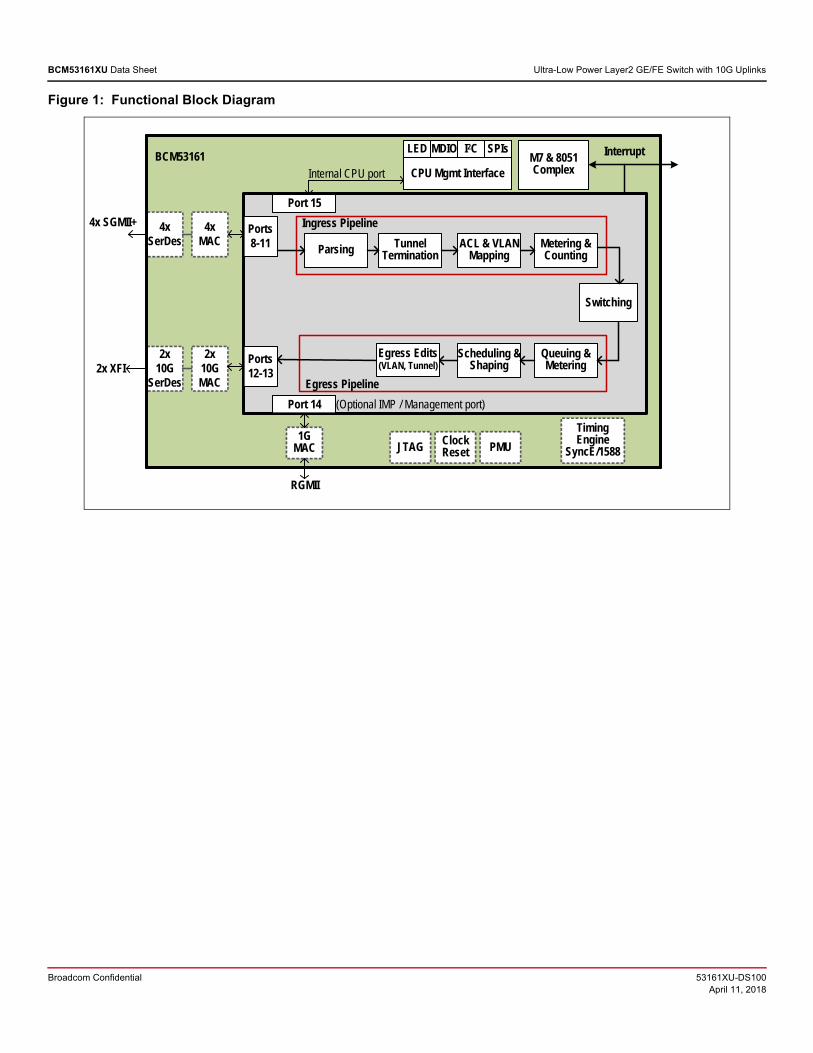
Figure 1: Functional Block Diagram
BCM53161
Ports 8-11
M7 & 8051Complex
4xMAC
Ingress Pipeline4x SGMII+
Timing Engine
SyncE/1588
Parsing
Switching
Queuing & Metering
Metering & Counting
ACL & VLAN Mapping
Tunnel Termination
Scheduling & Shaping
4xSerDes
Egress Pipeline
2x10GMAC
Ports 12-13
2x10G
SerDes2x XFI
LED MDIO I2C SPIs
CPU Mgmt InterfaceInternal CPU port
ClockReset
Port 14 (Optional IMP / Management port)
1GMAC
RGMII
JTAG PMU
Interrupt
Egress Edits(VLAN, Tunnel)
Port 15
Broadcom Confidential 53161XU-DS1003
BCM53161XU Data Sheet Ultra-Low Power Layer2 GE/FE Switch with 10G Uplinks
Table of Contents
Chapter 1: Introduction ...................................................................................................................... 71.1 Overview ....................................................................................................................................................................7
1.2 Target Markets...........................................................................................................................................................7
1.3 Operational Mode ......................................................................................................................................................9
1.4 BCM53161XU Devices ............................................................................................................................................12
1.5 System Functional Blocks .....................................................................................................................................13
1.5.1 Overview .........................................................................................................................................................13
1.5.2 Media Access Controller .................................................................................................................................13
1.5.2.1 Receive Function ..................................................................................................................................13
1.5.2.2 Transmit Function .................................................................................................................................13
1.5.2.3 Flow Control..........................................................................................................................................14
1.5.2.3.1 10/100 Mb/s Half-Duplex.............................................................................................................................. 14
1.5.2.3.2 10/100/1000 Mb/s Full-Duplex ..................................................................................................................... 14
1.5.2.3.3 Priority Flow Control ..................................................................................................................................... 14
1.5.3 Interdevice Interface .......................................................................................................................................15
1.5.3.1 Switch to Control Plane: CB Tag ..........................................................................................................16
1.5.3.2 Switch to Control Plane: Time Stamp Tag............................................................................................18
1.5.3.3 Control Plane to Switch: CB Tag ..........................................................................................................18
1.5.4 MIB Engine .....................................................................................................................................................19
1.5.4.1 MIB Counters........................................................................................................................................20
1.5.5 Integrated High-Performance Memory............................................................................................................24
1.5.6 Robo 2 Switch Core ........................................................................................................................................24
1.5.6.1 Buffer Management ..............................................................................................................................24
1.5.6.2 Memory Arbitration ...............................................................................................................................24
1.5.6.3 Transmit Output Port Queues...............................................................................................................24
1.6 Notational Conventions ..........................................................................................................................................25
Chapter 2: Features and Operation ................................................................................................. 262.1 Overview ..................................................................................................................................................................26
2.2 ARM Cortex-M7 Core ..............................................................................................................................................27
2.3 Software Reset ........................................................................................................................................................27
2.4 Jumbo Frame Support ............................................................................................................................................27
2.5 AutoDOS ..................................................................................................................................................................27
2.6 AutoVOIP .................................................................................................................................................................28
2.7 AutoQoS...................................................................................................................................................................29
2.7.1 Egress Scheduling ..........................................................................................................................................29
2.7.2 Flow Control ....................................................................................................................................................29
2.7.3 Flood Limiting..................................................................................................................................................29
2.8 Auto LoopDetect .....................................................................................................................................................29
Broadcom Confidential 53161XU-DS1004
BCM53161XU Data Sheet Ultra-Low Power Layer2 GE/FE Switch with 10G Uplinks
2.8.1 Auto Loop Detect Configurations ....................................................................................................................30
2.8.2 Port Shutdown Feature ...................................................................................................................................30
2.9 Auto IGMP Snooping ..............................................................................................................................................30
2.9.1 General IGMP Snooping.................................................................................................................................30
2.9.2 Static Multicast Router Interface .....................................................................................................................31
2.9.3 Block Unknown Multicast Interface .................................................................................................................31
2.9.4 Leave Implementation.....................................................................................................................................31
2.10 Cascading ..............................................................................................................................................................31
2.11 Cable Diagnosis ....................................................................................................................................................31
2.12 Power-Saving Modes ............................................................................................................................................32
2.12.1 Auto Power Down Mode ...............................................................................................................................32
2.12.2 Energy Efficient Ethernet Mode ....................................................................................................................32
Chapter 3: Applications and Configuration ................................................................................... 343.1 Overview ..................................................................................................................................................................34
3.2 Unmanaged Applications (UM) ..............................................................................................................................34
3.2.1 Unmanaged Base Configuration.....................................................................................................................34
3.2.2 Unmanaged with Advanced Features.............................................................................................................36
3.2.3 High-Speed Unmanaged ................................................................................................................................36
3.2.4 Unmanaged Cascade Support........................................................................................................................37
Chapter 4: Software Components ................................................................................................... 404.1 8051 and M7 Running Environment ......................................................................................................................40
4.2 M7 Operating System Environment ......................................................................................................................41
4.3 Unmanaged Application .........................................................................................................................................41
Chapter 5: System Interfaces .......................................................................................................... 425.1 Overview ..................................................................................................................................................................42
5.2 Copper Interface......................................................................................................................................................42
5.2.1 Auto-Negotiation .............................................................................................................................................42
5.2.2 Lineside (Remote) Loopback Mode ................................................................................................................42
5.3 Frame Management Port Interface ........................................................................................................................42
5.3.1 RGMII Interface...............................................................................................................................................43
5.4 SerDes Interface ......................................................................................................................................................43
5.5 Configuration Pins ..................................................................................................................................................43
5.6 Programming Interfaces .........................................................................................................................................43
5.6.1 SPI Interface ...................................................................................................................................................43
5.6.2 SPI Slave ........................................................................................................................................................43
5.6.2.1 SPI Transactions ..................................................................................................................................44
5.6.2.1.1 Clock Polarity and Phase ............................................................................................................................. 44
5.6.2.1.2 Fields............................................................................................................................................................ 44
5.6.2.1.3 Command Word Format ............................................................................................................................... 45
5.6.2.1.4 Burst Length ................................................................................................................................................. 45
Broadcom Confidential 53161XU-DS1005
BCM53161XU Data Sheet Ultra-Low Power Layer2 GE/FE Switch with 10G Uplinks
5.6.2.1.5 Supported Transactions ............................................................................................................................... 45
5.6.2.1.6 SPIS and Chip Reset ................................................................................................................................... 46
5.6.2.1.7 Read/Write Status Format............................................................................................................................ 47
5.6.2.1.8 SPI Status .................................................................................................................................................... 47
5.6.2.1.9 ACK/NACK Byte Format .............................................................................................................................. 47
5.6.2.2 SPI Slave Operation .............................................................................................................................48
5.6.2.2.1 Slave Mode Normal Write ............................................................................................................................ 48
5.6.2.2.2 Slave Mode Normal Read ............................................................................................................................ 49
5.6.2.2.3 Slave Mode Fast Read................................................................................................................................. 50
5.6.2.2.4 Slave Mode Fast Write ................................................................................................................................. 50
5.6.3 SPI Master ......................................................................................................................................................51
5.6.3.1 SPI Master Operation ...........................................................................................................................51
5.6.3.1.1 Master Mode Normal Write .......................................................................................................................... 51
5.6.3.1.2 Master Mode Normal Read .......................................................................................................................... 52
5.6.4 Quad SPI Flash Interface................................................................................................................................54
5.6.5 MDC/MDIO Interface ......................................................................................................................................54
5.6.5.1 MDC/MDIO Interface Register Programming .......................................................................................54
5.7 LED Interfaces .........................................................................................................................................................55
5.8 Digital Voltage Regulator (LDO) ............................................................................................................................56
5.9 MFIO Interface .........................................................................................................................................................57
Chapter 6: Hardware Signal Definitions ......................................................................................... 606.1 I/O Signal Types ......................................................................................................................................................60
6.2 Signal Descriptions.................................................................................................................................................61
6.2.1 19×19 mm2 Package ......................................................................................................................................61
Chapter 7: Pin Assignment .............................................................................................................. 687.1 Pin List by Pin Number (19×19 mm2 Package) ....................................................................................................68
7.2 Pin List by Pin Name (19×19 mm2 Package) ........................................................................................................72
7.3 Ball Map (19×19 mm2 Package).............................................................................................................................76
Chapter 8: Electrical Characteristics .............................................................................................. 778.1 Absolute Maximum Ratings ...................................................................................................................................77
8.2 Recommended Operating Conditions and DC Characteristics ..........................................................................78
8.2.1 Standard 3.3V Signals ....................................................................................................................................79
8.2.2 Standard 2.5V Signals ....................................................................................................................................79
8.2.3 REFCLK Input Timing .....................................................................................................................................79
8.2.4 SGMII DC Characteristics...............................................................................................................................80
8.2.5 SGMII Transmit Timing ...................................................................................................................................80
8.2.6 QSGMII Transmitter ........................................................................................................................................80
8.2.7 QSGMII Receiver............................................................................................................................................80
8.2.8 XFI Transmitter Performance Specification ....................................................................................................81
8.2.9 XFI Transmitter DC Characteristics ................................................................................................................81
Broadcom Confidential 53161XU-DS1006
BCM53161XU Data Sheet Ultra-Low Power Layer2 GE/FE Switch with 10G Uplinks
8.2.10 XFI Receiver Input Performance Specification .............................................................................................82
8.2.11 XFI Receiver DC Characteristics ..................................................................................................................82
8.2.12 RGMII Pin Operation at 2.5V VDDO_RGMII ................................................................................................82
8.2.13 RGMII Pin Operation at 1.5V VDDO_RGMII ................................................................................................82
8.3 Power Consumption ...............................................................................................................................................83
8.3.1 Power Consumption........................................................................................................................................83
Chapter 9: Timing Characteristics .................................................................................................. 849.1 Reset and Clock Timing .........................................................................................................................................84
9.2 RGMII Interface Timing ...........................................................................................................................................85
9.2.1 RGMII Output Timing (Normal Mode) .............................................................................................................85
9.2.2 RGMII Output Timing (Delayed Mode) ...........................................................................................................86
9.2.3 RGMII Input Timing (Normal Mode)................................................................................................................87
9.2.4 RGMII Input Timing (Delayed Mode) ..............................................................................................................87
9.3 MDC/MDIO Timing ...................................................................................................................................................88
9.4 Serial Flash Timing .................................................................................................................................................89
9.5 SPI Interface Timing................................................................................................................................................90
9.5.1 BCM53161XU SPI-1 Master Interface Timing (A1) ........................................................................................90
9.5.2 BCM53161XU SPI-2 Slave Interface Timing (A1) ..........................................................................................91
9.5.3 BCM53161XU SPI-1 Master Interface Timing (B0) ........................................................................................92
9.5.4 BCM53161XU SPI-2 Slave Interface Timing (B0) ..........................................................................................93
9.6 JTAG Interface.........................................................................................................................................................93
9.7 BSC Timing ..............................................................................................................................................................94
9.8 Serial LED Interface Timing ...................................................................................................................................96
9.9 SGMII/SerDes Timing ..............................................................................................................................................97
9.10 2.5GE/SerDes Timing ............................................................................................................................................98
9.11 Synchronous Ethernet Interface..........................................................................................................................98
Chapter 10: Thermal Characteristics .............................................................................................. 9910.1 BCM53161XU Package with Heat Sink (45×45×15 mm3) ..................................................................................99
Chapter 11: Mechanical Information ............................................................................................. 100
Chapter 12: Ordering Information ................................................................................................. 101
Revision History ............................................................................................................................. 102
Broadcom Confidential 53161XU-DS1007
BCM53161XU Data Sheet Ultra-Low Power Layer2 GE/FE Switch with 10G Uplinks
Chapter 1: Introduction
1.1 Overview
This document provides details of the functional, operational, and electrical characteristics of the Broadcom® BCM53161XU. This document is for designers interested in integrating the BCM53161XU switches into their hardware designs and for others who need specific data about the physical characteristics and operation of the BCM53161XU switches.
The BCM53161XU is a highly integrated Ethernet switches that are optimally designed for cost-effective low-power applications in the SMB, Enterprise, Service-Provider, SOHO, and Industrial-Ethernet markets. The BCM53161XU is the first family of products in the RoboSwitch® product line to introduce 10 GE ports, which are relevant in markets that are rapidly transitioning to Gigabit-Ethernet connectivity anywhere.
The BCM53161XU switch core supports full-duplex packet forwarding bandwidth of 31 Gb/s for all packet lengths (64 byte to 9720 Jumbo frames).
The family is based on a core technology that supports:
Four 2.5GE/1GE SGMII ports with integrated XMACs
Two 10GE/2.5GE/1GE XFI ports with integrated XMACs
One RGMII port for PHY-less connection to the management agent (available only in full-duplex mode)
An integrated Motorola SPI-compatible interface
High-performance, integrated packet buffer memory
An address resolution engine
The GMACs support full-duplex and half-duplex modes for 10 Mb/s and 100 Mb/s, and full-duplex for 1000 Mb/s. Flow control is supported in half-duplex mode with backpressure. In full-duplex mode, IEEE 802.3x frame-based flow control is supported. The GMACs are IEEE 802.3-compliant and support a maximum frame size of 9720 bytes.
The BCM53161XUX supports advanced ContentAware™ processing using a compact field processor (CFP). Up to four intelligent ContentAware processes are performed in parallel for every packet. This flexible engine uses TCAM-based architecture which allows wildcard capabilities. Action examples include dropping, changing the forward port map, adding forward port, assigning the priority of a frame, and so on. These advanced ContentAware processes are well suited for access control lists (ACLs) and DoS prevention.
An integrated address management engine provides address learning and recognition functions at maximum frame rates. The address table provides capacity for learning up to 16K unicast addresses. Addresses are added to the table after receiving an error-free packet.
The MIB statistics registers collect receive and transmit statistics for each port and provide direct hardware support for the EtherLike-MIB, MIB II (interfaces), and the first four groups of the RMON MIB. All nine groups of RMON can be supported by using additional capabilities, such as port mirroring/snooping, together with an external microcontroller to process some MIB attributes. The MIB registers can be accessed through the Serial Peripheral Interface Port by an external microcontroller.
1.2 Target Markets
The BCM53161XU series targets four main markets:
Broadcom Confidential 53161XU-DS1008
BCM53161XU Data Sheet Ultra-Low Power Layer2 GE/FE Switch with 10G Uplinks
SMB – Capacity requirement in this market is steadily growing. While 1GE is currently the prominent connectivity speed (about 55% of all links in the SMB), 2016 is the year in which 10GE connectivity is expected to reach the SMB market as well. The BCM53161XU was designed to support this market segment by providing 1GE connectivity toward the SMB customers' end nodes and 2.5GE/10GE connectivity toward the WAN.
Service Provider – The BCM53161XU is focused on two sub-segments within the Service Provider market: 10G G/EPON MDU ONUs and 10GE small-cells. The first sub-segment mentioned is expected to drive the next cycle of growth in embedded connectivity. The BCM53161XUis designed to complete G/EPON chip-sets in ONU and design and deliver a cost effective and high-speed solution. The series is also designed to be used as an embedded component within a small-cell design as they are upgraded to 2.5GE and 10GE connection.
Broadcom Confidential 53161XU-DS1009
BCM53161XU Data Sheet Ultra-Low Power Layer2 GE/FE Switch with 10G Uplinks
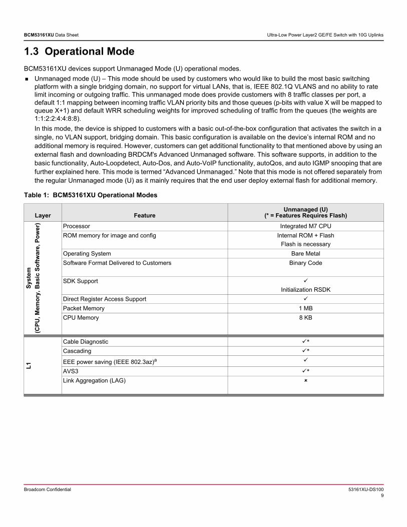
1.3 Operational Mode
BCM53161XU devices support Unmanaged Mode (U) operational modes.
Unmanaged mode (U) – This mode should be used by customers who would like to build the most basic switching platform with a single bridging domain, no support for virtual LANs, that is, IEEE 802.1Q VLANS and no ability to rate limit incoming or outgoing traffic. This unmanaged mode does provide customers with 8 traffic classes per port, a default 1:1 mapping between incoming traffic VLAN priority bits and those queues (p-bits with value X will be mapped to queue X+1) and default WRR scheduling weights for improved scheduling of traffic from the queues (the weights are 1:1:2:2:4:4:8:8).
In this mode, the device is shipped to customers with a basic out-of-the-box configuration that activates the switch in a single, no VLAN support, bridging domain. This basic configuration is available on the device’s internal ROM and no additional memory is required. However, customers can get additional functionality to that mentioned above by using an external flash and downloading BRDCM's Advanced Unmanaged software. This software supports, in addition to the basic functionality, Auto-Loopdetect, Auto-Dos, and Auto-VoIP functionality, autoQos, and auto IGMP snooping that are further explained here. This mode is termed “Advanced Unmanaged.” Note that this mode is not offered separately from the regular Unmanaged mode (U) as it mainly requires that the end user deploy external flash for additional memory.
Table 1: BCM53161XU Operational Modes
Layer FeatureUnmanaged (U)
(* = Features Requires Flash)
Sys
tem
(CP
U, M
emo
ry, B
asic
So
ftw
are,
Po
wer
) Processor Integrated M7 CPU
ROM memory for image and config Internal ROM + Flash
Flash is necessary
Operating System Bare Metal
Software Format Delivered to Customers Binary Code
SDK Support
Initialization RSDK
Direct Register Access Support
Packet Memory 1 MB
CPU Memory 8 KB
L1
Cable Diagnostic *
Cascading *
EEE power saving (IEEE 802.3az)a
AVS3 *
Link Aggregation (LAG)
Broadcom Confidential 53161XU-DS10010
BCM53161XU Data Sheet Ultra-Low Power Layer2 GE/FE Switch with 10G UplinksL
2 F
orw
ard
ing
Jumbo Frames (9720)
Switching/MAC Learning (16K)
Broadcast Storm Control *
VLAN support (multiple bridging domains)
VLAN translation
Isolation group (tree)
Ingress Mirroring
Egress Mirroring
Traffic Sampling
CFP support (ACLs)
AutoLoop *
AutoVOIP *
(256 SA)
AutoDOS *
L2
Qo
S
Queues per port 8
IEEE 802.1p Priority mapping *
Through AutoQoS – mapping is fixed
DSCP priority mapping *
Through AutoQoS – mapping is fixed
Scheduling configurable SP *
Through AutoQoS
Scheduling configurable WRR *
Through AutoQoS - Weights are configurable
Metering Rate Limiting
Shaping queue/port
Hierarchical Shaping
Flow Control – PAUSE IEEE 802.3x *
Flow Control – PFC IEEE 802.1QBB *
Man
agem
ent Debug CLI
RESTful API
Rx and Tx Counters
Mu
ltic
ast IGMP Snooping *
Protocols and Advanced Features
LLDP
Rapid Spanning Tree
Cisco MAC-in-MAC
Port Extender/IEEE 802.1BR
Table 1: BCM53161XU Operational Modes
Layer FeatureUnmanaged (U)
(* = Features Requires Flash)
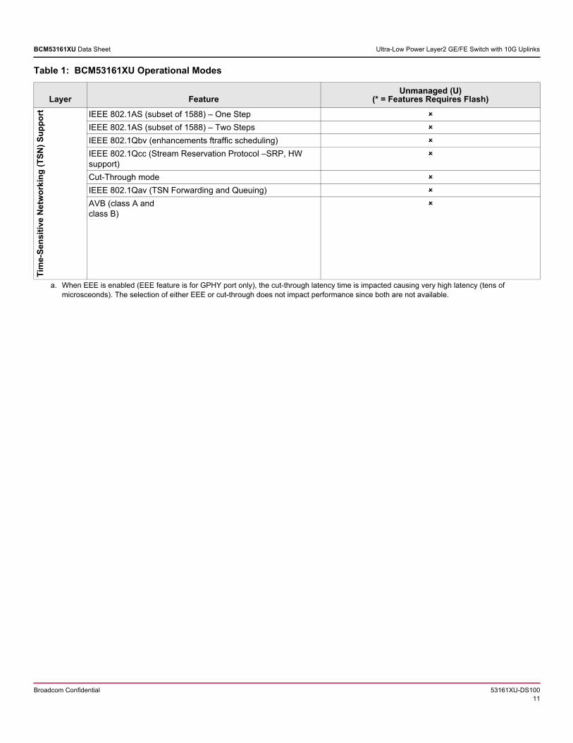
Broadcom Confidential 53161XU-DS10011
BCM53161XU Data Sheet Ultra-Low Power Layer2 GE/FE Switch with 10G UplinksT
ime-
Sen
siti
ve N
etw
ork
ing
(T
SN
) S
up
po
rt IEEE 802.1AS (subset of 1588) – One Step
IEEE 802.1AS (subset of 1588) – Two Steps
IEEE 802.1Qbv (enhancements ftraffic scheduling)
IEEE 802.1Qcc (Stream Reservation Protocol –SRP, HW support)
Cut-Through mode
IEEE 802.1Qav (TSN Forwarding and Queuing)
AVB (class A and class B)
a. When EEE is enabled (EEE feature is for GPHY port only), the cut-through latency time is impacted causing very high latency (tens of microsceonds). The selection of either EEE or cut-through does not impact performance since both are not available.
Table 1: BCM53161XU Operational Modes
Layer FeatureUnmanaged (U)
(* = Features Requires Flash)
Broadcom Confidential 53161XU-DS10012
BCM53161XU Data Sheet Ultra-Low Power Layer2 GE/FE Switch with 10G Uplinks
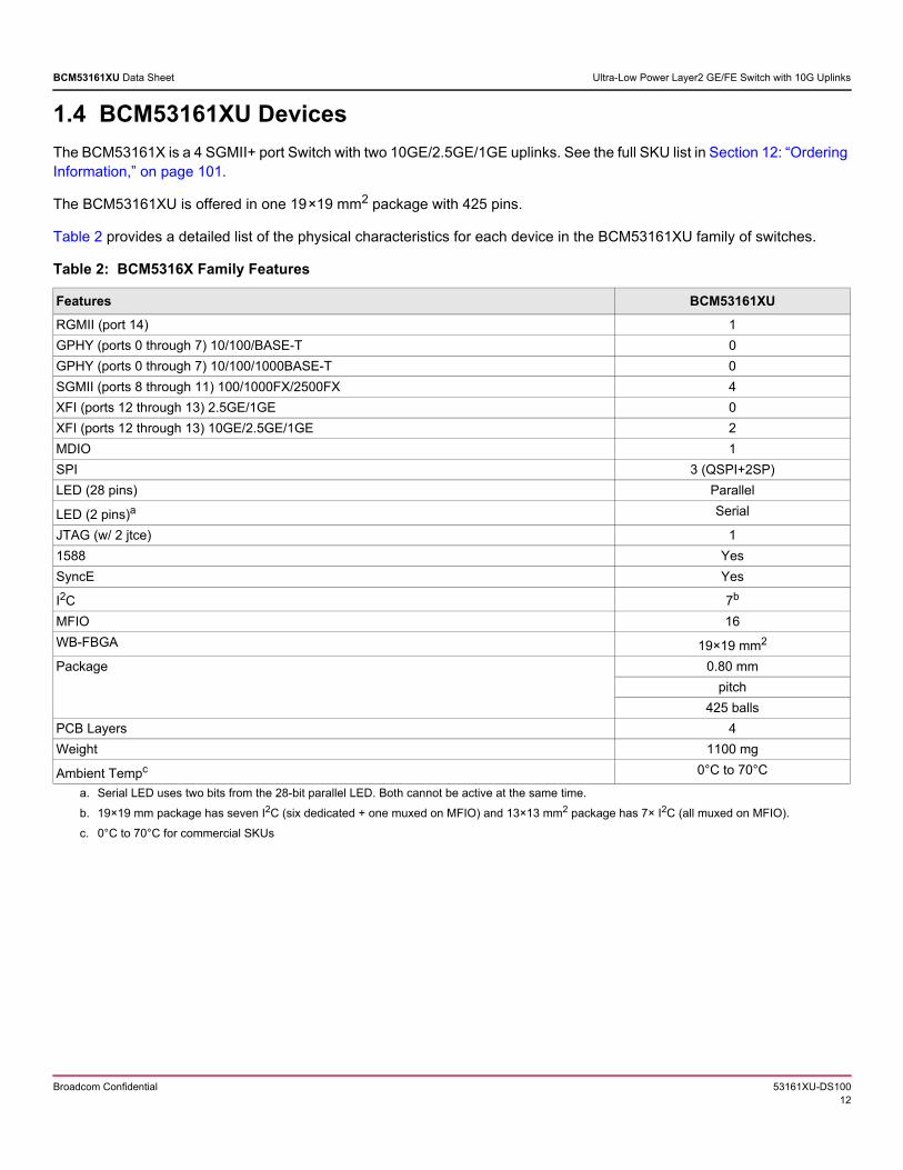
1.4 BCM53161XU Devices
The BCM53161X is a 4 SGMII+ port Switch with two 10GE/2.5GE/1GE uplinks. See the full SKU list in Section 12: “Ordering Information,” on page 101.
The BCM53161XU is offered in one 19×19 mm2 package with 425 pins.
Table 2 provides a detailed list of the physical characteristics for each device in the BCM53161XU family of switches.
Table 2: BCM5316X Family Features
Features BCM53161XU
RGMII (port 14) 1
GPHY (ports 0 through 7) 10/100/BASE-T 0
GPHY (ports 0 through 7) 10/100/1000BASE-T 0
SGMII (ports 8 through 11) 100/1000FX/2500FX 4
XFI (ports 12 through 13) 2.5GE/1GE 0
XFI (ports 12 through 13) 10GE/2.5GE/1GE 2
MDIO 1
SPI 3 (QSPI+2SP)
LED (28 pins) Parallel
LED (2 pins)a
a. Serial LED uses two bits from the 28-bit parallel LED. Both cannot be active at the same time.
Serial
JTAG (w/ 2 jtce) 1
1588 Yes
SyncE Yes
I2C 7b
b. 19×19 mm package has seven I2C (six dedicated + one muxed on MFIO) and 13×13 mm2 package has 7× I2C (all muxed on MFIO).
MFIO 16
WB-FBGA 19×19 mm2
Package 0.80 mm
pitch
425 balls
PCB Layers 4
Weight 1100 mg
Ambient Tempc
c. 0°C to 70°C for commercial SKUs
0°C to 70°C
Broadcom Confidential 53161XU-DS10013
BCM53161XU Data Sheet Ultra-Low Power Layer2 GE/FE Switch with 10G Uplinks
1.5 System Functional Blocks
1.5.1 Overview
The BCM53161XU includes the following blocks:
Media Access Controller
Interdevice Interface
MIB Engine
Integrated High-Performance Memory
Robo 2 Switch Core
Each of these blocks is discussed in additional detail in the following sections.
1.5.2 Media Access Controller
The BCM53161XU contains two 1G/2.5G/10G XMACs, and four 10/100/1000/2.5G MACs.
The MAC automatically selects the appropriate speed (CSMA/CD or full-duplex) based on the PHY auto-negotiation result. In full-duplex mode, IEEE 802.3x PAUSE frame-based flow control is also determined through auto-negotiation. The MAC is IEEE 802.3, IEEE 802.3u, and IEEE 802.3x-compliant.
1.5.2.1 Receive Function
The MAC initiates frame reception following the assertion of receive data valid indication from the physical layer. The MAC monitors the frame for the following error conditions:
Receive error indication from the PHY
Runt frame error if frame is fewer than 64 bytes
CRC error
Long frame error if frame is greater than standard max. frame size or 9,720 bytes for jumbo-enabled ports.
NOTE: Frames longer than standard max. frame size are considered oversized frames. When jumbo-frame mode is enabled, only the frames longer than 9,720 bytes are bad frames and dropped.
If no errors are detected, the frame is processed by the switch controller. Frames with errors are discarded. Receive functions can be disabled using register settings.
1.5.2.2 Transmit Function
Frame transmission begins with the switch controller queuing a frame to the MAC transmitter. The frame data is transmitted as received from the switch controller. The transmit controller is responsible for preamble insertion, carrier deferral, collision back-off, and inter-packet gap enforcement.
In 10/100 Mb/s half-duplex mode, when a frame is queued for transmission, the transmit controller behaves as specified by the IEEE 802.3 requirements for frame deferral. Following deferral, the transmitter adds 8 bytes of preamble and SFD to the frame data received from the switch controller. If, during frame transmission, a collision is observed and the collision window timer has not expired, the transmit controller asserts jam and then executes the back-off algorithm. The frame is retransmitted when appropriate. On the 16th consecutive collision, the back-off algorithm starts over at the initial state, the collision counter is reset, and attempts to transmit the current frame continue. Following a late collision, the frame is aborted, and the switch controller is allowed to queue the next frame for transmission.
Broadcom Confidential 53161XU-DS10014
BCM53161XU Data Sheet Ultra-Low Power Layer2 GE/FE Switch with 10G Uplinks
While in full-duplex mode, the transmit controller ignores carrier activity and collision indication. Transmission begins after the switch controller queues the frame and the 96-bit times of IPG have been observed. Transmit functions can be disabled using register settings.
1.5.2.3 Flow Control
The BCM53161XU implements an intelligent flow-control algorithm to minimize the system impact resulting from traffic congestion. Buffer memory allocation is adaptive to the status of each port’s speed and duplex mode, providing an optimal balance between flow management and per-port memory depth. The BCM53161XU initiates flow control in response to buffer memory conditions on a per-port basis.
The MACs are capable of flow control in full-duplex mode.
1.5.2.3.1 10/100 Mb/s Half-Duplex
In 10/100 half-duplex mode, the MAC back-pressures a receiving port by transmitting a 96-bit time jam packet to the port. A single jam packet is asserted for each received packet for the duration of the time the port is in the flow-control state.
1.5.2.3.2 10/100/1000 Mb/s Full-Duplex
Flow control in full-duplex mode functions as specified by the IEEE 802.3x requirements. In the receiver, MAC flow-control frames are recognized and, when properly received, set the flow-control pause time for the transmit controller. The pause time is assigned from the 2-byte pause time field following the pause opcode. MAC control PAUSE frames are not forwarded from the receiver to the switch controller.
When the switch controller requests flow control, the transmit controller transmits a MAC control PAUSE frame with the pause time set to maximum. When the condition that caused the flow control state is no longer present, a second MAC control PAUSE frame is sent with the pause time field set to 0.
1.5.2.3.3 Priority Flow Control
Priority Flow Control (PFC) is a mechanism of conveying the per priority XON/XOFF information for 8 different classes using MAC control frames. Unimac provides the flexibility to program the DA, TYPE, and OPCODE fields for the PFC frames. The PFC feature can be independently enabled inside the MAC and pause should be disabled while PFC is operational to ensure IEEE compliance.
Broadcom Confidential 53161XU-DS10015
BCM53161XU Data Sheet Ultra-Low Power Layer2 GE/FE Switch with 10G Uplinks
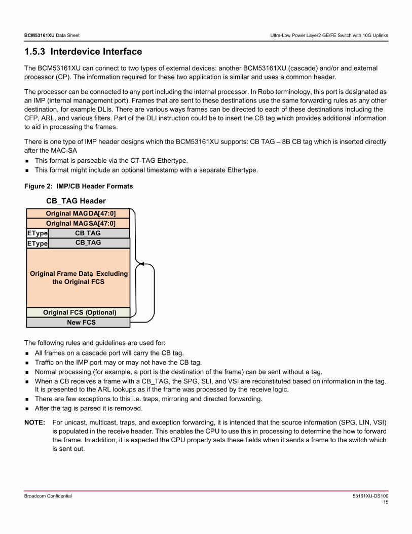
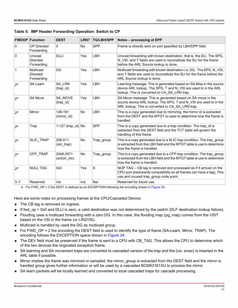
1.5.3 Interdevice Interface
The BCM53161XU can connect to two types of external devices: another BCM53161XU (cascade) and/or and external processor (CP). The information required for these two application is similar and uses a common header.
The processor can be connected to any port including the internal processor. In Robo terminology, this port is designated as an IMP (internal management port). Frames that are sent to these destinations use the same forwarding rules as any other destination, for example DLIs. There are various ways frames can be directed to each of these destinations including the CFP, ARL, and various filters. Part of the DLI instruction could be to insert the CB tag which provides additional information to aid in processing the frames.
There is one type of IMP header designs which the BCM53161XU supports: CB TAG – 8B CB tag which is inserted directly after the MAC-SA
This format is parseable via the CT-TAG Ethertype.
This format might include an optional timestamp with a separate Ethertype.
Figure 2: IMP/CB Header Formats
The following rules and guidelines are used for:
All frames on a cascade port will carry the CB tag.
Traffic on the IMP port may or may not have the CB tag.
Normal processing (for example, a port is the destination of the frame) can be sent without a tag.
When a CB receives a frame with a CB_TAG, the SPG, SLI, and VSI are reconstituted based on information in the tag. It is presented to the ARL lookups as if the frame was processed by the receive logic.
There are few exceptions to this i.e. traps, mirroring and directed forwarding.
After the tag is parsed it is removed.
NOTE: For unicast, multicast, traps, and exception forwarding, it is intended that the source information (SPG, LIN, VSI) is populated in the receive header. This enables the CPU to use this in processing to determine the how to forward the frame. In addition, it is expected the CPU properly sets these fields when it sends a frame to the switch which is sent out.
CB_TAG
Original MAC-DA[47:0]
Original MAC-SA[47:0]
New FCS
CB_TAG
Original FCS (Optional)
CB_TAG Header
Original Frame Data, Excluding
the Original FCS
EType
EType
Broadcom Confidential 53161XU-DS10016
BCM53161XU Data Sheet Ultra-Low Power Layer2 GE/FE Switch with 10G Uplinks
The Switch to CP and CP to Switch tag formats are purposely defined to be consistent across the IMP and Cascade modes. The forwarding codes (fwd_op) are defined to allow the hardware to interpret the intended function from the code point regardless of the specific IMP or Cascade type in most cases.
1.5.3.1 Switch to Control Plane: CB Tag
This tag is used to communicate information to an attached CPU or cascaded BCM53161XU. The format and fields are defined in the following tables. The tag is attached to frames using editing directives. The directive could be associated with a port (PET table) or DLI. The Ethertype for this tag is taken from a configuration register. The format and fields are defined in Table 3.
The forwarding operation (FWD_OP) field defines the content of the DEST field and provides information to the CPU regarding why the frame was delivered. The DEST field in the header is overlay with number of meanings summarized in the following table.
Table 3: Switch to CB TAG Format
15 14 13 12 11 10 09 08 07 06 05 04 03 02 01 00
Ethertype
TC DP FWD_OP DEV LBH/TRAP_GROUP/SPP/DPP
DEST[11:0] - depends on FWD_OP for example, DLLI/DG/EXCEPTION R R SPG
SPG T N_VSI [11:0] (VSI or LIN based on T)
Table 4: Switch to CP Header Format Fields
Field Function
Ethertype Configured value
TC TC value classified for the packet by the switch
DP Discard precedence
DEV Source device identifier; configured by software
SPG Source Port Group – SPG determined for the frame
FWD_OP Forwarding Operation – see table
T LIN Type indicator. 0 is LIN, 1 is PV format
N_VSI Source Local Logical Interface: If T = 1 (type PV), SLLI = 1,0,SPG; VSI=N_VSI else(type LIN) SLLI=0,N_VSI; VSI=LIN2VSI(N_VSI);
DEST - overlay Overlay field with one of the following depending on FWD_OP
DLLI Destination Logical Local Interface: If FWD_OP = UNICAST
DG Destination Group (multicast/broadcast): If FWD_OP = MULTICAST
EXCEPTION Exception – Identifies the reason a trap was triggered (TRAP, SLIC, CFP): If FWD_OP = TRAP
LBH - overlay Trap Group/Load Balancing Hash : If FWD_OP=TRAP, TRAP_GROUP else LBH
LBH Load balancing hash- Valid for all op codes except 2
Trap_group Trap group for the SLICT and CFP traps in FWD_OP=2
SPP Source Physical Port for traps (FWD_OP=2)
DPP Destination Physical Port
RSVD Reserved – write as zero, ignore on receipt
Broadcom Confidential 53161XU-DS10017
BCM53161XU Data Sheet Ultra-Low Power Layer2 GE/FE Switch with 10G Uplinks
Here are some notes on processing frames at the CPU/Cascaded Device:
The CB tag is removed on ingress.
If fwd_op = 0x0 and DLLI is zero, a valid destination was not determined by the switch (DLF destination lookup failure).
Flooding uses a multicast forwarding with a zero DG. In this case, the flooding map (pg_map) comes from the VSIT based on the VSI in the frame (or LIN2VSI).
Multicast is handled by used the DG as multicast group.
For FWD_OP = 2 the encoding the DEST field is used to identify the type of frame (SA-Learn, Mirror, TRAP). The encoding follows the EXCEPTION space shown in Figure 24.
The DEV field must be preserved if the frame is sent to a CPU with CB_TAG. This allows the CPU to determine which of the two devices the originated exception frame.
SA learning and SA movement traps are converted to cascaded version of the trap and the vsi, smac is inserted in the ARL table if possible.
Mirror implies the frame was mirrored or sampled; the mirror_group is extracted from the DEST field and the mirror is handled group gives further information or will be used by a cascaded BCM53161XU to process the mirror.
SA learn packets will be locally learned and converted to local cascaded traps for cascade processing.
Table 5: IMP Header Forwarding Operation: Switch to CP
FWDOP Function DEST LRN? TG/LBH/SPP Notes – processing at EPP
0 CP Directed Forwarding
0 No DPP Frame is directly sent on port specified by LBH/DPP field.
0 Unicast Directed Forwarding
DLLI Yes LBH Unicast forwarding with known destination, that is, the DLI. The SPG, N_VSI, and T fields are used to reconstitute the SLI for the frame before the ARL Source lookup is done.
1 Multicast Directed Forwarding
DG Yes LBH Multicast forwarding with known destination i.e. DG. The SPG, N_VSI, and T fields are used to reconstitute the SLI for the frame before the ARL Source lookup is done.
2a
a. For FWD_OP = 2 the DEST is defined as an EXCEPTION following the encoding shown in Figure 24.
SA Learn SA_LRN (trap_id)
Yes LBH Learning message: This is generated based on SA Miss in the source device ARL lookup. The SPG, T and N_VSI are used to in the ARL lookup. This is converted to CA_SA_LRN trap.
2a SA Move SA_MOVE (trap_id)
Yes LBH SA Move message: This is generated based on SA move in the source device ARL lookup. The SPG, T and N_VSI are used to in the ARL lookup. This is converted to CA_SA_LRN trap.
2a Mirror 128-191 (mirror_Id)
No LBH This is a copy generated due to mirroring, the mirror id is extracted from the DEST and the MTGT is used to determine how the frame is handled.
2a Trap 1-127 (trap_id) No SPP This is a copy generated due to a trap condition. The trap_id is extracted from the DEST field and the TCT table will govern the handling of this frame.
2a SLIC_TRAP 256-511 (slic_trap)
No Trap_group This is a copy generated due to a SLIC trap condition. The trap_group is extracted from the LBH field and the MTGT table is use to determine how the frame is handled.
2a CFP_TRAP 2048-3071 (action_idx)
No Trap_group This is a copy generated due to a CFP trap condition. The trap_group is extracted from the LBH field and the MTGT table is use to determine how the frame is handled.
2a NULL TAG 0x0 Yes X NOP TAG – CB tag is removed and processed as if it arrived on the CPU port (backwards compatibility so all frames can have a tag), This use and unused trap_group code point.
3–7 Reserved n/a n/a Na/ Reserved for future use.
Broadcom Confidential 53161XU-DS10018
BCM53161XU Data Sheet Ultra-Low Power Layer2 GE/FE Switch with 10G Uplinks
The trap packet uses the trap_group to process the frame. Note this is the only format that has a SPP versus a SPG.
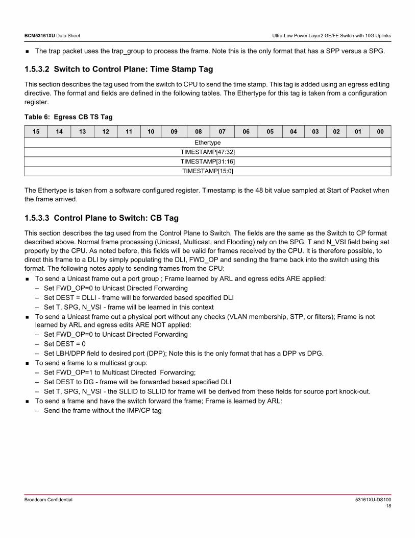
1.5.3.2 Switch to Control Plane: Time Stamp Tag
This section describes the tag used from the switch to CPU to send the time stamp. This tag is added using an egress editing directive. The format and fields are defined in the following tables. The Ethertype for this tag is taken from a configuration register.
The Ethertype is taken from a software configured register. Timestamp is the 48 bit value sampled at Start of Packet when the frame arrived.
1.5.3.3 Control Plane to Switch: CB Tag
This section describes the tag used from the Control Plane to Switch. The fields are the same as the Switch to CP format described above. Normal frame processing (Unicast, Multicast, and Flooding) rely on the SPG, T and N_VSI field being set properly by the CPU. As noted before, this fields will be valid for frames received by the CPU. It is therefore possible, to direct this frame to a DLI by simply populating the DLI, FWD_OP and sending the frame back into the switch using this format. The following notes apply to sending frames from the CPU:
To send a Unicast frame out a port group ; Frame learned by ARL and egress edits ARE applied:
– Set FWD_OP=0 to Unicast Directed Forwarding
– Set DEST = DLLI - frame will be forwarded based specified DLI
– Set T, SPG, N_VSI - frame will be learned in this context
To send a Unicast frame out a physical port without any checks (VLAN membership, STP, or filters); Frame is not learned by ARL and egress edits ARE NOT applied:
– Set FWD_OP=0 to Unicast Directed Forwarding
– Set DEST = 0
– Set LBH/DPP field to desired port (DPP); Note this is the only format that has a DPP vs DPG.
To send a frame to a multicast group:
– Set FWD_OP=1 to Multicast Directed Forwarding;
– Set DEST to DG - frame will be forwarded based specified DLI
– Set T, SPG, N_VSI - the SLLID to SLLID for frame will be derived from these fields for source port knock-out.
To send a frame and have the switch forward the frame; Frame is learned by ARL:
– Send the frame without the IMP/CP tag
Table 6: Egress CB TS Tag
15 14 13 12 11 10 09 08 07 06 05 04 03 02 01 00
Ethertype
TIMESTAMP[47:32]
TIMESTAMP[31:16]
TIMESTAMP[15:0]
Broadcom Confidential 53161XU-DS10019
BCM53161XU Data Sheet Ultra-Low Power Layer2 GE/FE Switch with 10G Uplinks
1.5.4 MIB Engine
The MIB Engine is responsible for processing status words received from each port. Based on whether it is a receive status or transmit status, appropriate MIB counters are updated. The BCM53161XU implements 66 MIB counters on a per-port basis. MIB counters can be categorized into three groups: receive-only counters, transmit-only counters, and receive or transmit counters. This latter group can, as a group, be selectively steered to the receive or transmit process on a per-port basis. The section below describes each individual counter.
The BCM53161XU offers the MIB snapshot feature per port. A snapshot of a selected port MIB registers can be captured and available to the users while MIB counters are continuing to count.
Broadcom Confidential 53161XU-DS10020
BCM53161XU Data Sheet Ultra-Low Power Layer2 GE/FE Switch with 10G Uplinks
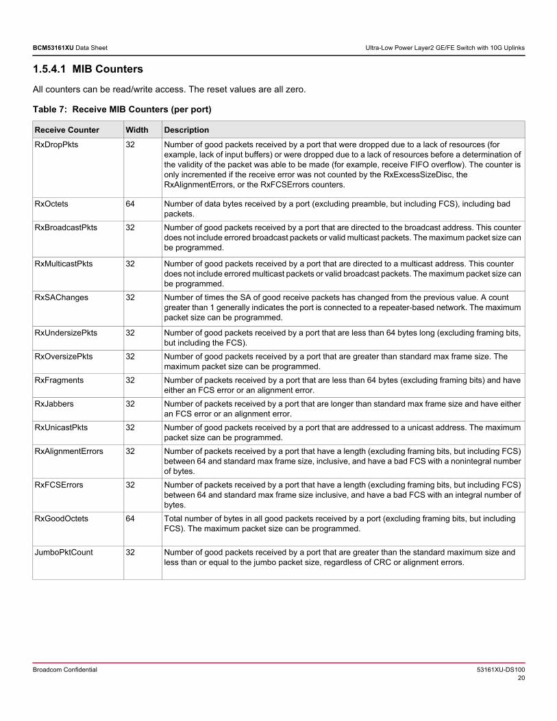
1.5.4.1 MIB Counters
All counters can be read/write access. The reset values are all zero.
Table 7: Receive MIB Counters (per port)
Receive Counter Width Description
RxDropPkts 32 Number of good packets received by a port that were dropped due to a lack of resources (for example, lack of input buffers) or were dropped due to a lack of resources before a determination of the validity of the packet was able to be made (for example, receive FIFO overflow). The counter is only incremented if the receive error was not counted by the RxExcessSizeDisc, the RxAlignmentErrors, or the RxFCSErrors counters.
RxOctets 64 Number of data bytes received by a port (excluding preamble, but including FCS), including bad packets.
RxBroadcastPkts 32 Number of good packets received by a port that are directed to the broadcast address. This counter does not include errored broadcast packets or valid multicast packets. The maximum packet size can be programmed.
RxMulticastPkts 32 Number of good packets received by a port that are directed to a multicast address. This counter does not include errored multicast packets or valid broadcast packets. The maximum packet size can be programmed.
RxSAChanges 32 Number of times the SA of good receive packets has changed from the previous value. A count greater than 1 generally indicates the port is connected to a repeater-based network. The maximum packet size can be programmed.
RxUndersizePkts 32 Number of good packets received by a port that are less than 64 bytes long (excluding framing bits, but including the FCS).
RxOversizePkts 32 Number of good packets received by a port that are greater than standard max frame size. The maximum packet size can be programmed.
RxFragments 32 Number of packets received by a port that are less than 64 bytes (excluding framing bits) and have either an FCS error or an alignment error.
RxJabbers 32 Number of packets received by a port that are longer than standard max frame size and have either an FCS error or an alignment error.
RxUnicastPkts 32 Number of good packets received by a port that are addressed to a unicast address. The maximum packet size can be programmed.
RxAlignmentErrors 32 Number of packets received by a port that have a length (excluding framing bits, but including FCS) between 64 and standard max frame size, inclusive, and have a bad FCS with a nonintegral number of bytes.
RxFCSErrors 32 Number of packets received by a port that have a length (excluding framing bits, but including FCS) between 64 and standard max frame size inclusive, and have a bad FCS with an integral number of bytes.
RxGoodOctets 64 Total number of bytes in all good packets received by a port (excluding framing bits, but including FCS). The maximum packet size can be programmed.
JumboPktCount 32 Number of good packets received by a port that are greater than the standard maximum size and less than or equal to the jumbo packet size, regardless of CRC or alignment errors.
Broadcom Confidential 53161XU-DS10021
BCM53161XU Data Sheet Ultra-Low Power Layer2 GE/FE Switch with 10G Uplinks
RxPausePfcPkts 32 When PAUSE is configured: This counter counts the number of PAUSE frame on the port. When the port is configured in PFC mode it counts the number of PFC frames.
Number of PAUSE frames received by a port. The PAUSE frame must have a valid MAC Control Frame EtherType field (88–08h), have a destination MAC address of either the MAC Control frame reserved multicast address (01-80-C2-00-00-01) or the unique MAC address associated with the specific port, a valid PAUSE opcode (00–01), be a minimum of 64 bytes in length (excluding preamble but including FCS), and have a valid CRC. Although an IEEE 802.3-compliant MAC is only permitted to transmit PAUSE frames when in full-duplex mode with flow control enabled and with the transfer of PAUSE frames determined by the result of auto-negotiation, an IEEE 802.3 MAC receiver is required to count all received PAUSE frames, regardless of its half/full-duplex status. An indication that a MAC is in half-duplex with the RxPausePkts incrementing indicates a noncompliant transmitting device on the network.
RxSymbolErrors 32 Total number of times a valid-length packet was received at a port and at least one invalid data symbol was detected. The counter only increments once per carrier event and does not increment on detection of a collision during the carrier event.
RxDiscard 32 Number of good packets received by a port that were discarded by the Forwarding Process. This would include any shaping or DOS filters.
RxPkts64Octets 32 Number of packets received (including error packets) that are 64 bytes long.
RxPkts65to127Octets 32 Number of packets received (including error packets) that are between 65 and 127 bytes long.
RxPkts128to255Octets 32 Number of packets received (including error packets) that are between 128 and 255 bytes long.
RxPkts256to511Octets 32 Number of packets received (including error packets) that are between 256 and 511 bytes long.
RxPkts512to1023Octets
32 Number of packets received (including error packets) that are between 512 and 1023 bytes long.
RxPkts1024toMaxPktOctets
32 Number of packets received (include error packets) that are between 1024 and the standard maximum packet size inclusive.
Table 7: Receive MIB Counters (per port) (Continued)
Receive Counter Width Description
Broadcom Confidential 53161XU-DS10022
BCM53161XU Data Sheet Ultra-Low Power Layer2 GE/FE Switch with 10G Uplinks
Table 8: Transmit MIB Counters
Transmit Counter Width Description
TxDropPkts 32 This counter is incremented every time a transmit packet is dropped due to lack of resources (for example, transmit FIFO underflow), or an internal MAC sublayer transmit error not counted by either the TxLateCollision or the TxExcessiveCollision counters.
TxOctets 64 Total number of good bytes of data transmitted by a port (excluding preamble but including FCS).
TxBroadcastPkts 32 Number of good packets transmitted by a port that are directed to a broadcast address. This counter does not include errored broadcast packets or valid multicast packets.
TxMulticastPkts 32 Number of good packets transmitted by a port that are directed to a multicast address. This counter does not include errored multicast packets or valid broadcast packets.
TxCollisions 32 Number of collisions experienced by a port during packet transmissions.
TxUnicastPkts 32 Number of good packets transmitted by a port that are addressed to a unicast address.
TxSingleCollision 32 Number of packets successfully transmitted by a port that have experienced exactly one collision.
TxMultipleCollision 32 Number of packets successfully transmitted by a port that have experienced more than one collision.
TxDeferredTransmit 32 Number of packets transmitted by a port for which the first transmission attempt is delayed because the medium is busy. This only applies to the Half Duplex mode, while the Carrier Sensor Busy.
TxLateCollision 32 Number of times that a collision is detected later than 512 bit-times into the transmission of a packet.
TxExcessiveCollision 32 Number of packets that are not transmitted from a port because the packet experienced 16 transmission attempts.
TxPausePfcPkts 32 Number of PAUSE control frames sent when the port is configured in PAUSE mode. In PFC mode, it counts the number of PFC frames sent.
TxFrameInDisc 32 Number of valid packets received which are discarded by the forwarding process due to lack of space on an output queue (not maintained or reported in the MIB counters). This attribute only increments if a network device is not acting in compliance with a flow control request or the ROBO GE Switchcore internal flow-control/buffering scheme has been configured incorrectly.
TxQ0PKT 32 Total number of good packets transmitted on COS0, which is specified in MIB queue select register when QoS is enabled.
TxQ1PKT 32 Total number of good packets transmitted on COS1, which is specified in MIB queue select register when QoS is enabled.
TxQ2PKT 32 Total number of good packets transmitted on COS2, which is specified in MIB queue select register when QoS is enabled.
TxQ3PKT 32 Total number of good packets transmitted on COS3, which is specified in MIB queue select register when QoS is enabled.
TxQ4PKT 32 Total number of good packets transmitted on COS4, which is specified in MIB queue select register when QoS is enabled.
TxQ5PKT 32 Total number of good packets transmitted on COS5, which is specified in MIB queue select register when QoS is enabled.
Broadcom Confidential 53161XU-DS10023
BCM53161XU Data Sheet Ultra-Low Power Layer2 GE/FE Switch with 10G Uplinks
TxQ6PKT 32 Total number of good packets transmitted on COS6, which is specified in MIB queue select register when QoS is enabled.
TxQ7PKT 32 Total number of good packets transmitted on COS7, which is specified in MIB queue select register when QoS is enabled.
TxPkts64Octets 32 Number of transmitted packets (including error packets) that are 64 bytes long.
TxPkts65to127Octets 32 Number of transmitted packets (including error packets) that are between 65 and 127 bytes long.
TxPkts128to255Octets 32 Number of transmitted packets (including error packets) that are between 128 and 255 bytes long.
TxPkts256to511Octets 32 Number of transmitted packets (including error packets) that are between 256 and 511 bytes long.
TxPkts512to1023Octets 32 Number of transmitted packets (including error packets) that are between 512 and 1023 bytes long.
TxPkts1024toMaxPktOctets 32 Number of transmitted packets that (include error packets) are between 1024 and the standard maximum packet size inclusive.
Table 8: Transmit MIB Counters (Continued)
Transmit Counter Width Description
Broadcom Confidential 53161XU-DS10024
BCM53161XU Data Sheet Ultra-Low Power Layer2 GE/FE Switch with 10G Uplinks
1.5.5 Integrated High-Performance Memory
The BCM53161XU embeds a high-performance SRAM for storing packet data and associated metadata.
The integrated memory is 1 MB and can be flexibly partitioned into a packet buffer region, and a region available to the M7/8051 for instruction/data memory as well as storage for packets forwarded to the CPU (UM mode is restricted by OTP to only 128 KB of the 1 MB of memory). The BCM53161XU M7 processor also has 32 KB ITCM, 64 KB DCTM, 16 KB I-Cache, and 16 KB D-Cache.
In addition, instead of the IVM and EMV, the following tables exist:
Logical Interface Mapper (LIM): 2K entry hash table to support virtual ports and double-tagged frames, etc.
VSI Tag Control (VTC): 4K entry with per port controls for egress edits
This eliminates the need for external memory and allows for the implementation of extremely low-cost systems.
The internal RAM controller efficiently executes memory transfers and achieves nonblocking performance for stand-alone 8-port applications and for applications with up to 15 ports and 33 Gb/s throughput.
1.5.6 Robo 2 Switch Core
The core of the BCM53161XU devices is a cost-effective and high-performance switch controller. The controller manages packet forwarding between the MAC receive and transmit ports through the frame buffer memory with a store and forward architecture. The switch controller encompasses the functions of buffer management, memory arbitration, and transmit descriptor queuing.
1.5.6.1 Buffer Management
The frame buffer memory is divided into pages (units of data consisting of 256 bytes each). Each received packet may be allocated more than one page. For example, six pages are required to store a 1522-byte frame. Frame data is stored in the buffer memory as the packet is received. After reception, the frame is queued to the egress port(s) transmit queue. This list tracks the transmission of the packet. After successful packet transmission, the buffer memory is released to the free buffer pool.
1.5.6.2 Memory Arbitration
Processes requesting access to the internal memory include the receive and transmit frame data handlers, egress descriptor update, and output-port queue managers. These processes are arbitrated to provide fair access to the memory and minimize the latency of critical processes to provide a fully nonblocking solution.
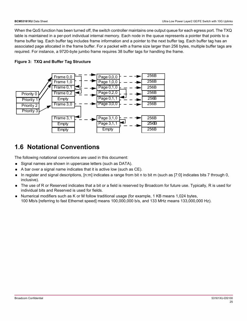
1.5.6.3 Transmit Output Port Queues
Frames are maintained in the egress port using a linked list. Two levels of linked lists are used to maintain one output queue (see Figure 3). The first level is the TXQ linked list, and the second level is the buffer tag linked list. The TXQ linked list is used to maintain frame TC order for each port. For each frame, the buffer tag linked list is used to maintain the order of the buffer pages corresponding to each frame.
Each egress port supports up to eight transmit queues for servicing Quality of Service (QoS). All eight transmit queues share the all entries of the TXQ table. The TXQ table is maintained as a linked list, and each node in the TXQ uses one entry in the TXQ table.
Broadcom Confidential 53161XU-DS10025
BCM53161XU Data Sheet Ultra-Low Power Layer2 GE/FE Switch with 10G Uplinks
When the QoS function has been turned off, the switch controller maintains one output queue for each egress port. The TXQ table is maintained in a per-port individual internal memory. Each node in the queue represents a pointer that points to a frame buffer tag. Each buffer tag includes frame information and a pointer to the next buffer tag. Each buffer tag has an associated page allocated in the frame buffer. For a packet with a frame size larger than 256 bytes, multiple buffer tags are required. For instance, a 9720-byte jumbo frame requires 38 buffer tags for handling the frame.
Figure 3: TXQ and Buffer Tag Structure
1.6 Notational Conventions
The following notational conventions are used in this document:
Signal names are shown in uppercase letters (such as DATA).
A bar over a signal name indicates that it is active low (such as CE).
In register and signal descriptions, [n:m] indicates a range from bit n to bit m (such as [7:0] indicates bits 7 through 0, inclusive).
The use of R or Reserved indicates that a bit or a field is reserved by Broadcom for future use. Typically, R is used for individual bits and Reserved is used for fields.
Numerical modifiers such as K or M follow traditional usage (for example, 1 KB means 1,024 bytes, 100 Mb/s [referring to fast Ethernet speed] means 100,000,000 b/s, and 133 MHz means 133,000,000 Hz).
Frame 0,0
Frame 1,0
Empty
Frame 0,1
Empty
Frame 0,2
Frame 3,1
Empty
Frame 3,0
Priority 0
Empty
Page 0,1,0
Page 3,1,1
Page 0,2,0
Page 3,1,0
Priority 1Page 3,0,0
256B
256B
256B
256B
256B
256B
256B
256B
256B
Priority 3
Priority 2
Page 0,1,1
Page 1,0,0
Page 0,0,0
Broadcom Confidential 53161XU-DS10026
BCM53161XU Data Sheet Ultra-Low Power Layer2 GE/FE Switch with 10G Uplinks
Chapter 2: Features and Operation
2.1 Overview
The BCM53161XU switches include the following features:
ARM Cortex-M7 Core
Software Reset
Jumbo Frame Support
AutoDOS
AutoVOIP
AutoQoS
Auto LoopDetect
Auto IGMP Snooping
Cascading
Cable Diagnosis
Power-Saving Modes
The following sections discuss each feature in more detail.
Broadcom Confidential 53161XU-DS10027
BCM53161XU Data Sheet Ultra-Low Power Layer2 GE/FE Switch with 10G Uplinks
2.2 ARM Cortex-M7 Core
The BCM53161XU integrates a low-power and high-performance ARM Cortex-M7 processor core with a clock speed of up to 400 MHz. The ARM Cortex-M7 core includes integrated 16 KB two-way set-associative I-Cache and 16 KB four-way set-associative D-Cache. The BCM53112/BCM5315X/BCM5316X also supports a 32 KB ITCM and 64 KB DTCM.
2.3 Software Reset
The BCM53161XU provides software resets. Software resets can be triggered by setting the register.
NOTE: Software reset sets all the register to the default values. Software reset does not latch in the strap pin values, but the previous latched strap pin values are retained.
2.4 Jumbo Frame Support
The BCM53161XU can receive and transmit frames of extended length on ports linked at Gigabit speed. Referred to as jumbo frames, these packets are longer than the standard maximum size, but shorter than 9728 bytes.
Jumbo packets can be received or forwarded to 1000BASE-T, and 2.5G, and 10G linked ports that are jumbo-frame enabled.
Up to 38 buffer memory pages are required for storing and the longest allowed jumbo frame. While there is no physical limitation to the number of ports that can be jumbo enabled, it is recommended that no more than two be enabled simultaneously to ensure system performance. There is no performance penalty for enabling additional jumbo ports beyond the potential strain on memory resources that can occur due to accumulated jumbo packets at multiple ports.
2.5 AutoDOS
The Automatic Denial-Of-Service (AutoDOS) feature detects potential DOS attacks and drops suspected incoming packets to defeat the attack. There are several possible DOS attacks that are identified based on simple classification rules that are applied to the incoming packet. Those rules, or a subset of them, must be selected for detection and dropping in unmanaged mode. Table 9 lists the DOS related classification rules that we support.
Table 9: DOS Prevention Supported in UM
DOS Type (Rule Type) Description
MAC_LAND MACDA=MADSA in an Ethernet packet.
IP_LAND IPDA=IPSA in an IP (v4/v6) datagram.
TCP_BLAT DPort=SPort in a TCP header carried in an unfragmented IP datagram or in the first fragment of a fragmented IP datagram.
UDP_BLAT DPort=SPort in a UDP header carried in an unfragmented IP datagram or in the first fragment of a fragmented IP datagram.
TCP_NULLScan Seq_Num=0 & All TCP_FLAGs=0, in a TCP header carried in an unfragmented IP datagram or in the first fragment of a fragmented IP datagram.
TCP_XMASScan Seq_Num= 0 & FIN=1 & URG=1 & PSH = 1 in a TCP header carried in an unfragmented IP datagram or in the first fragment of a fragmented IP datagram.
TCP_SYNFINScan SYN=1 & FIN=1 in a TCP header carried in an unfragmented IP datagram or in the first fragment of a fragmented IP datagram.
TCP_SYNError SYN=1 & ACK=0 & SRC_Port<1024 in a TCP header carried in an unfragmented IP datagram or in the first fragment of a fragmented IP datagram.
Broadcom Confidential 53161XU-DS10028
BCM53161XU Data Sheet Ultra-Low Power Layer2 GE/FE Switch with 10G Uplinks
The AutoDOS feature needs to be enabled in the configure command interface along with the set of rules that the customer would like to activate.
2.6 AutoVOIP
The Automatic Voice-Over-IP (AutoVOIP) feature detects likely VOIP streams and assigns high priority to the associated packets. The purpose is to provide better quality of service to VOIP traffic flows that are sensitive to frame delay and thus influenced by lower qualities of service. When talking on a voice-over-IP phone, a user expects to have no interruptions in the conversation and excellent voice quality. The concept is to assume that packets going to or from an IP phone vendor's equipment are likely VOIP packets, and this distinction is done based on MAC OUI field (the highest order 24 bit of the MAC Source Address). Internally, the packets with matching OUIs are assigned to traffic class (TC) of 4.
The following table lists the eight OUIs IP phone vendors which are configured for Auto VOIP by default and will be functional when AutoVOIP feature is turned on.
TCP_FragError The first IP fragment is not large enough to contain all required TCP header information. The total length of fragment as indicated in IP header is lesser than the combined size of IP header and TCP header.
ICMPv4_Fragment The ICMPv4 protocol data unit carried in a fragmented IPv4 datagram.
ICMPv6_Fragment The ICMPv6 protocol data unit carried in a fragmented IPv6 datagram.
ICMPv4_LongPing The ICMPv4 Ping (Echo Request) protocol data unit carried in an unfragmented IPv4 datagram with its Total Length indicating a value greater than the MAX_ICMPv4_Size + size of IPv4 header.
ICMPv6_LongPing The ICMPv6 Ping (Echo Request) protocol data unit carried in an unfragmented IPv6 datagram with its Payload Length indicating a value greater than the MAX_ICMPv6_Size.
Table 10: Default Vendor OUIs Supported
Vendor OUI
Siemens ag phone 00:01:E3
Avaya 00:04:0D
Cisco 00:03:6B
3COM 00:E0:BB
Polycom 00:E0:75
Pingtel 00:D0:1E
H3C 00:0F:E2
NEC 00:60:B9
Table 9: DOS Prevention Supported in UM (Continued)
DOS Type (Rule Type) Description
Broadcom Confidential 53161XU-DS10029
BCM53161XU Data Sheet Ultra-Low Power Layer2 GE/FE Switch with 10G Uplinks
2.7 AutoQoS
Automatic Quality-Of-Service (AutoQOS) feature supports changing the scheduling policy at egress, enabling flow control and setting up flood limiting for broadcast, unknown unicast and multicast streams (also known as BUM traffic). Each of these features is explained in the following sections.
2.7.1 Egress Scheduling
The UM software allows users to set an egress scheduling algorithm for each queue, on each port. Scheduling can be set to either Strict Priority (SP) or Weighted Round Robin (WRR) on each port queue.
Under strict priority, a higher numbered queue is completely served before serving other lower numbered queues. In WRR, each queue is served depending on the weights specified for each queue. The WRR defaults weights are set to 1:1:2:2:4:4:8:8 weight values corresponding to queue0 to queue7. The weights for WRR can be set in range 1 to 255. Setting a weight value of zero for any queue configures strict priority for that particular queue on the specified port.
2.7.2 Flow Control
The UM software supports 802.1x PAUSE generation on enabling the AutoQoS feature. By default, Avenger responds to PAUSE frames even without enabling any AutoQoS feature. Once the AutoQoS feature is enabled, there is a separate command to enable PAUSE generation. The Avenger generates 802.1x PAUSE frames with a SMAC of 02:00:00:00:00:00.
2.7.3 Flood Limiting
The BCM53161XU UM supports a storm control/flood limit feature using forwarding meters. This provides the ability to control the rate at which broadcast, multicast, and unknown unicast packets are received. Users can set a threshold receive rate for each of the mentioned traffic type on per port basis. If the receive rate of any of the mentioned traffic type is more than the threshold set, the excess packets are dropped.
This feature is implemented in UM as SrTCM (Single rate Three Color Marking) meters defined in RFC2697 which expects users to provide Committed Information Rate (CIR) along with Committed Burst Size (CBS) and Excess Burst Size (EBS). By default, none of the meters are configured and the user must configure a profile and add it to a meter by using config commands.
UM allows users to configure 31 different profiles and assign them to a meter for a particular traffic type on a per port basis.
2.8 Auto LoopDetect
This feature is a non-spanning tree loop detect. The purpose is to provide effectively an indication (LED) of a loop, optionally disable the port, and expect that someone else will eliminate that loop (usually manually). The process is to send a Loop Detect PDU, periodically, based on a timer.
Loopdetect PDU format:
field width value description
Loop_det_da 48b 0x0900090913A6 multicast destination address
Loop_det_sa 48b MAC system source address
Loop_det_type 16b 0x88b7 OUI extended ethertype
Protocol ID 40b 0x000AF70001 Broadcom OUI (0x000AF7), protocol # (0x0001)
Broadcom Confidential 53161XU-DS10030
BCM53161XU Data Sheet Ultra-Low Power Layer2 GE/FE Switch with 10G Uplinks
The source MAC address for the loopdetect PDU should be set along with config command for enabling auto loopdetect.
2.8.1 Auto Loop Detect Configurations
Each port may be enabled to send Loop Detect PDUs. The loop detect feature may be globally enabled. The loopdetect PDUs are transmitted at the interval of "5" seconds.
2.8.2 Port Shutdown Feature
The port shutdown feature will disable the port when a loop detect PDU sourced from this device returns. The feature will re-enable the port to test if the loop is still active.The desired functionality is:
1. Detect the port with loop.
2. Shut down the loop port. Set LED to show the port with loop.
3. After X minutes, re-enable the looped port (X is initially 2 minute).
4. Check for loop again.
5. If a loop is found, goto 2 (set X to 2X (max = 1024 mins)).
6. If a loop is no longer active, re-enable looped port and return port LED to normal operation (set X to 2 min).
2.9 Auto IGMP Snooping
IGMP snooping feature allows the BCM53156XU/BCM53158XU/BCM53161XU switch to listen on IGMP traffic exchanged between routers and hosts in the network. By listening, the switch learns the multicast information and program the switch hardware with multicast groups and the ports associated with them.
2.9.1 General IGMP Snooping
By default the switch floods the multicast traffic to all the ports in the broadcast domain. IGMP snooping feature tracks the multicast routers and the hosts interested in receiving the traffic for multicast groups. It uses this learned information to program the switch to forward the traffic for a specific multicast address on the interested ports rather than broadcasting to the entire domain. The maximum number of multicast groups supported is 64.Standards
The snooping implementation is based on the IETF RFC 4541. It supports the IGMPv1, IGMPv2, and IGMPv3 protocols.
IGMPv1 (RFC 1112): Supports processing of all IGMPv1 messages. IGMPv1 does not send the explicit Leave message; the switch software removes the group membership information when the group membership interval expires.
IGMPv2 (RFC 2236): Supports processing of all IGMPv2 messages. For the Leave messages, instead of immediately removing the group waits for the default interval expiry.
IGMPV3 (RFC 3376): Supports the processing of IGMV3 messages, but ignores the source addresses as the switch does not support Source Specific Multicasting (SSM). If the host is interested to receive for a multicast group coming from a specific source, the switch does not support it. Instead it allows the traffic from all the sources to the host for that multicast group.
Payload 24b 0x01, egress port # Version =0x01, egress port # (2 bytes)
field width value description
Broadcom Confidential 53161XU-DS10031
BCM53161XU Data Sheet Ultra-Low Power Layer2 GE/FE Switch with 10G Uplinks
2.9.2 Static Multicast Router Interface
This feature allows static multicast router interface configuration. When an interface is configured as multicast router interface, all the IGMP report and leave messages will be sent out on the configured interface. Unlike dynamically learned multicast router interfaces, the configured ones will never expire.
2.9.3 Block Unknown Multicast Interface
This feature allows configuring the behavior of unlearned multicast traffic. If it is configured as 1 (TRUE), it drops all unlearned multicast traffic on all the ports. By default it is zero, which allows the flooding of unlearned multicast traffic.
2.9.4 Leave Implementation
Multicast groups are not removed immediately after IGMP leave messages are received. Instead waits for the configured leave time out or the max response time in the next group specific query message from the multicast routers. Implementation uses the minimum of these two values, for removing the groups. If the leave time out is configured as zero, then the multicast group is removed immediately after the IGMP leave is received.
2.10 Cascading
UM Advanced supports cascading of two BCM53161XU chips together to increase port count. The setup works as if a single high port count switch. One Avenger is primary and another is secondary based on the strap settings. The strap setting on primary is configured to a value corresponding to cascading enabled - primary and secondary device to cascading enabled – secondary. The primary Avenger is responsible for configuring both devices and is configured to boot from the M7 from flash.
These devices are connected with a SPI interface. The hardware supports memory mapping model across this interface to facilitate using the same drivers for local and remote devices. One port from each BCM53161XU is connected to facilitate packet switching across the BCM53161XU units. Customer can also configure a static LAG across any two ports (preferably 10G interfaces) in each BCM53161XU to achieve non-blocking operation.
By default, no ports are configured for cascading.
NOTE: The avenger adds 8 byte header to the frame transmitted on cascading ports.
2.11 Cable Diagnosis
UM Advanced supports Cable diag on internal GPHY ports via Enhanced Cable Diag functionality provided in phy. The cable diag feature can be initiated either through config command or through GPIO pins.
If config command is used to run the cable diags, then cable diags will run during switch init only. It can also be executed through GPIO pins on need basis. It takes approximately two seconds to run cable diags and print the results.
The config command to run the cable diags is described under section 3.2.8.
The result from Enhanced Cable Diags can be one of the following five :
ECD busy – ECD engine is busy, not able initiate cable diags
ECD time out – Cable diag initiated but not completed successfully in given time.
Invalid – Cable diag completed successfully, but result is invalid.
Broadcom Confidential 53161XU-DS10032
BCM53161XU Data Sheet Ultra-Low Power Layer2 GE/FE Switch with 10G Uplinks
Fault – Cable diag completed successfully, one/more pairs have fault.
No Fault – Cable diag completed successfully, all 4 pairs are terminated properly.
In case of ECD busy result, the cable diag will stop running immediately. In case of any other result, the cable diag will continue to run on remaining ports.
The Fault result indicates that one/more pairs of the port have one of the following three faults:
Open
Intra short
Inter short (cross talk)
NOTE: Any traffic flowing through the ports under cable diag will be disrupted for the duration of diagnostics, hence it is not recommended to run cable diags with traffic flowing.
2.12 Power-Saving Modes
The BCM53161XU offers different power savings modes for different operating states. All the power saving scheme are implemented without any external CPU requirement.
The various power savings modes are:
Auto Power Down mode: This is a stand alone PHY feature which is enabled by a register bit setting. The PHY shuts off the analog portion of the circuitry when cable is not connected or the link partner power is down.
Energy Efficient Ethernet (EEE) mode: Energy Efficient Ethernet is IEEE 802.1az, an extension of the IEEE 802.3 standard. IEEE defines support for the PHY to operate in Low Power Idle (LPI) mode. When enabled, this mode supports QUIET times during low link utilization, allowing the both sides of link to disable portions of each PHY's operating circuitry and save power.
NOTE: The EEE function is for the GPHY port only
2.12.1 Auto Power Down Mode
Auto Power Down mode saves PHY power consumption while the link is down. When the user enables the Auto Power Down mode through a PHY register bit setting, the PHY goes into the power savings mode automatically whenever it is in link-down state. During the Power Down state, the PHY wakes up every 2.7 or 5.4 seconds, depending on the register settings, and checks for a link signal. If no link signal is detected, then the PHY goes back to Power Down state, or the PHY wakes up and resumes the link process.
Automatic Power Down mode applies to the following conditions:
1. Cable is plugged in, but the link partner is shut down (for example, when a PC is off), so the port is in link down state.
2. Cable is unplugged, so the port is in link down state.
2.12.2 Energy Efficient Ethernet Mode
Energy Efficient Ethernet (EEE) power savings mode saves PHY power consumption while the link is up but when extended idle periods may exist between packet traffic. In EEE power savings mode PHY power consumption is scalable to the actual bandwidth utilization. The PHY can go in to “Quiet” mode (low-power idle mode) when there is no data to be transmitted. This feature is based on the latest IEEE 802.3az standard. The EEE supporting capability of the link partner is a must for this feature to work, and the discovery of the capability is during auto-negotiation through Link Layer Discovery Protocol (LLDP). This EEE feature is an embedded PHY feature and no external CPU is required.
Broadcom Confidential 53161XU-DS10033
BCM53161XU Data Sheet Ultra-Low Power Layer2 GE/FE Switch with 10G Uplinks
In this mode, the MAC determines when to enter low power mode by examining the state of the transmit queues associated with each MAC. Four simple adjustments (settings) are used to trigger (optimize) the behavior of EEE control policy. These adjustments are:
Two-part sleep delay timer
Minimum low-power idle duration timer
Wake transition timer
The two-way communication between the PHY and its link partner is required for the PHY to achieve the power savings on both sides. The transmit PHY sends a sleep symbol to the link partner, and the link partner enters low power state. When the transmit PHY sends a wake symbol, the regular packet transfer mode resumes.
Broadcom Confidential 53161XU-DS10034
BCM53161XU Data Sheet Ultra-Low Power Layer2 GE/FE Switch with 10G Uplinks
Chapter 3: Applications and Configuration
3.1 Overview
The BCM53161XU supports unmanaged, web managed, and fully managed modes of operation. Each of these modes is discussed in more detail in the following sections.
3.2 Unmanaged Applications (UM)
UM operation is an out-of-box operation. When power is applied to the box, it will initialize and forward frames without any other configuration or external interaction. This configuration uses the integrated M7 CPU. The device automatically forwards frames after power is applied. The configuration of the system is static and completely contained within the Flash. Figure 4 provides an overview of the SKUs supported.
Figure 4: Unmanaged Applications
3.2.1 Unmanaged Base Configuration
The basic unmanaged configuration is the simplest possible application for BCM53161XU. In this case, only the internal PHY are used (8x1G). Figure 5 depicts the unmanaged base configuration.
Required UM Configurations
2x 1G/2.5G or 2x 10G
XFI
SGMII+
PHY /Optics
RGM
II
PHY/Optics
4x 2.5G
10G
BCM5316XU
OTP
ROM
(Q)SPI
4x SGMII
10G
Flash
8051
M7
BCM5316XU
Broadcom Confidential 53161XU-DS10035
BCM53161XU Data Sheet Ultra-Low Power Layer2 GE/FE Switch with 10G Uplinks
Figure 5: Basic Unmanaged Configuration
The operational processors are the internal 8051 and integrated M7 CPU. The 8051 recognizes OTP and activates the M7. AVS and the rest of the Unmanaged software is running on the M7. An external Flash is required for AVS and is also used for optional customer configuration or bug fixes. Table 11 shows the valid straps and OTP in this configuration.
The embedded 8051 is responsible for the following features in this mode:
Processing of straps and OTP configurations (ROM CODE)
8051 enters sleep mode and periodically runs link scan and error code (ROM CODE)
The integrated M7 CPU is responsible for the following features in this mode:
AVS mechanism running (M7 Flash code)
Basic unmanaged configuration of the switch core (M7 Flash code)
Enabling internal PHYs (M7 Flash code)
Enable forwarding (ROM CODE)
Periodically runs link scan and error code (M7 Flash code)
Table 11: Basic Unmanaged OTP and Strap Configuration
OTP Feature Values Strap Feature Values
XFI Disable Enabled (off) M7_Boot_src M7 Flash
QSMII Disabled Enabled (off) Enable_qspi Disable
ARL SIZE 8K Entries Cascading_config Stand-alone, hardware forwarding.
LIM Disable Enabled (off) – –
CFP Disable Enabled (off) – –
Robo 2 switch Buffer Sizea
a. All SKUs for UM mode are restricted by the OTP to only 128 KB of the 1 MB of memory.
512-8K PB, 8 KB 8051 – –
RGMII Disable Disabled (on) – –
GPHY Disable Enabled (off) – –
1G Disable Disabled (on) – –
Flash
Uw
ire/s
pi
CB Switch
High Speed
SerDes (x2)
Low Speed
SerDes (x4)
RGMII
CPU Subsystem
NOC
MFIO
SPI0/1
ARM M724K TCM16K/16K$
8051
I2C
CM
ProgramMemory
PacketMemory
MDIO QSPI
Time SyncBCM53161XU
Broadcom Confidential 53161XU-DS10036
BCM53161XU Data Sheet Ultra-Low Power Layer2 GE/FE Switch with 10G Uplinks
3.2.2 Unmanaged with Advanced Features
The unmanaged applications have four value added features: AutoVOIP, AutoDOS, AutoQoS, and AutoLoopDetect. These four features require an external SPI Flash to hold the configuration and program data for the integrated M7 CPU. The following is a list of functions performed:
Processing of straps and OTP configurations (ROM CODE)
AVS mechanism running (M7 Flash code)
Basic unmanaged configuration of the switch core (M7 Flash code)
Enabling AutoVOIP, AutoDOS, and AutoQoS configuration (M7 Flash code)
Enabling internal PHYs (M7 Flash Code)
Enable forwarding (M7 Flash Code)
Vectoring (executing from Flash) to AutoLoopDetect Application Code or enters sleep mode (M7 Flash code)
Periodically runs link scan and error code (ROM CODE)
3.2.3 High-Speed Unmanaged
The internal SerDes or external devices (PHY, PSE, etc.) require additional code space and complexity. Figure 6 on page 36 provides a sample configuration of this application with external PSE, 10G, and 1G copper PHYs.
Figure 6: High-Speed Unmanaged
Table 12 describes the values for the valid OTP and strap settings.
Table 12: High-Speed Unmanaged OTP and Strap Configuration
OTP Feature Values Strap Feature Values
XFI Disable Disabled (on) M7_Boot_src M7 Flash
or
High SpeedSerDes
(x2)
Low Speed
(x4)
RGMII
Time SyncCPU Subsystem
NOC
MFIO
SPI0/1
ARM M724K TCM16K/16K$
8051
I2C MDIO QSPI
DAP
CB SwitchCM
ProgramMemory
PacketMemory
EPP
IPP
BCM84882
2x10G PHY
cl45
cl22
FLASH
SP
I
xfixfi
BCM50291
4x 1G PHY
BCM59111
4xPoE PSE
i2cSGMII+
RJ-
45
RJ-
45
RJ-
45
RJ-
45
RJ-45
RJ-45SerDes
SerDes
BCM53161XU
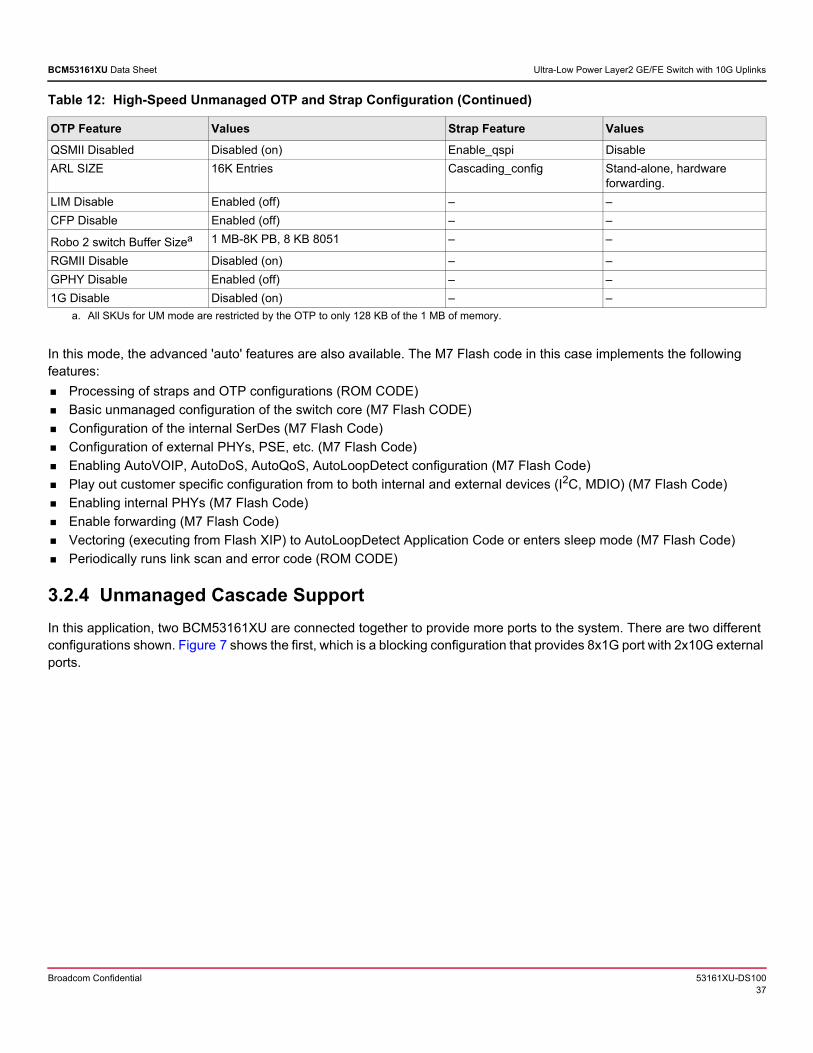
Broadcom Confidential 53161XU-DS10037
BCM53161XU Data Sheet Ultra-Low Power Layer2 GE/FE Switch with 10G Uplinks
In this mode, the advanced 'auto' features are also available. The M7 Flash code in this case implements the following features:
Processing of straps and OTP configurations (ROM CODE)
Basic unmanaged configuration of the switch core (M7 Flash CODE)
Configuration of the internal SerDes (M7 Flash Code)
Configuration of external PHYs, PSE, etc. (M7 Flash Code)
Enabling AutoVOIP, AutoDoS, AutoQoS, AutoLoopDetect configuration (M7 Flash Code)
Play out customer specific configuration from to both internal and external devices (I2C, MDIO) (M7 Flash Code)
Enabling internal PHYs (M7 Flash Code)
Enable forwarding (M7 Flash Code)
Vectoring (executing from Flash XIP) to AutoLoopDetect Application Code or enters sleep mode (M7 Flash Code)
Periodically runs link scan and error code (ROM CODE)
3.2.4 Unmanaged Cascade Support
In this application, two BCM53161XU are connected together to provide more ports to the system. There are two different configurations shown. Figure 7 shows the first, which is a blocking configuration that provides 8x1G port with 2x10G external ports.
QSMII Disabled Disabled (on) Enable_qspi Disable
ARL SIZE 16K Entries Cascading_config Stand-alone, hardware forwarding.
LIM Disable Enabled (off) – –
CFP Disable Enabled (off) – –
Robo 2 switch Buffer Sizea 1 MB-8K PB, 8 KB 8051 – –
RGMII Disable Disabled (on) – –
GPHY Disable Enabled (off) – –
1G Disable Disabled (on) – –
a. All SKUs for UM mode are restricted by the OTP to only 128 KB of the 1 MB of memory.
Table 12: High-Speed Unmanaged OTP and Strap Configuration (Continued)
OTP Feature Values Strap Feature Values
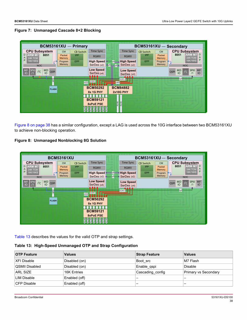
Broadcom Confidential 53161XU-DS10038
BCM53161XU Data Sheet Ultra-Low Power Layer2 GE/FE Switch with 10G Uplinks
Figure 7: Unmanaged Cascade 8+2 Blocking
Figure 8 on page 38 has a similar configuration, except a LAG is used across the 10G interface between two BCM53161XU to achieve non-blocking operation.
Figure 8: Unmanaged Nonblocking 8G Solution
Table 13 describes the values for the valid OTP and strap settings.
Table 13: High-Speed Unmanaged OTP and Strap Configuration
OTP Feature Values Strap Feature Values
XFI Disable Disabled (on) Boot_src M7 Flash
QSMII Disabled Disabled (on) Enable_qspi Disable
ARL SIZE 16K Entries Cascading_config Primary vs Secondary
LIM Disable Enabled (off) – –
CFP Disable Enabled (off) – –
— Secondary
High Speed
(x2)
Low Speed
(x4)
RGMII
Time Sync CPU Subsystem
NOC
MFIO
SPI0/1I2CMD
IOQSPI
CB SwitchARM M724K TCM16K/16K$
8051 DAP
CM
ProgramMemory
PacketMemory
EPP
IPP
FLASH
xfixfi
BCM50292
8x 1G PHY
BCM59121
8xPoE PSE
BCM84882
2x10G PHY
— Primary
High Speed
(x2)
Low Speed
(x4)
RGMII
Time SyncCPU Subsystem
NOC
MFIO
SPI0/1
ARM M724K TCM16K/16K$
8051
I2C MDIO QSPI
DAP
CB SwitchCM
ProgramMemory
PacketMemory
EPP
IPP
xfi
cl22SP
I spiSGMII+SGMII+
cl45
SerDesSerDes
SerDes SerDes
RJ-
45
RJ-
45
RJ-
45
RJ-
45
RJ-
45
RJ-
45
RJ-
45
RJ-
45
RJ-
45
RJ-
45
BCM53161XU BCM53161XU
— Secondary
High Speed
(x2)
Low Speed
(x4)
RGMII
Time Sync CPU Subsystem
NOC
MFIO
SPI0/1I2CMD
IOQSPI
CB SwitchARM M724K TCM16K/16K$
8051 DAP
CM
ProgramMemory
PacketMemory
EPP
IPP
FLASHBCM50292
8x 1G PHY
BCM59121
8xPoE PSE
High Speed
(x2)
Low Speed
(x4)
RGMII
Time SyncCPU Subsystem
NOC
MFIO
SPI0/1
ARM M724K TCM16K/16K$
8051
I2C MDIO QSPI
DAP
CB SwitchCM
ProgramMemory
PacketMemory
EPP
IPP
cl22SP
I spiSGMII+SGMII+
xfi
xfi SerDesSerDes
SerDes SerDes
RJ-
45
RJ-
45
RJ-
45
RJ-
45
RJ-
45
RJ-
45
RJ-
45
RJ-
45
BCM53161XU BCM53161XU
Broadcom Confidential 53161XU-DS10039
BCM53161XU Data Sheet Ultra-Low Power Layer2 GE/FE Switch with 10G Uplinks
In this mode, the advanced 'auto' features are also available. In this system, there are two BCM53161XU where one is the primary and one is the secondary based on a strapping. The primary BCM53161XU is responsible for configuring both devices. These devices are connected with an SPI interface. The hardware supports memory mapping model across this interface to facilitate using the same drivers for local and remote devices. External devices, such as PHYS and PSE are connected to the Primary BCM53161XU.
The M7 Flash code on the primary BCM53161XU implements the following features:
Processing of straps and OTP configurations (ROM CODE)
Basic unmanaged configuration of the switch core (M7 Flash code)
Configuration of the SerDes on Primary (M7 Flash code)
Configuration of cascade on Primary (M7 Flash code)
Configuration of the SerDes on Secondary (M7 Flash code)
Configuration of cascade on Secondary (M7 Flash code)
Configuration of external PHYs, PSE, and so forth (M7 Flash code)
Enabling AutoVOIP, AutoDoS, and AutoQoS configuration (M7 Flash code)
Play out customer specific configuration from Flash to both internal and external devices (I2C, MDIO) (M7 Flash code)
Enable internal PHYs on Primary (M7 Flash code)
Enable internal PHYs on Secondary this is via the MDIO on in the secondary device (M7 Flash code)
Enable external PHYs (M7 Flash code)
Enable forwarding on both Primary and Secondary devices (M7 Flash code)
Vectoring (executing from flash) to AutoLoopDetect Application Code or enters sleep mode (M7 Flash code)
The M7 on the secondary BCM53161XU device implements the following features:
Processing of straps and OTP configurations (ROM CODE)
Basic unmanaged configuration of the switch core (M7 Flash code)
Identified as secondary based on straps (M7 Flash code)
Does NOT enable PHYS or unmanaged forwarding (M7 Flash code)
Robo 2 switch Buffer Sizea 1 MB-8K PB, 8 KB 8051 – –
RGMII Disable Disabled (on) – –
GPHY Disable Enabled (off) – –
1G Disable Disabled (on) – –
a. All SKUs for UM mode are restricted by the OTP to only 128 KB of the 1 MB of memory.
Table 13: High-Speed Unmanaged OTP and Strap Configuration (Continued)
OTP Feature Values Strap Feature Values
Broadcom Confidential 53161XU-DS10040
BCM53161XU Data Sheet Ultra-Low Power Layer2 GE/FE Switch with 10G Uplinks
Chapter 4: Software Components
This section describes on of the software components the will run on the BCM53161XU. This is not an exhaustive list.
4.1 8051 and M7 Running Environment
The operating environment is a bare metal environment. The following is list of components in the ROM environment:
Running on the 8051:
SKU/OTP/Strap processing (ROM) – Process straps, OTP and SKUS options.
Running on the M7:
AVS mechanism
Based device setup (ROM) – Configures PLL, clocks, and central memory.
Basic Unmanaged Configuration (ROM) – Configures the Robo 2 switch core for default unmanaged configuration.
Internal GPHY configuration (ROM) – Configures and enables GPHY ports.
Link scan/error handling (ROM) – handles links going up and down as well and any errors (ECC).
The following are advanced unmanaged features:
Advanced registered playback – Reads register play-back data from the QSPI Flash and applies it to the device and external components via MDIO and I2C.
AutoVOIP/AutoQoS/AutoDOS – Configures these features (that is, OUI and voice VLAN) from flash.
AutoLoopDetect – Operation code which performs autoloopdetect feature. This runs from flash.
Broadcom Confidential 53161XU-DS10041
BCM53161XU Data Sheet Ultra-Low Power Layer2 GE/FE Switch with 10G Uplinks
4.2 M7 Operating System Environment
The M7 uses an operating system environment based on OpenRTOS/FreeRTOS. The following is a list of features:
ARM CMSIS-Driver (ARM) – Portable device driver infrastructure.
4.3 Unmanaged Application
Figure 9 shows the basic unmanaged software components.
Figure 9: Unmanaged Software Components
Flash Application
(AutoXXX)
ROM, Application
(Strap, UM config,
and so forth)
BCM531XXU HardwareROM
8051 Cortex M7 Other Peripherals
(for example, Flash/UART)Robo 2 Switch
Broadcom Confidential 53161XU-DS10042
BCM53161XU Data Sheet Ultra-Low Power Layer2 GE/FE Switch with 10G Uplinks
Chapter 5: System Interfaces
5.1 Overview
The BCM53161XU include the following interfaces:
Copper Interface
Frame Management Port Interface
SerDes Interface
Configuration Pins
Programming Interfaces
LED Interfaces
Digital Voltage Regulator (LDO)
Each interface is discussed in detail in these sections.
5.2 Copper Interface
The internal PHYs transmit and receive data using the analog copper interface. This section discusses the following topics:
Auto-Negotiation
Lineside (Remote) Loopback Mode
5.2.1 Auto-Negotiation
The BCM53161XU negotiate a mode of operation over the copper media using the auto-negotiation mechanism defined in the IEEE 802.3u and IEEE 802.3ab specifications. When the auto-negotiation function is enabled, the BCM53161XU automatically choose the mode of operation by advertising its abilities and comparing them with those received from its link partner. The BCM53161XU can be configured to advertise the following modes:
1000BASE-T full-duplex and/or half-duplex.
100BASE-TX full-duplex and/or half-duplex.
10BASE-T full-duplex and/or half-duplex.
The transceiver negotiates with its link partner and chooses the highest common operating speed and duplex mode, commonly referred to as highest common denominator (HCD). Auto-negotiation can be disabled by software control, but is required for 1000BASE-T operation.
5.2.2 Lineside (Remote) Loopback Mode
The lineside loopback mode allows the testing of the copper interface from the link partner. This mode is enabled by setting bit 15 of the Miscellaneous Test register. The MDI receive packet is passed through the PCS and sent back out as the MDI transmit packet. The PCS receive data appears on the internal MAC interface.
5.3 Frame Management Port Interface
The dedicated frame management port provides high-speed connection to transfer management packets to an external management agent. For more information about frame management, see “Interdevice Interface” on page 15. The port is configurable to RGMII using strap pins or software configuration.
Broadcom Confidential 53161XU-DS10043
BCM53161XU Data Sheet Ultra-Low Power Layer2 GE/FE Switch with 10G Uplinks
NOTE: The Frame Management port interface supports only full-duplex mode.
The BCM53161XU supports EEE features for external PHYs connected on the IMP and GMII (port5) only through the GMII interface.
5.3.1 RGMII Interface
The Reduced Gigabit Media Independent Interface (RGMII) serves as a digital data interface between the BCM53161XU and an external management entity or an external PHY to provide additional data port capacity. Transmit and receive data is clocked on the rising and falling edge of the clocks. This reduces the number of data signals crossing the MAC interface without affecting the data transmission rate. The RGMII transmits data synchronously using the TXD[3:0] and RXD[3:0] data signals. The BCM53161XU offers either 2.5V or 1.5V RGMII interface with an external device.
5.4 SerDes Interface
The BCM53161XU provides 4x SGMII + 2x XFI interfaces.
5.5 Configuration Pins
Initial configuration of the BCM53161XU takes place during power-on/reset by loading internal control values from hardware strap pins. The value of the pin is loaded when the reset sequence completes, and the pin transitions to normal operation. Pull-up or pull-down resistors can be added to these pins to control the device configuration. If the pins are left floating, the default value is determined based on the internal pull-up or pull-down configuration. See “Signal Descriptions” on page 61 for additional information.
5.6 Programming Interfaces
The BCM53161XU can be programmed using the SPI interface. The interfaces share a common pin set that is configured using the strap pin. The “SPI Interface” provides access for a general-purpose microcontroller, allowing read and write access to the internal BCM53161XU register space. It is configured to be compatible with the Motorola Serial Peripheral Interface (SPI) protocol.
An explanation follows for using the serial interface with an SPI-compatible CPU (“SPI Interface”). Either mode can be selected with the strap pin. Either mode has access to the same register space.
5.6.1 SPI Interface
One way to access the BCM53161XU internal registers is to use the SPI-compatible interface. This four-pin interface is designed to support a fully functional, bidirectional Motorola serial peripheral interface (SPI) for register read/write access. In addition, there is another SPI master for cascading configuration. The maximum speed of operation is 25 MHz.
5.6.2 SPI Slave
The SPI2 is a four-pin interface that comprises the following:
SS2 – Slave select is used to signal start, end of transaction by the master.
SCK2 – Slave Clock driven by Master.
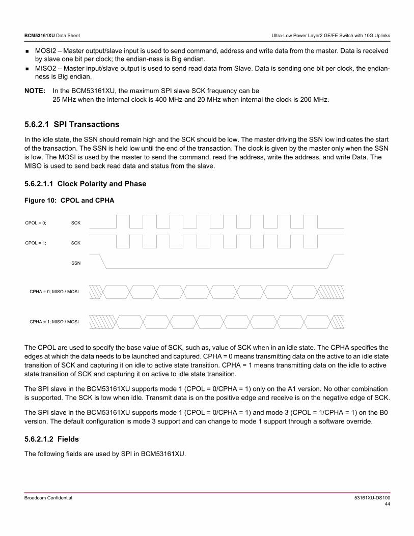
Broadcom Confidential 53161XU-DS10044
BCM53161XU Data Sheet Ultra-Low Power Layer2 GE/FE Switch with 10G Uplinks
MOSI2 – Master output/slave input is used to send command, address and write data from the master. Data is received by slave one bit per clock; the endian-ness is Big endian.
MISO2 – Master input/slave output is used to send read data from Slave. Data is sending one bit per clock, the endian-ness is Big endian.
NOTE: In the BCM53161XU, the maximum SPI slave SCK frequency can be 25 MHz when the internal clock is 400 MHz and 20 MHz when internal the clock is 200 MHz.
5.6.2.1 SPI Transactions
In the idle state, the SSN should remain high and the SCK should be low. The master driving the SSN low indicates the start of the transaction. The SSN is held low until the end of the transaction. The clock is given by the master only when the SSN is low. The MOSI is used by the master to send the command, read the address, write the address, and write Data. The MISO is used to send back read data and status from the slave.
5.6.2.1.1 Clock Polarity and Phase
Figure 10: CPOL and CPHA
The CPOL are used to specify the base value of SCK, such as, value of SCK when in an idle state. The CPHA specifies the edges at which the data needs to be launched and captured. CPHA = 0 means transmitting data on the active to an idle state transition of SCK and capturing it on idle to active state transition. CPHA = 1 means transmitting data on the idle to active state transition of SCK and capturing it on active to idle state transition.
The SPI slave in the BCM53161XU supports mode 1 (CPOL = 0/CPHA = 1) only on the A1 version. No other combination is supported. The SCK is low when idle. Transmit data is on the positive edge and receive is on the negative edge of SCK.
The SPI slave in the BCM53161XU supports mode 1 (CPOL = 0/CPHA = 1) and mode 3 (CPOL = 1/CPHA = 1) on the B0 version. The default configuration is mode 3 support and can change to mode 1 support through a software override.
5.6.2.1.2 Fields
The following fields are used by SPI in BCM53161XU.
CPOL = 0;
CPOL = 1;
CPHA = 0; MISO / MOSI
SSN
SCK
CPHA = 1; MISO / MOSI
SCK
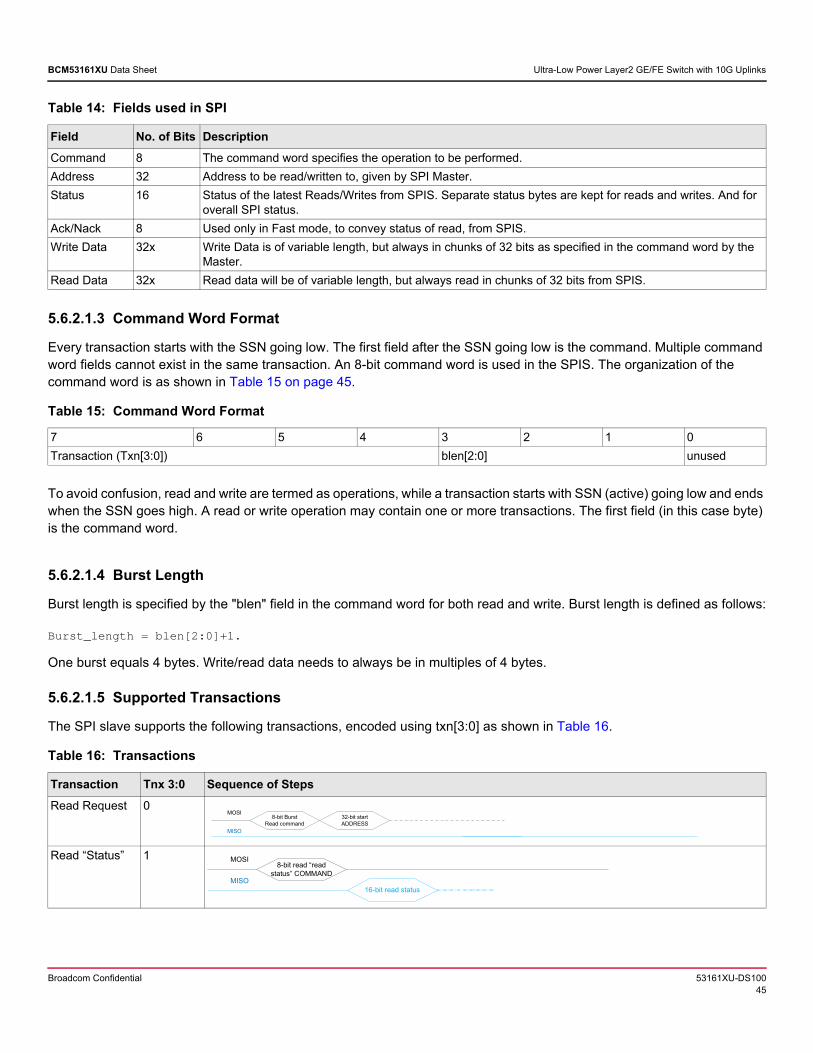
Broadcom Confidential 53161XU-DS10045
BCM53161XU Data Sheet Ultra-Low Power Layer2 GE/FE Switch with 10G Uplinks
5.6.2.1.3 Command Word Format
Every transaction starts with the SSN going low. The first field after the SSN going low is the command. Multiple command word fields cannot exist in the same transaction. An 8-bit command word is used in the SPIS. The organization of the command word is as shown in Table 15 on page 45.
To avoid confusion, read and write are termed as operations, while a transaction starts with SSN (active) going low and ends when the SSN goes high. A read or write operation may contain one or more transactions. The first field (in this case byte) is the command word.
5.6.2.1.4 Burst Length
Burst length is specified by the "blen" field in the command word for both read and write. Burst length is defined as follows:
Burst_length = blen[2:0]+1.
One burst equals 4 bytes. Write/read data needs to always be in multiples of 4 bytes.
5.6.2.1.5 Supported Transactions
The SPI slave supports the following transactions, encoded using txn[3:0] as shown in Table 16.
Table 14: Fields used in SPI
Field No. of Bits Description
Command 8 The command word specifies the operation to be performed.
Address 32 Address to be read/written to, given by SPI Master.
Status 16 Status of the latest Reads/Writes from SPIS. Separate status bytes are kept for reads and writes. And for overall SPI status.
Ack/Nack 8 Used only in Fast mode, to convey status of read, from SPIS.
Write Data 32x Write Data is of variable length, but always in chunks of 32 bits as specified in the command word by the Master.
Read Data 32x Read data will be of variable length, but always read in chunks of 32 bits from SPIS.
Table 15: Command Word Format
7 6 5 4 3 2 1 0
Transaction (Txn[3:0]) blen[2:0] unused
Table 16: Transactions
Transaction Tnx 3:0 Sequence of Steps
Read Request 0
Read “Status” 1
8-bit Burst Read command
32-bit start ADDRESS
MOSI
MISO
8-bit read “read status” COMMAND
MOSI
16-bit read statusMISO
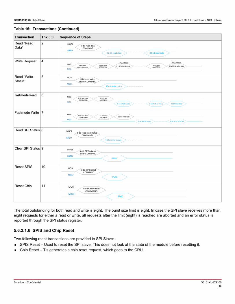
Broadcom Confidential 53161XU-DS10046
BCM53161XU Data Sheet Ultra-Low Power Layer2 GE/FE Switch with 10G Uplinks
The total outstanding for both read and write is eight. The burst size limit is eight. In case the SPI slave receives more than eight requests for either a read or write, all requests after the limit (eight) is reached are aborted and an error status is reported through the SPI status register.
5.6.2.1.6 SPIS and Chip Reset
Two following reset transactions are provided in SPI Slave:
SPIS Reset – Used to reset the SPI slave. This does not look at the state of the module before resetting it.
Chip Reset – Tis generates a chip reset request, which goes to the CRU.
Read “Read Data”
2
Write Request 4
Read “Write Status”
5
Fastmode Read 6
Fastmode Write 7
Read SPI Status 8
Clear SPI Status 9
Reset SPIS 10
Reset Chip 11
Table 16: Transactions (Continued)
Transaction Tnx 3:0 Sequence of Steps
8-bit read data COMMAND
MOSI
32-bit read dataMISO
32-bit read data
8-bit Burst write command
32-bit start ADDRESS
MOSI
MISO
N x 32-bit write data
N=Burst size
N x 32-bit write data32-bit start ADDRESS
N=Burst size
8-bit read write-status COMMAND
MOSI
16-bit write statusMISO
8-bit fast read COMMAND
32-bit read ADDRESS
MOSI
MISO8-bit NACK Status 8-bit ACK STATUS 32-bit read data
8-bit fast Write COMMAND
32-bit write ADDRESS
MOSI
MISO
32-bit write data
8-bit NACK Status 8-bit ACK STATUS
8-bit read read-status COMMAND
MOSI
16-bit read statusMISO
8-bit SPIS status clear COMMAND
MOSI
MISO8'h00
8-bit SPIS reset COMMAND
MOSI
MISO8'h00
8-bit CHIP reset COMMAND
MOSI
MISO8'h00
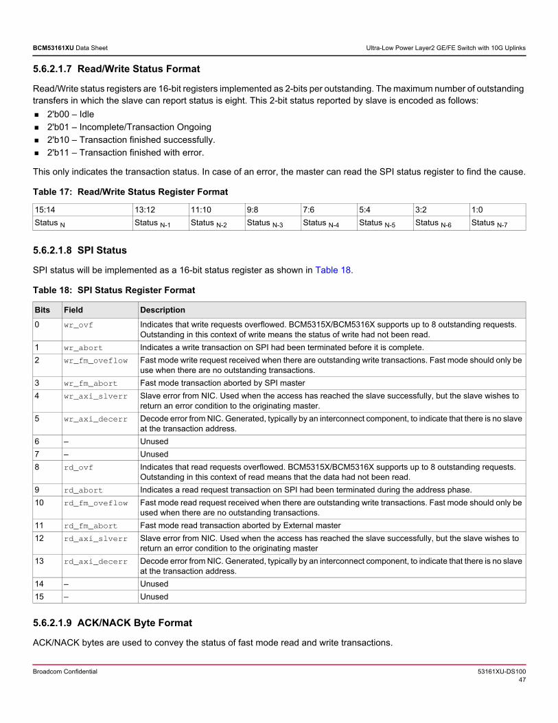
Broadcom Confidential 53161XU-DS10047
BCM53161XU Data Sheet Ultra-Low Power Layer2 GE/FE Switch with 10G Uplinks
5.6.2.1.7 Read/Write Status Format
Read/Write status registers are 16-bit registers implemented as 2-bits per outstanding. The maximum number of outstanding transfers in which the slave can report status is eight. This 2-bit status reported by slave is encoded as follows:
2'b00 – Idle
2'b01 – Incomplete/Transaction Ongoing
2'b10 – Transaction finished successfully.
2'b11 – Transaction finished with error.
This only indicates the transaction status. In case of an error, the master can read the SPI status register to find the cause.
5.6.2.1.8 SPI Status
SPI status will be implemented as a 16-bit status register as shown in Table 18.
5.6.2.1.9 ACK/NACK Byte Format
ACK/NACK bytes are used to convey the status of fast mode read and write transactions.
Table 17: Read/Write Status Register Format
15:14 13:12 11:10 9:8 7:6 5:4 3:2 1:0
Status N Status N-1 Status N-2 Status N-3 Status N-4 Status N-5 Status N-6 Status N-7
Table 18: SPI Status Register Format
Bits Field Description
0 wr_ovf Indicates that write requests overflowed. BCM5315X/BCM5316X supports up to 8 outstanding requests. Outstanding in this context of write means the status of write had not been read.
1 wr_abort Indicates a write transaction on SPI had been terminated before it is complete.
2 wr_fm_oveflow Fast mode write request received when there are outstanding write transactions. Fast mode should only be use when there are no outstanding transactions.
3 wr_fm_abort Fast mode transaction aborted by SPI master
4 wr_axi_slverr Slave error from NIC. Used when the access has reached the slave successfully, but the slave wishes to return an error condition to the originating master.
5 wr_axi_decerr Decode error from NIC. Generated, typically by an interconnect component, to indicate that there is no slave at the transaction address.
6 – Unused
7 – Unused
8 rd_ovf Indicates that read requests overflowed. BCM5315X/BCM5316X supports up to 8 outstanding requests. Outstanding in this context of read means that the data had not been read.
9 rd_abort Indicates a read request transaction on SPI had been terminated during the address phase.
10 rd_fm_oveflow Fast mode read request received when there are outstanding write transactions. Fast mode should only be used when there are no outstanding transactions.
11 rd_fm_abort Fast mode read transaction aborted by External master
12 rd_axi_slverr Slave error from NIC. Used when the access has reached the slave successfully, but the slave wishes to return an error condition to the originating master
13 rd_axi_decerr Decode error from NIC. Generated, typically by an interconnect component, to indicate that there is no slave at the transaction address.
14 – Unused
15 – Unused
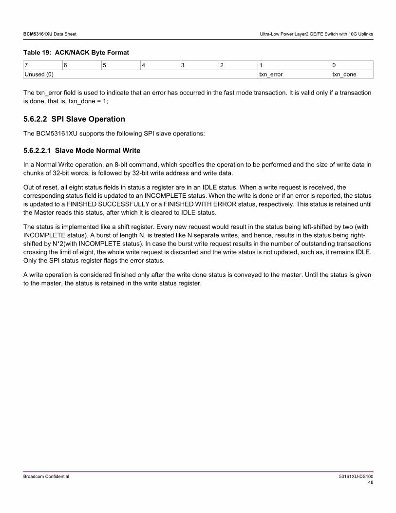
Broadcom Confidential 53161XU-DS10048
BCM53161XU Data Sheet Ultra-Low Power Layer2 GE/FE Switch with 10G Uplinks
The txn_error field is used to indicate that an error has occurred in the fast mode transaction. It is valid only if a transaction is done, that is, txn_done = 1;
5.6.2.2 SPI Slave Operation
The BCM53161XU supports the following SPI slave operations:
5.6.2.2.1 Slave Mode Normal Write
In a Normal Write operation, an 8-bit command, which specifies the operation to be performed and the size of write data in chunks of 32-bit words, is followed by 32-bit write address and write data.
Out of reset, all eight status fields in status a register are in an IDLE status. When a write request is received, the corresponding status field is updated to an INCOMPLETE status. When the write is done or if an error is reported, the status is updated to a FINISHED SUCCESSFULLY or a FINISHED WITH ERROR status, respectively. This status is retained until the Master reads this status, after which it is cleared to IDLE status.
The status is implemented like a shift register. Every new request would result in the status being left-shifted by two (with INCOMPLETE status). A burst of length N, is treated like N separate writes, and hence, results in the status being right-shifted by N*2(with INCOMPLETE status). In case the burst write request results in the number of outstanding transactions crossing the limit of eight, the whole write request is discarded and the write status is not updated, such as, it remains IDLE. Only the SPI status register flags the error status.
A write operation is considered finished only after the write done status is conveyed to the master. Until the status is given to the master, the status is retained in the write status register.
Table 19: ACK/NACK Byte Format
7 6 5 4 3 2 1 0
Unused (0) txn_error txn_done
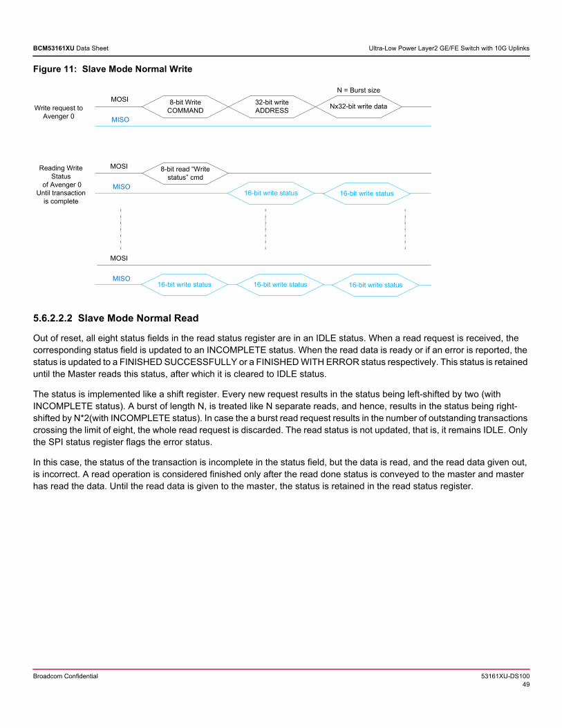
Broadcom Confidential 53161XU-DS10049
BCM53161XU Data Sheet Ultra-Low Power Layer2 GE/FE Switch with 10G Uplinks
Figure 11: Slave Mode Normal Write
5.6.2.2.2 Slave Mode Normal Read
Out of reset, all eight status fields in the read status register are in an IDLE status. When a read request is received, the corresponding status field is updated to an INCOMPLETE status. When the read data is ready or if an error is reported, the status is updated to a FINISHED SUCCESSFULLY or a FINISHED WITH ERROR status respectively. This status is retained until the Master reads this status, after which it is cleared to IDLE status.
The status is implemented like a shift register. Every new request results in the status being left-shifted by two (with INCOMPLETE status). A burst of length N, is treated like N separate reads, and hence, results in the status being right-shifted by N*2(with INCOMPLETE status). In case the a burst read request results in the number of outstanding transactions crossing the limit of eight, the whole read request is discarded. The read status is not updated, that is, it remains IDLE. Only the SPI status register flags the error status.
In this case, the status of the transaction is incomplete in the status field, but the data is read, and the read data given out, is incorrect. A read operation is considered finished only after the read done status is conveyed to the master and master has read the data. Until the read data is given to the master, the status is retained in the read status register.
8-bit Write COMMAND
32-bit write ADDRESS
MOSI
MISO
Nx32-bit write dataWrite request to Avenger 0
8-bit read “Write status” cmd
16-bit write status
MOSI
MISO
Reading Write Status
of Avenger 0Until transaction
is complete
MOSI
MISO
N = Burst size
16-bit write status
16-bit write status 16-bit write status 16-bit write status
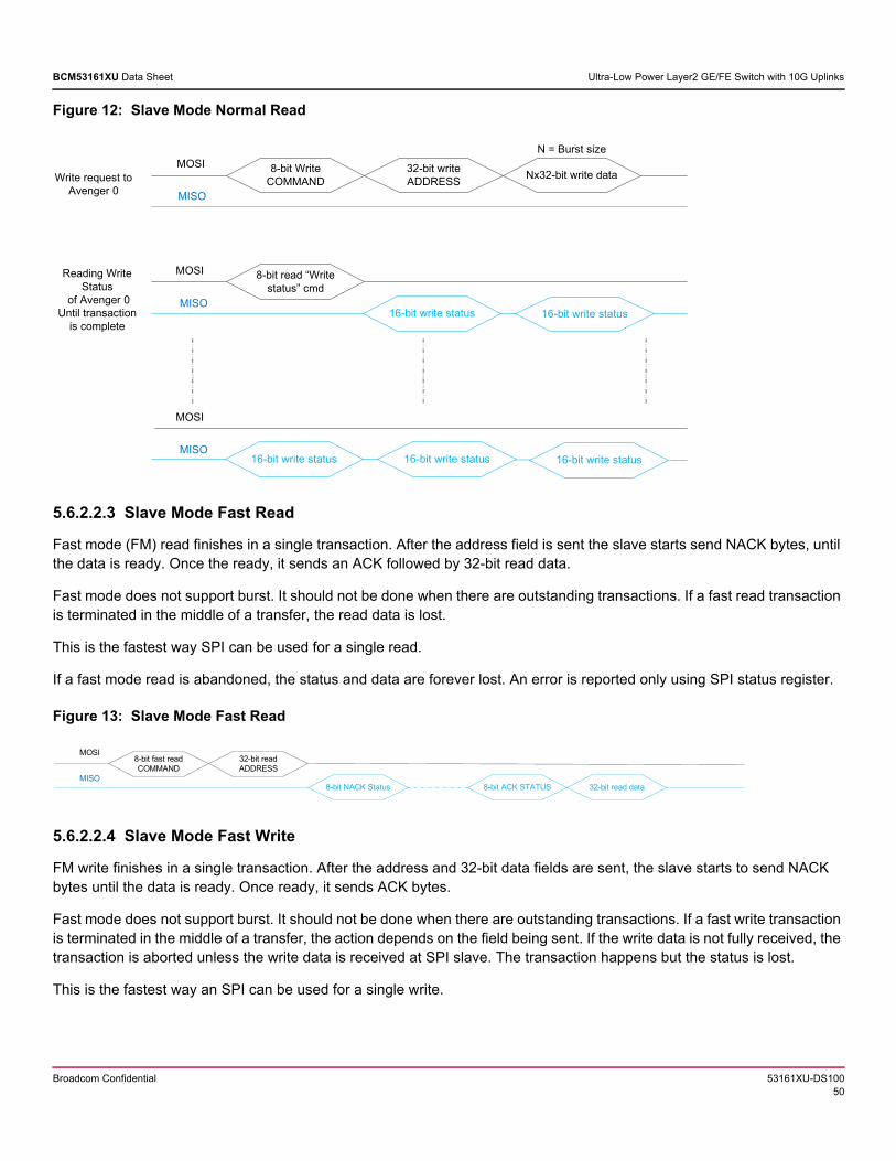
Broadcom Confidential 53161XU-DS10050
BCM53161XU Data Sheet Ultra-Low Power Layer2 GE/FE Switch with 10G Uplinks
Figure 12: Slave Mode Normal Read
5.6.2.2.3 Slave Mode Fast Read
Fast mode (FM) read finishes in a single transaction. After the address field is sent the slave starts send NACK bytes, until the data is ready. Once the ready, it sends an ACK followed by 32-bit read data.
Fast mode does not support burst. It should not be done when there are outstanding transactions. If a fast read transaction is terminated in the middle of a transfer, the read data is lost.
This is the fastest way SPI can be used for a single read.
If a fast mode read is abandoned, the status and data are forever lost. An error is reported only using SPI status register.
Figure 13: Slave Mode Fast Read
5.6.2.2.4 Slave Mode Fast Write
FM write finishes in a single transaction. After the address and 32-bit data fields are sent, the slave starts to send NACK bytes until the data is ready. Once ready, it sends ACK bytes.
Fast mode does not support burst. It should not be done when there are outstanding transactions. If a fast write transaction is terminated in the middle of a transfer, the action depends on the field being sent. If the write data is not fully received, the transaction is aborted unless the write data is received at SPI slave. The transaction happens but the status is lost.
This is the fastest way an SPI can be used for a single write.
8-bit Write COMMAND
32-bit write ADDRESS
MOSI
MISO
Nx32-bit write dataWrite request to Avenger 0
8-bit read “Write status” cmd
16-bit write status
MOSI
MISO
Reading Write Status
of Avenger 0Until transaction
is complete
MOSI
MISO
N = Burst size
16-bit write status
16-bit write status 16-bit write status 16-bit write status
8-bit fast read COMMAND
32-bit read ADDRESS
MOSI
MISO8-bit NACK Status 8-bit ACK STATUS 32-bit read data
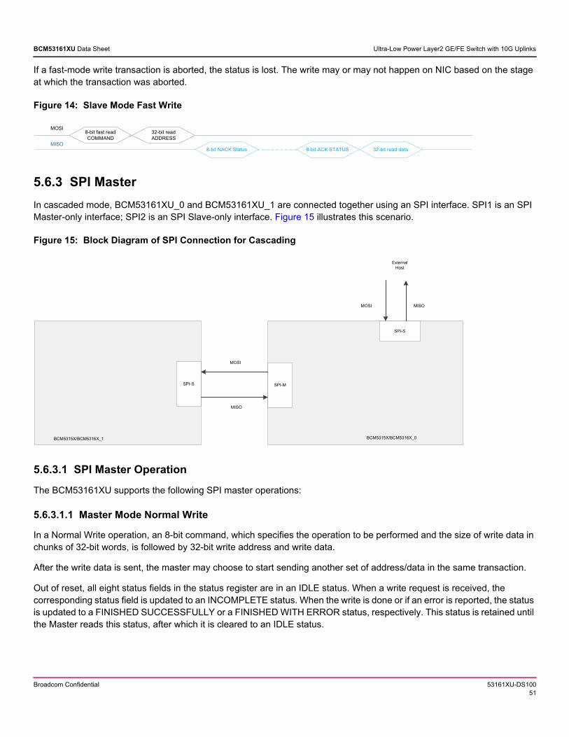
Broadcom Confidential 53161XU-DS10051
BCM53161XU Data Sheet Ultra-Low Power Layer2 GE/FE Switch with 10G Uplinks
If a fast-mode write transaction is aborted, the status is lost. The write may or may not happen on NIC based on the stage at which the transaction was aborted.
Figure 14: Slave Mode Fast Write
5.6.3 SPI Master
In cascaded mode, BCM53161XU_0 and BCM53161XU_1 are connected together using an SPI interface. SPI1 is an SPI Master-only interface; SPI2 is an SPI Slave-only interface. Figure 15 illustrates this scenario.
Figure 15: Block Diagram of SPI Connection for Cascading
5.6.3.1 SPI Master Operation
The BCM53161XU supports the following SPI master operations:
5.6.3.1.1 Master Mode Normal Write
In a Normal Write operation, an 8-bit command, which specifies the operation to be performed and the size of write data in chunks of 32-bit words, is followed by 32-bit write address and write data.
After the write data is sent, the master may choose to start sending another set of address/data in the same transaction.
Out of reset, all eight status fields in the status register are in an IDLE status. When a write request is received, the corresponding status field is updated to an INCOMPLETE status. When the write is done or if an error is reported, the status is updated to a FINISHED SUCCESSFULLY or a FINISHED WITH ERROR status, respectively. This status is retained until the Master reads this status, after which it is cleared to an IDLE status.
8-bit fast read COMMAND
32-bit read ADDRESS
MOSI
MISO8-bit NACK Status 8-bit ACK STATUS 32-bit read data
SPI-S
SPI-MSPI-S
BCM5315X/BCM5316X_0BCM5315X/BCM5316X_1
MISOMOSI
External Host
MISO
MOSI
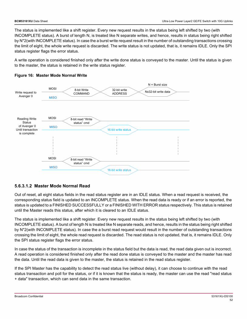
Broadcom Confidential 53161XU-DS10052
BCM53161XU Data Sheet Ultra-Low Power Layer2 GE/FE Switch with 10G Uplinks
The status is implemented like a shift register. Every new request results in the status being left shifted by two (with INCOMPLETE status). A burst of length N, is treated like N separate writes, and hence, results in status being right shifted by N*2(with INCOMPLETE status). In case the a burst write request result in the number of outstanding transactions crossing the limit of eight, the whole write request is discarded. The write status is not updated, that is, it remains IDLE. Only the SPI status register flags the error status.
A write operation is considered finished only after the write done status is conveyed to the master. Until the status is given to the master, the status is retained in the write status register.
Figure 16: Master Mode Normal Write
5.6.3.1.2 Master Mode Normal Read
Out of reset, all eight status fields in the read status register are in an IDLE status. When a read request is received, the corresponding status field is updated to an INCOMPLETE status. When the read data is ready or if an error is reported, the status is updated to a FINISHED SUCCESSFULLY or a FINISHED WITH ERROR status respectively. This status is retained until the Master reads this status, after which it is cleared to an IDLE status.
The status is implemented like a shift register. Every new request results in the status being left shifted by two (with INCOMPLETE status). A burst of length N is treated like N separate reads, and hence, results in the status being right shifted by N*2(with INCOMPLETE status). In case the a burst read request would result in the number of outstanding transactions crossing the limit of eight, the whole read request is discarded. The read status is not updated, that is, it remains IDLE. Only the SPI status register flags the error status.
In case the status of the transaction is incomplete in the status field but the data is read, the read data given out is incorrect. A read operation is considered finished only after the read done status is conveyed to the master and the master has read the data. Until the read data is given to the master, the status is retained in the read status register.
If the SPI Master has the capability to detect the read status live (without delay), it can choose to continue with the read status transaction and poll for the status, or if it is known that the status is ready, the master can use the read "read status + data" transaction, which can send data in the same transaction.
8-bit Write COMMAND
32-bit write ADDRESS
MOSI
MISO
Nx32-bit write dataWrite request to Avenger 0
8-bit read “Write status” cmd
16-bit write status
MOSI
MISO
Reading Write Status
of Avenger 0Until transaction
is complete
8-bit read “Write status” cmd
16-bit write status
MOSI
MISO
N = Burst size
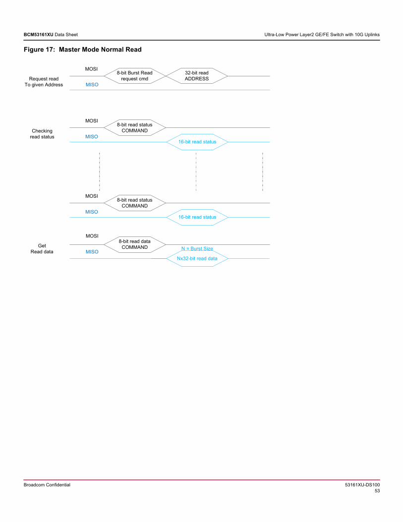
Broadcom Confidential 53161XU-DS10053
BCM53161XU Data Sheet Ultra-Low Power Layer2 GE/FE Switch with 10G Uplinks
Figure 17: Master Mode Normal Read
8-bit Burst Read request cmd
32-bit read ADDRESS
MOSI
MISO
8-bit read status COMMAND
MOSI
16-bit read statusMISO
8-bit read data COMMAND
Nx32-bit read data
MOSI
MISO
Request read To given Address
Checking read status
Get Read data
8-bit read status COMMAND
MOSI
16-bit read statusMISO
N = Burst Size
Broadcom Confidential 53161XU-DS10054
BCM53161XU Data Sheet Ultra-Low Power Layer2 GE/FE Switch with 10G Uplinks
5.6.4 Quad SPI Flash Interface
The BCM53161XU offers a quad SPI interface and supports Execute in Place (XIP) as a boot source configured by a strapped option. The interface comprises six signal pins: chip select (SS), Flash clock (SCK), Data input/output (DATA0~3).
NOTE: EPROM and QSPI are both muxed in the same pins, therefore these two interfaces are exclusive.
5.6.5 MDC/MDIO Interface
The BCM53161XU offers an MDC/MDIO interface (support both CL22 and CL45) for accessing the PHY registers. The PHY registers are accessed directly by using direct PHY addresses from 0x01~0x08.
5.6.5.1 MDC/MDIO Interface Register Programming
The BCM53161XU are designed to be fully compliant with the MII clause of the IEEE 802.3u Ethernet specification. The MDC pin of the BCM53161XU sources a 2.5 MHz clock. Serial bidirectional data transmitted using the MDIO pin is synchronized with the MDC clock. Each MII read or write instruction is initiated by the BCM53161XU and contains the following:
Preamble (PRE) – To signal the beginning of an MII instruction after reset, at least 32 consecutive 1-bits must be written to the MDIO pin. A preamble of 32 1-bits is required only for the first read or write following reset. A preamble of fewer than 32 1-bits causes the remainder of the instruction to be ignored.
Start of Frame (ST) – A 01 pattern indicates that the start of the instruction follows.
Operation Code (OP) – A read instruction is indicated by 10, while a write instruction is indicated by 01.
PHY Address (PHYAD) – A 5-bit PHY address follows, with the MSB transmitted first. The PHY address allows a single MDIO bus to access multiple PHY chips.
Register Address (REGAD) – A 5-bit register address follows, with the MSB transmitted first.
Turnaround (TA) – The next bit times are used to avoid contention on the MDIO pin when a read operation is performed. When a write operation is being performed, 10 must be sent by the BCM53161XU chip during these two bit times. When a read operation is being performed, the MDIO pin of the BCM53161XU must be put in a high-impedance state during these bit times. The external PHY drives the MDIO pin to 0 during the second bit time.
Data – The last 16 bits of the Instruction are the actual data bits. During a write operation, these bits are written to the MDIO pin with the most significant bit (MSB) transmitted first by the BCM53161XU. During a read operation, the data bits are driven by the external PHY with the MSB transmitted first.
Table 20 summarizes the complete management frame format.
Table 20: MII Management Frame Format
Operation PRE ST OP PHYAD REGAD TA Data Direction
Read 1 ... 1 01 10 AAAAA RRRRR ZZZ0
Z ... ZD ... D
Driven by master
Driven by slave
Write 1 ... 1 01 01 AAAAA RRRRR 10 D ... D Driven to master
Table 21: PHY MDIO Address Map
MDIO Slave MDIO Address
GPHY0-0 1
GPHY0-1 2
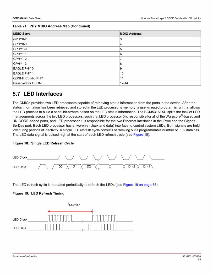
Broadcom Confidential 53161XU-DS10055
BCM53161XU Data Sheet Ultra-Low Power Layer2 GE/FE Switch with 10G Uplinks
5.7 LED Interfaces
The CMICd provides two LED processors capable of retrieving status information from the ports in the device. After the status information has been retrieved and stored in the LED processor's memory, a user-created program is run that allows the LED process to build a serial bit-stream based on the LED status information. The BCM53161XU splits the task of LED managements across the two LED processors, such that LED processor 0 is responsible for all of the Warpcore®-based and UNICORE-based ports, and LED processor 1 is responsible for the two Ethernet interfaces in the iProc and the Gigabit SerDes port. Each LED processor has a two-wire (clock and data) interface to control system LEDs. Both signals are held low during periods of inactivity. A single LED refresh cycle consists of clocking out a programmable number of LED data bits. The LED data signal is pulsed high at the start of each LED refresh cycle (see Figure 18).
Figure 18: Single LED Refresh Cycle
The LED refresh cycle is repeated periodically to refresh the LEDs (see Figure 19 on page 55).
Figure 19: LED Refresh Timing
GPHY0-2 3
GPHY0-3 4
GPHY1-0 5
GPHY1-1 6
GPHY1-2 7
GPHY1-3 8
EAGLE PHY 0 9
EAGLE PHY 1 10
QSGMII/Combo PHY 11
Reserved for QSGMII 12-14
Table 21: PHY MDIO Address Map (Continued)
MDIO Slave MDIO Address
D0 D1 D2 Dn-1Dn-2
LED Clock
LED Data
tLEDREF
LED Clock
LED Data
Broadcom Confidential 53161XU-DS10056
BCM53161XU Data Sheet Ultra-Low Power Layer2 GE/FE Switch with 10G Uplinks
5.8 Digital Voltage Regulator (LDO)
The BCM53161XU LDO generates a 1.8V power supply. The 1.8V is used internally as an intermediate voltage level in 28 nm technology.

Broadcom Confidential 53161XU-DS10057
BCM53161XU Data Sheet Ultra-Low Power Layer2 GE/FE Switch with 10G Uplinks
5.9 MFIO Interface
The BCM53161XU offers a total of 16 MFIO (Multi-Function I/O) pins. Those MFIO pins can be programmable to operate in different function modes, such UART, GPIO, and so forth.
Table 22 lists the modes of each MFIO pin.
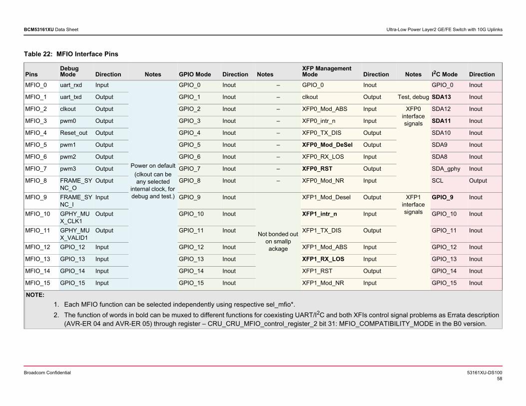
Broadcom Confidential 53161XU-DS10058
BCM53161XU Data Sheet Ultra-Low Power Layer2 GE/FE Switch with 10G Uplinks
Table 22: MFIO Interface Pins
PinsDebug Mode Direction Notes GPIO Mode Direction Notes
XFP Management Mode Direction Notes I2C Mode Direction
MFIO_0 uart_rxd Input
Power on default
(clkout can be any selected
internal clock, for debug and test.)
GPIO_0 Inout – GPIO_0 Inout GPIO_0 Inout
MFIO_1 uart_txd Output GPIO_1 Inout – clkout Output Test, debug SDA13 Inout
MFIO_2 clkout Output GPIO_2 Inout – XFP0_Mod_ABS Input XFP0 interface signals
SDA12 Inout
MFIO_3 pwm0 Output GPIO_3 Inout – XFP0_intr_n Input SDA11 Inout
MFIO_4 Reset_out Output GPIO_4 Inout – XFP0_TX_DIS Output SDA10 Inout
MFIO_5 pwm1 Output GPIO_5 Inout – XFP0_Mod_DeSel Output SDA9 Inout
MFIO_6 pwm2 Output GPIO_6 Inout – XFP0_RX_LOS Input SDA8 Inout
MFIO_7 pwm3 Output GPIO_7 Inout – XFP0_RST Output SDA_gphy Inout
MFIO_8 FRAME_SYNC_O
Output GPIO_8 Inout – XFP0_Mod_NR Input SCL Output
MFIO_9 FRAME_SYNC_I
Input GPIO_9 Inout
Not bonded out on smallp ackage
XFP1_Mod_Desel Output XFP1 interface signals
GPIO_9 Inout
MFIO_10 GPHY_MUX_CLK1
Output GPIO_10 Inout XFP1_intr_n Input GPIO_10 Inout
MFIO_11 GPHY_MUX_VALID1
Output GPIO_11 Inout XFP1_TX_DIS Output GPIO_11 Inout
MFIO_12 GPIO_12 Input GPIO_12 Inout XFP1_Mod_ABS Input GPIO_12 Inout
MFIO_13 GPIO_13 Input GPIO_13 Inout XFP1_RX_LOS Input GPIO_13 Inout
MFIO_14 GPIO_14 Input GPIO_14 Inout XFP1_RST Output GPIO_14 Inout
MFIO_15 GPIO_15 Input GPIO_15 Inout XFP1_Mod_NR Input GPIO_15 Inout
NOTE:
1. Each MFIO function can be selected independently using respective sel_mfio*.
2. The function of words in bold can be muxed to different functions for coexisting UART/I2C and both XFIs control signal problems as Errata description (AVR-ER 04 and AVR-ER 05) through register – CRU_CRU_MFIO_control_register_2 bit 31: MFIO_COMPATIBILITY_MODE in the B0 version.
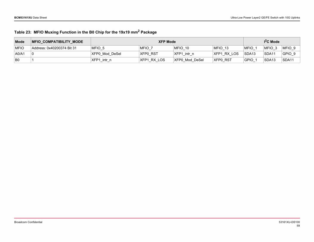
Broadcom Confidential 53161XU-DS10059
BCM53161XU Data Sheet Ultra-Low Power Layer2 GE/FE Switch with 10G Uplinks
Table 23: MFIO Muxing Function in the B0 Chip for the 19x19 mm2 Package
Mode MFIO_COMPATIBILITY_MODE XFP Mode I2C Mode
MFIO Address: 0x40200374 Bit 31 MFIO_5 MFIO_7 MFIO_10 MFIO_13 MFIO_1 MFIO_3 MFIO_9
A0/A1 0 XFP0_Mod_DeSel XFP0_RST XFP1_intr_n XFP1_RX_LOS SDA13 SDA11 GPIO_9
B0 1 XFP1_intr_n XFP1_RX_LOS XFP0_Mod_DeSel XFP0_RST GPIO_1 SDA13 SDA11
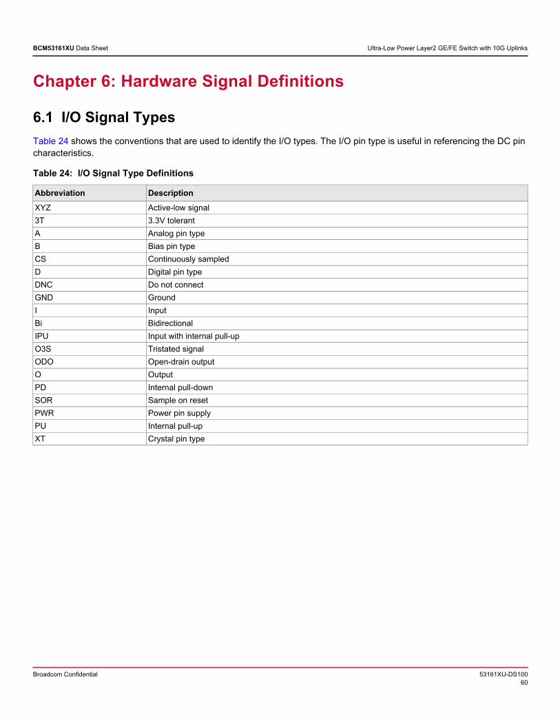
Broadcom Confidential 53161XU-DS10060
BCM53161XU Data Sheet Ultra-Low Power Layer2 GE/FE Switch with 10G Uplinks
Chapter 6: Hardware Signal Definitions
6.1 I/O Signal Types
Table 24 shows the conventions that are used to identify the I/O types. The I/O pin type is useful in referencing the DC pin characteristics.
Table 24: I/O Signal Type Definitions
Abbreviation Description
XYZ Active-low signal
3T 3.3V tolerant
A Analog pin type
B Bias pin type
CS Continuously sampled
D Digital pin type
DNC Do not connect
GND Ground
I Input
Bi Bidirectional
IPU Input with internal pull-up
O3S Tristated signal
ODO Open-drain output
O Output
PD Internal pull-down
SOR Sample on reset
PWR Power pin supply
PU Internal pull-up
XT Crystal pin type
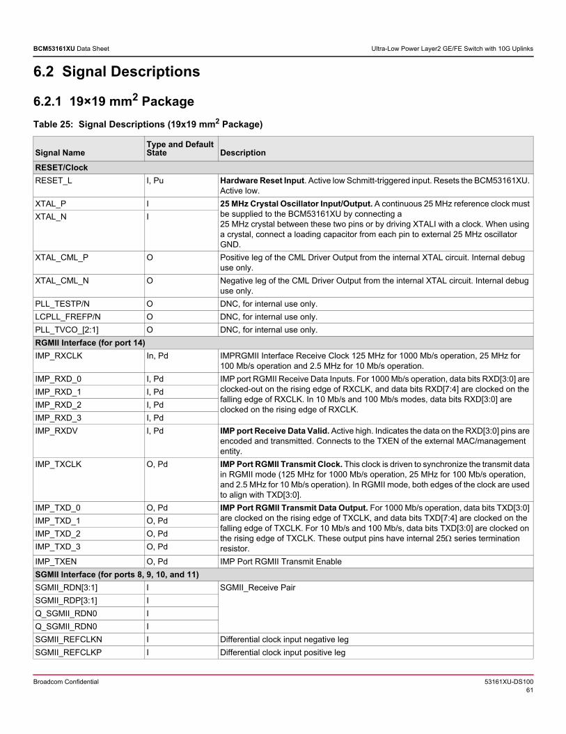
Broadcom Confidential 53161XU-DS10061
BCM53161XU Data Sheet Ultra-Low Power Layer2 GE/FE Switch with 10G Uplinks
6.2 Signal Descriptions
6.2.1 19×19 mm2 Package
Table 25: Signal Descriptions (19x19 mm2 Package)
Signal NameType and Default State Description
RESET/Clock
RESET_L I, Pu Hardware Reset Input. Active low Schmitt-triggered input. Resets the BCM53161XU. Active low.
XTAL_P I 25 MHz Crystal Oscillator Input/Output. A continuous 25 MHz reference clock must be supplied to the BCM53161XU by connecting a 25 MHz crystal between these two pins or by driving XTALI with a clock. When using a crystal, connect a loading capacitor from each pin to external 25 MHz oscillator GND.
XTAL_N I
XTAL_CML_P O Positive leg of the CML Driver Output from the internal XTAL circuit. Internal debug use only.
XTAL_CML_N O Negative leg of the CML Driver Output from the internal XTAL circuit. Internal debug use only.
PLL_TESTP/N O DNC, for internal use only.
LCPLL_FREFP/N O DNC, for internal use only.
PLL_TVCO_[2:1] O DNC, for internal use only.
RGMII Interface (for port 14)
IMP_RXCLK In, Pd IMPRGMII Interface Receive Clock 125 MHz for 1000 Mb/s operation, 25 MHz for 100 Mb/s operation and 2.5 MHz for 10 Mb/s operation.
IMP_RXD_0 I, Pd IMP port RGMII Receive Data Inputs. For 1000 Mb/s operation, data bits RXD[3:0] are clocked-out on the rising edge of RXCLK, and data bits RXD[7:4] are clocked on the falling edge of RXCLK. In 10 Mb/s and 100 Mb/s modes, data bits RXD[3:0] are clocked on the rising edge of RXCLK.
IMP_RXD_1 I, Pd
IMP_RXD_2 I, Pd
IMP_RXD_3 I, Pd
IMP_RXDV I, Pd IMP port Receive Data Valid. Active high. Indicates the data on the RXD[3:0] pins are encoded and transmitted. Connects to the TXEN of the external MAC/management entity.
IMP_TXCLK O, Pd IMP Port RGMII Transmit Clock. This clock is driven to synchronize the transmit data in RGMII mode (125 MHz for 1000 Mb/s operation, 25 MHz for 100 Mb/s operation, and 2.5 MHz for 10 Mb/s operation). In RGMII mode, both edges of the clock are used to align with TXD[3:0].
IMP_TXD_0 O, Pd IMP Port RGMII Transmit Data Output. For 1000 Mb/s operation, data bits TXD[3:0] are clocked on the rising edge of TXCLK, and data bits TXD[7:4] are clocked on the falling edge of TXCLK. For 10 Mb/s and 100 Mb/s, data bits TXD[3:0] are clocked on the rising edge of TXCLK. These output pins have internal 25 series termination resistor.
IMP_TXD_1 O, Pd
IMP_TXD_2 O, Pd
IMP_TXD_3 O, Pd
IMP_TXEN O, Pd IMP Port RGMII Transmit Enable
SGMII Interface (for ports 8, 9, 10, and 11)
SGMII_RDN[3:1] I SGMII_Receive Pair
SGMII_RDP[3:1] I
Q_SGMII_RDN0 I
Q_SGMII_RDN0 I
SGMII_REFCLKN I Differential clock input negative leg
SGMII_REFCLKP I Differential clock input positive leg
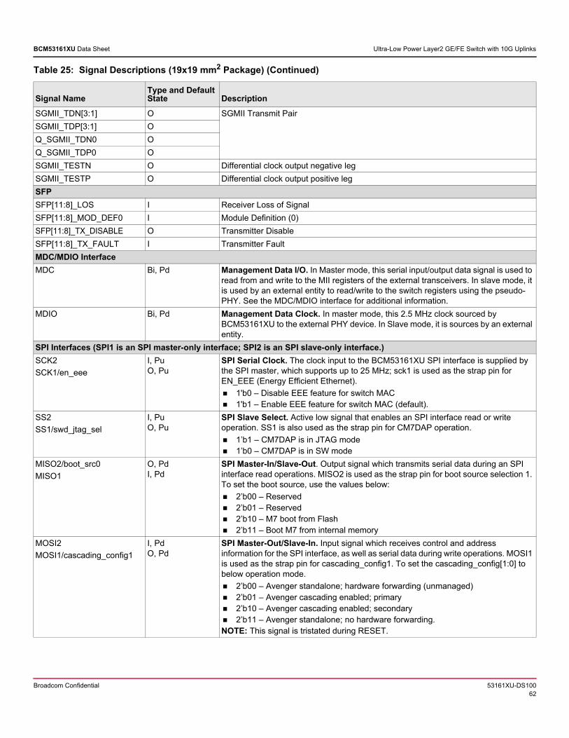
Broadcom Confidential 53161XU-DS10062
BCM53161XU Data Sheet Ultra-Low Power Layer2 GE/FE Switch with 10G Uplinks
SGMII_TDN[3:1] O SGMII Transmit Pair
SGMII_TDP[3:1] O
Q_SGMII_TDN0 O
Q_SGMII_TDP0 O
SGMII_TESTN O Differential clock output negative leg
SGMII_TESTP O Differential clock output positive leg
SFP
SFP[11:8]_LOS I Receiver Loss of Signal
SFP[11:8]_MOD_DEF0 I Module Definition (0)
SFP[11:8]_TX_DISABLE O Transmitter Disable
SFP[11:8]_TX_FAULT I Transmitter Fault
MDC/MDIO Interface
MDC Bi, Pd Management Data I/O. In Master mode, this serial input/output data signal is used to read from and write to the MII registers of the external transceivers. In slave mode, it is used by an external entity to read/write to the switch registers using the pseudo-PHY. See the MDC/MDIO interface for additional information.
MDIO Bi, Pd Management Data Clock. In master mode, this 2.5 MHz clock sourced by BCM53161XU to the external PHY device. In Slave mode, it is sources by an external entity.
SPI Interfaces (SPI1 is an SPI master-only interface; SPI2 is an SPI slave-only interface.)
SCK2
SCK1/en_eee
I, Pu O, Pu
SPI Serial Clock. The clock input to the BCM53161XU SPI interface is supplied by the SPI master, which supports up to 25 MHz; sck1 is used as the strap pin for EN_EEE (Energy Efficient Ethernet).
1'b0 – Disable EEE feature for switch MAC 1'b1 – Enable EEE feature for switch MAC (default).
SS2
SS1/swd_jtag_sel
I, Pu O, Pu
SPI Slave Select. Active low signal that enables an SPI interface read or write operation. SS1 is also used as the strap pin for CM7DAP operation.
1’b1 – CM7DAP is in JTAG mode 1’b0 – CM7DAP is in SW mode
MISO2/boot_src0
MISO1
O, Pd I, Pd
SPI Master-In/Slave-Out. Output signal which transmits serial data during an SPI interface read operations. MISO2 is used as the strap pin for boot source selection 1. To set the boot source, use the values below:
2’b00 – Reserved 2’b01 – Reserved 2’b10 – M7 boot from Flash 2’b11 – Boot M7 from internal memory
MOSI2
MOSI1/cascading_config1
I, PdO, Pd
SPI Master-Out/Slave-In. Input signal which receives control and address information for the SPI interface, as well as serial data during write operations. MOSI1 is used as the strap pin for cascading_config1. To set the cascading_config[1:0] to below operation mode.
2’b00 – Avenger standalone; hardware forwarding (unmanaged) 2’b01 – Avenger cascading enabled; primary 2’b10 – Avenger cascading enabled; secondary 2’b11 – Avenger standalone; no hardware forwarding.NOTE: This signal is tristated during RESET.
Table 25: Signal Descriptions (19x19 mm2 Package) (Continued)
Signal NameType and Default State Description
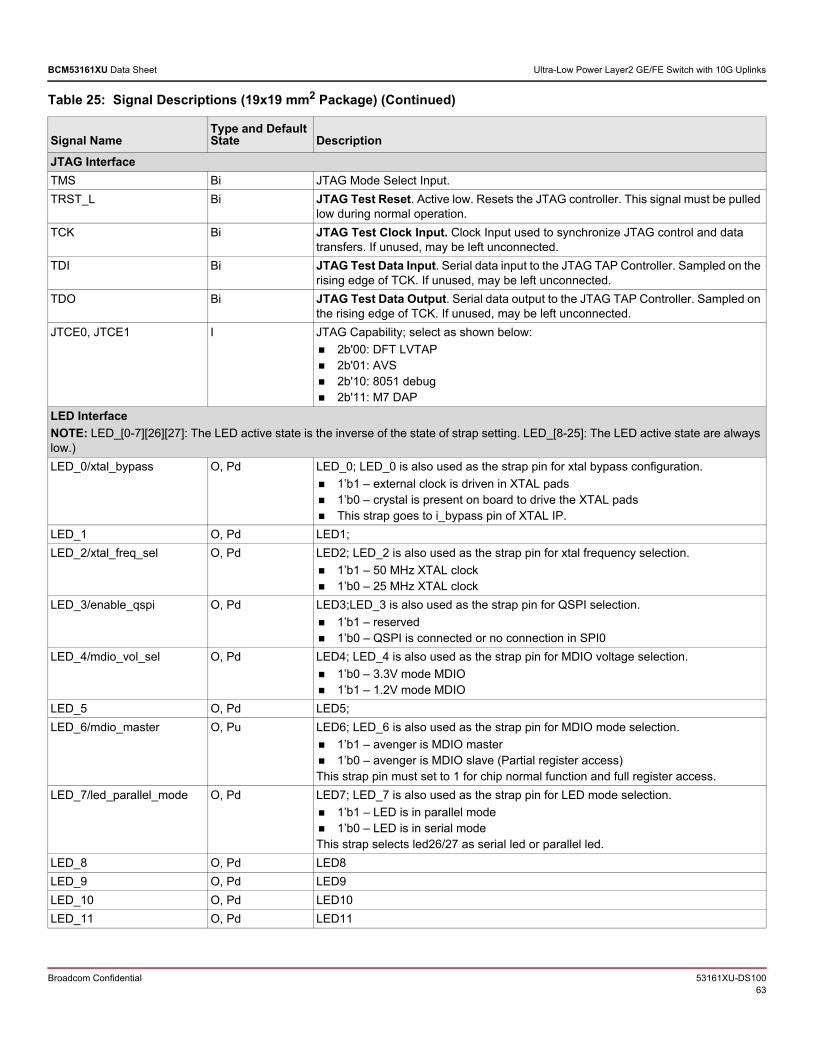
Broadcom Confidential 53161XU-DS10063
BCM53161XU Data Sheet Ultra-Low Power Layer2 GE/FE Switch with 10G Uplinks
JTAG Interface
TMS Bi JTAG Mode Select Input.
TRST_L Bi JTAG Test Reset. Active low. Resets the JTAG controller. This signal must be pulled low during normal operation.
TCK Bi JTAG Test Clock Input. Clock Input used to synchronize JTAG control and data transfers. If unused, may be left unconnected.
TDI Bi JTAG Test Data Input. Serial data input to the JTAG TAP Controller. Sampled on the rising edge of TCK. If unused, may be left unconnected.
TDO Bi JTAG Test Data Output. Serial data output to the JTAG TAP Controller. Sampled on the rising edge of TCK. If unused, may be left unconnected.
JTCE0, JTCE1 I JTAG Capability; select as shown below:
2b'00: DFT LVTAP 2b'01: AVS 2b'10: 8051 debug 2b'11: M7 DAP
LED Interface
NOTE: LED_[0-7][26][27]: The LED active state is the inverse of the state of strap setting. LED_[8-25]: The LED active state are always low.)
LED_0/xtal_bypass O, Pd LED_0; LED_0 is also used as the strap pin for xtal bypass configuration.
1’b1 – external clock is driven in XTAL pads 1’b0 – crystal is present on board to drive the XTAL pads This strap goes to i_bypass pin of XTAL IP.
LED_1 O, Pd LED1;
LED_2/xtal_freq_sel O, Pd LED2; LED_2 is also used as the strap pin for xtal frequency selection.
1’b1 – 50 MHz XTAL clock 1’b0 – 25 MHz XTAL clock
LED_3/enable_qspi O, Pd LED3;LED_3 is also used as the strap pin for QSPI selection.
1’b1 – reserved 1’b0 – QSPI is connected or no connection in SPI0
LED_4/mdio_vol_sel O, Pd LED4; LED_4 is also used as the strap pin for MDIO voltage selection.
1’b0 – 3.3V mode MDIO 1’b1 – 1.2V mode MDIO
LED_5 O, Pd LED5;
LED_6/mdio_master O, Pu LED6; LED_6 is also used as the strap pin for MDIO mode selection.
1’b1 – avenger is MDIO master 1’b0 – avenger is MDIO slave (Partial register access)This strap pin must set to 1 for chip normal function and full register access.
LED_7/led_parallel_mode O, Pd LED7; LED_7 is also used as the strap pin for LED mode selection.
1’b1 – LED is in parallel mode 1’b0 – LED is in serial modeThis strap selects led26/27 as serial led or parallel led.
LED_8 O, Pd LED8
LED_9 O, Pd LED9
LED_10 O, Pd LED10
LED_11 O, Pd LED11
Table 25: Signal Descriptions (19x19 mm2 Package) (Continued)
Signal NameType and Default State Description
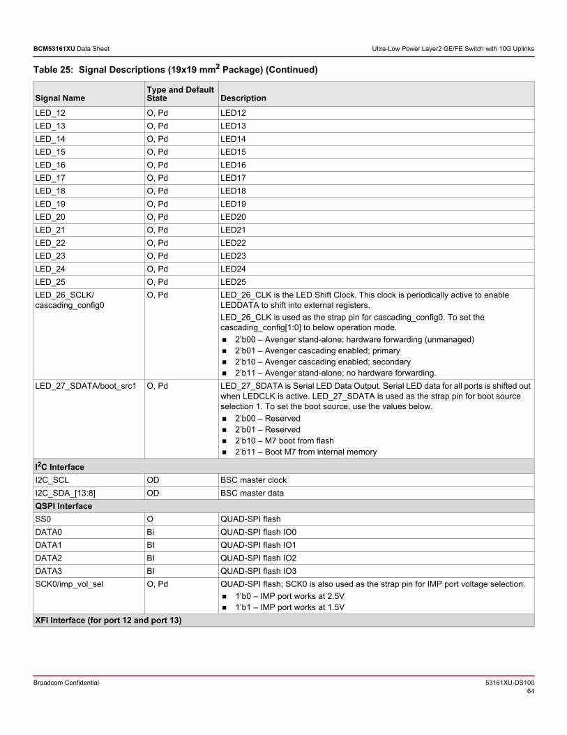
Broadcom Confidential 53161XU-DS10064
BCM53161XU Data Sheet Ultra-Low Power Layer2 GE/FE Switch with 10G Uplinks
LED_12 O, Pd LED12
LED_13 O, Pd LED13
LED_14 O, Pd LED14
LED_15 O, Pd LED15
LED_16 O, Pd LED16
LED_17 O, Pd LED17
LED_18 O, Pd LED18
LED_19 O, Pd LED19
LED_20 O, Pd LED20
LED_21 O, Pd LED21
LED_22 O, Pd LED22
LED_23 O, Pd LED23
LED_24 O, Pd LED24
LED_25 O, Pd LED25
LED_26_SCLK/cascading_config0
O, Pd LED_26_CLK is the LED Shift Clock. This clock is periodically active to enable LEDDATA to shift into external registers.
LED_26_CLK is used as the strap pin for cascading_config0. To set the cascading_config[1:0] to below operation mode.
2’b00 – Avenger stand-alone; hardware forwarding (unmanaged) 2’b01 – Avenger cascading enabled; primary 2’b10 – Avenger cascading enabled; secondary 2’b11 – Avenger stand-alone; no hardware forwarding.
LED_27_SDATA/boot_src1 O, Pd LED_27_SDATA is Serial LED Data Output. Serial LED data for all ports is shifted out when LEDCLK is active. LED_27_SDATA is used as the strap pin for boot source selection 1. To set the boot source, use the values below.
2’b00 – Reserved 2’b01 – Reserved 2’b10 – M7 boot from flash 2’b11 – Boot M7 from internal memory
I2C Interface
I2C_SCL OD BSC master clock
I2C_SDA_[13:8] OD BSC master data
QSPI Interface
SS0 O QUAD-SPI flash
DATA0 Bi QUAD-SPI flash IO0
DATA1 BI QUAD-SPI flash IO1
DATA2 BI QUAD-SPI flash IO2
DATA3 BI QUAD-SPI flash IO3
SCK0/imp_vol_sel O, Pd QUAD-SPI flash; SCK0 is also used as the strap pin for IMP port voltage selection.
1’b0 – IMP port works at 2.5V 1’b1 – IMP port works at 1.5V
XFI Interface (for port 12 and port 13)
Table 25: Signal Descriptions (19x19 mm2 Package) (Continued)
Signal NameType and Default State Description
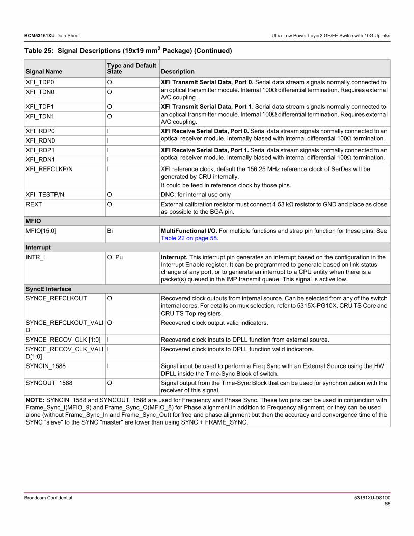
Broadcom Confidential 53161XU-DS10065
BCM53161XU Data Sheet Ultra-Low Power Layer2 GE/FE Switch with 10G Uplinks
XFI_TDP0 O XFI Transmit Serial Data, Port 0. Serial data stream signals normally connected to an optical transmitter module. Internal 100 differential termination. Requires external A/C coupling.
XFI_TDN0 O
XFI_TDP1 O XFI Transmit Serial Data, Port 1. Serial data stream signals normally connected to an optical transmitter module. Internal 100 differential termination. Requires external A/C coupling.
XFI_TDN1 O
XFI_RDP0 I XFI Receive Serial Data, Port 0. Serial data stream signals normally connected to an optical receiver module. Internally biased with internal differential 100 termination.XFI_RDN0 I
XFI_RDP1 I XFI Receive Serial Data, Port 1. Serial data stream signals normally connected to an optical receiver module. Internally biased with internal differential 100 termination.XFI_RDN1 I
XFI_REFCLKP/N I XFI reference clock, default the 156.25 MHz reference clock of SerDes will be generated by CRU internally.
It could be feed in reference clock by those pins.
XFI_TESTP/N O DNC; for internal use only
REXT O External calibration resistor must connect 4.53 kΩ resistor to GND and place as close as possible to the BGA pin.
MFIO
MFIO[15:0] Bi MultiFunctional I/O. For multiple functions and strap pin function for these pins. See Table 22 on page 58.
Interrupt
INTR_L O, Pu Interrupt. This interrupt pin generates an interrupt based on the configuration in the Interrupt Enable register. It can be programmed to generate based on link status change of any port, or to generate an interrupt to a CPU entity when there is a packet(s) queued in the IMP transmit queue. This signal is active low.
SyncE Interface
SYNCE_REFCLKOUT O Recovered clock outputs from internal source. Can be selected from any of the switch internal cores. For details on mux selection, refer to 5315X-PG10X, CRU TS Core and CRU TS Top registers.
SYNCE_REFCLKOUT_VALID
O Recovered clock output valid indicators.
SYNCE_RECOV_CLK [1:0] I Recovered clock inputs to DPLL function from external source.
SYNCE_RECOV_CLK_VALID[1:0]
I Recovered clock inputs to DPLL function valid indicators.
SYNCIN_1588 I Signal input be used to perform a Freq Sync with an External Source using the HW DPLL inside the Time-Sync Block of switch.
SYNCOUT_1588 O Signal output from the Time-Sync Block that can be used for synchronization with the receiver of this signal.
NOTE: SYNCIN_1588 and SYNCOUT_1588 are used for Frequency and Phase Sync. These two pins can be used in conjunction with Frame_Sync_I(MFIO_9) and Frame_Sync_O(MFIO_8) for Phase alignment in addition to Frequency alignment, or they can be used alone (without Frame_Sync_In and Frame_Sync_Out) for freq and phase alignment but then the accuracy and convergence time of the SYNC "slave" to the SYNC "master" are lower than using SYNC + FRAME_SYNC.
Table 25: Signal Descriptions (19x19 mm2 Package) (Continued)
Signal NameType and Default State Description
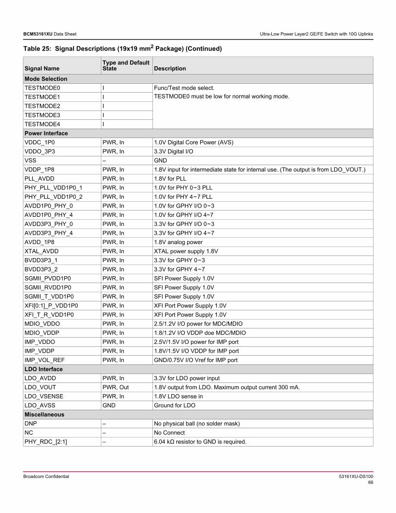
Broadcom Confidential 53161XU-DS10066
BCM53161XU Data Sheet Ultra-Low Power Layer2 GE/FE Switch with 10G Uplinks
Mode Selection
TESTMODE0 I Func/Test mode select.
TESTMODE0 must be low for normal working mode.TESTMODE1 I
TESTMODE2 I
TESTMODE3 I
TESTMODE4 I
Power Interface
VDDC_1P0 PWR, In 1.0V Digital Core Power (AVS)
VDDO_3P3 PWR, In 3.3V Digital I/O
VSS – GND
VDDP_1P8 PWR, In 1.8V input for intermediate state for internal use. (The output is from LDO_VOUT.)
PLL_AVDD PWR, In 1.8V for PLL
PHY_PLL_VDD1P0_1 PWR, In 1.0V for PHY 0~3 PLL
PHY_PLL_VDD1P0_2 PWR, In 1.0V for PHY 4~7 PLL
AVDD1P0_PHY_0 PWR, In 1.0V for GPHY I/O 0~3
AVDD1P0_PHY_4 PWR, In 1.0V for GPHY I/O 4~7
AVDD3P3_PHY_0 PWR, In 3.3V for GPHY I/O 0~3
AVDD3P3_PHY_4 PWR, In 3.3V for GPHY I/O 4~7
AVDD_1P8 PWR, In 1.8V analog power
XTAL_AVDD PWR, In XTAL power supply 1.8V
BVDD3P3_1 PWR, In 3.3V for GPHY 0~3
BVDD3P3_2 PWR, In 3.3V for GPHY 4~7
SGMII_PVDD1P0 PWR, In SFI Power Supply 1.0V
SGMII_RVDD1P0 PWR, In SFI Power Supply 1.0V
SGMII_T_VDD1P0 PWR, In SFI Power Supply 1.0V
XFI[0:1]_P_VDD1P0 PWR, In XFI Port Power Supply 1.0V
XFI_T_R_VDD1P0 PWR, In XFI Port Power Supply 1.0V
MDIO_VDDO PWR, In 2.5/1.2V I/O power for MDC/MDIO
MDIO_VDDP PWR, In 1.8/1.2V I/O VDDP doe MDC/MDIO
IMP_VDDO PWR, In 2.5V/1.5V I/O power for IMP port
IMP_VDDP PWR, In 1.8V/1.5V I/O VDDP for IMP port
IMP_VOL_REF PWR, In GND/0.75V I/O Vref for IMP port
LDO Interface
LDO_AVDD PWR, In 3.3V for LDO power input
LDO_VOUT PWR, Out 1.8V output from LDO. Maximum output current 300 mA.
LDO_VSENSE PWR, In 1.8V LDO sense in
LDO_AVSS GND Ground for LDO
Miscellaneous
DNP – No physical ball (no solder mask)
NC – No Connect
PHY_RDC_[2:1] – 6.04 kΩ resistor to GND is required.
Table 25: Signal Descriptions (19x19 mm2 Package) (Continued)
Signal NameType and Default State Description
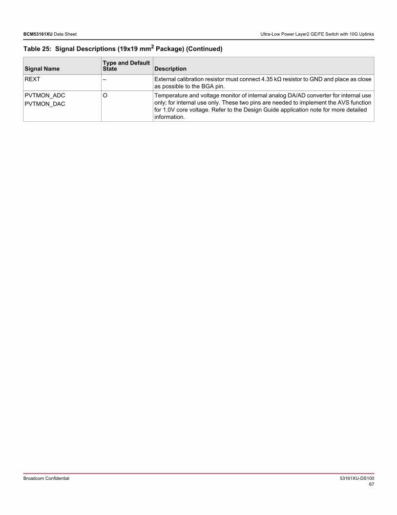
Broadcom Confidential 53161XU-DS10067
BCM53161XU Data Sheet Ultra-Low Power Layer2 GE/FE Switch with 10G Uplinks
REXT – External calibration resistor must connect 4.35 kΩ resistor to GND and place as close as possible to the BGA pin.
PVTMON_ADC
PVTMON_DAC
O Temperature and voltage monitor of internal analog DA/AD converter for internal use only; for internal use only. These two pins are needed to implement the AVS function for 1.0V core voltage. Refer to the Design Guide application note for more detailed information.
Table 25: Signal Descriptions (19x19 mm2 Package) (Continued)
Signal NameType and Default State Description
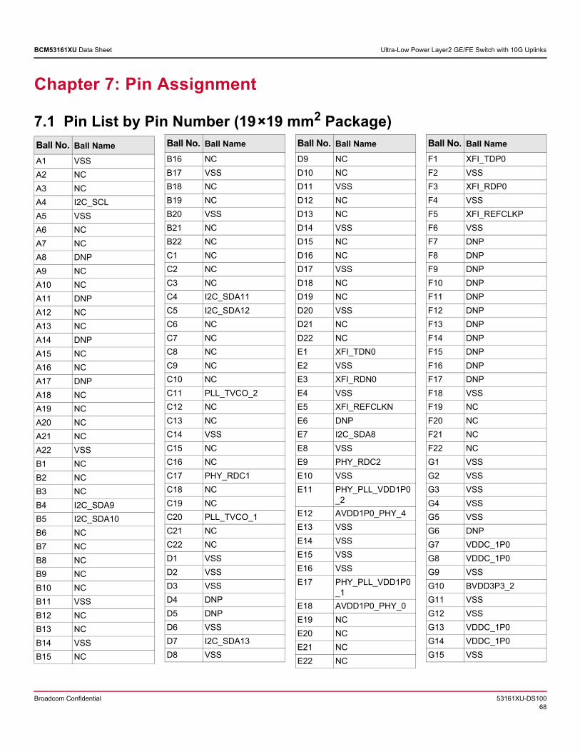
Broadcom Confidential 53161XU-DS10068
BCM53161XU Data Sheet Ultra-Low Power Layer2 GE/FE Switch with 10G Uplinks
Chapter 7: Pin Assignment
7.1 Pin List by Pin Number (19×19 mm2 Package)
Ball No. Ball Name
A1 VSS
A2 NC
A3 NC
A4 I2C_SCL
A5 VSS
A6 NC
A7 NC
A8 DNP
A9 NC
A10 NC
A11 DNP
A12 NC
A13 NC
A14 DNP
A15 NC
A16 NC
A17 DNP
A18 NC
A19 NC
A20 NC
A21 NC
A22 VSS
B1 NC
B2 NC
B3 NC
B4 I2C_SDA9
B5 I2C_SDA10
B6 NC
B7 NC
B8 NC
B9 NC
B10 NC
B11 VSS
B12 NC
B13 NC
B14 VSS
B15 NC
B16 NC
B17 VSS
B18 NC
B19 NC
B20 VSS
B21 NC
B22 NC
C1 NC
C2 NC
C3 NC
C4 I2C_SDA11
C5 I2C_SDA12
C6 NC
C7 NC
C8 NC
C9 NC
C10 NC
C11 PLL_TVCO_2
C12 NC
C13 NC
C14 VSS
C15 NC
C16 NC
C17 PHY_RDC1
C18 NC
C19 NC
C20 PLL_TVCO_1
C21 NC
C22 NC
D1 VSS
D2 VSS
D3 VSS
D4 DNP
D5 DNP
D6 VSS
D7 I2C_SDA13
D8 VSS
Ball No. Ball Name
D9 NC
D10 NC
D11 VSS
D12 NC
D13 NC
D14 VSS
D15 NC
D16 NC
D17 VSS
D18 NC
D19 NC
D20 VSS
D21 NC
D22 NC
E1 XFI_TDN0
E2 VSS
E3 XFI_RDN0
E4 VSS
E5 XFI_REFCLKN
E6 DNP
E7 I2C_SDA8
E8 VSS
E9 PHY_RDC2
E10 VSS
E11 PHY_PLL_VDD1P0_2
E12 AVDD1P0_PHY_4
E13 VSS
E14 VSS
E15 VSS
E16 VSS
E17 PHY_PLL_VDD1P0_1
E18 AVDD1P0_PHY_0
E19 NC
E20 NC
E21 NC
E22 NC
Ball No. Ball Name
F1 XFI_TDP0
F2 VSS
F3 XFI_RDP0
F4 VSS
F5 XFI_REFCLKP
F6 VSS
F7 DNP
F8 DNP
F9 DNP
F10 DNP
F11 DNP
F12 DNP
F13 DNP
F14 DNP
F15 DNP
F16 DNP
F17 DNP
F18 VSS
F19 NC
F20 NC
F21 NC
F22 NC
G1 VSS
G2 VSS
G3 VSS
G4 VSS
G5 VSS
G6 DNP
G7 VDDC_1P0
G8 VDDC_1P0
G9 VSS
G10 BVDD3P3_2
G11 VSS
G12 VSS
G13 VDDC_1P0
G14 VDDC_1P0
G15 VSS
Ball No. Ball Name
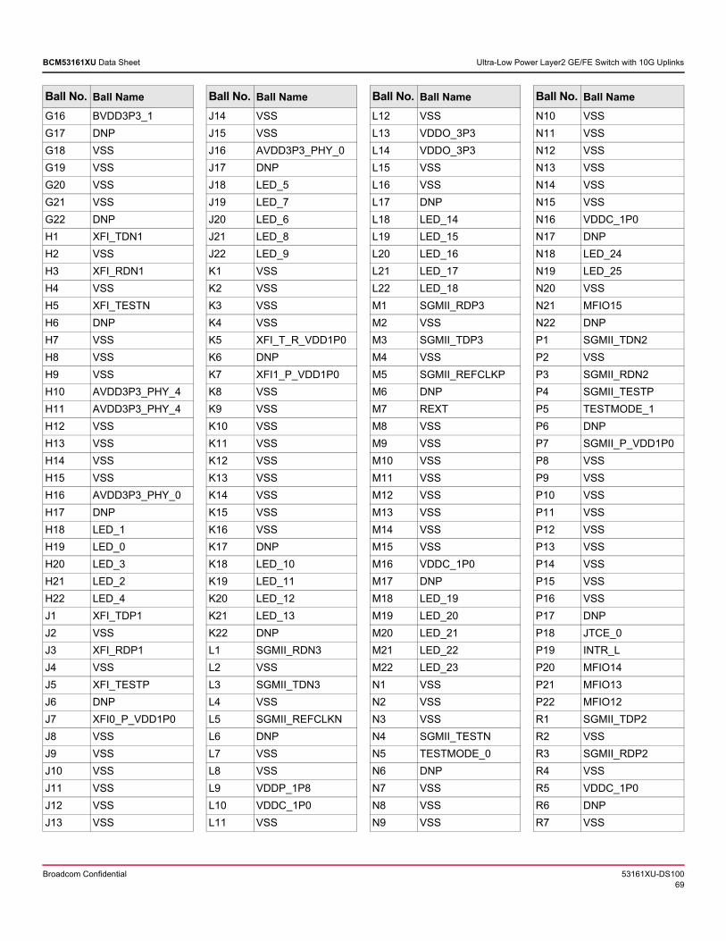
Broadcom Confidential 53161XU-DS10069
BCM53161XU Data Sheet Ultra-Low Power Layer2 GE/FE Switch with 10G Uplinks
G16 BVDD3P3_1
G17 DNP
G18 VSS
G19 VSS
G20 VSS
G21 VSS
G22 DNP
H1 XFI_TDN1
H2 VSS
H3 XFI_RDN1
H4 VSS
H5 XFI_TESTN
H6 DNP
H7 VSS
H8 VSS
H9 VSS
H10 AVDD3P3_PHY_4
H11 AVDD3P3_PHY_4
H12 VSS
H13 VSS
H14 VSS
H15 VSS
H16 AVDD3P3_PHY_0
H17 DNP
H18 LED_1
H19 LED_0
H20 LED_3
H21 LED_2
H22 LED_4
J1 XFI_TDP1
J2 VSS
J3 XFI_RDP1
J4 VSS
J5 XFI_TESTP
J6 DNP
J7 XFI0_P_VDD1P0
J8 VSS
J9 VSS
J10 VSS
J11 VSS
J12 VSS
J13 VSS
Ball No. Ball Name
J14 VSS
J15 VSS
J16 AVDD3P3_PHY_0
J17 DNP
J18 LED_5
J19 LED_7
J20 LED_6
J21 LED_8
J22 LED_9
K1 VSS
K2 VSS
K3 VSS
K4 VSS
K5 XFI_T_R_VDD1P0
K6 DNP
K7 XFI1_P_VDD1P0
K8 VSS
K9 VSS
K10 VSS
K11 VSS
K12 VSS
K13 VSS
K14 VSS
K15 VSS
K16 VSS
K17 DNP
K18 LED_10
K19 LED_11
K20 LED_12
K21 LED_13
K22 DNP
L1 SGMII_RDN3
L2 VSS
L3 SGMII_TDN3
L4 VSS
L5 SGMII_REFCLKN
L6 DNP
L7 VSS
L8 VSS
L9 VDDP_1P8
L10 VDDC_1P0
L11 VSS
Ball No. Ball Name
L12 VSS
L13 VDDO_3P3
L14 VDDO_3P3
L15 VSS
L16 VSS
L17 DNP
L18 LED_14
L19 LED_15
L20 LED_16
L21 LED_17
L22 LED_18
M1 SGMII_RDP3
M2 VSS
M3 SGMII_TDP3
M4 VSS
M5 SGMII_REFCLKP
M6 DNP
M7 REXT
M8 VSS
M9 VSS
M10 VSS
M11 VSS
M12 VSS
M13 VSS
M14 VSS
M15 VSS
M16 VDDC_1P0
M17 DNP
M18 LED_19
M19 LED_20
M20 LED_21
M21 LED_22
M22 LED_23
N1 VSS
N2 VSS
N3 VSS
N4 SGMII_TESTN
N5 TESTMODE_0
N6 DNP
N7 VSS
N8 VSS
N9 VSS
Ball No. Ball Name
N10 VSS
N11 VSS
N12 VSS
N13 VSS
N14 VSS
N15 VSS
N16 VDDC_1P0
N17 DNP
N18 LED_24
N19 LED_25
N20 VSS
N21 MFIO15
N22 DNP
P1 SGMII_TDN2
P2 VSS
P3 SGMII_RDN2
P4 SGMII_TESTP
P5 TESTMODE_1
P6 DNP
P7 SGMII_P_VDD1P0
P8 VSS
P9 VSS
P10 VSS
P11 VSS
P12 VSS
P13 VSS
P14 VSS
P15 VSS
P16 VSS
P17 DNP
P18 JTCE_0
P19 INTR_L
P20 MFIO14
P21 MFIO13
P22 MFIO12
R1 SGMII_TDP2
R2 VSS
R3 SGMII_RDP2
R4 VSS
R5 VDDC_1P0
R6 DNP
R7 VSS
Ball No. Ball Name
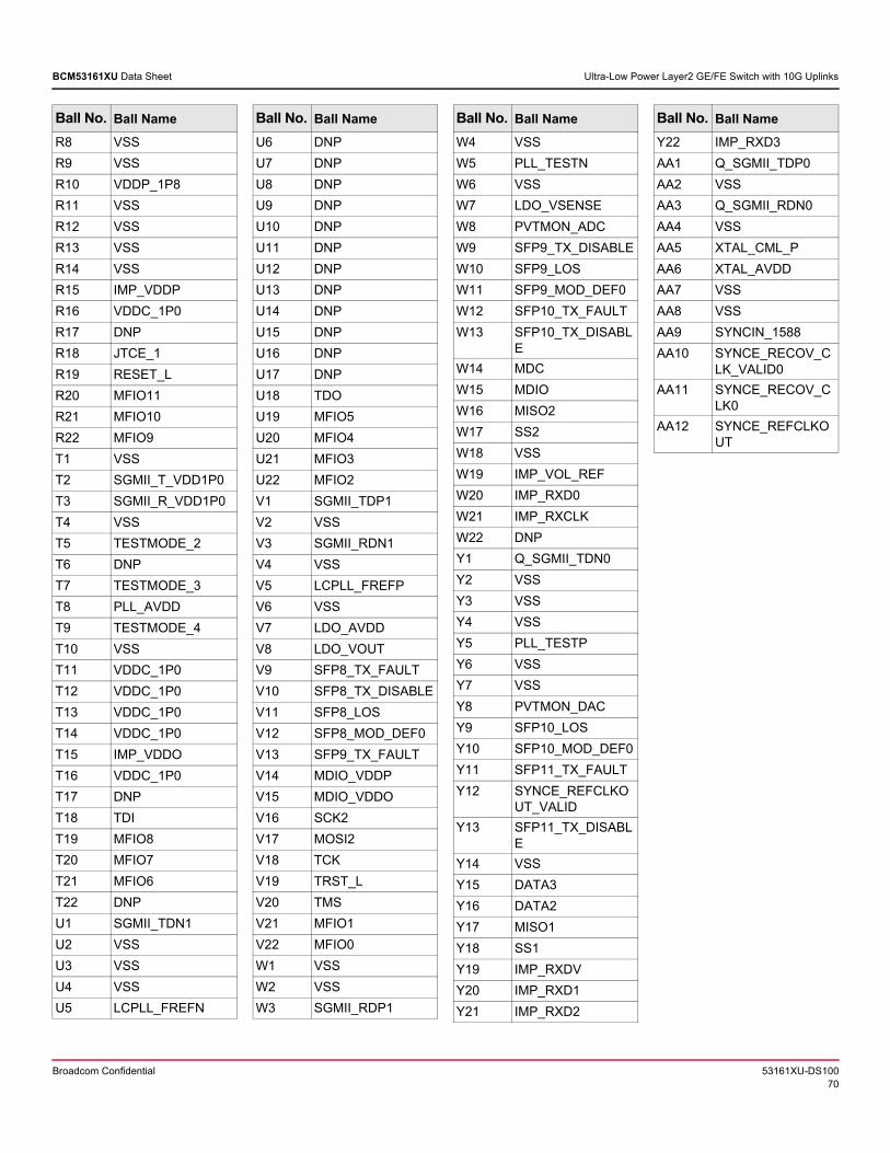
Broadcom Confidential 53161XU-DS10070
BCM53161XU Data Sheet Ultra-Low Power Layer2 GE/FE Switch with 10G Uplinks
R8 VSS
R9 VSS
R10 VDDP_1P8
R11 VSS
R12 VSS
R13 VSS
R14 VSS
R15 IMP_VDDP
R16 VDDC_1P0
R17 DNP
R18 JTCE_1
R19 RESET_L
R20 MFIO11
R21 MFIO10
R22 MFIO9
T1 VSS
T2 SGMII_T_VDD1P0
T3 SGMII_R_VDD1P0
T4 VSS
T5 TESTMODE_2
T6 DNP
T7 TESTMODE_3
T8 PLL_AVDD
T9 TESTMODE_4
T10 VSS
T11 VDDC_1P0
T12 VDDC_1P0
T13 VDDC_1P0
T14 VDDC_1P0
T15 IMP_VDDO
T16 VDDC_1P0
T17 DNP
T18 TDI
T19 MFIO8
T20 MFIO7
T21 MFIO6
T22 DNP
U1 SGMII_TDN1
U2 VSS
U3 VSS
U4 VSS
U5 LCPLL_FREFN
Ball No. Ball Name
U6 DNP
U7 DNP
U8 DNP
U9 DNP
U10 DNP
U11 DNP
U12 DNP
U13 DNP
U14 DNP
U15 DNP
U16 DNP
U17 DNP
U18 TDO
U19 MFIO5
U20 MFIO4
U21 MFIO3
U22 MFIO2
V1 SGMII_TDP1
V2 VSS
V3 SGMII_RDN1
V4 VSS
V5 LCPLL_FREFP
V6 VSS
V7 LDO_AVDD
V8 LDO_VOUT
V9 SFP8_TX_FAULT
V10 SFP8_TX_DISABLE
V11 SFP8_LOS
V12 SFP8_MOD_DEF0
V13 SFP9_TX_FAULT
V14 MDIO_VDDP
V15 MDIO_VDDO
V16 SCK2
V17 MOSI2
V18 TCK
V19 TRST_L
V20 TMS
V21 MFIO1
V22 MFIO0
W1 VSS
W2 VSS
W3 SGMII_RDP1
Ball No. Ball Name
W4 VSS
W5 PLL_TESTN
W6 VSS
W7 LDO_VSENSE
W8 PVTMON_ADC
W9 SFP9_TX_DISABLE
W10 SFP9_LOS
W11 SFP9_MOD_DEF0
W12 SFP10_TX_FAULT
W13 SFP10_TX_DISABLE
W14 MDC
W15 MDIO
W16 MISO2
W17 SS2
W18 VSS
W19 IMP_VOL_REF
W20 IMP_RXD0
W21 IMP_RXCLK
W22 DNP
Y1 Q_SGMII_TDN0
Y2 VSS
Y3 VSS
Y4 VSS
Y5 PLL_TESTP
Y6 VSS
Y7 VSS
Y8 PVTMON_DAC
Y9 SFP10_LOS
Y10 SFP10_MOD_DEF0
Y11 SFP11_TX_FAULT
Y12 SYNCE_REFCLKOUT_VALID
Y13 SFP11_TX_DISABLE
Y14 VSS
Y15 DATA3
Y16 DATA2
Y17 MISO1
Y18 SS1
Y19 IMP_RXDV
Y20 IMP_RXD1
Y21 IMP_RXD2
Ball No. Ball Name
Y22 IMP_RXD3
AA1 Q_SGMII_TDP0
AA2 VSS
AA3 Q_SGMII_RDN0
AA4 VSS
AA5 XTAL_CML_P
AA6 XTAL_AVDD
AA7 VSS
AA8 VSS
AA9 SYNCIN_1588
AA10 SYNCE_RECOV_CLK_VALID0
AA11 SYNCE_RECOV_CLK0
AA12 SYNCE_REFCLKOUT
Ball No. Ball Name
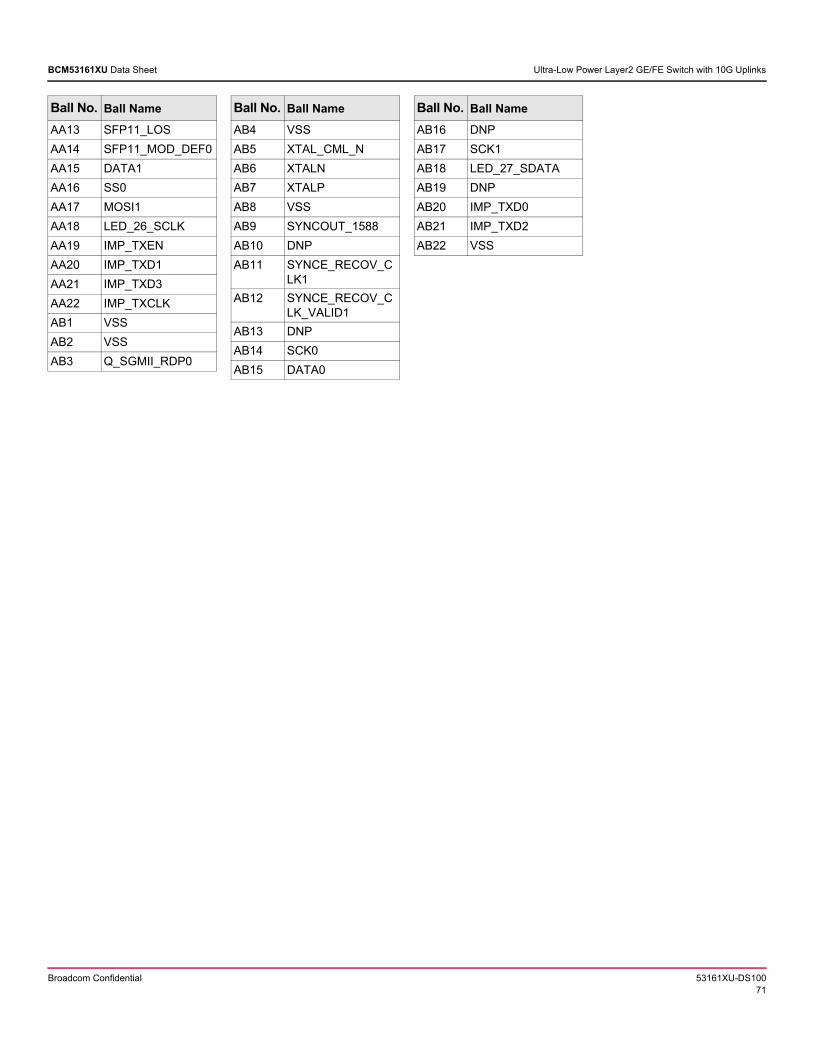
Broadcom Confidential 53161XU-DS10071
BCM53161XU Data Sheet Ultra-Low Power Layer2 GE/FE Switch with 10G Uplinks
AA13 SFP11_LOS
AA14 SFP11_MOD_DEF0
AA15 DATA1
AA16 SS0
AA17 MOSI1
AA18 LED_26_SCLK
AA19 IMP_TXEN
AA20 IMP_TXD1
AA21 IMP_TXD3
AA22 IMP_TXCLK
AB1 VSS
AB2 VSS
AB3 Q_SGMII_RDP0
Ball No. Ball Name
AB4 VSS
AB5 XTAL_CML_N
AB6 XTALN
AB7 XTALP
AB8 VSS
AB9 SYNCOUT_1588
AB10 DNP
AB11 SYNCE_RECOV_CLK1
AB12 SYNCE_RECOV_CLK_VALID1
AB13 DNP
AB14 SCK0
AB15 DATA0
Ball No. Ball Name
AB16 DNP
AB17 SCK1
AB18 LED_27_SDATA
AB19 DNP
AB20 IMP_TXD0
AB21 IMP_TXD2
AB22 VSS
Ball No. Ball Name
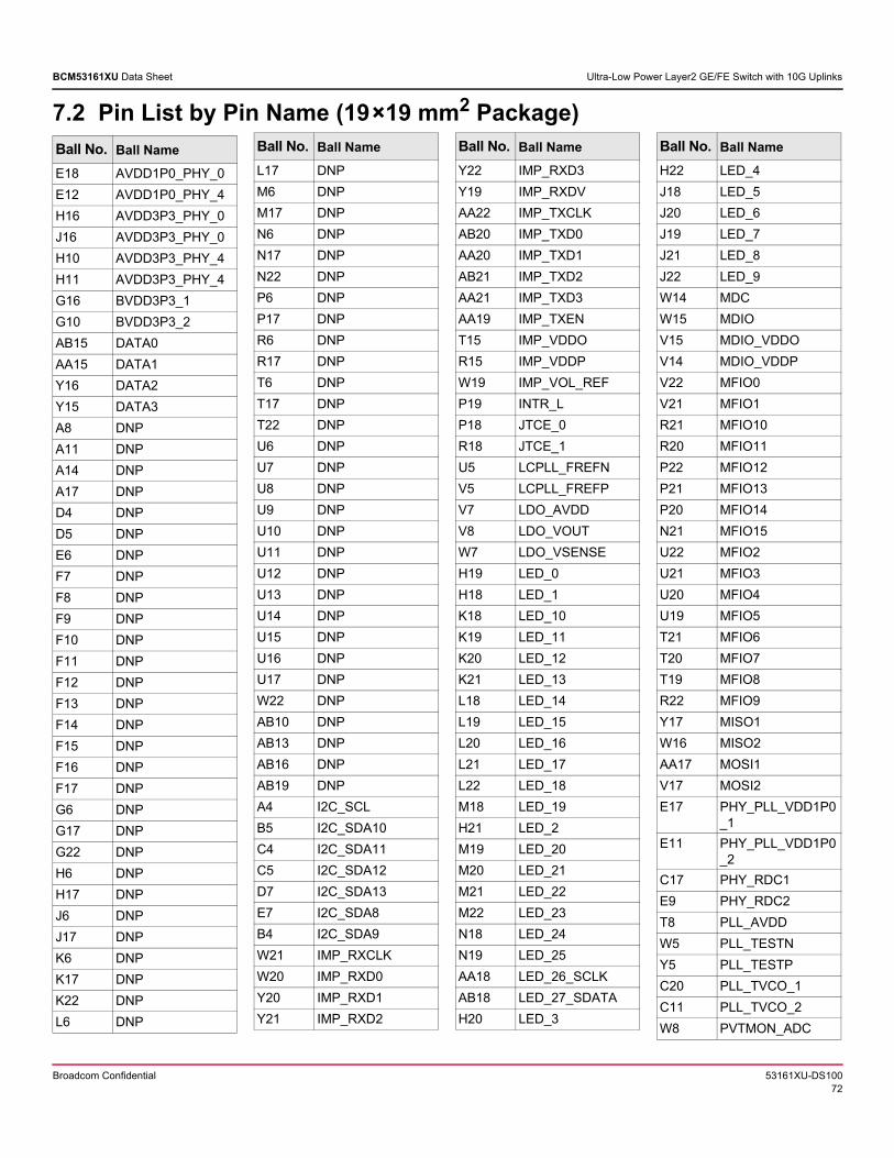
Broadcom Confidential 53161XU-DS10072
BCM53161XU Data Sheet Ultra-Low Power Layer2 GE/FE Switch with 10G Uplinks
7.2 Pin List by Pin Name (19×19 mm2 Package)
Ball No. Ball Name
E18 AVDD1P0_PHY_0
E12 AVDD1P0_PHY_4
H16 AVDD3P3_PHY_0
J16 AVDD3P3_PHY_0
H10 AVDD3P3_PHY_4
H11 AVDD3P3_PHY_4
G16 BVDD3P3_1
G10 BVDD3P3_2
AB15 DATA0
AA15 DATA1
Y16 DATA2
Y15 DATA3
A8 DNP
A11 DNP
A14 DNP
A17 DNP
D4 DNP
D5 DNP
E6 DNP
F7 DNP
F8 DNP
F9 DNP
F10 DNP
F11 DNP
F12 DNP
F13 DNP
F14 DNP
F15 DNP
F16 DNP
F17 DNP
G6 DNP
G17 DNP
G22 DNP
H6 DNP
H17 DNP
J6 DNP
J17 DNP
K6 DNP
K17 DNP
K22 DNP
L6 DNP
L17 DNP
M6 DNP
M17 DNP
N6 DNP
N17 DNP
N22 DNP
P6 DNP
P17 DNP
R6 DNP
R17 DNP
T6 DNP
T17 DNP
T22 DNP
U6 DNP
U7 DNP
U8 DNP
U9 DNP
U10 DNP
U11 DNP
U12 DNP
U13 DNP
U14 DNP
U15 DNP
U16 DNP
U17 DNP
W22 DNP
AB10 DNP
AB13 DNP
AB16 DNP
AB19 DNP
A4 I2C_SCL
B5 I2C_SDA10
C4 I2C_SDA11
C5 I2C_SDA12
D7 I2C_SDA13
E7 I2C_SDA8
B4 I2C_SDA9
W21 IMP_RXCLK
W20 IMP_RXD0
Y20 IMP_RXD1
Y21 IMP_RXD2
Ball No. Ball Name
Y22 IMP_RXD3
Y19 IMP_RXDV
AA22 IMP_TXCLK
AB20 IMP_TXD0
AA20 IMP_TXD1
AB21 IMP_TXD2
AA21 IMP_TXD3
AA19 IMP_TXEN
T15 IMP_VDDO
R15 IMP_VDDP
W19 IMP_VOL_REF
P19 INTR_L
P18 JTCE_0
R18 JTCE_1
U5 LCPLL_FREFN
V5 LCPLL_FREFP
V7 LDO_AVDD
V8 LDO_VOUT
W7 LDO_VSENSE
H19 LED_0
H18 LED_1
K18 LED_10
K19 LED_11
K20 LED_12
K21 LED_13
L18 LED_14
L19 LED_15
L20 LED_16
L21 LED_17
L22 LED_18
M18 LED_19
H21 LED_2
M19 LED_20
M20 LED_21
M21 LED_22
M22 LED_23
N18 LED_24
N19 LED_25
AA18 LED_26_SCLK
AB18 LED_27_SDATA
H20 LED_3
Ball No. Ball Name
H22 LED_4
J18 LED_5
J20 LED_6
J19 LED_7
J21 LED_8
J22 LED_9
W14 MDC
W15 MDIO
V15 MDIO_VDDO
V14 MDIO_VDDP
V22 MFIO0
V21 MFIO1
R21 MFIO10
R20 MFIO11
P22 MFIO12
P21 MFIO13
P20 MFIO14
N21 MFIO15
U22 MFIO2
U21 MFIO3
U20 MFIO4
U19 MFIO5
T21 MFIO6
T20 MFIO7
T19 MFIO8
R22 MFIO9
Y17 MISO1
W16 MISO2
AA17 MOSI1
V17 MOSI2
E17 PHY_PLL_VDD1P0_1
E11 PHY_PLL_VDD1P0_2
C17 PHY_RDC1
E9 PHY_RDC2
T8 PLL_AVDD
W5 PLL_TESTN
Y5 PLL_TESTP
C20 PLL_TVCO_1
C11 PLL_TVCO_2
W8 PVTMON_ADC
Ball No. Ball Name
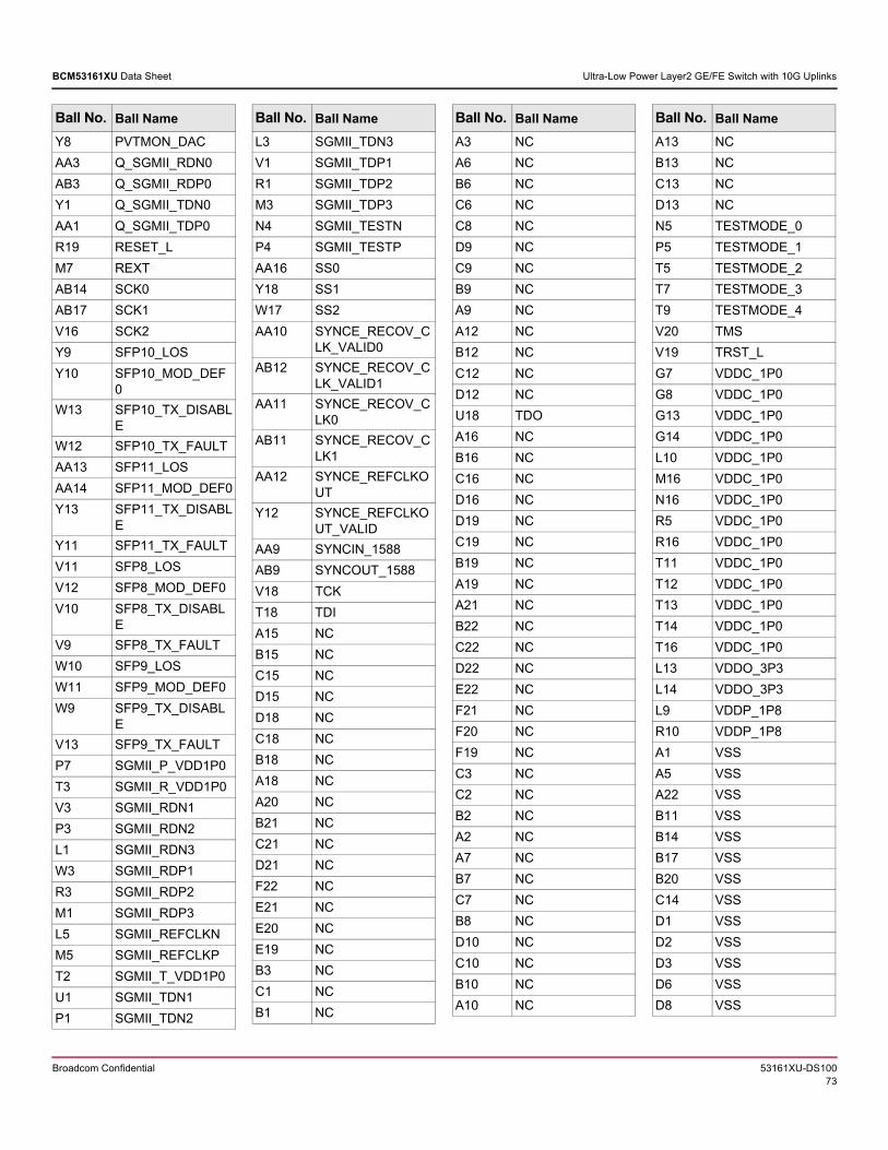
Broadcom Confidential 53161XU-DS10073
BCM53161XU Data Sheet Ultra-Low Power Layer2 GE/FE Switch with 10G Uplinks
Y8 PVTMON_DAC
AA3 Q_SGMII_RDN0
AB3 Q_SGMII_RDP0
Y1 Q_SGMII_TDN0
AA1 Q_SGMII_TDP0
R19 RESET_L
M7 REXT
AB14 SCK0
AB17 SCK1
V16 SCK2
Y9 SFP10_LOS
Y10 SFP10_MOD_DEF0
W13 SFP10_TX_DISABLE
W12 SFP10_TX_FAULT
AA13 SFP11_LOS
AA14 SFP11_MOD_DEF0
Y13 SFP11_TX_DISABLE
Y11 SFP11_TX_FAULT
V11 SFP8_LOS
V12 SFP8_MOD_DEF0
V10 SFP8_TX_DISABLE
V9 SFP8_TX_FAULT
W10 SFP9_LOS
W11 SFP9_MOD_DEF0
W9 SFP9_TX_DISABLE
V13 SFP9_TX_FAULT
P7 SGMII_P_VDD1P0
T3 SGMII_R_VDD1P0
V3 SGMII_RDN1
P3 SGMII_RDN2
L1 SGMII_RDN3
W3 SGMII_RDP1
R3 SGMII_RDP2
M1 SGMII_RDP3
L5 SGMII_REFCLKN
M5 SGMII_REFCLKP
T2 SGMII_T_VDD1P0
U1 SGMII_TDN1
P1 SGMII_TDN2
Ball No. Ball Name
L3 SGMII_TDN3
V1 SGMII_TDP1
R1 SGMII_TDP2
M3 SGMII_TDP3
N4 SGMII_TESTN
P4 SGMII_TESTP
AA16 SS0
Y18 SS1
W17 SS2
AA10 SYNCE_RECOV_CLK_VALID0
AB12 SYNCE_RECOV_CLK_VALID1
AA11 SYNCE_RECOV_CLK0
AB11 SYNCE_RECOV_CLK1
AA12 SYNCE_REFCLKOUT
Y12 SYNCE_REFCLKOUT_VALID
AA9 SYNCIN_1588
AB9 SYNCOUT_1588
V18 TCK
T18 TDI
A15 NC
B15 NC
C15 NC
D15 NC
D18 NC
C18 NC
B18 NC
A18 NC
A20 NC
B21 NC
C21 NC
D21 NC
F22 NC
E21 NC
E20 NC
E19 NC
B3 NC
C1 NC
B1 NC
Ball No. Ball Name
A3 NC
A6 NC
B6 NC
C6 NC
C8 NC
D9 NC
C9 NC
B9 NC
A9 NC
A12 NC
B12 NC
C12 NC
D12 NC
U18 TDO
A16 NC
B16 NC
C16 NC
D16 NC
D19 NC
C19 NC
B19 NC
A19 NC
A21 NC
B22 NC
C22 NC
D22 NC
E22 NC
F21 NC
F20 NC
F19 NC
C3 NC
C2 NC
B2 NC
A2 NC
A7 NC
B7 NC
C7 NC
B8 NC
D10 NC
C10 NC
B10 NC
A10 NC
Ball No. Ball Name
A13 NC
B13 NC
C13 NC
D13 NC
N5 TESTMODE_0
P5 TESTMODE_1
T5 TESTMODE_2
T7 TESTMODE_3
T9 TESTMODE_4
V20 TMS
V19 TRST_L
G7 VDDC_1P0
G8 VDDC_1P0
G13 VDDC_1P0
G14 VDDC_1P0
L10 VDDC_1P0
M16 VDDC_1P0
N16 VDDC_1P0
R5 VDDC_1P0
R16 VDDC_1P0
T11 VDDC_1P0
T12 VDDC_1P0
T13 VDDC_1P0
T14 VDDC_1P0
T16 VDDC_1P0
L13 VDDO_3P3
L14 VDDO_3P3
L9 VDDP_1P8
R10 VDDP_1P8
A1 VSS
A5 VSS
A22 VSS
B11 VSS
B14 VSS
B17 VSS
B20 VSS
C14 VSS
D1 VSS
D2 VSS
D3 VSS
D6 VSS
D8 VSS
Ball No. Ball Name
Broadcom Confidential 53161XU-DS10074
BCM53161XU Data Sheet Ultra-Low Power Layer2 GE/FE Switch with 10G Uplinks
D11 VSS
D14 VSS
D17 VSS
D20 VSS
E2 VSS
E4 VSS
E8 VSS
E10 VSS
E13 VSS
E14 VSS
E15 VSS
E16 VSS
F2 VSS
F4 VSS
F6 VSS
F18 VSS
G1 VSS
G2 VSS
G3 VSS
G4 VSS
G5 VSS
G9 VSS
G11 VSS
G12 VSS
G15 VSS
G18 VSS
G19 VSS
G20 VSS
G21 VSS
H2 VSS
H4 VSS
H7 VSS
H8 VSS
H9 VSS
H12 VSS
H13 VSS
H14 VSS
H15 VSS
J2 VSS
J4 VSS
J8 VSS
J9 VSS
Ball No. Ball Name
J10 VSS
J11 VSS
J12 VSS
J13 VSS
J14 VSS
J15 VSS
K1 VSS
K2 VSS
K3 VSS
K4 VSS
K8 VSS
K9 VSS
K10 VSS
K11 VSS
K12 VSS
K13 VSS
K14 VSS
K15 VSS
K16 VSS
L2 VSS
L4 VSS
L7 VSS
L8 VSS
L11 VSS
L12 VSS
L15 VSS
L16 VSS
M2 VSS
M4 VSS
M8 VSS
M9 VSS
M10 VSS
M11 VSS
M12 VSS
M13 VSS
M14 VSS
M15 VSS
N1 VSS
N2 VSS
Ball No. Ball Name
N3 VSS
N7 VSS
N8 VSS
N9 VSS
N10 VSS
N11 VSS
N12 VSS
N13 VSS
N14 VSS
N15 VSS
N20 VSS
P2 VSS
P8 VSS
P9 VSS
P10 VSS
P11 VSS
P12 VSS
P13 VSS
P14 VSS
P15 VSS
P16 VSS
R2 VSS
R4 VSS
R7 VSS
R8 VSS
R9 VSS
Ball No. Ball Name
R11 VSS
R12 VSS
R13 VSS
R14 VSS
T1 VSS
T4 VSS
T10 VSS
U2 VSS
U3 VSS
U4 VSS
V2 VSS
V4 VSS
V6 VSS
W1 VSS
W2 VSS
W4 VSS
W6 VSS
W18 VSS
Y2 VSS
Y3 VSS
Y4 VSS
Y6 VSS
Y7 VSS
Y14 VSS
AA2 VSS
AA4 VSS
Ball No. Ball Name
Broadcom Confidential 53161XU-DS10075
BCM53161XU Data Sheet Ultra-Low Power Layer2 GE/FE Switch with 10G Uplinks
AA7 VSS
AA8 VSS
AB1 VSS
AB2 VSS
AB4 VSS
AB8 VSS
AB22 VSS
E3 XFI_RDN0
H3 XFI_RDN1
F3 XFI_RDP0
J3 XFI_RDP1
E5 XFI_REFCLKN
F5 XFI_REFCLKP
K5 XFI_T_R_VDD1P0
E1 XFI_TDN0
H1 XFI_TDN1
F1 XFI_TDP0
J1 XFI_TDP1
H5 XFI_TESTN
J5 XFI_TESTP
J7 XFI0_P_VDD1P0
K7 XFI1_P_VDD1P0
AA6 XTAL_AVDD
AB5 XTAL_CML_N
AA5 XTAL_CML_P
AB6 XTALN
AB7 XTALP
Ball No. Ball Name
Broadcom Confidential 53161XU-DS10076
BCM53161XU Data Sheet Ultra-Low Power Layer2 GE/FE Switch with 10G Uplinks
7.3 Ball Map (19×19 mm2 Package)
Figure 20: Ball Map (19×19 mm2 Package)
1 2 3 4 5 6 7 8 9 10 11 12 13 14 15 16 17 18 19 20 21 22
A VSS NC I2C_SCL VSS DNP DNP DNP DNP VSS A
BI2C_SDA
9
I2C_SDA
10VSS VSS VSS VSS B
CI2C_SDA
11
I2C_SDA
12
PLL_TVC
O_2VSS
PHY_RD
C1
PLL_TVC
O_1C
D VSS VSS VSS DNP DNP VSSI2C_SDA
13VSS VSS VSS VSS VSS D
EXFI_TDN
0VSS
XFI_RDN
0VSS
XFI_REF
CLKNDNP
I2C_SDA
8VSS
PHY_RD
C2VSS
PHY_PLL
_VDD1P0
_2
AVDD1P0
_PHY_4VSS VSS VSS VSS
PHY_PLL
_VDD1P0
_1
AVDD1P0
_PHY_0E
F XFI_TDP0 VSSXFI_RDP
0VSS
XFI_REF
CLKPVSS DNP DNP DNP DNP DNP DNP DNP DNP DNP DNP DNP VSS F
G VSS VSS VSS VSS VSS DNPVDDC_1P
0
VDDC_1P
0VSS
BVDD3P3
_2VSS VSS
VDDC_1P
0
VDDC_1P
0VSS
BVDD3P3
_1DNP VSS VSS VSS VSS DNP G
HXFI_TDN
1VSS
XFI_RDN
1VSS
XFI_TEST
NDNP VSS VSS VSS
AVDD3P3
_PHY_4
AVDD3P3
_PHY_4VSS VSS VSS VSS
AVDD3P3
_PHY_0DNP LED_1 LED_0 LED_3 LED_2 LED_4 H
J XFI_TDP1 VSSXFI_RDP
1VSS
XFI_TEST
PDNP
XFI0_P_V
DD1P0VSS VSS VSS VSS VSS VSS VSS VSS
AVDD3P3
_PHY_0DNP LED_5 LED_7 LED_6 LED_8 LED_9 J
K VSS VSS VSS VSSXFI_T_R_
VDD1P0DNP
XFI1_P_V
DD1P0VSS VSS VSS VSS VSS VSS VSS VSS VSS DNP LED_10 LED_11 LED_12 LED_13 DNP K
LSGMII_R
DN3VSS
SGMII_TD
N3VSS
SGMII_R
EFCLKNDNP VSS VSS
VDDP_1P
8
VDDC_1P
0VSS VSS
VDDO_3
P3
VDDO_3
P3VSS VSS DNP LED_14 LED_15 LED_16 LED_17 LED_18 L
MSGMII_R
DP3VSS
SGMII_TD
P3VSS
SGMII_R
EFCLKPDNP REXT VSS VSS VSS VSS VSS VSS VSS VSS
VDDC_1P
0DNP LED_19 LED_20 LED_21 LED_22 LED_23 M
N VSS VSS VSSSGMII_TE
STN
TESTMO
DE_0DNP VSS VSS VSS VSS VSS VSS VSS VSS VSS
VDDC_1P
0DNP LED_24 LED_25 VSS MFIO15 DNP N
PSGMII_TD
N2VSS
SGMII_R
DN2
SGMII_TE
STP
TESTMO
DE_1DNP
SGMII_P_
VDD1P0VSS VSS VSS VSS VSS VSS VSS VSS VSS DNP JTCE_0 INTR_L MFIO14 MFIO13 MFIO12 P
RSGMII_TD
P2VSS
SGMII_R
DP2VSS
VDDC_1P
0DNP VSS VSS VSS
VDDP_1P
8VSS VSS VSS VSS
IMP_VDD
P
VDDC_1P
0DNP JTCE_1 RESET_L MFIO11 MFIO10 MFIO9 R
T VSSSGMII_T_
VDD1P0
SGMII_R_
VDD1P0VSS
TESTMO
DE_2DNP
TESTMO
DE_3
PLL_AVD
D
TESTMO
DE_4VSS
VDDC_1P
0
VDDC_1P
0
VDDC_1P
0
VDDC_1P
0
IMP_VDD
O
VDDC_1P
0DNP TDI MFIO8 MFIO7 MFIO6 DNP T
USGMII_TD
N1VSS VSS VSS
LCPLL_F
REFNDNP DNP DNP DNP DNP DNP DNP DNP DNP DNP DNP DNP TDO MFIO5 MFIO4 MFIO3 MFIO2 U
VSGMII_TD
P1VSS
SGMII_R
DN1VSS
LCPLL_F
REFPVSS
LDO_AV
DD
LDO_VO
UT
SFP8_TX
_FAULT
SFP8_TX
_DISABL
E
SFP8_LO
S
SFP8_MO
D_DEF0
SFP9_TX
_FAULT
MDIO_VD
DP
MDIO_VD
DOSCK2 MOSI2 TCK TRST_L TMS MFIO1 MFIO0 V
W VSS VSSSGMII_R
DP1VSS
PLL_TES
TNVSS
LDO_VS
ENSE
PVTMON
_ADC
SFP9_TX
_DISABL
E
SFP9_LO
S
SFP9_MO
D_DEF0
SFP10_T
X_FAULT
SFP10_T
X_DISAB
LE
MDC MDIO MISO2 SS2 VSSIMP_VOL
_REF
IMP_RXD
0
IMP_RXC
LKDNP W
YQ_SGMII_
TDN0VSS VSS VSS
PLL_TES
TPVSS VSS
PVTMON
_DAC
SFP10_L
OS
SFP10_M
OD_DEF0
SFP11_T
X_FAULT
SYNCE_
REFCLK
OUT_VAL
ID
SFP11_T
X_DISAB
LE
VSS DATA3 DATA2 MISO1 SS1IMP_RXD
V
IMP_RXD
1
IMP_RXD
2
IMP_RXD
3Y
AAQ_SGMII_
TDP0VSS
Q_SGMII_
RDN0VSS
XTAL_CM
L_P
XTAL_AV
DDVSS VSS
SYNCIN_
1588
SYNCE_
RECOV_
CLK_VAL
ID0
SYNCE_
RECOV_
CLK0
SYNCE_
REFCLK
OUT
SFP11_L
OS
SFP11_M
OD_DEF0DATA1 SS0 MOSI1
LED_26_
SCLK
IMP_TXE
N
IMP_TXD
1
IMP_TXD
3
IMP_TXC
LKAA
AB VSS VSSQ_SGMII_
RDP0VSS
XTAL_CM
L_NXTALN XTALP VSS
SYNCOU
T_1588DNP
SYNCE_
RECOV_
CLK1
SYNCE_
RECOV_
CLK_VAL
ID1
DNP SCK0 DATA0 DNP SCK1LED_27_
SDATADNP
IMP_TXD
0
IMP_TXD
2VSS AB
1 2 3 4 5 6 7 8 9 10 11 12 13 14 15 16 17 18 19 20 21 22
NC
NC
NC
NCNC
NCNC
NC NC
NC NC NC
NC NC NC
NC NC
NC
NC
NC
NC
NC NC
NC NC
NC NC
NC NC
NC NC
NC NC
NC
NC
NC NC NC
NCNC
NC
NC NC
NC
NC NC
NC
NC
NC
NC
NC NC
NC NC NC
NC NC
NC
NC
NC
NC
NC
NC
Broadcom Confidential 53161XU-DS10077
BCM53161XU Data Sheet Ultra-Low Power Layer2 GE/FE Switch with 10G Uplinks
Chapter 8: Electrical Characteristics
8.1 Absolute Maximum Ratings
Table 26: Absolute Maximum Ratingsa
a. These specifications indicate levels where permanent damage to the device may occur. Functional operation is not guaranteed under these conditions. Operation at maximum conditions for extended periods may adversely affect long-term reliability of the device.
Parameter Symbol Min. Max. Unit
3.3V Supply Voltage VDDO_3P3, AVDD3P3_PHY0, AVDD3P3_PHY1
AVDD3P3_PHY2, AVDD3P3_PHY3, BVDD3P3
LDO_AVDD, MDIO_VDDOb
b. MDC/MDIO for 3.3V/1.2V.
–0.5 +3.63 V
2.5V Supply Voltage RGMII_VDDOc
c. RGMII interface for 2.5V/1.5V.
–0.5 +2.75 V
1.5V Supply Voltage RGMII_VDDOc, RGMII_VDDPc –0.5 +1.65 V
1.8V Supply Voltage VDDP_1P8, OTP_VDD, AVDD_PVTMON,
PLL_VDD1P8, XTAL_VDD1P8, UPI_VDD18
UPI_VDD18_int
RGMII_VDDPc, MDIO_VDDPb
–0.5 +1.98 V
1.2V Supply Voltage DDR_VDDO, DDR_VDDO_CK
MDIO_VDDOb,MDIO_VDDPb
–0.5 +1.32 V
1.0V Supply Voltage VDDC_1P0, AVDD0P9_PHY0, AVDD0P9_PHY1
AVDD0P9_PHY2, AVDD0P9_PHY3,
PHYPLL_VDD0P9, QSGMII_P_R_VDD1P0
QSGMII_T_VDD1P0, XFI_P_R_VDD1P0
XFI_T_VDD1P0, RESCAL_pad_i_VDD1p0
–0.5 +1.1 V
Maximum Junction Temperature TJ_MAX – +110 °C
Commercial Ambient Temperature (Operating)
TA 0 +70 °C
Industrial Ambient Temperature (Operating)
TA –40 +85 °C
Operating Humidity – – +85 %
Storage Temperature TSTG –40 +125 °C
Storage Humidity – – 60 %
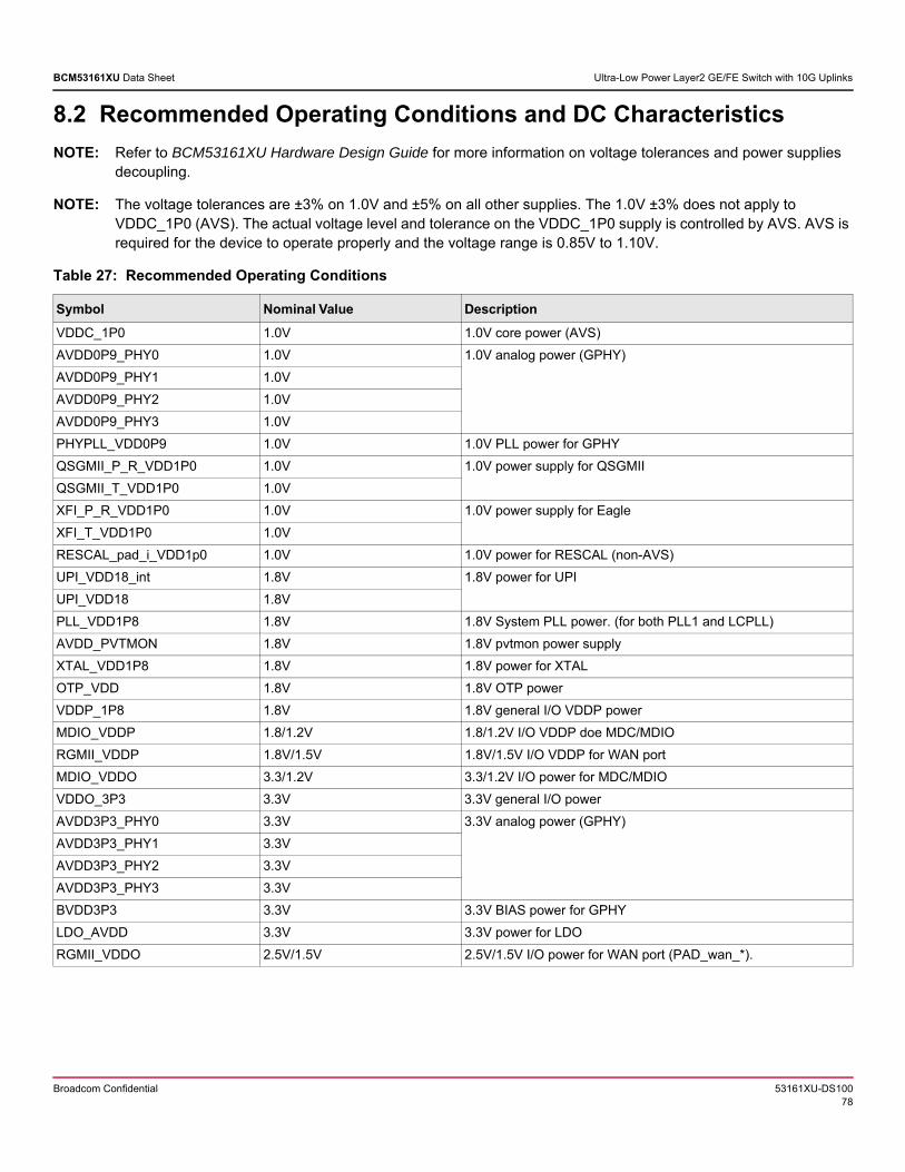
Broadcom Confidential 53161XU-DS10078
BCM53161XU Data Sheet Ultra-Low Power Layer2 GE/FE Switch with 10G Uplinks
8.2 Recommended Operating Conditions and DC Characteristics
NOTE: Refer to BCM53161XU Hardware Design Guide for more information on voltage tolerances and power supplies decoupling.
NOTE: The voltage tolerances are ±3% on 1.0V and ±5% on all other supplies. The 1.0V ±3% does not apply to VDDC_1P0 (AVS). The actual voltage level and tolerance on the VDDC_1P0 supply is controlled by AVS. AVS is required for the device to operate properly and the voltage range is 0.85V to 1.10V.
Table 27: Recommended Operating Conditions
Symbol Nominal Value Description
VDDC_1P0 1.0V 1.0V core power (AVS)
AVDD0P9_PHY0 1.0V 1.0V analog power (GPHY)
AVDD0P9_PHY1 1.0V
AVDD0P9_PHY2 1.0V
AVDD0P9_PHY3 1.0V
PHYPLL_VDD0P9 1.0V 1.0V PLL power for GPHY
QSGMII_P_R_VDD1P0 1.0V 1.0V power supply for QSGMII
QSGMII_T_VDD1P0 1.0V
XFI_P_R_VDD1P0 1.0V 1.0V power supply for Eagle
XFI_T_VDD1P0 1.0V
RESCAL_pad_i_VDD1p0 1.0V 1.0V power for RESCAL (non-AVS)
UPI_VDD18_int 1.8V 1.8V power for UPI
UPI_VDD18 1.8V
PLL_VDD1P8 1.8V 1.8V System PLL power. (for both PLL1 and LCPLL)
AVDD_PVTMON 1.8V 1.8V pvtmon power supply
XTAL_VDD1P8 1.8V 1.8V power for XTAL
OTP_VDD 1.8V 1.8V OTP power
VDDP_1P8 1.8V 1.8V general I/O VDDP power
MDIO_VDDP 1.8/1.2V 1.8/1.2V I/O VDDP doe MDC/MDIO
RGMII_VDDP 1.8V/1.5V 1.8V/1.5V I/O VDDP for WAN port
MDIO_VDDO 3.3/1.2V 3.3/1.2V I/O power for MDC/MDIO
VDDO_3P3 3.3V 3.3V general I/O power
AVDD3P3_PHY0 3.3V 3.3V analog power (GPHY)
AVDD3P3_PHY1 3.3V
AVDD3P3_PHY2 3.3V
AVDD3P3_PHY3 3.3V
BVDD3P3 3.3V 3.3V BIAS power for GPHY
LDO_AVDD 3.3V 3.3V power for LDO
RGMII_VDDO 2.5V/1.5V 2.5V/1.5V I/O power for WAN port (PAD_wan_*).
Broadcom Confidential 53161XU-DS10079
BCM53161XU Data Sheet Ultra-Low Power Layer2 GE/FE Switch with 10G Uplinks
8.2.1 Standard 3.3V Signals
These specifications apply to all 3.3V signals, such as Serial Flash, MII, MFIO, I2C, MDC/MDIO, SyncE pins, JTAG interfaces, and clock reset pins.
8.2.2 Standard 2.5V Signals
These specifications apply to all 2.5V signals, such as RGMII interface.
8.2.3 REFCLK Input Timing
Parameter Symbol Conditions Min. Typ. Max. Unit
Input voltage VIN – –0.3 – 3.63
Input low voltage VIL – – – 0.8 V
Input high voltage VIH – 2.0 – – V
Output low voltage VOL IOL = 4 mAa
a. For BCM5316X, increase IOL from 4 mA to 6 mA for VOL Max value to meet specifications at higher than 90°C ambient thermal conditions.
– – 0.4 V
Output low current IOL VOL = 0.4V 4.0 – – mA
Output high voltage VOH IOH = –4 mA 2.4 – – V
Parameter Symbol Conditions Min. Typ. Max. Unit
Input voltage VIN – –0.3 – 2.75
Input low voltage VIL – – – 0.8 V
Input high voltage VIH – 1.7 – – V
Output low voltage VOL – – – 0.4 V
Output high voltage VOH – 2.0 – – V
Table 28: REFCLK Input Timing
Parameter Symbol Min. Typ. Max. Unit
Frequency Cfreq – 25 – MHz
Accuracy – –15 – +15 ppm
RMS Jitter (noise bandwidth: 10 kHz – 5 MHz) – – 0.444 0.651 ps
RMS Jitter (noise bandwidth: 10 kHz – 1 MHz) – – 0.281 0.392 ps
ESR – – – 15 ohm
Frequency Cfreq – 156.25 – MHz
Accuracy – –50 – +50 ppm
RMS Jitter – – – 0.7 ps
Rise/Fall time (20%~80%) Tr/Tf – 200 300 ps
Broadcom Confidential 53161XU-DS10080
BCM53161XU Data Sheet Ultra-Low Power Layer2 GE/FE Switch with 10G Uplinks
8.2.4 SGMII DC Characteristics
8.2.5 SGMII Transmit Timing
8.2.6 QSGMII Transmitter
8.2.7 QSGMII Receiver
Table 29: SGMII DC Characteristics
Parameter Symbol Min. Max. Unit
Output differential voltage SOUT+ VOD 400 1200 mV
Input Voltage range SGIN+ VIN 50 1000 mV
Input differential threshold SGIN+ VID – 50 mV
Table 30: SGMII Transmit Timing
Parameter Symbol Min. Max. Unit
Fall time (20% to 80%) SGOUT+ TF 100 200 ps
Rise time (20% to 80%) SGOUT+ TR 100 200 ps
Table 31: QSGMII Transmitter
Parameter Symbol Min. Typ. Max. Unit
Baud Rate TBaud - 5.000 – Gsym/s
Output Differential Voltage
(into floating Load Rload=100 ohm)
TDIFF 400 - 1200 mVppd
Differential Resistance TRD 80 100 120 Ohms
Recommended Output Rise and Fall Time (20% to 80%) TR/ TF 30 – – Ps
Transmitter Common Mode Noise TNCM – – 5% of TDIFF mVppd
Output current short TIS – 100 mA –
Output Common Mode Voltage TCM 735 – 1135 –
Output Amplitude – – – – –
Table 32: QSGMII Receiver
Parameter Symbol Min. Typ. Max. Unit
Baud Rate RBaud – 5.0 – Gsym/s
Output Differential Voltage
(into floating Load Rload=100Ω)
RDIFF 100 – 750 mVppd
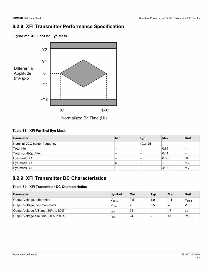
Broadcom Confidential 53161XU-DS10081
BCM53161XU Data Sheet Ultra-Low Power Layer2 GE/FE Switch with 10G Uplinks
8.2.8 XFI Transmitter Performance Specification
Figure 21: XFI Far-End Eye Mask
8.2.9 XFI Transmitter DC Characteristics
Table 33: XFI Far-End Eye Mask
Parameter Min. Typ. Max. Unit
Nominal VCO center frequency – 10.3125 – –
Total jitter – – 0.61 –
Total non-EQJ Jitter – – 0.41 –
Eye mask X1 – – 0.305 UI
Eye mask Y1 60 – – mV
Eye mask Y1 – – 410 mV
Table 34: XFI Transmitter DC Characteristics
Parameter Symbol Min. Typ. Max. Unit
Output Voltage, differential Vod1V 0.5 1.0 1.1 Vptpd
Output Voltage, common mode Vocm – 0.5 – V
Output Voltage fall time (20% to 80%) tfall 24 – 47 ps
Output Voltage rise time (20% to 80%) trise 24 – 47 Ps
Differential
Applitude
(mV)p-p
Y2
Y1
0
-Y1
-Y2
Normalized Bit Time (UI)
X1 1-X1
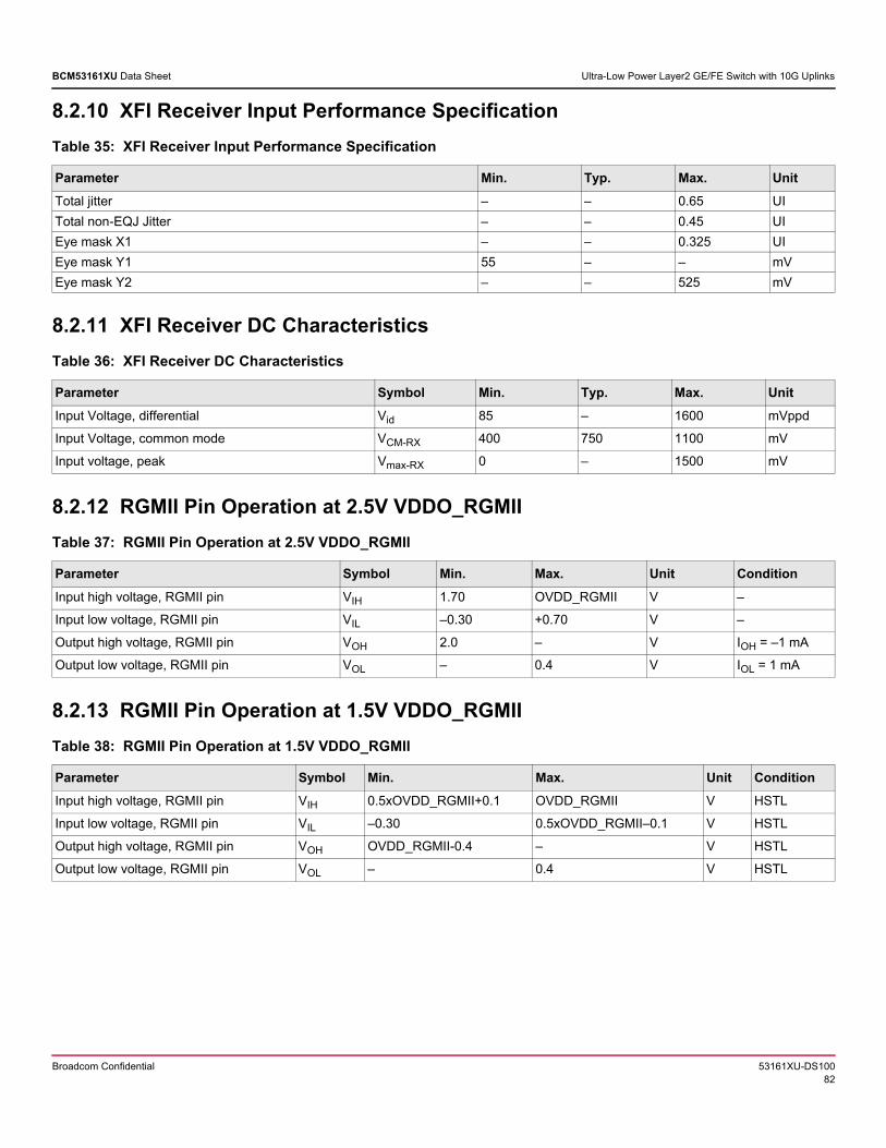
Broadcom Confidential 53161XU-DS10082
BCM53161XU Data Sheet Ultra-Low Power Layer2 GE/FE Switch with 10G Uplinks
8.2.10 XFI Receiver Input Performance Specification
8.2.11 XFI Receiver DC Characteristics
8.2.12 RGMII Pin Operation at 2.5V VDDO_RGMII
8.2.13 RGMII Pin Operation at 1.5V VDDO_RGMII
Table 35: XFI Receiver Input Performance Specification
Parameter Min. Typ. Max. Unit
Total jitter – – 0.65 UI
Total non-EQJ Jitter – – 0.45 UI
Eye mask X1 – – 0.325 UI
Eye mask Y1 55 – – mV
Eye mask Y2 – – 525 mV
Table 36: XFI Receiver DC Characteristics
Parameter Symbol Min. Typ. Max. Unit
Input Voltage, differential Vid 85 – 1600 mVppd
Input Voltage, common mode VCM-RX 400 750 1100 mV
Input voltage, peak Vmax-RX 0 – 1500 mV
Table 37: RGMII Pin Operation at 2.5V VDDO_RGMII
Parameter Symbol Min. Max. Unit Condition
Input high voltage, RGMII pin VIH 1.70 OVDD_RGMII V –
Input low voltage, RGMII pin VIL –0.30 +0.70 V –
Output high voltage, RGMII pin VOH 2.0 – V IOH = –1 mA
Output low voltage, RGMII pin VOL – 0.4 V IOL = 1 mA
Table 38: RGMII Pin Operation at 1.5V VDDO_RGMII
Parameter Symbol Min. Max. Unit Condition
Input high voltage, RGMII pin VIH 0.5xOVDD_RGMII+0.1 OVDD_RGMII V HSTL
Input low voltage, RGMII pin VIL –0.30 0.5xOVDD_RGMII–0.1 V HSTL
Output high voltage, RGMII pin VOH OVDD_RGMII-0.4 – V HSTL
Output low voltage, RGMII pin VOL – 0.4 V HSTL
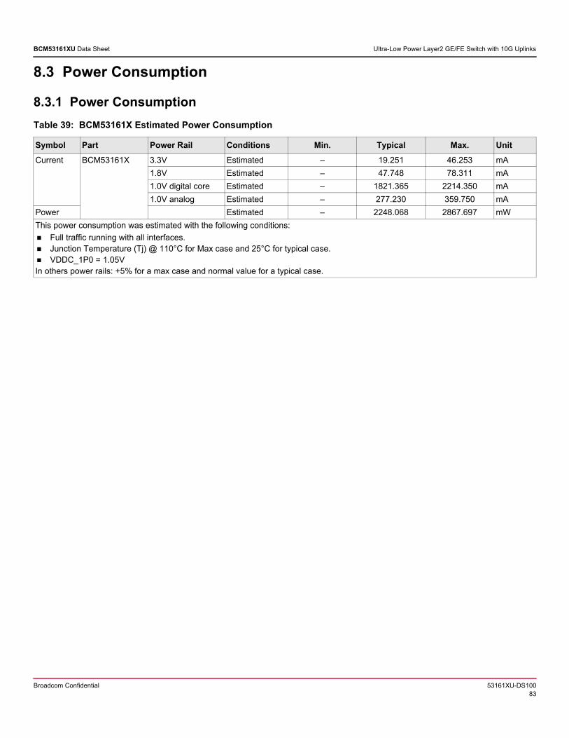
Broadcom Confidential 53161XU-DS10083
BCM53161XU Data Sheet Ultra-Low Power Layer2 GE/FE Switch with 10G Uplinks
8.3 Power Consumption
8.3.1 Power Consumption
Table 39: BCM53161X Estimated Power Consumption
Symbol Part Power Rail Conditions Min. Typical Max. Unit
Current BCM53161X 3.3V Estimated – 19.251 46.253 mA
1.8V Estimated – 47.748 78.311 mA
1.0V digital core Estimated – 1821.365 2214.350 mA
1.0V analog Estimated – 277.230 359.750 mA
Power Estimated – 2248.068 2867.697 mW
This power consumption was estimated with the following conditions:
Full traffic running with all interfaces. Junction Temperature (Tj) @ 110°C for Max case and 25°C for typical case. VDDC_1P0 = 1.05VIn others power rails: +5% for a max case and normal value for a typical case.
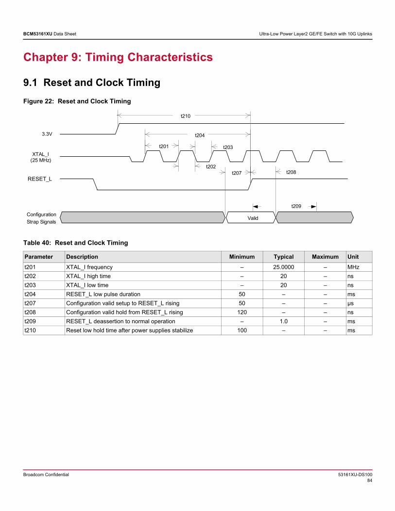
Broadcom Confidential 53161XU-DS10084
BCM53161XU Data Sheet Ultra-Low Power Layer2 GE/FE Switch with 10G Uplinks
Chapter 9: Timing Characteristics
9.1 Reset and Clock Timing
Figure 22: Reset and Clock Timing
Table 40: Reset and Clock Timing
Parameter Description Minimum Typical Maximum Unit
t201 XTAL_I frequency – 25.0000 – MHz
t202 XTAL_I high time – 20 – ns
t203 XTAL_I low time – 20 – ns
t204 RESET_L low pulse duration 50 – – ms
t207 Configuration valid setup to RESET_L rising 50 – – μs
t208 Configuration valid hold from RESET_L rising 120 – – ns
t209 RESET_L deassertion to normal operation – 1.0 – ms
t210 Reset low hold time after power supplies stabilize 100 – – ms
3.3V
XTAL_I(25 MHz)
RESET_L
Configuration
Strap SignalsValid
t201
t202
t203
t204
t207 t208
t209
t210
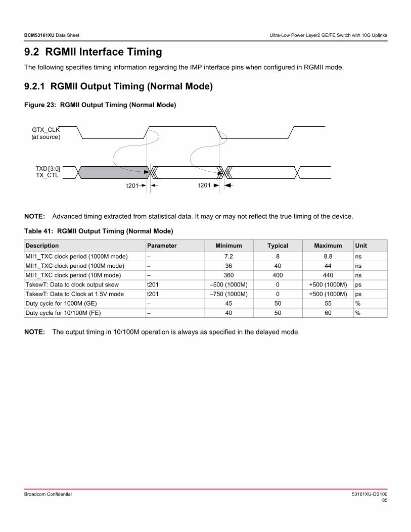
Broadcom Confidential 53161XU-DS10085
BCM53161XU Data Sheet Ultra-Low Power Layer2 GE/FE Switch with 10G Uplinks
9.2 RGMII Interface TimingThe following specifies timing information regarding the IMP interface pins when configured in RGMII mode.
9.2.1 RGMII Output Timing (Normal Mode)
Figure 23: RGMII Output Timing (Normal Mode)
NOTE: Advanced timing extracted from statistical data. It may or may not reflect the true timing of the device.
NOTE: The output timing in 10/100M operation is always as specified in the delayed mode.
Table 41: RGMII Output Timing (Normal Mode)
Description Parameter Minimum Typical Maximum Unit
MII1_TXC clock period (1000M mode) – 7.2 8 8.8 ns
MII1_TXC clock period (100M mode) – 36 40 44 ns
MII1_TXC clock period (10M mode) – 360 400 440 ns
TskewT: Data to clock output skew t201 –500 (1000M) 0 +500 (1000M) ps
TskewT: Data to Clock at 1.5V mode t201 –750 (1000M) 0 +500 (1000M) ps
Duty cycle for 1000M (GE) – 45 50 55 %
Duty cycle for 10/100M (FE) – 40 50 60 %
GTX_CLK(at source)
TX_CTL
t201
TXD[3:0]
t201
Broadcom Confidential 53161XU-DS10086
BCM53161XU Data Sheet Ultra-Low Power Layer2 GE/FE Switch with 10G Uplinks
9.2.2 RGMII Output Timing (Delayed Mode)
Figure 24: RGMII Output Timing (Delayed Mode)
NOTE: Advanced timing extracted from statistical data. It may or may not reflect the true timing of the device.
Table 42: RGMII Output Timing (Delayed Mode)
Description Parameter Minimum Typical Maximum Unit
MII1_TXC clock period (1000M mode) – 7.2 8 8.8 ns
MII1_TXC clock period (100M mode) – 36 40 44 ns
MII1_TXC clock period (10M mode) – 360 400 440 ns
TsetupT
Data valid to clock transition: Available setup time at the output source (delayed mode)
t201D 1.2 (all speeds)
2.0 – ns
TholdT
Clock transition to data valid: Available hold time at the output source (delayed mode)
t202D 1.2(all speeds)
2.0 – ns
TsetupT
Data valid to clock transition: Available setup time at the output source (1.5V mode)
t201D 1.0 (all speeds)
2.0 – ns
TholdT
Clock transition to data valid: Available hold time at the output source (1.5V mode)
t202D 1.0 (all speeds)
2.0 – ns
Duty cycle for 1000M (GE) – 45 50 55 %
Duty cycle for 10/100M (FE) – 40 50 60 %
Delayed
GTX_CLK(actual output
at source)
TX_CTRL
t201D
TXD[3:0]
t201D
t202D
t202D
GTX_CLK(internal)
Broadcom Confidential 53161XU-DS10087
BCM53161XU Data Sheet Ultra-Low Power Layer2 GE/FE Switch with 10G Uplinks
9.2.3 RGMII Input Timing (Normal Mode)
Figure 25: RGMII Input Timing (Normal Mode)
NOTE: Advanced timing extracted from statistical data. It may or may not reflect the true timing of the device.
9.2.4 RGMII Input Timing (Delayed Mode)
Figure 26: RGMII Input Timing (Delayed Mode)
Table 43: RGMII Input Timing (Normal Mode)
Description Parameter Minimum Typical Maximum Unit
MII1_RXC clock period (1000M mode) – 7.2 8 8.8 ns
MII1_RXC clock period (100M mode) – 36 40 44 ns
MII1_RXC clock period (10M mode) – 360 400 440 ns
TsetupR Input setup time: Valid data to clock
t301 1.0 2.0 – ns
TholdR Input hold time: Clock to valid data
t302 1.0 2.0 – ns
Duty cycle for 1000M (GE) – 45 50 55 %
Duty cycle for 10/100M (FE) – 40 50 60 %
RXCLK(internal)
RX_CTRLRXD[3:0]
RXCLK(actual )
t302 t301
t302t301
RXCLK(internal)
RX_CTRLRXD[3:0]
RXCLK(actual )
t302 t301
t302t301
Broadcom Confidential 53161XU-DS10088
BCM53161XU Data Sheet Ultra-Low Power Layer2 GE/FE Switch with 10G Uplinks
NOTE: Advanced timing extracted from statistical data. It may or may not reflect the true timing of the device.
9.3 MDC/MDIO Timing
The following specifies timing information regarding the MDC/MDIO interface pins.
Figure 27: MDC/MDIO Timing (Slave Mode)
NOTE: Advanced timing extracted from statistical data. It may or may not reflect the true timing of the device.
Table 44: RGMII Input Timing (Delayed Mode)
Description Parameter Minimum Typical Maximum Unit
TsetupR
Input setup time (delayed mode)
t301D –1.0 (1000M) – – ns
–1.0 (10/100M) – – ns
TholdR
Input hold time (delayed mode)
t302D 3.0 (1000M) – – ns
9.0 (10/100M) – – ns
Table 45: MDC/MDIO Timing (Slave Mode)
Description Parameter Minimum Typical Maximum Unit
MDC cycle time t401 80 – – ns
MDC high/low – 30 – – ns
MDC rise/fall time t402 – – 10 ns
MDIO input setup time to MDC rising t403 7.5 – – ns
MDIO input hold time from MDC rising t404 7.5 – – ns
MDIO output delay from MDC rising t405 0 – 45 ns
MDIO
(Input)
MDC
MDIO
(Output)
t405
t403
t401
t404
t402
t402
Broadcom Confidential 53161XU-DS10089
BCM53161XU Data Sheet Ultra-Low Power Layer2 GE/FE Switch with 10G Uplinks
Figure 28: MDC/MDIO Timing (Master Mode)
9.4 Serial Flash Timing
Figure 29: Serial Flash Timing Diagram
Table 46: MDC/MDIO Timing (Master Mode)
Description Parameter Minimum Typical Maximum Unit
MDC cycle time t401 400 – – ns
MDC high/low – 160 – 240 ns
MDC rise/fall time t402 – – 10 ns
MDIO input setup time to MDC rising t403 20 – – ns
MDIO input hold time from MDC rising t404 7.5 – – ns
MDIO output delay from MDC rising t405 0 – 30 ns
MDIO
(Into PHY)
MDC
MDIO
(From PHY)
t405m
t403
t401
t404
t402
t402
Din
Dout
SFLASH_CLK
SFLASH_IO3~0(Read)
SFLASH_IO3~0(Write)
T2
T4
Tp
SFLASH_CS_L
T1
T3
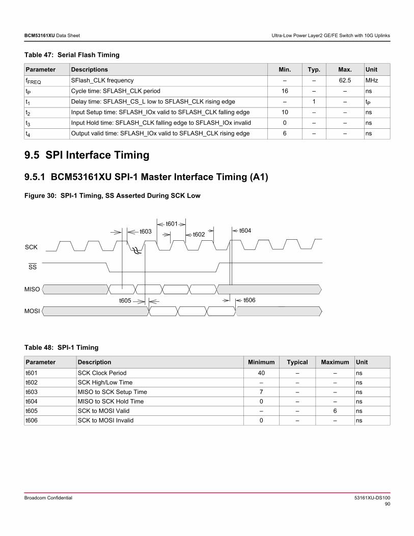
Broadcom Confidential 53161XU-DS10090
BCM53161XU Data Sheet Ultra-Low Power Layer2 GE/FE Switch with 10G Uplinks
9.5 SPI Interface Timing
9.5.1 BCM53161XU SPI-1 Master Interface Timing (A1)
Figure 30: SPI-1 Timing, SS Asserted During SCK Low
Table 47: Serial Flash Timing
Parameter Descriptions Min. Typ. Max. Unit
fFREQ SFlash_CLK frequency – – 62.5 MHz
tP Cycle time: SFLASH_CLK period 16 – – ns
t1 Delay time: SFLASH_CS_L low to SFLASH_CLK rising edge – 1 – tP
t2 Input Setup time: SFLASH_IOx valid to SFLASH_CLK falling edge 10 – – ns
t3 Input Hold time: SFLASH_CLK falling edge to SFLASH_IOx invalid 0 – – ns
t4 Output valid time: SFLASH_IOx valid to SFLASH_CLK rising edge 6 – – ns
Table 48: SPI-1 Timing
Parameter Description Minimum Typical Maximum Unit
t601 SCK Clock Period 40 – – ns
t602 SCK High/Low Time – – – ns
t603 MISO to SCK Setup Time 7 – – ns
t604 MISO to SCK Hold Time 0 – – ns
t605 SCK to MOSI Valid – – 6 ns
t606 SCK to MOSI Invalid 0 – – ns
SCK
SS
MISO
MOSI
t601
t602t603 t604
t605 t606
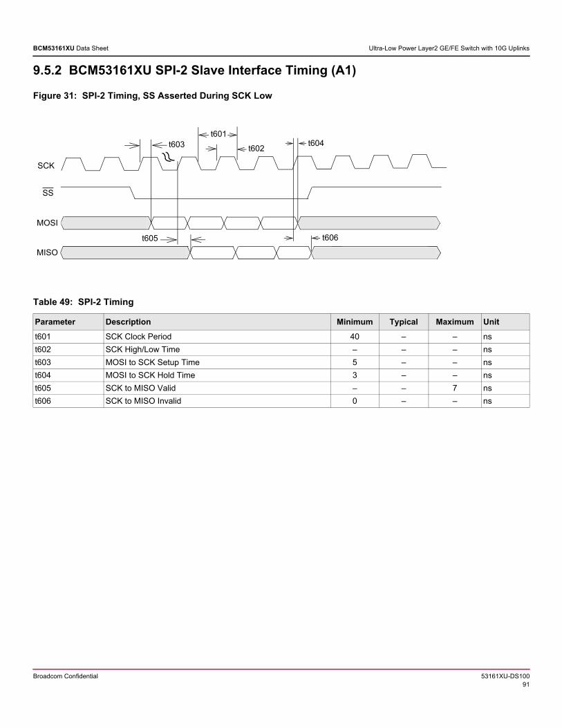
Broadcom Confidential 53161XU-DS10091
BCM53161XU Data Sheet Ultra-Low Power Layer2 GE/FE Switch with 10G Uplinks
9.5.2 BCM53161XU SPI-2 Slave Interface Timing (A1)
Figure 31: SPI-2 Timing, SS Asserted During SCK Low
Table 49: SPI-2 Timing
Parameter Description Minimum Typical Maximum Unit
t601 SCK Clock Period 40 – – ns
t602 SCK High/Low Time – – – ns
t603 MOSI to SCK Setup Time 5 – – ns
t604 MOSI to SCK Hold Time 3 – – ns
t605 SCK to MISO Valid – – 7 ns
t606 SCK to MISO Invalid 0 – – ns
SCK
SS
MOSI
MISO
t601
t602t603 t604
t605 t606
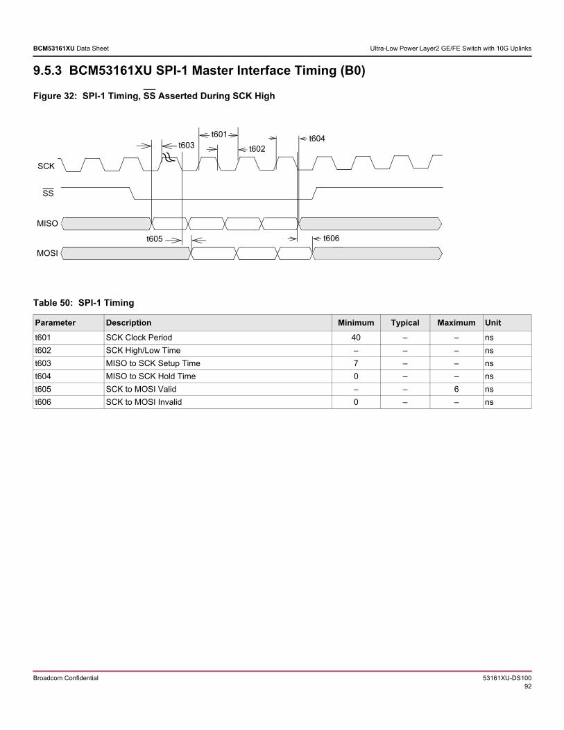
Broadcom Confidential 53161XU-DS10092
BCM53161XU Data Sheet Ultra-Low Power Layer2 GE/FE Switch with 10G Uplinks
9.5.3 BCM53161XU SPI-1 Master Interface Timing (B0)
Figure 32: SPI-1 Timing, SS Asserted During SCK High
Table 50: SPI-1 Timing
Parameter Description Minimum Typical Maximum Unit
t601 SCK Clock Period 40 – – ns
t602 SCK High/Low Time – – – ns
t603 MISO to SCK Setup Time 7 – – ns
t604 MISO to SCK Hold Time 0 – – ns
t605 SCK to MOSI Valid – – 6 ns
t606 SCK to MOSI Invalid 0 – – ns
SCK
SS
MISO
MOSI
t601
t602t603t604
t605 t606
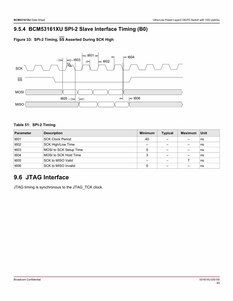
Broadcom Confidential 53161XU-DS10093
BCM53161XU Data Sheet Ultra-Low Power Layer2 GE/FE Switch with 10G Uplinks
9.5.4 BCM53161XU SPI-2 Slave Interface Timing (B0)
Figure 33: SPI-2 Timing, SS Asserted During SCK High
9.6 JTAG Interface
JTAG timing is synchronous to the JTAG_TCK clock.
Table 51: SPI-2 Timing
Parameter Description Minimum Typical Maximum Unit
t601 SCK Clock Period 40 – – ns
t602 SCK High/Low Time – – – ns
t603 MOSI to SCK Setup Time 5 – – ns
t604 MOSI to SCK Hold Time 3 – – ns
t605 SCK to MISO Valid – – 7 ns
t606 SCK to MISO Invalid 0 – – ns
SCK
SS
MOSI
MISO
t601
t602t603t604
t605 t606
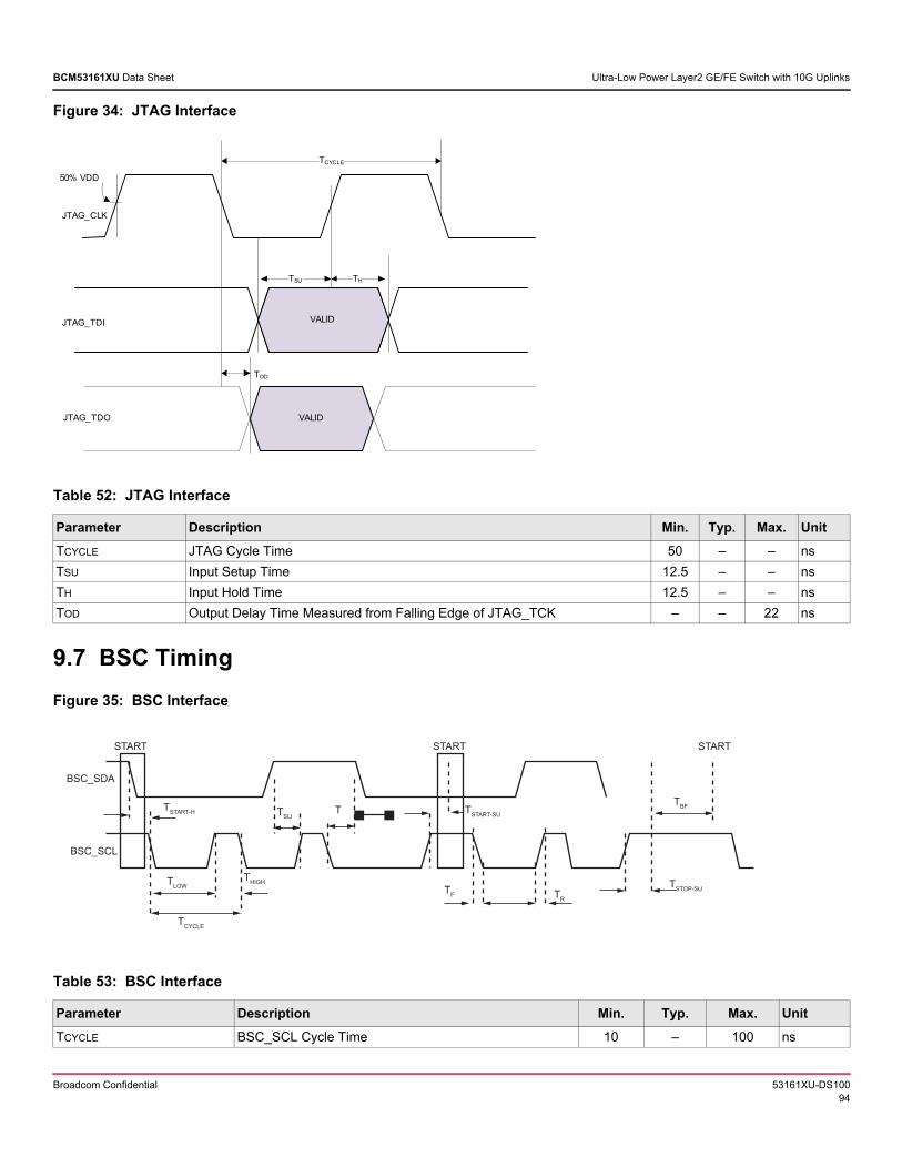
Broadcom Confidential 53161XU-DS10094
BCM53161XU Data Sheet Ultra-Low Power Layer2 GE/FE Switch with 10G Uplinks
Figure 34: JTAG Interface
9.7 BSC Timing
Figure 35: BSC Interface
Table 52: JTAG Interface
Parameter Description Min. Typ. Max. Unit
TCYCLE JTAG Cycle Time 50 – – ns
TSU Input Setup Time 12.5 – – ns
TH Input Hold Time 12.5 – – ns
TOD Output Delay Time Measured from Falling Edge of JTAG_TCK – – 22 ns
Table 53: BSC Interface
Parameter Description Min. Typ. Max. Unit
TCYCLE BSC_SCL Cycle Time 10 – 100 ns
TCYCLE
TSU TH
JTAG_TDI
JTAG_TDO
50% VDD
JTAG_CLK
TOD
VALID
VALID
START START START
TSTART-SUT
SU
TSTART-H
THIGHT
LOW
TCYCLE
BSC_SDA
BSC_SCL
T
TF T
R
TBF
TSTOP-SU
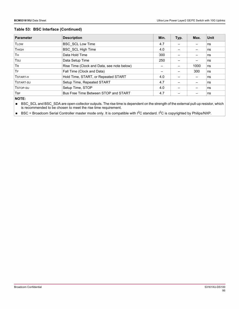
Broadcom Confidential 53161XU-DS10095
BCM53161XU Data Sheet Ultra-Low Power Layer2 GE/FE Switch with 10G Uplinks
TLOW BSC_SCL Low Time 4.7 – – ns
THIGH BSC_SCL High Time 4.0 – – ns
TH Data Hold Time 300 – – ns
TSU Data Setup Time 250 – – ns
TR Rise Time (Clock and Data, see note below) – – 1000 ns
TF Fall Time (Clock and Data) – – 300 ns
TSTART-H Hold Time, START, or Repeated START 4.0 – – ns
TSTART-SU Setup Time, Repeated START 4.7 – – ns
TSTOP-SU Setup Time, STOP 4.0 – – ns
TBF Bus Free Time Between STOP and START 4.7 – – ns
NOTE:
BSC_SCL and BSC_SDA are open-collector outputs. The rise time is dependent on the strength of the external pull-up resistor, which is recommended to be chosen to meet the rise time requirement.
BSC = Broadcom Serial Controller master mode only. It is compatible with I2C standard. I2C is copyrighted by Philips/NXP.
Table 53: BSC Interface (Continued)
Parameter Description Min. Typ. Max. Unit
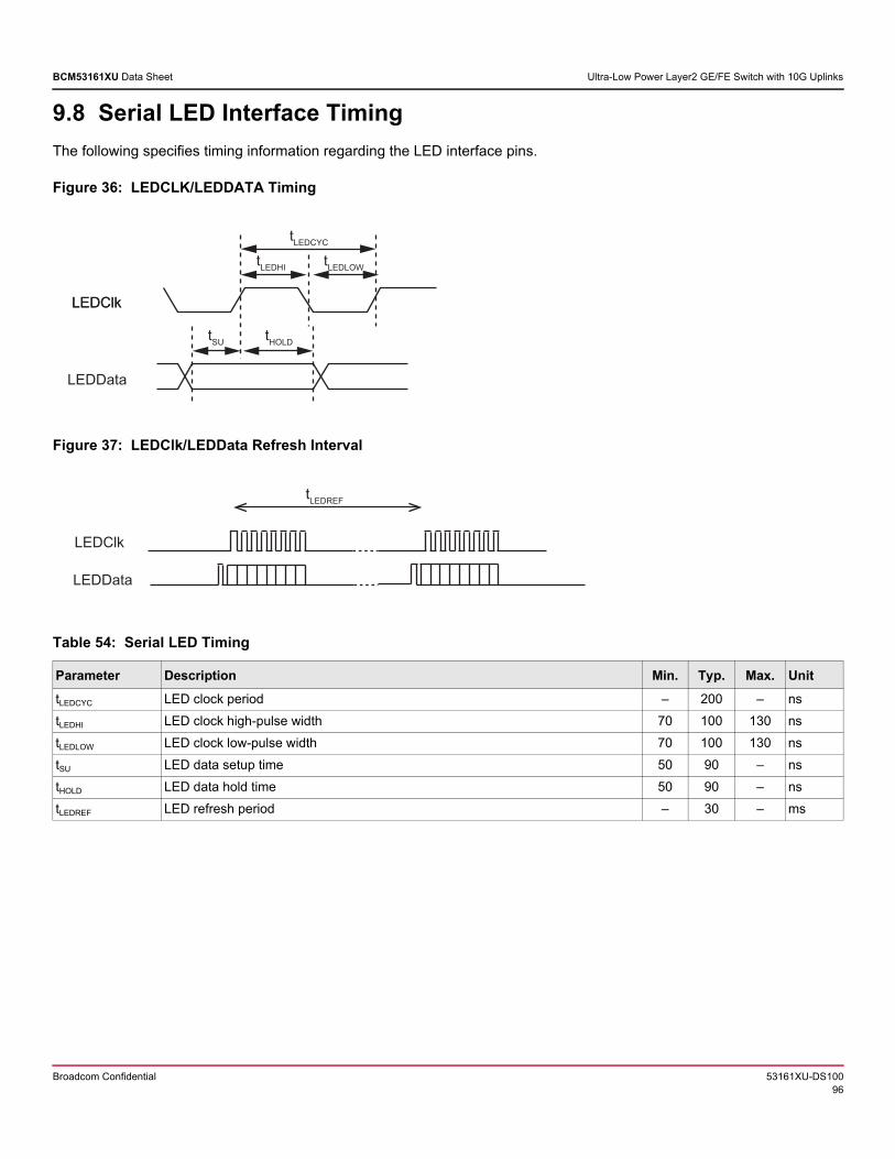
Broadcom Confidential 53161XU-DS10096
BCM53161XU Data Sheet Ultra-Low Power Layer2 GE/FE Switch with 10G Uplinks
9.8 Serial LED Interface Timing
The following specifies timing information regarding the LED interface pins.
Figure 36: LEDCLK/LEDDATA Timing
Figure 37: LEDClk/LEDData Refresh Interval
Table 54: Serial LED Timing
Parameter Description Min. Typ. Max. Unit
tLEDCYC LED clock period – 200 – ns
tLEDHI LED clock high-pulse width 70 100 130 ns
tLEDLOW LED clock low-pulse width 70 100 130 ns
tSU LED data setup time 50 90 – ns
tHOLD LED data hold time 50 90 – ns
tLEDREF LED refresh period – 30 – ms
LEDClk
LEDData
LEDClk
tLEDCYC
tLEDLOW
tLEDHI
tHOLD
tSU
LEDData
LEDClk
tLEDREF
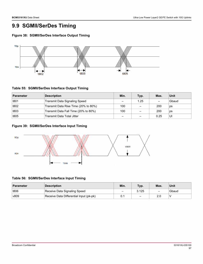
Broadcom Confidential 53161XU-DS10097
BCM53161XU Data Sheet Ultra-Low Power Layer2 GE/FE Switch with 10G Uplinks
9.9 SGMII/SerDes Timing
Figure 38: SGMII/SerDes Interface Output Timing
Figure 39: SGMII/SerDes Interface Input Timing
Table 55: SGMII/SerDes Interface Output Timing
Parameter Description Min. Typ. Max. Unit
t801 Transmit Data Signaling Speed – 1.25 – Gbaud
t802 Transmit Data Rise Time (20% to 80%) 100 – 200 ps
t803 Transmit Data Fall Time (20% to 80%) 100 – 200 ps
t805 Transmit Data Total Jitter – – 0.25 UI
Table 56: SGMII/SerDes Interface Input Timing
Parameter Description Min. Typ. Max. Unit
t806 Receive Data Signaling Speed – 3.125 – Gbaud
v809 Receive Data Differential Input (pk-pk) 0.1 – 2.0 V
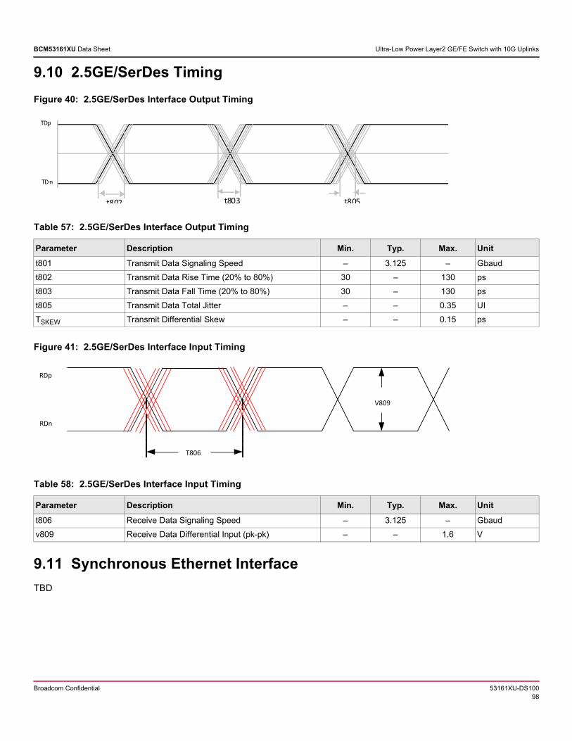
Broadcom Confidential 53161XU-DS10098
BCM53161XU Data Sheet Ultra-Low Power Layer2 GE/FE Switch with 10G Uplinks
9.10 2.5GE/SerDes Timing
Figure 40: 2.5GE/SerDes Interface Output Timing
Figure 41: 2.5GE/SerDes Interface Input Timing
9.11 Synchronous Ethernet Interface
TBD
Table 57: 2.5GE/SerDes Interface Output Timing
Parameter Description Min. Typ. Max. Unit
t801 Transmit Data Signaling Speed – 3.125 – Gbaud
t802 Transmit Data Rise Time (20% to 80%) 30 – 130 ps
t803 Transmit Data Fall Time (20% to 80%) 30 – 130 ps
t805 Transmit Data Total Jitter – – 0.35 UI
TSKEW Transmit Differential Skew – – 0.15 ps
Table 58: 2.5GE/SerDes Interface Input Timing
Parameter Description Min. Typ. Max. Unit
t806 Receive Data Signaling Speed – 3.125 – Gbaud
v809 Receive Data Differential Input (pk-pk) – – 1.6 V
t802 t803
TDp
t805
TDn
T806
V809
RDn
RDp
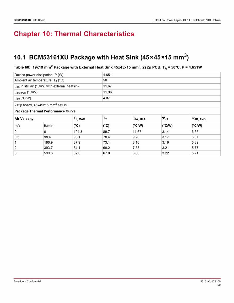
Broadcom Confidential 53161XU-DS10099
BCM53161XU Data Sheet Ultra-Low Power Layer2 GE/FE Switch with 10G Uplinks
Chapter 10: Thermal Characteristics
10.1 BCM53161XU Package with Heat Sink (45×45×15 mm3)
Table 60: 19x19 mm2 Package with External Heat Sink 45x45x15 mm3, 2s2p PCB, TA = 50°C, P = 4.651W
Device power dissipation, P (W) 4.651
Ambient air temperature, TA (°C) 50
θJA in still air (°C/W) with external heatsink 11.67
θJB/AVG (°C/W) 11.96
θJC (°C/W) 4.07
2s2p board, 45x45x15 mm3 estHS
Package Thermal Performance Curve
Air Velocity TJ, MAX TT θJA, JMA ΨJT ΨJB, AVG
m/s ft/min (°C) (°C) (°C/W) (°C/W) (°C/W)
0 0 104.3 89.7 11.67 3.14 6.35
0.5 98.4 93.1 78.4 9.28 3.17 6.07
1 196.9 87.9 73.1 8.16 3.19 5.89
2 393.7 84.1 69.2 7.33 3.21 5.77
3 590.6 82.0 67.0 6.88 3.22 5.71
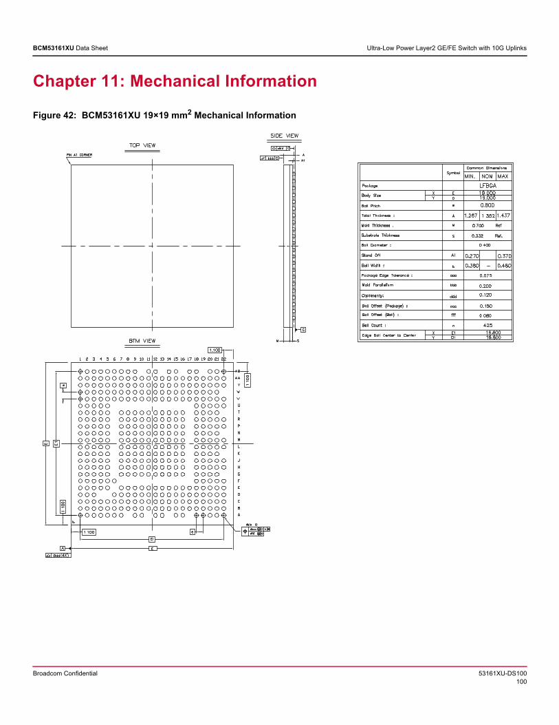
Broadcom Confidential 53161XU-DS100100
BCM53161XU Data Sheet Ultra-Low Power Layer2 GE/FE Switch with 10G Uplinks
Chapter 11: Mechanical Information
Figure 42: BCM53161XU 19×19 mm2 Mechanical Information
Broadcom Confidential 53161XU-DS100101
BCM53161XU Data Sheet Ultra-Low Power Layer2 GE/FE Switch with 10G Uplinks
Chapter 12: Ordering Information
Table 61: Ordering Information
Part Number Operational Mode Package Ambient Temperature
BCM53161XUB1KLFBG Unmanaged 19×19 mm2, 425-pin FBGA 0°C to 70°C
Broadcom Confidential 53161XU-DS100102
BCM53161XU Data Sheet Ultra-Low Power Layer2 GE/FE Switch with 10G Uplinks
Revision History
53161XU-DS100-R; April 11, 2018
Initial release.

Broadcom, the pulse logo, Connecting everything, ContentAware, RoboSwitch, Warpcore, Avago Technologies, Avago, and the A logo are among the trademarks of Broadcom and/or its affiliates in the United States, certain other countries and/or the EU.
Copyright © 2018 by Broadcom. All Rights Reserved.
The term “Broadcom” refers to Broadcom Inc. and/or its subsidiaries. For more information, please visit www.broadcom.com.
Broadcom reserves the right to make changes without further notice to any products or data herein to improve reliability, function, or design. Information furnished by Broadcom is believed to be accurate and reliable. However, Broadcom does not assume any liability arising out of the application or use of this information, nor the application or use of any product or circuit described herein, neither does it convey any license under its patent rights nor the rights of others.